

Page 1

g
Title P
age
GE Industrial Systems
489
Generator Management Relay
COMMUNICATIONS GUIDE
Software Revision: 3.00
GE Publication Code: GEK-106495A
GE Multilin Part Number: 1601-0149-A2
Copyright © 2004 GE Multilin
GE Multilin
215 Anderson Avenue, Markham, Ontario
Canada L6E 1B3
Tel: (905) 294-6222 Fax: (905) 201-2098
Internet: http://www.GEindustrial.com/multilin
T
E
S
I
R
E
G
D
E
R
ISO9001:2000
G
E
GE Multilin's Quality Management
System is registered to
ISO9001:2000
QMI # 005094
UL # A3775
N
I
M
L
I
U
T
L
Page 2

Page 3

Tabl
e of Contents
Communications Guide
489
Table of Contents
MODBUS PROTOCOL Electrical Interface.................................................................................................................................. 1
MODBUS FUNCTIONS Supported Functions ............................................................................................................................. 3
MODBUS MEMORY MAP Memory Map Information..................................................................................................................... 9
DNP PROTOCOL Device Profile Document..................................................................................................................... 46
DNP POINT LISTS Binary Input / Binary Input Change (Objects 01/02) .......................................................................... 49
Modbus RTU Description...................................................................................................................... 1
Data Frame Format and Data Rate ....................................................................................................... 1
Data Packet Format................................................................................................................................ 2
CRC-16 Algorithm .................................................................................................................................. 3
Timing..................................................................................................................................................... 3
Function Codes 03/04: Read Setpoints / Actual Values ...................................................................... 4
Function Code 05: Execute Operation.................................................................................................. 5
Function Code 06: Store Single Setpoint............................................................................................. 5
Function Code 07: Read Device Status ................................................................................................ 6
Function Code 08: Loopback Test......................................................................................................... 6
Function Code 16: Store Multiple Setpoints........................................................................................ 7
Function Code 16: Performing Commands ......................................................................................... 8
Error Responses..................................................................................................................................... 8
User-Definable Memory Map Area ...................................................................................................... 9
Event Recorder....................................................................................................................................... 9
Waveform Capture .............................................................................................................................. 10
Dual Setpoints...................................................................................................................................... 10
Passcode Operation............................................................................................................................. 10
489 Memory Map................................................................................................................................. 11
Memory Map Data Formats................................................................................................................ 40
Implementation Table ......................................................................................................................... 47
Default Variations ................................................................................................................................ 48
Binary / Control Relay Output Block (Objects 10/12)......................................................................... 51
Binary / Frozen Counter (Objects 20/21)............................................................................................. 52
Analog Input / Input Change (Objects 30/32).....................................................................................53
GE Multilin
http://www.GEindustrial.com/multilin
i
Page 4

Communications Guide
Table of Contents489
ii
http://www.GEindustrial.com/multilin
GE Multilin
Page 5

Modbus Protocol
Communications Guide
489 Communications Guide
GE Publication Code: GEK-106495A
GE Multilin Part Number: 1601-0149-A2
Copyright © 2004 GE Multilin
Modbus Protocol
Electrical Interface The hardware or electrical interface is one of the following: one of two 2-wire RS485
ports from the rear terminal connector or the RS232 from the front panel connector.
In a 2-wire RS485 link, data flow is bidirectional. Data flow is half-duplex for both
the RS485 and the RS232 ports. That is, data is never transmitted and received at
the same time. RS485 lines should be connected in a daisy chain configuration
(avoid star connections) with a terminating network installed at each end of the link,
i.e. at the master end and at the slave farthest from the master. The terminating
network should consist of a 120 Ω resistor in series with a 1 nF ceramic capacitor
when used with Belden 9841 RS485 wire. The value of the terminating resistors
should be equal to the characteristic impedance of the line. This is approximately
120 Ω for standard #22 AWG twisted pair wire. Shielded wire should always be used
to minimize noise. Polarity is important in RS485 communications. Each '+' terminal
of every 489 must be connected together for the system to operate. Refer to the
489 Instruction Manual for correct serial port wiring.
489
Modbus RTU
Description
Data Frame Format and
Data Rate
GE Multilin
The 489 implements a subset of the AEG Modicon Modbus RTU serial communication
standard. Many popular programmable controllers support this protocol directly with
a suitable interface card allowing direct connection of relays. Although the Modbus
protocol is hardware independent, the 489 interfaces include two 2-wire RS485
ports and one RS232 port. Modbus is a single master, multiple slave protocol
suitable for a multi-drop configuration as provided by RS485 hardware. In this
configuration up to 32 slaves can be daisy-chained together on a single
communication channel.
The 489 is always a slave; it cannot be programmed as a master. Computers or
PLCs are commonly programmed as masters. The Modbus protocol exists in two
versions: Remote Terminal Unit (RTU, binary) and ASCII. Only the RTU version is
supported by the 489. Monitoring, programming, and control functions are
performed with read/write register commands.
One data frame of an asynchronous transmission to or from a 489 is default to 1
start bit, 8 data bits, and 1 stop bit. This produces a 10-bit data frame. This is
important for transmission through modems at high bit rates (11 bit data frames are
not supported by Hayes modems at bit rates of greater than 300 bps). The parity bit
is optional as odd or even. If it is programmed as odd or even, the data frame
consists of 1 start bit, 8 data bits, 1 parity bit, and 1 stop bit.
Modbus protocol can be implemented at any standard communication speed. The
489 RS485 ports support operation at 1200, 2400, 4800, 9600, and 19200 baud.
The front panel RS232 baud rate is fixed at 9600 baud.
http://www.GEindustrial.com/multilin
1
Page 6

Modbus Protocol489
Communications Guide
Data Packet Format A complete request/response sequence consists of the following bytes (transmitted
as separate data frames):
1. A Master Query Message consisting of: a 1-byte Slave Address, a 1-byte Func-
tion Code, a variable number of Data Bytes depending on the Function Code,
and a 2-byte CRC code.
2. A Slave Response Message consisting of: a 1-byte Slave Address, a 1-byte
Function Code, a variable number of Data Bytes depending on the Function
Code, and a 2-byte CRC code.
The terms Slave Address, Function Code, Data Bytes, and CRC are explained below:
• SLAVE ADDRESS: This is the first byte of every transmission. This byte
represents the user-assigned address of the slave device that is to receive the
message sent by the master. Each slave device must be assigned a unique
address and only the addressed slave will respond to a transmission that starts
with its address. In a master request transmission the Slave Address represents
the address of the slave to which the request is being sent. In a slave response
transmission the Slave Address represents the address of the slave that is
sending the response. The RS232 port ignores the slave address, so it will
respond regardless of the value in the message. Note: A master transmission
with a Slave Address of 0 indicates a broadcast command. Broadcast commands
can be used for specific functions.
• FUNCTION CODE: This is the second byte of every transmission. Modbus
defines function codes of 1 to 127. The 489 implements some of these
functions. In a master request transmission the Function Code tells the slave
what action to perform. In a slave response transmission if the Function Code
sent from the slave is the same as the Function Code sent from the master
indicating the slave performed the function as requested. If the high order bit of
the Function Code sent from the slave is a 1 (i.e. if the Function Code is greater
than 127) then the slave did not perform the function as requested and is
sending an error or exception response.
• DATA BYTES: This is a variable number of bytes depending on the Function
Code. These may be actual values, setpoints, or addresses sent by the master
to the slave or vice-versa. Data is sent MSByte first followed by the LSByte.
• CRC: This is a two byte error checking code. CRC is sent LSByte first followed
by the MSByte. The RTU version of Modbus includes a two byte CRC-16 (16-bit
cyclic redundancy check) with every transmission. The CRC-16 algorithm
essentially treats the entire data stream (data bits only; start, stop and parity
ignored) as one continuous binary number. This number is first shifted left 16
bits and then divided by a characteristic polynomial (11000000000000101B).
The 16-bit remainder of the division is appended to the end of the transmission,
LSByte first. The resulting message including CRC, when divided by the same
polynomial at the receiver will give a zero remainder if no transmission errors
have occurred.
If a 489 Modbus slave device receives a transmission in which an error is indicated
by the CRC-16 calculation, the slave device will not respond to the transmission. A
CRC-16 error indicates than one or more bytes of the transmission were received
incorrectly and thus the entire transmission should be ignored in order to avoid the
489 performing any incorrect operation. The CRC-16 calculation is an industry
standard method used for error detection. An algorithm is included here to assist
programmers in situations where no standard CRC-16 calculation routines are
available.
2
http://www.GEindustrial.com/multilin
GE Multilin
Page 7

Modbus Functions
Communications Guide
CRC-16 Algorithm Once the following algorithm is complete, the working register “A” will contain the
CRC value to be transmitted. Note that this algorithm requires the characteristic
polynomial to be reverse bit ordered. The MSbit of the characteristic polynomial is
dropped since it does not affect the value of the remainder.
The symbols used in the algorithm are shown below:
--> data transfer
A
; A
; A
low
CRC 16 bit CRC-16 result
i, j loop counters
(+) logical EXCLUSIVE-OR operator
N total number of data bytes
D
i
G 16 bit characteristic polynomial = 1010000000000001 (binary)
shr (x) right shift operator (the LSbit of x is shifted into a carry flag, a '0' is
The CRC algorithm is shown below:
1. FFFF (hex) --> A
2. 0 --> i
3. 0 --> j
4. D
(+) A
i
5. j + 1 --> j
6. shr (A)
7. Is there a carry? No: go to step 8.
8. Is j = 8? No: go to 5.; Yes: continue.
9. i + 1 --> i
10. Is i = N? No: go to 3.; Yes: continue.
11. A --> CRC
16-bit working register; low and high order bytes of A (the 16-bit
high
working register)
i-th data byte (i = 0 to N – 1)
with MSbit dropped and bit order reversed
shifted into the MSbit of x, all other bits are shifted right one
location)
--> A
low
low
Yes: G (+) A --> A and continue.
489
Timing Data packet synchronization is maintained by timing constraints. The receiving
device must measure the time between the reception of characters. If three and one
half character times elapse without a new character or completion of the packet,
then the communication link must be reset (i.e. all slaves start listening for a new
transmission from the master). Thus at 9600 baud a delay of greater than 3.5 × 1/
9600 × 10 = 3.65 ms will cause the communication link to be reset.
Modbus Functions
Supported Functions The following functions are supported by the 489:
• Function Codes 03 and 04: Read Setpoints and Actual Values
• Function Code 05: Execute Operation
• Function Code 06: Store Single Setpoint
• Function Code 07: Read Device Status
• Function Code 08: Loopback Test
• Function Code 16: Store Multiple Setpoints
A detailed explanation of how the 489 implements these function codes is shown in
the following sections.
GE Multilin
http://www.GEindustrial.com/multilin
3
Page 8

Communications Guide
Modbus Functions489
Function Codes 03/04:
Read Setpoints / Actual
Value s
Modbus implementation: Read Input and Holding Registers
489 Implementation: Read Setpoints and Actual Values
For the 489 Modbus implementation, these commands are used to read any setpoint
(‘holding registers’) or actual value (‘input registers’). Holding and input registers
are 16-bit (two byte) values transmitted high order byte first. Thus all 489 setpoints
and actual values are sent as two bytes. The maximum of 125 registers can be read
in one transmission. Function codes 03 and 04 are configured to read setpoints or
actual values interchangeably since some PLCs do not support both function codes.
The slave response to these function codes is the slave address, function code, a
count of the number of data bytes to follow, the data itself and the CRC. Each data
item is sent as a two byte number with the high order byte sent first. The CRC is
sent as a two byte number with the low order byte sent first.
Message Format and Example:
Request slave 11 to respond with 2 registers starting at address 0235. For this
example, the register data in these addresses is:
Address Data
0235 0064
0236 000A
Master Transmission Bytes Example Description
Slave Address 1 0B message for slave 11
Function Code 1 03 read register values
Data Starting Address 2 02 32 data starting at 0235h
Number of Setpoints 2 00 02 2 registers = 4 bytes total
CRC (low, high) 2 D5 17 computed CRC error code
Slave Response Bytes Example Description
Slave Address 1 0B message from slave 11
Function Code 1 03 read register values
Byte Count 1 04 2 registers = 4 bytes total
Data #1 (high, low) 2 00 64 value in address 0235h
Data #2 (high, low) 2 00 0A value in address 0236h
CRC (low, high) 2 EB 91 computed CRC error code
4
http://www.GEindustrial.com/multilin
GE Multilin
Page 9
Modbus Functions
Communications Guide
489
Function Code 05:
Execute Operation
Modbus Implementation: Force Single Coil
489 Implementation: Execute Operation
This function code allows the master to request specific 489 command operations.
The command numbers listed in the Commands area of the memory map
correspond to operation code for function code 05. The operation commands can
also be initiated by writing to the Commands area of the memory map using
function code 16. Refer to Section Function Code 16: Store Multiple Setpoints on
page –7 for complete details.
Supported Operations:Reset 489 (operation code 1); Generator Start (operation
code 2);
Generator Stop (operation code 3); Waveform Trigger (operation code 4)
Message Format and Example:
Reset 489 (operation code 1).
Master Transmission Bytes Example Description
Slave Address 1 0B message for slave 11
Function Code 1 05 execute operation
Operation Code 2 00 01 reset command (op code 1)
Code Value 2 FF 00 perform function
CRC (low, high) 2 DD 50 computed CRC error code
Slave Response Bytes Example Description
Slave Address 1 0B message from slave 11
Function Code 1 05 execute operation
Operation Code 2 00 01 reset command (op code 1)
Code Value 2 FF 00 perform function
CRC (low, high) 2 DD 50 computed CRC error code
Function Code 06: Store
Single Setpoint
Modbus Implementation: Preset Single Register
489 Implementation: Store Single Setpoint
This command allows the master to store a single setpoint into the 489 memory.
The slave response to this function code is to echo the entire master transmission.
Message Format and Example:
Request slave 11 to store the value 01F4 in Setpoint address 1180. After the
transmission in this example is complete, Setpoints address 1180 will contain the
value 01F4.
Master Transmission Bytes Example Description
Slave Address 1 0B message for slave 11
Function Code 1 06 store single setpoint
Data Starting Address 2 11 80 setpoint address 1180h
Data 2 01 F4 data for address 1180h
CRC (low, high) 2 8D A3 computed CRC error code
Slave Response Bytes Example Description
Slave Address 1 0B message from slave 11
Function Code 1 06 store single setpoint
Data Starting Address 2 11 80 setpoint address 1180h
Data 2 01 F4 data for address 1180h
CRC (low, high) 2 8D A3 computed CRC error code
GE Multilin
http://www.GEindustrial.com/multilin
5
Page 10
Communications Guide
Modbus Functions489
Function Code 07: Read
Device Status
Modbus Implementation: Read Exception Status
489 Implementation: Read Device Status
This function reads the selected device status. A short message length allows for
rapid reading of status. The returned status byte has individual bits set to 1 or 0
depending on the slave device status. The 489 general status byte is shown below:
BIT DESCRIPTION BIT DESCRIPTION
B0 1 TRIP relay operated = 1 B4 5 ALARM relay operated = 1
B1 2 AUXILIARY relay operated = 1 B5 6 SERVICE relay operated = 1
B2 3 AUXILIARY relay operated = 1 B6 Stopped = 1
B3 4 AUXILIARY relay operated = 1 B7 Running = 1
Note that if status is neither stopped or running, the generator is starting.
Message Format and Example:
Request status from slave 11.
Master Transmission Bytes Example Description
Slave Address 1 0B message for slave 11
Function Code 1 07 read device status
CRC (low, high) 2 47 42 computed CRC error code
Slave Response Bytes Example Description
Slave Address 1 0B message from slave 11
Function Code 1 07 read device status
Device Status 1 59 status = 01011001b
CRC (low, high) 2 C2 08 computed CRC error code
Function Code 08:
Loopback Test
Modbus Implementation: Loopback Test
489 Implementation: Loopback Test
This function is used to test the integrity of the communication link. The 489 will
echo the request.
Message Format and Example:
Loopback test from slave 11.
Master Transmission Bytes Example Description
Slave Address 1 0B message for slave 11
Function Code 1 08 loopback test
Diagnostic Code 2 00 00 must be 0000h
Data 2 00 00 must be 0000h
CRC (low, high) 2 E0 A1 computed CRC error code
Slave Response Bytes Example Description
Slave Address 1 0B message from slave 11
Function Code 1 08 loopback test
Diagnostic Code 2 00 00 must be 0000h
Data 2 00 00 must be 0000h
CRC (low, high) 2 E0 A1 computed CRC error code
6
http://www.GEindustrial.com/multilin
GE Multilin
Page 11
Modbus Functions
Communications Guide
489
Function Code 16: Store
Multiple Setpoints
Modbus Implementation: Preset Multiple Registers
489 Implementation: Store Multiple Setpoints
This function code allows multiple Setpoints to be stored into the 489 memory.
Modbus “registers” are 16-bit (two byte) values transmitted high order byte first.
Thus all 489 setpoints are sent as two bytes. The maximum number of Setpoints
that can be stored in one transmission is dependent on the slave device. Modbus
allows up to a maximum of 60 holding registers to be stored. The 489 response to
this function code is to echo the slave address, function code, starting address, the
number of Setpoints stored, and the CRC.
Message Format and Example:
Request slave 11 to store the value 01F4 to Setpoint address 1180 and the value
0001 to setpoint address 1181. After the transmission in this example is complete,
489 slave 11 will have the following setpoints information stored:
Address Data
1180 01F4
1181 0001
Master Transmission Bytes Example Description
Slave Address 1 0B message for slave 11
Function Code 1 10 store setpoints
Data Starting Address 2 11 80 data starting at 1180h
Number of Setpoints 2 00 02 2 setpoints = 4 bytes total
Byte Count 1 04 2 registers = 4 bytes
Data 1 2 01 F4 data for address 1180h
Data 2 2 00 01 data for address 1181h
CRC (low, high) 2 9B 89 computed CRC error code
Slave Response Bytes Example Description
Slave Address 1 0B message from slave 11
Function Code 1 10 store multiple setpoints
Data Starting Address 2 11 80 data starting at 1180h
Number of Setpoints 2 00 02 2 setpoints (4 bytes total)
CRC (low, high) 2 45 B6 computed CRC error code
GE Multilin
http://www.GEindustrial.com/multilin
7
Page 12

Communications Guide
Modbus Functions489
Function Code 16:
Performing Commands
Some PLCs may not support execution of commands using function code 5 but do
support storing multiple setpoints using function code 16. To perform this operation
using function code 16 (10h), a certain sequence of commands must be written at
the same time to the 489. The sequence consists of: Command Function register,
Command operation register and Command Data (if required). The Command
Function register must be written with the value of 5 indicating an execute operation
is requested. The Command Operation register must then be written with a valid
command operation number from the list of commands shown in the memory map.
The Command Data registers must be written with valid data if the command
operation requires data. The selected command will execute immediately upon
receipt of a valid transmission.
Message Format and Example:
Perform a 489 RESET (operation code 1).
Master Transmission Bytes Example Description
Slave Address 1 0B message for slave 11
Function Code 1 10 store setpoints
Data Starting Address 2 00 80 setpoint address 0080h
Number of Setpoints 2 00 02 2 setpoints = 4 bytes total
Byte Count 1 04 2 registers = 4 bytes
Command Function 2 00 05 data for address 0080h
Command Function 2 00 01 data for address 0081h
CRC (low, high) 2 0B D6 computed CRC error code
Slave Response Bytes Example Description
Slave Address 1 0B message from slave 11
Function Code 1 10 store multiple setpoints
Data Starting Address 2 00 80 setpoint address 0080h
Number of Setpoints 2 00 02 2 setpoints (4 bytes total)
CRC (low, high) 2 40 8A computed CRC error code
Error Responses When a 489 detects an error other than a CRC error, a response will be sent to the
master. The MSbit of the Function Code byte will be set to 1 (i.e. the function code
sent from the slave will be equal to the function code sent from the master plus
128). The following byte will be an exception code indicating the type of error that
occurred.
Transmissions received from the master with CRC errors will be ignored by the 489.
The slave response to an error (other than CRC error) will be:
• SLAVE ADDRESS: 1 byte
• FUNCTION CODE: 1 byte (with MSbit set to 1)
•EXCEPTION CODE: 1 byte
•CRC: 2 bytes
The 489 implements the following exception response codes.
01: ILLEGAL FUNCTION
The function code transmitted is not one of the functions supported by the 489.
02: ILLEGAL DATA ADDRESS
The address referenced in the data field transmitted by the master is not an
allowable address for the 489.
03: ILLEGAL DATA VALUE
The value referenced in the data field transmitted by the master is not within range
for the selected data address.
8
http://www.GEindustrial.com/multilin
GE Multilin
Page 13

Modbus Memory Map
Communications Guide
489
Modbus Memory Map
Memory Map
Information
NOTE
User-Definable
Memory Map Area
The data stored in the 489 is grouped as Setpoints and Actual Values. Setpoints can
be read and written by a master computer. Actual Values are read only. All Setpoints
and Actual Values are stored as two byte values. That is, each register address is
the address of a two-byte value. Addresses are listed in hexadecimal. Data values
(Setpoint ranges, increments, and factory values) are in decimal.
Many Modbus communications drivers add 40001d to the actual address of the
register addresses. For example: if address 0h was to be read, 40001d would be the
address required by the Modbus communications driver; if address 320h (800d) was
to be read, 40801d would be the address required by the Modbus communications
driver.
The 489 contains a User Definable area in the memory map. This area allows
remapping of the addresses of all Actual Values and Setpoints registers. The User
Definable area has two sections:
1. A Register Index area (memory map addresses 0180h to 01FCh) that contains
125 Actual Values or Setpoints register addresses.
2. A Register area (memory map addresses 0100h to 017Ch) that contains the
data at the addresses in the Register Index.
Register data that is separated in the rest of the memory map may be remapped to
adjacent register addresses in the User Definable Registers area. This is
accomplished by writing to register addresses in the User Definable Register Index
area. This allows for improved throughput of data and can eliminate the need for
multiple read command sequences.
For example, if the values of Average Phase Current (register addresses 0412h and
0413h) and Hottest Stator RTD Temperature (register address 04A0h) are required
to be read from an 489, their addresses may be remapped as follows:
1. Write 0412h to address 0180h (User Definable Register Index 0000) using func-
tion code 06 or 16.
2. Write 0413h to address 0181h (User Definable Register Index 0001) using func-
tion code 06 or 16.
(Average Phase Current is a double register number)
3. Write 04A0h to address 0182h (User Definable Register Index 0001) using func-
tion code 06 or 16.
A read (function code 03 or 04) of registers 0100h (User Definable Register 0000)
and 0101h (User Definable Register 0001) will return the Average Phase Current
and register 0102h (User Definable Register 0002) will return the Hottest Stator
RTD Temperature.
Event Recorder The 489 event recorder data starts at address 3000h. Address 3003h is the ID
number of the event of interest (a high number representing the latest event and a
low number representing the oldest event). Event numbers start at zero each time
the event record is cleared, and count upwards. To retrieve event 1, write ‘1’ to the
Event Record Selector (3003h) and read the data from 3004h to 30E7h. To retrieve
event 2, write ‘2’ to the Event Record Selector (3003h) and read the data from
3004h to 30E7h. All 40 events may be retrieved in this manner. The time and date
stamp of each event may be used to ensure that all events have been retrieved in
order without new events corrupting the sequence of events (event 0 should be less
recent than event 1, event 1 should be less recent than event 2, etc.).
If more than 40 events have been recorded since the last time the event record was
cleared, the earliest events will not be accessible. For example, if 100 events have
been recorded (i.e., the total events since last clear in register 3002h is 100),
events 60 through 99 may be retrieved. Writing any other value to the event record
selector (register 3003h) will result in an “invalid data value” error.
GE Multilin
http://www.GEindustrial.com/multilin
9
Page 14

Modbus Memory Map489
Communications Guide
Each communications port can individually select the ID number of the event of
interest by writing address 3003h. This way the front port, rear port and auxiliary
port can read different events from the event recorder simultaneously.
Waveform Capture The 489 stores up to 64 cycles of A/D samples in a waveform capture buffer each
time a trip occurs. The waveform capture buffer is time and date stamped and may
therefore be correlated to a trip in the event record. To access the waveform capture
memory, select the channel of interest by writing the number to the Waveform
Capture Channel Selector (30F5h). Then read the waveform capture data from
address 3100h-31BFh, and read the date, time and line frequency from addresses
30F0h-30F4h.
Each communications port can individually select a Waveform Channel Selector of
interest by writing address 30F5h. This way the front port, rear port and auxiliary
port can read different Waveform Channels simultaneously.
The channel selector must be one of the following values:
VALUE SELECTED A/D SAMPLES SCALE FACTOR
0 Phase A line current 500 counts equals 1 × CT primary
1 Phase B line current 500 counts equals 1 × CT primary
2 Phase C line current 500 counts equals 1 × CT primary
3 Neutral-End phase A current 500 counts equals 1 × CT primary
4 Neutral-End phase B current 500 counts equals 1 × CT primary
5 Neutral-End phase C current 500 counts equals 1 × CT primary
6 Ground current 500 counts equals 1 × CT primary
7 Phase A to neutral voltage 2500 counts equals 120 secondary volts
8 Phase B to neutral voltage 2500 counts equals 120 secondary volts
9 Phase C to neutral voltage 2500 counts equals 120 secondary volts
or 1A for 50:0.025
Dual Setpoints Each communications port can individually select an Edit Setpoint Group of interest
by writing address 1342h. This way the front port, rear port and auxiliary port can
read and alter different setpoints simultaneously.
Passcode Operation Each communications port can individually set the Passcode Access by writing
address 88h with the correct Passcode. This way the front port, rear port and
auxiliary port have individual access to the setpoints. Reading address 0203h,
COMMUNICATIONS SETPOINT ACCESS register, provides the user with the current state
of access for the given port. A value of 1 read from this register indicates that the
user has full access rights to changing setpoints from the given port.
10
http://www.GEindustrial.com/multilin
GE Multilin
Page 15

Modbus Memory Map
Communications Guide
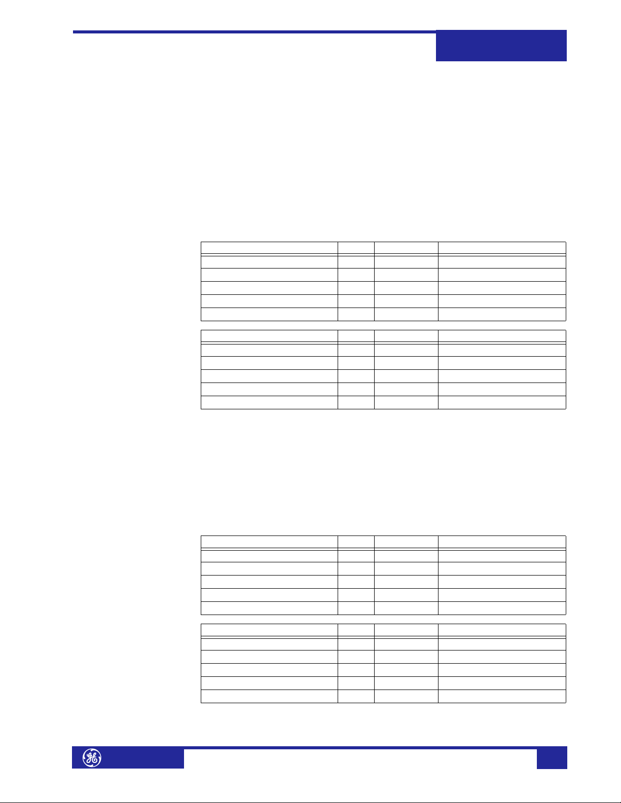
489 Memory Map The 489 memory map is shown in the following table.
Table 1: 489 Memory Map (Sheet 1 of 29)
ADDR NAME RANGE STEP UNITS FORMAT DEFAULT
PRODUCT ID
0000 GE Multilin Product Device Code N/A N/A N/A F1 32
0001 Product Hardware Revision 1 to 26 1 N/A F15 N/A
0002 Product Software Revision N/A N/A N/A F16 N/A
0003 Product Modification Number 0 to 999 1 N/A F1 N/A
0010 Boot Program Revision N/A N/A N/A F16 N/A
0011 Boot Program Modification Number 0 to 999 1 N/A F1 N/A
MODEL ID
0040 Order Code 0 to 16 1 N/A F22 N/A
0050 489 Revision 12 1 N/A F22 N/A
0060 489 Boot Revision 12 1 N/A F22 N/A
COMMANDS
0080 Command Function Code (always 5) 5 N/A N/A F1 N/A
0081 Command Operation Code 0 to 65535 1 N/A F1 N/A
0088 Communications Port Passcode 0 to 99999999 1 N/A F12 0
00F0 Time (Broadcast) N/A N/A N/A F24 N/A
00F2 Date (Broadcast) N/A N/A N/A F18 N/A
USER_MAP / USER MAP VALUES
0100 User Map Value #1 of 125... 5 N/A N/A F1 N/A
017C User Map Value #125 of 125 5 N/A N/A F1 N/A
USER_MAP / USER MAP ADDRESSES
0180 User Map Address #1 of 125... 0 to 3FFF 1 hex F1 0
01FC User Map Address #125 of 125 0 to 3FFF 1 hex F1 0
STATUS / GENERATOR STATUS
0200 Generator Status 0 to 4 1 – F133 1
0201 Generator Thermal Capacity Used 0 to 100 1 % F1 0
0202 Estimated Trip Time On Overload 0 to 65535
0203 Communications Setpoint Access 0 to 1 N/A N/A F126 N/A
STATUS / SYSTEM STATUS
0210 General Status 0 to 65535 1 N/A F140 0
0211 Output Relay Status 0 to 63 1 N/A F141 0
0212 Active Setpoint Group 0 to 1 1 N/A F118 0
STATUS / LAST TRIP DATA
0220 Cause of Last Trip 0 to 139 1 – F134 0
0221 Time of Last Trip N/A N/A N/A F19 N/A
0223 Date of Last Trip N/A N/A N/A F18 N/A
0225 Tachometer Pretrip 0 to 7200 1 RPM F1 0
0226 Phase A Pre-Trip Current 0 to 999999 1 Amps F12 0
0228 Phase B Pre-Trip Current 0 to 999999 1 Amps F12 0
022A Phase C Pre-Trip Current 0 to 999999 1 Amps F12 0
022C Phase A Pre-Trip Differential Current 0 to 999999 1 Amps F12 0
022E Phase B Pre-Trip Differential Current 0 to 999999 1 Amps F12 0
0230 Phase C Pre-Trip Differential Current 0 to 999999 1 Amps F12 0
0232 Negative Sequence Current Pretrip 0 to 2000 1 % FLA F1 0
0233 Ground Current Pretrip 0 to 20000000 1 A F14 0
0235 Pre-Trip A-B Voltage 0 to 50000 1 Volts F1 0
0236 Pre-Trip B-C Voltage 0 to 50000 1 Volts F1 0
0237 Pre-Trip C-A Voltage 0 to 50000 1 Volts F1 0
0238 Frequency Pretrip 0 to 12000 1 Hz F3 0
023B Real Power (MW) Pretrip –2000000 to 2000000 1 MW F13 0
1, 2, 3 See Table footnotes on page 39
1
1sF12 –1
489
GE Multilin
http://www.GEindustrial.com/multilin
11
Page 16

Modbus Memory Map489
Communications Guide
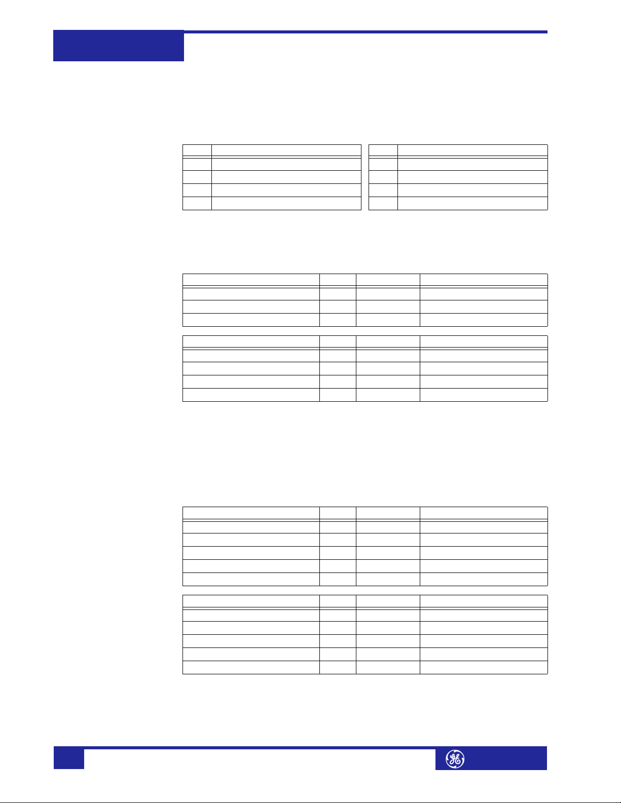
Table 1: 489 Memory Map (Sheet 2 of 29)
ADDR NAME RANGE STEP UNITS FORMAT DEFAULT
023D Reactive Power Mvar Pretrip –2000000 to 2000000 1 Mvar F13 0
023F Apparent Power MVA Pretrip 0 to 2000000 1 MVA F13 0
0241 Last Trip Data Stator RTD 1 to 12 1 – F1 1
0242 Hottest Stator RTD Temperature –50 to 250 1 °C F4 0
0243 Last Trip Data Bearing RTD 1 to 12 1 – F1 1
0244 Hottest Bearing RTD Temperature –50 to 250 1 °C F4 0
0245 Last Trip Data Other RTD 1 to 12 1 – F1 1
0246 Hottest Other RTD Temperature –50 to 250 1 °C F4 0
0247 Last Trip Data Ambient RTD 1 to 12 1 – F1 1
0248 Hottest Ambient RTD Temperature –50 to 250 1 °C F4 0
0249 Analog Input 1 Pretrip –50000 to 50000 1 Units F12 0
024B Analog Input 2 Pretrip –50000 to 50000 1 Units F12 0
024D Analog Input 3 Pretrip –50000 to 50000 1 Units F12 0
024F Analog Input 4 Pretrip –50000 to 50000 1 Units F12 0
025C Hottest Stator RTD Temperature –50 to 250 1 °F F4 0
025D Hottest Bearing RTD Temperature –50 to 250 1 °F F4 0
025E Hottest Other RTD Temperature –50 to 250 1 °F F4 0
025F Hottest Ambient RTD Temperature –50 to 250 1 °F F4 0
0260 Neutral Voltage Fundamental Pretrip 0 to 250000 1 Volts F10 0
0262 Neutral Voltage 3rd Harmonic Pretrip 0 to 250000 1 Volts F10 0
0264 Pre-Trip Vab/Iab 0 to 65535 1 ohms s F2 0
0265 Pre-Trip Vab/Iab Angle 0 to 359 1 ° F1 0
STATUS / TRIP PICKUPS
0280 Input A Pickup 0 to 4 1 – F123 0
0281 Input B Pickup 0 to 4 1 – F123 0
0282 Input C Pickup 0 to 4 1 – F123 0
0283 Input D Pickup 0 to 4 1 – F123 0
0284 Input E Pickup 0 to 4 1 – F123 0
0285 Input F Pickup 0 to 4 1 – F123 0
0286 Input G Pickup 0 to 4 1 – F123 0
0287 Sequential Trip Pickup 0 to 4 1 – F123 0
0288 Field-Breaker Discrepancy Pickup 0 to 4 1 – F123 0
0289 Tachometer Pickup 0 to 4 1 – F123 0
028A Offline Overcurrent Pickup 0 to 4 1 – F123 0
028B Inadvertent Energization Pickup 0 to 4 1 – F123 0
028C Phase Overcurrent Pickup 0 to 4 1 – F123 0
028D Negative Sequence Overcurrent Pickup 0 to 4 1 – F123 0
028E Ground Overcurrent Pickup 0 to 4 1 – F123 0
028F Phase Differential Pickup 0 to 4 1 – F123 0
0290 Undervoltage Pickup 0 to 4 1 – F123 0
0291 Overvoltage Pickup 0 to 4 1 – F123 0
0292 Volts/Hertz Pickup 0 to 4 1 – F123 0
0293 Phase Reversal Pickup 0 to 4 1 – F123 0
0294 Underfrequency Pickup 0 to 4 1 – F123 0
0295 Overfrequency Pickup 0 to 4 1 – F123 0
0296 Neutral Overvoltage (Fundamental) Pickup 0 to 4 1 – F123 0
0297 Neutral Undervoltage (3rd Harmonic) Pickup 0 to 4 1 – F123 0
0298 Reactive Power Pickup 0 to 4 1 – F123 0
0299 Reverse Power Pickup 0 to 4 1 – F123 0
029A Low Forward Power Pickup 0 to 4 1 – F123 0
029B Thermal Model Pickup 0 to 4 1 – F123 0
029C RTD #1 Pickup 0 to 4 1 – F123 0
029D RTD #2 Pickup 0 to 4 1 – F123 0
1, 2, 3 See Table footnotes on page 39
12
http://www.GEindustrial.com/multilin
GE Multilin
Page 17

Modbus Memory Map
Communications Guide
Table 1: 489 Memory Map (Sheet 3 of 29)
ADDR NAME RANGE STEP UNITS FORMAT DEFAULT
029E RTD #3 Pickup 0 to 4 1 – F123 0
029F RTD #4 Pickup 0 to 4 1 – F123 0
02A0 RTD #5 Pickup 0 to 4 1 – F123 0
02A1 RTD #6 Pickup 0 to 4 1 – F123 0
02A2 RTD #7 Pickup 0 to 4 1 – F123 0
02A3 RTD #8 Pickup 0 to 4 1 – F123 0
02A4 RTD #9 Pickup 0 to 4 1 – F123 0
02A5 RTD #10 Pickup 0 to 4 1 – F123 0
02A6 RTD #11 Pickup 0 to 4 1 – F123 0
02A7 RTD #12 Pickup 0 to 4 1 – F123 0
02A8 Analog Input 1 Pickup 0 to 4 1 – F123 0
02A9 Analog Input 2 Pickup 0 to 4 1 – F123 0
02AA Analog Input 3 Pickup 0 to 4 1 – F123 0
02AB Analog Input 4 Pickup 0 to 4 1 – F123 0
02AC Loss Of Excitation 1 Pickup 0 to 4 1 – F123 0
02AD Loss Of Excitation 2 Pickup 0 to 4 1 – F123 0
02AE Ground Directional Pickup 0 to 4 1 – F123 0
02AF High-Set Phase Overcurrent Pickup 0 to 4 1 – F123 0
02B0 Distance Zone 1 Pickup 0 to 4 1 – F123 0
02B1 Distance Zone 2 Pickup 0 to 4 1 – F123 0
STATUS / ALARM PICKUPS
0300 Input A Pickup 0 to 4 1 – F123 0
0301 Input B Pickup 0 to 4 1 – F123 0
0302 Input C Pickup 0 to 4 1 – F123 0
0303 Input D Pickup 0 to 4 1 – F123 0
0304 Input E Pickup 0 to 4 1 – F123 0
0305 Input F Pickup 0 to 4 1 – F123 0
0306 Input G Pickup 0 to 4 1 – F123 0
0307 Tachometer Pickup 0 to 4 1 – F123 0
0308 Overcurrent Pickup 0 to 4 1 – F123 0
0309 Negative Sequence Overcurrent Pickup 0 to 4 1 – F123 0
030A Ground Overcurrent Pickup 0 to 4 1 – F123 0
030B Undervoltage Pickup 0 to 4 1 – F123 0
030C Overvoltage Pickup 0 to 4 1 – F123 0
030D Volts/Hertz Pickup 0 to 4 1 – F123 0
030E Underfrequency Pickup 0 to 4 1 – F123 0
030F Overfrequency Pickup 0 to 4 1 – F123 0
0310 Neutral Overvoltage (Fundamental) Pickup 0 to 4 1 – F123 0
0311 Neutral Undervoltage (3rd harmonic) Pickup 0 to 4 1 – F123 0
0312 Reactive Power Pickup 0 to 4 1 – F123 0
0313 Reverse Power Pickup 0 to 4 1 – F123 0
0314 Low Forward Power Pickup 0 to 4 1 – F123 0
0315 RTD #1 Pickup 0 to 4 1 – F123 0
0316 RTD #2 Pickup 0 to 4 1 – F123 0
0317 RTD #3 Pickup 0 to 4 1 – F123 0
0318 RTD #4 Pickup 0 to 4 1 – F123 0
0319 RTD #5 Pickup 0 to 4 1 – F123 0
031A RTD #6 Pickup 0 to 4 1 – F123 0
031B RTD #7 Pickup 0 to 4 1 – F123 0
031C RTD #8 Pickup 0 to 4 1 – F123 0
031D RTD #9 Pickup 0 to 4 1 – F123 0
031E RTD #10 Pickup 0 to 4 1 – F123 0
031F RTD #11 Pickup 0 to 4 1 – F123 0
1, 2, 3 See Table footnotes on page 39
489
GE Multilin
http://www.GEindustrial.com/multilin
13
Page 18

Modbus Memory Map489
Communications Guide
Table 1: 489 Memory Map (Sheet 4 of 29)
ADDR NAME RANGE STEP UNITS FORMAT DEFAULT
0320 RTD #12 Pickup 0 to 4 1 – F123 0
0321 Open Sensor Pickup 0 to 4 1 – F123 0
0322 Short/Low Temperature Pickup 0 to 4 1 – F123 0
0323 Thermal Model Pickup 0 to 4 1 – F123 0
0324 Trip Counter Pickup 0 to 4 1 – F123 0
0325 Breaker Failure Pickup 0 to 4 1 – F123 0
0326 Trip Coil Monitor Pickup 0 to 4 1 – F123 0
0327 VT Fuse Failure Pickup 0 to 4 1 – F123 0
0328 Current Demand Pickup 0 to 4 1 – F123 0
0329 MW Demand Pickup 0 to 4 1 – F123 0
032A Mvar Demand Pickup 0 to 4 1 – F123 0
032B MVA Demand Pickup 0 to 4 1 – F123 0
032C Analog Input 1 Pickup 0 to 4 1 – F123 0
032D Analog Input 2 Pickup 0 to 4 1 – F123 0
032E Analog Input 3 Pickup 0 to 4 1 – F123 0
032F Analog Input 4 Pickup 0 to 4 1 – F123 0
0330 Not Programmed Pickup 0 to 4 1 – F123 0
0331 Simulation Mode Pickup 0 to 4 1 – F123 0
0332 Output Relays Forced Pickup 0 to 4 1 – F123 0
0333 Analog Output Forced Pickup 0 to 4 1 – F123 0
0334 Test Switch Shorted Pickup 0 to 4 1 – F123 0
0335 Ground Directional Pickup 0 to 4 1 – F123 0
0336 IRIG-B Alarm Pickup 0 to 4 1 – F123 0
0337 Generator Running Hour Pickup 0 to 4 1 – F123 0
STATUS / DIGITAL INPUTS
0380 Access Switch State 0 to 1 1 – F207 0
0381 Breaker Status Switch State 0 to 1 1 – F207 0
0382 Assignable Digital Input 1 State 0 to 1 1 – F207 0
0383 Assignable Digital Input 2 State 0 to 1 1 – F207 0
0384 Assignable Digital Input 3 State 0 to 1 1 – F207 0
0385 Assignable Digital Input 4 State 0 to 1 1 – F207 0
0386 Assignable Digital Input 5 State 0 to 1 1 – F207 0
0387 Assignable Digital Input 6 State 0 to 1 1 – F207 0
0388 Assignable Digital Input 7 State 0 to 1 1 – F207 0
0389 Trip Coil Supervision 0 to 1 1 – F132 0
STATUS / REAL TIME CLOCK
03FC Date (Read-only) N/A N/A N/A F18 N/A
03FE Time (Read-only) N/A N/A N/A F19 N/A
METERING DATA / CURRENT METERING
0400 Phase A Output Current 0 to 999999 1 Amps F12 0
0402 Phase B Output Current 0 to 999999 1 Amps F12 0
0404 Phase C Output Current 0 to 999999 1 Amps F12 0
0406 Phase A Neutral-Side Current 0 to 999999 1 Amps F12 0
0408 Phase B Neutral-Side Current 0 to 999999 1 Amps F12 0
040A Phase C Neutral-Side Current 0 to 999999 1 Amps F12 0
040C Phase A Differential Current 0 to 999999 1 Amps F12 0
040E Phase B Differential Current 0 to 999999 1 Amps F12 0
0410 Phase C Differential Current 0 to 999999 1 Amps F12 0
0412 Average Phase Current 0 to 999999 1 Amps F12 0
0414 Generator Load 0 to 2000 1 % FLA F1 0
0415 Negative Sequence Current 0 to 2000 1 % FLA F1 0
0416 Ground Current 0 to 10000 1 Amps F14 0
0420 Phase A Current Angle 0 to 359 1 ° F1 0
1, 2, 3 See Table footnotes on page 39
14
http://www.GEindustrial.com/multilin
GE Multilin
Page 19

Modbus Memory Map
Communications Guide
Table 1: 489 Memory Map (Sheet 5 of 29)
ADDR NAME RANGE STEP UNITS FORMAT DEFAULT
0421 Phase B Current Angle 0 to 359 1 ° F1 0
0422 Phase C Current Angle 0 to 359 1 ° F1 0
0423 Phase A Neutral-Side Angle 0 to 359 1 ° F1 0
0424 Phase B Neutral-Side Angle 0 to 359 1 ° F1 0
0425 Phase C Neutral-Side Angle 0 to 359 1 ° F1 0
0426 Phase A Differential Angle 0 to 359 1 ° F1 0
0427 Phase B Differential Angle 0 to 359 1 ° F1 0
0428 Phase C Differential Angle 0 to 359 1 ° F1 0
0429 Ground Current Angle 0 to 359 1 ° F1 0
METERING DATA / VOLTAGE METERING
0440 Phase A-B Voltage 0 to 50000 1 Volts F1 0
0441 Phase B-C Voltage 0 to 50000 1 Volts F1 0
0442 Phase C-A Voltage 0 to 50000 1 Volts F1 0
0443 Average Line Voltage 0 to 50000 1 Volts F1 0
0444 Phase A-N Voltage 0 to 50000 1 Volts F1 0
0445 Phase B-N Voltage 0 to 50000 1 Volts F1 0
0446 Phase C-N Voltage 0 to 50000 1 Volts F1 0
0447 Average Phase Voltage 0 to 50000 1 Volts F1 0
0448 Per Unit Measurement Of V/Hz
0449 Frequency 500 to 9000 1 Hz F3 0
044A Neutral Voltage Fund 0 to 250000 1 Volts F10 0
044C Neutral Voltage 3rd Harmonic 0 to 250000 1 Volts F10 0
044E Neutral Voltage Vp3 3rd Harmonic 0 to 250000 1 Volts F10 0
0450 Vab/Iab 0 to 65535 1 ohms F2 0
0451 Vab/Iab Angle 0 to 359 1 ° F1 0
0460 Line A-B Voltage Angle 0 to 359 1 ° F1 0
0461 Line B-C Voltage Angle 0 to 359 1 ° F1 0
0462 Line C-A Voltage Angle 0 to 359 1 ° F1 0
0463 Phase A-N Voltage Angle 0 to 359 1 ° F1 0
0464 Phase B-N Voltage Angle 0 to 359 1 ° F1 0
0465 Phase C-N Voltage Angle 0 to 359 1 ° F1 0
0466 Neutral Voltage Angle 0 to 359 1 – F1 0
METERING DATA / POWER METERING
0480 Power Factor –100 to 100 1 – F6 0
0481 Real Power –2000000 to 2000000 1 MW F13 0
0483 Reactive Power –2000000 to 2000000 1 Mvar F13 0
0485 Apparent Power –2000000 to 200000 1 MVA F13 0
0487 Positive Watthours 0 to 4000000000 1 MWh F13 0
0489 Positive Varhours 0 to 4000000000 1 Mvarh F13 0
048B Negative Varhours 0 to 4000000000 1 Mvarh F13 0
METERING DATA / TEMPERATURE
04A0 Hottest Stator RTD 1 to 12 1 – F1 0
04A1 Hottest Stator RTD Temperature –52 to 250 1 °C F4 –52
04A2 RTD #1 Temperature –52 to 251 1 °C F4 –52
04A3 RTD #2 Temperature –52 to 251 1 °C F4 –52
04A4 RTD #3 Temperature –52 to 251 1 °C F4 –52
04A5 RTD #4 Temperature –52 to 251 1 °C F4 –52
04A6 RTD #5 Temperature –52 to 251 1 °C F4 –52
04A7 RTD #6 Temperature –52 to 251 1 °C F4 –52
04A8 RTD #7 Temperature –52 to 251 1 °C F4 –52
04A9 RTD #8 Temperature –52 to 251 1 °C F4 –52
04AA RTD #9 Temperature –52 to 251 1 °C F4 –52
04AB RTD #10 Temperature –52 to 251 1 °C F4 –52
1, 2, 3 See Table footnotes on page 39
2
0 to 200 1 – F3 0
489
GE Multilin
http://www.GEindustrial.com/multilin
15
Page 20

Modbus Memory Map489
Communications Guide
Table 1: 489 Memory Map (Sheet 6 of 29)
ADDR NAME RANGE STEP UNITS FORMAT DEFAULT
04AC RTD #11 Temperature –52 to 251 1 °C F4 –52
04AD RTD #12 Temperature –52 to 251 1 °C F4 –52
04C0 Hottest Stator RTD Temperature –52 to 250 1 °F F4 –52
04C1 RTD #1 Temperature –52 to 251 1 °F F4 –52
04C2 RTD #2 Temperature –52 to 251 1 °F F4 –52
04C3 RTD #3 Temperature –52 to 251 1 °F F4 –52
04C4 RTD #4 Temperature –52 to 251 1 °F F4 –52
04C5 RTD #5 Temperature –52 to 251 1 °F F4 –52
04C6 RTD #6 Temperature –52 to 251 1 °F F4 –52
04C7 RTD #7 Temperature –52 to 251 1 °F F4 –52
04C8 RTD #8 Temperature –52 to 251 1 °F F4 –52
04C9 RTD #9 Temperature –52 to 251 1 °F F4 –52
04CA RTD #10 Temperature –52 to 251 1 °F F4 –52
04CB RTD #11 Temperature –52 to 251 1 °F F4 –52
04CC RTD #12 Temperature –52 to 251 1 °F F4 –52
METERING DATA / DEMAND METERING
04E0 Current Demand 0 to 1000000 1 Amps F12 0
04E2 MW Demand 0 to 2000000 1 MW F13 0
04E4 Mvar Demand 0 to 2000000 1 Mvar F13 0
04E6 MVA Demand 0 to 2000000 1 MVA F13 0
04E8 Peak Current Demand 0 to 1000000 1 Amps F12 0
04EA Peak MW Demand 0 to 2000000 1 MW F13 0
04EC Peak Mvar Demand 0 to 2000000 1 Mvar F13 0
04EE Peak MVA Demand 0 to 2000000 1 MVA F13 0
METERING DATA / ANALOG INPUTS
0500 Analog Input 1 –50000 to 50000 1 Units F12 0
0502 Analog Input 2 –50000 to 50000 1 Units F12 0
0504 Analog Input 3 –50000 to 50000 1 Units F12 0
0506 Analog Input 4 –50000 to 50000 1 Units F12 0
METERING DATA / SPEED
0520 Tachometer 0 to 7200 1 RPM F1 0
LEARNED DATA / PARAMETER AVERAGES
0600 Average Generator Load 0 to 2000 1 %FLA F1 0
0601 Average Negative Sequence Current 0 to 2000 1 %FLA F1 0
0602 Average Phase-Phase Voltage 0 to 50000 1 V F1 0
0603 Reserved – – – – –
0604 Reserved – – – – –
LEARNED DATA / RTD MAXIMUMS
0620 RTD #1 Maximum Temperature (Celsius) –52 to 251 1 °C F4 –52
0621 RTD #2 Maximum Temperature (Celsius) –52 to 251 1 °C F4 –52
0622 RTD #3 Maximum Temperature (Celsius) –52 to 251 1 °C F4 –52
0623 RTD #4 Maximum Temperature (Celsius) –52 to 251 1 °C F4 –52
0624 RTD #5 Maximum Temperature (Celsius) –52 to 251 1 °C F4 –52
0625 RTD #6 Maximum Temperature (Celsius) –52 to 251 1 °C F4 –52
0626 RTD #7 Maximum Temperature (Celsius) –52 to 251 1 °C F4 –52
0627 RTD #8 Maximum Temperature (Celsius) –52 to 251 1 °C F4 –52
0628 RTD #9 Maximum Temperature (Celsius) –52 to 251 1 °C F4 –52
0629 RTD #10 Maximum Temperature (Celsius) –52 to 251 1 °C F4 –52
062A RTD #11 Maximum Temperature (Celsius) –52 to 251 1 °C F4 –52
062B RTD #12 Maximum Temperature (Celsius) –52 to 251 1 °C F4 –52
0640 RTD #1 Maximum Temperature (Fahrenheit) –52 to 251 1 °F F4 –52
0641 RTD #2 Maximum Temperature (Fahrenheit) –52 to 251 1 °F F4 –52
0642 RTD #3 Maximum Temperature (Fahrenheit) –52 to 251 1 °F F4 –52
1, 2, 3 See Table footnotes on page 39
16
http://www.GEindustrial.com/multilin
GE Multilin
Page 21

Modbus Memory Map
Communications Guide
Table 1: 489 Memory Map (Sheet 7 of 29)
ADDR NAME RANGE STEP UNITS FORMAT DEFAULT
0643 RTD #4 Maximum Temperature (Fahrenheit) –52 to 251 1 °F F4 –52
0644 RTD #5 Maximum Temperature (Fahrenheit) –52 to 251 1 °F F4 –52
0645 RTD #6 Maximum Temperature (Fahrenheit) –52 to 251 1 °F F4 –52
0646 RTD #7 Maximum Temperature (Fahrenheit) –52 to 251 1 °F F4 –52
0647 RTD #8 Maximum Temperature (Fahrenheit) –52 to 251 1 °F F4 –52
0648 RTD #9 Maximum Temperature (Fahrenheit) –52 to 251 1 °F F4 –52
0649 RTD #10 Maximum Temperature (Fahrenheit) –52 to 251 1 °F F4 –52
064A RTD #11 Maximum Temperature (Fahrenheit) –52 to 251 1 °F F4 –52
064B RTD #12 Maximum Temperature (Fahrenheit) –52 to 251 1 °F F4 –52
LEARNED DATA / ANALOG IN MIN/MAX
0700 Analog Input 1 Minimum –50000 to 50000 1 Units F12 0
0702 Analog Input 1 Maximum –50000 to 50000 1 Units F12 0
0704 Analog Input 2 Minimum –50000 to 50000 1 Units F12 0
0706 Analog Input 2 Maximum –50000 to 50000 1 Units F12 0
0708 Analog Input 3 Minimum –50000 to 50000 1 Units F12 0
070A Analog Input 3 Maximum –50000 to 50000 1 Units F12 0
070C Analog Input 4 Minimum –50000 to 50000 1 Units F12 0
070E Analog Input 4 Maximum –50000 to 50000 1 Units F12 0
MAINTENANCE / TRIP COUNTERS
077F Trip Counters Last Cleared (Date) N/A N/A N/A F18 N/A
0781 Total Number of Trips 0 to 50000 1 – F1 0
0782 Digital Input Trips 0 to 50000 1 – F1 0
0783 Sequential Trips 0 to 50000 1 – F1 0
0784 Field-Breaker Discrepancy Trips 0 to 50000 1 – F1 0
0785 Tachometer Trips 0 to 50000 1 – F1 0
0786 Offline Overcurrent Trips 0 to 50000 1 – F1 0
0787 Phase Overcurrent Trips 0 to 50000 1 – F1 0
0788 Negative Sequence Overcurrent Trips 0 to 50000 1 – F1 0
0789 Ground Overcurrent Trips 0 to 50000 1 – F1 0
078A Phase Differential Trips 0 to 50000 1 – F1 0
078B Undervoltage Trips 0 to 50000 1 – F1 0
078C Overvoltage Trips 0 to 50000 1 – F1 0
078D Volts/Hertz Trips 0 to 50000 1 – F1 0
078E Phase Reversal Trips 0 to 50000 1 – F1 0
078F Underfrequency Trips 0 to 50000 1 – F1 0
0790 Overfrequency Trips 0 to 50000 1 – F1 0
0791 Neutral Overvoltage (Fundamental) Trips 0 to 50000 1 – F1 0
0792 Neutral Undervoltage (3rd Harmonic) Trips 0 to 50000 1 – F1 0
0793 Reactive Power Trips 0 to 50000 1 – F1 0
0794 Reverse Power Trips 0 to 50000 1 – F1 0
0795 Low Forward Power Trips 0 to 50000 1 – F1 0
0796 Stator RTD Trips 0 to 50000 1 – F1 0
0797 Bearing RTD Trips 0 to 50000 1 – F1 0
0798 Other RTD Trips 0 to 50000 1 – F1 0
0799 Ambient RTD Trips 0 to 50000 1 – F1 0
079A Thermal Model Trips 0 to 50000 1 – F1 0
079B Inadvertent Energization Trips 0 to 50000 1 – F1 0
079C Analog Input 1 Trips 0 to 50000 1 – F1 0
079D Analog Input 2 Trips 0 to 50000 1 – F1 0
079E Analog Input 3 Trips 0 to 50000 1 – F1 0
079F Analog Input 4 Trips 0 to 50000 1 – F1 0
MAINTENANCE / GENERAL COUNTERS
07A0 Number Of Breaker Operations 0 to 50000 1 – F1 0
1, 2, 3 See Table footnotes on page 39
489
GE Multilin
http://www.GEindustrial.com/multilin
17
Page 22

Modbus Memory Map489
Communications Guide
Table 1: 489 Memory Map (Sheet 8 of 29)
ADDR NAME RANGE STEP UNITS FORMAT DEFAULT
07A1 Number Of Thermal Resets 0 to 50000 1 – F1 0
MAINTENANCE / TRIP COUNTERS
07A2 Loss Of Excitation 1 Trips 0 to 50000 1 – F1 0
07A3 Loss Of Excitation 2 Trips 0 to 50000 1 – F1 0
07A4 Ground Directional Trips 0 to 50000 1 – F1 0
07A5 High-Set Phase Overcurrent Trips 0 to 50000 1 – F1 0
07A6 Distance Zone 1 Trips 0 to 50000 1 – F1 0
07A7 Distance Zone 2 Trips 0 to 50000 1 – F1 0
MAINTENANCE / TIMERS
07E0 Generator Hours Online 0 to 1000000 1 h F12 0
PRODUCT INFO. / 489 MODEL INFO.
0800 Order Code 0 to 65535 1 N/A F136 N/A
0801 489 Serial Number 3000000 to 9999999 1 – F12 3000000
PRODUCT INFO. / CALIBRATION INFO.
0810 Original Calibration Date N/A N/A N/A F18 N/A
0812 Last Calibration Date N/A N/A N/A F18 N/A
489 SETUP / PREFERENCES
1000 Default Message Cycle Time 5 to 100 5 s F2 20
1001 Default Message Timeout 10 to 900 1 s F1 300
1003 Parameter Averages Calculation Period 1 to 90 1 min F1 15
1004 Temperature Display 0 to 1 1 – F100 0
1005 Waveform Trigger Position 1 to 100 1 % F1 25
1006 Passcode (Write Only) 0 to 99999999 1 N/A F12 0
1008 Encrypted Passcode (Read Only) N/A N/A N/A F12 N/A
100A Waveform Memory Buffer 1 to 16 1 – F1 8
489 SETUP / SERIAL PORTS
1010 Slave Address 1 to 254 1 – F1 254
1011 Computer RS485 Baud Rate 0 to 5 1 – F101 4
1012 Computer RS485 Parity 0 to 2 1 – F102 0
1013 Auxiliary RS485 Baud Rate 0 to 5 1 – F101 4
1014 Auxiliary RS485 Parity 0 to 2 1 – F102 0
1015 Port Used For DNP 0 to 3 1 – F216 0
1016 DNP Slave Address 0 to 255 1 – F1 255
1017 DNP Turnaround Time 0 to 100 10 ms F1 10
489 SETUP / REAL TIME CLOCK
1030 Date N/A N/A N/A F18 N/A
1032 Time N/A N/A N/A F19 N/A
1034 IRIG-B Type 0 to 2 1 – F220 0
489 SETUP / MESSAGE SCRATCHPAD
1060 Scratchpad 0 to 40 1 – F22 _
1080 Scratchpad 0 to 40 1 – F22 _
10A0 Scratchpad 0 to 40 1 – F22 _
10C0 Scratchpad 0 to 40 1 – F22 _
10E0 Scratchpad 0 to 40 1 – F22 _
489 SETUP / CLEAR DATA
1130 Clear Last Trip Data 0 to 1 1 – F103 0
1131 Clear Mwh And Mvarh Meters 0 to 1 1 – F103 0
1132 Clear Peak Demand Data 0 to 1 1 – F103 0
1133 Clear RTD Maximums 0 to 1 1 – F103 0
1134 Clear Analog Inputs Minimums/Maximums 0 to 1 1 – F103 0
1135 Clear Trip Counters 0 to 1 1 – F103 0
1136 Clear Event Record 0 to 1 1 – F103 0
1137 Clear Generator Information 0 to 1 1 – F103 0
1, 2, 3 See Table footnotes on page 39
18
http://www.GEindustrial.com/multilin
GE Multilin
Page 23

Modbus Memory Map
Communications Guide
Table 1: 489 Memory Map (Sheet 9 of 29)
ADDR NAME RANGE STEP UNITS FORMAT DEFAULT
1138 Clear Breaker Information 0 to 1 1 – F103 0
SYSTEM SETUP / CURRENT SENSING
1180 Phase CT Primary 10 to 50001 1 Amps F1 50001
1181 Ground CT 0 to 3 1 – F104 0
1182 Ground CT Ratio 10 to 10000 1 : 1 / :5 F1 100
SYSTEM SETUP / VOLTAGE SENSING
11A0 VT Connection Type 0 to 2 1 – F106 0
11A1 Voltage Transformer Ratio 100 to 30000 1 : 1 F3 500
11A2 Neutral VT Ratio 100 to 24000 1 : 1 F3 500
11A3 Neutral Voltage Transformer 0 to 1 1 – F103 0
SYSTEM SETUP / GEN. PARAMETERS
11C0 Generator Rated MVA 50 to 2000001 1 MVA F13 2000001
11C2 Generator Rated Power Factor 5 to 100 1 – F3 100
11C3 Generator Voltage Phase-Phase 100 to 30001 1 V F1 30001
11C4 Generator Nominal Frequency 0 to 3 1 Hz F107 0
11C5 Generator Phase Sequence 0 to 2 1 – F124 0
SYSTEM SETUP / SERIAL START/STOP
11E0 Serial Start/Stop Initiation 0 to 1 1 – F105 0
11E1 Startup Initiation Relays (2-5) 1 to 4 1 – F50 0
11E2 Shutdown Initiation Relays (1-4) 0 to 3 1 – F50 0
11E3 Serial Start/Stop Events 0 to 1 1 – F105 0
DIGITAL INPUTS / BREAKER STATUS
1200 Breaker Status 0 to 1 1 – F209 1
DIGITAL INPUTS / GENERAL INPUT A
1210 Assign Digital Input 0 to 7 1 – F210 0
1211 Asserted Digital Input State 0 to 1 1 – F131 0
1212 Input Name 0 to 12 1 – F22 _
1218 Block Input From Online 0 to 5000 1 s F1 0
1219 General Input A Control 0 to 1 1 – F105 0
121A Pulsed Control Relay Dwell Time 0 to 250 1 s F2 0
121B Assign Control Relays (1-5) 0 to 4 1 – F50 0
121C General Input A Control Events 0 to 1 1 – F105 0
121D General Input A Alarm 0 to 2 1 – F115 0
121E Assign Alarm Relays (2-5) 1 to 4 1 – F50 16
121F General Input A Alarm Delay 1 to 50000 1 s F2 50
1220 General Input A Alarm Events 0 to 1 1 – F105 0
1221 General Input A Trip 0 to 2 1 – F115 0
1222 Assign Trip Relays (1-4) 0 to 3 1 – F50 1
1223 General Input A Trip Delay 1 to 50000 1 s F2 50
DIGITAL INPUTS / GENERAL INPUT B
1230 Assign Digital Input 0 to 7 1 – F210 0
1231 Asserted Digital Input State 0 to 1 1 – F131 0
1232 Input Name 0 to 12 1 – F22 _
1238 Block Input From Online 0 to 5000 1 s F1 0
1239 General Input B Control 0 to 1 1 – F105 0
123A Pulsed Control Relay Dwell Time 0 to 250 1 s F2 0
123B Assign Control Relays (1-5) 0 to 4 1 – F50 0
123C General Input B Control Events 0 to 1 1 – F105 0
123D General Input B Alarm 0 to 2 1 – F115 0
123E Assign Alarm Relays (2-5) 1 to 4 1 – F50 16
123F General Input B Alarm Delay 1 to 50000 1 s F2 50
1240 General Input B Alarm Events 0 to 1 1 – F105 0
1241 General Input B Trip 0 to 2 1 – F115 0
1, 2, 3 See Table footnotes on page 39
489
GE Multilin
http://www.GEindustrial.com/multilin
19
Page 24

Modbus Memory Map489
Communications Guide
Table 1: 489 Memory Map (Sheet 10 of 29)
ADDR NAME RANGE STEP UNITS FORMAT DEFAULT
1242 Assign Trip Relays (1-4) 0 to 3 1 – F50 1
1243 General Input B Trip Delay 1 to 50000 1 s F2 50
DIGITAL INPUTS / GENERAL INPUT C
1250 Assign Digital Input 0 to 7 1 – F210 0
1251 Asserted Digital Input State 0 to 1 1 – F131 0
1252 Input Name 0 to 12 1 – F22 _
1258 Block Input From Online 0 to 5000 1 s F1 0
1259 General Input C Control 0 to 1 1 – F105 0
125A Pulsed Control Relay Dwell Time 0 to 250 1 s F2 0
125B Assign Control Relays (1-5) 0 to 4 1 – F50 0
125C General Input C Control Events 0 to 1 1 – F105 0
125D General Input C Alarm 0 to 2 1 – F115 0
125E Assign Alarm Relays (2-5) 1 to 4 1 – F50 16
125F General Input C Alarm Delay 1 to 50000 1 s F2 50
1260 General Input C Alarm Events 0 to 1 1 – F105 0
1261 General Input C Trip 0 to 2 1 – F115 0
1262 Assign Trip Relays (1-4) 0 to 3 1 – F50 1
1263 General Input C Trip Delay 1 to 50000 1 s F2 50
DIGITAL INPUTS / GENERAL INPUT D
1270 Assign Digital Input 0 to 7 1 – F210 0
1271 Asserted Digital Input State 0 to 1 1 – F131 0
1272 Input Name 0 to 12 1 – F22 _
1278 Block Input From Online 0 to 5000 1 s F1 0
1279 General Input D Control 0 to 1 1 – F105 0
127A Pulsed Control Relay Dwell Time 0 to 250 1 s F2 0
127B Assign Control Relays (1-5) 0 to 4 1 – F50 0
127C General Input D Control Events 0 to 1 1 – F105 0
127D General Input D Alarm 0 to 2 1 – F115 0
127E Assign Alarm Relays (2-5) 1 to 4 1 – F50 16
127F General Input D Alarm Delay 1 to 50000 1 s F2 50
1280 General Input D Alarm Events 0 to 1 1 – F105 0
1281 General Input D Trip 0 to 2 1 – F115 0
1282 Assign Trip Relays (1-4) 0 to 3 1 – F50 1
1283 General Input D Trip Delay 1 to 50000 1 s F2 50
DIGITAL INPUTS / GENERAL INPUT E
1290 Assign Digital Input 0 to 7 1 – F210 0
1291 Asserted Digital Input State 0 to 1 1 – F131 0
1292 Input Name 0 to 12 1 – F22 _
1298 Block Input From Online 0 to 5000 1 s F1 0
1299 General Input E Control 0 to 1 1 – F105 0
129A Pulsed Control Relay Dwell Time 0 to 250 1 s F2 0
129B Assign Control Relays (1-5) 0 to 4 1 – F50 0
129C General Input E Control Events 0 to 1 1 – F105 0
129D General Input E Alarm 0 to 2 1 – F115 0
129E Assign Alarm Relays (2-5) 1 to 4 1 – F50 16
129F General Input E Alarm Delay 1 to 50000 1 s F2 50
12A0 General Input E Alarm Events 0 to 1 1 – F105 0
12A1 General Input E Trip 0 to 2 1 – F115 0
12A2 Assign Trip Relays (1-4) 0 to 3 1 – F50 1
12A3 General Input E Trip Delay 1 to 50000 1 s F2 50
DIGITAL INPUTS / GENERAL INPUT F
12B0 Assign Digital Input 0 to 7 1 – F210 0
12B1 Asserted Digital Input State 0 to 1 1 – F131 0
1, 2, 3 See Table footnotes on page 39
20
http://www.GEindustrial.com/multilin
GE Multilin
Page 25

Modbus Memory Map
Communications Guide
Table 1: 489 Memory Map (Sheet 11 of 29)
ADDR NAME RANGE STEP UNITS FORMAT DEFAULT
12B2 Input Name 0 to 12 1 – F22 _
12B8 Block Input From Online 0 to 5000 1 s F1 0
12B9 General Input F Control 0 to 1 1 – F105 0
12BA Pulsed Control Relay Dwell Time 0 to 250 1 s F2 0
12BB Assign Control Relays (1-5) 0 to 4 1 – F50 0
12BC General Input F Control Events 0 to 1 1 – F105 0
12BD General Input F Alarm 0 to 2 1 – F115 0
12BE Assign Alarm Relays (2-5) 1 to 4 1 – F50 16
12BF General Input F Alarm Delay 1 to 50000 1 s F2 50
12C0 General Input F Alarm Events 0 to 1 1 – F105 0
12C1 General Input F Trip 0 to 2 1 – F115 0
12C2 Assign Trip Relays (1-4) 0 to 3 1 – F50 1
12C3 General Input F Trip Delay 1 to 50000 1 s F2 50
DIGITAL INPUTS / GENERAL INPUT G
12D0 Assign Digital Input 0 to 7 1 – F210 0
12D1 Asserted Digital Input State 0 to 1 1 – F131 0
12D2 Input Name 0 to 12 1 – F22 _
12D8 Block Input From Online 0 to 5000 1 s F1 0
12D9 General Input G Control 0 to 1 1 – F105 0
12DA Pulsed Control Relay Dwell Time 0 to 250 1 s F2 0
12DB Assign Control Relays (1-5) 0 to 4 1 – F50 0
12DC General Input G Control Events 0 to 1 1 – F105 0
12DD General Input G Alarm 0 to 2 1 – F115 0
12DE Assign Alarm Relays (2-5) 1 to 4 1 – F50 16
12DF General Input G Alarm Delay 1 to 50000 1 s F2 50
12E0 General Input G Alarm Events 0 to 1 1 – F105 0
12E1 General Input G Trip 0 to 2 1 – F115 0
12E2 Assign Trip Relays (1-4) 0 to 3 1 – F50 1
12E3 General Input G Trip Delay 1 to 50000 1 s F2 50
DIGITAL INPUTS / REMOTE RESET
1300 Assign Digital Input 0 to 7 1 – F210 0
DIGITAL INPUTS / TEST INPUT
1310 Assign Digital Input 0 to 7 1 – F210 0
DIGITAL INPUTS / THERMAL RESET
1320 Assign Digital Input 0 to 7 1 – F210 0
DIGITAL INPUTS / DUAL SETPOINTS
1340 Assign Digital Input 0 to 7 1 – F210 0
1341 Active Setpoint Group 0 to 1 1 – F118 0
1342 Edit Setpoint Group 0 to 1 1 – F118 0
DIGITAL INPUTS / SEQUENTIAL TRIP
1360 Assign Digital Input 0 to 7 1 – F210 0
1361 Sequential Trip Type 0 to 1 1 – F206 0
1362 Assign Trip Relays (1-4) 0 to 3 1 – F50 1
1363 Sequential Trip Level 2 to 99 1 × Rated MW F14 5
1365 Sequential Trip Delay 2 to 1200 1 s F2 10
DIGITAL INPUTS / FIELD-BREAKER DISCREPANCY
1380 Assign Digital Input 0 to 7 1 – F210 0
1381 Field Status Contact 0 to 1 1 – F109 0
1382 Assign Trip Relays (1-4) 0 to 3 1 – F50 1
1383 Field-Breaker Discrepancy Trip Delay 1 to 5000 1 s F2 10
DIGITAL INPUTS / TACHOMETER
13A0 Assign Digital Input 0 to 7 1 – F210 0
13A1 Rated Speed 100 to 3600 1 RPM F1 3600
1, 2, 3 See Table footnotes on page 39
489
GE Multilin
http://www.GEindustrial.com/multilin
21
Page 26

Modbus Memory Map489
Communications Guide
Table 1: 489 Memory Map (Sheet 12 of 29)
ADDR NAME RANGE STEP UNITS FORMAT DEFAULT
13A2 Tachometer Alarm 0 to 2 1 – F115 0
13A3 Assign Alarm Relays (2-5) 1 to 4 1 – F50 16
13A4 Tachometer Alarm Speed 101 to 175 1 %Rated F1 110
13A5 Tachometer Alarm Delay 1 to 250 1 s F1 1
13A6 Tachometer Alarm Events 0 to 1 1 – F105 0
13A7 Tachometer Trip 0 to 2 1 – F115 0
13A8 Assign Trip Relays (1-4) 0 to 3 1 – F50 1
13A9 Tachometer Trip Speed 101 to 175 1 %Rated F1 110
13AA Tachometer Trip Delay 1 to 250 1 s F1 1
DIGITAL INPUTS / WAVEFORM CAPTURE
13C0 Assign Digital Input 0 to 7 1 – F210 0
DIGITAL INPUTS / GROUND SWITCH STATUS
13D0 Assign Digital Input 0 to 7 1 – F210 0
13D1 Ground Switch Contact 0 to 1 1 – F109 0
OUTPUT RELAYS / RELAY RESET MODE
1400 1 Trip 0 to 1 1 – F117 0
1401 2 Auxiliary 0 to 1 1 – F117 0
1402 3 Auxiliary 0 to 1 1 – F117 0
1403 4 Auxiliary 0 to 1 1 – F117 0
1404 5 Alarm 0 to 1 1 – F117 0
1405 6 Service 0 to 1 1 – F117 0
CURRENT ELEMENTS / OVERCURRENT ALARM
1500 Overcurrent Alarm 0 to 2 1 – F115 0
1501 Assign Alarm Relays (2-5) 1 to 4 1 – F50 16
1502 Overcurrent Alarm Level 10 to 150 1 × FLA F3 101
1503 Overcurrent Alarm Delay 1 to 2500 1 s F2 1
1504 Overcurrent Alarm Events 0 to 1 1 – F105 0
CURRENT ELEMENTS / OFFLINE OVERCURRENT
1520 Offline Overcurrent Trip 0 to 2 1 – F115 0
1521 Assign Trip Relays (1-4) 0 to 3 1 – F50 1
1522 Offline Overcurrent Pickup 5 to 100 1 × CT F3 5
1523 Offline Overcurrent Trip Delay 3 to 99 1 Cycles F1 5
CURRENT ELEMENTS / INADVERTENT ENERGIZATION
1540 Inadvertent Energize Trip 0 to 2 1 – F115 0
1541 Assign Trip Relays (1-4) 0 to 3 1 – F50 1
1542 Arming Signal 0 to 1 1 – F202 0
1543 Inadvertent Energize O/c Pickup 5 to 300 1 × CT F3 5
1544 Inadvertent Energize Pickup 50 to 99 1 × Rated V F3 50
CURRENT ELEMENTS / PHASE OVERCURRENT
1600 Phase Overcurrent Trip 0 to 2 1 – F115 0
1601 Assign Trip Relays (1-4) 0 to 3 1 – F50 1
1602 Enable Voltage Restraint 0 to 1 1 – F103 0
1603 Phase Overcurrent Pickup 15 to 2000 1 × CT F3 1000
1604 Curve Shape 0 to 13 1 – F128 0
1605 FlexCurve™ Trip Time at 1.03 × PU 0 to 65535 1 ms F1 65535
1606 FlexCurve™ Trip Time at 1.05 × PU 0 to 65535 1 ms F1 65535
1607 FlexCurve™ Trip Time at 1.10 × PU 0 to 65535 1 ms F1 65535
1608 FlexCurve™ Trip Time at 1.20 × PU 0 to 65535 1 ms F1 65535
1609 FlexCurve™ Trip Time at 1.30 × PU 0 to 65535 1 ms F1 65535
160A FlexCurve™ Trip Time at 1.40 × PU 0 to 65535 1 ms F1 65535
160B FlexCurve™ Trip Time at 1.50 × PU 0 to 65535 1 ms F1 65535
160C FlexCurve™ Trip Time at 1.60 × PU 0 to 65535 1 ms F1 65535
160D FlexCurve™ Trip Time at 1.70 × PU 0 to 65535 1 ms F1 65535
1, 2, 3 See Table footnotes on page 39
22
http://www.GEindustrial.com/multilin
GE Multilin
Page 27

Modbus Memory Map
Communications Guide
Table 1: 489 Memory Map (Sheet 13 of 29)
ADDR NAME RANGE STEP UNITS FORMAT DEFAULT
160E FlexCurve™ Trip Time at 1.80 × PU 0 to 65535 1 ms F1 65535
160F FlexCurve™ Trip Time at 1.90 × PU 0 to 65535 1 ms F1 65535
1610 FlexCurve™ Trip Time at 2.00 × PU 0 to 65535 1 ms F1 65535
1611 FlexCurve™ Trip Time at 2.10 × PU 0 to 65535 1 ms F1 65535
1612 FlexCurve™ Trip Time at 2.20 × PU 0 to 65535 1 ms F1 65535
1613 FlexCurve™ Trip Time at 2.30 × PU 0 to 65535 1 ms F1 65535
1614 FlexCurve™ Trip Time at 2.40 × PU 0 to 65535 1 ms F1 65535
1615 FlexCurve™ Trip Time at 2.50 × PU 0 to 65535 1 ms F1 65535
1616 FlexCurve™ Trip Time at 2.60 × PU 0 to 65535 1 ms F1 65535
1617 FlexCurve™ Trip Time at 2.70 × PU 0 to 65535 1 ms F1 65535
1618 FlexCurve™ Trip Time at 2.80 × PU 0 to 65535 1 ms F1 65535
1619 FlexCurve™ Trip Time at 2.90 × PU 0 to 65535 1 ms F1 65535
161A FlexCurve™ Trip Time at 3.00 × PU 0 to 65535 1 ms F1 65535
161B FlexCurve™ Trip Time at 3.10 × PU 0 to 65535 1 ms F1 65535
161C FlexCurve™ Trip Time at 3.20 × PU 0 to 65535 1 ms F1 65535
161D FlexCurve™ Trip Time at 3.30 × PU 0 to 65535 1 ms F1 65535
161E FlexCurve™ Trip Time at 3.40 × PU 0 to 65535 1 ms F1 65535
161F FlexCurve™ Trip Time at 3.50 × PU 0 to 65535 1 ms F1 65535
1620 FlexCurve™ Trip Time at 3.60 × PU 0 to 65535 1 ms F1 65535
1621 FlexCurve™ Trip Time at 3.70 × PU 0 to 65535 1 ms F1 65535
1622 FlexCurve™ Trip Time at 3.80 × PU 0 to 65535 1 ms F1 65535
1623 FlexCurve™ Trip Time at 3.90 × PU 0 to 65535 1 ms F1 65535
1624 FlexCurve™ Trip Time at 4.00 × PU 0 to 65535 1 ms F1 65535
1625 FlexCurve™ Trip Time at 4.10 × PU 0 to 65535 1 ms F1 65535
1626 FlexCurve™ Trip Time at 4.20 × PU 0 to 65535 1 ms F1 65535
1627 FlexCurve™ Trip Time at 4.30 × PU 0 to 65535 1 ms F1 65535
1628 FlexCurve™ Trip Time at 4.40 × PU 0 to 65535 1 ms F1 65535
1629 FlexCurve™ Trip Time at 4.50 × PU 0 to 65535 1 ms F1 65535
162A FlexCurve™ Trip Time at 4.60 × PU 0 to 65535 1 ms F1 65535
162B FlexCurve™ Trip Time at 4.70 × PU 0 to 65535 1 ms F1 65535
162C FlexCurve™ Trip Time at 4.80 × PU 0 to 65535 1 ms F1 65535
162D FlexCurve™ Trip Time at 4.90 × PU 0 to 65535 1 ms F1 65535
162E FlexCurve™ Trip Time at 5.00 × PU 0 to 65535 1 ms F1 65535
162F FlexCurve™ Trip Time at 5.10 × PU 0 to 65535 1 ms F1 65535
1630 FlexCurve™ Trip Time at 5.20 × PU 0 to 65535 1 ms F1 65535
1631 FlexCurve™ Trip Time at 5.30 × PU 0 to 65535 1 ms F1 65535
1632 FlexCurve™ Trip Time at 5.40 × PU 0 to 65535 1 ms F1 65535
1633 FlexCurve™ Trip Time at 5.50 × PU 0 to 65535 1 ms F1 65535
1634 FlexCurve™ Trip Time at 5.60 × PU 0 to 65535 1 ms F1 65535
1635 FlexCurve™ Trip Time at 5.70 × PU 0 to 65535 1 ms F1 65535
1636 FlexCurve™ Trip Time at 5.80 × PU 0 to 65535 1 ms F1 65535
1637 FlexCurve™ Trip Time at 5.90 × PU 0 to 65535 1 ms F1 65535
1638 FlexCurve™ Trip Time at 6.00 × PU 0 to 65535 1 ms F1 65535
1639 FlexCurve™ Trip Time at 6.50 × PU 0 to 65535 1 ms F1 65535
163A FlexCurve™ Trip Time at 7.00 × PU 0 to 65535 1 ms F1 65535
163B FlexCurve™ Trip Time at 7.50 × PU 0 to 65535 1 ms F1 65535
163C FlexCurve™ Trip Time at 8.00 × PU 0 to 65535 1 ms F1 65535
163D FlexCurve™ Trip Time at 8.50 × PU 0 to 65535 1 ms F1 65535
163E FlexCurve™ Trip Time at 9.00 × PU 0 to 65535 1 ms F1 65535
163F FlexCurve™ Trip Time at 9.50 × PU 0 to 65535 1 ms F1 65535
1640 FlexCurve™ Trip Time at 10.0 × PU 0 to 65535 1 ms F1 65535
1641 FlexCurve™ Trip Time at 10.5 × PU 0 to 65535 1 ms F1 65535
1642 FlexCurve™ Trip Time at 11.0 × PU 0 to 65535 1 ms F1 65535
1, 2, 3 See Table footnotes on page 39
489
GE Multilin
http://www.GEindustrial.com/multilin
23
Page 28

Modbus Memory Map489
Communications Guide
Table 1: 489 Memory Map (Sheet 14 of 29)
ADDR NAME RANGE STEP UNITS FORMAT DEFAULT
1643 FlexCurve™ Trip Time at 11.5 × PU 0 to 65535 1 ms F1 65535
1644 FlexCurve™ Trip Time at 12.0 × PU 0 to 65535 1 ms F1 65535
1645 FlexCurve™ Trip Time at 12.5 × PU 0 to 65535 1 ms F1 65535
1646 FlexCurve™ Trip Time at 13.0 × PU 0 to 65535 1 ms F1 65535
1647 FlexCurve™ Trip Time at 13.5 × PU 0 to 65535 1 ms F1 65535
1648 FlexCurve™ Trip Time at 14.0 × PU 0 to 65535 1 ms F1 65535
1649 FlexCurve™ Trip Time at 14.5 × PU 0 to 65535 1 ms F1 65535
164A FlexCurve™ Trip Time at 15.0 × PU 0 to 65535 1 ms F1 65535
164B FlexCurve™ Trip Time at 15.5 × PU 0 to 65535 1 ms F1 65535
164C FlexCurve™ Trip Time at 16.0 × PU 0 to 65535 1 ms F1 65535
164D FlexCurve™ Trip Time at 16.5 × PU 0 to 65535 1 ms F1 65535
164E FlexCurve™ Trip Time at 17.0 × PU 0 to 65535 1 ms F1 65535
164F FlexCurve™ Trip Time at 17.5 × PU 0 to 65535 1 ms F1 65535
1650 FlexCurve™ Trip Time at 18.0 × PU 0 to 65535 1 ms F1 65535
1651 FlexCurve™ Trip Time at 18.5 × PU 0 to 65535 1 ms F1 65535
1652 FlexCurve™ Trip Time at 19.0 × PU 0 to 65535 1 ms F1 65535
1653 FlexCurve™ Trip Time at 19.5 × PU 0 to 65535 1 ms F1 65535
1654 FlexCurve™ Trip Time at 20.0 × PU 0 to 65535 1 ms F1 65535
1655 Overcurrent Curve Multiplier 0 to 100000 1 – F14 100
1657 Overcurrent Curve Reset 0 to 1 1 – F201 0
1658 Voltage Lower Limit 10 to 60 1 % F1 10
CURRENT ELEMENTS / NEGATIVE SEQUENCE
1700 Negative Sequence Alarm 0 to 2 1 – F115 0
1701 Assign Alarm Relays (2-5) 1 to 4 1 – F50 16
1702 Negative Sequence Alarm Pickup 3 to 100 1 %FLA F1 3
1703 Negative Sequence Alarm Delay 1 to 1000 1 s F2 50
1704 Negative Sequence Alarm Events 0 to 1 1 – F105 0
1705 Negative Sequence Overcurrent Trip 0 to 2 1 – F115 0
1706 Assign Trip Relays (1-4) 0 to 3 1 – F50 1
1707 Negative Sequence Overcurrent Trip Pickup 3 to 100 1 %FLA F1 8
1708 Negative Sequence Overcurrent Constant K 1 to 100 1 – F1 1
1709 Negative Sequence Overcurrent Maximum Time 10 to 1000 1 s F1 1000
170A Negative Sequence Overcurrent Reset Rate 0 to 9999 1 s F2 2270
CURRENT ELEMENTS / GROUND O/C
1720 Ground Overcurrent Alarm 0 to 2 1 – F115 0
1721 Assign Alarm Relays (2-5) 1 to 4 1 – F50 16
1722 Ground Overcurrent Alarm Pickup 5 to 2000 1 × CT F3 20
1723 Ground Overcurrent Alarm Delay 0 to 100 1 Cycles F1 0
1724 Ground Overcurrent Alarm Events 0 to 1 1 – F105 0
1725 Ground Overcurrent Trip 0 to 2 1 – F115 0
1726 Assign Trip Relays (1-4) 0 to 3 1 – F50 1
1727 Ground Overcurrent Trip Pickup 5 to 2000 1 × CT F3 20
1728 Curve Shape 0 to 13 1 – F128 0
1729 FlexCurve™ Trip Time at 1.03 × PU 0 to 65535 1 ms F1 65535
172A FlexCurve™ Trip Time at 1.05 × PU 0 to 65535 1 ms F1 65535
172B FlexCurve™ Trip Time at 1.10 × PU 0 to 65535 1 ms F1 65535
172C FlexCurve™ Trip Time at 1.20 × PU 0 to 65535 1 ms F1 65535
172D FlexCurve™ Trip Time at 1.30 × PU 0 to 65535 1 ms F1 65535
172E FlexCurve™ Trip Time at 1.40 × PU 0 to 65535 1 ms F1 65535
172F FlexCurve™ Trip Time at 1.50 × PU 0 to 65535 1 ms F1 65535
1730 FlexCurve™ Trip Time at 1.60 × PU 0 to 65535 1 ms F1 65535
1731 FlexCurve™ Trip Time at 1.70 × PU 0 to 65535 1 ms F1 65535
1732 FlexCurve™ Trip Time at 1.80 × PU 0 to 65535 1 ms F1 65535
1, 2, 3 See Table footnotes on page 39
24
http://www.GEindustrial.com/multilin
GE Multilin
Page 29

Modbus Memory Map
Communications Guide
Table 1: 489 Memory Map (Sheet 15 of 29)
ADDR NAME RANGE STEP UNITS FORMAT DEFAULT
1733 FlexCurve™ Trip Time at 1.90 × PU 0 to 65535 1 ms F1 65535
1734 FlexCurve™ Trip Time at 2.00 × PU 0 to 65535 1 ms F1 65535
1735 FlexCurve™ Trip Time at 2.10 × PU 0 to 65535 1 ms F1 65535
1736 FlexCurve™ Trip Time at 2.20 × PU 0 to 65535 1 ms F1 65535
1737 FlexCurve™ Trip Time at 2.30 × PU 0 to 65535 1 ms F1 65535
1738 FlexCurve™ Trip Time at 2.40 × PU 0 to 65535 1 ms F1 65535
1739 FlexCurve™ Trip Time at 2.50 × PU 0 to 65535 1 ms F1 65535
173A FlexCurve™ Trip Time at 2.60 × PU 0 to 65535 1 ms F1 65535
173B FlexCurve™ Trip Time at 2.70 × PU 0 to 65535 1 ms F1 65535
173C FlexCurve™ Trip Time at 2.80 × PU 0 to 65535 1 ms F1 65535
173D FlexCurve™ Trip Time at 2.90 × PU 0 to 65535 1 ms F1 65535
173E FlexCurve™ Trip Time at 3.00 × PU 0 to 65535 1 ms F1 65535
173F FlexCurve™ Trip Time at 3.10 × PU 0 to 65535 1 ms F1 65535
1740 FlexCurve™ Trip Time at 3.20 × PU 0 to 65535 1 ms F1 65535
1741 FlexCurve™ Trip Time at 3.30 × PU 0 to 65535 1 ms F1 65535
1742 FlexCurve™ Trip Time at 3.40 × PU 0 to 65535 1 ms F1 65535
1743 FlexCurve™ Trip Time at 3.50 × PU 0 to 65535 1 ms F1 65535
1744 FlexCurve™ Trip Time at 3.60 × PU 0 to 65535 1 ms F1 65535
1745 FlexCurve™ Trip Time at 3.70 × PU 0 to 65535 1 ms F1 65535
1746 FlexCurve™ Trip Time at 3.80 × PU 0 to 65535 1 ms F1 65535
1747 FlexCurve™ Trip Time at 3.90 × PU 0 to 65535 1 ms F1 65535
1748 FlexCurve™ Trip Time at 4.00 × PU 0 to 65535 1 ms F1 65535
1749 FlexCurve™ Trip Time at 4.10 × PU 0 to 65535 1 ms F1 65535
174A FlexCurve™ Trip Time at 4.20 × PU 0 to 65535 1 ms F1 65535
174B FlexCurve™ Trip Time at 4.30 × PU 0 to 65535 1 ms F1 65535
174C FlexCurve™ Trip Time at 4.40 × PU 0 to 65535 1 ms F1 65535
174D FlexCurve™ Trip Time at 4.50 × PU 0 to 65535 1 ms F1 65535
174E FlexCurve™ Trip Time at 4.60 × PU 0 to 65535 1 ms F1 65535
174F FlexCurve™ Trip Time at 4.70 × PU 0 to 65535 1 ms F1 65535
1750 FlexCurve™ Trip Time at 4.80 × PU 0 to 65535 1 ms F1 65535
1751 FlexCurve™ Trip Time at 4.90 × PU 0 to 65535 1 ms F1 65535
1752 FlexCurve™ Trip Time at 5.00 × PU 0 to 65535 1 ms F1 65535
1753 FlexCurve™ Trip Time at 5.10 × PU 0 to 65535 1 ms F1 65535
1754 FlexCurve™ Trip Time at 5.20 × PU 0 to 65535 1 ms F1 65535
1755 FlexCurve™ Trip Time at 5.30 × PU 0 to 65535 1 ms F1 65535
1756 FlexCurve™ Trip Time at 5.40 × PU 0 to 65535 1 ms F1 65535
1757 FlexCurve™ Trip Time at 5.50 × PU 0 to 65535 1 ms F1 65535
1758 FlexCurve™ Trip Time at 5.60 × PU 0 to 65535 1 ms F1 65535
1759 FlexCurve™ Trip Time at 5.70 × PU 0 to 65535 1 ms F1 65535
175A FlexCurve™ Trip Time at 5.80 × PU 0 to 65535 1 ms F1 65535
175B FlexCurve™ Trip Time at 5.90 × PU 0 to 65535 1 ms F1 65535
175C FlexCurve™ Trip Time at 6.00 × PU 0 to 65535 1 ms F1 65535
175D FlexCurve™ Trip Time at 6.50 × PU 0 to 65535 1 ms F1 65535
175E FlexCurve™ Trip Time at 7.00 × PU 0 to 65535 1 ms F1 65535
175F FlexCurve™ Trip Time at 7.50 × PU 0 to 65535 1 ms F1 65535
1760 FlexCurve™ Trip Time at 8.00 × PU 0 to 65535 1 ms F1 65535
1761 FlexCurve™ Trip Time at 8.50 × PU 0 to 65535 1 ms F1 65535
1762 FlexCurve™ Trip Time at 9.00 × PU 0 to 65535 1 ms F1 65535
1763 FlexCurve™ Trip Time at 9.50 × PU 0 to 65535 1 ms F1 65535
1764 FlexCurve™ Trip Time at 10.0 × PU 0 to 65535 1 ms F1 65535
1765 FlexCurve™ Trip Time at 10.5 × PU 0 to 65535 1 ms F1 65535
1766 FlexCurve™ Trip Time at 11.0 × PU 0 to 65535 1 ms F1 65535
1767 FlexCurve™ Trip Time at 11.5 × PU 0 to 65535 1 ms F1 65535
1, 2, 3 See Table footnotes on page 39
489
GE Multilin
http://www.GEindustrial.com/multilin
25
Page 30

Modbus Memory Map489
Communications Guide
Table 1: 489 Memory Map (Sheet 16 of 29)
ADDR NAME RANGE STEP UNITS FORMAT DEFAULT
1768 FlexCurve™ Trip Time at 12.0 × PU 0 to 65535 1 ms F1 65535
1769 FlexCurve™ Trip Time at 12.5 × PU 0 to 65535 1 ms F1 65535
176A FlexCurve™ Trip Time at 13.0 × PU 0 to 65535 1 ms F1 65535
176B FlexCurve™ Trip Time at 13.5 × PU 0 to 65535 1 ms F1 65535
176C FlexCurve™ Trip Time at 14.0 × PU 0 to 65535 1 ms F1 65535
176D FlexCurve™ Trip Time at 14.5 × PU 0 to 65535 1 ms F1 65535
176E FlexCurve™ Trip Time at 15.0 × PU 0 to 65535 1 ms F1 65535
176F FlexCurve™ Trip Time at 15.5 × PU 0 to 65535 1 ms F1 65535
1770 FlexCurve™ Trip Time at 16.0 × PU 0 to 65535 1 ms F1 65535
1771 FlexCurve™ Trip Time at 16.5 × PU 0 to 65535 1 ms F1 65535
1772 FlexCurve™ Trip Time at 17.0 × PU 0 to 65535 1 ms F1 65535
1773 FlexCurve™ Trip Time at 17.5 × PU 0 to 65535 1 ms F1 65535
1774 FlexCurve™ Trip Time at 18.0 × PU 0 to 65535 1 ms F1 65535
1775 FlexCurve™ Trip Time at 18.5 × PU 0 to 65535 1 ms F1 65535
1776 FlexCurve™ Trip Time at 19.0 × PU 0 to 65535 1 ms F1 65535
1777 FlexCurve™ Trip Time at 19.5 × PU 0 to 65535 1 ms F1 65535
1778 FlexCurve™ Trip Time at 20.0 × PU 0 to 65535 1 ms F1 65535
1779 Overcurrent Curve Multiplier 0 to 100000 1 – F14 100
177B Overcurrent Curve Reset 0 to 1 1 – F201 0
CURRENT ELEMENTS / PHASE DIFFERENTIAL
17E0 Phase Differential Trip 0 to 2 1 – F115 0
17E1 Assign Trip Relays (1-4) 0 to 3 1 – F50 1
17E2 Differential Trip Minimum Pickup 5 to 100 1 × CT F3 10
17E3 Differential Trip Slope 1 1 to 100 1 % F1 10
17E4 Differential Trip Slope 2 1 to 100 1 % F1 20
17E5 Differential Trip Delay 0 to 100 1 cycles F1 0
CURRENT ELEMENTS / GROUND DIRECTIONAL
1800 Supervise With Digital Input 0 to 1 1 – F103 1
1801 Ground Directional MTA 0 to 3 1 – F217 0
1802 Ground Directional Alarm 0 to 2 1 – F115 0
1803 Assign Alarm Relays (2-5) 1 to 4 1 – F50 16
1804 Ground Directional Alarm Pickup 5 to 2000 1 × CT F3 5
1805 Ground Directional Alarm Delay 1 to 1200 1 s F2 30
1806 Ground Directional Alarm Events 0 to 1 1 – F105 0
1807 Ground Directional Trip 0 to 2 1 – F115 0
1808 Assign Trip Relays (1-4) 0 to 3 1 – F50 1
1809 Ground Directional Trip Pickup 5 to 2000 1 × CT F3 5
180A Ground Directional Trip Delay 1 to 1200 1 s F2 30
CURRENT ELEMENTS / HIGH-SET PHASE OVERCURRENT
1830 High-Set Phase Overcurrent Trip 0 to 2 1 – F115 0
1831 Assign Trip Relays (1-4) 0 to 3 1 – F50 1
1832 High-Set Phase Overcurrent Pickup 15 to 2000 1 × CT F3 500
1833 High-Set Phase Overcurrent Delay 0 to 10000 1 s F3 100
VOLTAGE ELEMENTS / UNDERVOLTAGE
2000 Undervoltage Alarm 0 to 2 1 – F115 0
2001 Assign Alarm Relays (2-5) 1 to 4 1 – F50 16
2002 Undervoltage Alarm Pickup 50 to 99 1 × Rated F3 85
2003 Undervoltage Alarm Delay 2 to 1200 1 s F2 30
2004 Undervoltage Alarm Events 0 to 1 1 – F105 0
2005 Undervoltage Trip 0 to 2 1 – F115 0
2006 Assign Trip Relays (1-4) 0 to 3 1 – F50 1
2007 Undervoltage Trip Pickup 50 to 99 1 × Rated F3 80
2008 Undervoltage Trip Delay 2 to 100 1 s F2 10
1, 2, 3 See Table footnotes on page 39
26
http://www.GEindustrial.com/multilin
GE Multilin
Page 31

Modbus Memory Map
Communications Guide
Table 1: 489 Memory Map (Sheet 17 of 29)
ADDR NAME RANGE STEP UNITS FORMAT DEFAULT
2009 Undervoltage Curve Reset Rate 0 to 9999 1 s F2 14
200A Undervoltage Curve Element 0 to 1 1 – F208 0
VOLTAGE ELEMENTS / OVERVOLTAGE
2020 Overvoltage Alarm 0 to 2 1 – F115 0
2021 Assign Alarm Relays (2-5) 1 to 4 1 – F50 16
2022 Overvoltage Alarm Pickup 101 to 150 1 × Rated F3 115
2023 Overvoltage Alarm Delay 1 to 1200 1 s F2 30
2024 Overvoltage Alarm Events 0 to 1 1 – F105 0
2025 Overvoltage Trip 0 to 2 1 – F115 0
2026 Assign Trip Relays (1-4) 0 to 3 1 – F50 1
2027 Overvoltage Trip Pickup 101 to 150 1 × Rated F3 120
2028 Overvoltage Trip Delay 1 to 100 1 s F2 10
2029 Overvoltage Curve Reset Rate 0 to 9999 1 s F2 14
202A Overvoltage Curve Element 0 to 1 1 – F208 0
VOLTAGE ELEMENTS / VOLTS/HERTZ
2040 Volts/Hertz Alarm 0 to 2 1 – F115 0
2041 Assign Alarm Relays (2-5) 1 to 4 1 – F50 16
2042 Volts/Hertz Alarm Pickup 50 to 199 1 × Nominal F3 100
2043 Volts/Hertz Alarm Delay 1 to 1500 1 s F2 30
2044 Volts/Hertz Alarm Events 0 to 1 1 – F105 0
2045 Volts/Hertz Trip 0 to 2 1 – F115 0
2046 Assign Trip Relays (1-4) 0 to 3 1 – F50 1
2047 Volts/Hertz Trip Pickup 50 to 199 1 × Nominal F3 100
2048 Volts/Hertz Trip Delay 1 to 1500 1 s F2 10
2049 Volts/Hertz Curve Reset Rate 0 to 9999 1 s F2 14
204A Volts/Hertz Trip Element 0 to 3 1 – F211 0
VOLTAGE ELEMENTS / PHASE REVERSAL
2060 Phase Reversal Trip 0 to 2 1 – F115 0
2061 Assign Trip Relays (1-4) 0 to 3 1 – F50 1
VOLTAGE ELEMENTS / UNDERFREQUENCY
2080 Block Underfrequency From Online 0 to 5 1 s F1 1
2081 Voltage Level Cutoff 50 to 99 1 × Rated F3 50
2082 Underfrequency Alarm 0 to 2 1 – F115 0
2083 Assign Alarm Relays (2-5) 1 to 4 1 – F50 16
2084 Underfrequency Alarm Level 2000 to 6000 1 Hz F3 5950
2085 Underfrequency Alarm Delay 1 to 50000 1 s F2 50
2086 Underfrequency Alarm Events 0 to 1 1 – F105 0
2087 Underfrequency Trip 0 to 2 1 – F115 0
2088 Assign Trip Relays (1-4) 0 to 3 1 – F50 1
2089 Underfrequency Trip Level 1 2000 to 6000 1 Hz F3 5950
208A Underfrequency Trip Delay 1 1 to 50000 1 s F2 600
208B Underfrequency Trip Level 2 2000 to 6000 1 Hz F3 5800
208C Underfrequency Trip Delay 2 1 to 50000 1 s F2 300
VOLTAGE ELEMENTS / OVERFREQUENCY
20A0 Block Overfrequency From Online 0 to 5 1 s F1 1
20A1 Voltage Level Cutoff 50 to 99 1 × Rated F3 50
20A2 Overfrequency Alarm 0 to 2 1 – F115 0
20A3 Assign Alarm Relays (2-5) 1 to 4 1 – F50 16
20A4 Overfrequency Alarm Level 2501 to 7000 1 Hz F3 6050
20A5 Overfrequency Alarm Delay 1 to 50000 1 s F2 50
20A6 Overfrequency Alarm Events 0 to 1 1 – F105 0
20A7 Overfrequency Trip 0 to 2 1 – F115 0
20A8 Assign Trip Relays (1-4) 0 to 3 1 – F50 1
1, 2, 3 See Table footnotes on page 39
489
GE Multilin
http://www.GEindustrial.com/multilin
27
Page 32

Modbus Memory Map489
Communications Guide
Table 1: 489 Memory Map (Sheet 18 of 29)
ADDR NAME RANGE STEP UNITS FORMAT DEFAULT
20A9 Overfrequency Trip Level 1 2501 to 7000 1 Hz F3 6050
20AA Overfrequency Trip Delay 1 1 to 50000 1 s F2 600
20AB Overfrequency Trip Level 2 2501 to 7000 1 Hz F3 6200
20AC Overfrequency Trip Delay 2 1 to 50000 1 s F2 300
VOLTAGE ELEMENTS / NEUTRAL OVERVOLTAGE (FUNDAMENTAL)
20C0 Neutral Overvoltage Alarm 0 to 2 1 – F115 0
20C1 Assign Alarm Relays (2-5) 1 to 4 1 – F50 16
20C2 Neutral Overvoltage Alarm Level 20 to 1000 1 Vsec. F2 30
20C3 Neutral Overvoltage Alarm Delay 1 to 1200 1 s F2 10
20C4 Neutral Overvoltage Alarm Events 0 to 1 1 – F105 0
20C5 Neutral Overvoltage Trip 0 to 2 1 – F115 0
20C6 Assign Trip Relays (1-4) 0 to 3 1 – F50 1
20C7 Neutral Overvoltage Trip Level 20 to 1000 1 V F2 50
20C8 Neutral Overvoltage Trip Delay 1 to 1200 1 s F2 10
20C9 Supervise With Digital Input 0 to 1 1 – F103 0
20CA Neutral Overvoltage Curve Reset Rate 0 to 9999 1 s F2 0
20CB Neutral Overvoltage Trip Element 0 to 1 1 – F208 1
VOLTAGE ELEMENTS / NEUTRAL UNDERVOLTAGE (3rd HARMONIC)
20E0 Low Power Blocking Level 2 to 99 1 × Rated MW F14 5
20E2 Low Voltage Blocking Level 50 to 100 1 × Rated F3 75
20E3 Neutral Undervoltage Alarm 0 to 2 1 – F115 0
20E4 Assign Alarm Relays (2-5) 1 to 4 1 – F50 16
20E5 Neutral Undervoltage Alarm Level 5 to 200 1 V F2 5
20E6 Neutral Undervoltage Alarm Delay 5 to 120 1 s F1 30
20E7 Neutral Undervoltage Alarm Events 0 to 1 1 – F105 0
20E8 Neutral Undervoltage Trip 0 to 2 1 – F115 0
20E9 Assign Trip Relays (1-4) 0 to 3 1 – F50 1
20EA Neutral Undervoltage Trip Level 5 to 200 1 V F2 10
20EB Neutral Undervoltage Trip Delay 5 to 120 1 s F1 30
VOLTAGE ELEMENTS / LOSS OF EXCITATION
2100 Enable Voltage Supervision 0 to 1 1 – F103 0
2101 Voltage Level 70 to 100 1 × rated F3 70
2102 Circle 1 Trip 0 to 2 1 – F115 0
2103 Assign Circle 1 Trip Relays (1-4) 0 to 3 1 – F50 1
2104 Circle 1 Diameter 25 to 3000 1 Ω s F2 250
2105 Circle 1 Offset 10 to 3000 1 Ω sF2 25
2106 Circle 1 Trip Delay 1 to 100 1 s F2 50
2107 Circle 2 Trip 0 to 2 1 – F115 0
2108 Assign Circle 2 Trip Relays (1-4) 0 to 3 1 – F50 1
2109 Circle 2 Diameter 25 to 3000 1 Ω s F2 350
210A Circle 2 Offset 10 to 3000 1 Ω sF2 25
210B Circle 2 Trip Delay 1 to 100 1 s F2 50
VOLTAGE ELEMENTS / DISTANCE ELEMENT
2130 Step Up Transformer Setup 0 to 1 1 – F219 0
2131 Fuse Failure Supervision 0 to 1 1 – F105 0
2132 Zone 1 Trip 0 to 2 1 – F115 0
2133 Assign Zone 1 Trip Relays (1-4) 0 to 3 1 – F50 1
2134 Zone 1 Reach 1 to 5000 1 Ω s F2 100
2135 Zone 1 Angle 50 to 85 1 ° F1 75
2136 Zone 1 Trip Delay 0 to 1500 1 s F2 4
2137 Zone 2 Trip 0 to 2 1 – F115 0
2138 Assign Zone 2 Trip Relays (1-4) 0 to 3 1 – F50 1
2139 Zone 2 Reach 1 to 5000 1 Ω s F2 100
1, 2, 3 See Table footnotes on page 39
28
http://www.GEindustrial.com/multilin
GE Multilin
Page 33

Modbus Memory Map
Communications Guide
Table 1: 489 Memory Map (Sheet 19 of 29)
ADDR NAME RANGE STEP UNITS FORMAT DEFAULT
213A Zone 2 Angle 50 to 85 1 ° F1 75
213B Zone 2 Trip Delay 0 to 1500 1 s F2 20
POWER ELEMENTS / REACTIVE POWER
2200 Block Mvar Element From Online 0 to 5000 1 s F1 1
2201 Reactive Power Alarm 0 to 2 1 – F115 0
2202 Assign Alarm Relays (2-5) 1 to 4 1 – F50 16
2203 Positive Mvar Alarm Level
2205 Negative Mvar Alarm Level
2207 Negative Mvar Alarm Delay 2 to 1200 1 s F2 10
2208 Reactive Power Alarm Events 0 to 1 1 – F105 0
2209 Reactive Power Trip 0 to 2 1 – F115 0
220A Assign Trip Relays (1-4) 0 to 3 1 – F50 1
220B Positive Mvar Trip Level
220D Negative Mvar Trip Level
220F Negative Mvar Trip Delay 2 to 1200 1 s F2 10
2210 Positive Mvar Trip Delay 2 to 1200 1 s F2 200
2211 Positive Mvar Alarm Delay 2 to 1200 1 s F2 100
POWER ELEMENTS / REVERSE POWER
2240 Block Reverse Power From Online 0 to 5000 1 s F1 1
2241 Reverse Power Alarm 0 to 2 1 – F115 0
2242 Assign Alarm Relays (2-5) 1 to 4 1 – F50 16
2243 Reverse Power Alarm Level 2 to 99 1 × Rated F14 5
2245 Reverse Power Alarm Delay 2 to 1200 1 s F2 100
2246 Reverse Power Alarm Events 0 to 1 1 – F105 0
2247 Reverse Power Trip 0 to 2 1 – F115 0
2248 Assign Trip Relays (1-4) 0 to 3 1 – F50 1
2249 Reverse Power Trip Level 2 to 99 1 × Rated F14 5
224B Reverse Power Trip Delay 2 to 1200 1 s F2 200
POWER ELEMENTS / LOW FORWARD POWER
2280 Block Low Forward Power From Online 0 to 15000 1 s F1 0
2281 Low Forward Power Alarm 0 to 2 1 – F115 0
2282 Assign Alarm Relays (2-5) 1 to 4 1 – F50 16
2283 Low Forward Power Alarm Level 2 to 99 1 × Rated MW F14 5
2285 Low Forward Power Alarm Delay 2 to 1200 1 s F2 100
2286 Low Forward Power Alarm Events 0 to 1 1 – F105 0
2287 Low Forward Power Trip 0 to 2 1 – F115 0
2288 Assign Trip Relays (1-4) 0 to 3 1 – F50 1
2289 Low Forward Power Trip Level 2 to 99 1 × Rated MW F14 5
228B Low Forward Power Trip Delay 2 to 1200 1 s F2 200
RTD TEMPERATURE / RTD TYPES
2400 Stator RTD Type 0 to 3 1 – F120 0
2401 Bearing RTD Type 0 to 3 1 – F120 0
2402 Ambient RTD Type 0 to 3 1 – F120 0
2403 Other RTD Type 0 to 3 1 – F120 0
RTD TEMPERATURE / RTD #1
2420 RTD #1 Application 0 to 4 1 – F121 1
2421 RTD #1 Alarm 0 to 2 1 – F115 0
2422 Assign Alarm Relays (2-5) 1 to 4 1 – F50 16
2423 RTD #1 Alarm Temperature 1 to 250 1 °C F1 130
2424 RTD #1 Alarm Events 0 to 1 1 – F105 0
2425 RTD #1 Trip 0 to 2 1 – F115 0
2426 RTD #1 Trip Voting 1 to 12 1 – F122 1
2427 Assign Trip Relays (1-4) 0 to 3 1 – F50 1
1, 2, 3 See Table footnotes on page 39
3
3
3
3
2 to 201 1 x rated F14 85
2 to 201 1 x rated F14 85
2 to 201 1 Mvar F14 80
2 to 201 1 Mvar F14 80
489
GE Multilin
http://www.GEindustrial.com/multilin
29
Page 34

Modbus Memory Map489
Communications Guide
Table 1: 489 Memory Map (Sheet 20 of 29)
ADDR NAME RANGE STEP UNITS FORMAT DEFAULT
2428 RTD #1 Trip Temperature 1 to 250 1 °C F1 155
2429 RTD #1 Name 0 to 8 1 – F22 _
RTD TEMPERATURE / RTD #2
2460 RTD #2 Application 0 to 4 1 – F121 1
2461 RTD #2 Alarm 0 to 2 1 – F115 0
2462 Assign Alarm Relays (2-5) 1 to 4 1 – F50 16
2463 RTD #2 Alarm Temperature 1 to 250 1 °C F1 130
2464 RTD #2 Alarm Events 0 to 1 1 – F105 0
2465 RTD #2 Trip 0 to 2 1 – F115 0
2466 RTD #2 Trip Voting 1 to 12 1 – F122 2
2467 Assign Trip Relays (1-4) 0 to 3 1 – F50 1
2468 RTD #2 Trip Temperature 1 to 250 1 °C F1 155
2469 RTD #2 Name 0 to 8 1 – F22 _
RTD TEMPERATURE / RTD #3
24A0 RTD #3 Application 0 to 4 1 – F121 1
24A1 RTD #3 Alarm 0 to 2 1 – F115 0
24A2 Assign Alarm Relays (2-5) 1 to 4 1 – F50 16
24A3 RTD #3 Alarm Temperature 1 to 250 1 °C F1 130
24A4 RTD #3 Alarm Events 0 to 1 1 – F105 0
24A5 RTD #3 Trip 0 to 2 1 – F115 0
24A6 RTD #3 Trip Voting 1 to 12 1 – F122 3
24A7 Assign Trip Relays (1-4) 0 to 3 1 – F50 1
24A8 RTD #3 Trip Temperature 1 to 250 1 °C F1 155
24A9 RTD #3 Name 0 to 8 1 – F22 _
RTD TEMPERATURE / RTD #4
24E0 RTD #4 Application 0 to 4 1 – F121 1
24E1 RTD #4 Alarm 0 to 2 1 – F115 0
24E2 Assign Alarm Relays (2-5) 1 to 4 1 – F50 16
24E3 RTD #4 Alarm Temperature 1 to 250 1 °C F1 130
24E4 RTD #4 Alarm Events 0 to 1 1 – F105 0
24E5 RTD #4 Trip 0 to 2 1 – F115 0
24E6 RTD #4 Trip Voting 1 to 12 1 – F122 4
24E7 Assign Trip Relays (1-4) 0 to 3 1 – F50 1
24E8 RTD #4 Trip Temperature 1 to 250 1 °C F1 155
24E9 RTD #4 Name 0 to 8 1 – F22 _
RTD TEMPERATURE / RTD #5
2520 RTD #5 Application 0 to 4 1 – F121 1
2521 RTD #5 Alarm 0 to 2 1 – F115 0
2522 Assign Alarm Relays (2-5) 1 to 4 1 – F50 16
2523 RTD #5 Alarm Temperature 1 to 250 1 °C F1 130
2524 RTD #5 Alarm Events 0 to 1 1 – F105 0
2525 RTD #5 Trip 0 to 2 1 – F115 0
2526 RTD #5 Trip Voting 1 to 12 1 – F122 5
2527 Assign Trip Relays (1-4) 0 to 3 1 – F50 1
2528 RTD #5 Trip Temperature 1 to 250 1 °C F1 155
2529 RTD #5 Name 0 to 8 1 – F22 _
RTD TEMPERATURE / RTD #6
2560 RTD #6 Application 0 to 4 1 – F121 1
2561 RTD #6 Alarm 0 to 2 1 – F115 0
2562 Assign Alarm Relays (2-5) 1 to 4 1 – F50 16
2563 RTD #6 Alarm Temperature 1 to 250 1 °C F1 130
2564 RTD #6 Alarm Events 0 to 1 1 – F105 0
2565 RTD #6 Trip 0 to 2 1 – F115 0
1, 2, 3 See Table footnotes on page 39
30
http://www.GEindustrial.com/multilin
GE Multilin
Page 35

Modbus Memory Map
Communications Guide
Table 1: 489 Memory Map (Sheet 21 of 29)
ADDR NAME RANGE STEP UNITS FORMAT DEFAULT
2566 RTD #6 Trip Voting 1 to 12 1 – F122 6
2567 Assign Trip Relays (1-4) 0 to 3 1 – F50 1
2568 RTD #6 Trip Temperature 1 to 250 1 °C F1 155
2569 RTD #6 Name 0 to 8 1 – F22 _
RTD TEMPERATURE / RTD #7
25A0 RTD #7 Application 0 to 4 1 – F121 2
25A1 RTD #7 Alarm 0 to 2 1 – F115 0
25A2 Assign Alarm Relays (2-5) 1 to 4 1 – F50 16
25A3 RTD #7 Alarm Temperature 1 to 250 1 °C F1 80
25A4 RTD #7 Alarm Events 0 to 1 1 – F105 0
25A5 RTD #7 Trip 0 to 2 1 – F115 0
25A6 RTD #7 Trip Voting 1 to 12 1 – F122 7
25A7 Assign Trip Relays (1-4) 0 to 3 1 – F50 1
25A8 RTD #7 Trip Temperature 1 to 250 1 °C F1 90
25A9 RTD #7 Name 0 to 8 1 – F22 _
RTD TEMPERATURE / RTD #8
25E0 RTD #8 Application 0 to 4 1 – F121 2
25E1 RTD #8 Alarm 0 to 2 1 – F115 0
25E2 Assign Alarm Relays (2-5) 1 to 4 1 – F50 16
25E3 RTD #8 Alarm Temperature 1 to 250 1 °C F1 80
25E4 RTD #8 Alarm Events 0 to 1 1 – F105 0
25E5 RTD #8 Trip 0 to 2 1 – F115 0
25E6 RTD #8 Trip Voting 1 to 12 1 – F122 8
25E7 Assign Trip Relays (1-4) 0 to 3 1 – F50 1
25E8 RTD #8 Trip Temperature 1 to 250 1 °C F1 90
25E9 RTD #8 Name 0 to 8 1 – F22 _
RTD TEMPERATURE / RTD #9
2620 RTD #9 Application 0 to 4 1 – F121 2
2621 RTD #9 Alarm 0 to 2 1 – F115 0
2622 Assign Alarm Relays (2-5) 1 to 4 1 – F50 16
2623 RTD #9 Alarm Temperature 1 to 250 1 °C F1 80
2624 RTD #9 Alarm Events 0 to 1 1 – F105 0
2625 RTD #9 Trip 0 to 2 1 – F115 0
2626 RTD #9 Trip Voting 1 to 12 1 – F122 9
2627 Assign Trip Relays (1-4) 0 to 3 1 – F50 1
2628 RTD #9 Trip Temperature 1 to 250 1 °C F1 90
2629 RTD #9 Name 0 to 8 1 – F22 _
RTD TEMPERATURE / RTD #10
2660 RTD #10 Application 0 to 4 1 – F121 2
2661 RTD #10 Alarm 0 to 2 1 – F115 0
2662 Assign Alarm Relays (2-5) 1 to 4 1 – F50 16
2663 RTD #10 Alarm Temperature 1 to 250 1 °C F1 80
2664 RTD #10 Alarm Events 0 to 1 1 – F105 0
2665 RTD #10 Trip 0 to 2 1 – F115 0
2666 RTD #10 Trip Voting 1 to 12 1 – F122 10
2667 Assign Trip Relays (1-4) 0 to 3 1 – F50 1
2668 RTD #10 Trip Temperature 1 to 250 1 °C F1 90
2669 RTD #10 Name 0 to 8 1 – F22 _
RTD TEMPERATURE / RTD #11
26A0 RTD #11 Application 0 to 4 1 – F121 4
26A1 RTD #11 Alarm 0 to 2 1 – F115 0
26A2 Assign Alarm Relays (2-5) 1 to 4 1 – F50 16
26A3 RTD #11 Alarm Temperature 1 to 250 1 °C F1 80
1, 2, 3 See Table footnotes on page 39
489
GE Multilin
http://www.GEindustrial.com/multilin
31
Page 36

Modbus Memory Map489
Communications Guide
Table 1: 489 Memory Map (Sheet 22 of 29)
ADDR NAME RANGE STEP UNITS FORMAT DEFAULT
26A4 RTD #11 Alarm Events 0 to 1 1 – F105 0
26A5 RTD #11 Trip 0 to 2 1 – F115 0
26A6 RTD #11 Trip Voting 1 to 12 1 – F122 11
26A7 Assign Trip Relays (1-4) 0 to 3 1 – F50 1
26A8 RTD #11 Trip Temperature 1 to 250 1 °C F1 90
26A9 RTD #11 Name 0 to 8 1 – F22 _
RTD TEMPERATURE / RTD #12
26E0 RTD #12 Application 0 to 4 1 – F121 3
26E1 RTD #12 Alarm 0 to 2 1 – F115 0
26E2 Assign Alarm Relays (2-5) 1 to 4 1 – F50 16
26E3 RTD #12 Alarm Temperature 1 to 250 1 °C F1 60
26E4 RTD #12 Alarm Events 0 to 1 1 – F105 0
26E5 RTD #12 Trip 0 to 2 1 – F115 0
26E6 RTD #12 Trip Voting 1 to 12 1 – F122 12
26E7 Assign Trip Relays (1-4) 0 to 3 1 – F50 1
26E8 RTD #12 Trip Temperature 1 to 250 1 °C F1 80
26E9 RTD #12 Name 0 to 8 1 – F22 _
RTD TEMPERATURE / OPEN RTD SENSOR
2720 Open RTD Sensor Alarm 0 to 2 1 – F115 0
2721 Assign Alarm Relays (2-5) 1 to 4 1 – F50 16
2722 Open RTD Sensor Alarm Events 0 to 1 1 – F105 0
RTD TEMPERATURE / RTD SHORT/LOW TEMPERATURE
2740 RTD Short/Low Temperature Alarm 0 to 2 1 – F115 0
2741 Assign Alarm Relays (2-5) 1 to 4 1 – F50 16
2742 RTD Short/Low Temperature Alarm Events 0 to 1 1 – F105 0
THERMAL MODEL / MODEL SETUP
2800 Enable Thermal Model 0 to 1 1 – F103 0
2801 Overload Pickup Level 101 to 125 1 × FLA F3 101
2802 Unbalance Bias K Factor 0 to 12 1 – F1 0
2803 Cool Time Constant Online 0 to 500 1 min F1 15
2804 Cool Time Constant Offline 0 to 500 1 min F1 30
2805 Hot/Cold Safe Stall Ratio 1 to 100 1 – F3 100
2806 Enable RTD Biasing 0 to 1 1 – F103 0
2807 RTD Bias Minimum 0 to 250 1 °C F1 40
2808 RTD Bias Center Point 0 to 250 1 °C F1 130
2809 RTD Bias Maximum 0 to 250 1 °C F1 155
280A Select Curve Style 0 to 2 1 – F142 0
280B Standard Overload Curve Number 1 to 15 1 – F1 4
280C Time to Trip at 1.01 × FLA 5 to 999999 1 s F10 5
280E Time to Trip at 1.05 × FLA 5 to 999999 1 s F10 5
2810 Time to Trip at 1.10 × FLA 5 to 999999 1 s F10 5
2812 Time to Trip at 1.20 × FLA 5 to 999999 1 s F10 5
2814 Time to Trip at 1.30 × FLA 5 to 999999 1 s F10 5
2816 Time to Trip at 1.40 × FLA 5 to 999999 1 s F10 5
2818 Time to Trip at 1.50 × FLA 5 to 999999 1 s F10 5
281A Time to Trip at 1.75 × FLA 5 to 999999 1 s F10 5
281C Time to Trip at 2.00 × FLA 5 to 999999 1 s F10 5
281E Time to Trip at 2.25 × FLA 5 to 999999 1 s F10 5
2820 Time to Trip at 2.50 × FLA 5 to 999999 1 s F10 5
2822 Time to Trip at 2.75 × FLA 5 to 999999 1 s F10 5
2824 Time to Trip at 3.00 × FLA 5 to 999999 1 s F10 5
2826 Time to Trip at 3.25 × FLA 5 to 999999 1 s F10 5
2828 Time to Trip at 3.50 × FLA 5 to 999999 1 s F10 5
1, 2, 3 See Table footnotes on page 39
32
http://www.GEindustrial.com/multilin
GE Multilin
Page 37

Modbus Memory Map
Communications Guide
Table 1: 489 Memory Map (Sheet 23 of 29)
ADDR NAME RANGE STEP UNITS FORMAT DEFAULT
282A Time to Trip at 3.75 × FLA 5 to 999999 1 s F10 5
282C Time to Trip at 4.00 × FLA 5 to 999999 1 s F10 5
282E Time to Trip at 4.25 × FLA 5 to 999999 1 s F10 5
2830 Time to Trip at 4.50 × FLA 5 to 999999 1 s F10 5
2832 Time to Trip at 4.75 × FLA 5 to 999999 1 s F10 5
2834 Time to Trip at 5.00 × FLA 5 to 999999 1 s F10 5
2836 Time to Trip at 5.50 × FLA 5 to 999999 1 s F10 5
2838 Time to Trip at 6.00 × FLA 5 to 999999 1 s F10 5
283A Time to Trip at 6.50 × FLA 5 to 999999 1 s F10 5
283C Time to Trip at 7.00 × FLA 5 to 999999 1 s F10 5
283E Time to Trip at 7.50 × FLA 5 to 999999 1 s F10 5
2840 Time to Trip at 8.00 × FLA 5 to 999999 1 s F10 5
2842 Time to Trip at 10.0 × FLA 5 to 999999 1 s F10 5
2844 Time to Trip at 15.0 × FLA 5 to 999999 1 s F10 5
2846 Time to Trip at 20.0 × FLA 5 to 999999 1 s F10 5
2848 Minimum Allowable Voltage 70 to 95 1 % F1 80
2849 Stall Current at Minimum Voltage 200 to 1500 1 × FLA F3 480
284A Safe Stall Time at Minimum Voltage 5 to 9999 1 s F2 200
284B Acceleration Intersect at Minimum Voltage 200 to 1500 1 × FLA F3 380
284C Stall Current at 100% Voltage 200 to 1500 1 × FLA F3 600
284D Safe Stall Time at 100% Voltage 5 to 9999 1 s F2 100
284E Acceleration Intersect at 100% Voltage 200 to 1500 1 × FLA F3 500
THERMAL MODEL / THERMAL ELEMENTS
2900 Thermal Model Alarm 0 to 2 1 – F115 0
2901 Assign Alarm Relays (2-5) 1 to 4 1 – F50 16
2902 Thermal Alarm Level 10 to 100 1 %Used F1 75
2903 Thermal Model Alarm Events 0 to 1 1 – F105 0
2904 Thermal Model Trip 0 to 2 1 – F115 0
2905 Assign Trip Relays (1-4) 0 to 3 1 – F50 1
MONITORING / TRIP COUNTER
2A00 Trip Counter Alarm 0 to 2 1 – F115 0
2A01 Assign Alarm Relays (2-5) 1 to 4 1 – F50 16
2A02 Trip Counter Alarm Level 1 to 50000 1 Trips F1 25
2A03 Trip Counter Alarm Events 0 to 1 1 – F105 0
MONITORING / BREAKER FAILURE
2A20 Breaker Failure Alarm 0 to 2 1 – F115 0
2A21 Assign Alarm Relays (2-5) 1 to 4 1 – F50 16
2A22 Breaker Failure Level 5 to 2000 1 × CT F3 100
2A23 Breaker Failure Delay 10 to 1000 10 ms F1 100
2A24 Breaker Failure Alarm Events 0 to 1 1 – F105 0
MONITORING / TRIP COIL MONITOR
2A30 Trip Coil Monitor Alarm 0 to 2 1 – F115 0
2A31 Assign Alarm Relays (2-5) 1 to 4 1 – F50 16
2A32 Trip Coil Monitor Alarm Events 0 to 1 1 – F105 0
MONITORING / VT FUSE FAILURE
2A50 VT Fuse Failure Alarm 0 to 2 1 – F115 0
2A51 Assign Alarm Relays (2-5) 1 to 4 1 – F50 16
2A52 VT Fuse Failure Alarm Events 0 to 1 1 – F105 0
MONITORING / CURRENT DEMAND
2A60 Current Demand Period 5 to 90 1 min F1 15
2A61 Current Demand Alarm 0 to 2 1 A F115 0
2A62 Assign Alarm Relays (2-5) 1 to 4 1 A F50 16
2A63 Current Demand Limit 10 to 2000 1 × FLA F14 125
1, 2, 3 See Table footnotes on page 39
489
GE Multilin
http://www.GEindustrial.com/multilin
33
Page 38

Modbus Memory Map489
Communications Guide
Table 1: 489 Memory Map (Sheet 24 of 29)
ADDR NAME RANGE STEP UNITS FORMAT DEFAULT
2A65 Current Demand Alarm Events 0 to 1 1 A F105 0
MONITORING / MW DEMAND
2A70 MW Demand Period 5 to 90 1 min F1 15
2A71 MW Demand Alarm 0 to 2 1 – F115 0
2A72 Assign Alarm Relays (2-5) 1 to 4 1 – F50 16
2A73 MW Demand Limit 10 to 200 1 × Rated F14 125
2A75 MW Demand Alarm Events 0 to 1 1 – F105 0
MONITORING / Mvar DEMAND
2A80 Mvar Demand Period 5 to 90 1 min F1 15
2A81 Mvar Demand Alarm 0 to 2 1 – F115 0
2A82 Assign Alarm Relays (2-5) 1 to 4 1 – F50 16
2A83 Mvar Demand Limit 10 to 200 1 × Rated F14 125
2A85 Mvar Demand Alarm Events 0 to 1 1 – F105 0
MONITORING / MVA DEMAND
2A90 MVA Demand Period 5 to 90 1 min F1 15
2A91 MVA Demand Alarm 0 to 2 1 – F115 0
2A92 Assign Alarm Relays (2-5) 1 to 4 1 – F50 16
2A93 MVA Demand Limit 10 to 200 1 × Rated F14 125
2A95 MVA Demand Alarm Events 0 to 1 1 – F105 0
MONITORING / PULSE OUTPUT
2AB0 Positive kWh Pulse Output Relays (2-5) 1 to 4 1 – F50 0
2AB1 Positive kWh Pulse Output Interval 1 to 50000 1 – F1 10
2AB2 Positive kvarh Pulse Output Relays (2-5) 1 to 4 1 – F50 0
2AB3 Positive kvarh Pulse Output Interval 1 to 50000 1 – F1 10
2AB4 Negative kvarh Pulse Output Relays (2-5) 1 to 4 1 – F50 0
2AB5 Negative kvarh Pulse Output Interval 1 to 50000 1 – F1 10
2AB6 Pulse Width 200 to 1000 1 – F1 200
MONITORING / RUNNING HOUR SETUP
2AC0 Initial Generator Running Hours 0 to 999999 1 h F12 0
2AC2 Generator Running Hour Alarm 0 to 2 1 – F115 0
2AC3 Assign Alarm Relays (2-5) 1 to 4 1 – F50 16
2AC4 Generator Running Hour Limit 1 to 1000000 1 h F12 1000
2AC6 Reserved
ANALOG INPUT/OUTPUT / ANALOG OUTPUT 1
2B00 Analog Output 1 0 to 42 1 – F127 0
ANALOG INPUT/OUTPUT / ANALOG OUTPUT 2
2B01 Analog Output 2 0 to 42 1 – F127 0
ANALOG INPUT/OUTPUT / ANALOG OUTPUT 3
2B02 Analog Output 3 0 to 42 1 – F127 0
ANALOG INPUT/OUTPUT / ANALOG OUTPUT 4
2B03 Analog Output 4 0 to 42 1 – F127 0
ANALOG INPUT/OUTPUT / ANALOG OUTPUTS
2B04 Ia Output Current Minimum 0 to 2000 1 × FLA F3 0
2B05 Ia Output Current Maximum 0 to 2000 1 × FLA F3 125
2B06 Ib Output Current Minimum 0 to 2000 1 × FLA F3 0
2B07 Ib Output Current Maximum 0 to 2000 1 × FLA F3 125
2B08 Ic Output Current Minimum 0 to 2000 1 × FLA F3 0
2B09 Ic Output Current Maximum 0 to 2000 1 × FLA F3 125
2B0A Average Output Current Minimum 0 to 2000 1 × FLA F3 0
2B0B Average Output Current Maximum 0 to 2000 1 × FLA F3 125
2B0C Negative Sequence Current Minimum 0 to 2000 1 %FLA F1 0
2B0D Negative Sequence Current Maximum 0 to 2000 1 %FLA F1 100
2B0E Averaged Generator Load Minimum 0 to 2000 1 × FLA F3 0
1, 2, 3 See Table footnotes on page 39
34
http://www.GEindustrial.com/multilin
GE Multilin
Page 39

Modbus Memory Map
Communications Guide
Table 1: 489 Memory Map (Sheet 25 of 29)
ADDR NAME RANGE STEP UNITS FORMAT DEFAULT
2B0F Averaged Generator Load Maximum 0 to 2000 1 × FLA F3 125
2B10 Hottest Stator RTD Minimum –50 to 250 1 °C F4 0
2B11 Hottest Stator RTD Maximum –50 to 250 1 °C F4 200
2B12 Hottest Bearing RTD Minimum –50 to 250 1 °C F4 0
2B13 Hottest Bearing RTD Maximum –50 to 250 1 °C F4 200
2B14 Ambient RTD Minimum –50 to 250 1 °C F4 0
2B15 Ambient RTD Maximum –50 to 250 1 °C F4 70
2B16 RTD #1 Minimum –50 to 250 1 °C F4 0
2B17 RTD #1 Maximum –50 to 250 1 °C F4 200
2B18 RTD #2 Minimum –50 to 250 1 °C F4 0
2B19 RTD #2 Maximum –50 to 250 1 °C F4 200
2B1A RTD #3 Minimum –50 to 250 1 °C F4 0
2B1B RTD #3 Maximum –50 to 250 1 °C F4 200
2B1C RTD #4 Minimum –50 to 250 1 °C F4 0
2B1D RTD #4 Maximum –50 to 250 1 °C F4 200
2B1E RTD #5 Minimum –50 to 250 1 °C F4 0
2B1F RTD #5 Maximum –50 to 250 1 °C F4 200
2B20 RTD #6 Minimum –50 to 250 1 °C F4 0
2B21 RTD #6 Maximum –50 to 250 1 °C F4 200
2B22 RTD #7 Minimum –50 to 250 1 °C F4 0
2B23 RTD #7 Maximum –50 to 250 1 °C F4 200
2B24 RTD #8 Minimum –50 to 250 1 °C F4 0
2B25 RTD #8 Maximum –50 to 250 1 °C F4 200
2B26 RTD #9 Minimum –50 to 250 1 °C F4 0
2B27 RTD #9 Maximum –50 to 250 1 °C F4 200
2B28 RTD #10 Minimum –50 to 250 1 °C F4 0
2B29 RTD #10 Maximum –50 to 250 1 °C F4 200
2B2A RTD #11 Minimum –50 to 250 1 °C F4 0
2B2B RTD #11 Maximum –50 to 250 1 °C F4 200
2B2C RTD #12 Minimum –50 to 250 1 °C F4 0
2B2D RTD #12 Maximum –50 to 250 1 °C F4 200
2B2E AB Voltage Minimum 0 to 150 1 × Rated F3 0
2B2F AB Voltage Maximum 0 to 150 1 × Rated F3 125
2B30 BC Voltage Minimum 0 to 150 1 × Rated F3 0
2B31 BC Voltage Maximum 0 to 150 1 × Rated F3 125
2B32 CA Voltage Minimum 0 to 150 1 × Rated F3 0
2B33 CA Voltage Maximum 0 to 150 1 × Rated F3 125
2B34 Average Voltage Minimum 0 to 150 1 × Rated F3 0
2B35 Average Voltage Maximum 0 to 150 1 × Rated F3 125
2B36 Volts/Hertz Minimum 0 to 200 1 × Rated F3 0
2B37 Volts/Hertz Maximum 0 to 200 1 × Rated F3 150
2B38 Frequency Minimum 0 to 9000 1 Hz F3 5900
2B39 Frequency Maximum 0 to 9000 1 Hz F3 6100
2B3C Power Factor Minimum –99 to 100 1 – F6 80
2B3D Power Factor Maximum –99 to 100 1 – F6 –80
2B3E Reactive Power Minimum –200 to 200 1 × Rated F6 0
2B3F Reactive Power Maximum –200 to 200 1 × Rated F6 125
2B40 Real Power (MW) Minimum –200 to 200 1 × Rated F6 0
2B41 Real Power (MW) Maximum –200 to 200 1 × Rated F6 125
2B42 Apparent Power Minimum 0 to 200 1 × Rated F3 0
2B43 Apparent Power Maximum 0 to 200 1 × Rated F3 125
2B44 Analog Input 1 Minimum –50000 to 50000 1 Units F12 0
2B46 Analog Input 1 Maximum –50000 to 50000 1 Units F12 50000
1, 2, 3 See Table footnotes on page 39
489
GE Multilin
http://www.GEindustrial.com/multilin
35
Page 40

Modbus Memory Map489
Communications Guide
Table 1: 489 Memory Map (Sheet 26 of 29)
ADDR NAME RANGE STEP UNITS FORMAT DEFAULT
2B48 Analog Input 2 Minimum –50000 to 50000 1 Units F12 0
2B4A Analog Input 2 Maximum –50000 to 50000 1 Units F12 50000
2B4C Analog Input 3 Minimum –50000 to 50000 1 Units F12 0
2B4E Analog Input 3 Maximum –50000 to 50000 1 Units F12 50000
2B50 Analog Input 4 Minimum –50000 to 50000 1 Units F12 0
2B52 Analog Input 4 Maximum –50000 to 50000 1 Units F12 50000
2B54 Tachometer Minimum 0 to 7200 1 RPM F1 3500
2B55 Tachometer Maximum 0 to 7200 1 RPM F1 3700
2B56 Thermal Capacity Used Minimum 0 to 100 1 % F1 0
2B57 Thermal Capacity Used Maximum 0 to 100 1 % F1 100
2B58 Neutral Voltage Third Harmonic Minimum 0 to 250000 1 Volts F10 0
2B5A Neutral Voltage Third Harmonic Maximum 0 to 250000 1 Volts F10 450
2B5C Current Demand Minimum 0 to 2000 1 × FLA F3 0
2B5D Current Demand Maximum 0 to 2000 1 × FLA F3 125
2B5E Mvar Demand Minimum 0 to 200 1 × Rated F3 0
2B5F Mvar Demand Maximum 0 to 200 1 × Rated F3 125
2B60 MW Demand Minimum 0 to 200 1 × Rated F3 0
2B61 MW Demand Maximum 0 to 200 1 × Rated F3 125
2B62 MVA Demand Minimum 0 to 200 1 × Rated F3 0
2B63 MVA Demand Maximum 0 to 200 1 × Rated F3 125
ANALOG INPUT/OUTPUT / ANALOG INPUT 1
2C00 Analog Input 1 0 to 3 1 – F129 0
2C05 Analog Input 1 Units 0 to 6 1 – F22 _
2C08 Analog Input 1 Minimum –50000 to 50000 1 Units F12 0
2C0A Analog Input 1 Maximum –50000 to 50000 1 Units F12 100
2C0C Block Analog Input 1 From Online 0 to 5000 1 s F1 0
2C0D Analog Input 1 Alarm 0 to 2 1 – F115 0
2C0E Assign Alarm Relays (2-5) 1 to 4 1 – F50 16
2C0F Analog Input 1 Alarm Level –50000 to 50000 1 Units F12 10
2C11 Analog Input 1 Alarm Pickup 0 to 1 1 – F130 0
2C12 Analog Input 1 Alarm Delay 1 to 3000 1 s F2 1
2C13 Analog Input 1 Alarm Events 0 to 1 1 – F105 0
2C14 Analog Input 1 Trip 0 to 2 1 – F115 0
2C15 Assign Trip Relays (1-4) 0 to 3 1 – F50 1
2C16 Analog Input 1 Trip Level –50000 to 50000 1 Units F12 20
2C18 Analog Input 1 Trip Pickup 0 to 1 1 – F130 0
2C19 Analog Input 1 Trip Delay 1 to 3000 1 s F2 1
2C1A Analog Input 1 Name 0 to 12 1 – F22 _
ANALOG INPUT/OUTPUT / ANALOG INPUT 2
2C40 Analog Input 2 0 to 3 1 – F129 0
2C45 Analog Input 2 Units 0 to 6 1 – F22 _
2C48 Analog Input 2 Minimum –50000 to 50000 1 Units F12 0
2C4A Analog Input 2 Maximum –50000 to 50000 1 Units F12 100
2C4C Block Analog Input 2 From Online 0 to 5000 1 s F1 0
2C4D Analog Input 2 Alarm 0 to 2 1 – F115 0
2C4E Assign Alarm Relays (2-5) 1 to 4 1 – F50 16
2C4F Analog Input 2 Alarm Level –50000 to 50000 1 Units F12 10
2C51 Analog Input 2 Alarm Pickup 0 to 1 1 – F130 0
2C52 Analog Input 2 Alarm Delay 1 to 3000 1 s F2 1
2C53 Analog Input 2 Alarm Events 0 to 1 1 – F105 0
2C54 Analog Input 2 Trip 0 to 2 1 – F115 0
2C55 Assign Trip Relays (1-4) 0 to 3 1 – F50 1
2C56 Analog Input 2 Trip Level –50000 to 50000 1 Units F12 20
1, 2, 3 See Table footnotes on page 39
36
http://www.GEindustrial.com/multilin
GE Multilin
Page 41

Modbus Memory Map
Communications Guide
Table 1: 489 Memory Map (Sheet 27 of 29)
ADDR NAME RANGE STEP UNITS FORMAT DEFAULT
2C58 Analog Input 2 Trip Pickup 0 to 1 1 – F130 0
2C59 Analog Input 2 Trip Delay 1 to 3000 1 s F2 1
2C5A Analog Input 2 Name 0 to 12 1 – F22 _
ANALOG INPUT/OUTPUT / ANALOG INPUT 3
2C80 Analog Input 3 0 to 3 1 – F129 0
2C85 Analog Input 3 Units 0 to 6 1 – F22 _
2C88 Analog Input 3 Minimum –50000 to 50000 1 Units F12 0
2C8A Analog Input 3 Maximum –50000 to 50000 1 Units F12 100
2C8C Block Analog Input 3 From Online 0 to 5000 1 s F1 0
2C8D Analog Input 3 Alarm 0 to 2 1 – F115 0
2C8E Assign Alarm Relays (2-5) 1 to 4 1 – F50 16
2C8F Analog Input 3 Alarm Level –50000 to 50000 1 Units F12 10
2C91 Analog Input 3 Alarm Pickup 0 to 1 1 – F130 0
2C92 Analog Input 3 Alarm Delay 1 to 3000 1 s F2 1
2C93 Analog Input 3 Alarm Events 0 to 1 1 – F105 0
2C94 Analog Input 3 Trip 0 to 2 1 – F115 0
2C95 Assign Trip Relays (1-4) 0 to 3 1 – F50 1
2C96 Analog Input 3 Trip Level –50000 to 50000 1 Units F12 20
2C98 Analog Input 3 Trip Pickup 0 to 1 1 – F130 0
2C99 Analog Input 3 Trip Delay 1 to 3000 1 s F2 1
2C9A Analog Input 3 Name 0 to 12 1 – F22 _
ANALOG INPUT/OUTPUT / ANALOG INPUT 4
2CC0 Analog Input 4 0 to 3 1 – F129 0
2CC5 Analog Input 4 Units 0 to 6 1 – F22 _
2CC8 Analog Input 4 Minimum –50000 to 50000 1 Units F12 0
2CCA Analog Input 4 Maximum –50000 to 50000 1 Units F12 100
2CCC Block Analog Input 4 From Online 0 to 5000 1 s F1 0
2CCD Analog Input 4 Alarm 0 to 2 1 – F115 0
2CCE Assign Alarm Relays (2-5) 1 to 4 1 – F50 16
2CCF Analog Input 4 Alarm Level –50000 to 50000 1 Units F12 10
2CD1 Analog Input 4 Alarm Pickup 0 to 1 1 – F130 0
2CD2 Analog Input 4 Alarm Delay 1 to 3000 1 s F2 1
2CD3 Analog Input 4 Alarm Events 0 to 1 1 – F105 0
2CD4 Analog Input 4 Trip 0 to 2 1 – F115 0
2CD5 Assign Trip Relays (1-4) 0 to 3 1 – F50 1
2CD6 Analog Input 4 Trip Level –50000 to 50000 1 Units F12 20
2CD8 Analog Input 4 Trip Pickup 0 to 1 1 – F130 0
2CD9 Analog Input 4 Trip Delay 1 to 3000 1 s F2 1
2CDA Analog Input 4 Name 0 to 12 1 – F22 _
489 TESTING / SIMULATION MODE
2D00 Simulation Mode 0 to 3 1 – F138 0
2D01 Pre-fault To Fault Time Delay 0 to 300 1 s F1 15
489 TESTING / PRE-FAULT SETUP
2D20 Pre-Fault Iphase Output 0 to 2000 1 × CT F3 0
2D21 Pre-Fault Voltages Phase-N 0 to 150 1 × Rated F3 100
2D22 Pre-Fault Current Lags Voltage 0 to 359 1 ° F1 0
2D23 Pre-Fault Iphase Neutral 0 to 2000 1 × CT F3 0
2D24 Pre-Fault Current Ground 0 to 2000 1 × CT F3 0
2D25 Pre-Fault Voltage Neutral 0 to 1000 1 Volts F2 0
2D26 Pre-Fault Stator RTD Temp –50 to 250 1 °C F4 40
2D27 Pre-Fault Bearing RTD Temp –50 to 250 1 °C F4 40
2D28 Pre-Fault Other RTD Temp –50 to 250 1 °C F4 40
2D29 Pre-Fault Ambient RTD Temp –50 to 250 1 °C F4 40
1, 2, 3 See Table footnotes on page 39
489
GE Multilin
http://www.GEindustrial.com/multilin
37
Page 42

Modbus Memory Map489
Communications Guide
Table 1: 489 Memory Map (Sheet 28 of 29)
ADDR NAME RANGE STEP UNITS FORMAT DEFAULT
2D2A Pre-Fault System Frequency 50 to 900 1 Hz F2 600
2D2B Pre-Fault Analog Input 1 0 to 100 1 % F1 0
2D2C Pre-Fault Analog Input 2 0 to 100 1 % F1 0
2D2D Pre-Fault Analog Input 3 0 to 100 1 % F1 0
2D2E Pre-Fault Analog Input 4 0 to 100 1 % F1 0
2D4C Pre-Fault Stator RTD Temp –50 to 250 1 °F F4 40
2D4D Pre-Fault Bearing RTD Temp –50 to 250 1 °F F4 40
2D4E Pre-Fault Other RTD Temp –50 to 250 1 °F F4 40
2D4F Pre-Fault Ambient RTD Temp –50 to 250 1 °F F4 40
489 TESTING / FAULT SETUP
2D80 Fault Iphase Output 0 to 2000 1 × CT F3 0
2D81 Fault Voltages Phase-N 0 to 150 1 × Rated F3 100
2D82 Fault Current Lags Voltage 0 to 359 1 ° F1 0
2D83 Fault Iphase Neutral 0 to 2000 1 × CT F3 0
2D84 Fault Current Ground 0 to 2000 1 × CT F3 0
2D85 Fault Voltage Neutral 0 to 1000 1 Volts F2 0
2D86 Fault Stator RTD Temp –50 to 250 1 °C F4 40
2D87 Fault Bearing RTD Temp –50 to 250 1 °C F4 40
2D88 Fault Other RTD Temp –50 to 250 1 °C F4 40
2D89 Fault Ambient RTD Temp –50 to 250 1 °C F4 40
2D8A Fault System Frequency 50 to 900 1 Hz F2 600
2D8B Fault Analog Input 1 0 to 100 1 % F1 0
2D8C Fault Analog Input 2 0 to 100 1 % F1 0
2D8D Fault Analog Input 3 0 to 100 1 % F1 0
2D8E Fault Analog Input 4 0 to 100 1 % F1 0
2DBC Fault Stator RTD Temp –50 to 250 1 °F F4 40
2DBD Fault Bearing RTD Temp –50 to 250 1 °F F4 40
2DBE Fault Other RTD Temp –50 to 250 1 °F F4 40
2DBF Fault Ambient RTD Temp –50 to 250 1 °F F4 40
489 TESTING / TEST OUTPUT RELAYS
2DE0 Force Operation Of Relays 0 to 8 1 – F139 0
489 TESTING / TEST ANALOG OUTPUT
2DF0 Force Analog Outputs Function 0 to 1 1 – F126 0
2DF1 Analog Output 1 Forced Value 0 to 100 1 % F1 0
2DF2 Analog Output 2 Forced Value 0 to 100 1 % F1 0
2DF3 Analog Output 3 Forced Value 0 to 100 1 % F1 0
2DF4 Analog Output 4 Forced Value 0 to 100 1 % F1 0
EVENT RECORDER / GENERAL
3000 Event Recorder Last Reset Date (2 Words) N/A N/A N/A F18 N/A
3002 Total Number Of Events Since Last Clear 0 to 65535 1 N/A F1 N/A
3003 Event Record Selector 0 to 65535 1 – F1 0
EVENT RECORDER / SELECTED EVENT
3004 Cause Of Event 0 to 139 1 – F134 0
3005 Time Of Event (2 Words) N/A N/A N/A F19 N/A
3007 Date Of Event (2 Words) N/A N/A N/A F18 N/A
3009 Tachometer 0 to 7200 1 RPM F1 0
300A Phase A Current 0 to 999999 1 Amps F12 0
300C Phase B Current 0 to 999999 1 Amps F12 0
300E Phase C Current 0 to 999999 1 Amps F12 0
3010 Phase A Differential Current 0 to 999999 1 Amps F12 0
3012 Phase B Differential Current 0 to 999999 1 Amps F12 0
3014 Phase C Differential Current 0 to 999999 1 Amps F12 0
3016 Neg. Seq. Current 0 to 2000 1 %FLA F1 0
1, 2, 3 See Table footnotes on page 39
38
http://www.GEindustrial.com/multilin
GE Multilin
Page 43

Modbus Memory Map
Communications Guide
Table 1: 489 Memory Map (Sheet 29 of 29)
ADDR NAME RANGE STEP UNITS FORMAT DEFAULT
3017 Ground Current 0 to 20000000 1 A F14 0
3019 A-B Voltage 0 to 50000 1 Volts F1 0
301A B-C Voltage 0 to 50000 1 Volts F1 0
301B C-A Voltage 0 to 50000 1 Volts F1 0
301C Frequency 0 to 12000 1 Hz F3 0
301D Active Group 0 to 1 1 – F1 0
301F Real Power (MW) –2000000 to 2000000 1 MW F13 0
3021 Reactive Power Mvar –2000000 to 2000000 1 Mar F13 0
3023 Apparent Power MVA 0 to 2000000 1 MVA F13 0
3025 Hottest Stator RTD Number 1 to 12 1 – F1 1
3026 Hottest Stator RTD Temperature –50 to 250 1 °C F4 0
3027 Hottest Bearing RTD Number 1 to 12 1 – F1 1
3028 Hottest Bearing RTD Temperature –50 to 250 1 °C F4 0
3029 Hottest Other RTD Number 1 to 12 1 – F1 1
302A Hottest Other RTD Temperature –50 to 250 1 °C F4 0
302B Hottest Ambient RTD Number 1 to 12 1 – F1 1
302C Hottest Ambient RTD Temperature –50 to 250 1 °C F4 0
302D Analog Input 1 –50000 to 50000 1 Units F12 0
302F Analog Input 2 –50000 to 50000 1 Units F12 0
3031 Analog Input 3 –50000 to 50000 1 Units F12 0
3033 Analog Input 4 –50000 to 50000 1 Units F12 0
3035 Phase A Neutral Current 0 to 999999 1 Amps F12 0
3037 Phase B Neutral Current 0 to 999999 1 Amps F12 0
3039 Phase C Neutral Current 0 to 999999 1 Amps F12 0
30E0 Hottest Stator RTD Temperature –50 to 250 1 °F F4 0
30E1 Hottest Bearing RTD Temperature –50 to 250 1 °F F4 0
30E2 Hottest Other RTD Temperature –50 to 250 1 °F F4 0
30E3 Hottest Ambient RTD Temperature –50 to 250 1 °F F4 0
30E5 Neutral Voltage (Fundamental) 0 to 250000 1 Volts F10 0
30E7 Neutral Voltage (3rd Harmonic) 0 to 250000 1 Volts F10 0
30E9 Vab/Iab 0 to 65535 1 ohms s F1 0
30EA Vab/Iab Angle 0 to 359 1 ° F1 0
WAVEFORM MEMORY SETUP
30F0 Waveform Memory Trigger Date N/A N/A N/A F18 N/A
30F2 Waveform Memory Trigger Time N/A N/A N/A F19 N/A
30F4 Frequency During Trace Acquisition 0 to 12000 1 Hz F3 0
30F5 Waveform Memory Channel Selector (Holding Register) 0 to 9 1 N/A F214 0
30F6 Waveform Trigger Selector 1 to 65535 1 N/A F1 0
30F7 Waveform Trigger Cause (Read-only) 0 to 139 1 N/A F134 0
30F8 Number of Samples per Waveform Capture 1 to 768 1 N/A F1 168
30F9 Number of Waveform Captures Taken 0 to 65535 1 N/A F1 0
WAVEFORM MEMORY SAMPLES
3100 First Waveform Memory Sample –32767 to 32767 1 N/A F4 0
3400 Last Waveform Memory Sample –32767 to 32767 1 N/A F4 0
1, 2, 3 See Table footnotes on page 39
1. A Value of 65535 indicates ‘Never’
2. A value of 0xFFFF indicates “no measurable value”.
3. Maximum value turns feature ‘Off’
489
GE Multilin
http://www.GEindustrial.com/multilin
39
Page 44

489
Communications Guide
Modbus Memory Map
Memory Map Data
Formats
The data formats used in the Modbus memory map are shown below.
Table 2: Data Formats (Sheet 1 of 12)
CODE TYPE DEFINITION
F1 16 bits UNSIGNED VALUE
Example: 1234 stored as 1234
F2 16 bits UNSIGNED VALUE,
Example: 123.4 stored as 1234
F3 16 bits UNSIGNED VALUE,
Example: 12.34 stored as 1234
F4 16 bits 2’s COMPLEMENT
Example: –1234 stored as –1234 (i.e.
64302)
F5 16 bits 2’s COMPLEMENT
Example: -123.4 stored as -1234 (i.e.
64302)
F6 16 bits 2’s COMPLEMENT
Example: –12.34 stored as –1234 (i.e.
64302)
F10 32 bits 2’s COMPLEMENT
1st 16 bits High Order Word of Long
2nd 16 bits Low Order Word of Long
Example: –12345.6 stored as
–123456 (i.e. 1st word: FFFE hex, 2nd
word: 1DC0 hex)
F12 32 bits 2’s COMPLEMENT
1st 16 bits High Order Word of Long
2nd 16 bits Low Order Word of Long
Example: -123456 stored as -123456
(i.e. 1st word: FFFE hex, 2nd word:
1DC0 hex)
F13 32 bits 2’s COMPLEMENT
1st 16 bits High Order Word of Long
2nd 16 bits Low Order Word of Long
Example: -123.456 stored as -123456
(i.e. 1st word: FFFE hex, 2nd word:
1DC0 hex)
F14 32 bits 2’s COMPLEMENT
1st 16 bits High Order Word of Long
2nd 16 bits Low Order Word of Long
Example: -1234.56 stored as -123456
(i.e. 1st word: FFFE hex, 2nd word:
1DC0 hex)
1 DECIMAL PLACE
2 DECIMAL PLACES
SIGNED VALUE
SIGNED VALUE
1 DECIMAL PLACES
SIGNED VALUE
2 DECIMAL PLACES
SIGNED LONG VALUE
1 DECIMAL PLACE
Valu e
Valu e
SIGNED LONG VALUE
Valu e
Valu e
SIGNED LONG VALUE,
3 DECIMAL PLACES
Valu e
Valu e
SIGNED LONG VALUE,
2 DECIMAL PLACES
Valu e
Valu e
Table 2: Data Formats (Sheet 2 of 12)
CODE TYPE DEFINITION
F15 16 bits HARDWARE REVISION
0000 0000
0000 0001
0000 0000
0000 0010
... ...
0000 0000
0001 1010
F16 16 bits SOFTWARE REVISION
1111 1111
xxxx xxxx
xxxx xxxx
1111 1111
Example: Revision 2.30 stored as
0230 hex
F18 32 bits DATE (MM/DD/YYYY)
1st byte Month (1 to 12)
2nd byte Day (1 to 31)
3rd & 4th
byte
Example: Feb. 20, 1996 stored as
34867148 (i.e. 1st word: 0214, 2nd
word 07CC)
F19 32 bits TIME (HH:MM:SS:hh)
1st byte Hours (0 to 23)
2nd byte Minutes (0 to 59)
3rd byte Seconds (0 to 59)
4th byte Hundreds of seconds (0
Example: 2:05pm stored as
235208704 (i.e. 1st word: 0E05, 2nd
word 0000)
F20 32 bits 2’s COMPLEMENT
1st 16 bits High Order Word of Long
2nd 16 bits Low Order Word of Long
Note: -1 means “Never”
F22 16 bits TWO 8-BIT
MSB First Character
LSB Second Character
Example: String ‘AB’ stored as 4142
hex.
F24 32 bits TIME FORMAT FOR
st
byte Hours (0 to 23)
1
nd
byte Minutes (0 to 59)
2
rd
& 4th
3
bytes
Example: 1:15:48:572 stored as
17808828 (i.e., 1
word BDBC)
1 = A
2 = B
26 = Z
Major Revision Number
0 to 9 in steps of 1
Minor Revision Number
(two BCD digits)
00 to 99 in steps of 1
Year (1995 to 2094)
to 99)
SIGNED LONG VALUE
Valu e
Valu e
CHARACTERS
PACKED INTO 16-BIT
UNSIGNED
BROADCAST
Milliseconds (0 to 59999)
Note: Clock resolution
limited to 0.01 sec
st
word 010F, 2nd
40
http://www.GEindustrial.com/multilin
GE Multilin
Page 45

Modbus Memory Map 489
Communications Guide
Table 2: Data Formats (Sheet 3 of 12)
CODE TYPE DEFINITION
F100 Unsigned
16 bit
integer
0Celsius
1 Fahrenheit
FC101 Unsigned
16 bit
integer
0 300 baud
1 1200 baud
2 2400 baud
3 4800 baud
4 9600 baud
5 19200 baud
F102 Unsigned
16 bit
integer
0None
1Odd
2Even
F103 Unsigned
16 bit
integer
0No
1Yes
F104 Unsigned
16 bit
integer
0None
1 1 A Secondary
2 50/0.025 Ground CT
3 5 A Secondary
F105 Unsigned
16 bit
integer
0Off
1On
F106 Unsigned
16 bit
integer
0None
1Open Delta
2Wye
F107 Unsigned
16 bit
integer
0 ----
1 60 Hz
2 50 Hz
3 25 Hz
F109 Unsigned
16 bit
integer
0 Auxiliary A
1 Auxiliary B
F115 Unsigned
16 bit
integer
0Off
1Latched
2Unlatched
TEMPEATURE DISPLAY
UNITS
RS 485 BAUD RATE
RS 485 PARITY
NO/YES SELECTION
GROUND CT TYPE
OFF/ON SELECTION
VOLTAGE
TRANSFORMER
CONNECTION TYPE
NOMINAL FREQUENCY
STARTER STATUS
SWITCH
ALARM / TRIP TYPE
SELECTION
Table 2: Data Formats (Sheet 4 of 12)
CODE TYPE DEFINITION
F117 Unsigned
16 bit
integer
0All Resets
1Remote Reset Only
2Keypad Reset Only
F118 Unsigned
16 bit
integer
0 Group 1
1 Group 2
F120 Unsigned
16 bit
integer
0 100 Ohm Platinum
1 120 Ohm Nickel
2 100 Ohm Nickel
3 10 Ohm Copper
F121 Unsigned
16 bit
integer
0 None
1 Stator
2Bearing
3Ambient
4Other
F122 Unsigned
16 bit
integer
1RTD #1
2RTD #2
3RTD #3
4RTD #4
5RTD #5
6RTD #6
7RTD #7
8RTD #8
9RTD #9
10 RTD #10
11 RTD #11
12 RTD #12
F123 Unsigned
16 bit
integer
0Not Enabled
1Inactive
2 Timing Out
3Active Trip
4Latched Trip
F124 Unsigned
16 bit
integer
0 ----
1ABC
2ACB
F126 Unsigned
16 bit
0 Disabled
1Enabled
RESET MODE
SETPOINT GROUP
RTD TYPE
RTD APPLICATION
RTD VOTING
SELECTION
ALARM/TRIP STATUS
PHASE ROTATION
SELECTION
DISABLED / ENABLED
SELECTION
GE Multilin
http://www.GEindustrial.com/multilin
41
Page 46

489
Communications Guide
Modbus Memory Map
Table 2: Data Formats (Sheet 5 of 12)
CODE TYPE DEFINITION
F127 Unsigned
16 bit
integer
0None
1 IA Output Current
2 IB Output Current
3 IC Output Current
4 Average Output Current
5 Negative Sequence
6Average Generator Load
7 Hottest Stator RTD
8 Hottest Bearing RTD
9Ambient RTD
10 RTD #1
11 RTD #2
12 RTD #3
13 RTD #4
14 RTD #5
15 RTD #6
16 RTD #7
17 RTD #8
18 RTD #9
19 RTD #10
20 RTD #11
21 RTD #12
22 AB Voltage
23 BC Voltage
24 CA Voltage
25 Average Voltage
26 Volts/Hertz
27 Frequency
28 Third Harmonic Neutral
29 Power Factor
30 Reactive Power (Mvar)
31 Real Power (MW)
32 Apparent Power (MVA)
33 Analog Input 1
34 Analog Input 2
35 Analog Input 3
36 Analog Input 4
37 Tachometer
38 Thermal Capacity Used
39 Current Demand
40 Mvar Demand
41 MW Demand
42 MVA Demand
F128 Unsigned
16 bit
integer
0 ANSI Extremely Inverse
1 ANSI Very Inverse
2 ANSI Normally Inverse
3 ANSI Moderately Inverse
4 IEC Curve A (BS142)
ANALOG OUTPUT
PARAMETER
SELECTION
Current
Voltage
OVERCURRENT CURVE
STYLE SELECTION
Table 2: Data Formats (Sheet 6 of 12)
CODE TYPE DEFINITION
F128
5 IEC Curve B (BS142)
ctd.
6 IEC Curve C (BS142)
7IEC Short Inverse
8IAC Extremely Inverse
9 IAC Very Inverse
10 IAC Inverse
11 IAC Short Inverse
12 FlexCurve™
13 Definite Time
FC129 Unsigned
16 bit
integer
0 Disabled
1 4 to 20 mA
2 0 to 20 mA
30 to 1 mA
F130 Unsigned
16 bit
integer
0Over
1Under
FC131 Unsigned
16 bit
integer
0Closed
1Open
F132 Unsigned
16 bit
integer
0No Coil
1Coil
F133 Unsigned
16 bit
integer
0 Offline
1 Offline
2 Online
3Overload
4Tripped
F134 Unsigned
16 bit
integer
0No Event
1 General Switch A Trip
2 General Switch B Trip
3 General Switch C Trip
4 General Switch D Trip
5 General Switch E Trip
6 General Switch F Trip
7General Switch G Trip
8 Sequential Trip
9Tachometer Trip
10 Unknown Trip
11 Unknown Trip
12 Overload Trip
13 Unknown Trip
14 Neutral Overvoltage Trip
15 Neutral Undervoltage
ANALOG INPUT
SELECTION
PICKUP TYPE
INPUT SWITCH
STATUS
TRIP COIL
SUPERVISION STATUS
GENERATOR STATUS
CAUSE OF EVENT /
CAUSE OF LAST TRIP
(3rd Harmonic) Trip
42
http://www.GEindustrial.com/multilin
GE Multilin
Page 47

Modbus Memory Map 489
Communications Guide
Table 2: Data Formats (Sheet 7 of 12)
CODE TYPE DEFINITION
F134
16 Not Used
ctd.
17 Not Used
18 Not Used
19 Not Used
20 Differential Trip
21 Acceleration Trip
22 RTD 1 Trip
23 RTD 2 Trip
24 RTD 3 Trip
25 RTD 4 Trip
26 RTD 5 Trip
27 RTD 6 Trip
28 RTD 7 Trip
29 RTD 8 Trip
30 RTD 9 Trip
31 RTD 10 Trip
32 RTD 11 Trip
33 RTD 12 Trip
34 Undervoltage Trip
35 Overvoltage Trip
36 Phase Reversal Trip
37 Overfrequency Trip
38 Power Factor Trip
39 Reactive Power Trip
40 Underfrequency Trip
41 Analog Input 1 Trip
42 Analog Input 2 Trip
43 Analog Input 3 Trip
44 Analog Input 4 Trip
45 Single Phasing Trip
46 Reverse Power Trip
47 Field-Breaker Discrepancy
48 Offline Overcurrent Trip
49 Phase Overcurrent Trip
50 Negative Sequence
51 General Switch A Alarm
52 General Switch B Alarm
53 General Switch C Alarm
54 General Switch D Alarm
55 General Switch E Alarm
56 General Switch F Alarm
57 General Switch G Alarm
58 Not Used
59 Tachometer Alarm
60 Thermal Model Alarm
61 Overload Alarm
62 Underfrequency Alarm
63 Not Used
64 Ground Fault Alarm
65 RTD 1 Alarm
66 RTD 2 Alarm
67 RTD 3 Alarm
68 RTD 4 Alarm
Overcurrent Trip
Table 2: Data Formats (Sheet 8 of 12)
CODE TYPE DEFINITION
F134
69 RTD 5 Alarm
ctd.
70 RTD 6 Alarm
71 RTD 7 Alarm
72 RTD 8 Alarm
73 RTD 9 Alarm
74 RTD 10 Alarm
75 RTD 11 Alarm
76 RTD 12 Alarm
77 Open RTD Alarm
78 Short/Low RTD Alarm
79 Undervoltage Alarm
80 Overvoltage Alarm
81 Overfrequency Alarm
82 Power Factor Alarm
83 Reactive Power Alarm
84 Low Forward Power Alarm
85 Trip Counter Alarm
86 Breaker Failure Alarm
87 Current Demand Alarm
88 kW Demand Alarm
89 kvar Demand Alarm
90 kVA Demand Alarm
91 Broken Rotor Bar
92 Analog Input 1 Alarm
93 Analog Input 2 Alarm
94 Analog Input 3 Alarm
95 Analog Input 4 Alarm
96 Reverse Power Alarm
97 Incomplete Sequence
98 Negative Sequence Alarm
99 Ground Overcurrent
100 Not Used
101 Service Alarm
102 Control Power Lost
103 Control Power Applied
104 Thermal Reset Close
105 Emergency Reset Open
106 Start While Blocked
107 Relay Not Inserted
108 Trip Coil Supervision
109 Breaker Failure
110 VT Fuse Failure
111 Simulation Started
112 Simulation Stopped
113 Ground Overcurrent Trip
114 Volts/Hertz Trip
115 Volts/Hertz Alarm
116 Low Forward Power Trip
117 Inadvertent Energization
118 Serial Start Command
119 Serial Stop Command
120 Input A Control
121 Input B Control
Alarm
Alarm
GE Multilin
http://www.GEindustrial.com/multilin
43
Page 48

489
Communications Guide
Modbus Memory Map
Table 2: Data Formats (Sheet 9 of 12)
CODE TYPE DEFINITION
F134
122 Input C Control
ctd.
123 Input D Control
124 Input E Control
125 Input F Control
126 Input G Control
127 Neutral Overvoltage
128 Neutral Undervoltage
129 Setpoint Group 1 Active
130 Setpoint Group 2 Active
131 Loss of Excitation 1
132 Loss of Excitation 2
133 Ground Directional Trip
134 Ground Directional Alarm
135 High-Set Phase
136 Distance Zone 1 Trip
137 Distance Zone 2 Trip
138 Digital Input Waveform
139 Serial Waveform Trigger
F136 Unsigned
16 bit
integer
Bit 0 0 = P5 (5 A CT
Bit 1 0 = HI (High Voltage
Bit 2 0 = A20 (4 to 20 mA
F138 Unsigned
16 bit
integer
0Off
1 Simulate Pre-Fault
2 Simulate Fault
3Pre-Fault to Fault
F139 Unsigned
16 bit
integer
0 Disabled
11 TRIP
22 AUXILIARY
33 AUXILIARY
44 AUXILIARY
55 ALARM
66 SERVICE
7 All Relays
8No Relays
F140 16 bits GENERAL STATUS
bit 0 Relay in Service
bit 1 Active Trip Condition
bit 2 Active Alarm Condition
bit 3 Reserved
Alarm
(3rd Harmonic) Alarm
Overcurrent Trip
Trig ge r
ORDER CODE
secondary), 1 = P1 (1 A
CT secondary)
Power Supply),
1 = LO (Low Voltage
Power Supply)
Analog Outputs),
1 = A1 (0 to 1 mA Analog
Outputs)
SIMULATION MODE
FORCE OPERATION OF
RELAYS
Table 2: Data Formats (Sheet 10 of 12)
CODE TYPE DEFINITION
F140
bit 4 Reserved
ctd.
bit 5 Reserved
bit 6 Reserved
bit 7 Simulation Mode Enabled
bit 8 Breaker Open LED
bit 9 Breaker Closed LED
bit 10 Hot Stator LED
bit 11 Negative Sequence LED
bit 12 Ground LED
bit 13 Loss of Field LED
bit 14 VT Failure LED
bit 15 Breaker Failure LED
F141 16 bits OUTPUT RELAY
bit 0 1 TRIP
bit 1 2 AUXILIARY
bit 2 3 AUXILIARY
bit 3 4 AUXILIARY
bit 4 5 ALARM
bit 5 6 SERVICE
bit 6 to
bit 15
F142 Unsigned
16 bit
integer
0Standard
1Custom
2 Voltage Dependent
F200 Unsigned
16 bit
integer
0 Buffer Cleared
1 Received OK
2 Wrong Slave Address
3 Illegal Function
4 Illegal Count
5 Illegal Register Address
6 CRC Error
7 Illegal Data
F201 Unsigned
16 bit
integer
0 Instantaneous
1Linear
F202 Unsigned
16 bit
integer
0 Undervoltage and Offline
1 Undervoltage or Offline
F206 Unsigned
16 bit
integer
0Low Forward Power
1Reverse Power
F207 Unsigned
16 bit
integer
0Open
1Shorted
STATUS
Not Used
THERMAL MODEL
CURVE STYLE
SELECTION
COMMUNICATION
MONITOR BUFFER
STATUS
CURVE RESET TYPE
INADVERTENT
ENERGIZATION
ARMING TYPE
SEQUENTIAL TRIP
TYPE
SWITCH STATUS
44
http://www.GEindustrial.com/multilin
GE Multilin
Page 49

Modbus Memory Map 489
Communications Guide
Table 2: Data Formats (Sheet 11 of 12)
CODE TYPE DEFINITION
F208 Unsigned
16 bit
integer
0Curve
1 Definite Time
F209 Unsigned
16 bit
integer
0 Breaker Auxiliary A
1 Breaker Auxiliary B
F210 Unsigned
16 bit
integer
0None
1 Input 1
2 Input 2
3 Input 3
4 Input 4
5 Input 5
6 Input 6
7 Input 7
F211 Unsigned
16 bit
integer
0Curve #1
1Curve #2
2Curve #3
3 Definite Time
F212 Unsigned
16 bit
integer
0All
1RTD #1
2RTD #2
3RTD #3
4RTD #4
5RTD #5
6RTD #6
7RTD #7
8RTD #8
9RTD #9
10 RTD #10
11 RTD #11
12 RTD #12
F213 Unsigned
16 bit
integer
0 Computer RS485
1 Auxiliary RS485
2 Front Panel RS232
UNDERVOLTAGE TRIP
ELEMENT TYPE
BREAKER OPERATION
TYPE
ASSIGNABLE INPUT
SELECTION
VOLTS/HERTZ
ELEMENT TYPE
RTD NUMBER
COMMUNICATIONS
MONITOR PORT
SELECTION
Table 2: Data Formats (Sheet 12 of 12)
CODE TYPE DEFINITION
F214 Unsigned
16 bit
integer
0 Phase A Line Current
1 Phase B Line Current
2 Phase C Line Current
3 Phase A Line Current
4 Neutral-End Phase A Line
5 Neutral-End Phase B Line
6 Neutral-End Phase C Line
7 Phase A to Neutral
8 Phase B to Neutral
9 Phase C to Neutral
F215 Unsigned
16 bit
integer
0 Neutral-End CTs
1 Output-End CTs
F216 Unsigned
16 bit
integer
0 None
1Computer RS485
2 Auxiliary RS485
3 Front Panel RS485
F217 Unsigned
16 bit
integer
0 0 degrees
1 90 degrees
2 180 degrees
3 270 degrees
F218 Unsigned
16 bit
integer
0 52 Closed
1 52 Open/Closed
F219 Unsigned
16 bit
integer
0 None
1Delta/Wye
F220 Unsigned
16 bit
integer
0 None
1 DC Shift
2 Amplitude Modulated
WAVEFORM MEMORY
CHANNEL SELECTOR
512 counts = 1 × CT
512 counts = 1 × CT
512 counts = 1 × CT
512 counts = 1 × CT
Current
512 counts = 1 × CT
Current
512 counts = 1 × CT
Current
512 counts = 1 × CT
Voltage; 3500 counts =
120 secondary volts
Voltage; 3500 counts =
120 secondary volts
Voltage; 3500 counts =
120 secondary volts
CURRENT SOURCE
DNP PORT SELECTION
GROUND
DIRECTIONAL MTA
BREAKER STATE
STEP-UP
TRANSFORMER TYPE
IRIG-B TYPE
GE Multilin
http://www.GEindustrial.com/multilin
45
Page 50

Communications Guide
Ë
Ë
Ë
Ë
DNP Protocol489
DNP Protocol
Device Profile
Document
The communications port configured as a DNP slave port must support the full set of
features listed in the Level 2 DNP V3.00 Implementation (DNP-L2) described in
Chapter 2 of the subset definitions. See the DNP protocol website at http://
www.dnp.org for details
DNP 3.0: DEVICE PROFILE DOCUMENT
Vendor Name: General Electric Multilin Inc.
Device Name: 489 Generator Management Relay
Highest DNP Level Supported:
For Requests: Level 2
For Responses: Level 2
Notable objects, functions, and/or qualifiers supported in addition to the Highest DNP
Levels Supported (the complete list is described in the attached table):
Binary Input (Object 1, variations 1 and 2)
Binary Output (Object 10, variation 2)
Binary Counter (Object 20, variations 5 and 6)
Frozen Counter (Object 21, variations 9 and 10)
Analog Input (Object 30, variations 1, 2, 3, and 4)
Analog Input Change (Object 32, variations 1, 2, 3, and 4)
Warm Restart (Function Code 14)
Maximum Data Link Frame Size (octets):
Tran s m i t t e d : 2 9 2
Received: 292
Maximum Data Link Re-tries:
None
Ë
Fixed
Ë
Configurable
Ë
Requires Data Link Layer Confirmation:
Never
Ë
Always
Ë
Sometimes
Ë
Configurable
Ë
Requires Application Layer Confirmation:
Never
Ë
Always
Ë
When reporting Event Data
Ë
When sending multi-fragment responses
Ë
Sometimes
Ë
Configurable
Ë
Timeouts while waiting for:
Data Link Confirm None Fixed Variable Configurable
Complete Appl. Fragment None Fixed Variable Configurable
Application Confirm None Fixed Variable Configurable
Complete Appl. Response None Fixed Variable Configurable
Others: (None)
Ë
Ë
Ë
(fixed value is 5000 milliseconds)
Ë
Device Function:
Master Slave
Ë
Maximum Application Fragment Size
(octets):
Transmitted: 2048
Received: 2048
Maximum Application Layer Re-tries:
None
Ë
Configurable
Ë
Ë
Ë Ë
Ë Ë
Ë Ë
Ë Ë
46
http://www.GEindustrial.com/multilin
GE Multilin
Page 51

DNP Protocol
Ë
Ë
Ë
Ë
Ë
Ë
Ë
Ë
Ë
Ë
Ë
Communications Guide
DNP 3.0: DEVICE PROFILE DOCUMENT (Continued)
Executes Control Operations:
Write Binary Outputs Never Always Sometimes Configurable
Select/Operate Never Always Sometimes Configurable
Direct Operate Never Always Sometimes Configurable
Direct Operate: No Ack Never Always Sometimes Configurable
Count > 1 Never Always Sometimes Configurable
Pulse On Never Always Sometimes Configurable
Pulse Off Never Always Sometimes Configurable
Latch On Never Always Sometimes Configurable
Latch Off Never Always Sometimes Configurable
See Binary / Control Relay Output Block (Objects 10/12) on page 51 for an
explanation of the above.
Queue Never Always Sometimes Configurable
Clear Queue Never Always Sometimes Configurable
Reports Binary Input Change Events when
no specific variations requested:
Never
Ë
Only time-tagged
Ë
Only non-time-tagged
Ë
Configurable to send both, one or
Ë
the other
Sends Unsolicited Responses:
Never
Ë
Configurable
Ë
Only certain objects
Ë
Sometimes
Ë
ENABLE/DISABLE UNSOLICITED
Ë
Function codes supported
Default Counter Object/Variation:
No Counters Reported
Ë
Configurable
Ë
Default Object / Default Variation
Ë
Point-by-point list attached
Ë
Sends Multi-Fragment Responses: Yes No
Ë Ë Ë
Ë Ë Ë
Ë
Ë
Ë Ë
Ë Ë
Ë Ë Ë
Ë
Ë Ë
Ë Ë Ë
Ë Ë Ë
Ë Ë Ë
Ë Ë Ë
Ë Ë Ë
Reports time-tagged Binary Input Change
Events when no specific variation
requested:
Never
Ë
Binary Input Change With Time
Ë
Binary Input Change With Relative
Ë
Time
Configurable
Ë
Sends Static Data in Unsolicited
Responses:
Never
Ë
When Device Restarts
Ë
When Status Flags Change
Ë
Counters Roll Over at:
No Counters Reported
Ë
Configurable
Ë
16 Bits
Ë
32 Bits
Ë
Other Value
Ë
Point-by-point list attached
Ë
Ë
Ë
489
Implementation Table The table below gives a list of all objects recognized and returned by the relay.
Additional information is provided on the following pages including a list of the
default variations returned for each object and lists of defined point numbers for
each object.
Implementation Table Notes:
1. For this object, the quantity specified in the request must be exactly 1 as there
is only one instance of this object defined in the relay.
2. All static data known to the relay is returned in response to a request for Class
0. This includes all objects of type 1 (Binary Input), type 10 (Binary Output),
type 20 (Binary Counter), type 21 (Frozen Counter) and type 30 (Analog Input).
3. The point tables for Binary Input and Analog Input objects contain a field that
defines to which event class the corresponding static data point has been
assigned.
4. For this object, the qualifier code must specify an index of 7 only.
5. Delay Measurement (function code 23) is supported since the relay allows for
writing the time via object 50 and it also periodically sets the “Time Synchronization Required” Internal Indication (IIN). The IIN is set at power-up and will be
set again 24 hours after it was last cleared. The IIN is cleared when time is written as object 50 data or if IRIG-B is enabled and relay time is updated as a
result of a successful decoding of this signal.
GE Multilin
http://www.GEindustrial.com/multilin
47
Page 52

Communications Guide
Table 3: DNP Implementation Table
Object Request Response
Obj Var Description Func Codes Qual Codes
1 0 Binary Input - All Variations 1 06
1 1 Binary Input 1 00, 01, 06 129 00, 01
1 2 Binary Input With Status (Note 6) 1 00, 01, 06 129 00, 01
2 0 Binary Input Change - All Variations 1 06, 07, 08
2 1 Binary Input Change Without Time 1 06, 07, 08 129 17, 28
2 2 Binary Input Change With Time 1 06, 07, 08 129 17, 28
10 0 Binary Output - All Variations 1 06
10 2 Binary Output Status 1 00, 01, 06 129 00, 01
12 1 Control Relay Output Block 3, 4, 5, 6 17, 28 129 17, 28
20 0 Binary Counter - All Variations 1, 7, 8, 9, 10 06 129 00, 01
20 5 32-Bit Binary Counter without Flag 1, 7, 8, 9, 10 06 129 00, 01
20 6 16-Bit Binary Counter without Flag 1, 7, 8, 9, 10 06 129 00, 01
21 0 Frozen Counter - All Variations 1 06 129 00, 01
21 9 32-Bit Frozen Counter without Flag 1 06 129 00, 01
21 10 16-Bit Frozen Counter without Flag 1 06 129 00, 01
30 0 Analog Input - All Variations 1 06
30 1 32-Bit Analog Input With Flag 1 00, 01, 06 129 00, 01
30 2 16-Bit Analog Input With Flag 1 00, 01, 06 129 00, 01
30 3 32-Bit Analog Input Without Flag 1 00, 01, 06 129 00, 01
30 4 16-Bit Analog Input Without Flag 1 00, 01, 06 129 00, 01
32 0 Analog Input Change - All Variations 1 06, 07, 08
32 1 32-Bit Analog Input Change without Time 1 06, 07, 08 129 17, 28
32 2 16-Bit Analog Input Change without Time 1 06, 07, 08 129 17, 28
32 3 32-Bit Analog Input Change with Time 1 06, 07, 08 129 17, 28
32 4 16-Bit Analog Input Change with Time 1 06, 07, 08 129 17, 28
50 1 Time and Date 1, 2 07 (Note 1) 129 07
60 1 Class 0 Data (Note 2) 1 06 129
60 2 Class 1 Data (Note 3) 1 06, 07, 08 129
60 3 Class 2 Data (Note 3) 1 06, 07, 08 129
60 4 Class 3 Data (Note 3) 1 06, 07, 08 129
80 1 Internal Indications 2 00 (Note 4) 129
No object - Cold Start 13
No object - Warm Start 14
No object - Delay Measurement (Note 5) 23
(Hex)
DNP Protocol489
Func Codes Qual Codes
(Hex)
Default Variations The following table specifies the default variation for all objects returned by the
relay. These are the variations that will be returned for the object in a response
when no specific variation is specified in a request.
Table 4: Default Variations
48
OBJECT DESCRIPTION DEFAULT
1 Binary Input - Single Bit 1
2 Binary Input Change With Time 2
10 Binary Output Status 2
20 16-Bit Binary Counter without Flag 6
21 16-Bit Frozen Counter without Flag 10
30 32-Bit Analog Input Without Flag 3
32 32-Bit Analog Input Change Without Time 1
http://www.GEindustrial.com/multilin
VARIATION
GE Multilin
Page 53

DNP Point Lists 489
Communications Guide
DNP Point Lists
Binary Input / Binary
Input Change (Objects
01/02)
The point list for Binary Inputs (Object 01) and Binary Input Change (Object 02) is
shown below:
Table 5: Binary Inputs (Sheet 1 of 4)
Idx Description Class
0 Relay In Service Class 1
1 Trip Condition Active Class 1
2 Alarm Condition Active Class 1
3 Simulation Mode Enabled Class 1
4 Breaker Is Open Class 1
5 Breaker Is Closed Class 1
6 Hot Stator Fault Active Class 1
7 Negative Sequence Fault Active Class 1
8 Ground Fault Active Class 1
9 Loss Of Field Fault Active Class 1
10 VT Failure Detected Class 1
11 Breaker Failure Detected Class 1
12 Relay 1 Trip Operated Class 1
13 Relay 2 Auxiliary Operated Class 1
14 Relay 3 Auxiliary Operated Class 1
15 Relay 4 Auxiliary Operated Class 1
16 Relay 5 Alarm Operated Class 1
17 Relay 6 Service Operated Class 1
18 Setpoint Access Input Closed Class 1
19 Breaker Status Input Closed Class 1
20 Assignable Input 1 Closed Class 1
21 Assignable Input 2 Closed Class 1
22 Assignable Input 3 Closed Class 1
23 Assignable Input 4 Closed Class 1
24 Assignable Input 5 Closed Class 1
25 Assignable Input 6 Closed Class 1
26 Assignable Input 7 Closed Class 1
27 Trip Coil Supervision - Coil
Detected
40 Assignable Input 1 Trip Active
or Latched
41 Assignable Input 2 Trip Active
or Latched
42 Assignable Input 3 Trip Active
or Latched
43 Assignable Input 4 Trip Active
or Latched
44 Assignable Input 5 Trip Active
or Latched
45 Assignable Input 6 Trip Active
or Latched
46 Assignable Input 7 Trip Active
or Latched
47 Sequential Trip Active or
Latched
48 Field-Breaker Discrepancy Trip
Active or Latched
49 Tachometer Trip Active or
Latched
Class 1
Class 1
Class 1
Class 1
Class 1
Class 1
Class 1
Class 1
Class 1
Class 1
Class 1
Table 5: Binary Inputs (Sheet 2 of 4)
Idx Description Class
50 Offline Overcurrent Trip Active
or Latched
51 Inadvertent Energization Trip
Active or Latched
52 Phase Overcurrent Trip Active
or Latched
53 Negative Sequence
Overcurrent Trip Active or
Latched
54 Ground Overcurrent Trip Active
or Latched
55 Phase Differential Trip Active or
Latched
56 Undervoltage Trip Active or
Latched
57 Overvoltage Trip Active or
Latched
58 Volts/Hertz Trip Active or
Latched
59 Phase Reversal Trip Active or
Latched
60 Underfrequency Trip Active or
Latched
61 Overfrequency Trip Active or
Latched
62 Neutral Overvoltage Trip Active
or Latched
63 Neutral Undervoltage (Third
Harmonic) Trip Active or
Latched
64 Reactive Power Trip Active or
Latched
65 Reverse Power Trip Active or
Latched
66 Low Fwd Power Trip Active or
Latched
67 Thermal Model Trip Active or
Latched
68 RTD 1 Trip Active or Latched Class 1
69 RTD 2 Trip Active or Latched Class 1
70 RTD 3 Trip Active or Latched Class 1
71 RTD 4 Trip Active or Latched Class 1
72 RTD 5 Trip Active or Latched Class 1
73 RTD 6 Trip Active or Latched Class 1
74 RTD 7 Trip Active or Latched Class 1
75 RTD 8 Trip Active or Latched Class 1
76 RTD 9 Trip Active or Latched Class 1
77 RTD 10 Trip Active or Latched Class 1
78 RTD 11 Trip Active or Latched Class 1
79 RTD 12 Trip Active or Latched Class 1
80 Analog Input 1 Trip Active or
Latched
81 Analog Input 2 Trip Active or
Latched
Class 1
Class 1
Class 1
Class 1
Class 1
Class 1
Class 1
Class 1
Class 1
Class 1
Class 1
Class 1
Class 1
Class 1
Class 1
Class 1
Class 1
Class 1
Class 1
Class 1
GE Multilin
http://www.GEindustrial.com/multilin
49
Page 54

489
Communications Guide
DNP Point Lists
Table 5: Binary Inputs (Sheet 3 of 4)
Idx Description Class
82 Analog Input 3 Trip Active or
Latched
83 Analog Input 4 Trip Active or
Latched
84 Loss of Excitation Circle 1 Trip
Active or Latched
85 Loss of Excitation Circle 2 Trip
Active or Latched
86 Ground Directional Trip Active
or Latched
87 High Set Phase Overcurrent
Trip Active or Latched
88 Distance Zone 1 Trip Active or
Latched
89 Distance Zone 2 Trip Active or
Latched
100 Assignable Input 1 Alarm
Active / Latched
101 Assignable Input 2 Alarm
Active or Latched
102 Assignable Input 3 Alarm
Active or Latched
103 Assignable Input 4 Alarm
Active or Latched
104 Assignable Input 5 Alarm
Active or Latched
105 Assignable Input 6 Alarm
Active or Latched
106 Assignable Input 7 Alarm
Active / Latched
107 Tachometer Alarm Active or
Latched
108 Overcurrent Alarm Active or
Latched
109 Negative Sequence Alarm
Active or Latched
110 Ground Overcurrent Alarm
Active or Latched
111 Undervoltage Alarm Active or
Latched
112 Overvoltage Alarm Active or
Latched
113 Volts/Hertz Alarm Active or
Latched
114 Underfreq Alarm Active or
Latched
115 Overfrequency Alarm Active or
Latched
116 Neutral Overvoltage Alarm
Active or Latched
117 Neutral Undervoltage (Third
Harmonic) Alarm Active or
Latched
118 Reactive Power Alarm Active or
Latched
119 Reverse Power Alarm Active or
Latched
120 Low Forward Power Alarm
Active / Latched
121 RTD 1 Alarm Active or Latched Class 1
122 RTD 2 Alarm Active or Latched Class 1
123 RTD 3 Alarm Active or Latched Class 1
Class 1
Class 1
Class 1
Class 1
Class 1
Class 1
Class 1
Class 1
Class 1
Class 1
Class 1
Class 1
Class 1
Class 1
Class 1
Class 1
Class 1
Class 1
Class 1
Class 1
Class 1
Class 1
Class 1
Class 1
Class 1
Class 1
Class 1
Class 1
Class 1
Table 5: Binary Inputs (Sheet 4 of 4)
Idx Description Class
124 RTD 4 Alarm Active or Latched Class 1
125 RTD 5 Alarm Active or Latched Class 1
126 RTD 6 Alarm Active or Latched Class 1
127 RTD 7 Alarm Active or Latched Class 1
128 RTD 8 Alarm Active or Latched Class 1
129 RTD 9 Alarm Active or Latched Class 1
130 RTD 10 Alarm Active or Latched Class 1
131 RTD 11 Alarm Active or Latched Class 1
132 RTD 12 Alarm Active or Latched Class 1
133 Open Sensor Alarm Active or
Latched
134 Short/Low Temp Alarm Active
or Latched
135 Thermal Model Alarm Active or
Latched
136 Trip Counter Alarm Active or
Latched
137 Breaker Failure Alarm Active or
Latched
138 Trip Coil Monitor Alarm Active
or Latched
139 VTFF Alarm Active or Latched Class 1
140 Current Dmd Alarm Active or
Latched
141 MW Demand Alarm Active or
Latched
142 Mvar Demand Alarm Active or
Latched
143 MVA Alarm Active or Latched Class 1
144 Analog Input 1 Alarm Active or
Latched
145 Analog Input 2 Alarm Active or
Latched
146 Analog Input 3 Alarm Active or
Latched
147 Analog Input 4 Alarm Active or
Latched
148 Not Programmed Alarm Active
or Latched
149 Simulation Mode Alarm Active
or Latched
150 Output Relays Forced Alarm
Active or Latched
151 Analog Output Forced Alarm
Active or Latched
152 Test Switch Shorted Alarm
Active or Latched
153 Ground Directional Alarm
Active or Latched
154 IRIG-B Failure Alarm Active or
Latched
155 Generator Running Hour Alarm
Active or Latched
Class 1
Class 1
Class 1
Class 1
Class 1
Class 1
Class 1
Class 1
Class 1
Class 1
Class 1
Class 1
Class 1
Class 1
Class 1
Class 1
Class 1
Class 1
Class 1
Class 1
Class 1
Any detected change in the
state of any point assigned to
NOTE
Class 1 will cause the generation
of an event object.
50
http://www.GEindustrial.com/multilin
GE Multilin
Page 55

DNP Point Lists
Communications Guide
489
Binary / Control Relay
Output Block (Objects
10/12)
Table 6: Binary Output Point List
INDEX DESCRIPTION
0 Reset
1 Generator Start
2 Generator Stop
3 Clear Trip Counters
4 Clear Last Trip Data
5 Clear MWh and Mvarh
6 Clear Peak Demand Data
7 Clear Generator Information
8 Clear Breaker Information
The following restrictions should be noted when using object 12 to control the points
listed above:
1. The Count field is checked first. If it is zero, the command will be accepted but
no action will be taken. If this field is non-zero, the command will be executed
exactly once regardless of its value.
2. The Control Code field of object 12 is then inspected:
– The Queue and Clear sub-fields are ignored.
–If the Control Code field is zero (i.e., NUL operation) the command is
accepted but no action is taken.
– For all points, the only valid control is “Close - Pulse On” (41 hex). This is
used to initiate the function (e.g., Reset) associated with the point.
– Any value in the Control Code field not specified above is invalid and will
be rejected.
–The On Time and Off Time fields are ignored. A ”Pulse On” control takes
effect immediately when received. Thus, the timing is irrelevant.
–The Status field in the response will reflect the success or failure of the
control attempt thus:
– A Status of “Request Accepted” (0) will be returned if the command was
accepted.
– A Status of “Request not Accepted due to Formatting Errors” (3) will be
returned if the Control Code field was incorrectly formatted or an invalid
Code was present in the command.
– A Status of “Control Operation not Supported for this Point” (4) will be
returned if an attempt was made to operate the point and the relay, owing
to its configuration, does not allow the point to perform its function.
An operate of the Reset point may fail (even if the command is accepted) due to
other inputs or conditions (e.g., blocks) existing at the time. To verify the success or
failure of an operate of this point it is necessary that the associated Binary Input(s)
be examined after the control attempt is performed.
When using object 10 to read the status of any Binary Output, a value of zero will
always be returned. This is due to the fact that all points are “Pulse On” and are
deemed to be normally off.
GE Multilin
http://www.GEindustrial.com/multilin
51
Page 56

Communications Guide
DNP Point Lists489
Binary / Frozen Counter
(Objects 20/21)
Table 7: Counters Point List
INDEX ROLLOVER
0 50000 Number of Breaker Operations
1 50000 Number of Thermal Resets
2 50000 Number of Trips (total)
3 50000 Number of Digital Input Trips
4 50000 Number of Sequential Trips
5 50000 Number of Field-Breaker Discrepancy Trips
6 50000 Number of Tachometer Trips
7 50000 Number of Offline Overcurrent Trips
8 50000 Number of Phase Overcurrent Trips
9 50000 Number of Negative Sequence Overcurrent Trips
10 50000 Number of Ground Overcurrent Trips
11 50000 Number of Phase Differential Trips
12 50000 Number of Undervoltage Trips
13 50000 Number of Overvoltage Trips
14 50000 Number of Volts/Hertz Trips
15 50000 Number of Phase Reversal Trips
16 50000 Number of Underfrequency Trips
17 50000 Number of Overfrequency Trips
18 50000 Number of Neutral Overvoltage (Fundamental) Trips
19 50000 Number of Neutral Undervoltage (Third Harmonic) Trips
20 50000 Number of Reactive Power Trips
21 50000 Number of Reverse Power Trips
22 50000 Number of Underpower Trips
23 50000 Number of Stator RTD Trips
24 50000 Number of Bearing RTD Trips
25 50000 Number of Other RTD Trips
26 50000 Number of Ambient RTD Trips
27 50000 Number of Thermal Model Trips
28 50000 Number of Inadvertent Energization Trips
29 50000 Number of Analog Input 1 Trips
30 50000 Number of Analog Input 2 Trips
31 50000 Number of Analog Input 3 Trips
32 50000 Number of Analog Input 4 Trips
33 50000 Number of Loss of Excitation Circle 1 Trips
34 50000 Number of Loss of Excitation Circle 2 Trips
35 50000 Number of Ground Directional Trips
36 50000 Number of High Set Phase Overcurrent Trips
37 50000 Number of Distance Zone 1 Trips
38 50000 Number of Distance Zone 2 Trips
POINT
DESCRIPTION
52
NOTE
The counters cannot be cleared with the Freeze/Clear function codes (9/10).
Instead, the control relay output block points can be used to clear groups of
counters. There is only one copy of each counter, so clearing a counter via Modbus
or the front panel display causes the corresponding DNP counter point to be cleared
and vice-versa.
http://www.GEindustrial.com/multilin
GE Multilin
Page 57

DNP Point Lists
Communications Guide
489
Analog Input / Input
Change (Objects 30/32)
In the following table, the Format column indicates that the associated data point
format is determined by the entry in Data Formats on page 40. For example, an
“F1” format is described in that table as a (16-bit) unsigned value without any
decimal places. Therefore, the value read should be interpreted in this manner.
Many of the values reported by the 489 have a size of 32-bits and have had their
upper and lower 16-bit components assigned to separate points. Where indicated,
refer to the appropriate note following the table for more detail.
Table 8: Analog Inputs Point List (Sheet 1 of 4)
INDEX FOR-
10 F1 Phase A Pre-Trip Current Class 1 Notes 3, 6
11 F1 Phase B Pre-Trip Current Class 1 Notes 3, 6
12 F1 Phase C Pre-Trip Current Class 1 Notes 3, 6
13 F1 Phase A Pre-Trip Differential Current Class 1 Notes 3, 6
14 F1 Phase B Pre-Trip Differential Current Class 1 Notes 3, 6
15 F1 Phase C Pre-Trip Differential Current Class 1 Notes 3, 6
16 F1 Pre-Trip Negative Sequence Current Class 1 Note 3
17 F1 Ground Current Scale Factor. Will always
18 F6 Pre-Trip Ground Current (scaled according
19 F1 Phase A-B Pre-Trip Voltage Class 1 Note 3
20 F1 Phase B-C Pre-Trip Voltage Class 1 Note 3
21 F1 Phase C-A Pre-Trip Voltage Class 1 Note 3
22 F3 Pre-Trip Frequency Class 1 Note 3
23 F1 Pre-Trip Real Power (MW) Class 1 Notes 3,8
24 F1 Pre-Trip Real Power (kW) Class 1 Notes 3,8
25 F1 Pre-Trip Reactive Power (Mar Class 1 Notes 3,8
26 F1 Pre-Trip Reactive Power (kvar) Class 1 Notes 3,8
27 F1 Pre-Trip Apparent Power (MVA) Class 1 Notes 3,8
28 F1 Pre-Trip Apparent Power (kVA) Class 1 Notes 3,8
29 F1 Last Trip Stator RTD Class 1 Note 3
30 F4 Last Trip Hottest Stator RTD Temperature
31 F1 Last Trip Bearing RTD Class 1 Note 3
32 F4 Last Trip Hottest Bearing RTD Temperature
33 F1 Last Trip Other RTD Class 1 Note 3
34 F4 Last Trip Hottest Other RTD Temperature
MAT
0 F133 Generator Status Class 1 Note 3
1 F1 Generator Thermal Capacity Used Class 1
2 F1 Estimated Trip Time On Overload
3 F134 Cause Of Last Trip Class 1 Note 3
4 F19 Time Of Last Trip (Upper 16 Bits) Class 1 Notes 3,4
5 F19 Time Of Last Trip (Lower 16 Bits) Class 1 Notes 3,4
6 F18 Date Of Last Trip (Upper 16 Bits) Class 1 Notes 3,4
7 F18 Date Of Last Trip (Lower 16 Bits) Class 1 Notes 3,4
8 F1 Tachometer Pre-Trip Class 1 Note 3
9 F1 Scale factor for pre-trip current readings
DESCRIPTION EVENT CLASS
(seconds, 65535 means never)
(pre-trip points marked with “Note 6”).
Will always be a power of 10 (1, 10, 100,
etc.). Changes only when the configuration
setpoints are changed.
be a power of 10 (1, 10, 100, etc.).
Changes only when the configuration
setpoints are changed.
to previous setpoint)
(°C)
(°C)
(°C)
ASSIGNED TO
Class 1
Class 1 Note 3
Class 1 Note 3
Class 1 Note 3
Class 1 Note 3
Class 1 Note 3
Class 1 Note 3
NOTES
GE Multilin
http://www.GEindustrial.com/multilin
53
Page 58

Communications Guide
DNP Point Lists489
Table 8: Analog Inputs Point List (Sheet 2 of 4)
INDEX FOR-
35 F1 Last Trip Ambient RTD Class 1 Note 3
36 F4 Last Trip Hottest Ambient RTD
37 F12 Pre-Trip Analog Input 1 Class 1 Notes 3,9
38 F12 Pre-Trip Analog Input 2 Class 1 Notes 3,9
39 F12 Pre-Trip Analog Input 3 Class 1 Notes 3,9
40 F12 Pre-Trip Analog Input 4 Class 1 Notes 3,9
41 F1 Pre-Trip Fundamental Frequency Neutral
42 F10 Pre-Trip Fundamental Frequency Neutral
43 F1 Pre-Trip Third Harmonic Neutral Voltage
44 F10 Pre-Trip Third Harmonic Neutral Voltage
45 F2 Pre-Trip Vab/Iab (loss of excitation
46 F1 Pre-Trip Vab/Iab Angle (loss of excitation
47 F1 Scale factor for current readings (points
48 F1 Phase A Output Current Class 2 Note 7
49 F1 Phase B Output Current Class 2 Note 7
50 F1 Phase C Output Current Class 2 Note 7
51 F1 Phase A Neutral-Side Current Class 2 Note 7
52 F1 Phase B Neutral-Side Current Class 2 Note 7
53 F1 Phase C Neutral-Side Current Class 2 Note 7
54 F1 Phase A Differential Current Class 2 Note 7
55 F1 Phase B Differential Current Class 2 Note 7
56 F1 Phase C Differential Current Class 2 Note 7
57 F1 Average Phase Current Class 2 Note 7
58 F1 Generator Load (percent) Class 2
59 F1 Negative Sequence Current Class 2
60 F1 Ground Current Scale Factor. Will always
61 F3 Ground Current (scaled according to the
62 F1 Phase A-B Voltage Class 2
63 F1 Phase B-C Voltage Class 2
64 F1 Phase C-A Voltage Class 2
65 F1 Average Line Voltage Class 2
66 F1 Phase A-N Voltage Class 2
67 F1 Phase B-N Voltage Class 2
68 F1 Phase C-N Voltage Class 2
69 F1 Average Phase Voltage Class 2
70 F3 Per Unit Measurement Of V/Hz Class 2
71 F3 Frequency Class 2 Note 2
72 F1 Fundamental Frequency Neutral Voltage
73 F10 Fundamental Frequency Neutral Voltage
MAT
DESCRIPTION EVENT CLASS
Temperature (°C)
Voltage ( vo lts)
Voltage (tenths of a volt)
(volts)
(tenths of a volt)
impedance)
impedance angle)
marked with “Note 7”). Will always be a
power of 10 (1, 10, 100, etc.). Changes
only when the configuration setpoints are
changed.
be a power of 10 (1, 10, 100, etc.).
Changes only when the configuration
setpoints are changed.
previous point)
(volts)
(tenths of a volt)
ASSIGNED TO
Class 1 Note 3
Class 1 Notes 3,10
Class 1 Notes 3,10
Class 1 Notes 3,10
Class 1 Notes 3,10
Class 1 Note 3
Class 1 Note 3
Class 1 Note 3
Class 1 Note 3
Class 2
Class 2 Note 10
Class 2 Note 10
NOTES
54
http://www.GEindustrial.com/multilin
GE Multilin
Page 59

DNP Point Lists
Communications Guide
Table 8: Analog Inputs Point List (Sheet 3 of 4)
INDEX FOR-
74 F1 Third Harmonic Neutral Voltage (volts) Class 2 Note 10
75 F10 Third Harmonic Neutral Voltage (tenths of
76 F1 Third Harmonic Terminal Voltage (volts) Class 2 Note 10
77 F10 Third Harmonic Terminal Voltage (tenths of
78 F2 Vab/Iab (loss of excitation impedance) Class 2
79 F1 Vab/Iab Angle (loss of excitation
80 F6 Power Factor Class 2
81 F1 Real Power (MW) Class 2 Note 8
82 F1 Real Power (kW) Class 2 Note 8
83 F1 Reactive Power (Mar) Class 2 Note 8
84 F1 Reactive Power (kvar) Class 2 Note 8
85 F1 Apparent Power (MVA) Class 2 Note 8
86 F1 Apparent Power (kVA) Class 2 Note 8
87 F1 Hottest Stator RTD Class 2 Note 3
88 F4 Hottest Stator RTD Temperature (°C) Class 2
89 F4 RTD #1 Temperature (°C) Class 2
90 F4 RTD #2 Temperature (°C) Class 2
91 F4 RTD #3 Temperature (°C) Class 2
92 F4 RTD #4 Temperature (°C) Class 2
93 F4 RTD #5 Temperature (°C) Class 2
94 F4 RTD #6 Temperature (°C) Class 2
95 F4 RTD #7 Temperature (°C) Class 2
96 F4 RTD #8 Temperature (°C) Class 2
97 F4 RTD #9 Temperature (°C) Class 2
98 F4 RTD #10 Temperature (°C) Class 2
99 F4 RTD #11 Temperature (°C) Class 2
100 F4 RTD #12 Temperature (°C) Class 2
101 F1 Current Demand Class 2 Note 7
102 F1 MW Demand Class 2 Note 8
103 F1 kW Demand Class 2 Note 8
104 F1 Mvar Demand Class 2 Note 8
105 F1 kvar Demand Class 2 Note 8
106 F1 MVA Demand Class 2 Note 8
107 F1 kVA Demand Class 2 Note 8
108 F1 Peak Current Demand Class 2 Note 7
109 F1 Peak MW Demand Class 2 Note 8
110 F1 Peak kW Demand Class 2 Note 8
111 F1 Peak Mvar Demand Class 2 Note 8
112 F1 Peak kvar Demand Class 2 Note 8
113 F1 Peak MVA Demand Class 2 Note 8
114 F1 Peak kVA Demand Class 2 Note 8
115 F12 Analog Input 1 Class 2 Note 9
116 F12 Analog Input 2 Class 2 Note 9
117 F12 Analog Input 3 Class 2 Note 9
118 F12 Analog Input 4 Class 2 Note 9
119 F1 Tachometer RPM Class 2
120 F1 Average Generator Load Class 2
MAT
DESCRIPTION EVENT CLASS
a volt)
a volt)
impedance angle)
ASSIGNED TO
Class 2 Note 10
Class 2 Note 10
Class 2
489
NOTES
GE Multilin
http://www.GEindustrial.com/multilin
55
Page 60

Communications Guide
DNP Point Lists489
Table 8: Analog Inputs Point List (Sheet 4 of 4)
INDEX FOR-
121 F1 Average Negative Sequence Current Class 2
122 F1 Average Phase-Phase Voltage Class 2
123 - User Map Value 1 Note 5
124 - User Map Value 2 Note 5
246 - User Map Value 124 Note 5
247 - User Map Value 125 Note 5
248 F118 Active Setpoint Group Class 1 Note 3
249 F13 Positive kWh Class 2
250 F13 Positive kvarh Class 2
251 F13 Negative kvarh Class 2
252 F12 Generator Hours Online Class 2
MAT
↓↓…↓... ↓ ↓
DESCRIPTION EVENT CLASS
ASSIGNED TO
NOTES
TABLE NOTES:
1. Unless otherwise specified, an event object will be generated for a point if the
current value of the point changes by an amount greater than or equal to two
percent of its previous value.
2. An event object is created for the Frequency point if the frequency changes by
0.04 Hz or more from its previous value.
3. An event object is created for these points if the current value of a point is in
any way changed from its previous value.
4. To support existing SCADA hardware that is not capable of 32-bit data reads,
the upper and lower 16-bit portions of these 32-bit values have been assigned
to separate points. To read this data, it is necessary to read both the upper and
lower 16-bit portions, concatenate these two values to form a 32-bit value and
interpret the result in the format associated with the point as specified in Data
Formats on page 40.
5. The data returned by a read of the User Map Value points is determined by the
values programmed into the corresponding User Map Address registers (which
are only accessible via Modbus). Refer to User-Definable Memory Map Area on
page 9 for more information. Changes in User Map Value points never generate
event objects. Note that it is possible to refer to a 32-bit quantity in a user map
register, which may require the use of a 32-bit variation to read the associated
analog input point.
6. The scale for pre-trip currents is determined by the value in point 9, which
should not normally change
7. The scale for currents is determined by the value in point 47, which should not
normally change
8. Each power quantity is available at two different points, with two different scale
factors (kW and MW, for example). The user should select the unit which is closest to providing the resolution and range desired. If 32-bit analog input capability is present, the higher-resolution (kW, kvar, kVA) points should generally be
used, since they provide the greatest resolution.
9. Analog input values may be –50000 to +50000 if so configured. Therefore, 32bit analog input capability is required to read the full possible range. If the
SCADA equipment can only read 16-bit registers, the analog inputs should be
configured to operate within the range –32768 to +32767.
10. Each neutral voltage quantity is available at two different points, with two different scale factors (volts and tenths of a volt). The user should select the unit
which is closest to providing the resolution and range desired. If 32-bit analog
input capability is present, the higher-resolution (tenths of a volt) points should
generally be used, since they provide the greatest resolution.
56
http://www.GEindustrial.com/multilin
GE Multilin
Page 61

Ind
ex
Index
A
ANALOG INPUTS
DNP point list ................................................................ 2-53
Communications Guide
489
E
ELECTRICAL INTERFACE..................................................2-1
ERROR RESPONSES ........................................................2-8
EVENT RECORDER ...........................................................2-9
B
BAUD RATE ...................................................................... 2-1
BINARY COUNTER DNP POINTS .................................... 2-52
BINARY INPUTS DNP POINTS......................................... 2-49
BINARY OUTPUTS DNP POINTS ..................................... 2-51
C
COMMUNICATIONS
data frame format ............................................................ 2-1
data rate ......................................................................... 2-1
error responses ............................................................... 2-8
passcode ...................................................................... 2-10
CRC-16 ...................................................................... 2-2, 2-3
CYCLIC REDUNDANCY CHECK
see CRC-16
D
DATA FORMATS, MEMORY MAP..................................... 2-40
DATA FRAME FORMAT ..................................................... 2-1
DATA PACKET FORMAT ................................................... 2-2
DATA RATE....................................................................... 2-1
DEFAULT VARIATIONS ................................................... 2-48
DNP
device profile document ................................................. 2-46
implementation table ..................................................... 2-47
point lists .....................................................2-49, 2-51, 2-52
DNP COMMUNICATIONS
device profile document ................................................. 2-46
DUAL SETPOINTS........................................................... 2-10
L
LOOPBACK TEST ..............................................................2-6
M
MEMORY MAP
data formats ..................................................................2-40
description....................................................................... 2-9
format codes.................................................................. 2-40
information ......................................................................2-9
Modbus .........................................................................2-11
user-definable..................................................................2-9
MODBUS
description....................................................................... 2-1
execute operation ............................................................2-5
function code 03 ..............................................................2-4
function code 04 ..............................................................2-4
function code 05 ..............................................................2-5
function code 06 ..............................................................2-5
function code 07 ..............................................................2-6
function code 08 ..............................................................2-6
function code 16 ..............................................................2-7
loopback test ...................................................................2-6
performing commands ......................................................2-8
read actual values............................................................2-4
read device status............................................................2-6
read setpoints ..................................................................2-4
store multiple setpoints ....................................................2-7
store single setpoint.........................................................2-5
MODBUS FUNCTIONS .......................................................2-3
GE Multilin
R
RS232 COMMUNICATIONS ................................................2-1
RS485 COMMUNICATIONS ................................................2-1
http://www.GEindustrial.com/multilin
i
Page 62

489
Communications Guide
T
TIMING .............................................................................. 2-3
TRACE MEMORY............................................................. 2-10
U
USER DEFINABLE MEMORY MAP .....................................2-9
W
WAVEFORM CAPTURE.................................................... 2-10
ii
http://www.GEindustrial.com/multilin
GE Multilin
 Loading...