

Page 1
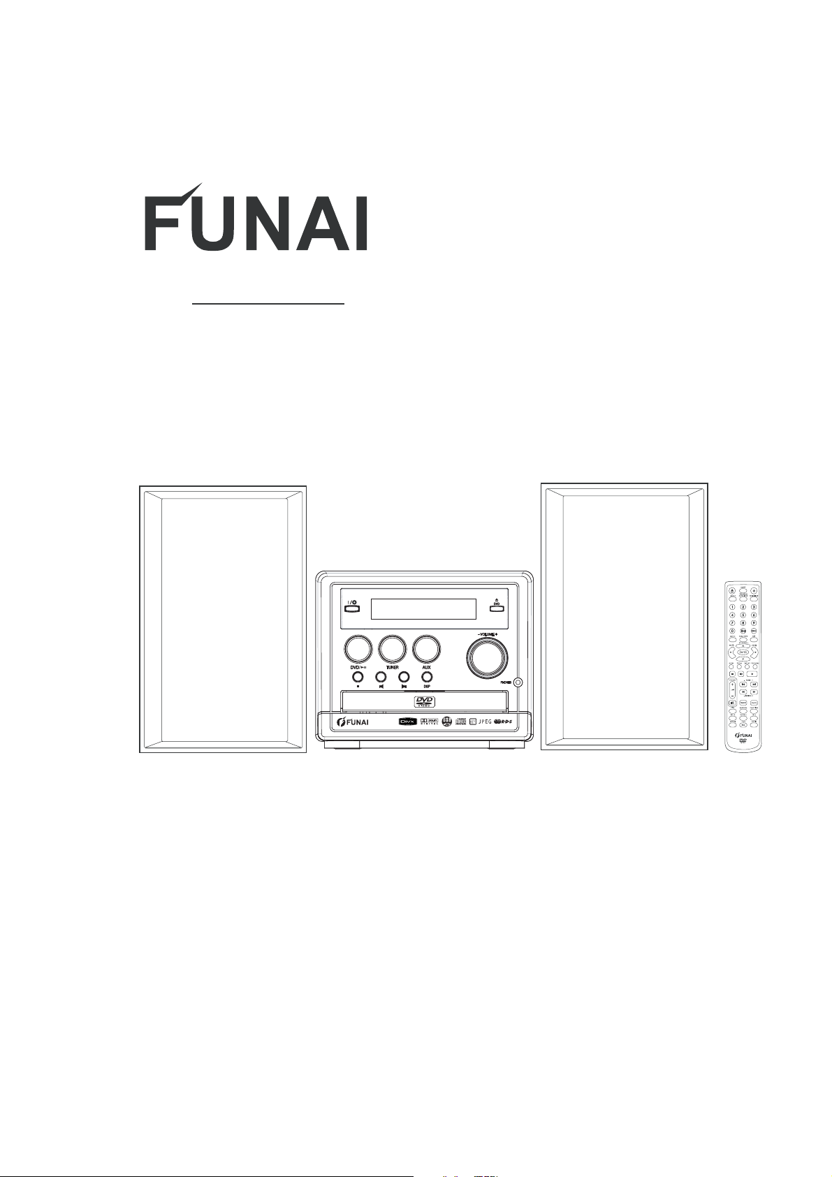
DVA-206LX
CAUTION
BEFORE SERVICING THE UNIT, READ THE "SAFETY PRECAUTIONS"
IN THIS MANUAL.
Page 2
WARNING
WARNING
DVA-206LX
To prevent fire or shock hazard, do not
expose the unit to rain or moisture.
To avoid electrical shock, do not open the
cabinet. Refer servicing to qualified
personnel only. Mains lead must only be
changed at a qualified service shop.
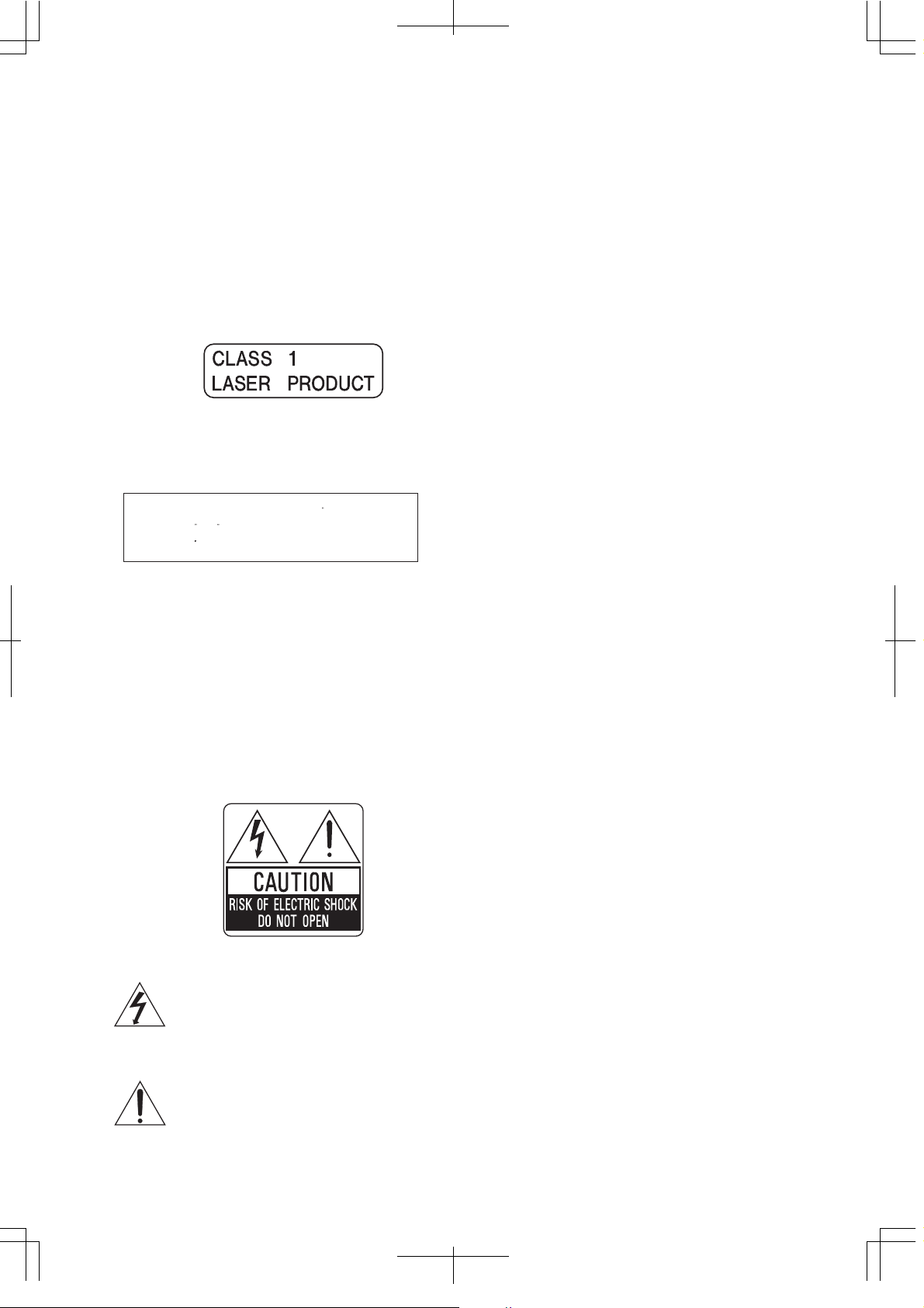
This appliance is classified as a CLASS 1 LASER
product. The CLASS 1 LASER PRODUCT
MARKING is located on the rear panel.
CAU TION . INV ISIB LE LASER R ADIATI ON WHEN O PEN AND IN TERLO CKS DEFE ATED.AV OID EXPO SURE TO BE AM.
VOR SICHT I . UNSIC HTBAR E LASERS TRAHL UNG TRI TT AUS, WE NN DECK EL GEOFFNET UND WENN
SICH ERHEI TSVER RIEGE LUNG UB ERBRU CKT IST. NIC HT DEM ST RAHL AUSS ETZEN I
VARN ING . OSYN LIG LAS ERSTR ALNIN G NAR DEN NA DEL AR OPPN AD OCH SPA RR AR URKO PPLAD ST RALEN
AR FARLI G.
ADVA RSEL. U SYNLIG L ASERS TRALI NG VED ABN ING NAR .
SIKK ERHED SAFBR YDERE E R UDE AF F UNKTI ON . UNDG A UDS/ ETTE LSE FOR ST RALIN G
.
This label is located on the Laser protective
housing inside the enclosure.
Dear Customer,
Thank you for purchasing our product, before
you using it, please read this safety information
and precautions contained in the following
pages to ensure the safe use of your DVD
Player.
To prevent fire or shock hazard, do not expose
this product to rain or moisture.
The apparatus shall not be exposed to dripping
or splashing and that no object filled with
liquids, such as vases, shall be placed on the
apparatus.
CAUTION
To avoid electrical shock, do not open the
cover (or back). Refer servicing to qualified
service personnel.
To prevent electric shock match wide bland of
plug to wide slot, fully insert.
DANGER
This DVD Player uses a visible Laser Beam.
The DVD Player is a class 1 laser product.
To prevent direct exposure laser beam. When
the enclosure is opened, visible laser radiation
is present , which is harmful to the eye.
Use of control or adjustments or performance
of procedures other than those specified herein
may result in hazarded radiation exposure.
Do not open the covers and do not repair
yourself.
Refer to the qualified personnel for servicing.
The lightning flash with arrowhead symbol, within
an equilateral triangle, is intended to alert the
user to the presence of uninsulated "danger
voltage" within the product's enclosure that may
be of sufficient magnitude to constitute a risk of
electric shock to persons.
The exclamation point within an equilateral
triangle is intended to alert the user to presence
of important operating and servicing instructions.
1-1
Page 3

DVA-206LX
I
MPORTANT SAFETY
INSTRUCTIONS
Failed to meet following precautions
may result in damage to DVD Player
Power Sources
Be sure that the power supply voltage of the
area where this unit will be used meets the
required voltage. (230V AC, 50Hz)
Keep the power cord from heating devices.
Do not pinch the power cord by heavy items.
Power cord should be routed well.
Environment
DO NOT
In an environment prone to extreme temperatures
or humidity.
Near heat source like heat registers, stoves,
or other products (including amplifiers) that
produce heat.
Near water - for example, near bath tub,
wash bowl kitchen sink, and the like.
In direct sunlight, heater.
In a dusty environment.
In where strong magnetic fields are generated.
On a surface that is unstable or subject to
vibration.
place the DVD Player
Overloading
Do not overload wall outlet, extension cords,
or integrated convenience receptacles.
Without using
When not using in near future, unplug power
cord.
Cleaning
Unplug this product from the wall outlet before
cleaning.
Do not use liquid cleaners or aerosol cleaners.
Use a damp cloth for cleaning.
Object and Liquid Entry
Do not place heavy objects on the DVD Player.
Do not push objects of any kind into this product.
Never spill liquid of anything on the product.
Ventilation
Do not block the DVD Player's ventilation
openings.
1-2
Page 4

CONTENTS
DISASSEMBLY .................................................................... 1-1
COVER TOP ........................................................................................... 1-1
CABINET FRONT ASSEMBLY ............................................................ 1-1
SPEAKER AND SUBWOOFER JACK ................................................. 1-1
PANEL REAR ASSEMBLY ................................................................... 1-2
TUNER BOX .......................................................................................... 1-2
MPEG BOARD ...................................................................................... 1-2
AMP BOARD ......................................................................................... 1-2
POWER BOARD .................................................................................... 1-3
DVA-206LX
TRANSFORMER .................................................................................... 1-3
DVD MECHANISM ................................................................................. 1-3
DESCRIPTION OF MAJOR ICS ............................................................ 1-4
PARTS LIST ......................................................................... 2-1
CABLE JOIN DIAGRAM ....................................................................... 2-3
DECK MECHANISM EXPLODED VIEW AND PARTS LIST ................ 2-4
PACKING MATERIALS AND ACCESSORIES PARTS LIST ............... 2-10
1-3
Page 5
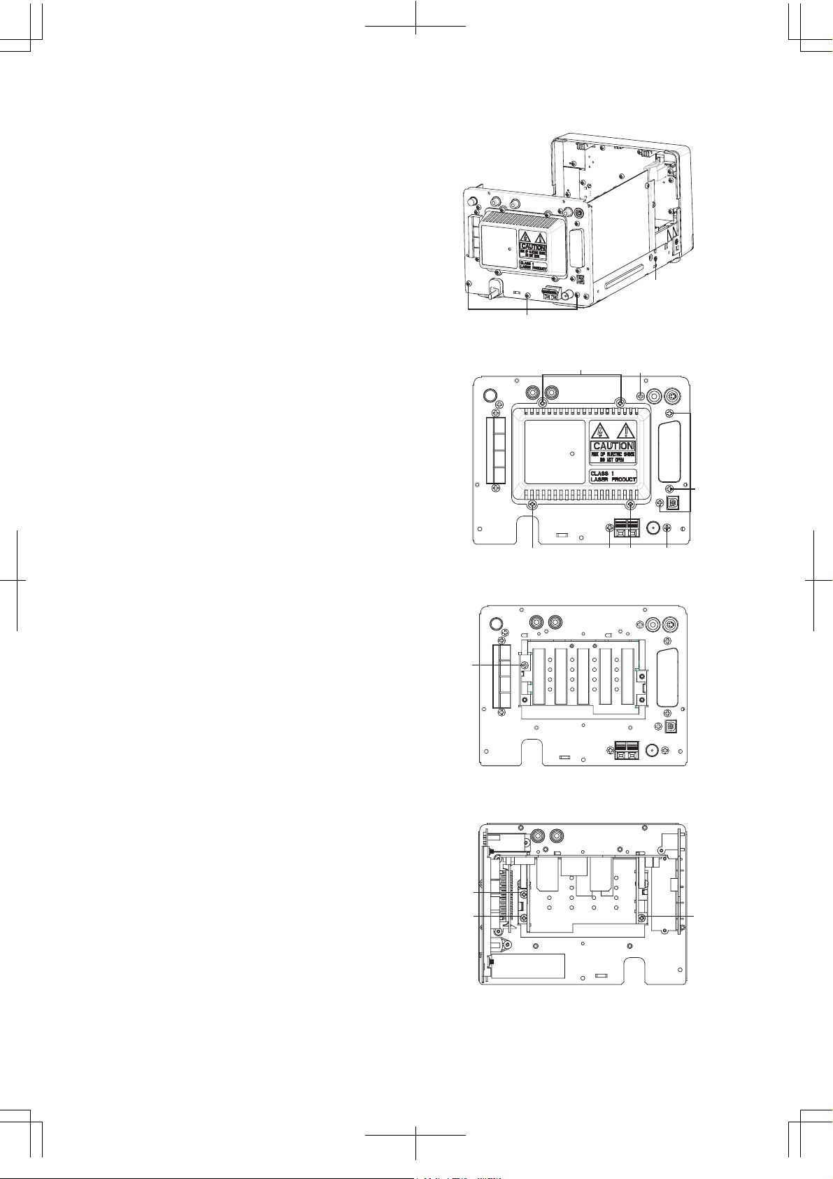
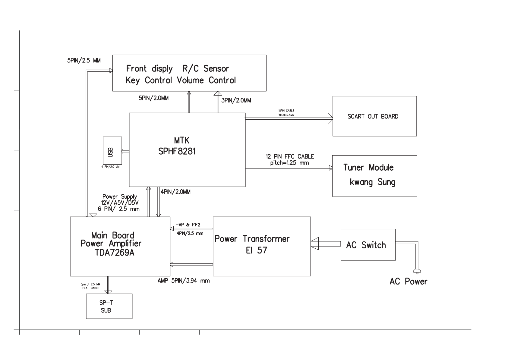
Panel rear assembly
(See Fig.4)
1. Unplug B1-B7, B13, B15.
2. Unscrew 3 screws F and screw G.
3. Take out panel rear upward with tuner box,
mpeg board, speaker jack board and amp
board assembly together.
4. Unplug cable B8.
G
F
Fig.4
Tuner box
(See Fig.5)
* This work based on step 4.
1. Unplug cable B11.
2. Unscrew 2 screws H.
Mpeg board
(See Fig.5)
* This work based on step 4.
1. Unplug A9, A10.
2. Unscrew 4 screws I.
Amp board
(See Fig.5-Fig.7)
* This work based on step 4.
1. Unscrew 4 screws J, remove cover heat
sink (Fig.5).
2. Unscrew screw K (Fig.6).
3. Unplug B16, if mpeg board in its place, need
to unplug B9, B10 yet.
4. Unscrew 3 screws L (Fig.7).
J
JJHH
K
L
L
I
I
Fig.5
Fig.6
L
1-4
Fig.7
Page 6
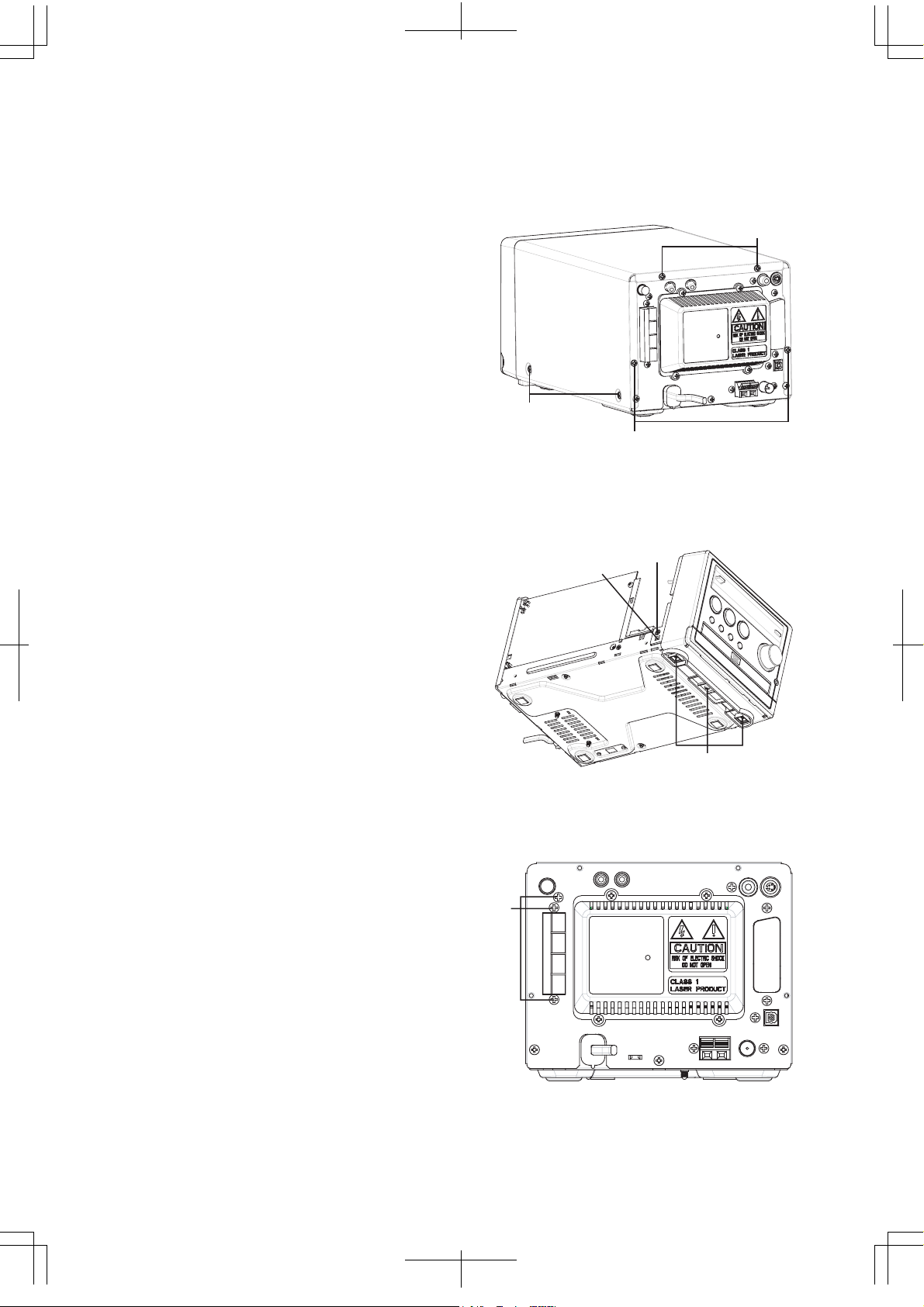
Cover top
(See Fig.1)
1. Unscrew 8 screws A.
2. Pull out cover top upward and backword.
Cabinet front assembly
(See Fig.2)
* This work based on step 1.
1. Power this set, then eject the DVD tray.
2. Force and pull the DVD door out.
3. Unscrew 2 screws B and 3 screws C.
4. Unplug B1-B5, B12.
5. Press the lock D toward two sides and pull
out cabinet front assembly.
A
A
A
Fig.1
B
D
Speaker and subwoofer jack
1. Unplug B16.
2. Unscrew 3 screws E.
C
Fig.2
(See Fig.3)
E
Fig.3
1-5
Page 7
DVA-206LX
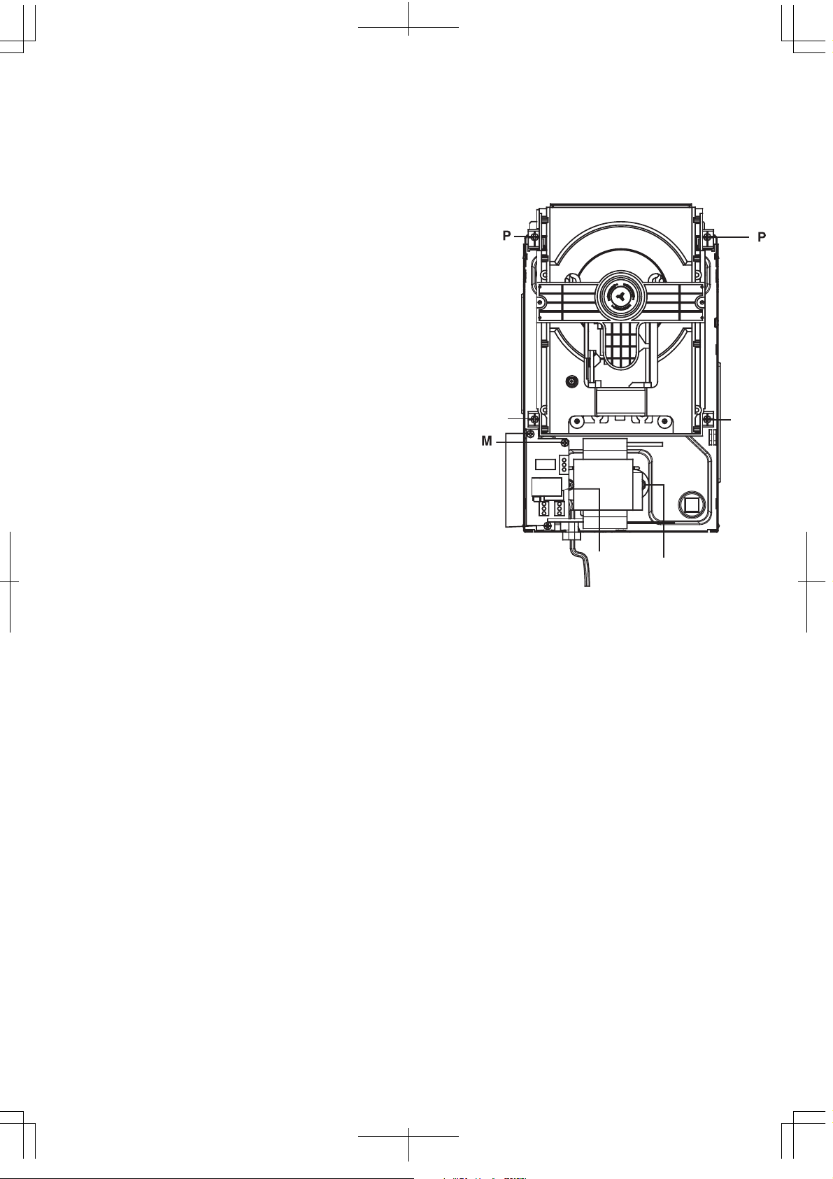
Power board
* This work based on step 4.
1. Unplug B14, B17.
2. Unscrew 3 screws
M
.
Transformer
(See Fig.8)
(See Fig.8)
* This work based on step 4 and step 8.
1. Unscrew 2 screws
N
.
DVD mechanism
(See Fig.8)
* This work based on step 2 and step 4.
P
1. Unscrew 4 screws
.
P
N
N
Fig.8
P
1-6
Page 8
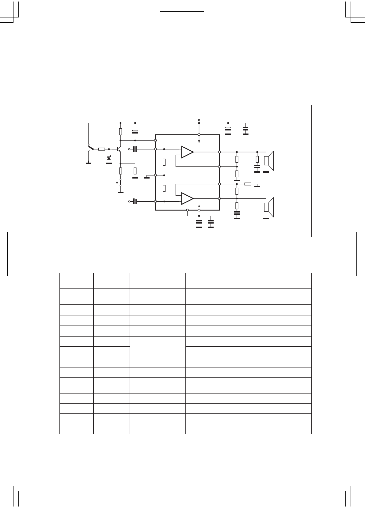
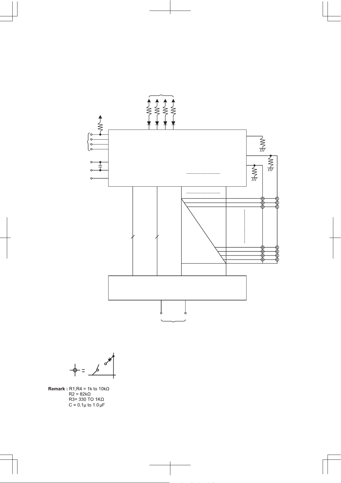
Description of major ICs
TDA7269SA POWER AMPLIFIER
1. Figure 3. Test and Application Circuit (Stereo Configuration)
+V
S
SW1
ST-BY
R2 C3
Q1
R1
DZ
R4
SW2
MUTE
MUTE/
ST-BY
5
IN (L)
7
C1
R3
GND
9
C2
IN (R)
11
D94AU087B
-
-
+
+V
3
6
1
-V
S
C7
S
10 IN- (R)
DVA-206LX
C5
C4
OUT (L)
4+
R10
C9
R7
C8
R9
RL (L)
RL (R)
R5
IN- (L)
8
R6
R8
OUT (R)
2
C6
2. APPLICATION SUGGESTIONS (Demo Board Schematic)
The recommended values of the external components are those shown the demoboard
schematic different values can be used, the following table can help the designer.
S
U
COMPONEN
T
GGESTION
V
ALU
E
P
UR
POSE
ARGER THAN
L
RECOMMENDED VALU
E
R1 10KΩ Mute Circuit Increase of Dz Biasing
Current
R2 15KΩ Mute Circuit V
R3 18KΩ Mute Circuit V
R4 15KΩ Mute Circuit V
R5, R8 18KΩ Closed Loop Gain
R6, R9 560Ω Decrease of Gain
Setting (*)
#5 Shifted Downward V
pin
#5 Shifted Upward V
pin
#5 Shifted Upward V
pin
Increase of Gain
R7, R10 4.7Ω Frequency Stability Danger of Oscillations Danger of Oscillations
C1, C2 1µF Input DC Decoupling Higher Low Frequency Cutoff
C3 1µF St-By/M ute Time
Larger On/Off Time Smaller On/Off Time
Constant
C4, C6 1000µF Supply Voltage Bypass Danger of Oscillations
C5, C7 0.1µF Supply Voltage Bypass Danger of Oscillations
C8, C9 0.1µF Frequency Stability
Dz 5.1V Mute C
ircuit
S
MALLER T
HAN
RECOMMENDED VALU
#5 Shifted Upward
pin
#5 Shifted Downward
pin
#5 Shifted Downward
pin
E
(*) Closed loop gain has to be 25dB
1-7
Page 9
DVA-206LX
AD6315 VFD CONTROLLER / DRIVER
Features
- Multiple display modes
(16-segment & 12-digit to 24-segment & 4-digit)
- Key scanning (16 x 2 matrix)
- Dimming circuit (eight steps)
- High-voltage output ( V
- 4 channel LED ports
- No external resistors necessary for driver
outputs
(P-ch open-drain + pull-down resistor output)
- Serial interface (CLK, STB, D
- Package: 44-pin plastic QFP and LQFP
2. Pin Assignments
EE (max)
= VDD – 35V )
, D
)
IN
OUT
General Description
The AD6315 is a VFD (Vacuum Fluorescent Display
or fluorescent Indicator Panel) driver that is driven
on a 1/4- to 1/12- duty factor. It consists of 16
segments and 4 grids output lines, 8 segments /
grid output driving lines, a display memory, a control
circuit, and a key scan circuit. Serial data is input to
the AD6315 through a 3-wire serial interface. This
VFD driver is ideal as a peripheral device for a
single-chip microcomputer
.
Seg20/Grid9
Seg21/Grid
Seg22/Grid
Seg23/Grid6
Seg24/Grid5
Grid
Grid3
Grid2
Grid1
V
DD
11
12
/Grid
/Grid
18
17
Seg19/Grid10
Seg
Seg
31
32
33
3435363738394041424344
8
7
16
/KS
16
VEESeg
29
30
28
14
13
12
11
10
/KS
/KS
/KS
/KS
14
13
12
Seg15/KS15
Seg
Seg
Seg
25
26
27
11
Seg
24
/KS
10
Seg
23
2221201918171615141312
Seg9/KS9
Seg8/KS
Seg7/KS
8
7
Seg6/KS6
Seg5/KS5
4
Seg4/KS4
Seg3/KS3
Seg2/KS2
Seg1/KS1
V
DD
1-8
V
V
SS
11
10
9
8
7
6
5
4
3
2
1
1
LED
2
LED
4
OSC
LED
LED3
OUT
D
IN
D
CLK
STB
1
KEY
2
KEY
SS
Page 10
3. Pin Descriptions
y
Symbol Name No. Description
D
IN
D
OUT
Data input 7
Data output 6
STB Strobe 9
CLK
OSC
Seg
/KS1 to
1
Seg
/KS16
16
Grid
to Grid4 High-voltage output (Grid) 39 to 42 Grid output pins
1
/Grid12 to
Seg
17
Seg
/Grid5
24
to LED4 LED output 1 to 4 CMOS output
LED
1
, KEY2 Key data input 10, 11
KEY
1
V
DD
V
SS
V
EE
Clock input 8
Oscillator pin 5
High-voltage output (Segment) 14 to 29
High-voltage output
(Segment/grid)
31 to 38
Logic power 13, 43
Logic ground 12, 44 Connect this pin to system GND.
Pull-down level 30
Input serial data at rising edge of shift clock,
starting from the low order bit.
Output serial data at the falling edge of the
shift clock, starting from low order bit. This is
N-ch open-drain output pin.
Initializes serial interface at the rising or
falling edge of the AD6315. It then waits for
reception of a command. Data input after
STB falling is processed as a command.
While command data is processed, current
processing is stopped, and the serial
interface is initialized. While STB is high, CLK
is ignored.
Reads serial data at the rising edge, and
outputs data at the falling edge.
Connect resistor in between this pin and Vss to set
up the oscillation frequency.
Segment output pins (Dual function as key
source)
These pins are selectable for segment or grid
driving.
Data input to these pins is latched at the end
of the display cycle.
Logic power supply
Driver power supply
DVA-206LX
4. Ordering Information
AD6315 X X
Package
Q: QFP-44L
Packing
Blank : Tra
L : LQFP-44L
1-9
Page 11
DVA-206LX
5. Absolute Maximum Ratings (TA = 25OC, VSS = 0V)
Parameter Symbol Rating
Logic supply voltage VDD -0.5 to +6.0 V
Driver supply voltage V
Logic input voltage V
VFD driver output voltage V
LED driver output current I
VFD driver output current I
Power dissipation P
Operating ambient temperature T
Storage temperature T
Note :
Derate at -6.4W/OC TA = 25OC or higher.
Caution :
If the absolute maximum rating of even one of the above parameters is exceeded even
momentarily, the quality of the product may be degraded. Absolute maximum ratings, therefore,
specify the values exceeding which the product may be physically damaged. Be sure to use the
product within the range of the absolute maximum ratings.
V
EE
- 0.5 to VDD + 0.5 V
I1
V
O2
O1
O2
D
-25 to +85
A
-50 to +150
stg
+ 0.5 to VDD – 40 V
DD
- 0.5 to VDD + 0.5 V
EE
15 mA
-40 (grid)
-15 (segment)
800 (Note) mW
Unit
mA
O
C
O
C
6. Recommended Operating Range (TA = -20 to 70OC, VSS = 0V)
Parameter Symbol Min. Typ. Max. Unit
Remark :
Logic supply voltage V
High-level input voltage V
Low-level input voltage V
Driver supply voltage V
Maximum power consumption
Pmax = VFD driver dissipation + R
consumption
Where
segment current = 3mA, grid current = 15mA, and LED current = 20mA
VFD driver dissipation = number of segments x 6 + number of grids/(number of grids + 1) x
30(mW)
R
L dissipation
~
(VDD - VEE)2 / 50 x (number of segments + 1 ) (mW)
=
LED driver dissipation = number of LEDs x 20 (mW)
Dynamic power consumption = V
4.5 5 5.5 V
DD
0.7 VDD VDD V
IH
0 0.3 V
IL
0 VDD-35
EE
L dissipation + LED driver dissipation + dynamic power
DD x 5 (mW)
V
DD
V
1-10
Page 12
7. Application Circuit
DVA-206LX
V
DD
To Microcontroller
-30V V
V
DD
R1
D
OUT
D
IN
CLK
LED
LED1
LED2
R3
In the case of low-level output is display on signal.
OSC
LED3
LED4
R2
STB
AD16315
5
V
DD
0V
V
DD
C
V
SS
EE
to Grid4
1
Grid
4
12
/Grid
/Grid
17
to Seg
Seg
8
24
16
/KS
16
Seg
1
/KS
1
Seg
KEY
KEY
2
1
R4
Key Matrix
Note
(16X2)
Note :
Fluorescent Indicator Panel (FIP)
(VFD)
F+
Driving voltage for FIP (VFD)
F-
1-11
Page 13
DVA-206LX
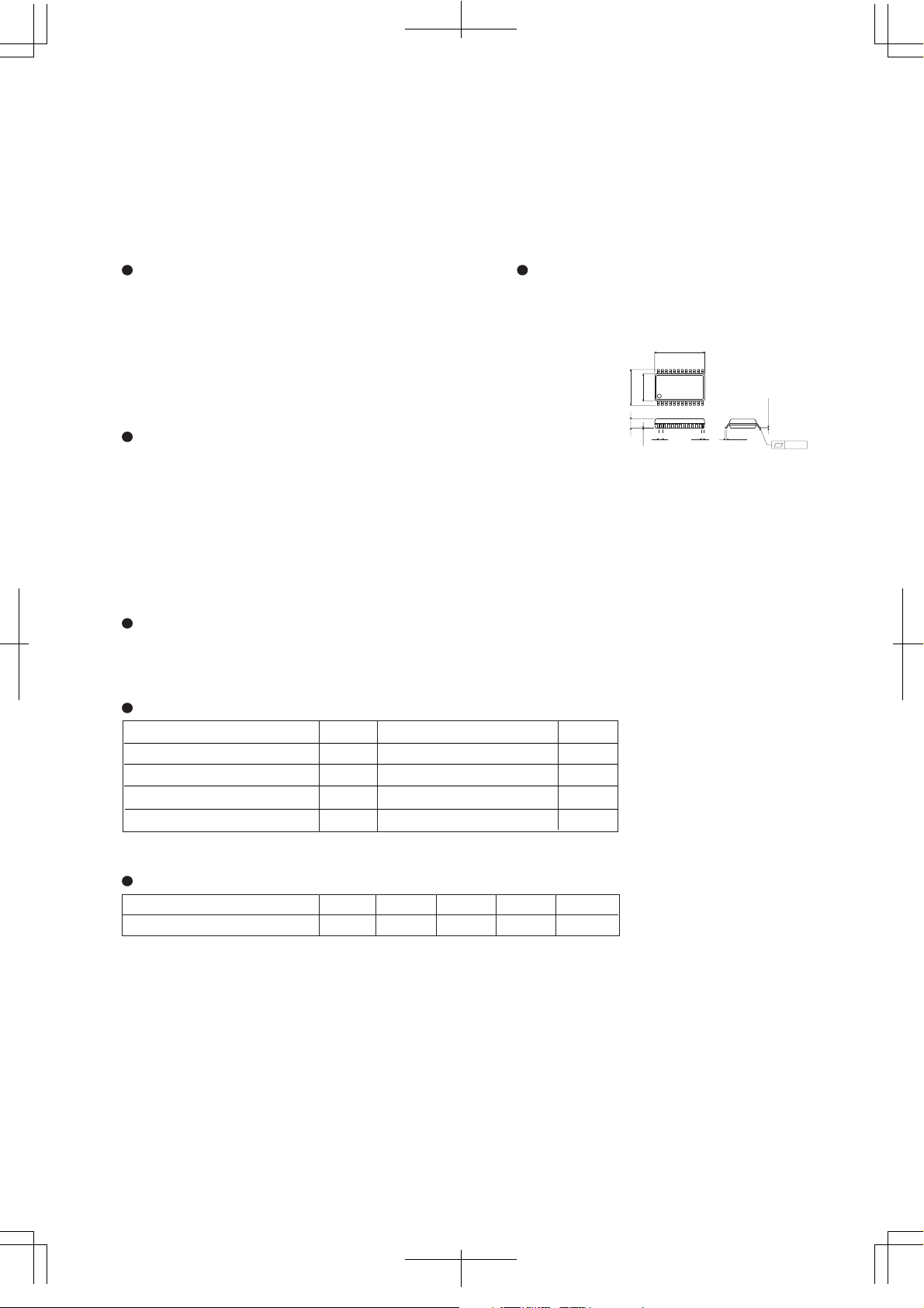
BD3871 SOUND PROCESSOR
Description Dimension (Units : mm)
BD3871FS is a sound processor for CD/MD radio
cassette player. This IC provides all functions,
such as input selector (3 input sources), an input
gain amplifier (25dB, 27dB, 29dB),and a surround,
tone (bass, treble). This IC can be controlled
by a 2-wire serial data interface.
Features
7.8±0.3
1.8±0.1
5.4±0.2
0.1 1
1) Can select center frequency and Q value of Bass
characteristics by external components.
2) Mute switch at the input terminal can reduce cross talk.
3) Surround function is composed without external components.
4) Ideal for energy-saving designs with low current consumption
due to the adoption of the BiCMOS process, allowing easy-design
of the regulator blocks in the set.
10.0±0.2
24
13
12
1
0.36±0.1
0.8
SSOP-A24
0.3Min
0.15±0.1
0.15
Applications
CD radio cassette player, MD radio cassette player, Micro component stereo
Absolute Maximum Ratings (Ta=25°C)
-25
-55
Limits
10
800
~
~
+75
+125
Unit
V
mW
°C
°C
Parameter Symbol
Power supply voltage
Power dissipation
Operating temperature range
Storage temperature range
∗ Derating : 8.0mW/°C for operation above Ta=25°C
Vcc
Pd
Topr
Ts tg
Recommended Operating Conditions (Ta=25°C)
Parameter Min. Max. UnitTyp.Symbol
Operating voltage V
DD 84.5 9.5 V
1-12
Page 14
Electrical characteristics
(Unless otherwise noted ; Ta=25°C, Vcc=8V, f=1kHz, Vi=50mVrms, RL=10 , Rg=600 ,
INPUT GAIN=24dB, Vol=0dB, bass,treble=0dB, surround=OFF)
Symbol Min. Max. Unit ConditionsTyp.Parameter
Circuit current
Output voltage gain
Total harmonic distortion
Maximum output voltage
Residual noise voltage
Output residual noise voltage
Volume control range
Bass control range
Treble control range
Surround gain (Antiphase)
I
Q
G
V
THD
Vomax
Vno
Vmno
VRI
GB
TB
Vsur
-
22
-
1.6
-
-
-90
+12
-16
+10
-14
8
8
24
0.01
2.1
4.5
40
-87
+14
-14
+12
-12
10
21
26
0.1
-
15
80
-84
+16
-12
+14
-10
12
mA
dB
%
Vrms
µVrms
µVrms
dB
dB
dB
dB
No signal
V
OUT=1Vrms, Bw=400~30kHz
THD=1%, Bw=400~30kHz
Rg=0 , Vol=-
●
Rg=0 , Vol=0dB, Bw=IHF-A
V
IN=1Vrms, 1dB/STEP
IN=100mVrms, 2dB/STEP
V
V
IN=100mVrms, 2dB/STEP
IN=100mVrms
V
DVA-206LX
, Bw=IHF-A
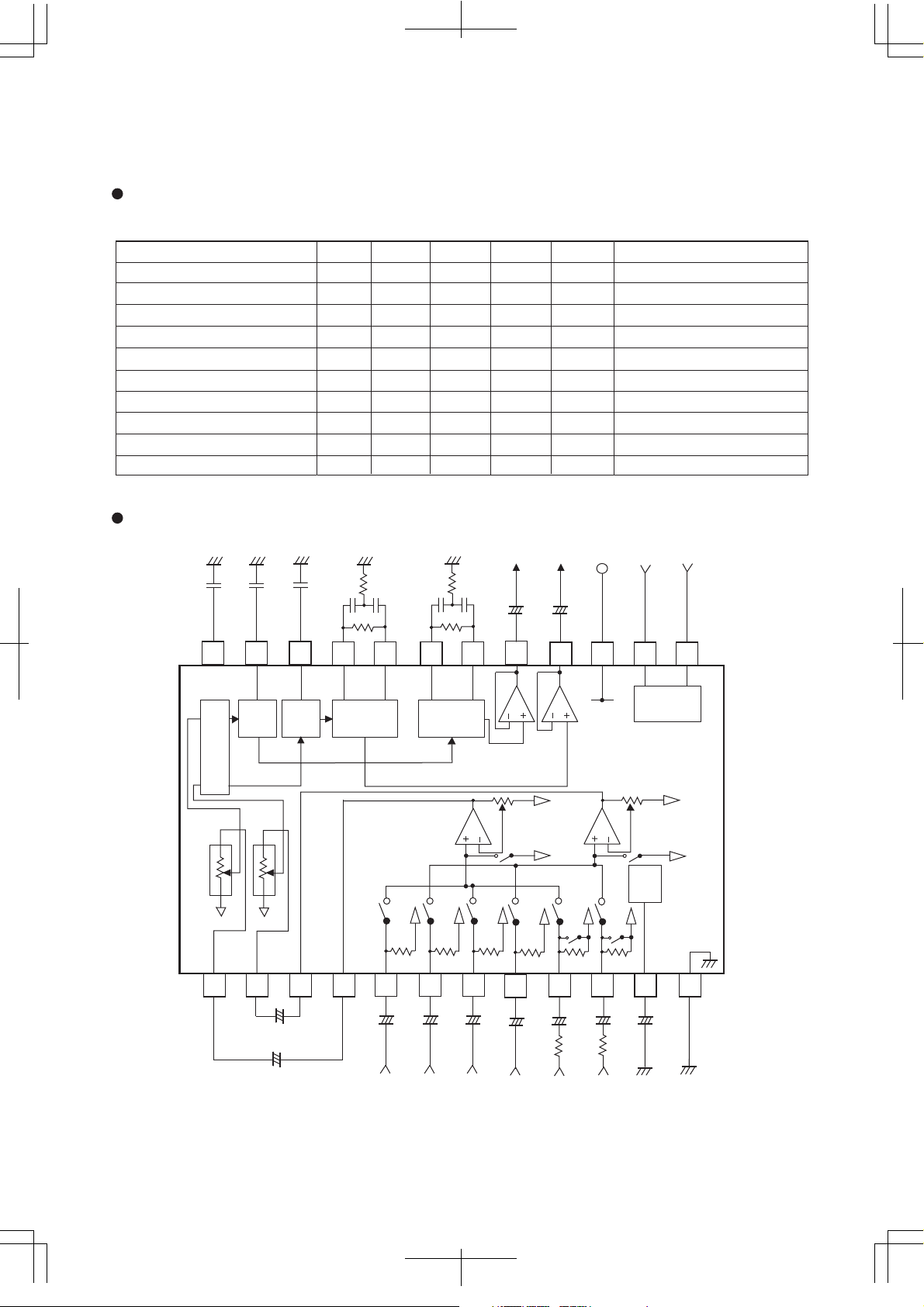
Application Circuit
0.33
µ
Surround
0dB
~
-87dB
-
●
0.0022
Treble1
fc=8kHz
Vcc/2Vcc/2
0.0022
µ
Treble2
fc=8kHz
+
10µ
+
µ
10
µ
5.6K
0.1µ 0.1µ
390K
Bass
2
f
0
=80Hz
0.1µ 0.1µ
50k
+
10
µ
390K
Bass1
f
0
=80Hz
+
10
µ
5.6K
+
10
50k50k
µ
OUT1
10µ
50k
+
10µ
DATA
VccOUT2
CLOCK
LATCH
10µ
++
131415161718192021222324
Logic
Vcc/2
987654321
+
10
4.7K
50k
Vcc/2
50k
+
10µ
µ
4.7K
+
47µ
Vcc/2
BD3871FS
121110
UNIT
RESISTANCE :
CAPACITOR : F
C2
C1B2B1A2A1
1-13
Page 15

DVA-206LX
FEATURES:
8 Mbit (x8) Multi-Purpose Flash
SST39VF088
SST39VF0882.7V 8Mb (x8) MPF memory
Preliminary Specifications
• Organized as 1M x8
• Single Voltage Read and Write Operations
– 2.7-3.6V
• Superior Reliability
– Endurance: 100,000 Cycles (typical)
– Greater than 100 years Data Retention
• Low Power Consumption (typical values at 5 MHz)
– Active Current: 12 mA (typical)
– Standby Current: 4 µA (typical)
• Sector-Erase Capability
– Uniform 4 KByte sectors
• Block-Erase Capability
– Uniform 64 KByte blocks
• Fast Read Access Time:
– 70 and 90 ns
• Latched Address and Data
PRODUCT DESCRIPTION
• Fast Erase and Byte-Program
– Sector-Erase Time: 18 ms (typical)
– Block-Erase Time: 18 ms (typical)
– Chip-Erase Time: 70 ms (typical)
– Byte-Program Time: 14 µs (typical)
– Chip Rewrite Time: 15 seconds (typical)
• Automatic Write Timing
– Internal V
Generation
PP
• End-of-Write Detection
– Toggle Bit
– Data# Polling
• CMOS I/O Compatibility
• JEDEC Standard
– Flash EEPROM Pinouts and command sets
• Packages Available
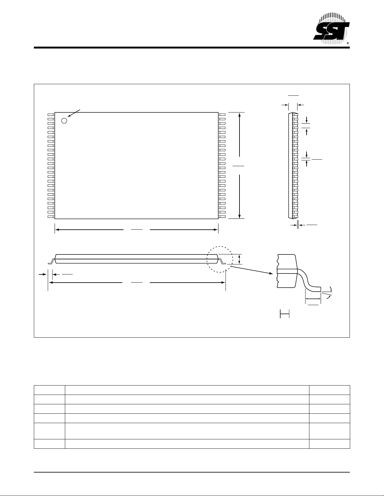
– 48-lead TSOP (12mm x 20mm)
The SST39VF08 8 device is a 1M x8 CMO S Mult i-P urpose
Flash (MPF) manufactured with SST’s proprietary, high
performance CMOS SuperFlash technology. The split-gate
cell design and th ick-oxide tunneling in jector attain better
reliability and manufacturability compared with alternate
approaches. The S ST39V F088 wr i tes (P rogram or E rase)
with a 2.7-3.6V power supply. It conforms to JEDEC standard pinouts for x8 memories.
Featuring high performance Byte-Program, the
SST39VF088 device provides a typical Byte-Program time
of 14 µsec. The devices u s e Toggle Bit or Data# Polling to
indicate the comp letion of Program operation. To protect
against inadver ten t wri te, they have on-chip hardware and
Software Data Protection schemes. Designed, manufactured, and tested for a wide spectrum of applications, these
devices are offered with a guaranteed endurance of 10,000
cycles. Data retention is rated at greater than 100 years.
The SST39VF088 device is suited for applications that
require convenient and economica l updating of program,
configuration, or da ta memory. For all system appl i ca tio ns,
they significantly i mp r ove performa nc e an d re liability, while
lowering power consumption. They inherently use less
energy during Erase and Program than alternative flash
technologies. The tota l energy consumed is a function of
the applied voltage, curre nt, and time of ap plic ation. S inc e
for any given voltage range, the SuperFlash technology
uses less current to program and has a shorter erase time,
the total energy consumed during any Erase or Program
operation is less than alternative flash technologies. They
also improve flexibility while l owerin g the cost for program ,
data, and configuration storage applications.
The SuperFlash technology provides fixed Erase an d P r ogram times, independent o f the num ber of Erase/ Program
cycles that have occurred. Therefore the system software
or hardware does not have to be modified or de-rated as is
necessary with al ternativ e flas h techn ologies , whos e Erase
and Program times i ncrease with accumul ated Erase/P rogram cycles .
To meet high density, surface mount requirements, the
SST39VF088 is offered in 48-lead TSO P packaging. See
Figure 1 f or pi n assign ments .
©2003 Silicon Storage Technology, Inc.
S71227-04-000 11/03
1
1-14
The SST logo and SuperFlash are registered trademarks of Silicon Storage Technology, Inc.
MPF is a trademark of Silicon Storage Technology, Inc.
These specifications are subject to change without notice.
Page 16
8 Mbit Multi-Purpose Flash
SST39VF088
DVA-206LX
Preliminary Specifications
A16
A15
A14
A13
A12
A11
A10
A9
NC
NC
WE#
NC
NC
NC
NC
A19
A18
A8
A7
A6
A5
A4
A3
A2
1
2
3
4
5
6
7
8
9
10
11
12
13
14
15
16
17
18
19
20
21
22
23
24
Standard Pinout
T op Vie w
Die Up
FIGURE 1: PIN ASSIGNMENTS FOR 48-LEAD TSOP
TABLE 2: P
Symbol Pin Name Functions
1
-A
A
MS
DQ7-DQ
CE# Chip Enable To activate the device when CE# is low.
OE# Output Enable To gate the data output buffers.
WE# Write Enable To control the Write operations.
V
DD
V
SS
NC No Connection Unconnected pins.
1. AMS = Most significant address
A
MS
IN DESCRIPTION
Address Inputs To provide memory addresses. During Sector-Erase AMS-A12 address lines will s elect the
0
Data Input/output To output data during Read cycles and receive input data during Write cycles.
0
sector. During Block-Erase A
MS-A16
Data is internally latched during a Write cycle.
The outputs are in tri-state when OE# or CE# is high.
Power Supply To provide power supply voltage: 2.7-3.6V for SST39VF088
Ground
= A19 for SST39VF088
48
47
46
45
44
43
42
41
40
39
38
37
36
35
34
33
32
31
30
29
28
27
26
25
1227 48-tsop P01.0
A17
NC
V
SS
A0
DQ7
NC
DQ6
NC
DQ5
NC
DQ4
V
DD
NC
DQ3
NC
DQ2
NC
DQ1
NC
DQ0
OE#
V
SS
CE#
A1
address lines will select the block.
T2.0 1227
©2003 Silicon Storage Technology, Inc. S71227-04-000 11/03
1-15
Page 17
DVA-206LX
8 Mbit Multi-Purpose Flash
SST39VF088
Preliminary Specifications
Absolute Maximum Stress Ratings (Applied conditions greater than those listed under “Absolute Maximum
Stress Ratings” may cause pe r manent dama ge to the device. This is a stres s rating only and funct ional operatio n
of the device at these conditions or conditions greater tha n those defined in the ope rational sections of t his data
sheet is not implied. Exposure to absolute maximum stress rating conditions may affect device reliability.)
Temperature Under Bias . . . . . . . . . . . . . . . . . . . . . . . . . . . . . . . . . . . . . . . . . . . . . . . . . . . . . . . . . -55°C to +125°C
Storage Temperature . . . . . . . . . . . . . . . . . . . . . . . . . . . . . . . . . . . . . . . . . . . . . . . . . . . . . . . . . . . -65°C to +150°C
D. C. Voltage on Any Pin to Ground Potential . . . . . . . . . . . . . . . . . . . . . . . . . . . . . . . . . . . . . . . .-0.5V to V
Transient Voltage (<20 ns) on Any Pin to Ground Potential . . . . . . . . . . . . . . . . . . . . . . . . . . . . .-2.0V to V
Voltage on A
Pin to Ground Potential . . . . . . . . . . . . . . . . . . . . . . . . . . . . . . . . . . . . . . . . . . . . . . . . -0.5V to 13.2V
9
Package Power Dissipation Capability (Ta = 25°C) . . . . . . . . . . . . . . . . . . . . . . . . . . . . . . . . . . . . . . . . . . . . . . 1.0W
Surface Mount Lead Soldering Temperature (3 Seconds) . . . . . . . . . . . . . . . . . . . . . . . . . . . . . . . . . . . . . . . 240°C
Output Short Circ uit Cur rent
1. Outputs shorted for no more than one second. No more than one output shorted at a time.
1
. . . . . . . . . . . . . . . . . . . . . . . . . . . . . . . . . . . . . . . . . . . . . . . . . . . . . . . . . . . . . 50 mA
DD
DD
+0.5V
+2.0V
OPERATING RANGE FOR SST39V F088
Range Ambient Temp V
Commercial 0°C to +70°C 2.7-3.6V
Industr ial -40°C to +85°C 2.7-3.6V
DD
AC CONDITIONS OF TEST
Input Rise/Fall Time . . . . . . . . . . . . . . 5 ns
Output Load . . . . . . . . . . . . . . . . . . . . CL = 100 pF
See Figures 11 and 12
©2003 Silicon Storage Technology, Inc. S71227-04-000 11/03
1-16
Page 18

Preliminary Specifications
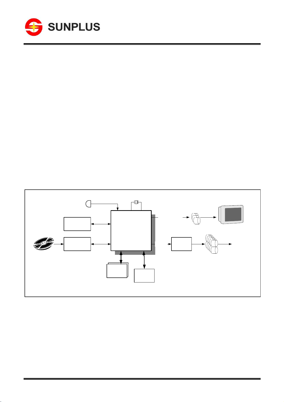
PRODUCT ORDERING INFORMATION
SST 39 VF 088 - 70 - 4C - EK E
XX
XXXXXX -XXX -XX-XXX X
DVA-206LX
8 Mbit Multi-Purpose Flash
SST39VF088
Environmental Attribute
E = non-Pb
Package Modifi e r
K = 48 leads
Package Type
E = TSOP (type 1, die up, 12mm x 20mm)
Temperature Range
C = Commercial = 0°C to +70°C
I = Industrial = -40°C to +85°C
Minimum Endurance
4 = 10,000 cycles
Read Access Speed
70 = 70 ns
90 = 90 ns
Device Density
088 = 8 Mbit
Voltage
V = 2.7-3.6V
Product Series
39 = Multi-Purpose Flash
Valid combinations for SST39VF088
SST39VF088-70-4C-EK
SST39VF088-70-4C-EKE
SST39VF088-90-4C-EK
SST39VF088-90-4C-EKE
SST39VF088-70-4I-EK
SST39VF088-70-4I-EKE
SST39VF088-90-4I-EK
SST39VF088-90-4I-EKE
Note: Valid combinations are those products in mass production or will be in mass production. Consult your SST sales
representative to confirm availability of valid combinations and to determine availability of new combinations.
©2003 Silicon Storage Technology, Inc. S71227-04-000 11/03
1-17
Page 19
DVA-206LX
8 Mbit Multi-Purpose Flash
SST39VF088
PACKAGING DIAGRAMS
Pin # 1 Identifier
12.20
11.80
Preliminary Specifications
1.05
0.95
0.50
BSC
0.27
0.17
18.50
18.30
0.70
0.50
Note: 1. Complies with JEDEC publication 95 MO-142 DD dimensions,
although some dimensions may be more stringent.
2. All linear dimensions are in millimeters (max/min).
3. Coplanarity: 0.1 mm
4. Maximum allowable mold flash is 0.15 mm at the package ends, and 0.25 mm between leads.
20.20
19.80
1.20
DETAIL
max.
1mm
0.15
0.05
0.70
0.50
48-tsop-EK-8
48-LEAD THIN SMALL OUTLINE PACKAGE (TSOP) 12MM X 20MM
SST PACKAGE CODE: EK
TABLE 11: R
Number Description Date
00
01
02
03
EVISION HISTORY
• Initial Release
• Corrected Byte-Program 3rd Cycle Data from 20H to A0H in Table 4 on page 6
• Corrected Byte-Program 3rd Cycle Data from 20H to A0H in Figures 3 and 4
• Auto Low Power feature references removed.
Mar 2003
Apr 2003
Jun 2003
Aug 2003
(CE# toggled high achieves same effect.)
04
• 2004 Data Book
Nov 2003
0˚- 5˚
©2003 Silicon Storage Technology, Inc. S71227-04-000 11/03
1-18
Page 20
Features
• Low-voltage and Standard-voltage Operation
– 2.7 (V
– 1.8 (V
• Internally Organized 128 x 8 (1K), 256 x 8 (2K), 512 x 8 (4K),
1024 x 8 (8K) or 2048 x 8 (16K)
• 2-wire Serial Interface
• Schmitt Trigger, Filtered Inputs for Noise Suppression
• Bi-directional Data Transfer Protocol
• 100 kHz (1.8V) and 400 kHz (2.5V, 2.7V, 5V) Compatibility
• Write Protect Pin for Hardware Data Protection
• 8-byte Page (1K, 2K), 16-byte Page (4K, 8K, 16K) Write Modes
• Partial Page Writes are Allowed
• Self-timed Write Cycle (5 ms max)
• High-reliability
– Endurance: 1 Million Write Cycles
– Data Retention: 100 Years
• Automotive Grade, Extended Temperature and Lead-free/Halogen-free Devices
Available
• 8-lead PDIP, 8-lead JEDEC SOIC, 8-lead MAP, 5-lead SOT23,
8-lead TSSOP and 8-ball dBGA2™ Packages
= 2.7V to 5.5V)
CC
= 1.8V to 5.5V)
CC
DVA-206LX
2-wire
Serial EEPROM
1K (128 x 8)
2K (256 x 8)
4K (512 x 8)
8K (1024 x 8)
Description
The AT24 C01A/02/04 /08/1 6 provides 1024/ 2048/40 96/8192/ 16384 bits of ser ial electrically erasable and programmable read-only memor y (EEPROM) organized as
128/256/512/1024/2048 words of 8 bits each. The device is optimized for use in many
industrial and commercial applications where low-power and low-voltage operation
are essential. The AT24C01A/02/04/08/16 is available in space-saving 8-lead PDIP,
8-lead JEDEC SOIC, 8-lead MAP, 5-lead SOT23 (AT24C01A/AT24C02/AT24C04), 8lead TSSOP and 8-ball dBGA2 packages and is accessed via a 2-wire serial interface.
In addition, the entire family is available in 2.7V (2.7V to 5.5V) and 1.8V (1.8V to 5.5V)
versions.
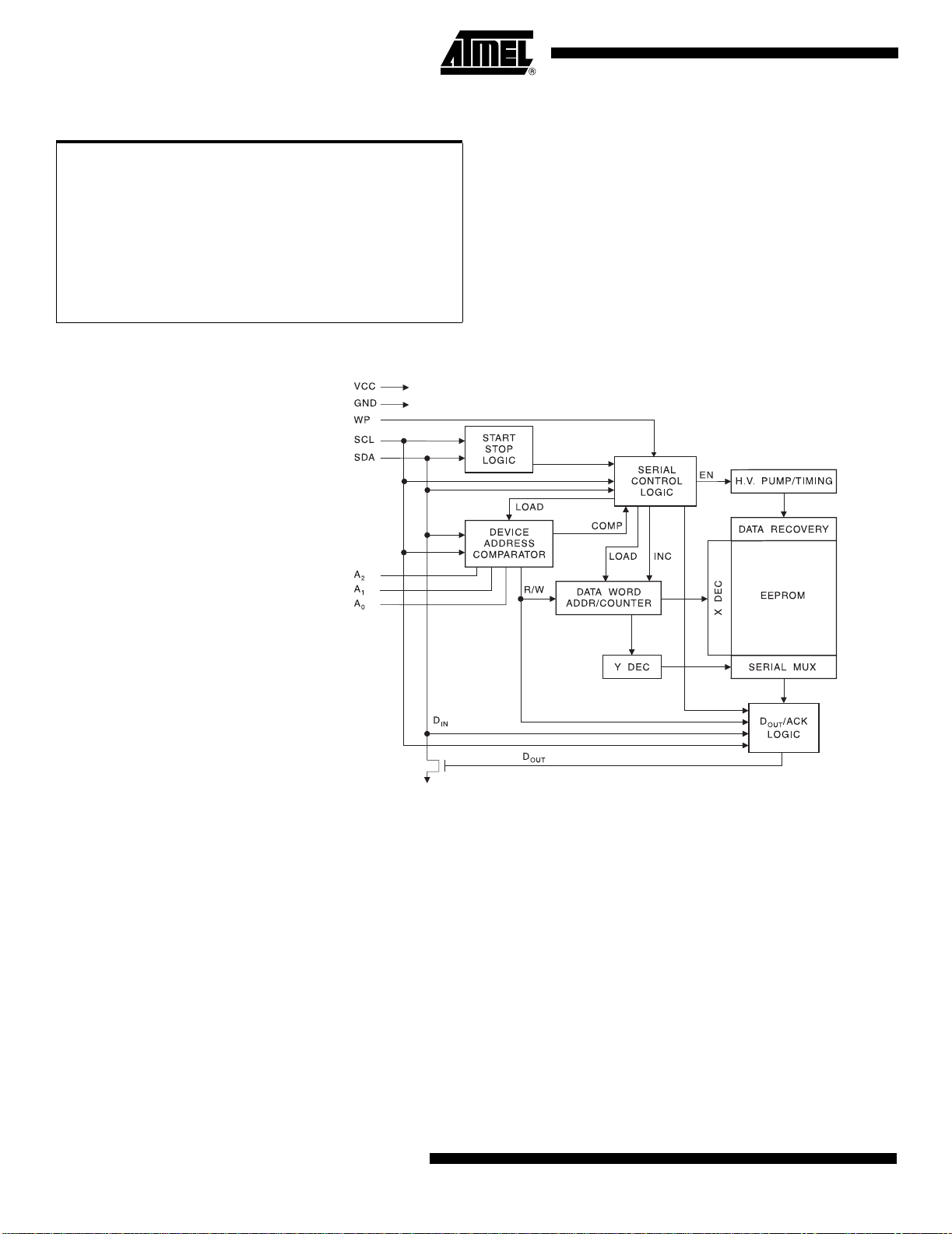
Pin Configurations
Pin Name Function
A0 - A2 Address Inputs
SDA Serial Data
SCL Serial Clock Input
WP Write Pro tect
NC No Connect
GND Ground
VCC Power Supply
8-lead TSSOP
A0
A1
A2
GND
8-ball dBGA2
VCC
WP
SCL
SDA
Bottom View
8
1
2
3
4
8
7
6
5
VCC
7
WP
6
SCL
5
SDA
1
A0
2
A1
3
A2
4
GND
GND
A0
A1
A2
VCC
WP
SCL
SDA
8-lead SOI C
1
2
3
4
8-lead MAP
8
7
6
5
Bottom View
VCC
8
WP
7
SCL
6
SDA
5
A0
1
A1
2
A2
3
GND
4
16K (2048 x 8)
AT24C01A
AT24C02
AT24C04
AT24C08
AT24C16
Note: 1. This device is not recom-
mended for new designs.
Please refer to AT24C08A.
2. This device is not recommended for new designs.
Please refer to AT24C16A.
(1)
(2)
A0
A1
A2
GND
8-lead PDIP
1
2
3
4
8
7
6
5
VCC
WP
SCL
SDA
5-lead SOT23
SCL
GND
SDA
5-lead SOT23 Rotated (R)
(1k only)
1
2
3
WP
5
VCC
4
SCL
GND
SDA
1
2
3
VCC
5
NC
4
0180R–SEEPR–4/04
1
1-19
Page 21
DVA-206LX
Absolute Maximum Ratings
Operating Temperature.................................. -55°C to +125°C
Storage Temperature..................................... -65°C to +150°C
Voltage on Any Pin
with Respect to Ground.....................................-1.0V to +7.0V
Maximum Operating Voltage ..........................................6.25V
DC Output Current........................................................5.0 mA
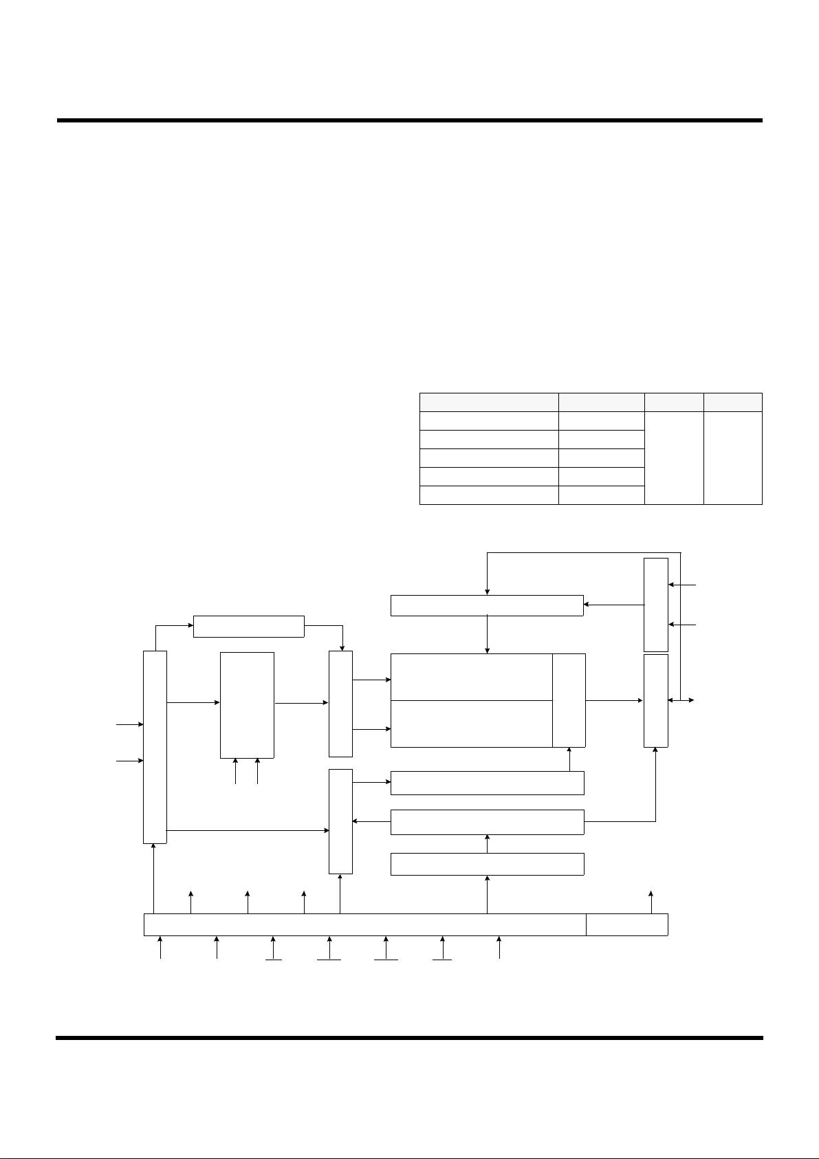
Block Diagram
*NOTICE: Stresses beyond those listed under “Absolute
Maximum Ratings” may cause permanent damage to the dev ice . This i s a stress r at ing onl y and
functional operati on of the de vic e at these or an y
other conditions beyond those indicated in the
operational sections of this specification is not
implied. Exposure to absolute maximum rating
conditions f or extend ed periods ma y affect d evice
reliability.
2
AT24C01A/02/04/08/16
0180R–SEEPR–4/04
1-20
Page 22
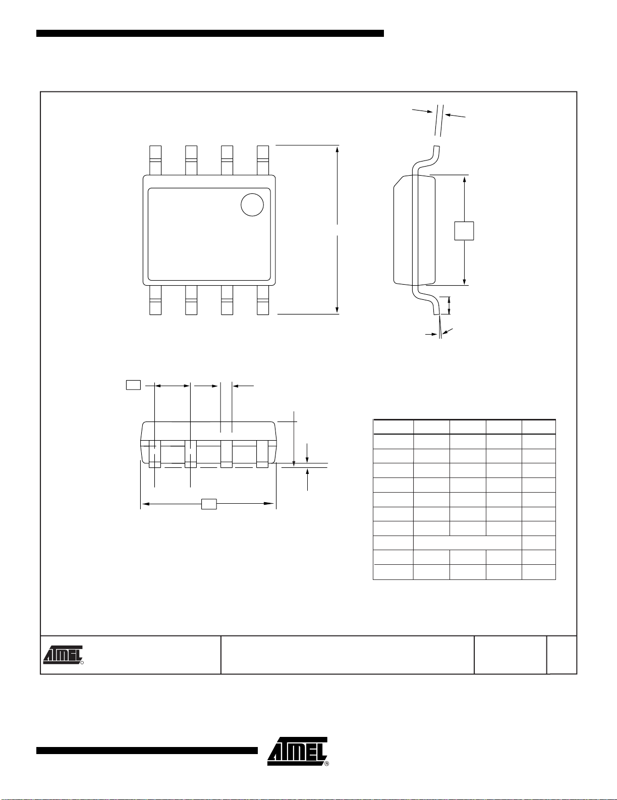
8S1 – JEDEC SOIC
DVA-206LX
AT24C01A/02/04/08/16
C
1
E
N
∅
E1
L
Top View
End View
e
D
Side View
B
A
SYMBOL
A1
A 1.35 – 1.75
A1 0.10 – 0.25
b 0.31 – 0.51
C 0.17 – 0.25
D 4.80 – 5.00
E1 3.81 – 3.99
E 5.79 – 6.20
e 1.27 BSC
L 0.40 – 1.27
∅ 0˚ – 8˚
COMMON DIMENSIONS
(Unit of Measure = mm)
MIN
NOM
MAX
NOTE
Note:
These drawings are for general information only. Refer to JEDEC Drawing MS-012, Variation AA for proper dimensions, tolerances, datums, etc.
1150 E. Cheyenne Mtn. Blvd.
Colorado Springs, CO 80906
R
0180R–SEEPR–4/04
TITLE
8S1, 8-lead (0.150" Wide Body), Plastic Gull Wing
Small Outline (JEDEC SOIC)
DRAWING NO.
8S1 B
10/7/03
REV.
1-21
Page 23
DVA-206LX
K4S161622D CMOS SDRAM
512K x 16Bit x 2 Banks Synchronous DRAM
GENERAL DESCRIPTIONFEATURES
• 3.3V power supply
• LVTTL compatible with multiplexed address
• Dual banks operation
• MRS cycle with address key programs
-. CAS Latency ( 2 & 3)
-. Burst Length (1, 2, 4, 8 & full page)
-. Burst Type (Sequential & Interleave)
• All inputs are sampled at the positive going edge of the system
clock
• Burst Read Single-bit Write operation
• DQM for masking
• Auto & self refresh
• 15.6us refresh duty cycle (2K/32ms)
The K4S161622D is 16,777,216 bits synchronous high data
rate Dynamic RAM organized as 2 x 524,288 words by 16 bits,
fabricated with SAMSUNG′s high performance CMOS technology. Synchronous design allows precise cycle control with the
use of system clock I/O transactions are possible on every clock
cycle. Range of operating frequencies, programmable burst
length and programmable latencies allow the same device to be
useful for a variety of high bandwidth, high performance memory system applications.
ORDERING INFORMATION
Part NO. MAX Freq. Interface Package
K4S161622D-TC/L55 183MHz
K4S161622D-TC/L60 166MHz
K4S161622D-TC/L70 143MHz
K4S161622D-TC/L80 125MHz
K4S161622D-TC/L10 100MHz
LVTTL
50
TSOP(II)
FUNCTIONAL BLOCK DIAGRAM
Bank Select
Refresh Counter
Row Buffer
Address Register
CLK
ADD
LRAS
LCBR
LCKE
LRAS LCBR LWE LDQM
Data Input Register
Row Decoder Col. Buffer
512K x 16
512K x 16
Column Decoder
Latency & Burst Length
Programming Register
LCAS LWCBR
Timing Register
LWE
LDQM
Sense AMP
Output BufferI/O Control
DQi
1-22
CLK CKE CS RAS CAS WE L(U)DQM
Samsung Electronics reserves the right to
*
change products or specification without
notice.
Page 24
K4S161622D CMOS SDRAM
PIN CONFIGURATION (TOP VIEW)
VDD
LDQM
A10/AP
PIN FUNCTION DESCRIPTION
DQ0
DQ1
VSSQ
DQ2
DQ3
VDDQ
DQ4
DQ5
VSSQ
DQ6
DQ7
VDDQ
WE
CAS
RAS
CS
BA
A0
A1
A2
A3
VDD
1
2
3
4
5
6
7
8
9
10
11
12
13
14
15
16
17
18
19
20
21
22
23
24
25
50
49
48
47
46
45
44
43
42
41
40
39
38
37
36
35
34
33
32
31
30
29
28
27
26
VSS
DQ15
DQ14
VSSQ
DQ13
DQ12
VDDQ
DQ11
DQ10
VSSQ
DQ9
DQ8
VDDQ
N.C/RFU
UDQM
CLK
CKE
N.C
A9
A8
A7
A6
A5
A4
VSS
50PIN TSOP (II)
(400mil x 825mil)
(0.8 mm PIN PITCH)
DVA-206LX
Pin Name Input Function
CLK System Clock Active on the positive going edge to sample all inputs.
CS Chip Select
CKE Clock Enable
A0 ~ A10/AP Address
BA Bank Select Address
RAS Row Address Strobe
CAS Column Address Strobe
WE Write Enable
L(U)DQM Data Input/Output Mask
DQ0 ~ 15 Data Input/Output Data inputs/outputs are multiplexed on the same pins.
VDD/VSS Power Supply/Ground Power and ground for the input buffers and the core logic.
VDDQ/VSSQ Data Output Power/Ground
N.C/RFU
No Connection/
Reserved for Future Use
Disables or enables device operation by masking or enabling all inputs except
CLK, CKE and L(U)DQM
Masks system clock to freeze operation from the next clock cycle.
CKE should be enabled at least one cycle prior to new command.
Disable input buffers for power down in standby.
Row / column addresses are multiplexed on the same pins.
Row address : RA0 ~ RA10, column address : CA0 ~ CA7
Selects bank to be activated during row address latch time.
Selects bank for read/write during column address latch time.
Latches row addresses on the positive going edge of the CLK with RAS low.
Enables row access & precharge.
Latches column addresses on the positive going edge of the CLK with CAS low.
Enables column access.
Enables write operation and row precharge.
Latches data in starting from CAS, WE active.
Makes data output Hi-Z, tSHZ after the clock and masks the output.
Blocks data input when L(U)DQM active.
Isolated power supply and ground for the output buffers to provide improved noise
immunity.
This pin is recommended to be left No Connection on the device.
1-23
Page 25

DVA-206LX
K4S161622D CMOS SDRAM
ABSOLUTE MAXIMUM RATINGS
Parameter Symbol Value Unit
Voltage on any pin relative to Vss VIN, VOUT -1.0 ~ 4.6 V
Voltage on VDD supply relative to Vss VDD, VDDQ -1.0 ~ 4.6 V
Storage temperature TSTG -55 ~ +150 °C
Power dissipation PD 1 W
Short circuit current IOS 50 mA
Note :
Permanent device damage may occur if ABSOLUTE MAXIMUM RATINGS are exceeded.
Functional operation should be restricted to recommended operating condition.
Exposure to higher than recommended voltage for extended periods of time could affect device reliability.
DC OPERATING CONDITIONS
Recommended operating conditions (Voltage referenced to VSS = 0V, TA = 0 to 70°C)
Parameter Symbol Min Typ Max Unit Note
Supply voltage VDD, VDDQ 3.0 3.3 3.6 V 4
Input logic high votlage VIH 2.0 3.0 VDDQ+0.3 V 1
Input logic low voltage VIL -0.3 0 0.8 V 2
Output logic high voltage VOH 2.4 - - V IOH = -2mA
Output logic low voltage VOL - - 0.4 V IOL = 2mA
Input leakage current ILI -10 - 10 uA 3
Note :
:
1. VIH (max) = 5.6V AC. The overshoot voltage duration is ≤ 3ns.
2. VIL (min) = -2.0V AC. The undershoot voltage duration is ≤ 3ns.
3. Any input 0V ≤ VIN ≤ VDDQ.
Input leakage currents include HI-Z output leakage for all bi-directional buffers with Tri-State outputs.
4. The VDD condition of K4S161622D-55/60 is 3.135V~3.6V.
CAPACITANCE (VDD = 3.3V, TA = 23°C, f = 1MHz, VREF =1.4V ± 200 mV)
Pin Symbol Min Max Unit
Clock CCLK 2 4 pF
RAS, CAS, WE, CS, CKE, L(U)DQM CIN 2 4 pF
Address CADD 2 4 pF
DQ0 ~ DQ15 COUT 3 5 pF
DECOUPLING CAPACITANCE GUIDE LINE
Recommended decoupling capacitance added to power line at board.
Parameter Symbol Value Unit
Decoupling Capacitance between VDD and VSS CDC1 0.1 + 0.01 uF
Decoupling Capacitance between VDDQ and VSSQ CDC2 0.1 + 0.01 uF
Note :
1. VDD and VDDQ pins are separated each other.
All VDD pins are connected in chip. All VDDQ pins are connected in chip.
2. VSS and VSSQ pins are separated each other
All VSS pins are connected in chip. All VSSQ pins are connected in chip.
1-24
Page 26

DVA-206LX
K4S161622D CMOS SDRAM
DC CHARACTERISTICS
(Recommended operating condition unless otherwise noted, TA = 0 to 70°C)
Parameter Symbol Test Condition
Operating Current
(One Bank Active)
Precharge Standby Current in power-down mode
Precharge Standby Current
in non power-down mode
Active Standby Current
in power-down mode
Active Standby Current
in non power-down mode
(One Bank Active)
CAS
Latency
Burst Length =1
ICC1
ICC2P CKE≤VIL(max), tCC = 15ns 2
ICC2PS CKE & CLK≤VIL(max), tCC = ∞ 2
ICC2N
ICC2NS
ICC3P CKE≤VIL(max), tCC = 15ns 3
ICC3PS CKE & CLK≤VIL(max), tCC = ∞ 3
ICC3N
ICC3NS
tRC≥tRC(min)
Io = 0 mA
CKE≥VIH(min), CS≥VIH(min), tCC = 15ns
Input signals are changed one time during 30ns
CKE≥VIH(min), CLK≤VIL(max), tCC = ∞
Input signals are stable
CKE≥VIH(min), CS≥VIH(min), tCC = 15ns
Input signals are changed one time during 30ns
CKE≥VIH(min), CLK≤VIL(max), tCC = ∞
Input signals are stable
-55 -60 -70 -80 -10
3 120 115 105 95 85
2 - - 110 95 80
Version
Unit Note
mA 2
mA
15
mA
5
mA
25 mA
15 mA
Operating Current
(Burst Mode)
Refresh Current ICC5 tRC≥tRC(min)
Self Refresh Current ICC6 CKE≤0.2V
Note :
1. Unless otherwise notes, Input level is CMOS(VIH/VIL=VDDQ/VSSQ) in LVTTL.
2. Measured with outputs open. Addresses are changed only one time during tcc(min).
3. Refresh period is 32ms. Addresses are changed only one time during tcc(min).
4. K4S161622D-TC**
5. K4S161622D-TL**
ICC4
Io = 0 mA
Page Burst 2Banks Activated
tCCD = 2CLKs
3 155 150 140 130 115
mA 2
2 - - 125 115 100
3 105 100 90 90 80
mA 3
2 - - 100 90 80
1 mA 4
250 uA 5
1-25
Page 27

DVA-206LX
K4S161622D CMOS SDRAM
PACKAGE DIMENSIONS
50-TSOP2-400CF
Unit : Millimeters
0~8°
0.10MAX
0.075MAX
[ ]
#50
#1
(0.875) 0.30
+0.10
-0.05
20.95
± 0.10
0.35
+0.10
-0.05
#26
#25
0.80TYP
[0.80±0.08]
11.76±0.20
0.05MIN
1.20MAX
1.00± 0.10
0.25 TYP
± 0.10
10.16
+0.075
0.125
-0.035
(0.50)
± 0.20
(10.76)
11.76
(0.50)
1-26
Page 28

Please be aware that an important notice concerning availability, standard warranty, and use in critical applications of Texas Instruments
DVA-206LX
)###"2 #".)(&'
!#"$ *1%' '&#)$*&'
FEATURES
D 24-Bit Resolution
D Analog Performance (V
− Dynamic Range: 106 dB
− SNR: 106 dB, Typical
− THD+N: 0.002%, Typical
− Full-Scale Output: 4 V p-p, Typical
= 5 V):
CC
D 4×/8× Oversampling Digital Filter:
− Stop-Band Attenuation: −50 dB
− Pass-Band Ripple: ±0.04 dB
D Sampling Frequency: 5 kHz to 200 kHz
D System Clock: 128 f
512 fS, 768 fS, 1152 fS With Auto Detect
, 192 fS, 256 fS, 384 fS,
S
D Software Control (PCM1753, PCM1755):
− Accepts 16-, 18-, 20-, and 24-Bit Audio
Formats: Standard, I2S, and Left-Justified
− Digital Attenuation: 0 dB to −63 dB,
0.5 dB/Step
− Digital De-Emphasis
− Digital Filter Rolloff: Sharp or Slow
− Soft Mute
− Zero Flags for Each Output
− Open-Drain Output Zero Flag (PCM1755)
D Hardware Control (PCM1754):
− I2S and 16-Bit Word, Right-Justified
− 44.1 kHz Digital De-Emphasis
− Soft Mute
− Zero Flag for L-, R-Channel Common
Output
D Power Supply: 5-V Single Supply
D Small 16-Lead SSOP Package, Lead-Free
APPLICATIONS
D A/V Receivers
D DVD Movie Players
D DVD Add-On Cards For High-End PCs
D DVD Audio Players
D HDTV Receivers
D Car Audio Systems
D Other Applications Requiring 24-Bit Audio
DESCRIPTION
The PCM1753/54/55 is a CMOS, monolithic, integrated
circuit, which includes stereo digital-to-analog converters
and support circuitry in a small 16-lead SSOP package.
The data converters use TI’s enhanced multilevel
delta-sigma architecture, which employs 4th-order noise
shaping and 8-level amplitude quantization to achieve
excellent dynamic performance and improved tolerance to
clock jitter. The PCM1753/54/55 accepts industrystandard audio data formats with 16- to 24-bit data,
providing easy interfacing to audio DSP and decoder
chips. Sampling rates up to 200 kHz are supported. A full
set of user-programmable functions is accessible through
a three-wire serial control port, which supports register
write functions.
The PCM1753/55 is pin compatible with the PCM1748,
PCM1742, and PCM1741, except for pin 5.
SLES092 − OCTOBER 2003
These devices have limited built-in ESD protection. The leads should be shorted together or the device placed in conductive foam during
storage or handling to prevent electrostatic damage to the MOS gates.
semiconductor products and disclaimers thereto appears at the end of this data sheet.
Audio Precision and System Two are trademarks of Audio Precision, Inc.
Other trademarks are the property of their respective owners.
!"#$%&" ' ()##*& %' "! +),-(%&" .%&*/ #".)(&'
("!"#$ &" '+*(!(%&"' +*# &0* &*#$' "! *1%' '&#)$*&' '&%.%#. 2%##%&3/
#".)(&" +#"(*''4 ."*' "& *(*''%#-3 (-).* &*'&4 "! %-- +%#%$*&*#'/
Copyright 2003, Texas Instruments Incorporated
1-27
Page 29

PCM1753DBQ
16-pin SSOP
16DBQ
−25°C to 85°C
PCM1753
PCM1754DBQ
16-pin SSOP
16DBQ
−40°C to 85°C
PCM1754
PCM1755DBQ
16-pin SSOP
16DBQ
−25°C to 85°C
PCM1755
PARAMETER
TEST CONDITIONS
UNIT
PARAMETER
TEST CONDITIONS
UNIT
Audio-data interface format
Audio-data interface format
Audio-data bit length
Audio-data bit length
DVA-206LX
SLES092 − OCTOBER 2003
PACKAGE/ORDERING INFORMATION
PRODUCT PACKAGE
(1)
For the most current specification and package information, refer to our web site at www.ti.com.
PACKAGE
CODE
OPERATION
TEMPERATURE
RANGE
PACKAGE
MARKING
www.ti.com
ORDERING
NUMBER
PCM1753DBQ Tube
PCM1753DBQR Tape and reel
PCM1754DBQ Tube
PCM1754DBQR Tape and reel
PCM1755DBQ Tube
PCM1755DBQR Tape and reel
(1)
TRANSPORT MEDIA
ABSOLUTE MAXIMUM RATINGS
over operating free-air temperature range unless otherwise noted
Supply voltage: V
Ground voltage differences: AGND, DGND ±0.1 V
Input voltage −0.3 V to 6.5 V
Input current (any pins except supplies) ±10 mA
Ambient temperature under bias −40°C to 125°C
Storage temperature −55°C to 150°C
Junction temperature 150°C
Lead temperature (soldering) 260°C, 5 s
Package temperature (IR reflow, peak) 260°C
(1)
Stresses beyond those listed under “absolute maximum ratings” may cause permanent damage to the device. These are stress ratings only , a nd
functional operation of the device at these or any other conditions beyond those indicated under “recommended operating conditions” is not
implied. Exposure to absolute-maximum-rated conditions for extended periods may affect device reliability.
CC
(1)
UNIT
−0.3 V to 6.5 V
ELECTRICAL CHARACTERISTICS
All specifications at TA = 25°C, VCC = 5 V , fS = 44.1 kHz, system clock = 384 fS and 24-bit data, unless otherwise noted
PCM1753DBQ, PCM1754DBQ,
PCM1755DBQ
MIN TYP MAX
Resolution 24 Bits
DATA FORMAT
PCM1753
PCM1755
PCM1754 I2S, standard
PCM1753
PCM1755
PCM1754 16−24-bit (I2S), 16-bit (standard)
Audio data format MSB first, 2s complement
f
S
Sampling frequency 5 200 kHz
System clock frequency
Standard, I2S, left-justified
16-, 18-, 20-, 24-bit, selectable
128 fS, 192 fS, 256 fS, 384 fS,
512 fS, 768 fS, 1152 f
S
2
1-28
Page 30

www.ti.com
V
V
PCM1753/PCM1755
PCM1754
PIN ASSIGNMENTS
DVA-206LX
SLES092 − OCTOBER 2003
(TOP VIEW)
BCK
DATA
LRCK
DGND
NC
V
CC
OUT
OUT
1
2
3
4
5
6
L
R
7
8
16
15
14
13
12
11
10
9
FUNCTIONAL BLOCK DIAGRAM
BCK
LRCK
DATA
(FMT) ML
(MUTE) MC
(DEMP) MD
Audio
Serial
Port
Oversampling
Serial
Control
Port
SCK
ML
MC
MD
ZEROL/NA
ZEROR/ZEROA
V
COM
AGND
4y/8y
Digital
Filter
and
Function
Control
Enhanced
Multi-Level
Delta-Sigma
Modulator
BCK
DATA
LRCK
DGND
V
V
OUT
V
OUT
NC
CC
(TOP VIEW)
1
2
3
4
5
6
L
R
DAC
DAC
7
8
Output Amp
and
Low-Pass Filter
Output Amp
and
Low-Pass Filter
16
15
14
13
12
11
10
SCK
FMT
MUTE
DEMP
TEST
ZEROA
V
COM
9
AGND
V
OUT
V
COM
V
OUT
L
R
(TEST)
SCK
†
Open-Drain Output for the PCM1755
( ): PCM1754
System
Clock
Manager
System Clock
Zero Detect
†
ZEROL/NA
†
(ZEROA)
ZEROR/ZEROA
Power Supply
DGND
V
CC
AGND
1-29
Page 31

I/O
DESCRIPTION
DVA-206LX
SLES092 − OCTOBER 2003
Terminal Functions
TERMINAL
NAME NO.
PCM1753/PCM1755
AGND 9 − Analog ground
BCK 1 I Audio data bit clock input
DATA 2 I Audio data digital input
DGND 4 − Digital ground
LRCK 3 I L-channel and R-channel audio data latch enable input
MC 14 I Mode control clock input
MD 13 I Mode control data input
ML 15 I Mode control latch input
NC 5 −
SCK 16 I System clock input
V
CC
V
COM
V
L 7 O Analog output for L-channel
OUT
V
R 8 O Analog output for R-channel
OUT
ZEROR/ZEROA 11 O Zero flag output for R-channel/Zero flag output for L-/R-channels
ZEROL/NA 12 O Zero flag output for L-channel/Not assigned
PCM1754
AGND 9 − Analog ground
BCK 1 I Audio data bit clock input
DATA 2 I Audio data digital input
DEMP 13 I De-emphasis control
DGND 4 − Digital ground
FMT 15 I Data format select
LRCK 3 I L-channel and R-channel audio data latch enable input
MUTE 14 I Analog mixing control
NC 5 −
SCK 16 I System clock input
TEST 12 I Test pin. Ground or open
V
CC
V
COM
V
L 7 O Analog output for L-channel
OUT
V
R 8 O Analog output for R-channel
OUT
ZEROA 11 O Zero flag output for L/R channels
(1)
Schmitt-trigger input with internal pulldown.
(2)
Open-drain output (PCM1755).
6 − Analog power supply, 5 V
10 − Common voltage decoupling
6 − Analog power supply, 5 V
10 − Common voltage decoupling
(1)
(1)
(1)
(2)
(1)
(1)
(1)
(1)
www.ti.com
(2)
1-30
Page 32

MECHANICAL DATA
MSOI004E JANUARY 1995 – REVISED MAY 2002
DBQ (R–PDSO–G**) PLASTIC SMALL–OUTLINE P ACKAGE
DVA-206LX
0.025 (0,64)
24
112
A
0.010 (0,25)
0.004 (0,10)
0.012 (0,30)
0.008 (0,20)
13
0.157 (3,99)
0.150 (3,81)
0.069 (1,75) MAX
0.005 (0,13)
0.244 (6,20)
0.228 (5,80)
Seating Plane
0.004 (0,10)
0.008 (0,20) NOM
Gauge Plane
0.010 (0,25)
0°–8°
0.035 (0,89)
0.016 (0,40)
PINS **
DIM
A MAX
A MIN
D
NOTES: A. All linear dimensions are in millimeters.
B. This drawing is subject to change without notice.
C. Body dimensions do not include mold flash or protrusion not to exceed 0.006 (0,15).
D. Falls within JEDEC MO–137.
M0–137
VARIATION
16
0.197
(5,00)
0.189
(4,80)
AB AD AE AF
20 24
0.344
(8,74)
0.337
(8,56)
0.344
(8,74)
0.337
(8,56)
28
0.394
(10,01)
0.386
(9,80)
4073301/F 02/02
POST OFFICE BOX 655303 • DALLAS, TEXAS 75265
1-31
Page 33
DVA-206LX
DVD SINGLE CHIP MPEG A/V PROCESSOR
1. GENERAL DESCRIPTION
PPrreelliimmiinnaarry
y
SPHE8281S/Sx
SPHE8281S A/V decoder is a single-chip integrated DVD A/V
decoder. It is designed to maximize system performance with
minimum cost. It integrates DVD/CD controller, host processor,
A/V decoding hardware, audio quality ADC and a 6-channel
multi-format TV-encoder.
SPHE8281S supports DVD and CD physical formats. For logical
formats it supports DVD-Video, Super Video CD, Video CD,
CD-DA, OKO, and CD-ROM discs.
SPHE8281S performs real-time decoding and playback of
ISO/IEC 11172 MPEG1, 13818 MPEG2 sources. For audio it
supports Dolby Digital and MPEGI/II Layer1/2, PCM, LPCM audio
playback.
Application utilizing the SPHE8281S is presented below:
IR
VFD
front panel
SPHE8281S
SPHE8281S also combines all the functions required for a
high-performance progressive-scan DVD system. Built-in
de-interlacing hardware allows high quality DVD playback. The
embedded digital audio decoder is able to support key control and
audio sound effects for Karaoke.
In additional to that SPHE8281S includes a flexible 2D graphics
engine for high quality user interface and other applications.
Complex application could be built using this platform easily.
Development tools of SPHE8281S include complete compiler
tools, programming guide and system application libraries.
4-ch video output
DVD-loader
2~10 ch
Audio
DAC
Audio
amplifier
SDRAM
ROM
© Sunplus Technology Co., Ltd.
1-32
Spec is subject to change without prior notice
APR. 07, 2005
Preliminary Version: 0.1
Page 34

DVA-206LX
4. SIGNAL DESCRIPTION
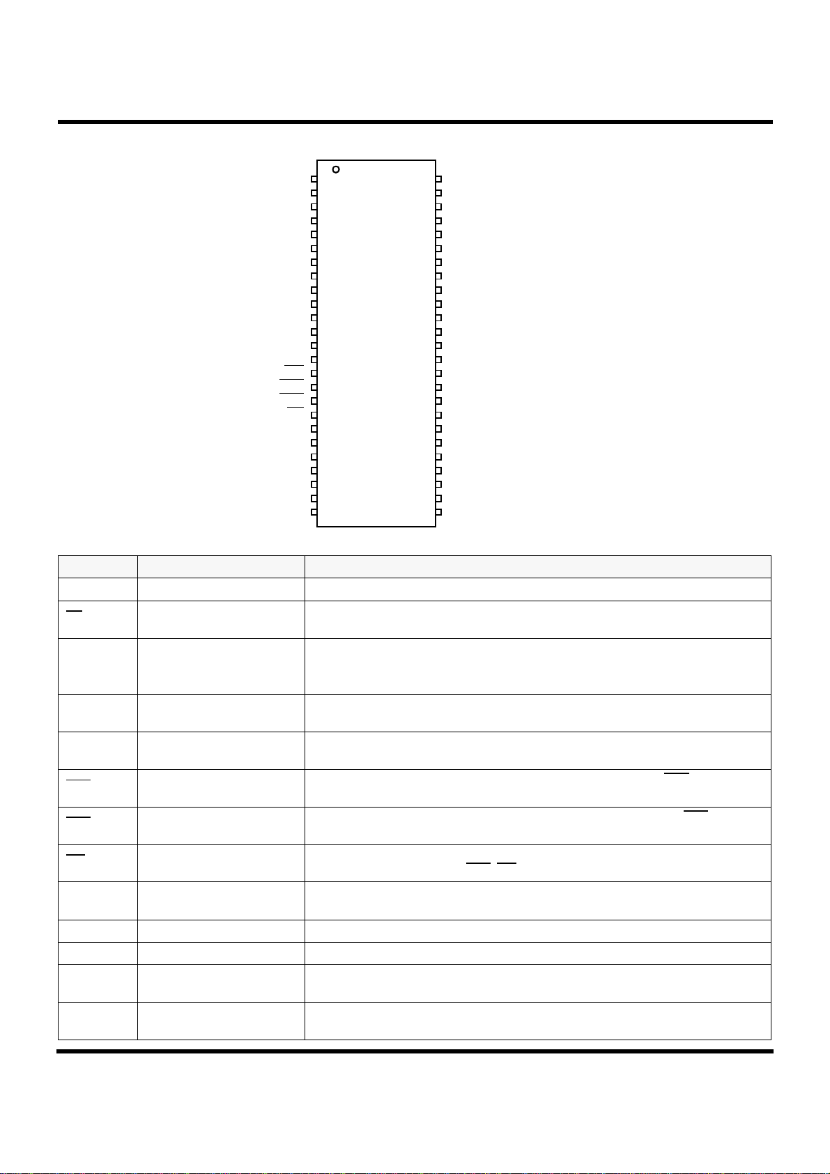
4.1. Pin Configuration
R_A12
R_A7
R_A6
R_A5
R_A4
R_A3
R_A2
R_A1
R_A0
R_D0
R_D2
VSS_O5/VSS_K5
R_D3
R_D4
R_D5
R_D6
R_D7
R_OE_B
VDD_K4
M_DQM2/GPIO
M_DQM3/GPIO
R_A10
R_A13
R_A14
R_A17
R_WE_B
M_A3
M_A2
M_A1
VSS_O4/VSS_K4
M_A0
M_A10
M_DQM1/GPIO
M_BA1/GPIO
R_A15
AIN
AIN_R
VDD_ADC
VSS_ADC
R_A16
R_A18
A_IEC_TX/GP IO
A_DAT A0/GPIO
VDD_O5
A_DAT A1/GPIO
A_DAT A2/GPIO
A_DAT A3/GPIO
A_LRCK/GPIO
VSS_K6/VSS_O6
A_BCK/GPIO
A_XCK/ GPIO
UA0_RX/GPIO
UA0_TX/GPIO
V_COMP
V_BIAS
V_FSADJ
V_REFOUT
TV_DAC0
VDD_TVA0
VSS_TVA 0
VDD_TVA1
VSS_TVA 1
TV_DAC3
TV_DAC4
VDD_TVA2
TV_DAC5
VSS_TVA 2
PLL_AVDD
LPFO
LPFN
VREFO
PDFLT
FDFLT
LPFNIN
LGIN
PLL_DS_AVSS
RFI
CNIN
SLVL
DS_AVDD
RF_AVDD
GMRES
AGCCAP
RFRP
RFO
FLTIP
FLTIN
R_A11
R_A9
R_A8
141
140
139
138
137
VDD_O4
136
135
134
133
132
131
130
R_D1
162
161
160
159
158
157
156
155
154
153
152
151
150
149
148
147
146
145
144
143
163
164
165
166
VM
167
168
169
170
171
172
173
174
175
176
177
178
179
180
181
182
183
184
185
186
187
188
189
190
191
192
193
194
195
196
197
198
199
200
201
202
203
204
205
206
207
208
209
210
211
212
213
214
215
216
1234567891011121314151617181920212223242526272829303132333435363738394041424344454647484950515253
SPHE8281S
142
8202S-216P
216 PIN LQFP
24x24mm
129
2
128
127
126
125
M_DQM0/GPIO
124
123
M_A4
122
VDD_K3
121
PPrreelliimmiinnaarry
SPHE8281S/Sx
M_A11/GPIO
M_D8
M_A5
120
M_A6
119
M_A7
118
M_A8
117
M_A9
116
M_CKE/GPIO
115
VSS_O3/VSS_K3
114
M_CLKO
113
VDD_O3
112
111
110
M_D9
109
54
108
107
106
105
104
103
102
101
100
99
98
97
96
95
94
93
92
91
90
89
88
87
86
85
84
83
82
81
80
79
78
77
76
75
74
73
72
71
70
69
68
67
66
65
64
63
62
61
60
59
58
57
56
55
M_D10
M_D11
M_D12
VDD_K2
M_D13
M_D14
M_D15
M_BA0
M_CS0_B/GPIO
VSS_O2/VSS_K2
M_RAS_B
M_CAS_B
M_WE_B
M_D0
M_D1
M_D2
VDD_O2
M_D3
M_D4
M_D5
M_D6
M_D7
VDD_PLLV
VSS_PLLV
VDD_PLLA
VSS_PLLA
RESERVED
RESERVED
RESERVED
RESERVED
CLKOUT
CLKIN
R_A19
R_A20/E_MX10
VFD_DATA/GPIO
VFD_STB/GPIO
VFD_CLK/GPIO
IR_IN/GPIO
RST_B
R_CS1_B/GPIO
R_CS2_B/GPIO
R_CS3_B/GPIO
R_CS4_B/GPIO
GPIO
VDD_O1
GPIO/ttio3_7
GPIO/ttio2_6
GPIO/ttio1_5
VSS_O1/VSS_K1
GPIO/ttio0_4
GPIO/TRAY_IS_OUT
GPIO/TRAY_IS_IN
VDD_K1
DFCT/GPIO
y
RFIP
RFIS
DPDA
DPDB
DPDC
DPDD
DVDD
RFSUM
AGCOP
AGCON
DVDC
© Sunplus Technology Co., Ltd.
Spec is subject to change without prior notice
CDF
CDE
CDA
CDB
DVDA
DVDB
RF_AVSS
APC_AVSS
V21
V165
R33K
CDMDI
CDLDO
DVDMDI
DVDLDO
SVOTST
RFRPPH
APC_SRV_AVDD
APR. 07, 2005
FEO
TEO
SBAD
OPVIP
OPVIN
TEOLP
RFRPBH
SBADPH
RFRPMEAN
OPVOP
E_MX8
E_MX9
DAFEO
DATEO
DA_AVSS
AD_DA_AVDD
SRV_AD_VGRD_AVSS
FGIN/GPIO
DMEA/GPIO
SC_OUT/GPIO
SPDC_OUT/GPIO
LDSW/GPIO
HOMESW/GPIO
SC1_OUT /GPIO
TRAY_OUT/GPIO
1-33
Preliminary Version: 0.1
Page 35
DVA-206LX
7. PACKAGE/PAD LOCATION
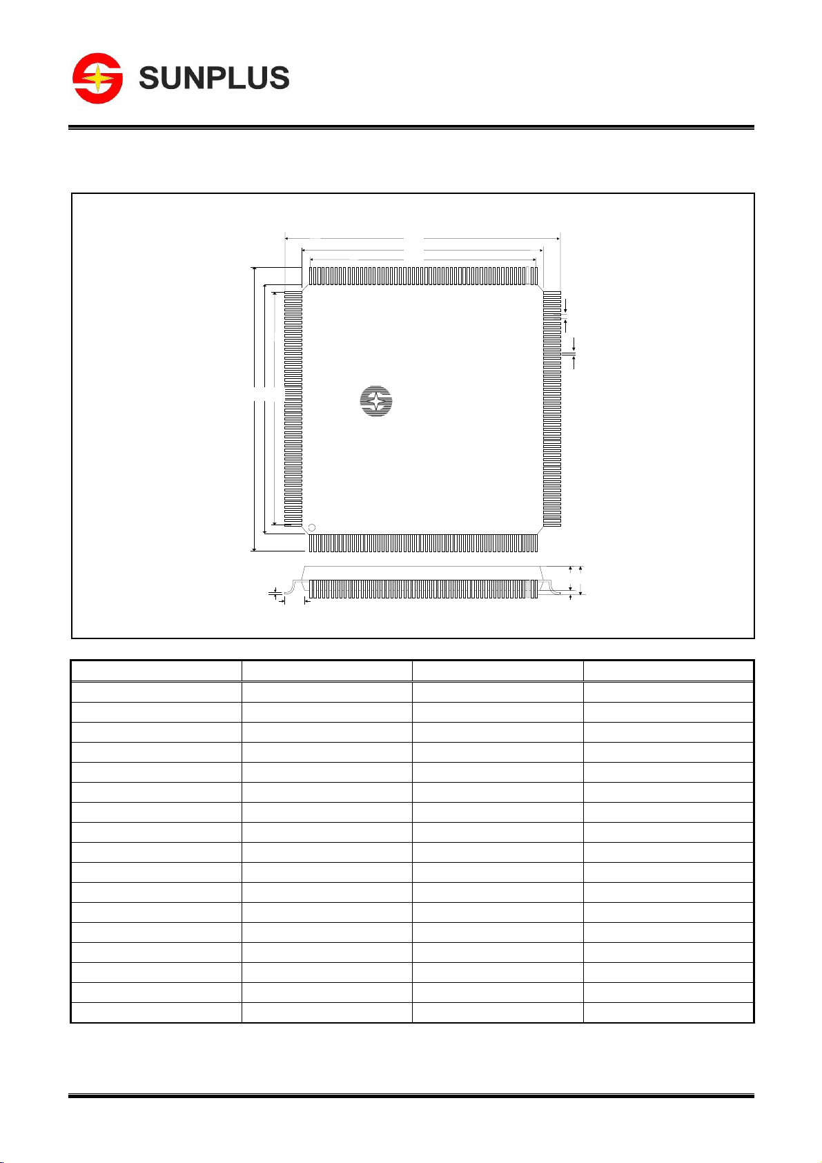
7.1. Outline Dimensions
D
D1
D2
E1E
E2
SUNPLUS
SPHE8281S
YYWW
PPrreelliimmiinnaarry
SPHE8281S/Sx
e
b
y
Unit: Millimeter
c
L1
AA2
A1
Symbol Min. Nom. Max.
A - - 1.60
A1 0.05 - 0.15
A2 1.35 1.40 1.45
D 26.00 BSC. 26.00 BSC. 26.00 BSC.
D1 24.00 BSC. 24.00 BSC. 24.00 BSC.
E 26.00 BSC. 26.00 BSC. 26.00 BSC.
E1 24.00 BSC. 24.00 BSC. 24.00 BSC.
R2 0.08 - 0.20
R1 0.08 - -
θ
θ1
θ2
θ3
0O 3.5 O 7
0 O - -
11 O 12 O 13 O
11 O 12 O 13 O
O
c 0.09 - 0.20
L 0.45 0.60 0.75
L1 1.00 REF 1.00 REF 1.00 REF
S 0.20 - -
© Sunplus Technology Co., Ltd.
1-34
Proprietary & Confidential
APR. 07, 2005
Preliminary Version: 0.1
Page 36
5
4
3
2
1
AB C D EF G
3-1
Page 37
8
7
6
5
4
3
2
1
1
2
3
4
5
3-2
Page 38
8
7
6
5
4
3
2
1
1
2
3
4
5
3-3
Page 39

5
4
3
2
1
AB C D EF G
3-4
Page 40
5
4
3
2
1
AB C D EF G
3-5
Page 41

5
4
3
2
1
AB C D EF G
3-6
Page 42

5
4
3
2
1
AB C D EF G
3-7
Page 43

5
4
3
2
1
AB C D EF G
3-8
Page 44

5
4
3
2
1
AB C D EF G
3-9
Page 45

5
4
3
2
1
AB C D EF G
3-10
Page 46

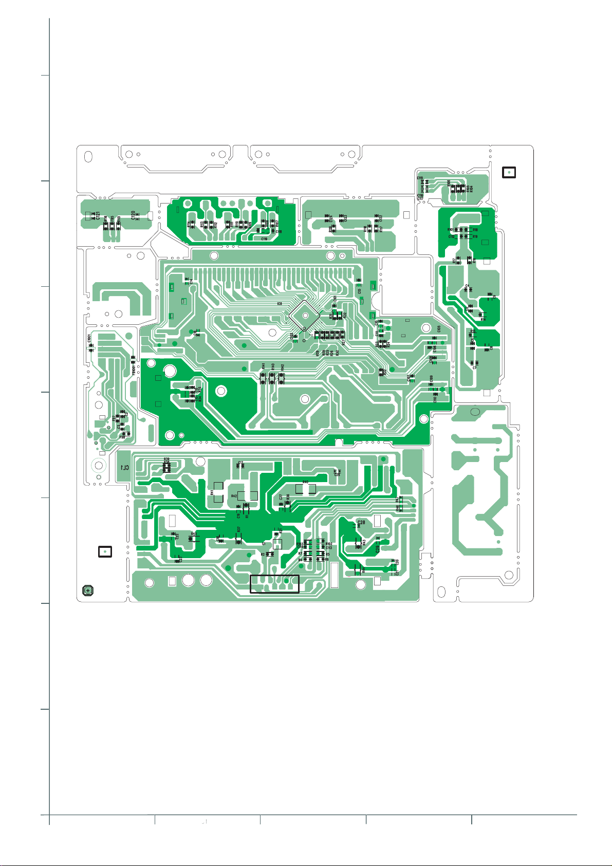
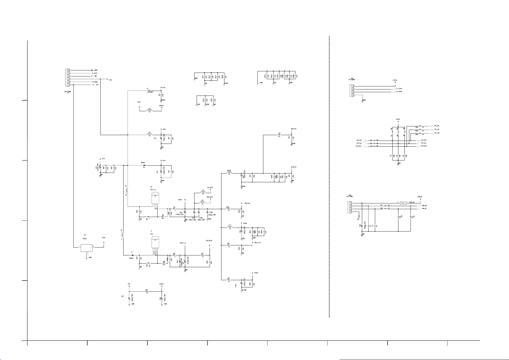
PARTS LIST
[ DVA-206LX ]
- Contents -
Cable join diagram .......................................................................................... 2 - 3
Deck mechanism exploded view and parts list ............................................... 2 - 4
Packing materials and accessories parts list .................................................. 2 - 10
2-1
Page 47

<MEMO>
2-2
Page 48

2-3
Page 49
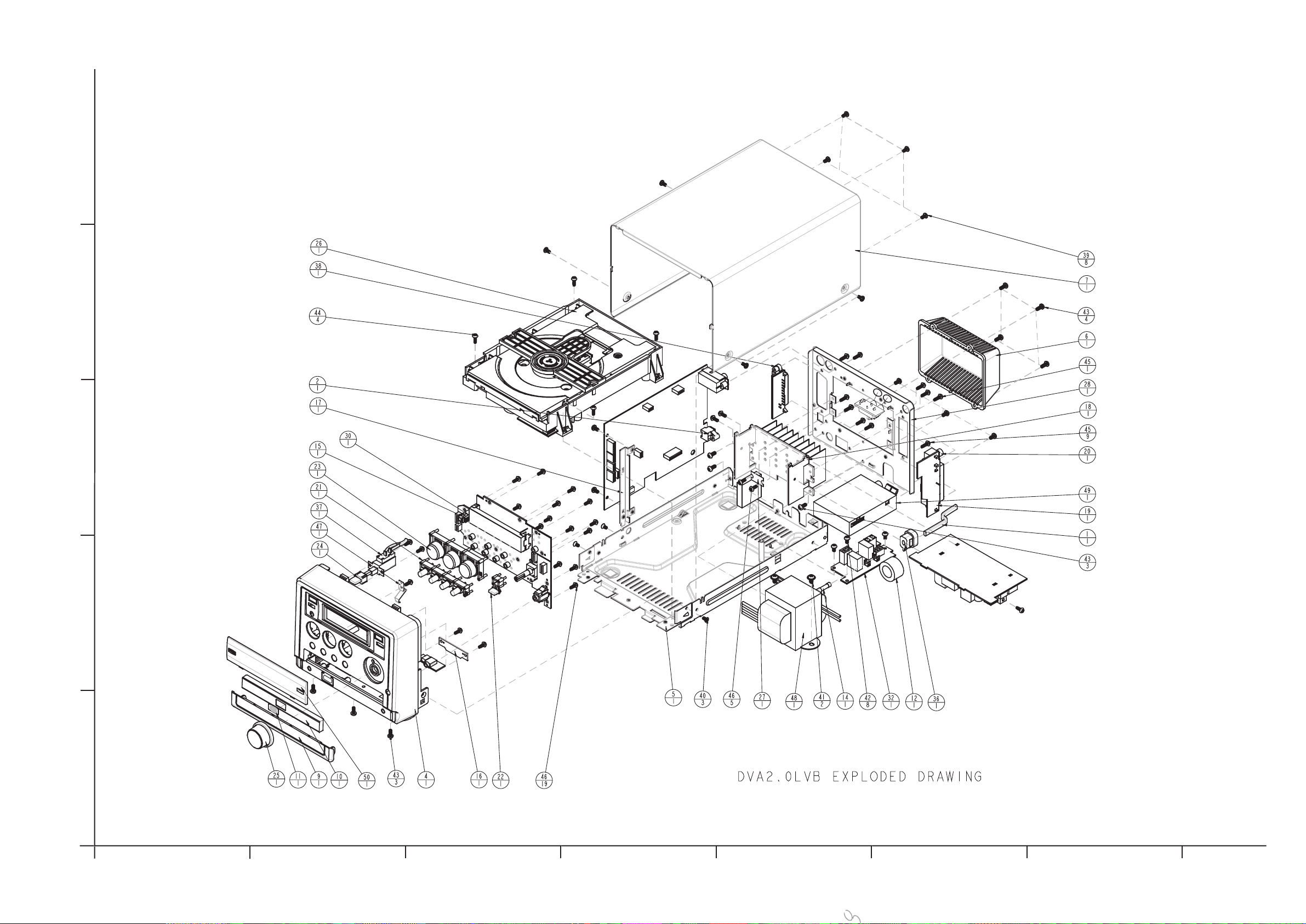
Exploded view of general assembly and parts list
1
2-4
E
Page 50

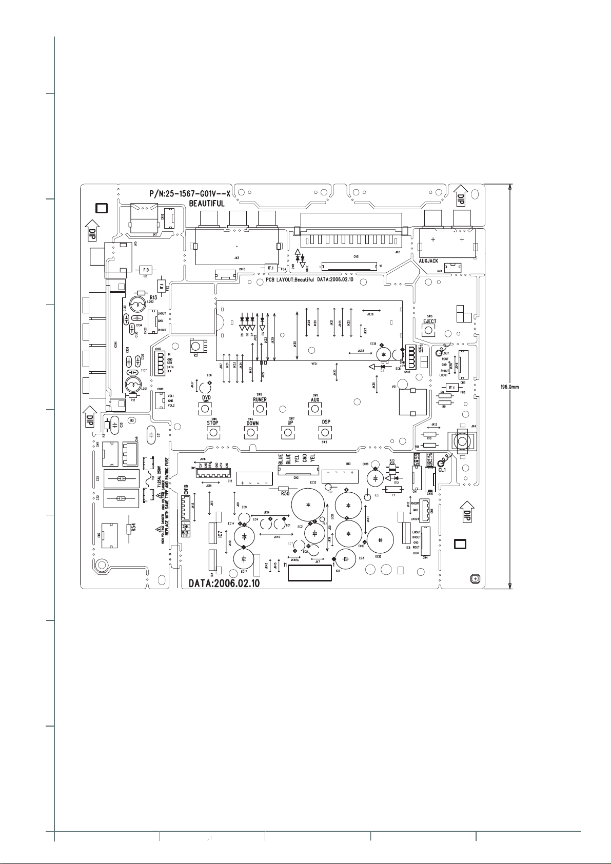
■ Parts list (Exploded view of general assembly)
remark !
Item
Location
1 14-0135-2-----X AC-CORD0135 1
2 23-F075-1-----V APTX178AT 1
3 23-B179-1-----X AUXIN_MSJ03526 1
4 10-7963-01-21-V1 CABI_FRONT_B 1 ABS
5 20-2807-01-01-W1 CHAS_MAIN 1
6 10-7906-01-01-V1 COVER_HT_SINK 1 ABS
7 20-2865-01-01-W1 COVER_TOP_B 1
8 30-1935-01-01-01 CUSHION_PT 1
9 10-7966-02-01-V1 DOOR_AUX_B 1 ABS
10 10-7965-01-01-V1 DOOR_DVD 1 ABS
11 10-7499-01-01-01 DVD_LOGO 1 PC_CUT_SHEET
12 18A-0018-1-----X FERRITE_BEAD 1
13 20-2111-02-01-X1 FILTER-LENS 1
14 4-0308-1-----V FUSE_3 1 1.25A 250V
15 20-2907-01-01-01 HLDR_SENSOR 1
16 HLDR_USB 1 splited from pcb amp assy
17 20-2810-01-01-W1 HOLDER_PCB_MPEG 1
18 20-2808-01-11-01 HT_SINK_ASSY 1
19 23-0143-2-----V JACK_SPEAKER 1
20 23-B068-2-----U JACK_SUBW 1
21 10-7889-02-01-V1 KEY_ADJUST 1 ABS
22 10-7888-02-01-V1 KEY_DVD_OPEN 1 ABS
23 10-7890-02-01-V1 KEY_FUNC 1 ABS
24 10-7887-02-01-V1 KEY_PW 1 ABS
25 10-7967-01-01-V1 KNOB-VOL 1 ABS
26 39-0008-1-----V MECHANISM LOADER
27 30-2153-01-01-V1 MICA_SHEET 1
28 20-2866-02-11-X1 PANEL_REAR_B 1
29 640-D20LV2-02S00 PCB_AMP_ASSY 1 652-D206LX-020
30 640-206LX2-02S00 PCB_FR_ASSY_B 1 splited from pcb amp assy
31 PCB_JACK_SPEAKER_AS 1 splited from pcb amp assy
32 PCB_POWER_ASSY 1 splited from pcb amp assy
33 PCB_SCART_ASSY 1 splited from pcb amp assy
34 640-D20LV8-02S00 PCB_MPEG_ASSY 1 658-D206LX-020
35 640-206LX8-02S00 PCB_AUXIN_ASSY 1 splited from pcb mpeg assy
36 30-1789-01-01-01 PINCER 1
37 8-0470-2-----U POWER_SWITCH 1 8A/250V
38 23-0137-2-----V SCART_SC104 1
Parts number Parts name Q'ty. Description
38-0022-1-----X DVD MECH 1
DVA-206LX
39 BT-0006-04-S1 SCREW-BT-3X6-M 8 SILVER for cover top
40 KM-000-60-2S SCREW-KM-3X6 3
41 PMW-0011-01-S3 SCREW-PMW-4X8 2
42 RM-0006-03-S3 SCREW-RM3X6 8
2-5
Page 51

DVA-206LX
remark !
Item
Location
Parts number Parts name Q'ty. Description
43 RM-0006-04-S3 SCREW-RM3X8 10
44 RM-0006-06-S3 SCREW-RT-3X10-M 4 for dvd mechanism
45 RT-0006-17-B3 SCREW-RT-H-3X10 10
46 RT-0006-11-B3 SCREW-RT-H-3X8 24
47 20-2867-01-01-01 SPRING_DOOR_AUX 1 0.3mm 300H SUS304
48 211-011116-001W0 TRANSFORMER 1
49 Z-25-0941-01V TUNER-BOX 1
50 10-7964-02-01-X1 WINDOW_DISPLAY_B 1 AS
2-6
Page 52
■ MAIN BOARD ASSEMBLY
Item PWB TOP
1 1-0202-2------X IC NJM78M05FA 5V IC Regulato 1.000000 pcs IC4
2 1-1529-1------X IC RPM7138-V4 REMOTE 1.000000 pcs IC2
3 1-1657-1------X C-IC AD6315F, VFD DRIVER QFP 1.000000 pcs IC8
4 1-1661-1------V IC KIA7810API REGULATOR 1.000000 pcs IC6
5 1-1735-1------X IC TDA7269SA POWER AMP 1.000000 pcs IC5
6 1-1836-1------V LOW DROPOUT VOLTAGE REGULATO 1.000000 pcs IC7
7 11-A050-M0----Y Black Wire 50mm UL1007 #18 1.000000 pcs CL1
8 11-AT140-E0---X JUMPER WIRE 140mm BLK W/TERM 1.000000 pcs PL100
9 11-P70-J0-----V WIRE ASSY L=70mm BLACK UL100 1.000000 pcs PL1
10 12P2-0224-----V 2Pins Plug Wire Assy L=300mm 1.000000 pcs CN9
11 12P2-0227-1---V CONN ASSY 2PINS Pitch=2.5mm 1.000000 pcs FOR ETECT SWITCH
12 12P3-0239-----V PLUG CONN 3PINS P=2.0mm L=18 1.000000 pcs CN18
13 12P3-0264-----Y 3PINS PLUG CONN ASSY P=2.0mm 1.000000 pcs AUX
7 12P4-0284-----V PLUG CONN 4PINS P=2.5mm L=50 1.000000 pcs CN6
8 12P5-0152-----V PLUG CONN 5PINS P=2.0mm L=12 2.000000 pcs CN19,CN17
9 12P5-0153-----V PLUG CONN 5PINS P=2.5mm L=28 1.000000 pcs CN3
10 12P5-0154-----V PLUG CONN 5PINS P=2.0mm L=26 1.000000 pcs CN13
11 12P6-0160-----V PLUG CONN 6PINS P=2.5mm L=14 1.000000 pcs CN5
12 12S3-0068-----X 3PIN SOCKET CONNECTOR CN03P/ 2.000000 pcs CN7,CN11
13 12S4-0080-----V CONN 4PINS V PITCH=2.5mm 1.000000 pcs CN20
14 12S5-0013-----X 5 Pins Socket Connector (Pit 1.000000 pcs CN10
15 12S5-0134-1---X CONN, 5P V P=2.5mm "JM24188- 1.000000 pcs CN4
16 12S5-0161-----V 5Pins Socket Connector P=3.9 1.000000 pcs CN2
17 18A843556-N000X2 F-BEAD 843556 TB36 TAPING 52 5.000000 pcs FB6,FB1,FB2,JK39,JK46
18 18A916221-A005V0 F-BEAD 220ohm @ 100MHz 9P160 8.000000 pcs R107,R108,R109,R110,R111,R112,
19 R113,R114
20 18HG102SN-A005X0 C-Bead 1000ohm at 100MHz BLM 2.000000 pcs FB7 FB8
21 20-1196-01-01-X1 "Fuse Holder," 2.000000 pcs
22
23
24 20-2808-01-11-01 HT SINK MAIN 1.000000 pcs
25 20-2809-01-01-01 HOLDER VFD SPTE 0.3mm 2.000000 pcs
26 20-2907-01-01-01 HOLDER SENSOR 1.000000 pcs
27 23-0137-2-----V Scart RGB Connector MRC-021V 1.000000 pcs JK2
28 23-0143-2-----V SPEAKER PUSH TERMINAL 4PINS 1.000000 pcs CON1 SP-T
29 23-B029-2-----V Headphone Jack (HTJ-035-18AB 1.000000 pcs JK4
30 23-B068-2-----U JACK,PIN 1P BLK RCA-107B(BK) 1.000000 pcs JK5
31 23-B179-1-----X RCA JACK 2P RED/WHITE 1.000000 pcs AUX JACK
32 25-1567-G01V--X pcb dva2.0lxb main board 94v 1.000000 pcs
33 26-0070-2-----V Chock Coil 1.0uH PIN L=4.2 + 2.000000 pcs L201,L202
34 26BLM21PG-A002V1 C-COIL BLM21PG221SN1D (EMI F 3.000000 pcs R116,R115,FB5,
35 27-0212-1-----V DVD VACUUM FLUORESCENT DISPL 1.000000 pcs VFD
36 2KTC3875G-A019X8 Transistor KTC3875GR (0.15W) 1.000000 pcs Q1
37 3-RS202-1-----X DIODE RS202 FOR FS-G5 2.000000 pcs D12,D10
38 30-1903-01-01-01 VFD PAD CORD WITH TWO ADHESI 2.000000 pcs
39 30-2111-02-01-X1 FILTER LENS SHEET (20x85.5x0 1.000000 pcs FOR VFD
40 30-2153-01-01-V1 MICA SHEET 1.000000 pcs FOR AMP IC
41 31N4001---M000X6 Diode IN-4001,26mm TAPE 2.000000 pcs D13,D2
42
43
44 372-060803-RTBX0 RH/TS 3xL8mm A553008005 5.000000 pcs FOR HT-SINK/AMP IC
45 4-3001060-N000X2 Protector 3A 491 SERIES 1.000000 pcs R50
46 664-DV55M*-02S Insertion Indicrect Material 1.000000 pcs
47 5-01-2 BONDING GLUE #575 (EMEDING) 1.300000 g
48 5-02-11 HEAT CURING ADHESIVE 1R-130 0.009000 ml
49 5-04-18-------X OM-325 lead free no clean 0.476000 g
50 5-04-19-------X Lead Free soldering wire 0.560000 g
51 5-05-8--------V Lead free solder bar SN100CE 8.100000 g
52 5-06-3--------V LEAD FREE SOLDERING FLUX 4.760000 g
53 5-11-13 High temperature masking tap 35.000000 mm
54 5-11-15 High temperature masking tap 90.000000 mm
55 5-28-5--------V Lead Free Tinned copper wire 2.210000 g B VERSION:JK6,JK7,JK8,JK9,JK10
56 ,JK11,JK12,JK13,JK14,JK15,JK16
57 ,JK17,JK18,JK19,JK20JK21,JK22,
58 JK23,JK24,JK25,JK26,JK27,JK28,
59 JK29,JK30,JK31,JK32,JK33,JK34J
60 K35,JK36,JK37,JK38,JK40,JK41,J
61 K42,JK43,JK44,JK45,A VERSION:J
62 K6,JK7,JK8,JK9,JK10,JK11,JK12,
63 JK13,JK14,JK15,JK16,JK17,JK18,
64 JK19,JK20JK21,JK22,JK23,JK24,J
65 K25,JK26,JK27,JK28,JK29,JK30,J
66 K31,JK32,JK33,JK34JK35,JK36,JK
67 37,JK38,JK39,JK40,JK41,JK42,JK
68 43,JK44,JK45,JK47,JK48,
69 5-48-5 HG-1700 Heat Sink Grease 1.600000 g
PWB
Bottom Part Number Description Q'ty Unit Remark
12S4-0072-----X 4PINS,SOCKET CONNECTOR 1.000000 pcs CN1
31N4148---M000V7 Diode IN-4148,26mm TAPE [ROH 4.000000 pcs D5,D7,D8,D9
DVA-206LX
2-7
Page 53

DVA-206LX
Item PWB TOP
70
71 8-0440-1------V SW,RTRY, RE012307PVB30 1.000000 pcs V01
72 8EVQ11G05-P015V0 Light touch switch EVQ11G05R 8.000000 pcs SW1,SW2,SW3,SW4,SW5,SW6,SW7,SW8
73 CC101500J-A041V0 C-CAP, U 100P-50V J C0G 2.000000 pcs C12,C13
74 CC102500J-A021V0 C-CAP,1000PF 50V J COG SIZE: 3.000000 pcs C2,C3,C1001
75 CC104500K-A042V0 C-CAP.S 0.1UF 50V K B CER. 15.000000 pcs C10,C16,C17,C18,C19,C20,C21,C22
76 ,C23,C26,C27,C28,C29,C5,C6
77 CC153500K-A042V0 C-CAP,0.015uF 50V K X7R 2.000000 pcs C8,C9
78 CC472500K-A042V0 C-CAP, 4700PF 50V K X7R 2.000000 pcs C14,C15
79 CC563250K-A042V0 C-CAP, 0.056UF 25V K X7R 2.000000 pcs C4,C7
80 CE-228-25-M-SNY1 ELECT. CAP. 2200uF +/-20% 25 2.000000 pcs EC10,EC11
81 CE-688-16-M---Y E-CAP,6800uF/16V +/-20% GS 1.000000 pcs EC13
82 CE105500M-P015Y0 Elect.Cap. 1uF +/-20% 50V 3.000000 pcs EC1,EC4,EC5
83 CE107500M-P015Y0 Elect. Cap. 100uF +/-20% 50 1.000000 pcs EC16
84 CE108100M-P015Y0 Elect. Cap. 1000uF +/-20% 1 2.000000 pcs EC14,EC17
PWB
Bottom Part Number Description Q'ty Unit Remark
CE108250M-P015Y0 Elect. Cap. 1000uF +/-20% 2 3.000000 pcs EC2,EC3,EC12
CE226100M-P015Y0 Elect. Cap. 22uF +/-20% 10V 1.000000 pcs EC9
CE476100M-P015Y0 Elect. Cap. 47uF +/-20% 10V 1.000000 pcs EC6
CE476500M-P015Y0 Elect. Cap. 47uF +/-20% 50V 1.000000 pcs EC8
CE477100M-P015Y0 Elect. Cap. 470uF +/-20% 10 1.000000 pcs EC15
CT-102-250-M--V1 Y-CAP 1000pF 250VAC P=10mm 2.000000 pcs C30,C31
CT-224-275-M--X CAP 0.22uF 275V RE224x2 2.000000 pcs C32,C25
RC0000085-A003V0 C-JUMPER(0ohm) 1/8 +/-5% 3.000000 pcs R140,R141,R142
RC0000105-A005V0 C-JUMPER, 1/10W J(+/-5%) 2.000000 pcs FB1001,R101
RC0100105-A005V0 C-RES 1 ohm 1/10W +/-5% 2.000000 pcs R38,R39
RC1000045-M000V0 RES 10 OHM 1/4W J 26mm TAPE 2.000000 pcs R12,R13
RC1000105-A005V0 C-RES 10 ohm 1/10W +/-5% 2.000000 pcs R14,R15
RC1010105-A005V0 C-RES 100 ohm 1/10W +/-5% 2.000000 pcs R24,R22
85 RC1020085-M000V0 RES 1 K 1/8W J 26mm TAPE 2.000000 pcs R33,R20
86 RC1020105-A005V0 C-RES 1K ohm 1/10W +/-5% 2.000000 pcs R5,R7
87 RC1030105-A005V0 C-RES 10K ohm 1/10W +/-5% 7.000000 pcs R25,R26,R27,R31,R32,R6,R4
88 RC1040105-A005V0 C-RES 100K ohm 1/10W +/-5% 2.000000 pcs R16,R17
89 RC1530105-A005V0 C-RES 15K ohm 1/10W +/-5% 1.000000 pcs R2
90 RC2020105-A005V0 C-RES 2K ohm 1/10W +/-5% 2.000000 pcs R34,R35
91 RC2210045-M000V0 RES 220 J C 1/4W 26mm TAPE 4.000000 pcs R8,R9,R10,R11
92 RC2230105-A005V0 C-RES 22K ohm 1/10W +/-5% 2.000000 pcs R46,R47
RC3300105-A005V0 C-RES 33 ohm 1/10W +/-5% 2.000000 pcs R28,R30
RC3350025-N000V4 RES,3.3M OHM 1/2W +/-5% 52mm 1.000000 pcs R54
RC4730105-A005V0 C-RES 47K ohm 1/10W +/-5% 1.000000 pcs R23
RC5630105-A005V0 C-RES 56K ohm 1/10W +/-5% 1.000000 pcs R29
RC6820105-A005V0 C-RES 6.8K ohm 1/10W +/-5% 1.000000 pcs R21
RC8220105-A005V0 C-RES 8.2K ohm 1/10W +/-5% 1.000000 pcs R19
RF1010045-N000V0 FUSIBLE RES, 100 ohm J 1/4W 1.000000 pcs F1
RM0022025-N000VT RES,0.22ohm/0.5W +/-5% 52mm 2.000000 pcs R51,R52
2-8
Page 54
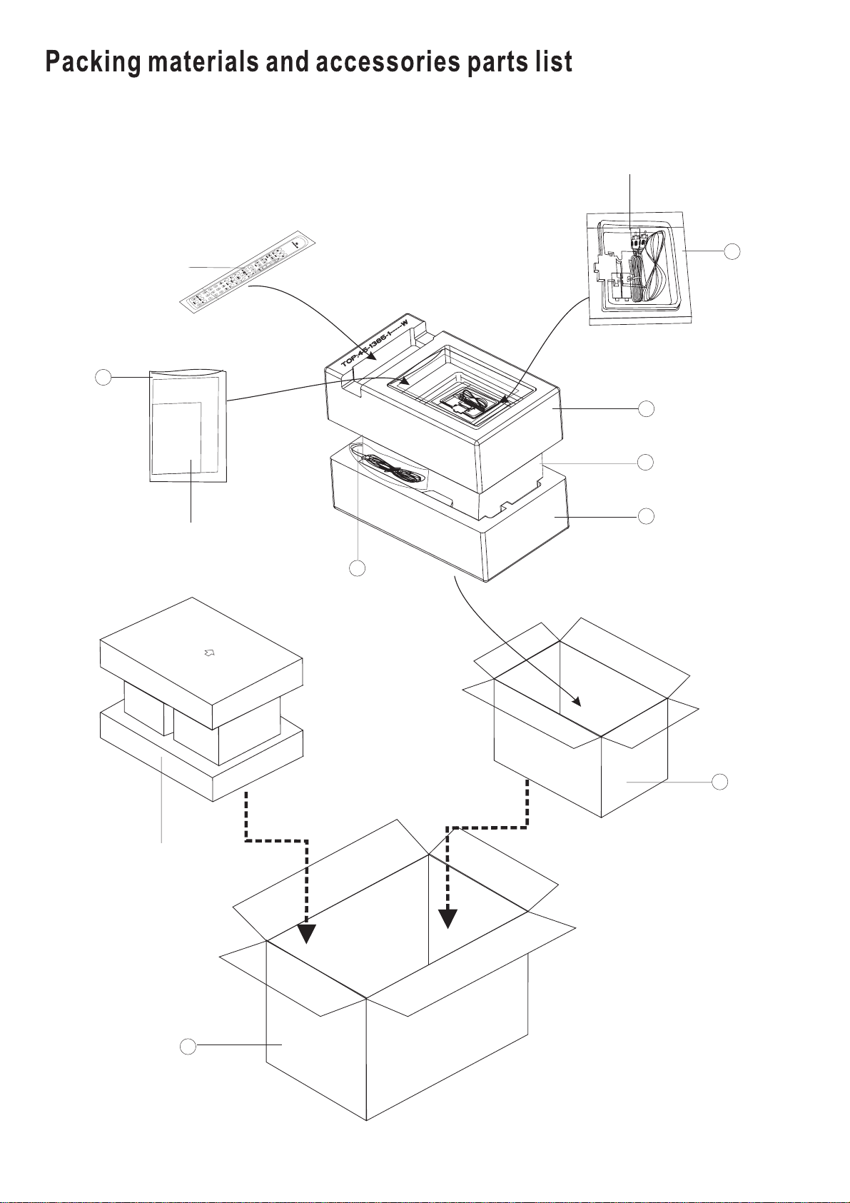
P1
A1
DVA-206LX
A3~A6
P1
--
++
--
++
P4
A7
P3
FRONT VIWE
P5
A2
P2
FRONT
P6
P7
2-9
Page 55

DVA-206LX
▓ Parts list (Packing)
!
Item Parts number Parts name Q'ty Description Area
P 1 470-011100-001X0 POLY BAG 2 IB/ACCESSORY
P 2 470-011526-000X0 POLY BAG 1 AC CORD
P 3 450-021410-001X0 EPE FOAM BAG 1 UNIT
P 4 450-001385-001W0 POLY FORM TOP 1 UNIT
P 5 450-001386-000W0 POLY FORM BOTTOM 1 UNIT
P 6 410-020918-000*0 GIFT BOX 1 UNIT
P 7 430-002085-000X0 MASTER CARTON 1 UNIT
▓ Parts list (Accessories)
!
Item Parts number Parts name Q'ty Description Area
A 1 600-D20LXB-02SX0 REMOTE CONTROL 1
A 2 440-001750-000X0 INSTRUCTION MANUAL 1
A 3 AN-0105-1-----Y FM ANT WIRE 1
A 4 AN-0103-1-----V AM LOOP ANT 1
A 5 5-30-32 BATTERY 2
A 6 11-F1500-SA0-3V VEDIO LINE CORD 1
A 7 644-206LX0-02S00 Speaker Box Assembly 1
2-10
 Loading...