

Page 1
SERVICE MANUAL
This Service Manual is for the
B4-M500 (ECB91ED) / B4-M501 (ECB93ED) / B4-M502 (ECB95ED) model.
For the B4-M500 (ECB91ED) / B4-M501 (ECB93ED) / B4-M502 (ECB95ED)
model, the letter (ECB91ED) / (ECB93ED) / (ECB95ED) is printed on the
Model No. Label on the back of the unit. Refer to the Model No. Label below.
ECB91ED
MODEL NO. B4-M500
Blu-ray Disc Player
Model No. Label
"ECB91ED"
ECB93ED
MODEL NO. B4-M501
Blu-ray Disc Player
Model No. Label
"ECB93ED"
ECB95ED
MODEL NO. B4-M502
Blu-ray Disc Player
Model No. Label
"ECB95ED"
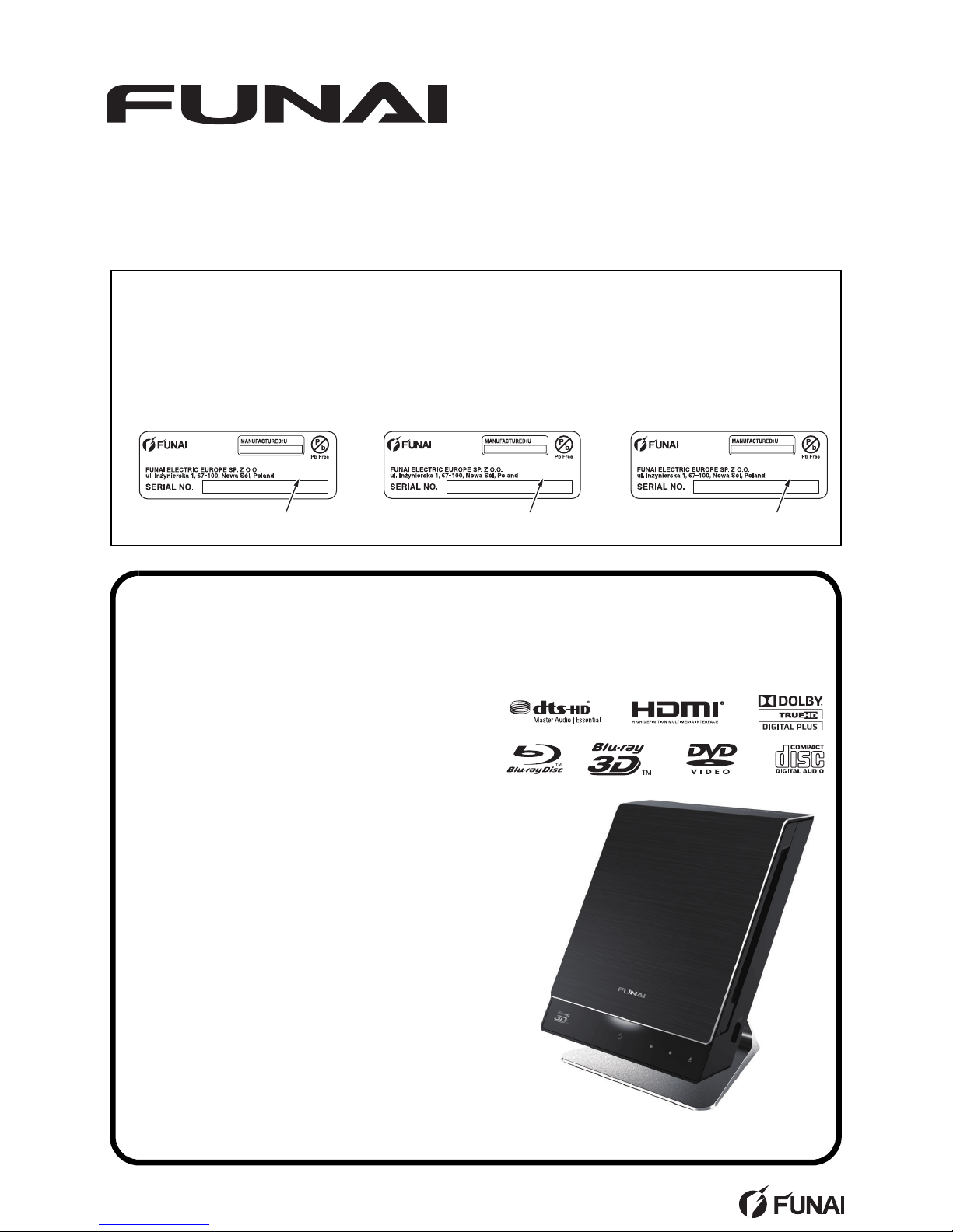
BLU-RAY DISC PLAYER
B4-M500
B4-M501
B4-M502
Page 2

TABLE OF CONTENTS
Specifications . . . . . . . . . . . . . . . . . . . . . . . . . . . . . . . . . . . . . . . . . . . . . . . . . . . . . . . . . . . . . . . . . . . . . . . . . . 1-1-1
Laser Beam Safety Precautions . . . . . . . . . . . . . . . . . . . . . . . . . . . . . . . . . . . . . . . . . . . . . . . . . . . . . . . . . . . . 1-2-1
Important Safety Precautions . . . . . . . . . . . . . . . . . . . . . . . . . . . . . . . . . . . . . . . . . . . . . . . . . . . . . . . . . . . . . . 1-3-1
Standard Notes for Servicing . . . . . . . . . . . . . . . . . . . . . . . . . . . . . . . . . . . . . . . . . . . . . . . . . . . . . . . . . . . . . . 1-4-1
Cabinet Disassembly Instructions. . . . . . . . . . . . . . . . . . . . . . . . . . . . . . . . . . . . . . . . . . . . . . . . . . . . . . . . . . . 1-5-1
How to Initialize the BLU-RAY Disc Player . . . . . . . . . . . . . . . . . . . . . . . . . . . . . . . . . . . . . . . . . . . . . . . . . . . . 1-6-1
Firmware Renewal Mode . . . . . . . . . . . . . . . . . . . . . . . . . . . . . . . . . . . . . . . . . . . . . . . . . . . . . . . . . . . . . . . . . 1-7-1
Error Message . . . . . . . . . . . . . . . . . . . . . . . . . . . . . . . . . . . . . . . . . . . . . . . . . . . . . . . . . . . . . . . . . . . . . . . . . 1-8-1
Home Network (DLNA) Error Code. . . . . . . . . . . . . . . . . . . . . . . . . . . . . . . . . . . . . . . . . . . . . . . . . . . . . . . . . . 1-9-1
Troubleshooting . . . . . . . . . . . . . . . . . . . . . . . . . . . . . . . . . . . . . . . . . . . . . . . . . . . . . . . . . . . . . . . . . . . . . . . .1-10-1
Block Diagrams . . . . . . . . . . . . . . . . . . . . . . . . . . . . . . . . . . . . . . . . . . . . . . . . . . . . . . . . . . . . . . . . . . . . . . . . 1-11-1
Schematic Diagrams / CBA and Test Points. . . . . . . . . . . . . . . . . . . . . . . . . . . . . . . . . . . . . . . . . . . . . . . . . . 1-12-1
Waveforms . . . . . . . . . . . . . . . . . . . . . . . . . . . . . . . . . . . . . . . . . . . . . . . . . . . . . . . . . . . . . . . . . . . . . . . . . . . 1-13-1
Wiring Diagram . . . . . . . . . . . . . . . . . . . . . . . . . . . . . . . . . . . . . . . . . . . . . . . . . . . . . . . . . . . . . . . . . . . . . . . .1-14-1
Exploded Views. . . . . . . . . . . . . . . . . . . . . . . . . . . . . . . . . . . . . . . . . . . . . . . . . . . . . . . . . . . . . . . . . . . . . . . . 1-15-1
Mechanical Parts List . . . . . . . . . . . . . . . . . . . . . . . . . . . . . . . . . . . . . . . . . . . . . . . . . . . . . . . . . . . . . . . . . . . 1-16-1
Electrical Parts List . . . . . . . . . . . . . . . . . . . . . . . . . . . . . . . . . . . . . . . . . . . . . . . . . . . . . . . . . . . . . . . . . . . . .1-17-1
Precautions on 3D video images
This unit supports Blu-ray 3D. When servicing problems related to 3D image output, the following
equipments are needed.
- 3D capable TV
- 3D compatible HDMI cable
- 3D glasses
- Blu-ray 3D disc
Manufactured under license from Dolby Laboratories.
Dolby and the double-D symbol are trademarks of Dolby Laboratories.
Page 3

1-1-1 ECB91_93_95SP
SPECIFICATIONS
D Note
• The specifications and design of this product are subject to change without notice.
General
Signal system NTSC/PAL colour
Power requirements DC 12 V (DC IN terminal)
Power consumption 14 W (standby: 0.5 W)
Dimensions (width x height x depth) 180 x 218 x 158 mm
Weight 2.0 kg
Operating temperature 5°C to 40°C
Operating humidity Less than 80 % (no condensation)
Terminals
DC input 12 V, 1500 mA
USB input
TYPE A
USB 2.0
Bus power current: MAX. 500 mA
AV outp ut
(mini jack x 1)
Composite-video: 1 Vp-p (75 ƙ)
Audio L/R: 2 Vrms (1 kƙ)
Audio output (Digital)
(Optical jack x 1) Digital connector
HDMI output
(HDMI jack x 1)
Digital video: 480p/576p, 720p, 1080i, 1080p, 1080p24/
Digital audio
LAN terminal 10BASE-T / 100BASE-TX
Page 4
1-2-1 ECB91ED(B4P)LBSP(1VM432602)
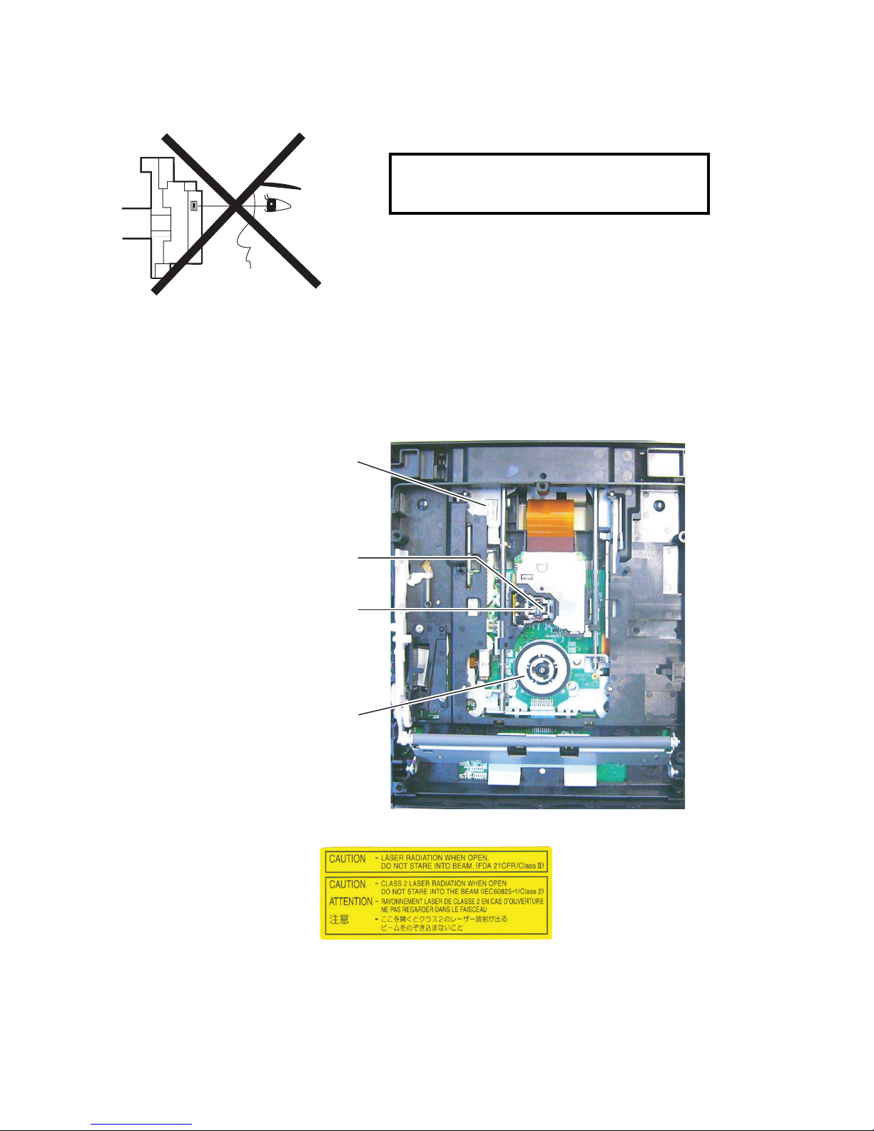
LASER BEAM SAFETY PRECAUTIONS
This BD player uses a pickup that emits a laser beam.
The laser beam is emitted from the location shown in the figure. When checking the laser diode, be sure to keep
your eyes at least 30 cm away from the pickup lens when the diode is turned on. Do not look directly at the laser
beam.
CAUTION: Use of controls and adjustments, or doing procedures other than those specified herein, may result in
hazardous radiation exposure.
Location: Top of Shield Top
Do not look directly at the laser beam coming
from the pickup or allow it to strike against your
skin.
Drive Mechanism Assembly
Laser Beam Radiation
Laser Pickup
Turntable
Page 5

1-3-1 ECB91ISP
IMPORTANT SAFETY PRECAUTIONS
Product Safety Notice
Some electrical and mechanical parts have special
safety-related characteristics which are often not
evident from visual inspection, nor can the protection
they give necessarily be obtained by replacing them
with components rated for higher voltage, wattage,
etc. Parts that have special safety characteristics are
identified by a ! on schematics and in parts lists. Use
of a substitute replacement that does not have the
same safety characteristics as the recommended
replacement part might create shock, fire, and/or other
hazards. The Product’s Safety is under review
continuously and new instructions are issued
whenever appropriate. Prior to shipment from the
factory, our products are carefully inspected to confirm
with the recognized product safety and electrical
codes of the countries in which they are to be sold.
However, in order to maintain such compliance, it is
equally important to implement the following
precautions when a set is being serviced.
Precautions during Servicing
A. Parts identified by the ! symbol are critical for
safety. Replace only with part number specified.
B. In addition to safety, other parts and assemblies
are specified for conformance with regulations
applying to spurious radiation. These must also be
replaced only with specified replacements.
Examples: RF converters, RF cables, noise
blocking capacitors, and noise blocking filters, etc.
C. Use specified internal wiring. Note especially:
1) Wires covered with PVC tubing
2) Double insulated wires
3) High voltage leads
D. Use specified insulating materials for hazardous
live parts. Note especially:
1) Insulation tape
2) PVC tubing
3) Spacers
4) Insulators for transistors
E. When replacing AC primary side components
(transformers, power cord, etc.), wrap ends of
wires securely about the terminals before
soldering.
F. Observe that the wires do not contact heat
producing parts (heatsinks, oxide metal film
resistors, fusible resistors, etc.).
G. Check that replaced wires do not contact sharp
edges or pointed parts.
H. When a power cord has been replaced, check that
5~6 kg of force in any direction will not loosen it.
I. Also check areas surrounding repaired locations.
J. Be careful that foreign objects (screws, solder
droplets, etc.) do not remain inside the set.
K. When connecting or disconnecting the internal
connectors, first, disconnect the AC plug from the
AC outlet.
L. When reassembling, be sure to use the original
screws or specified screws listed in the parts list.
M. This unit is classified as a CLASS 1 LASER
PRODUCT.
Page 6
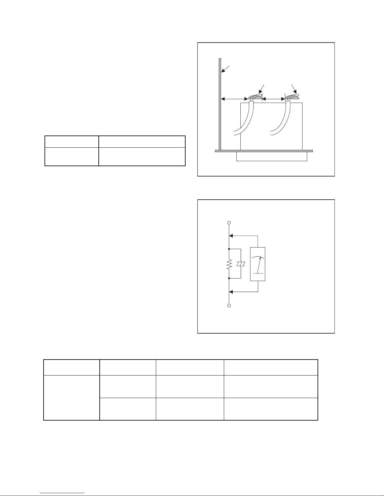
1-3-2 ECB91ISP
Safety Check after Servicing
Examine the area surrounding the repaired location for
damage or deterioration. Observe that screws, parts,
and wires have been returned to their original positions.
Afterwards, do the following tests and confirm the
specified values to verify compliance with safety
standards.
1. Clearance Distance
When replacing primary circuit components, confirm
specified clearance distance (d) and (d’) between
soldered terminals, and between terminals and
surrounding metallic parts. (See Fig. 1)
Table 1 : Ratings for selected area
Note: This table is unofficial and for reference only.
Be sure to confirm the precise values.
2. Leakage Current Test
Confirm the specified (or lower) leakage current
between B (earth ground, power cord plug prongs) and
externally exposed accessible parts (RF terminals,
antenna terminals, video and audio input and output
terminals, microphone jacks, earphone jacks, etc.) is
lower than or equal to the specified value in the table
below.
Measuring Method (Power ON) :
Insert load Z between B (earth ground, power cord plug
prongs) and exposed accessible parts. Use an AC
voltmeter to measure across the terminals of load Z.
See Fig. 2 and the following table.
AC Line Voltage Clearance Distance (d), (d’)
230 V
≥ 2.5 mm(d)
≥ 5.0 mm(d’)
Chassis or Secondary Conductor
Primary Circuit
Fig. 1
d' d
AC Voltmeter
(High Impedance)
Exposed Accessible Part
B
One side of
Power Cord Plug Prongs
Z
Fig. 2
Table 2: Leakage current ratings for selected areas
Note: This table is unofficial and for reference only. Be sure to confirm the precise values.
AC Line Voltage Load Z Leakage Current (i)
One side of power cord plug
prongs (B) to:
230 V
2kΩ RES.
Connected in
parallel
i≤0.7mA AC Peak
i≤2mA DC
RF or
Antenna terminals
50kΩ RES.
Connected in
parallel
i≤0.7mA AC Peak
i≤2mA DC
A/V Input, Output
Page 7
1-4-1 BDP_SN
STANDARD NOTES FOR SERVICING
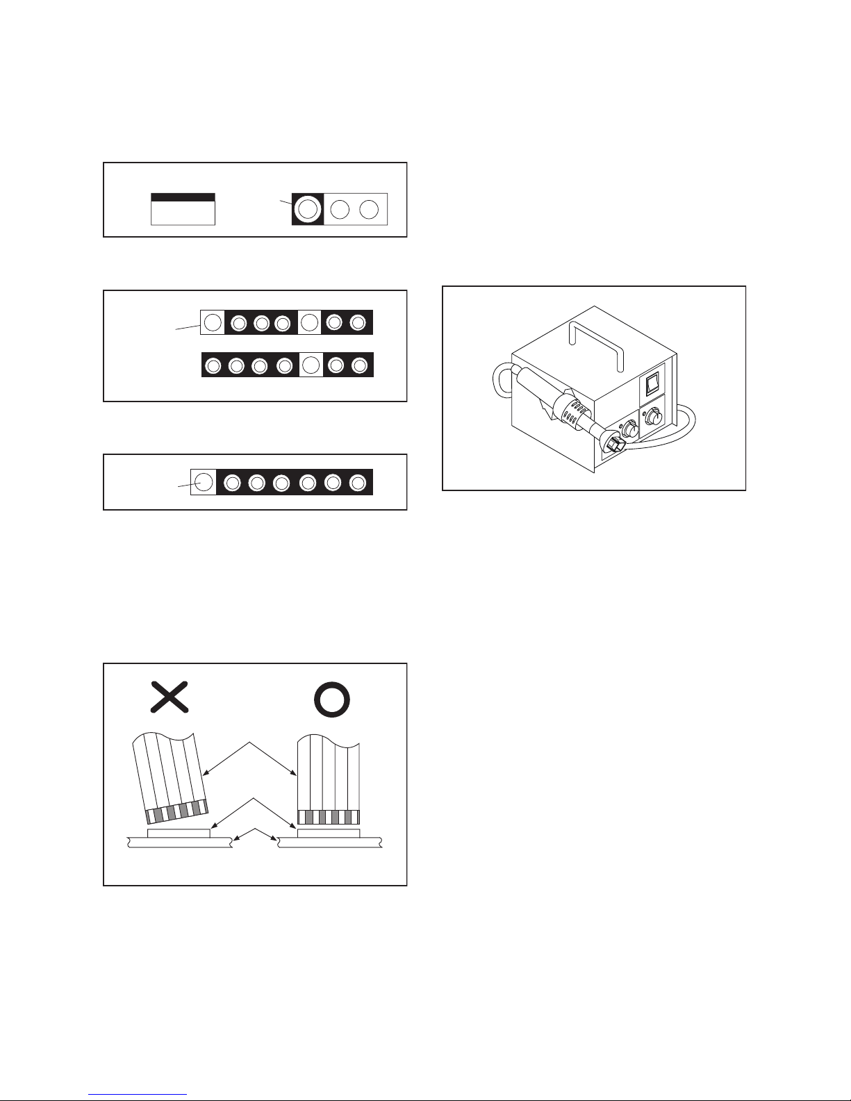
Circuit Board Indications
1. The output pin of the 3 pin Regulator ICs is
indicated as shown.
2. For other ICs, pin 1 and every fifth pin are
indicated as shown.
3. The 1st pin of every male connector is indicated as
shown.
Instructions for Connectors
1. When you connect or disconnect the FFC (Flexible
Foil Connector) cable, be sure to first disconnect
the AC cord.
2. FFC (Flexible Foil Connector) cable should be
inserted parallel into the connector, not at an
angle.
Pb (Lead) Free Solder
When soldering, be sure to use the Pb free solder.
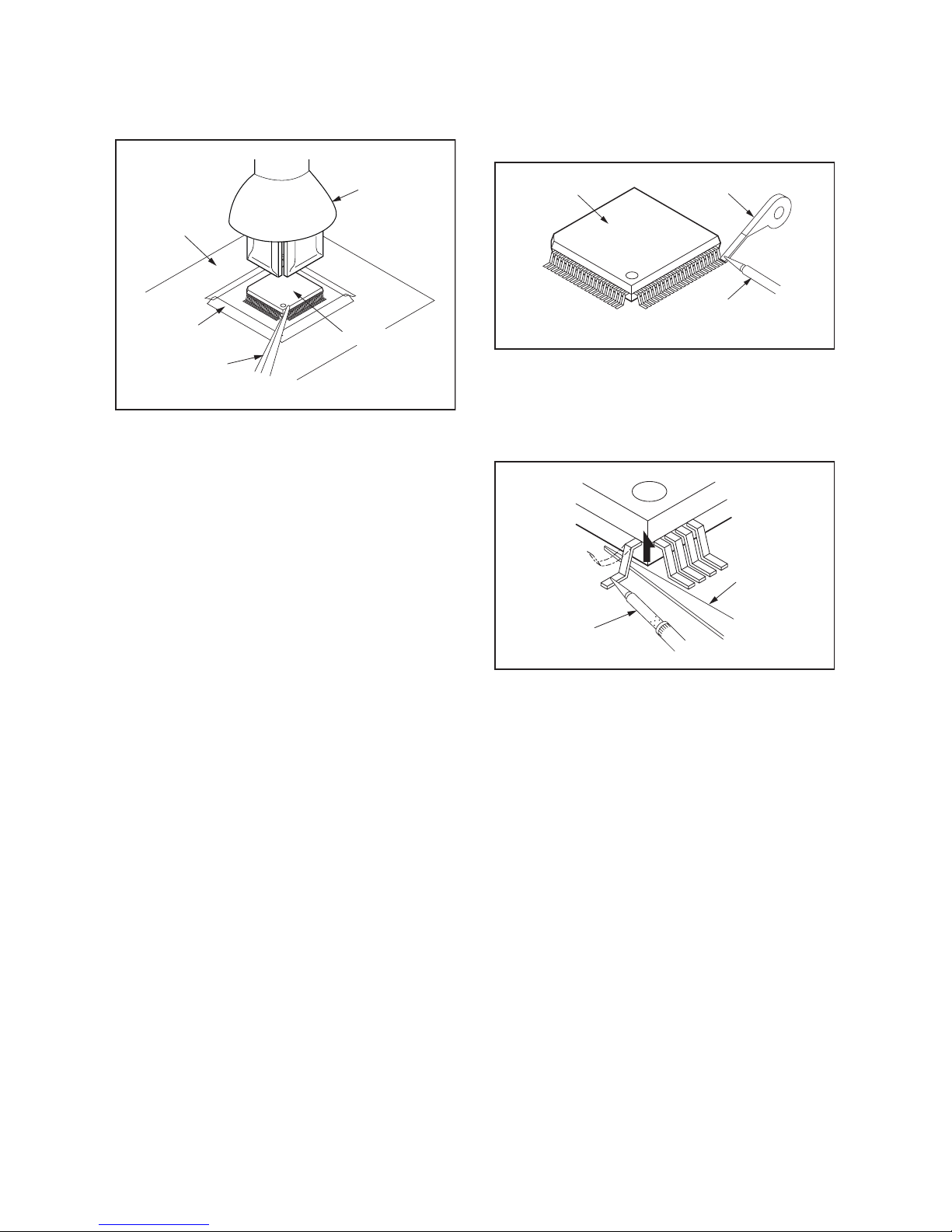
How to Remove / Install Flat Pack-IC
1. Removal
With Hot-Air Flat Pack-IC Desoldering Machine:
1. Prepare the hot-air flat pack-IC desoldering
machine, then apply hot air to the Flat Pack-IC
(about 5 to 6 seconds). (Fig. S-1-1)
2. Remove the flat pack-IC with tweezers while
applying the hot air.
3. Bottom of the flat pack-IC is fixed with glue to the
CBA; when removing entire flat pack-IC, first apply
soldering iron to center of the flat pack-IC and heat
up. Then remove (glue will be melted). (Fig. S-1-6)
4. Release the flat pack-IC from the CBA using
tweezers. (Fig. S-1-6)
CAUTION:
1. The Flat Pack-IC shape may differ by models. Use
an appropriate hot-air flat pack-IC desoldering
machine, whose shape matches that of the Flat
Pack-IC.
2. Do not supply hot air to the chip parts around the
flat pack-IC for over 6 seconds because damage
to the chip parts may occur. Put masking tape
around the flat pack-IC to protect other parts from
damage. (Fig. S-1-2)
To p Vie w
Out
In
Bottom View
Input
5
10
Pin 1
Pin 1
FFC Cable
Connector
CBA
* Be careful to avoid a short circuit.
Fig. S-1-1
Page 8
1-4-2 BDP_SN
3. The flat pack-IC on the CBA is affixed with glue, so
be careful not to break or damage the foil of each
pin or the solder lands under the IC when
removing it.
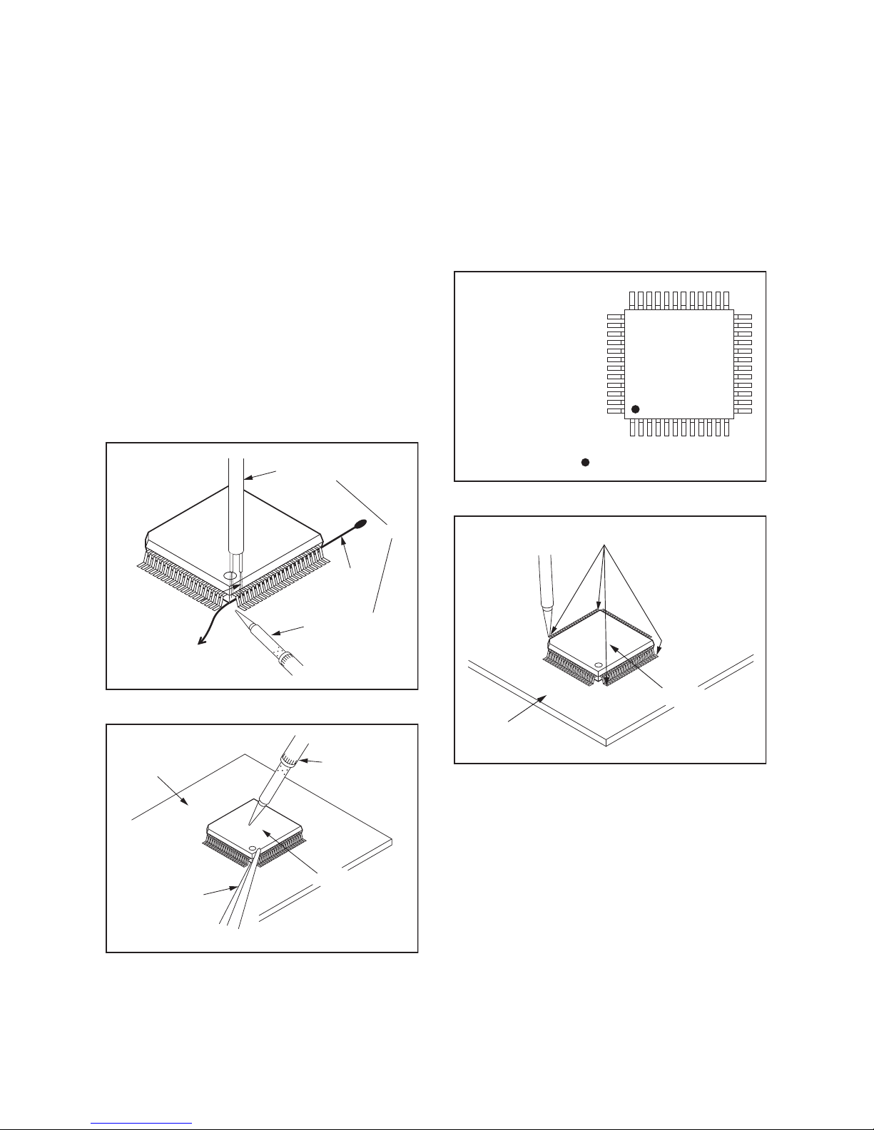
With Soldering Iron:
1. Using desoldering braid, remove the solder from
all pins of the flat pack-IC. When you use solder
flux which is applied to all pins of the flat pack-IC,
you can remove it easily. (Fig. S-1-3)
2. Lift each lead of the flat pack-IC upward one by
one, using a sharp pin or wire to which solder will
not adhere (iron wire). When heating the pins, use
a fine tip soldering iron or a hot air desoldering
machine. (Fig. S-1-4)
3. Bottom of the flat pack-IC is fixed with glue to the
CBA; when removing entire flat pack-IC, first apply
soldering iron to center of the flat pack-IC and heat
up. Then remove (glue will be melted). (Fig. S-1-6)
4. Release the flat pack-IC from the CBA using
tweezers. (Fig. S-1-6)
Hot-air
Flat Pack-IC
Desoldering
Machine
CBA
Flat Pack-IC
Tweezers
Masking
Ta pe
Fig. S-1-2
Flat Pack-IC
Desoldering Braid
Soldering Iron
Fig. S-1-3
Fine Tip
Soldering Iron
Sharp
Pin
Fig. S-1-4
Page 9
1-4-3 BDP_SN
With Iron Wire:
1. Using desoldering braid, remove the solder from
all pins of the flat pack-IC. When you use solder
flux which is applied to all pins of the flat pack-IC,
you can remove it easily. (Fig. S-1-3)
2. Affix the wire to a workbench or solid mounting
point, as shown in Fig. S-1-5.
3. While heating the pins using a fine tip soldering
iron or hot air blower, pull up the wire as the solder
melts so as to lift the IC leads from the CBA
contact pads as shown in Fig. S-1-5.
4. Bottom of the flat pack-IC is fixed with glue to the
CBA; when removing entire flat pack-IC, first apply
soldering iron to center of the flat pack-IC and heat
up. Then remove (glue will be melted). (Fig. S-1-6)
5. Release the flat pack-IC from the CBA using
tweezers. (Fig. S-1-6)
Note: When using a soldering iron, care must be
taken to ensure that the flat pack-IC is not
being held by glue. When the flat pack-IC is
removed from the CBA, handle it gently
because it may be damaged if force is applied.
2. Installation
1. Using desoldering braid, remove the solder from
the foil of each pin of the flat pack-IC on the CBA
so you can install a replacement flat pack-IC more
easily.
2. The “ I ” mark on the flat pack-IC indicates pin 1.
(See Fig. S-1-7.) Be sure this mark matches the
pin 1 on the PCB when positioning for installation.
Then presolder the four corners of the flat pack-IC.
(See Fig. S-1-8.)
3. Solder all pins of the flat pack-IC. Be sure that
none of the pins have solder bridges.
To Solid
Mounting Point
Soldering Iron
Iron Wire
or
Hot Air Blower
Fig. S-1-5
Fine Tip
Soldering Iron
CBA
Flat Pack-IC
Tweezers
Fig. S-1-6
Example :
Pin 1 of the Flat Pack-IC
is indicated by a " " mark.
Fig. S-1-7
Presolder
CBA
Flat Pack-IC
Fig. S-1-8
Page 10
1-4-4 BDP_SN
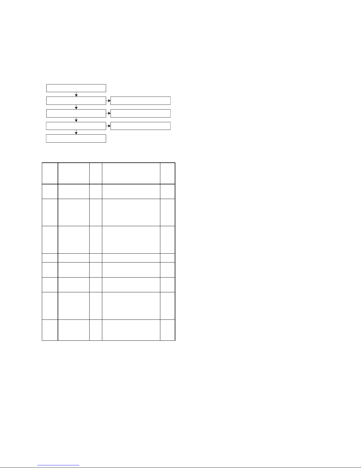
Instructions for Handling Semiconductors
Electrostatic breakdown of the semi-conductors may
occur due to a potential difference caused by
electrostatic charge during unpacking or repair work.
1. Ground for Human Body
Be sure to wear a grounding band (1 MΩ) that is
properly grounded to remove any static electricity that
may be charged on the body.
2. Ground for Workbench
Be sure to place a conductive sheet or copper plate
with proper grounding (1 MΩ) on the workbench or
other surface, where the semi-conductors are to be
placed. Because the static electricity charge on
clothing will not escape through the body grounding
band, be careful to avoid contacting semi-conductors
with your clothing.
<Incorrect>
CBA
Grounding Band
Conductive Sheet or
Copper Plate
1MΩ
1MΩ
<Correct>
CBA
Page 11
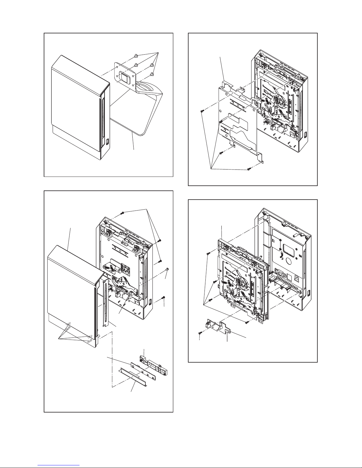
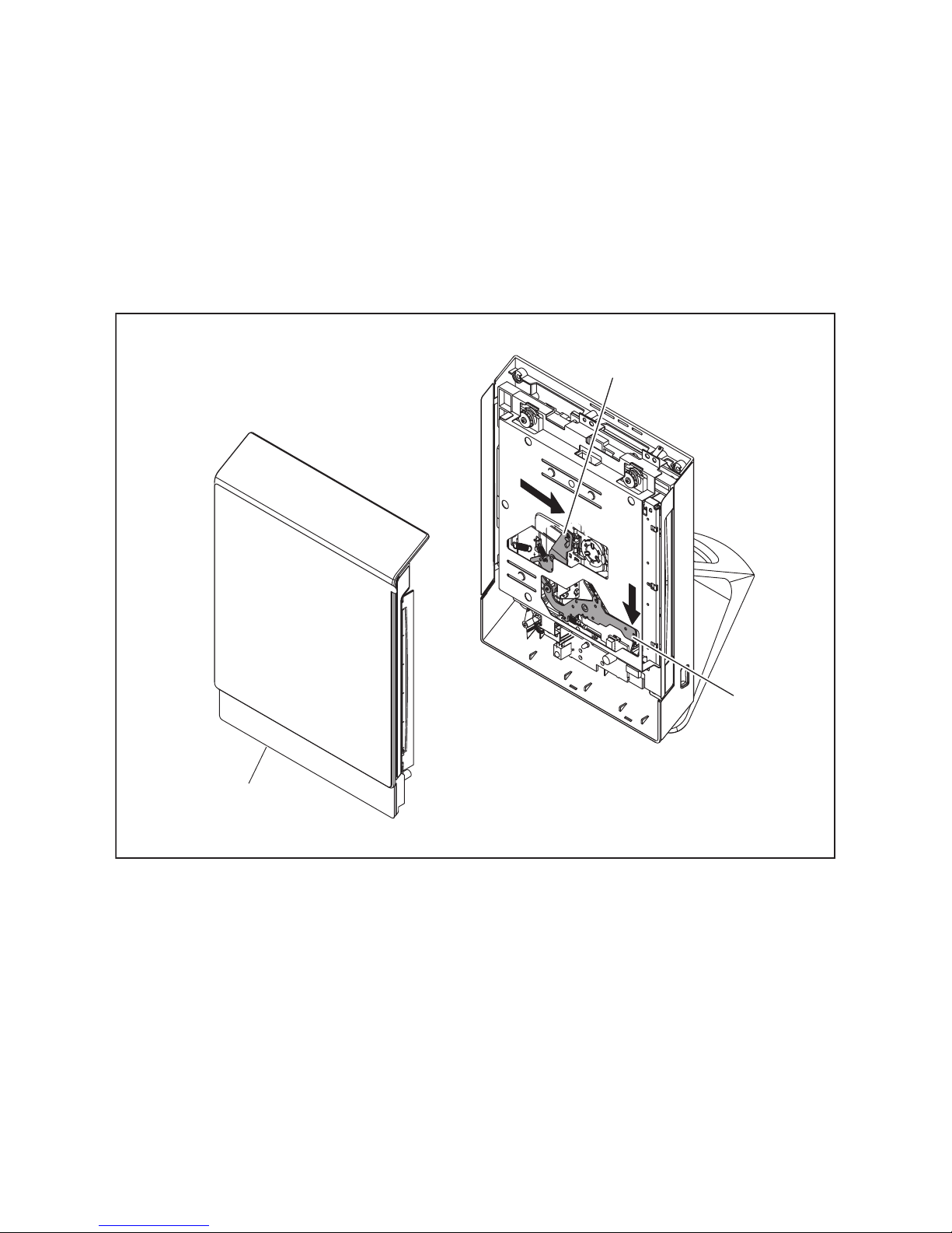
1-5-1 ECB91_93_95DC
CABINET DISASSEMBLY INSTRUCTIONS
1. Disassembly Flowchart
This flowchart indicates the disassembly steps to gain
access to items to be serviced. When reassembling,
follow the steps in reverse order. Bend, route, and
dress the cables as they were originally.
2. Disassembly Method
Note:
(1) Identification (location) No. of parts in the figures
(2) Name of the part
(3) Figure Number for reference
(4) Identification of parts to be removed, unhooked,
unlocked, released, unplugged, unclamped, or
desoldered.
P = Spring, L = Locking Tab, S = Screw,
CN = Connector
e.g. 2(S-2) = two Screws of (S-2),
2(L-2) = two Locking Tabs of (L-2)
(5) Refer to “Reference Notes.”
Reference Notes
1. CAUTION 1: Locking Tabs (L-1) are fragile.
Be careful not to break them.
2. The BD Main CBA & BD Mechanism Assembly
is adjusted as a unit at factory. Therefore, do
not disassemble it. When replacing the BD
Main CBA & BD Mechanism Assembly as a BD
Loader Unit.
ID/
Loc.
No.
Part
Fig.
No.
Removal
Note
[1]
Stand
Assembly
D1 4(S-1) ---
[2]
Front
Assembly
D2
4(S-2), (S-3),
CN1002,
Disc Entry Plate
Assembly
---
[3]
T-Sensor
CBA
D2
4(L-1),
Sensor PCB Holder,
Diffusion Sheet
Assembly
1
[4] Shield Top D3 4(S-4) ---
[5]
Remote
CBA
D4 (S-5), CN1001 ---
[6]
BD Loader
Unit
D4 4(S-6) ---
[7] Jack CBA D5
4(S-7), Heat Sink,
Shield Bottom,
BD Main CBA & BD
Mechanism Assembly
2
[8]
Bottom
Cover
Assembly
D6
FFC Sheet,
Bottom Panel Spring,
Bottom Plate
---
↓
(1)
↓
(2)
↓
(3)
↓
(4)
↓
(5)
[2] Front Assembly
[4] Shield Top
[1] Stand Assembly
[8] Bottom Cover Assembly
[3] T-Sensor CBA
[5] Remote CBA
[7] Jack CBA
[6] BD Loader Unit
Page 12
1-5-2 ECB91_93_95DC
[1] Stand Assembly
(S-1)
Fig. D1
[2] Front
Assembly
[3] T-Sensor CBA
(S-2)
(S-2)
CN1002
Disc Entry Plate
Assembly
Sensor PCB Holder
Diffusion Sheet
Assembly
(S-3)
(L-1)
Fig. D2
[4] Shield Top
(S-4)
Fig. D3
[5] Remote CBA
[6] BD Loader Unit
(S-5)
CN1001
(S-6)
Fig. D4
Page 13
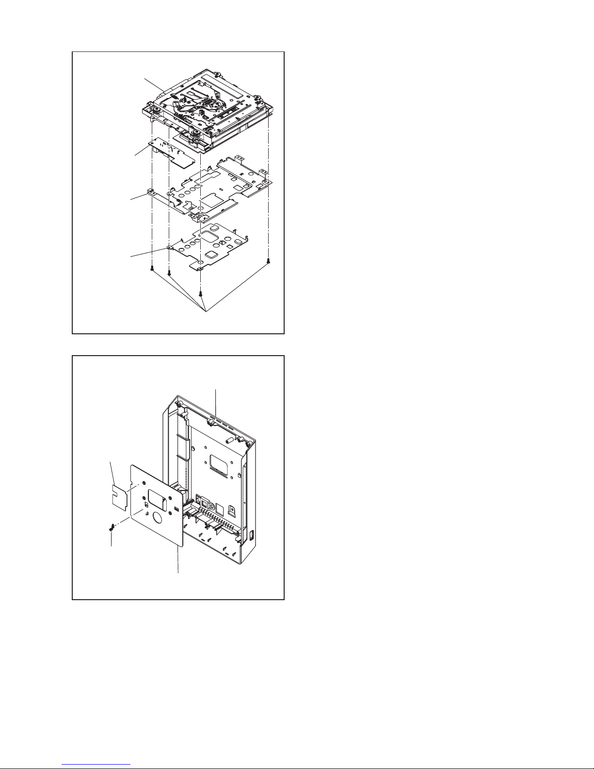
1-5-3 ECB91_93_95DC
[7] *Jack CBA
Shield Bottom
Heat Sink
(S-7)
*
BD Main CBA &
BD Mechanism Assembly
* See Reference Note 2.
Fig. D5
[8] Bottom Cover Assembly
Bottom Panel Spring
FFC Sheet
Bottom Plate
Fig. D6
Page 14
1-5-4 ECB91_93_95DC
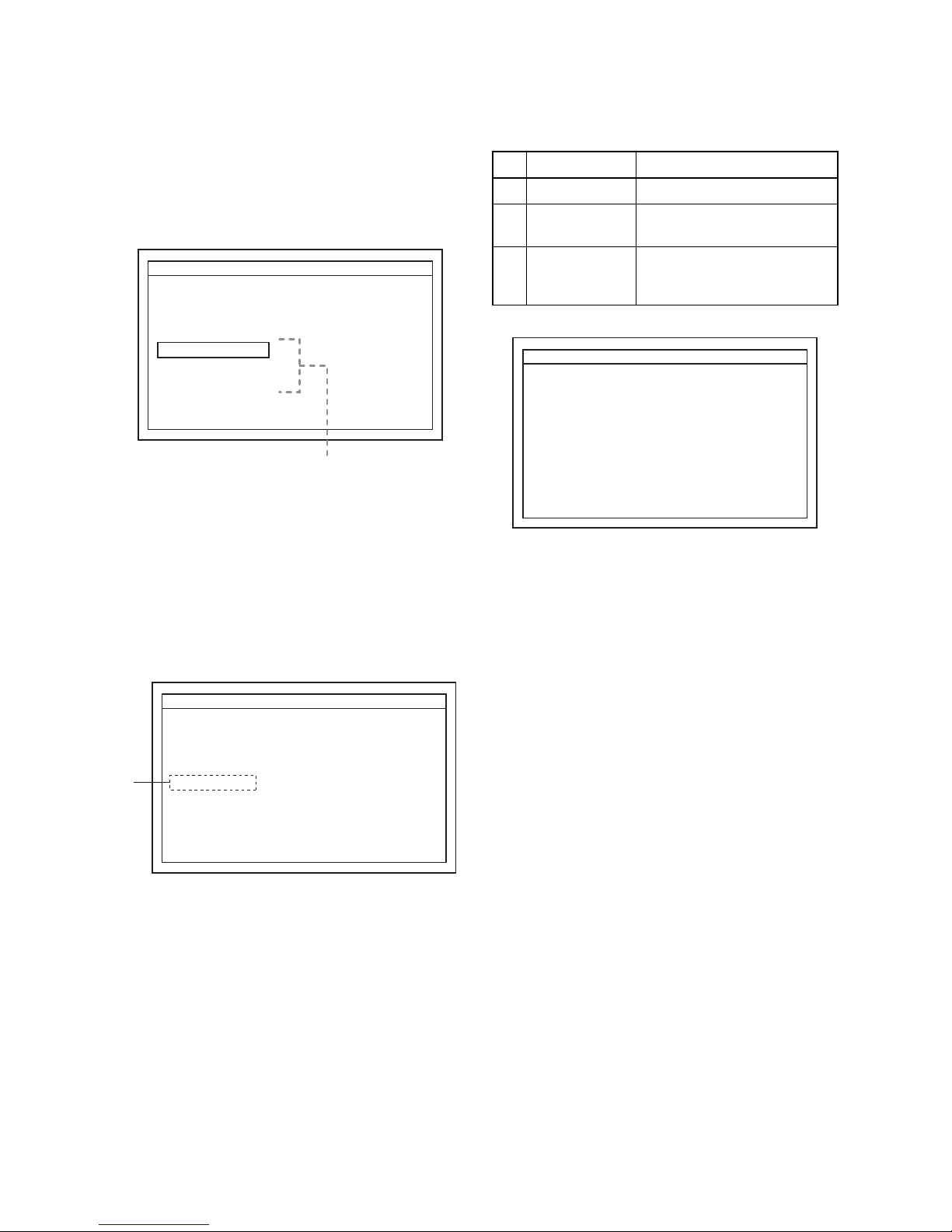
3. How to Eject a Disc
When a disc cannot be removed due to malfunction or when an unplayable disc is inserted, follow the
procedure below to remove the disc.
Procedure A
1. Unplug the AC adapter and then plug it in.
2. Turn the power on by pressing the [ A ] button and the disc will be ejected automatically.
Procedure B
1. Remove the Front Assembly.
2. While pressing the portion A down, slide the portion B in the direction of the arrow as shown below to eject the
disc.
A
B
Front Assembly
Page 15

1-6-1 ECB91_93_95INT
HOW TO INITIALIZE THE BLU-RAY DISC PLAYER
To put the program back at the factory-default,
initialize the BD player as the following procedure.
Note:
• By initializing, network is reset to disconnected state
and “Network Service Disclaimer” appears on the
screen.
• Once the unit is initialized, the unit starts from
Initialization the next time it is turned on. The
Initialization allows quick set up of language and
network settings. To exit this mode, select “Cancel”
on the screen.
1. Turn the power on.
2. Remove the disc on the tray and close the tray.
3. Press [G] (skip up), [1], [2], and [3] buttons on
the remote control unit in this order.
Fig. a appears on the screen.
Fig. a
4. Press [ C ] button on the remote control unit.
Fig. b appears on the screen.
Fig. b
5. After initializing, the power will turn off
automatically.
"*" differ depending on the models.
F/W Name
Version
Region
Pickup
Version Display
: *******
: *.**.**
: *-*
: **
Default Setting : --
Default Setting : STOP End : STANDBY-ON
VFD/LED Check : OK
"*" differ depending on the models.
F/W Name
Version
Region
Pickup
Version Display
: *******
: *.**.**
: *-*
: **
Default Setting : SUCCESS
Default Setting : STOP End : STANDBY-ON
VFD/LED Check : OK
Page 16
1-7-1 ECB91_93_95FW
FIRMWARE RENEWAL MODE
Note: The file extension of the available firmware is
“b42”.
1. Turn the power on and remove the disc on the tray
and close the tray.
2. Press [G] (skip up), [6], [5], and [4] buttons on
the remote control unit in this order.
Fig. a appears on the screen.
Fig. a Version Up Mode Screen (Example)
3. Select “Disc” or “USB” or “SD Card” and press
[OK] button on the remote control unit.
4. Insert the disc or USB Memory Stick or SD Card
for version up.
5. The BD player enters the F/W version up mode
automatically. Fig. b will appear on the screen.
Make sure to insert the proper F/W for the state of
this model.
Fig. b Programming Mode Screen (Example)
The appearance shown in (*1) of Fig. b is
described as follows:
Fig. c Version Up Mode
6. After the update, the power will turn off
automatically.
7. The power turns back on automatically. Remove
the disc or USB Memory Stick or SD Card from the
unit.
Note: All the settings will be put back to factory-
default.
The following USB Memory Stick/SD Card can be
used for software update. Make sure to use a device
that has enough space.
• USB Memory Stick (FAT16/FAT32 file system)
•
SD/Mini SD/Micro SD Card (FAT12/FAT16 file system)
•
SDHC/Mini SDHC/Micro SDHC Card (FAT32 file system)
"*" differ depending on the models.
F/W Version Mode
Please select software update mode.
Disc
USB
SD Card
F/W Name : ******* Ver.*.**.**
The available software update mode will
differ depending on the model type.
"*" differ depending on the models.
F/W Version Mode
Loading Disc...
F/W Name : ******* Ver *.**.**
(*1)
No. Appearance State
1 Loading Disc Loading the disc
2 Reading...
Sending files into the
memory.
3 See LED.
Writing new version data,
the progress will be displayed
as shown in Fig. c.
"*" differ depending on the models.
F/W Version Mode
F/W Name : ******* Ver *.**.**
1. ALL
Version : *.**.**
CHECKSUM : ****
***************.b42
See LED.
Updating
Success
Error
: LED flash alternately.
: LED remain on.
: All LED flash at the same time.
The unit will automatically turn off when update is completed,
and automatically turns back on.
Page 17

1-7-2 ECB91_93_95FW
How to Verify the Firmware Version
1. Turn the power on.
2. Remove the disc on the tray and close the tray.
3. Press [G] (skip up), [1], [2], and [3] buttons on
the remote control unit in this order.
Fig. d appears on the screen.
Fig. d
4. To exit this mode, press [ ] button.
"*" differ depending on the models.
F/W Name
Version
Region
Pickup
Version Display
: *******
: *.**.**
: *-*
: **
Default Setting : --
Default Setting : STOP End : STANDBY-ON
VFD/LED Check : OK
Page 18

1-7-3 ECB91_93_95FW
FIRMWARE RENEWAL MODE (for User)
Disc/USB Memory Stick/SD Card Update
1. Press [HOME] button to display Setup menu.
2. Select Settings - Others - Software Update.
3. Select the software update mode from "Disc" or
“USB Memory Stick” or “SD Memory Card.” The
available software update mode will differ
depending on the model type.
4. The screen appears in Fig. e when “Yes” is
chosen.
Insert the disc or USB Memory Stick or SD Card for
software update.
Fig. e (Example of Disc mode)
5. Disc loading starts. Fig. f will appear on the
screen.
Fig. f (Example of Disc mode)
6. Fig. g will appear on the screen, then select “Yes”.
Fig. g
7. Firmware loading starts. Fig. h will appear on the
screen.
Fig. h
8. Updating starts automatically. Fig. i will appear on
the screen.
Fig. i (Example of Disc mode)
9. The power turns off automatically.
10. The power turns back on automatically. Remove
the disc or USB Memory Stick or SD Card from the
unit.
Note: The setup setting configured before the update
will be kept.
The following USB Memory Stick/SD Card can be
used for software update. Make sure to use a device
that has enough space.
• USB Memory Stick (FAT16/FAT32 file system)
• SD/Mini SD/Micro SD Card (FAT12/FAT16 file
system)
• SDHC/Mini SDHC/Micro SDHC Card (FAT32 file
system)
Software Update
Please insert a disc for software update. If you want to exit update, press
[RETURN].
Software Update
Loading Disc....
Software Update
Current Version : X.XX.XX
: X.XX.XXInsert Version
Select 'Yes' and press [OK] button to start updating.
Press 'No' to exit software update.
No Yes
Software Update
If you want to exit update, press [RETURN].
Loading Software...
1. Loading 2. Updating
Software Update
Updating Software...
Updating
Success
: flash alternately.
:
1. Loading 2. Updating
Please wait for a few minutes.
Do not unplug the AC cord or interrupt updating process.
When update is completed unit will automatically turn off.
Update disc will eject after unit automatically turns back on.
remain on.
Page 19

1-7-4 ECB91_93_95FW
Network Update
1. Press [HOME] button to display Setup menu.
2. Select Settings - Others - Software Update Network.
3. When “Yes” is chosen, the screen appears in Fig. j
and the unit starts connecting to the network.
Fig. j
4. The firmware version confirmation screen (Fig. k)
will appear on the screen. Select “Yes” and press
[OK] button.
Fig. k
5. Firmware downloading starts.
6. Upon completion of downloading, Fig. l will appear
on the screen.
Press [OK] button.
Fig. l
7. The unit starts reading the firmware. Fig. m will
appear on the screen.
Fig. m
8. Updating starts automatically. Fig. n will appear on
the screen.
Fig. n
9. The power turns off automatically.
10. The power turns back on automatically.
Note: The setup setting configured before the update
will be kept.
Network Error Message
Software Update
Network Connecting...
Software Update
Current Version : X.XX.XX
: X.XX.XXLatest Version
The latest software can be downloaded.
Do you want to download?
No Yes
Software Update
Software download has been completed.
Software update will start shortly.
Press [OK].
Software Update
If you want to exit update, press [RETURN].
Then all download data will be erased.
Loading Software...
1. Loading 2. Updating
No. Error Message
1
The cable is not connected.
Please confirm the connection of the cable.
2
DHCP cannot be acquired.
Please confirm connection or set it with the
manual operation.
3
Internet Protocol address is not set.
Please confirm the set content.
4
The equipment with same Internet Protocol
address already exists.
Please set another Internet Protocol address.
5
There is no response from Default gateway.
Please confirm the address of Default
gateway.
6
It is not possible to connect to the DNS server.
Please confirm the Internet connection or the
DNS address setting.
7
It is not possible to connect to the server.
Please contact our support center.
8
It is not possible to confirm the software
version.
Please contact our support center.
9
Cannot connect to the wireless network.
Please confirm the wireless network setting.
Software Update
Updating Software...
1. Loading 2. Updating
Please wait for a few minutes.
Do not unplug the AC cord or interrupt updating process.
When update is completed unit will automatically turn off,
and unit will automatically turn back on.
Updating
Success
: flash alternately.
:
remain on.
Page 20

1-8-1 ECB91/93/95ER
ERROR MESSAGE
Note: Only error messages for the unit’s corresponding media will appear.
Error Message
Disc Error
Disc Error
- - Please eject the disc. - Playback feature may not be available on this Disc.
Loader Error
Loader Error
The unit stopped automatically due to loader error.
Please open the disc tray once and then close it.
Parental Lock Error
Parental Lock On
The current selected parental level prohibits playback.
Region Error
Region Error
Playback is not authorized in your region.
Region code of this disc :
The device connected for HDMI
connection does not support HDCP.
(There is no message.)
USB Error
Memory Device Error
- - Please check the Memory Device. - There is no playback file on the Memory Device or Device has incorrect/
no format.
BD-Live Network Connecting Error
BD-Live Setting Error
Network connection is interrupted. Please confirm “BD-Live Setting”.
LAN Cable Not Connected
The cable is not connected.
Please confirm the connection of the cable.
Cannot Acquire DHCP Server
DHCP cannot be acquired.
Please confirm connection or set it with the manual operation.
Cannot Acquire IP Address
Internet Protocol address is not set.
Please confirm the set content.
Already Existing IP Address
The equipment with same Internet Protocol address already exists.
Please set another Internet Protocol address.
No Response From Default
Gateway
There is no response from Default gateway.
Please confirm the address of Default gateway.
Cannot Connect To DNS Server
It is not possible to connect to the DNS server.
Please confirm the Internet connection or the DNS address setting.
Cannot Connect To Server
It is not possible to connect to the server.
Please contact our support center.
Cannot Confirm Firmware Version
It is not possible to confirm the software version.
Please contact our support center.
Disc Error
- - Please eject the disc. - -
Playback feature may not be available on this Disc.
Page 21

1-8-2 ECB91/93/95ER
Firmware Update Error
(Update File Error)
Error detected.
File may be corrupted.
Please download software again.
Error detected.
Please confirm whether it is USB device that corresponds to software
update.
Cannot Connect To Download
Server
It is not possible to connect to the server.
Please contact our support center.
USB Error
Error in the USB Connection. USB operation has been stopped
automatically. Please remove the USB device and restart the unit.
Error Message
Page 22

1-9-1 ECB91/93/95DLNAER
HOME NETWORK (DLNA) ERROR CODE
Error Code appears in the error screen when the unit
detects an error, as shown below. The code is used to
specifically determine the cause of error.
Fig. 1: Error Code (Example)
Error Code are displayed with “NE[********]” (“*” is
error code) as shown above.
Error Code Form
In the Home Network (DLNA), Error Code are used as
follows.
Fig. 2
“Summary Error Code” are shown in the list below.
Network Error
Cannot connected to server. Please check your settings.
Press [OK].
NE [00202010]
Error CodeError message
002XXXXX
Detailed Error Code
Summary Error Code
Summary
Error Code
Error message
02
Cannot connect to server. Please
check your settings.
03 Playback Error
05 No playable files found.
20 System Error
21
Unable to display files from the
server. Please check server
settings.
22 List Updated.
23 Connection with server lost.
24
Unable to connect to more than 10
servers. Please turn off or stop
broadcasting 1 or more servers.
Page 23

1-9-2 ECB91/93/95DLNAER
Detailed Error Code table (DLNA – HTTP Status Code)
Status Code Description
201 Created A new resource was created by this unit’s request.
202 Accepted This unit’s request was accepted but its processing is not completed.
204 No Content Though the server processed the request, there was no content.
205 Reset Content No content.
300 Multiple Choices
• There are multiple choices.
• The server could not determine its response.
• Requested information contains multiple representations.
This status is handled as Redirection by default and complies with the content
of Location HEAD related to this response.
301 Moved Permanently
• Moved Permanently.
• Requested resource has been assigned to a new permanent URI (Uniform
Resource Identifier). Any future references to this source must use one of the
returned URIs.
• Indicates that requested information is moved to the URI specified by the
Location HEAD. When this status is received, the default action is tracking
the Location HEAD related to the response. When the original request
method is POST, the redirected request will use GET.
302 Found
• Found.
• Requested resource resides temporarily under a different URI.(Uniform
Resource Identifier)
• Indicates that requested information exists in the URI specified by the Location HEAD. When this status is received, Location HEAD related to the
response will be tracked by default. When the request method is POST the
redirected request will use GET.
303 See Other
• See other.
• The response to the request can be found under a different URI (Uniform
Resource Identifier) and to get this response, GET HTTP method will be
used.
• As a result of POST, client will be automatically redirected to the URI specified by the Location HEAD. GET will be used for requesting to a resource
specified by the Location HEAD.
304 Not Modified
This unit caches the latest resource and the requested resource is not
modified. (exception protocol error)
305 Use Proxy
• Proxy will be used.
• The requested resource must be accessed through the proxy specified by the
Location field.
• Indicates that request must use the URI given by the Location HEAD to use
the proxy server.
400 Bad Request The server could not understand this unit’s request.
401 Unauthorized Indicates that the resource requested by this unit requires authentication.
403 Forbidden The server received this unit’s request, but refused to fulfill it.
404 Not Found The requested URI was not found.
405 Method Not Allowed
• The method is not allowed.
• The HTTP behavior used is not allowed.
• Indicates that request method (POST or GET) is not allowed by the
requested resource.
406 Not Acceptable
• The client could not find an acceptable response.
• Indicates that the client specifies not to accept arbitrary representation for
Accept header which could be used by the resource.
407 Proxy Authentication
Required
• Proxy authentication is required.
• Indicates that the requested proxy will request authentication. Proxy-authenticate header contains the detailed method for authentication.
408 Request Timeout
• While waiting for request, the server timed out.
• Indicates that the client did not send a request within the expected time by
the server.
Page 24

1-9-3 ECB91/93/95DLNAER
Detailed Error Code table (DLNA – Application Status Code)
409 Conflict
• There is a conflict.
• The server timed out while waiting for a request.
• Indicates that the client did not send a request within the expected time by
the server.
410 Gone
• No longer available.
• The requested resource could not be found at the server and forwarding
address is unknown.
• Indicates that requested resource is no longer available.
411 Length Required
• Length required.
• The server refused to accept the request where Content-Length was undefined.
• Indicates Content-length header is not defined.
412 Precondition Failed
• Fails to fulfill precondition.
• The precondition in one or more of the requested header field has been
tested false by the server.
• The precondition given in the request could not be fulfilled and the request
failed. Precondition can be set using If-Match, If-None-Match, If-UnmodifiedSince request header.
413 Request Entity Too
Large
• The requested entity is too large.
• The server refused to process the request since the requested entity is larger
than the server is willing or able to process.
• Indicates that the request is too large for the server to process.
414 Request-URI Too Long
• The Request-URI is too long.
• The server refused to process the request because the request URI (Uniform
Resource Identifier) is too long for the server to interpret.
• Indicates that the URI is too long.
415 Unsupported Media
Ty pe
• The media type is not supported.
• The server refused to process the request because the format of request
entity is not supported by the requested resource for the requested method.
• Indicates the requested format is not supported.
500 Internal Server Error Internal server error occurred.
501 Not Implemented
The server does not support functionalities required to process the request
from this unit.
502 Bad Gateway
The proxy server between this unit and the server received an invalid reply from
another proxy or the original server.
503 Service Unavailable
• Service is unavailable.
• The service is temporarily overloaded.
• Because of overloading or maintenance, the server is temporarily unavailable.
504 Gateway Timeout
• Gateway timed out.
• While waiting for gateway, the request timed out.
• Indicates that the intermediate proxy server has timed out while waiting for a
response from another proxy or original server.
505 Version Not Supported
• The version is not supported.
• The server refuses or does not support the version of protocol given in the
request message.
• Indicates that requested version is not supported by the server.
Status Code Description
001 Nothing List
As a result of list creation process, there is no item to be displayed from the
received data.
010 LAN Disconnect This unit’s LAN is disconnected.
020 Application Status Error Error was detected in the DLNA application’s internal state.
021 Application Status Error Error was detected in the DLNA application’s internal state.
022 Application System Error Error was detected in the DLNA application system.
Status Code Description
Page 25

1-9-4 ECB91/93/95DLNAER
023 Unsupported Audio
Format
An unsupported audio format was discovered.
024 Server Number Over
Limit
Discovered server numbers over limit.
025 Changed List The contents list currently displayed has been updated.
026 Disconnected Server The original server of the displaying contents list has been disconnected.
027 Application System Error Error was detected upon start of DLNA application.
600 Disconnected Server The original server of the contents has been disconnected.
601 Not Exist Content Content does not exist.
602 Critical Error System error.
603 Changed List The contents list has been updated at the server.
620 Not Exist Content Image content does not exist.
621 Get failure Image data get error. (an error other than HTTP status and under 500s)
622 File Open Error Image data working file open error.
623 File Read Error Image data working file read error.
624 File Close Error Image data working file close error.
625 Decode mode Error Image data decode mode error.
626 Header Error Image data header error.
627 Struct Error Image data header structural error.
628 Decode Error Image data decode error.
629 Unsupported Format Unsupported format.
630 Unsupported Size Unsupported data size.
631 Attach Error Shared memory attach error.
632 Dettach Error Shared memory detach error.
633 Server Time Out Error Server timed out.
640 File Read Error File read error.
641 Unsupported Format Unsupported Format.
642 No Change Decode
Frame
No updates of decode frame.
643 Stream Get Error Stream get error.
660 File Read Error File read error.
661 Unsupported Format Unsupported format.
662 Video Analyze Error Video analyze error.
663 Audio Analyze Error Audio analyze error.
664 1sec Offset Get Error 1sec offset get error.
665 Address Search Error Address search error.
680 RFS_EVENT_SOCKET_
ERROR
Socket error.
681 RFS_EVENT_HTTP_
RES_SERVER_
REFUSED
Server refusal notification.
682 RFS_EVENT_HTTP_
RES_NOT_FOUND
The specified contents could not be found.
683 RFS_EVENT_HTTP_
RES_SERVER_ERROR
Server error.
Status Code Description
Page 26

1-9-5 ECB91/93/95DLNAER
684 RFS_EVENT_HTTP_
RES_UNEXPECTED_
CODE
Unexpected status code.
685 RFS_EVENT_HTTP_
RES_RANGE_NOT_
SATISFIABLE
The specified range is not satisfiable.
686 RFS_EVENT_RECV_
TIMEOUT
Timed out while waiting for response.
687 RFS_EVENT_DTCP_
ERROR
RCVC internal error. (DTCP originated)
688 RFS_EVENT_DTCP_
CONNECT_ERROR
DTCP connection error.
689 RFS_EVENT_DTCP_
KEY_MNG_ERROR
Kx key error.
690 RFS_EVENT_
RESPONSE_DATA_
ERROR
Received message is invalid.
691 RFS_EVENT_SYSTEM_
ERROR
RCVC internal error.
692 RFS_EVENT_TCP_
DISCONNECTED
The TCP connection has been disconnected by the server during streaming.
693 RFS_EVENT_
CONNECT_TIMEOUT
Time out occurred while establishing TCP connection.
694 RFS_EVENT_RECV_
ERROR
Could not receive contents.
700 Refresh Error Failed to update server list.
701 Disconnected Server The server has been disconnected while displaying contents list.
702 Server Not Found The server has been disconnected while getting contents list.
703 Server Info Error Failed to get server information while getting contents list.
704 Contents List Error Failed to get contents list.
705 Server Config Error Failed to configure server.
706 List Not Found Failed to get contents list.
707 Changed List Displayed contents list has been updated.
708 Object Not Found Neither folders or playable contents was found.
709 Object Not Found By
Filter
Playable contents was not found by filter.
710 Object Count Zero Nothing was found in the folder.
711 ILLEGAL Server Info The contents information from the server is invalid.
712 ILLEGAL Total Count The total counts of contents from the server is invalid.
713 Folder not Exist
The specified folder does not exist. (The current contents list displayed has
been updated)
714 Critical Error An error occurred on the system.
Status Code Description
Page 27

1-10-1 ECB91TR
TROUBLESHOOTING
FLOW CHART NO.1
The power cannot be turned on.
With the AC adapter connected to the set, is 12V
voltage supplied from AC adapter?
Replace the AC adapter.
Ye s
Ye s
No
See Flow Chart No.2 <The key operation is not
functioning.>
No
Is 3.3V voltage supplied to Pin(2) of CN2001 on the
T-Sensor CBA?
Replace the BD Loader Unit.
Replace the BD Loader Unit.
Replace the BD Loader
Unit.
No
Is 12V voltage supplied to Pin(9) of CN6201?
Is operation (POWER, PLAY, STOP, EJECT)
possible from the unit?
Ye s
Ye s
See Flow Chart No.3 <No operation is possible from
the remote control unit.(Operation is possible from
the unit.)>
No
Is operation (POWER, PLAY, STOP, EJECT)
possible from the remote control unit?
Check if the pattern between JK8001 and CN6201 is
shorted.
Ye s
Ye s
Replace the Jack CBA
Unit.
No
No
Ye s
Ye s N o
Ye s N o
No
FLOW CHART NO.2
The key operation is not functioning.
Does the LED on the T-Sensor CBA light up when
turning the power on?
Does the LED on the T-Sensor CBA light brightly
when pressing each switches (POWER, PLAY,
STOP, EJECT)?
Is 3.3V voltage supplied to Pin(2) of CN2001?
No
Is 5V voltage supplied to Pin(1) of CN2001?
Is 3.3V voltage supplied to Pin(2) of CN2001?
Ye s N o
Replace IC2001.
Repalce the BD Loader Unit.
Repalce the BD Loader Unit.
Replace IC2001.
Repalce the BD Loader Unit.
Replace the BD Loader Unit.
Ye s
Page 28

1-10-2 ECB91TR
FLOW CHART NO.4
There is [No Disc] indication.
Both functions of picture and sound do not operate normally.
Replace the BD Loader Unit.
FLOW CHART NO.5
Picture does not appear normally.
Audio is not outputted normally.
Replace the BD Loader Unit.
FLOW CHART NO.3
No operation is possible from the remote control unit.(Operation is possible from the unit.)
Replace the RS1001 (remote control receiver) or
remote control unit.
Is the "L" pulse sent out Pin(1) of RS1001 (remote
control receiver) when the remote control unit
is activated?
Replace the BD Loader Unit.
Is 3.3V voltage supplied to Pin(2) of RS1001
(remote control receiver) ?
Ye s
No
Replace the BD Loader Unit.
No
Ye s
Page 29

1-11-1
BLOCK DIAGRAMS
ECB91BLS
System Control Block Diagram
IC6001
(MAIN MICRO CONTROLLER)
XRST-STM
XRST
XRST
XTRST
XFERST
BD MAIN CBA
PWSW2
PWSW4
F15
F20
D16
F14
E16
CEC-IN
Q6403
CEC
PWSW2
PWSW4
B12
D14
A13
E12
A10
B10
CK27XI
CK27XO
27MHz
X'TAL
X6901
JK6401
PWSW1
PWSW1
B15
TO POWER SUPPLY
BLOCK DIAGRAM
DVD-DISC-OUT
IREDCON-SUB
DVD-DISC-OUT
IREDCON-SUB
C13
D13
DVD-DISC-IN
DVD-DISC-IN
B13
TO DIGITAL SIGNAL
PROCESS 1
BLOCK DIAGRAM
AUDIO-MUTE
AUDIO-MUTE
TO VIDEO/AUDIO
BLOCK DIAGRAM
P-ON+3.3V
RESET
IC6901,
Q6901,
Q6902
EV+3.3V
RESET
IC6905
P-ON+1.5V
13
BUFFER
CN6201 CN1001 CN1002
46I2C-DAT
37I2C-CLK
25I2C-DAT
16I2C-CLK
REMOTE CBA
A11
F12
I2C-DAT
I2C-CLK
19LED-LIGHT
28REMOTE
B11
F10
LED-LIGHT
REMOTE
CN2001
T-SENSOR CBA
P-ON+5V
10
9
132
4
D2001
Q2001
Q2002
D2002 PLAY
IC2001
(TOUCH SENSOR)
SCL
KEY4
POWER
STOP
PLAY
EJECT
13
POWER-LED
SDA
12
PLAY-LED
11
STOP-LED
8
EJECT-LED
POWER
KEY2
STOP
KEY3
PLAY
KEY1
EJECT
Q2003
D2003 STOP
EJECT
Q2004
D2004
POWER
LED LIGHT
D1001
Q1001
EV+12V
REMOTE
SENSOR
RS1001
Q6202
Page 30

1-11-2
Digital Signal Process 1 Block Diagram
ECB91BLD1
BD MAIN CBA
W15
V14
U13
DISC-IN 3
DISC-OUT 2
LED-POW 1
HU(+) 11
HU(-) 10
HV(+) 9
HV(-) 8
HW(+) 7
HW(-) 6
HB 5
CN7102
IC6001
(MAIN MICRO CONTROLLER/DIGITAL SIGNAL PROCESS)
IC7101(MOTOR DRIVE)
TRACKING
ACTUATOR
DRIVE
OEIC
(BD/CD/DVD)
IC7102
(MOTOR DRIVE)
FE
DIGITAL
SIGNAL
PROCESS
STREAM
CONTROL
COPY
PROTECT
AACS
BD+
CSS
CPRM
MATRIX
RF
GENERATOR
E19
D19
B19
C19
L22
L23
G25
G26
242119131415161718
SLD2(+) 5
SLD2(-) 6
SLD1(+) 7
SLD1(-) 8
CN7101
LOAD(-) 3
LOAD(+) 4
CLAMP-SW 2
TD 4
TR 3
FR1 6
FD1 5
EXPA(+) 9
EXPA(-) 10
EXPB(+) 7
EXPB(-) 8
A-D *1
E-H *2
RF(+) 38
RF(-) 36
LDD-SDATA
LDD-SCLK
LDD-SDATA 23
LDD-SCLK 24
CN7001
CN7001
*1: 29,30,33,34
*2: 40-43
201918
17
262524
23
LOADING
MOTOR DRIVE
4
5
COLLIMATE
LENS
MOTOR DRIVE
SLED
MOTOR DRIVE
SPINDLE
MOTOR
DRIVE
12
FOCUS 1
ACTUATOR
DRIVE
TRACKING-CONTROL
TO DIGITAL SIGNAL
PROCESS 2 BLOCK
DIAGRAM
(IC6001)
FOCUS1-CONTROL
FOCUS2-CONTROL
SLED1-CONTROL
SLED2-CONTROL
CLAMP-SW
SPINDLE-CONTROL
SPINDLE-FG
LOAD-CONTROL
EXPA-CONTROL
EXPB-CONTROL
27
22
21
FOCUS 2
ACTUATOR
DRIVE
29
162815
B17
A1737
38
F19
E18
DISC-IN
B18
DISC-OUT
DVD-DISC-IN
IREDCON-SUB
DVD-DISC-OUT
C20
PA-ADJ
A22
PB-ADJ
C23
7
C17
10
B20
4
H25
H26
RF
EQUALIZER
WOB
/LPP
MPX
A19
LASER
DIODE
DRIVE
SLED
MOTOR
SPINDLE
MOTOR
FR2 2
FD2 1
LOADING
MOTOR
VIDEO SIGNAL AUDIO SIGNAL
CLAMP
41
40
1
2
BD LOADER UNIT
D26, E25,
E26, F25
B26, C25,
C26, D25
DISC-OUT DISC-IN
Q7707
EV+3.3V
P-ON+3.3V
Q7705,
Q7706
Q7702,
Q7703
SW
SW
TO SYSTEM
CONTROL
BLOCK
DIAGRAM
IC7501(OP AMP)
576
312
Page 31

1-11-3
ECB91BLD2
Digital Signal Process 2 Block Diagram
BD MAIN CBA
JACK CBA
ED (0-7)
MII-RXD (0-3), MII-TXD (0-3)
MMDQ (0-31)
MMA (0-13)
MEDIA
PROCESSOR
Java (BD-J)
MPEG-2
DiVX
VC-1
H.264
DECODER
HD (TS)
SD (PS)
FROM DIGITAL
SIGNAL PROCESS 1
BLOCK DIAGRAM
(IC6001)
ETHERNET
INTERFACE
MEMORY
I/F
IC6001 (MAIN MICRO CONTROLLER/DIGITAL SIGNAL PROCESS)
IC6906
(NAND FLASH MEMORY)
(ETHERNET JACK)
NAND FLASH
MEMORY (1Gbit)
(DDR3 SDRAM)
IC6101,IC6102
DDR3 SDRAM
(2Gbit) x 2
I/P
CONVERTER
/SCALING
DIGITAL
VIDEO
OUT
HDMI
I/F
DIGITAL
AUDI O
OUT
VIDEO
DAC
TO VIDEO/AUDIO
BLOCK DIAGRAM
VIDEO
DAC-SCK
DAC-BCK
DAC-LRCK
DATA
TO VIDEO/AUDIO
BLOCK DIAGRAM
VIDEO SIGNAL AUDIO SIGNAL
SPDIF
IC8001
TX(+) 1
(USB JACK)
USBDP0 3
USBDN0 2
TX(-) 3
RX(+) 4
RX(-) 6
CN8002
CN8001 CN6501
TMDS DATA 2-
TMDS DATA 2+
TMDS DATA 1-
TMDS DATA 1+
TMDS DATA 0-
TMDS DATA 0+
TMDS CLOCK +
TMDS CLOCK -
JK6401
HDMI-CONNECTOR
DOC DATA
DOC CLOCK
HOT PLUG DETECT
191516
31649
7
10
12
USBDP0
USBDN0
CN6301
42-45 42-45
MII-RXD(0-3)
6-9 6-9
MII-TXD(0-3)
D7
E7E6B5A5B4A4B3A3A2
B2
V3
V2
R2
E10
D10
C10
B9
K4
Page 32

1-11-4
Video/Audio Block Diagram
BD MAIN CBA
JACK CBA
TO DIGITAL
SIGNAL
PROCESS 2
BLOCK DIAGRAM
6.75MHz
VIDEO
VIDEO SIGNAL AUDIO SIGNAL
IC6701 (VIDEO DRIVER)
4dB
AMP
LPF 2
2dB
AMP
75Ω
DRIVER
4
IC6602
(AUDIO D/A CONVERTER)
AUDIO
DAC
121513
14
(L-CH)
(R-CH)
MUTE
7
6
17
TO SYSTEM CONTROL
BLOCK DIAGRAM
AUDIO-MUTE
DATA
DAC-SCK
DAC-BCK
DAC-LRCK
SPDIF
CN6501
CN8001
35 35AUDIO(L)-OUT
33 33AUDIO(R)-OUT
16 16SPDIF
DIGITAL
AUDIO OUT
(OPTICAL)
JK8003
3
JK8002
AV-OUT
WF1
WF3
WF2
18 18VIDEO-OUT
ECB91BLV
Page 33

1-11-5
Power Supply Block Diagram
ECB91BLP
BD MAIN CBA
JACK CBA
CN8001 CN6501
IC6005
IC6002
+5V REG.
Q6006, Q6009
SW+12V
Q6002, Q6007
SW+12V
23-28
EV+12V
23-28
P-ON+12V
P-ON+5V
EV+3.3V
IC6106
+1.2V REG.
EV+1.2V
IC6006
P-ON+3.3V
A+8V
A+8V-REG
TO SYSTEM CONTROL
BLOCK DIAGRAM
PWSW4
PWSW1
PWSW2
Q6011
Q6010
+3.3V REG.
JK8001
DC-IN
Q6001,Q6008
SW+3.3V
+8V REG.
P-ON+1.2V
IC6003
+1.2V REG.
Q6004
Q6003
P-ON+1.5V
IC6004
+1.5V REG.
Page 34

1-12-1 B4.2P_SC
SCHEMATIC DIAGRAMS / CBA AND TEST POINTS
Standard Notes
WARNING
Many electrical and mechanical parts in this chassis
have special characteristics. These characteristics
often pass unnoticed and the protection afforded by
them cannot necessarily be obtained by using
replacement components rated for higher voltage,
wattage, etc. Replacement parts that have these
special safety characteristics are identified in this
manual and its supplements; electrical components
having such features are identified by the mark “!” in
the schematic diagram and the par ts list. Before
replacing any of these components, read the parts list
in this manual carefully. The use of substitute
replacement parts that do not have the same safety
characteristics as specified in the parts list may create
shock, fire, or other hazards.
Notes:
1. Do not use the part number shown on these
drawings for ordering. The correct part number is
shown in the parts list, and may be slightly
different or amended since these drawings were
prepared.
2. All resistance values are indicated in ohms
(K = 10
3
, M = 106).
3. Resistor wattages are 1/4W or 1/6W unless
otherwise specified.
4. All capacitance values are indicated in µF
(P = 10
-6
µF).
5. All voltages are DC voltages unless otherwise
specified.
6. Electrical parts such as capacitors, connectors,
diodes, IC’s, transistors, resistors, switches, and
fuses are identified by four digits. The first two
digits are not shown for each component. In each
block of the diagram, there is a note such as
shown below to indicate these abbreviated two
digits.
Page 35

1-12-2 B4.2P_SC
LIST OF CAUTION, NOTES, AND SYMBOLS USED IN THE SCHEMATIC DIAGRAMS ON
THE FOLLOWING PAGES:
1. Note:
1. Do not use the part number shown on the drawings for ordering. The correct part number is shown in the
parts list, and may be slightly different or amended since the drawings were prepared.
2. To maintain original function and reliability of repaired units, use only original replacement parts which are
listed with their part numbers in the parts list section of the service manual.
2. Voltage indications for PLAY and STOP mode on the schematics are as shown below:
3. How to read converged lines
4. Test Point Information
2
3
1
5.0
(2.5)
5.0
The same voltage for
both PLAY & STOP modes
Indicates that the voltage
is not consistent here.
PLAY mode
STOP mode
(Unit: Volt)
1-D3
Distinction Area
Line Number
(1 to 3 digits)
Examples:
1. "1-D3" means that line number "1" goes to the line numbe
r
"1" of the area "D3".
2. "1-B1" means that line number "1" goes to the line number
"1" of the area "B1".
3
2
1
ABCD
1-B1
1-D3
AREA D3
AREA B1
: Indicates a test point with a jumper wire across a hole in the PCB.
: Used to indicate a test point with a component lead on foil side.
: Used to indicate a test point with no test pin.
: Used to indicate a test point with a test pin.
The reference number of parts on Schematic Diagrams/CBA can be retrieved by
application search function.
Page 36

1-12-3
4 RX(+)
1 TX(+)
R8011 100
R8012 100
100R8017
5NU
100R8013
7NUR8021
4.7K
0.1
C8010
100R8019
2NU
100R8034
100R8036
3 TX(-)
R8010 100
100R8015
6 RX(-)
100R8016
100R8014
100R8035
100R8037
0.1
C8017
0.1
C8018
1
2
3
4
5
6
7
8
910111213141516
17
18
19
20
21
22
23
24
25 26 3027 28 29 31 32
IC8001
KSZ8051MNL
2.2
C8013
100R8038
0.1
C8021
100R8018
0.1
C8014
CN8002
8 GND
R8023
BEAD
30GND
11MDIO-INTL
21GND
37GND
4MII-CRS
6MII-TXD3
23EV+12V
43MII-RXD1
25EV+12V
45MII-RXD3
7MII-TXD2
40MII-RXER
41MII-RXDV
19GND
42MII-RXD0
2P-ON+3.3V
36GND
12GND
15P-ON+5V
27EV+12V
17GND
13MII-TXCLK
9MII-TXD0
32GND
29GND
22GND
20GND
44MII-RXD2
26EV+12V
28EV+12V
18VIDEO-OUT
24EV+12V
35AUDIO(L)-OUT
3PHYRSTL
8MII-TXD1
CN8001
1P-ON+3.3V
33AUDIO(R)-OUT
39GND
14GND
38MII-RXCLK
5MII-COL
16SPDIF
31GND
34GND
10MII-TXEN
46MDC
47MDIO
48GND
49CK250
50GND
100R8033
R8020
BEAD
47P
C8023
R8022
6.49K
100P
C8009
VIN
VCC
GND
JK8003
JST1223
2
1
3
0.1
C8001
JK8001
JK8002
R8001
470
47P
C8022
2200P
C8004
D8001
EDZTE6112B
D8002
EDZTE6112B
R8002
470
R8008
02200P
C8005
1
C8012
1000P
C8024
R8005
0
R8039
0
R8032
0
AUDIO SIGNALVIDEO SIGNAL
WF1
WF2
WF3
1000P
C8025
1
2
3
4
REXT
VDD
(+3.3V)
LED
DRIVER
GND
ETHERNET
INTERFACE
VDD
(+3.3V)
PARALLEL/SERIAL
DECODER
SERIAL/PARALLEL
DECODER
RECEIVER
NU
VDD
(+1.2V)
TRANSMITTER
(ETHERNET JACK)
XI
MII/RMII/SMII
REGISTERS AND
CONTROLLER
INTERFACE
TO BD MAIN
CBA CN6501
TRANS,MODULE
FIBER OPTIC
DIGITAL
AUDIO OUT
(OPTICAL)
BEDFAC
DC-IN
AV-OUT
JACK CBA
ECB91SCJ
Jack Schematic Diagram
Page 37

1-12-4
4 GND
5 EV+3.3V
2 I2C-DAT
3 INT
1 I2C-CLK
CN1002
6 P-ON+5V
3EV+3.3V
6I2C-DAT
5INT
CN1001
1EV+12V
2P-ON+5V
4GND
7I2C-CLK
8REMOTE
9LED-LIGHT
231
RS1001
KSM-712TH2E
VOUT
VCC
GND
0.1
C1001
6.8K
R1001
Q1001
MMBTSA1504Y
100K
R1003
C1003
220/6.3V
R1004
1.8K
R1005
1.8K
D1001
204-15/T2C3-4NQA
REMOTE CBA
AB
2
C
1
(REMOTE SENSOR)
(LED DRIVE)
LED LIGHT
TO T-SENSOR
CBA CN2001
TO BD MAIN
CBA CN6201
12.0
5.0
3.3
0
3.3
3.1
3.1
3.1
11.2
12.0
12.0
11.2
ECB91SCP3
Remote Schematic Diagram
Page 38

1-12-5
5I2C-DAT
2EV+3.3V
3GND
4INT
CN2001
1P-ON+5V
6I2C-CLK
R2005
100
C2002
100P
1234
5
6
7
8
9101112
13
14
15
16
IC2001
WT5701-UG160WT
POWER
PLAY
STOP
EJECT
NU
INT
VSS
EJECT
-LED
SDA
SCL
STOP
-LED
PLAY
-LED
POWER-LED
NU
VDD
NU
R2004
100
C2003
0.1
C2001
100P
Q2002
SRC1202SF
0.01
C2005
D2002
LTW-C193TS5
R2007
150
R2001
10K
Q2004
SRC1202SF
0.01
C2007
D2003
LTW-C193TS5
R2008
150
Q2003
SRC1202SF
0.01
C2006
D2004
LTW-C193TS5
R2009
150
D2001
LTW-C193TS5
R2006
150
Q2001
SRC1202SF
0.01
C2004
CAB
1
2
T-SENSOR CBA
TO REMOTE
CBA CN1002
(TOUCH SENSOR)
KEY4
POWER
KEY2
STOP
KEY3
PLAY
KEY1
EJECT
(LED DRIVE)
PLAY
(LED DRIVE)(LED DRIVE)
STOP EJECT
(LED DRIVE)
POWER
3.0
0.3
0
3.0
0.3
0
3.0
0
0.3 0.3
0
3.0
0.3 0.3 3.0 3.0
0.3
0
3.3
0.3
3.3
0.2 0.2 0.2 0.2
ECB91SCT
T-Sensor Schematic Diagram
Page 39

1-12-6
VIDEO SIGNAL AUDIO SIGNAL
8EXPB(-)
TR
3TR
FR2 2
FD2
VC-PDF24
7EXPB(+)
4TD
FR1
9EXPA(+)
BINE26
P-ON+3.3V
GINB26
EXPB(-)
10EXPA(-)
SW1K22
FD1
A+5V
TD
EXPA(+)
5FD1
FR2
P-ON+5V(1)
C7001
0.1
CN7001
1FD2
EXPA(-)
A+8V
EXPB(+)
6FR1
39GND
30D
31SW2
14GND
37GND
35GND
43H
13THERMOOP
11GND
45VC-PD
27+5V
15+8V
21GND
32SW1
20+5V
28OPU-MKR
C7010
0.1
THERMOOPD23
R7031
10K
L7001
BEAD
C7015
0.1
C701910C7003
0.1
SW2L26
OPU-MKRK24
6 XFERST
NU M21
R7306 10K
R7313 10K
NU L25
2 SENSJ1
NU N22
R7308 10K
C7304 100P
R7307 10K
NU N21
C7301 100P
SOT0 M24
SENSJ2 L24
5 SIN0
R7312 10K
SENSJ1 K23
3 GND
C7303 100P
4 SOT0
CN7301
1 SENSJ2
SIN0 M25
XFERST
R7309 10K
C7302 100P
R7310 10K
NU M22
IC6001(1/8)
*1
MN2WS0210D3
R7311 10K
NU N26
NU N25
NU J24
NU D22
NU C22
NU J25
NU G24
PA-ADJ A22
PB-ADJ C23
IRED CON C21
NUD20
NU B24
NU A23
NU B25
NU A24
NU B23
NU A25
NUA20
U
HV(+)
12 A+5V
DISC-OUT
2 DISC-OUT
14 V
4 GND
8 HV(-)
HV(-)
10 HU(-)
9 HV(+)
HW(+)
DISC-IN
3 DISC-IN
V
7 HW(+)
11 HU(+)
HB
5HB
13 U
HW(-)
6 HW(-)
HU(-)
W
CN7102
15 W
HU(+)
R7142 100
R7143
100
C7402 1
C7401 0.1
E23
F23
C7404 0.1
F18
D21
R7402 10K
C7405
0.082
C7406 8200P
K25
K26
C7408 0.1
C7407 0.033
G22
C7409 0.1
H24
H21
R7403 10K
L6
VHALF
R7407
10K
R7406
10K
12GND
16GND
18GND
R7037 4.7K
17TEST-V
R7038
10K
TEST-VB22
LD-TYPEJ22
19LD-TYPE
C701810C7002
0.1
22LDON LDONE20
25DSEN DSENM23
LDD-SCLKL22
LDD-SDATAL23
24LDD-SCLK
23LDD-SDATA
26GND
CINE2529C
33A AINF25
34B DIND26
BDRFBH25
C7014 1
RFBG25
C7011 1
38BDRF(+)
C7012 1
RFAG26
36BDRF(-)
C7013 1
BDRFAH26
HINC25
EIND25
40F
42E
41G
FINC26
44GND
1 LED-POW
C7146 0.01
C7145 0.01
C7144 0.01
Q7702
MMBTSA1504Y
R7708
220K
R7707
820K
Q7703
MMBTSC3875G
R7725
10K
R7709
10K
Q7705
MMBTSA1504Y
R7718
220K
R7717
820K
R7719
10K
R7726
10K
Q7706
MMBTSC3875G
R7706 1K
IREDCON-SUB
DVD-DISC-OUT
DVD-DISC-IN
R7716 1K
R7727
10K
R7733
820K
Q7709
MMBTSC3875G
R7734
220K
R7735
10K
Q7708
MMBTSA1504Y
Q7707
MMBTSA1504Y
C7150 1000P
C7151 1000P
C7152 1000P
EV+3.3V
C7704
0.1
R7722
10K
R7723
4.7K
R7737
10K
PA-ADJ
PB-ADJ
C7153 0.01
C7147 560P
C7148 560P
C7142
1000P
C7703
82P
4
1
3
2
EABCD F
BD MAIN CBA
COPY
PROTECT
AACS
BD+
CSS
CPRM
STREAM
CONTROL
FE
DIGITAL
SIGNAL
PROCESS
MAIN MICRO CONTROLLER
/DIGITAL SIGNAL PROCESS
TO BD MAIN 8
IC6001(8/8)
CONTINUE
BD MAIN 7
CONTINUE
BD MAIN 2
CONTINUE
BD MAIN 2
TO BD MECHANISM
ASSEMBLY
TO BD MAIN 2
IC6001(2/8)
CONTINUE
BD MAIN 5
(NO CONNECTION)
(TO RELAY CBA)
CONTINUE
BD MAIN 2
VHALFOUT
VHALF
HDVREF
NU
NU
NU
NU
NU
NU
CONTINUE
BD MAIN 2
(SWITCHING)
CONTINUE
BD MAIN 5
CONTINUE
BD MAIN 2
(SWITCHING)
(SWITCHING)
(SWITCHING)
(SWITCHING)
(SWITCHING)
(SWITCHING)
ECB91SCB1
BD Main 1 Schematic Diagram
The order of pins shown in this diagram is different from that of actual IC6001.
IC6001 is divided into eight and shown as IC6001 (1/8) ~ IC6001 (8/8) in this BD Main Schematic Diagram Section.
1 NOTE:
Page 40

1-12-7
C7128
0.1
R7139 1.2
C7130
0.1
P-ON+3.3V
P-ON+12V
A+5V
C20
D19
E19
A17
B17
B19
C19
A19
F19
C17
B21
B20
C18
E18
C7127
0.1
C7125 68P
R7131
51K
R7101
10K
R7128 22K
C7112
6800P
C7124
0.1
R7127
4.7K
R7126
47K
FD1
FD2
TD
TR
FR1
FR2
R7105
4.7K
C7104
1000P
R7102
47K
R7106
4.7K
C7105
1000PR7103
47K
R7107
4.7KC7106
1000P
R7104
47K
R7136
1
C7115
0.1
C7119
180P
C7118
0.1
R7124 18K
R7138 1
C7110
6800P
R7122
4.7K
R7121
47K
R7118
4.7K
A+8V-REG
C7116
0.1
C7117
0.1
C7123
0.1
R7125 18K
R7123
4.7K
C7111
6800P
R7111
47K
R7113
22K
R7112
47K
C7122
0.1
1
2
3
4
5
6
7
9
14
8
15
16
17
19
20
18
21 22
23
24
36
35
34
28
27
26
25
37
38
39
40
41
42
SLED1
MOTOR
DRIVE
SLED2
MOTOR
DRIVE
FUNCTION
SELECT
COLLIMATE
LENS MOTOR
DRIVE
FOCUS1
ACTUATOR
DRIVE
11
10
13
12
33
32
31
30
29
LOADING
MOTOR
TRACKING
ACTUATOR
DRIVE
COLLIMATE
LENS MOTOR
DRIVE
FOCUS2
ACTUATOR
DRIVE
IC7101
AM9268FD
VCC
GND
OSC
RSL1
VMCOL
VCC
PSL2
GND
NU
NU
BIAS
VCC
REG-EN
GND
VCC
GND
EXPB(+)
EXPA(+)
EXPB(-)
EXPA(-)
C7109
2700P
R7117
4.7K
R7120
47K
W
V
U
HW(-)
HW(+)
HV(-)
HV(+)
HU(-)
HU(+)
1
2
3
4
5
6
7
9
10
8
11
12
13
15
16
14
17
18
19
20
21
28
27
26
25
24
23
22
BIAS
BRAKE
SELECT
CTL
HALL
BIAS
120°
MATRIX
FG
REVERSE
IC7102
AM9858
OSC
GND
GND
VCC
VREF
GND
GND
GND
VM1
VM2
HB
C7126
0.01
R7130 3K
C7114
680P
D18
R7736 10K
IC6001(2/8)
*1
MN2WS0210D3
B18
6SLD2(-)
7SLD1(+)
5SLD2(+)
8SLD1(-)
DISC-IN
DISC-OUT
R7114
22K
C7108
1500P
C7107
1500P
VHALF
C7131
220/16V
R7140 1.2
C7120
220/16V
R7119
1
3LOAD(-)
4LOAD(+)
2CLAMP-SW
CN7101
1GND
C7140
1500P
C7133
2200P
C7132
2200P
C7139
1500P
C7137
1500P
C7138
1500P
C7136
1000P
C7135
1000P
VCC
GND
14 13 12 11 10 9 8
2745316
IC7501
UTC324Y
PA-ADJ
R7516
10K
C7510
0.01
R7517
1K
R7513
100K
R7514
100K
R7515
10K
C7509
0.01
R7511
1K
PB-ADJ
C7508
0.1
R7507 100K
R7509
10K
C7506
0.01
R7508 100K
P-ON+5V(1)
C7705
0.1
C7511
0.1
C7134
1000P
R7510
10K
C7507
0.01
C7121
10
R7503
BEAD
2
K
4
1
3
LGIJH
MAIN MICRO CONTROLLER
/DIGITAL SIGNAL PROCESS
(MOTOR DRIVE)
(MOTOR DRIVE)
DISC-IN
EXPA-CONTROL
EXPB-CONTROL
SLED1-CONTROL
SLED2-CONTROL
FOCUS1-CONTROL
FOCUS2-CONTROL
TRACKING-CONTROL
LOAD-CONTROL
SPINDLE-CONTROL
CTL-MTR
SPINDLE-FG
PS
CLAMP-SW
CONTINUE
BD MAIN 1
CONTINUE
BD MAIN 7
BD MAIN CBA
CONTINUE
BD MAIN 1
CONTINUE
BD MAIN 1
BR-MTR
TO BD MAIN 1
IC6001(1/8)
DISC-OUT
TO BD MECHANISM
ASSEMBLY
CONTINUE
BD MAIN 1
CONTINUE
BD MAIN 1
(OP AMP)
ECB91SCB2
BD Main 2 Schematic Diagram
The order of pins shown in this diagram is different from that of actual IC6001.
IC6001 is divided into eight and shown as IC6001 (1/8) ~ IC6001 (8/8) in this BD Main Schematic Diagram Section.
1 NOTE:
Page 41

1-12-8
N3
Y23
AE24
AF23
Y24
AD23
AF24
AA24
AB24
Y22
U25
AC25
AC23
AA25
AD26
U23
AB22
AE26
AB25
U22
AA23
R24
U24
AC26
AF25
IC6001(3/8)
*1
MN2WS0210D3
AB23
Y25
AE23
AB26
R6971
4.7K
1
2
3
4
5
6
7
9
10
8
11
12
13
15
16
14
17
18
19
20
21
30
28
27
42
29
26
25
40
39
24
23
22
41
38
37
36
34
33
35
32
31
43
44
48
45
46
47
IC6906
K9F1G08U0D-SCB0
R6910 10K
R6908 10K
R6913 10K
R6907 10K
R6915 10K
R6920 10K
R6921 10K
R6916 10K
R6914 10K
R6909 10K
R6911 10K
R6919 10K
R6912 10K
R6917 10K
R6918 10K
R6922 10K
R6925 10K
R6926 10K
R6924 10KR6939 2.2K
R6940 2.2K
R6936 2.2K
R6942 2.2K
R6941 1K
C6913
0.1
C6915
1
AE25
AD25
R6972 56
R6973 56
R6974 56
R6976 56
R6977 56
R6975 56
R6978 56
R6947 10K
AC24
U21
T22
AA21
T24
T23
R22
R21
R23
R6950 10K
R6956 10K
P24
D17
R6957 10K
P25
Y26
C6910
10P
R6969
1K
R6980 56
R6981 56
R6982 56
R6979 56
R6986 56
R6985 56
R6984 56
R6983 56
A16
E17
B16
C16
D16
N24
R6960 1K
R6967 10K
R6965 10K
R6966 10K
C6912 1
P-ON+3.3V
XTRST
AD24
R6946 10K
R6945 10K
R6958 10K
N23
R6968
1K
R25
AA22
R6954 10K
R6952 10K
R6951 10K
R6949 10K
R6948 10K
R6959 10K
R6938 1K
Y21
T25
R6932 10K
R6933 10K
ED2
XNFCE
EA6
ED14
ED7
ED1
EA7
ED0
ED15
EA24
ED8
ED0
NFCLE
EA2
ED1
ED11
ED3
XNFWE
EA3
XNFWP
ED12
ED4
EA4
ED7
ED6
TO BD MAIN 8
IC6001(8/8)
EA1
ED5
ED10
NU
EA0
ED4
ED9
ED5
XNFRE
MAIN MICRO CONTROLLER
/DIGITAL SIGNAL PROCESS
MEMORY
I/F
ED2
EA5
ED3
ED13
ED6
NFALE
NU
I/O7
NU
/WE
ED7
ED2
ED5
VCC
I/O4
NU
NU
NU
NU
ALE
NU
NU
R/B
/WP I/O1
NU
NU
I/O6
NU
NU
NU
NU
VCC
(NAND FLASH MEMORY)
I/O0
NU
I/O2
NU
I/O5
CLE
ED0
NU
NU
/RE
I/O3
NU
VSS
NU
ED1
ED3
NU
NU
ED4
NU
NU
NU
NU
NU
VSS
ED6
NU
/CE
NU
3
QM
4
2
N
1
OP R
BD MAIN CBA
NANDRYBY
NU
NU
NU
NU
NU
NU
NU
NU
NU
NU
NU
NU
NU
XTRST
CONTINUE
BD MAIN 7
CONTINUE
BD MAIN 5
NU
NU
NU
NU
NU
NU
NU
NU
NU
ECB91SCB3
BD Main 3 Schematic Diagram
The order of pins shown in this diagram is different from that of actual IC6001.
IC6001 is divided into eight and shown as IC6001 (1/8) ~ IC6001 (8/8) in this BD Main Schematic Diagram Section.
1 NOTE:
Page 42

1-12-9
AD17
AD9
AD13
AC11
AE14
AF11
AA9
AC15
AC14
AD6
AE11
AE12
AC10
AE18
AF14
AE13
AC13
AE9
AE10
AC12
AF13
AA13
AD15
AE6
AE15
AB12
AB13
AD11
AC9
F3 DQSL
D1VSSQ
A9VSS
A10/APL7
A4P8
R9VDD
G3 /DQSL
N9VDD
K3 /CAS
0.1
C6114
BA2
IC6101
K4B2G1646C-HCH9
M3
B9VSSQ
A3N2
E1VSS
A9R3
N1VDD
L2 /CS
D9VDD
A2P3
J2VSS
NU L1
A8T8
B1VSSQ
BA1N8
K2VDD
L3 /WE
B2VDD
A1P7
A7R2
BA0M2 G7VDD
K1 ODT
240
R6102
A0N3
A6R8
A12N7
G8VSS
K8VDD
DQU7A3
NU L9
D8VSSQ
A5P2
A11R7
B3VSS
A1VDDQ
J3 /RAS
R1VDD
M7NU
150
R6120
270R6114
270R6115
AF2
AE3
1K
R6109
1K
R6112
0.1
C6131
AF3
IC6001(4/8)
*1
MN2WS0210D3
AA18
NU J1
NU J9
E7 DML
DQU6B8
DQU5A2
DQU4A7
DQU2C8
DQU3C2
DQU1C3
DQU0D7
DQL6G2
DQL7H7
DQL5H8
DQL4H3
DQL2F2
DQL3F8
DQL1F7
DQL0E3
T9VSS
T1VSS
P9VSS
P1VSS
M9VSS
M1VSS
J8VSS
0.1
C6115
0.1
C6101
0.1
C6102
0.1
C6103
0.1
C6105
0.1
C6106
0.1
C6107
0.1
C6110
0.1
C6111
P-ON+1.5V
0.1
C6104
0.1
C6109
E9VDDQ
A8VDDQ
D2VDDQ
C1VDDQ
C9VDDQ
F1VDDQ
A13T3
B7 /DQSU
D3 DMU
C7 DQSU
T2 /RESET
H2VDDQ
H9VDDQ
10
C611210C6113
T7NU
G9VSSQ
E2VSSQ
E8VSSQ
G1VSSQ
F9VSSQ
K7 /CK
K9 CKE
CKJ7
240
R6101
H1VREFDQ
M8VREFCA
L8ZQ
270
R6104
270
R6103
A9R3
NU L9
DQL3F8
T7NU
0.1
C6116
BA0M2
NU J9
R9VDD
N1VDD
D8VSSQ
DQL1F7
A13T3
G7VDD
E7 DML
M8VREFCA
0.1
C6122
K9 CKE
L2 /CS
A5P2
DQL0E3
D9VDD
G9VSSQ
A11R7
T9VSS
A2P3
B3VSS
0.1
C6119
T1VSS
0.1
C6117
E2VSSQ
T2 /RESET
J2VSS
G3 /DQSL
P9VSS
10
C6128
K1 ODT
DQU6B8
10
C6127
NU L1
N9VDD
P1VSS
A1VDDQ
240
R6106
DQU5A2
H2VDDQ
H9VDDQ
A8T8
K3 /CAS
M9VSS
J3 /RAS
DQU4A7
0.1
C6124
B1VSSQ
0.1
C6129
0.1
C6118
0.1
C6125
M1VSS
R1VDD
DQU2C8
E9VDDQ
BA1N8
J8VSS
M7NU
A0N3
DQU3C2
A8VDDQ
K2VDD
270
R6108
270
R6107
D2VDDQ
DQU1C3
L3 /WE
0.1
C6130
C1VDDQ
A6R8
CKJ7
DQU0D7
0.1
C6120
K7 /CK
C9VDDQ
H1VREFDQ
DQL6G2
BA2
IC6102
K4B2G1646C-HCH9
M3
F9VSSQ
E8VSSQ
B2VDD
F3 DQSL
F1VDDQ
A12N7
DQL7H7
A1P7
D1VSSQ
L8ZQ
G1VSSQ
B9VSSQ
G8VSS
DQL5H8 A9VSS
240
R6105
0.1
C6121
A3N2
0.1
C6126
C7 DQSU
K8VDD
DQL4H3
A7R2
D3 DMU
A10/APL7
B7 /DQSU
E1VSS
DQU7A3
DQL2F2
A4P8
NU J1
AC6
AB6
AD4
AC5
AD5
AF4
AE4
AC4
AB8
AB9
AD7
AC8
AE8
AC7
AF5
AF19
AE5
AF7
AE7
AE19
AE17
AF17
AD14
AD12
270
R6116
270
R6117
10K
R6113
U10
240
R6111
10K
R6110
AD8
AC19
AA16
AB18
AA15
AF20
AB16
AD20
AD18
AB15
AC18
AC16
AD19
AC17
AE20
AD16
AE16
AA8
AF10
10R6150
10R6149
AA12
AD10
10R6139
10R6138
10R6141
10R6140
10R6145
10R6146
MMXCK
MMDM3
MMDM1
1
MMXCS1
S
MMXCAS
V
MMDQS1
W
MMVREF0
MMXRAS
3
T
MMCKE0
MMDM2
MMVREF1
MMDM0
MMDQS2
MMXWE
MMDQS0
MMDQS3
X
MMCK
C0XCS0
4
2
U
MMODT0
MMA4
MMA9
MMBA1
MMA3
MMA8
MMBA2
MMA2
MMA7
MMA12
MMA1
MMA6
MMA11
MMA0
MMA5
MMA10
MMBA0
MMBA2
MMBA1
MMBA0
MMA12
MMA11
MMA10
MMA9
MMA8
MMA7
MMA6
MMA5
MMA4
MMA3
MMA2
MMA1
MMA0
MMDQ14
MMDQ31
MMDQ30
MMDQ29
MMDQ28
MMDQ27
MMDQ26
MMDQ25
MMDQ24
MMDQ23
MMDQ22
MMDQ20
MMDQ19
MMDQ18
MMDQ17
MMDQ16
MMDQ15
MMDQ14
MMDQ13
MMDQ12
MMDQ11
MMDQ10
MMDQ9
MMDQ8
MMDQ7
MMDQ6
MMDQ5
MMDQ4
MMDQ3
MMDQ2
MMDQ1
MMDQ21
MMDQ0
MMVCAL
MMROUT
DDR3PWCTL
(DDR3 SDRAM)
MAIN MICRO CONTROLLER
/DIGITAL SIGNAL PROCESS
MEMORY
I/F
TO BD MAIN 8
IC6001(8/8)
MMXDQS0
MMXDQS1
MMXDQS2
MMXDQS3
MMDQ13
MMDQ10
MMDQ12
MMDQ8
MMDQ11
MMDQ9
MMDQ15
MMDQ2
MMDQ5
MMDQ6
MMDQ4
MMDQ7
MMDQ0
MMDQ1
MMDQ3
CONTINUE
BD MAIN 7
MMA13
MMDQ29
MMDQ31
MMDQ30
MMBA2
MMDQ23
MMBA1
MMDQ20
MMBA0
MMDQ19
MMA12
MMDQ22
MMA11
MMDQ16
MMA10
MMDQ21
MMA9
MMDQ17
MMA8
MMDQ18
MMA7
MMA6
MMA5
MMA4
MMA3
MMA2
MMA1
MMA0
MMDQ25
(DDR3 SDRAM)
MMA13
MMDQ28
MMDQ26
MMDQ27
MMDQ24
MMA13
MMXRESET
NU
BD MAIN CBA
MMDQ25
MMDQ11
MMDQ29
MMDQ15
MMDQ19
MMDQ2
MMDQ6
MMDQ24
MMDQ10
MMDQ28
MMDQ14
MMDQ18
MMDQ1
MMDQ5
MMDQ23
MMDQ9
MMDQ27
MMDQ13
MMDQ31
MMDQ17
MMDQ21
MMDQ4
MMDQ22
MMDQ8
MMDQ26
MMDQ12
MMDQ30
MMDQ16
MMDQ0
MMDQ3
MMDQ20
MMDQ7
MMA9
MMA10
MMA6
MMA2
MMBA1
MMA4
MMA13
MMBA0
MMA11
MMA7
MMA3
MMA0
MMA12
MMA8
MMA5
MMA1
MMBA2
MMCKE1
MMODT1
ECB91SCB4
BD Main 4 Schematic Diagram
The order of pins shown in this diagram is different from that of actual IC6001.
IC6001 is divided into eight and shown as IC6001 (1/8) ~ IC6001 (8/8) in this BD Main Schematic Diagram Section.
1 NOTE:
Page 43

1-12-10
P21 NU
M6 NU
IC6001(5/8)
*1
MN2WS0210D3
M5 NU
N6 NU
P4 NU
N5 NU
T26 NU
U26 NU
P26 NU
P6 NU
P5 NU
N1 NU
N2 NU
P1 NU
P2 NU
F16 NU
F17 NU
K11 NU
K12 NU
F7 VDD33STM
C6201
0.1
F8 VDD12STM
C6202
0.1
P-ON+3.3V
D15 NU
C15 NU
E15 NU
F14XRST
R6203 10K
R6204 10K
R6205 10K
R6209 10K
R6214 10K
R6215 100K
R6216 100K
R6217 10K
R6219 10K
R6220 10K
R6221 10K
R6223 10K
R6224 10K
B8 SAFETY2
A14 NU
F13 NU
C12 TEST-MODE
B12 CEC-IN
D12 INT
B13 DVD-DISC-IN
D13 IREDCON-SUB
C13 DVD-DISC-OUT
E13 NU
E14 NU
F12 I2C-DAT
C14 NU
E12 AUDIO-MUTE
B11 REMOTE
A11 I2C-CLK
F10 LED-LIGHT
C9 NU
D9 NU
E9 NU
F9 NU
A8 NU
D8 NU
R6227 100K
R6228 4.7K
R6229 4.7K
R6230 100K
R6231 100K
R6234 4.7K
R6274
10K
R6279 10K
R6281 10K
R6276 10K
R6278 4.7K
R6277 4.7K
R6283 4.7K
R6282 4.7K
R6280 10K
A10CK27X0
B10CK27XI
1M
R6906
22P
C6909
18P
C6908
R10NU
L13NU
F20XFERST
E16XRST
F15XRST-STM
XTRST
D6901
1SS400ST
R6904
100
32
14
IC6901
IC-PST8212UR
NUVDD
OUT GND
EV+1.2V
C6905
0.1
R6989
10K
XFERST
AUDIO-MUTE
SAFETY2
R6273
1K
B14 NU
PWSW1B15
P-ON+1.5V
32
14
IC6905
IC-PST8428UR
CDVDD
GND OUT
R6902
10K
C6902
8200P
C6903
0.1
C6904
0.1
P22 NU
P23 NU
R6232 4.7K
R6218 10K
MMBTSC3875G
Q6901
R6905
1K
R6990
10K
MMBTSC3875G
Q6902
R6987
1K
R6988
68K
R6991
10K
C6901
0.01
R6240 4.7K
R6211 10K
C8 SAFETY3-HI
E8 NU
A7 NU
B7 NU
B6 NU
C7 NU
R6239 4.7K
R6238 4.7K
R6237 4.7K
R6236 4.7K
R6235 1K
A13 PWSW4
D14 PWSW2
PWSW4
R6251 330
PWSW2
SAFETY2
CEC-IN
R6292 1K
R6293 1K
R6294 1K
X6901
27MHz
14
23
PWSW1
1000P
C6204R6296
100K
DVD-DISC-IN
DVD-DISC-OUT
IREDCON-SUB
TP6202 TP6201
R6222 10K
SAFETY3-HI
0.1
C6203
R6257
470K
R6275
1K
SAFETY2
3I2C-CLK
5INT
1LED-LIGHT
2REMOTE
4I2C-DAT
6GND
7EV+3.3V
8P-ON+5V
R6241
10K
CN6201
9EV+12V
EV+12V
EV+3.3V
P-ON+5V
MMBTSC3875G
Q6202
R6202
BEAD
3
4
2
1
BD MAIN CBA
MAIN MICRO CONTROLLER
/DIGITAL SIGNAL PROCESS
CONTINUE
BD MAIN 7
CONTINUE
BD MAIN 3
(RESET)
CONTINUE
BD MAIN 1
ZYABAA AC AD
CONTINUE
BD MAIN 7
(RESET)
(RESET)
(RESET)
CONTINUE
BD MAIN 6
TEST MODE
(LED DRIVE)
CONTINUE
BD MAIN 8
TO REMOTE
CBA CN1001
CONTINUE
BD MAIN 1
ECB91SCB5
BD Main 5 Schematic Diagram
The order of pins shown in this diagram is different from that of actual IC6001.
IC6001 is divided into eight and shown as IC6001 (1/8) ~ IC6001 (8/8) in this BD Main Schematic Diagram Section.
1 NOTE:
Page 44

1-12-11
VIDEO SIGNAL AUDIO SIGNAL
12345678910
11121314151617181920
DAC
SERIAL I/F
OVER SAMPLING
DIGITAL FILTER
MODULATOR
DAC
IC6602
PCM5100PWR
VDD
CAPP
GND
CAPM
VNEG
VDD
GND
VCOM FILTER
FMT
LDOO
GND
VDD
F11
B9
R6637 56
R6608 10K
C10
E11
R6635 56
K3NU
D10
E10
*1
IC6001(6/8)
MN2WS0210D3
L3NU
M3NU
R6638 56
R6636 56
R6634 1K
R6604 10K
K2NU
K4
L2NU
C11
D11
M2NU
R6629 1K
L1NU
K1NU
R6603 10K
R6607 10K
R6601 10K
R6628 1K
P-ON+3.3V
EV+3.3V
R6639
10K
L6601
100uH
C6607
10
D6601
1SS400ST
SAFETY2
AUDIO-MUTE
C6606
10
C6605
10
R6642
10K
C6614
2.2
C6619
2.2
D6701
1SS400ST
L6701
100uH
16BIAS
2
4
5
75Ω
DRIVER
LPF
VCC
3NU
GND
IC6701
MM3462ANREH
C6713
0.1
R6744
75
P-ON+5V
NU J3
NU E1
NU C1
NU E4
NU G2
NU J2
NU E2
NU G3
NU F3
NU H1
NU E3
NU H2
NU H4
NU F2
NU H3
NU F6
NU J5
NU G6
NU J4
NU D1
NU G1
NU F5
NU E5
NU G4
NU H5
NU F4
NU G5
NU H6
NU K5
NU N4
NU M4
NU L5
NU L4
VIDEO
R6613 10K
R6614 10K
R6615 10K
R6627 1K
R6633 1K
R6706 33
R6705 10K
R6707 33
R6710 33K
R6708 33K
R6709 5.6K
R6712 33K
R6713 33K
R6714 33K
R6716 33K
R6715 33K
R6717 33K
R6719 33K
R6718 33K
R6720 33K
R6722 33K
R6721 33K
R6724 33K
R6726 33K
R6723 33K
R6727 33K
R6725 33K
R6728 33K
R6729 33K
R6730 33K
R6731 33K
R6733 33K
R6736 33K
R6737 33K
R6622 1K
R6623 1K
R6619
1K
R6701 4.7K
R6702 10K
R6703 10K
R6704 10K
C6603
220/6.3V
C6716
220/6.3V
C6610
0.1
C6611
0.1
C6612
0.1
C660810C6613
0.1
C6711
2.2
C6709
22
R6657 56
9MII-TXD0
2P-ON+3.3V
28+12V
48GND
31GND
CN6501
1P-ON+3.3V
13MII-TXCLK
18VIDEO-OUT
44MII-RXD2
43MII-RXD1
7MII-TXD2
34GND
30GND
27EV+12V
17GND
45MII-RXD3
12GND
5MII-COL
39GND
46MDC
19GND
26EV+12V
40MII-RXER
38MII-RXCLK
42MII-RXD0
50GND
47MDIO
8MII-TXD1
3PHYRSTL
24EV+12V
6MII-TXD3
20GND
41MII-RXDV
33AUDIO(R)-OUT
49CK250
22GND
23EV+12V
10MII-TXEN
25EV+12V
29GND
21GND
4MII-CRS
16SPDIF
11MDIO-INTL
37GND
35AUDIO(L)-OUT
32GND
15P-ON+5V
36GND
14GND
CK25OY1
MII-TXD0Y2
MII-TXD1Y3
MII-TXD2AA2
MII-TXD3AA3
MII-RXCLKAE1
MII-RXD0AC1
MII-RXD1AC2
MII-RXD2AD1
MII-RXD3AD2
MII-RXDVAC3
MII-RXERAB3
PHYRSTLW6
MII-COLY5
MII-CRSW5
R6501
10K
R6502
10K
R6503
10K
R6504
10K
MII-TXENAB2
MDIO-INTLAA4
MII_TXCLKAB1
EV+12V
MDCW4
MDIOY4
R6526
1K
R65121KR65111KR6513
1K
BD MAIN CBA
2
3
1
4
AH AIAF AG AJAE
AUDIO D/A
CONVERTER
TO BD MAIN 8
IC6001(8/8)
MAIN MICRO CONTROLLER
/DIGITAL SIGNAL PROCESS
DIGITAL
AUDIO
OUT
TO BD MAIN 8
IC6001(8/8)
(VIDEO DRIVER)
CONTINUE
BD MAIN 7
CONTINUE
BD MAIN 5
CONTINUE
BD MAIN 8
TO JACK CBA
CN8001
TO BD MAIN 8
IC6001(8/8)
ECB91SCB6
BD Main 6 Schematic Diagram
The order of pins shown in this diagram is different from that of actual IC6001.
IC6001 is divided into eight and shown as IC6001 (1/8) ~ IC6001 (8/8) in this BD Main Schematic Diagram Section.
1 NOTE:
Page 45

1-12-12
R6035
3.6K
C6004
0.1
1
2
3
45
6
7
8
IC6004
BD9321EFJ-E2
C6011
3300P
C6023
0.01
C6017
10
R6036
15K
C6035
6800P
C6012
0.1
R6007
3.3K
L6002
10uH
R6021
4.7K
R6019
1.3K
R6033
100
R6005
5.6K
L6003
3.6uH
R6034
2.4K
R6013
1K
R6006
3.3K
1
2
3
45
6
7
8
IC6002
BD9329EFJ-E2
C6033
0.01
1
2
3
45
6
7
8
IC6003
BD9321EFJ-E2
C6026
0.1
R6025
1K
R6008
18K
C6016
0.1
C6025
0.01
R6020
3.3K
C6005
10
L6004
10UH
R6041
330
1
2
3
45
6
7
8
IC6005
BD9321EFJ-E2
L6005
10UH
R6042
15K
R6043
3.3K
C6045
2200P
R6044
10K
C6043
0.1
C6037
10
C6036
0.1
D6009
1SS400ST
R6057
1K
PWSW2
R6024
10K
Q6004
MMBTSA1504Y
R6023
1K
PWSW4
SAFETY2
Q6009
STJ001SF
G
SD
R6052
10K
10K
R6056
Q6006
MMBTRC104SS
C6015
10
C6049
10
D6013
1SS400ST
10
C6056
340
R6063
123
IC6006
UTC1117YA
VOUT
VIN
COM
R6062
120
10
C6054
R6046
3.3K
D6011
1SS400ST
10
C605110C6052
340
R6092
10
C605722C6047
3.3K
R6049
1.5K
R6064
D6012
1SS400ST
123 54
IC6106
MM3464A12NRH
GNDCEVDDNUVOUT
4.7
C6062
0.1
C6063
1
C6064
R6065
10K
1.1K
R6048
0.1
C6803
0.1
C6807
0.1
C6802
0.1
C6806
0.1
C6804
VDDIO15
IC6001(7/8)
*1
MN2WS0210D3
*A
0.1
C6808
VDDIOCK15AA11
0.1
C6809
VDD33*B
0.1
C6813
0.1
C6812
0.1
C6811
0.1
C6810
AVSSAPLLU5
AVSSVPLLC6
AVDD33MPLLR6
AVDD33DPLLAD3
AVDD33APLLR3
AVDD33VPLLD6
0.1
C6820
0.1
C6819
0.1
C6821
0.1
C6822
AVSSAF21
AVSSD1G21
AVSSDRCG23
AVSSDRCH22
AVSSFEA26
AVSSFEC24
AVSSFED24
AVSSFEF22
GND *E
0.1
C6831
0.1
C6829
0.1
C6830
VDD12*C
10
C6839
0.1
C6834
0.1
C6835
VDDR12*D
VDDA12AE2
VDDA12U11
VDDA12T11
0.1
C6838
AVDD12DRCH23
10
C6801
0.1
C6814
0.1
C6828
0.1
C6833
R6812
BEAD
0.1
C6805
0.1
C6815
0.1
C6817
0.1
C6816
0.1
C6818
AVDD33D1J21
AVDD33FEE22
0.1
C6825
0.1
C6824
0.1
C6826
0.1
C6827
AVDD33DRCJ23
AVDD33AE21
AVDD33FEE24
0.1
C6823
0.1
C6832
L7501 BEAD
L7502 BEAD
10
C7502
0.1
C7501
C6031
10
C6040
10
C6030
10
C6021
10
C6041
10
C6020
10
A+8V
A+5V
P-ON+5V(1)
P-ON+3.3V
P-ON+12V
A+8V-REG
A+5V
P-ON+3.3V
P-ON+1.5V
EV+1.2V
P-ON+1.5V
P-ON+3.3V
P-ON+3.3V
P-ON+5V
P-ON+1.2V
P-ON+3.3V
P-ON+5V
P-ON+3.3V
L6006
BEAD
330/6.3V
C7503
P-ON+5V(1)
R6061
10K
R6050
1K
Q6011
MMBTSA1504Y
Q6010
MMBTSC3875G
R6047
10k
C60181C6007
1
C60061C6003
1
C6028
1
C6010
1
PTZTE255.6B
D6019
R6039
10K
R6045
4.3K
SAFETY3-HI
D6010
1SS400ST
C60381C6013
1
C6058
10
TFZTR3.9B
D6004
Q6001
STJ001SF
G
SD
C600910C6008
10
R6010
3.3K
R6004
10K
C6014
1
Q6008
MMBTRC104SS
CRZ16
D6001
0.1
C6053
10
C6065
D6008
1SS400ST
R6037
FCC32631ADTP
C6027
10
Q6002
STJ001SF
G
SD
10K
R6016
PWSW1
Q6007
MMBTRC104SS
R6015
10K
C6022
1
R6002
FCC32102ADTP
D6002
GDSK34A-TR
EV+12V
EV+3.3V
EV+3.3V
EV+3.3V
EV+12V
EV+3.3V
R6022
10kQ6003
MMBTSC3875G
D6018
1SS400
P-ON+5V
R6053
BEAD
R6054
BEAD
R6072
BEAD
R6073
BEAD
R6091
BEAD
R6085
BEAD
BD MAIN CBA
4
2
3
1
AN AOAL AM APAK
COMP
GND
SS
SW
GND
BST
FB
BST
VIN
(+1.2V REG.)
BST
FB
EN
(+3.3V REG.)
SS
GND
VIN
SS
COMP
COMPFBSW
EN
VIN
SW
(+1.5V REG.)
EN
FBGND
(+5V REG.)
SS
VIN
SW
BST
COMP
EN
(SWITCHING)
(SW+12V)
(SWITCHING)
(+8V REG.)
(+1.2V REG.)
MAIN MICRO CONTROLLER
/DIGITAL SIGNAL PROCESS
*C:K14,K15,L14~L17,M12~M16,N12~N16,
P13~P16,V21,AB4
*E:A1,G7,J6,K13,K16,K17,L11,L12,L21,M11,
M17,N10,N11,P3,P10~P12,R11~R16,T12~T15,
T21,U12,U15,Y6,AB5,AB7,AB10,AB11,AB14,
AB17,AB19,AF1,AF8,AF16,AF26
*B:K6,K10,K21,L10,N17,P17,R4,AA5,AA20
*A:U13,U14,AA6,AA7,AA10,AA14,AA17,AA19
*D:T16,T17,U16,U17,AB20,AC20
CONTINUE
BD MAIN 5
CONTINUE
BD MAIN 1
CONTINUE
BD MAIN 2
CONTINUE
BD MAIN 4
CONTINUE
BD MAIN 5
CONTINUE
BD MAIN 6
CONTINUE
BD MAIN 8
CONTINUE
BD MAIN 3
(SWITCHING)
(SW+3.3V)
(SWITCHING)
(SW+12V)
(SWITCHING)
(SWITCHING)
(SWITCHING)
ECB91SCB7
BD Main 7 Schematic Diagram
The order of pins shown in this diagram is different from that of actual IC6001.
IC6001 is divided into eight and shown as IC6001 (1/8) ~ IC6001 (8/8) in this BD Main Schematic Diagram Section.
1 NOTE:
Page 46

1-12-13
11 GND
5 GND
9 TMDS DATA0-
19 HOT PLUG DETECT
18 P-ON+5V
R6409
6.8K
3 TMDS DATA2-
14 NU
2 GND
10 TMDS CLOCK+
7 TMDS DATA0+
12 TMDS CLOCK-
CEC-IN
17 GND
15 DDC CLOCK
8 GND
4 TMDS DATA1+
13 CEC
JK6401
1 TMDS DATA2+
6 TMDS DATA1-
16 DDC DATA
L6402
EXC28CG900U
L6401
EXC28CG900U
A5
B5
A4
B4
B3
A3
A2
B2
E7
E6
D7
10
C6407
R6407
1.8K
R6408
1.8K
AVDD33 T4
AVDD33 T6
AVDD33 R5
0.1C6701
22C6714
0.1C6702
22C6715
AVSS U2
AVSS U4
P-ON+1.2V
W24 NU
R6327 33K
V24 NU
V23 NU
R6325 33K
W23 NU
R6323 33K
W26 NU
V22 NU
R6322 33K
R6321 33K
R6326 33K
R6328 33K
V25 NU
P-ON+3.3V
W21 VDDSD18-33
IC6001(8/8)
MN2WS0210D3
*1
W25 NU
W22 NU
P-ON+5V
W1 AVDD33USB0
AD21 AVDD33USB1
V6 VDD12USB0
V4 AVSSUSB0
AC21 AVSSUSB1
1C6308
1C6307
0.1C6304
0.1C6303
1C6306
0.1
C6338
USBDN0V2
USBDP0V3
R6329 10K
AE22 NU
AD22 USB1OVC
AE21 USB1PENC
W2 USB0OVC
AF22 NU
W3 USB0PENC
1
2
34
5
IC6301
BD2224G-TR
VIN
GND
/EN /OC
VOUT
V5 NU
AC22 NU
C6309
0.1
R6318 6.2K
R6311
10K
AUDIO SIGNALVIDEO SIGNAL
R6305
4.7K
T1
U1
R2
T2
R6412
10K
R6414
3.3
MMBTSC3875G
Q6402
Q6401
MMBTSA1504Y
R6410
10K
R6411
10K
SAFETY2
R6310
4.7K
VIDEO
R6741 120
R6740 120
R6739 120
R6738
120
0.1C6703
SVCOMP1 T3
SVCOMP2 U6
0.1C6705
R6749 18K
SVIREF T5
SVVREF U3
0.1C6707
R6746 24K
R6747 10K R6748 1K
Q6403
SSM3K15AMFV
G
DS
EV+3.3V
R6417
27K
1
C6408
4GND
2USBDN0
3USBDP0
CN6301
1VCC
AB21 VDD12USB1
0.1C6301
1C6305
0.1C6302
T10 NU
R17 NU
R6317 6.2K
B1 HTEXT-SWING
R6401 510
M10 NU
D5 AVDD33HDPLL
D2 AVDD33HT
0.1C6411
10C6409
C5 AVSSHDPLL
D3 AVDD33HT
D4 AVDD33HT
0.1C6402
0.1C6403
0.1C6405
4.7C6404
C2 AVSSHT
C3 AVSSHT
C4 AVSSHT
R6316 10K
R6315 10K
0.1
C6401
R6418
3.3
L6403
PZ1608D221-1R0TF
R6333 10K
1
C6316
1
C6315
R6307
10K
R6403
BEAD
R6309
BEAD
0.1
C631110C6310
4
2
3
1
(HDMI-CONNECTOR)
CONTINUE
BD MAIN 6
TO BD MAIN 3
IC6001(3/8)
JAVA(BD-J)
MPEG-2
DiVX
VC-1
H.264
DECODER
HD(TS)
SD(PS)
MEDIA
PROCESSOR
TO BD MAIN 4
IC6001(4/8)
TO BD MAIN 1
IC6001(1/8)
MAIN MICRO CONTROLLER
/DIGITAL SIGNAL PROCESS
CONTINUE
BD MAIN 7
TO BD MAIN 6
IC6001(6/8)
HIGH-SIDE
SWICH
I/P
CONVERTER
/SCALING
DIGITAL
VIDEO
OUT
VIDEO
DAC
HDMI
I/F
TO BD MAIN 6
IC6001(6/8)
ATAR AVAUASAQ
CURRENT
LIMIT
CURRENT
LIMIT
CONTINUE
BD MAIN 5
BD MAIN CBA
(BUFFER)
(USB JACK)
TO BD MAIN 6
IC6001(6/8)
ECB91SCB8
BD Main 8 Schematic Diagram
The order of pins shown in this diagram is different from that of actual IC6001.
IC6001 is divided into eight and shown as IC6001 (1/8) ~ IC6001 (8/8) in this BD Main Schematic Diagram Section.
1 NOTE:
Page 47

1-12-14
G
RS1001
C1002
R1002
R1001
C1001
D1001
R1004
Q1001
R1003
CN1002
CN1001
C1003
R1005
R1006
R1007
F
BECB90F0101
1
V-3
RS1001
D1001
CN1002
CN1001
C1003
BECB90F01011
Remote CBA Top View
F
G
P
b
T-Sensor CBA Top View
1
BECB90G0201
R2009
D2004
Q2004
C2007
R2008
D2003
Q2003
C2006
D2002
R2007
Q2002
C2005
C2001
C2002
R2005
C2003
L2001
R2004
CN2001
R2006
D2001
Q2001
C2004
R2001
6
1
1
16
V5
BECB90G02011
Remote CBA Bottom View
T-Sensor CBA Bottom View
Page 48

WAVEFORMS
WF2
AUDIO(L)-OUT
AUDIO(L)-OUT
JK8002 (AUDIO(L) OUT)
1V
1V
0.5ms
0.5ms
SPDIF
SPDIF
1V
1V
0.1
0.1
µ
sec
sec
WF3
JK8003(DIGITAL AUDIO OUT)
WF1
JK8002 (VIDEO OUT)
VIDEO-OUT
VIDEO-OUT
0.5V
0.5V
2020µ
sec
sec
NOTE:
Input: COLOR BAR SIGNAL
(WITH 1KHz AUDIO SIGNAL)
B4.2PWF
1-13-1
Page 49

WIRING DIAGRAM
ECB91WI
1-14-1
T-SENSOR CBAREMOTE CBA
JACK CBA
BD MAIN CBA
HDMI-CONNECTOR
ETHERNET
JACK
USB JACK
CN1001
CN6201
9
8
7
6
5
4
3
2
1
1
2
3
4
5
6
7
8
9
EV+3.3V
P-ON+5V
GND
INT
I2C-DAT
I2C-CLK
REMOTE
EV+12V
LED-LIGHT
CN6501
CN8001
1
2
3
4
5
6
7
8
9
10
11
12
13
14
15
16
17
18
19
20
21
22
23
24
24
23
22
21
20
19
18
17
16
15
14
13
12
11
10
9
8
7
6
5
4
3
2
1
P-ON+3.3V
MII-TXEN
MDIO-INTL
GND
MII-TXCLK
GND
VIDEO-OUT
GND
GND
GND
GND
29
30
31
32
32
31
30
29
GND
GND
GND
GND
33
33
AUDIO(R)-OUT
34
34
GND
35
35
AUDIO(L)-OUT
36
36
GND
37
37
GND
38
38
MII-RXCLK
40
40
MII-RXER
41
41
MII-RXDV
42
42
MII-RXD0
43
43
MII-RXD1
44
44
MII-RXD2
45
45
MII-RXD3
39
39
GND
48
48
GND
46
46
MDC
47
47
MDIO
50
50
GND
49
49
CK250
GND
P-ON+5V
SPDIF
P-ON+3.3V
PHYRSTL
MII-CRS
MII-COL
MII-TXD3
MII-TXD2
MII-TXD1
MII-TXD0
EV+12V
EV+12V
25
26
26
25
EV+12V
EV+12V
27
28
28
27
EV+12V
EV+12V
BD LOADER UNIT
RELAY CBA
SW CBA
PICKUP
CN7001
CN7101
CN7102
16
GND
15
+8V
8
SLD1(-)
7
SLD1(+)
6
SLD2(-)
5
SLD2(+)
4
LOAD(+)
3
LOAD(-)
2
CLUMPSW
1
GND
14
GND
13
THERMOOP
12
GND
11
GND
10
EXPA(-)
9
EXPA(+)
8
EXPB(-)
1
LED-POW
2
DISC-OUT
3
DISC-IN
4
GND
5
HB
6
HW(-)
7
HW(+)
8
HV(-)
9
HV(+)
10
HU(-)
11
HU(+)
12
A+5V
13
U
14
V
15
W
7
EXPB(+)
6
FR1
5
FD1
4
TD
3
TR
2
FR2
1
FD2
45
VC-PD
44
GND
43
H
42
E
41
G
40
F
39
GND
38
BDRF(+)
37
GND
36
BDRF(-)
35
GND
34
B
SPINDLE
MOTOR
M
SLED
MOTOR
M
M
LOADING
MOTOR
DISC
-IN
DISC
-OUT
17
TEST-V
32
SW1
31
SW2
30
D
29
C
28
OPU-MKR
27
+5V
26
GND
25
DSEN
24
LDD-SCLK
23
LDD-SDATA
22
LDON
21
GND
20
+5V
19
LD-TYPE
18
GND
33
A
12345
6
1
234
5
6
P-ON+5V
EV+3.3V
GND
INT
I2C-DAT
I2C-CLK
CN1002 CN2001
DC-IN
AV-OUT
DIGITAL
AUDIO OUT
(OPTICAL)
LENS DRIVE
PD-IC
CD-LD
BD-LD
PD-LD
DVD-LD
LASER DIODE DRIVE
CLAMP
Page 50

1-15-1 ECB91_93_95CEX
EXPLODED VIEWS
Cabinet
See Electrical Parts List
for parts with this mark.
Some Ref. Numbers are
not in sequence.
Remote CBA
T-Sensor CBA
Jack CBA
BD Loader Unit
2L041
2L041
A1X
B11
B5
A3
A6
2L042
2L041
B4
B12
B13
B3
A2
A8-1
A7
A4
A5
2L030
B10-1
2L050
2L050
2L020
2L050
2L042
2L042
2L043
B2
Page 51

1-15-2 ECB91_93_95PEX
Packing
A8-2
S1
S3
S2
S2
X4
X9
X8
X7
X1
X2-A X2-B X2-C X2-D X3-A X3-B X3-C X3-D X3-E X3-F X3-G X3-H X3-I X6
X5
Upper Side
Lower Side
FRONT
Page 52

2011/08/10 1-16-1 ECB91_93_95CA.fm
MECHANICAL PARTS LIST
PRODUCT SAFETY NOTE: Products marked with a
! have special characteristics important to safety.
Before replacing any of these components, read
carefully the product safety notice in this service
manual. Don’t degrade the safety of the product
through improper servicing.
NOTE: Parts that are not assigned part numbers
(---------) are not available.
Comparison Chart of Models and Marks
Model Mark
B4-M500 A
B4-M501 B
B4-M502 C
Ref. No. Mark Description Part No.
A1X A FRONT ASSEMBLY ECB90ED 1VM232336
A1X B FRONT ASSEMBLY ECB92ED 1VM232337
A1X C FRONT ASSEMBLY ECB94ED 1VM232338
A2 BOTTOM COVER ASSEMBLY ECB90ED 1VM338918
A3 DISC ENTRY PLATE ASSEMBLY
ECB90ED
1VM338139
A4 STAND ASSEMBLY ECB90ED 1VM232536
A5 LICENSE LABEL ECB90ED ----------
A6 CAUTION LABEL E5KA0UD ----------
A7 A MODEL NO.LABEL(U) ECB91ED or ----------
A MODEL NO.LABEL(D) ECB91ED ----------
A7 B MODEL NO.LABEL(U) ECB93ED or ----------
B MODEL NO.LABEL(D) ECB93ED ----------
A7 C MODEL NO.LABEL(U) ECB95ED or ----------
C MODEL NO.LABEL(D) ECB95ED ----------
A8-1 A BARCODE LABEL ECB91ED or ----------
A BARCODE LABEL UNFIGURED
ECB91ED
----------
A8-1 B BARCODE LABEL ECB93ED or ----------
B BARCODE LABEL UNFIGURED
ECB93ED
----------
A8-1 C BARCODE LABEL ECB95ED or ----------
C BARCODE LABEL UNFIGURED
ECB95ED
----------
A8-2 A BARCODE LABEL ECB91ED or ----------
A BARCODE LABEL UNFIGURED
ECB91ED
----------
A8-2 B BARCODE LABEL ECB93ED or ----------
B BARCODE LABEL UNFIGURED
ECB93ED
----------
A8-2 C BARCODE LABEL ECB95ED or ----------
C BARCODE LABEL UNFIGURED
ECB95ED
----------
2L020 SCREW M3X6 BIND+ (B-NI) SBH33060
2L030 SCREW M4 X 8 TORX M4 X 8 TORX STCT4080
2L041 SCREW P-TIGHT M2.6X8 BIND HEAD+ GBJP9080
2L042 SCREW P-TIGHT M2.6X8 BIND HEAD+ GBJP9080
2L043 SCREW P-TIGHT M2.6X8 BIND HEAD+ GBJP9080
2L050 SCREW TAP TIGHT M2.6X8 M2.6X8
BIND HEAD +
GBHP9080
B2 SHIELD TOP ECB90ED 1VM231737
B3 BOTTOM PLATE ECB90ED 1VM337737
B4 BOTTOM PANEL SPRING ECB90ED 1VM439599
B5 SENSOR PCB HOLDER ECB90ED 1VM337126
B10-1 F-CO TM SHEET HSM6025 XK1000FUR002
B11 DIFFUSION SHEET ASSEMBLY
ECB90ED
1VM338577
B12 FFC SHEET ECB90ED 1VM440439
B13 TAPE HIMELON H9206JD ----------
PACKING
S1 A GIFT BOX CARTON ECB90ED 1VM338278
S1 B GIFT BOX CARTON ECB92ED 1VM338579
S1 C GIFT BOX CARTON ECB94ED 1VM338580
S2 SIDE PAD ECB90ED 1VM126519
S3 SET BAG ECB90ED 1VM440519
ACCESSORIES
X1 ACCESSORY BAG E5700UD 0VM415576C
X2-A! OWNERS MANUAL(DE) ECB91ED 1VMN31673
X2-B! OWNERS MANUAL(PL) ECB91ED 1VMN31674
X2-C! OWNERS MANUAL(CS) ECB91ED 1VMN31675
X2-D! OWNERS MANUAL(EN) ECB91ED 1VMN31713
X3-A QUICK GUIDE(DE) ECB91ED 1VMN31697
X3-B QUICK GUIDE(PL) ECB91ED 1VMN31698
X3-C QUICK GUIDE(CS) ECB91ED 1VMN31699
X3-D QUICK GUIDE(HU) ECB91ED 1VMN31700
X3-E QUICK GUIDE(SK) ECB91ED 1VMN31701
X3-F QUICK GUIDE(BG) ECB91ED 1VMN31702
X3-G QUICK GUIDE(RO) ECB91ED 1VMN31703
X3-H QUICK GUIDE(RU) ECB91ED 1VMN31704
X3-I QUICK GUIDE(EN) ECB91ED 1VMN31714
X4 BATTERY GR03M or XB0M371GLP01
BATTERY R03-B500/01S XB0M451CZB01
X5 OWNERS MANUAL CD-ROM ECB91ED 1VM338599
X6 WARRANTY SHEET E3TF0ED 1VMN29433B
X7 REMOTE CONTROL UNIT 000-
223300010
URMT380C2001
X8 AC ADAPTER BK.1P18B.103 UADDCADAR001
X9 AV CORD 1500/BLACK WPZ152SCP006
Ref. No. Mark Description Part No.
Page 53

2011/07/29 1-17-1 ECB91_93_95EL.fm
ELECTRICAL PARTS LIST
PRODUCT SAFETY NOTE: Products marked with a
! have special characteristics important to safety.
Before replacing any of these components, read
carefully the product safety notice in this service
manual. Don't degrade the safety of the product
through improper servicing.
NOTES:
1. Parts that are not assigned part numbers (---------)
are not available.
2. Tolerance of Capacitors and Resistors are noted
with the following symbols.
BD LOADER UNIT
REMOTE CBA
T-SENSOR CBA
C.....±0.25% D.....±0.5% F.....±1%
G.....±2% J......±5% K.....±10%
M.....±20% N.....±30% Z.....+80/-20%
Ref. No. Description Part No.
BD LOADER UNIT
Consists of the following
N7KF0DUN
MECHANISM ASSEMBLY ----------
BD MAIN CBA ----------
JACK CBA 1VSA28584
Ref. No. Description Part No.
REMOTE CBA
Consists of the following
1VSA28544
CAPACITORS
C1001 CHIP CERAMIC CAP.(1608) F Z 0.1µF/25V or CHD1EZ30F104
CHIP CERAMIC CAP.(1608) F Z 0.1µF/50V CHD1JZ30F104
C1003 ELECTROLYTIC CAP. 220µF/6.3V/M/H7 or CEA221ENW025
ELECTROLYTIC CAP. 220µF/6.3V M H7 or CE0KMAVSL221
CAP ELECTROLYTIC 220µF/6.3V/M/H7 or CA0K221ENE10
ALUMINUM ELECTROLYTIC CAP 220µF/6.3V H7CE0KMAVSM221
CONNECTORS
CN1001 CONNECTOR PRINT MES 1.0-15X-9PW JC5X09JSH001
CN1002 CONNECTOR PRINT MES 1.0-15X-6PW JC5X06JSH001
DIODE
D1001 LED (WHITE) 204-15/T2C3-4NQA NPQN21415T2C
TRANSISTORS
Q1001 PNP TRANSISTOR SMD MMBTSA1504Y or NQ1YBTSA1504
PNP TRANSISTOR SMD 2SA1980SFY or NQ1Y2SA1980S
PNP TRANSISTOR SMD 2SA1980SY or NQXY2SA1980S
CHIP TRANSISTOR KTA1504S-Y-RTK/P NQ1YKTA1504S
RESISTORS
R1001 CHIP RES. 1/10W J 6.8k Ω or RRXAJR5Z0682
RES CHIP 1608 1/10W J 6.8k Ω RRXA682YF002
R1003 CHIP RES. 1/10W J 100k Ω or RRXAJR5Z0104
RES CHIP 1608 1/10W J 100k Ω RRXA104YF002
R1004 CHIP RES. 1/10W J 1.8k Ω or RRXAJR5Z0182
RES CHIP 1608 1/10W J 1.8k Ω RRXA182YF002
R1005 CHIP RES. 1/10W J 1.8k Ω or RRXAJR5Z0182
RES CHIP 1608 1/10W J 1.8k Ω RRXA182YF002
MISCELLANEOUS
RS1001 SENSOR REMOTE RECEIVER KSM-712TH2E orUSESJRSKK044
SENSOR REMOTE RECEIVER KSM-712TH2P USESJRSKK060
Ref. No. Description Part No.
T-SENSOR CBA
Consists of the following:
1VSA28545
CAPACITORS
C2001 CHIP CERAMIC CAP.(1608) CH J 100pF/50V or CHD1JJ3CH101
CHIP CERAMIC CAP. NP0/J/100pF/50V CHD1010YF020
C2002 CHIP CERAMIC CAP.(1608) CH J 100pF/50V or CHD1JJ3CH101
CHIP CERAMIC CAP. NP0/J/100pF/50V CHD1010YF020
C2003 CHIP CERAMIC CAP.(1608) F Z 0.1µF/50V or CHD1JZ30F104
CHIP CERAMIC CAP.(1608) Y5V/Z/0.1µF/50V CHD1040YF102
C2004 CHIP CERAMIC CAP. B K 0.01µF/25V or CHD1EK30B103
CHIP CERAMIC CAP.(1608) B K 0.01µF/50V CHD1JK30B103
C2005 CHIP CERAMIC CAP. B K 0.01µF/25V or CHD1EK30B103
CHIP CERAMIC CAP.(1608) B K 0.01µF/50V CHD1JK30B103
C2006 CHIP CERAMIC CAP. B K 0.01µF/25V or CHD1EK30B103
CHIP CERAMIC CAP.(1608) B K 0.01µF/50V CHD1JK30B103
C2007 CHIP CERAMIC CAP. B K 0.01µF/25V or CHD1EK30B103
CHIP CERAMIC CAP.(1608) B K 0.01µF/50V CHD1JK30B103
CONNECTOR
CN2001 FFC CONNECTOR 6P 9611S-06Y916 JC96D06ER014
DIODES
D2001 LED WHITE SMD LTW-C193TS5 NP1ZLTWC193T
D2002 LED WHITE SMD LTW-C193TS5 NP1ZLTWC193T
D2003 LED WHITE SMD LTW-C193TS5 NP1ZLTWC193T
D2004 LED WHITE SMD LTW-C193TS5 NP1ZLTWC193T
IC
IC2001 IC FOR TOUCH SENSOR WT5701-UG160WT NSCA0TWLT004
TRANSISTORS
Q2001 NPN TRANSISTOR RES-IN SRC1202SF or NQ1ZSRC1202S
TRANSISTOR KRC102S-RTK/P NQ1ZKRC102SP
Q2002 NPN TRANSISTOR RES-IN SRC1202SF or NQ1ZSRC1202S
TRANSISTOR KRC102S-RTK/P NQ1ZKRC102SP
Q2003 NPN TRANSISTOR RES-IN SRC1202SF or NQ1ZSRC1202S
TRANSISTOR KRC102S-RTK/P NQ1ZKRC102SP
Q2004 NPN TRANSISTOR RES-IN SRC1202SF or NQ1ZSRC1202S
TRANSISTOR KRC102S-RTK/P NQ1ZKRC102SP
RESISTORS
R2001 CHIP RES. 1/10W J 10k Ω or RRXAJR5Z0103
RES CHIP 1608 1/10W J 10k Ω RRXA103YF002
R2004 CHIP RES. 1/10W J 100 Ω or RRXAJR5Z0101
RES CHIP 1608 1/10W J 100 Ω RRXA101YF002
R2005 CHIP RES. 1/10W J 100 Ω or RRXAJR5Z0101
RES CHIP 1608 1/10W J 100 Ω RRXA101YF002
R2006 CHIP RES. 1/10W J 150 Ω or RRXAJR5Z0151
RES CHIP 1608 1/10W J 150 Ω RRXA151YF002
R2007 CHIP RES. 1/10W J 150 Ω or RRXAJR5Z0151
RES CHIP 1608 1/10W J 150 Ω RRXA151YF002
R2008 CHIP RES. 1/10W J 150 Ω or RRXAJR5Z0151
RES CHIP 1608 1/10W J 150 Ω RRXA151YF002
R2009 CHIP RES. 1/10W J 150 Ω or RRXAJR5Z0151
RES CHIP 1608 1/10W J 150 Ω RRXA151YF002
Page 54

B4-M500/B4-M501/B4-M502
ECB91/93/95ED
2011-08-12
Ver.1
 Loading...