

Page 1
SERVICE MANUAL
– SEPARATE VOLUME –
CONFIDENTIAL
This is the Service Manual Separate Volume of
32FL552/10 model. This Separate Volume contains
confidential information which is legally protected
under applicable law. Disclosure of the information
to any third party is strictly prohibited.
32″ COLOR LCD TELEVISION
32FL552/10
Page 2

32″ COLOR LCD TELEVISION
32FL552/10
TABLE OF CONTENTS
Electrical Adjustment Instructions . . . . . . . . . . . . . . . . . . . . . . . . . . . . . . . . . . . . . . . . . . . . . . . . . . . . . . . . . . . 1-1
Schematic Diagrams / CBA and Test Points . . . . . . . . . . . . . . . . . . . . . . . . . . . . . . . . . . . . . . . . . . . . . . . . . . . 2-1
The LCD panel is manufactured to provide many years of useful life.
Occasionally a few non active pixels may appear as a tiny spec of color.
This is not to be considered a defect in the LCD screen.
Page 3
1-1 LC10P(A23FAEP)EA
ELECTRICAL ADJUSTMENT INSTRUCTIONS
General Note: “CBA” is abbreviation for
“Circuit Board Assembly.”
Note: Electrical adjustments are required after
replacing circuit components and certain
mechanical parts. It is important to perform
these adjustments only after all repairs and
replacements have been completed.
Also, do not attempt these adjustments unless
the proper equipment is available.
Test Equipment Required
1. Remote control unit
2. Color Analyzer,
CA-310 (KONICA MINOLTA Luminance meter) or
measuring instrument as good as CA-310.
3. LED32-H9000M (2010 Model)
4. LVDS WIRE (Custom-Made)
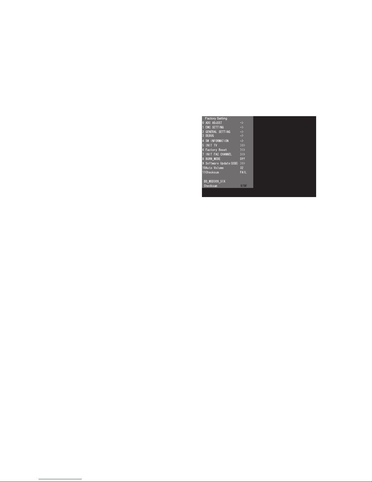
How to set up the service mode:
Service mode:
1. Turn the power on.
2. Press [SOURCE], [2], [5], [8] and [0] buttons on
the remote control unit in this order to enter the
service mode. The Factory Setting menu appears
in the screen.
Example:
Page 4
1-2 LC10P(A23FAEP)EA
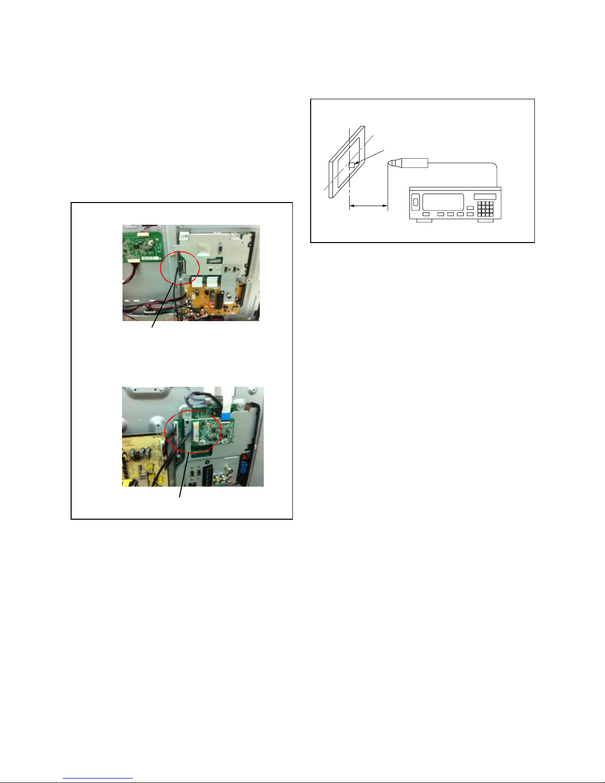
1. VCOM Adjustment
Preparation:
Change the Panel Code of the LED32-H9000M from
140 to 117 since the LVDS Format of LED32-H900M
is “JEIDA” and LVDS Format of 32FL552/10 is
“VESA”.
Procedure:
1. Connect the connector (LVDS OUT) on the Digital
Main CBA Unit of the LED32-H9000M (2010
Model) to the connector (LVDS IN) on the T-CON
CBA of 32FL552/10 with long LVDS wire.
2. Set the color analyzer at the zero point calibration
and bring the optical receptor pointing at the
center of the LCD-Panel of this LCD TV.
Note: The optical receptor must be set
perpendicularly to the LCD Panel surface.
3. Turn on the power of LED32-H9000M.
4. Turn on the power of 32FL552/10.
5. Enter the service mode through LED32-H9000M.
6. Enter the service mode through 32FL552/10 and
press [2] button on the remote control unit. The
Flicker pattern appears in the screen.
Adjust the variable resistor on the T-CON CBA so
that the color analyzer value becomes minimum.
7. To cancel or to exit from the VCOM Adjustment,
press [BACK] button.
Connector (LVDS OUT) on
the Digital Main CBA Unit
Connector (LVDS IN) on the T-CON CBA
LED32-H9000M (2010 Model)
32FL552/10
Color Analyzer
To avoid interference from ambient
light, this adjustment should be
performed in a dark room.
Perpendicularity
L = 3 cm
Page 5

2-1 LCDP_SC
SCHEMATIC DIAGRAMS / CBA AND TEST POINTS
Standard Notes
WARNING
Many electrical and mechanical parts in this chassis
have special characteristics. These characteristics
often pass unnoticed and the protection afforded by
them cannot necessarily be obtained by using
replacement components rated for higher voltage,
wattage, etc. Replacement parts that have these
special safety characteristics are identified in this
manual and its supplements; electrical components
having such features are identified by the mark “!” in
the schematic diagram and the par ts list. Before
replacing any of these components, read the parts list
in this manual carefully. The use of substitute
replacement parts that do not have the same safety
characteristics as specified in the parts list may create
shock, fire, or other hazards.
Notes:
1. Do not use the part number shown on these
drawings for ordering. The correct part number is
shown in the parts list, and may be slightly
different or amended since these drawings were
prepared.
2. All resistance values are indicated in ohms
(K = 10
3
, M = 106).
3. Resistor wattages are 1/4W or 1/6W unless
otherwise specified.
4. All capacitance values are indicated in µF
(P = 10
-6
µF).
5. All voltages are DC voltages unless otherwise
specified.
6. Electrical parts such as capacitors, connectors,
diodes, IC’s, transistors, resistors, switches, and
fuses are identified by four digits. The first two
digits are not shown for each component. In each
block of the diagram, there is a note such as
shown below to indicate these abbreviated two
digits.
Page 6
2-2 LCDP_SC
LIST OF CAUTION, NOTES, AND SYMBOLS USED IN THE SCHEMATIC DIAGRAMS ON
THE FOLLOWING PAGES:
1. CAUTION:
FOR CONTINUED PROTECTION AGAINST FIRE HAZARD, REPLACE ONLY WITH THE SAME TYPE
FUSE.
2. CAUTION:
Fixed Voltage (or Auto voltage selectable) power supply circuit is used in this unit.
If Main Fuse (F101) is blown, first check to see that all components in the power supply circuit are not
defective before you connect the AC plug to the AC power supply. Otherwise it may cause some components
in the power supply circuit to fail.
3. Note:
1. Do not use the part number shown on the drawings for ordering. The correct part number is shown in the
parts list, and may be slightly different or amended since the drawings were prepared.
2. To maintain original function and reliability of repaired units, use only original replacement parts which are
listed with their part numbers in the parts list section of the service manual.
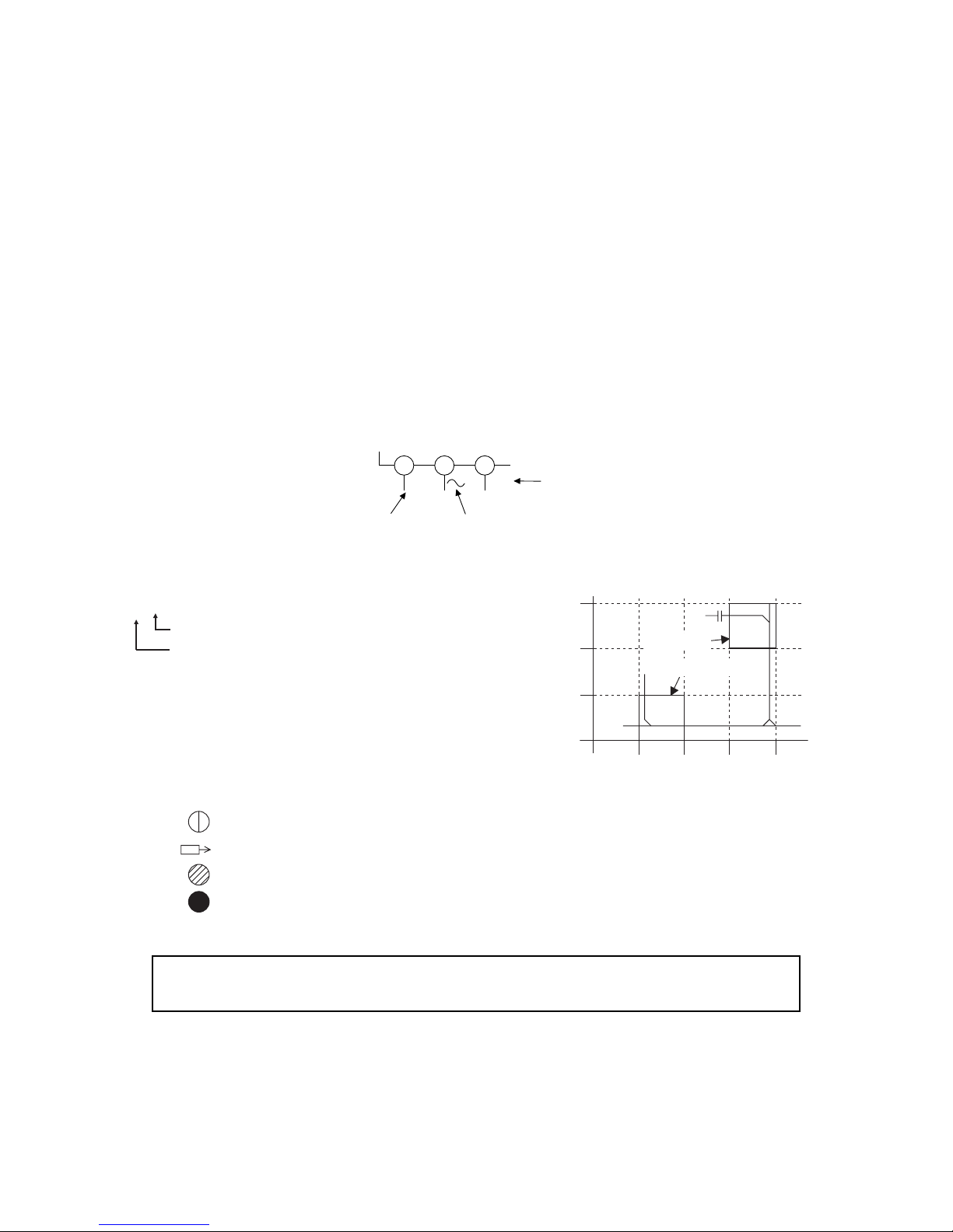
4. Voltage indications on the schematics are as shown below:
Plug the TV power cord into a standard AC outlet.:
5. How to read converged lines
6. Test Point Information
2
3
1
5.0 5.0
Voltage
Indicates that the voltage
is not consistent here.
Power on mode
(Unit: Volt)
3
2
1
ABCD
1-B1
1-D3
AREA D3
AREA B1
1-D3
Distinction Area
Line Number
(1 to 3 digits)
Examples:
1. "1-D3" means that line number "1" goes to the line numbe
r
"1" of the area "D3".
2. "1-B1" means that line number "1" goes to the line number
"1" of the area "B1".
: Indicates a test point with a jumper wire across a hole in the PCB.
: Used to indicate a test point with a component lead on foil side.
: Used to indicate a test point with no test pin.
: Used to indicate a test point with a test pin.
The reference number of parts on Schematic Diagrams can be retrieved by
application search function.
Page 7

2-3
10K
R122
Z101
220V
2 +12V
D202
2080
1
C114
4321
U102
0
R110
470P
C213
OPEN
C104
18V
ZD201
4 GND
33V
Z303
5 +5V
1K
R205
LF102
LINE
FILTER
3 GND
1000P
/1KV
C215A
ZV103
DSPL-301M
U103
TL431
510K
R108
5 GND
0.47
CX101
CN1
AC CORD
OPEN
C404
43K
R407
6 GND
68/63V
C403
4148
D203
10K
R307
1
C102
OPEN
R217
20
R204
CN3
1 +12V
10V
Z109
18V
Z305
680/25V
C211
D304
KDS184
1N4007
D201
270K
R102
4321
U301
2222
Q304
470/35V
C413
10K3
R419
OPEN
CY107
1000P
C406
24V
Z106
Q401
25A80V
G
D
S
27K
R212
1
C408
6 +5V
18K
R207
510K
R405
110K
R106
2 LED1
10
/50V
C202
3NU
22
/50V
C108
270K
R101
Q101
30A/40V
G
DS
4.7
R109
LB402
BEAD
OPEN
Q102
20
R203
22K
R208
100K
R313
OPEN
Z108
4 BACKLIGHT-ADJ
OPEN
CY105
1K
R302
1R414
U202
TL431
CN1
1
1K
R115
8 +5V
4.7K
R220
2 AMP+24V
2A/250V
F102
1 LED2
KTD1347
Q301
OPEN
R218
0.1/2W
R404
100K
R413
10K
R219
1N4148
D301
510K
R406
1K
R114
1000P
CY102
3 BACKLIGHT-SW
20
R113
10K
R309
10
/50V
C103
220P
C111
3 GND
0.1
C302
4 GND
LB401
BEAD
15V
Z304
22/50V
C307
RT101
2.5D15
OPEN
C105
OPEN
R216
OPEN
R215
270K
R101
470/35V
C207
3K
R409
2
220P
C205
OPEN
Z302
SR210
D401
470K
R303
OPERN
C110
1
2
34
5
6
U201
GR8833
D303
OPEN
P6KE180A
Z201
OPEN
C405
1K
R306
18K
R418
1000P
C107
1000P
C412
220P
C201
ZV104
DSPL-301M
0.18/3W
R211
1000P
C401
220V
Z102
LF101
LINE
FILTER
1N4007
D101
Q201
10N65
G
D
S
470K
R305
RV101
14D561
1K
R312
100KR415
0.47
C109
OPEN
C305
PR1004
D102
680/25V
C209
1000P
/1KV
C215
0.47
C410
Q303
2907
0.47
C212
1
C409
1K
R304
1K
R417
2222
Q302
0.1
C204
68K
R209
1
C304
1000/10V
C112
OPEN
C116
5.1M
R105
ZV101
DSPL-301M
10K
R117
OPEN
R120
18K
R116
680/25V
C208
CN4
7 LED3
OPEN
Z301
20
R201
4.7K
R311
10
R202
9 GND
13
1
15
14
16
3
6
5
11
4
7
12
10
89
2
U401
OZ9998B
1K
R402
6 LED4
PR1004
D103
1000/10V
C113
LF103
LINE
FILTER
1N5408
D112
2 PS-ON
10 +12V
1000/10V
C115
5.6K
R410
360K
R411
4.7
R301
9.53K
R118
0.1
C210
430K
R408
OPEN
R112
4321
U203
CN5
1 AMP+24V
SB5100
D204
5NU
474K
C411
150
/450V
C101
1K
R206
0.1
C203
1K
R412
5.1M
R104
BD101
4A600V
OPEN
CY108
OPEN
R308
4 LED-VCC
10K
R403
10
R401
ZV102
DSPL-301M
1000P
C407
470
R210
OPEN
R119
1
2
3
45
6
7
8
U101
0170
OPEN
R121
T5A L 250V
F101
470P
C303
100P
C402
OPEN
C214
OPEN
R214
91K
R107
7 +5V
CN2
1 STB+5V
1KR416
OPEN
R123
SB560
D104
4.7V
Z107
0.1
C106
10
R111
517
2
9
4
3
8
10
11
12
T201
POWER TRANS
16B
5
A
2
3
T101
POWER TRANS
1000P
CY101
1000P
CY103
1000P
CY104
0.47
CX102
OPEN
CY106
SB5100
D204A
470/35V
C206
L202
1.5uH
L401
40uH
L201
1.5uH
2K
R213
470K
R310
1000P
C306
L101
1.5uH
SB560
D104A
OPEN
R124
P6KE180A
Z105
(FEED BACK)
(SHUNT REG.)
(SHUNT REG.)
TO LCD PANEL
ASSEMBLY
1
2
3
4
ABCD
(FEED BACK)
EF
(ISOLATOR)
POWER SUPPLY CBA UNIT
HOT COLD
HOT CIRCUIT. BE CAREFUL.
(SWITCHING)
VCCCOMP
OUT
CT CS
GND
VFB
DRV
DRV
GND
VCC
VIN VSTR
DRV
(SWITCHING)
(SWITCHING)
TO DIGITAL MAIN
CBA UNIT CN24
(SW+5V)
(SWITCHING)
(SWITCHING)
(SWITCHING)
OVP
DRIVE4
VREF
GND
(LED BACKLIGHT DRIVER)
SSTCMP
VIN
RT
STATUS
ISET
DRIVE1
(SWITCHING)
TO DIGITAL MAIN
CBA UNIT CN3
TO DIGITAL MAIN
CBA UNIT CN2
DRIVE2
DRIVE3
CONTROL
LOGIC
SWITCHING
CONTROL
SWITCHING
CONTROL
A23FASCP
Power Supply Schematic Diagram
NOTE:
The voltage for parts in hot circuit is measured using
hot GND as a common terminal.
CAUTION !
Fixed voltage (or Auto voltage selectable) power supply circuit is used in this unit.
If Main Fuse (F101) is blown , check to see that all components in the power supply
circuit are not defective before you connect the AC plug to the AC power supply.
Otherwise it may cause some components in the power supply circuit to fail.
CAUTION !
For continued protection against fire hazard,
replace only with the same type fuse.
Page 8

2-4
R10
10K
231
RE2
GP1USC32XP
VOUT
GND
VCC
10
C23
0.1
C8
560P
C7
D15
19-213-W1D
-ANPHY-3T
3 REMOTE
CN1
1 +5V
7 GND
6 GND
5 IR-KEY
4 GND
2 LED-R
D1
PMLL4148L
231
U3
LC1117CLTR33
ADJ
VOUT
VIN
10
C2
1
C4
OPEN
C9
0.01
C1
15K
R9
0.01
C12
1
2
3
4
5
6
7
8
9
10
11
12 13
14
15
16
17
18
19
20
21
22
23
24
U1
JST8D080P
P04
P03
P02
P01
P00
TS-7
NU
VC1
GND
VDD
NU
IR-KEY
REMOTE
OSCI
P07
P06
P05
0.1
C11
OPEN
C3
FUNCTION CBA UNIT
AB
2
C
1
TO DIGITAL MAIN
CBA UNIT CN9
(REMOTE SENSOR)
POWER
(+3.3V REG.)
POWER
CH DOWN
CH UP
TV/AV
(TOUCH SENSOR)
VOL DOWN
MENU
VOL UP
TV/AV
MENU
VOL DOWN
VOL UP
POWER
CH DOWN
CH UP
A23FASCF
Function Schematic Diagram
Page 9

2-5
20 LVDS-ED0(+)
29 LVDS-ED3(-)
21 LVDS-ED1(-)
24 LVDS-ED2(+)
23 LVDS-ED2(-)
28 LVDS-CE(+)
27 LVDS-CE(-)
30 LVDS-ED3(+)
19 LVDS-ED0(-)
22 LVDS-ED1(+)
4 GND
14 GND
3 VIN+12V
13 GND
5 GND
35 VSEL1
2 VIN+12V
33 CON1
36 VSEL2
34 NU
31 GND
25 GND
26 GND
CN5
1 VIN+12V
6 GND
32 GND
OPEN
R55
100R63
100R68
AD24
AC24
RP28 OPEN
AD25
AC23
AE24
AE23
AD23
RP29 OPEN
AC20
AE22
AC22
AD21
RP30 33x4
AE19
RP31 33x4
AC19
AD20
AE20
AC17
AE17
AD18
RP27 OPEN
AC18
AD22
AC21
RP32 33x4
AD19
AD17
F5EXT-SDA
F6EXT-SCL
D4NU
C3NU
E4NU
F4NU
C7NU
5P
C2285PC229
OPEN
C226
OPEN
C227
A7NU
4.7KR195
10KR311
4.7K
R53
M+3.3V
T4NU
AMP-STB
AMP-MUTEY9AMP-MUTE
Y8AMP-STB
R6NU
10KR272
AA8NU
AC11NU
AA9NU
V5NU
AB7NU
AB10NU
AA10NU
T5NU
AB8NU
H5LED-R
K4LED-G
C5POW-EN
M6PANEL-EN
L5BACKLIGHT-SW
10KR295
10KR199
CN9
1 +5V
3 LED-G
2 LED-R
6 IR-KEY
5 GND
510R60
22
R58
L6 OPEN
4 REMOTE
12K
R81L8
300
0.1
C41
D5
AVLC18S02003
STB+5V
OPEN
Q11
Q8
OPEN
OPEN
R16
OPEN
R25
OPEN
R59
OPEN
R61
OPEN
R62
0.1
C36
OPEN
C68
10P
C49
L10
3001K
R88
OPEN
C58
4.7K
R77
STB+3.3V
G5REMOTE
4.7K
R94
4.7K
R99
BACKLIGHT-ADJ
POW-EN
BACKLIGHT-SW
PANEL-EN
4.7K
R187
E6BACKLIGHT-ADJ
D6NU
AB24NU
AB25NU
10KR86
10KR87
4.7K
R82
G4KEYB
J5KEYA
OPEN
R26
1
2
3
45
6
7
8
U9
W25Q32BVSSIG
CS
SO
WP
GND SI
SCK
HOLD
VCC
A4 SPI-CSN
A3 SPI-SDO
A2 SPI-SCK
B3 SPI-SDI
B2 FLASH-WP
C4 NU
100K
R85
0.1
C80
AA23 NU
AA24 NU
AE2 XOUT
AD1 XIN
Y1
24MHz
33
R183
33P
C208
33P
C174
1M
R181
E5 RESET
D1
AVLC18S02003
1K
R1
SGM810
Q10
0.1
C200
100K
R179
0.1
C195
2USB1-DM
4GND
3USB1-DP
CN25
1USB+5V
5GND
6GND
M+5V
AE11 USB1-DM
AD11 USB1-DP
C2 NU
B1 NU
E2
100/16V
D52
AIES12U020R2
D75
AIES12U020R2
F11 GND
E11 GND
AC25
*1
U7(1/6)
MSD309PX-LF-SW
F2
FSMD110
10K
R310
10K
R270
0.1
C81
PANEL-VCC
9 LVDS-OD1(-)
11 LVDS-OD2(-)
7 LVDS-OD0(-)
10 LVDS-OD1(+)
12 LVDS-OD2(+)
8 LVDS-OD0(+)
16 LVDS-CO(+)
15 LVDS-CO(-)
17 LVDS-OD3(-)
18 LVDS-OD3(+)
37 LVDS-OD4(-)
38 LVDS-OD4(+)
39 LVDS-ED4(-)
40 LVDS-ED4(+)
FC
4
1
3
2
EADB
DIGITAL MAIN CBA UNIT
TO T-CON CBA
CN1001
LVDS
TX
TO DIGITAL
MAIN 4
U7(4/6)
DIGITAL SIGNAL PROCESS
/MAIN MICRO CONTROLLER
TO FUNCTION
CBA UNIT CN1
(MEMORY)
(RESET)
(USB JACK)
CONTINUE
DIGITAL 2
CONTINUE
DIGITAL 5
CONTINUE
DIGITAL 2
A23FASCD1
Digital Main 1 Schematic Diagram
The order of pins shown in this diagram is different from that of actual U7.
U7 is divided into six and shown as U7 (1/6) ~ U7 (6/6) in this Digital Main Schematic Diagram Section.
1 NOTE:
Page 10

2-6
1
2
3
45
6
7
8
U1
AIC2857FGR8TR
BS
IN
SW
GND FB
COMP
EN
NU
3GND
1STB+5V
CN2
10+12V
4GND
2PS-ON
9GND
E7
100/25V
Q9
MMBT3904
0.1
C26
0.1
C225E8
470/10V
0.1
C28E9
100/16V
R28
510
4.7K
R30
R32
10K
Q7
OPEN
Q6
3CG3906M
R33
OPEN
R35
47K
POW-EN
0.1
C119
0.1C310
C11
R2
100K
0.01
C2
L5
10uH
R6
4.7K
4.7K
R9
E1
470/10V 0.1
C14
OPEN
C15
0.01
C16
R36
2.2K
OPEN
C20
0.01
C1
0.1
C12
1
2
3
45
6
7
8
U3
AIC2857FGR8TR
BS
IN
SW
GND FB
COMP
EN
NU
0.1
C7
OPEN
C19
R4
4.7K
0.01
C8
L1
22uH
R8
2.2K
0.1
C10
E3
470/10V OPEN
C13
10
C132
R3
100K
11K
R5
0.01
C17
1234
U2
LC1117CLTR33
VOUT
VIN
GND
VOUT
0.1C610
C197
0.1
C5
10
C196
0.1
C44
1234
U5
LC1117CLTR33
VOUT
VIN
GND
VOUT
0.1
C31
OPEN
C102
1N4007
D3
OPEN
C62
2PVCC
CN1
1PANEL+5V
3+12V
2+12V
CN3
1+12V
3BACKLIGHT-SW
5GND
4BACKLIGHT-ADJ
6GND
6+5V
5+5V
8+5V
7+5V
2GND
CN6
1GND
CN7
1GND
2GND
3GND
5GND
4GND
6GND
Q2
MMBT3904
1K
R13
OPEN
R12
10K
R11
OPEN
R23
510
R20
OPEN
R22
BACKLIGHT-SW
R17
33
0.1
C25
OPEN
R19
L2
300
R18
33 510
R15
10K
R21
Q3
MMBT3904
OPEN
C23
L3
300
OPEN
C24
BACKLIGHT-ADJ
Q4
MMBT3904
10K
R24
PANEL-EN
10K
R10
100K
R14 0.1
C21
H17 AVDD-DDRB
H16 AVDD-DDRB
G17 AVDD-DDRA
G16 AVDD-DDRB
E18 AVDD-DDRA
F17 AVDD-DDRA
F18 AVDD-DDRA
J16 AVDD-DDRB
J17 AVDD-DDRB
E19 VDDP
F19 VDDP
G18 AVDD-LPLL-MEMPLL
M8 AVDD2P5-ADC
M9 AVDD2P5-ADC
N8 AVDD25-REF
N9 AVDD25-REF
R9 AVDD-AU25
P8 AVDD25-MOD
P9 AVDD25-MOD
T8 AVDD25-PGA
U8 AVSS-PGA
L9
1200.1
C57
L23
120
E9 AVDD-DVI
E10 AVDD-DVI
F10 AVDD-DVI
F9 AVDD-DVI
G9 AVDD-DVI
G10 AVDD-DMPLL
H9 AVDD3P3-ADC
H10 AVDD3P3-ADC
K9 AVDD-AU33
J9 AVDD-EAR33
Q1
AO3407A
G
DS
PANEL-VCC
0.1
C22 E6
100/25V
E22 VDDC1.2V
F22 VDDC1.2V
E21 VDDC1.2V
F21 VDDC1.2V
G21 VDDC1.2V
H21 VDDC1.2V
E20 VDDC1.2V
F20 VDDC1.2V
G20 VDDC1.2V
G22 VDDC1.2V
H20 DVDD-MIUA
J20 DVDD-MIUB
J21 AVDD1P2
L10 DVDD-NODIE
1
C82
*A GND
0.1
C22110C222
1
C161
0.1
C219
0.1
C220
0.1
C156
E17
*1
U7(2/6)
MSD309PX-LF-SW
AVDD-DDRA
M+5V
STB+3.3V
STB+5V
M+3.3V
M+5V
+12V
M+3.3V
M+5V
M+3.3V
STB+5V
M+1.8V
0.1
C4
MSD309
0
MSD308
OPEN
LI
4
1
3
2
KGJH
DIGITAL MAIN CBA UNIT
(+1.8V REG.)
TO POWER SUPPLY
CBA CN2
(+1.32V REG.)
(+3.3V REG.) (+3.3V REG.)
TO POWER SUPPLY
CBA CN3
(SWITCHING)
(SWITCHING)
(SWITCHING)
(SWITCHING)
(SWITCHING)
DIGITAL SIGNAL PROCESS
/MAIN MICRO CONTROLLER
(NO CONNECTION)
(NO CONNECTION)
(NO CONNECTION)
*A:D11~D16,E12~E16,F12~F16,G11,G12,
G14,G15,H11~H15,H22,J10~J15,J22,
K10~K22,L11~L22,M10~M22,N10~N22,
P10~P18,R10~R18,T10~T18,U10~U18,
V7~V12,W7~W12,Y10,AC2,AE1
CONTINUE
DIGITAL 5
CONTINUE
DIGITAL 1
CONTINUE
DIGITAL 1
CONTINUE
DIGITAL 6
CONTINUE
DIGITAL 4
CONTINUE
DIGITAL 3
(SWITCHING)
A23FASCD2
Digital Main 2 Schematic Diagram
The order of pins shown in this diagram is different from that of actual U7.
U7 is divided into six and shown as U7 (1/6) ~ U7 (6/6) in this Digital Main Schematic Diagram Section.
1 NOTE:
Page 11

2-7
10
C40
0.1
C33
0.1
C45
0.1
C50
0.1
C46
0.1
C43
0.1
C29
0.1
C38
0.1
C39
0.1
C30
0.1
C42
10
C52
0.1
C48
0.1
C51
M+1.8V
0.1
C32
0.1
C34
0.1
C35
0.1
C47
P3A9
M3A1
N7A6
B1 DQ14
E2 NU
N3A5
M7A2
D7 DQ10
H7 DQ2
R7 NU
P2A7
R2A12
D3 DQ11
F9 DQ7
N2A3
G8 DQ0
*C VSS
D9 DQ13
A2 NU
M8A0
B9 DQ15
D1 DQ12
H9 DQ5
C2 DQ9
P8A8
P7A11
N8A4
R3 NU
U4
NT5TU32M16DG-AC
*B VDD
M2A10
H3 DQ3
G2 DQ1
F1 DQ6
C8 DQ8
H1 DQ4
L2BA0
L3BA1
E8DQS0B
L1BA2
F7DQS0
K7RASZ
K2CKE
K8MCLKZ
K3WEZ
A8DQS1B
B7DQS1
J8MCLK
L7CASZ
L8/CS
R8A13
K9ODT
B3DQM1
F3DQM0
J2 VREF
C54
0.1
R40
10K
R39
10K
B18 MA-DQ12
B17 MA-DQ14
A18 MA-DQ11
C18 MA-DQ9
RP1 22x4
C20 MA-DQ4
RP3 22x4
C19 MA-DQ6
A19 MA-DQ1
B19 MA-DQ3
B13 MA-DQ13
RP5 22x4
C15 MA-DQ15
B14 MA-DQ8
C14 MA-DQ10
B12 MA-DQ5
RP8 22x4
A13 MA-DQ7
C13 MA-DQ0
A12 MA-DQ2
RP9 22x4
A16 MA-DQS0
C16 MA-DQS0B
RP11 22x4
A15 MA-DQS1
B15 MA-DQS1B
RP13 22x4
C17 MA-DQM1
B16 MA-DQM0
RP15 22x4
C12 MA-MCLK
B11 MA-MCLKZ
A21 MA-BA0
RP17 75x4
B20 MA-WEZ
C21 MA-CKE
B21 MA-BA1
B22 MA-A10
C22 MA-BA2
RP23 75x4
B24 MA-A12
C8 MA-A11
A23 MA-A5
C23 MA-A7
RP21 75x4
RP19 75x4
A24 MA-A9
C9 MA-A6
A22 MA-A1
B9 MA-A4
B23 MA-A3
B8 MA-A8
75R43
C11 MA-ODT
B7 MA-A13
75R41
RP25 75x4
C10 MA-A0
A10 MA-CASZ
B10 MA-RASZ
A9 MA-A2
*EVSS
L2 BA0
R8 A13
N2 A3
J24MB-DQ10 C8DQ8
D3DQ11
W25MB-A7
C24MB-A11
L8 /CS
F1DQ6
P2 A7
H3DQ3P24MB-DQ1
H7DQ2
L24MB-DQS0
M7 A2
J8 MCLK
V23MB-A10
T23MB-CKE
E2NU
A8 DQS1B
N23MB-DQ9
N24MB-DQ11
N7 A6
F25MB-MCLKZ
F23MB-RASZ
E23MB-A0
P3 A9
K8 MCLKZ
M24MB-DQM1
K24MB-DQS1
M25MB-DQ14
V25MB-A3
U24MB-A1
K7 RASZ
R3NU
W24MB-A9
D1DQ12
L1 BA2
G24MB-DQ2
M8 A0
P7 A11
F3 DQM0
F24MB-ODT
D9DQ13
L3 BA1
C2DQ9
K9 ODT
G8DQ0
J25MB-DQ8
H1DQ4
F9DQ7
R2 A12
V24MB-A5
W23MB-A12
G2DQ1
R23MB-DQ3
R7NU
P23MB-DQ6
L7 CASZ
M2 A10 D7DQ10
L23MB-DQS0B
U23MB-BA2
N3 A5
R25MB-WEZ
B7 DQS1
B1DQ14
T25MB-BA1
R24MB-DQ4
N25MB-DQ12
K3 WEZ
G23MB-MCLK
M3 A1
E24MB-CASZ
T24MB-BA0
D24MB-A2
K25MB-DQS1B
C25MB-A8
M23MB-DQM0
K2 CKE
D25MB-A4
D23MB-A6
H9DQ5
B9DQ15
F7 DQS0
N8 A4
H23MB-DQ0
E8 DQS0B
B25MB-A13
B3 DQM1
A2NU
P8 A8
75R42
RP18 75x4
RP22 75x4
RP4 22x4
RP26 75x4
RP7 22x4
RP14 22x4
RP2 22x4
RP20 75x4
RP10 22x4
75R44
RP16 22x4
RP24 75x4
RP6 22x4
RP12 22x4
K23MB-DQ15
J23MB-DQ13
H24MB-DQ7
G25MB-DQ5
R48
10K
J2 VREF
C56
0.1
R47
10K
U6
NT5TU32M16DG-AC
*D VDD
56
R3756R38
C53
0.1
56
R46
C55
0.1
56
R45
R91
10K
C134
0.1
R90
10K
C118
0.1
D22
*1
U7(3/6)
MSD309PX-LF-SW
MVREF
R
1
P
4
O
3
NQM
2
DIGITAL MAIN CBA UNIT
*C:A3,A7,B2,B8,D2,D8,E3,E7,
F2,F8,H2,H8,J3,J7,N1,P9
(DDR2 SDRAM)
*B:A1,A9,C1,C3,C7,C9,E1,E9,
G1,G3,G7,G9,J1,J9,M9,R1
DIGITAL SIGNAL PROCESS
/MAIN MICRO CONTROLLER
MA-DQ11
MA-DQ12
MA-DQ9
MA-DQ14
MA-DQ3
MA-DQ4
MA-DQ6
MA-DQ1
MA-DQ8
MA-DQ10
MA-DQ13
MA-DQ15
MA-DQ0
MA-DQ2
MA-DQ5
MA-DQ7
MA-DQ0
MA-DQ1
MA-DQ2
MA-DQ3
MA-DQ4
MA-DQ5
MA-DQ6
MA-DQ7
MA-DQ8
MA-DQ9
MA-DQ10
MA-DQ11
MA-DQ12
MA-DQ13
MA-DQ14
MA-DQ15
MA-A13
MA-BA0
MA-BA1
MA-A4
MA-A11
MA-A6
MA-A8
MA-A1
MA-A10
MA-BA2
MA-A5
MA-A3
MA-A9
MA-A7
MA-A12
MA-A0
MA-A2
MA-A0
MA-A1
MA-A2
MA-A3
MA-A4
MA-A5
MA-A6
MA-A7
MA-A8
MA-BA2
MA-A12
MA-A9
MA-BA1
MA-A11
MA-A10
MA-A13
MA-BA0
MB-DQ15
MB-A12
MB-DQ6
MB-A1
MB-BA2
MB-A13
MB-A9
*E:A3,A7,B2,B8,D2,D8,E3,E7,
F2,F8,H2,H8,J3,J7,N1,P9
MB-DQ7
MB-A2
MB-A5
MB-BA0
MB-BA1
MB-DQ8
MB-A3
(DDR2 SDRAM)
MB-A3
MB-BA1
MB-A11
MB-DQ9
MB-A4
*D:A1,A9,C1,C3,C7,C9,E1,E9,
G1,G3,G7,G9,J1,J9,M9,R1
MB-DQ0
MB-A9
MB-A4
MB-A10 MB-DQ10
MB-A5
MB-DQ1
MB-A7
MB-A11
MB-A13
MB-DQ11
MB-A6
MB-DQ2
MB-A12
MB-A6
MB-BA0
MB-DQ12
MB-A7
MB-DQ3
MB-A0
MB-A8
MB-DQ11
MB-DQ13
MB-A8
MB-DQ4
MB-A2
MB-A1
MB-DQ14
MB-BA2
MB-DQ5
MB-A0
MB-A10
MB-DQ12
MB-DQ9
MB-DQ14
MB-DQ6
MB-DQ1
MB-DQ3
MB-DQ4
MB-DQ15
MB-DQ2
MB-DQ5
MB-DQ10
MB-DQ7
MB-DQ8
MB-DQ13
MB-DQ0
TO
DIGITAL
MAIN 4
U7(4/6)
MEMORY
I/F
CONTINUE
DIGITAL 2
A23FASCD3
Digital Main 3 Schematic Diagram
The order of pins shown in this diagram is different from that of actual U7.
U7 is divided into six and shown as U7 (1/6) ~ U7 (6/6) in this Digital Main Schematic Diagram Section.
1 NOTE:
Page 12

2-8
100P
C117
330P
C136
75
R203
220
R232
100
R237
CN19
CN8
0.047
C79
0.047
C188
MMBT3904
Q26
W6NU
68
R300
P2
Q12
3CG3906M
R3
W1 NU
N3
V3
W4 NU
W3 NU
N1NU
AA5
U7(4/6)
*1
MSD309PX-LF-SW
Y6 SC1-FB
CN4
SCART JACK
123456789101112131415161718192021
0.047
C17768R291
W5 NU
M1
68
R83
0.047
C184
AC5 NU
N2
P3
AA4 NU
68
R309
3.9V-LL-34-1/2WD6220P
C17075R279
33
R278
0.047
C169
AVLC18S02003
D23
OPEND275
R301
100
R298
100P
C183
AVLC18S02003
D32
750
R290
33
R285
0.047
C176
AVLC18S02003
D35
750
R299
33
R296
0.047
C181
AVLC18S02003
D36
OPEN
D4
10K
R303
2.2K
R306
AVLC18S02003
D39
750
R308
33
R305
0.047
C186
AVLC18S02003
D40
OPEN
C175
6.8K
R282
12K
R284
1
C173
3.9V-LL-34-1/2W
D38
3.9V-LL-34-1/2W
D43
1000P
C182
47K
R297
1
C180
100
R102
100K
R177
220P
C207
AVLC18S02003
D42
OPEN
C179
6.8K
R2921C178
12K
R293
3.9V-LL-34-1/2W
D44
3.9V-LL-34-1/2W
D45
1000P
C187
47K
R307
1
C185
100
R197
100K
R287
220P
C224
0.1
C172
100/16V
E13
OPEN
C139
10K
R288
15K
R281
0
R74
1
C171
220
R72
120
R289
120
R7675R80
OPEN
C131
33
R277
0.1
C130
D46
AVLC18S02003
33
R191
0
R186
1000P
C109
0.047
C111
TV+5V
75
R204
D47
AVLC18S02003
33
R180
0.047
C106
33
R188
D48
AVLC18S02003
75
R200
0.047
C112
CN17
D37
OPEN
220P
C10475R178
33
R176
0.047
C103
OPEN
C110
D41
OPEN
6.8K
R184
12K
R190
1
C107
OPEN
C116
12K
R205
1
C115
D49
OPEN
6.8K
R198
CN26
D66
OPEN
6.8K
R250
12K
R253
1
C143
D64
OPEN
6.8K
R248
12K
R245
1
C142
W2B4 SC1-FS
T6
AA6
Y5
U6
R4
R5
U2
U3
R2
R1
T2
T1
T3
V4NU
V6
U5
AD6NU
AC6NU
P5
AD5NU
AE5NU
22K
R252
33
R218
1
2
3
4514
13
12
11156
7
8
9
10
CN16
PC-RGB-IN
D53
OPEN
L15
60
10P
C12575R219
0.047
C124
L1660D55
OPEN
0.047
C127
10P
C12875R225
33
R223
D60
OPEN33
R236
0.047
C135
10P
C13775R238
L17
60
D65
AVLC18S02003
L20
300100
R251
33P
C144
33P
C141 D63
AVLC18S02003
100
R242
22K
R244
L18
300
D54
AVLC18S02003
0
R224
0
R230
D59
AVLC18S02003
M3
M2
L3
L2
K1
K3
N4PC-HS
N5PC-VS
0.047C126 68R220
68R2260.047C129
0.047C138 68R239
K2NU
N6VGA-SDA
P6VGA-SCL
68R1930.047C113
68R1850.047C108
0.047C114 68R194
STB+5V
AA2
AA3
AD3IF-AGC
DIF-OUT2
DIF-OUT1
IF-AGC
V1
V2
AMP(L)-OUT
AMP(R)-OUT
AB4AUVRP
AB5AUVAG
AC3AUVRM
1C83
1C92
120
L24
A6NU
B5NU
B6NU
C6NU
G6NU
H6NU
C1NU
4.7KR56
10KR57
10KR67
4.7K
R221
4.7K
R222
M+3.3V
AUDIO(R)-IN
COMPONENT
-Y-IN
DIGITAL
AUDIO-OUT
(COAXIAL)
AUDIO(L)-IN
COMPONENT
-Pb-IN
PC-AUDIO-IN
COMPONENT
-Pr-IN
DIGITAL SIGNAL PROCESS
/MAIN MICRO CONTROLLER
XSTUVW
3
2
1
4
VIDEO-IN
DAC
SW
AUDIO
I/F
TO DIGITAL
MAIN 6
U7(6/6)
A/D
CONVERTER
DIGITAL
SIGNAL
PROCESS
DEMODULATOR
/MPEG DECODER
DESCRAMBLER
/TS INTERFACE
DIGITAL MAIN CBA UNIT
CONTINUE
DIGITAL 5
TO DIGITAL
MAIN 6
U7(6/6)
CONTINUE
DIGITAL 2
CONTINUE
DIGITAL 5
TO DIGITAL
MAIN 1
U7(1/6)
TO DIGITAL
MAIN 3
U7(3/6)
TO DIGITAL
MAIN 6
U7(6/6)
(BUFFER)
(BUFFER)
A23FASCD4
Digital Main 4 Schematic Diagram
The order of pins shown in this diagram is different from that of actual U7.
U7 is divided into six and shown as U7 (1/6) ~ U7 (6/6) in this Digital Main Schematic Diagram Section.
1 NOTE:
Page 13

2-9
MMBT3904
Q24
0.1
C152
CN24
1AMP+24V
PMLL4148L
D68
OPEN
R338
1K
R275
AMP-MUTE
3GND
47K
R274
0.33
C154
E18
100/16V
0.1
C150
1
C166
100K
R105
1K
R273
33K
R271
10
C159
AMP(R)-OUT
1
C164
1
C151
2AMP+24V
22uH
L21
1K
R269
OPEN
C37
22uH
L22
E15
47/16V
0.1
C167
AMP-STB
M+5V
100P
C165
100K
R286
1000P
C223
4GND
AMP(L)-OUT
+12V
100
R101
0.1
C158
PMLL4148L
D77
Q23
3CG3906M
10
C155
12345678910
11
12
13
14
15
16
17
18
19
20
21222324252627282930
31
32
33
34
35
36
37
38
39
40
U13
R2A15122FP
10
C157
10K
R337
100
R196
0.47
C160
0.33
C163
SK34A-SMA
D67
0.1
C168 E17
470/35V
33K
R276
1000P
C206
0.1
C162
TV+5V
100P
C153
T1 TUNER UNIT
1
NU2B1(+5V)3RF-AGC4SCL5SDA6B2(+5V)7NU8GND9IF-AGC10DIF-OUT111DIF-OUT212ANALOG-IF13GND14GND15GND16GND
T2 OPEN
1
NU2B1(+5V)3RF-AGC4SCL5SDA6B2(+5V)7NU8GND9IF-AGC10DIF-OUT111DIF-OUT212ANALOG-IF13GND14GND15GND16GND
OPEN
R111
OPEN
R112
OPEN
C74
4.7K
R132
OPEN
C75
4.7K
R131
1
C94
10K
R137
1K
R135
AE4 TUNER-SDA
AD4 TUNER-SCL
DIF-OUT2
IF-AGC
DIF-OUT1
100
R133
0.56uH
L14
30P
C87
0.1
C86
100
R138
0.1
C90
0
R268
AE3 RF-AGC
10K
R136
10K
R134
1
C91
0.1
C69
Q13
3CG3906M
100K
R125
MMBT3904
Q14
10K
R126
0
R121
10K
R128
AC4 AGC-SW
AD2 SIF-SW
Y3 NU
Y2 NU
0.1C762.2KR70
0.1C782.2KR79
AB1 VIFP
AA1 VIFM
AB2 SIFP
AB3 SIFM
33
R207
OPEN
R117
0.047
C64
0.1C84
0.1C88
OPEN
L13
0.1C85
0.1C89
0.01
C73
0.047
C63
OPEN
R118
BA591
D8
MMBT3904
Q15 1K
R130
4.7K
R129
2.2K
R127
4.7K
R120
2.2K
R123
10
C71
0.1
C66
100
R122
123
U10
UTC78D05L
GND
VOUT
VIN
0.1
C70
0.1
C671C9
0.1
C61 E12
470/6.3V
AA7
*1
U7(5/6)
MSD309PX-LF-SW
AGC-DETECT
SPEAKER
L-CH
3 SP-GND
2 SP-GND
4 SP(R)
SPEAKER
R-CH
CN23
1 SP(L)
CN13
1K
R235
1000P
C212
2.2K
R231
2200P
C27
470/35V
E16
OPEN
C65
470/35V
E14
2200P
C72
2.2K
R233
1K
R240
1000P
C214
21 345
(SAW FILTER)
SAW1
HDAF389A7DC
ININGND
OUT
OUT
21345
(SAW FILTER)
SAW1
VF389A1DC
ININGND
OUT
OUT
OPEN
R267
ADAA
4
1
3
2
ACYABZ
DIGITAL MAIN CBA UNIT
NU
GND
GND
PROT
AVCC
ROSC
VDD
PWM
GENE.
HB1
HB2
GND
VDD
GND
GND
(AUDIO AMP)
GND
GND
PWM
GENE.
DVDD1
TO POWER SUPPLY
CBA CN5
GND
GND
GND
GND
VREFF
GND
CBIAS
CONTROL
LOGIC
GND
GND
VDD
GND
GND
GND
VDD
DIGITAL SIGNAL PROCESS
/MAIN MICRO CONTROLLER
(+5V REG.)
HEADPHONE
JACK
CONTINUE
DIGITAL 4
CONTINUE
DIGITAL 1
CONTINUE
DIGITAL 4
CONTINUE
DIGITAL 2
(SWITCHING)
(SWITCHING)
(SWITCHING)
(SWITCHING)
(SWITCHING)
A23FASCD5
Digital Main 5 Schematic Diagram
The order of pins shown in this diagram is different from that of actual U7.
U7 is divided into six and shown as U7 (1/6) ~ U7 (6/6) in this Digital Main Schematic Diagram Section.
1 NOTE:
Page 14

2-10
10K
R150
33R147
100
R149
33R145
OPEN
C98
R171
10K
R139
1K
10 TMDS-CLOCK(+)
5 GND
2 GND
16 SDA
3 TMDS-D2(-)
9 TMDS-D0(-)
19 HOT PLUG DETECT
15 SCL
4 TMDS-D1(+)
14 NU
7 TMDS-D0(+)
11 GND
13 HDMI-CEC
8 GND
CN11
1 TMDS-D2(+)
12 TMDS-CLOCK(-)
6 TMDS-D1(-)
18 +5V
17 GND
MMBT3904
Q16
0R173
0R168
0R164
0R162
0R159
0R155
0R152
0R157
20 GND
21 GND
22 GND
23 GND
OPEN
C99
R143
10K
R166
10K
D26
BAT54C 0.1
C18
R141
OPEN
J1
J2
J3
H2
H3
G1
G2
G3
HDMI-CEC K5
M5
M4
K6HDMI1-HPD
R144
10K
33R148
CN12
1 TMDS-D2(+)
0R174
18 +5V
16 SDA
D1
8 GND
2 GND
6 TMDS-D1(-)
R172
10K
OPEN
C101
0R160
12 TMDS-CLOCK(-)
MMBT3904
Q17
13 HDMI-CEC
F1
11 GND
10 TMDS-CLOCK(+)
23 GND
5 GND
J4HDMI2-HPD
10K
R151
22 GND
J6
14 NU
7 TMDS-D0(+)
OPEN
C100
D3
21 GND
0R163
4 TMDS-D1(+)
20 GND
0R158
15 SCL
E3
33R146
L6
E2
F3
0R165
19 HOT PLUG DETECT
R140
1K
0R153
9 TMDS-D0(-)
D2
R142
OPEN
0R169
D27
BAT54C
3 TMDS-D2(-)
R167
10K
F2
0R156
17 GND
M+5V
D19 OPEN
D34 OPEN
D13 OPEN
D21 OPEN
D11 OPEN
D15 OPEN
D9 OPEN
D29 AVLC18S02003
D31 AVLC18S02003
D17 OPEN
D24 OPEN
D18 OPEN
D22 OPEN
D33 OPEN
D10 OPEN
D20 OPEN
D30 AVLC18S02003
D14 OPEN
D28 AVLC18S02003
D16 OPEN
D12 OPEN
D25 OPEN
AC8NU
AD9NU
AC9NU
AD10NU
AE10NU
AC10NU
AE8NU
AD8NU
AE7NU
AD7NU
AC7NU
35GND
51CI+5V
34GND
30CI-D0
54TS1-D5
33NU
47TS1-D0
44CI-IORDN
14CI-A14
59CI-WAITN
50TS1-D3
32CI-D2
68GND
25CI-A4
28CI-A1
22CI-A7
16CI-IRQAN
64TS-D0
40TS-D6
56TS1-D7
61CI-REGN
29CI-A0
67PCM-CD2N
17CI+5V
37TS-D3
6CI-D7
53TS1-D4
4CI-D5
42NU
11CI-A9
65TS-D1
9CI-OEN
18CI+5V
46TS1-START
49TS1-D2
58CI-RESET
24CI-A5
27CI-A2
63TS-MOSTART0
39TS-D5
21CI-A12
7CI-CEN
3CI-D4
60NU
66TS-D2
13CI-A13
55TS1-D6
52CI+5V
31CI-D1
15CI-WEN
48TS1-D1
36PCM-CD1N
CN10
1GND
12CI-A8
20TS1-CLK
5CI-D6
45CI-IOWRN
8CI-A10
2CI-D3
38TS-D4
23CI-A6
57TS-CLK
26CI-A3
19TS1-VLD
41TS-D7
62TS-MOVAL0
43NU
10CI-A11
69GND
70GND
71GND
72GND
Y16 TS1-D0
OPEN
R95
AD14 TS1-D1
AD15 TS1-D2
AC15 TS1-D3
Y17 TS1-D5
AB19 TS1-D7
AC16 TS1-D4
AB17 TS1-D6
Y18 TS1-CLK
AE16 TS1-VLD
AB16 TS1-START
U20 TS-D0
V20 TS-D1
R19 TS-D2
AE13 TS-D3
AC13 TS-D4
AB11 TS-D6
AB13 TS-D7
Y11 TS-D5
Y19 TS-CLK
Y23 TS-MOVAL0
W20 TS-MOSTART0
W21 CI-D0
U21 CI-D1
U19 CI-D2
AD12 CI-D3
*1
U7(6/6)
MSD309PX-LF-SW
AC12 CI-D4
AD13 CI-D5
AA11 CI-D7
Y12 CI-D6
AA13 CI-CEN
Y13 CI-OEN
Y15 CI-A11
AA12 CI-A10
AA16 CI-A8
AA15 CI-A13
AA14 CI-A9
AC14 CI-WEN
AD16 CI-IRQAN
AE14 CI-A14
AA17 CI-A12
OPEN
C59
AA19 CI-A7
AA18 CI-A6
Y21 CI-A5
AA20 CI-A4
Y22 CI-A1
AB22 CI-A2
AA22 CI-A3
Y24 CI-A0
D7
BAT54C
R981KR106
1K
100
R104
AB23 PCM-CDN
R107
1K
Y14 CI-IORDN
AB14 CI-IOWRN
Y20 CI-RESET
AB20 CI-WAITN
AA21 CI-REGN
Y25NU
T21NU
T19NU
P21NU
P20NU
R20NU
T20NU
P19NU
R96
10K
R97
10K
M+3.3V
22R7
L11
120
FB1
OPEN
L12
OPEN
0.1
C60 E10
100/16V
3
2
1
4
AE AF AG AH AI AJ
DIGITAL MAIN CBA UNIT
HDMICONNECTOR-1
(SWITCHING)
HDMICONNECTOR-2
(SWITCHING)
DIGITAL SIGNAL PROCESS
/MAIN MICRO CONTROLLER
HDMI
I/F
AUDIO
DECODER
VIDEO
DECODER
TO DIGITAL
MAIN 4
U7(4/6)
TO DIGITAL
MAIN 4
U7(4/6)
(TO CI CARD SLOT)
TO DIGITAL
MAIN 4
U7(4/6)
CI
CONTROL
CONTINUE
DIGITAL 2
A23FASCD6
Digital Main 6 Schematic Diagram
The order of pins shown in this diagram is different from that of actual U7.
U7 is divided into six and shown as U7 (1/6) ~ U7 (6/6) in this Digital Main Schematic Diagram Section.
1 NOTE:
Page 15

2-11
Power Supply CBA Top View
Because a hot chassis ground is present in the power supply
circuit, an isolation transformer must be used when repairing.
Also, in order to have the ability to increase the input slowly,
when troubleshooting this type of power supply circuit,
a variable isolation transformer is required.
NOTE:
The voltage for parts in hot circuit is measured using
hot GND as a common terminal.
CAUTION !
Fixed voltage (or Auto voltage selectable) power supply circuit is used in this unit.
If Main Fuse (F101) is blown , check to see that all components in the power supply
circuit are not defective before you connect the AC plug to the AC power supply.
Otherwise it may cause some components in the power supply circuit to fail.
CAUTION !
For continued protection against fire hazard,
replace only with the same type fuse.
Page 16

2-12
Power Supply CBA Bottom View
Because a hot chassis ground is present in the power supply
circuit, an isolation transformer must be used when repairing.
Also, in order to have the ability to increase the input slowly,
when troubleshooting this type of power supply circuit,
a variable isolation transformer is required.
NOTE:
The voltage for parts in hot circuit is measured using
hot GND as a common terminal.
CAUTION !
Fixed voltage (or Auto voltage selectable) power supply circuit is used in this unit.
If Main Fuse (F101) is blown , check to see that all components in the power supply
circuit are not defective before you connect the AC plug to the AC power supply.
Otherwise it may cause some components in the power supply circuit to fail.
CAUTION !
For continued protection against fire hazard,
replace only with the same type fuse.
Page 17

2-13
Function CBA Top View
Function CBA Bottom View
KM.FN5B
Page 18

2-14
Digital Main CBA Top View
Page 19

2-15
Digital Main CBA Bottom View
Page 20

32FL552/10
A23FAEP
2012-03-27
Ver.1
 Loading...