

Page 1
SERVICE MANUAL
Main Section
I Specifications
I Preparation for Servicing
I Adjustment Procedures
I Schematic Diagrams
I CBA’s
I Exploded views
I Parts List
When servicing the deck
mechanism, refer to MK14 Deck
Mechanism Section.
Deck Mechanism Part No.:
N25C0FL
VIDEO CASSETTE RECORDER
31A-450
31C-450
SECAMPAL
Page 2

MAIN SECTION
VIDEO CASSETTE RECORDER
31A-450/31C-450
Sec. 1: Main Section
I Specifications
I Preparation for Servicing
I Adjustment Procedures
I Schematic Diagrams
I CBA’s
I Exploded Views
I Par ts L ist
TABLE OF CONTENTS
Specifications . . . . . . . . . . . . . . . . . . . . . . . . . . . . . . . . . . . . . . . . . . . . . . . . . . . . . . . . . . . . . . . . . . . . . . . . . 1-1-1
Important Safety Precautions . . . . . . . . . . . . . . . . . . . . . . . . . . . . . . . . . . . . . . . . . . . . . . . . . . . . . . . . . . . . . 1-2-1
Standard Notes for Servicing . . . . . . . . . . . . . . . . . . . . . . . . . . . . . . . . . . . . . . . . . . . . . . . . . . . . . . . . . . . . . 1-3-1
Preparation for Servicing . . . . . . . . . . . . . . . . . . . . . . . . . . . . . . . . . . . . . . . . . . . . . . . . . . . . . . . . . . . . . . . . 1-4-1
Cabinet Disassembly Instructions. . . . . . . . . . . . . . . . . . . . . . . . . . . . . . . . . . . . . . . . . . . . . . . . . . . . . . . . . . 1-5-1
Electrical Adjustment Instructions. . . . . . . . . . . . . . . . . . . . . . . . . . . . . . . . . . . . . . . . . . . . . . . . . . . . . . . . . . 1-6-1
How to Initialize the VCR . . . . . . . . . . . . . . . . . . . . . . . . . . . . . . . . . . . . . . . . . . . . . . . . . . . . . . . . . . . . . . . . 1-7-1
Function Indicator Symbols. . . . . . . . . . . . . . . . . . . . . . . . . . . . . . . . . . . . . . . . . . . . . . . . . . . . . . . . . . . . . . . 1-8-1
Block Diagrams. . . . . . . . . . . . . . . . . . . . . . . . . . . . . . . . . . . . . . . . . . . . . . . . . . . . . . . . . . . . . . . . . . . . . . . . 1-9-1
Schematic Diagrams / CBA’s and Test Points. . . . . . . . . . . . . . . . . . . . . . . . . . . . . . . . . . . . . . . . . . . . . . . . 1-10-1
Waveforms . . . . . . . . . . . . . . . . . . . . . . . . . . . . . . . . . . . . . . . . . . . . . . . . . . . . . . . . . . . . . . . . . . . . . . . . . . 1-11-1
Wiring Diagrams . . . . . . . . . . . . . . . . . . . . . . . . . . . . . . . . . . . . . . . . . . . . . . . . . . . . . . . . . . . . . . . . . . . . . . 1-12-1
IC Pin Function Descriptions. . . . . . . . . . . . . . . . . . . . . . . . . . . . . . . . . . . . . . . . . . . . . . . . . . . . . . . . . . . . . 1-13-1
Lead Identifications. . . . . . . . . . . . . . . . . . . . . . . . . . . . . . . . . . . . . . . . . . . . . . . . . . . . . . . . . . . . . . . . . . . . 1-14-1
Exploded Views. . . . . . . . . . . . . . . . . . . . . . . . . . . . . . . . . . . . . . . . . . . . . . . . . . . . . . . . . . . . . . . . . . . . . . . 1-15-1
Mechanical Parts List . . . . . . . . . . . . . . . . . . . . . . . . . . . . . . . . . . . . . . . . . . . . . . . . . . . . . . . . . . . . . . . . . . 1-16-1
Electrical Parts List . . . . . . . . . . . . . . . . . . . . . . . . . . . . . . . . . . . . . . . . . . . . . . . . . . . . . . . . . . . . . . . . . . . . 1-17-1
Page 3

SPECIFICATIONS
Description Unit Minimum Nominal Maximum Remark
1. Video
1-1. Video Output (PB) Vp-p 0.8 1.0 1.2 FL6A
1-2. Video Output (R/P) Vp-p 0.8 1.0 1.2
1-3. Video S/N Y (R/P) dB 40 45
1-4. Video Color S/N AM (R/P) dB 37 41 SP Mode
1-5. Video Color S/N PM (R/P) dB 30 36 SP Mode
1-6. Resolution (PB) Line 230 245 SP Mode
2. Servo
2-1. Jitter Low µsec 0.07 0.12 SP Mode
2-2. Wow & Flutter % 0.3 0.5 SP Mode
3. Normal Audio
3-1. Output (PB) dBV -9 -6 -3 SP Mode
3-2. Output (R/P) dBV -9 -6 -1.5 SP Mode
3-3. S/N (R/P) dB 36 41 SP Mode
3-4. Distortion (R/P) % 1.0 4.0 SP Mode
3-5. Freq. resp (R/P) at 200Hz dB -7 -4 SP Mode
(-20dB ref. 1kHz) at 6kHz dB -10 -4 SP Mode
SP Mode,
W/O Burst
4. Tuner
4-1. Video output Vp-p 0.8 1.0 1.2 E-E Mode
4-2. Video S/N dB 39 42 E-E Mode
4-3. Audio output dB -10 -6 -2 E-E Mode
4-4. Audio S/N dB 40 46 E-E Mode
Note: Nominal specs represent the design specs. All units should be able to approximate these – some will
exceed and some may drop slightly below these specs. Limit specs repres ent the absolute worst con dition that
still might be considered acceptable; In no case should a unit fail to meet limit specs.
1-1-1 HM340SP
Page 4

IMPORTANT SAFETY PRECAUTIONS
Product Safety Notice
Some electrical and mechanical parts have special
safety-related characteristic s which are often not evident from visual inspection, nor can the protection
they give necessarily be obtained by replacing them
with components rated for higher voltage, wattage,
etc. Parts that have special s afety characteristics are
identifi ed b y a ! on schematics and in parts lists. Use
of a substitute replacement that does not have the
same safety characteristics as the recommended
replacement part might create shock, fire, and/or other
hazards. The Product’s Safety is under review continuously and new instructions are issued whenever
appropriate. Prior to shipment from the factory, our
products are carefully inspected to confirm with the
recognized product safety and electr ical codes of the
countries in which they are to be sold. However, in
order to maintai n suc h c omp li anc e, it is e qual ly imp or tant to implement the following precautions when a set
is being serviced.
Precautions during Servicing
A. Parts identified by the ! symbol are critical for
safety. Replace only with part number specified.
B. In addition to safety, other parts and assemblies
are specified for conformance with regulations
applying to spur ious radi ation. Thes e must also be
replaced only with specified replacements.
Examples: RF conver ters, RF cables, noise blocking capacitors, and noise blocking filters, etc.
C. Use specified internal wiring. Note especially:
1)Wires covered with PVC tubing
2)Double insulated wires
3)High voltage leads
D. Use specified insulating materials for hazardous
live parts. Note especially:
1)Insulation tape
2)PVC tubing
3)Spacers
4)Insulators for transistors
E. When replacing AC primary side components
(transformers, power cord, etc.), wrap ends of
wires securely about the terminals before soldering.
F. Observe that the wires do no t co ntac t he at prod uc -
ing parts (heatsink s, oxide metal film resist ors, fusible resistors, etc.).
G. Check that replaced wires do not contact sharp
edges or pointed parts.
H. When a power cord has b een replac ed, check that
5 - 6 kg of force in any direction will not loosen it.
I. Also check areas surrounding repaired locations.
J. Be careful that foreign objects (screws, solder
droplets, etc.) do not remain inside the set.
K. Crimp type wire connector
The power transformer uses crimp type connectors
which connect the power cord and the primary side
of the transformer. When replacing the transformer,
follow these steps carefully and precisely to prevent shock hazards.
Replacement procedure
1)Remove the old connector by cutting the wires at a
point close to the connector.
Important: Do not re-use a connector. (Discard it.)
2)Strip about 15 mm of the insu lation from the ends
of the wires. If the wires are stranded, twist the
strands to avoid frayed conductors.
3)Align the lengths of the wires to be connected.
Insert the wires fully into the connector.
4)Use a crimping tool to crimp the metal sleeve at its
center. Be sure to crimp fully to the comp lete closure of the tool.
L. When connecting or disconnecting the internal
connectors, first, disconne ct the AC plug from the
AC outlet.
1-2-1 U31P_ISP
Page 5
Safety Check after Servicing
Examine the area surrounding the repaired location
for damage or deterioration. Observe that screws,
parts, and wires have been returned to their original
positions. Afterwards, do the following tests and confirm the specified values to verify compliance with
safety standards.
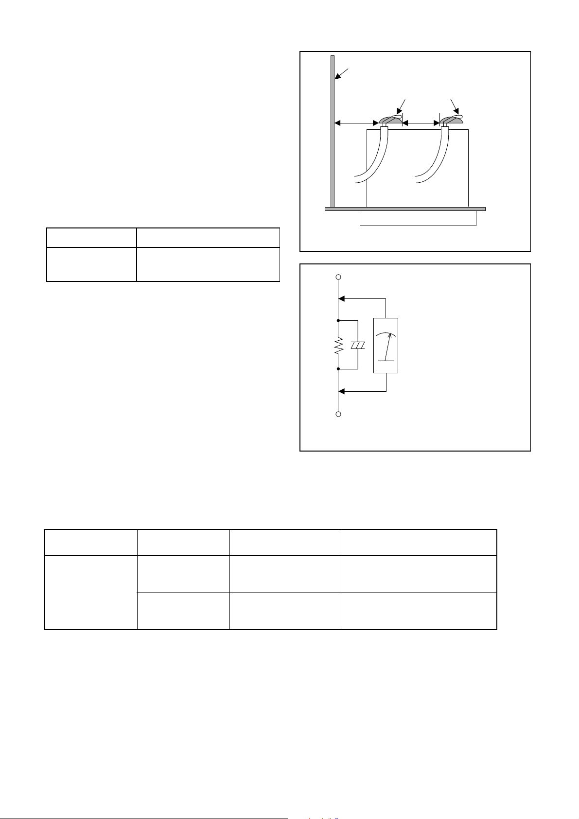
1. Clearance Distance
When replacing primary circuit components, confirm
specified clearance dista nce (d) and (d’) between soldered terminals, and between terminals and surrounding metallic parts. (See Fig. 1)
Table 1 : Ratings for selected area
AC Line Voltage Clearance Distance (d), (d’)
220 to 240 V
Note: This table is unofficial and for reference only.
Be sure to confirm the precise values.
≥ 3mm(d)
≥ 6 mm(d’)
2. Leakage Curre nt Test
Confirm the specified (or lower) leakage current
between B (earth ground, power cord plug prongs)
and externally exposed accessible parts (RF terminals, antenna terminals, video and audio input and
output terminals, microphone jacks, earphone jacks,
etc.) is lower than or equal to the specified value in the
table below.
Measuring Method (Power ON) :
Insert load Z between B (earth ground, power cord
plug prongs) and exposed accessible parts. Use an
AC voltmeter to measure across t he ter minals of l oad
Z. See Fig. 2 and the following table.
Chassis or Secondary Conductor
Primary Circuit
d' d
Exposed Accessible Part
Z
One side of
B
Power Cord Plug Prongs
AC Voltmeter
(High Impedance)
Fig. 1
Fig. 2
Table 2: Leakage current ratings for selected areas
AC Line Voltage Load Z Leakage Current (i)
2kΩ RES.
Connected in
parallel
220 to 240 V
50kΩ RES.
Connected in
parallel
Note: This table is unofficial and for reference only. Be sure to confirm the precise values.
i≤0.7mA AC Peak
i≤2mA DC
i≤0.7mA AC Peak
i≤2mA DC
1-2-2 U31P_ISP
One side of power cord plug
prongs (B) to:
RF or
Antenna terminals
A/V Input, Output
Page 6
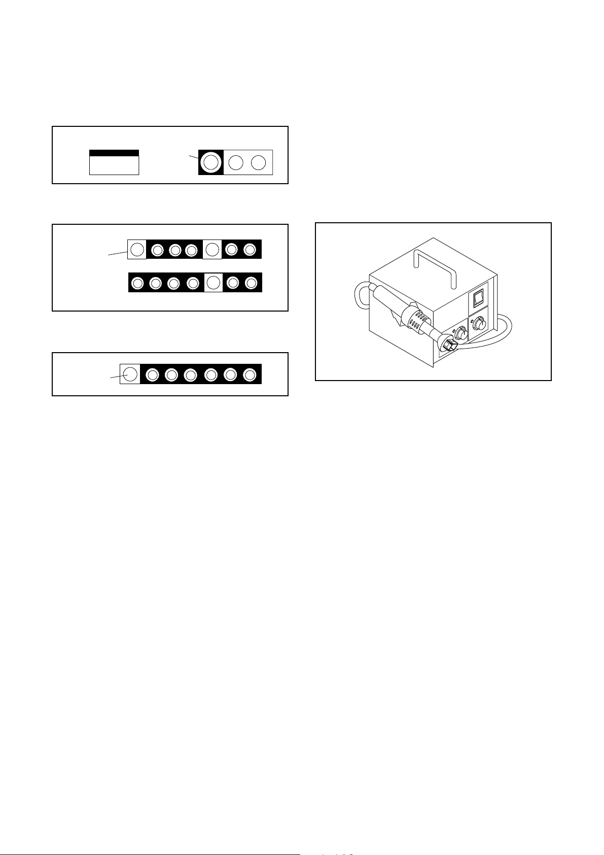
STANDARD NOTES FOR SERVICING
Circuit Board Indications
1. The output pin of the 3 pin Regulator ICs is
indicated as shown.
Top View
Out
2. For other ICs, pin 1 and every fifth pin are
indicated as shown.
Pin 1
3. The 1st pin of every male connector is indicated as
shown.
Pin 1
Input
In
Bottom View
5
10
Pb (Lead) Free Solder
When soldering, be sure to use the Pb free solder.
How to Remove / Install Flat Pack-IC
1. Removal
With Hot-Air Flat Pack-IC Desoldering Machine:
1. Prepare the hot-air flat pack-IC desoldering
machine, then apply hot air to the Flat Pack-IC
(about 5 to 6 seconds). (Fig. S-1-1)
Fig. S-1-1
2. Remove the flat pack-IC with tweezers while
applying the hot air.
3. Bottom of the flat pa ck-IC is fixed with glue to the
CBA; when removing entire flat pack-IC, first apply
soldering iron to center of the flat pack-IC and heat
up. Then remove (glue will be melted). (Fig. S-1-6)
4. Release the flat pack-IC from the CBA using
tweezers. (Fig. S-1-6)
CAUTION:
1. The Flat Pack-IC shape may differ by models. Use
an appropriate hot-air flat pack-IC desoldering
machine, whose shape matches that of the Flat
Pack-IC.
2. Do not supply hot air to the c hip par ts around the
flat pack-IC for over 6 seconds because damage
to the chip parts may occur. Put masking tape
around the flat pack-IC to protec t other pa r ts from
damage. (Fig. S-1-2)
1-3-1 VCRP_SN
Page 7
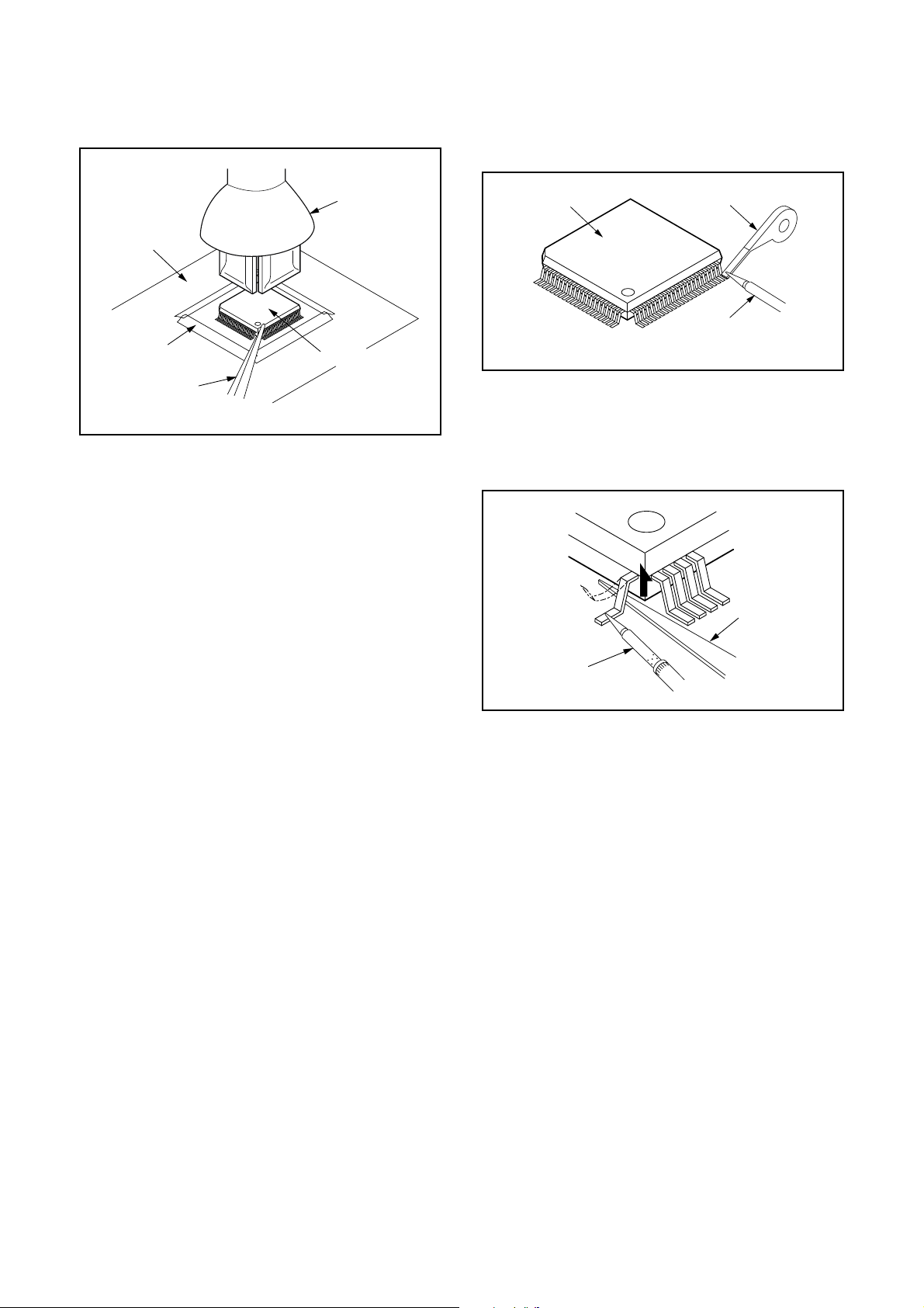
3. The flat pack-IC on the CBA is affixed with glue, so
be careful not to break or dam age the foil of ea ch
pin or the solder lands under the IC when
removing it.
With Soldering Iron:
1. Using desoldering braid, remove the solder from
all pins of the flat pack-IC. When you use solder
flux which is applie d to all pi ns of the fl at pack-IC,
you can remove it easily. (Fig. S-1-3)
CBA
Masking
Tape
Tweezers
Hot-air
Flat Pack-IC
Desoldering
Machine
Flat Pack-IC
Fig. S-1-2
Flat Pack-IC
Desoldering Braid
Soldering Iron
Fig. S-1-3
2. Lift each lead of the flat pack-IC upward one by
one, using a shar p pin or wi re to which s older will
not adhere (iron wire). W hen hea tin g the pins, use
a fine tip soldering iron or a hot air desoldering
machine. (Fig. S-1-4)
Sharp
Pin
Fine Tip
Soldering Iron
3. Bottom of the flat pa ck-IC is fixed with glue to the
CBA; when removing entire flat pack-IC, first apply
soldering iron to center of the flat pack-IC and heat
up. Then remove (glue will be melted). (Fig. S-1-6)
4. Release the flat pack-IC from the CBA using
tweezers. (Fig. S-1-6)
Fig. S-1-4
1-3-2 VCRP_SN
Page 8
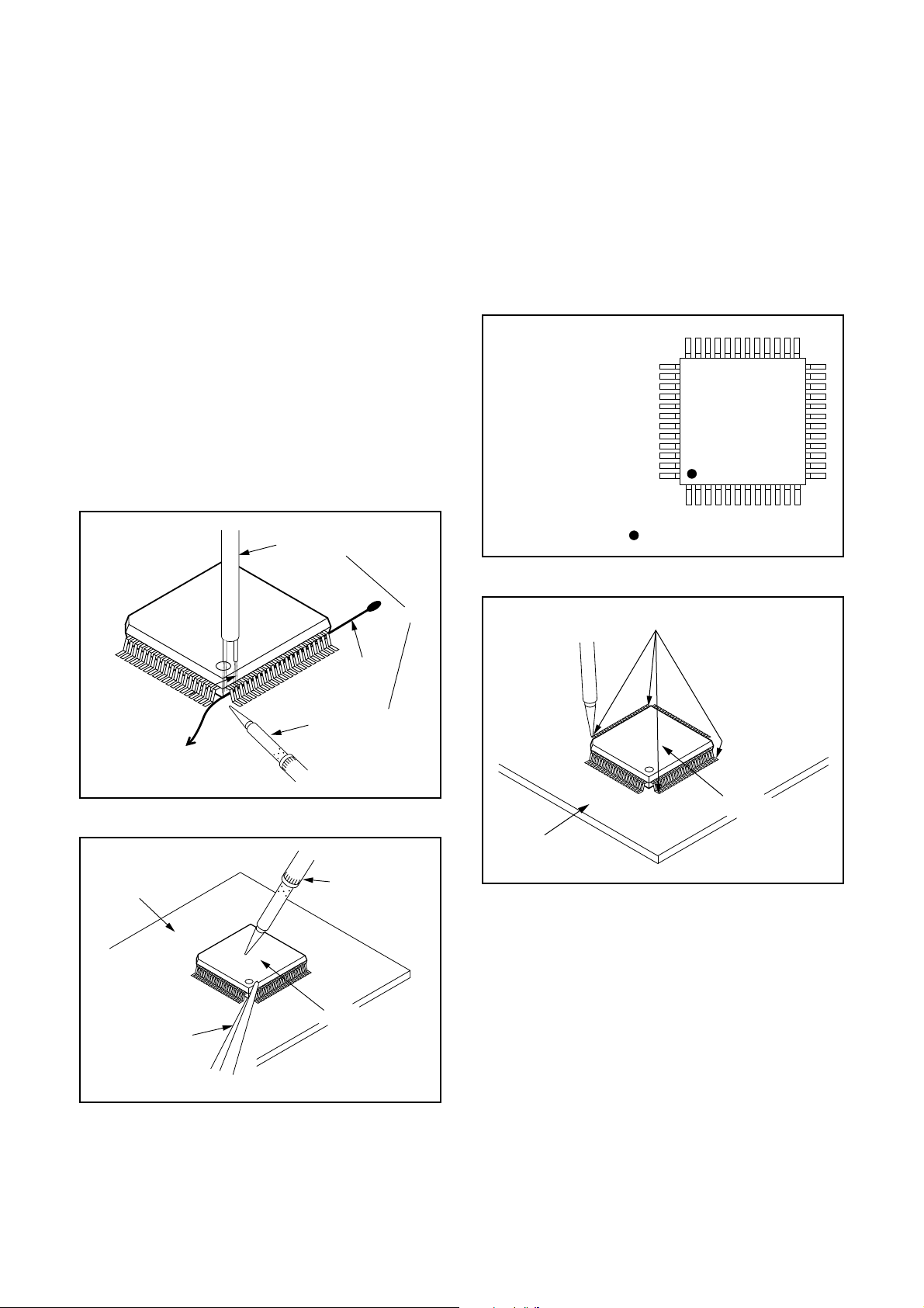
With Iron Wire:
1. Using desoldering braid, remove the solder from
all pins of the flat pack-IC. When you use solder
flux which is ap plied to all pins of the flat pack-IC,
you can remove it easily. (Fig. S-1-3)
2. Affix the wire to a workbench or solid mounting
point, as shown in Fig. S-1-5.
3. While heating the pins using a fine tip soldering
iron or hot air blower, pull up the wire as the solder
melts so as to lift the IC leads from the CBA
contact pads as shown in Fig. S-1-5.
4. Bottom of the f lat pack-IC is fixed with glue to the
CBA; when removing entire flat pack-IC, first apply
soldering iron to center of the flat pack-IC and heat
up. Then remove (glue will be melted). (Fig. S-1-6)
5. Release the flat pack-IC from the CBA using
tweezers. (Fig. S-1-6)
Note: When using a soldering iron, care must be
taken to ensure that the flat pack-IC is not
being held by glue. When the flat pack-IC is
removed from the CBA, handle it gently
because it may be damaged if force is applied.
Hot Air Blower
2. Installation
1. Using desoldering braid, remove the solder from
the foil of each pin of the flat pack-IC on the CBA
so you can install a r ep la cem ent fl at p ack-IC mo re
easily.
2. The “●” mar k on the flat pack-IC indicates pin 1.
(See Fig. S-1-7.) Be su re thi s mar k m atche s the 1
on the PCB when positioni ng for installa tion. Then
presolder the four corners of th e fl at pa ck-IC. (See
Fig. S-1-8.)
3. Solder all pins of the flat pack-IC. Be sure that
none of the pins have solder bridges.
Example :
Pin 1 of the Flat Pack-IC
is indicated by a " " mark.
Fig. S-1-7
To Solid
Mounting Point
CBA
Tweezers
Iron Wire
Soldering Iron
Fig. S-1-5
Fine Tip
Soldering Iron
Flat Pack-IC
or
Presolder
Flat Pack-IC
CBA
Fig. S-1-8
Fig. S-1-6
1-3-3 VCRP_SN
Page 9
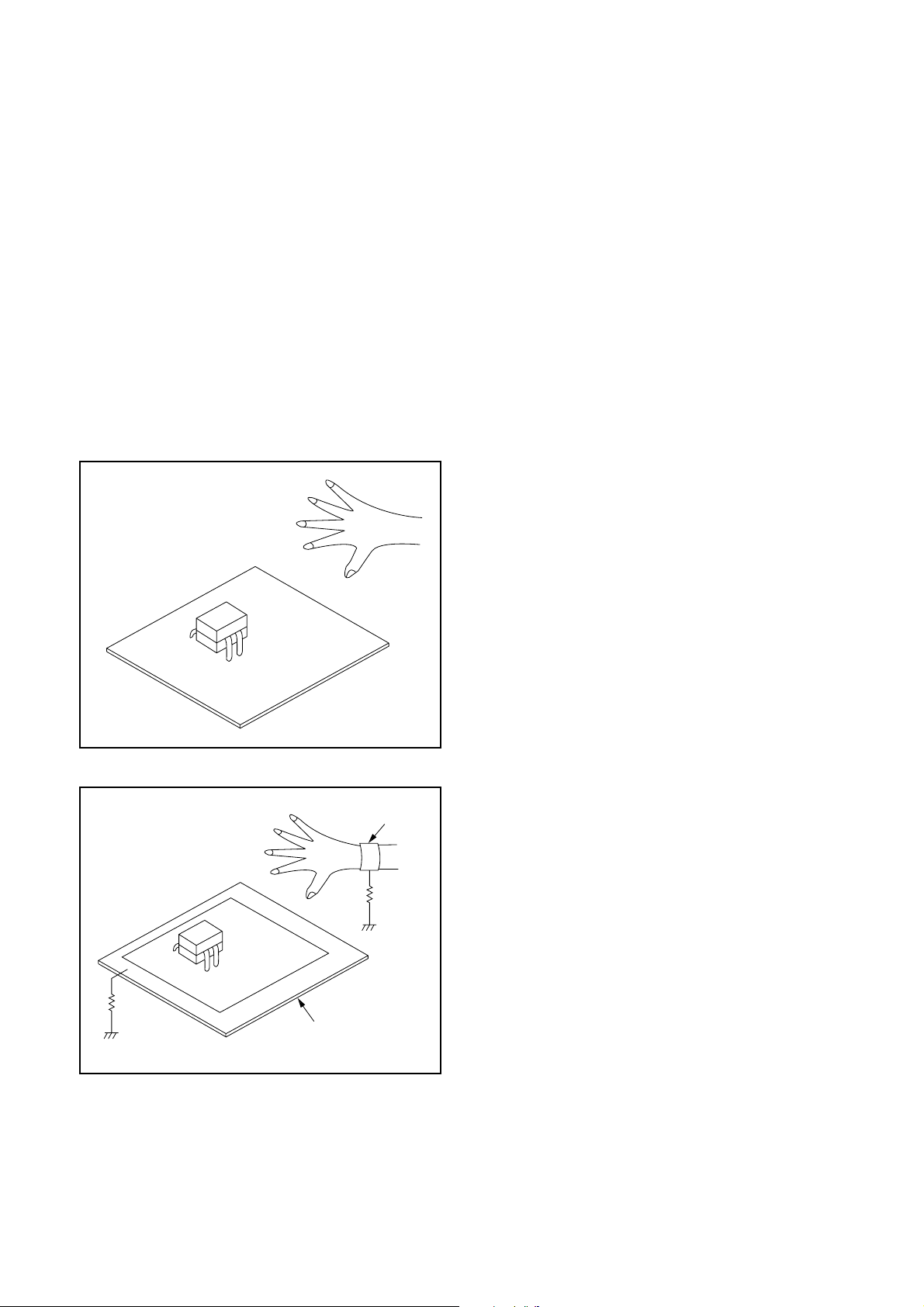
Instructions for Handling Semiconductors
Electrostatic breakdown of the semi-conductors may
occur due to a potential difference caused by
electrostatic charge during unpacking or repair work.
1. Ground for Human Body
Be sure to wear a grounding band (1 MΩ) that is
properly grounded to remove any static el ectric ity that
may be charged on the body.
2. Ground for Workbench
Be sure to place a c onductive sheet or copper plate
with proper grounding (1 MΩ) on the workbench or
other surface, where the semi-conductors are to be
placed. Because the static electricity charge on
clothing will not escape through the body grounding
band, be careful to avoid contacting semi-conductor s
with your clothing.
<Incorrect>
<Correct>
1MΩ
CBA
Grounding Band
1MΩ
CBA
Conductive Sheet or
Copper Plate
1-3-4 VCRP_SN
Page 10
PREPARATION FOR SERVICING
How to Enter the Service Mode
About Optical Sensors
Caution:
An optical sensor system is used for the Tape Start
and End Sensors on this equipment. Carefully read
and follow the instructions below. Otherwise the unit
may operate erratically.
What to do for preparation
Insert a tape into the Deck Mechanism Asse mbly and
press the PLAY button. The tape will be loaded into
the Deck Mechanism Assembly. Make sure the power
is on, connect TP507 (S-INH) to GND. T his will stop
the function of Tape Start Sensor, Tape End Sensor
and Reel Sensors. (If these TPs ar e c on nected before
plugging in the unit, the function of the sensors will
stay valid.) See Fig. 1.
Note: Because the Tape End Sensors are inactive, do
not run a tape al l t he way to the start or the end of the
tape to avoid tape damage.
Q505
Q504
TP507
S-INH
Fig. 1
1-4-1 HM4N0PFS
Page 11
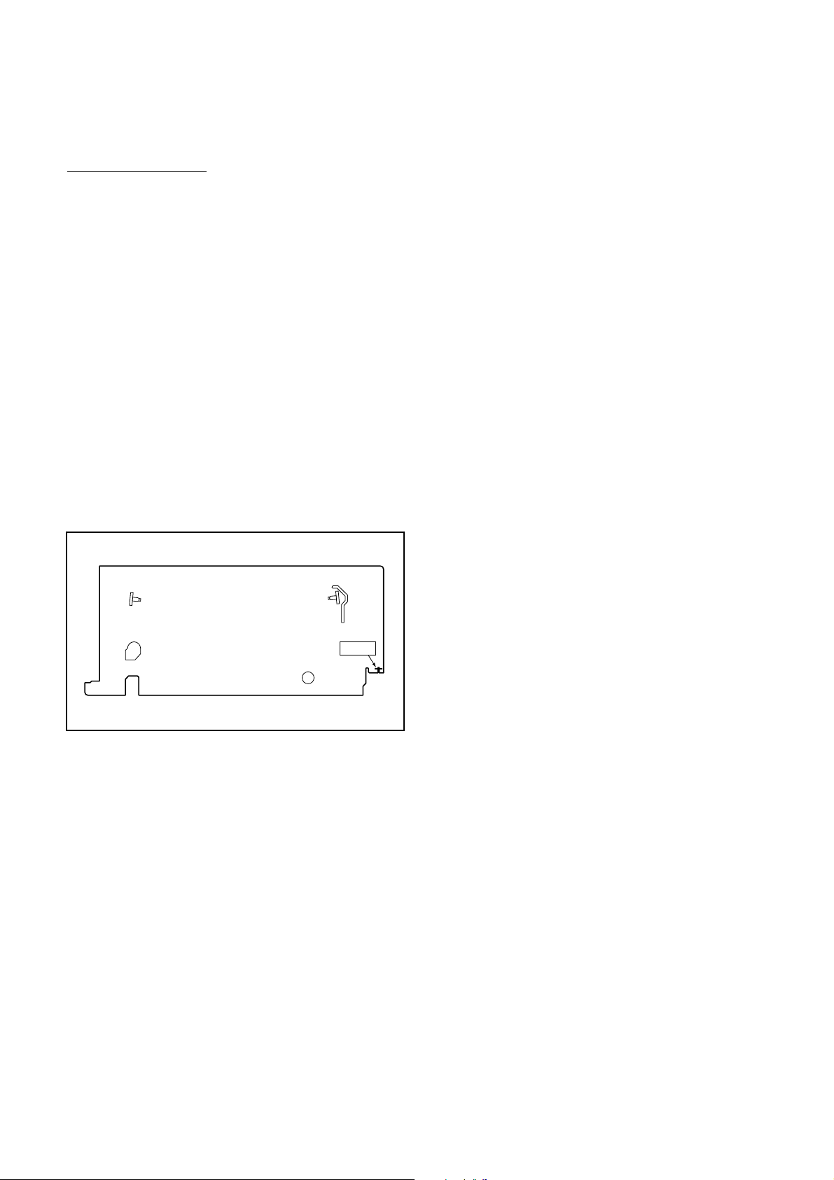
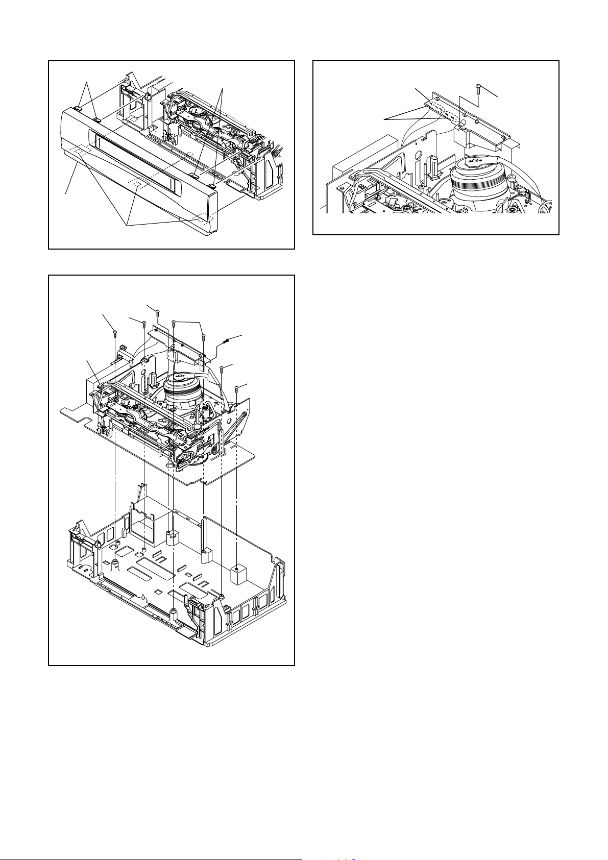
CABINET DISASSEMBLY INSTRUCTIONS
1. Disassembl y Flowchart
This flowchar t indi cates the di sass embly ste ps to ga in
access to item(s) to be serviced. When reassembling,
follow the steps in reverse order. Bend, route, and
dress the cables as they were originally.
[1] T op Case
[2] Front Assembly
[3] VCR Chassis Unit
[4] Jack CBA
[5] Deck Assembly
[6] Main CBA
[7] Cylinder Shield
2. Disassembl y Method
REMOVAL
ID/
LOC
.No.
PART
REMOVE/*UNHOOK/
Fig.
UNLOCK/RELEASE/
No.
UNPLUG/DESOLDER
Note
(1):Identification (location) No. of parts in the figures
(2):Name of the part
(3):Figure Number for reference
(4): Identification of parts to be removed, unhooked,
unlocked, released, unplugged, unclamped, or
desoldered.
P=Spring, L=Locking Tab, S=Screw,
CN=Connector
*=Unhook, Unlock, Release, Unplug, or Desolder
e.g. 2(S-2) = two Screws (S-2),
2(L-2) = two Locking Tabs (L-2)
(5):Refer to “Reference Notes.”
Reference Notes
CAUTION: Locking Tabs (L-1) and (L-2) are fragile.
Be careful not to break them.
1. Remove five Screws (S-2), three Screws (S-3) and
Screw (S-4). Then, slowly lift the VCR Chassis Unit
(Deck Assembly, Jack CBA and Main CBA) up.
2. When reassembling, solder wire jumpers as shown
in Fig. D5.
3. Before installing the Deck Assembly, be sure to
place the pin of LD-SW on Main CBA as shown in
Fig. D6. Then, install the Deck Assembly while
aligning the hole of Cam Gear with the pin of LDSW, the shaft of Cam Gear with the hol e of L D-SW
as shown in Fig. D6.
[1] Top Case D1 7(S-1) -
Front
[2]
Assembly
VCR Chassis
[3]
Unit
[4] Jack CBA D4 Desolder, (S-5) -
Deck
[5]
Assembly
[6] Main CBA D5 ---------- -
Cylinder
[7]
Shield
↓
(1)
↓
(2)
D2 *3(L-1),*4(L-2) -
D3 5(S-2), 2(S-3), (S-4) 1
D5
2(S-6), Desolder 2,3
D6
D5 (S-7) -
↓
(3)
↓
(4)
(S-1)
(S-1)
[1] T op Case
(S-1)
↓
(5)
Fig. D1
1-5-1 HM340DC
Page 12
(L-2)
[2] Front
Assembly
(S-2)
[3]VCR
Chassis
Unit
(L-1)
(S-3)
(S-2)
(L-2)
(S-2)
[4] Jack CBA
(S-5)
Desolder
Fig. D4
Fig. D2
(S-4)
(S-3)
(S-2)
Fig. D3
1-5-2 HM340DC
Page 13
[7] Cylinder Shield
FE Head
Cylinder Assembly
(S-7)
ACE Head
Assembly
Pin
SW507
LD-SW
[6] Main CBA
From
FE Head
From
Cylinder
Assembly
(S-6)
TOP VIEW
From
ACE Head
Assembly
[5] Deck
Assembly
[6] Main CBA
(S-6)
From
Capstan Motor
Assembly
Lead with
blue stripe
[5] Deck Assembly
Shaft
Hole
LD-SW
Cam Gear
Hole
Pin
[6] Main CBA
Fig. D6
Printing
Lead with
white stripe
Lead connections of Deck Assembly and Main CBA
Lead with
blue stripe
Desolder
from bottom
side
Fig. D5
1-5-3 HM340DC
Page 14
ELECTRICAL ADJUSTMENT INSTRUCTIONS
General Note: "CBA" is an abbreviation for
"Circuit Board Assembly."
NOTE:
1.Electri cal adjustm ents are re quired after re placing
circuit components and certain mechanical par ts.
It is impor tant to do these adjustments only after
all repairs and replacements have been completed. Also, do not attempt these adjustments
unless the proper equipment is available.
2.To perfor m these alignment / confirmation procedures, make sure that the tracking control is set in
the center po sition: Press either "CHANNEL L5??" or
"CHANNEL K" button on the remote control unit
first, then the "PLAY" button (Front Panel only).
Te st Equipment Required
1.Oscilloscope: Dual-trace with 10:1 probe,
V-Range: 0.001~50V/Div.,
F-Range: DC~AC-20MHz
2.Alignment Tape (FL6A)
Head Switching Position Adjustment
Purpose:
To determ ine the Head Switching position during
playback.
Symptom of Misadjustment:
May cause Head Switch ing noise or vertical jit ter
in the picture.
Test point Adj.Point Mode Input
J23(V-OUT)
TP502(RF-SW)
GND
Tape
FL6A Oscilloscope
Connections of Measurement Equipment
Main CBA
VR501
(Switching Point)
(MAIN CBA)
Measurement
Equipment
J23
GND
TP502
PLAY
(SP)
6.5H±1H
(416µs±64µs)
Oscilloscope
-----
Spec.
CH1 CH2
Trig. (+)
Figure 1
EXT. Syncronize Trigger Point
CH1
CH2
Reference Notes:
Playback the Alignment tape and adjust VR501 so that
the V-sync front edg e of the CH1 video out put waveform is at the 6.5H±1H (416µs±64µs) delayed position
from the rising edge o f the CH2 head switching pulse
waveform.
1.0H
6.5H+/-1H (416µs+/-64µs)
Switching Pulse
0.5H
V-Sync
1-6-1 FEGVCREA
Page 15

HOW TO INITIALIZE THE VCR
To put the program back at the factory-default,
initialize the VCR as the following procedure.
1. Make sure that no timer programming is set. If not,
reset all timer programming.
2. Turn the power off.
3. Press the [STOP/EJECT] button and
[CHANNEL K] button on the unit simultaneously
for at least 2 seconds.
4. Release the [STOP/EJECT] button and
[CHANNEL K] button to complete this mode.
1-7-1 HM340INT
Page 16
FUNCTION INDICATOR SYMBOLS
Note:
The following symbols will appear on the indicator panel to indicate the current mode or operation of the VCR.
On-screen modes will also be momentarily displayed on the tv screen when you press the operation buttons.
Display panel
31A-450
TAPE IN TIMER RECFUNCTIONSTANDBY
31C-450
CASSETTE MINUTERIE ENR. FONCTIONVEILLE
STANDBY
VEILLE
FUNCTION
FONCTION
TAPE IN
CASSETTE
TIMER
MINUTERIE
REC
ENR.
" H "= LED Light on, " L "= LED Light off
MODE INDICATOR ACTIVE
Always " H " during electricity
Power on = " H "
Power off = " L "
Cassette in = " H "
Cassette out = " L "
Timer stand by = " H "
One touch recording = " H "
Timer recording = " H "
General mode = " L "
REC mode = " H "
REC pause
General mode = " L "
Blinks at 0.8Hz interval
1-8-1 HM340FIS
Page 17

TV screen
Note:
OSD for mechanical error will be displayed for 5 sec. after the mechanical error occurs.
Cause Indicator Active
When reel or capstan mechanism is not
functioning correctly
When tape loading mechanism is not
functioning correctly
When cassette loading mechanism is not
functioning correctly
When the drum is not working properly
P-ON Power safety detection
When reel or capstan mechanism is not functioning
correctly
A
R
When tape loading mechanism i s not function ing correctly
“A R” is displayed on a TV screen. (Refer to Fig. 1.)
“A T” is displayed on a TV screen. (Refer to Fig. 2.)
“A C” is displayed on a TV screen. (Refer to Fig. 3.)
“A D” is displayed on a TV screen. (Refer to Fig. 4.)
“A P” is displayed on a TV screen. (Refer to Fig. 5.)
Fig. 1
When the drum is not working properly
A
D
P-ON Power safety detection
Fig. 4
A
T
Fig. 2
When cassette loadi ng mechanism is not functi oning
correctly
A
C
Fig. 3
A
P
Fig. 5
1-8-2 HM340FIS
Page 18

BLOCK DIAGRAMS
Servo / System Control Block Diagram
A
B
Model Mark
31A-450
31C-450
Comparison Chart of
Models & Marks
AL+5V
VR501
SW-POINT
AL+5V
SDA
SCL
SDA
TU701(TUNER UNIT)
SCL
3
5
12
11
SDA
SCL
IC503 (MEMORY)
5
6
TO
AUDIO BLOCK
IIC-BUS SCL
AUDIO-SW-1
AUDIO-SW-2
IIC-BUS SDA
A-MUTE-H
RF-SW
D-REC-H
IIC-BUS SCL
IIC-BUS SDA
C-ROTA
D-V-SYNC
FROM/TO
VIDEO BLOCK
V-ENV
H-A-SW
H-A-COMP
C-SYNC
TRICK-H
SECAM-H
TP507
SENS-INH
KEY
IC501
(SERVO/SYSTEM CONTROL)
REMOTE
RS501
AL+5V
SWITCH
8
7
KEY- 2
KEY- 1REMOCON-IN
CTL(+)
LD-SW
9
14
957610480
SENSOR
S-LED
D502
AL+5V
KEY
CTL(-)
94
SWITCH
ST-S
END-S
T-REEL
2
PG-DELAY
S-REEL
79
Q501
PS503
31
REC-SAF-SW
RESET
34
RESET
TIMER+5V
S-REEL
REC-SAFETY
SW506
AL+5V
STAND-BY
D561
D562
POWER
Q562
POWER-LED
CAS-LED
TIMER-LED
26
25
24
23
D563
CAS
Q563
REC-LED
D564
TIMER
Q564
29
AUDIO-SW-1
D565
REC
Q565
83
30
A-MUTE-H
AUDIO-SW-2
71
72
D-REC-H
IIC-BUS SCL
IIC-BUS SDA
LM-FWD/REV
D-CONT
D-PFG
77
81
90
P-ON+15V
AL+12V
CN502
P-ON+15V11AL+12V(2)10GND9D-PFG8D-CONT7LM-FWD/REV
12
GND5C-CONT4C-F/R3C-FG2P-ON+5V1AL+12V/+20.5V
6
13
15
183316
RF-SW
C-ROTA
D-V-SYNC
C-CONT
C-F/R
C-FG
78
87
6
17
V-ENV
H-A-SW
H-A-COMP
AL+12V/+20.5V
P-ON+5V
58
C-SYNC
C-POW-SW
65
61
TRICK-H
SECAM-H
B
P-ON-H
C-POW-SW
P-DOWN-L
67
66
86
P-ON-H
P-DOWN-L
FROM/TO
POWER
SUPPLY
BLOCK
SW507
LD-SW
MAIN CBA
ST-S
Q504
Q505
SENSOR CBA
END-S
T-REEL
Q503
TP506
END-S
SENSOR CBA
(DECK ASSEMBLY)
CN504
CL504
2 CTL(+)
1 CTL(-)
CONTROL
ACE HEAD ASSEMBLY
HEAD
1-9-1
MOTOR
CAPSTAN MOTOR
M
PG
SENSOR
CYLINDER ASSEMBLY
DRUM
MOTOR
DRIVE
CIRCUIT
CAPSTAN
MOTOR
M
M
LOADING
MOTOR
HM340BLS
Page 19

Video Block Diagram
A
B
VIDEO (L)-1
HEAD
VIDEO (R)-1
HEAD
VIDEO (R)-2
HEAD
VIDEO (L)-2
HEAD
B
Model Mark
31A-450
31C-450
Comparison Chart of
Models & Marks
7978
REC-VIDEO SIGNAL PB-VIDEO SIGNAL MODE: SP/REC
69684643
IIC-BUS SDA
IIC-BUS SCL
65
FROM
SERVO/SYSTEM
CONTROL BLOCK
B
50
55
CYLINDER ASSEMBLY
(DECK ASSEMBLY)
123
CN253
VIDEO(R)-1
VIDEO-COM
969593
SP
HEAD
SP
P
R
SERIAL
DECORDER
LUMINANCE
SIGNAL
Y. DELAY
456
VIDEO(L)-1
VIDEO(L)-2
VIDEO-COM
94
AMP
EP
PROCESS
AGC
BYPASS
VIDEO(R)-2
908988
WF1
87
EP
HEAD
AMP
REC FM
AGC
+
Y
CCD 1H DELAY
CHARA.
INS.
TP502
RF-SW
C
1/2
RF-SW
C-ROTA
D-REC-H
D-V-SYNC
62
70
80
D-REC-H
D-V-SYNC
C-ROTA/RF-SW
RPRP
CHROMINANCE
SIGNAL
PROCESS
FBC
FROM/TO SERVO/SYSTEM
CONTROL BLOCK
V-ENV
H-A-SW
C-SYNC
TRICK-H
67
84
83
V-ENV
C-SYNC
H-A-COMP
PR
SECAM-H
PB-H OUT
AGC VXO
71
H-A-SW
Y/C
MIX
H-A-COMP
PAL/SECAM
DETECTOR
IC370 (PAL/SECAM DECTECTOR)
1
171418216
29
28
21
WF2
C-PB
TP301
252928 44
X301
4.433619MHz
58 59
IC501 (OSD)
MAIN CBA
COLOR
-IN
OSD
CHARACTER
MIX
52
IC301
(Y/C SIGNAL PROCESS)
BUFFER
Q351
IN1
IN2
TUNER
485052
6
24
VIDEO IN
VIDEO OUT
TU701(TUNER UNIT)
1-9-2
IN2
MUTE
PB/EE
IN1
MUTE
TUNER
PB/EE
56
WF3
JACK CBA
J23
61
63
V-OUT
CN151
CN101
JK101
CN152
1
VIDEO-OUT1
1
Q101
BUFFER
19
VIDEO
-OUT1
1
VIDEO-OUT2
VIDEO-IN1
33
1
CN102
Q102
BUFFER
JK102
20
19
VIDEO
-IN1
VIDEO
-OUT2
VIDEO-IN2 3
3
20
VIDEO
-IN2
HM340BLV
Page 20

Audio Block Diagram
Mode : SP/REC
152
PB/EE
PB-AUDIO SIGNAL REC-AUDIO SIGNAL
MAIN CBA
IC151 (SWITCHING)
PB/EE
PB/EE
3
4
1214151110
PB/EE
TUNER
IN2
IN1
13
IN1
TO SERVO/SYSTEM
CONTROL BLOCK
AUDIO-SW-1
AUDIO-SW-2
9
SW
CTL
ALC
TO SERVO/SYSTEM
71
68 69
16
CONTROL BLOCK
A-MUTE-H
IIC-BUS SCL
IIC-BUS SDA
11
12
MUTE
SERIAL
DECODER
AUDIO HD-SW
CONTROL
DET
INV
LINE
ALC
R
AMP
ATT
REC-ON
P
REC
AMP
J972
A
2
21
AUDI O
TU-AUDIO
TU701(TUNER UNIT)
CN151
5
7
Q151
CN152
8
BUFFER
6
Q152
BUFFER
TUNER
IC301 (AUDIO SIGNAL PROCESS)
IN1
J982
IN2
151317
EQ
PB-ON
5
98
AMP
6
7
SP/LP-ON
+5V
Q401
CN504
AUDIO-PB/REC
3
Q402
4 A-COM
BIAS
6 AE-H
OSC
100
3
AUTO
BIAS
2
1
Q406
5 AE-H/FE-H
+5V
Q403 (SWITCHING)
Q405
(PB=ON)
CN501
2 FE-H
1 FE-H-GND
JACK CBA
JK101
AUDIO-IN1
AUDIO-OUT1
5
7
CN101
261
AUDIO-IN1
AUDIO-IN1
AUDIO-OUT1
CN102
JK102
3
261
AUDIO-OUT1
AUDIO-IN2
AUDIO-IN2
AUDIO-OUT2
6
8
3
AUDIO-IN2
AUDIO-OUT2
AUDIO-OUT2
A
B
Model Mark
31A-450
31C-450
Comparison Chart of
Models & Marks
1-9-3
ACE HEAD ASSEMBLY
AUDI O
HEAD
(DECK ASSEMBLY)
AUDI O
ERASE
HEAD
FE HEAD
FULL
ERASE
HEAD
HM340BLA
Page 21

Power Supply Block Diagram
P-ON+44V
P-ON+15V12P-ON-H
AL+12V/+20.5V
AL+12V
C-POW-SW
AL+5V
TIMER+5V
P-ON+5V
AL-5V
P-DOWN-L
MAIN CBA
Q051
CAUTION !
Fixed voltage (or Auto voltage selectable) power supply circuit is used in this unit.
If Main Fuse (F001) is blown , check to see that all components in the power supply
circuit are not defective before you connect the AC plug to the AC power supply.
Otherwise it may cause some components in the power supply circuit to fail.
T001
2
Q057
Q052
13
Q055
Q058
14
4
15
Q001
Q054
Q059
16
Q056
SHUNT
REGULATOR
Q004
11
17
18
1
4
IC001
ERROR
6
7
VOLTAGE DET
COLD
23
NOTE:
The voltage for parts in hot circuit is measured using
hot GND as a common terminal.
BRIDGE
D001 - D004
LINE
F001 L003
T1.6A L 250V
HOT CIRCUIT. BE CAREFUL.
CAUTION !
For continued protection against fire hazard,
replace only with the same type fuse.
AC001
RECTIFIER
FILTER
1-9-4
Q002
Q003
HOT
HM340BLP
Page 22

SCHEMATIC DIAG RAMS / CBA’S AND TEST POINTS
Standard Notes
WARNING
Many electrical and mechanical parts in this chassis
have special characteristics. These characteristics
often pass unnoticed and the protection afforded by
them cannot necessarily be obtained by using
replacement components rated for higher voltage,
wattage, etc. Replacement parts that have these special safety character istics are id entified in th is manual
and its supplements; electrical components having
such features are identified by the m ark " ! " in the
schematic diagram and the par ts list. Before replacing
any of these components, read the parts list in this
manual carefully. The use of substitute replacement
parts that do not have the same safety characterist ics
as specified in the pa r ts list may create sh ock, fire, or
other hazards.
Notes:
1. Do not use the part number sh own on these draw-
ings fo r orde ring. The cor rect part number is sho wn
in the parts list, and may be slightly different or
amended since these drawings were prepared.
2. All resistance values are indicated in ohms
3
(K=10
3. Resistor wattages are 1/4W or 1/6W unless other-
wise specified.
4. All capacitance values are indicated in µF
(P=10
5. All voltages are DC voltages unless otherwise
specified.
6. Electrical parts such as capacitors, connectors,
diodes, IC’s, transistors, resistors, switches, and
fuses are identified by four digits. The first two digits are not shown for each component. In each
block of the diagram, there is a note such as shown
below to indicate these abbreviated two digits.
, M=106).
-6
µF).
1-10-1 SCPA1
Page 23

LIST OF CAUTION, NOTES, AND SYMBOLS USED IN THE SCHEMATIC DIAGRAMS ON THE FOLLOW ING
PAGES:
1. CAUTION:
FOR CONTINUED PROTECTION AGAINST FIRE HAZARD, REPLACE ONLY WITH THE SAME TYPE FUSE.
2. CAUTION:
Fixed Voltage (or Auto voltage selectable) power supply circuit is used in this unit.
If Main Fuse (F001) is blown, first check to see that all components in the power supply circuit are not defective
before you connect the AC plug to the AC power supply. Otherwise it may cause some components in the
power supply circuit to fail.
3. Note:
(1) Do not use the part number shown on the drawings for ordering. The correct part number is shown in the
parts list, and may be slightly different or amended since the drawings were prepared.
(2) To maintai n original function and reliabi lity of repaired units, use only orig inal replacement par ts which are
listed with their part numbers in the parts list section of the service manual.
4. Mode: SP/REC
5. Voltage indications for PLAY and REC modes on the schematics are as shown below:
Unit: Volts
The same voltage for
both PLAY & REC modes
6. How to read converged lines
1-D3
Distinction Area
Line Number
(1 to 3 digits)
Examples:
1. "1-D3" means that line number "1" goes to the line number
"1" of the area "D3".
2. "1-B1" means that line number "1" goes to the line number
"1" of the area "B1".
7. Test Point Information
: Indicates a test point with a jumper wire across a hole in the PCB.
: Used to indicate a test point with a component lead on foil side.
5.0
231
5.0
PLAY mode
REC mode
(2.5)
Indicates that the voltage
is not consistent here.
3
AREA D3
2
1
AREA B1
1-D3
ABCD
1-B1
: Used to indicate a test point with no test pin.
: Used to indicate a test point with a test pin.
1-10-2 SCRK05
Page 24

Main 1/6 Schematic Diagram
Comparison Chart of
Models and Marks
MODEL MARK
31A-450 A
31C-450
B
1-10-3
HM340SCM1
Page 25

Main 2/6 & Sensor Schematic Diagram
Comparison Chart of
Models and Marks
MODEL MARK
31A-450 A
31C-450
B
1-10-4
HM340SCM2
Page 26

Main 3/6 Schematic Diagram
Comparison Chart of
Models and Marks
MODEL MARK
31A-450 A
31C-450
B
1-10-5
HM340SCM3
Page 27

Main 4/6 & Jack Schematic Diagram
1-10-6
HM340SCM4
Page 28
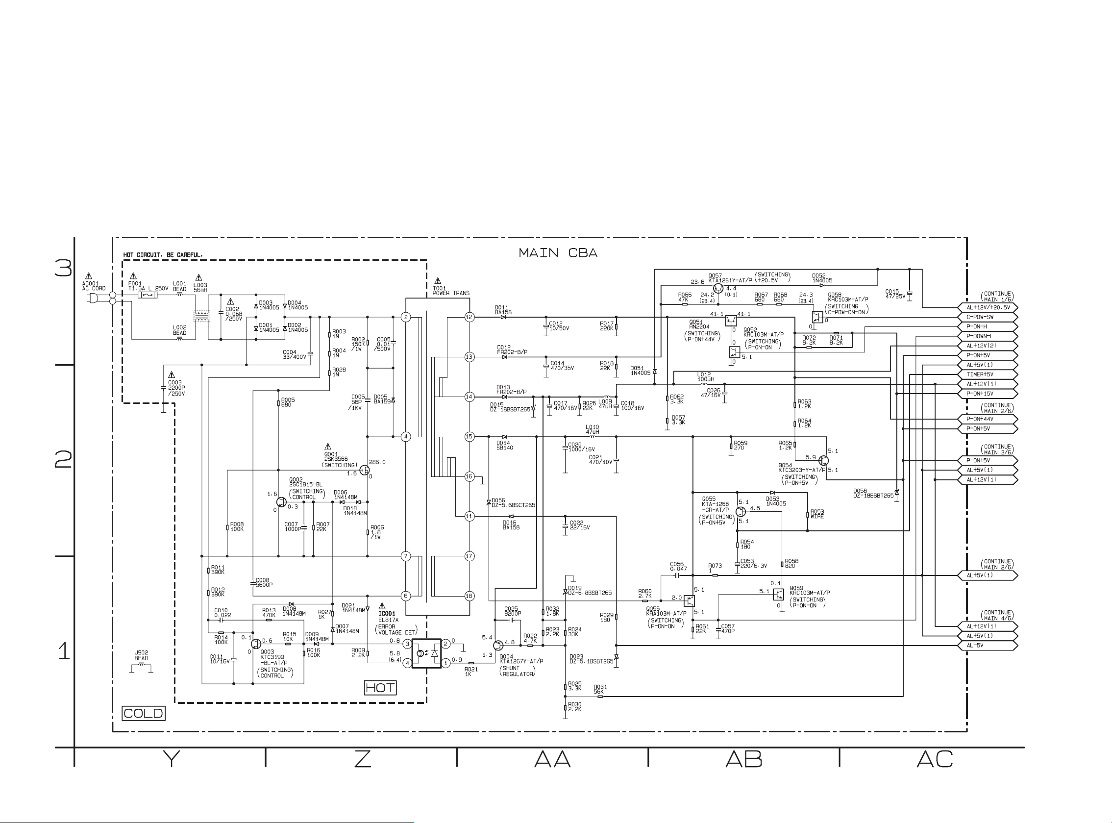
Main 5/6 Schematic Diagram
CAUTION !
Fixed voltage (or Auto voltage selectable) power supply circuit is used in this unit.
If Main Fuse (F001) is blown , check to see that all components in the power supply
circuit are not defective before you connect the AC plug to the AC power supply.
Otherwise it may cause some components in the power supply circuit to fail.
CAUTION !
For continued protection against fire hazard,
replace only with the same type fuse.
NOTE:
The voltage for parts in hot circuit is measured using
hot GND as a common terminal.
1-10-7
HM340SCM5
Page 29

Main 6/6 Schematic Diagram ( B )
Comparison Chart of
Models and Marks
MODEL MARK
31A-450 A
31C-450
B
1-10-8
HM342SCM6
Page 30

Main CBA Top View
CAUTION !
For continued protection against fire hazard,
replace only with the same type fuse.
NOTE:
The voltage for parts in hot circuit is measured using
hot GND as a common terminal.
Sensor CBA Top View
BHF300F01012A
CAUTION !
Fixed voltage (or Auto voltage selectable) power supply circuit is used in this unit.
If Main Fuse (F001) is blown , check to see that all components in the power supply
circuit are not defective before you connect the AC plug to the AC power supply.
Otherwise it may cause some components in the power supply circuit to fail.
BHF300F01012B
Because a hot chassis ground is present in the power
supply circut, an isolation transformer must be used.
Also, in order to have the ability to increase the input
slowly, when troubleshooting this type power supply
circuit, a variable isolation transformer is required.
WF3
J23
V-OUT
WF1
TP502
RF-SW
VR501
SW-POINT
1-10-9
TP507
S-INH
TP501
CTL
WF2
TP301
C-PB
BHM450F01011A
Page 31

Main CBA Bottom View
CAUTION !
For continued protection against fire hazard,
replace only with the same type fuse.
NOTE:
The voltage for parts in hot circuit is measured using
hot GND as a common terminal.
CAUTION !
Fixed voltage (or Auto voltage selectable) power supply circuit is used in this unit.
If Main Fuse (F001) is blown , check to see that all components in the power supply
circuit are not defective before you connect the AC plug to the AC power supply.
Otherwise it may cause some components in the power supply circuit to fail.
Because a hot chassis ground is present in the power
supply circut, an isolation transformer must be used.
Also, in order to have the ability to increase the input
slowly, when troubleshooting this type power supply
circuit, a variable isolation transformer is required.
1-10-10
BHM450F01011A
Page 32

Jack CBA Top View
Jack CBA Bottom View
1-10-11
BHM450F01011C
Page 33

WAVEFORMS
NOTE:
Input
VCR: COLOR BAR SIGNAL (WITH 1KHz AUDIO SIGNAL)
(WF1~WF3)
WF2
UPPER
TP301
WF1
LOWER
TP502
C-PB 10mV x 10
RF-SW 0.5V x 10
5ms
WF3
UPPER
J23
WF1
LOWER
TP502
V-OUT 0.1V x 10
RF-SW 0.5V x 10
50µs
WF3
J23
V-OUT E-E
10µs 50mV x 10
1-11-1
U31PWF
Page 34

WIRING DIAGRAM
AC CORD
JK101,102
1234567
JW001
AL+12V(1)
GND
1 VIDEO-OUT1
2
3 VIDEO-IN1
4
CN151 CN101
123456789
AUDIO(L)-IN17
JK1-8P-OUT
AUDIO(R)-OUT1
5
6
1011121314151617181920
JACK CBA
1234567
JW002
GND
1 VIDEO-OUT2
CN152 CN102
GND5
2NU3 VIDEO-IN2
4
21
8
AUDIO(L)-IN28
SC2-IN
AUDIO(R)-OUT2
6
7
SENSOR CBA
SENSOR CBA
ANT-IN ANT-OUT
CTL(-)1
CN504
MAIN CBA
A-COM4
CTL(+)2
AE-H6
AE-H/FE-H5
AUDIO-PB/REC3
FE-H2
CN501
FE-H GND1
CAPSTAN
MOTOR
CN502
M
C-F/R
P-ON+5V
1 AL+12V/+20.5V
2
3 C-FG
4
MOTOR
C-CONT5
GND
6
DRIVE
CIRCUIT
GND
D-PFG9
D-CONT8
LM-FWD/REV
7
10
P-ON+15V12
AL+12V(2)
11
CAPSTAN
MOTOR
CN253
VIDEO(R)-11
VIDEO-COM2
3 VIDEO(L)-1
VIDEO-COM5
VIDEO(R)-26
VIDEO(L)-2
4
M
LOADING
MOTOR
AUDIO HEAD
CONTROL HEAD
ACE HEAD ASSEMBLY
(DECK ASSEMBLY)
AUDIO
ERASE HEAD
FULL
ERASE HEAD
FE HEAD
M
PG
SENSOR
CYLINDER ASSEMBLY
DRUM
MOTOR
VIDEO
(R)1
HEAD
VIDEO
(L)1
HEAD
VIDEO
(L)2
HEAD
VIDEO
(R)2
HEAD
HM340WI1-12-1
Page 35

IC PIN FUNCTION DESCRIPTIONS
Comparison Chart of Models and Marks
Model Mark
31A-450 A
31C-450 B
IC501( SERVO / SYSTEM CONTROL IC )
“H” ≥ 4.5V, “L” ≤ 1.0V
IN/
Pin
Mark
No.
1INSC2-IN
2IN
3INPOW-SAF
4 IN END-S
OUT
Signal
Name
PGDELAY
Function
Input Signal
from Pin 8 of
SCART2
Video Head
Switching Pul se
Signal Adjusted
Voltage
P-ON Power
Detection Input
Signal
Tape End
Position Detect
Signal
Active
Level
A/D
A/D
A/D
A/D
IN/
Pin
Mark
No.
17 IN
18 OUT RF-SW
19 - NU Not Used -
20 - NU Not Used 21 - NU Not Used 22 - NU Not Used -
23 OUT
24
25
26
27 - NU Not Used -
OUT
OUT CAS-LED
OUT
OUT REC-LED
Signal
Name
H-ACOMP
POWERLED
TIMERLED
Function
Head Amp
Comparator
Signal
Video Head
Switching Pulse
“STANDBY”
LED Signal
Output
“TAPE IN” LED
Signal Output
“TIMER” LED
Signal Output
“REC” LED
Signal Output
Active
Level
H/L
H/L
H
H
H
H
5INAFC
6INV-ENV
7INKEY-1
8INKEY-2
9INLD-SW
10 IN ST-S
11 - NU Not Used 12 - NU Not Used -
13 OUT
14 IN
15 OUT C-ROTA
16 OUT H-A-SW
D-VSYNC
REMOCON
-IN
Automatic
Frequency
Control Signal
Video Envelope
Comparator
Signal
Key Scan Input
Signal 1
Key Scan Input
Signal 2
Deck Mode
Position
Detector Signal
Tape Start
Position
Detector Signal
Dummy V-sync
Output
Remote Control
Sensor
Color Phase
Rotary
Changeover
SIgnal
Video Head
Amp Switching
Pulse
A/D
A/D
A/D
A/D
A/D
A/D
H/Hi-z
H/L
H/L
28 - NU Not Used -
29 OUT
30 OUT
31 IN
32 IN A-MODE
33 OUT D-REC-H
34 IN RESET
35 IN Xcin Sub Clock 36 OUT Xcout Sub Clock -
L
37 - Vcc Vcc 38 IN Xin
39 OUT Xout
40 - Vss Vss(GND) -
AUDIOSW-1
AUDIOSW-2
RECSAF-SW
Audio IN/OUT
Control Signal
Audio IN/OUT
Control Signal
Recording
Safety SW
Detect (With
Record tab="L"/
With out Record
tab="H")
Hi-Fi Tape
Detection
Signal
Delayed Record
Signal
System Reset
Signal
(Reset=”L”)
Main Clock
Input
Main Clock
Input
H/L
H/L
H
L
H
L
-
-
1-13-1 HM340PIN
Page 36

Pin
No.
Mark
IN/
OUT
Signal
Name
Function
Active
Level
Pin
No.
Mark
IN/
OUT
Signal
Name
Function
Active
Level
41 - NU Not Used 42 - NU Not Used -
43 IN CLKSEL
44 IN OSCin
45 OUT OSCout
Clock Select
(GND)
Clock Input for
letter size
Clock Output for
letter size
46 - NU Not Used 47 - LP LP -
48 IN
FSC-IN
[4.43MHz]
4.43MHz Clock
Input
49 - OSDVss OSDVss -
50 IN OSD-V-IN
OSD Video
Signal Input
51 - NU Not Used -
52 OUT
OSD-VOUT
OSD Video
Signal Output
53 - OSDVcc OSDVcc -
LPF Conne cte d
54 - HLF
Terminal
(Slicer)
SECAM or
55 IN
COLORIN
MESECAM
Chroma Video
Input Signal at
Z/L
Super Impose
56 - NU Not Used 57 - NU Not Used -
Composite
58 IN C-SYNC
Synchronized
PULSE
Pulse
SCART 1 8Pin
59 OUT 8POUT-1
Output Control
H/L
Signal
60 - NU Not Used -
A - NU Not Used -
61
BIN
SECAM-HSECAM Mode
at High
H/L
62 OUT SD-H SD-H 63 - NU Not Used 64 - NU Not Used -
A - NU Not Used -
65
BOUTTRICK-H
Special
Playback = “H”
in SECAM
Mode
65 - NU Not Used -
66 OUT
C-POWSW
67 OUT P-ON-H
-
Capstan Power
Switching
Signal
Powe r On
Signal at High
H/L
H
68 - NU Not Used -
-
69 - NU Not Used 70 - NU Not Used -
71 OUT
IIC-BUS
SCL
-
IN/
72
OUT
IIC-BUS
SDA
2
C BUS
I
Control Clock
2
I
C BUS
Control Data
H/L
H/L
73 - NU Not Used -
74 - NU Not Used -
75 - NU Not Used -
-
76 OUT C-CONT
77 OUT D-CONT
-
Capstan Motor
Control Signal
Drum Motor
Control Signal
Capstan Motor
PWM
PWM
FWD/REV
78 OUT C-F/R
Control Signal
H/L
(FWD=”L”/
REV=”H”)
79 IN S-REEL
80 IN T-REEL
81 OUT
LM-FWD/
REV
Supply Reel
Rotation Signal
Take Up Reel
Rotation Signal
Loading Motor
Control Signal
PULSE
PULSE
H/L/
Hi-z
82 - NU Not Used 83 OUT
A-MUTE-HAudio Mute
Control Signal
H
84 - NU Not Used 85 - NU Not Used -
86 IN
P-DOWNL
Power Voltage
Down Detector
Signal
L
Capstan Motor
87 IN C-FG
Rotation
PULSE
Detection Pulse
88 - NU Not Used 89 - NU Not Used -
Drum Motor
H
90 IN D-PFG
Pulse
PULSE
Generator
1-13-2 HM340PIN
Page 37

Pin
No.
Mark
IN/
OUT
Signal
Name
Function
Active
Level
IN/
OUT
IN/
OUT
AMPVRE
F OUT
AMPVRE
Fin
CTL (-)
CTL (+)
CTLAMP
out
91 -
92 93 - P80/C P80/C Terminal -
94
95
96 - AMPC
97 -
98 - AMPVcc AMPVcc -
99 - AVcc
V-Ref for CTL
AMP
V-Ref for CTL
AMP
Playback/
Record Control
Signal (-)
Playback/
Record Control
Signal (+)
CTL AMP
Connected
Terminal
To Monitor for
CTL AMP
Output
A/D Converter
Power Input/
Standard
Voltage Input
H/L
H/L
PULSE
-
-
-
-
100 IN AGC
Notes:
Abbreviation for Active Level:
PWM -----Pulse Wide Modulation
A/D--------Analog - Digital Converter
IF AGC
Comparator
Signal
A/D
1-13-3 HM340PIN
Page 38

LEAD IDENTIFICATIONS
KRA103M-AT/P
KRC103M-AT/P
KTA-1266-GR-AT/P
KTA1267-(GR,Y)-AT/P
KTC3199-(BL,GR,Y)-AT/P
RN2204(TE4 F T)
E C B
BR24L02F-WE2
CAT24WC02WI-TE13
8
1
RN1511(TE85R.F)
FMG4A T148
5
4
E C B
MID-32A22F
PT204-6B-12
C
E
KTA1504S-(GR,Y)-RTK/P
KTC3875S-Y-RTK/P
2SA1015-GR(TE2 F T)
2SA1020-Y(TE6 F M)
2SC1815-(BL,GR,Y)(TE2 F T)
2SC2120-Y(TE2 F T)
KTA1281Y-AT/P
KTC3203-Y-AT/P
2SK3566
G D S
LA71750EM-MPB-E
M3776AMCA-AA4GP-U1
M3776AMCA-AB5GP-U1
80
81
LA70100M-TRM-E
30
1
LTV-817-B-F
PS2561A-1(Q,W)
EL817(A,B)
1
2
1: Anode
2: Cathode
3: Emitter
4: Collector
16
15
4
3
51
50
C1 C2
B1 E B2
CD4052BCSJX_NL
CD4052BNSR
TC4052BF(ELNF)
16
1
C
100
BE
1
9
8
31
30
Note:
A: Anode
K: Cathode
E: Emitter
C: Collector
B: Base
R: Reference
S: Source
G: Gate
D: Drain
1-14-1 HM340LE
Page 39

Front Panel
EXPLODED VIEWS
A1X
1-15-1 HM340FEX
Page 40

Cabinet
2L011
JACK CBA
2L022
2B9
2L022
A5
2L011
2L012
2B9
2L011
2B18
A2
2L021
2L011
2L011
2L021
2L042
See Electrical Parts List
for parts with this mark.
Some Ref. Numbers are
not in sequence.
2L021
2L021
2B5
2L051
MAIN CBA
2L041
SENSOR CBA
2B46
2B8
2L031
2B7
2L041
2L099
2L021
1B1
A10
A3
A7
1-15-2 HM340CEX
Page 41

Packing
SERIAL NO.
X47X26
[ B ]
X47
[ A ]
X22
X2
[ B ]
X1
X20CX20D
X20B
X20A
X20EX20G X20FX20H
S2
X20
X3
X6
S2
Some Ref. Numbers
are not in sequence.
S7
X4
S3
Unit
S1
A14
Comparison Chart of
Models and Marks
Model Mark
31A-450
31C-450
A
B
1-15-3 HM340PEX
Page 42

MECHANICAL PARTS LIST
PRODUCT SAFETY NOTE: Products marked with a
! have special characteristics important to safety.
Before replacing any of these components, read
carefully the product safety notice in this service
manual. Don't degrade the safety of the product
through improper servicing.
NOTE: Parts that are not assigned part numbers
(---------) are not available.
Comparison Chart of Models and Marks
Model Mark
31A-450 A
31C-450 B
Ref. No. Mark Description Part No.
A1X A FRONT ASSEMBL Y HE340ED 0VM204080
A1X B FRONT ASSEMBL Y HE341FD 0VM204162
A2 CASE TOP(ANTHRACITE) HE240ED 0VM101267
A3 CHASSIS HE470ED 0VM000174G
A5 JACK BOARD(2-21P) HE470ED
A7 BOTTOM PANEL HK47PED 1VM321769
A10! A RATING LABEL HM340ED ---------A10! B RATING LABEL HM342FD ---------A14 LABEL SERIAL NO. HE240ED ---------A14 A BARCODE LABEL HM340ED ---------A14 B BARCODE LABEL HM342FD ---------1B1 DECK ASSEMBLY CZD014/VM25C0 N25C0FL
2B5 SHEILD CYLINDER HG470ED 0VM306638
2B7 SHIELD ASSEMBLY HG470ED
2B8 BUSH LED(F) H3700UD
2B9 CUSHION HC460ED 0VM413251
2B18 FIBER TOP CASE HC460ED 0VM412906
2B46 ROHM HOLDER H7770JD
2L011 SCREW P-TIGHT 3X10 BIND HEAD+ GBCP3100
2L012 SCREW P-TIGHT 3X10 BIND HEAD+ GBCP3100
2L021 SCREW P-TIGHT M3* 10
2L022 SCREW P-TIGHT M3* 10
2L031 SCREW S-TIGHT M3X6 BIND HEAD+ GBJS3060
2L041 SCREW P-TIGHT M3X8 BIND HEAD+ GBJP3080
2L042 SCREW P-TIGHT M3X8 BIND HEAD+ GBJP3080
2L051 SCREW M3X5 HEAD+ BIND S-TIGHT GBJS3050
2L099 SCREW P-TIGHT M3X8 BIND HEAD+ GBCP3080
S1 A GIFT BOX CART O N HM340ED 1VM322837
S1 B GIFT BOX CART ON HM342FD 1VM322839
S2 STYROFOAM HG470ED 0VM204516
S3 UNIT BAG V4 010PA 0VM406453B
S7 B 21P PAD HC463FD 0VM413384
X1 A REMOTE CONTROL UNIT NA994ED NA994ED
X1 B REMOTE CONTROL UNIT NA991FD NA991FD
X2 DRY BATTERY R6P/2S or XB0M451T0001
X3 RF CORD P AL 1.2M or WPZ0122LG001
X4 ACCESSORY BAG E5795 ED 0VM416059
X6 B 21P CABLE(BYR SUPPLY) H9300ED 0VMN03276
(See Electric al P arts List )
(See Electric al P arts List )
(See Electric al P arts List )
(See Electric al P arts List )
WASHERHEAD+
WASHERHEAD+
(See Electric al P arts List )
GCJP3100
PACKING
ACCESSORIES
DRY BATTERY R6UW/2S or XB0M311MS001
DRY BATTERY ES-GR6M-C XB0M571GLP01
RF CABLE CC100 102001 2010 WPZ0122LW001
Ref. No. Mark Description Part No.
X20! B OWNERS MANUAL(FR) HM342FD 1VMN22361
X20A! A OWNERS MANUAL(EN) HM340ED 1VMN22354
X20B! A OWNERS MANUAL(DE) HM340ED 1VMN22355
X20C! A OWNERS MANUAL(IT) HM340ED 1VMN22356
X20D! A OWNERS MANUAL(EL) HM340ED 1VMN22357
X20E! A OWNERS MANUAL(SV) HM340ED 1VMN22358
X20F! A OWNERS MANUAL(DA) HM340ED 1VMN22359
X20G! A OWNERS MANUAL(FI) HM240ED 1VMN22934
X20H! A OWNERS MANUAL(NO) HM240ED 1VMN22958
X22 A SERVICE CENTER LIST HC2C0ED 0VMN03071C
X26 A WARRANTY CARD HK340ED 1VMN22360
X47 A LABEL SERIAL NO . H9 500ED ----------
20060403 1-16-1 HM340CA
Page 43

ELECTRICAL PARTS LIST
PRODUCT SAFETY NOTE: Products marked with a
! have special characteristics important to safety.
Before replacing any of these components, read
carefully the product safety notice in this service
manual. Don't degrade the safety of the product
through improper servicing.
NOTES:
1. Parts that are not assigned part numbers (---------)
are not available.
2. Tolerance of Capacitors and Resistors are noted
with the following symbols.
C.....±0.25% D.....±0.5% F.....±1%
G.....±2% J......±5% K.....±10%
M.....±20% N.....±30% Z.....+80/-20%
Comparison Chart of Models and Marks
Model Mark
31A-450 A
31C-450 B
MCV CBA
Ref. No. Mark Description Part No.
ABMCV CBA
MCV CBA
Consists of the following:
MAIN CBA (MCV-A)
JACK CBA (MCV -C)
SENSOR CBA
MAIN CBA
Ref. No. Mark Description Part No.
MAIN CBA (MCV-A)
Consists of the following:
CAPACITORS
C002! METALIZED FILM CAP. 0.068µF/250V K orCT2E683DC011
! METALIZED FILM CAP . 0.068µF/250V K orCT2E683DC014
! METALIZED FILM CAP . 0.068µF/250V M CT2E683MS037
C003! SAFTY CAP. 2200pF/250V or CCN2EMA0E222
! SAFETY CAP. 2200pF/250V CA2E222MR049
C004 ELECTROLYTIC CAP. 33µF/400V M CE2HMZXJH330
C005 CERAMIC CAP. B K 0.01µF/500V CCD2JKP0B103
C006 CERAMIC CAP. SL K 56pF/1KV or CCD3AKPSL560
CERAMIC CAP. SL J 56pF/1KV CCD3AJPSL560
C007 CERAMIC CAP .(AX) B K 1000pF/50V CCA1JKT0B102
C008 CERAMIC CAP .(AX) X K 5600pF/16V CCA1CKT0X562
C010 FILM CAP (P) 0.022µF/50V J or CMA1JJP00223
FILM CAP .(P) 0.022µF/50V J or CA1J223MS029
FILM CAP .(P) 0.022µF/100V J CMA2AJP00223
C011 ELECTROLYTIC CAP. 10µF/16V M H7 or CE1CMAVS L100
ALUMINUM ELECTROLYTIC CAP 10µF/
16V H7
C012 ELECTROLYTIC CAP. 10µF/50V M H7 or CE1JMAVS L100
ALUMINUM ELECTROLYTIC CAP 10µF/
50V H7
C014 ELECTROLYTIC CAP. 470µF/35V M or CE1GMASDL471
ELECTROLYTIC CAP. 470µF/35V M CE1GMASTM471
C015 ELECTROLYTIC CAP. 47µF/25V M H7 or CE1EMAVSL4 70
ALUMINUM ELECTROLYTIC CAP 47µF/
25V H7
C017 ELECTROLYTIC CAP. 470µF/16V M or CE1CMASDL471
1VSA14371
1VSA14372
----------
---------0VSA14893
----------
CE1CMA VSM1 00
CE1JMA VS M100
CE1EMAVSM470
Ref. No. Mark Description Part No.
ELECTROLYTIC CAP . 47 0µF/16V M CE1CMASTM471
C018 ELECTROLYTIC CAP. 100µF/16V M or CE1CMASDL101
ELECTROLYTIC CAP . 10 0µF/16V M CE1CMASTM101
C020 ELE CTR OLYTIC CAP. 1000µF/16V M or CE1CMASDL102
ALUMINUM ELECTROLYTIC CAP
1000µF/16V M
C021 ELECTROLYTIC CAP. 470µF/10V M or CE1AMASDL471
ELECTROLYTIC CAP . 47 0µF/10V M CE1AMASTM471
C022 ELECTROLYTIC CAP. 22µF/16V M H7 or CE1CMAVSL220
CAP ELE H7-85 22µF/16V H7 CE1CMAVSM220
C025 CHIP CERAMIC CAP. B K 8200pF/50V CHD1JK30B822
C026 ELECTROLYTIC CAP. 47µF/16V M H7 or CE1CMAVSL470
ALUMINUM ELECTROLYTIC CAP 47µF/
16V H7
C053 ELECTROLYTIC CAP. 220µF/6.3V M H7 orCE0KMASSL221
ELECTROLYTIC CAP . 22 0µF/6.3V M H7 CE0KMASSM221
C056 CHIP CERAMIC CAP.(1608) B K 0.047µF/
C057 CHIP CERAMIC CAP.(1608) CH J 470pF/
C151 CHIP CERAMIC CAP.(1608) F Z 0.1µF/
C152 CHIP CERAMIC CAP.(1608) F Z 0.1µF/
C154 CHIP CERAMIC CAP.(1608) F Z 0.1µF/
C155 ELECTROLYTIC CAP. 10µF/16V M H7 or CE1CMAVSL100
C156 ELECTROLYTIC CAP. 10µF/16V M H7 or CE1CMAVSL100
C157 ELECTROLYTIC CAP. 1µF/50V M H7 or CE1JMAVSL1R0
C158 CHIP CERAMIC CAP.(1608) B K 1000pF/
C159 CHIP CERAMIC CAP.(1608) F Z 0.1µF/
C251 ELECTROLYTIC CAP. 10µF/16V M H7 or CE1CMAVSL100
C252 CHIP CERAMIC CAP.(1608) B K 1000pF/
C253 ELECTROLYTIC CAP. 1µF/50V M H7 or CE1JMAVSL1R0
C254 CHIP CERAMIC CAP.(1608) F Z 0.1µF/
C302 CHIP CERAMIC CAP.(1608) B K 0.022µF/
C303 ELECTROLYTIC CAP. 1µF/50V M H7 or CE1JMAVSL1R0
C304 ELECTROLYTIC CAP. 1µF/50V M H7 or CE1JMAVSL1R0
C305 CHIP CERAMIC CAP. F Z 0.22µF/16V CHD1CZ30F224
50V or
CHIP CERAMIC CAP.(1608) B K 0.047µF/
25V
50V
50V or
CHIP CERAMIC CAP.(1608) F Z 0.1µF/
25V
50V or
CHIP CERAMIC CAP.(1608) F Z 0.1µF/
25V
50V or
CHIP CERAMIC CAP.(1608) F Z 0.1µF/
25V
ALUMINUM ELECTROLYTIC CAP 10µF/
16V H7
ALUMINUM ELECTROLYTIC CAP 10µF/
16V H7
ALUMINUM ELECTROLYTIC CAP 1µF/
50V H7
50V
50V or
CHIP CERAMIC CAP.(1608) F Z 0.1µF/
25V
ALUMINUM ELECTROLYTIC CAP 10µF/
16V H7
50V
ALUMINUM ELECTROLYTIC CAP 1µF/
50V H7
50V or
CHIP CERAMIC CAP.(1608) F Z 0.1µF/
25V
50V or
CHIP CERAMIC CAP.(1608) B K 0.022µF/
25V
ALUMINUM ELECTROLYTIC CAP 1µF/
50V H7
ALUMINUM ELECTROLYTIC CAP 1µF/
50V H7
CE1CMZPTM102
CE1CMAVSM470
CHD1JK30B473
CHD1EK30B473
CHD1JJ3CH471
CHD1JZ30F104
CHD1EZ30F104
CHD1JZ30F104
CHD1EZ30F104
CHD1JZ30F104
CHD1EZ30F104
CE1CMAVSM100
CE1CMAVSM100
CE1JMAVSM1R0
CHD1JK30B102
CHD1JZ30F104
CHD1EZ30F104
CE1CMAVSM100
CHD1JK30B102
CE1JMAVSM1R0
CHD1JZ30F104
CHD1EZ30F104
CHD1JK30B223
CHD1EK30B223
CE1JMAVSM1R0
CE1JMAVSM1R0
20060403 1-17-1 HM340EL
Page 44

Ref. No. Mark Description Part No.
C307 CHIP CERAMIC CAP.(1608) B K 0.047µF/
C308 CHIP CERAMIC CAP.(1608) B K 0.022µF/
C309 CHIP CERAMIC CAP.(1608) F Z 0.1µF/
C310 CHIP CERAMIC CAP.(1608) B K 0.047µF/
C312 CHIP CERAMIC CAP. B K 8200pF/50V CHD1JK30B822
C313 CHIP CERAMIC CAP.(1608) F Z 0.1µF/
C314 CHIP CERAMIC CAP.(1608) B K 0.01µF/
C315 CHIP CERAMIC CAP.(1608) F Z 0.1µF/
C316 CHIP CERAMIC CAP.(1608) B K 0.01µF/
C317 ELECTROLYTIC CAP. 47µF/6.3V M H7 o r CE0KMA VS L470
C318 ELECTROLYTIC CAP. 1µF/50V M H7 or CE1JMAVSL1R0
C319 ELECTROLYTIC CAP. 1µF/50V M H7 or CE1JMAVSL1R0
C320 CHIP CERAMIC CAP.(1608) F Z 0.1µF/
C321 CHIP CERAMIC CAP.(1608) F Z 0.1µF/
C322 ELECTROLYTIC CAP. 10µF/16V M H7 or CE1CMAVS L100
C323 CHIP CERAMIC CAP.(1608) F Z 0.1µF/
C324 CHIP CERAMIC CAP.(1608) CH J 68pF/
C325 CHIP CERAMIC CAP.(1608) F Z 0.1µF/
C326 CHIP CERAMIC CAP.(1608) CH J 68pF/
C327 ELECTROLYTIC CAP. 0.47µF/50V M H7 orCE1JMA VS LR47
C331 CHIP CERAMIC CAP.(1608) F Z 0.1µF/
C332 CHIP CERAMIC CAP.(1608) F Z 0.1µF/
C333 ELECTROLYTIC CAP. 0.47µF/50V M H7 orCE1JMA VS LR47
C334 ELECTROLYTIC CAP. 4.7µF/25V M NP H7CP1EMAVSB4R7
C335 ELECTROLYTIC CAP. 10µF/16V M H7 or CE1CMAVS L100
50V or
CHIP CERAMIC CAP.(1608) B K 0.047µF/
25V
50V or
CHIP CERAMIC CAP.(1608) B K 0.022µF/
25V
50V or
CHIP CERAMIC CAP.(1608) F Z 0.1µF/
25V
50V or
CHIP CERAMIC CAP.(1608) B K 0.047µF/
25V
50V or
CHIP CERAMIC CAP.(1608) F Z 0.1µF/
25V
50V
50V or
CHIP CERAMIC CAP.(1608) F Z 0.1µF/
25V
50V
ALUMINUM ELECTROLYTIC CAP 47µF/
6.3V H7
ALUMINUM ELECTROLYTIC CAP 1µF/
50V H7
ALUMINUM ELECTROLYTIC CAP 1µF/
50V H7
50V or
CHIP CERAMIC CAP.(1608) F Z 0.1µF/
25V
50V or
CHIP CERAMIC CAP.(1608) F Z 0.1µF/
25V
ALUMINUM ELECTROLYTIC CAP 10µF/
16V H7
50V or
CHIP CERAMIC CAP.(1608) F Z 0.1µF/
25V
50V
50V or
CHIP CERAMIC CAP.(1608) F Z 0.1µF/
25V
50V
ALUMINUM ELECTROLYTIC CAP
0.47µF/50V H7
50V or
CHIP CERAMIC CAP.(1608) F Z 0.1µF/
25V
50V or
CHIP CERAMIC CAP.(1608) F Z 0.1µF/
25V
ALUMINUM ELECTROLYTIC CAP
0.47µF/50V H7
CHD1JK30B473
CHD1EK30B473
CHD1JK30B223
CHD1EK30B223
CHD1JZ30F104
CHD1EZ30F104
CHD1JK30B473
CHD1EK30B473
CHD1JZ30F104
CHD1EZ30F104
CHD1JK30B103
CHD1JZ30F104
CHD1EZ30F104
CHD1JK30B103
CE0KMAVSM470
CE1JMA VS M1R0
CE1JMA VS M1R0
CHD1JZ30F104
CHD1EZ30F104
CHD1JZ30F104
CHD1EZ30F104
CE1CMA VSM1 00
CHD1JZ30F104
CHD1EZ30F104
CHD1JJ3CH680
CHD1JZ30F104
CHD1EZ30F104
CHD1JJ3CH680
CE1JMA VS MR47
CHD1JZ30F104
CHD1EZ30F104
CHD1JZ30F104
CHD1EZ30F104
CE1JMA VS MR47
Ref. No. Mark Description Part No.
ALUMINUM ELECTROLYTIC CAP 10µF/
16V H7
C336 CHIP CERAMIC CAP.(1608) CH J
C337 CHIP CERAMIC CAP.(1608) F Z 0.1µF/
C338 ELECTROLYTIC CAP. 100µF/6.3V H7 or CE0KMAVSL101
C339 ELECTROLYTIC CAP. 1µF/50V M H7 or CE1JMAVSL1R0
C340 CHIP CERAMIC CAP. CH J 120pF/50V CHD1JJ3CH121
C341 CHIP CERAMIC CAP. CH J 220pF/50V CHD1JJ3CH221
C342 ELECTROLYTIC CAP. 1µF/50V M H7 or CE1JMAVSL1R0
C343 CHIP CERAMIC CAP.(1608) F Z 0.1µF/
C345 CHIP CERAMIC CAP.(1608) CH J 68pF/
C346 CHIP CERAMIC CAP.(1608) CH J 68pF/
C347 CHIP CERAMIC CAP.(1608) CH D 10pF/
C351 ELECTROLYTIC CAP. 220µF/6.3V M H7 orCE0KMAVSL221
C352 ELECTROLYTIC CAP. 100µF/16V M H7 or CE1CMAVSL101
C370 B CHIP CERAMIC CAP.(1608) B K 0.01µF/
C371 B CHIP CERAMIC CAP.(1608) B K 0.022µF/
C372 B CHIP CERAMIC CAP.(1608) F Z 0.1µF/
C373 B CHIP CERAMIC CAP.(1608) F Z 0.1µF/
C374 B CHIP CERAMIC CAP.(1608) F Z 0.1µF/
C375 B CHIP CERAMIC CAP.(1608) B K 0.01µF/
C376 B CHIP CERAMIC CAP.(1608) B K 0.022µF/
C377 B CERAMIC CAP .(AX) Y M 0.01µF/16V CCA1CMT0Y103
C378 B CHIP CERAMIC CAP.(1608) B K 0.01µF/
C379 B ELECTROLYTIC CAP. 0.47µF/50V M H7 orCE1JMAVSLR47
C381 B CHIP CERAMIC CAP.(1608) F Z 0.1µF/
C382 B CHIP CERAMIC CAP. B K 2200pF/50V CHD1JK30B222
C383 B CHIP CERAMIC CAP. B K 2200pF/50V CHD1JK30B222
C384 B ELECTROLYTIC CAP . 2.2µF/50V M H7 or CE1JMAVSL2R2
C401 ELECTROLYTIC CAP. 47µF/6.3V M H7 or CE0KMAVSL470
1000pF/50V or
CHIP CERAMIC CAP. CH J 1000pF/25V CHD1EJ3CH102
50V or
CHIP CERAMIC CAP.(1608) F Z 0.1µF/
25V
ALUMINUM ELECTROLYTIC CAP
100µF/6.3V H7
ALUMINUM ELECTROLYTIC CAP 1µF/
50V H7
ALUMINUM ELECTROLYTIC CAP 1µF/
50V H7
50V or
CHIP CERAMIC CAP.(1608) F Z 0.1µF/
25V
50V
50V
50V
ALUMINUM ELECTROLYTIC CAP
220µF/6.3V H7
ALUMINUM ELECTROLYTIC CAP
100µF/16V H7
50V
50V or
B CHIP CERAMIC CAP.(1608) B K 0.022µF/
25V
50V or
B CHIP CERAMIC CAP.(1608) F Z 0.1µF/
25V
50V or
B CHIP CERAMIC CAP.(1608) F Z 0.1µF/
25V
50V or
B CHIP CERAMIC CAP.(1608) F Z 0.1µF/
25V
50V
50V or
B CHIP CERAMIC CAP.(1608) B K 0.022µF/
25V
50V
B ALUMINUM ELECTROLYTIC CAP
0.47µF/50V H7
50V or
B CHIP CERAMIC CAP.(1608) F Z 0.1µF/
25V
B ALUMINUM ELECTROLYTIC CAP 2.2µF/
50V H7
CE1CMAVSM100
CHD1JJ3CH102
CHD1JZ30F104
CHD1EZ30F104
CE0KMAVSM101
CE1JMAVSM1R0
CE1JMAVSM1R0
CHD1JZ30F104
CHD1EZ30F104
CHD1JJ3CH680
CHD1JJ3CH680
CHD1JD3CH100
CE0KMAVSM221
CE1CMAVSM101
CHD1JK30B103
CHD1JK30B223
CHD1EK30B223
CHD1JZ30F104
CHD1EZ30F104
CHD1JZ30F104
CHD1EZ30F104
CHD1JZ30F104
CHD1EZ30F104
CHD1JK30B103
CHD1JK30B223
CHD1EK30B223
CHD1JK30B103
CE1JMAVSMR47
CHD1JZ30F104
CHD1EZ30F104
CE1JMAVSM2R2
20060403 1-17-2 HM340EL
Page 45

Ref. No. Mark Description Part No.
ALUMINUM ELECTROLYTIC CAP 47µF/
6.3V H7
C402 ELECTROLYTIC CAP. 220µF/6.3V M H7 orCE0KMASSL221
ELECTROLYTIC CAP. 220µF/6.3V M H7 CE0KMASSM221
C403 CERAMIC CAP. B K 470pF/100V CCD2AKS0B471
C404 FILM CAP .(P) 0.018µF/50V J or CMA1JJP00183
FILM CAP .(P) 0.018µF/50V J or CA1J183MS029
FILM CAP .(P) 0.018µF/100V J CMA2AJP00183
C411 CHIP CERAMIC CAP.(1608) B K 1000pF/
C412 CHIP CERAMIC CAP. B K 1800pF/50V CHD1JK30B182
C414 CHIP CERAMIC CAP.(1608) B K 0.01µF/
C415 ELECTROLYTIC CAP. 10µF/16V M H7 or CE1CMAVS L100
C416 CHIP CERAMIC CAP.(1608) F Z 0.1µF/
C417 CHIP CERAMIC CAP.(1608) B K 0.022µF/
C418 CHIP CERAMIC CAP.(1608) CH J 33pF/
C419 CHIP CERAMIC CAP. B K 2200pF/50V CHD1JK30B222
C421 ELECTROLYTIC CAP. 33µF/6.3V M H7 o r CE0KMA VS L330
C422 ELECTROLYTIC CAP. 4.7µF/25V M H7 or CE1EMAVSL4R7
C423 CHIP CERAMIC CAP.(1608) F Z 0.1µF/
C424 ELECTROLYTIC CAP. 22µF/6.3V M H7 o r CE0KMA VS L220
C425 CHIP CERAMIC CAP.(1608) F Z 0.1µF/
C426 CHIP CERAMIC CAP.(1608) F Z 0.1µF/
C427 CHIP CERAMIC CAP. CH J 220pF/50V CHD1JJ3CH221
C428 CHIP CERAMIC CAP.(1608) CH J 68pF/
C429 CHIP CERAMIC CAP.(1608) CH J 68pF/
C430 ELECTROLYTIC CAP. 47µF/6.3V M H7 o r CE0KMA VS L470
C501 ELECTROLYTIC CAP. 220µF/6.3V M H7 orCE0KMAVSL221
C502 CHIP CERAMIC CAP.(1608) F Z 0.1µF/
C506 CERAMIC CAP .(AX) B K 100pF/50V CCA1JKT0B101
C508 ELECTROLYTIC CAP. 1µF/50V M H7 or CE1JMAVSL1R0
C510 ELECTROLYTIC CAP. 22µF/10V M H7 or CE1AMAVSL2 20
C511 ELECTROLYTIC CAP. 100µF/6.3V H7 or CE0KMAVSL101
C512 CHIP CERAMIC CAP.(1608) F Z 0.1µF/
50V
50V
ALUMINUM ELECTROLYTIC CAP 10µF/
16V H7
50V or
CHIP CERAMIC CAP.(1608) F Z 0.1µF/
25V
50V or
CHIP CERAMIC CAP.(1608) B K 0.022µF/
25V
50V
ALUMINUM ELECTROLYTIC CAP 33µF/
6.3V H7
ALUMINUM ELECTROLYTIC CAP 4.7µF/
25V H7
50V or
CHIP CERAMIC CAP.(1608) F Z 0.1µF/
25V
ALUMINUM ELECTROLYTIC CAP 22µF/
6.3V H7
50V or
CHIP CERAMIC CAP.(1608) F Z 0.1µF/
25V
50V or
CHIP CERAMIC CAP.(1608) F Z 0.1µF/
25V
50V
50V
ALUMINUM ELECTROLYTIC CAP 47µF/
6.3V H7
ALUMINUM ELECTROLYTIC CAP
220µF/6.3V H7
50V or
CHIP CERAMIC CAP.(1608) F Z 0.1µF/
25V
ALUMINUM ELECTROLYTIC CAP 1µF/
50V H7
ALUMINUM ELECTROLYTIC CAP 22µF/
10V H7
ALUMINUM ELECTROLYTIC CAP
100µF/6.3V H7
50V or
CE0KMAVSM470
CHD1JK30B102
CHD1JK30B103
CE1CMA VSM1 00
CHD1JZ30F104
CHD1EZ30F104
CHD1JK30B223
CHD1EK30B223
CHD1JJ3CH330
CE0KMAVSM330
CE1EMAVSM4R7
CHD1JZ30F104
CHD1EZ30F104
CE0KMAVSM220
CHD1JZ30F104
CHD1EZ30F104
CHD1JZ30F104
CHD1EZ30F104
CHD1JJ3CH680
CHD1JJ3CH680
CE0KMAVSM470
CE0KMAVSM221
CHD1JZ30F104
CHD1EZ30F104
CE1JMA VS M1R0
CE1AMAVSM220
CE0KMAVSM101
CHD1JZ30F104
Ref. No. Mark Description Part No.
CHIP CERAMIC CAP.(1608) F Z 0.1µF/
25V
C513 CHIP CERAMIC CAP.(1608) CH J 22pF/
C514 CHIP CERAMIC CAP.(1608) CH J 22pF/
C515 CHIP CERAMIC CAP. CH J 18pF/50V CHD1JJ3CH180
C516 CHIP CERAMIC CAP. CH J 18pF/50V CHD1JJ3CH180
C517 CHIP CERAMIC CAP.(1608) B K 4700pF/
C518 CHIP CERAMIC CAP.(1608) B K 0.047µF/
C519 CHIP CERAMIC CAP.(1608) B K 0.01µF/
C520 CHIP CERAMIC CAP.(1608) CH J 100pF/
C521 CHIP CERAMIC CAP. CH J 560pF/50V CHD1JJ3CH561
C522 ELECTROLYTIC CAP. 22µF/6.3V M H7 or CE0KMASSL220
C523 CHIP CERAMIC CAP.(1608) B K 1000pF/
C524 CHIP CERAMIC CAP. CH J 330pF/50V CHD1JJ3CH331
C526 CHIP CERAMIC CAP.(1608) B K 4700pF/
C527 ELECTROLYTIC CAP. 22µF/6.3V M H7 or CE0KMASSL220
C528 CHIP CERAMIC CAP.(1608) B K 0.01µF/
C530 CERAMIC CAP.(AX) F Z 0.022µF/25V CCA1EZTFZ2 23
C531 CERAMIC CAP.(AX) Y M 0.01µF/16V CCA1CMT0Y103
C532 ELECTROLYTIC CAP. 22µF/6.3V M H7 or CE0KMASSL220
C533 CHIP CERAMIC CAP.(1608) F Z 0.1µF/
C535 CHIP CERAMIC CAP.(1608) B K 0.01µF/
C538 CHIP CERAMIC CAP.(1608) B K 0.022µF/
C563 CHIP CERAMIC CAP. F Z 1µF/10V or CHD1AZB0F105
C564 CHIP CERAMIC CAP.(1608) CH J 100pF/
C567 CHIP CERAMIC CAP.(1608) F Z 0.1µF/
C701 A CHIP CERAMIC CAP.(1608) B K 0.047µF/
C702 CHIP CERAMIC CAP.(1608) F Z 0.1µF/
C704 CHIP CERAMIC CAP.(1608) B K 0.01µF/
C705 A CHIP CERAMIC CAP. CH J 56pF/50V CHD1JJ3CH560
C706 CHIP CERAMIC CAP.(1608) F Z 0.1µF/
C708 CHIP CERAMIC CAP.(1608) B K 0.01µF/
C709 ELECTROLYTIC CAP. 1µF/50V M H7 or CE1JMAVSL1R0
C710 CHIP CERAMIC CAP.(1608) B K 1000pF/
C715 CHIP CERAMIC CAP.(1608) B K 0.01µF/
50V
50V
50V
50V or
CHIP CERAMIC CAP.(1608) B K 0.047µF/
25V
50V
50V
ALUMINUM ELECTROLYTIC CAP 22µF/
6.3V H7
50V
50V
ALUMINUM ELECTROLYTIC CAP 22µF/
6.3V H7
50V
ALUMINUM ELECTROLYTIC CAP 22µF/
6.3V H7
50V or
CHIP CERAMIC CAP.(1608) F Z 0.1µF/
25V
50V
50V or
CHIP CERAMIC CAP.(1608) B K 0.022µF/
25V
CHIP CERAMIC CAP. F Z 1µF/10V CHD1AZ30F105
50V
50V or
CHIP CERAMIC CAP.(1608) F Z 0.1µF/
25V
50V or
A CHIP CERAMIC CAP.(1608) B K 0.047µF/
25V
50V or
CHIP CERAMIC CAP.(1608) F Z 0.1µF/
25V
50V
50V or
CHIP CERAMIC CAP.(1608) F Z 0.1µF/
25V
50V
ALUMINUM ELECTROLYTIC CAP 1µF/
50V H7
50V
50V
CHD1EZ30F104
CHD1JJ3CH220
CHD1JJ3CH220
CHD1JK30B472
CHD1JK30B473
CHD1EK30B473
CHD1JK30B103
CHD1JJ3CH101
CE0KMASSM220
CHD1JK30B102
CHD1JK30B472
CE0KMASSM220
CHD1JK30B103
CE0KMASSM220
CHD1JZ30F104
CHD1EZ30F104
CHD1JK30B103
CHD1JK30B223
CHD1EK30B223
CHD1JJ3CH101
CHD1JZ30F104
CHD1EZ30F104
CHD1JK30B473
CHD1EK30B473
CHD1JZ30F104
CHD1EZ30F104
CHD1JK30B103
CHD1JZ30F104
CHD1EZ30F104
CHD1JK30B103
CE1JMAVSM1R0
CHD1JK30B102
CHD1JK30B103
20060403 1-17-3 HM340EL
Page 46
Ref. No. Mark Description Part No.
C851 CHIP CERAMIC CAP.(1608) CH J 22pF/
C852 CHIP CERAMIC CAP.(1608) CH J 22pF/
C853 CHIP CERAMIC CAP.(1608) B K 4700pF/
C854 CHIP CERAMIC CAP.(1608) B K 0.01µF/
C855 CHIP CERAMIC CAP.(1608) F Z 0.1µF/
C856 CHIP CERAMIC CAP. CH J 180pF/50V CHD1JJ3CH181
C858 B CHIP CERAMIC CAP. CH J 560pF/50V CHD1JJ3CH561
C859 ELECTROLYTIC CAP. 47µF/6.3V M H7 o r CE0KMA VS L470
C862 CHIP CERAMIC CAP.(1608) B K 0.01µF/
50V
50V
50V
50V
50V or
CHIP CERAMIC CAP.(1608) F Z 0.1µF/
25V
ALUMINUM ELECTROLYTIC CAP 47µF/
6.3V H7
50V
CHD1JJ3CH220
CHD1JJ3CH220
CHD1JK30B472
CHD1JK30B103
CHD1JZ30F104
CHD1EZ30F104
CE0KMAVSM470
CHD1JK30B103
DIODES
D001 RECTIFIER DIODE 1N4005 or NDQZ001N4005
RECTIFIER DIODE 1N4005 NDWZ001N4005
D002 RECTIFIER DIODE 1N4005 or NDQZ001N4005
RECTIFIER DIODE 1N4005 NDWZ001N4005
D003 RECTIFIER DIODE 1N4005 or NDQZ001N4005
RECTIFIER DIODE 1N4005 NDWZ001N4005
D004 RECTIFIER DIODE 1N4005 or NDQZ001N4005
RECTIFIER DIODE 1N4005 NDWZ001N4005
D005 RECTIFIER DIODE BA159 or NDQZ000BA159
RECTIFIER DIODE BA159 NDWZ000BA159
D006 SWITCHING DIODE 1N4148M or NDTZ01N4148M
SWITCHING DIODE 1SS133(T -77 ) QDTZ001SS133
D007 SWITCHING DIODE 1N4148M or NDTZ01N4148M
SWITCHING DIODE 1SS133(T -77 ) QDTZ001SS133
D008 SWITCHING DIODE 1N4148M or NDTZ01N4148M
SWITCHING DIODE 1SS133(T -77 ) QDTZ001SS133
D009 SWITCHING DIODE 1N4148M or NDTZ01N4148M
SWITCHING DIODE 1SS133(T -77 ) QDTZ001SS133
D011 RECTIFIER DIODE BA158 or NDQZ000BA158
RECTIFIER DIODE BA158 NDWZ000BA158
D012 RECTIFIER DIODE FR202-B/P or NDQZ000FR202
FAST RECOVERY DIODE FR202 NDWZ000FR202
D013 RECTIFIER DIODE FR202-B/P or NDQZ000FR202
FAST RECOVERY DIODE FR202 NDWZ000FR202
D014 SCHOTTKY BARRIER DIODE SB140 or NDQZ000SB140
SCHOTTKY BARRIER DIODE SB140 NDWZ000SB140
D015 ZENER DIODE DZ-18BSBT265 or NDTB00DZ18BS
ZENER DIODE MTZJT-7718B QDTB00MTZJ18
D016 RECTIFIER DIODE BA158 or NDQZ000BA158
RECTIFIER DIODE BA158 NDWZ000BA158
D018 SWITCHING DIODE 1N4148M or NDTZ01N4148M
SWITCHING DIODE 1SS133(T -77 ) QDTZ001SS133
D019 ZENER DIODE DZ-6.8BSBT265 or NDTB0DZ6R8BS
ZENER DIODE MTZJT-776.8B QDTB0MTZJ6R8
D021 SWITCHING DIODE 1N4148M or NDTZ01N4148M
SWITCHING DIODE 1SS133(T -77 ) QDTZ001SS133
D023 ZENER DIODE DZ-5.1BSBT265 or NDTB0DZ5R1BS
ZENER DIODE MTZJT-775.1B QDTB0MTZJ5R1
D051 RECTIFIER DIODE 1N4005 or NDQZ001N4005
RECTIFIER DIODE 1N4005 NDWZ001N4005
D052 RECTIFIER DIODE 1N4005 or NDQZ001N4005
RECTIFIER DIODE 1N4005 NDWZ001N4005
D053 RECTIFIER DIODE 1N4005 or NDQZ001N4005
RECTIFIER DIODE 1N4005 NDWZ001N4005
D056 ZENER DI ODE D Z-5. 6BS CT26 5 or NDTC0DZ5R6B S
ZENER DIODE MTZJT-775.6C QDTC0MTZJ 5R6
D057 CARBON RES. 1/4W J 3.3k Ω RCX4JA TZ 0332
D058 ZENER DIODE DZ-18BSBT265 or NDTB00DZ18BS
ZENER DIODE MTZJT-7718B QDTB00MTZJ18
D153 ZENER DIODE DZ-11BSAT265 or NDTA00DZ11BS
Ref. No. Mark Description Part No.
ZENER DIODE MTZJT -7711A QDTA00MTZJ11
D155 ZENER DIODE DZ-11BSA T265 or NDTA0 0DZ11BS
ZENER DIODE MTZJT -7711A QDTA00MTZJ11
D301 SWITCHING DIODE 1N4148M or NDTZ01N4148M
SWITCHING DIODE 1SS133(T-77) QDTZ001SS133
D370 B SWITCHING DIODE 1N4148M or NDTZ01N4148M
B SWITCHING DIODE 1SS133(T-77) QDTZ001SS133
D501 SWITCHING DIODE 1N4148M or NDTZ01N4148M
SWITCHING DIODE 1SS133(T-77) QDTZ001SS133
D502 LED MIE-534A2 or NPZZM1E534A 2
LED SIR-563ST3F P or QPQPS1R563ST
LED SIR-563ST3F Q QPQQS1R563ST
D553 SWITCHING DIODE 1N4148M or NDTZ01N4148M
SWITCHING DIODE 1SS133(T-77) QDTZ001SS133
D561 LED(RED) 204HD/E NPQZ00204HDE
D562 LED(RED) 204HD/E NPQZ00204HDE
D563 LED(GREEN) 204- 10GD/S 957 NPQZ10GD S957
D564 LED(RED) 204HD/E NPQZ00204HDE
D565 LED(RED) 204HD/E NPQZ00204HDE
D701 ZENER DIODE DZ-33BSDT265 or NDTD00DZ33BS
ZENER DIODE MTZJT -7733D QDTD00MTZJ33
ICS
IC001! PHOTOCOUPLER EL817A or NPEA000EL817
! PHO T OCOUPLER EL817B or NPEB000EL817
! PHO T OCOUPLER LTV-817B-F or NPEB0LTV817F
! PHO T OCOUPLER PS2561A-1(Q) or QPEQPS2561A1
! PHO T OCOUPLER PS2561A-1(W) QPEWPS2561A1
IC151 IC SWITCHING TC4052BF(ELNF) or QSZBA0TTS162
IC SWITCHING CD4052BNSR or NSZBA0TTY091
IC SWITCHING CD4052BCSJX_NL NSZBA0TF3137
IC301 IC Y/C/A LA71750EM-MPB-E QSZBA0RSY020
IC370 B IC SECAM LA70100M-TRM-E QSZBA0TSY019
IC501 A SYSCON IC M3776AMCA-AB5GP-U1 QSZAC0RMB192
IC501 B SYSCON IC M3776AMCA-AA4GP-U1 QSZAB0RMB193
IC503 IC CAT24WC02WI-TE13 or NSZBA0T BG007
IC BR24L02F-WE2 QSZBA0TRM068
COILS
L001! BEAD CORE ASSEMBLY HK47PED 1VSA12574
L002 BEAD CORE ASSEMBLY HK47PED 1VSA12575
L003! LINE FILTER 56MH TLF14CB5 630R2 or LLBG00ZT U022
! LIN E FILTER 50MH LF-4D-E503 (PB
L009 CHOKE COIL 47µH or LLBD00PKV022
L010 CHOKE COIL 47µH or LLBD00PKV022
L012 INDUCTOR 100µH-J-5FT LLARJCSTU101
L251 INDUCTOR 5.6µH-K-26T LLAXKA TTU5 R6
L301 INDUCTOR(100µH K) LAP02TA101K LLAXKATTU101
L370 B PCB JUMPER D0.6-P5.0 JW5.0T
L403 INDUCTOR 47µH-K-5FT LLARKBSTU470
L501 INDUCTOR(100µH K) LAP02TA101K LLAXKATTU101
L701 PCB JUMPER D0.6-P5. 0 JW5.0T
L703 A PCB JUMPER D0.6-P5.0 JW5.0T
L704 A INDUCTOR 15µH-K-26T LLAXKATTU150
L851 INDUCTOR 1.8µH-K-26T LLAXKA TTU1 R8
FREE)
RADIAL TYPE CHOKE COIL CW68-
470K-841040N P or
CHOKE COIL 47µH-K or LLBD00PKT001
FIXED INDUCTORS(PB FREE)
LGB0810TLF-47 0K
RADIAL TYPE CHOKE COIL CW68-
470K-841040N P or
CHOKE COIL 47µH-K or LLBD00PKT001
FIXED INDUCTORS(PB FREE)
LGB0810TLF-47 0K
LLBG00ZKQ014
LLBD00PKV023
LLBD00PU6010
LLBD00PKV023
LLBD00PU6010
TRANSISTORS
Q001! FET 2SK3566 QFWZ02SK3566
Q002 TRANSISTOR 2SC1815-BL(TE2 F T) QQS22SC1815F
Q003 TRANSISTOR KTC3199-BL-AT/ P or NQS5KTC3199P
TRANSISTOR 2SC1815-BL(TE2 F T) QQS22SC1815F
20060403 1-17-4 HM340EL
Page 47

Ref. No. Mark Description Part No.
Q004 TRANSISTOR KTA1267-Y-A T/P or NQSYKTA1267P
TRANSISTOR KTA1267-GR-A T/P NQS1KTA1267P
Q051 TRANSISTOR RN2204(TE4 F T) QQSZ0RN2204F
Q052 NPN TRANSISTOR KRC103M-AT/P NQSZKRC103MP
Q054 TRANSISTOR KTC3203-Y -AT/P or NQSYKTC3203P
TRANSISTOR 2SC2120-Y(TE2 F T) QQSY2SC2120F
Q055 TRANSISTOR KTA-1266-GR-AT/P or NQS4KT A1266P
TRANSISTOR 2SA1015-GR(TE2 F T) QQS12SA1015F
Q056 RES. BUILT-IN TRANSISTOR KRA103M-
Q057 TRANSISTOR KTA1281Y-A T/P or NQVYKT A1281P
Q058 NPN TRANSISTOR KRC103M-AT/P NQSZKRC103MP
Q059 NPN TRANSISTOR KRC103M-AT/P NQSZKRC103MP
Q151 CHIP TRANSISTOR KTC3875S-Y-RTK/P NQ1YKTC3875S
Q152 CHIP TRANSISTOR KTC3875S-Y-RTK/P NQ1YKTC3875S
Q351 CHIP TRANSISTOR KT A1504S-Y-RTK/P orNQ1YKT A1504S
Q352 TRANSISTOR KTC3199-Y -AT/P or NQSYKTC3199P
Q401 TRANSISTOR KTA-1266-GR-AT/P or NQS4KT A1266P
Q402 TRANSISTOR KTC3203-Y -AT/P or NQSYKTC3203P
Q403 RES. BUILT-IN TRANSISTOR KRA103M-
Q405 CHIP TRANSISTOR RN1511(TE85R.F) orQQ2Z0RN151 1F
Q406 CHIP TRANSISTOR KTC3875S-Y-RTK/P NQ1YKTC3875S
Q501 TRANSISTOR KTC3199-BL-A T/P or NQS5KTC3199P
Q503 PHOTO TRANSISTOR PT204-6B-12 or NPWZT2046B12
Q551 TRANSISTOR KTC3199-BL-A T/P or NQS5KTC3199P
Q552 NPN TRANSISTOR KRC103M-AT/P NQSZKRC103MP
Q562 TRANSISTOR KTC3199-Y -AT/P or NQSYKTC3199P
Q563 TRANSISTOR KTC3199-Y -AT/P or NQSYKTC3199P
Q564 TRANSISTOR KTC3199-Y -AT/P or NQSYKTC3199P
Q565 TRANSISTOR KTC3199-Y -AT/P or NQSYKTC3199P
AT/P
TRANSISTOR 2SA1020-Y(TE6 F M) QQSY2SA1020F
CHIP TRANSISTOR KTA1504S-GR-RTK/PNQ14KTA1504S
TRANSISTOR KTC3199-GR-AT/P or NQS4KTC3199P
TRANSISTOR 2SC1815-Y(TE2 F T) or QQSY2SC1815F
TRANSISTOR 2SC1815-GR(TE2 F T) QQS12SC1815F
TRANSISTOR 2SA1015-GR(TE2 F T) QQS12SA1015F
TRANSISTOR 2SC2120-Y(TE2 F T) QQSY2SC2120F
AT/P
CHIP TRANSISTOR FMG4A T1 48 QQ2Z000FMG4A
TRANSISTOR 2SC1815-BL(TE2 F T) QQS22SC1815F
PHOTO TRANSIST OR MID-32A22F NPWZ1D32A22F
TRANSISTOR 2SC1815-BL(TE2 F T) QQS22SC1815F
TRANSISTOR KTC3199-GR-AT/P or NQS4KTC3199P
TRANSISTOR 2SC1815-Y(TE2 F T) or QQSY2SC1815F
TRANSISTOR 2SC1815-GR(TE2 F T) QQS12SC1815F
TRANSISTOR KTC3199-GR-AT/P or NQS4KTC3199P
TRANSISTOR 2SC1815-Y(TE2 F T) or QQSY2SC1815F
TRANSISTOR 2SC1815-GR(TE2 F T) QQS12SC1815F
TRANSISTOR KTC3199-GR-AT/P or NQS4KTC3199P
TRANSISTOR 2SC1815-Y(TE2 F T) or QQSY2SC1815F
TRANSISTOR 2SC1815-GR(TE2 F T) QQS12SC1815F
TRANSISTOR KTC3199-GR-AT/P or NQS4KTC3199P
TRANSISTOR 2SC1815-Y(TE2 F T) or QQSY2SC1815F
TRANSISTOR 2SC1815-GR(TE2 F T) QQS12SC1815F
NQSZ0KRA103M
NQSZ0KRA103M
RESISTORS
R002 MET AL OXIDE FILM RES. 1W J 150k Ω or RN01154ZU001
MET AL OXIDE FILM RES. 1W J 150k Ω RN01154KE009
R003 CARBON RES. 1/4W J 1M Ω RCX4JATZ0105
R004 CARBON RES. 1/4W J 1M Ω RCX4JATZ0105
R005 CARBON RES. 1/6W G 680 Ω or RCX6GA TZ0681
CARBON RES. 1/4W G 680 Ω RCX4GATZ0681
R006 MET AL OXIDE FILM RES. 1W J 1.8 Ω or RN011R8ZU001
MET AL OXIDE FILM RES. 1W J 1.8 Ω RN011R8KE009
R007 CARBON RES. 1/6W J 22k Ω or RCX6JATZ0223
CARBON RES. 1/4W J 22k Ω RCX4JATZ0223
R008 CARBON RES. 1/6W J 100k Ω or RCX6JATZ0104
Ref. No. Mark Description Part No.
CARBON RES. 1/4W J 10 0k Ω RCX4JATZ0104
R009 CARBON RES. 1/6W G 2.2k Ω or RCX6GATZ0222
CARBON RES. 1/4W G 2.2k Ω RCX4GATZ0222
R011 CARBON RES. 1/ 4W J 390k Ω RCX4J ATZ0394
R012 CARBON RES. 1/ 4W J 390k Ω RCX4J ATZ0394
R013 CARBON RES. 1/ 6W J 470k Ω or RCX6JA TZ047 4
CARBON RES. 1/4W J 47 0k Ω RCX4JATZ0474
R014 CARBON RES. 1/ 6W J 100k Ω or RCX6JA TZ010 4
CARBON RES. 1/4W J 10 0k Ω RCX4JATZ0104
R015 CARBON RES. 1/6W J 10k Ω or RCX6JATZ0103
CARBON RES. 1/4W J 10k Ω RCX4JATZ0103
R016 CARBON RES. 1/ 6W J 100k Ω or RCX6JA TZ010 4
CARBON RES. 1/4W J 10 0k Ω RCX4JATZ0104
R017 CHIP RES. 1/10W J 220k Ω RRXAJR5Z0224
R018 CHIP RES. 1/10W J 22k Ω RRXAJR5Z0223
R021 CHIP RES. 1/10W J 1k Ω RRXAJR5Z0102
R022 CHIP RES. 1/10W J 4.7k Ω RRXAJR5Z0472
R023 CHIP RES.(1608) 1/10W F 2.2k Ω or RRXAFR5H0222
CHIP RES. 1/10W F 2.2k Ω RRXAFR5Z0222
R024 CHIP RES. 1/10W J 33k Ω RRXAJR5Z0333
R025 CHIP RES.(1608) 1/10W F 3.3k Ω or RRXAFR5H0332
CHIP RES. 1/10W F 3.3k Ω RRXAFR5Z0332
R026 CHIP RES. 1/10W J 22k Ω RRXAJR5Z0223
R027 CARBON RES. 1/6W J 1k Ω or RCX6J ATZ0102
CARBON RES. 1/4W J 1k Ω RCX4JATZ0102
R028 CARBON RES. 1/4W J 1M Ω RCX4JA TZ0105
R029 CARBON RES. 1/ 6W J 180 Ω or RCX6JA TZ018 1
CARBON RES. 1/4W J 18 0 Ω RCX4JA TZ0181
R030 CHIP RES.(1608) 1/10W F 2.2k Ω or RRXAFR5H0222
CHIP RES. 1/10W F 2.2k Ω RRXAFR5Z0222
R031 CHIP RES. 1/10W J 56k Ω RRXAJR5Z0563
R032 CHIP RES. 1/10W J 1.8k Ω RRXAJR5Z0182
R053 PCB JUMPER D0.6-P5.0 JW5.0T
R054 CHIP RES. 1/10W J 180 Ω RRXAJR5Z0181
R058 CARBON RES. 1/ 6W J 820 Ω or RCX6JA TZ082 1
CARBON RES. 1/4W J 82 0 Ω RCX4JA TZ0821
R059 CARBON RES. 1/ 4W J 270 Ω RCX4JATZ0271
R060 CARBON RES. 1/ 6W J 2.7k Ω or RCX6JA TZ0272
CARBON RES. 1/4W J 2. 7k Ω RCX4JATZ0272
R061 CHIP RES. 1/10W J 22k Ω RRXAJR5Z0223
R062 CARBON RES. 1/ 4W J 3.3k Ω RCX4JATZ0332
R063 CARBON RES. 1/ 4W J 1.2k Ω RCX4JATZ0122
R064 CARBON RES. 1/ 4W J 1.2k Ω RCX4JATZ0122
R065 CARBON RES. 1/ 4W J 1.2k Ω RCX4JATZ0122
R066 CHIP RES. 1/10W J 47k Ω RRXAJR5Z0473
R067 CARBON RES. 1/ 4W J 680 Ω RCX4JATZ0681
R068 CARBON RES. 1/ 4W J 680 Ω RCX4JATZ0681
R071 CARBON RES. 1/ 4W J 8.2k Ω RCX4JATZ0822
R072 CARBON RES. 1/ 4W J 8.2k Ω RCX4JATZ0822
R073 CARBON RES. 1/6W J 1 Ω or RCX6JA TZ01R0
CARBON RES. 1/4W J 1 Ω RCX4JATZ01R0
R151 CHIP RES. 1/10W J 2.7k Ω RRXAJR5Z0272
R152 CHIP RES. 1/10W J 390k Ω RRXAJR5Z0394
R153 CHIP RES. 1/10W J 2.2k Ω RRXAJR5Z0222
R154 CHIP RES. 1/10W J 390k Ω RRXAJR5Z0394
R155 CHIP RES. 1/10W J 22k Ω RRXAJR5Z0223
R251 CHIP RES. 1/10W J 2.2k Ω RRXAJR5Z0222
R252 CHIP RES. 1/10W J 39k Ω RRXAJR5Z0393
R301 CHIP RES. 1/10W J 1.2k Ω RRXAJR5Z0122
R302 CHIP RES. 1/10W J 8.2k Ω RRXAJR5Z0822
R305 CHIP RES. 1/10W J 3.9k Ω RRXAJR5Z0392
R307 CHIP RES. 1/10W J 4.7k Ω RRXAJR5Z0472
R308 CHIP RES. 1/10W J 6.8k Ω RRXAJR5Z0682
R309 CHIP RES. 1/10W J 100 Ω RRXAJR5Z0101
R310 CHIP RES. 1/10W J 10k Ω RRXAJR5Z0103
R311 CHIP RES. 1/10W J 18k Ω RRXAJR5Z0183
R312 CHIP RES. 1/10W J 10k Ω RRXAJR5Z0103
20060403 1-17-5 HM340EL
Page 48

Ref. No. Mark Description Part No.
R313 CHIP RES. 1/10W J 18k Ω RRXAJR5Z0183
R315 CHIP RES. 1/10W J 2.2k Ω RRXAJR5Z0222
R316 CHIP RES. 1/10W J 6.8k Ω RRXAJR5Z0682
R317 CHIP RES. 1/10W J 1.2k Ω RRXAJR5Z0122
R318 CHIP RES. 1/10W J 4.7k Ω RRXAJR5Z0472
R319 CHIP RES. 1/10W J 10k Ω RRXAJR5Z0103
R320 CHIP RES. 1/10W J 1k Ω RRXAJR5Z0102
R321 CARBON RES. 1/6W J 33 Ω or RCX6JA TZ0330
CARBON RES. 1/4W J 33 Ω RCX4JATZ0330
R323 CARBON RES. 1/6W J 33 Ω or RCX6JA TZ0330
CARBON RES. 1/4W J 33 Ω RCX4JATZ0330
R324 CHIP RES. 1/10W J 47k Ω RRXAJR5Z0473
R325 CHIP RES. 1/10W J 33 Ω RRXAJR5Z0330
R326 CHIP RES.(1608) 1/10W 0 Ω RRXAZR5Z0000
R330 CHIP RES. 1/10W J 5.6M Ω RRXAJR5Z0565
R331 CHIP RES. 1/10W J 10k Ω RRXAJR5Z0103
R334 CHIP RES.(1608) 1/10W 0 Ω RRXAZR5Z0000
R351 A CHIP RES. 1/10W J 180 Ω RRXAJR5Z0181
R351 B CHIP RES. 1/10W J 150 Ω RRXAJR5Z0151
R352 CHIP RES. 1/10W J 150 Ω RRXAJR5Z0151
R355 CARBON RES. 1/4W J 680 Ω RCX4JATZ0681
R357 CHIP RES. 1/10W J 220 Ω RRXAJR5Z0221
R358 A CHIP RES. 1/10W J 1.5k Ω RRXAJR5Z0152
R360 CHIP RES. 1/10W J 1.8k Ω RRXAJR5Z0182
R361 CHIP RES. 1/10W J 1k Ω RRXAJR5Z0102
R370 B CHIP RES. 1/10W J 2.7k Ω RRXAJR5Z0272
R371 B CARBON RES. 1/6W J 5.6k Ω or RCX6JATZ0562
B CARBON RES. 1/4W J 5.6k Ω RCX4JA TZ 0562
R372 B CHIP RES. 1/10W J 3.9k Ω RRXAJR5Z0392
R401 CHIP RES. 1/10W J 5.6k Ω RRXAJR5Z0562
R402 CHIP RES. 1/10W J 22k Ω RRXAJR5Z0223
R403 CHIP RES. 1/10W J 47k Ω RRXAJR5Z0473
R404 CARBON RES. 1/6W J 100 Ω or RCX6JATZ0101
CARBON RES. 1/4W J 100 Ω RCX4JATZ0101
R407 CARBON RES. 1/4W J 820 Ω RCX4JATZ0821
R408 CHIP RES. 1/10W J 12k Ω RRXAJR5Z0123
R409 CHIP RES. 1/10W J 5.6k Ω RRXAJR5Z0562
R411 CHIP RES. 1/10W J 1k Ω RRXAJR5Z0102
R412 CHIP RES. 1/10W J 27k Ω RRXAJR5Z0273
R413 CHIP RES. 1/10W J 330k Ω RRXAJR5Z0334
R414 CHIP RES. 1/10W J 120 Ω RRXAJR5Z0121
R415 CHIP RES. 1/10W J 12k Ω RRXAJR5Z0123
R416 CHIP RES. 1/10W J 1.8k Ω RRXAJR5Z0182
R417 CHIP RES. 1/10W J 560 Ω RRXAJR5Z0561
R418 CHIP RES.(1608) 1/10W 0 Ω RRXAZR5Z0000
R421 CHIP RES. 1/10W J 12k Ω RRXAJR5Z0123
R422 CHIP RES. 1/10W J 10k Ω RRXAJR5Z0103
R423 CHIP RES. 1/10W J 22k Ω RRXAJR5Z0223
R424 CHIP RES. 1/10W J 3.9k Ω RRXAJR5Z0392
R425 CHIP RES. 1/10W J 68k Ω RRXAJR5Z0683
R426 CHIP RES. 1/10W J 12k Ω RRXAJR5Z0123
R427 CHIP RES. 1/10W J 68k Ω RRXAJR5Z0683
R428 CHIP RES. 1/10W J 12k Ω RRXAJR5Z0123
R429 CHIP RES. 1/10W J 2.2k Ω RRXAJR5Z0222
R501 CHIP RES. 1/10W J 1k Ω RRXAJR5Z0102
R502 CHIP RES. 1/10W J 1k Ω RRXAJR5Z0102
R503 CHIP RES. 1/10W J 1k Ω RRXAJR5Z0102
R504 CHIP RES. 1/10W J 10k Ω RRXAJR5Z0103
R505 CHIP RES. 1/10W J 10k Ω RRXAJR5Z0103
R506 CHIP RES. 1/10W J 10k Ω RRXAJR5Z0103
R509 CHIP RES. 1/10W J 4.7k Ω RRXAJR5Z0472
R510 A CHIP RES. 1/10W J 10k Ω RRXAJR5Z0103
R511 CHIP RES. 1/10W J 100k Ω RRXAJR5Z0104
R513 CHIP RES. 1/10W J 2.2k Ω RRXAJR5Z0222
R514 CHIP RES. 1/10W J 820 Ω RRXAJR5Z0821
R516 CHIP RES. 1/10W J 330k Ω RRXAJR5Z0334
R517 CHIP RES. 1/10W J 1k Ω RRXAJR5Z0102
Ref. No. Mark Description Part No.
R518 CHIP RES. 1/10W J 470 Ω RRXAJR5Z0471
R520 CHIP RES. 1/10W J 10k Ω RRXAJR5Z0103
R521 CHIP RES. 1/10W J 220k Ω RRXAJR5Z0224
R522 CHIP RES. 1/10W J 39k Ω RRXAJR5Z0393
R523 CHIP RES. 1/10W J 10k Ω RRXAJR5Z0103
R524 CHIP RES. 1/10W J 5.6k Ω RRXAJR5Z0562
R525 CHIP RES. 1/10W J 1.5k Ω RRXAJR5Z0152
R526 CHIP RES. 1/10W J 1.8k Ω RRXAJR5Z0182
R527 CHIP RES. 1/10W J 680 Ω RRXAJR5Z0681
R528 CHIP RES. 1/10W J 18k Ω RRXAJR5Z0183
R529 CARBON RES. 1/ 4W J 270 Ω RCX4JATZ0271
R530 CHIP RES. 1/10W J 180 Ω RRXAJR5Z0181
R531 CHIP RES. 1/10W J 68k Ω RRXAJR5Z0683
R533 CHIP RES. 1/10W J 33k Ω RRXAJR5Z0333
R534 CARBON RES. 1/6W G 3.6k Ω or RCX6GATZ0362
CARBON RES. 1/4W G 3.6k Ω RCX4GATZ0362
R535 CARBON RES. 1/6W G 10k Ω or RCX6GATZ0103
CARBON RES. 1/4W G 10k Ω RCX4GA TZ0103
R536 CARBON RES. 1/6W G 470 Ω or RCX6GATZ0471
CARBON RES. 1/4W G 470 Ω RCX4GATZ0471
R537 CARBON RES. 1/6W G 22k Ω or RCX6GATZ0223
CARBON RES. 1/4W G 22k Ω RCX4GA TZ0223
R538 CARBON RES. 1/6W G 1.5k Ω or RCX6GATZ0152
CARBON RES. 1/4W G 1.5k Ω RCX4GATZ0152
R539 CARBON RES. 1/6W G 4.7k Ω or RCX6GATZ0472
CARBON RES. 1/4W G 4.7k Ω RCX4GATZ0472
R540 CHIP RES. 1/10W J 390k Ω RRXAJR5Z0394
R541 CHIP RES. 1/10W J 390k Ω RRXAJR5Z0394
R542 CHIP RES. 1/10W J 1.8k Ω RRXAJR5Z0182
R543 CHIP RES. 1/10W J 1k Ω RRXAJR5Z0102
R544 CHIP RES. 1/10W J 2.7k Ω RRXAJR5Z0272
R545 CHIP RES. 1/10W J 2.2k Ω RRXAJR5Z0222
R546 CHIP RES. 1/10W J 12k Ω RRXAJR5Z0123
R547 CHIP RES. 1/10W J 1.8k Ω RRXAJR5Z0182
R548 CHIP RES. 1/10W J 1k Ω RRXAJR5Z0102
R549 CHIP RES. 1/10W J 1.2k Ω RRXAJR5Z0122
R551 CHIP RES. 1/10W J 100 Ω RRXAJR5Z0101
R552 CHIP RES. 1/10W J 10k Ω RRXAJR5Z0103
R553 CARBON RES. 1/ 4W J 820 Ω RCX4JATZ0821
R556 A CHIP RES. 1/10W J 10k Ω RRXAJR5Z0103
R557 A CHIP RES. 1/10W J 10k Ω RRXAJR5Z0103
R561 CARBON RES. 1/ 6W J 330 Ω or RCX6JA TZ033 1
CARBON RES. 1/4W J 33 0 Ω RCX4JA TZ0331
R562 CARBON RES. 1/ 6W J 330 Ω or RCX6JA TZ033 1
CARBON RES. 1/4W J 33 0 Ω RCX4JA TZ0331
R563 CARBON RES. 1/ 4W J 270 Ω RCX4JATZ0271
R564 CARBON RES. 1/ 6W J 330 Ω or RCX6JA TZ033 1
CARBON RES. 1/4W J 33 0 Ω RCX4JA TZ0331
R565 CARBON RES. 1/ 6W J 330 Ω or RCX6JA TZ033 1
CARBON RES. 1/4W J 33 0 Ω RCX4JA TZ0331
R567 CHIP RES. 1/10W J 3.9k Ω RRXAJR5Z0392
R568 CHIP RES. 1/10W J 3.9k Ω RRXAJR5Z0392
R569 CHIP RES. 1/10W J 3.9k Ω RRXAJR5Z0392
R570 CHIP RES. 1/10W J 3.9k Ω RRXAJR5Z0392
R602 CHIP RES. 1/10W J 10k Ω RRXAJR5Z0103
R603 CHIP RES. 1/10W J 10k Ω RRXAJR5Z0103
R606 CHIP RES. 1/10W J 10k Ω RRXAJR5Z0103
R612 CHIP RES. 1/10W J 10k Ω RRXAJR5Z0103
R613 CHIP RES. 1/10W J 10k Ω RRXAJR5Z0103
R701 CARBON RES. 1/ 6W J 1.8k Ω or RCX6JA TZ0182
CARBON RES. 1/4W J 1. 8k Ω RCX4JATZ0182
R702 CARBON RES. 1/6W J 1k Ω or RCX6J ATZ0102
CARBON RES. 1/4W J 1k Ω RCX4JATZ0102
R703 CARBON RES. 1/6W J 1k Ω or RCX6J ATZ0102
CARBON RES. 1/4W J 1k Ω RCX4JATZ0102
R706 CHIP RES. 1/10W J 1k Ω RRXAJR5Z0102
R851 CHIP RES. 1/10W J 1.5k Ω RRXAJR5Z0152
20060403 1-17-6 HM340EL
Page 49

Ref. No. Mark Description Part No.
R852 CHIP RES. 1/10W J 1k Ω RRXAJR5Z0102
R853 CHIP RES. 1/10W J 1k Ω RRXAJR5Z0102
SWITCHES
SW501 TACT SWITCH KSM0614B or SST0101HH013
T A CT SWI TCH SKQSAF001A o r SST0101AL041
T ACT SWITCH TC-1104(H=9.5) SST0101DNG01
SW502 TACT SWITCH KSM0614B or SST0101HH013
T A CT SWI TCH SKQSAF001A o r SST0101AL041
T ACT SWITCH TC-1104(H=9.5) SST0101DNG01
SW503 TACT SWITCH KSM0614B or SST0101HH013
T A CT SWI TCH SKQSAF001A o r SST0101AL041
T ACT SWITCH TC-1104(H=9.5) SST0101DNG01
SW504 TACT SWITCH KSM0614B or SST0101HH013
T A CT SWI TCH SKQSAF001A o r SST0101AL041
T ACT SWITCH TC-1104(H=9.5) SST0101DNG01
SW505 TACT SWITCH KSM0614B or SST0101HH013
T A CT SWI TCH SKQSAF001A o r SST0101AL041
T ACT SWITCH TC-1104(H=9.5) SST0101DNG01
SW506 LEAF SWITCH MXS01830MVP0 SSC0101MCE03
SW507 ROT A RY MODE SWITCH SSS-53MD SSR0106KB003
SW509 TACT SWITCH KSM0614B or SST0101HH013
T A CT SWI TCH SKQSAF001A o r SST0101AL041
T ACT SWITCH TC-1104(H=9.5) SST0101DNG01
SW510 TACT SWITCH KSM0614B or SST0101HH013
T A CT SWI TCH SKQSAF001A o r SST0101AL041
T ACT SWITCH TC-1104(H=9.5) SST0101DNG01
SW511 TACT SWITCH KSM0614B or SST0101HH013
T A CT SWI TCH SKQSAF001A o r SST0101AL041
T ACT SWITCH TC-1104(H=9.5) SST0101DNG01
SW512 TACT SWITCH KSM0614B or SST0101HH013
T A CT SWI TCH SKQSAF001A o r SST0101AL041
T ACT SWITCH TC-1104(H=9.5) SST0101DNG01
MISCELLANEOUS
2B7 SHIELD ASSEMBLY HG470ED 0VM416072
2B8 BUSH LED(F) H3700UD 0VM409508
2B46 ROHM HOLDER H7770JD 0VM304573
AC001! AC CORD PE8G 2CG9G0A -057 WAE0172 L W012
F001! FUSE T1.6AL/250V or P AG C20BW3162
! FUSE 50T016H 1.6A/250V PAGH20BHV162
FH001 FUSE HOLDER MSF-015 LF (B110) or XH01Z00LY002
FUSE HOLDER DFH-001 XH01Z00RP001
FH002 FUSE HOLDER MSF-015 LF (B110) or XH01Z00LY002
FUSE HOLDER DFH-001 XH01Z00RP001
J902 BEAD CORE ASSEMBL Y HK47PED 1VSA12575
JW001 FLA T CABLE 7P AWG26#2651/P2.0/150 WX3807S6FF15
JW002 FLA T CABLE 8P AWG26#2651/P1.25/150 WX1HC267-001
PS503 PHOTO INTERRUPTER RPI-302C70 QPWZP1302C70
RS501 REMOTE RECEIVER MIM-93M9DKF or USESJRSUNT03
REMOTE RECEIVER PIC-37042LQ USESJRSKK038
T001! TRANS POWER 6707 LTTZ PE0KT003
TP301 PCB JUMPER D0.6-P10.0 JW10.0T
TP501 PCB JUMPER D0.6-P6.0 JW6.0T
TP502 PCB JUMPER D0.6-P5.0 JW5.0T
TP506 PCB JUMPER D0.6-P5.0 JW5.0T
TP507 PCB JUMPER D0.6-P6.0 JW6.0T
TU701 A TUNER UNIT TMDG2-861A UTUNPLGAL014
TU701 B TUNER UNIT TMDZ2-761A UTUNPSLAL004
VR501 CARBON P.O.T . VZ0 67TL1 B104 PB(F) VRCB104HH014
X301 XTAL 4.433619MHz or FXC445LLN004
XT A L 1K*0443 34EE FXC445LDS002
X301 B QUARTZ CRYST AL 4.433619MHz FXC445LCHE01
X501 XTAL 12MHz 12.000MHz or FXD126LDS002
QUARTS CRYSTAL 12.000000MHz FXD126LCHE01
X502 XTAL QTF38-32768K125P20L or FXC323LQUA02
XT A L DT38 32 .768kH z FX0323LDS001
JACK CBA
Ref. No. Mark Description Part No.
JACK CBA (MCV-C)
Consists of the following:
CAPACITORS
JACK C BA ( MCV-C) ---------C102 CHIP CERAMIC CAP. B K 2200pF/50V CHD1JK30B222
C104 CHIP CERAMIC CAP.(1608) CH J 470pF/
C105 CHIP CERAMIC CAP. (1608) F Z 0.1µF/
C107 ELECTROL YTIC CAP. 1µF/50V M H7 or CE1JMAVSL1R0
C108 CHIP CERAMIC CAP. (1608) B K 1000pF/
C109 CHIP CERAMIC CAP. B K 2200pF/50V CHD1JK30B222
C112 CHIP CERAMIC CAP.(1608) CH J 470pF/
C113 CHIP CERAMIC CAP. B K 2200pF/50V CHD1JK30B222
C115 ELECTROL YTIC CAP. 100µF/16V M H7 or CE1CMAVSL101
C116 ELECTROL YTIC CAP. 470µF/6.3V M or CE0KMASDL471
C117 ELECTROL YTIC CAP. 470µF/6.3V M or CE0KMASDL471
50V
50V or
CHIP CERAMIC CAP.(1608) F Z 0.1µF/
25V
ALUMINUM ELECTROLYTIC CAP 1µF/
50V H7
50V
50V
ALUMINUM ELECTROLYTIC CAP
100µF/16V H7
ELECTROLYTIC CAP . 47 0µF/6.3V M CE0KMASTM471
ELECTROLYTIC CAP . 47 0µF/6.3V M CE0KMASTM471
DIODES
D101 ZENER DIODE DZ-11BSA T265 or NDTA0 0DZ11BS
ZENER DIODE MTZJT -7711A QDTA00MTZJ11
D102 ZENER DIODE DZ-11BSA T265 or NDTA0 0DZ11BS
ZENER DIODE MTZJT -7711A QDTA00MTZJ11
D103 ZENER DIODE DZ-11BSA T265 or NDTA0 0DZ11BS
ZENER DIODE MTZJT -7711A QDTA00MTZJ11
D104 ZENER DIODE DZ-11BSA T265 or NDTA0 0DZ11BS
ZENER DIODE MTZJT -7711A QDTA00MTZJ11
D105 ZENER DIODE DZ-11BSA T265 or NDTA0 0DZ11BS
ZENER DIODE MTZJT -7711A QDTA00MTZJ11
COILS
L101 BEAD CORE ASSEMBLY HK47PED 1VSA12574
L102 BEAD CORE ASSEMBLY HK47PED 1VSA12574
TRANSISTORS
Q101 TRANSISTOR KTA-1266-GR-AT/P or NQS4KT A1266P
TRANSISTOR 2SA1015-GR(TE2 F T) QQS12SA1015F
Q102 TRANSISTOR KTA-1266-GR-AT/P or NQS4KT A1266P
TRANSISTOR 2SA1015-GR(TE2 F T) QQS12SA1015F
RESISTORS
R101 CARBON RES. 1/4W J 1k Ω RCX4JATZ0102
R102 CARBON RES. 1/4W J 1k Ω RCX4JATZ0102
R105 CARBON RES. 1/ 6W J 4.7k Ω or RCX6JA TZ0472
CARBON RES. 1/4W J 4. 7k Ω RCX4JATZ0472
R106 CARBON RES. 1/ 6W J 4.7k Ω or RCX6JA TZ0472
CARBON RES. 1/4W J 4. 7k Ω RCX4JATZ0472
R108 CARBON RES. 1/4W J 68 Ω RCX4JA TZ0680
R109 CHIP RES. 1/10W J 75 Ω or RRXAJR5Z0750
RES CHIP 1608 1/ 10W J 7 5 Ω RRXA750YF002
R110 CARBON RES. 1/4W J 1k Ω RCX4JATZ0102
R111 CARBON RES. 1/4W J 1k Ω RCX4JATZ0102
R114 CARBON RES. 1/ 6W J 4.7k Ω or RCX6JA TZ0472
CARBON RES. 1/4W J 4. 7k Ω RCX4JATZ0472
R115 CARBON RES. 1/ 6W J 4.7k Ω or RCX6JA TZ0472
CARBON RES. 1/4W J 4. 7k Ω RCX4JATZ0472
R116 CARBON RES. 1/6W J 15k Ω or RCX6JATZ0153
CARBON RES. 1/4W J 15k Ω RCX4JATZ0153
R117 CHIP RES. 1/10W J 10k Ω or RRXAJR5Z0103
RES CHIP 1608 1/ 10W J 1 0k Ω RRXA103YF002
R118 CARBON RES. 1/4W J 68 Ω RCX4JA TZ0680
R119 CHIP RES. 1/10W J 75 Ω or RRXAJR5Z0750
----------
CHD1JJ3CH471
CHD1JZ30F104
CHD1EZ30F104
CE1JMAVSM1R0
CHD1JK30B102
CHD1JJ3CH471
CE1CMAVSM101
20060403 1-17-7 HM340EL
Page 50

Ref. No. Mark Description Part No.
RES CHIP 1608 1/10W J 75 Ω RRXA750YF002
R120 CARBON RES. 1/6W J 680 Ω or RCX6JATZ0681
CARBON RES. 1/4W J 680 Ω RCX4JATZ0681
R123 CHIP RES. 1/10W J 220 Ω or RRXAJR5Z0221
RES CHIP 1608 1/10W J 220 Ω RRXA221YF002
R125 CARBON RES. 1/6W J 680 Ω or RCX6JATZ0681
CARBON RES. 1/4W J 680 Ω RCX4JATZ0681
R126 CHIP RES. 1/10W J 220 Ω or RRXAJR5Z0221
RES CHIP 1608 1/10W J 220 Ω RRXA221YF002
R127 CHIP RES.(1608) 1/10W 0 Ω or RRXAZR5Z0000
RES CHIP 1608 1/10W J 0 Ω RRXA000YF002
MISCELLANEOUS
2L022 SCREW P-TIGHT M3* 10
A5 JACK BO ARD( 2-21P) H E470ED 0VM203835
JK101 RGB CONNECTOR MRC-021V-01
JK102 RGB CONNECTOR MRC-021V-01
WASHERHEAD+
ABS(B110
ABS(B110
GCJP3100
JXGL210LY007
JXGL210LY007
SENSOR CBA
Ref. No. Mark Description Part No.
SENSOR CBA
Consists of the following:
TRANSISTORS
Q504 PHOTO TRANSISTOR PT204-6B-12 or NPWZT2046B12
PHOTO TRANSIST OR MID-32A22F NPWZ1D32A22F
Q505 PHOTO TRANSISTOR PT204-6B-12 or NPWZT2046B12
PHOTO TRANSIST OR MID-32A22F NPWZ1D32A22F
0VSA14893
20060403 1-17-8 HM340EL
Page 51

31A-450/31C-450
HM340ED/342FD
2006-05-08
 Loading...