


Denshi FCP-2155 ECG
SERVICE MANUAL
Interpretive Electrocardiograph
FCP-2155
4R2044
V
FUKUDA DENSHI CO••LTD.

Copyright © 1997 by Fukuda Denshi Co., Ltd.
No part of this document may be copied
or transmitted in any form without
the prior written permission of Fukuda
Denshi Co., Ltd.
Manufactured in Japan
Foreword
We I~stup here the warning marks used in Fukuda operation and
service manuals.
When you service the FCP-2155, read this service manual
thoroughly and pay attention especially to instructions bearing
the following marks:
Warning Marks
Warning marks used in operation and service manuals and labelled
on the equipment have the following meanings:
Read them carefully to understand the meanings and make sure of
the significance of each particular.
This mark is used to indicate the direct hazards
~Danger
which may lead to the death or serious injury of the
person, may wholly damage the instrument or may
cause fire hazard, unless the instructions written
there are observed.
!
Warning hazards which may lead to the death or serious injury
~Caution
NOTE
Other Marks
This mark is used to indicate the indirect potential
of the person, may wholly damage the instrument
or may cause fire hazard, unless the instructions
written there are observed.
This mark is used to indicate the possible hazards
which may lead to a mild or medium injury of the
person, may partially damage the instrument or may
erase data from the computer.
"NOTE" is not warning instructions but offers infor-
mation to prevent the person from doinq erroneous
servicing.
Notice to indicate general unspecific prohibited
matters.
Notice to indicate general unspecific caution, warn-
ing or hazard.

This service manual describes technical information on FCP-2155to
aid the service engineer in troubleshooting.
The manual is intended to be used by service engineers of Fukuda
representatives and authorized technical staff concerned with medical elec-
tronic equipment. Description includes repairing and assembling methods
of each component unit of FCP-2155. For parts lists and diagrams, refer
to the Part II of the service manual.
The service manual consists of the following nine chapters:
1. General Description
The outline of FCP-2155, specifications and controls and indicators
are described.
2. Circuit Description
Circuit configuration and functions are explained.
3. Troubleshooting
Troubles vs. causes and countermeasures are described.
4. Maintenance
Procedures to replace the power fuse, ROM and battery and to perform
self-test are described.
5. Periodical Inspection
Inspection procedures to prevent troubles and ensure safe and com-
plete operation of the instrument are described.
6. Circuit Diagrams
7. Assembly Diagrams
8. Electrical Parts Lists
9. Structural Diagrams
&
Caution
• Never remodel Fukuda medical electronic equipment.
~
• The service manual is intended for the service
engineers of Fukuda representatives and the techni-
cal staff concerned with medical electronic equip-
ment. Servicing, reassembling and adjustment shall
~
be performed by autorized service engineers.
• Prepare proper facilities and tools when servicing.
• Be sure to follow the instructions of operation manual
when operating the equipment. For operating precau-
tions, refer to the operation manual.
ii
~ Servicing Precautions
&. Listed below are the instructions of prohibit, danger, warning, and cau-
tion which are described in this service manual. When taking the proce-
dure bearing the following mark, read the description thoroughly, then
start the task.
it
Caution
When checking voltages and signals on circuits for troubleshooting,
take sufficient care to avoid short circuit.
Also take care of the AC input side of PCB-6238. Contacting it when
the instrument is powered may cause an accidental hazard.
Lt
Caution
When replacing the power fuse, be sure to turn the power off and dis-
connect the power cord from the wall outlet in advance.
Lt
Caution
When replacing the ROM, be sure to turn the power off in advance.
Also take care to mount it in correct direction.
(page 3-2)
(page 4-1)
it
Caution
When replacing the battery, be sure to turn the power off and discon-
nect the power cord from the wall outlet in advance.
Lt
Caution
Disassembling/Reassembling Precautions
• Be sure to turn the power off and disconnect the power cord from
the wall outlet. Then start disassembling the equipment.
• When removing the main PC board, remove the Ni-MH battery in
advance.
• Take care not to disconnect and connect the key panel and sensor
board from/to the connector too frequently. Too frequent disconnec-
tion and connection of these units may cause poor contact.
• Use proper screwdrivers to loosen screws.
• When reassembling, make sure all screws are tightened to original
positions and all disconnected connectors are reconnected properly.
PC Board Handling Precautions
• PC boards are equipped with extremely sensitive devices to static
electricity.
(page 4-2)
(page 4-8)
• PC boards are sensitive electronic assemblies. Take proper meas-
ures for removed PC boards, e.g. put them in a conductive bag.
• Handle PC boards carefully. Giving an impact to them may damage
devices mounted onto them.
• Never remove a PC board or connect the connector to it when sup-
plied with power.
iii

.&
Caution
If you find a value which exceeds the allowable level, be sure to let
the user avoid using the equipment. If the user operates the equipment
as it is, he/she may receive an hazardous accident.
(page 5-2)
Equipment Classification
The FCP-2155 is classified into the following equipment:
1. Protection against electrical shock
Class I
2. Type against electrical shock
Applied part: Type CF
3. Degree of protection against harmful water invasion
Other equipment
4. Degree of safety in using under air-inflammable anesthetic gases or
oxygen/nitrous oxide-anesthetic gases
Equipment used under an environment containing no inflammable
anesthetic gases or no inflammable cleaning agent.
5. Running mode
Continuous running mode
iv
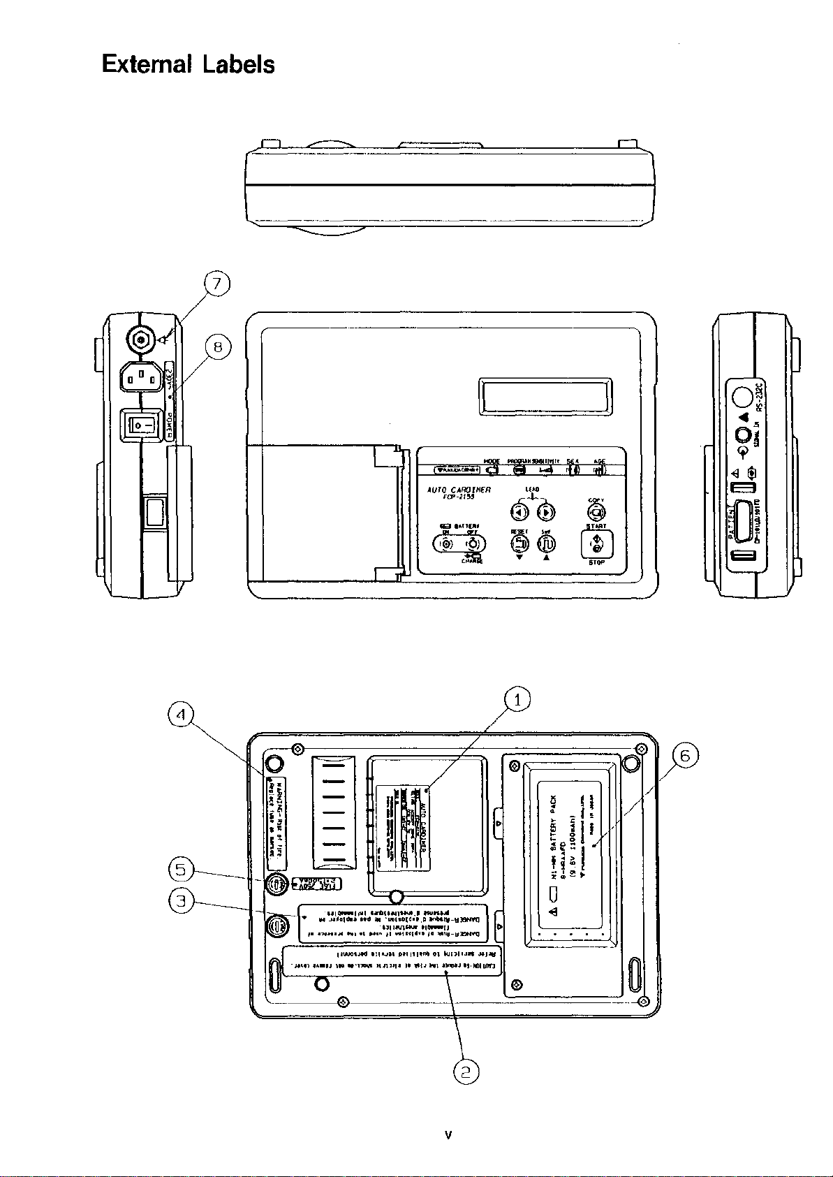
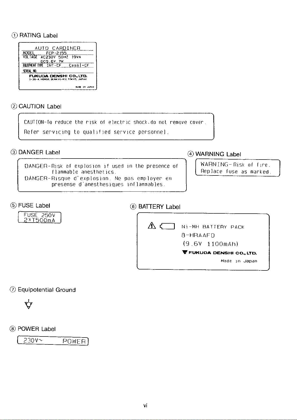
External Labels
-
7
-
,
[1 I]
L~
_cee.
Aura CAROINER
~ --''''''~.
0
'CP·2JS5
@I ...
w.o
-+-
@0
~
....
~:
(I~)
e»
C~
In
-,
RESE'
@@
""
,
..
...
'1iE
,t.)
'Iff)
@
CfJ
STOP
II
I
IIt~
I~
J
1
/
o
~
v
CD
RATING Label
AUTO CARDINER
MODEL FCP-2155
VOLTAGE AC230V 50HZ 19VA
EWIPI£NIIYIl:
SERIAlI(J.
o
CAUTION Label
OC9.6V 7W
INT-CF CassJ-CF
FUKUDA DENSHI
3-39-4. HONGO.IlU'lKYO-KU. TOKYO. JAPAN
CO~
cro.
CAUTION-To reduce the rIsk of electr'lC shock,do not remove cover.
Refer servICIng to qualIfIed serVIce personnel.
@
DANG ER Label
@
WARNING Label
~----------------------------------------------~
DANGER-Rlsk of explosion if used rn the presence of
flammable anesthetics.
DANGER-Rlsqued'explosion.
Ne
pas
employer' en
presense d'aneslhesIQues Inflammables.
WARNING-RISk ofrir
Replace fuse as marked.
e .
® FUSE Label
FUSE 250V
2xT500mA
(j)
Equipotential Ground
® POWER Label
230V'"
POWER)
® BATTERY Label
~ ~ Ni-MH BATTERY PACK
8-HRAAFO
(9.6V 1100mAh)
Y
FUKUDA DENSHI
Made1n Japan
CO~
LTD.
vi
CHAPTER
1
General Description
1. Outline '" 1-1
2. Specifications 1-1
3. Controls and Indicators 1-3
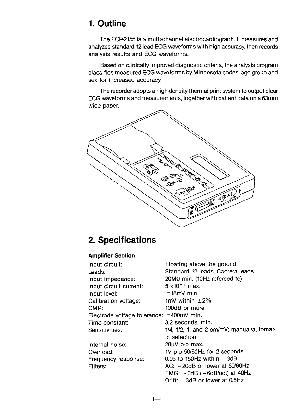
1. Outline
The FCP-2155is a multi-channel electrocardiograph. It measures and
analyzes standard 12-lead ECG waveforms with high accuracy, then records
analysis results and ECG waveforms.
Based on clinically improved diagnostic criteria, the analysis program
classifies measured ECG waveforms by Minnesota codes, age group and
sex for increased accuracy.
The recorder adopts a hlqh-density thermal print system to output clear
ECG waveforms and measurements, together with patient data on a 63mm
wide paper.
2. Specifications
Amplifier Section
Input circuit:
Leads:
Input impedance:
Input circuit current:
Input level:
Calibration voltage:
CMR:
Floating above the ground
Standard 12 leads, Cabrera leads
20MO min. (10Hz refereed to)
5 x10⁻⁸max.
±18mV min.
1mV within ±2%
100dB or more
Electrode voltage tolerance: ± 400mV min.
Time constant: 3.2 seconds. min.
Sensitivities: 1/4, 1/2, 1, and 2 cm/mV; manual/automat-
ic selection
20llV
p-p
max.
1V p-p 50/60Hz for 2 seconds
0.05 to 150Hz within - 3dB
AC: - 20dB or lower at 50/60Hz
EMG: -3dB (-6dB/oct) at 40Hz
Drift: -3dB or lower at 0.5Hz
Internal noise:
Overload:
Frequency response:
Filters:
1-1

A/D conversion:
Sampling speed:
Amplifier Section
13 bits
1ms
Recording system:
Paper speeds:
Recording density:
Chart paper:
Auxiliary Input Section
DC input:
Display Section
Display:
Types of characters:
General
Safety features:
Power requirements:
Dimensions:
Weight:
Thermal writing with thermal print head
25 and 50mm/sec within ±3%
8 dots/mm in amplitude direction
1msec in time axis direction
Roll paper 63mm wide x 30m long
Z-fold paper 63mm wide x 20m long,
75mm/fold
10mm/0.5V, unbalanced, input impedance
100kO min.
Liquid crystal, 40 characters (20 chars. x 2
lines), character configuration 5 x 7 dots
Alphanumerics and symbols
Class I and internally-powered equip-
ment, Type CF (IEC 601-1)
115V AC, 50/60Hz; 19VA
230V AC, 50/60Hz; 19VA
Ni-MH rechageable battery 9.6V DC, 7W
Continuous operation time: Approx. 70
minutes at 20°C
Charging time: Within 3 hours
260N) x 18.2(D) x 6.05(H) cm
2.0kg (including the battery)
Operating Environmental Conditions
Temperature: 10 to 40°C
Humidity: 30 to 85% R.H. (no dew condensing)
Atmospheric pressure: 70 to 106kPa (700 to 1060mbar)
Transportation/Storage Environmental Conditions
Temperature: -10 to +50°C
Humidity: 10 to 90% R.H. (no dew condensation)
Atmospheric pressure: 70 to 106kPa (700 to 1060mbar)
1-2
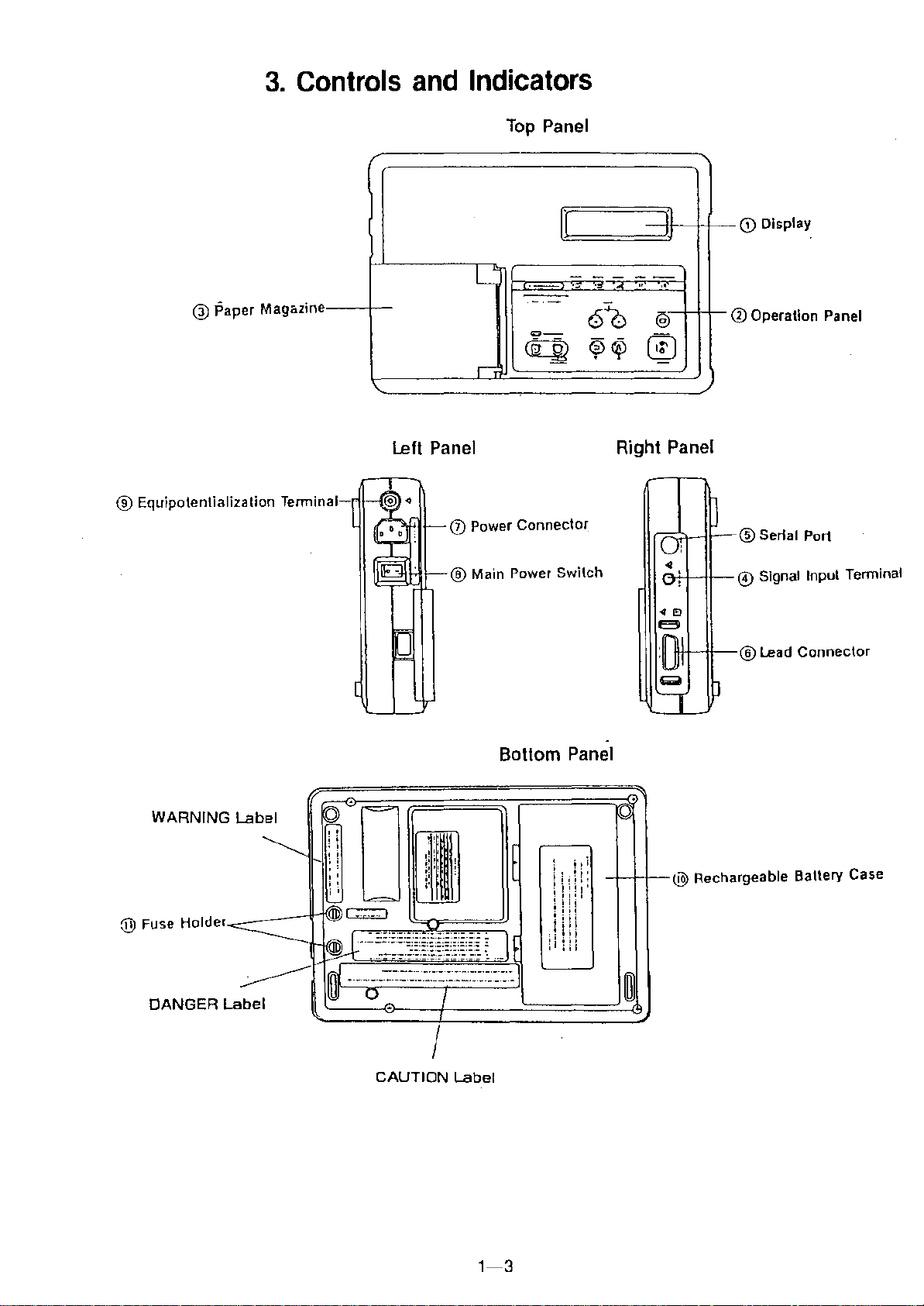
3. Controls and Indicators
Top Panel
@
Paper Magazine
® Equipotenlialization Terminal-
r
I
\..
Left Panel
L"
cgm
IT
(2)
Power Connector
co-
-.-
II
-
OJ
-
-
--
"
00
~~
Right Panel
-Ii
@j
@
-
~
<D
Display
o.
®Operation Panel
}
WARNING Label
I
CAUTION Label
Bottom Panel
It
-t--t-1r--
@
Rechargeable Battery Case
1-3
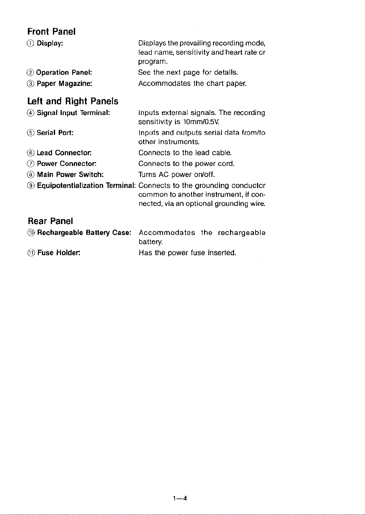
Front Panel
CD
Display:
@
Operation Panel:
@ Paper Magazine:
Left
and Right Panels
@)
Signal Input Terminal: Inputs external signals. The recording
® Serial Port:
® Lead Connector:
(J) Power Connector:
® Main Power Switch:
Displays the prevailing recording mode,
lead name, sensitivity and heart rate or
program.
See the next page for details.
Accommodates the chart paper.
sensitivity is 10mm/O.5V.
Inputs and outputs serial data from/to
other instruments.
Connects to the lead cable.
Connects to the power cord.
Turns AC power on/off.
® Equipotentialization Terminal: Connects to the grounding conductor
common to another instrument, if con-
nected, via an optional grounding wire.
Rear Panel
@)
Rechargeable Battery Case: Accommodates the rechargeable
battery.
@
Fuse Holder: Has the power fuse inserted.
1-4
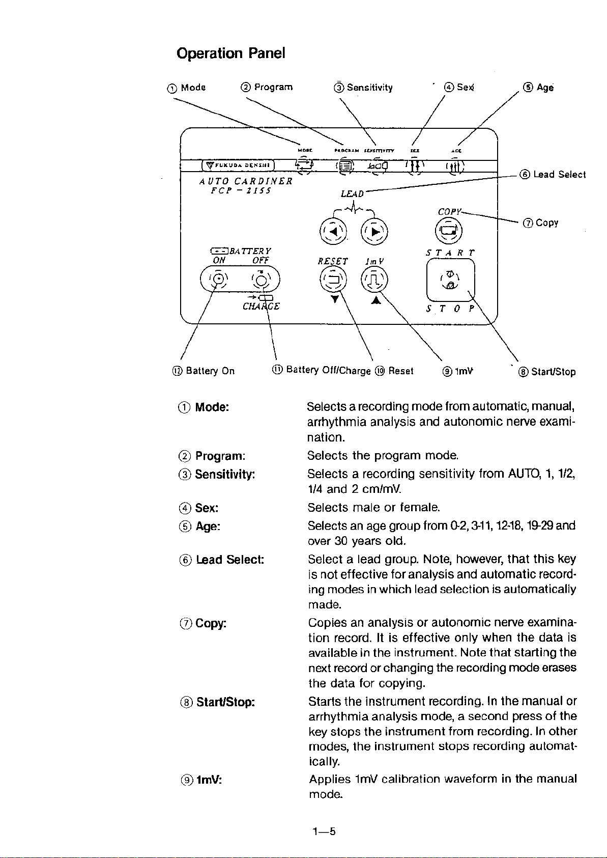
Operation Panel
CD
Mode
@ Program
(}) Sensitivity
. @Sex!
®Age
JtoIO.C
r.oc...... SClfsmvrTY
ILl
.Ct
VruKuDA D£"SIII
ern'
l:lCJ
......
-,'
® Lead Select
AUTO CARDINER
FCP -
2155
LEAD
.i:
®®
evCopy
.
'-
./
E3BATTERY
S TAR T
ON
OFF
RESET
1m V
( <P\
~
@
Battery On
CD
Mode:
@ Program:
@
Sensitivity:
@Sex:
®Age:
® Lead Select:
Ci)
Copy:
® Start/Stop:
@1mV:
@
Battery Off/Charge
@
Reset
@1mV
® Start/Stop
Selects a recording mode from automatic, manual,
arrhythmia analysis and autonomic nerve exami-
nation.
Selects the program mode.
Selects a recording sensitivity from AUTO, 1,
1/2,
1/4
and 2
cm/mV.
Selects male or female.
Selects an age group from 0-2,3-11,12-18,19-29and
over 30 years old.
Select a lead group. Note, however, that this key
is not effective for analysis and automatic record-
ing modes in which lead selection is automatically
made.
Copies an analysis or autonomic nerve examina-
tion record. It is effective only when the data is
available in the instrument. Note that starting the
next record or changing the recording mode erases
the data for copying.
Starts the instrument recording. In the manual or
arrhythmia analysis mode, a second press of the
key stops the instrument from recording. In other
modes, the instrument stops recording automat-
ically.
Applies 1mV calibration waveform in the manual
mode.
1-5

@ Reset: Keeps resetting the circuit while held down.
@ Battery Off/Charge: Turnsthe power off in battery operation. In AC oper-
ation, a press of the key places the instrument in
charge mode.
@ Battery On:
Turns the power on in battery operation. A press
of the key during battery charge cancels charge
mode and calls up the same initial display as upon
turning the AC power on.
1-6

CHAPTER
2
Circuit Description
1. Introduction 2-1
2. Floating Input Circuit 2-3
2.1 Buffer Amplifier 2-4
2.2 Middle Amplifier : 2-5
2.3 A/D Converter 2-6
2.4 Amplifier Control and Interface 2-7
3. Peripheral A/D Converter Circuit 2-S
4. Clock
5. Serial Port 2-9
6. Motor Control Circuit 2-10
7. Sensor Circuit 2-11
S. CPU·GA Circuit 2-11
9. LCD Control Circuit 2-12
10. Thermal Print Head Control Circuit. 2-12
11. Power Supply Circuit with Charging Circuit 2-13
11.1 Outline of the System 2-13
11.2 Rectifier/Smoothing and On/Off Control Circuits 2-13
&
Backup Memory 2-S
11.2.1 AC Operation 2-13
11.2.2 On/Off Control Circuit 2-13
11.2.3+5V and+5VA Generator 2-14
11.2.4 -5VA Generator 2-14
11.2.5+SV Generator 2-15
11.2.6+24V Generator 2-15
11.2.7 Isolated Power Circuit.. 2-16
11.2.S Charging Circuit 2-17

1. Introduction
The FCP-2155 is composed of the following circuits:
(1) Main Board PCB-6430
• Floating input circuit
• Motor control circuit
• Sensor circuit
• Reset circuit
• CPU circuit
• LCD control circuit
• Thermal print head control circuit
• Memory backup circuit
• Power supply ciruit
• Charging circuit
(2) Sensor Board PCB-6239
(3) AC Inlet Board PCB-6410
ECG signals input from the lead connector are amplified in the float-
ing input circuit. The amplified signals are converted into digital signals.
The digital signals are digitally filtered then transferred to the thermal print
head control circuit to be recorded on the chart paper.
The LCD screen displays the heart rate detected with a software
technic, lead-off status, if any, filter onloff status, etc.
The power supply circuit supplies power to circuits, while the charg-
ing circuit charges the Ni-MH battery. The charge status is displayed on
the LCD screen.
2-1
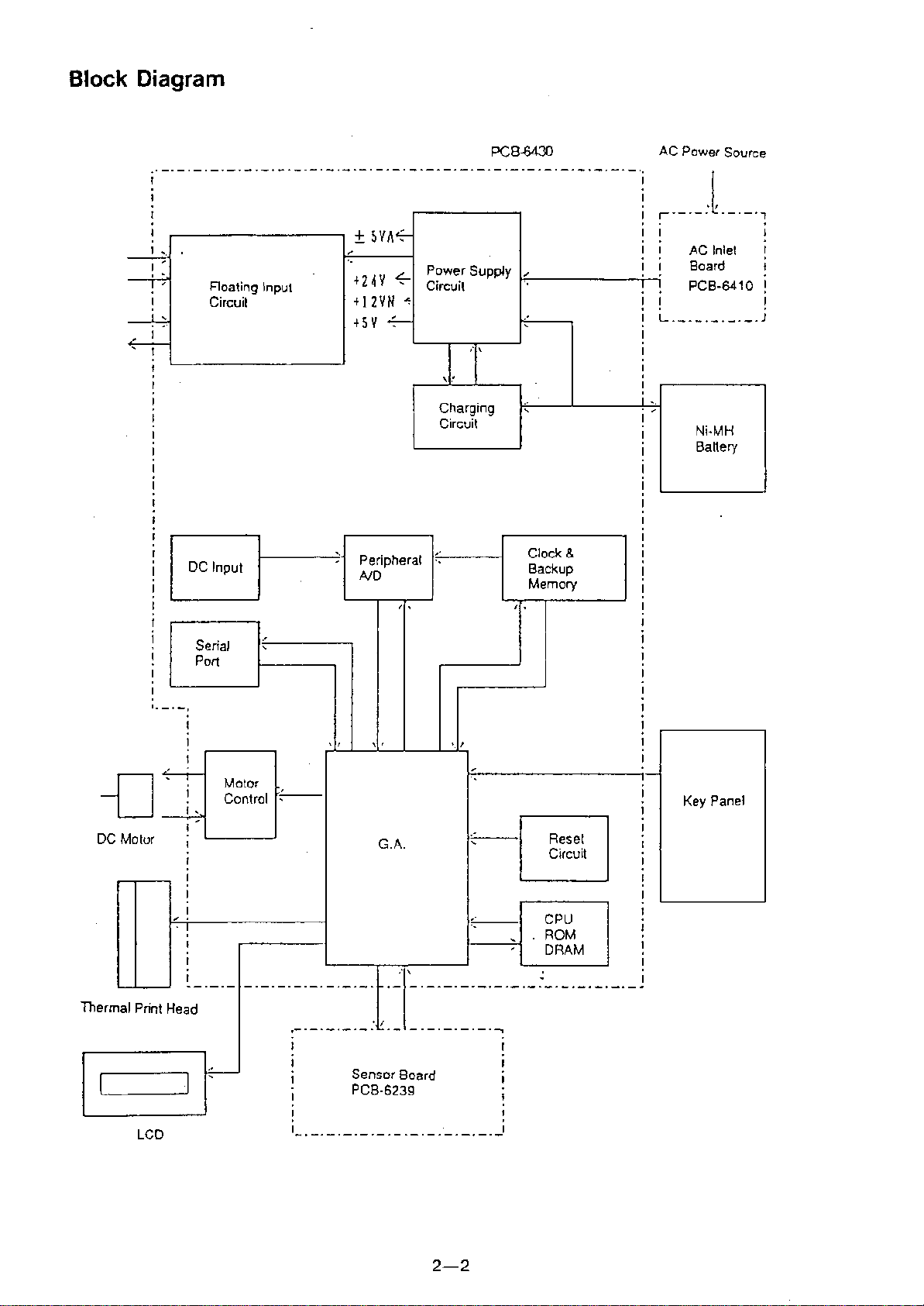
Block Diagram
PCB-M30
AC Power Source
.0 _~_. _.
o _. • _ • • _. _. • _ .. _ .. _. _ .. ',
,
,
. .
,
,
.
.
,
,
r=r=>;
-_-_-,
1
±
5VII';;-
,
1
I
1 '.
.-
I I
AC Inlel
,
--1-'
"
1
I
Board
1
--T'
+24V
~
Power Supply
.-
Floating Input
Circuit
! !
PCB-6410
I
,
Circuit
+12VN
~
,
I
,
--4
+5V
-7-
,
I
L,__________
J
-,
~
I
" I
J
T
,
,
,
,
,
,
,
Charging
.'
i-.
"
.
,
,
Circuit
I
, ,
Ni·MH
,
I
Battery
1
I
1
I
1
B
I
1
,
Peripheral
"
Clock
&
,
,
,
"
Backup
I
NO
I
I
Memory
,
f,
f,
I
I
Serial
.'
"
1
Port
1
1
'._0_,
1
1
I
-D
~
~
DC Motur
Thermal Print Head
. !
I
1
1
Motor
Control
\
.
'. I
I
,
,
Key Panel
1
I
,
,
,
I
I
,
,
I
Reset
Circuit
G.A.
.-
---
"
CPU
ROM
DRAM
:
\
• I
• __ o • .. ._o _
,_._-_._-_-
-_
-.-.-.-.-.~
• I
,
,
I
~
,
Sensor Board
,
PCB-6239
LCD
,
'_._-_._-_-_-_._._-_._-_-_
2-2
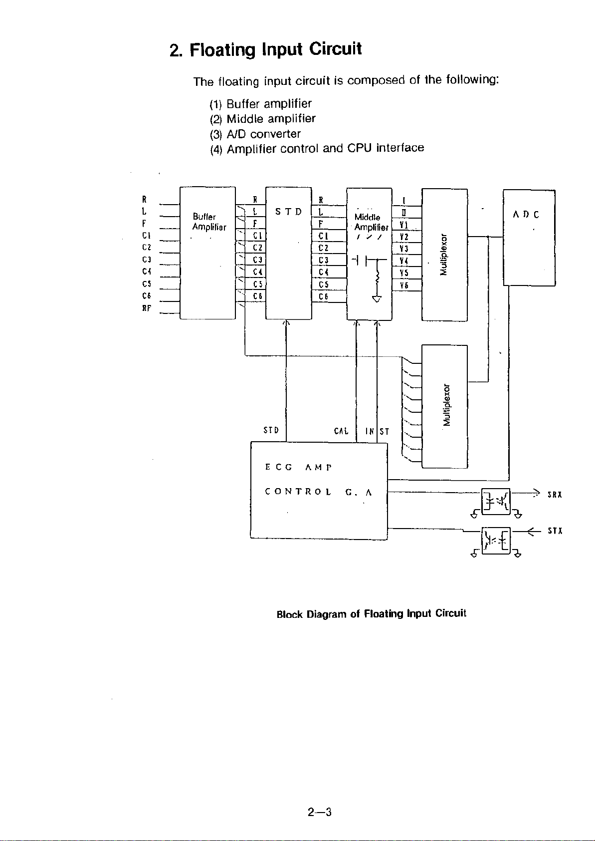
2. Floating Input Circuit
The floating input circuit is composed of the following:
(1)Buffer amplifier
(2)Middle amplifier
(3)AID converter
(4)Amplifier control and CPU interface
R
L
F
C1
C2
C3
C~
CS
C6
RF
-
-
-
-
-
Buller
Amplifier
-
-
-
-
-
R
I'
I'
,
<,
,
.,
<,
-;
i'
L
F
Cl
C2
C3
C(
CS
C6
S T 0
I
R
L
F
CI
C2
C3
C(
cs
C6
.. .
Middle
. Amplifier
I :.//
-IT
I •
I
IT
VI
Y2
V3
H
vs
V6
\
g.
"5
:::E
AOC
0
x
Q)
.
I'--
STD
E C G
AMP
CAL
IN
ST
'..__
'-
-,
......_
'.__
.'._
.'._
'._
'.__
'-
0
)(
Q)
g
"5
:::E
1-
CONTROL
Block Diagram of Floating Input Circuit
G.
A
[B]~
.fi
_,
\.
¢
---E-
SR
ST
x
2-3
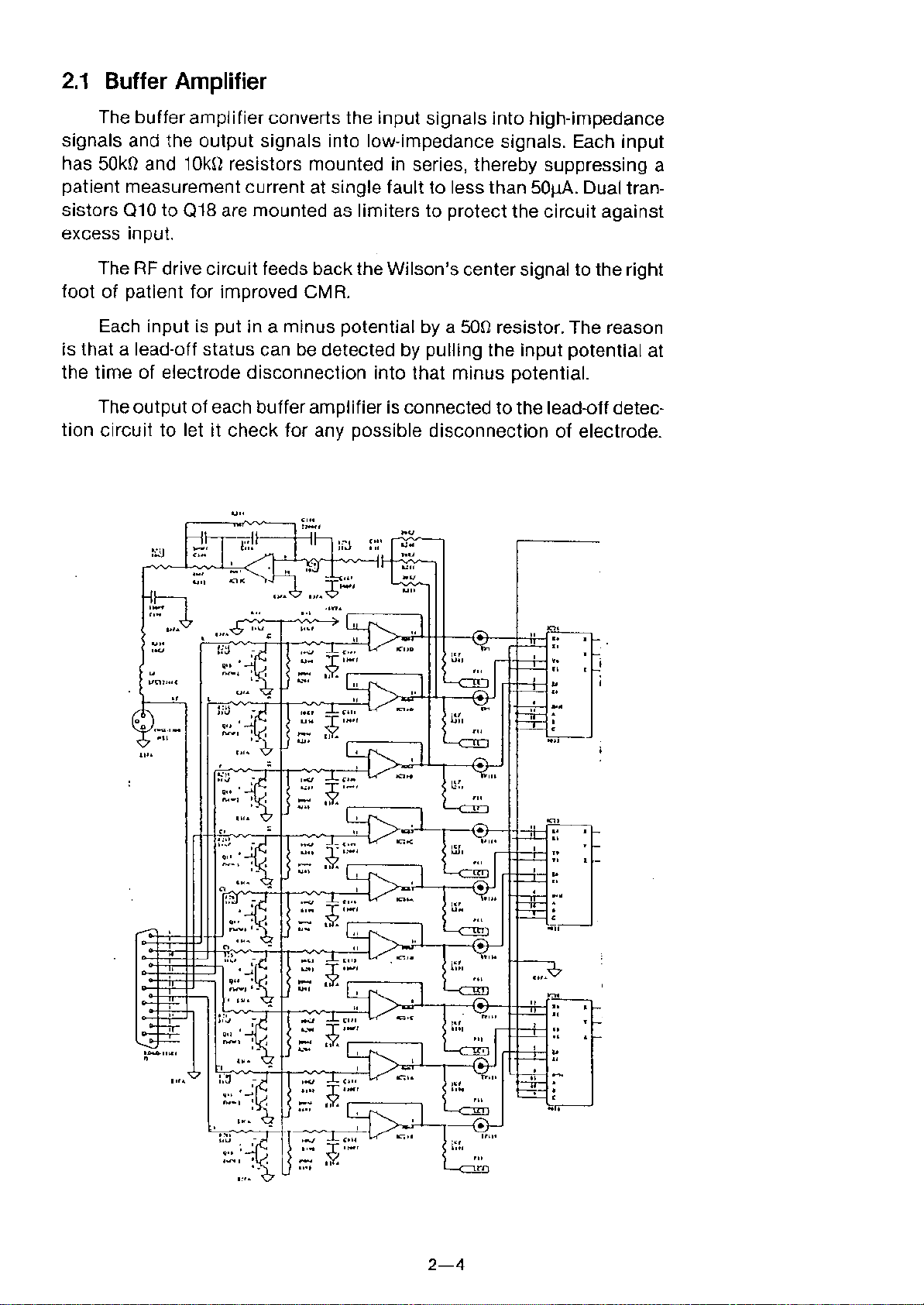
2.1 Buffer Amplifier
The buffer amplifier converts the input signals into high-impedance
signals and the output signals into low-impedance signals. Each input
has 50kO and 10kO resistors mounted in series, thereby suppressing a
patient measurement current at single fault to less than 50~. Dual tran-
sistors Q10 to Q18 are mounted as limiters to protect the circuit against
excess input.
The RF drive circuit feeds back the Wilson's center signal to the right
foot of patient for improved
eM
R.
Each input is put in a minus potential by a 500 resistor. The reason
is that a lead-off status can be detected by pulling the input potential at
the time of electrode disconnection into that minus potential.
The output of each buffer amplifier is connected to the lead-off detec-
tion circuit to let it check for any possible disconnection of electrode.
,h
CI ". __ ~
'U...
...
,.
,
....
(I,.
2-4
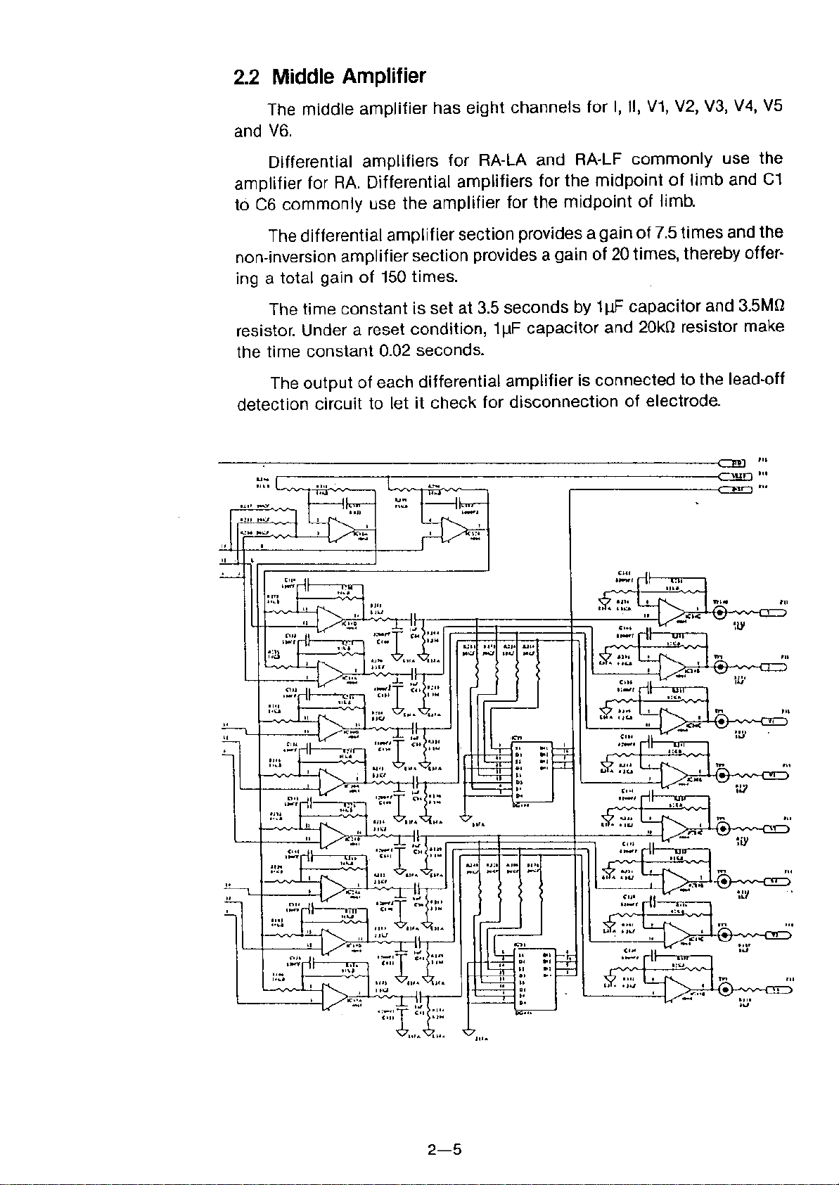
2.2 Middle Amplifier
The middle amplifier has eight channels for I, II, V1, V2, V3, V4, V5
and V6.
Differential amplifiers for RA-LA and RA-LF commonly use the
amplifier for RA. Differential amplifiers for the midpoint of limb and C1
to C6 commonly use the amplifier for the midpoint of limb.
The differential amplifier section provides a gain of 7.5 times and the
non-inversion amplifier section provides a gain of 20 times, thereby offer-
ing a total gain of 150 times.
The time constant is set at 3.5 seconds by 1Wcapacitor and 3.5MO
resistor. Under a reset condition, 1Wcapacitor and 20kO resistor make
the time constant 0.02 seconds.
The output of each differential amplifier is connected to the lead-off
detection circuit to let it check for disconnection of electrode.
,
..
l!U ,....T
..
&.:11 UI, C,I Uti
,...:1
-.J
u(./
t... "
IJU
.....
....
....
""
,.,.
2-5
2.3 AID Converter
The multiplexor (IC35, 36, 41) sequentially selects analog signals of
middle amplifier and lead-off detection to let the
them to digital signals. It takes 1211Sto convert signals of one channel.
.
~ ~ r~
'" KJ
'" D
.It
,.. U
...~.......-~~~~~".r'r'l'
'It ..
't'
l....!!...-
,"
I'
c___L
n
AJD
converter (lC39)convert
JY_,--"""
.u
II
'"'
OOC'I
I-';r-' --,
c-c' ~
t--"VV'-f
UI'
1'"
"',
t-l...
r:;:;
I~UH'
."
"
,<I
.,
..
..
,
u..
..
,
......
•
Signals are input in the
Lead for lead-off detection is switched every 1ms.
V1 to Lead Off V1 to Lead Off
1ms
,.,
"Q
AJD
converter in the following order.
C6
2-6
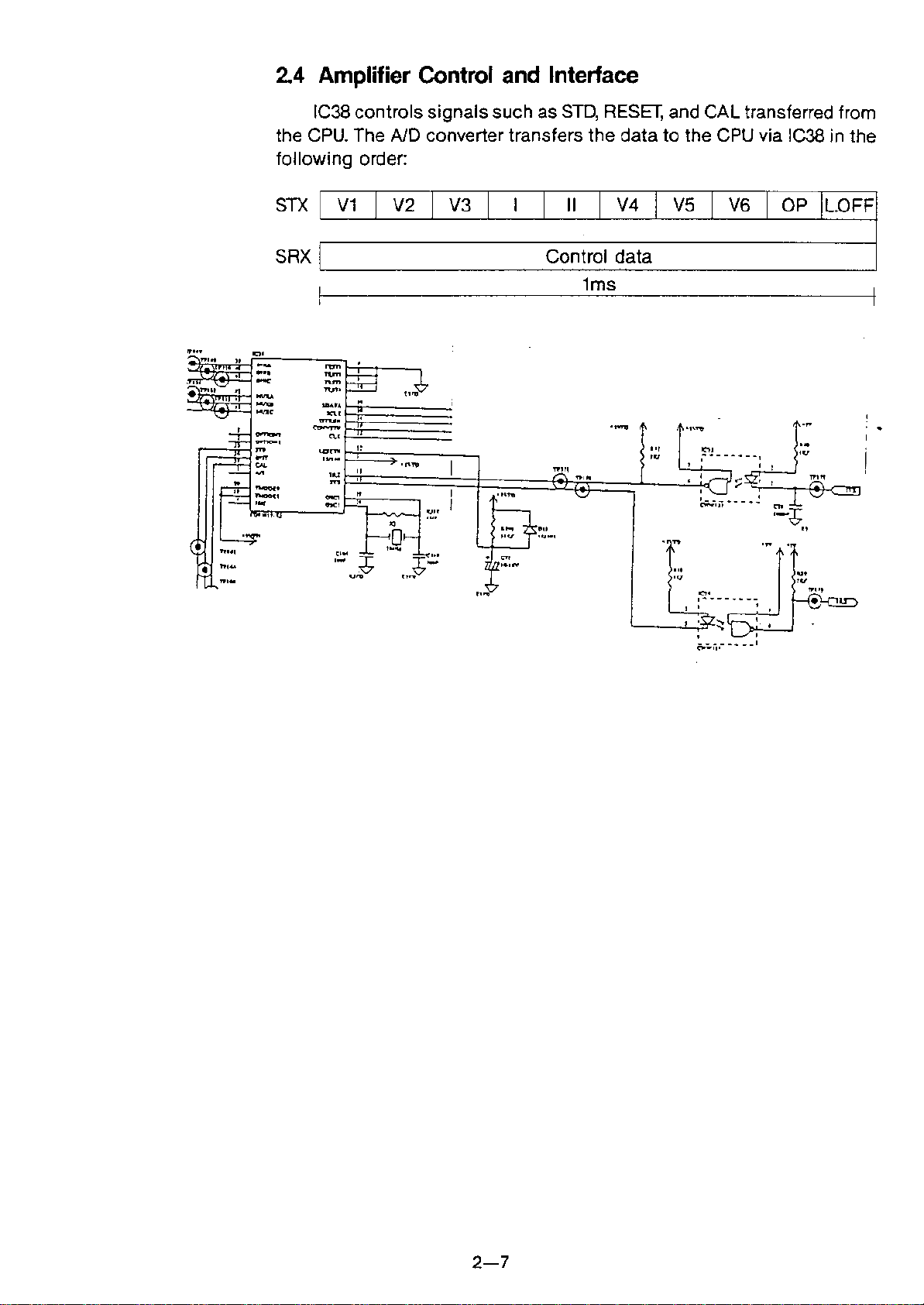
2.4 Amplifier Control and Interface
IC38 controls signals such as STD, RESET, and CAL transferred from
the CPU. The
AJD
converter transfers the data to the CPU via
1C38
in the
following order:
STXIV1
I
V2
I
V3
I
I
I " I
V4
I
V5
I
V6
I OP IL.OFF
SRX
I
L- ~ ~
Control data
1ms
"".
II:,.
.....
TUn
....
TUn
..
""
1Un
"
"".
""'"
...,..
......
"
_c
ont
.
,
o.;"ij,- - ... __
1
2-7
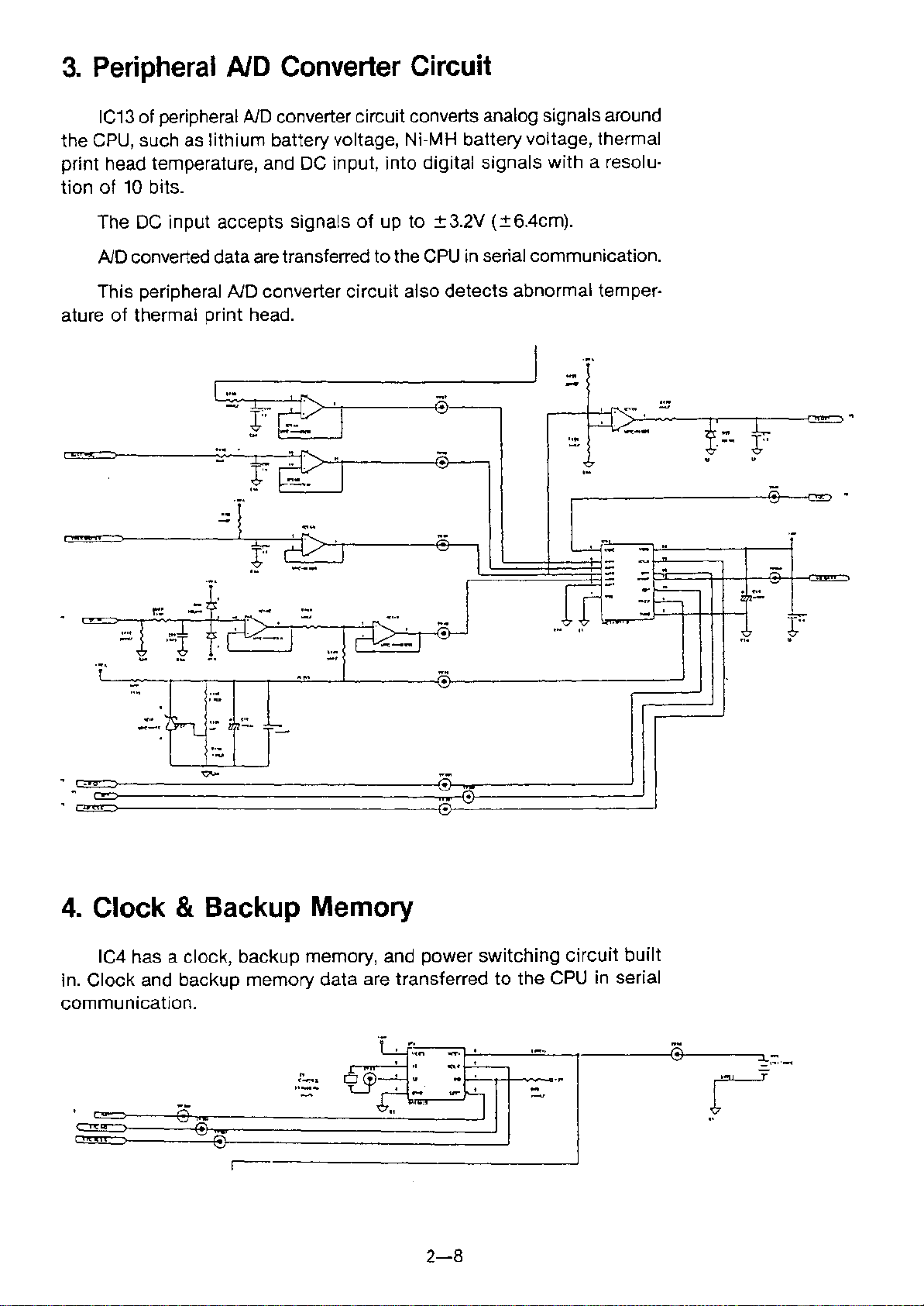
3. Peripheral AID Converter Circuit
IC13of peripheral AiD converter circuit converts analog signals around
the CPU, such as lithium battery voltage, Ni-MH battery voltage, thermal
print head temperature, and DC input, into digital signals with a resolu-
tion of 10 bits.
The DC input accepts signals of up to ±3.2V {±6.4cm}.
AiD converted data are transferred to the CPU in serial communication.
This peripheral AiD converter circuit also detects abnormal temper-
ature of thermal print head.
MW
,
T
::~
,,_
-
.•.
-
r..:
-
.~±
'M
..
[
-
La?
J/~
...
--
.
".
-
t~
.-
".
-
T
r-V
r
;tf ~ ._
~.-(--Q~.
_. _.
"W
....
-
."""_
"M
'~
---
'ou
T --
'M
'I
.
...
.
-
•...
&-~J
_.
e
-0--
;:;.
._,.
&-
""
•
-
~"-~
""
-
,'7
'M
co.
~-
,
I
.n~:
-
~
-
-
-
-
-
..
I-!-
...
--
_
"
.
.
*:~-
f.
U
Qfx::':"
~
...
;:;
v
;::0::
'-'
~"
u
.-
~
-
"~
~
::: i
,,_
....
..
--
=::...
"-
•
-;;.
Z
'-"
-_.
":r
.
-
~
~
4. Clock & Backup Memory
IC4 has a clock, backup memory, and power switching circuit built
in. Clock and backup memory data are transferred to the CPU in serial
communication.
.
',n
.
..
..
,
"
....
.,
..
('~I
,,_
..
~
,
2\
'-C./~
'..;;.It-=::
'-'
r--
-
......
.,"
-
-~
.
,
,
...
.M
-,
...
-
~
<:»
~.
r::
..
2-8

5. Serial Port
."
The serial controller is in the GA
RS232G level by IG5 and IG6.
The connector J1 can supply +5V power. But do not take an output
of over 500mA from the connector.
Caution: Take care of the serial port. It is not floating.
It
"X
,.
II
....
..
H"'"
novr
II
....
."
..
\U
(1GB)
and the data from it are made
..
It..
UD4T4
rJ
LJ'
•
IOU
II
II
...
'"'
.....
....
~
rJ
..
"
"
,
LJ'
IOU'
2-9
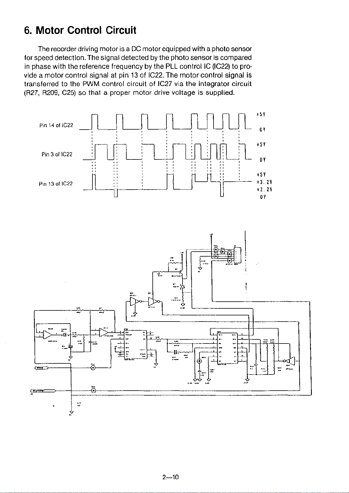
6. Motor Control Circuit
The recorder driving motor is a DC motor equipped with a photo sensor
for speed detection. The signal detected by the photo sensor is compared
in phase with the reference frequency by the PLL controllC (IC22) to pro-
vide a motor control signal at pin
transferred to the PWM control circuit of IC27 via the integrator circuit
(R27, R209, C25) so that a proper motor drive voltage is supplied.
13
of IC22. The motor control signal is
t5V
Pin 14 of IC22
Pin 3 01lC22
Pin 13 of IC22
..
I
t
I I I'
I I I I
..
I'
·
·
· .
·
.
.
.
JLU,~__,
...
,
..
-
...
~""
· .
·
·
· .
OV
.
tSV
1
.
.
ov
t5V
+3. 2V
t
2. 2V
OV
...
...
2-10
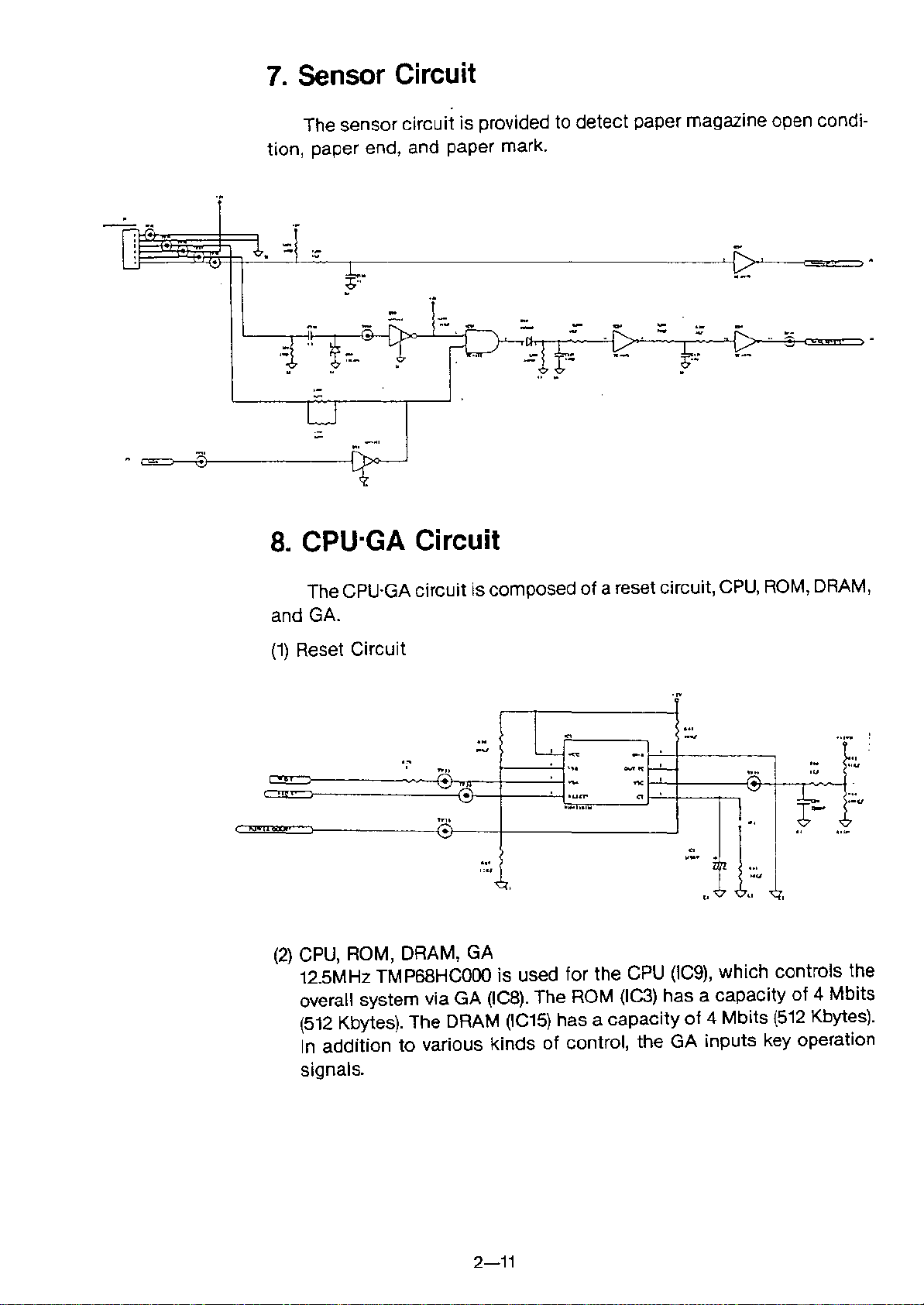
7. Sensor Circuit
The sensor circuit is provided to detect paper magazine open condi-
tion, paper end, and paper mark.
8. CPU·GA Circuit
The CPU·GA circuit is composed of a reset circuit, CPU, ROM, DRAM,
and GA.
(1) Reset Circuit
..
,
.~
,
....
•
....
.M
~v
Q
L~~
'n
-
,
'ucr
• ....h.U..
...
..,.'"
"'"
C1
•
...
I:..'
,
(2) CPU, ROM, DRAM, GA
12.5MHz TMP68HCOOOis used for the CPU (IC9), which controls the
overall system via GA (ICB).The ROM (IC3) has a capacity of 4 Mbits
(512 Kbytes). The DRAM (IC15) has a capacity of 4 Mbits (512 Kbytes).
In addition to various kinds of control, the GA inputs key operation
~
,
,
,-
_•• ~rz ..,
Z
0.:;./
I
0,
" 1
..'¢' :,'"
'Ct,
~
..
'M
'U
.1
,,7
1':'-
-
9
>:;
..
,
u
signals.
2-11

9. LCD Control Circuit
Since the LCD (NDM202AOO)has a controller built in, it is interfaced
directly with the CPU.
VO for contrast adjustment is set at a fixed voltage.
10. Thermal Print Head Control Circuit
The thermal print head control circuit is built in the GA (IC8) controls
the print head for recording waveforms and alphanumerics, as well as
controlling strobe and heating temperatures.
Data transfer
Waveform data are written in the register in the gate array every 1ms
then transferred to the thermal print head. Alphanumeric data are trans-
ferred to the thermal print head via the gate array.
Strobe control
The thermal print head heating degree is controlled by changing the
base temperature or the pulsewidth of strobe according to a chart speed.
Heat control
Previous dot heating information is stored in the heat control memory
and based on the information heating temperature is controlled to an
optimum printout condition.
Print head protection
An overheat of thermal print head or magazine open condition forcibly
shut off the +24V supply.
2-12
11. Power Supply Circuit with Charging Circuit
11.1Outline of the System
Using the AC power through the transformer or the OC power from
the NI-MH battery, the power supply circuit makes and supplies neces-
sary regulated powers. The power supply circuit involves a circuit to charge
the Ni-MH battery.
AC Power
OC Power
Transformer
l
Battery
I
Rectifier
ON/OFF
J--
-1
Chargingcircuit
Block Diagram of Power Supply Circuit
control
circuit
J-~
~
r-
+12V
Regulatedpowers
+8V
+5V
±5VA
±5VF, B
+24V
¢
rJ'J
:=::
:::J
u
'-
i:3
Q)
.~
o
-
Q)
Cl.
rJ'J
Q)
a:::
11.2 Rectifier/Smoothing and On/Off Control Circuits
11.2.1 AC Operation
The AC power transformed in voltage by the transformer is rectified
through 09, 011, 015, and 016 and smoothed by C1 and C2. These low
VF Schottky diodes 09, 011, 015, and 016 form a bridge circuit to reduce
lowering of the voltage and features less heat generation.
11.2.2 OnlOff Control Circuit
In battery operation, a press of the Battery ON key turns the FEr switch
025 on, thereby letting the current flow to 03 and the base of 03 be driven.
Thus, 05 is kept on and the power is supplied to the equipment if the Bat-
tery On key is detached.
The battery voltage is detected via 022. If it lowers to approximately
7.9V,the gate array generates a power-off signal to turn 021 on and can-
cel the bias voltage of 03, thereby turning 025 off. Since power supply
to the equipment stops at that time, the equipment is turned off.
Similarly, when the Battery Off key is pressed, the bias voltage of 03
is cancelled, thereby turning the equipment off. In AC operation, 021 is
on and the base of 03 cannot be driven, thereby making it impossible to
keep 024 in ON status and disabling battery operation.
2-13
V:'~
f'.-'
(510-1.1
r.
r--::-
11
I
I
<<X~~H.~~~A~lJ~~-----------------}_I--[-1-2-H~~
1"1
IISSXlL20
[12H ~lS 0
c)
117 ~
1
10K
T ~
lU ', 220~ AB
I\~.
0.51ci
[12H
r . R~
022
~c.
luness
200K;:V
UHS21?~f~zs; lY £l:m OlH
. (12H .
OlfS'A
~~K
~---+~--:l
r"'
O. lOt(
155102
01 ISSl01
~~~21l
~~S2J2
1111
1I1~
lOt(
t-t-t---t----if----f-J
[nH
UHS212
11.1
20K
.. 1147
lOt(
au
IISl
10K
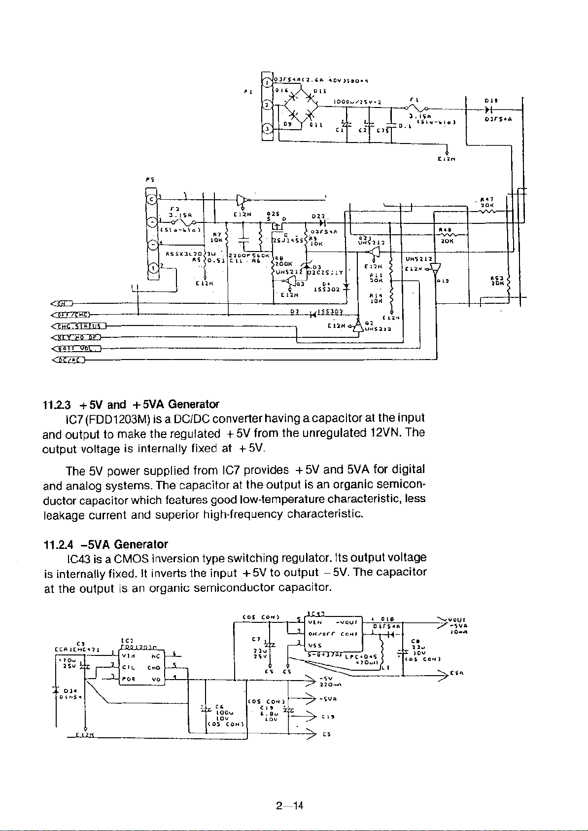
11.2.3 +5V and +5VA Generator
IC7(FDD1203M) is a DCIDC converter having a capacitor at the input
and output to make the regulated +5V from the unregulated 12VN. The
output voltage is internally fixed at +5V.
The 5V power supplied from le7 provides +5V and 5VA for digital
and analog systems. The capacitor at the output is an organic semicon-
ductor capacitor which features good low-temperature characteristic, less
leakage current and superior high-frequency characteristic.
11.2.4 -5VA Generator
IC43 is a CMOS inversion type switching regulator. Its output voltage
is internally fixed.
It
inverts the input +5V to output - 5V. The capacitor
at the output is an organic semiconductor capacitor.
(OS COH)
C7
llu
lSV
(S
t--:-:'~__"'
CI
12"
10V
(OS COH)
"""'..::;oVOU
-SVA
10_
I
laO"
"
10V
(OS 'OH)
2-14
 Loading...