

Fujitsu stn1nk60z Service manual

STN1NK60Z,
TO-92 (Ammopak)
SOT-223
D(2,4)
G(1)
S(3)
AM01476v1
STQ1NK60ZR
N-channel 600 V, 13 Ω typ., 0.3 A Zener-protected SuperMESH™
Power MOSFETs in SOT-223 and TO-92 packages
Datasheet - production data
Features
Order codes
4
3
2
1
STN1NK60Z
STQ1NK60ZR-AP 3 W
• 100% avalanche tested
V
DSRDS(on)maxID
600 V 15 Ω 0.3 A
• Extremely high dv/dt capability
• Gate charge minimized
• ESD improved capability
• Zener-protected
P
TOT
3.3 W
Figure 1. Internal schematic diagram
Applications
• Switching applications
Description
These devices are N-channel Zener-protected
Power MOSFETs developed using
STMicroelectronics' SuperMESH™ technology,
achieved through optimization of ST's well
established strip-based PowerMESH™ layout. In
addition to a significant reduction in onresistance, this device is designed to ensure a
high level of dv/dt capability for the most
demanding applications.
Table 1. Device summary
Order codes Marking Package Packaging
STN1NK60Z 1NK60Z SOT-223 Tape and reel
STQ1NK60ZR-AP 1NK60ZR TO-92 Ammopak
July 2014 DocID9509 Rev 14 1/18
This is information on a product in full production.
www.st.com

Contents STN1NK60Z, STQ1NK60ZR
Contents
1 Electrical ratings . . . . . . . . . . . . . . . . . . . . . . . . . . . . . . . . . . . . . . . . . . . . 3
2 Electrical characteristics . . . . . . . . . . . . . . . . . . . . . . . . . . . . . . . . . . . . . 4
2.1 Electrical characteristics (curves) . . . . . . . . . . . . . . . . . . . . . . . . . . . . . . . . 6
3 Test circuits . . . . . . . . . . . . . . . . . . . . . . . . . . . . . . . . . . . . . . . . . . . . . . 9
4 Package mechanical data . . . . . . . . . . . . . . . . . . . . . . . . . . . . . . . . . . . . 10
4.1 SOT-223, STN1NK60Z . . . . . . . . . . . . . . . . . . . . . . . . . . . . . . . . . . . . . . . .11
4.2 TO-92 ammopack, STQ1NK60ZR-AP . . . . . . . . . . . . . . . . . . . . . . . . . . . 13
5 Packaging mechanical data . . . . . . . . . . . . . . . . . . . . . . . . . . . . . . . . . . 15
6 Revision history . . . . . . . . . . . . . . . . . . . . . . . . . . . . . . . . . . . . . . . . . . . 17
2/18 DocID9509 R ev 14

STN1NK60Z, STQ1NK60ZR Electrical ratings
1 Electrical ratings
Table 2. Absolute maximum ratings
Symbol Parameter
I
V
V
DM
P
DS
GS
I
D
I
D
TOT
Drain-source voltag e 600 V
Gate-source voltage ± 30 V
Drain current (continuous) at TC = 25 °C 0.3 A
Drain current (continuous) at TC=100 °C 0.189 A
(1)
Drain current (pulsed) 1.2 A
Total dissipation at TC = 25 °C 3.3 3 W
Derating factor 0.026 0.024 W/°C
ESD
dv/dt
T
T
stg
1. Pulse width limited by safe operating area
2. ISD ≤ 0.3 A, di/dt ≤ 200 A/µs, VDD = 80%V
Human body model
C=100 pF, R=1.5 kΩ
(2)
Peak diode recovery volt ag e slo pe 4.5 V/ns
Operating junction temperature
J
Storage tem pera ture °C
Value
Unit
SOT-223 TO-92
800 V
°C
- 55 to 150
(BR)DSS
T a ble 3. Thermal resistance
Value
Symbol Parameter
SOT-223 TO-92
R
thj-amb
R
thj-lead
1. When mounted on 1 inch² FR-4 board, 2 Oz Cu, t < 30 s.
Thermal resistance junction-ambient max 38
Thermal resistance junction-lead max 40 °C/W
T able 4. Avalanche data
(1)
120 °C/W
Symbol Parameter Value Unit
I
AR
E
AS
Avalanche current, repetitive or not repetitive
(pulse width limited by T
j max
)
Single pulse avalanche energy
(starting T
= 25 °C, ID = IAR, V
J
DD
= 50 V)
0.3 A
60 mJ
Unit
DocID9509 Rev 14 3/18
18

Electrical characteristics STN1NK60Z, STQ1NK60ZR
2 Electrical characteristics
(T
= 25 °C unless otherwise specified)
CASE
Table 5. On/off states
Symbol Parameter Test conditions Min. Typ. Max. Unit
V
(BR)DSS
I
DSS
I
GSS
V
GS(th)
R
DS(on)
Drain-source breakdown
voltage
Zero gate voltage drain
current
Gate body leakage current
Gate threshold volta ge
Static drain-source
on- resistance
VGS= 0, ID = 1 mA
= 0, V
V
GS
V
= 0, V
GS
T
= 125 °C
C
= 0, V
V
DS
= VGS, ID = 50 µA
V
DS
V
= 10 V , ID = 0.4 A
GS
=600 V
DS
=600 V,
DS
= ± 20 V
GS
600 V
1µA
50 µA
±
10 µA
3 3.75 4.5 V
13 15 Ω
Table 6. Dynamic
Symbol Parameter Test conditions Min. Typ. Max. Unit
C
oss eq
(1)
g
fs
C
C
C
Forward transconductance
Input capacitance
iss
Output capacitance - 17.6 pF
oss
Reverse transfer
rss
capacitance
Equivalent output
(2)
.
capacitance
=15 V, ID = 0.4 A
V
DS
V
= 0, V
GS
DS
f=1 MHz
VGS= 0, V
DS
= 25 V,
= 0 to 480 V
-0.5 S
-94 pF
-2.8 pF
-11 pF
Q
Q
Q
1. Pulsed: pulse duration=300µs, duty cycle 1.5%
2. C
increases from 0 to 80% V
Total gate charge
g
Gate-source charge - 1 nC
gs
Gate-drain charge - 2.7 nC
gd
is defined as a constant equivalent capacitance giving the same charging time as C
oss eq.
DSS
=480 V, ID = 0.8 A
V
DD
=10 V
V
GS
(see Figure 19)
4/18 DocID9509 R ev 14
-4.96.9nC
when VDS
oss

STN1NK60Z, STQ1NK60ZR Electrical characteristics
Table 7. Switching times
Symbol Parameter Test conditions Min. Typ. Max. Unit
t
d(on)
t
d(off)
Turn-on delay time
V
= 300 V, ID = 0.4 A,
t
Rise time - 5 - ns
r
Turn-of f del ay time - 13 - ns
t
Fall time - 28 - ns
f
DD
= 4.7 Ω, V
R
G
(see Figure 18)
GS
= 10 V
-5.5-ns
T a ble 8. Source drain diode
Symbol Parameter Test conditions Min. Typ. Max. Unit
I
SD
I
SDM
V
SD
t
Q
I
RRM
t
Q
I
RRM
1. Pulse width limited by safe operating area.
2. Pulsed: pulse duration=300µs, duty cycle 1.5%
Source-drain current - 0.8 A
(1)
Source-drain current (pulsed) - 2.4 A
(2)
Forward on voltage
Reverse recovery time
rr
Reverse recovery charge - 216 nC
rr
Reverse recovery current - 3.2 A
Reverse recovery time
rr
Reverse recovery charge - 224 nC
rr
Reverse recovery current - 3.2 A
=0, I
V
I
GS
SD
= 0.8 A,
SD
= 0.8 A
di/dt = 100 A/µs,
= 20 V
V
DD
I
= 0.8 A,
SD
di/dt = 100 A/µs,
= 20V, Tj = 150 °C
V
DD
-1.6V
- 135 ns
- 140 ns
Table 9. Gate-source Zener diode
Symbol Parameter Test conditions Min Typ. Max. Unit
V
(BR)GSO
Gate-source breakdown voltage IGS = ± 1mA, ID=0 30 - - V
The built-in back-to-back Zener diodes have specifically been designed to enhance the
device's ESD capability. In this respect the Zener voltage is appropriate to achieve an
efficient and cost-effective intervention to protect the device's integrity. These integrated
Zener diodes thus avoid the usage of external components.
DocID9509 Rev 14 5/18
18
Electrical characteristics STN1NK60Z, STQ1NK60ZR
10
-3
10
-2
10
-1
10
0
10
1
t
p
(s)
10
-2
10
-1
K
0.2
0.05
0.02
0.01
0.1
Zthj-pcb=K*Rthj-pcb,
Rthj-pcb=62.5°C/W
Single pulse
δ=0.5
10
2
t < 30s
SOT-223
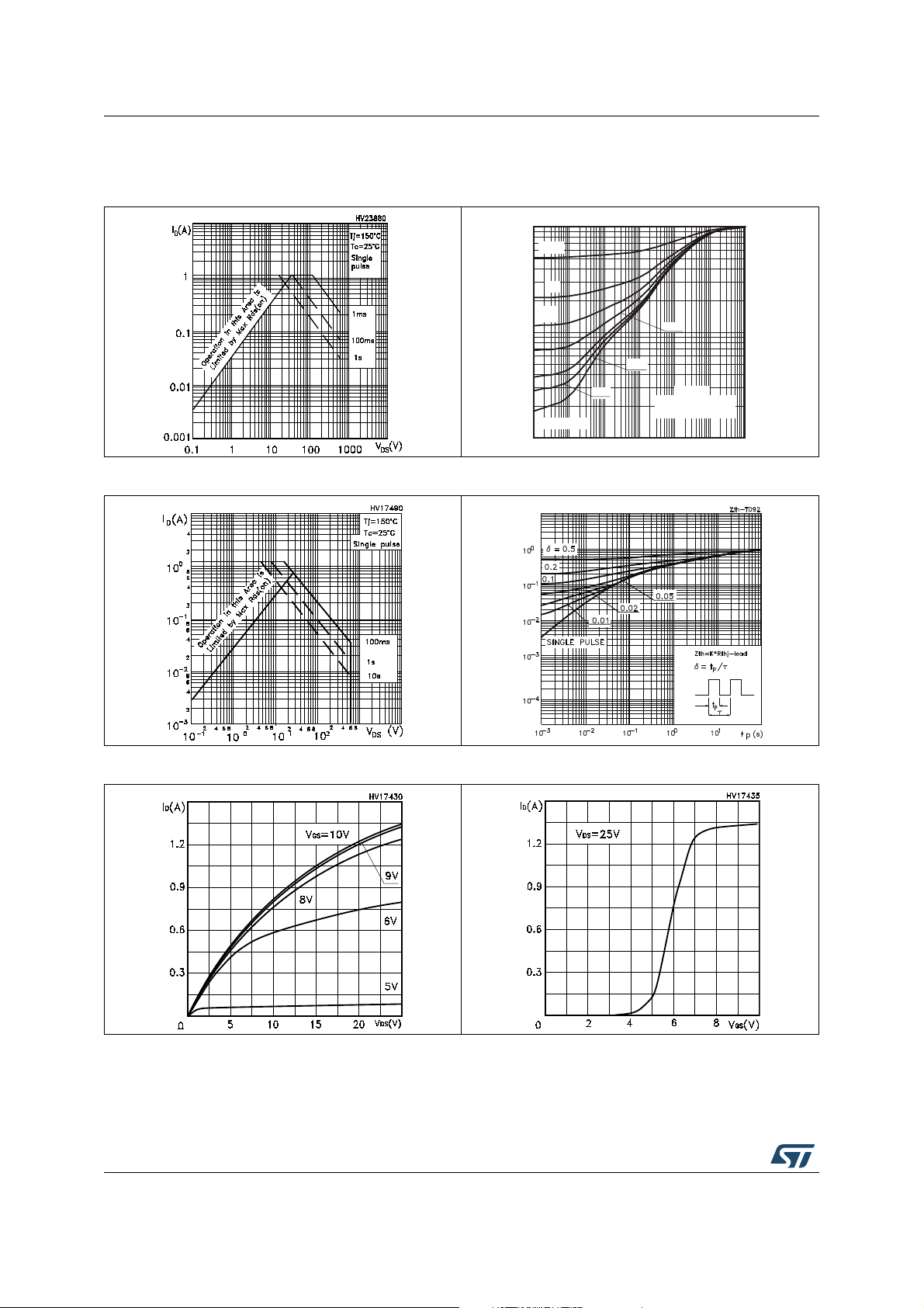
2.1 Electrical characteristics (curves)
Figure 2. Safe operating area for SOT-223 Figure 3. Thermal impedance for SOT-223
Figure 4. Safe operating area for TO-92 Figure 5. Thermal impedance for TO-92
6/18 DocID9509 R ev 14
Figure 6. Output characteristics Figure 7. Transfer characteristics
 Loading...