

Page 1

FUJITSU SEMICONDUCTOR
SUPPORT SYSTEM
SS01-26006-2E
F2MC-8FX Family
MCU BOARD for MB95FV100-103
MB2146-303
OPERATION MANUAL
Page 2

PREFACE
Thank you for purchasing the MCU board for F2MC*-8FX family MB95FV100-103 (model number: MB2146-303).
The MB2146-303 is a development support tool for developing and evaluating applied products
based on the F
This manual is intended for engineers who use the MB2146-303 (referred to below as the MCU
board) to develop applied products based on Fujitsu's F
ual explains how to handle the MCU board and its functions as well as the setting procedures. Be
sure to read this manual before using the MCU board.
2
* : F
MC is the abbreviation used for FUJITSU Flexible Microcontroller.
■ Using the product safely
This manual contains important information required for using the MB2146-303 safely. Be sure to
read through the manual before using the product and follow the instructions contained therein to use
it correctly.
In particular, carefully read “Caution of the products described in this document” at the beginning
of this manual to understand the requirements for safe use of the product before using it.
After reading the manual, keep it handy for future reference.
■ Warranty and liability disclaimers
The specifications of the product are subject to change without notice.
In no event shall Fujitsu be liable for any loss or damages whatsoever directly or indirectly arising
out of the use of the product.
2
MC-8FX family of microcontrollers manufactured by Fujitsu.
2
MC-8FX family microcontrollers. The man-
■ Product operating environment
Use the product at an operating temperature between 5 °C and 35 °C and at an operating humidity
between 20% to 80%. Avoid using it in a hot or humid environment and prevent condensation.
The product is a frameless PC board unit with all electronic components exposed. Therefore, neither
put anything on the product nor touch or let an electrically charged material contact a metal part of
it. Once the product has been powered, try to keep those objects away from it which can short-circuit
it or easily catch fire and burn. Use the product as horizontal as possible and avoid operating it at a
place exposed to strong vibration, dust, or explosive gas.
Note that using the product not in the above operating environment may unexpectedly cause personal
injury to the user (or another person if present near the product) or physical damage to properties
around the product.
You should also keep the packaging materials used for shipping the product. They work well as they
are when you transport the product again, for example, if it becomes out of order and needs to be
repaired.
■ Related manuals
Refer to the following manuals as well:
• Hardware Manual of the MCU used
• Data Sheet of the MCU used
• “MB2146-09 BGM Adapter Instruction Manual”
• Related “Header Board Instruction Manuals”
• “S
OFTUNE Workbench Operation Manual”
• “S
OFTUNE Workbench USER’S Manual”
i
i
Page 3
■ Caution of the products described in this document
The following precautions apply to the product described in this manual.
Indicates a potentially hazardous situation which, if not avoided appropriately, may
CAUTION
Cuts, Damage
Cuts
result in minor or moderate injury and/or damage to the product or the equipment
to which the product is connected, to software resources such as data, or to other
properties.
Before moving the product, be sure to turn off all the power supplies and unplug the
cables. Watch your steps when carrying the product. Do not use the product at an
unstable location such as a place exposed to strong vibration or a sloping surface.
Doing so may let the product fall, resulting in an injury or fault.
The product has some sharp-pointed or edged parts inevitably exposed, such as
jumper plugs. Use meticulous care in handling the product not to get injured with
such pointed parts.
Damage
Damage
Damage
Damage
Damage
Damage
Neither put anything on or apply shock to the product. Once the product has been
powered, do not carry it. Doing either may cause a fault due to a load or shock.
Since the product contains many electronic components, keep it away from direct
sunlight, high temperature, and high humidity to prevent condensation. Do not use
or store the product where it is exposed to much dust or a strong magnetic or electric field for an extended period of time.
An adverse operating or storage environment can cause a fault.
Use the product within the ranges of its general specifications.
Operating it outside the range of any general specification may cause a fault.
To prevent electrostatic breakdown, do not let your finger or an object touch any
metal part of the connector. Before handling the product, touch a metal object (such
as a door knob) to discharge static electricity from your body.
When turning the power on or off, follow the relevant procedure described in this
document. Before turning the power on, in particular, be sure to finish making all the
required connections. To set up and use the product, follow the instructions given
in this document.
Using the product incorrectly or inappropriately may cause a fault.
Before plugging or unplugging any cable for this product, be sure to turn the power
supply off. When unplugging the cable, remove it while holding the connector without pulling the cable itself. Pulling the cable itself or bending it may expose or disconnect the cable core, resulting in a fault.
Damage
When stored, the product should be kept in its packaging box as it has no housing.
Re-transporting the product may damage it to cause a fault. Keep the packaging
materials used for shipment of the product and use them when re-transporting it.
ii
ii
Page 4

• The contents of this document are subject to change without notice.
Customers are advised to consult with FUJITSU sales representatives before ordering.
• The information, such as descriptions of function and application circuit examples, in this document are presented solely for the purpose of reference to show examples of operations and uses of FUJITSU semiconductor device; FUJITSU
does not warrant proper operation of the device with respect to use based on such information. When you develop
equipment incorporating the device based on such information, you must assume any responsibility arising out of such
use of the information. FUJITSU assumes no liability for any damages whatsoever arising out of the use of the information.
• Any information in this document, including descriptions of function and schematic diagrams, shall not be construed
as license of the use or exercise of any intellectual property right, such as patent right or copyright, or any other right
of FUJITSU or any third party or does FUJITSU warrant non-infringement of any third-party’s intellectual property
right or other right by using such information. FUJITSU assumes no liability for any infringement of the intellectual
property rights or other rights of third parties which would result from the use of information contained herein.
• The products described in this document are designed, developed and manufactured as contemplated for general use,
including without limitation, ordinary industrial use, general office use, personal use, and household use, but are not
designed, developed and manufactured as contemplated (1) for use accompanying fatal risks or dangers that, unless
extremely high safety is secured, could have a serious effect to the public, and could lead directly to death, personal
injury, severe physical damage or other loss (i.e., nuclear reaction control in nuclear facility, aircraft flight control, air
traffic control, mass transport control, medical life support system, missile launch control in weapon system), or (2)
for use requiring extremely high reliability (i.e., submersible repeater and artificial satellite).
Please note that FUJITSU will not be liable against you and/or any third party for any claims or damages arising in
connection with above-mentioned uses of the products.
• Any semiconductor devices have an inherent chance of failure. You must protect against injury, damage or loss from
such failures by incorporating safety design measures into your facility and equipment such as redundancy, fire protection, and prevention of over-current levels and other abnormal operating conditions.
• If any products described in this document represent goods or technologies subject to certain restrictions on export under the Foreign Exchange and Foreign Trade Law of Japan, the prior authorization by Japanese government will be
required for export of those products from Japan.
Copyright ©2004-2006 FUJITSU LIMITED All rights reserved
iii
Page 5
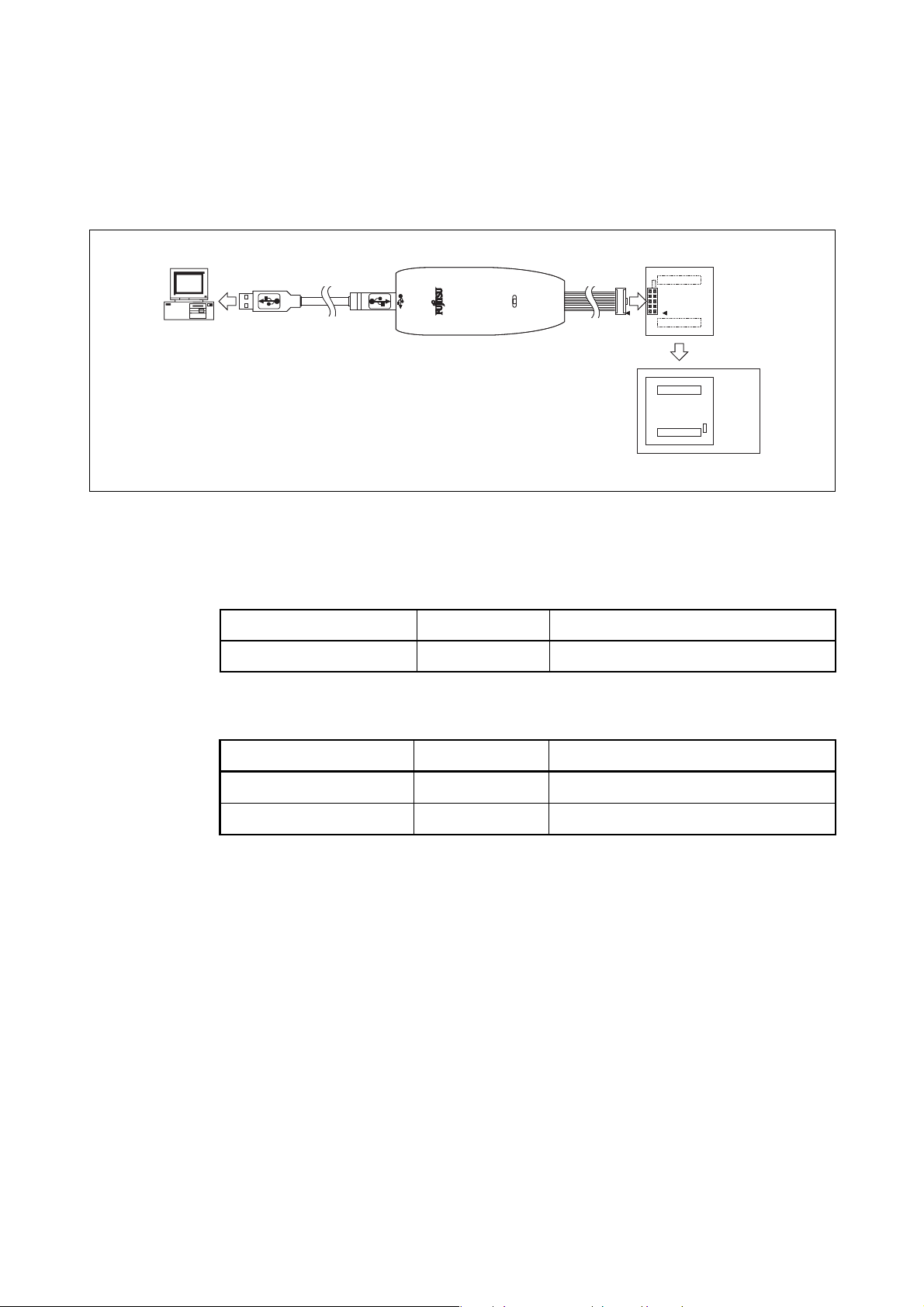
1. Product Outline
MB2146-303 is the MCU board (model number : MB2146-303) mounting an evaluation MCU in
2
MC-8FX Family of Fujitsu 8-bit microcontrollers. To build an F2MC-8FX evaluation environ-
the F
ment, combine three products : the header board, MCU board, and BGM adapter (model number :
MB2146-09) as shown in Figure 1.
■ Product configuration
Tables 1, and Table 2. list the product configuration in the MCU board package and options.
MCU board
MB2146-09
BGM adapter
Header board
Figure 1 System configuration
Table 1 Product configuration
Name Part number Description
2
F
MC-8FX MCU board *
MB2146-303 MCU board with built-in MB95FV100-103
* : Neither the oscillator nor the capacitor is bundled with this product. Therefore, preparately.
Table 2 option (sold separately)
Name Part number Description
BGM adapter *
Header board *
1
2
MB2146-09
ICE unit for F
MB2146-2xx Connector/package conversion header board
2
MC-8FX
*1 : To use the BGM adapter, you need additional tools such as debugger software.
*2 : The header board is an interface board to connect the emulator to your user system. Choose
and purchase a type of header board which is applicable to the production MCU to be used.
1
Page 6
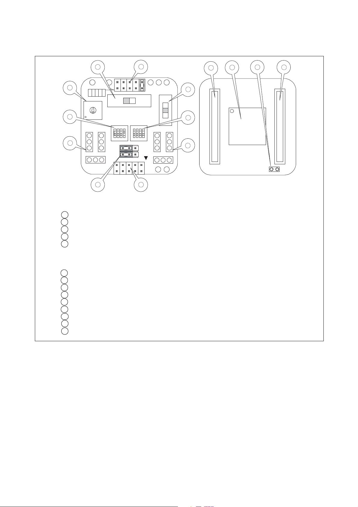
■ Appearance and part name
The appearance of a MCU board and the name of each part are shown in Figure 2.
1
APB8CX0X1X0A
1
2
C B A
X1A
3V5V
LVD2OFFLVD1
MAIN CLOCK
11
13
14
4
6
8
HEADER I/F CONNECTOR A
HEADER I/F CONNECTOR B
3
5
7
LVD4
8
7
6
5
4
3
2
1
PRODUCT SELECT
GND
LVD3
9
0
2
A
F
VCC
LVD1
LVD2
B
C
D
E
ADAPTER
LVD0
CLK
CLK S.V.
ON ON
1 2 3 4 1 2 3 4
SUB CLOCK
BGM
9 10
To p vi ew
Bottom view
1 LVD2 detection voltage selector jumper plug (it is not available, when debugging)
2 Voltage selector switch
3 Product selector switch
4 LVD selector switch
5 Clock selector switch (SW1-1: CLK)
APB8 bus output selector switch (SW1-3: APB8) (for extension) (it is not available,
when debugging)
C-pin selector switch (SW1-4: C)
6 Clock input selector switch (SW2-1: X0, SW2-2: X1, SW2-3: X0A, SW2-4: X1A)
7 Sub clock crystal oscillator mounting socket
8 Main clock crystal oscillator mounting socket
9 Sub clock selector jumper plug
10 BGM adapter connector
11 Header board I/F connector A
12 Header board I/F connector B
13 Evaluation MCU (MB95FV100-103)
14 Incorrect insertion prevention guard
12
Figure 2 MCU board appearance figure
2. Checking the Delivered Product
Before using the MCU board,confirm that the following components are included in the box:
• MCU board : 1
• Operation manual (English version, this manual) : 1
• Operation manual (Japanese version) : 1
2
Page 7
3. Procedure for connecting the user system
■ Connecting the MCU board to the header board
Align the MCU board and the header board facing each other, then plug their mating connectors together. The connectors are provided with incorrect insertion prevention guards located diagonally.
Position the two boards correctly without letting the incorrect insertion prevention guards interfere
with each other and plug the connectors together completely (see “Figure 3”).
Incorrect insertion
prevention guard
MCU board
Header board
Figure 3 Connection of MCU board and header board
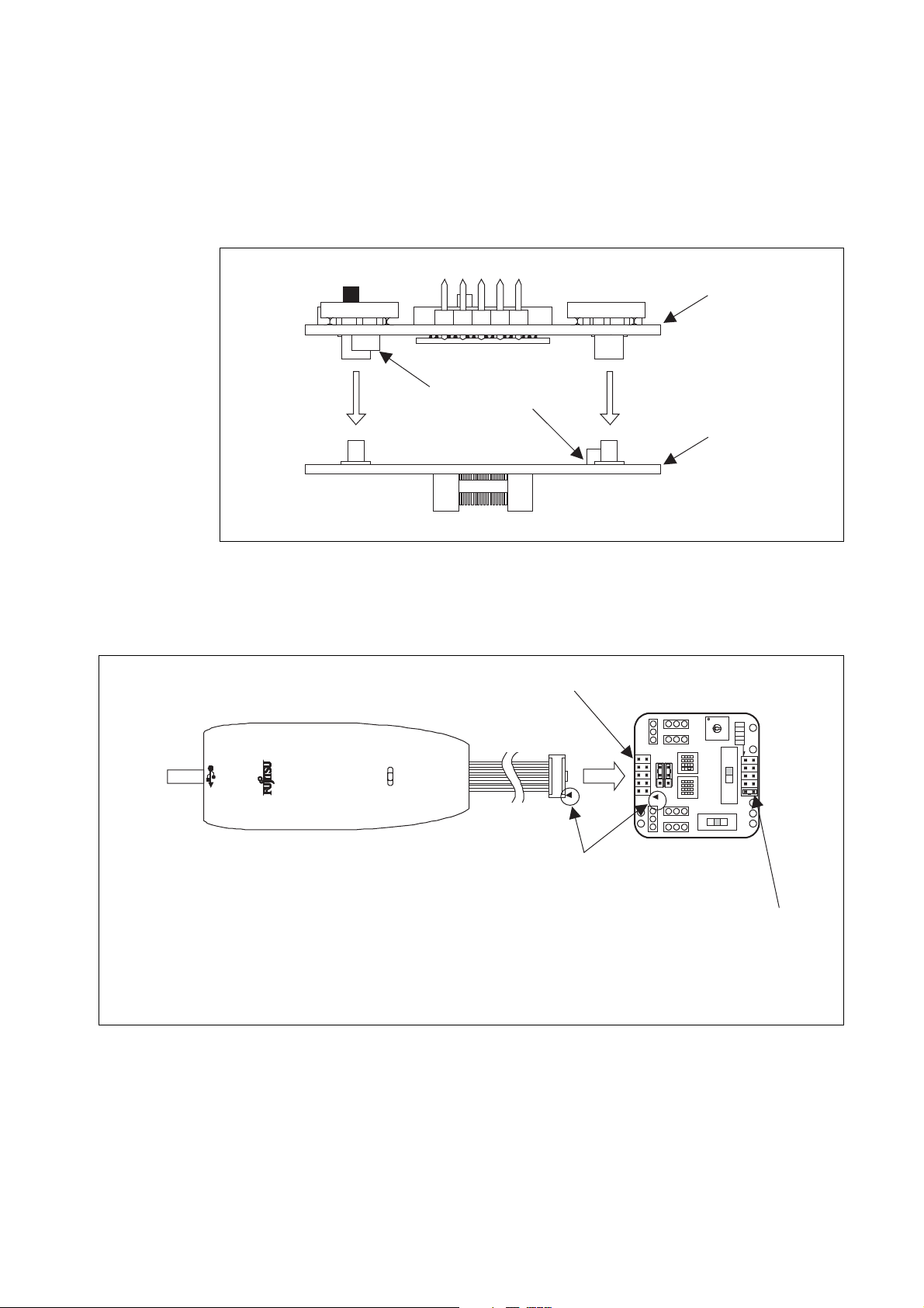
■ Connecting the MCU board to the BGM adapter
Connect the BGM adapter to the MCU board. Plug the BGM adapter's interface connector deep into
the BGM adapter connector on the MCU board with their index marks (▼) aligned (see “Figure 4”).
BGM adapter connector (CN3)
BGM adapter
M2146-09
* : Be sure to connect the BGM adapter correctly to the BGM adapter connector (CN3) on the MCU
board. Connecting it to the LVD2 detection voltage jumper plug (S2) by mistake can damage the
MCU board
PRODUCT SELECT
5
4
3
6
2
7
LVD4
1
8
0
9
LVD3
GND VCC
F
A
E
B
LVD2
D
1 2 3 4 1 2 3 4
C
LVD1
LVD0
ON ON
CLK
CLK S.V.
APB8
C
X0
X1
X0A
X1A
3V5V
LVD2OFFLVD1
ADAPTER
BGM
SUB CLOCK
C B A
2
MAIIN CLOCK
1
Index mark
LVD2 detection voltage jumper plug (S2) *
Figure 4 Connection of MCU board and BGM adapter
3
Page 8

■ Note on connection
• Be sure to connect the BGM adapter connector (CN3) correctly. The BGM adapter connector
and the LVD2 detection voltage selector jumper plug have the same shape (see “Figure 5”).
The MCU board may break if the BGM adapter connector is accidentally plugged into the
LVD2 detection voltage selector jumper plug (S2) on the other side of the board.
PRODUCT SELECT
5
4
3
6
2
7
LVD4
1
8
0
9
LVD3
GND
F
A
E
B
LVD2
D
C
LVD1
VCC
LVD0
ON ON
1 2 3 4 1 2 3 4
CLK
CLK S.V.
APB8
C
X0
X1
X0A
X1A
3V5V
LVD2OFFLVD1
MB2146-09
OK
ADAPTER
BGM
SUB CLOCK
C B A
2
MAIN CLOCK
1
■ Disconnection
MB2146-09
NG
LVD2OFFLVD1
3V5V
LVD0
VCC
LVD1
LVD2
GND
LVD3
LVD4
X1A
X0A
X1
X0
C
APB8
CLK S.V.
CLK
D
C
B
E
A
F
9
0
8
1
7
2
6
3
5
4
PRODUCT SELECT
MAIN CLOCK
1
2
C B A
1 2 3 4 1 2 3 4
ON ON
SUB CLOCK
BGM
ADAPTER
Figure 5 Connection direction of BGM adapter
• To supply a main clock signal from the user system, make an oscillation circuit on the user
system such that it supplies the clock signal to the MCU board via a buffer circuit.
1. Remove the BGM adapter from the MCU board. Holding the MCU board firmly, pull the BGM
adapter vertically from the BGM adapter connector on the MCU board.
2. Remove the header board from the MCU board. Remove it with uniform force without applying
force to only one point.
4
Page 9

4. How to setup
■ How to the switch and jumper plug on a MCU board setup
Please set the following switches referring to “Figure 6 The switch and jumper plug on a MCU
board”.
1. Set the clock selector switch (SW1-1) to ON or OFF to disable or enable the sub clock, respec-
tively.
2. Set the C-pin selector switch (SW1-4) to ON.
3. Set the clock input selector switch (SW2).
Check that value with “5. Setting of the Switch and Jumper Plug ■ Setting of clock input selector
switch (SW2)”.
4. Set the product selector switch (SW3) to the value corresponding to the number of pins on the
production MCU.
Check that value with “5. Setting of the Switch and Jumper Plug ■ Setting of the product selector
switch (SW3)”.
5. Set the LVD selector switch (SW4) to LVD1 or OFF to enable or disable the sub clock, respec-
tively.
6. Set the power supply selector switch (SW5) to 5 V.
7. Set the sub clock selector jumper plug (S1).
Check that value with “5. Setting of the Switch and Jumper Plug ■ Settings of the sub clock se-
lector jumper plug (S1)”.
Please use with following settings, so APB8 bus and LVD2 functions are not available.
• Set (SW1-2) to OFF (For reservation bit).
• Set the APB8 bus output selector switch (SW1-3) to OFF.
• Set the LVD2 detection voltage jumper plug (S2) to LVD0.
Check that value with “5. Setting of the Switch and Jumper Plug ■ Settings of the LVD2 de-
tection voltage jumper plug (S2)”.
S2
GND
VCC
X1A
3V
LVD2OFFLVD1
SW4
SC2SC3
LVD4
LVD1
LVD3
LVD2
8
9
7
A
6
B
5
C
4
D
3
E
2
F
1
0
SW3
PRODUCT SELECT
SC5
SC6
5V
LVD0
SW5
CLK
ON ON
CLK S.V.
APB8CX0X1X0A
1 2 3 4 1 2 3 4
SUB CLOCK
BGM
ADAPTER
SW1
S2
C B A
SW2
1
2
SC1SC4
MAIN CLOCK
Figure 6 The switch and jumper plug on a MCU board
5
Page 10

■ How to oscillator mounting on a MCU board
Mount the crystal or ceramic oscillator into the crystal oscillator mounting sockets (for the main
clock and sub clock) on the MCU board.
The MCU board has one crystal oscillator mounting socket for the main clock and the other for the
sub clock. To distinguish them from each other, the board has the “MAIN CLOCK” and “SUB
CLOCK” labels printed near the main clock socket and sub clock socket, respectively. Mount the
crystal or ceramic oscillator along with a capacitor on the MCU board (see “Figure 7”).
GND
Capacitor mounting socket
Crystal oscillator
mounting socket
• For information on the crystal oscillator such as its frequency, refer to the datasheet
for the evaluation MCU.
• For the capacitance of the capacitor, refer to the datasheet for the crystal oscillator, etc.
• Neither the crystal oscillator nor the capacitor is bundled with this product.
Figure 7 The example of mount of crystal or ceramic oscillator
Capacitor mounting socket
Ceramic oscillator
Crystal
oscillator
6
Page 11

5. Setting of the Switch and Jumper Plug
■ Position of the switch and jumper plug
The positions of the switch and jumper plug on a MCU board is shown in Figure 8, and specifications
are shown in Table 3.
LVD1
LVD0
LVD4
LVD3
LVD2
LVD4
8
7
6
5
4
3
2
1
PRODUCT SELECT
SC5
GND
LVD3
9
0
A
F
VCC
LVD1
LVD2
B
C
D
E
SW3
SC6
ADAPTER
LVD0
SW5
CLK
CLK S.V.
APB8CX0X1X0A
ON ON
1 2 3 4 1 2 3 4
SW1
S2
C B A
SUB CLOCK
BGM
S2
3V5V
LVD2OFFLVD1
1
2
X1A
SW2
SW4
SC2
SC3
SC1SC4
MAIN CLOCK
Item
SW/S
name
Clock selector switch (SW1-1)
- (SW1-2)
APB8 bus output selector
switch
(SW1-3)
C-pin selector switch (SW1-4)
Clock input selector
switch
(SW2)
Product selector switch (SW3)
LVD selector switch (SW4)
Voltage selector switch (SW5)
Sub clock selector jumper plug
LVD2 detection voltage
setting jumper plug
(S1)
(S2)
Figure 8 Positions of switches and jumper plugs on MCU board
Table 3 Switch and Jumper plug settings
Setting
ON : Disable the sub clock
OFF : Enable the sub clock
For reserved bit,
Please set to OFF at all times.
ON : Enable the APB8 bus
OFF : Disable the APB8 bus
ON : Connect the C pin and the on-board 0.1µF capacitor
OFF : Disconnect the C pin and the on-board 0.1µF capacitor
Select the main clock and sub clock source on the MCU board or on
the user system. (See “■ Setting of clock input selector switch
(SW2)”.)
Set this switch depending on the number of pins on the target MCU
to be used. (See “■ Setting of the product selector switch (SW3)”.)
Select the low-voltage detection function.
LVD1 : LVD1 enabled
OFF : LVD function disabled
LVD2 : LVD2 enabled
Select 5V or 3V supply on the operating voltage of the evaluation
MCU.
5V : 5V supply
3V : 3V supply
Select whether to use the sub clock. See the relevant table. (See “■
Settings of the sub clock selector jumper plug (S1)”.)
Set the LVD2 detection voltage. (See “■ Settings of the LVD2 detection voltage jumper plug (S2)”.)
Initial
setting
OFF
OFF
OFF
ON
OFF
0
OFF
5V
Jumper of
B-C
LVD0
7
Page 12

■ Setting of clock input selector switch (SW2)
Figure 9 shows the clock input selector switch. Table 4 lists switch positions and main clock supply
clock source. Table 5 lists switch positions and sub clock.
X0X1X0A
ON
X1A
1 2 3 4
Figure 9 Clock input selector switch (SW2)
Table 4 Setting of main clock supply source
Main clock supply source
Settings of the clock input selector switch
SW2-1 SW2-2
Clock area OFF OFF
User system ON ON
Table 5 Setting of sub clock
Sub clock
Settings of the clock input selector
switch
Used Supply source M1 correspondence pin SW2-3 SW2-4
enable Clock area
X0A : R3 pin
X1A : V1 pin
OFF OFF
disable - ON ON
■ Setting of the product selector switch (SW3)
Table 6 lists the setting of product selector switch and product type.
Table 6 Setting of the product selector switch
Switch setting Product type
0 100-pin package type
1 80-pin package type
2 64-pin package type
3 48-pin package type
4 32-pin package type
5 28-pin package type
6 20-pin package type
7 Setting Prohibited
8 100-pin package , LCD function integrated type
9 80-pin package , LCD function integrated type
A 64-pin package , LCD function integrated type
B 48-pin package , LCD function integrated type
C
D
E
F
Setting Prohibited
8
Page 13

■ Setting of the sub clock selector jumper plug (S1)
Table 7 lists jumper plug positions and sub clock selection. Figure 10 shows the examples of sub
clock selection.
Table 7 Setting of sub clock selector
Sub clock
Used
enable
disable ⎯ Jumper of 1:A - 1:B Jumper of 2:A - 2:B Example 2
* : Oscillation is not guaranteed when the crystal oscillator is mounted on the user system.
Supply
source *
Clock
area
M1 correspondence
pin
X0A : R3 pin
X1A : V1 pin
Jumper of 1:B - 1:C Jumper of 2:B - 2:C Example 1
1
2
C B A
Example 1
Figure 10 The example of sub clock selection
■ Settings of the LVD2 detection voltage jumper plug (S2)
Figure 11 shows the settings of the LVD2 detection voltage jumper plug (S2). Table 8 lists jumper
plug positions and detection voltages.
(This setting is not available, when debugging. Please use with LVD0 setting.)
Settings of the sub clock selector
jumper plug (S1)
X0A X1A
1
2
C B A
Example 2
Example
of settings
LVD4
LVD3
LVD2
LVD1
LVD0
Figure 11 The LVD2 detection voltage jumper plug (S2)
Table 8 Setting of the LVD2 detection voltage jumper plug
Jumper plug points LVD2 setting value
LVD0 + 4.17 V
LVD1 + 3.74 V
LVD2 + 3.3 V
LVD3 + 2.9 V
LVD4 + 2.6 V
9
Page 14

6. Product Specifications
■ General specifications
The general specifications of a MCU board is shown in Table 9.
Item Specification
Table 9 General specifications
Name
Part number MB2146-303
Power supply
Frequency of operation Max. 16MHz
Operating temperature 5 °C to 35 °C
Operating humidity 20 % to 80 % (No condensation is allowed.)
Dimensions 40.0mm (W) × 40.0mm (D) × 14.6mm (H)
Weight 13g
■ Functional explanation
The functional specifications of a MCU board is shown in Table 10, and the functional block diagram is shown in Figure 12.
The MCU board for F
Evaluation MCU
(MB95FV100-103)
MCU board power supply
Table 10 MCU board functional specifications
2
MC-8FX MB95FV100-103
+ 5.0V (UVcc)
(It supplies from a user system)
+ 5.0V
Item Description
MCU board function
Switches
Jumper plugs
Clock mounting socket
Serves as the adapter used in combination with the BGM adapter and
header board to provide connection between the BGM adapter and evaluation MCU and between the evaluation MCU and user system.
Serve for clock selection, APB8 bus output selection, C-pin setting, clock
selection, product selection, low-voltage detection setting, and voltage selection.
The jumper plugs on the MCU board can be used to make various settings
for low-voltage detection and clock selection.
The crystal oscillator mounted socket on the MCU board is used to supply
clock signals to the main clock (X0/X1) and sub clock (X0A/X1A) pins
on the evaluation MCU from the MCU board.
10
Page 15

Header board
connector
Voltage
selector
switch
C-pin
selector
switch
0
1
Product
selector
switch
1
0
1
0
Clock selector
1
0
1
0
0
1
switch
1
2
3
4
AVcc
AVR
AVss
AVcc3
AVR3
Vcc
MB95FV100-103
C
(Evaluation MCU)
PG0
SEL4
SEL0
SEL1
SEL2
SEL3
Vcc,GND,BRSTX
BSIN,BSOUT
BDBMX,BEXCK
Other pins
(Reserved)
APBEN
LVDREXT
LVDEN
LVDEN2
X0,X1
X0A,X1A
LVDIN
LVR0
LVR1
LVR2
LVR3
LVR4
0
1
APB8 bus output
selector switch
0
1
LV D
selector
switch
0
1
2
3
Clock
selector
circuit
BGM
adapter
connector
1
2
3
4
5
LVD2 detection voltage
setting jumper plug
Header board
connector
■ Clock settings
Figure 12 MCU board functional block diagram
Figure 13 shows the clock-related circuit diagram.
X0
T4
X1
U2
Crystal oscillator mounting
socket(Main Clock)
( M1)
X0A
R3
X1A
V1
Crystal oscillator
( R1)
mounting socket
(Sub Clock)
Sub clock selector
GND
CBA
jumper plug
(S1)
Clock input selector
switch(SW2)
1
2
3
4
1
2
X0
X1
X0A
X1A
GND
Figure 13 Clock selector circuit
11
Page 16

■ Connector socket specifications
The specifications of a connector and a socket is shown in Table 11.
Item Description
Header board interface connector Connects the MCU board to a header board.
BGM adapter connector Connects the MCU board to the BGM adapter.
Main clock mount socket Mounts the main clock crystal oscillator.
Sub clock mount socket Mounts the sub clock crystal oscillator.
Table 11 Connector and socket specifications
12
Page 17

■ Pin assignment of header board I/F connector
Tables 12 and 13 lists the pin assignments of the header board interface connector on the MCU
board.
Table 12 Pin assignment of header board I/F connector A
Connector
Pin
Number
Evaluation
MCU Pin
Number
Signal line
name
Connector
Pin
Number
Evaluation
MCU Pin
Number
Signal line
name
Connector
Pin
Number
Evaluation
MCU Pin
Number
Signal line
name
1 A9 PC4 41 E2 LVR3 81 P3 BSOUT
2B9PC142E1LVSS *82P4BDBMX
3C9PC243F4LVDREXT83R1 P83
4 D9 PC3 44 F3 LVDBGR 84 R2 BRSTX
5 A8 PC0 45 F2 LVDENX 85 R3 X0A
6 B8 PB4 46 F1 P22A 86 R4 RSTX
7C8PB547 − GND * 87 T1 ROMS1
8D8PB648 − GND * 88 T2 BSIN
9 A7 PB7 49 G4 P20A 89 T3 Vss *
10 B7 PB2 50 G3 NC1 90 T4 X0
11 C7 PB0 51 G2 P21A 91 U1 BEXCK
12 D7 PB1 52 G1 P23A 92 U2 X1
13 A6 PB3 53 H4 P24A 93 U3 MOD
14 B6 PA2 54 H3 P25A 94 U4 PF2
15 C6 P95 55 H2 P26A 95 V1 X1A
16 D6 PA0 56 H1 P27A 96 V2 Vcc53 *
17 A5 PA3 57 J4 P24B 97 − GND *
18 B5 P94 58 J3 P50 98 − GND *
19 C5 P90 59 J2 P23B 99 V3 PINT0
20 D5 P91 60 J1 P51 100 V4 PSEL_EXT
21 A4 PA1 61 K1 P52 101 R5 PF1
22 A3 P93 62 K2 P55 102 T5 PF0
23 − GND * 63 K3 P54 103 U5 NC2
24 − GND * 64 K4 P53 104 V5 PENABLE
25 A2 (Reserved) 65 L1 P70 105 R6 APBENX
26 A1 Vss * 66 L2 P74 106 T6 PINT1
27 B4 P92 67 L3 P73 107 U6 PCLK
28 B3 TCLK 68 L4 P72 108 V6 PADDR0
29 B2 LVCC * 69 M1 P71 109 R7 PACTIVE
30 B1 LVDIN 70 M2 P76 110 T7 PLOCK
31 C4 Cpin 71 M3 P80 111 U7 PWRITE
32 C3 Vcc51 * 72 M4 P77 112 V7 PADDR1
33 C2 LVDENX2 73 − GND * 113 R8 PADDR2
34 C1 LVR4 74 − GND * 114 T8 PADDR3
35 D4 TESTO 75 N1 P75 115 U8 PADDR4
36 D3 LVDOUT 76 N2 P82 116 V8 PADDR5
37 D2 LVR2 77 N3 PG0 117 R9 PADDR7
38 D1 BGOENX 78 N4 P84 118 T9 PRDATA0
39 E4 LVR1 79 P1 P81 119 U9 PADDR6
40 E3 LVR0 80 P2 ROMS0 120 V9 PRDATA1
13
Page 18

Table 13 Pin assignment of header board I/F connector B
Connector
Pin
Number
Evaluation
MCU Pin
Number
Signal line
name
Connector
Pin
Number
Evaluation
MCU Pin
Number
Signal line
name
Connector
Pin
Number
Evaluation
MCU Pin
Number
Signal line
1 A10 PC5 41 E17 NC4 81 P16 P34
2 B10 PD0 42 E18 SEL0 82 P15 P35
3 C10 PC6 43 F15 SEL3 83 R18 P44
4 D10 PC7 44 F16 SEL4 84 R17 P36
5 A11 PD1 45 F17 SEL1 85 R16 P31
6 B11 PD2 46 F18 P04C 86 R15 AVcc3
7 C11 PD3 47 − GND * 87 T18 P40
8D11PD448 − GND * 88 T17 P32
9 A12 PD5 49 G15 P06C 89 T16 AVss
10 B12 PD7 50 G16 P07C 90 T15 AVR
11 C12 P61 51 G17 P05C 91 U18 P33
12 D12 P60 52 G18 P00C 92 U17 P30
13 A13 PD6 53 H15 P01C 93 U16 AVR3
14 B13 P64 54 H16 P02C 94 U15 P15
15 C13 P66 55 H17 P03C 95 V18 AVcc
16 D13 P65 56 H18 P07A 96 V17 DA0
17 A14 P62 57 J15 P04A 97 − GND *
18 B14 PE0A 58 J16 P05A 98 − GND *
19 C14 PE3A 59 J17 P06A 99 V16 P14
20 D14 PE2A 60 J18 P03A 100 V15 P10
21 A15 P63 61 K18 P02A 101 R14 P16
22 A16 P67 62 K17 P07B 102 T14 DA1
23 − GND * 63 K16 P01A 103 U14 P13
24 − GND * 64 K15 P00A 104 V14 PWDATA7
25 A17 PE4A 65 L18 P06B 105 R13 P11
26 A18 Vcc54 * 66 L17 P05B 106 T13 P12
27 B15 PE1A 67 L16 P04B 107 U13 NC3
28 B16 PE5A 68 L15 P03B 108 V13 PWDATA3
29 B17 PE7A 69 M18 P02B 109 R12 PWDATA5
30 B18 PE3B 70 M17 P00B 110 T12 PWDATA6
31 C15 PE6A 71 M16 P46 111 U12 PWDATA4
32 C16 Vss * 72 M15 P47 112 V12 PRDATA7
33 C17 PE2B 73 − GND * 113 R11 PWDATA0
34 C18 PE7B 74 − GND * 114 T11 PWDATA1
35 D15 PE1B 75 N18 P01B 115 U11 PWDATA2
36 D16 PE0B 76 N17 P43 116 V11 PRDATA6
37 D17 PE6B 77 N16 P41 117 R10 PRDATA3
38 D18 SEL2 78 N15 P42 118 T10 PRDATA4
39 E15 PE5B 79 P18 P45 119 U10 PRDATA5
40 E16 PE4B 80 P17 P37 120 V10 PRDATA2
name
* : About power supply pins (common to connectors A and B)
Connect the Vcc51, Vcc53 and Vcc54 pins to Vcc. Disconnect the LVCC pin from Vcc.
Connect the Vss pin to GND. Disconnect the LVSS pin from GND.
14
Page 19

■ Header board specifications
Figure 14 shows recommended dimensions of the header board connected to the MCU board.
Table 14 lists general specifications of the header board.
Incorrect insertion
prevention guard
MCU board I/F
connector B
Figure 14 Recommended dimensions of the header board (Top view)
40 mm
30 mm
40 mm
20 mm
13 mm
1212
20 mm
18 mm
119120119120
MCU board I/F
connector A
Table 14 general specifications of the header board.
Item Description
MCU board interface connector
Incorrect prevention guard
Spacing between the MCU and header boards when
engaged
120 pin 0.5 mm pitch 2 piece connector (Straight) × 2
Model number: WR-120SB-VF-N1
(Japan Aviation Electronics Industry, Limited)
2 pin SIP socket
Model number: PCW-3-1-1PW (MAC EIGHT)
Approx. 5.0 mm
15
Page 20

SS01-26006-2E
FUJITSU SEMICONDUCTOR • SUPPORT SYSTEM
2
F
MC-8FX Family
MCU BOARD for MB95FV100-103
MB2146-303
OPERATION MANUAL
July 2006 the second edition
Published FUJITSU LIMITED Electronic Devices
Edited Business Promotion Dept.
Page 21

 Loading...