

Page 1

FUJITSU SEMICONDUCTOR
CONTROLLER MANUAL
HARDWARE MANUAL
MN702-00009-1v0-E
8-BIT MICROCONTROLLER
New 8FX
MB95630H Series
Page 2

Page 3

8-BIT MICROCONTROLLER
New 8FX
MB95630H Series
HARDWARE MANUAL
For the information for microcontroller supports, see the following website.
http://edevice.fujitsu.com/micom/en-support/
FUJITSU SEMICONDUCTOR LIMITED
Page 4

Page 5

PREFACE
■ The Purpose and Intended Readership of This Manual
Thank you very much for your continued special support for Fujitsu Semiconductor products.
The MB95630H Series is a line of products developed as general-purpose products in the New
8FX family of proprietary 8-bit single-chip microcontrollers applicable as application-specific
integrated circuits (ASICs). The MB95630H Series can be used for a wide range of
applications from consumer products including portable devices to industrial equipment.
Intended for engineers who actually develop products using the MB95630H Series of
microcontrollers, this manual describes its functions, features, and operations. You should read
through the manual.
This manual is written to explain the respective configurations and operations of peripheral
functions, but not to provide specifications of a device.
For detailed specifications of a device, refer to its data sheet.
2
MC-8FX Programming Manual".
■ Trademark
For details on individual instructions, refer to "F
2
Note: F
The company names and brand names in this document are the trademarks or registered
trademarks of their respective owners.
MC is the abbreviation of FUJITSU Flexible Microcontroller.
■ Sample Programs
Fujitsu Semiconductor provides sample programs free of charge to operate the peripheral
resources of the New 8FX family of microcontrollers. Feel free to use such sample programs to
check the operational specifications and usages of Fujitsu microcontrollers.
Note that sample programs are subject to change without notice. As these pieces of software
are offered to show standard operations and usages, evaluate them sufficiently before use with
your system. Fujitsu Semiconductor assumes no liability for any damages whatsoever arising
out of the use of sample programs.
i
Page 6
How to Use This Manual
■ Finding a Function
The following methods can be used to search for details of a function in this manual:
• Searching from CONTENTS
CONTENTS lists the contents in this manual in the order of description.
• Searching from registers
The address at which a register is located is not mentioned in this manual. To check the
address of a register, refer to "■ I/O MAP" in the device data sheet.
■ Chapters
This manual explains one peripheral function in one chapter.
■ Terminology
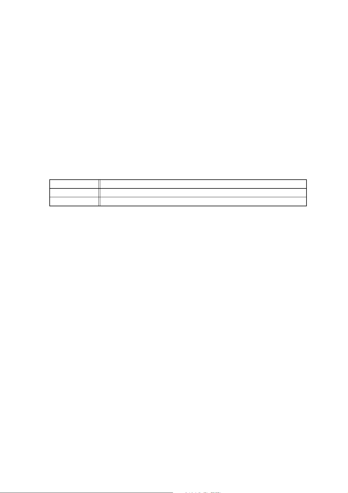
This manual uses the following terminology.
Te r m Explanation
Wor d Indicates an access in unit of 16 bits.
Byte Indicates an access in unit of 8 bits.
■ Notations
The notations in "■ Register Configuration" in this manual are explained below:
• bit: bit number
• Field: bit field name
• Attribute: Attributes for read access and write access of each bit
- R: Read-only
- W: Write-only
- R/W: Readable/Writable
- —: Undefined
• Initial value: Initial value of a bit after a reset
- 0: The initial value is "0".
- 1: The initial value is "1".
- X: The initial value is undefined.
Multiple bits are indicated in this manual in the following way.
- Example 1: bit7:0 represents bit7 to bit0.
- Example 2: SCM[2:0] represents SCM2 to SCM0.
The values such as those indicating addresses are written in this manual in the following ways:
- Hexadecimal number: The prefix "0x" is attached to the beginning of a value (e.g.:
0xFFFF).
- Binary number: The prefix "0b" is attached to the beginning of a value (e.g.: 0b1111).
- Decimal number: Only the number is used (e.g.: 1234).
In this manual, "n" in a pin name and a register abbreviation represents the channel number.
ii
Page 7

• The contents of this document are subject to change without notice.
Customers are advised to consult with sales representatives before ordering.
• The information, such as descriptions of function and application circuit examples, in this document are presented
solely for the purpose of reference to show examples of operations and uses of FUJITSU SEMICONDUCTOR
device; FUJITSU SEMICONDUCTOR does not warrant proper operation of the device with respect to use based
on such information. When you develop equipment incorporating the device based on such information, you must
assume any responsibility arising out of such use of the information. FUJITSU SEMICONDUCTOR assumes no
liability for any damages whatsoever arising out of the use of the information.
• Any information in this document, including descriptions of function and schematic diagrams, shall not be
construed as license of the use or exercise of any intellectual property right, such as patent right or copyright, or
any other right of FUJITSU SEMICONDUCTOR or any third party or does FUJITSU SEMICONDUCTOR
warrant non-infringement of any third-party's intellectual property right or other right by using such information.
FUJITSU SEMICONDUCTOR assumes no liability for any infringement of the intellectual property rights or other
rights of third parties which would result from the use of information contained herein.
• The products described in this document are designed, developed and manufactured as contemplated for general
use, including without limitation, ordinary industrial use, general office use, personal use, and household use, but
are not designed, developed and manufactured as contemplated (1) for use accompanying fatal risks or dangers
that, unless extremely high safety is secured, could have a serious effect to the public, and could lead directly to
death, personal injury, severe physical damage or other loss (i.e., nuclear reaction control in nuclear facility,
aircraft flight control, air traffic control, mass transport control, medical life support system, missile launch control
in weapon system), or (2) for use requiring extremely high reliability (i.e., submersible repeater and artificial
satellite). Please note that FUJITSU SEMICONDUCTOR will not be liable against you and/or any third party for
any claims or damages arising in connection with above-mentioned uses of the products.
• Any semiconductor devices have an inherent chance of failure. You must protect against injury, damage or loss
from such failures by incorporating safety design measures into your facility and equipment such as redundancy,
fire protection, and prevention of over-current levels and other abnormal operating conditions.
• Exportation/release of any products described in this document may require necessary procedures in accordance
with the regulations of the Foreign Exchange and Foreign Trade Control Law of Japan and/or US export control
laws.
• The company names and brand names herein are the trademarks or registered trademarks of their respective
owners.
Copyright © 2011-2012 FUJITSU SEMICONDUCTOR LIMITED All rights reserved.
iii
Page 8

iv
Page 9

CONTENTS
CHAPTER 1 MEMORY ACCESS MODE .............................................................. 1
1.1 Memory Access Mode ......................................................................................................... 2
CHAPTER 2 CPU .................................................................................................. 3
2.1 Dedicated Registers ............................................................................................................ 4
2.1.1 Register Bank Pointer (RP) ............................................................................................ 6
2.1.2 Direct Bank Pointer (DP) ................................................................................................ 7
2.1.3 Condition Code Register (CCR) ..................................................................................... 9
2.2 General-purpose Register ................................................................................................. 11
2.3 Placement of 16-bit Data in Memory ................................................................................. 13
CHAPTER 3 CLOCK CONTROLLER ................................................................. 15
3.1 Overview ............................................................................................................................ 16
3.2 Oscillation Stabilization Wait Time .................................................................................... 24
3.3 Registers ........................................................................................................................... 27
3.3.1 System Clock Control Register (SYCC) ....................................................................... 28
3.3.2 PLL Control Register (PLLC) ........................................................................................ 29
3.3.3 Oscillation Stabilization Wait Time Setting Register (WATR) ....................................... 30
3.3.4 Standby Control Register (STBC) ................................................................................ 32
3.3.5 System Clock Control Register 2 (SYCC2) .................................................................. 34
3.3.6 Standby Control Register 2 (STBC2) ........................................................................... 36
3.4 Clock Modes ...................................................................................................................... 37
3.5 Operations in Low Power Consumption Mode (Standby Mode) ........................................ 41
3.5.1 Notes on Using Standby Mode ..................................................................................... 42
3.5.2 Sleep Mode .................................................................................................................. 48
3.5.3 Stop Mode .................................................................................................................... 49
3.5.4 Time-base Timer Mode ................................................................................................ 51
3.5.5 Watch Mode ................................................................................................................. 53
3.6 Clock Oscillator Circuit ...................................................................................................... 54
3.7 Overview of Prescaler ....................................................................................................... 55
3.8 Configuration of Prescaler ................................................................................................. 56
3.9 Operation of Prescaler ....................................................................................................... 57
3.10 Notes on Using Prescaler .................................................................................................. 59
CHAPTER 4 RESET ............................................................................................ 61
4.1 Reset Operation ................................................................................................................ 62
4.2 Register ............................................................................................................................. 66
4.2.1 Reset Source Register (RSRR) .................................................................................... 67
4.3 Notes on Using Reset ........................................................................................................ 70
CHAPTER 5 INTERRUPTS ................................................................................. 71
5.1 Interrupts ........................................................................................................................... 72
5.1.1 Interrupt Level Setting Registers (ILR0 to ILR5) ........................................................... 73
5.1.2 Interrupt Processing ..................................................................................................... 75
v
Page 10

5.1.3 Nested Interrupts .......................................................................................................... 77
5.1.4 Interrupt Processing Time ............................................................................................ 78
5.1.5 Stack Operation During Interrupt Processing ............................................................... 79
5.1.6 Interrupt Processing Stack Area ................................................................................... 80
CHAPTER 6 I/O PORT ....................................................................................... 81
6.1 Overview ............................................................................................................................ 82
6.2 Configuration and Operations ............................................................................................ 83
CHAPTER 7 TIME-BASE TIMER ........................................................................ 87
7.1 Overview ............................................................................................................................ 88
7.2 Configuration ..................................................................................................................... 89
7.3 Interrupt ............................................................................................................................. 91
7.4 Operations and Setting Procedure Example ..................................................................... 92
7.5 Register ............................................................................................................................. 95
7.5.1 Time-base Timer Control Register (TBTC) ................................................................... 96
7.6 Notes on Using Time-base Timer ...................................................................................... 98
CHAPTER 8 HARDWARE/SOFTWARE WATCHDOG TIMER .......................... 99
8.1 Overview .......................................................................................................................... 100
8.2 Configuration ................................................................................................................... 101
8.3 Operations and Setting Procedure Example ................................................................... 103
8.4 Register ........................................................................................................................... 106
8.4.1 Watchdog Timer Control Register (WDTC) ................................................................ 107
8.5 Notes on Using Watchdog Timer ..................................................................................... 109
CHAPTER 9 WATCH PRESCALER ................................................................. 111
9.1 Overview .......................................................................................................................... 112
9.2 Configuration ................................................................................................................... 113
9.3 Interrupt ........................................................................................................................... 115
9.4 Operations and Setting Procedure Example ................................................................... 116
9.5 Register ........................................................................................................................... 119
9.5.1 Watch Prescaler Control Register (WPCR) ................................................................ 120
9.6 Notes on Using Watch Prescaler ..................................................................................... 122
CHAPTER 10 WILD REGISTER FUNCTION ...................................................... 123
10.1 Overview .......................................................................................................................... 124
10.2 Configuration ................................................................................................................... 125
10.3 Operations ....................................................................................................................... 127
10.4 Registers ......................................................................................................................... 128
10.4.1 Wild Register Data Setting Registers (WRDR0 to WRDR2) ...................................... 129
10.4.2 Wild Register Address Setting Registers (WRAR0 to WRAR2) ................................. 130
10.4.3 Wild Register Address Compare Enable Register (WREN) ....................................... 131
10.4.4 Wild Register Data Test Setting Register (WROR) .................................................... 132
10.5 Typical Hardware Connection Example .......................................................................... 133
CHAPTER 11 8/16-BIT COMPOSITE TIMER ..................................................... 135
11.1 Overview .......................................................................................................................... 136
11.2 Configuration ................................................................................................................... 138
vi
Page 11

11.3 Channel ........................................................................................................................... 141
11.4 Pins .................................................................................................................................. 142
11.5 Interrupts ......................................................................................................................... 143
11.6 Operation of Interval Timer Function (One-shot Mode) ................................................... 144
11.7 Operation of Interval Timer Function (Continuous Mode) ............................................... 146
11.8 Operation of Interval Timer Function (Free-run Mode) .................................................... 148
11.9 Operation of PWM Timer Function (Fixed-cycle mode) .................................................. 150
11.10 Operation of PWM Timer Function (Variable-cycle Mode) .............................................. 152
11.11 Operation of PWC Timer Function .................................................................................. 154
11.12 Operation of Input Capture Function ............................................................................... 156
11.13 Operation of Noise Filter .................................................................................................. 158
11.14 Registers ......................................................................................................................... 159
11.14.1 8/16-bit Composite Timer Status Control Register 0 (Tn0CR0/Tn1CR0) ................... 160
11.14.2 8/16-bit Composite Timer Status Control Register 1 (Tn0CR1/Tn1CR1) ................... 163
11.14.3 8/16-bit Composite Timer Timer Mode Control Register (TMCRn) ............................ 167
11.14.4 8/16-bit Composite Timer Data Register (Tn0DR/Tn1DR) ......................................... 170
11.15 Notes on Using 8/16-bit Composite Timer ....................................................................... 173
CHAPTER 12 EXTERNAL INTERRUPT CIRCUIT ............................................. 175
12.1 Overview .......................................................................................................................... 176
12.2 Configuration ................................................................................................................... 177
12.3 Channels ......................................................................................................................... 178
12.4 Pin ................................................................................................................................... 179
12.5 Interrupt ........................................................................................................................... 180
12.6 Operations and Setting Procedure Example ................................................................... 181
12.7 Register ........................................................................................................................... 183
12.7.1 External Interrupt Control Register (EIC) .................................................................... 184
12.8 Notes on Using External Interrupt Circuit ........................................................................ 186
CHAPTER 13 INTERRUPT PIN SELECTION CIRCUIT ..................................... 187
13.1 Overview .......................................................................................................................... 188
13.2 Configuration ................................................................................................................... 189
13.3 Pins .................................................................................................................................. 190
13.4 Operation ......................................................................................................................... 191
13.5 Register ........................................................................................................................... 192
13.5.1 Interrupt Pin Selection Circuit Control Register (WICR) ............................................. 193
13.6 Notes on Using Interrupt Pin Selection Circuit ................................................................ 196
CHAPTER 14 LIN-UART .................................................................................... 197
14.1 Overview .......................................................................................................................... 198
14.2 Configuration ................................................................................................................... 200
14.3 Pins .................................................................................................................................. 205
14.4 Interrupts ......................................................................................................................... 206
14.4.1 Timing of Receive Interrupt Generation and Flag Set ................................................ 209
14.4.2 Timing of Transmit Interrupt Generation and Flag Set ............................................... 211
14.5 LIN-UART Baud Rate ...................................................................................................... 213
14.5.1 Baud Rate Setting ...................................................................................................... 215
14.5.2 Reload Counter .......................................................................................................... 219
14.6 Operations of LIN-UART and LIN-UART Setting Procedure Example ............................ 221
vii
Page 12

14.6.1 Operations in Asynchronous Mode (Operating Mode 0, 1) ........................................ 223
14.6.2 Operations in Synchronous Mode (Operating Mode 2) .............................................. 227
14.6.3 Operations of LIN function (Operating Mode 3) .......................................................... 231
14.6.4 Serial Pin Direct Access ............................................................................................. 234
14.6.5 Bidirectional Communication Function (Normal Mode) .............................................. 235
14.6.6 Master/Slave Mode Communication Function (Multiprocessor Mode) ....................... 237
14.6.7 LIN Communication Function ..................................................................................... 240
14.6.8 Examples of LIN-UART LIN Communication Flow Chart (Operating Mode 3) ........... 241
14.7 Registers ......................................................................................................................... 243
14.7.1 LIN-UART Serial Control Register (SCR) ................................................................... 244
14.7.2 LIN-UART Serial Mode Register (SMR) ..................................................................... 246
14.7.3 LIN-UART Serial Status Register (SSR) .................................................................... 248
14.7.4 LIN-UART Receive Data Register/LIN-UART Transmit Data Register (RDR/TDR) ... 250
14.7.5 LIN-UART Extended Status Control Register (ESCR) ............................................... 252
14.7.6 LIN-UART Extended Communication Control Register (ECCR) ................................ 255
14.7.7 LIN-UART Baud Rate Generator Registers 1, 0 (BGR1, BGR0) ................................ 257
14.8 Notes on Using LIN-UART .............................................................................................. 258
CHAPTER 15 8/10-BIT A/D CONVERTER ......................................................... 263
15.1 Overview .......................................................................................................................... 264
15.2 Configuration ................................................................................................................... 265
15.3 Pin ................................................................................................................................... 267
15.4 Interrupt ........................................................................................................................... 268
15.5 Operations and Setting Procedure Example ................................................................... 269
15.6 Registers ......................................................................................................................... 272
15.6.1 8/10-bit A/D Converter Control Register 1 (ADC1) ..................................................... 273
15.6.2 8/10-bit A/D Converter Control Register 2 (ADC2) ..................................................... 275
15.6.3 8/10-bit A/D Converter Data Register (Upper/Lower) (ADDH/ADDL) ......................... 277
15.7 Notes on Using 8/10-bit A/D Converter ........................................................................... 278
CHAPTER 16 LOW-VOLTAGE DETECTION RESET CIRCUIT ........................ 281
16.1 Overview .......................................................................................................................... 282
16.2 Configuration ................................................................................................................... 283
16.3 Pins .................................................................................................................................. 284
16.4 Operation ......................................................................................................................... 285
16.5 Register ........................................................................................................................... 286
16.5.1 LVD Reset Voltage Selection ID Register (LVDR) ..................................................... 287
CHAPTER 17 CLOCK SUPERVISOR COUNTER .............................................. 289
17.1 Overview .......................................................................................................................... 290
17.2 Configuration ................................................................................................................... 291
17.3 Operations ....................................................................................................................... 293
17.4 Registers ......................................................................................................................... 298
17.4.1 Clock Monitoring Data Register (CMDR) .................................................................... 299
17.4.2 Clock Monitoring Control Register (CMCR) ................................................................ 300
17.5 Notes on Using Clock Supervisor Counter ...................................................................... 302
CHAPTER 18 8/16-BIT PPG ............................................................................... 305
18.1 Overview .......................................................................................................................... 306
viii
Page 13

18.2 Configuration ................................................................................................................... 307
18.3 Channel ........................................................................................................................... 309
18.4 Pins .................................................................................................................................. 310
18.5 Interrupt ........................................................................................................................... 311
18.6 Operations and Setting Procedure Example ................................................................... 312
18.6.1 8-bit PPG Independent Mode ..................................................................................... 313
18.6.2 8-bit Prescaler + 8-bit PPG Mode ............................................................................... 315
18.6.3 16-bit PPG Mode ........................................................................................................ 317
18.7 Registers ......................................................................................................................... 320
18.7.1 8/16-bit PPG timer n1 Control Register (PCn1) .......................................................... 321
18.7.2 8/16-bit PPG timer n0 Control Register (PCn0) .......................................................... 323
18.7.3 8/16-bit PPG timer n1/n0 Cycle Setup Buffer Register (PPSn1/PPSn0) .................... 325
18.7.4 8/16-bit PPG timer n1/n0 Duty Setup Buffer Register (PDSn1/PDSn0) ..................... 326
18.7.5 8/16-bit PPG Start Register (PPGS) ........................................................................... 327
18.7.6 8/16-bit PPG Output Reverse Register (REVC) ......................................................... 329
18.8 Notes on Using 8/16-bit PPG .......................................................................................... 331
CHAPTER 19 16-BIT PPG TIMER ...................................................................... 333
19.1 Overview .......................................................................................................................... 334
19.2 Configuration ................................................................................................................... 335
19.3 Channel ........................................................................................................................... 337
19.4 Pins .................................................................................................................................. 338
19.5 Interrupts ......................................................................................................................... 339
19.6 Operations and Setting Procedure Example ................................................................... 340
19.7 Registers ......................................................................................................................... 344
19.7.1 16-bit PPG Downcounter Register (Upper/Lower) (PDCRHn/PDCRLn) .................... 345
19.7.2 16-bit PPG Cycle Setting Buffer Register (Upper/ Lower) (PCSRHn/PCSRLn) ......... 346
19.7.3 16-bit PPG Duty Setting Buffer Register (Upper/Lower) (PDUTHn/PDUTLn) ............ 347
19.7.4 16-bit PPG Status Control Register (Upper) (PCNTHn) ............................................. 348
19.7.5 16-bit PPG Status Control Register (Lower) (PCNTLn) ............................................. 350
19.8 Notes on Using 16-bit PPG Timer ................................................................................... 352
CHAPTER 20 16-BIT RELOAD TIMER .............................................................. 353
20.1 Overview .......................................................................................................................... 354
20.2 Configuration ................................................................................................................... 356
20.3 Channel ........................................................................................................................... 358
20.4 Pins .................................................................................................................................. 359
20.5 Interrupt ........................................................................................................................... 360
20.6 Operations and Setting Procedure Example ................................................................... 361
20.6.1 Internal Clock Mode .................................................................................................... 363
20.6.2 Event Count Mode ...................................................................................................... 367
20.7 Registers ......................................................................................................................... 369
20.7.1 16-bit Reload Timer Control Status Register (Upper) (TMCSRHn) ............................ 370
20.7.2 16-bit Reload Timer Control Status Register (Lower) (TMCSRLn) ............................ 372
20.7.3 16-bit Reload Timer Timer Register (Upper/Lower) (TMRHn/TMRLn) ....................... 374
20.7.4 16-bit Reload Timer Reload Register (Upper/Lower) (TMRLRHn/TMRLRLn) ........... 375
20.8 Notes on Using 16-bit Reload Timer ............................................................................... 376
ix
Page 14

CHAPTER 21 MULTI-PULSE GENERATOR ...................................................... 377
21.1 Overview .......................................................................................................................... 378
21.2 Block Diagram ................................................................................................................. 381
21.3 Pins .................................................................................................................................. 389
21.4 Interrupts ......................................................................................................................... 390
21.5 Operations ....................................................................................................................... 392
21.5.1 Operation of Position Detection .................................................................................. 394
21.5.2 Operation of Data Write Control Unit .......................................................................... 396
21.5.3 Operation of 16-bit MPG Output Data Buffer Register (Upper/Lower)
(OPDBRHx/OPDBRLx) .............................................................................................. 400
21.5.4 Operation of Data Transfer of 16-bit MPG Output Data Register (Upper/Lower) ....... 402
21.5.4.1 At OPDBRH0 and OPDBRL0 Write ......................................................................... 404
21.5.4.2 At 16-bit Reload Timer Underflow ........................................................................... 405
21.5.4.3 At Position Detection ............................................................................................... 407
21.5.4.4 At Position Detection and Timer Underflow ............................................................. 409
21.5.4.5 At Position Detection or Timer Underflow ................................................................ 412
21.5.4.6 At One-shot Position Detection ............................................................................... 414
21.5.4.7 When One-shot Position Detection and Reload Timer Underflow ........................... 415
21.5.4.8 When One-shot Position Detection or Reload Timer Underflow ............................. 416
21.5.5 Operation of DTTI Input Control ................................................................................. 417
21.5.6 Operation of Noise Cancellation Function .................................................................. 420
21.5.7 Operation of 16-bit Timer ............................................................................................ 421
21.6 Registers ......................................................................................................................... 426
21.6.1 16-bit MPG Output Control Register (Upper) (OPCUR) ............................................. 427
21.6.2 16-bit MPG Output Control Register (Lower) (OPCLR) .............................................. 429
21.6.3 16-bit MPG Output Data Register (Upper/Lower) (OPDUR/OPDLR) ......................... 431
21.6.3.1 16-bit MPG Output Data Register (Upper) (OPDUR) .............................................. 432
21.6.3.2 16-bit MPG Output Data Register (Lower) (OPDLR) ............................................... 434
21.6.4 16-bit MPG Output Data Buffer Register (Upper/Lower) (OPDBRHx/OPDBRLx) ...... 435
21.6.4.1 16-bit MPG Output Data Buffer Register (Upper) (OPDBRHx) ............................... 436
21.6.4.2 16-bit MPG Output Data Buffer Register (Lower) (OPDBRLx) ................................ 438
21.6.5 16-bit MPG Input Control Register (Upper/Lower) (IPCUR/IPCLR) ........................... 440
21.6.5.1 16-bit MPG Input Control Register (Upper) (IPCUR) ............................................... 441
21.6.5.2 16-bit MPG Input Control Register (Lower) (IPCLR) ............................................... 443
21.6.6 16-bit MPG Compare Clear Register (Upper/Lower) (CPCUR/CPCLR) .................... 445
21.6.7 16-bit MPG Timer Buffer Register (Upper/Lower) (TMBUR/TMBLR) ......................... 446
21.6.8 16-bit MPG Timer Control Status Register (TCSR) .................................................... 447
21.6.9 16-bit MPG Noise Cancellation Control Register (NCCR) .......................................... 449
21.7 Notes on Using Multi-pulse Generator ............................................................................ 450
21.8 Sample Program for Multi-pulse Generator ..................................................................... 452
CHAPTER 22 UART/SIO ..................................................................................... 455
22.1 Overview .......................................................................................................................... 456
22.2 Configuration ................................................................................................................... 457
22.3 Channel ........................................................................................................................... 459
22.4 Pins .................................................................................................................................. 460
22.5 Interrupts ......................................................................................................................... 461
22.6 Operations and Setting Procedure Example ................................................................... 462
22.6.1 Operations in Operation Mode 0 ................................................................................ 463
x
Page 15

22.6.2 Operations in Operation Mode 1 ................................................................................ 470
22.7 Registers ......................................................................................................................... 476
22.7.1 UART/SIO Serial Mode Control Register 1 (SMC1n) ................................................. 477
22.7.2 UART/SIO Serial Mode Control Register 2 (SMC2n) ................................................. 479
22.7.3 UART/SIO Serial Status and Data Register (SSRn) .................................................. 481
22.7.4 UART/SIO Serial Input Data Register (RDRn) ........................................................... 483
22.7.5 UART/SIO Serial Output Data Register (TDRn) ......................................................... 484
CHAPTER 23 UART/SIO DEDICATED BAUD RATE GENERATOR ................ 485
23.1 Overview .......................................................................................................................... 486
23.2 Channel ........................................................................................................................... 487
23.3 Operations ....................................................................................................................... 488
23.4 Registers ......................................................................................................................... 489
23.4.1 UART/SIO Dedicated Baud Rate Generator Prescaler Select Register (PSSRn) ..... 490
23.4.2 UART/SIO Dedicated Baud Rate Generator Baud Rate Setting Register (BRSRn) .. 491
CHAPTER 24 I2C BUS INTERFACE .................................................................. 493
24.1 Overview .......................................................................................................................... 494
24.2 Configuration ................................................................................................................... 495
24.3 Channel ........................................................................................................................... 498
24.4 Pins .................................................................................................................................. 499
24.5 Interrupts ......................................................................................................................... 500
24.6 Operations and Setting Procedure Example ................................................................... 502
24.6.1 l
24.6.2 Function to Wake up the MCU from Standby Mode ................................................... 511
24.7 Registers ......................................................................................................................... 513
24.7.1 I
24.7.2 I
24.7.3 I
24.7.4 I
24.7.5 I
24.7.6 I
24.8 Notes on Using I
2
C Bus Interface ........................................................................................................ 503
2
C Bus Control Register 0 (IBCR0n) ......................................................................... 514
2
C Bus Control Register 1 (IBCR1n) ......................................................................... 517
2
C Bus Status Register (IBSRn) ................................................................................ 521
2
C Data Register (IDDRn) ......................................................................................... 524
2
C Address Register (IAARn) .................................................................................... 525
2
C Clock Control Register (ICCRn) ........................................................................... 526
2
C Bus Interface .................................................................................... 528
CHAPTER 25 DUAL OPERATION FLASH MEMORY ....................................... 531
25.1 Overview .......................................................................................................................... 532
25.2 Sector/Bank Configuration ............................................................................................... 534
25.3 Invoking Flash Memory Automatic Algorithm .................................................................. 535
25.4 Checking Automatic Algorithm Execution Status ............................................................ 537
25.4.1 Data Polling Flag (DQ7) ............................................................................................. 539
25.4.2 Toggle Bit Flag (DQ6) ................................................................................................. 541
25.4.3 Execution Timeout Flag (DQ5) ................................................................................... 542
25.4.4 Sector Erase Timer Flag (DQ3) .................................................................................. 543
25.4.5 Toggle Bit2 Flag (DQ2) ............................................................................................... 544
25.5 Programming/Erasing Flash Memory .............................................................................. 545
25.5.1 Placing Flash Memory in Read/Reset State ............................................................... 546
25.5.2 Programming Data to Flash Memory .......................................................................... 547
25.5.3 Erasing All Data from Flash Memory (Chip Erase) ..................................................... 549
25.5.4 Erasing Specific Data from Flash Memory (Sector Erase) ......................................... 550
xi
Page 16

25.5.5 Suspending Sector Erase from Flash Memory ........................................................... 552
25.5.6 Resuming Sector Erase of Flash Memory .................................................................. 553
25.5.7 Unlock Bypass Program ............................................................................................. 554
25.6 Operations ....................................................................................................................... 555
25.7 Flash Security .................................................................................................................. 557
25.8 Registers ......................................................................................................................... 558
25.8.1 Flash Memory Status Register 2 (FSR2) .................................................................... 559
25.8.2 Flash Memory Status Register (FSR) ......................................................................... 562
25.8.3 Flash Memory Sector Write Control Register 0 (SWRE0) .......................................... 565
25.8.4 Flash Memory Status Register 3 (FSR3) .................................................................... 567
25.8.5 Flash Memory Status Register 4 (FSR4) .................................................................... 568
25.9 Notes on Using Dual Operation Flash Memory ............................................................... 576
CHAPTER 26 NON-VOLATILE REGISTER (NVR) INTERFACE ....................... 577
26.1 Overview .......................................................................................................................... 578
26.2 Configuration ................................................................................................................... 579
26.3 Registers ......................................................................................................................... 580
26.3.1 Main CR Clock Trimming Register (Upper) (CRTH) ................................................... 581
26.3.2 Main CR Clock Trimming Register (Lower) (CRTL) ................................................... 582
26.3.3 Main CR Clock Temperature Dependent Adjustment Register (CRTDA) .................. 583
26.3.4 Watchdog Timer Selection ID Register (Upper/Lower) (WDTH/WDTL) ..................... 584
26.4 Notes on Main CR Clock Trimming ................................................................................. 585
26.5 Notes on Using NVR Interface ........................................................................................ 587
CHAPTER 27 COMPARATOR ............................................................................ 589
27.1 Overview .......................................................................................................................... 590
27.2 Configuration ................................................................................................................... 591
27.3 Pins .................................................................................................................................. 593
27.4 Interrupt ........................................................................................................................... 594
27.5 Operations and Setting Procedure Example ................................................................... 595
27.6 Register ........................................................................................................................... 596
27.6.1 Comparator Control Register (CMR0C) ..................................................................... 597
CHAPTER 28 SYSTEM CONFIGURATION CONTROLLER .............................. 599
28.1 Overview .......................................................................................................................... 600
28.2 Register ........................................................................................................................... 601
28.2.1 System Configuration Register (SYSC) ...................................................................... 602
28.3 Notes on Using Controller ............................................................................................... 604
APPENDIX ............................................................................................................. 605
APPENDIX A Instruction Overview ............................................................................................. 606
A.1 Addressing ...................................................................................................................... 609
A.2 Special Instruction ........................................................................................................... 613
A.3 Bit Manipulation Instructions (SETB, CLRB) ................................................................... 617
A.4 F
A.5 Instruction Map ................................................................................................................ 621
2
MC-8FX Instructions .................................................................................................... 618
xii
Page 17

Major revisions in this edition
A change on a page is indicated by a vertical line drawn on the left of that page.
Page Revisions (For details, see their respective pages.)
ii How to Use This Manual
■ Finding a Function
— CHAPTER 1 NOTES ON DEVICE
HANDLING
21 CHAPTER 3 CLOCK
CONTROLLER
3.1 Overview
■ Standby Mode
22 3.1 Overview
■ Combinations of Clock Mode
and Standby Mode
Table 3.1-3
23 3.1 Overview
■ Combinations of Clock Mode
and Standby Mode
Table 3.1-4
33 3.3.4 Standby Control Register
(STBC)
■ Register Functions
Added the following section.
• Searching from registers
Deleted the entire chapter from the hardware manual.
For details of device handling, refer to "■ PRECAUTIONS
FOR DEVICE HANDLING", "■ NOTES ON DEVICE
HANDLING" and "■ PIN CONNECTION" in the device
data sheet.
Added the following statement.
In every standby mode, two further operating mode options,
normal standby mode and deep standby mode, can be
selected by the deep standby mode control bit in the standby
control register 2 (STBC2:DSTBYX).
Revised the internal operating states of the Flash memory
and RAM.
Added note *6.
Revised the internal operating states of the Flash memory
and RAM.
Added note *6.
Corrected the following heading in the bit function table of
the TMD bit.
In main clock mode or main CR clock mode
→
In main clock mode, main CR clock mode or main CR PLL
clock mode
53 3.5.5 Watch Mode
■ Operations in Watch Mode
● Release from Watch Mode
82 CHAPTER 6 I/O PORT
6.1 Overview
■ Overview
Table 6.1-1
83 6.2 Configuration and Operations of
I/O Port
■ Configuration of I/O Port
84 6.2 Configuration and Operations of
I/O Port
■ Operations of I/O Port
● Operation as an input port
Added the following statement at the end of the section.
However, if a program is being executed on the RAM, no
Flash recovery wait time occurs.
Added details of the A/D input disable register (upper).
Added the following note for the A/D input disable register
(upper) and the A/D input disable register (lower).
Refer to "■ I/O MAP" in the device data sheet for the
availability of the A/D input disable register (upper) and A/D
input disable register (lower).
Added A/D input disable register (upper) (AIDRH).
Revised the following statement.
When using an analog input shared pin as an input port, set
the corresponding bit in the A/D input disable register
(lower) (AIDRL) to "1".
→
When using an analog input shared pin as an input port, set
the corresponding bit in the A/D input disable register
(upper/lower) (AIDRH/AIDRL) to "1".
xiii
Page 18

Page Revisions (For details, see their respective pages.)
85 6.2 Configuration and Operations of
I/O Port
■ Operations of I/O Port
● Operation as an analog input pin
108 CHAPTER 8 HARDWARE/
SOFTWARE WATCHDOG
TIMER
8.4.1 Watchdog Timer Control
Register (WDTC)
■ Register Functions
152 CHAPTER 11 8/16-BIT
COMPOSITE TIMER
11.10 Operation of PWM Timer
Function (Variable-cycle
Mode)
■ Operation of PWM Timer Func-
tion (Variable-cycle Mode)
Figure 11.10-1
162 11.14.1 8/16-bit Composite Timer
Status Control Register 0
(Tn0CR0/Tn1CR0)
■ Register Functions
Revised the following statement.
Set the bit in the DDRx register corresponding to the analog
input pin to "0" and the bit corresponding to that pin in the
AIDRL register to "0".
→
Set the bit in the DDRx register corresponding to the analog
input pin to "0" and the bit corresponding to that pin in the
AIDRH/AIDRL register to "0".
Revised details of "Writing "0101"" of the WTE[3:0] bits in
the bit function table.
Corrected the following register names.
T00DR → Tn0DR
T01DR → Tn1DR
Corrected the bit number in the title of details of the F[3:0]
bits.
[bit3] → [bit3:0]
299 CHAPTER 17 CLOCK
SUPERVISOR COUNTER
17.4.1 Clock Monitoring Data Register (CMDR)
■ Register Functions
323 CHAPTER 18 8/16-BIT PPG
18.7.2 8/16-bit PPG Timer n0 Control Register (PCn0)
■ Register Functions
345 CHAPTER 19 16-BIT PPG TIMER
19.7.1 16-bit PPG Downcounter
Register (Upper/Lower)
(PDCRHn/PDCRLn)
■ Register Functions
362 CHAPTER 20 16-BIT RELOAD
TIMER
20.6 Operations and Setting Procedure Example
■ Setting Procedure Example
448 CHAPTER 21 MULTI-PULSE
GENERATOR
21.6.8 16-bit MPG Timer Control
Status Register (TCSR)
■ Register Functions
Corrected the name of the CMDR[7:0] bits.
Analog input pin select bits → Clock monitoring data bits
Added the following statement to details of the PIE0 bit.
In 16-bit PPG mode, use this bit to control the interrupt
request of the 8/16-bit PPG.
Revised the initial value of the DC06 bit.
1 → 0
Corrected the following register abbreviation.
TMR1 → TMRHn/TMRLn
Corrected the abbreviation of the compare clear interrupt
request flag bit.
PDIF → ICLR
xiv
Page 19

Page Revisions (For details, see their respective pages.)
481 CHAPTER 22 UART/SIO
22.7 UART/SIO Serial Status and
Data Register (SSRn)
■ Register Functions
514
CHAPTER 24 I
2
C BUS
INTERFACE
2
24.7.1 I
C Bus Control Register 0
(IBCR0n)
517
CHAPTER 24 I
2
C BUS
INTERFACE
24.7.2 I
2
C Bus Control Register 1
(IBCR1n)
597 CHAPTER 27 COMPARATOR
27.6.1 Comparator Control Register (CMR0C)
■ Register Functions
Corrected the following register abbreviation in the
respective details of the PER bit, the OVE bit and the FER
bit.
SMR2n → SMC2n
Revised the summary of this section.
Revised the summary of this section.
Revised the initial value of the IF bit.
X → 0
xv
Page 20

xvi
Page 21

CHAPTER 1
MEMORY ACCESS MODE
This chapter describes the memory access
mode.
1.1 Memory Access Mode
MN702-00009-1v0-E FUJITSU SEMICONDUCTOR LIMITED 1
Page 22
CHAPTER 1 MEMORY ACCESS MODE
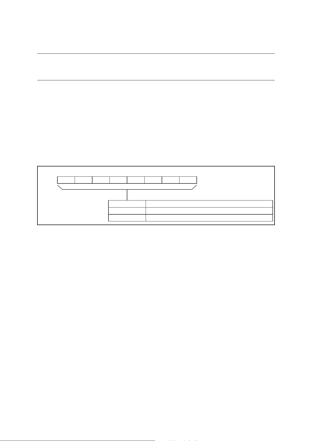
Address
0xFFFD
Data
0x00
Other than 0x00 Reserved. Do not set mode data to any value other than 0x00.
Selects single-chip mode.
Operation
bit7 bit6 bit5 bit4 bit3bit2 bit1 bit0
1.1 Memory Access Mode
MB95630H Series
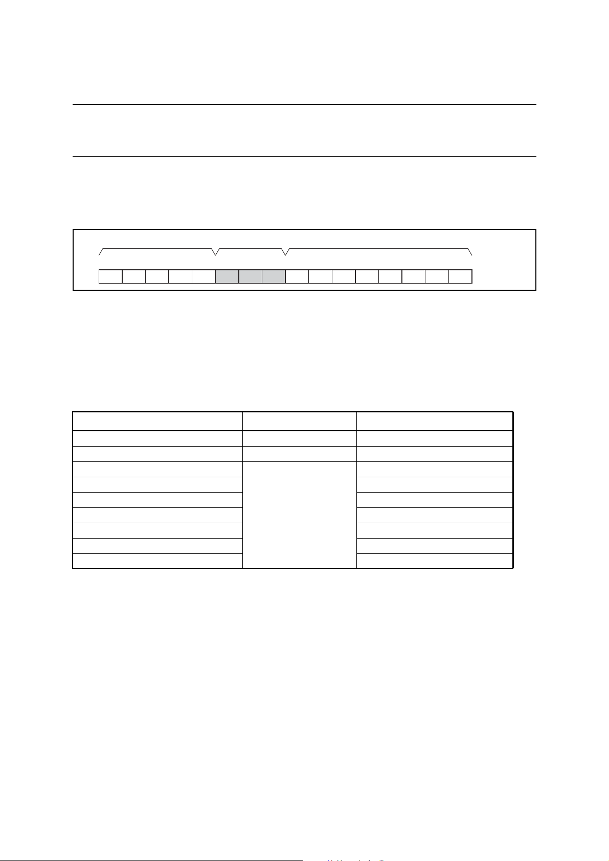
1.1 Memory Access Mode
The MB95630H Series supports only one memory access mode: single-chip
mode.
■ Single-chip Mode
In single-chip mode, only the internal RAM and the Flash memory are used, and no external
bus access is executed.
● Mode data
Mode data is the data used to determine the memory access mode of the CPU.
The mode data address is fixed at "0xFFFD". Always set the mode data of the Flash memory to
"0x00" to select the single-chip mode.
Figure 1.1-1 Mode Data Settings
After a reset is released, the CPU fetches mode data first.
The CPU then fetches the reset vector after the mode data. It starts executing instructions from
the address set in the reset vector.
2 FUJITSU SEMICONDUCTOR LIMITED MN702-00009-1v0-E
Page 23

CHAPTER 2
CPU
This chapter describes the functions and
operations of the CPU.
2.1 Dedicated Registers
2.2 General-purpose Register
2.3 Placement of 16-bit Data in Memory
MN702-00009-1v0-E FUJITSU SEMICONDUCTOR LIMITED 3
Page 24
CHAPTER 2 CPU
Initial value
0xFFFD
Program counter
Indicates the address of the current instruction.
0x0000 Accumulator (A)
Temporary storage register for arithmetic operation and transfer
0x0000
Te mp or ary accumulator (T)
Performs arithmetic operations with the accumulator.
0x0000
Index register
Indicates an index address.
0x0000 Extra pointer
Indicates a memory address.
0x0000 Stack pointer
Indicates the current stack location.
0x0030Program status
Stores a register bank pointer,
a direct bank pointer, and a condition code.
16 bits
PS
SP
EP
IX
PC
TH TL
AH AL
RP DP CCR
:
:
:
:
:
:
:
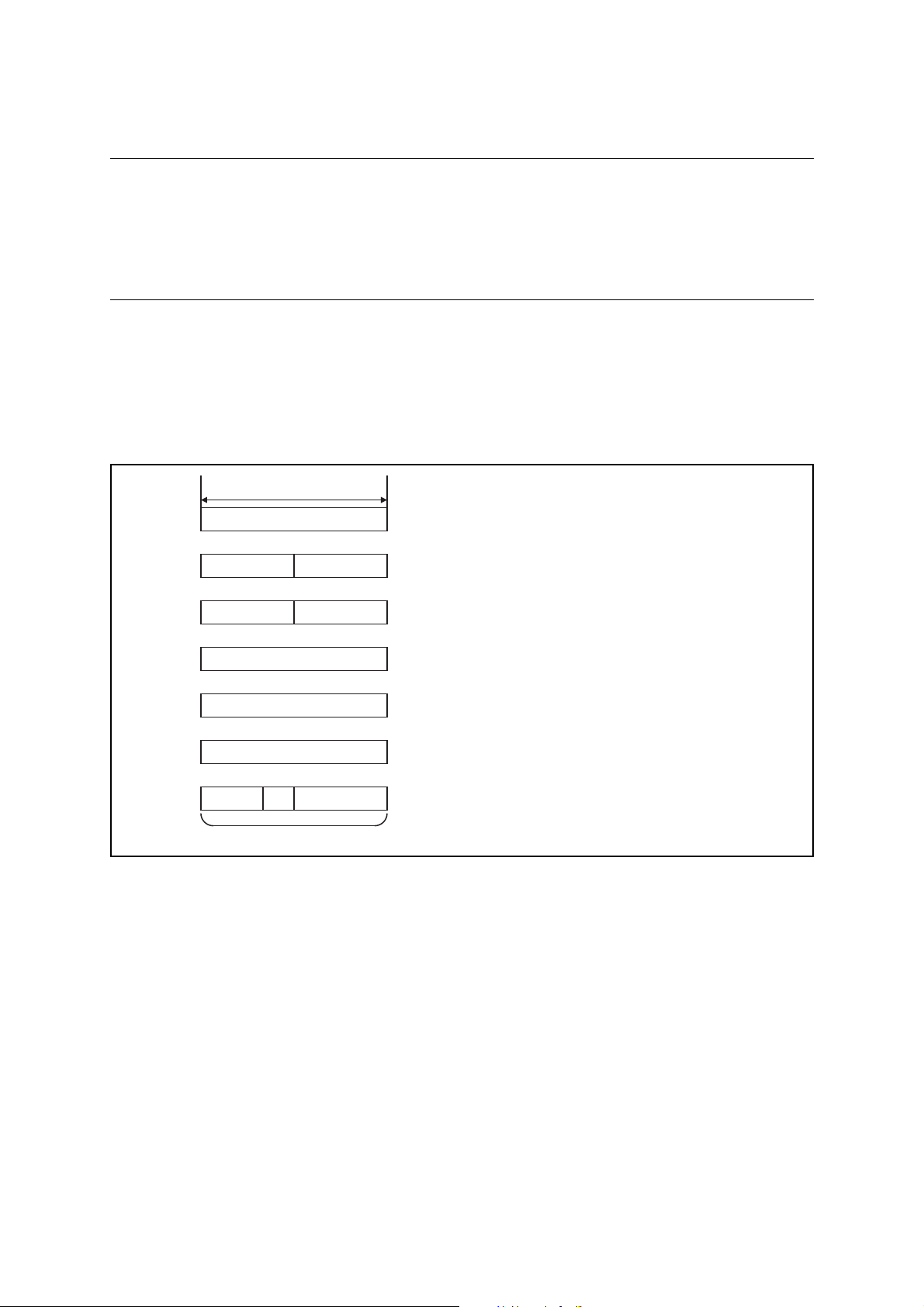
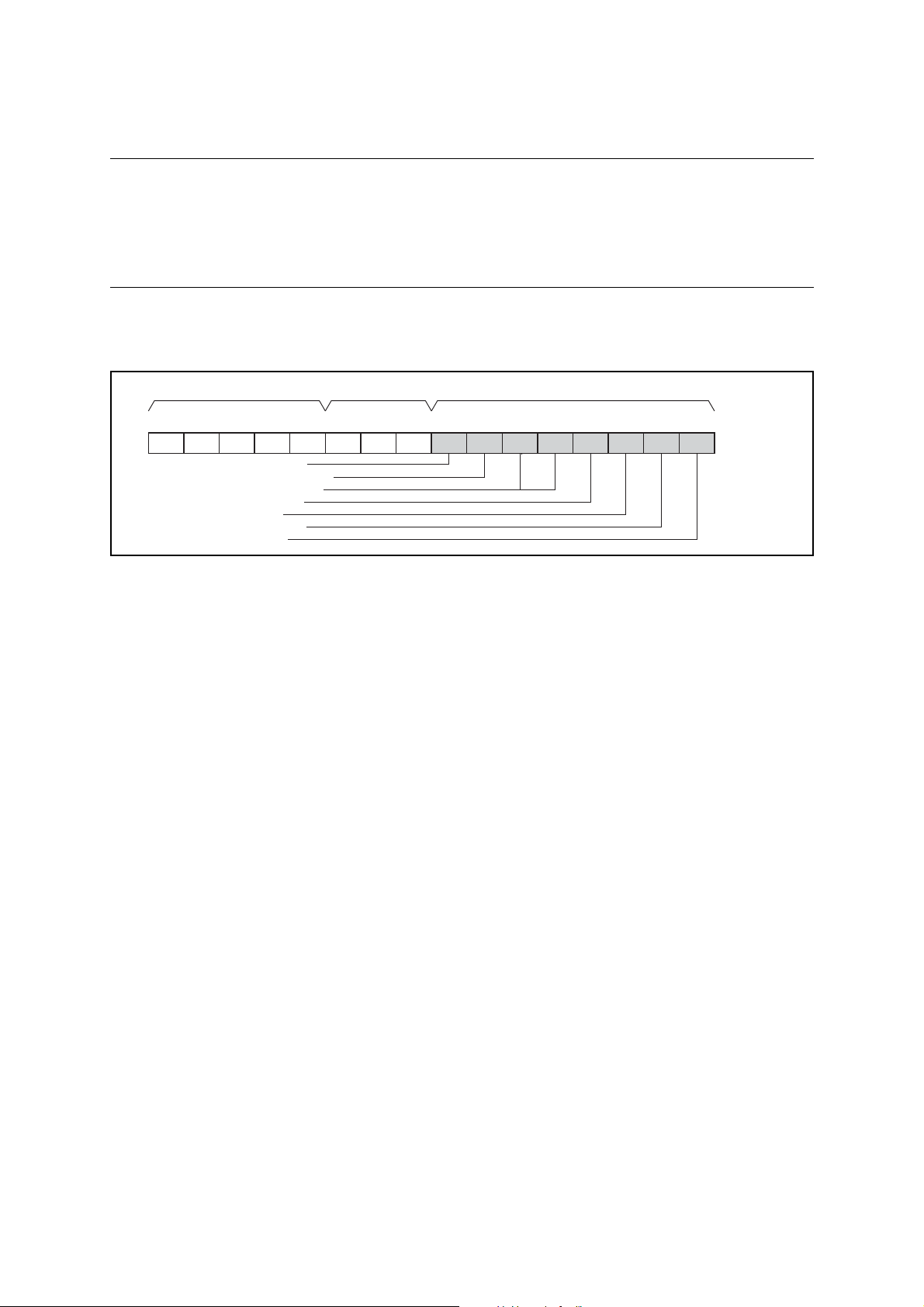
2.1 Dedicated Registers
MB95630H Series
2.1 Dedicated Registers
The CPU has dedicated registers: a program counter (PC), two registers for
arithmetic operations (A and T), three address pointers (IX, EP, and SP), and the
program status (PS) register. Each of the registers is 16 bits long. The PS
register consists of the register bank pointer (RP), direct bank pointer (DP), and
condition code register (CCR).
■ Configuration of Dedicated Registers
The dedicated registers in the CPU consist of seven 16-bit registers. As for the accumulator (A)
and the temporary accumulator (T), using only the lower eight bits of the respective registers is
also supported.
Figure 2.1-1 shows the configuration of the dedicated registers.
Figure 2.1-1 Configuration of Dedicated Registers
■ Functions of Dedicated Registers
Program counter (PC)
●
● Accumulator (A)
4 FUJITSU SEMICONDUCTOR LIMITED MN702-00009-1v0-E
The program counter is a 16-bit counter which contains the memory address of the instruction
currently executed by the CPU. The program counter is updated whenever an instruction is
executed or an interrupt or a reset occurs. The initial value set immediately after a reset is the
mode data read address (0xFFFD).
The accumulator is a 16-bit register for arithmetic operation. It is used for a variety of
arithmetic and transfer operations of data in memory or data in other registers such as the
temporary accumulator (T). The data in the accumulator can be handled either as word (16-bit)
data or byte (8-bit) data. For byte-length arithmetic and transfer operations, only the lower
eight bits (AL) of the accumulator are used with the upper eight bits (AH) left unchanged. The
initial value set immediately after a reset is "0x0000".
Page 25

MB95630H Series
● Temporary accumulator (T)
The temporary accumulator is an auxiliary 16-bit register for arithmetic operation. It is used to
perform arithmetic operations with the data in the accumulator (A). The data in the temporary
accumulator is handled as word data for word-length (16-bit) operations with the accumulator
(A) and as byte data for byte-length (8-bit) operations. For byte-length operations, only the
lower eight bits (TL) of the temporary accumulator are used and the upper eight bits (TH) are
not used.
When a MOV instruction is used to transfer data to the accumulator (A), the previous contents
of the accumulator are automatically transferred to the temporary accumulator. When
transferring byte-length data, the upper eight bits (TH) of the temporary accumulator remain
unchanged. The initial value after a reset is "0x0000".
● Index register (IX)
The index register is a 16-bit register used to hold the index address. The index register is used
with a single-byte offset (-128 to +127). The offset value is added to the index address to
generate the memory address for data access. The initial value after a reset is "0x0000".
● Extra pointer (EP)
CHAPTER 2 CPU
2.1 Dedicated Registers
The extra pointer is a 16-bit register which contains the value indicating the memory address
for data access. The initial value after a reset is "0x0000".
● Stack pointer (SP)
The stack pointer is a 16-bit register which holds the address referenced when an interrupt or a
sub-routine call occurs and by the stack push and pop instructions. During program execution,
the value of the stack pointer indicates the address of the most recent data pushed onto the
stack. The initial value after a reset is "0x0000".
● Program status (PS)
The program status is a 16-bit control register. The upper eight bits consists of the register bank
pointer (RP) and direct bank pointer (DP); the lower eight bits consists of the condition code
register (CCR).
In the upper eight bits, the upper five bits consists of the register bank pointer used to contain
the address of the general-purpose register bank. The lower three bits consists of the direct
bank pointer which locates the area to be accessed at high-speed by direct addressing.
The lower eight bits consists of the condition code register (CCR) which consists of flags that
represent the state of the CPU.
The instructions that can access the program status are "MOVW A,PS" and "MOVW PS,A".
The register bank pointer (RP) and direct bank pointer (DP) in the program status register can
also be read from and written to by accessing the mirror address (0x0078).
Note that the condition code register (CCR) is a part of the program status register and cannot
be accessed independently.
Refer to the "F
2
MC-8FX Programming Manual" for details on using the dedicated registers.
MN702-00009-1v0-E FUJITSU SEMICONDUCTOR LIMITED 5
Page 26
CHAPTER 2 CPU
CCRDPRP
PS 0b00000
RP
initial value
R4 R3 R2 R1 R0 DP2 DP1 DP0 H I IL1 IL0 N Z V C
bit15 bit14 bit13bit12 bit11 bit10 bit9 bit8bit7 bit6 bit5 bit4 bit3bit2 bit1 bit0
2.1 Dedicated Registers
MB95630H Series
2.1.1 Register Bank Pointer (RP)
The register bank pointer (RP) in bit15 to bit11 of the program status (PS)
register contains the address of the general-purpose register bank that is
currently in use and is translated into a real address when general-purpose
register addressing is used.
■ Configuration of Register Bank Pointer (RP)
Figure 2.1-2 shows the configuration of the register bank pointer.
Figure 2.1-2 Configuration of Register Bank Pointer
The register bank pointer contains the address of the register bank currently in use. The content
of the register bank pointer is translated into a real address according to the rule shown in
Figure 2.1-3.
Figure 2.1-3 Rule for Translation into Real Addresses in General-purpose Register Area
Fixed value RP: Upper Op-code: Lower
Generated
address
“0” “0”
↓↓↓↓↓↓↓↓↓↓↓↓↓↓↓↓
A15 A14 A13 A12 A11 A10 A9 A8 A7 A6 A5 A4 A3 A2 A1 A0
“0” “0” “0” “0” “0” “1” R4 R3 R2 R1 R0 b2 b1 b0
The register bank pointer specifies the register bank used as general-purpose registers in the
RAM area. There are a total of 32 register banks, which are specified by setting a value
between 0 and 31 in the upper five bits of the register bank pointer. Each register bank has
eight 8-bit general-purpose registers which are selected by the lower three bits of the op-code.
The register bank pointer allows the space from "0x0100" to "0x01FF"(max) to be used as a
general-purpose register area. However, certain products have restrictions on the size of the
area available for the general-purpose register area. The initial value of the register bank
pointer after a reset is "0x0000".
■ Mirror Address for Register Bank and Direct Bank Pointer
Values can be written to the register bank pointer (RP) and the direct bank pointer (DP) by
accessing the program status (PS) register with the "MOVW PS,A" instruction; the two
pointers can be read by accessing PS with the "MOVW A,PS" instruction. Values can also be
directly written to and read from the two pointers by accessing "0x0078", the mirror address of
the register bank pointer.
6 FUJITSU SEMICONDUCTOR LIMITED MN702-00009-1v0-E
Page 27
CHAPTER 2 CPU
CCRDPRP
PS 0b000
DP
initial value
R4 R3 R2 R1 R0 DP2 DP1 DP0 H I IL1 IL0 N Z V C
bit15 bit14 bit13bit12 bit11 bit10 bit9 bit8bit7 bit6 bit5 bit4 bit3bit2 bit1 bit0
MB95630H Series
2.1 Dedicated Registers
2.1.2 Direct Bank Pointer (DP)
The direct bank pointer (DP) in bit10 to bit8 of the program status (PS) register
specifies the area to be accessed by direct addressing.
■ Configuration of Direct Bank Pointer (DP)
Figure 2.1-4 shows the configuration of the direct bank pointer.
Figure 2.1-4 Configuration of Direct Bank Pointer
The area of "0x0000 to 0x007F" and that of "0x0090 to 0x047F" can be accessed by direct
addressing. Access to 0x0000 to 0x007F is specified by an operand regardless of the value in
the direct bank pointer. Access to 0x0090 to 0x047F is specified by the value of the direct bank
pointer and the operand.
Table 2.1-1 shows the relationship between the direct bank pointer (DP) and the access area;
Table 2.1-2 lists the direct addressing instructions.
Table 2.1-1 Direct Bank Pointer and Access Area
Direct bank pointer (DP[2:0]) Operand-specified dir Access area*
0bXXX (It does not affect mapping.) 0x0000 to 0x007F 0x0000 to 0x007F
0b000 (Initial value) 0x0090 to 0x00FF 0x0090 to 0x00FF
0b001
0b010 0x0180 to 0x01FF
0b011 0x0200 to 0x027F
0b100 0x0280 to 0x02FF
0b101 0x0300 to 0x037F
0b110 0x0380 to 0x03FF
0b111 0x0400 to 0x047F
*: The available access area varies among products. For details, refer to the device data sheet.
0x0080 to 0x00FF
0x0100 to 0x017F
MN702-00009-1v0-E FUJITSU SEMICONDUCTOR LIMITED 7
Page 28

CHAPTER 2 CPU
2.1 Dedicated Registers
Table 2.1-2 Direct Address Instruction List
MB95630H Series
Applicable instructions
CLRB dir:bit
SETB dir:bit
BBC dir:bit,rel
BBS dir:bit,rel
MOV A,dir
CMP A,dir
ADDC A,dir
SUBC A,dir
MOV dir,A
XOR A,dir
AND A,dir
OR A,dir
MOV dir,#imm
CMP dir,#imm
MOVW A,dir
MOVW dir,A
8 FUJITSU SEMICONDUCTOR LIMITED MN702-00009-1v0-E
Page 29
CHAPTER 2 CPU
MB95630H Series
2.1 Dedicated Registers
2.1.3 Condition Code Register (CCR)
The condition code register (CCR) in the lower eight bits of the program status
(PS) register consists of the bits (H, N, Z, V, and C) containing information
about the arithmetic result or transfer data and the bits (I, IL1, and IL0) used to
control the acceptance of interrupt requests.
■ Configuration of Condition Code Register (CCR)
Figure 2.1-5 Configuration of Condition Code Register (CCR)
CCRDPRP
bit15 bit14 bit13bit12 bit11 bit10 bit9 bit8bit7 bit6 bit5 bit4 bit3bit2 bit1 bit0
R4 R3 R2 R1 R0 DP2 DP1 DP0 H I IL1 IL0 N Z V C
PS 0b00110000
Half carry flag
Interrupt enable flag
Interrupt level bits
Negative flag
Zero flag
OVerflow flag
Carry flag
CCR
initial value
The condition code register is a part of the program status (PS) register and therefore cannot be
accessed independently.
■ Bits Showing Operation Results
● Half carry flag (H)
This flag is set to "1" when a carry from bit3 to bit4 or a borrow from bit4 to bit3 occurs due to
the result of an operation. Otherwise, the flag is set to "0". Do not use this flag for any
operation other than addition and subtraction as the flag is intended for decimal-adjusted
instructions.
● Negative flag (N)
This flag is set to "1" when the value of the most significant bit is "1" due to the result of an
operation, and is set to "0" when the value of the most significant bit is "0".
● Zero flag (Z)
This flag is set to "1" when the result of an operation is "0", and is set to "0" when the result of
an operation is a value other than "0".
● Overflow flag (V)
This flag indicates whether the result of an operation has caused an overflow, with the operand
used in the operation being regarded as an integer expressed as a complement of two. If an
overflow occurs, the overflow flag is set to "1"; otherwise, it is set to "0".
MN702-00009-1v0-E FUJITSU SEMICONDUCTOR LIMITED 9
Page 30
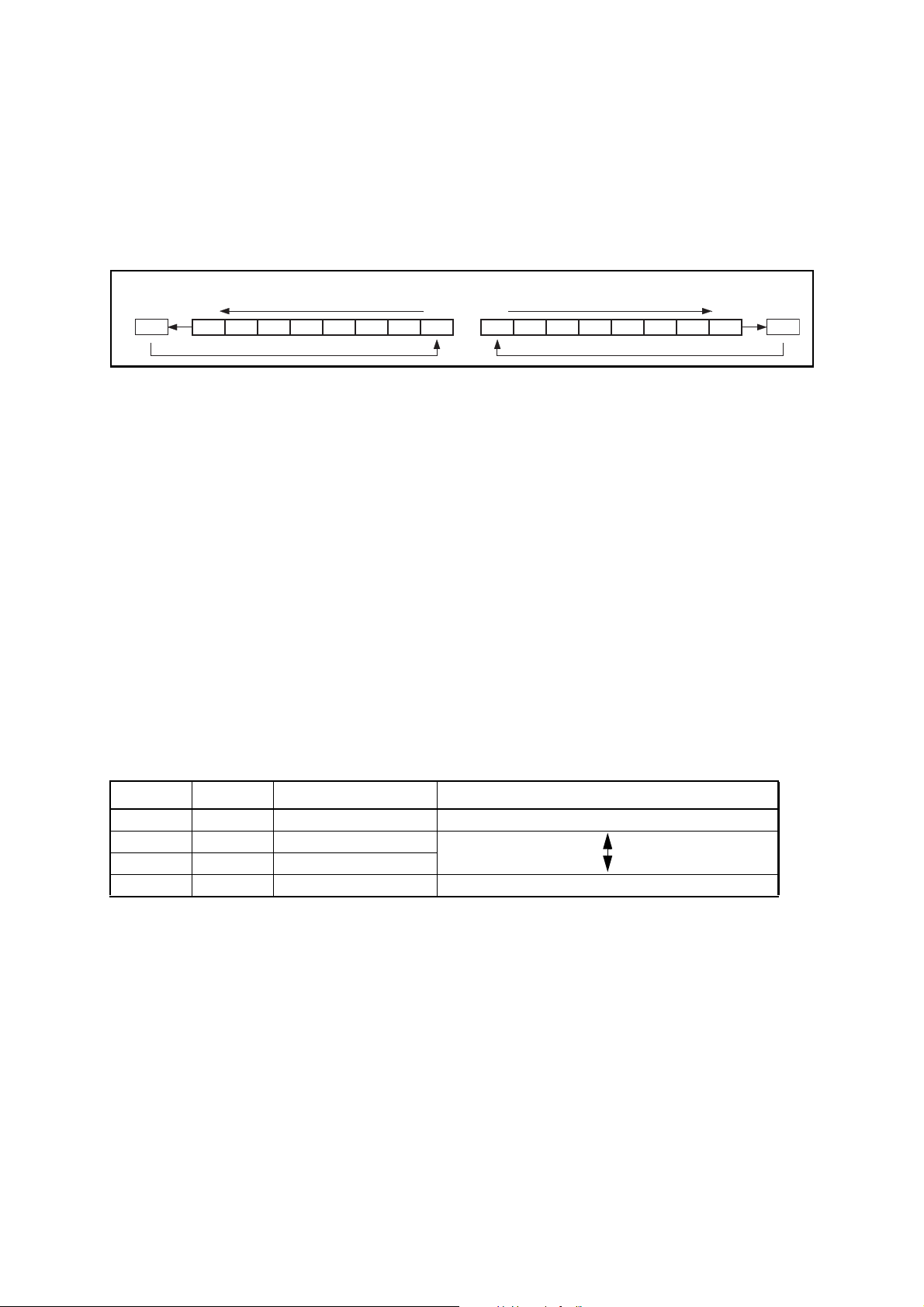
CHAPTER 2 CPU
Right-shift (RORC)•Left-shift (ROLC)•
bit0bit7
C
bit0bit7
C
2.1 Dedicated Registers
● Carry flag (C)
This flag is set to "1" when a carry from bit7 or a borrow to bit7 occurs due to the result of an
operation. Otherwise, the flag is set to "0". When a shift instruction is executed, the flag is set
to the shift-out value.
Figure 2.1-6 shows how the carry flag is updated by a shift instruction.
Figure 2.1-6 Carry Flag Updated by Shift Instruction
■ Interrupt Acceptance Control Bits
● Interrupt enable flag (I)
When this flag is set to "1", interrupts are enabled and accepted by the CPU. When this flag is
set to "0", interrupts are disabled and rejected by the CPU.
The initial value after a reset is "0".
The SETI and CLRI instructions set and clear the flag to "1" and "0", respectively.
MB95630H Series
● Interrupt level bits (IL[1:0])
These bits indicate the level of the interrupt currently accepted by the CPU.
The interrupt level is compared with the value of the interrupt level setting register (ILR0 to
ILR5) that corresponds to the interrupt request (IRQ00 to IRQ23) of each peripheral function.
The CPU services an interrupt request only when its interrupt level is smaller than the value of
these bits with the interrupt enable flag set (CCR:I = 1). Table 2.1-3 lists interrupt level
priorities. The initial value after a reset is "0b11".
Table 2.1-3 Interrupt Levels
IL1 IL0 Interrupt level Priority
00 0 High
01 1
10 2
1 1 3 Low (No interrupt)
The interrupt level bits (IL[1:0]) are usually "0b11" when the CPU does not service an interrupt
(with the main program running).
For details of interrupts, see "5.1 Interrupts".
10 FUJITSU SEMICONDUCTOR LIMITED MN702-00009-1v0-E
Page 31

CHAPTER 2 CPU
MB95630H Series
2.2 General-purpose Register
2.2 General-purpose Register
The general-purpose registers are a memory block in which each bank consists
of eight 8-bit registers. Up to 32 register banks can be used in total. The
register bank pointer (RP) is used to specify a register bank.
Register banks are useful for interrupt handling, vector call processing, and
sub-routine calls.
■ Configuration of General-purpose Register
• The general-purpose register is an 8-bit register and is located in a register bank in the
general-purpose register area (in RAM).
• Up to 32 banks can be used, each of which consists of eight registers (R0 to R7).
• The register bank pointer (RP) specifies the register bank currently being used and the lower
three bits of the op-code specify the general-purpose register 0 (R0) to the general-purpose
register 7 (R7).
Figure 2.2-1 shows the configuration of the register banks.
Figure 2.2-1 Configuration of Register Banks
This address = 0x0100 + 8 × (RP)
Address 0x100
For information on the general-purpose register area available on each product, see "■ AREAS
FOR SPECIFIC APPLICATIONS" in the device data sheet.
0x107
R0
R1
R2
R3
R4
R5
R6
R7
Bank 0
Memory area
R0
R1
R2
R3
R4
R5
R6
R7
8 bits
R0
R1
R2
R3
R4
R5
R6
R7
0x1F8
0x1FF
Bank 31
32 banks
The number of banks
available is restricted by
the available RAM size.
MN702-00009-1v0-E FUJITSU SEMICONDUCTOR LIMITED 11
Page 32

CHAPTER 2 CPU
2.2 General-purpose Register
■ Features of General-purpose Registers
The general-purpose register has the following features.
• High-speed access to RAM with short instructions (general-purpose register addressing).
• Grouping registers into a block of register banks facilitates data protection and division of
registers in terms of functions.
A general-purpose register bank can be allocated exclusively to an interrupt service routine or a
vector call (CALLV #0 to #7) processing routine. For instance, the fourth register bank is
always assigned to the second interrupt.
Data of a general-purpose register before an interrupt can be saved to a dedicated register bank
by just specifying that register bank at the beginning of an interrupt service routine. This
therefore eliminates the need to save data of a general-purpose register in a stack, thereby
enabling the CPU to receive interrupts at high speed.
Note:
In an interrupt service routine, include one of the following in a program to ensure that
values of the interrupt level bits (CCR:IL[1:0]) of the condition code register are not
modified when modifying a register bank pointer (RP) to specify a register bank.
• Read the interrupt level bits and save their values before writing a value to the RP.
• Directly write a new value to the RP mirror address "0x0078" to update the RP.
• As for a product whose RAM size is 256 bytes, the area available for general-registers
is from "0x0100" to "0x018F", which is half of that of the product whose RAM size is
512 bytes or above. Therefore, when using a program development tool such as a C
compiler to set a general-register area, ensure that the area used as a general-register
area does not exceed the size of RAM installed.
MB95630H Series
12 FUJITSU SEMICONDUCTOR LIMITED MN702-00009-1v0-E
Page 33

MB95630H Series
Before
execution
Memory Memory
A
0x1234
MOVW 0091H, A
0x0090
0x0091
0x0092
0x0093
0x0090
0x0091
0x0092
0x0093
0x12
0x34
A
0x1234
After
execution
2.3 Placement of 16-bit Data in Memory
2.3 Placement of 16-bit Data in Memory
This section describes how 16-bit data is stored in memory.
■ Placement of 16-bit Data in Memory
● State of 16-bit data stored in RAM
When 16-bit data is written to memory, the upper byte of the data is stored at a smaller address
and the lower byte is stored at the next address. When 16-bit data is read, it is handled in the
same way.
Figure 2.3-1 shows how 16-bit data is placed in memory.
Figure 2.3-1 Placement of 16-bit Data in Memory
CHAPTER 2 CPU
● Storage state of 16-bit data specified by an operand
Even when the operand in an instruction specifies 16-bit data, the upper byte is stored at the
address closer to the op-code (instruction) and the lower byte is stored at the address next to the
one at which the upper byte is stored.
That is true whether an operand is either a memory address or 16-bit immediate data.
Figure 2.3-2 shows how 16-bit data in an instruction is placed.
Figure 2.3-2 Placement of 16-bit Data in Instruction
Extended address
[Example]
MOV A, 5678H
MOVW A, #1234H
0xXXX0
0xXXX2
0xXXX5
0xXXX8
XX XX
60 56 78
E4 12 34
XX
;
16-bit immediate data
;
Assemble
Extended address
;
16-bit immediate data
;
● Storage state of 16-bit data in the stack
When 16-bit register data is saved in a stack on an interrupt, the upper byte is stored at a lower
address in the same way as 16-bit data specified by an operand.
MN702-00009-1v0-E FUJITSU SEMICONDUCTOR LIMITED 13
Page 34

CHAPTER 2 CPU
2.3 Placement of 16-bit Data in Memory
MB95630H Series
14 FUJITSU SEMICONDUCTOR LIMITED MN702-00009-1v0-E
Page 35

CHAPTER 3
CLOCK CONTROLLER
This chapter describes the functions and
operations of the clock controller.
3.1 Overview
3.2 Oscillation Stabilization Wait Time
3.3 Registers
3.4 Clock Modes
3.5 Operations in Low Power Consumption Mode (Standby
Mode)
3.6 Clock Oscillator Circuit
3.7 Overview of Prescaler
3.8 Configuration of Prescaler
3.9 Operation of Prescaler
3.10 Notes on Using Prescaler
MN702-00009-1v0-E FUJITSU SEMICONDUCTOR LIMITED 15
Page 36

CHAPTER 3 CLOCK CONTROLLER
3.1 Overview
MB95630H Series
3.1 Overview
The New 8FX family has a built-in clock controller that optimizes its power
consumption. It supports both of the external main clock and the external
subclock.
The clock controller enables/disables clock oscillation, enables/disables the
supply of clock signals to the internal circuit, selects the clock source, and
controls the internal CR oscillator and frequency divider circuits.
■ Overview of Clock Controller
The clock controller enables/disables clock oscillation, enables/disables clock supply to the
internal circuit, selects the clock source, and controls the internal CR oscillator and frequency
divider circuits.
The clock controller controls the internal clock according to the clock mode, standby mode
settings and the reset operation. The clock mode is used to select an internal operating clock;
the standby mode is used to enable and disable clock oscillation and signal supply.
The clock controller selects the optimum power consumption and functions depending on the
combination of clock mode and standby mode.
This product has five source clocks: a main clock formed by dividing the main oscillation
clock by 2, a subclock formed by dividing the sub-oscillation clock by 2, a main CR clock, a
main CR PLL clock formed by multiplying the main CR oscillation clock by the PLL
multiplier, and a sub-CR clock formed by dividing the sub-CR oscillation clock by 2.
16 FUJITSU SEMICONDUCTOR LIMITED MN702-00009-1v0-E
Page 37

MB95630H Series
Standby control register (STBC)
System clock selector
Divide by 2
Divide by 2
Clock
control
circuit
Oscillation
stabilization
wait circuit
Supply to CPU
Supply to perip-
heral resources
Source clock
selection
control circuit
System clock control register 2 (SYCC2)
(7)
(8)
(1): Main clock (FCH)
(2): Subclock (F
CL
)
(3): Main clock
(4): Subclock
(5): Main CR clock (F
CRH
)
(6): Sub-CR clock (F
CRL
)
(7): Source clock (SCLK)
(8): Machine clock (MCLK)
(9): Main CR PLL clock (F
MCRPLL
)
Main CR
clock oscillator
circuit
Main clock
oscillator
circuit
Subclock
oscillator
circuit
Main CR PLL
clock oscillator
circuit
Sub-CR
clock oscillator
circuit
Divide by 2
(5)
(6)
(9)
(1)
(2)
(3)
(4)
Watch or time-base
timer mode
Sleep mode
Stop mode
Clock for time-base timer
Clock for watch timer
MPEN - - - -
MPMC1 MPMC0 MPRDY
SRDY
SOSCE MOSCE
SCRE MCREMRDY
SCRDY MCRDY
STP TMD - - -SLP SPL SRST
Standby control register 2 (STBC2)
To Flash memory
- - - -
DSTBYX
- - -
System clock control register (SYCC)
SCM2 SCS1 SCS0 DIV1 DIV0SCM1 SCM0 SCS2
Oscillation stabilization wait time setting register (WATR)
PLL control register (PLLC)
SWT3 MWT3 MWT2 MWT1 MWT0SWT2 SWT1 SWT0
Prescaler
No division
Divide by 4
Divide by 8
Divide by 16
■ Block Diagram of Clock Controller
Figure 3.1-1 is the block diagram of the clock controller.
Figure 3.1-1 Block Diagram of Clock Controller
CHAPTER 3 CLOCK CONTROLLER
3.1 Overview
MN702-00009-1v0-E FUJITSU SEMICONDUCTOR LIMITED 17
Page 38

CHAPTER 3 CLOCK CONTROLLER
3.1 Overview
■ Configuration of Clock Controller
● Main clock oscillator circuit
This block is the oscillator circuit for the main clock.
● Subclock oscillator circuit
This block is the oscillator circuit for the subclock.
● Main CR clock oscillator circuit
This block is the oscillator circuit for the main CR clock.
● Main CR PLL clock oscillator circuit
This block is the oscillator circuit for the main CR PLL clock.
● Sub-CR clock oscillator circuit
This block is the oscillator circuit for the sub-CR clock.
MB95630H Series
● System clock selector
This block selects a clock according to the clock mode used from the following five types of
source clock: main clock, subclock, main CR clock, main CR PLL clock and sub-CR clock.
The source clock selected is divided by the prescaler. The divided clock is called "machine
clock", which is to be supplied to the clock control circuit.
● Clock control circuit
This block controls the supply of the machine clock to the CPU and each peripheral resource
according to the standby mode used or oscillation stabilization wait time.
● Oscillation stabilization wait circuit
This block outputs oscillation stabilization wait time signals according to clocks that are
enabled to operate.
In the case of main clock, its oscillation stabilization signal can be selected from 14 types of
oscillation stabilization signals created by a dedicated timer in the oscillation stabilization wait
circuit. In case of subclock, its oscillation stabilization signal can be selected from 15 types of
oscillation stabilization signals created by the same dedicated timer.
● System clock control register (SYCC)
This register is used to select a clock mode and a machine clock divide ratio, and to indicate
the current clock mode.
● PLL control register (PLLC)
This register is used to control the main CR PLL clock multiplier settings.
● Standby control register (STBC)
This register is used to control the transition from RUN state to standby mode, the setting of
pin states in stop mode, time-base timer mode, or watch mode, and the generation of software
resets.
18 FUJITSU SEMICONDUCTOR LIMITED MN702-00009-1v0-E
Page 39

MB95630H Series
● System clock control register 2 (SYCC2)
This register is used to enable/disable the oscillations of the main clock, main CR clock,
subclock, and sub-CR clock, and to display the ready signals of main clock oscillation,
subclock oscillation, sub-CR oscillation and main CR oscillation.
● Oscillation stabilization wait time setting register (WATR)
This register is used to set the oscillation stabilization wait time for the main clock and
subclock.
● Standby control register 2 (STBC2)
This register is used to control the deep standby mode.
CHAPTER 3 CLOCK CONTROLLER
3.1 Overview
MN702-00009-1v0-E FUJITSU SEMICONDUCTOR LIMITED 19
Page 40

CHAPTER 3 CLOCK CONTROLLER
3.1 Overview
MB95630H Series
■ Clock Modes
There are five clock modes:
• Main clock mode
• Main CR clock mode
• Main CR PLL clock mode
• Subclock mode
• Sub-CR clock mode.
Table 3.1-1 shows the relationships between the clock modes and the machine clock (operating
clock for the CPU and peripheral functions).
Table 3.1-1 Clock Modes and Machine Clock Selection
Clock mode Machine clock
Main clock mode The machine clock is generated by dividing the main oscillation clock by 2.
Main CR clock mode The machine clock is generated from the main CR clock.
Main CR PLL clock mode
Subclock mode The machine clock is generated by dividing the sub-oscillation clock by 2.
Sub-CR clock mode The machine clock is generated by dividing the sub-CR oscillation clock by 2.
In any clock mode, the frequency of a selected clock can be divided.
The machine clock is generated by multiplying the main CR clock by a PLL
multiplier.
20 FUJITSU SEMICONDUCTOR LIMITED MN702-00009-1v0-E
Page 41

MB95630H Series
■ Standby Mode
The clock controller selects whether to enable or disable clock oscillation and clock supply to
the internal circuitry according to the standby mode selected. With the exception of time-base
timer mode and watch mode, the standby mode can be set independently of the clock mode.
Table 3.1-2 shows the relationships between standby modes and clock supply states.
Table 3.1-2 Standby Mode and Clock Supply States
Standby mode Clock supply state
Sleep mode
Time-base timer mode
Watch mode
Stop mode
Clock supply to the CPU is stopped. As a result, the CPU stops operating, but other
peripheral functions continue operating.
Clock signals are only supplied to the time-base timer and the watch prescaler, while the
clock supply to other circuits is stopped. As a result, all the functions other than the timebase timer, watch prescaler, external interrupt, and low-voltage detection reset (option)
are stopped.
The time-base timer mode can be used in main clock mode, main CR clock mode and
main CR PLL clock mode.
Main clock oscillation is stopped. Clock signals are supplied only to the watch prescaler,
while clock supply to other circuits is stopped. As a result, all the functions other than
the watch prescaler, external interrupt, and low-voltage detection reset (option) are
stopped.
The watch mode is the standby mode that can be used in subclock mode and sub-CR
clock mode.
Main clock oscillation and subclock oscillation are stopped, and clock supply to all
circuits is stopped. As a result, all the functions other than external interrupt and lowvoltage detection reset (option) are stopped.
CHAPTER 3 CLOCK CONTROLLER
3.1 Overview
Note:
In every standby mode, two further operating mode options, normal standby mode and deep
standby mode, can be selected by the deep standby mode control bit in the standby control
register 2 (STBC2:DSTBYX).
For details, see "3.5.1 Notes on Using Standby Mode".
Clocks that are not mentioned in Table 3.1-2 are supplied under particular settings.
For example, with main clock mode being used in stop mode, when SYCC2:SOSCE or
SYCC2:SCRE has been set to "1", the watch prescaler continues its operation.
In addition, with the hardware watchdog timer already started, the watchdog timer
operates also in standby mode, depending on the settings of the non-volatile register
(NVR) interface. For details of the non-volatile register (NVR) interface, see "CHAPTER
26 NON-VOLATILE REGISTER (NVR) INTERFACE".
MN702-00009-1v0-E FUJITSU SEMICONDUCTOR LIMITED 21
Page 42

CHAPTER 3 CLOCK CONTROLLER
3.1 Overview
MB95630H Series
■ Combinations of Clock Mode and Standby Mode
Table 3.1-3 and Table 3.1-4 list the combinations of clock mode and standby mode, and the
respective operating states of different internal circuits with different combinations of clock
mode and standby mode.
Table 3.1-3 Combinations of Standby Mode and Clock Mode, and Internal Operating States (1)
RUN Sleep
Function
Main clock
mode
Main CR
clock mode/
Main CR PLL
Subclock
mode
Sub-CR
clock mode
Main clock
mode
clock mode
Main clock Operating
Main CR clock/
Main CR PLL
clock
Subclock
Sub-CR clock
CPU Operating Operating Stopped Stopped
Flash memory Operating Operating
RAM Operating Operating Value held Value held
I/O ports Operating Operating Output held Output held
Time-base timer Operating Stopped Operating Stopped
Watch prescaler
External interrupt Operating Operating Operating Operating
Hardware
watchdog timer
Software watchdog
timer
Low-voltage
detection reset
Other peripheral
functions
*2
Stopped
Operating
Operating
Operating
Operating Operating
Operating Operating Stopped Stopped
Operating Operating Operating Operating
Operating Operating Operating Operating
*1
Stopped
Operating Stopped
*3
*4
*3, *4
Stopped Operating
Operating
*4
Operating
Operating
Operating
Operating
Stopped
*3
Operating
Main CR
clock mode/
Main CR PLL
clock mode
*1
Stopped
*2
Operating Stopped
*3
Operating
*4
Operating
Operating
*6
*3, *4
*5
Va l u e he l d
Subclock
mode
Operating
*4
Operating
Valu e h e l d
Operating
Operating
clock mode
Stopped
Sub-CR
Operating
Operating
*6
*5
*3
*1: The main clock runs when the main clock oscillation enable bit in the system clock control register 2
(SYCC2:MOSCE) is set to "1".
*2: The main CR clock or the main CR PLL clock runs when main CR clock oscillation enable bit in the system
clock control register 2 (SYCC2:MCRE) is set to "1".
*3: The module runs when the subclock oscillation enable bit in the system clock control register 2
(SYCC2:SOSCE) is set to "1".
*4: The module runs when the sub-CR clock oscillation enable bit in the system clock control register 2
(SYCC2:SCRE) is set to "1".
*5: The hardware watchdog timer stops when the hardware watchdog timer is disabled by the non-volatile
register (NVR) interface.
*6: The state of the Flash memory in a standby mode can be selected from two options, normal state and low-
power state, by the deep standby mode control bit in the standby control register 2 (STBC2:DSTBYX).
22 FUJITSU SEMICONDUCTOR LIMITED MN702-00009-1v0-E
Page 43

CHAPTER 3 CLOCK CONTROLLER
MB95630H Series
3.1 Overview
Table 3.1-4 Combinations of Standby Mode and Clock Mode and Internal Operating States (2)
Time-base timer Watch Stop
Operating
Operating
Operating
Main CR
clock mode/
Main CR PLL
clock mode
*3
*4
Val u e he l d
*3, 4
Operating
Subclock
mode
*6
*5
Sub-CR
clock mode
Stopped
Stopped
Stopped
Function
Main clock
mode
Main CR
clock mode/
Main CR PLL
Subclock
mode
Sub-CR
clock mode
Main clock
mode
clock mode
Main clock Operating
Main CR clock/
Main CR PLL
clock
Subclock
Sub-CR clock
CPU Stopped Stopped Stopped
Flash memory
RAM Value held Value held Value held
I/O ports Output held / Hi-Z Output held/Hi-Z Output held/Hi-Z
Time-base timer Operating Stopped Stopped
Watch prescaler
External interrupt Operating Operating Operating
Hardware
watchdog timer
Software watchdog
timer
Low-voltage
detection reset
Other peripheral
functions
*2
Stopped
Operating
Operating
Value held
Operating
Operating
Stopped Stopped Stopped
Operating Operating Operating
Stopped Stopped Stopped
*1
Stopped
Operating Stopped Stopped
*3
*4
*6
*3, *4
*5
Stopped Stopped
Operating
Operating
*4
Value held
Operating
Operating
Operating
Operating
*6
*5
*3
*1: The main clock runs when the main clock oscillation enable bit in the system clock control register 2
(SYCC2:MOSCE) is set to "1".
*2: The main CR clock or the main CR PLL clock runs when main CR clock oscillation enable bit in the system
clock control register 2 (SYCC2:MCRE) is set to "1".
*3: The module runs when the subclock oscillation enable bit in the system clock control register 2
(SYCC2:SOSCE) is set to "1".
*4: The module runs when the sub-CR clock oscillation enable bit in the system clock control register 2
(SYCC2:SCRE) is set to "1".
*5: The hardware watchdog timer stops when the hardware watchdog timer is disabled by the non-volatile
register (NVR) interface.
*6: The state of the Flash memory in a standby mode can be selected from two options, normal state and low-
power state, by the deep standby mode control bit in the standby control register 2 (STBC2:DSTBYX).
MN702-00009-1v0-E FUJITSU SEMICONDUCTOR LIMITED 23
Page 44

CHAPTER 3 CLOCK CONTROLLER
Oscillation stabilization
wait time
()
Normal operation
Operation after returning
from stop mode or a reset
Oscillation started
X1
Oscillation time of
oscillator
Oscillation stabilized
3.2 Oscillation Stabilization Wait Time
MB95630H Series
3.2 Oscillation Stabilization Wait Time
The oscillation stabilization wait time is the time after the oscillator circuit
stops oscillation until the oscillator resumes its stable oscillation at its natural
frequency. The clock controller obtains the oscillation stabilization wait time
after the start of oscillation by counting a specific number of oscillation clock
cycles. During the oscillation stabilization wait time, the clock controller stops
clock supply to internal circuits.
■ Oscillation Stabilization Wait Time
The clock controller obtains the oscillation stabilization wait time after the start of oscillation
by counting a specific number of oscillation clock cycles. During the oscillation stabilization
wait time, the clock controller stops clock supply to internal circuits.
When the power is switched on, or when a state transition request making the oscillator start
from the oscillation stop state is generated due to a change of clock mode caused by a reset, by
an interrupt in stop mode or by the software operation, before making the clock mode transit to
another mode, the clock controller automatically waits for the oscillation stabilization wait time
of the clock for that mode to elapse.
Figure 3.2-1 shows how the oscillator runs immediately after starting oscillating.
Figure 3.2-1 Behavior of Oscillator Immediately after Starting Oscillation
Oscillation stabilization wait time of main clock, subclock, main CR clock, main CR PLL
clock or sub-CR clock is counted by using a dedicated counter. The count value can be set in
the oscillation stabilization wait time setting register (WATR). Set it in keeping with the
oscillator characteristics.
When a power-on reset occurs, the oscillation stabilization wait time is fixed at the initial
value.
Table 3.2-1 shows the length of oscillation stabilization wait time.
Table 3.2-1 Oscillation Stabilization Wait Time
Clock Reset source Oscillation stabilization wait time
Main clock
Subclock
Power-on reset
Other than power-on reset Register settings (WATR:MWT[3:0])
Power-on reset
Other than power-on reset Register settings (WATR:SWT[3:0])
Initial value: (2
Initial value: (2
14
-2)/FCH (FCH: main clock frequency)
15
-2)/FCL (FCL: subclock frequency)
24 FUJITSU SEMICONDUCTOR LIMITED MN702-00009-1v0-E
Page 45

MB95630H Series
■ PLL Clock Oscillation Stabilization Wait Time
As with the oscillation stabilization wait time of the oscillator, when a request for state
transition from PLL oscillation stopped state to oscillation start is generated due to an interrupt
in stop mode or a change of clock mode by software, the clock controller first waits for the
main CR clock oscillation stabilization wait time to elapse, and then automatically waits for the
PLL clock oscillation stabilization wait time to elapse.
Table 3.2-2 shows the PLL oscillation stabilization wait time.
Table 3.2-2 PLL Oscillation Stabilization Wait Time
PLL oscillation stabilization wait time
Main CR PLL clock
2
12
/F
MCRPLL
CHAPTER 3 CLOCK CONTROLLER
3.2 Oscillation Stabilization Wait Time
*
*: F
MCRPLL
= 16 MHz
■ CR Clock Oscillation Stabilization Wait Time
As with the oscillation stabilization wait time of the oscillator, when a state transition request
making CR oscillation start from the CR oscillation stop state is generated due to a change of
clock mode caused by an interrupt in standby mode or by the software operation, the clock
controller automatically waits for the CR oscillation stabilization wait time to elapse.
Table 3.2-3 shows the CR oscillation stabilization wait time.
Table 3.2-3 CR Oscillation Stabilization Wait Time
CR oscillation stabilization wait time
CRH
CRL
*1
*2
*1: F
*2: F
CRH
CRL
Main CR clock
Sub-CR clock
= 4 MHz
= 150 kHz
210/F
25/F
■ Oscillation Stabilization Wait Time and Clock Mode/Standby Mode Transition
If state transition occurs, the clock controller automatically waits for the oscillation
stabilization wait time to elapse whenever necessary. Depending on the circumstances under
which state transition occurs, the clock controller does not wait for the oscillation stabilization
wait time to elapse even if state transition occurs.
For details on state transition, see "3.4 Clock Modes" and "3.5 Operations in Low Power
Consumption Mode (Standby Mode)".
MN702-00009-1v0-E FUJITSU SEMICONDUCTOR LIMITED 25
Page 46

CHAPTER 3 CLOCK CONTROLLER
3.2 Oscillation Stabilization Wait Time
MB95630H Series
■ Order of Priority for Oscillation Stabilization Wait Times
When multiple clocks are enabled simultaneously, the clock controller counts the respective
oscillation stabilization wait times of clocks according to a designated order of priority. Below
are the respective orders of priority for counting different oscillation stabilization wait times in
different clock modes.
• Main clock mode
Sub-CR clock > Subclock > Main CR clock > Main CR PLL clock
• Main CR clock mode
Sub-CR clock > Subclock > Main CR PLL clock > Main clock
• Main CR PLL clock mode
Sub-CR clock > Subclock > Main clock
• Subclock mode
Sub-CR clock > Main CR clock or main clock > Main CR PLL clock
• Sub-CR clock mode
Main CR clock or main clock > Subclock > Main CR PLL clock
26 FUJITSU SEMICONDUCTOR LIMITED MN702-00009-1v0-E
Page 47

CHAPTER 3 CLOCK CONTROLLER
MB95630H Series
3.3 Registers
This section provides details of registers of the clock controller.
Table 3.3-1 List of Clock Controller Registers
3.3 Registers
Register
abbreviation
SYCC System clock control register 3.3.1
PLLC PLL control register 3.3.2
WAT R Oscillation stabilization wait time setting register 3.3.3
STBC Standby control register 3.3.4
SYCC2 System clock control register 2 3.3.5
STBC2 Standby control register 2 3.3.6
Register name Reference
MN702-00009-1v0-E FUJITSU SEMICONDUCTOR LIMITED 27
Page 48

CHAPTER 3 CLOCK CONTROLLER
3.3 Registers
MB95630H Series
3.3.1 System Clock Control Register (SYCC)
The system clock control register (SYCC) selects a machine clock divide ratio
and a clock mode, and indicates the current clock mode.
■ Register Configuration
bit 7 6 5 4 3 2 1 0
Field SCM2 SCM1 SCM0 SCS2 SCS1 SCS0 DIV1 DIV0
Attribute R R R R/W R/W R/W R/W R/W
Initial value X X X 1 1 0 1 1
■ Register Functions
[bit7:5] SCM[2:0]: Clock mode monitor bits
These bits indicate the current clock mode.
These bits are read-only bits. Writing values to these bits has no effect on operation.
bit7:5 Details
Reading "000" Indicates that the current clock mode is subclock mode.
Reading "010" Indicates that the current clock mode is main clock mode.
Reading "100" Indicates that the current clock mode is sub-CR clock mode.
Reading "110" Indicates that the current clock mode is main CR clock mode.
Reading "111" Indicates that the current clock mode is main CR PLL clock mode.
[bit4:2] SCS[2:0]: Clock mode select bits
These bits select a clock mode.
bit4:2 Details
Writing "000" Selects subclock mode.
Writing "010" Selects main clock mode.
Writing "100" Selects sub-CR clock mode.
Writing "110" Selects main CR clock mode.
Writing "111" Selects main CR PLL clock mode.
Note: Do not write to SCS[2:0] any value other than those listed in the table above.
[bit1:0] DIV[1:0]: Machine clock divide ratio select bits
These bits select the machine clock divide ratio for the source clock.
The machine clock is generated from the source clock according to the divide ratio set by these bits.
bit1:0 Details
Writing "00" Source clock (no division)
Writing "01" Source clock/4
Writing "10" Source clock/8
Writing "11" Source clock/16
28 FUJITSU SEMICONDUCTOR LIMITED MN702-00009-1v0-E
Page 49

CHAPTER 3 CLOCK CONTROLLER
MB95630H Series
3.3 Registers
3.3.2 PLL Control Register (PLLC)
The PLL control register (PLLC) controls the main CR PLL clock multiplier
settings.
■ Register Configuration
bit 7 6 5 4 3 2 1 0
Field MPEN MPMC1 MPMC0 MPRDY — — — —
Attribute R/W R/W R/W R — — — —
Initial value 0 0 0 X 0 0 0 0
■ Register Functions
[bit7] MPEN: Main CR PLL clock enable bit
This bit enables or disables the main CR PLL clock.
When SCS[2:0] are set to "0b111", this bit will be automatically set to "1".
When SCS[2:0] or SCM[2:0] are set to "0b111", writing "0" to this bit has no effect on operation.
This bit will be automatically set to "0" when the clock mode transits from one mode to another mode except
main CR PLL clock mode.
When the current clock mode is subclock mode or sub-CR clock mode, writing "1" to this bit has no effect on
operation.
bit7 Details
Writing "0" Disables the main CR PLL clock.
Writing "1" Enables the main CR PLL clock.
[bit6:5] MPMC[1:0]: Main CR PLL clock multiplier select bits
These bits select a main CR PLL clock multiplier.
The settings of these bits can be modified only when the main CR PLL clock is stopped. Thus these bits can
be modified in main clock mode, main CR clock mode, subclock mode or sub-CR clock mode.
bit6:5 Details
Writing "00" Main CR clock × 2
Writing "01" Main CR clock × 2.5
Writing "10" Main CR clock × 3
Writing "11" Main CR clock × 4
Note: When SCS[2:0] or SCM[2:0] are set to "0b111", writing values to MPMC[1:0] is prohibited.
[bit4] MPRDY: Main CR PLL clock oscillation stabilization bit
This bit indicates whether the main CR PLL clock oscillation is ready.
bit4 Details
Reading "0"
Reading "1" Indicates that the main CR PLL clock oscillation wait time is over.
Indicates that main CR PLL clock is in the oscillation stabilization wait state or that the main CR
PLL clock has stopped.
[bit3:0] Undefined bits
Their read values are always "0". Writing values to these bits has no effect on operation.
MN702-00009-1v0-E FUJITSU SEMICONDUCTOR LIMITED 29
Page 50

CHAPTER 3 CLOCK CONTROLLER
3.3 Registers
MB95630H Series
3.3.3 Oscillation Stabilization Wait Time Setting Register (WATR)
This register selects oscillation stabilization wait times.
■ Register Configuration
bit 7 6 5 4 3 2 1 0
Field SWT3 SWT2 SWT1 SWT0 MWT3 MWT2 MWT1 MWT0
Attribute R/W R/W R/W R/W R/W R/W R/W R/W
Initial value 1 1 1 1 1 1 1 1
■ Register Functions
[bit7:4] SWT[3:0]: Subclock oscillation stabilization wait time select bits
These bits set the subclock oscillation stabilization wait time.
bit7:4
Writing "1111"
Writing "1110"
Writing "1101"
Writing "1100"
Writing "1011"
Writing "1010"
Writing "1001"
Writing "1000"
Writing "0111"
Writing "0110"
Writing "0101"
Writing "0100"
Writing "0011"
Writing "0010"
Writing "0001"
Writing "0000"
No. of cycles
215 - 2
214 - 2
213 - 2
212 - 2
211 - 2
210 - 2
29 - 2
28 - 2
27 - 2
26 - 2
25 - 2
24 - 2
23 - 2
22 - 2
21 - 2
21 - 2
(215-2)/FCL
(214-2)/F
(213-2)/F
(212-2)/F
(211-2)/F
(210-2)/F
(29-2)/F
(28-2)/F
(27-2)/F
(26-2)/F
(25-2)/F
(24-2)/F
(23-2)/F
(22-2)/F
(21-2)/F
(21-2)/F
CL
CL
CL
CL
CL
CL
CL
CL
CL
CL
CL
CL
CL
CL
CL
Details
Subclock (FCL) = 32.768 kHz
About 1.0 s
About 0.5 s
About 0.25 s
About 0.125 s
About 62.44 ms
About 31.19 ms
About 15.56 ms
About 7.75 ms
About 3.85 ms
About 1.89 ms
About 915.5 µs
About 427.2 µs
About 183.1 µs
About 61.0 µs
0.0 µs
0.0 µs
The number of cycles in the above table is the minimum value. The maximum value is the number of cycles
in the above table plus 1/F
CL
.
Note: Do not modify these bits during subclock oscillation stabilization wait time. Modify them when the
subclock oscillation stabilization bit in the system clock control register 2 (SYCC2:SRDY) has been
set to "1". These bits can be modified when the subclock is stopped with the subclock oscillation stop
bit in the system clock control register 2 (SYCC2:SOSCE) set to "0" in main clock mode, main CR
clock mode, main CR PLL clock mode, or sub-CR clock mode.
30 FUJITSU SEMICONDUCTOR LIMITED MN702-00009-1v0-E
Page 51

MB95630H Series
[bit3:0] MWT[3:0]: Main clock oscillation stabilization wait time select bits
These bits set the main clock oscillation stabilization wait time.
CHAPTER 3 CLOCK CONTROLLER
3.3 Registers
bit3:0
Writing "1111"
Writing "1110"
Writing "1101"
Writing "1100"
Writing "1011"
Writing "1010"
Writing "1001"
Writing "1000"
Writing "0111"
Writing "0110"
Writing "0101"
Writing "0100"
Writing "0011"
Writing "0010"
Writing "0001"
Writing "0000"
No. of cycles
214 - 2
213 - 2
212 - 2
211 - 2
210- 2
29 - 2
28 - 2
27 - 2
26 - 2
25 - 2
24 - 2
23 - 2
22 - 2
21 - 2
21 - 2
21 - 2
(214 - 2)/F
(213 - 2)/F
(212 - 2)/F
(211 - 2)/F
(210- 2)/F
(29 - 2)/F
(28 - 2)/F
(27 - 2)/F
(26 - 2)/F
(25 - 2)/F
(24 - 2)/F
(23 - 2)/F
(22 - 2)/F
(21 - 2)/F
(21 - 2)/F
(21 - 2)/F
CH
CH
CH
CH
CH
CH
CH
CH
CH
CH
CH
CH
CH
CH
CH
CH
Details
Main clock (FCH) = 4 MHz
About 4.10 ms
About 2.05 ms
About 1.02 ms
About 511.5 µs
About 255.5 µs
About 127.5 µs
About 63.5 µs
About 31.5 µs
About 15.5 µs
About 7.5 µs
About 3.5 µs
About 1.5 µs
About 0.5 µs
0.0 µs
0.0 µs
0.0 µs
The number of cycles in the above table is the minimum value. The maximum value is the number of cycles
in the above table plus 1/F
CH
.
Note: Do not modify these bits during main clock oscillation stabilization wait time. Modify them when the
main clock oscillation stabilization bit in the system clock control register 2 (SYCC2:MRDY) has
been set to "1". These bits can be modified when the main clock is stopped with the main clock
oscillation stop bit in the system clock control register 2 (SYCC2:MOSCE) set to "0" in main CR
clock mode, main CR PLL clock mode, subclock mode, or sub-CR clock mode.
MN702-00009-1v0-E FUJITSU SEMICONDUCTOR LIMITED 31
Page 52

CHAPTER 3 CLOCK CONTROLLER
3.3 Registers
MB95630H Series
3.3.4 Standby Control Register (STBC)
The standby control register (STBC) controls transition from the RUN state to
sleep mode, stop mode, time-base timer mode, or watch mode, sets the pin
state in stop mode, time-base timer mode, and watch mode, and controls the
generation of software resets.
■ Register Configuration
bit 7 6 5 4 3 2 1 0
Field STP SLP SPL SRST TMD — — —
Attribute W W R/W W W — — —
Initial value 0 0 0 0 0 0 0 0
■ Register Functions
[bit7] STP: Stop bit
This bit sets the transition to stop mode.
The read value of this bit is always "0".
bit7 Details
Writing "0" Has no effect on operation.
Writing "1" Causes the device to transit to stop mode.
Note: After an interrupt request is generated, writing "1" to this bit is ignored. For details, see "3.5.1 Notes
on Using Standby Mode".
[bit6] SLP: Sleep bit
This bit sets the transition to sleep mode.
The read value of this bit is always "0".
bit6 Details
Writing "0" Has no effect on operation.
Writing "1" Causes the device to transit to sleep mode.
Note: After an interrupt request is generated, writing "1" to this bit is ignored. For details, see "3.5.1 Notes
on Using Standby Mode".
[bit5] SPL: Pin state setting bit
This bit sets the states of external pins in stop mode, time-base timer mode, and watch mode.
bit5 Details
Writing "0" The state (level) of an external pin in stop mode, time-base timer mode and watch mode is kept.
An external pin becomes high impedance in stop mode, time-base timer mode and watch mode.
Writing "1"
(A pin for which connection to a pull-up resistor has been selected in the pull-up register is pulled
up.)
32 FUJITSU SEMICONDUCTOR LIMITED MN702-00009-1v0-E
Page 53

CHAPTER 3 CLOCK CONTROLLER
MB95630H Series
3.3 Registers
[bit4] SRST: Software reset bit
This bit sets the software reset.
The read value of this bit is always "0".
bit4 Details
Writing "0" Has no effect on operation.
Writing "1" Generates a 3-machine clock reset signal.
[bit3] TMD: Watch bit
This bit sets transition to time-base timer mode or watch mode.
Writing "1" to this bit in main clock mode, main CR clock, or main CR PLL clock mode causes the device to
transit to time-base timer mode.
Writing "1" to this bit in subclock mode or sub-CR clock mode causes the device to transit to watch mode.
Writing "0" to this bit has no effect on operation.
The read value of this bit is always "0".
Details
bit3
Writing "0" Has no effect on operation. Has no effect on operation.
Writing "1"
In main clock mode, main CR clock mode
or main CR PLL clock mode
Causes the device to transit to time-base timer
mode.
In subclock mode or sub-CR clock mode
Causes the device to transit to watch mode
Note: After an interrupt request is generated, writing "1" to this bit is ignored. For details, see "3.5.1 Notes
on Using Standby Mode".
[bit2:0] Undefined bits
Their read values are always "0". Writing values to these bits has no effect on operation.
Notes:
• Set a standby mode after making sure that the transition to clock mode has been
completed by comparing the values of the clock mode monitor bits (SYCC:SCM[2:0])
and clock mode select bits (SYCC:SCS[2:0]) in the system clock control register.
• If two or more of the following bits, stop bit (STP), sleep bit (SLP), software reset bit
(SRST) and watch bit (TMD), are set to "1" together, the order of priority for such bits
is as follows:
(1) Software reset bit (SRST)
(2) Stop bit (STP)
(3) Watch bit (TMD)
(4) Sleep bit (SLP)
When released from standby mode, the device returns to the normal operating state.
MN702-00009-1v0-E FUJITSU SEMICONDUCTOR LIMITED 33
Page 54

CHAPTER 3 CLOCK CONTROLLER
3.3 Registers
MB95630H Series
3.3.5 System Clock Control Register 2 (SYCC2)
The system clock control register 2 (SYCC2) indicates the respective
stabilization conditions of main clock oscillation, subclock oscillation, main CR
clock oscillation and sub-CR clock oscillation, and controls main clock
oscillation, subclock oscillation, main CR clock oscillation and sub-CR clock
oscillation.
■ Register Configuration
bit 7 6 5 4 3 2 1 0
Field SRDY MRDY SCRDY MCRDY SOSCE MOSCE SCRE MCRE
Attribute R R R R R/W R/W R/W R/W
Initial value X X X X 0 0 1 1
■ Register Functions
[bit7] SRDY: Subclock oscillation stabilization bit
This bit indicates whether the subclock oscillation has become stable.
This bit is read-only. Writing a value to this bit has no effect on operation.
bit7 Details
Reading "0"
Reading "1" Indicates that the subclock oscillation wait time is over.
Indicates that the clock controller is in the subclock oscillation stabilization wait state or that the
subclock oscillation has stopped.
[bit6] MRDY: Main clock oscillation stabilization bit
This bit indicates whether the main clock oscillation has become stable.
This bit is read-only. Writing a value to this bit has no effect on operation.
bit6 Details
Reading "0"
Reading "1" Indicates that the main clock oscillation wait time is over.
Indicates that the clock controller is in the main clock oscillation stabilization wait state or that the
main clock oscillation has stopped.
[bit5] SCRDY: Sub-CR clock oscillation stabilization bit
This bit indicates whether the sub-CR clock oscillation has become stable.
This bit is read-only. Writing a value to this bit has no effect on operation.
bit5 Details
Reading "0"
Reading "1" Indicates that the sub-CR clock oscillation wait time is over.
Indicates that the clock controller is in the sub-CR clock oscillation stabilization wait state or that
the sub-CR clock oscillation has stopped.
[bit4] MCRDY: Main CR clock oscillation stabilization bit
This bit indicates whether the main CR clock oscillation has become stable.
This bit is read-only. Writing a value to this bit has no effect on operation.
bit4 Details
Reading "0"
Reading "1" Indicates that the main CR clock oscillation wait time is over.
Indicates that the clock controller is in the main CR clock oscillation stabilization wait state or
that the main CR clock oscillation has stopped.
34 FUJITSU SEMICONDUCTOR LIMITED MN702-00009-1v0-E
Page 55

CHAPTER 3 CLOCK CONTROLLER
MB95630H Series
3.3 Registers
[bit3] SOSCE: Subclock oscillation enable bit
This bit enables or disables the subclock oscillation.
When SCS[2:0] are set to "0b000", this bit will be automatically set to "1".
When SCS[2:0] or SCM[2:0] are set to "0b000", writing "0" to this is has no effect on operation.
bit3 Details
Writing "0" Disables the subclock oscillation.
Writing "1" Enables the subclock oscillation.
[bit2] MOSCE: Main clock oscillation enable bit
This bit enables or disables the main clock oscillation.
When SCS[2:0] are set to "0b010", this bit will be automatically set to "1".
When SCS[2:0] or SCM[2:0] are set to "0b010", writing "0" to this is has no effect on operation.
This bit will be automatically set to "0" when the clock mode is changed from one mode to another mode
other than main clock mode.
When the current clock mode is subclock mode or sub-CR clock mode, writing "1" to this bit has no effect on
operation.
bit2 Details
Writing "0" Disables the main clock oscillation.
Writing "1" Enables the main clock oscillation.
[bit1] SCRE: Sub-CR clock oscillation enable bit
This bit enables or disables the sub-CR clock oscillation.
When SCS[2:0] are set to "0b100", this bit will be automatically set to "1".
When SCS[2:0] or SCM[2:0] are set to "0b100", writing "0" to this is has no effect on operation.
When SCS[2:0] and SCM[2:0] are not set to "0b100", this bit can be modified independently of other bits.
bit1 Details
Writing "0" Disables the sub-CR clock oscillation.
Writing "1" Enables the sub-CR clock oscillation.
[bit0] MCRE: Main CR clock oscillation enable bit
This bit enables or disables the main CR clock oscillation.
When SCS[2:0] are set to "0b110" or "0b111", this bit will be automatically set to "1".
When SCS[2:0] or SCM[2:0] are set to "0b110" or "0b111", writing "0" to this is has no effect on operation.
This bit will be automatically set to "0" when the clock mode is changed from one mode to another mode
except main CR clock mode or from main CR PLL clock mode.
When the current clock mode is subclock mode or sub-CR clock mode, writing "1" to this bit has no effect on
operation.
bit0 Details
Writing "0" Disables the main CR clock oscillation.
Writing "1" Enables the main CR clock oscillation.
MN702-00009-1v0-E FUJITSU SEMICONDUCTOR LIMITED 35
Page 56

CHAPTER 3 CLOCK CONTROLLER
3.3 Registers
MB95630H Series
3.3.6 Standby Control Register 2 (STBC2)
The standby control register 2 (STBC2) controls the deep standby mode.
■ Register Configuration
bit 7 6 5 4 3 2 1 0
Field — — — — — — — DSTBYX
Attribute — — — — — — — R/W
Initial value 0 0 0 0 0 0 0 0
■ Register Functions
[bit7:1] Undefined bits
Their read values are always "0". Writing values to these bits has no effect on operation.
[bit0] DSTBYX: Deep standby mode control bit
This bit makes the device transit to deep standby mode by setting the Flash memory to the low-power state in
standby mode.
Writing "0"
Writing "1"
Notes:
bit0 Details
Sets the Flash memory to the low-power state when the device enters standby mode according to
the setting of the standby control register (STBC). (deep standby mode)
Keeps the Flash memory at the normal state when the device enters standby mode according to
the setting of the standby control register (STBC). (normal standby mode)
• Waking up the device from deep standby mode and waking up the device from the
normal standby mode differ in the time required to wake up the device after an
interrupt source occurs. See the table below for details.
Maximum time required to wake up the device from deep
standby mode
(SCLK: source clock, MCLK: machine clock)
In main clock mode, main CR clock
mode, or main CR PLL clock mode
In subclock mode or sub-CR clock
mode
(10 SCLK + 150 µs + 6 MCLK) +
(2 SCLK + 150 µs + 6 MCLK) +
time required to wake up the
device from normal standby mode
time required to wake up the
device from normal standby mode
• Refer to "■ ELECTRICAL CHARACTERISTICS" in the device data sheet for the
difference between the deep standby mode and the normal standby mode in power
consumption.
• Do not make the device transit to deep standby mode when a Flash command
sequence (except read/reset) has been invoked.
36 FUJITSU SEMICONDUCTOR LIMITED MN702-00009-1v0-E
Page 57

CHAPTER 3 CLOCK CONTROLLER
MB95630H Series
3.4 Clock Modes
3.4 Clock Modes
There are five clock modes: main clock mode, subclock mode, main CR clock
mode, main CR PLL clock mode, and sub-CR clock mode. Mode switching
occurs according to the settings in the system clock control register (SYCC).
■ Operations in Main Clock Mode
In main clock mode, the main clock is used as the machine clock for the CPU and peripheral
functions.
The time-base timer operates using the main clock.
The watch prescaler operates using the subclock or the sub-CR clock.
While the device is operating in main clock mode, it can be set to transit to one of the
following standby mode: sleep mode, stop mode, or time-base timer mode.
After a reset, the device always enters main CR clock mode regardless of the clock mode used
before that reset.
■ Operations in Subclock Mode
In subclock mode, main clock oscillation is stopped* and the subclock is used as the machine
clock for the CPU and peripheral functions. In this mode, the time-base timer stops as it
requires the main clock for operation.
While the device is operating in subclock mode, it can be set to transit to one of the following
standby mode: sleep mode, stop mode, or watch mode.
■ Operations in Main CR Clock Mode or Main CR PLL Clock Mode
In main CR clock mode or main CR PLL clock mode, the main CR clock or the main CR PLL
clock is used as the machine clock for the CPU and peripheral functions. The time-base timer
and the watchdog timer operate using the main CR clock or the main CR PLL clock.
The watch prescaler operates using the subclock or the sub-CR clock.
While the device is operating in main CR clock mode or the main CR PLL clock mode, it can
be set to transit to one of the following standby mode: sleep mode, stop mode, or time-base
timer mode.
■ Operations in Sub-CR Clock Mode
In sub-CR clock mode, main clock oscillation is stopped* and the sub-CR clock is used as the
machine clock for the CPU and peripheral functions. In this mode, the time-base timer stops as
it requires the main clock for operation. The watch prescaler operates using the sub-CR clock.
While the device is operating in sub-CR clock mode, it can be set to transit to one of the
following standby mode: sleep mode, stop mode, or watch mode.
*: The oscillation of the main clock, main CR clock, or main CR PLL clock is automatically disabled
(writing "0" to SYCC2:MOSCE, SYCC2:MCRE or PLLC:MPEN respectively) when the clock mode
transits from main clock mode, main CR clock mode or main CR PLL clock mode to subclock mode or
sub-CR clock mode. In subclock mode or sub-CR clock mode, writing "1" to SYCC2:MOSCE,
SYCC2:MCRE or PLLC:MPEN cannot enable the main clock, the main CR clock, or the main CR
PLL clock respectively.
MN702-00009-1v0-E FUJITSU SEMICONDUCTOR LIMITED 37
Page 58

CHAPTER 3 CLOCK CONTROLLER
3.4 Clock Modes
■ Clock Mode State Transition Diagram
There are five clock modes: main clock mode, subclock mode, main CR clock mode, main CR
PLL clock mode and sub-CR clock mode. The device can switch between these modes
according to the settings in the system clock control register (SYCC).
Figure 3.4-1 Clock Mode State Transition Diagram
Power on
MB95630H Series
(4)
Sub-CR clock
oscillation
stabilization
wait time
Reset state
<1>
Main CR clock
oscillation stabilization
wait time
+
sub-CR clock
oscillation stabilization
wait time
Main CR clock mode
Main CR clock mode
(or main CR PLL
clock mode)
(2)
(1)
(or main CR PLL clock)
oscillation stabilization
(3)
Main CR clock
A reset occurs in any other state.
Main CR clock
(or main CR PLL clock)
oscillation stabilization
wait time
(5)
(6)
Main clock
oscillation
stabilization
wait time
(7)
(10)
(8)
(9)
Subclock
oscillation
stabilization
wait time
Main clock mode
(12)
(11)
Main clock
oscillation
stabilization
wait time
Sub-CR clock mode
(14)
(13)
(16)
(15)
Sub-CR clock
oscillation
stabilization
wait time
Subclock
oscillation
stabilization
wait time
(19)
(20)
Subclock mode
(18)
(17)
38 FUJITSU SEMICONDUCTOR LIMITED MN702-00009-1v0-E
Page 59

MB95630H Series
Table 3.4-1 Clock Mode State Transition Table (1 / 2)
CHAPTER 3 CLOCK CONTROLLER
3.4 Clock Modes
Current
State
<1> Reset state Main CR clock
(1)
(2)
(3)
Main CR clock/
Main CR PLL
clock
(4)
(5)
(6)
(7)
Main clock
(8)
(9)
(10)
(11)
(12)
Next State Description
Sub-CR clock
Subclock
Main clock
Main CR clock/
Main CR PLL
clock
Sub-CR clock
Subclock
After a reset, the device waits for the main CR clock oscillation stabilization wait time
and the sub-CR clock oscillation stabilization wait time to elapse and transits to main
CR clock mode. Even if that reset is a watchdog reset, software reset or external reset
caused in any clock mode, the device waits for the sub-CR clock oscillation
stabilization wait time and the main CR clock oscillation stabilization wait time to
elapse.
The device transits to sub-CR clock mode when the clock mode select bits in the
system clock control register (SYCC:SCS[2:0]) are set to "0b100".
However, when the sub-CR has been stopped according to the setting of the sub-CR
clock oscillation enable bit in the system clock control register 2 (SYCC2:SCRE), the
device waits for the sub-CR clock oscillation stabilization wait time to elapse before
transiting to sub-CR clock mode. In other words, when the sub-CR clock oscillation is
enabled in advance, and the sub-CR clock oscillation stabilization bit in the system
clock control register 2 (SYCC2:SCRDY) is "1", the device transits to sub-CR clock
mode immediately after the clock mode select bits (SYCC:SCS[2:0]) are set to
"0b100".
When the clock mode select bits in the system clock control register (SYCC:SCS[2:0])
are set to "0b000", the device transits to subclock mode after waiting for the subclock
oscillation stabilization wait time.
When the subclock oscillation is enabled by the setting of the subclock oscillation
enable bit in the system clock control register 2 (SYCC2:SOSCE), and the subclock
oscillation stabilization bit in the system clock control register 2 (SYCC2:SRDY) is
"1", the device transits to subclock mode immediately after the clock mode select bits
(SYCC:SCS[2:0]) are set to "0b000".
When the clock mode select bits in the system clock control register (SYCC:SCS[2:0])
are set to "0b010", the device transits to main clock mode after waiting for the main
clock oscillation stabilization wait time.
When the main clock oscillation is enabled by the setting of the main clock oscillation
enable bit in the system clock control register 2 (SYCC2:MOSCE), and the main clock
oscillation stabilization bit in the system clock control register 2 (SYCC2:MRDY) is
"1", the device transits to main clock mode immediately after the clock mode select
bits (SYCC:SCS[2:0]) are set to "0b010".
When the clock mode select bits in the system clock control register (SYCC:SCS[2:0])
are set to "0b110", the device transits to main CR clock mode after waiting for the
main CR clock oscillation stabilization wait time. When the main CR clock oscillation
is enabled by the setting of the main CR clock oscillation enable bit in the system
clock control register 2 (SYCC2:MCRE), and the main clock oscillation stabilization
bit in the system clock control register 2 (SYCC2:MRDY) is "1", the device transits to
main CR clock mode immediately after the clock mode select bits (SYCC:SCS[2:0])
are set to "0b110".
When the clock mode select bits in the system clock control register (SYCC:SCS[2:0])
are set to "0b111", the device transits to main CR PLL clock mode after waiting for the
main CR PLL clock oscillation stabilization wait time. When the main CR PLL clock
oscillation is enabled by the setting of the main CR PLL clock enable bit in the PLL
control register (PLLC:MPEN), and the main CR PLL clock oscillation stabilization
bit in the PLL control register (PLLC:MPRDY) is "1", the device transits to main CR
clock mode immediately after the clock mode select bits (SYCC:SCS[2:0]) are set to
"0b111".
Same as (1) and (2)
Same as (3) and (4)
MN702-00009-1v0-E FUJITSU SEMICONDUCTOR LIMITED 39
Page 60

CHAPTER 3 CLOCK CONTROLLER
3.4 Clock Modes
Table 3.4-1 Clock Mode State Transition Table (2 / 2)
MB95630H Series
Current
State
(13)
Sub-CR clock
(14) Main clock
(15)
(16)
(17)
Subclock
(18) Main clock Same as (14)
(19)
(20)
Next State Description
When the clock mode select bits in the system clock control register (SYCC:SCS[2:0])
Main CR clock/
Main CR PLL
clock
Subclock Same as (3) and (4)
Main CR clock/
Main CR PLL
clock
Sub-CR clock Same as (1) and (2)
are set to "0b110", the device transits to main CR clock mode after waiting for the
main CR clock oscillation stabilization wait time.
When the clock mode select bits in the system clock control register (SYCC:SCS[2:0])
are set to "0b111", the device transits to main CR PLL clock mode after waiting for the
main CR PLL clock oscillation stabilization wait time.
When the clock mode select bits in the system clock control register (SYCC:SCS[2:0])
are set to "0b010", the device transits to main clock mode after waiting for the main
clock oscillation stabilization wait time.
Same as (13)
40 FUJITSU SEMICONDUCTOR LIMITED MN702-00009-1v0-E
Page 61

CHAPTER 3 CLOCK CONTROLLER
MB95630H Series
3.5 Operations in Low Power Consumption Mode (Standby Mode)
3.5 Operations in Low Power Consumption Mode
(Standby Mode)
There are four standby modes: sleep mode, stop mode, time-base timer mode
and watch mode.
■ Overview of Transiting to and Returning from Standby Mode
There are four standby modes: sleep mode, stop mode, time-base timer mode, and watch mode.
The device transits to standby mode according to the settings in the standby control register
(STBC).
The device is released from standby mode by an interrupt or a reset. Before transiting to
normal operation, the device may wait for the oscillation stabilization wait time to elapse if
necessary.
When the clock mode returns from standby mode due to a reset, the device returns to main CR
clock mode. When the clock mode returns from standby mode due to an interrupt, the device
returns to the previous clock mode before transiting to standby mode.
■ Pin States in Standby Mode
The pin state setting bit (STBC:SPL) of the standby control register can be used to keep the
preceding state of an I/O port or a peripheral resource pin before its transition to stop mode,
time-base timer mode or watch mode, and to set an I/O port or a peripheral resource pin to high
impedance in stop mode, time-base timer mode or watch mode.
Refer to the device data sheet for the states of all pins in standby mode.
MN702-00009-1v0-E FUJITSU SEMICONDUCTOR LIMITED 41
Page 62

CHAPTER 3 CLOCK CONTROLLER
3.5 Operations in Low Power Consumption
Mode (Standby Mode)
MB95630H Series
3.5.1 Notes on Using Standby Mode
Even if the standby control register (STBC) sets standby mode, transition to
standby mode does not occur when an interrupt request has been generated
from a peripheral resource. When the device returns from standby mode to the
normal operating state in response to an interrupt, the operation that follows
varies depending on whether the interrupt request is accepted or not.
■ Insert at least three NOP instructions immediately after a standby mode
setting instruction.
The device requires four machine clock cycles before entering standby mode after it is set in
the standby control register. During that period, the CPU executes the program. To avoid
program execution during this transition to standby mode, insert at least three NOP
instructions.
The device still runs normally even if instructions other than NOP instructions are inserted
after the instruction that sets the device to transit to standby mode. On this occasion, the
following two events may occur. Firstly, an instruction that should be executed after the
standby mode is released may be executed before the device transits to standby mode.
Secondly, the device may transit to standby mode while an instruction is being executed, and
the execution of that same instruction is resumed after the device is released from standby
mode (increasing the number of instruction execution cycles).
■ Check that clock mode transition has been completed before setting the
standby mode.
Before setting the standby mode, ensure that clock-mode transition has been completed by
comparing the values of the clock mode monitor bits (SYCC:SCM[2:0]) and clock mode select
bits (SYCC:SCS[2:0]) in the system clock control register.
■ An interrupt request may suppress the transition to standby mode.
When the standby mode is set with an interrupt request whose interrupt level is higher than
"0b11" having been issued, the device ignores the value written to the standby control register
and continues executing instructions without transiting to the standby mode set. Even after the
interrupt of that interrupt request is processed, the device does not transit to the standby mode
set.
The same operations are executed when interrupts are disabled by the interrupt enable flag
(CCR:I) and the interrupt level bits (CCR:IL[1:0]) of the condition code register of the CPU.
■ The standby mode is also released when the CPU rejects interrupts.
When an interrupt request whose interrupt level is higher than "0b11" is issued in standby
mode, the device is released from standby mode, regardless of the settings of the interrupt
enable flag (CCR:I) and the interrupt level bits (CCR:IL[1:0]) of the condition code register
(CCR) of the CPU.
After being released from standby mode, the device processes interrupts if interrupts are to be
accepted according to the settings of the condition code register (CCR) of the CPU. If
interrupts are not to be accepted according to the settings of CCR, the device resumes
instruction execution from the instruction following the one executed before the device transits
to standby mode.
42 FUJITSU SEMICONDUCTOR LIMITED MN702-00009-1v0-E
Page 63

CHAPTER 3 CLOCK CONTROLLER
MB95630H Series
3.5 Operations in Low Power Consumption
Mode (Standby Mode)
■ In every standby mode, the following two operating modes can be selected.
1. Deep standby mode (STBC2:DSTBYX = 0)
In standby mode, the power consumption in deep standby mode is lower than that in normal
standby mode. However, since the device has to wait for the Flash recovery wait time to
elapse before being woken up from deep standby mode by a reset or an interrupt source, it
takes more time to wake up the device from deep standby mode than from normal standby
mode.
2. Normal standby mode (STBC2:DSTBYX = 1)
In standby mode, the power consumption in normal standby mode is higher than that in
deep standby mode. However, since the device does not have to wait for the Flash recovery
wait time to elapse before being woken up from normal standby mode by a reset or an
interrupt source, it takes lesser time to wake up the device from deep standby mode than
from normal standby mode.
For details of the Flash recovery wait time, see Table 3.5-2. For the difference between deep
standby and normal standby in power consumption, refer to "■ ELECTRICAL
CHARACTERISTICS" in the device data sheet.
MN702-00009-1v0-E FUJITSU SEMICONDUCTOR LIMITED 43
Page 64

CHAPTER 3 CLOCK CONTROLLER
Power on
Reset state
Normal
(RUN) state
Watch mode
Main clock/main CR clock/
main CR PLL clock/
subclock/
sub-CR clock oscillation
stabilization wait time
Time-base
timer mode
Stop mode
Sleep mode
(1)
(2)
(3)
(5)
(6)
A reset occurs in any state.
<1>
(4)
(8)
(7)
Main CR clock
oscillation stabilization
wait time
+
sub-CR clock
oscillation stabilization
wait time
3.5 Operations in Low Power Consumption
Mode (Standby Mode)
MB95630H Series
■ Standby Mode State Transition Diagram (with Deep Standby Mode Disabled)
Figure 3.5-1 shows a standby mode state transition diagram (with deep standby mode
disabled).
Figure 3.5-1 Standby Mode State Transition Diagram (with Deep Standby Mode Disabled)
Table 3.5-1 Table of State Transition with Deep Standby Mode Disabled (Transition to and
from Standby Mode) (1 / 2)
State transition Description
After a reset, the device transits to main CR clock mode.
Normal operation after reset
<1>
state
(1)
Sleep mode
(2)
(3)
Stop mode
(4)
(5)
Time-base timer mode
(6)
44 FUJITSU SEMICONDUCTOR LIMITED MN702-00009-1v0-E
If the reset that has occurred is a power-on reset, a watchdog reset, a software reset,
or an external reset, the device always wait for the main CR clock oscillation
stabilization wait time and the sub-CR clock oscillation stabilization wait time to
elapse.
The device transits to sleep mode when "1" is written to the sleep bit in the standby
control register (STBC:SLP).
The device returns to the RUN state in response to an interrupt from a peripheral
resource.
The device transits to stop mode when "1" is written to the stop bit in the standby
control register (STBC:STP).
In response to an external interrupt, after waiting for the elapse of the oscillation
stabilization wait time required according to the current clock mode, the device
returns to the RUN state.
The device transits to time-base timer mode when "1" is written to the watch bit in
the standby control register (STBC:TMD) in main clock mode, main CR clock mode,
or main CR PLL clock mode.
The device returns to the RUN state in response to an interrupt from a peripheral
resource.
Page 65

CHAPTER 3 CLOCK CONTROLLER
MB95630H Series
3.5 Operations in Low Power Consumption
Mode (Standby Mode)
Table 3.5-1 Table of State Transition with Deep Standby Mode Disabled (Transition to and
from Standby Mode) (2 / 2)
State transition Description
(7)
Watch mode
(8)
The device transits to watch mode when "1" is written to the watch bit in the standby
control register (STBC:TMD) in subclock mode or sub-CR clock mode.
The device returns to the RUN state in response to an interrupt from a peripheral
resource.
MN702-00009-1v0-E FUJITSU SEMICONDUCTOR LIMITED 45
Page 66

CHAPTER 3 CLOCK CONTROLLER
Power on
Reset state
Normal
(RUN) state
Watch mode
Main clock/main CR clock/main CR PLL clock/
subclock/sub-CR clock
oscillation stabilization wait time
Sleep mode (Flash recovery wait time*)
Sleep mode (Flash recovery wait time*)
Time-base
timer mode
Stop mode
Sleep mode
(1)
(2)
(3)
(5)
(6)
A reset occurs in any state.
<1>
(4)
(8)
(7)
Main CR clock
oscillation stabilization
wait time
+
sub-CR clock
oscillation stabilization
wait time
Sleep mode (Flash recovery wait time*)
Sleep mode (Flash recovery wait time*)
3.5 Operations in Low Power Consumption
Mode (Standby Mode)
MB95630H Series
■ Standby Mode State Transition Diagram (with Deep Standby Mode Enabled)
Figure 3.5-2 shows a standby mode state transition diagram (with deep standby mode enabled).
Figure 3.5-2 Standby Mode State Transition Diagram (with Deep Standby Mode Enabled)
*: Flash memory recovery wait time (SCLK: source clock, MCLK: machine clock)
• In main clock mode, main CR clock mode, or main CR PLL clock mode
Maximum: 10 SCLK + 150 µs + 6 MCLK
• In subclock mode or sub-CR clock mode
Maximum: 2 SCLK + 150 µs + 6 MCLK
46 FUJITSU SEMICONDUCTOR LIMITED MN702-00009-1v0-E
Page 67

CHAPTER 3 CLOCK CONTROLLER
MB95630H Series
3.5 Operations in Low Power Consumption
Mode (Standby Mode)
Table 3.5-2 Table of State Transition with Deep Standby Mode Enabled (Transition to and from
Standby Mode)
State transition Description
After a reset, the device transits to main CR clock mode.
Normal operation after reset
<1>
state
(1)
Sleep mode
(2)
(3)
Stop mode
(4)
(5)
Time-base timer mode
(6)
(7)
Watch mode
(8)
If the reset that has occurred is a power-on reset, a watchdog reset, a software reset,
or an external reset, the device always wait for the main CR clock oscillation
stabilization wait time and the sub-CR clock oscillation stabilization wait time to
elapse.
The device transits to sleep mode when "1" is written to the sleep bit in the standby
control register (STBC:SLP).
In response to an interrupt from a peripheral resource, after the Flash recovery wait
time elapses, the device returns to the RUN state.
During the Flash recovery wait time, the device transits to sleep mode. (The CPU
stops its operation; the peripheral resource resumes its operation.)
However, if a program is being executed on the RAM, no Flash recovery wait time
occurs.
The device transits to stop mode when "1" is written to the stop bit in the standby
control register (STBC:STP).
In response to an external interrupt, after the oscillation stabilization wait time
required according to the current clock mode and the Flash recovery wait time elapse,
the device returns to the RUN state.
When the oscillation stabilization wait time is shorter than the Flash recovery wait
time, after the oscillation stabilization wait time elapses, the device transits to sleep
mode and remains in sleep mode until the Flash recovery wait time elapses.
When the oscillation stabilization wait time is longer than the Flash recovery wait
time, after the oscillation stabilization wait time elapses, the device returns to the
RUN state.
However, if a program is being executed on the RAM, no Flash recovery wait time
occurs.
The device transits to time-base timer mode when "1" is written to the watch bit in
the standby control register (STBC:TMD) in main clock mode or main CR clock
mode.
In response to an interrupt from a peripheral resource, after the Flash recovery wait
time elapses, the device returns to the RUN state.
During the Flash recovery wait time, the device transits to sleep mode. (The CPU
stops its operation; the peripheral resource resumes its operation.)
However, if a program is being executed on the RAM, no Flash recovery wait time
occurs.
The device transits to watch mode when "1" is written to the watch bit in the standby
control register (STBC:TMD) in subclock mode or sub-CR clock mode.
In response to an interrupt from a peripheral resource, after the Flash recovery wait
time elapses, the device returns to the RUN state.
During the Flash recovery wait time, the device transits to sleep mode. (The CPU
stops its operation; the peripheral resource resumes its operation.)
However, if a program is being executed on the RAM, no Flash recovery wait time
occurs.
MN702-00009-1v0-E FUJITSU SEMICONDUCTOR LIMITED 47
Page 68

CHAPTER 3 CLOCK CONTROLLER
3.5 Operations in Low Power Consumption
Mode (Standby Mode)
MB95630H Series
3.5.2 Sleep Mode
In sleep mode, the operations of the CPU and watchdog timer are stopped.
■ Operations in Sleep Mode
In sleep mode, the CPU and the operating clock for the watchdog timer are stopped. The CPU
retains the contents of registers and RAM existing at the point immediately before the device
transits to sleep mode and stops; however, all peripheral functions except the watchdog timer
continue their operations.
In the case of hardware watchdog timer, if it is enabled in standby mode by the non-volatile
register function, in sleep mode, the sub-CR clock does not stop and the hardware watchdog
timer continues its operation. For details, see "CHAPTER 26 NON-VOLATILE REGISTER
(NVR) INTERFACE".
● Transition to sleep mode
Writing "1" to the sleep bit in the standby control register (STBC:SLP) causes the device to
enter sleep mode.
● Release from sleep mode
A reset or an interrupt from a peripheral function releases the device from sleep mode.
With the deep standby mode control bit (STBC2:DSTBYX) set to "0", even after a reset occurs
or an interrupt is generated by a peripheral function, the device continues operating in sleep
mode until the Flash recovery wait time elapses.
However, if a program is being executed on the RAM, no Flash recovery wait time occurs.
48 FUJITSU SEMICONDUCTOR LIMITED MN702-00009-1v0-E
Page 69

CHAPTER 3 CLOCK CONTROLLER
MB95630H Series
3.5 Operations in Low Power Consumption
Mode (Standby Mode)
3.5.3 Stop Mode
In stop mode, the main clock, the main CR clock, the main CR PLL clock and
the subclock are stopped.
■ Operations in Stop Mode
In stop mode, the main clock, the main CR clock, the main CR PLL clock and the subclock are
stopped. In this mode, while retaining the contents of registers and RAM existing at the point
immediately before the device transits to stop mode, the device stops all functions except
external interrupt and low-voltage detection reset.
As for hardware watchdog timer, if it is enabled in standby mode by the non-volatile register
function, in stop mode, the sub-CR clock does not stop and the hardware watchdog timer
continues its operation. For details, see "CHAPTER 26 NON-VOLATILE REGISTER (NVR)
INTERFACE".
● Transition to stop mode
Writing "1" to the stop bit in the standby control register (STBC:STP) causes the device to
transit to stop mode. At that point, if the pin state setting bit in the standby control register
(STBC:SPL) is "0", the states of the external pins are kept; if the SPL bit is "1", the states of
the external pins become high impedance (a pin is pulled up if the pull-up resistor connection
for that pin is selected in the pull-up register).
● Release from stop mode
The device is released from stop mode by a reset or an external interrupt. In any clock mode, if
the hardware watchdog timer is enabled in standby mode by the non-volatile register function,
the sub-CR clock does not stop, and the watchdog timer and the watch prescaler operate in stop
mode. The device can also be released from stop mode by an interrupt from the watch
prescaler. For details, see "CHAPTER 26 NON-VOLATILE REGISTER (NVR)
INTERFACE".
With the deep standby mode control bit (STBC2:DSTBYX) set to "0", after a reset occurs or an
interrupt is generated by a peripheral function, the device executes different operations,
depending on the relation between the oscillation stabilization wait time and the Flash recovery
wait time as explained below.
• When the oscillation stabilization wait time is shorter than the Flash recovery wait time
After the oscillation stabilization wait time elapses, the device transits to sleep mode and
remains in sleep mode until the Flash recovery wait time elapses.
• When the oscillation stabilization wait time is longer than the Flash recovery wait time
After the oscillation stabilization wait time elapses, the device returns to the RUN state.
However, if a program is being executed on the RAM, no Flash recovery wait time occurs.
MN702-00009-1v0-E FUJITSU SEMICONDUCTOR LIMITED 49
Page 70

CHAPTER 3 CLOCK CONTROLLER
3.5 Operations in Low Power Consumption
Mode (Standby Mode)
Note:
If the device is released from stop mode by an interrupt, a peripheral function having
transited to stop mode during operation resumes operating from the point at which it
transited to stop mode. Therefore, some settings of that peripheral function, such as the
initial interval time of the interval timer, become undefined. Initialize that peripheral
function if necessary after releasing the device from stop mode.
MB95630H Series
50 FUJITSU SEMICONDUCTOR LIMITED MN702-00009-1v0-E
Page 71

CHAPTER 3 CLOCK CONTROLLER
MB95630H Series
3.5 Operations in Low Power Consumption
Mode (Standby Mode)
3.5.4 Time-base Timer Mode
In time-base timer mode, only the main clock oscillator, the subclock oscillator,
the time-base timer, and the watch prescaler operate. The CPU and the
operating clock for peripheral functions are stopped in this mode.
■ Operations in Time-base Timer Mode
The time-base timer mode is a mode in which main clock supply is stopped except the clock
supply to the time-base timer. In this mode, while retaining the contents of registers and RAM
existing at the point immediately before the device transits to time-base timer mode, the device
stops all functions except the time-base timer, external interrupt and low-voltage detection
reset.
Subclock oscillation and sub-CR clock oscillation can be enabled or disabled by the subclock
oscillation enable bit and the sub-CR clock oscillation enable bit in the system clock control
register 2 (SYCC2:SOSCE, SCRE) respectively. If the subclock oscillates, the watch prescaler
continues its operation.
In the case of hardware watchdog timer, if it is enabled in standby mode by the non-volatile
register function, in time-base timer mode, the sub-CR clock does not stop and the hardware
watchdog timer continues its operation. For details, see "CHAPTER 26 NON-VOLATILE
REGISTER (NVR) INTERFACE".
● Transition to time-base timer mode
If the clock mode monitor bits in the system clock control register (SYCC:SCM[2:0]) are
"0b010", "0b110", or "0b111", writing "1" to the watch bit in the standby control register
(STBC:TMD) causes the device to transit to time-base timer mode.
The device can transit to time-base timer mode only when the clock mode is main clock mode,
main CR clock mode or main CR PLL clock mode.
After the device transits to time-base time mode, if the pin state setting bit in the standby
control register (STBC:SPL) is "0", the states of the external pins are kept; if the SPL bit is "1",
the states of the external pins become high impedance (a pin is pulled up if the pull-up resistor
connection for that pin is selected in the pull-up register).
● Release from time-base timer mode
The device is released from time-base timer mode by a reset, a time-base timer interrupt, or an
external interrupt.
Subclock oscillation and sub-CR clock oscillation can be enabled or disabled by setting the
subclock oscillation enable bit (SOSCE) and the sub-CR clock oscillation enable bit (SCRE) in
the system clock control register 2 (SYCC2). When the subclock oscillates, the device can be
released from time-base timer mode by an interrupt from the watch prescaler.
With the deep standby mode control bit (STBC2:DSTBYX) set to "0", even after a reset occurs
or an interrupt is generated by a peripheral function, the device transits to sleep mode until the
Flash recovery wait time elapses.
However, if a program is being executed on the RAM, no Flash recovery wait time occurs.
MN702-00009-1v0-E FUJITSU SEMICONDUCTOR LIMITED 51
Page 72

CHAPTER 3 CLOCK CONTROLLER
3.5 Operations in Low Power Consumption
Mode (Standby Mode)
Note:
If the device is released from time-base timer mode by an interrupt, a peripheral function
having transited to time-base timer mode during operation resumes operating from the
point at which it transited to time-base timer mode. Therefore, some settings of that
peripheral function, such as the initial interval time of the interval timer, become
undefined. Initialize that peripheral function if necessary after releasing the device from
time-base timer mode.
MB95630H Series
52 FUJITSU SEMICONDUCTOR LIMITED MN702-00009-1v0-E
Page 73

CHAPTER 3 CLOCK CONTROLLER
MB95630H Series
3.5 Operations in Low Power Consumption
Mode (Standby Mode)
3.5.5 Watch Mode
In watch mode, only the subclock, the sub-CR clock and the watch prescaler
operate. The CPU and the operating clock for peripheral functions are stopped
in this mode.
■ Operations in Watch Mode
In watch mode, while retaining the contents of registers and RAM existing at the point
immediately before the device transits to watch mode, the device stops all functions except the
watch prescaler, external interrupt and low-voltage detection reset.
In the case of hardware watchdog timer, if it is enabled in standby mode by the non-volatile
register function, in watch mode, the sub-CR clock does not stop and the hardware watchdog
timer continues its operation. For details, see "CHAPTER 26 NON-VOLATILE REGISTER
(NVR) INTERFACE".
● Transition to watch mode
Note:
If the clock mode monitor bits in the system clock control register (SYCC:SCM[2:0]) are
"0b000" or "0b100", writing "1" to the watch bit in the standby control register (STBC:TMD)
causes the device to transit to watch mode.
The device can transit to watch mode only when the clock mode is subclock mode or sub-CR
clock mode.
After the device transits to watch mode, if the pin state setting bit in the standby control
register (STBC:SPL) is "0", the states of the external pins are kept; if the SPL bit is "1", the
states of the external pins become high impedance (a pin is pulled up if the pull-up resistor
connection for that pin is selected in the pull-up register).
● Release from watch mode
The device is released from watch mode by a reset, a watch interrupt, or an external interrupt.
With the deep standby mode control bit (STBC2:DSTBYX) set to "0", even after a reset occurs
or an interrupt is generated by a peripheral function, the device transits to sleep mode until the
Flash recovery wait time elapses.
However, if a program is being executed on the RAM, no Flash recovery wait time occurs.
If the device is released from watch mode by an interrupt, a peripheral function having
transited to time-base timer mode during operation resumes operating from the point at
which it transited to time-base timer mode. Therefore, some settings of that peripheral
function, such as the initial interval time of the interval timer, become undefined. Initialize
that peripheral function if necessary after releasing the device from watch mode.
MN702-00009-1v0-E FUJITSU SEMICONDUCTOR LIMITED 53
Page 74

CHAPTER 3 CLOCK CONTROLLER
CCCC
X0 X1 X0A X1A
Main clock
oscillator circuit
Subclock
oscillator circuit
Connecting to two external clocks
Open Open
X0 X1 X0A X1A
Main clock
oscillator circuit
Subclock
oscillator circuit
X1 open
Open
X0 X1 X0A X1A
Main clock
oscillator circuit
Subclock
oscillator circuit
Inverted X0 input to X1
3.6 Clock Oscillator Circuit
MB95630H Series
3.6 Clock Oscillator Circuit
The clock oscillator circuit generates an internal clock with an oscillator
connected to the clock oscillation pin or by inputting a clock signal to the clock
oscillation pin.
■ Clock Oscillator Circuit
● Using crystal oscillators and ceramic oscillators
Connect crystal oscillators or ceramic oscillators as shown in Figure 3.6-1.
Figure 3.6-1 Sample Connection of Crystal Oscillators and Ceramic Oscillators
● Using external clock
As shown in Figure 3.6-2, connect the external clock to the X0 pin while leaving the X1 pin
unconnected or supplying inverted clock of the X0 pin to the X1 pin (refer to the device data
sheet). To supply clock signals to the subclock from an external clock, connect that external
clock to the X0A pin while leaving the X1A pin unconnected.
Figure 3.6-2 Sample Connection of External Clocks
54 FUJITSU SEMICONDUCTOR LIMITED MN702-00009-1v0-E
Page 75

CHAPTER 3 CLOCK CONTROLLER
MB95630H Series
3.7 Overview of Prescaler
3.7 Overview of Prescaler
The prescaler generates the count clock source to be supplied to various
peripheral functions from the machine clock (MCLK) and the count clock
output from the time-base timer.
■ Prescaler
The prescaler generates the count clock source to be supplied to various peripheral functions
from the machine clock (MCLK) with which the CPU operates and from the count clock
(F
/27, FCH/28, F
CH
timer. The count clock source is a clock whose frequency is divided by the prescaler or a
buffered clock. The peripheral functions listed below use the clock whose frequency is divided
by the prescaler as the count clock source.
The prescaler has no control register and always operates with the machine clock (MCLK) and
the count clock (F
base timer.
/26, F
CRH
/27, FCH/28, F
CH
CRH
/27, F
CRH
MCRPLL
/26, F
CRH
/26, or F
/27, F
MCRPLL
MCRPLL
/27) output from the time-base
/26, or F
MCRPLL
/27) of the time-
• 8/16-bit composite timer
• 8/10-bit A/D converter
• 8/16-bit PPG
• 16-bit PPG timer
• 16-bit reload timer
• UART/SIO dedicated baud rate generator
MN702-00009-1v0-E FUJITSU SEMICONDUCTOR LIMITED 55
Page 76

CHAPTER 3 CLOCK CONTROLLER
3.8 Configuration of Prescaler
3.8 Configuration of Prescaler
Figure 3.8-1 is the block diagram of the prescaler.
■ Block Diagram of Prescaler
Figure 3.8-1 Block Diagram of Prescaler
Prescaler
Counter value
From
time-base
timer
CH/2
F
FCH/2
MCLK (machine clock)
7
FCRH/2
or
8
FCRH/2
FMCRPLL/2
FMCRPLL/2
6
7
6
or
7
5-bit
counter
Output
control circuit
MB95630H Series
MCLK/2
MCLK/4
MCLK/8
MCLK/16
MCLK/32
FCH/27, FCRH/26 or FMCRPLL/2
FCH/28, FCRH/27 or FMCRPLL/2
Count
clock
source
to
different
peripheral
functions
6
7
MCLK
F
FCRH
FMCRPLL
• 5-bit counter
• Output control circuit
■ Input Clock
The prescaler uses the machine clock, or the output clock of the time-base timer as the input
clock.
■ Output Clock
The prescaler supplies clocks to the following peripheral functions:
• 8/16-bit composite timer
• 8/10-bit A/D converter
• 8/16-bit PPG
• 16-bit PPG timer
• 16-bit reload timer
• UART/SIO dedicated baud rate generator
: Machine clock (internal operating frequency)
: Main clock frequency
CH
: Main CR clock frequency
: Main CR PLL clock frequency
This counter counts the machine clock (MCLK) and outputs the count value to the output
control circuit.
Based on the 5-bit counter value, this circuit supplies clocks generated by dividing the
machine clock (MCLK) by 2, 4, 8, 16, or 32 to individual peripheral functions. The circuit
also buffers the clock from the time-base timer (F
F
MCRPLL
/26, or F
MCRPLL
/27) and supplies it to peripheral functions.
/27, FCH/28, F
CH
CRH
/26, F
CRH
/27,
56 FUJITSU SEMICONDUCTOR LIMITED MN702-00009-1v0-E
Page 77

CHAPTER 3 CLOCK CONTROLLER
MB95630H Series
3.9 Operation of Prescaler
3.9 Operation of Prescaler
The prescaler generates count clock sources to different peripheral functions.
■ Operation of Prescaler
The prescaler generates count clock sources from a clock whose frequency is generated by
dividing the machine clock(MCLK), or from buffered signals from the time-base timer (F
F
CH
/28, F
CRH
/26, F
CRH
/27, F
MCRPLL
/26, or F
MCRPLL
/27), and then supplies them to different
peripheral functions. The prescaler keeps operating while the machine clock and the clocks
from the time-base timer are being supplied.
Table 3.9-1, Table 3.9-2 and Table 3.9-3 list the count clock sources generated by the
prescaler.
CH
/27,
Table 3.9-1 Count Clock Sources Generated by Prescaler (F
Count clock source
frequency
MCLK/2 5 MHz 8 MHz 8.125 MHz
MCLK/4 2.5 MHz 4 MHz 4.0625 MHz
MCLK/8 1.25 MHz 2 MHz 2.0313 MHz
MCLK/16 0.625 MHz 1 MHz 1.0156 MHz
MCLK/32 0.3125 MHz 0.5 MHz 0.5078 MHz
/2
F
CH
F
/2
CH
Frequency
(FCH = 20 MHz,
MCLK = 10 MHz)
7
8
156.25 kHz 250 kHz 253.9 kHz
78.125 kHz 125 kHz 126.95 kHz
Frequency
(FCH = 32 MHz,
MCLK = 16 MHz)
(FCH = 32.5 MHz,
MCLK = 16.25 MHz)
Table 3.9-2 Count Clock Sources Generated by Prescaler (F
Count clock source
frequency
MCLK/2 2 MHz
MCLK/4 1 MHz
MCLK/8 0.5 MHz
MCLK/16 0.25 MHz
MCLK/32 125 kHz
/2
F
CRH
F
/2
CRH
6
7
Frequency
= 4 MHz,
(F
CRH
MCLK= 4 MHz)
62.5 kHz
31.25 kHz
)
CH
Frequency
)
CRH
MN702-00009-1v0-E FUJITSU SEMICONDUCTOR LIMITED 57
Page 78

CHAPTER 3 CLOCK CONTROLLER
3.9 Operation of Prescaler
MB95630H Series
Table 3.9-3 Count Clock Sources Generated by Prescaler (F
Count clock source
frequency
MCLK/2 4 MHz 5 MHz 6 MHz 8 MHz
MCLK/4 2 MHz 2.5 MHz 3 MHz 4 MHz
MCLK/8 1 MHz 1.25 MHz 1.5 MHz 2 MHz
MCLK/16 0.5 MHz 0.625 MHz 0.75 MHz 1 MHz
MCLK/32 0.25 MHz 0.3125 MHz 0.375 MHz 0.5 MHz
MCRPLL
MCRPLL
/2
/2
F
F
Frequency
(F
MCRPLL
MCLK = 8 MHz)
6
7
= 8 MHz,
125 kHz 156.25 kHz 187.5 kHz 0.25 MHz
62.5 kHz 78.125 kHz 93.75 kHz 125 kHz
Frequency
(F
MCRPLL
= 10 MHz,
MCLK = 10 MHz)
(F
MCRPLL
MCLK = 12 MHz)
MCRPLL
Frequency
= 12 MHz,
)
Frequency
(F
MCLK = 16 MHz)
MCRPLL
= 16 MHz,
58 FUJITSU SEMICONDUCTOR LIMITED MN702-00009-1v0-E
Page 79

CHAPTER 3 CLOCK CONTROLLER
MB95630H Series
3.10 Notes on Using Prescaler
3.10 Notes on Using Prescaler
This section provides notes on using the prescaler.
The prescaler operates with the machine clock and the clock generated from the time-base
timer, and keeps operating while those clocks are being supplied. Therefore, in the operation
immediately after a peripheral resource is started, an error of up to one cycle of the clock
source captured by that peripheral resource will occur, depending on the output value of the
prescaler.
Figure 3.10-1 Clock Capture Error Occurring Immediately after a Peripheral Function Starts
Prescaler output
Start of peripheral function
Clock captured by
peripheral function
Clock capture error
immediately after
a peripheral function starts
The prescaler count value affects the following peripheral functions:
• 8/16-bit composite timer
• 8/10-bit A/D converter
• 8/16-bit PPG
• 16-bit PPG timer
• 16-bit reload timer
• UART/SIO dedicated baud rate generator
MN702-00009-1v0-E FUJITSU SEMICONDUCTOR LIMITED 59
Page 80

CHAPTER 3 CLOCK CONTROLLER
3.10 Notes on Using Prescaler
MB95630H Series
60 FUJITSU SEMICONDUCTOR LIMITED MN702-00009-1v0-E
Page 81

CHAPTER 4
RESET
This section describes the reset operation.
4.1 Reset Operation
4.2 Register
4.3 Notes on Using Reset
MN702-00009-1v0-E FUJITSU SEMICONDUCTOR LIMITED 61
Page 82

CHAPTER 4 RESET
4.1 Reset Operation
MB95630H Series
4.1 Reset Operation
When a reset source occurs, the CPU immediately stops the process being
executed and enters the reset release wait state. When the reset is released,
the CPU reads mode data and the reset vector from the Flash memory (mode
fetch). When the power is switched on or when the device is released from a
reset in subclock mode, sub-CR clock mode, or stop mode, the CPU performs
mode fetch after the oscillation stabilization wait time has elapsed.
■ Reset Sources
There are five reset sources for the reset.
Table 4.1-1 Reset Sources
Reset source Reset condition
External reset "L" level is input to the external reset pin.
Software reset
Watchdog reset The watchdog timer overflows.
Power-on reset The power is switched on.
Low-voltage detection reset (optional) The supply voltage falls below the detection voltage.
"1" is written to the software reset bit in the standby control register
(STBC:SRST).
● External reset
An external reset is generated if "L" level is input to the external reset pin (RST
An external input reset signal is received asynchronously with the operating clock of the
microcontroller via the internal noise filter and then generates an internal reset signal that is
synchronized with the machine clock to initialize the internal circuit. Therefore, the operating
clock of the microcontroller is necessary for initializing the internal circuit. In order to operate
with the external clock, external clock signals must be input. However, the external pins
(including I/O ports and peripheral functions) are reset asynchronously. In addition, there is a
standard value of the pulse width for external reset input. If the value is below the standard
value, a reset signal may not be accepted.
The standard value is shown in the device data sheet. Design an external reset circuit that
satisfies the standard value.
● Software reset
Writing "1" to the software reset bit of the standby control register (STBC:SRST) generates a
software reset.
● Watchdog reset
After the watchdog timer starts, a watchdog reset is generated if the watchdog timer is not
cleared within a predetermined period of time.
).
● Power-on r eset
A power-on reset is generated when the power is switched on.
62 FUJITSU SEMICONDUCTOR LIMITED MN702-00009-1v0-E
Page 83

MB95630H Series
● Low-voltage detection reset (optional)
The circuit is only available on certain products. Check the availability of the circuit in the
device data sheet.
The low-voltage detection reset circuit generates a reset if the power supply voltage falls below
a predetermined level.
The logical function of the low-voltage detection reset is equivalent to that of the power-on
reset. All information relating to the power-on reset of this hardware manual also applies to the
low-voltage detection reset.
For details of the low-voltage detection reset, see "CHAPTER 16 LOW-VOLTAGE
DETECTION RESET CIRCUIT".
■ Reset Time
The reset time varies according to the reset source.
• In the case of software reset, watchdog reset and external reset:
The reset time is affected by the number of machine cycles selected before a reset, the
RAM access protection function inhibiting resets during the RAM access, and the sub-CR
clock oscillation stabilization wait time. The effective time of the RAM access protection
function lengthens according to the number of machine clock cycles selected before a reset.
When a reset occurs with the sub-CR clock oscillation stabilization bit in the system clock
control register 2 (SYCC2:SCRDY) set to "1", the device is released from the reset state
after the main CR clock oscillation stabilization wait time elapses.
When a reset occurs with the sub-CR clock oscillation stabilization bit in the system clock
control register 2 (SYCC2:SCRDY) set to "0", the device is released from the reset state
after both sub-CR clock oscillation stabilization wait time and main CR clock oscillation
stabilization wait time elapse.
• In the case of power-on reset and low-voltage detection reset:
The device is released from the reset state after both sub-CR clock oscillation stabilization
wait time and main CR clock oscillation stabilization wait time elapse.
■ Reset Output
When the reset input function is effective and the reset output function is effective, the RST pin
outputs "L" level while resetting it. However, the function to output "L" level is not provided
for external reset in the reset pin.
For details of the reset input function and the reset output function setting, see "CHAPTER 28
SYSTEM CONFIGURATION CONTROLLER".
CHAPTER 4 RESET
4.1 Reset Operation
MN702-00009-1v0-E FUJITSU SEMICONDUCTOR LIMITED 63
Page 84

CHAPTER 4 RESET
4.1 Reset Operation
■ Overview of Reset Operation
Figure 4.1-1 Reset Operation Flow
MB95630H Series
During reset
Software reset
Watchdog reset
Suppress resets
during RAM access
Sub-CR clock is ready?
YES
Sub-CR clock
oscillation stabilization
wait time reset state
NO
External reset input
Supress resets
during RAM access
Sub-CR clock is ready?
YES
Sub-CR clock
oscillation stabilization
wait time reset state
Released from
external reset?
YES
Power-on reset/
low-voltage delection
reset
NO
Sub-CR clock
oscillation stabilization
wait time reset state
NO
Mode fetch
Normal operation
(Run state)
In any reset, the CPU performs mode fetch after the main CR clock oscillation stabilization
wait time elapses.
■ Effect of Reset on RAM Contents
When a reset occurs, the CPU halts the operation of the command currently being executed,
and enters the reset state. However, during RAM access execution, in order to protect the RAM
access, an internal reset signal synchronized with the machine clock is generated after an RAM
access ends. This function prevents a word-data write operation from being interrupted by a
reset while data of two bytes is being written.
Main CR clock oscillation
stabilization wait time
Capture mode data
Capture reset vector
Capture instruction code from the
address indicated by the reset
vector and execute the instruction.
64 FUJITSU SEMICONDUCTOR LIMITED MN702-00009-1v0-E
Page 85

MB95630H Series
■ Pin State During a Reset
When a reset occurs, an I/O port or a peripheral resource pin remains high impedance until the
setting of that I/O port or that peripheral resource pin by software is executed after the reset is
released.
Note:
Connect a pull-up resistor to a pin that becomes high impedance during a reset to prevent
the device from malfunctioning.
For details of the states of all pins during a reset, refer to the device data sheet.
CHAPTER 4 RESET
4.1 Reset Operation
MN702-00009-1v0-E FUJITSU SEMICONDUCTOR LIMITED 65
Page 86

CHAPTER 4 RESET
4.2 Register
4.2 Register
This section provides details of the register for reset.
Table 4.2-1 List of Register for Reset
MB95630H Series
Register
abbreviation
RSRR Reset source register 4.2.1
Register name Reference
66 FUJITSU SEMICONDUCTOR LIMITED MN702-00009-1v0-E
Page 87

CHAPTER 4 RESET
MB95630H Series
4.2 Register
4.2.1 Reset Source Register (RSRR)
The reset source register indicates the source of a reset generated.
■ Register Configuration
bit 7 6 5 4 3 2 1 0
Field — — — EXTS WDTR PONR HWR SWR
Attribute — — — R/W R/W R/W R/W R/W
Initial value 0 0 0 X X X X X
■ Register Functions
[bit7:5] Undefined bits
Their read values are always "0". Writing values to these bits has no effect on operation.
[bit4] EXTS: External reset flag bit
When this bit is set to "1", that indicates an external reset has occurred.
When any other reset occurs, this bit retains the value that has existed before such reset occurs.
This bit reads "0" when read by a read access. A write access (writing "0" or "1") to this bit sets it to "0".
bit4 Details
Read access The read value is always "0".
Being set to "1" Indicates that the an external reset has occurred.
Write access Sets this bit to "0".
[bit3] WDTR: Watchdog reset flag bit
When this bit is set to "1", that indicates a watchdog reset has occurred.
When any other reset occurs, this bit retains the value that has existed before such reset occurs.
This bit reads "0" when read by a read access. A write access (writing "0" or "1") to this bit sets it to "0".
bit3 Details
Read access The read value is always "0".
Being set to "1" Indicates that the a watchdog reset has occurred.
Write access Sets this bit to "0".
[bit2] PONR: Power-on reset flag bit
When this bit is set to "1", that indicates a power-on reset or a low-voltage detection reset (optional) has
occurred.
When any other reset occurs, this bit retains the value that has existed before such reset occurs
The circuit is only available on certain products. Check the availability of the circuit in the device data sheet.
This bit reads "0" when read by a read access. A write access (writing "0" or "1") to this bit sets it to "0".
bit2 Details
Read access The read value is always "0".
Being set to "1" Indicates that the a power-on reset or a low-voltage detection reset (optional) has occurred.
Write access Sets this bit to "0".
MN702-00009-1v0-E FUJITSU SEMICONDUCTOR LIMITED 67
Page 88

CHAPTER 4 RESET
4.2 Register
MB95630H Series
[bit1] HWR: Hardware reset flag bit
When this bit is set to "1", that indicates a hardware reset (power-on reset, low-voltage detection reset
(optional), external reset or watchdog reset) other than software reset has occurred. Therefore, when any of
bit2 to bit4 is set to "1", this bit is set to "1" as well.
When a software reset occurs, the bit retains the value that has existed before the software reset occurs.
This bit reads "0" when read by a read access. A write access (writing "0" or "1") to this bit sets it to "0".
bit1 Details
Read access The read value is always "0".
Being set to "1" Indicates that the a hardware reset has occurred.
Write access Sets this bit to "0".
[bit0] SWR: Software reset flag bit
When this bit is set to "1", that indicates a software reset has occurred.
When a hardware reset occurs, the bit retains the value that has existed before the hardware reset occurs.
This bit reads "0" when read by a read access. A write access (writing "0" or "1") to this bit or a power-on
reset sets it to "0".
bit0 Details
Read access The read value is always "0".
Being set to "1" Indicates that the a software reset has occurred.
Write access Sets this bit to "0".
Note:
Since reading the reset source register clears its contents, save the contents of this
register to the RAM before using those contents for calculation.
68 FUJITSU SEMICONDUCTOR LIMITED MN702-00009-1v0-E
Page 89

CHAPTER 4 RESET
MB95630H Series
4.2 Register
■ State of Reset Source Register (RSRR)
Table 4.2-2 State of Reset Source Register
Reset source EXTS WDTR PONR HWR SWR
Power-on reset ××110
Low-voltage detection reset (optional) ××110
Software reset 1
Watchdog reset 1 1
External reset 1 1
1: Flag set
: Previous state kept
×: Indeterminate
EXTS: When this bit is set to "1", that indicates an external reset has occurred.
WDTR: When this bit is set to "1", that indicates a watchdog reset has occurred.
PONR: When this bit is set to "1", that indicates a power-on reset or low-voltage detection reset (optional) has
occurred.
HWR: When this bit is set to "1", that indicates one of the following reset has occurred: an external reset, a
watchdog reset, a power-on reset or a low-voltage detection reset (optional).
SWR: When this bit is set to "1", that indicates that a software reset has occurred.
MN702-00009-1v0-E FUJITSU SEMICONDUCTOR LIMITED 69
Page 90

CHAPTER 4 RESET
4.3 Notes on Using Reset
4.3 Notes on Using Reset
This section provides notes on using the reset.
■ Notes on Using Reset
● Initialization of registers and bits by reset source
Some registers and bits are initialized only by a certain reset source.
• The type of reset source determines which bit in the reset source register (RSRR) is to be
initialized.
• The oscillation stabilization wait time setting register (WATR) of the clock controller can
only be initialized by a power-on reset.
MB95630H Series
70 FUJITSU SEMICONDUCTOR LIMITED MN702-00009-1v0-E
Page 91

CHAPTER 5
INTERRUPTS
This chapter describes the interrupts.
5.1 Interrupts
MN702-00009-1v0-E FUJITSU SEMICONDUCTOR LIMITED 71
Page 92

CHAPTER 5 INTERRUPTS
5.1 Interrupts
5.1 Interrupts
This section describes the interrupts.
■ Overview of Interrupts
The New 8FX family has 24 interrupt request inputs for respective peripheral functions, for
each of which an interrupt level can be set independently to each other.
When a peripheral resource generates an interrupt request, the interrupt request is output to the
interrupt controller. The interrupt controller checks the interrupt level of that interrupt request
and then notifies the CPU of the generation of the interrupt. The CPU processes that interrupt
according to the interrupt acceptance status. The device wakes up from standby mode by an
interrupt request generated in standby mode and resumes executing instructions.
■ Interrupt Requests from Peripheral Functions
When the CPU receives an interrupt request, it branches to the interrupt service routine with
the interrupt vector table address corresponding to the interrupt request as the address of the
branch destination.
The priority of each interrupt request in interrupt processing can be set to one of the four levels
by the interrupt level setting registers (ILR0 to ILR5).
While an interrupt is being processed in the interrupt service routine, if another interrupt whose
interrupt request is of the same level or below the one of the interrupt being processed is
generated, it is processed after the current interrupt service routine is completed. In addition, if
multiple interrupt requests that are set to the same interrupt level are made, IRQ00 is at the top
of the priority order.
MB95630H Series
For interrupt sources, refer to "■ INTERRUPT SOURCE TABLE" in the device data sheet.
72 FUJITSU SEMICONDUCTOR LIMITED MN702-00009-1v0-E
Page 93

CHAPTER 5 INTERRUPTS
MB95630H Series
5.1 Interrupts
5.1.1 Interrupt Level Setting Registers (ILR0 to ILR5)
The interrupt level setting registers (ILR0 to ILR5) contain 24 pairs of 2-bit data
assigned to the interrupt requests of different peripheral functions. Each pair
of bits (interrupt level setting bits) is used to set the interrupt level of an
interrupt request.
■ Register Configuration
ILR0
bit 7 6 5 4 3 2 1 0
Field L03[1:0] L02[1:0] L01[1:0] L00[1:0]
Attribute R/W R/W R/W R/W R/W R/W R/W R/W
Initial value 1 1 1 1 1 1 1 1
ILR1
bit 7 6 5 4 3 2 1 0
Field L07[1:0] L06[1:0] L05[1:0] L04[1:0]
Attribute R/W R/W R/W R/W R/W R/W R/W R/W
Initial value 1 1 1 1 1 1 1 1
ILR2
bit 7 6 5 4 3 2 1 0
Field L11[1:0] L10[1:0] L09[1:0] L08[1:0]
Attribute R/W R/W R/W R/W R/W R/W R/W R/W
Initial value 1 1 1 1 1 1 1 1
ILR3
bit 7 6 5 4 3 2 1 0
Field L15[1:0] L14[1:0] L13[1:0] L12[1:0]
Attribute R/W R/W R/W R/W R/W R/W R/W R/W
Initial value 1 1 1 1 1 1 1 1
ILR4
bit 7 6 5 4 3 2 1 0
Field L19[1:0] L18[1:0] L17[1:0] L16[1:0]
Attribute R/W R/W R/W R/W R/W R/W R/W R/W
Initial value 1 1 1 1 1 1 1 1
ILR5
bit 7 6 5 4 3 2 1 0
Field L23[1:0] L22[1:0] L21[1:0] L20[1:0]
Attribute R/W R/W R/W R/W R/W R/W R/W R/W
Initial value 1 1 1 1 1 1 1 1
The interrupt level setting registers assign a pair of bits to every interrupt request. The values
of interrupt level setting bits in these registers represent the priority of an interrupt request
(interrupt level: 0 to 3) in interrupt processing.
MN702-00009-1v0-E FUJITSU SEMICONDUCTOR LIMITED 73
Page 94

CHAPTER 5 INTERRUPTS
5.1 Interrupts
The interrupt level setting bits are compared with the interrupt level bits in the condition code
register (CCR:IL[1:0]).
If the interrupt level of an interrupt request is 3, the CPU ignores that interrupt request.
Table 5.1-1 shows the relationships between interrupt level setting bits and interrupt levels.
Table 5.1-1 Relationships Between Interrupt Level Setting Bits and Interrupt Levels
LXX[1:0] Interrupt level Priority
00 0 Highest
01 1
10 2
11 3 Lowest (No interrupt)
XX:00 to 23 Number of an interrupt request
While the main program is being executed, the interrupt level bits in the condition code register
(CCR:IL[1:0]) are "0b11".
MB95630H Series
74 FUJITSU SEMICONDUCTOR LIMITED MN702-00009-1v0-E
Page 95

CHAPTER 5 INTERRUPTS
Interrupt
from peripheral
resource?
Peripheral
resource interrupt request
output enabled?
Determine interrupt priority and
transfer interrupt level to CPU
Compare interrupt level
with IL bit in PS
START
Run main program
Restore PC and PS
Initialize peripheral resources
Interrupt level higher
than IL value?
I flag = 1?
Clear interrupt request
Execute interrupt processing
RETI
Update IL in PS
PC ← interrupt vector
Save PC and PS to stack
Level comparator
Interrupt
controller
AND
Interrupt request
flag
Interrupt request
enabled
Condition code register (CCR)
Comparator
Check
CPU
RAM
Internal data bus
I
IL
Release from stop mode
Release from sleep mode
Release from time-base
timer mode or watch mode
(1)
(2)
(3)
(4)
(5)
(6)
(7)
(3)
(4)
(5)
(6)
(7)
NO
NO
NO
NO
YES
YES
YES
YES
Interrupt service routine
Each peripheral resource
MB95630H Series
5.1 Interrupts
5.1.2 Interrupt Processing
When an interrupt request is made by a peripheral resource, the interrupt
controller notifies the CPU of the interrupt level of that interrupt request. When
the CPU is ready to accept interrupts, it halts the program it is executing and
executes an interrupt service routine.
■ Interrupt Processing
The procedure for processing an interrupt is as follows: the generation of an interrupt source in a
peripheral resource, the execution of the main program, the setting of the interrupt request flag bit,
the evaluation of the interrupt request enable bit, the evaluation of the interrupt level (ILR0 to
ILR5 and CCR:IL[1:0]), the checking for interrupt requests of the same interrupt level made
simultaneously, and the evaluation of the interrupt enable flag (CCR:I).
Figure 5.1-1 shows the interrupt processing.
Figure 5.1-1 Interrupt Processing
MN702-00009-1v0-E FUJITSU SEMICONDUCTOR LIMITED 75
Page 96

CHAPTER 5 INTERRUPTS
5.1 Interrupts
(1) All interrupt requests are disabled immediately after a reset. In the peripheral resource
initialization program, initialize those peripheral functions that generate interrupts and set
their interrupt levels in their respective interrupt level setting registers (ILR0 to ILR5)
before starting operating such peripheral functions. The interrupt level can be set to 0, 1, 2,
or 3. Level 0 is given the highest priority, and level 1 the second highest. Assigning level 3
to a peripheral resource disables interrupts from that peripheral resource.
(2) Execute the main program (or the interrupt service routine in the case of nested interrupts).
(3) When an interrupt source is generated in a peripheral resource, the interrupt request flag bit
for that peripheral resource is set to "1". Provided that the interrupt request enable bit for
that peripheral resource has been set to the value that enables interrupts, an interrupt request
of that peripheral resource is output to the interrupt controller.
(4) The interrupt controller keeps monitoring interrupt requests from individual peripheral
functions and notifies the CPU of the interrupt level having priority over the others among
interrupt levels already made. If there are interrupt requests having the same interrupt level,
their positions in the priority order are also compared in the interrupt controller.
(5) If the interrupt level received has priority over (smaller interrupt level number) the level set
in the interrupt level bits (CCR:IL[1:0]) in the condition code register, the CPU checks the
content of the interrupt enable flag (CCR:I), and accepts the interrupt provided that
interrupts have been enabled (CCR:I = 1).
(6) The CPU saves the contents of the program counter (PC) and the program status (PS) to the
stack, captures the start address of the interrupt service routine from the corresponding
interrupt vector table address, modifies the values of the interrupt level bits in the condition
code register (CCR:IL[1:0]) to the values of the interrupt level received, then starts
executing the interrupt service routine.
(7) Finally, the CPU uses the RETI instruction to restore the values of the program counter
(PC) and the program status (PS) from the stack and resumes executing the instruction
following the one executed just before the interrupt.
MB95630H Series
Note:
The interrupt request flag bit for a peripheral resource is not automatically cleared to "0"
after an interrupt request is accepted. Therefore, such bit must be cleared to "0" by using
a program (writing "0" to the interrupt request flag bit) in the interrupt service routine.
The low power consumption (standby mode) is released by an interrupt. For details, see "3.5
Operations in Low Power Consumption Mode (Standby Mode)".
76 FUJITSU SEMICONDUCTOR LIMITED MN702-00009-1v0-E
Page 97

CHAPTER 5 INTERRUPTS
MB95630H Series
5.1 Interrupts
5.1.3 Nested Interrupts
Different interrupt levels can be assigned to multiple interrupt requests from
peripheral functions in the interrupt level setting registers (ILR0 to ILR5) to
process nested interrupts.
■ Nested Interrupts
During the execution of an interrupt service routine, if another interrupt request whose interrupt
level has priority over the interrupt level of the interrupt being processed is made, the CPU
suspends the current interrupt processing and accepts the interrupt request given priority. The
interrupt level of an interrupt request can be set to 0 to 3. If it is set to 3, the CPU does not
accept that interrupt request.
[Example: Nested interrupts]
In the following example of nested interrupts, assuming that the external interrupt is to be
given priority over the timer interrupt, the interrupt level of the timer interrupt is set to 2 and
that of the external interrupt to 1. If the external interrupt is generated while the timer interrupt
is being processed, they are processed as shown in Figure 5.1-2.
Figure 5.1-2 Example of Nested Interrupts
Timer Interrupt ProcessingMain Program External Interrupt Processing
Initialize peripheral resources (1)
Timer interrupt occurs (2)
Resume main program
(8)
Interrupt level 2
(CCR:IL[1:0]=0b10)
Suspend
Resume
Interrupt level 1
(CCR:IL[1:0]=0b01)
(3) External interrupt
occurs
(6) Process timer interrupt
(7) Return from timer interrupt
(4) Process external interrupt
(5) Return from external interrupt
• While the timer interrupt is being processed, the interrupt level bits in the condition code
register (CCR:IL[1:0]) hold the same value as that of the interrupt level setting registers
(ILR0 to ILR5) corresponding to the timer interrupt (level 2 in this example). If an interrupt
request whose interrupt level has priority over the interrupt level of the timer interrupt (level
1 in the example) is made, that interrupt is processed first.
• To temporarily disable nested interrupts processing while the timer interrupt is being
processed, disable interrupts by setting the interrupt enable flag in the condition code
register (CCR:I) to "0", or set the interrupt level bits (CCR:IL[1:0]) to "0b00".
• After the interrupt processing is completed, if the interrupt return instruction (RETI) is
executed, the value of the program counter (PC) and that of the program status (PS) are
restored, and the CPU resumes executing the program interrupted. In addition, the values of
the condition code register (CCR) return to the ones existing before the interrupt due to the
restoration of the value of the program status (PS).
MN702-00009-1v0-E FUJITSU SEMICONDUCTOR LIMITED 77
Page 98

CHAPTER 5 INTERRUPTS
CPU operation
Interrupt wait time
Interrupt request
sampling wait time
Normal instruction execution
Interrupt handling time
(9 machine clock cycles)
Interrupt handling Interrupt service routine
Interrupt request generated
: Last instruction cycle in which the interrupt request is sampled
5.1 Interrupts
MB95630H Series
5.1.4 Interrupt Processing Time
Before the CPU enters the interrupt service routine after an interrupt request is
made, it needs to wait for the interrupt processing time, which consists of the
time between the occurrence of an interrupt request and the end of the
execution of the instruction being executed, and the interrupt handling time
(the time required to initiate interrupt processing) to elapse. The maximum
interrupt processing time is 26 machine clock cycles.
■ Interrupt Processing Time
Before executing the interrupt service routine after an interrupt request is made, the CPU needs
to wait for the interrupt request sampling wait time and the interrupt handling time to elapse.
● Interrupt request sampling wait time
The CPU decides whether an interrupt request has occurred by sampling the interrupt request
during the last cycle of an instruction. Therefore, the CPU cannot recognize interrupt requests
while executing an instruction. This sampling wait time reaches its maximum when an
interrupt request occurs immediately after the CPU starts executing the DIVU instruction,
whose execution cycle is the longest (17 machine clock cycles).
● Interrupt handling time
After accepting an interrupt, the CPU requires nine machine clock cycles to perform the
following interrupt processing setup:
• Saves the value of the program counter (PC) and that of the program status (PS) to the
stack.
• Sets the PC to the start address (interrupt vector) of interrupt service routine.
• Updates the interrupt level bits (CCR:IL[1:0]) in the program status (PS).
Figure 5.1-3 Interrupt Processing Time
When an interrupt request occurs immediately after the CPU starts executing the DIVU
instruction, whose execution cycle is the longest (17 machine clock cycles), the interrupt
processing time spans 26 machine clock cycles.
The span of a machine clock cycle varies depending on the clock mode and main clock speed
change (gear function). For details, see "CHAPTER 3 CLOCK CONTROLLER".
78 FUJITSU SEMICONDUCTOR LIMITED MN702-00009-1v0-E
Page 99

CHAPTER 5 INTERRUPTS
MB95630H Series
5.1 Interrupts
5.1.5 Stack Operation During Interrupt Processing
This section describes how the contents of a register are saved and restored
during interrupt processing.
■ Stack Operation at the Start of Interrupt Processing
Once the CPU accepts an interrupt, it automatically saves the current value of the program
counter (PC) and that of the program status (PS) values to the stack.
Figure 5.1-4 shows the stack operation at the start of interrupt processing.
Figure 5.1-4 Stack Operation at Start of Interrupt Processing
Immediately before interrupt
Address
0x0870
PS
0xE000
PC
0x0280
SP
0x027C
0x027D
0x027E
0x027F
0x0280
0x0281
Memory
0xXX
0xXX
0xXX
0xXX
0xXX
0xXX
Immediately after interrupt
SP
0x0870
PS
0xE000
PC
■ Stack Operation after Returning from Interrupt
When the CPU executes the interrupt return instruction (RETI) at the end of interrupt
processing, it restores from the stack the value of the program status (PS) first and that of the
program counter (PC), which is opposite to the sequence of saving the two values to the stack.
After the restoration, both PS and PC return to their states before the start of interrupt
processing.
Note:
Since the value of the accumulator (A) and that of the temporary accumulator (T) are not
automatically saved to the stack, use the PUSHW and POPW instructions to save and
restore the values of A and T.
0x027C
0x027C
0x027D
0x027E
0x027F
0x0280
0x0281
MemoryAddress
0x08
0x70
0xE0
0x00
0xXX
0xXX
}
}
PS
PC
MN702-00009-1v0-E FUJITSU SEMICONDUCTOR LIMITED 79
Page 100

CHAPTER 5 INTERRUPTS
0x0000
I/O
RAM
Generalpurpose
register
Flash
memory
Stack area
Recommended SP value
(when the biggest RAM address is 0x0280)
Addresses vary among products. For details,
refer to the device data sheet.
Data area
Access
prohibited
0x0080
0x0100
0x0200
0x0280
0xFFFF
5.1 Interrupts
MB95630H Series
5.1.6 Interrupt Processing Stack Area
The stack area in RAM is used for interrupt processing. The stack pointer (SP)
contains the start address of the stack area.
■ Interrupt Processing Stack Area
The stack area is also used for saving and restoring the program counter (PC) when the
subroutine call instruction (CALL) or the vector call instruction (CALLV) is executed, and for
saving temporarily and restoring register contents by the PUSHW and POPW instructions.
• The stack area is secured on the RAM together with the data area.
• Initialize the stack pointer (SP) so that it indicates the biggest RAM address and make the
data area start from the smallest RAM address.
Figure 5.1-5 shows an example of setting the interrupt processing stack area.
Figure 5.1-5 Example of Setting Interrupt Processing Stack Area
Note:
The stack area is utilized by interrupts, sub-routine calls, the PUSHW instruction, etc. in
descending order of addresses. It is released by return instructions (RETI, RET), the
POPW instruction, etc. in ascending order of addresses. If the address value of the stack
area used decreases due to nested interrupts or subroutine calls, do not let the stack
area overlap the data area and the general-register area, both of which retain other data.
80 FUJITSU SEMICONDUCTOR LIMITED MN702-00009-1v0-E
 Loading...