

Page 1

FUJITSU SEMICONDUCTOR
CONTROLLER MANUAL
F2MC-8FX
8-BIT MICROCONTROLLER
MB95170J Series
HARDWARE MANUAL
Version 1.0
Page 2

Page 3

FUJITSU LIMITED
F2MC-8FX
8-BIT MICROCONTROLLER
MB95170J Series
HARDWARE MANUAL
“Check Sheet” is seen at the following support page
URL : http://www.fujitsu.com/global/services/microelectronics/product/micom/support/index.html
“Check Sheet” lists the minimal requirement items to be checked to prevent problems beforehand in system
development.
Be sure to refer to the “Check Sheet” for the latest cautions on development.
Page 4

Page 5

i
PREFACE
■ The Purpose and Intended Readership of This Manual
Thank you very much for your continued special support for Fujitsu semiconductor products .
The MB95170J series is a line of products developed as general-purpose products in the F2MC-FX series
of proprietary 8-bit single-chip microcontrollers applicable as application-specific integrated circuits
(ASICs). The MB95170J series can be used for a wide range of applications from consumer products
including portable devices to industrial equipment.
Intended for engineers who actually develop products using the MB95170J series of microcontrollers, this
manual describes its functions, features, and operations. You should read through the manual.
For details o n individual instru ctions, refer to the "F
2
MC-8FX Programming Manua l" .
Note: F2MC is the abbreviation of FUJITSU Flexible Microcontroller.
■ License
Purchase of Fujitsu I2C components conveys a license under the Philips I2C Patent Rights to use, these
components in an I
2
C system provided that the system conforms to the I2C Standard Specification as
defined by Philips.
■ Sample Programs
Fujitsu provides sample programs free of charge to operate the peripheral resources of the F2MC-8FX
family of microcontrollers. Feel free to use such sample programs to check the operational specifications
and usages of Fujits u mi crocontrollers.
Microcontroller support information:
http://www.fujitsu.com/global/services/microelectronics/product/micom/support/index.html
* Note that sample programs are subject to change without notice. As these pieces of software are offered
to show standard operations and usages, evaluate them sufficiently before use with your system. Fujitsu
assumes no liability for any damages whatsoeve r arising out of the use of sample progra ms.
Page 6

ii
Copyright©2006 FU JITSU LIMITED All rights reserved
• The contents of this document are subject to change without notice. Customers are advised to consult with FUJITSU sales
representatives before ordering.
• The information, such as descriptions of function and application circuit examples, in this document are presented solely
for the purpose of reference to show examples of operations and uses of Fujitsu semiconductor device; Fujitsu does not
warrant proper operation of the device with respect to use based on such information. When you develop equipment
incorporating the device based on such information, you must assume any responsibility arising out of such use of the
inform at ion. Fuji ts u as su m e s n o lia b i l ity fo r an y dam a g es wh a ts oever ari si ng out of the us e of the info rm a ti o n.
• Any information in this document, including descriptions of function and schematic diagrams, shall not be construed as
license of the use or exercise of any intellectual property right, such as patent right or copyright, or any other right of
Fujitsu or any third party or does Fujitsu warrant non-infringement of any third-party's intellectual property right or other
right by using such information. Fujitsu assumes no liability for any infringement of the intellectual property rights or other
rights of third partie s which would result from the use of information contained herein.
• The products described in this document are designed, developed and manufactured as contemplated for general use,
including without limitation, ordinary industrial use, general office use, personal use, and household use, but are not
designed, developed and manufactured as contemplated (1) for use accompanying fatal risks or dangers that, unless
extremely high safety is secured, could have a serious effect to the public, and could lead directly to death, personal injury,
severe physical damage or other loss (i.e., nuclear reaction control in nuclear facility, aircraft flight control, air traffic
control, mass transport control, medical life support system, missile launch control in weapon system), or (2) for use
requiring extremely high reliability (i.e., submersible repeater and artificial satellite). Please note that Fujitsu will not be
liable against you and/or any third party for any claims or damages arising in connection with above-mentioned uses of the
products.
• Any semiconductor devices have an inherent chance of failure. You must protect against injury, damage or loss from such
failures by incorporating safety design measures into your facility and equipment such as redundancy, fire protection, and
prevention of over-current levels an d other abnormal operating conditions.
• If any products described in this document represent goods or technologies subject to certain restrictions on export under
the Foreign Exchange and Foreign Trade Law of Japan, the prior authorization by Japanese government will be required for
export of those products from Japan.
Page 7

iii
CONTENTS
CHAPTER 1 DESCRIPTION ............................................................................................. 1
1.1 Feature of MB95170J Series .............................................................................................................. 2
1.2 Product Lineup of MB95170J Series .................................................................................................. 4
1.3 Difference Among Products and Notes on Selecting Products ......................................................... 7
1.4 Block Diagram of MB95170J Series ................................................................................................... 9
1.5 Pin Assignment ................................................................................................................................. 10
1.6 Package Dimension .......................................................................................................................... 11
1.7 Pin Description .................................................................................................................................. 13
1.8 I/O Circuit Type ................................................................................................................................. 17
CHAPTER 2 HANDLING DEVICES ................................................................................ 21
2.1 Device Handling Precautions ............................................................................................................ 22
CHAPTER 3 MEMORY SPACE ...................................................................................... 25
3.1 Memory Space .................................................................................................................................. 26
3.2 Memory Map ..................................................................................................................................... 28
CHAPTER 4 MEMORY ACCESS MODE ........................................................................ 29
4.1 Memory Access Mode ...................................................................................................................... 30
CHAPTER 5 CPU ............................................................................................................ 31
5.1 Dedicated Registers ......................................................................................................................... 32
5.1.1 Register Bank Pointer (RP) ......................................................................................................... 34
5.1.2 Direct Bank Pointer (DP) ............................................................................................................. 35
5.1.3 Condition Code Register (CCR) .................................................................................................. 37
5.2 General-purpose Registers ............................................................................................................... 39
5.3 Placement of 16-bit Data in Memory ................................................................................................ 41
CHAPTER 6 CLOCK CONTROLLER ............................................................................. 43
6.1 Overview of Clock Controller ............................................................................................................ 44
6.2 Oscillation Stabilization Wait Time .................................................................................................... 50
6.3 System Clock Control Register (SYCC) ........................................................................................... 52
6.4 PLL Control Register (PLLC) ............................................................................................................ 54
6.5 Oscillation Stabilization Wait Time Setting Register (WATR) ........................................................... 56
6.6 Standby Control Register (STBC) ..................................................................................................... 60
6.7 Clock Modes ..................................................................................................................................... 63
6.8 Operations in Low-power Consumption Modes (Standby Modes) ................................................... 67
6.8.1 Notes on Using Standby Mode .................................................................................................... 68
6.8.2 Sleep Mode ................................................................................................................................. 72
6.8.3 Stop Mode ................................................................................................................................... 73
6.8.4 Timebase Timer Mode ................................................................................................................. 74
6.8.5 Watch Mode ................................................................................................................................ 75
Page 8

iv
6.9 Clock Oscillator Circuits .................................................................................................................... 76
6.10 Overview of Prescaler ....................................................................................................................... 78
6.11 Configuration of Prescaler ................................................................................................................ 79
6.12 Operating Explanation of Prescaler .................................................................................................. 80
6.13 Notes on Use of Prescaler ................................................................................................................ 81
CHAPTER 7 RESET ........................................................................................................ 83
7.1 Reset Operation ................................................................................................................................ 84
7.2 Reset Source Register (RSRR) ........................................................................................................ 88
CHAPTER 8 INTERRUPTS ............................................................................................. 91
8.1 Interrupts ........................................................................................................................................... 92
8.1.1 Interrupt Level Setting Registers (ILR0 to ILR5) .......................................................................... 94
8.1.2 Interrupt Processing .................................................................................................................... 95
8.1.3 Nested Interrupts ......................................................................................................................... 97
8.1.4 Interrupt Processing Time ........................................................................................................... 98
8.1.5 Stack Operations During Interrupt Processing ............................................................................ 99
8.1.6 Interrupt Processing Stack Area ................................................................................................ 100
CHAPTER 9 I/O PORT .................................................................................................. 101
9.1 Overview of I/O Ports ...................................................................................................................... 102
9.2 Port 0 .............................................................................................................................................. 104
9.2.1 Port 0 Registers ......................................................................................................................... 106
9.2.2 Operations of Port 0 .................................................................................................................. 107
9.3 Port 1 .............................................................................................................................................. 109
9.3.1 Port 1 Registers ......................................................................................................................... 112
9.3.2 Operations of Port 1 .................................................................................................................. 113
9.4 Port 4 .............................................................................................................................................. 115
9.4.1 Port 4 Registers ......................................................................................................................... 117
9.4.2 Operations of Port 4 .................................................................................................................. 118
9.5 Port 5 .............................................................................................................................................. 120
9.5.1 Port 5 Registers ......................................................................................................................... 122
9.5.2 Operations of Port 5 .................................................................................................................. 123
9.6 Port 6 .............................................................................................................................................. 125
9.6.1 Port 6 Registers ......................................................................................................................... 127
9.6.2 Operations of Port 6 .................................................................................................................. 128
9.7 Port 9 .............................................................................................................................................. 130
9.7.1 Port 9 Registers ......................................................................................................................... 132
9.7.2 Operations of Port 9 .................................................................................................................. 133
9.8 Port A .............................................................................................................................................. 135
9.8.1 Port A Registers ........................................................................................................................ 137
9.8.2 Operations of Port A .................................................................................................................. 138
9.9 Port B .............................................................................................................................................. 140
9.9.1 Port B Registers ........................................................................................................................ 142
9.9.2 Operations of Port B .................................................................................................................. 143
9.10 Port C .............................................................................................................................................. 145
9.10.1 Port C Registers ........................................................................................................................ 147
Page 9

v
9.10.2 Operations of Port C .................................................................................................................. 148
9.11 Port E .............................................................................................................................................. 150
9.11.1 Port E Registers ........................................................................................................................ 152
9.11.2 Operations of Port E .................................................................................................................. 153
CHAPTER 10 TIMEBASE TIMER ................................................................................... 155
10.1 Overview of Timebase Timer .......................................................................................................... 156
10.2 Configuration of Timebase Timer ................................................................................................... 158
10.3 Registers of the Timebase Timer .................................................................................................... 161
10.3.1 Timebase Timer Control Register (TBTC) ................................................................................. 162
10.4 Interrupts of Timebase Timer .......................................................................................................... 164
10.5 Explanation of Timebase Timer Operations and Setup Procedure Example ................................. 166
10.6 Precautions when Using Timebase Timer ...................................................................................... 169
CHAPTER 11 WATCHDOG TIMER ................................................................................ 171
11.1 Overview of Watchdog Timer ......................................................................................................... 172
11.2 Configuration of Watchdog Timer ................................................................................................... 173
11.3 Registers of the Watchdog Timer ................................................................................................... 175
11.3.1 Watchdog Timer Control Register (WDTC) ............................................................................... 176
11.4 Explanation of Watchdog Timer Operations and Setup Procedure Example ................................. 178
11.5 Precautions when Using Watchdog Timer ...................................................................................... 180
CHAPTER 12 HARDWARE WATCHDOG TIMER .......................................................... 181
12.1 Overview of Hardware Watchdog Timer ......................................................................................... 182
12.2 Configuration of Hardware Watchdog Timer .................................................................................. 183
12.3 Registers of the Hardware Watchdog Timer ................................................................................... 185
12.3.1 Hardware Watchdog Timer Control Register (HWDC) .............................................................. 186
12.4 Explanation of Hardware Watchdog Timer Operations and Setup Procedure Example ................ 188
12.5 Precautions when Using Hardware Watchdog Timer ..................................................................... 190
CHAPTER 13 WATCH PRESCALER ............................................................................. 191
13.1 Overview of Watch Prescaler ......................................................................................................... 192
13.2 Configuration of Watch Prescaler ................................................................................................... 193
13.3 Registers of the Watch Prescaler ................................................................................................... 195
13.3.1 Watch Prescaler Control Register (WPCR) ............................................................................... 196
13.4 Interrupts of Watch Prescaler ......................................................................................................... 198
13.5 Explanation of Watch Prescaler Operations and Setup Procedure Example ................................. 200
13.6 Precautions when Using Watch Prescaler ...................................................................................... 202
13.7 Sample Programs for Watch Prescaler .......................................................................................... 203
CHAPTER 14 WATCH COUNTER .................................................................................. 205
14.1 Overview of Watch Counter ............................................................................................................ 206
14.2 Configuration of Watch Counter ..................................................................................................... 207
14.3 Registers of Watch Counter ............................................................................................................ 209
14.3.1 Watch Counter Data Register (WCDR) ..................................................................................... 210
14.3.2 Watch Counter Control Register (WCSR) ................................................................................. 212
14.4 Interrupts of Watch Counter ............................................................................................................ 214
Page 10

vi
14.5 Explanation of Watch Counter Operations and Setup Procedure Example ................................... 215
14.6 Precautions when Using Watch Counter ........................................................................................ 217
14.7 Sample Programs for Watch Counter ............................................................................................. 218
CHAPTER 15 WILD REGISTER ..................................................................................... 219
15.1 Overview of Wild Register .............................................................................................................. 220
15.2 Configuration of Wild Register ........................................................................................................ 221
15.3 Registers of Wild Register .............................................................................................................. 223
15.3.1 Wild Register Data Setup Registers (WRDR0 to WRDR2) ....................................................... 225
15.3.2 Wild Register Address Setup Registers (WRAR0 to WRAR2) .................................................. 226
15.3.3 Wild Register Address Compare Enable Register (WREN) ...................................................... 227
15.3.4 Wild Register Data Test Setup Register (WROR) ..................................................................... 228
15.4 Operating Description of Wild Register ........................................................................................... 229
15.5 Typical Hardware Connection Example .......................................................................................... 230
CHAPTER 16 8/16-BIT COMPOSITE TIMER ................................................................. 231
16.1 Overview of 8/16-bit Composite Timer ........................................................................................... 232
16.2 Configuration of 8/16-bit Composite Timer ..................................................................................... 234
16.3 Channels of 8/16-bit Composite Timer ........................................................................................... 237
16.4 Pins of 8/16-bit Composite Timer ................................................................................................... 238
16.5 Registers of 8/16-bit Composite Timer ........................................................................................... 239
16.5.1 8/16-bit Composite Timer 00/01 Control Status Register 0 (T00CR0/T01CR0) ........................ 240
16.5.2 8/16-bit Composite Timer 00/01 Control Status Register 1 (T00CR1/T01CR1) ........................ 244
16.5.3 8/16-bit Composite Timer 00/01 Timer Mode Control Register (TMCR0) ................................. 248
16.5.4 8/16-bit Composite Timer 00/01 Data Register (T00DR/T01DR) .............................................. 251
16.6 Interrupts of 8/16-bit Composite Timer ........................................................................................... 254
16.7 Operating Description of Interval Timer Function (One-shot Mode) ............................................... 256
16.8 Operating Description of Interval Timer Function (Continuous Mode) ............................................ 258
16.9 Operating Description of Interval Timer Function (Free-run Mode) ................................................ 260
16.10 Operating Description of PWM Timer Function (Fixed-cycle mode) ............................................... 262
16.11 Operating Description of PWM Timer Function (Variable-cycle Mode) .......................................... 264
16.12 Operating Description of PWC Timer Function ............................................................................... 266
16.13 Operating Description of Input Capture Function ........................................................................... 268
16.14 Operating Description of Noise Filter .............................................................................................. 270
16.15 States in Each Mode during Operation ........................................................................................... 271
16.16 Precautions when Using 8/16-bit Composite Timer ........................................................................ 273
CHAPTER 17 16-BIT PPG TIMER .................................................................................. 275
17.1 Overview of 16-bit PPG Timer ........................................................................................................ 276
17.2 Configuration of 16-bit PPG Timer .................................................................................................. 277
17.3 Channels of 16-bit PPG Timer ........................................................................................................ 278
17.4 Pins of 16-bit PPG Timer ................................................................................................................ 279
17.5 Registers of 16-bit PPG Timer ........................................................................................................ 282
17.5.1 16- bit PPG Down Counter Registers (PDCRH0, PDCRL0) ...................................................... 284
17.5.2 16-bit PPG Cycle Setting Buffer Registers (PCSRH0, PCSRL0) .............................................. 285
17.5.3 16-bit PPG Duty Setting Buffer Registers (PDUTH0, PDUTL0) ................................................ 286
17.5.4 16-bit PPG Status Control Register (PCNTH0, PCNTL0) ......................................................... 288
Page 11

vii
17.6 Interrupts of 16-bit PPG Timer ........................................................................................................ 292
17.7 Explanation of 16-bit PPG Timer Operations and Setup Procedure Example ................................ 293
17.8 Precautions when Using 16-bit PPG Timer .................................................................................... 297
17.9 Sample Programs for 16-bit PPG Timer ......................................................................................... 298
CHAPTER 18 EXTERNAL INTERRUPT CIRCUIT ......................................................... 303
18.1 Overview of External Interrupt Circuit ............................................................................................. 304
18.2 Configuration of External Interrupt Circuit ....................................................................................... 305
18.3 Channels of External Interrupt Circuit ............................................................................................. 306
18.4 Registers of External Interrupt Circuit ............................................................................................. 307
18.4.1 External Interrupt Control Register (EIC00) ............................................................................... 308
18.5 Interrupts of External Interrupt Circuit ............................................................................................. 310
18.6 Explanation of External Interrupt Circuit Operations and Setup Procedure Example ..................... 311
18.7 Precautions when Using External Interrupt Circuit ......................................................................... 313
18.8 Sample Programs for External Interrupt Circuit .............................................................................. 314
CHAPTER 19 INTERRUPT PIN SELECTION CIRCUIT ................................................. 317
19.1 Overview of Interrupt Pin Selection Circuit ..................................................................................... 318
19.2 Configuration of Interrupt Pin Selection Circuit ............................................................................... 319
19.3 Pins of Interrupt Pin Selection Circuit ............................................................................................. 320
19.4 Registers of Interrupt Pin Selection Circuit ..................................................................................... 321
19.4.1 Interrupt Pin Selection Circuit Control Register (WICR) ............................................................ 322
19.5 Operating Description of Interrupt Pin Selection Circuit ................................................................. 325
19.6 Precautions when Using Interrupt Pin Selection Circuit ................................................................. 326
CHAPTER 20 UART/SIO ................................................................................................. 327
20.1 Overview of UART/SIO ................................................................................................................... 328
20.2 Configuration of UART/SIO ............................................................................................................ 329
20.3 Channels of UART/SIO ................................................................................................................... 331
20.4 Pins of UART/SIO ........................................................................................................................... 332
20.5 Registers of UART/SIO ................................................................................................................... 333
20.5.1 UART/SIO Serial Mode Control Register 1 (SMC10) ................................................................ 334
20.5.2 UART/SIO Serial Mode Control Register 2 (SMC20) ................................................................ 336
20.5.3 UART/SIO Serial Status and Data Register (SSR0) ................................................................. 338
20.5.4 UART/SIO Serial Input Data Register (RDR0) .......................................................................... 340
20.5.5 UART/SIO Serial Output Data Register (TDR0) ........................................................................ 341
20.6 Interrupts of UART/SIO ................................................................................................................... 342
20.7 Explanation of UART/SIO Operations and Setup Procedure Example .......................................... 343
20.7.1 Operating Description of Operation Mode 0 .............................................................................. 344
20.7.2 Operating Description of Operation Mode 1 .............................................................................. 351
20.8 Sample Programs for UART/SIO .................................................................................................... 357
CHAPTER 21 UART/SIO DEDICATED BAUD RATE GENERATOR ............................. 361
21.1 Overview of UART/SIO Dedicated Baud Rate Generator .............................................................. 362
21.2 Channels of UART/SIO Dedicated Baud Rate Generator .............................................................. 363
21.3 Registers of UART/SIO Dedicated Baud Rate Generator .............................................................. 364
21.3.1 UART/SIO Dedicated Baud Rate Generator Prescaler Selection Register (PSSR) .................. 365
Page 12

viii
21.3.2 UART/SIO Dedicated Baud Rate Generator Baud Rate Setting Register (BRSR) ................... 366
21.4 Operating Description of UART/SIO Dedicated Baud Rate Generator ........................................... 367
CHAPTER 22 I2C ............................................................................................................. 369
22.1 Overview of I2C ............................................................................................................................... 370
22.2 I
2
C Configuration ............................................................................................................................ 371
22.3 I
2
C Channels .................................................................................................................................. 374
22.4 I
2
C Bus Interface Pins .................................................................................................................... 375
22.5 I
2
C Registers .................................................................................................................................. 377
22.5.1 I
2
C Bus Control Registers (IBCR00, IBCR10) ........................................................................... 378
22.5.2 I
2
C Bus Status Register (IBSR0) ............................................................................................... 386
22.5.3 I
2
C Data Register (IDDR0) ........................................................................................................ 388
22.5.4 I
2
C Address Register (IAAR0) ................................................................................................... 389
22.5.5 I
2
C Clock Control Register (ICCR0) .......................................................................................... 390
22.6 I
2
C Interrupts .................................................................................................................................. 392
22.7 I
2
C Operations and Setup Procedure Examples ............................................................................ 395
22.7.1 l
2
C Interface ............................................................................................................................... 396
22.7.2 Function to Wake up the MCU from Standby Mode .................................................................. 403
22.8 Notes on Use of I
2
C ........................................................................................................................ 405
22.9 Sample Programs for I
2
C ................................................................................................................ 407
CHAPTER 23 10-BIT A/D CONVERTER ........................................................................ 411
23.1 Overview of 10-bit A/D Converter ................................................................................................... 412
23.2 Configuration of 10-bit A/D Converter ............................................................................................. 413
23.3 Pins of 10-bit A/D Converter ........................................................................................................... 415
23.4 Registers of 10-bit A/D Converter ................................................................................................... 417
23.4.1 A/D Control Register 1 (ADC1) .................................................................................................. 418
23.4.2 A/D Control Register 2 (ADC2) .................................................................................................. 420
23.4.3 A/D Data Registers (ADDH, ADDL) ........................................................................................... 422
23.5 Interrupts of 10-bit A/D Converter ................................................................................................... 423
23.6 Operations of 10-bit A/D Converter and Its Setup Procedure Examples ........................................ 424
23.7 Notes on Use of 10-bit A/D Converter ............................................................................................ 427
23.8 Sample Programs for 10-bit A/D Converter .................................................................................... 428
CHAPTER 24 LCD CONTROLLER ................................................................................. 431
24.1 Overview of LCD Controller ............................................................................................................ 432
24.2 Configuration of LCD Controller ...................................................................................................... 433
24.2.1 Internal Driver Resistors for LCD Controller .............................................................................. 435
24.2.2 External Divider Resistors for LCD Controller ........................................................................... 437
24.3 Pins of LCD Controller .................................................................................................................... 439
24.4 Registers of LCD Controller ............................................................................................................ 445
24.4.1 LCDC Control Register (LCDCC) .............................................................................................. 446
24.4.2 LCDC Enable Register 1 (LCDCE1) .......................................................................................... 448
24.4.3 LCD Enable Registers 2 to 5 (LCDCE2 to 5) ............................................................................ 450
24.4.4 LCDC Blinking Setting Registers 1/2 (LCDCB1/2) .................................................................... 451
24.5 LCD Controller Display RAM .......................................................................................................... 452
24.6 Operations of LCD Controller ......................................................................................................... 453
Page 13

ix
24.6.1 Output Waveform during LCD Controller Operation (1/2 Duty) ................................................. 455
24.6.2 Output Waveform during LCD Controller Operation (1/3 Duty) ................................................. 457
24.6.3 Output Waveform during LCD Controller Operation (1/4 Duty) ................................................. 459
24.7 Notes on Use of LCD Controller ..................................................................................................... 461
CHAPTER 25 LOW-VOLTAGE DETECTION RESET CIRCUIT ..................................... 463
25.1 Overview of Low-voltage Detection Reset Circuit ........................................................................... 464
25.2 Configuration of Low-voltage Detection Reset Circuit .................................................................... 465
25.3 Pins of Low-voltage Detection Reset Circuit ................................................................................... 466
25.4 Operations of Low-voltage Detection Reset Circuit ........................................................................ 467
CHAPTER 26 CLOCK SUPERVISOR ............................................................................. 469
26.1 Overview of Clock Supervisor ......................................................................................................... 470
26.2 Configuration of Clock Supervisor .................................................................................................. 471
26.3 Registers of Clock Supervisor ........................................................................................................ 473
26.3.1 Clock Supervisor Control Register (CSVCR) ............................................................................ 474
26.4 Operations of Clock Supervisor ...................................................................................................... 476
26.5 Precautions when Using Clock Supervisor ..................................................................................... 479
CHAPTER 27 REAL TIME CLOCK ................................................................................. 481
27.1 Overview of Real time clock ........................................................................................................... 482
27.2 Configuration of Real Time Clock ................................................................................................... 483
27.3 Registers of Real Time Clock ......................................................................................................... 487
27.3.1 Real Time Clock Control Register Upper (RTCCRH) ................................................................ 489
27.3.2 Real Time Clock Control Register Lower (RTCCRL) ................................................................. 494
27.3.3 Minute Compare Register (MICR) ............................................................................................. 496
27.3.4 Hour Compare Register (HRCR) ............................................................................................... 497
27.3.5 Day Compare Register (DYCR) ................................................................................................ 498
27.3.6 Month Compare Register (MOCR) ............................................................................................ 499
27.3.7 Second register (SECR) ............................................................................................................ 500
27.3.8 Minute Register (MINR) ............................................................................................................. 501
27.3.9 Hour Register (HOUR) .............................................................................................................. 502
27.3.10 Day of the Week Register (DOWR) ........................................................................................... 503
27.3.11 Day Register (DAYR) ................................................................................................................ 504
27.3.12 Month Register (MONR) ............................................................................................................ 505
27.3.13 Year Register (YEAR) ............................................................................................................... 506
27.3.14 Frequency Fine-tuning Register (FFTR) .................................................................................... 507
27.3.15 Auto-Calibration Control Register (CALCR) .............................................................................. 510
27.4 Real Time Clock Interrupt ............................................................................................................... 512
27.5 Operation of the Real Time Clock ................................................................................................... 513
27.6 Notes on using RTC ....................................................................................................................... 517
CHAPTER 28 256-KBIT FLASH MEMORY .................................................................... 519
28.1 Overview of 256-Kbit Flash Memory ............................................................................................... 520
28.2 Sector Configuration of Flash Memory ........................................................................................... 521
28.3 Register of Flash Memory ............................................................................................................... 523
28.3.1 Flash Memory Status Register (FSR) ........................................................................................ 524
Page 14

x
28.4 Starting the Flash Memory Automatic Algorithm ............................................................................ 526
28.5 Checking the Automatic Algorithm Execution Status ...................................................................... 528
28.5.1 Data Polling Flag (DQ7) ............................................................................................................ 530
28.5.2 Toggle Bit Flag (DQ6) ................................................................................................................ 531
28.5.3 Execution Time-out Flag (DQ5) ................................................................................................. 532
28.5.4 Toggle Bit 2 Flag (DQ2) ............................................................................................................. 533
28.6 Details of Programming/Erasing Flash Memory ............................................................................. 534
28.6.1 Placing Flash Memory in the Read/Reset State ........................................................................ 535
28.6.2 Programming Data into Flash Memory ...................................................................................... 536
28.6.3 Erasing All Data from Flash Memory (Chip Erase) .................................................................... 538
28.7 Features of Flash Security .............................................................................................................. 539
CHAPTER 29 EXAMPLE OF SERIAL PROGRAMMING CONNECTION ...................... 541
29.1 Basic Configuration of MB95170J Serial Programming Connection ............................................. 542
29.2 Example of Serial Programming Connection .................................................................................. 545
29.3 Example of Minimum Connection to Flash Microcomputer Programmer ....................................... 547
APPENDIX ......................................................................................................................... 551
APPENDIX A I/O Map ................................................................................................................................ 552
APPENDIX B Table of Interrupt Causes .................................................................................................... 558
APPENDIX C Instruction Overview ............................................................................................................ 559
APPENDIX D Mask Option ........................................................................................................................ 575
APPENDIX E Writing to Flash Microcontroller Using Parallel Writer .......................................................... 576
Page 15

1
CHAPTER 1
DESCRIPTION
This chapter explains a feature and a basic specification
of the MB95170J series.
1.1 Feature of MB95170J Series
1.2 Product Lineup of MB95170J Series
1.3 Difference Among Products and Notes on Selecting Products
1.4 Block Diagram of MB95170J Series
1.5 Pin Assignment
1.6 Package Dimension
1.7 Pin Description
1.8 I/O Circuit Type
Page 16

2
CHAPTER 1 DESCRIPTION
1.1 Feature of MB95170J Series
In addition to a compact instruction set, the MB95170J series is a general-purpose
single-chip microcontroller built-in abundant peripheral functions.
■ Feature of MB95170J Series
●
F2MC-8FX CPU core
Instruction system opt imized for controllers
• Multiplication and division instructions
• 16-bit arithmetic operation
• Bit test branc h in st r u ct ion
• Bit operation instructions etc.
● Clock
•Main clock
• Main PLL clock
• Subclock
● Timer
• 8/16-bit compound timer x 2 channels
• 16-bit PPG x 8 channel s
• Timeb a s e ti mer
• Watch pr e scaler
● UART/SIO
• With full-du plex double buffer
• An asynchronous (UART) clock or a synchronous(SIO) serial data transfer capable
● I
2
C
• Built-in wake up function
● External interrupt
• Interrupt by the edge detection (Select rising edge/falling edge/both edges)
• Can be used to recover from low-power consumption (standby) mode
● 10-bit A/D converter
• 10-bit resolutions x 8 channels
● LCD controller (LCDC)
• 28 SEG x 4 COM
• built-in Resistor Ladder
Page 17

3
CHAPTER 1 DESCRIPTION
● Low-power consumption (standby) mode
• Stop mode
•Sleep mode
• Watch mo d e
• Timeb a s e ti mer mode
● Real Time Clock(RTC)
• Time with inf ormation of second, minute, hour, day of the week, day, month and year
• Automatic leap - y ea r adj u stment
• Two differe nt calibraion methods
● I/O port: Max 54
• General-purpose I/O ports (N-ch open drain) : 2
• General-purpose I/O ports (CMOS) : 52
● Programmable input voltage levels of port
Automotive input level / CMOS input level / Hysteresis input level
● Flash memory security function
Protects the content of Flash memory(Flash memory device only)
* : Purchase of Fujitsu I
2
C components conveys a license under the Philips I2C Patent Rights to use, these components in an
I
2
C system provided tha t the system conforms to the I2C Standard Specification as defined by Philips.
Page 18
4
CHAPTER 1 DESCRIPTION
1.2 Product Lineup of MB95170J Series
MB95170J series is available in two types. Table 1.2-1 lists the product lineup and Table
1.2-2 lists the CPUs and peripheral functions.
■ Product Lineup of MB95170J Series
Table 1.2-1 Product Lineup of MB95170J Series
Part Number
Parameter
MB95F176JS MB95F176JW
Type
Flash memory pr oduct Flash memory product
ROM capacity
32K(MAX) 32K(MAX)
RAM capacity 1K (MAX) 1K (MAX)
Reset outpu t No No
Option
Clock syst em
Single Clock Dual Clock
Low voltag e
detection reset
Yes Yes
Clock
superv isor
Yes Yes
Page 19
5
CHAPTER 1 DESCRIPTION
Table 1.2-2 CPU and Peripheral Function of MB95170J Series
Item Specification
CPU function
Number of basic instructions: 136 instructions
Instruction bit length: 8 bits
Instruction length: 1 to 3 bytes
Data bit length: 1, 8, and 16 bits
Minimum instruction exe cution time: 0.1μs (at machine clock 10 MHz)
Interrupt processing time: 0.9μs (at machine clock 10 MHz)
Peripheral
function
Port
General-purpose I/O ports (N-ch open drain): 2
General-purpose I/O ports (CMOS) : 52
To tal : 54 (M ax)
Timebase timer Interrupt cycle: 0.5 ms, 2.1 ms, 8. 2 m s, 32.8 ms (at main oscillation clock 4 MHz)
Watchdog timer
Reset generation cycle
At main oscillation clock at 10 MHz : 105 ms (Min)
At sub osci llation clock at 32.768 kHz : 250 ms (Min)
Hardware watchdog timer
Reset generation cycle
At RC oscillation clock 200 kHz : Min 327.68 ms
At RC oscillation clock 50 kHz : Max 2.62 s
Wild r egisters Capable of replacing three bytes of ROM data
I
2
C bus
Master/ slave sending/receiving
Bus error function, Arbit ration function, Forwarding dir ection detect ion function
Generating repeatedly and detecting function of the start condition
Built-in wake up function
UART/SIO
Data transfer is enabled at UART/SIO
Built-in full-duplex double buffer, Changeable data length (5/6/7/8-bit), Built-in baud rate
generator
NRZ method transfer for mat, Error detected function
LSB-first or MSB-first can be selected
Serial data transfer is available for clock synchronous (SIO) and clock asynchron ous (UART)
10-bit A/ D converter 8 channel s 10-bit resolution can be selected
LCD control ler
(LCDC)
MAX. 28 SEG x 4 CO M
Blinking function*2
8/16-bit compound timer
2ch.Each channel of the timer can be used as "2 cha nnels x 8-bit time r" or "1 channel x 16-bit
timer"
Built-in timer function, PWC function, PWM function and capture function
Count clock: available f rom internal clocks (7 types) or ex ternal clocks
With square wave output
16-bit PPG
8ch.PWM mode or one-shot mode ca n be selected
Counter operation clock: available from eight selectable clock sources
Support for external trigger activation
Watch counter
Count clock: available f rom four selectable clock source s (125 ms, 250 ms, 500 ms, or 1 s)
Counter value can be set within the range of 0 to 63 (When one second is se lected as for the
clock so urce and the counter value is set to 60 , it is possible to count for one minute.)
Watch prescale r Available from four selectab le interval time s (125 ms, 250 ms, 500 ms, 1 s)
Peripheral
function
Exter na l in te rrupt
12 channel s Interrupt by edge detection (Select rising edge/fallin g edge/both edges)
Can be used to recover from standby modes
Page 20

6
CHAPTER 1 DESCRIPTION
*1: Embedded Algorithm is a trade mark of Advanced Mic ro D evices Inc.
*2: Blinking f unction
is only for two-system clock product.
*3: Watch mode is only for two-s ystem clock product.
Flash memory
Support s automatic programming, Embedded Algorithm
TM
*1
Write/Erase/Erase-Suspend/Resume commands
A flag indicating completion of the algorithm
Number o f write/earse cycles (Minim um ) : 10000 times
Data rete n tio n tim e : 20 yea rs
Block protection with external programming voltage
Flash Sec urity Feature for protecting the content of the Flash
Standby Mode Sleep, stop, watch*3 and timebase timer
Table 1.2-2 CPU and Peripheral Function of MB95170J Series
Item Specification
Page 21

7
CHAPTER 1 DESCRIPTION
1.3 Difference Among Products and Notes on Selecting
Products
■ Difference Points among Products and Notes on Selecting a Product
●
Notes on using evaluation products
The Evaluation product has not only the functions of the MB95170J series but also those of other products
to support software development for multiple series and models of the F
2
MC-8FX family. The I/O
addresses for peripheral resources not used by the MB95170J series are therefore access-barred. Read/write
access to these access-barred addresses may cause peripheral resources supposed to be unused to operate,
resulting in unexpecte d malfunctions of hardware or software.
Particularly, do not use word access to odd numbered byte address in the prohibited areas (If these access
are used, the address may be read or writ ten unexpectedly).
Also, as the read values of prohibited addresses on the evaluation product are different to the values on the
flash memory and mask ROM products, do not use these values in the program.
The Evaluation product do not support the functions of some bits in single-byte registers. Read/write access
to these bits does not cause hardware malfunctions. The Evaluation, and Flash memory product are
designed to behave completely the same way in terms of hardware and software.
● Difference of memory space
If the amount of memory on the Evaluation product is different from that of the Flash memory product,
carefully check the difference in the amount of memory from the model to be actually used when
developing software.
For details of memory space, refer to “3.1 Memory Space”.
● Current consumption
For details of current consumption, refer to “ n ELE CTRICAL CHARACTERISTICS” in data sheet.
● Package
For detailed information on each package, see "n Package and Its Corresponding Product" and "1.6
Package Dimension".
● Operating voltage
The operating voltage are different between the Eva luation and Flash memory products .
For details of operating voltage, refer to “n ELECTRICAL CHARACTERISTICS” in data sheet.
Page 22

8
CHAPTER 1 DESCRIPTION
■ Package and Its Corresponding Product
❍: usable
× : unusable
MB95F176JS MB95F176JW
FPT-64P-M23 ❍❍
FPT-64P-M24 ❍❍
Package
Product
Page 23
9
CHAPTER 1 DESCRIPTION
1.4 Block Diagram of MB95170J Series
Figure 1.4-1 shows the block diagram of all MB95170J series.
■ Block Diagram of All MB95170J Series
Figure 1.4-1 Block Diagram of All MB95170J Series
*
PE4/INT10/SEG28
to
PE7/INT13/SEG31
PA0/COM0 to PA3/COM3
PB0/SEG00/TPCLK/CALPL
PC0/TRG0/SEG08
to
PC7/TRG7/SEG15
P60/SEG16 to P61/SEG17
P42/PPG4
P43/PPG5
P14/PPG1
P40/PPG2
P41/PPG3
P13/PPG0/ADTG
P62/TO10/SEG18
P51/SDA0
P50/SCL0
P92/V1/PPG6
P91/V2/PPG7
P90/V3
P63/TO11/SEG19
P00/AN00/INT00
to
P05/AN05/INT05
P10/UI0/EC0
P64/EC1/SEG20
P65/SEG21
RST
X0,X1
P95/X1A*
P94/X0A*
MOD, V
CC, VSS, C
DVcc, DVss x 2
P11/UO0/TO01
P12/UCK0/TO00
I
2
C
F
2
MC-8FX CPU
UART/SIO
10-bit A/D
converter
C
LCDC
16-bit PPG 0
RTC
ROM
RAM
Port Port
External interrupt ch8 to ch11
Interrupt control
Wild register
Reset control
Clock control
Watch prescaler
Watch counter
External interrupt ch0 to ch7
Internal bus
Other pins
* : It is general-purpose port in single clock product, and it is sub clock oscillation pin in dual clock product.
P06/AN06/INT06/SEG22
P07/AN07/INT07/SEG23
8/16-bit compound
timer ch0
8/16-bit compound
timer ch1
RC oscillator
Hardware watchdog
16-bit PPG 1
16-bit PPG 2
16-bit PPG 3
16-bit PPG 4
16-bit PPG 5
16-bit PPG 7
16-bit PPG 6
PB1/SEG01 to PB7/SEG07
Page 24
10
CHAPTER 1 DESCRIPTION
1.5 Pin Assignment
■ Pin Assignment of MB95170J Series
Figure 1.5-1 Pin Assignment of MB95170J Series
(TOP VIEW)
1
2
3
4
5
6
7
8
9
10
11
12
13
14
15
16
DVss
P12/UCK0/TO00
P11/UO0/TO01
P10/UI0/EC0
P07/INT07/AN07/SEG23
P06/INT06/AN06/SEG22
P05/INT05/AN05
P04/INT04/AN04
P03/INT03/AN03
P02/INT02/AN02
P01/INT01/AN01
P00/INT00/AN00
MOD
X0
X1
Vss
P64/SEG20/EC1
P63/SEG19/TO11
P62/SEG18/TO10
P61/SEG17
P60/SEG16
PC7/SEG15/TRG7
PC6/SEG14/TRG6
PC5/SEG13/TRG5
PC4/SEG12/TRG4
PC3/SEG11/TRG3
PC2/SEG10/TRG2
PC1/SEG09/TRG1
PC0/SEG08/TRG0
PB7/SEG07
PB6/SEG06
PB5/SEG05
Vcc
PB4/SEG04
PB3/SEG03
PB2/SEG02
PB1/SEG01
PB0/SEG00/TPCLK/CALPL
PA3/COM3
P50/SCL0
RST
P94/X0A
P95/X1A
C
48
47
46
45
44
43
42
41
40
39
38
37
36
35
34
33
P51/SDA0
PA0/COM0
PA1/COM1
PA2/COM2
P13/ADTG/PPG
0
P65/SEG21
PE4/SEG28/INT
1
PE5/SEG29/INT
1
PE6/SEG30/INT
1
PE7/SEG31/INT
1
P90/V3
P42/PPG4
DVcc
P41/PPG3
P40/PPG2
P14/PPG1
P43/PPG5
P92/V1/PPG6
P91/V2/PPG7
DVss
17 18 19 20 21 22 23 24 25 26 27 28 29 30 31 32
64 63 62 61 60 59 58 57 56 55 54 53 52 51 50 49
(FPT-64P-M23/FPT-64P-M24)
Page 25
11
CHAPTER 1 DESCRIPTION
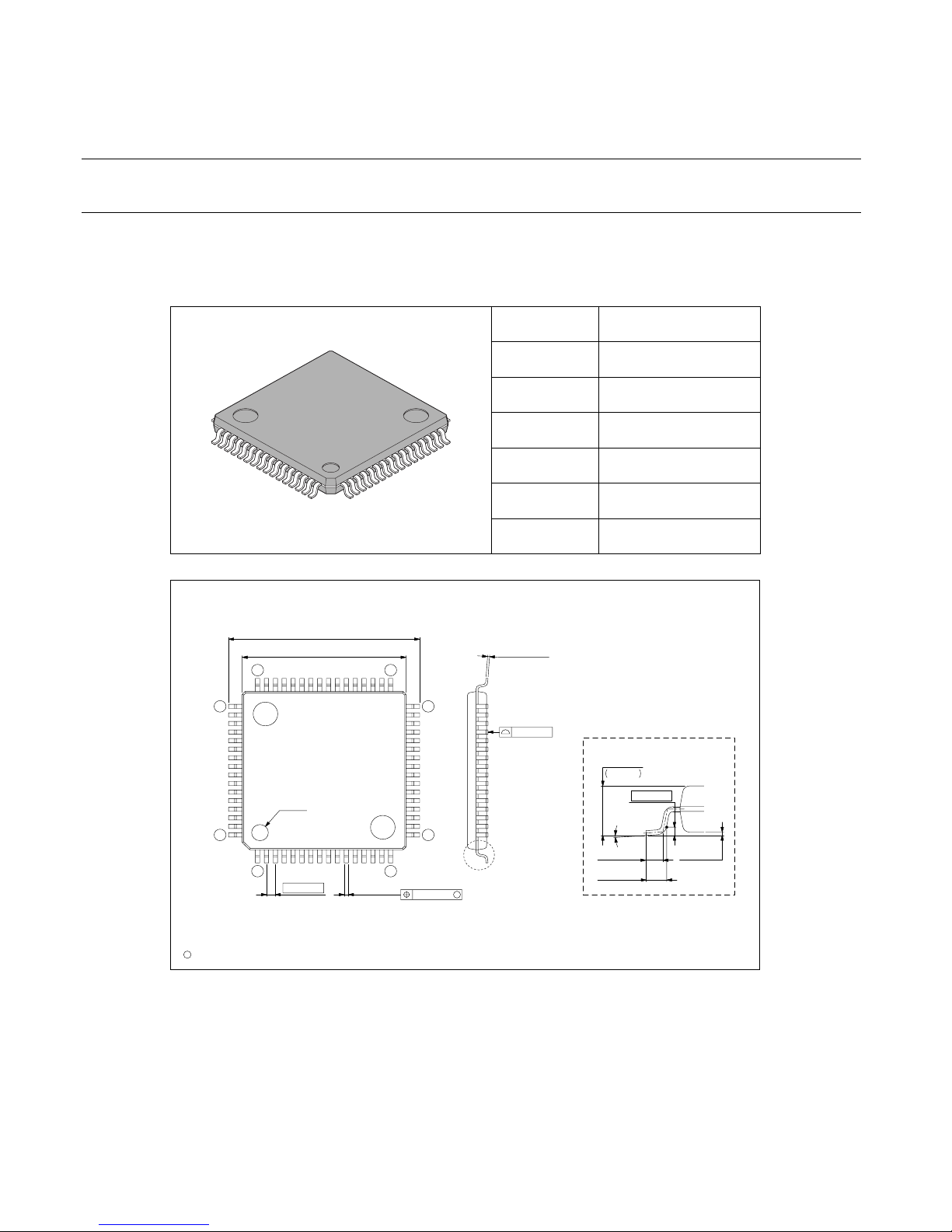
1.6 Package Dimension
MB95170J series is available in two types of package.
■ Package Dimension of FPT-64P-M23
Figure 1.6-1 Package Dimension of FPT-64P-M23
Please confirm the latest Package dimension by following URL.
http://edevice.fujitsu.com/fj/DATASHEET/ef-ovpklv.html
64-pin plastic LQFP Lead pitch 0.65 mm
Package width ×
package length
12.0 × 12.0 mm
Lead shape Gullwing
Sealing method Plastic mold
Mounting height
1.70 mm MAX
Code
(Reference)
P-LFQFP64-12×12-0.65
64-pin plastic LQFP
(FPT-64P-M23)
(FPT-64P-M23)
C
2003 FUJITSU LIMITED F64034S-c-1-1
0.65(.026)
0.10(.004)
1
16
17
32
49
64
3348
*12.00±0.10(.472±.004)SQ
14.00±0.20(.551±.008)SQ
INDEX
0.32±0.05
(.013
±.002)
M
0.13(.005)
0.145±0.055
(.0057
±.0022)
"A"
.059
–.004
+.008
–0.10
+0.20
1.50
0~8˚
0.25(.010)
(Mounting height)
0.50±0.20
(.020
±.008)
0.60±0.15
(.024
±.006)
0.10±0.10
(.004±.004)
Details of "A" part
(Stand off)
Dimensions in mm (inches).
Note: The values in parentheses are reference values
Note 1)* : These dimensions do not include resin protrusion.
Note 2) Pins width and pins thickness include plating thickness.
Note 3) Pins width do not include tie bar cutting remainder.
Page 26
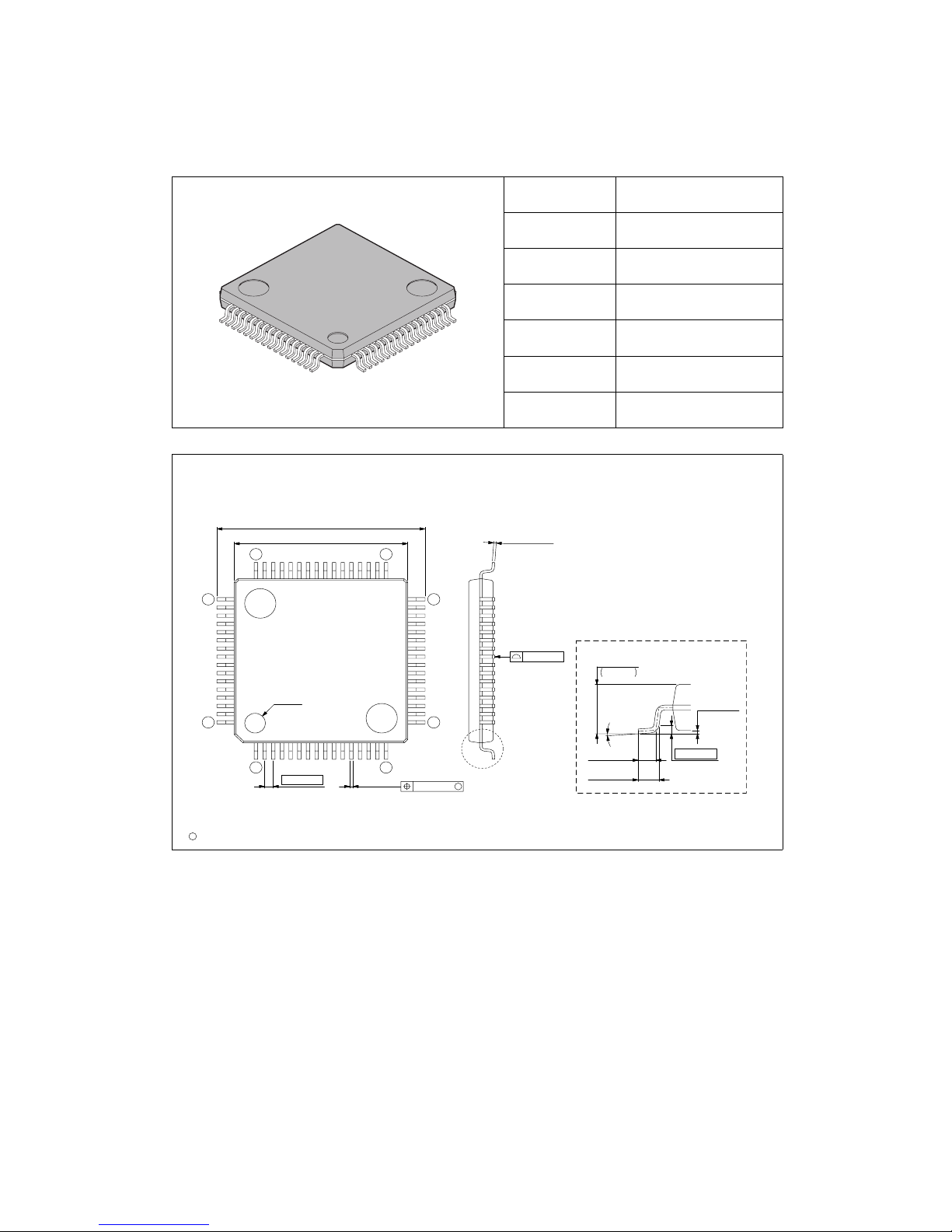
12
CHAPTER 1 DESCRIPTION
■ Package Dimension of FPT-64P-M24
Figure 1.6-2 Package Dimension of FPT-64P-M24
Please confirm the latest Package dimension by following URL.
http://edevice.fujitsu.com/fj/DATASHEET/ef-ovpklv.html
64-pin plastic LQFP Lead pitch 0.50 mm
Package width ×
package length
10.0 × 10.0 mm
Lead shape Gullwing
Sealing method Plastic mold
Mounting height
1.70 mm MAX
Weight 0.32g
Code
(Reference)
P-LFQFP64-10×10-0.50
64-pin plastic LQFP
(FPT-64P-M24)
(FPT-64P-M24)
LEAD No.
Details of "A" part
0.25(.010)
(Stand off)
(.004±.004)
0.10±0.10
(.024±.006)
0.60±0.15
(.020±.008)
0.50±0.20
1.50
+0.20
–0.10
+.008
–.004
.059
0˚~8˚
"A"
0.08(.003)
(.006±.002)
0.145±0.055
0.08(.003)
M
(.008±.002)
0.20±0.05
0.50(.020)
12.00±0.20(.472±.008)SQ
10.00±0.10(.394±.004)SQ
INDEX
49
64
3348
17
32
161
2005 FUJITSU LIMITED F64036S-c-1-1
C
(Mounting height)
*
Dimensions in mm (inches).
Note: The values in parentheses are reference values
Note 1) * : These dimensions do not include resin protrusion.
Note 2) Pins width and pins thickness include plating thickness.
Note 3) Pins width do not include tie bar cutting remainder.
Page 27
13
CHAPTER 1 DESCRIPTION
1.7 Pin Description
Table 1.7-1 shows pin description. The alphabet in the "Circuit Type" column of Table
1.7-1 corresponds to the one in the "Classification" column of Table 1.8-1.
■ Pin Description
Table 1.7-1 Pin Description (1 / 3)
Pin no.
Pin name
I/O
circuit
type*
2
Function
LQFP*
1
1DVSS⎯
Power supply pin (GND)
2
P12/UCK0/
TO00
H
General -purpose I/O port
The pin is shared with 8/16-bi t compound timer ch.0 output and UART/SIO ch.0
clock I/O .
3
P11/UO0/
TO01
H
General -purpose I/O port
The pin is share d with 8/16-b it compo und timer ch. 0 output and UART/SIO ch .0 data
output.
4 P10/UI0/EC0 G
General -purpose I/O port
The pin is share d with 8/16-b it compo und timer ch.0 clock input and UART/ SIO ch.0
data input.
5
P07/S23/
INT07/AN07
S
General -purpose I/O port
The pins are shared with LCDC SEG output (SEG23) , external interrupt input and
A/D converter analog input.
6
P06/S22/
INT06/AN06
General -purpose I/O port
The pins are shared with LCDC SEG output (SEG22) , external interrupt input and
A/D converter analog input.
7
P05/INT05/
AN05
J
General -purpose I/O port
The pins are shared with external interrupt input and A/D converter analog input.
8
P04/INT04/
AN04
9
P03/INT03/
AN03
10
P02/INT02/
AN02
11
P01/INT01/
AN01
12
P00/INT00/
AN00
13 MOD B
An operati ng m ode designation pin
14 X0 A
Main clock oscillation pi n
15 X1 A
Main clock oscillation pin
Page 28
14
CHAPTER 1 DESCRIPTION
16 V
SS
⎯
Power supply pin (GND)
17 V
CC
⎯
Power supply pin
18 C ⎯ Capacitor connection pin
19 P95/X1A
A/H
General -purpose I/O port
The pins are shared with sub clock oscillation pin
20 P94/X0A
21 RST B’
Rese t pi n
22 P50/SCL0
I
General -purpose I/O port
The pin is shared with I
2
C ch.0 clock I/O.
23 P51/SDA0
General -purpose I/O port
The pin is shared with I
2
C ch.0 data I/O.
24 PA0/COM0
M
General -purpose I/O port
The pins are shared with LCDC COM output.
25 PA1/COM1
26 PA2/COM2
27 PA3/COM3
28
PB0/S00/TP-
CLK/CALPL
M
General -purpose I/O port
The pins are shared with LCDC SEG output and RTC I/O.
29 PB1/S01
M
General -purpose I/O port
The pi ns are sh ared with LC D C S EG o utput.
30 PB2/S02
31 PB3/S03
32 PB4/S04
33 PB5/S05
34 PB6/S06
35 PB7/S07
36 PC0/S08/TRG0
General -purpose I/O port
The pins are shared with LCDC SEG output and PPG trigger input.
37 PC1/S09/TRG1
38 PC2/S10/TRG2
39 PC3/S11/TRG3
40 PC4/S12/TRG4
M
General -purpose I/O port
The pins are shared with LCDC SEG output and PPG trigger input.
41 PC5/S13/TRG5
42 PC6/S14/TRG6
43 PC7/S15/TRG7
Table 1.7-1 Pin Description (2 / 3)
Pin no.
Pin name
I/O
circuit
type*
2
Function
LQFP*
1
Page 29
15
CHAPTER 1 DESCRIPTION
44 P60/S16
M
General -purpose I/O port
The pi ns are sh ared with LC D C S EG o utput.
45 P61/S17
46 P62/S18/TO10
General -purpose I/O port
The pins are sh ared wi th LCDC SEG outp ut and 8/16 -bit compound timer ch.1 ou tput
(TO10, TO11)
47 P63/S19/TO11
48 P64/S20/EC1
General -purpose I/O port
The pins are sh ar ed with LCD C SEG ou tpu t and 8/ 16- bit co mpoun d tim er ch. 1 cl ock
input
49 P65/S21
General -purpose I/O port
The pi ns are sh ared with LC D C S EG o utput
50
PE4/S28/
INT10
Q
General -purpose I/O port
The pins are shared with external interrupt input (INT10 to INT13) and LCDC SEG
output (SEG 28 to SEG31)
51
PE5/S29/
INT11
52
PE6/S30/
INT12
53
PE7/S31/
INT13
54 P90/V3 R
General -purpose I/O port
The pins are shared with power supply pins for LCDC drive
55 DV
SS
⎯
Power supply pin (GND)
56 P91/V2/PPG7
R
General -purpose I/O port
The pins are shared with power sup ply pins for LCDC drive and 16-bit PPG 7 output
57 P92/V1/PPG6
General -purpose I/O port
The pins are shared with power sup ply pins for LCDC drive and 16-bit PPG 6 output
58 P43/PPG5 H’
General -purpose I/O port
The pins are shared with and 16-bit PPG 5 output
59 P42//PPG4 H’
General -purpose I/O port
The pins are shared with and 16-bit PPG 4 output
60 DV
CC
⎯
Power supply pin
61 P41/PPG3
H’
General -purpose I/O port
The pins are shared with and 16-bit PPG 3 output
62 P40/PPG2
General -purpose I/O port
The pins are shared with and 16-bit PPG 2 output
63 P14/PPG1 H’
General -purpose I/O port
The pins are shared with and 16-bit PPG 1 output
64
P13/ADTG/
PPG0
H’
General -purpose I/O port
The pins are shared with and 16-bit PPG 0 output and A/D trigger input
Table 1.7-1 Pin Description (3 / 3)
Pin no.
Pin name
I/O
circuit
type*
2
Function
LQFP*
1
Page 30

16
CHAPTER 1 DESCRIPTION
*1 : FPT-64P-M23 , FPT-64P-M24
*2 : For the I/O circuit type, refer to “1.8 I/ O Ci rcuit Type”.
Page 31

17
CHAPTER 1 DESCRIPTION
1.8 I/O Circuit Type
Table 1.8-1 lists the I/O circuit types. Also, the alphabet in the "Type" column of Table
1.8-1 corresponds to the one in the "I/O circuit type" column of Table 1.7-1.
■ I/O Circuit Type
Table 1.8-1 I/O Circuit Type (1 / 3)
Type Circuit Remarks
A
• Oscillation circuit
• High-speed side
Feedback resistance: appro x 1 MΩ
• Low-speed side
Feedback resistance: appro x 10 MΩ
B
• Only for input
• Hysteresis input
B’
• Hysteresis input
G
• CMOS output
• CMOS input
• Hysteresis input
• With pull-up control
• Automotive input
H
• CMOS output
• Hysteresis input
• With pull-up control
• Automotive input
X0 (X0A)
X1 (X1A)
N-ch
Standby control
Clock input
Mode input
Reset input
R
P-ch
N-ch
P-ch
Pull-up control
Standby control
Digital output
Digital output
Hysteresis input
CMOS input
Automotive input
P-ch
P-ch
N-ch
R
Pull-up control
Standby control
Digital output
Digital output
Hysteresis input
Automotive input
Page 32

18
CHAPTER 1 DESCRIPTION
H’
• CMOS output
• Hysteresis input
• Automotive input
I
• N-ch open drain output
• CMOS input
• Hysteresis input
• Automotive input
J
• CMOS output
• Hysteresis input
• Analog input
• With pull-up control
• Automotive input
M
• CMOS output
• LCD output
• Hysteresis input
• Automotive input
Table 1.8-1 I/O Circuit Type (2 / 3)
Type Circuit Remarks
P-ch
N-ch
Standby con-
Digital output
Digital output
Hysteresis input
Automotive input
N-ch
Standby control
Digital output
CMOS input
Hysteresis input
Automotive input
R
P-ch
P-ch
N-ch
Pull-up control
A/D control
Standby control
Analog input
Digital output
Hysteresis input
Digital output
Automotive input
P-ch
N-ch
Standby control
Hysteresis input
Digital output
Digital output
LCD control
LCD output
Automotive input
Page 33

19
CHAPTER 1 DESCRIPTION
N
• CMOS output
• LCD output
• CMOS input
• Hysteresis input
• Automotive input
Q
• CMOS output
• LCD output
• Hysteresis input
• Automotive input
R
• CMOS output
• LCD power supply
• Hysteresis input
• Automotive input
S
• CMOS output
• LCD output
• Hysteresis input
• Analog input
• Automotive input
Table 1.8-1 I/O Circuit Type (3 / 3)
Type Circuit Remarks
P-ch
N-ch
LCD control
Digital output
Hysteresis input
CMOS input
Digital output
Standby control
LCD output
Automotive input
P-ch
N-ch
Standby control
Digital output
Hysteresis input
LCD control
Digital output
External
interrupt control
LCD output
Automotive input
P-ch
N-ch
LCD control
Standby control
LCD built-in division
resistance I/O
Hysteresis input
Digital output
Digital output
Automotive input
P-ch
N-ch
A/D control
Standby control
Analog input
Digital output
Hysteresis input
Digital output
Automotive input
LCD output
Page 34

20
CHAPTER 1 DESCRIPTION
Page 35

21
CHAPTER 2
HANDLING DEVICES
This chapter gives notes on using.
2.1 Device Handling Precautions
Page 36

22
CHAPTER 2 HANDLING DEVICES
2.1 Device Handling Precautions
This section summarizes the precautions on the device's power supply voltage and pin
treatment.
■ Device Handling Precautions
●
Preventing Latch-up
Care must be taken to ensure that maximum voltage ratings are not exceeded when they are used.
Latch-up may occur on CMOS ICs if voltage higher than V
CC
or lower than VSS is applied to input and
output pins other than medium- and high-withstand voltage pins or if higher than the rating voltage is
applied betwee n V
CC
pin and VSS pin.
When latch-up occurs, power s upply current increases rapidly and might thermally damage el ements.
● Stable Supply Voltage
Supply voltage should be stabilized.
A sudden change in power-supply voltage may cause a malfunction even within the guaranteed operating
range of the Vcc power-supply volt age.
For stabilizatio n , in principle, keep the variation in V cc ripple (p-p v alue) in a comm ercial freq u ency range
(50/60 Hz) not to exceed 10% of the standard Vcc value and suppress the voltage variation so that the
transient variation rate does not exceed 0.1 V/ms during a momentary change such as when the power
supply is switched.
● Precautions for Use of External Clock
Even when an external clock is used, oscillation stabilization wait time is required for power-on reset,
wake-up from subclock mode or stop mode.
Page 37

23
CHAPTER 2 HANDLING DEVICES
■ Pin Connection
● Treatment of Unused Pin
Leaving unused input pins unconnected can cause abnormal operation or latch-up, leaving to permanent
damage.
Unused input pins should always be pulled up or down through resistance of at least 2 kΩ. Any
unused input/output pins may be set to output mode and left open, or set to input mode and treated the same
as unused input pins. If the r e is unused output pin, make it open.
● Power Supply Pins
In products with multiple V
CC
or VSS pins, the pins of the same potential are internally connected in the
device to avoid abnormal operations including latch-up. However, you must connect the pins to external
power supply and a ground line to lower the electro-magnetic emission level, to prevent abnormal
operation of strobe signals caused by the rise in the ground level, and to conform to the total output current
rating.
Moreover, connect the current supply source with the V
CC
and VSS pins of this device at the low
impedance.
It is also advisable to connect a ceramic bypass capacitor of approximately 0.1 μF between V
CC
and V
SS
pins near this device.
● Mode Pin (MOD)
Connect the mode pin dire ctly to V
CC
or VSS.
To prevent the device unintentionally entering test mode due to noise, lay out the printed circuit board so as
to minimize the dist ance from the mode pins to V
CC
or VSS and to provide a low-impedance connection.
Use a ceramic capacitor or a capacitor with eq uivalent frequency charact eristics. A bypass capacitor of V
CC
pin must have a capacitance value higher than CS. For connection of smoothing capacitor CS, see the
diagram below.
Figure 2.1-1 C pin connection diagram
CS
C
Page 38

24
CHAPTER 2 HANDLING DEVICES
Page 39

25
CHAPTER 3
MEMORY SPACE
This chapter describes memory space.
3.1 Memory Space
3.2 Memory Map
Page 40

26
CHAPTER 3 MEMORY SPACE
3.1 Memory Space
The memory space on the F2MC-8FX family is 64 K bytes, divided into I/O, extended I/O,
data, and program areas. The memory space includes special-purpose areas such as
the general-purpose registers and vector table.
■ Configuration of Memory Space
● I/O area (addresses: 0000
H
to 007FH)
• This area contains the control registers and data registers for on-chip peripheral resources.
• As the I/O area is allocated as part of memory space, it can be accessed in the same way as for memory.
It can also be accessed at higher speed by using direct address ing instructions.
● Extended I/O area (addresses: 0F00
H
to 0FFFH)
• This area contains the control registers and data registers for on-chip peripheral resources.
• As the ex t en d ed I / O ar e a is alloc at ed as part of memory sp ace, it can be a cc es sed in t h e s a me w ay as fo r
memory.
● Data area
• Stat ic RAM is incorporated as the interna l data area.
• The internal RAM capacity is different depending on the product.
• The RAM area from 80
H
to FFH can be accessed at higher speed by using direct addressing instructions.
• The area from 100
H
to 47FH is an extended direct addressing area. It can be accessed at higher speed by
direct addressing ins tructions with the dire ct ba nk pointer set.
• Addresses 100
H
to 1FFH can be used as a general-purpose register area.
● Program area
• ROM is incorporated as the internal program area.
• The internal ROM capacity is different depending on the model.
• Addresses FFC0
H
to FFFFH are used as the vector table.
Page 41

27
CHAPTER 3 MEMORY SPACE
■ Configuration of Memory Space For Specific Usage
● General-purpose Register Area (Addresses: 0100
H
to 01FFH)
• This area contains the auxiliary registers used for 8-bit arithmetic or transfer operations.
• As the area is allocated as part of the RAM area, it can also be used as ordinary RAM.
• When the area is used as general-purpose registers, general-purpose register addressing enables higher-
speed access using short instructions.
• For details, see Section "5.1.1 Register Bank Pointer (RP)" and Section "5.2 General-purpose
Registers".
● Vector Table Area (Addresses: FFC0
H
to FFFFH)
• This area is used as the vector table for vector call instructions (CALLV), interrupts, and resets.
• The vector table area is allocated at the top of the ROM area. At the individual addresses in the vector
table, the star t ad d r esses of the ir re sp ective ser v i ce routin es ar e set as d at a.
Table 8.1-1 lists the vector table addresses to be referenced for vector call instructions, interrupts, and for
resets.
For details, see "CHAPTER 8 INTERRUPTS", "CHAPTER 7 RESET", and "● CALLV #vct" in
"Appendix C.2 Special Ins truction".
Page 42

28
CHAPTER 3 MEMORY SPACE
3.2 Memory Map
Figure 3.2-1 Memory Map
0000
H
I/O area Direct addressing area
0080
H
0100
H
Data area
Register banks
(General-purpose register area)
Extended direct addressing area
0200
H
Address #1
Access prohibited
0F00
H
Extended I/O area
Address #2
Program area
FFC0
H
FFFF
H
Vector table area
Product
Flash memory RAM Address #1 Address #2
MB95F176JS/
MB95F176JW
32K bytes 1K byte
0480
H
08000
H
Page 43

29
CHAPTER 4
MEMORY ACCESS MODE
This chapter describes the memory access mode.
4.1 Memory Access Mode
Page 44

30
CHAPTER 4 MEMORY ACCESS MODE
4.1 Memory Access Mode
The memory access mode supported by the MB95170J series is only single-chip mode.
■ Single-chip Mode
Single-chip mode uses only internal RAM and ROM without using an external bus access.
● Mode data
Mode data is used to determine the memory access mode of the CPU.
The mode data address is fixed as FFFD
H
(The value of FFFCH can be any value). Be sure to set the mode
data of internal ROM to 00
H
to select single-chip mode.
Figure 4.1-1 Mode Data Settings
After a reset, the CPU fetches mode data first.
The CPU then fetches the reset vector after the mode data. The instruction is performed from the address
set by reset vector.
● Mode pin (MOD)
Be sure to set the mode pin (MOD) to "V
SS
".
Address bit7 bit6 bit5 bit4 bit3 bit2 bit1 bit0
FFFD
H
Data Operation
00
H
Select single-chip mode.
Other than 00
H
Reserved. Do not make any setting.
Page 45

31
CHAPTER 5
CPU
This chapter describes functions and operations of the
CPU.
5.1 Dedicated Registers
5.2 General-purpose Registers
5.3 Placement of 16-bit Data in Memory
Page 46

32
CHAPTER 5 CPU
5.1 Dedicated Registers
The CPU has its dedicated registers: the program counter (PC), two arithmetic registers
(A and T), three address pointers (IX, EP, and SP), and the program status (PS) register.
Each of the registers is 16 bits long. The PS register consists of the register bank
pointer (RP), direct pointer (DP), and condition code register (CCR).
■ Configuration of Dedicated Registers
The dedicated registers in the CPU are seven 16-bit registers. Accumulator (A) and temporary accumulator
(T) can also be used with only their lo wer eight bits in serv ice.
Figure 5.1-1 shows th e configuration of the dedica ted registers.
Figure 5.1-1 Configuration of Dedicated Registers
■ Functions of Dedicated Registers
● Program counter (PC)
The program counter is a 16-bit counter which contains the memory address of the instruction currently
executed by the CPU. The program counter is updated whenever an instruction is executed or an interrupt
or reset occurs. The initial value set immediately after a reset is the mode data read address (FFFD
H
).
● Accumulator (A)
The accumulator is a 16-bit register for arithmetic operation. It is used for a variety of arithmetic and
transfer operations of data in memory or data in other registers such as the temporary accumulator (T). The
data in the accumulator can be handled either as word (16-bit) data or byte (8-bit) data. For byte-length
arithmetic and transfer operations, only the lower eight bits (AL) of the accumulator are used with the
upper eight bits (AH) left unchanged. The initial value set immediately a fter a reset is 0000
H
.
Address
FFFD
H
PC : Program counter
Contains the address of the current instruction.
0000
H
AH AL : Accumulator (A)
Temporary storage register for arithmetic operation and
transfer.
0000
H
TH TL : Temporary accumulator (T)
Performs an operation with accumulator.
0000
H
IX : Index register
Register containing an index address.
0000
H
EP : Extra pointer
Pointer containing a memory address.
0000
H
SP : Stack pointer
Contains the current stack location.
0030
H
RP
DP CCR
: Program status
Register consisting of the register bank pointer, direct bank
pointer, and condition code register.
16 bits
PS
Page 47

33
CHAPTER 5 CPU
● Temporary accumulator (T)
The temporary accumulator is an auxiliary 16-bit register for arithmetic operation. It is used to perform
arithmetic operations with the data in the accumulator (A). The data in the temporary accumulator is
handled as word data for word-length (16-bit) operations with the accumulator (A) and as byte data for
byte-length (8-bit) operations. For byte-length operations, only the lower eight bits (TL) of the temporary
accumulator are used and the upper eight bits (TH) are not used.
When a MOV instruction is used to transfer data to the accumulator (A), the previous contents of the
accumulator are automatically transferred to the temporary accumulator. When transferring byte-length
data, the upper eight bits (TH) of the temporary accumulator remain unchanged. The initial value after a
reset is 0000
H
.
● Index register (IX)
The index register is a 16-bit register used to hold the index address. The index register is used with a
single-byte offset (-128 to +127). The offset value is added to the index address to generate the memory
address for data acc es s. The initial va lue after a re set is 0000
H
.
● Extra pointer (EP)
The extra pointer is a 16-bit register which contains the value indicating the memory address for data
access. The initial value after a reset is 00 00
H
.
● Stack pointer (SP)
The stack pointer is a 16-bit register which holds the address referenced when an interrupt or subroutine
call occurs and by the stack push and pop instructions. During program execution, the value of the stack
pointer indicates the address of the most recent data pushed onto the stack. The initial value after a reset is
0000
H
.
● Program status (PS)
The program status is a 16-bit control register. The upper eight bits make up the register bank pointer (RP)
and direct bank pointer (DP); the lower eight bits make up the condition code register (CCR).
In the upper eight bits, the upper five bits make up the register bank pointer used to contain the address of
the general-purpose register bank. The lower three bits make up the direct bank pointer which locates the
area to b e ac ce s sed at hi gh s p ee d by d ir e ct add ressing.
The lower eight bits make up the condition code register (CCR) which consists of flags that represent the
state of the CPU.
The instructions that can access the program status are MOVW A,PS or MOVW PS,A. The register bank
pointer (RP) and direct bank pointer (DP) in the program status register can also be read from or written to
by accessing the mirror address (0078
H
).
Note that the condition code register (CCR) is part of the program status register and cannot be accessed
independently.
Refer to the "F
2
MC-8FX Programming Manual" for details on using the dedicate d registers.
Page 48

34
CHAPTER 5 CPU
5.1.1 Register Bank Pointer (RP)
The register bank pointer (RP) in bits 15 to 11 of the program status (PS) register
contains the address of the general-purpose register bank that is currently in use and is
translated into a real address when general-purpose register addressing is used.
■ Configuration of Register Bank Pointer (RP)
Figure 5.1-2 shows th e configuration of the regist er bank pointer.
Figure 5.1-2 Configuration of Register Bank Pointer
The register bank pointer contains the address of the register bank currently being used. The content of the
register bank pointe r is translated into a real address ac cording to the rule shown in Figure 5.1-3.
Figure 5.1-3 Rule for Translation into Real Addresses in General-purpose Register Area
The register bank pointer specifies the register bank used as general-purpose registers in the RAM area.
There are a total of 32 register banks. The current register bank is specified by setting a value between 0
and 31 in the upper five bits of the register bank pointer. Each register bank has eight 8-bit general-purpose
registers which are sel ected by the lower three bits of the op-code.
The register bank pointer allows the space from 0100
H
to up to 01FFH to be used as a general-purpose
register area. Note, however, that the available area is limited depending on the product. The initial value
after a reset is 0000
H
.
■ Mirror Address for Register Bank and Direct Bank Pointers
The register bank pointer (RP) and direct bank pointer (DP) can be written to and read from by accessing
the program status (PS) register using the "MOVW A,PS" and "MOVW PS,A" instructions, respectively.
They can also be written to and read from directly by accessing mirror address 0078
H
of the register bank
pointer.
RP DP CCR
bit15 bit14 bit13 bit12 bit11 bit10 bit9 bit8 bit7 bit6 bit5 bit4 bit3 bit2 bit1 bit0
PS
R4 R3 R2 R1 R0
DP2 DP1 DP0
HIIL1IL0NZVC
00000
B
RP Initial
value
Fixed value RP: Upper Op-code: Lower
"0" "0" "0" "0" "0" "0" "0" "1" R4 R3 R2 R1 R0 b2 b1 b0
↓
↓ ↓ ↓ ↓ ↓ ↓ ↓ ↓ ↓ ↓ ↓ ↓ ↓ ↓ ↓
A15 A14 A13 A12 A11 A10 A9 A8 A7 A6 A5 A4 A3 A2 A1 A0
Generated
address
Page 49

35
CHAPTER 5 CPU
5.1.2 Direct Bank Pointer (DP)
The direct bank pointer (DP) in bits 10 to 8 of the program status (PS) register specifies
the area to be accessed by direct addressing.
■ Configuration of Direct Bank Pointer (DP)
Figure 5.1-4 shows the configuration of the direct bank pointer.
Figure 5.1-4 Configuration of Direct Bank Pointer
The areas from 0000
H
to 007FH and 0080H to 047FH can be accessed by direct addressing. Access to
0000
H
to 007FH is specified with an operand regardless of the value in the direct bank pointer. Access to
0080
H
to 047FH is specified with the value in the value of the direct bank pointer and the operand.
Table 5.1-1 shows the relationship between direct bank pointer (DP) and access area; Table 5.1-2 lists the
direct addressing instructions.
RP DP CCR
bit15 bit14 bit13 bit12 bit11 bit10 bit9 bit8 bit7 bit6 bit5 bit4 bit3 bit2 bit1 bit0
PS
R4 R3 R2 R1 R0
DP2 DP1 DP0
HIIL1IL0NZVC
000
B
DP Initial
value
Table 5.1-1 Direct Access Pointer and Access Area
Direct bank pointer (DP) [2:0] Operand-specified dir Access area
XXX
B
(It doesn't affect the mapping. ) 0000
H
to 007F
H
0000H to 007F
H
000
B
(Initial value )
0080H to 00FF
H
0080H to 00FF
H
001
B
0100H to 017F
H
010
B
0180H to 01FF
H
011
B
0200H to 027F
H
100
B
0280H to 02FF
H
101
B
0300H to 037F
H
110
B
0380H to 03FF
H
111
B
0400H to 047F
H
Page 50

36
CHAPTER 5 CPU
Table 5.1-2 Direct Address Instruction List
Applicable Instruction
CLRB dir:bit
SETB dir:bit
BBC dir:bit,rel
BBS dir:bit,rel
MOV A,dir
CMP A,d ir
ADDC A,dir
SUBC A,dir
MOV dir,A
XOR A,dir
AND A,dir
OR A,dir
MOV dir,#imm
CMP dir,#imm
MOVW A,dir
MOVW dir,A
Page 51

37
CHAPTER 5 CPU
5.1.3 Condition Code Register (CCR)
The condition code register (CCR) in the lower eight bits of the program status (PS)
register consists of the bits (H, N, Z, V, and C) containing information about the
arithmetic result or transfer data and the bits (I, IL1, and IL0) used to control the
acceptance of interrupt requests.
■ Configuration of Condition Code Register (CCR)
Figure 5.1-5 Configuration of Condition Code Register
The condition code register is a part of the program status (PS) register and therefore cannot be accessed
independently.
■ Bits Result Information Bits
● Half carry flag (H)
This flag is set to "1" when a carry from bit 3 to bit 4 or a borrow from bit 4 to bit 3 occurs as the result of
an operation. Otherwise, the flag is set to "0". Do not use this flag for any operation other than addition and
subtraction as the fla g is intended for decimal-adjus ted instructions.
● Negative flag (N)
This flag is set to "1" when the value of the most significant bit is "1 " as th e result of an operation and set to
"0" if the value is "0".
● Zero flag (Z)
This flag is set to "1" when the result of an operation is "0" and set to "0" otherwise.
● Overflow flag (V)
This flag indicates whether an operation has resulted in an overflow, assuming the operand used for the
operation as an integer represented by a two's complement. The flag is set to "1" when an overflow occurs
and set to "0" otherwise.
RP DP CCR
bit15 bit14 bit13 bit12 bit11 bit10 bit9 bit8 bit7 bit6 bit5 bit4 bit3 bit2 bit1 bit0
PS
R4 R3 R2 R1 R0
DP2 DP1 DP0
H I IL1 IL0 N Z V C
00110000
B
Half carry flag
Interrupt enable flag
Interrupt level bits
Negative flag
Zero flag
Overflow flag
Carry flag
CCR Initial
value
Page 52

38
CHAPTER 5 CPU
● Carry flag (C)
This flag is set to "1" when a carry from bit 7 or a borrow to bit 7 occurs as the result of an operation.
Otherwise, the flag is set to "0" . W h en a shift instruction is executed, the flag is set to the shift-out value.
Figure 5.1-6 shows how the car ry flag is updated by a shift instruct ion.
Figure 5.1-6 Carry Flag Updated by Shift Instruction
■ Interrupt Acceptance Control Bits
● Interrupt enable flag (I)
When this flag is set to "1", interrupts are enabled and accepted by the CPU. When this flag is set to "0",
inter ru p t s are di s a bl ed and rejected by th e CPU.
The initial value after a reset is "0".
The SETI and CLRI instructi ons set and clear the flag to "1" and "0", respectively.
● Interrupt level bits (IL1, IL0)
These bits indicate the level of the interrupt currently accepted by the CPU.
The interrupt level is compared with the value of the interrupt level setting register (ILR0 to ILR5) that
corresponds to the interrupt request (IRQ0 to IRQ23) of each peripheral resource.
The CPU services an interrupt request only when its interrupt level is smaller than the value of these bits
with the interrupt enable flag set (CCR: I = 1). Table 5.1-3 lists interrupt level priorities. The initial value
after a reset is "11
B
".
The interrupt level bits (IL1, IL0) are usually "11
B
" with the CPU not servicing an interrupt (with the main
program running).
For details on interrupts, see 8.1 Interrupts.
• Left-shift (ROLC) • Right-shift (RORC)
bit7 bit0 bit7 bit0
C C
Table 5.1-3 Interrupt Levels
IL1 IL0 Interrupt Level Priority
00 0 High
01 1
10 2
1 1 3 Low (No interrupt)
Page 53

39
CHAPTER 5 CPU
5.2 General-purpose Registers
The general-purpose registers are memory blocks consisting of eight 8-bit registers per
bank. A total of up to 32 register banks can be used. The register bank pointer (RP) is
used to specify the register bank.
Register banks are useful for interrupt handling, vector call processing, and subroutine
calls.
■ Configuration of General-purpose Registers
• The general-purpose registers are 8-bit registers and are located in register banks in the general-purpose
register area (in RAM).
• Up to 32 banks can be used , where each bank consists of eight regi sters (R0 to R7).
• The register bank pointer (RP) specifies the register bank currently being used and the lower three bits
of the op-code specify general-purpose register 0 (R0) to 7 (R7).
Figure 5.2-1 shows th e configuration of the regist er banks.
Figure 5.2-1 Configuration of Register Banks
For information on the general-purpose register area available on each model , s ee "3.2 Memory Map".
R0
R1
R2
R3
R4
R5
R6
R7
R0
= 0100
H + 8 × (RP)
R1
R2
R3
R4
R5
R6
R7
R0
R1
R2
R3
R4
R5
R6
R7
This address
32 banks
Memory area
1F8
H
Address 100
H
107
H
1FF
H
8bits
The number of banks
available is restricted by
the RAM capacity
available.
Bank 31
Bank 0
Page 54

40
CHAPTER 5 CPU
■ Features of General-purpose Registers
The general-purpose re gisters have the following features:
• High-speed access to RAM using short instructions (general-purpose register addressing).
• Blocks of r egister banks facilita ting data backup and division by function unit.
General-purpose register banks can be allocated exclusively for specific interrupt service routines or vector
call (CALLV #0 to #7) processing routines. An example is always using the fourth register bank for the
second interrupt.
Only specifying a dedicated register bank at the beginning of an interrupt service routine automatically
saves the general-purpose registers before the interrupt. This eliminates the need for pushing generalpurpose register data onto the stack, all owing the CPU to accept interrupts at high speed.
Notes:
• When coding an interrupt service routine, be careful not to change the value of the interrupt level bits
(CCR: IL1, IL0) in the condition code register when specifying the register bank by updating the register
bank pointer (RP) in that routine. Perform the programming by using either of them.
• Read the interrupt level bits and save their value before writing to the RP.
• Directly write to the RP mirror address "0078H" to update the RP.
Page 55

41
CHAPTER 5 CPU
5.3 Placement of 16-bit Data in Memory
This section describes how 16-bit data is stored in memory.
■ Placement of 16-bit Data in Memory
● State of 16-bit data stored in RAM
When you write 16-bit data to memory, the upper byte of the data is stored at a smaller address and the
lower byte is stored at the next address. When you read 16-bit data, it is handled in the same way.
Figure 5.3-1 shows how 16-bit data is placed in memory.
Figure 5.3-1 Placing 16-bit Data in Memory
● State of operand-specified 16-bit data
In the same way, even when the operands in an instruction specifies 16-bit data, the upper byte is stored at
the address closer to the op-code (instruction) and the lower byte is stored at the next address.
That is true whether the ope rands are either memory addresses or 16-bit immediate data.
Figure 5.3-2 shows how 16-bi t data in an instruction is pla ced.
Figure 5.3-2 Storing 16-bit Data in Instruction
● State of 16-bit data in the stack
When 16-bit register data is pushed onto the stack upon an interrupt, the upper byte is stored at a lower
address in the same way.
Before
execution
After
execution
Memory Memory
Extended address
16-bit immediate data
Assemble
Extended address
16-bit immediate data
[Example]
Page 56

42
CHAPTER 5 CPU
Page 57

43
CHAPTER 6
CLOCK CONTROLLER
This chapter describes the functions and operations of
the clock controller.
6.1 Overview of Clock Controller
6.2 Oscillation Stabilization Wait Time
6.3 System Clock Control Register (SYCC)
6.4 PLL Control Register (PLLC)
6.5 Oscillation Stabilization Wait Time Setting Register (WATR)
6.6 Standby Control Register (STBC)
6.7 Clock Modes
6.8 Operations in Low-power Consumption Modes (Standby Modes)
6.9 Clock Oscillator Circuits
6.10 Overview of Prescaler
6.11 Configuration of Prescaler
6.12 Operating Explanation of Prescaler
6.13 Notes on Use of Prescaler
Page 58

44
CHAPTER 6 CLOCK CONTROLLER
6.1 Overview of Clock Controller
The F2MC-8FX family has a built-in clock controller that optimizes its power
consumption. It includes two- system clock product supporting both of the main clock
and subclock and single system clock product supporting only the main clock.
The clock controller enables/disables clock oscillation, enables/disables the supply of
clock signals to the internal circuitry, selects the clock source, and controls the PLL
and frequency divider circuits.
■ Overview of Clock Controller
The clock controller enables/disables clock oscillation, enables/disables clock supply to the internal
circuitry, sel ects the clock source, and controls the PLL and frequency divider circ uits.
The clock controller controls the internal clock according to the clock mode, standby mode settings and the
reset operation. The current clock mode selects the internal operating clock and the standby mode selects
whether to enable or disable clock oscillation and signal supply.
The clock controller selects the optimum power consumption and features depending on the combination of
clock mode and standby mode.
Two- system clock product have three different source clocks: a main clock, which is the main oscillation
clock divided by two, a subclock, which is the sub oscillation clock divided by two and a main PLL clock,
which is the main osc illation clock multiplied by the PLL multiplier.
Single system clock product have two different source clocks: a main clock, which is the main oscillation
clock divided by two; and a main PLL clock, which is the main oscillation clock multiplied by the PLL
multiplier.
Page 59

45
CHAPTER 6 CLOCK CONTROLLER
■ Block Diagram of the Clock Controller
Figure 6.1-1 shows the block diagram of the clock controller.
Figure 6.1-1 Clock Controller Block Diagram
- - -
Standby control register (STBC)
Subclock
oscillator
circuit
System clock selector
Prescaler
No division
Divide by 4
Divide by 8
Divide by 16
Main clock
oscillator circuit
Divide by 2
Main PLL
oscillator
circuit
Divide by 2
Clock
control
circuit
Subclock control
System clock control register (SYCC)
Oscillation
stabilization
wait circuit
Supply to CPU
Supply to peripheral
resources
Sleep signal
Stop signal
Watch or timebase
timer
Clock for timebase
timer
Main clock control
Oscillation stabilization wait time setting register (WATR)
Source clock
selection
control circuit
MPMC1
PLL controller register (PLLC)
(1)
(2)
(4)
(3)
(5)
(6)
(7)
(1): Main clock (F
CH
)
(2): Subclock (F
CL
)
(3): Main clock
(4): Subclock
(5): Main PLL clock
(6): Source clock
(7): Machine clock (MCLK)
From timebase timer
2
14
/FCH to 21/FCH
From watch prescaler
2
15
/FCL to 21/F
CL
FCH
F
CL
MPMC0 MPRDY
- STP SLP SPL
SRST
TMD
MPEN
SCM1 SCM0 SCS1 SCS0 SRDY SUBS DIV1 DIV0
SWT3
SWT2 SWT1 SWT0
MWT3
MWT2
MWT1 MWT0
Clock for watch
prescaler
-
-
-
Page 60

46
CHAPTER 6 CLOCK CONTROLLER
The clock controlle r cons ists of the following blocks:
● Main clock oscillator circuit
This block is the oscillator circuit for the main clock.
● Subclock oscillator circuit (Two-system clock product)
This block is the oscillator circuit for the subclock.
● Main PLL oscillator circuit
This block is the oscillator circuit for the main PLL.
● System clock selector
This block selects one of the three different source clocks for main clock, subclock and main PLL clock
depending on the clock mode. The prescaler frequency-divides the selected source clock into the machine
clock. It is suppli ed to the clock control circuit.
● Clock control circuit
This block controls the supply of the machine clock to the CPU and each peripheral resource according to
the standby mode or oscillation stabilization wait time.
● Oscillation stabilization wait circuit
This block outputs the oscillation stabilization wait time signal for each clock from 14 types of main-clock
oscillation stabilization signals created by the timebase timer and 15 types of subclock oscillation
stabilization signals created by the watch prescaler.
● System clock control register (SYCC)
This register is used to control current clock mode display, clock mode selection, machine clock divide
ratio selecti on, and subclock oscillation in main clock mode and main PLL clock mode.
● Standby control register (STBC)
This register is used to control the transition from RUN state to standby mode, the setting of pin states in
stop mode, timebase tim er mode, or watch mode, and the generation of software resets.
● PLL control register (PLLC)
This register is used to enable/disable the oscillation of the main PLL clock, set the multiplier, and to
indicate the stability of PLL oscillation.
● Oscillation stabilization wait time setting register (WATR)
This register is used to set the oscillation stabilization wait time for the main clock and subclock.
Page 61

47
CHAPTER 6 CLOCK CONTROLLER
■ Clock Modes
There are three clock mod es available: main clock mode, main P LL cloc k mode and subclock mode.
Table 6.1-1 shows the relationships between the clock modes and the machine clock (operating clock for
the CPU and peripheral resources).
In any of the clock modes, the selected clock can also be frequency-divided. Additionally, in modes using a
PLL clock, a multiplier for the clock frequency can also be set.
■ Peripheral Resources not Affected by Clock Mode
Note that the peripheral resources listed in the table below are not affected by the clock mode, division, and
PLL multiplier settings. Table 6.1-2 lists the peripheral resources not affected by the clock mode.
For some peripheral resources other than those listed above, it may be possible to select the timebase timer
or watch prescaler output as a count clock. Check the description of each peripheral resource for details.
Table 6.1-1 Clock Modes and Machine Clock Selection
Clock Mode Machine Clock
Main clock mode The machine cl ock is generated from the main clock (main clock divided by 2).
Main PLL clock mode
The machine c lock i s ge nerat ed fro m the m ain PL L clo ck (m ain cl ock multip li ed by
the PLL multiplier).
Subclock m ode
(Two-system clock product only)
The machine cl ock is generated from the subclock (subclock divide d by 2).
Table 6.1-2 Peripheral Resources Not Affected by Clock Mode
Peripheral Resource Operating Clock
Timebase timer
Main clock (2
1
/FCH: main clock divided by 2)
Watchdog timer
Main clock (with timebase timer output selected)
Subcloc k (w ith watch prescaler output selected) (Two-system clock product only)
Watch prescal er
(T wo -syst em clo ck pr oduct onl y)
Subclock (2
1
/FCL: subclock divided by 2)
Clock counter
(T wo -syst em clo ck pr oduct onl y)
Subclock (watch prescaler output)
Page 62

48
CHAPTER 6 CLOCK CONTROLLER
■ Standby Modes
The clock controller selects whether to enable or disable clock oscillation and clock supply to internal
circuitry depending on each standby mode. With the exception of timebase timer mode and watch mode,
the standby mode can be set independently of the clock mode.
Table 6.1-3 shows the relationships between standby modes and clock supply states.
Table 6.1-3 Standby Modes and Clock Supply States
Standby Mode Clock Supply States
Sleep mode
Stops clock sup ply to the CPU and watchdo g ti mer. As a r esult , the CPU st ops operat i on,
but othe r peripheral resources continue operating.
Timebas e timer mode
Supplies clock signals only to the timebase timer , w atch prescaler, and watc h counter
while s topping clock supply to other circuits. As a result, al l the function s other than the
timebase timer, watch prescaler, watch counter, external interrupt, and low-voltage
detect ion reset are stopped.
Ti mebase timer mode is only the standby mode for main clock mode or main PLL clock
mode.
Watch mode
(Two-s ystem cl oc k
product only)
Stops ma in clock oscill ation, but suppl ies clock signals only to the watc h prescaler and
watch c ounter while stopping clock supply to other c ircuits. As a result, all the functions
other than the watch prescaler, watch counter, external interrupt, and low-voltage
detect ion reset are stopped.
Watch mode is o nly the standby mo de for subclock mo de.
Stop m o de
Stops ma in clock oscillation and subclock oscillation and stops the supply of all clock
signals. As a result, all the functi ons other than external interr upt and low-voltage
detect ion reset are stopped.
Page 63

49
CHAPTER 6 CLOCK CONTROLLER
■ Combinations of Clock Mode and Standby Mode
Table 6.1-4 lists the combinations of clock mode and standby mode and their respective operating states of
internal circuits.
*1: Operat es w hen th e ma in PLL cl ock os cill atio n e nab le b it in the PL L co ntr ol regis te r (P LLC :MPE N )
is set to "1".
*2: Stops when the subclock oscillation stop bit in the system clock control register (SYCC:SUBS) is set
to "1".
*3: Watch counter keeps counting and no interrupts occur. When the subclock oscillation stop bit in the
system clock con trol register (SYCC: SUBS) is set to "1", watch counter stops.
Table 6.1-4 Combinations of Standby Mode and Clock Mode and Internal Operating States
Function
RUN Sleep
Timebase
Timer
Watch (Twosystem clock
product)
Stop
Main
clock
mode
Main
PLL
clock
mode
Sub clock mode
(Two-system
clock product)
Main
clock
mode
Main
PLL
clock
mode
Sub clock mode
(Two-system
clock product)
Main
clock
mode
Main
PLL
clock
mode
Sub clock mode
(Two-system
clock product)
Main PLL clock
mode
Main cloc k Operating Stoppe d Operating Stopped Operating Stopped Stopped Stopped
Main PLL
clock
Stop ped*1Operat-
ing
Stopped
Stop ped*1Operat-
ing
Stopped Stopped*1 Stopped Stopped Stopped
Subclock Operating*2 Operating Operating*2 Operating Operating*2 Operating
Operat-
ing*2
Stop ped
CPU Operating Operating Stopped Stopped Stopped Stopped Stopped Stopped
ROM
Operatin g Opera ting Value held Value held Val u e held Value held
Value
held
Value
held
RAM
I/O ports Operati ng Operating Output hel d Output held Output held Output held
Output
held/
Hi-Z
Output
held/Hi-
Z
Timebase timer Operating Stopped Operating Stopped Operating Stopped Stopped Stopped
Watch
prescaler
Operating*2 Operating Operating*2 Operating Operating*2 Operating
Operat-
ing*2
Stop ped
Watch counter Operating*2 Operating Operat ing*2 Operating Operating*2 Operati ng
Operat-
ing*3
Stop ped
External
interrupt
Operating Operating Operating Operating Operating Operating
Operat-
ing
Operat-
ing
Watchdog
timer
Operating Operating Stopped Stopped Stopped Stopped Stopped Stopped
Low-voltage
detection reset
Operating Operating Operating Operating Operating Operating
Operat-
ing
Operat-
ing
Other
peripheral
resources
Operating Operating Operating Operating Stopped Stopped Stopped Stopped
Page 64

50
CHAPTER 6 CLOCK CONTROLLER
6.2 Oscillation Stabilization Wait Time
The oscillation stabilization wait time is the time after the oscillator circuit stops
oscillation until the oscillator resumes its stable oscillation at its natural frequency. The
clock controller obtains the oscillation stabilization wait time by counting a set number
of oscillation clock cycles to prevent clock supply to internal circuits.
■ Oscillation Stabilization Wait Time
The clock controller obtains the oscillation stabilization wait time followed by the initiation of oscillation
by counting a set number of oscillation clock cycles to prevent clock supply to internal circuits.
When a state transition request for starting oscillation when the power is turned on or for restarting halted
oscillation at a clock mode change by a reset, an interrupt in standby mode, or by software, the clock
controller automatically waits until the oscillation stabilization wait time for the main clock or subclock has
passed and then caus es transition to the next state.
Figure 6.2-1 shows oscillation immediat ely after being started.
Figure 6.2-1 Behavior of Oscillator Immediately after Starting Oscillation
The main clock oscillation stabilization wait time is counted by using the timebase timer. The subclock
oscillation stabilization wait time is counted by using the watch prescaler. The count can be set in the
oscillation stabilization wait time setting register (WATR). Set it in keeping with the oscillator
characteristics.
When a power-on reset occurs, the osc illation stabilization wait time is fixed to the initial value.
Table 6.2-1 shows the length of oscillation s tabilization wait time.
After the oscillation stabilization wait time of the main clock ends, the oscillation stabilization wait time of
subclock measure me nt is begun.
■ PLL Clock Oscillation Stabilization Wait Time
As with the oscillation stabilization wait time of the oscillator, the clock controller automatically waits for
()
Oscillation stabilization
wait time
Normal operation
Operation after returning
from stop mode or a reset
Oscillation started
X1
Oscillation time of
oscillator
Oscillation stabilized
Table 6.2-1 Oscillation Stabilization Wait Time
Clock Factor Oscillation Stabilization Wait Time
Main clock
Power- on reset
Initial va lu e : (2
14
-2)/FCH, where FCH is the main clock frequency
(specified when ROM is ordered for mask pro ducts)
Other than pow er-on reset Register setting value (WA T R:M W T3, MWT2, MWT1, MWT0)
Subclock
(Two-system clock product)
Power- on reset
Initial va lu e : (2
15
-2)/FCL, where FCL is the subclock frequency.
Other than power-on reset Register setti ng value (WATR:SWT3, SWT2, SWT1, SWT0)
Page 65

51
CHAPTER 6 CLOCK CONTROLLER
the PLL oscillation stabilization wait time to elapse after a request for state transition from PLL oscillation
stopped state to oscillation start is generated via an interrupt in standby mode or a change of clock mode by
software. Note that the PLL clock oscillation stabilization wait time changes according to the PLL startup
timing.
Table 6.2-2 shows the PLL oscillation stabilization wait time.
■ Oscillation Stabilization Wait Time and Clock Mode/Standby Mode Transition
The clock controller automatically waits for the oscillation stabilization wait time to elapse as needed when
the operating state causes a transition. Depending on the state transition, however, the clock controller does
not always wait f or the oscillation stabilization wait time.
For details on state transitions, see "6.7 Clock Modes" and "6.8 Operations in Low-power Consumption
Modes (Standby Modes)".
Table 6.2-2 PLL Oscillation Stabilization Wait Time
PLL Oscillation Stabilization Wait Time
Remarks
Minimum time Maximum time
Main PLL clock
2
11
/FCH x 2 211/FCH x 3
• Stabilization wait time is taken while 2
11
/FCH is counted
twice (minimum) or three times (maximum).
•F
CH
represe nts the main clock frequency.
Page 66

52
CHAPTER 6 CLOCK CONTROLLER
6.3 System Clock Control Register (SYCC)
The system clock control register (SYCC) is used to indicate and switch the current clock
mode, select the machine clock divide ratio, and control subclock oscillation in main clock
mode and main PLL clock mode.
■ Configuration of System Clock Control Register (SYCC)
Figure 6.3-1 Configuration of System Clock Control Register (SYCC)
DIV1 Machine clock divide ratio selection bits
0 0 Source clock
0 1 Source clock / 4
1 0 Source clock / 8
1 1 Source clock /16
SUBS Subclock oscillation stop bit
0 Starts subclock oscillation
1 Stops subclock oscillation
SRDY Subclock oscillation stability bit
0
Indicates the subclock oscillation stabilization
wait state or subclock oscillation being stopped
1 Indicates subclock oscillation being stable
Cock mode selection bits
0 0 Subclock mode
0 1
1 0 Main clock mode
1 1 Main PLL clock mode
Clock mode monitor bits
0 0 Subclock mode
0 1 Meaningless
1
0
Main clock mode
1 1 Main PLL clock mode
SCS1
DIV0DIV1
SUBSSRDYSCS0SCM0
SCM1
0007
H
Address
bit0
Initial value
1010x011
B
R/WR/WR/WR/WR/W R/WXR/WXR/WX
bit1bit2bit3
bit4 bit5 bit6 bit7
R/WX : Read only (Readable, writting has no effect on operation)
R/W : Readable/writable (Read value is the same as write value)
X : Indeterminate
: Initial value
DIV0
SCS1
SCS0
SCM0
SCM1
Setting prohibited
Page 67

53
CHAPTER 6 CLOCK CONTROLLER
Table 6.3-1 Functions of Bits in System Clock Control Register (SYCC)
Bit name Function
bit7
bit6
SCM1, SCM0:
Clock mode monitor
bits
Indicate the current clock mode.
When set to "00": the bi ts indicate subclock mode.
When set to "10": the bit indicate main clock mode.
When set to "11": the bit indicat e main PLL cloc k mode.
These bits are read-only; any value attempted to be written is me aningless.
bit5
bit4
SCS1, SCS0:
Clock mode selec tion
bits
Specify the clock mode.
When set to "00": the bits spec ify trans iti on to sub c lo ck mode.( Two-system clock produc t on ly )
When set to "01": setting is prohibited.
When set to "10": the bits spec ify trans iti on to ma in clo c k m o de .
When set to "11": the bits specify transition to main PLL clock mode.
Once a clock m ode has been sel ected in the SCS1 and SCS0 bits, any attempt to write to them is ignored
until the transition to that clock mode is completed.
On single sy stem clock produ ct, an attempt to write "00" or "01" to these bits is ignored, leaving their
value unchanged.
bit3
SRDY:
Subclock os cillation
stabil ity bit
(Two-system clock
product only)
Indicates whether subclock oscillation has become stable.
• Wh en s e t t o "1", th e SR DY bit in di cates th a t the os ci llation stabiliz a tio n wait ti m e fo r the su b cl oc k has
passed.
• When set to "0", the SRDY bit indicates that the clock controller is in the subclock oscillation
stabilization wait s tate or that subclock oscillati on has been stopped.
This bit is read-only; any value attempted to be written is meaningless.
On single sy stem clock produ ct, the value of th e bit is meaningless.
bit2
SUBS:
Subclock os cillation
stop bit
(Two-system clock
product only)
Stops su bclock oscillation in main clock mode or main PLL clock mode.
When set to "0": the bit en ables subclock oscillation.
When set to "1": the bit s tops subclock o scillation.
Notes:
• In subclock mode, the subcloc k oscillates regardless of the value of this bit, except in stop mode.
• Do not update the SYCC: SCS1 bit and this bit at the same time.
• On single system clock product, the value of thi s bit has no effect on operation.
bit1
bit0
DIV1, DIV0:
Machine clock divide
ratio selection bits
• These bits select the machine clock divide ratio to the source clock.
•
The machine clock is generated from the source clock according to the divide ratio set by the
bits.
DIV1 DIV0
Machine Clock Divide Ratio
Selection Bits
SCM1, 0 = 10
B
0 0 Source clock (No division) Main clock divided by 2
0 1 Source clock/4 Main clock divided by 8
1 0 Source clock/8 Main clock divided by 16
1 1 Source clock/16 Main clock divided by 32
Page 68

54
CHAPTER 6 CLOCK CONTROLLER
6.4 PLL Control Register (PLLC)
The PLL control register (PLLC) controls the main PLL clock.
■ Configuration of PLL Control Register (PLLC)
Figure 6.4-1 Configuration of PLL Control Register (PLLC)
MPRDY Main PLL clock oscillation stability bit
0
Indicates the main PLL clock oscillation stabilization
wait state or main PLL clock oscillation being stopped
1 Indicates main PLL clock oscillation being stable
MPMC1 Main PLL clock multiplier setting bits
0 0 Main clock x 1
0 1 Main clock x 2
1 0 Main clock x 2.5
1 1 Setting prohibited
MPEN Main PLL clock oscillation enable bit
0 Disables main PLL clock oscillation
1 Enables main PLL clock oscillation
bit7
Address
0006
H
MPMC1
Initial value
00000000
B
MPEN
MPMC0 - - -
R/W
R0/W0R0/W0R0/W0R/W R/W
R0/W0
R/W
R/W : Readable/writable (Read value is the same as write value)
: Initial value
MPRDY -
bit6
bit5
bit4
bit3
bit2
bit1
bit0
MPMC0
R0/W0 : Undefined bit (Read value is “0”, write data should be “0”)
- : Unused
Page 69

55
CHAPTER 6 CLOCK CONTROLLER
Table 6.4-1 Functions of Bits in PLL Control Register (PLLC)
Bit name Function
bit7
MPEN:
Main PLL clock
oscillati on enable bit
Enables or disables the oscillation of the m ain PLL clock in main clock mode or timebase timer
mode.
When se t to "1 ": the bit enables main PLL clock oscillation.
When se t to "0 ": the bit disables m ain PLL clock oscillation.
In main PLL clock mode, the main PLL clock oscillates regardless of the value of this bit either in
the RUN state or in sleep mode.
bit6
bit5
MPMC1, MPMC0:
Main PLL clock
multi pl ier settin g b its
Set the multiplier for the main PLL clock.
Note: The value of these bits can be changed only when the main PLL clock is stopped.
Therefore, do not attempt to update the bits with the PLL clock oscillation enable bit
(MPEN) is set to "1" or with the clock mode selection bits in the system clock control
register (SYCC: SCS1, 0) are set to "11". (It is however possible to set these bits at the
same time as setting MPEN to "1".)
bit4
MPRDY:
Main PLL clock
oscillati on stability bit
Indicates w hether main PLL clock oscillati on has become stable.
• W he n set to "1", th e MPR DY bit ind ic ates that the os cill atio n sta bili zati on w ait tim e fo r the main
PLL clock has passed.
• When set to "0", the MPR DY bit indic ates that the clo ck controller is in th e main PLL clo ck
oscillation stabilization wait state or that main PLL clock oscillation has been stopped.
This bit is rea d-only; any value attempted to be written is meani ngless and has no effect on the
operation.
bit3
to
bit0
Unused bits
When read, these bits always return "0". These are unused bits.
When write,these bits should be written by "0".
MPMC1 MPMC0 Main PLL clock multiplier setting bits
0 0 Main clock x 1
0 1 Main clock x 2
1 0 Main clock x 2.5
1 1 Setting prohibited
Page 70

56
CHAPTER 6 CLOCK CONTROLLER
6.5 Oscillation Stabilization Wait Time Setting Register (WATR)
This register is used to set the oscillation stabilization wait time.
■ Configuration of Oscillation Stabilization Wait Time Setting Register (WATR)
Figure 6.5-1 Configuration of Oscillation Stabilization Wait Time Setting Register (WATR)
MWT3 MWT2 MWT1 MWT0
Number of
Cycles
Number of
Cycles
Main Oscillation Clock FCH = 4 MHz
1 1 1 1 214-2
2
13
-2
2
12
-2
2
11
-2
2
10
-2
2
9
-2
2
8
-2
2
7
-2
2
6
-2
2
5
-2
2
4
-2
2
3
-2
2
2
-2
2
1
-2
2
1
-2
2
1
-2
2
14
-2
2
15
-2
2
13
-2
2
12
-2
2
11
-2
2
10
-2
2
9
-2
2
8
-2
2
7
-2
2
6
-2
2
5
-2
2
4
-2
2
3
-2
2
2
-2
2
1
-2
2
1
-2
(2
14
-2)/F
CH
About 4.10 ms
(2
13
-2)/F
CH
About 2.05 ms
(2
12
-2)/F
CH
About 1.02 ms
(2
11
-2)/F
CH
511.5 μs
(2
10
-2)/F
CH
255.5 μs
(2
9
-2)/F
CH
127.5 μs
(2
8
-2)/F
CH
63.5 μs
(2
7
-2)/F
CH
31.5 μs
(2
6
-2)/F
CH
15.5 μs
(2
5
-2)/F
CH
7.5 μs
(2
4
-2)/F
CH
3.5 μs
(2
3
-2)/F
CH
1.5 μs
(2
2
-2)/F
CH
0.5 μs
(2
1
-2)/F
CH
0.0 μs
(2
1
-2)/F
CH
0.0 μs
(2
1
-2)/F
CH
0.0 μs
1 1 1 0
1 1 0 1
1 1 0 0
1 0 1 1
1 0 1 0
1 0 0 1
1 0 0 0
0 1 1 1
0 1 1 0
0 1 0 1
0 1 0 0
0 0 1 1
0 0 1 0
0 0 0 1
0 0 0 0
SWT3 SWT2 SWT1 SWT0
Sub Oscillation Clock FCL = 32.768 kHz
1 1 1 1
1 1 1 0
1 1 0 1
1 1 0 0
1 0 1 1
1 0 1 0
1 0 0 1
1 0 0 0
0 1 1 1
0 1 1 0
0 1 0 1
0 1 0 0
0 0 1 1
0 0 1 0
0 0 0 1
0 0 0 0
(2
14
-2)/FCL About 0.5 s
(2
15
-2)/F
CL
About 1.00 s
(2
13
-2)/FCL About 0.25 s
(2
12
-2)/FCL About 0.125 s
(2
11
-2)/FCL About 62.44 ms
(2
10
-2)/FCL About 31.19 ms
(2
9
-2)/FCL About 15.56 ms
(2
8
-2)/FCL About 7.75 ms
(2
7
-2)/FCL About 3.85 ms
(2
6
-2)/FCL About 1.89 ms
(2
5
-2)/FCL About 915.5 μs
(2
4
-2)/FCL About 427.2 μs
(2
3
-2)/FCL About 183.1 μs
(2
2
-2)/FCL About 61.0 μs
(2
1
-2)/FCL 0.0 μs
(2
1
-2)/FCL 0.0 μs
Bit7 Bit6 Bit5 Bit4 Bit3 Bit2 Bit1 Bit0
Address
0005
H
SWT2
Initial value
11111111
B
SWT3
SWT1 SWT0 MWT3 MWT2
MWT1
MWT0
R/WR/WR/WR/WR/WR/WR/WR/W
R/W
: Readable/writable (Read value is the same as write value)
: Initial value (For mask ROM products, you can specify the initial value when ordering mask ROM.)
Page 71

57
CHAPTER 6 CLOCK CONTROLLER
Table 6.5-1 Functions of Bits in Oscillation Stabilization Wait Time Setting Register (WATR) (1 / 2)
Bit name Function
bit7
to
bit4
SWT3, SWT2,
SWT1, SWT0:
Subclock oscillation
stabilization wait time
selection bits
Set the subclock oscillation stabilization wait time.
On single system clock product, the value of these bits is meaningl ess.
Number of cycl es in the abov e ta ble is for a minim um va lue. Add 1/ F
CL
to the number of cycl e in th e
above tabl e for a maximum value.
Note: Do not update these bits during subclock oscillation stabilization wait time. You shoul d
update the m either with the subclock oscillation stability bi t in the system clock control
register (SYCC: SRDY) s et to "1" or i n su bcl ock mo de. Y ou can al so upda te the m whil e t he
subclock is stopped with the subclock oscillation stop bit in the system clock control
register (SYCC:SUBS) set to "1" in main clock mode or main PLL clock mode.
SWT3 SWT2 SWT1 SWT0
Number of
Cycles
Subclock F
CL
= 32.768 kHz
1111
2
15
-2
(2
15
-2)/F
CL
About 1.0 s
1110
2
14
-2
(2
14
-2)/F
CL
About 0.5 s
1101
2
13
-2
(2
13
-2)/F
CL
About 0.25 s
1100
2
12
-2
(2
12
-2)/FCL About 0.125 s
1011
2
11
-2
(2
11
-2)/FCL About 62.44 ms
1010
2
10
-2
(2
10
-2)/FCL About 31.19 ms
1001
2
9
-2
(2
9
-2)/FCL About 15.56 ms
1000
2
8
-2
(2
8
-2)/FCL About 7.75 ms
0111
2
7
-2
(2
7
-2)/FCL About 3.85 ms
0110
2
6
-2
(2
6
-2)/FCL About 1.89 ms
0101
2
5
-2
(2
5
-2)/FCL About 915.5 μs
0100
2
4
-2
(2
4
-2)/FCL About 427.2 μs
0011
2
3
-2
(2
3
-2)/FCL About 183.1 μs
0010
2
2
-2
(2
2
-2)/FCL About 61.0 μs
0001
2
1
-2
(2
1
-2)/FCL 0.0 μs
0000
2
1
-2
(2
1
-2)/FCL 0.0 μs
Page 72

58
CHAPTER 6 CLOCK CONTROLLER
bit3
to
bit0
MWT3, MWT2,
MWT1, MWT0:
Main clock osc illation
stabilization wait time
selection bits
Set the main clock oscillation stabilization wait time.
Number of cycles is for a minimum value. Add 1/F
CL
to the minimum value for a maximum value.
Note: Do not update these bits during main clock oscillation stabilization wait time. You should
update them in m ain clock mode or mai n PLL clock mode. You can also update t hem in
subclock mode.
Table 6.5-1 Functions of Bits in Oscillation Stabilization Wait Time Setting Register (WATR) (2 / 2)
Bit name Function
MWT3 MWT2 MWT1
MWT0
Number of
Cycles
Main clock F
CH
= 4 MHz
1111
2
14
-2
(2
14
-2)/F
CH
About 4.10 ms
1110
2
13
-2
(2
13
-2)/F
CH
About 2.05 ms
1101
2
12
-2
(2
12
-2)/F
CH
About 1.02 ms
1100
2
11
-2
(2
11
-2)/F
CH
511.5 μs
1011
2
10
-2
(2
10
-2)/F
CH
255.5 μs
1010
2
9
-2
(2
9
-2)/F
CH
127.5 μs
1001
2
8
-2
(2
8
-2)/F
CH
63.5 μs
1000
2
7
-2
(2
7
-2)/F
CH
31.5 μs
0111
2
6
-2
(2
6
-2)/F
CH
15.5 μs
0110
2
5
-2
(2
5
-2)/F
CH
7.5 μs
0101
2
4
-2
(2
4
-2)/F
CH
3.5 μs
0100
2
3
-2
(2
3
-2)/F
CH
1.5 μs
0011
2
2
-2
(2
2
-2)/F
CH
0.5 μs
0010
2
1
-2
(2
1
-2)/F
CH
0.0 μs
0001
2
1
-2
(2
1
-2)/F
CH
0.0 μs
0000
2
1
-2
(2
1
-2)/F
CH
0.0 μs
Page 73

59
CHAPTER 6 CLOCK CONTROLLER
Page 74

60
CHAPTER 6 CLOCK CONTROLLER
6.6 Standby Control Register (STBC)
The standby control register (STBC) is used to control transition from the RUN state to
sleep mode, stop mode, timebase timer mode, or watch mode, set the pin state in stop
mode, timebase timer mode, and watch mode, and to control the generation of software
resets.
■ Standby Control Register (STBC)
Figure 6.6-1 Standby Control Register (STBC)
Watch bit
TMD
Read Write
0
Always reads
"0".
Has no effect on the operation.
Main clock mode
Main PLL clock mode
Subclock mode
1 -
Causes transition to
timebase timer mode
Causes transition to
watch mode
Software reset bit
SRST
Read Write
0 Always reads "0". Has no effect on the operation
1 -
Generates a 3 machine clock reset signal
SPL
Pin state setting bit
0
Holds external pins in their immediately preceding state in stop mode, timebase
timer mode, or watch mode
1
Places external pins in a high impedance state in stop mode, timebase timer
mode, or watch mode.
Sleep bit
SLP
Read Write
0 Always reads "0". Has no effect on the operation
1 - Causes transition to sleep mode
Stop bit
STP
Read Write
0 Always reads "0". Has no effect on the operation
1 - Causes transition to stop mode
Address
0008
H
bit7
bit6
bit3
Initial value
00000000
B
STP
SLP
R/W
SPL
R0,WR0,WR0,WR0,W
R0/WX R0/WX R0/WX
SRST TMD
-
-
-
R0,W : Write only (Writable, "0" is read)
R/W : Readable/writable (Read value is the same as write value)
R0/WX : Undefined bit (Read value is "0", writting has no effect on operation)
- : Unused
: Initial value
bit2
bit1 bit0bit5
bit4
Page 75

61
CHAPTER 6 CLOCK CONTROLLER
Table 6.6-1 Functions of Bits in Standby Control Register (STBC)
Bit Name Function
bit7
STP:
Stop bit
Sets transition to stop mode.
When se t to "0 ": the bit is meaningless.
When se t to "1 ": the bit cause s transiti on to stop mode.
• When read, the bit always returns "0".
Note: An attempt to wr ite "1" to th is bit is ignored if an interrupt re q uest has been issued. For
details, see 6.8.1 Notes on Using Standby Mode.
bit6
SLP:
Sleep bit
Sets transition to sleep mod e.
When se t to "0 ": the bit is meaningless.
When se t to "1 ": the bit causes transition to sleep mode.
• When read, the bit always returns "0".
Note: An attempt to write "1" to this bit is ignored if an interrupt request has been issued. For
details, see 6.8.1 Notes on Using Standby Mode".
bit5
SPL:
Pin state setting bit
Sets the states of external pins in stop mode, timebase timer mode, and watch mode.
When se t to "0 ": the bit holds the states (levels) of externa l pins in stop mode, timebase timer
mode, and wat ch mode.
When se t to "1 ": the bit places external pins in a high impedance state in stop mode, timebase
timer mode, and watch mode. (Those pins are pulled up for which pull-up
resistor connection has been selected in the pull-u p setting regist er.)
bit4
SRST:
Software reset bit
Sets a software reset.
When se t to "0 ": the bit is meaningless.
When se t to "1 ": the bit generates a 3 machine clock res et signal.
• When read, the bit always returns "0".
bit3
TMD:
Watch b it
On two-system clock product, this bit sets transition to timebase timer mode or watch mode.
On single sys tem clock product, the bit sets transition to timebase timer mode .
• Writing "1" to the bit in main clock mode or main PLL clock mode causes transition to timebase
timer mode.
• Writing "1 " to the bit in subclock mode causes tr ansition to watch mode.
• Writing "0" to the bit is meaningless.
• When read, the bit always returns "0".
Note: An attempt to wr ite "1" to th is bit is ignored if an interrupt re q uest has been issued. For
details, see 6.8.1 Notes on Using Standby Mode".
bit2
to
bit0
Unused bits
When read, these bits always return "0". These are unused bits.
The bits are read-only; any value attempted to be written is meaningless.
Page 76

62
CHAPTER 6 CLOCK CONTROLLER
Notes:
• Set the standby mode after making sure that the transition to clock mode has been completed by comparing
the values of the clock mode monitor bits (SYCC:SCM1,0) and clock mode setting bits (SYCC:SCS1,0) in
the system clock control register.
• If you write "1" simultaneously to two or more of the stop bit (STP), sleep bit (SLP), software reset bit
(SRST), and watch bit (TMD), prio rity is given to them in the following order:
(1) Software reset bit (SRST)
(2) Stop bit (STP)
(3) Watch bit (TMD)
(4) Sleep bit (SLP)
When released from the standby mode, the device returns to the normal ope rating status.
Page 77

63
CHAPTER 6 CLOCK CONTROLLER
6.7 Clock Modes
The clock modes available are: main clock mode, subclock mode and main PLL clock
mode. Mode switching takes place according to the settings in the system clock control
register (SYCC).
Subclock mode is not supported by single system clock product.
■ Operations in Main Clock Mode
Main clock mode uses the main clock as the machine clock for the CPU and peripheral resources.
The timebase timer operates with the main clock.
The watch prescaler and watc h counter operate with the subclock (on two-system clock product).
If you set standby mode during operation in main clock mode, the device can enter sleep mode, stop mode,
or timebase timer mode.
After a reset, main clock mode is al ways set regardless of the clock mode used before the reset.
■ Operations in Subclock Mode (on Two-system Clock Product)
Subclock mode uses the subclock as the machine clock for the CPU and peripheral resources with main
clock oscillation stopped. In this mode, the timebase timer remains stopped as it requires the main clock for
operation.
If you set standby mode during operation in subclock mode, the device can enter sleep mode, stop mode, or
watch mode.
■ Operations in Main PLL Clock Mode
Main PLL clock mode uses the main PLL clock as the machine clock for the CPU and peripheral resources.
The timebase timer and watchdog timer operate with the main clock.
The watch prescaler and watc h counter operate with the subclock (on two-system clock product).
If you set standby mode during operation in main PLL clock mode, the device can enter sleep mode, stop
mode, or timebase timer mode.
Page 78

64
CHAPTER 6 CLOCK CONTROLLER
■ Clock Mode State Transition Diagram
The clock modes available are: main clock mode, main PLL clock mode and subclock mode. The device
can sw it ch be t w ee n th e s e mo d e s acco r d i ng to th e setting s in th e sys tem clock co nt r o l re g ister (SY C C ).
Figure 6.7-1 Clock Mode State Transition Diagram (Two-system Clock Product)
Power on
Reset state
Main clock oscillation
stabilization wait time
Main PLL clock
oscillation stabiliza-
tion wait time
Main clock oscillation
stabilization wait time
Subclock oscillation
stabilization wait time
Subclock mode
Main clock mode
Main clock/main PLL
clock oscillation
stabilization wait time
(1)
(2)
(3)
(5)
(4)
(6)
(8)
(9)
(7)
Reset occurs in each state.
<1>
<2>
Main PLL
clock mode
Page 79

65
CHAPTER 6 CLOCK CONTROLLER
Figure 6.7-2 Clock Mode State Transition Diagram (Single System Clock Product)
Power on
Reset state
Main PLL clock
oscillation stabiliza-
tion wait time
Main PLL
clock mode
Main clock mode
(5)
Reset occurs in each state.
<1>
<2>
(3)
(4)
Main clock oscillation
stabilization wait time
Page 80

66
CHAPTER 6 CLOCK CONTROLLER
Table 6.7-1 Clock Mode State Transition Table
Current
State
Next State Description
<1>
Reset state Main cl oc k
After a reset, the device waits for the main clock oscillation stabilization wait time to elapse
and enters m ain clock mode.
If the reset is a watchdog reset, software reset, or external reset caused in main clock mode
or main PLL clock mode, however, the device does not wait for the main clock oscillation
stabilization w a it time to elapse.
<2>
(1)
Main clock
Subclock
The device enters subclock mode when the system clock selection bits in the system clock
control register (SY C C : S C S1 , 0) are set to "00".
Note, h oweve r, that th e devi ce wa its fo r the s ubclo ck os cillati on sta biliz ation wait ti me to
elapse before entering subclock mode either if the subclock has been stopped according to
the setting of the subclock oscillation stop bit in the system clock control register (SYCC:
SUBS) in main clock mode or if the subclock oscillation stabilization wait time has not
passed immediately after the power is turned on.
(2)
(3)
Main PLL clock
When the system clock selection bits in the system clock control register (SYCC: SCS1, 0)
are set to "11", the dev ice enters main PLL c lock mode af ter waiting for the main PLL clo ck
oscillation sta b il iz ation wait time.
Note, however, that the device does not wait for the main PLL clock oscillation stabilizat ion
wait time to elapse if the main PLL clock has been oscillating according to the setting of the
main PLL clock oscillation enable bit in the PLL control register (PLLC: MPEN).
(4)
(5)
Main PLL
clock
Main clock
The device enters main clock mode when the system clock selection bits in the system clock
control register (SY C C : S C S1 , 0) are set to "10".
(6)
Subclock
The device enters subclock mode when the system clock selection bits in the system clock
control register (SY C C : S C S1 , 0) are set to "00".
Note, h oweve r, that th e devi ce wa its fo r the s ubclo ck os cillati on sta biliz ation wait ti me to
elapse before entering subclock mode either if the subclock has been stopped according to
the setting of the subclock oscillation stop bit in the system clock control register (SYCC:
SUBS) in mai n PLL clock mode or if the subcloc k oscillatio n stabilization wait time has not
passed immediately after the power is turned on.
(7)
(8)
Subclock
Main clock
When the system clock selection bits in the system clock control register (SYCC: SCS1, 0)
are set to "10", the device enters main clock mode after waiting for the main clock
oscillation sta b il iz ation wait time.
(9) Main PLL cl ock
When the system clock selection bits in the system clock control register (SYCC: SCS1, 0)
are set to "11", the dev ice enters main PLL c lock mode af ter waiting for the main PLL clo ck
oscillation stabilization wait time or main clock oscillation stabilization wait time to elapse,
whichever is longer.
Page 81

67
CHAPTER 6 CLOCK CONTROLLER
6.8 Operations in Low-power Consumption Modes (Standby
Modes)
The standby modes available are: sleep mode, stop mode, timebase timer mode, and
watch mode.
■ Overview of Transitions to and from Standby Mode
The standby modes available are: sleep mode, stop mode, timebase timer mode, and watch mode. The
device enters standby mo de according to the settings in the st andby control register (STBC).
The device is released from standby mode in response to an interrupt or reset. Before transition to normal
operation, the device waits for the oscillation stabilization wait time to elapse as required.
When released from standby mode by a reset, the device returns to main clock mode. When released from
standby mode by an interrupt, the device enters the clock mode in which the device was before entering the
standby mode.
■ Pin States in Standby Mode
The pin state setting bit (STBC:SPL) of the standby control register can be used to set the I/O port/
peripheral resource pins in the stop mode, timebase timer mode, or watch mode to hold their immediately
preceding state or to be placed in a high impedance state.
Page 82

68
CHAPTER 6 CLOCK CONTROLLER
6.8.1 Notes on Using Standby Mode
Even if the standby control register (STBC) sets standby mode, transition to the
standby mode does not take place when an interrupt request has been issued from a
peripheral resource. When the device returns from standby mode to the normal
operating state in response to an interrupt, the operation that follows varies depending
on whether the interrupt request is accepted or not.
■ Place at Least Three NOP Instructions Immediately Following a Standby Mode Setting
Instruction.
The device requires four machine clock cycles before entering standby mode after it is set in the standby
control register. During that period, the CPU executes the program. To avoid program execution during this
transition to sta ndby mode, enter at least th ree NOP instructions.
The device operates normally if you place instructions other than NOP instructions. In that case, however,
note that the device may execute the instructions to be executed after being released from standby mode
before entering the standby mode and that the device may enter the standby mode during instruction
execution, which is resumed after the device is released from the standby mode (increasing the number of
instruction execution cycles).
■ Check That Clock-mode Transition has been Completed before Setting Standby Mode.
Before setting standby mode, make sure that clock-mode transition has been completed by comparing the
values of the clock mode monitor bit (SYCC: SCM1, 0) and clock mode setting bit (SYCC: SCS1, 0) in the
system clock control register.
■ An Interrupt Request may Suppress Transition to Standby Mode.
If an attempt is made to set a standby mode while an interrupt request with an interrupt level higher than
"11" has been issued, the device ignores the attempt to write to the standby control register and continues
instruction execution without entering the standby mode. The device does not enter the standby mode even
after having servic ed the interrupt.
This behavior is the same as when interrupts are disabled by the interrupt enable flag (CCR:I) and interrupt
level bits in the condition co de register (CCR: I L 1,0) of the CPU.
■ Standby Mode is Also Canceled when the CPU Rejects Interrupts.
When an interrupt request with an interrupt level higher than "11" is issued in standby mode, the device is
released from the standby mode regardless of the settings of the interrupt enable flag (CCR: I) and interrupt
level bits (CCR:IL1,0) of the condition code register of the CPU.
After being released from standby mode, the device services the interrupt when the CPU's condition code
register has been set to accept interrupts. If the register has been set to reject interrupts, the device resumes
processing from the instruction that follows the last instruction executed before entering the standby mode.
Page 83

69
CHAPTER 6 CLOCK CONTROLLER
■ Standby Mode State Transition Diagram
Figure 6.8-1 and Figure 6.8 -2 are standby mode state transit ion diagrams.
Figure 6.8-1 Standby Mode State Transition Diagram (Two-system Clock Product)
Power on
Reset state
Main clock oscillation
stabilization wait time
Normal
(RUN) state
Watch mode
<2>
<1>
Main clock/main
PLL clock
Subclock oscillation
stabilization wait
time
Main PLL clock
oscillation stabilization wait time
Timebase
timer mode
Stop mode
Sleep mode
(1)
(2)
(3)
(4)
(5)
(6)
(7)
(8)
(9)
Reset occurs in each state.
Page 84

70
CHAPTER 6 CLOCK CONTROLLER
Figure 6.8-2 Standby Mode State Transition Diagram (Single System Clock Product)
Power on
Reset state
Reset occurs in each state.
Main clock/main
PLL clock oscillation
stabilization wait
time
Main PLL clock
oscillation stabilization wait time
Timebase timer
mode
Stop mode
Sleep mode
(1)
(2)
(3)
(4)
(5)
(6)
(7)
Main clock oscillation
stabilization wait time
Normal (RUN) state
<1>
<2>
Page 85

71
CHAPTER 6 CLOCK CONTROLLER
Table 6.8-1 State Transition Diagram (Transitions to and from Standby Modes)
State Transition Description
<1>
Normal operation from reset
state
After a r eset, the device enters main clock mode.
If the reset is a power-on reset, the device always waits for the main clock oscillation stabilization
wait time to elapse.
When the clock mode before the reset is subclock mode, the device waits for the main clock
oscillation stabilization wait time to elapse. The device waits for it as well when the standby mode
is stop mode.
When the clock mode before the reset is main clock mode or main PLL clock mode and the
standby mode is other than stop mode, the device does not wait for the main clock oscillation
stabil izatio n wait time t o elap se ev en aft er ent erin g a re set sta te in r espon se to a wat chdog r eset,
software reset, or external reset.
<2>
(1)
Sleep mode
The device enters sleep mode when "1" is written to the sleep bit in the standby control register
(STBC: SLP).
(2) The device returns to the RUN state in response to an interrupt from a peripheral resour ce.
(3)
Stop mode
The device enters stop mode when "1" is written to the stop bit in the standby control register
(STBC: STP).
(4)
In response to an external interrupt, the device returns to the RUN state after waiting for the
oscillation stabil ization wait ti m e required for each clock mode.
When the device waits for a PLL oscillation stabilization wait time, it waits for the relevant
oscillation st abilizat ion wai t t im e or P L L o s cillatio n stabil iz ation wa i t time to el ap se , w h icheve r i s
longer.
(5)
Timebase timer mode
The de vi ce enters t im e b ase tim er m o d e w h en "1" is writte n to th e watch bi t in the s ta n db y contro l
registe r (STBC: TMD) in main clock mode or main PLL clock mode.
(6)
The device returns to the RUN state in response to a timebase timer interrupt, watch prescaler/
watch counter interrupt, or external interrupt.
When the clock mode is main PLL clock mode, the device waits for the main PLL clock oscillation
stabilization wait time to elapse. If the main PLL oscillation enable bit in the PLL control register
(PLLC: MPEN) contains "1", however, the device does not wait for that time to elapse even when
the clock mode is main PLL clock mode.
(7)
(8)
Watch mode
The dev ice ente rs w atc h mod e w hen "1" i s wr itte n to the w atc h b it in the s tan dby contr ol re gis te r
(STBC: TMD) in subc lo c k m od e .
(9)
The device returns to the normal operating state in response to a watch prescaler/watch counter
interrup t or extern a l in te rr up t..
Page 86

72
CHAPTER 6 CLOCK CONTROLLER
6.8.2 Sleep Mode
Sleep mode stops the operations of the CPU and watchdog timer.
■ Operations in Sleep Mode
Sleep mode stops the operating clock for the CPU and watchdog timer. In this mode, the CPU stops while
retaining the contents of registers and RAM that exist immediately before the transition to sleep mode, but
the peripheral resources except the watchdog timer continue operating.
● Transition to sleep mode
Writing "1" to the sleep bit in the standby control register (STBC:SLP) causes the device to enter sleep
mode.
● Cancellation of sleep mode
A reset or an interrupt from a peripheral resou rce releases the device from sleep mode.
Page 87

73
CHAPTER 6 CLOCK CONTROLLER
6.8.3 Stop Mode
Stop mode stops the main clock.
■ Operations in Stop Mode
Stop mode stops the main clock. In this mode, the device stops all the functions except external interrupt
and low-voltage detection reset while retaining the contents of registers and RAM that exist immediately
before the transition to stop mode.
In main clock mode or main PLL clock mode, however , you can start or stop subclock oscilla tion by setting
the subclock oscillation stop bit in the system clock control register (SYCC: SUBS). When the subclock is
oscillating, the watch prescaler and watch counter operate.
● Transition to stop mode
Writing "1" to the stop bit in the standby control register (STBC:STP) causes the device to enter stop mode.
At this time, the states of external pins are retained when the pin state setting bit in the standby control
register (STBC:SPL) is "0", and the states of external pins become high impedance when that bit is "1"
(those pins are pulled up for which pull-up resistor connection has been selected in the pull-up setting
register).
In main clock mode or main PLL clock mode, a timebase timer interrupt request may be generated while
the device is waiting for main clock oscillation to stabilize after being released from stop mode by an
interrupt. If the interrupt interval time of the timebase timer is shorter than the main clock oscillation
stabilization wait time, you should disable interrupt requests output from the timebase timer before entering
stop mode, thereby preventing unexpected interrupts from occurring.
You should also disable interrupt requests output from the watch prescaler before entering stop mode in
subclock mode.
● Cancellation of stop mode
The device is released from stop mode in response to a reset or an external interrupt.
In main clock mode or main PLL clock mode, you can start or stop subclock oscillation by setting the
subclock oscillation stop bit in the system clock control register (SYCC: SUBS). When the subclock is
oscillating, you can also release the device from stop mode using an interrupt by the watch prescaler or
watch counter.
Note:
When stop mode is canceled via an interrupt, peripheral resources placed into stop mode during an action
resume that action. Therefore, the initial interval time of the interval timer and other similar settings are
rendered indeterminate . After rec overy from stop mode, initialize each periphera l resource as necessary.
Page 88

74
CHAPTER 6 CLOCK CONTROLLER
6.8.4 Timebase Timer Mode
Timebase timer mode allows only the main clock oscillation, subclock oscillation,
timebase timer, and watch prescaler to work. The operating clock for the CPU and
peripheral resources is stopped in this mode.
■ Operations in Timebase Timer Mode
In timebase timer mode, main clock supply is stopped except for the timebase timer. The device stops all
the functions except timebase timer, external interrupt and low-voltage detection reset while retaining the
contents of registers and RAM that exist immediately before the transition to timebase timer mode.
You can however start or stop subclock oscillation by setting the subclock oscillation stop bit in the system
clock control register (SYCC: SUBS). When the subclock is oscillating, the watch prescaler and watch
coun ter operat e.
● Transition to timebase timer mode
Writing "1" to the watch bit in the standby control register (STBC:TMD) causes the device to enter
timebase timer mode if the system clock monitor bits in the system clock control register (SYCC: SCM1,
0) are "10" or "11".
The device can enter timebase timer mode only when the clock mode is main clock mode or main PLL
clock mode.
Upon transition to timebase timer mode, the states of external pins are retained when the pin state setting
bit in the standby control register (STBC:SPL) is "0", and the states of external pins become high
impedance when that bit is "1" (those pins are pulled up for which pull-up resistor connection has been
selected in the pull-up setting register).
● Cancellation of timebase timer mode
The device is released from timebase timer mode in response to a reset, timebase timer interrupt, or
external interrupt.
You can start or stop subclock oscillation by setting the subclock oscillation stop bit in the system clock
control register (SYCC: SUBS). When the subclock is oscillating, you can also release the device from
timebase timer mode using an interrupt by the watch prescal er or wat ch co unter.
Note:
When timebase timer mode is canceled via an interrupt, peripheral resources placed into timebase timer mode
during an action resume that action. Therefore, the initial interval time of the interval timer and other similar
settings are rendered indeterminate. After recovery from timebase timer mode, initialize each peripheral
resource as necessa ry .
Page 89

75
CHAPTER 6 CLOCK CONTROLLER
6.8.5 Watch Mode
Watch mode allows only the subclock and watch prescaler to work. The operating clock
for the CPU and peripheral resources is stopped in this mode.
■ Operations in Watch Mode
In watch mode, the operating clock for the CPU and peripheral resources is stopped. The device stops all
the functions except the watch prescaler, watch counter, external interrupt, and low-voltage detection reset
while retaining the contents of registers and RAM that exist immediately before the transition to watch
mode.
● Transition to watch mode
Writing "1" to the watch bit in the standby control register (STBC:TMD) causes the device to enter watch
mode if the system clock monitor bits in the system clock control register (SYCC: SCM1, 0) are "00".
The device can enter watch mode only when the clock mode is subclock mode. Upon transition to watch
mode, the states of external pins are retained when the pin state setting bit in the standby control register
(STBC:SPL) is "0", and the states of external pins become high impedance when that bit is "1" (those pins
are pulled up for which pull-up resistor connection has be en selected in the pull-up setting register).
● Cancellation of watch mode
The device is released from watch mode in response to a reset, watch interrupt, or external interrupt.
Note:
When watch mode is canceled via an interrupt, peripheral resources placed into watch mode during an action
resume that action. Therefore, the initial interval time of the interval timer and other similar settings are
rendered indeterminate . After rec overy from watch mode, initialize each periphera l resource as necessary.
Page 90

76
CHAPTER 6 CLOCK CONTROLLER
6.9 Clock Oscillator Circuits
The clock oscillator circuit generates an internal clock with an oscillator connected to
or a clock signal input to the clock oscillation pin.
■ Clock Oscillator Circuit
●
Using crystal and ceramic oscillators
Connect crystal a nd ce ramic oscillators as shown in Figure 6.9-1.
Figure 6.9-1 Sample Connections of Crystal and Ceramic Oscillators
● Using external clock
As shown in Figure 6.9-2, connect the external clock to the X0 pin while leaving the X1 pin open. To
supply the subclock from an external source, connect the external clock to the X0A pin while leaving the
X1A pin open.
Figure 6.9-2 Sample Connections of External Clocks
X0 1X X0A X1A 63 / I NT13 / X0 A P6 4 / X1
Main clock
oscillator circuit
Subclock
oscillator circuit
Main clock
oscillator circuit
Two-system clock product Single system clock product
C
C
C CCC
X0 1X
Main clock
oscillator circuit
Subclock
oscillator circuit
Main clock
oscillator circuit
Open
Open
Open
X0 1X X0 1XX0A X1A
Two-system clock product Single system clock product
Page 91

77
CHAPTER 6 CLOCK CONTROLLER
Note:
If you use only the main clock without using subclock oscillation on a two-system clock product and it enters
subclock mode for some reason, there is no solution to recovering its operation as there is no clock supply
available. If you use the main clock alone, therefore, be sure to select a single system clock produ ct.
Page 92

78
CHAPTER 6 CLOCK CONTROLLER
6.10 Overview of Prescaler
The prescaler generates the count clock source for various peripheral resources from
the machine clock (MCLK) and the count clock output from the time-base timer.
■ Prescaler
The prescaler generates the count clock source for various peripheral resources from the machine clock
(MCLK) that drives the CPU and the count clock (2
7
/FCH or 28/FCH) output from of the time-base timer.
The count clock source is a clock frequency-divided by the prescaler or a buffered clock, used by the
peripheral resources listed below. Note that the prescaler has no control register and operates continuously
driven by the machine clock (MCLK) and the count clock (2
7
/FCH or 28/FCH) of the timebase timer.
• 8/16-bit composite timer 0, 1
• 16-bit PPG timer 0 ~ 7
• UART/SIO baud rate generator 0
• 10-bit A/D conv erter
Page 93

79
CHAPTER 6 CLOCK CONTROLLER
6.11 Configuration of Prescaler
Figure 6.11-1 is a block diagram of the prescaler.
■ Prescaler Block Diagram
Figure 6.11-1 Prescaler Block Diagram
• 5-bit counter
The machine clock (MCLK) is counted by a 5-bit counter and the count value is output to the output
control circuit .
• Output control circuit
Based on the 5-bit counter value, this circuit supplies clocks generated by frequency-dividing the
machine clock (MCLK) by 2, 4, 8, 16, or 32 to individual peripheral resources. The circuit also buffers
the clock from the timebase timer (2
7
/FCH and 28/FCH) and supplies it to the peripheral resources.
■ Input Clock
The prescaler uses the machine clock or the clock output from the timebase timer as the input clock.
■ Output Clock
The prescaler supplies clocks to the 8/10-bit composite timer, 16-bit PPG timer, UART/SIO dedicated baud
rate generator, and 10-bit A/D converter.
MCLK: Machine clock (internal operating frequency)
Prescaler
2
7
/F
CH
Output
control circuit
28/F
CH
MCLK (machine clock)
From
timebase
timer
Count
clock
source
To
individual
peripheral
resources
5-bit
counter
27/F
CH
2/MCLK
28/F
CH
4/MCLK
8/MCLK
16/MCLK
32/MCLK
Counter value
Page 94

80
CHAPTER 6 CLOCK CONTROLLER
6.12 Operating Explanation of Prescaler
The prescaler generates count clock sources to individual peripheral resources.
■ Operations of Prescaler
The prescaler generates count clock sources from the frequency-divided version of the machine clock
(MCLK) and buffered signals from the timebase timer (2
7
/ FCH, 28/ FCH) and supplies them to individual
peripheral resources. The prescaler remains operating as long as the machine clock and timebase timer
clock s are suppli ed.
Table 6.12-1 lists the count clock sources genera ted by the prescaler.
Table 6.12-1 Count Clock Sources Generated by Prescaler
Count Clock Source
Cycle
Cycle (F
CH
=10MHz,
MCLK=10MHz)
Cycle (FCH =16MHz,
MCLK=16MHz)
Cycle (FCH =16.25MHz,
MCLK=16.25MHz)
2/MCLK MCLK/2 (5MHz) MCLK/2 (8MHz) MCLK/2 (8.125MHz)
4/MCLK MCLK/4 (2.5MHz) MCLK/4 (4MHz) MCLK/4 (4.0625MHz)
8/MCLK MCLK/8 (1.25MHz) MCLK/8 (2MHz) MCLK/8 (2.0313MHz)
16/MCLK MCLK/16 (0.625MHz) M CLK/16 (1MHz) MCLK/16 (1.0156MHz)
32/MCLK MCLK/32 (0.3125MHz) MCLK/32 (0.5MHz) MCLK/32 (0.5078MHz)
2
7
/ F
CH
FCH /2
7
(78kHz)
F
CH
/2
7
(125kHz)
F
CH
/2
7
(127kHz)
2
8
/ F
CH
FCH /2
8
(39kHz)
F
CH
/2
8
(62.5kHz)
F
CH
/2
8
(63.5kHz)
Page 95

81
CHAPTER 6 CLOCK CONTROLLER
6.13 Notes on Use of Prescaler
This section gives notes on using the prescaler.
The prescaler uses the machine clock and timebase timer clock and operates continuously while these
clocks are running. Accordingly, the operations of individual peripheral resources immediately after they
are activated may involve an error of up to one cycle of the clock source captured by the resource,
depending on the presc aler output value.
Figure 6.13-1 Clock Capturing Error Immediately after Activation of Peripheral Resources
The prescaler count value affects the following resourc es:
•UART/SIO
• 8/16-bit composite timer
• 16-bit PPG
• 10-bit A/D conv erter
Prescaler output
Resource activation
Clock capturing
by resource
Clock capturing error
immediately after
resource activation
Page 96

82
CHAPTER 6 CLOCK CONTROLLER
Page 97

83
CHAPTER 7
RESET
This section describes the reset operation.
7.1 Reset Operation
7.2 Reset Source Register (RSRR)
Page 98

84
CHAPTER 7 RESET
7.1 Reset Operation
When a reset factor occurs, the CPU stops the current execution immediately and
enters the reset release wait state. When the device is released from the reset, the CPU
reads mode data and the reset vector from internal ROM (mode fetch). When the power
is turned on or when the device is released from a reset in subclock mode or stop
mode, the CPU performs mode fetch after the oscillation stabilization wait time has
passed.
■ Reset Factors
Reset s are classifi ed in to fi v e r eset facto r s.
● External reset
An external reset is gen erated upon "L" level input to the external reset pin (RST
).
An externally input reset signal is accepted asynchronously via the internal noise filter and generates an
internal reset signal in synchronization with the machine clock to initialize the internal circuit.
Consequently, a clock is necessary for internal circuit initialization. Clock input is therefore necessary for
operation with an external clock.
Note, however, that ex ternal pins (including I/O ports and peripheral resources) are reset asynchronously.
Additionally, there are standard pulse-width values for external reset input. If the value is below the
standard, the reset may not be accepted. The standard value is listed on the data sheet. Please design your
external reset circuit so that this standard is met.
● Software reset
Writing "1" to the software reset bit of the standby control register (STBC:SRST) generates a software
reset.
● Watchdog reset
After the watchdog timer starts, a watchdog reset is generated if the watchdog timer is not cleared within a
preset amount of time.
Table 7.1-1 Reset Factors
Reset Factor Reset Condition
External reset "L" level input to the external reset pin
Software reset
"1" is written to the software reset bit (ST BC: SRST) in the standby control
register.
Watchdog reset The watchdog tim er causes an overflow .
Power-on reset/
low-voltage detection reset
The power is turned on or th e supply volta g e falls below t he detected voltage.
Clock sup ervisory reset
Oscillation stops abnormally, not caused by a predefined state transition.
Page 99

85
CHAPTER 7 RESET
● Power-on reset/low-voltage detection reset
A power-on reset is generated when the power is turned on.
Some 5-V products have a low-voltage detection reset circuit integrated.
The low-voltage detection reset circuit generates a reset if the power supply voltage falls below a
predetermined le vel.
The logical function of the low-voltage detection reset is completely equivalent to the power-on reset. All
the text in this manual concerning power-on resets applies to low-voltage detection resets as well.
For details about low-voltage detection resets, see "CHAPTER 25 LOW-VOLTAGE DETECTION
RESET CIRCUIT".
● Clock supervisory reset
Some 5 V products have an on-board clock supervisor.
The clock supervisor monitors the main oscillation clock and sub oscillation clock, and generates a reset if
oscillation stops abnormally, not caused by a predefi ned state transition. After re se t, a clock generated by
the on-board RC oscillation circuit is s upplied internally.
See CHAPTER 26 CLOCK SUPERVISOR for details about the clock supervisor.
■ Reset Time
In the case of a software reset or watchdog reset, the reset time consists of a total of three machine clock
cycles: one machine clock cycle at the machine clock frequency selected before the reset, and two machine
clock cycles at the machine clock frequency initially set after the reset (1/32 of the main clock frequency).
However, the reset time may be extended in machine clock cycles of the frequency selected before the
reset, via the RAM access protection function which suppresses resets during RAM access. In addition,
when in main clock oscillation stabilization standby mode, the reset time is further extended for the
oscillation stabilization wait time.
External resets and resets are also affected by the RAM access protection function and main clock
oscillation stabilization wait time.
In the case of a power-on reset or low-voltage detection reset, the reset continues during the oscillation
stabilization wait time.
■ Reset Output
The reset pin does not have an output function.
Page 100

86
CHAPTER 7 RESET
■ Overview of Reset Operation
Figure 7.1-1 Reset Operation Flow
In the case of a power-on reset/low-voltage detection reset, and a reset when in subclock mode or stop
mode, the CPU performs mode fetch after the main clock oscillation stabilization wait time has elapsed. If
the external reset input is not cleared after the oscillation stabilization wait time has elapsed, the CPU
performs mode fetch after the exte r nal reset input is cleared.
■ Effect of Reset on RAM Contents
When a reset occurs, the CPU halts the operation of the command currently being executed, and enters the
reset status. During RAM acces s execution, however, RAM access protec tion causes an internal reset signal
to be generated in synchronization with the machine clock, after RAM access has ended. This function
prevents a word-data write operation from being cut off by a reset aft er one byte.
■ Pin State During a Reset
When a reset occurs, all of the I/O ports and peripheral resource pins remain in a high impedance state until
setup is performed by software after the reset is released.
External reset input
Software reset
Watchdog reset
Power-on reset/
low-voltage detection
reset
Released from
external reset
Main clock oscillation
stabilization wait time
Reset state
Main clock oscillation
stabilization wait time
Reset state
Main clock oscillation
stabilization wait time
Reset state
Capture mode data.
Capture reset vector.
Capture instruction code from the
address indicated by reset vector
and execute the instruction.
During reset
Mode fetch
Normal
operation
(Run state)
YES
YES
NO
YES
NO
NO
Suppress resets
during RAM access
Suppress resets
during RAM access
Subclock mode
During operation in
sub-PLL clock mode
In subclock mode,
or stop mode
 Loading...