


FUJITSU SEMICONDUCTOR
DATA SHEET
32-bit Proprietary Microcontroller
CMOS
FR60Lite MB91270/280 Series
MB91F272/F272S/V280
DESCRIPTION
■
The MB91270/280 series is single chip microcontroller that builds various I/O resources and the bus control
mechanisms into by using 32-bit efficient RISC CPU for the built-in control being demanded for CPU processing
high performance/high-speed. Because the vast address space that 32-bit CPU accesses is supported, the external
bus access is basically. To speed up CPU instruction execution, MB91270/280 has built-in RAM of 16 Kbytes (for
data) .
DS07-16801-1E
It is best specification for the built-in usage in which efficient CPU processing power such as the digital video
camera, navigation systems, and DVD players is demanded.
The MB91270/280 series power-up the bus access based on FR30/40 family CPU, and is FR60 Lite family
corresponding to use at high speed.
FEATURES
■
• FR CPU characteristics
• 32-bit RISC, load/store architecture with a five-stage pipeline
• Maximum operating frequency: 32 MHz (using the PLL at an oscillation frequency of 4 MHz)
• 16-bit fixed length instructions (basic instructions), 1 instruction per cycle
(Continued)
PACKAGES
■
401-pin ceramic PGA 100-pin plastic LQFP
(PGA-401C-A02) (FPT-100P-M05)
MB91270/280 Series
• Instruction optimized for embedded applications:
Memory-to-memory transfer, bit manipulation, barrel shift instruction etc.
• Instructions adapted for high - level languages:
Function entry/exit instructions, multiple - register load/store instructions
• Register interlock functions:
Facilitating coding in assemblers
• Built-in multiplier supported at the instruction level.
Signed 32-bit multiplication: 5 cycles.
Signed 16-bit multiplication: 3 cycles.
• Interrupt (PC, PS save): 6 cycles, 16 priority levels
• Harvard architecture allowing program access and data access to be executed simultaneously
• Instruction compatible with FR family
• External bus interface
• Maximum operating frequency: 16 MHz
• Can output full 24-bit address range (16 Mbyte space)
• 8,16-bit data output
• Unused data/address pin can be used as general-purpose I/O ports.
• Capable of chip select output for completely independent four areas settable in 64 Kbytes minimum.
• Supports the following memory interfaces
SRAM, ROM/Flash
• Basic bus cycle: 2 cycles
• Programmable automatic wait cycle generation function capable of inserting wait cycles for each area
• RDY input for external wait cycles
• Built-in memory
MB91V280 MB91F272 (S)
ROM/Flash External SRAM Flash 256 Kbytes
F-bus RAM 48 Kbytes 10 Kbytes
The peripheral circuits are described below.
See “■PRODUCT LINEUP” for the number of available channels on each model.
• DMAC (DMA Controller)
• Capable of simultaneous operation of up to five channels
• Two forwarding factors (internal peripheral/software)
• Bit search module (for REALOS)
Search for the position of the bit “1”/“0”-changed first in one word from the MSB
• LIN UARTs (LIN-UART) : Up to 7 channels
• Asynchronous (start-stop synchronous) communications, clock synchronous communications
• Synch-Break detection
• Built-in baud rate generator on each channel
• Supports SPI (mode 2: Clock synchronous communication mode)
• CAN CONTROLLERS : 3 channels (Max)
• High-speed transfer : 1 Mbps
• 32 message buffer (128 message buffer on the MB91V280)
(Continued)
2

MB91270/280 Series
• Various timers
• 16-bit reload timer : 3 channels (including one channel for use by REALOS)
The internal clock can be divided by 2, 8, or 32
• 16-bit free-running timer: 4 channels
Output compare module: 8 channels
Input capture module: 8 channels
• 8/16-bit PPG timer: 8-bit x 16 channels or 16-bit x 8 channels
• Interrupt controller
• Interrupt from internal peripheral
• Software-selectable priority level (16 levels)
• D/A converter : 2 channels
8-bit or 10-bit resolution, R-2R type
• A/D converter: 24 channels (MB91V280 has an additional module with eight more channels)
• 10-bit resolution
• Successive approximation conversion type
Conversion time : 3 µs
• Conversion mode (single conversion mode, continuous conversion mode)
• Activation source (software, external trigger, peripheral interrupt)
• Other interval timer/counter
• 8/16-bit up down counter :
8 bits × 4 channels or 16 bits × 2 channels
• 16-bit timebase timer / watchdog timer
2
C bus interface* (400 Kbps): 3 channels
• I
• Master/slave sending and receiving
• Arbitration and clock synchronization
• Hardware watchdog
Interval time: 569 ms (Min), 771 ms (Max)
(Using a self-oscillation circuit (100 kHz) with a trimming function.)
• I/O port
• Pull-up/pull-down can be controlled independently for each pin.
• The input level for each pin can be set to either CMOS Schmitt trigger levels or CMOS automotive Schmitt
trigger levels.
• The pin level can be read directly.
• Max 120 ports
• Other features
• Internal oscillator circuit as clock source, allowing PLL multiplication to be selected
• INITX is prepared as a reset pin.
• Watchdog timer reset, software reset
• Available low-power consumption modes are stop mode, sleep mode, and real time clock mode.
Supports low-power consumption operation with CPU operating at 32 kHz (MB91F272 only).
• Gear function
• Built-in timebase timer
• Output clock (clock monitor)
(Continued)
3

MB91270/280 Series
(Continued)
• Clock Modulator
• Clock monitor function
Uses an internal self-oscillation circuit to monitor whether the main clock halts.
• Package PGA-401, LQFP-100
• CMOS technology (0.35 µm)
• Power supply voltage: 3.5 V to 5.5 V
The 3.3 V supply to internal circuits is generated by an internal step-down circuit.
2
* : I
C license
Purchase of Fujitsu I
components in an I
by Philips.
2
C components conveys a license under the Philips I2C Patent Rights to use, these
2
C system provided that the system conforms to the I2C Standard Specification as defined
4

PRODUCT LINEUP
■
MB91270/280 Series
Kind
Parameter
Package LQFP-100 PGA-401
Built - in ROM/Flash Flash 256 Kbytes External SRAM
RAM 10 Kbytes 48 Kbytes
External bus
External interrupt 16 channels 40 channels
DMAC (DMA Controller) 5 channels 5 channels
Clock modulator Yes Yes
Clock monitor function Yes Yes
Clock monitor Yes Yes
32 kHz sub-clock
Real time clock Yes Yes
CAN controllers 1 channel (32 message buffer) 3 channels (128 message buffer)
LIN UARTs (LIN-UART) 7 channels 7 channels
2
C interface 3 channels 3 channels
I
16 - bit reload timer 3 channels 3 channels
8/16-bit up down counter 2 channels 2 channels
16 - bit free - run timer 4 channels 4 channels
Input capture 8 channels 8 channels
Output compare 8 channels 8 channels
8/16-bit PPG
10-bit A/D converter 24 channels 24 channels + 8 channels
8/10-bit D/A converter No 2 channels
Pin pull-up/down See “■PIN FUNCTION” All pins
Input level selector See “■PIN FUNCTION” All pins
Debugging support Wild register DSU4
MB91F272 (S) MB91V280
Address : 24 bits
Data : 16 bits
(Multiplex only)
Option
(MB91F272 only)
16-bit x 8 channels
8-bit x 16 channels
Address : 24 bits
Data : 16 bits
Yes
16-bit x 8 channels
8-bit x 16 channels
5

MB91270/280 Series
R
P
T
P
P
P
P
P
P
P
P
P
P
P
PIN ASSIGNMENT
■
P25/A21/IN1
P24/A20/IN0
P23/A19/PPGF
P22/A18/PPGD
P21/A17/PPGB
P20/A16/PPG9
9998979695949392919089888786858483828180797877
100
(TOP VIEW)
P17/AD15/SCK4
P16/AD14/SOT4
P15/AD13/SIN4
X0X1VSSVCCP14/AD12/SCK3
P13/AD11/SOT3
P12/AD10/SIN3/INT11
P11/AD09/TOT1
P10/AD08/TIN1
P07/AD07/INT15
P06/AD06/INT14
P05/AD05/SCK6/INT13
P04/AD04/SOT6/INT12
P03/AD03/SIN6/INT11
P02/AD02/SCK5/INT10
P01/AD01/SOT5/INT9
76
P26/A22/IN2
P27/A23/IN3
P30/ASX/IN4
32/WR0X/RX2/INT10R
P45/AIN2/SCL0/FRCK1
P31/RDX/IN5
P33/WR1X/TX2
P34/BRQ/OUT4
P35/BGRNTX/OUT5
P36/RDY/OUT6
P37/SYSCLK/OUT7
P40/(X0A)
P41/(X1A)
P42/IN6/RX1/INT9R
P43/IN7/TX1
P44/SDA0/FRCK0
P46/BIN2/SDA1
P47/ZIN2/SCL1
P50/AN8/SIN2
P51/AN9/SOT2
P52/AN10/SCK2
P53/AN11/BIN1
1
2
3
4
5
6
7
8
9
10
11
12
CC
V
13
V
SS
14
C
15
16
17
18
19
20
21
22
23
24
25
26272829303132333435363738394041424344454647484950
CC
AV
P56/AN14
P57/AN15
55/AN13/ZIN1
54/AN12/AIN1
AVRL
AVRH
SS
AV
LQFP-100
P60/AN0/PPG0
P61/AN1/PPG2
P62/AN2/PPG4
P63/AN3/PPG6
P64/AN4/PPG8
SS
V
65/AN5/PPGA
70/AN16/INT0
67/AN7/PPGE
66/AN6/PPGC
71/AN17/INT1
72/AN18/INT2
73/AN19/INT3
74/AN20/INT4
75/AN21/INT5
MD2
75
P00/AD00/SIN5/INT8
74
PA1/TX0
73
PA0/RX0/INT8R
72
P97/OUT3
71
P96/OUT2/ZIN0
70
P95/OUT1/BIN0
69
P94/OUT0/AIN0
68
P93/PPG7/ZIN3/CS3X
67
P92/PPG5/BIN3/CS2X
66
P91/PPG3/AIN3/CS1X
65
P90/PPG1/CS0X
SS
64
V
V
CC
63
P87/SCK1
62
P86/SOT1
61
P85/SIN1
60
P84/SCK0/INT15R
59
P83/TOT2/SOT0
58
P82/TIN2/SIN0/INT14R
57
P81/TOT0/INT13R/CKO
56
P80/TIN0/INT12R/ADTG
55
P77/AN23/INT7/SCL2
54
P76/AN22/INT6/SDA2
53
INITX
52
MD0
51
MD1
(FPT-100P-M05)
6

PIN FUNCTION
■
MB91270/280 Series
Pin No. Pin name
90 X1 X1 OB Oscillator output pin
91 X0 X0 OA Oscillator input pin
52 INITX INITX N Reset input pin (“L” active)
49 to 51 MD2 to MD0 MD2 to MD0 J
75
76
77
78
79
P00/AD00/
SIN5/INT8
P01/AD01/
SOT5/INT9
P02/AD02/
SCK5/INT10
P03/AD03/
SIN6/INT11
P04/AD04/
SOT6/INT12
Function
name
P00
AD00
INT8 External interrupt request 8 input pin
SIN5 Serial data input pin for LIN-UART5
P01
AD01
INT9 External interrupt request 9 input pin
SOT5 Serial data output pin for LIN-UART5
P02
AD02
INT10 External interrupt request 10 input pin
SCK5 Clock I/O pin for LIN-UART5
P03
AD03
INT11 External interrupt request 11 input pin
SIN6 Serial data input pin for LIN-UART6
P04
AD04
INT12 External interrupt request 12 input pin
SOT6 Serial data output pin for LIN-UART6
I/O circuit
type*
T
T
T
T
T
Operation mode select input pin.
Connect to V
Port 0
General-purpose I/O ports.
This function is enabled in single-chip mode.
External address/data bus I/O pin bit 0
This function is enabled when the external bus is enabled.
General-purpose I/O ports.
This function is enabled in single-chip mode.
External address/data bus I/O pin bit 1
This function is enabled when the external bus is enabled.
General-purpose I/O ports.
This function is enabled in single-chip mode.
External address/data bus I/O pin bit 2
This function is enabled when the external bus is enabled.
General-purpose I/O ports.
This function is enabled in single-chip mode.
External address/data bus I/O pin bit 3
This function is enabled when the external bus is enabled.
General-purpose I/O ports.
This function is enabled in single-chip mode.
External address/data bus I/O pin bit 4
This function is enabled when the external bus is enabled.
or VSS directly.
CC
Function
* : See “■ I/O CIRCUIT TYPE” for the I/O circuit type.
(Continued)
7

MB91270/280 Series
Pin No. Pin name
80
81
82
83
84
85
86
P05/AD05/
SCK6/INT13
P06/AD06/
INT14
P07/AD07/
INT15
P10/AD08/
TIN1
P11/AD09/
TOT1
P12/AD10/
SIN3/
INT11R
P13/AD11/
SOT3
Function
name
P05
AD05
INT13 External interrupt request 13 input pin
SCK6 Clock I/O pin for LIN-UART6
P06
AD06
INT14 External interrupt request 14 input pin
P07
AD07
INT15 External interrupt request 15 input pin
P10
AD08
TIN1 Event input pin for reload timer 1
P11
AD09
TOT1 Output pin for reload timer 1
P12
AD10
SIN3 Serial data input pin for LIN-UART3
INT11R External interrupt request 11 input pin (Set by EISSR)
P13
AD11
SOT3 Serial data output pin for LIN-UART3
I/O circuit
type*
T
T
T
T
T
T
T
Function
General-purpose I/O ports.
This function is enabled in single-chip mode.
External address/data bus I/O pin bit 5
This function is enabled when the external bus is enabled.
General-purpose I/O ports.
This function is enabled in single-chip mode.
External address/data bus I/O pin bit 6
This function is enabled when the external bus is enabled.
General-purpose I/O ports.
This function is enabled in single-chip mode.
External address/data bus I/O pin bit 7
This function is enabled when the external bus is enabled.
Port 1
General-purpose I/O ports.
This function is enabled in single-chip mode.
External address/data bus I/O pin bit 8
This function is enabled when the external bus is enabled.
General-purpose I/O ports.
This function is enabled in single-chip mode.
External address/data bus I/O pin bit 9
This function is enabled when the external bus is enabled.
General-purpose I/O ports.
This function is enabled in single-chip mode.
External address/data bus I/O pin bit 10
This function is enabled when the external bus is enabled.
General-purpose I/O ports.
This function is enabled in single-chip mode.
External address/data bus I/O pin bit 11
This function is enabled when the external bus is enabled.
* : See “■ I/O CIRCUIT TYPE” for the I/O circuit type.
8
(Continued)

MB91270/280 Series
Pin No. Pin name
87
92
93
94
95
96
97
* : See “■ I/O CIRCUIT TYPE” for the I/O circuit type.
P14/AD12/
SCK3
P15/AD13/
SIN4
P16/AD14/
SOT4
P17/AD15/
SCK4
P20/A16/
PPG9
P21/A17/
PPGB
P22/A18/
PPGD
Function
name
P14
AD12
SCK3 Clock I/O pin for LIN-UART3
P15
AD13
SIN4 Serial data input pin for LIN-UART4
P16
AD14
SOT4 Serial data output pin for LIN-UART4
P17
AD15
SCK4 Clock I/O pin for LIN-UART4
P20
A16
PPG9 Output pin for PPG9
P21
A17
PPGB Output pin for PPGB
P22
A18
PPGD Output pin for PPGD
I/O circuit
type*
T
T
T
T
A
A
A
Function
General-purpose I/O ports.
This function is enabled in single-chip mode.
External address/data bus I/O pin bit 12
This function is enabled when the external bus is enabled.
General-purpose I/O ports.
This function is enabled in single-chip mode.
External address/data bus I/O pin bit 13
This function is enabled when the external bus is enabled.
General-purpose I/O ports.
This function is enabled in single-chip mode.
External address/data bus I/O pin bit 14
This function is enabled when the external bus is enabled.
General-purpose I/O ports.
This function is enabled in single-chip mode.
External address/data bus I/O pin bit 15
This function is enabled when the external bus is enabled.
Port 2
General-purpose I/O ports.
This function is enabled in single-chip mode.
External address bus output pin bit 16
This function is enabled when the external bus is enabled.
General-purpose I/O ports.
This function is enabled in single-chip mode.
External address bus output pin bit 17
This function is enabled when the external bus is enabled.
General-purpose I/O ports.
This function is enabled in single-chip mode.
External address bus output pin bit 18
This function is enabled when the external bus is enabled.
(Continued)
9

MB91270/280 Series
Pin No. Pin name
98
99, 100,
1, 2
3
4
5
6
* : See “■ I/O CIRCUIT TYPE” for the I/O circuit type.
P23/A19/
PPGF
P24/A20/IN0
to
P27/A23/IN3
P30/ASX/
IN4
P31/RDX/
IN5
P32/WR0X/
RX2/
INT10R
P33/WR1X/
TX2
Function
name
P23
A19
PPGF Output pin for PPGF
P24 to P27
A20 to A23
IN0 to IN3 Data sample input pins for input capture ICU0 to ICU3
P30
ASX
IN4 Data sample input pin for input capture ICU4
P31
RDX
IN5 Data sample input pin for input capture ICU5
P32
WR0X
RX2 CAN2 RX input pin (MB91V280 only)
INT10R External interrupt request 10 input pin (Set by EISSR)
P33
WR1X
TX2 CAN2 TX output pin (MB91V280 only)
I/O circuit
type*
A
A
A
A
A
A
Function
General-purpose I/O ports.
This function is enabled in single-chip mode.
External address bus output pin bit 19
This function is enabled when the external bus is enabled.
General-purpose I/O ports.
This function is enabled in single-chip mode.
External address bus output pin bits 20 to 23
This function is enabled when the external bus is enabled.
Port 3
General-purpose I/O ports.
This function is enabled in single-chip mode.
External address strobe output pin
This function is enabled when the external bus is enabled.
General-purpose I/O ports.
This function is enabled in single-chip mode.
External read strobe output pin
This function is enabled when the external bus is enabled.
General-purpose I/O ports.
This function is enabled in single-chip mode.
External data bus write strobe output pin. Enabled when the
external bus is enabled.
WR0X is used as the data write strobe for 8-bit access and
as the upper 8 bits of the data in 16-bit access.
General-purpose I/O ports.
This function is enabled in single-chip mode.
Write strobe output pin for lower 8 bits in external data bus
Enabled when the external bus is enabled and external bus
16-bit mode is selected.
(Continued)
10

MB91270/280 Series
Pin No. Pin name
7
8
9
10
11, 12
16
17
18
* : See “■ I/O CIRCUIT TYPE” for the I/O circuit type.
P34/BRQ/
OUT4
P35/
BGRNTX/
OUT5
P36/RDY/
OUT6
P37/
SYSCLK/
OUT7
P40/ (X0A) ,
P41/ (X1A)
P42/IN6/
RX1/INT9R
P43/IN7/
TX1
P44/SDA0/
FRCK0
Function
name
P34
BRQ
OUT4 Waveform output pin for output compare OCU4.
P35
BGRNTX
OUT5 Waveform output pin for output compare OCU5.
P36
RDY
OUT6 Waveform output pin for output compare OCU6.
P37
SYSCLK
OUT7 Waveform output pin for output compare OCU7.
P40, P41 A
X0A, X1A
P42
IN6 Data sample input pin for input capture ICU6
RX1 CAN1 RX input pin (MB91V280 only)
INT9R External interrupt request 9 input pin (Set by EISSR)
P43
IN7 Data sample input pin for input capture ICU7
TX1 CAN1 TX output pin (MB91V280 only)
P44
SDA0 Serial data I/O pin for I
FRCK0 16-bit input/output timer 0 input pin
I/O circuit
type*
T
(A)
A
T
A
WA
WB
A
A
C
Function
General-purpose I/O ports.
This function is enabled in single-chip mode.
External bus request input pin
Enabled when the external bus and the bus request functions are enabled.
(MB91V280 only)
General-purpose I/O ports.
This function is enabled in single-chip mode.
External bus acknowledge output pin
Enabled when the external bus and the bus request
functions are enabled.
(MB91V280 only)
General-purpose I/O ports.
This function is enabled in single-chip mode.
External ready input pin
Enabled when the external bus and the bus request functions are enabled.
General-purpose I/O ports.
This function is enabled in single-chip mode.
External clock output pin
This function is enabled when the external bus is enabled.
Port 4
General-purpose I/O ports
(S-suffix models)
sub-clock oscillator input pin
(without S-suffix models)
General-purpose I/O ports
General-purpose I/O ports
General-purpose I/O ports
2
C0
(Continued)
11

MB91270/280 Series
Pin No. Pin name
Function
name
I/O circuit
type*
P45
19
P45/AIN2/
SCL0/
FRCK1
SCL0 Serial clock I/O pin for I
C
FRCK1 16-bit input/output timer 1 input pin
AIN2 16/8-bit up-count input pin for up down counter 2/3
P46
20
P46/BIN2/
SDA1
SDA1 Serial clock I/O pin for I
C
BIN2 16/8-bit down-count input pin for up down counter 2/3
P47
21
P47/ZIN2/
SCL1
SCL1 Serial clock I/O pin for I
C
ZIN2 16/8-bit reset input pin for up down counter 2/3
P50
22
P50/AN8/
SIN2
AN8 Analog input pin of A/D converter
D
SIN2 Serial data input pin for LIN-UART2
P51
23
P51/AN9/
SOT2
AN9 Analog input pin of A/D converter
D
SOT2 Serial data output pin for LIN-UART2
P52
24
P52/AN10/
SCK2
AN10 Analog input pin of A/D converter
D
SCK2 Clock I/O pin for LIN-UART2
P53
25
P53/AN11/
BIN1
AN11 Analog input pin of A/D converter
D
BIN1 8-bit down-count input pin for 16-bit up down counter 1
P54
26
P54/AN12/
AIN1
AN12 Analog input pin of A/D converter
D
AIN1 8-bit up-count input pin for 16-bit up down counter 1
P55
27
P55/AN13/
ZIN1
AN13 Analog input pin of A/D converter
D
ZIN1 8-bit reset input pin for 16-bit up down counter 1
P56
AN14 Analog input pin of A/D converter
E
28
P56/AN14/
DAO0
DAO0 Analog output pin 0 for D/A converter (MB91V280 only)
P57
29
P57/AN15/
DAO1
AN15 Analog input pin of A/D converter
E
DAO1 Analog output pin 1 for D/A converter (MB91V280 only)
* : See “■ I/O CIRCUIT TYPE” for the I/O circuit type.
General-purpose I/O ports
2
C0
General-purpose I/O ports
2
C1
General-purpose I/O ports
2
C1
Port 5
General-purpose I/O ports
General-purpose I/O ports
General-purpose I/O ports
General-purpose I/O ports
General-purpose I/O ports
General-purpose I/O ports
General-purpose I/O ports
General-purpose I/O ports
Function
(Continued)
12

MB91270/280 Series
Pin No. Pin name
P60/AN0/
PPG0
34 to 41
43 to 48
53
54
55
56
57
* : See “■ I/O CIRCUIT TYPE” for the I/O circuit type.
to
P67/AN7/
PPGE
P70/AN16/
INT0
to
P75/AN21/
INT5
P76/AN22/
INT6/SDA2
P77/AN23/
INT7/SCL2
P80/TIN0/
INT12R/
ADTG
P81/TOT0/
INT13R/
CKOT
P82/TIN2/
SIN0/INT14R
Function
name
P60 to P67
AN0 to AN7 Analog input pin of A/D converter
PPG0
PPG2
PPG4
PPG6
PPG8
PPGA
PPGC
PPGE
P70 to P75
AN16 to
AN21
INT0 to INT5 External interrupt request 0 to 5 input pin
P76
AN22 Analog input pin of A/D converter
INT6 External interrupt request 6 input pin
SDA2 Serial clock I/O pin for I
P77
AN23 Analog input pin of A/D converter
INT7 External interrupt request 7 input pin
SCL2 Serial clock I/O pin for I
P80
TIN0 Event input pin for reload timer 0
ADTG Trigger input pin for A/D converter
INT12R External interrupt request 12 input pin (Set by EISSR)
P81
TOT0 Output pin for reload timer 0
CKOT Output pin for clock monitor
INT13R External interrupt request 13 input pin (Set by EISSR)
P82
SIN0 Serial data input pin for LIN-UART0
TIN2 Event input pin for reload timer 2
INT14R External interrupt request 14 input pin (Set by EISSR)
I/O circuit
type*
D
D
CA
CA
A
A
A
Function
Port 6
General-purpose I/O ports
Output pin for PPG
Port 7
General-purpose I/O ports
Analog input pin of A/D converter
General-purpose I/O ports
2
C2
General-purpose I/O ports
2
C2
Port 8
General-purpose I/O ports
General-purpose I/O ports
General-purpose I/O ports
(Continued)
13

MB91270/280 Series
Pin No. Pin name
58
59
60 P85/SIN1
61 P86/SOT1
62 P87/SCK1
65
66
67
68
69
* : See “■ I/O CIRCUIT TYPE” for the I/O circuit type.
P83/TOT2/
SOT0
P84/SCK0/
INT15R
P90/PPG1/
CS0X
P91/PPG3/
AIN3/CS1X
P92/PPG5/
BIN3/CS2X
P93/PPG7/
ZIN3/CS3X
P94/OUT0/
AIN0
Function
name
P83
SOT0 Serial data output pin for LIN-UART0
TOT2 Output pin for reload timer 2
P84
SCK0 Clock I/O pin for LIN-UART0
INT15R External interrupt request 15 input pin (Set by EISSR)
P85
SIN1 Serial data input pin for LIN-UART1
P86
SOT1 Serial data output pin for LIN-UART1
P87
SCK1 Clock I/O pin for LIN-UART1
P90
CS0X
PPG1 Output pin for PPG1
P91
CS1X
PPG3 Output pin for PPG3
AIN3 8-bit up-count input pin for up down counter 3
P92
CS2X
PPG5 Output pin for PPG5
BIN3 8-bit down-count input pin for up down counter 3
P93
CS3X
PPG7 Output pin for PPG7
ZIN3 8-bit reset input pin for up down counter 3
P94
OUT0 Waveform output pin for output compare OCU0
AIN0 16/8-bit up-count input pin for up down counter 0/1
I/O circuit
type*
A
A
A
A
A
A
A
A
A
A
Function
General-purpose I/O ports
General-purpose I/O ports
General-purpose I/O ports
General-purpose I/O ports
General-purpose I/O ports
Port 9
General-purpose I/O ports
External chip select 0
This function is enabled when the external bus is enabled.
General-purpose I/O ports
External chip select 1
This function is enabled when the external bus is enabled.
General-purpose I/O ports
External chip select 2
This function is enabled when the external bus is enabled.
General-purpose I/O ports
External chip select 3
This function is enabled when the external bus is enabled.
General-purpose I/O ports
(Continued)
14

MB91270/280 Series
Pin No. Pin name
70
71
72 P97/OUT3
73
74 PA1/TX0
⎯ PB0
⎯ PB1
⎯ PB2
⎯ PB3
⎯ PB4
⎯ PB5
* : See “■ I/O CIRCUIT TYPE” for the I/O circuit type.
P95/OUT1/
BIN0
P96/OUT2/
ZIN0
PA0/RX0/
INT8R
Function
name
P95
OUT1 Waveform output pin for output compare OCU1
BIN0 16/8-bit down-count input pin for up down counter 0/1
P96
OUT2 Waveform output pin for output compare OCU2
ZIN0 16/8-bit reset input pin for up down counter 0/1
P97
OUT3 Waveform output pin for output compare OCU3
PA0
RX0 RX input pin for CAN0
INT8R External interrupt request 8 input pin (Set by EISSR)
PA1
TX0 TX output pin for CAN0
PB0
INT8-2 External interrupt request 8 input pin (Set by EPFRB)
SIN5-2 Serial data input pin for LIN-UART5 (Set by PFRB)
PB1
INT9-2 External interrupt request 9 input pin (Set by EPFRB)
SOT5-2 Serial data output pin for LIN-UART5
PB2
INT10-2 External interrupt request 10 input pin (Set by EPFRB)
SCK5-2 Clock I/O pin for LIN-UART5 (set by PFRB)
PB3
INT11-2 External interrupt request 11 input pin (Set by EPFEB)
SIN6-2 Serial data input pin for LIN-UART6 (Set by PFRB)
PB4
INT12-2 External interrupt request 12 input pin (Set by EPFRB)
SOT6-2 Serial data output pin for LIN-UART6
PB5
INT13-2 External interrupt request 13 input pin (Set by EPFRB)
SCK6-2 Clock I/O pin for LIN-UART6 (set by PFRB)
I/O circuit
type*
A
A
A
A
A
Port B (MB91V280 only)
A
A
A
A
A
A
Port C (MB91V280 only)
Function
General-purpose I/O ports
General-purpose I/O ports
General-purpose I/O ports
Port A
General-purpose I/O ports
General-purpose I/O ports
General-purpose I/O ports
General-purpose I/O ports
General-purpose I/O ports
General-purpose I/O ports
General-purpose I/O ports
General-purpose I/O ports
(Continued)
15

MB91270/280 Series
Pin No. Pin name
⎯ PC0
⎯ PC1
⎯ PC2
⎯ PC3
⎯ PC4
⎯ PC5
⎯ PC6
⎯ PC7
⎯ PD0
⎯ PD1
⎯ PD2
* : See “■ I/O CIRCUIT TYPE” for the I/O circuit type.
Function
name
PC0
OUT4-2 Output pin for output compare 4
INT0R External interrupt request 0 input pin (Set by EISSR)
PC1
OUT5-2 Output pin for output compare 5
INT1R External interrupt request 1 input pin (Set by EISSR)
PC2
SIN3-2 Serial data input pin for LIN-UART3 (Set by PFRC)
INT2R External interrupt request 2 input pin (Set by EISSR)
PC3
SOT3-2 Serial data output pin for LIN-UART3
INT3R External interrupt request 3 input pin (Set by EISSR)
PC4
SCK3-2 Clock I/O pin for LIN-UART3 (set by PFRC)
INT4R External interrupt request 4 input pin (Set by EISSR)
PC5
SIN4-2 Serial data input pin for LIN-UART4 (Set by PFRC)
INT5R External interrupt request 5 input pin (Set by EISSR)
PC6
SOT4-2 Serial data output pin for LIN-UART4
INT6R External interrupt request 6 input pin (Set by EISSR)
PC7
SCK4-2 Clock I/O pin for LIN-UART4 (set by PFRC)
INT7R External interrupt request 7 input pin (Set by EISSR)
PD0
INT16 External interrupt request 16 input pin
PPG9-2 Output pin for PPG9 (8)
PD1
INT17 External interrupt request 17 input pin
PPGB-2 Output pin for PPGB (A)
PD2
INT18 External interrupt request 18 input pin
PPGD-2 Output pin for PPGD (C)
I/O circuit
type*
A
A
A
A
A
A
A
A
Port D (MB91V280 only)
A
A
A
Function
General-purpose I/O ports
General-purpose I/O ports
General-purpose I/O ports
General-purpose I/O ports
General-purpose I/O ports
General-purpose I/O ports
General-purpose I/O ports
General-purpose I/O ports
General-purpose I/O ports
General-purpose I/O ports
General-purpose I/O ports
(Continued)
16

MB91270/280 Series
Pin No. Pin name
⎯ PD3
⎯ PD4
⎯ PD5
⎯ PD6
⎯ PD7
⎯ PE0
⎯ PE1
⎯ PE2
⎯ PE3
⎯ PE4
* : See “■ I/O CIRCUIT TYPE” for the I/O circuit type.
Function
name
PD3
INT19 External interrupt request 19 input pin
PPGF-2 Output pin for PPGF (E)
PD4
INT20 External interrupt request 20 input pin
IN0-2 Input pin for input capture ICU0 (set by PFRD)
PD5
INT21 External interrupt request 21 input pin
IN1-2 Input pin for input capture ICU1 (set by PFRD)
PD6
INT22 External interrupt request 22 input pin
IN2-2 Input pin for input capture ICU2 (set by PFRD)
PD7
INT23 External interrupt request 23 input pin
IN3-2 Input pin for input capture ICU3 (set by PFRD)
PE0
A00
INT24 External interrupt request 24 input pin
PE1
A01
INT25 External interrupt request 25 input pin
PE2
A02
INT26 External interrupt request 26 input pin
PE3
A03
INT27 External interrupt request 27 input pin
PE4
A04
INT28 External interrupt request 28 input pin
I/O circuit
type*
A
A
A
A
A
Port E (MB91V280 only)
A
A
A
A
A
Function
General-purpose I/O ports
General-purpose I/O ports
General-purpose I/O ports
General-purpose I/O ports
General-purpose I/O ports
General-purpose I/O ports
External address bus output pin bit 0
This function is enabled when the external bus is enabled.
General-purpose I/O ports
External address bus output pin bit 1
This function is enabled when the external bus is enabled.
General-purpose I/O ports
External address bus output pin bit 2
This function is enabled when the external bus is enabled.
General-purpose I/O ports
External address bus output pin bit 3
This function is enabled when the external bus is enabled.
General-purpose I/O ports
External address bus output pin bit 4
This function is enabled when the external bus is enabled.
(Continued)
17

MB91270/280 Series
Pin No. Pin name
⎯ PE5
⎯ PE6
⎯ PE7
⎯ PF0
⎯ PF1
⎯ PF2
⎯ PF3
⎯ PF4
⎯ PF5
* : See “■ I/O CIRCUIT TYPE” for the I/O circuit type.
Function
name
PE5
A05
INT29 External interrupt request 29 input pin
PE6
A06
INT30 External interrupt request 30 input pin
PE7
A07
INT31 External interrupt request 31 input pin
PF0
A08
INT32 External interrupt request 32 input pin
PF1
A09
INT33 External interrupt request 33 input pin
PF2
A10
INT34 External interrupt request 34 input pin
PF3
A11
INT35 External interrupt request 35 input pin
PF4
A12
INT36 External interrupt request 36 input pin
PF5
A13
INT37 External interrupt request 37 input pin
I/O circuit
type*
A
A
A
Port F (MB91V280 only)
A
A
A
A
A
A
Function
General-purpose I/O ports
External address bus output pin bit 5
This function is enabled when the external bus is enabled.
General-purpose I/O ports
External address bus output pin bit 6
This function is enabled when the external bus is enabled.
General-purpose I/O ports
External address bus output pin bit 7
This function is enabled when the external bus is enabled.
General-purpose I/O ports
External address bus output pin bit 8
This function is enabled when the external bus is enabled.
General-purpose I/O ports
External address bus output pin bit 9
This function is enabled when the external bus is enabled.
General-purpose I/O ports
External address bus output pin bit 10
This function is enabled when the external bus is enabled.
General-purpose I/O ports
External address bus output pin bit 11
This function is enabled when the external bus is enabled.
General-purpose I/O ports
External address bus output pin bit 12
This function is enabled when the external bus is enabled.
General-purpose I/O ports
External address bus output pin bit 13
This function is enabled when the external bus is enabled.
(Continued)
18

MB91270/280 Series
(Continued)
Pin No. Pin name
Function
name
PF6
⎯ PF6
A14
INT38 External interrupt request 38 input pin
PF7
⎯ PF7
A15
INT39 External interrupt request 39 input pin
PG0
⎯ PG0
AN24 Analog input pin of A/D converter
PG1
⎯ PG1
AN25 Analog input pin of A/D converter
PG2
⎯ PG2
AN26 Analog input pin of A/D converter
PG3
⎯ PG3
AN27 Analog input pin of A/D converter
PG4
⎯ PG4
AN28 Analog input pin of A/D converter
PG5
⎯ PG5
AN29 Analog input pin of A/D converter
PG6
⎯ PG6
AN30 Analog input pin of A/D converter
PG7
⎯ PG7
AN31 Analog input pin of A/D converter
13, 63, 88 V
14, 42,
64, 89
CC
SS
V
⎯⎯Power supply (5 V) input pin
⎯⎯Power supply (0 V) input pin
15 C ⎯⎯Power stabilization capacitance pin
30 AV
CC
⎯⎯Analog power supply input pin
31 AVRH ⎯⎯
32 AVRL ⎯⎯Low reference voltage input pin for the A/D converter
33 AV
SS
⎯⎯Analog V
I/O circuit
type*
General-purpose I/O ports
A
External address bus output pin bit 14
This function is enabled when the external bus is enabled.
General-purpose I/O ports
A
External address bus output pin bit 15
This function is enabled when the external bus is enabled.
Port G (MB91V280 only)
General-purpose I/O ports
D
General-purpose I/O ports
D
General-purpose I/O ports
D
General-purpose I/O ports
D
General-purpose I/O ports
D
General-purpose I/O ports
D
General-purpose I/O ports
D
General-purpose I/O ports
D
Power supply pin
Reference voltage input pin for the A/D converter
Ensure that a voltage greater than AVRH is applied to AV
when turning this power supply on or off.
input pin
SS
Function
CC
* : See “■ I/O CIRCUIT TYPE” for the I/O circuit type.
19

MB91270/280 Series
ut
ut
ut
ut
ut
ut
I/O CIRCUIT TYPE
■
Type Circuit Remarks
Pull-up control
P-ch
N-ch
P-ch
N-ch
Po
No
A
Pull-down control
CMOS hysteresis input
Automotive input
Standby control for
disconnect input
P-ch
N-ch
Po
No
B
CMOS hysteresis input
• CMOS level output
(I
= 4 mA, IOH = −4 mA)
OL
• CMOS hysteresis input
(With function to disconnect
input during standby mode. )
• Automotive input
(With function to disconnect
input during standby mode. )
• Resistor that can be set
pull-up resistor : Approx. 50 Ω
• CMOS level output
(I
= 4 mA, IOH = −4 mA)
OL
• CMOS hysteresis input
(With function to disconnect
input during standby mode. )
• Automotive input
(With function to disconnect
input during standby mode. )
20
Automotive input
Standby control for
disconnect input
P-ch
Po
• CMOS level output
(I
= 3 mA, IOH = −3 mA)
OL
• CMOS hysteresis input
(With function to disconnect
N-ch
No
input during standby mode. )
• Automotive input
C
CMOS hysteresis input
Automotive input
Standby control for
(With function to disconnect
input during standby mode. )
disconnect input
(Continued)

MB91270/280 Series
ut
ut
ut
ut
Type Circuit Remarks
CA
P-ch
N-ch
Po
No
CMOS hysteresis input
Automotive input
Standby control for
disconnect input
Analog input
• CMOS level output
(I
= 3 mA, IOH = −3 mA)
OL
• CMOS hysteresis input
(With function to disconnect
input during standby mode. )
• Automotive input
(With function to disconnect
input during standby mode. )
• A/D analog input
Pull-up control
• CMOS level output
(I
= 4 mA, IOH = −4 mA)
OL
• CMOS hysteresis input
(With function to disconnect
P-ch
P-ch
Po
input during standby mode. )
• Automotive input
N-ch
N-ch
No
(With function to disconnect
input during standby mode. )
• Resistor that can be set
D
Pull-down control
pull-up resistor : Approx. 50 Ω
• A/D analog input
CMOS hysteresis input
Automotive input
Standby control for
disconnect input
Analog input
(Continued)
21

MB91270/280 Series
ut
ut
ut
ut
Type Circuit Remarks
P-ch
N-ch
Po
No
CMOS hysteresis input
E
Automotive input
Standby control for
disconnect input
Analog input
Analog output
• CMOS level output
(I
= 4 mA, IOH = −4 mA)
OL
• CMOS hysteresis input
(With function to disconnect
input during standby mode. )
• Automotive input
(With function to disconnect
input during standby mode. )
• A/D analog input
• D/A analog output
J
CMOS hysteresis input
CMOS hysteresis input
• CMOS hysteresis input
• Pull-up resistor value :
N
Pull-up resistor
Approx. 50 kΩ
CMOS hysteresis input
Pull-up control
• CMOS level output
(I
= 4 mA, IOH = −4 mA)
OL
• CMOS hysteresis input
(With function to disconnect
P-ch
P-ch
Po
input during standby mode. )
• Automotive input
N-ch
N-ch
No
(With function to disconnect
input during standby mode. )
T
Pull-down control
CMOS hysteresis input
•TTL
(With function to disconnect
input during standby mode. )
• Resistor that can be set
pull-up resistor : Approx. 50 kΩ
Automotive input
22
TTL input
Standby control for
disconnect input
(Continued)

MB91270/280 Series
utX
X
l
utX
X
l
(Continued)
Type Circuit Remarks
OA
OB
1
0
Xo
Standby control signa
Oscillation circuit
High speed oscillation feedback resistance =
Approx. 1 MΩ
WA
WB
1A
Xo
Oscillation circuit
Low speed oscillation feedback
resistance = Approx. 10 MΩ
0A
Standby control signa
23

MB91270/280 Series
I/O CELL LIST
■
Input
Type
Pull Up/Down
(50 kΩ)
CMOS (C)
CMOS Schmitt (CS)
Automotive (A)
Input Stop
Analog Line
A Up/Down switch CS/A switch Stop ⎯ 4 mA
B ⎯ CS/A switch Stop ⎯ 4 mA
C* ⎯ CS/A switch Stop ⎯ 3 mA I
CA* ⎯ CS/A switch Stop Input 3 mA I
D Up/Down switch CS/A switch Stop Input 4 mA ADC
E ⎯ CS/A switch Stop I/O 4 mA ADC + DAC
J ⎯ C ⎯⎯⎯MD[2 : 0]
N Up CS (initx) ⎯⎯⎯INITX
T Up/Down switch CS/A/TTL switch Stop ⎯ 4 mA
OA
OB
WA
WB
⎯⎯Stop ⎯⎯
⎯⎯Stop ⎯⎯
Output Driv-
er
Remarks
2
Has TTL
Oscillator
Oscillator
2
C
C + ADC
input
4 MHz
32 kHz
* : When the C and CA ports are set for use as an I2C interface, the outputs are Nch open drain outputs.
Otherwise, functions as a CMOS output.
PIN INPUT VOLTAGE
■
Form Type V
IL
V
C CMOS input VSS + 0.3 V VCC − 0.3 V
CS (initx) CMOS Schmitt trigger input (for INITX pin) 0.2 × V
CS CMOS Schmitt trigger input 0.3 × V
A CMOS automotive Schmitt trigger input 0.5 × V
CC
CC
CC
0.8 × V
0.7 × V
0.8 × V
T TTL input 0.8 V 2.1 V
IH
CC
CC
CC
24

MB91270/280 Series
HANDLING DEVICES
■
• Preventing Latch-up
Latch-up may occur in a CMOS IC if a voltage greater than V
pin or if an above-rating voltage is applied between V
CC
increases the power supply current and may cause thermal destruction of an element. When you use a CMOS
IC, do not exceed the maximum rating.
• Treatment of Unused Pins
Do not leave an unused input pin open, since it may cause a malfunction. Handle by, for example, using a pull-
up or pull-down resistor.
• About Power Supply Pins
In products with multiple V
or VSS pins, the pins of the same potential are internally connected in the device
CC
to avoid abnormal operations including latch-up. However, you must connect the pins to external power supply
and a ground line to lower the electro-magnetic emission level, to prevent abnormal operation of strobe signals
caused by the rise in the ground level, and to conform to the total output current rating.
or less than VSS is applied to an input or output
CC
pin and VSS pin. A latch-up, if it occurs, significantly
Moreover, connect the current supply source with the V
It is also advisable to connect a ceramic bypass capacitor of approximately 0.1 µF between V
and VSS pins of this device at the low impedance.
CC
and VSS near
CC
this device.
• About Crystal Oscillator Circuit
Noise near the X0, X1, X0A and X1A pins may cause the device to malfunction. Design the printed circuit board
so that X0, X1, X0A and X1A the crystal oscillator (or ceramic oscillator), and the bypass capacitor to ground
are located as close to the device as possible.
It is strongly recommended to design the PC board artwork with the X0, X1, X0A and X1A pins surrounded by
ground plane because stable operation can be expected with such a layout.
Please ask the crystal maker to evaluate the oscillational characteristics of the crystal and this device.
• Notes on Using External Clock
When external clock is selected, supply it to X0 pin generally, and simultaneously the opposite phase clock to
X0 must be supplied to X1 pin. However, in this case the stop mode (oscillation stop mode) must not be used.
(This is because the X1 pin stops at High level output in STOP mode.)
Using an external clock (normal)
X0
Note : The STOP mode (oscillation stop mode) cannot be used.
• Notes when using no sub-clock
Use a single-clock model if not using the sub-clock.
X1
25

MB91270/280 Series
Always connect a resonator of 100 kHz or less on dual clock models.
• Treatment of N.C. or OPEN pins
Pins marked as N.C. and OPEN must be left open - circuit.
• About Mode pins (MD0 to MD2)
These pins should be connected directly to V
due to noise, design the printed circuit board such that the distance between the mode pins and V
as short as possible and the connection impedance is low.
• Operation at start-up
The INITX pin must be held at the “L”level when turning on the power.
• Source oscillation input at power on
When turning the power on, maintain clock input until the device is released from the oscillation stabilization
wait state.
or VSS. To prevent the device erroneously switching to test mode
CC
CC
or VSS is
• Caution on Operations during PLL Clock Mode
Even if the oscillator comes off or the clock input stops with the PLL clock selected for this microcontroller, the
microcontroller may continue to operate at the free-running frequency of the PLL’s internal self-oscillating oscillator circuit.
Performance of this operation, however, cannot be guaranteed.
• External bus setting
This device is guaranteed for use with a 16 MHz external bus.
If the base clock is set to 32 MHz with DIVR1 (external bus base clock division setting register) set to its initial
value, the external bus also operates at 32 MHz. When changing the base clock, first set the external bus so
that it will not exceed 16 MHz.
• Pull-up control
The AC characteristics cannot be guaranteed if pull-up resistors are used for pins used as external bus pins.
26

BLOCK DIAGRAM
■
MB91270/280 Series
Clock generator
Bit search
module
Debug
support
DMA
controller
External bus
24-bit address
16-bit data
Clock
supervisor
LIN-
UART0
32
D-bus
32
External bus I/F
FR 60 Lite
CPU CORE
Harvard bus
converter
32
Hardware
watchdog
R-bus
32
I-bus
Flash/
MASK ROM
32
R-bus
adapter
16
Watchdog
timer
F-bus
Voltage
regulator
F-bus-
RAM
CAN
DAC
ADC
sub-clock
LIN-
UART
I2C
400 kHz
External interrupt
Reload timer
ICU
16 bits
Clock
monitor
Free-run timer
Up down counter
8/16 bits
Real time
clock
Output Compare
16 bits
PPG
8/16 bits
27

MB91270/280 Series
0
0
0
0
0
0
0
0
0
F
0
0
0
MEMORY MAP
■
MB91V280 MB91F272 (S)
000 0000
000 0400
001 0000
002 0000
002 0500
003 4000
003 8000
003 D800
004 0000
H
H
H
H
H
H
H
H
H
I/O
I/O
CAN
Access prohibited
Built-in RAM
48 Kbytes
I/O
I/O
Access prohibitedAccess prohibited
CAN
Access prohibited
Built-in RAM
10 Kbytes
Direct
addressing area
Refer to “■I/O Map”
H
Access prohibited
Emulation
SRAM area
External area
Access prohibited
Flash
256 Kbytes
External area
008 0000
00C 0000
010 0000
FFF FFFF
H
H
H
Note : The initial value for the emulation SRAM area on the MB91V280 is 512 Kbytes (0X080000H to 0X100000H).
An SRAM area of up to 1024 Kbytes is supported (0X050000
to 0X150000H)
H
28

I/O MAP
r
■
How to read I/O map
Address
000000
Initial values of register bits are represented as follows
•“1” : Initial value“1”
H
+
0
PDR0 [R/W] B
XXXXXXXX
+
1
PDR1 [R/W] B
XXXXXXXX
Read/write attribute, Access unit
(B: Byte, H: Half word, W: Word)
Initial value of register after a reset
Register name (First-column register at address 4n; second-column registe
at address 4n + 1)
Address of left - most register (When using word access, the register
in column 1 is in the MSB side of the data.)
Register
PDR2 [R/W] B
MB91270/280 Series
+
2
XXXXXXXX
+
3
PDR3 [R/W] B
XXXXXXXX
Block
T-unit
Port data regis-
ter
•“0” : Initial value“0”
•“X” : Initial value“X”
• “-” : No physical register is present at the location (access prohibited) .
29

MB91270/280 Series
Address
000000
000004
000008
00000C
000010
000014
to
00003C
000040
000044
000048
00004C
000050
000054
000058
00005C
000060
000064
000068
00006C
+
PDR0 [R/W] B, H
H
XXXXXXXX
PDR4 [R/W] B, H
H
XXXXXXXX
PDR8 [R/W] B, H
H
XXXXXXXX
PDRC [R/W] B, H
H
XXXXXXXX
PDRG [R/W] B, H
H
XXXXXXXX
H
H
EIRR0 [R/W]
H
H
H
H
H
H
H
H
H
H
H
H
00000000
DICR [R/W]
-------0
XXXXXXXX XXXXXXXX
XXXXXXXX XXXXXXXX
XXXXXXXX XXXXXXXX
⎯⎯
SCR0 [R, R/W]
00000000
ESCR0 [R/W]
00000100
SCR5 [R, R/W]
00000000
ESCR5 [R/W]
00000100
0
TMRLR0 [W]
TMRLR1 [W]
TMRLR2 [W]
+
1
PDR1 [R/W] B, H
XXXXXXXX
PDR5 [R/W] B, H
XXXXXXXX
PDR9 [R/W] B, H
XXXXXXXX
PDRD [R/W] B, H
XXXXXXXX
⎯⎯⎯
ENIR [R/W]
00000000
HRCL [R, R/W]
0--11111
⎯
⎯
SMR0 [W, R/W]
00000000
ECCR0
[R, W, R/W]
000000XX
SMR5 [W, R/W]
00000000
ECCR5
[R, W, R/W]
000000XX
Register
Block
+
2
PDR2 [R/W] B, H
XXXXXXXX
PDR6 [R/W] B, H
XXXXXXXX
PDRA [R/W] B, H
------XX
PDRE [R/W] B, H
XXXXXXXX
PDR3 [R/W] B, H
PDR7 [R/W] B, H
PDRB [R/W] B, H
PDRF [R/W] B, H
+
3
XXXXXXXX
XXXXXXXX
--XXXXXX
XXXXXXXX
Port Data
Registers
(PDRB to PDRG
are only available
on the MB91V280.)
⎯ System Reserved
ELVR0 [R/W]
00000000 00000000
Ext. INT 0-7
⎯⎯DLY / I-Unit
TMR0 [R]
XXXXXXXX XXXXXXXX
Reload Timer 0
TMCSR0 [R, RW]
00000000 00000000
TMR1 [R]
XXXXXXXX XXXXXXXX
Reload Timer 1
TMCSR1 [R, RW]
00000000 00000000
TMR2 [R]
XXXXXXXX XXXXXXXX
Reload Timer 2
TMCSR2 [R, RW]
00000000 00000000
SSR0 [R, R/W]
00001000
RDR0/TRD0
[R/W]
00000000
LIN-UART 0
BGR10 [R/W]
00000000
SSR5 [R, R/W]
00001000
BGR00 [R/W]
00000000
RDR5/TRD5
[R/W]
00000000
LIN-UART 5
BGR15 [R/W]
00000000
BGR05 [R/W]
00000000
30
(Continued)

MB91270/280 Series
Address
000070
000074
000078
to
0000AC
0000B0
0000B4
0000B8
0000BC
0000C0
0000C4
0000C8
0000CC
0000D0
0000D4
0000D8
0000DC
0000E0
SCR6 [R, R/W]
H
H
H
H
H
H
H
H
H
H
H
H
H
H
H
H
H
00000000
ESCR6 [R/W]
00000100
SCR1 [R, R/W]
00000000
ESCR1 [R/W]
00000100
SCR2 [R, R/W]
00000000
ESCR2 [R/W]
00000100
SCR3 [R, R/W]
00000000
ESCR3 [R/W]
00000100
SCR4 [R, R/W]
00000000
ESCR4 [R/W]
00000100
EIRR1 [R/W]
00000000
+
0
SMR6 [W, R/W]
00000000
ECCR6
[R, W, R/W]
000000XX
SMR1 [W, R/W]
00000000
ECCR1
[R, W, R/W]
000000XX
SMR2 [W, R/W]
00000000
ECCR2
[R, W, R/W]
000000XX
SMR3 [W, R/W]
00000000
ECCR3
[R, W, R/W]
000000XX
SMR4 [W, R/W]
00000000
ECCR4
[R, W, R/W]
000000XX
ENIR1 [R/W]
00000000
TCTDT0 [R/W] H
00000000 00000000
TCTDT1 [R/W] H
00000000 00000000
TCTDT2 [R/W] H
00000000 00000000
TCTDT3 [R/W] H
00000000 00000000
+
1
Register
Block
+
2
SSR6 [R, R/W]
00001000
+
3
RDR6/TRD6
[R/W]
00000000
LIN-UART 6
BGR16 [R/W]
00000000
BGR06 [R/W]
00000000
⎯ System Reserved
SSR1 [R, R/W]
00001000
RDR1/TRD1
[R/W]
00000000
LIN-UART 1
BGR11 [R/W]
00000000
SSR2 [R, R/W]
00001000
BGR01 [R/W]
00000000
RDR2/TRD2
[R/W]
00000000
LIN-UART 2
BGR12 [R/W]
00000000
SSR3 [R, R/W]
00001000
BGR02 [R/W]
00000000
RDR3/TRD3
[R/W]
00000000
LIN-UART 3
BGR13 [R/W]
00000000
SSR4 [R, R/W]
00001000
BGR03 [R/W]
00000000
RDR4/TRD4
[R/W]
00000000
LIN-UART 4
BGR14 [R/W]
00000000
ELVR1 [R/W]
00000000 00000000
⎯
⎯
⎯
⎯
BGR04 [R/W]
00000000
TCCS0 [R/W] B
00000000
TCCS1 [R/W] B
00000000
TCCS2 [R/W] B
00000000
TCCS3 [R/W] B
00000000
Ext. INT 8 to 15
Free-run Timer 0
Free-run Timer 1
Free-run Timer 2
Free Run Timer 3
(Continued)
31

MB91270/280 Series
Address
0000E4
0000E8
0000EC
0000F0
0000F4
0000F8
0000FC
000100
000104
000108
00010C
000110
000114
000118
000110
000120
to
00012C
000130
000134
000138
00013C
000140
H
H
H
H
H
H
H
H
H
H
H
H
H
H
H
H
H
H
H
H
H
H
Register
+
0
IPCP1 [R]
XXXXXXXX XXXXXXXX
+
1
+
2
IPCP0 [R]
XXXXXXXX XXXXXXXX
⎯⎯⎯
IPCP3 [R]
XXXXXXXX XXXXXXXX
XXXXXXXX XXXXXXXX
IPCP2 [R]
⎯⎯⎯
IPCP5 [R]
XXXXXXXX XXXXXXXX
XXXXXXXX XXXXXXXX
IPCP4 [R]
⎯⎯⎯
IPCP7 [R]
XXXXXXXX XXXXXXXX
XXXXXXXX XXXXXXXX
IPCP6 [R]
⎯⎯⎯
⎯ System Reserved
OCCP1 [R/W]
XXXXXXXX XXXXXXXX
OCCP3 [R/W]
XXXXXXXX XXXXXXXX
OCS23 [R/W]
11101100 00001100
OCCP5 [R/W]
XXXXXXXX XXXXXXXX
OCCP7 [R/W]
XXXXXXXX XXXXXXXX
OCS67 [R/W]
11101100 00001100
OCCP0 [R/W]
XXXXXXXX XXXXXXXX
OCCP2 [R/W]
XXXXXXXX XXXXXXXX
OCS01 [R/W]
11101100 00001100
OCCP4 [R/W]
XXXXXXXX XXXXXXXX
OCCP6 [R/W]
XXXXXXXX XXXXXXXX
OCS45 [R/W]
11101100 00001100
⎯ System Reserved
EIRR2 [R/W]
00000000
EIRR3 [R/W]
00000000
EIRR4 [R/W]
00000000
⎯
DADR1 [R/W]
------00 00000000
ENIR2 [R/W]
00000000
ENIR3 [R/W]
00000000
ENIR4 [R/W]
00000000
DACR [R/W]
-----000
ELVR2 [R/W]
00000000 00000000
ELVR3 [R/W]
00000000 00000000
ELVR4 [R/W]
00000000 00000000
DADR0 [R/W]
------00 00000000
⎯
+
3
ICS01 [R/W]
00000000
ICS23 [R/W]
00000000
ICS45 [R/W]
00000000
ICS67 [R/W]
00000000
DADBL [R/W]
-------0
Block
Input Capture Unit
0, 1
Input Capture Unit
2, 3
Input Capture Unit
4, 5
Input Capture Unit
6, 7
Output Compare
1/0
Output Compare
3/2
Output Compare
3 to 0 Ctrl.
Output Compare
5/4
Output Compare
7/6
Output Compare
7 to 4 Ctrl.
Ext. INT 16 to 23
Ext. INT 24 to 31
(MB91V280 only)
Ext. INT 32 to 39
(MB91V280 only)
D/A Converter
(MB91V280 only)
(Continued)
32

MB91270/280 Series
Address
000144
00014C
000150
000158
00015C
000160
000164
to
00016C
000170
000174
000178
00017C
000180
000184
000188
00018C
000190
000194
000198
+
0
H
H
WTHR [R/W] B, H
H
H
H
H
H
H
H
H
UDRC1 [W] B, H
H
⎯
⎯
XXXXXXXX
00000000 00000000
ADCS1 [R/W]
00000000
ADCT1 [R/W]
00010000
CUCR [R/W] B, H, W
CUTR1 [R] B, H, W
00000000
UDCCH0 [R/W] B,
H
H
00000000
UDCCH1 [R/W] B,
H
H
-0000000
H
UDRC3 [W] B, H
H
00000000
UDCCH2 [R/W] B,
H
H
00000000
UDCCH3 [R/W] B,
H
H
-0000000
H
H
AD2CS1 [R/W]
H
AD2CT1 [R/W]
H
00000000 00000000
00000000
00010000
WTDBL [R/W] B
------00
WTMR [R/W] B, H
XXXXXXXX
ADERH [R/W]
ADCS0 [R, R/W]
00000000
ADCT0 [R/W]
00101100
-------- ---00000
-------- 00000000
UDRC0 [W] B, H
00000000
UDCCL0 [R/W]
-0000000
UDCCL1 [R/W]
-0000000
UDRC2 [W] B, H
00000000
UDCCL2 [R/W]
-0000000
UDCCL3 [R/W]
-0000000
AD2ERH [R/W]
AD2CS0 [R, R/W]
00000000
AD2CT0 [R/W]
00101100
Register
+
1
+
2
WTCR [R/W] B, H
00000000 000-00-X
WTBR [R/W] B
---XXXXX XXXXXXXX XXXXXXXX
WTSR [R/W] B
--XXXXXXXX
ADERL [R/W]
00000000 00000000
ADCR1 [R]
------XX
ADSCH [R/W]
---00000
CUTD [R/W] B, H, W
10000000 00000000
CUTR2 [R] B, H, W
00000000 00000000
⎯ System Reserved
UDCR1 [R] B, H
00000000
B, H
B, H
⎯
⎯
⎯ System Reserved
UDCR3 [R] B, H
00000000
B, H
B, H
⎯
⎯
⎯ System Reserved
AD2ERL [R/W]
00000000 00000000
AD2CR1 [R]
------XX
AD2SCH [R/W]
---00000
+
3
⎯
ADCR0 [R]
XXXXXXXX
ADECH [R/W]
---00000
UDCR0 [R] B, H
00000000
UDCS0 [R/W] B
00000000
UDCS1 [R/W] B
00000000
UDCR2 [R] B, H
00000000
UDCS2 [R/W] B
00000000
UDCS2 [R/W] B
00000000
AD2CR0 [R]
XXXXXXXX
AD2ECH [R/W]
---00000
Block
Real Time Clock000148
A/D Converter000154
Clock Calibration
(MB91V280 and
without S-suffix
models only)
Up Down Counter
0/1
Up Down Counter
2/3
A/D Converter 2
(MB91V280 only)
(Continued)
33

MB91270/280 Series
Address
00019C
0001A0
0001A4
0001A8
0001AC
0001B0
0001B8
0001BC
0001C0
0001C8
0001CC
0001D0
0001D8
0001DC
H
H
H
H
H
PRLH0 [R/W]
H
XXXXXXXX
PRLH2 [R/W]
H
XXXXXXXX
PPGC0 [R/W]
H
H
PRLH4 [R/W]
H
XXXXXXXX
PRLH6 [R/W]
H
XXXXXXXX
PPGC4 [R/W]
H
H
PRLH8 [R/W]
H
XXXXXXXX
PRLHA [R/W]
H
XXXXXXXX
PPGC8 [R/W]
H
H
+
0
CMPR [R/W] B, H
--000010 11111101
CMT1 [R/W] B, H, W
00000000 10000000
CANPRE
[R, R/W]
00000000
B, H, W
B, H, W
B, H, W
0000000X
B, H, W
B, H, W
B, H, W
0000000X
B, H, W
B, H, W
B, H, W
0000000X
Register
+
1
⎯
PRLL0 [R/W]
B, H, W
XXXXXXXX
PRLL2 [R/W]
B, H, W
XXXXXXXX
PPGC1 [R/W]
B, H, W
0000000X
PRLL4 [R/W]
B, H, W
XXXXXXXX
PRLL6 [R/W]
B, H, W
XXXXXXXX
PPGC5 [R/W]
B, H, W
0000000X
PRLL8 [R/W]
B, H, W
XXXXXXXX
PRLLA [R/W]
B, H, W
XXXXXXXX
PPGC9 [R/W]
B, H, W
0000000X
+
2
+
3
⎯ System Reserved
Block
⎯
CMCR [R/W] B, H
-0010000
Clock Modulator
CMT2 [R/W] B, H, W
00000000 00000000
EISSR [R/W] B, H
00000000 00000000
CAN Clock Presc /
Ext. Int. Source Sel.
⎯ System Reserved
PRLH1 [R/W]
B, H, W
XXXXXXXX
PRLH3 [R/W]
B, H, W
XXXXXXXX
PPGC2 [R/W]
B, H, W
0000000X
PRLL1 [R/W]
B, H, W
XXXXXXXX
PRLL3 [R/W]
B, H, W
XXXXXXXX
PPGC3 [R/W]
B, H, W
0000000X
PPG0 to PPG30001B4
⎯ System Reserved
PRLH5 [R/W]
B, H, W
XXXXXXXX
PRLH7 [R/W]
B, H, W
XXXXXXXX
PPGC6 [R/W]
B, H, W
0000000X
PRLL5 [R/W]
B, H, W
XXXXXXXX
PRLL7 [R/W]
B, H, W
XXXXXXXX
PPGC7 [R/W]
B, H, W
0000000X
PPG4 to PPG70001C4
⎯ System Reserved
PRLH9 [R/W]
B, H, W
XXXXXXXX
PRLHB [R/W]
B, H, W
XXXXXXXX
PPGCA [R/W]
B, H, W
0000000X
PRLL9 [R/W]
B, H, W
XXXXXXXX
PRLLB [R/W]
B, H, W
XXXXXXXX
PPGCB [R/W]
B, H, W
0000000X
PPG8 to PPGB0001D4
⎯ System Reserved
34
(Continued)
MB91270/280 Series
Address
0001E0
0001E8
0001EC
0001F0
0001F4
0001F8
0001FC
000200
000208
00020C
000210
000214
000218
00021C
000220
000224
000228
to
00023C
+
PRLHC [R/W]
H
B, H, W
XXXXXXXX
PRLHE [R/W]
H
B, H, W
XXXXXXXX
PPGCC [R/W]
H
B, H, W
0000000X
H
H
PPGTRG [R/W] B, H, W
00000000 00000000
PPGSWAP [R/W]
H
B
00000000
CMCLKR [R/W] B
H
H
H
H
H
H
H
H
H
H
H
H
H
H
----0000
Register
Block
0
+
1
PRLLC [R/W]
B, H, W
XXXXXXXX
PRLLE [R/W]
B, H, W
XXXXXXXX
PPGCD [R/W]
B, H, W
0000000X
+
2
PRLHD [R/W]
B, H, W
XXXXXXXX
PRLHF [R/W]
B, H, W
XXXXXXXX
PPGCE [R/W]
B, H, W
0000000X
+
3
PRLLD [R/W]
B, H, W
XXXXXXXX
PRLLF [R/W]
B, H, W
XXXXXXXX
PPGCF [R/W]
B, H, W
0000000X
PPGC to PPGF0001E4
⎯ System Reserved
PPGREVC [R/W] B, H, W
00000000 00000000
⎯⎯⎯
PPG0 to PPGF
Enable / Reverse
PPG0 to PPGF
Output Swap
⎯⎯⎯Clock Monitor
⎯ System Reserved
DMACA0 [R/W]
00000000 00000000 00000000 00000000
DMACB0 [R/W]
00000000 00000000 00000000 00000000
DMAC000204
DMACA1 [R/W]
00000000 00000000 00000000 00000000
DMACB1 [R/W]
00000000 00000000 00000000 00000000
DMACA2 [R/W]
00000000 00000000 00000000 00000000
DMACB2 [R/W]
00000000 00000000 00000000 00000000
DMACA3 [R/W]
00000000 00000000 00000000 00000000
DMAC
DMACB3 [R/W]
00000000 00000000 00000000 00000000
DMACA4 [R/W]
00000000 00000000 00000000 00000000
DMACB4 [R/W]
00000000 00000000 00000000 00000000
⎯ System Reserved
(Continued)
35
MB91270/280 Series
Address
000240
000244
to
0003EC
0003F0
0003F4
0003F8
0003FC
000400
000404
000408
00040C
000410
000414
to
00041C0
000420
000424
000428
00042C
000430
+
H
H
H
H
H
H
H
DDR0 [R/W] B, H
H
H
H
H
H
H
H
H
H
H
H
00000000
DDR4 [R/W] B, H
00000000
DDR8 [R/W] B, H
00000000
DDRC [R/W] B, H
00000000
DDRG [R/W] B, H
00000000
H
PFR0 [R/W] B, H
00000000
PFR4 [R/W] B, H
00000000
PFR8 [R/W] B, H
00000000
PFRC [R/W] B, H
00000000
PFRG [R/W] B, H
00000000
Register
0
+
1
+
2
DMACR [R/W]
0XX00000 XXXXXXXX XXXXXXXX XXXXXXXX
⎯ System Reserved
BSD0 [W]
XXXXXXXX XXXXXXXX XXXXXXXX XXXXXXXX
BSD1 [R/W]
XXXXXXXX XXXXXXXX XXXXXXXX XXXXXXXX
BSDC [W]
XXXXXXXX XXXXXXXX XXXXXXXX XXXXXXXX
BSRR [R]
XXXXXXXX XXXXXXXX XXXXXXXX XXXXXXXX
DDR1 [R/W] B, H
00000000
DDR5 [R/W] B, H
00000000
DDR9 [R/W] B, H
00000000
DDRD [R/W] B, H
00000000
DDR2 [R/W] B, H
00000000
DDR6 [R/W] B, H
00000000
DDRA [R/W] B, H
------00
DDRE [R/W] B, H
00000000
⎯⎯⎯
⎯ System Reserved
PFR1 [R/W] B, H
00000000
PFR5 [R/W] B, H
00000000
PFR9 [R/W] B, H
00000000
PFRD [R/W] B, H
00000000
PFR2 [R/W] B, H
00000000
PFR6 [R/W] B, H
00000000
PFRA [R/W] B, H
------00
PFRE [R/W] B, H
00000000
⎯⎯⎯
+
3
DDR3 [R/W] B, H
00000000
DDR7 [R/W] B, H
00000000
DDRB [R/W] B, H
--000000
DDRF [R/W] B, H
00000000
PFR3 [R/W] B, H
00000000
PFR7 [R/W] B, H
00000000
PFRB [R/W] B, H
--000000
PFRF [R/W] B, H
00000000
Block
DMAC
Bit Search
Data Direction
Registers
(DDRB to DDRG
are only available
on the MB91V280)
Port Function
Registers
(PFRB to PFRG
are only available
on the MB91V280)
36
(Continued)
MB91270/280 Series
Address
000434
to
00043C
000440
000444
000448
00044C
000450
000454
000458
00045C
000460
000464
000468
00046C
000470
to
00047C
000480
000488
00048C
000490
H
H
ICR00 [R, R/W]
H
H
H
H
H
H
H
H
H
H
H
H
H
H
H
H
H
H
H
---11111
ICR04 [R, R/W]
---11111
ICR08 [R, R/W]
---11111
ICR12 [R, R/W]
---11111
ICR16 [R, R/W]
---11111
ICR20 [R, R/W]
---11111
ICR24 [R, R/W]
---11111
ICR28 [R, R/W]
---11111
ICR32 [R, R/W]
---11111
ICR36 [R, R/W]
---11111
ICR40 [R, R/W]
---11111
ICR44 [R, R/W]
---11111
RSRR [R, R/W]
10000000
CLKR [R/W]
00000000
OSCR [W, R/W]
00000000
Register
+
0
+
1
⎯ System Reserved
ICR01 [R, R/W]
---11111
ICR05 [R, R/W]
---11111
ICR09 [R, R/W]
---11111
ICR13 [R, R/W]
---11111
ICR17 [R, R/W]
---11111
ICR21 [R, R/W]
---11111
ICR25 [R, R/W]
---11111
ICR29 [R, R/W]
---11111
ICR33 [R, R/W]
---11111
ICR37 [R, R/W]
---11111
ICR41 [R, R/W]
---11111
ICR45 [R, R/W]
---11111
ICR02 [R, R/W]
---11111
ICR06 [R, R/W]
---11111
ICR10 [R, R/W]
---11111
ICR14 [R, R/W]
---11111
ICR18 [R, R/W]
---11111
ICR22 [R, R/W]
---11111
ICR26 [R, R/W]
---11111
ICR30 [R, R/W]
---11111
ICR34 [R, R/W]
---11111
ICR38 [R, R/W]
---11111
ICR42 [R, R/W]
---11111
ICR46 [R, R/W]
---11111
⎯ System Reserved
STCR [R/W]
00110011
WPR [W]
XXXXXXXX
⎯⎯
TBCR [R/W]
00XXXX00
DIVR0 [R/W]
00000011
OSCCR [R/W]
XXXXXXX0
⎯ System Reserved
⎯⎯⎯Stb. Wait Timer
+
2
+
3
ICR03 [R, R/W]
---11111
ICR07 [R, R/W]
---11111
ICR11 [R, R/W]
---11111
ICR15 [R, R/W]
---11111
ICR19 [R, R/W]
---11111
ICR23 [R, R/W]
Block
---11111
ICR27 [R, R/W]
Interrupt Control
Unit
---11111
ICR31 [R, R/W]
---11111
ICR35 [R, R/W]
---11111
ICR39 [R, R/W]
---11111
ICR43 [R, R/W]
---11111
ICR47 [R, R/W]
---11111
CTBR [W]
XXXXXXXX
DIVR1 [R/W]
00000000
Clock Control Unit000484
⎯
(Continued)
37
MB91270/280 Series
Address
000494
to
0004A8
0004AC
0004B0
to
0004FC
000500
000504
000508
00050C
000510
000514
to
00051C
000520
000524
000528
00052C
000530
000534
to
00053C
H
H
H
H
H
PPER0 [R/W]
H
00000000
PPER4 [R/W]
H
00000000
PPER8 [R/W]
H
00000000
PPERC [R/W]
H
00000000
PPERG [R/W]
H
00000000
H
H
PPCR0 [R/W]
H
00000000
PPCR4 [R/W]
H
00000000
PPCR8 [R/W]
H
00000000
PPCRC [R/W]
H
00000000
PPCRG [R/W]
H
00000000
H
H
+
0
⎯
B, H
B, H
B, H
B, H
B, H
B, H
B, H
B, H
B, H
B, H
Register
+
1
+
2
+
3
⎯ System Reserved
CSVCR [R/W]
0001XX00
⎯⎯Clock Supervisor
⎯ System Reserved
PPER1 [R/W]
B, H
00000000
PPER5 [R/W]
B, H
00000000
PPER9 [R/W]
B, H
00000000
PPERD [R/W]
B, H
00000000
PPER2 [R/W]
B, H
00000000
PPER6 [R/W]
B, H
00000000
PPERA [R/W]
B, H
------00
PPERE [R/W]
B, H
00000000
PPER3 [R/W]
B, H
00000000
PPER7 [R/W]
B, H
00000000
PPERB [R/W]
B, H
--000000
PPERF [R/W]
B, H
00000000
⎯⎯⎯
⎯ System Reserved
PPCR1 [R/W]
B, H
00000000
PPCR5 [R/W]
B, H
00000000
PPCR9 [R/W]
B, H
00000000
PPCRD [R/W]
B, H
00000000
PPCR2 [R/W]
B, H
00000000
PPCR6 [R/W]
B, H
00000000
PPCRA [R/W]
B, H
------00
PPCRE [R/W]
B, H
00000000
PPCR3 [R/W]
B, H
00000000
PPCR7 [R/W]
B, H
00000000
PPCRB [R/W]
B, H
--000000
PPCRF [R/W]
B, H
00000000
⎯⎯⎯
⎯ System Reserved
Block
Port Pull-up/down
Enable Registers
(PPERB to PPERG
are only available
on the MB91V280)
Port Pull-up/down
Control Registers
(PPCRB to PPCRG
are only available
on the MB91V280)
(Continued)
38

MB91270/280 Series
Address
000540
000544
000548
00054C
000550
000554
to
00055C
000560
000568
00056C
000570
000578
00057C
000580
000588
00058C
000590
to
0005F8
0005FC
+
PILR0 [R/W] B, H
H
H
H
H
H
H
H
H
H
H
H
H
H
H
H
H
H
H
H
H
H
H
00000000
PILR4 [R/W] B, H
00000000
PILR8 [R/W] B, H
00000000
PILRC [R/W] B, H
00000000
PILRG [R/W]
00000000
IBCR0 [R/W]
00000000
ITMKH0 [R/W, R]
00----11
⎯
IBCR1 [R/W]
00000000
ITMKH1 [R/W, R]
00----11
⎯
IBCR2 [R/W]
00000000
ITMKH2 [R/W, R]
00----11
⎯
⎯
Register
Block
0
PILR1 [R/W] B, H
+
1
PILR2 [R/W] B, H
00000000
PILR5 [R/W] B, H
PILR6 [R/W] B, H
00000000
PILR9 [R/W] B, H
PILRA [R/W] B, H
00000000
PILRD [R/W] B, H
PILRE [R/W] B, H
00000000
+
2
00000000
00000000
------00
00000000
+
3
PILR3 [R/W] B, H
00000000
PILR7 [R/W] B, H
00000000
PILRB [R/W] B, H
--000000
PILRF [R/W] B, H
00000000
Port Input Level
select Registers
(PILRB to PILRG
are only available
on the MB91V280)
⎯⎯⎯
⎯ System Reserved
IBSR0 [R]
00000000
ITMKL0 [R/W]
11111111
IDAR0 [R/W]
00000000
ITBAH0 [R/W]
------00
ISMK0 [R/W]
01111111
ICCR0 [R/W]
-0011111
ITBAL0 [R/W]
00000000
ISBA0 [R/W]
-0000000
⎯
2
C 0000564
I
⎯ System Reserved
IBSR1 [R]
00000000
ITMKL1 [R/W]
11111111
IDAR1 [R/W]
00000000
ITBAH1 [R/W]
------00
ISMK1 [R/W]
01111111
ICCR1 [R/W]
-0011111
ITBAL1 [R/W]
00000000
ISBA1 [R/W]
-0000000
⎯
2
C 1000574
I
⎯ System Reserved
IBSR2 [R]
00000000
ITMKL2 [R/W]
11111111
IDAR2 [R/W]
00000000
ITBAH2 [R/W]
------00
ISMK2 [R/W]
01111111
ICCR2 [R/W]
-0011111
ITBAL2 [R/W]
00000000
ISBA2 [R/W]
-0000000
⎯
2
C 2000584
I
⎯ System Reserved
⎯ System Reserved
HWDCS [R/W]
B, H
00011000
⎯⎯
Hardware
Watchdog
(Continued)
39
MB91270/280 Series
Address
000600
000604
000608
00060C
000610
000614
to
00061C
000620
000624
000628
00062C
000630
000634
to
00063C
000640
000644
000648
00064C
EPFR0 [R/W]
H
00000000
EPFR4 [R/W]
H
00000000
EPFR8 [R/W]
H
00000000
EPFRC [R/W]
H
00000000
EPFRG [R/W]
H
00000000
H
H
PIDR0 [R] B, H
H
XXXXXXXX
PIDR4 [R] B, H
H
XXXXXXXX
PIDR8 [R] B, H
H
XXXXXXXX
PIDRC [R] B, H
H
XXXXXXXX
PIDRG [R] B, H
H
XXXXXXXX
H
H
H
H
H
H
+
0
+
1
EPFR1 [R/W]
B, H
B, H
00000000
EPFR5 [R/W]
B, H
B, H
00000000
EPFR9 [R/W]
B, H
B, H
00000000
EPFRD [R/W]
B, H
B, H
00000000
B, H
⎯⎯⎯
PIDR1 [R] B, H
XXXXXXXX
PIDR5 [R] B, H
XXXXXXXX
PIDR9 [R] B, H
XXXXXXXX
PIDRD [R] B, H
XXXXXXXX
⎯⎯⎯
ASR0 [R/W]
00000000 00000000
ASR1 [R/W]
XXXXXXXX XXXXXXXX
ASR2 [R/W]
XXXXXXXX XXXXXXXX
ASR3 [R/W]
XXXXXXXX XXXXXXXX
Register
Block
+
2
EPFR2 [R/W]
B, H
00000000
EPFR6 [R/W]
B, H
00000000
EPFRA [R/W]
B, H
------00
EPFRE [R/W]
B, H
00000000
+
3
EPFR3 [R/W]
B, H
00000000
EPFR7 [R/W]
B, H
00000000
EPFRB [R/W]
B, H
--000000
EPFRF [R/W]
B, H
00000000
Extra Port Function
Register
(EPFRB to EPFRG
are only available
on the MB91V280)
⎯ System Reserved
PIDR2 [R] B, H
XXXXXXXX
PIDR6 [R] B, H
XXXXXXXX
PIDRA [R] B, H
------XX
PIDRE [R] B, H
XXXXXXXX
PIDR3 [R] B, H
XXXXXXXX
PIDR7 [R] B, H
XXXXXXXX
PIDRB [R] B, H
--XXXXXXXX
PIDRF [R] B, H
XXXXXXXX
Input Data Direct
Read Data Register
(PIDRB to PDIRG
are only available
on the MB91V280)
⎯ System Reserved
ACR0 [R/W]
00110*00 00000000
ACR1 [R/W]
XXXX0X00 00X0XXXX
T-Unit
ACR2 [R/W]
XXXX0X00 00X0XXXX
ACR3 [R/W]
01XX0X00 00X0XXXX
40
(Continued)

MB91270/280 Series
Address
000650
to
00065C
000660
000664
000668
to
00067F
000680
000684
to
0007F8
0007FC
000800
to
000FFC
001000
001004
001008
00100C
001010
001014
001018
00101C
001020
001024
00102B
to
006FFC
H
H
H
H
H
H
H
H
H
H
H
H
H
H
H
H
H
H
H
H
H
H
H
H
Register
+
0
+
1
+
2
+
3
⎯⎯⎯⎯
AWR0 [R/W]
01110000 01011011
AWR2 [R/W]
0XXX0000 XX0X1XXX
AWR1 [R/W]
XXXX0000 XX0X1XXX
AWR3 [R/W]
0XXX0000 0X0X1XXX
⎯⎯⎯⎯
CSER [R/W]
----0001
⎯⎯⎯
⎯ System Reserved
⎯
MODR [W]
XXXXXXXX
⎯⎯Mode Register
⎯ System Reserved
⎯
⎯
⎯
⎯
⎯
⎯
⎯
⎯
⎯
⎯
----0000 00000000 00000000
----0000 00000000 00000000
----0000 00000000 00000000
----0000 00000000 00000000
----0000 00000000 00000000
----0000 00000000 00000000
----0000 00000000 00000000
----0000 00000000 00000000
00000000 00000000 00000000
00000000 00000000 00000000
DMASA0 [R/W]
DMADA0 [R/W]
DMASA1 [R/W]
DMADA1 [R/W]
DMASA2 [R/W]
DMADA2 [R/W]
DMASA3 [R/W]
DMADA30 [R/W]
DMASA4 [R/W]
DMADA4 [R/W]
⎯ System Reserved
Block
T-Unit
DMAC
(Continued)
41

MB91270/280 Series
Address
007000
007004
007008
to
01FFFC
020000
020004
020008
02000C
020010
020014
020018
02001C
020020
020024
020030
to
02003C
020040
020044
020048
02004C
020050
020054
H
H
H
H
H
H
H
H
H
H
H
H
H
H
H
H
H
H
H
H
H
H
Register
+
0
FLCR [R/W]
0110X000
FLWC [R/W]
00000011
+
1
+
2
⎯⎯⎯
⎯⎯⎯
⎯ System Reserved
CTRLR0 [R, R/W]
00000000 00000001
ERRCNT0 [R]
00000000 00000000
INTR0 [R]
00000000 00000000
BRPER0 [R, R/W]
00000000 00000000
IF1CREQ0 [R, R/W]
00000000 00000001
IF1MSK20 [R, R/W]
11111111 11111111
IF1ARB20 [R/W]
00000000 00000000
IF1MCTR0 [R, R/W]
00000000 00000000
IF1DTA10 [R/W]
XXXXXXXX XXXXXXXX
IF1DTB10 [R/W]
XXXXXXXX XXXXXXXX
STATR0 [R, R/W]
00000000 00000000
BTR0 [R, R/W]
00100011 00000001
TESTR0 [R, R/W]
00000000 00000000
⎯
IF1CMSK0 [R, R/W]
00000000 00000000
IF1MSK10 [R, R/W]
11111111 11111111
IF1ARB10 [R/W]
00000000 00000000
⎯
IF1DTA20 [R/W]
XXXXXXXX XXXXXXXX
IF1DTB20 [R/W]
XXXXXXXX XXXXXXXX
System Reserved (IF1 data mirror, little endian byte ordering)
IF2CREQ0 [R, R/W]
00000000 00000001
IF2MSK20 [R, R/W]
11111111 11111111
IF2ARB20 [R/W]
00000000 00000000
IF2MCTR0 [R, R/W]
00000000 00000000
IF2DTA10 [R/W]
XXXXXXXX XXXXXXXX
IF2DTB10 [R/W]
XXXXXXXX XXXXXXXX
IF2CMSK0 [R, R/W]
00000000 00000000
IF2MSK10 [R, R/W]
11111111 11111111
IF2ARB10 [R/W]
00000000 00000000
⎯
IF2DTA20 [R/W]
XXXXXXXX XXXXXXXX
IF2DTB20 [R/W]
XXXXXXXX XXXXXXXX
+
3
Flash I/F
CAN 0
CAN 0
Block
42
(Continued)

MB91270/280 Series
Address
020060
to
02007C
020080
020090
0200A0
0200B0
0200B4
to
0200FC
020100
020104
020108
02010C
020110
020114
020118
02011C
020120
020124
020130
to
02013C
020140
020144
020148
Register
Block
+
0
H
+
1
+
2
+
3
System Reserved (IF2 data mirror, little endian byte ordering)
H
H
H
H
H
H
TREQR20 [R]
00000000 00000000
NEWDT20 [R]
00000000 00000000
INTPND20 [R]
00000000 00000000
MSGVAL20 [R]
00000000 00000000
TREQR10 [R]
00000000 00000000
NEWDT10 [R]
00000000 00000000
INTPND10 [R]
00000000 00000000
MSGVAL10 [R]
00000000 00000000
CAN 0
⎯ System Reserved
H
H
H
H
H
H
H
H
H
H
H
H
CTRLR1 [R, R/W]
00000000 00000001
ERRCNT1 [R]
00000000 00000000
INTR1 [R]
00000000 00000000
BRPER1 [R, R/W]
00000000 00000000
IF1CREQ1 [R, R/W]
00000000 00000001
IF1MSK21 [R, R/W]
11111111 11111111
IF1ARB21 [R/W]
00000000 00000000
IF1MCTR1 [R, R/W]
00000000 00000000
IF1DTA11 [R/W]
XXXXXXXX XXXXXXXX
IF1DTB11 [R/W]
XXXXXXXX XXXXXXXX
STATR1 [R, R/W]
00000000 00000000
BTR1 [R, R/W]
00100011 00000001
TESTR1 [R, R/W]
00000000 00000000
⎯
IF1CMSK1 [R, R/W]
00000000 00000000
IF1MSK11 [R, R/W]
11111111 11111111
IF1ARB11 [R/W]
00000000 00000000
⎯
IF1DTA21 [R/W]
XXXXXXXX XXXXXXXX
IF1DTB21 [R/W]
XXXXXXXX XXXXXXXX
CAN 1
(MB91V280 only)
System Reserved (IF1 data mirror, little endian byte ordering)
H
H
H
H
IF2CREQ1 [R, R/W]
00000000 00000001
IF2MSK21 [R, R/W]
11111111 11111111
IF2ARB21 [R/W]
00000000 00000000
IF2CMSK1 [R, R/W]
00000000 00000000
IF2MSK11 [R, R/W]
11111111 11111111
IF2ARB11 [R/W]
00000000 00000000
(Continued)
43

MB91270/280 Series
Address
02014C
020150
020154
020160
to
02017C
020180
020190
0201A0
0201B0
020200
020204
020208
02020C
020210
020214
020218
02021C
020220
020224
020230
to
02023C
020240
Register
Block
+
0
H
H
H
H
IF2MCTR1 [R, R/W]
00000000 00000000
IF2DTA11 [R/W]
XXXXXXXX XXXXXXXX
IF2DTB11 [R/W]
XXXXXXXX XXXXXXXX
System Reserved (IF2 data mirror, little endian byte ordering)
H
H
H
H
H
H
H
H
H
H
H
H
H
H
H
H
TREQR21 [R]
00000000 00000000
NEWDT21 [R]
00000000 00000000
INTPND21 [R]
00000000 00000000
MSGVAL21 [R]
00000000 00000000
CTRLR2 [R, R/W]
00000000 00000001
ERRCNT2 [R]
00000000 00000000
INTR2 [R]
00000000 00000000
BRPER2 [R, R/W]
00000000 00000000
IF1CREQ2 [R, R/W]
00000000 00000001
IF1MSK22 [R, R/W]
11111111 11111111
IF1ARB22 [R/W]
00000000 00000000
IF1MCTR2 [R, R/W]
00000000 00000000
IF1DTA12 [R/W]
XXXXXXXX XXXXXXXX
IF1DTB12 [R/W]
XXXXXXXX XXXXXXXX
+
1
+
2
+
3
⎯
IF2DTA21 [R/W]
XXXXXXXX XXXXXXXX
IF2DTB21 [R/W]
XXXXXXXX XXXXXXXX
CAN 1
TREQR11 [R]
(MB91V280 only)
00000000 00000000
NEWDT11 [R]
00000000 00000000
INTPND11 [R]
00000000 00000000
MSGVAL11 [R]
00000000 00000000
STATR2 [R, R/W]
00000000 00000000
BTR2 [R, R/W]
00100011 00000001
TESTR2 [R, R/W]
00000000 00000000
⎯
IF1CMSK2 [R, R/W]
00000000 00000000
IF1MSK12 [R, R/W]
11111111 11111111
CAN 2
IF1ARB12 [R/W]
00000000 00000000
(MB91V280 only)
⎯
IF1DTA22 [R/W]
XXXXXXXX XXXXXXXX
IF1DTB22 [R/W]
XXXXXXXX XXXXXXXX
System Reserved (IF1 data mirror, little endian byte ordering)
H
H
IF2CREQ2 [R, R/W]
00000000 00000001
IF2CMSK2 [R, R/W]
00000000 00000000
44
(Continued)

(Continued)
Address
020244
020248
02024C
020250
020254
020260
H
H
H
H
H
H
to
02027C
020280
020290
0202A0
0202B0
H
H
H
H
H
to
03FFFC
H
to
0FFFFC
H
MB91270/280 Series
Register
+
0
IF2MSK22 [R, R/W]
11111111 11111111
IF2ARB22 [R/W]
00000000 00000000
IF2MCTR2 [R, R/W]
00000000 00000000
IF2DTA12 [R/W]
XXXXXXXX XXXXXXXX
IF2DTB12 [R/W]
XXXXXXXX XXXXXXXX
+
1
+
2
+
3
IF2MSK12 [R, R/W]
11111111 11111111
IF2ARB12 [R/W]
00000000 00000000
⎯
IF2DTA22 [R/W]
XXXXXXXX XXXXXXXX
IF2DTB22 [R/W]
XXXXXXXX XXXXXXXX
System Reserved (IF2 data mirror, little endian byte ordering)
TREQR22 [R]
00000000 00000000
NEWDT22 [R]
00000000 00000000
INTPND22 [R]
00000000 00000000
MSGVAL22 [R]
00000000 00000000
TREQR12 [R]
00000000 00000000
NEWDT12 [R]
00000000 00000000
INTPND12 [R]
00000000 00000000
MSGVAL12 [R]
00000000 00000000
⎯⎯⎯⎯F-bus RAM
⎯⎯⎯⎯Flash/MASK ROM
Block
CAN 2
(MB91V280 only)
45

MB91270/280 Series
INTERRUPT VECTOR
■
Interrupt source
Interrupt
number
Deci-
mal
Hexa-
deci-
mal
Interrupt level Interrupt vector DMA
Register Address Offset
Reset 0 00 ⎯⎯3FC
Mode vector 1 01 ⎯⎯3F8
System reserved 2 02 ⎯⎯3F4
System reserved 3 03 ⎯⎯3F0
System reserved 4 04 ⎯⎯3EC
System reserved 5 05 ⎯⎯3E8
System reserved 6 06 ⎯⎯3E4
Coprocessor absent trap 7 07 ⎯⎯3E0
Coprocessor error trap 8 08 ⎯⎯3DC
INTE instruction 9 09 ⎯⎯3D8
Instruction break exception 10 0A ⎯⎯3D4
Operand break trap 11 0B ⎯⎯3D0
Step trace trap 12 0C ⎯⎯3CC
NMI request (tool) 13 0D ⎯⎯3C8
Undefined instruction excep-
tion
NMI request 15 0F
14 0E ⎯⎯3C4
15 (F
)
H
fixed
⎯ 3C0
External interrupt 0 16 10 ICR00 0x440 3BC
External interrupt 1 17 11 ICR01 0x441 3B8
External interrupt 2 18 12 ICR02 0x442 3B4
External interrupt 3 19 13 ICR03 0x443 3B0
External interrupt 4 20 14 ICR04 0x444 3AC
External interrupt 5 21 15 ICR05 0x445 3A8
External interrupt 6 22 16 ICR06 0x446 3A4
External interrupt 7 23 17 ICR07 0x447 3A0
Reload timer 0 24 18 ICR08 0x448 39C
Reload timer 1 25 19 ICR09 0x449 398
Reload timer 2 26 1A ICR10 0x44A 394
LIN-UART 0 reception 27 1B ICR11 0x44B 390
LIN-UART 0 transmission 28 1C ICR12 0x44C 38C
LIN-UART 1 reception 29 1D ICR13 0x44D 388
LIN-UART 1 transmission 30 1E ICR14 0x44E 384
H
H
H
H
H
H
H
H
H
H
H
H
H
H
H
H
H
H
H
H
H
H
H
H
H
H
H
H
H
H
H
TBR
default
address
000FFFFC
000FFFF8
000FFFF4
000FFFF0
000FFFEC
000FFFE8
000FFFE4
000FFFE0
000FFFDC
000FFFD8
00FFFD4C
000FFFD0
000FFFCC
000FFFC8
000FFFC4
000FFFC0
000FFFBC
000FFFB8
000FFFB4
000FFFB0
000FFFAC
000FFFA8
000FFFA4
000FFFA0
000FFF9C
000FFF98
000FFF94
000FFF90
000FFF8C
000FFF88
000FFF84
RN Stop
⎯⎯
H
⎯⎯
H
⎯⎯
H
⎯⎯
H
⎯⎯
H
⎯⎯
H
⎯⎯
H
⎯⎯
H
⎯⎯
H
⎯⎯
H
⎯⎯
H
⎯⎯
H
⎯⎯
H
⎯⎯
H
⎯⎯
H
⎯⎯
H
6 ⎯
H
7 ⎯
H
⎯⎯
H
⎯⎯
H
⎯⎯
H
⎯⎯
H
⎯⎯
H
⎯⎯
H
8 ⎯
H
9 ⎯
H
10 ⎯
H
0Stop
H
3 ⎯
H
1Stop
H
4 ⎯
H
46
(Continued)

MB91270/280 Series
Interrupt source
Interrupt
number
Deci-
mal
Hexa-
deci-
mal
Interrupt level Interrupt vector DMA
Register Address Offset
LIN-UART 2 reception 31 1F ICR15 0x44F 380
LIN-UART 2 transmission 32 20 ICR16 0x450 37C
CAN 0 33 21 ICR17 0x451 378
CAN 1/ICU 6/7* 34 22 ICR18 0x452 374
CAN 2* 35 23 ICR19 0x453 370
LIN-UART 3/5 reception 36 24 ICR20 0x454 36C
LIN-UART 3/5 transmission 37 25 ICR21 0x455 368
LIN-UART 4/6 reception 38 26 ICR22 0x456 364
LIN-UART 4/6 transmission 39 27 ICR23 0x457 360
2
I
C 0 40 28 ICR24 0x458 35C
2
I
C 1/UDC 2 41 29 ICR25 0x459 358
2
I
C 2 42 2A ICR26 0x45A 354
A/D converter 43 2B ICR27 0x45B 350
RTC 44 2C ICR28 0x45C 34C
UDC 1 45 2D ICR29 0x45D 348
Main oscillation stabilization
wait timer
46 2E ICR30 0x45E 344
TBT overflow 47 2F ICR31 0x45F 340
PPG 0/1/4/5 48 30 ICR32 0x460 33C
PPG 2/3/6/7 49 31 ICR33 0x461 338
PPG 8/9/C/D 50 32 ICR34 0x462 334
PPG A/B/E/F 51 33 ICR35 0x463 330
FRT 0/1 52 34 ICR36 0x464 32C
FRT 2/3 53 35 ICR37 0x465 328
ICU 0/1/2/3 54 36 ICR38 0x466 324
ICU 4/5 55 37 ICR39 0x467 320
OCU 0/1/2/3
UDC 3
56 38 ICR40 0x468 31C
OCU 4/5/6/7 57 39 ICR41 0x469 318
UDC 0 58 3A ICR42 0x46A 314
External interrupt 8/9/10/11) 59 3B ICR43 0x46B 310
External interrupt 12 to 39* 60 3C ICR44 0x46C 30C
ROM correction interrupt 61 3D ICR45 0x46D 308
DMA 62 3E ICR46 0x46E 304
Delay interrupt 63 3F ICR47 0x46F 300
TBR
default
RN Stop
address
H
H
H
H
H
H
H
H
H
H
H
H
H
H
H
H
H
H
H
H
H
H
H
H
H
H
H
H
H
H
H
H
H
000FFF80
000FFF7C
000FFF78
000FFF74
000FFF70
000FFF6C
000FFF68
000FFF64
000FFF60
000FFF5C
000FFF58
000FFF54
000FFF50
000FFF4C
000FFF48
000FFF44
000FFF40
000FFF3C
000FFF38
000FFF34
000FFF30
000FFF2C
000FFF28
000FFF24
000FFF20
000FFF1C
000FFF18
000FFF14
000FFF10
000FFF0C
000FFF08
000FFF04
000FFF00
2Stop
H
5 ⎯
H
⎯⎯
H
⎯⎯
H
⎯⎯
H
⎯⎯
H
⎯⎯
H
⎯⎯
H
⎯⎯
H
⎯⎯
H
⎯⎯
H
⎯⎯
H
14 ⎯
H
⎯⎯
H
⎯⎯
H
⎯⎯
H
⎯⎯
H
⎯⎯
H
⎯⎯
H
⎯⎯
H
⎯⎯
H
⎯⎯
H
⎯⎯
H
⎯⎯
H
⎯⎯
H
⎯⎯
H
⎯⎯
H
⎯⎯
H
⎯⎯
H
⎯⎯
H
⎯⎯
H
⎯⎯
H
⎯⎯
H
(Continued)
47

MB91270/280 Series
(Continued)
Interrupt
number
Interrupt source
Deci-
mal
Hexa-
deci-
mal
System reserved (REALOS) 64 40 ⎯⎯2FC
System reserved (REALOS) 65 41 ⎯⎯2F8
System reserved 66 42 ⎯⎯2F4
System reserved 67 43 ⎯⎯2F0
System reserved 68 44 ⎯⎯2EC
System reserved 69 45 ⎯⎯2E8
System reserved 70 46 ⎯⎯2E4
System reserved 71 47 ⎯⎯2E0
System reserved 72 48 ⎯⎯2DC
System reserved 73 49 ⎯⎯2D8
System reserved 74 4A ⎯⎯2D4
System reserved 75 4B ⎯⎯2D0
System reserved 76 4C ⎯⎯2CC
System reserved 77 4D ⎯⎯2C8
System reserved 78 4E ⎯⎯2C4
System reserved 79 4F ⎯⎯2C0
Used by INT instruction
80
to
255
50
to
FF
Interrupt level Interrupt vector DMA
Register Address Offset
2BC
⎯⎯
000
to
H
H
H
H
H
H
H
H
H
H
H
H
H
H
H
H
H
H
TBR
default
address
000FFEFC
000FFEF8
000FFEF4
000FFEF0
000FFEEC
000FFEE8
000FFEE4
000FFEE0
000FFEDC
000FFED8
000FFED4
000FFED0
000FFECC
000FFEC8
000FFEC4
000FFEC0
000FFEBC
to
000FFC00
RN Stop
⎯⎯
H
⎯⎯
H
⎯⎯
H
⎯⎯
H
⎯⎯
H
⎯⎯
H
⎯⎯
H
⎯⎯
H
⎯⎯
H
⎯⎯
H
⎯⎯
H
⎯⎯
H
⎯⎯
H
⎯⎯
H
⎯⎯
H
⎯⎯
H
H
⎯⎯
H
* : CAN1, CAN2, and external interrupts 16 to 39 are only available on the MB91V280.
48
PIN STATES IN EACH CPU STATE
■
• Pin states in single-chip mode
At initialization
Port
name
P00
P01
P02
P03
P04
P05
P06 INT14 P06
P07 INT15 P07
P10 TIN1 P10
P11 TOT1 P11
P12
P13 SOT3 P13
P14 SCK3 P14
P15 SIN4 P15
P16 SOT4 P16
P17 SCK4 P17
P20 PPG9 P20
P21 PPGB P21
P22 PPGD P22
P23 PPGF P23
P24 IN0 P24
P25 IN1 P25
P26 IN2 P26
P27 IN3 P27
Specified
function
name
INT8
SIN5
INT9
SOT5
INT10
SCK5
INT11
SIN6
INT12
SOT6
INT13
SCK6
SIN3
INT11R
Func-
tion
name
P00
P01
P02
P03
P04
P05
P12 *1
Internal ROM mode
vector (MD2-0 = 000)
INIT RST
Output Hi-Z
Input
enabled
Output Hi-Z
Input
enabled
Output Hi-Z
Input
enabled
Output Hi-Z
Input
enabled
Output Hi-Z
Input
enabled
Output Hi-Z
Input
enabled
MB91270/280 Series
Sleep
Sub sleep
Maintain
previous state
Maintain
previous state
Maintain
previous state
In stop mode
In RTC mode
HIZ = 0HIZ = 1
Maintain
previous state
Maintain
previous state
Maintain
previous state
Output Hi-Z
Input
disconnect
Output Hi-Z
Input
disconnect
Output Hi-Z
Input
disconnect
Remarks
*1
(Continued)
49

MB91270/280 Series
At initialization
Port
name
P30 IN4 P30
P31 IN5 P31
P32
P33 TX2 P33
P34 OUT4 P34
P35 OUT5 P35
P36 OUT6 P36
P37 OUT7 P37
P40 ⎯ P40 Output Hi-Z
P41 ⎯ P41
P42
P43
P44
P45
P46
P47
P50
P51
P52
P53
P54
Specified
function
name
RX2
INT10R
RX1
INT9R
IN7
TX1
SDA0
FRCK0
SCL0
FRCK1
AIN2
SDA1
BIN2
SCL1
ZIN2
AN8
SIN2
AN9
SOT2
AN10
SCK2
AN11
BIN1
AN12
AIN1
Func-
tion
name
P32 *1
P42
P43
P44
P45
P46
P47
P50
P51
P52
P53
P54
Internal ROM mode
vector (MD2-0 = 000)
INIT RST
Output Hi-Z
Input
enabled
Input
enabled
Output Hi-Z
Input
enabled
Output Hi-Z
Input
enabled
Output Hi-Z
Input
enabled
Output Hi-Z
Input
enabled
Output Hi-Z
Input
enabled
Output Hi-Z
Input
enabled
Sleep
Sub sleep
Maintain
previous state
Maintain
previous state
Maintain
previous state
Maintain
previous state
In stop mode
In RTC mode
HIZ = 0HIZ = 1
Maintain
previous state
Maintain
previous state
Maintain
previous state
Maintain
previous state
Output Hi-Z
Input
disconnect
Output Hi-Z
Input
disconnect
Output Hi-Z
Input
disconnect
Output Hi-Z
Input
disconnect
Remarks
*1
50
(Continued)

MB91270/280 Series
Port
name
P55
P56
P57
P60
P61
P62
P63
P64
P65
P66
P67
P70
P71
P72
P73
P74
P75
P76
P77
Specified
function
name
AN13
ZIN1
AN14
DAO0
AN15
DAO1
AN0
PPG0
AN1
PPG2
AN2
PPG4
AN3
PPG6
AN4
PPG8
AN5
PPGA
AN6
PPGC
AN7
PPGE
AN16
INT0
AN17
INT1
AN18
INT2
AN19
INT3
AN20
INT4
AN21
INT5
AN22
INT6
SDA2
AN23
INT7
SCL2
Func-
tion
name
P55
P56
P57
P60
P61
P62
P63
P64
P65
P66
P67
P70
P71
P72
P73
P74
P75
P76
P77
At initialization
Internal ROM mode
vector (MD2-0 = 000)
INIT RST
Output Hi-Z
Input
enabled
Output Hi-Z
Input
enabled
Output Hi-Z
Input
enabled
Output Hi-Z
Input
enabled
Output Hi-Z
Input
enabled
Output Hi-Z
Input
enabled
Output Hi-Z
Input
enabled
Output Hi-Z
Input
enabled
Sleep
Sub sleep
Maintain
previous state
Maintain
previous state
Maintain
previous state
Maintain
previous state
In stop mode
In RTC mode
HIZ = 0HIZ = 1
Maintain
previous state
Maintain
previous state
Maintain
previous state
Maintain
previous state
Output Hi-Z
Input
disconnect
Output Hi-Z
Input
disconnect
Output Hi-Z
Input
disconnect
Output Hi-Z
Input
disconnect
Remarks
*1
*1
(Continued)
51
MB91270/280 Series
Port
name
P80
P82
P83
P84
P85 SIN1 P85
P86 SOT1 P86
P87 SCK1 P87
P90 PPG1 P90
P91
P92
P93
P94
P95
P96
P97 OUT3 P97
PA0
PA1 TX0 PA1
PB0
Specified
function
name
TIN0
ADTG
INT12R
TOT0
CKOT
INT13R
SIN0
TIN2
INT14R
SOT0
TOT2
SCK0
INT15R
PPG3
AIN3
PPG5
BIN3
PPG7
ZIN3
OUT0
AIN0
OUT1
BIN0
OUT2
ZIN0
RX0
INT8R
INT8-2
SIN5-2
Func-
tion
name
P80
P81
P82
P83
P84 *1
P91
P92
P93
P94
P95
P96
PA0
PB0
At initialization
Internal ROM mode
vector (MD2-0 = 000)
INIT RST
Output Hi-Z
Input
enabled
Output Hi-Z
Input
enabled
Output Hi-Z
Input
enabled
Output Hi-Z
Input
enabled
Output Hi-Z
Input
enabled
Output Hi-Z
Input
enabled
Output Hi-Z
Input
enabled
Output Hi-Z
Input
enabled
Sleep
Sub sleep
Maintain
previous state
Maintain
previous state
Maintain
previous state
Maintain
previous state
In stop mode
In RTC mode
HIZ = 0HIZ = 1
Maintain
previous state
Maintain
previous state
Maintain
previous state
Maintain
previous state
Output Hi-Z
Input
disconnect
Output Hi-Z
Input
disconnect
Output Hi-Z
Input
disconnect
Output Hi-Z
Input
disconnect
Remarks
*1P81
*1
*2
52
(Continued)

MB91270/280 Series
Port
name
PB1
PB2
PB3
PB4
PB5
PC0
PC1
PC2
PC3
PC4
PC5
PC6
PC7
Specified
function
name
INT9-2
SOT5-2
INT10-2
SCK5-2
INT11-2
SIN6-2
INT12-2
SOT6-2
INT13-2
SCK6-2
OUT4-2
INT0R
OUT5-2
INT1R
SIN3-2
INT2R
SOT3-2
INT3R
SCK3-2
INT4R
SIN4-2
INT5R
SOT4-2
INT6R
SCK4-2
INT7R
Func-
tion
name
PB1
PB2
PB3
PB4
PB5
PC0
PC1
PC2
PC3
PC4
PC5
PC6
PC7
At initialization
Internal ROM mode
vector (MD2-0 = 000)
INIT RST
Output Hi-Z
Input
enabled
Output Hi-Z
Input
enabled
Output Hi-Z
Input
enabled
Output Hi-Z
Input
enabled
Output Hi-Z
Input
enabled
Output Hi-Z
Input
enabled
Sleep
Sub sleep
Maintain
previous state
Maintain
previous state
Maintain
previous state
In stop mode
In RTC mode
HIZ = 0HIZ = 1
Maintain
previous state
Maintain
previous state
Maintain
previous state
Output Hi-Z
Input
disconnect
Output Hi-Z
Input
disconnect
Output Hi-Z
Input
disconnect
Remarks
*2
*1
*1
(Continued)
53
MB91270/280 Series
Port
name
PD0
PD1
PD2
PD3
PD4
PD5
PD6
PD7
PE0 INT24 PE0
PE1 INT25 PE1
PE2 INT26 PE2
PE3 INT27 PE3
PE4 INT28 PE4
PE5 INT29 PE5
PE6 INT30 PE6
PE7 INT31 PE7
PF0 INT32 PF0
PF1 INT33 PF1
PF2 INT34 PF2
PF3 INT35 PF3
PF4 INT36 PF4
PF5 INT37 PF5
PF6 INT38 PF6
PF7 INT39 PF7
Specified
function
name
PPG9-2
INT16
PPGB-2
INT17
PPGD-2
INT18
PPGF-2
INT19
IN0-2
INT20
IN1-2
INT21
IN2-2
INT22
IN3-2
INT23
Func-
tion
name
PD0
PD1
PD2
PD3
PD4
PD5
PD6
PD7
At initialization
Internal ROM mode
vector (MD2-0 = 000)
INIT RST
Output Hi-Z
Input
enabled
Output Hi-Z
Input
enabled
Output Hi-Z
Input
enabled
Output Hi-Z
Input
enabled
Output Hi-Z
Input
enabled
Output Hi-Z
Input
enabled
Sleep
Sub sleep
Maintain
previous state
Maintain
previous state
Maintain
previous state
In stop mode
In RTC mode
HIZ = 0 HIZ = 1
Maintain
previous state
Maintain
previous state
Maintain
previous state
Output Hi-Z
Input
disconnect
Output Hi-Z
Input
disconnect
Output Hi-Z
Input
disconnect
Remarks
*1
*1
*1
54
(Continued)

MB91270/280 Series
(Continued)
At initialization
Port
name
PG0 AN24 PG0
PG1 AN25 PG1
PG2 AN26 PG2
PG3 AN27 PG3
PG4 AN28 PG4
PG5 AN29 PG5
PG6 AN30 PG6
PG7 AN31 PG7
*1 : Pins become inputs and can be used to wakeup from STOP mode when the corresponding external interrupt
Specified
function
name
is enabled in ENIR and the pin is selected as an external interrupt input pin in EISSR.
Func-
tion
name
Internal ROM mode
vector (MD2-0 = 000)
INIT RST
Output Hi-Z
Input
enabled
Output Hi-Z
Input
enabled
Sleep
Sub sleep
Maintain
previous state
Maintain
previous state
In stop mode
In RTC mode
HIZ = 0HIZ = 1
Output Hi-Z
Input
disconnect
Remarks
*1
*2 : Outputs go to Hi-Z at power on or while the INIT
Input enabled : This indicates that the input function is available in this state.
Input disconnect : Disconnects the external input at the input gate immediately adjacent to the pin .
An "L" level is passed to internal circuits.
Output Hi-Z : This makes the pin go to high-impedance by preventing the pin drive transistor from
driving.
Output is maintained : Indicates that pins maintain the output level they had prior to changing to this mode.
In other words, the pin outputs the value from the internal peripheral if the internal
peripheral that uses the output is operating, and the pin maintains its output level if the
pin is set as a port.
Maintain previous state : Indicates that output pins maintain the output level they had prior to changing to this
mode, and input pins continue to operate.
pin is at the “L” level starting from the falling edge on the INIT pin.
55
MB91270/280 Series
• Pin states in external bus mode
• The external bus interface pins become outputs while the device is in the settings initialization (INIT) state.
The pins go to the Hi-Z state while the INITX pin is at the “L” level. The value listed in the table is output when
the INITX pin goes to the “H” level.
• The external bus interface output functions for ports 2, 3, 9, E, and F can be disabled by setting EPFR. The
meanings of the following symbols used in the table are:
B : External bus interface function mode (EPFR = 0)
P : General-purpose port or peripheral function mode (EPFR = 1)
Port
name
P00
P01
P02
P03
P04
P05
P06
P07
Speci-
fied
function
name
AD00
INT8
SIN5
AD01
INT9
SOT5
AD02
INT10
SCK5
AD03
INT11
SIN6
AD04
INT12
SOT6
AD05
INT13
SCK6
AD06
INT14
AD07
INT15
Func-
tion
name
AD00
AD01
AD02
AD03
AD04
AD05
AD06
AD07
At a initial/reset
Initial Value
External ROM
mode vector
(MD2-0 = 001)
Output Hi-Z
Input enabled
Internal ROM
mode vector
(MD2-0 = 000)
Output Hi-Z
Input enabled
In stop mode
Sleep
Sub sleep
Address output (MPX)
Output Hi-Z Input
enabled (Data)
In RTC mode
HIZ = 0 HIZ = 1
Output
Hi-Z
Input
disconnect
Remarks
*1
56
(Continued)
MB91270/280 Series
Port
name
P10
P11
P12
P13
P14
P15
P16
P17
P20
P21
P22
P23
P24
P25
P26
P27
Speci-
fied
function
name
AD08
TIN1
AD09
TOT1
AD10
SIN3
INT11R
AD11
SOT3
AD12
SCK3
AD13
SIN4
AD14
SOT4
AD15
SCK4
A16
PPG9
A17
PPGB
A18
PPGD
A19
PPGF
A20
IN0
A21
IN1
A22
IN2
A23
IN3
At a initial/reset
Func-
tion
name
AD08
AD09
AD10 *1
AD11
AD12
AD13
AD14
AD15
A16
A17
A18
A19
A20
A21
A22
A23
External ROM
mode vector
(MD2-0 = 001)
Output Hi-Z
Input enabled
Output Hi-Z
Input enabled
Output 0xFF
Initial Value
Internal ROM
mode vector
(MD2-0 = 000)
Output Hi-Z
Input enabled
Output Hi-Z
Input enabled
Output Hi-Z
Input enabled
Sleep
Sub sleep
Address output (MPX)
Output Hi-Z Input
enabled (Data)
Address output (MPX)
Output Hi-Z Input
enabled (Data)
B : Address output
P : Maintain previous
state
In stop mode
In RTC mode
Remarks
HIZ = 0 HIZ = 1
Output
Hi-Z
Input
disconnect
Output
Hi-Z
Input
disconnect
Output
Hi-Z
Input
disconnect
(Continued)
*2
57

MB91270/280 Series
Speci-
Port
name
P30
P31
P32
P33
P34 OUT4 P34
P35 OUT5 P35
P36
P37
P40 ⎯ P40
P41 ⎯ P41
P42
P43
P44
fied
function
name
ASX
IN4
RDX
IN5
WR0X
RX2
INT10R
WR1X
TX2
RDY
OUT6
SYSCLK
OUT7
RX1
INT9R
IN7
TX1
SDA0
FRCK0
Func-
tion
name
ASX
RDX
WR0X
WR1X *2
RDY
P37 Clock output
P42
P43
P44
At a initial/reset
Initial Value
External ROM
mode vector
(MD2-0 = 001)
“H” level output
Output Hi-Z
Input enabled
Same as single-chip mode
Internal ROM
mode vector
(MD2-0 = 000)
Output Hi-Z
Input enabled
In stop mode
Sleep
Sub sleep
B : “H” level output
P : Maintain previous
state
Maintain previous state
B : Output Hi-Z
P : Maintain previous
state
B : Clock
output
P : Maintain
previous
state
In RTC mode
HIZ = 0 HIZ = 1
B :
“H” level
output
P :
Maintain
previous
state
Remarks
*2
*1
*2
Output
Hi-Z
Input
disconnect
*2
(Continued)
58

MB91270/280 Series
Port
name
P45
P46
P47
P50
P51
P52
P53
P54
P55
P56
P57
P60
P61
P62
P63
P64
P65
P66
P67
Speci-
fied
function
name
SCL0
AIN2
FRCK1
SDA1
BIN2
SCL1
ZIN2
AN8
SIN2
AN9
SOT2
AN10
SCK2
AN11
BIN1
AN12
AIN1
AN13
ZIN1
AN14
DAO0
AN15
DAO1
AN0
PPG0
AN1
PPG2
AN2
PPG4
AN3
PPG6
AN4
PPG8
AN5
PPGA
AN6
PPGC
AN7
PPGE
Func-
tion
name
P45
P46
P47
P50
P51
P52
P53
P54
P55
P56
P57
P60
P61
P62
P63
P64
P65
P66
P67
At a initial/reset
Initial Value
External ROM
mode vector
(MD2-0 = 001)
Same as single-chip mode
Same as single-chip mode
Same as single-chip mode
Internal ROM
mode vector
(MD2-0 = 000)
Sleep
Sub sleep
In stop mode
In RTC mode
Remarks
HIZ = 0 HIZ = 1
(Continued)
59

MB91270/280 Series
Speci-
Port
name
P70
P71
P72
P73
P74
P75
P76
P77
P80
P81
P82
P83
P84
P85 SIN1 P85
P86 SOT1 P86
P87 SCK1 P87
fied
function
name
AN16
INT0
AN17
INT1
AN18
INT2
AN19
INT3
AN20
INT4
AN21
INT5
AN22
INT6
SDA2
AN23
INT7
SCL2
TIN0
ADTG
INT12R
TOT0
CKOT
INT13R
SIN0
TIN2
INT14R
SOT0
TOT2
SCK0
INT15R
Func-
tion
name
P70
P71
P72
P73
P74
P75
P76
P77
P80
P81
P82
P83
P84
At a initial/reset
Initial Value
External ROM
mode vector
(MD2-0 = 001)
Same as single-chip mode
Same as single-chip mode
Internal ROM
mode vector
(MD2-0 = 000)
Sleep
Sub sleep
In stop mode
In RTC mode
Remarks
HIZ = 0 HIZ = 1
(Continued)
60

MB91270/280 Series
Speci-
Port
name
P90
P91
P92
P93
P94
P95
P96
P97 OUT3 P97
PA0
PA1 TX0 PA1
PB0
PB1
PB2
PB3
PB4
PB5
fied
function
name
CS0X
PPG1
CS1X
PPG3
AIN3
CS2X
PPG5
BIN3
CS3X
PPG7
ZIN3
OUT0
AIN0
OUT1
BIN0
OUT2
ZIN0
RX0
INT8R
INT8-2
SIN5-2
INT9-2
SOT5-2
INT10-2
SCK5-2
INT11-2
SIN6-2
INT12-2
SOT6-2
INT13-2
SCK6-2
Func-
tion
name
CS0X
CS1X
CS2X
CS3X
P94
P95
P96
PA0
PB0
PB1
PB2
PB3
PB4
PB5
At a initial/reset
Initial Value
External ROM
mode vector
(MD2-0 = 001)
“H” level output
Same as single-chip mode
Same as single-chip mode
Same as single-chip mode
Internal ROM
mode vector
(MD2-0 = 000)
Output Hi-Z
Input enabled
In stop mode
Sleep
Sub sleep
B : “H” level output
P : Maintain previous
state
In RTC mode
HIZ = 0 HIZ = 1
Output
Hi-Z
Input
disconnect
Remarks
*2
(Continued)
61

MB91270/280 Series
Port
name
PC0
PC1
PC2
PC3
PC4
PC5
PC6
PC7
PD0
PD1
PD2
PD3
PD4
PD5
PD7
Speci-
fied
function
name
OUT4-2
INT0R
OUT5-2
INT1R
SIN3-2
INT2R
SOT3-2
INT3R
SCK3-2
INT4R
SIN4-2
INT5R
SOT4-2
INT6R
SCK4-2
INT7R
PPG9-2
INT16
PPGB-2
INT17
PPGD-2
INT18
PPGF-2
INT19
IN0-2
INT20
IN1-2
INT21
IN2-2
INT22
IN3-2
INT23
Func-
tion
name
PC0
PC1
PC2
PC3
PC4
PC5
PC6
PC7
PD0
PD1
PD2
PD3
PD4
PD5
PD6
PD7
At a initial/reset
Initial Value
External ROM
mode vector
(MD2-0 = 001)
Same as single-chip mode
Same as single-chip mode
Same as single-chip modePD6
Internal ROM
mode vector
(MD2-0 = 000)
Sleep
Sub sleep
In stop mode
In RTC mode
Remarks
HIZ = 0 HIZ = 1
(Continued)
62

MB91270/280 Series
Speci-
Port
name
PE0
PE1
PE2
PE3
PE4
PE5
PE6
PE7
PF0
PF1
PF2
PF3
PF4
PF5
PF6
PF7
PG0 AN24 PG0
PG1 AN25 PG1
PG2 AN26 PG2
PG3 AN27 PG3
fied
function
name
A00
INT24
A01
INT25
A02
INT26
A03
INT27
A04
INT28
A05
INT29
A06
INT30
A07
INT31
A08
INT32
A09
INT33
A10
INT34
A11
INT35
A12
INT36
A13
INT37
A14
INT38
A15
INT39
Func-
tion
name
A00
A01
A02
A03
A04
A05
A06
A07
A08
A09
A10
A11
A12
A13
A14
A15
At a initial/reset
Initial Value
External ROM
mode vector
(MD2-0 = 001)
“H” level output
“H” level output
Same as single-chip mode
Internal ROM
mode vector
(MD2-0 = 000)
Output Hi-Z
Input enabled
Output Hi-Z
Input enabled
In stop mode
Sleep
Sub sleep
B : Address output
P : Maintain previous
state
B : Address output
P : Maintain previous
state
In RTC mode
HIZ = 0 HIZ = 1
Output
Hi-Z
Input
disconnect
Output
Hi-Z
Input
disconnect
Remarks
*1
*2
*1
*2
(Continued)
63

MB91270/280 Series
(Continued)
At a initial/reset
Speci-
Port
name
PG4 AN28 PG4
PG5 AN29 PG5
PG6 AN30 PG6
PG7 AN31 PG7
*1 : Pins become inputs and can be used to wakeup from STOP mode when the corresponding external interrupt
is enabled in ENIR and the pin is selected as an external interrupt input pin in EISSR.
*2 : Outputs go to Hi-Z at power on or while the INITX pin is at the “L” level starting from the falling edge on the
INITX pin.
Input enabled : This indicates that the input function is available in this state.
Input disconnect : Disconnects the external input at the input gate immediately adjacent to the pin .
Output Hi-Z : This makes the pin go to high-impedance by preventing the pin drive transistor from
Output is maintained : Indicates that pins maintain the output level they had prior to changing to this mode.
Maintain previous state : Indicates that output pins maintain the output level they had prior to changing to this
fied
function
name
Func-
tion
name
External ROM
mode vector
(MD2-0 = 001)
Same as single-chip mode
An "L" level is passed to internal circuits.
driving.
In other words, the pin outputs the value from the internal peripheral if the internal
peripheral that uses the output is operating, and the pin maintains its output level if the
pin is set as a port.
mode, and input pins continue to operate.
Initial Value
Internal ROM
mode vector
(MD2-0 = 000)
Sleep
Sub sleep
In stop mode
In RTC mode
Remarks
HIZ = 0 HIZ = 1
64
ELECTRICAL CHARACTERISTICS
■
1. Absolute Maximum Ratings
MB91270/280 Series
Parameter Symbol
Unit Remarks
Min Max
Rating
Power supply voltage
V
AV
CC
CC
VSS − 0.3 VSS + 6.0 V
VSS − 0.3 VSS + 6.0 V AVCC = VCC*
AVRH VSS − 0.3 VSS + 6.0 V AVCC ≥ AVRH
Input voltage V
Output voltage V
“L” level maximum output current*
“L” level average output current*
2
3
I
I
OLAV1
“L” level total maximum output current ΣI
“L” level total average output current*
“H” level maximum output current*
“H” level average output current*
2
3
4
ΣI
I
I
OHAV1
“H” level total maximum output current ΣI
“H” level total average output current*
4
ΣI
OHAV1
Power consumption P
I
O
OL1
OL1
OLAV1
OH1
OH1
D
VSS − 0.3 VCC + 0.3 V
VSS − 0.3 VCC + 0.3 V
⎯ 15 mA
⎯ 4mA
⎯ 120 mA
⎯ 50 mA
⎯ − 15 mA
⎯ − 4mA
⎯ − 120 mA
⎯ − 50 mA
⎯ 500 mW
− 40 + 105 °C Single-chip mode
Operating temperature T
A
− 40 + 85 °C External bus mode
Storage temperature Tstg − 55 + 150 °C
+B Input rating (Maximum clamp current) I
IHH
⎯ 2mA*5
1
*1 : Ensure that AVCC does not exceed VCC including at times such as when the power is turned on.
*2 : The maximum output current specifies the peak current for an individual pin.
*3 : The average output current specifies the average current that flows through an individual pin over a period of
100 ms. The average value is the operating current × operation ratio.
*4 : The total average output current specifies the average current that flows through all of the pins over a period
of 100 ms. The average value is the operating current × operation ratio.
*5 : The +B input rating specifies the current for an individual pin.
[Applicable to pins] P00 to P07, P10 to P17, P20 to P27, P30 to P37, P40 to P47
P50 to P57, P60 to P67, P70 to P77, P80 to P87, P90 to P97
PA0, PA1, PB0 to PB5, PC0 to PC7, PD0 to PD7, PE0 to PE7
PF0 to PF7, PG0 to PG7
(+B input to P56 and P57 not allowed on the MB91V280.)
WARNING: Semiconductor devices can be permanently damaged by application of stress (voltage, current,
temperature, etc.) in excess of absolute maximum ratings. Do not exceed these ratings.
65

MB91270/280 Series
[ For +B input (12V to 16V) ]
1. Do not connect the +B potential directly to a microcontroller pin.
2. Always place a current-limiting resistor between the +B signal and microcontroller pins.
I
= 2mA per pin (Max) [during normal operation and during transients such as when turning the power on
IHH
or off]
3. Although the internal protection diode in the microcontroller causes the potential between the +B input-limiting resistor and microcontroller pin to be equal to the V
circuit structure that obstructs this operation or that causes this potential to be exceeded.
Sample recommended circuits:
+ on voltage of the protection diode, do not use a
CC
Protection diode
Current-limiting
IIHH
resistor
+ B input (0 V to 16 V)
66

2. Recommended Operating Conditions
C
Parameter Symbol
V
AV
Power supply voltage
V
AV
V
Smoothing capacitor* C
Operating temperature T
CC
CC
CC
CC
CC
S
A
Min Max
4.5 5.5 V Normal operation
3.5 5.5 V Excluding A/D converter operation.
3.0 5.5 V
1 ( ± 50 % tolerance) µF
− 40 + 105 °C Single-chip mode
− 40 + 85 °C External bus mode
MB91270/280 Series
(VSS = AVSS = 0.0 V)
Value
Unit Remarks
Maintain RAM data during STOP
mode
Use a ceramic capacitor or a capacitor
of similar frequency characteristics.
On the Vcc pin, use a bypass capacitor that has a larger capacity than that
of Cs.
* : Refer to the following figure for connection of smoothing capacitor Cs.
• C Pin Connection Diagram
C
S
VSS
AVSS
WARNING: The recommended operating conditions are required in order to ensure the normal operation of the
semiconductor device. All of the device’s electrical characteristics are warranted when the device is
operated within these ranges.
Always use semiconductor devices within their recommended operating condition ranges. Operation
outside these ranges may adversely affect reliability and could result in device failure.
No warranty is made with respect to uses, operating conditions, or combinations not represented on
the data sheet. Users considering application outside the listed conditions are advised to contact their
FUJITSU representatives beforehand.
67
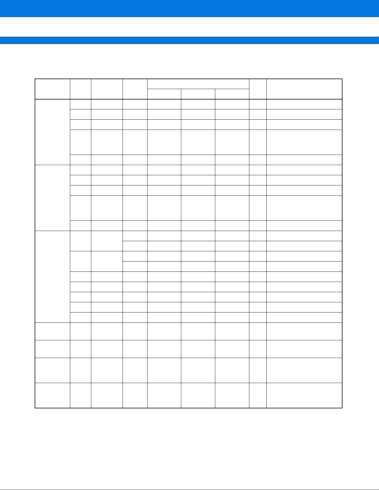
MB91270/280 Series
3. DC Characteristics
(TA : Recommended Operating Conditions,
Parameter
“H” level
input
voltage
“L” level
input
voltage
Power
supply
current
Input leak
current
Input capacitance
Pull-up
resistor
Pull-down
resistor
Sym-
bol
V
IHS
IHC
V
IHT
V
V
IHM
IHI
V
ILS
V
V
ILC
ILT
V
V
ILM
ILI
V
I
CC
I
CCS
I
CCL
I
CCSL
CCR32
I
I
CCR4
I
CCH
I
IL
IN
C
UP
R
DOWN
R
Pin name
⎯⎯0.8 × V
⎯⎯0.7 × V
⎯⎯2.1 ⎯ V
MD0
MD1
MD2
INITX ⎯ 0.8 × V
⎯⎯V
⎯⎯V
⎯⎯V
MD0
MD1
MD2
INITX ⎯ VSS − 0.3 ⎯ 0.2 × V
V
V
V
V
V
V
V
⎯⎯−5 ⎯ 5 µA All input pins
⎯⎯ ⎯ 515pF
⎯⎯25 50 100 kΩ
⎯ − 325 50 100kΩ
CC
CC
CC
CC
CC
CC
CC
Condi-
tions
⎯ V
⎯ V
*2 ⎯ 100 120 mA Normal operation*
*3 ⎯ 70 90 mA Normal operation*
*4 ⎯ 40 55 mA SLEEP operation*
*5 ⎯ 20 30 mA SLEEP operation*
*6 ⎯ 400 700 µA Sub operation
*7 ⎯ 300 600 µA Sub-SLEEP operation
*8 ⎯ 200 300 µA 32 kHz clock operation *
*9 ⎯ 700 1000 µA 4 MHz clock operation*
*10 ⎯ 20 100 µASTOP
= 5.0 V ± 10 %,
CC
V
Value
Unit Remarks
Min Typ Max
CC
CC
− 0.3 ⎯ VCC + 0.3 V
CC
CC
− 0.3 ⎯ 0.5 × V
SS
− 0.3 ⎯ 0.3 × V
SS
− 0.3 ⎯ 0.8 V TTL input*
SS
− 0.3 ⎯ VSS + 0.3 V
SS
⎯ V
⎯ V
⎯ V
+ 0.3 V CMOS automotive input
CC
+ 0.3 V CMOS Schmitt input
CC
+ 0.3 V TTL input*
CC
+ 0.3 V
CC
V CMOS automotive input
CC
V CMOS Schmitt input
CC
V
CC
Selectable except for P44
to P47, P56, P57, P76,
and P77
Selectable except for P44
to P47, P56, P57, P76,
and P77
= A
SS
V
1
1
= 0.0 V)
SS
V
11
11
11
11
12
12
68
(Continued)

MB91270/280 Series
(Continued)
Parameter
“H” level
Output
voltage
“L” level
Output
voltage
Sym-
bol
V
OH
OHI
V
OL
V
OLI
V
Pin name
⎯
P44 to
P47
P76, P77
⎯
P44 to
P47
P76, P77
Condi-
tions
=
I
OH
− 4 mA
I
=
OH
− 3 mA
=
I
OL
4 mA
I
=
OL
3 mA
Min Typ Max
V
− 0.5 ⎯⎯V
CC
V
− 0.5 ⎯⎯V Pins also used for I2C
CC
⎯⎯0.4 V
⎯⎯0.4 V Pins also used for I
*1 : In external bus mode, only P00 to P07, P10 to P17, and P36 can be selected.
*2 : CLKB = 32 MHz, CLKP = 32 MHz, CLKT = 16 MHz, CANCLK = 16 MHz
*3 : CLKB = 32 MHz, CLKP = 8 MHz, CLKT = 4 MHz, CANCLK = 8 MHz
*4 : CPU halted for case *2.
Value
Unit Remarks
Other than P44 to P47,
P76, P77
Other than P44 to P47,
P76, P77
2
C
*5 : CPU halted for case *3.
*6 : CLKB = CLKP = CLKT = CANCLK = 32 kHz, T
= + 25 °C
A
*7 : CPU halted for case *6
*8 : CPU and peripheral circuits halted, main oscillation halted, 32 kHz clock operation, T
*9 : CPU and peripheral circuits halted, sub-oscillation halted, 4 MHz clock operation, T
*10 : CPU and peripheral circuits halted, all oscillation circuits halted, T
= + 25 °C
A
= + 25 °C
A
= + 25 °C
A
*11 : The current consumption values for normal operation mode and SLEEP mode assume that the peripheral
circuits are operating at maximum capacity.
*12 : The current consumption value for clock mode operation does not include the consumption of the external
oscillator.
69

MB91270/280 Series
4. Flash Memory Program and Erase Characteristics
Parameter Conditions
Unit Remarks
Min Typ Max
Value
Sector erase time
Chip erase time
Half-word write time
Chip write time
= + 25 °C
A
V
= 5.0 V
CC
= + 25 °C
A
T
V
= 5.0 V
CC
= + 25 °C
A
T
V
= 5.0 V
CC
= + 25 °C
A
T
V
= 5.0 V
CC
⎯ 15 s
⎯ 14 ⎯ s
⎯ 16 3600 µs
⎯ 2.1 ⎯ s
Excludes time for internal write prior
to erase.
Excludes time for internal write prior
to erase.
Excludes system-level overhead
time.
Excludes system-level overhead
time.
T
Erase/Write cycle ⎯ 10000 ⎯⎯cycle
Data retention time
Average
T
= + 85 °C
A
20* ⎯⎯year
* : Calculated value based on technology reliability test data.
(Value calculated using the Arrhenius equation for the burn-in test results with an average temperature of + 85 °C.)
70
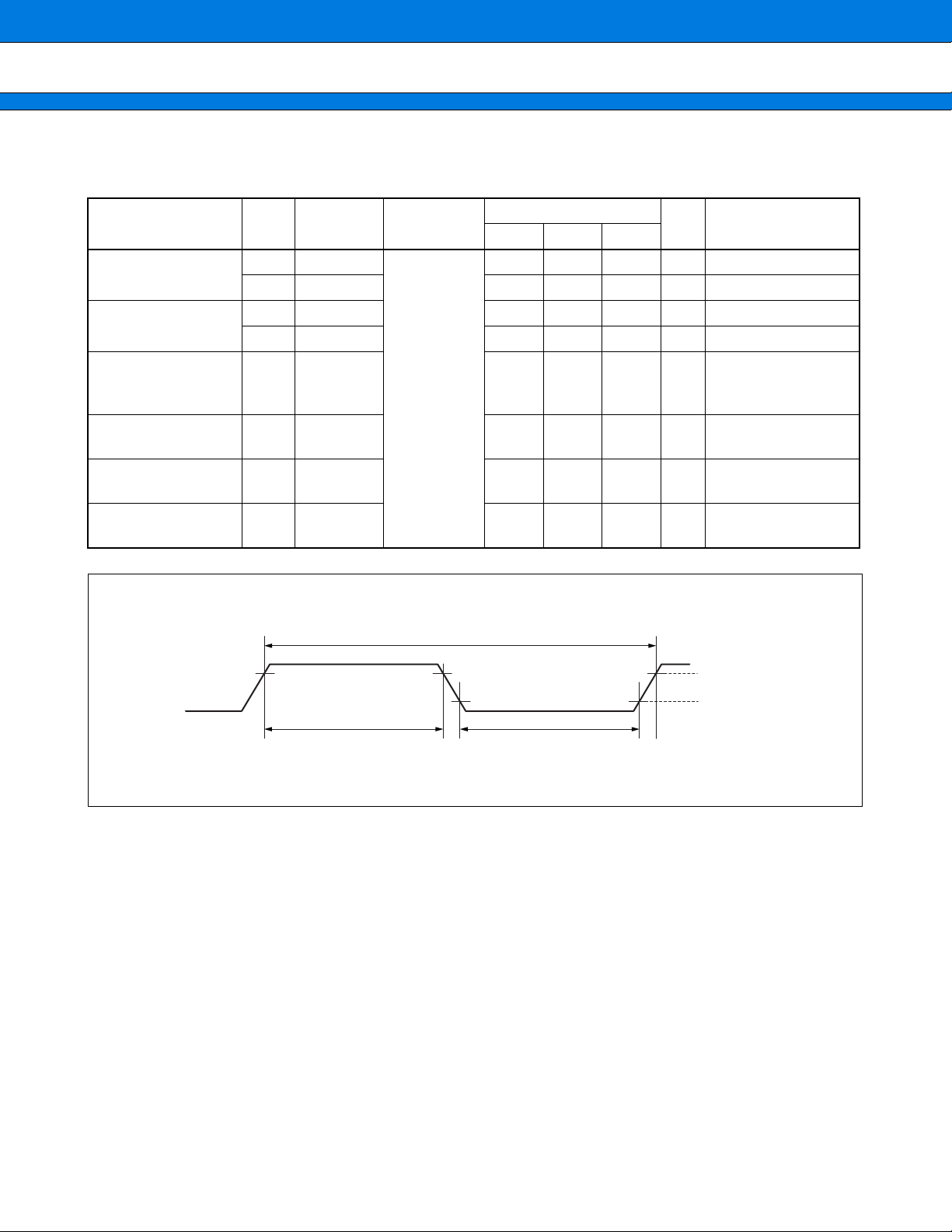
5. AC Characteristics
C
C
X
Parameter
Source oscillation
clock frequency
Source oscillation
clock cycle time
Input clock pulse
width
Input clock rise time
and fall time
Internal operation
clock frequency
Internal operating
clock cycle time
Sym-
bol
F
t
t
CYLL
P
P
tcr, tcf X0 ⎯⎯ 5ns
F
MB91270/280 Series
(TA : Recommended Operating Conditions,
Pin name Conditions
Min Typ Max
F
CA
CYL
X0, X1
C
⎯ 412MHz
X0A, X1A ⎯ 32.768 100 kHz
X0, X1 83.3 250 ⎯ ns
X0A, X1A 10 30.5 ⎯µs
WH
WL
CP
t
CP
X0 30 ⎯⎯ns
⎯
⎯⎯⎯32 MHz
⎯ 31.25 ⎯⎯ns
Value
= 5.0 V ± 10 %,
CC
V
Unit Remarks
= A
SS
V
= 0.0 V)
SS
V
Typically use a duty
ratio in the range
40 % to 60 %.
When external clock
is used
When main clock,
PLL clock are used.
When main clock,
PLL clock are used.
X0, X1 Clock Timing
0
PWH
tCYL
tcf
PWL
0.8 VC
0.2 VC
tcr
71
MB91270/280 Series
5
4
3
2
• Operation Assurance Range
Relation between internal operation clock frequency and power supply voltage
.5
.5
(V)
CC
.5
Recommended operation range
(A/D converter accuracy
guarantee range)
Operation Assurance Range
PLL operation
guarantee range
Power supply voltage V
28 32
Internal operation clock frequency F
(MHz)
CP
Note Use a PLL operation stabilization wait time of 500 µs or more.
Relation between oscillation clock frequency and internal operation clock
Internal operation clock frequency
PLL clock
Main clock
PLL multi-
plication
rate = 2
PLL multi-
plication
rate = 3
PLL multi-
plication
rate = 4
PLL multi-
plication
rate = 6
PLL multi-
plication
rate = 8
4 MHz 2 MHz 8 MHz 12 MHz 16 MHz 24 MHz 32 MHz
Oscillation clock
frequency
8 MHz 4 MHz 16 MHz 24 MHz 32 MHz ⎯⎯
12 MHz 6 MHz 24 MHz ⎯⎯⎯⎯
Sample oscillation circuit
X0 X1
R
72
C1
C
MB91270/280 Series
0
0
0
4
0
0
0
2
The AC standards assume the following measurement reference voltages.
Input signal waveform Output signal waveform
Hysteresis input pin Output pin
.7 V
CC
.3 V
CC
Hysteresis input pin (Automotive)
.8 VCC
.5 VCC
TTL input pin
.1 V
.8 V
.6 V
.4 V
⎯
⎯
73

MB91270/280 Series
I
• Reset input
: Recommended Operating Conditions,
(T
A
Parameter Symbol Pin name
INITX input time t
NITX
INTL
INITX ⎯
Condi-
tions
0.2 V
= 5.0 V ± 10%,
CC
V
= A
SS
V
V
Value
Unit Remarks
Min Max
10 ⎯µs
300 ⎯µsAt STOP
8 ⎯ ms At power-on
t
INTL
0.2 V
CC
CC
= 0.0 V)
SS
The following reset input standard should be satisfied as RAM data protection standard.
Voltage drop time Extarnal reset input standard (INITX)
CC
(V)
V
Min Max Min Max
At drop of 4.0 ≥ 3.5 V
256 t
CP
⎯ 300 µs ⎯
tCP : Period of the internal base clock.
V
CC
4 V
3.5 V 3.5 V
INITX
300 µs or more
256 t
CP
=
To protect RAM data, input INITX of 256 tCP or more before voltage drop at V
CC
3.5 V or less.
74

• UART Timing
Parameter
Serial clock cycle time t
SCK↓→SOT delay
time
Valid SIN→SCK↑ t
SCK↑→
valid SIN hold time
Serial clock “H” pulse
width
Serial clock “L” pulse
width
SCK↓→SOT delay
time
Valid SIN→SCK↑ t
SCK↑→
valid SIN hold time
Sym-
bol
SCYC
t
SLOV
IVSH
SHIX
t
SHSL
t
t
SLSH
SLOV
t
IVSH
SHIX
t
: Recommended Operating Conditions,
A
(T
Pin name
SCKx
SCKx
SOTx
Condi-
tions
Value
Min Max
8 t
CP
− 80 80 ns
⎯
100 ⎯ ns
SCKx
SINx
60 ⎯ ns
4 t
CP
SCKx
4 t
CP
SCKx
SOTx
⎯
⎯ 150 ns
60 ⎯ ns
SCKx
SINx
60 ⎯ ns
MB91270/280 Series
= 5.0 V ± 10 %,
CC
V
Unit Remarks
⎯ ns
⎯ ns
⎯ ns
Internal shift clock mode
Output pin capacitance is
= 80 pF + 1 × TTL
L
C
External shift clock mode
Output pin capacitance is
= 80 pF + 1 × TTL
C
L
= A
SS
V
= 0.0 V)
SS
V
Note : These are AC Characteristics at clock synchronous mode.
is the load capacitance connected to the pin for testing.
C
L
75

MB91270/280 Series
S
S
S
S
• Internal shift clock mode
t
SCYC
CKx
OTx
SINx
• External shift clock mode
CKx
OTx
0.8 V
t
SLOV
0.6 V
t
SLOV
CC
2.4 V
0.8 V
t
SLSH
2.4 V
0.8 V
0.8 V
0.5 V
t
IVSH
CC
CC
0.6 V
t
IVSH
2.4 V
CC
0.8 V
CC
t
SHSL
t
t
SHIX
SHIX
0.8 V
CC
0.8 V
0.8 V
0.5 V
CC
CC
0.8 V
CC
SINx
0.5 V
CC
0.8 V
0.5 V
CC
CC
76

• Timer input timing
T
I
: Recommended Operating Conditions,
A
(T
Parameter Symbol Pin name Conditions
Input pulse width
INx
CUx
t
TIWH
t
TIWL
0.8 V
TINx
t
CC
INx
TIWH
0.8 V
CC
⎯ 4 t
t
TIWL
0.5 V
CC
0.5 V
MB91270/280 Series
V
Value
Min Max
CP
CC
= 5.0 V ± 10 %,
CC
⎯ ns ⎯
= A
SS
V
Unit Remarks
= 0.0 V)
SS
V
77

MB91270/280 Series
6. Electrical Characteristics for the A/D Converter
• Electrical characteristics
: Recommended Operating Conditions,
(T
A
Parameter
Sym-
bol
Pin name
Min Typ Max
Value
Resolution ⎯⎯ ⎯ ⎯ 10 bit
Total error ⎯⎯ ⎯ ⎯ ± 3.0 LSB
Nonlinear error ⎯⎯ ⎯ ⎯ ± 2.5 LSB
Differential linear error ⎯⎯ ⎯ ⎯ ± 1.9 LSB
Zero transition voltage V
Full-scale transition
voltage
V
Sampling time t
Compare time t
A/D conversion time t
Analog port input
current
Analog input voltage V
FST
SMP
CMP
CNV
AIN
I
OT
AIN
AN0 to
AN23
AN0 to
AN23
⎯ 1.375 ⎯⎯µs*1
⎯ 1.375 ⎯⎯µs*2
⎯ 2.750 ⎯⎯µs*3
AN0 to
AN23
AN0 to
AN23
AV
SS
− 1.5 LSB
AVRH
− 3.5 LSB
AV
SS
+ 0.5 LSB
AVRH
− 1.5 LSB
+ 2.5 LSB
+ 0.5 LSB
⎯⎯10 µAV
0 ⎯ AVRH V
Reference voltage AVRH AVRH 4.0 ⎯ AV
Power supply current
I
AH
I
Reference voltage
supplying current
I
RH
I
Interchannel disparity ⎯
A
R
AV
CC
AVRH
AN0 to
AN31
⎯ 2.4 4.7 mA
⎯⎯ 5 µA*4
⎯ 600 900 µAV
⎯⎯ 5 µA*4
⎯⎯ 4LSB
= 5.0 V ± 10 %,
CC
V
AV
SS
AVRH
CC
Unit Remarks
V
1 LSB =
(AVRH − AV
V
V
AVSS
AVRH
= A
SS
V
≤ V
AIN
= 5.0 V
SS
V
SS
≤ V
= 0.0 V)
) / 1024
AVCC
*1 : For F
*2 : For F
*3 : For F
= 32 MHz, t
CP
= 32 MHz, t
CP
= 32 MHz, this is equivalent to the conversion time per channel when t
CP
= (Rext + Rin) × Cin × 7 = ST × CLKP period = 2 ch × 31.25 ns = 1.375 µs
SMP
= CKIN × 11 = CT × CLKP period × 11 = 4 h × 31.25 ns × 11 = 1.375 µs
CMP
and t
SMP
CMP
are selected.
*4 : Specifies the power supply current when the A/D converter is not operating and the CPU is in stop mode
(Vcc = AVcc = AVRH = 5.0 V)
Notes : • The error becomes proportionately larger for lower AVRH voltages.
• Use the device with external circuits of the following output impedance r
External circuit output impedance r
= 5 kΩ (Max)
S
for analog inputs :
S
• If the output impedance of the external circuit is too high, the analog voltage sampling time may be
insufficient.
• If inserting a capacitor between the external circuit and an input pin to prevent direct current flow, select
a capacitance several thousand times larger than C
due to the C
sampling capacitor in the chip.
SH
to minimize the capacitive voltage divider effect
SH
78

• Analog input equivalent circuit
External circuit
MB91270/280 Series
Microcontroller internal circuit
r
Input pin AN0
S
R
SH
C
SH
Input pin AN7
V
S
S/H circuit
Analog channel selector
< Recommended parameter values for each component >
: under 5 kΩ
S
r
R
= Approx. 2.5 kΩ
SH
C
= Approx. 10 pF
SH
Note : Parameter values for each component are indicative design values.
Comparator
79

MB91270/280 Series
• Definition of terminology
Resolution
Represents the change in analog signal able to be detected by the A/D converter.
10
For 10-bit conversion, the analog voltage can be resolved into 2
Total error
This error indicates the difference between actual and theoretical values, and is the total value of errors that can
come from offset error, gain error, nonlinear error, and noise.
Linearity error
Represents the difference between the actual conversion characteristic and the line between the zero transition
point (00 0000 0000 ⇔ 00 0000 0001) and full scale transition point (11 1111 1110 ⇔ 11 1111 1111).
Differential linear error
Deviation of input voltage, which is required for changing output code by 1 LSB, from an ideal value.
= 1024 increments.
80

1
1
1
1
0
0
0
0
• Conversion characteristics for 10-bit A/D converter
1 1111 1111
1 1111 1110
1 1111 1101
1 1111 1100
MB91270/280 Series
Digital output
0 0000 0011
0 0000 0010
0 0000 0001
0 0000 0000
1 LSB × N + V
V
OT
OT
Linearity error
V
NT
V
(N+1)T
V
FST
Analog input
VOT = AVSS + 0.5 LSB [V] (
V
= AVRH − 1.5 LSB [V] (
FST
V
= Digital output voltage at which transition from (N − 1) to N occurs.
FST
1 LSB =
Linearity error =
theoretical value
theoretical value
V
− V
FST
OT
1022
V
− (1 LSB × N + VOT)
NT
1 LSB
)
)
[LSB]
V (
+ 1) T − V
Differential linear error =
N
1 LSB
NT
− 1
[LSB]
81
MB91270/280 Series
ORDERING INFORMATION
■
Part number Package Remarks
MB91V280CR
MB91F272SPFV
MB91F272PFV
401-pin Ceramic PGA
(PGA-401C-A02)
100-pin plastic LQFP
(FPT-100P-M05)
100-pin plastic LQFP
(FPT-100P-M05)
Evaluation model
Single clock model
Dual clock model
82
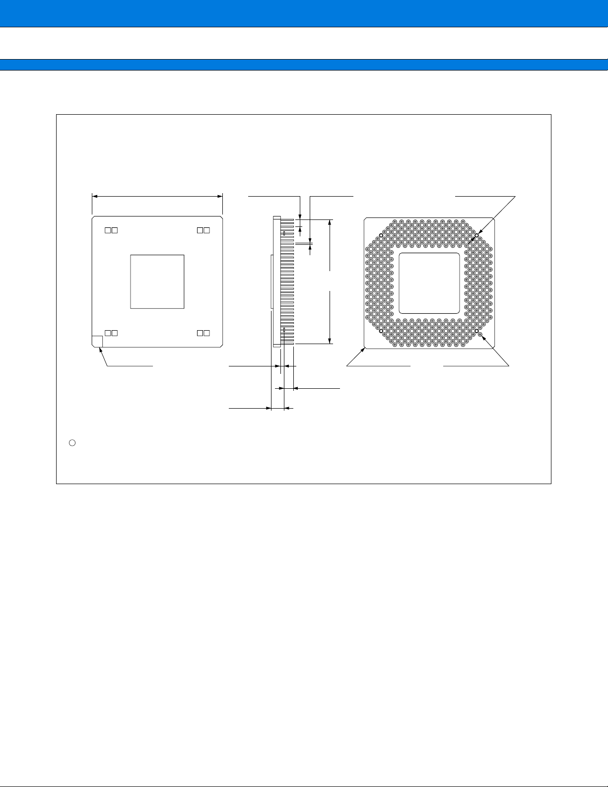
PACKAGE DIMENSIONS
■
401-pin ceramic PGA
(PGA-401C-A02)
MB91270/280 Series
48.26 ± 0.55
(1.900 ± .022)
INDEX AREA
C
1994 FUJITSU LIMITED R401002SC-2-2
SQ
1.20 ± 0.25
(.047 ± .010)
5.27 (.207)
MAX
2.54 (.100) TYP 0.40 ± 0.10
(.016 ± .004)
45.72 (1.800)
REF
3.40 ± 0.40
(.134 ± .016)
Dimensions in mm (inches).
Note : The values in parentheses are reference values.
DIA
1.02 (.040) C TYP
(4 PLCS)
1.00 (.039) DIA TYP
(4 PLCS)
EXTRA INDEX PIN
(Continued)
83
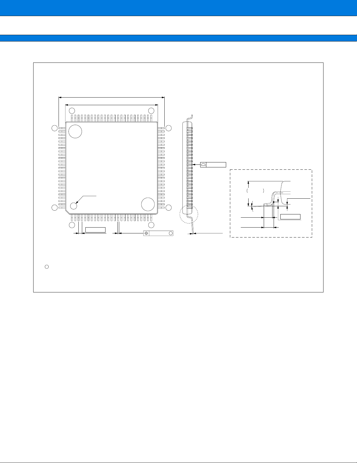
MB91270/280 Series
)
(Continued)
100-pin plastic LQFP
(FPT-100P-M05)
16.00±0.20(.630±.008)SQ
*
14.00±0.10(.551±.004)SQ
75
76 50
INDEX
100
125
0.50(.020)
0.20±0.05
(.008±.002)
Note 1) * : These dimensions do not include resin protrusion.
Note 2) Pins width and pins thickness include plating thickness.
Note 3) Pins width do not include tie bar cutting remainder.
51
0.08(.003)
Details of "A" part
+.008
+0.20
.059
–.004
–0.10
1.50
0.08(.003)
(Mounting height)
26
"A"
M
0.145±0.055
(.0057±.0022)
0˚~8˚
0.50±0.20
(.020±.008)
0.60±0.15
(.024±.006)
0.10±0.10
(.004±.004
(Stand off)
0.25(.010)
C
2003 FUJITSU LIMITED F100007S-c-4-6
Dimensions in mm (inches).
Note : The values in parentheses are reference values.
84

MB91270/280 Series
The information for microcontroller supports is shown in the following homepage.
http://www.fujitsu.com/global/services/microelectronics/product/micom/support/index.html
FUJITSU LIMITED
All Rights Reserved.
The contents of this document are subject to change without notice.
Customers are advised to consult with FUJITSU sales
representatives before ordering.
The information, such as descriptions of function and application
circuit examples, in this document are presented solely for the
purpose of reference to show examples of operations and uses of
Fujitsu semiconductor device; Fujitsu does not warrant proper
operation of the device with respect to use based on such
information. When you develop equipment incorporating the
device based on such information, you must assume any
responsibility arising out of such use of the information. Fujitsu
assumes no liability for any damages whatsoever arising out of
the use of the information.
Any information in this document, including descriptions of
function and schematic diagrams, shall not be construed as license
of the use or exercise of any intellectual property right, such as
patent right or copyright, or any other right of Fujitsu or any third
party or does Fujitsu warrant non-infringement of any third-party’s
intellectual property right or other right by using such information.
Fujitsu assumes no liability for any infringement of the intellectual
property rights or other rights of third parties which would result
from the use of information contained herein.
The products described in this document are designed, developed
and manufactured as contemplated for general use, including
without limitation, ordinary industrial use, general office use,
personal use, and household use, but are not designed, developed
and manufactured as contemplated (1) for use accompanying fatal
risks or dangers that, unless extremely high safety is secured, could
have a serious effect to the public, and could lead directly to death,
personal injury, severe physical damage or other loss (i.e., nuclear
reaction control in nuclear facility, aircraft flight control, air traffic
control, mass transport control, medical life support system, missile
launch control in weapon system), or (2) for use requiring
extremely high reliability (i.e., submersible repeater and artificial
satellite).
Please note that Fujitsu will not be liable against you and/or any
third party for any claims or damages arising in connection with
above-mentioned uses of the products.
Any semiconductor devices have an inherent chance of failure. You
must protect against injury, damage or loss from such failures by
incorporating safety design measures into your facility and
equipment such as redundancy, fire protection, and prevention of
over-current levels and other abnormal operating conditions.
If any products described in this document represent goods or
technologies subject to certain restrictions on export under the
Foreign Exchange and Foreign Trade Law of Japan, the prior
authorization by Japanese government will be required for export
of those products from Japan.
F0511
© 2005 FUJITSU LIMITED Printed in Japan
 Loading...