

Page 1

FUJITSU SEMICONDUCTOR
CONTROLLER MANUAL
CM71-10106-1E
FR30
32-Bit Microcontroller
MB91F109
Hardware Manual
Page 2

Page 3

FR30
32-Bit Microcontroller
MB91F109
Hardware Manual
FUJITSU LIMITED
Page 4

Page 5

PREFACE
■
Objectives and Intended Reader
The MB91F109 has been developed as one of the "32-bit single-chip microcontroller FR30
series" products that use new RISC architecture CPUs as their cores. It has optimal
specifications for embedding applications that require high CPU processing power.
This manual explains the functions and operations of the MB91F109 for the engineers who
actually develop products using the MB91F109. Read this manual thoroughly. Refer to the
instruction manual for details on individual instructions.
■
Trademarks
FR stands for FUJITSU RISC controller, a product of Fujitsu Limited.
Embedded Algorithm
TM
is a trademark of Advanced Micro Devices, Inc.
i
Page 6

■
Organization of This Manual
This manual consists of 16 chapters and an appendix.
Chapter 1 Overview
Chapter 1 provides ba sic general infor mation on the MB91F1 09, inc luding i ts c haracteri stic s,
a block diagram, and function overview.
Chapter 2 CPU
Chapter 2 provides basic information on the FR series CPU core functions including the
architecture, specifications, and instructions.
Chapter 3 Clock Generator and Controller
Chapter 3 provides detailed information on the generation and control of the clock that
controls the MB91F109.
Chapter 4 Bus Interface
Chapter 4 explain s the basic items of the external bus interface, register co nfiguration and
functions, bus operations, bus timing, and provides bus operation program samples.
Chapter 5 I/O Ports
Chapter 5 provides an overv iew of I/O ports, explains the I/O port register c onfiguration and
the conditions for using external terminals as I/O ports.
Chapter 6 External Interrupt/NMI Controller
Chapter 6 provides an overvi ew of the external inter rupt/NMI controlle r, explains the regi ster
configuration and functions, and operations of the external interrupt/NMI controller.
Chapter 7 Delayed Interrupt Module
Chapter 7 provides an overview of the delayed interrupt module, explains the register
configuration and functions, and operations of the delayed interrupt module.
Chapter 8 Interrupt Controller
Chapter 8 provides an overview of the inte rrupt contro ller, expl ains the register con figurati on
and functions, and operations of th e interrupt con troller. The chapt er also explains the hold
request cancel request function using examples.
Chapter 9 U-TIMER
Chapter 9 provides an overview of the U-TIMER, explains the register configuration and
functions, and operations of the U-TIMER.
Chapter 10 UART
Chapter 10 provides an overview of the UART, explains the register configuration and
functions, and operations of the UART.
Chapter 11 A/D Converter (Successive Approximation Type)
Chapter 11 provides an overview of the A/D converter, explains the register configuration
and functions, and operations of the A/D converter.
Chapter 12 16-bit Reload Timer
Chapter 12 provides an overview of the 16-bit reload timer, explains the register
configuration and functions, and operations of the 16-bit reload timer.
Chapter 13 Bit Search Module
Chapter 13 provides an overview of the bit search module, explains the register configuration
and functions, and operations and save/restore processing of the bit search module.
ii
Page 7

Chapter 14 PWM Timer
Chapter 14 provides a n overview of the PWM timer, expl ains the register configurati on and
functions, and operations of the PWM timer.
Chapter 15 DMAC
Chapter 15 provides an overview of the DMAC, explains the register configuration and
functions, and operations of the DMAC.
Chapter 16 Flash Memory
Chapter 16 explains the flash memory functions and operations.
The chapter provides information on using the flash memory from the FR CPU.
For information on usi ng the fl ash memo ry from th e ROM writ er, refer to the user ’s guid e for
the ROM writer.
Appendix
The appendix provides information on I/O maps, interrupt vectors, terminal states in each
CPU status, notes on usin g the little endian area, and a listing of instructi ons. It includes
details of these types of inform ation that are not covered by the text that can be refere nced
for programming.
iii
Page 8

1. The contents of this document are subject to change without notice. Customers are advised to consult
with FUJITSU sales representatives before ordering.
2. The information and circuit diagrams in this document are presented as examples of semiconductor
device applications, and are not intended to be incorporated in devices for actual use. Also, FUJITSU is
unable to assume responsibility for infringement of any patent rights or other rights of third parties
arising from the use of this information or circuit diagrams.
3. The contents of this document may not be reproduced or copied without the permission of FUJITSU
LIMITED.
4. FUJITSU semiconductor devices are intended for use in standard applications (computers, office
automation and other office equipments, industrial, communications, and measurement equipments,
personal or household devices, etc.).
CAUTION:
Customers considering the use of our products in special applications where failure or abnormal
operation may directly affect human lives or cause physical injury or property damage, or where
extremely high levels of reliability are demanded (such as aerospace systems, atomic energy controls,
sea floor repeaters, vehicle operating controls, medical devices for life support, etc.) are requested to
consult with FUJITSU sales representatives before such use. The company will not be responsible for
damages arising from such use withou t prior approval.
5. Any sem iconductor devi ces have inherent ly a certain ra te of failure. You must protect against injur y,
damage or loss from such failures by incorporating safety design measures into your facility and
equipment such as redundancy, fire protection, and prevention of over-current levels and other
abnormal operating conditions.
6. If any products described in this document represent goods or technologies subject to certain
restrictions on export under the Foreign Exchange and Foreign Trade Control Law of Japan, the prior
authorization by Japanese government should be required for export of those products from Japan.
©1999 FUJITSU LIMITED Printed in Japan
iv
Page 9

How to Read This Manual
■
Description Format of this Manual
Major terms used in this manual are explained below:
Term Meaning
I-BUS 16-bit wide bus used for internal instructions. Since the FR series uses
an internal Harvard architecture, independent buses are used for
instructions and data. A bus converter is connected to the I-BUS.
D-BUS Internal 32-bit wide data bus. Internal resources are connected to the
D-BUS.
C-BUS Internal multiplex bus. The C-BUS is connected to the I-BUS and D-
BUS via a switch. An external interface module is connected to the CBUS. Data and instructions are multiplexed in the external data bus.
R-BUS Internal 16-bit wide data bus. The R-BUS is connected to the D-BUS
via an adapter. Various I/O ports, the clock generator, and interrupt
controller are connected to the R-BUS. Since the R-BUS is 16 bits
wide in which addresses and data are multiplexed, it takes twice as
much or more cycle time than usual for the CPU to access these
resources.
E-unit Operation executing unit
φ
θ
System clock output from the clock generator to each internal resource
connected to the R-BUS. The system clock at the highest speed
shows the same cycle as source oscillation but is divided into 1, 1/2, 1/
4, and 1/8 (or 1/2, 1/4, 1/8, and 1/16) by PCK1 and PCK0 of the clock
generator GCR register.
System clock or operation clock for the CPU and resources connected
to a bus other than the R-BUS. The system clock at the highest speed
shows the same cycle as source oscillation but is divided into 1, 1/2, 1/
4, and 1/8 (or 1/2, 1/4, 1/8, and 1/16) by CCK1 and CCK0 of the clock
generator GCR register.
v
Page 10

vi
Page 11

CONTENTS
CHAPTER 1 OVERVIEW ................................................................................................... 1
1.1 MB91F109 Characteristics .................................................................................................................... 2
1.2 General Block Diagram of MB91F109 ................................................................................................... 6
1.3 Outside Dimensions ............................................................................................................................... 7
1.4 Pin Arrangement Diagrams ................................................................................................................. 10
1.5 Pin Functions ....................................................................................................................................... 14
1.6 I/O Circuit Format ................................................................................................................................ 22
1.7 Memory Address Space ......................................... ...... ............................................. ....... .... ............... 24
1.8 Handling of Devices ............................................................................................................................. 26
CHAPTER 2 CPU ............................................................................................................. 29
2.1 CPU Architecture ...... ....... ...... ....... ............................................. ...... ....... ...... ....... ...... .... ...................... 30
2.2 Internal Architecture ...................... ...... ....... ...... ....... ............................................. ...... ... ....................... 31
2.3 Programming Model .................................. ...... ....... ............................................. ...... ....... . .................. 33
2.3.1 General-Purpose Registers ............................................................................................................ 35
2.3.2 Special Registers ............................................................................................................................ 36
2.3.3 Program Status Register (PS) ........................................................................................................ 39
2.4 Data Structure ...................................................................................................................................... 42
2.5 Word Alignment ................................................................................................................................... 43
2.6 Memory Map ....... ...... ....... ...... ....... ...... ....... ............................................. ...... ....... ...... ... ....................... 44
2.7 Instruction Overview ............................................................................................................................ 46
2.7.1 Branch Instructions with Delay Slots .............................................................................................. 48
2.7.2 Branch Instructions without Delay Slots ......................................................................................... 51
2.8 EIT (Exception, Interrupt, and Trap) .................................................................................................... 52
2.8.1 EIT Interrupt Levels .......... ....... ...... ....... ...... ............................................. ....... ...... .......................... 54
2.8.2 Interrupt Control Register (ICR) ...................................................................................................... 56
2.8.3 System Stack Pointer (SSP) ........................................................................................................... 57
2.8.4 Interrupt Stack ................................................................................................................................ 58
2.8.5 Table Base Register (TBR) ............................................................................................................ 59
2.8.6 EIT Vector Table ............................................................ ....... ...... ....... ...... ....... ................................ 60
2.8.7 Multiple EIT Processing .................................................................................................................. 62
2.8.8 EIT Operation ............. ............................................. ...... ....... ...... ....... ...... ....................................... 64
2.9 Reset Sequence .................................................................................................................................. 68
2.10 Operation Mode ........ ....... ...... ....... ...... ....... ...... ....... ...... ...... ....... .......................................................... 69
CHAPTER 3 CLOCK GENERATOR AND CONTROLLER ............................................. 73
3.1 Outline of Clock Generator and Controller ........................................................................................... 74
3.2 Reset Reason Resister (RSRR) and Watchdog Cycle Control Register (WTCR) ............................... 76
3.3 Standby Control Register (STCR) ....................................................................................................... 78
3.4 DMA Request Suppression Register (PDRR) ..................................................................................... 80
3.5 Timebase Timer Clear Register (CTBR) .............................................................................................. 81
3.6 Gear Control Register (GCR) .............................................................................................................. 82
3.7 Watchdog Timer Reset Delay Register (WPR) .................................................................................... 85
3.8 PLL Control Register (PCTR) .............................................................................................................. 86
vii
Page 12

3.9 Gear Function ..................................................................................................................................... 87
3.10 Standby Mode (Low Power Consumption Mechanism) ...................................................................... 90
3.10.1 Stop State ...................................................................................................................................... 92
3.10.2 Sleep State .................................................................................................................................... 95
3.10.3 Standby Mode State Transition ..................................................................................................... 98
3.11 Watchdog Function ............................................................................................................................. 99
3.12 Reset Source Hold Circuit ................................................................................................................. 101
3.13 DMA Suppression ............................................................................................................................. 103
3.14 Clock Doubler Function ..................................................................................................................... 105
3.15 Example of PLL Clock Setting .......................................................................................................... 108
CHAPTER 4 BUS INTERFACE ..................................................................................... 111
4.1 Outline of Bus Interface .................................................................................................................... 112
4.2 Chip Select Area ............................................................................................................................... 115
4.3 Bus Interface ..................................................................................................................................... 116
4.4 Area Select Register (ASR) and Area Mask Register (AMR) ........................................................... 118
4.5 Area Mode Register 0 (AMD0) .......................................................................................................... 121
4.6 Area Mode Register 1 (AMD1) .......................................................................................................... 123
4.7 Area Mode Register 32 (AMD32) ...................................................................................................... 124
4.8 Area Mode Register 4 (AMD4) .......................................................................................................... 125
4.9 Area Mode Register 5 (AMD5) .......................................................................................................... 126
4.10 DRAM Control Register 4/5 (DMCR4/5) ........................................................................................... 127
4.11 Refresh Control Register (RFCR) ..................................................................................................... 130
4.12 External Pin Control Register 0 (EPCR0) ......................................................................................... 132
4.13 External Pin Control Register 1 (EPCR1) ......................................................................................... 135
4.14 DRAM Signal Control Register (DSCR) ............................................................................................ 136
4.15 Little Endian Register (LER) ............................................................................................................. 138
4.16 Relationship between Data Bus Widths and Control Signals ........................................................... 139
4.16.1 Bus Access with Big Endians ...................................................................................................... 141
4.16.2 Bus Access with Little Endians .................................................................................................... 147
4.16.3 External Access ........................................................................................................................... 151
4.16.4 DRAM Relationships .................................................................................................................... 155
4.17 Bus Timing ........................................................................................................................................ 159
4.17.1 Basic Read Cycle ................ ............................................. ...... ....... ...... ....... ...... ........................... 162
4.17.2 Basic Write Cycles .. ...... ....... ...... ....... ...... ....... ...... ....... ...... ...... ..................................................... 164
4.17.3 Read Cycles in Each Mode ......................................................................................................... 166
4.17.4 Write Cycles in Each Mode .......................................................................................................... 168
4.17.5 Read and Write Combination Cycles ........................................................................................... 170
4.17.6 Automatic Wait Cycles ................................................................................................................. 171
4.17.7 External Wait Cycles .................................................................................................................... 172
4.17.8 Usual DRAM Interface: Read ...................................................................................................... 173
4.17.9 Usual DRAM Interface: Write ....................................................................................................... 175
4.17.10 Usual DRAM Read Cycles ........................................................................................................... 177
4.17.11 Usual DRAM Write Cycles ........................................................................................................... 179
4.17.12 Automatic Wait Cycles in Usual DRAM Interface ........................................................................ 181
4.17.13 DRAM Interface in High-Speed Page Mode ................................................................................ 182
4.17.14 Single DRAM Interface: Read ...................................................................................................... 185
4.17.15 Single DRAM Interface: Write ...................................................................................................... 186
4.17.16 Single DRAM Interface ................................................................................................................ 187
viii
Page 13

4.17.17 Hyper DRAM Interface: Read ....................................................................................................... 188
4.17.18 Hyper DRAM Interface: Write ....................................................................................................... 189
4.17.19 Hyper DRAM Interface ................................................................................................................. 190
4.17.20 DRAM Refresh ............................................................................................................................. 191
4.17.21 External Bus Request ................................................................................................................... 193
4.18 Internal Clock Multiplication (Clock Doubler) ..................................................................................... 194
4.19 Program Example for External Bus Operation ................................................................................... 196
CHAPTER 5 I/O PORTS ................................................................................................. 201
5.1 Outline of I/O Ports ............................................................................................................................ 202
5.2 Port Data Register (PDR) .......................... ...... ....... ...... ...... ....... ...... ................................... ............... 203
5.3 Data Direction Register (DDR) .......................................................................................................... 204
5.4 Using External Pins as I/O Ports ....................................................................................................... 205
CHAPTER 6 EXTERNAL INTERRUPT/NMI CONTROLLER ........................................ 211
6.1 Overview of External Interrupt/NMI Controller ................................................................................... 212
6.2 Enable Interrupt Request Register (ENIR) ........................................................................................ 213
6.3 External Interrupt Request Register (EIRR) ...................................................................................... 214
6.4 External Level Register (ELVR) ......................................................................................................... 215
6.5 External Interrupt Operation .............................................................................................................. 216
6.6 External Interrupt Request Levels ..................................................................................................... 217
6.7 Nonmaskable Interrupt (NMI) Operation ............................................................................................ 218
CHAPTER 7 DELAYED INTERRUPT MODULE ........................................................... 219
7.1 Overview of Delayed Interrupt Module ............................................................................................. 220
7.2 Delayed Interrupt Control Register (DICR) ........................................................................................ 221
7.3 Operation of Delayed Interrupt Module .............................................................................................. 222
CHAPTER 8 INTERRUPT CONTROLLER .................................................................... 223
8.1 Overview of Interrupt Controller ........................................................................................................ 224
8.2 Interrupt Controller Block Diagram .................................................................................................... 227
8.3 Interrupt Control Register (ICR) ......................................................................................................... 228
8.4 Hold Request Cancel Request Level Setting Register (HRCL) ......................................................... 230
8.5 Priority Check .................................................................................................................................... 231
8.6 Returning from the Standby Mode (Stop/Sleep) ................................................................................ 234
8.7 Hold Request Cancel Request .......................................................................................................... 235
8.8 Example of Using the Hold Request Cancel Request Function (HRCR) ........................................... 236
CHAPTER 9 U-TIMER .................................................................................................... 239
9.1 Overview of U-TIMER ........................................................................................................................ 240
9.2 U-TIMER Registers ............................................................................................................................ 241
9.3 U-TIMER Operation ........................................................................................................................... 243
CHAPTER 10 UART ......................................................................................................... 245
10.1 Overview of UART ............................................................................................................................. 246
10.2 Serial Mode Register (SMR) .............................................................................................................. 248
10.3 Serial Control Register (SCR) ............................................................................................................ 250
10.4 Serial Input Data Register (SIDR) and Serial Output Data Register (SODR) .................................... 252
ix
Page 14

10.5 Serial Status Register (SSR) ............................................................................................................ 253
10.6 UART Operation .................................... ...... ....... ...... ............................................. ....... . ................... 255
10.7 Asynchronous (Start-Stop) Mode .... ....... ...... ....... ...... ....... ............................................. ...... .............. 257
10.8 CLK Synchronous Mode ................................................................................................................... 258
10.9 UART Interrupt Occurrence and Flag Setting Timing ....................................................................... 260
10.10 Notes on Using the UART and Example for Using the UART .......................................................... 263
10.11 Setting Examples of Baud Rates and U-TIMER Reload Values ....................................................... 265
CHAPTER 11 A/D CONVERTER (Successive approximation type) ............................ 267
11.1 Overview of A/D Converter (Successive Approximation Type) ......................................................... 268
11.2 Control Status Register (ADCS) ....................................................................................................... 270
11.3 Data Register (ADCR) ...................................................................................................................... 275
11.4 A/D Converter Operation .................................................................................................................. 276
11.5 Conversion Data Protection Function ............................................................................................... 278
11.6 Notes on Using the A/D Converter .................................................................................................... 280
CHAPTER 12 16-BIT RELOAD TIMER ........................................................................... 281
12.1 Overview of 16-bit Reload Timer ...................................................................................................... 282
12.2 Control Status Register (TMCSR) ..................................................................................................... 284
12.3 16-Bit Timer Register (TMR) and 16-Bit Reload Register (TMRLR) ................................................. 286
12.4 Operation of 16-Bit Reload Timer .................................................................................................... 287
12.5 Counter States .................................................................................................................................. 289
CHAPTER 13 BIT SEARCH MODULE ............................................................................ 291
13.1 Overview of the Bit Search Module ................................................................................................... 292
13.2 Bit Search Module Registers ............................................................................................................ 293
13.3 Bit Search Module Operation and Save/Restore Processing ........................................................... 295
CHAPTER 14 PWM TIMER ............................................................................................. 299
14.1 Overview of PWM Timer ................................................................................................................... 300
14.2 PWM Timer Block Diagram ............................................................................................................... 302
14.3 Control Status Register (PCNH, PCNL) ............................................................................................ 304
14.4 PWM Cycle Setting Register (PCSR) ............................................................................................... 308
14.5 PWM Duty Cycle Setting Register (PDUT) ....................................................................................... 309
14.6 PWM Timer Register (PTMR) ........................................................................................................... 310
14.7 General Control Register 1 (GCN1) .................................................................................................. 311
14.8 General Control Register 2 (GCN2) .................................................................................................. 314
14.9 PWM Operation ................................................................................................................................ 315
14.10 One-Shot Operation .......................................................................................................................... 317
14.11 Interrupt ............................................................................................................................................ 319
14.12 Constant "L" or Constant "H" Output from PWM Timer .................................................................... 320
14.13 Starting Multiple PWM Timer Channels ............................................................................................ 321
CHAPTER 15 DMAC ........................................................................................................ 323
15.1 Overview of DMAC ........................................................................................................................... 324
15.2 DMAC Parameter Descriptor Pointer (DPDP) .................................................................................. 326
15.3 DMAC Control Status Register (DACSR) ......................................................................................... 327
15.4 DMAC Pin Control Register (DATCR) .............................................................................................. 329
x
Page 15

15.5 Descriptor Register in RAM ................ ....... ...... ....... ............................................. ...... ....... .. ............... 332
15.6 DMAC Transfer Modes ...................................................................................................................... 335
15.7 Output of Transfer Request Acknowledgment and Transfer End signals .......................................... 338
15.8 Notes on DMAC ................................................................................................................................ 339
15.9 DMAC Timing Charts ......................................................................................................................... 342
15.9.1 Timing Charts of the Descriptor Access Block ............................................................................. 343
15.9.2 Timing Charts of Data Transfer Block .......................................................................................... 345
15.9.3 Transfer Stop Timing Charts in Continuous Transfer Mode ......................................................... 347
15.9.4 Transfer Termination Timing Charts ............................................................................................. 349
CHAPTER 16 FLASH MEMORY ...................................................................................... 351
16.1 Outline of Flash Memory .................................................................................................................... 352
16.2 Block Diagram of Flash Memory ........................................................................................................ 354
16.3 Flash Memory Status Register (FSTR) .............................................................................................. 355
16.4 Sector Configuration of Flash Memory ......................................................... ....... ...... ....... ...... ........... 357
16.5 Flash Memory Access Modes ............................................................................................................ 359
16.6 Starting the Automatic Algorithm ....................................................................................................... 361
16.7 Execution Status of the Automatic Algorithm ..................................................................................... 364
APPENDIX .......................................................................................................................... 369
APPENDIX A I/O Maps ............................................................................................................................. 370
APPENDIX B Interrupt Vectors ................................................................................................................ 379
APPENDIX C Pin Status for Each CPU Status ......................................................................................... 383
APPENDIX D Notes on Using Little Endian Areas ................................................................................... 395
D.1 C Compiler (fcc911) ........................................................................................................................ 396
D.2 Assembler (fsm911) ........................................................................................................................ 399
D.3 Linker (flnk911) ............................................................................................................................... 401
D.4 Debuggers (sim911, eml911, and mon911) .................................................................................... 402
APPENDIX E Instructions ......................................................................................................................... 403
E.1 FR-Series Instructions ..................................................................................................................... 409
INDEX ................................................................................................................................. 425
xi
Page 16

FIGURES
Figure 1.2-1 General Block Diagram of MB91F109 ........................................................................................ 6
Figure 1.3-1 Outside Dimensions of FPT-100P-M06 ...................................................................................... 7
Figure 1.3-2 Outside Dimensions of FPT-100P-M05 ...................................................................................... 8
Figure 1.3-3 Outside Dimensions of BGA-112P-M01 ..................................................................................... 9
Figure 1.4-1 QFP-100 Pin Arrangements ........ ...... ....... ...... ....... ...... ...... ....... ...... .......................................... 10
Figure 1.4-2 LQFP-100 Pin Arrangements ................................................................................................... 11
Figure 1.4-3 FBGA-112 Pin Arrangements ................... ...... ....... ...... ...... ....... ...... ....... ...... ....... ...... ................ 12
Figure 1.7-1 MB91F109 Memory Map ......................................................... ...... .......................................... 24
Figure 1.8-1 Example of Using an External Clock (Normal Method) ............................................................ 26
Figure 1.8-2 Example of Using an External Clock (Possible at 12.5 MHz or Lower) .................................... 27
Figure 2.2-1 Internal Architecture ........ ...... ....... ............................................. ...... ....... ...... ....... ...................... 31
Figure 2.2-2 Instruction Pipeline ............................ ....... ...... ............................................. ....... ...................... 32
Figure 2.3-1 Configuration of general-purpose registers .............................................................................. 33
Figure 2.3-2 Configuration of special registers ............................................................................................. 34
Figure 2.3-3 Configuration of General-Purpose Registers ............................................................................ 35
Figure 2.3-4 Configuration of Special Registers ........................................................................................... 36
Figure 2.4-1 Data Mapping in Bit Ordering Mode ................................................................... ...... ....... . ........ 42
Figure 2.4-2 Data Mapping in Byte Ordering Mode ................... ...... ...... ....... ...... ....... ...... ....... ...... ................ 42
Figure 2.6-1 MB91F109 Memory Map .......................................................................................................... 44
Figure 2.6-2 Memory Map Common to the FR Series. ................................................................................. 45
Figure 2.8-1 Example of Interrupt Stack ....................................................................................................... 58
Figure 2.8-2 Example of Multiple EIT Processing ......................................................................................... 63
Figure 2.10-1 Mode Register Configuration ............. ....... ...... ....... ...... ...... ....... ...... .......................................... 70
Figure 3.1-1 Clock Generator and Controller Registers ................................................................................ 74
Figure 3.1-2 Block Diagram of the Clock Generator and Controller .............................................................. 75
Figure 3.9-1 Gear Controller Block Diagram ................................................................................................. 87
Figure 3.9-2 Clock Selection Timing Chart ................................................................................................... 89
Figure 3.10-1 Stop Controller Block Diagram ................. ...... ....... ...... ...... ....... ...... ....... ...... ....... ...................... 92
Figure 3.10-2 Sleep Controller Block Diagram ................................................................................................ 95
Figure 3.10-3 Standby Mode State Transition ................................................................................................ 98
Figure 3.11-1 Watchdog Timer Block Diagram ............................................................................................... 99
Figure 3.11-2 Watchdog Timer Operating Timing ......................................................................................... 100
Figure 3.11-3 Timebase Timer Counter ........................................................................................................ 100
Figure 3.12-1 Block Diagram of Reset Source Hold Circuit .......................................................................... 101
Figure 3.13-1 DMA Suppression Circuit Block Diagram ............................................................................... 103
xii
Page 17

Figure 3.15-1 Example of PLL Clock Setting ................................................................................................. 108
Figure 3.15-2 Clock System Reference Diagram .......................................................................................... 109
Figure 4.1-1 Bus Interface Registers ............ ....... ...... ....... ...... ...... ....... ...... .................................................. 113
Figure 4.1-2 Bus Interface Block Diagram .................................... ....... ...... ....... ........................................... 114
Figure 4.2-1 Example of Setting Chip Select Areas ..................................................................................... 115
Figure 4.4-1 Sample Maps of the Chip Select Areas ................................................................................... 120
Figure 4.16-1 Data bus Widths and Control Signals in Usual Bus Interface .................................................. 139
Figure 4.16-2 Data Bus Widths and Control Signals in DRAM Interface ....................................................... 139
Figure 4.16-3 Relationship between Internal Register and External Data Bus for Word Access .................. 141
Figure 4.16-4 Relationship between Internal Register and External Data Bus for Half-Word Access ........... 141
Figure 4.16-5 Relationship between Internal Register and External Data Bus for Byte Access .................... 142
Figure 4.16-6 Relationship between Internal Register and External Data Bus for 16-bit Bus Width ............. 142
Figure 4.16-7 Relationship between Internal Register and External Data Bus for 8-bit Bus Width ............... 143
Figure 4.16-8 External Bus Access for 16-bit Bus Width ............................................................................... 144
Figure 4.16-9 External Bus Access for 8-bit Bus Width ................................................................................. 145
Figure 4.16-10 Example of Connection between MB91F109 and External Devices ....................................... 146
Figure 4.16-11 Relationship between Internal Register and External Data Bus for Word Access .................. 147
Figure 4.16-12 Relationship between Internal Register and External Data Bus for Half-word Access ............ 148
Figure 4.16-13 Relationship between Internal Register and External Data Bus for Byte Access .................... 148
Figure 4.16-14 Relationship between Internal Register and External Data Bus for 16-bit Bus Width ............. 149
Figure 4.16-15 Relationship between Internal Register and External Data Bus for 8-bit Bus Width ............... 149
Figure 4.16-16 Example of Connection between MB91F109 and External Devices (16-Bit Bus Width) ......... 150
Figure 4.16-17 Example of Connection between MB91F109 and External Devices (8-Bit Bus Width) ........... 150
Figure 4.16-18 Example of Connection between MB91F109 and One 8-bit Output DRAM (8-Bit Data Bus) . 156
Figure 4.16-19 Example of Connection between MB91F109 and Two 8-Bit Output DRAMs
(16-Bit Data Bus) ..................................................................................................................... 157
Figure 4.16-20 Example of Connection between MB91F109 and Two 16-Bit Output DRAMs
(16-Bit Data Bus) ..................................................................................................................... 158
Figure 4.17-1 Example of Basic Read Cycle Timing Chart ............................................................................ 162
Figure 4.17-2 Example for Basic Write Cycle Timing .................................................................................... 164
Figure 4.17-3 Example 1 of Read Cycle Timing Chart .................................................................................. 166
Figure 4.17-4 Example 2 of Read Cycle Timing Chart .................................................................................. 166
Figure 4.17-5 Example 3 of Read Cycle Timing Chart .................................................................................. 166
Figure 4.17-6 Example 4 of Read Cycle Timing Chart .................................................................................. 167
Figure 4.17-7 Example 5 of Read Cycle Timing Chart .................................................................................. 167
Figure 4.17-8 Example 1 of Write Cycle Timing Chart ................................................................................... 168
Figure 4.17-9 Example 2 of Write Cycle Timing Chart ................................................................................... 168
Figure 4.17-10 Example 3 of Write Cycle Timing Chart ................................................................................... 168
Figure 4.17-11 Example 4 of Write Cycle Timing Chart ................................................................................... 169
xiii
Page 18

Figure 4.17-12 Example 5 of Write Cycle Timing Chart .................................................................................. 169
Figure 4.17-13 Example of Read and Write Combination Cycle Timing Chart ............................................... 170
Figure 4.17-14 Example of Automatic Wait Cycle Timing Chart ..................................................................... 171
Figure 4.17-15 Example of External Wait Cycle Timing Chart ........................................................................ 172
Figure 4.17-16 Example of Usual DRAM Interface Read Timing Chart .......................................................... 173
Figure 4.17-17 Example of Usual DRAM Interface Write Timing Chart .......................................................... 175
Figure 4.17-18 Example 1 of Usual DRAM Read Cycle Timing Chart ............................................................ 177
Figure 4.17-19 Example 2 of Usual DRAM Read Cycle Timing Chart ............................................................ 178
Figure 4.17-20 Example 3 of Usual DRAM Read Cycle Timing Chart ............................................................ 178
Figure 4.17-21 Example 1 of Usual DRAM Write Cycle Timing Chart ............................................................ 179
Figure 4.17-22 Example 2 of Usual DRAM Write Cycle Timing Chart ............................................................ 180
Figure 4.17-23 Example 3 of Usual DRAM Write Cycle Timing Chart ............................................................ 180
Figure 4.17-24 Example of Automatic Wait Cycle Timing Chart in Usual DRAM Interface ............................ 181
Figure 4.17-25 Example 1 of DRAM Interface Timing Chart in High-Speed Page Mode ............................... 182
Figure 4.17-26 Example 2 of DRAM Interface Timing Chart in High-Speed Page Mode ............................... 182
Figure 4.17-27 Example 3 of DRAM Interface Timing Chart in High-Speed Page Mode ............................... 183
Figure 4.17-28 Example 4 of DRAM Interface Timing Chart in High-Speed Page Mode ............................... 184
Figure 4.17-29 Example of Single DRAM Interface Read Timing Chart ......................................................... 185
Figure 4.17-30 Example of Single DRAM Interface Write Timing Chart ......................................................... 186
Figure 4.17-31 Example of Single DRAM Interface Timing Chart ................................................................... 187
Figure 4.17-32 Example of Hyper DRAM Interface Read Timing Chart ......................................................... 188
Figure 4.17-33 Example of Hyper DRAM Interface Write Timing Chart .......................................................... 189
Figure 4.17-34 Example of Hyper DRAM Interface Timing Chart ................................................................... 190
Figure 4.17-35 Example of CAS before RAS (CBR) Refresh Timing Chart .................................................... 191
Figure 4.17-36 Example of Timing Chart of CBR Refresh Automatic Wait Cycle ........................................... 192
Figure 4.17-37 Example of Selfrefresh Timing Chart . ....... ...... ....... ...... ...... ....... ...... ....... ................................. 192
Figure 4.17-38 Example of Bus Control Release Timing Chart ...................................................................... 193
Figure 4.17-39 Example of Bus Control Acquisition Timing ............................................................................ 193
Figure 4.18-1 Example of Timing Chart for 2X Clock (BW-16bit, Access-Word Read) ................................ 194
Figure 4.18-2 Example of Timing for 1X Clock (BW-16bit, Access-Word Read) .......................................... 195
Figure 5.1-1 Basic I/O Port Block Diagram ................................................................................................. 202
Figure 6.1-1 External Interrupt/NMI Controller Registers ........... ...... ...... .............................................. ....... 212
Figure 6.1-2 External Interrupt/NMI Controller Block Diagram .................................................................... 212
Figure 6.5-1 External Interrupt Operation .............. ....... ...... ....... ............................................. ...... .............. 216
Figure 6.6-1 Clearing the Interrupt Cause Hold Circuit at Level Setting for the Interrupt Request Mode ... 217
Figure 6.6-2 Input of an Interrupt Cause in Interrupt Enable Mode and a Request Issued to the Interrupt
Controller ................................................................................................................................ 217
Figure 6.7-1 NMI Request Detection Block ................................................................................................. 218
xiv
Page 19

Figure 7.1-1 Delayed Interrupt Module Register ..................... ...... ....... ...... ....... .................................. ......... 220
Figure 7.1-2 Delayed Interrupt Module Block Diagram ................................................................................ 220
Figure 8.1-1 Interrupt Controller Registers (1/2) .......................................................................................... 225
Figure 8.1-2 Interrupt Controller Registers (2/2) .......................................................................................... 226
Figure 8.2-1 Block Diagram of the Interrupt Controller ................................................................................ 227
Figure 8.8-1 Example of Hardware Configuration for Using the Hold Request Cancel Request Function .. 236
Figure 8.8-2 Example of Timing for Hold Request Cancel Request Sequence (Interrupt Level: HRCL > a) 237
Figure 8.8-3 Example of Timing for Hold Request Cancel Request Sequence
(Interrupt Level: HRCL > a > b) ............................................................................................... 237
Figure 9.1-1 U-TIMER Registers ............................................ ............................................. ....... ................. 240
Figure 9.1-2 U-TIMER Block Diagram ......................................................................................................... 240
Figure 9.3-1 Example of Using U-TIMER Channels 0 and 1 in Cascade Mode .......................................... 243
Figure 10.1-1 UART Registers ....................................................................................................................... 246
Figure 10.1-2 UART Block Diagram ................................... ...... ...... ....... ...... ....... ...... ....... .............................. 247
Figure 10.7-1 Format of Data Transferred in Asynchronous (Start-Stop) Mode (Mode 0 or 1) ..................... 257
Figure 10.8-1 Format of Data Transferred in CLK Synchronous Mode (Mode 2) .......................................... 258
Figure 10.9-1 ORE, FRE, and RDRF Set Timing (Mode 0) ........................................................................... 260
Figure 10.9-2 ORE, FRE, and RDRF Set Timing (Mode 1) ........................................................................... 261
Figure 10.9-3 ORE and RDRF Set Timing (Mode 2) ..................................................................................... 261
Figure 10.9-4 TDRE Set Timing (Mode 0 or 1) .............................................................................................. 262
Figure 10.9-5 TDRE Set Timing (Mode 2) ..................................................................................................... 262
Figure 10.10-1 Sample System Structure for Mode 1 ...................................................................................... 263
Figure 10.10-2 Communication Flowchart for Mode 1 ................ ...... .............................................. ...... ........... 264
Figure 11.1-1 A/D Converter Registers ......................................................................................................... 268
Figure 11.1-2 Block Diagram of the A/D Converter. ...................................................................................... 269
Figure 11.5-1 Workflow of the Data Protection Function when DMA Transfer is Used ................................. 279
Figure 12.1-1 16-Bit Reload Timer Registers .............. ....... ...... ...... ....... ...... ....... ...... ..................................... 282
Figure 12.1-2 16-Bit Reload Timer Block Diagram ................................................... ....... ...... ....... ...... ........... 283
Figure 12.4-1 Counter Start and Operation Timing ........................................................................................ 287
Figure 12.4-2 Underflow Operation Timing .................................................................................................... 288
Figure 12.5-1 Counter States Transition ...................... ....... ...... ...... ....... ...... ....... ...... ....... .............................. 289
Figure 13.1-1 Bit Search Module Registers ................................................................................................... 292
Figure 13.1-2 Block Diagram of the Bit Search Module ................................................................................. 292
Figure 14.1-1 PWM Timer Registers ........................... ....... ...... ...... ....... ......................................... ............... 301
Figure 14.2-1 General Block Diagram of PWM Timer ................................................................................... 302
Figure 14.2-2 Block Diagram of Single PWM Timer Channel ........................................................................ 303
Figure 14.9-1 PWM Operation Timing Chart (Trigger Restart Disabled) ......................... ...... ....... ...... ........... 316
Figure 14.9-2 PWM Operation Timing Chart (Trigger Restart Enabled) ................... ....... ...... ....... ...... ....... .... 316
xv
Page 20

Figure 14.10-1 One-Shot Operation Timing Chart (Trigger Restart Disabled) ................................................ 318
Figure 14.10-2 One-Shot Operation Timing Chart (Trigger Restart Enabled) ................................................ 318
Figure 14.11-1 Causes of Interrupts and Their Timing (PWM Output: Normal Polarity) ................................ 319
Figure 14.12-1 Example of Keeping PWM Output at a Lower Level ............................................................... 320
Figure 14.12-2 Example of Keeping PWM Output at a High Level ................................................................. 320
Figure 15.1-1 DMAC Registers ................................ ....... ...... ....... ...... ...... ..................................................... 324
Figure 15.1-2 DMAC Block Diagram ............................................................................................................. 325
Figure 16.1-1 Flash Memory Registers ....... ....... ...... ....... ...... ....... ...... ...... ....................................... .............. 352
Figure 16.2-1 Block diagram of the Flash Memory ....................................................................................... 354
Figure 16.4-1 Memory Map and Sector Configuration .................................................................................. 357
Figure 16.7-1 Structure of the Hardware Sequence Flag .................. ...... ....... .............................................. 364
xvi
Page 21

TABLES
Table 1.4-1 FBGA Package Pin Names ....................................................................................................... 13
Table 1.5-1 Pin Functions (1/5) .................................................................................................................... 14
Table 1.5-2 Pin Functions (2/5) .................................................................................................................... 15
Table 1.5-3 Pin Functions (3/5) .................................................................................................................... 17
Table 1.5-4 Pin Functions (4/5) .................................................................................................................... 18
Table 1.5-5 Pin Functions (5/5) .................................................................................................................... 20
Table 1.6-1 I/O circuit format (1/2) ................................................................................................................ 22
Table 1.6-2 I/O circuit format (1/2) ................................................................................................................ 23
Table 2.8-1 Interrupt Level .......................................................................................................................... 54
Table 2.8-2 Assignments of Interrupt Causes and Interrupt Vectors ............................................................ 56
Table 2.8-3 Vector Table ............................................................................................................................. 61
Table 2.8-4 Priority for EIT Event Acceptance and Masking Other Events .................................................. 62
Table 2.8-5 EIT Handler Execution Order .................................................................................................... 63
Table 2.10-1 Mode Pins and Setting Modes ................................................................................................... 69
Table 2.10-2 Bus Mode Setting Bit and the Function .................................................................................... 70
Table 3.2-1 Watchdog Timer Cycles Specified by WT1 and WT0 ................................................................ 77
Table 3.3-1 Oscillation Stabilization Wait Time Specified by OSC1 and OSC0 ........................................... 79
Table 3.6-1 CPU Machine Clock .................................................................................................................. 82
Table 3.6-2 Peripheral Machine Clock ...................... ....... ............................................. ...... ....... ................... 83
Table 3.7-1 Watchdog Timer Cycles Specified by WT1 and WT0 ................................................................ 85
Table 3.10-1 Types of Operation in Standby Mode ........................................................................................ 90
Table 3.14-1 Operating Frequency Combinations Depending on whether the Clock Doubler
Function is Enabled or Disabled .............................................................................................. 107
Table 4.3-1 Correspondence between Chip Select Areas and Selectable Bus Interfaces ......................... 116
Table 4.10-1 Page Size of DRAM Connected .............................................................................................. 127
Table 4.10-2 Combinations of Bus Widths Available in Areas 4 and 5 ......................................................... 129
Table 4.15-1 Mode Setting Using the Combination of Bits (LE2, LE1, and LE0) ........................................ 138
Table 4.16-1 Relationship between Data Bus Widths and Control Signals .................................................. 140
Table 4.16-2 Functions and Bus Widths of DRAM Control Pins ................................................................... 155
Table 4.16-3 Page Size Select Bits .............................................................................................................. 156
Table 5.4-1 External Bus Functions to be Selected (1/4) ........................................................................... 205
Table 5.4-2 External Bus Functions to be Selected (2/4) ........................................................................... 206
Table 5.4-3 External Bus Functions to be Selected (3/4) ........................................................................... 207
Table 5.4-4 External Bus Functions to be Selected (4/4) ........................................................................... 209
Table 6.4-1 External Interrupt Request Mode ............................................................................................. 215
xvii
Page 22

Table 8.3-1 Correspondences between the Interrupt Level Setting Bits and Interrupt Levels ................... 229
Table 8.5-1 Relationships among Interrupt Causes, Numbers, and Levels (1/2) ...................................... 231
Table 8.5-2 Relationships among Interrupt Causes, Numbers, and Levels (2/2) ...................................... 232
Table 8.7-1 Settings for the Interrupt Levels for which a Hold Request Cancel Request is Issued ........... 235
Table 10.2-1 Selection of UART Operation Modes ...................................................................................... 248
Table 10.6-1 UART Operation Modes ......................................................................................................... 255
Table 10.11-1 Baud Rates and U-TIMER Reload Values in Asynchronous (Start-Stop) Mode .................... 265
Table 10.11-2 Baud Rates and U-TIMER Reload Values in CLK Synchronous Mode .................................. 265
Table 11.2-1 Selecting the Causes for Starting the A/D Converter ............................................................. 271
Table 11.2-2 Selecting the A/D Converter Operation Mode ........................................................................ 272
Table 11.2-3 Setting the A/D Conversion Start Channel ............................................................................. 273
Table 11.2-4 Setting the A/D Conversion End Channel ............................................................................... 273
Table 12.2-1 CSL Bit Setting Clock Source ................................................................................................. 284
Table 13.3-1 Bit Positions and Returned Values (Decimal) ......................................................................... 296
Table 14.3-1 Selection of the Count Clock .................................................................................................. 305
Table 14.3-2 PWM Output When "1" is Written to PGMS ............................................................................ 305
Table 14.3-3 Selection of Trigger Input Edge .............................................................................................. 305
Table 14.3-4 Selection of Interrupt Causes ................................................................................................. 306
Table 14.3-5 Specification of the Polarity of the PWM Output and the Edge .............................................. 306
Table 14.7-1 Selection of Ch3 Trigger Input ................................................................................................ 312
Table 14.7-2 Selection of Ch2 Trigger Input ................................................................................................ 312
Table 14.7-3 Selection of Ch1 Trigger Input ................................................................................................ 313
Table 14.7-4 Selection of Ch0 Trigger Input ................................................................................................ 313
Table 15.2-1 Channel Descriptor Addresses ............................................................................................... 326
Table 15.4-1 Selection of Transfer Input Detection Levels .......................................................................... 330
Table 15.4-2 Specification of Transfer Request Acknowledgment Output .................................................. 330
Table 15.4-3 Specification of Transfer End Output ...................................................................................... 331
Table 15.5-1 Specification of Transfer Source or Destination Address Update Modes ............................... 333
Table 15.5-2 Address Increment/De crem ent Unit ... ....... ...... ............................................. ....... ...... ....... ....... 333
Table 15.5-3 Specification of Transfer Data Size ........................................................................................ 333
Table 15.5-4 Transfer Mode Specification ................................................................................................... 334
Table 15.9-1 Codes Used in the Timing Charts ........................................................................................... 342
Table 16.4-1 Sector Addresses ................................................................................................................... 358
Table 16.6-1 Commands ............................................................................................................................. 361
Table 16.7-1 Statuses of the Hardware Sequence Flag .............................................................................. 365
Table A-1 I/O Map (1/6) ........................................................................................................................... 371
Table A-2 I/O Map (2/6) ........................................................................................................................... 372
Table A-3 I/O Map (3/6) ........................................................................................................................... 373
xviii
Page 23

Table A-4 I/O Map (4/6) ........................................................................................................................... 375
Table A-5 I/O Map (5/6) ........................................................................................................................... 376
Table A-6 I/O Map .................................................................................................................................... 377
Table B-1 Interrupt Vectors (1/2) .............................................................................................................. 379
Table B-2 Interrupt Vectors (2/2) .............................................................................................................. 380
Table C-1 Explanation of Terms Used in the Pin Status List ................................................................... 383
Table C-2 Pin Status for 16-bit External Bus Length and 2CA1WR Mode .............................................. 384
Table C-3 Pin Status for 16-bit External Bus Length and 2CA1WR Mode .............................................. 387
Table C-4 Pin Status in 8-bit External Bus Mode .................................................................................... 390
Table C-5 Pin Status in Single Chip Mode .............................................................................................. 393
Table E-1 Explanation of Addressing Mode Codes ................................................................................. 405
Table E-2 Instruction Formats .................................................................................................................. 407
Table E.1-1 Addition and Subtraction Instructions ...................................................................................... 410
Table E.1-2 Compare Operation Instructions .............................................................................................. 410
Table E.1-3 Logical Operation Instructions ................................................................................................. 411
Table E.1-4 Bit Operation Instructions ........................................................................................................ 411
Table E.1-5 Multiplication and Division Instructions .................................................................................... 412
Table E.1-6 Shift Instructions ...................................................................................................................... 412
Table E.1-7 Immediate Value Setting or 16/32-Bit Immediate Value Transfer Instruction .......................... 413
Table E.1-8 Memory Load Instructions ....................................................................................................... 413
Table E.1-9 Memory Store Instructions ....................................................................................................... 414
Table E.1-10 Interregister Transfer Instructions ............................................................................................ 414
Table E.1-11 Standard Branch (Without Delay) Instructions ........................................................................ 415
Table E.1-12 Del ayed Branc h Instruc tion s ................................................. ....... ........................................... 416
Table E.1-13 Other Instructions ................................................................................................................... 417
Table E.1-14 20-Bit Standard Branch Macro Instructions ............................................................................. 418
Table E.1-15 20-Bit Delayed-Branch Macro Instructions .............................................................................. 419
Table E.1-16 32-Bit Standard Branch Macro Instructions ............................................................................. 420
Table E.1-17 32-Bit Delayed-Branch Macro Instructions .............................................................................. 421
Table E.1-18 Direct Addressing Instructions ................................................................................................ 422
Table E.1-19 Resource Instructions ............................................................................................................. 422
Table E.1-20 Coprocessor Control Instructions ........................................................................................... 423
xix
Page 24

xx
Page 25

CHAPTER 1 OVERVIEW
This chapter provides basic general information on the MB91F109, including its
characteristics, block diagram, and function overview.
1.1 MB91F109 Characteristics
1.2 General Block Diagram of MB91F 109
1.3 Outside Dimensions
1.4 Pin Arrangement Diagrams
1.5 Pin Functions
1.6 I/O Circuit Format
1.7 Memory Address Space
1.8 Handling of Devices
1
Page 26

CHAPTER 1 OVERVIEW
1.1 MB91F109 Characteristics
The MB91F109 is a standard single-chip microcontroller using a 32-bit RISC CPU
(FR30 series) as its core. It contains various I/O resources and bus control
mechanisms for embedded control applications that require high-speed CPU
processing.
This microcontroller contains 254-kilobyte flash ROM and 4-kilobyte RAM.
It has optimal specifications for embedding applications such as navigation systems,
high-performance facsimiles, and printer controls, which require high CPU processing
power.
■
Characteristics
❍
FR-CPU
• 32-bit RISC (FR30), load/store architecture, 5-stage pipeline
• Opera ting frequency: Internal 25 MHz [ex ternal 25 MHz] (source osci llation 12.5 MHz with
PLL used)
• General-purpose registers: 32 bits x 16
• 16-bit fixed-length instructions (basic instructions), one instruction per cycle
• Inter-memory transfer, bit processing, and barrel shift instructions, which are suitable for
embedding applications
• Function entry/exit instructions and register data multiload/store instructions, which are
compliant with high-level language instructions
• Register interlock function, which eases assembler coding
• Branch instruction with delay slot, which reduces overheads in branch processing
• Built-in adder, supported in the instruction level
• Signed 32-bit addition: 5 cycles
• Signed 16-bit addition: 3 cycles
• Interrupt (PC, PS saving): 6 cycles, 16 priority levels
❍
Bus interface
• Operating frequency: Up to 25 MHz (internal), 25 MHz (external bus)
• 25-bit address bus (32-megabyte address space)
• 16-bit address output, 8-bit or 16-bit data input and output
• Basic bus cycle: 2 clock cycles
• Chip Select output that can be set in 64 kilobytes minimum: 6 lines
• Interface support for each type of memory
• DRAM interface (areas 4 and 5)
2
Page 27

1.1 MB91F109 Characteristics
• Automatic wait cycle: Any number of cycles (0 to 7) can be set for each area.
• Unused data and address terminals can be used as I/O ports.
• Support for little endian mode (selecting one of areas 1 to 5)
❍
DRAM interface
• 2-bank independent control (areas 4 and 5)
• Double CAS DRAM (normal DRAM interface), single CAS DRAM, and hyper DRAM
• Basic bus cycle: Five cycles in normal mode. Two-cycle access i s enabled in high-speed
page mode.
• Programmable waveform: Automatic 1-cycle wait can be inserted into RAS or CAS.
• DRAM refresh
• CBR refresh (The interval can be set as desired using the 6-bit timer.)
• Self-refresh mode
• Support for 8-, 9-, 10-, or 12-line column address
• Choice between 2CAS/1WE and 2WE/1CAS
❍
DMAC (DMA controller)
• Eight channels
• Transfer cause: External terminal or internal resource interrupt request
• Transfer sequence
• Step transfer or block transfer
• Burst transfer or continuous transfer
• Transfer data length: Selectable from 8, 16, and 32 bits
• A temporary stop is enabled by an NMI/interrupt request.
❍
UART
• Independent three channels
• Full duplex double buffer
• Data length: 7 to 9 bits (no parity) or 6 to 8 bits (with parity)
• Choice between asynchronous (start-stop synchronization) communication and clock
asynchronous communication
• Multiproc es so r mode
• Built- in 16-bit timer (U-Timer) as a baud rate gene rator, which can generate a desired baud
rates
• An external clock can be used as a transfer clock.
• Error detection: Parity error, frame error, and overrun
❍
A/D converter (successive approximation conversion type)
• 10-bit resolution, 4 channels
• Successive approximation conversion type: 5.6 µs at 25 MHz
• Built-in sample and hold circuit
• Conversion mode: Selectable from single conversion, scan conversion, and repeat
3
Page 28

CHAPTER 1 OVERVIEW
conversion
• Starting: Selectable from software, external trigger, and internal timer
❍
Reload timer
• 16-bit timer: Three channels
• Internal clock: 2-clock cycle resolution. Selec table from 2-, 8-, and 32-frequency div ision
mode
❍
Other interval timers
• 16-bit timer: Three channels (U-Timer)
• PWM timer: Four channels
• Watchdog timer: One channel
❍
Bit search module
• Searches for the bit position that first change s between 1 and 0 beginning from MSB of a
word in one cycle.
❍
Interrupt controller
• External interrupt input: Nonmaskable interrupt, normal interrupt × 4 (INT0 to INT3)
• Internal interrupt causes: UART, DMAC, A/D, reload timer, PWM, UTIMER, and delayed
interrupt
• Up to 16 priority levels are programmable for interrupts other than nonmaskable interrupts.
❍
Reset types
• Power-on reset, watchdog timer reset, software reset, and external reset
❍
Power save mode
• Sleep/stop mode
❍
Clock control
• Gear func tion: Desired oper ating clock fre quencies can be s et for the CPU and per ipherals
independently.
A gear clock can be selected from 1/1, 1/2, 1/4, and 1/8 (or 1/2, 1/4, 1/8, and 1/16).
However, the operating clock frequency for peripherals cannot exceed 25 MHz.
❍
Others
• Packages: QFP-100, LQFP-100, FBGA-112
• CMOS technology: 0.5 µm
• Power supply: 3.3 V plus or minus 0.3 V
• 254-kilobyte f lash ROM: Can be r ead, written, and erased by a single power supply.
4
Page 29

■
Available Types
1.1 MB91F109 Characteristics
MB91V106 MB91106 MB91F109
IROM - 63 Kbyte -
IRAM 64 Kbyte - -
CROM - 64 Kbyte 254 Kbyte
CRAM 64 Kbyte - 2 Kbyte
RAM 2 Kbyte2 Kbyte2 Kbyte
I$ - - -
Others - - -
5
Page 30
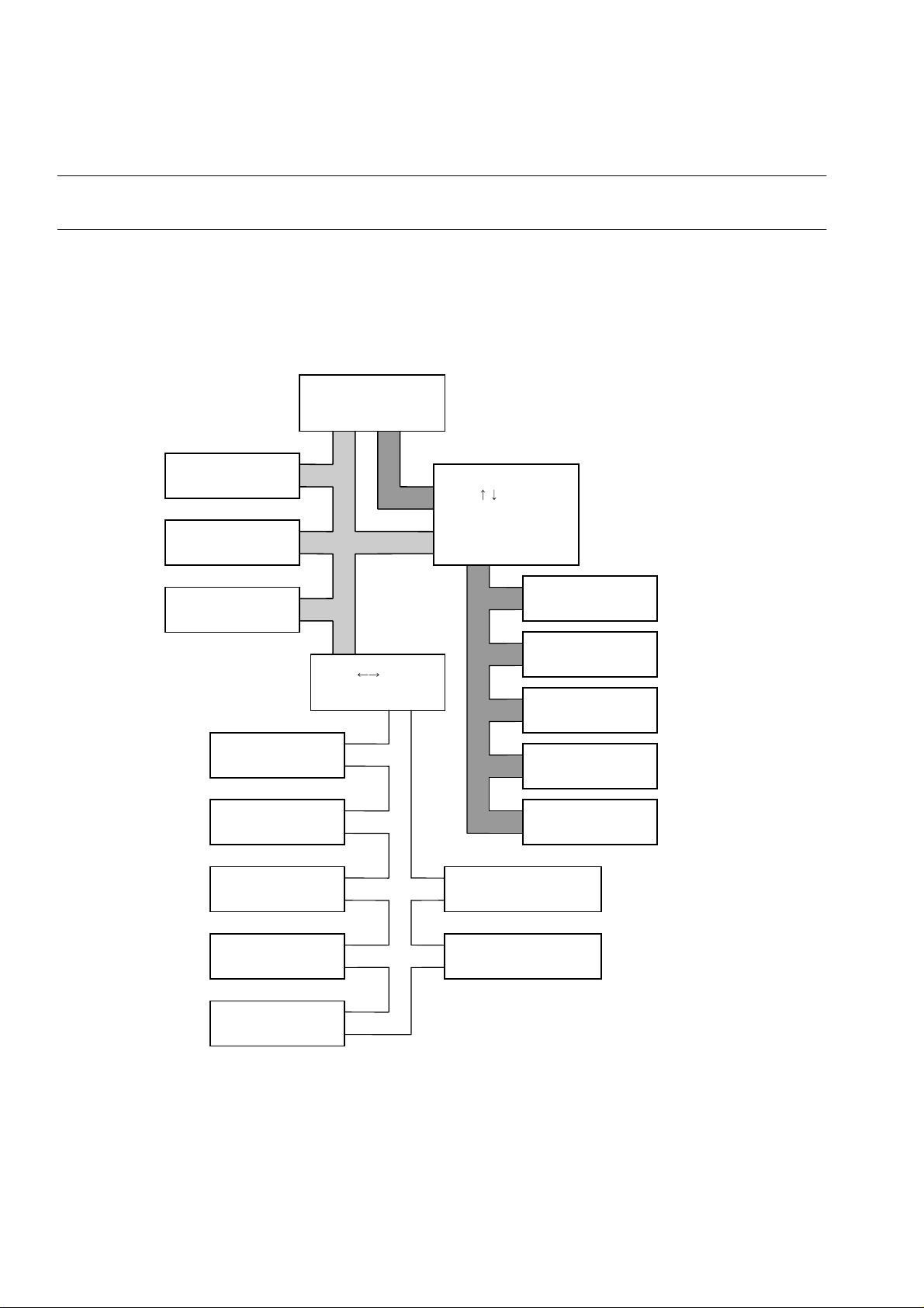
CHAPTER 1 OVERVIEW
1.2 General Block Diagram of MB91F109
Figure 1.2.1 is a general MB91F109 block diagram.
■
General Block Diagram of MB91F109
Figure 1.2-1 General Block Diagram of MB91F109
FR CPU
I-bus(16bit)
RAM 2KB
Bit Search Module
DMAC (8ch)
DREQ0 DREQ1 DREQ2
DACK0 DACK1 DACK2
EOP0 EOP1 EOP2
Clock Control Unit
X0 X1
(Watch Dog Timer)
RSTX
D-bus(32bit)
32bit
Bus Converter
16bit
Harvard
Princeton
Bus Converter
C-bus
(32bit)
DRAM Controller
FLASH ROM
254KB
Bus Controller
Port 0-B
D31-D16
A24-A00
RDX
WR0X-1X
RDY
CLK
CS0X-5X
BRQ BGRNTX
RAS0 RAS1
CS0L CS1L
CS0H CS1H
DW0X DW1X
INT0-INT3
NMIX
AN0-AN3
AVCC AVRH
AVSS AVRL
ATGX
Interrupt Control Unit
(4ch)
Reload Timer
(3 ch)
Port
R-bus
(16bit)
UART (3ch)10bit A/D Converter
with Baud Rate Timer
PWM Timer (4ch)
RAM 2KB
SI0 SI1 SI2
SO0 SO1 SO2
SC0 SC1 SC2
OCPA0-OCPA3
TRG0-3
Notes:
• Terminals are represented by the function (some terminals are actually multiplexed).
• When REALOS is used, perform time management using an external interrupt or internal
timer.
6
Page 31

1.3 Outside Dimensions
1.3 Outside Dimensions
Figures 1.3.1 to 1.3.3 show the outside dimensions of the MB91F109.
■
Outside Dimensions (QFP-100)
Figure 1.3-1 Outside Dimensions of FPT-100P-M06
EIAJ code
*
:
QFP100-P-1420-4
Plastic QFP with 100 pins
(FPT-100P-M06)
Plastic QFP with 100 pins
(F PT-100P -M06 )
81
23.90 0.40 (.941 .016)
20.00 0.20 (.787 .008)
5180
50
Lead pitch
Package
width x length
Lead shape
0.65 mm
14 x 20 mm
Gull wing
Sealing Plastic mold
Flat terminal
section length
0.80 mm
3.35(.132)MAX
(Mounting height)
0.05(.002)MIN
(ST AND OFF)
INDEX
100
LEAD No.
c
1994 FUJITSU LIMITED F100008-3C-2
1
0.65(.0256)TYP
18.85(.742)REF
22.30 0.40(.878 .016)
0.30 0.10
(.012 .004)
0.10(.004)
"A"
0.13(.005)
14.00 0.20
(.551 .008)(.705 .016)
31
30
M
"B"
17.90 0.40
Details of "A" part
0.25(.010)
0.0(.012)
0.18(.007)MAX
0.53(.021)MAX
12.35(.486)
REF
0.15 0.05(.006 .002)
Details of "B" part
16.30 0.40
(.642 .016)
0 10
0.80 0.20
(.031 .008)
Unit: mm (inches)
7
Page 32

CHAPTER 1 OVERVIEW
■
Outside Dimensions (LQFP-100)
Figure 1.3-2 Outside Dimensions of FPT-100P-M05
Plastic LQFP with 100 pins
(FPT-100P-M05)
Plastic LQFP with 100 pins
(FPT-100P-M05)
75 51
16.00 0.20(.630 .008)SQ
14.00 0.10(.551 .004)SQ
EIAJ code:
Lead pitch
Package
*
QFP100-P-1414-1
0.50 mm
14 x 14 mm
width x length
Lead shape Gull wing
Sealing
+0.20
-0.10
1.50
+.008
.059 -.004
(Mouting height)
Plastic mold
76
INDEX
100
LEAD No.
0.50(.0197)TYP
0.10(.004)
C
1995 FUJITSU LIMITED F100007S-2C-3
"A"
+0.08
-0.03
0.18
+.003
.007 -.001
50
26
251
0.08(.003)
(.472)
REF
"B"
+0.05
-0.02
M
0.127
.005
+.002
-.001
15.0012.00
(.591)
NOM
Details of "B" part
010
Details of "A" part
0.15(.006)MAX
0.40(.016)MAX
0.10 0.10
(.004 .004)
(STAND OFF)
0.50 0.20(.020 .008)
0.15(.006)
0.15(.006)
Unit: mm (inches)
8
Page 33

■
Outside Dimensions (FBGA-112)
Figure 1.3-3 Outside Dimensions of BGA-112P-M01
1.3 Outside Dimensions
Plastic FBGA with 112 pins
(BGA-112P-M01)
Plastic FBGA with 112 pins
(BGA-112P-M01)
10.00 0.10(.394 .004)SQ .049 -.004
Ball pitch
Ball matrix
Package
width x length
Sealing
Mount height
Ball size
0.80 mm
11
10.00 × 10.00 mm
Plastic mold
1.45 mm MAX
0.45
Note: The actual corner shape may differ from the drawing.
+.008
+0.20
-0.10
1.25
(Mounting height)
0.38 0.10(.015 .004)
(Stand off)
8.00(.314)REF
0.80(.031)TYP
INDEX
C0.80(.031)
C
1998 FUJITSU LIMITED B112001S-2C-2
0.10(.004)
LK
JHGFEDCBA
112- 0.45 0.10
(112- .018 .004)
0.08(.003)
11
10
9
8
7
6
5
4
3
2
1
M
Unit: mm (inches)
9
Page 34

CHAPTER 1 OVERVIEW
1.4 Pin Arrangement Diagrams
Figures 1.4.1 to 1.4.3 show the pin arrangements of the MB91F109.
■
Pin Arrangements (QFP-100)
Figure 1.4-1 QFP-100 Pin Arrangements
PB2/CS0H
PB3/DW0X
EOP2/PB4/RAS1
DREQ2/PB5/CS1L
DACK2/PB6/CS1H
PB7/DW1X
VCC
PA6/CLK
PA5/CS5X
PA4/CS4X
EOP1/PA3/CS3X
PA2/CS2X
PA1/CS1X
PA0/CS0X
NMIX
VCC
RSTX
VSS
MD0
MD1
MD2
P80/RDY
P81/BGRNTX
P82/BRQ
P83/RDX
P84/WR0X
P85/WR1X
P20/D16
P21/D17
P22/D18
CS0L/PB1
INT0/PE0
RAS0/PB0
97
98
99
100
1
2
3
4
5
6
7
8
9
10
11
12
13
14
15
16
17
18
19
20
21
22
23
24
25
26
27
28
29
30
313233343536373839404142434445
X1
X0
VCC
INT1/PE1
96
94
95
MB91F109
(TOP VIEW)
FPT-100P-M06
DREQ0/PE4
INT3/PE3/SC2
INT2/PE2/SC1
VSS
91
92
93
90
PF7/OCPA0/ATGX
DACK1/PE7
DACK0/PE6
DREQ1/PE5
86
87
88
89
SC0/PF2/OCPA3
SI1/PF3/TRG2
SO1/PF4/TRG3
SI2/PF5/OCPA1
SO2/PF6/OCPA2
81
82
83
84
85
80
79
78
77
76
75
74
73
72
71
70
69
68
67
66
65
64
63
62
61
60
59
58
57
56
55
54
53
52
51
46
474849
50
SO0/PF1/TRG1
SI0/PF0/TRG0
AN3
AN2
AN1
AN0
AVSS/AVRL
AVRH
AVCC
A24/EOP0/P70
A23/P67
A22/P66
VSS
A21/P65
A20/P64
A19/P63
A18/P62
A17/P61
A16/P60
A15/P57
A14/P56
A13/P55
A12/P54
A11/P53
A10/P52
A09/P51
A08/P50
A07/P47
A06/P46
A05/P45
10
P25/D21
P24/D20
P23/D19
P30/D24
P27/D23
P26/D22
P33/D27
P32/D26
P31/D25
P36/D30
P35/D29
P34/D28
VSS
P37/D31
VCC
P41/A01
P40/A00
P44/A04
P43/A03
P42/A02
Page 35

■
Pin Arrangements (LQFP-100)
DREQ2/PB5/CS1L
DACK2/PB6/CS1H
PB7/DW1X
VCC
PA6/CLK
PA5/CS5X
PA4/CS4X
EOP1/PA3/CS3X
PA2/CS2X
PA1/CS1X
PA0/CS0X
NMIX
VCC
RSTX
VSS
MD0
MD1
MD2
P80/RDY
P81/BGRNTX
P82/BRQ
P83/RDX
P84/WR0X
P85/WR1X
P20/D16
Figure 1.4-2 LQFP-100 Pin Arrangements
DACK1/PE7
DACK0/PE6
DREQ1/PE5
DREQ0/PE4
INT3/PE3/SC2
INT2/PE2/SC1
VSS
X1
X0
VCC
INT1/PE1
INT0/PE0
RAS0/PB0
CS0L/PB1
CS0H/PB2
DW0X/PB3
RAS1/PB4/EOP2
84
85
86
87
88
89
90
91
92
93
94
95
96
97
98
99
100
1
2
3
4
5
6
7
8
9
10
11
12
13
14
15
16
17
18
19
20
21
22
23
24
25
26
27
28
29
MB91F109
(TOP VIEW)
FPT-100P-M05
38
37
36
35
34
33
32
31
30
39
40
41
42
1.4 Pin Arrangement Diagrams
SO0/PF1/TRG1
SC0/PF2/OCPA3
SI1/PF3/TRG2
SO1/PF4/TRG3
SI2/PF5/OCPA1
SO2/PF6/OCPA2
PF7/OCPA0/ATGX
77
78
79
80
81
82
83
43
44
45
46
47
48
49
76
58
57
56
55
54
53
52
51
50
SI0/PF0/TRG0
75
74
73
72
71
70
69
68
67
66
65
64
63
62
61
60
59
AN3
AN2
AN1
AN0
AVSS/AVRL
AVRH
AVCC
A24/EOP0/P70
A23/P67
A22/P66
VSS
A21/P65
A20/P64
A19/P63
A18/P62
A17/P61
A16/P60
A15/P57
A14/P56
A13/P55
A12/P54
A11/P53
A10/P52
A09/P51
A08/P50
P23/D19
P22/D18
P21/D17
P26/D22
P25/D21
P24/D20
P31/D25
P30/D24
P27/D23
P34/D28
P33/D27
P32/D26
VSS
P36/D30
P35/D29
VCC
P40/A00
P37/D31
P43/A03
P42/A02
P41/A01
P46/A06
P45/A05
P44/A04
P47/A07
11
Page 36

CHAPTER 1 OVERVIEW
■
Pin Arrangements (FBGA-112)
11
10
9
8
7
Figure 1.4-3 FBGA-112 Pin Arrangements
6
5
4
3
2
1
TOP VIEW
INDEX
LKJHGFEDCBA
Table 1.4.1 shows the cross-references of the FBGA package pin names.
12
Page 37

1.4 Pin Arrangement Diagrams
Table 1.4-1 FBGA Package Pin Names
BALL-No. PIN-NAME BALL-No. PIN-NAME BALL-No. PIN-NAME
A1
A2
A3
A4
A5
A6
A7
A8
A9
A10
A11
B1
B2
B3
B4
B5
B6
B7
B8
B9
B10
B11
C1
C2
C3
N.C
RAS1/ PB4/ EOP2
CS0L/ PB1
INT1/ PE1
X1
INT3/ SC2/ PE3
DACK1/ PE7
SI2/ OCPA1/ PF5
SC0/ OCPA3/ PF2
SI0/ TRG0/ PF0
N.C.
CS1L/ PB5/ DREQ2
CS1H/ PB6/ DACK2
CS0H/ PB2
INT0/ PE0
X0
INT2/ SC1/ PE2
DACK0/ PE6
SO2/ OPCA2/ PF6
SI1/ TRG2/ PF3
SO0/ TRG1/ PF1
AN3
DW1X/ PB7
VCC
CLK/ PA6
D6
D7
D8
D9
D10
D11
E1
E2
E3
E4
E8
E9
E10
E11
F1
F2
F3
F4
F8
F9
F10
F11
G1
G2
G3
VCC
DREQ0/ PE4
OCPA0/ PF7/ ATGX
AN2
AVRH
AVCC
CS1X/ PA1
CS0X/ PA0
NMIX
VCC
AVSS/ AVRL
N.C.
A23/ P67
A22/ P66
RSTX
VSS
MD0
MD2
A24/ P70/ EOP0
VSS
A21/ P65
A20/ P64
N.C.
MD1
RDY/ P80
H9
H10
H11
J1
J2
J3
J4
J5
J6
J7
J8
J9
J10
J11
K1
K2
K3
K4
K5
K6
K7
K8
K9
K10
K11
A14/ P56
A13/ P55
N.C.
RDX/ P83
WR0X/ P84
D21/ P25
D24/ P30
N.C.
VSS
VCC
A06/ P46
A12/ P54
A11/ P53
N.C.
D16/ P20
D18/ P22
D20/ P24
D23/ P27
D27/ P33
D30/ P36
A00/ P40
A02/ P42
A05/ P45
A10/ P52
A09/ P51
C4
C5
C6
C7
C8
C9
C10
C11
D1
D2
D3
D4
D5
DW0X/ PB3
N.C.
VSS
DREQ1/ PE5
N.C
SO1/ TRG3/ PF4
AN1
AN0
CS5X/ PA5
CS4X/ PA4
CS3X/ PA3/ EOP1
CS2X/ PA2
RAS0/ PB0
G4
G8
G9
G10
G11
H1
H2
H3
H4
H5
H6
H7
H8
N.C.
A19/ P63
A18/ P62
A17/ P61
A16/ P60
BGRNTX/ P81
BRQ/ P82
WR1X/ P85
D25/ P31
D28/ P34
N.C.
A03/ P43
A15/ P57
L1
L2
L3
L4
L5
L6
L7
L8
L9
L10
L11 A08/ P50
N.C.
D17/ P21
D19/ P23
D22/ P26
D26/ P32
D29/ P35
D31/ P37
A01/ P41
A04/ P44
A07/ P47
13
Page 38

CHAPTER 1 OVERVIEW
1.5 Pin Functions
Tables 1.5.1 to 1.5.5 lists the MB91F109 pin functions.
The numbers shown in the tables has nothing to do with the package pin numbers.
Since pins have different pin numbers among QFP, LQFP, and FBGA, see Section 1.4,
"Pin Arrangement Diagrams."
■
Pin Functions
Table 1.5-1 Pin Functions (1/5)
NO. Pin name I/O circuit
format
E Bits 16 to 23 of external data bus.
E Bits 24 to 31 of external data bus.
F Bits 00 to 15 of external address bus.
10
11
12
13
14
15
16
17
18
19
20
21
22
23
24
25
26
27
28
29
30
31
32
1
2
3
4
5
6
7
8
9
D16/P20
D17/P21
D18/P22
D19/P23
D20/P24
D21/P25
D22/P26
D23/P27
D24/P30
D25/P31
D26/P32
D27/P33
D28/P34
D29/P35
D30/P36
D31/P37
A00/P40
A01/P41
A02/P52
A03/P43
A04/P44
A05/P45
A06/P46
A07/P47
A08/P50
A09/P51
A10/P52
A11/P53
A12/P54
A13/P55
A14/P56
A15/P57
Function
When the external bus width is set to 8 bits or in
single-chip mode, these pins can be used as
general-purpose I/O ports (P20 to P27).
When these pins are not used for the data bus, they
can be used as general-purpose I/O ports (P30 to
P37).
When these pins are not used for the address bus,
they can be used as general-purpose I/O ports (P40
to P47 and P50 to P57).
14
Page 39

Table 1.5-1 Pin Functions (1/5)
1.5 Pin Functions
NO. Pin name I/O circuit
format
33
34
35
36
37
38
39
40
Table 1.5-2 Pin Functions (2/5)
NO. Pin name I/O circuit
41 A24/P70/EOP0 F Bit 24 of external address bus.
A16/P60
A17/P61
A18/P62
A19/P63
A20/P64
A21/P65
A22/P66
A23/P67
F Bits 16 to 23 of external address bus.
When these pins are not used for the address bus,
they can be used as general-purpose I/O ports (P60
to P67).
format
This pin is enabled when DMAC EOP output is
enabled.
[EOP0] DMAC EOP output (ch0)
[P70] When this pin is not used as A24 and EOP0,
the pin can be used as a general-purpose I/O port.
Function
Function
42 RDY/P80 E External Ready input. 0 is input when the bus cycle
being executed is not completed. When the pin is
not used for this purpose, it can be used as a
general-purpose I/O port.
43 BGRNTX/P81 F Output of external bus release acceptance. L is
output when the external bus has been released.
When the pin is not used for this purpose, it can be
used as a general-purpose I/O port.
44 BRQ/P82 E Input of external bus release request. 1 is input to
request that the external bus be released. When
the pin is not used for this purpose, it can be used
as a general-purpose I/O port.
45 RDX/P83 F External bus read strobe.
When the pin is not used for this purpose, it can be
used as a general-purpose I/O port.
46 WR0X/P84 F External bus write strobe. Individual control signals
and data bus byte positions have the following
relationships:
15
Page 40

CHAPTER 1 OVERVIEW
Table 1.5-2 Pin Functions (2/5)
NO. Pin name I/O circuit
Function
format
47 WR1X/P85 F
D15 to D08
D07 to D00
16-bit bus width
WR0X
WR1X
8-bit bus width
WR0X
(can be used as a port)
Note:
WR1X is Hi-Z while it is in reset state. When it is
used as a 16-bit bus, attach a pull-up resistor to
the outside.
[P84 or P85] When WR0X or WR1X is not used,
the pin can be used as a general-purpose I/O port.
48
49
50
CS0X/PA0
CS1X/PA1
CS2X/PA2
F Chip Select 0 output (Low active)
Chip Select 1 output (Low active)
Chip Select 2 output (Low active)
[PA0, 1, or 2] When the pin is not used for the
above purpose, it can be used as a generalpurpose I/O port.
51 CS3X/PA3/EOP1 F Chip Select 3 output (Low active)
[EOP1] DMAC EOP1 output (ch1). This function is
valid when DMAC EOP output is enabled.
[PA3] When CS3X and EOP1 are not used, the pin
can be used as a general-purpose I/O port.
Single-chip mode
(can be used as a port)
(can be used as a port)
52
53
CS4X/PA4
CS5X/PA5
F Chip Select 4 output (Low active)
Chip Select 5 output (Low active)
[PA4 or 5] When the pin is not used for the above
purpose, it can be used as a general-purpose I/O
port.
54 CLK/PA6 F System clock output. The pin outputs the same
clock frequency as the external bus operating
frequency.
[PA6] When the pin is not used for this purpose, it
can be used as a general-purpose I/O port.
16
Page 41

Table 1.5-3 Pin Functions (3/5)
1.5 Pin Functions
NO. Pin name I/O circuit
format
55
56
57
58
59
60
61
62
RAS0/PB0
CS0L/PB1
CS0H/PB2
DW0X/PB3
RAS1/PB4/EOP2
CS1L/PB5/DREQ2
CS1H/PB6/DACK2
DW1X/PB7
F RAS output of DRAM bank 0
Function
CASL output of DRAM bank 0
CASH output of DRAM bank 0
WE
output of DRAM bank 0 (Low active)
RAS output of DRAM bank 1
CASL output of DRAM bank 1
CASH output of DRAM bank 1
WE
output of DRAM bank 1 (Low active)
See the description of the DRAM interface for more
information.
[EOP2] DMAC EOP output (ch2). This function is
valid when DMAC EOP output is enabled.
[DREQ2] Input of DMA external transfer request.
This input is used from time to time when this pin is
selected for the DMAC transfer cause. Therefore, it
is needed to stop output by other functions except
when such output is performed intentionally.
[DACK2] Output of DMAC external transfer request
acceptance (ch2). This function is valid when the
output of DMAC transfer request acceptance is
enabled.
[PB0-7] When each pin is not used for the
corresponding purpose, the pin can be used as a
general-purpose I/O port.
63
64
65
66
67
68 RSTX B External reset input
69 VCC - Digital circuit power supply.
70 NMIX D Nonmaskable interrupt (NMI) input (Low active)
71
72
MD0
MD1
MD2
X0
X1
INT0/PE0
INT1/PE1
C Mode pins 0 to 2.
Use these pins to set the basic MCU operation
mode.
Connect these pins directly to Vcc or Vss.
A Clock (oscillator) input
Clock (oscillator) output
Be sure to connect the power supply to every VCC
pin.
F [INT0, 1] Input of external interrupt request. This
input is used from time to time while the
corresponding external interrupt is enabled.
Therefore, it is needed to stop output by other
functions except when such output is performed
intentionally.
[PE0, 1] General-purpose I/O ports
17
Page 42

CHAPTER 1 OVERVIEW
Table 1.5-3 Pin Functions (3/5)
NO. Pin name I/O circuit
format
73 INT2/SC1/PE2 F [INT2] Input of external interrupt request. This
input is used from time to time while the
corresponding external interrupt is enabled.
Therefore, it is needed to stop output by other
functions except when such output is performed
intentionally.
[SC1] UART1 clock I/O. Clock output can be used
when UART1 clock output is enabled.
[PE2] General-purpose I/O port. This function is
valid when UART1 clock output is disabled.
74 INT3/SC2/PE3 F [INT3] Input of external interrupt request. This
input is used from time to time while the
corresponding external interrupt is enabled.
Therefore, it is needed to stop output by other
functions except when such output is performed
intentionally.
[SC2] UART2 clock I/O. Clock output can be used
when UART2 clock output is enabled.
[PE3] General-purpose I/O port. This function is
valid when UART2 clock output is disabled.
Function
Table 1.5-4 Pin Functions (4/5)
NO. Pin name I/O circuit
format
75
76
77 DACK0/PE6 F [DACK0] Output of DMAC external transfer
DREQ0/PE4
DREQ1/PE5
F [DREQ0, 1] Input of DMA external transfer request.
This input is used from time to time when this pin is
selected for the DMAC transfer cause. Therefore, it
is needed to stop output by other functions except
when such output is performed intentionally.
[PE4, 5] General-purpose I/O ports
request acceptance (ch0). This function is valid
when the output of DMAC transfer request
acceptance is enabled.
[PE6] General-purpose I/O port. This function is
valid when the output of DMAC transfer request
acceptance or DACK0 output is disabled.
Function
18
Page 43

Table 1.5-4 Pin Functions (4/5)
1.5 Pin Functions
NO. Pin name I/O circuit
format
78 DACK1/PE7 F [DACK1] Output of DMAC external transfer
request acceptance (ch1). This function is valid
when the output of DMAC transfer request
acceptance is enabled.
[PE7] General-purpose I/O port. This function is
valid when the output of DMAC transfer request
acceptance or DACK1 output is disabled.
79 SI0/TRG0/PF0 F [SI0] UART0 data input The input of each pin
[TRG0] External trigger
input of PWM timer
[PF1] General-purpose I/O port.
80 SO0/TRG1/PF1 F [SO0] UART0 data output. This function is valid
when UART0 data output is enabled.
Function
is used from time to
time while input
operation is selected.
Therefore, it is needed
to stop output by other
functions except when
such output is
performed
intentionally.
[TRG1] External trigger input of PWM timer. This
function is valid when PF1 and UART0 data output
is disabled.
[PF1] General-purpose I/O port. This function is
valid when UART0 data output is disabled.
81 SC0/OCPA3/PF2 F [SC0] UART0 clock I/O. Clock output can be used
when UART0 clock output is enabled.
[OCPA3] PWM timer output. This function is valid
when PWM timer output is enabled.
[PF2] General-purpose I/O port. This function is
valid when UART0 clock output is disabled.
82 SI1/TRG2/PF3 F [SI1] UART1 data input The input of each pin
[TRG2] External trigger
input of PWM timer
is used from time to
time while input
operation is selected.
Therefore, it is needed
to stop output by other
functions except when
such output is
performed
intentionally.
[PF3] General-purpose I/O port.
19
Page 44

CHAPTER 1 OVERVIEW
Table 1.5-4 Pin Functions (4/5)
NO. Pin name I/O circuit
format
83 SO1/TRG3/PF4 F [SO1] UART1 data output. This function is valid
when UART1 data output is enabled.
[TRG3] External trigger input of PWM timer. This
function is valid when PF4 and UART1 data output
is disabled.
[PF4] General-purpose I/O port. This function is
valid when UART1 data output is disabled.
Table 1.5-5 Pin Functions (5/5)
NO. Pin name I/O circuit
format
84 SI2/OCPA1/PF5 F [SI2] UART2 data input This input is used from
time to time while UART2 is operating for input.
Therefore, it is needed to stop output by other
functions except when such output is performed
intentionally.
Function
Function
[OCPA1] PWM timer output. This function is valid
when PWM timer output is enabled.
[PF5] General-purpose I/O port.
85 SO2/OCPA2/PF6 F [SO2] UART2 data output. This function is valid
when UART2 data output is enabled.
[OCPA2] PWM timer output. This function is valid
when PWM timer output is enabled.
[PF6] General-purpose I/O port. This function is
valid when UART2 data output is disabled.
86 OCPA0/PF7/ATGX F [OCPA0] PWM timer output. This function is valid
when PWM timer output is enabled.
[PF7] General-purpose I/O port. This function is
valid when PWM timer output is disabled.
[ATGX] External trigger input for A/D converter.
This input is used from time to time when this pin is
selected for the A/D start cause. Therefore, it is
needed to stop output by other functions except
when such output is performed intentionally.
87
to
90
AN0 to AN3 G [AN0-3] A/D converter analog input.
91 AVCC - VCC power supply for A/D converter
20
Page 45

Table 1.5-5 Pin Functions (5/5)
1.5 Pin Functions
NO. Pin name I/O circuit
format
92 AVRH - Reference voltage of A/D converter (high potential
side). Always turn the pin on or off while the
voltage equal to AVRH or higher is applied to VCC.
93 AVSS/AVRL - A/D converter VSS power supply and reference
voltage (low potential side)
94
to
96
97
to
100
VCC - Digital circuit power supply. Be sure to connect the
power supply to every VCC pin.
VSS - Digital circuit ground level
Note:
An I/O port and resou rce I/O are mu ltipl exe d, as shown l ike xx xx/ Pxx, at m ost pin s listed above.
If the port conflicts with resource output at this type of pin, the resource output is given priority.
Function
21
Page 46

CHAPTER 1 OVERVIEW
1.6 I/O Circuit Format
Tables 1.6.1 and 1.6.2 shows I/O circuit formats.
■
I/O Circuit Format
Table 1.6-1 I/O circuit format (1/2)
Classification Circuit format Remarks
A • For 50 MHz
X1
Clock input
• Oscillation feedback transistor:
About 1 M
Ω
• Standb y co ntro l
X0
STANDBY
B • CMOS level hysteresis input
• No standby control
R
P-channel transistor
N-channel transistor
Diffused resistor
Digital input
CMOS
• Pull-up resistance: About 50 k
C • CMOS level input
• High voltage control enabled for
flash test
Ω
22
Control signal
Mode input
Diffused resistor
Page 47

1.6 I/O Circuit Format
Table 1.6-1 I/O circuit format (1/2)
Classification Circuit format Remarks
D • CMOS level hysteresis input
• No standby control
P-channel transistor
N-channel transistor
Diffused resistor
CMOS
Digital input
Table 1.6-2 I/O circuit format (1/2)
Classification Circ uit format Remarks
E • CMOS level output
• Standby control
Digital output
Diffused resistor
STANDBY
Digital output
Digital input
F • CMOS level output
• CMOS level hysteresis input
Digital output
• Standb y co ntr ol
Diffused resistor
STANDBY
Digital output
Digital input
G • Analog input
Digital output
Diffused resistor
Digital output
Analog input
23
Page 48

CHAPTER 1 OVERVIEW
1.7 Memory Address Space
The logical address space of the FR series consists of 4 gigabytes (232 addresses) and
the CPU accesses them linearly.
■
Memory map
Figure 1.7.1 shows the memory address space of the MB91F109.
Figure 1.7-1 MB91F109 Memory Map
0000 0000
0000 0400
0000 0800
0000 1000
0000 1800
0001 0000
External-ROM
external-bus mode
H
I/O I/O I/O
H
I/O I/O I/O
H
Access inhibited
H
Internal RAM 2 KB
H
Access inhibited
H
External area
Internal-ROM
external-bus mode
Access inhibited
Internal RAM 2 KB
Access inhibited
External area
Access inhibited
Internal RAM 2 KB
Single-chip mode
Access inhibited
Internal RAM 2 KB
Access inhibited
Access inhibited
Access inhibited
Internal RAM 2 KB
Direct
addressing
area
I/O map
(See Appendix A.)
0001 0000
0008 0000
000C 0000
000C 0800
H
H
H
H
FFFF FFFF
24
FLASH ROM
254KB
External area
H
FLASH ROM
254KB
Access inhibited
0010 0000
FFFF FFFF
H
H
Note:
The CPU can access no external areas in single-chip mode.
To enable the CP U to access an external area, select interna l ROM external bus mode using
the mode register.
Page 49

1.7 Memory Address Space
❍
Direct addressing area
The following area in the address space is used for I/O. This area is called the direct
addressing area. The a ddresses in this area can be direc tly specified for instruction op erands.
The direct addressing area varies depending on the size of accessed data as follows:
• Byte data access: 0 to 0FF
H
• Half-word data access: 0 to 1FFH
• Word data access: 0 to 3FF
H
25
Page 50

CHAPTER 1 OVERVIEW
1.8 Handling of Devices
This section provides notes on using devices.
■
Device Handling
❍
Latchup prevention
If voltage highe r than Vcc or lower th an Vss is applied to a CMOS IC input or o utput pin or if
voltage exceedi ng the rating is a pplie d betwe en Vc c an d Vs s, la tchup may b e cau sed. La tch up
rapidly increases supply current and may cause thermal damage to the device. To prevent
such damage, do not to let voltage exceed the maximum rated voltage.
Also, do not to let the analog power supply exceed the digital power supply.
❍
Treatment of unused input pin
Leaving an unused input pin open may cause a malfunction. To avoid this malfunction, pull it up
or push it down.
❍
Input of external reset signal
To ensure that the dev ice is completely re set when the L level is input to the RSTX pin , the L
level input to the RSTX pin must continue for at least five machine cycles.
❍
Note on using an external clock
When an external clock is used, use the X0 pin unless otherwise specified and supply a
negative-phase clock to the X1 pi n simultaneously. Do not use STOP mode (oscillation stop
mode) for this operation because the X1 pin is disabled when H is output at STOP.
At 12.5 MHz, an external clock can be used by supplying it to only the X0 pin.
Figures 1.8.1 and 1.8.2 show examples of using an external clock.
Figure 1.8-1 Example of Using an External Clock (Normal Method)
X0
X1
MB91F109
Note:
STOP mode (oscillation stop mode) cannot be used.
26
Page 51

1.8 Handling of Devices
Figure 1.8-2 Example of Using an External Clock (Possible at 12.5 MHz or Lower)
X0
❍
Connection of power pins (Vcc and Vss)
OPEN X1
MB91F109
When two or more V cc or Vss pins are used, the device is designed so that the pins, whic h
should be at the same potential, are connected to one another inside the device t o prevent a
malfunction such as a latchup. However, to minimize unnecessary radiation, prevent strobe
signal malfunction t hat might be caused by an increase of the g round leve l, and observe the
total output current standard , be sure to c onnect a ll power pi ns to the po wer supply and ground
outside.
In addition, consid er measures so that impedance is minimized for connection from the powe r
supply to Vcc and Vss of the device.
It is recommended to insert a ceram ic capaci tor of ab out 0.1µF as a bypass capa citor, near the
device, between Vcc and Vss.
❍
Crystal oscillation circuit
Noise generated near t he X0 or X1 pi n causes the device to mal function . Design the PC board
so that the X0 and X1 pin s, crysta l oscillato r (or cerami c oscill ator), and by pass capac itor to the
ground are located as near to one another as possible. Also, prevent the wiring of these
components from crossing the wiring of other components wherever possible.
Such PC board artwork that places the ground around the X0 and X1 pins is strongly
recommended for stable operation.
❍
Treatment of NC pin
Be sure to keep the NC pin open.
❍
Mode pins (M D 0 to M D 2)
Connect the mode pins directly to Vcc or Vss.
To prevent malfuncti on by noise, minimize the pattern length between each mode pin a nd Vcc
or Vss on the PC board and also minimize impedance for pattern connection.
❍
At power-on
When power is turned on, be sure to begin by putting the RSTX pin in the L level and secure the
time for at least five cy cles of the internal operating clock a fter the power supply reaches the
Vcc level. Put the RSTX pin in the H level only after that.
❍
Pin conditions at power-on
The pin conditions at power -on are unstable. When power is turned on, oscillati on begins and
the circuits are initialized.
❍
Input of source oscillation at power-on
When power is turned on , be s ure to i npu t cl oc k s ig nals unti l the os ci ll ation s tabilization wait flag
is reset.
27
Page 52

CHAPTER 1 OVERVIEW
❍
Initialization by power-on reset
Devices contain registers that are initialized only by power-on reset. To initialize these
registers, turn the power off and turn it on again to execute power-on resetting.
❍
Recovery from sleep or stopped state
To recover from the sleep or stopped state that has been entered from a program in C-bus
RAM, do not use an interrupt but execute resetting.
28
Page 53

CHAPTER 2 CPU
This chapter provides basic information on the FR series CPU core functions including
the architecture, specifications, and instructions.
2.1 CPU Architecture
2.2 Internal Architecture
2.3 Programming Model
2.4 Data Structure
2.5 Word Alignment
2.6 Memory Map
2.7 Instruction Overview
2.8 EIT (Exception, Interrupt, and Trap)
2.9 Reset Sequence
2.10 Operation Mode
29
Page 54

CHAPTER 2 CPU
2.1 CPU Architecture
The FR30 CPU is a high performance core that uses the RISC architecture and
supports advanced functional instructions geared to embedding applications.
■
Characteristics of CPU Architecture
❍
RISC architecture
• Basic instruction: One instruction per cycle
❍
32-bit architecture
• 32-bit general-purpose register x 16
❍
Linear 4-gigabyte memory space
❍
Internal operation of the adder
• Addition of 32 bits x 32 bits: Five cycles
• Addition of 16 bits x 16 bits: Three cycles
❍
Enhanced interrupt processing function
• High-speed response (six cycles)
• Suppor t of multip le co ncur re nt interr up ts
• Level mask function (16 levels)
❍
Enhanced I/O operation instructions
• Inter-memory transfer instruction
• Bit processing instruction
❍
High coding efficiency
• Basic instruction word length: 16 bits
❍
Low power consumption
• Sleep mode and stop mode
30
Page 55

2.2 Internal Architecture
2.2 Internal Architecture
The FR CPU uses the Harvard architecture in which the instruction bus and data bus
are independent of each other.
The "32 bits <--> 16 bits" bus converter is connected to the data bus (D-BUS) to
implement the interface between the CPU and peripheral resources. The "Harvard <-->
Princeton" bus converter is connected to both I-BUS and D-BUS to implement the
interface between the CPU and bus controller.
■
Internal Architecture
Figure 2.2.1 shows the internal architecture.
Figure 2.2-1 Internal Architecture
FR CPU
D-BUS
I-BUS
32
I-ADDR
16
❍
CPU
I-DATA
32bit
16bit
Bus
converter
16 32
Resources
D-ADDR
D-DATA
R-BUS
32
32
Harvard
Princeton
Bus
converter
C-BUS
Bus controller
The CPU is a compact implement of the 32-bit RISC FR architecture.
It uses a five-stage instruction pipeline system to execute one instruction per cycle. The
pipeline consists of the following five stages:
• Instruction fetch (IF): Outputs an instruction address and fetches the instruction.
• Instruction decode (ID): Decodes the fetched instruction and also reads registers.
• Execution (EX): Executes operation.
• Memory access (MA): Accesses memory for loading or storing data.
• Write back (WB): Writes the operation results (or loaded memory data) to registers.
Figure 2.2.2 shows the instruction pipeline.
31
Page 56

CHAPTER 2 CPU
CLK
Figure 2.2-2 Instruction Pipeline
Instruction 1
Instruction 2
Instruction 3
Instruction 4
Instruction 5
Instruction 6
❍
WB
MA
EX
ID
IF
WB
MA
EX
ID
IF
WB
MA
EX
ID
WB
MA
EX
WB
MA WB
Instructions are always executed in order. That is, instruction A that is put into the pipeline
before instruction B always reaches the write back stage before instruction B.
Instructions are normall y executed at a rate of on e instruction pe r cycle. However, a loa d/store
instruction involving memory wait, branch instruction without a delay slot, or multiple-cycle
instruction, re quires multiple c ycles to complete execution. The instruction execu tion speed is
also slowed down when instruction supply takes time.
"32 bits <--> 16 bits" bus converter
The "32 bits <--> 16 bits" bus conve rter interfaces between the D-BUS tha t allows high-speed
32-bit wide access and R-BUS that allows 16-bit wide access. It thus enables the CPU to
access data in the internal peripheral circuits.
Upon receipt of a 32- bit wide acces s from the CP U, the bus con verter c onverts i t into two 16-b it
wide accesses to implement access to the R-BUS. Some internal peripheral circuits have
restrictions on access width.
❍
"Harvard <--> Princeton" bus converter
The "Harvard <--> Princ eton" bus c onverter coo rdinates th e inst ruction ac cess and da ta access
of the CPU to implement smooth interfacing with the external bus.
The CPU has Harvard ar ch ite ct ure i n whi ch th e i nstr uc tio n b us a nd data b us are independent of
each other. The bus controller that controls the external bus has Princeton architecture
consisting of a single bus. The bus conv erter gi ves p riori ty to the instruc tion an d data a ccesse s
of the CPU to control accesse s to the bus contr oller. This co ntrol always optimizes the order of
access to the external bus.
The bus converter ha s a two-word w rite buffer to eliminat e the CPU’s bu s wait time and a oneword prefetch buffer for instruction fetch.
32
Page 57

2.3 Programming Model
2.3 Programming Model
This section explains the CPU registers that are essential for programming. The CPU
registers are classified into the following two groups:
• General-purpose registers
• Special registers
■
General-Purpose Registers
Figure 2.3.1 shows the configuration of general-purpose registers.
Figure 2.3-1 Configuration of general-purpose registers
32 bits
[Initial value]
■
Special Registers
R 0
R 1
R 12
R 13
R 14
R 15
A
F
S
C
P
P
Figure 2.3.2 shows the configuration of special registers.
XXXX XXXX
XXXX XXXX
0000 0000
H
H
H
33
Page 58

CHAPTER 2 CPU
Figure 2.3-2 Configuration of special registers
32 bits
Program counter
Program status
Table base register
Return pointer
System stack pointer
User stack pointer
Multiplication/division
result register
PC
PS
TBR
RP
SSP
USP
MDH
MDL
ILM
SCR
CCR
34
Page 59

2.3 Programming Model
2.3.1 General-Purpose Registers
Registers R0 to R15 are general-purpose registers. They are used as accumulators for
various types of operation or memory access pointers.
■
General-Purpose Registers
Figure 2.3.3 shows the configuration of general-purpose registers.
Figure 2.3-3 Configuration of General-Purpose Registers
32 bits
[Initial value]
R 0
R 1
R 12
R 13
R 14
R 15
A
F
S
C
P
P
XXXX XXXX
XXXX XXXX
0000 0000
H
H
H
Of 16 registers, the following registers are provided for special applications, with some
instructions being enhanced.
• R13: Virtual accumulator
• R14: Frame pointer
• R15: Stack pointer
The initial values of R0 to R14 after resetting are undefined. The initial value of R15 is
00000000
(SSP value).
H
35
Page 60

CHAPTER 2 CPU
2.3.2 Special Registers
The special registers are used for special purposes. They are the program counter
(PC), program status (PS), table base register (TBR), return pointer (RP), system stack
pointer (SSP), user stack pointer (USP), and multiplication/division result register
(MDH/MDL).
■
Special Registers
Figure 2.3.4 shows the configuration of special registers.
Figure 2.3-4 Configuration of Special Registers
[Initial value]
Program counter
PC
XXXX XXXX
(undefined)
H
Program status
Table base register
Return pointer
System stack pointer
User stack pointer
Multiplication/division
result register
❍
Program counter (PC)
PS
TBR
RP
SSP
USP
MDH
MDL
000F FC00
XXXX XXXX
0000 0000
XXXX XXXX
XXXX XXXX
XXXX XXXX
H
H
H
H
H
H
(undefined)
(undefined)
(undefined)
(undefined)
The program counter indicates the address of the program being executed.
Bit 0 is set to 0 when the PC is updated according to instruction execution. Bit 0 may be set to 1
only when an odd- numbered address is sp ecified for the branch destination address. Even at
this event, bit 0 is in val id and an i ns truc tio n must be put at an address cons is ti ng o f a mu lti pl e of
two.
36
The initial value after resetting is undefined.
Page 61

2.3 Programming Model
❍
Program status (PS)
The program status register holds the program status in three parts, CCR, SCR, and ILM. See
Section 2.3.3 for more information.
The undefined bits are all reserved. When the register is read, 0 is always read from these bits.
No data can be written to this register.
❍
Table base register (TBR)
The table base register holds the first address of the vector table used for EIT processing.
The initial value after resetting is 000FFC00
❍
Return pointer (RP)
.
H
The return pointer register holds the address to which control returns from a subroutine.
When the CALL instruction is executed, the PC value is transferred to the RP.
When the RET instruction is executed, the RP value is transferred to the PC.
The initial value after resetting is undefined.
❍
System stack pointer (SSP)
SSP stands for system stack pointer.
When the S flag is 0, the SSP functions as R15.
The SSP can be specified explicitly.
It can also be used as a stack poi nter to specify the stack for sav ing the PS an d PC when EIT
occurs.
The initial value after resetting is 00000000
❍
User stack pointer (USP)
H.
USP stands for user stack pointer.
When the S flag is 1, the USP functions as R15.
The USP can be specified explicitly.
The initial value after resetting is undefined.
The USP cannot be used for the RETI instruction.
❍
Multiplication/division result register (MDH/MDL)
The MDH and MDL are each 32 bits long.
The initial value after resetting is undefined.
[Multiplication]
When 32-bit data is multiplied by 32-bit data, the resultant 64-bit data is stored in the
multiplication/division result register as follows:
• MDH: 32 high-order bits
• MDL: 32 low-order bits
The result of multiplying 16 bits by 16 bits is stored as follows:
• MDH: Undefined
• MDL: Resultant 32-bit data
37
Page 62

CHAPTER 2 CPU
[Division]
When calculation begins, a dividend is stored in the MDL.
The result of divis ion by the DIV0S/DIV0U, D IV1, DIV2, DIV3, or DIV 4S instruction is stored in
the MDL and MDH as follows:
• MDH: Remainder
• MDL: Quotient
38
Page 63

2.3 Programming Model
2.3.3 Program Status Register (PS)
The program status register holds the program status in three parts, ILM, SCR, and
CCR. The undefined bits are all reserved. When the register is read, 0 is always read
from these bits.
No data can be written to this register.
■
Program Status Register (PS)
The configuration of the program status register (PS) is shown below:
31 20 16 10 8 7 0
ILM SCR CCR
❍
Condition code register (CCR)
The configuration of the condition code register (CCR) is shown below:
7
65
[bit 5] S: Stack flag
This bit specifies the stack pointer used as R15.
0: Uses SSP as R15.
The bit is automatically set to 0 when EIT occurs.
1: Uses USP as R15.
This bit is cleared to 0 by resetting.
Set the bit to 0 when the RETI instruction is executed.
[bit 4] I: Interrupt enable flag
This bit enables or disables a user interrupt request.
0: Disables user interrupts.
The bit is cleared to 0 when the INT instruction is executed.
(The value before the bit is cleared is saved to the stack.)
43
S
INZ
2
10
VC
[Initial value]
--00XXXX
B
1: Enables user interrupts.
The masking of user interrupt requests is controlled by the value held in the ILM.
This bit is cleared to 0 by resetting.
39
Page 64

CHAPTER 2 CPU
[bit 3] N: Negative flag
[bit 2] Z: Zero flag
[bit 1] V: Overflow flag
This bit indicates a sign applicable when the operation result is assumed to be an intege r
that is represented in two’s complement.
0: Indicates that the operation result is a positive value.
1: Indicates that the operation result is a negative value.
The initial value after resetting is undefined.
This bit indicates whether the operation result is 0.
0: Indicates that the operation result is a value other than 0.
1: Indicates that the operation result is 0.
The initial value after resetting is undefined.
This bit assumes that the o perands used for operation are each an integer represented in
two’s complement and indicates whether an overflow occurred as the result of operation.
0: Indicates that no overflow occurred as the result of operation.
1: Indicates that an overflow occurred as the result of operation.
The initial value after resetting is undefined.
[bit 0] C: Carry flag
This bit indicates whether carry from the most significant bit or borrow occurred during
operation.
0: Indicates that no carry and borrow occurred.
1: Indicates that carry or borrow occurred.
The initial value after resetting is undefined.
❍
System condition code register (SCR)
The configuration of the system condition code register (SCR) is as follows:
98
10
D1 D0 XX0
T
[Initial value]
B
[bit 10, 9] D1, D0: Step division flag
These bits hold intermediate data during execution of s tep division.
They must not be changed during execution of step division.
When other processin g is performed during execution of s tep division, continued operation
for step division is guaranteed by saving and restoring the value in the PS register.
40
The initial value after resetting is undefined.
When the DIV0S instruction is executed, the dividend and divisor are referenced and set.
Execution of the DIV0U instruction forcibly clears the bits.
Page 65

2.3 Programming Model
[bit 8] T: Step-trace-trap flag
This flag specifies whether to enable step-trace-trap.
0: Disables step-trace-trap.
1: Enables step-trace-trap.
Setting the bit to 1 inhibits all user NMIs and user interrupts.
The flag is cleared to 0 by resetting.
The step-trace-trap function is used by an emulator. It cannot be used in user programs
while it is used by the emulator.
❍
Interrupt level mask register (ILM)
The configuration of the interrupt level mask register (ILM) is as follows:
20 19 18 17 16
ILM4 ILM3 ILM2 ILM1 ILM0 01111
[Initial value]
B
The ILM register holds an in ter rupt l ev el mas k value. The value held by th e ILM r egi st er is us ed
for level masking.
Of the interrupt request s input to the CPU, onl y those with higher inter rupt levels than the level
indicated by the ILM are accepted.
The level values range in descending order of highness from 0 (00000
) to 31 (11111B).
B
The values that can be set fro m a program are limited. When the ori ginal value i s in the ran ge
from 16 to 31, a new value that can be set mus t be in the same range, i. e., from 16 to 31. If an
instruction that sets a value from 0 to 15 is executed, the "specified value + 16" is returned.
When the original value is in the range from 0 to 15, a desired value from 0 to 31 can be set.
The register is cleared to 15 (01111
) by resetting.
B
41
Page 66

CHAPTER 2 CPU
2.4 Data Structure
FR-series data is mapped as follows:
• Bit ordering: Little endian
• Byte ordering: Big endian
■
Bit Ordering
The FR series uses little endian for bit ordering.
Figure 2.4.1 shows data mapping in bit ordering mode.
Figure 2.4-1 Data Mapping in Bit Ordering Mode
■
Byte Ordering
bit312927252321191715131197531
302826242220181614121086420
MSB
The FR series uses big endian for byte ordering.
Figure 2.4.2 shows data mapping in byte ordering mode.
Figure 2.4-2 Data Mapping in Byte Ordering Mode
MSB LSB
Address n
Address (n+1)
Address (n+2)
Address (n+3)
Memory
bit
70
10101010
11001100
11111111
00010001
bit31 23 15 7 0
10101010 11001100 11111111 00010001
LSB
42
Page 67

2.5 Word Alignment
2.5 Word Alignment
Since instructions and data are accessed in b y tes, mappi ng ad dr esses v a ry depending
on instruction length or data width.
■
Program Access
A program running i n the FR series must be placed at an address consisting of a mul tiple of
two.
Bit 0 of the pr ogram counter (PC) is se t to 0 when the PC is updated according to instr uction
execution. Bit 0 may be set to 1 only when an odd-numbered address is specified for the
branch destination address. Even at this event, bit 0 is invalid and an instruction must be
placed at an address consisting of a multiple of two.
No odd-numbered address exception occurs.
■
Data Access
When data access is made in the FR series, address alignment is performed forcibly in
accordance with access width as follows:
• Word a ccess: Addresses are aligned in multiples of four (the two least significant bits are
forcibly set to 00).
• Half-word access: Addresses are aligned in multiples of two (on least significant bit is
forcibly set to 0).
• Byte access: -
As explained above, som e bits are forcibly set to 0 when a word or half-word data access is
made, but this is applicab le only to the calcul ation result of an effe ctive address. For i nstance,
in @(R13, Ri) a ddr es sing mode, the regi ste r before addition i s us ed a s is for calculation (eve n if
the least significant bit is 1), and the least significant bit of the result of addition is masked.
Thus, the register before calculation is not masked.
[Example] LD @(R13, R2), R0
R13
R2
Result of addition
Address pin
00002222
00000003H
00002225H
Forced masking of two LSBs
00002224H
H
43
Page 68

CHAPTER 2 CPU
2.6 Memory Map
This section shows an MB91F109 memory map and a memory map common to the FR
series.
■
MB91F109 Memory Map
The address space is 32 bits long linearly.
Figure 2.6.1 shows an MB91F109 memory map.
Figure 2.6-1 MB91F109 Memory Map
0000 0000
H
Byte data
0000 0100
0000 0200
H
Half-word data
H
Direct addressing area
Word data
0000 0400
000F FC00
H
H
Initial vector
table area
000F FFFF
FFFF FFFF
❍
Direct addressing area
H
H
The following area in the address space is used for I/O. The addresses in this area can be
directly specified for instruction operands.
The size of the direct addressing area varies depending on data length.
44
• Byte data (8 bits): 0 to 0FF
H
• Half-word data (16 bits): 0 to 1FFH
• Word data (32 bits): 0 to 3FF
❍
Initial vector table area
The area ranging from 000FFC00
H
to 000FFFFFH is the EIT vector table initial area.
H
The vector table us ed for EIT proc essing can be m apped to des ired address es by rewriti ng the
TBR. The table is returned to these initial addresses when the TBR is reset.
Page 69

■
Memory Map Common to the FR Series
The FR series defines the following mem ory m ap. Thi s mem or y map i s comm on t hroug hout the
FR series regardless of types (except in single chip mode).
Figure 2.6.2 shows the memory map common to the FR series.
Figure 2.6-2 Memory Map Common to the FR Series.
00000000H
00000010H
00000100H
00000200H
00000400H
00000800H
(PDR)
Byte I/O
HalfWord I/O
Word I/O
Other I/O
Access inhibited
2.6 Memory Map
Direct addressing area
00001000H
00010000H
00080000H
000C0000H
00100000H
FFFFFFFFH
<Note>
(60KB)
(256KB)
Internal RAM or
access inhibited
External area
Instruction ROM
or external area
Internal ROM
or external area
External area
1KB
Initial vector area
The external areas cannot be accessed in single chip mode.
The MB91F109 assigns internal ROM area 0C0000
to 0C07FFH to 2 kilobytes of internal RAM.
H
45
Page 70

CHAPTER 2 CPU
2.7 Instruction Overview
The FR series supports logical operation, bit manipulation, and direct addressing
instructions, which are optimized for embedding applications, in addition to general
RISC instructions. Each instruction, which is 16 bits long (some are 32 bits or 48 bits
long), shows excellent memory use efficiency. See Appendix E, "Instructions," for
details about instructions.
The instruction set can be divided into the following function groups:
• Arithmetic operation
• Load and store
•Branch
• Logical operation and bit manipulation
• Direct addressing
•Others
■
Instruction Overview
❍
Arithmetic operation
Arithmetic operation includes the standard arithmetic operation instructions (addition,
subtraction, and comparison) and shift instructions (logical shift and arithmetic shift). For
addition and subtraction, operation with carry for multiword length operation, and operation
without changing the flag value, which is useful for address calculation, are also supported.
Furthermore, the "32 x 32 bits" and "16 x 16 bits" multiply instructions and "32/32 bits" step
divide instructions are available.
The FR series also supports imme diate transfer instructi ons, which allow immedia te data to be
set in registers, and inter-register transfer instructions.
Every arithmetic operation instruction executes using the general-purpose registers and
multiplication/division registers in the CPU.
❍
Load and store
Load or store instructi ons are used to read data from externa l memory or write data to it. They
are also used to read data from the peripheral circuits (I/O) inside the chip or write data to it.
Load and store instruct ions each use three types of acces s data length: byte, half word, and
word. The FR series supports not only general register indirect memory addressing but also, for
some instructions, register indirect memory addressing with displacement or with register
increment/decrement.
46
❍
Branch
The branch instruction group includes branch, cal l, interrupt, and recovery instr uctions. There
are two types of branch instructions. One has a delay slot and one does not. They can be used
most suitably for applications.
For more information on the branch instructions, see Sec tions 2.7.1, "Branch instructi ons with
delay slot," and 2.7.2, "Branch instructions without delay slot."
Page 71

2.7 Instruction Overview
❍
Logical operation and bit manipulation
A logical operation instruction can execute AND, OR, or EOR logical operation between
general-purpose registers or between a general-purpose register and memory (or I/O). A bit
manipulation instruction can directly manipulate the contents of memory (or I/O). These
instructions use general register indirect memory addressing.
❍
Direct addressing
The direct addressing instructions are used for access between I/O and general-purpose
registers or betw een I/O and memory. S pecifying an I/O address directly in an instructi on, not
via a register, enables high-speed and highly efficient ac cess. For some instr uctions, register
indirect memory addressing with register increment/decrement is also available.
❍
Others
Other instructions are available for PS register flag setting, stack operation, and sign/zero
extension. The FR series also supports function entry/exit and register multiload/store
instructions compliant with high-level languages.
47
Page 72

CHAPTER 2 CPU
2.7.1 Branch Instructions with Delay Slots
A branch instruction causes the program to branch and execute the instruction at the
branch destination after the instruction (called the delay slot) placed immediately after
the branch instruction is executed.
■
Branch Instructions with Delay Slots
The following instructions execute branch operation with a delay slot:
JMP:D @Ri CALL:D label12 CALL:D @Ri RET:D
BRA:D label9 BNO:D labe l9 BEQ:D label9 BNE:D label9
BC:D label9 BNC: D label9 BN:D label9 BP:D label9
BV:D labe l9 BNV:D label9 BLT:D label9 BGE:D label 9
BLE:D label9 BGT:D label9 BLS:D label9 BHI:D label9
■
Theory of Operation of Branch Instructions with Delay Slots
A branch instruction c auses the program to branch and execute the inst ruction at the branch
destination after the instruction (called the delay slot) placed immediately after the branch
instruction is executed.
Since a delay slot instruction is executed before branching, the execution speed seems one
cycle. However, w hen a valid instruction cannot b e put at the delay slot, the NOP in struction
must be provided.
[Example]
; Instruction list
ADD R1, R2 ;
BRA:D LABEL ; Branch instruction
MOV R2, R3 ; Delayed slot---Executed before branching
:
LABEL : ST R3, @R4 ; Branch destination
For a conditional br anch in structi on, the instructi on plac ed at the d elay slot is ex ecuted wh ether
the branch condition is satisfied or not.
For delayed branch ins truc tions, the execution orde r of s ome ins tr uc tio ns se ems to be rev er s ed.
This is only applicable to PC updating. Other operations, such as register updating and
referencing, are executed in order of coding.
48
Concrete examples are shown below.
Page 73

2.7 Instruction Overview
❍
Ri that is referenced by the JMP:D @Ri or CALL:D @Ri instruction is not affected even
when the instruction in the delay slot updates the Ri.
[Example]
LDI:32 #Label, R0
JMP:D @R0 ; Branches to Label.
LDI:8 #0, R0 ; Does not affect the branch destination
address.
:
❍
RP that is referenced by the RET:D instruction is not affected even when the instruction in
the delay slot updates the RP.
[Example]
RET:D ; Branches to the address indicated by the RP that
is set previously.
MOV R8, RP ; Does not affect the return operation.
:
❍
The flag that is referenced by the Bcc:D rel instruction is not affected by the instruction in
the delay slot.
[Example]
ADD #1, R0 ; Changes the flag.
BC:D Overflow ; Branches according to the execution result of the
above instruction.
ANDCCR #0 ; Updates the flag which is not referenced by the
above branch instruction.
:
❍
When RP is referenced by the instruction in the delay slot of the CALL:D instruction, the
data updated by the CALL:D instruction is read.
[Example]
CALL:D Label ; Updates RP and branches.
MOV RP, R0 ; Transfers the RP; the executio n resul t of
the above CALL:D instruction.
:
49
Page 74

CHAPTER 2 CPU
■
Restrictions on Branch Instructions with Delay Slots
❍
Instructions that can be placed in delay slots
An instruction that can be executed in the delay slot must satisfy all of the following conditions:
• One-cycle instruction
• Non-branch instruction
• Instruction whose operation is not affected even when the execution order changes
"One-cycle instr uction" is an in struction for whic h 1, a, b, c, or d is indicated in the cycle count
column in the list of instructions.
❍
Step-trace-trap
No step-trace-trap is generated between the delay slot and the execution of the branch
instruction having the delay slot.
❍
Interrupt/NMI
No interrupt/NMI is accepted between the delay slo t and t he executio n of the branch in structi on
having the delay slot.
❍
Undefined-instruction exception
Even if an undefined i nstruction is placed in the de lay slot, no undefined-instruction exception
occurs. The undefined instruction works as the NOP instruction
50
Page 75

2.7 Instruction Overview
2.7.2 Branch Instructions without Delay Slots
Instructions including branch instructions without delay slots are executed in order of
coding.
■
Branch Instructions Without Delay Slots
The instructions represented as follows execute branching without delay slots:
JMP @Ri CALL label12 CALL @Ri RET
BRA label9 BNO label9 BEQ label9 BNE label9
BC label9 BNC label9 BN label9 BP label9
BV label9 BNV label9 BLT label9 BGE label9
BLE label9 BGT label9 BLS label9 BHI label9
■
Theory of Operation of Branch Instructions Without Delay Slots
Instructions including branch instructions without delay slots are executed in order of coding.
The instruction provided immediately before the branch instruction is not executed before
branching.
[Example]
; Instruction list
ADD R1, R2 ;
BRA LABEL ; Branch instruction (without a delay slot)
MOV R2, R3 ; Not executed
:
LABEL : ST R3, @R4 ; Branch destination
The number of exec ution cy cles fo r a bran ch inst ruction without a delay slot is two cy cles wh en
it involves branching, or one cycle when it does not involve branching.
Since no dummy ins truction is plac ed in the de lay slot, the instru ction cod ing effic iency i s better
than that of a branch instruction with a delay slot containing a NOP instruction.
Selecting an ope ratio n with a dela y sl ot when an effecti ve ins truct ion c an be p lace d in th e dela y
slot and select ing an opera tion wi thout a de lay slo t ot herwise can s atis fy both exec ution speed s
and coding efficiency.
51
Page 76

CHAPTER 2 CPU
2.8 EIT (Exception, Interrupt, and Trap)
EIT indicates that the program being executed is interrupted by an event and another
program is executed. EIT is a generic name coined from the words: exception,
interrupt, and trap.
An exception is an event that occurs in connection with the context of the current
execution. Program execution resumes from the instruction that has caused an
exception.
An interrupt is an event that occurs regardless of the context of the current execution.
The event is caused by hardware.
A trap is an event that occurs in connection with the context of the current execution.
Some traps such as a system call are indicated by a program. Execution resumes
from the instruction following the one that caused a trap.
■
EIT Characteristics
■
EIT Causes
• Support of multiple concurrent interrupts
• Interrupt level mask function (The user can use 15 levels.)
• Trap instruction (INT)
• EIT for emulator activation (hardware and software)
The EIT causes are as follow s:
• Reset
• User interrupt (internal resource, external interrupt)
•NMI
• Delayed interrupt
• Undefined-instruction exception
• Trap instruction (INT)
• Trap instruction (INTE)
• Step-trace-trap
• Coprocessor nonexistent trap
• Coprocessor error trap
■
Return from EIT
52
Use the following instruction to return from EIT:
• RETI instruction
Page 77

■
Note on EIT
2.8 EIT (Exception, Interrupt, and Trap)
❍
Delay slot
The delay slot of a branch instruction has restrictions on EIT. See Section 2.7, "Instruction
Overview," for details of the restrictions.
53
Page 78

CHAPTER 2 CPU
2.8.1 EIT Interrupt Levels
The EIT interrupt levels range from 0 to 31, which are managed using five bits.
■
Interrupt Levels
Table 2.8.1 summarizes the assignments of the EIT interrupt levels.
Table 2.8-1 Interrupt Level
Level Cause Remarks
Binary Decimal
00000 0 (Reserved by the system)
: : :
: : :
00011 3 (Reserved by the system)
INTE instruction
00100 4
Step-trace-trap
00101 5 (Reserved by the system)
: : :
: : :
01110 14 (Reserved by the system)
01111 15 NMI (for the user)
10000 16 Interrupt When ILM is set, user interrupts are
10001 17 Interrupt
: : :
: : :
11110 30 Interrupt
When the original value of ILM is
one from 16 to 31, no value within
this range can be set in ILM by a
program.
inhibited.
11111 31 - When ICR is set, interrupts are
inhibited.
Operation can be performed on levels 16 to 31.
Undefined-instruc tion exceptions, coprocessor nonexi stent traps, coprocessor error traps, and
INT instructions are not affected by interrupt levels. ILM is not changed either.
54
Page 79

■
I Flag
The I flag specifies whether to enable or disabl e interrupts. It is provid ed at bit 4 of PS registe r
CCR.
Value Function
0 Disables interrupts.
The bit is cleared to 0 when the INT instruction is executed.
(The value before the bit is cleared is saved to the stack.)
1 Enables interrupts.
The masking of interrupt requests is controlled by the value held in the ILM.
■
Interrupt Level Mask Register (ILM)
ILM is a part of the PS register (bits 16 to 20) that holds an interrupt level mask value.
Of the interrupt request s input to the CPU, onl y those with higher inter rupt levels than the level
indicated by the ILM are accepted.
2.8 EIT (Exception, Interrupt, and Trap)
The level values range in descending order from 0 (00000
The values that can be set fro m a program are limited. When the ori ginal value i s in the ran ge
from 16 to 31, a new value that can be set mus t be in the same range, i. e., from 16 to 31. If an
instruction that sets a value from 0 to 15 is executed, the "specified value + 16" is returned.
When the original value is in the range from 0 to 15, a desired value from 0 to 31 can be set.
<Note>
Use the SETILM instruction to set the level to the ILM register.
■
Level Mask for Interrupt/NMI
When an NMI or interrupt request is is sued, the inte rrupt level (se e Table 2.8.1) of the interrupt
cause is compared with the level mask value indicated by the ILM. The interrupt request is
masked and not accepted if the following condition is satisfied:
• Interrupt level held by the cause is greater than or equal to Level mask value
) to 31 (11111B).
B
55
Page 80

CHAPTER 2 CPU
2.8.2 Interrupt Control Register (ICR)
The interrupt control register, which is provided in the interrupt controller, is used to
set the level for each interrupt request. The ICR is divided to correspond to individual
interrupt causes. The ICR is mapped in the I/O address space and accessed from the
CPU via the bus.
■
Configuration of Interrupt Control Register (ICR)
The configuration of the interrupt control register (ICR) is shown below:
76543210
ICR4 ICR3 ICR2 ICR1 ICR0 ---11111
R R/W R/W R/W R/W
■
Bit Functions of Interrupt Control Register (ICR)
[bit 4] ICR4
This bit is always 1.
[bit 3 to 0] ICR3 to 0
These four bits correspond to the four low-order bits of the interrupt level of the
corresponding interrupt cause. The bits can be read and written.
The bits together with bit 4 enable the ICR to specify a value in the range from 16 to 31.
■
Interrupt Control Register (ICR) Mapping
Table 2.8.2 Assignments of interrupt causes and interrupt vectors
Table 2.8-2 Assignments of Interrupt Causes and Interrupt Vectors
Interrupt
Interrupt control register Corresponding interrupt vector
cause
Number Address Number Address
Hexadecimal Decimal
IRQ00 ICR00 00000400
H
10
H
Initial value
16 TBR+3BC
H
IRQ01 ICR01 00000401
IRQ02 ICR02 00000402
:
:
:
:
IRQ45 ICR45 0000042D
IRQ46 ICR46 0000042E
IRQ47 ICR47 0000042F
See Chapter 8, "Interrupt Controller," for more information.
56
H
H
:
:
H
H
H
11
12
3D
3E
3F
H
H
:
:
H
H
H
17 TBR+3B8
18 TBR+3B4
:
:
:
:
61 TBR+308
62 TBR+304
63 TBR+300
H
H
H
H
H
Page 81

2.8 EIT (Exception, Interrupt, and Trap)
2.8.3 System Stack Pointer (SSP)
The system stack pointer (SSP) indicates the stack used to save data for EIT
processing or restore data for returning from EIT.
■
System Stack Pointer (SSP)
The configuration of the system stack pointer (SSP) register is shown below:
bit31 0
SSP
Value 8 is subtra cted from the stack pointer during EIT p rocessing, and 8 is adde d to it during
returning from EIT.
The initial value after resetting is 00000000H.
The SSP also functions as general-purpose register R15 when the S flag of the CCR is 0.
[Initial value]
00000000
H
57
Page 82

CHAPTER 2 CPU
2.8.4 Interrupt Stack
The interrupt stack is the area indicated by the system stack pointer (SSP). The PC or
PS value is saved to it or restored from it. After an interrupt is caused, the PC value is
stored at the address indicated by the SSP and the PS value is stored at the address
"SSP + 4."
■
Interrupt Stack
Figure 2.8.1 shows an example of the interrupt stack.
Figure 2.8-1 Example of Interrupt Stack
SSP
80000000
7FFFFFFC
7FFFFFF8
[Before interrupt]
80000000
Memory
H
H
H
[After interrupt]
H
SSP
7FFFFFF8
H
Memory
80000000
7FFFFFFC
7FFFFFF8
H
P
H
H
P
S
C
58
Page 83

2.8 EIT (Exception, Interrupt, and Trap)
2.8.5 Table Base Register (TBR)
The table base register (TBR) indicates the first address of the EIT vector table.
■
Table Base Register (TBR)
The configuration of the table base register (TBR) is shown below:
bit31 0
TBR
[Initial value]
000FFC00
H
The address obtained by addin g the offset defined for each EIT cause to the TBR is a ve ctor
address.
The initial value after resetting is 000FFC00
.
H
59
Page 84

CHAPTER 2 CPU
2.8.6 EIT Vector Table
The 1-kilobyte area beginning from the address, indicated by the table base register
(TBR), is the EIT vector area.
■
EIT Vector Table
The area size per vector is 4 bytes. The relationship between a vector number and vector
address is represented as follows:
vctadr = TBR + vctofs
=TBR + (3FC
v ct a dr : v e c to r a d dr e ss
vctofs: vector offset
v ct : ve ct o r n um b er
The two low-order bits of the result of addition are always treated as 00.
The area ranging from 000 FFC00
reset.
- 4 x vct)
H
to 000FFFFFH is the initial area of t he vector table afte r it is
H
60
Page 85

Table 2.8.3 is the vector table in the architecture.
Special functions are assigned to some vectors.
Table 2.8-3 Vector Table
2.8 EIT (Exception, Interrupt, and Trap)
Vector offset
(hexadecimal)
Vector number Explanation
Hexadecima
Decimal
l
3FC 00 0 Reset (*1)
3F8 01 1 Reserved by the syst em
3F4 02 2 Reserved by the syst em
3F0 03 3 Reserved by the syst em
:
:
:
:
:
:
3E0 07 7 Res er v ed by the system
3DC 08 8 Reser v ed by the sy st em
3D8 09 9 INTE instruction
3D4 0A 10 Reserved by the system
3D0 0B 11 Reserved by the system
3CC 0C 12 Step-trace-trap
3C8 0D 13 Reserved by the syst em
:
:
3C4 0E 14 Undefined-instruction exception
3C0 0F 15 NMI (for user)
3BC 10 16 Maskable interrupt cause #0
3B8 11 17 Maskable interrupt cause #1 *
:
:
:
:
:
:
:
:
300 3F 63 Maskable interrupt cause/INT instruction
2FC 40 64 Reserved by the system (used for REALOS)
2F8 41 65 Reserved by the system (used for REALOS)
2F4 42 66 Maskable interrupt cause/INT instruction
:
:
:
:
:
:
:
:
000 FF 255
*1: Fixed address 000FFFFC
is always used for the reset vector even when the TBR value is changed.
H
*2: See Appendix B, "Interrupt Vector," for the vector table for the MB91F109.
2
61
Page 86

CHAPTER 2 CPU
2.8.7 Multiple EIT Processing
When multiple EIT events occur concurrently, the CPU selects one EIT event, accepts
it, executes the EIT sequence, and then detects another EIT event. It repeats this
operation for all EIT events. When no more acceptable EIT event is detected, the CPU
executes the instruction of the handler of the EIT event accepted last.
When multiple EIT events occur concurrently, the execution order of the handlers of
individual events is determined according to the following two factors:
• Priority for EIT event acceptance
• Mode of masking other EIT events after one is accepted
■
Priority for EIT Event Acceptance
The priority for EI T event acceptance i s the order in wh ich an EIT event to be accepted for an
EIT sequence is selected. In the EIT sequence, PS and PC are saved, PC is updated (as
needed,) and the other EIT events are masked.
The handler of an EIT ev ent accepted earl ier is not always executed first. Tab le 2.8.4 lists the
priority levels for acceptance of individual EIT events.
Table 2.8-4 Priority for EIT Event Acceptance and Masking Other Events
Acceptance
priority
1 Reset The other events are discarded.
2 Undefined-instru cti on ex ce ptio n Can cel
3 INT instruction I flag=0
Coprocessor nonexistent trap
Coprocessor error trap
4 User interrupt ILM = Level of accepted event
5 NMI (for user) ILM = 15
6 Step-trace-trap ILM = 4
7 INTE instruction ILM = 4
After an EIT event is accepte d and mas k proce ssing is perform ed for ot her even ts, the ha ndlers
of the concurrent EIT events are executed in the order shown in Table 2.8.5.
EIT event Masking other events
None
62
Page 87

2.8 EIT (Exception, Interrupt, and Trap)
Table 2.8-5 EIT Handler Execution Order
Handler execution order Event
1 Reset (*1)
2 Undefined-instruction exception
3 Step-trace-trap *
4 INTE instruction *
2
2
5 NMI (for user)
6INT instruction
7 User interrupt
8 Coprocessor nonexistent trap
Coprocessor error trap
*1: The other EIT events are discarded.
*2: The INTE instruction cannot be used in an environment where a step-trace-trap
EIT event occurs.
Figure 2.8.2 shows an example of multiple EIT processing.
Figure 2.8-2 Example of Multiple EIT Processing
Main routine
NMI handler
INT instruction
Priority
(High) NMI occurrence
(Low) INT instruction
execution
handler
Executed first
Executed next
63
Page 88

CHAPTER 2 CPU
2.8.8 EIT Operation
This section explains EIT operation.
Suppose the transfer source "PC" appearing in the following explanation indicates the
address of the instruction that detected an EIT event.
"Next instruction address" appearing in the following explanation means the address
of the instruction that detected EIT as follows:
• LDI: 32 --- PC + 6
• LDI: 20, COPOP, COPLD, COPST, COPSV --- PC + 4
• Other instructions --- PC + 2
■
Operation for User Interrupt/NMI
When a user interrupt or user NMI interrupt request is issued, t he system checks whether to
accept the request as follows:
❍
Checking whether to accept an interrupt request
1. The interrupt levels of the requests issued concurrently are compared, and the request
having the highe st level (smallest num eric value) is select ed. For maskable inter rupts, the
values held by the co rrespondi ng ICRs a re used fo r the c ompared le vels. For nonma skable
interrupts, the constants defined in advance are used.
2. When multiple interrupt requests have the same level, the interrupt request having the
smallest interrupt number is selected.
3. The interrupt level o f the selected interrupt reque st is compared with the level m ask value
indicated by the ILM.
• When th e interrupt level equals or exceeds the level mask value, the interrupt requ est is
masked and not accepted.
• When the interrupt level is less than the level mask value, proceed to step 4).
4. If the I flag is 0 when the selected interrupt request is a maskable interrupt, the interrupt
request is masked and not accepted. If the I flag is 1, proceed to step 5).
• When the sele cted interr upt reque st is an NMI, proceed to step 5) regar dless o f the I flag
value.
5. If the above conditions are satisfied, the interrupt request is accepted at the end of
processing of the current instruction.
If a user interrupt/NMI r eques t is acce pted whe n an EIT r equest is detec ted, the CPU, usi ng the
interrupt number corresponding to the accepted interrupt request, operates as follows:
64
The parentheses ( ) in [Operation] represent the address indicated by the register.
Page 89

[Operation]
SSP - 4 --> SSP
PS --> (SSP)
SSP - 4 --> SSP
Next instruction address --> (SSP)
Interrupt level of accepted request --> ILM
"0" --> S flag
(TBR + vector offset of accepted interrupt request) --> PC
Before executing the firs t instruction of the handler after the end of an inte rrupt sequence, the
CPU detects another EIT. If another ac ceptable EIT is detected, the CPU pro ceeds to an EIT
processing sequence.
■
Operation for INT Instruction
The operation for the INT #u8 instruction is shown below.
The CPU branches to the interrupt handler of the vector indicated by u8.
[Operation]
SSP - 4 --> SSP
2.8 EIT (Exception, Interrupt, and Trap)
PS --> (SSP)
SSP - 4 --> SSP
PC + 2 --> (SSP)
"0" --> I flag
"0" --> S flag
(TBR + 3FC
■
Operation for INTE Instruction
The operation for the INTE instruction is shown below.
The CPU branches to the interrupt handler of the vector with vector number #9.
[Operation]
SSP - 4 --> SSP
PS --> (SSP)
SSP - 4 --> SSP
PC + 2 --> (SSP)
"00100" --> ILM
"0" --> S flag
(TBR + 3D8
- 4 × u8) --> PC
H
) --> PC
H
Do not use the INTE instruction in an INTE instruction or step-trace-trap processing routine.
No INTE EIT occurs during step execution.
65
Page 90

CHAPTER 2 CPU
■
Operation for Step-trace-trap
After the T flag in the PS SCR is se t to enable the ste p-trace function, a trap occ urs every time
an instruction is executed, resulting in a break.
A step-trace-trap is detect ed unde r the foll owi ng con di tio ns:
• T flag = 1
• Instruction other than a delayed branch instruction
• During ex ecution of something other than the INTE instruction or step-tr ace-trap processing
routine
If the above conditions are met, a break occurs at the end of the current instruction operation.
[Operation]
SSP - 4 --> SSP
PS --> (SSP)
SSP - 4 --> SSP
Next instruction address --> (SSP)
"00100" --> ILM
"0" --> S flag
(TBR + 3CC
) --> PC
H
After the T flag in the PS SCR is set to enable the step-trace function, user NMIs and user
interrupts are inhibited. No INTE EIT occurs, either.
■
Operation for Undefined-instruction Exception
If an instruction is found undefined during instruction decoding, an undefined-instruction
exception occurs.
An undefined-instruction exception occurs under the following conditions:
• The instruction is found undefined during instruction decoding.
• The instruction is provided at a location other than a delay slot (not immediately after a
delayed branch instruction).
If the above conditions are met, an undefined-instruction exception occurs and results in a
break.
[Operation]
SSP - 4 --> SSP
PS --> (SSP)
SSP - 4 --> SSP
PC --> (SSP)
"0" --> S flag
66
(TBR + 3C4
) --> PC
H
The address of the i nstruction that de tected the undefi ned-instruction e xception is sav ed to the
PC.
Page 91

■
Coprocessor Nonexistent Trap
If a coprocessor instru ction that attempts to use a cop rocessor that is not instal led is executed,
a coprocessor nonexistent trap occurs.
[Operation]
SSP - 4 --> SSP
PS --> (SSP)
SSP - 4 --> SSP
Next instruction address --> (SSP)
"0" --> S flag
2.8 EIT (Exception, Interrupt, and Trap)
(TBR + 3E0
■
Coprocessor Error Trap
If an error occurs while a coprocessor is used, a coprocessor error trap occurs when a
coprocessor instruct ion that uses the coprocessor is execute d afterwards. (No coprocessor is
installed in this product.)
[Operation]
SSP - 4 --> SSP
PS --> (SSP)
SSP - 4 --> SSP
Next instruction address --> (SSP)
"0" --> S flag
(TBR + 3DC
■
Operation for RETI Instruction
The RETI instruction is used to return from the EIT processing routine.
[Operation]
(R15) --> PC
R15 + 4 --> R15
) --> PC
H
) --> PC
H
(R15) --> PS
R15 + 4 --> R15
The RETI instruction must be executed while the S flag is 0.
67
Page 92

CHAPTER 2 CPU
2.9 Reset Sequence
This section explains CPU resetting.
■
Causes of Resetting
The causes of resetting are as follows:
• Input from an external reset pin
• Software reset by manipulation of the SRST bit of standby control register (STCR)
• Expiration of watchdog timer
• Power- on rese t
■
Initialization by Resetting
When a cause for resetting occurs, the CPU is initialized.
❍
Releasing from the external reset pin or software reset
■
Reset Sequence
• The pin is set to the predetermined state.
• Each res ource in the dev ice is put in the reset state. The contr ol register is initia lized to the
predetermined value.
• The lowest gear is selected for the clock frequency.
After the cause of resetting is cleared, the CPU executes the following reset sequence:
• (000FFFFC
<Note>
After the CPU is reset, the operation mode is defined in details using the mode register.
For details, see the description of the mode register in Section 2.10, "Operation Mode."
) --> PC
H
68
Page 93

2.10 Operation Mode
2.10 Operation Mode
Two operation modes, bus mode and access mode, are available.
The mode pins (MD2, MD1, and MD0) and mode register (MODR) are used to control
the operation mode.
■
Operation Mode
Two operation modes, bus mode and access mode, are available.
■
Mode Pins
Bus mode
Single chip
Internal-ROM-external bus
External-ROM-external bus
❍
Bus mode
In bus mode, the operati ons of int ernal ROM an d external a ccess functi ons are con trolled. The
mode pins (MD2, MD1, MD0 ), and the M1 and M0 bits of the mode register (M ODR) are used
for control in this mode.
❍
Access mode
In access mode, external data bus width is controlled. Th e mode pins (M D2, MD1, MD0), a nd
the BW1 and BW0 bits of the ar ea mode registers (AMD0, AM D1, AMD32, AMD4, AMD5) are
used for control in this mode.
Three mode pins, MD2, MD1, and MD0 , are used for opera tion specifica tion as shown in Table
2.10.1.
Table 2.10-1 Mode Pins and Setting Modes
Mode pins Mode name Reset
MD2MD1 MD
0
@@@@@@@@
vector
access area
Access mode
16-bit bus width
8-bit bus width
External data
bus width
Remarks
0 0 0 External
vector mode 0
0 0 1 External
vector mode 1
010 - - - Reserved
0 1 1 Internal vector
mode
1-- - - - Reserved
External 8 bit External-ROM-
external bus mode
External 16 bit External-ROM-
external bus mode
Internal (Mode register) Single chip mode
69
Page 94

CHAPTER 2 CPU
■
Mode Data
Data that the CPU writes at 0000 07FF
The mode register (MODR) exists at 0000 07FF
CPU operates based on the mode set to the register.
Mode data can be written to the mode register only on ce after resetting. The mode set to the
register is validated immediately after it is set.
■
Mode Register (MODR)
Figure 2.10.1 shows the configuration of the mode register (MODR).
MODR address: 0000 07FF
❍
Bus mode setting bits (M1, M0)
These bits specify the bus mode that becomes valid after completion of writing to the mode
register.
Table 2.10.2 summarizes the functions that can be specified by combinations of these bits.
after resetting is called mode data.
H
. After mode data is set to this register, the
H
Figure 2.10-1 Mode Register Configuration
Initial value
H
M1 M0 * * * * * * XXXXXXXX W
Bus mode setting bits
Access
Table 2.10-2 Bus Mode Setting Bit and the Function
M1 M0 Function Remarks
0
0
1
1
0
1
0
1
Single chip mode
Internal-ROM-external bus mode
External-ROM-external bus mode
- Reserved
<Note>
Set only "10" for a model that has no internal ROM.
❍
Other bits (*)
Always write 0 to these bits.
■
Notes on Writing to the Mode Register (MODR)
Before writing to the MODR, be sure to se t AMD0 to AMD5 to deci de the bus wid th of each ch ip
select (CS) area.
The MODR has no bits used to set the bus width.
For a bus width, the val ue set to mode pins MD2 to MD0 is valid before writing to the MODR,
and the value set to BW1 and BW0 of AMD0 to AMD5 is valid after writing to the MODR.
For instance, external reset vectors are normally processed in the normal area 0 (in which
CS0X is active) and the bus wid th for this op eration is determ ined by the MD2 to MD0 pins . If a
bus width of 16 bi ts is set to MD2 to MD0, and the MODR is written withou t writing to AMD0,
area 0 shifts to an 8-bit bus mode after writing to the MODR. This is because the default bus
width of AMD0 is 8 bits, and consequently causes a malfunction.
70
To prevent this problem, be sure to set AMD0 to AMD5 before writing to the MODR.
Page 95

RSTX (reset)
2.10 Operation Mode
MODR writing
Bus width specification
MD2,1,0
BW1 and BW0 of AMD0 to AMD5
71
Page 96

CHAPTER 2 CPU
72
Page 97

CHAPTER 3 CLOCK GENERATOR AND CON TROLLER
This chapter provides detailed information on the generation and control of clock
pulses that control the MB91F109.
3.1 Outline of Clock Generator and Controller
3.2 Reset Reason Resister (RSRR) and Watchdog Cycle Control Register
(WTCR)
3.3 Standby Control Register (STCR)
3.4 DMA Request Suppre s s io n Re gi ster (PDRR)
3.5 Timebase Timer Clear Register (CTBR)
3.6 Gear Control Regi ster (GCR)
3.7 Watchdog Timer Reset Delay Re gi ste r (W PR)
3.8 PLL Control Register (PCTR)
3.9 Gear Function
3.10 Standby Mode (Low Power Consumption Mechanism)
3.11 Watchdog function
3.12 Reset source hold circuit
3.13 DMA suppression
3.14 Clock doubler function
3.15 Example of PLL Clock Setting
73
Page 98

CHAPTER 3 CLOCK GENERATOR AND CONTROLLER
3.1 Outline of Clock Generator and Controller
The clock generator and controller are the modules that have the following functions:
• CPU clock generation (including the gear function)
• Peripheral clock generation (including the gear function)
• Reset generation and cause retention
• Standby function
• Suppression of DMA request
• Built-in PLL (frequency multiplier circuit)
■
Registers of Clock Generator and Controller
Figure 3.1.1 shows the registers of the clock generator and controller.
Figure 3.1-1 Clock Generator and Controller Registers
15 14 13 12 11 10 09 08 07 06 05 04 03 02 01 00
RSRR/WTCR STCR
PDRR CTBR
GCR WPR
PCTR
74
Page 99

■
Clock Generator and Controller Block Diagram
Figure 3.1.2 is a block diagram of the clock generator and controller.
Figure 3.1-2 Block Diagram of the Clock Generator and Controller
3.1 Outline of Clock Generator and Controller
X0 PLL
X1
Internal interrupt
Internal reset
CPU hold permission
Oscillation
circuit
R
|
B
U
S
[Gear controller]
GCR register
Peripheral
gear
PCTR register
1/2
[Stop/sleep controller]
STCR register
CPU gear
Selector
circuit
generation
Status
transition
control
circuit
Internal
clock
circuit
Reset
generation
F/F
CPU clock
Internal bus clock
External bus clock
Peripheral
DMA clock
Internal peripheral
clock
Stop state
Sleep state
CPU hold request
Internal reset
DMA request
Power-on reset
RSTX pin
[DMA suppression
circuit]
PDRR register
[Reset reason circuit]
RSRR register
[Watchdog controller]
WPR register
CTBR register
Watchdog F/F
Timebase timer
Count clock
75
Page 100

CHAPTER 3 CLOCK GENERATOR AND CONTROLLER
3.2 Reset Reason Resister (RSRR) and Watchdog Cycle
Control Register (WTCR)
The reset reason register (RSRR) holds the type of the reset event that occurred, and
the watchdog cycle control register (WTCR) specifies the cycle of the watchdog timer.
■
Configuration of Reset Reason Register (RSRR) and Watchdog Cycle Control Register (WTCR)
The configuration of the reset reason register (RSRR) and watchdog cycle control register
(WTCR) is shown below:
15 14 13 12 11 10 09 08
00000480
■
Bit Functions of the Reset Reason Register (RSRR) and Watchdog Cycle Control Register (WTCR)
[bit 15] PONR
[bit 14] (Reserved)
[bit 13] WDOG
[bit 12] ERST
[bit 11] SRST
H
PONR WDOG ERST SRST WT1 WT0 1XXXX-00 R/W
RSRR(R) WTCR(W)
When "1", the bit indicates that the reset that occur red previously w as a power-on rese t. It
also indicates that the other bits of this register are invalid.
This bit is reserved. The value read from this bit undefined.
When "1", the bit indicates that the reset that occurred previously was a watchdog reset.
When "1", the bit indi cates tha t the reset th at occurre d previously was a re set caused by the
external reset pin.
After power-on
Initial value
Access
76
When "1", the b it indicates that the res et that occurred prev iously was a reset ca used by a
software reset request.
[bit 10] (Reserved)
This bit is reserved. The value read from this bit undefined.
 Loading...