

Page 1
Fujitsu Microelectronics Europe
User Guide
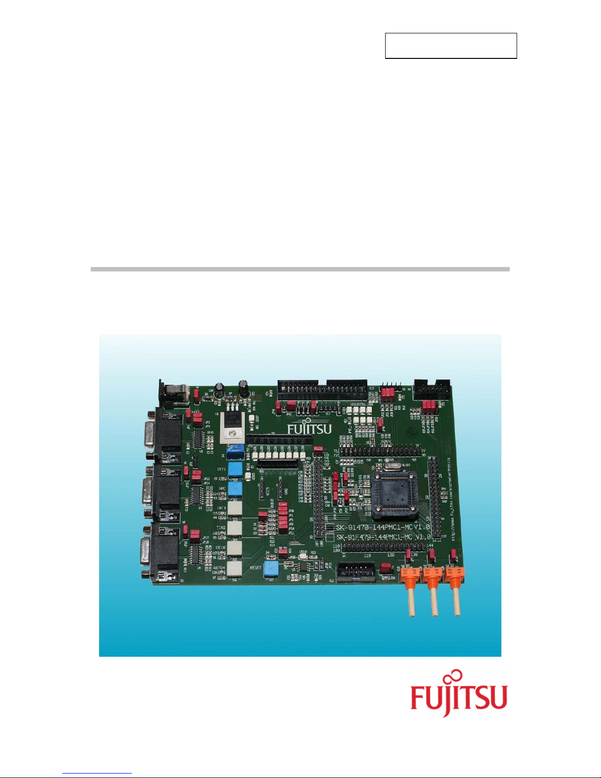
SK-91470-144PMC1-MC
FMEMCU-UG-910067-10
FR FAMILY
MB91470 SERIES
EVALUATION BOARD
USER GUIDE
Page 2

SK-91470-144PMC1-MC User Guide
Revision History
Revision History
Date Issue
2007/11/19 V1.0 Cha First Version
This document contains 24 pages.
FMEMCU-UG-910067-10 - 2 - © Fujitsu Microelectronics Europe Gm bH
Page 3

SK-91470-144PMC1-MC User Guide
Warranty and Disclaimer
Warranty and Disclaimer
To the maxim um extent p ermitted by applicabl e law, Fuji tsu Microe lectronic s Europe Gm bH restric ts
its warranties and its liability for the SK-91470-144PMC1-MC Board and all its deliverables (eg.
software include or header files, application examples, target boards, evaluation boards, engineering
samples of IC’s etc.), its performance and any consequential damages, on the use of the Product in
accordance with (i) the terms of the License Agreement and the Sale and Purchase Agreement under
which agreements the Product has been delivered, (ii) the technical descriptions and (iii) all
accompanying written materials. In addition, to the maximum extent permitted by applicable law,
Fujitsu Microelectronics Europe GmbH disclaims all warranties and liabilities for the performance of
the Product and any consequential damages in cases of unauthorized decompiling and/or reverse
engineering and/or disassembling. Note, the SK-91470-144PMC1-MC Board and all its
deliverables are intended and must only be used in an evaluation laboratory environment.
1. Fujitsu Microelectronics Europe GmbH warrants that the Product will perform substantially in
accordance with the accompanying written materials for a period of 90 days form the date of
receipt by the customer. Concerning the hardware components of the Product, Fujitsu
Microelectronics Europe GmbH warrants that the Product will be free from defects in material
and workmanship under use and service as specified in the accompanyin g written materials
for a duration of 1 year from the date of receipt by the customer.
2. Should a Product turn out to be defect, Fujitsu Microelectronics Europe GmbH´s entire liability
and the customer’s exclusive remedy shall be, at Fujitsu Microelectronics Europe GmbH´s
sole discretion, either return of the purchase price and the license fee, or repl acement of the
Product or parts thereof, if the Product is returned to Fujitsu Microelectronics Europe GmbH in
original packing and without further defects resulting from the customer’s use or the transport.
However, this warranty is excluded if the defect has resulted from an accident not attributable
to Fujitsu Microelectronics Europe GmbH, or abuse or misapplication attributable to the
customer or any other third party not r elating to Fu jitsu Microelectronics Europe GmbH.
3. To the maximum extent permitted by applicable law Fujitsu Microelectronics Europe GmbH
disclaims all other warranties, whether expressed or implied, in particular, but not limited to,
warranties of merchantability and fitness for a particular purpose for which the Product is not
designated.
4. To the maximum extent permitted by applicable law, Fujitsu Microelectronics Europe GmbH´s
and its supplier’s liability are restricted to intention and gross negligence.
NO LIABILITY FOR CONSEQUENTIAL DAMAGES
To the maximum extent permitted by applicable law, in no event shall Fujitsu
Microelectronics Europe GmbH and its suppliers be liable for any damages whatsoever
(including but without limitation, consequential and/or indirect damages for personal
injury, assets of substantial value, loss of profits, interruption of business operation,
loss of information, or any other monetary or pecuniary loss) arising from the use of
the Product.
Should one of the above stipulations be or become invalid and/or unenforceable, the remaining
stipulations shall stay in full effect
© Fujitsu Microelectronics Europe GmbH - 3 - FMEMCU-UG-910067-10
Page 4

SK-91470-144PMC1-MC User Guide
Contents
0 Contents
REVISION HISTORY.............................................................................................................. 2
WARRANTY AND DISCLAIMER........................................................................................... 3
0 CONTENTS........................................................................................................................4
1 OVERVIEW........................................................................................................................5
1.1 Abstract..................................................................................................................... 5
1.2 Features.................................................................................................................... 5
1.3 General Description ..................................................................................................6
2 INSTALLATION................................................................................................................. 7
3 DEFAULT JUMPER SETTINGS........................................................................................ 8
3.1 Default Jumper settings for MB91F479-PMC1 ......................................................... 8
4 JUMPERS AND SWITCHES ........................................................................................... 11
4.1 Power Supply (JP: 26, 41) ......................................................................................11
4.2 Analog Power Supply Voltage (JP: 24, 27, 28, 35, 36)........................................... 12
4.3 UART0 (JP: 2, 3, 4)................................................................................................. 13
4.4 UART1 (JP: 12, 14, 15)........................................................................................... 13
4.5 UART2 (JP: 17, 18, 19)........................................................................................... 14
4.6 Reset-Generation (JP: 9, 23, 25, 30)...................................................................... 14
4.7 Buttons SW1-SW7 (JP: 1, 5, 6, 8, 10, 11, 25, 38)................................................... 15
5 PROGRAMMING THE INTERNAL FLASH MEMORY.................................................... 16
5.1 Asynchronous Mode ...............................................................................................16
5.2 Synchronous Mode................................................................................................. 17
6 CONNECTORS................................................................................................................ 18
6.1 Power connector (X15) ...........................................................................................18
6.2 Edge connectors (X1 – X4)..................................................................................... 18
6.3 UART0- UART2 connectors (X5, X6, X7)............................................................... 18
6.4 USER-LEDs & optional LC-Display......................................................................... 19
6.5 PWM LEDs.............................................................................................................. 19
6.6 MotorDrive connector.............................................................................................. 20
6.7 Hall sensor and encoder interface (JP: 20, 21, 22, 29, 31, 33, 34)......................... 21
7 RELATED PRODUCTS................................................................................................... 22
8 INFORMATION IN THE WWW........................................................................................ 23
FMEMCU-UG-910067-10 - 4 - © Fujitsu Microelectronics Europe Gm bH
Page 5

SK-91470-144PMC1-MC User Guide
Chapter 1 Overview
1 Overview
1.1 Abstract
The SK-91470-144PMC1-MC is a multifunctional evaluation board for the Fujitsu 32-bit FR
Flash microcontroller series MB91470.
It can be used stand-alone or together with the MB2198 Emulator system for software
development and testing. The board allows the designer immediately to start software
development before his own final target system is available.
The SK-91470-144PMC1-MC can be used together with an external power stage such as
the SK-POWER-3P-LV-MC to evaluate motor control applications. Therefore, connectors
featuring the corresponding control and feedback signals are provided to enable quick set-up
of the system.
1.2 Features
- Supports Fujitsu’s MB91470 Series MCUs in the FPT-144P-M12 package or the
MB91FV470 evaluation MCU with the MB2198-160 adapter board and the MB2198-161
header board. By default, the Board is delivered with an MB91F479-PMC1 MCU.
< 9-15V unregulated external DC power supply
< 5V on-board voltage regulator
< Power-LEDs for supply voltage
< Onboard voltage supervisor monitors supply voltage
< In-Circuit serial Flash programming via UART
< All resources available for evaluation
< All MCU pins routed to edge connectors
< 34-pin connector for external power stage / inverter
< Connector for Hall sensor and quadrature encoder input
< 10 MHz main crystal
< Three RS232 interfaces are usable simultaneously
< 8 User LEDs, optional: alphanumeric standard LC-Display
< LEDs for PWM output
< Reset button, Reset LED
< 4 user buttons + NMI + DTTI test buttons, 3 user potentiometers
This board must only be used for test applications
in an evaluation laboratory environment.
© Fujitsu Microelectronics Europe GmbH - 5 - FMEMCU-UG-910067-10
Page 6

SK-91470-144PMC1-MC User Guide
Chapter 1 Overview
1.3 General Description
The SK-91470-144PMC1-MC supports the MB91470 32-bit Flash microcontroller series in
the 144-pin 0.4mm pitch package (FPT-144P-M12), like the MB91F479-PMC1.
It can be used as a stand-alone evaluation board or together with the MB2198 emulation
system using the adapter board MB2198-160 and the header board MB2198-161.
This evaluation board supports the following package: FPT-144P-M12.
The board is supplied with a socketed 10 MHz crystal as main oscillation source. Using the
internal PLL of the MCU, internal clock rates up to 80 MHz can be achieved.
Three separate RS232 transceivers are available to connect three on-chip UARTs to 9-pin
D-Sub connectors (X5, X6, X7). The transceivers generate the adequate RS232 levels for
the receive (RXD) and transmit (TXD) lines. The DTR line can be used to generate a system
reset. The RTS signal can be shortcut to CTS using the jumpers JP4, JP15 and JP19.
In-circuit programming (asynchronous) can be done via X5 (UART0).
All pins of the microcontroller except the oscillator pins X0/1 and the analog reference
voltages AVRH2-4 are connected to the edge connectors X1-X4 and are directly available to
the user. Furthermore, a 34-pin connector features all signals needed to connect an external
3-phase power stage (inverter), such as the 6ch PWM output from the Waveform generator,
as well as the analog measurement signals from the power stage. Additionally, there is a
connector for Hall sensors and quadrature encoders as motor speed / position feedback.
The on-board voltage regulator allows the user to connect an unregulated DC input voltage
of +9V to +15V to X15, or the external power stage can supply the voltage input to the
regulator. In case of any modifications of the board, or when supplying e.g. encoders or
sensors, care must be taken that the total power consumption will not overheat the voltage
regulators. Maximum additional output current for VCC is about 200-500mA, depending on
the input voltage.
There are seven push button switches on the board, which can be connected to input ports
of the microcontroller. This allows the user to evaluate external interrupts, external ADC
trigger or timer input functions as well as simple input polling. One button is reserved as
‘Reset’-button for the microcontroller. Two buttons are reserved for NMI (Non-Maskable
Interrupt) and the DTTI (fault protection) function.
Eight user LEDs are connected to Port 00 and grounded by a 1K resistor network. If these
LEDs are not required, the resistor network can be removed to disconnect the LEDs and to
free the IO port. Additional LEDs show the activity on the Waveform Generator outputs
RTO0-5 and an optional timer output.
The user potentiometers can be connected to the ADC for evaluation and application control.
The analog inputs of the 12-bit AD converter units 3+4 as well as AN2-0 to AN2-7 of the 10-
bit ADC unit 2 can be equipped with a capacitor in order to reduce no ise by forming an RC
low-pass with an external or on-board resistor.
FMEMCU-UG-910067-10 - 6 - © Fujitsu Microelectronics Europe Gm bH
Page 7

SK-91470-144PMC1-MC User Guide
Chapter 2 Installation
2 Installation
Carefully remove the board from the shipping carton.
First, check if there are any damages before powering up the evaluation board.
For the power supply a DC input voltage of 9V – 15V is recommended. The positive
voltage (+) must be connected to the center, and ground (GND) must be conne cted to
the shield of the connector X15!
Alternatively, the board can be supplied by an external circuit connected to the motor
control connector (X12), Pin 11+12. Also here, max. 15V input is recommended. Set
JP41 accordingly to select the voltage input source.
After power-on, the green power-on LED (LED17) should light up. If the LED does not light
up, switch off the power supply and check input polarity as well as the setting of JP41.
The in-circuit programming allows the user to program own applications into the Flash
memory. The procedures for Flash programming are described in chapter 5.
- Remove the MCU from the socket (NQ-PACK) before using a probe cable or adapter
board!
Note:
Some customers experience connectivity problems when mounting the MCU into the
socket adapter. Only the small red screwdriver available in your box should be used
to connect the cover (HQPACK) onto the socket (NQPACK).
If the four screws are not tightened equally, then it may cause a poor contact.
Do not screw the cover too tight (max 0.054 Nm). If you have connectivity problems,
please loosen the screws and tighten the screws again equally.
Do not clean NQPACK, YQPACK, and YQSOCKET with steam. Cleaning material will
contaminate inside of connector.
© Fujitsu Microelectronics Europe GmbH - 7 - FMEMCU-UG-910067-10
Page 8
SK-91470-144PMC1-MC User Guide
Chapter 3 Default Jumper settings
3 Default Jumper settings
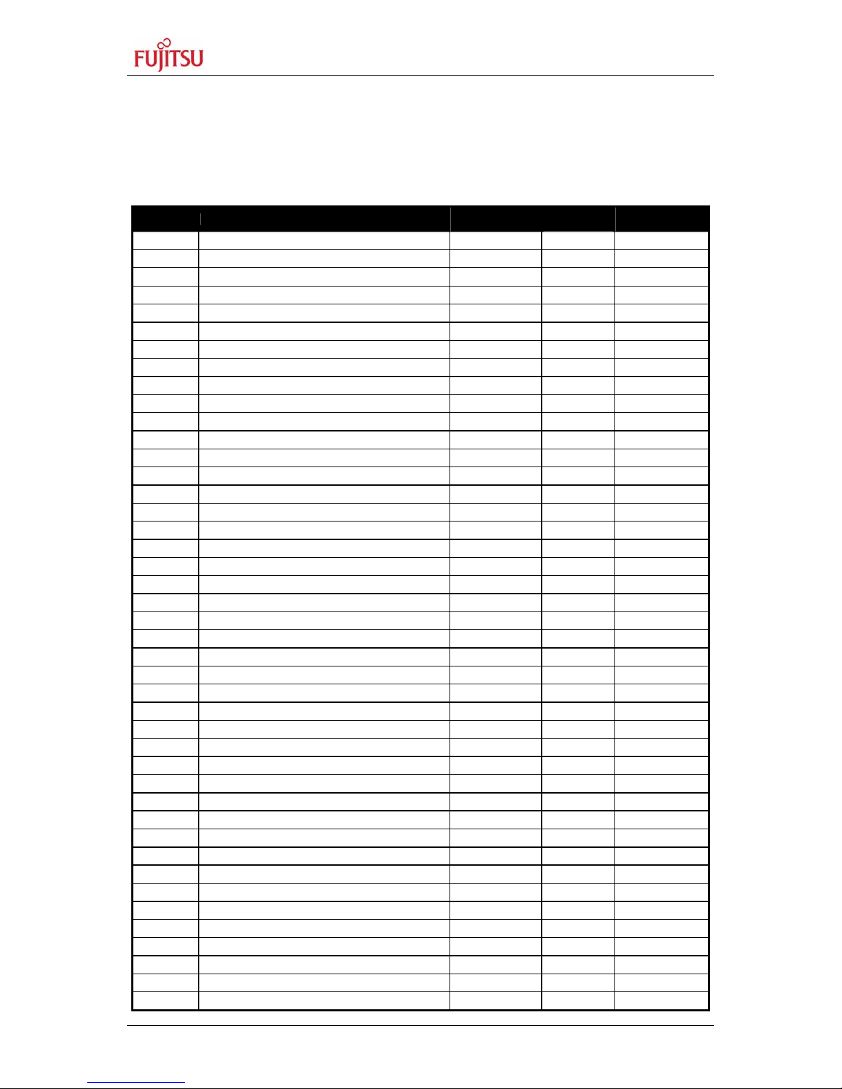
3.1 Default Jumper settings for MB91F479-PMC1
Jumper Description / Function Type
JP1 NMI Jumper 2pin closed F12
JP2 UART0 - SIN0 Jumper 2pin closed K7
JP3 UART0 - SOT0 Jumper 2pin closed K7
JP4 UART0 RTS-CTS Jumper 2pin closed K6
JP5 INT3 Jumper 2pin closed E12
JP6 Common INT
JP7 P1 - AN2-5
JP8 TIN2
JP9 Reset UART0/1
JP10 CKI0
JP11 ADTG4
JP12 UART1 - SIN1
JP13 P2 - AN2-6
JP14 UART1 - SOT1
JP15 UART1 RTS-CTS
JP16 P3 - AN2-7
JP17 UART2 - SIN2
JP18 UART2 - SOT2
JP19 UART2 RTS-CTS
JP20 HALL A – IC0
JP21 HALL B – IC1
JP22 HALL C – IC2
JP23 WD - TOUT3
JP24 AVCC
JP25 EXT. Reset
JP26 MCU VCC
JP27 AVRH2
JP28 AVRH3
JP29 ENC_TIN0
JP30 Watchdog
JP31 En c ode r A – AIN 0
JP32 Mode RUN / PGM
JP33 Encoder B – BIN0
JP34 Encoder I – ZIN0
JP35 AVSS
JP36 AVRH4
JP37 OPT1 – INT7/PPG7
JP38 DTTI
JP39 OPT6 – AN2-4
JP40 PWMLEDS
JP41 DCIN INT/EXT
JP42 I Phase B ADC select
JP43 U DC Bus sense – AN2-3
Jumper 2pin
Jumper 2pin
Jumper 2pin
Jumper 3pin
Jumper 2pin
Jumper 2pin
Jumper 2pin
Jumper 2pin
Jumper 2pin
Jumper 2pin
Jumper 2pin
Jumper 2pin
Jumper 2pin
Jumper 2pin
Jumper 2pin
Jumper 2pin
Jumper 2pin
Jumper 2pin
Jumper 2pin
Jumper 2pin
Jumper 2pin
Jumper 2pin
Jumper 2pin
Jumper 2pin
Jumper 2pin
Jumper 2pin
Jumper 3pin
Jumper 2pin
Jumper 2pin
Jumper 2pin
Jumper 2pin
Jumper 2pin
Jumper 2pin
Jumper 2pin
Jumper 2pin
Jumper 3pin
Jumper 3pin
Jumper 2pin
Default
Setting
closed E11
closed C21
closed E12
open H6
closed E12
closed E12
closed H7
closed C23
closed G7
closed H6
closed C24
closed E7
closed D7
closed E6
closed M20
closed M20
closed M21
open C15
closed F16
closed D12
closed J15
closed F17
closed G17
open L24
open C15
closed L24
1-2 C19
closed L23
closed L23
closed G16
closed G16
open L17
closed F12
open L15
closed K20
1-2 L6
2-3 L13
closed L15
Coordinates
FMEMCU-UG-910067-10 - 8 - © Fujitsu Microelectronics Europe Gm bH
Page 9

SK-91470-144PMC1-MC User Guide
Chapter 3 Default Jumper settings
Jumper Description / Function Type
JP44 AGND
JP45 OPT1_LED
JP46 U Phase A sense – AN2-0
JP47 U Phase B sense – AN2-1
JP48 U Phase C sense – AN2-2
Solder JP 2pin closed
Default
Setting
Jumper 2pin closed
Jumper 2pin open
Jumper 2pin open
Jumper 2pin open
Coordinates
L12
K17
L14
L14
L14
© Fujitsu Microelectronics Europe GmbH - 9 - FMEMCU-UG-910067-10
Page 10

SK-91470-144PMC1-MC User Guide
Chapter 3 Default Jumper settings
A B C D E F G H J K L M N
1
3
4
5
6
7
8
9
10
11
12
13
14
15
16
17
UART2 UART1 UART0 1
3
4
5
6
7
8
9
10
11
12
13
14
15
16
17
18
19
20
21
22
23
24
25
18
19
20
21
22
23
24
25
A B C D E F G H J K L M N
FMEMCU-UG-910067-10 - 10 - © Fujitsu Microelectronics Europe G mbH
Page 11

SK-91470-144PMC1-MC User Guide
Chapter 4 Jumpers and Switches
4 Jumpers and Switches
This chapter describes all jumpers and switches that can be modified on the evaluation
board. The default setting (for MB91F479) is shown with a grey shaded area.
4.1 Power Supply (JP: 26, 41)
The onboard voltage regulator provides stabilized 5V supply to the MCU and peripherals.
Even though it is thermally protected against overload, care must be taken when supplying
current for additional circuitry, like sensors or encoders.
JP26 Connects the MCU supply to VCC5; can be used for MCU current measurement
JP41 Selects on-board (X15) or ext. (X12) DC input
Jumper Setting Description
(MCUVCC)
(DCIN EXT/INT)
Closed MCUVCC connected to VCC5 JP26
Open for current measurement
1-2 DC input by X15 JP41
2-3 DC input by X12 (ext. power stage)
© Fujitsu Microelectronics Europe GmbH - 11 - FMEMCU-UG-910067-10
Page 12

SK-91470-144PMC1-MC User Guide
Chapter 4 Jumpers and Switches
4.2 Analog Power Supply Voltage (JP: 24, 27, 28, 35, 36)
The power supply as well as the positive reference voltages for the A/D-converters can be
provided internally or externally.
JP24, JP35 connects analog power supply voltages (AVcc and AVss)
JP27 connects the analog reference voltage AVRH2 to AVcc
JP28 connects the analog reference voltage AVRH3 to AVcc
JP36 connects the analog reference voltage AVRH4 to AVcc
Jumper Setting Description
Closed AVcc is connected to Vcc
JP24 (AVcc)
Open AVcc is disconnected from Vcc
Closed AVRH2 is connected to AVcc
JP27 (AVRH2)
Open AVRH2 defined by resistor network
*1
Closed AVRH3 is connected to AVcc
JP28 (AVRH3)
Open AVRH3 defined by resistor network
*1
Closed AVRH4 is connected to AVcc
JP36 (AVRH4)
Open AVRH4 defined by resistor network
*1
Closed AVss is connected to GND
JP35 (AVss)
Open AVss is disconnected from GND
*1
By default the resistor networks are not mounted on the board
By default, the A/D-converter supply and reference voltages are the same as the
microcontroller supply voltage.
Note:
If JP24 and JP35 are open, the user has to supply an adequate analog voltage supply (AVcc
and AVss) to the A/D-converter.
If JP27 is open, the resistors R27 and R37 define AVRH2.
If JP28 is open, the resistors R26 and R36 define AVRH3.
If JP36 is open, the resistors R43 and R47 define AVRH4.
By default the resistor networks are not mounted on the board. Standard SMD0805 chip resistors can
be used.
FMEMCU-UG-910067-10 - 12 - © Fujitsu Microelectronics Europe G mbH
Page 13

SK-91470-144PMC1-MC User Guide
Chapter 4 Jumpers and Switches
4.3 UART0 (JP: 2, 3, 4)
One RS232-transceiver (U2, X5) can be connected to the microcontrollers UART interface 0.
JP2, JP3 connect UART 0 to the RS232 transceiver (U2, X5)
JP4 Some programs (e.g. Terminals) need a connection between CTS and RTS
Jumper Setting Description
Closed
SIN0 of MCU is connected to UART0
JP2 (SIN0)
Open
Closed
SIN0 not connected to UART0
SOT0 of MCU is connected to UART0
JP3 (SOT0)
Open
SOT0 not connected to UART0
Closed RTS and CTS of X5 are connected
JP4 (RTS-CTS)
Open RTS and CTS of X5 are not connected
By default, UART0 (SIN0/SOT0) is connected to X5.
UART0 is also used for asynchronous in-circuit Flash programming.
4.4 UART1 (JP: 12, 14, 15)
One RS232-transceiver (U3, X6) can be connected to the microcontrollers UART interface 1.
JP12, JP14 connect UART 1 to the RS232 transceiver (U3, X6)
JP15 Some programs (e.g. Terminals) ne ed a connection between CTS and RTS
Jumper Setting Description
Closed
SIN1 of MCU is connected to UART1
JP12 (SIN1)
Open
Closed
SIN1 not connected to UART1
SOT1 of MCU is connected to UART1
JP14 (SOT1)
Open
SOT1 not connected to UART1
Closed RTS and CTS of X6 are connected
JP15 (RTS-CTS)
Open RTS and CTS of X6 are not connected
By default, UART1 (SIN1/SOT1) is connected to X6.
© Fujitsu Microelectronics Europe GmbH - 13 - FMEMCU-UG-910067-10
Page 14

SK-91470-144PMC1-MC User Guide
Chapter 4 Jumpers and Switches
4.5 UART2 (JP: 17, 18, 19)
One RS232-transceiver (U3, X6) can be connected to the microcontrollers UART interface 2.
JP17, JP18 connect UART 2 to the RS232 transceiver (U4, X7)
JP19 Some programs (e.g. Terminals) ne ed a connection between CTS and RTS
Jumper Setting Description
Closed
SIN2 of MCU is connected to UART2
JP17 (SIN2)
Open
Closed
SIN2 not connected to UART2
SOT2 of MCU is connected to UART2
JP18 (SOT2)
Open
SOT2 not connected to UART2
Closed RTS and CTS of X7 are connected
JP19 (RTS-CTS)
Open RTS and CTS of X7 are not connected
By default, UART2 (SIN2/SOT2) is connected to X7.
4.6 Reset-Generation (JP: 9, 23, 25 , 30)
In addition to the internal Power-On reset, the microcontroller can be reset by an external
reset circuit (Voltage Monitor) and also by a RS232 interface.
JP9 This jumper selects whether the DTR line from UART0 or UART1
will generate a system reset.
JP23 This jumper connects the MCU Pin 17 (Base timer output TOUT3) to the external
watchdog IC’s trigger input
JP25 Open this jumper if no external Reset shall be generated, e.g. to avoid accidental
reset during long-term testing or demonstration.
JP30 This jumper enables the watchdog function of the reset IC U5. If this is closed, U5
U5 issues a reset if it is not periodically re-triggered by the MCU (PJ7/TOUT3)
Jumper Setting Description
1 - 2 DTR of UART0 is selected for reset generation
JP9
2 - 3 DTR of UART1 is selected for reset generation
Closed MCU Pin 17 (PJ7/TOUT3) connected to U5
JP23 (WD_TOUT3)
Open MCU Pin 17 (PJ7/TOUT3) not connected to U5
Closed INITX connected to reset circuit / supply monitor U5
JP25 (Ext. Reset)
Open No connections to INITX
Closed U5 watchdog function enabled JP30
(Watchdog)
FMEMCU-UG-910067-10 - 14 - © Fujitsu Microelectronics Europe G mbH
Open U5 watchdog function disabled
Page 15

SK-91470-144PMC1-MC User Guide
Chapter 4 Jumpers and Switches
Note:
While a reset signal is asserted the red Reset-LED (LED16) is lit.
During normal operation, this LED should be off.
If the reset LED is steadily on or blinks periodically, check the power supply input voltage
and the settings for the reset generation by UART as well as the jumpers JP23 and JP30.
4.7 Buttons SW1-SW7 (JP: 1, 5, 6, 8, 10, 11, 25, 38)
JP1, JP5, JP8, JP10, JP11, JP38
Six user push buttons SW1-SW6 can be connected to the microcontroller.
SW2 also serves as test button for the MCU DTTI function, which stops the
PWM output e.g. in case of an inverter fault.
JP6 Common interrupt for SW3-SW6: Eases up button event handling when the
buttons are used to control an application
JP25 External reset circuit and button SW7 can be connected to the microcontroller.
Jumper Setting Description
JP1 (SW1) Closed NMIX of the MCU is connected to SW1
Open No connection to the microcontroller
JP38 (SW2) Closed DTTI button + LED15 connected to MCU Pin 57 (DTTI)
Open No connection to the microcontroller
JP5 (SW3) Closed Pin 23 (INT3) of MCU is connected to SW3 and JP6
Open No connection of INT3
JP8 (SW4) Closed Pin 14 (TIN2) is connected to SW4
Open No connection to the microcontroller
JP10 (SW5) Closed Pin 56 (CKI0) of the MCU is connected to SW5
Open No connection to the microcontroller
Closed Pin 67 (ADTG4) of the MCU is connected to SW6
JP11 (SW6)
Open No connection to the microcontroller
JP6
(COMM. INT)
Closed SW3 - SW6 connected to INT3 (wired-OR)
Open Only SW3 is connected to INT3
JP25 (Reset)
Closed INITX is connected to the reset IC and SW7
Open No connection to INITX
By default, all push-buttons as well as the reset circuit are connected to the microcontroller.
© Fujitsu Microelectronics Europe GmbH - 15 - FMEMCU-UG-910067-10
Page 16

SK-91470-144PMC1-MC User Guide
Chapter 5 Programming the internal Flash memory
5 Programming the internal Flash memory
The MB91F479 has an internal bootloader for asynchronous as well as synchronous Flashprogramming:
< Serial asynchronous Flash-programming via X5 (UART 0)
< Serial synchronous Flash-programming via X11
5.1 Asynchronous Mode
To use the asynchronous Flash programming mode, follow the following steps:
1. Install the newest FJ FR Flash programmer.
2. Connect the Starterkit (UART 0) to t he PC using a 1:1 cable.
3. Start the Flash programmer by double-clicking on the icon
4. Select appropriate MCU type, oscillator frequency, COM-Port, and the path to your
HEX-File (.mhx)
5. Power-off the board
6. Set JP32 to 2-3 (PRG) and power up the Board
7. Press the “Full Operation” button to start programming, press the RESET button
(SW7) and click on ‘OK’.
CAUTION: DO NOT INTERRUPT OR CUT OF F POWER DURING ERASE!!!
8. When download and programming was completed successfully, a message appears.
In case of errors, please check COM-Port configuration, cable connection and jumper
settings.
9. After successful programming, Power off the board and set JP32 back to 1-2 (RUN)
10. Power on the board to start the application
FMEMCU-UG-910067-10 - 16 - © Fujitsu Microelectronics Europe G mbH
Page 17

SK-91470-144PMC1-MC User Guide
Chapter 5 Programming the internal Flash memory
5.2 Synchronous Mode
In order to program the Flash-ROM synchronously special third-party soft- and hardware has
to be used, e.g. GALEP-4 from www.conitec.de
A dedicated Flash programming socket (X11) is provided on the evaluation-board for direct
connection to this programmer.
X11: Flash programming socket:
. This tool is not available for free.
P80 1
MD0 3
RSTx 5
SOT 7
VCC 9
2 P81
4 MD2
6 SIN
8 SCK
10 GND
To allow the parallel programming tool to set the mode pins and programming mode
(P80/P81), be sure to remove JP32 and external circuits connected to P80/P81 (Pin 20+21).
© Fujitsu Microelectronics Europe GmbH - 17 - FMEMCU-UG-910067-10
Page 18

SK-91470-144PMC1-MC User Guide
Chapter 6 Connectors
6 Connectors
6.1 Power connector (X15)
The following figure shows the power connection jack X15. It is used to connect an external
unregulated DC power supply voltage (9V-15V DC) to the evaluation board. Higher input
voltages are possible, but cause higher heat dissipation of the voltage regulator U6,
depending on the total load current.
Shield: Ground (GND)
Connector X15:
Center: positive DC input (+)
It is recommended to use 9V DC input to minimize the power dissipation of the voltage
regulator.
6.2 Edge connectors (X1 – X4)
All pins (except oscillator pins) of the microcontroller are directly connected to the edge
connectors X1 to X4 as follows:
Connector MCU Pins Connector MCU Pins
X1 (1 - 36) 1 - 36 X3 (73 - 108) 73 - 108
X2 (37 - 72) 37 - 72 X4 (109 - 144) 109 - 144
The odd pin numbers are located on the outer side and the even pin numbers are located on
the inner side (closer to the MCU) of the connectors.
6.3 UART0- UART2 connectors (X5, X6, X7)
Three 9-pin D-Sub female connectors are used
for the serial interface UART0-2.
TXD is the transmit output, RXD is the receive input.
The DTR signal can be used to generate a reset.
Please use a 1:1 cable for PC connection.
FMEMCU-UG-910067-10 - 18 - © Fujitsu Microelectronics Europe G mbH
Connectors X5-X7:
GND DTR RxD TxD
5
9
CTS RTS DSR
1
6
Page 19

SK-91470-144PMC1-MC User Guide
Chapter 6 Connectors
6.4 USER-LEDs & optional LC-Display
Eight LEDs are supplied for user applications. In order to disconnect the LEDs from the
microcontroller, the resistor network RN1 can be removed.
Instead of the user-LEDs an alphanumeric LC-Display (optional) can be connected.
The following control signals are provided:
1 2 3 4 5 6 7 8 9 10 11 12 13 14
LCD
LED
MCU Pin
MCU Port
GND VCC V0 RS R/W E - - - - D4 D5 D6 D7
109 110 111 112 113 114 115 116
P00 P01 P02 P03 P04 P05 P06 P07
LED1 LED2 LED
3
LED4 LED5 LED6 LED7 LED
8
6.5 PWM LEDs
The board provides seven LEDs, indicating the state of each PWM output (LED9-LED14).
LED Signal LED Signal LED Signal
LED9 RTO0/PWM1H LED11 RTO2/PWM2H LED13 RTO4/PWM3H
LED10 RTO1/PWM1L LED12 RTO3/PWM2L LED14 RTO5/PWM3L
JP40 can be removed in case these LEDs shall not be used.
LED18 can be connected to P87/INT7/PPG7 (Pin27) in order to indicate the brake chopper
control signal (JP37 set). The solder JP45 can be opened to disable the LED also when
JP37 is set, in case this is needed.
© Fujitsu Microelectronics Europe GmbH - 19 - FMEMCU-UG-910067-10
Page 20

SK-91470-144PMC1-MC User Guide
Chapter 6 Connectors
6.6 MotorDrive connector
The MotorDrive connector can be used to connect an external power stage for motor control.
It holds the necessary signals for PWM generation and current / voltage measurement.
MotorDrive Connector Pin cross-reference:
X12 pin MCU pin Signal X12 pin MCU pin Signal
1 VSS GND 2 VSS GND
3 38 RTO0 (PWM1H) 4 39 RTO1 (PWM1L)
5 40 RTO2 (PWM2H) 6 41 RTO3 (PWM2L)
7 42 RTO4 (PWM3H) 8 43 RTO5 (PWM3L)
9 VSS GND 10 VSS GND
11 n/c ext. DC in 12 n/c ext. DC in
13 (27 via JP37) OPT1 (Brake) 14 n/c OPT2
15 n/c OPT3 16 n/c OPT4
17 n/c OPT5 18 (86 via JP39) OPT6 (TEMP)
19 57 DTTI (Fault) 20 85 via JP43 DC bus voltage sense
21 VSS via JP44 Shield ground 22 82 via JP46 Phase A voltage sense
23
25
27
29
31
33
VSS via JP44
VSS via JP44
VSS via JP44
VSS via JP44
VSS via JP44
VSS via JP44
Shield ground 24 83 via JP47 Phase B voltage sense
Shield ground 26 84 via JP48 Phase C voltage sense
Shield ground 28 71 DC Bus current sense
Shield ground 30 68 Phase A current sense
Shield ground 32 69 / 76 (JP42) Phase B current sense
Shield ground 34 70 Phase C current sense
Pins 13 -18 are spare pins and not used by default. They are connected to the pin header
X13 as well as JP37 and JP39. JP37 can be used to connect OPT1 to Pin27 of the MCU
(INT7/PPG7) in case the external circuit provides e.g. a break resistor which shall be
controlled by PPG7 or an additional interrupt source to be monitored. JP39 connects OPT6
to the analog input AN2-4 (Pin86), e.g. for a temperature sensor.
FMEMCU-UG-910067-10 - 20 - © Fujitsu Microelectronics Europe G mbH
Page 21

SK-91470-144PMC1-MC User Guide
Chapter 6 Connectors
6.7 Hall sensor and encoder interface (JP: 20, 21, 22, 29, 31, 33, 34)
JP20, JP21, JP22 These jumpers connect the Hall sensors (X8) to the input capture pins
IC0-IC2 of the MCU
JP31, JP33, JP34 These jumpers connect the encoder interface (X9) to the up/down
counter inputs AIN, BIN and ZIN
JP29 This jumper connects the up/down counter’s AIN input to the Base
Timer 0 input (TIN0) for easy speed measurement in PWC mode.
Jumper Setting Description
JP20
Open Hall A input is not connected to the MCU
Closed Hall A input is connected to IC0
Open Hall B input is not connected to the MCU
JP21
Closed Hall B input is connected to IC1
Open Hall C input is not connected to the MCU
JP22
Closed Hall C input is connected to IC2
Open Encoder Ch. A is not connected to the MCU
JP31
Closed Encoder Ch. A is connected to AIN0
Open Encoder Ch. B is not connected to the MCU
JP33
Closed Encoder Ch. B is connected to BIN0
Open Encoder index signal is not connected to the MCU
JP34
Closed Encoder index signal is connected to ZIN0
Open No connection between AIN0 and TIN0
JP29
Closed AIN0 and TIN0 are connected
If required by the encoder in use, additional pull-up resistors (R28-R30, usually 2k7) can be
mounted on the board near the encoder connector. Use standard SMD0805 chip resistors.
© Fujitsu Microelectronics Europe GmbH - 21 - FMEMCU-UG-910067-10
Page 22

SK-91470-144PMC1-MC User Guide
Chapter 7 Related Products
7 Related Products
< SK-91470-144PMC1-MC Evaluation board for the MB91470 Series MCU in the
FPT-144P-M12 package
< SK-91F479-144PMC1-MC Evaluation board with MB91F479 Series MCU in the
FPT-144P-M12 package (no MCU socket)
< SK-POWER-3P-LV-MC 3-phase, low voltage MOSFET power stage for Motor
Control
< NQPACK144SE Socket for package FPT-144P-M12
(Tokyo Eletech Corp. http://www.tetc.co.jp/e_index.htm
< HQPACK144SE Header for NQPACK144SE
< MB91470 Series
< MB91FV470 MB91470/480 Series Evaluation chip
< MB91F479-PMC1 Flash MCU
< MB2198-160 BGA-224P Adapter Board
< MB2198-161 LQFP-144p Header type 9 Board
)
FMEMCU-UG-910067-10 - 22 - © Fujitsu Microelectronics Europe G mbH
Page 23

SK-91470-144PMC1-MC User Guide
Chapter 8 Information in the WWW
8 Information in the WWW
Information about FUJITSU MICROELECTRONICS Products
can be found on the following Internet pages:
Microcontrollers (8-, 16- and 32bit), Graphics Controllers
Datasheets and Hardware Manuals, Support Tools (Hard- and Software)
http://mcu.emea.fujitsu.com/
Linear Products: Power Management, A/D and D/A Converters
http://www.fujitsu.com/emea/services/microelectronics/linears/
Media Products: SAW filters, acoustic resonators and VCOs
http://www.fujitsu.com/emea/services/microelectronics/saw/
For more information about FUJITSU MICROELECTRONICS
http://www.fujitsu.com/emea/services/microelectronics/
© Fujitsu Microelectronics Europe GmbH - 23 - FMEMCU-UG-910067-10
Page 24

SK-91470-144PMC1-MC User Guide
Chapter 8 Information in the WWW
Recycling
Gültig für EU-Länder:
Gemäß der Europäischen WEEE-Richtlinie und deren Umsetzung in landesspezifische
Gesetze nehmen wir dieses Gerät wieder zurück.
Zur Entsorgung schicken Sie das Gerät bitte an die folgende Adresse:
Fujitsu Microelectronics Europe GmbH
Warehouse/Disposal
Monzastraße 4a
63225 Langen
Valid for European Union Countries:
According to the European WEEE-Directive and its implementation into national laws we
take this device back.
For disposal please send the device to the following address:
Fujitsu Microelectronics Europe GmbH
Warehouse/Disposal
Monzastraße 4a
63225 Langen
FMEMCU-UG-910067-10 - 24 - © Fujitsu Microelectronics Europe G mbH
 Loading...