

Page 1
Fujitsu Microelectronics Europe
User Guide
SK-91467R-176PMC
FMEMCU-UG-910053-16
MB91460 SERIES
EVALUATION BOARD
USER GUIDE
Page 2

SK-91467R-176PMC User Guide
Revision History
Revision History
Date Issue
2006/12/06 CSc - Initial version V1.0
2007/03/02 V1.1 Recycling Note added
2007/06/28 V1.2 OGl - Updated asynchronous programming port/pin definition
2007/07/31 V1.3 OGL - Updated figure 2-1 default jumper settings
2007/11/05 V1.4 OGL – Updated mode setting definitions, programming flow
2007/12/27 V1.5 OGL – removed wrong head line
2008/04/21 V1.6 MHz – corrected programming settings
This document contains 45 pages.
FMEMCU-UG-910053-16 - 2 - © Fujitsu Microelectronics Europe GmbH
Page 3

SK-91467R-176PMC User Guide
Warranty and Disclaimer
Warranty and Disclaimer
To the maximum extent permitted by applicable law, Fujitsu Microelectronics Europe GmbH restricts
its warranties and its liability for the SK-91467R-176PMC Board and all its deliverables (eg.
software include or header files, application examples, target boards, evaluation boards, engineering
samples of IC’s etc.), its performance and any consequential damages, on the use of the Product in
accordance with (i) the terms of the License Agreement and the Sale and Purchase Agreement under
which agreements the Product has been delivered, (ii) the technical descriptions and (iii) all
accompanying written materials. In addition, to the maximum extent permitted by applicable law,
Fujitsu Microelectronics Europe GmbH disclaims all warranties and liabilities for the performance of
the Product and any consequential damages in cases of unauthorized decompiling and/or reverse
engineering and/or disassembling. Note, the SK-91467R-176PMC Board and all its deliverables
are intended and must only be used in an evaluation laboratory environment.
1. Fujitsu Microelectronics Europe GmbH warrants that the Product will perform substantially in
accordance with the accompanying written materials for a period of 90 days form the date of
receipt by the customer. Concerning the hardware components of the Product, Fujitsu
Microelectronics Europe GmbH warrants that the Product will be free from defects in material
and workmanship under use and service as specified in the accompanying written materials
for a duration of 1 year from the date of receipt by the customer.
2. Should a Product turn out to be defect, Fujitsu Microelectronics Europe GmbH´s entire liability
and the customer’s exclusive remedy shall be, at Fujitsu Microelectronics Europe GmbH´s
sole discretion, either return of the purchase price and the license fee, or replacement of the
Product or parts thereof, if the Product is returned to Fujitsu Microelectronics Europe GmbH in
original packing and without further defects resulting from the customer’s use or the transport.
However, this warranty is excluded if the defect has resulted from an accident not attributable
to Fujitsu Microelectronics Europe GmbH, or abuse or misapplication attributable to the
customer or any other third party not relating to Fujitsu Microelectronics Europe GmbH.
3. To the maximum extent permitted by applicable law Fujitsu Microelectronics Europe GmbH
disclaims all other warranties, whether expressed or implied, in particular, but not limited to,
warranties of merchantability and fitness for a particular purpose for which the Product is not
designated.
4. To the maximum extent permitted by applicable law, Fujitsu Microelectronics Europe GmbH´s
and its supplier’s liability are restricted to intention and gross negligence.
NO LIABILITY FOR CONSEQUENTIAL DAMAGES
To the maximum extent permitted by applicable law, in no event shall Fujitsu
Microelectronics Europe GmbH and its suppliers be liable for any damages whatsoever
(including but without limitation, consequential and/or indirect damages for personal
injury, assets of substantial value, loss of profits, interruption of business operation,
loss of information, or any other monetary or pecuniary loss) arising from the use of
the Product.
Should one of the above stipulations be or become invalid and/or unenforceable, the remaining
stipulations shall stay in full effect
© Fujitsu Microelectronics Europe GmbH - 3 - FMEMCU-UG-910053-16
Page 4

SK-91467R-176PMC User Guide
Contents
0 Contents
REVISION HISTORY.............................................................................................................. 2
WARRANTY AND DISCLAIMER........................................................................................... 3
0 CONTENTS........................................................................................................................4
1 OVERVIEW........................................................................................................................6
1.1 Abstract..................................................................................................................... 6
1.2 Features.................................................................................................................... 7
1.3 General Description .................................................................................................. 8
2 INSTALLATION............................................................................................................... 10
2.1 Connection/Power-On............................................................................................. 10
2.2 Default Jumper settings for MB91467R.................................................................. 11
2.3 Jumper Location ..................................................................................................... 13
2.4 Software Installation................................................................................................ 14
3 JUMPERS AND SWITCHES........................................................................................... 15
3.1 Operating Mode (S1) .............................................................................................. 15
3.2 Power Supply (S3, JP: 8, 9, 11, 12, 66).................................................................. 17
3.3 Analog Power Supply Voltage (JP: 9, 8, 10)........................................................... 20
3.4 LIN / UART Connectors (X2 – X5).......................................................................... 21
3.5 CAN interfaces (X7+X10)........................................................................................ 25
3.6 Reset Generation (JP: 50, 51, 52, 53, 60, 70, 80, 90) ............................................ 25
3.7 User Buttons SW1, SW2, SW3, SW4, SW5 (JP: 11, 12, 13, 14, 15)...................... 27
3.8 Memories (SRAM/Flash)......................................................................................... 28
4 CONNECTORS................................................................................................................ 29
4.1 Power connector (X6) ............................................................................................. 29
4.2 Edge connector (J1, J2, J3, J4) .............................................................................. 29
4.3 LIN-UART connectors (X2-X5)................................................................................ 30
4.4 CAN Connector (X7+X10)....................................................................................... 30
4.5 USER-LEDs............................................................................................................ 31
4.6 External Bus Connectors (X13, X14)...................................................................... 33
5 PROGRAMMING THE INTERNAL FLASH..................................................................... 35
5.1 Asynchronous Mode ............................................................................................... 35
5.2 Synchronous Mode................................................................................................. 38
6 PROGRAMMING SWB MONITOR DEBUGGER............................................................ 39
7 APPENDIX....................................................................................................................... 40
FMEMCU-UG-910053-16 - 4 - © Fujitsu Microelectronics Europe GmbH
Page 5

SK-91467R-176PMC User Guide
Contents
7.1 Related Products .................................................................................................... 40
7.2 Information in the WWW......................................................................................... 41
7.3 Tables ..................................................................................................................... 42
7.4 Figures.................................................................................................................... 43
7.5 Abbreviations .......................................................................................................... 44
© Fujitsu Microelectronics Europe GmbH - 5 - FMEMCU-UG-910053-16
Page 6

SK-91467R-176PMC User Guide
Chapter 1 Overview
1 Overview
1.1 Abstract
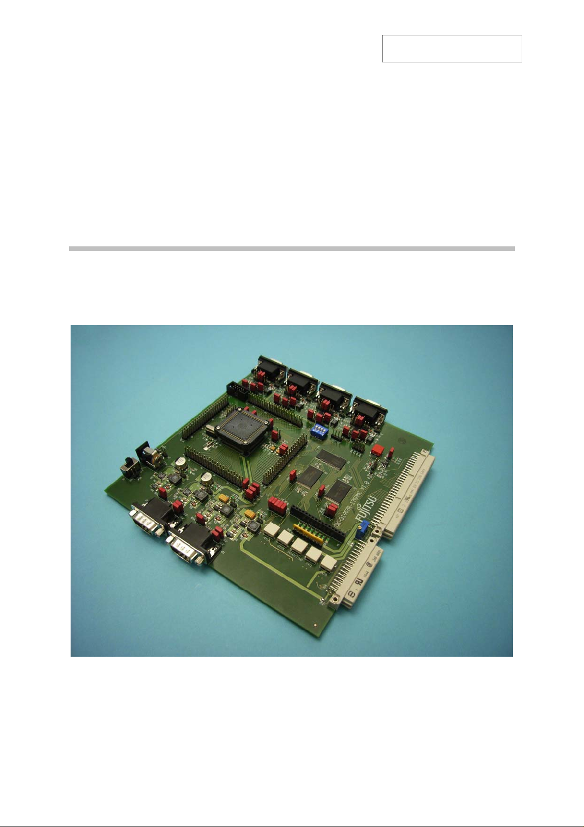
The SK-91467R-176PMC is a multifunctional evaluation board for the Fujitsu 32-bit FR60
Flash microcontroller series MB91460.
It can be used stand-alone for software development and testing or as a simple target board
to work with the emulator system.
The board allows the designer immediately to start software development before his own
final target system is available.
FMEMCU-UG-910053-16 - 6 - © Fujitsu Microelectronics Europe GmbH
Page 7

SK-91467R-176PMC User Guide
Chapter 1 Overview
1.2 Features
< Supports Fujitsu’s MB91F467R MCU in FPT-176P-M07 package or the MB2198
Emulator System with the Probe Cables EMA-MB91F467R-NLS-176M07 and EMAMB91F467R-LS-176M07
< 9-12V unregulated external DC power supply
< 5V, 3.3V, 2.5V and 1.8V onboard switching mode voltage regulators
< Power-LEDs for all supply voltages
< Onboard voltage supervisor monitors three of four supply voltages
< In-Circuit serial Flash programming (UART0)
< All resources available for evaluation
< All MCU pins routed to connectors
< 4 MHz main crystal
< 32 kHz crystal for sub clock operation
< Four RS232- or LIN interfaces and two CAN interfaces are usable simultaneously
< 3V capable CAN, LIN and RS232 transceivers
< 8 User LEDs
< Reset button, Reset LED
< 5 User buttons
< 96+48-pin VG connectors featuring external bus signals, e.g. for graphic sub-board
< 4 MB Flash ROM, 2 MB SRAM and 8 MB SDRAM connected to external bus
This board must only be used for test applications
in an evaluation laboratory environment.
© Fujitsu Microelectronics Europe GmbH - 7 - FMEMCU-UG-910053-16
Page 8

SK-91467R-176PMC User Guide
Chapter 1 Overview
1.3 General Description
The SK-91467R-176PMC supports the 32-bit Flash microcontroller MB91F467R.
It can be used as a stand-alone evaluation board or as a target board for the emulator
debugger.
The evaluation board supports the following package: FPT-176P-M07.
1.3.1 MCU Clocks
The board is supplied with a 4 MHz crystal as main oscillation source. Using the internal PLL
of the µC, internal clock rates up to 100 MHz can be achieved.
1.3.2 RS-232 and LIN
Four separate RS232 transceivers and four single-wire LIN-transceivers (TLE7259) are
available to connect four on-chip UARTs to 9-pin D-Sub connectors (X2-X5). The
transceivers generate the adequate RS232 levels for the receive (RXD) and transmit (TXD)
and LIN bus lines. In RS232 mode, either the DTR line or the RTS line can be selected with
jumpers (JP67, 77, 87, 97) to generate a system reset. The RTS signal can be shortcut to
CTS using the jumpers JP68, 78, 88 and 98. Each of the four D-Sub connectors can be
configured as RS232 or LIN. The LIN Vs line can be powered by the unregulated supply
input of the board, so no additional supply is needed (JP69, 79, 89 and 99).
All transceivers are fully 3.3V IO compatible to enable low voltage applications.
In-circuit programming (asynchronous, synchronous) can be done via LIN-UART 0(X2).
1.3.3 CAN Bus
Two high-speed CAN transceivers (TLE6250GV33) can be connected to the CAN interfaces
of the MCU to allow easy connection to CAN networks.
All transceivers are fully 3.3V IO compatible to enable low voltage applications.
1.3.4 MCU Pins / External Bus Interface Connector
All pins of the microcontroller except the oscillator pins X0/1(A) are connected to edge
connectors in functional groups and are directly available to the user. Furthermore, all
signals of the external bus interface are connected to a 96+48-pin VG connector to interface
e.g. external graphic sub-boards such as Fujitsu’s ‘Jasmine’ sub-board.
1.3.5 Power Supply
The on-board switching mode voltage regulators allow the user to connect an unregulated
DC input voltage of +9V to +15V, and supplies all voltages needed by the board and an
optional graphic sub-board. The regulators are rated with 3A (5V and 3.3V) resp. 1.5A (2.5V,
1.8V) and are thermally protected against overload.
1.3.6 User Buttons
There are six push button switches on the board, which can be connected to input ports of
the microcontroller. This allows the user to evaluate external Interrupts, external ADC trigger
or Input Capture functions as well as simple input polling. One button is reserved as ‘Reset’button for the microcontroller, controlled by the supply monitor IC.
FMEMCU-UG-910053-16 - 8 - © Fujitsu Microelectronics Europe GmbH
Page 9
SK-91467R-176PMC User Guide
Chapter 1 Overview
1.3.7 User LEDs
Eight user LEDs are connected to Port 28 and grounded by a 220R resistor network. If these
LEDs are not required, the resistor network can be removed to disconnect the LEDs and to
free the IO port.
1.3.8 Onboard Memories
4 MB Flash ROM, 2 MB SRAM and 8 MB SDRAM are connected to external bus chip select
areas 0 (Flash),1 (SRAM) and 2 (SDRAM). SRAM and SDRAM can be accessed 16 bit
wide. Flash can be accessed 8 bit or 16 bit wide (JP40, JP42).
1.3.9 I2C Bus
Additional pull-up resistors can be connected to the I²C bus lines by setting the according
Jumpers (JP20, 21, 22, 23, 24, 25) for I²C 0/1.
1.3.10 Emulator System
If the board is used as an emulator target board, the microcontroller must be removed from
the socket and the corresponding probe cable has to be mounted:
Series V-Chip Probe cable Socket
MB91460R MB91V460
EMA-MB91F467R-NLS-176M07
NQPACK176SD
HQPACK176SD
Table 1-1: Emulation System
Attention:
Socket for Flash chip mounting and probe cable connection is very sensitive. Always fit
probe cable or socket cover very carefully. If any unexpected problems occur, please check
proper connection of MCU/probe cable pads to socket.
Note:
Some customers experience connectivity problems when connecting the MCU into
the socket adapter. Only the small red screwdriver available in your box should be
used to connect the cover (HQPACK) onto the socket (NQPACK).
If the four screws are not tightening equally, then it may cause a poor contact.
Do not screw the cover too tight (max 0.054 Nm). If you have connectivity problems
then please loosen the screws and tighten again the screws equally.
Do not clean NQPACK, YQPACK, and YQSOCKET with steam. Cleaning material will
contaminate inside of connector.
© Fujitsu Microelectronics Europe GmbH - 9 - FMEMCU-UG-910053-16
Page 10

SK-91467R-176PMC User Guide
Chapter 2 Installation
2 Installation
2.1 Connection/Power-On
Carefully remove the board from the shipping carton.
First, check if there are any damages before powering up the evaluation board.
For the power supply a DC input voltage of 9V – 15V is recommended. The positive
voltage (+) must be connected to the shield, and ground (GND) must be connected to
the center pin of the connector X6!
Special care must be taken to the max. input voltage, if the LIN Vs lines are supplied
by the board (JP69, 79, 89, 99), since the input supply voltage is directly applied to pin
1 of X2-X5 without a voltage regulator.
After power-on (Switch S3 or JP19), the yellow power-on LEDs (D20, D28, D32, D36) should
be lit. If the LEDs do not light up, switch off the power supply and check input polarity and
current capability of the DC supply used.
The starter-kit is delivered with programmed Softune Workbench (SWB) Monitor Debugger
in the external flash. The SWB Monitor Debugger checks also the external SRAM access at
CS1. In case of successful access to external SRAM the LED LD1, LD3 and LD7 are on.
To use the SWB Monitor Debugger, the CPU mode selection must be set to the External
Reset Vector mode by setting DIP switch S1 to (Off, Off, Off, On), which is the delivery state.
To use the MCU with the internal flash, which is normally required for the final application,
the CPU mode selection must be set to the Internal Reset Vector mode by setting DIP switch
S1 to (Off, Off, Off, Off)
The in-circuit programming allows the user to program own applications into the Flash
memory. The procedures for Flash programming are described in chapter 6.
If the board shall be used as an emulator target board, switch off the power supply and
remove the microcontroller from the socket. Now the probe cable can be mounted on the
socket. Take care of the pin 1 marking on the socket and fasten the probe cable with the
provided screws.
Do not use any other probe cable than EMA-MB91F467R-NLS-176M07 only!
Connect the probe cable to the MB2198-300 emulation Adapter Board. Check all jumper
settings of the evaluation board, the Probe Cable and the Adapter Board.
When turning on the system, be sure to use the following power-up sequence:
1. Power up the Emulator Main Unit (MB2198-01)
2. Power up the Adapter Board (MB2198-300)
3. Power up the target Board (SK-91467R-176PMC)
To turn off the system, switch off the components in reverse order, beginning with the target
Board.
Please refer to the corresponding user manuals and application notes for the emulator how
to set up the emulator system. After power on, the ‘Reset’-LED of the emulator must be off
and the ‘Vcc’-LED must be on.
If the Reset LED is still lit, check the settings of the emulator system and the power supply of
the evaluation board.
FMEMCU-UG-910053-16 - 10 - © Fujitsu Microelectronics Europe GmbH
Page 11
SK-91467R-176PMC User Guide
Chapter 2 Installation
2.2 Default Jumper settings for MB91467R
The following table lists all jumpers including its default setting and location on the starterkit.
Jumper Description / Function Type Default
JP1 VCC5_1, VCC 5V/3.3V Jumper 3 pin 2-3 E 9
JP2 VCC5_2, VCC 5V/3.3V Jumper 3 pin 2-3 E 9
JP3 VCC5_3, VCC 5V/3.3V Jumper 3 pin 2-3 E 9
JP4 VCC5_1 Jumper 2 pin Clodes J 4
JP5 VCC5_2 Jumper 2 pin Clodes J 5
JP6 VCC5_3 Jumper 2 pin Clodes J 7
JP7 VCC3 Jumper 2 pin Clodes E 9
JP8 AVss Jumper 2 pin Closed H 9
JP9 AVcc Jumper 2 pin Closed H 9
JP10 AVRH=AVCC Jumper 2 pin Closed H 8
JP11 SW1 (INT0) Jumper 2 pin Closed E 11
JP12 SW2 (INT1) Jumper 2 pin Closed E 11
JP13 SW3 (ICU0/TIN0) Jumper 2 pin Closed E 12
JP14 SW4 (NMIX) Jumper 2 pin Closed E 12
JP15 SW5 (ATGX) Jumper 2 pin Closed E 12
JP19 POWER Jumper 2 pin Open C 3
JP20 SDA0 Pullup Jumper 2 pin Open H 8
JP21 SCL0 Pullup Jumper 2 pin Open H 8
JP22 SDA1 Pullup Jumper 2 pin Open J 4
JP23 SCL1 Pullup Jumper 2 pin Open J 4
JP24 SDA2 Pullup Jumper 2 pin Open H 4
JP25 SCL2 Pullup Jumper 2 pin Open H 4
JP30 X14B – VCC1V8 Solder JP 2 pin Closed B 17
JP31 X14B – Vin Solder JP 2 pin Open E 17
JP33A CAN0, VCC_3/VCC5V Jumper 3 pin 1-2 B 4
JP33B CAN1, VCC_3/VCC5V Jumper 3 pin 1-2 B 8
JP34 CAN0 RX Jumper 2 pin Closed B 6
JP35 CAN0 TX Jumper 2 pin Closed B 6
JP37 CAN1 RX Jumper 2 pin Closed B 10
JP38 CAN1 TX Jumper 2 pin Closed B 10
JP40 Flash: Word / Byte Jumper 3 pin 1-2 F 15
JP41 Flash Enable Jumper 3 pin 2-3 G 13
JP42 Flash: 16bit / 8bit Jumper 3 pin 1-2 F 15
JP44 SRAM Enable Jumper 3 pin 2-3 G 11
JP46 SDRAM: MCLKO=MCKLI Solder JP 2 pin Closed J 11
JP50 Monitor: 1V8/2V5 Solder JP 3 pin 2-3 K 16
JP51 DTR sel Jumper 3 pin Open J 15
JP52 Direct RST Solder JP 3 pin 1-2 K 15
JP53 RST MCU Jumper 2 pin Closed K 16
JP60 Reset by UART6 Jumper 2 pin Open K 14
JP61 SIN6: RS232 / LIN Jumper 3 pin 1-2 L 12
JP62 SOT6: RS232 / LIN Jumper 3 pin 1-2 L 13
JP63 LIN6: Enable Jumper 2 pin Open M 13
JP64 LIN6: Jumper 3 pin 1-2 L 13
JP65 LIN6: Master Jumper 2 pin Open M 14
Layout
Schematic
1 / 3
1 / 3
1 / 3
1 / 3
1 / 3
1 / 3
1 / 3
1 / 3
1 / 3
1 / 3
1 / 3
1 / 3
1 / 3
1 / 3
1 / 3
2 / 3
2 / 3
2 / 3
2 / 3
2 / 3
2 / 3
2 / 3
3 / 3
3 / 3
2 / 3
2 / 3
2 / 3
2 / 3
2 / 3
2 / 3
3 / 3
3 / 3
3 / 3
3 / 3
3 / 3
2 / 3
2 / 3
2 / 3
2 / 3
2 / 3
2 / 3
2 / 3
2 / 3
2 / 3
2 / 3
© Fujitsu Microelectronics Europe GmbH - 11 - FMEMCU-UG-910053-16
Page 12
SK-91467R-176PMC User Guide
Chapter 2 Installation
Jumper Description / Function Type Default
JP66 LIN-UART 6: RS232 / LIN Jumper 3 pin 1-2 M13
JP67 UART6: DTR/RTS Jumper 3 pin Open M 13
JP68 UART6: RTS-CTS Jumper 2 pin Closed M 13
JP69 LIN 6: VBat Jumper 2 pin Open M 12
JP70 Reset by UART5 Jumper 2 pin Open K 14
JP71 SIN5: RS232 / LIN Jumper 3 pin 1-2 L 6
JP72 SOT5: RS232 / LIN Jumper 3 pin 1-2 L 6
JP73 LIN5: Enable Jumper 2 pin Open M 7
JP74 LIN5: Jumper 3 pin 1-2 L 7
JP75 LIN5: Master Jumper 2 pin Open M 6
JP76 LIN-UART 5: RS232 / LIN Jumper 3 pin 1-2 M6
JP78 UART5: DTR/RTS Jumper 3 pin Open M 6
JP77 UART5: RTS-CTS Jumper 2 pin Closed M 6
JP79 LIN 5: VBat Jumper 2 pin Open M 5
JP80 Reset by UART0 Jumper 2 pin Open K 13
JP81 SIN0: RS232 / LIN Jumper 3 pin 1-2 L 2
JP82 SOT0: RS232 / LIN Jumper 3 pin 1-2 L 3
JP83 LIN0: Enable Jumper 2 pin Open M 3
JP84 LIN0: Jumper 3 pin 1-2 L 3
JP85 LIN0: Master Jumper 2 pin Open M 4
JP86 LIN-UART 0: RS232 / LIN Jumper 3 pin 1-2 M 3
JP87 UART0: DTR/RTS Jumper 3 pin Open M 3
JP88 UART0: RTS-CTS Jumper 2 pin Closed M 3
JP89 LIN 0: VBat Jumper 2 pin Open M 2
JP90 Reset by UART4 Jumper 2 pin Open K 14
JP91 SIN4: RS232 / LIN Jumper 3 pin 1-2 L 9
JP92 SOT4: RS232 / LIN Jumper 3 pin 1-2 L 10
JP93 LIN4: Enable Jumper 2 pin Open M 10
JP94 LIN4: Jumper 3 pin 1-2 L 10
JP95 LIN4: Master Jumper 2 pin Open M 11
JP96 LIN-UART 4: RS232 / LIN Jumper 3 pin 1-2 M 9
JP97 UART4: DTR/RTS Jumper 3 pin Open M 9
JP98 UART4: RTS-CTS Jumper 2 pin Closed M 9
JP99 LIN 4: VBat Jumper 2 pin Open M 9
Layout
Schematic
2 / 3
2 / 3
2 / 3
2 / 3
2 / 3
2 / 3
2 / 3
2 / 3
2 / 3
2 / 3
2 / 3
2 / 3
2 / 3
2 / 3
2 / 3
2 / 3
2 / 3
2 / 3
2 / 3
2 / 3
2 / 3
2 / 3
2 / 3
2 / 3
2 / 3
2 / 3
2 / 3
2 / 3
2 / 3
2 / 3
2 / 3
2 / 3
2 / 3
2 / 3
Table 2-1: Jumper Settings
FMEMCU-UG-910053-16 - 12 - © Fujitsu Microelectronics Europe GmbH
Page 13
SK-91467R-176PMC User Guide
Chapter 2 Installation
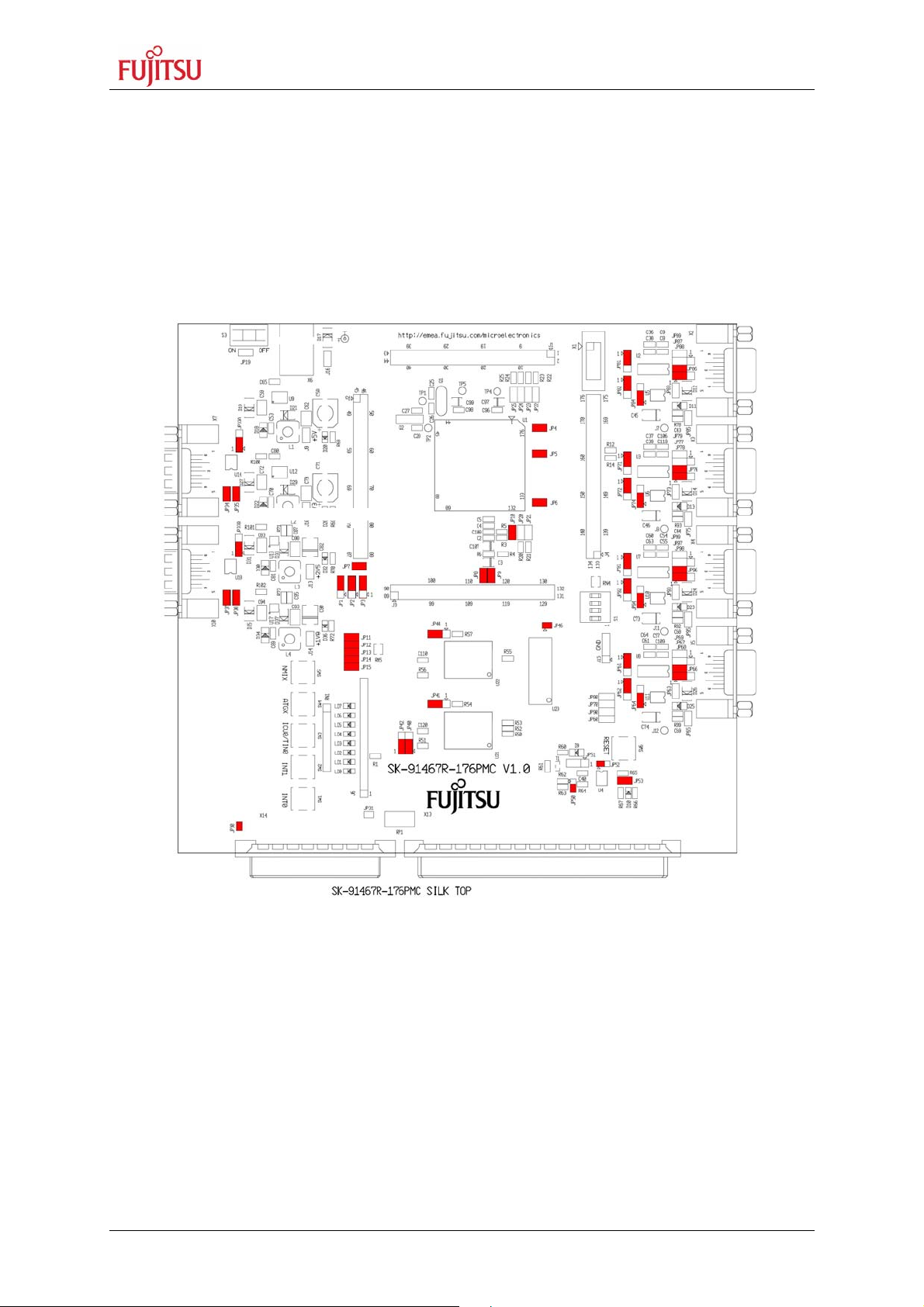
2.3 Jumper Location
The following picture shows the silk plot of the starter-kit with marked default jumper
settings.
The following picture shows the silk plot of the starterkit with marked default jumper settings.
A B C D E F G H J K L M N
1 1
2 2
3 3
4
4
5 5
6 6
CAN 0 CAN 1
7 7
8
UART/LIN 5 UART/LIN 0 UART/LIN 6
8
9 9
10 10
UART/LIN 4
11 11
12 12
13 13
14 14
15 15
16 16
17 17
18 18
19
19
A B C D E F G H J K L M N
Figure 2-1: Default Jumper Settings
© Fujitsu Microelectronics Europe GmbH - 13 - FMEMCU-UG-910053-16
Page 14
SK-91467R-176PMC User Guide
Chapter 2 Installation
2.4 Software Installation
2.4.1 Installation of Softune Workbench
With the “SK-91467R-176PMC” Fujitsu supplies a full working development environment
called Softune Workbench V6. To develop own software the Softune Workbench
development environment must be installed first. Follow the instructions for successful
installation of the Softune Workbench.
1) Before starting the installation setup ensure that you are logged in with administrator
or poweruser permissions, otherwise the Softune Workbench installation will fail! Be
aware that Softune Workbench does not support multi-user support. Therefore
install- and user login must be the same.
2) Browse on the starter-kit DVD-ROM into the directory ‘Micros DVD 4.0\pdf’ and start
the FRSTA*.exe.
3) Follow the installation instructions.
4) For the default installation path it is recommended to use c:\Softune32.
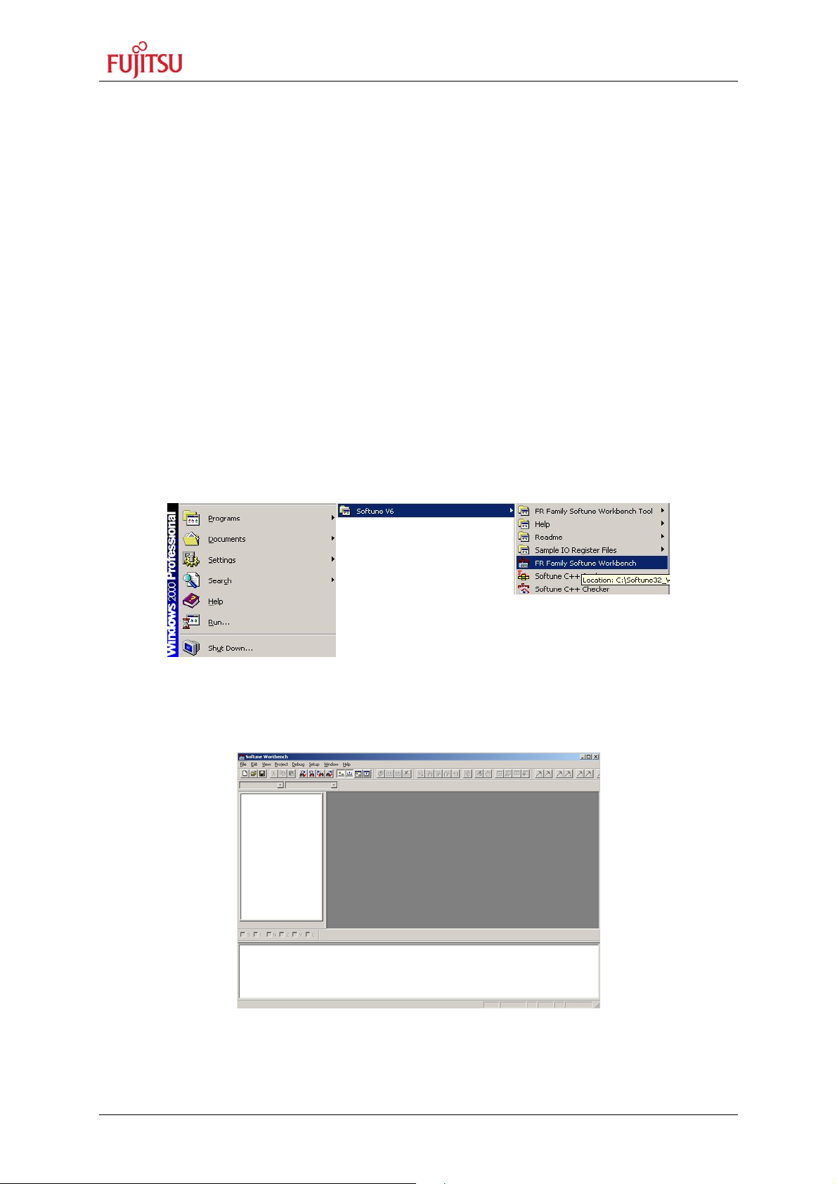
5) After the installation is finished. The FR Family Softune Workbench can be started
via the Windows “Start” menu.
Figure 2-2: Softune Workbench Start Menu Location
6) When Softune Workbench was started the following window will be shown.
Figure 2-3: Softune Workbench V6 IDE
FMEMCU-UG-910053-16 - 14 - © Fujitsu Microelectronics Europe GmbH
Page 15

SK-91467R-176PMC User Guide
1 2 3 4
MD3 MD2 MD1 MD0
Chapter 3 Jumpers and Switches
3 Jumpers and Switches
This chapter describes all jumpers and switches that can be modified on the evaluation
board. The default setting for the MB91F467R Series is shown with a grey shaded area.
3.1 Operating Mode (S1)
3.1.1 Single chip run mode (default)
DIP switch Setting Logical value
S1/1 (MD3)
ON (closed) 1 (high)
OFF (open) 0 (low)
DIP-Switch S1
(default setting)
S1/2 (MD2)
ON (closed) 1 (high)
OFF (open) 0 (low)
S1/3 (MD1)
ON (closed) 1 (high)
OFF (open) 0 (low)
S1/4 (MD0)
ON (closed) 1 (high)
OFF (open) 0 (low)
Table 3-1-1: default MCU Operating Mode
ON
OFF
Figure 3-1-1: MCU mode switch for single chip run
© Fujitsu Microelectronics Europe GmbH - 15 - FMEMCU-UG-910053-16
Page 16

SK-91467R-176PMC User Guide
1 2 3 4
MD3 MD2 MD1 MD0
Chapter 3 Jumpers and Switches
3.1.2 Serial programming mode
To use the serial programming mode set S1 as follows
DIP switch Setting Logical value
S1/1 (MD3) OFF (open) 0 (low)
S1/2 (MD2) ON (closed) 1 (high)
S1/3 (MD1) OFF (open) 0 (low)
S1/4 (MD0) OFF (open) 0 (low)
Table 3-2-2: Serial programming MCU Operating Mode
DIP-Switch S1
(default setting)
ON
OFF
Figure 3-2-2: MCU mode switch for serial programming
3.1.2.1 Communication mode for serial programming
With P15_2 and P15_3 you can set the communication mod for the serial programming.
P15_2 P15_3 Function
0 (low) 0 (low) asynchronous
0 (low) 1 (high) synchronous
1 (high) X forbidden
FMEMCU-UG-910053-16 - 16 - © Fujitsu Microelectronics Europe GmbH
Table 3-3-2-1: Communication mode for serial programming
Page 17

SK-91467R-176PMC User Guide
Chapter 3 Jumpers and Switches
3.2 Power Supply (S3, JP: 8, 9, 11, 12, 66)
The onboard voltage regulators provide stabilized 5V and 3.3V supplies to the MCU and
peripherals. Even though they are thermally protected against overload, care must be taken
when supplying current for additional circuitry.
The LIN Vs line can be connected directly to the input supply of the board by Jumpers. In
this case, the input voltage to the board has to be suitable for the connected bus devices
(mostly around 12V). Since there is a protection diode between Vin and Vs, it is not possible
to power the board over the LIN bus.
S3 Power Switch
JP1 Selects the MCU IO Block 1 and peripherals VCC_1 voltage (3.3V or 5V)
JP2 Selects the MCU IO Block 2 and peripherals VCC_2 voltage (3.3V or 5V)
JP3 Selects the MCU IO Block 3 and peripherals VCC_3 voltage (3.3V or 5V)
JP4 Connects the MCU IO Block 1 Supply (MCUVCC5_1) to VCC_1. Can be used for
current measurement.
JP5 Connects the MCU IO Block 2 Supply (MCUVCC5_2) to VCC_2. Can be used for
current measurement.
JP6 Connects the MCU IO Block 3 Supply (MCUVCC5_3) to VCC_3. Can be used for
current measurement.
JP7 Supplies the MCU External Bus MCUVCC3 with VCC3V3 (3.3V). Can be used for
current measurement.
JP19 Power jumper; overrides the power switch S3.
JP69, 79, 89, 99 Connects Vs (Pin 1 of D-Sub Connector) to VBAT.
Switch Setting Description
S3
ON (1-2) Power ON
OFF (2-3) Power OFF
Table 3-4: Power Switch
Jumper Setting Description
JP1
(VCC_1 3.3V/5V)
1 - 2 MCU IO Block 1/ Peripherals @ 3.3V
2 - 3 MCU IO Block 1/ Peripherals @ 5V
JP2
(VCC_2 3.3V/5V)
JP3
(VCC_3 3.3V/5V)
JP4
(VCC5_1)
1 - 2 MCU IO Block 2/ Peripherals @ 3.3V
2 - 3 MCU IO Block 2/ Peripherals @ 5V
1 - 2 MCU IO Block 3/ Peripherals @ 3.3V
2 - 3 MCU IO Block 3/ Peripherals @ 5V
Closed Power supply VCC_1 connected to MCUVCC5_1
Open Power supply VCC_1 not connected to
MCUVCC5_1
© Fujitsu Microelectronics Europe GmbH - 17 - FMEMCU-UG-910053-16
Page 18

SK-91467R-176PMC User Guide
+5V
+3.3V
+2.5V
+1.8V
GND
Chapter 3 Jumpers and Switches
JP5
Closed Power supply VCC_2 connected to MCUVCC5_2
(VCC5_2)
Open Power supply VCC_2 not connected to
MCUVCC5_2
JP6
(VCC5_3)
JP7
(VCC3)
Closed Power supply VCC_3 connected to MCUVCC5_3
Open Power supply VCC_3 not connected to
MCUVCC5_3
Closed Power supply VCC3V3 connected to MCUVCC3
Open Power supply VCC3V3 not connected to
MCUVCC3
Closed Board is always on JP19
(Power)
Open S3 switches the Board on and off
Closed Vs (Pin1) of LIN connector is powered by the board JP69, 79, 89, 99
(VBAT)
Open No voltage supply to Vs of LIN
Table 3-5: Power Supply Configuration
By default, all Board supplies are set to 5V.
Figure 3-3: Voltage Test Pins
FMEMCU-UG-910053-16 - 18 - © Fujitsu Microelectronics Europe GmbH
Page 19

SK-91467R-176PMC User Guide
Chapter 3 Jumpers and Switches
Regulator Test Pin Voltage
U9 J9 5.0 V
U12 J10 3.3 V
U13 J13 2.5 V
U17 J14 1.8 V
- J15 GND
Table 3-6: Voltage Test Pins
© Fujitsu Microelectronics Europe GmbH - 19 - FMEMCU-UG-910053-16
Page 20

SK-91467R-176PMC User Guide
Chapter 3 Jumpers and Switches
3.3 Analog Power Supply Voltage (JP: 9, 8, 10)
The power supply as well as the positive reference voltage for the A/D-converter can be
provided internally or externally.
JP3, JP7 connects analog power supply voltages (AVcc and AVss)
JP5 connects the analog reference voltage AVRH to AVcc
Jumper Setting Description
Closed AVcc is connected to Vcc
JP9 (AVcc)
Open AVcc is disconnected from Vcc
Closed AVRH is connected to AVcc
JP10 (AVRH)
Open AVRH defined by resistor network
*1
Closed AVss is connected to GND
JP8 (AVss)
Open AVss is disconnected from GND
*1
By default the resistor network (R4, R6) is not mounted on the board
Table 3-7: ADC Supply
Default: JP9, JP10 and JP8 are closed
By default, the A/D-converter supply and reference voltage is connected to VCC3V3 (3.3V)
Note:
If JP8 and JP9 are open, the user has to supply an adequate analog voltage supply (AVcc
and AVss) to the A/D-converter.
If JP10 is open, the resistors R4 and R6 define AVRH.
By default the resistor network (R4, R6) is not mounted on the board.
FMEMCU-UG-910053-16 - 20 - © Fujitsu Microelectronics Europe GmbH
Page 21

SK-91467R-176PMC User Guide
Chapter 3 Jumpers and Switches
3.4 LIN / UART Connectors (X2 – X5)
There are four identical circuit blocks for LIN or RS232 connections. Each of the four D-Sub
connectors can be configured as LIN or RS232 interface. DTS or RTS can be selected as
reset source, and RTS and CTS can be connected by a jumper, since some terminals and
Flash programming tools need this connection. Pin 1 (PIN Vs) of X2-X5 can be connected to
the voltage input (VBat) of the board by jumpers in order to supply the LIN bus. When using
this feature, pay attention to the input voltage of the board, since there is only a protection
diode between Vin and Vs.
LIN-UART 4:
Jumper Setting Description
JP91
(RXD)
JP92
(TXD)
(LIN enable)
(LIN master)
(RS232/LIN)
(DTR/RTS)
(RTS-CTS)
1-2 SIN4 is connected to RS232 transceiver
2-3 SIN4 is connected to LIN transceiver
1-2 SOT4 is connected to RS232 transceiver
2-3 SOT4 is connected to LIN transceiver
Closed LIN transceiver for X4 is enabled JP93
Open LIN transceiver for X4 is disabled
Closed LIN-UART 4 is LIN Master JP95
Open LIN-UART 4 is LIN Slave
1-2 X4 Pin2 is connected to RS232 transceiver (T1out) JP96
2-3 X4 Pin2 is connected to LIN transceiver (BUS)
1-2 DTR signal (Pin 6 of X4) is used as reset source JP97
2-3 RTS signal (Pin 7 of X4) is used as reset source
Closed RTS and CTS of X4 are connected JP98
Open RTS and CTS of X4 are not connected
Closed Pin 1 (LIN Vs) of X4 is connected to Vin JP99
(LIN VBbat)
Open Pin 1 (LIN Vs) of X4 is not connected to Vin
Table 3-8: UART 4 Settings
By default, UART4 is connected to X4 and configured as RS232 interface.
© Fujitsu Microelectronics Europe GmbH - 21 - FMEMCU-UG-910053-16
Page 22

SK-91467R-176PMC User Guide
Chapter 3 Jumpers and Switches
LIN-UART 5:
Jumper Setting Description
JP71
(RXD)
JP72
(TXD)
(LIN enable)
(LIN master)
(RS232/LIN)
(DTR/RTS)
(RTS-CTS)
1-2 SIN5 is connected to RS232 transceiver
2-3 SIN5 is connected to LIN transceiver
1-2 SOT5 is connected to RS232 transceiver
2-3 SOT5 is connected to LIN transceiver
Closed LIN transceiver for X3 is enabled JP73
Open LIN transceiver for X3 is disabled
Closed LIN-UART 5 is LIN Master JP75
Open LIN-UART 5 is LIN Slave
1-2 X3 Pin2 is connected to RS232 transceiver (T1out) JP76
2-3 X3 Pin2 is connected to LIN transceiver (BUS)
1-2 DTR signal (Pin 6 of X4) is used as reset source JP77
2-3 RTS signal (Pin 7 of X4) is used as reset source
Closed RTS and CTS of X3 are connected JP78
Open RTS and CTS of X3 are not connected
Closed Pin 1 (LIN Vs) of X3 is connected to Vin JP79
(LIN VBbat)
Open Pin 1 (LIN Vs) of X3 is not connected to Vin
Table 3-9: UART 5 Settings
By default, UART5 is connected to X3 and configured as RS232 interface.
FMEMCU-UG-910053-16 - 22 - © Fujitsu Microelectronics Europe GmbH
Page 23

SK-91467R-176PMC User Guide
Chapter 3 Jumpers and Switches
LIN-UART 6:
Jumper Setting Description
JP61
(RXD)
JP62
(TXD)
(LIN enable)
(LIN master)
(RS232/LIN)
(DTR/RTS)
(RTS-CTS)
1-2 SIN6 is connected to RS232 transceiver
2-3 SIN6 is connected to LIN transceiver
1-2 SOT6 is connected to RS232 transceiver
2-3 SOT6 is connected to LIN transceiver
Closed LIN transceiver for X5 is enabled JP63
Open LIN transceiver for X5 is disabled
Closed LIN-UART 6 is LIN Master JP65
Open LIN-UART 6 is LIN Slave
1-2 X5 Pin2 is connected to RS232 transceiver (T1out) JP66
2-3 X5 Pin2 is connected to LIN transceiver (BUS)
1-2 DTR signal (Pin 6 of X5) is used as reset source JP67
2-3 RTS signal (Pin 7 of X5) is used as reset source
Closed RTS and CTS of X5 are connected JP68
Open RTS and CTS of X5 are not connected
Closed Pin 1 (LIN Vs) of X5 is connected to Vin JP69
(LIN VBbat)
Open Pin 1 (LIN Vs) of X5 is not connected to Vin
Table 3-10: UART 6 Settings
By default, UART6 is connected to X5 and configured as RS232 interface.
© Fujitsu Microelectronics Europe GmbH - 23 - FMEMCU-UG-910053-16
Page 24

SK-91467R-176PMC User Guide
Chapter 3 Jumpers and Switches
LIN-UART 0:
Jumper Setting Description
JP81
(RXD)
JP82
(TXD)
(LIN enable)
(LIN master)
(RS232/LIN)
(DTR/RTS)
(RTS-CTS)
1-2 SIN0 is connected to RS232 transceiver
2-3 SIN0 is connected to LIN transceiver
1-2 SOT0 is connected to RS232 transceiver
2-3 SOT0 is connected to LIN transceiver
Closed LIN transceiver for X2 is enabled JP83
Open LIN transceiver for X2 is disabled
Closed LIN-UART 0 is LIN Master JP85
Open LIN-UART 0 is LIN Slave
1-2 X2 Pin2 is connected to RS232 transceiver (T1out) JP86
2-3 X2 Pin2 is connected to LIN transceiver (BUS)
1-2 DTR signal (Pin 6 of X2) is used as reset source JP87
2-3 RTS signal (Pin 7 of X2) is used as reset source
Closed RTS and CTS of X2 are connected JP88
Open RTS and CTS of X2 are not connected
Closed Pin 1 (LIN Vs) of X2 is connected to Vin JP89
(LIN VBbat)
Open Pin 1 (LIN Vs) of X2 is not connected to Vin
Table 3-11: UART 0 Settings
By default, UART0 is connected to X2 and configured as RS232 interface.
For Flash programming, UART0 has to be used (RS232).
FMEMCU-UG-910053-16 - 24 - © Fujitsu Microelectronics Europe GmbH
Page 25

SK-91467R-176PMC User Guide
Chapter 3 Jumpers and Switches
3.5 CAN interfaces (X7+X10)
Two high-speed CAN-transceivers can be connected to the microcontroller’s CAN interfaces
(CAN0-CAN1.
Jumper Setting Description
JP34CAN0 RX) Closed RX0 of MCU is connected to CAN0 (X7)
JP35CAN0 TX) Closed TX0 of MCU is connected to CAN0 (X7)
JP37CAN1 RX) Closed RX1 of MCU is connected to CAN1 (X10)
JP38CAN1 TX) Closed TX1 of MCU is connected to CAN1 (X10)
Table 3-12: CAN Settings
By default, all two CAN Interfaces are connected to X7 and X10.
3.6 Reset Generation (JP: 50, 51, 52, 53, 60, 70, 80, 90)
In addition to the internal Power-On reset, the microcontroller can be reset by an external
reset circuit (Voltage Monitor) and also by a RS232 interface. Refer to the chapter ‘LIN /
UART Connectors (X2 – X5)’ for DTR / RTS selection.
JP60, 70, 80, 90: Selects X4, X3, X5 or X2 as reset source
JP51 The signal on the DTR/RTS line can be negated with this jumper.
Remove the jumper in order to disable the RS232 reset circuit.
JP52 This solder jumper selects between normal (immediate) reset and delayed reset.
In delayed reset mode, the reset button has to be held down for 2 sec before a
reset is generated to avoid accidental resets.
JP53 Open this jumper if no external Reset shall be generated.
In this case only the internal reset is active (e.g.: power-on)
JP50 This solder jumper selects the third voltage monitored by the reset IC (1.8V and
2.5V are always monitored).
© Fujitsu Microelectronics Europe GmbH - 25 - FMEMCU-UG-910053-16
Page 26

SK-91467R-176PMC User Guide
Chapter 3 Jumpers and Switches
Jumper Setting Description
JP90
(RST 4)
JP70
(RST 5)
JP60
(RST 6)
JP80
(RST 0)
(DTR sel)
(Direct RST)
JP50
Closed LIN-UART 4 (X2) connected to reset circuit
Open LIN-UART 4 (X2) not connected to reset circuit
Closed LIN-UART 5 (X3) connected to reset circuit
Open LIN-UART 5 (X3) not connected to reset circuit
Closed LIN-UART 6 (X5) connected to reset circuit
Open LIN-UART 6 (X5) not connected to reset circuit
Closed LIN-UART 0 (X4) connected to reset circuit
Open LIN-UART 0 (X4) not connected to reset circuit
1-2 No negation for the DTR/RTS signal JP51
2-3 DTR/RTS signal is negated
1-2 Reset is applied immediately when SW6 is pressed JP52
2-3 Reset is applied when SW6 is pressed >2sec
1-2 VCC1V8 is monitored by reset IC
2-3 VCC2V5 is monitored by reset IC
Closed External reset generation is active JP53
(RST MCU)
Open No external reset generation
Table 3-13: Reset Connection
By default, the external reset is enabled and set to immediate reset, the reset by UART is
disabled.
Note:
While a reset signal is asserted the red Reset-LED D10 is lit.
During normal operation, this LED should be off!
If JP51(DTR sel) is set, one of the RST jumpers (JP60, 70, 80, 90) and the according
DTR/RTS jumper have to be set, too.
If the reset LED is steadily on, check the power supply input voltage and the settings for the
reset-generation by UART and JP51.
FMEMCU-UG-910053-16 - 26 - © Fujitsu Microelectronics Europe GmbH
Page 27

SK-91467R-176PMC User Guide
Chapter 3 Jumpers and Switches
3.7 User Buttons SW1, SW2, SW3, SW4, SW5 (JP: 11, 12, 13, 14, 15)
JP11, 12, 13, 14, 15 Five user push buttons (SW1-SW5) can be connected to the
microcontroller.
Jumper Setting Description
JP11 (SW1)
Closed Pin 119 (INT0) of the MCU is connected to “SW1”
Open No connection to the microcontroller
Closed Pin 120 (INT1) of the MCU is connected to “SW2”
JP12 (SW2)
Open No connection to the microcontroller
Closed Pin 168 (ICU0/TIN0) of the MCU is connected to “SW3”
JP13 (SW3)
Open No connection to the microcontroller
Closed Pin 92 (ATGX) of the MCU is connected to “SW4”
JP14 (SW4)
Open No connection to the microcontroller
Closed Pin 28 (NMIX) of the MCU is connected to “SW5”
JP15 (SW5)
Open No connection to the microcontroller
Table 3-14: User Push Buttons
Default: JP11, 12, 13, 14, 15 closed
By default, all push-buttons are connected to the microcontroller.
© Fujitsu Microelectronics Europe GmbH - 27 - FMEMCU-UG-910053-16
Page 28

SK-91467R-176PMC User Guide
Chapter 3 Jumpers and Switches
3.8 Memories (SRAM/Flash)
Flash ROM can be accessed 8bit or 16bit wide. This is selectable by jumpers JP40, JP42
SRAM and SDRAM can be accessed 16 bit wide.
The memories can be disabled by jumpers JP41(Flash) and JP44(SRAM) to use the
ChipSelectLines CSX0 and CSX1 for the graphic interface.
Jumper Setting Description
JP40
(Flash 8/16bit)
JP42:
(Flash A0/D16)
JP41:
(Flash Enable)
JP44:
(SRAM Enable)
JP46:
(MCLKO=MCKLI)
1-2 Flash is used in 16bit mode
2-3 Flash is used in 8bit mode
1-2 Flash is used in 16bit mode
2-3 Flash is used in 8bit mode
1-2 Flash is enabled
2-3 Flash is disabled
1-2 SRAM is enabled
2-3 SRAM is disabled
closed MCLKO connected to MCKLI
open MCLKO not connected to MCKLI
Table 3-15: Flash/SRAM setting
FMEMCU-UG-910053-16 - 28 - © Fujitsu Microelectronics Europe GmbH
Page 29

SK-91467R-176PMC User Guide
+
Chapter 4 Connectors
4 Connectors
4.1 Power connector (X6)
The following figure shows the power connection jack X6. This connector is used to connect
an external unregulated DC power supply voltage (9V-12V DC) to the evaluation board.
Connector X6:
Shield is connected to positive voltage supply
The switching mode voltage regulators allow a wide input range. This might be of interest
when using Vin to power the LIN bus Vs line.
Center is connected to ground (GND)
Figure 4-1: Power Connector
4.2 Edge connector (J1, J2, J3, J4)
All pins (except oscillator Pins) of the microcontroller are directly connected to J1 – J4 as
follows:
Connector MCU Pins
J1 1 – 44
J2 45 – 88
J3 89 – 132
J4 133 – 176
The odd pin numbers are located on the one side and the even pin numbers are located on
the other side of the connector.
© Fujitsu Microelectronics Europe GmbH - 29 - FMEMCU-UG-910053-16
Page 30

SK-91467R-176PMC User Guide
Chapter 4 Connectors
4.3 LIN-UART connectors (X2-X5)
Four 9-pin D-Sub female connectors are used for the serial interfaces. Note that X2 to X5
are shared between the RS232- and LIN transceivers and must be configured to the desired
functionality (refer to chapter 3.4 for details).
Figure 4-2: UART Connector
Pin Number Pin Signal Description
1 +VBat Power from / to LIN bus
2
3 RXD RS-232 receive input
4 DTR Connected to DSR (pin 6)
5 GND Ground normally used for RS232 connection
6 DSR Connected to DTR (pin 4)
7 RTS Can be connected with CTS by jumper
8 CTS Can be connected with RTS by jumper
9 LGND Ground normally used for LIN connection
Shield GND Ground
TXD RS-232 transmit output
LIN Bi-directional LIN-interface bus
Table 4-1: UART Connector Signals
4.4 CAN Connector (X7+X10)
Six 9-pin D-Sub male connectors are used for the CAN interfaces CAN0-CAN1. All CAN
interfaces can be used simultaneously.
Figure 4-3: CAN Connector
Pin Number Pin Signal Description
1 NC Not used
2 CANL LOW-level CAN voltage input/output
3 GND Ground
4 NC Not used
5 NC Not used
6 NC Not used
7 CANH HIGH-level CAN voltage input/output
8 NC Not used
9 NC Not used
Shield GND Ground
Table 4-2: CAN Connector Signals
FMEMCU-UG-910053-16 - 30 - © Fujitsu Microelectronics Europe GmbH
Page 31

SK-91467R-176PMC User Guide
Chapter 4 Connectors
4.5 USER-LEDs
Eight LEDs are supplied for user applications. In order to disconnect the LEDs from the
related microcontroller port (Port 28), the resistor network RN1 can be removed.
The following control signals are provided:
Figure 4-4: User LEDs
8 7 6 5 4 3 2 1
LED LD7 LD6 LD5 LD4 LD3 LD2 LD1 LD0
Port 28_7 28_6 28_5 28_4 28_3 28_2 28_1 28_0
Table 4-3: User LEDs
© Fujitsu Microelectronics Europe GmbH - 31 - FMEMCU-UG-910053-16
Page 32

SK-91467R-176PMC User Guide
Chapter 4 Connectors
In-Circuit-Programming Connector (X1)
There is a flash-programming socket on the starter-kit which makes it possible to program
the flash MCU with a special programming adapter. The reset signal is also available at this
connector. Be advised to set the right MCU mode (refer to chapter 3.1 for details).
Figure 4-5: In-circuit programming connector
Pin Number Pin Signal Description
1 P15_3 Select communication mode
2 P13_2 Select communication mode
3 NC Not used
4 MD2 Mode Pin2
5 INITX MCU reset signal
6 SIN0 UART0 receive data
7 SOT0 UART0 transmit data
8 SCK0 UART0 clock
9 NC Not used
10 GND Ground
Table 4-4: In-circuit programming connector
FMEMCU-UG-910053-16 - 32 - © Fujitsu Microelectronics Europe GmbH
Page 33

SK-91467R-176PMC User Guide
A1 2.5 V
- B1 2.5 V
- C1 2.5 V
-
Chapter 4 Connectors
4.6 External Bus Connectors (X13, X14)
4.6.1 VG96ABC DIN 41612 (X13)
Pin Name MCU Pin Name MCU Pin Name MCU
A2 3.3 V - B2 3.3 V - C2 3.3 V A3 5.0 V - B3 5.0 V - C3 5.0 V A4 GND VSS B4 GND VSS C4 GND VSS
A5 NC - B5 NC - C5 NC A6 NC - B6 NC - C6 NC A7 NC - B7 NC - C7 NC A8 NC - B8 NC - C8 NC -
A9 NC - B9 NC - C9 NC A10 NC - B10 D16 P01_0 C10 D17 P01_1
A11 D18 P01_2 B11 D19 P01_3 C11 D20 P01_4
A12 D21 P01_5 B12 D22 P01_6 C12 D23 P01_7
A13 D24 P00_0 B13 D25 P00_1 C13 D26 P00_2
A14 D27 P00_3 B14 D28 P00_4 C14 D29 P00_5
A15 D30 P00_6 B15 D31 P00_7 C15 GND VSS
A16 GND VSS B16 GND VSS C16 GND VSS
A17 A0 P07_0 B17 A1 P07_1 C17 A2 P07_2
A18 A3 P07_3 B18 A4 P07_4 C18 A5 P07_5
A19 A6 P07_6 B19 A7 P07_7 C19 A8 P06_0
A20 A9 P06_1 B20 A10 P06_2 C20 A11 P06_3
A21 A12 P06_4 B21 A13 P06_5 C21 A14 P06_6
A22 A15 P06_7 B22 A16 P05_0 C22 A17 P05_1
A23 A18 P05_2 B23 A19 P05_3 C23 A20 P05_4
A24 A21 P05_5 B24 NC - C24 NC A25 NC - B25 NC - C25 NC A26 NC - B26 NC - C26 NC A27 NC - B27 NC - C27 GND VSS
A28 P16_0 P16_0 B28 P29_1 P29_1 C28 P29_2 P29_2
A29 P16_3 P16_3 B29 P29_4 P29_4 C29 P29_5 P29_5
A30 P16_6 P16_6 B30 P29_7 P29_7 C30 GND VSS
A31 2.5V - B31 2.5V - C31 NC A32 GND VSS B32 GND VSS C32 GND VSS
Table 4-5: VG96 (X13) Signals
Note:
The pin numbers of the VG connectors refer to the male connectors, that plugs
into the Starterkit.
© Fujitsu Microelectronics Europe GmbH - 33 - FMEMCU-UG-910053-16
Page 34

SK-91467R-176PMC User Guide
Pin Name
MCU
-P. Pin Name
MCU
-P. Pin Name
MCU
-P. A1
CSX0
P09_0
B1 GND VSS C1
CSX1
P09_1
Chapter 4 Connectors
4.6.2 VG48ABC DIN 41612 (X14)
A2 CSX2 P09_2 B2 1.8V JP30 - C2 CSX3 P09_3
A3 NC - B3 GND VSS C3 NC A4 NC - B4 1.8V JP30 - C4 RDY P08_7
A5 BGRNTX P08_5 B5 GND VSS C5 BRQ P08_6
A6 RDX P08_4 B6 NC - C6 WRX0 P08_0
A7 WRX1 P08_1 B7 NC - C7 NC A8 NC - B8 NC - C8 ASX P10_1
A9 NC - B9 NC - C9 MCLK0 P10_4
A10 DREQ0 P13_0 B10 NC - C10 DACKX0 P13_1
A11 DEOP0 P13_2 B11 NC - C11 NC A12 INT2 P24_2 B12 NC - C12 SDA0 P22_4
A13 INT3 P24_3 B13 NC - C13 SCL0 P22_5
A14 SIN5 P19_4 B14 Vin JP31 - C14 SOT5 P19_5
A15 GND VSS B15 Vin JP31 - C15 SCK5 P19_6
A16 INITX INITX B16 Vin JP31 - C16 GND VSS
Note:
The pin numbers of the VG connectors refer to the male connectors, that plugs
into the Starterkit.
Table 4-6: VG48 (X14) Signals
4.6.3 Distance between VG-Connectors
To connect own applications to the Starterkit the following figure shows the distance
between the VG DIN 41612 connectors.
8,89mm/
350mil
Figure 4-6: Layout of DIN VG Connectors:
FMEMCU-UG-910053-16 - 34 - © Fujitsu Microelectronics Europe GmbH
Page 35

SK-91467R-176PMC User Guide
Chapter 5 Programming the internal Flash
5 Programming the internal Flash
All Flash devices have an internal bootloader for asynchronous as well as synchronous
Flash-programming:
< Asynchronous serial Flash-programming via X2 (UART 0)
< Synchronous serial Flash-programming via X1
5.1 Asynchronous Mode
This chapter describes the serial asynchronous programming of the internal flash with the
help of the ‘FME-FR Programmer’ in automatic mode. For other programming possibilities,
please see the application note mcu-an-300012-e-mb91460_flash_programming.pdf.
1) For serial asynchronous programming SUB-D9 connector X2 which is connected to
UART0 has to be used. The following jumper setting is needed.
Jumper Setting Description
JP81
1-2 SIN0 is connected to RS232 transceiver
(RXD)
JP82
1-2 SOT0 is connected to RS232 transceiver
(TXD)
JP86
1-2 X2 Pin4/6 is connected to RS232 transceiver (T1out)
(RS232/LIN)
Table 5-1: Jumper Settings for Programming
© Fujitsu Microelectronics Europe GmbH - 35 - FMEMCU-UG-910053-16
Page 36

SK-91467R-176PMC User Guide
Chapter 5 Programming the internal Flash
2) If the programming software should generate a reset signal on RTS or DTR line, refer
to the following jumper list.
Jumper Setting Description
Closed RTS and CTS of X2 are connected JP88
(RTS-CTS)
Open RTS and CTS of X2 are not connected
1-2 DTR signal (Pin 6 of X2) is used as reset source JP87
(DTR/RTS)
JP80
(RST 0)
JP51
(DTR / DTRx)
JP53
(RST MCU)
2-3 RTS signal (Pin 7 of X2) is used as reset source
Closed LIN-UART 0 (X2) connected to reset circuit
1-2 No negation for the DTR/RTS signal
2-3 DTR/RTS signal is negated
Closed External reset generation is active
Table 5-2: Jumper Settings for reset signal
3) The CPU Mode selection must be set to serial programming mode by setting DIP
switch S1 to (Off, On, Off, Off)
4) Start the ‘FME-FR Programmer’ and connect the UART0 to your serial PC
communication port. A straight cable connection has to be used.
5) Choose the microcontroller device (“MB91F467R”) as device type and browse to the
mhx-file you want to program to the embedded flash memory of the microcontroller.
Press the button “Automatic Mode” to start programming.
6) Immediately reset the microcontroller.
FMEMCU-UG-910053-16 - 36 - © Fujitsu Microelectronics Europe GmbH
Page 37

SK-91467R-176PMC User Guide
RESET MCU
Chapter 5 Programming the internal Flash
Figure 5-1: Settings for Automatic Mode
7) If your hardware supports MCU reset via DTR or RTS signal lines of the PC’s COM
port, go to sheet “Signals” and select the appropriate reset signal line. The
programmer now resets the microcontroller automatically before starting the
programming sequence and you do not have to reset the MCU manually immediately
after pressing the button “Automatic Mode”.
Figure 5-2: Reset Signal Settings
© Fujitsu Microelectronics Europe GmbH - 37 - FMEMCU-UG-910053-16
Page 38

SK-91467R-176PMC User Guide
SOT0 7
Chapter 5 Programming the internal Flash
The software now automatically writes a flash loader to the microcontroller, does a blank
check and erases the flash memory if necessary. After that the user application is
programmed to the embedded flash memory.
During this sequence the actual progress status can be seen by checked off steps on the
“Automatic” sheet and the messages below in the message box.
If the programming sequence is ended successfully, you will receive the output shown in
figure 7.
The Addresses 0x14:8000 to 0x14:800F cannot be written in automatic mode. This is a built
in security feature to prevent unintended writing to the Flash Security Vectors and Boot
Security Vectors. Otherwise it would be possible to secure flash content and to lock the
microcontroller for serial programming/reading/erasing by not being able to enter the internal
loader anymore. If you want to use these features explicitly, you have to program these
dedicated addresses by using the “Prog Word” Function of the step-by-step mode.
Figure 5-3: Successful Programming in Automatic Mode
5.2 Synchronous Mode
In order to program the Flash-ROM synchronously special third-party soft- and hardware has
to be used, e.g. GALEP-4 from www.conitec.de
A dedicated Flash programming socket (X1) is provided on the evaluation-board for direct
connection to this programmer.
X1: Flash programming socket
Figure 5-4: Flash Programming Socket
FMEMCU-UG-910053-16 - 38 - © Fujitsu Microelectronics Europe GmbH
. This tool is not available for free.
n/c 1
n/c 3
RST 5
VCC 9
2 n/c
4 n/c
6 SIN0
8 SCK0
10 GND
Page 39

SK-91467R-176PMC User Guide
Chapter 6 Programming SWB Monitor Debugger
6 Programming SWB Monitor Debugger
Do program Softune Workbench Monitor Debbuger to external Flash, get the latest Monitor
Debugger Project (91467r_mondeb_uart4_extbus_flash_sram) from our website.
The CPU Mode selection must be set to serial programming mode by setting DIP switch S1
to (Off, On, Off, Off)
Choose MB91F467R as device type and select tab ‘External Flash’. Mark the checkboxes
‘Enable ext. Flash’, ‘CS0’ and ‘Chip erase’ (only needed if ext. Flash is not blank).
Figure 6-1: CS settings for SWB Monitor Debugger programming
Please check following entries for register settings:
ASR0: 0100 ACR0: 8820 AWR0: 3378
Select tab ‘Automatic’, browse to SWB monitor debugger file (e.g.
your_path\MONDEB\FLASH\ABS\91467r_mondeb_uart4_extbus_flash_sram.mhx), press
button “Automatic Mode” and reset microcontroller.
Programmer will execute single steps described in chapter 6.1. After successful
programming, set mode pins to external vector fetch mode (S1: off, off, off, on) and reset
microcontroller. In case of successful startup of the monitor debugger and access to external
SRAM the LED LD1, LD3 and LD7 are lit. Now connection to Softune Workbench can be
started.
© Fujitsu Microelectronics Europe GmbH - 39 - FMEMCU-UG-910053-16
Page 40

SK-91467R-176PMC User Guide
Chapter 7 Appendix
7 Appendix
7.1 Related Products
< SK-91467R-176PMC Evaluation board for the MB91F467R MCU
in FPT-176P-M07 package
< MB2198-01 Emulator debugger main unit
< MB2198-10 DSU cable
< MB2198-300 Emulation Pod
< NQPACK176SD Socket for package FPT-176P-M07
(Tokyo Eletech Corp
http://www.tetc.co.jp/e_products/e_nq_techdrawings.htm
< EMA-MB91F467R-NLS-176M07 Emulator probe cable for MB91F467R MCU
< MB91460 Series
< MB91V460 MB91460 Series Evaluation chip
< MB91467R-176PMC Flash MCU
)
FMEMCU-UG-910053-16 - 40 - © Fujitsu Microelectronics Europe GmbH
Page 41

SK-91467R-176PMC User Guide
Chapter 7 Appendix
7.2 Information in the WWW
Information about FUJITSU MICROELECTRONICS Products
can be found on the following Internet pages:
http://emea.fujitsu.com/microelectronics
Microcontrollers (8-, 16- and 32bit), Graphics Controllers
Datasheets and Hardware Manuals, Support Tools (Hard- and Software)
http://www.fme.gsdc.de/gsdc.htm
© Fujitsu Microelectronics Europe GmbH - 41 - FMEMCU-UG-910053-16
Page 42

SK-91467R-176PMC User Guide
Chapter 7 Appendix
7.3 Tables
Table 1-1: Emulation System...................................................................................................9
Table 2-1: Jumper Settings....................................................................................................12
Table 3-1-1: default MCU Operating Mode............................................................................ 15
Table 3-2-2: Serial programming MCU Operating Mode....................................................... 16
Table 3-3-2-1: Communication mode for serial programming ............................................... 16
Table 3-4: Power Switch........................................................................................................ 17
Table 3-5: Power Supply Configuration................................................................................. 18
Table 3-6: Voltage Test Pins.................................................................................................. 19
Table 3-7: ADC Supply.......................................................................................................... 20
Table 3-8: UART 4 Settings................................................................................................... 21
Table 3-9: UART 5 Settings................................................................................................... 22
Table 3-10: UART 6 Settings................................................................................................. 23
Table 3-11: UART 0 Settings................................................................................................. 24
Table 3-12: CAN Settings...................................................................................................... 25
Table 3-13: Reset Connection............................................................................................... 26
Table 3-14: User Push Buttons..............................................................................................27
Table 3-15: Flash/SRAM setting............................................................................................ 28
Table 4-1: UART Connector Signals...................................................................................... 30
Table 4-2: CAN Connector Signals........................................................................................ 30
Table 4-3: User LEDs ............................................................................................................31
Table 4-4: In-circuit programming connector......................................................................... 32
Table 4-5: VG96 (X13) Signals.............................................................................................. 33
Table 4-6: VG48 (X14) Signals.............................................................................................. 34
Table 5-1: Jumper Settings for Programming........................................................................35
Table 5-2: Jumper Settings for reset signal........................................................................... 36
FMEMCU-UG-910053-16 - 42 - © Fujitsu Microelectronics Europe GmbH
Page 43

SK-91467R-176PMC User Guide
Chapter 7 Appendix
7.4 Figures
Figure 2-1: Default Jumper Settings...................................................................................... 13
Figure 2-2: Softune Workbench Start Menu Location............................................................ 14
Figure 2-3: Softune Workbench V6 IDE................................................................................. 14
Figure 3-1-1: MCU mode switch for single chip run............................................................... 15
Figure 3-2-2: MCU mode switch for serial programming ....................................................... 16
Figure 3-3: Voltage Test Pins ................................................................................................ 18
Figure 4-1: Power Connector.................................................................................................29
Figure 4-2: UART Connector................................................................................................. 30
Figure 4-3: CAN Connector ................................................................................................... 30
Figure 4-4: User LEDs...........................................................................................................31
Figure 4-5: In-circuit programming connector........................................................................32
Figure 4-6: Layout of DIN VG Connectors:............................................................................ 34
Figure 5-1: Settings for Automatic Mode ............................................................................... 37
Figure 5-2: Reset Signal Settings.......................................................................................... 37
Figure 5-3: Successful Programming in Automatic Mode...................................................... 38
Figure 5-4: Flash Programming Socket................................................................................. 38
Figure 6-1: CS settings for SWB Monitor Debugger programming........................................ 39
© Fujitsu Microelectronics Europe GmbH - 43 - FMEMCU-UG-910053-16
Page 44

SK-91467R-176PMC User Guide
Chapter 7 Appendix
7.5 Abbreviations
ADC Analogue Digital Converter
CAN Controller Area Network
CS Chip Select
FME Fujitsu Microelectronics Europe GmbH
LIN Local Interconnect Network
MCU Microcontroller Unit
PCB Printed Circuit Board
SRAM Static Random Access Memory
SDRAM Synchronous Dynamic Random Access Memory
UART Universal Asynchronous Receiver Transmitter
FMEMCU-UG-910053-16 - 44 - © Fujitsu Microelectronics Europe GmbH
Page 45

SK-91467R-176PMC User Guide
Chapter 7 Appendix
Recycling
Gültig für EU-Länder:
Gemäß der Europäischen WEEE-Richtlinie und deren Umsetzung in landesspezifische
Gesetze nehmen wir dieses Gerät wieder zurück.
Zur Entsorgung schicken Sie das Gerät bitte an die folgende Adresse:
Fujitsu Microelectronics Europe GmbH
Warehouse/Disposal
Monzastraße 4a
63225 Langen
Valid for European Union Countries:
According to the European WEEE-Directive and its implementation into national laws we
take this device back.
For disposal please send the device to the following address:
Fujitsu Microelectronics Europe GmbH
Warehouse/Disposal
Monzastraße 4a
63225 Langen
© Fujitsu Microelectronics Europe GmbH - 45 - FMEMCU-UG-910053-16
 Loading...