

Page 1

FUJITSU SEMICONDUCTOR
CONTROLLER MANUAL
CM71-xxxxx-1E
FR60
32-BIT MICROCONTROLLER
MB91460 Series
User’s Manual
- PRELIMINARY -
Version 1.00
2006-10-22
Page 2

FUJITSU LIMITED
Page 3

FR60
32-BIT MICROCONTROLLER
MB91460 Series
User’s Manual
Page 4

• The contents of this document are subject to change without notice.
Customers are advised to consult with FUJITSU sales representatives before ordering.
• The information, such as descriptions of function and application circuit examples, in this document are presented solely
for the purpose of reference to show examples of operations and uses of Fujitsu semiconductor device; Fujitsu does not
warrant proper operation of the device with respect to use based on such information. When you develop equipment
incorporating the device based on such information, you must assume any responsibility arising out of such use of the
information. Fujitsu assumes no liability for any damages whatsoever arising out of the use of the information.
• Any information in this document, including descriptions of function and schematic diagrams, shall not be construed as
license of the use or exercise of any intellectual property right, such as patent right or copyright, or any other right of
Fujitsu or any third party or does Fujitsu warrant non-infringement of any third-party' s intellectual property right or other
right by using such information. Fujitsu assumes no liability for any infringement of the intellectual property rights or other
rights of third parties which would result from the use of information contained herein.
• The products described in this document are designed, developed and manufactured as contemplated for general use,
including without limitation, ordinary industrial use, general office use, personal use, and household use, but are not
designed, developed and manufactured as contemplated (1) for use accompanying fatal risks or dangers that, unless
extremely high safety is secured, could have a serious effect to the public, and could lead directly to death, personal injury,
severe physical damage or other loss (i.e., nuclear reaction control in nuclear facility, aircraft flight control, air traffic
control, mass transport control, medical life support system, missile launch control in weapon system), or (2) for use
requiring extremely high reliability (i.e., submersible repeater and artificial satellite).
Please note that Fujitsu will not be liable against you and/or any third party for any claims or damages arising in connection
with above-mentioned uses of the products.
• Any semiconductor devices have an inherent chance of failure. You must protect against injury, damage or loss from such
failures by incorporating safety design measures into your facility and equipment such as redundancy, fire protection, and
prevention of over-current levels and other abnormal operating conditions.
• If any products described in this document represent goods or technologies subject to certain restrictions on export under
the Foreign Exchange and Foreign Trade Law of Japan, the prior authorization by Japanese government will be required
for export of those products from Japan.
©2004 FUJITSU LIMITED Printed in Japan
-i
Page 5

TOC
Chapter 1 Introduction......................................................................................... 1
1. How to Handle the Device..................................................................................................... 1
2. Instruction for Users............................................................................................................... 3
3. Caution: debug-related matters............................................................................................. 6
4. How to Use This Document................................................................................................... 7
Chapter 2 MB91460 Rev.A/Rev.B Overview..................................................... 11
1. Overview.............................................................................................................................. 11
2. Features............................................................................................................................... 11
3. MB91460 Series Product Lineup......................................................................................... 19
4. Block Diagram ..................................................................................................................... 21
Chapter 3 MB91460 Series Basic Information ................................................. 23
1. Memory Map........................................................................................................................ 23
2. I/O Map................................................................................................................................ 24
3. Interrupt Vector Table.......................................................................................................... 73
4. Package............................................................................................................................... 78
5. Pin Assignment Diagram..................................................................................................... 79
6. Pin Definitions...................................................................................................................... 80
7. I/O Circuit Type.................................................................................................................... 94
8. Pin State Table.................................................................................................................... 96
Chapter 4 CPU Architecture ............................................................................ 105
1. Overview............................................................................................................................ 105
2. Features............................................................................................................................. 106
3. CPU................................................................................................................................... 107
4. 32-bit/16-bit Bus Converter................................................................................................ 107
5. Harvard/Princeton Bus Converter...................................................................................... 107
6. Instruction Overview.......................................................................................................... 108
7. Data Structure.................................................................................................................... 109
8. Word Alignment................................................................................................................. 110
9. Addressing......................................................................................................................... 111
Chapter 5 CPU Registers................................................................................. 113
1. General-purpose Registers................................................................................................ 113
2. Dedicated Registers .......................................................................................................... 113
Chapter 6 EIT: Exceptions, Interrupts and Traps.......................................... 121
1. Overview............................................................................................................................ 121
2. Features............................................................................................................................. 121
3. EIT Trigger......................................................................................................................... 121
4. Return from EIT................................................................................................................. 121
5. EIT Interrupt Level............................................................................................................. 122
i
Page 6

6. EIT Vector Table................................................................................................................ 122
7. Multiple EIT Processing..................................................................................................... 123
8. Operation........................................................................................................................... 125
9. Caution .............................................................................................................................. 128
Chapter 7 Branch Instruction.......................................................................... 129
1. Branch Instruction with Delay Slot..................................................................................... 129
2. Operation of Branch Instruction with Delay Slot................................................................ 129
3. Actual Example (with Delay Slot)....................................................................................... 130
4. Restrictions on Branch Instruction with Delay Slot............................................................ 131
5. Branch Instruction without Delay Slot................................................................................ 132
6. Operation of Branch Instruction without Delay Slot........................................................... 132
Chapter 8 Device State Transition .................................................................. 133
1. Overview............................................................................................................................ 133
2. Features............................................................................................................................. 133
3. State Transition Diagram................................................................................................... 134
Chapter 9 Reset ................................................................................................ 139
1. Overview............................................................................................................................ 139
2. Features............................................................................................................................. 139
3. Configuration ..................................................................................................................... 140
4. Registers............................................................................................................................ 141
5. INIT Pin Input (INIT: Settings Initialization Reset) ............................................................ 146
6. Watchdog Reset (INIT: Settings Initialization Reset)......................................................... 148
7. Software Reset (RST: Operation Initialization Reset)....................................................... 149
8. Reset Operation Modes..................................................................................................... 150
9. MCU Operation Mode........................................................................................................ 151
10. Caution .............................................................................................................................. 152
Chapter 10 Standby............................................................................................ 155
1. Overview............................................................................................................................ 155
2. Features............................................................................................................................. 155
3. Configuration ..................................................................................................................... 156
4. Registers............................................................................................................................ 157
5. Operation........................................................................................................................... 159
6. Settings.............................................................................................................................. 161
7. Q&A................................................................................................................................... 161
8. Caution .............................................................................................................................. 165
Chapter 11 Memory Controller.......................................................................... 167
1. Overview............................................................................................................................ 167
2. FLASH Interface................................................................................................................ 167
3. General Purpose RAM....................................................................................................... 167
4. Instruction Cache and Data Buffer..................................................................................... 167
5. Prefetch ............................................................................................................................. 167
6. Fixed Mode and Reset Vectors ......................................................................................... 167
7. Registers............................................................................................................................ 168
ii
Page 7

8. Explanations of Registers.................................................................................................. 169
Chapter 12 Instruction Cache............................................................................ 179
1. General description............................................................................................................ 179
2. Main body structure........................................................................................................... 179
3. Operating mode conditions................................................................................................ 185
4. Cacheable areas in the instruction cache.......................................................................... 186
5. Settings for handling the I-Cache ...................................................................................... 186
Chapter 13 Clock Control .................................................................................. 189
1. Overview............................................................................................................................ 189
2. Features............................................................................................................................. 189
3. Configuration ..................................................................................................................... 190
4. Registers............................................................................................................................ 191
5. Operation........................................................................................................................... 199
6. Settings.............................................................................................................................. 201
7. Q & A................................................................................................................................. 202
8. Caution .............................................................................................................................. 205
Chapter 14 PLL Interface ................................................................................... 207
1. Overview............................................................................................................................ 207
2. Features............................................................................................................................. 207
3. Frequency calculation........................................................................................................ 207
4. Registers............................................................................................................................ 208
5. Recommended Settings .................................................................................................... 212
6. Clock Auto Gear Up/Down................................................................................................. 213
7. Caution .............................................................................................................................. 215
Chapter 15 CAN Clock Prescaler ...................................................................... 217
1. Overview............................................................................................................................ 217
2. Features............................................................................................................................. 217
3. Registers............................................................................................................................ 218
Chapter 16 Clock Supervisor ............................................................................ 221
1. Overview Clock Supervisor................................................................................................ 221
2. Clock Supervisor Register................................................................................................. 222
3. Block Diagram Clock Supervisor....................................................................................... 224
4. Operation Modes............................................................................................................... 225
Chapter 17 Clock Modulator.............................................................................. 239
1. Overview............................................................................................................................ 239
2. Clock Modulator Registers................................................................................................. 240
3. Application Note................................................................................................................. 247
Chapter 18 Timebase Counter........................................................................... 249
1. Overview............................................................................................................................ 249
2. Features............................................................................................................................. 249
iii
Page 8

3. Configuration ..................................................................................................................... 250
4. Registers............................................................................................................................ 251
5. Operation........................................................................................................................... 253
6. Settings.............................................................................................................................. 259
7. Q&A................................................................................................................................... 260
8. Caution .............................................................................................................................. 262
Chapter 19 Timebase Timer............................................................................... 263
1. Overview............................................................................................................................ 263
2. Features............................................................................................................................. 263
3. Configuration ..................................................................................................................... 264
4. Register ............................................................................................................................. 265
5. Operation........................................................................................................................... 267
6. Setting................................................................................................................................ 268
7. Q & A................................................................................................................................. 269
8. Caution .............................................................................................................................. 271
Chapter 20 Software Watchdog Timer.............................................................. 273
1. Overview............................................................................................................................ 273
2. Features............................................................................................................................. 273
3. Configuration ..................................................................................................................... 274
4. Register ............................................................................................................................. 275
5. Operation........................................................................................................................... 278
6. Setting................................................................................................................................ 280
7. Q & A................................................................................................................................. 281
8. Caution .............................................................................................................................. 282
Chapter 21 Hardware Watchdog Timer ............................................................ 283
1. Overview............................................................................................................................ 283
2. Configuration ..................................................................................................................... 284
3. Register ............................................................................................................................. 285
4. Functions........................................................................................................................... 287
5. Caution .............................................................................................................................. 288
Chapter 22 Main Oscillation Stabilisation Timer ............................................. 289
1. Overview............................................................................................................................ 289
2. Features............................................................................................................................. 289
3. Configuration ..................................................................................................................... 290
4. Register ............................................................................................................................ 291
5. Operation........................................................................................................................... 292
6. Setting................................................................................................................................ 294
7. Q & A................................................................................................................................. 295
8. Caution .............................................................................................................................. 297
Chapter 23 Sub Oscillation Stabilisation Timer............................................... 299
1. Overview............................................................................................................................ 299
2. Features............................................................................................................................. 299
3. Configuration ..................................................................................................................... 300
iv
Page 9

4. Register ............................................................................................................................. 301
5. Operation........................................................................................................................... 303
6. Setting................................................................................................................................ 306
7. Q & A................................................................................................................................. 307
8. Caution .............................................................................................................................. 309
Chapter 24 Interrupt Control ............................................................................. 311
1. Overview............................................................................................................................ 311
2. Features............................................................................................................................. 311
3. Configuration ..................................................................................................................... 312
4. Registers............................................................................................................................ 313
5. Operation........................................................................................................................... 318
6. Setting................................................................................................................................ 319
7. Q & A................................................................................................................................. 319
8. Caution .............................................................................................................................. 320
Chapter 25 External Interrupt............................................................................ 321
1. Overview............................................................................................................................ 321
2. Features............................................................................................................................. 321
3. Configuration ..................................................................................................................... 322
4. Registers............................................................................................................................ 325
5. Operation........................................................................................................................... 327
6. Setting................................................................................................................................ 328
7. Q & A................................................................................................................................. 328
8. Caution .............................................................................................................................. 331
Chapter 26 DMA Controller................................................................................ 333
1. Overview of the DMA Controller (DMAC).......................................................................... 333
2. DMA Controller (DMAC) Registers.................................................................................... 335
3. DMA Controller (DMAC) Operation ................................................................................... 354
4. Operation Flowcharts......................................................................................................... 373
5. Data Bus............................................................................................................................ 376
6. DMA External Interface...................................................................................................... 379
Chapter 27 Delayed Interrupt ............................................................................ 383
1. Overview............................................................................................................................ 383
2. Features............................................................................................................................. 383
3. Configuration ..................................................................................................................... 383
4. Register ............................................................................................................................. 384
5. Operation........................................................................................................................... 384
6. Setting................................................................................................................................ 385
7. Q & A................................................................................................................................. 385
8. Caution .............................................................................................................................. 385
Chapter 28 Bit Search ........................................................................................ 387
1. Overview............................................................................................................................ 387
2. Features............................................................................................................................. 387
3. Configuration ..................................................................................................................... 388
v
Page 10

4. Register ............................................................................................................................. 389
5. Operation........................................................................................................................... 391
6. Setting................................................................................................................................ 393
7. Q & A................................................................................................................................. 394
8. Caution .............................................................................................................................. 395
Chapter 29 MPU / EDSU..................................................................................... 397
1. Overview............................................................................................................................ 397
2. Features............................................................................................................................. 398
3. Break Functions................................................................................................................. 399
4. Registers............................................................................................................................ 407
5. Quick Reference................................................................................................................ 429
Chapter 30 I/O Ports........................................................................................... 431
1. I/O Ports Functions............................................................................................................ 431
2. I/O Circuit Types................................................................................................................ 453
3. Port Register Settings........................................................................................................ 454
Chapter 31 External Bus.................................................................................... 507
1. Overview of the External Bus Interface ............................................................................. 507
2. External Bus Interface Registers....................................................................................... 512
3. Setting Example of the Chip Select Area........................................................................... 542
4. Endian and Bus Access..................................................................................................... 543
5. Operation of the Ordinary bus interface............................................................................. 562
6. Burst Access Operation..................................................................................................... 574
7. Address/data Multiplex Interface ....................................................................................... 576
8. Prefetch Operation............................................................................................................. 579
9. SDRAM/FCRAM Interface Operation................................................................................ 582
10. DMA Access Operation ..................................................................................................... 592
11. Bus Arbitration................................................................................................................... 608
12. Procedure for Setting a Register ....................................................................................... 610
13. Notes on Using the External Bus Interface........................................................................ 611
Chapter 32 USART (LIN / FIFO) ......................................................................... 613
1. Overview............................................................................................................................ 613
2. USART Configuration........................................................................................................ 616
3. USART Pins....................................................................................................................... 620
4. USART Registers .............................................................................................................. 621
5. USART Interrupts .............................................................................................................. 638
6. USART Baud Rates........................................................................................................... 642
7. USART Operation.............................................................................................................. 647
8. Notes on using USART...................................................................................................... 663
Chapter 33 I2C Controller .................................................................................. 665
1. Overview............................................................................................................................ 665
2. I2C Interface Registers...................................................................................................... 667
3. I2C Interface Operation ..................................................................................................... 685
4. Programming Flow Charts................................................................................................. 687
vi
Page 11

Chapter 34 CAN Controller................................................................................ 691
1. Overview............................................................................................................................ 691
2. Register Description .......................................................................................................... 692
3. Functional Description....................................................................................................... 720
4. CAN Application................................................................................................................. 724
Chapter 35 Free-Run Timer ............................................................................... 733
1. Overview............................................................................................................................ 733
2. Features............................................................................................................................. 733
3. Configuration Diagram....................................................................................................... 734
4. Registers............................................................................................................................ 735
5. Operation........................................................................................................................... 739
6. Setting................................................................................................................................ 741
7. Q & A................................................................................................................................. 742
8. Caution .............................................................................................................................. 745
Chapter 36 Input Capture................................................................................... 747
1. Overview............................................................................................................................ 747
2. Features............................................................................................................................. 747
3. Configuration ..................................................................................................................... 748
4. Register ............................................................................................................................. 749
5. Operation........................................................................................................................... 752
6. Settings.............................................................................................................................. 754
7. Q&A................................................................................................................................... 755
8. Caution .............................................................................................................................. 758
Chapter 37 Output Compare.............................................................................. 759
1. Overview............................................................................................................................ 759
2. Features............................................................................................................................. 759
3. Configuration Diagram....................................................................................................... 760
4. Registers............................................................................................................................ 761
5. Operation........................................................................................................................... 765
6. Settings.............................................................................................................................. 767
7. Q & A................................................................................................................................. 768
8. Caution .............................................................................................................................. 773
Chapter 38 Reload Timer ................................................................................... 775
1. Overview............................................................................................................................ 775
2. Features............................................................................................................................. 775
3. Configuration ..................................................................................................................... 776
4. Registers............................................................................................................................ 778
5. Operation........................................................................................................................... 782
6. Setting................................................................................................................................ 787
7. Q & A................................................................................................................................. 789
8. Caution .............................................................................................................................. 794
Chapter 39 Programmable Pulse Generator.................................................... 795
1. Overview............................................................................................................................ 795
vii
Page 12

2. Features............................................................................................................................. 795
3. Configuration ..................................................................................................................... 797
4. Registers............................................................................................................................ 799
5. Operation........................................................................................................................... 808
6. Setting................................................................................................................................ 811
7. Q & A................................................................................................................................. 813
8. Caution .............................................................................................................................. 821
Chapter 40 Pulse Frequency Modulator........................................................... 823
1. PFM Overview................................................................................................................... 823
2. Reload Counter Registers ................................................................................................. 826
3. Reload Counter Operation................................................................................................. 830
4. PFM Operation and Setting............................................................................................... 833
Chapter 41 Up/Down Counter............................................................................ 835
1. Overview............................................................................................................................ 835
2. Feature .............................................................................................................................. 835
3. Configuration ..................................................................................................................... 836
4. Register ............................................................................................................................. 840
5. Operation........................................................................................................................... 848
6. Setting................................................................................................................................ 855
7. Q&A................................................................................................................................... 857
8. Caution .............................................................................................................................. 862
Chapter 42 Sound Generator............................................................................. 863
1. Overview............................................................................................................................ 863
2. Block Diagram ................................................................................................................... 864
3. Registers............................................................................................................................ 865
Chapter 43 Stepper Motor Controller ............................................................... 871
1. Overview............................................................................................................................ 871
2. Registers............................................................................................................................ 872
3. Operation........................................................................................................................... 881
4. Caution .............................................................................................................................. 883
Chapter 44 A/D Converter.................................................................................. 885
1. Overview of A/D Converter................................................................................................ 885
2. Block Diagram of A/D Converter........................................................................................ 886
3. Registers of A/D Converter................................................................................................ 887
4. Operation of A/D Converter............................................................................................... 896
5. Setting................................................................................................................................ 899
6. Q & A................................................................................................................................. 901
7. Caution .............................................................................................................................. 906
Chapter 45 D/A Converter.................................................................................. 909
1. Overview............................................................................................................................ 909
2. Features............................................................................................................................. 909
3. Configuration ..................................................................................................................... 910
viii
Page 13

4. Registers............................................................................................................................ 911
5. Operation........................................................................................................................... 913
6. Setting................................................................................................................................ 914
7. Q & A................................................................................................................................. 915
8. Caution .............................................................................................................................. 916
Chapter 46 Alarm Comparator .......................................................................... 917
1. Overview............................................................................................................................ 917
2. Block Diagram .................................................................................................................. 917
3. Alarm Comparator Control/Status Register (ACSR).......................................................... 918
4. Operation Modes............................................................................................................... 919
Chapter 47 LCD Controller ................................................................................ 921
1. Overview............................................................................................................................ 921
2. Features............................................................................................................................. 921
3. Configuration ..................................................................................................................... 922
4. Registers............................................................................................................................ 924
5. Operation........................................................................................................................... 929
6. Setting................................................................................................................................ 934
7. Q&A................................................................................................................................... 935
8. Caution .............................................................................................................................. 940
Chapter 48 Clock Monitor.................................................................................. 941
1. Overview............................................................................................................................ 941
2. Features............................................................................................................................. 941
3. Configuration ..................................................................................................................... 942
4. Register ............................................................................................................................. 943
5. Operation........................................................................................................................... 945
6. Settings.............................................................................................................................. 946
7. Q&A................................................................................................................................... 946
8. Caution .............................................................................................................................. 947
Chapter 49 Real-Time Clock.............................................................................. 949
1. Overview............................................................................................................................ 949
2. Features............................................................................................................................. 949
3. Configuration ..................................................................................................................... 950
4. Registers............................................................................................................................ 951
5. Operation........................................................................................................................... 956
6. Setting................................................................................................................................ 958
7. Q&A................................................................................................................................... 959
8. Caution .............................................................................................................................. 961
Chapter 50 Subclock Calibration Unit .............................................................. 963
1. Overview............................................................................................................................ 963
2. Block Diagram ................................................................................................................... 964
3. Timing................................................................................................................................ 965
4. Clocks................................................................................................................................ 966
5. Register Description .......................................................................................................... 967
ix
Page 14

6. Application Note................................................................................................................. 973
Chapter 51 Low Voltage Reset/Interrupt .......................................................... 975
1. Overview............................................................................................................................ 975
2. Features............................................................................................................................. 975
3. Registers............................................................................................................................ 976
Chapter 52 Regulator Control ........................................................................... 979
1. Overview............................................................................................................................ 979
2. Features............................................................................................................................. 979
3. Registers............................................................................................................................ 980
Chapter 53 Fixed Mode-Reset Vector / BOOT-ROM........................................ 983
1. Overview............................................................................................................................ 983
2. Check for Boot Conditions................................................................................................. 983
3. Registers modified by Boot ROM ...................................................................................... 988
4. Flash Access Mode Switching........................................................................................... 989
5. Bootloader Update Strategy .............................................................................................. 990
Chapter 54 Flash Memory.................................................................................. 993
1. Overview............................................................................................................................ 993
2. Features............................................................................................................................. 993
3. Configuration ..................................................................................................................... 994
4. Registers............................................................................................................................ 996
5. Access Modes ................................................................................................................... 996
6. Flash Access Mode Switching........................................................................................... 997
7. Auto Algorithms ................................................................................................................. 999
8. Caution ............................................................................................................................ 1007
Chapter 55 Flash Security ............................................................................... 1009
1. Overview.......................................................................................................................... 1009
2. Features........................................................................................................................... 1009
3. Flash Security Vectors..................................................................................................... 1010
4. Register ........................................................................................................................... 1013
Chapter 56 Electrical Specification................................................................. 1017
x
Page 15

xi
Page 16

xii
Page 17

Chapter 1 Introduction
1.How to Handle the Device
Chapter 1 Introduction
1. How to Handle the Device
■ Device Handling Instructions
This chapter describes latch-up prevention and pin termination.
● To set latch-up prevention
Latch up may occur on CMOS ICs when the applied voltage for input terminals or output terminals is higher than V
or lower than VSS, or a voltage higher than the maximum rating voltage is applied between VCCand VSS. Make sure
not to apply a voltage higher than the maximum rating voltage since latch up may surge electric current and result in
the thermal destruction of the device.
● Termination of unused pin
An unused pin must be terminated by a pull-up or pull-down resistor externally, or by switching on the internal pull-up
or pull-down resistor before enabling the pin inputs to avoid transverse current.
CC
● Power-supply pin
If multiple VCCand VSSexist, as a matter of device design, they are connected to each other to prevent an error when
their voltage should be identical in the device. In order to reduce unnecessary radiation, prevent an strobe signal error
due to upward ground level, and comply with total output current standard, be sure to externally connect them to power
supply and ground. Give consideration to connect V
Near the device, it is preferable to connect about 0.1uF ceramic capacitor as a bypass capacitor between V
.
V
SS
CC andVSS
of the device from power supply at low impedance.
● Crystal-oscillator circuit
Noise to X0 or X1 pin may cause an error. Make a design for printed board to closely allocate X0, X1, crystal oscillator
(or ceramic oscillator), bypass capacitor towards ground and the device.
It is recommended to make a printed board artwork which surrounds X0 and X1 pins using ground.
The above recommendations also apply to the subclock oscillator pins X0A and X1A.
● NC and OPEN pin termination
Do not terminate NC pin and OPEN pin to use.
● Mode pins (from MD0 to MD2)
Connect pins from MD0 to MOD2 directly to VCCor VSSto use. To avoid entering test mode due to noise, make a short
pattern length between each mode pin on printed board and V
or VSS to connect pins at low impedance.
CC
CC
and
● At the time of power-on
Immediately after power-on operation, be sure to reset INIT pin to initialize the setting (INIT). Immediately after poweron operation, to ensure the oscillation stabilization time required for oscillation circuit, hold “L”-level input to the pin
during the oscillation stabilization time required for oscillation circuit. (INIT operation on the pin initializes the setting for
oscillation stabilization time to minimum value.)
● Source oscillation input at the time of power-on
At the time of power-on, be sure to input the clock until the oscillation stabilization wait is over.
1
Page 18

Chapter 1 Introduction
1.How to Handle the Device
● Caution: during the PLL clock operation
Even if oscillator is disconnected or input is stopped while selecting PLL clock, self-excited oscillation circuit in the PLL
may continue running at self-running frequency. This self-running operation is not covered by guarantee.
● For more specification about operating voltage, see the latest data sheet.
2
Page 19

Chapter 1 Introduction
2.Instruction for Users
2. Instruction for Users
■ Clock Controls
By inputting “L” to INIT, ensure clock oscillation stabilization time.
■ Switching of dual-purpose port
Use PFR (Port function register) to switch between PORT and dual-purpose port.
■ Low-power-consumption mode
• For standby mode, enable synchronous standby (TBCR.SYNCS=“1”) and then use the following sequences.
(LDI
(LDI
STB
LDUB
LDUB
NOP
NOP
NOP
NOP
NOP
In addition, after returning from standby, set I flag, ILM and ICR in order to branch to interrupt handler which
triggered the return.
• If you use monitor debugger, you should avoid the following.
• Do not set breakpoints for command sequence above.
• Do not conduct stepwise execution for command sequence above.
#_STCR, R12
R0, @R12
@R12, R0
@R12, R0
value_of_standby is a write data to STCR#value_of_standby, R0
_STCR is the STCR address. (481H)
Write to Standby Control Register (STCR).
STCR read for synchronous standby.
Dammy read STCR again.
NOP x 5 for timing adjustment.
■ Power-on sequence
Power-on and power-off sequence valid for MB91V460 Rev.A. Please review the datasheets of the flash
devices for a valid power-on and power-off sequence on those devices.
Power-on sequence: (1) VDD5 , VDD35, HVDD5, VDD5R (2) AVCC, AVRH, V0-V3
Power-off sequence: (1) AVCC, AVRH, V0-V3 (2) VDD5 , VDD35, HVDD5, VDD5R
The power supply V3 for LCD must not exceed VDD5. The power-on of V3 should be carried out after poweron of VDD5R and VDD5. To power on analogue power supply AVCC and analogue signal, power VDD5R and
VDD5 on before.
■ Power supply operating conditions
Power supply recommendation valid for MB91V460 Rev.A. Please review the datasheets of the flash devices
for a recommendation of the power supply conditions on those devices.
[VDD5 = HVDD5 = AVCC] >= VDD35. This is the recommended condition.
3
Page 20

Chapter 1 Introduction
2.Instruction for Users
■ Caution: PS register
Because some commands previously proceed PS register, interrupt processing routine may be broken during
the use of debugger or displayed data on PS flag may be updated due to the following excecptional operations
((1) and (2)).
In each case, it is designed to correctly re-proceed operations after the return, the operation before and after
EIT is carried out in accordance with the specification.
• In immediately preceding DIV0U or DIV0S command,
• If interrupted by user,
• If stepwise execution is carried out,
• If data event or emulator menu made a break,
The following operation may be generated.
1. D0 or D1 flag is updated ahead.
2. EIT processing routine (interruption by user or emulator) is carried out.
3. After the return from EIT, it executes DIV0U or DIV0S command and then D0 or D1 flag are updated
to the same value as 1.
• If you execute each command of ORCCR, STILM, MOV Ri or PS to enable interruption with
interruption by user generated, the following operation may be generated.
4. PS register is updated ahead.
5. EIT processing routine (interruption by user) is carried out.
6. After the return from EIT, it executes commands above, and then PS register is updated to the same
value as 1.
■ Watchdog timer function
Watchdog timer function equipped with FR60 monitors the progress to ensure that program executes reset
delay operation within a specified time and resets CPU if reset delay operation was not executed due to
runaway of program. Once you enable watchdog timer function, it continues running until it is reset.
By way of exception, reset delay is automatically conducted under the condition where CPU program
execution is stopped. For this exceptional condition, see “Chapter 20 Software Watchdog Timer (Page
No.273)“.
■ Register against read/modify/write command
SMR register within UART cannot use read/modify/write command. To write in SMR register, write by Byte/
Half-word/Word in consideration with write control bit (bit-5, 4, 2, 0) rather than accessing by bit-by-bit.
4
Page 21

Chapter 1 Introduction
2.Instruction for Users
■ Caution: writing to registers which include a status flag
Writing to a register including a status flag (in particular, interrupt request flag) in order to control the function,
note that you should not clear status flag unintentionally.
That is, take care not to clear the flag for status bit and make control bit to be the expected value during the
writing.
Especially, for control bits consisting of several bits, bit command is not available since single bit access is
only acceptable for bit command, you should write into the both of control bit and status flag at the same time
by Byte/Half-word/Word access. In this case, you should not clear other bits (bits of status flag) unintentionally.
The following shows registers which mostly include both of several bits and status flag.
• TBCR
• OSCR
•TWCR
• TCCS0, TCCS1
• ICS01
• TMCSR0, TMCSR1, TMCSR2, TMCSR3
• PCN00, PCN01, PCN02,...
• ADCSL0, ADCSL1
• CCR0, CCR1
Note: For bit command, you do not have to be careful since this matter has been already considered.
■ Caution: writing to registers which include a status flag
Writing to a register including a status flag (in particular, interrupt request flag) in order to control the function,
note that the actual writing to the registers may be delayed. This is because of using write buffers on the
busses to the resources which accept a write access from CPU immediately but can access the resource
registers delayed.
In this case it can happen that within an ISR the interrupt request flag is cleared by writing to the register and
the ISR is completed with RETI, but the interrupt request flag is still active and the ISR is executed again.
To synchronize the access to the resources on this architecture please follow this recommendation:
Use a read access (byte or halfword) to the RBSYNC address to synchronize the CPU operation (e.g. the
interrupt acceptance of the CPU) to a preceding write access to the resources on R-bus (e.g. to an interrupt
flag) on following addresses (0x0000-0x01FF, 0x0280-0x037F, 0x0400-0x063F and 0x0C00-0x0FFF).
Use a read access (byte or halfword) to the CBSYNC address to synchronize the CPU operation (e.g. the
interrupt acceptance of the CPU) to a preceding write access to the CANs on D-bus (e.g. to an interrupt flag)
on following addresses (0xC000-0xFFFF).
5
Page 22

Chapter 1 Introduction
3.Caution: debug-related matters
3. Caution: debug-related matters
■ Stepwise execution of RETI command
Under the circumstances where interruption is often generated when carrying out stepwise execution, only
relevant interrupt processing routine is repeatedly executed after the stepwise execution of RETI. Therefore,
main routine or low-level interruption program will not be executed.
To avoid this problem, do not proceed stepwise execution of RETI command.
Or, upon the time when no debug is needed for relevant interrupt routine, proceed the debug by prohibiting
relevant interruptions.
■ Operand break
Do not set the access for area including system stack pointer address as the target for data event break.
6
Page 23

4.How to Use This Document
4. How to Use This Document
■ Main terminology: This table shows main terminology used for FR60.
Term Meaning
32-bit-wide bus for internal instruction.
I-bus
D-bus
F-bus
R-bus
X-bus 32-bit-wide address and data bus. Via bus-converter for external bus, it accesses to external bus.
Main clock
(F
CL-MAIN
Subclock
(F
CL-SUB
Base clock
(Φ)
CPU clock
(CLKB)
Peripheral clock
(CLKP)
External bus clock
(CLKT)
CAN clock
(CLKCAN)
Main clock mode
Subclock mode
Main RUN Main RUN is the status which is in main clock mode and also all circuits are operable.
Sub RUN Sub RUN is the status which is in subclock mode and also all circuits are operable.
Oscillation
stabilization time
Main clock
oscillation
stabilization wait
)
)
Since FR60 series employ internal Harvard architecture, instruction and data are independent bus. For I-bus,
Harverd/Prinston-bus-converter is connected.
Internal 32-bit-wide data bus.
For D-bus, bit search module, Harverd/Prinston-bus-converter, R-bus interface (32-bit⇔16-bit Busconverter), and CAN modules are connected.
Internal 32-bit-wide bus.
F-bus is connected to embedded Flash/ROM and embedded RAM.
Internal 16-bit-wide data bus.
R-bus is connected to D-bus via R-bus-converter. For R-bus, peripheral function, I/O, clock generator and
interrupt controller are connected.
This a clock which acts as a benchmark for LSI operation triggered by high-speed-side oscillation.
This is connected to main clock oscillation stabilization timer and clock generator.
This a clock which acts as a benchmark for LSI operation triggered by low-speed-side oscillation.
This is connected to sub oscillation stabilisation timer, real-time clock and clock generator.
At the maximum speed, base clock has the same cycle as source oscillation. In PLL of the clock generator,
base clock has clock multiplied by 1, 2, 3, 4, 5, 6, 7 and 8 or clock divided by 2.
Base clock is basis clock which generates CLKB, CLKP and CKLT in the clock generator.
CPU clock is the clock which is referred by CPU, embedded ROM, embedded RAM, bit search module and
internal bus (I-bus, D-bus, F-bus and X-bus) operations. Generated from the base clock in the clock generator.
Peripheral clock is the clock which is referred by each peripheral function (peripheral functions other than bit
search module and CAN) connected to R-bus and R-bus, clock control, interrupt controller, I/O port and
external interrupt input d operations. Generated from the base clock in the clock generator.
External bus clock is the clock which is referred by external expansion bus interface connected to X-BUS and
external clock output operations. Generated from the base clock in the clock generator.
CAN clock is the clock which is referred by the CAN modules. Generated from the non modulated PLL
output clock to ensure operation within CAN network oscillation tolerances.
Mode which runs based on main clock. This main clock mode has status such as main RUN,main sleep, main
stop, oscillation stabilization wait RUN, oscillation stabilization wait reset and program reset.
Mode which runs based on subclock. This subclock mode has status such as sub RUN, sub sleep, sub stop,
subclock oscillation stabilization wait RUN and program reset.
Upon the reset (INITX, RST), return from stop, return from PLL abnormal operation, generation of watchdog
and during main clock stop, it takes oscillation stabilization time for main clock. Time base timer counts the
time.
Wait time until main clock oscillates after main clock stops in subclock mode.
Main clock oscillation stabilization timer counts the time.
Chapter 1 Introduction
7
Page 24
Chapter 1 Introduction
4.How to Use This Document
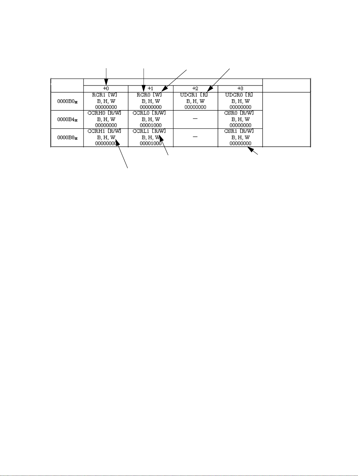
■ Access size and address position
Offset Register name Write-only Read-only
Address
Address offset value/Register name
Read/write
Block
Up/down counter
0, 1
Initial value
Byte access, Half-word access, and Word access are allowed.
There are three kinds of accesses such as Byte access, Half-word access and Word access. However, note
that some registers have restricted access. For more information, see “3.2. I/O Map (Page No.24)” or “Detail
Description of Register” in each chapter.
B,H,W : Byte access, Half-word access, and Wordaccess are allowed.
B : Byte access (Be sure to access by Byte.)
H : Half-word access (Be sure to access by Half-word.)
W : Word access (Be sure to access by Word.)
B, H : Byte access, Half-word access only (Word access is not allowed.)
H,W : Half-word access, Word access only (Byte access is not allowed.)
Reference
The following describes address position to access.
• In Word access, address becomes multiple of 4. (Lowest order 2 bits mandatorily become “00”.)
• In Half-word access, address becomes multiple of 2. (Lowest order 1 bit mandatorily becomes “0”.)
• In Byte access, address will not be changed.
Therefore, for example, make RCR0 register to use Half-word access,
For address 0B0H, RCR1+RCR0 register is accessed.
(When address offset is +1 and +2, (Example: RCR0+UDCR1) Half-word access is not allowed.)
8
Page 25
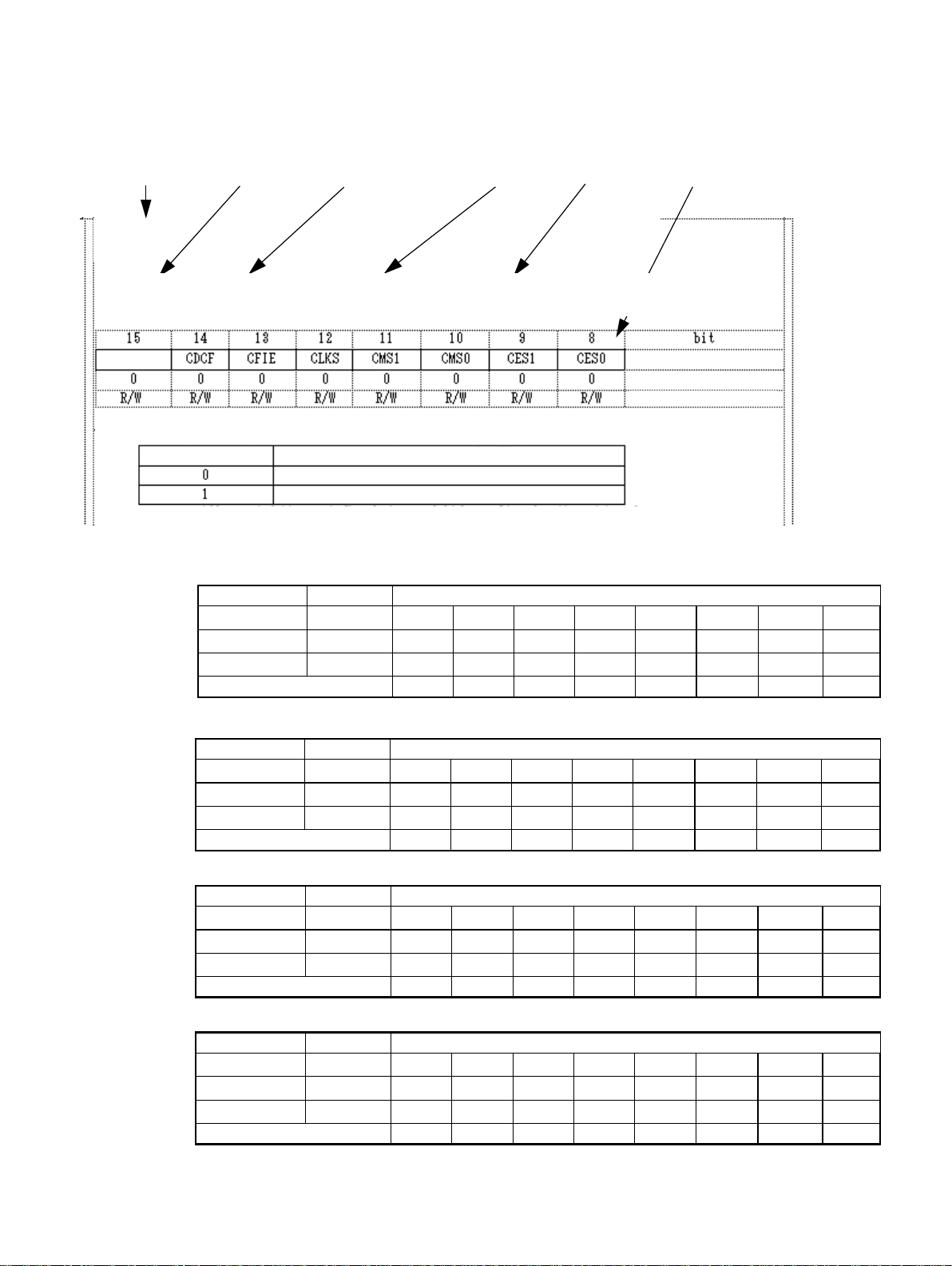
■ About access size and bit position
Register markRegister name Target peripheral device Address Access size Bit position
(1) Counter control register (Higher byte)
This is the register (higher byte) which controls up/down counter operation.
CCRH0 (Up/down counter 0): address 00B4h (Access: Byte, Half-word, Word)
CCRH1 (Up/down counter 1): address 00B8h (Access: Byte, Half-word, Word)
M16E/Reserved
*
bit15: Enable 16-bit mode
M16E (CCRH0 only) Enable 16-bit mode
8-bit x 2-channel mode (8-bit mode)
16-bit x 1-channel mode (16-bit mode)
*: CCRH1: ReservedAlways write 0 for writing. The read value is indeterminate.
Chapter 1 Introduction
4.How to Use This Document
Initial value
Attribute
When access size changes, bit position changes.
• In the case that address offset value is +0 (Example: CCRH0 register)
Access size Address Bit position
Byte
Half-word
Word
0B4
0B4
0B4
H+0H
H+0H
H+0H
07 06 05 04 03 02 01 00
15 14 13 12 11 10 09 08
31 30 29 28 27 26 25 24
Bit name M16E CDCF CFIE CLKS CMS1 CMS0 CES1 CES0
• In the case that address offset value is +1 (Example: CCRL0 register)
Access size Address Bit position
Byte
Half-word
Word
Bit name
0B4
0B4
0B4
H+1H
H+0H
H+0H
07 06 05 04 03 02 01 00
07 06 05 04 03 02 01 00
23 22 21 20 19 18 17 16
Reserved
CTUT UCRE RLDE UDCC CGSC CGE1 CGE0
• In the case that address offset value is +2 (Example: UDCR1 register)
Access size Address Bit position
Byte
Half-word
Word
0B0
0B0
0B0
H+2H
H+2H
H+0H
07 06 05 04 03 02 01 00
15 14 13 12 11 10 09 08
15 14 13 12 11 10 09 08
Bit name D15 D14 D13 D12 D11 D10 D9 D8
• In the case that address offset value is +3 (Example: UDCR 1 register)
Access size Address Bit position
Byte
Half-word
Word
0B0
0B0
0B0
H+3H
H+2H
H+0H
07 06 05 04 03 02 01 00
07 06 05 04 03 02 01 00
07 06 05 04 03 02 01 00
Bit name D7 D6 D5 D4 D3 D2 D1 D0
9
Page 26

Chapter 1 Introduction
4.How to Use This Document
■ Meaning of Bit Attribute Symbols
R : Readable
W : Writable
RM : Reading operation during read/modify/write operation.
“/” (Slash) R/W: Readable and writable. (The read value is the value written.)
“,” (comma) R,W: Values are different between read and write. (The read value is different from
the value written.)
R0 : The read value is “0”.
R1 : The read value is “1”.
W0 : Always write “0”.
W1 : Always write “1”.
(RM0) : read/modify/write operation reads “0”.
(RM1) : read/modify/write operation reads “1”.
RX : The read value is indeterminate. (Reserved bit or undefined bit)
WX : Writing does not affect the operation. (Undefined bit)
• Example of how R/W is used
• R/W : Readable and writable. (The read value is the value written.)
• R,W : Readable and writable. (The read value and written value are different.)
• R,RM/W : Readable and writable. (The read value and written value are different. Read/modify/write
command reads the value written.) Example: port data register
• R(RM1),W : Readable and writable. (The read value and written value are different. Read/modify/write
command reads 1.) Example: interrupt request flag
• R/WX : Read-only (Read-only. Writing does not affect the operation.)
• R1,W : Write-only (Write-only. The read value is 1.)
• R0,W : Write-only (Write-only. The read value is 0.)
• RX,W : Write-only (Write-only. The read value is indeterminate.)
• R/W0 : Reserved bit (The written value is 0. The read value is the value written.)
• R0/W0 : Reserved bit (The written value is 0. The read value is 0.)
• R1,W0 : Reserved bit (The written value is 0. The read value is 1.)
• RX,W0 : Reserved bit (The written value is 0. The read value is indeterminate.)
• R/W1 : Reserved bit (The written value is 1. The read value is the value written.)
• R1/W1 : Reserved bit (The written value is 1. The read value is 1.)
• R0,W1 : Reserved bit (The written value is 1. The read value is 0.)
• RX,W1 : Reserved bit (The written value is 1. The read value is indeterminate.)
• RX/WX : Undefined bit (The read value is indeterminate. Writing does not affect the operation.)
• R0/WX : Undefined bit (The read value is 0. Writing does not affect the operation.)
10
Page 27

Chapter 2 MB91460 Rev.A/Rev.B Overview
1.Overview
Chapter 2 MB91460 Rev.A/Rev.B Overview
1. Overview
MB91460 is a series of standard microcontrollers containing a range of I/O peripherals and bus control
functions. MB91460 features a 32-bit RISC CPU (FR60 series) core and is suitable for embedded control
applications requiring high-performance and high-speed CPU processing. MB91460 derivatives also contain
up to 16 kByte instruction cache memory and other internal memories to improve the execution speed of the
CPU.
MB91460 Rev.B has the same features as MB91460 Rev.A and adds some additional components in order to
support infotainment applications. Which components and modules will be included in MB91460 Rev.B is not
yet decided finally. So this document gives only a proposal at this stage of development.
MB91460 Rev.B : This series is presently being specified, and not available yet.
2. Features
2.1 FR60 CPU Core
• 32-bit RISC, load/store architecture, pipeline 5 stages
• Maximum operating frequency: Core clock = 100 MHz (device dependent)
(Source oscillation= 4 MHz, multiplied by 25 (PLL clock multiplier method))
• General-purpose registers: 16 x 32 bits
• 16-bit fixed-length instruction (Base instruction)
• 32-bit linear address space: 4 Gbytes
• Instructions suitable for embedded application
• Transfer command between memories
• Bit-processing instruction
• Barrel-shift instructions
• Instructions supporting C-language
• Function's enter command /exit command
• Multi-load/store command of register contents
• Assembler statement is also easily available
Register's interlock function
• Multiplier's embedded application/command level support
• Signed 32-bit multiplication: 5 cycles
• Signed 16-bit multiplication: 3 cycles
• Interrupt (PC/PS are saved): 6 cycles (16 priority level)
• Harvard architecture enables simultaneous execution of program access and data access
• Memory protection function
• Embedded debug support
• Commands compatible with FR family
2.2 Instruction Cache
• 2 way set associative I-cache
• Up to 4 kByte integrated
11
Page 28

Chapter 2 MB91460 Rev.A/Rev.B Overview
2.Features
• 4 words (16 bytes) per set
• Variable capacity (4/2/1 kB)
• Lock function enabling programs to be resident
• Available as instruction RAM requiring no wait state when not used as an instruction cache
• Direct mapped I-cache
• Up to 16 kByte integrated
• Variable capacity (16/8/4/2/1 kB)
• Lock function enabling programs to be resident
2.3 Interrupt Controller
• A total of 17 external interrupt lines (1 nonmaskable interrupt pin, 8 normal interrupt pins, 8 interrupt pins
shared (with peripheral inputs for Wake Up from STOP mode, e.g. CAN RX)
• Interrupts from internal peripherals (128 interrupt vectors)
• Priority levels programmable for normal interrupt lines excluding the nonmaskable one (16 levels)
• Capable of using the normal interrupt and nonmaskable interrupt pins for Wake Up from STOP mode
2.4 Internal Data RAM
• Up to 64 kBytes integrated
• Zero wait state for read/write access
• Referenced as Data-RAM or D-RAM in this manual
2.5 Internal Instruction/Data RAM
• Up to 64 kBytes integrated
• Zero wait state for read/write access of instructions
• One wait state for read/write access of data
• Referenced as General-Purpose-RAM (GP-RAM) or I/D-RAM in this manual
2.6 Embedded Instruction/Data Memory
• Up to 4 MByte (Flash or Mask ROM)
• Programmable wait state for read/write access
• Flash/ROM security
2.7 External Bus Interface
• 8 chip select areas with individual area size, data bus width selection (8, 16, 32-bit) and wait
• Address bus up to 32 bit wide
• Programmable auto-wait function or external wait input (RDY)
• Basic bus cycles : 2 cycles
• Prefetch function
• Burst access function
2.8 DMA Controller
• Four transfer modes supported: single/block, burst, continuous transfer, and fly-by
• 5 channels (4 channels for external-to-external transfer)
12
Page 29

Chapter 2 MB91460 Rev.A/Rev.B Overview
• 3 types of transfer sources (external pins/internal peripherals/and software)
• Up to 128 selectable internal transfer sources
• Addressing mode: Specifying up to 32-bit addresses (Increment/decrement/fixed)
• Transfer mode (Demand transfer/burst transfer/step transfer/block transfer)
• Fly-by transfer supported (between external I/O and memory)
• Transferred data size selectable from among 8, 16, and 32 bits
2.9 Infotainment extension (MB91460 Rev.B)
• Inter-IC sound bus (I2S)
• master or slave operation
• operation up to 2.5 MBit/s
• MOST support (MediaLB for controlling an external MOST IC is integrated)
• Digital interface to external MOST controller
• Frame sync pattern support
• Scalable data rate for streaming, packet, control, isochronous
• System-broadcast channel for administration
• Broadcast support for synchronous data
• USB
• USB 1.1 compliant up to 12Mbit/s (USB 2.0 tbd)
• Configurable endpoints
• Supports control, bulk, interrupt and isochronous transfer
• built-in FIFO for all endpoints
• clock and data recovery
• Flexray
• Event or Time triggered protocol
• Asynchronous or synchronous operation
• Fault tolerant operation (2 channels supported)
• Static and dynamic data transfer
• Transfer rates up to 10 MBit/s
• Ethernet
2.Features
MB91460 Rev.B : This series is presently being specified and not available yet.
13
Page 30

Chapter 2 MB91460 Rev.A/Rev.B Overview
2.Features
2.10 Peripheral Function
• General-purpose port : Up to 288
• N channel open drain port out of above: 8 (for I2C)
• A/D converter : 32 channels (1 unit)
• Series-parallel type
• Resolution: 10 bits
• Minimum conversion time: 3us
• Single conversion mode
• Continuous conversion mode
• Stop conversion mode
• Activation by software or external trigger can be selected
• Reload timer 7 and A/D Converter co-operate
• D/A converter : 2 channels
• R-2R type
• Resolution: 10 bits
• Conversion rate: 0.45us (when 20 pF load is applied)
• Conversion rate: 2us (when 100 pF load is applied)
• Alarm comparator : 2 channels
• Monitors an external voltage and generates an interrupt in case of a voltage lower or higher than the
defined thresholds
• Status is readable, interrupts can be masked separately
• External interrupt input : 16 channels
• Can be programmed to be edge sensitive or level sensitive
• Interrupt mask and request pending bits per channel
• 6 channels combined with CAN RX for wakeup
• Non maskable interrupt (NMI) : 1 channel
• Highest priority of all user interrupts
• Bit search module (using REALOS)
• Function to search the first bit position of “1”, “0”, “Changed” from MSB (most significant bit) within 1
word
• Up/down counter : 16 bits x 2 channels (8 bits x 4 channels)
• Timer mode, up/down count mode, phase difference mode (x2, x4)
• Includes clock prescaler (f
RES
/21, f
RES
/23)
• Reload timer : 16 bits x 8 channels
14
Page 31

• 16-bit reload counter
Chapter 2 MB91460 Rev.A/Rev.B Overview
2.Features
• Includes clock prescaler (f
RES
/21, f
RES
/23, f
RES
/25, f
RES
/26, f
RES
/27)
• Free-run timer : 16 bits x 8 channels
• 16-bit free running counter, signals an interrupt when overflow or match with compare register
• Includes prescaler (f
RES
/22, f
RES
/24, f
RES
/25, f
RES
/26)
• Timer data register has R/W access
• PPG : 16 bit x 16 channels
• 16 bit down counter, cycle and duty setting registers
• Interrupt at triggering, cycle or duty match
• PWM operation and one-shot operation
• Internal prescaler allows f
RES
/20, f
RES
/22, f
RES
/24, f
/26 as counter clock
RES
• Can be triggered by software, reload timer or external trigger
• Reload timer 0/1 available as trigger for PPG 0/1/2/3
• Reload timer 2/3 available as trigger for PPG 4/5/6/7
• Reload timer 4/5 available as trigger for PPG 8/9/10/11
• Reload timer 6/7 available as trigger for PPG 12/13/14/15
• External trigger for PPG 0/8 (shared)
• External trigger for PPG 1/9 (shared)
• External trigger for PPG 2/10 (shared)
• External trigger for PPG 3/11 (shared)
• External trigger for PPG 4/12 (shared)
• External trigger for PPG 5/13 (shared)
• External trigger for PPG 6/14 (shared)
• External trigger for PPG 7/15 (shared)
• Input capture : 16 bits x 8 channels
• Rising edge, falling edge or rising & falling edge sensitive
• Free-run timer 0 available as trigger for input capture 0/1
• Free-run timer 1 available as trigger for input capture 2/3
• Free-run timer 4 available as trigger for input capture 4/5
• Free-run timer 5 available as trigger for input capture 6/7
• Output compare : 16 bits x 8 channels
• Signals an interrupt when a match with of 16-bit IO timer occurs
• An output signal can be generated
• Free-run timer 2 available as trigger for output compare 0/1
• Free-run timer 3 available as trigger for output compare 2/3
• Free-run timer 6 available as trigger for output compare 4/5
• Free-run timer 7 available as trigger for output compare 6/7
15
Page 32

Chapter 2 MB91460 Rev.A/Rev.B Overview
2.Features
• LIN-USART (LIN=Local Interconnect Network) : 16 channels
• Full-duplex double buffer system (4 ch with 16 byte RX/TX FIFO buffer each)
• With parity/without parity selectable
• 1 or 2 stop bits selectable
• 7 or 8 bits data length selectable
• NRZ type transfer format
• Asynchronous /synchronous communications selectable
• Master-slave communication function (multiprocessor mode)
• Dedicated baud rate prescaler is embedded in each channel
• External clock is able to use as transfer clock
• Parity error, frame error, and overrun error detecting functions
• SPI compatible
• LIN master and slave
• LIN USART 0/8 and ICU 0 co-operate (for LIN sync field in slave mode)
• LIN USART 1/9 and ICU 1 co-operate (for LIN sync field in slave mode)
• LIN USART 2/10 and ICU 2 co-operate (for LIN sync field in slave mode)
• LIN USART 3/11 and ICU 3 co-operate (for LIN sync field in slave mode)
• LIN USART 4/12 and ICU 4 co-operate (for LIN sync field in slave mode)
• LIN USART 5/13 and ICU 5 co-operate (for LIN sync field in slave mode)
• LIN USART 6/14 and ICU 6 co-operate (for LIN sync field in slave mode)
• LIN USART 7/15 and ICU 7 co-operate (for LIN sync field in slave mode)
• CAN : 6 channels
• Supports CAN protocol version 2.0 part A and B
• Bit rates up to 1 Mbit/s
• Up to 128 message objects
• Each message object has its own identifier mask
• Programmable FIFO mode (cocatenation of message objects)
• Maskable interrupt
• Disabled Automatic Retransmission mode for Time Triggered CAN applications
• Programmable loop-back mode for self-test operation
•I2C (400k fast mode) : 4 channels
• Master or slave transmission
• Arbitration function
• Clock synchronization function
• Slave address and general call address detect function
• Transfer direction detect function
• Start condition repeat generation and detection function
• Bus error detect function
• Compatible to I2C standard and fast mode specification (operation up to 400 kHz, 10 bit addressing)
• Includes clock divider functionality
• SCL and SDA lines include optional noise filter. The noise filter allows the suppression of spikes in
16
Page 33

the range of 1 to 1.5 cycles of the resource clock (CLKP)
• PFM (pulse frequency modulator) : 16 bits x 1 channel
• 16-bit reload timers for generating high/low pulse waveforms
Chapter 2 MB91460 Rev.A/Rev.B Overview
2.Features
• Includes clock prescaler (f
RES
/21, f
RES
/23, f
RES
/25, f
RES
/26, f
RES
/27)
• Sound Generator : 1 channel
• 8-bit PWM signal is mixed with tone frequency from 16-bit reload counter
• PWM clock by internal prescaler: f
RES
/20, f
RES
/21, f
RES
/22, f
RES
/23, f
RES
/2
4
• Tone frequency: PWM frequency / 2 / (reload value + 1)
• Stepper Motor Controller : 6 channels
• Four high current outputs for each channel
• Two synchronized 8/10-bit PWMs per channel
• Internal prescaling for PMW clock: f
RES
/1, f
RES
/4, f
RES
/5, f
RES
/6, f
RES
/8, f
RES
/10, f
RES
/12, f
RES
• LCD controller
• 4 common / 40 segment
• Display: Up to 160 cells (for 1/4 duty cycle)
• Duty cycle: Selectable from options: 1/2, 1/3 and 1/4
• Bias: Fixed at 1/3
• Frame period: Selectable from four options. (for clock, peripheral clock or subclock is selectable)
• Driver: Built-in (for internal divided resistors), or external divided resistors can be connected to the
V0-V3 pins
• Data memory: Built-in 16-byte data memory for display
• Stop mode: Enable LCD display in the sub-stop mode
• Blank display: Selectable
• Pin: The SEG0-39 of COM0-4 pin usage can be switched between general and specialized purposes
• Others: External divided resistors can be also used to shut off the current when LCD is deactivated
/16
• Timebase/watchdog timer (26 bits)
• Adjustable watchdog timer interval (between 220 and 226 system clock cycles)
• RC oscillator watchdog timer (16 bits)
• Real-time clock (counts during stop mode)
• RTC module can be clocked either from 32 kHz crystal, 4 MHz quartz or from the RC Oscillator
• Facility to correct oscillation deviation (subclock calibration)
• Read/write accessible second/minute/ hour registers
• Can signal interrupts every halfsecond/second/ minute/hour/day
• Internal clock divider and prescaler provide exact 1s clock based on a 4 MHz or a 32 kHz clock input
• Prescaler value for 4 MHz is 0F423F
H
17
Page 34

Chapter 2 MB91460 Rev.A/Rev.B Overview
2.Features
• Prescaler value for 32 kHz is 001FFF
H
• Clock monitor (clock output function): 1 channel
• Clock supervisor
• Monitors external 32kHz and 4MHz for fails (e.g. crystal breaks)
• Switches in case of fail to an available recovery clock (subclock or RC clock)
• Clock modulator (reduction of EME)
• Subclock calibration
• Calibration of the RTC timer in 32 kHz or RC oscillator operation, based on the more accurate 4 MHz
quartz is possible
• Main oscillation stabilisation timer
• 23 bit counter for main oscillation stabilisation wait when running in sub clock mode
• Generates an interrupt when stabilisation time has elapsed
• Sub oscillation stabilisation timer
• 15 bit counter for sub oscillation stabilisation wait when running in main clock mode
• Generates an interrupt when stabilisation time has elapsed
• Low-consumption modes: SLEEP/Sub-Run/RTC/STOP function
• Package: BGA660-03EK (Evaluation device MB91V460)
• CMOS 0.35um technology (Evaluation device MB91V460)
• Power supply (Evaluation device MB91V460):
• Single power supply 3.3V
• Single power supply 5V
18
Page 35

Chapter 2 MB91460 Rev.A/Rev.B Overview
3.MB91460 Series Product Lineup
3. MB91460 Series Product Lineup
Feature MB91V460 Rev.A MB91V460 Rev.B MB91F467DA
Core frequency 80 MHz 100 MHz 100 MHz
Resource frequency 40 MHz 50 MHz 50 MHz
Technology 0.35um 0.18um 0.18um
Watchdog yes yes yes
Watchdog (RC osc. based) yes (disengageable) yes (disengageable) yes
Bit Search yes yes yes
Reset Input (INITX) yes yes yes
Clock Modulator yes yes yes
Low Power Mode yes yes yes
DMA 5 ch 5 ch 5 ch
MAC (uDSP) no tbd no
MMU/MPU MPU
Flash Emulation SRAM Emulation SRAM 1 MByte
Flash Protection n.a. n.a. yes
1)
MPU
1)
MPU
1)
D-bus RAM 64 kByte 64 kByte 32 kByte
I/D-bus RAM 64 kByte 64 kByte 32 kByte
I-bus RAM / I-Cache 16 kByte 16 kByte 8 kByte
Boot-ROM / BI-ROM 4 kByte 4 kByte 4 kByte
RTC 1 ch 1 ch 1 ch
Free Running Timer 8 ch 8 ch 8 ch
ICU 8 ch 8 ch 8 ch
OCU 8 ch 8 ch 4 ch
Reload Timer 8 ch 8 ch 8 ch
PPG 16-bit 16 ch 16 ch 12 ch
PFM 16-bit 1 ch 1 ch 1 ch
Sound Generator 1 ch 1 ch 1 ch
Up/Down Counter (8/16-bit) 4 ch (8-bit) / 2 ch (16-bit) 4 ch (8-bit) / 2 ch (16-bit) 3 ch (8-bit) / 1 ch (16-bit)
C_CAN (32 MsgBuf) 6 ch (128msg) 6 ch (128msg) 3 ch (32msg)
LIN-USART 4 ch + 4 ch FIFO + 8 ch 4 ch + 4 ch FIFO + 8 ch 1 ch + 4 ch FIFO
I2C (400k) 4 ch 4 ch 3 ch
FR external bus yes (32bit addr, 32bit data) yes (32bit addr, 32bit data) yes (26bit addr, 32bit data)
External Interrupts 16 ch 16 ch 10 ch
NMI Interrupts 1 ch 1 ch no
SMC 6 ch 6 ch 6 ch
LCD controller (40x4) 1 ch 1 ch no
19
Page 36

Chapter 2 MB91460 Rev.A/Rev.B Overview
3.MB91460 Series Product Lineup
Feature MB91V460 Rev.A MB91V460 Rev.B MB91F467DA
ADC (10 bit) 32 ch 32 ch 24 ch
Alarm Comparator 2 ch 2 ch 1 ch
Supply Supervisor yes yes yes
Clock Supervisor yes yes yes
Main clock oscillator 4 MHz 4 MHz 4 MHz
Sub clock oscillator 32 kHz 32 kHz 32 kHz
RC Oscillator 100 kHz 100 kHz / 2 MHz 100 kHz / 2 MHz
PLL x 25 x 25 x 25
DSU4 yes yes no
EDSU yes yes yes
JTAG Boundary Scan no tbd no
Supply Voltage 3V / 5V tbd 3V / 5V
Regulator yes tbd yes
Power Consumption n.a. n.a. < 1 W
Temperatur Range (Ta) 0..70 C 0..70 C -40..105 C
Package PGA/BGA PGA/BGA QFP208
Power on to PLL run < 20 ms < 20 ms < 20 ms
Flash Download Time n.a. n.a. < 30 sec (2M)
I2S no yes no
MediaLB (MOST interface) no yes no
USB no yes no
Flexray no yes no
MB91V460 Rev.B : This series is presently being specified and not available yet.
1) The Memory protection Unit (MPU) is a part of the EDSU functionality
20
Page 37

4. Block Diagram
The following illustration shows the block diagram of MB91460 series.
Figure 4-1 Block Diagram MB91460 Series
Chapter 2 MB91460 Rev.A/Rev.B Overview
4.Block Diagram
MD[2:0]INITX X0/X1
INT[15:0]
External
Interrupt
Test ControllerClock/Reset/Device State Controller
Resource−/Port−/Test−Pin Multiplexer
VEC/LEVEL
I−Unit
EDSU/MPU
Bit Search
Resource Group
Resources
CAN
64KB
Data−RAM
GPIOs/Resource IOs
Port−Bus
General
Purpose
R−Bus
R−Unit
Ext. Bus Interface
Port Group
Ports
T−BusX−Bus
T−Unit
FR60 CPU Core
DSU4
EMU RAM
ICE Interface
1KByte
Trace RAM
128 words
external
Trace RAM
max.
64K words
64 kByte
GP−RAM
M−Bus
F−Bus
DMAC
D−Bus
I−Bus
I$
4KB
Memory
Controller
Queue
Prefetch
B−Unit
Flash−I$
16 kByte
Core Group
MB91V460
8MB
max.
Flash
SRAM/
21
Page 38

Chapter 2 MB91460 Rev.A/Rev.B Overview
4.Block Diagram
22
Page 39

Chapter 3 MB91460 Series Basic Information
1.Memory Map
Chapter 3 MB91460 Series Basic Information
This chapter describes MB91460 series basic information including Memory- and I/O map, interrupt vector table, pin function list, circuit type and pin state table for each device mode.
1. Memory Map
Figure 1-1 Memory Map
23
Page 40

Chapter 3 MB91460 Series Basic Information
2.I/O Map
2. I/O Map
This section shows the association between memory space and each register of peripheral resources.
• Table convention
Address
000000
H
PDRD[R/W]
xxxxxxxx
+0
Address offset/Register name
+1
PDR1[R/W]
+2
PDR2[R/W]
xxxxxxxx xxxxxxxx xxxxxxxx
Read/Write attribute (R: Read, W: Write)
Register initial value ("0", "1", "X" : undefined, "-" : not implemented)
Register name (First column register is 4n address,
Second column register is 4n+2 address...)
Leftmost register address
(For Word access, first register becomes MSB side of the data.)
Note: Bit value of register shows initial values as follows.
•"1": Initial value is "1".
• "0": Initial value is "0".
• "X": Initial value is indeterminate.
• "N/A": No physical register exists in the position.
Do not use other data access attributes to access data.
+3
PDR3[R/W]
MSB LSB
Block
T-unit
Port data register
24
Page 41

Table 2-1 I/O Map
Address
Chapter 3 MB91460 Series Basic Information
2.I/O Map
Register
Block
+0 +1 +2 +3
000000
000004
000008
00000C
000010
000014
000018
00001C
000020
000024
00002C
H
H
H
H
PDR00 [R/W]
XXXXXXXX
PDR04 [R/W]
XXXXXXXX
PDR08 [R/W]
XXXXXXXX
PDR12 [R/W]
XXXXXXXX
PDR01 [R/W]
XXXXXXXX
PDR05 [R/W]
XXXXXXXX
PDR09 [R/W]
XXXXXXXX
PDR13 [R/W]
XXXXXXXX
PDR02 [R/W]
XXXXXXXX
PDR06 [R/W]
XXXXXXXX
PDR10 [R/W]
XXXXXXXX
PDR14 [R/W]
XXXXXXXX
PDR03 [R/W]
XXXXXXXX
PDR07 [R/W]
XXXXXXXX
PDR11 [R/W]
XXXXXXXX
PDR15 [R/W]
XXXXXXXX
R-bus
H
H
H
H
H
H
PDR16 [R/W]
XXXXXXXX
PDR20 [R/W]
XXXXXXXX
PDR24 [R/W]
XXXXXXXX
PDR28 [R/W]
XXXXXXXX
PDR32 [R/W]
XXXXXXXX
PDR17 [R/W]
XXXXXXXX
PDR21 [R/W]
XXXXXXXX
PDR25 [R/W]
XXXXXXXX
PDR29 [R/W]
XXXXXXXX
PDR33 [R/W]
XXXXXXXX
PDR18 [R/W]
XXXXXXXX
PDR22 [R/W]
XXXXXXXX
PDR26 [R/W]
XXXXXXXX
PDR30 [R/W]
XXXXXXXX
PDR34 [R/W]
XXXXXXXX
PDR19 [R/W]
XXXXXXXX
PDR23 [R/W]
XXXXXXXX
PDR27 [R/W]
XXXXXXXX
PDR31 [R/W]
XXXXXXXX
PDR35 [R/W]
XXXXXXXX
Port Data
Register
reserved
H
000030
000034
000038
00003C
000040
000044
H
H
H
H
H
H
EIRR0 [R/W]
00000000
EIRR1 [R/W]
00000000
DICR [R/W]
- - - - - - - 0
SCR00 [R/W,W]
00000000
ESCR00 [R/W]
00000X00
ENIR0 [R/W]
00000000
ENIR1 [R/W]
00000000
HRCL [R/W]
0 - - 11111
SMR00 [R/W,W]
00000000
ECCR00
[R/W,R,W]
000000XX
reserved
ELVR0 [R/W]
00000000 00000000
ELVR1 [R/W]
00000000 00000000
RBSYNC
SSR00 [R/W,R]
00001000
*1
RDR00/TDR00
00000000
res.
Ext. INT 0-7
NMI
Ext. INT 8-15
DLYI/I-unit
[R/W]
USART (LIN)
0
25
Page 42

Chapter 3 MB91460 Series Basic Information
2.I/O Map
Address
+0 +1 +2 +3
Register
Block
000048
00004C
000050
000054
000058
00005C
000060
000064
H
H
H
H
H
H
H
H
SCR01 [R/W,W]
00000000
ESCR01 [R/W]
00000X00
SCR02 [R/W,W]
00000000
ESCR02 [R/W]
00000X00
SCR03 [R/W,W]
00000000
ESCR03 [R/W]
00000X00
SCR04 [R/W,W]
00000000
ESCR04 [R/W]
00000X00
SMR01 [R/W,W]
00000000
ECCR01
[R/W,R,W]
000000XX
SMR02 [R/W,W]
00000000
ECCR02
[R/W,R,W]
000000XX
SMR03 [R/W,W]
00000000
ECCR03
[R/W,R,W]
000000XX
SMR04 [R/W,W]
00000000
ECCR04
[R/W,R,W]
000000XX
SSR01 [R/W,R]
00001000
SSR02 [R/W,R]
00001000
SSR03 [R/W,R]
00001000
SSR04 [R/W,R]
00001000
FSR04 [R]
- - - 00000
RDR01/TDR01
00000000
res.
RDR02/TDR02
00000000
res.
RDR03/TDR03
00000000
res.
RDR04/TDR04
00000000
FCR04 [R/W]
0001 - 000
[R/W]
USART (LIN)
1
[R/W]
USART (LIN)
2
[R/W]
USART (LIN)
3
[R/W]
USART (LIN)
4
with FIFO
26
000068
00006C
000070
000074
000078
00007C
H
H
H
H
H
H
SCR05 [R/W,W]
00000000
ESCR05 [R/W]
00000X00
SCR06 [R/W,W]
00000000
ESCR06 [R/W]
00000X00
SCR07 [R/W,W]
00000000
ESCR07 [R/W]
00000X00
SMR05 [R/W,W]
00000000
ECCR05
[R/W,R,W]
000000XX
SMR06 [R/W,W]
00000000
ECCR06
[R/W,R,W]
000000XX
SMR07 [R/W,W]
00000000
ECCR07
[R/W,R,W]
000000XX
SSR05 [R/W,R]
00001000
FSR05 [R]
- - - 00000
SSR06 [R/W,R]
00001000
FSR06 [R]
- - - 00000
SSR07 [R/W,R]
00001000
FSR07 [R]
- - - 00000
RDR05/TDR05
[R/W]
00000000
FCR05 [R/W]
0001 - 000
RDR06/TDR06
[R/W]
00000000
FCR06 [R/W]
0001 - 000
RDR07/TDR07
[R/W]
00000000
FCR07 [R/W]
0001 - 000
USART (LIN)
5
with FIFO
USART (LIN)
6
with FIFO
USART (LIN)
7
with FIFO
Page 43

Address
Chapter 3 MB91460 Series Basic Information
2.I/O Map
Register
Block
+0 +1 +2 +3
000080
000084
000088
00008C
000090
000094
000098
00009C
0000A0
0000A4
H
H
H
H
BGR100 [R/W]
00000000
BGR102 [R/W]
00000000
BGR104 [R/W]
00000000
BGR106 [R/W]
00000000
PWC20 [R/W]
- - - - - - XX XXXXXXXX
res. res.
PWC21 [R/W]
- - - - - - XX XXXXXXXX
res. res.
PWC22 [R/W]
- - - - - - XX XXXXXXXX
res. res.
H
H
H
H
H
H
BGR000 [R/W]
00000000
BGR002 [R/W]
00000000
BGR004 [R/W]
00000000
BGR006 [R/W]
00000000
BGR101 [R/W]
00000000
BGR103 [R/W]
00000000
BGR105 [R/W]
00000000
BGR107 [R/W]
00000000
PWC10 [R/W]
- - - - - - XX XXXXXXXX
PWS20 [R/W]
-0000000
PWC11 [R/W]
- - - - - - XX XXXXXXXX
PWS21 [R/W]
-0000000
PWC12 [R/W]
- - - - - - XX XXXXXXXX
PWS22 [R/W]
-0000000
BGR001 [R/W]
00000000
BGR003 [R/W]
00000000
BGR005 [R/W]
00000000
BGR007 [R/W]
00000000
PWS10 [R/W]
--000000
PWS11 [R/W]
--000000
PWS12 [R/W]
--000000
Baudrate
Generator
USART (LIN)
0-7
Stepper Motor
0
Stepper Motor
1
Stepper Motor
2
0000A8
0000AC
0000B0
0000B4
0000B8
0000BC
0000C0
0000C4
0000C8
0000CC
H
H
H
H
H
H
H
H
H
H
PWC23 [R/W]
- - - - - - XX XXXXXXXX
res. res.
PWC24 [R/W]
- - - - - - XX XXXXXXXX
res. res.
PWC25 [R/W]
- - - - - - XX XXXXXXXX
res. res.
res.
res.
res.
PWC0 [R/W]
-00000--
PWC2 [R/W]
-00000--
PWC4 [R/W]
-00000--
PWS23 [R/W]
-0000000
PWS24 [R/W]
-0000000
PWS25 [R/W]
-0000000
reserved
PWC13 [R/W]
- - - - - - XX XXXXXXXX
PWS13 [R/W]
--000000
PWC14 [R/W]
- - - - - - XX XXXXXXXX
PWS14 [R/W]
--000000
PWC15 [R/W]
- - - - - - XX XXXXXXXX
PWS15 [R/W]
--000000
res.
res.
res.
PWC1 [R/W]
-00000--
PWC3 [R/W]
-00000--
PWC5 [R/W]
-00000--
Stepper Motor
3
Stepper Motor
4
Stepper Motor
5
Stepper Motor
Control
0-5
27
Page 44

Chapter 3 MB91460 Series Basic Information
2.I/O Map
Address
+0 +1 +2 +3
Register
Block
0000D0
0000D4
0000D8
0000DC
0000E0
0000E4
0000E8
0000EC
0000F0
0000F4
H
H
H
H
H
H
H
H
H
H
IBCR0 [R/W]
00000000
ITMKH0 [R/W]
00 - - - - 11
res.
IBCR1 [R/W]
00000000
ITMKH1 [R/W]
00 - - - - 11
res.
LCDCMR [R/W]
- - - - 0000
VRAM00 [R/W]
XXXXXXXX
VRAM04 [R/W]
XXXXXXXX
VRAM08 [R/W]
XXXXXXXX
IBSR0 [R]
00000000
ITMKL0 [R/W]
11111111
IDAR0 [R/W]
00000000
IBSR1 [R]
00000000
ITMKL1 [R/W]
11111111
IDAR1 [R/W]
00000000
LCR0 [R/W]
00010000
VRAM01 [R/W]
XXXXXXXX
VRAM05 [R/W]
XXXXXXXX
VRAM09 [R/W]
XXXXXXXX
ITBAH0 [R/W]
- - - - - - 00
ISMK0 [R/W]
01111111
ICCR0 [R/W]
- 0011111
ITBAH1 [R/W]
- - - - - - 00
ISMK1 [R/W]
01111111
ICCR1 [R/W]
- 0011111
LCR1H [R/W]
- - - - - - 00
VRAM02 [R/W]
XXXXXXXX
VRAM06 [R/W]
XXXXXXXX
VRAM10 [R/W]
XXXXXXXX
ITBAL0 [R/W]
00000000
ISBA0 [R/W]
- 0000000
res.
ITBAL1 [R/W]
00000000
ISBA1 [R/W]
- 0000000
res.
LCR1L [R/W]
00000000
VRAM03 [R/W]
XXXXXXXX
VRAM07 [R/W]
XXXXXXXX
VRAM11 [R/W]
XXXXXXXX
I2C 0
I2C 1
LCD
Controller
0000F8
0000FC
000100
000104
000108
000110
000114
000118
00011C
H
VRAM12 [R/W]
XXXXXXXX
VRAM16 [R/W]
H
XXXXXXXX
H
H
H
H
GCN10 [R/W]
00110010 00010000
GCN11 [R/W]
00110010 00010000
GCN12 [R/W]
00110010 00010000
PTMR00 [R]
11111111 11111111
VRAM13 [R/W]
XXXXXXXX
VRAM17 [R/W]
XXXXXXXX
VRAM14 [R/W]
XXXXXXXX
VRAM18 [R/W]
XXXXXXXX
res.
res.
res.
PCSR00 [W]
XXXXXXXX XXXXXXXX
VRAM15 [R/W]
XXXXXXXX
VRAM19 [R/W]
XXXXXXXX
GCN20 [R/W]
- - - - 0000
GCN21 [R/W]
- - - - 0000
GCN22 [R/W]
- - - - 0000
PPG Control
0-3
PPG Control
4-7
PPG Control
8-11
PPG 0
H
H
PDUT00 [W]
XXXXXXXX XXXXXXXX
PTMR01 [R]
11111111 11111111
PCNH00 [R/W]
0000000 -
PCSR01 [W]
XXXXXXXX XXXXXXXX
PCNL00 [R/W]
000000 - 0
PPG 1
H
PDUT01 [W]
XXXXXXXX XXXXXXXX
PCNH01 [R/W]
0000000 -
PCNL01 [R/W]
000000 - 0
28
Page 45

Address
Chapter 3 MB91460 Series Basic Information
2.I/O Map
Register
Block
+0 +1 +2 +3
000120
000124
000128
00012C
000130
000134
000138
00013C
000140
000144
H
PTMR02 [R]
11111111 11111111
PCSR02 [W]
XXXXXXXX XXXXXXXX
PPG 2
H
H
PDUT02 [W]
XXXXXXXX XXXXXXXX
PTMR03 [R]
11111111 11111111
PCNH02 [R/W]
0000000 -
PCSR03 [W]
XXXXXXXX XXXXXXXX
PCNL02 [R/W]
000000 - 0
PPG 3
H
H
PDUT03 [W]
XXXXXXXX XXXXXXXX
PTMR04 [R]
11111111 11111111
PCNH03 [R/W]
0000000 -
PCSR04 [W]
XXXXXXXX XXXXXXXX
PCNL03 [R/W]
000000 - 0
PPG 4
H
H
PDUT04 [W]
XXXXXXXX XXXXXXXX
PTMR05 [R]
11111111 11111111
PCNH04 [R/W]
0000000 -
PCSR05 [W]
XXXXXXXX XXXXXXXX
PCNL04 [R/W]
000000 - 0
PPG 5
H
H
PDUT05 [W]
XXXXXXXX XXXXXXXX
PTMR06 [R]
11111111 11111111
PCNH05 [R/W]
0000000 -
PCSR06 [W]
XXXXXXXX XXXXXXXX
PCNL05 [R/W]
000000 - 0
PPG 6
H
PDUT06 [W]
XXXXXXXX XXXXXXXX
PCNH06 [R/W]
0000000 -
PCNL06 [R/W]
000000 - 0
000148
00014C
000150
000154
000158
00015C
000160
000164
000168
00016C
H
PTMR07 [R]
11111111 11111111
PCSR07 [W]
XXXXXXXX XXXXXXXX
PPG 7
H
H
PDUT07 [W]
XXXXXXXX XXXXXXXX
PTMR08 [R]
11111111 11111111
PCNH07 [R/W]
0000000 -
PCSR08 [W]
XXXXXXXX XXXXXXXX
PCNL07 [R/W]
000000 - 0
PPG 8
H
H
PDUT08 [W]
XXXXXXXX XXXXXXXX
PTMR09 [R]
11111111 11111111
PCNH08 [R/W]
0000000 -
PCSR09 [W]
XXXXXXXX XXXXXXXX
PCNL08 [R/W]
000000 - 0
PPG 9
H
H
PDUT09 [W]
XXXXXXXX XXXXXXXX
PTMR10 [R]
11111111 11111111
PCNH09 [R/W]
0000000 -
PCSR10 [W]
XXXXXXXX XXXXXXXX
PCNL09 [R/W]
000000 - 0
PPG 10
H
H
PDUT10 [W]
XXXXXXXX XXXXXXXX
PTMR11 [R]
11111111 11111111
PCNH10 [R/W]
0000000 -
PCSR11 [W]
XXXXXXXX XXXXXXXX
PCNL10 [R/W]
000000 - 0
PPG 11
H
PDUT11 [W]
XXXXXXXX XXXXXXXX
PCNH11 [R/W]
0000000 -
PCNL11 [R/W]
000000 - 0
29
Page 46

Chapter 3 MB91460 Series Basic Information
2.I/O Map
Address
+0 +1 +2 +3
Register
Block
000170
000174
000178
00017C
000180
000184
000188
00018C
000190
000194
P0TMCSRH
H
[R/W]
- 0 - 000 - 0
P0TMCSRL
[R/W]
- - - 00000
P1TMCSRH
[R/W]
- 0 - 000 - 0
P1TMCSRL
[R/W]
- - - 00000
Pulse
H
H
H
H
H
H
H
H
H
P0TMRLR [W]
XXXXXXXX XXXXXXXX
P1TMRLR [W]
XXXXXXXX XXXXXXXX
res.
ICS01 [R/W]
00000000
IPCP0 [R]
XXXXXXXX XXXXXXXX
IPCP2 [R]
XXXXXXXX XXXXXXXX
OCS01 [R/W]
- - - 0 - - 00 0000 - - 00
OCCP0 [R/W]
XXXXXXXX XXXXXXXX
OCCP2 [R/W]
XXXXXXXX XXXXXXXX
reserved
P0TMR [R]
XXXXXXXX XXXXXXXX
P1TMR [R]
XXXXXXXX XXXXXXXX
res.
ICS23 [R/W]
00000000
IPCP1 [R]
XXXXXXXX XXXXXXXX
IPCP3 [R]
XXXXXXXX XXXXXXXX
OCS23 [R/W]
- - - 0 - - 00 0000 - - 00
OCCP1 [R/W]
XXXXXXXX XXXXXXXX
OCCP3 [R/W]
XXXXXXXX XXXXXXXX
Frequency
Modulator
Input
Capture
0-3
Output
Compare
0-3
000198
00019C
0001A0
0001A4
0001A8
0001AC
0001B0
0001B4
H
SGCRH [R/W]
0000 - - 00
H
SGAR [R/W]
00000000
H
ADERH [R/W]
00000000 00000000
ADCS1 [R/W]
00000000
H
H
H
ADCT1 [R/W]
00010000
res.
TMRLR0 [W]
XXXXXXXX XXXXXXXX
SGCRL [R/W]
- - 0 - - 000
res.
ADCS0 [R/W]
00000000
ADCT0 [R/W]
00101100
ACSR0 [R/W]
011XXX00
SGFR [R/W, R]
XXXXXXXX XXXXXXXX
SGTR [R/W]
XXXXXXXX
ADERL [R/W]
00000000 00000000
ADCR1 [R]
000000XX
ADSCH [R/W]
- - - 00000
res.
TMR0 [R]
XXXXXXXX XXXXXXXX
SGDR [R/W]
XXXXXXXX
ADCR0 [R]
XXXXXXXX
ADECH [R/W]
- - - 00000
ACSR1 [R/W]
011XXX00
Sound
Generator
A/D
Converter
Alarm Comparator 0-1
Reload Timer
0
TMCSRH0
H
reserved
[R/W]
- - - 00000
TMCSRL0
[R/W]
0 - 000000
(PPG 0-1)
30
Page 47

Address
Chapter 3 MB91460 Series Basic Information
2.I/O Map
Register
Block
+0 +1 +2 +3
0001B8
0001BC
0001C0
0001C4
0001C8
0001CC
0001D0
0001D4
0001D8
0001DC
H
TMRLR1 [W]
XXXXXXXX XXXXXXXX
XXXXXXXX XXXXXXXX
TMR1 [R]
Reload Timer
1
TMCSRH1
H
reserved
[R/W]
- - - 00000
H
TMRLR2 [W]
XXXXXXXX XXXXXXXX
XXXXXXXX XXXXXXXX
TMR2 [R]
TMCSRL1
[R/W]
0 - 000000
(PPG 2-3)
Reload Timer
2
TMCSRH2
H
reserved
[R/W]
- - - 00000
H
TMRLR3 [W]
XXXXXXXX XXXXXXXX
XXXXXXXX XXXXXXXX
TMR3 [R]
TMCSRL2
[R/W]
0 - 000000
(PPG 4-5)
Reload Timer
3
TMCSRH3
H
reserved
[R/W]
- - - 00000
H
TMRLR4 [W]
XXXXXXXX XXXXXXXX
XXXXXXXX XXXXXXXX
TMR4 [R]
TMCSRL3
[R/W]
0 - 000000
(PPG 6-7)
Reload Timer
4
TMCSRH4
H
reserved
[R/W]
- - - 00000
H
TMRLR5 [W]
XXXXXXXX XXXXXXXX
XXXXXXXX XXXXXXXX
TMR5 [R]
TMCSRL4
[R/W]
0 - 000000
(PPG 8-9)
Reload Timer
5
TMCSRH5
H
reserved
[R/W]
- - - 00000
TMCSRL5
[R/W]
0 - 000000
(PPG 10-11)
0001E0
0001E4
0001E8
0001EC
0001F0
0001F4
H
TMRLR6 [W]
XXXXXXXX XXXXXXXX
XXXXXXXX XXXXXXXX
TMCSRH6
H
reserved
[R/W]
- - - 00000
H
TMRLR7 [W]
XXXXXXXX XXXXXXXX
XXXXXXXX XXXXXXXX
TMCSRH7
H
reserved
[R/W]
- - - 00000
TMR6 [R]
TMR7 [R]
TMCSRL6
[R/W]
0 - 000000
TMCSRL7
[R/W]
0 - 000000
Reload Timer
6
(PPG 12-13)
Reload Timer
7
(PPG 14-15)
(ADC)
Free Running
H
TCDT0 [R/W]
XXXXXXXX XXXXXXXX
res.
TCCS0 [R/W]
00000000
Timer 0
(ICU 0-1)
Free Running
H
TCDT1 [R/W]
XXXXXXXX XXXXXXXX
res.
TCCS1 [R/W]
00000000
Timer 1
(ICU 2-3)
31
Page 48

Chapter 3 MB91460 Series Basic Information
2.I/O Map
Address
+0 +1 +2 +3
0001F8
0001FC
H
H
TCDT2 [R/W]
XXXXXXXX XXXXXXXX
TCDT3 [R/W]
XXXXXXXX XXXXXXXX
Register
res.
res.
TCCS2 [R/W]
00000000
TCCS3 [R/W]
00000000
Block
Free Running
Timer 2
(OCU 0-1)
Free Running
Timer 3
(OCU 2-3)
000200
000204
000208
00020C
000210
000214
000218
00021C
000220
000224
H
DMACA0 [R/W]
00000000 0000XXXX XXXXXXXX XXXXXXXX
H
DMACB0 [R/W]
00000000 00000000 XXXXXXXX XXXXXXXX
H
DMACA1 [R/W]
00000000 0000XXXX XXXXXXXX XXXXXXXX
H
DMACB1 [R/W]
00000000 00000000 XXXXXXXX XXXXXXXX
H
DMACA2 [R/W]
00000000 0000XXXX XXXXXXXX XXXXXXXX
H
DMACB2 [R/W]
00000000 00000000 XXXXXXXX XXXXXXXX
H
DMACA3 [R/W]
DMAC
00000000 0000XXXX XXXXXXXX XXXXXXXX
H
DMACB3 [R/W]
00000000 00000000 XXXXXXXX XXXXXXXX
H
DMACA4 [R/W]
00000000 0000XXXX XXXXXXXX XXXXXXXX
H
DMACB4 [R/W]
00000000 00000000 XXXXXXXX XXXXXXXX
32
000228
00023C
000240
000244
00024C
000250
000254
H
H
H
H
H
H
H
DMACR [R/W]
0 - - 00000
reserved
reserved
reserved
DMATEST0 [R/W]
XXXXXXXX 00000000 00000000 0000XXXX
DMATEST1 [R]
XXXXXXXX XXXXX000 00000000 00000000
DMA Test
(do not use)
Page 49

Address
Chapter 3 MB91460 Series Basic Information
2.I/O Map
Register
Block
+0 +1 +2 +3
000258
00027C
000280
000284
000288
00028C
000290
000294
H
H
H
H
H
H
H
H
SCR08 [R/W,W]
00000000
ESCR08 [R/W]
00000X00
SCR09 [R/W,W]
00000000
ESCR09 [R/W]
00000X00
SCR10 [R/W,W]
00000000
ESCR10 [R/W]
00000X00
SMR08 [R/W,W]
00000000
ECCR08
[R/W,R,W]
000000XX
SMR09 [R/W,W]
00000000
ECCR09
[R/W,R,W]
000000XX
SMR10 [R/W,W]
00000000
ECCR10
[R/W,R,W]
000000XX
reserved
SSR08 [R/W,R]
00001000
SSR09 [R/W,R]
00001000
SSR10 [R/W,R]
00001000
RDR08/TDR08
00000000
res.
RDR09/TDR09
00000000
res.
RDR10/TDR10
00000000
res.
[R/W]
USART (LIN)
8
[R/W]
USART (LIN)
9
[R/W]
USART (LIN)
10
000298
00029C
0002A0
0002A4
0002A8
0002AC
H
H
H
H
H
H
SCR11 [R/W,W]
00000000
ESCR11 [R/W]
00000X00
SCR12 [R/W,W]
00000000
ESCR12 [R/W]
00000X00
SCR13 [R/W,W]
00000000
ESCR13 [R/W]
00000X00
SMR11 [R/W,W]
00000000
ECCR11
[R/W,R,W]
000000XX
SMR12 [R/W,W]
00000000
ECCR12
[R/W,R,W]
000000XX
SMR13 [R/W,W]
00000000
ECCR13
[R/W,R,W]
000000XX
SSR11 [R/W,R]
00001000
SSR12 [R/W,R]
00001000
SSR13 [R/W,R]
00001000
RDR11/TDR11
00000000
res.
RDR12/TDR12
00000000
res.
RDR13/TDR13
00000000
res.
[R/W]
USART (LIN)
11
[R/W]
USART (LIN)
12
[R/W]
USART (LIN)
13
33
Page 50

Chapter 3 MB91460 Series Basic Information
2.I/O Map
Address
+0 +1 +2 +3
Register
Block
0002B0
0002B4
0002B8
0002BC
0002C0
0002C4
0002C8
0002CC
0002D0
0002D4
0002D8
SCR14 [R/W,W]
H
H
SCR15 [R/W,W]
H
H
H
H
H
H
H
H
H
00000000
ESCR14 [R/W]
00000X00
00000000
ESCR15 [R/W]
00000X00
BGR108 [R/W]
00000000
BGR110 [R/W]
00000000
BGR112 [R/W]
00000000
BGR114 [R/W]
00000000
res.
IPCP4 [R]
XXXXXXXX XXXXXXXX
IPCP6 [R]
XXXXXXXX XXXXXXXX
SMR14 [R/W,W]
00000000
ECCR14
[R/W,R,W]
000000XX
SMR15 [R/W,W]
00000000
ECCR15
[R/W,R,W]
000000XX
BGR008 [R/W]
00000000
BGR010 [R/W]
00000000
BGR012 [R/W]
00000000
BGR014 [R/W]
00000000
ICS45 [R/W]
00000000
SSR14 [R/W,R]
00001000
res.
SSR15 [R/W,R]
00001000
res.
BGR109 [R/W]
00000000
BGR111 [R/W]
00000000
BGR113 [R/W]
00000000
BGR15 [R/W]
00000000
res.
IPCP5 [R]
XXXXXXXX XXXXXXXX
IPCP7 [R]
XXXXXXXX XXXXXXXX
RDR14/TDR14
[R/W]
00000000
RDR15/TDR15
[R/W]
00000000
BGR009 [R/W]
00000000
BGR011 [R/W]
00000000
BGR013 [R/W]
00000000
BGR015 [R/W]
00000000
ICS67 [R/W]
00000000
USART (LIN)
14
USART (LIN)
15
Baudrate
Generator
USART (LIN)
8-15
Input
Capture
4-7
34
0002DC
0002E0
0002E4
0002E8
0002EC
0002F0
H
H
H
H
OCS45 [R/W]
- - - 0 - - 00 0000 - - 00
OCCP4 [R/W]
XXXXXXXX XXXXXXXX
OCCP6 [R/W]
XXXXXXXX XXXXXXXX
OCS67 [R/W]
- - - 0 - - 00 0000 - - 00
OCCP5 [R/W]
XXXXXXXX XXXXXXXX
OCCP7 [R/W]
XXXXXXXX XXXXXXXX
Output
Compare
4-7
reserved
H
Free Running
H
TCDT4 [R/W]
XXXXXXXX XXXXXXXX
res.
TCCS4 [R/W]
00000000
Timer 4
(ICU 4-5)
Page 51

Address
0002F4
0002F8
0002FC
H
H
Chapter 3 MB91460 Series Basic Information
2.I/O Map
Register
Block
+0 +1 +2 +3
Free Running
TCDT5 [R/W]
XXXXXXXX XXXXXXXX
TCDT6 [R/W]
XXXXXXXX XXXXXXXX
H
TCDT7 [R/W]
XXXXXXXX XXXXXXXX
res.
res.
res.
TCCS5 [R/W]
00000000
TCCS6 [R/W]
00000000
TCCS7 [R/W]
00000000
Timer 5
(ICU 6-7)
Free Running
Timer 6
(OCU 4-5)
Free Running
Timer 7
(OCU 6-7)
000300
000304
000308
00030C
000310
000314
000318
00031C
000320
000324
00032C
H
H
H
H
H
H
H
H
H
H
H
UDRC1 [W]
00000000
UDCCH0 [R/W]
00001000
UDCCH1 [R/W]
00001000
UDRC3 [W]
00000000
UDCCH2 [R/W]
00001000
UDCCH3 [R/W]
00001000
GCN13 [R/W]
00110010 00010000
UDRC0 [W]
00000000
UDCCL0 [R/W]
00000000
UDCCL1 [R/W]
00000000
UDRC2 [W]
00000000
UDCCL2 [R/W]
00000000
UDCCL3 [R/W]
00000000
reserved
reserved
reserved
UDCR1 [R]
00000000
res.
res.
UDCR3 [R]
00000000
res.
res.
res.
UDCR0 [R]
00000000
UDCS0 [R/W]
00000000
UDCS1 [R/W]
00000000
UDCR2 [R]
00000000
UDCS2 [R/W]
00000000
UDCS3 [R/W]
00000000
GCN23 [R/W]
- - - - 0000
Up/Down
Counter
0-1
Up/Down
Counter
2-3
PPG Control
12-15
000330
000334
000338
00033C
H
PTMR12 [R]
11111111 11111111
PCSR12 [W]
XXXXXXXX XXXXXXXX
PPG 12
H
H
PDUT12 [W]
XXXXXXXX XXXXXXXX
PTMR13 [R]
11111111 11111111
PCNH12 [R/W]
0000000 -
PCSR13 [W]
XXXXXXXX XXXXXXXX
PCNL12 [R/W]
000000 - 0
PPG 13
H
PDUT13 [W]
XXXXXXXX XXXXXXXX
PCNH13 [R/W]
0000000 -
PCNL13 [R/W]
000000 - 0
35
Page 52

Chapter 3 MB91460 Series Basic Information
2.I/O Map
Address
+0 +1 +2 +3
Register
Block
000340
000344
000348
00034C
000350
00035C
000360
000364
000368
00036C
000370
H
PTMR14 [R]
11111111 11111111
PCSR14 [W]
XXXXXXXX XXXXXXXX
PPG 14
H
H
PDUT14 [W]
XXXXXXXX XXXXXXXX
PTMR15 [R]
11111111 11111111
PCNH14 [R/W]
0000000 -
PCSR15 [W]
XXXXXXXX XXXXXXXX
PCNL14 [R/W]
000000 - 0
PPG 15
H
H
PDUT15 [W]
XXXXXXXX XXXXXXXX
PCNH15 [R/W]
0000000 -
PCNL15 [R/W]
000000 - 0
reserved
H
H
H
H
H
H
res.
DADR0 [R/W]
- - - - - - XX XXXXXXXX
IBCR2 [R/W]
00000000
ITMKH2 [R/W]
00 - - - - 11
res.
DACR [R/W]
- - - - - 000
IBSR2 [R]
00000000
ITMKL2 [R/W]
11111111
IDAR2 [R/W]
00000000
res. res.
DADR1 [R/W]
- - - - - - XX XXXXXXXX
ITBAH2 [R/W]
- - - - - - 00
ISMK2 [R/W]
01111111
ICCR2 [R/W]
- 0011111
ITBAL2 [R/W]
00000000
ISBA2 [R/W]
- 0000000
res.
D/A
Converter
I2C 2
000374H
000378
00037C
000380
00038C
000390
000394
0003BC
0003C0
0003C4
IBCR3 [R/W]
00000000
H
H
H
ITMKH3 [R/W]
00 - - - - 11
res.
IBSR3 [R]
00000000
ITMKL3 [R/W]
11111111
IDAR3 [R/W]
00000000
ITBAH3 [R/W]
- - - - - - 00
ISMK3 [R/W]
01111111
ICCR3 [R/W]
- 0011111
ITBAL3 [R/W]
00000000
ISBA3 [R/W]
- 0000000
res.
I2C 3
reserved
H
H
H
ROMS [R/W]
XXXXXXXX XXXXXXXX
res.
ROM Select
Register
reserved
H
H
H
reserved
reserved
ISIZE [R/W]
- - - - - - 10
I-Cache
36
Page 53

Address
Chapter 3 MB91460 Series Basic Information
2.I/O Map
Register
Block
+0 +1 +2 +3
0003D8
0003E0
0003E4
0003E8
0003EC
0003F0
0003F4
0003F8
0003FC
000400
00043C
H
reserved
H
H
H
reserved
ICHCR [R/W]
0 - 000000
I-Cache
reserved
H
H
H
H
H
H
XXXXXXXX XXXXXXXX XXXXXXXX XXXXXXXX
XXXXXXXX XXXXXXXX XXXXXXXX XXXXXXXX
XXXXXXXX XXXXXXXX XXXXXXXX XXXXXXXX
XXXXXXXX XXXXXXXX XXXXXXXX XXXXXXXX
BSD0 [W]
BSD1 [R/W]
BSDC [W]
BSRR [R]
Bit Search
Module
reserved
H
37
Page 54

Chapter 3 MB91460 Series Basic Information
2.I/O Map
Address
+0 +1 +2 +3
Register
Block
000440
000444
000448
00044C
000450
000454
000458
00045C
000460
000464
H
H
H
H
H
H
H
H
ICR00 [R/W]
---11111
ICR04 [R/W]
---11111
ICR08 [R/W]
---11111
ICR12 [R/W]
---11111
ICR16 [R/W]
---11111
ICR20 [R/W]
---11111
ICR24 [R/W]
---11111
ICR28 [R/W]
---11111
ICR01 [R/W]
---11111
ICR05 [R/W]
---11111
ICR09 [R/W]
---11111
ICR13 [R/W]
---11111
ICR17 [R/W]
---11111
ICR21 [R/W]
---11111
ICR25 [R/W]
---11111
ICR29 [R/W]
---11111
ICR02 [R/W]
---11111
ICR06 [R/W]
---11111
ICR10 [R/W]
---11111
ICR14 [R/W]
---11111
ICR18 [R/W]
---11111
ICR22 [R/W]
---11111
ICR26 [R/W]
---11111
ICR30 [R/W]
---11111
ICR03 [R/W]
---11111
ICR07 [R/W]
---11111
ICR11 [R/W]
---11111
ICR15 [R/W]
---11111
ICR19 [R/W]
---11111
ICR23 [R/W]
---11111
ICR27 [R/W]
---11111
ICR31 [R/W]
---11111
Interrupt
Control
H
H
ICR32 [R/W]
---11111
ICR36 [R/W]
---11111
ICR33 [R/W]
---11111
ICR37 [R/W]
---11111
ICR34 [R/W]
---11111
ICR38 [R/W]
---11111
ICR35 [R/W]
---11111
ICR39 [R/W]
---11111
Unit
000468
00046C
000470
000474
000478
00047C
000480
000484
000488
H
H
H
H
H
H
H
ICR40 [R/W]
---11111
ICR44 [R/W]
---11111
ICR48 [R/W]
---11111
ICR52 [R/W]
---11111
ICR56 [R/W]
---11111
ICR60 [R/W]
---11111
RSRR [R/W]
10000000
ICR41 [R/W]
---11111
ICR45 [R/W]
---11111
ICR49 [R/W]
---11111
ICR53 [R/W]
---11111
ICR57 [R/W]
---11111
ICR61 [R/W]
---11111
STCR [R/W]
00110011
ICR42 [R/W]
---11111
ICR46 [R/W]
---11111
ICR50 [R/W]
---11111
ICR54 [R/W]
---11111
ICR58 [R/W]
---11111
ICR62 [R/W]
---11111
TBCR [R/W]
00XXXX00
ICR43 [R/W]
---11111
ICR47 [R/W]
---11111
ICR51 [R/W]
---11111
ICR55 [R/W]
---11111
ICR59 [R/W]
---11111
ICR63 [R/W]
---11111
CTBR [W]
XXXXXXXX
Clock
Control
H
H
CLKR [R/W]
----0000
CTEST [R/W]
XXXX00XX
WPR [W]
XXXXXXXX
DIVR0 [R/W]
00000011
res. res. res.
DIVR1 [R/W]
00000000
Unit
C-Unit Test
(do not use)
38
Page 55

Address
Chapter 3 MB91460 Series Basic Information
2.I/O Map
Register
Block
+0 +1 +2 +3
00048C
000490
000494
000498
0004A0
0004A4
0004A8
0004AC
0004B0
0004B4
PLLDIVM [R/W]
H
PLLCTRL [R/W]
H
H
PORTEN [R/W]
H
H
H
H
H
H
H
- - - - 0000
- - - - 0000
OSCC1 [R/W]
- - - - - 010
- - - - - - 00
res.
- - - - - - - - - - - XXXXX XXXXXXXX XXXXXXXX
WTHR [R/W]
- - - 00000
CSVTR [R/W]
(do not use)
CUCR [R/W]
- - - - - - - - - - - 0 - - 00
CUTR1 [R]
- - - - - - - - 00000000
PLLDIVN [R/W]
- - 000000
PLLDIVG [R/W]
- - - - 0000
res. res. res.
OSCS1 [R/W]
00001111
OSCC2 [R/W]
- - - - - 010
res. res. res.
WTCER [R/W]
- - - - - - 00
WTCR [R/W]
00000000 000 - 00 - 0
WTBR [R/W]
WTMR [R/W]
- - 000000
CSVCR [R/W]
00011100
WTSR [R/W]
- - 000000
CSCFG [R/W]
0X000000
CUTD [R/W]
10000000 00000000
CUTR2 [R]
00000000 00000000
PLLMULG [W]
00000000
OSCS2 [R/W]
00001111
res.
CMCFG [R/W]
00000000
PLL Clock
Gear Unit
Main/Sub
Oscillator Control
(do not use)
Port Input
Enable Control
Real Time
Clock
(Watch Timer)
ClockSupervisor /
Selector /
Monitor
Calibration
Unit of Sub
Oscillation
0004B8
0004BC
0004C0
0004C4
0004C8
0004CC
H
H
H
H
H
H
CMPR [R/W]
- - 000010 11111101
CMT1 [R/W]
00000000 1 - - - 0000
CANPRE [R/W]
0 - - - 0000
LVSEL [R/W]
00000111
OSCRH [R/W]
000 - - 001
OSCCR [R/W]
- - - - - - 00
CANCKD [R/W]
- - 000000
LVDET [R/W]
- 0000 - 00
OSCRL [R/W]
- - - - - 000
res.
res.
CMT2 [R/W]
- - 000000 - - 000000
res. res.
HWWDE [R/W]
- - - - - - 00
WPCRH [R/W]
000 - - 001
REGSEL [R/W]
- - 000110
CMCR [R/W]
- 001 - - 00
HWWD [R/W,W]
00011000
WPCRL [R/W]
- - - - - - 00
REGCTR [R/W]
- - - 0 - - 00
Clock
Modulation
CAN Clock
Control
LV Detection
/ HardwareWatchdog
Main-/SubOscillation Stabilisation Timer
Main/SubOscillation
Standby Control /
Main/Sub Regulator Control
39
Page 56

Chapter 3 MB91460 Series Basic Information
2.I/O Map
Address
+0 +1 +2 +3
Register
Block
0004D0
0004D4
0004D8
0004DC
00063C
H
H
H
H
C340R [R/W]
- - - - - - - 0
SHDE [R/W]
0 - - - - - - -
EXTLV [R/W]
00000000 00000000
res.
res.
EISSRH [R/W]
00000000
EXTE [R/W]
00000000
res. res.
EISSRL [R/W]
00000000
EXTF [R/W]
00000000
340 Compatibility Mode
(do not use)
Supply Shut
Down Mode
reserved
H
40
Page 57

Address
Chapter 3 MB91460 Series Basic Information
2.I/O Map
Register
Block
+0 +1 +2 +3
000640
000644
000648
00064C
000650
000654
000658
00065C
000660
000664
H
H
H
H
H
H
H
H
H
H
ASR0 [R/W]
00000000 00000000
ASR1 [R/W]
XXXXXXXX XXXXXXXX
ASR2 [R/W]
XXXXXXXX XXXXXXXX
ASR3 [R/W]
XXXXXXXX XXXXXXXX
ASR4 [R/W]
XXXXXXXX XXXXXXXX
ASR5 [R/W]
XXXXXXXX XXXXXXXX
ASR6 [R/W]
XXXXXXXX XXXXXXXX
ASR7 [R/W]
XXXXXXXX XXXXXXXX
AWR0 [R/W]
01111111 11111*11
AWR2 [R/W]
XXXXXXXX XXXXXXXX
ACR0 [R/W]
1111**00 00000000
ACR1 [R/W]
XXXXXXXX XXXXXXXX
ACR2 [R/W]
XXXXXXXX XXXXXXXX
ACR3 [R/W]
XXXXXXXX XXXXXXXX
ACR4 [R/W]
XXXXXXXX XXXXXXXX
ACR5 [R/W]
XXXXXXXX XXXXXXXX
ACR6 [R/W]
XXXXXXXX XXXXXXXX
ACR7 [R/W]
XXXXXXXX XXXXXXXX
AWR1 [R/W]
XXXXXXXX XXXXXXXX
AWR3 [R/W]
XXXXXXXX XXXXXXXX
External Bus
Unit
000668
00066C
000670
000674
000678
00067C
000680
000684
000688
0007F8
H
H
H
H
H
H
H
H
H
H
MCRA [R/W]
XXXXXXXX
IOWR0 [R/W]
XXXXXXXX
CSER [R/W]
00000001
RCRH [R/W]
00XXXXXX
AWR4 [R/W]
XXXXXXXX XXXXXXXX
AWR6 [R/W]
XXXXXXXX XXXXXXXX
MCRB [R/W]
XXXXXXXX
IOWR1 [R/W]
XXXXXXXX
CHER [R/W]
11111111
RCRL [R/W]
XXXX0XXX
XXXXXXXX XXXXXXXX
XXXXXXXX XXXXXXXX
reserved
IOWR2 [R/W]
XXXXXXXX
reserved
res.
reserved
ACR0[11:10] depends on Modevector fetch information on buswidth
TCR[3:0] INIT value = 0000, keeps value after RST
AWR5 [R/W]
AWR7 [R/W]
reserved
IOWR3 [R/W]
XXXXXXXX
TCR [R/W]
0000****
reserved
41
Page 58

Chapter 3 MB91460 Series Basic Information
2.I/O Map
Address
+0 +1 +2 +3
Register
Block
0007FC
000800
000BFC
000C00
000C04
000CFC
000D00
000D04
000D08
000D0C
000D10
000D14
H
H
res.
MODR [W]
XXXXXXXX
res. res. Mode Register
reserved DSU4 / RTM
H
H
H
TVCTW [W]
XXXXXXXX
TVCTR [R]
- - XXXXXX
res.
IOS [R/W]
- - - - - - - 0
I-Unit Test
(do not use)
reserved
H
H
H
H
H
PDRD00 [R]
XXXXXXXX
PDRD04 [R]
XXXXXXXX
PDRD08 [R]
XXXXXXXX
PDRD12 [R]
XXXXXXXX
PDRD01 [R]
XXXXXXXX
PDRD05 [R]
XXXXXXXX
PDRD09 [R]
XXXXXXXX
PDRD13 [R]
XXXXXXXX
PDRD02 [R]
XXXXXXXX
PDRD06 [R]
XXXXXXXX
PDRD10 [R]
XXXXXXXX
PDRD14 [R]
XXXXXXXX
PDRD03 [R]
XXXXXXXX
PDRD07 [R]
XXXXXXXX
PDRD11 [R]
XXXXXXXX
PDRD15 [R]
XXXXXXXX
R-bus
H
PDRD16 [R]
XXXXXXXX
PDRD17 [R]
XXXXXXXX
PDRD18 [R]
XXXXXXXX
PDRD19 [R]
XXXXXXXX
Port Data
Direct Read
Register
H
PDRD20 [R]
XXXXXXXX
PDRD21 [R]
XXXXXXXX
PDRD22 [R]
XXXXXXXX
PDRD23 [R]
XXXXXXXX
42
000D18
000D1C
000D20
000D24
000D3C
H
H
H
H
PDRD24 [R]
XXXXXXXX
PDRD28 [R]
XXXXXXXX
PDRD32 [R]
XXXXXXXX
PDRD25 [R]
XXXXXXXX
PDRD29 [R]
XXXXXXXX
PDRD33 [R]
XXXXXXXX
PDRD26 [R]
XXXXXXXX
PDRD30 [R]
XXXXXXXX
PDRD34 [R]
XXXXXXXX
PDRD27 [R]
XXXXXXXX
PDRD31 [R]
XXXXXXXX
PDRD35 [R]
XXXXXXXX
reserved
H
Page 59

Address
Chapter 3 MB91460 Series Basic Information
2.I/O Map
Register
Block
+0 +1 +2 +3
000D40
000D44
000D48
000D4C
000D50
000D54
000D58
000D5C
000D60
000D64
000D7C
H
H
H
H
H
H
H
H
H
H
DDR00 [R/W]
00000000
DDR04 [R/W]
00000000
DDR08 [R/W]
00000000
DDR12 [R/W]
00000000
DDR16 [R/W]
00000000
DDR20 [R/W]
00000000
DDR24 [R/W]
00000000
DDR28 [R/W]
00000000
DDR32 [R/W]
00000000
DDR01 [R/W]
00000000
DDR05 [R/W]
00000000
DDR09 [R/W]
00000000
DDR13 [R/W]
00000000
DDR17 [R/W]
00000000
DDR21 [R/W]
00000000
DDR25 [R/W]
00000000
DDR29 [R/W]
00000000
DDR33 [R/W]
00000000
DDR02 [R/W]
00000000
DDR06 [R/W]
00000000
DDR10 [R/W]
00000000
DDR14 [R/W]
00000000
DDR18 [R/W]
00000000
DDR22 [R/W]
00000000
DDR26 [R/W]
00000000
DDR30 [R/W]
00000000
DDR34 [R/W]
00000000
DDR03 [R/W]
00000000
DDR07 [R/W]
00000000
DDR11 [R/W]
00000000
DDR15 [R/W]
00000000
DDR19 [R/W]
00000000
DDR23 [R/W]
00000000
DDR27 [R/W]
00000000
DDR31 [R/W]
00000000
DDR35 [R/W]
00000000
R-bus
Port Direction
Register
reserved
H
000D80
000D84
000D88
000D8C
000D90
000D94
000D98
000D9C
000DA0
H
H
H
H
H
H
H
H
H
PFR00 [R/W]
11111111
PFR04 [R/W]
11111111
PFR08 [R/W]
11111111
PFR12 [R/W]
00000000
PFR16 [R/W]
00000000
PFR20 [R/W]
00000000
PFR24 [R/W]
00000000
PFR28 [R/W]
00000000
PFR32 [R/W]
00000000
PFR01 [R/W]
11111111
PFR05 [R/W]
11111111
PFR09 [R/W]
11111111
PFR13 [R/W]
00000000
PFR17 [R/W]
00000000
PFR21 [R/W]
00000000
PFR25 [R/W]
00000000
PFR29 [R/W]
00000000
PFR33 [R/W]
00000000
PFR02 [R/W]
11111111
PFR06 [R/W]
11111111
PFR10 [R/W]
11111111
PFR14 [R/W]
00000000
PFR18 [R/W]
00000000
PFR22 [R/W]
00000000
PFR26 [R/W]
00000000
PFR30 [R/W]
00000000
PFR34 [R/W]
00000000
PFR03 [R/W]
11111111
PFR07 [R/W]
11111111
PFR11 [R/W]
00000000
PFR15 [R/W]
00000000
PFR19 [R/W]
00000000
PFR23 [R/W]
00000000
PFR27 [R/W]
00000000
PFR31 [R/W]
00000000
PFR35 [R/W]
00000000
R-bus
Port Function
Register
43
Page 60

Chapter 3 MB91460 Series Basic Information
2.I/O Map
Address
+0 +1 +2 +3
Register
Block
000DA4
000DBC
000DC0
000DC4
000DC8
000DCC
000DD0
000DD4
000DD8
000DDC
000DE0
H
H
H
H
H
H
H
H
H
H
H
EPFR00 [R/W]
00000000
EPFR04 [R/W]
00000000
EPFR08 [R/W]
00000000
EPFR12 [R/W]
00000000
EPFR16 [R/W]
00000000
EPFR20 [R/W]
00000000
EPFR24 [R/W]
00000000
EPFR28 [R/W]
00000000
EPFR32 [R/W]
00000000
EPFR01 [R/W]
00000000
EPFR05 [R/W]
00000000
EPFR09 [R/W]
00000000
EPFR13 [R/W]
00000000
EPFR17 [R/W]
00000000
EPFR21 [R/W]
00000000
EPFR25 [R/W]
00000000
EPFR29 [R/W]
00000000
EPFR33 [R/W]
00000000
reserved
EPFR02 [R/W]
00000000
EPFR06 [R/W]
00000000
EPFR10 [R/W]
00000000
EPFR14 [R/W]
00000000
EPFR18 [R/W]
00000000
EPFR22 [R/W]
00000000
EPFR26 [R/W]
00000000
EPFR30 [R/W]
00000000
EPFR34 [R/W]
00000000
EPFR03 [R/W]
00000000
EPFR07 [R/W]
00000000
EPFR11 [R/W]
00000000
EPFR15 [R/W]
00000000
EPFR19 [R/W]
00000000
EPFR23 [R/W]
00000000
EPFR27 [R/W]
00000000
EPFR31 [R/W]
00000000
EPFR35 [R/W]
00000000
R-bus Port
Extra Function
Register
000DE4
000DFC
H
reserved
H
44
Page 61

Address
Chapter 3 MB91460 Series Basic Information
2.I/O Map
Register
Block
+0 +1 +2 +3
000E00
000E04
000E08
000E0C
000E10
000E14
000E18
000E1C
000E20
000E24
000E3C
H
H
H
H
H
H
H
H
H
H
H
PODR00 [R/W]
00000000
PODR04 [R/W]
00000000
PODR08 [R/W]
00000000
PODR12 [R/W]
00000000
PODR16 [R/W]
00000000
PODR20 [R/W]
00000000
PODR24 [R/W]
00000000
PODR28 [R/W]
00000000
PODR32 [R/W]
00000000
PODR01 [R/W]
00000000
PODR05 [R/W]
00000000
PODR09 [R/W]
00000000
PODR13 [R/W]
00000000
PODR17 [R/W]
00000000
PODR21 [R/W]
00000000
PODR25 [R/W]
00000000
PODR29 [R/W]
00000000
PODR33 [R/W]
00000000
reserved
PODR02 [R/W]
00000000
PODR06 [R/W]
00000000
PODR10 [R/W]
00000000
PODR14 [R/W]
00000000
PODR18 [R/W]
00000000
PODR22 [R/W]
00000000
PODR26 [R/W]
00000000
PODR30 [R/W]
00000000
PODR34 [R/W]
00000000
PODR03 [R/W]
00000000
PODR07 [R/W]
00000000
PODR11 [R/W]
00000000
PODR15 [R/W]
00000000
PODR19 [R/W]
00000000
PODR23 [R/W]
00000000
PODR27 [R/W]
00000000
PODR31 [R/W]
00000000
PODR35 [R/W]
00000000
R-bus Port
Output Drive
Select
Register
000E40
000E44
000E48
000E4C
000E50
000E54
000E58
000E5C
000E60
H
H
H
H
PILR00 [R/W]
00000000
PILR04 [R/W]
00000000
PILR08 [R/W]
00000000
PILR12 [R/W]
00000000
PILR01 [R/W]
00000000
PILR05 [R/W]
00000000
PILR09 [R/W]
00000000
PILR13 [R/W]
00000000
PILR02 [R/W]
00000000
PILR06 [R/W]
00000000
PILR10 [R/W]
00000000
PILR14 [R/W]
00000000
PILR03 [R/W]
00000000
PILR07 [R/W]
00000000
PILR11 [R/W]
00000000
PILR15 [R/W]
00000000
R-bus Port
H
PILR16 [R/W]
00000000
PILR17 [R/W]
00000000
PILR18 [R/W]
00000000
PILR19 [R/W]
00000000
Input Level
Select
Register
H
H
H
H
PILR20 [R/W]
00000000
PILR24 [R/W]
00000000
PILR28 [R/W]
00000000
PILR32 [R/W]
00000000
PILR21 [R/W]
00000000
PILR25 [R/W]
00000000
PILR29 [R/W]
00000000
PILR33 [R/W]
00000000
PILR22 [R/W]
00000000
PILR26 [R/W]
00000000
PILR30 [R/W]
00000000
PILR34 [R/W]
00000000
PILR23 [R/W]
00000000
PILR27 [R/W]
00000000
PILR31 [R/W]
00000000
PILR35 [R/W]
00000000
45
Page 62

Chapter 3 MB91460 Series Basic Information
2.I/O Map
Address
+0 +1 +2 +3
Register
Block
000E64
000E7C
000E80
000E84
000E88
000E8C
000E90
000E94
000E98
000E9C
000EA0
H
H
H
H
H
H
H
H
H
H
H
EPILR00 [R/W]
00000000
EPILR04 [R/W]
00000000
EPILR08 [R/W]
00000000
EPILR12 [R/W]
00000000
EPILR16 [R/W]
00000000
EPILR20 [R/W]
00000000
EPILR24 [R/W]
00000000
EPILR28 [R/W]
00000000
EPILR32 [R/W]
00000000
EPILR01 [R/W]
00000000
EPILR05 [R/W]
00000000
EPILR09 [R/W]
00000000
EPILR13 [R/W]
00000000
EPILR17 [R/W]
00000000
EPILR21 [R/W]
00000000
EPILR25 [R/W]
00000000
EPILR29 [R/W]
00000000
EPILR33 [R/W]
00000000
reserved
EPILR02 [R/W]
00000000
EPILR06 [R/W]
00000000
EPILR10 [R/W]
00000000
EPILR14 [R/W]
00000000
EPILR18 [R/W]
00000000
EPILR22 [R/W]
00000000
EPILR26 [R/W]
00000000
EPILR30 [R/W]
00000000
EPILR34 [R/W]
00000000
EPILR03 [R/W]
00000000
EPILR07 [R/W]
00000000
EPILR11 [R/W]
00000000
EPILR15 [R/W]
00000000
EPILR19 [R/W]
00000000
EPILR23 [R/W]
00000000
EPILR27 [R/W]
00000000
EPILR31 [R/W]
00000000
EPILR35 [R/W]
00000000
R-bus Port
Extra Input
Level Select
Register
000EA4
000EBC
H
reserved
H
46
Page 63

Address
Chapter 3 MB91460 Series Basic Information
2.I/O Map
Register
Block
+0 +1 +2 +3
000EC0
000EC4
000EC8
000ECC
000ED0
000ED4
000ED8
000EDC
000EE0
000EE4
000EFC
H
H
H
H
H
H
H
H
H
H
H
PPER00 [R/W]
00000000
PPER04 [R/W]
00000000
PPER08 [R/W]
00000000
PPER12 [R/W]
00000000
PPER16 [R/W]
00000000
PPER20 [R/W]
00000000
PPER24 [R/W]
00000000
PPER28 [R/W]
00000000
PPER32 [R/W]
00000000
PPER01 [R/W]
00000000
PPER05 [R/W]
00000000
PPER09 [R/W]
00000000
PPER13 [R/W]
00000000
PPER17 [R/W]
00000000
PPER21 [R/W]
00000000
PPER25 [R/W]
00000000
PPER29 [R/W]
00000000
PPER33 [R/W]
00000000
reserved
PPER02 [R/W]
00000000
PPER06 [R/W]
00000000
PPER10 [R/W]
00000000
PPER14 [R/W]
00000000
PPER18 [R/W]
00000000
PPER22 [R/W]
00000000
PPER26 [R/W]
00000000
PPER30 [R/W]
00000000
PPER34 [R/W]
00000000
PPER03 [R/W]
00000000
PPER07 [R/W]
00000000
PPER11 [R/W]
00000000
PPER15 [R/W]
00000000
PPER19 [R/W]
00000000
PPER23 [R/W]
00000000
PPER27 [R/W]
00000000
PPER31 [R/W]
00000000
PPER35 [R/W]
00000000
R-bus Port
Pull-Up/Down
Enable
Register
000F00
000F04
000F08
000F0C
000F10
000F14
000F18
000F1C
000F20
H
PPCR00 [R/W]
11111111
PPCR04 [R/W]
11111111
PPCR08 [R/W]
11111111
PPCR12 [R/W]
11111111
H
H
H
PPCR01 [R/W]
11111111
PPCR05 [R/W]
11111111
PPCR09 [R/W]
11111111
PPCR13 [R/W]
11111111
PPCR02 [R/W]
11111111
PPCR06 [R/W]
11111111
PPCR10 [R/W]
11111111
PPCR14 [R/W]
11111111
PPCR03 [R/W]
11111111
PPCR07 [R/W]
11111111
PPCR11 [R/W]
11111111
PPCR15 [R/W]
11111111
R-bus Port
H
PPCR16 [R/W]
11111111
PPCR17 [R/W]
11111111
PPCR18 [R/W]
11111111
PPCR19 [R/W]
11111111
Pull-Up/Down
Control
Register
H
PPCR20 [R/W]
11111111
PPCR24 [R/W]
11111111
PPCR28 [R/W]
11111111
PPCR32 [R/W]
11111111
H
H
H
PPCR21 [R/W]
11111111
PPCR25 [R/W]
11111111
PPCR29 [R/W]
11111111
PPCR33 [R/W]
11111111
PPCR22 [R/W]
11111111
PPCR26 [R/W]
11111111
PPCR30 [R/W]
11111111
PPCR34 [R/W]
11111111
PPCR23 [R/W]
11111111
PPCR27 [R/W]
11111111
PPCR31 [R/W]
11111111
PPCR35 [R/W]
11111111
47
Page 64

Chapter 3 MB91460 Series Basic Information
2.I/O Map
Address
+0 +1 +2 +3
Register
Block
000F24
000F3C
001000
001004
001008
00100C
001010
001014
001018
00101C
001020
H
reserved
H
H
DMASA0 [R/W]
XXXXXXXX XXXXXXXX XXXXXXXX XXXXXXXX
H
DMADA0 [R/W]
XXXXXXXX XXXXXXXX XXXXXXXX XXXXXXXX
H
DMASA1 [R/W]
XXXXXXXX XXXXXXXX XXXXXXXX XXXXXXXX
H
DMADA1 [R/W]
XXXXXXXX XXXXXXXX XXXXXXXX XXXXXXXX
H
DMASA2 [R/W]
XXXXXXXX XXXXXXXX XXXXXXXX XXXXXXXX
DMAC
H
DMADA2 [R/W]
XXXXXXXX XXXXXXXX XXXXXXXX XXXXXXXX
H
DMASA3 [R/W]
XXXXXXXX XXXXXXXX XXXXXXXX XXXXXXXX
H
DMADA3 [R/W]
XXXXXXXX XXXXXXXX XXXXXXXX XXXXXXXX
H
DMASA4 [R/W]
XXXXXXXX XXXXXXXX XXXXXXXX XXXXXXXX
001024
001028
006FFC
007000
007004
007008
00700C
007010
007014
007FFC
H
DMADA4 [R/W]
XXXXXXXX XXXXXXXX XXXXXXXX XXXXXXXX
H
reserved
H
H
FMCS [R/W]
01101000
res.
FCHCR [R/W]
- - - - - - 00 10000011
Flash Memory/
H
FMWT [R/W]
11111111 11111111
res.
FMPS [R/W]
- - - - - 000
I-Cache
Control
Register
H
H
00000000 00000000 00000000 00000000
- - - - - - - - - 0000000 00000000 00000000
H
- - - - - - - - - 0000000 00000000 00000000
H
FMAC [R]
FCHA0 [R/W]
FCHA1 [R/W]
I-Cache Noncacheable
area setting
Register
reserved
H
48
Page 65

Address
Chapter 3 MB91460 Series Basic Information
2.I/O Map
Register
Block
+0 +1 +2 +3
008000
00BFFC
00C000
00C004
00C008
00C00C
00C010
00C014
00C018
00C01C
00C020
H
H
H
H
MB91V460 Boot-ROM size is 4kB : 00B000H - 00BFFC
(instruction access is 1 waitcycle, data access is 1 waitcycle)
CTRLR0 [R/W]
00000000 00000001
ERRCNT0 [R]
00000000 00000000
STATR0 [R/W]
00000000 00000000
BTR0 [R/W]
00100011 00000001
H
Boot ROM
16 kB
CAN 0
Control
H
H
H
H
H
H
H
INTR0 [R]
00000000 00000000
BRPER0 [R/W]
00000000 00000000
IF1CREQ0 [R/W]
00000000 00000001
IF1MSK20 [R/W]
11111111 11111111
IF1ARB20 [R/W]
00000000 00000000
IF1MCTR0 [R/W]
00000000 00000000
IF1DTA10 [R/W]
00000000 00000000
TESTR0 [R/W]
00000000 X0000000
CBSYNC0
*2
IF1CMSK0 [R/W]
00000000 00000000
IF1MSK10 [R/W]
11111111 11111111
IF1ARB10 [R/W]
00000000 00000000
res.
IF1DTA20 [R/W]
00000000 00000000
Register
00C024
00C028
00C02C
00C030
00C034
00C038
00C03C
H
H
IF1DTB10 [R/W]
00000000 00000000
IF1DTB20 [R/W]
00000000 00000000
CAN 0
IF 1 Register
reserved
H
H
H
H
IF1DTA20 [R/W]
00000000 00000000
IF1DTB20 [R/W]
00000000 00000000
IF1DTA10 [R/W]
00000000 00000000
IF1DTB10 [R/W]
00000000 00000000
reserved
H
49
Page 66

Chapter 3 MB91460 Series Basic Information
2.I/O Map
Address
+0 +1 +2 +3
Register
Block
00C040
00C044
00C048
00C04C
00C050
00C054
00C058
00C05C
00C060
00C064
00C068
00C07C
H
H
H
H
H
H
H
IF2CREQ0 [R/W]
00000000 00000001
IF2MSK20 [R/W]
11111111 11111111
IF2ARB20 [R/W]
00000000 00000000
IF2MCTR0 [R/W]
00000000 00000000
IF2DTA10 [R/W]
00000000 00000000
IF2DTB10 [R/W]
00000000 00000000
IF2CMSK0 [R/W]
00000000 00000000
IF2MSK10 [R/W]
11111111 11111111
IF2ARB10 [R/W]
00000000 00000000
res.
IF2DTA20 [R/W]
00000000 00000000
IF2DTB20 [R/W]
00000000 00000000
CAN 0
IF 2 Register
reserved
H
H
H
H
IF2DTA20 [R/W]
00000000 00000000
IF2DTB20 [R/W]
00000000 00000000
IF2DTA10 [R/W]
00000000 00000000
IF2DTB10 [R/W]
00000000 00000000
reserved
H
50
Page 67

Address
Chapter 3 MB91460 Series Basic Information
2.I/O Map
Register
Block
+0 +1 +2 +3
00C080
00C084
00C088
00C08C
00C090
00C094
00C098
00C09C
00C0A0
00C0A4
H
H
H
H
H
H
H
H
H
H
TREQR20 [R]
00000000 00000000
TREQR40 [R]
00000000 00000000
TREQR60 [R]
00000000 00000000
TREQR80 [R]
00000000 00000000
NEWDT20 [R]
00000000 00000000
NEWDT40 [R]
00000000 00000000
NEWDT60 [R]
00000000 00000000
NEWDT80 [R]
00000000 00000000
INTPND20 [R]
00000000 00000000
INTPND40 [R]
00000000 00000000
TREQR10 [R]
00000000 00000000
TREQR30 [R]
00000000 00000000
TREQR50 [R]
00000000 00000000
TREQR70 [R]
00000000 00000000
NEWDT10 [R]
00000000 00000000
NEWDT30 [R]
00000000 00000000
NEWDT50 [R]
00000000 00000000
NEWDT70 [R]
00000000 00000000
INTPND10 [R]
00000000 00000000
INTPND30 [R]
00000000 00000000
CAN 0
Status Flags
00C0A8
00C0AC
00C0B0
00C0B4
00C0B8
00C0BC
00C0C0
00C0FC
H
H
H
H
H
H
H
INTPND60 [R]
00000000 00000000
INTPND80 [R]
00000000 00000000
MSGVAL20 [R]
00000000 00000000
MSGVAL40 [R]
00000000 00000000
MSGVAL60 [R]
00000000 00000000
MSGVAL80 [R]
00000000 00000000
INTPND50 [R]
00000000 00000000
INTPND70 [R]
00000000 00000000
MSGVAL10 [R]
00000000 00000000
MSGVAL30 [R]
00000000 00000000
MSGVAL50 [R]
00000000 00000000
MSGVAL70 [R]
00000000 00000000
reserved
H
51
Page 68

Chapter 3 MB91460 Series Basic Information
2.I/O Map
Address
+0 +1 +2 +3
Register
Block
00C100
00C104
00C108
00C10C
00C110
00C114
00C118
00C11C
00C120
00C124
H
H
CTRLR1 [R/W]
00000000 00000001
ERRCNT1 [R]
00000000 00000000
STATR1 [R/W]
00000000 00000000
BTR1 [R/W]
00100011 00000001
CAN 1
Control
H
H
H
H
H
H
H
H
INTR1 [R]
00000000 00000000
BRPER1 [R/W]
00000000 00000000
IF1CREQ1 [R/W]
00000000 00000001
IF1MSK21 [R/W]
11111111 11111111
IF1ARB21 [R/W]
00000000 00000000
IF1MCTR1 [R/W]
00000000 00000000
IF1DTA11 [R/W]
00000000 00000000
IF1DTB11 [R/W]
00000000 00000000
TESTR1 [R/W]
00000000 X0000000
CBSYNC1
*2
IF1CMSK1 [R/W]
00000000 00000000
IF1MSK11 [R/W]
11111111 11111111
IF1ARB11 [R/W]
00000000 00000000
res.
IF1DTA21 [R/W]
00000000 00000000
IF1DTB21 [R/W]
00000000 00000000
Register
CAN 1
IF 1 Register
00C128
00C12C
00C130
00C134
00C138
00C13C
H
reserved
H
H
H
H
IF1DTA21 [R/W]
00000000 00000000
IF1DTB21 [R/W]
00000000 00000000
IF1DTA11 [R/W]
00000000 00000000
IF1DTB11 [R/W]
00000000 00000000
reserved
H
52
Page 69

Address
Chapter 3 MB91460 Series Basic Information
2.I/O Map
Register
Block
+0 +1 +2 +3
00C140
00C144
00C148
00C14C
00C150
00C154
00C158
00C15C
00C160
00C164
00C168
00C17C
H
H
H
H
H
H
H
IF2CREQ1 [R/W]
00000000 00000001
IF2MSK21 [R/W]
11111111 11111111
IF2ARB21 [R/W]
00000000 00000000
IF2MCTR1 [R/W]
00000000 00000000
IF2DTA11 [R/W]
00000000 00000000
IF2DTB11 [R/W]
00000000 00000000
IF2CMSK1 [R/W]
00000000 00000000
IF2MSK11 [R/W]
11111111 11111111
IF2ARB11 [R/W]
00000000 00000000
res.
IF2DTA21 [R/W]
00000000 00000000
IF2DTB21 [R/W]
00000000 00000000
CAN 1
IF 2 Register
reserved
H
H
H
H
IF2DTA21 [R/W]
00000000 00000000
IF2DTB21 [R/W]
00000000 00000000
IF2DTA11 [R/W]
00000000 00000000
IF2DTB11 [R/W]
00000000 00000000
reserved
H
53
Page 70

Chapter 3 MB91460 Series Basic Information
2.I/O Map
Address
+0 +1 +2 +3
Register
Block
00C180
00C184
00C188
00C18C
00C190
00C194
00C198
00C19C
00C1A0
00C1A4
H
H
H
H
H
H
H
H
H
H
TREQR21 [R]
00000000 00000000
TREQR41 [R]
00000000 00000000
TREQR61 [R]
00000000 00000000
TREQR81 [R]
00000000 00000000
NEWDT21 [R]
00000000 00000000
NEWDT41 [R]
00000000 00000000
NEWDT61 [R]
00000000 00000000
NEWDT81 [R]
00000000 00000000
INTPND21 [R]
00000000 00000000
INTPND41 [R]
00000000 00000000
TREQR11 [R]
00000000 00000000
TREQR31 [R]
00000000 00000000
TREQR51 [R]
00000000 00000000
TREQR71 [R]
00000000 00000000
NEWDT11 [R]
00000000 00000000
NEWDT31 [R]
00000000 00000000
NEWDT51 [R]
00000000 00000000
NEWDT71 [R]
00000000 00000000
INTPND11 [R]
00000000 00000000
INTPND31 [R]
00000000 00000000
CAN 1
Status Flags
00C1A8
00C1AC
00C1B0
00C1B4
00C1B8
00C1BC
00C1C0
00C1FC
H
H
H
H
H
H
H
INTPND61 [R]
00000000 00000000
INTPND81 [R]
00000000 00000000
MSGVAL21 [R]
00000000 00000000
MSGVAL41 [R]
00000000 00000000
MSGVAL61 [R]
00000000 00000000
MSGVAL81 [R]
00000000 00000000
INTPND51 [R]
00000000 00000000
INTPND71 [R]
00000000 00000000
MSGVAL11 [R]
00000000 00000000
MSGVAL31 [R]
00000000 00000000
MSGVAL51 [R]
00000000 00000000
MSGVAL71 [R]
00000000 00000000
reserved
H
54
Page 71

Address
Chapter 3 MB91460 Series Basic Information
2.I/O Map
Register
Block
+0 +1 +2 +3
00C200
00C204
00C208
00C20C
00C210
00C214
00C218
00C21C
00C220
00C224
H
H
CTRLR2 [R/W]
00000000 00000001
ERRCNT2 [R]
00000000 00000000
STATR2 [R/W]
00000000 00000000
BTR2 [R/W]
00100011 00000001
CAN 2
Control
H
H
H
H
H
H
H
H
INTR2 [R]
00000000 00000000
BRPER2 [R/W]
00000000 00000000
IF1CREQ2 [R/W]
00000000 00000001
IF1MSK22 [R/W]
11111111 11111111
IF1ARB22 [R/W]
00000000 00000000
IF1MCTR2 [R/W]
00000000 00000000
IF1DTA12 [R/W]
00000000 00000000
IF1DTB12 [R/W]
00000000 00000000
TESTR2 [R/W]
00000000 X0000000
CBSYNC2
*2
IF1CMSK2 [R/W]
00000000 00000000
IF1MSK12 [R/W]
11111111 11111111
IF1ARB12 [R/W]
00000000 00000000
res.
IF1DTA22 [R/W]
00000000 00000000
IF1DTB22 [R/W]
00000000 00000000
Register
CAN 2
IF 1 Register
00C228
00C22C
00C230
00C234
00C238
00C23C
H
reserved
H
H
H
H
IF1DTA22 [R/W]
00000000 00000000
IF1DTB22 [R/W]
00000000 00000000
IF1DTA12 [R/W]
00000000 00000000
IF1DTB12 [R/W]
00000000 00000000
reserved
H
55
Page 72

Chapter 3 MB91460 Series Basic Information
2.I/O Map
Address
+0 +1 +2 +3
Register
Block
00C240
00C244
00C248
00C24C
00C250
00C254
00C258
00C25C
00C260
00C264
00C268
00C27C
H
H
H
H
H
H
H
IF2CREQ2 [R/W]
00000000 00000001
IF2MSK22 [R/W]
11111111 11111111
IF2ARB22 [R/W]
00000000 00000000
IF2MCTR2 [R/W]
00000000 00000000
IF2DTA12 [R/W]
00000000 00000000
IF2DTB12 [R/W]
00000000 00000000
IF2CMSK2 [R/W]
00000000 00000000
IF2MSK12 [R/W]
11111111 11111111
IF2ARB12 [R/W]
00000000 00000000
res.
IF2DTA22 [R/W]
00000000 00000000
IF2DTB22 [R/W]
00000000 00000000
CAN 2
IF 2 Register
reserved
H
H
H
H
IF2DTA22 [R/W]
00000000 00000000
IF2DTB22 [R/W]
00000000 00000000
IF2DTA12 [R/W]
00000000 00000000
IF2DTB12 [R/W]
00000000 00000000
reserved
H
56
Page 73

Address
Chapter 3 MB91460 Series Basic Information
2.I/O Map
Register
Block
+0 +1 +2 +3
00C280
00C284
00C288
00C28C
00C290
00C294
00C298
00C29C
00C2A0
00C2A4
H
H
H
H
H
H
H
H
H
H
TREQR22 [R]
00000000 00000000
TREQR42 [R]
00000000 00000000
TREQR62 [R]
00000000 00000000
TREQR82 [R]
00000000 00000000
NEWDT22 [R]
00000000 00000000
NEWDT42 [R]
00000000 00000000
NEWDT62 [R]
00000000 00000000
NEWDT82 [R]
00000000 00000000
INTPND22 [R]
00000000 00000000
INTPND42 [R]
00000000 00000000
TREQR12 [R]
00000000 00000000
TREQR32 [R]
00000000 00000000
TREQR52 [R]
00000000 00000000
TREQR72 [R]
00000000 00000000
NEWDT12 [R]
00000000 00000000
NEWDT32 [R]
00000000 00000000
NEWDT52 [R]
00000000 00000000
NEWDT72 [R]
00000000 00000000
INTPND12 [R]
00000000 00000000
INTPND32 [R]
00000000 00000000
CAN 2
Status Flags
00C2A8
00C2AC
00C2B0
00C2B4
00C2B8
00C2BC
00C2C0
00C2FC
H
H
H
H
H
H
H
INTPND62 [R]
00000000 00000000
INTPND82 [R]
00000000 00000000
MSGVAL22 [R]
00000000 00000000
MSGVAL42 [R]
00000000 00000000
MSGVAL62 [R]
00000000 00000000
MSGVAL82 [R]
00000000 00000000
INTPND52 [R]
00000000 00000000
INTPND72 [R]
00000000 00000000
MSGVAL12 [R]
00000000 00000000
MSGVAL32 [R]
00000000 00000000
MSGVAL52 [R]
00000000 00000000
MSGVAL72 [R]
00000000 00000000
reserved
H
57
Page 74

Chapter 3 MB91460 Series Basic Information
2.I/O Map
Address
+0 +1 +2 +3
Register
Block
00C300
00C304
00C308
00C30C
00C310
00C314
00C318
00C31C
00C320
00C324
H
H
CTRLR3 [R/W]
00000000 00000001
ERRCNT3 [R]
00000000 00000000
STATR3 [R/W]
00000000 00000000
BTR3 [R/W]
00100011 00000001
CAN 3
Control
H
H
H
H
H
H
H
H
INTR3 [R]
00000000 00000000
BRPER3 [R/W]
00000000 00000000
IF1CREQ3 [R/W]
00000000 00000001
IF1MSK23 [R/W]
11111111 11111111
IF1ARB23 [R/W]
00000000 00000000
IF1MCTR3 [R/W]
00000000 00000000
IF1DTA13 [R/W]
00000000 00000000
IF1DTB13 [R/W]
00000000 00000000
TESTR3 [R/W]
00000000 X0000000
CBSYNC3
*2
IF1CMSK3 [R/W]
00000000 00000000
IF1MSK13 [R/W]
11111111 11111111
IF1ARB13 [R/W]
00000000 00000000
res.
IF1DTA23 [R/W]
00000000 00000000
IF1DTB23 [R/W]
00000000 00000000
Register
CAN 3
IF 1 Register
00C328
00C32C
00C330
00C334
00C338
00C33C
H
reserved
H
H
H
H
IF1DTA23 [R/W]
00000000 00000000
IF1DTB23 [R/W]
00000000 00000000
IF1DTA13 [R/W]
00000000 00000000
IF1DTB13 [R/W]
00000000 00000000
reserved
H
58
Page 75

Address
Chapter 3 MB91460 Series Basic Information
2.I/O Map
Register
Block
+0 +1 +2 +3
00C340
00C344
00C348
00C34C
00C350
00C354
00C358
00C35C
00C360
00C364
00C368
00C37C
H
H
H
H
H
H
H
IF2CREQ3 [R/W]
00000000 00000001
IF2MSK23 [R/W]
11111111 11111111
IF2ARB23 [R/W]
00000000 00000000
IF2MCTR3 [R/W]
00000000 00000000
IF2DTA13 [R/W]
00000000 00000000
IF2DTB13 [R/W]
00000000 00000000
IF2CMSK3 [R/W]
00000000 00000000
IF2MSK13 [R/W]
11111111 11111111
IF2ARB13 [R/W]
00000000 00000000
res.
IF2DTA23 [R/W]
00000000 00000000
IF2DTB23 [R/W]
00000000 00000000
CAN 3
IF 2 Register
reserved
H
H
H
H
IF2DTA23 [R/W]
00000000 00000000
IF2DTB23 [R/W]
00000000 00000000
IF2DTA13 [R/W]
00000000 00000000
IF2DTB13 [R/W]
00000000 00000000
reserved
H
59
Page 76

Chapter 3 MB91460 Series Basic Information
2.I/O Map
Address
+0 +1 +2 +3
Register
Block
00C380
00C384
00C388
00C38C
00C390
00C394
00C398
00C39C
00C3A0
00C3A4
H
H
H
H
H
H
H
H
H
H
TREQR23 [R]
00000000 00000000
TREQR43 [R]
00000000 00000000
TREQR63 [R]
00000000 00000000
TREQR83 [R]
00000000 00000000
NEWDT23 [R]
00000000 00000000
NEWDT43 [R]
00000000 00000000
NEWDT63 [R]
00000000 00000000
NEWDT83 [R]
00000000 00000000
INTPND23 [R]
00000000 00000000
INTPND43 [R]
00000000 00000000
TREQR13 [R]
00000000 00000000
TREQR33 [R]
00000000 00000000
TREQR53 [R]
00000000 00000000
TREQR73 [R]
00000000 00000000
NEWDT13 [R]
00000000 00000000
NEWDT33 [R]
00000000 00000000
NEWDT53 [R]
00000000 00000000
NEWDT73 [R]
00000000 00000000
INTPND13 [R]
00000000 00000000
INTPND33 [R]
00000000 00000000
CAN 3
Status Flags
00C3A8
00C3AC
00C3B0
00C3B4
00C3B8
00C3BC
00C3C0
00C3FC
H
H
H
H
H
H
H
INTPND63 [R]
00000000 00000000
INTPND83 [R]
00000000 00000000
MSGVAL23 [R]
00000000 00000000
MSGVAL43 [R]
00000000 00000000
MSGVAL63 [R]
00000000 00000000
MSGVAL83 [R]
00000000 00000000
INTPND53 [R]
00000000 00000000
INTPND73 [R]
00000000 00000000
MSGVAL13 [R]
00000000 00000000
MSGVAL33 [R]
00000000 00000000
MSGVAL53 [R]
00000000 00000000
MSGVAL73 [R]
00000000 00000000
reserved
H
60
Page 77

Address
Chapter 3 MB91460 Series Basic Information
2.I/O Map
Register
Block
+0 +1 +2 +3
00C400
00C404
00C408
00C40C
00C410
00C414
00C418
00C41C
00C420
00C424
H
H
CTRLR4 [R/W]
00000000 00000001
ERRCNT4 [R]
00000000 00000000
STATR4 [R/W]
00000000 00000000
BTR4 [R/W]
00100011 00000001
CAN 4
Control
H
H
H
H
H
H
H
H
INTR4 [R]
00000000 00000000
BRPER4 [R/W]
00000000 00000000
IF1CREQ4 [R/W]
00000000 00000001
IF1MSK24 [R/W]
11111111 11111111
IF1ARB24 [R/W]
00000000 00000000
IF1MCTR4 [R/W]
00000000 00000000
IF1DTA14 [R/W]
00000000 00000000
IF1DTB14 [R/W]
00000000 00000000
TESTR4 [R/W]
00000000 X0000000
CBSYNC4
*2
IF1CMSK4 [R/W]
00000000 00000000
IF1MSK14 [R/W]
11111111 11111111
IF1ARB14 [R/W]
00000000 00000000
res.
IF1DTA24 [R/W]
00000000 00000000
IF1DTB24 [R/W]
00000000 00000000
Register
CAN 4
IF 1 Register
00C428
00C42C
00C430
00C434
00C438
00C43C
H
reserved
H
H
H
H
IF1DTA24 [R/W]
00000000 00000000
IF1DTB24 [R/W]
00000000 00000000
IF1DTA14 [R/W]
00000000 00000000
IF1DTB14 [R/W]
00000000 00000000
reserved
H
61
Page 78

Chapter 3 MB91460 Series Basic Information
2.I/O Map
Address
+0 +1 +2 +3
Register
Block
00C440
00C444
00C448
00C44C
00C450
00C454
00C458
00C45C
00C460
00C464
00C468
00C47C
H
H
H
H
H
H
H
IF2CREQ4 [R/W]
00000000 00000001
IF2MSK24 [R/W]
11111111 11111111
IF2ARB24 [R/W]
00000000 00000000
IF2MCTR4 [R/W]
00000000 00000000
IF2DTA14 [R/W]
00000000 00000000
IF2DTB14 [R/W]
00000000 00000000
IF2CMSK4 [R/W]
00000000 00000000
IF2MSK14 [R/W]
11111111 11111111
IF2ARB14 [R/W]
00000000 00000000
res.
IF2DTA24 [R/W]
00000000 00000000
IF2DTB24 [R/W]
00000000 00000000
CAN 4
IF 2 Register
reserved
H
H
H
H
IF2DTA24 [R/W]
00000000 00000000
IF2DTB24 [R/W]
00000000 00000000
IF2DTA14 [R/W]
00000000 00000000
IF2DTB14 [R/W]
00000000 00000000
reserved
H
62
Page 79

Address
Chapter 3 MB91460 Series Basic Information
2.I/O Map
Register
Block
+0 +1 +2 +3
00C480
00C484
00C488
00C48C
00C490
00C494
00C498
00C49C
00C4A0
00C4A4
H
H
H
H
H
H
H
H
H
H
TREQR24 [R]
00000000 00000000
TREQR44 [R]
00000000 00000000
TREQR64 [R]
00000000 00000000
TREQR84 [R]
00000000 00000000
NEWDT24 [R]
00000000 00000000
NEWDT44 [R]
00000000 00000000
NEWDT64 [R]
00000000 00000000
NEWDT84 [R]
00000000 00000000
INTPND24 [R]
00000000 00000000
INTPND44 [R]
00000000 00000000
TREQR14 [R]
00000000 00000000
TREQR34 [R]
00000000 00000000
TREQR54 [R]
00000000 00000000
TREQR74 [R]
00000000 00000000
NEWDT14 [R]
00000000 00000000
NEWDT34 [R]
00000000 00000000
NEWDT54 [R]
00000000 00000000
NEWDT74 [R]
00000000 00000000
INTPND14 [R]
00000000 00000000
INTPND34 [R]
00000000 00000000
CAN 4
Status Flags
00C4A8
00C4AC
00C4B0
00C4B4
00C4B8
00C4BC
00C4C0
00C4FC
H
H
H
H
H
H
H
INTPND64 [R]
00000000 00000000
INTPND84 [R]
00000000 00000000
MSGVAL24 [R]
00000000 00000000
MSGVAL44 [R]
00000000 00000000
MSGVAL64 [R]
00000000 00000000
MSGVAL84 [R]
00000000 00000000
INTPND54 [R]
00000000 00000000
INTPND74 [R]
00000000 00000000
MSGVAL14 [R]
00000000 00000000
MSGVAL34 [R]
00000000 00000000
MSGVAL54 [R]
00000000 00000000
MSGVAL74 [R]
00000000 00000000
reserved
H
63
Page 80

Chapter 3 MB91460 Series Basic Information
2.I/O Map
Address
+0 +1 +2 +3
Register
Block
00C500
00C504
00C508
00C50C
00C510
00C514
00C518
00C51C
00C520
00C524
H
H
CTRLR5 [R/W]
00000000 00000001
ERRCNT5 [R]
00000000 00000000
STATR5 [R/W]
00000000 00000000
BTR5 [R/W]
00100011 00000001
CAN 5
Control
H
H
H
H
H
H
H
H
INTR5 [R]
00000000 00000000
BRPER5 [R/W]
00000000 00000000
IF1CREQ5 [R/W]
00000000 00000001
IF1MSK25 [R/W]
11111111 11111111
IF1ARB25 [R/W]
00000000 00000000
IF1MCTR5 [R/W]
00000000 00000000
IF1DTA15 [R/W]
00000000 00000000
IF1DTB15 [R/W]
00000000 00000000
TESTR5 [R/W]
00000000 X0000000
CBSYNC5
*2
IF1CMSK5 [R/W]
00000000 00000000
IF1MSK15 [R/W]
11111111 11111111
IF1ARB15 [R/W]
00000000 00000000
res.
IF1DTA25 [R/W]
00000000 00000000
IF1DTB25 [R/W]
00000000 00000000
Register
CAN 5
IF 1 Register
00C528
00C52C
00C530
00C534
00C538
00C53C
H
reserved
H
H
H
H
IF1DTA25 [R/W]
00000000 00000000
IF1DTB25 [R/W]
00000000 00000000
IF1DTA15 [R/W]
00000000 00000000
IF1DTB15 [R/W]
00000000 00000000
reserved
H
64
Page 81

Address
Chapter 3 MB91460 Series Basic Information
2.I/O Map
Register
Block
+0 +1 +2 +3
00C540
00C544
00C548
00C54C
00C550
00C554
00C558
00C55C
00C560
00C564
00C568
00C57C
H
H
H
H
H
H
H
IF2CREQ5 [R/W]
00000000 00000001
IF2MSK25 [R/W]
11111111 11111111
IF2ARB25 [R/W]
00000000 00000000
IF2MCTR5 [R/W]
00000000 00000000
IF2DTA15 [R/W]
00000000 00000000
IF2DTB15 [R/W]
00000000 00000000
IF2CMSK5 [R/W]
00000000 00000000
IF2MSK15 [R/W]
11111111 11111111
IF2ARB15 [R/W]
00000000 00000000
res.
IF2DTA25 [R/W]
00000000 00000000
IF2DTB25 [R/W]
00000000 00000000
CAN 5
IF 2 Register
reserved
H
H
H
H
IF2DTA25 [R/W]
00000000 00000000
IF2DTB25 [R/W]
00000000 00000000
IF2DTA15 [R/W]
00000000 00000000
IF2DTB15 [R/W]
00000000 00000000
reserved
H
65
Page 82

Chapter 3 MB91460 Series Basic Information
2.I/O Map
Address
+0 +1 +2 +3
Register
Block
00C580
00C584
00C588
00C58C
00C590
00C594
00C598
00C59C
00C5A0
00C5A4
H
H
H
H
H
H
H
H
H
H
TREQR25 [R]
00000000 00000000
TREQR45 [R]
00000000 00000000
TREQR65 [R]
00000000 00000000
TREQR85 [R]
00000000 00000000
NEWDT25 [R]
00000000 00000000
NEWDT45 [R]
00000000 00000000
NEWDT65 [R]
00000000 00000000
NEWDT85 [R]
00000000 00000000
INTPND25 [R]
00000000 00000000
INTPND45 [R]
00000000 00000000
TREQR15 [R]
00000000 00000000
TREQR35 [R]
00000000 00000000
TREQR55 [R]
00000000 00000000
TREQR75 [R]
00000000 00000000
NEWDT15 [R]
00000000 00000000
NEWDT35 [R]
00000000 00000000
NEWDT55 [R]
00000000 00000000
NEWDT75 [R]
00000000 00000000
INTPND15 [R]
00000000 00000000
INTPND35 [R]
00000000 00000000
CAN 5
Status Flags
00C5A8
00C5AC
00C5B0
00C5B4
00C5B8
00C5BC
00C5C0
00EFFC
H
H
H
H
H
H
H
INTPND65 [R]
00000000 00000000
INTPND85 [R]
00000000 00000000
MSGVAL25 [R]
00000000 00000000
MSGVAL45 [R]
00000000 00000000
MSGVAL65 [R]
00000000 00000000
MSGVAL85 [R]
00000000 00000000
INTPND55 [R]
00000000 00000000
INTPND75 [R]
00000000 00000000
MSGVAL15 [R]
00000000 00000000
MSGVAL35 [R]
00000000 00000000
MSGVAL55 [R]
00000000 00000000
MSGVAL75 [R]
00000000 00000000
reserved
H
66
Page 83

Address
Chapter 3 MB91460 Series Basic Information
2.I/O Map
Register
Block
+0 +1 +2 +3
00F000
00F004
00F008
00F00C
00F010
00F014
00F01C
00F020
00F024
00F028
00F02C
H
H
H
H
H
H
- - - - - - - - - - - - - - - - 11111100 00000000
- - - - - - - - - - - - - 000 00000000 10 - - 000000
00000000 00000000 00000000 00000000
00000000 00000000 00000000 00000000
00000000 00000000 00000000 00000000
BCTRL [R/W]
BSTAT [R/W]
BIAC [R]
BOAC [R]
BIRQ [R/W]
reserved
H
H
H
H
H
- - - - - - - - 00000000 00000000 00000000
- - - - - - - - 00000000 00000000 00000000
- - - - - - - - 00000000 00000000 00000000
- - - - - - - - 00000000 00000000 00000000
BCR0 [R/W]
EDSU / MPU
BCR1 [R/W]
BCR2 [R/W]
BCR3 [R/W]
00F030
00F034
00F038
00F03C
00F040
00F07C
H
H
H
H
H
- - - - - - - - 00000000 00000000 00000000
- - - - - - - - 00000000 00000000 00000000
- - - - - - - - 00000000 00000000 00000000
- - - - - - - - 00000000 00000000 00000000
BCR4 [R/W]
BCR5 [R/W]
BCR6 [R/W]
BCR7 [R/W]
reserved
H
67
Page 84

Chapter 3 MB91460 Series Basic Information
2.I/O Map
Address
+0 +1 +2 +3
Register
Block
00F080
00F084
00F088
00F08C
00F090
00F094
00F098
00F09C
00F0A0
00F0A4
H
H
H
H
H
H
H
H
XXXXXXXX XXXXXXXX XXXXXXXX XXXXXXXX
XXXXXXXX XXXXXXXX XXXXXXXX XXXXXXXX
XXXXXXXX XXXXXXXX XXXXXXXX XXXXXXXX
XXXXXXXX XXXXXXXX XXXXXXXX XXXXXXXX
XXXXXXXX XXXXXXXX XXXXXXXX XXXXXXXX
XXXXXXXX XXXXXXXX XXXXXXXX XXXXXXXX
XXXXXXXX XXXXXXXX XXXXXXXX XXXXXXXX
XXXXXXXX XXXXXXXX XXXXXXXX XXXXXXXX
BAD0 [R/W]
BAD1 [R/W]
BAD2 [R/W]
BAD3 [R/W]
BAD4 [R/W]
BAD5 [R/W]
BAD6 [R/W]
BAD7 [R/W]
EDSU / MPU
H
H
XXXXXXXX XXXXXXXX XXXXXXXX XXXXXXXX
XXXXXXXX XXXXXXXX XXXXXXXX XXXXXXXX
BAD8 [R/W]
BAD9 [R/W]
00F0A8
00F0AC
00F0B0
00F0B4
00F0B8
00F0BC
H
H
H
H
H
H
XXXXXXXX XXXXXXXX XXXXXXXX XXXXXXXX
XXXXXXXX XXXXXXXX XXXXXXXX XXXXXXXX
XXXXXXXX XXXXXXXX XXXXXXXX XXXXXXXX
XXXXXXXX XXXXXXXX XXXXXXXX XXXXXXXX
XXXXXXXX XXXXXXXX XXXXXXXX XXXXXXXX
XXXXXXXX XXXXXXXX XXXXXXXX XXXXXXXX
BAD10 [R/W]
BAD11 [R/W]
BAD12 [R/W]
BAD13 [R/W]
BAD14 [R/W]
BAD15 [R/W]
68
Page 85

Address
Chapter 3 MB91460 Series Basic Information
2.I/O Map
Register
Block
+0 +1 +2 +3
00F0C0
00F0C4
00F0C8
00F0CC
00F0D0
00F0D4
00F0D8
00F0DC
00F0E0
00F0E4
H
H
H
H
H
H
H
H
XXXXXXXX XXXXXXXX XXXXXXXX XXXXXXXX
XXXXXXXX XXXXXXXX XXXXXXXX XXXXXXXX
XXXXXXXX XXXXXXXX XXXXXXXX XXXXXXXX
XXXXXXXX XXXXXXXX XXXXXXXX XXXXXXXX
XXXXXXXX XXXXXXXX XXXXXXXX XXXXXXXX
XXXXXXXX XXXXXXXX XXXXXXXX XXXXXXXX
XXXXXXXX XXXXXXXX XXXXXXXX XXXXXXXX
XXXXXXXX XXXXXXXX XXXXXXXX XXXXXXXX
BAD16 [R/W]
BAD17 [R/W]
BAD18 [R/W]
BAD19 [R/W]
BAD20 [R/W]
BAD21 [R/W]
BAD22 [R/W]
BAD23 [R/W]
EDSU / MPU
H
H
XXXXXXXX XXXXXXXX XXXXXXXX XXXXXXXX
XXXXXXXX XXXXXXXX XXXXXXXX XXXXXXXX
BAD24 [R/W]
BAD25 [R/W]
00F0E8
00F0EC
00F0F0
00F0F4
00F0F8
00F0FC
00F100
00FFFC
H
H
H
H
H
H
H
XXXXXXXX XXXXXXXX XXXXXXXX XXXXXXXX
XXXXXXXX XXXXXXXX XXXXXXXX XXXXXXXX
XXXXXXXX XXXXXXXX XXXXXXXX XXXXXXXX
XXXXXXXX XXXXXXXX XXXXXXXX XXXXXXXX
XXXXXXXX XXXXXXXX XXXXXXXX XXXXXXXX
XXXXXXXX XXXXXXXX XXXXXXXX XXXXXXXX
BAD26 [R/W]
BAD27 [R/W]
BAD28 [R/W]
BAD29 [R/W]
BAD30 [R/W]
BAD31 [R/W]
reserved
H
69
Page 86

Chapter 3 MB91460 Series Basic Information
2.I/O Map
Address
+0 +1 +2 +3
Register
Block
010000
013FFC
014000
017FFC
018000
01BFFC
01C000
01FFFC
H
H
H
H
Cache TAG way 1
(010000
- 0107FCH)
H
Cache TAG way 2
(014000
- 0147FCH)
H
2 way set
associative
I-Cache
H
H
H
H
Cache RAM way 1
(018000
- 0187FCH)
H
Cache RAM way 2
(01C000
- 01C7FCH)
H
4kB
70
Page 87

Address
Chapter 3 MB91460 Series Basic Information
2.I/O Map
Register
Block
+0 +1 +2 +3
020000
02FFFC
030000
03FFFC
040000
05FFFC
060000
07FFFC
080000
09FFFC
0A0000
0BFFFC
0C0000
0DFFFC
H
H
H
H
H
MB91V460 D-RAM size is 64kB : 020000H - 02FFFC
H
(data access is 0 waitcycles)
MB91V460 I-/D-RAM size is 64kB : 030000H - 03FFFC
H
(instruction access is 0 waitcycles, data access is 1 waitcycle)
D-RAM
64 kB
I-/D-RAM
64 kB
ROMS00 area (128kB)
H
H
ROMS01 area (128kB)
H
H
ROMS02 area (128kB)
H
H
ROMS03 area (128kB)
H
H
ROMS04 area (128kB)
H
0E0000
0FFFF4
0FFFF8
0FFFFC
100000
13FFFC
140000
17FFFC
180000
1BFFFC
1C0000
1FFFFC
H
ROMS05 area (128kB)
H
H
FMV [R]
06 00 00 00
H
Fixed
Reset/Mode
H
H
FRV [R]
00 00 BF F8
H
Vector
ROMS06 area (256kB)
H
H
ROMS07 area (256kB)
H
H
ROMS08 area (256kB)
H
H
ROMS09 area (256kB)
H
71
Page 88

Chapter 3 MB91460 Series Basic Information
2.I/O Map
Address
+0 +1 +2 +3
Register
Block
200000
H
27FFFC
280000
H
H
2FFFFC
300000
H
H
37FFFC
380000
H
H
3FFFFC
400000
H
H
47FFFC
480000
H
H
4FFFFC
H
Write operations to address 0FFFF8
shown above will be read.
ROMS10 area (512kB)
ROMS11 area (512kB)
ROMS12 area (512kB)
ROMS13 area (512kB)
ROMS14 area (512kB)
ROMS15 area (512kB)
and 0FFFFCH are not possible. When reading these addresses, the values
H
Notes:
*1
Use a read access (byte or halfword) to this address to synchronize the CPU operation (e.g. the interrupt acceptance of the CPU) to a preceding write access to the resources on R-bus (e.g. to an interrupt flag) on following
addresses (0x0000-0x01FF, 0x0280-0x037F, 0x0400-0x063F and 0x0C00-0x0FFF).
*2
Use a read access (byte or halfword) to this address to synchronize the CPU operation (e.g. the interrupt acceptanceoftheCPU)toaprecedingwriteaccesstotheCANsonD-bus(e.g. to an interrupt flag) on followingaddresses
(0xC000-0xFFFF).
72
Page 89

Chapter 3 MB91460 Series Basic Information
3.Interrupt Vector Table
3. Interrupt Vector Table
This section shows the allocation of interrupt and interrupt vector/interrupt register.
Interrupt
Interrupt number
Decimal
Hexadecimal
Interrupt level
Setting
Register
*1
Register
address
Interrupt vector
Offset
*2
Default Vector
address
Reset 0 00 - - 0x3FC 0x000FFFFC
Mode vector 1 01 - - 0x3F8 0x000FFFF8
System reserved 2 02 - - 0x3F4 0x000FFFF4
System reserved 3 03 - - 0x3F0 0x000FFFF0
System reserved 4 04 - - 0x3EC 0x000FFFEC
CPU supervisor mode
(INT #5 instruction)
*6
Memory Protection excep-
*6
tion
Co-processor
fault trap
*5
Co-processor
error trap
INTE instruction
*5
*5
5 05 - - 0x3E8 0x000FFFE8
6 06 - - 0x3E4 0x000FFFE4
7 07 - - 0x3E0 0x000FFFE0
8 08 - - 0x3DC 0x000FFFDC
9 09 - - 0x3D8 0x000FFFD8
RN
*8
Instruction break
exception
Operand break trap
Step trace trap
NMI interrupt (tool)
*5
*5
*5
*5
Undefined instruction
exception
NMI request 15 0F
External Interrupt 0 16 10
10 0A - - 0x3D4 0x000FFFD4
11 0B - - 0x3D0 0x000FFFD0
12 0C - - 0x3CC 0x000FFFCC
13 0D - - 0x3C8 0x000FFFC8
14 0E - - 0x3C4 0x000FFFC4
F
fixed
H
0x3C0 0x000FFFC0
0x3BC 0x000FFFBC 0, 16
ICR00 0x440
External Interrupt 1 17 11 0x3B8 0x000FFFB8 1, 17
External Interrupt 2 18 12
0x3B4 0x000FFFB4 2, 18
ICR01 0x441
External Interrupt 3 19 13 0x3B0 0x000FFFB0 3, 19
External Interrupt 4 20 14
0x3AC 0x000FFFAC 20
ICR02 0x442
External Interrupt 5 21 15 0x3A8 0x000FFFA8 21
External Interrupt 6 22 16
0x3A4 0x000FFFA4 22
ICR03 0x443
External Interrupt 7 23 17 0x3A0 0x000FFFA0 23
73
Page 90

Chapter 3 MB91460 Series Basic Information
3.Interrupt Vector Table
External Interrupt 8 24 18
ICR04 0x444
External Interrupt 9 25 19 0x398 0x000FFF98
External Interrupt 10 26 1A
ICR05 0x445
External Interrupt 11 27 1B 0x390 0x000FFF90
External Interrupt 12 28 1C
ICR06 0x446
External Interrupt 13 29 1D 0x388 0x000FFF88
External Interrupt 14 30 1E
ICR07 0x447
External Interrupt 15 31 1F 0x380 0x000FFF80
Reload Timer 0 32 20
ICR08 0x448
Reload Timer 1 33 21 0x378 0x000FFF78 5, 33
Reload Timer 2 34 22
ICR09 0x449
Reload Timer 3 35 23 0x370 0x000FFF70 35
Reload Timer 4 36 24
ICR10 0x44A
Reload Timer 5 37 25 0x368 0x000FFF68 37
Reload Timer 6 38 26
ICR11 0x44B
Reload Timer 7 39 27 0x360 0x000FFF60 39
0x39C 0x000FFF9C
0x394 0x000FFF94
0x38C 0x000FFF8C
0x384 0x000FFF84
0x37C 0x000FFF7C 4, 32
0x374 0x000FFF74 34
0x36C 0x000FFF6C 36
0x364 0x000FFF64 38
Free Run Timer 0 40 28
ICR12 0x44C
Free Run Timer 1 41 29 0x358 0x000FFF58 41
Free Run Timer 2 42 2A
ICR13 0x44D
Free Run Timer 3 43 2B 0x350 0x000FFF50 43
Free Run Timer 4 44 2C
ICR14 0x44E
Free Run Timer 5 45 2D 0x348 0x000FFF48 45
Free Run Timer 6 46 2E
ICR15 0x44F
Free Run Timer 7 47 2F 0x340 0x000FFF40 47
CAN 0 48 30
ICR16 0x450
CAN 1 49 31 0x338 0x000FFF38
CAN 2 50 32
ICR17 0x451
CAN 3 51 33 0x330 0x000FFF30
CAN 4 52 34
ICR18 0x452
CAN 5 53 35 0x328 0x000FFF28
USART (LIN) 0 RX 54 36
ICR19 0x453
USART (LIN) 0 TX 55 37 0x320 0x000FFF20 7, 49
0x35C 0x000FFF5C 40
0x354 0x000FFF54 42
0x34C 0x000FFF4C 44
0x344 0x000FFF44 46
0x33C 0x000FFF3C
0x334 0x000FFF34
0x32C 0x000FFF2C
0x324 0x000FFF24 6, 48
USART (LIN) 1 RX 56 38
ICR20 0x454
USART (LIN) 1 TX 57 39 0x318 0x000FFF18 9, 51
0x31C 0x000FFF1C 8, 50
74
Page 91

Chapter 3 MB91460 Series Basic Information
3.Interrupt Vector Table
USART (LIN) 2 RX 58 3A
0x314 0x000FFF14 52
ICR21 0x455
USART (LIN) 2 TX 59 3B 0x310 0x000FFF10 53
USART (LIN) 3 RX 60 3C
0x30C 0x000FFF0C 54
ICR22 0x456
USART (LIN) 3 TX 61 3D 0x308 0x000FFF08 55
System reserved 62 3E
ICR23
*4
0x457
0x304 0x000FFF04
Delayed Interrupt 63 3F 0x300 0x000FFF00
System reserved
*3
64 40
0x2FC 0x000FFEFC
(ICR24) (0x458)
System reserved
*3
USART (LIN, FIFO) 4 RX 66 42
65 41 0x2F8 0x000FFEF8
0x2F4 0x000FFEF4 10, 56
ICR25 0x459
USART (LIN, FIFO) 4 TX 67 43 0x2F0 0x000FFEF0 11, 57
USART (LIN, FIFO) 5 RX 68 44
0x2EC 0x000FFEEC 12, 58
ICR26 0x45A
USART (LIN, FIFO) 5 TX 69 45 0x2E8 0x000FFEE8 13, 59
USART (LIN, FIFO) 6 RX 70 46
0x2E4 0x000FFEE4 60
ICR27 0x45B
USART (LIN, FIFO) 6 TX 71 47 0x2E0 0x000FFEE0 61
USART (LIN, FIFO) 7 RX 72 48
0x2DC 0x000FFEDC 62
ICR28 0x45C
USART (LIN, FIFO) 7 TX 73 49 0x2D8 0x000FFED8 63
I2C 0 / I2C 2 74 4A
0x2D4 0x000FFED4
ICR29 0x45D
I2C 1 / I2C 3 75 4B 0x2D0 0x000FFED0
USART (LIN) 8 RX 76 4C
0x2CC 0x000FFECC 64
ICR30 0x45E
USART (LIN) 8 TX 77 4D 0x2C8 0x000FFEC8 65
USART (LIN) 9 RX 78 4E
0x2C4 0x000FFEC4 66
ICR31 0x45F
USART (LIN) 9 TX 79 4F 0x2C0 0x000FFEC0 67
USART (LIN) 10 RX 80 50
0x2BC 0x000FFEBC 68
ICR32 0x460
USART (LIN) 10 TX 81 51 0x2B8 0x000FFEB8 69
USART (LIN) 11 RX 82 52
0x2B4 0x000FFEB4 70
ICR33 0x461
USART (LIN) 11 TX 83 53 0x2B0 0x000FFEB0 71
USART (LIN) 12 RX 84 54
0x2AC 0x000FFEAC 72
ICR34 0x462
USART (LIN) 12 TX 85 55 0x2A8 0x000FFEA8 73
USART (LIN) 13 RX 86 56
0x2A4 0x000FFEA4 74
ICR35 0x463
USART (LIN) 13 TX 87 57 0x2A0 0x000FFEA0 75
USART (LIN) 14 RX 88 58
0x29C 0x000FFE9C 76
ICR36 0x464
USART (LIN) 14 TX 89 59 0x298 0x000FFE98 77
USART (LIN) 15 RX 90 5A
0x294 0x000FFE94 78
ICR37 0x465
USART (LIN) 15 TX 91 5B 0x290 0x000FFE90 79
75
Page 92

Chapter 3 MB91460 Series Basic Information
3.Interrupt Vector Table
Input Capture 0 92 5C
0x28C 0x000FFE8C 80
ICR38 0x466
Input Capture 1 93 5D 0x288 0x000FFE88 81
Input Capture 2 94 5E
0x284 0x000FFE84 82
ICR39 0x467
Input Capture 3 95 5F 0x280 0x000FFE80 83
Input Capture 4 96 60
0x27C 0x000FFE7C 84
ICR40 0x468
Input Capture 5 97 61 0x278 0x000FFE78 85
Input Capture 6 98 62
0x274 0x000FFE74 86
ICR41 0x469
Input Capture 7 99 63 0x270 0x000FFE70 87
Output Compare 0 100 64
0x26C 0x000FFE6C 88
ICR42 0x46A
Output Compare 1 101 65 0x268 0x000FFE68 89
Output Compare 2 102 66
0x264 0x000FFE64 90
ICR43 0x46B
Output Compare 3 103 67 0x260 0x000FFE60 91
Output Compare 4 104 68
0x25C 0x000FFE5C 92
ICR44 0x46C
Output Compare 5 105 69 0x258 0x000FFE58 93
Output Compare 6 106 6A
0x254 0x000FFE54 94
ICR45 0x46D
Output Compare 7 107 6B 0x250 0x000FFE50 95
Sound Generator 108 6C
0x24C 0x000FFE4C
ICR46 0x46E
Pulse Frequ. Modulator 109 6D 0x248 0x000FFE48
System reserved 110 6E
ICR47
*4
0x46F
0x244 0x000FFE44
System reserved 111 6F 0x240 0x000FFE40
Prog. Pulse Gen. 0 112 70
0x23C 0x000FFE3C 15, 96
ICR48 0x470
Prog. Pulse Gen. 1 113 71 0x238 0x000FFE38 97
Prog. Pulse Gen. 2 114 72
0x234 0x000FFE34 98
ICR49 0x471
Prog. Pulse Gen. 3 115 73 0x230 0x000FFE30 99
Prog. Pulse Gen. 4 116 74
0x22C 0x000FFE2C 100
ICR50 0x472
Prog. Pulse Gen. 5 117 75 0x228 0x000FFE28 101
Prog. Pulse Gen. 6 118 76
0x224 0x000FFE24 102
ICR51 0x473
Prog. Pulse Gen. 7 119 77 0x220 0x000FFE20 103
Prog. Pulse Gen. 8 120 78
0x21C 0x000FFE1C 104
ICR52 0x474
Prog. Pulse Gen. 9 121 79 0x218 0x000FFE18 105
Prog. Pulse Gen. 10 122 7A
0x214 0x000FFE14 106
ICR53 0x475
Prog. Pulse Gen. 11 123 7B 0x210 0x000FFE10 107
Prog. Pulse Gen. 12 124 7C
0x20C 0x000FFE0C 108
ICR54 0x476
Prog. Pulse Gen. 13 125 7D 0x208 0x000FFE08 109
76
Page 93

Chapter 3 MB91460 Series Basic Information
3.Interrupt Vector Table
Prog. Pulse Gen. 14 126 7E
ICR55 0x477
Prog. Pulse Gen. 15 127 7F 0x200 0x000FFE00 111
Up/Down Counter 0 128 80
ICR56 0x478
Up/Down Counter 1 129 81 0x1F8 0x000FFDF8
Up/Down Counter 2 130 82
ICR57 0x479
Up/Down Counter 3 131 83 0x1F0 0x000FFDF0
Real Time Clock 132 84
ICR58 0x47A
Calibration Unit 133 85 0x1E8 0x000FFDE8
A/D Converter 0 134 86
ICR59 0x47B
- 135 87 0x1E0 0x000FFDE0
Alarm Comparator 0 136 88
ICR60 0x47C
Alarm Comparator 1 137 89 0x1D8 0x000FFDD8
Low Voltage Detection 138 8A
ICR61 0x47D
- 139 8B 0x1D0 0x000FFDD0
Timebase Overflow 140 8C
ICR62 0x47E
PLL Clock Gear 141 8D 0x1C8 0x000FFDC8
0x204 0x000FFE04 110
0x1FC 0x000FFDFC
0x1F4 0x000FFDF4
0x1EC 0x000FFDEC
0x1E4 0x000FFDE4 14, 112
0x1DC 0x000FFDDC
0x1D4 0x000FFDD4
0x1CC 0x000FFDCC
DMA Controller 142 8E
Main/Sub OSC stability wait 143 8F 0x1C0 0x000FFDC0
Boot Security vector
Used by the INT
instruction.
*7
144 90 - - 0x1BC 0x000FFDBC
145
to
255
91
to
FF
ICR63 0x47F
--
0x1C4 0x000FFDC4
0x1B8
to
0x000
0x000FFDB8
to
0x000FFC00
Table 3-1 Interrupt Vector Table
Notes:
*1
The ICRs are located in the interrupt controller and set the interrupt level for each interrupt request. An ICR is
provided for each interrupt request.
*2
The vector address for each EIT (exception, interrupt or trap) is calculated by adding the listed offset to the table
base register value (TBR). The TBR specifies the top of the EIT vector table. The addresses listed in the table are
for the default TBR value (0x000FFC00). The TBR is initialized to this value by a reset. After executionof the internal boot ROM TBR is set to 0x000FFC00.
*3
Used by REALOS
*4
ICR23 and ICR47 can be exchanged by setting the REALOS compatibility bit (addr 0x0C03 : IOS[0])
*5
System reserved
*6
Memory Protection Unit (MPU) support
*7
Only for MB91V460. Please see Chapter 53 Fixed Mode-Reset Vector / BOOT-ROM (Page No.983) for boot
security vectors used on flash devices.
*8
RN resource number used for DMA operation. No number means that this resource interrupt cannot be used to
trigger a DMA transfer.
77
Page 94

Chapter 3 MB91460 Series Basic Information
4.Package
4. Package
■ BGA-660P-M02 package (BGA660-03EK): MB91V460
Figure 4-1 External Dimension of BGA660-03EK
78
Page 95

5. Pin Assignment Diagram
■ MB91V460 (BGA660 package)
Figure 5-1 Pin Assignment Diagram of BGA660-03EK
Chapter 3 MB91460 Series Basic Information
5.Pin Assignment Diagram
79
Page 96

Chapter 3 MB91460 Series Basic Information
6.Pin Definitions
6. Pin Definitions
JEDEC
AL38 315 262 P00_7 D31 D31 - - TP04_0 U/D CH / A / TTL Stop TTL (extbus) 4mA
AJ37 314 261 P00_6 D30 D30 - - TP04_0 U/D CH / A / TTL Stop TTL (extbus) 4mA
AJ36 311 259 P00_5 D29 D29 - - TP04_0 U/D CH / A / TTL Stop TTL (extbus) 4mA
AJ35 310 258 P00_4 D28 D28 - - TP04_0 U/D CH / A / TTL Stop TTL (extbus) 4mA
AH36 309 257 P00_3 D27 D27 - - TP04_0 U/D CH / A / TTL Stop TTL (extbus) 4mA
AH35 308 256 P00_2 D26 D26 - - TP04_0 U/D CH / A / TTL Stop TTL (extbus) 4mA
AK38 307 255 P00_1 D25 D25 - - TP04_0 U/D CH / A / TTL Stop TTL (extbus) 4mA
AJ38 305 253 P00_0 D24 D24 - - TP04_0 U/D CH / A / TTL Stop TTL (extbus) 4mA
AH37 304 252 P01_7 D23 D23 - - TP04_0 U/D CH / A / TTL Stop TTL (extbus) 4mA
AG37 302 251 P01_6 D22 D22 - - TP04_0 U/D CH / A / TTL Stop TTL (extbus) 4mA
AG35 300 249 P01_5 D21 D21 - - TP04_0 U/D CH / A / TTL Stop TTL (extbus) 4mA
AG36 299 250 P01_4 D20 D20 - - TP04_0 U/D CH / A / TTL Stop TTL (extbus) 4mA
AF35 298 247 P01_3 D19 D19 - - TP04_0 U/D CH / A / TTL Stop TTL (extbus) 4mA
AF36 297 248 P01_2 D18 D18 - - TP04_0 U/D CH / A / TTL Stop TTL (extbus) 4mA
AH38 295 246 P01_1 D17 D17 - - TP04_0 U/D CH / A / TTL Stop TTL (extbus) 4mA
AF37 294 244 P01_0 D16 D16 - - TP04_0 U/D CH / A / TTL Stop TTL (extbus) 4mA
AG38 293 245 P02_7 D15 D15 - - TP04_0 U/D CH / A / TTL Stop TTL (extbus) 4mA
AE37 292 243 P02_6 D14 D14 - - TP04_0 U/D CH / A / TTL Stop TTL (extbus) 4mA
AE36 289 241 P02_5 D13 D13 - - TP04_0 U/D CH / A / TTL Stop TTL (extbus) 4mA
AD37 288 240 P02_4 D12 D12 - - TP04_0 U/D CH / A / TTL Stop TTL (extbus) 4mA
AD36 287 239 P02_3 D11 D11 - - TP04_0 U/D CH / A / TTL Stop TTL (extbus) 4mA
AC37 286 238 P02_2 D10 D10 - - TP04_0 U/D CH / A / TTL Stop TTL (extbus) 4mA
AF38 285 237 P02_1 D9 D9 - - TP04_0 U/D CH / A / TTL Stop TTL (extbus) 4mA
AE38 283 236 P02_0 D8 D8 - - TP04_0 U/D CH / A / TTL Stop TTL (extbus) 4mA
AD35 282 234 P03_7 D7 D7 - - TP04_0 U/D CH / A / TTL Stop TTL (extbus) 4mA
AC35 280 233 P03_6 D6 D6 - - TP04_0 U/D CH / A / TTL Stop TTL (extbus) 4mA
AB37 278 231 P03_5 D5 D5 - - TP04_0 U/D CH / A / TTL Stop TTL (extbus) 4mA
AC36 277 232 P03_4 D4 D4 - - TP04_0 U/D CH / A / TTL Stop TTL (extbus) 4mA
AA37 276 229 P03_3 D3 D3 - - TP04_0 U/D CH / A / TTL Stop TTL (extbus) 4mA
AB36 275 230 P03_2 D2 D2 - - TP04_0 U/D CH / A / TTL Stop TTL (extbus) 4mA
AD38 273 228 P03_1 D1 D1 - - TP04_0 U/D CH / A / TTL Stop TTL (extbus) 4mA
AC38 271 227 P03_0 D0 D0 - - TP04_0 U/D CH / A / TTL Stop TTL (extbus) 4mA
AB35 272 226 X1 - - - - TO00_1 - OSC Stop X1 -
AA36 270 225 X0 - - - - TO00_0 - OSC Stop X0 -
AB38 267 222 X1A - - - - TO01_1 - OSC Stop X1A -
AA35 266 221 X0A - - - - TO01_0 - OSC Stop X0A -
W37 257 211 MONCLK - - - - TC10_0 - - no MONCLK 8mA
V35 256 212 P04_7 A31 A31 - - TP04_0 U/D CH / A / TTL Stop TTL (extbus) 4mA
V38 255 209 P04_6 A30 A30 - - TP04_0 U/D CH / A / TTL Stop TTL (extbus) 4mA
U38 253 207 P04_5 A29 A29 - - TP04_0 U/D CH / A / TTL Stop TTL (extbus) 4mA
Pad
Pin (INNER)
I/O Function PFR=1 EPFR=1 Special Type
Pull Up/
Dwn
CMOS/
CMOS Hyst/
Auto / TTL Input Stop Usage Output
80
Page 97

Chapter 3 MB91460 Series Basic Information
6.Pin Definitions
V37 252 208 P04_4 A28 A28 - - TP04_0 U/D CH / A / TTL Stop TTL (extbus) 4mA
V36 251 205 P04_3 A27 A27 - - TP04_0 U/D CH / A / TTL Stop TTL (extbus) 4mA
U37 250 206 P04_2 A26 A26 - - TP04_0 U/D CH / A / TTL Stop TTL (extbus) 4mA
U36 249 203 P04_1 A25 A25 - - TP04_0 U/D CH / A / TTL Stop TTL (extbus) 4mA
U35 248 204 P04_0 A24 A24 - - TP04_0 U/D CH / A / TTL Stop TTL (extbus) 4mA
T35 246 202 P05_7 A23 A23 - - TP04_0 U/D CH / A / TTL Stop TTL (extbus) 4mA
T38 243 200 P05_6 A22 A22 - - TP04_0 U/D CH / A / TTL Stop TTL (extbus) 4mA
T37 242 199 P05_5 A21 A21 - - TP04_0 U/D CH / A / TTL Stop TTL (extbus) 4mA
R38 241 198 P05_4 A20 A20 - - TP04_0 U/D CH / A / TTL Stop TTL (extbus) 4mA
R37 240 197 P05_3 A19 A19 - - TP04_0 U/D CH / A / TTL Stop TTL (extbus) 4mA
T36 239 196 P05_2 A18 A18 - - TP04_0 U/D CH / A / TTL Stop TTL (extbus) 4mA
R36 237 195 P05_1 A17 A17 - - TP04_0 U/D CH / A / TTL Stop TTL (extbus) 4mA
P37 236 194 P05_0 A16 A16 - - TP04_0 U/D CH / A / TTL Stop TTL (extbus) 4mA
N37 234 193 P06_7 A15 A15 - - TP04_0 U/D CH / A / TTL Stop TTL (extbus) 4mA
P38 233 192 P06_6 A14 A14 - - TP04_0 U/D CH / A / TTL Stop TTL (extbus) 4mA
N38 231 190 P06_5 A13 A13 - - TP04_0 U/D CH / A / TTL Stop TTL (extbus) 4mA
P35 230 189 P06_4 A12 A12 - - TP04_0 U/D CH / A / TTL Stop TTL (extbus) 4mA
P36 229 188 P06_3 A11 A11 - - TP04_0 U/D CH / A / TTL Stop TTL (extbus) 4mA
N35 228 187 P06_2 A10 A10 - - TP04_0 U/D CH / A / TTL Stop TTL (extbus) 4mA
N36 227 186 P06_1 A9 A9 - - TP04_0 U/D CH / A / TTL Stop TTL (extbus) 4mA
M37 226 185 P06_0 A8 A8 - - TP04_0 U/D CH / A / TTL Stop TTL (extbus) 4mA
L37 224 184 P07_7 A7 A7 - - TP04_0 U/D CH / A / TTL Stop TTL (extbus) 4mA
M38 221 182 P07_6 A6 A6 - - TP04_0 U/D CH / A / TTL Stop TTL (extbus) 4mA
M35 220 181 P07_5 A5 A5 - - TP04_0 U/D CH / A / TTL Stop TTL (extbus) 4mA
L38 219 180 P07_4 A4 A4 - - TP04_0 U/D CH / A / TTL Stop TTL (extbus) 4mA
L35 218 179 P07_3 A3 A3 - - TP04_0 U/D CH / A / TTL Stop TTL (extbus) 4mA
M36 217 178 P07_2 A2 A2 - - TP04_0 U/D CH / A / TTL Stop TTL (extbus) 4mA
L36 215 177 P07_1 A1 A1 - - TP04_0 U/D CH / A / TTL Stop TTL (extbus) 4mA
K37 214 176 P07_0 A0 A0 - - TP04_0 U/D CH / A / TTL Stop TTL (extbus) 4mA
J37 212 175 P08_7 RDY RDY - - TP04_0 U/D CH / A / TTL Stop TTL (extbus) 4mA
K38 211 174 P08_6 BRQ BRQ - - TP04_0 U/D CH / A / TTL Stop TTL (extbus) 4mA
J38 209 172 P08_5 BGRNTX BGRNTX - - TP04_0 U/D CH / A / TTL Stop TTL (extbus) 4mA
K35 208 171 P08_4 RDX RDX - - TP04_0 U/D CH / A / TTL Stop TTL (extbus) 4mA
K36 207 170 P08_3 WRX3 WRX3 - - TP04_0 U/D CH / A / TTL Stop TTL (extbus) 4mA
J35 206 169 P08_2 WRX2 WRX2 - - TP04_0 U/D CH / A / TTL Stop TTL (extbus) 4mA
J36 205 168 P08_1 WRX1 WRX1 - - TP04_0 U/D CH / A / TTL Stop TTL (extbus) 4mA
H37 202 167 P08_0 WRX0 WRX0 - - TP04_0 U/D CH / A / TTL Stop TTL (extbus) 4mA
G37 200 165 P09_7 CSX7 CSX7 - - TP04_0 U/D CH / A / TTL Stop TTL (extbus) 4mA
H38 199 164 P09_6 CSX6 CSX6 - - TP04_0 U/D CH / A / TTL Stop TTL (extbus) 4mA
G38 197 163 P09_5 CSX5 CSX5 - - TP04_0 U/D CH / A / TTL Stop TTL (extbus) 4mA
H36 196 162 P09_4 CSX4 CSX4 - - TP04_0 U/D CH / A / TTL Stop TTL (extbus) 4mA
F38 195 161 P09_3 CSX3 CSX3 - - TP04_0 U/D CH / A / TTL Stop TTL (extbus) 4mA
G35 194 160 P09_2 CSX2 CSX2 - - TP04_0 U/D CH / A / TTL Stop TTL (extbus) 4mA
E38 193 159 P09_1 CSX1 CSX1 - - TP04_0 U/D CH / A / TTL Stop TTL (extbus) 4mA
F37 192 158 P09_0 CSX0 CSX0 - - TP04_0 U/D CH / A / TTL Stop TTL (extbus) 4mA
81
Page 98

Chapter 3 MB91460 Series Basic Information
6.Pin Definitions
E37 190 157 P10_7 - - - - TP04_0 U/D CH / A / TTL Stop TTL (extbus) 4mA
G36 189 156 P10_6 MCLKE MCLKE ^ - TP04_0 U/D CH / A / TTL Stop TTL (extbus) 4mA
F36 187 154 P10_5 MCLKI MCLKI /MCLKI - TP04_0 U/D CH / A / TTL Stop TTL (extbus) 4mA
F35 186 153 P10_4 MCLKO MCLKO /MCLKO - TP04_0 U/D CH / A / TTL Stop TTL (extbus) 4mA
D38 185 152 P10_3 WEX WEX ^ - TP04_0 U/D CH / A / TTL Stop TTL (extbus) 4mA
E35 184 151 P10_2 BAAX BAAX ^ - TP04_0 U/D CH / A / TTL Stop TTL (extbus) 4mA
C38 183 150 P10_1 ASX ASX ^ - TP04_0 U/D CH / A / TTL Stop TTL (extbus) 4mA
D37 178 147 P10_0 SYSCLK SYSCLK /SYSCLK - TP04_0 U/D CH / A / TTL Stop TTL (extbus) 4mA
E36 177 148 P11_7 - - - - TP04_0 U/D CH / A / TTL Stop TTL (extbus) 4mA
C37 176 145 P11_6 - - - - TP04_0 U/D CH / A / TTL Stop TTL (extbus) 4mA
D36 175 146 P11_5 - - - - TP04_0 U/D CH / A / TTL Stop TTL (extbus) 4mA
B36 171 143 P11_4 - - - - TP04_0 U/D CH / A / TTL Stop TTL (extbus) 4mA
C35 170 142 P11_3 - - - - TP04_0 U/D CH / A / TTL Stop TTL (extbus) 4mA
B35 169 141 P11_2 - - - - TP04_0 U/D CH / A / TTL Stop TTL (extbus) 4mA
C34 168 139 P11_1 IOWRX IOWRX - - TP04_0 U/D CH / A / TTL Stop TTL (extbus) 4mA
A36 166 138 P11_0 IORDX IORDX - - TP04_0 U/D CH / A / TTL Stop TTL (extbus) 4mA
D34 165 137 P12_7 DEOP3 DEOP3 - - TP04_0 U/D CH / A / TTL Stop TTL (extbus) 4mA
A35 164 136 P12_6 DEOTX3 DEOTX3 DEOP3 - TP04_0 U/D CH / A / TTL Stop TTL (extbus) 4mA
D33 163 135 P12_5 DACKX3 DACKX3 ^ - TP04_0 U/D CH / A / TTL Stop TTL (extbus) 4mA
B34 161 134 P12_4 DREQ3 DREQ3 ^ - TP04_0 U/D CH / A / TTL Stop TTL (extbus) 4mA
C33 160 133 P12_3 DEOP2 DEOP2 - - TP04_0 U/D CH / A / TTL Stop TTL (extbus) 4mA
B33 159 132 P12_2 DEOTX2 DEOTX2 DEOP2 - TP04_0 U/D CH / A / TTL Stop TTL (extbus) 4mA
C32 158 131 P12_1 DACKX2 DACKX2 ^ - TP04_0 U/D CH / A / TTL Stop TTL (extbus) 4mA
A34 156 130 P12_0 DREQ2 DREQ2 ^ - TP04_0 U/D CH / A / TTL Stop TTL (extbus) 4mA
B32 155 129 P13_7 DEOP1 DEOP1 - - TP04_0 U/D CH / A / TTL Stop TTL (extbus) 4mA
A33 154 128 P13_6 DEOTX1 DEOTX1 DEOP1 - TP04_0 U/D CH / A / TTL Stop TTL (extbus) 4mA
B31 153 127 P13_5 DACKX1 DACKX1 ^ - TP04_0 U/D CH / A / TTL Stop TTL (extbus) 4mA
D31 149 125 P13_4 DREQ1 DREQ1 ^ - TP04_0 U/D CH / A / TTL Stop TTL (extbus) 4mA
C31 148 124 P13_3 DEOP0 DEOP0 - - TP04_0 U/D CH / A / TTL Stop TTL (extbus) 4mA
D30 147 123 P13_2 DEOTX0 DEOTX0 DEOP0 - TP04_0 U/D CH / A / TTL Stop TTL (extbus) 4mA
C30 146 122 P13_1 DACKX0 DACKX0 ^ - TP04_0 U/D CH / A / TTL Stop TTL (extbus) 4mA
A32 144 120 P13_0 DREQ0 DREQ0 ^ - TP04_0 U/D CH / A / TTL Stop TTL (extbus) 4mA
B30 143 119 P14_7 - ICU7/TIN7 TIN7 TTG15/7 TP00_0 U/D CH / A Stop - 4mA
A31 142 118 P14_6 - ICU6/TIN6 TIN6 TTG14/6 TP00_0 U/D CH / A Stop - 4mA
B29 141 117 P14_5 - ICU5/TIN5 TIN5 TTG13/5 TP00_0 U/D CH / A Stop - 4mA
C29 138 116 P14_4 - ICU4/TIN4 TIN4 TTG12/4 TP00_0 U/D CH / A Stop - 4mA
D29 137 115 P14_3 - ICU3/TIN3 TIN3 TTG11/3 TP00_0 U/D CH / A Stop - 4mA
C28 136 114 P14_2 - ICU2/TIN2 TIN2 TTG10/2 TP00_0 U/D CH / A Stop - 4mA
D28 135 113 P14_1 - ICU1/TIN1 TIN1 TTG9/1 TP00_0 U/D CH / A Stop - 4mA
A30 134 112 P14_0 - ICU0/TIN0 TIN0 TTG8/0 TP00_0 U/D CH / A Stop - 4mA
A29 132 111 P15_7 - OCU7 TOT7 - TP00_0 U/D CH / A Stop - 4mA
B28 131 110 P15_6 - OCU6 TOT6 - TP00_0 U/D CH / A Stop - 4mA
B27 129 108 P15_5 - OCU5 TOT5 - TP00_0 U/D CH / A Stop - 4mA
D27 127 107 P15_4 - OCU4 TOT4 - TP00_0 U/D CH / A Stop - 4mA
C27 126 106 P15_3 - OCU3 TOT3 - TP00_0 U/D CH / A Stop - 4mA
82
Page 99

Chapter 3 MB91460 Series Basic Information
6.Pin Definitions
D26 125 105 P15_2 - OCU2 TOT2 - TP00_0 U/D CH / A Stop - 4mA
C26 124 104 P15_1 - OCU1 TOT1 - TP00_0 U/D CH / A Stop - 4mA
A28 122 102 P15_0 - OCU0 TOT0 - TP00_0 U/D CH / A Stop - 4mA
B26 121 101 P16_7 - PPG15 ATGX - TP00_0 U/D CH / A Stop - 4mA
A27 120 100 P16_6 - PPG14 PFM - TP00_0 U/D CH / A Stop - 4mA
B25 119 99 P16_5 - PPG13 SGO - TP00_0 U/D CH / A Stop - 4mA
C25 116 97 P16_4 - PPG12 SGA - TP00_0 U/D CH / A Stop - 4mA
B24 115 96 P16_3 - PPG11 ^ - TP00_0 U/D CH / A Stop - 4mA
C24 114 95 P16_2 - PPG10 ^ - TP00_0 U/D CH / A Stop - 4mA
B23 113 94 P16_1 - PPG9 ^ - TP00_0 U/D CH / A Stop - 4mA
A26 112 93 P16_0 - PPG8 ^ - TP00_0 U/D CH / A Stop - 4mA
A25 110 92 P17_7 - PPG7 - - TP00_0 U/D CH / A Stop - 4mA
D24 109 91 P17_6 - PPG6 - - TP00_0 U/D CH / A Stop - 4mA
D23 107 90 P17_5 - PPG5 - - TP00_0 U/D CH / A Stop - 4mA
B22 105 88 P17_4 - PPG4 - - TP00_0 U/D CH / A Stop - 4mA
C23 104 89 P17_3 - PPG3 - - TP00_0 U/D CH / A Stop - 4mA
B21 103 86 P17_2 - PPG2 - - TP00_0 U/D CH / A Stop - 4mA
C22 102 87 P17_1 - PPG1 - - TP00_0 U/D CH / A Stop - 4mA
A24 100 85 P17_0 - PPG0 - - TP00_0 U/D CH / A Stop - 4mA
D22 99 82 P18_7 - - - - TP00_0 U/D CH / A Stop - 4mA
A23 98 83 P18_6 - SCK7 ZIN3/CK7 - TP00_0 U/D CH / A Stop - 4mA
C21 97 80 P18_5 - SOT7 BIN3 - TP00_0 U/D CH / A Stop - 4mA
A22 94 79 P18_4 - SIN7 AIN3 - TP00_0 U/D CH / A Stop - 4mA
D21 93 77 P18_3 - - - - TP00_0 U/D CH / A Stop - 4mA
A21 92 78 P18_2 - SCK6 ZIN2/CK6 - TP00_0 U/D CH / A Stop - 4mA
D20 91 75 P18_1 - SOT6 BIN2 - TP00_0 U/D CH / A Stop - 4mA
B20 90 76 P18_0 - SIN6 AIN2 - TP00_0 U/D CH / A Stop - 4mA
C20 89 73 P19_7 - - - - TP00_0 U/D CH / A Stop - 4mA
A20 88 74 P19_6 - SCK5 CK5 - TP00_0 U/D CH / A Stop - 4mA
C19 87 71 P19_5 - SOT5 ^ - TP00_0 U/D CH / A Stop - 4mA
A19 86 72 P19_4 - SIN5 ^ - TP00_0 U/D CH / A Stop - 4mA
D19 85 70 P19_3 - - - - TP00_0 U/D CH / A Stop - 4mA
B19 84 69 P19_2 - SCK4 CK4 - TP00_0 U/D CH / A Stop - 4mA
D18 83 68 P19_1 - SOT4 ^ - TP00_0 U/D CH / A Stop - 4mA
A18 82 67 P19_0 - SIN4 ^ - TP00_0 U/D CH / A Stop - 4mA
A17 80 65 P20_7 - - - - TP00_0 U/D CH / A Stop - 4mA
B18 79 64 P20_6 - SCK3 ZIN1/CK3 - TP00_0 U/D CH / A Stop - 4mA
C18 78 63 P20_5 - SOT3 BIN1 - TP00_0 U/D CH / A Stop - 4mA
B17 77 62 P20_4 - SIN3 AIN1 - TP00_0 U/D CH / A Stop - 4mA
C17 76 61 P20_3 - - - - TP00_0 U/D CH / A Stop - 4mA
D17 75 60 P20_2 - SCK2 ZIN0/CK2 - TP00_0 U/D CH / A Stop - 4mA
D16 73 58 P20_1 - SOT2 BIN0 - TP00_0 U/D CH / A Stop - 4mA
A16 70 57 P20_0 - SIN2 AIN0 - TP00_0 U/D CH / A Stop - 4mA
B16 69 55 P21_7 - - - - TP00_0 U/D CH / A Stop - 4mA
A15 68 56 P21_6 - SCK1 CK1 - TP00_0 U/D CH / A Stop - 4mA
83
Page 100

Chapter 3 MB91460 Series Basic Information
6.Pin Definitions
B15 67 53 P21_5 - SOT1 ^ - TP00_0 U/D CH / A Stop - 4mA
C16 66 54 P21_4 - SIN1 ^ - TP00_0 U/D CH / A Stop - 4mA
C15 64 52 P21_3 - - - - TP00_0 U/D CH / A Stop - 4mA
B14 63 51 P21_2 - SCK0 CK0 - TP00_0 U/D CH / A Stop - 4mA
B13 61 49 P21_1 - SOT0 ^ - TP00_0 U/D CH / A Stop - 4mA
A14 60 50 P21_0 - SIN0 ^ - TP00_0 U/D CH / A Stop - 4mA
A13 58 47 P22_7 - SCL1 - - TP02_0 - CH / A Stop I2C 3mA
D14 57 46 P22_6 - SDA1 - INT15 TP02_0 - CH / A Stop I2C 3mA
C14 56 45 P22_5 - SCL0 - - TP02_0 - CH / A Stop I2C 3mA
D13 55 44 P22_4 - SDA0 - INT14 TP02_0 - CH / A Stop I2C 3mA
C13 54 42 P22_3 - TX5 - - TP00_0 U/D CH / A Stop - 4mA
B12 53 43 P22_2 - RX5 - INT13 TP00_0 U/D CH / A Stop - 4mA
B11 51 41 P22_1 - TX4 - - TP00_0 U/D CH / A Stop - 4mA
A12 48 39 P22_0 - RX4 - INT12 TP00_0 U/D CH / A Stop - 4mA
D12 47 38 P23_7 - TX3 - - TP00_0 U/D CH / A Stop - 4mA
A11 46 37 P23_6 - RX3 - INT11 TP00_0 U/D CH / A Stop - 4mA
D11 45 36 P23_5 - TX2 - - TP00_0 U/D CH / A Stop - 4mA
C12 44 35 P23_4 - RX2 - INT10 TP00_0 U/D CH / A Stop - 4mA
C11 42 34 P23_3 - TX1 - - TP00_0 U/D CH / A Stop - 4mA
B10 41 33 P23_2 - RX1 - INT9 TP00_0 U/D CH / A Stop - 4mA
B9 39 32 P23_1 - TX0 - - TP00_0 U/D CH / A Stop - 4mA
A10 38 31 P23_0 - RX0 - INT8 TP00_0 U/D CH / A Stop - 4mA
A9 36 29 P24_7 - INT7 - SCL3 TP02_0 - CH / A Stop I2C 3mA
D10 35 28 P24_6 - INT6 - SDA3 TP02_0 - CH / A Stop I2C 3mA
C10 34 26 P24_5 - INT5 - SCL2 TP02_0 - CH / A Stop I2C 3mA
D9 33 27 P24_4 - INT4 - SDA2 TP02_0 - CH / A Stop I2C 3mA
C9 32 25 P24_3 - INT3 - - TP00_0 U/D CH / A Stop - 4mA
B8 29 24 P24_2 - INT2 - - TP00_0 U/D CH / A Stop - 4mA
B7 27 23 P24_1 - INT1 - - TP00_0 U/D CH / A Stop - 4mA
A8 26 20 P24_0 - INT0 - - TP00_0 U/D CH / A Stop - 4mA
D2 688 576 P25_7 - SMC2M5 - - TP05_0 - CH / A Stop SMC / AN 30mA
E3 687 575 P25_6 - SMC2P5 - - TP05_0 - CH / A Stop SMC / AN 30mA
C1 685 573 P25_5 - SMC1M5 - - TP05_0 - CH / A Stop SMC / AN 30mA
E4 684 572 P25_4 - SMC1P5 - - TP05_0 - CH / A Stop SMC / AN 30mA
D1 683 571 P25_3 - SMC2M4 - - TP05_0 - CH / A Stop SMC / AN 30mA
F4 682 570 P25_2 - SMC2P4 - - TP05_0 - CH / A Stop SMC / AN 30mA
E2 680 568 P25_1 - SMC1M4 - - TP05_0 - CH / A Stop SMC / AN 30mA
F2 678 567 P25_0 - SMC1P4 - - TP05_0 - CH / A Stop SMC / AN 30mA
F3 679 566 P26_7 - SMC2M3 AN31 - TP05_0 - CH / A Stop SMC / AN 30mA
G3 677 565 P26_6 - SMC2P3 AN30 - TP05_0 - CH / A Stop SMC / AN 30mA
E1 675 562 P26_5 - SMC1M3 AN29 - TP05_0 - CH / A Stop SMC / AN 30mA
G2 674 563 P26_4 - SMC1P3 AN28 - TP05_0 - CH / A Stop SMC / AN 30mA
F1 673 560 P26_3 - SMC2M2 AN27 - TP05_0 - CH / A Stop SMC / AN 30mA
H2 672 561 P26_2 - SMC2P2 AN26 - TP05_0 - CH / A Stop SMC / AN 30mA
H4 668 558 P26_1 - SMC1M2 AN25 - TP05_0 - CH / A Stop SMC / AN 30mA
84
 Loading...