

Page 1
Fujitsu Microelectronics Europe
User Guide
FMEMCU-UG-910017-11
MB88121 SERIES
MB91460 SERIES
STARTER KIT
SK-91F467-FLEXRAY
USER GUIDE
Page 2

SK-91F467-FLEXRAY V1.1
Revision History
Revision History
Date Issue
22/11/2005
V1.0, MSt,
first official version
V1.1, MSt
01/06/2006
SK-91F467D-208PFV information removed,
Getting started chapter changed to new Monitor debugger version
This document contains 73 pages.
FMEMCU-UG-910017-11 - 2 - © Fujitsu Microelectronics Europe GmbH
Page 3

SK-91F467-FLEXRAY V1.1
Warranty and Disclaimer
Warranty and Disclaimer
To the maximum extent permitted by applicable law, Fujitsu Microelectronics Europe GmbH restricts
its warranties and its liability for the SK-91F467-FLEXRAY and all its deliverables (eg. software
include or header files, application examples, target boards, evaluation boards, engineering samples
of IC’s etc.), its performance and any consequential damages, on the use of the Product in
accordance with (i) the terms of the License Agreement and the Sale and Purchase Agreement under
which agreements the Product has been delivered, (ii) the technical descriptions and (iii) all
accompanying written materials. In addition, to the maximum extent permitted by applicable law,
ujitsu Microelectronics Europe GmbH disclaims all warranties and liabilities for the performance of
F
the Product and any consequential damages in cases of unauthorised decompiling and/or reverse
engineering and/or disassembling. Note, the SK-91F467-FLEXRAY board and all its deliverables
are intended and must only be used in an evaluation laboratory environment.
1. Fujitsu Microelectronics Europe GmbH warrants that the Product will perform substantially in
accordance with the accompanying written materials for a period of 90 days form the date of
receipt by the customer. Concerning the hardware components of the Product, Fujitsu
Microelectronics Europe GmbH warrants that the Product will be free from defects in material
and workmanship under use and service as specified in the accompanying written materials
for a duration of 1 year from the date of receipt by the customer.
2. Should a Product turn out to be defect, Fujitsu Microelectronics Europe GmbH’s entire liability
and the customer’s exclusive remedy shall be, at Fujitsu Microelectronics Europe GmbH’s
sole discretion, either return of the purchase price and the license fee, or replacement of the
Product or parts thereof, if the Product is returned to Fujitsu Microelectronics Europe GmbH in
original packing and without further defects resulting from the customer’s use or the transport.
However, this warranty is excluded if the defect has resulted from an accident not attributable
to Fujitsu Microelectronics Europe GmbH, or abuse or misapplication attributable to the
customer or any other third party not relating to Fujitsu Microelectronics Europe GmbH.
3. To the maximum extent permitted by applicable law Fujitsu Microelectronics Europe GmbH
disclaims all other warranties, whether expressed or implied, in particular, but not limited to,
warranties of merchantability and fitness for a particular purpose for which the Product is not
designated.
4. To the maximum extent permitted by applicable law, Fujitsu Microelectronics Europe GmbH’s
and its suppliers´ liability is restricted to intention and gross negligence.
NO LIABILITY FOR CONSEQUENTIAL DAMAGES
To the maximum extent permitted by applicable law, in no event shall Fujitsu
Microelectronics Europe GmbH and its suppliers be liable for any damages whatsoever
(including but without limitation, consequential and/or indirect damages for personal
injury, assets of substantial value, loss of profits, interruption of business operation,
loss of information, or any other monetary or pecuniary loss) arising from the use of
the Product.
Should one of the above stipulations be or become invalid and/or unenforceable, the remaining
stipulations shall stay in full effect
© Fujitsu Microelectronics Europe GmbH - 3 - FMEMCU-UG-910017-11
Page 4

SK-91F467-FLEXRAY V1.1
Contents
Contents
REVISION HISTORY............................................................................................................ 2
WARRANTY AND DISCLAIMER ......................................................................................... 3
CONTENTS .......................................................................................................................... 4
1 INTRODUCTION.............................................................................................................. 7
1.1 Abstract................................................................................................................... 7
1.2 Features.................................................................................................................. 8
1.3 General Description................................................................................................. 9
1.3.1 On Board Memory ................................................................................... 10
1.3.2 MCU Clocks............................................................................................. 10
1.3.3 MCU Operating Mode.............................................................................. 10
1.3.4 FlexRay CC Clock ................................................................................... 10
1.3.5 FlexRay CC-MCU Connection ................................................................. 10
1.3.6 External Bus interface Connectors........................................................... 10
1.3.7 FlexRay Physical Layer ........................................................................... 10
1.3.8 CAN Bus.................................................................................................. 10
1.3.9 RS-232 and LIN....................................................................................... 10
1.3.10 MCU Pins11
1.3.11 User Buttons............................................................................................ 11
1.3.12 User LEDs and optional LCD................................................................... 11
1.3.13 Power Supply .......................................................................................... 11
2 INSTALLATION ............................................................................................................. 12
2.1 Jumper Settings .................................................................................................... 14
2.2 Jumper Location.................................................................................................... 16
2.3 Software Installation.............................................................................................. 17
2.3.1 Installation of Softune Workbench ........................................................... 17
3 JUMPERS AND SWITCHES.......................................................................................... 19
3.1 MCU Operating-Mode (S5).................................................................................... 19
3.2 FlexRay CC Operating-Mode (S2)......................................................................... 20
3.3 FlexRay CC SPI Settings (S1)............................................................................... 21
3.4 Power Supply ........................................................................................................ 22
3.4.1 MCU Power Supply Voltage .................................................................... 24
3.4.2 MCU Analogue Power Supply Voltage..................................................... 24
3.4.3 FlexRay CC Power Supply Voltage at SK-91F467-FLEXRAY.................. 25
3.5 MCU-FlexRay CC Connection at SK-91F467-FLEXRAY....................................... 26
FMEMCU-UG-910017-11 - 4 - © Fujitsu Microelectronics Europe GmbH
Page 5

SK-91F467-FLEXRAY V1.1
Contents
3.6 FlexRay Physical Layer......................................................................................... 27
3.6.1 Channel A................................................................................................ 27
3.6.2 Channel B................................................................................................ 28
3.6.3 FT1080 Control Settings (S6) .................................................................. 30
3.7 CAN0 – CAN2 ....................................................................................................... 31
3.8 LIN / RS-232 UART............................................................................................... 31
3.8.1 UART 2.................................................................................................... 32
3.8.2 UART 4 (Flash programming).................................................................. 33
3.8.3 UART 5.................................................................................................... 34
3.9 User Push Buttons INT0, INT1, INT2 and ICU0/TIN0............................................ 35
3.10 User DIP Switch 8 Bit (S4) .................................................................................... 35
3.11 Reset Generation .................................................................................................. 36
4 CONNECTORS.............................................................................................................. 38
4.1 Power Connector (X5)........................................................................................... 38
4.2 UART / LIN Connector (X1, X4, X8) ...................................................................... 38
4.3 CAN Connector (X9, X10, X11) ............................................................................. 39
4.4 FlexRay Connector (X2, X6).................................................................................. 39
4.5 FlexRay Physical Layer Module Connector (X3, X7) ............................................. 40
4.6 USER-LEDs and optional LC-Display (D1-D16, J6)............................................... 41
4.7 In-Circuit-Programming Connector (X12) .............................................................. 42
4.8 MCU Pin Connectors (J1-J4)................................................................................. 42
4.9 External Bus Connectors (X13, X14)..................................................................... 43
4.9.1 VG96ABC DIN 41612 (X13) .................................................................... 43
4.9.2 VG48ABC DIN 41612 (X14) .................................................................... 44
4.9.3 Distance between VG-Connectors........................................................... 44
5 GETTING STARTED...................................................................................................... 45
5.1 Introduction to Softune Workbench ....................................................................... 45
5.2 Project Start-up ..................................................................................................... 47
5.2.1 Create a New Project:.............................................................................. 47
5.2.2 Use Active Configuration MONDEBUG_INTERNAL ................................ 49
5.2.3 Use Active configuration STANDALONE ................................................. 51
5.3 Softune Workbench Monitor Debugger.................................................................. 52
5.3.1 General Description................................................................................. 52
5.3.2 Basic Debugger Features ........................................................................ 55
5.4 Advanced Monitor Debugger Features.................................................................. 56
5.5 Memory Configuration for User Applications.......................................................... 59
6 FLASH PROGRAMMING............................................................................................... 61
© Fujitsu Microelectronics Europe GmbH - 5 - FMEMCU-UG-910017-11
Page 6

SK-91F467-FLEXRAY V1.1
Contents
6.1 Programming internal Flash of MB91F467DA series............................................. 61
7 TROUBLE SHOOTING.................................................................................................. 64
8 SILK-PLOT OF THE BOARD ........................................................................................ 65
8.1 Top Side................................................................................................................ 65
8.2 Bottom Side........................................................................................................... 66
9 PCB HISTORY............................................................................................................... 67
9.1 SK-91F467-FLEXRAY V1.0 .................................................................................. 67
9.2 SK-91F467-FLEXRAY V1.1 .................................................................................. 67
10 APPENDIX..................................................................................................................... 68
10.1 Related Products................................................................................................... 68
10.2 Information on the WWW ...................................................................................... 69
10.3 Tables ................................................................................................................ 70
10.4 Figures ................................................................................................................ 72
10.5 Abbreviations ........................................................................................................ 73
FMEMCU-UG-910017-11 - 6 - © Fujitsu Microelectronics Europe GmbH
Page 7

SK-91F467-FLEXRAY V1.1
Introduction
1 Introduction
1.1 Abstract
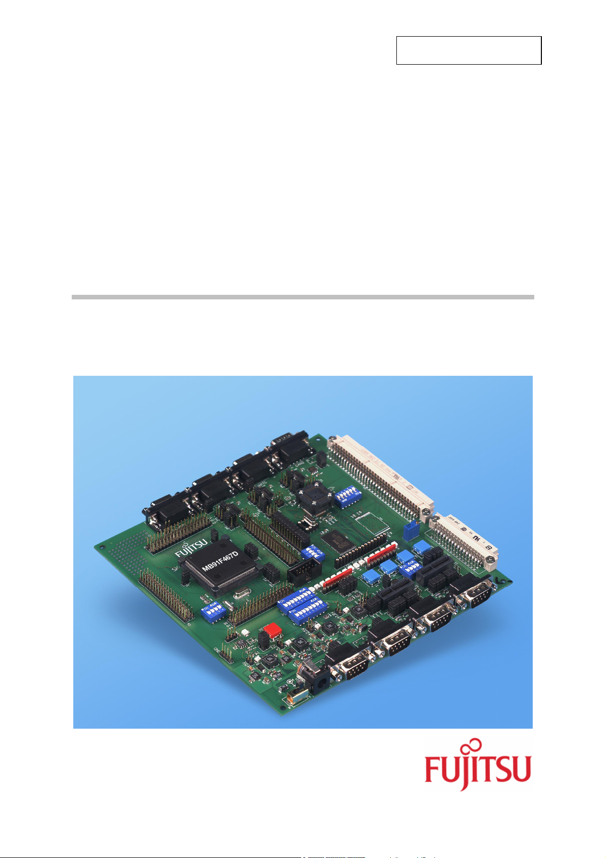
The SK-91F467-FLEXRAY is a multifunctional development board for the FUJITSU FlexRay
communication controller MB88121 and the 32-bit Flash microcontroller MB91F467DA. It
can be used stand alone for software development and testing or together with monitordebugger software.
The board allows the designer immediately to start with the software and system
development, before his own final target system is available.
© Fujitsu Microelectronics Europe GmbH - 7 - FMEMCU-UG-910017-11
Page 8

SK-91F467-FLEXRAY V1.1
Introduction
1.2 Features
• Supports 32-bit Flash microcontroller MB91F467D
• Supports FlexRay CC MB88121
• 9-12V (2000mA) unregulated external DC power supply
• 5V, 3.3V, 2.5V and 1.8V on-board switching regulators with power status-LEDs
• Triple supply monitor to watch 5V, 3.3V and selectable 2.5V or 1.8V
• On-board Memory:
o 32Mbit (4MByte) SRAM
• It is possible to connect the FlexRay CC in different ways to the MCU
• 16 bit non multiplexed / multiplexed bus
• 8 bit non multiplexed / multiplexed bus
• SPI communication
• All microcontroller resources available for evaluation
• All microcontroller pins routed to pin header
• In-Circuit serial Flash programming
• Three selectable RS-232 or LIN UART-interfaces
• Three High-Speed CAN interfaces
• Two FlexRay channels (Ch-A, Ch-B)
• FlexRay physical layer RS-485 available
• FlexRay physical layer driver module from TZM (FT1080) connectable
• 16 User LEDs
• optional: alphanumeric standard LC-Display connectable
• Reset button, Reset-LED
• 4 User buttons, one 8 bit MCU port can be connected to DIP switches
• External bus interface routed to 96pin and 48pin DIN 41612 (VG) connectors
This board must only be used for test applications
in an evaluation laboratory environment.
FMEMCU-UG-910017-11 - 8 - © Fujitsu Microelectronics Europe GmbH
Page 9

SK-91F467-FLEXRAY V1.1
Introduction
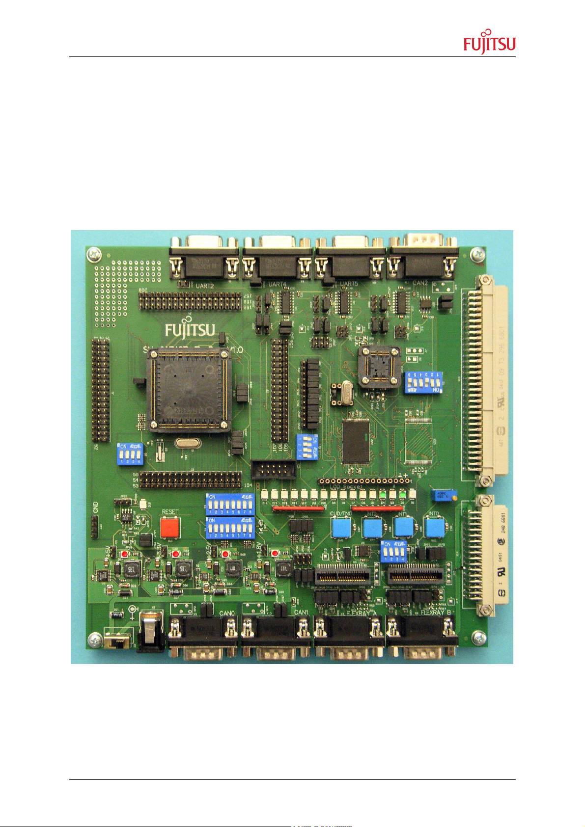
1.3 General Description
The SK-91F467-FLEXRAY supports the FUJITSU 32-bit Flash microcontroller MB91F467D
and the FUJITSU FlexRay stand alone communication controller MB88121.
The Starter Kit can be used as a stand-alone development platform, or if a MCU socket is
soldered instead of the Flash MCU MB91F467D, with the emulation system MB91V460
adapter board (MB2198-300) and 208 pin probe cable board (PB-91467D-NLS-208PFV).
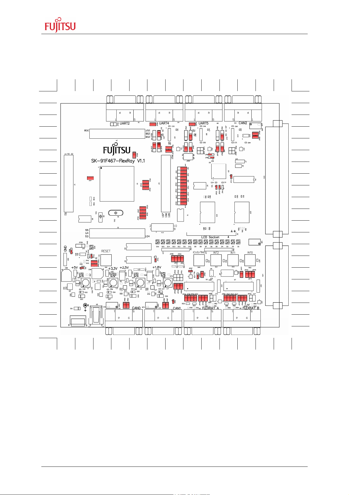
This User Guide is describing PCB version V1.1. The PCB version is printed at the TOP side
of the starter kit close to MB91F467D MCU [U1].
© Fujitsu Microelectronics Europe GmbH - 9 - FMEMCU-UG-910017-11
Page 10

SK-91F467-FLEXRAY V1.1
Introduction
1.3.1 On Board Memory
The starter kit includes 32MBit (4MByte) SRAM memory on board. The SRAM can be used
with 5V, or with 3.3V external bus supply voltage.
1.3.2 MCU Clocks
The board is supplied with a 4MHz crystal as the main oscillation clock for the MCU. Using
the internal PLL of the MCU, internal clock rates up to 100MHz can be achieved. The MCU
sub clock is connected to a 32.768 kHz crystal.
1.3.3 MCU Operating Mode
The operating mode of the microcontroller can be selected with the Dip-switch S5.
1.3.4 FlexRay CC Clock
The FlexRay CC clock is operated by a 10MHz crystal mounted in a socket. By removing the
10MHz crystal it is also possible to use an external clock oscillator.
1.3.5 FlexRay CC-MCU Connection
The FlexRay CC (MB88121) is connected to the MCU via external bus. It is possible to use it
in 8 bit / 16 bit multiplexed, 8 bit / 16 bit non multiplexed or SPI communication-mode
(dependent from revision of MB88121). With jumper or switches the user can change
between the different modes.
1.3.6 External Bus interface Connectors
Via DIN 41612 VG96ABC and VG48ABC connectors (external bus interface of the MCU), it
is possible to connect the FlexRay FPGA Board to the Starter Kit and use the FPGA as
FlexRay communication controller. It is also possible to connect other devices e.g. user
applications or Fujitsu graphic device sub boards.
1.3.7 FlexRay Physical Layer
The connection to the physical layer of the FlexRay bus with 9-pin D-Sub connectors (X2
and X6) is realized with RS485 transceiver, or it is also possible to deselect the RS485
transceiver and use pluggable physical layer driver module from TZM (FT1080) instead.
1.3.8 CAN Bus
Three high-speed CAN-transceivers (PCA82C250) are available to connect all available onchip CAN-controllers to 9-pin D-Sub connectors (X9, X10 and X11). The transceivers
provides differential transmit and receive capability between CAN-controller and CAN-bus.
1.3.9 RS-232 and LIN
RS-232 and LIN signals are shared on the 9-pin D-Sub connectors (X1, X4 and X8). It can
be selected, if RS-232 or LIN will be used.
Three separate RS-232 transceivers and three separate LIN transceivers are available, to
connect the on-chip USARTs to the 9-pin D-Sub connectors.
The RS-232 transceivers generate the adequate RS-232 levels for receive (RXD) and
transmit (TXD) lines. The RTS signal can be shortcut to CTS using jumpers (some PC
software needs this connection, when a 1:1 cable is used).
FMEMCU-UG-910017-11 - 10 - © Fujitsu Microelectronics Europe GmbH
Page 11

SK-91F467-FLEXRAY V1.1
Introduction
Either the DTR line or the RTS line of X1, X4 or X8 connectors can be selected to generate
a system reset.
The LIN transceivers (TLE6259) generate the adequate levels to drive the bus line in LINsystems for automotive and industrial applications.
1.3.10 MCU Pins
All 208 pins of the microcontroller are connected to the edge connectors J1, J2, J3 and J4
and are directly available to the user.
1.3.11 User Buttons
There are four push buttons on board, which can be connected to input-ports of the
microcontroller. Some ports may support additional functions like external interrupts (INT0,
INT1 and INT2) and trigger for the Reload Timer or Input-Capture (TIN0 / ICU0). One
additional button is reserved as System-Reset-button to reset the MCU and the FLEXRAY
CC simultaneously, but it is possible to disconnect the RST-ports with JP52 or JP54.
It is possible to connect with Dip-switch S3 eight port input switches at S4 to the MCU port
P26_D0 – P26_D7. All eight ports can be switched separately to use e.g. only four ports as
input.
1.3.12 User LEDs and optional LCD
Sixteen user-LEDs are connected via two pull-down resistor networks to port P25_D0 P25_D7 and to port P16_D0 - P16_D7. Parallel to the LEDs on port P25, the connector J6
can be used to connect a standard alphanumeric display. The resistor networks RN2 and
RN3 can be removed, to free the ports.
1.3.13 Power Supply
The four on-board step-down switching regulators allow the user to connect an unregulated
DC input voltage between +9V to +12V (max. 2000mA) to the starter-kit. The switching
regulators provide the voltages of 5V (3A), 3.3V (3A), 2.5V (1,5A) and 1.8V (1,5A) on the
starter kit. These voltages give also the possibility, to connect an optional graphic-controller
starter kit to the board. The switching regulators are short circuit protected and provide a
thermal shutdown.
If the SK-91F467-FLEXRAY starter-kit is connected to the Fujitsu FlexRay FPGA-board it is
possible, that the power supply for the SK-91F467-FLEXRAY will be provided by the FPGAboard and a power supply connection to the SK-91F467-FLEXRAY is not needed. For that
case the pins 14B, 15B and 16B of DIN 41612 VG48ABC connector X14 are used as
voltage input behind the SK-91F467-FLEXRAY on-board power switch, so that the power
switch on the FPGA board switches the whole system.
© Fujitsu Microelectronics Europe GmbH - 11 - FMEMCU-UG-910017-11
Page 12
SK-91F467-FLEXRAY V1.1
Installation
2 Installation
Remove the board carefully from the shipping carton.
First check if there are any damages before power on the starter kit.
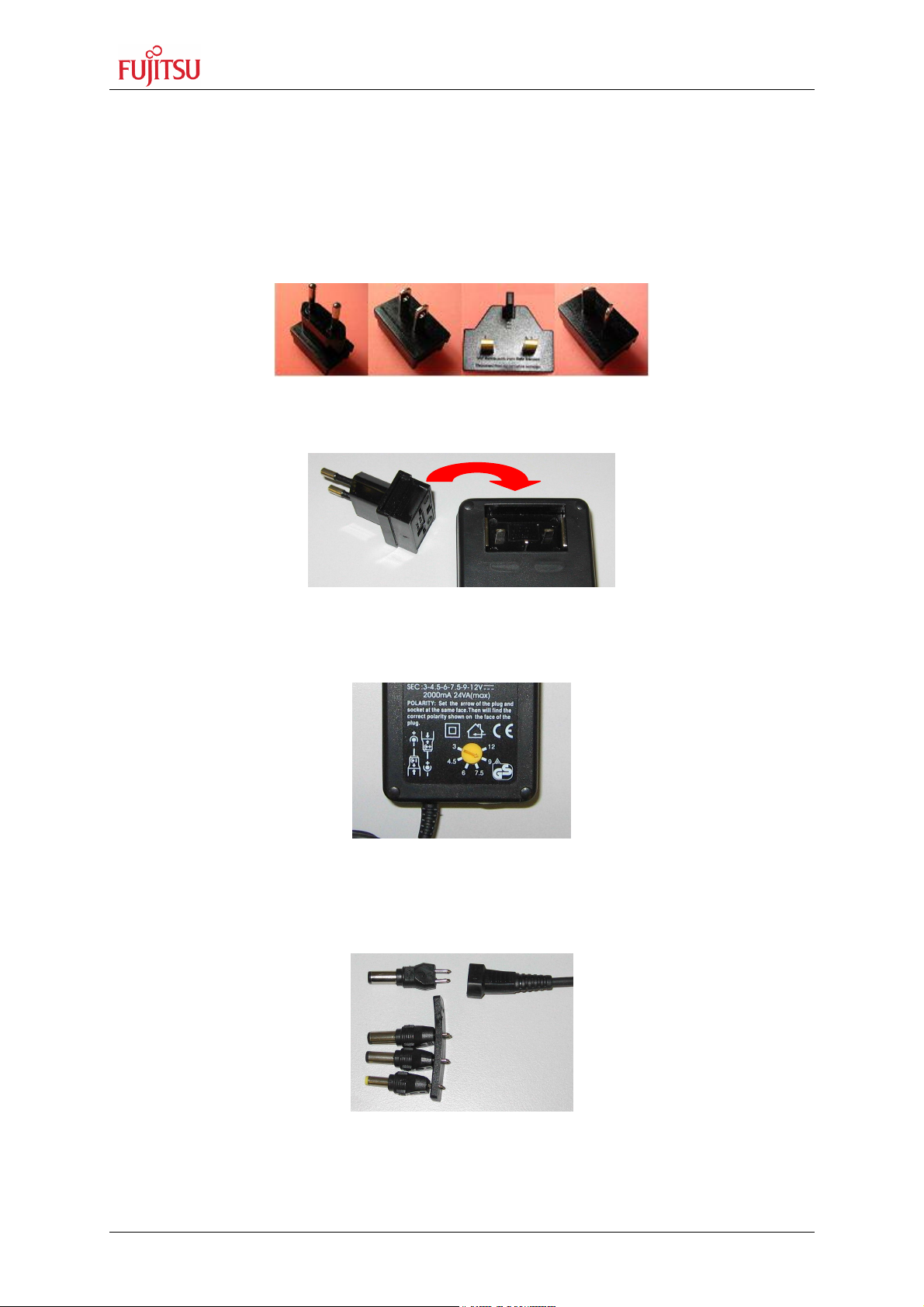
To supply the starter kit, use the delivered In-Plug AC-DC Adapter (UPA 2000). Select the
AC plug adapter suitable for your country power sockets
Figure 2-1: AC plug adapter
and insert this adapter into the connection terminal on the AC-DC adapter.
Figure 2-2: AC plug adapter selection
Check the selected output DC voltage of the AC-DC In-Plug adapter at the voltage selection
key. It should be 9V! Change the output voltage only in a powered-down condition!
Figure 2-3: DC voltage selection
Select the low voltage adapter suitable to the power connector X5 at the SK-91F467FLEXRAY and plug it to the connecting socket in the right orientation (+ connected to shield
and GND connected to centre pin).
Figure 2-4: Low voltage adapter selection
Now connect the DC low voltage adapter to the Starter kit and plug in the In-Plug Power
Supply to a power socket. The SK-91F467-FLEXRAY can be turned on with the on board
power switch S8 (or S9).
FMEMCU-UG-910017-11 - 12 - © Fujitsu Microelectronics Europe GmbH
Page 13
SK-91F467-FLEXRAY V1.1
Installation
For the power supply of the SK-91F467-FLEXRAY a DC input voltage of 9V – 12V is
recommended. The positive voltage (+) must be connected to the shield, and ground
(GND) must be connected to the centre of the connector X5!
After power-on of the SK-91F467-FLEXRAY, the four red power-on LEDs D24 (5V), D30
(3.3V), D34 (2.5V) and D40 (1.8V) should be light. The reset LED D18 should be off.
Additionally the LED D2 and D4 should be on. The starter kit is delivered with programmed
Softune Workbench Monitor Debugger in internal Flash of MB91F467D series. The monitor
debugger is checking also the external SRAM access at CS1. In case of successful access
to external SRAM the LED D2 and D4 are ON. In case of failed access LED D1 and D4 are
set to ON.
Figure 2-5: Starter kit status after power on
© Fujitsu Microelectronics Europe GmbH - 13 - FMEMCU-UG-910017-11
Page 14

SK-91F467-FLEXRAY V1.1
Installation
2.1 Jumper Settings
The following table lists all jumpers including its default setting and location on the starter kit.
The default jumper setting is described for 16 bit non multiplexed bus communication
between MCU and FlexRay CC.
Jumper Description / Function Type Default
JP1 ASSP A10 / INT2 Jumper 3 pin 1-2 G 7 1 / 3
JP2 ASSP A9 / INT3 Jumper 3 pin 1-2 G 7 1 / 3
JP3 ASSP A5 / SCK Jumper 3 pin 1-2 G 8 1 / 3
JP4 ASSP A4 / SDI Jumper 3 pin 1-2 G 8 1 / 3
JP5 ASSP A3 / SDO Jumper 3 pin 1-2 G 8 1 / 3
JP6 ASSP BCLK – MCU MCLKI Solder Jumper 2 pad Closed K 9 1 / 3
JP7 ASSP – MCU A0 connection Jumper 2 pin Closed B 8 1 / 3
JP8 ASSPVcc 5V / 3.3V Solder Jumper 3 pad 1-2 J 6 1 / 3
JP9 ASSPVcc1 ASSPVcc / 3.3V Solder Jumper 3 pad 1-2 J 6 1 / 3
JP10 ASSP D10 / MDS2 Jumper 3 pin 1-2 G 8 1 / 3
JP11 ASSP D9 / MDS1 Jumper 3 pin 1-2 G 9 1 / 3
JP12 ASSP D8 / MDS0 Jumper 3 pin 1-2 G 9 1 / 3
JP13 ASSP C-Pin – 1.8V Solder Jumper 2 pad Closed K 8 1 / 3
JP14 ASSP D5 / INT2 Jumper 3 pin 1-2 G 9 1 / 3
JP15 MCUVcc - AVcc Jumper 2 pin Closed E 9 1 / 3
JP16 AVcc - AVRH Jumper 2 pin Closed E 9 1 / 3
JP17 ASSP D4 / INT3 Jumper 3 pin 1-2 G 10 1 / 3
JP18 GND - AVss Jumper 2 pin Closed E 8 1 / 3
JP19 ASSP CS CSX3 / CSX6 Jumper 3 pin 1-2 G 10 1 / 3
JP20 ASSP ALE / INT2 Jumper 3 pin 1-2 G 10 1 / 3
JP21 VDD35 MCUVcc / 3.3V Solder Jumper 3 pad 1-2 F 15 1 / 3
JP22 ASSP BGT – 1.8V Solder Jumper 2 pad Closed J 9 1 / 3
JP23 MCUVcc – HVDD5 Jumper 2 pin Closed E 10 1 / 3
JP24 ASSP MT - GND Solder Jumper 2 pad Closed K 9 1 / 3
JP25 MCUVcc – VDD5R Jumper 2 pin Closed E 11 1 / 3
JP26 Vcc - MCUVcc Jumper 2 pin Closed E 11 1 / 3
JP27 MCUVcc – VDD5 Jumper 2 pin Closed E 11 1 / 3
JP28 GND – HVSS5 Jumper 2 pin Closed E 6 1 / 3
JP29 DTR select DTR / /DTR Jumper 3 pin Open B 14 2 / 3
JP30 UART2 RTS - CTS Jumper 2 pin Open D 3 2 / 3
JP31 FlexRay nSTB – P18_6 Jumper 2 pin Open G 16 2 / 3
JP32 FlexRay WAKE – P18_5 Jumper 2 pin Open G 16 2 / 3
JP33 FlexRay EN – P18_4 Jumper 2 pin Open G 16 2 / 3
JP34 FlexRay CHA RS485 Termination Jumper 2 pin Closed H 18 2 / 3
JP35 FlexRay RxD_A Jumper 2 pin Closed J 18 2 / 3
JP36 FlexRay CHA RS485 Termination Jumper 2 pin Closed H 18 2 / 3
JP37 UART2 RxD RS232 / LIN Jumper 3 pin 2-3 F 5 2 / 3
JP38
JP39
JP40
JP41
JP42
JP43
JP44
JP45
JP46
JP47
JP48
JP49
JP50
JP51
JP52
JP53 VccPL 5V / 3.3V
JP54 RESET - MCU RST
FlexRay CHA RS485 - BM
UART2 DTR / RTS
FlexRay TxEN_A
FlexRay CHA RS485 - BP
Watch 1.8V
Watch 2.5V
UART2 TxD RS232 / LIN
FlexRay TxD_A
UART2 RS232 / LIN
UART2 LIN Enable
FlexRay CHA EN
FlexRay CHA WAKE
FlexRay CHA nSTB
UART2 LIN Master Yes / No
RESET - ASSP RST
Jumper 2 pin Closed
Jumper 3 pin Open F 4 2 / 3
Jumper 2 pin Closed J 18 2 / 3
Jumper 2 pin Closed
Solder Jumper 2 pad Open
Solder Jumper 2 pad Closed B 15 2 / 3
Jumper 3 pin 2-3 F 5 2 / 3
Jumper 2 pin Closed H 18 2 / 3
Jumper 3 pin 2-3 F 4 2 / 3
Jumper 2 pin Closed G 6 2 / 3
Jumper 2 pin Closed G 17 2 / 3
Jumper 2 pin Closed G 17 2 / 3
Jumper 2 pin Closed G 17 2 / 3
Jumper 2 pin Closed G 5 2 / 3
Jumper 2 pin Closed B 16 2 / 3
Solder Jumper 3 pad 1-2
Jumper 2 pin Closed
Layout
Coordinates
H 18
H 18
B 15
H 16
B 15
Schematic
Page
2 / 3
2 / 3
2 / 3
2 / 3
2 / 3
FMEMCU-UG-910017-11 - 14 - © Fujitsu Microelectronics Europe GmbH
Page 15
SK-91F467-FLEXRAY V1.1
Installation
Jumper Description / Function Type Default
JP55 FlexRay CHA nERR – P14_4
JP56 FlexRay CHA VBat
JP57 UARTX RST Select
JP58
JP59
JP60 UART4 RxD RS232 / LIN
JP61
JP62
JP63 FlexRay CHB RS485 - BM
JP64 UART4 DTR / RTS
JP65 UART4 TxD RS232 / LIN
JP66 FlexRay TxEN_B
JP67
JP68 Vcc 5V / 3.3V
JP69 UART4 RS232 / LIN
JP70 FlexRay TxD_B
JP71 UART4 LIN Enable
JP72 UART4 LIN Master Yes / No
JP73 FlexRay CHB EN
JP74 FlexRay CHB WAKE
JP75 FlexRay CHB nSTB
JP76 FlexRay CHB nERR – P14_7
JP77
JP78 UART5 RTS - CTS Jumper 2 pin Closed H 3 2 / 3
JP79 UART5 RxD RS232 / LIN Jumper 3 pin 1-2 J 5 2 / 3
JP80
JP81
JP82 CAN0 RxD Jumper 2 pin
JP83 CAN0 TxD Jumper 2 pin Closed D 19 2 / 3
JP84
JP85
JP86
JP87 CAN1 RxD Jumper 2 pin
JP88 CAN1 TxD Jumper 2 pin Closed F 19 2 / 3
JP89 CAN2 RxD Jumper 2 pin
JP90 CAN2 TxD Jumper 2 pin Closed M 4 2 / 3
JP91 Vin – Ext Voltage Solder Jumper 2 pad Closed G 18 3 / 3
JP92 INT0 Jumper 2 pin Closed G 15 3 / 3
JP93 INT1 Jumper 2 pin Closed G 15 3 / 3
JP94 INT2 Jumper 2 pin Closed G 15 3 / 3
JP95 ICU0/TIN0 Jumper 2 pin Closed G 15 3 / 3
JP96 Direct RESET Solder Jumper 3 pad 1-2 A 14 2 / 3
JP97 VCC1V8 to X14B2 Solder Jumper 2 pad Closed H 16 3 / 3
UART4 RTS - CTS Jumper 2 pin Closed
FlexRay CHB RS485 Termination
FlexRay RxD_B Jumper 2 pin Closed
FlexRay CHB RS485 Termination
FlexRay CHB RS485 - BP
FlexRay CHB VBat
UART5 DTR / RTS
UART5 TxD RS232 / LIN
UART5 RS232 / LIN
UART5 LIN Enable
UART5 LIN Master Yes / No
Jumper 2 pin
Jumper 2 pin
Jumper 6 pin
Jumper 2 pin Closed
Jumper 3 pin 1-2
Jumper 2 pin Closed
Jumper 2 pin Closed
Jumper 3 pin Open
Jumper 3 pin 1-2
Jumper 2 pin Closed
Jumper 2 pin Closed K 18 2 / 3
Solder Jumper 3 pad 1-2
Jumper 3 pin 1-2
Jumper 2 pin Closed
Jumper 2 pin Open
Jumper 2 pin Open
Jumper 2 pin Closed
Jumper 2 pin Closed
Jumper 2 pin Closed
Jumper 2 pin
Jumper 2 pin
Jumper 3 pin Open J 4 2 / 3
Jumper 3 pin 1-2 K 5 2 / 3
Jumper 3 pin 1-2 K 4 2 / 3
Jumper 2 pin Open K 6 2 / 3
Jumper 2 pin Open K 6 2 / 3
Open J 18
Closed J 16
Open H 6
Open L 18
Closed
Closed
Closed
Closed
Layout
Coordinates
F 3
K 18
H 5
L 18
K 18
K 18
H 4
H 5
L 18
B 16
H 4
L 18
H 6
H 6
L 16
L 16
L 16
L 16 2 / 3
D 19 2 / 3
G 19 2 / 3
M 4 2 / 3
Schematic
Page
2 / 3
2 / 3
2 / 3
2 / 3
2 / 3
2 / 3
2 / 3
2 / 3
2 / 3
2 / 3
2 / 3
2 / 3
2 / 3
2 / 3
2 / 3
2 / 3
2 / 3
2 / 3
2 / 3
2 / 3
2 / 3
Table 2-1: Jumper settings
© Fujitsu Microelectronics Europe GmbH - 15 - FMEMCU-UG-910017-11
Page 16
SK-91F467-FLEXRAY V1.1
Installation
2.2 Jumper Location
The following picture shows the silk plot of the starter kit with marked default jumper settings.
A B C D E F G H J K L M N
1 1
2 2
3 3
4 4
5 5
6 6
7 7
8 8
9 9
10 10
11 11
12 12
13 13
14 14
15 15
16 16
17 17
18 18
19 19
20 20
21
21
A B C D E F G H J K L M N
Figure 2-6: Default Jumper Settings
FMEMCU-UG-910017-11 - 16 - © Fujitsu Microelectronics Europe GmbH
Page 17
SK-91F467-FLEXRAY V1.1
Installation
2.3 Software Installation
2.3.1 Installation of Softune Workbench
Fujitsu supplies a full working 32bit development environment with the “SK-91F467FLEXRAY” starter kit called Softune Workbench V6. The Softune Workbench also supports
a monitor debugger which is pre-programmed into the internal Flash memory of the “SK91F467-FLEXRAY”. To develop own software and to work with the Monitor Debugger of the
“SK-91F467-FLEXRAY” the Softune Workbench development environment must be installed
first. Follow the instructions for successful installation of the Softune Workbench.
1) Before starting the installation setup ensure that you are logged in with administrator
or power user permissions, otherwise the Softune installation will fail! Be aware that
Softune does not support multi-user support. Therefore install- and user login must
be the same.
2) Browse on the starter kit CD-ROM into the directory Software\SWBInstall and start
the setup.exe
You can also start the installation using a browser by opening the index.html of the
CD-ROM. Use the link “Software\Softune Workbench\” in the left side frame.
3) Follow the installation instructions
4) For the default installation path it is recommended to use c:\Softune32
5) After the installation is finished, Softune Workbench for FR can be started via the
Windows “Start” menu
Figure 2-7: Softune Workbench start menu location
6) When Softune Workbench is started the following window will be shown
© Fujitsu Microelectronics Europe GmbH - 17 - FMEMCU-UG-910017-11
Page 18

SK-91F467-FLEXRAY V1.1
Installation
Figure 2-8: Softune Workbench V6 IDE
FMEMCU-UG-910017-11 - 18 - © Fujitsu Microelectronics Europe GmbH
Page 19
SK-91F467-FLEXRAY V1.1
1 2 3 4
MD0 MD1 MD2 nc
Jumpers and Switches
3 Jumpers and Switches
This chapter describes all jumpers and switches that can be modified on the starter kit. The
default setting is shown with a grey shaded area.
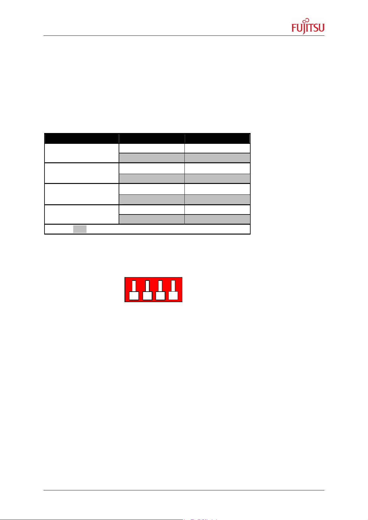
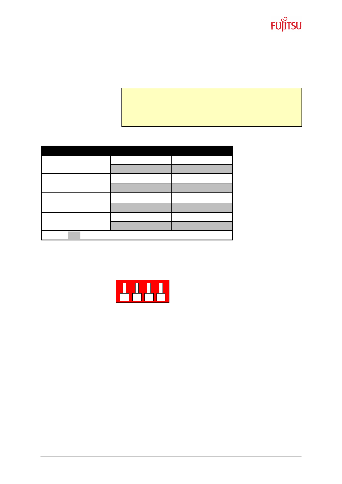
3.1 MCU Operating-Mode (S5)
The DIP-switch S5 is used to set the operating mode of the MCU. Ensure that the mode pin
settings correspond to the operation-mode of the application. For more detailed information
please check the Hardware-Manual of the microcontroller.
DIP switch Setting Logical value
S5/1 (MD0)
ON (closed) 1 (high)
OFF (open) 0 (low)
S5/2 (MD1)
ON (closed) 1 (high)
OFF (open) 0 (low)
S5/3 (MD2)
ON (closed) 1 (high)
OFF (open) 0 (low)
S5/4 (Not used)
ON (closed) Not connected
OFF (open) Not connected
Default: grey
Table 3-1: MCU Operating Mode
By default, the “Single Chip Run-Mode” of MB91F467DA is selected.
Dip-Switch S5
(default setting)
ON
OFF
Figure 3-1: MCU Mode Switch
© Fujitsu Microelectronics Europe GmbH - 19 - FMEMCU-UG-910017-11
Page 20
SK-91F467-FLEXRAY V1.1
1 2 3 4 5 6
Jumpers and Switches
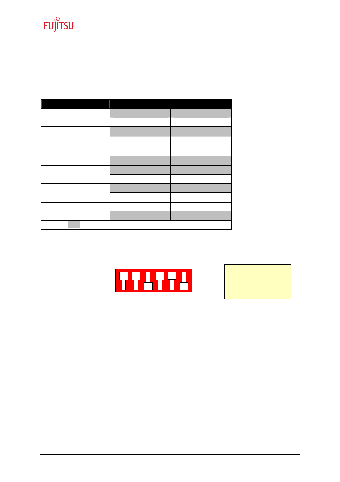
3.2 FlexRay CC Operating-Mode (S2)
The DIP-switch S2 is used to set the operating mode of the FlexRay communication
controller. Ensure that the mode pin settings correspond to the operation-mode of the
application. For more detailed information please check the Hardware-Manual of the
FlexRay CC.
DIP switch Setting Logical value
S2/1 (MD0)
ON (closed) 0 (low)
OFF (open) 1 (high)
S2/2 (MD1)
ON (closed) 0 (low)
OFF (open) 1 (high)
S2/3 (MD2)
ON (closed) 0 (low)
OFF (open) 1 (high)
S2/4 (MDE0)
ON (closed) 0 (low)
OFF (open) 1 (high)
S2/5 (MDE1)
ON (closed) 0 (low)
OFF (open) 1 (high)
S2/6 (MDE2)
ON (closed) 0 (low)
OFF (open) 1 (high)
Default: grey
Table 3-2: FlexRay CC Operating Mode
By default, the “16-bit non multiplexed mode” is selected.
Dip-Switch S2
(default setting)
MD0 MD1 MD2 MDE0 MDE1 MDE2
ON
OFF
Note:
The DIP-switch (S2)
on PCB rotated 180°
Figure 3-2: FlexRay CC Mode Switch
FMEMCU-UG-910017-11 - 20 - © Fujitsu Microelectronics Europe GmbH
Page 21
SK-91F467-FLEXRAY V1.1
1 2 3 4
Jumpers and Switches
3.3 FlexRay CC SPI Settings (S1)
The DIP-switch S1 is used to set the FlexRay CC SPI settings, if the FlexRay CC is selected
to communicate with the MCU over SPI. For more detailed information please check the
Hardware-Manual of the FlexRay CC.
Note:
he DIP-switch (S1) is connected to the FlexRay CC in case the
T
jumpers setting are set to SPI communication mode. Please refer
to chapter 3.5 MCU-FlexRay CC Connection.
DIP switch Setting Logical value
S1/1 (MDS0)
ON (closed) 0 (low)
OFF (open) 1 (high)
S1/2 (MDS1)
ON (closed) 0 (low)
OFF (open) 1 (high)
S1/3 (MDS2)
ON (closed) 0 (low)
OFF (open) 1 (high)
S1/4 (Not used)
ON (closed) Not connected
OFF (open) Not connected
Default: grey
Table 3-3: FlexRay CC SPI Settings
The SPI function is not jet supported by MB88121!
Dip-Switch S1
(default setting)
MDS0 MDS1 MDS2 nc
ON
OFF
Figure 3-3: FlexRay CC SPI-Mode Switch
© Fujitsu Microelectronics Europe GmbH - 21 - FMEMCU-UG-910017-11
Page 22
SK-91F467-FLEXRAY V1.1
Jumpers and Switches
3.4 Power Supply
There are four on-board switching regulators to provide the voltages 5V, 3.3V, 2.5V and
1.8V on the starter-kit. With the power ON/OFF-switch S8 or S9 (S9 is a soldering option to
use a different switch), the main input voltage from DC-connector X5 will be connected to the
VIN voltage of the board. The VIN voltage supplies the switching regulators and the VBat
voltage of the FlexRay physical layer driver modules from TZM (FT1080), if they are
connected to X3 and X7.
Switch Setting Description
S8 or S9
Default: grey
With JP91 the pins B14, B15 and B16 of the external bus interface connector X14 can be
connected to the VIN voltage, so that it is possible to supply the board from an external
connected board e.g. the Fujitsu FlexRay FPGA board.
ON (1-2) Power ON
OFF (2-3) Power OFF
Table 3-4: Power Switch
There is a triple supply monitor on-board, which monitors three of the four DC output
voltages and generates a system reset, in case with wrong levels of the on board voltages.
5V and 3.3V are always monitored and the third monitored voltage can be selected with the
solder jumpers JP42 and JP43.
With JP68 it is possible to select the whole board supply voltage Vcc to 5V or 3.3V
Jumper Setting Description
JP91
ON (closed) Vin connected to X14 pins B14, B15 and B16
OFF (open) Vin not connected to X14 pins B14, B15 and B16
JP42
ON (closed) Vcc1V8 connected to supply monitor
OFF (open) Vcc1V8 not connected to supply monitor
JP43
ON (closed) Vcc2V5 connected to supply monitor
OFF (open) Vcc2V5 not connected to supply monitor
JP68
1-2 Vcc is connected to 5V
2-3 Vcc is connected to 3.3V
Default: grey
Table 3-5: Power supply configurations
FMEMCU-UG-910017-11 - 22 - © Fujitsu Microelectronics Europe GmbH
Page 23

SK-91F467-FLEXRAY V1.1
Jumpers and Switches
Figure 3-4: Voltage Test Points
Regulator Test point Voltage
U9 J21 +5V
U11 J22 +3.3V
U14 J23 +2.5V
U17 J24 +1.8V
- J20 GND
Table 3-6: Voltage Test Points
© Fujitsu Microelectronics Europe GmbH - 23 - FMEMCU-UG-910017-11
Page 24

SK-91F467-FLEXRAY V1.1
Jumpers and Switches
3.4.1 MCU Power Supply Voltage
P21 With this jumper it is possible to connect the MCU external bus interface supply
J
VDD35 to 3.3V. The MCU MB91460 series supports the function to supply the MCU
with 5V so that the normal I/O ports work with 5V and supply the external bus
interface with 3.3V.
JP23 This jumper is used to connect the HVDD5 supply to MCUVcc. The HVDD5 is the
MCU supply voltage for the high current ports.
JP25 This jumper is used to connect the VDD5R MCU supply pins to MCUVcc
JP26 This jumper is used to connect the Vcc voltage to MCUVcc.
JP27 This jumper is used to connect the VDD5 MCU supply pins to MCUVcc
JP28 This jumper is used to connect the HVSS5 MCU pins to GND. HVSS5 are the GND
pins for the high current ports.
Note:
JP23, JP25, JP26, JP27 and JP28 can be used for
measurements of power consumption of the MCU.
Jumper Setting Description
JP21
1-2 VDD35 connected to MCUVcc
2-3 VDD35 connected to 3.3V
JP23
ON (closed) HVDD5 connected to MCUVcc
OFF (open) HVDD5 not connected to MCUVcc
JP25
ON (closed) VDD5R connected to MCUVcc
OFF (open) VDD5R not connected to MCUVcc
JP26
ON (closed) MCUVcc connected to Vcc
OFF (open) MCUVcc not connected to Vcc
JP27
ON (closed) VDD5 connected to MCUVcc
OFF (open) VDD5 not connected to MCUVcc
JP28
ON (closed) HVSS5 connected to GND
OFF (open) HVSS5 not connected to GND
Default: grey
Table 3-7: MCU Power Supply SK-91F467-FLEXRAY
3.4.2 MCU Analogue Power Supply Voltage
The power supply as well as the reference voltage for the A/D-converter can be provided
internally or externally.
JP15 Connects power supply AVcc of the A/D converter to MCUVcc
JP16 Connects high reference voltage AVRH of the A/D converter to AVcc
JP18 Connects AVss of the A/D converter to GND
FMEMCU-UG-910017-11 - 24 - © Fujitsu Microelectronics Europe GmbH
Page 25

SK-91F467-FLEXRAY V1.1
Jumpers and Switches
Jumper Setting Description
JP15
ON (closed) AVcc is connected to MCUVcc
OFF (open) AVcc is disconnected
JP16
JP18
ON (closed) AVRH is connected to AVcc
OFF (open) AVRH defined by resistor network
ON (closed) AVss is connected to GND
*1
OFF (open) AVss is disconnected
Default: grey
*1
By default the resistor network (R10 and R13) is not assembled on the board
Table 3-8: MCU ADC Supply
Note:
If JP15 or JP18 are open, the user has to supply an adequate analogue voltage supply (AVcc
and AVss) to the A/D-converter.
If JP16 is open, the potential divider comprising resistors R10 and R13 define AVRH.
3.4.3 FlexRay CC Power Supply Voltage at SK-91F467-FLEXRAY
JP8 Connects 5V or 3.3V voltage supply to ASSPVcc
JP9 Connects 3.3V or ASSPVcc to ASSP voltage supply pin Vcc1 (3.3V by default)
JP13 Connects ASSP C-pin to 1.8V voltage supply
JP22 Connects ASSP pin 8 to 1.8V voltage supply
JP24 Connects ASSP pin 9 to GND
Jumper Setting Description
JP8
JP9
JP13
JP22
JP24
Default: grey
1-2 5V connected to ASSPVcc
2-3 3.3V connected to ASSPVcc
1-2 3.3V connected to ASSP Vcc1 pin
2-3 ASSPVcc connected to ASSP Vcc1 pin
ON (closed) 1.8V connected to ASSP C-pin
OFF (open) 1.8V not connected to ASSP C-pin
ON (closed) 1.8V connected to ASSP pin 8
OFF (open) 1.8V not connected to ASSP pin 8
ON (closed) GND connected to ASSP pin 9
OFF (open) GND not connected to ASSP pin 9
Table 3-9: FlexRay CC Supply
© Fujitsu Microelectronics Europe GmbH - 25 - FMEMCU-UG-910017-11
Page 26

SK-91F467-FLEXRAY V1.1
Jumpers and Switches
3.5 MCU-FlexRay CC Connection at SK-91F467-FLEXRAY
The FlexRay communication controller MB88121 provides different communication modes to
a microcontroller. The MB88121 has different pin functions in its communication modes.
Therefore it is possible to connect the CC in different ways to the MCU, to evaluate the
different communication modes.
JP1 Connects MCU INT6 or MCU A10 to CC pin 35 (INT2 / A10)
JP2 Connects MCU INT7 or MCU A9 to CC pin 36 (INT3 / A9)
JP3 Connects MCU A5 or MCU SCK6 to CC pin 40 (SCK / A5)
JP4 Connects MCU A4 or MCU SOT6 to CC pin 41 (SDI / A4)
JP5 Connects MCU A3 or MCU SIN6 to CC pin 42 (SDO / A3)
JP7 Connects MCU A0 with CC A0
JP10 Connects MCU D26 or CC SPI-mode switch S1-3 (MDS2) to CC pin 53 (AD10 /
D10 / AD2 / D2 / MDS2)
JP11 Connects MCU D25 or CC SPI-mode switch S1-2 (MDS1) to CC pin 54 (AD9 /
D9 / AD1 / D1 / MDS1)
JP12 Connects MCU D24 or CC SPI-mode switch S1-1 (MDS0) to CC pin 55 (AD8 /
D8 / AD0 / D0 / MDS0)
JP14 Connects MCU D21 or MCU INT6 to CC pin 58 (AD5 / INT2)
JP17 Connects MCU D20 or MCU INT7 to CC pin 59 (AD4 / INT3)
JP19 Connects MCU CSX3 or MCU CSX6 to CC pin 19 (CS)
JP20 Connects MCU INT6 or MCU ASX to CC pin 22 (ALE / INT2)
Note:
For more information about the FlexRay CC modes and the
different pin functions, please refer to MB88121 documentation.
Jumper Setting Description
JP1
1-2 MCU INT6 connected to CC INT2
2-3 MCU A10 connected to CC A10
JP2
1-2 MCU INT7 connected to CC INT3
2-3 MCU A9 connected to CC A9
JP3
1-2 MCU A5 connected to CC A5
2-3 MCU SCK6 connected to CC SCK
JP4
1-2 MCU A4 connected to CC A4
2-3 MCU SOT6 connected to CC SDI
JP5
1-2 MCU A3 connected to CC A3
2-3 MCU SIN6 connected to CC SDO
JP7
ON (closed) MCU A0 is connected to CC A0
OFF (open) MCU A0 is not connected to CC A0
JP10 1-2 MCU D26 connected to CC AD2 / AD10
FMEMCU-UG-910017-11 - 26 - © Fujitsu Microelectronics Europe GmbH
Page 27

SK-91F467-FLEXRAY V1.1
Jumpers and Switches
Jumper Setting Description
2-3 CC SPI-mode switch S1-3 connected to CC MDS2
P11
J
1-2 MCU D25 connected to CC AD1 / AD9
2-3 CC SPI-mode switch S1-2 connected to CC MDS1
JP12
1-2 MCU D24 connected to CC AD0 / AD8
2-3 CC SPI-mode switch S1-1 connected to CC MDS0
JP14
1-2 MCU D21 connected to CC AD5
2-3 MCU INT6 connected to CC INT2
JP17
1-2 MCU D20 connected to CC AD4
2-3 MCU INT7 connected to CC INT3
JP19
1-2 MCU CSX3 connected to CC CS
2-3 MCU CSX6 connected to CC CS
JP20
1-2 MCU INT6 connected to CC INT2
2-3 MCU ASX connected to CC ALE
Default: grey
Table 3-10: MCU-FlexRay CC Connection
3.6 FlexRay Physical Layer
The SK-91F467-FLEXRAY provides different FlexRay physical layer communication. The
default setting is for RS-485 physical layer communication (on board). To test the original
FlexRay physical layer transceiver, it is possible to deselect the RS-485 transceiver and plug
in FlexRay physical layer driver module from TZM (FT1080). With the TZM (FT1080)
modules the user has the possibility to evaluate transceiver chips from different vendors
quite easy.
Note:
Disconnect the RS-485 physical layer transceiver signals before
plugging in the FT1080 modules to X3 and X7.
3.6.1 Channel A
JP35 Connects FlexRay channel A RxD to RS-485 transceiver (FT1080 must not be
plugged in X3!)
JP40 Connects FlexRay channel A TxEN to RS-485 transceiver (FT1080 must not be
plugged in X3!)
JP45 Connects FlexRay channel A TxD to RS-485 transceiver (FT1080 must not be
plugged in X3!)
JP38 Connects FlexRay channel A RS-485 transceiver output B to Sub-D-9
connector (X2)
JP41 Connects FlexRay channel A RS-485 transceiver output A to Sub-D-9
connector (X2)
JP34, JP36 Connects RS-485 termination network to signal lines at FlexRay channel A
JP48 Connects FT1080 module CH-A EN to configuration switch S6
© Fujitsu Microelectronics Europe GmbH - 27 - FMEMCU-UG-910017-11
Page 28

SK-91F467-FLEXRAY V1.1
Jumpers and Switches
JP49 Connects FT1080 module CH-A WAKE to configuration switch S6
P50 Connects FT1080 module CH-A nSTB to configuration switch S6
J
JP55 Connects FT1080 module CH-A nERR to MCU port P14_4
JP53 Selects VccPL (supply voltage of CH-A and CH-B FT1080 modules) 3.3V or 5V
JP56 Connects FT1080 module CH-A VBat to VBat (input voltage of the starter kit)
Jumper Setting Description
JP35
ON (closed) TXDA connected to RS-485 transceiver
OFF (open) TXDA not connected to RS-485 transceiver
JP40
ON (closed) TXENA connected to RS-485 transceiver
OFF (open) TXENA not connected to RS-485 transceiver
JP45
ON (closed) RXDA connected to RS-485 transceiver
OFF (open) RXDA not connected to RS-485 transceiver
JP38
ON (closed) CH-A RS-485 output B connected to X2
OFF (open) CH-A RS-485 output B not connected to X2
JP41
ON (closed) CH-A RS-485 output A connected to X2
OFF (open) CH-A RS-485 output A not connected to X2
JP34, JP36
ON (closed) Line termination connected to CH-A RS-485
OFF (open) Line termination not connected to CH-A RS-485
JP48
ON (closed) CH-A FT1080 EN connected to S6
OFF (open) CH-A FT1080 EN connected to S6
JP49
ON (closed) CH-A FT1080 WAKE connected to S6
OFF (open) CH-A FT1080 WAKE connected to S6
JP50
ON (closed) CH-A FT1080 nSTB connected to S6
OFF (open) CH-A FT1080 nSTB connected to S6
JP55
ON (closed) CH-A FT1080 nERR connected to MCU P14_4
OFF (open) CH-A FT1080 nERR not connected to MCU P14_4
JP53
1-2 Vcc 5V is connected to VccPL
2-3 Vcc 3.3V is connected to VccPL
JP56
ON (closed) VBat is connected to FT1080 CH-A
OFF (open) VBat is not connected to FT1080 CH-A
Default: grey
Table 3-11: FlexRay CH-A Configuration
3.6.2 Channel B
JP61 Connects FlexRay channel B RxD to RS-485 transceiver (FT1080 must not be
plugged in X7!)
JP66 Connects FlexRay channel B TxEN to RS-485 transceiver (FT1080 must not be
plugged in X7!)
JP70 Connects FlexRay channel B TxD to RS-485 transceiver (FT1080 must not be
plugged in X7!)
FMEMCU-UG-910017-11 - 28 - © Fujitsu Microelectronics Europe GmbH
Page 29

SK-91F467-FLEXRAY V1.1
Jumpers and Switches
JP63 Connects FlexRay channel B RS-485 transceiver output B to Sub-D-9
connector (X6)
JP67 Connects FlexRay channel B RS-485 transceiver output A to Sub-D-9
connector (X6)
JP59, JP62 Connects RS-485 termination network to signal lines at FlexRay channel B
JP73 Connects FT1080 module CH-B EN to configuration switch S6
JP74 Connects FT1080 module CH-B WAKE to configuration switch S6
JP75 Connects FT1080 module CH-B nSTB to configuration switch S6
JP76 Connects FT1080 module CH-B nERR to MCU port P14_7
JP77 Connects FT1080 module CH-B VBat to VBat (input voltage of the starter kit)
Jumper Setting Description
JP61
ON (closed) TXDB connected to RS-485 transceiver
OFF (open) TXDB not connected to RS-485 transceiver
JP66
ON (closed) TXENB connected to RS-485 transceiver
OFF (open) TXENB not connected to RS-485 transceiver
JP70
ON (closed) RXDB connected to RS-485 transceiver
OFF (open) RXDB not connected to RS-485 transceiver
JP63
ON (closed) CH-B RS-485 output B connected to X6
OFF (open) CH-B RS-485 output B not connected to X6
JP67
ON (closed) CH-B RS-485 output A connected to X6
OFF (open) CH-B RS-485 output A not connected to X6
JP59, JP62
ON (closed) Line termination connected to CH-B RS-485
OFF (open) Line termination not connected to CH-B RS-485
JP73
ON (closed) CH-B FT1080 EN connected to S6
OFF (open) CH-B FT1080 EN connected to S6
JP74
ON (closed) CH-B FT1080 WAKE connected to S6
OFF (open) CH-B FT1080 WAKE connected to S6
JP75
ON (closed) CH-B FT1080 nSTB connected to S6
OFF (open) CH-B FT1080 nSTB connected to S6
JP76
ON (closed) CH-B FT1080 nERR connected to MCU P14_7
OFF (open) CH-B FT1080 nERR not connected to MCU P14_7
JP77
ON (closed) VBat is connected to FT1080 CH-B
OFF (open) VBat is not connected to FT1080 CH-B
Default: grey
Table 3-12: FlexRay CH-B Configuration
© Fujitsu Microelectronics Europe GmbH - 29 - FMEMCU-UG-910017-11
Page 30

SK-91F467-FLEXRAY V1.1
1 2 3 4
EN
WAKE
nSTB
nc
Jumpers and Switches
3.6.3 FT1080 Control Settings (S6)
The DIP switch S6 is used to set EN, WAKE and nSTB signals of the FlexRay physical layer
driver modules from TZM (FT1080). The control signals can also be connected with jumper
to the MCU to give the possibility to set them via user software. Both modules (FT1080) will
be set simultaneously, if JP48-JP50 and JP73-JP75 are closed.
DIP switch Setting Logical value
S6/1 (EN)
ON (closed) 0 (low)
OFF (open) 1 (high)
S6/2 (WAKE)
ON (closed) 0 (low)
OFF (open) 1 (high)
S6/3 (nSTB)
ON (closed) 0 (low)
OFF (open) 1 (high)
S6/4 (Not used)
ON (closed) Not connected
OFF (open) Not connected
Default: grey
Table 3-13: FT1080 Control Settings
Dip-Switch S6
(default setting)
ON
OFF
Figure 3-5: FT1080 Control Switch
JP31 Connects nSTB signal of FT1080 modules to MCU port 18_6
JP32 Connects WAKE signal of FT1080 modules to MCU port 18_5
JP33 Connects EN signal of FT1080 modules to MCU port 18_4
Jumper Setting Description
JP31
ON (closed) nSTB is connected to MCU P18_6
OFF (open) No connection to the microcontroller
JP32
ON (closed) WAKE is connected to MCU P18_5
OFF (open) No connection to the microcontroller
JP33
ON (closed) EN is connected to MCU P18_4
OFF (open) No connection to the microcontroller
Default: grey
Table 3-14: FT1080 Connection to MCU
FMEMCU-UG-910017-11 - 30 - © Fujitsu Microelectronics Europe GmbH
Page 31

SK-91F467-FLEXRAY V1.1
Jumpers and Switches
3.7 CAN0 – CAN2
Three high-speed CAN-transceivers (PCA82C250) are on-board to connect all available onchip CAN to 9-pin D-Sub connectors (X9, X10 and X11).
JP82 Connects MCU RX0 to CAN transceiver U15
JP83 Connects MCU TX0 to CAN transceiver U15
JP87 Connects MCU RX1 to CAN transceiver U18
JP88 Connects MCU TX1 to CAN transceiver U18
JP89 Connects MCU RX2 to CAN transceiver U19
JP90 Connects MCU TX2 to CAN transceiver U19
Jumper Setting Description
JP82
JP83
JP87
JP88
JP89
JP90
Default: grey
ON (closed) CAN0 RxD connected to MCU
OFF (open) No connection to the microcontroller
ON (closed) CAN0 TxD connected to MCU
OFF (open) No connection to the microcontroller
ON (closed) CAN1 RxD connected to MCU
OFF (open) No connection to the microcontroller
ON (closed) CAN1 TxD connected to MCU
OFF (open) No connection to the microcontroller
ON (closed) CAN2 RxD connected to MCU
OFF (open) No connection to the microcontroller
ON (closed) CAN2 TxD connected to MCU
OFF (open) No connection to the microcontroller
Table 3-15: CAN-MCU connection
3.8 LIN / RS-232 UART
There are three UART connectors X1, X4 and X8 (9-pin D-Sub) on-board, which can be
used for RS-232 or LIN communication (to get information in detail about pin usage, please
refer to chapter 4.2 UART / LIN Connector (X1, X4, X8)). The LIN transceiver needs to be
configured as LIN-master or LIN-slave.
© Fujitsu Microelectronics Europe GmbH - 31 - FMEMCU-UG-910017-11
Page 32

SK-91F467-FLEXRAY V1.1
Jumpers and Switches
3.8.1 UART 2
UART2 (connector X1) is selected as LIN master at default setting.
P37 Select, if SIN2 is connected to RS-232- or LIN-transceiver
J
JP44 Select, if SOT2 is connected to RS-232- or LIN-transceiver
JP46 Select, if RS-232- or LIN-transceiver is connected to X1 pin2 (shared pin)
JP30 Some terminal programs needs a connection between CTS and RTS
JP39 Selects, if DTR or RTS will be used for system reset generation
JP47 Enables the LIN transceiver
JP51 Selects, if UART2 will be LIN master or LIN slave
Jumper Setting Description
JP37
1-2 MCU SIN2 connected to RS-232 transceiver
2-3 MCU SIN2 connected to LIN transceiver
JP44
1-2 MCU SOT2 connected to RS-232 transceiver
2-3 MCU SOT2 connected to LIN transceiver
JP46
1-2 X1 pin2 is connected to RS-232 transceiver
2-3 X1 pin2 is connected to LIN transceiver
JP30
ON (closed) RTS and CTS is connected at connector X1
OFF (open) RTS and CTS is not connected at connector X1
JP39
1-2 DTR can be used for system reset
2-3 RTS can be used for system reset
JP47
ON (closed) LIN transceiver is enabled
OFF (open) LIN transceiver is not enabled
JP51
ON (closed) LIN master mode
OFF (open) LIN slave mode
Default: grey
Note:
UART2 has to be selected with
JP57, to generates a system reset
Table 3-16: UART2 Settings
FMEMCU-UG-910017-11 - 32 - © Fujitsu Microelectronics Europe GmbH
Page 33

SK-91F467-FLEXRAY V1.1
Jumpers and Switches
3.8.2 UART 4 (Flash programming)
UART4 (connector X4) is selected as RS-232 at default setting. UART4 is also used to write
user software into the Flash of the MCU.
JP60 Select, if SIN4 is connected to RS-232- or LIN-transceiver
JP65 Select, if SOT4 is connected to RS-232- or LIN-transceiver
JP69 Select, if RS-232- or LIN-transceiver is connected to X4 pin2 (shared pin)
JP58 Some terminal programs needs a connection between CTS and RTS
JP64 Selects, if DTR or RTS will be used for system reset generation
JP71 Enables the LIN transceiver
JP72 Selects, if UART4 will be LIN master or LIN slave
Jumper Setting Description
JP60
1-2 MCU SIN4 connected to RS-232 transceiver
2-3 MCU SIN4 connected to LIN transceiver
JP65
1-2 MCU SOT4 connected to RS-232 transceiver
2-3 MCU SOT4 connected to LIN transceiver
JP69
1-2 X4 pin2 is connected to RS-232 transceiver
2-3 X4 pin2 is connected to LIN transceiver
JP58
ON (closed) RTS and CTS is connected at connector X4
OFF (open) RTS and CTS is not connected at connector X4
JP64
1-2 DTR can be used for system reset
2-3 RTS can be used for system reset
JP71
ON (closed) LIN transceiver is enabled
OFF (open) LIN transceiver is not enabled
JP72
ON (closed) LIN master mode
OFF (open) LIN slave mode
Default: grey
Note:
UART4 has to be selected with
JP57, to generates a system reset
Table 3-17: UART4 Settings
© Fujitsu Microelectronics Europe GmbH - 33 - FMEMCU-UG-910017-11
Note:
UART4 is used as serial interface
for Softune Workbench Monitor
Debugger. Jumper J58 must be
closed.
Page 34

SK-91F467-FLEXRAY V1.1
Jumpers and Switches
3.8.3 UART 5
UART5 (connector X8) is selected as RS-232 at default setting.
P79 Select, if SIN5 is connected to RS-232- or LIN-transceiver
J
JP81 Select, if SOT5 is connected to RS-232- or LIN-transceiver
JP84 Select, if RS-232- or LIN-transceiver is connected to X8 pin2 (shared pin)
JP78 Some terminal programs needs a connection between CTS and RTS
JP80 Selects, if DTR or RTS will be used for system reset
generation
JP85 Enables the LIN transceiver
JP86 Selects, if UART5 will be LIN master or LIN slave
Jumper Setting Description
JP79
1-2 MCU SIN4 connected to RS-232 transceiver
2-3 MCU SIN4 connected to LIN transceiver
JP81
1-2 MCU SOT4 connected to RS-232 transceiver
2-3 MCU SOT4 connected to LIN transceiver
JP84
1-2 X4 pin2 is connected to RS-232 transceiver
2-3 X4 pin2 is connected to LIN transceiver
JP78
ON (closed) RTS and CTS is connected at connector X4
OFF (open) RTS and CTS is not connected at connector X4
JP80
1-2 DTR can be used for system reset
2-3 RTS can be used for system reset
JP85
ON (closed) LIN transceiver is enabled
OFF (open) LIN transceiver is not enabled
JP86
ON (closed) LIN master mode
OFF (open) LIN slave mode
Default: grey
Note:
UART5 has to be selected with
JP57, to generates a system reset
Table 3-18: UART5 Settings
FMEMCU-UG-910017-11 - 34 - © Fujitsu Microelectronics Europe GmbH
Page 35

SK-91F467-FLEXRAY V1.1
Jumpers and Switches
3.9 User Push Buttons INT0, INT1, INT2 and ICU0/TIN0
There are four user push buttons on the starter kit, which can be connected to the
microcontroller.
JP92 – JP95 Connects the user push buttons (SW2 – SW5) to the microcontroller
Jumper Setting Description
JP92 (SW2)
JP93 (SW3)
JP94 (SW4)
JP95 (SW5)
Default: grey
ON (closed) Button INT0 is connected to the microcontroller
OFF (open) No connection to the microcontroller
ON (closed) Button INT1 is connected to the microcontroller
OFF (open) No connection to the microcontroller
ON (closed) Button INT2 is connected to the microcontroller
OFF (open) No connection to the microcontroller
ON (closed) Button ICU0/TIN0 is connected to the microcontroller
OFF (open) No connection to the microcontroller
Table 3-19: User Push Buttons
3.10 User DIP Switch 8 Bit (S4)
There is an 8 bit user-DIP-switch on-board, which can be connected to one MCU port (P26),
Connecting High- or Low level to the pins. S3, also an 8 bit DIP-switch, dis-/connect the
eight channels of S4 to the MCU pins. In case of other usage of these pins, open S3 switch
accordingly.
DIP switch Setting Logical value
S4/1 - 8
Default: grey
Table 3-20: S4 Values
DIP switch Setting Description
S3/1 - 8
Default: grey
ON (closed) 0 (low)
OFF (open) 1 (high)
Note:
DIP-switch S3 is used to connect DIP-switch S4 to the MCU port
pins at port P26.
ON (closed) S4/1-8 connected to MCU port P26_0-7
OFF (open) No connection to the microcontroller
Table 3-21: S3 Settings
© Fujitsu Microelectronics Europe GmbH - 35 - FMEMCU-UG-910017-11
Page 36

SK-91F467-FLEXRAY V1.1
Jumpers and Switches
3.11 Reset Generation
A system reset can be generated in different ways. The first possibility is to press the user
reset push button (SW1). Secondly the supply monitor will generate a reset if an unusual
voltage is detected and third a reset is raised if a UART that does a reset is selected.
If a system reset is done, it will be displayed by the red reset LED (D18).
The system reset will do a simultaneous reset of the microcontroller and the FlexRay
communication controller. The MCU and / or the FlexRay CC can be disconnected from the
system reset signal with two jumpers.
The Reset push button can be used in two modes:
• no delay of Reset
• press Reset button 2s
The selection is done by solder Jumper JP96.
JP52 Connects the FlexRay CC to the system reset signal (SK91F467-FLEXRAY)
JP54 Connects the MCU to the system reset signal
Jumper Setting Description
JP52
ON (closed) Reset is connected to FlexRay CC RST
OFF (open) No connection to the FlexRay CC
JP54
ON (closed) Reset is connected to MCU INITX
OFF (open) No connection to the MCU
JP96
1-2 Reset is generated when SW1 is pressed
2-3 Reset is generated after SW1 is pressed 2s
Default: grey
Table 3-22: Reset Connections
The triple supply monitor on-board has the possibility to watch 5V, 3.3V and the third voltage
is user configurable 2.5V or 1.8V. If any voltage has a failure, a system reset will be done.
JP42 Monitoring of 1.8V supply voltage
JP43 Monitoring of 2.5V supply voltage
Jumper Setting Description
JP42
ON (closed) Vcc1V8 connected to supply monitor
OFF (open) Vcc1V8 not connected to supply monitor
JP43
ON (closed) Vcc2V5 connected to supply monitor
OFF (open) Vcc2V5 not connected to supply monitor
Default: grey
Table 3-23: Supply Monitor Settings
By default 2.5V supply will be monitored.
The system reset also can be done via any UART. Therefore the user has the possibility to
select one of the three on-board UARTs.
FMEMCU-UG-910017-11 - 36 - © Fujitsu Microelectronics Europe GmbH
Page 37

SK-91F467-FLEXRAY V1.1
Jumpers and Switches
JP57 Select which UART should do the system reset
P29 The polarity of the DTR/RTS signal can be inverted by this jumper. Remove the
J
jumper to disable the UART reset function
Jumper Setting Description
1-2 Reset will be done via UART2
JP57
3-4 Reset will be done via UART4
5-6 Reset will be done via UART5
JP29
1-2 No polarity inversion for the DTR/RTS signal
2-3 Polarity inversion for the DTR/RTS signal
Table 3-24: Reset UART Selection
By default the UART reset is disabled.
Note:
During normal operation, the reset LED should be off!
If the reset LED is steadily on, check the power supply
voltages and the settings for the reset generation by UART.
© Fujitsu Microelectronics Europe GmbH - 37 - FMEMCU-UG-910017-11
Page 38

SK-91F467-FLEXRAY V1.1
Connectors
4 Connectors
4.1 Power Connector (X5)
The following figure shows the power connection jack of the starter kit. This connector is
used to connect an external unregulated DC power supply voltage (9V-12V DC
recommended 2000mA).
Shield is connected to positive voltage supply (+)
Centre is connected to ground (GND)
Table
Figure 4-1: Power Connector
4.2 UART / LIN Connector (X1, X4, X8)
Three 9-pin D-Sub female connectors are used for the serial interfaces LIN/UART2,
LIN/UART4 and LIN/UART5.
Take care, that the RS232 as well as the LIN signals are shared at the connectors and have
to be selected by jumpers (see chapter 3.8).
Figure 4-2: UART Connector
Pin Number Pin Signal Description
1 +VBat Power from LIN bus
2
TXD RS-232 transmit output
LIN Bi-directional LIN-interface
3 RXD RS-232 receive input
4 DTR Connected to DSR (pin 6)
5 GND Ground normally used for RS232 connection
6 DSR Connected to DTR (pin 4)
7 RTS Can be connected with CTS by jumper
8 CTS Can be connected with RTS by jumper
9 LGND Ground normally used for LIN connection
Shield GND Ground
Table 4-1: UART Connector Signals
Note:
Please use 1:1 cable for RS232 PC-connection.
FMEMCU-UG-910017-11 - 38 - © Fujitsu Microelectronics Europe GmbH
Page 39

SK-91F467-FLEXRAY V1.1
Connectors
4.3 CAN Connector (X9, X10, X11)
Three 9-pin D-Sub male connectors are used for the CAN interfaces CAN0, CAN1 and
CAN2.
Figure 4-3: CAN Connector
Pin Number Pin Signal Description
1 NC Not used
2 CANL LOW-level CAN voltage input/output
3 GND Ground
4 NC Not used
5 NC Not used
6 NC Not used
7 CANH HIGH-level CAN voltage input/output
8 NC Not used
9 NC Not used
Shield GND Ground
Table 4-2: CAN Connector Signals
4.4 FlexRay Connector (X2, X6)
Two 9-pin D-Sub male connectors are used for the two FlexRay channels A and B. As
default RS-485 is used at SK-91F467-FLEXRAY.
Figure 4-4: FlexRay Connector
Pin Number Pin Signal Description
1 NC Not used
2 BM Bus line Minus
3 GND Ground
4 NC Not used
5 User Connected to optional pin head (CH-A: J9; CH-B: J14)
6 NC Not used
7 BP Bus line Plus
8 NC Not used
9 NC Not used
Shield Shield Connected to shield of FT1080 modules
Table 4-3: FlexRay Connector Signals
© Fujitsu Microelectronics Europe GmbH - 39 - FMEMCU-UG-910017-11
Page 40

SK-91F467-FLEXRAY V1.1
Connectors
4.5 FlexRay Physical Layer Module Connector (X3, X7)
To use the FlexRay physical layer driver module from TZM (FT1080) there are two special
connectors on board of SK-91F467-FLEXRAY, both for FlexRay channels A and B, to insert
the modules. If the modules FT1080 should be used, it is necessary to disable the RS-485
driver modules (see chapter 3.6).
Figure 4-5: FlexRay Physical Layer Connector
Pin Number Pin Signal Description
1 SGND Signal Ground
2 Shield FlexRay bus shield (filtered)
3 NC Not used
4 BM Bus line Minus
5 NC Not used
6 BP Bus line Plus
7 EN Mode control input
8 NC Not used
9 WAKE Local wakeup
10 NC Not used
11 nSTB Mode control input
12 NC Not used
13 BGE Bus guardian enable
14 NC Not used
15 No Pin Coded
16 No Pin Coded
17 TxD Transmission data input
18 Ubuffer Transmitter supply voltage buffering
19 TxEN Transmission data enable
20 GND Ground
21 RxD Receive data output
22 VIO I/O supply voltage
23 RxEN Receive data enable output (not used)
24 GND Ground
25 INH2 Inhibit switch floating in standby / sleep mode
26 Vcc Supply voltage
27 INH1 Inhibit switch floating in sleep mode
28 GND Ground
29 nERR Error indication
30 VBat Battery supply voltage
31 NC Not used
32 GND Ground
33 NC Not used
34 nCS ID-EEPROM SPI-nCS (connected to optional pin header)
35 NC Not used
36 SDI ID-EEPROM SPI data in (connected to optional pin header)
37 TRXD0 Star (connected to optional pin header)
38 SDO ID-EEPROM SPI data out (connected to optional pin header)
39 TRXD1 Star (connected to optional pin header)
40 SCK ID-EEPROM SPI clock (connected to optional pin header)
Table 4-4: FlexRay Physical Layer Modules
FMEMCU-UG-910017-11 - 40 - © Fujitsu Microelectronics Europe GmbH
Page 41

SK-91F467-FLEXRAY V1.1
D1
LCD contrast
D
8
D1
6
D
9
Connectors
4.6 USER-LEDs and optional LC-Display (D1-D16, J6)
There are sixteen user LEDs on-board, D1-D8 connected to MCU port P25 and D9-D16
connected to MCU port P16. To disconnect the LEDs from the MCU, it is possible to remove
RN3 (D1-D8 at port P25) and RN2 (D9-D16 at port P16).
It is also possible to connect a standard LCD module with backlight to connector J6. With the
potentiometer RP1 the contrast of the LCD can be adjusted.
Pin 14 13 12 11 10 9 8 7 6 5 4 3 2 1 16 15
LCD
LED
Port
MCU
DB7 DB6 DB5 DB4 - - - - E R/W RS VO Vcc GND LED- LED+
D8 D7 D6 D5 D4 D3 D2 D1
P25_7 P25_6 P25_5 P25_4 P25_3 P25_2 P25_1 P25_0
187 186 185 184 181 180 179 178
Table 4-5: LED/LCD Signals
(Port: P16_7)
(Port: P16_0)
(Port: P25_7)
Figure 4-6: User LEDs / LCD
(Port: P25_0)
© Fujitsu Microelectronics Europe GmbH - 41 - FMEMCU-UG-910017-11
Page 42

SK-91F467-FLEXRAY V1.1
Connectors
4.7 In-Circuit-Programming Connector (X12)
There is a Flash-programming socket on the starter kit which makes it possible to program
the Flash MCU with a special programming adapter. Mode pins and reset signal is also
available at this connector.
Figure 4-7: In Circuit Programming Connector
Pin Number Pin Signal Description
1 NC Not used
2 NC Not used
3 MD0 MCU mode-pin 0
4 MD2 MCU mode-pin 2
5 INITX MCU reset signal
6 SIN4 UART4 receive data
7 SOT4 UART4 transmit data
8 SCK4 UART4 clock
9 VCC Board supply voltage
10 GND Ground
Table 4-6: In-Circuit Programming Connector
4.8 MCU Pin Connectors (J1-J4)
All MCU pins are directly connected to the four pin header around the MCU. The last two
pins of the pin header J1, J2, J3 and J4 are unused (see PCB overprint).
Connector MCU Pins
J1 1-52
J2 53-104
J3 105-156
J4 157-208
Table 4-7: MCU Pin Connectors
On the PCB, the corresponding pin numbers of the MCU are written next to the connector
pins.
FMEMCU-UG-910017-11 - 42 - © Fujitsu Microelectronics Europe GmbH
Page 43

SK-91F467-FLEXRAY V1.1
A1
2.5 V
-B12.5 V
-C12.5 V
-
Connectors
4.9 External Bus Connectors (X13, X14)
4.9.1 VG96ABC DIN 41612 (X13)
Pin Name MCU-P. Pin Name MCU-P. Pin Name MCU-P.
A2 3.3V - B2 3.3V - C2 3.3V -
A3 5.0 V - B3 5.0 V - C3 5.0 V -
A4 GND - B4 GND - C4 GND -
A5 D0 192 B5 D1 193 C5 D2 194
A6 D3 195 B6 D4 196 C6 D5 197
A7 D6 198 B7 D7 199 C7 D8 200
A8 D9 201 B8 D10 202 C8 D11 203
A9 D12 204 B9 D13 205 C9 D14 206
A10 D15 207 B10 D16 2 C10 D17 3
A11 D18 4 B11 D19 5 C11 D20 6
A12 D21 7 B12 D22 8 C12 D23 9
A13 D24 10 B13 D25 11 C13 D26 12
A14 D27 13 B14 D28 14 C14 D29 15
A15 D30 16 B15 D31 17 C15 GND -
A16 GND - B16 GND - C16 GND -
A17 A0 18 B17 A1 19 C17 A2 20
A18 A3 21 B18 A4 22 C18 A5 23
A19 A6 24 B19 A7 25 C19 A8 28
A20 A9 29 B20 A10 30 C20 A11 31
A21 A12 32 B21 A13 33 C21 A14 34
A22 A15 35 B22 A16 36 C22 A17 37
A23 A18 38 B23 A19 39 C23 A20 40
A24 A21 41 B24 A22 42 C24 A23 43
A25 A24 44 B25 A25 45 C25 NC -
A26 NC - B26 NC - C26 NC -
A27 NC - B27 NC - C27 GND -
A28 P27_0 158 B28 P27_1 159 C28 P27_2 160
A29 P27_3 161 B29 P27_4 164 C29 P27_5 165
A30 P27_6 166 B30 P27_7 167 C30 GND -
A31 2.5V - B31 2.5V - C31 NC
A32 GND - B32 GND - C32 GND
Table 4-8. VG96 (X13) Signals
Note:
The pin numbers of the VG connectors refer to the male connectors that plugs into
the starter kit. Please see chapter 5 to find the right orientation.
© Fujitsu Microelectronics Europe GmbH - 43 - FMEMCU-UG-910017-11
Page 44

SK-91F467-FLEXRAY V1.1
Pin
Name
MCU
-P.Pin
Name
MCU
-P.Pin
Name
MCU
-
P.
A1
CSX0
56B1GND-C1CSX157
Connectors
4.9.2 VG48ABC DIN 41612 (X14)
A2 CSX2 58 B2 1.8V - C2 CSX3 59
A3 NC - B3 GND - C3 NC -
A4 CSX6 60 B4 1.8V - C4 RDY 55
A5 BGRNTX 51 B5 GND - C5 BRQ 54
A6 RDX 50 B6 NC - C6 WRX0 46
A7 WRX1 47 B7 NC - C7 WRX2 48
A8 WRX3 49 B8 NC - C8 ASX 62
A9 NC - B9 NC - C9 MCLKO 65
A10 DREQ0 189 B10 NC - C10 DACKX0 190
A11 DEOP0 191 B11 NC - C11 NC -
A12 INT12 97 B12 NC - C12 SDA0 99
A13 INT13 98 B13 NC - C13 SCL0 100
A14 SIN5 109 B14 Vin - C14 SOT5 110
A15 GND - B15 Vin - C15 SCK5 111
A16 INITX 73 B16 Vin - C16 GND -
Table 4-9: VG48 (X14) Signals
Note:
The pin numbers of the VG connectors refer to the male connectors that plugs into
the starter kit. Please see chapter 5 to find the right orientation.
4.9.3 Distance between VG-Connectors
To connect own applications to the starter-kit the following figure shows the distance
between the VG DIN 41612 connectors.
8,89mm/
350mil
Figure 4-8: Layout of DIN VG Connectors
FMEMCU-UG-910017-11 - 44 - © Fujitsu Microelectronics Europe GmbH
Page 45

SK-91F467-FLEXRAY V1.1
Getting Started
5 Getting Started
Make sure Softune Workbench for FR is installed on your PC and the “SK-91F467FLEXRAY” or “SK-91F467D-208PFV” is ready to use (power-on (X5), serial connection
(UART4) to COM port of the PC). Refer to Chapter 2 Installation for details on the hardware
and software installation.
5.1 Introduction to Softune Workbench
Start Softune Workbench. Select <File> <Open Workspace> to load the first example “SK91F467-FLEXRAY_test.wsp”. All examples can be found in the folder \software\examples on
the starter kit CD-ROM. It is recommended to copy this folder to the local hard-drive. In the
project tree on the left side, you can open the “source”-folder which contains the source-files
registered to this project. A double-click on one of the files will invoke the built-in editor,
which supports syntax-highlighting, tags and various other functions.
Figure 5-1: Softune Workbench main window
Note:
You may customize the editor by a right-click on the editor
window.
© Fujitsu Microelectronics Europe GmbH - 45 - FMEMCU-UG-910017-11
Page 46

SK-91F467-FLEXRAY V1.1
Getting Started
Whenever you modify the source-files, you have to re-compile and link the related files to
produce a valid load module (ABS-file). This is done using the MAKE-function. MAKE
invokes the assembler, C-compiler and linker for FR whenever necessary (only modified files
will be re-compiled).
If you wish to re-compile the entire project regardless of any changes, you can use the
BUILD-function. To check for syntax-errors on a specific source-file, use the
COMPILE/ASSEMBLE function.
These three functions are available on the button-bar or from the main menu (Project –
Compile / Make / Build / Abort).
Click on MAKE or BUILD. Messages from the individual language tools will be fed into the
output window at the bottom of the main screen. If the tool chain (C-compiler X Assembler
X Linker) was completed successfully, the message “No Error” will appear.
If you get any errors during compilation, an appropriate message will be generated. Try this
with a simple syntax-error (e.g. delete a semicolon “;” from the end of a C-line) and click on
MAKE again. You will now see a message like this:
Now Making...
--------------------Configuration: Starterkit91302_Test.prj - Debug--------------------
main.c
*** C:\SK-91F467-FLEXRAY\SK-91F467-FLEXRAY_Test\Src\main.c(81) E4065B: expected a ";"
*** C:\SK-91F467-FLEXRAY\SK-91F467-FLEXRAY_Test\Src\main.c(104) W1012B: warning: parsing
restarts here after previous syntax error
1 error detected in the compilation of
"C:\SK-91F467-FLEXRAY\SK-91F467-FLEXRAY_Test\Src\main.c".
------------------------------
Error detected.
------------------------------
To locate the position in the source-file, where the error has occurred, double-click on the
message. The editor will open the appropriate source-file, indicating the error highlighted in
red, depending on the customise settings of the editor. Correct the error and re-compile the
project as explained above.
If more errors occurred, you can go through the error list step by step using the menu “Edit –
Top/Previous/Next/Bottom Error” or using the appropriate buttons which have the same
functions:
Note:
To get on-line help about a specific error, select the error
message and press F1. In many cases, you can get some useful
hints how to solve the problem. Of course, you can also use the
HELP-menu anytime during development or debugging.
FMEMCU-UG-910017-11 - 46 - © Fujitsu Microelectronics Europe GmbH
Page 47

SK-91F467-FLEXRAY V1.1
In any case the settings done in the template must be checked and have to be
Getting Started
5.2 Project Start-up
In order to allow a quick and smooth project start-up Fujitsu Microelectronics Europe
supplies a template project as a reference. The easiest way to start a new project is to make
a copy of the template project and use this copy as a start-up. The template includes the
latest start91460.asm file, MCU header file, IRQ table, basic linker and C-Compiler settings.
Note:
adjusted to the specific needs and settings of the final application. The template is
providing an example for building up a new project.
THIS SAMPLE CODE IS PROVIDED AS IS AND IS SUBJECT TO ALTERATIONS. FUJITSU
MICROELECTRONICS ACCEPTS NO RESPONSIBILITY OR LIABILITY FOR ANY ERRORS
OR/ELIGIBILITY FOR ANY PURPOSES. (C) Fujitsu Microelectronics Europe GmbH
5.2.1 Create a New Project:
1. In order to start a new user-project use the “91460_template_91467d” project
2. Copy the folder 91460_template_91467d and rename the folder to e.g.
my_application
3. Enter the folder “my_application”
Rename “91460_template_91467d.prj” into “my_application.prj”
Rename “91460_template_91467d” into “my_application.wsp”
4. Edit “my_application.prj”
Rename “91460_template_91467d” -> “my_application”
5. Edit “my_application.wsp”
Rename “91460_template_91467d” -> “my_application”
© Fujitsu Microelectronics Europe GmbH - 47 - FMEMCU-UG-910017-11
Page 48

Rename “
91460_template_91467d
”
into “my_application”
SK-91F467-FLEXRAY V1.1
Getting Started
6. Start Softune Workbench and open your project
Figure 5-2: Open Softune Workbench workspace (*.wsp)
FMEMCU-UG-910017-11 - 48 - © Fujitsu Microelectronics Europe GmbH
Page 49

SK-91F467-FLEXRAY V1.1
Getting Started
7) Select Active Configuration “MONDEBUG”
Figure 5-3: Project configuration selection
5.2.2 Use Active Configuration MONDEBUG_INTERNAL
With this selection the project is linked to be used with the Softune Workbench monitor
debugger. Corresponding linker settings are done for the memory map in order to avoid
overwriting of the sections which are used by the monitor debugger. The code is linked in
this configuration for external SRAM, otherwise it is not possible to debug code with the
Softune Workbench monitor debugger. The monitor
7. Check MCU settings in the module start91460.asm. Be careful regarding any
modifications. If the peripheral clock speed is modified it can happen that the
communication between Softune Workbench and monitor debugger is lost. In the
module start91460.asm some basic MCU settings are done and some initial data
copy transfers are performed for specific data sections e.g. INIT. Check module
vectors.c if any interrupts are used for proper vector table set-up.
Note:
Always check the memory map of the linker settings and ensure
that this memory map is suitable for the application and target
system in use. Additionally the .mp1 file should be checked to
ensure correct settings.
8. Write application code in the module main.c or add any other module to the project.
9. Write and modify source code and settings corresponding to the needs of the
application. Finally use “Make”, or “Build” to compile and link the project. The
generated output files can be found in the sub-folder MONDEB_INTERNAL of the
project folder. The *.mhx file (Motorola S-Record) is located in the ABS sub-folder.
© Fujitsu Microelectronics Europe GmbH - 49 - FMEMCU-UG-910017-11
Page 50

SK-91F467-FLEXRAY V1.1
Getting Started
Note:
Always check the memory map of the linker settings and ensure
that this memory map is suitable for the application and target
system in use. Additionally the *.mp1 file should be checked to
ensure correct settings..
Figure 5-4: Open Softune Workbench Linker mapping file
Check linker mapping list in the*.mp1 file by right-click on “my_application.abs”,
Open List File, *.mp1.
Figure 5-5: Softune Workbench Linker Mapping
FMEMCU-UG-910017-11 - 50 - © Fujitsu Microelectronics Europe GmbH
Page 51

SK-91F467-FLEXRAY V1.1
Getting Started
Start Softune Monitor Debugger via the “Debug” Command
Figure 5-6: Start Softune Workbench Monitor Debugger
10. After the project is built and debugged successfully switch to the active configuration
STANDALONE
5.2.3 Use Active configuration STANDALONE
11. With this selection the project is linked to work in internal flash memory. This
configuration will not work with the Softune Workbench monitor debugger. In this
configuration the code is linked to work in internal Flash memory, only.
12. Use “Make”, or “Build” to compile and link the project for internal Flash memory. The
generated output files can be found in the sub-folder STANDALONE of the project
folder. The *.mhx file (Motorola S-Record) is located in the ABS sub-folder.
Note:
Always check the memory map of the linker settings and ensure
that this memory map is suitable for the application and target
system in use. Additionally the *.mp1 file should be checked to
ensure correct settings.
13. Program the generated *.mhx file (Motorola S-Record) with the Flash programming
utility into the internal Flash. See Chapter 6.1 “Programming the internal Flash
Memory” for more details.
© Fujitsu Microelectronics Europe GmbH - 51 - FMEMCU-UG-910017-11
Page 52

SK-91F467-FLEXRAY V1.1
Getting Started
Note:
It is not possible to use the Softune Workbench monitor debugger
with this configuration because no code can be debugged which is
located in internal Flash. Also this configuration does not support
special debugger settings, which are disabled for this
onfiguration.
c
5.3 Softune Workbench Monitor Debugger
5.3.1 General Description
Whenever you have created a valid load module successfully, you can switch from the
development mode to the debugging mode of Softune Workbench.
Basically, there are 3 types of debugging systems supported :
1. The software simulator: This type of debugger is always present and does not
require any special hardware extensions. The simulator will cover the FR-core
features, but no peripheral functions. Therefore, you can use the simulator to
verify program flow, check for dynamic errors, look at the generated assembler
code , etc. .
2. The monitor debugger: This debugger type requires an evaluation board like the
“SK-91F467-FLEXRAY” connected to one of the COM-ports of your PC.
Therefore, make sure the evaluation board connected and powered-up as
described before. Explanations in this manual refer to the monitor debugger only.
3. The emulator debugger: The in-circuit-emulator (ICE) is a system, which allows a
connection to any target system using a probe-cable. The appropriate system for
the MB91F467DA series is the MB2198-01 system. More information about this
system can be found on Fujitsu's website.
Which debugger is used for the actual project can be configured in the project tree as shown
below or in the “Project – Setup Project – Debug” menu. The current selection is blue
marked (icon):
The default settings for the monitor debugger are: COM-Port 1, 57K6 baud, 8N1. If you wish
to change the COM-port, please right-click on the “Mondeb_57K6_com1.sup” entry and
select change.
Note:
If you change the baud rate or use a different crystal frequency,
you have to change the UART-settings in the debugging kernel
source project, re-compile and flash the new kernel to your “SK91F467-xxx” board first. The project can be found in
Software\SWBMonitorDebugger. All settings are done in the
module u_io.asm.
If these settings are correct, start your debugging session:
FMEMCU-UG-910017-11 - 52 - © Fujitsu Microelectronics Europe GmbH
Page 53

SK-91F467-FLEXRAY V1.1
Reset
8 User LEDs
U1, MCU MB91F467DA
Getting Started
Make sure you have connected the “SK-91F467-xxx” starter kit and your monitor-kernel is
stored in the internal flash memory of the MB91F467DA series at the starter kit. Then power
up and reset the starter kit. Check the following configurations:
1) Correct CPU Mode selection (DIP-Switch S5)
After Power on the Monitor debugger indicates via the 8 user-LEDs the current
status. The following status indications exist. Ensure that the CPU is working in
normal RUN Mode (DIP-Switch S5 position all OFF)
DIP switch S5, default all OFF
Figure 5-7: MB91F467D and mode pin DIP switch
2) Correct start-up of the monitor debugger
Figure 5-8: Reset button and user LED
In case of any other status indication push the reset button or check chapter 6.6.1 for
detailed information.
Start the debugger by double clicking the “Mondeb_57K6_com1.sup” entry in the
project/debug tree - or by using “Debug – Start Debug” from the menu. You should see a
progress bar indicating the download process.
If no process is indicated an error message will occur (“e.g. Invalid communication status”).
Double-check the settings again as explained above. Also make sure the evaluation-board is
powered on, ready to use and the RS232-cable is connected properly. Also see the troubleshooting section in the appendix.
© Fujitsu Microelectronics Europe GmbH - 53 - FMEMCU-UG-910017-11
Page 54

SK-91F467-FLEXRAY V1.1
Getting Started
After starting the debugger, the source window will be opened which contains locate-arrows
for each (possible) source-line, the original source-code,
Figure 5-9: SWB debugging window
Breakpoint-indicators and the assembler code (in “mixed view”). The current program
position will be indicated by a yellow line. Use right-click in the source window to configure
the view (add/remove control characters, View Mixed source code, Breakpoint …)
Note:
You can choose “mixed view” from the context menu (right-click)
to display source and assembly code at the same time. The
command “go to current” will take you to the active code line!
FMEMCU-UG-910017-11 - 54 - © Fujitsu Microelectronics Europe GmbH
Page 55

SK-91F467-FLEXRAY V1.1
Getting Started
5.3.2 Basic Debugger Features
GO: Executes the program continuously from the memory location pointed to by the
current program counter (PC) until a termination factor occurs.
STEP IN: Executes the program stepwise according to the listing in the source
window (steps in C- or ASM). Note that interrupts are disabled during step execution !
STEP OVER: Executes the program stepwise except call-instructions (which will be
executed until return). Interrupts are not disabled during a continuous CALL...RETURN
execution.
STEP OUT: Executes the program continuously to the parent function (until
RETURN). Interrupts are enabled. Note, that debug information is required for this function.
EXECUTE UNTIL CURSOR: Automatically sets a breakpoint at the actual cursor
position and executes continuously until this breakpoint, which will be deleted
afterwards.
Each valid code line in a debugger window automatically has a locator (blue arrow) and a
breakpoint-option (circle). Note that some C-lines may not be displayed with locators and
breakpoints, because the compiler has created “optimized” assembler-code. Select “mixed
view” in order to check the compiler output.
Instead of single-steps, you may also use the arrows to directly execute your program until a
certain line of your source-code :
© Fujitsu Microelectronics Europe GmbH - 55 - FMEMCU-UG-910017-11
Page 56

SK-91F467-FLEXRAY V1.1
Getting Started
BORT: Forcibly terminates execution. This button is not fully supported by the
A
monitor debugger and may cause malfunction if used to abort “continuous
operation” of the MCU.
This command button can only be used to abort single code line operations
Example: for(k=DELAY_CONSTANT; k>0; k--);
Use the button INT0 on the “SK-91F467-xxx” for ABORT function.
To ABORT continuous execution on the “SK-91F467-xxx” starter kit, you have to
use the INT0 button on the “SK-91F467-xxx” starter kit.
5.4 Advanced Monitor Debugger Features
TOGGLE BREAKPOINT: Sets or deletes breakpoint at the current source line:
To set or delete a breakpoint, click the circles at the beginning of a source-line.
A indicates an active breakpoint. Hit “Run continuously” to execute code until
reaching this line. A list of all breakpoints can be found under the “Debug – Breakpoint”
menu. 255 Software-Breakpoints (using TRAP replacement) are possible.
Note:
To set breakpoints at positions which are currently not visible (e.g.
because the source window of that module is not open), you can
also enter a symbolic label directly in the “Breakpoint” menu.
Example: Enter “main” in the address-field and confirm. The new
breakpoint will automatically be assigned to the address of the
“main()”-function.
REGISTER WINDOW: Displays the CPU-register window. Updated registers appear
in red. Setup in context menu defines which Registers should be displayed.
WATCH WINDOW: Displays the current variables to „watch“. Double-click on any
variable in your code then specify watch in context menu to add to watch window. All listed
variables in a watch window can be displayed in any number format. Use Edit to directly
change the contents.
MEMORY WINDOW: Displays memory areas in various formats defined by Setup
(context menu). Changing of address/data is possible when debugger is not executing.
FMEMCU-UG-910017-11 - 56 - © Fujitsu Microelectronics Europe GmbH
Page 57

SK-91F467-FLEXRAY V1.1
Getting Started
The memory window can be very helpful to check the registers or the frame memory of the
connected graphic controller !
DISASSEMBLER: Disassembles the content of the code memory beginning from
actual PC position and displays the result in a separate window. Individual
assembler-lines can be changed using the „inline assemble“-function.
DEBUG - STACK: Displays the current stack contents in terms of function calls.
Parameters, if any, are displayed in brackets.
DEBUG - VECTOR: Reads out and displays the actual interrupt-vector table. Use the „jump“
function to display any code areas pointed to by an interrupt vector (e.g. interrupt service
routines used in your program).
DEBUG - CALL: This function can be used to „call“ any routine defined in your code when
the debugger is on hold.
DEBUG – LOAD TARGET FILE: Starts a new download of the current load module (ABS
file). Usually this function will be executed automatically after starting the debugger (defined
in debug settings ; see „Project-Setup-Debug“). However, this function can be useful to reinitialize the debugger for the current debug session.
VIEW - SYMBOL: This function displays all (global) symbols of the current project.
Information about the type (char, integer etc.) and the location (address in RAM or register)
can be shown using „detail“.
VIEW - LOCAL: Similar to View-Symbol, but only local variables of the current function are
shown.
VIEW - COMMAND: From this window, the debugger can be controlled using a command
line input. All GUI functions are available as individual commands.
Example:
Run continuously
Step
Examine PDRG
Set break main
Dump/Halfword 0x2000000..0x20000FF
Shortcuts to complex commands can be defined (“alias”) and parameter strings can be
substituted by variables.
Example: mydump = Dump/Halfword 2000000..20000ff
© Fujitsu Microelectronics Europe GmbH - 57 - FMEMCU-UG-910017-11
Page 58

SK-91F467-FLEXRAY V1.1
Getting Started
A set of commands can be combined to a “macro”. Aliases and macros can be defined
using the command window context menu.
Example: restart: set register PC=2000000
set break main
Run continuously
In order to document or save debugging details such as memory contents, all outputs fed to
the command console can be written to a file (“logging”).
A whole “program” of commands (incl. flow control) can be written to a PRC-file and
executed. Procedure-files are simple text-files with the extension “.PRC” and can be created
by the Softune Workbench editor or any other text editor. To execute a procedure-file, use
the command window menu or the “file-open” menu during debugging.
Note:
Procedure-files can be very helpful to configure the debugenvironment automatically, perform automated tests (e.g. when a
new C-module has to be tested) or to enhance basic emulator
functions such as breakpoints. Using a procedure file, breakpoints
can be defined dynamically depending on program conditions.
See the “Command Reference Manual” (on-line help) for detailed
information about the available command and parameter syntax.
Some procedure files exist already included in the example project
directory.
FMEMCU-UG-910017-11 - 58 - © Fujitsu Microelectronics Europe GmbH
Page 59

SK-91F467-FLEXRAY V1.1
Getting Started
5.5 Memory Configuration for User Applications
Valid load module files can only be achieved if the language tool configuration is appropriate.
The most convenient way to create owns a project is to copy the provided Template-Projects
from the example-directory and use it as “blank sheet”.
If the Softune Monitor debugger is being used the following memory areas are reserved by
the monitor debugger and must not be used by the application.
Memory Map of Softune Workbench Monitor debugger
91460_mondeb_uart4-v11
Memory Type Used for Area(s) Sections
Internal CPU Data
RAM
Internal Flash
Memory of
Stack, Data 0x28000 - 0x28FFF
0x000F:0000-
Debug Kernel
0x000F:FFFF
STACK, DATA
CODE, CONST
MB91F467DA series
Vector Table
0x0F:FC000x0F:FFFF
INTVECT
Note:
Be aware that the memory map may depend on the debugger version and any
modifications of the debugger made by the user.
Table 5-1: Memory map of Monitor debugger 91460_mondeb_uart4-v11
Note:
The following chip select areas are used by the Softune monitor
debugger and must not be used or overlap with other chip select
areas:
CS1 – SRAM 0x0080.0000 - 0x009F.FFFF
© Fujitsu Microelectronics Europe GmbH - 59 - FMEMCU-UG-910017-11
Page 60

SK-91F467-FLEXRAY V1.1
Getting Started
Always check the Linker Settings (“Project – Setup Project – Linker – Disposition”) to make
sure the following memory map is applied according to the project configuration:
Recommended linker settings for “SK-91F467-xxx” starter kits for debugging
Memory Type Used for Area(s) Sections
Data RAM, Variables, Stack 0x029000 -
DATA, INIT, STACK
0x02FFFF
External SRAM 1MB Code, Const,
IRQ Vector
0x00840000 0x0094FFFF
CODE, CONST
Table
Table 5-2: Linker Settings for MB91F467DA Monitor Debugger configuration
Note:
In any case all settings must be checked and corrected
corresponding to specific application requirements. Also check
settings in the start91467.asm initialisation file! Use the linker
mapping list (e.g. *.mp1 file) to check the final memory allocation.
The following chip select areas are used by the Softune monitor
debugger and must not be used or overlap with other chip select
areas:
CS1 – SRAM 0x0080.0000 - 0x009F.FFFF
Checklist for project configuration:
• Make sure, the correct Target MCU (“Project – Setup Project - MCU” menu)
MB91F467D is selected.
• Use the correct linker settings as outlined above depending on your target
MCU and the target area (embedded flash or external RAM).
• Use the provided templates to make sure the sections are located correctly.
• Always check the *.mp1 file (use right mouse click on top *.abs file in the
project window of Softune Workbench and select “open list file”) to see the
used sections and address areas!
• The following Chip select areas are used by the Softune monitor debugger and
must not be used or overlap with other chip select areas:
CS1 – SRAM 0x0080.0000 - 0x009F.FFFF
Note:
Be aware that the Softune Workbench monitor debugger is only
able to debug code which is located in RAM! It is not possible to
debug code located in Flash memory!
FMEMCU-UG-910017-11 - 60 - © Fujitsu Microelectronics Europe GmbH
Page 61

SK-91F467-FLEXRAY V1.1
cd6
a
Flash Programming
6 Flash Programming
6.1 Programming internal Flash of MB91F467DA series
To program the Monitor debugger or any other Application into the internal Flash memory of
MB91F467DA series following steps must be taken.
1) To install the Flash Programming utility on the PC the following steps must be taken
a. Browse to the folder “Software\FlashProgramming” of the starter kit CD-ROM
and execute the FME_FR_Flashprogrammer_v3_7.exe file. The default
installation folder is: C:\Softune6\Utility\
b. Start Flash Programming tool by double click flash.exe within the installed
folder: C:\Softune6\Utility\FME_FlashProgrammer_v3_7\flashprg.exe
2) Open the Flash programming Utility by double click the flashprg.exe file
3) Select CPU type, COM Port, baud rate, Hex File as shown in the following figure
a. Device Type: MB91F467D
b. Com port: 1
c. Baudrate: 38400
d. Hex File: MonDeb91467D.mhx
Use button “Browse” and browse to
c:\..\Software\MonitorDebugger\ MonDeb91467D.mhx
Figure 6-1: FME FR-Flash Programmer for MB91F467D series
© Fujitsu Microelectronics Europe GmbH - 61 - FMEMCU-UG-910017-11
Page 62

SK-91F467-FLEXRAY V1.1
Flash Programming
4) Connect starter kit and PC with a RS232 cable. MB91F467 is using UART4 interface
for serial Flash Programming.
5) Power-off the board or assert and hold RESET
6) Press “Automatic” button to start automatic Flash Programming
Using the “Automatic” button the Programming steps are automatically proceed by
the Flash Programmer Utility.
7) Power-on the board or release RESET to start Flash Programming
After pressing the “Automatic” button release the RESET button or power on the
starter kit in order to start boot Rom execution of MB91F467DA series.
All steps are proceed automatically, download the Flash Programming routine, ‘blank
check’, Flash erase if necessary and Programming the Application.
Following is displayed in the message window in case of successful programming:
Sending start characters...
Connection OK.
Filesize=8192 (0x2000)
bincommand:
write
writing 8192 bytes...
received checksum = 4426 (0x114A)
calculated checksum = 4426 (0x114A)
OK - checksums match
write finished.
Sending Baudrate Information:
received checksum = 114 (0x0072)
calculated checksum = 114 (0x0072)
OK - checksums match
write byte finished.
Baudrate set (write byte) finished.
calling address 0x030000
bincommand:
"call"
call initiated - waiting for returnvalue...
returnvalue = 254
searching for flash-loader...
Flash mode activated (">" received)
Checking...
Blank Check finished
Chip erase in process...
FMEMCU-UG-910017-11 - 62 - © Fujitsu Microelectronics Europe GmbH
Page 63

SK-91F467-FLEXRAY V1.1
Flash Programming
CAUTION : DO NOT INTERRUPT OR CUT OFF POWER DURING ERASE !!!
Chip-erase successful
Sending download command
loading and programming...
00148000: Security Address not programmed, use Prog Word!
00148004: Security Address not programmed, use Prog Word!
00148006: Security Address not programmed, use Prog Word!
001448008: Security Address not programmed, use Prog Word!
0014800C: Security Address not programmed, use Prog Word!
0014800E: Security Address not programmed, use Prog Word!
Download and programming completed
Automode finished.
COM port closed
automatically disconnect
Figure 6-2: FME Flash Programmer output message window
As shown in the message window the Security address is not programmed in
Automatic programming process. This is done for security reason to avoid the
activation of the Security function by accident.
8) After successful programming assert Reset or Power-off / On the board in order to
start the programmed application.
Note 1:
The MB91F467DA series is checking the serial UART4 interface
for valid string to enter Flash programming mode. For details
about boot sequence refer to Hardware Manual of MB91460
series.
Note 2:
Be aware of Security Features of MB91F467DA series. Check
Documentation of MB91460 series for detailed information!
© Fujitsu Microelectronics Europe GmbH - 63 - FMEMCU-UG-910017-11
Page 64

SK-91F467-FLEXRAY V1.1
Trouble shooting
7 Trouble shooting
Problem Solution
Starter kit does not power-on correctly.
Some or all of the power LEDs (D24, D30,
D34, and D40) do not lit up.
Starter kit stays in reset.
LED D18 (Reset indicator) lights up
permanently.
The communication from Softune
Workbench to the evaluation board fails
(Communication errors)
The windows of the debugger are empty. * This is due to wrong (maybe old) file path
When trying to program the application to
the embedded flash, the programmer
stops at first address with “loading error” !
Hardware units such as LEDs, user
buttons, UART are not working.
LCD at parallel LCD port does not work
Graphic sub-board does not work Check power supply 9-12V/1500mA. Reduce
Check voltage supply and jumpers :
The voltage on DC-Power plug should be in the
range of 9-12V. The plug should have + on shield
and – on the centre. The power supply should be
able to supply at least 500mA. To support both, the
“SK-91F467D-208PFV” and a graphic sub-board
the supply should be able to supply 1500mA.
* The LEDs should light up after switching on the
board. Use a multimeter to see whether 5V,3.3V,
2.5V and 1.8V are present on the Vcc/GND test
measurement points J21, J22, J23 and J24.
Check jumper positions according to chapter 2.1
Remove all user extensions of the starter kit
LED D18 (Reset) should flash. If D18 lights up
permanently, the voltage is too low - Increase the
voltage supply and check available supply current
to solve the problem.
Remove all user extensions on the board to avoid
any shortcuts or leakage current!
Make sure your COM-port number and the baud
rate settings are correct (see debugger
introduction). The default COM-port is 1 and the
default baud rate is 57K6Baud.
Make sure no other programs are using the same
COM-port on your PC. Close all other applications
(e.g. Flash programmer utilities, terminals etc.)
* Check if RTS/CTS is closed on the CPU module
(check jumper JP58, 60, 65 are closed).
* Use only a RS232 extension 1:1 cable
information. Closing all windows in the debugger
and re-open should fix the problem.
* You are probably trying to program a program to
the flash which is linked for the external RAM area.
Check for details the linker memory map and the
linker output mapping file *.mp1 file.
Make sure you have enabled these units on the
evaluation board using the appropriate jumpers.
See the provided examples and the hardware
manual for information on how to control the
peripherals.
Adjust the potentiometer RP1 to adjust contrast
of LCD. Remove resistor network RN3
external bus clock frequency
Table 7-1: Trouble shooting
FMEMCU-UG-910017-11 - 64 - © Fujitsu Microelectronics Europe GmbH
Page 65

SK-91F467-FLEXRAY V1.1
Power
Power
X13
A1
C16
B16
A16
C32
B32
A32C1B1
A1
CAN0
X9
CAN1
CAN2
UART2
UART5
FlexRay CH
-
A
FlexRay CH
-
B
Silk-Plot of the Board
8 Silk-Plot of the Board
8.1 Top Side
A B C D E F G H J K L M N
1 1
X1
X4
UART4
X8
2 2
3 3
4 4
5 5
6 6
7 7
8 8
X11
(female)
9 9
VG96
10 10
11 11
12
12
13 13
14
RST
15
ICU0
INT2
INT1
INT0
14
15
16 16
X14
17
VG48 (female)
18
B1
20
21
X10
Optional FlexRay phy.
Layer Module X3
X2
Optional FlexRay phy.
Layer Module X7
X6
C1
17
18
19 19
20
21
Switch
A B C D E F G H J K L M N
Figure 8-1: Board Layout (Top Side)
© Fujitsu Microelectronics Europe GmbH - 65 - FMEMCU-UG-910017-11
Page 66

SK-91F467-FLEXRAY V1.1
Silk-Plot of the Board
8.2 Bottom Side
A B C D E F G H J K L M N
1 1
2 2
3 3
4 4
5 5
6 6
7 7
8 8
9 9
10 10
11 11
12 12
13 13
14 14
15 15
16 16
17 17
18 18
19 19
20 20
21 21
A B C D E F G H J K L M N
Figure 8-2: Board Layout (Bottom Side)
FMEMCU-UG-910017-11 - 66 - © Fujitsu Microelectronics Europe GmbH
Page 67

SK-91F467-FLEXRAY V1.1
PCB History
9 PCB History
9.1 SK-91F467-FLEXRAY V1.0
Part Problem Fixed
U20 Wrong UB/LB connection (WRX2 and WRX3 has to be connected) V1.1
14 Connect 1.8V supply not directly to X14 (add jumper) V1.1
X
U6 Additionally pull-up resistors for MCU and ASSP reset line V1.1
Reset button connection (SW1), add further option to activate reset
U6
U9 Add C=220uF/16F between Vcc5V and GND V1.1
U11 Add C=220uF/16F between Vcc3V3 and GND V1.1
U14 Add C=100uF/16F between Vcc2V5 and GND V1.1
U17 Add C=100uF/16F between Vcc1V8 and GND V1.1
directly when pressing SW1. Actually, SW1 must be pressed 2s to
activate reset. (add solder jumper to select one option)
V1.1
Table 9-1: History PCB V1.0
9.2 SK-91F467-FLEXRAY V1.1
Part Problem Fixed
Table 9-2: History PCB V1.1
© Fujitsu Microelectronics Europe GmbH - 67 - FMEMCU-UG-910017-11
Page 68

SK-91F467-FLEXRAY V1.1
Appendix
10 Appendix
10.1 Related Products
• SK-91460-MAIN Evaluation main board for MB91460 Series
• SK-91460-91F467D-208PFV MCU-board incl. MB91F467DA for SK-91460-MAIN
• SK-91F467D-208PFV Evaluation board with MB91F467DA
• SK-91F467-FLEXRAY Evaluation board with MB91F467DA and MB88121A
• ADA-91V460-91F467D Conversion adapter MB91V460 to MB91F467D
• MB2198-01 Emulator debugger main unit
• MB2198-10 DSU cable
• MB2198-300 Adapter board for MB91V460 emulation chip (BGA-660P)
• MB91V460 Emulation chip of MB91460 Series
• PB-91467D-208PFV Probe cable for MB91F467DA target system
(Recommended for SK-91F467D-208PFV)
• PB-91467D-NLS-208PFV Probe cable for MB91F467DA target system
(Recommended for SK-91F467-FLEXRAY)
• NQPACK208SD Socket for package FPT-208P-M01 and FPT-208P-M04
Tokyo Eletech Corp. www.tetc.co.jp/e_tet.htm
• HQPACK208SD306H Header for FPT-208P-M01 e.g.: MB91F467D
• YQPACK208SD Joint connector extension for NQPACK208SD
• YQSOCKET208SDN Joint connector socket for NQPACK208SD
• MB91F467DA Flash chip of MB91460 Series
• MB88121A FlexRay Communication Controller
FMEMCU-UG-910017-11 - 68 - © Fujitsu Microelectronics Europe GmbH
Page 69

SK-91F467-FLEXRAY V1.1
Appendix
10.2 Information on the WWW
Information about FUJITSU MICROELECTRONICS Products
can be found on the following Internet pages:
Microcontrollers (8-, 16- and 32bit), Graphics Controllers
Datasheets and Hardware Manuals, Support Tools (Hard- and Software)
http://www.fme.gsdc.de/gsdc.htm
Automotive products: MCU, Graphic display controller, MPEG en/decoder, gyro sensors
http://www.fujitsu.com/emea/services/industries/automotive/
Linear Products: Power Management, A/D and D/A Converters
http://www.fujitsu.com/emea/services/microelectronics/linears/
Media Products: SAW filters, acoustic resonators and VCOs
http://www.fujitsu.com/emea/services/microelectronics/saw/
For more information about FUJITSU MICROELECTRONICS
http://emea.fujitsu.com/microelectronics
© Fujitsu Microelectronics Europe GmbH - 69 - FMEMCU-UG-910017-11
Page 70

10.3 Tables
SK-91F467-FLEXRAY V1.1
Appendix
Table 2-1: Jumper settings................................................................................................... 15
Table 3-1: MCU Operating Mode ......................................................................................... 19
Table 3-2: FlexRay CC Operating Mode .............................................................................. 20
Table 3-3: FlexRay CC SPI Settings .................................................................................... 21
Table 3-4: Power Switch ...................................................................................................... 22
Table 3-5: Power supply configurations ............................................................................... 22
Table 3-6: Voltage Test Points............................................................................................. 23
Table 3-7: MCU Power Supply SK-91F467-FLEXRAY......................................................... 24
Table 3-8: MCU ADC Supply ............................................................................................... 25
Table 3-9: FlexRay CC Supply............................................................................................. 25
Table 3-10: MCU-FlexRay CC Connection...........................................................................27
Table 3-11: FlexRay CH-A Configuration .............................................................................28
Table 3-12: FlexRay CH-B Configuration .............................................................................29
Table 3-13: FT1080 Control Settings ................................................................................... 30
Table 3-14: FT1080 Connection to MCU.............................................................................. 30
Table 3-15: CAN-MCU connection....................................................................................... 31
Table 3-16: UART2 Settings ................................................................................................ 32
Table 3-17: UART4 Settings ................................................................................................ 33
Table 3-18: UART5 Settings ................................................................................................ 34
Table 3-19: User Push Buttons ............................................................................................35
Table 3-20: S4 Values..........................................................................................................35
Table 3-21: S3 Settings........................................................................................................35
Table 3-22: Reset Connections............................................................................................ 36
Table 3-23: Supply Monitor Settings .................................................................................... 36
Table 3-24: Reset UART Selection ...................................................................................... 37
Table 4-1: UART Connector Signals .................................................................................... 38
Table 4-2: CAN Connector Signals ...................................................................................... 39
Table 4-3: FlexRay Connector Signals................................................................................. 39
Table 4-4: FlexRay Physical Layer Modules ........................................................................40
Table 4-5: LED/LCD Signals ................................................................................................41
Table 4-6: In-Circuit Programming Connector ...................................................................... 42
Table 4-7: MCU Pin Connectors .......................................................................................... 42
Table 4-8. VG96 (X13) Signals ............................................................................................ 43
Table 4-9: VG48 (X14) Signals ............................................................................................ 44
Table 5-1: Memory map of Monitor debugger 91460_mondeb_uart4-v11 ............................ 59
Table 5-2: Linker Settings for MB91F467DA Monitor Debugger configuration...................... 60
FMEMCU-UG-910017-11 - 70 - © Fujitsu Microelectronics Europe GmbH
Page 71

SK-91F467-FLEXRAY V1.1
Appendix
Table 7-1: Trouble shooting ................................................................................................. 64
Table 9-1: History PCB V1.0 ................................................................................................67
Table 9-2: History PCB V1.1 ................................................................................................67
© Fujitsu Microelectronics Europe GmbH - 71 - FMEMCU-UG-910017-11
Page 72

SK-91F467-FLEXRAY V1.1
Appendix
10.4 Figures
Figure 2-1: AC plug adapter................................................................................................. 12
Figure 2-2: AC plug adapter selection.................................................................................. 12
Figure 2-3: DC voltage selection .......................................................................................... 12
Figure 2-4: Low voltage adapter selection............................................................................ 12
Figure 2-5: Starter kit status after power on ......................................................................... 13
Figure 2-6: Default Jumper Settings..................................................................................... 16
Figure 2-7: Softune Workbench start menu location............................................................. 17
Figure 2-8: Softune Workbench V6 IDE ............................................................................... 18
Figure 3-1: MCU Mode Switch ............................................................................................. 19
Figure 3-2: FlexRay CC Mode Switch .................................................................................. 20
Figure 3-3: FlexRay CC SPI-Mode Switch ........................................................................... 21
Figure 3-4: Voltage Test Points............................................................................................ 23
Figure 3-5: FT1080 Control Switch.......................................................................................30
Figure 4-1 Power Connector ................................................................................................38
Figure 4-2 UART Connector................................................................................................. 38
Figure 4-3: CAN Connector.................................................................................................. 39
Figure 4-4: FlexRay Connector ............................................................................................ 39
Figure 4-5: FlexRay Physical Layer Connector .................................................................... 40
Figure 4-6: User LEDs / LCD ............................................................................................... 41
Figure 4-7: In Circuit Programming Connector ..................................................................... 42
Figure 4-8: Layout of DIN VG Connectors............................................................................ 44
Figure 5-1: Softune Workbench main window ...................................................................... 45
Figure 5-2: Open Softune Workbench workspace (*.wsp) .................................................... 48
Figure 5-3: Project configuration selection ........................................................................... 49
Figure 5-4: Open Softune Workbench Linker mapping file ................................................... 50
Figure 5-5: Softune Workbench Linker Mapping .................................................................. 50
Figure 5-6: Start Softune Workbench Monitor Debugger...................................................... 51
Figure 5-7: MB91F467D and mode pin DIP switch............................................................... 53
Figure 5-8: Reset button and user LED................................................................................ 53
Figure 5-9: SWB debugging window .................................................................................... 54
Figure 6-1: FME FR-Flash Programmer for MB91F467D series........................................... 61
Figure 6-2: FME Flash Programmer output message window.............................................. 63
Figure 8-1: Board Layout (Top Side).................................................................................... 65
Figure 8-2: Board Layout (Bottom Side)............................................................................... 66
FMEMCU-UG-910017-11 - 72 - © Fujitsu Microelectronics Europe GmbH
Page 73

SK-91F467-FLEXRAY V1.1
Appendix
10.5 Abbreviations
ADC Analogue Digital Converter
ASSP Application Specific Standard Product
CAN Controller Area Network
CC Communication Controller
CS Chip Select
FME Fujitsu Microelectronics Europe GmbH
FPGA Field Programmable Gate Array
GDC Graphical Display Controller
LB Lower Byte
LIN Local Interconnect Network
MCU Microcontroller Unit
PCB Printed Circuit Board
SRAM Static Random Access Memory
TZM Transferzentrum Mikroelektronik
UART Universal Asynchronous Receiver Transmitter
UB Upper Byte
UG User Guide
USART Universal Synchronous Asynchronous Receiver Transmitter
© Fujitsu Microelectronics Europe GmbH - 73 - FMEMCU-UG-910017-11
 Loading...