

Page 1
FUJITSU SEMICONDUCTOR
Prelminary
2004.11.12
DATA SHEET
32-Bit Proprietary Microcontroller
LSI Network Security System
MB91401
DESCRIPTION
■■■■
The MB91401 is a network security LSI incorporating a Fujitsu’s 32-bit, FR-family RISC microcontroller with 10/
100Base-T MAC Controller, encr yption function and authentication function. The LSI contains an encryption
authentication hardware accelerator that boosts the LSI’ s perf ormance for encryption and authentication communication (IKE/IPsec/SSL) to be demanded further.
The MAC controller has a packet filtering function that reduces the load on the CPU for an increasing amount of
packet processing. In addition, the board has the External interface for high-speed data communication with
various external hosts, USB ports as general-purpose interfaces, and various card interfaces.
FEATURES
■■■■
••••
Encryption and authentication processing by hardware accelerator function
The LSI performs processing five times f aster than b y the con v entional combination of encryption/authentication
hardware macros and software or about 400 times f aster than by softw are only. In addition, CPU processing load
factor to be involved in the encryption and the authentication processing can be decreased to 1/5 or less.
Also, the LSI uses the embedded accelerator to execute that public-key encr yption algorithm about 100 times
faster than by software processing, which generally puts an extremely heavy load microcontrollers.
(Continued)
PACKAGE
■■■■
244-pin plastic FBGA
(BGA-240P-M01)
Page 2

MB91401
Prelminary
2004.11.12
• For DES-ECB/DES-CBC/3DES-ECB/3DES-CBC mode*
• For MD5/SHA-1/HMAC-MD5/HMAC-SHA-1 mode
• DH group: for 1 (MODP 768 bit) /2 (1024 bit)
For the encryption/authentication macros, a software library is available by contacting the Fujitsu sales repre-
sentative as required.
* : Encryption function (DES/3DES)
Method to encrypt, and to decrypt plainte xt in 64 bits with code and decoding ke y to 56 bits . (3DES is repeated
three times. The key can be set by 168 bits or less.)
•
Packet filtering function
The internal feature for L3/L4 packet filtering lets specific data pass or halts them based on address (IP/MAC
address) settings. Moreover, the function (multicast address filter function) to receive the data is provided in
case of the multicast address registered besides my address, too.
• IEEE 802.3 compliant 10/100M MAC
• MII interface (for full-duplex/half-duplex)
• SMI interface for PHY device control
Note : The filtering function of layer 3/4 (mount on hardware).
This feature determines whether to pass or discard packets when this la yer 3 (network layer) IP addresses
or layer 4 (tra nsport layer) TCP/UDP port numbers match conditions.
••••
Outside interface with telecommunication facility (EXTERNAL INTERFACE)
MB91401 is equipped it with the register for the communication and with mass sending and receiving FIFO that
achieves a large amount of data sending and receiving. Host functions include processing of data stored in a
3 KByte receive buff er and a 1.5 KByte transmit b uff er and stopping of data reception. when the buff ers become
full.
This enables communication control even during data transmission and reception, thereby improving communication efficiency while reducing the CPU load.
• 8/16 bit data port
• Equipped with sending and receiving data port control function
• Transfer rate : 133 Mbps (Max)
••••
General Purpose IO (GPIO)
The interruption can be generated in the I/O port in eight bits according to changing the input signal. Moreover,
the I/O setting can be done in each bit.
••••
Memory Interface
It is possible to connect it with an external memory.
••••
2
USB Function Controller
It can not operate as host USB.
• For USB FUNCTION Rev2.0FS
• Double Buffer Specification
(Continued)
Page 3

MB91401
Prelminary
2004.11.12
(Continued)
••••
CARD Interface (CompactFlash)
The CompactFlash interface is a memory and I/O mode correspondence. It corresponds to the I/O of data such
as not only the memory card but also the communication cards.
2
••••
I
C Interface
• Master/slave sending and receiving
• For standard mode (100 Kbps Max)
3
Page 4
MB91401
Prelminary
2004.11.12
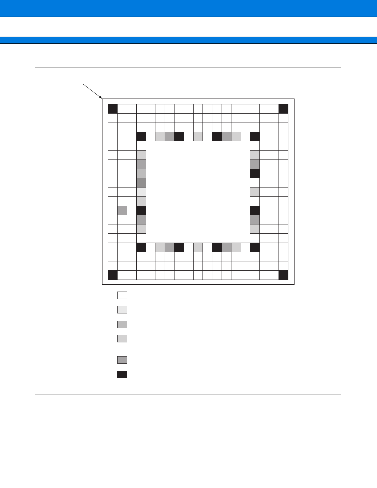
PIN ASSIGNMENT
■■■■
INDEX
21
3 4 5 6 7 8 9 10111213141516171819
A
B
C
D
E
F
G
H
J
K
10
L
11
M
12
N
13
P
14
R
15
T
16
U
17
V
18
W 2122232425262728293031323334353637
71
1
72
136
2
73
137
3
74
138
4
75
139
5
76
140
6
77
141
7
78
142
8
79
143
9
80
144
81
145
82
146
83
147
84
148
85
149
86
150
87
151
88
90
89
2019
70
135
192
193
194
195
196
197
198
199
200
201
202
203
204
205
152
91
69
134
191
240
206
153
92
68
133
190
239
207
154
93
67
132
189
238
208
155
94
66
65
131
130
188
187
237
236
(TOP-VIEW)
(SUB240W)
209
210
156
157
95
96
64
129
186
235
211
158
97
63
128
185
234
212
159
98
62
127
184
233
213
160
99
61
126
183
232
214
161
100
60
125
182
231
215
162
101
59
124
181
230
216
163
102
58
123
180
229
228
227
226
225
224
223
222
221
220
219
218
217
164
103
57
122
179
178
177
176
175
174
173
172
171
170
169
168
167
166
165
104
56
121
120
119
118
117
116
115
114
113
112
111
110
109
108
107
106
105
55
54
53
52
51
50
49
48
47
46
45
44
43
42
41
40
39
38
4
: signal (204 lines)
: PLLVDD (1 line)
: PLLVSS (1 line)
: VDDI (12 lines)
: VDDE (9 lines)
: VSS (16lins)
199
197
195, 200, 203, 207, 211, 215, 1219, 223
227, 231, 235, 239
83, 196, 202, 208, 214, 220, 226, 232, 238
1, 19, 37, 55, 193, 198, 201, 205, 209
213, 217, 225, 229, 233, 237
Page 5
■■■■
Prelminary
2004.11.12
MB91401
PIN NUMBER TABLE
Pin Number Pin name Pin Number
1 VSS 61 UDP 121 EXD11 181 SDA
2 CFD15 62 CFWEX 122 EXD14 182 USBINS
3 ICLK 63 CFCE1X 123 CFCD2X 183 UDM
4 ICS0 64 CFIORDX 124 UCLKSEL 184 CFRESET
5 TDI 65 CFA1 125 CFWAITX 185 CFREGX
6 UCLK48 66 CFA5 126 N.C. 186 CFA0
7 TMS 67 CFA8 127 CFOEX 187 CFA3
8 XINI 68 CFD0 128 CFCE2X 188 CFA7
9 PLLBYPAS 69 CFD3 129 CFIOWRX 189 CFA10
10 OSCEB 70 CFD7 130 CFA2 190 CFD2
11 TEST0 71 CFD10 131 CFA6 191 CFD5
12 OSCEA 72 CFD13 132 CFA9 192 CFD9
13 TEST2 73 CFD14 133 CFD1 193 VSS
14 SCK0 74 ICS2 134 CFD4 194 ICD2
15 SIN0 75 ICS1 135 CFD8 195 VDDI
16 INT5 76 BREAKI 136 CFD11 196 VDDE
17 A3 77 CLKSEL 137 CFD12 197 PLLVSS
18 A2 78 TRST 138 ICD0 198 VSS
19 VSS 79 MDI0 139 ICD1 199 PLLVDD
20 A4 80 MDI2 140 ICD3 200 VDDI
21 A7 81 PLLSET0 141 TDO 201 VSS
22 A10 82 TEST1 142 MDI1 202 VDDE
23 A13 83 VDDE 143 VPD 203 VDDI
24 A16 84 TEST3 144 PLLSET1 204 INITXI
25 MCLKO 85 SIN1 145 OSCC 205 VSS
26 A21 86 SOUT0 146 TCK 206 NMIX
27 RDX 87 INT6 147 PLLS 207 VDDI
28 WRX2 88 A6 148 SCK1 208 VDDE
29 CSX0 89 A5 149 SOUT1 209 VSS
30 N.C. 90 A8 150 INT7 210 A0
31 D0 91 A11 151 A9 211 VDDI
32 D2 92 A14 152 A12 212 A1
33 D5 93 A17 153 A15 213 VSS
34 D9 94 A19 154 A18 214 VDDE
35 D12 95 A22 155 A20 215 VDDI
36 D15 96 WRX3 156 A23 216 D8
37 VSS 97 WRX1 157 RDY 217 VSS
38 D17 98 CSX1 158 WRX0 218 D26
39 D18 99 N.C. 159 CSX6 219 VDDI
40 D20 100 D1 160 N.C. 220 VDDE
41 D23 101 D3 161 N.C. 221 VSS
42 D27 102 D6 162 D4 222 MDCLK
43 TXEN 103 D10 163 D7 223 VDDI
44 TXD0 104 D13 164 D11 224 MDIO
45 RXD0 105 D16 165 D14 225 VSS
46 TXCLK 106 D19 166 D22 226 VDDE
47 RXD2 107 D21 167 D25 227 VDDI
48 RXCLK 108 D24 168 D29 228 EXD3/GPIO3
49 EXIS16 109 D28 169 D31 229 VSS
50 EXCSX 110 D30 170 TXD2 230 CFVS1X
51 EXD0/GPIO0 111 TXD1 171 TXD3 231 VDDI
52 EXD4/GPIO4 112 RXD1 172 RXDV 232 VDDE
53 EXD7/GPIO7 113 RXER 173 COL 233 VSS
54 EXD10 114 RXD3 174 DREQRX 234 CFVCC3EX
55 VSS 115 RXCRS 175 DREQTX 235 VDDI
56 EXD12 116 EXA 176 EXWRX 236 CFA4
57 EXD13 117 EXRDX 177 EXD2/GPIO2 237 VSS
58 CFCD1X 118 EXD1/GPIO1 178 EXD6/GPIO6 238 VDDE
59 SCL 119 EXD5/GPIO5 179 EXD9 239 VDDI
60 CFRDY 120 EXD8 180 EXD15 240 CFD6
Pin name
Pin Number
Pin name
Pin Number
Pin name
5
Page 6
MB91401
Prelminary
2004.11.12
PIN DESCRIPTION
■■■■
[SYSTEM] [ETHERNET MAC CONTROLLER]
INT7 to INT5 3 RXCLK 1
MDI2 to MDI0 3 RXER 1
[OSCILLATOR]
[PLL CONTROL]
PLLSET1, PLLSET0 2
[ICE]
ICS2 to ICS0 3 EXWRX 1
ICD3 to ICD0 4 DREQTX 1
[JTAG]
[TEST]
TEST3 to TEST0 4 CFA10 to CFA0 11
[UART]
SOUT1, SOUT0 2 CFCD2X, CFCD1X 2
SCK1, SCK0 2 CFVS1X 1
[MEMORY IF]
WRX3 to WRX0 4 CFOEX 1
CSX0, CSX1, CSX6 3 CFWEX 1
XINI 1 TXCLK 1
INITXI 1 TXD3 to TXD0 4
NMIX 1 TXEN 1
OSCEA 1 RXDV 1
OSCC 1 RXCRS 1
OSCEB 1 COL 1
PLLS 1 MDIO 1
PLLBYPAS 1 EXCSX 1
CLKSEL 1 EXA 1
BREAKI 1 EXRDX 1
ICLK 1 DREQRX 1
TCK 1
TRST 1
TMS 1 UCLK48 1
TDI 1 UCLKSEL 1
TDO 1 UDP 1
VPD 1 CFD15 to CFD0 16
SIN1, SIN0 2 CFREGX 1
A23 to A0 24 CFWAITX 1
D31 to D0 32 CFVCC3EX 1
RDX 1 CFRESET 1
RDY 1 CFIORDX 1
MCLKO 1
Signal line
Power Supply/
MB91401
GND
N.C.
BGA-240P-M01
196 pin
39 pin
5 pin
[EXTERNAL IF]
[USB IF]
[CARD IF]
2
[I
C IF]
RXD3 to RXD0 4
MDCLK 1
EXD15 to EXD0/GPIO7 to GPIO0 16
EXIS16 1
USBINS 1
UDM 1
CFCE2X, CFCE1X 2
CFRDY (CFIREQ) 1
CFIOWRX 1
SDA 1
SCL 1
6
Page 7
SYSTEM (9 pin)
Prelminary
2004.11.12
Pin name Pin no.
XINI 8 IN D
INITXI 204
NMIX 206
INT7
INT6
INT5
MDI2
MDI1
MDI0
150
87
16
80
142
79
Polarity
Nega-
tive
Nega-
tive
IN D
IN D
Circuit
I/O
IN D
IN D
MB91401
Function/application
Clock input pin
Input pin of clock generated in clock generator. 10 MHz to
50 MHz frequency can be input.
Reset input pin
This pin inputs a signal to initialize the LSI.
When turning on the power supply, apply “0” to the pin until
the clock signal input to the CLKIN pin becomes stable.
All built-in registers and external pins are initialized, and the
built-in PLL is stopped when “0” is asserted to INITXI.
NMI input pin
Non-Maskable Interrupt signal
External interrupt input pins
These pins input an external interrupt request signal.
For external interrupt detection, set the ENIR, EIRR and
ELVR registers of the FR core.
Mode pins
These pins determine the operation mode of the LSI.
Always set this bit to “001”.
OSCILLATOR (3 pin)
Pin name Pin no.
OSCEA 12 IN G
OSCC 145
OSCEB 10 OUT G
PLL CONTROL (5 pin)
Pin name Pin no.
PLLS 147 IN D
PLLSET1 144 IN D
PLLSET0 81 IN D
PLLBYPAS 9 IN D
CLKSEL 77 IN D
Polarity
Nega-
tive
Polarity
Circuit
I/O
IN D
Circuit
I/O
Function/application
Crystal oscillation input pin
Input pin of crystal oscillation cell.
Crystal oscillation control input pin
Oscillation control pin of crystal oscillation cell.
“0” : Oscillation
“1” : Oscillation stop
Crystal oscillation output pin
Output pin of crystal oscillation cell.
Function/application
PLL/through mode (reset) switching input pin
“0” : PLL through mode (oscillation stop)
“1” : PLL oscillation mode
Input clock division ratio select input pin
“0” : Input clock direct
“1” : Input clock divided by 2
Division ratio select input to PLL FB pin
“0” : Two dividing frequency is input to the terminal FB.
“1” : Four dividing frequency is input to the terminal FB.
PLL bypass select input pin
“0” : PLL used
“1” : PLL unused
Input clock switching input pin
“0” : XINI (External clock)
“1” : Built-in OSC generating clock
7
Page 8
MB91401
Prelminary
2004.11.12
ICE (9 pin)
Pin name Pin no.
BREAKI 76 IN D
Polarity
I/O
Circuit
Function/application
Emulator break request pin
This pin inputs the emulator break request when an ICE is
connected.
ICS2
ICS1
ICS0
ICLK 3 I/O B
ICD3
ICD2
ICD1
ICD0
JTAG (5 pin)
Pin name Pin no.
TCK 146 IN E
TRST 78 IN E
TMS 7 IN E
TDI 5 IN E
74
75
4
140
194
139
138
OUT F
I/O B
Polarity
I/O
Circuit
Emulator chip status pins
These pins output the emulator status when an ICE is
connected.
Emulator clock pin
This pin serves as the emulator clock pin when an ICE is
connected.
Emulator data pins
These pins serve as the emulator data bus when an ICE is
connected.
Function/application
JTAG test clock pin
Note : Please input “1” when unused.
JTAG test reset pin
Note : Please input “0” when unused.
TAP controller mode select pin
Note : Please input “1” when unused.
JTAG test data input pin
JTAG test serial data input pin.
Note : Please input “1” when unused.
TEST (5 pin)
8
TDO 141 OUT F
Pin name Pin no.
VPD 143 IN
TEST3
TEST2
TEST1
TEST0
84
13
82
11
Polarity
IN D
I/O
Circuit
JTAG test data output pin
JTAG test serial data output pin
Function/application
Mode pin
Input “0” to this pin.
Test pin
Input “0000” to this pin.
Note : Don’t set other than above description.
Page 9
UART (6 pin)
Prelminary
2004.11.12
Pin name Pin no.
Polarity
I/O
Circuit
MB91401
Function/application
SIN1
SIN0
SOUT1
SOUT0
SCK1
SCK0
MEMORY IF (66 pin)
Pin name Pin no.
A23
A22
A21
A20
A19
A18
A17
A16
A15
A14
A13
A12
A11
A10
A9
A8
A7
A6
A5
A4
A3
A2
A1
A0
85
15
149
86
148
14
156
95
26
155
94
154
93
24
153
92
23
152
91
22
151
90
21
88
89
20
17
18
212
210
IN D
OUT F
I/O B
Polarity
OUT B
I/O
Circuit
Serial data input pins
Serial data input pin of UART built-in FR core.
Serial data output pins
Serial data output pin of UART built-in FR core.
Serial clock I/O pins
Serial clock input/output pin of UART built-in FR core.
Function/application
Address output pins
24 bits address signal pin.
(Continued)
9
Page 10
MB91401
Prelminary
2004.11.12
(Continued)
Pin name Pin no.
D31
D30
D29
D28
D27
D26
D25
D24
D23
D22
D21
D20
D19
D18
D17
D16
D15
D14
D13
D12
D11
D10
D9
D8
D7
D6
D5
D4
D3
D2
D1
D0
169
110
168
109
42
218
167
108
41
166
107
40
106
39
38
105
36
165
104
35
164
103
34
216
163
102
33
162
101
32
100
31
Polarity
I/O B
I/O
Circuit
Function/application
Data input/output pins
32 bits data input/output signal pin.
10
CSX6
CSX1
CSX0
RDX 27
WRX3
WRX2
WRX1
WRX0
MCLKO 25 OUT F
RDY 157
159
98
29
96
28
97
158
Nega-
tive
Nega-
tive
Nega-
tive
Posi-
tive
OUT B
OUT B
OUT B
IN D
Chip select output pins
3-bit chip select signal pin.
Output the “L” level when accessing to external memory.
Read strobe output pin
Read strobing signal pin.
Output the “L” level when read accessing.
Write strobing output pins
Write strobing signal pin.
Output the “L” level when write accessing.
Memory clock output pin
Clock for peripheral resources pin.
External RDY input pin
When the external bus is not completed, the bus cycle can
be extended by inputting “0”.
Page 11
ETHERNET MAC CONTROLLER (17 pin)
Prelminary
2004.11.12
Pin name Pin no.
RXCLK 48 IN D
Polarity
I/O
Circuit
MB91401
Function/application
Clock input for reception pin
MII sync signal during reception. The frequency is 2.5 MHz
at 10 Mbps and 25 MHz at 100 Mbps.
RXER 113
RXDV 172
RXCRS 115
RXD3
RXD2
RXD1
RXD0
COL 173
TXCLK 46 IN D
TXEN 43
TXD3
TXD2
TXD1
TXD0
114
47
112
45
171
170
111
44
Posi-
tive
Posi-
tive
Posi-
tive
IN D
Posi-
tive
Posi-
tive
OUT F
IN D
IN D
IN D
IN D
OUT F
Receive error input pin
It is recognized that there is an error in the reception packet
when “1” is input from the PHY device at receiving.
Receive data valid input pin
It is recognized that receive data is effective.
Career sense input pin
The state that the reception or the transmission is done is
recognized.
Receive data input pins
4-bit data input from PHY device.
Collision detection input pin
When TXEN signal is active and “1”, the collision is
recognized. The collision is not recognized without these
conditions.
Clock input for transfer pin
It becomes synchronous of MII when transmitting. The
frequency is 2.5 MHz at 10 Mbps and 25 MHz at 100 Mbps.
Transfer enable output pin
It is shown that effective data is on the TXD bus. It is output
synchronizing with TXCLK.
Transfer data output pins
4-bit data bus sent to the PHY device. It is output
synchronizing with TXCLK.
MDCLK 222 OUT F
MDIO 224 I/O B
SMI clock output pin
SMI IF clock pin
Connect to SMI clock input pin of PHY device.
SMI data input/output pin
Connect to SMI data of PHY device.
11
Page 12
MB91401
Prelminary
2004.11.12
EXTERNAL IF (23 pin)
Pin name Pin no.
Polarity
I/O
Circuit
Function/application
EXCSX 50
EXA 116 IN D
EXD15
EXD14
EXD13
EXD12
EXD11
EXD10
EXD9
EXD8
EXD7/GPIO7
EXD6/GPIO6
EXD5/GPIO5
EXD4/GPIO4
EXD3/GPIO3
EXD2/GPIO2
EXD1/GPIO1
EXD0/GPIO0
EXRDX 117
180
122
57
56
121
54
179
120
53
178
119
52
228
177
118
51
Nega-
tive
I/O B
I/O B
Nega-
tive
IN D
IN D
External chip select input pin
Chip select input pin from external host.
External address input pin
Address input pin from external host.
“0” : Register select
“1” : FIFO data select
External data input/output pins
The I/O terminal of data bus bit of bit15 to bit8 with an
external host.
External data/GPIO input/output pins
The I/O terminal of data bus bit of bit7 to bit0 with an
external host.
Note : When EXIS16 “0” input, it becomes the I/O terminal
of GPIO7 to GPIO0.
External read strobing input pin
Read strove input pin from external host
EXWRX 176
EXIS16 49 IN D
DREQRX 174
DREQTX 175
Nega-
tive
Nega-
tive
Nega-
tive
IN D
OUT F
OUT F
External write strobing input pin
Write strove input pin from external host
External data bus width select input pin
Bit width select pin of EXD
“0” : 8 bit
(Note : EXD15 to EXD8 are enabled.)
“1” : 16 bit
External reception data request output pin
Recordable data to reception FIFO is shown.
External transfer data request output pin
It is shown that there are data in transmission register and
transmission FIFO.
12
Page 13
USB IF (5 pin)
Prelminary
2004.11.12
Pin name Pin no.
UDP 61 I/O C
UDM 183 I/O C
USBINS 182 IN D
UCLK48 6 IN D
Polarity
I/O
Circuit
MB91401
Function/application
USB data D + (differential) pin
I/O signal pin on the plus side of the USB data.
Use the LSI with 25 Ω to 30 Ω (27 Ω recommended)
external series load resistors, 1.5 kΩ pull-up resistors and
about 100 kΩ resistors. Input “0” when the USB macro is
unused.
USB data D − (differential) pin
I/O signal pin on the minus side of the USB data.
Use the LSI with 25 Ω to 30 Ω (27 Ω recommended)
external series load resistors, 1.5 kΩ pull-up resistors and
about 100 kΩ resistors. Input “0” when the USB macro is
unused.
USB insert input pin
USB socket input detection pin. Be sure to input “0” when
not using USB macro.
48 MHz input (external clock input) pin
This pin inputs an external 48-MHz clock signal.
The USB macro operates based on this clock. Input the
clock with high accuracy (as not only LSI but also a device)
more than 2500 ppm. Input “0” when the USB macro is unused.
UCLKSEL 124 IN D
USB clock select pin
Clock select pin using for USB macro
“0” : Using internal clock
“1” : Using UCLK48
13
Page 14
MB91401
Prelminary
2004.11.12
CARD IF (41 pin)
14
Pin name Pin no.
CFD15
CFD14
CFD13
CFD12
CFD11
CFD10
CFD9
CFD8
CFD7
CFD6
CFD5
CFD4
CFD3
CFD2
CFD0
CFD0
CFA10
CFA9
CFA8
CFA7
CFA6
CFA5
CFA4
CFA3
CFA2
CFA1
CFA0
CFCE2X 128
CFCE1X 63
CFREGX 185
CFCD2X 123
2
73
72
137
136
71
192
135
70
240
191
134
69
190
133
68
189
132
67
188
131
66
236
187
130
65
186
Polarity
I/O B
OUT B
Nega-
tive
Nega-
tive
Nega-
tive
Nega-
tive
I/O
OUT B
OUT B
OUT B
IN E
Circuit
Function/application
CF data input/output pins
I/O data/status/command signal pin to CompactFlash card
side
CF address 10 to 0 output pins
Address output CFA10 to CFA0 pins to CompactFlash card
side
CF card enable output pin
Byte access output pin to CompactFlash card side
Note : Supported for access to CFD7 to CFD0.
When “L” level is output, odd number byte access of the
word is shown.
CF card enable output pin
Byte access output pin to CompactFlash card side
Note : Supported for access to CFD7 to CFD0.
When “L” level is output at word access, even number byte
access of the word is shown.
When the byte is accessed, the even number byte and odd
number byte access become possible because CFA0 and
CFCE2X are combined and used by it.
CF Attribute/Common switching output pin
Attribute/Common switching output pin to CompactFlash
card side
“H” : Common Memory select
“L” : Attribute Memory select
Card connection detect input pin : CFCD2X
Checking connection pin of the socket and CompactFlash
card. It is shown that the CompactFlash card was connected
when this signal and CFCD1X are both input by “0”.
(Continued)
Page 15
(Continued)
Prelminary
2004.11.12
Pin name Pin no.
CFCD1X 58
CFVS1X 230
CFRDY
(CFIREQ)
60
Polarity
Nega-
tive
Nega-
tive
Posi-
tive
(Nega-
tive)
Circuit
I/O
IN E
IN E
IN E
MB91401
Function/application
Card connection detect input pin : CFCD1X
Checking connection pin of the socket and CompactFlash
card. It is shown that the CompactFlash card was connected
when this signal and CFCD2X are both input by “0”.
CF side GND input pin
GND level detection pin from CompactFlash side.
The “0” input to the pin assumes that the CompactFlash
card can operate at 3.3 V, setting the CFVCC3EX pin to the
“L” level.
CF ready input pin : memory card
Ready input pin from CompactFlash memory card side
“1” : Ready
“0” : Busy
(CF interrupt : I/O card)
Interrupt request pin of CompactFlash I/O card. It is shown
the interrupt request was done from the I/O card when input
to this signal by “0”.
CFWAITX 125
CFVCC3EX 234
CFRESET 184
CFOEX 127
CFWEX 62
CFIORDX 64
Nega-
tive
Nega-
tive
Posi-
tive
Nega-
tive
Nega-
tive
Nega-
tive
IN E
OUT B
OUT A
OUT B
OUT B
OUT B
Cycle wait input pin during CF execution
Cycle wait input pin from CompactFlash card side
“0” : It is shown that there is a wait demand at the cycle
under ex ecution.
“1” : It is shown that there is no wait demand at the cycle
under execution.
CF3.3 V power enable output pin
Outputs “L” level when the CompactFlash card is operable
at 3.3 V.
The output signal enables 3.3-volt power supply to the
CompactFlash card. The pin outputs “L” level only when the
CFVS1X pin detects “0”; otherwise, the pin outputs “H”.
CF reset output pin
Reset output pin to CompactFlash card side.
CompactFlash is reset at “H” output.
CF read strobe output pin
Read strove output pin to CompactFlash card (memory
mode and Attribute memory area)
CF register write output pin
Write clock output pin to CompactFlash card (register write
and Card Configuration Register area).
The register write is executed at the rising edge from “L” to
“H”.
CFIO read strobing output pin
Read strove output pin to CompactFlash card (I/O mode)
CFIOWRX 129
Nega-
tive
OUT B
CFIO write strobing output pin
Write strove output pin to CompactFlash card (I/O mode)
15
Page 16
MB91401
Prelminary
2004.11.12
2
C IF (2 pin)
I
Pin name Pin no.
Polarity
SDA 181 I/O B
I/O
Circuit
Function/application
Serial data line input/output pin
2
I
C bus data I/O pin
SCL 59 I/O B
Serial clock line input/output pin
2
I
C bus clock I/O pin
Power Supply/GND (39 pin)
Pin name Pin no.
Polarity
PLLVDD 199
I/O
Power
supply
Circuit
V-E
Function/application
APLL dedicated power supply pin
This pin is for 1.8 V power supply pin.
PLLVSS 197 GND V-S APLL dedicated GND Pin
83
196
202
VDDE
208
214
220
Power
supply
V-E 3.3 V power supply pin
226
232
238
195
200
203
207
211
VDDI
215
219
Power
supply
V-E 1.8 V power supply pin
223
227
231
235
239
1
19
37
55
193
198
201
VSS
205
209
GND V-S GND Pin
213
217
221
225
229
233
237
16
Page 17
I/O CIRCUIT TYPE
Prelminary
2004.11.12
■■■■
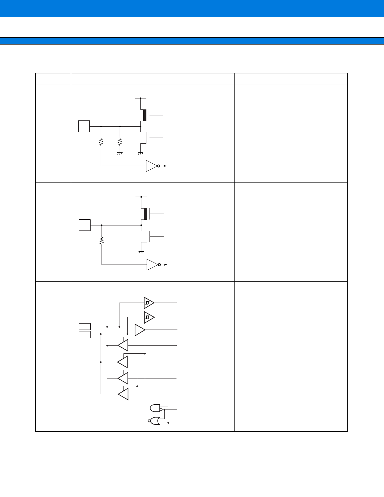
Type Circuit Remarks
MB91401
Digital output
• With pull/down
• CMOS level output
A
Digital output
• CMOS level input
• Value of pull-down resistance =
approx. 33 kΩ (Typ)
Digital input
Digital output]
B
Digital output
• CMOS level output
• CMOS level input
Digital input
+
input
D
−
D
D+
input
Differential input
D−
Full D
+
output
C USB I/O
−
Full D
output
+
Low D
Low D
output
−
output
Direction
Speed
(Continued)
17
Page 18
MB91401
Prelminary
2004.11.12
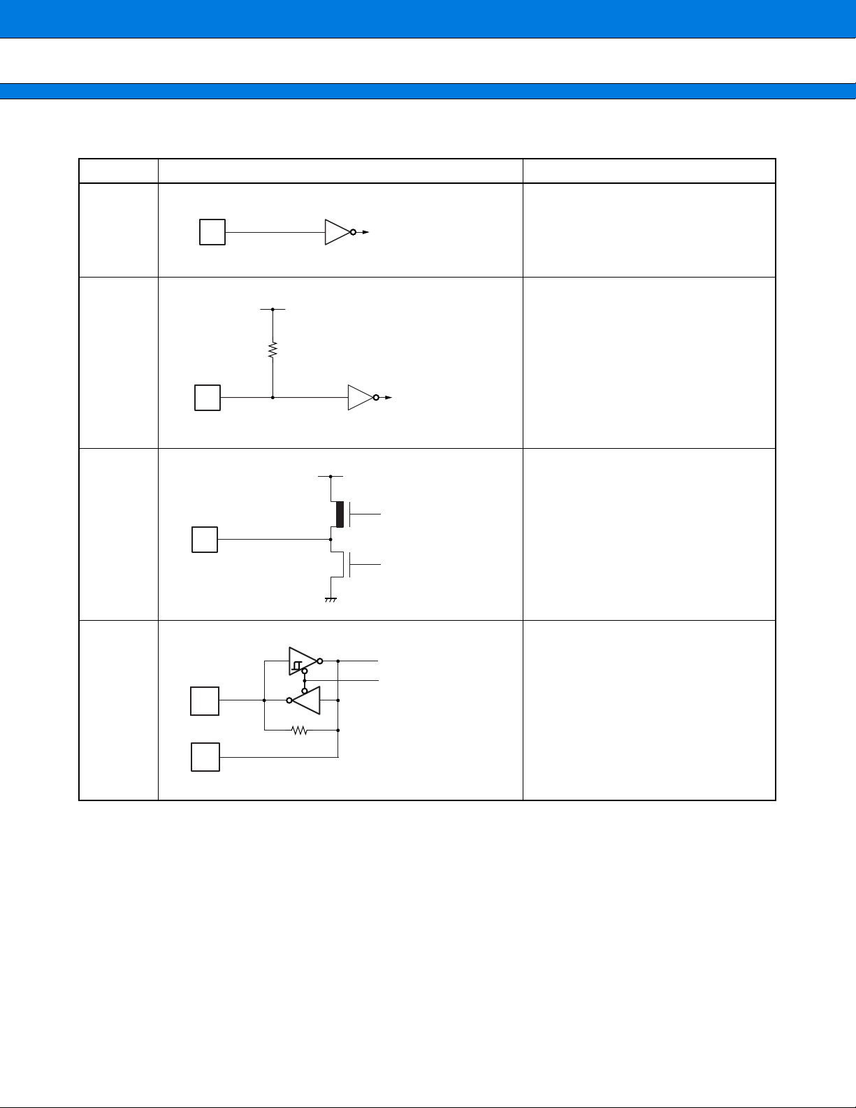
(Continued)
Type Circuit Remarks
D CMOS level input
E
F CMOS level output
Digital input
Digital input
Digital output
Digital output
• With pull-up
• CMOS level input
• Value of pull-up resistance =
approx. 33 kΩ (Typ)
18
Oscillation output
Control
G Oscillation circuit
Page 19
MB91401
Prelminary
2004.11.12
HANDLING DEVICES
■■■■
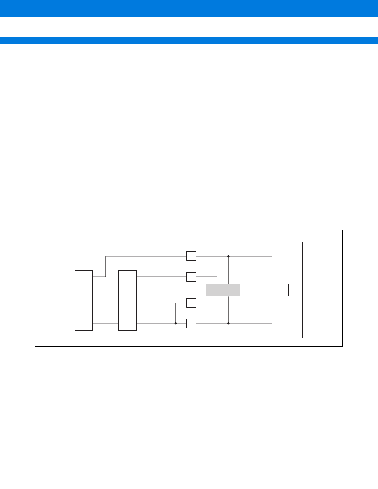
Preventing Latch-up
When a voltage that is higher than V
and the output terminal in CMOS IC or the voltage that exceeds ratings between V
latch-up phenomenon might be caused. If latch-up occurs, the supply current increases rapidly, sometimes
resulting in thermal breakdown of the device. Use meticulous care not to let any voltage exceed the maximum
rating during device operation.
Separation of power supply pattern
Analog PLL (APLL at the following) is installed in this LSI. The po wer supply f or VCO and for digital is separ ated
in LSI so that the oscillation characteristic of APLL may receive the influence of power supply variation.
Therefore, the power supply is recommended to be separated also on the mounting base.
•••• Separation of power supply pattern (recommended)
Take measures to reduce impedance, for example, by using as wide a power pattern as possible.
The recommendation example is shown as follows.
• For two power supplies (for digital and for VCO)
It is advisable to provide a digital power-supply (a) and VCO power-supply (b) and connect them to the LSI’s
equivalents, respectively.
DDE and a voltage that is lower than VSS are impressed to the input terminal
DDE to VSS is impressed, the
Figure For 2-power supply (for digital and for VCO)
Power
supply
(a)
VDD (for digital)
PLLVDD (for VCO)
Power
supply
(b)
PLLVSS
VSS
APLL
Logic part
LSI
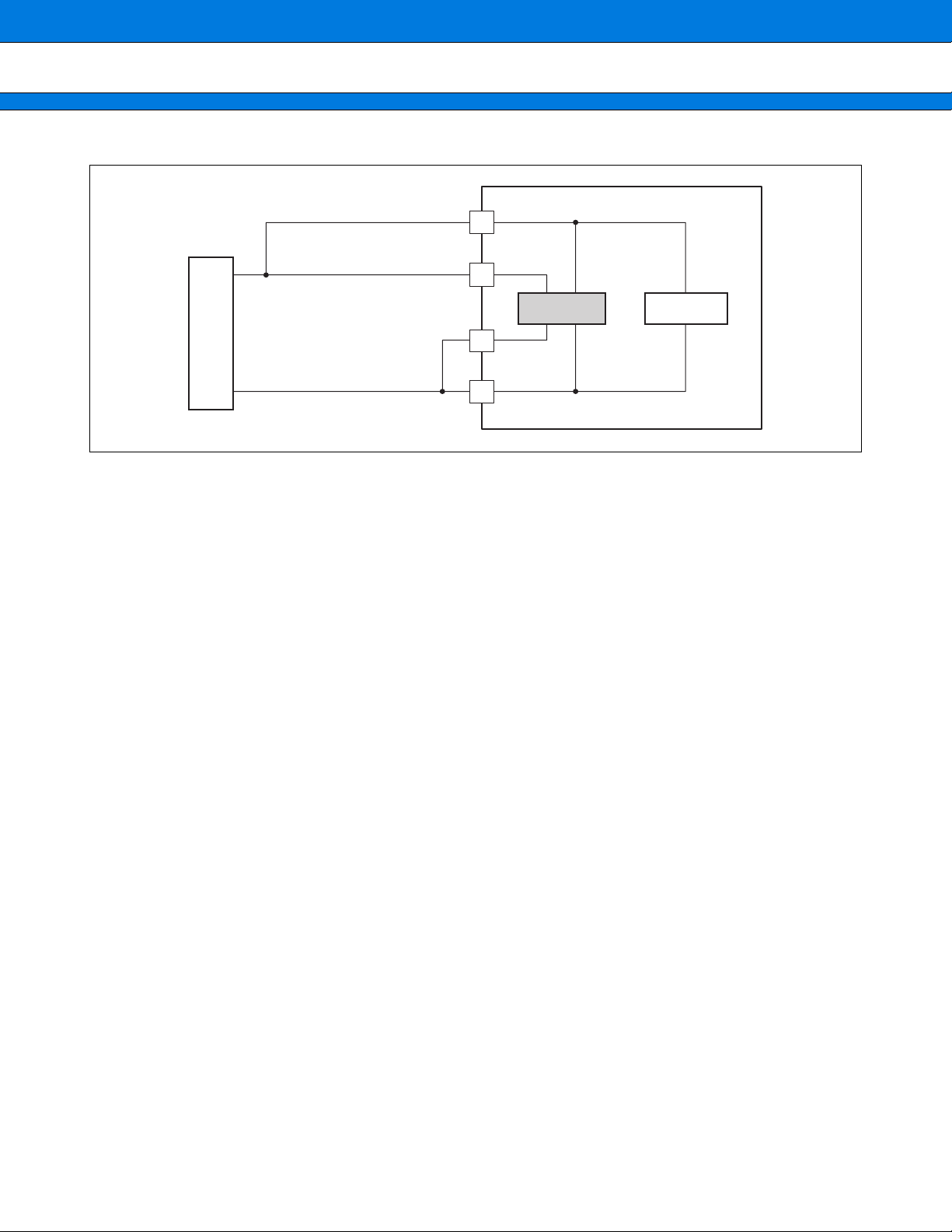
• For the common power supply
To share a single power-supply for digital and VCO uses, it is advisable to separate the output into the digital
and VCO wiring patternsand connect them to the LSI.
19
Page 20
MB91401
Prelminary
2004.11.12
Figure When you share the power suppl y for digital and for VCO
VDD (for digital)
PLLVDD (for VCO)
Power
supply
(a)
Treatment of the unused pins
Leaving unused input pins open results in a malfunction, so process the pull-up or pull-down.
Treatment of OPEN pins
Be sure to use open pins in open state.
Treatment of output pins
A large current may flow to an output pin left connected to the power-supply, another output pin, or to a high
capacitance load. Leaving the output pin that way for an extended period of time degrades the device. Use
meticulous care in using the device not to exceed the absolute maximum rating.
PLLVSS
VSS
APLL
Logic part
LSI
About Mode (MDI2 to MDI0, VPD) pin and Test (TEST3 to TEST0) pin
Connect these pins directly to VDDE or VSS. To prevent the device from entering test mode accidentally due to
noise, minimize the lengths of the patterns between individual mode pins and VDDE or VSS on the PC board
as possible and connect them with as low an impedance as possible.
About power supply pins
In products with multiple VDDE, VDDI or VSS pins, the pins of the same potential are internally connected in
the device to av oid abnormal operations including latch-up. Howe ver you must connect the pins to e xternal power
supply and a ground line to lower the electro-magnetic emission level to prevent abnormal operation strobe
signals caused by the rise in the ground level, and to conform to the total output current rating.
The power pins should be connected to VDDE, VDDI and VSS of this device at the lowest possible impedance
from the current supply source.
It is also advisable to connect a ceramic bypass capacitor of approximately 0.1 µF between VDDE and VSS,
and between VDDI and VSS near this device.
Crystal Oscillator Circuit
Noise near the OSCEA terminal may cause the MB91401 to malfunction.
Design the circuit board so that OSCEA terminal, OSCEB terminal and the cr ystal oscillator, and the bypass
capacitor to ground are located as close to the device as possible.
It is strongly recommended to design the PC board artwork with the OSCEA ter minal and OSCEB terminal
surrounded by ground plane because stable operation can be expected with such a layout.
20
Page 21
MB91401
Prelminary
2004.11.12
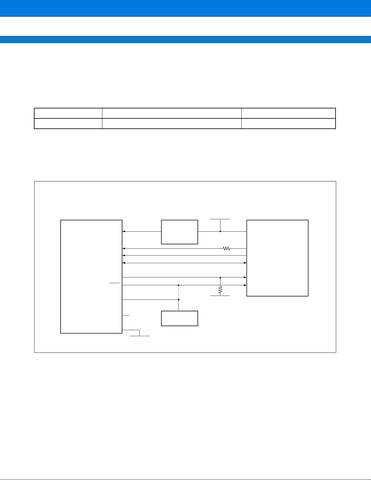
CONNECTED SPECIFICATION OF MB91401 AND ICE
■■■■
Recommended type and circuit configuration of the emulator interface connector mounting on the user system,
attention when designing and wiring regulation are shown.
When the flat cable is used, the combination of the connectors with housing should be selected.
Recommended connector type
Attached cable Part number Remarks
FPC cable FH10A-30S-1SH (Maker : Hirose Electric Co., Ltd.) With latch
• Circuit composition
Please put the dumping resistance 15 Ω in the series in the ICLK terminal signal because of the stability of
operation when connecting it with ICE. Resistance must be mounted near the terminal ICLK of this LSI when
you design the printed wiring board.
Emulator interface connector
MB2198-0 and MB2197-01 side
UVCC
ICLK
ICS2 to ICS0
ICD3 to ICD0
BREAKI
RST
xRSTIN
(Open)
FR
∗1
FUSE
∗2
Reset output
V
CC
15 Ω
10 kΩ
MCU for evaluation
MB91401
CC
V
∗3
ICLK
ICS2 to ICS0
ICD3 to ICD0
BREAKI
INITXI
circuit
GND
VSS
*1 : Use the line (inter connect) to flow the rating current or more.
*2 : The change circuit might become necessary, and refer to “Precaution when designing”.
*3 : Mount resistance near the terminal ICLK of MB91401.
21
Page 22
MB91401
Prelminary
2004.11.12
• Precaution when designing
When evaluation MCU on the user system is operated in the state that the emulator is not connected, should
be treated as follow each input terminal of evaluation MCU connected with the emulator interface on the user
system.
Therefore, note that the switch circuit etc, might become necessary in the user system when you design.
The terminal processing in each emulator interface is shown as follows.
Pin treatment of emulator interface (DSU-3)
Evaluation MCU terminal name Pin treatment
RST
Others To open.
Emulator interface wiring regulations
Signal line name Wiring regulations
ICLK
ICS2 to ICS0
ICD3 to ICD0
BREAKI
UV
CC
GND • Connect directly with a power supply system pattern such as grandopran.
• Reference document
Please match and refer to the following manual for the connection with ICE.
• DSU-FR Emulator MB2198-01 Hardware Manual
• FR20/30 series MB2197-01 Hardware Manual
To be connected the RST terminal with the reset output circuit in the
user system.
• The total wiring length of each signal (From evaluation MCU pin to the
emulator interface connector pin) is made within 50 mm.
• The difference of the total wiring length of each signal makes within 2 cm
and the total wiring length of ICLK is the shortest.
• Wire the pattern with capacity more than the ratings current.
• Each power supply and GND may cause a short-circuit or reverse connec-
tion in between by a wrong connection of a probe. Insert a protection circuit
such as a fuse into each power supply pattern to safeguard it.
22
Page 23
JTAG
Prelminary
2004.11.12
The JTAG function is installed in this LSI.
Note that the terminal INITXI should be input in "L" when using JTAG.
Notes when quartz vibrator is mounted
The crystal oscillation circuit built into this LSI operates by the following compositions.
MB91401
OSC
MB91401
• Pin description
Pin name Function
OSCC Oscillation control terminal of crystal oscillation cell (OSC)
OSCEA Input terminal of crystal oscillation cell (OSC)
OSCEB Output terminal of crystal oscillation cell (OSC)
OSCC OSCEA
C1 C2 C3
Quartz
vibrator
OSCEB
Rr
Installation
when over tone
oscillates
L
• Circuit constant on external substrate
When OSCCL is input, the OSCEA and OSCEB oscillate at the natural frequency of the crystal oscillator and
propagated into the LSI.
Circuit constants Description
C1, C2, C3 External load capacity
L Inductance
Rr Dumping resistance (addition if necessary)
23
Page 24

MB91401
Prelminary
2004.11.12
• Reference Value
Oscillation frequency C1, C2 C3 L Rr
to 30 MHz 5 pF to 33 pF None None None
20 MHz to 50 MHz 5 pF to 15 pF 10 nF approx. 1 µH approx. None
It is necessary to add C3/L depending on a basic wave and the over tone characteristic of the oscillator of the
20 MHz to 30 MHz belt.
Note : These reference v alues are standards. The constant changes according to the characteristic of the quartz
vibrator used. Therefore, we will recommend the initial evaluation that uses the evaluation sample to the
decision of the circuit constant. Please contact FUJITSU representatives about the evaluation sample.
••••
Notes when encryption/authentication accelarator is used
When using the encryption/authentication installed in this LSI, it is necessary to the following notes.
32-bit data bus
The encryption/authentication accelerator fetches data from the area storing data to be subject to encryption/
authentication and encrypts or authenticates the data without CPU inter vention. In the encryption processing,
write is done in the area where it wants to store the data after the encryption is processed.
MB91401
32bit
encryption/
authentication
accelerator
Holding request withdrawal demand function OFF
When accessing to the storage destination of encryption/authentication processing data, the encryption/authentication accelerator should hold an internal bus of this LSI.
Therefore, when the encryption/authentication accelerator are used, it should be set that the holding request
withdrawal doesn’t demand.
Please set the HRCL register that sets the interrupt level that becomes the standard of the holding request
withdrawal demand generation to "10000" in the FR core.
Data Bus
RAM
At the storage destination of
encryption/authentication
processing data
24
For NMIs, the hold request cancel request occurs regardless of the HRCL register setting. When the encryption/
authentication accelerator is used, therefore, NMI input may cause encr yption/authentication to fail to result
correctly. In that case, the correspondence said that it will execute the encryption/authentication processing
under execution again is necessary.
Page 25

MB91401
Prelminary
2004.11.12
••••
Notes as device
Treatment of Unused Input Pins
It causes the malfunction that the unused input terminal is made open, and do the processing such as 1 stack
or 0 stacks.
About Mode pins (MDI2 to MDI0)
Connect these pins with the input buffer by 1 to 1 to prevent the malfunction by the noise, and connect directly
to VDD or VSS outside of ASIC.
Operation at start-up
Specify set initialization reset (INIT) with the terminal INITXI when you turn on the power supply.
Moreover, connect "L" level input to the terminal INITXI until the input clock is steady.
About watch dog timer
The watchdog timer function of this macro monitors a program to check whether it dela ys a reset within a certain
period of time. If the program runs out of control and fails to dela y the reset, the w atchdog timer function resets
the CPU.
Therefore, it keeps operating until reset is specified when the watchdog timer function is made effective once.
Exceptionally, the reset postponement is automatically done under the condition that the program execution of
CPU stops. Refer to the parag raph of the function explanation of the w atchdog timer for the condition of applying
to this exception.
There is a possibility that watchdog reset is not generated when entering the above-mentioned state by the
reckless driving of the system. In that case, please specify reset (INIT) from external INITX terminal.
Restrictions
• Clock control block
• Secure the clock stability waiting time at "L" input to INITXI.
• When entering the standby mode, use the following sequences after using the synchronous standby mode
(TBCR:set at the bit8 SYNCS bit of timebase counter control register).
(LDI #value_of_standby, R0) ; Value_of standby is write data to STCR.
(LDI #_STCR, R12) ; _STCR is address (481H) of STCR.
STB R0, @R12 ; Write to standby control register (STCR).
LDUB @R12, R0 ; STCR read for synchronous standby
LDUB @R12, R0 ; Dummy re-read of STCR
NOP
NOP
NOP
NOP
NOP
In addition, set the I-flag and the ILM and ICR registers to branch to an interrupt handler when the interrupt
handler triggers the microcontroller to return from the standby mode.
• Please do not do the following when the monitor debugger is used.
• Please do not set the break point to the above-mentioned instruction row.
25
Page 26

MB91401
Prelminary
2004.11.12
CPU
• The instruction fetch is not done from D-bus, and does not set the code area on D-bus RAM.
• Set neither stack area nor the vector table on the instruction RAM.
• The following operations may be performed when the instruction immediately followed by a DIVOU/DIVOS
instruction is (a) halted by a user interrupt or NMI, (b) single-stepped, or (c) breaks in response to a data event
or emulator menu:
(1) The D0 and D1 flags are updated in advance.
(2) An EIT handling routine (user interrupt, NMI, or emulator) is executed.
(3) Upon returning from the EIT, the DIVOU/DIVOS instruction is executed and the D0 and D1 flags are
updated to the same values as in (1) .
• The following operations are performed when the ORCCR/STILM/MOVRi and PS instructions are executed.
(1) The PS register is updated in advance.
(2) Executing of EIT processing routine (user interrupt • NMI)
(3) Upon returning from the EIT, the above instructions are executed and the PS register is updated to the
same value as in (1) .
• Since some instructions manipulate the PS register earlier, the following exceptions may cause the interrupt
handler to break or the PS flag to update its display setting when the debugger is being used. As the microcontroller is designed to carry out reprocessing correctly upon returning from such an EIT event in either case,
it performs operations before and after the EIT as specified.
1. When (a) user interrupt and NMI are accepted or (b) step is executed or (c) break is done by the data
event or the menu of the emulator in the instruction immediately before the instruction of DIV0U/DIV0S,
the following operation might be done.
(1) The D0 and D1 flags are updated in advance.
(2) An EIT handling routine (user interrupt, NMI, or emulator) is executed.
(1) Upon returning from the EIT, the DIVOU/DIVOS instruction is executed and the D0 and D1 flags are
updated to the same values as in (3) .
2. When ORCCR, STILM, MOV Ri, and PS each instruction is executed to permit interrupt with the user
interrupt and the NMI factor generated, the following operation is done.
(1) The PS register is updated in advance.
(2) The EIT processing routine (user interrupt, NMI or emulator) is executed.
(3) Upon returning from the EIT, the above instructions are executed and the PS register is updated to
the same value as in (1).
• Do not access the data to the cache memory at the control register of the instruction cash and RAM mode
immediately before the instruction of RETI.
• If one of the instructions listed below is executed, the SSP or USP* value is not used as the R15 value and,
as a result, an incorrect value is written to memory.
• Only ten following kinds of instructions that specify R15 as Ri correspond.
AND R15, @Rj ANDH R15, @Rj ANDB R15, @Rj
OR R15, @Rj ORH R15, @Rj ORB R15, @Rj
EOR R15, @Rj EORH R15, @Rj EORB R15, @Rj
XCHB @Rj, R15
* : As for R15, there are no realities. When R15 is accessed from the program, SSP or USP is accessed by the
state of "S" flag of the PS register. Please specify gener al registers other than R15 when ten abov e-mentioned
instructions are described by the assembler.
26
Page 27

MB91401
Prelminary
2004.11.12
• External bus interface
• When the bus width of the area set up as little endian is 32-bit, confine to word (32-bit) access when accessing
the relevant area.
• When enabling prefetch to the area set to the Little endian, giv e the access to the corresponding area as word
(32 bits) access limitation. In the byte and the half word access, it is not possible to access it correctly.
• DMA
• Do not transfer DMA to instruction RAM.
• Bit Search Module
• BSD0, BSD1, and the BDSC register are only the word accesses.
27
Page 28

MB91401
Prelminary
2004.11.12
NOTES OF DEBUG
■■■■
Step execution of RETI instruction
In an environment where interrupts frequently occur during single-step execution, only the relevant interrupt
processing routines are ex ecuted repeatedly during single-step execution of the RETI instruction. This will prevent
the main routine and low-interrupt-level programs from being executed.
Do not execute step of RETI instruction for escape.
When the relevant interrupt routine no longer requires being debugged, disab le the relevant interrupt and perf orm
debugging.
Operand break
Do not set the access which is used for area, including the address of system stack pointer, to the target of data
event br eak.
Interrupt handler to NMI request (tool)
To prevent the malfunction because of the noise problem of DSU pin when ICE is unconnected, the following
programs are added to the interrupt handler by the cause flag, which is only set by the break request from ICE.
ICE can be used even if this program is added.
Location to added
The following interrupt handler
Interrupt resource : NMI request (tool)
Interrupt number : 13 (decimal), 0D (hexadecimal)
Offset : 3C8
TBR is default address. : 000FFFC8H
Additional program
STM (R0, R1)
LDI #B00
LDI #0, R1
STB R1, @R0 ; Clear the break resource register.
LDM (R0, R1)
RETI
Trace mode
If the trace mode is set to "Full trace mode" during debug (in full trace mode, built-in FIFO is used as output
buffer, the trace memory of the main body of ICE is used, and the trace data lost is not occurred), the electric
current is increased and D-busDMA access may be lost.
Also, the trace data lost may be occurred.
To take the measures, do not set full trace mode.
Simultaneous generation of a software break and a user interrupt/NMI
When a software break and a user interrupt/NMI occur simultaneously, the emulator debugger may react as
follows.
• The debugger stops pointing to a location other than the programmed breakpoints.
• The halted program is not re-executed correctly.
H, R0 ; B00H is address of the break resource register.
H
28
When these problems are occurred, not only the software break, the hardware break should also be used. Do
not set the break to the corresponding location when using monitor debugger.
Page 29

BLOCK DIAGRAM
Prelminary
2004.11.12
■■■■
MB91401
Serial IF
(2ch)
INT/NMI
Ext. IF/
PORT
FR core E Crystal Unit
D-RAM (8 KB)
R
UART
INT
Timer
Authentication macro
IPsec Accelerator
(IKE Accelerator)
DES/3DES
HMAC-MD5/SHA1
DH
External IF
MUX
GPIO
MB91401
B
T
I-Cach (4 KB)
DMAC
DSU
LAN controller
10/100 Ethernet
MAC Controller
L3/L4 Filtering
USB Function
Rev2.0FS
CARD IF
2
C IF
I
MEMORY IF
OSC
CLK
Cont
PLL
CLKIN
USB CLK (48 MHz)
DSU IF
PHY
USB IF
CompactFlash IF
2
I
C Bus
FLASH
SRAM
FR core : CPU, U-Timer, UART, Timer, Interrupt controller, DMAC, Bit search, External interrupt, Memory_IF,
Data-RAM, Cache, Bus controller
Peripheral resources : LAN, External_IF, GPIO , Card, Encryption/Authentication, I
2
C, USB (P eripheral resource
is connected to bus of bus controller. )
29
Page 30

MB91401
Prelminary
2004.11.12
MEMORY SPACE
■■■■
• Memory space
32
The FR family has 4 GByte of logical addresses (2
Direct Addressing Areas
The following address space areas are used as I/O areas.
These areas are called direct addressing areas, in which the address of an operand can be specified directly
during an instruction.
The direct addressing area varies as shown below depending on the size of access data:
→ byte data access : 0-0FF
H
→ half word data access : 0-1FFH
→ word data access : 0-3FFH
• Memory Map
The memory space of the macro consists of the following areas.
address) which can be linearly accessed by the CPU.
Direct Addressing Areas
Refer to I/O Map
I/O
I/O
I-bus RAM 4 KB
(and its mirror)
Access disallowed area
D-bus RAM 8 KByte
External area
0000 0000
0000 0400H
0001 0000H
0002 0000H
0003 F800H
0004 0000H
H
30
FFFF FFFFH
Page 31

GENERAL PURPOSE REGISTERS
Prelminary
2004.11.12
■■■■
R0
R1
R12
R13
R14
R15
32 bits
AC
FP
SP
Initial Value:
XXXX XXXX
XXXX XXXXH
0000 0000H
MB91401
H
Registers R0 to R15 are general-purpose registers. The registers are used as the accumulator and memory
access pointers for CPU operations.
Of these 16 registers, the registers listed below are intended f or special applications, for which some instructions
are enhanced.
R13: Virtual accumulator
R14: frame pointer
R15:Stack pointer
The initial values of R0 to R14 after a reset are indeterminate. R15 is initialized to 00000000
H (SSP value).
31
Page 32

MB91401
Prelminary
2004.11.12
MODE SETTINGS
■■■■
The FR family uses the mode pins (MDI2 to MDI0) and the mode register (MODR) to set the operation mode.
••••
Mode Pins
Three mode pins MDI[2], MDI[1], and MDI[0] are used to specify a mode vector fetch or test mode.
Mode pins
Mode name
MDI2 to MDI0
0 0 0 Reserved
0 0 1 external ROM mode vector External Bus width is set by the mode data.
0 1 0 User circuit test FR stops (with clock signal supplied).
0 1 1 Reserved
1 0 0 Reserved
1 0 1 Reserved
1 1 0 Reserved
1 1 1 Reserved
Reset vector
access area
Remarks
Setting MDI2 to MDI0 to "010", USRTEST is set to "1" and the de vice operates in the user circuit test mode. The
FR71 core is suspended in the user circuit test mode while SYSCLK and MCLKO are operating. The reserved
modes include the FR71 core test mode. In this case, the signal at the FR TEST pin becomes "1" and enters the
FR71 core test mode. If the FRTEST pin = "1", that circuit configuration is required which allows the separately
defined pins of the FR71 core to be controlled and monitored from the outside of the chip.
••••
Mode Register (MODR)
The data written to the mode register (MODR) by hardware using a mode vector fetch is called mode data.
When this register is set by hardware, the CPU operates in the operation mode corresponding to the register
setting.
The mode register is set only by an INIT-level reset cause. The user program cannot access this register.
However, as an exception, when the macro shifts to emulation mode by INTE instruction, or shifts to emulation
mode by a break at a debug using ICE, this register is mapped at 0000_07FD
ICE, perform the mode data setting before the program loading by writing a appropriate value to this register.
Note : No data is existed in the address (0000_07FFH ) in the mode register of the FR family.
••••
Register
76543210
MODR XXXXXXXX
0 0 0 0 0 0 WTH1 WTH0
H. Select this function when using
Initial Value
B
[bit7 to bit2] Reserved bit
32
Operation mode setting bits
Be sure to set this bit to “000000”. Setting them to any other value may result in an unpredictable operation.
Page 33

MB91401
Prelminary
2004.11.12
[bit1, bit0] WTH1, WTH0 (Bus width setting bits)
These bits specify the bus width. The value of the bits is set in the DBW1 and DBW0 bits in ACR0 (CSO area).
Set these bits to a value other than “11”.
WTH1 WTH0 Function Remarks
0 0 8-bit bus width External bus mode
0 1 16-bit bus width External bus mode
1 0 32-bit bus width External bus mode
1 1 Setting disabled
••••
Operation mode
In the operation mode, there are a bus mode and an access mode.
Bus mode Access mode
32-bit bus width
External ROM
bus
16-bit bus width
8-bit bus width
Bus mode
In bus mode, the operations of internal ROM and the external access functions are controlled according to the
mode setting pins (MD2 to MD0) and the values of mode data.
Although the FR71 architecture supports this bus mode, this macro cannot use the single-chip or internal ROM/
external bus mode but can use the external ROM/external bus mode only.
Access mode
Access mode indicates the mode that controls the external data bus width, and is specified by the WTH1/WTH0
bits, and the DBW1/DBW0 bits within ACR0 to ACR7 (Area Configuration Registers).
Bus mode
The FR family has three bus modes described below. Please refer to “■ MEMORY SPACE” for details.
33
Page 34

MB91401
Prelminary
2004.11.12
I/O MAP
■■■■
This shows the location of the various peripheral resource registers in the memory space.
[How to read the table]
Address
Register
0000_0000
|
0000_003C
0000_0040
H
H
H
++++
0
EIRR [R/W]
00000000
++++
1
ENIR [R/W]
00000000
Reserved
Read/Write attribute
Initial value after a reset
Register name (First-column register at address 4n; second-column register
at address 4n + 2)
Left most register address (When accessing it by word, the register of
column 1 is positioned on the MSB side of data.)
Note : Initial values of register bits are represented as follows :
“1” : Initial Value “1”
“0” : Initial Value “0”
“X” : Initial Value “X”
“-” : Access prohibited in reserved area.
Register
Address
++++
0
++++
1
++++
2
ELVR [R/W]
00000000 00000000
++++
2
++++
3
Ext Int
Block
++++
3
Block
34
0000_0000
to
0000_003C
0000_0040
0000_0044
0000_0048
0000_004C
0000_0050
0000_0054
0000_0058
0000_005C
H
H
EIRR [R/W]
H
H
H
H
H
H
H
H
00000000
DICR [R/W]
-------0
TMRLR0
XXXXXXXX
TMRLR1
XXXXXXXX
TMRLR2
XXXXXXXX
ENIR [R/W]
00000000
HRCL [R/W]
0-11111
[W]
XXXXXXXX
[W]
XXXXXXXX
[W]
XXXXXXXX
Reserved
ELVR
00000000
[R/W]
00000000
Ext Int
DLYI/I-unit
TMR0
XXXXXXXX
[R]
XXXXXXXX
Reload Timer 0
TMCSR0
----0000
TMR1
XXXXXXXX
[R/W]
00000000
[R]
XXXXXXXX
Reload Timer 1
TMCSR1
----0000
TMR2
XXXXXXXX
[R/W]
00000000
[R]
XXXXXXXX
Reload Timer 2
TMCSR2
----0000
[R/W]
00000000
(Continued)
Page 35

MB91401
Prelminary
2004.11.12
Address
0000_0060
0000_0064
0000_0068
0000_0048
0000_0070
to
0000_01FC
0000_0200
0000_0204
0000_0208
0000_020C
H
H
H
H
H
H
H
H
H
H
++++
0
SSR0 [R/W]
00001-00
UTIM0 [R]
00000000
SSR1 [R/W]
00001-00
UTIM1 [R]
00000000
Register
++++
1
SIDR0 [R/W]
XXXXXXXX
(UTIMR0 [W])
00000000
SIDR1 [R/W]
XXXXXXXX
(UTIMR1 [W])
00000000
DMACA0
00000000 00000000
DMACB0
00000000 00000000
DMACA1
00000000 00000000
DMACB1
00000000 00000000
++++
2
SCR0 [R/W]
00000100
DRCL0 [W]
--------
SCR1 [R/W]
00000100
DRCL1 [W]
--------
++++
3
SMR0 [R/W]
00--0-0-
UTIMC0 [R/W]
0--00001
SMR1 [R/W]
00--0-0-
UTIMC1 [R/W]
0--00001
UART0
U-TIMER0
UART1
U-TIMER1
Reserved
[R/W]
0000XXXX XXXXXXXX
[R/W]
00000000 00000000
[R/W]
0000XXXX XXXXXXXX
[R/W]
00000000 00000000
Block
0000_0210
0000_0214
0000_0218
0000_021C
0000_0220
0000_0224
0000_0228H
to
0000_023C
0000_0240
0000_0244
to
0000_0300
0000_0304
H
H
H
H
H
H
H
H
H
H
H
00000000 00000000
00000000 00000000
00000000 00000000
00000000 00000000
00000000 00000000
00000000 00000000
0XX00000 XXXXXXXX
DMACA2
DMACB2
DMACA3
DMACB3
DMACA4
DMACB4
DMACR
[R/W]
0000XXXX XXXXXXXX
DMAC
[R/W]
00000000 00000000
[R/W]
0000XXXX XXXXXXXX
[R/W]
00000000 00000000
[R/W]
0000XXXX XXXXXXXX
[R/W]
00000000 00000000
Reserved
[R/W]
XXXXXXXX XXXXXXXX
DMAC
Reserved
ISIZE [R/W]
------10
Instruction
Cache
(Continued)
35
Page 36
MB91401
Prelminary
2004.11.12
Address
0000_0308
to
0000_03E0
0000_03E4
0000_03E8H
to
0000_03EC
0000_03F0
0000_03F4
0000_03F8
0000_03FC
0000_0400
to
0000_043C
0000_0440
0000_0444
++++
0
H
H
H
H
H
H
H
H
H
H
H
H
ICR00[R/W]
---11111
ICR04[R/W]
---11111
XXXXXXXX XXXXXXXX
XXXXXXXX XXXXXXXX
XXXXXXXX XXXXXXXX
XXXXXXXX XXXXXXXX
++++
ICR01[R/W]
---11111
ICR05[R/W]
---11111
Register
1
Reserved
Reserved
BSD0
[W]
XXXXXXXX XXXXXXXX
BSD1
[R/W]
XXXXXXXX XXXXXXXX
BSDC
[W]
XXXXXXXX XXXXXXXX
BSRR
[R]
XXXXXXXX XXXXXXXX
Reserved
ICR02[R/W]
---11111
ICR06[R/W]
---11111
++++
2
ICHRC [R/W]
ICR03[R/W]
ICR07[R/W]
++++
3
0-000000
---11111
---11111
Block
Instruction
Cache
Bit Search
Module
36
0000_0448
0000_044C
0000_0450
0000_0454
0000_0458
0000_045C
0000_0460
0000_0464
0000_0468
H
H
H
H
H
H
H
H
H
ICR08[R/W]
---11111
ICR12[R/W]
---11111
ICR16[R/W]
---11111
ICR20[R/W]
---11111
ICR24[R/W]
---11111
ICR28[R/W]
---11111
ICR32[R/W]
---11111
ICR36[R/W]
---11111
ICR40[R/W]
---11111
ICR09[R/W]
---11111
ICR13[R/W]
---11111
ICR17[R/W]
---11111
ICR21[R/W]
---11111
ICR25[R/W]
---11111
ICR29[R/W]
---11111
ICR33[R/W]
---11111
ICR37[R/W]
---11111
ICR41[R/W]
---11111
ICR10[R/W]
---11111
ICR14[R/W]
---11111
ICR18[R/W]
---11111
ICR22[R/W]
---11111
ICR26[R/W]
---11111
ICR30[R/W]
---11111
ICR34[R/W]
---11111
ICR38[R/W]
---11111
ICR42[R/W]
---11111
ICR11[R/W]
---11111
ICR15[R/W]
---11111
ICR19[R/W]
---11111
ICR23[R/W]
---11111
ICR27[R/W]
---11111
ICR31[R/W]
---11111
ICR35[R/W]
---11111
ICR39[R/W]
---11111
ICR43[R/W]
---11111
Interrupt Control
Unit
(Continued)
Page 37

(Continued)
Prelminary
2004.11.12
Address
++++
0
Register
++++
1
++++
2
MB91401
++++
3
Block
0000_046C
0000_0470
to
0000_047C
0000_0480
0000_0484
0000_0488
to
0000_063F
0000_0640
0000_0644
0000_0648
0000_064C
0000_0650
ICR44[R/W]
H
H
---11111
Reserved
H
RSRR [R/W]
H
10000000*
H
Access disallowed
H
H
H
H
H
H
H
00000000
XXXXXXXX
XXXXXXXX
XXXXXXXX
XXXXXXXX
2
ASR0
ASR1
ASR2
ASR3
ASR4
ICR45[R/W]
---11111
STCR [R/W]
00110011*
WPR [W]
XXXXXXXX
[R/W]
00000000
[R/W]
XXXXXXXX
[R/W]
XXXXXXXX
[R/W]
XXXXXXXX
[R/W]
XXXXXXXX
ICR46[R/W]
---11111
TBCR [R/W]
2
00XXXX00*
1
DIVR0 [R/W]
00000011*
1
ICR47[R/W]
---11111
CTBR [R/W]
XXXXXXXX
DIVR1 [R/W]
00000000
Interrupt Control
Clock Control
Reserved
ACR0
1111**00
ACR1
XXXXXXXX
ACR2
XXXXXXXX
ACR3
XXXXXXXX
ACR4
XXXXXXXX
[R/W]
00000000*
[R/W]
XXXXXXXX
[R/W]
XXXXXXXX
[R/W]
XXXXXXXX
[R/W]
XXXXXXXX
3
Unit
Unit
0000_0654
0000_0658
0000_065C
0000_0660
0000_0664
0000_0668
0000_066C
0000_0670
0000_0674
0000_0678H
H
H
H
H
H
H
H
H
H
XXXXXXXX
ASR5
XXXXXXXX
ASR6
XXXXXXXX
ASR7
XXXXXXXX
AWR0
01111111
AWR2
XXXXXXXX
AWR4
XXXXXXXX
AWR6
XXXXXXXX
MCRA
IOWR0 [R/W]
XXXXXXXX
[R/W]
XXXXXXXX
[R/W]
XXXXXXXX
[R/W]
XXXXXXXX
[R/W]
11111111
[R/W]
XXXXXXXX
[R/W]
XXXXXXXX
[R/W]
XXXXXXXX
MCRB
XXXXXXXX
IOWR1 [R/W]
XXXXXXXX
ACR5
XXXXXXXX
ACR6
XXXXXXXX
ACR7
XXXXXXXX
AWR1
XXXXXXXX
AWR3
XXXXXXXX
AWR5
XXXXXXXX
AWR7
XXXXXXXX
IOWR2 [R/W]
XXXXXXXX
[R/W]
XXXXXXXX
[R/W]
XXXXXXXX
[R/W]
XXXXXXXX
[R/W]
XXXXXXXX
[R/W]
XXXXXXXX
[R/W]
XXXXXXXX
[R/W]
XXXXXXXX
Memory IF
(Continued)
37
Page 38
MB91401
Prelminary
2004.11.12
(Continued)
Address
++++
0
Register
++++
1
++++
2
++++
Block
3
0000_067C
0000_0680H
0000_0684H
0000_0688
0000_0FFC
H
CSER [R/W]
00000001
CHER [R/W]
XXXXXXX1
RCR
00XXXXXX 00XXXXXX
H
to
H
TCR [R/W]
00000000*
1
Memory IF
Reserved
*1 : An initial value is a different register at the reset level. The display is the one at the INIT level.
*2 : An initial value is a different register at the reset level. The display is due to the INIT level by INITX.
*3 : An initial value is set by the WTH bit of the mode vector.
Register
Address
0000_1000
0000_1004
0000_1008
++++
0
H
H
H
XXXXXXXX XXXXXXXX
XXXXXXXX XXXXXXXX
XXXXXXXX XXXXXXXX
++++
1
DMASA0
[R/W]
XXXXXXXX XXXXXXXX
DMADA0
[R/W]
XXXXXXXX XXXXXXXX
DMASA1
[R/W]
XXXXXXXX XXXXXXXX
++++
2
++++
3
Block
0000_100C
0000_1010
0000_1014
0000_1018
0000_101C
0000_1020
0000_1024
0000_1028H
to
0000_FFFC
H
H
XXXXXXXX XXXXXXXX
XXXXXXXX XXXXXXXX
DMADA1
DMASA2
[R/W]
XXXXXXXX XXXXXXXX
[R/W]
XXXXXXXX XXXXXXXX
DMAC
H
H
H
H
H
XXXXXXXX XXXXXXXX
XXXXXXXX XXXXXXXX
XXXXXXXX XXXXXXXX
XXXXXXXX XXXXXXXX
XXXXXXXX XXXXXXXX
DMADA2
DMASA3
DMADA3
DMASA4
DMADA4
[R/W]
XXXXXXXX XXXXXXXX
[R/W]
XXXXXXXX XXXXXXXX
[R/W]
XXXXXXXX XXXXXXXX
[R/W]
XXXXXXXX XXXXXXXX
[R/W]
XXXXXXXX XXXXXXXX
Reserved
H
38
Page 39

MB91401
Prelminary
2004.11.12
Address
010F_0000
010F_0004H
010F_0008
to
010F_FFFF
Address
0110_0000
0110_0004
0110_0008
0110_000C
0110_0008
0110_000C
0110_0008
0110_000C
0110_0010
0110_0014
0110_0018
0110_001C
0110_0020
0110_0024
++++
0
H
BSR[R]
00000000
DAR[R/W]
XXXXXXXX
H
H
++++
0
H
H
H
H
H
H
H
H
H
DLCR0*
0X000000
DLCR4*
00000010
DLCR8[R/W]
00000000
DLCR12[R/W]
00000000
MAR8[R/W]
00000000
MAR12[R/W]
00000000
BMPR12*
00000000
00000000-00000000
FILTER_CMD
H
[R/W]
XXXXXXXX
FILTER_STATUS
H
[R]
XXXXXXXX
FILTER_DATA
H
[R/W]
XXXXXXXX
FL_CONTROL
H
[R/W]
XXXXXXXX
FL_SUBNET
H
[R/W]
XXXXXXXX
BMPR8
Register
++++
1
BCR[R/W]
00000000
(Reserved)
++++
1
DLCR1[R, W]
00000000
DLCR5*
01000001
DLCR9[R/W]
00000000
DLCR13[R/W]
00000000
MAR9[R/W]
00000000
MAR13[R/W]
00000000
Register
DLCR10[R/W]
++++
2
CCR[R/W]
10000000
++++
2
DLCR2*
00000000
DLCR6*
10000000
00000000
MAR10[R/W]
00000000
MAR14[R/W]
00000000
BMPR10*
00000000
BMPR14*
00000000
00000000-00000000
1XXXXXXX
BC2R[R/W]
DLCR3[R/W]
DLCR11[R/W]
MAR11[R/W]
MAR15[R/W]
[R/W]
++++
3
ADR[R/W]
00XX0000
++++
3
00000000
DLCR7*
00000000
00000000
00000000
00000000
BMPR11*
00000111
Block
2
C
I
Block
LAN controller
Bank 0
Bank 1
Bank 2
(Continued)
39
Page 40
MB91401
Prelminary
2004.11.12
(Continued)
Address
0110_0028
0110_002C
0110_0030
0110_0034
0110_0038
0110_003C
0110_0040
0110_0044
0110_0048
H
SMI_CMD_ST
H
H
H
SMI_PHY_ADD
H
SMI_CONTROL
H
SMI_STATUS[R]
H
SMI_INTENABLE
H
SMI_MDCDIV
H
++++
0
SMI_CMD[R/W]
00000000-00000000
[R/W]
00XXXXXX
SMI_DATA [R/W]
00000000-00000000
SMI_POLLINTVL [R/W]
00000000-00000000
[R/W]
00000XXX
[R/W]
111XXXXX
XXXXXXXX
[R/W]
0XXXXXXX
[R/W]
01011XXX
Register
++++
1
++++
2
++++
3
SIM IF
SIM IF
Block
* : The attribute is different according to the bit.
40
Page 41

MB91401
Prelminary
2004.11.12
Address
0114_0000
0114_0004
0114_0008
0114_000C
0114_0010
0114_0014
0114_0018
0114_001C
0114_0020
0114_0024
Register
++++
0
H
H
H
H
H
H
H
H
H
H
00000000-00000000
00000000-00000000
00000000-0XXXXXXX
00000000-00XXXXXX
00000000-00000000
00000000-00000000
EXIFRXR[R]
EXIFTXR[W]
EXIFCR[W]
EXIFSR[R]
00000000-00000000
00000000-00000000
++++
1
EXIFRXDR
[R]
00000000-00000000
EXIFTXDR
[W]
00000000-00000000
EXIFRXSR
[R]
00000000-00000000
EXIFTXSR
[R]
00000000-00000000
++++
2
PIOCR[R/W]
00000000
PIODR[R/W]
Connecting
destination
++++
3
External IF
GPIO
Block
Address
0500_03E0
0501_0000
to
0501_07FF
0501_1000
to
0501_17FF
Register
Block
++++
0
H
H
H
H
H
IR[R/W]
00000000
(Attribute Memory Area : window 0)
(Common Memory Area : window 1)
++++
1
DR[R/W]
10000011
AMR
CMR
++++
2
(Reserved)
++++
3
RR[R/W]
00000000
Compact FLASH
IF
41
Page 42

MB91401
Prelminary
2004.11.12
Address
0540_0000
0540_0004
0540_0008
0540_000C
to
0540_001F
0540_0020
0540_0024
0540_0028
0540_002C
0540_0030
Register
Block
++++
0
H
H
H
H
H
H
H
H
FIFO0out[R]
XXXXXXXX-XXXXXXXX
FIFO1[R]
XXXXXXXX-XXXXXXXX
FIFO3[W]
XXXXXXXX-XXXXXXXX
CONT2[R/W]
XXXXXXXX_XXX00000
CONT4[R/W]
XXXXXXXX_XXX00000
++++
1
(Reserved)
++++
2
++++
3
FIFO0in[W]
XXXXXXXX-XXXXXXXX
FIFO2[W]
XXXXXXXX-XXXXXXXX
CONT1[R/W]
XXXXX0XX-XXX00000
CONT3[R/W]
XXXXXXXX_XXX00000
CONT5[R/W]
XXXXXXXX_XXXX00XX
USB
H
H
CONT6[R/W]
XXXXXXXX_XXXX00XX
CONT8[R/W]
XXXXXXXX_XXX00000
CONT7[R/W]
XXXXXXXX_XXX00000
CONT9[R/W]
XXXXXXXX_0XXX0000
0540_0034
0540_0038
0540_003C
to
0540_003F
0540_0040
0540_0044
0540_0048
to
0540_005F
0540_0060
0540_0064
H
H
H
H
H
H
H
H
H
H
CONT10[R/W]
XXXX0000_X000000X
TRSIZE[R/W]
00010001-00010001
(Reserved)
RSIZE0[R]
XXXXXXXX-XXXX0000
RSIZE1[R]
XXXXXXXX-X0000000
(Reserved)
TTSIZE[R/W]
00010001-00010001
ST1[R/W]
XXXXXX00-00000000
USB
(Continued)
42
Page 43

(Continued)
Prelminary
2004.11.12
Address
++++
0
Register
++++
1
++++
2
MB91401
++++
3
Block
0540_0068
0540_006C
0540_0070H
to
0540_007B
0540_007C
0540_0080
to
0540_FFFF
Address
0580_0000
0580_0008
H
H
H
H
H
H
H
H
H
XXXXXXXX-X0000000
XXXXX000-00000000
++++
00000000-00000001
00000000-00000000
00000000-00000000
ST2[R]
ST4[R]
0
MACRORR[W/R]
CARDIMR[R/W]
USBPLLRP[R/W]
(Reserved)
(Reserved)
Register
++++
1
ST3[R/W]
XXXXXXXX-XXX00000
ST5[R/W]
XXXX0XXX-XX000000
RESET[R/W]
XXXXXXXX-XXXXXX00
++++
2
++++
3
CARDSR[R/W]
00000000-00000000
CARDISR[R]
00000000-00000000
USB
Block
Chip Register0580_0004
43
Page 44

MB91401
Prelminary
2004.11.12
INTERRUPT VECTOR
■■■■
Interrupt source
Interrupt number
Decimal
Hexa-
decimal
Interrupt
level
Offset
Address of TBR
default
RN
Reset 0 00 3FCH 000FFFFCH
Mode vector 1 01 3F8
H 000FFFF8H
System reserved 2 02 3F4H 000FFFF4H
System reserved 3 03 3F0
System reserved 4 04 3EC
H 000FFFF0H
H 000FFFECH
System reserved 5 05 3E8H 000FFFE8H
System reserved 6 06 3E4
Coprocessor absent trap 7 07 3E0
H 000FFFE4H
H 000FFFE0H
Coprocessor error trap 8 08 3DCH 000FFFDCH
INTE instruction 9 09 3D8
Instruction break exception 10 0A 3D4
H 000FFFD8H
H 000FFFD4H
Operand break trap 11 0B 3D0H 000FFFD0H
Step trace trap 12 0C 3CC
NMI request (tool) 13 0D 3C8
H 000FFFCCH
H 000FFFC8H
Undefined instruction exception 14 0E 3C4H 000FFFC4H
NMI request 15 0F F
Ethernet MAC IF 16 10 ICR00 3BC
Authentication macro 17 11 ICR01 3B8
H fixed 3C0H 000FFFC0H
H 000FFFBCH 4
H 000FFFB8H 5
IPSec Accelerator/Code macro 18 12 ICR02 3B4H 000FFFB4H 8
EX IF/GPIO 19 13 ICR03 3B0
2
USB/I
C/CARD IF 20 14 ICR04 3ACH 000FFFACH
H 000FFFB0H 9
External interrupt 5 21 15 ICR05 3A8H 000FFFA8H
External interrupt 6 22 16 ICR06 3A4
External interrupt 7 23 17 ICR07 3A0
H 000FFFA4H
H 000FFFA0H
Reload timer 0 24 18 ICR08 39CH 000FFF9CH 6
Reload timer 1 25 19 ICR09 398
Reload timer 2 26 1A ICR10 394
H 000FFF98H 7
H 000FFF94H
UART0 (Reception completed) 27 1B ICR11 390H 000FFF90H 0
UART1 (Reception completed) 28 1C ICR12 38C
UART0 (RX completed) 29 1D ICR13 388
UART1 (RX completed) 30 1E ICR14 384
H 000FFF8CH 1
H 000FFF88H 2
H 000FFF84H 3
DMAC0 (end error) Ethernet MAC IF 31 1F ICR15 380H 000FFF80H
DMAC1 (end error) External IF 32 20 ICR16 37C
H 000FFF7CH
44
DMAC2 (end error) USB 33 21 ICR17 378
H 000FFF78H
(Continued)
Page 45

MB91401
Prelminary
2004.11.12
Interrupt source
Interrupt number
Decimal
Hexa-
decimal
Interrupt
level
Offset
Address of TBR
default
RN
DMAC3 (end, error) 34 22 ICR18 374H 000FFF74H
DMAC4 (end, error) 35 23 ICR19 370
System reserved 36 24 ICR20 36C
H 000FFF70H
H 000FFF6CH
System reserved 37 25 ICR21 368H 000FFF68H
System reserved 38 26 ICR22 364
System reserved 39 27 ICR23 360
H 000FFF64H
H 000FFF60H
System reserved 40 28 ICR24 35CH 000FFF5CH
System reserved 41 29 ICR25 358
System reserved 42 2A ICR26 354
H 000FFF58H
H 000FFF54H
System reserved 43 2B ICR27 350H 000FFF50H
System reserved 44 2C ICR28 34C
U-TIMER0 45 2D ICR29 348
H 000FFF4CH
H 000FFF48H
U-TIMER1 46 2E ICR30 344H 000FFF44H
Timebase timer overflow 47 2F ICR31 340
System reserved 48 30 ICR32 33C
H 000FFF40H
H 000FFF3CH
System reserved 49 31 ICR33 338H 000FFF38H
System reserved 50 32 ICR34 334
System reserved 51 33 ICR35 330
System reserved 52 34 ICR36 32C
H 000FFF34H
H 000FFF30H
H 000FFF2CH
System reserved 53 35 ICR37 328H 000FFF28H
System reserved 54 36 ICR38 324
System reserved 55 37 ICR39 320
H 000FFF24H
H 000FFF20H
System reserved 56 38 ICR40 31CH 000FFF1CH
System reserved 57 39 ICR41 318
System reserved 58 3A ICR42 314
H 000FFF18H
H 000FFF14H
System reserved 59 3B ICR43 310H 000FFF10H
System reserved 60 3C ICR44 30C
System reserved 61 3D ICR45 308
H 000FFF0CH
H 000FFF08H
System reserved 62 3E ICR46 304H 000FFF04H
Delay interrupt source bit 63 3F ICR47 300
System reserved (Used by REALOS*) 64 40 2FC
System reserved (Used by REALOS*) 65 41 2F8
H 000FFF00H
H 000FFEFCH
H 000FFEF8H
System reserved 66 42 2F4H 000FFEF4H
System reserved 67 43 2F0
H 000FFEF0H
(Continued)
45
Page 46

MB91401
Prelminary
2004.11.12
(Continued)
Interrupt source
Interrupt number
Decimal
Hexa-
decimal
Interrupt
level
Offset
System reserved 68 44 2ECH 000FFEECH
Address of TBR
default
RN
System reserved 69 45 2E8
H 000FFEE8H
System reserved 70 46 2E4H 000FFEE4H
System reserved 71 47 2E0
System reserved 72 48 2DC
H 000FFEE0H
H 000FFEDCH
System reserved 73 49 2D8H 000FFED8H
System reserved 74 4A 2D4
System reserved 75 4B 2D0
H 000FFED4H
H 000FFED0H
System reserved 76 4C 2CCH 000FFECCH
System reserved 77 4D 2C8
System reserved 78 4E 2C4
H 000FFEC8H
H 000FFEC4H
System reserved 79 4F 2C0H 000FFEC0H
Used by INT instruction
80
to
255
50
to
FF
2BC
to
000
H
000FFEBCH
to
H
000FFC00
H
(2) NMI (Non Maskable Interrupt)
NMIs have the highest priority among the interrupt sources handled by this module.
An NMI is always selected whenever other types of interrupt sources occur at the same time.
• If an NMI occurs, the interrupt controller passes the information to the CPU :
Interrupt level : 15 (01111
B)
Interrupt number : 15 (0001111B)
• NMI detection
NMIs are set and detected by the external interrupt/NMI controller. This module only generates an interr upt
level, interrupt number, and MHALTI upon NMI request.
• Suppressing DMA transfer upon NMI request
When an NMI request occurs, the MHALTI bit in the HRCL register is set to "1", suppressing DMA transfer. To
permit DMA transfer, clear the MHALTI bit to "0" at the end of the NMI routine.
46
Page 47

MB91401
Prelminary
2004.11.12
ELECTRICAL CHARACTERISTICS
■■■■
1. Absolute Maximum Ratings
Parameter Symbol
Power supply
voltage*
1
I/O VDDE VSS − 0.3 VSS + 4.0 V
Internal V
DDI VSS − 0.3 VSS + 2.5 V
Analog power supply voltage PLLVDD VSS − 0.3 VSS + 4.0 V *2
Input voltage*
Output voltage*
“L” level maximum output current I
“L” level average output current I
“L” level total maximum output current ΣI
“L” level total average output cur rent ΣI
“H” level maximum output current I
“H” level average output current I
“H” level total maximum output current ΣI
“H” level total average output cur rent ΣI
Power consumption P
1
1
VI VSS − 0.3 VDDE + 0.3 V
VO VSS − 0.3 VDDE + 0.3 V
OL T.B.D mA *3
OLAV T.B.D mA *4
OL T.B.D mA
OLAV T.B.D mA *5
OH T.B.D mA *3
OHAV T.B.D mA *4
OH T.B.D mA
OHAV T.B.D mA *5
D T.B.D mW
Operating temperature Ta − 10 70 °C
Storage temperature Tstg − 55 150 °C
Rating
Unit
Min Max
Remarks
*1 : This parameter is based on VSS = PLLVSS = 0 V.
*2 : Note that analog power supply voltage and input voltage do not exceed VDDE + 0.3 V at power on.
*3 : The maximum output current is the peak value for a single pin.
*4 : The average output current is the average current for a single pin over a period of 100 ms.
*5 : The total average output current is the average current for all pins over a period of 100 ms.
WARNING: Semiconductor devices can be permanently damaged by application of stress (voltage, current,
temperature, etc.) in excess of absolute maximum ratings. Do not exceed these ratings.
Notes : • Apply equal potential to all of the VDDE pins.
• Apply equal potential to all of the VDDI pins.
• Fix all of the VSS pins at 0 V.
• Leave N.C. pins open.
47
Page 48

MB91401
Prelminary
2004.11.12
2. Recommended Operating Conditions
(VSS = PLLVSS = 0 V)
Parameter Symbol
Power supply voltage
I/O V
Internal V
Analog power supply voltage PLLVDD VSS + 3.0 VDDE V
Operating temperature Ta − 10 70.0 °C
WARNING: The recommended operating conditions are required in order to ensure the normal operation of the
semiconductor device. All of the device’s electrical characteristics are warranted when the device is
operated within these ranges.
Always use semiconductor devices within their recommended operating condition ranges. Operation
outside these ranges may adversely affect reliability and could result in device failure.
No warranty is made with respect to uses, operating conditions, or combinations not represented on
the data sheet. Users considering application outside the listed conditions are advised to contact their
FUJITSU representatives beforehand.
DDE 3.0 3.3 3.6 V
DDI 1.65 1.8 1.95 V
Min Typ Max
Value
Unit
48
Page 49
3. DC Characteristics
Prelminary
2004.11.12
• Other than USB
Parameter
“H” level input
voltage
“L” level input
voltage
“H” level output
voltage
“L” level output
voltage
Input leak current I
Pull-up resistance R
Pull-down
resistance
Power supply
current
Input capacitance C
Symbol
V
V
V
V
R
I
MB91401
(VSS = PLLVSS = 0 V)
Pin Conditions
Min Typ Max
IH 2.0
IL
OH
OL
LI
VDDE = 3.0 V,
I
OH = 4.0 mA
VDDE = 3.0 V,
I
OH = 4.0 mA
VDDE = 3.6 V,
V
SS < VI < VDDE
VSS − 0.3
VDDE − 0.5
0.4 V
± 5 µA
TCK/TRST/TMS/
TDI/TDO/
PULU
CFCD2X/
CFCD1X/
10 33 80 kΩ
CFVS1X/CFRDY/
CFWAITX
PULD CFRESET 10 33 80 kΩ
VDDE VDDI = 1.8 V,
CC
VDDI T.B.D mA
Without power
IN
supply
V
DDE = 3.3 V,
fc = 50 MHz
18 pF
T.B.D mA
Value
VDDE + 0.3
0.8 V
V
Unit
V
49
Page 50

MB91401
Prelminary
2004.11.12
• USB
Parameter
Symbol
Pin Conditions
(VSS = PLLVSS = 0 V)
Value
Min Typ Max
Unit
Remarks
“H” level output
voltage
“L” level output
voltage
“H” level output
current
“L” level output
current
output short circuit
current
Input leak current I
V
OH IOH = − 100 µAVDDE − 0.2 VDDE V
V
OL IOL = 100 µA0 0.2 V
I
OH VOH = VDDE − 0.4 V − 20 mA
IOL VOL = 0.4 V 20 mA
I
OS 300 mA *1
LZ ± 5 µA*2
*1 : <About the output short-circuit current>
Output short-circuit current I
or V
SS (within the maximum rating) . The current is “the short-circuit current per differential output pin.” As the
OS is the maximum current that flows when the output pin is connected to VDDE
USB I/O buffer is a diff erential output, the short-circuit current should be considered for both of the output pins.
Monitor the short-circuit current
“L” level
“H” output
Short-circuited at GND level
3-State Enable "L"
“H” level
3-State Enable "L"
“H” output
*2 : <About Measurement of Z leakage current I
Input leakage current I
or V
SS voltage is applied to the bidirectional pin.
LZ is measured with the USB I/O buffer in the high-impedance state when the VDDE
Z output
3-State Enable "H"
Short-circuited at VDDE level
Monitor the short-circuit current
LZ>
Monitor the leakage current
0 V, VDD level applied to output pin
50
Page 51
USB Specification Revision 1.1
Prelminary
2004.11.12
Parameter Symbol
Input Levels
MB91401
Value
Unit Remarks
Min Max
High (driven) V
Low V
IH 2.0 V*1
IL 0.8 V *1
Diffential Input Sensitivity VDI 0.2 V*2
Differential Common Mode Range V
CM 0.8 2.5 V *2
Output Levels
High (driven) V
Low V
Output Signal Crossover Voltage V
OH 0.0 0.3 V *3
OL 2.8 3.6 V *3
CRS 1.3 2.0 V *4
Terminations
Bus Pull-up Resistor on Upstream Port R
Termination Voltage for Upstream Port
Pull-up
*1 : <Input Levels V
IH, VIL>
PU 1.425 1.575 kΩ 1.5 kΩ ± 5%
V
TERM 3.0 3.6 V *5
The switching threshold voltage of the USB I/O buffer’s single-end receiver is set within the range from
V
IL (Max) = 0.8 V to VIH (Min) = 2.0 V (TTL input standard) .
For V
IH and VIL, the LSI has some hysteresis to reduce noise susceptibility.
*2 : <Input Levels V
DI, VCM>
A differential receiver is used to receive USB differential data signals.
The differential receiver has a diff erential input sensitivity of 200 mV when the diff erential data input falls within
the range from 0.8 V to 2.5 V with respect to the local ground reference level.
The above voltage range is referred to as common-mode input voltage range.
*3 : <Output Levels V
1.0
sensitivity (V)
0.2
Minimum operating input
0.8
2.5
Common mode input voltage (V)
OL, VOH>
The output driving performance levels of the driver are 0.3 V or less (to 3.6-V, 1.5 kΩ load) in the low
state (V
OL) and 2.8 V or more (to ground, 1.5 kΩ load) in the high state (VOH) .
51
Page 52

MB91401
Prelminary
2004.11.12
*4 : <Output Levels V
CRS>
The cross voltage of the external diff erential output signals (D+ and D−) falls within the range from 1.3 V to 2.0 V.
D+
Max 2.0 V
VCRS standard range
Max 1.3 V
D−
*5 : <Terminations V
V
TERM indicates the pull-up voltage at the upstream port.
TERM>
52
Page 53

MB91401
Prelminary
2004.11.12
4. AC Characteristics
The following measurement conditions depending on the supply voltage apply to the MB91401 unless otherwise
specified.
• AC measurement condition
0 V
Input Output
VIH
IL
V
IH VDDE × 0.8 VOH VDDE/2
V
V
IL VDDE × 0.2 VOL VDDE/2
VCC
0 V
VOH
OL
V
VCC
• Load condition
C = 55 pF
(1) Clock
Value
Parameter Symbol Pin Conditions
Unit Remarks
Min Max
Fclkcyc XINI External clock 10.0 50.0 MHz
Input clock frequency
Internal operating clock frequency
(FR70E/peripheral module)
Internal operating clock frequency
(USBC)
Internal operating clock frequency
2
C IF)
(I
Fclkcyc
Fclkin 50.0 MHz *
Fusop 48.0 MHz
Fi2op 12.5 MHz
OSCEA,
OSCEB
Oscillation 10.0 50.0 MHz
External memory clock frequency MCLKO 50.0 MHz
* : The clock frequency must be set to over 25 MHz for the Ethernet MAC interface to perform 100 Base
communication.
Fclkcyc
XINI
OSCEA/OSCEB
53
Page 54
MB91401
Prelminary
2004.11.12
(2) Reset
Parameter
Symbol
Pin Conditions
Value
Unit Remarks
Min Max
Reset input time trstl INITXI
PLL reset input time tprstl PLLS At using of PLL 1 µs
Note : tcp is internal CPU and clock cycle period for peripheral module.
INITXI
PLLS
After power
supply &
input clock
stabilization
At unusing of PLL 5 tcp ns
At using of PLL 600 + 1 µs
trstl, tprstl
54
Page 55

MB91401
Prelminary
2004.11.12
(3) Normal memory access
Parameter Symbol Pin Typical timing
Address delay time tchav A23 to A0 MCLKO ↑ 0 tcycp / 2 + 7ns
CSX delay time tchcsl CSX2 to CSX0 MCLKO ↑ 0 tcycp / 2 + 7ns
CSX delay time tchcsh CSX2 to CSX0 MCLKO ↑ 0 tcycp / 2 + 7ns
WRX delay time tchwrl WRX3 to WRX0 MCLKO ↑ − 19ns
WRX delay time tchwrh WRX3 to WRX0 MCLKO ↑ − 19ns
Data delay time tchdv D31 to D0 MCLKO ↑ 0 tcycp / 2 + 7ns
RDX delay time tchrdl RDX MCLKO ↑ − 19ns
RDX delay time tchrdh RDX MCLKO ↑ − 19ns
Data setup tdsrh D31 to D0 MCLKO ↑ 19 ns
Data hold trhdx D31 to D0 MCLKO ↑ − 1 ns
Note : tcycp is external memory clock cycle period.
Value
Unit Remarks
Min Max
MCLKO
A23 to A0
CSX2 to CSX0
WRX3 to WRX0
D31 to D0
RDX
D31 to D0
tcycp
tchav
tchcsl
tchdv
tchrdl
tchwrl
tchcsh
tchwrh
tchrdh
tdsrh
trhdx
55
Page 56
MB91401
Prelminary
2004.11.12
(4) Ready input
Value
Parameter Symbol Pin Typical timing
Min Max
RDY setup trdys RDY MCLKO ↑ 19 ns
RDY hold trdyh RDY MCLKO ↑ − 1 ns
MCLKO
RDY
Unit Remarks
trdys
trdyh
trdys
trdyh
56
Page 57
(5) UART
Prelminary
2004.11.12
Parameter Symbol Pin Conditions
MB91401
Value
Unit Remarks
Min Max
Serial clock
cycle time
SCLK ↓
SOUT delay time
Valid SIN
SCLK ↑
SCLK ↑ →
valid SIN hold time
Serial clock
“H” Pulse Width
Serial clock
“L” Pulse Width
SCLK ↓
SOUT delay time
Valid SIN
SCLK ↑
SCLK ↑
valid SIN hold time
Note : timcycp is operational clock period of peripheral module built-in FR70E core.
→
→
→
→
→
tscyc SCK1, SCK0
tslov SOUT1, SOUT0 − 80 80 ns
tivsh SIN1, SIN0 100 ns
tshix SIN1, SIN0 60 ns
tshsl SCK1, SCK0
tslsh SCK1, SCK0 4 × timcycp ns
tslov SOUT1, SOUT0 150 ns
tivsh SIN1, SIN0 60 ns
tshix SIN1, SIN0 60 ns
Internal
shift clock
mode
External
shift clock
mode
8 × timcycp ns
4 × timcycp ns
57
Page 58

MB91401
Prelminary
2004.11.12
• Internal shift clock mode
tscyc
SCK1, SCK0
SOUT1, SOUT0
SIN1, SIN0
• External shift clock mode
SCK1, SCK0
SOUT1, SOUT0
V
OL VOL
tslov
tivsh
tslsh
tslov
VOH
tshix
tshsl
SIN1, SIN0
tivsh
tshix
58
Page 59

MB91401
Prelminary
2004.11.12
(6) MII interface
Parameter Symbol Pin Typical timing
TXEN delay time tdel_txen TXEN TXCLK ↑ 015ns
TXD delay time tdel_txd TXD3 to TXD0 TXCLK ↑ 015ns
RXDV setup time tsu_rxdv RXDV RXCLK ↑ 2 ns
RXSV Hold Time thd_rxdv RXDV RXCLK ↑ 3 ns
RXD setup time tsu_rxd RXD3 to RXD0 RXCLK ↑ 2 ns
RXD Hold Time thd_rxdv RXD3 to RXD0 RXCLK ↑ 3 ns
RXERsetup time tsu_rxer RXER RXCLK ↑ 2 ns
RXER Hold Time thd_rxer RXER RXCLK ↑ 3 ns
• Transmission
Value
Unit Remarks
Min Max
TXCLK
TXEN
TXD3 to TXD0
TXCLK
TXEN
TXD3 to TXD0
tdel_txen
X55
tdel_txd
tdel_txen
Xnn−1
tdel_txd
59
Page 60

MB91401
Prelminary
2004.11.12
• Reception
RXCLK
RXDV
RXD3 to RXD0
thd_rxdv
tsu_rxdv
055
thd_rxdv
tsu_rxd
RXCLK
RXDV
RXD3 to RXD0
RXCLK
RXER
tsu_rxd
thd_rxdv
thd_rxdv
thd_rxer
tsu_rxdv
tsu_rxer
0nn−1
tsu_rxer
thd_rxer
60
Page 61

MB91401
Prelminary
2004.11.12
(7) MDIO interface
Parameter Symbol Pin typical timing
MDIO setup time tsu_mdio MDIO MDCLK ↑ 10 ns
MDIO Hold Time thd_mdio MDIO MDCLK ↑ 0 ns
MDIO delay time tdel_mdio MDIO MDCLK ↑ 10 30 ns
Value
Unit Remarks
Min Max
MDIO switching time
(IN → OUT)
MDIO switching time
(OUT → IN)
MDCLK
MDIO (INPUT)
MDCLK
MDIO (OUTPUT)
MDCLK
tdel_turnon MDIO MDCLK ↑ 10 30 ns
tdel_turnoff MDIO MDCLK ↑ 10 30 ns
tsu_mdio
tdel_mdio
thd_mdio
tsu_mdio
thd_mdio
tdel_mdio
MDIO
(INPUT OUTPUT)
MDCLK
MDIO
(OUTPUT INPUT)
Input Mode Output Mode
tdel_turnon
Input ModeOutput Mode
tdel_turnoff
61
Page 62

MB91401
Prelminary
2004.11.12
(8) External IF
• Read access
Parameter Symbol Pin
EX Read Cycle time texrc EXA, EXCSX 6 × tcp ns
EXA to Data Valid texadv EXA, EXD 5 × tcp ns
EXCSX to Data Valid texcsdv EXCSX, EXD 5 × tcp ns
EXRDX to Data Out Enable texdoe EXRDX, EXD 5 × tcp ns
EXRDX “H” to High Z texdhz EXRDX, EXD 5 × tcp + 8ns
Note : tcp is internal CPU and operational clock period for peripheral module.
texrc
texadv
EXA
Value
Unit Remarks
Min Max
EXCSX
EXWRX
EXRDX
EXD15: to EXD0
texcsdv
texdoe
texdhz
62
Page 63

• Write access
Prelminary
2004.11.12
Value
Parameter Symbol Pin
Unit Remarks
Min Max
EX Write Cycle time texwc EXA, EXCSX 5 × tcp ns
EXA to Data Setup time texads EXA, EXD 4 × tcp ns
EXCSX to Data Setup time texcsds EXCSX, EXD 4 × tcp ns
EXWRX “L” Pulse width texwp EXRDX, EXD 4 × tcp ns
EXD Setup time texds EXRDX, EXD 11 ns
EXD Hold time texdh EXRDX, EXD 0 ns
Note : tcp is internal CPU and operational clock period for peripheral module.
texwc
texads
EXA
MB91401
EXCSX
EXWRX
EXD15 to EXD0
EXRDX
tchdv
texcsds
texwp
texds
texdhz
63
Page 64

MB91401
Prelminary
2004.11.12
(9) USB interface
Parameter Symbol Pin
Min Typ Max
Input clock tucyc UCLK48 48*
RISE Time tutfr UDP, UDM 4 20 ns *2
Fall Time tutff UDP, UDM 4 20 ns *2
Differential Rise and Fall
Timing Matching
tutfrfm UDP, UDM 90 111.11 % *2
Driver Output Resistance tzdrv UDP, UDM 28 44 Ω *3
tucyc
UCLK48
Value
Unit Remarks
1
MHz 2500ppm accuracy*
1
UDP
UDM
10% 10%
90% 90%
tutfftutfr
*1 : The AC characteristics of the USB interface conform to USB Specification Revision 1.1.
*2 : <Driver Characteristics TFR, TFF, TFRFM>
These items specify the differential data signal rise (trise) and fall (tfall) times.
These are defined as the times between 10% to 90% of the output signal voltage.
For the full-speed buff er , trise and tf all are specified such that the tr/tf ratio f alls within ± 10% to minimize RFI
radiation.
*3 : <Driver Characteristics ZDRV>
USB full-speed connection is performed via a shielded twisted-pair cable at a characteristic impedance of
90 Ω ± 15%. The USB Standard stipulates that the USB driv er’ s output impedance m ust be within the range
of 28 Ω to 44Ω. The USB Standard also stipulates that a discrete serial resistor (R
S) must be added to have
balance while satisfying the above standard.
The output impedance of the USB I/O buffer on this LSI is about 3 Ω to 19 Ω. Serial resistor R
must be 25 Ω to 30 Ω (27 Ω recommended) .
Capacitor CL of 50 pF must be added as well.
S to be added
64
Page 65

T×D+
Prelminary
2004.11.12
T×D−
MB91401
Full-speed Buffer
Rs
28 Ω to 44 Ω Equiv. Imped
CL = 50 pF
Rs
28 Ω to 44 Ω Equiv. Imped
3-State
CL = 50 pF
Notes : • Driver output impedance 3 Ω to 19 Ω
• Rs series resistance: 25 Ω to 30 Ω
• Add a series resistor of preferably 27 Ω
65
Page 66

MB91401
Prelminary
2004.11.12
2
C interface
(10) I
• Input timing specification
Parameter Symbol Pin
SDA input setup time ts2sdai SDA 250 ns *
SDA input hold time th2sdai SDA 0 ns *
SCL cycle time tcscli SCL 10 µs*
SCL input “H” pulse time twhscli SCL 4 µs*
SCL input “L” pulse time twlscli SCL 4.7 µs*
SCL input setup time ts2scli SCL 4 µs*
SCL input hold time th2scli SCL 4.7 µs*
* : Initial Value : I
2
C bus standards.
Value
Unit Remarks
Min Max
SDA (input)
STOP START
D7 D6 D5 D4 D3 D2 D1 D0 ACK
ts2scli th2scli ts2sdai th2sdai
RESTART
ts2scli th2scli
SCL (input)
tcscli twhscli twlscli
• Output timing specification
Value
Parameter Symbol Pin
Unit Remarks
Min Max
SCL output cycle time tcsclo SCL (2 × m) + 2 PCLK *
SCL output “H” Pulse Time twhsclo SCL m + 2 PCLK *
SCL output “L” Pulse Time twlsclo SCL m PCLK *
SCL output setup time ts2sclo SCL m + 2 PCLK *
SCL output hold time th2sclo SCL m × 2 PCLK *
SDA output hold time th2sdao SDA 5 PCLK *
* : For value m, refer to Section 7.5.2.3 “Clock Control Register (CCR) in the I
indicates I
2
C interface operating clock frequency.
2
C Interface Specifications.” PCLK
66
SDA (output)
SCL (output)
STOP START
D7 D6 D5 D4 D3 D2 D1 D0 ACK
ts2sclo th2sclo th2sdao
RESTART
ts2sclo th2sclo
tcsclo twhsclo twlsclo
Page 67

(11) Card IF
Prelminary
2004.11.12
• Read access
Parameter Symbol Pin
MB91401
Value
Unit Remarks
Min Max
CF Read Cycle time tcfrc
CFA to Data Valid tcfadv
CFCEX to Data Valid tcfcedv
CFOEX CFIORDX to Data Out
Enable
CFOEX CFIORDX “H” to High Z tcfdhz
CFA10 to CFA0
CFCE2X, CFCE1X
CFWEX, CFIOWRX
tcfdoe
CFA10 to CFA0,
CFCE2X, CFCE1X
CFA10 to CFA0,
CFD15 to CFD0
CFCE2X, CFCE1X,
CFD15 to CFD0
CFOEX, CFIORDX,
CFD15 to CFD0
CFOEX, CFIORDX,
CFD15 to CFD0
tcfrc
tcfadv
tcfcedv
ns
ns
ns
ns
ns
CFOEX, CFIORDX
CFD15 to CFD0
tcfdoe
tcfdhz
67
Page 68

MB91401
Prelminary
2004.11.12
• Write access
Parameter Symbol Pin
CF Write Cycle time tcfwc
CFA to Data Setup time tcfads
CFA10 to CFA0,
CFCE2X, CFCE1X
CFA10 to CFA0,
CFD15 to CFD0
Value
Unit Remarks
Min Max
ns
ns
CFCEX to Data Setup time tcfceds
CFWEX CFIOWRX “L” Pulse
width
tcffwp CFWEX, CFIOWRX ns
CFD Setup time tcfds
CFD Hold time tcfdhz
CFA10 to CFA0
CFCE2X, CFCE1X
CFWEX, CFIOWRX
CFCE2X, CFCE1X,
CFD15 to CFD0
CDWEX, CFIOWRX,
CFD15 to CFD0
CDWEX, CFIOWRX,
CFD15 to CFD0
tcfwc
tcfads
tcfceds
tcffwp
tcfds
ns
ns
ns
68
CFD15 to CFD0
tcfdhz
CFOEX, CFIORDX
Page 69

ORDERING INFORMATION
Prelminary
2004.11.12
■■■■
Part number Package Remarks
MB91401
MB91401
240-pin plastic FBGA
(BGA-240P-M01)
69
Page 70

MB91401
Prelminary
2004.11.12
PACKAGE DIMENSION
■■■■
240-pin plastic FBGA
(BGA-240P-M01)
10.00±0.10(.394±.004)SQ
(INDEX AREA)
Note: The actual shape of coners may differ from the dimension.
+0.20
.044
Ð0.10
1.13
(Mounting height)
0.10(.004)
0.25±0.10
(.010±.004)
(Stand off)
+.008
Ð.004
9.00(.354)
REF
240-¯0.30±0.10
(240-¯.012±.004)
INDEX
WVUTRPNMLKJHGFEDCBA
0.50(.020)
TYP
0.05(.002)
M
19
18
17
16
15
14
13
12
11
10
9
8
7
6
5
4
3
2
1
C
1999 FUJITSU LIMITED B240001S-2C-2
Dimensions in mm (inches).
Note : The values in parentheses are reference values.
70
Page 71

MEMO
Prelminary
2004.11.12
MB91401
71
Page 72

MB91401
Prelminary
2004.11.12
FUJITSU LIMITED
For further information please contact:
Japan
FUJITSU LIMITED
Marketing Division
Electronic Devices
Shinjuku Dai-Ichi Seimei Bldg. 7-1,
Nishishinjuku 2-chome, Shinjuku-ku,
Tokyo 163-0721, Japan
Tel: +81-3-5322-3353
Fax: +81-3-5322-3386
http://edevice.fujitsu.com/
North and South America
FUJITSU MICROELECTRONICS AMERICA, INC.
1250 E. Arques Avenue, M/S 333
Sunnyvale , CA 94088-3470, U.S.A.
Tel: +1-408-737-5600
Fax: +1-408-737-5999
http://www.fma.fujitsu.com/
Europe
FUJITSU MICROELECTRONICS EUROPE GmbH
Am Siebenstein 6-10,
D-63303 Dreieich-Buchschlag,
Germany
Tel: +49-6103-690-0
Fax: +49-6103-690-122
http://www.fme.fujitsu.com/
Asia Pacific
FUJITSU MICROELECTRONICS ASIA PTE LTD.
#05-08, 151 Lorong Chuan,
New Tech Park,
Singapore 556741
Tel: +65-6281-0770
Fax: +65-6281-0220
http://www.fmal.fujitsu.com/
Korea
FUJITSU MICROELECTRONICS K OREA LTD.
1702 KOSMO TOWER, 1002 Daechi-Dong,
Kangnam-Gu,Seoul 135-280
Korea
Tel: +82-2-3484-7100
Fax: +82-2-3484-7111
http://www.fmk.fujitsu.com/
All Rights Reserved.
The contents of this document are subject to change without notice.
Customers are advised to consult with FUJITSU sales
representatives before ordering.
The information, such as descriptions of function and application
circuit examples, in this document are presented solely for the
purpose of reference to show examples of operations and uses of
Fujitsu semiconductor device; Fujitsu does not warrant proper
operation of the device with respect to use based on such
information. When you develop equipment incorporating the
device based on such information, you must assume any
responsibility arising out of such use of the information. Fujitsu
assumes no liability for any damages whatsoever arising out of
the use of the information.
Any information in this document, including descriptions of
function and schematic diagrams, shall not be construed as license
of the use or exercise of any intellectual property right, such as
patent right or copyright, or any other right of Fujitsu or any third
party or does Fujitsu warrant non-infringement of any third-party’s
intellectual property right or other right by using such information.
Fujitsu assumes no liability for any infringement of the intellectual
property rights or other rights of third parties which would result
from the use of information contained herein.
The products described in this document are designed, developed
and manufactured as contemplated for general use, including
without limitation, ordinary industrial use, general office use,
personal use, and household use, but are not designed, developed
and manufactured as contemplated (1) for use accompanying fatal
risks or dangers that, unless extremely high safety is secured, could
have a serious effect to the public, and could lead directly to death,
personal injury, severe physical damage or other loss (i.e., nuclear
reaction control in nuclear facility, aircraft flight control, air traffic
control, mass transport control, medical life support system, missile
launch control in weapon system), or (2) for use requiring
extremely high reliability (i.e., submersible repeater and artificial
satellite).
Please note that Fujitsu will not be liable against you and/or any
third party for any claims or damages arising in connection with
above-mentioned uses of the products.
Any semiconductor devices have an inherent chance of failure. You
must protect against injury, damage or loss from such failures by
incorporating safety design measures into your facility and
equipment such as redundancy, fire protection, and prevention of
over-current levels and other abnormal operating conditions.
If any products described in this document represent goods or
technologies subject to certain restrictions on export under the
Foreign Exchange and Foreign Trade Law of Japan, the prior
authorization by Japanese government will be required for export
of those products from Japan.
2004 FUJITSU LIMITED Printed in Japan
 Loading...