

Page 1

FUJITSU SEMICONDUCTOR
CONTROLLER MANUAL
CM71-10121-3E
FR60
32-BIT MICROCONTROLLER
MB91350A Series
HARDWARE MANUAL
Page 2

Page 3

FR60
32-BIT MICROCONTROLLER
MB91350A Series
HARDWARE MANUAL
Be sure to refer to the “Check Sheet” for the latest cautions on development.
“Check Sheet” is seen at the following support page
URL : http://www.fujitsu.com/global/services/microelectronics/product/micom/support/index.html
“Check Sheet” lists the minimal requirement items to be checked to prevent problems beforehand in system development.
FUJITSU LIMITED
Page 4

Page 5

CONTENTS
■ Objectives and Intended Reader
The MB91350A series is one of the FR60 family of microcontrollers. The FR60 fam ily of microcontroll ers
is based on the FR30/40 family of CPUs, which u se a 32-b it high-performance RI SC CPU as the core CPU.
The FR60 family offers enhanced bus access. The MB91350A series is a single-chip microcontroller with
built-in peripheral resources. The MB91350A series is ideal for embedded control applications th at require
high-performance or high-speed CPU processing.
This manual is intended for engineers who will develop products using the MB91 350A seri es and describes
the functions and operations of the MB91350A series. Read this manual thoroughly.
For more information on instructions, see the "Instructions Manual".
Note : FR, which is an abbreviation of FUJITSU RISC controller, is a product of FUJITSU LIMITED.
■ Trademark
The company names and brand names herein are the trademarks or registered trademarks of their respective
owners.
■ License
Purchase of Fujitsu I2C components conveys a licence under the Philips I2C Patent Rights to use, these
2
components in an I
defined by Philips.
C system provided that the system conforms to the I2C Standard Specification as
■ Organization of This Manual
This manual consists of the following 19 chapters and an appendix.
CHAPTER 1 OVERVIEW
This chapter provides basic information required to u nderstand the MB91 350A series. It covers features
and dimensions, and presents a block diagram of the MB91350A series.
CHAPTER 2 HANDLING THE DEVICE
This chapter provides precautions on handling the device.
CHAPTER 3 CPU AND CONTROL UNITS
This chapter provides basic information required to understand the MB91350A series core CPU
functions. It covers architecture, specifications, and instructions.
CHAPTER 4 EXTERNAL BUS INTERFACE
This chapter describes basic items related to the external bus interface, register configuration/functions,
bus operation, bus timing, and procedures for setting the registers.
CHAPTER 5 I/O PORT
This chapter describes the I/O ports and the configuration and functions of registers.
i
Page 6

CHAPTER 6 8/16-bit Up/Down Counters/Timer and U-Timers
This chapter outlines the 8/16-bit up/down counter/timer an d U-TIMER and explains the configuration
and functions of the registers and timer operations.
CHAPTER 7 16-BIT FREE-RUNNING TIMER AND 16-BIT RELOAD TIMER
This chapter outlines the 16-bit free-running timer and 16-bit reload timer and explains the
configuration and functions of the registers and timer operations.
CHAPTER 8 PROGRAMMABLE PULSE GENERATOR (PPG) TIMER
This chapter gives an outline of the PPG (Programmable Pulse Generator) timer and explains the
register configuration and functions and the timer operations.
CHAPTER 9 INTERRUPT CONTROLLER
This chapter describes the overview of the interrupt controller, the configuration and functions of
registers, and interrupt controller operation.
CHAPTER 10 EXTERNAL INTERRUPT AND NMI CONTROLLER
This chapter outlines the external interrupt/NMI controller and explains the configuration and functions
of the registers and operations of the external interrupt/NMI controller.
CHAPTER 11 REALOS-RELATED HARDWARE
This chapter outlines the delayed interrupt module and bit search module, and explains the
configuration and functions of registers and operations.
CHAPTER 12 A/D CONVERTER
This chapter outlines the A/D converter and explains the configuration and functions of registers and
the A/D converter operations.
CHAPTER 13 8-BIT D/A CONVERTER
This chapter gives an overview of the 8-bit D/A converter, register configuration and functions, an d 8bit D/A converter operation.
CHAPTER 14 UART, SERIAL I/O INTERFACE (SIO), INPUT CAPTURE MODULE, AND
OUTPUT COMPARE MODULE
This chapter outlines the UART, SIO, input capture, and output compare, and expl ains the configuration
and functions of registers. It also explains UART, SIO, input capture, and output compare operations.
CHAPTER 15 I
This chapter describes the overview of the I
2
and I
C interface operation.
2
C INTERFACE
2
C interface, the configuration and functions of registers,
CHAPTER 16 DMA CONTROLLER (DMAC)
This chapter describes the overview of the DMAC, the configuration and functions of registers, and
DMAC operation.
CHAPTER 17 FLASH MEMORY
This chapter provides an outline of flash memory and explains its register configuration, register
functions, and operations.
CHAPTER 18 MB91F355A/F353A/F356B/F357B SERIAL PROGRAMMING CONNECTION
This chapter describes the serial onboard writing connection (Fujitsu standard) using the AF220/AF210 /
AF120/AF110 Flash Microcontroller Programmer by Yokogawa Digital Computer Corporation.
ii
Page 7

CHAPTER 19 DATA INTERNAL RAM/INSTRUCTION INTERNAL RAM ACCESS
RESTRICTION FUNCTIONS
This chapter outlines a function that restricts access to data internal RAM and instruction internal RAM.
It also explains the configuration and functions of reg isters and internal RAM operatio ns.
APPENDIX
This appendix consists of the following parts: I/O map, interrupt vectors, pin state for each CPU state,
and the instruction lists.
iii
Page 8

• The contents of this document are subject to change without notice.
Customers are advised to consult with sales representatives before ordering.
• The information, such as descriptions of function and application circuit examples, in this document are presented solely for the
purpose of reference to show examples of operations and uses of FUJITSU semiconductor device; FUJITSU does not warrant
proper operation of the device with respect to use based on such information. When you develop equipment incorporating the
device based on such information, you must assume any responsibility arising out of such use of the information. FUJITSU
assumes no liability for any damages whatsoever arising out of the use of the information.
• Any information in this document, including descriptions of function and schematic diagrams, shall not be construed as license
of the use or exercise of any intellectual property right, such as patent right or copyright, or any other right of FUJITSU or any
third party or does FUJITSU warrant non-infringement of any third-party's intellectual property right or other right by using such
information. FUJITSU assumes no liability for any infringement of the intellectual property rights or other rights of third parties
which would result from the use of information contained herein.
• The products described in this document are designed, developed and manufactured as contemplated for general use, including
without limitation, ordinary industrial use, general office use, personal use, and household use, but are not designed, developed
and manufactured as contemplated (1) for use accompanying fatal risks or dangers that, unless extremely high safety is secured,
could have a serious effect to the public, and could lead directly to death, personal injury, severe physical damage or other loss
(i.e., nuclear reaction control in nuclear facility, aircraft flight control, air traffic control, mass transport control, medical life
support system, missile launch control in weapon system), or (2) for use requiring extremely high reliability (i.e., submersible
repeater and artificial satellite).
Please note that FUJITSU will not be liable against you and/or any third party for any claims or damages arising in connection
with above-mentioned uses of the products.
• Any semiconductor devices have an inherent chance of failure. You must protect against injury, damage or loss from such
failures by incorporating safety design measures into your facility and equipment such as redundancy, fire protection, and
prevention of over-current levels and other abnormal operating conditions.
• Exportation/release of any products described in this document may require necessary procedures in accordance with the
regulations of the Foreign Exchange and Foreign Trade Control Law of Japan and/or US export control laws.
• The company names and brand names herein are the trademarks or registered trademarks of their respective owners.
Copyright ©2003-2007 FUJITSU LIMITED All rights reserved
iv
Page 9

CONTENTS
CHAPTER 1 OVERVIEW ................................................................................................... 1
1.1 Features ........................ .......... .......... ......... .......... .......... ......... ....... ......... .......... .................................. 2
1.2 Block Diagram .................................................................................................................................... 7
1.3 Package Dimensions .......................................................................................................................... 9
1.4 Pin Layout ......................................................................................................................................... 11
1.5 List of Pin Functions ......................................... ... ... ... .... ...................................... .... ... ... ................... 13
1.6 Input-output Circuit Forms ................................................................................................................ 27
CHAPTER 2 HANDLING THE DEVICE .......................................................................... 31
2.1 Precautions on Handling the Device ................................................................................................. 32
2.2 Precautions on Using the Little-Endian Area .................................................................................... 37
2.2.1 C Compiler (fcc911) ................................. .... ... ....................................... ... ... ... .... ......................... 38
2.2.2 Assembler (fasm911) .................................................................................................................. 41
2.2.3 Linker (flnk911) ............................................................................................................................ 42
2.2.4 Debuggers (sim911, eml911, and mon911) ................................................................................ 43
CHAPTER 3 CPU AND CONTROL UNITS ..................................................................... 45
3.1 Memory Space .............. ... .... ... ... ....................................... ... ... .......................................................... 46
3.2 Internal Architecture ......... .... ... ... ....................................... ... ... .... ... ................................................... 49
3.2.1 Internal Architecture .................................................................................................................... 50
3.2.2 Overview of Instructions ........................................... ... ... ... .... ...................................... ... ............. 53
3.3 Programming Model ......................................................................................................................... 55
3.3.1 General-Purpose Registers .................. ... ....................................... ... .... ...................................... 56
3.3.2 Dedicated Registers .................................................................................................................... 57
3.4 Data Configuration ............................................................................................................................ 64
3.5 Memory Map ........................ ... ....................................... ... ... ....................................... ...................... 66
3.6 Branch Instructions ........................................................................................................................... 67
3.6.1 Operations with a Delay Slot ................................................. ... ... ... ... .... ...................................... 68
3.6.2 Operation without Delay Slot ....................................................................................................... 71
3.7 EIT (Exception, Interrupt, and Trap) ................................................................................................. 72
3.7.1 EIT Interrupt Levels .... ....................................... ... .... ... ... ....................................... ... ... ................ 73
3.7.2 ICR (Interrupt Control Register) ................................................................................................... 75
3.7.3 SSP (System Stack Pointer) ........................................................................................................ 77
3.7.4 Interrupt Stack ...... ... ....................................... ... ... ....................................... ... .... ......................... 78
3.7.5 TBR (Table Base Register) ......................................................................................................... 79
3.7.6 EIT Vector Table ...... ....................................... ... ... .... ... ....................................... ... ... .. ................. 80
3.7.7 Multiple EIT Processing ............................................................................................................... 84
3.7.8 Operations ................................................................................................................................... 86
3.8 Operating Modes ................. ... ... ....................................... ... ... ....................................... ................... 90
3.8.1 Bus Modes ................................................................................................................................... 91
3.8.2 Mode Settings .............................................................................................................................. 92
3.9 Reset (Device Initialization) .............................................................................................................. 94
3.9.1 Reset Levels ......... ... ... .... ...................................... .... ... ....................................... ... ...................... 95
v
Page 10

3.9.2 Reset Sources ................................... ... ... ....................................... ... .... ...................................... 96
3.9.3 Reset Sequence ................................ ... ... .... ... ... ....................................... ... ... ............................. 98
3.9.4 Oscillation Stabilization Wait Time .............................................................................................. 99
3.9.5 Reset Operation Modes ........................... ....................................... ... .... .................................... 102
3.10 Clock Generation Control ................................. ... ... ... ....................................... ... .... ... ... ................. 104
3.10.1 PLL Controls ................................................ ... ... ... .... ...................................... .... ... .................... 105
3.10.2 Oscillation Stabilization Wait Time and PLL Lock Wait Time .................................................... 106
3.10.3 Clock Distribution ....................................................................................................................... 108
3.10.4 Clock Division ............................................................................................................................ 110
3.10.5 Block Diagram of Clock Generation Controller ......................................... ... ... .... ... .................... 111
3.10.6 Register of Clock Generation Controller ............................................ .... ... ... ... .... ....................... 112
3.10.7 Peripheral Circuits of Clock Controller ....................................................................................... 129
3.11 Device State Control ....................................................................................................................... 133
3.11.1 Device States and State Transitions ......................................................................................... 134
3.11.2 Low-power Consumption Modes ............................................................................................... 138
3.12 Watch Timer ................................................................................................................................... 143
3.13 Main Clock Oscillation Stabilization Wait Timer .............................................................................. 149
3.14 Peripheral Stop Control .................................................................................................................. 155
CHAPTER 4 EXTERNAL BUS INTERFACE ................................................................ 161
4.1 Overview of the External Bus Interface .......................................................................................... 162
4.2 External Bus Interface Registers .................................................................................................... 167
4.2.1 ASR0 to ASR3 (Area Select Register) .............. ... .... ... ... ....................................... ... ... ... .... ... ... . 168
4.2.2 ACR0 to ACR7 (Area Configuration Registers) ......................................................................... 169
4.2.3 AWR0 to AWR3 (Area Wait Register) ....................................................................................... 175
4.2.4 IOWR0 to IOWR3 (I/O Wait Registers for DMAC) ..................................................................... 181
4.2.5 Chip Select Enable Register (CSER) ........................................................................................ 183
4.2.6 TCR (Terminal and Timing Control Register) ........... ... ... ... ....................................... ... ... .... ... .... 184
4.3 Setting Example of the Chip Select Area ........................................................................................ 186
4.4 Byte Ordering (Endian) and Bus Access ....................................... ... ... ... ........................................ 188
4.4.1 Relationship Between Data Bus Widths and Control Signals .................................................... 189
4.4.2 Big Endian Bus Access ............................................................................................................. 190
4.4.3 Little Endian Bus Access ........................................................................................................... 197
4.4.4 External Access ......................................................................................................................... 201
4.5 Ordinary Bus Interface .................................................................................................................... 205
4.6 Address/data Multiplex Interface .................. .... ...................................... .... ... ................................. 215
4.7 Prefetch Operation ............................................ ...................................... .... .................................... 218
4.8 DMA Access Operation .................................................................................................................. 222
4.9 Bus Arbitration ................................................................................................................................ 228
4.10 Procedure for Setting a Register .................................................................................................... 230
CHAPTER 5 I/O PORT .................................................................................................. 231
5.1 Overview of the I/O Port ................................................................................................................. 232
5.2 I/O Port Registers ........................................................................................................................... 234
CHAPTER 6 8/16-bit Up/Down Counters/Timer and U-Timers ................................. 245
6.1 8/16-bit Up/Down Counters/Timers ..................... ... ... .... ... ....................................... ... ... ... .............. 246
vi
Page 11

6.1.1 Overview of 8/16-bit Up/Down Counters/Tim er s ............................... .... ... ... ... .... ....................... 247
6.1.2 8/16-bit Up/Down Counters/Timer Registers ............................................................................. 252
6.1.3 Operation of the 8/16-bit Up/Down Counters/Timers ................................................................ 259
6.2 U-TIMER ....................... .......................................... .......................................... .............................. 268
6.2.1 Overview of the U-TIMER ............................... ... ... .... ... ....................................... ... ... ... .............. 269
6.2.2 U-TIMER Registers ................................................................................................................... 270
6.2.3 Operation of the U-TIMER ......................................................................................................... 275
CHAPTER 7 16-BIT FREE-RUNNING TIMER AND 16-BIT RELOAD TIMER ............. 277
7.1 16-bit Free-Running Timer ...... ... ... .... ...................................... .... ... ... ... ........................................... 278
7.1.1 Structure of the 16-bit Free-Running Timer ............................................................................... 279
7.1.2 16-bit Free-Running Timer Registers ................................ .... ... ... ....................................... ... .... 280
7.1.3 Operation of the 16-bit Free-Running Timer .............................................................................. 284
7.2 16-bit Reload Timer ................... ... .... ... ... ... ....................................... ... ... .... .................................... 286
7.2.1 Structure of the 16-bit Reload Timer ......................................................................................... 287
7.2.2 16-bit Reload Timer Register ..................................................................................................... 289
7.2.3 Operation of the 16-bit Reload Register .................................................................................... 292
CHAPTER 8 PROGRAMMABLE PULSE GENERATOR (PPG) TIMER ...................... 297
8.1 Overview of the PPG Timer ............................................................................................................ 298
8.2 PPG Timer Registers ...................................................................................................................... 302
8.2.1 Control Status Register ............................................................................................................. 303
8.2.2 PPG Cycle Setting Register (PCSR) ......................................................................................... 307
8.2.3 PPG Duty Setting Register (PDUT) ........................................................................................... 308
8.2.4 PPG Timer Register (PTMR) ..................................................................................................... 309
8.2.5 General Control Register 10 ...................................................................................................... 310
8.2.6 General Control Register 20 ...................................................................................................... 313
8.3 Operation of the PPG Timer ................ ... ... ... .... ... ....................................... ... ... ... .... ....................... 314
8.3.1 Timing Charts for PWM Operation ............................................................................................ 315
8.3.2 Timing Charts for One-Shot Operation ...................................................................................... 317
8.3.3 Interrupt Sources and Timing Chart (with PPG output set for ordinary polarity) ........................ 318
8.3.4 Examples of Methods of All-L and All-H PPG Output ................................................................ 319
8.3.5 Activation of Multiple Channels Using the General Control Register ........................................ 320
CHAPTER 9 INTERRUPT CONTROLLER ................................................................... 323
9.1 Overview of the Interrupt Controller ................................................................................................ 324
9.2 Interrupt Controller Registers ..................................... .... ... ... ... ....................................... ... .............. 328
9.2.1 Interrupt Control Register (ICR) ................................................................................................. 329
9.2.2 Hold request cancellation request register (HRCL) ................................................................... 331
9.3 Operation of the Interrupt Controller .......................... .... ... ....................................... ... ... ................. 332
CHAPTER 10 EXTERNAL INTERRUPT AND NMI CONTROLLER ............................... 341
10.1 Overview of the External Interrupt and NMI Controller ................................................................... 342
10.2 External Interrupt and NMI Controller Registers ............................................................................. 344
10.2.1 Enable Interrupt Request Register (ENIRn) .............................................................................. 345
10.2.2 External Interrupt Request Register (EIRRn) ............................................................................ 346
10.2.3 External Level Register (ELVRn) ............................................................................................... 347
vii
Page 12

10.3 Operation of the External Interrupt and NMI Con tr oller .................................................................. 348
CHAPTER 11 REALOS-RELATED HARDWARE .......................................................... 351
11.1 Delayed Interrupt Module ............................................................................................................... 352
11.1.1 Overview of the Delayed Interrupt Module .................................. ... ....................................... ... . 353
11.1.2 Delayed Interrupt Module Registers .......................................................................................... 354
11.1.3 Operation of the Delayed Interrupt Module ............................................................................... 355
11.2 Bit Search Module ............................................ ...................................... .... ... ... ... ........................... 356
11.2.1 Overview of the Bit Search Module ............................................. ... ... .... .................................... 357
11.2.2 Bit Search Module Registers ..................................................................................................... 358
11.2.3 Operation of the Bit Search Module .......................................................................................... 360
CHAPTER 12 A/D CONVERTER .................................................................................... 363
12.1 Overview of the A/D Converter ....................................................................................................... 364
12.2 A/D Converter Registers ................................................................................................................. 366
12.2.1 Control Status Register (ADCS1) .............................................................................................. 367
12.2.2 Control Status Register (ADCS2) .............................................................................................. 370
12.2.3 Conversion Time Setting Register (ADCT) ................................................................................ 373
12.2.4 Data Registers (ADTHx and ADTLx) ......................................................................................... 375
12.3 Operation of the A/D Converter ........ ... ... ... ... ....................................... ... .... .................................... 376
CHAPTER 13 8-BIT D/A CONVERTER .......................................................................... 379
13.1 Overview of the 8-bit D/A Converter ................................. ....................................... ... ... ................. 380
13.2 8-bit D/A Converter Register ........................................................................................................... 382
13.3 8-bit D/A Converter Operation ........................................................................................................ 384
CHAPTER 14 UART, SERIAL I/O INTERFACE (SIO), INPUT CAPTURE MODULE,
AND OUTPUT COMPARE MODULE ...................................................... 385
14.1 UART ................................... ....................................................................... .................................... 386
14.1.1 Features of the UART ................................................................................................................ 387
14.1.2 UART Registers ......................................................................................................................... 390
14.1.3 Operation of the UART .............................................................................................................. 399
14.1.4 Example of using the UART ...................................................................................................... 407
14.2 Serial I/O Interface (SIO) ................................................................................................................ 410
14.2.1 Overview of the Serial I/O Interface (SIO) ............ .... ... ... ... .... ...................................... ... .... ....... 411
14.2.2 Serial I/O Interface Registers .................................................................................................... 413
14.2.3 Operation of the Serial I/O Interface (SIO) ................................................................................ 419
14.3 Input Capture Module ............. ... ... .... ... ... ....................................... ... ... ........................................... 425
14.3.1 Overview of the Input Capture Module .............. ... .... ... ... ....................................... ... ... .............. 426
14.3.2 Input Capture Module Registers ................................................................................................ 428
14.3.3 Input Capture Operation ............................................................................................................ 430
14.4 Output Compare ............................................................................................................................. 431
14.4.1 Features of the Output Compare Module .................................................................................. 432
14.4.2 Output Compare Module Registers ........................................................................................... 434
14.4.3 Operation of the Output Compare Module ................................................................................ 437
viii
Page 13

CHAPTER 15 I2C INTERFACE ....................................................................................... 439
15.1 Overview of the I2C Interface .......................................................................................................... 440
15.2 I
15.3 Explanation of I
15.4 Operation Flowcharts .... ... .... ... ... ... ....................................... ... .... .................................... ................ 468
2
C Interface Registers ................................................................................................................... 444
15.2.1 Bus Status Register (IBSR) ....................................................................................................... 445
15.2.2 Bus Control Register (IBCR) ..................................................................................................... 448
15.2.3 Clock Control Register (ICCR) .................................................................................................. 455
15.2.4 10-bit Slave Address Register (ITBA) ........................................................................................ 457
15.2.5 10-bit Slave Address Mask Register (ITMK) ............................................................................. 458
15.2.6 7-bit Slave Address Register (ISBA) ......................................................................................... 460
15.2.7 7-bit Slave Address Mask Register (ISMK) ............................................................................... 461
15.2.8 Data Register (IDAR) ................................................................................................................. 462
15.2.9 Clock Disable Register (IDBL) ................................................................................................... 463
2
C Interface Operation ........................................................................................... 464
CHAPTER 16 DMA CONTROLLER (DMAC) .................................................................. 471
16.1 Overview .......................... ....................................... .......................................... .............................. 472
16.2 Detailed Explanation of Registers ................................................................................................... 475
16.2.1 DMAC ch0 to ch4 Control/Status Registers A ........................................................................... 476
16.2.2 DMAC ch0 to ch4 Control/Status Registers B ........................................................................... 482
16.2.3 DMAC ch0 to ch4 Transfer Source/Transfer Destination Add re ss Set tin g Regi st er s ............ ... . 488
16.2.4 DMAC ch0 to ch4 DMAC All-Channel Control Register ..................................... ... .................... 490
16.3 Explanation of Operation ........... ... .... ... ....................................... ... ... .............................................. 492
16.3.1 Overview of Operation ........................................................... ...................................... .. ............ 493
16.3.2 Setting a Transfer Request ........................................................................................................ 496
16.3.3 Transfer Sequence ............................... ... ....................................... ... .... .................................... 497
16.3.4 General Aspects of DMA Transfer ............................................................................................. 501
16.3.5 Addressing Mode .. ... ....................................... ... ... .... ...................................... .... ... ... ... .............. 503
16.3.6 Data Types ................................................................................................................................ 504
16.3.7 Transfer Count Control ............................ .... ... ... ... ....................................... ... .... ... ... ................. 505
16.3.8 CPU Control .............................................................................................................................. 506
16.3.9 Hold Arbitration .......................................................................................................................... 507
16.3.10 Operation from Starting to End/Stopping ................................................................................... 508
16.3.11 Transfer Request Acceptance and Transfer .............................................................................. 509
16.3.12 Clearing Peripheral Interrupts by DMA ...................................................................................... 510
16.3.13 Temporary Stopping .......................... ... ... .... ... ....................................... ... ... .............................. 511
16.3.14 Operation End/Stopping ............................................................................................................ 512
16.3.15 Stopping Due To an Error .......................................................................................................... 513
16.3.16 DMAC Interrupt Control ........................ ... .... ... ....................................... ... ... .............................. 514
16.3.17 DMA Transfer during Sleep ....................................................................................................... 515
16.3.18 Channel Selection and Control .................................................................................................. 516
16.3.19 Supplement on External Pin and Internal Operation Timing ..................................................... 518
16.4 Operation Flowcharts .... ... .... ... ... ... ....................................... ... .... .................................... ................ 522
16.5 Data Path ........................................................................................................................................ 525
16.6 DMA External Interface ................................................................................................................... 529
ix
Page 14

CHAPTER 17 FLASH MEMORY ..................................................................................... 533
17.1 Outline of Flash Memory ................................................................................................................. 534
17.2 Flash Memory Registers ................................................................................................................. 539
17.2.1 Flash Control/Status Register (FLCR) (CPU mode) .................................................................. 540
17.2.2 Flash Memory Wait Register (FLWC) ................... .... ...................................... .... ... ... ................. 543
17.3 Explanation of Flash Memory Operation .......................................................... ... .... ... ... ................. 545
17.4 Automatic Algorithm of Flash Memory ....... ....................................... ... ... .... ... ................................. 547
17.4.1 Command Sequence ......................................................... .... ... ... ... ... ........................................ 548
17.4.2 Checking the Automatic Algorithm Operating Status ................................................................ 552
17.5 Writing to and Erasing Flash Memory ............................................................................................. 557
17.5.1 Read/Reset Status .................................................................................................................... 558
17.5.2 Data Writing ............................................................................................................................... 559
17.5.3 Data Erasure (Chip Erasure) ..................................................................................................... 561
17.5.4 Data Erasure (Sector Erasure) .................................................................................................. 562
17.5.5 Temporary Sector Erase Stop ........................... ....................................... ... ... .... ... .................... 564
17.5.6 Sector Erase Restart ................................................................................................................. 565
CHAPTER 18 MB91F355A/F353A/F356B/F357B SERIAL PROGRAMMING CONNECTION
................................................................................................................... 567
18.1 Basic Configuration of MB91F355A/F353A/F356B/F357B Serial Programming Connection ......... 568
18.2 Pins Used for Fujitsu Standard Serial Onboard Writing .................................................................. 569
18.3 Examples of Serial Programming Connection ........................ .... ... ... ... ... ....................................... . 570
18.4 System Configuration of Flash Microcontrolle r Pro g ramm e r ...................... ... ... ... .... ....................... 572
18.5 Other Precautionary Information .................................................................... ... ... ........................... 573
CHAPTER 19 DATA INTERNAL RAM/INSTRUCTION INTERNAL RAM
ACCESS RESTRICTION FUNCTIONS .................................................... 575
19.1 Overview .......................... ....................................... .......................................... .............................. 576
19.2 Explanation of Registers ............... .... ... ... ....................................... ... ... ... ........................................ 577
19.3 Explanation of Operation ........... ... .... ... ....................................... ... ... .............................................. 579
APPENDIX ......................................................................................................................... 581
APPENDIX A I/O Map ................................................................................................................................ 582
APPENDIX B Interrupt Vector .................................................................................................................... 594
APPENDIX C Pin States in Each CPU State .............................................................................................. 597
APPENDIX D Instruction Lists .................................................................................................................... 603
INDEX...................................................................................................................................619
x
Page 15

Main changes in this edition
Page Changes (For details, refer to main body.)
- - Products were changed.
(MB91F353A/352A/353A → MB91F353A/351A/352A/353A)
(MB91F35 → MB91F353A/351A/352A/353A)
(MB91F35A → MB91F353A/351A/352A/353A)
(MB91F355A/353A → MB91F353A/F355A/F356B/F357B)
(MB91F355A/355A/354A → MB91F355A/355A/354A/F356B/ F3 57B)
- - "flash memories" were changed.
(256 KB flash memories → 256K bytes/128K bytes flash memories)
(512 KB flash memories → 512K bytes/256K bytes flash memories)
- - The following terms were unified.
(FR series → FR family)
(FR30 series → FR30 family)
3 1.1 Features "Table 1.1-1 Internal Memory Details" was changed.
(The column for MB91351A was added.)
(The columns for MB91F356B and MB91F357B were added.)
5 1.1 Features "■ Other Features" was changed.
(LQFP-176 (lead pitch 0.50 mm) → MB91F355A/F356B/F357B/355A/354A:
LQFP-176 (lead pitch 0.50 mm))
6 1.1 Features "Table 1.1-2 Comparison of Functions: Internal Memory (Products whose
Memory Capacity is to be Extended and the Configuration of Memory are Currently under Study.)" was changed.
(The column for MB91351A was added.)
7, 8 1.2 Block Diagram "Figure 1.2-1 MB91F353A/353A/352A/351A Block Diagram" was changed.
"Figure 1.2-2 MB91355A/354A/F355A/F356B/F357B Block Diagram" was
changed.
12 1.4 Pin Layout "■ Pin layout of the MB91352A and MB91F353A (LQFP-120)" was deleted.
46 3.1 Memory Space "Figure 3.1-1 MB91F355A, MB91355A, MB91F353A, MB91353A and
MB95F357B Memory Maps" was changed.
(Internal ROM → Internal RAM)
47 "Figure 3.1-2 MB91351A Memory Map " was added.
"Figure 3.1-3 MB91354A and MB91352A Memory Map" was changed.
(Internal ROM → Internal RAM)
48 "Figure 3.1-4 MB91F356B Memory Map" was added.
xi
Page 16

Page Changes (For details, refer to main body.)
48 3.1 Memory Space "■ Memory Map" was changed.
(For the MB91V350A, a 512K-byte internal ROM area is used as emulation
RAM for the MB91355A, F355A, 353A, and F353A memory map. In addi-
tion, the instruction internal RAM is extended from 8 KB to 16 KB. → For the
MB91V350A, with the memory map of the MB91355A/F355A/353A/F353A/
F357B, the 512K bytes area of the internal ROM, and with the memory map of
the MB91F356B, the 256K bytes area of the internal ROM, is the emulation
RAM. In addition, internal RAM(Instruction) is extended from 8K bytes to16K
bytes.)
174 4.2.2 ACR0 to ACR7
(Area Configuration Registers)
230 4.10 Procedure for Setting
a Register
238
to
244
246 6.1 8/16-bit Up/Down
271 6.2.2 U-TIMER Registers "■ Reload Register (UTIMR)" was changed.
275 6.2.3 Operation of the U-
348 10.3 Operation of the
5.2 I/O Port Registers "Table 5.2-1 Initial Values and Functions of the Port Function Registers
Counters/Timers
TIMER
External Interrupt and
NMI Controller
"Notes:" was changed.
"(Set both ASR and ACR at the same ti me us ing wo rd access. When acces sing
ASR and ACR using half word, please set ACR after setting ASR.)" was
added.
"■ Procedure for Setting the External Bus Interface" was changed.
(PFRs)" was changed.
("*2" was deleted.)
"■ Overview of the 8/16-bit Up/Down Counters/Timers" was changed.
(The MB91F355A/355A/354A/V350A→ The MB91F355A/355A/354A/
F356B/F357B)
("Note:" was added.)
"■ Calculation of Baud Rate" was changed.
("Note:" was added.)
"■ Operating Procedure for an External Interrupt" was changed.
("1. Terminal and general-purpose I/O port used as external interrupt input are
set to input port." was added.)
384 13.3 8-bit D/A Converter
Operation
413, 414 14.2.2 Serial I/O Interface
Registers
450 15.2.2 Bus Control Regis-
ter (IBCR)
451
to
454
479 16.2.1 DMAC ch0 to ch4
Control/Status Registers A
"Table 13.3-1 Logical Expressions for D/A Converter Output Voltage" was
changed.
(Values specified in DADR1 DADR2 DADR3 → Values specified in DADR0
DADR1 DADR2)
"[Bits 15, 14, and 13] Shift clock selection bits (SMD2, SMD1, SMD0: Serial
shift clock mode)" was changed.
"[Bit 12] MSS (Master Slave Select)" was changed.
("Note:" was changed.)
"■ Bus Control Register (IBCR)" was changed.
("Note:" was changed.)
"■ [Bits 28 to 24] IS4 to 0 (Input Select)*: Transfer Source Selection" was
changed.
xii
Page 17

Page Changes (For details, refer to main body.)
494 16.3.1 Overview of Opera-
tion
"● Fly-by transfer (I/O → memory)" was changed.
(Access areas used for MB91350A fly-by transfer must be external areas. →
Access areas used for MB91F355A/F356B/F357B/355A fly-by transfer must
be external areas.)
534 17.1 Outline of Flash
536 "Figure 17.1-3 Memory Map of MB91F356B Flash Memory" was added.
Memory
"Summary of 17.1 Outline of Flash Memory" was changed.
537, 538 "■ Sector Address Table of Flash Memory" was changed.
544 17.2.2 Flash Memory W ait
"[Bits 2 to 0] WTC2, WTC1, and WTC0 (wait cycle bits)" was changed.
Register (FLWC)
559 17.5.2 Data Writing "■ How to Specify Address" was changed.
568 18.1 Basic Configuration
of MB91F355A/F353A/
F356B/F357B
Serial Programming Con-
"■ Basic Configuration of MB91F355A/F353A/F356B/F357B Serial Programming Connection" was changed.
("Either a program operating in single-chip mode or a program operating in
internal ROM external bus mode is selected to write." was added.)
nection
569 18.2 Pins Used for Fujitsu
Standard Serial Onboard
"Table 18.2-1 Function of Pins Used for Fujitsu Standard Serial Onboard Writing" was changed.
Writing
573 18.5 Other Precautionary
Information
"● Oscillation Clock Frequency" was changed.
(4.0 MHz and 12.0 MHz → 10.0 MHz and 12.5 MHz)
"● Port State for Write Operations on Flash Memory" was changed.
(reset state except → initial state in the single-chip mode except)
584 APPENDIX A I/O Map "Address 00009C
of Table A-1 I/O Map" was changed.
H
("*1" was added.)
The vertical lines marked in the left side of the page show the changes.
xiii
Page 18

xiv
Page 19

CHAPTER 1
OVERVIEW
The FR family is a standard single-chip microcontroller
that has a 32-bit high-performance RISC CPU as well as
internal I/O resources and bus control configuration for
embedded controllers that require high-performance or
high-speed CPU processing.
This model is an FR60 family model that is based on the
FR30/40 family of CPUs, and offers enhanced bus
access. The FR family is a single-chip microcontroller
with built-in peripheral resources.
1.1 Features
1.2 Block Diagram
1.3 Package Dimensions
1.4 Pin Layout
1.5 List of Pin Functions
1.6 Input-output Circuit Forms
1
Page 20

CHAPTER 1 OVERVIEW
1.1 Features
This section describes the features of the FR60 family microcontrollers.
■ FR CPU Features
• 32-bit RISC, load/store architecture, five stages pipeline
• Maximum operating frequency of 50 MHz [PLL used: Oscillation at 12.5 MHz]
• 16-bit fixed-length instructions (basic instructions), one instruction per cycle
• Memory-to-memory transfer, bit processing, instructions including barrel shift, etc.--instructions
appropriate for embedded applications
• Function entry and exit instructions, multi load/store instructions of register content--instructions
compatible with high-level languages
• Register interlock function to facilitate assembly- language coding
• Built-in multiplier/instruction-level support
• Signed 32-bit multiplication: 5 cycles
• Interrupts (saving of PC and PS): 6 cycles, 16 priority lev els
• Harvard architecture enabling simultaneous execution of both program access and data access
• Instructions compatible with the FR family
■ Bus Interface
• Maximum operating frequency of 25 MHz
• 24-bit address full output (16M bytes space) capability
• 8/16-bit data output
• Prefetch buffer installed
• Use of unused data/address pins as general-purpose I/O ports
• Totally independent 4-area chip select outputs that can be configured in units as small as 64K bytes
• Supported interface for each type of memory
• Basic bus cycle (2 cycles)
• Automatic wait cycle generator that can be programmed for each area and can insert waits.
• External wait cycle using RDY input
• DMA support of fly-by transfer capable of wait control for independent I/O
• Signed 16-bit multiplication: 3 cycles
(21-bit address full output (2M bytes space) capability: MB91F353A/351A/35 2A/353A)
SRAM and ROM/FLASH
Page mode FLASHROM and page mode ROM interface
(The MB91F353A/351A/352A/353A does not support fly-by transfer.)
2
Page 21

■ Internal Memory
Table 1.1-1 provides details about internal memory.
Table 1.1-1 Internal Memory Details
Memory MB91V350A MB91F355A MB91F356B MB91F357B MB91355A MB91354A MB91F353A MB91353A MB91352A MB91351A
ROM None 512K bytes 256K bytes 512K bytes 512K bytes 384K bytes 512K bytes 512K bytes 384K bytes 384K bytes
Stack RAM 16K bytes 16K bytes 16K bytes 16K bytes 16K bytes 8K bytes 16K bytes 16K bytes 8K bytes 16K bytes
Instruction
RAM
16K bytes 8K bytes 8K bytes 8K bytes 8K bytes 8K bytes 8K bytes 8K bytes 8K bytes 8K bytes
■ DMAC (DMA Controller)
• Up to 5 channels can operate simultaneously (3 channels for external → external)
• Three transfer sources (external pins, built-in peripherals, and software)
• Selectability of activation source using software (activation can be from UART0, UART1, and
UART2).
• Addressing mode with 32-bit full address specifications (increase, decrease, fixed)
• Transfer modes (demand transfer, burst transfer, step transfer, block transfer)
• Fly-by transfer supported between external I/O and memory
• Transfer data size that can be selected from 8, 16, and 32 bits
• Multibyte transfer supported (defined by software)
• DMAC descriptor I/O area (200 to 240
(The MB91F353A/351A/352A/353A does not have an external interface.)
External pin transfer is not supported. Demand transfer and fly-by transfer cannot be used.
■ Bit Search Module (Used by REALOS)
• Searches for the position of the first bit varying between 1 and 0 in the MSB of a word
■ Various Timers
• 16-bit reload timer; 4 channels (including 1 channel for REALOS)
The internal clock can be selected using divide by 2, 8, or 32.
(For ch3, divide by 64 or 128 can also be selected.)
• 16-bit free-running timer; 1 channel
Output compare: 8 channels (MB91F353A/351A/352A/353A: 2 channels)
Input capture: 4 channels
• 16-bit PPG timer: 6 channels (MB91F353A/351A/352A/353A: 3 channels)
and 1000H to 1024H)
H
3
Page 22

CHAPTER 1 OVERVIEW
■ UART
• UART full-duplex double buffer
• 5 channels, (MB91F353A/351A/352A/353A: 4 channels)
• Parity or no parity can be selected.
• Either asynchronous (start-stop synchronization) or CLK synchronous commu nicati on can be sel ected.
• Built-in timer for dedicated baud rates
• An external clock can be used as the transfer clock.
• Plentiful error detection functions (parity, frame, overrun)
• 115 kbps supported
■ SIO
• 8-bit data serial transfer
• 3 channels, (MB91F353A/351A/352A/353A: 2 channels)
• A shift clock can be selected from three internal types and one external type.
• The shift direction can be switched between LSB and MSB.
■ Interrupt Controller
• Total number of external interrupts: 17
(MB91F353A/351A/352A/353A: (9)) [One non-maskable interrupt pin and 16 (8) ordinary
interrupt pins that can be used for wakeup in stop mode.]
• Interrupts from internal peripherals
• Priority level can be defined as programmable (16 levels) except for the unmaskable pin
■ D/A Converter
• 8-bit resolution: 3 channels (MB91F353A/351A/352A/353A: 2 channels)
■ A/D Converter
• 10-bit resolution: 12 channels (MB91F353A/351A/352A/353A: 8 channels)
• Serial-parallel conversion type
Conversion time: About 1.48 µs
• Conversion modes (single conversion mode and continuous conversion mode)
• Activation sources (software, external trigger, and peripheral interrupt)
■ Other Interval Timers and Counters
• 8/16-bit up/down counter
Note: The MB91F353A/351A/352A/353A supports only an 8-bit up/down counter.
• 16-bit timer (U-TIMER), 5 channels, (MB91F353A/351A/352A/353A: 4 channels)
• Watchdog timer
4
Page 23

■ I2C* Bus Interface (400 kbps Supported)
• 1 channel master/slave send and receive
- Arbitration function and clock synchronization function
■ I/O Ports
• 3 V I/O ports
(5 V input is supported for those ports that are also used for external in terrupts (16 ports, MB9 1F353A/
351A/352A/353A: 8 ports).
• Up to 126 ports (MB91F353A/351A/352A/35 3A: Up to 84 ports)
■ Other Features
• Internal oscillation circuit as a clock source provided. PLL multiplication can also be selected.
•INIT
• Additionally, a watchdog timer reset and software resets are provided.
• Stop mode and sleep mode supported as low-power consumption modes
• Gear function
• Built-in timebase timer
• Package:
is provided as a reset pin.
(When the INIT
stabilize.)
Low-power consumption operation using 32 kHz CPU operation enabled
MB91F355A/F356B/F357B/355A/354A: LQFP-176 (lead pitch 0.50 mm)
pin is cleared, CPU operation starts immediately without waiting for oscillation to
MB91F353A/351A/352A/353A: LQFP-120 (lead pitch 0.50 mm)
• CMOS technology: 0.35 µm
• Supply voltage: 3.3 V (-0.3 V to +0.3 V)
2
*: I
C license
Purchase of Fujitsu I
components in an I
defined by Philips.
2
C components conveys a license under the Philips I2C Patent Rights to use, these
2
C system provided that the system conforms to the I2C Standard Specification as
5
Page 24

CHAPTER 1 OVERVIEW
■ Comparison of Functions
Table 1.1-2 compares the functions of FR60 family microcontrollers.
Table 1.1-2 Comparison of Functions: Internal Memory (Products whose Memory Capacity is to be
Extended and the Configuration of Memory are Currently under
Study.)
Function
MB91V350A
MB91F355A
MB91355A
MB91F357B
MB91F356B MB91354A
MB91F353A
MB91353A
MB91352A MB91351A
ROM None 512K bytes 256K bytes 384K bytes 512K bytes 384K bytes 384K bytes
Stack RAM 16K bytes 16K bytes 16K bytes 8K bytes 16K bytes 8K bytes 16K bytes
Instruction RAM 16K bytes 8K bytes 8K bytes 8K bytes 8K bytes 8K bytes 8K bytes
DMAC 5ch 5ch 5ch 5ch 5ch 5ch 5ch
A/D input 12ch 12ch 12ch 12ch 8ch 8ch 8ch
D/A input 3ch 3ch 3ch 3ch 2ch 2ch 2ch
UART 5ch 5ch 5ch 5ch 4ch 4ch 4ch
U-TIMER 5ch 5ch 5ch 5ch 4ch 4ch 4ch
SIO 3ch 3ch 3ch 3ch 2ch 2ch 2ch
External interrupt 16ch 16ch 16ch 16ch 8ch 8ch 8ch
Free-running timer 1ch 1ch 1ch 1ch 1ch 1ch 1ch
PPG 6ch 6ch 6ch 6ch 3ch 3ch 3ch
Reload timer 4ch 4ch 4ch 4ch 4ch 4ch 4ch
Input capture 4ch 4ch 4ch 4ch 4ch 4ch 4ch
Output compare 8ch 8ch 8ch 8ch 2ch 2ch 2ch
8-bit up/down counter 2ch 2ch 2ch 2ch 1ch 1ch 1ch
2
I
C
1ch 1ch 1ch 1ch 1ch 1ch 1ch
Number of pins 279 176 176 176 120 120 120
6
Page 25
1.2 Block Diagram
Figure 1.2-1 is a block diagram of the MB91F353A/353A/352A/351A.
Figure 1.2-2 is a block diagram of the MB91355A/354A/F355A/F356B/F357B.
■ MB91F353A/353A/352A/351A Block Diagram
Figure 1.2-1 MB91F353A/353A/352A/351A Block Diagram
FR CPU Core
X0,
MD0 to
X0A,
INT0 to
SI0 to
SO0 to
SCK0 to
SO6,
SCK6,
X1
INIT
X1A
SI6,
(Instruction execution
Clock
2
control
Watch timer
Interrupt
controller
External interrupt
7
(8 channels)
NMI
7
7
7
7
7
SIO (2 channels)
7
Bit search
Stack RAM
ROM/Flash
RAM
enabled)
UART
(4 channels)
U-TIMER
(4 channels)
32
32
32 16
adapter
16
32
Bus converter
32
DMAC
(5 channels)
External
memory
interface
PORT
16-bit PPG
(3 channels)
Reload timer
(4 channels)
Free-running timer
Input capture
(4 channels)
Output compare
(2 channels)
to 00
A20
D31
to 16
RD
WR1, WR0
RDY
BRQ
BGRNT
SYSCLK
PORT
TRG0
PPG0, 2,
FRCK
to 3
IN0
OC0, 2
to 4
4
AN0
to 7
A/D (8 channels)
ATG
AVRH, AVCC
AVSS, AVRL
DA0
DAVC, DAVS
to 1
D/A (2 channels)
2
C (1 channel)
I
Up/down counter
(1 channel)
SDA
SCL
AIN0
BIN0
ZIN0
MB91F353A MB91353A MB91352A MB91351A
ROM/Flash Flash 512K bytes 512K bytes 384K bytes 384K bytes
RAM (Stack) 16K bytes 16K bytes 8K bytes 16K bytes
RAM (Instruction
execution enabled)
8K bytes8K bytes8K bytes8K bytes
7
Page 26
CHAPTER 1 OVERVIEW
■ MB91355A/354A/F355A/F356B/F357B Block Diagram
Figure 1.2-2 MB91355A/354A/F355A/F356B/F357B Block Diagram
FR CPU Core
X0,
MD0 to
INIT
X0A,
INT0 to
SI0 to
SO0 to
SCK0 to
SI5 to
SO5 to
SCK5 to
X1
X1A
NMI
2
15
4
4
4
7
7
7
Clock
control
Watch timer
Bit search
Stack RAM
ROM/Flash 512KB
(F356B only : 256 KB)
RAM
(Instruction execution
enabled)
32 16
adapter
16
Interrupt
controller
External interrupt
(16 channels)
UART (5 channels)
U-TIMER
(5 channels)
SIO (3 channels)
32
32
32
Bus converter
32
DMAC
(5 channels)
16-bit PPG
(6 channels)
Reload timer
(4 channels)
Free-running timer
Input capture
(4 channels)
Output compare
(2 channels)
External
memory
interface
PORT
DREQ0
to 2
DACK0
to 2
EOP/DSTP to 2
IOWR
IORD
A23
to 00
D31
to 16
RD
WR1, WR0
RDY
BRQ
BGRNT
SYSCLK
PORT
TRG0
to 5
to 5
PPG0
TOT0
to 3
FRCK
IN0
to 3
OC0
to 7
to 11
AN0
AVRH, AVCC
AVSS, AVRL
DA0 to 2
DAVC, DAVS
ATG
A/D (12 channels)
D/A (3 channels)
2
I
C (1 channel)
Up/down counter
(1 channel)
SDA
SCL
AIN0, 1
BIN0, 1
ZIN0, 1
MB91F355A MB91F356B MB91F357B MB91355A MB91354A
ROM/Flash Flash
512K bytes
Flash
256K bytes
Flash
512K bytes
512K bytes 384K bytes
RAM (Stack) 16K bytes 16K bytes 16K bytes 16K bytes 8K bytes
RAM (Instruction
execution enabled)
8K bytes 8K bytes 8K bytes 8K bytes 8K bytes
8
Page 27
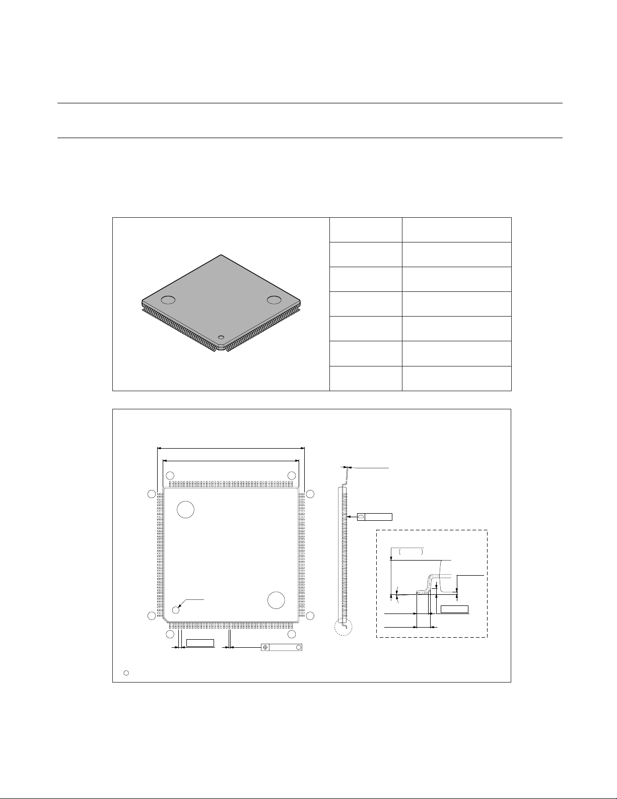
1.3 Package Dimensions
Figure 1.3-1 and show the package dimensions.
■ MB91F355/354A/355A/F356B/F357B Package Dimensions (Reference Diagram)
Consult your customer representative for the formal version.
Figure 1.3-1 MB91F355/354A/355A/F356B/F357B Package Dimensions
176-pin plastic LQFP Lead pitch 0.50 mm
(FPT-176P-M02)
176-pin plastic LQFP
(FPT-176P-M02)
26.00±0.20(1.024±.008)SQ
*
24.00±0.10(.945±.004)SQ
133
Package width ×
package length
24.0 × 24.0 mm
Lead shape Gullwing
Sealing method Plastic mold
Mounting height
1.70 mm MAX
Weight 1.86g
Code
(Reference)
Note 1)* : Values do not include resin protrusion.
Resin protrusion is +0.25(.010)Max(each side).
Note 2) Pins width and pins thickness include plating thickness
Note 3) Pins width do not include tie bar cutting remainder.
0.145±0.055
89132
88
(.006±.002)
0.08(.003)
Details of "A" part
P-LFQFP176-24×24-0.50
+0.20
–0.10
1.50
(Mounting height)
+.008
–.004
.059
INDEX
176
1
LEAD No.
C
2003 FUJITSU LIMITED F176006S-c-4-6
0.50(.020)
0.22±0.05
(.009±.002)
0.08(.003)
0.10±0.10
0˚~8˚
45
44
M
"A"
0.50±0.20
(.020±.008)
0.60±0.15
(.024±.006)
Dimensions in mm (inches).
Note: The values in parentheses are reference values.
(.004±.004)
0.25(.010)
(Stand off)
9
Page 28

CHAPTER 1 OVERVIEW
■ MB91F353A/351A/352A/353A Package Dimensions
Figure 1.3-2 MB91F353A/351A/352A/353A Package Dimensions
120-pin plastic LQFP Lead pitch 0.50 mm
(FPT-120P-M21)
120-pin plastic LQFP
(FPT-120P-M21)
18.00±0.20(.709±.008)SQ
+0.40
*
–0.10
16.00
90 61
91
.630 –.004
Package width ×
package length
16.0 × 16.0 mm
Lead shape Gullwing
Sealing method Plastic mold
Mounting height
1.70 mm MAX
Weight 0.88 g
Code
(Reference)
Note 1) * : These dimensions do not include resin protrusion.
Resin protrusion is +0.25(.010) MAX(each side).
Note 2) Pins width and pins thickness include plating thickness.
Note 3) Pins width do not include tie bar cutting remainder.
+.016
SQ
60
0.08(.003)
P-LFQFP120-16×16-0.50
Details of "A" part
+0.20
–0.10
1.50
(Mounting height)
+.008
.059 –.004
10
INDEX
120
1 30
LEAD No.
0.50(.020)
C
2002 FUJITSU LIMITED F120033S-c-4-4
0.22±0.05
(.009±.002)
31
0.08(.003)
0~8
"A"
+0.05
–0.03
M
0.145
.006
+.002
–.001
Dimensions in mm (inches).
Note: The values in parentheses are reference values.
˚
0.60±0.15
(.024±.006)
0.10±0.05
(.004±.002)
(Stand off)
0.25(.010)
Page 29
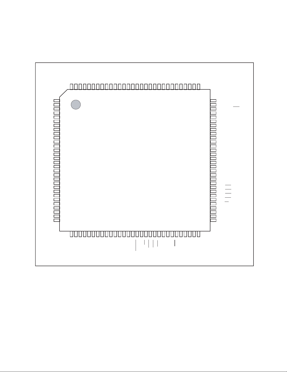
1.4 Pin Layout
88
Figure 1.4-1 , Figure 1.4-2 show the FR60 family pin layouts.
■ Pin Layout of the MB91F355A/354A/355A/F356B/F357B
The installed package is FPT-176P-M02.
Figure 1.4-1 Pin Layout of the MB91F355A/354A/355A/F356B/F357B
PG4/SO5
PG3/SI5
PG2/SCK4
PG1/SO4
PG0/SI4
PH5/SCK3
PH4/SO3
PH3/SI3
PH2/SCK2
PH1/SO2
PH0/SI2
PI5/SCK1
PI4/SO1
PI3/SI1
PI2/SCK0
PI1/SO0
PI0/SI0
VCCVSSPJ7/INT15
PJ6/INT14
PJ5/INT13
PJ4/INT12
PJ3/INT11
PJ2/INT10
PJ1/INT9
PJ0/INT8
PK7/INT7/ATG
PK6/INT6/FRCK
PK5/INT5
PK4/INT4
PK3/INT3
PK2/INT2
PK1/INT1
PK0/INT0
VCCVSSPL1/SCL
PL0/SDA
VSSPM5/SCK7/ZIN1/TRG5
PM4/SO7/BIN1/TRG4
PM3/SI7/AIN1/TRG3
PM2/SCK6/ZIN0/TRG2
PG5/SCK5
NMI
X1A
Vss
X0A
MD2
MD1
MD0
X0
Vcc
X1
INIT
Vss
Vcc
PC0/DREQ2
PC1/DACK2
PC2/DSTP2/DEOP2
PB0/DREQ0
PB1/DACK0
PB2/DSTP0/DEOP0
PB3/DREQ1
PB4/DACK1
PB5/DSTP1/DEOP1
PB6/IOWR
PB7/IORD
A0/CS0
PA1/CS1
PA2/CS2
PA3/CS3
V
V
P80/IN0/RDY
P81/IN1/BGRNT
P82/IN2/BRQ
P83/RD
P84/WR0
P85/IN3/WR1
P90/SYSCLK
P91
P92/MCLK
P93
P94/AS
V
V
132
131
130
129
128
127
126
125
124
123
122
121
120
119
118
117
116
115
114
113
112
111
110
109
108
107
106
133
134
135
136
137
138
139
140
141
142
143
144
145
146
147
148
149
MB91F355A/MB91355A/MB91354A/
150
151
152
153
154
155
156
157
158
159
160
161
162
SS
CC
163
164
165
166
167
168
169
170
171
172
173
174
175
SS
CC
176
12345678910111213141516171819202122232425262728293031323334353637383940414243
MB91F356B/MB91F357B
TOP VIEW
(LQFP176)
105
104
103
102
101
100
9998979695949392919089
87
86
85
84
83
82
81
80
79
78
77
76
75
74
73
72
71
70
69
68
67
66
65
64
63
62
61
60
59
58
57
56
55
54
53
52
51
50
49
48
47
46
45
44
PM1/SO6/BIN0/TRG1
PM0/SI6/AIN0/TRG0
PN5/PPG5
PN4/PPG4
PN3/PPG3
PN2/PPG2
PN1/PPG1
PN0/PPG0
CC
V
V
SS
PO7/OC7
PO6/OC6
PO5/OC5
PO4/OC4
PO3/OC3
PO2/OC2
PO1/OC1
PO0/OC0
PP3/TOT3
PP2/TOT2
PP1/TOT1
PP0/TOT0
CC
V
V
SS
AVSS/AVRL
AVRH
AV
CC
AN11
AN10
AN9
AN8
AN7
AN6
AN5
AN4
AN3
AN2
AN1
AN0
DA2
DA1
DA0
DAVC
DAVS
P20/D16
P21/D17
P22/D18
P23/D19
P24/D20
P25/D21
P26/D22
P27/D23
P30/D24
P31/D25
P32/D26
P33/D27
P34/D28
P35/D29
P36/D30
SS
CC
V
V
P40/A00
P41/A01
P42/A02
P43/A03
P44/A04
P45/A05
P46/A06
P47/A07
P50/A08
P51/A09
P37/D31
P52/A10
P53/A11
P54/A12
P55/A13
P56/A14
SS
CC
V
V
P57/A15
P60/A16
P62/A18
P61/A17
P63/A19
P64/A20
P65/A21
P66/A22
P67/A23
11
Page 30
CHAPTER 1 OVERVIEW
■ Pin Layout of the MB91F353A/351A/352A/353A
The installed package is FPT-120P-M21.
Figure 1.4-2 Pin Layout of the MB91F353A/351A/352A/353A
/AVRL
SS
AN7
AN6
AN5
AN4
AN3
AN2
AN1
AN0
VSSAV
CC
DAVC
DAVS
DA0
DA1
PH5/SCK3
PH4/SO3
AVRH
AV
PH3/SI3
PH2/SCK2
PH1/SO2
PH0/SI2
PO2/OC2
SSVCC
PO0/OC0
V
PI5/SCK1
PI4/SO1
PI3/SI1
PI2/SCK0
P20/D16
P21/D17
P22/D18
P23/D19
P24/D20
P25/D21
P26/D22
P27/D23
P30/D24
P31/D25
P32/D26
P33/D27
P34/D28
P35/D29
P36/D30
P37/D31
P40/A00
V
V
P41/A01
P42/A02
P43/A03
P44/A04
P45/A05
P46/A06
P47/A07
P50/A08
P51/A09
P52/A10
P53/A11
120
119
118
117
116
115
114
113
112
111
110
109
108
107
106
105
104
103
1
2
3
4
5
6
7
8
9
10
11
12
13
14
15
16
17
18
SS
19
CC
20
21
22
23
24
25
26
27
28
29
30
31
3233343536
MB91F353A/MB91351A/
MB91352A/MB91353A
TOP VIEW
(LQFP-120)
3738394041424344454647484950515253545556575859
999897969594939291
102
101
100
90
PI1/SO0
89
PI0/SI0
88
PK7/INT7/ATG
87
PK6/INT6/FRCK
86
PK5/INT5
85
PK4/INT4
84
PK3/INT3
83
PK2/INT2
82
PK1/INT1
81
PK0/INT0
80
PM5/SCK7
79
PM4/SO7/TRG4
78
PM3/SI7/TRG3
77
V
76
75
74
73
72
71
70
69
68
67
66
65
64
63
62
61
60
CC
V
SS
PM2/SCK6/ZIN0/TRG2
PM1/SO6/BIN0/TRG1
PM0/SI6/AIN0/TRG0
PN4/PPG4
PN2/PPG2
PN0/PPG0
PA3/CS3
PA2/CS2
PA1/CS1
PA0/CS0
P94/AS
P93
P91
P90/SYSCLK
X1A
12
P54/A12
P55/A13
P56/A14
P57/A15
P60/A16
P61/A17
SS
SS
PL1/SCL
PL0/SDA
CC
V
V
P80/IN0/RDY
P82/IN2/BRQ
P83/RD
NMI
P84/WR0
P85/IN3/WR1
MD2
MD1
MD0
INIT
V
P62/A18
P63/A19
P64/A20
SS
CC
X1
X0
V
V
X0A
P81/IN1/BGRNT
Page 31

1.5 List of Pin Functions
Table 1.5-1 lists the functions of the pins. Table 1.5-2 lists the power supply and GND
pins. See Figure 1.4-1 , Figure 1.4-2 for the pin layouts.
■ List of Pin Functions
Table 1.5-1 Pin Functions (1 / 13)
Pin number
176 pins 120 pins
1 to 8 1 to 8
9 to 16 9 to 16
19 to 26 17,20 to 26
27 to 34 27 to 34
37 to 41 35 to 39
I/O
Pin name
D16 to D23
P20 to P27 Can be used as a port in external bus 8-bit mode.
D24 to D31
P30 to P37 Can be used as a port in single-chip mode.
A00 to A07
P40 to P47 Can be used as a port in single-chip mode.
A08 to A15
P50 to P57 Can be used as a port in single-chip mode.
A16 to A20
P60 to P64
circuit
type
C
C
C
C
C
Function
Bits 16 to 23 of the external data bus.
Valid only in external bus mode.
Bits 24 to 31 of the external data bus.
Valid only in external bus mode.
Bits 0 to 7 of the external address bus.
Valid only in external bus mode.
Bits 8 to 15 of the external address bus.
Valid only in external bus mode.
Bits 16 to 20 of the external address bus.
Valid only in external bus mode.
Can be used as a port in single-chip mode or when an
external address bus is not used.
A21 to A23
42 to 44 -
P65 to P67
47, 48 106,105 DA0, DA1 - D/A converter output pin
49 - DA2 - D/A converter output pin
50 to 57 113 to 120 AN0 to AN 7 G Analog input pin
58 to 61 - AN8 to AN11 G Analog input pin
TOT0 to
TOT3
67 to 70 -
PP0 to PP3
C
D
Bits 21 to 23 of the external address bus.
Valid only in external bus mode.
Can be used as a port in single-chip mode or when an
external address bus is not used.
[TOT0 to TOT3] are reload timer output ports.
This function is valid when timer output is enabled.
[PP0 to PP3] are general-purpose I/O ports.
This function is valid when the timer output function is
disabled.
13
Page 32

CHAPTER 1 OVERVIEW
Table 1.5-1 Pin Functions (2 / 13)
Pin number
176 pins 120 pins
71 97
72 -
73 98
74 to 78 -
Pin name
OC0
PO0
OC1
PO1
OC2
PO2
OC3 to OC7
PO3 to PO7
PPG0
I/O
circuit
type
D
D
D
D
Function
[OC0] is an output compare output pin.
[PO0] is a general-purpose I/O port.
This function can be used as a port when output compare
output is not used.
[OC1] is an output compare output pin.
[PO1] is a general-purpose I/O port.
This function can be used as a port when output compare
output is not used.
[OC2] is an output compare output pin.
[PO2] is a general-purpose I/O port.
This function can be used as a port when output compare
output is not used.
[OC3 to OC7] are output compare output pins.
[PO3 to PO7] are general-purpose I/O ports.
This function can be used as a port when output compare
output is not used.
[PPG0] is a PPG timer output pin.
81 70
82 -
83 71
84 -
85 72
PN0
PPG1
PN1
PPG2
PN2
PPG3
PN3
PPG4
PN4
PPG5
D
D
D
D
D
[PN0] is a general-purpose I/O port.
This function can be used as a port when PPG timer output
is not used.
[PPG1] is a PPG timer output pin.
[PN1] is a general-purpose I/O port.
This function can be used as a port when PPG timer output
is not used.
[PPG2] is a PPG timer output pin.
[PN2] is a general-purpose I/O port.
This function can be used as a port when PPG timer output
is not used.
[PPG3] is a PPG timer output pin.
[PN3] is a general-purpose I/O port.
This function can be used as a port when PPG timer output
is not used.
[PPG4] is a PPG timer output pin.
[PN4] is a general-purpose I/O port.
This function can be used as a port when PPG timer output
is not used.
[PPG5] is a PPG timer output pin.
86 -
14
PN5
D
[PN5] is a general-purpose I/O port.
This function can be used as a port when PPG timer output
is not used.
Page 33

Table 1.5-1 Pin Functions (3 / 13)
Pin number
176 pins 120 pins
87 73
Pin name
SI6
AIN0
TRG0
PM0
SO6
I/O
circuit
type
D
Function
[SI6] is data input for serial I/O6.
Since this input is always used when serial I/O6 input is
operating, output using the port must be stopped beforehand
unless this operation is the intended operation.
[AIN0] is input for the up/down timer.
Since this input is always used when input is allowed,
output using the port must be stopped beforehand unless
this operation is the intended operation.
[TRG0] is external trigger input for PPG timer 0.
Since this input is always used when input is allowed,
output using the port must be stopped beforehand unless
this operation is the intended operation.
[PM0] is a general-purpose I/O port.
This function can be used as a port when serial I/O, up/
down timer, and PPG timer output are not used.
[SO6] is data output from serial I/O6.
This function is valid when data output from serial I/O6 is
allowed.
88 74
89 75
BIN0
TRG1
PM1
SCK6
ZIN0
TRG2
[BIN0] is input for the up/down timer.
Since this input is always used when input is allowed,
output using the port must be stopped beforehand unless
this operation is the intended operation.
D
[TRG1] is external trigger input for PPG timer 1.
Since this input is always used when input is allowed,
output using the port must be stopped beforehand unless
this operation is the intended operation.
[PM1] is a general-purpose I/O port.
This function can be used as a port when serial I/O, up/
down timer, and PPG timer output are not used.
[SCK6] is clock I/O for serial I/O6.
This function is valid when clock output from serial I/O6 is
allowed or when external shift clock input is used.
[ZIN0] is input for the up/down timer.
Since this input is always used when input is allowed,
output using the port must be stopped beforehand unless
this operation is the intended operation.
D
[TRG2] is external trigger input for PPG timer 2.
Since this input is always used when input is allowed,
output using the port must be stopped beforehand unless
this operation is the intended operation.
PM2
[PM2] is a general-purpose I/O port.
This function can be used as a port when serial I/O, up/
down timer, and PPG timer output are not used.
15
Page 34

CHAPTER 1 OVERVIEW
Table 1.5-1 Pin Functions (4 / 13)
Pin number
176 pins 120 pins
90 78
Pin name
SI7
AIN1*
TRG3
PM3
S07
I/O
circuit
type
D
Function
[SI7] is data input for serial I/O7.
Since this input is always used when serial I/O7 input is
operating, output using the port must be stopped beforehand
unless this operation is the intended operation.
[AIN1] is input for the up/down timer.
Since this input is always used when input is allowed,
output using the port must be stopped beforehand unless
this operation is the intended operation.
*
: The 120-pin version does not support this function.
[TRG3] is external trigger input for PPG timer 3.
Since this input is always used when input is allowed,
output using the port must be stopped beforehand unless
this operation is the intended operation.
[PM3] is a general-purpose I/O port.
This function can be used as a port when serial I/O, up/
down timer, and PPG timer output are not used.
[S07] is data output from serial I/O7.
This function is valid when data output from serial I/O7 is
allowed.
91 79
BIN1*
TRG4
PM4
[BIN1] is input for the up/down timer.
Since this input is always used when input is allowed,
output using the port must be stopped beforehand unless
this operation is the intended operation.
*
D
: The 120-pin version does not support this function.
[TRG4] is external trigger input for PPG timer 4.
Since this input is always used when input is allowed,
output using the port must be stopped beforehand unless
this operation is the intended operation.
[PM4] is a general-purpose I/O port.
This function can be used as a port when serial I/O, up/
down timer, and PPG timer output are not used.
16
Page 35

Table 1.5-1 Pin Functions (5 / 13)
Pin number
176 pins 120 pins
92 80
94 42
Pin name
SCK7
ZIN1*
TRG5*
PM5
SDA
I/O
circuit
type
D
F
Function
[SCK7] is clock I/O for serial I/O7.
This function is valid when clock output from serial I/O7 is
allowed or when external shift clock input is used.
[ZIN1] is input for the up/down timer.
Since this input is always used when input is allowed,
output using the port must be stopped beforehand unless
this operation is the intended operation.
*
: The 120-pin version does not support this function.
[TRG5] is external trigger input for PPG timer 5.
Since this input is always used when input is allowed,
output using the port must be stopped beforehand unless
this operation is the intended operation.
*
: The 120-pin version does not support this function.
[PM5] is a general-purpose I/O port.
This function can be used as a port when serial I/O, up/
down timer, and PPG timer output are not used.
[SDA] is a DATA I/O pin for the I
This function is valid when the I
2
C bus.
2
C is allowed to operate in
standard mode.
Output using the port must be stopped beforehand unless
this operation is intended (open drain output).
95 41
98 to 103 81 to 86
[PL0] is a general-purpose I/O port.
PL0
This function can be used as a port when I
not allowed (open drain output).
2
C bus.
2
C is allowed to operate in
SCL
[SCL] is a CLK I/O pin for the I
This function is valid when the I
standard mode.
F
Output using the port must be stopped beforehand unless
this operation is intended (open drain output).
[PL1] is a general-purpose I/O port.
PL1
This function can be used as a port when I
not allowed (open drain output).
[INT0 to INT5] are external interrupt input.
Since this input is always used when the corresponding
INT0 to INT5
E
external interrupt is allowed, output using the port must be
stopped beforehand unless this operation is the intended
operation.
PK0 to PK5 [PK0 to PK5] are general-purpose I/O ports.
2
C operation is
2
C operation is
17
Page 36

CHAPTER 1 OVERVIEW
Table 1.5-1 Pin Functions (6 / 13)
Pin number
176 pins 120 pins
104 87
105 88
I/O
Pin name
INT6
FRCK
PK6 [PK6] is a general-purpose I/O port.
INT7
ATG
circuit
type
E
E
Function
[INT6] is external interrupt input.
Since this input is always used when the corresponding
external interrupt is allowed, output using the port must be
stopped beforehand unless this operation is the intended
operation.
[FRCK] is external clock input pin for the free-running
timer.
Since this input is always used when it is selected as
external clock input for the free-running timer, output using
the port must be stopped beforehand unless this operation is
the intended operation.
[INT7] is external interrupt input.
Since this input is always used when the corresponding
external interrupt is allowed, output using the port must be
stopped beforehand unless this operation is the intended
operation.
[ATG] is external trigger for the A/D converter.
Since this input is always used when it is selected as the
source of A/D activation, output using the port must be
stopped beforehand unless this operation is the intended
operation.
106 to 113 -
116 89
117 90
PK7 [PK7] is a general-purpose I/O port.
[INT8 to INT15] are external interrupt input.
INT8 to
INT15
PJ0 to PJ7 [PJ0 to PJ7] are general-purpose I/O ports.
SI0
PI0 [PI0] is a general-purpose I/O port.
SO0
PI1
E
D
D
Since this input is always used when the corresponding
external interrupt is allowed, output using the port must be
stopped beforehand unless this operation is the intended
operation.
[SI0] is data input for UART0.
Since this input is always used when UART0 input is
operating, output using the port must be stopped beforehand
unless this operation is the intended operation.
[SO0] is data output from UART0.
This function is valid when UART0 data output is allowed.
[PI1] is a general-purpose I/O port.
This function is valid when UART0 data output is not
allowed.
18
Page 37

Table 1.5-1 Pin Functions (7 / 13)
Pin number
176 pins 120 pins
118 91
119 92
120 93
121 94
I/O
Pin name
SCK0
PI2
SI1
PI3 [PI3] is a general-purpose I/O port.
SO1
PI4
SCK1
PI5
circuit
type
D
D
D
D
Function
[SCK0] is clock I/O for UART0.
This function is valid when UART0 clock output is allowed
or when external clock input is used.
[PI2] is a general-purpose I/O port.
This function is valid when UART0 clock output is not
allowed or when external clock input is not used.
[SI1] is data input for UART1.
Since this input is always used when UART1 input is
operating, output using the port must be stopped beforehand
unless this operation is the intended operation.
[SO1] is data output from UART1.
This function is valid when UART1 data output is allowed.
[PI4] is a general-purpose I/O port.
This function is valid when UART1 data output is not
allowed.
[SCK1] is clock I/O for UART1.
This function is valid when UART1 clock output is allowed
or when external clock input is used.
[PI5] is a general-purpose I/O port.
This function is valid when UART1 clock output is not
allowed or when external clock input is not used.
122 99
123 100
124 101
[SI2] is data input for UART2.
SI2
D
PH0 [PH0] is a general-purpose I/O port.
SO2
D
PH1
SCK2
D
PH2
Since this input is always used when UART2 input is
operating, output using the port must be stopped beforehand
unless this operation is the intended operation.
[SO2] is data output from UART2.
This function is valid when UART2 data output is allowed.
[PH1] is a general-purpose I/O port.
This function is valid when UART2 data output is not
allowed or when external shift clock input is used.
[SCK2] is clock I/O for UART2.
This function is valid when UART2 clock output is allowed
or when external clock input is used.
[PH2] is a general-purpose I/O port.
This function is valid when UART2 clock output is not
allowed or when external clock input is not used.
19
Page 38

CHAPTER 1 OVERVIEW
Table 1.5-1 Pin Functions (8 / 13)
Pin number
176 pins 120 pins
125 102
126 103
127 104
128 -
I/O
Pin name
SI3
PH3 [PH3] is a general-purpose I/O port.
SO3
PH4
SCK3
PH5
SI4
circuit
type
D
D
D
D
Function
[SI3] is data input for UART3.
Since this input is always used when UART3 input is
operating, output using the port must be stopped beforehand
unless this operation is the intended operation.
[SO3] is data output from UART3.
This function is valid when UART3 data output is allowed.
[PH4] is a general-purpose I/O port.
This function is valid when UART3 data output is not
allowed.
[SCK3] is clock I/O for UART3.
This function is valid when UART3 clock output is allowed
or when external clock input is used.
[PH5] is a general-purpose I/O port.
This function is valid when UART3 clock output is not
allowed or when external clock input is not used.
[SI4] is data input for UART4.
Since this input is always used when UART4 input is
operating, output using the port must be stopped beforehand
unless this operation is the intended operation.
129 -
130 -
131 -
PG0 [PG0] is a general-purpose I/O port.
[SO4] is data output from UART4.
SO4
D
PG1
SCK4
D
PG2
SI5
D
PG3 [PG3] is a general-purpose I/O port.
This function is valid when serial I/O4 data output is
allowed.
[PG1] is a general-purpose I/O port.
This function is valid when serial I/O4 data output is not
allowed.
[SCK4] is clock I/O for UART4.
This function is valid when serial I/O4 clock output is
allowed or when external clock input is used.
[PG2] is a general-purpose I/O port
This function is valid when serial I/O4 clock output is not
allowed or when external clock input is not used.
[SI5] is data input for serial I/O5.
Since this input is always used when serial I/O5 input is
operating, output using the port must be stopped beforehand
unless this operation is the intended operation.
20
Page 39

Table 1.5-1 Pin Functions (9 / 13)
Pin number
Pin name
176 pins 120 pins
I/O
circuit
type
Function
[SO5] is data output from serial I/O5.
SO5
This function is valid when serial I/O5 data output is
allowed.
132 -
D
[PG4] is a general-purpose I/O port.
PG4
This function is valid when serial I/O5 data output is not
allowed.
[SCK5] is clock I/O for serial I/O5.
SCK5
This function is valid when serial I/O5 clock output is
allowed or when external shift clock input is used.
133 -
D
[PG5] is a general-purpose I/O port.
PG5
This function is valid when serial I/O5 clock output is not
allowed or when external clock input is not used.
134 51 NMI
H NMI (non-maskable interrupt) input
135 61 X1A B Cl ock (oscillation) output (subclock)
137 60 X0A B Cl ock (oscillation) input (subclock)
H [MD2 to MD0] are mode pins 2 to 0.
These pins set the basic operating mode. Connect the pins to
V
or VSS.
CC
138 to 140 52 to 54 MD2 to MD0
J
Input circuit type:
• The production version (mask ROM version) is the "H"
type.
• The flash ROM version is the "J" type.
141 58 X0 A Clock (oscillation) input (main clo c k)
143 57 X1 A Clock (oscillation) output (main clock)
144 55 INIT
I External reset input
[DREQ2] is DMA external transfer request input.
Since this input is always used when it is selected as the
147 -
DREQ2
C
source of DMA activation, output using the port must be
stopped beforehand unless this operation is the intended
operation.
PC0 [PC0] is a general-purpose I/O port.
[DACK2] is DMA external transfer request acceptance
output.
This function is valid when DMA transfer request
acceptance output is allowed.
148 -
DACK2
C
[PC1] is a general-purpose I/O port.
PC1
This function is valid when DMA transfer request
acceptance output is allowed.
21
Page 40

CHAPTER 1 OVERVIEW
Table 1.5-1 Pin Functions (10 / 13)
Pin number
176 pins 120 pins
149 -
150 -
151 -
I/O
Pin name
DEOP2
DSTP2
PC2
DREQ0
PB0 [PB0] is a general-purpose I/O port.
DACK0
PB1
circuit
type
C
C
C
Function
[DEOP2] is DMA external transfer end output.
This function is valid when DMA external transfer end
output is allowed.
[DSTP2] is DMA external transfer stop input.
This function is valid when DMA external transfer stop
input is allowed.
[PC2] is a general-purpose I/O port.
This function is valid when DMA external transfer end
output and external transfer stop input are not allowed.
[DREQ0] is DMA external transfer request input.
Since this input is always used when it is selected as the
source of DMA activation, output using the port must be
stopped beforehand unless this operation is the intended
operation.
[DACK0] is DMA external transfer request acceptance
output.
This function is valid when DMA transfer request
acceptance output is allowed.
[PB1] is a general-purpose I/O port.
This function is valid when DMA transfer request
acceptance output is not allowed.
152 -
153 -
[DEOP0] is DMA external transfer end output.
DEOP0
DSTP0
PB2
DREQ1
PB3 [PB3] is a general-purpose I/O port.
C
C
This function is valid when DMA external transfer end
output is allowed.
[DSTP0] is DMA external transfer stop input.
This function is valid when DMA external transfer stop
input is allowed.
[PB2] is a general-purpose I/O port.
This function is valid when DMA external transfer end
output and external transfer stop input are not allowed.
[DREQ1] is DMA external transfer request input.
Since this input is always used when it is selected as the
source of DMA activation, output using the port must be
stopped beforehand unless this operation is the intended
operation.
22
Page 41

Table 1.5-1 Pin Functions (11 / 13)
Pin number
176 pins 120 pins
154 -
155 -
156 -
Pin name
DACK1
PB4
DEOP1
DSTP1
PB5
IOWR
PB6
I/O
circuit
type
C
C
C
Function
[DACK1] is DMA external transfer request acceptance
output.
This function is valid when DMA transfer request
acceptance output is allowed.
[PB4] is a general-purpose I/O port.
This function is valid when DMA external transfer request
acceptance output is not allowed.
[DEOP1] is DMA external transfer end output.
This function is valid when DMA external transfer end
output is allowed.
[DSTP1] is DMA external transfer stop input.
This function is valid when DMA external transfer stop
input is allowed.
[PB5] is a general-purpose I/O port.
This function is valid when DMA external transfer end
output and external transfer stop input are not allowed.
[IOWR
] is write strobe output for DMA fly-by transfer.
This function is valid when write strobe output for DMA
fly-by transfer is allowed.
[PB6] is a general-purpose I/O port.
This function is valid when write strobe output for DMA
fly-by transfer is not allowed.
157 -
158 66
159 67
160 68
IORD
PB7
CS0
PA0
CS1
PA1
CS2
PA2
[IORD
] is read strobe output for DMA fly-by transfer.
This function is valid when read strobe output for DMA fly-
C
C
C
C
by transfer is allowed.
[PB7] is a general-purpose I/O port.
This function is valid when read strobe output for DMA flyby transfer is not allowed.
] is chip select 0 output.
[CS0
This function is valid in external bus mode.
[PA0] is a general-purpose I/O port.
This function is valid in single-chip mode.
] is chip select 1 output.
[CS1
This function is valid when chip select 1 output is allowed.
[PA1] is a general-purpose I/O port.
This function is valid when chip select 1 output is not
allowed.
] is chip select 2 output.
[CS2
This function is valid when chip select 2 output is allowed.
[PA2] is a general-purpose I/O port.
This function is valid when chip select 2 output is not
allowed.
23
Page 42

CHAPTER 1 OVERVIEW
Table 1.5-1 Pin Functions (12 / 13)
Pin number
176 pins 120 pins
161 69
164 45
165 46
Pin name
CS3
PA3
RDY
IN0
P80
BGRNT
IN1
I/O
circuit
type
C
D
D
Function
] is chip select 3 output.
[CS3
This function is valid when chip select 3 output is allowed.
[PA3] is a general-purpose I/O port.
This function is valid when chip select 3 output is not
allowed.
[RDY] is external ready input.
This function is valid when external ready input is allowed.
[IN0] is an input capture input pin.
Since this input is always used when it is selected for input
capture input, output using the port must be stopped
beforehand unless this operation is the intended operation.
[P80] is a general-purpose I/O port.
This function is valid when external ready input is not
allowed.
[BGRNT
The low level is output when the external bus is open.
This function is valid when output is allowed.
[IN1] is an input capture input pin.
Since this input is always used when it is selected for input
capture input, output using the port must be stopped
beforehand unless this operation is the intended operation.
] is external bus open acceptance output.
166 47
167 48
P81
BRQ
IN2
P82
RD
P83
[P81] is a general-purpose I/O port.
This function is valid when external bus open acceptance is
not allowed.
[BRQ] is external bus open request input.
Input to the high level [1] if you want to open the external
bus.
This function is valid when input is allowed.
[IN2] is an input capture input pin.
D
D
Since this input is always used when it is selected for input
capture input, output using the port must be stopped
beforehand unless this operation is the intended operation.
[P82] is a general-purpose I/O port.
This function is valid when external bus open request is not
allowed.
] is external bus read strobe output.
[RD
This function is valid in external bus mode.
[P80] is a general-purpose I/O port.
This function is valid in single-chip mode.
24
Page 43

Table 1.5-1 Pin Functions (13 / 13)
Pin number
176 pins 120 pins
168 49
169 50
170 62
Pin name
WR0
P84
WR1
IN3
P85
SYSCLK
P90
I/O
circuit
type
D
D
C
Function
] is external bus write strobe output.
[WR0
This function is valid in external bus mode.
[P80] is a general-purpose I/O port.
This function is valid in single-chip mode.
[WR1
] is external bus write strobe output.
This function is valid when WR1
mode is allowed.
[IN3] is an input capture input pin.
Since this input is always used when it is selected for input
capture input, output using the port must be stopped
beforehand unless this operation is the intended operation.
[P85] is a general-purpose I/O port.
This function is valid when external bus write enable output
is not allowed.
[SYSCLK] is system clock output.
This function is valid when system clock output is allowed.
A clock having the same frequency as the external bus
operating frequency is output (stopped in stop mode).
[P90] is a general-purpose I/O port.
This function is valid when system clock output is not
allowed.
output in external bus
171 63 P91 C [P91] is a general-purpose I/O port.
[MCLK] is memory clock output.
MCLK
172 -
P92
173 64 P93 C [P93] is a general-purpose I/O port.
AS
174 65
P94
*: These functions are not supported for the 120-pin version.
C
C
This function is valid when memory clock output is
allowed. A clock having the same frequency as the external
bus operating frequency is output (stopped in sleep mode).
[P92] is a general-purpose I/O port.
This function is valid when memory clock output is not
allowed.
[AS
] is address strobe output.
This function is valid when address strobe output is
allowed.
[P94] is a general-purpose I/O port.
This function is valid when address load output is not
allowed.
25
Page 44

CHAPTER 1 OVERVIEW
Table 1.5-2 Power Supply and GND Pins
Pin number
176 pins 120 pins
Pin name Function
17,35,65,79,93,96,114,
136,145,162,175
18,36,66,80,97,115,142,14
6,163,176
45 107 DAVS D/A converter GND pin
46 108 DAVC D/A converter power supply pin
62 109
63 110 AVRH A/D converter reference power supply pin
64 111
18,40,43,59,76,9
6,112
19,44,56,77,95
V
SS
V
CC
AV
CC
/AVRL A/D converter analog GND pin
AV
SS
GND pins. Use the same potential for all pins.
3.3 V power supply pins. Use the same potential
for all pins.
A/D converter analog power supply pin
26
Page 45

1.6 Input-output Circuit Forms
This section describes the I/O circuit types listed in Table 1.6-1 .
■ Input-Output Circuit Types
Table 1.6-1 Input-Output Cir cuit Types (1 / 3)
Classification Circuit type Remarks
• Oscillation feedback resistor for high-
X1
Clock input
speed operation (main clock oscillation) :
About 1 MΩ
A
X0
Standby control
• Oscillation feedback resistor for low-
X1A
Clock input
B
X0A
Standby control
speed operation (subclock oscilla ti on) :
About 7 MΩ
• CMOS level output
• CMOS level input
Pull-up control
With standby control
Digital output
With pull- up control
Pull-up resistance = about 50 kΩ (Typ)
C
Digital output
Digital input
Standby control
I
OL
= 8 mA
27
Page 46

CHAPTER 1 OVERVIEW
Table 1.6-1 Input-Output Cir cuit Types (2 / 3)
Classification Circuit type Remarks
• CMOS level output
Pull-up control
• CMOS level hysteresis input
With standby control
Digital output
With pull- up control
Pull-up resistance = about 50 kΩ (Typ)
D
Digital output
Digital input
Standby control
I
OL
= 4 mA
• CMOS level output
• CMOS level hysteresis input
al output
Digit
I
= 4 mA
OL
E
5 V withstand voltage
Digital output
Digital input
• Nch open-drain output
• CMOS level hysteresis input
Digital output
F
Digital input
Standby control
With standby control
5 V withstand voltage
I
= 15 mA
OL
Analog input with switches
28
G
Analog input
Control
Page 47

Table 1.6-1 Input-Output Cir cuit Types (3 / 3)
Classification Circuit type Remarks
• CMOS level hysteresis input
H
Digital input
• CMOS level hysteresis input
With pull-up resistor
Pull-up resistance = about 50 kΩ (Typ)
I
Digital input
• CMOS level input (flash memory
products only)
J
Control signal
Mode input
Diffusion resistor
29
Page 48

CHAPTER 1 OVERVIEW
30
Page 49

CHAPTER 2
HANDLING THE DEVICE
This chapter provides precautions on handling FR famil y
microcontrollers.
2.1 Precautions on Handling the Device
2.2 Precautions on Using the Little-Endian Area
31
Page 50

CHAPTER 2 HANDLING THE DEVICE
2.1 Precautions on Handling the Device
This section contains information on the prevention of latch-ups, pin processing,
handling of circuits, input at power-on and so on.
■ Preventing a Latch-up
A latch-up can occur if, on a CMOS IC, a voltage higher than VCC or a voltage lower than VSS is applied to
an input or output pin or a voltage higher than the rating is applied between V
occurs, significantly increases the power supply current and may cause thermal destruction of an element.
When you use a CMOS IC, be very careful not to exceed the maximum rating.
■ Unused Input Pins
Do not leave an unused input pin open, since it may cause a malfunction. Handle by, for example, using a
pull-up or pull-down resistor.
■ Po wer Supply Pins
If more than one VCC or VSS pin exists, those that must be kept at the same potential are designed to be
connected to one other inside the device to prevent malfunctions such as latch-up. Be sure to connect the
pins to a power supply and ground external to the device to minimize u ndesired electromagnetic radiation,
prevent strobe signal malfunctions due to an increase in ground level, and conform to the total output
current rating. Given consideration to connecting the current supply source to V
the lowest impedance possible.
It is also recommended that a ceramic capacitor of around 0.1 µF be connected between V
circuit points close to the device as a bypass capacitor.
and VSS. A latch-up, if it
CC
and VSS of the device at
cc
and VSS at
CC
■ Quartz Oscillation Circuit
Noise near the X0, X1, X0A, and X1A pins may cause the device to malfunction. Design printed circuit
boards so that X0 and X1, X0A and X1A, the quartz oscillator (or ceramic oscillator), and the bypass
capacitor to ground are located as near as possible to one another.
In addition, it is strongly recommended that printed circuit board artwork that surrounds the X0 , X1, X0A,
and X1A pins with ground be used to make stable operation more likely.
■ Note on Using an External Clock
When an external clock is used, use the X0 pin unless otherwise specify and supply a negative-phase clock
to the X1 pin simultaneously. Do not use STOP mode (oscillation stop mode) for this operation because the
X1 pin is disabled when H is output at STOP.
Figure 2.1-1 Example of Using an External Clock (Normal Method)
Note: STOP mode (oscillation stop mode) cannot be used.
X0
X1
32
Page 51

■ Note for the Case of Using No Subclock
When the oscillator is not connect to the X0A,X1A pins, set the X0A pin to the pull-down operation and
open the X1A pin.
Figure 2.1-2 Setting for the Case of Using No Subclock
X0A
OPEN
■ Handling of NC and Open Pins
NC and open pins must be left open.
■ Mode Pins (MD0 to MD2)
These pins must be directly connected to VCC or VSS when they are used. Keep the pattern length between
a mode pin on a printed circuit board and V
low impedance.
■ Power-on
At power-on, be sure to set the INIT pin to the low level.
Also immediately after power-on, keep the INIT
required frequency stability. (For initialization by INIT from the INIT
time is set to the minimum value.)
■ Source Oscillation Input at Power-on
At power-on, be sure to input a source clock until the oscillation stabilization wait time is cleared.
■ Note on Operating in PLL Clock Mode
If the PLL clock mode is selected, the microcontroller attempt to be working with the self-oscillating circuit
even when there is no external oscillator or external clock input is stopped . Performance of this operation,
however, cannot be guaranteed.
X1A
MB91350A
or VSS as short as possible so that they can be connected at a
CC
pin at the L level until the oscillator has reached the
pin, the oscillation stabilization wait
■ Setting the External Bus
The MB91350A model type guarantees a 25 MHz external bus.
If the base clock is set to 50 MHz without the DIVR1 (external bus base clock freq.-divide setting register)
initial value being unchanged, the external bus will also be set to 50 MH z. When changing the base clock,
first set the external bus so that it does not exceed 25 MHz and then change the base clock.
■ MCLK and SYSCLK
The difference between MCLK and SYSCLK is that MCLK stops in sleep mode and stop mode whereas
SYSCLK stops only in stop mode. Use MCLK or SYSCLK, whichever is appropriate.
After initialization, MCLK is disabled (PORT) and SYSCLK is enabled. To use MCLK, you must set the
port function register (PFR) to use MCLK.
33
Page 52

CHAPTER 2 HANDLING THE DEVICE
■ Pull-up Control
The AC specification will not be guaranteed if pull-u p resi stor is connected to pins that are used as external
bus pins.
In addition, ports for which pull-up resistor is connected will be disabled in stop mode with HIZ = 1 and for
hardware standby.
■ Clock Controller
When inputting the low level to INIT, allocate wait time to allow oscillation to stabilize.
■ Subclock Switching
Immediately after switching the clock source to subclock mode from the main clock, insert at least one
NOP instruction.
(ldi #0x0b, r0)
(ldi #_CLKR ,r12)
stb r0, @r12 // sub-clock mode
nop // Must insert NOP instruction
■ Bit Search Module
Only word access is supported for the BSD0, BSD1, and BDSC registers.
■ D-bus Memory
Because instruction fetch to the D-bus memory is not executed, do not set the code area in the D-bus
memory.
If instruction fetch to the D-bus memory is executed, incorrect data will be interpreted for the codes,
causing a runaway condition.
■ Low-power Consumption Mode
When sleep or stop mode is set, always read the same registers immediately after writing to the standby
control register (STCR).
Specifically, use the sequence given below.
In addition, after returning from standby mode, set the I flag, ILM, and ICR to branch to the interrupt
handler that causes the return.
(ldi #value_of_standby, r0)
(ldi #_STCR, r12)
stb r0, @r12 // set STOP/SLEEP bit
ldub @r12, r0 // Must read STCR
ldub @r12, r0 // after reading, go into standby mode
nop // Must insert NOP * 5
nop
nop
nop
nop
34
Page 53

■ Prefetch
When prefetch to an area set as little endian is allowed, restrict access to that area to word (32-bit) access.
Access will be incorrect if byte or halfword access is allowed.
■ Accessing I/O Ports
Only byte access is supported for port access.
■ Switching Shared Port Functions
Use the port function register (PFR) to switch the pins that also serve as ports. To switch the bus pins, use
the external bus setting.
■ Internal RAM
The function that restricts internal RAM size operates immediately after a reset is cleared. Only 4K bytes
can be used for data and another 4K bytes for program execution regardless of the amount of RAM
installed for the device.
To release the restriction function, rewrite the setting of the function.
In addition, if the above setting would be rewritten, include at least one NOP instructio n immediately after
that processing.
■ Flash Memory
In programming mode, flash memory cannot be used for interrupt vector tables (reset is enabled).
■ Notes of PS Register
Since some instructions process the PS register first, interrupt processing routines can lead to breaks during
debugging or updating of the PS register flag due to the following exceptions.
Whichever the case, the program is designed to reprocess correctly after returning from EIT to ensure that
operation before and after EIT conforms to specifications.
1 The following operations may occur when (a) user interrupt/NMI is received, (b) step execution is
performed, (c) break occurs in a data event or emulator menu in an immediately preceding DIVOU/
DIVOS instruction.
(1) D0 and D1 flags precede and are renewed.
(2) EIT processing routine (user interruption, NMI or emulator) is executed .
(3) After returning from EIT, DIVOU/DIVOS instructions are executed and the D0 and D1 flags are
updated to the same value as (1).
2 When each ORCCR/STILM/MOV Ri and PS instruction is executed to permit interrupting with the user
interruption and the NMI factor generated, the following operations are done.
(1) The PS register precedes and is updated.
(2) EIT processing routine (user interruption, NMI, or emulator) is executed.
(3) After returning from EIT, the above instructions are executed and the PS register is updated to the
same value as (1).
35
Page 54

CHAPTER 2 HANDLING THE DEVICE
■ Precautions on the Debuggers
● Single-step execution of the RETI instruction
In an environment where interrupts frequently occur, only the relevant interrupt processing routines are
executed repeatedly during single-step execution.
As a result, the main routines and programs that have a low interrupt level will not be executed. (For
example, if the RETI is executed in single-step mode with timebase timer interrupts allowed, the break will
always be at the beginning of the timebase routine.)
For stages in which debugging of the relevant interrupt processing routines is not required, disable the
relevant interrupts.
● Break function
If the target address of a hardware break (including event breaks) is the address of the current system stack
pointer or if the target address is set in an area that contains the stack pointer, a break will occur after one
instruction is executed. This applies even when there is no data access instruction in the user program.
To avoid the problem, do not set word access for the area that contains the address of the system stack
pointer as a target of a hardware break (including event breaks).
● Internal ROM (flash memory and MASK ROM)
Note the following points when using an evaluation chip:
• Do not set the internal ROM area as the DMAC transfer destination.
• If the internal ROM area is set as the DMAC transfer destination, the internal ROM area may be
rewritten if a break occurs during DMAC transfer. (The internal ROM area can be set as the DMAC
transfer source.)
● Concurrent occurrence of a software break (INTE instruction) and user interrupt or NMI
If a software break and a user interrupt or NMI occur concurrently, the following problems occur in the
debugger:
• The debugger stops, indicating a point other than the break point set by the user.
• After having stopped, the debugger does not correctly execute processing.
If this problem occurs, use a hardware break in place of a software break. If you use a monitor debugger,
avoid setting a break at the relevant point.
● About the operand break
If there is a stack pointer in an area that is set as operand break of DSU, the system may cause
malfunctions. Do not set the access for the area that contains the address of the system stack pointer as a
target of a data event break.
36
Page 55

2.2 Precautions on Using the Little-Endian Area
This section provides precautions on using the little-endian area.
■ Precautions on Using the Little-Endian Area
Note the precautions for the following items when using the little-endian area:
• C compiler
• Assembler
•Linker
• Debuggers
37
Page 56

CHAPTER 2 HANDLING THE DEVICE
2.2.1 C Compiler (fcc911)
When programming with the C language, operation will be unpredictable if the following
operations are executed for the little-endian area:
• Mapping of variables with initial values
• Structure assignment
• Manipulation of arrays other than character-type arrays using character string
operation functions
• Specification of the -K lib option when character string operation functions are being
used
• Use of the double type and long double type
• Mapping of the stack to the little-endian area
■ Mapping of Variables with Initial Values
Variables with initial values cannot be mapped to the little-endian area.
The compiler does not have a function for gen erating little-endian initial values. V ariables can be mapped
to the little-endian area, but initial values cannot be set.
Provide processing at the beginning of the program that sets initial values.
Example:
Setting an initial value for the variable little_data in the little-endian area
extern int little_data;
void little_init(void) {
little_data = initial value;
}
void main(void) {
little_init( );
...
}
38
Page 57

■ Structure Assignment
When structures are assigned among structures, the compiler selects the optimum transfer method and
executes transfer for each byte, halfword, and word.
As a result, the correct result will not be obtained i f structure assignment spans structure variables assigned
to the regular area and structure variables assigned to the little-endian area.
Assign the members of a structure individually.
Example:
Assigning a structure to the structure variable little_st in the little-endian area
struct tag { char c; int i; } normal_st;
extern struct tag little_st;
#define STRMOVE(DEST,SRC) DEST.c=SRC.c;DEST.i=SRC.i;
void main(void) {
STRMOVE(little_st,normal_st);
}
In addition, mapping of the structure m embers de pends on the compiler. If a different compiler was used to
compile a structure, the members will be mapped differently. In this case, the correct result will not be
obtained even though the method described above is used.
If the mappings of the structure members do not match, do not map structure variables in the little-endian
area.
■ Manipulation of Arrays Other than Character-type Arrays Using Character String
Operation Functions
Character string operation functions provided as a standard library are processed in byte units.
As a result, the correct result will not be obtained if processing that uses character string operation
functions is executed for areas that have a type other than char, unsigned char, or signed char mapped in the
little-endian area.
Do not execute this type of processing.
Incorrect processing example:
Transferring word data using memcpy
int big = 0x01020304; /* Big-endian area */
extern int little; /* Little-endian area */
memcpy(&little,&big,4); /* Transfer using memcpy */
The result of the executing the above code is shown below. An error occurs when word data is transferred.
(Big-endian area) (Little-endian area)
01 02 03 04 01 02 03 04
(Correct result)
memcpy
04 03 02 01
39
Page 58

CHAPTER 2 HANDLING THE DEVICE
■ Specification of the -K lib Option when Character String Operation Functions are Used
When the -K lib option is specified, the compiler expands several character string operation functions
inline. Because the compiler selects the optimum processing method at this time, processing may change
for each halfword or word.
If the processing changes, processing for the little-endian area will not be executed correctly.
Do not specify the -K lib option when executing processing that uses character string operation fu nctions
for the little-endian area. In addition, do not specify the -O 4 or -K speed option that includes the -K lib
option.
■ Use of the Double Type and Long Double Type
In double type access, the high-order word is accessed. In long double type access, the low-order word is
accessed.
For this reason, the correct result will not be obtained when double type and long double type variables
mapped in the little-endian area are accessed.
Variables of the same type allocated in the little-endian area can be assigned among the variables.
However, optimization can replace the assignment of these variables with an assignment of literals.
Do not map double type and long double type variables in the little-endian area.
Incorrect processing example:
Transferring double type data
double big = 1.0; /* Big-endian area */
extern int little; /* Little-endian area */
little = big; /* Transfer double type data */
The result of executing the above code is shown below. An error occurs when the double type data is
transferred.
(Big-endian area) (Little-endian area)
3f f0 00 00 00 00 00 00
(Correct result)
00 00 00 00 00 00 f0 3f
00 00 f0 3f 00 00 00 00
■ Mapping of the Stack to the Little-endian Area
Operation will be unpredictable if part or all of the stack is mapped to the little-endian area.
40
Page 59

2.2.2 Assembler (fasm911)
/
Note the following points regarding the little-endian area when programming with the
FR assembly language:
■ Sections
Since the main purpose of the little-endian area is to exchange data with little-endi an system CPUs, define
the little-endian area as a data section without initial values.
Access by the MB91101 will be unpredictable if a code, stack, or data section with initial values is
specified in the little-endian area.
Example:
* Correct section definitions of the little-endian area */
.SECTION Little_Area, DATA, ALIGN=4
Little_Word:
.RES.W 1
Little_Half:
.RES.H 1
Little_Byte:
.RES.B 1
■ Accessing Data
When data in the little-endian area is accessed, the data values can be coded without having to take the byte
ordering into consideration.
However, when accessing data in the little-endian area, access it using the data size.
Example:
LDI #0x01020304, r0
LDI #Little_Word, r1
LDI #0x0102, r2
LDI #Little_Half, r3
LDI #0x01, r4
LDI #Little_Byte, r5
/* Using the ST instruction (or LD instruction) to access 32-bit data*/
ST r0, @r1
/* Using the STH instruction (or LDH instruction) to access 16-bit data*/
STH r2, @r3
/* Using the STB instruction (or LDB instruction) to access 8-bit data*/
STB r4, @r5
The data values will be unpredictable if the MB91350A model type is used to access data using a size that
is not the data size. For example, the data values will be unpredictable if a 32-bit access instruction is used
to access two consecutive 16-bit data items at one time.
41
Page 60

CHAPTER 2 HANDLING THE DEVICE
2.2.3 Linker (flnk911)
When creating programs that use the little-endian area, note the following points
regarding section mapping at link time:
■ Restriction on Section Types
Only data sections without initial values can be mapped in the little-endian area.
If a data section with initial values, a stack section, or a code section is mapped in the little-endian area,
arithmetic operations such as address decisions will be executed internally in the linker using the bigendian method, causing program operation that is unpredictable.
■ Non-detection of Errors
Because the linker does not recognize the little-endian area, an error message may not be posted if the
restriction described above is not observed.
When using the linker, be careful of the contents for the sections mapped into the little-endian area.
42
Page 61

2.2.4 Debuggers (sim911, eml911, and mon911)
When creating programs that use the little-endian area, note the following points
regarding the debuggers:
■ Simulator Debugger
There is no memory space specification command for displaying the little-endian area.
Therefore, when memory operator commands or instructions that manipulate memory are executed, the
area is handled as a big-endian area.
■ Emulator and Monitor Debuggers
Note that the data will not be handled using its correct values when the following commands are used to
access the little-endian area:
• set memory, show memory, enter, examine, and set watch commands
When floating-point (single or double) data is handled, setting or disp lay of the specified values wi ll not
be possible.
• search memory command
When a search uses halfword or word data, execution of the search with the specified values will not be
possible.
• Line/reverse assembly (including display of reverse assembly in the source window)
Setting or display of the correct instruction codes will not be possible. (Do not map instruction codes in
the little-endian area.)
• call and show call commands
Operation will be unpredictable if the stack area is mapped in the l ittle-endian area. (Do not map the
stack area in the little-endian area.)
43
Page 62

CHAPTER 2 HANDLING THE DEVICE
44
Page 63

CHAPTER 3
CPU AND CONTROL UNITS
This chapter provides basic information required to
understand the core CPU functions of FR family
microcontrollers. It covers architecture, specifications,
and instructions.
3.1 Memory Space
3.2 Internal Architecture
3.3 Programming Model
3.4 Data Configuration
3.5 Memory Map
3.6 Branch Instructions
3.7 EIT (Exception, Interrupt, and Trap)
3.8 Operating Modes
3.9 Reset (Device Initialization)
3.10 Clock Generation Control
3.11 Device State Control
3.12 Watch Timer
3.13 Main Clock Oscillation Stabilization Wait Timer
3.14 Peripheral Stop Control
45
Page 64

CHAPTER 3 CPU AND CONTROL UNITS
3.1 Memory Space
FR family microcontrollers have a logical address space of 4 GB (232 addresses). The
CPU accesses this space linearly.
■ Direct Addressing Area
The areas in the address space listed below are used for input-output.
These areas called the direct addressing area. The address of an operand can be directly specified in an
instruction.
The size of the direct addressing area varies according to the size of data to be accessed:
• Byte data access: 000
• Halfword data access: 000H to 1FF
• Word data access: 000H to 3FF
to 0FF
H
H
H
H
■ Memory Map
Figure 3.1-1 to Figure 3.1-4 show the memory spaces of FR family microcontrollers.
Figure 3.1-1 MB91F355A, MB91355A, MB91F353A, MB91353A and MB95F357B Memory Maps
External ROM
external bus mode
I/O
I/O
Access not
allowed
Internal
RAM (8 KB)
Internal
RAM (16 KB)
(Data)
Access not
allowed
External area
Direct addressing area
Reference to I/O map
0000 0000
0000 0400
0001 0000
0003 E000
0004 0000
0004 4000
0005 0000
0008 0000
0010 0000
FFFF FFFF
Single-chip mode
H
H
H
H
H
H
H
H
H
H
Access not
allowed
Internal
RAM (8 KB)
(Instruction)
Internal
RAM (16 KB)
Access not
allowed
Internal ROM
(512 KB)
Access not
allowed
I/O
I/O
(Data)
Internal ROM
external bus mode
I/O
I/O
Access not
allowed
Internal
RAM (8 KB)
(Instruction) (Instruction)
Internal
RAM (16 KB)
(Data)
Access not
allowed
External area
Internal ROM
(512 KB)
External area
46
Page 65

Figure 3.1-2 MB91351A Memory Ma p
0000 0000
0000 0400
0001 0000
0003 E000
0004 0000
0004 4000
0005 0000
0008 0000
000A 0000
0010 0000
FFFF FFFF
H
H
H
H
H
H
H
H
H
H
H
Single-chip mode
I/O
I/O
Access not
allowed
Internal
RAM (8 KB)
(Instruction)
Internal
RAM (16 KB)
(Data)
Access not
allowed
Internal ROM
(384 KB)
Access not
allowed
Internal ROM
external bus mode
I/O
I/O
Access not
allowed
Internal
RAM (8 KB)
(Instruction)
Internal
RAM (16 KB)
(Data)
Access not
allowed
External area
Access not
allowed
Internal ROM
(384 KB)
External area
External ROM
external bus mode
I/O
I/O
Access not
allowed
Internal
RAM (8 KB)
(Instruction)
Internal
RAM (16 KB)
(Data)
Access not
allowed
External area
Direct addressing area
Reference to I/O map
Figure 3.1-3 MB91354A and MB91352A Memory Map
0000 0000
0000 0400
0001 0000
0003 E000
0004 0000
0004 2000
0005 0000
0008 0000
000A 0000
0010 0000
FFFF FFFF
Single-chip mode
H
H
H
H
H
H
H
H
H
H
H
I/O
I/O
Access not
allowed
Internal
RAM (8 KB)
(Instruction)
Internal
RAM (8 KB)
(Data)
Access not
allowed
Internal ROM
(384 KB)
Access not
allowed
Internal ROM
external bus mode
I/O
I/O
Access not
allowed
Internal
RAM (8 KB)
(Instruction)
Internal
RAM (8 KB)
(Data)
Access not
allowed
External area
Access not
allowed
Internal ROM
(384 KB)
External area
External ROM
external bus mode
I/O
I/O
Access not
allowed
Internal
RAM (8 KB)
(Instruction)
Internal
RAM (16 KB)
(Data)
Access not
allowed
External area
Direct addressing area
Reference to I/O map
47
Page 66

CHAPTER 3 CPU AND CONTROL UNITS
Figure 3.1-4 MB91F356B Memory Map
0000 0000
0000 0400
0001 0000
0003 E000
0004 0000
0004 4000
0005 0000
0008 0000
000C 0000
0010 0000
FFFF FFFF
Single-chip mode
H
H
H
Access not
allowed
H
Internal
RAM (8 KB)
(Instruction)
H
Internal
RAM (16 KB)
H
H
H
H
Internal ROM
H
H
I/O
I/O
(Data)
Access not
allowed
(256 KB)
Access not
allowed
Internal ROM
external bus mode
I/O
I/O
Access not
allowed
Internal
RAM (8 KB)
(Instruction)
Internal
RAM (16 KB)
(Data)
Access not
allowed
External area
Access not allowed
Internal ROM
(256 KB)
External area
External ROM
external bus mode
I/O
I/O
Access not
allowed
Internal
RAM (8 KB)
(Instruction)
Internal
RAM (16 KB)
(Data)
Access not
allowed
External area
Direct addressing area
Reference to I/O map
• Each mode setting is determined based on the mode vecto r fetch after INIT
setting the modes, see Section "3.8.2 Mode Settings".)
negate. (For details about
• For the MB91V350A, with the memory ma p of the MB91355A/F355A/353A/F353A/F357 B, the 512K bytes
area of the internal ROM, and with the memory map of the MB91F356B, the 256K bytes area of the internal
ROM, is the emulation RAM. In addition, internal RAM(Instruction) is extended from 8K bytes to16K bytes.
• The available internal RAM area is restricted as soon as a reset is cleared. If the available area setting
would be rewritten, include at least one NOP instruction immediately after that processing.
48
Page 67

3.2 Internal Architecture
This section describes the structure of the internal architecture and instructions of the
FR family microcontrollers.
■ Overview of Internal Architecture
The FR family CPUs employ RISC architecture to create a high-performance core with instructions that
provide high-level functions for embedded applications.
49
Page 68

CHAPTER 3 CPU AND CONTROL UNITS
3.2.1 Internal Architecture
This section describes the features and structure of the internal architecture.
■ Features of the Internal Architecture
• RISC architecture used
Basic instruction: One instruction per cycle
• 32-bit architecture
General-purpose register: 32 bits x 16
• 4 GB linear memory space
• Multiplier installed
32-bit by 32-bit multiplication: 5 cycles
16-bit by 16-bit multiplication: 3 cycles
• Enhanced interrupt processing function
Quick response speed: 6 cycles
Support of multiple interrupts
Level mask function: 16 levels
• Enhanced instructions for I/O operations
Memory-to-memory transfer instruction
Bit-processing instructions
• Efficient code
Basic instruction word length: 16 bits
• Low-power consumption
Sleep and stop modes
Gear function
50
Page 69

■ Structure of the Internal Architecture
The FR CPU uses the Harvard architecture, in which the instruction bus and data buses are ind ependent of
each other.
A 32-bit ↔ 16-bit bus converter is connected to the 32-bit bus (F-bus) to provide an interface between the
CPU and peripheral resources.
A Harvard ↔ Princeton bus converter is connected to the I-bus and D-bus to provide an interface between
the CPU and the bus controller.
Figure 3.2-1 shows the structure of the internal architecture.
Figure 3.2-1 Structure of the Internal Architecture
D-bus I-bus
I address
D address
Data
RAM
D data
FRex CPU
I data
32
32
32
32
Harvard
Princeton
bus
converter
External address
24
External data
16
32-bit
16-bit
Bus converter
R-bus
Peripheral resources Internal I/O
16
Address
Data
32
32
F-bus
Bus converter
51
Page 70

CHAPTER 3 CPU AND CONTROL UNITS
■ CPU
The CPU is a compact implementation of the 32-bit RISC FR architecture. Five instructio n pipelines are
used to execute one instruction per cycle. A pipeline consists of the following stages:
Figure 3.2-2 shows the structure of the instruction pipeline.
• Instruction fetch (IF): Outputs an instructio n address to fetch an instruction.
• Instruction decode (ID): Decodes a fetched instruction. Also reads a register.
• Execution (EX): Executes an arithmetic operation.
• Memory access (MA): Performs a load or store access to memory.
• Write-back (WB): Writes an operation result (or loaded memory data) to a register.
Figure 3.2-2 Structure of the Instruction Pipeline
CLK
Instruction 1
Instruction 2
Instruction 3
Instruction 4
Instruction 5
Instruction 6
Instructions are never executed randomly. If Instruction A enters a pipeline before Instruction B, it always
reaches the write-back stage before Instruction B.
In general, one instruction is executed per cycle. However, multiple cycles are required to execute a load/
store instruction with a memory wait, a branch instruction without a delay slot, or a multiple-cycle
instruction. The execution of instructions slows down if the instructions are not supplied fast enough.
■ 32-bit/16-bit Bus Converter
The 32-bit/16-bit bus converter provides an interface between the F-bus accessed at high-speed with a 32bit width and the R-bus accessed with a 16-bit width. This converter enables data access to the built-in
peripheral circuits from the CPU.
WB
MA WB
EX MA WB
ID EX MA WB
IF ID EX MA WB
IF ID EX MA
WB
If the CPU performs a 32-bit width access to the R-bus, this bus converter converts the access into two 16bit width accesses. Some of the built-in peripheral circuits have limitations on the access bus width.
■ Harvard/Princeton Bus Converter
The Harvard/Princeton bus converter coordinates CPU instruction access and data access, and provides a
smooth interface with the external buses.
The CPU has a Harvard architecture with separate buses for instructions and data. On the oth er hand, the
bus controller that performs control of external buses has a Princeton architecture with a single bus. The
Harvard/Princeton bus converter assigns priorities to instruction and data accesses from the CPU to control
accesses to the bus controller. This function allows the order of external bus accesses to be permanently
optimized.
52
Page 71

3.2.2 Overview of Instructions
The FR supports the general RISC instruction set as well as logical operation, bit
manipulation, and direct addressing instructions optimized for embedded applications.
For the instruction set, see the APPENDIX D "Instruction Lists".
Each instruction is 16-bit long (except for some instructions are 32- or 48-bit long),
resulting in superior efficiency of memory use.
An instruction set is classified into the following function groups:
• Arithmetic operation
• Load and store
• Branch
• Logical operation and bit manipulation
• Direct addressing
• Other
■ Arithmetic Operation
Arithmetic operation instructions include standard arithmetic operation instructions (addition, subtracti on,
and comparison) and shift instructions (logical shift and arithmetic operation shift). The addition and
subtraction instructions include an operation with carries for use with multiple-word-lengt h operations and
an operation that does not change flag values, a convenience in address calculations.
Furthermore, 32-bit-by-32-bit and 16-bit-by-16-bit multipli cation instructions and a 32-bit-by-32-bit step
division instruction are provided.
Additionally, an immediate data transfer instruction that sets immediate data in a register and a register-toregister transfer instruction are provided.
An arithmetic operation instruction is executed using the general-purpose registers and the multiplication
and division registers in the CPU.
■ Load and Store
Load and store instructions read and write to external memory. They are also used to read and write to a
peripheral circuit (I/O) on the chip.
Load and store instructions have three access lengths: byte, halfword, and word. In addition to indirect
memory addressing via general registers, indirect memory addressing via registers with displacements and
via registers with register incrementing or decrementing are provided for some instructions.
■ Branch
The branch group includes branch, call, interrupt, and return instructions. Som e branch instructions have
delay slots while others do not. These may be optimized according to the application. The branch
instructions are described in detail later.
53
Page 72

CHAPTER 3 CPU AND CONTROL UNITS
■ Logical Operation and Bit Manipulation
Logical operation instructions perform the AND, OR, and EOR logical operation s between general-purpose
registers or a general-purpose register and memory (and I/O). Bit manipulation instructions directly
manipulate the contents of memory (and I/O).
They access memory using general register indirect addressing.
■ Direct Addressing
Direct addressing instructions are used for access between an I/O and a general-purpose register or between
an I/O and the memory. High-speed and high-efficiency access can be achieved since an I/O address is
directly specified in an instruction instead of using register indirect addressing. Indir ect mem ory addressing
via registers with register incrementing or decrementing are provided for some instructions.
■ Other Types of Instructions
Other types of instructions include instructions that provide flag setting, stack manipulation, sign/zero
extension, and other functions in the PS register. Also, function entry and exit instructions that support
high-level languages and register multi-load/store instructions are provided.
54
Page 73

3.3 Programming Model
This section describes the programming model, general-purpose registers, and
dedicated registers of the FR family microcontrollers.
■ Basic Programming Model
Figure 3.3-1 shows the FR family basic programming model.
Figure 3.3-1 Basic Programming Model
32 bits
[Initial value]
R0
R1
General-purpose
register
Program counter PC
Program status PS ILM SCR CCR
Table base register TBR
R12
R13
R14
R15
AC
FP
SP
XXXX XXXX
XXXX XXXX
0000 0000
H
H
H
Return pointer RP
System stack pointer SSP
User stack pointer USP
Multiply and divide registers MDH
MDL
55
Page 74

CHAPTER 3 CPU AND CONTROL UNITS
3.3.1 General-Purpose Registers
Registers R0 to R15 are general-purpose registers.
They are used as the accumulator for various arithmetic operations and as pointers for
memory access.
■ General-Purpose Registers
Figure 3.3-2 shows the configuration of the general-purpose registers.
Figure 3.3-2 Configuration of General-Purpose Registers
32 bits
[Initial value]
R0 XXXX XXXX
R1
R12
R13 AC
R14 FP XXXX XXXX
R15
S
P 0000 0000
H
H
H
Since it is assumed that the following registers of the 16 registers will be used for specific applications,
some of the instructions have been enhanced accordingly:
• R13: Virtual accumulator
• R14: Frame pointer
• R15: Stack pointer
The initial value after a reset is not defined for R0 to R14. For R15, the initial value is 00000000
(SSP
H
value).
56
Page 75

3.3.2 Dedicated Registers
The dedicated registers are used for specific applications.
FR family microcontrollers provide the following dedicated registers:
• PS (Program Status)
• CCR (Condition Code Register)
• SCR (System Condition Code Register)
•ILM
• PC (Program Counter)
• TBR (Table Base Register)
• RP (Return Pointer)
• SSP (System Stack Pointer)
• USP (User Stack Pointer)
• Multiply & Divide register
■ PS (Program Status)
The program status (PS) register holds the program status and consists of three parts: ILM, SCR, and CCR.
In the figure, all the undefined bits are reserved. During reading, "0" is always read.
This register cannot be written.
The configuration of the program status (PS) register is shown below:
Bit location 31 2 0 1 6 10 8 7 0
ILM
SCR
CCR
57
Page 76

CHAPTER 3 CPU AND CONTROL UNITS
■ CCR (Condition Code Register)
The configuration of the condition code register (CCR) is shown below:
76543210[Initial value]
--SINZVC
[Bit 5] Stack flag
This bit specifies the stack pointer to be used as R15.
Value Description
0 The system stack pointer (SSP) is used as R15.
When an EIT occurs, this bit is automatically set to "0".
(Note that the value saved on the stack is the value before it is cleared.)
1 The user stack pointer (USP) is used as R15.
--00XXXX
B
• Reset clears this bit to "0".
• Set this bit to "0" when executing a RETI instruction.
[Bit 4] Interrupt enable flag
This bit enables or disables a user interrupt request.
Value Description
0 User interrupt disabled.
When the INT instruction is executed, this bit is cleared to "0".
(Note that the value saved on the stack is the value before it is cleared.)
1 User interrupt enabled.
The mask processing of a user interrupt request is controlled by the value held in ILM.
• Reset clears this bit to "0".
[Bit 3] Negative flag
This bit indicates the sign when the operation result is regarded as an integer represented by its 2's
complement.
Value Description
0 Indicates that the operation result is a positive value.
58
1 Indicates that the operation result is a negative value.
• The initial value after reset is undefined.
Page 77

[Bit 2] Zero flag
This bit indicates whether the operation result is "0".
Value Description
0 Indicates that the operation result is not "0".
1 Indicates that the operation result is "0".
• The initial value after reset is undefined.
[Bit 1] Overflow flag
This bit indicates whether an overflow has occurred as a result of the operation when the operand using
the operation is regarded as an integer represented by its 2's complement.
Value Description
0 Indicates that the operation result did not cause an overflow.
1 Indicates that the operation result caused an overflow.
• The initial value after reset is undefined.
[Bit 0] Carry flag
This bit indicates whether a carry or a borrow has occurred from the most significant bit in the
operation.
Value Description
0 Indicates that no carry or borrow has occurred.
1 Indicates that a carry or borrow has occurred.
• The initial value after reset is undefined.
59
Page 78

CHAPTER 3 CPU AND CONTROL UNITS
■ SCR (System Condition Code Register)
The configuration of the system condition code register (SCR) is shown below:
10 9 8 [Initial value]
D1 D0 T
[Bits 10 and 9] Step division flag
These bits hold the intermediate data when step division is executed.
Do not change these bits during step division. To execute other processing during a step division, save
and restore the value of the PS register to ensure that the step division is restarted.
• The initial value after reset is undefined.
• When the DIVOS instruction is executed, the multiplicand and divisor are accessed and this flag is set.
• When the DIV0U instruction is executed, this flag is cleared.
• DIV0S/DIV0U command and user interruption/NMI simultaneous receipt;
Do not perform any process desiring D0/D1 bit of the PS resister before the EIT branch in the EIT
process routine.
XX0
B
• When a halt caused by break, step, etc. occurs right before the DIV0S/DIV0U command, the D0/D1 bit
of the PS register may not display a valid value.
Calculation result, however, will be valid after recovery.
[Bit 8] Step trace trap flag
This bit specifies whether the step trace trap is to be enabled.
Value Description
0 The step trace trap is disabled.
1 The step trace trap is enabled.
All user NMIs and user interrupts are prohibited.
• Reset initializes this bit to "0".
• The step trace trap function is also used by emulators. When being used by an emulator, this function
cannot be used in a user program.
60
Page 79

■ ILM
The configuration of the ILM register is shown below:
The interrupt level mask (ILM) register holds an interrupt level mask value. The valu e held in ILM is used
as a level mask.
An interrupt request to the CPU is accepted only when its interrupt level is higher than the level indicated
in this ILM.
The highest level is 0 (00000
The program setting range is limited.
• When the original value is between 16 and 31:
A new value between 16 and 31 can be set. If an instruction that sets a value between 0 and 15 is
executed, the specified value plus 16 is transferred.
• When the original value is between 0 and 15: Any value between 0 and 31 can be set.
Reset initializes this bit to 15 (01111
■ PC (Program Counter)
The configuration of the program counter (PC) register is shown below:
20 19 18 17 16 [In itial value]
ILM4 ILM3 ILM2 ILM1 ILM0
), and the lowest level is 31 (11111B).
B
).
B
01111
B
31 0 [Initial value]
PC
[Bits 31 to 0]
These are the bits of the program counter that indicates the address of the instruction being executed.
Bit 0 is set to "0" when the PC is updated after an instruction is executed. Bit 0 can become "1" only if
the branch address is an odd number address.
However, even if the branch address is an odd number address, bit 0 is invalid and therefore the
instruction should be placed at an address for multiple of two.
The initial value after reset is undefined.
■ TBR (Table Base Register)
The configuration of the table base register (TBR) is shown below:
31 0 [Initial value]
TBR
The table base register holds the first address of the vector table to be used during EIT processing.
The initial value after reset is 000FFC00
XXXXXXXX
000FFC00
.
H
H
H
61
Page 80

CHAPTER 3 CPU AND CONTROL UNITS
■ RP (Return Pointer)
The configuration of the return pointer (RP) register is shown below:
31 0 [Initial value]
RP
The return pointer holds the address returned from a subroutine.
When a CALL instruction is executed, the PC value is transferred to this RP.
When a RET instruction is executed, the RP contents are transferred to PC.
The initial value after reset is undefined.
■ SSP (System Stack Pointer)
The configuration of the system stack pointer (SSP) register is shown below:
31 0 [Initial value]
SSP
XXXXXXXX
00000000
H
H
SSP is the system stack pointer.
SSP functions as R15 when the S flag is "0".
SSP can also be specified explicitly.
This register is also used as a stack pointer that specifies the stack on which the PS and PC contents are to
be saved if an EIT occurs.
The initial value after reset is 00000000
■ USP (User Stack Pointer)
The configuration of the user stack pointer (USP) register is shown below:
USP
USP is the user stack pointer
USP functions as R15 when the S flag is "1".
USP can also be specified explicitly.
The initial value after reset is undefined.
This register cannot be used by the RETI instruction.
.
H
31 0 [Initial value]
XXXXXXXX
H
62
Page 81

■ Multiply & Divide Register
The configuration of the multiply & divide register is shown below:
MDH
MDL
The multiply and divide registers are 32-bit long.
The initial value after reset is undefined.
• When multiplication is executed
For a 32-bit-by-32-bit multiplication, the 64-bit long operation result is stored in the multiply and divide
registers as follows:
MDH: High-order 32 bits
MDL: Low-order 32 bits
For a 16-bit-by-16-bit multiplication, the re sult is stored as follows:
MDH: Undefined
MDL: 32-bit result
• When division is executed
At the start of calculation, the dividend is stored in MDL.
If a DIV0S/DIV0U, DIV1, DIV2, DIV3, or DIV4S instruction is executed for a division, the result is
stored in MDL and MDH as follows:
MDH: Remainder
MDL: Quotient
31 0
63
Page 82

CHAPTER 3 CPU AND CONTROL UNITS
3.4 Data Configuration
This section describes the data structure in FR family microcontrollers.
■ Bit Ordering
FR family microcontrollers use the little endian method for bit ordering.
Figure 3.4-1 shows the data configuration in bit ordering.
Figure 3.4-1 Data Configuration in Bit Ordering
bit3129272523211917151311 9 7 5 3 1
302826242220181614121086420
MSB LSB
■ Byte Ordering
FR family microcontrollers use the big endian method for byte ordering.
Figure 3.4-2 shows the data configuration in byte ordering.
Figure 3.4-2 Data Configuration in Byte Ordering
MSB LSB
Address (n+1)
Address (n+2)
Address (n+3)
Memory bit 31 23
10101010
bit
7
0
10101010Address n
11001100
11111111
00010001
15 7 0
11001100 11111111 00010001
64
Page 83

■ W o rd Alignment
● Program access
An FR family program must be placed at an address that is a multiple of 2.
Bit 0 of the PC is set to "0" if the PC is updated when an instruction is executed.
Bit 0 can be set to "1" only if an odd-number address is specified as the branch address.
If Bit 0 is set to "1", however, Bit 0 is invalid and an instruction must be placed at the address that is a
multiple of 2.
No odd-number address exception exists.
● Data access
When FR family data is accessed, forced alignment is applied as described below to the address based on
the width.
Word access: An address must be a multiple of 4. (The lowest-order 2 bits are forcibly set to "00".)
Halfword access: An address must be a multiple of 2. (The lowest-order bit is forcibly set to "0".)
Byte access: During word or halfword data access, some of the bits in the result of calculating an effective address are
forcibly set to "0".
For example, in @(R13, Ri) addressing mode, the register before addition is used without chang e in the
calculation (even if the lowest-order bit is "1") and the low-order bits are masked. A register before
calculation is not masked.
[Example] LD @(R13, R2), R0
R13 00002222
R2 00000003
H
H
+)
Addition result 00002225
H
Lower 2 bits forcibly masked
Address pin 00002224
H
65
Page 84

CHAPTER 3 CPU AND CONTROL UNITS
3.5 Memory Map
This section describes the memory maps of the FR family microcontrollers.
■ Memory Map
The address space is 32 bits linear.
Figure 3.5-1 shows the memory map.
Figure 3.5-1 Memory Map
0000 0000
0000 0100
0000 0200H
0000 0400
000F FC00
000F FFFF
FFFF FFFF
● Direct addressing area
H
Byte data
H
Direct addressing areaHalfword data
Word data
H
H
Vector table
initial area
H
H
66
The following areas in the address space are the areas for I/O. When direct addressing is used in these
areas, an operand address can be directly specified in an instruction.
The size of an address area for which an address can be directly specified varies is determined by the data
length as follows:
• Byte data (8 bits): 000
• Halfword data (16 bits): 000H to 1FF
• Word data (32 bits): 000H to 3FF
● Vector table initial area
The area from 000FFC00
You can place the vector table that will be used during EIT processing at any address by rewriting the TBR.
Initialization by a reset places the table at this address.
to 0FF
H
to 000FFFFFH is the initial EIT vector table area.
H
H
H
H
Page 85

3.6 Branch Instructions
This section describes the branch instructions used in the FR family microcontrollers.
■ Overview of Branch Instructions
In the FR family microcontrollers, both operations with and without a delay slot can be specified for the
branch instructions.
67
Page 86

CHAPTER 3 CPU AND CONTROL UNITS
3.6.1 Operations with a Delay Slot
This section describes operation when operations with a delay slot are specified for a
branch instruction.
■ Branch Instructions with Delay Slot
Instructions written as follows perform a branch operation wi th a delay slot :
JMP:D @Ri CALL:D label12 CALL:D @Ri RET:D
BRA:D label9 BNO:D label9 BEQ:D label9 BNE:D label9
BC:D label9 BNC:D label9 BN:D label9 BP:D label9
BV:D label9 BNV:D label9 BLT:D label9 BGE:D label9
BLE:D label9 BGT:D label9 BLS:D label9 BHI:D label9
■ Operation with Delay Slot
In an operation with a delay slot, the instruction imm ediately f ollowi ng the br anch in structio n (this is call ed
the delay slot) is executed, then the instruction at the branch destination is executed.
Since an instruction in the delay slot is executed before the branch operation, the apparent execution speed
is one cycle. However, a NOP instruction must be placed in the delay slot if there is no valid instruction put
there.
[Example]
; List of instructions
ADD R1, R2, ;
BRA:D LABEL ; Branch instruction
MOV R2, R3, ; Delay slot ... Executed before branch
...
LABEL : ST R3, @R4 ; Branch destination
If a conditional branch instruction is used, an instruction placed in the delay slot is executed whether or not
the condition for branching is met.
If a delay branch instruction is used, the order of execution for some instructions seems to be reversed.
However, this occurs only for updating the PC and the instructions are executed in the specified order for
other operations (register update and reference, etc.)
The following is a concrete example.
68
1) Ri referred by the JMP:D @Ri / CALL:D @Ri instruction is not affected even though Ri is updated by
the instruction in the delay slot.
Page 87

[Example]
LDI:32 #Label, R0
JMP:D @R0 ; Branch to Label
LDI:8 #0, R0 ; No effect on the branch destination address
...
2) RP referred by the RET:D instruction is not affected even though RP is updated by the instruction in the
delay slot.
[Example]
RET:D ; Branch to address defined beforehand in RP
MOV R8, RP ; No effect on the return operation
...
3) The flag referred by the Bcc:D rel instruction is not affected by the instruction in the delay slot.
[Example]
ADD #1, R0 ; Flag change
BC:D Overflow ; Branch to execution result of above instruction
ANDCCR #0 ; This flag update is not referred by the above branch instruction.
...
4) If RP is referred by an instruction in the delay slot of the CALL:D instruction, the data that has been
updated by the CALL:D instruction is read.
[Example]
CALL:D Label ; Updating RP and branching
MOV RP, R0 ; Transferring RP, execution result of above CALL:D
...
■ Limitations on Operation with Delay Slot
● Instructions that can be placed in the delay slot
Only an instruction meeting the following conditions can be executed in the delay slot.
• One-cycle instruction
• Instruction other than a branch instruction
• Instruction whose operation is not affected even though the order is changed
A one-cycle instruction is an instruction denoted in the Number of Cycles column in the list of
instructions as 1, a, b, c, and d.
69
Page 88

CHAPTER 3 CPU AND CONTROL UNITS
● Step trace trap
A step trace trap does not occur between the execution of a branch instruction with a delay slot and the
delay slot.
● Interrupt NMI
An interrupt /NMI is not accepted between the execution of a branch instruction with a delay slot and the
delay slot.
● Undefined instruction exception
An undefined instruction exception does not occur if there is an undefined instruction in the delay sl ot. If an
undefined instruction is in the delay slot, it operates as a NOP instruction.
70
Page 89

3.6.2 Operation without Delay Slot
This section describes operation when operations without a delay slot are specified for
a branch instruction.
■ Instructions not Using a Delay Slot
The instructions below execute branch operations without a delay slot:
JMP @Ri CALL label12 CALL @Ri RET
BRA label9 BNO label9 BEQ label9 BNE label9
BC label9 BNC label9 BN label9 BP label9
BV label9 BNV label9 BLT label9 BGE label9
BLE label9 BGT label9 BLS label9 BHI label9
■ Operation without Delay Slot
In an operation without a delay slot, the instruction is executed by the order of the list.
Instruction immediately after the instruction is not executed before branch.
[Example]
; List of instructions
ADD R1, R2, ;
BRA LABEL ; Branch instruction (without a delay slot)
MOV R2, R3, ; Not executed
...
LABEL : ST R3, @R4 ; Branch destination
A branch instruction without a delay slot is executed in two cycles if a branch occurs and in one cycle if no
branch occurs.
Since no appropriate instruction can be placed in the delay slot, branch instructions without a d elay slot
result in more efficient instruction codes than branch instructions with a delay slot and with NOP specified.
For both optimal execution speed and code efficiency, select an operation with a delay slot if a valid
instruction can be placed in the delay slot; otherwise, select an operation without a delay slot.
71
Page 90

CHAPTER 3 CPU AND CONTROL UNITS
3.7 EIT (Exception, Interrupt, and Trap)
EIT, a generic term for exception, interrupt, and trap, refers to suspending program
execution if an event occurs during execution and then executing another program.
An exception is an event that occurs related to the execution context. Execution
restarts from the instruction that caused the exception.
An interrupt is an event that occurs independently of execution context. The event is
caused by hardware.
A trap is an event that occurs related to the execution context. Some traps, such as
system calls, are specified in a program. Execution restarts from the instruction
following the one that caused the trap.
■ Features of EIT
• Multiple interrupts support
• Level masking function (15 levels available to the user)
■ EIT Causes
Note:
Restrictions apply to EIT regarding the delay slot of branch instructions. See Section "3.6 Branch
Instructions" for more information.
• Trap instruction (INT)
• Emulator activation EIT (hardware/software)
The following are causes of EIT:
• Reset
• User interrupt (internal resource, external inter rup t)
•NMI
• Delayed interrupt
• Undefined instruction exception
• Trap instruction (INT)
• Trap instruction (INTE)
• Step trace trap
• No-coprocessor trap
• Coprocessor error trap
■ Return from EIT
• RETI instruction
72
Page 91

3.7.1 EIT Interrupt Levels
The interrupt levels are 0 to 31 and are managed with five bits.
■ EIT Interrupt Levels
Table 3.7-1 shows the allocation of the levels.
Table 3.7-1 Interrupt Levels
Level
Binary Decimal
00000
...
...
00011
00100
00101
...
...
01110
01111 15 NMI (for user)
10000
10001
...
...
11110
11111
Operation is possible for levels 16 to 31.
The interrupt level does not affect an undefined instruction exception, no-coprocessor trap, coprocessor
error trap, or an INT instruction. It does not change the ILM, either.
...
...
...
...
14
16
17
...
...
30
31
0
3
4
5
(Reserved for system)
...
...
(Reserved for system)
INTE instruction
Step trace trap
(Reserved for system)
...
...
(Reserved for system)
Interrupt
Interrupt
...
...
Interrupt
-
If the original ILM value is between 16
and 31, a program cannot set a value in
this ILM range.
User interrupts prohibited if ILM is set
Interrupts prohibited if ICR is set
73
Page 92

CHAPTER 3 CPU AND CONTROL UNITS
■ I Flag
A flag that specifies whether an interrupt is perm itted or prohibited. This flag is provided as Bit 4 of the PS
register.
Value Description
Interrupts prohibited
0
1
Cleared to "0" if the INT instruction is executed.
(Note that a value saved on the stack is the value before it is cleared.)
Interrupts permitted
The mask processing of an interrupt request is controlled by the value in the ILM
register.
■ Interrupt Level Mask (ILM) Register
A PS register (Bits 20 to 16) that holds an interrupt level mask value.
The CPU accepts only an interrupt request sent to it with an interrupt level higher than the level indicated
by the ILM.
The highest level is 0 (00000
Values that can be set by a program have a limit. If the original value is between 16 and 31, the new value
must be between 16 and 31. If an instruction that sets a value between 0 and 15 is executed, the specified
value plus 16 is transferred.
If the original value is between 0 and 15, any value between 0 and 31 may be set. Use the STILM
instruction to specify an arbitrary value.
B
■ Level Mask for Interrupt and NMI
If an NMI or interrupt request occurs, the interrupt level (Table 3.7-1 ) of the interrupt source is compared
with the level mask value held in the ILM. A request meeting the following condi tion is masked and is not
accepted:
Interrupt level of cause ≥ Level mask value
) and the lowest level is 31 (11111B).
74
Page 93

3.7.2 ICR (Interrupt Control Register)
The interrupt control register (ICR: Interrupt Control Register), located in the interrupt
controller, sets the level of an interrupt request. An ICR is provided for each of the
interrupt request inputs. The ICR is mapped on the I/O space and is accessed from the
CPU through a bus.
■ Configuration of Interrupt Control Register (ICR)
The following shows the configuration of the interrupt control register (ICR) bits.
76543210[Initial value]
- - - ICR4 ICR3 ICR2 ICR1 ICR0
R R/W R/W R/W R/W
[Bit 4] ICR4
ICR4 is always set to "1".
[Bits 3 to 0] ICR3 to 0
These bits are the low-order 4 bits of the interrupt level for the corresponding interrupt source. They can
be read and written to. Together with Bit 4, a value between 16 and 31 can be set in the ICR.
---111111
B
■ Mapping of Interrupt Control Register (ICR)
Table 3.7-2 shows the relationship between interrupt sources, interrupt control register, and interrupt
vectors.
Table 3.7-2 Interrupt Sour ces, Interrupt Control Registers, and Interrupt Vectors
Interrupt control register Corresponding interrupt vector
Interrupt
source
Number Address
Hexadecimal Decimal
IRQ00 ICR00 00000440
IRQ01 ICR01 00000441
IRQ02 ICR02 00000442
H
H
H
10
11
12
... ... ... ... ... ...
... ... ... ... ... ...
IRQ45 ICR45 0000046D
IRQ46 ICR46 0000046E
H
H
3D
3E
H
H
H
H
H
Number
16 TBR + 3BC
17 TBR + 3B8
18 TBR + 3B4
61 TBR + 308
62 TBR + 304
Address
H
H
H
H
H
IRQ47 ICR47 0000046F
H
3F
H
63 TBR + 300
H
75
Page 94

CHAPTER 3 CPU AND CONTROL UNITS
Table 3.7-2 Interrupt Sour ces, Interrupt Control Registers, and Interrupt Vectors
Interrupt control register Corresponding interrupt vector
Interrupt
source
TBR initial value: 000F FC00
Number Address
H
Note: See "CHAPTER 9 INTERRUPT CONTROLLER".
Number
Address
Hexadecimal Decimal
76
Page 95

3.7.3 SSP (System Stack Pointer)
SSP (System Stack Pointer) is used to point to the stack to save and restore data when
EIT is accepted or a return operation occurs.
■ System Stack Pointer (SSP)
The configuration of the SSP register is shown below:
31... ...0 [Initial value]
SSP
Eight is subtracted from the register value during EIT processing and eight is added to the register value
during the return operation from EIT that occurs when the RETI instruction is executed.
The system stack pointer (SSP) is initialized to 00000000
The SSP is also used as general-purpose register R15 if the S flag in the CCR is set to "0".
00000000
by a reset.
H
H
77
Page 96

CHAPTER 3 CPU AND CONTROL UNITS
3.7.4 Interrupt Stack
The PC and PS values are saved and restored using the area pointed to by the SSP.
After an interrupt, the PC is stored at the address pointed to by the SSP and the PS is
stored at the address SSP + 4.
■ Interrupt Stack
Figure 3.7-1 shows an example of an interrupt stack.
Figure 3.7-1 Interrupt Stack
[Before interrupt] [After interrupt]
SSP 80000000
Memory
80000000
7FFFFFFC
7FFFFFF8
H
H
H
H
SSP 7FFFFFF8
80000000
7FFFFFFC
7FFFFFF8
H
H
H
PS
PC
H
78
Page 97

3.7.5 TBR (Table Base Register)
TBR (Table Base Register) indicates the beginning address of the vector table for EIT.
■ Table Base Register (TBR)
The configuration of the TBR register is shown below:
31... ...0 [Initial value]
TBR
Obtain a vector address by adding to the TBR the offset value predetermined for an EIT cause.
The table base register (TBR) is initialized to 000FFC00
H
000FFC00
by a reset.
H
79
Page 98

CHAPTER 3 CPU AND CONTROL UNITS
3.7.6 EIT Vector Table
A 1K bytes area from the address indicated in the tab le base register (TBR) is the vector
area for EIT.
■ EIT Vector Table
The size for each vector is 4 bytes. The relationship between a vector number and a vector address can be
expressed as follows:
vctadr = TBR + vctofs
= TBR + (3FC H - 4 x vct)
vctadr: Vector address
vctofs: Vector offset
vct: Vector number
The low-order two bits of the addition result are always handled as 00.
The area from 000FFC00
to 000FFFFFH is the initial area for the vector table upon reset.
H
Special functions are allocated to some of the vectors.
Table 3.7-3 shows the vector table on the architecture.
Table 3.7-3 Vector Table (1 / 4)
Interrupt number
Interrupt source
Interrupt
Decimal Hexadecimal
*1
Reset
Mode vector
*1
000 -
101 -
Reserved for system 2 02 Reserved for system 3 03 Reserved for system 4 04 Reserved for system 5 05 Reserved for system 6 06 No-coprocessor trap 7 07 -
level
Offset
3FC
3F8
H
3F4
H
3F0
H
3EC
3E8
3E4
3E0
Default address of
H
000FFFFC
000FFFF8
000FFFF4
000FFFF0
H
H
H
H
000FFFEC
000FFFE8
000FFFE4
000FFFE0
TBR
H
H
H
H
H
H
H
H
Coprocessor error trap 8 08 INTE instruction 9 09 Instruction break exception 10 0A Operand break trap 11 0B Step trace trap 12 0C -
80
3DC
3D8
3D4
3D0
3CC
H
H
H
H
H
000FFFDC
000FFFD8
000FFFD4
000FFFD0
000FFFCC
H
H
H
H
H
Page 99

Table 3.7-3 Vector Table (2 / 4)
Interrupt number
Interrupt source
Decimal Hexadecimal
Interrupt
level
NMI request (tool) 13 0D Undefined instruction exception 14 0E -
NMI request 15 0F
Fixed to
15(F
External Interrupt 0 16 10 ICR00
External Interrupt 1 17 11 ICR01
External Interrupt 2 18 12 ICR02
External Interrupt 3 19 13 ICR03
External Interrupt 4 20 14 ICR04
External Interrupt 5 21 15 ICR05
External Interrupt 6 22 16 ICR06
External Interrupt 7 23 17 ICR07
Offset
3C8
3C4
)
H
3C0
3BC
3B8
3B4
3B0
3AC
3A8
3A4
3A0
Default address of
H
H
H
H
H
H
H
H
H
H
H
000FFFC8
000FFFC4
000FFFC0
000FFFBC
000FFFB8
000FFFB4
000FFFB0
000FFFAC
000FFFA8
000FFFA4
000FFFA0
TBR
H
H
H
H
H
H
H
H
H
H
H
Reload Timer 0 24 18 ICR08
Reload Timer 1 25 19 ICR09
Reload Timer 2 26 1A ICR10
Maskable interrupt source
Maskable interrupt source
Maskable interrupt source
Maskable interrupt source
Maskable interrupt source
Maskable interrupt source
Maskable interrupt source
Maskable interrupt source
Maskable interrupt source
Maskable interrupt source
*2
*2
*2
*2
*2
*2
*2
*2
*2
*2
27 1B ICR11
28 1C ICR12
29 1D ICR13
30 1E ICR14
31 1F ICR15
32 20 ICR16
33 21 ICR17
34 22 ICR18
35 23 ICR19
36 24 ICR20
39C
398
394
390
38C
388
384
380
37C
378
374
370
36C
H
H
H
H
H
H
H
H
H
H
H
H
H
000FFF9C
000FFF98
000FFF94
000FFF90
000FFF8C
000FFF88
000FFF84
000FFF80
000FFF7C
000FFF78
000FFF74
000FFF70
000FFF6C
H
H
H
H
H
H
H
H
H
H
H
H
H
Maskable interrupt source
Maskable interrupt source
*2
*2
37 25 ICR21
38 26 ICR22
368
364
H
H
000FFF68
000FFF64
H
H
81
Page 100

CHAPTER 3 CPU AND CONTROL UNITS
Table 3.7-3 Vector Table (3 / 4)
Interrupt source
Maskable interrupt source
Maskable interrupt source
Maskable interrupt source
Maskable interrupt source
Maskable interrupt source
Maskable interrupt source
Maskable interrupt source
Maskable interrupt source
Interrupt number
Decimal Hexadecimal
*2
*2
*2
*2
*2
*2
*2
*2
39 27 ICR23
40 28 ICR24
41 29 ICR25
42 2A ICR26
43 2B ICR27
44 2C ICR28
45 2D ICR29
46 2E ICR30
Interrupt
level
Timebase timer overflow 47 2F ICR31
Maskable interrupt source
Maskable interrupt source
*2
*2
48 30 ICR32
49 31 ICR33
Offset
360
H
35C
358
H
354
H
350
H
34C
348
H
344
H
340
H
33C
338
H
Default address of
000FFF60
H
000FFF5C
000FFF58
000FFF54
000FFF50
H
000FFF4C
000FFF48
000FFF44
000FFF40
H
000FFF3C
000FFF38
TBR
H
H
H
H
H
H
H
H
H
H
H
Maskable interrupt source
Maskable interrupt source
Maskable interrupt source
Maskable interrupt source
Maskable interrupt source
Maskable interrupt source
Maskable interrupt source
Maskable interrupt source
Maskable interrupt source
Maskable interrupt source
Maskable interrupt source
Maskable interrupt source
Maskable interrupt source
*2
*2
*2
*2
*2
*2
*2
*2
*2
*2
*2
*2
*2
50 32 ICR34
51 33 ICR35
52 34 ICR36
53 35 ICR37
54 36 ICR38
55 37 ICR39
56 38 ICR40
57 39 ICR41
58 3A ICR42
59 3B ICR43
60 3C ICR44
61 3D ICR45
62 3E ICR46
334
330
32C
328
324
320
31C
318
314
310
30C
308
304
H
H
H
H
H
H
H
H
H
H
H
H
H
000FFF34
000FFF30
000FFF2C
000FFF28
000FFF24
000FFF20
000FFF1C
000FFF18
000FFF14
000FFF10
000FFF0C
000FFF08
000FFF04
H
H
H
H
H
H
H
H
H
H
H
H
H
Delayed interrupt source bit 63 3F ICR47
Reserved for system (used in
REALOS)
64 40 -
82
300
2FC
H
H
000FFF00
000FFEFC
H
H
 Loading...