

Page 1

FUJITSU SEMICONDUCTOR
HARDWARE MANUAL
MB87J2120 & MB87P2020 -A
Lavender & Jasmine
Colour LCD/CRT/TV Controller
Fujitsu Microelectronics Europe GmbH
European MCU Design Centre (EMDC)
Am Siebenstein 6-10
D-63303 Dreieich-Buchschlag
Germany
Version: 1.8
File: MB87P2020.fm
Specification
Page 2

MB87J2120, MB87P2020-A Hardware Manual
Revision History
Version Date Remark
0.8 05. Apr. 2001 First Release
0.9 27. Apr. 2001 Preliminary Release
1.0 29. Jun. 2001 Overview Section and Register List reviewed
SDC, PP, AAF, DIPA and ULB descriptions reviewed
1.1 20. Jul. 2001 Register List improved, Lavender pinning added, overall review
1.2 02. Aug. 2001 APLL spec included (CU)
Review: overview, functional descriptions, register/command lists
Preliminary AC Spec for Jasmine
1.3 05. Oct. 2001 AC Spec for both devices, Lavender added/Jasmine reviewed
Two pinning lists - sorted by name/pin number
ULB DMA limit description (DMA FIFO limits vs. IPA block size)
SDC Register description reviewed
1.4 11. Oct 2001 Clarified AC Spec output characteristics (20/50pF conditions)
1.5 27. Mar 2002 Pinning and additional registers for MB87P2020-A added
Design description for changes in MB87P2020-A added
AC Spec updated for MB87P2020-A
1.6 05. Apr 2002 AC Spec for MB87J2120 updated
1.7 22. Jul 2002 Description changed to MB87P2020-A
1.8 18. Sep 2003 Display restriction description for physical colors added (1bpp,
4bpp, RGB111 colour formats only)
File: /usr/home/msed/gdc_dram/doc/manual/MB87P2020.fm
Copyright
© 2001 by Fujitsu Microelectronics Europe GmbH
European MCU Design Centre (EMDC)
Am Siebenstein 6-10
D-63303 Dreieich-Buchschlag
Germany
This document contains information considered proprietary by the publisher. No part of
this document may be copied, or reproduced in any form or by any means, or transferred
to anythird party without the prior written consent of the publisher. The document is subject to change without prior notice.
Page 12
Page 3

Table of Contents
Table of Contents
PART A - Lavender and Jasmine Overview
1 Overview. . . . . . . . . . . . . . . . . . . . . . . . . . . . . . . . . . . . . . . . . . . . . . . . . . . . . . . . 15
1.1 Application overview. . . . . . . . . . . . . . . . . . . . . . . . . . . . . . . . . . . . . . . . . . . . . . . . . . . . . . . . 15
1.2 Jasmine/Lavender Block Diagram. . . . . . . . . . . . . . . . . . . . . . . . . . . . . . . . . . . . . . . . . . . . . . 15
2 Features and Functions . . . . . . . . . . . . . . . . . . . . . . . . . . . . . . . . . . . . . . . . . . . . 19
3 Clock supply and generation. . . . . . . . . . . . . . . . . . . . . . . . . . . . . . . . . . . . . . . . 21
4 Register and Command Overview . . . . . . . . . . . . . . . . . . . . . . . . . . . . . . . . . . . 23
4.1 Register Overview . . . . . . . . . . . . . . . . . . . . . . . . . . . . . . . . . . . . . . . . . . . . . . . . . . . . . . . . . . 23
4.2 Command Overview . . . . . . . . . . . . . . . . . . . . . . . . . . . . . . . . . . . . . . . . . . . . . . . . . . . . . . . . 23
PART B - Functional Descriptions
B-1 Clock Unit (CU). . . . . . . . . . . . . . . . . . . . . . . . . . . . . . . . . . . . . . . . . 27
1 Functional Description . . . . . . . . . . . . . . . . . . . . . . . . . . . . . . . . . . . . . . . . . . . . 29
1.1 Overview . . . . . . . . . . . . . . . . . . . . . . . . . . . . . . . . . . . . . . . . . . . . . . . . . . . . . . . . . . . . . . . . . 29
1.2 Reset Generation . . . . . . . . . . . . . . . . . . . . . . . . . . . . . . . . . . . . . . . . . . . . . . . . . . . . . . . . . . . 30
1.3 Register Set . . . . . . . . . . . . . . . . . . . . . . . . . . . . . . . . . . . . . . . . . . . . . . . . . . . . . . . . . . . . . . . 30
2 APLL Specification . . . . . . . . . . . . . . . . . . . . . . . . . . . . . . . . . . . . . . . . . . . . . . . 33
2.1 Definitions . . . . . . . . . . . . . . . . . . . . . . . . . . . . . . . . . . . . . . . . . . . . . . . . . . . . . . . . . . . . . . . . 34
2.1.1 Phase Skew . . . . . . . . . . . . . . . . . . . . . . . . . . . . . . . . . . . . . . . . . . . . . . . . . . . . . . . . . . . . 34
2.1.2 Duty. . . . . . . . . . . . . . . . . . . . . . . . . . . . . . . . . . . . . . . . . . . . . . . . . . . . . . . . . . . . . . . . . . 34
2.1.3 Lock Up Time . . . . . . . . . . . . . . . . . . . . . . . . . . . . . . . . . . . . . . . . . . . . . . . . . . . . . . . . . .34
2.1.4 Jitter. . . . . . . . . . . . . . . . . . . . . . . . . . . . . . . . . . . . . . . . . . . . . . . . . . . . . . . . . . . . . . . . . . 34
2.1.5 Variation in Output Cycle. . . . . . . . . . . . . . . . . . . . . . . . . . . . . . . . . . . . . . . . . . . . . . . . .34
2.1.6 Maximum Power Consumption . . . . . . . . . . . . . . . . . . . . . . . . . . . . . . . . . . . . . . . . . . . . 35
2.2 Usage Instructions . . . . . . . . . . . . . . . . . . . . . . . . . . . . . . . . . . . . . . . . . . . . . . . . . . . . . . . . . . 35
3 Clock Setup and Configuration . . . . . . . . . . . . . . . . . . . . . . . . . . . . . . . . . . . . . 36
3.1 Configurable Circuitry. . . . . . . . . . . . . . . . . . . . . . . . . . . . . . . . . . . . . . . . . . . . . . . . . . . . . . . 36
3.2 Clock Unit Programming Sequence . . . . . . . . . . . . . . . . . . . . . . . . . . . . . . . . . . . . . . . . . . . . 37
3.3 Application Notes . . . . . . . . . . . . . . . . . . . . . . . . . . . . . . . . . . . . . . . . . . . . . . . . . . . . . . . . . . 38
B-2 User Logic Bus Controller (ULB) . . . . . . . . . . . . . . . . . . . . . . . . . . 39
Table of Contents Page 1
Page 4

MB87J2120, MB87P2020-A Hardware Manual
1 Functional description. . . . . . . . . . . . . . . . . . . . . . . . . . . . . . . . . . . . . . . . . . . . . .41
1.1 ULB functions. . . . . . . . . . . . . . . . . . . . . . . . . . . . . . . . . . . . . . . . . . . . . . . . . . . . . . . . . . . . . . 41
1.2 ULB overview. . . . . . . . . . . . . . . . . . . . . . . . . . . . . . . . . . . . . . . . . . . . . . . . . . . . . . . . . . . . . . 42
1.3 Signal synchronisation between MCU and display controller . . . . . . . . . . . . . . . . . . . . . . . . . 44
1.3.1 Write synchronization for Lavender and Jasmine . . . . . . . . . . . . . . . . . . . . . . . . . . . . . . 44
1.3.2 Read synchronization . . . . . . . . . . . . . . . . . . . . . . . . . . . . . . . . . . . . . . . . . . . . . . . . . . . .45
1.3.3 DMA and interrupt signal synchronization . . . . . . . . . . . . . . . . . . . . . . . . . . . . . . . . . . . 45
1.3.4 Output signal configuration . . . . . . . . . . . . . . . . . . . . . . . . . . . . . . . . . . . . . . . . . . . . . . . 46
1.4 Address decoding . . . . . . . . . . . . . . . . . . . . . . . . . . . . . . . . . . . . . . . . . . . . . . . . . . . . . . . . . . . 46
1.4.1 Overview . . . . . . . . . . . . . . . . . . . . . . . . . . . . . . . . . . . . . . . . . . . . . . . . . . . . . . . . . . . . . 46
1.4.2 Register space. . . . . . . . . . . . . . . . . . . . . . . . . . . . . . . . . . . . . . . . . . . . . . . . . . . . . . . . . . 47
1.4.3 SDRAM space . . . . . . . . . . . . . . . . . . . . . . . . . . . . . . . . . . . . . . . . . . . . . . . . . . . . . . . . . 49
1.4.4 Display controller bus access types (word, halfword, byte). . . . . . . . . . . . . . . . . . . . . . . 51
1.4.5 Display controller data modes (32/16 Bit interface) . . . . . . . . . . . . . . . . . . . . . . . . . . . . 52
1.5 Command decoding and execution. . . . . . . . . . . . . . . . . . . . . . . . . . . . . . . . . . . . . . . . . . . . . . 53
1.5.1 Command and data interface to MCU . . . . . . . . . . . . . . . . . . . . . . . . . . . . . . . . . . . . . . . 53
1.5.2 Command execution and programming . . . . . . . . . . . . . . . . . . . . . . . . . . . . . . . . . . . . . . 55
1.5.3 Structure of command controller . . . . . . . . . . . . . . . . . . . . . . . . . . . . . . . . . . . . . . . . . . . 58
1.5.4 Display controller commands. . . . . . . . . . . . . . . . . . . . . . . . . . . . . . . . . . . . . . . . . . . . . . 59
1.5.5 Registers and flags regarding command execution . . . . . . . . . . . . . . . . . . . . . . . . . . . . . 60
1.6 Flag and interrupt handling. . . . . . . . . . . . . . . . . . . . . . . . . . . . . . . . . . . . . . . . . . . . . . . . . . . . 61
1.6.1 Flag and interrupt registers. . . . . . . . . . . . . . . . . . . . . . . . . . . . . . . . . . . . . . . . . . . . . . . .61
1.6.2 Interrupt controller configuration. . . . . . . . . . . . . . . . . . . . . . . . . . . . . . . . . . . . . . . . . . . 61
1.6.3 Interrupt generation . . . . . . . . . . . . . . . . . . . . . . . . . . . . . . . . . . . . . . . . . . . . . . . . . . . . . 62
1.6.4 Interrupt configuration example. . . . . . . . . . . . . . . . . . . . . . . . . . . . . . . . . . . . . . . . . . . . 63
1.6.5 Display controller flags . . . . . . . . . . . . . . . . . . . . . . . . . . . . . . . . . . . . . . . . . . . . . . . . . . 64
1.7 DMA handling . . . . . . . . . . . . . . . . . . . . . . . . . . . . . . . . . . . . . . . . . . . . . . . . . . . . . . . . . . . . . 64
1.7.1 DMA interface . . . . . . . . . . . . . . . . . . . . . . . . . . . . . . . . . . . . . . . . . . . . . . . . . . . . . . . . . 64
1.7.2 DMA modes . . . . . . . . . . . . . . . . . . . . . . . . . . . . . . . . . . . . . . . . . . . . . . . . . . . . . . . . . . . 64
1.7.3 DMA settings . . . . . . . . . . . . . . . . . . . . . . . . . . . . . . . . . . . . . . . . . . . . . . . . . . . . . . . . . . 66
1.7.4 DMA programming examples . . . . . . . . . . . . . . . . . . . . . . . . . . . . . . . . . . . . . . . . . . . . . 68
2 ULB register set. . . . . . . . . . . . . . . . . . . . . . . . . . . . . . . . . . . . . . . . . . . . . . . . . . .71
2.1 Description . . . . . . . . . . . . . . . . . . . . . . . . . . . . . . . . . . . . . . . . . . . . . . . . . . . . . . . . . . . . . . . . 71
2.2 ULB initialization . . . . . . . . . . . . . . . . . . . . . . . . . . . . . . . . . . . . . . . . . . . . . . . . . . . . . . . . . . . 74
B-3 SDRAM Controller (SDC) . . . . . . . . . . . . . . . . . . . . . . . . . . . . . . . .75
1 Function Description. . . . . . . . . . . . . . . . . . . . . . . . . . . . . . . . . . . . . . . . . . . . . . .77
1.1 Overview. . . . . . . . . . . . . . . . . . . . . . . . . . . . . . . . . . . . . . . . . . . . . . . . . . . . . . . . . . . . . . . . . . 77
Page 2
Page 5

Table of Contents
1.2 Arbitration . . . . . . . . . . . . . . . . . . . . . . . . . . . . . . . . . . . . . . . . . . . . . . . . . . . . . . . . . . . . . . . . 78
1.3 SDRAM Timing . . . . . . . . . . . . . . . . . . . . . . . . . . . . . . . . . . . . . . . . . . . . . . . . . . . . . . . . . . . 78
1.4 Sequencer for Refresh and Power Down. . . . . . . . . . . . . . . . . . . . . . . . . . . . . . . . . . . . . . . . . 79
1.5 Address Mapping. . . . . . . . . . . . . . . . . . . . . . . . . . . . . . . . . . . . . . . . . . . . . . . . . . . . . . . . . . . 81
1.5.1 Elucidations regarding Address Mapping. . . . . . . . . . . . . . . . . . . . . . . . . . . . . . . . . . . . . 83
2 SDRAM Ports. . . . . . . . . . . . . . . . . . . . . . . . . . . . . . . . . . . . . . . . . . . . . . . . . . . . 92
2.1 External SDRAM I-/O-Pads with configurable sampling Time (Lavender). . . . . . . . . . . . . . 92
2.2 Integrated SDRAM Implementation (Jasmine). . . . . . . . . . . . . . . . . . . . . . . . . . . . . . . . . . . . 93
3 Configuration . . . . . . . . . . . . . . . . . . . . . . . . . . . . . . . . . . . . . . . . . . . . . . . . . . . . 94
3.1 Register Summary . . . . . . . . . . . . . . . . . . . . . . . . . . . . . . . . . . . . . . . . . . . . . . . . . . . . . . . . . . 94
3.2 Core clock dependent Timing Configuration . . . . . . . . . . . . . . . . . . . . . . . . . . . . . . . . . . . . . 95
3.2.1 General Setup . . . . . . . . . . . . . . . . . . . . . . . . . . . . . . . . . . . . . . . . . . . . . . . . . . . . . . . . . . 95
3.2.2 Refresh Configuration for integrated DRAM (Jasmine). . . . . . . . . . . . . . . . . . . . . . . . . . 95
B-4 Pixel Processor (PP). . . . . . . . . . . . . . . . . . . . . . . . . . . . . . . . . . . . . . 97
1 Functional Description . . . . . . . . . . . . . . . . . . . . . . . . . . . . . . . . . . . . . . . . . . . . 99
1.1 Overview . . . . . . . . . . . . . . . . . . . . . . . . . . . . . . . . . . . . . . . . . . . . . . . . . . . . . . . . . . . . . . . . . 99
1.1.1 PP Structure. . . . . . . . . . . . . . . . . . . . . . . . . . . . . . . . . . . . . . . . . . . . . . . . . . . . . . . . . . . . 99
1.1.2 Function of submodules . . . . . . . . . . . . . . . . . . . . . . . . . . . . . . . . . . . . . . . . . . . . . . . . . 100
1.2 Configuration Registers. . . . . . . . . . . . . . . . . . . . . . . . . . . . . . . . . . . . . . . . . . . . . . . . . . . . . 101
1.3 Special Command Options . . . . . . . . . . . . . . . . . . . . . . . . . . . . . . . . . . . . . . . . . . . . . . . . . . 103
1.3.1 Bitmap Mirror . . . . . . . . . . . . . . . . . . . . . . . . . . . . . . . . . . . . . . . . . . . . . . . . . . . . . . . . . 103
1.3.2 Bitmap Direction. . . . . . . . . . . . . . . . . . . . . . . . . . . . . . . . . . . . . . . . . . . . . . . . . . . . . . . 103
2 Format Definitions . . . . . . . . . . . . . . . . . . . . . . . . . . . . . . . . . . . . . . . . . . . . . . . 104
2.1 Legend of symbols. . . . . . . . . . . . . . . . . . . . . . . . . . . . . . . . . . . . . . . . . . . . . . . . . . . . . . . . . 104
2.2 Data Formats at ULB Interface . . . . . . . . . . . . . . . . . . . . . . . . . . . . . . . . . . . . . . . . . . . . . . . 105
2.3 Data Formats for Video RAM / SDC Interface. . . . . . . . . . . . . . . . . . . . . . . . . . . . . . . . . . . 106
B-5 Antialiasing Filter (AAF) . . . . . . . . . . . . . . . . . . . . . . . . . . . . . . . . 109
1 Functional Description . . . . . . . . . . . . . . . . . . . . . . . . . . . . . . . . . . . . . . . . . . . 111
1.1 AAF Overview. . . . . . . . . . . . . . . . . . . . . . . . . . . . . . . . . . . . . . . . . . . . . . . . . . . . . . . . . . . . 111
1.1.1 Top Level Structure. . . . . . . . . . . . . . . . . . . . . . . . . . . . . . . . . . . . . . . . . . . . . . . . . . . . . 111
1.1.2 AAU Function. . . . . . . . . . . . . . . . . . . . . . . . . . . . . . . . . . . . . . . . . . . . . . . . . . . . . . . . . 112
1.2 Configuration Registers. . . . . . . . . . . . . . . . . . . . . . . . . . . . . . . . . . . . . . . . . . . . . . . . . . . . . 113
1.3 Application Notes . . . . . . . . . . . . . . . . . . . . . . . . . . . . . . . . . . . . . . . . . . . . . . . . . . . . . . . . . 114
1.3.1 Restrictions due to Usage of AAF . . . . . . . . . . . . . . . . . . . . . . . . . . . . . . . . . . . . . . . . . 114
Table of Contents Page 3
Page 6

MB87J2120, MB87P2020-A Hardware Manual
1.3.2 Supported Colour Formats . . . . . . . . . . . . . . . . . . . . . . . . . . . . . . . . . . . . . . . . . . . . . . . 115
1.3.3 Related SDC Configuration . . . . . . . . . . . . . . . . . . . . . . . . . . . . . . . . . . . . . . . . . . . . . . 115
B-6 Direct and Indirect Physical Memory Access Unit (DIPA) . . . . .117
1 Overview. . . . . . . . . . . . . . . . . . . . . . . . . . . . . . . . . . . . . . . . . . . . . . . . . . . . . . . .119
2 Configuration Registers . . . . . . . . . . . . . . . . . . . . . . . . . . . . . . . . . . . . . . . . . . .121
2.1 Register List . . . . . . . . . . . . . . . . . . . . . . . . . . . . . . . . . . . . . . . . . . . . . . . . . . . . . . . . . . . . . . 121
2.2 Recommended Settings. . . . . . . . . . . . . . . . . . . . . . . . . . . . . . . . . . . . . . . . . . . . . . . . . . . . . . 121
2.3 Related Settings and Informations . . . . . . . . . . . . . . . . . . . . . . . . . . . . . . . . . . . . . . . . . . . . . 122
B-7 Video Interface Controller (VIC). . . . . . . . . . . . . . . . . . . . . . . . . . 123
1 Introduction . . . . . . . . . . . . . . . . . . . . . . . . . . . . . . . . . . . . . . . . . . . . . . . . . . . . .125
1.1 Video Interface Controller functions and features . . . . . . . . . . . . . . . . . . . . . . . . . . . . . . . . . 125
1.2 Video data handling . . . . . . . . . . . . . . . . . . . . . . . . . . . . . . . . . . . . . . . . . . . . . . . . . . . . . . . . 125
2 VIC Description. . . . . . . . . . . . . . . . . . . . . . . . . . . . . . . . . . . . . . . . . . . . . . . . . .127
2.1 Data Input Formats . . . . . . . . . . . . . . . . . . . . . . . . . . . . . . . . . . . . . . . . . . . . . . . . . . . . . . . . . 127
2.2 Data format in Video RAM (SDRAM). . . . . . . . . . . . . . . . . . . . . . . . . . . . . . . . . . . . . . . . . . 129
2.3 Data Input Timing. . . . . . . . . . . . . . . . . . . . . . . . . . . . . . . . . . . . . . . . . . . . . . . . . . . . . . . . . . 130
2.3.1 Videoscaler-Mode . . . . . . . . . . . . . . . . . . . . . . . . . . . . . . . . . . . . . . . . . . . . . . . . . . . . . 130
2.3.2 CCIR-Mode . . . . . . . . . . . . . . . . . . . . . . . . . . . . . . . . . . . . . . . . . . . . . . . . . . . . . . . . . . 131
2.3.3 External-Timing-mode . . . . . . . . . . . . . . . . . . . . . . . . . . . . . . . . . . . . . . . . . . . . . . . . . . 132
3 VIC settings . . . . . . . . . . . . . . . . . . . . . . . . . . . . . . . . . . . . . . . . . . . . . . . . . . . . .135
3.1 Register list . . . . . . . . . . . . . . . . . . . . . . . . . . . . . . . . . . . . . . . . . . . . . . . . . . . . . . . . . . . . . . . 135
3.2 Register Description . . . . . . . . . . . . . . . . . . . . . . . . . . . . . . . . . . . . . . . . . . . . . . . . . . . . . . . . 139
B-8 Graphic Processing Unit (GPU). . . . . . . . . . . . . . . . . . . . . . . . . . .149
1 Functional Description . . . . . . . . . . . . . . . . . . . . . . . . . . . . . . . . . . . . . . . . . . . .151
1.1 GPU Features . . . . . . . . . . . . . . . . . . . . . . . . . . . . . . . . . . . . . . . . . . . . . . . . . . . . . . . . . . . . . 151
1.2 GPU Overview . . . . . . . . . . . . . . . . . . . . . . . . . . . . . . . . . . . . . . . . . . . . . . . . . . . . . . . . . . . . 152
1.2.1 Top Level Structure . . . . . . . . . . . . . . . . . . . . . . . . . . . . . . . . . . . . . . . . . . . . . . . . . . . . 152
1.2.2 DFU Function. . . . . . . . . . . . . . . . . . . . . . . . . . . . . . . . . . . . . . . . . . . . . . . . . . . . . . . . . 152
1.2.3 CCU Function. . . . . . . . . . . . . . . . . . . . . . . . . . . . . . . . . . . . . . . . . . . . . . . . . . . . . . . . . 153
1.2.4 LSA Function . . . . . . . . . . . . . . . . . . . . . . . . . . . . . . . . . . . . . . . . . . . . . . . . . . . . . . . . . 154
1.2.5 BSF Function . . . . . . . . . . . . . . . . . . . . . . . . . . . . . . . . . . . . . . . . . . . . . . . . . . . . . . . . . 154
2 Color Space Concept. . . . . . . . . . . . . . . . . . . . . . . . . . . . . . . . . . . . . . . . . . . . . .156
Page 4
Page 7

Table of Contents
2.1 Background . . . . . . . . . . . . . . . . . . . . . . . . . . . . . . . . . . . . . . . . . . . . . . . . . . . . . . . . . . . . . . 156
2.2 Data Flow for Color Space Conversion within GPU. . . . . . . . . . . . . . . . . . . . . . . . . . . . . . . 156
2.3 Mapping from Logical to Intermediate Color Space. . . . . . . . . . . . . . . . . . . . . . . . . . . . . . . 157
2.4 Mapping from Intermediate to Physical Color Space . . . . . . . . . . . . . . . . . . . . . . . . . . . . . . 157
3 GPU Control Information. . . . . . . . . . . . . . . . . . . . . . . . . . . . . . . . . . . . . . . . . 162
3.1 Layer Description Record . . . . . . . . . . . . . . . . . . . . . . . . . . . . . . . . . . . . . . . . . . . . . . . . . . . 162
3.2 Merging Description Record . . . . . . . . . . . . . . . . . . . . . . . . . . . . . . . . . . . . . . . . . . . . . . . . . 164
3.3 Display Interface Record . . . . . . . . . . . . . . . . . . . . . . . . . . . . . . . . . . . . . . . . . . . . . . . . . . . . 165
3.4 Supported Physical Color Space / Bit Stream Format Combinations . . . . . . . . . . . . . . . . . . 167
3.5 Twin Display Mode . . . . . . . . . . . . . . . . . . . . . . . . . . . . . . . . . . . . . . . . . . . . . . . . . . . . . . . . 167
3.6 Scan Modes . . . . . . . . . . . . . . . . . . . . . . . . . . . . . . . . . . . . . . . . . . . . . . . . . . . . . . . . . . . . . . 168
3.7 YUV to RGB conversion. . . . . . . . . . . . . . . . . . . . . . . . . . . . . . . . . . . . . . . . . . . . . . . . . . . . 171
3.7.1 YUV422 Demultiplexing and Chrominance Interpolation. . . . . . . . . . . . . . . . . . . . . . . 171
3.7.2 Matrix Multiplication . . . . . . . . . . . . . . . . . . . . . . . . . . . . . . . . . . . . . . . . . . . . . . . . . . . 172
3.7.3 Inverse Gamma Correction . . . . . . . . . . . . . . . . . . . . . . . . . . . . . . . . . . . . . . . . . . . . . . . 172
3.8 Duty Ratio Modulation . . . . . . . . . . . . . . . . . . . . . . . . . . . . . . . . . . . . . . . . . . . . . . . . . . . . . 173
3.8.1 Working Principle. . . . . . . . . . . . . . . . . . . . . . . . . . . . . . . . . . . . . . . . . . . . . . . . . . . . . . 173
3.8.2 Usage. . . . . . . . . . . . . . . . . . . . . . . . . . . . . . . . . . . . . . . . . . . . . . . . . . . . . . . . . . . . . . . . 174
3.9 Master Timing Information . . . . . . . . . . . . . . . . . . . . . . . . . . . . . . . . . . . . . . . . . . . . . . . . . . 175
3.10 Generation of Sync Signals . . . . . . . . . . . . . . . . . . . . . . . . . . . . . . . . . . . . . . . . . . . . . . . . . 176
3.10.1 Overview. . . . . . . . . . . . . . . . . . . . . . . . . . . . . . . . . . . . . . . . . . . . . . . . . . . . . . . . . . . . 176
3.10.2 Position Matching . . . . . . . . . . . . . . . . . . . . . . . . . . . . . . . . . . . . . . . . . . . . . . . . . . . . . 176
3.10.3 Sequence Matching. . . . . . . . . . . . . . . . . . . . . . . . . . . . . . . . . . . . . . . . . . . . . . . . . . . . 177
3.10.4 Combining First-Stage Sync Signals . . . . . . . . . . . . . . . . . . . . . . . . . . . . . . . . . . . . . . 178
3.10.5 Sync Signal Delay Adjustment . . . . . . . . . . . . . . . . . . . . . . . . . . . . . . . . . . . . . . . . . . . 180
3.11 Pixel Clock Gating. . . . . . . . . . . . . . . . . . . . . . . . . . . . . . . . . . . . . . . . . . . . . . . . . . . . . . . . 180
3.12 Numerical Mnemonic Definitions . . . . . . . . . . . . . . . . . . . . . . . . . . . . . . . . . . . . . . . . . . . . 181
3.12.1 Color Space Code . . . . . . . . . . . . . . . . . . . . . . . . . . . . . . . . . . . . . . . . . . . . . . . . . . . . . 181
3.12.2 Bit Stream Format Code . . . . . . . . . . . . . . . . . . . . . . . . . . . . . . . . . . . . . . . . . . . . . . . . 182
3.12.3 Scan Mode Code . . . . . . . . . . . . . . . . . . . . . . . . . . . . . . . . . . . . . . . . . . . . . . . . . . . . . . 182
3.13 Bit to Color Channel Assignment . . . . . . . . . . . . . . . . . . . . . . . . . . . . . . . . . . . . . . . . . . . . 183
3.14 GPU Signal to GDC Pin Assignment . . . . . . . . . . . . . . . . . . . . . . . . . . . . . . . . . . . . . . . . . 184
3.14.1 Multi-Purpose Digital Signals. . . . . . . . . . . . . . . . . . . . . . . . . . . . . . . . . . . . . . . . . . . . 184
3.14.2 Analog Pixel Data . . . . . . . . . . . . . . . . . . . . . . . . . . . . . . . . . . . . . . . . . . . . . . . . . . . . . 184
3.14.3 Dedicated Sync Signals. . . . . . . . . . . . . . . . . . . . . . . . . . . . . . . . . . . . . . . . . . . . . . . . . 184
3.14.4 Sync Mixer connections . . . . . . . . . . . . . . . . . . . . . . . . . . . . . . . . . . . . . . . . . . . . . . . . 185
3.14.5 Color Key Output . . . . . . . . . . . . . . . . . . . . . . . . . . . . . . . . . . . . . . . . . . . . . . . . . . . . . 185
4 GPU Register Set . . . . . . . . . . . . . . . . . . . . . . . . . . . . . . . . . . . . . . . . . . . . . . . . 187
Table of Contents Page 5
Page 8

MB87J2120, MB87P2020-A Hardware Manual
4.1 Description . . . . . . . . . . . . . . . . . . . . . . . . . . . . . . . . . . . . . . . . . . . . . . . . . . . . . . . . . . . . . . . 187
4.2 Determination of Register Contents . . . . . . . . . . . . . . . . . . . . . . . . . . . . . . . . . . . . . . . . . . . . 194
4.2.1 Values Derived from Display Specs. . . . . . . . . . . . . . . . . . . . . . . . . . . . . . . . . . . . . . . . 194
4.2.2 Values Determined by Application . . . . . . . . . . . . . . . . . . . . . . . . . . . . . . . . . . . . . . . . 196
4.2.3 User preferences. . . . . . . . . . . . . . . . . . . . . . . . . . . . . . . . . . . . . . . . . . . . . . . . . . . . . . . 197
4.3 GPU Initialization Sequence. . . . . . . . . . . . . . . . . . . . . . . . . . . . . . . . . . . . . . . . . . . . . . . . . . 197
5 Bandwidth Considerations . . . . . . . . . . . . . . . . . . . . . . . . . . . . . . . . . . . . . . . . .198
5.1 Processing Bandwidth. . . . . . . . . . . . . . . . . . . . . . . . . . . . . . . . . . . . . . . . . . . . . . . . . . . . . . . 198
5.1.1 Average Bandwidth . . . . . . . . . . . . . . . . . . . . . . . . . . . . . . . . . . . . . . . . . . . . . . . . . . . . 198
5.1.2 Peak Bandwidth . . . . . . . . . . . . . . . . . . . . . . . . . . . . . . . . . . . . . . . . . . . . . . . . . . . . . . . 198
5.2 Memory Bandwidth . . . . . . . . . . . . . . . . . . . . . . . . . . . . . . . . . . . . . . . . . . . . . . . . . . . . . . . . 200
5.2.1 Average Bandwidth . . . . . . . . . . . . . . . . . . . . . . . . . . . . . . . . . . . . . . . . . . . . . . . . . . . . 201
5.2.2 Peak Bandwidth . . . . . . . . . . . . . . . . . . . . . . . . . . . . . . . . . . . . . . . . . . . . . . . . . . . . . . . 201
5.3 Recommendations. . . . . . . . . . . . . . . . . . . . . . . . . . . . . . . . . . . . . . . . . . . . . . . . . . . . . . . . . . 202
6 Functional Peculiarities. . . . . . . . . . . . . . . . . . . . . . . . . . . . . . . . . . . . . . . . . . . .204
6.1 Configuration Constraints. . . . . . . . . . . . . . . . . . . . . . . . . . . . . . . . . . . . . . . . . . . . . . . . . . . . 204
6.2 Bandwidth . . . . . . . . . . . . . . . . . . . . . . . . . . . . . . . . . . . . . . . . . . . . . . . . . . . . . . . . . . . . . . . . 204
6.3 Image Processing . . . . . . . . . . . . . . . . . . . . . . . . . . . . . . . . . . . . . . . . . . . . . . . . . . . . . . . . . . 205
6.4 Data Output. . . . . . . . . . . . . . . . . . . . . . . . . . . . . . . . . . . . . . . . . . . . . . . . . . . . . . . . . . . . . . . 206
6.5 Diagnostics . . . . . . . . . . . . . . . . . . . . . . . . . . . . . . . . . . . . . . . . . . . . . . . . . . . . . . . . . . . . . . . 206
7 Supported Displays . . . . . . . . . . . . . . . . . . . . . . . . . . . . . . . . . . . . . . . . . . . . . . .207
7.1 Passive Matrix LCD . . . . . . . . . . . . . . . . . . . . . . . . . . . . . . . . . . . . . . . . . . . . . . . . . . . . . . . . 208
7.2 Active Matrix (TFT) Displays . . . . . . . . . . . . . . . . . . . . . . . . . . . . . . . . . . . . . . . . . . . . . . . . 209
7.3 Electroluminescent Displays. . . . . . . . . . . . . . . . . . . . . . . . . . . . . . . . . . . . . . . . . . . . . . . . . . 210
7.4 Field Emission Displays . . . . . . . . . . . . . . . . . . . . . . . . . . . . . . . . . . . . . . . . . . . . . . . . . . . . . 212
7.5 Limitations for support . . . . . . . . . . . . . . . . . . . . . . . . . . . . . . . . . . . . . . . . . . . . . . . . . . . . . . 213
7.5.1 No Support due to VCOM Inversion . . . . . . . . . . . . . . . . . . . . . . . . . . . . . . . . . . . . . . . 213
7.5.2 Problems due to 5V CMOS Interfaces. . . . . . . . . . . . . . . . . . . . . . . . . . . . . . . . . . . . . . 213
B-9 Cold Cathode Fluorescence Light Driver (CCFL). . . . . . . . . . . .215
1 Introduction . . . . . . . . . . . . . . . . . . . . . . . . . . . . . . . . . . . . . . . . . . . . . . . . . . . . .217
2 Signal Waveform . . . . . . . . . . . . . . . . . . . . . . . . . . . . . . . . . . . . . . . . . . . . . . . . .219
2.1 General Description . . . . . . . . . . . . . . . . . . . . . . . . . . . . . . . . . . . . . . . . . . . . . . . . . . . . . . . . 219
2.2 Duration of the Phases . . . . . . . . . . . . . . . . . . . . . . . . . . . . . . . . . . . . . . . . . . . . . . . . . . . . . . 219
2.3 Pulse shape of FET1 and FET2. . . . . . . . . . . . . . . . . . . . . . . . . . . . . . . . . . . . . . . . . . . . . . . . 220
3 Register Description . . . . . . . . . . . . . . . . . . . . . . . . . . . . . . . . . . . . . . . . . . . . . .221
Page 6
Page 9

Table of Contents
3.1 Overview . . . . . . . . . . . . . . . . . . . . . . . . . . . . . . . . . . . . . . . . . . . . . . . . . . . . . . . . . . . . . . . . 221
3.2 Control Bits . . . . . . . . . . . . . . . . . . . . . . . . . . . . . . . . . . . . . . . . . . . . . . . . . . . . . . . . . . . . . . 221
4 Application Notes. . . . . . . . . . . . . . . . . . . . . . . . . . . . . . . . . . . . . . . . . . . . . . . . 223
4.1 CCFL Setup Example . . . . . . . . . . . . . . . . . . . . . . . . . . . . . . . . . . . . . . . . . . . . . . . . . . . . . . 223
4.2 CCFL Protection . . . . . . . . . . . . . . . . . . . . . . . . . . . . . . . . . . . . . . . . . . . . . . . . . . . . . . . . . . 223
PART C - Pinning and Electrical Specification
1 Pinning and Buffer Types . . . . . . . . . . . . . . . . . . . . . . . . . . . . . . . . . . . . . . . . . 227
1.1 Pinning for MB87P2020-A . . . . . . . . . . . . . . . . . . . . . . . . . . . . . . . . . . . . . . . . . . . . . . . . . . 227
1.1.1 Pinning . . . . . . . . . . . . . . . . . . . . . . . . . . . . . . . . . . . . . . . . . . . . . . . . . . . . . . . . . . . . . . 227
1.1.2 Buffer types. . . . . . . . . . . . . . . . . . . . . . . . . . . . . . . . . . . . . . . . . . . . . . . . . . . . . . . . . . . 240
1.2 Pinning for MB87P2020 . . . . . . . . . . . . . . . . . . . . . . . . . . . . . . . . . . . . . . . . . . . . . . . . . . . . 240
1.2.1 Pinning . . . . . . . . . . . . . . . . . . . . . . . . . . . . . . . . . . . . . . . . . . . . . . . . . . . . . . . . . . . . . . 240
1.2.2 Buffer types. . . . . . . . . . . . . . . . . . . . . . . . . . . . . . . . . . . . . . . . . . . . . . . . . . . . . . . . . . . 253
1.3 Pinning for MB87J2120. . . . . . . . . . . . . . . . . . . . . . . . . . . . . . . . . . . . . . . . . . . . . . . . . . . . . 254
1.3.1 Pinning . . . . . . . . . . . . . . . . . . . . . . . . . . . . . . . . . . . . . . . . . . . . . . . . . . . . . . . . . . . . . . 254
1.3.2 Buffer Types . . . . . . . . . . . . . . . . . . . . . . . . . . . . . . . . . . . . . . . . . . . . . . . . . . . . . . . . . . 270
2 Electrical Specification . . . . . . . . . . . . . . . . . . . . . . . . . . . . . . . . . . . . . . . . . . . 272
2.1 Maximum Ratings . . . . . . . . . . . . . . . . . . . . . . . . . . . . . . . . . . . . . . . . . . . . . . . . . . . . . . . . . 272
2.1.1 Power-on sequence . . . . . . . . . . . . . . . . . . . . . . . . . . . . . . . . . . . . . . . . . . . . . . . . . . . . . 272
2.1.2 External Signal Levels . . . . . . . . . . . . . . . . . . . . . . . . . . . . . . . . . . . . . . . . . . . . . . . . . . 273
2.1.3 APLL Power Supply Level. . . . . . . . . . . . . . . . . . . . . . . . . . . . . . . . . . . . . . . . . . . . . . . 273
2.1.4 DAC supply. . . . . . . . . . . . . . . . . . . . . . . . . . . . . . . . . . . . . . . . . . . . . . . . . . . . . . . . . . . 273
2.1.5 SDRAM Supply . . . . . . . . . . . . . . . . . . . . . . . . . . . . . . . . . . . . . . . . . . . . . . . . . . . . . . . 273
2.2 Recommended Operating Conditions . . . . . . . . . . . . . . . . . . . . . . . . . . . . . . . . . . . . . . . . . . 274
2.3 DC Characteristics. . . . . . . . . . . . . . . . . . . . . . . . . . . . . . . . . . . . . . . . . . . . . . . . . . . . . . . . . 274
2.4 Mounting / Soldering. . . . . . . . . . . . . . . . . . . . . . . . . . . . . . . . . . . . . . . . . . . . . . . . . . . . . . . 276
2.5 AC Characteristics. . . . . . . . . . . . . . . . . . . . . . . . . . . . . . . . . . . . . . . . . . . . . . . . . . . . . . . . . 277
2.5.1 Measurement Conditions . . . . . . . . . . . . . . . . . . . . . . . . . . . . . . . . . . . . . . . . . . . . . . . . 277
2.5.2 Definitions. . . . . . . . . . . . . . . . . . . . . . . . . . . . . . . . . . . . . . . . . . . . . . . . . . . . . . . . . . . . 277
2.5.3 Clock inputs . . . . . . . . . . . . . . . . . . . . . . . . . . . . . . . . . . . . . . . . . . . . . . . . . . . . . . . . . . 278
2.5.4 MCU User Logic Bus Interface . . . . . . . . . . . . . . . . . . . . . . . . . . . . . . . . . . . . . . . . . . . 280
2.5.5 Interrupt. . . . . . . . . . . . . . . . . . . . . . . . . . . . . . . . . . . . . . . . . . . . . . . . . . . . . . . . . . . . . . 282
2.5.6 DMA Control Ports. . . . . . . . . . . . . . . . . . . . . . . . . . . . . . . . . . . . . . . . . . . . . . . . . . . . . 283
2.5.7 Display Interface. . . . . . . . . . . . . . . . . . . . . . . . . . . . . . . . . . . . . . . . . . . . . . . . . . . . . . . 284
2.5.8 Video Input . . . . . . . . . . . . . . . . . . . . . . . . . . . . . . . . . . . . . . . . . . . . . . . . . . . . . . . . . . . 285
2.5.9 CCFL FET Driver . . . . . . . . . . . . . . . . . . . . . . . . . . . . . . . . . . . . . . . . . . . . . . . . . . . . . . 285
Table of Contents Page 7
Page 10

MB87J2120, MB87P2020-A Hardware Manual
2.5.10 Serial Peripheral Bus . . . . . . . . . . . . . . . . . . . . . . . . . . . . . . . . . . . . . . . . . . . . . . . . . . 286
2.5.11 Special and Mode Pins . . . . . . . . . . . . . . . . . . . . . . . . . . . . . . . . . . . . . . . . . . . . . . . . . 286
2.5.12 SDRAM Ports (Lavender) . . . . . . . . . . . . . . . . . . . . . . . . . . . . . . . . . . . . . . . . . . . . . . 286
PART D - Appendix
D-1 Jasmine Command and Register Description. . . . . . . . . . . . . . . . 291
1 Register Description . . . . . . . . . . . . . . . . . . . . . . . . . . . . . . . . . . . . . . . . . . . . . .293
2 Flag Description. . . . . . . . . . . . . . . . . . . . . . . . . . . . . . . . . . . . . . . . . . . . . . . . . .321
3 Command Description . . . . . . . . . . . . . . . . . . . . . . . . . . . . . . . . . . . . . . . . . . . .325
3.1 Command List. . . . . . . . . . . . . . . . . . . . . . . . . . . . . . . . . . . . . . . . . . . . . . . . . . . . . . . . . . . . . 325
3.2 Command and I/O Control . . . . . . . . . . . . . . . . . . . . . . . . . . . . . . . . . . . . . . . . . . . . . . . . . . . 332
D-2 Hints and restrictions for Lavender and Jasmine . . . . . . . . . . . . 333
1 Special hints . . . . . . . . . . . . . . . . . . . . . . . . . . . . . . . . . . . . . . . . . . . . . . . . . . . . .335
1.1 IPA resistance against wrong settings. . . . . . . . . . . . . . . . . . . . . . . . . . . . . . . . . . . . . . . . . . . 335
1.2 ULB_DREQ pin timing to host MCU . . . . . . . . . . . . . . . . . . . . . . . . . . . . . . . . . . . . . . . . . . 335
1.3 CLKPDR master reset. . . . . . . . . . . . . . . . . . . . . . . . . . . . . . . . . . . . . . . . . . . . . . . . . . . . . . . 336
1.4 MAU (Memory Access Unit) commands . . . . . . . . . . . . . . . . . . . . . . . . . . . . . . . . . . . . . . . . 336
1.5 Pixel Processor (PP) double buffering . . . . . . . . . . . . . . . . . . . . . . . . . . . . . . . . . . . . . . . . . . 337
1.6 Robustness of ULB_RDY signal . . . . . . . . . . . . . . . . . . . . . . . . . . . . . . . . . . . . . . . . . . . . . . 338
1.7 Robustness of command pipeline against software errors . . . . . . . . . . . . . . . . . . . . . . . . . . . 339
1.8 DMA resistance against wrong settings . . . . . . . . . . . . . . . . . . . . . . . . . . . . . . . . . . . . . . . . . 339
2 Restrictions. . . . . . . . . . . . . . . . . . . . . . . . . . . . . . . . . . . . . . . . . . . . . . . . . . . . . .341
2.1 ESD characteristics for I/O buffers. . . . . . . . . . . . . . . . . . . . . . . . . . . . . . . . . . . . . . . . . . . . . 341
2.2 Command FSM. . . . . . . . . . . . . . . . . . . . . . . . . . . . . . . . . . . . . . . . . . . . . . . . . . . . . . . . . . . . 343
2.3 GPU mastertiming synchronization . . . . . . . . . . . . . . . . . . . . . . . . . . . . . . . . . . . . . . . . . . . . 343
2.4 Read limitation for 16 Bit data interface to MCU. . . . . . . . . . . . . . . . . . . . . . . . . . . . . . . . . . 344
2.5 SDC sequencer readback. . . . . . . . . . . . . . . . . . . . . . . . . . . . . . . . . . . . . . . . . . . . . . . . . . . . . 346
2.6 Direct SDRAM access with 16bit and 8bit data mode . . . . . . . . . . . . . . . . . . . . . . . . . . . . . . 346
2.7 Input FIFO read in 16bit mode . . . . . . . . . . . . . . . . . . . . . . . . . . . . . . . . . . . . . . . . . . . . . . . . 347
2.8 ULB_DSTP pin function. . . . . . . . . . . . . . . . . . . . . . . . . . . . . . . . . . . . . . . . . . . . . . . . . . . . . 347
2.9 Software Reset for command execution . . . . . . . . . . . . . . . . . . . . . . . . . . . . . . . . . . . . . . . . . 348
2.10 AAF settings double buffering . . . . . . . . . . . . . . . . . . . . . . . . . . . . . . . . . . . . . . . . . . . . . . . 349
2.11 Pixel Engine (PE) Commands . . . . . . . . . . . . . . . . . . . . . . . . . . . . . . . . . . . . . . . . . . . . . . . 350
2.12 Pixel read back commands (GetPixel, XChPixel) . . . . . . . . . . . . . . . . . . . . . . . . . . . . . . . . 351
Page 8
Page 11

Table of Contents
2.13 Display Interface Re-configuration . . . . . . . . . . . . . . . . . . . . . . . . . . . . . . . . . . . . . . . . . . . 353
2.14 Display Limitation for physical color depths . . . . . . . . . . . . . . . . . . . . . . . . . . . . . . . . . . . 354
D-3 Abbreviations. . . . . . . . . . . . . . . . . . . . . . . . . . . . . . . . . . . . . . . . . . 355
Table of Contents Page 9
Page 12

MB87J2120, MB87P2020-A Hardware Manual
Page 10
Page 13

PART A - Lavender and Jasmine
Overview
Page 13
Page 14

MB87J2120, MB87P2020-A Hardware Manual
Page 14
Page 15

Graphic Controller Overview
1 Overview
1.1 Application overview
The MB87J2120 "Lavender" and MB87P2020-A “Jasmine” are colour LCD/CRT graphic display control-
1
lers (GDCs)
The architecture is designed to meet the low cost, low power requirements in embedded and especially in
automotive
Lavender and Jasmine support almost all LCD panel types and CRTs or other progressive scanned3moni-
tors/displays which can be connected via the digital or analog RGB output. Products requiring video/camera
input can take advantage of the supported digital video interface. The graphic instruction set is optimized
for minimal traffic at the MCU interface because it’s the most important performance issue of co-processing
graphic acceleration systems. Lavender uses external connected SDRAM, Jasmine is a compatible GDC
version with integrated SDRAM (1MByte) and comes with additional features.
Lavender and Jasmine support a set of 2D drawing functions with built in Pixel Processor, a video scaler
interface, units for physical and direct video memory access and a powerful video output stream formatter
for the greatest variety of connectable displays.
Figure 1-1 displays an application block diagram in order to show the connection possibilities of Jasmine.
For Lavender external SDRAM connection is required in addition.
interfacing to MB91xxxx micro controller family and support a wide range of display devices.
2
applications.
1.2 Jasmine/Lavender Block Diagram
Figure 1-2 shows all main components of Jasmine/Lavender graphic controllers. The User Logic Bus controller (ULB), Clock Unit (CU) and Serial Peripheral Bus (SPB) are connected to the User Logic Bus interface of 32 bit Fujitsu RISC microprocessors. 32 and 16 bit access modes are supported.
Table 1-1: GDC components
Shortcut Meaning Main Function
CCFL Cold Cathode Fluorescence
Lamp
CU Clock Unit Clock gearing and supply, Power save
DAC Digital Analog Converter Digital to analog conversion for analog
DPA (part of DIPA) Direct Physical memory Access Memory mapped SDRAM access with
GPU Graphics Processing Unit Frame buffer reader which converts to
DFU (part of GPU) Data Fetch Unit Graphic/video data acquisition
CCU (part of GPU) Colour Conversion Unit Colour format conversion to common
Cold cathode driver for display backlight
display
address decoding
video data format required by display
intermediate overlay format
1. The general term ’graphic display controller’ or its abbreviation ’GDC’ is used in this manual to identify both
devices. Mainly this is used to emphasize its common features.
2. Both display controllers have an enhanced temperature range of -40 to 85oC.
3. TV conform output (interlaced) is also possible with half the vertical resolution (line doubling).
Overview Page 15
Page 16
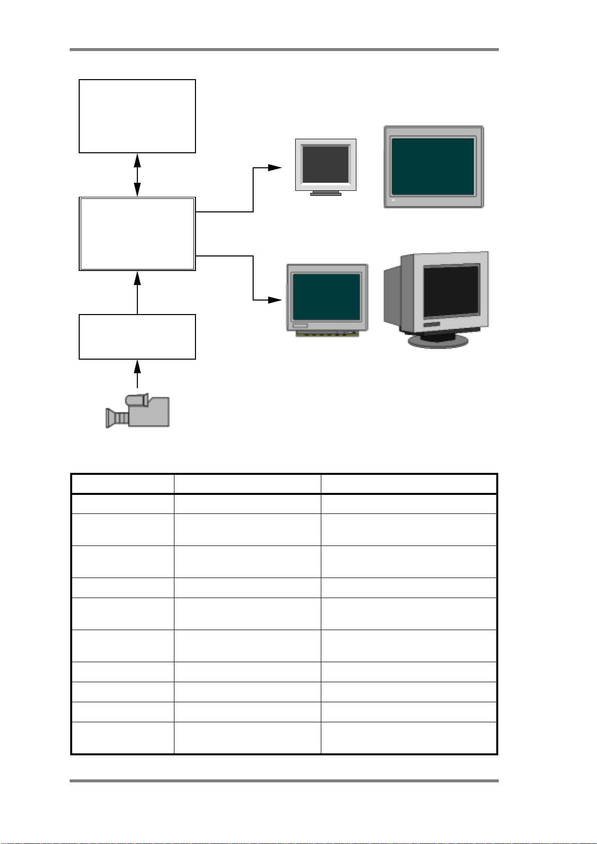
MB87J2120, MB87P2020-A Hardware Manual
Host MCU
MB91xxxx
Digital Video
MB87P2020 or MB87J2120
(Jasmine or Lavender)
RGB Analog
Video Scaler
e.g. VPX3220A, SAA7111A
Figure 1-1: Application overview
Table 1-1: GDC components
Shortcut Meaning Main Function
LSA (part of GPU) Line Segment Accumulator Layer overlay
BSF (part of GPU) BitStream Formatter Intermediate format to physical display
Format converter, Sync generation
IPA (part of DIPA) Indirect Physical memory Access SDRAM access with command register
and FIFO
MAU (part of PP) Memory Access Unit Pixel access to video RAM
MCP (part of PP) Memory CoPy Memory to memory copying of rectan-
gular areas
PE (part of PP) Pixel Engine Drawing of geometrical figures and bit-
maps
PP Pixel Processor Graphic oriented functions
SDC SDRAM Controller SDRAM access and arbitration
SPB Serial Peripheral Bus Serial interface (master)
ULB User Logic Bus (see MB91360
series specification)
Address decoding, command control,
flag, interrupt and DMA handling
Page 16
Page 17
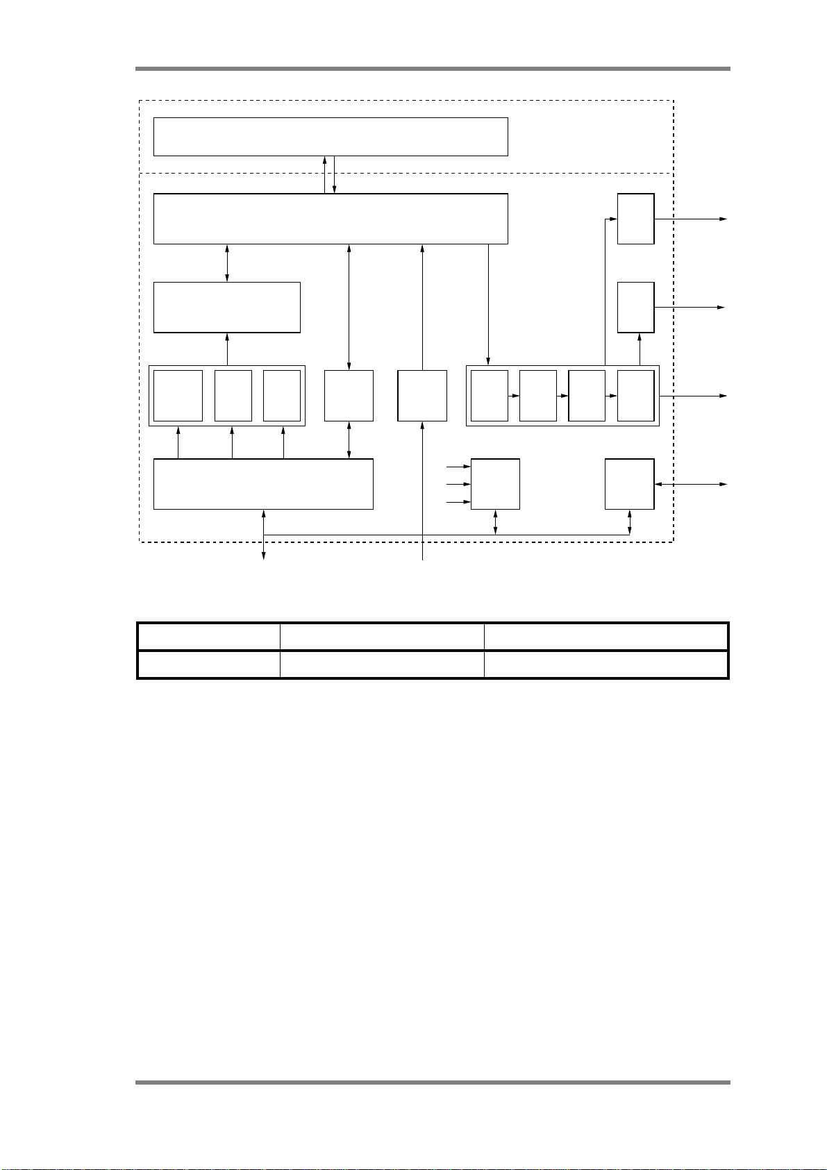
Embedded DRAM (1MByte) or external SDRAM (8MByte)
Graphic Controller Overview
MB87P2020 (Jasmine)
MB87J2120 (Lavender)
SDRAM Controller (SDC)
Anti Aliasing Filter (AAF)
Pixel Processor (PP)
Pixel
Engine
(PE)
User Logic Bus Interface (ULB)
Command Control
User Logic Bus
XTAL
PIX
BUS
Video Scaler Interface
Graphic Processing Unit (GPU)
CCUMAU MCP DIPA VIC DFU LSA BSF
Clock
Unit
(CU)
Figure 1-2: Component overview for Lavender and Jasmine graphic controllers
CCFL
Video
DACs
SPB
Back
Light
Analog
Video
Digital
Video
Serial
Table 1-1: GDC components
Shortcut Meaning Main Function
VIC Video Interface Controller YUV-/RGB-Interface to video grabber
The ULB provides an interface to host MCU (MB91360 series). The main functions are MCU (User Logic
Bus) control inclusive wait state handling, address decoding and device controls, data buffering / synchronisation between clock domains and command decoding. Beside normal data and command read and write
operation it supports DMA flow control for full automatic data transfer from MCU to GDC and vice versa.
Also an interrupt controlled data flow is possible and various interrupt sources inside the graphics controller
can be programmed.
The Clock Unit (CU) provides all necessary clocks to module blocks of GDC and a FR compliant (ULB)
interface to host MCU. Main functions are clock source select (XTAL, ULB clock, display clock or special
pin), programmable clock multiplier/divider with APLL, power management for all GDC devices and the
generation of synchronous RESET signal.
For Fujitsu internal purposes one independent macro is build in the GDC ASIC, the Serial Peripheral Bus
(SPB). It’s a single line serial interface. There is no interaction with other GDC components.
All drawing functions are executed in Pixel Processor (PP). It consists of three main components Pixel Engine (PE), Memory Access Unit (MAU) and Memory Copy (MCP). All functions provided by these blocks
are related to operations with pixel addresses {X, Y} possibly enhanced with layer information. GDC supports 16 layers by hardware, four of them can be visible at the same time. Each layer is capable of storing
Overview Page 17
Page 18

MB87J2120, MB87P2020-A Hardware Manual
any data type (graphic or video data with various colour depths) only restricted by the bandwidth limitation
of video memory at a given operating frequency.
Drawing functions are executed in the PE by writing commands and their dedicated parameter sets. All
commands can be taken from the command list in section 4.2. Writing of uncompressed and compressed
bitmaps/textures, drawing of lines, poly-lines and rectangles are supported by the PE. There are many special modes such as duplicating data with a mirroring function.
Writing and reading of pixels in various modes is handled by MAU. Single transfers and block or burst
transfers are possible. Also an exchange pixel function is supported.
With the MCP unit it is possible to transfer graphic blocks between layers of the same colour representation
very fast. Only size, source and destination points have to be given to duplicate some picture data. So it offers an easy and fast way to program moving objects or graphic libraries.
All PP image manipulation functions can be fed through an Antialiasing Filter (AAF). This is as much faster
than a software realisation. Due to the algorithm which shrinks the graphic size by two this has to be compensated by doubling the drawing parameters i.e. the co-ordinates of line endpoints.
DIPA stands for Direct/Indirect Physical Access. This unit handles rough video data memory access without pixel interpretation (frame buffer access). Depending on the colour depth (bpp, bit per pixel) one or
more pixel are stored in one data word. DPA (Direct PA) is a memory-mapped method of physical access.
It is possible in word (32 bit), half word (16 bit) or byte mode. The whole video memory or partial window
(page) can be accessed in a user definable address area of GDC. IPA (Indirect PA) is controlled per ULB
command interface and IPA access is buffered through the FIFOs to gain high access performance. It uses
the command GetPA and PutPA, which are supporting burst accesses, possibly handled with interrupt and
DMA control.
For displaying real-time video within the graphic environment both display controllers have a video interface for connection of video-scaler chips, e.g Intermetall’s IC VPX32xx series or Phillips SAA711x. Additionally the video input of Jasmine can handle CCIR standard conform digital video streams.
Several synchronisation modes are implemented in both controllers and work with frame buffering of one
up to three pictures. With line doubling and frame repetition there exist a large amount of possibilities for
frame rate synchronisation and interlaced to progressive conversion as well. Due to the strict timing of most
graphic displays the input video rate has to be independent from the output format. So video data is stored
as same principles as for graphic data using up to three of the sixteen layers.
The SDC is a memory controller, which arbitrates the internal modules and generates the required access
timings for SDRAM devices. With a special address mapping and an optimized algorithm for generating
control commands the controller can derive full benefit from internal SDRAM. This increases performance
respective at random (non-linear) memory access.
The most complex part of GDC is its graphic data processing unit (GPU). It reads the graphic/video data
from up to four layers from video memory and converts it to the required video output streams for a great
variety of connectable display types. It consists of Data Fetch Unit (DFU), Colour Conversion Unit (CCU)
which comes with 512 words by 24-bit colour look up table, Line Segment Accumulator (LSA) which does
the layer overlay and finally the Bitstream Formatter (BSF). The GPU has such flexibility for generating
the data streams, video timings and sync signals to be capable of driving the greatest variety of known display types.
Additional to the digital outputs video DACs provide the ability to connect analog video destinations. A
driver for the displays Cold Cathode Fluorescence Lamp (CCFL) makes the back light dimmable. It can be
synchronized with the vertical frequency of the video output to avoid visible artefacts during modulating
the lamp.
Page 18
Page 19
Graphic Controller Overview
2 Features and Functions
Table 2-1: Lavender and Jasmine features in comparison
MB87J2120 (Lavender) MB87P2020-A (Jasmine)
General features
• 2M words x 32 Bit external SDRAM
(64 Mbit)
•nointernal SDRAM
• Package: BGA-256P-M01 • Package: FPT-208P-M06
• Chip select sharing for up to four GDC devices
• synchronized reset (needs applied clock) • immediate asynchronous reset, synchronized
Pixel manipulation functions
• 2D Drawing and Bitmap Functions
- Lines and Polygons
- Rectangular Area
- Uncompressed Bitmap/1bit pixelmask
- Compressed Bitmap (TGA format)/1bit pixelmask
• Pixel Memory Access Functions
- Put Pixel
- Put Pixel FC (fixed colour)
- Put Pixel Word (packed)
- Exchange Pixel
- Get Pixel
• 256k words x 32 Bit internal SDRAM
(8 Mbit)
reset release
• Layer Register for text and bitmap functions • Layer Register enhancement for drawing functions (simplifies pixel addressing)
• Copy rectangular areas between layers
• Anti Aliasing Filter (AAF)
- resolution increase by factor 2 for each dimension (2x2 filter operator size)
• Free programmable Bitstream Formatter for a
great variety of supported displays (single/
dual/alternate scan):
- Passive Matrix LCD (single/dual scan)
- Active Matrix (TFT) Displays
- Electroluminescent Displays
- Field Emission Displays
- TV compatible output
- CRTs...
• 24 bit digital video output (RGB)
• Additional 4x4 AAF operator size
Display
• Additional Twin Display Mode feature (simultaneous digital and analog output without limitation of DIS_D[23:16] that carry special sync
signals).
Features and Functions Page 19
Page 20
MB87J2120, MB87P2020-A Hardware Manual
Table 2-1: Lavender and Jasmine features in comparison
MB87J2120 (Lavender) MB87P2020-A (Jasmine)
• On-Chip Video DAC, 50M Samples/s (dot clock)
• Flexible three-stage sync signal programming (trigger position/sequence, combining and delay) for
up to 8 signal outputs
• Colour keying between two limits
• Brightness modulation for displays with a Cold Cathode Fluorescence Lamp back-light
• Display resolution/drawing planes up to 16383 pixels for each dimension
• 4 layer + background colour simultaneous display and graphic overlay, programmable Z-order
• Blinking, transparency and background attributes
• Free programmable display section of a layer
• Separable Colour LUT with
256 entries x 24 Bit
• Duty Ratio Modulation (DRM) for pseudo hue/grey levels
• Hardware support for 16 layers, usable for graphic/video without restrictions
• Performance sharing with adjustable priorities and configurable block sizes for memory transfers enable maximal throughput for a wide range of applications
• Variable and display independent colour space
concept: Layers with 1, 2, 4, 8, 16, 24 bit per
pixel can be mixed and converted to one display specific format (logical-intermediatephysical format mapping)
Physical SDRAM access
• Memory mapped direct physical access for storage of non-graphics data or direct image access
• Indirect physical memory access for high bandwidth multipurpose data/video memory access
MCU interface
• 32/16 Bit MCU interface, designed for direct connection of MB91xxxx family (8/16/32Bit access)
• DMA support (all MB91xxxx modes)
• Interrupt support
• Colour LUT expansion to 512 entries
• Additional GPU a YUV to RGB converter in
order to allow YUV coded layers
• Additional Gamma correction RAMs are included (3x256x8Bit)
Video interface
• Video interface VPX32xx series by Micronas
Intermetall, Phillips SAA711x and others
• Video synchronization with up to 3 frame buffers
Clock generation
• Flexible clocking concept with on-chip PLL and up to 4 external clock sources:
- XTAL
- ULB bus clock
- Pixel clock
- Additional external clock pin (MODE[3]/RCLK)
• Separate power saving for each sub-module
• Additional CCIR conform input mode
Page 20
Page 21
Graphic Controller Overview
3 Clock supply and generation
GDC has a flexible clocking concept where four input clocks (OSC_IN/OUT, DIS_PIXCLK, ULB_CLK,
RCLK) can be used as clock source for Core clock (CLKK) and Display clock (CLKD).
The user can choose by software whether to take the direct clock input or the output of an APLL independent for Core- and Display clock. Both output clocks have different dividers programmable by software
(DIV x for CLKD and DIV z for CLKK). The clock gearing facilities offer the possibility to scale system
performance and power consumption as needed.
OSC_IN/OUT
DIS_PIXCLK
ULB_CLK
RCLK
VSC_CLKV
PLL Clock
Direct Clock
APLL
MUL y
System Clock Prescaler
DIV z
Pixel Clock Prescaler
DIV x
invert option
invert option
(Jasmine only)
INV INV
CLKK
CLKD
CLKM
CLKV
Figure 3-1: Clock gearing and distribution
Beside these two configurable clocks (CLKK and CLKD) GDC needs two additional internal clocks:
CLKM and CLKV (see also figure 3-1). CLKV is exclusively for video interface and is connected to input
clock pin VSC_CLKV. CLKM is used for User Logic Bus (ULB) interface and is connected to input clock
ULB_CLK. As already mentioned ULB_CLK can also be used to build CLKK and/or CLKD.
Table 3-1 shows all clocks used by GDC with their requirements.
Table 3-1: Clock supply
Clock Type Symbol Requirements Unit
Min Typ Max
XTAL clock input OSC_IN, OSC_OUT
Reserve clock input RCLK
a
12
ULB_CLK
-64MHz
b
-64MHz
ULB clock input ULB_CLK - - 64 MHz
Pixel clock input DIS_PIXCLK - - 54 MHz
Video clock input VSC_CLKV - -
54
c
MHz
Core clock internal CLKK ULB_CLK - 64 MHz
Display clock internal CLKD - - 54 MHz
Video clock internal CLKV - -
54
c
MHz
ULB clock internal CLKM - - 64 MHz
Clock supply and generation Page 21
Page 22

MB87J2120, MB87P2020-A Hardware Manual
a. If used as PLL input. APLL input frequency has to be at minimum 12 MHz, regardless which clock is routed
to APLL.
b. If used as direct clock source bypassing the APLL, the user should take care that resulting core clock fre-
quency is above or equal to MCU bus interface clock.Be aware of tolerances!
c. The video interface is designed to achieve 54 MHz but there is a side condition that video clock should be
smaller than half of core clock.
Page 22
Page 23
Graphic Controller Overview
4 Register and Command Overview
4.1 Register Overview
The GDC device is mainly configurable by registers. These configuration registers are mapped in a
64 kByte large address range from 0x0000 to 0xffff. It is possible to shift this register space in steps of
64 kByte by the Mode[1:0] pins in order to connect multiple GDC devices.
Above this 4*64 kByte = 256 kByte address range the SDRAM video memory could be made visible for
direct physical access.
At byte address 0x1f:ffff GDC memory map ends with a total size of 2 MByte.
4.2 Command Overview
The command register width is 32 Bit. It is divided into command code and parameters:
31
parameters
Partial writing (halfword and byte) of command register is supported. Command execution is triggered by
writing byte 3 (code, bits [7:0]). Thus parameters should be written before command code.
Not all commands need parameters. In these cases parameter section is ignored.
In table 4-1 all commands are listed with mnemonic, command code and command parameters (if neces-
sary. This is only a short command overview, a more detailed command list can be found in appendix.
Table 4-1: Command List
Mnemonic Code Function Addressed
Bitmap and Texture Functions
PutBM 01H Store bitmap into Video RAM Pixel Processor
PutCP 02H Store compressed bitmap into Video RAM
PutTxtBM 05H
PutTxtCP 06H
Draw uncompressed texture with fixed foreground
and background colour
Draw compressed texture with fixed foreground and
background colour
07
code
device
Drawing Functions (2D)
DwLine 03H
DwPoly 0FH
DwRect 04H
"Draw a line" - calculate pixel position and store
LINECOL into Video RAM
"Draw a polygon" - draws multiple lines between
defined points, see DwLine
"Draw an rectangle" - calculate pixel addresses and
store RECTCOL into Video RAM
Pixel Operations
Pixel Processor
Register and Command Overview Page 23
Page 24
MB87J2120, MB87P2020-A Hardware Manual
Table 4-1: Command List
Mnemonic Code Function Addressed
device
PutPixel 07H Store single pixel data into Video RAM Pixel Processor
PutPxWd 08H Store word of packed pixels into Video RAM
PutPxFC 09H Store fixed colour pixel data in Video RAM
GetPixel 0AH Load pixel data from Video RAM
XChPixel 0BH
MemCopy 0CH
PutPA 0DH
GetPA <n>,0EH
SwReset 00H
NoOp FFH
Load old pixel in Output FIFO and store pixel from
Input FIFO into Video RAM
Memory to Memory Operations
Memory Copy of rectangular area. Transfer of bitmaps from one layer to another or within one layer.
Physical Framebuffer Access
Store data in physical format into Video RAM, with
physical address auto-increment
Load data in physical format from Video RAM with
address auto-increment, stop after n words
System Control Commands
Stop current command immediately, reset command
controller and FIFOs
No drawing or otherwise operation, finish current
command and flush buffers
Pixel Processor
DIPA
All drawing and
access devices
Command Control (ULB)
Page 24
Page 25

PART B - Functional Descriptions
Page 25
Page 26

MB87J2120, MB87P2020-A Hardware Manual
Page 26
Page 27

B-1 Clock Unit (CU)
Page 27
Page 28

MB87J2120, MB87P2020-A Hardware Manual
Page 28
Page 29
Clock Unit
1 Functional Description
1.1 Overview
The clock unit (CU) provides all necessary clocks to GDC modules and an own interface to host MCU
(MB91360 series) in order to have durable access even if ULB clocks switched off.
The main functions of CU are:
• Clock source select (Oscillator, MCU Bus clock, Display clock and a reserve clock input)
• Programmable clock muliplier with APLL
• Separate dividers for master (core) clock and pixel clock
• Power management for all GDC modules
• Generation of synchronized RESET signal
• MB91360 series compliant (ULB) Bus interface for clock setup
Figure 1-1 shows the overview of the Clock Unit. OSC_IN, DIS_PIXCLK, ULB_CLK and RCLK1are possible to use as input sources. Both clock outputs of the main unit (MASTERCLK and PIXELCLK) and two
directly used clock inputs (ULB_CLK and VSC_CLKV) driving the clock gates unit which distributes to
all connected GDC sub-modules.
RCLK
DIS_PIXCLK
Main Unit
ULB_CLK
MASTERCLK
PIXELCLK
VSC_CLKV
Clock Gates
PE_CLKK_OUT
MAU_CLKK_OUT
MCP_CLK_OUT
PP_CLKK_OUT
AAF_CLKK_OUT
DIPA_CLKK_OUT
VIS_CLKK_OUT
VIS_CLKV_OUT
SDC_CLKK_OUT
CCFL_CLKK_OUT
SPB_CLKM_OUT
ULB_CLK_OUT
ULB_CLKM_OUT
GPUF_CLKK_OUT
GPUM_CLKK_OUT
GPUB_CLKK_OUT
PIX_CLKD_OUT
SPB_CLKMX_OUT
ULB_CLKKX_OUT
ULB_CLKMX_OUT
inverted clock outputs not inverted clock outputs
K
ULB
_A
_RDX
_WRX
_CSX
_CLK
ULB
_D
_A
_WRX
User Logic Bus
_CLK
OSC_IN
ULB_CLK
RESETX
Address Decoder
RSTX
Clk[Con|Pd]R_[rd|wr]
Register Set
RSTX
SW_RST
Reset Generator
ClkConR
LOCK
ClkPdR
[11]
[15]
OSC_IN
RSTX
SYNC_RSTX_CU
SYNC_RSTX
Figure 1-1: Block diagram of Clock Unit
1. MODE[3] pin is used for RCLK at Lavender
Functional Description Page 29
Page 30

MB87J2120, MB87P2020-A Hardware Manual
The GDC device has four different clock domains, that means clocks derived from four different sources.
The largest part of the design runs at core clock which operates at the highest frequency driven by the MASTERCLK output. Thus normally the APLL is used to provide a higher internal operation frequency. The
next domain is the display output interface which operates at pixel clock frequency. For most applications
it is recommended that this is the clock from OSC_IN pin, divided by two1. So the crystal oscillator has to
be choosen to have a whole-numbered multiple of the display clock frequency. Preferred routing is the DIRECT clock source channel since some displays require a small clock jitter which is not able to provide by
the APLL. The other clocks for MCU interface (ULB_CLK) and video interface (VSC_CLKV) are not derived by the clock routing and generating part and used directly from the appropriate input pin.
Finally the generated source clocks of the for domains go to the clock gating/distribution module. There are
gated clock buffers and inverters for each GDC module implemented. Each module has it’s own clock enable flag which can be programmed for modules needed by the application only. This method saves power
of not used functional blocks of GDC (refere to table 3-1).
The configuration of CU is stored in two registers, ClkConR and ClkPdR, which are connected to User Logic Bus for writing and reading. The bus interface consists of an address decoder and circuitry for different
access types (word, halfword and byte access over a 16 or 32 bit bus connection).
1.2 Reset Generation
GDC works with an internally synchronized, low active reset signal. The global chip reset can be triggered
by an external asynchronous reset or internally by software reset (configuration bit in ClkPdR). The external
triggered RESETX results in resetting all GDC components including the Clock Unit, however software
reset has no influence on CU internal registers.
Lavender synchronizes its external reset (RSTX pin). Reset is delayed until 4 clock cycles of each
ULB_CLK and OSC_IN are executed. This gives stability against spikes on the RSTX line but has the disadvantage of delayed reset response of Lavender.
For Jasmine internal reset is active immediately after tying RESETX low plus a small spike filter delay. Due
to the synchronization of RESETX the internal reset state ends after 4 clock periods of OSC_IN and 4 clock
periods of ULB_CLK after releasing RESETX pin. Reset output RSTX_SYNC for all internal GDC register
states are synchronized with OSC_IN, however internal Clock Unit registers are synchronized with
ULB_CLK in addition. Thus a minimum recovery time of 4 clock cycles of OSC_IN plus 4 cycles of
ULB_CLK is needed before writing to Clock Unit configuration registers is possible after RESETX becomes inactive.
The reset generator of Jasmine has a spike filter implemented, which suppresses short low pulses, typical
smaller than 9 ns. Under best case operating conditions (-40 deg. C; 2.7V; fast) maximum suppressed spike
width is specified to 5.5ns. This is the maximum reset pulse width which did not result in resetting the GDC
device. Minimum pulse width for guaranteed reset is specified to 1 clock cycle of OSC_IN (80 ns typical).
1.3 Register Set
Table 1-1 listst the clock setup registers. ClkConR (Clock Configuration Register) is mainly for generation
of the base clocks and the routing/selection from one of the four input sources. It controls the clock dividers
and the use of the APLL. The possibility to use a second clock path, called direct clock source, gives a high
flexibility for using the APLL either for MASTERCLK or PIXELCLK generation or both. Also the pin
function of DIS_PIXCLK can be defined in this register. If DIS_PIXCLK is selected as clock source the
pin should be configured as an input.
Upper 8 bits of ClkConR are used as identification of the different GDC types. Lavender is identified with
reading back a ’0x00’, Jasmine with a ’0x01’.
Use of DIS_PIXCLK as pixel clock output and selection of DIS_PIXCLK for the clock source can result in
unintentional feedbacks and has to be avoided.
1. Preferred is an even divider value to achive 50% clock duty
Page 30
Page 31

Clock Unit
ClkPdR (Clock Power Down Register) is a set of enable bits for the clocks provided to the dedicated GDC
modules. A bit set to ’1’ means the clock is enabled. If a module requires multiple clocks (inverted ones or
different domains) the enable bit switches all these lines.
Additional ClkPdR controls the work of the PLL and gives status information about it’s lock-state. Also a
global GDC reset function can be executed by setting a configuration bit of this register.
Table 1-1: CU registers
Register Bit Function Description Reset
Value
ClkConR [31:30] Direct Clock Source 00 Crystal oszillator (reset default)
01 Pixel clock
10 MCU Bus clock
11 reserved clock input (RCLKa)
[29:24] System clock prescaler
(DIV z)
[23:22] PLL Clock Source 00 Crystal oszillator (reset default)
[21:16] PLL Feedback divider
(DIV y)
[15] System Clock Select 0 Direct
[14] Pixel Clock Select 0 Direct
[13] Inverted Pixel Clock 0 not inverted
[12] Output disable
DIS_PIXCLK
[5:0] system clock prescaler value 0
01 Pixel clock
10 MCU Bus clock
11 reserved clock input (RCLK)
[5:0] pll multiplier value 0
1 PLL output
1 PLL output
1 inverted
0 internal pixelclock (output)
1 external pixelclock (input), high-Z
output
"00"
"00"
’0’
’0’
’0’
’1’
[11]
[10:0] Pixel clock prescaler
reserved test operation
(DIV x)
b
0 normal operation
1 core clock output on pin SPB_TST
[10:0] pixelclock prescaler value 0
’0’
Functional Description Page 31
Page 32

MB87J2120, MB87P2020-A Hardware Manual
Table 1-1: CU registers
Register Bit Function Description Reset
Value
ClkPdR 0 PP/PE Pixelengine clock
enable
1 PP/MAU clock enable 0 = disable, 1 = enable ’0’
2 PP/MCP clock enable 0 = disable, 1 = enable ’0’
3 AAF clock enable 0 = disable, 1 = enable ’0’
4 DIPA clock enable 0 = disable, 1 = enable ’0’
5 VIS clock enable 0 = disable, 1 = enable ’0’
6 SDC clock enable 0 = disable, 1 = enable ’0’
7 CCFL clock enable 0 = disable, 1 = enable ’0’
8 SPB clock enable 0 = disable, 1 = enable ’0’
9 ULB clock enable 0 = disable, 1 = enable ’0’
10 GPU clock enable 0 = disable, 1 = enable ’0’
11 PLL enable 0 = power down , 1 = run mode ’0’
12 VIC clock invert
(Jasmine)
PLL Lock (Lavender)
0 = disable, 1 = enable ’0’
0 = not inverted, 1 = inverted ’0’
0 = unlocked, 1 = locked (read only)
c
13 reserved - ’0’
14 PLL Lock (Jasmine)
15 Global HW Reset
0 = unlocked, 1 = locked (read only)
0 = run mode, 1 = reset (write only)
b
’0’
d
’0’
[31:24] Chip Id 0 = Lavender, 1 = Jasmine (read only) -
a.RCLK is mapped on MODE[3] at Lavender.
b.Only applicable for Jasmine
c.Normally all register bits are read-write. As the PLL lock bit is status information only, no write
access is possible to it. The lock bit is for test operation only and should not be used.
d.Read access results always in a value of ’0’. Writing ’1’ starts global HW Reset function, writing ’0’ releases reset.
Page 32
Page 33

Clock Unit
2 APLL Specification
This informations are for implemented APLL - U1PN741A. Output range is given for APLL output directly, not for the divider outputs.
The APLL macro has an operating supply voltage (VDD) of 2.5 0.25V. The oscillation guaranteed frequency range, maximum output frequency range and operating junction temperature range of the APLL are
shown in the table below.
Table 2-1: APLL Specifications
Operating Junction Temperature (Tj) -40 to 125 deg. C
Voltage supply (VDDI) 2.5 V +/- 0.25 V
Oscillation guaranteed frequency range 120 to 208.4 MHz
Maximum output frequency range
a
Input Frequency range 12 to 160 MHz
a.Range in which oscillation may be possible.
Table 2-2: APLL Characteristics for guaranteed design range
Input
[MHz]FBdivider
Out-
put
[MHz]
Phase
Skew
[ps]
25 8 200 444
-448
20
a
8 160 540
-520
13.217
b
10 132.17 1200
-1360
12
b
10 120 1334
-1466
40
b
4 160 640
-700
Duty
[%]
100.5
87.9
102.6
94
104.4
99.33
111.1
100.7
105.9
101.5
5.77 to 598.1 MHz
Lock Up
Time [us]
Jitter
[ps]
70 176
-142
100 232
-168
500 420
-246
25 760
-560
20 350
-190
Variations
in output
cycle [ps]
+130
-134
+64
-170
+234
-278
480
-560
238
-304
Power con-
sumption
[mW]
2.45
1.9
1.88
1.793
1.147
23.5
33
160
50
20
b
b
b
b
b
8 188 740
-940
6 198 560
-540
1 160 240
-150
4 200 340
-280
10 200 3600
-4200
110.6
97.2
100.4
88
101.2
98.9
98.5
87.7
109.5
87.5
65 208
-162
165 172
-140
12 190
-140
26 148
-140
88 560
-360
160
-182
148
-180
110
-140
96
-120
420
-480
2.387
2.397
1.147
2.45
2.45
a.Operating temperature -20 ... 90 deg. C, operating voltage 2.5 V +/- 0.15 V.
b.Operating temperature -40 ... 125 deg. C.
APLL Specification Page 33
Page 34

MB87J2120, MB87P2020-A Hardware Manual
2.1 Definitions
2.1.1 Phase Skew
Maximum phase differences between reference clock and feed back clock measured by the CK pin of the
PLL and the feedback clock measured by the FB pin.
CK
FB
2.1.2 Duty
Duty is the maximum and minimum values indicated by the ratio of a high pulse width to a low pulse with
(T
low
to T
) in one cycle of the output clock measured by the X pin of the PLL.
high
X
TT
high low
2.1.3 Lock Up Time
Lock up time is the time period that starts when the S pin of the PLL changes from 0 to 1 and ends when
the PLL is locked.
S
L
lock up time
2.1.4 Jitter
Jitter is the maximum and minimum values for cycle variations (T2-T1,T3-T2and T4-T3) in two continuous
cycles measured by the X pin of the PLL.
X
T1 T2 T3 T4
2.1.5 Variation in Output Cycle
The max./min. time periods from the rising edge of the output clock to thenext rising edge measured by the
X pin of the PLL. Observation points: 1400. The max./min values in T1, T2, T3 and T4 in above figure.
Page 34
Page 35

Clock Unit
2.1.6 Maximum Power Consumption
This is the maximum power consumption of the PLL when PLL is in locked state. The power dissipated by
extrenal dividers is not included into this amount.
2.2 Usage Instructions
•
Input the clock of crystal oscillator level into the CK pin of the PLL. Variations in the input clock
directly affects the PLL output, leading to unconformity to the specifications.
• In addition to the normal power supply, the PLL has a power supply for VC0 (pin name:
APLL_AVDD, APLL_AVSS). The VC0 power supply should be separate from other power supplies.
APLL Specification Page 35
Page 36

MB87J2120, MB87P2020-A Hardware Manual
3 Clock Setup and Configuration
3.1 Configurable Circuitry
Clock configuration can be easily done by setting up both registers ClkConR (Clock Configuration Register) and ClkPdR (Clock Power Down Register). ClkConR mainly controls the setup of multiplexers and
clock dividers in the main part of CU, which is shown in figure 3-1.
OSC_IN
DIS_PIXCLK
ULB_CLK
RCLK
Default Path
ClkConR
ClkPdR
[23:22]
[31:30]
[ bits ]
{ bits }
{11} [15]
lock {12}
L
S
A
CK
FB
[21:16]
APLL
DIV y
PLL CLOCK
X
DIRECT
[14]
[29:24]
DIV z
[10:0]
DIV x
[13]
XOR
tst
TST_MAS_CLKTST_PIX_CLK
tst
[12]
MASTERCLK
PIXELCLK
XZ_CU_PIXCK
(tristate)
Figure 3-1: Clock routing and configuration bits
ClkPdR decides which clocks should be enabled and distributed to the appropriate modules, listed in table
2-1. During change of ClkConR all enable bits in ClkPdR[10:0] have to be turned off to attain spike protection.
Table 3-1: Mapping of clock sources, outputs and their enable bits
ClkPdR Control Bit Clock Source Clock Output
0|1|2|3
Master
a
Pixel Processor (PP)
0 Master PP: Pixel Engine
1 Master PP: Memory Access Unit
2 Master PP: Memory Copy
3 Master Anti Aliasing Filter
4 Master Direct/Indirect Physical Access
5 Master Video Interface
5 Video Scaler (VSC_CLKV) Video Interface
6 Master SDRAM Controller
7 Master Cold Cathode Fluorescence Light
8 MCU Bus (ULB_CLK) Serial Peripheral Bus
9 Master User Logic Bus Interface and Com-
mand Controller
9 MCU Bus (ULB_CLK) User Logic Bus Interface
Page 36
Page 37

Table 3-1: Mapping of clock sources, outputs and their enable bits
ClkPdR Control Bit Clock Source Clock Output
10 Master Graphic Processing Unit
Clock Unit
10
a.Master and Pixel clock could be derived from one of four possible clock inputs (OSC_IN,
DIS_PIXCLK, ULB_CLK, RCLK/MODE[3]) with or without use of the PLL.
All clocks except VSC_CLKV can be used as Master or Pixel clock source. VSC_CLKV is for video interface dedicated use only.
There are no special requirements for the quartz crystal parameters. At the case of overtone oscillation additional external inductance L’=5-10uH and capacitor C’=10pF are needed. Two capacitors C=22pF have
to be connected from the OSC pins to ground in any case. Figure 3-2 shows recommendet circuit.
Pixel Clock
a
Graphic Processing Unit
OSC_IN OSC_OUT
XQ
L’
CC C’
Figure 3-2: Crystal connection between pins OSC_IN and OSC_OUT
Without a crystal oscillator connected (e.g. extrnal oscillator) the clock has to fed in the OSC_IN pin.
3.2 Clock Unit Programming Sequence
This section gives a recommendation for the sequence for GDC clock configuration. In general the Clock
Unit registers should be configured before all other GDC setup information.
• Apply stable clock and do a hardware reset.
• Write ClkConR for the required mode. Clock gates are disabled per reset default.
• Switch on PLL and optionally apply software reset (Set bits [11] and [15] in ClkPdR).
• Clear software reset bit (Optional, only if set before).
• Wait until APLL has stabilized and locked (lock-up time)
Polling of lock bit is optional and not sufficient that PLL locking process has finished. This signal is
for Fujitsu test purpose only. APLL lock-up state is reached if Lock bit becomes stable ’1’. This is
guaranteed after specified PLL lock-up time of 500us.
1
• Set required clock enable bits to open the clock gates.
1.The lock up time measured from PLL start (CLKPDR_RUN=’1’) to lock state
(CLKPDR_LCK=fixed ’1’).
Clock Setup and Configuration Page 37
Page 38

MB87J2120, MB87P2020-A Hardware Manual
An example sequence for this procedure is listed below:
/* CU control information */
G0CLKPDR = 0x00008800; // SW reset and APLL enable
G0CLKPDR = 0x00000800; // release SW reset, clock gates are still closed
G0CLKCR = 0x010E8001; // MASTER=XTAL*15/2, PIXCLK=XTAL/2 not inverted output
G0CLKPDR = 0x00000EF1; // enable GPU, ULB, CCFL, SDC, VIC, DIPA, PE
Figure 3-3: Clock configuration procedure with reset
3.3 Application Notes
The Clock Unit provides an internally synchronized reset signal to all GDC components. Therefore it’s necessary to have a stable clock applied to the OSC_IN pin during RESETX is low and/or at least after release
of RESETX. Otherwise the internal circuitry is not initialized properly or clock unstability after reset release
can cause malfunction.
With the direct clock source it’s possible to use a external ULB_CLK from the MCU or RCLK as clock
source for almost all internal GDC components. The APLL is not able to handle jitter/variations in input
clock.
If the GDC should operate in single clock mode over ULB_CLK driven by the MCU, ULB_CLK and
OSC_IN have to be bridged. In any case a clock has to feed in OSC_IN pin, otherwise the reset state would
not be left.
If system or pixel clock divider are initialized with an even value tis results in an odd divider value (value
interpreted +1). In this situation the duty of the output clock is not even 1:1. Most important this is for low
values. In case of not even duty the high duration is smaller than the low duration. Following table lists clock
divider and duty relationship.
Table 3-2: Clock division and resulting duty
Setup Value Divider Duty
0 1 1/1
1 2 1/1
2 3 2/1
3 4 1/1
4 5 3/2
5 6 1/1
6 7 4/3
...
Page 38
Page 39

B-2 User Logic Bus Controller (ULB)
Page 39
Page 40

MB87J2120, MB87P2020-A Hardware Manual
Page 40
Page 41

User Logic Bus
1 Functional description
1.1 ULB functions
The “User Logic Bus Interface” (ULB) provides an interface to host MCU (MB91360 series). It is responsible for data exchange between MCU and the graphic display controllers (GDC) Lavender or Jasmine
The communication between MCU and the display controller is register based and all display controller registers are mapped in the MCU address space.
The task of ULB is to organise write- or read accesses to different display controller components, including
ULB itself, depending on a given address. For read accesses the ULB multiplexes data streams from other
components and has to control the amount of needed bus wait states using MCU’s ULB_RDY pin.
The ULB provides also a command- and data interface to so called ’execution devices’ (Pixel Processor
(PP) and Indirect Memory Access Unit (IPA)). These execution devices are responsible for drawing command execution or for the handling of SDRAM access commands. The data transfer to and from execution
devices is always FIFO buffered. In order to ensure a rapid data transfer between MCU and display controller ULB contains one input and one output FIFO which are mapped to certain memory addresses within the
display controllers memory space. ULB controls the MCU port of these FIFOs (write for input FIFO and
read for output FIFO) while the ports to execution devices is controlled by the device itself.
The command interface has a two stage pipeline so command and register preparation is possible during
command execution of previous command. Most commands can have an infinite amount of processing data.
The FIFOs help to reduce the number of bus wait states.
Additionally to FIFO data exchange direct access to SDRAM and to initialisation registers is managed by
ULB. This direct SDRAM access maps the SDRAM physical into MCUs address space. Drawing functions
use a logical address mode for SDRAM access. Due to this direct (and also indirect via FIFOs) physical
access to SDRAM it can also be used to store user data and not only layer data (bitmaps, drawing results).
For direct SDRAM access (frame buffer or video RAM) the display controller internal SDRAM bus arbitration influences the MCU command execution time directly via ULB bus wait states via ULB_RDY signal.
Therefore longer access times should be calculated for this kind of memory access. ULB is able to handle
memory or register access operations concurrently to normal command execution (FIFO based).
Beside normal data and command read and write operation ULB supports also DMA flow control for full
automatic (without CPU activity) data transfer from MCU to display controller or vice versa. Only one direction at one time is supported because only one MCU-DMA channel is utilised. Also an interrupt controlled data flow based on programmable FIFO flags is possible. In both cases the ULB bus is used for data
transfer.
ULB offers a set of some special registers controlling the display controller behaviour or show the state of
the controller with respect to MCU:
• Flag-Register
• Flag-Behaviour-Register
• Interrupt-Mask-Register
• Interrupt-Level-Register
• DMA-Control-Register
• Command Register
• SDRAM access settings
• Debug Registers
ULB also provides an interrupt controller that can be programmed very flexible. Every flag can cause an
interrupt (controllable by Interrupt-Mask-Register) and for Jasmine it is selectable whether the interrupt for
a certain flag is level or edge triggered. Furthermore for every flag the programmer can determine whether
the flag is allowed to be reset by hardware or not (static or dynamic flag behaviour).
1
.
1. The term ’display controller’ is used as generic name for Lavender and Jasmine and covers both devices.
Functional description Page 41
Page 42

MB87J2120, MB87P2020-A Hardware Manual
The ULB internal DMA controller is able to use all DMA modes supported by MB91360 series. It operates
together with input or output FIFO and uses programmable limits. In demand mode the controller calculates
the amount of data to transfer by its own. In other modes the programmer has to ensure that enough space
is available in input FIFO so that no data loss can occur.
Because of different clock frequencies for ULB bus and display controller core clock an important ULB
function is the data synchronisation between these two clock domains. A asynchronous interface is offered
by ULB which allows independent clocks for ULB and core as long as ULB clock is equal or slower than
core clock.
In order to adjust the display controller’s operation mode so called ’mode pins’ (MODE[3:0]) are used:
• The display controller can also act as an 16 Bit device from MCU’s point of view. In this case ULB converts write data from 16 to 32 Bit and read data from 32 back to 16 Bit in order to hide interface parameters to internal display controller components. The data mode can be set by MODE[2].
• Up to four display controllers can join one chip select signal. So it is necessary to set the controller
’number’ by MODE[1:0]. ULB takes care about correct address decoding depending on this ’number’.
• In order to allow flexible PCB layout some signals can be inverted and can be set to tristate. For Jasmine
the inversion of ULB_RDY is controlled by MODE[3]. For more details about signal settings see
chapter 1.3.4.
In short terms the main functions of ULB are:
• MCU (User Logic Bus) bus control inclusive wait state handling for read access via ULB_RDY pin
• Address decoding and control of other display controller components
• Data buffering and synchronisation between different clock domains
• Command decoding and execution control
• Flag handling
• Programmable interrupt handling
• Programmable DMA based input/output FIFO control
• 16/32 Bit conversion for writing and reading
1.2 ULB overview
Figure 1-1 shows the block diagram of ULB top level design.
Table 1-1 gives an overview on main functions of ULB top level modules. Important modules will be ex-
plained in more detail in the following chapters.
Table 1-1: Top level modules of ULB
Name Main functions
Input Sync • Synchronization for write signals (MCU -> display controller)
Interrupt Controller (IC) • Flag register management
• Management of different interrupt sources
• User definable interrupt source masking and trigger condition
• Interrupt signal generation (Jasmine: programmable length for
edge request)
Address Decoder (AD) • Handling of other display controllers using the same chip select
signal
• Address decoding and calculation for direct SDRAM access
• Address segmentation management
• Control of MCU data I/O as result of address decoding
• Activation of Command Control, Register Control Unit (CTRL)
and Direct Physical Memory Access Units (DPA) as result of
address decoding
Page 42
Page 43

GDC I/O−Ring
ULB
MCU clock domainCore clock domain
MB91F361
Interrupt
Input Sync
User Logic Bus
Data In / OutCSX/RDX/WRX[3:0]Address
RDY DMA
Interrupt Controller
Address Decoder
Register File
Command
Controller
to DPAto CTRLDevice ControlCTRL
Figure 1-1: Block diagram for top level of ULB
Table 1-1: Top level modules of ULB
Name Main functions
I/O Controller
IFIFO
IFIFO read OFIFO write
OFIFO
DMA Controller
CTRL data
interface
DPA data
interface
Command Controller (CC) • Command decoding
• Management of command execution
• Condition decoding for control command execution
I/O controller (IOC) • Read/write control for data part of user logic bus
• Access control and status signal generation for data FIFOs and
registers for MCU and display controller site
• Clock domain synchronization for read data bus (display controller->MCU)
• Bus multiplexing for display controller read data busses
DMA Controller (DMAC) • DMA flow control for MCU site of input and output FIFO
Register File (RF) • Storing of user definable parameters for ULB
Functional description Page 43
Page 44

MB87J2120, MB87P2020-A Hardware Manual
000000000000000
111111111111111
000000000000000
000000000000000
111111111111111
111111111111111
000000000000000000
000000000000000000
111111111111111111
111111111111111111
000000000000000000
111111111111111111
1.3 Signal synchronisation between MCU and display controller
1.3.1 Write synchronization for Lavender and Jasmine
The data flow inside the ULB is divided in write- and read-direction. These data directions are completely
independent. That’s why there are two synchronisation points for ULB bus signals; one for write direction
and one for read direction.
The first synchronisation point is located inside ’Input Sync’ and is responsible for all ULB signals coming
from MCU (ULB_CSX,ULB_WRX, ULB_RDX, ULB_A, D_in). Other incoming MCU signals for
DMA are used directly inside the DMA controller which is partly clocked by ULB clock.
Note: For a correct operation of Input Synchronization ULB clock has to be equal or
slower than display controllercore clock.Note thatall tolerancesfor clocksshould
be taken into consideration.
In Jasmine a configurable sample behaviour for input signals has been introduced. In order to avoid interferences from external bus different sample modes can be set. It can be chosen between four different sample modes. Each mode combines one or more out of three sample points distributed over one bus cycle.
Figure 1-2 shows these sample points. Note that the sample points are only valid for control signals
ULB_CLK
ULB_CS
ULB_WRX[n]
ULB_RDX
ULB_A
ULB_D
Sample point:
Figure 1-2: Bus cycle sample points for Jasmine
(ULB_CSX,ULB_WRX, ULB_RDX); address and data bus are only sampled at point 2 (see figure 1-2).
The sampling is equal for read and write accesses.
The sample mode can be set in register IFCTRL_SMODE (see also table 2-1); table 1-2 shows all possible
settings and sample modes.
102
Table 1-2: Control signal sample modes for Jasmine
Mode IFCTRL_SMODE[1:0] Comment
3 point mode [default]
2 of 3 point mode
Page 44
00
01
all three sample points have to have the
same value
two out of three sample points have to
have the same value (majority decision)
Page 45

User Logic Bus
Table 1-2: Control signal sample modes for Jasmine
Mode IFCTRL_SMODE[1:0] Comment
2 point mode
10
sample point 1 and 2 (see figure 1-2)
have to have the same value
1 point mode 11 sample point 1 determines result value
Beside different sample modes Jasmine’s input synchronisation circuit contains priority logic to distinguish
between read or write access in the case that both control signals (ULB_RDX and ULB_WRX[n]) were detected. Because the I/O controller (ULB read path) may detect a read access the ULB_RDX signal for read
access has the highest priority.
In Lavender a different input synchronisation circuit is implemented were always one sample point is used1.
1.3.2 Read synchronization
For Lavender and Jasmine the ULB_RDY signal is gated by ULB_CSX. This means that the ULB_RDY signal goes immediately high after ULB_CSX=’1’ has been detected. It can not be ensured that correct data
are transferred to MCU in this case.
A protection against wrong tristate bus control signal switching is implemented in ULB. The bus driver is
only valid if ULB_CSX=’0’ and ULB_RDX=’0’. In all other cases ULB data bus is not driven.
Additionally to the described safety mechanisms which are implemented in both devices (Lavender and Jasmine) Jasmine has a programmable timeout for ULB_RDY signal generation. Therefore a counter is implemented which is loaded with the value set in register RDYTO_RDYTO[7:0] at the beginning of a bus read
cycle2. If the read value does not arrive within the counter runtime3ULB_RDY signal is forced to ’1’ and
the MCU can finish the bus read cycle. Note that in this case data transferred to MCU are not valid. The
occurrence of a ULB_RDY timeout is reflected in the flag FLNOM_ERDY (ULB_RDY timeout error; see also
flag description in appendix) which has been implemented in Jasmine. Additionally to the error flag the address where the timeout error occurred is stored in register RDYADDR_ADDR[20:0] in order to allow an
application running on MCU an error handling.
The ULB_RDY timeout counter can be disabled by turning RDYTO_RDTOEN off (set to ’0’).
In regular operation mode a ULB_RDY timeout can only occur if no memory bandwidth can be allocated by
the device handling the read request. Because the command execution is FIFO buffered (see also
chapter 1.1) and a read access from FIFO always returns a value within short time no timeout error can occur in normal command execution. Only a direct mapped memory read access (DPA read access; see also
chapter 1.4.3) in conjunction with very limited bandwidth may cause a ULB_RDY timeout error in normal
operation.
Beside this reason for timeout error in normal operation also disturbed bus transfers or bad signal integrity
may cause a timeout error.
1.3.3 DMA and interrupt signal synchronization
The DMA input and output signals (ULB_DREQ, ULB_DACK, ULB_DSTP) are used/generated in the
DMA Controller which is partly operating at ULB clock. Because these signals are generated in this part no
synchronisation is necessary. The signals influencing the DMA signal generation have to be synchronized
from Lavender/Jasmine core to ULB domain. For more details regarding DMA see chapter 1.7.
Another signal which needs to be transferred from Lavender/Jasmine core to ULB clock domain is the interrupt request signal (ULB_INTRQ). In chapter 1.6 a detailed description of interrupt signal generation is
given. The synchronisation of the interrupt request signal is different between Lavender and Jasmine. Jas-
1. For Lavender sample point1 is used to catch signals within ULB clock domain. Afterwards the caught signals will be sampled with core clock. As a result the real sample point depends on clock ration between ULB
and core clock.
2. A ULB bus read cycle is detected when ULB_CSX=0 and ULB_RDX=0.
3. The runtime ends when the counter reached value ’0’.
Functional description Page 45
Page 46

MB87J2120, MB87P2020-A Hardware Manual
mine supports level and edge triggered interrupt requests with programmable edge length while Lavender
is only supporting level triggered interrupt requests.
In level triggered interrupt mode the interrupt request is only reset if the flag which causes this interrupt is
also reset. Because of software flag reset the request signal is stable for a very long time and no internal
handshake mechanism is needed.
In difference to level triggered interrupt edge triggered interrupt reacts on a rising edge of a flag. This edge
causes a pulse of programmable length on interrupt request signal.
1.3.4 Output signal configuration
In order to allow flexible system integration both display controllers allow configuration for some output
signals to MCU. This includes an option to signal inversion and a tristate control in order to allow external
pull up resistors.
If the tristate control is enabled the according pin drives tristate (’Z’) instead of high level (’1’) while low
level (’0’) is driven in any case (emulated open drain).
Table 1-3 contains the settings for all configurable signals (ULB_DREQ, ULB_DSTP and ULB_INTRQ)
Table 1-3: Control for feedback signals
Signal Setting Lavender Jasmine
ULB_DREQ tristate Register: DMAFLAG_TRI Register: IFCTRL_DRTRI (1: tristate)
invert Register: DMAFLAG_INV Register: IFCTRL_DRINV (1: invert)
ULB_DSTP tristate Register: DMAFLAG_TRI Register: IFCTRL_DSTRI (1: tristate)
invert Register: DMAFLAG_INV Register: IFCTRL_DSINV (1: invert)
ULB_INTRQ tristate Register: DMAFLAG_TRI Register: IFCTRL_INTTRI (1: tristate)
invert Register: DMAFLAG_INV Register: IFCTRL_INTINV (1: invert)
ULB_RDY tristate no control possible Pin: RDY_TRIEN (1: tristate)
invert no control possible Pin: MODE[3] (1: invert)
valid for both display controllers. In Jasmine additionally ULB_RDY can be controlled by special pins1.
Note that there are differences in controlling the signal behaviour between Lavender and Jasmine. While in
Lavender the signals ULB_DREQ, ULB_DSTP and ULB_INTRQ are controlled together with two register
Bits for tristate and inversion (DMAFLAG_TRI and DMAFLAG_INV) in Jasmine every signal has its own
control (see table 1-3).
1.4 Address decoding
1.4.1 Overview
The useable address space for display controller chip select signal (ULB_CSX)is221Byte (2 MByte) and
the available space is divided into one configuration register space where all configuration registers are located and one SDRAM space were SDRAM windows can be established and accessed This space is configurable. Figure 1-3 shows the address space with the default settings for SDRAM space of Lavender and
Jasmine.
1. A register based control is not possible because read accesses would potentially not work in this case or the
MCU may hang with a wrong signal.
Page 46
Page 47

User Logic Bus
Register Space
Configurable
SDRAM Space
Jasmine default configuration
Register Space for GDC0
Register Space for other GDC Register Space for other GDC
not configured
Video Memory
Lavender default configuration
Register Space for GDC0
Video Memory window
not configured
0k
64k
256k
768k
1M
0x00010000
0x00040000
0x000C0000
0x00100000
2M
0x001FFFFF
Figure 1-3: Address space for Lavender and Jasmine with default configuration
Jasmine and Lavender support up to four devices for one chip select (ULB_CSX) signal. Also a mixed en-
vironment with different display controllers is possible. Register and SDRAM space are used by all connected display controllers. Figure 1-4 shows a possible scenario for four display controllers which treats
only as an example. Many other configurations for SDRAM space are possible while register space is fixed
configured.
1.4.2 Register space
The size and location of configuration registers for every display controller is fixed. The size is set to
64 kByte for every display controller and the location is specified by Mode Pins (MODE[1:0]) as described in Table 1-4.
Table 1-4: Address ranges for register space of different display controllers
Controller number MODE[1:0] Address range
0 00 00000h...0FFFFh
1 01 10000h...1FFFFh
2 10 20000h...2FFFFh
3 11 30000h...3FFFFh
Table 1-5 shows the register space for one display controller decoded by ULB address decoder. This decoder has a built in priority for the case of overlapping address areas. One display controller reserves the register
space for other controllers. Because the address decoder has a decoding priority it is not possible to overlay
the register space for other controllers with SDRAM windows.
Functional description Page 47
Page 48

MB87J2120, MB87P2020-A Hardware Manual
0
0
0
0
1
1
1
1
0
0
0
0
0
0
00000000
1
1
1
1
1
1
11111111
000000
111111
0
0
0
0
0
0
0
0
0
0
0
0
0
0
0
0
00000000
1
1
1
1
1
1
1
1
1
1
1
1
1
1
1
1
11111111
0
0
0
0
1
1
1
1
0
0
0
0
0
0
1
1
1
1
1
1
0
0
0
0
0
0
0
0
0
0
0
0
0
0
0
0
0
0
0
0
0
0
00000000
1
1
1
1
1
1
1
1
1
1
1
1
1
1
1
1
1
1
1
1
1
1
11111111
0
0
0
0
000000
1
1
1
1
111111
CSX
MODE[1:0]
GDC 0: gdc_offset0
GDC 0: gdc_size0
GDC 3: gdc_offset1
GDC 3: gdc_size1
GDC 0: gdc_offset1
GDC 0: gdc_size1
GDC 1: gdc_offset0
GDC 1: gdc_size0
GDC 1: gdc_offset1
GDC 1: gdc_size1
GDC 0 (64k)
GDC 1 (64k)
GDC 2 (64k)
GDC 3 (64k)
000000
111111
000000
111111
000000
111111
000000
111111
000000
111111
000000
111111
000000
111111
000000
111111
000000
111111
000000
111111
000000
111111
000000
111111
000000
111111
000000
111111
000000
111111
000000
111111
000000
111111
000000
111111
000000
111111
000000
111111
000000
111111
000000
111111
000000
111111
000000
111111
000000
111111
000000
111111
000000
111111
64k
128k
192k
256k
2
Register space
SDRAM space
empty space
21
SDRAM
GDC 0
0000
1111
0000
1111
0000
1111
0000
1111
SDRAM
GDC 1
SDRAM
GDC 2
SDRAM
GDC 3
GDC 0: sdram_offset0
GDC 0: gdc_size0
GDC 0: sdram_offset1
GDC 0: gdc_size1
GDC 1: sdram_offset1
GDC 1: gdc_size1
GDC 1: sdram_offset0
GDC 1: gdc_size0
GDC 3: sdram_offset1
GDC 3: gdc_size1
Figure 1-4: Address space example for four graphic display controller (GDC) devices
Within the upper part of register space (address range 0xFC00-0xFFFF) for one display controller a re-
served area is located. This area is needed for internal and/or external devices with the same ULB_CSX signal as the display controller which have their own address decoders. Internal devices using this area are
currently the Clock Unit (CU) and the Serial Peripheral Bus driver (SPB) (see also table 1-5).
Note that Lavender register space is compatible to Jasmine register space. Only new registers for new functions were added or not needed registers were removed but the same function can be found on the same registers. There are only a few exceptions (see register list for more details).
Table 1-5: Register address space for GDC
Priority Address range ULB addressed
Target component/Register
component
0x0000
Command register
0x0004 Input FIFO
0x0008 Output FIFO
0x000C
1
0x0010
ULB
0x0014
Flag register (normal access)
Flag register (reset access)
Flag register (set access)
a
a
a
Page 48
0x0018
0x001C
0x0020
Interrupt mask (normal access)
Interrupt mask (reset access)
Interrupt mask (set access)
a
a
a
Page 49

Table 1-5: Register address space for GDC
User Logic Bus
Priority Address range ULB addressed
component
0xFC00 - 0xFC07
0xFC08 - 0xFCFF
2
Reserved area
0xFD00 - 0xFD0F SPB
0xFD10 - 0xFFFF
0x0024 - 0x009F
0x0100 - 0x0217 SDC
0x1000 - 0x1243 GPU - LDR
0x1300 - 0x1383 GPU - MDR
0x1400 - 0x140F
Lavender: 0x2000 - 0x23FF
Jasmine: 0x2000 - 0x27FF
3
0x2800 - 0x2BFF
CTRL
0x3000 - 0x3263 GPU - DIR
Target component/Register
CU
c
empty
c
empty
ULB
GPU - MTX
b
GPU - CLUT
GPU - GAMMA
b
0x3270 - 0x3273 GPU - SDC
0x4000 - 0x403B VIC
0x4100 - 0x4133 PP
0x4200 - 0x420B DIPA
0x4400 - 0x4407 CCFL
0x4500 - 0x450F AAF
4
other display controllers (see
table 1-4)
-
5 SDRAM window1 range DPA SDRAM
6 SDRAM window0 range DPA SDRAM
7
a. Refer to section 1.6 for an explanation of register access types.
b. Jasmine only
c. A special ’empty’ signal is generated because the ULB is not allowed to drive the data bus for a read access
inside an empty area while the I/O Controller detects a valid read access.
Empty area within SDRAM
space
-
1.4.3 SDRAM space
empty
empty
c
c
For direct SDRAM access two independent windows can be set within ULB for one display controller. The
term ’window’ means that a part of the SDRAM memory can be blended into the MCU address space. Windows can be set up by defining window parameters within ULB’s register space. Before an established window is useable the SDRAM space has to be enabled. The following parameters can be used to set up
SDRAM windows (see also figure 1-4):
Functional description Page 49
Page 50

MB87J2120, MB87P2020-A Hardware Manual
• WNDOF0_OFF, WNDOF1_OFF to define an offset in MCU address space
• WNDSZ0_SIZE, WNDSZ1_SIZE to define SDRAM window size for MCU and SDRAM address space
• WNDSD0_OFF, WNDSD1_OFF to define SDRAM offset
All these parameters are explained in detail in table 2-1.
As displayed in figure 1-3 2 MByte (221Byte) - 256 kByte (register space) = 1.75 MByte can be used for
both windows within MCU address space. This address space is equal in Lavender and Jasmine while the
available SDRAM memory differs according to table 1-6. For Jasmine it is possible to map the entire
SDRAM memory into ULB’s SDRAM space in order to have linear access to SDRAM. For Lavender only
parts of SDRAM can be mapped to MCU address space at one given time but a dynamic reconfiguration is
possible.
Table 1-6: SDRAM memory for Lavender and Jasmine
Display Controller SDRAM type SDRAM size
Lavender external 8 MByte (64 MBit)
Jasmine internal 1 MByte (8 MBit)
All to one chip select signal connected display controllers share the available SDRAM space (1.75 MByte).
There is no additional restriction about the size or order of SDRAM windows of different controllers.
Figure 1-4 gives just one example but many more configurations are possible.
Gaps between SDRAM windows for a particular display controller are handled by ULB as well as SDRAM
windows of other controllers. Both possibilities can not be distinguished by the address decoder and they
produce an empty space hit which means that no data are driven for read access and a write access is simply
ignored.
Within one display controller overlapping SDRAM windows are allowed; this is controlled by address decoder priority according to table 1-5. This is not true for SDRAM windows from different controllers. Write
access is possible; the value is written to all SDRAM windows mapped to this address. Read access is not
possible and can damage display controller or MCU because no ULB bus driving control is available between different display controllers.
Note: There is no control for overlapping windows of more than one display controller
within SDRAM space. Reading from such an area can damage display controller
or MCU.
With help of SDRAM windows the SDRAM memory can be written or read with physical SDRAM addresses via a display controller component called ’DPA’ (Direct Physical Memory Access). In difference
to this addressing mode all drawing functions use a logical address (pixel coordinates with (layer, x, y)).
The SDRAM controller (SDC) within the display controller maps the logical pixel coordinates to a physical
SDRAM address. This mapping is block based1and differs between Lavender and Jasmine since it depends
on SDRAM architecture. A picture previously generated by Pixel Processor (PP) with help of drawing/bitmap commands can not be read back in a linear manner because the logical to physical address mapping
has to be performed in order to get the right physical address for a given logical address (layer, x, y). Also
for writing graphics which should be displayed by the Graphic Processing Unit (GPU) of a display controller the logical to physical mapping has to be taken into account. The easiest and most portable way (between
Lavender and Jasmine) to write or read to/from logical address space is to use PP commands. In this case
the mapping is done automatically and controller independent in hardware.
The physical SDRAM windows can be used for any kind of data as long they do not present a picture which
should be displayed by GPU. Within one SDRAM window a linear access to the data is possible.
Because the start address of each layer can be set in physical SDRAM addresses it is possible to divide the
SDRAM memory between layer and user data. Note that there is no layer overrun control implemented in
hardware within the display controller.
While the SDRAM memory windows are mapped into the MCU address space the access is basically organised as normal register access. But there are some important differences compared to normal register
1. See SDC specification for details.
Page 50
Page 51

User Logic Bus
access. In difference to a register which can be exclusively accessed via its address in MCU address space
the SDRAM is a resource that has to be shared between different display controller components. For one
special SDRAM address many different ways to access it1can be found. Therefore the SDRAM controller
(SDC) arbitrates the accesses with different priority.
For the direct SDRAM access does this mean that an undefined access time depending on current system
load occurs. For read accesses the ULB_RDY signal is used for synchronisation between MCU and display
controller while for write accesses a flag (RDPA) in flag register is used. The application has to poll this flag
(wait as long as flag is zero2) in order to synchronize write accesses to SDRAM window. As a side effect
no DMA access is possible for writing to SDRAM window. Since for reading the ULB_RDY signal is used
DMA access is possible.
While for Jasmine every kind of access (word (32 Bit), halfword (16 Bit) and byte (8 Bit)) is possible for
reading and writing to/from SDRAM windows for Lavender the read access is limited to word access
(32 Bit).
Table 1-7 sums up the access types and synchronization methods for both display controllers.
Table 1-7: Access type and synchronisation for Lavender and Jasmine
Access Item Lavender Jasmine
Read Synchronisation ULB_RDY signal ULB_RDY signal
Access word word, halfword, byte
DMA possible possible
Write Synchronisation Flag: FLNOM_RDPA Flag: FLNOM_RDPA
Access word, halfword, byte word, halfword, byte
DMA - -
Because of the SDRAM access arbitration and write restrictions (flag polling) direct physical SDRAM access is not the best method to access SDRAM memory.
For logical pixel access it is recommended to use command based and FIFO buffered drawing and access
functions (see chapter 1.5).
A better way to access the SDRAM memory in physical addressing mode is the indirect SDRAM memory
access via IPA component of display controller. This access type has some advantages compared to direct
access:
• linear access to SDRAM without window limits
• FIFO buffered transfer for effective SDRAM access
• address auto increment for reading and writing (burst SDRAM access)
• DMA is possible for reading and writing
1.4.4 Display controller bus access types (word, halfword, byte)
The MB91xxxx MCUs support three different bus access types for writing data from MCU to display controller.
• Word access: write 32Bit
• Halfword access: write 16Bit
• Byte access: write 8Bit
For a more detailed description see MB91360 series hardware manual.
1. Beside the described direct physical access the Pixel Processor can access with logical addresses and also an
indirect physical access (command based) via IPA is possible.
2. Make sure this flag is set to dynamic behaviour.
Functional description Page 51
Page 52

MB87J2120, MB87P2020-A Hardware Manual
Table 1-8 lists the supported bus access types for different address areas and data modes for Lavender and
Table 1-8: Bus access types for Lavender and Jasmine
Address area Lavender Jasmine
32Bit data mode
(MODE[2]=1)
16Bit data mode
(MODE[2]=0)
32Bit data mode
(MODE[2]=1)
16Bitdata mode
(MODE[2]=0)
Input FIFO word word word word
Output FIFO word word word word
a
Register space
word, halfword,
byte
SDRAM space word word word, halfword,
a. without input and output FIFO
word, halfword,
byte
word, halfword,
byte
byte
word, halfword,
byte
word, halfword,
byte
Jasmine. Note that for input and output FIFO only word access is allowed. Partial access can not be supported because every write/read access increments internal pointers.
Figure 1-5 shows the address to register mapping within display controller. Note that MB91xxxx MCUs use
MCU address space Display controller register
Address
7
0 31
WRX[2]WRX[1]WRX[0]
WRX[3]
Byte 0 Byte 1 Byte 2 Byte 3
0
Figure 1-5: MCU address to display controller register mapping
Big Endian byte order which means that byte0 is the MSB byte of a 32Bit word. Every byte has its own
valid signal (ULB_WRX[3:0]) and a combination of valid signals determines the access type for a write
access.
For reading always the whole bus width depending on data mode (32- or 16Bit) is transferred from display
controller to MCU. The MCU selects the right part for current read instruction internally.
1.4.5 Display controller data modes (32/16 Bit interface)
MB91xxxx MCUs are able to communicate with devices with different bit sizes for data bus (32-, 16- and
8Bit). Normally Lavender and Jasmine were designed to act as 32Bit devices. In this mode optimal performance can be achieved and no internal data mapping is necessary.
For special purposes both display controller can act as 16Bit devices. With help of this mode parts of data
bus can be made available as general purpose I/O pins or it may be possible to connect the display controller
to a 16Bit MCU1.
Page 52
Page 53

User Logic Bus
Beside the chip select signal configuration the 16 Bit mode has to be selected for the address space of
GDC(s) within MCU (see MB91360 series hardware manual) and with MODE[2] pin (1: 32Bit mode;
0: 16Bit mode) at the display controller. All data transfer is done at MSB side of data bus (Pins:
ULB_D[31:16]). For write accesses does this mean that the bus signals ULB_WRX[2:3] are not used
and should be set to ’1’ in 16Bit mode. Table 1-9 gives an overview on used parts of data bus and used control signals.
Table 1-9: Signal connection for data modes
Signal Data mode
32 Bit data mode
(MODE[2]=1)
Data bus ULB_D[31:0] ULB_D[31:16]
Write control signals ULB_WRX[3:0] ULB_WRX[1:0]
Read control signals ULB_RDX ULB_RDX
In 16Bit mode display controller address space (register and SDRAM space) is accessible as in 32Bit mode.
All bus access types described in chapter 1.4.4 can be used transparently.
For word write accesses a MB91xxxx MCU splits the word access into two half word accesses with consecutive addresses (increment two). Since the display controller is able to handle half word and byte accesses (see chapter 1.4.4) 16Bit mode can be supported.
ULB contains a 16Bit to 32Bit converter that is responsible for adapting the 16Bit bus access to internal
32Bit bus structure. For the special case of FIFO write access, where only word access is allowed not only
in 16Bit data mode, a special circuit was included which collects data for FIFO write access.
For read accesses ULB contains an additional converter which is responsible for converting the internal
32Bit bus structure to external 16Bit bus structure. For reading from output FIFO a special circuit is in
charge of reading only once from FIFO and store the value for second read.
16 Bit data mode
(MODE[2]=0)
set ULB_WRX[3:2] to ’1’
(pull up)
1.5 Command decoding and execution
1.5.1 Command and data interface to MCU
The display controller command interface to MCU consists of the following main parts:
• Command register where command instruction and command coded parameters can be written and read
• Input- and output FIFO for data exchange between MCU and display controller
• Command dependent flags set by command controller
• Debug register (read only) in order to watch command controller behaviour
Writing to command register has to be synchronised with command execution within display controller. In
chapter 1.5.3 the structure and function of ULB’s command decoder will be explained in detail. From programmers’ point of view a flag (FLNOM_CWEN) shows when command controller is able to receive a new
command. An application should poll FLNOM_CWEN flag before writing a new command or if interrupt
controlled flow is implemented it should write commands only after FLNOM_CWEN causes an interrupt.
If the display controller ’Application Programming Interface (API)’ is used, flag polling is done automatically before writing a new command. Figure 1-6 shows the draw line command within API as an example.
word GDC_CMD_DwLn(dword line_col) {
while (!G0FLNOM_CWEN); /* Wait until Command Write Enable flag is set */
1. This MCU should have the same bus interface as MB91xxxx or it has to be adapted with help of glue logic.
Functional description Page 53
Page 54

MB87J2120, MB87P2020-A Hardware Manual
G0LINECOL = line_col;
G0CMD = GDC_CMD_DWLINE;
return (0);
};
Figure 1-6: Draw line function as an example for command synchronisation
The function in figure 1-6 writes only the command and command dependent register settings (in this case
the line colour) to display controller, data transfer is done afterwards with help of FIFOs.
word GDC_FIFO_INP(dword *p_arr, word pcnt, byte dma_ena) {
if (dma_ena == 0) {
for (;pcnt>0;pcnt--) {
while (G0FLNOM_IFF != 0) G0FLRST_IFF = 1;
G0IFIFO = *p_arr++;
}
} else {
while ((DMACA0 & 0x80000000) != 0);
DMASA0 = (IO_LWORD)p_arr; // source address
DMACA0 = DMACA0 | 0x80000000 | 0x0E100000 | pcnt; // DMA operation enable
G0DMAFLAG_EN = 1;
}
return (0);
};
Figure 1-7: Function to put data to display controllers input FIFO
To write data to input FIFO another API function (GDC_FIFO_INP) shown in figure 1-7 is used.
GDC_FIFO_INP takes a pointer to an array with values1which should be written to FIFO together with
data count. Note that data count is not limited to FIFO size, it can have any size. Before data can be written
to FIFO (register: G0IFIFO) the API function polls the full flag of input FIFO in order to avoid FIFO overflow. The general flow for command execution and programming is discussed in chapter 1.5.2.
Optional the transfer can be controlled by DMA (parameter dma_ena). See chapter 1.7 for more details
about DMA and its handling within an application.
Both display controllers (Lavender and Jasmine) contains one input and one output FIFO. The sizes of these
FIFOs are different in display controllers and listed in table 1-10.
Table 1-10: FIFO sizes for Lavender and Jasmine
FIFO Size for Lavender Size for Jasmine
Input FIFO 128 words 64 words
Output FIFO 128 words 64 words
Every FIFO has a set of flags which allow a flow control by an application. A detailed description of FIFO
flags can be found in flag description located in appendix. Beside full and empty flag also two programmable limits (one lower and one upper limit) is implemented in both display controllers. These limits can be
used to perform an action within an application based on a certain FIFO load. This is often more efficient
than polling the full or empty flag for every single data word. Note that every flag can cause an interrupt
(for details see chapter 1.6) so that FIFO flags can be used for interrupt based flow control.
A general rule for input FIFO should be to check whether the free space in FIFO is large enough for the
amount of data words which have to be written.
Before reading from output FIFO the application should check whether enough data are available in output
FIFO. This can be done by polling the FIFO flags or by generating an interrupt.
As a replacement of application based flow control (polling or interrupt) DMA can be used to write data to
input FIFO or read data from output FIFO. For DMA the hardware takes care about FIFO load but an ap-
1. ’dword’ means 32 Bit unsigned.
Page 54
Page 55

User Logic Bus
plication has to prepare the data first and can not generate them ’on the fly’. The ULB DMA controller is
described in detail in chapter 1.7.
Command dependent flags and debug registers are listed and described in chapter 1.5.5.
1.5.2 Command execution and programming
Figure 1-8 shows a flow chart of display controller command execution and a C-example of a display controller command (GetPixel). For this example the C-API for Lavender and Jasmine is used. It is described
in a separate manual.
// ----------------------------------------
FLNOM_CWEN
Set command
dependent registers
Write Command 0
FLNOM_IF*
Write Data to
Input FIFO
FLNOM_CWEN
Write Command 1 *)
(Read commands only)
FLNOM_OF*
Read data from
Output FIFO
(Read commands only)
// Write command to display controller and
// set command registers for GetPixel
// (no registers required)
// ---------------------------------------GDC_CMD_GtPx();
// ---------------------------------------// write data to input FIFO
// ---------------------------------------for (jj=0;jj<pkg_size;jj++) {
GDC_FIFO_INP((dword*)BuildIfData(x,y,layer),1,0);
}
// ---------------------------------------// send NoOp command to force FIFO flush
// ---------------------------------------GDC_CMD_NOP();
// ---------------------------------------// wait for data in OF
// ---------------------------------------G0OFUL_UL = pkg_size;
while (G0FLNOM_OFH==0);
// read data from output FIFO
for (jj=0;jj<pkg_size;jj++) {
data[amount++] = G0OFIFO;
}
*) This command flushes input FIFO.
Usually NoOp can be used .
Figure 1-8: Command flow for display controller commands with an example for GetPixel
Before a new command can be written to command register the flag FLNOM_CWEN should be checked.
Therefore the flag register can simply be polled or an interrupt can be generated as result from the rising
edge of this flag. See chapter 1.6 for more details about flag and interrupt handling.
Afterwards command buffered registers can be written as well as the new command code itself. Note that
at this time the previous command may be still running (see also chapter 1.5.3 for a detailed discussion) and
also the previously buffered register contents is used.
Command buffered registers contain settings for a certain command (e.g. line colour for the DwLine command) which have to be synchronized to command change. The time of command change is determined by
hardware so that it is necessary to store values for next command in a separate register (e.g. new line colour
for next DwLine command right after the first one).
A list of command buffered registers can be found in the command description located in appendix. Also a
detailed register description is placed there.
The next step within command execution is to send data to input FIFO. The application has to take care that
no FIFO overrun occurs. Therefore it should watch the FIFO flags either by polling or via interrupt (see also
chapter 1.5.1). An application can compute input data with its own speed, the display controller waits for
new data if input FIFO runs empty.
Functional description Page 55
Page 56

MB87J2120, MB87P2020-A Hardware Manual
Note that some commands use the input FIFO and internal buffers for collecting data before processing
them. Therefore an application can not expect that all data are processed immediately. This can lead to an
incomplete drawing of figures or to an incomplete memory transfer depending on running command. The
input FIFO and all internal buffers will be forced to flush when the next command is sent to display controller.
The amount of collected data depends on executed command and can be programmed in separate registers.
These registers are REQCNT for all Pixel Processor commands and DIPAIF for physical memory access
commands (PutPA and GetPA).
Write commands can be executed with any amount of data in this way. The next command can be written
to command register after all data have been sent to input FIFO (see figure 1-8). This causes the termination
of previous command inclusive input FIFO and internal buffer flushing and the start of the new command
itself. If only a buffer flushing should be performed and no more commands have to be executed a NoOp
command can be used for this purpose.
For read commands (GetPixel, XChPixel)1the scenario is a bit more complex. Due to the buffer usage
of input FIFO and internal buffers the display controller does not process all data. As a result not all expected read data can be found in output FIFO. A read loop over the expected amount of data would hang because
not all data are available in FIFO.
A possibility to force the display controller to fill the output FIFO with the expected amount of data is to
send a new command to command register. This can be the next command that has to be executed (including
command buffered registers as described above) or in order to keep the code simple and readable a NoOp
command (see also figure 1-8).
Another possibility is to set the register REQCNT which controls the buffered data amount to ’0’. This forces
a single transfer for every written data word. Note that this setting decreases performance compared to larger values of REQCNT because no burst accesses to video memory are possible.
For data amounts larger than output FIFO size a division of data stream into packages is necessary. For each
of these packages the command flow according to figure 1-8 should be applied.
If an application wants to transfer a complete package at once without checking FIFO load for every data
word for instance via DMA or within an interrupt controlled application it is possible that not all data appear
in output FIFO and the initialized limit is not reached. Even if the next command was sent after GetPixel
or XChPixel which is normally suitable to flush input FIFO data flow blocking is not escaped.
Note that this behaviour does not occur if output FIFO is read with flag polling for every data word because the amount of words in output FIFO falls below the limit FIFOSIZE-REQCNT-1 at a certain time.
GetPA is not affected because it uses other registers than REQCNT for block size calculation as already
mentioned.
A possibility to utilize the full output FIFO size is to ensure that always REQCNT+1 words can be placed
in output FIFO. This limits the maximal package size (number of words to transfer for one output FIFO fill)
for a given REQCNT. The maximal package size can be calculated according to (1).
pkg_size trunc
FIFOSIZE
( ) REQCNT 1+()×≤
-------------------------------- REQCNT 1+
(1)
The function ’trunc’ in (1) means that only the natural part of this fraction should be taken for calculation.
The parameter ’FIFOSIZE’ is the size of output FIFO according to table 1-10. Note that ’pkg_size’is
the maximal package size, sizes smaller than the calculated size can be used.
Figure 1-9 shows an example how to read back large data amounts from display controller. The shown function reads back a complete bitmap defined by a pointer to the structure ’S_BM’ (’bm’).
The example for automatic calculation of pkg_size is given to show whole FIFO and command usage mechanism and to point out differences between Jasmine and Lavender implementations.
In order to calculate required package size GetBM reads back the register REQCNT2, determines the correct
output FIFO size with help of chip ID and calculates the required package size according to (1).
For every data package the command execution flow described above is used. It is nested into a double loop
1. GetPA is also a read command but it is a so called ’finite’ command which gets the number of data to transfer within a special register. This command is not concerned by this discussion.
2. G0REQCNT addresses the REQCNT register for GDC with number ’0’ (see chapter 1.4).
Page 56
Page 57

User Logic Bus
for every bitmap dimension. The reading of data from output FIFO is only done if the calculated package
size (pkg_size) has been reached or if the bitmap has been completely finished (last package). As flush
command for input FIFO after writing a whole package the next GetPixel command is sent to display
controller.
// Struct for bitmap data
struct S_BM {
byte layer; // layer to operate on
word x,y,dx,dy; // coordinates: offsets x,y; length dx,dy
dword *data; // bitmap data from x,y to (x+dx-1,y+dy-1)
// amount: dx*dy
};
/* Read back function with optimal package sizes */
dword GetBM(struct S_BM *bm) {
dword amount;
word x, y;
byte pkg_cnt, pkg_size, reqcnt, of_size;
// calculate optimal package size for given request count
reqcnt = G0REQCNT + 1; // minimum data amount for block transfer
of_size = G0CLKPDR_ID? 64: 128; // FIFO size for Jasmine : Lavender
pkg_size = (of_size / reqcnt) * reqcnt;
// initialize data counters
amount = 0; // bitmap pixels accumulative
pkg_cnt = 0; // intra package count
GDC_CMD_GtPx(); // GDC Mode: Get Pixel
while (!G0FLNOM_IFE); /* IFIFO should be empty that packet fits into */
// bitmap region, picture processing loop
for (y = 0; y < bm->dy; y++) {
for (x = 0; x < bm->dx; x++) {
// write address to input FIFO (relative to BM start point)
G0IFIFO = pix_address(bm->layer, x + bm->x, y + bm->y);
pkg_cnt++;
// get data if pkg_size completed (or even smaller last package)
if (pkg_cnt == pkg_size || (y == bm->dy - 1 && x == bm->dx - 1)) {
GDC_CMD_GtPx(); // flush by sending new command
G0OFUL_UL = pkg_cnt; // initialize block size FIFO limit
while (G0FLNOM_OFH == 0); // wait for all data avoids OF empty polling
while (pkg_cnt) { // receive data from OFIFO
bm->data[amount++] = G0OFIFO;) // Set pixel in bitmap array
pkg_cnt--;
} // while pkg_cnt
} // if pkg_cnt == pkg_size
} // x-loop
} // y-loop
return amount; // return number of data words in array
}
Figure 1-9: C-example for reading large data amounts from display controller
Note that for writing data to input FIFO in example from figure 1-9 no flag polling is necessary because it
is known that the amount of data is not larger than FIFO size (output FIFO and input FIFO have the same
size) and the input FIFO is empty at package start. Normally flag polling is necessary before writing data
to input FIFO. The API function ’GDC_FIFO_INP’ which was already described in chapter 1.5.1 automatically takes care of this issue.
In the example in figure 1-9 the package size is calculated dynamically in order to experiment with different
values for REQCNT. Normally it is possible to set up REQCNT according to application needs and calculate
the maximal package size offline. If an application is not dependent on reading data from output FIFO at
Functional description Page 57
Page 58

MB87J2120, MB87P2020-A Hardware Manual
once (e.g. per DMA or interrupt controlled) it may be easier to read data from FIFO as soon as they appear.
Figure 1-10 shows a code example where this is demonstrated.
// data array
dword data[SIZE];
// loop over package size
for (k=0; k < SIZE;k++){
// wait as long as OFIFO is empty
// make sure G0FLNOM_OFE is to dynamic!!!
while (G0FLNOM_OFE);
// read data into array
data[k] = G0OFIFO;
}
Figure 1-10: C-example for reading data continuously
1.5.3 Structure of command controller
The ULB contains a command controller which is responsible for controlling so called ’execution devices
(ED)’ within display controller. These EDs are responsible for command execution and data processing.
In current implementation of Lavender and Jasmine four execution devices are handled by ULB command
Table 1-11: Execution devices within Lavender and Jasmine
Execution device Function
Pixel Engine (PE) • Drawing of graphical primitives
• Drawing and RLE decompression of bitmaps
Pixel Processor
(PP)
Physical memory
access unit (DIPA)
Memory Access
Unit (MAU)
Memory Copy
(MCP)
• Writing and reading of pixel-addressed data
• Copying of pixel-addressed blocks within SDRAM
memory
IPA • Writing and reading of word-addressed data via
input- and output FIFO
controller. An overview on execution devices and their functions is given in table 1-11. See specifications
of these devices for a detailed description.
Most of display controller commands are so called ’infinite commands’ which means that these commands
have an unlimited number of processing data. The stop condition for infinite commands is writing a new
command. Therefore a second register is needed which contains the currently executed command. This register is controlled by hardware and not writeable by MCU. Jasmine has the possibility to watch currently
executed command with a read only debug register (CMDDEB; see chapter 1.5.5 for details).
Between the two command registers the Command Decoder is located. The command write time from command to shadow command register is determined by hardware because it depends on the execution state of
previous command. The structure of Command execution unit within ULB is shown in figure 1-11.
In order to avoid command pipeline overflow and to implement a command flow control between display
controller and MCU a flag ’command write enable’ (FLNOM_CWEN) is implemented. This flag signals that
a new command can be written into command register (FLNOM_CWEN=1). By writing the new command
the old command is still executed and the pipeline is filled with two commands which can be watched from
MCU by ’CMD_WR_EN=0’1.
1. This is only true when this flag is set to dynamic behaviour which is the reset value. See section 1.6 for a
detailed explanation.
Page 58
Page 59

User Logic Bus
MCU read commandCMDDEB
Waiting Command
Executed Command
Command Register (CMD)
Command decoder
Command Shadow Register
Command
Parameter
Instruction
Code
MCU write_valid
Command start
Command stop
Command ready
Command reset
shadow_valid
Command
Controller
FIFO read
FIFO space
FIFO empty
FIFO space
for execution devices
FIFO empty
for execution devices
FIFO read
from execution devices
FIFO write dataMCU write command FIFO write_valid
Input FIFO (IFIFO)
FIFO read data
for execution devices
Figure 1-11: Command execution within ULB
Additionally the write event of a new command triggers a mechanism that is responsible for dividing data
between different commands. This allows to write data for next command into input FIFO while the current
command is still running and the selected execution device reads data from FIFO.
Note: For the programmer it is important not to write data for currently executed com-
mand after writing a new command because these data would be interpreted as
data for new command.
After the currently running command has finished and all data in input FIFO have been processed the ULB
command controller writes next command into shadow register and sets ’CMD_WR_EN=1’.
Lavender differs between read and write commands. For commands reading data from display controller
via output FIFO for Lavender an additional condition has to be met before execution of a new command is
started.
Note: For a Lavender read command output FIFO has to be empty before a new com-
mand is started. In Jasmine this additional condition need not be respectedand the
output FIFO can collect data from different commands.
Two different error cases regarding the ULB command controller can be observed by MCU via special error
flags (FLNOM_ECODE, FLNOM_EDATA). A detailed description of flags regarding the command execution
can be found in chapter 1.5.5.
1.5.4 Display controller commands
Display controller commands for Lavender and Jasmine are divided per execution type into infinite, finite
and special commands. An additional subdivision can be made into write and read commands independent
from execution type (finite or infinite). For a detailed command list see appendix.
Infinite command execution is processed as described in section 1.5.3. The stop condition for infinite commands is the writing of next command. Infinite commands are:
• PutPA, DwLine, DwRect, PutPixel, PutPxWd, PutPxFC, GetPixel, XChPixel, MemCP
and DwPoly
Functional description Page 59
Page 60

MB87J2120, MB87P2020-A Hardware Manual
In difference to infinite commands for finite commands the amount of data to be processed is fixed. It is
defined by various register settings inside the execution devices or command coded parameters in case of
GetPA (CMD_PAR).
Finite commands are:
• PutBM, PutCP, PutTxtBM, PutTxtCP, GetPA
Special commands are control commands influencing the command execution itself or execution devices
but they do not process data. There are two special commands:
• Software reset (SwReset) and No Operation (NoOp)
The NoOp command is included in the normal command execution pipeline as described in section 1.5.3
with the exception that no execution device is activated and no data are read from input FIFO or written to
output FIFO. This command can be used to force the previous command to end data processing. Note that
all data send during NoOp command is active are kept for next command.
The SwReset command treats as a synchronous reset for command execution. This command is not included in the normal command pipeline and is executed immediately. The Command Controller inside ULB
and also all execution devices (complete PP, AAF and IPA inside DIPA) go in its initial state, the command
pipeline will be emptied and the FIFOs will be reset so that all data will be lost.
Note: During SwReset input- and output FIFO will be reset so that data loss will occur.
Not affected by software reset are display controller parts not responsible for command execution (SDC,
VIC, GPU, DPA inside DIPA, CU, CCFL and parts of ULB). These devices continue running and process-
ing data. To reset these devices a hardware reset is necessary1.
Due to a not interruptible SDRAM access software reset is not completed in one clock and needs execution
time depending on running SDRAM access for PP or IPA. Therefore the command flow control has also to
be used by an application after software reset.
Note: Also after SwReset the flag FLNOM_CWEN has to be polled in order to ensure a
save reset operation and execution of following commands.
1.5.5 Registers and flags regarding command execution
In order to allow an application controlling and watching the command execution ULB contains some flags
(within flag register) to provide the following functions:
• Flag: FLNOM_CWEN
Watching the command execution state as already described in section 1.5.3
• Flags: FLNOM_RIPA, FLNOM_RMCP, FLNOM_RMAU, FLNOM_RPE, FLNOM_BIPA, FLNOM_BMCP,
FLNOM_BMAU, FLNOM_BPE
Watching the state (busy or ready) of a specific execution device. Because all flags are high active both
variants are offered by display controller to capture the needed event (busy or ready).
• Flag: FLNOM_ECODE
A wrong command code was sent to display controller. The wrong code is treated internally as a NoOP
command which means that the command controller simply waits for a new command and no data
processing is performed. All data sent to input FIFO are kept for next command as an exception for
NoOp command behaviour.
• Flag: FLNOM_EDATA
This error flag is set when an execution device tries to read data from an empty input FIFO. This may
indicate a malfunction of execution device but the interpretation of this flag heavily depends on execution device implementation.
All flags are handled as described in section 1.6 and all are able to cause an interrupt if required. A detailed
flag description of all display controller flags can be found in flag description located in appendix.
1. A hardware reset can also be triggered by software by set register CLKPDR_MRST to ’1’.
Page 60
Page 61

User Logic Bus
Additionally to flags inside flag register debug registers are implemented in Lavender and Jasmine in order
to watch command controller status. Table 1-12 lists these debug registers. Note that some registers are only
implemented in Jasmine.
Table 1-12: ULB debug registers
Register Bits Name Description Device
Name Address
ULBDEB
0x0098
CMDDEB
0x009C
a. Lavender/Jasmine value due to different FIFO sizes
7/6a:0
15/14a:8
23/22a:16
7:0
31:8
IF Current input FIFO load (command
independent)
OF Current output FIFO load
IFLC Command dependent input FIFO
load
CMD Currently executed command (see
chapter 1.5.3)
PAR Command coded parameter for cur-
rent command (GetPA only)
all
all
all
Jasmine
Jasmine
1.6 Flag and interrupt handling
1.6.1 Flag and interrupt registers
The Interrupt Controller inside ULB contains one 32 Bit Flagregister (FLNOM; address 0x000C) and one
Interrupt-Mask-Register (INTNOM; address 0x0018) which allows a very flexible flag handling and interrupt generation control.
In order to avoid data inconsistencies during bit masking within flag- or interrupt-mask-register the mask
process is implemented in hardware for these two registers. This helps to avoid flag changes by hardware
between a read and a write access (read->mask->write back).
To distinguish between set-, reset- and direct write access different addresses are used:
• Address (FLNOM, INTNOM): normal write operation
• Address + 4 (FLRST, INTRST): reset operation (1: reset flag on specified position, 0: don’t touch)
• Address + 8 (FLSET, INTSET): set operation (1: set flag on specified position; 0: don’t touch)
All of these three addresses write physically to one register with three different methods. For reading all
addresses return the value of the assigned register (FLNOM or INTNOM).
For writing all bus access types as described in chapter 1.4.4 are possible for each of these addresses.
1.6.2 Interrupt controller configuration
Figure 1-12 shows the basic structure of interrupt generation circuit for one flag.
The Flagregister itself is set and reset able by hard- or software. A set event by hard- or software sets the
flag to ’1’ and a reset event sets the flag to ’0’. Software flag access has a higher priority than hardware
events but hardware events may be present some clock cycles around software access which is only one
clock active after synchronisation.
Note: Despite the higher priority of software access the hardware event may overwrite
the software settings after MCU write access if the set- or reset condition for the
desired flag is still true.
Functional description Page 61
Page 62

MB87J2120, MB87P2020-A Hardware Manual
flag_set(HW)
flag_reset(HW)
FLAGRES
MCU
Interrupt
mask (INTNOM)
D
Flagregister
(FLNOM)
S
R
1
0
MCU
INTLVL
MCU Address
1
0
flag0
.
.
.
.
.
.
.
.
flag31
Interrupt edge
generation
(Jasmine only)
INTREQINTC
Interrupt
Figure 1-12: Interrupt generation within interrupt controller for one flag
A flag set by hardware is always possible; the hardware reset can be switched off in order to avoid dynamic
flag changing. This flag behaviour is referred to as ’static’ flag behaviour. A forbidden hardware reset is
important for a handshake implementation between display controller and MCU for instance in connection
with interrupts.
If flag set and reset is allowed the flag behaviour is called ’dynamic’ behaviour. In this case the desired flag
simply follows the input signal. Note that flag changes may occur with core or display clock which may be
higher than ULB bus clock1. Therefore it is not possible to trace some hardware events because you can not
achieve a suitable sample rate. If the toggle rate for a real hardware flag is slow enough you can of course
set the flag behaviour to dynamic.
Many flags represent a state which can be manipulated by software so that dynamic behaviour makes sense
for these flags because they can be indirectly influenced by software. For instance the full flag for input
FIFO can only change its value after writing data to input FIFO.
The flag behaviour can be set with register FLAGRES. Flag hardware reset can be turned on (1: dynamic
flag behaviour) or off (0: static flag behaviour) for each flag separately.
1.6.3 Interrupt generation
The first operation for interrupt generation is the masking of Flagregister by Interrupt-Mask-Register. With
this mechanism an application can determine which flags can cause an interrupt by simply set (’1’) at the
same bitposition as the flag in Interrupt-Mask-Register. Every flag can be source for an interrupt because
an OR combination of flags is implemented in Interrupt Controller.
After the Flagregister a level detection circuit is implemented (see figure 1-12) which detects the rising edge
of a flag. With the INTLVL register the programmer can choose for every flag whether to take the flag itself
(level interrupt) or the edge detection signal with one core clock length (edge interrupt).
In level triggered interrupt mode an interrupt handshake should normally be used between MCU and Lavender/Jasmine. This means that the flag responsible for interrupt will be reset inside interrupt service routine
(ISR). The ISR is only called when MCU detects an interrupt request. As a result the interrupt request is
only taken back from Lavender/Jasmine after flag reset. So it is ensured that the interrupt signal is stable for
many ULB clocks in level triggered mode. Be careful with dynamic flags in this context.
In edge triggered interrupt mode no handshake between MCU and display controller is necessary. The display controller signals the MCU with a pulse on interrupt request signal (pin ULB_INTRQ) that a certain
event occurred within display controller. The MCU can call its ISR and does not need to reset the flag which
caused the interrupt if the flag behaviour is set to dynamic. If the flag behaviour is set to static and a reset
access from MCU is missing no more interrupts can be generated because no more rising edges for the interesting flag occur.
1. The real sample rate is again lower since it is the time between two bus read cycles.
Page 62
Page 63

User Logic Bus
Jasmine contains an edge generation circuit which is responsible for a prolongation of an impulse in case
of an edge interrupt. The impulse length can be set in INTREQ_INTC within a range from 0 to 63 ULB
clocks. For every edge impulse at the input of the edge generation circuit a pulse with the programmed
length will be generated at output. If a level interrupt occurs the output signal follows the input signal synchronized to ULB clock domain.
Lavender does not contain an edge generation circuit. Therefore no edge interrupt is possible.
For Lavender the default value for INTLVL register is edge trigger for interrupt for all flags. Make sure to
set the register INTLVL to 0x00000000 during Lavender initialisation.
For MCU interrupt programming ’H’ level should be used for display controller interrupt.
1.6.4 Interrupt configuration example
In figure 1-13 an example configuration for display controller and MCU is given. In this example an interrupt should be activated when the input FIFO load is equal or lower than ’1’ (Register: G0IFUL). To activate the interrupt generation the Bit 3 of Interrupt-Mask-Register is set to ’1’ via the set address for this
register. The interrupt trigger for display controller is set to level.
For MCU first all interrupts are turned off, global interrupt level and level for GDC-interrupt is set, the
MCU interrupt trigger is also set to level to ensure a save detection. At the end the port for external interrupts
is enabled, pending interrupt requests will be deleted and interrupt execution is turned on again in order to
enable GDC interrupt execution. In MB91xxxx hardware manual the interrupt initialisation is described in
more detail.
;; --------------------------------;; Init GDC
writereg G0FLAGRES, 0x3f401fff; set FIFO flags to dynamic
writereg G0IFUL, 0x00000001; set input FIFO limits for interrupt
writereg G0INTLVL, 0x0 ; level triggered
writereg G0INTSET, 0x8 ; IF <= IF-low(=1)
;; --------------------------------;; Init MCU
andccr #0xef ; disable all interrupts
;; set interrupt level for ext. INT0
ldi #0x14,r0; set interrupt level to 20
ldi #ICR00, r1; load address for ext. INT0
stb r0, @r1
;; set global interrupt level to 30
stilm #0x1e
;; initialize external interrupt
ldi #0x1, r0; enable only INT0
ldi #ENIR, r1; load address for int. enable register
stb r0, @r1
;; set interrupt request level
ldi #0b01, r0; set ’H’ level for INT0
ldi #ELVR, r1; load address for external level register
sth r0, @r1
;; enable interrupt ports
ldi #0b00000001, r0; enable INT0
ldi #PFRK, r1; port function register for interrupt 0
stb r0, @r1
;; clear all interrupt requests
ldi #0, r0
ldi #EIRR, r1
stb r0, @r1
nop
nop
nop
;; enable interrupts
orccr #0x10; set I-bit in CCR register
Functional description Page 63
Page 64

MB87J2120, MB87P2020-A Hardware Manual
;; ---------------------------------
Figure 1-13: Interrupt display controller and MCU initialisation example
1.6.5 Display controller flags
All display controller flags are located in the Flagregister (FLNOM) inside ULB Interrupt Controller and
handled as described in section 1.6.1.
All flags are explained in appendix. Note that some flags are only available for Jasmine.
1.7 DMA handling
1.7.1 DMA interface
In order to improve data transfer speed and to automate FIFO load controlling during command execution
Lavender and Jasmine contain a DMA controller which operates together with DMA-Controller (DMAC)
integrated in MB91xxxx series MCUs. It is located inside ULB’s I/O-Controller and handles the display
controller DMA interface (GDC-DMAC).
This interface consists of additional control signals; data transfer is handled by I/O Controller as for normal
MCU accesses. The DMA connection between display controller and MCU is shown in figure 1-14.
The GDC-DMAC requests a DMA transfer by setting ULB_DREQ to ’1’; the MCU acknowledges this request by set ULB_DACK to ’0’ during a valid bus cycle. ULB_DACK-pulses for other devices connected to
MCU are ignored by GDC-DMAC because the ULB_DACK signal is gated with ULB_CSX for display controller.
MCU
ULB_DREQ
DMA
Interface
Figure 1-14: DMA connection between display controller and MB91xxxx
In order to stop the MCU-DMAC externally by display controller the DMA stop signal (ULB_DSTP) exist.
This signal creates an error condition inside MCU-DMAC that can also cause an interrupt (see MB91xxxx
manual for more details).
A better solution than using ULB_DSTP signal for disabling MCU-DMAC is to disable DMA in MCU first
by writing DMACAx_PAUS=0 and DMACAx_DENB=0 and turn off GDC-DMAC afterwards.The DSTP
pin at MCU is not needed in this case and can be used as general purpose I/O. Note that the ULB_DSTP pin
at display controller may not be supported in future display controller releases.
ULB_DSTP
ULB_DACK
ULB
Lavender/
Jasmine
1.7.2 DMA modes
The MCU DMA-Controller can deliver/get data in two different ways:
1. ULB_DREQ Level triggered (Demand mode)
2. ULB_DREQ Edge triggered (Block-, Step- and Burstmode)
For a detailed description of supported DMA modes see MB91360 series hardware manual.
Page 64
Page 65

User Logic Bus
1.7.2.1 Level triggered DMA (demand mode)
In case 1. the length of the DREQ signal defines the amount of data to be transferred.
From MCU point of view an external device has to control the length of DREQ impulses according to inter-
nal buffer sizes. It is responsible for the division of data stream while the MCU is only controlling the total
amount of data to be transferred. In the special case of Lavender/Jasmine does this mean that the GDCDMAC counts the amount of free words for input FIFO (write DMA) or the number of words in output
FIFO (read DMA). Table 1-14 gives an overview on transfer sizes in different modes for display controller.
1
Before starting a demand transfer the GDC-DMAC tests for DMA start condition
words to be transferred, loads a counter with this value and counts this counter to zero. During counting
ULB_DREQ is set to active. This procedure is repeated until DMA within display controller is disabled.
The GDC-DMAC does not know the total amount of words to be transferred. It only tries to fill (write
DMA) or to flush (read DMA) its FIFOs. At the end of a complete DMA transfer ULB_DREQ could still be
active because from display controller’s point of view DMA is enabled and input FIFO needs data or output
FIFO has to deliver data. After disabling DMA for display controller the ULB_DREQ signal goes inactive.
Figure 1-15 shows the start of a write DMA demand transfer. Display controller requests one input FIFO
, detects the number of
Figure 1-15: Write DMA in demand mode
fill cycle
2
. During this time a display controller command is active and reads data from input FIFO concur-
rently. After a short break the second fill cycle is requested.
1.7.2.2 Edge triggered DMA (block-,step-, burstmode)
In case 2. (edge triggered DMA transfer) only the rising edge of ULB_DREQ signal is important. The
amount of data to be transferred is set within MCU (see also table 1-14).
A MCU peripheral device has to ensure that the ULB_DREQ impulse is long enough to be recognized by
MCU. In case of GDC the ULB_DREQ signal goes inactive after the MCU has acknowledged the DMA re-
quest3. Depending on MCU mode (block-, step- or burstmode) a MCU defined amount of data words is
transferred to or from display controller FIFOs. The programmer has to ensure that no FIFO overflow can
occur by setting up the appropriate value for input FIFO lower limit (IFDMA_LL) or output FIFO upper
limit (OFDMA_UL) (see chapter 1.7.3 for a detailed description).
Figure 1-16 shows a write DMA transfer in block mode. The block size is set to 10 words. Despite of this
Jasmine4toggles the ULB_DREQ signal after every falling edge of ULB_DACK signal because it does not
know the MCU settings. It can not distinguish between block-, step- or burst mode.
1. For write DMA: IFDMA_LL >= input FIFO load; for read DMA: OFDMA_UL <= output FIFO load.
2. For Jasmine one complete fill cycle contains 64 words.
3. This is the first high to low edge of the ULB_DACK signal combined with a valid chip select signal.
4. Lavender shows the same behaviour but this example was made with Jasmine.
Functional description Page 65
Page 66

MB87J2120, MB87P2020-A Hardware Manual
Figure 1-16: Write DMA in block mode
1.7.3 DMA settings
In order to use DMA feature for display controller it is necessary to set up DMA according to table 1-13.
DMAFLAG_EN is the general DMA enable flag; if this bit is set to ’0’ all DMA operations are stopped. Ad-
ditionally the falling edge of this flag during a running DMA transfer causes a reset of GDC-DMAC and
MCU-DMAC via ULB_DSTP signal in order to stop DMA transfer completely. This is important because
the transferred data belong to a command and a running DMA transfer influences next command and its
data stream which is not necessarily controlled by DMA.
Table 1-13: DMA register settings
Register Bits Flag
Name Address
IFDMA 0x0088
OFDMA 0x008C
DMAFLAG 0x0090
a. Lavender/Jasmine value due to different FIFO sizes
For DMA operation only one DMA channel is available between display controller and MCU. Therefore
only one FIFO can be written or read per DMA at a given time. The programmer can select the FIFO that
should be read or written with help of DMA by set DMAFLAG_IO according to table 1-13. An additional
gate with ULB_WRX or ULB_RDX ensures that only accesses for the selected mode are accepted.
The selected DMA mode can be selected with DMAFLAG_MODE. See chapter 1.7.2 for more details
about DMA modes.
The trigger condition for DMA start can be set separately for input (IFDMA_LL) and output FIFO
(OFDMA_UL). It represents a FIFO load and is completely independent from flag settings according to flag
7/6a:0
23/22a:16
12:8 DSTP
2 MODE
1 EN • ’1’: enable DMA 0
0IO
name
LL
UL
• Lower limit for DMA access to
input FIFO
• Upper limit for DMA access
from output FIFO
• Duration of ULB_DSTP signal in
ULB clocks.
• ’1’: DMA demand mode
• ’0’: DMA block/step- or burst
• ’1’: use DMA for input FIFO
• ’0’: use DMA for output FIFO
Description Default
value
10
60
7
0
mode
1
Page 66
Page 67

0
1
0
0
0
0
0
0
0
0
0
1
1
1
1
1
1
1
1
1
FIFOSIZE
User Logic Bus
IFDMA_UL
trans
IFDMA_LL
0000
1111
0
Input FIFO Output FIFO
Figure 1-17: FIFO limits for DMA transfer
description table in appendix. Figure 1-17 shows the meaning of these limits for input and output FIFO
while in table 1-14 the calculation for transfer sizes for FIFOs is listed.
In case of input FIFO the FIFO load has to be equal or smaller to meet trigger condition for DMA. For output
FIFO the load has to be equal or greater to trigger DMA transfer (see also figure 1-17).
Table 1-14: Transfer count calculation for DMA
Mode Input FIFO Output FIFO
Demand mode
trans = FIFOSIZEa - FIFO load
0000
1111
0000
1111
0000
1111
0000
1111
0000
1111
0000
1111
0000
1111
0000
1111
0000
1111
trans = FIFO load
trans
Block/step- or burst
mode
a. see table 1-10 for FIFO sizes for Lavender and Jasmine
Because the FIFOs can be accessed from GDC side (read from input FIFO and write to output FIFO) when
trigger condition becomes true the FIFO load itself is taken for calculation. In figure 1-17 this situation is
drawn.
IFDMA_LL FIFOSIZE≤ BLOCKSIZE–
OFDMA_UL BLOCKSIZE≥
For block/step- or burst mode condition (2) should be fulfilled for input FIFO in order to avoid FIFO overflow. For output FIFO at least one block should be available so that the condition (3) should be met. Otherwise wrong data may be delivered because BLOCKSIZE is transfered at once and not all data are available
at transfer time.
For setup of DMA trigger levels the GDC internal packet sizes for data processing have to be considered.
This are IPA block transfers and REQCNT for pixel data packetizing in Pixel Processor. It depends on command how many words are read from input FIFO or written to output FIFO at once. The amount of data
words is determined by type of command data stream (address informations, colour data with different colour depths). See command description in appendix for a detailed command description.
In general the at once processed information must be available in IFIFO or has to fit into OFIFO. If this state
is not reached the execution devices wait for data transfer by MCU until the requirements are fulfilled. If
the DMA trigger levels are not set up accordingly deadlock situations can occur (data lack or jam).
1. BLOCKSIZE is the amount of words which is transfered at one DMA request (depends on MCU settings).
Functional description Page 67
trans = <MCU defined> trans = <MCU defined>
1
(2)
(3)
Page 68

MB87J2120, MB87P2020-A Hardware Manual
For DMA demand mode settings according to (4) (0x3f for Jasmine, 0x7f for Lavender) to keep the input
FIFO full all the time and according to (5) to keep output FIFO flushed all the time avoid problems with
internal packetizing. Data will be transferred immediately if possible.
IFDMA_LL FIFOSIZE 1–=
(4)
OFDMA_UL 1=
(5)
For DMA Block/Step/Burst mode other trigger levels are required due to additional restriction for MCU
block transfer sizes (see equation (2) and (3) with their description).
Also at demand mode it is possible to set up other trigger levels in order to transfer more words at once. In
this cases special care should be taken to avoid the described deadlock situations. Reserve for required data
amount (IFIFO) or space (OFIFO) for packetized procession must be guaranteed all the time.
There are two possibilities to stop DMA transfer. The first is the falling edge of DMAFLAG_EN as already
mentioned. The second possibility is to interrupt the running command by a SWReset command. Because
the DMA controlled stream is normally coupled to the currently executed command1interruption of this
command should also cause DMA dropout. Because of FIFO reset during SWReset already transferred
data will also be deleted.
1.7.4 DMA programming examples
In figure 1-18 an example for a MCU- and Lavender DMA initialization is given. The MCU DMA channel
’0’ is used for DMA connection.
In DMACB0 and DMACA0 MCU registers the parameters for MCU-DMAC are set; with set of Bit 31 in
DMACR DMA operation is enabled inside MCU.
;;; DMA variables
blk_dma1: equ 1 ; block size
dtc_dma1: equ 0 ; transfer count
ofhigh_dma1: equ 1 ; DMA limit
dma1a: equ 0x8e100000 + (blk_dma1 << 16) + dtc_dma1) ; build data word for DMACA0
dma1of: equ (ofhigh_dma1 << 16)
;; ---------------------------------
;; Init DMA for Data output
;; ---------------------------------
writereg DMASA0, G0OFIFO ; source address
writereg DMADA0, 0x001c0000 ; destination address
writereg DMACB0, 0x28000004 ; type=00,md=10(demand),ws=10(word),inc.destination
writereg DMACR, 0x80000000 ; enable MCU-DMAC
writereg DMACA0, dma1a
writereg G0OFDMA, dma1of
writereg G0DMAFLAG, 0x00000206 ; OF, EN_DMA=1, demand mode, DSTP=2
; writereg G0DMAFLAG, 0x0000021E ; OF, EN_DMA=1, demand mode, DSTP=2, INV, TRI
; wait for DMA to finish
waitdma2:
readreg DMACA0 ;nach r2
ldi #0x80000000, r3
and r3, r2
bne waitdma2
Figure 1-18: MCU- and GDC-DMA initialization example
1. For input FIFO it is also possible to deliver data for waiting command (see section 1.5). But the SWReset
command flushes the command pipeline completely so that also the waiting command will be deleted. DMA
transfer has to stop anyway.
Page 68
Page 69

User Logic Bus
The chosen DMA mode is demand mode which should be set inside MCU and display controller. Additionally for display controller the output FIFO is selected for DMA operation and signal inversion and
tristate behaviour is not selected according to board implementation (see chapter 1.3.4). The DMA trigger
limit for output FIFO is set to 1 (register: G0OFDMA) which means that every new data word in output FIFO
causes a DMA transfer. In demand mode this ensures an empty FIFO after DMA operation but this causes
also a lot of protocol overhead because a handshake between display controller and MCU is necessary for
every data word. Therefore transfer performance may decrease slightly.
The loop labelled with ’waitdma2’ at the end of figure 1-18 stops program execution until the end of DMA
transfer. The following code can assume that data are transferred from display controller to MCU also as
result of this low FIFO limit.
Figure 1-19 shows an example where a RLE compressed bitmap is transferred to display controller with
help of DMA. This example uses C-API functions which are described in detail in a separate manual. See
C-Comments for a short explanation.
/*****************************************************************************/
/* Constant declarations */
/*****************************************************************************/
// Picture infos:
// - RLE compressed.
// - 16BPP.
// - 111 x 43 pixel, origin: 0, 0
// Picture dimensions
const hd_fujitsu_x = 111;
const hd_fujitsu_y = 43;
// Number of data words for ’hd_fujitsu’ array
const hd_fujitsu_num = 800;
// Array definition
const dword hd_fujitsu_array[] = {
0xeeffdfb8,
0xffdf04fd,
// ..data..
0xdf000000};
void main(void)
{
// use DMA (demand mode)
// -------------------------------------------- // Set up MCU- and GDC-DMAC
// -------------------------------------------- // ULB_DMA_HDG(dummy,dummy,mode,block,direction)
// mode: 00: block/step, 01: burst, 10: demand
// block: block size (1 in demand mode)
// direction: 1: input FIFO; 0: output FIFO
ULB_DMA_HDG(0, 0, 2, 1, 1);
// -------------------------------------------- // write parameter and command (see API description)
// -------------------------------------------- GDC_CMD_PtCP(0x0,hd_fujitsu_x-1,0x0,hd_fujitsu_y-1,0x0,0x0,0x0,0x0,0);
// -------------------------------------------- // activate DMA transfer
// -------------------------------------------- GDC_FIFO_INP((dword *)hd_fujitsu_array, (word)hd_fujitsu_num, 1);
// -------------------------------------------- // wait for end of transfer
// -------------------------------------------- while ((DMACA0 & 0x80000000) != 0);
// -------------------------------------------- // send NoOp in order to flush input FIFO
// ---------------------------------------------
Functional description Page 69
Page 70

MB87J2120, MB87P2020-A Hardware Manual
GDC_CMD_NOP();
}
Figure 1-19: DMA programming example with help of C-API
The first step is to initialize MCU-DMAC as well as GDC-DMAC with help of API function
’ULB_DMA_HDG’. This function does not start the transfer; it sets only DMA parameters for the following
transfer.
Afterwards the command for writing compressed bitmaps to display controller is sent to command register
together with the dimensions of the bitmap. See chapter 1.5 for more details about command execution.
With help of API function ’GDC_FIFO_INP’ DMA transfer is started. Note that the last function parameter is ’1’ which means that DMA transfer is enabled (see chapter 1.5.1 for a discussion about this function).
In order to synchronize DMA data flow with program flow a wait loop for end of DMA transfer is included
into the source code. This is not necessary in any case since the API functions ’ULB_DMA_HDG’ and
’GDC_FIFO_INP’ wait for the end of previous DMA transfer before they perform any action.
In the example in figure 1-19 the DMA synchronization is necessary in order to make sure that all data are
transferred when a NoOp command is sent to display controller to force a input FIFO flush. Without this
synchronization not sent data would be kept for the next command after NoOp.
Page 70
Page 71

User Logic Bus
2 ULB register set
2.1 Description
Some ULB registers are controlled by ULB itself and some are handled by CTRL in the same manner as
for all other GDC components. For the programmer there is no difference accessing these registers. An
overview on ULB- and CTRL controlled registers has already been given in table 1-5, section 1.4.
In table 2-1 an overview on all ULB registers is given. All addresses are relative to start of register space
for given GDC; see section 1.4 for details. The address values are byte addresses and can be accessed in
word (32 Bit), halfword (16 Bit) or byte (8 Bit) mode from MCU, except the FIFOs which can only be accessed in word mode.
Flag and interrupt mask register handling:
As already mentioned in section 1.6 the ULB contains one flag- and one interrupt mask register with special
access modes; therefore in table 2-1 flag- and interrupt mask register have each three addresses.
Table 2-1: ULB register description
Register Bits Group
Name Address
31:8 PAR Command parameter 0
CMD 0x0000
7:0 CODE Command code 0xFF (NoOp)
IFIFO 0x0004 31:0 - Input FIFO -
OFIFO 0x0008 31:0 - Output FIFO -
FLNOM 0x000C 31:0
FLRST 0x0010 31:0
FLSET 0x0014 31:0
INTNOM 0x0018 31:0
INTRST 0x001C 31:0
INTSET 0x0020 31:0
Name
-
-
-
- Interrupt mask register (normal
- Interrupt mask register (reset write
- Interrupt mask register (set write
Flag register (normal write access)
Flag register (reset write access)
Flag register (set write access)
write access)
’1’: use flag for interrupt
access)
’1’: use flag for interrupt
access)
Description Default value
a
0x20400000
a
0x20400000
a
0x20400000
0
0
0
Interrupt level/edge settings
’1’: positive edge of flag triggers
INTLVL 0x0024 31:0
WNDOF0 0x0040 20:0 OFF MCU offset for SDRAM window 0 0x10000
WNDSZ0 0x0044 20:0 SIZE Size of SDRAM window 0 0x20000
interrupt
’0’: high level of flag triggers interrupt
b
0xFFFFFFFF
ULB register set Page 71
Page 72

MB87J2120, MB87P2020-A Hardware Manual
Table 2-1: ULB register description
Register Bits Group
Name Address
WNDOF1 0x0048 20:0 OFF MCU offset for SDRAM window 1 0x50000
WNDSZ1 0x004C 20:0 SIZE Size of SDRAM window 1 0x00001
WNDSD0 0x0050 23:0
WNDSD1 0x0054 23:0
SDFLAG 0x0058 0
23:16
IFUL 0x0080
7:0
Name
OFF SDRAM offset for SDRAM
window 0
OFF SDRAM offset for SDRAM
window 1
EN ’1’: enable SDRAM space for
GDC
’0’: any access to SDRAM space is
ignored by GDC
UL Input FIFO upper limit for flag- or
interrupt controlled flow control
Flag IFH=1 if
IFLOADd>= IFUL:UL
LL Input FIFO lower limit for flag- or
interrupt controlled flow control
Flag IFL=1 if
IFLOADd<= IFUL:LL
Description Default value
0x000000
0x100000
c
0
c
0x0C
0x03
23:16
OFUL 0x0084
7:0
IFDMA 0x0088 7:0
OFDMA 0x008C 23:16
UL Output FIFO upper limit for flag- or
interrupt controlled flow control
Flag OFH=1 if
OFLOADe>= OFUL:UL
LL Output FIFO lower limit for flag- or
interrupt controlled flow control
Flag OFL=1 if
OFLOADe<= IFUL:LL
LL Lower limit for DMA access to
input FIFO
UL Upper limit for DMA access from
output FIFO
0x3C
0x0F
0x0A
0x3C
Page 72
Page 73

Table 2-1: ULB register description
User Logic Bus
Register Bits Group
Name Address
12:8
4
DMAFLAG 0x0090
3
2
1 EN ’1’: enable DMA 0
0
FLAGRES 0x0094 31:0
Description Default value
Name
DSTP Duration of ULB_DSTP signal.
This value can be set in order to
ensure a save MCU-DMAC reset.
Normally the default value should
work.
TRI ’1’: Set ’1’ to tristate (’Z’) for
ULB_DREQ, ULB_DSTP and
INTRQ
INV ’1’: Invert ULB_DREQ,
ULB_DSTP and INTRQ
MODE ’1’: DMA demand mode
’0’: DMA block/step- or burst
mode
IO ’1’: use DMA for input FIFO
’0’: use DMA for output FIFO
-
’1’: set flag to dynamic behaviour
’0’: set flag to static behaviour
7
0
0
0
1
f
f
0x20400000
IFLC Input FIFO load for current com-
mand
Attention: This value changes with
23:16
GDC core clock; correct sampling
by MCU can’t be ensured.
Value is read-only; writing is
ignored.
OF Output FIFO load
Attention: This value changes with
ULBDEB 0x0098
15:8
GDC core clock; correct sampling
by MCU can’t be ensured.
Value is read-only; writing is
ignored.
IF Input FIFO load independent from
current command
Attention: This value changes with
7:0
GDC core clock; correct sampling
by MCU can’t be ensured.
Value is read-only; writing is
ignored.
a. For meaning of flags and default value see section 1.6.
b. Attention: This is only allowed when GDC core clock is equal to ULB bus clock (see section 1.6)
c. See section 1.4.
d. IFLOAD: Input FIFO load
e. OFLOAD: Output FIFO load
f. For a description of flag handling see section 1.6.
0x00
0x00
0x00
ULB register set Page 73
Page 74

MB87J2120, MB87P2020-A Hardware Manual
2.2 ULB initialization
ULB contains no lockable registers; so it is possible to write to every register at any time.
There is no initialization order for ULB but some general rules should be followed:
• For Lavender INTLVL register should normally be set to 0x00000000 in order to trigger interrupt on
high level (see section 1.6 for more details).
• SDRAM space for direct memory access has to be initialized and enabled for use. Write valid values to
WNDOFx, WNDSZx, WNDSDx and 0x00000001 to SDFLAG. Be careful about overlapping windows
when more than one GDC is connected to MB91xxxx (see section 1.4 for more details).
• Initialize IFUL or OFUL with valid limits before using FIFO limit flags (OFH,OFL,IFH,IFL) for interrupt or polling. Otherwise default values will be taken as valid limits.
• Initialize MCU, IFDMA, OFDMA and DMAFLAG in this sequence with valid values in order to use DMA
for data transfer (see section 1.7 for details). Note that DMAFLAG_EN should be written at last because
it starts DMA transfer triggered by GDC.
• FLAGRES register should be initialized correctly before interrupt is enabled inside MCU or flags are
polled within user program in order to meet applications need.
• Read-only ULBDEB register exists only for debugging purpose; in normal applications flags in connection with FIFO limits should be preferred.
Page 74
Page 75

B-3 SDRAM Controller (SDC)
Page 75
Page 76

MB87J2120, MB87P2020-A Hardware Manual
Page 76
Page 77

SDRAM Controller
1 Function Description
1.1 Overview
This module is part of a graphic display controller (GDC) especially for automotive applications. The GDC
supports a set of 2D drawing functions (Pixel Processor) a video scaler interface, units for physical and direct video memory access and a powerful video output stream formatter for a great variety of connectable
displays.
Inside the GDC there is a memory controller which arbitrates the internal modules and generates the required access timings for SDRAM devices. With a special address mapping and an algorithm for generating
optimized control commands the controller can derive full benefit from 4-bank-interleaving supported by
the SDRAMs. So the row activation time is hidden if switching to another memory bank in most cases. This
increases performance respective at random (non-linear) memory access. Power down modes with Clock
Suspend (CSUS) with and without SELF-Refresh are supported.
The SDRAM Controller arbitrates GDC internal device requests for data transfers from/to the video mem-
ory. Important is also the address calculation which controls the mapping from a given logical address (in
layer, x- and y-pixel format) to the physical bank, row and column address. Thus the other devices are independent from the physical implementation of the memory structure.
If the Application for GDC needs physical video memory (frame buffer) access, knowledge is needed how
a logical address (layer, x, y) is converted to the physical address in video memory and how this address
maps into physical host MCU address space. There is also a buffered access method without mapping into
MCU address space possible, then only internal video memory address is of interest.
1
DIPA
PP
Arbiter
VIC
GPU
refresh timer
Calculation
Intra Word
Pixel Addressing
Figure 1-1: SDC Block Diagram embedded into GDC
Command Controller
Layer
Information
Address
DQM
CMD
write
4 x 512k x 32 Bit
D
D
D
A
D
64M SDRAM
1.Jasmine implementation (GDC with integrated DRAM) makes use of an integrated single-bank
SDRAM. Therefore special features as 4 bank interleaving and power suspend/self refresh are not
supported by the device.
Function Description Page 77
Page 78

MB87J2120, MB87P2020-A Hardware Manual
Main functionality is to provide an arbitrated video memory access for GDC components such as Pixel
Processor (PP), Direct/Indirect Memory Access (DIPA), the Video Interface Controller (VIC) and finally
the Graphic Processing Unit (GPU) which reads pixel data from memory and formats the output stream.
Because of the different requirements of the various components there are to support various access types,
such as burst and block modes with adjustable transfer sizes.
1.2 Arbitration
The arbitration of the four main GDC parts works priority based. The setup of priority values can be decided
by the requester component itself and is signalized to the SDRAM controller. The benefit is that the setup
can vary for different applications. There is also the possibility to change priority on the fly, e.g. if buffer
state changes. The connected component can decide about the urgency of the transfer.
Table 1-1: GDC modules and its priority registers with recommended configuration
Device Register Comment
GPU SDCP_LP = 3 SDCP_HP = 7 low and high priority, real time device
with automatic priority scaling
VIC SDRAM_LP = 2 SDRAM_HP = 6 low and high priority, real time device
with automatic priority scaling
PP/AAF SDCPRIO = 1 no automatic priority scaling sup-
ported
DIPA DIPACTRL_PDPA = 5 DIPACTRL_PIPA = 0 priorities for DPA and IPA access
Video RAM arbitration is done in principle of cooperative multitasking. This did not waste bandwidth if a
requester device uses only a part of its dedicated bandwidth as if time slicing would be used. All devices
share the commonly available bandwidth resource. Main advantage is that system performance could be
scaled and optimized for a wide range of different applications.
A decision about granting the next device is done priority based at the end of a currently processed device
request. The currently processed device is excluded from priority based selection for the next one. This results in granting requests for the two devices with given highest priorities alternately, if requested. Only
idling between these two devices could be used for the other ones. Therefore the devices with the two highest priorities could be considered as real-time (normally this should be GPU and VIC).
1.3 SDRAM Timing
Configurable options for the appropriate SDRAM timings listed in table 1-2. Defaults are listed for 100
MHz SDRAM types of MB811643242A for Lavender. Values for integrated DRAM version for Jasmine
are given in a separate column. The configuration value is a number of wait states. That means additional
Table 1-2: SDRAM Command Timings
Parameter Default Jasmine Description
tRP (RAS Precharge
Time)
tRRD (RAS to RAS Bank
Active Delay Time
tRAS (RAS Active Time) 60 ns 37.5 ns Time from ACTV to same bank PRE command
30 ns 22.5 ns Time from same bank PRE to row ACTV com-
mand
20 ns - Time from ACTV to opposite bank ACTV com-
mand
Page 78
Page 79

SDRAM Controller
Table 1-2: SDRAM Command Timings
Parameter Default Jasmine Description
tRCD (RAS to CAS Delay
Time)
tRW (Read to Write
Recovery Time)
a.This setup is not regarding DRAM timing, but required to avoid bus collision on internal busses
or external SDRAM tri-state busses due to pipelined operation. Values in parenthesis are possible
if anti aliasing filter is switched off and then no read-modify-write access is required.
clocks of idling before the next SDRAM access command. So the configuration value is lower by one than
the required timing from the SDRAM data sheet. If an absolute minimum time is given it’s necessary to
evaluate the corresponding number of clock periods for configuration. This depends on and should be optimized for the required core clock frequency.
Following procedure should be used:
1. divide given timing by the core clock period
2. round up to next integer
3. subtract one to have the right wait-state value
CAS Latency can be setup to values of 2 or 3 for Lavender. Jasmine is not programmable for different CL
values.
Additional configurable options are the refresh period (normally 16 us for one row) and the power on sta-
bilization timer (200 us) before the first initialization sequence begins to run. The refresh counter is reset
after each execution of a single row refresh job (not considering if it runs as time-out or idle task) and it
causes an time-out if the counter value reaches zero. The configuration values are given in a number of system clocks.
a
30 ns 22.5 ns Time from same row ACTV to READ or WRIT
command
10 (8) T 7 (5) T Pipeline recovery time from each READ to
WRIT command
1.4 Sequencer for Refresh and Power Down
Fixed command sequences such as SDRAM initialization, auto refresh, power down or wake-up and transfers of special data structures are easier to implement in a fixed and preprogrammed manner. These tasks
are assigned to the sequencer unit of SDC.
To keep the amount of memory low and guarantee a defined device shutdown the power down sequences
are not a part inside the standard micro program for refresh and initialization. However special power down
sequences are loaded into memory when needed. If the SDC currently processes a transfer controlled by the
address/command generator unit these sequence will be finished normally and then the new loaded routine
inside the micro program storage is executed.
One word of micro program code consists of an address argument (bits [12:6] for Lavender, bits [11:6] for
Jasmine1), flow control instruction and a container command (SDRAM command).2Figure 1-2 shows the
address sdram_cmdinstrnot used
12 031 35613 4 1
Figure 1-2: Micro program entry
format of one micro program entry. Bits [3:1] of SDRAM command coding the RAS, CAS and WE signal.
The internal representation is inverted compared with the SDRAM ports. Bit [0] for controlling the auto
precharge (AP) feature is not controllable by the sequencer and internally fixed to ’0’. Table 1-3 lists the
1.Jasmine has reduces sequencer size of 32 words. Thus address argument is 5 bit only.
2.Logical address operations and data validation flag are not needed in this application without
preprogrammed data structures.
Function Description Page 79
Page 80

MB87J2120, MB87P2020-A Hardware Manual
possible entries. In this Application there is no preprogrammed data transfer implemented. So the commands actv, writ, read and bst should not be used. Sequence programming is done with special flow control
Table 1-3: SDRAM control commands
Mnemonic Description Representation
{ras, cas, we}
mrs Mode Register Set 111
ref Auto/Self Refresh 110
pall Precharge all Banks 101
actv Activate Row 100
writ Write 011
read Read 010
bst Burst Stop 001
nop No Operation 000
instructions, sub program calls, loops, power down entry and exit are supported.1Table 1-4 lists possible
flow control instructions and their coding.
Table 1-4: Flow control instructions
Mnemonic Description Representation
run Run linear program
flow
ret Return from sub rou-
tine
call Call subroutine on
address argument (no
nested calls possible)
loop Repeat program at
address argument if
loop counter not
reached
end Alias for ’loop #0’
when loop counter is
’1’
pde Power down entry 110
000
001
010
011
011
pdx Power down exit 111
In general it’s recommended to use the ’mkctrl’ tool for GDC setup. It optimizes SDRAM timing based on
core clock frequency, calls the asmseq sequencer program and generates valid code for the sequencer. An
example of the micro code is provided with the assembler tools. There is also a compression tool which generates smaller programs with sub-routine calls from a linear coded micro program (asmseq_delay).
Size of sequencer memory is 64 entries for Lavender and 32 entries for Jasmine.
1.Read-write control, supported by the assembler (srw, rrw) is not implemented. There are no data
structures programmable for special transfers.
Page 80
Page 81

SDRAM Controller
1.5 Address Mapping
This section describes the relationship between logical and physical addresses and how to map from a given
logical address to the physical memory position. At the begin we have to introduce the meaning of the used
Layer Description Record (LDR) information. The Address Unit uses the parameters of the 16 LDR entries:
• PHA(i) Physical Address Offset
• DSZ_X(i) Domain Size X
• CSPC_CSC(i) Color Space Code.
The address offset PHA, stored in the LDR, describes the start address of a layers position. This is where the
most upper left pixel of a picture is located. Due to the block structure of the picture data, only the part of
the row address is valid for the physical start address offset entry (bits [22:12] for Lavender or [19:10] for
Jasmine, see figure 1-3). Lower bits are fixed to ’0’. That restriction applies because of the same row can’t
be used for different layers. Domain size in X-dimension DSZ_X is given in logical pixels. It is needed to
calculate the pixels per line. The Y-dimension is not needed, there is no automatic layer size limitation implemented. Please note that there is no DSZ_Y register implemented. Color space code CSPC_CSC is a representation of the appropriate color format. It is converted internally to calculate the bits per pixel (bpp) by
power of two, which is equal to the number of bits the pixel address has to be shifted to get the right word
address.
Table 1-5: Color Space Codes
Code Color Space Type bpp Shift
0x0 1bpp 1 0
0x1 2bpp 2 1
0x2 4bpp 4 2
0x3 8bpp 8 3
0x4 RGB555 16 4
0x5 RGB565 16 4
0x6 RGB888 32 5
0x7 YUV422 16 4
0x8 YUV444 32 5
0x9-0xD reserved for GPU intermediate color space
0xE
0xF
a.Jasmine only
YUV555
YUV656
a
a
16 5
16 5
The physical address is a combination of SDRAM bank, row and column address. The significance is predefined in following order from row over bank to column address. Thus the picture data is stored in a blocking structure drawn in section 1.5.1, figures 1-6/1-7. Additional to physical word addressing there can be
distinguished between several byte addresses. The complete physical address format is shown in figures 1-
Function Description Page 81
Page 82

MB87J2120, MB87P2020-A Hardware Manual
3 and 1-4 as it is used for IPA and DPA access methods.For LDR entries of PHA only row bits are valid,
not used row bank column byte
1222 11 10 9 2 1 031 23
Figure 1-3: Physical address format (Lavender)
not used row
1920
10 9 2 1 031
column byte
Figure 1-4: Physical address format (Jasmine)
lower bits are fixed to ’0’. This is due to the physical start address is aligned on the row grid.
For comparison, logical address format is shown in figure 1-5.
Layer [3:2] X Layer[1:0] Y
031 15 1430 29 16 13
Figure 1-5: Logical address format
Now back to the relationship between logical pixel address containing layer, X and Y location and the physical mapping of the pixel data. The needed bits per pixel line of the layer can be calculated as
XBits = DomSzX << Shift = DomSzX * bpp
Remark: Expression ’<< Shift’ interpretable as ’* bpp’ with the restriction
5
that bpp has a value range of power of two { }
202122232
,,,
4
2,,
For determining Shift value from its Color Space Code see table 1-5. It depends on the layer number and
how CSPACE is configured for it.
Layer memory can only be divided into whole numbered parts of rows in each dimension. Each row segment has a width of 8 words. Lavender uses 2 adjacent banks with same row number, thus a virtual row of
16 words is formed. From the number of bits the needed number of horizontal memory rows is
1
XRows = XBits[18:9] + (XBits[8:0]? 1: 0) (for Lavender)
XRows = XBits[18:8] + (XBits[7:0]? 1: 0) (for Jasmine)
Finally the row, bank and column addresses can be derived from the logical address components and this
temporary values. Con catenation of row, bank and column address enhanced with 2 bits for byte addressing
results in the physical address.
RA = Y[13:6] * XRows + (X << Shift)[18:9] (for Lavender)
RA = Y[13:5] * XRows + (X << Shift)[18:8] (for Jasmine)
BA = {Y[5], (X << Shift)[8]} (for Lavender only)
CA = {Y[4:0], (X << Shift)[7:5]}
1.Squared brackets stand for vector slices, curly braces are vector combinations.
Page 82
Page 83

SDRAM Controller
1.5.1 Elucidations regarding Address Mapping
1.5.1.1 Block Structure of Pixel Data
DRAMs have not equal access timings if randomly accessed. If a ROW address is already activated, faster
access can be done. Each ROW consists of 256 COL addresses.
As compromise between horizontal and vertical operation a block oriented access scheme is implemented.
A block is identical with one ROW, each 256 COL addresses with faster access. Disadvantage of this block
structure is a more complicated pixel addressing over direct physical access methods. Block size is defined
to 8 words horizontal1 and 32 lines vertical2. For example, this results to 32x32 pixel block size at 8 bpp.
If bank interleaving is used (on Lavender chip), same ROW address for each of the 4 banks are combined
to a macro block with double size in horizontal and vertical dimension. This gives the chance to activate a
ROW in another bank before reading from it during access is running on another bank. This hides row access time in most cases.
For access by pixel address the block structure is not relevant. It is mapped automatically by hardware to
the right physical address. If non-picture data or data which should not be displayed is stored via physical
access, address can be interpreted as linear space without rows, banks and columns. Only if physical access
on graphic data is required, the block based philosophy should be considered.
1.number of pixels depending on color depth (bpp)
2.word and pixel have same meaning
Function Description Page 83
Page 84

MB87J2120, MB87P2020-A Hardware Manual
Column
00
08
...
F8
00
...
070
BANK 0
ROW 0
7......
BANK 1
BANK 0
ROW 1
Word
BANK 1
BANK 0
ROW 2
BANK 1
BANK 2
F8
Figure 1-6: Memory Mapping of Bank, Row and Column Address (Lavender)
BANK 3
BANK 2
BANK 3
...
BANK 2
BANK 3
1.5.1.2 Access Methods and Devices
This section is not SDC relevant but the reader can have benefit in better architectural understanding of the
GDC device. It depicts setup of other GDC macros which are related to addressing data in memory.
• Pixel addressing for drawing commands
There are two main sections of command regarding addressing method. First group uses pixel address information over input FIFO, second group makes use of registers for pixel coordinates.
Commands Grp1 (FIFO): PutPixel, PutPxWd, PutPxFC, GetPixel, XChPixel,
DwLine, DwPoly, DwRect, MemCP
If PPCMD_ULAY register set to 0, complete logical address information is fed through Input FIFO. Format
consists of Layer, X and Y position. The 32 bit pixel address word is combined to (from MSB to LSB)
{L[3:2], X[13:0], L[1:0], Y[13:0]}.
If PPCMD_ULAY register set to 1, layer information is used from layer register PPCMD_LAY and is not
evaluated from Input FIFO. The appropriate layer bits of Input FIFO data are don’t care. Address Format
consists of X and Y position. The 32 bit pixel address word is combined to {L[- -], X[13:0], L[- -], Y[13:0]}.
Commands Grp2 (REGs): PutBM, PutCP, PutTxtBM, PutTxtCP
Page 84
Page 85

SDRAM Controller
These Commands have it’s dedicated coordinate registers. No address information is fed through Input
FIFO. They are using XYMIN, XYMAX, PPCMD_LAY registers.
Column
00
08
...
F8
00
...
...
070
ROW 0
ROW
n+1
7
...
ROW 1
ROW 2
ROW ROW n
n+2
Word
......
ROW 3
......
ROW
2n
F8
Figure 1-7: Memory Mapping of Row and Column Address (Jasmine)
...
• Direct memory mapped Physical Access (DPA)
Command Interface is not necessary for this access method. However some specialities should kept in consideration while using the DPA interface.
— DIPA clock is enabled
— DPA should be enabled by setting SDFLAG to ’1’
— Two windows are possible to map into MCU address space (shares GDC Chip Select)
— Window address offset WNDOF and size WNDSZ are mapped to required address space
— WNDSD is set to the section start address of video RAM which appears in the window
Mapped address calculates to
PHY_MAP = CS_REGION + WNDOF - WNDSD.
WNDSZ limits size of accessible address range. If exceeded no write permission is granted and tri-state
buffers kept close at reading.
DPA runs completely unbuffered. Additional there are no real-time or preferred data channels to the video
RAM available, the normal SDC requesting and arbitration procedures apply. The normal case is that DPA
Function Description Page 85
Page 86

MB87J2120, MB87P2020-A Hardware Manual
has to wait for higher prioritzed jobs an the currently running task for completion. Thus only a slow access
and difficult predictable timing results from this behaviour.
The not predictable access time requires DPA_RDY polling at writing due to the RDY line pull down feature
is in general only supported for read access in GDC.
With setting higher Priority for DPA access than GPU (display output) this situation can be improved. This
can help when high bandwidth components are running continuously, i.e. GPU, PP and VIC. The risk of
interrupting the real-time streams of GPU and VIC increases only negligible, but beware of changing default priority when working at the upper limit of bandwidth consumption.
• Indirect Physical Access (IPA)
Commands: PutPA, GetPA
IPA makes full benefit of physical access while using burst transfer techniques. Additional no restrictions
apply with address range limitation. Physical address is transferred to the Input FIFO. Data packets are also
routed through Input or Output FIFOs. To achieve maximum data throughput physical address auto-increment is implemented for GetPA function.
If logical pixel data is transferred via physical access, be aware of physical address incrementing method.
Due to the fact that single transfers with converted addresses (logical to physical) are not effective over this
device, the user should check if block based transfers are possible. Pixel data have to be divided into segments even to 8 data words in X-dimension and then next line of block can be transferred. Burst transfer
should start aligned on the block grid (8x32 words). With this method only one start address has to be converted and sent followed by a data block transfer of up to 256 words is possible. Another way is the transfer
of 8-words line segments with a start address with only moderate amount of address overhead. This has the
advantage that there is no need for restricting pixel position to the block grid in Y-dimension.
Problematic in any case is random access on pixels over physical addresses. Command and address calculation effort is too high. Dedicated Pixel commands should be used then.
If packetized block transfer is used, priority of IPA device has not that much influence on data rate compared to DPA. But increasing of IPA priority may cause interruption of real-time processes of VIC and
GPU. Only two devices with highest priority setting are kept as real-time due to the arbitration scheme.
Important parameters for IPA are Input and Output FIFO data amount MIN/MAX thresholds
(DIPAIF_IFMAX, DIPAIF_IFMIN, DIPAOF_OFMAX, DIPAOF_OFMIN). This thresholds control when
a transfer is started/stopped (max) and adjust block size of memory transfers (min). Higher block size improves performance but increases risk of data stream interruption for other devices.
1.5.1.3 Program Example
Following example demonstrates address mapping and physical access with relationship to pixel coordinates. Intention is to draw a rectangular area with radiancies and finally copy the drawn object per physical
access.
Page 86
Page 87

SDRAM Controller
/* ... before this section of code INIT_GDC from mkctrl tool was included */
ClrLayer(0x008080, 0);
ClrLayer(0x008080, 1);
/* ... here initialization of window handles W0...W2 is normally included */
xoff = 30;
yoff = 45;
aafen = 1;
/* DEMONSTRATION OF PHYSICAL ACCESS - DRAW ORIGINAL PATTERN */
puts (&W0, "[1] Drawing original pattern\n");
DrawRect (0xd0d000, 0, xoff, yoff, 100, 100);
GDC_CMD_NOP(); /* Cancel DwRect before AAF enable */
PXP_AAF_THE(aafen);
for (ang=0; ang<6.2828; ang+=0.15707) { /* draw radiancies */
recx = (word) (50*sin(ang));
recy = (word) (50*cos(ang));
DrawLine(0x000000, 0,
(xoff+50)<<aafen, (yoff+50)<<aafen, /* double size if AAF enabled */
recx<<aafen, recy<<aafen);
}
GDC_CMD_NOP();
PXP_AAF_THE(0);
/* DEMONSTRATION OF PHYSICAL ACCESS - COPY TO DESTINATION WOINDOW */
puts (&W0, "[2] Copy using physical access\n");
for (x=xoff; x<xoff+100; x++) {
for (y=yoff; y<yoff+100; y++) {
src = phy_address(0, x, y);
dest = phy_address(1, x, y);
*(dword *)dest = *(dword *)src;
}
}
puts (&W0, "[3] finished.\n");
Figure 1-8: Excerpts from main program of the physical copy example
The example given in figure 1-8 did not use polling of DPA_RDY flag. The information that the DPA device is ready for writing is implicitly given by the finished read access before. DPA has a two-stage buffer
and read access is synchronized by using the hardware flow control over ULB_RDY line. The following
write access has at least one free buffer available.
/* build required format of pixel address */
dword pix_address (byte layer, word x, word y) {
return (x << 16) + y + ((layer&0x0C) << 28) + ((layer&0x03) << 14);
}
Figure 1-9: Formatting logical address from Layer, X, Y
Function Description Page 87
Page 88

MB87J2120, MB87P2020-A Hardware Manual
/* layer description record lookup and bit per pixel (bpp) mapping */
byte bpp_lookup(byte layer) {
switch (G0CSPC_CSC(layer)) {
case 0: // 1bpp
return 1;
case 1: // 2bpp
return 2;
case 2: // 4bpp
return 4;
case 3: // 8bpp
return 8;
case 4: // RGB555
case 5: // RGB565
case 7: // YUV422
case 0x0e: // YUV555
case 0x0f: // YUV655
return 16;
default: // (6) RGB888, (8) YUV444
return 32;
}
}
Figure 1-10: Figuring out bpp value from layer setting
void DrawRect (dword c, byte l, word x, word y, word sx, word sy) {
dword corners[2];
corners[0] = pix_address(l, x, y);
corners[1] = pix_address(l, x+sx-1, y+sy-1);
GDC_CMD_DwRt(c);
GDC_FIFO_INP((dword*) corners, 2, 0);
}
void DrawLine (dword c, byte l, word x, word y, word lx, word ly) {
dword corners[2];
corners[0] = pix_address(l, x, y);
corners[1] = pix_address(l, x+lx-1, y+ly-1);
GDC_CMD_DwLn(c);
GDC_FIFO_INP((dword*) corners, 2, 0);
}
Figure 1-11: Easy to use drawing functions for the example
The functions above are not that important for understanding address calculation but used in examples given. They are shown for completeness only.
Most interesting is phy_address() function given in figure 1-12. Any information is queried from GDC registers. This is done for better understanding of internal arithmetic only. If some settings are known before
and fixed for the application, the algorithm can be simplified, which decreases execution time significantly.
It also shows the differences for Lavender and Jasmine.
Page 88
Page 89

SDRAM Controller
/* Build physical address from pixel address, function uses DRAM address */
/* window 0 only, pls ensure that DRAM mapping to MCU address is enabled */
dword phy_address (volatile byte layer, word x, word y) {
byte bpp; /* Color depth lookup, 1/2/4/8/16/32 */
byte ca; /* DRAM Column Address (8 bit) */
word DomSzX; /* Layer Size X-Dimension (14 bit) */
dword XBits; /* Number of Bits for one Line (19 bit) */
word XRows; /* Number of Row blocks in X-Dimension (10 bit) */
word ra; /* DRAM row address (without layer offset) */
byte ba; /* DRAM bank address, Lavender only (2 bit) */
dword PhySDC; /* Physical address SDRAM Controller view */
dword PhyMCU; /* Physical address MCU view */
dword LayOffs; /* Layer Offset */
/* Determine Layer parameters and number of bits per line of pixels (x)*/
/* Formula: XBits = DomSzX << Shift = DomSzX * bpp */
bpp = bpp_lookup(layer); /* layer color depth */
DomSzX = G0DSZ_X(layer); /* layer pixel width */
LayOffs = G0PHA(layer); /* layer start address */
XBits = DomSzX * bpp; /* layer bitsize width */
/* Column address, Formula: CA = {Y[4:0], (X << Shift)[7:5]} */
/* Y: 32 lines, X: 8 words each block */
ca = ((y & 0x1f) << 3) + (((x*bpp)&0xff)/32);
switch (G0CLKPDR_ID) {
case 1: /* ----------- ID: Jasmine, GDC-DRAM, single bank ------------ */
/* Number of memory rows (grid of pixel blocks) in X-dimension */
/* each partially used row has to be considered (add 1 if remainder) */
/* Formula: XRows = XBits[18:8] + (XBits[7:0]? 1: 0) */
XRows = (XBits>>8) + ((XBits & 0xff)? 1: 0);
/* DRAM row address relative to layer start address, each row has a */
/* block size of 256 bit in X-dimension and 32 lines in Y-dimension */
/* Formula: RA = Y[13:5] * XRows + (X << Shift)[18:8] */
ra = y/32*XRows + (x*bpp/256);
/* combination of address bits: [19:10]ra, [9:2]ca, [1:0]byte */
PhySDC = LayOffs + (ra<<10) + (ca<<2);
break;
case 0: /* -------- ID: Lavender, GDC with external DRAM, 4 bank ----- */
/* Formula: XRows = XBits[18:9] + (XBits[8:0]? 1: 0) */
XRows = (XBits>>9) + ((XBits & 0x1ff)? 1: 0);
/* row block size is 512 bit in X-dim, 64 lines in Y-dim */
/* Formula: RA = Y[13:6] * XRows + (X << Shift)[18:9] */
ra = y/64*XRows + (x*bpp/512);
/* there exist 4 banks with same row address, thus each row block */
/* consits of 4 bannk parts */
/* Formula: BA = {Y[5], (X << Shift)[8]} */
ba = ((y>>5) & 0x1)*2 + (((x*bpp)>>8) & 0x1);
/* combination of address: [22:12]ra, [11:10]ba, [9:2]ca, [1:0]byte */
PhySDC = LayOffs + (ra<<12) + (ba<<10) + (ca<<2);
break;
default:
return -1; /* err: wrong chip ID */
}
/* add GDC0 offset (G0CMD is first GDC address) and ULB settings */
/* such as MCU Window 0 offset and subtract SDRAM offset */
/* check consistency if memory window is mapped and reachable */
if (!G0SDFLAG_EN)
return -2; /* err: SDRAM mapping not enabled */
if (PhySDC < G0WNDSD0 || PhySDC >= G0WNDSD0+G0WNDSZ0)
return -3; /* err: pixel address outside mapped Video RAM space */
/* DRAM address GDC base address */
PhyMCU = (dword) (char *) PhySDC + (dword) (char *) &G0CMD
/* MCU offset SDRAM offset */
+ (char *) G0WNDOF0 - (char *) G0WNDSD0;
return PhyMCU;
}
Figure 1-12: Logical to physical address conversion routine
Function Description Page 89
Page 90

MB87J2120, MB87P2020-A Hardware Manual
Last example is an intelligent ClearLayer function, which determines the start address of the next layer automatically. In that way layer size in Y-dimension is calculated before drawing a monochrome rectangle
filling the complete layer.
void ClrLayer(dword color, byte layer) {
dword R0[2];
int j;
byte ppw;
dword next_layer_phy, PhysSz;
word DomSzXWrd, DomSzXBlk, DomSzYLin, DomSzY;
/* --------------- calculation of Domain Size Y --------------- */
next_layer_phy = 0x100000; /* max memory size */
/* search next Layer start address
and calculate physical size from actual to next layer */
for (j=0; j<16; j++) {
if ((layer!=j) && (G0PHA(j)>G0PHA(layer)) && (next_layer_phy>G0PHA(j))) {
next_layer_phy = G0PHA(j);
}
}
/* calculate max Domain Size Y to fit in Physical Layer Size */
PhysSz = next_layer_phy - G0PHA(layer);
ppw = 32/bpp_lookup(layer); /* pixel per word */
DomSzXWrd = G0DSZ_X(layer)/ppw + (G0DSZ_X(layer)%ppw? 1: 0);
if (G0CLKPDR_ID == 1) { /* Jasmine 8x32 row blocks */
DomSzXBlk = DomSzXWrd/8 + ((DomSzXWrd & 0x7)? 1: 0);
DomSzYLin = PhysSz/4/DomSzXBlk/8;
DomSzY = DomSzYLin - (DomSzYLin & 0x1f);
}
if (G0CLKPDR_ID == 0) { /* Lavender 16x64 row blocks */
DomSzXBlk = DomSzXWrd/16 + ((DomSzXWrd & 0xf)? 1: 0);
DomSzYLin = PhysSz/4/DomSzXBlk/16;
DomSzY = DomSzYLin - (DomSzYLin & 0x3f);
}
/* ----------------- Clea layer function ------------------- */
R0[0] = pix_address(layer, 0, 0);
R0[1] = pix_address(layer, G0DSZ_X(layer)-1, DomSzY-1);
GDC_CMD_DwRt(color);
GDC_FIFO_INP(R0, 2, 0);
}
Figure 1-13: ClearLayer with automatic layer size detection
1.5.1.4 Address Calculation - Example with concrete {X,Y} Pixel
Mkctrl Tcl-GUI Name in gdc_reg.h Value
gdc_offset0 WNDOF0 0x40000
gdc_size0 WNDSZ0 0x80000
sdram_offset0 WNDSD0 0x0
Physical Address Layer 0 PHA(0) 0x20000
Domain Size X DSZ_X(0) 640
Color Space Code CSPC_CSC(0) RGB555 (16bpp)
This example calculation is for the Lavender Chip. First calculation returns number of row-blocks in X-dimension. We need 20 (0x14) rows side by side for storing 640 pixels with color depth 16 bit.
XBits = DomSzX * bpp = 640 * 16 = 10240 = 0x2800
XRows = XBits[18:9] + (XBits[8:0]? 1: 0) = 10240/512 + 0 = 20 = 0x14
Page 90
Page 91

SDRAM Controller
Assumed first pixel {0,0} address is searched for, physical address is Layer 0 start address directly.
PhyMap = GDC_CS_Area + WNDOF0 - WNDSD0 = 0x30000000 + 0x40000 - 0
PhyMap = 0x30040000
PhyAddr = PhyMap + PHA(0) = 0x30060000
Now for pixel position of Layer 0, X=115, Y= 250 physical address should be transformed.
RA = Y[13:6] * XRows + (X << Shift)[18:9]
RA = 250/64*20 + 115*16/512 = 3*20 + 1840/512 = 63 = 0x3f = 0b11 1111
BA = {Y[5], (X << Shift)[8]} = {bit 5 of 0xFA, bit 8 of 0x730} = 0b11
CA = {Y[4:0], (X << Shift)[7:5]} = {0b11010, 0b001} = 0b1101 0001
Con catenation of RA, BA and CA results in the physical SDRAM word address. Additional con catenation
of two bits 0b00 convert it to a byte address (x 4).
PhySDRAM = {RA, BA, CA, 0b00} = 0b11 1111. 11.11 0100 01.00 = 0x3FF44
Finally physical address offset for Layer 0 has to be added.
PhyAddr = 0x20000 + 0x3FF44 = 0x5FF44
This address can be used for IPA directly. For DPA GDC_CS_Area, WNDOF0 and WNDSD0 have to be
considered.
PhyAddrDPA = PhyMap + PhyAddr = 0x30040000 + 0x5FF44 = 0x3009FF44.
Function Description Page 91
Page 92

MB87J2120, MB87P2020-A Hardware Manual
2 SDRAM Ports
From timing point of view critical is specially read accesses due to the fact, that delays of clock to the memory device and data back from memory to GDC have to be summarized relative to the internal rising clock
edge. Figure 2-3 shows when read data from SDRAM are valid after feeding back to GDC. There is the
additional restriction for keeping the setup and hold times of the data input registers, which reduces the valid
region of sampling time additionally. That’s why active clock edge of the input flip-flop has to be inside the
gray marked region. Best decision is the mid of this to have enough space for deviations. There are different
possibilities to compensate the part of total delay which is larger than one clock period. One is to insert a
delay buffer in the clock lines of the input registers, another is to sample data on falling clock edge of input
register. Additional to the input register clock delay there are to satisfy the hold time requirements of all
SDRAM input signals (outputs from GDC). Due to the fact that the input signal timing has to be relative to
the receiving clock at the SDRAM, this depends much on the delay of output clock buffer and clock wire
delay.
Core:
CLK
tdCLK
SDRAM:
CLK
tAC tOH
SDRAM:
D
tdD tdD
Core:
D
tsD thD
Sampling area
Figure 2-1: SDRAM Interface Timing
2.1 External SDRAM I-/O-Pads with configurable sampling
Time (Lavender)
Additional to the tri state control there is an special timing feature implemented at the SDRAM ports. Inside
the SDC there is a configurable hold time adjustment for the outputs and sampling time adjustment for the
data input.
The implemented solution uses configurable delays for each signal group (addresses and control signals, tri
state control, write data and read data). In this way it’s possible to compensate the influence of the board
layout in a comfortable way.
Registers for the SDRAM interface control the timing of the ports. Four different timings have to be satisfied:
• Hold time for SDRAM input pins address, command and DQM (tDCBTaout)
• Hold time for SDRAM data input pins (tDCBTdout)
Page 92
Page 93

SDRAM Controller
• Sampling time for SDRAM data outputs (tDCBTdin)
• Delay for switching the tri state buffer enable signal (tDCBToe)
Figure 2-2 shows the schematic of the implemented SDRAM interface circuitry. Variable clock line delays
ras, cas, we, dqm, cke
addr
addr_delay
oe
tristate_delay
wdata_sdram
dout_delay
rdata_sdram
CLKK
din_delay
configurable interface
clock delay
D Q
DQ
DQ
DQ
QD
registers
Figure 2-2: Design of SDRAM Interface
chip border
signal and external
clock driver
wire delay
RAS
CAS
WE
DQM
A
SDRAM
DQ
CLK
are implemented as buffer chains with multiplexed taps. The multiplexers respective the resulting delays
are controlled by a two-bit value for each signal group in the delay configuration byte. Under typical conditions a programmable range from nearly 1ns up to 4ns is possible in steps of 1ns.
Recommended values for the interface setup are tDCBTaout=2ns, tDCBTdout=2ns, tDCBTdin=3ns and
tDCBToe=1ns.
2.2 Integrated SDRAM Implementation (Jasmine)
Jasmine has no interface to external SDRAM. Delay adjustment is not needed and not implemented for the
integrated solution.
SDRAM Ports Page 93
Page 94

MB87J2120, MB87P2020-A Hardware Manual
3 Configuration
3.1 Register Summary
A summary of Initialization control registers is given in Table 3-1. Defaults are for 100 MHz operation frequency. Address definitions for symbolic word addresses are in the file ’cbp_const.v’.
Table 3-1: Configuration Information of SDC
Symbol Bits Description Reset Value
SDWAIT_OPT [20]
SDWAIT_TRP [19:16] tRP: RAS Precharge Time (PRE -> ACTV,
SDWAIT_TRRD [15:12]
SDWAIT_TRAS [11:8] tRAS: RAS Active Time (ACTV -> PRE,
SDWAIT_TRCD [7:4] tRCD: RAS to CAS Delay Time (ACTV ->
SDWAIT_TRW [3:0] tRW: Read to Write Recovery Time (READ ->
SDINIT [15:0] Init Period: Power On Stabilization Time
SDRFSH [15:0] Refresh Period: Single Row Refresh Period
SDSEQRAM[]
[0:63] Lavender
[0:31] Jasmine
[13:0] Sequencer RAM [13:0], 64 words
Interleave Opta: Execute Precharge and Activate during running Bursts of previous access.
default 2 wait states)
tRRDb: RAS to RAS Bank Active Delay Time
(ACTV -> ACTV, default 1 wait state)
default 5 wait states)
READ|WRIT, default 2 wait states)
WRIT, default 7 wait states)
Wrong reset value, Jasmine requires 7/5, Lavender 10/8, depending on used AAF or not.
(default 20000)
(default 1600)
[13:7]addr, [6:4]instr, [3:0]{ras,cas,we,ap}
(Jasmine has [12:7] address argument)
1
unused Jasmine
2
1
unused Jasmine
5
2
3 !
20000
1600
undefined
SDMODE [12:0]
SDIF_TAO [7:6]
SDIF_TDO [5:4] tDCBTdout: Data output register clock delay 0
SDIF_TDI [3:2] tDCBTdin: Data input register clock delay 0
SDIF_TOE [1:0] tDCBToe: Output enable register clock delay 0
MRSc: SDRAM Mode Register
[9] burst write enable, [6:4] CL, [3] interleave
burst, [2:0] burst length (0:3)=1,2,4,8 / 7=full
(default 0x033)
tDCBTaoutd: Address output register clock
delay (controls also CKE, DQM, RAS, CAS,
WE outputs)
Page 94
0x0033
Lavender only
0
Lavender only
Lavender only
Lavender only
Lavender only
Page 95

SDRAM Controller
Table 3-1: Configuration Information of SDC
Symbol Bits Description Reset Value
SDCFLAG_BUSY [0] CBPbusy: Set these flag before changing the
power on initialization period or the sequencer
RAM. Reset it after the access make changes
take affect.
SDCFLAG_DQMEN [1]
PHA[0:15] [22:12]
[19:10]
DSZ_X[0:15] [29:16] Layer Widths: X component of Layer Size in
CSPC_CSC[0:15] [3:0] Color Depth Table: Color definition code for
a.Lavender only. Jasmine works with single bank.
b.Has no effect for Jasmine.
c.Fixed and not accessible for Jasmine.
d.DCBT interface timing adjustable for Lavender only.
e.Jasmine only.
DQM partial write feature
8bpp and half word/16bpp access if set to 1.
Layer Start Addresses: Row address offset for
start position of each layer. First bit positions
for Lavender, second for Jasmine. [22/19:0]
can be handled as byte address, but only shown
bits are stored.
pixel
evaluation of the number of bits per pixel (bpp)
e
: Optimize byte/
0
0
Jasmine only
undefined
undefined
undefined
3.2 Core clock dependent Timing Configuration
3.2.1 General Setup
SDRAM access wait states and refresh periods are configurable to support a wide range of scalability in
matter of system performance and power consumption. Additional to the row refresh time out value the refresh sequence in the micro program sequencer is adaptable for its dedicated core frequency.
The configuration tool generates optimized settings for a given core clock frequency to met best performance result. If a fixed setting should be used over a certain frequency range (i.e. if clock scaling is used without the effort spending for re-configuration) the minimum frequency is required to calculate the refresh
period and the highest frequency should be used to calculate the values for the wait state timers. Thus refresh
condition and minimum access timing is always satisfied.
3.2.2 Refresh Configuration for integrated DRAM (Jasmine)
Setup of minimum refresh rate is based on core clock cycles. Thus the value for the refresh period has to be
configured for its dedicated core clock frequency. Additional to the core frequency, maximum junction temperature has significant influence on refresh period.
• Tjmax = up to 100 degC : tREF = 16.4ms
• Tjmax = 101 to 110 degC : tREF = 8.2ms
• Tjmax = 111 to 125 degC : tREF = 4.1ms
Assumed Row Refresh duration for all 1024 rows is evenly distributed to refresh all rows within above specification, refresh timing of 16/8/4 us have to be set up. For automotive temperature range 4 us are required.
Configuration Page 95
Page 96

MB87J2120, MB87P2020-A Hardware Manual
Page 96
Page 97

B-4 Pixel Processor (PP)
Page 97
Page 98

MB87J2120, MB87P2020-A Hardware Manual
Page 98
Page 99

Pixel Processor
1 Functional Description
The Pixel Processor (PP) is a component of the Graphics Display Controller (GDC), which realizes the main
functions “drawing of geometrical functions” and “writing and reading single pixel” to and from Video
RAM. It is implemented in the GDC design between User Logic Bus Interface (ULB) and the SDRAM Controller (SDC)/Anti Aliasing Filter (AAF), in reference to block diagram in GDC specification. The PP consists of three separate devices (execution devices) and other submodules. The execution devices are the
Pixel Engine (PE) for drawing function, the Memory Access Unit (MAU) for single pixel access and the
Memory CoPy unit (MCP) for copying rectangular areas. The submodules are Control Interface, ULB Interface, the SDC Interface and the fifos for pixel addresses and pixel data.
More information about the internal module can be found in the corresponding chapters and sections.
1.1 Overview
1.1.1 PP Structure
SDC/AAF
Pixel Processor
SDC-Inter-
PE MAU MCP
SDC bus
Fifo
AddrData
ULB-InterfaceCTRL-Interface
control bus
Command control
and Data
ULB
Figure 1-1: PP block diagram
The internal structure of PP is shown in figure 1-1. It consists of the execution devices (PP, MAU, MCP)
and the submodules Control interface, ULB interface and SDC interface. The ULB block in the figure 1-1
Functional Description Page 99
Page 100

MB87J2120, MB87P2020-A Hardware Manual
is only for understanding PP in context of GDC and represents the ULB functionality, such as command
control signals and data bus for reading and writing.
1.1.2 Function of submodules
The PE is a unit, which realizes the main function of PP, which are drawing of geometrical figures and writing compressed and uncompressed pictures into the Video RAM. The supported commands are:
• Drawing Commands
— DwLine (draw lines)
— DwRect (draw arectangular areas)
— DwPoly (draw a polygon)
• Bitmap Commands
— PutBM (write an uncompressed bitmap into Video RAM)
— PutCP (write an RLE compressed bitmap into Video RAM)
— PutTxtBM (write an uncompressed 1 bit pixel mask as a bitmap with a higher colour depth into
Video RAM)
— PutTxtCP (write an RLE compressed 1 bit pixel mask as a bitmap with a higher colour depth
into Video RAM).
The second unit in PP is the MAU. It realizes the single pixel access for reading and writing. Following
commands can be used by the programmer:
• Pixel Commands
— PutPixel (set one pixel on the display)
— PutPxFC (set one pixel with a fixed colour on the display)
— XChPixel (read-modify-write of a single pixel)
— GetPixel (read one pixel from the VideoRam)
— PutPxWd (write a 32bit data word with a number of pixels into the Video RAM; the number of
pixels depends on the colour depth of the target address).
The third execution device is the MCP. It gives a simple way for the programmer to copy rectangular areas
from the source layer to the target layer. The only command, which can be used is:
• Memory to Memory Commands
— MemCP (copy rectangular area from one layer to another)
The SDCI is a component, which manages the access to the SDC. The SDCI collects pixel adresses and data
to packages, which should be transferred to the Video RAM with one request. The addresses and data are
collected in the fifos (address and data fifo), every one of them has a size of 32bit*(64+2) words.
The Control interface is connected to the internal control bus system of the GDC, which allows the programmer to have access to the configuration registers of all sub modules or macros. All configuration registers of the PP are connected to the control bus system.
Page 100
 Loading...