

Page 1

FUJITSU SEMICONDUCTOR
DATA SHEET
Copyright©2012-2013 FUJITSU SEMICONDUCTOR LIMITED All rights reserved
2013.2
Memory FRAM
256 K (32 K × 8) Bit SPI
MB85RS256B
■ DESCRIPTION
MB85RS256B is a FRAM (Ferroelectric Random Access Memory) chip in a configuration of 32,768
words × 8 bits, using the ferroelectric process and silicon gate CMOS process technologies for forming the
nonvolatile memory cells.
MB85RS256B adopts the Serial Peripheral Interface (SPI).
The MB85RS256B is able to retain data without using a back-up battery, as is needed for SRAM.
The memory cells used in the MB85RS256B can be used for 10
12
read/write operations, which is a significant
improvement over the number of read and write operations supported by Flash memory and E
2
PROM.
MB85RS256B does not take long time to write data like Flash memories or E
2
PROM, and MB85RS256B
takes no wait time.
■ FEATURES
• Bit configuration : 32,768 words × 8 bits
• Serial Peripheral Interface : SPI (Serial Peripheral Interface)
Correspondent to SPI mode 0 (0, 0) and mode 3 (1, 1)
• Operating frequency : All commands except READ 33 MHz (Max)
READ command 25 MHz (Max)
• High endurance : 10
12
times / byte
• Data retention : 10 years ( + 85 °C), 95 years ( + 55 °C), over 200 years ( + 35 °C)
• Operating power supply voltage : 2.7 V to 3.6 V
• Low power consumption : Operating power supply current 6 mA (Typ@33 MHz)
Standby current 9 μA (Typ)
• Operation ambient temperature range : -40 °C to +85 °C
• Package : 8-pin plastic SOP (FPT-8P-M02)
RoHS compliant
DS501-00021-2v0-E
Page 2
MB85RS256B
2 DS501-00021-2v0-E
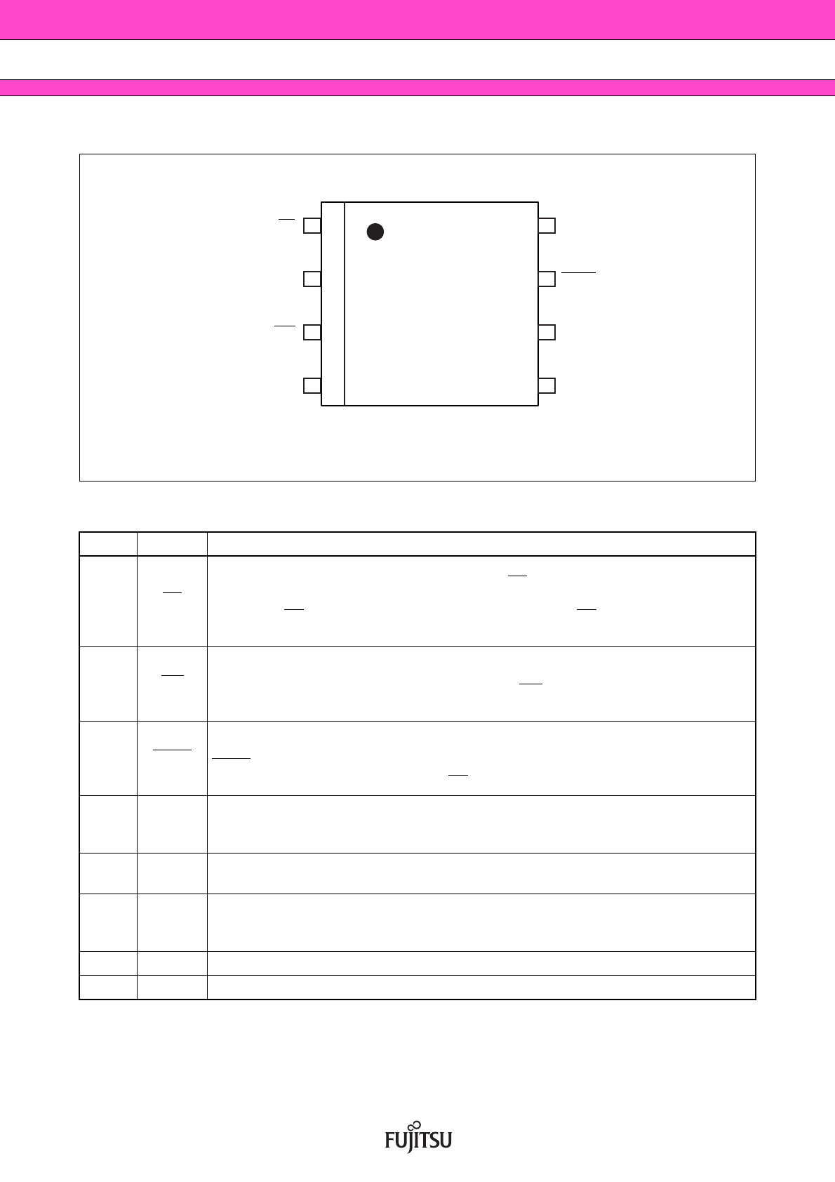
■ PIN ASSIGNMENT
■ PIN FUNCTIONAL DESCRIPTIONS
Pin No. Pin Name Functional description
1CS
Chip Select pin
This is an input pin to make chips select. When CS
is “H” level, device is in deselect
(standby) status and SO becomes High-Z. Inputs from other pins are ignored for this
time. When CS
is “L” level, de vice is in select (active) status. CS has to be “L” le vel bef ore
inputting op-code.
3WP
Write Protect pin
This is a pin to control writing to a status register. The writing of status register (see “■
STATUS REGISTER”) is protected in related with WP
and WPEN. See “■ WRITING
PROTECT” for detail.
7HOLD
Hold pin
This pin is used to interrupt serial input/output without making chips deselect. When
HOLD
is “L” level, hold oper ation is activated, SO becomes High-Z, SCK and SI become
do not care. While the hold operation, CS
has to be retained “L” level.
6SCK
Serial Clock pin
This is a clock input pin to input/output serial data. SI is loaded synchronously to a rising
edge, SO is output synchronously to a falling edge.
5SI
Serial Data Input pin
This is an input pin of serial data. This inputs op-code, address, and writing data.
2SO
Serial Data Output pin
This is an output pin of serial data. Reading data of FRAM memory cell array and status
register data are output. This is High-Z during standby.
8 VDD Supply Voltage pin
4 GND Ground pin
GNDSI
SO
VDD
SCK
WP
CS
HOLD
8
7
6
54
3
2
1
(TOP VIEW)
(FPT-8P-M02)
Page 3
MB85RS256B
DS501-00021-2v0-E 3
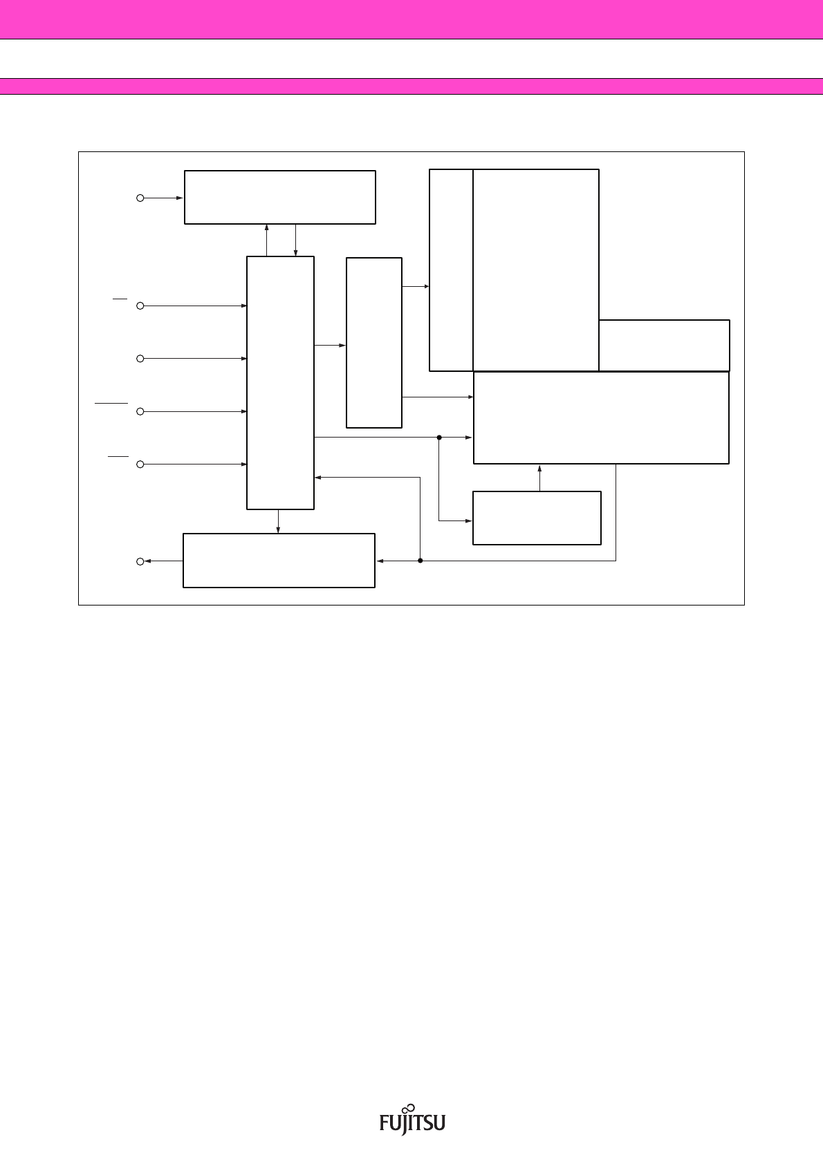
■ BLOCK DIAGRAM
SCK
SO
SI
Serial-Parallel Converter
FRAM Cell Array
32,768 ✕ 8
Column Decoder/Sense Amp/
Write Amp
FRAM
Status Register
Data Register
Parallel-Serial Converter
Control Circuit
Address Counter
Row Decoder
CS
WP
HOLD
Page 4
MB85RS256B
4 DS501-00021-2v0-E
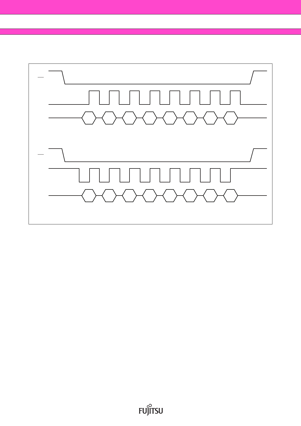
■ SPI MODE
MB85RS256B corresponds to the SPI mode 0 (CPOL = 0, CPHA = 0) , and SPI mode 3 (CPOL = 1, CPHA = 1) .
SCK
SI
CS
SCK
SI
CS
76543210
76543210
MSB LSB
MSB LSB
SPI Mode 0
SPI Mode 3
Page 5
MB85RS256B
DS501-00021-2v0-E 5
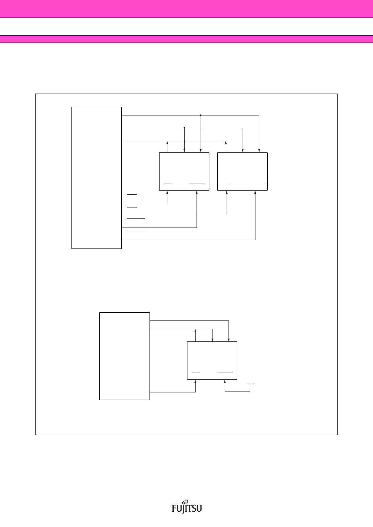
■ SERIAL PERIPHERAL INTERFACE (SPI)
MB85RS256B works as a slave of SPI. More than 2 devices can be connected by using microcontroller
equipped with SPI port. By using a microcontroller not equipped with SPI por t, SI and SO can be bus
connected to use.
SCK
SS1
HOLD1
MOSI
MISO
SS2
HOLD2
SCK
CS
HOLD
SISO
SCK
CS
HOLD
SISO
MB85RS256B
MB85RS256B
SCK
CS
HOLD
SISO
MB85RS256B
SPI
Microcontroller
MOSI : Master Out Slave In
MISO : Master In Slave Out
SS : Slave Select
System Configuration with SPI Port
System Configuration without SPI Port
Microcontroller
Page 6
MB85RS256B
6 DS501-00021-2v0-E
■ STATUS REGISTER
■ OP-CODE
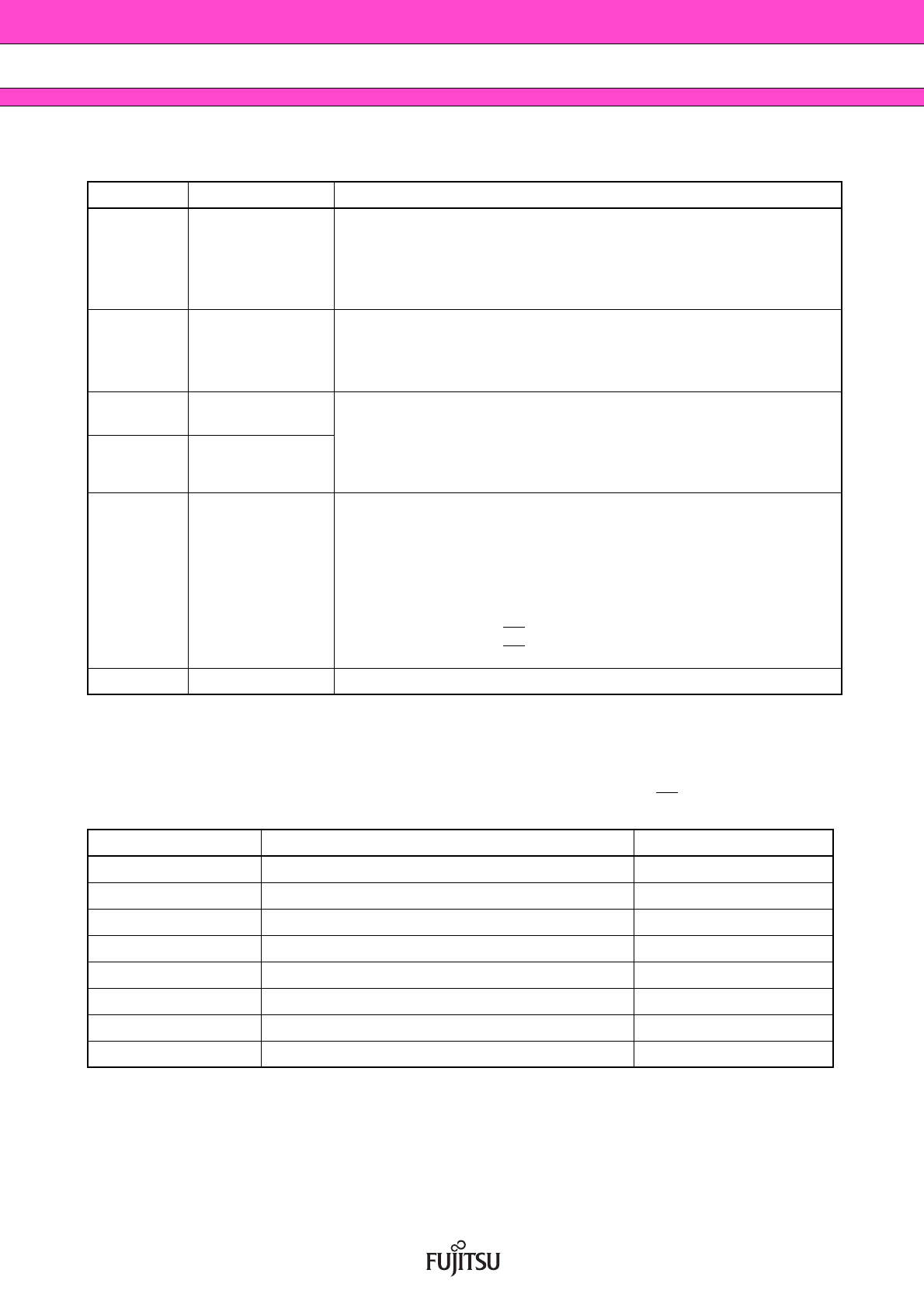
MB85RS256B accepts 8 kinds of command specified in op-code. Op-code is a code composed of 8 bits
shown in the table below. Do not input invalid codes other than those codes. If CS
is risen while inputting
op-code, the command are not performed.
Bit No. Bit Name Function
7WPEN
Status Register Write Protect
This is a bit composed of nonvolatile memories (FRAM). WPEN protects
writing to a status register (refer to “■ WRITING PRO TECT”) relating with
WP input. Writing with the WRSR command and reading with the RDSR
command are possible.
6 to 4 ⎯
Not Used Bits
These are bits composed of nonvolatile memories, writing with the WRSR
command is possible, and “000” is written before shipment. These bits are
not used but they are read with the RDSR command.
3 BP1
Block Protect
This is a bit composed of nonvolatile memory. This defines size of write
protect block for the WRITE command (refer to “■ BLOCK PROTECT”).
Writing with the WRSR command and reading with the RDSR command
are possible.
2 BP0
1WEL
Write Enable Latch
This indicates FRAM Array and status register are writable. The WREN
command is for setting, and the WRDI command is for resetting. With the
RDSR command, reading is possible but writing is not possible with the
WRSR command. WEL is reset after the following operations.
After power ON.
After WRDI command recognition.
The rising edge of CS
after WRSR command recognition.
The rising edge of CS
after WRITE command recognition.
0 0 This is a bit fixed to “0”.
Name Description Op-code
WREN Set Write Enable Latch 0000 0110
B
WRDI Reset Write Enable Latch 0000 0100B
RDSR Read Status Register 0000 0101B
WRSR Write Status Register 0000 0001B
READ Read Memory Code 0000 0011B
WRITE Write Memory Code 0000 0010B
RDID Read Device ID 1001 1111B
FSTRD Fast Read Memory Code 0000 1011B
Page 7
MB85RS256B
DS501-00021-2v0-E 7
■ COMMAND
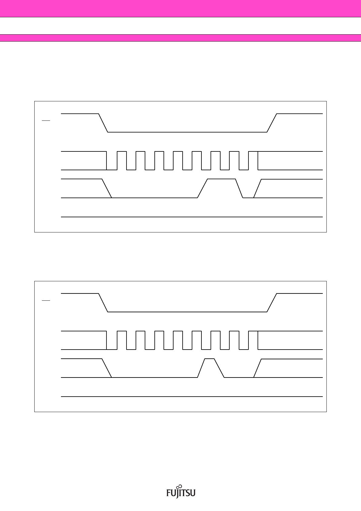
• WREN
The WREN command sets WEL (Write Enable Latch) . WEL has to be set with the WREN command before
writing operation (WRSR command and WRITE command) . WREN command is applicable to “Up to
33 MHz operation”.
• WRDI
The WRDI command resets WEL (Write Enable Latch) . Writing operation (WRSR command and WRITE
command) are not performed when WEL is reset. WRDI command is applicable to “Up to 33 MHz operation”.
SO
SCK
SI
CS
00000110
High-Z
76543210
InvalidInvalid
SO
SCK
SI
CS
00000100
High-Z
76543210
InvalidInvalid
Page 8
MB85RS256B
8 DS501-00021-2v0-E
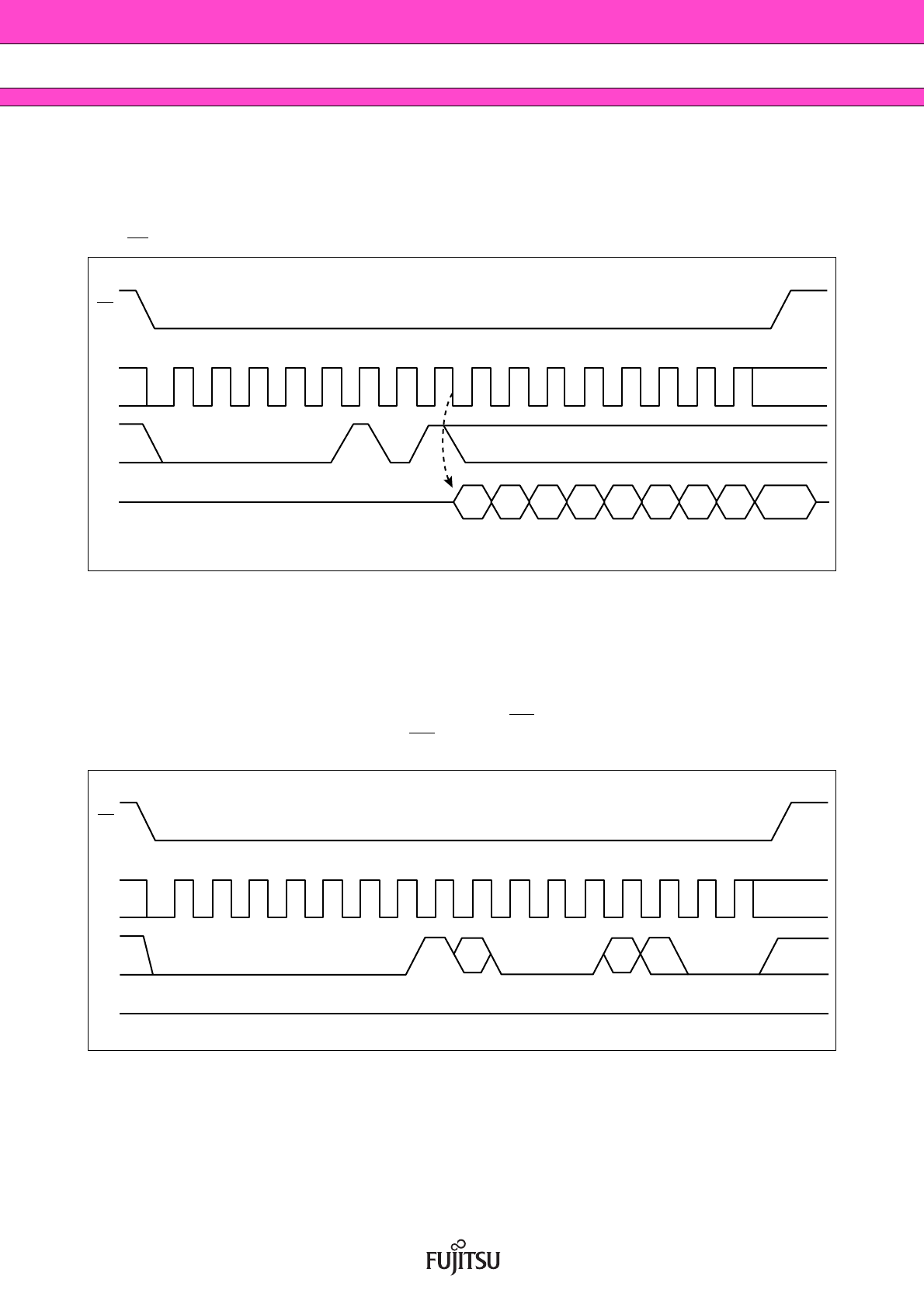
• RDSR
The RDSR command reads status register data. After op-code of RDSR is input to SI, 8-cycle clock is input
to SCK. The SI value is invalid for this time. SO is output synchronously to a falling edge of SCK. In the
RDSR command, repeated reading of status register is enabled by sending SCK continuously bef ore rising
of CS
. RDSR command is applicable to “Up to 33 MHz operation”.
• WRSR
The WRSR command writes data to the nonvolatile memory bit of status register. After perfor ming WRSR
op-code to a SI pin, 8 bits writing data is input. WEL (Write Enable Latch) is not able to be written with WRSR
command. A SI value correspondent to bit 1 is ignored. Bit 0 of the status register is fixed to “0” and cannot
be written. The SI value corresponding to bit 0 is ignored. WP
signal level shall be fixed before performing
WRSR command, and do not change the WP
signal level until the end of command sequence. WRSR
command is applicable to “Up to 33 MHz operation”.
SO
SCK
SI
CS
00000101
High-Z
76543210
Invalid
MSB
76543210
Data Out
LSB
Invalid
SO
SCK
SI
CS
00000001
76543210
Data In
MSB
76543210
High-Z
LSB
76543 210
Instruction
Page 9
MB85RS256B
DS501-00021-2v0-E 9
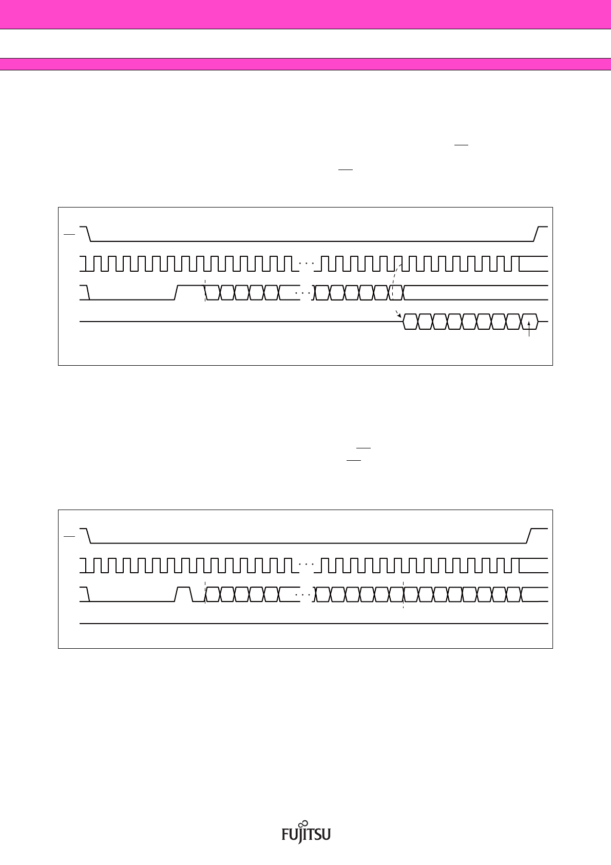
• READ
The READ command reads FRAM memory cell array data. Arbitrary 16 bits address and op-code of READ
are input to SI. The most significant address bit is invalid. Then, 8-cycle clock is input to SCK. SO is output
synchronously to the falling edge of SCK. While reading, the SI value is in valid. When CS
is risen, the READ
command is completed, but keeps on reading with automatic address increment which is enabled by con-
tinuously sending clocks to SCK in unit of 8 cycles before CS
rising. When it reaches the most significant
address, it rolls over to the starting address, and reading cycle keeps on infinitely. READ command is
applicable to “Up to 25 MHz operation”.
• WRITE
The WRITE command writes data to FRAM memory cell array . WRITE op-code , arbitrary 16 bits of address
and 8 bits of writing data are input to SI. The most significant address bit is invalid. When 8 bits of writing
data is input, data is written to FRAM memory cell array. Risen CS
will terminate the WRITE command, but
if you continue sending the writing data for 8 bits each bef ore CS
rising, it is possible to continue writing with
automatic address increment. When it reaches the most significant address, it rolls over to the starting
address, and writing cycle can be continued infinitely. WRITE command is applicable to “Up to 33MHz
operation”.
SO
SCK
SI
CS
00 00X11210
MSB
76543210
Data Out
MSB
High-Z
LSB
4201
Invalid
13121110982524232221201918 313029282726
OP-CODE
00 1 111314 35
16-bit Address
Invalid
LSB
20136457
SO
SCK
SI
CS
00 00X11210
MSB
76543210
Data In
MSB
High-Z
LSB
4201
13121110982524232221201918 313029282726
OP-CODE
00 0 111314 35
16-bit Address
LSB
20136457
Page 10
MB85RS256B
10 DS501-00021-2v0-E
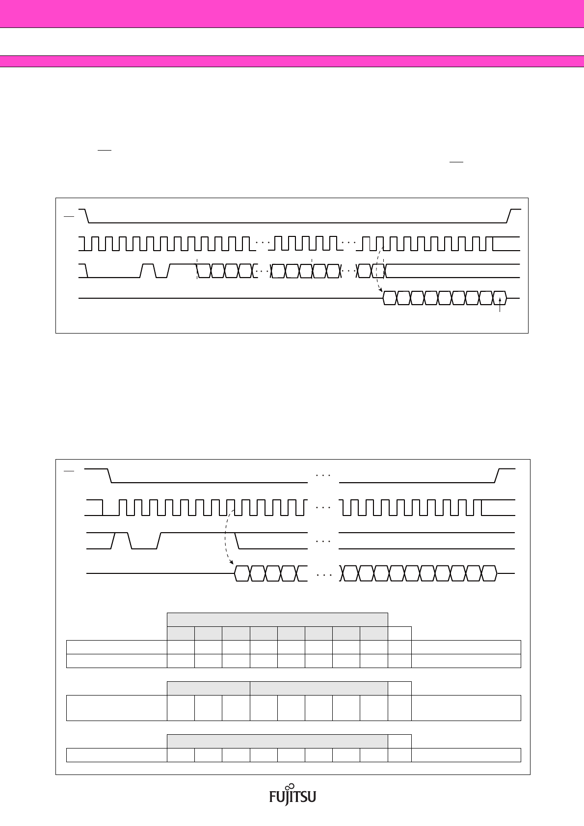
• FSTRD
The FSTRD command reads FRAM memory cell array data. Arbitrary 16 bits address and op-code of FSTRD
are input to SI followed by 8 bits dummy. The most significant address bit is invalid. Then, 8-cycle clock is
input to SCK. SO is output synchronously to the falling edge of SCK. While reading, the SI value is invalid.
When CS
is risen, the FSTRD command is completed, but keeps on reading with automatic address incre-
ment which is enabled by continuously sending clocks to SCK in unit of 8 cycles before CS
rising. When it
reaches the most significant address, it rolls over to the starting address, and reading cycle keeps on infinitely .
FSTRD command is applicable to “Up to 33 MHz operation”.
• RDID
The RDID command reads fixed Device ID. After performing RDID op-code to SI, 32-cycle clock is input to
SCK. The SI value is invalid for this time. SO is output synchronously to a falling edge of SCK. The output
is in order of Manufacturer ID (8bit)/Continuation code (8bit)/Product ID (1st Byte)/Product ID (2nd Byte).
RDID command is applicable to “Up to 33 MHz operation”.
In the RDID command, SO holds the output state of the last bit after 32-bit Device ID output by continuously
sending SCK clock before CS is risen. RDID command is applicable to “Up to 33 MHz operation”.
SO
SCK
SI
CS
00 01X113
76543210
MSB
High-Z
XX
111098 33323130 393837363534
00 1 1214
Invalid
LSB
20136457
1XX02
24 25232221
Invalid
MSB Data Out LSB
OP-CODE
16-bit Address 8-bit Dummy
SO
SCK
SI
CS
MSB
76543210
Data OutData Out
High-Z
LSB
111098
333231 393837363534
Invalid
30 282931
10011111
201364578
bit
7 6 5 4 3 2 1 0Hex
Manufacturer ID 0 0 0 0 0 1 0 0 04
H Fujitsu
Continuation code 0 1 1 1 1 1 1 1 7F
H
Proprietary use Density Hex
Product ID (1st Byte) 0 0 0 0 0 1 0 1 05H
Density: 00101B =
256kbit
Proprietary use Hex
Product ID (2nd Byte) 0 0 0 0 1 0 0 1 09
H
Page 11
MB85RS256B
DS501-00021-2v0-E 11
■ BLOCK PROTECT
Writing protect block for WRITE command is configured b y the value of BP0 and BP1 in the status register.
■ WRITING PROTECT
Writing operation of the WRITE command and the WRSR command are protected with the value of WEL,
WPEN, WP
as shown in the table.
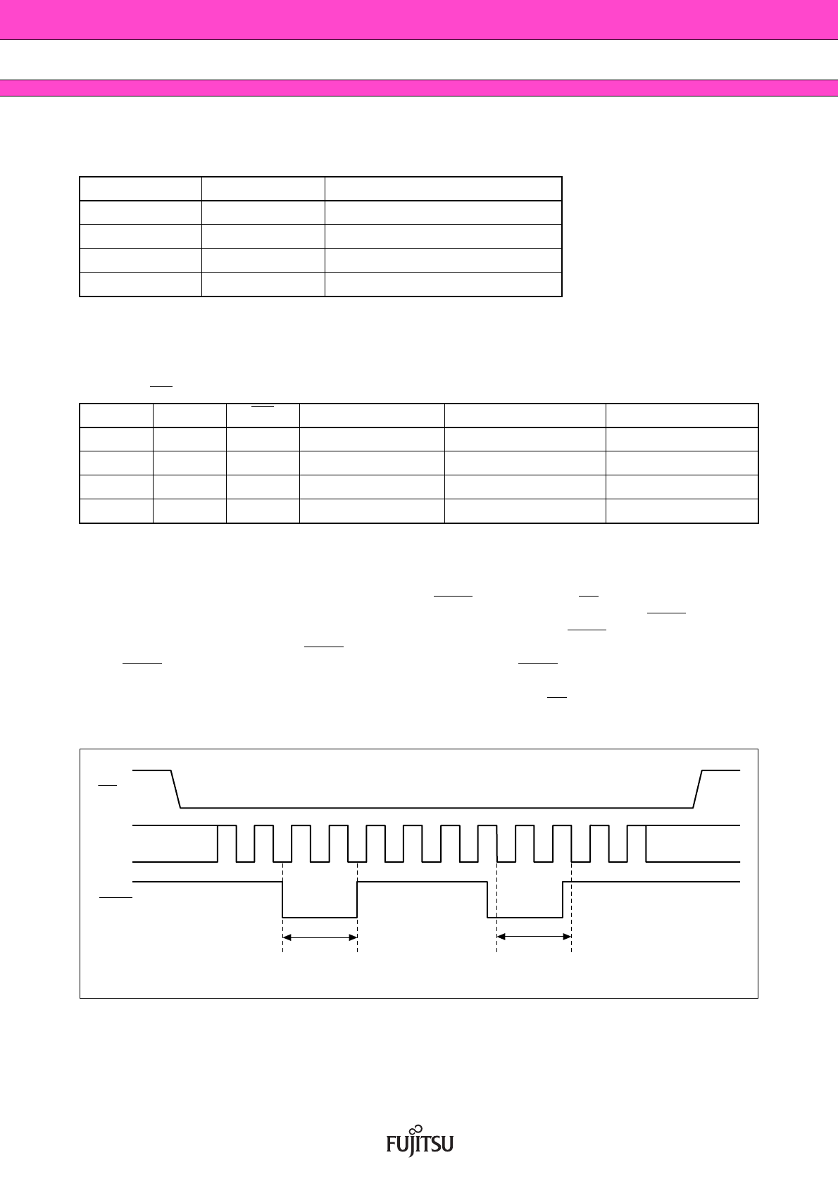
■ HOLD OPERATION
Hold status is retained without aborting a command if HOLD is “L” level while CS is “L” lev el. The timing for
starting and ending hold status depends on the SCK to be “H” level or “L” level when a HOLD
pin input is
transited to the hold condition as shown in the diagram below. In case the HOLD
pin transited to “L” level
when SCK is “L” level, return the HOLD
pin to “H” level at SCK being “L” le vel. In the same manner, in case
the HOLD
pin transited to “L” level when SCK is “H” level, return the HOLD pin to “H” level at SCK being “H”
level. Arbitrary command operation is interrupted in hold status, SCK and SI inputs become do not care.
And, SO becomes High-Z while reading command (RDSR, READ). If CS
is rising during hold status, a
command is aborted. In case the command is abor ted before its recognition, WEL holds the value before
transition to HOLD status.
BP1 BP0 Protected Block
00None
0 1 6000
H to 7FFFH (upper 1/4)
1 0 4000
H to 7FFFH (upper 1/2)
1 1 0000
H to 7FFFH (all)
WEL WPEN WP
Protected Blocks Unprotected Blocks Status Register
0 X X Protected Protected Protected
1 0 X Protected Unprotected Unprotected
1 1 0 Protected Unprotected Protected
1 1 1 Protected Unprotected Unprotected
SCK
CS
Hold Condition
HOLD
Hold Condition
Page 12
MB85RS256B
12 DS501-00021-2v0-E
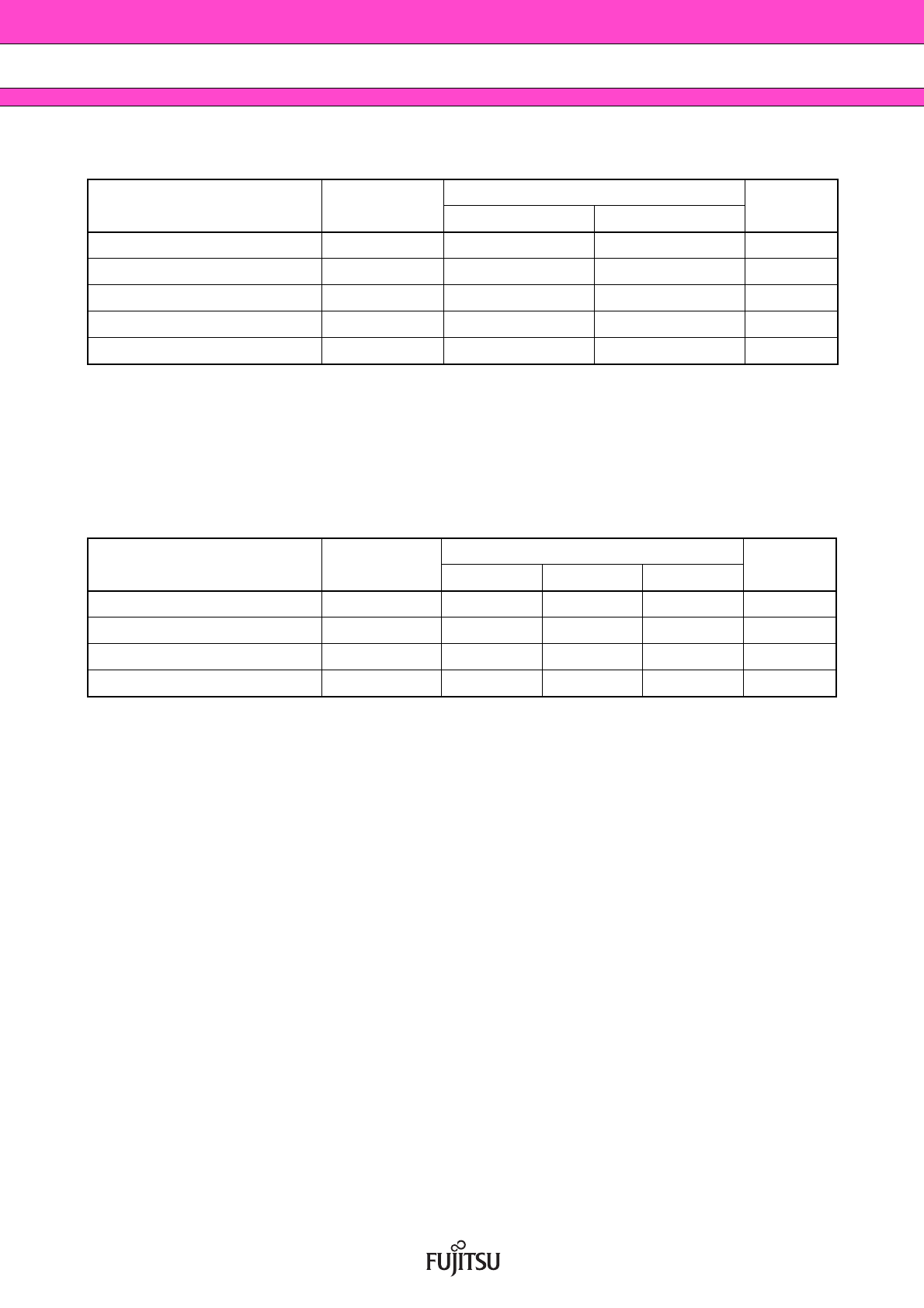
■ ABSOLUTE MAXIMUM RATINGS
*:These parameters are based on the condition that VSS is 0 V.
WARNING: Semiconductor devices can be permanently damaged by application of stress (voltage, current,
temperature, etc.) in excess of absolute maximum ratings. Do not exceed these ratings.
■ RECOMMENDED OPERATING CONDITIONS
*:These parameters are based on the condition that VSS is 0 V.
WARNING: The recommended operating conditions are required in order to ensure the normal operation of
the semiconductor device. All of the device's electrical characteristics are warranted when the
device is operated within these ranges.
Always use semiconductor devices within their recommended operating condition ranges.
Operation outside these ranges may adversely affect reliability and could result in device failure.
No warranty is made with respect to uses, operating conditions, or combinations not represented
on the data sheet. Users considering application outside the listed conditions are advised to contact
their representatives beforehand.
Parameter Symbol
Rating
Unit
Min Max
Power supply voltage* V
DD − 0.5 + 4.0 V
Input voltage* V
IN − 0.5 VDD + 0.5 V
Output voltage* V
OUT − 0.5 VDD + 0.5 V
Operation ambient temperature T
A − 40 + 85 °C
Storage temperature Tstg − 55 + 125 °C
Parameter Symbol
Value
Unit
Min Typ Max
Power supply voltage* V
DD 2.7 3.3 3.6 V
Input high voltage* V
IH VDD × 0.8 ⎯ VDD + 0.5 V
Input low voltage* V
IL − 0.5 ⎯ + 0.6 V
Operation ambient temperature T
A − 40 ⎯ + 85 °C
Page 13
MB85RS256B
DS501-00021-2v0-E 13
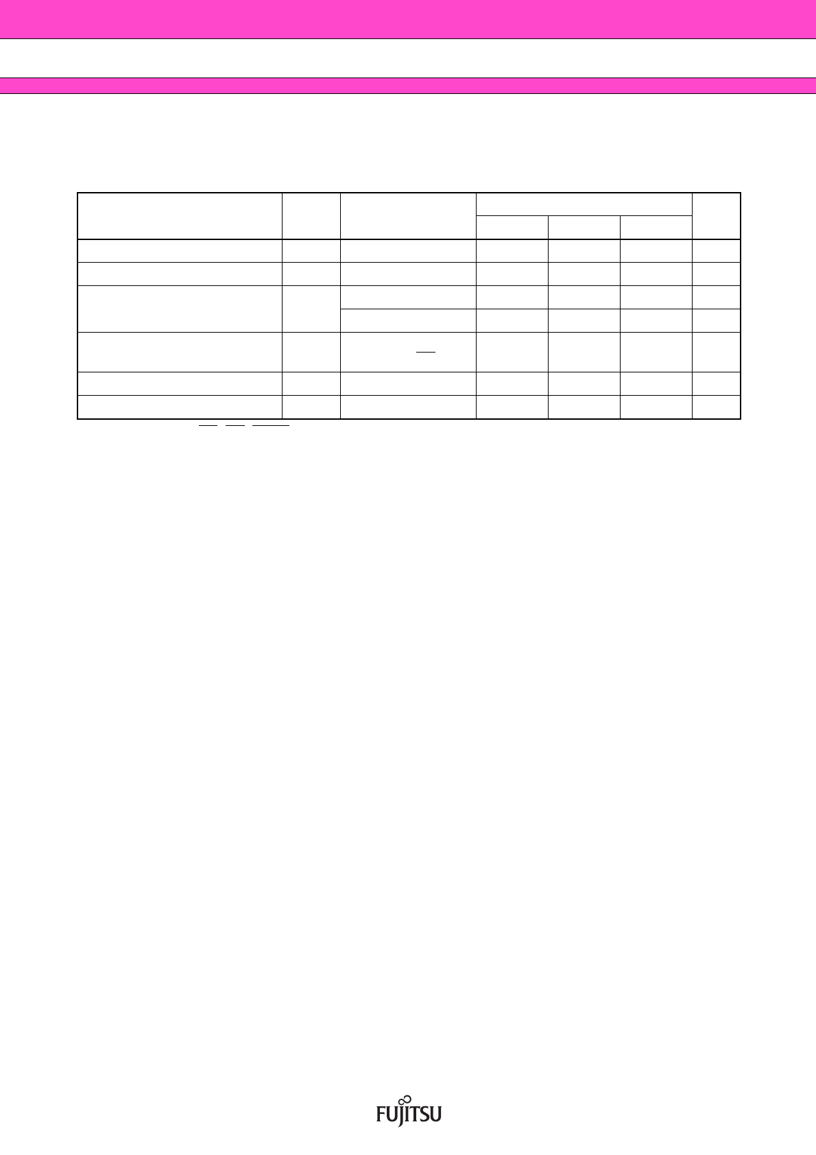
■ ELECTRICAL CHARACTERISTICS
1. DC Characteristics
(within recommended operating conditions)
*1 : Applicable pin : CS
, WP, HOLD, SCK, SI
*2 : Applicable pin : SO
Parameter Symbol Condition
Value
Unit
Min Typ Max
Input leakage current*
1
|ILI|VIN = 0 V to VDD ⎯⎯10 μA
Output leakage current*
2
|ILO|VOUT = 0 V to VDD ⎯⎯10 μA
Operating power supply current I
DD
SCK = 25 MHz ⎯ 45mA
SCK = 33 MHz ⎯ 56mA
Standby current I
SB
All inputs VSS or
SCK = SI = CS
= VDD
⎯ 950μA
Output high voltage V
OH IOH = −2 mA VDD × 0.8 ⎯⎯V
Output low voltage V
OL IOL = 2 mA ⎯⎯0.4 V
Page 14

MB85RS256B
14 DS501-00021-2v0-E
2. AC Characteristics
* : All commands except READ are applicable to “Up to 33 MHz operation”.
READ command is applicable to “Up to 25MHz operation”.
AC Test Condition
Power supply voltage : 2.7 V to 3.6 V
Operation ambient temperature : − 40 °C to + 85 °C
Input voltage magnitude : 0.3 V to 2.7 V
Input rising time : 5 ns
Input falling time : 5 ns
Input judge level : V
DD/2
Output judge level : V
DD/2
Parameter Symbol
Value
UnitUp to 25MHz operation Up to 33MHz operation*
MinMaxMinMax
SCK clock frequency f
CK 025033MHz
Clock high time t
CH 20 ⎯ 15 ⎯ ns
Clock low time t
CL 20 ⎯ 15 ⎯ ns
Chip select set up time t
CSU 10 ⎯ 10 ⎯ ns
Chip select hold time t
CSH 10 ⎯ 10 ⎯ ns
Output disable time t
OD ⎯ 20 ⎯ 20 ns
Output data valid time t
ODV ⎯ 18 ⎯ 13 ns
Output hold time t
OH 0 ⎯ 0 ⎯ ns
Deselect time t
D 60 ⎯ 40 ⎯ ns
Data in rising time t
R ⎯ 50 ⎯ 50 ns
Data falling time t
F ⎯ 50 ⎯ 50 ns
Data set up time t
SU 5 ⎯ 5 ⎯ ns
Data hold time t
H 5 ⎯ 5 ⎯ ns
HOLD set up time t
HS 10 ⎯ 10 ⎯ ns
HOLD hold time t
HH 10 ⎯ 10 ⎯ ns
HOLD output floating time t
HZ ⎯ 20 ⎯ 20 ns
HOLD output active time t
LZ ⎯ 20 ⎯ 20 ns
Page 15
MB85RS256B
DS501-00021-2v0-E 15
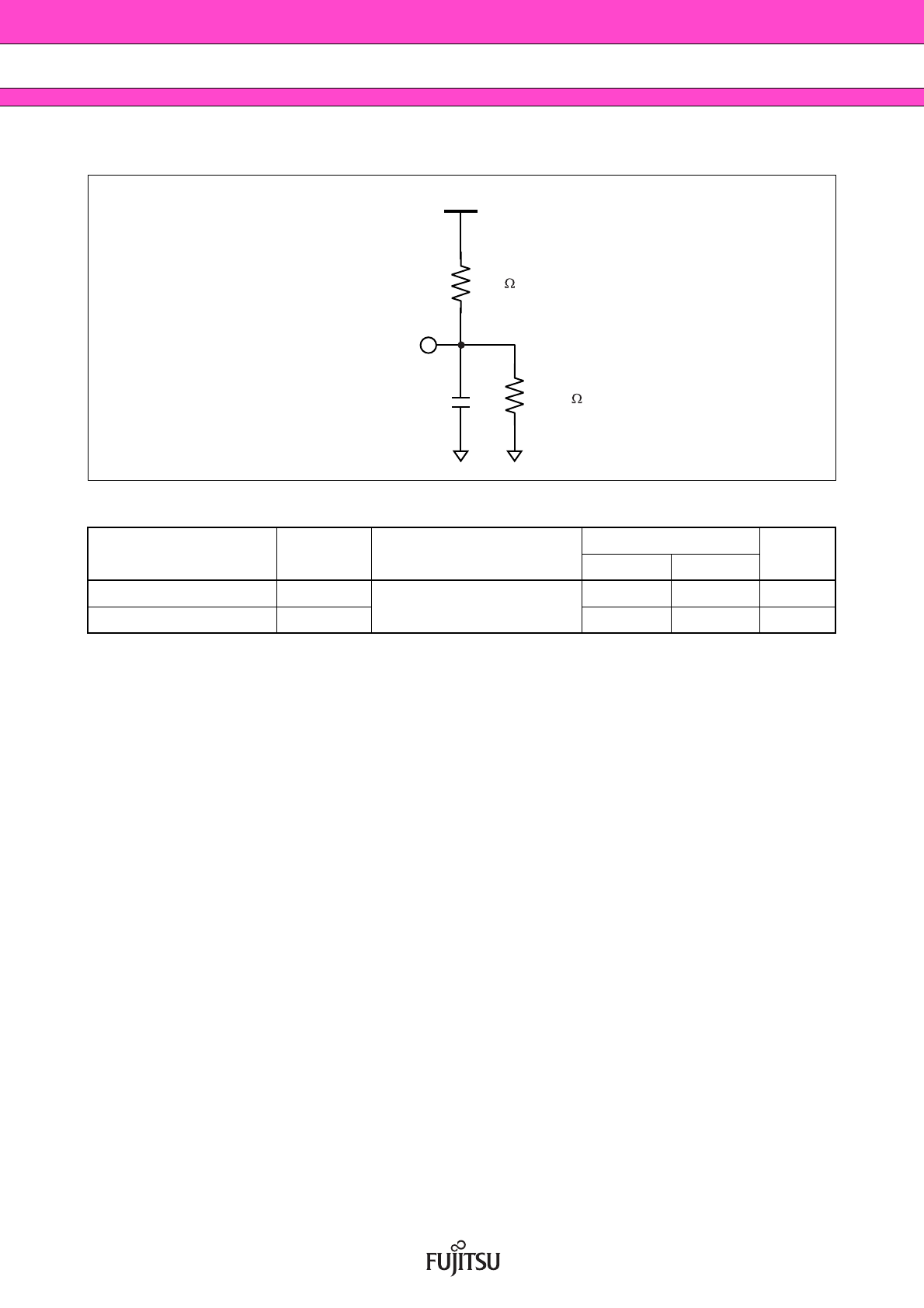
AC Load Equivalent Circuit
3. Pin Capacitance
Parameter Symbol Condition
Value
Unit
Min Max
Output capacitance C
O
VDD = VIN = VOUT = 0 V,
f = 1 MHz, T
A = +25 °C
⎯ 10 pF
Input capacitance C
I ⎯ 10 pF
30 pF
Output
3.3 V
1.2 k
0.95 k
Page 16
MB85RS256B
16 DS501-00021-2v0-E
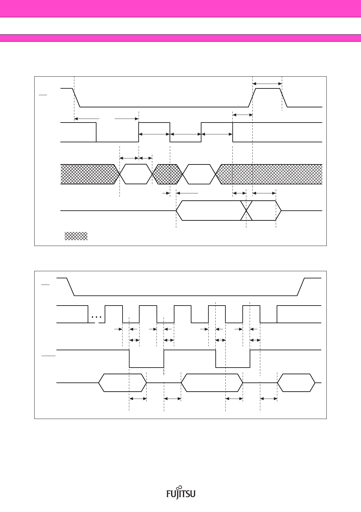
■ TIMING DIAGRAM
• Serial Data Timing
• Hold Timing
SCK
CS
Valid in
SI
SO
High-Z
: H or L
t
CSU
t
CH
t
CH
t
CL
t
SU
t
H
t
ODV
t
OH
t
OD
t
CSH
t
D
High-Z
SCK
CS
SO
t
HS tHS
tHHtHH
tHH tHH
tHZ tLZ tHZ tLZ
tHS tHS
HOLD
High-ZHigh-Z
Page 17
MB85RS256B
DS501-00021-2v0-E 17
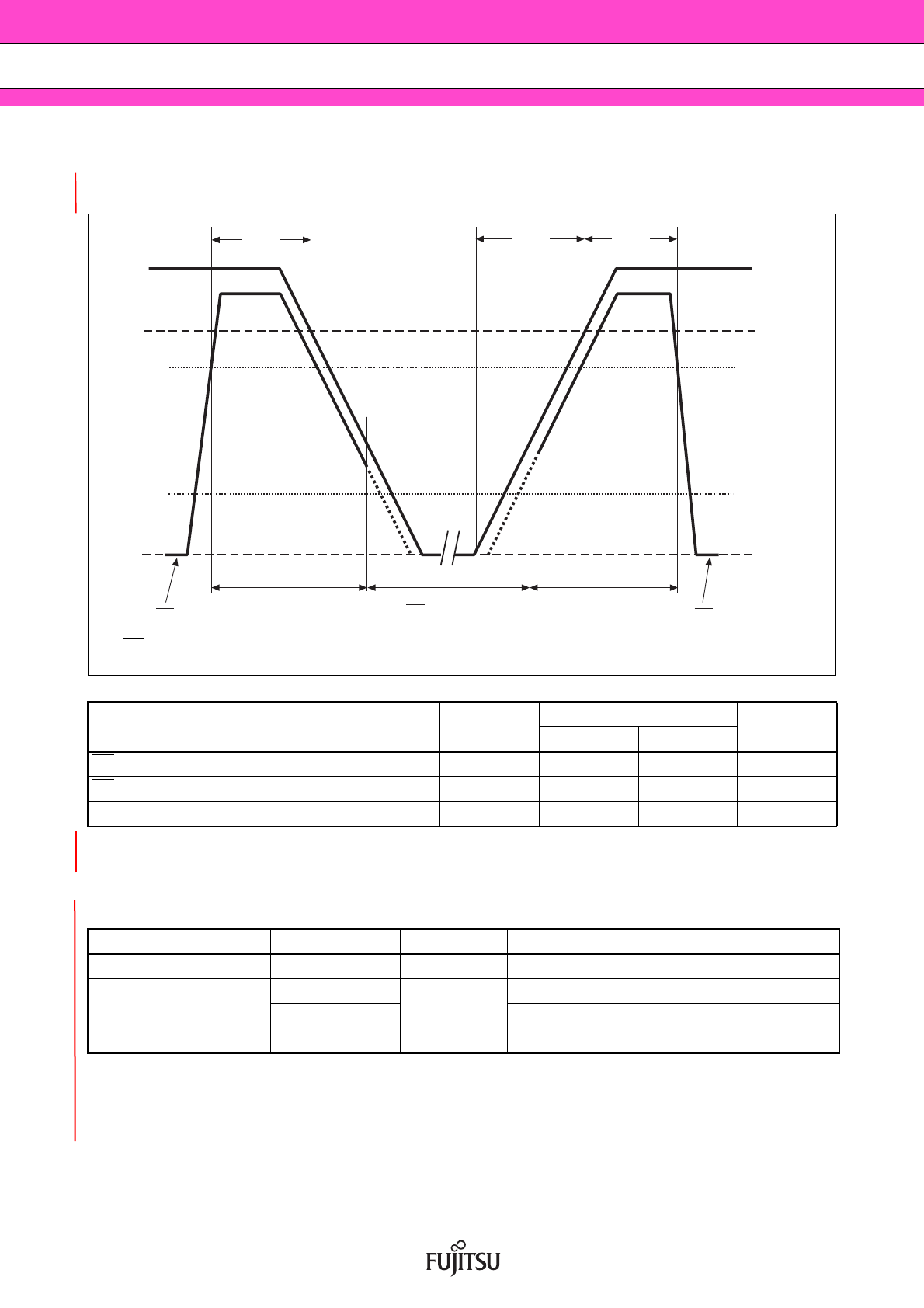
■ POWER ON/OFF SEQUENCE
If VDD falls down below 2.0 V, VDD is required to be started from 1.0 V or less to prevent malfunctions when
the power is turned on again (see the figure below).
If the device does not operate within the specified conditions of read cycle, write cycle or power on/off
sequence, memory data can not be guaranteed.
■ FRAM CHARACTERISTICS
*1 : T otal number of reading and writing defines the minimum value of endurance , as an FRAM memory operates
with destructive readout mechanism.
*2 : Minimun values define retention time of the first reading/writing data right after shipment, and these values
are calculated by qualification results.
■ NOTE ON USE
Data written before performing IR reflow is not guaranteed after IR reflow.
Parameter Symbol
Value
Unit
Min Max
CS
level hold time at power OFF tpd 200 ⎯ ns
CS
level hold time at power ON tpu 85 ⎯ ns
Power supply rising time tr 0.05 200 ms
Item Min Max Unit Parameter
Read/Write Endurance*
1
10
12
⎯ Times/byte Operation Ambient Temperature TA = + 85 °C
Data Retention*
2
10 ⎯
Years
Operation Ambient Temperature TA = + 85 °C
95 ⎯ Operation Ambient Temperature T
A = + 55 °C
≥ 200 ⎯ Operation Ambient Temperature T
A = + 35 °C
GND
CS >
V
DD × 0.8*
tpd
tputr
V
IL (Max)
1.0 V
V
IH (Min)
3.0 V
V
DD
CS : do not care
CS >
V
DD × 0.8*
CS CS
GND
V
IL (Max)
1.0 V
V
IH (Min)
3.0 V
V
DD
* : CS (Max) < VDD + 0.5 V
Page 18
MB85RS256B
18 DS501-00021-2v0-E
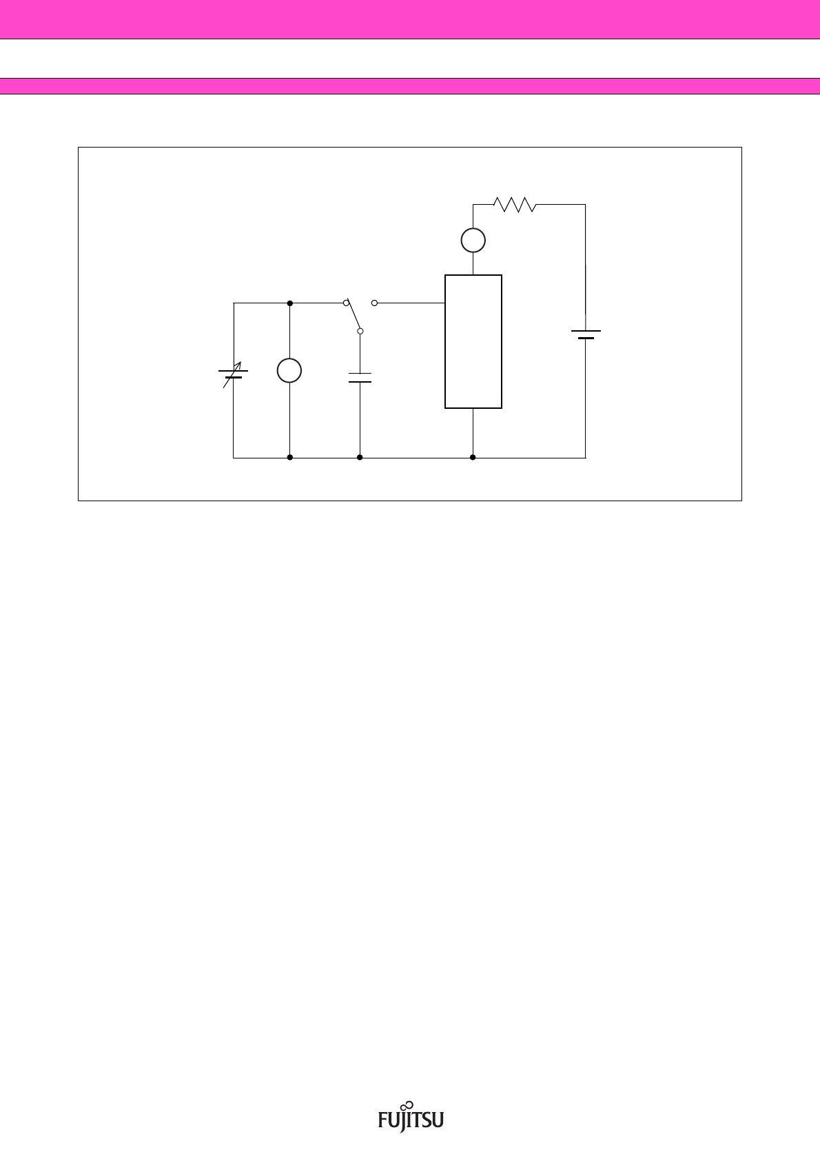
■ ESD AND LATCH-UP
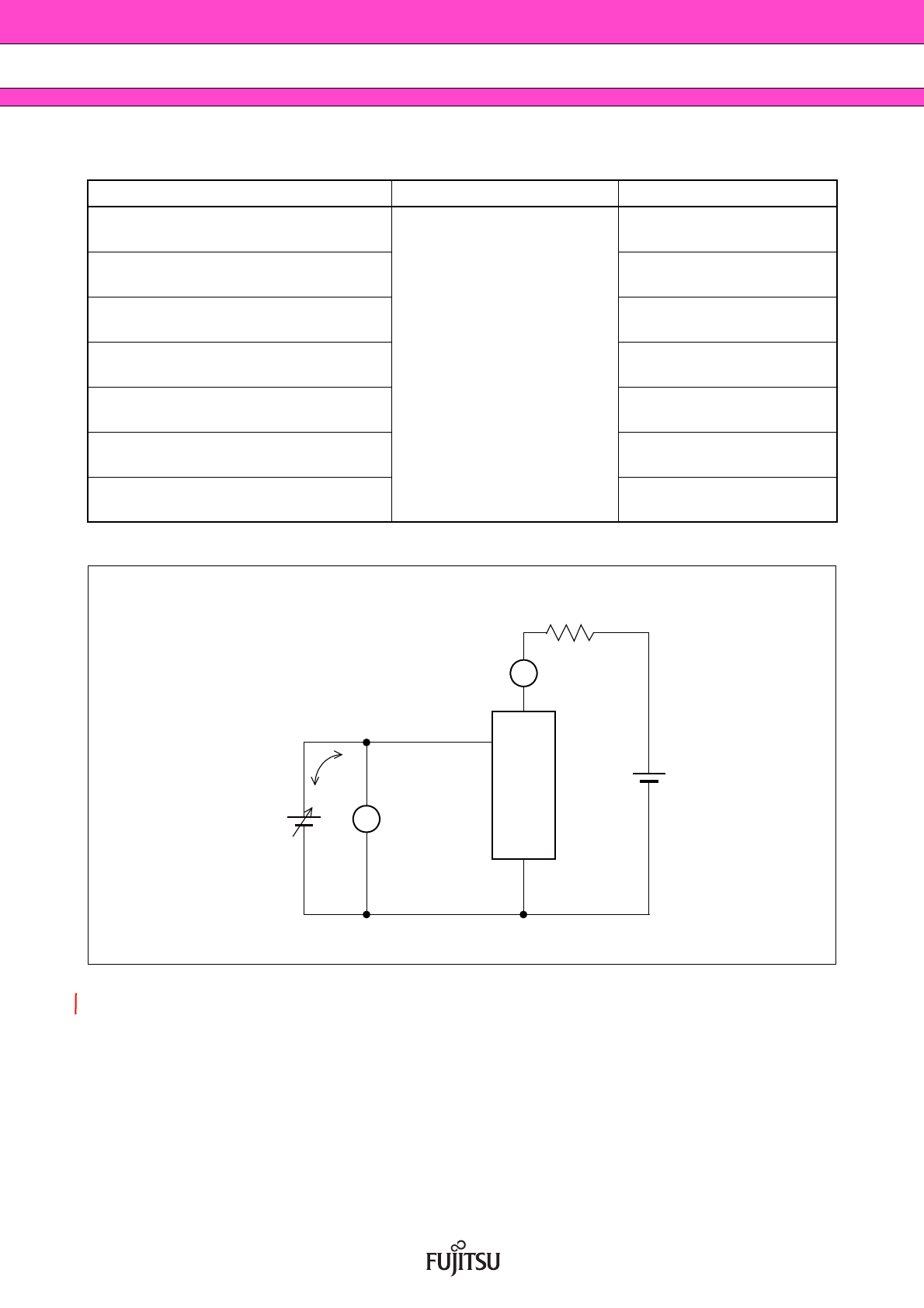
• Current method of Latch-Up Resistance Test
Note : The voltage V
IN is increased gradually and the current IIN of 300 mA at maximum shall flow.
Confirm the latch up does not occur under I
IN = ± 300 mA.
In case the specific requirement is specified for I/O and I
IN cannot be 300 mA, the voltage shall be
increased to the level that meets the specific requirement.
Test DUT Value
ESD HBM (Human Body Model)
JESD22-A114 compliant
MB85RS256BPNF-G-JNE1
≥
|2000 V|
ESD MM (Machine Model)
JESD22-A115 compliant
≥
|200 V|
ESD CDM (Charged Device Model)
JESD22-C101 compliant
⎯
Latch-Up (I-test)
JESD78 compliant
⎯
Latch-Up (V
supply overvoltage test)
JESD78 compliant
⎯
Latch-Up (Current Method)
Proprietary method
⎯
Latch-Up (C-V Method)
Proprietary method
⎯
A
VDD
VSS
DUT
V
I
IN
V
IN
+
-
Test terminal
Protection Resistance
VDD
(Max.Rating)
Reference
terminal
Page 19
MB85RS256B
DS501-00021-2v0-E 19
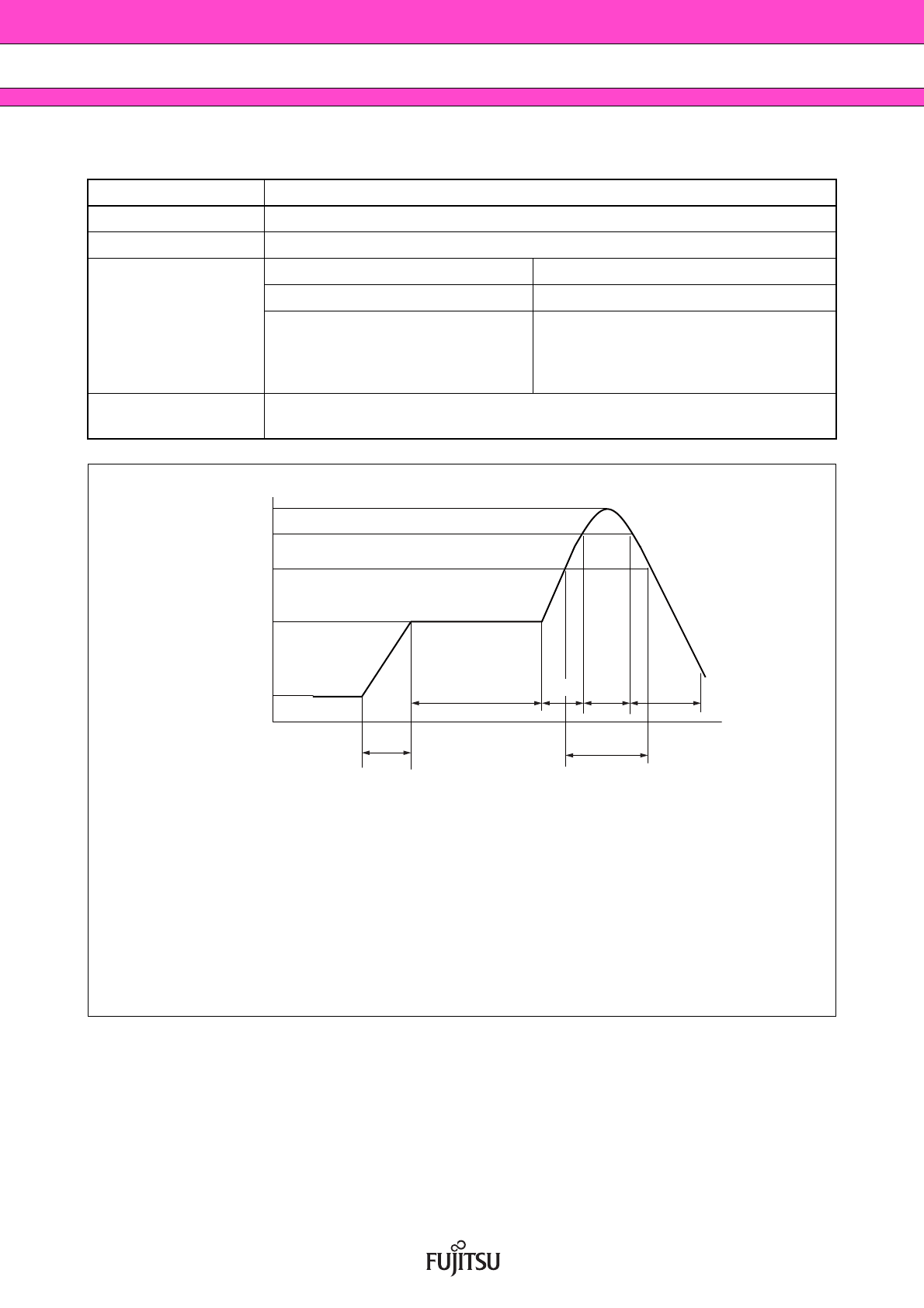
• C-V method of Latch-Up Resistance Test
Note : Charge voltage alternately switching 1 and 2 approximately 2 sec interval. This switching process is
considered as one cycle. Repeat this process 5 times. However, if the latch-up condition occurs before
completing 5times, this test must be stopped immediately.
VDD
VSS
DUT
V
IN
+
-
SW
1
2
C
200pF
V
A
Test
terminal
Protection Resistance
VDD
(Max.Rating)
Reference
terminal
Page 20
MB85RS256B
20 DS501-00021-2v0-E
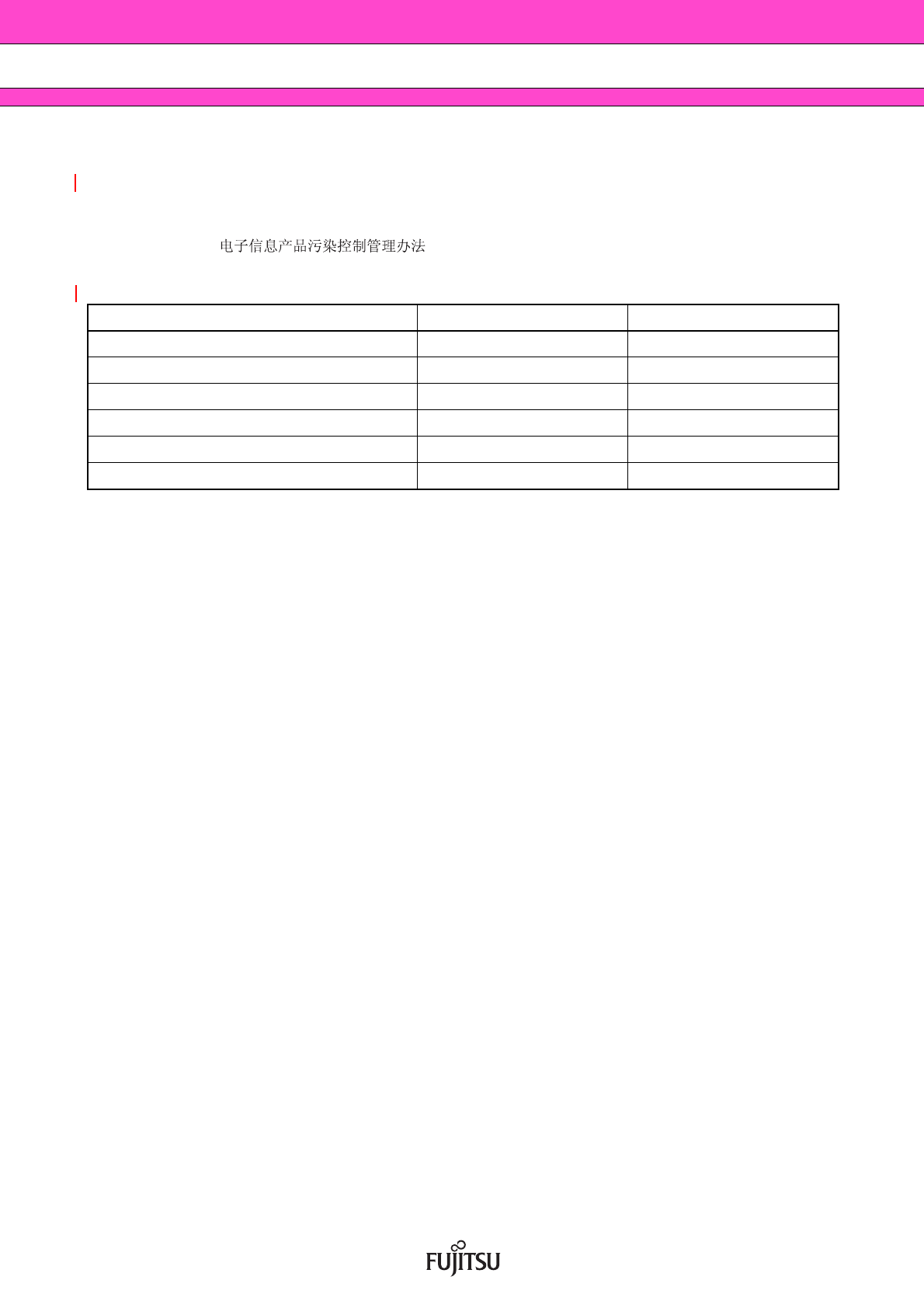
■ REFLOW CONDITIONS AND FLOOR LIFE
Reflow Profile
Item Condition
Method IR (infrared reflow) , Convection
Times 2
Floor life
Before unpacking Please use within 2 years after production.
From unpacking to 2nd reflow Within 8 days
In case over period of floor life
Baking with 125 °C+/-3 °C for
24hrs+2hrs/-0hrs is required.
Then please use within 8 days.
(Please remember baking is up to 2 times)
Floor life condition
Between 5 °C and 30 °C and also below 70%RH required.
(It is preferred lower humidity in the required temp range.)
260°C
(e)
(d
')
(d)
255°C
170 °C
190 °C
RT
(
b)
(a)
(c)
to
Note : Temperature on the top of the package body is measured.
(a) Average ramp-up rate : 1 °C/s to 4 °C/s
(b) Preheat & Soak : 170 °C to 190 °C, 60 s to 180 s
(c) Average ramp-up rate : 1 °C/s to 4 °C/s
(d) Peak temperature : Temperature 260 °C Max; 255 °C within 10 s
(d’) Liquidous temperature : Up to 230 °C within 40 s or
Up to 225 °C within 60 s or
Up to 220 °C within 80 s
(e) Cooling : Natural cooling or forced cooling
Liquidous
Temperature
Page 21
MB85RS256B
DS501-00021-2v0-E 21
■ RESTRICTED SUBSTANCES
This product complies with the regulations below (Based on current knowledge as of November 2011).
• EU RoHS Directive (2002/95/EC)
• China RoHS (Administration on the Control of Pollution Caused by Electronic Information Products
( ))
• Vietnam RoHS (30/2011/TT-BCT)
Restricted substances in each regulation are as follows.
* : The mark of “❍” shows below a threshold value.
Substances Threshold Contain status*
Lead and its compounds 1,000 ppm ❍
Mercury and its compounds 1,000 ppm ❍
Cadmium and its compounds 100 ppm ❍
Hexavalent chromium compound 1,000 ppm ❍
Polybrominated biphenyls (PBB) 1,000 ppm ❍
Polybrominated diphenyl ethers (PBDE) 1,000 ppm ❍
Page 22
MB85RS256B
22 DS501-00021-2v0-E
■ ORDERING INFORMATION
Part number Package Shipping form
Minimum shipping
quantity
MB85RS256BPNF-G-JNE1
8-pin plastic SOP
(FPT-8P-M02)
Tube 1
MB85RS256BPNF-G-JNERE1
8-pin plastic SOP
(FPT-8P-M02)
Embossed Carrier tape 1500
Page 23
MB85RS256B
DS501-00021-2v0-E 23
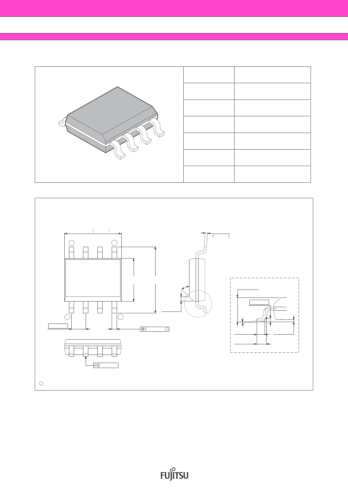
■ PACKAGE DIMENSION
Please check the latest package dimension at the following URL.
http://edevice.fujitsu.com/package/en-search/
8-pin plastic SOP Lead pitch 1.27 mm
Package width ×
package length
3.9 mm × 5.05 mm
Lead shape Gullwing
Sealing method Plastic mold
Mounting height 1.75 mm MAX
Weight 0.06 g
8-pin plastic SOP
(FPT-8P-M02)
(
FPT-8P-M02
)
C
1.27(.050)
3.90±0.30 6.00±0.20
.199
–.008
+.010
–0.20
+0.25
5.05
0.13(.005)
M
(.154±.012) (.236±.008)
0.10(.004)
14
58
0.44±0.08
(.017±.003)
–0.07
+0.03
0.22
.009
+.001
–.003
45
°
0.40(.016)
"A"
0~8
°
0.25(.010)
(Mounting height)
Details of "A" part
1.55±0.20
(.061±.008)
0.50±0.20
(.020±.008)
0.60±0.15
(.024±.006)
0.15±0.10
(.006±.004)
(Stand off)
0.10(.004)
*
1
*
2
2002-2012 FUJITSU SEMICONDUCTOR LIMITED F08004S-c-5-10
Dimensions in mm (inches).
Note: The values in parentheses are reference values.
Note 1) 1 : These dimensions include resin protrusion.
Note 2) 2 : These dimensions do not include resin protrusion.
Note 3) Pins width and pins thickness include plating thickness.
Note 4) Pins width do not include tie bar cutting remainder.
*
*
Page 24
MB85RS256B
24 DS501-00021-2v0-E
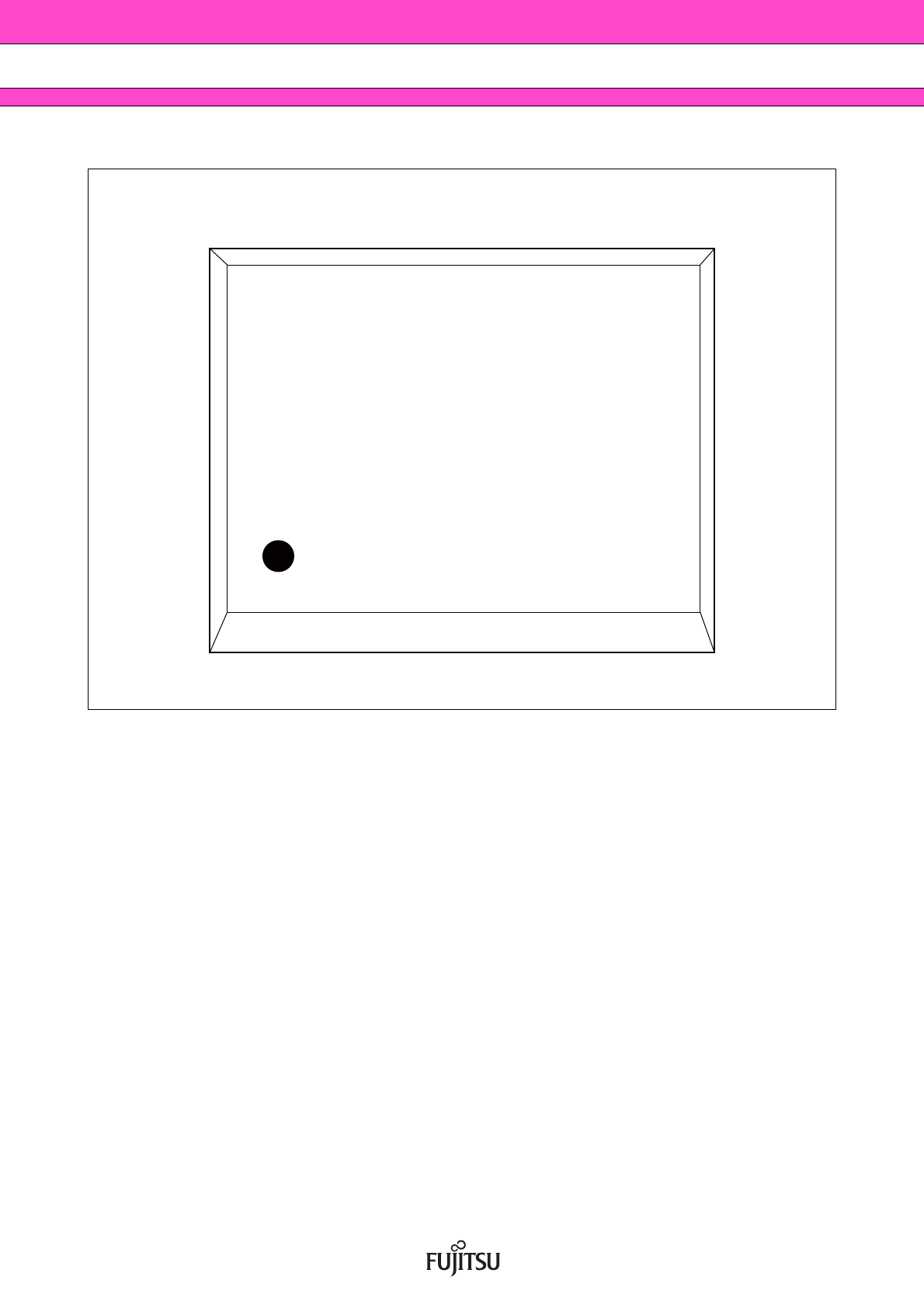
■ MARKING
RS256B
E11150
300
[MB85RS256BPNF-G-JNE1]
[MB85RS256BPNF-G-JNERE1]
[FPT-8P-M02]
Page 25
MB85RS256B
DS501-00021-2v0-E 25
■ PACKING INFORMATION
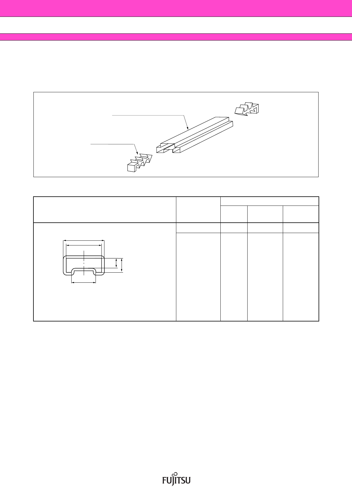
1. Tube
1.1 Tube Dimensions
• Tube/stopper shape
Tube cross-sections and Maximum quantity
Package form Package code
Maximum quantity
pcs/
tube
pcs/inner
box
pcs/outer
box
SOP, 8, plastic (2)
t = 0.5
Transparent polyethylene terephthalate
FPT
-8P-M02
95 7600 30400
(
Dimensions in mm)
(treated to antistatic)
Tube length: 520 mm
(treated to antistatic)
Stopper
Tube
Transparent polyethylene terephthalate
4.4
6.4
7.4
1.8
C
2006 FUJITSU LIMITED F08008-SET1-PET:FJ99L-0022-E0008-1-K-1
2.6
©2006-2010 FUJITSU SEMICONDUCTOR LIMITED
F08008-SET1-PET:FJ99L-0022-E0008-1-K-3
Page 26
MB85RS256B
26 DS501-00021-2v0-E
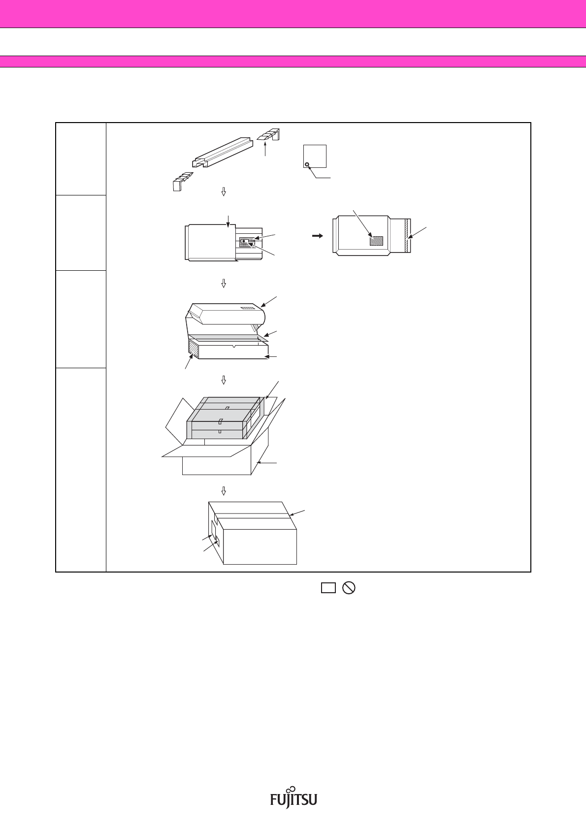
1.2 Tube Dry pack packing specifications
*1:For a product of witch part number is suffixed with “E1”, a “ ” marks is display to the moisture barrier
bag and the inner boxes.
*2:The space in the outer box will be filled with empty inner boxes, or cushions, etc.
*3:Please refer to an attached sheet about the indication label.
Note: The packing specifications may not be applied when the product is delivered via a distributer.
Tube
Dry pack
Inner box
Outer box
For SOP
Stopper
Aluminum Iaminated bag
Index mark
Desiccant
Label I
*1*3
Heat seal
Aluminum Iaminated bag
(tubes inside)
Cushioning material
Inner box
Label I
*1*3
Cushioning material
Humidity indicater
Outer box
*2
Label II-A
*3
Label II-B
*3
IC
Use adhesive tapes.
G
Pb
Page 27
MB85RS256B
DS501-00021-2v0-E 27
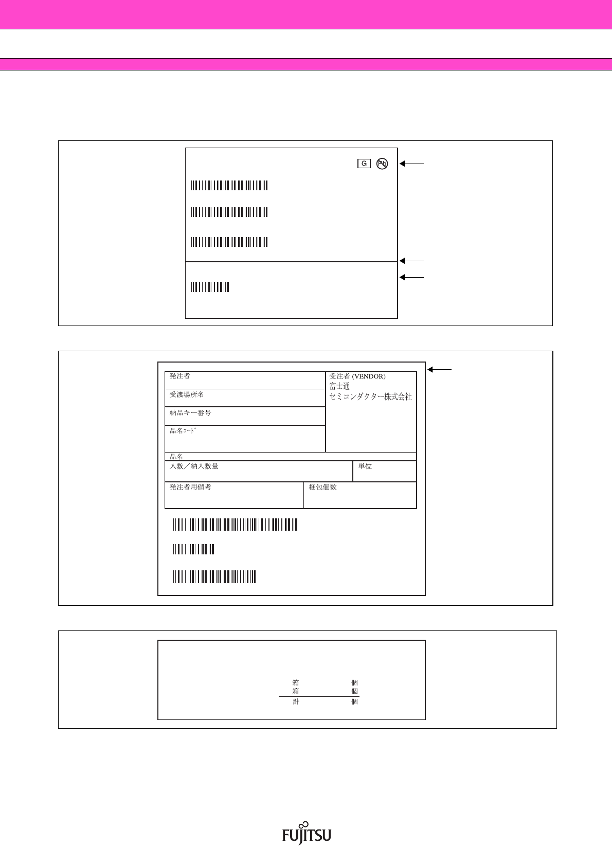
1.3 Product label indicators
Label I: Label on Inner box/Moisture Barrier Bag/ (It sticks it on the reel for the emboss taping)
[C-3 Label (50mm × 100mm) Supplemental Label (20mm × 100mm)]
Label II-A: Label on Outer box [D Label] (100mm × 100mm)
Label II-B: Outer boxes product indicate
Note: Depending on shipment state, “Label II-A” and “Label II-B” on the external boxe s might not be printed.
(Customer part number or FJ part number)
(Customer part number or FJ part number)
(FJ control number bar code)
XX/XX XXXX-XXX XXX
XXXX-XXX XXX
(Lot Number and quantity)
(Package count)
(Customer part number or FJ part number
bar code)
(Part number and quantity)
(FJ control number)
QC PASS
XXXXXXXXXXXXXX
XXXX/XX/XX (Packed years/month/day) ASSEMBLED IN xxxx
(3N)1 XXXXXXXXXXXXXX XXX
(Quantity)
(3N)2 XXXXXXXXXX
XXX pcs
XXXXXX
XXXXXXXXXXXXXX
(Customer part number or FJ part number)
XXXXXXXXXXXXXX
(Comment)
XXXXXXXXXXXXXX
(FJ control number )
XXXXXXXXXX
(LEAD FREE mark)
C-3 Label
Supplemental Label
Perforated line
XXXXXXXXXXXXX (Customer Name)
(CUST.)
XXX (FJ control number)
XXX (FJ control number)
XXX (FJ control number)
XXXXXXXXXXXXXX
(Part number)
(FJ control number + Product quantity)
(FJ control number + Product quantity
bar code)
(Part number + Product quantity bar code)
XXXXXXXXX (Delivery Address)
(DELIVERY POINT)
XXXXXXXXXXXXXX
(TRANS.NO.) (FJ control number)
XXXXXXXXXXXXXX
(PART NO.) (Customer part number or
FJ part number)
XXX/XXX
(Q’TY/TOTAL Q’TY)
XX
(UNIT)
(CUSTOMER'S
REMARKS)
XXXXXXXXXXXXXXXXXXXX
(PACKAGE COUNT)
XXX/XXX
(PART NAME) XXXXXXXXXXXXXX (Part number)
(3N)3 XXXXXXXXXXXXXX XXX
(Part number + Product quantity)
(3N)4 XXXXXXXXXXXXXX XXX
(FJ control number)
(FJ control number bar code)
(3N)5 XXXXXXXXXX
D Label
XXXXXXXXXXXXXX (Part number)
(Lot Number)
XXXX-XXX
XXXX-XXX
(Count) (Quantity)
X XXX
X XXX
XXX
Page 28
MB85RS256B
28 DS501-00021-2v0-E
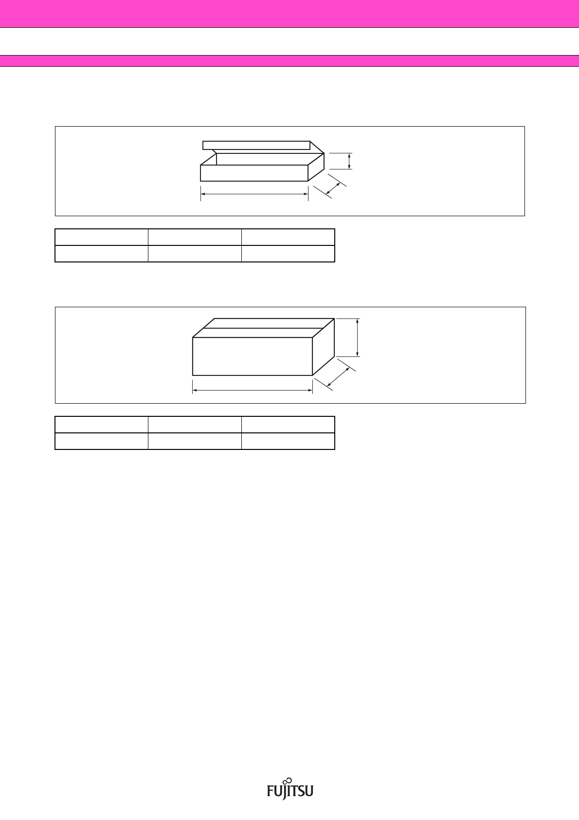
1.4 Dimensions for Containers
(1) Dimensions for inner box
(2) Dimensions for outer box
LWH
540 125 75
(Dimensions in mm)
LWH
565 270 180
(Dimensions in mm)
L
W
H
L
W
H
Page 29
MB85RS256B
DS501-00021-2v0-E 29
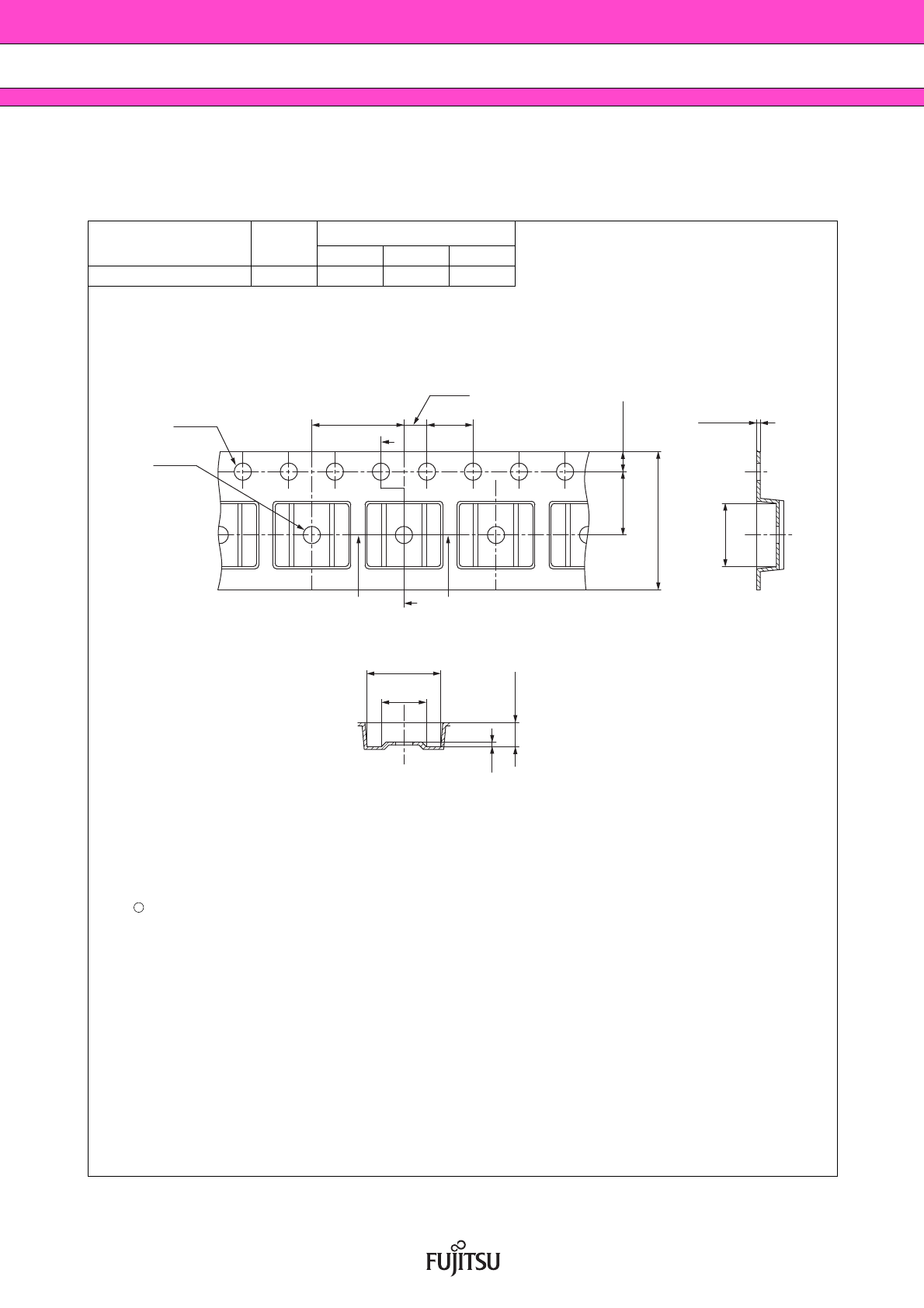
2. Emboss Tape
2.1 Tape Dimensions
PKG code
Reel No
Maximum storage capacity
pcs/reel
pcs/inner box pcs/outer box
FPT-8P-M02 3 1500 1500 10500
(Dimensions in mm)
Material : Conductive polystyrene
Heat proof temperature : No heat resistance.
Package should not be baked
by using tape and reel.
C
2012 FUJITSU SEMICONDUCTOR LIMITED SOL8-EMBOSSTAPE9 : NFME-EMB-X0084-1-P-1
8±0.1
6.4±0.1
3.9±0.2
4±0.1
5.5±0.05
5.5±0.1
2.1±0.1
0.4
1.75±0.1
0.3±0.05
2±0.05
+0.1
–0
ø1.5
+0.1
–0
ø1.5
+0.3
–0.1
12
B
BA A
SEC.A-A
SEC.B-B
Page 30
MB85RS256B
30 DS501-00021-2v0-E
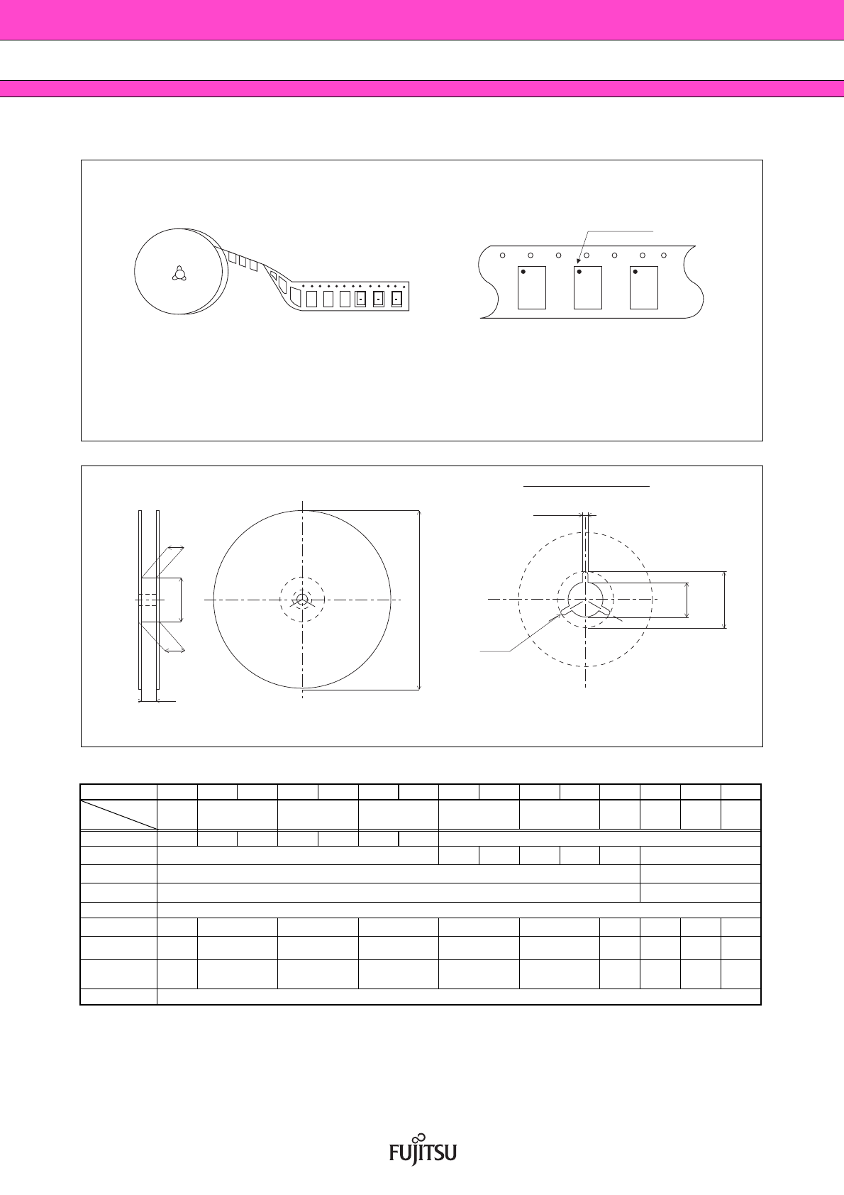
2.2 IC orientation
2.3 Reel dimensions
Dimensions in mm
Reel No123456789101112131415
Tape width
Symbol
8121624324456121624
A 254 ± 2 254 ± 2 330 ± 2 254 ± 2 330 ± 2 254 ± 2 330 ± 2 330 ± 2
B
100
100 150 100 150 100
100 ± 2
C 13 ± 0.2
13
D 21 ± 0.8
20.5
E 2 ± 0.5
W1
8.4 12.4 16.4 24.4 32.4 44.4 56.4 12.4 16.4 24.4
W2
less than
14.4
less than 18.4 less than 22.4 less than 30.4 less than 38.4 less than 50.4
less than
62.4
less than
18.4
less than
22.4
less than
30.4
W3
7.9 ~ 10.9 11.9 ~ 15.4 15.9 ~ 19.4 23.9 ~ 27.4 31.9 ~ 35.4 43.9 ~ 47.4
55.9 ~
59.4
12.4 ~
14.4
16.4 ~
18.4
24.4 ~
26.4
r1.0
(User Direction of Feed)
(User Direction of Feed)
• ER type
Index mark
(Reel side)
∗
∗
: Hub unit width dimensions
Reel cutout dimensions
W1
W2 r
E
W3
B
A
C
D
+2
-0
+2
-0
+2
-0
+2
-0
+2
-0
+2
-0
+0.5
-0.2
+1
-0.2
+2
-0
+2
-0
+2
-0
+2
-0
+2
-0
+2
-0
+2
-0
+1
-0
+1
-0
+0.1
-0
Page 31
MB85RS256B
DS501-00021-2v0-E 31
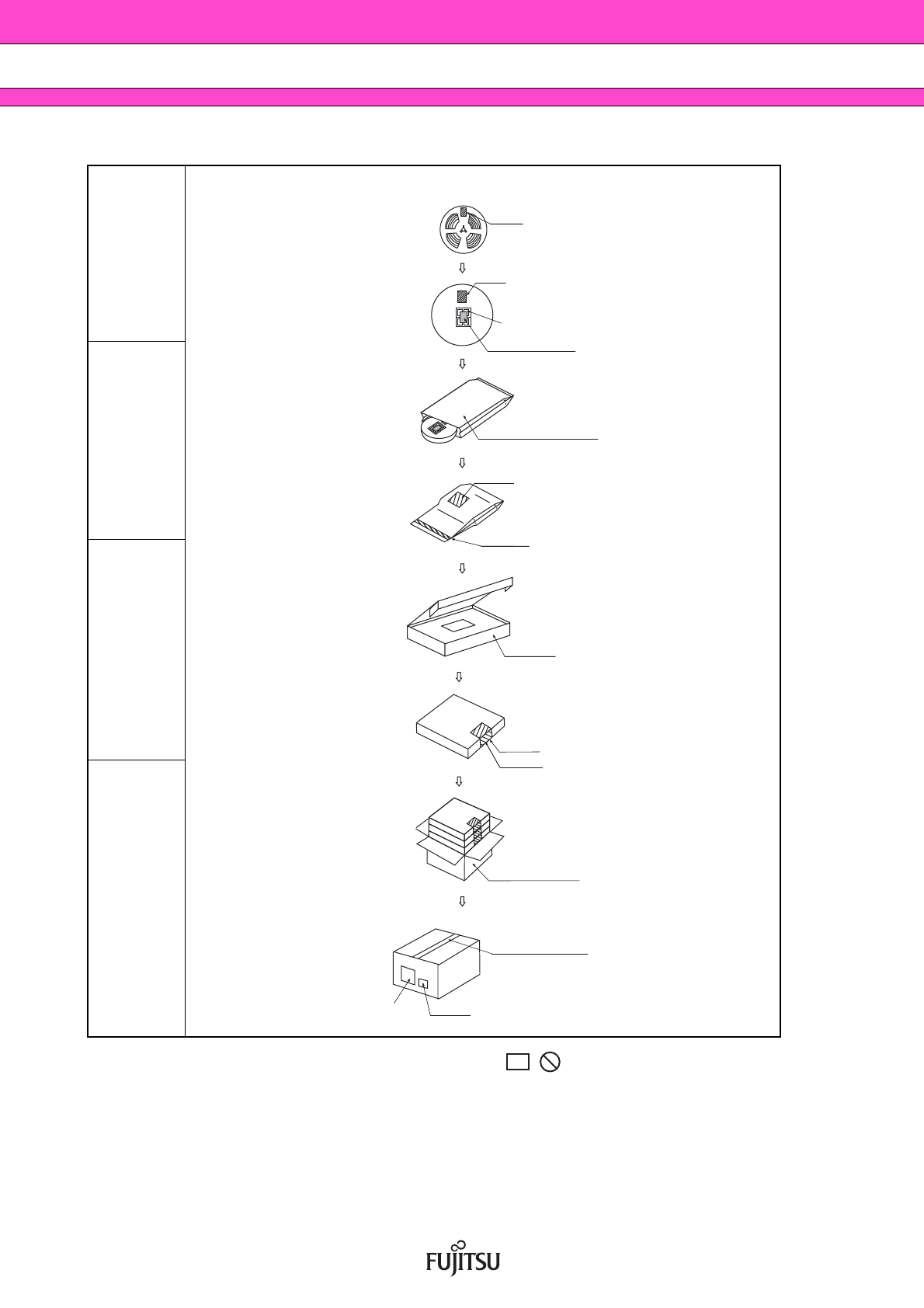
2.4 Taping (φ330mm Reel) Dry Pack Packing Specifications
*1:For a product of witch part number is suffixed with “E1”, a “ ” marks is display to the moisture barrier
bag and the inner boxes.
*2:The size of the outer box may be changed depending on the quantity of inner boxes.
*3:The space in the outer box will be filled with empty inner boxes, or cushions, etc.
*4:Please refer to an attached sheet about the indication label.
Note: The packing specifications may not be applied when the product is delivered via a distributer.
Embossed
tapes
Dry pack
Inner box
Outer box
Outside diameter: 330mm reel
Heat seal
Label I
*1, *4
Label II-B
*4
Label II-A
*4
Label I
*1, *4
Label I
*1, *4
Taping
Use adhesive tapes.
Outer box
*2, *3
φ
Inner box
Label I
*1, *4
Desiccant
Humidity indicator
Aluminum laminated bag
G
Pb
Page 32
MB85RS256B
32 DS501-00021-2v0-E
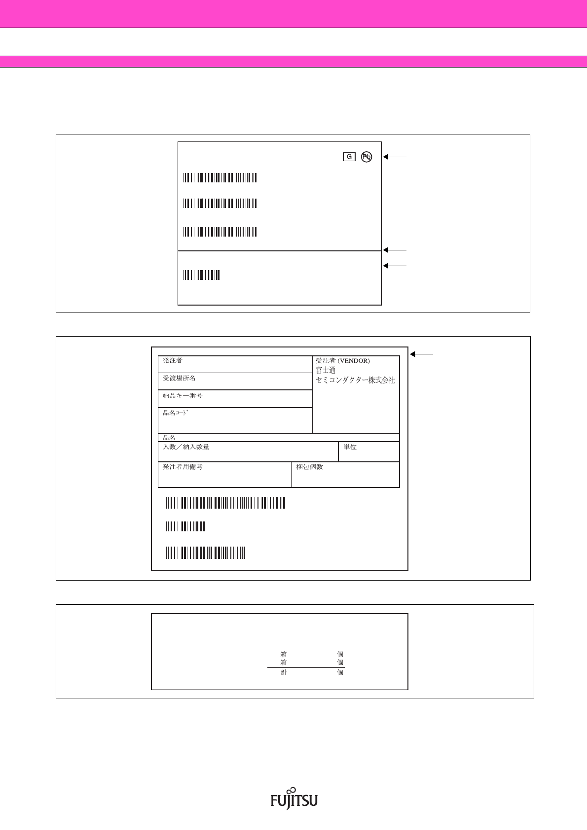
2.5 Product label indicators
Label I: Label on Inner box/Moisture Barrier Bag/ (It sticks it on the reel for the emboss taping)
[C-3 Label (50mm × 100mm) Supplemental Label (20mm × 100mm)]
Label II-A: Label on Outer box [D Label] (100mm × 100mm)
Label II-B: Outer boxes product indicate
Note: Depending on shipment state, “Label II-A” and “Label II-B” on the external boxe s might not be printed.
(Customer part number or FJ part number)
(Customer part number or FJ part number)
(FJ control number bar code)
XX/XX XXXX-XXX XXX
XXXX-XXX XXX
(Lot Number and quantity)
(Package count)
(Customer part number or FJ part number
bar code)
(Part number and quantity)
(FJ control number)
QC PASS
XXXXXXXXXXXXXX
XXXX/XX/XX (Packed years/month/day) ASSEMBLED IN xxxx
(3N)1 XXXXXXXXXXXXXX XXX
(Quantity)
(3N)2 XXXXXXXXXX
XXX pcs
XXXXXX
XXXXXXXXXXXXXX
(Customer part number or FJ part number)
XXXXXXXXXXXXXX
(Comment)
XXXXXXXXXXXXXX
(FJ control number )
XXXXXXXXXX
(LEAD FREE mark)
C-3 Label
Supplemental Label
Perforated line
XXXXXXXXXXXXX (Customer Name)
(CUST.)
XXX (FJ control number)
XXX (FJ control number)
XXX (FJ control number)
XXXXXXXXXXXXXX
(Part number)
(FJ control number + Product quantity)
(FJ control number + Product quantity
bar code)
(Part number + Product quantity bar code)
XXXXXXXXX (Delivery Address)
(DELIVERY POINT)
XXXXXXXXXXXXXX
(TRANS.NO.) (FJ control number)
XXXXXXXXXXXXXX
(PART NO.) (Customer part number or
FJ part number)
XXX/XXX
(Q’TY/TOTAL Q’TY)
XX
(UNIT)
(CUSTOMER'S
REMARKS)
XXXXXXXXXXXXXXXXXXXX
(PACKAGE COUNT)
XXX/XXX
(PART NAME) XXXXXXXXXXXXXX (Part number)
(3N)3 XXXXXXXXXXXXXX XXX
(Part number + Product quantity)
(3N)4 XXXXXXXXXXXXXX XXX
(FJ control number)
(FJ control number bar code)
(3N)5 XXXXXXXXXX
D Label
XXXXXXXXXXXXXX (Part number)
(Lot Number)
XXXX-XXX
XXXX-XXX
(Count) (Quantity)
X XXX
X XXX
XXX
Page 33
MB85RS256B
DS501-00021-2v0-E 33
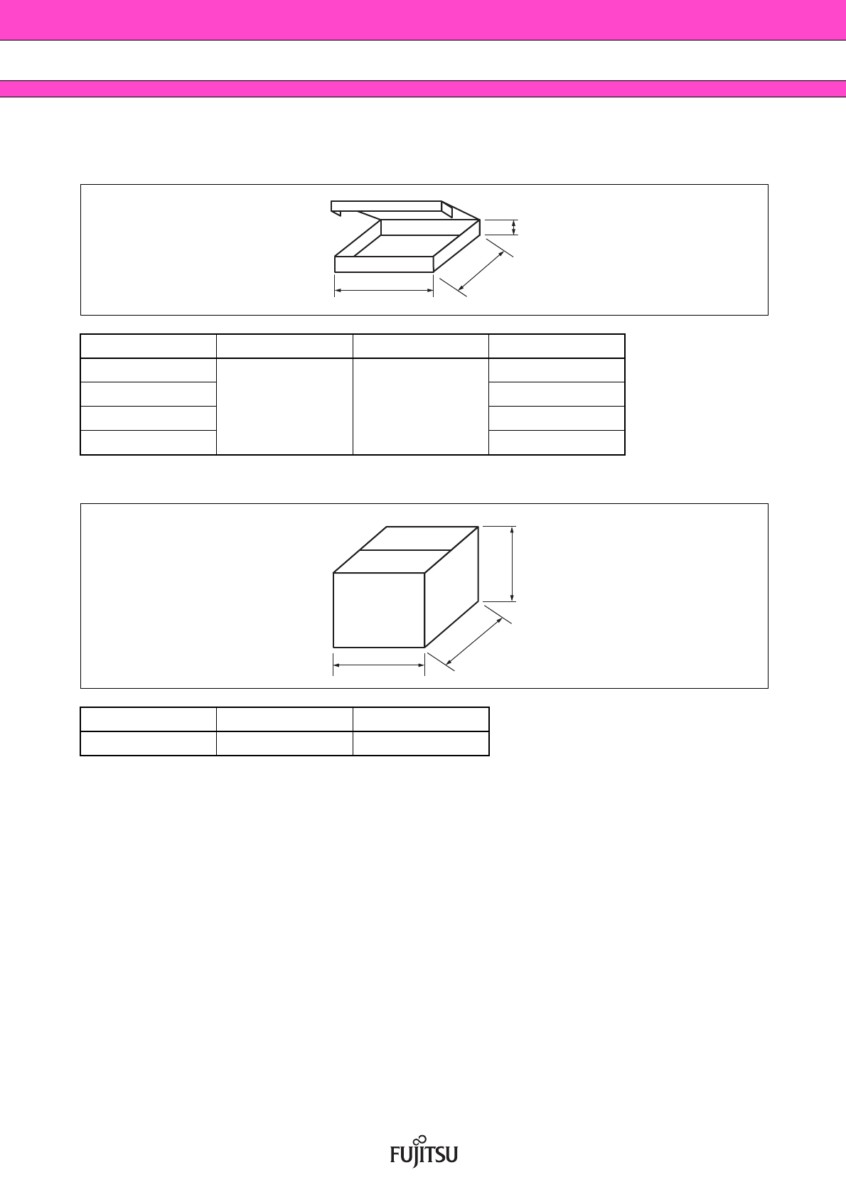
2.6 Dimensions for Containers
(1) Dimensions for inner box
(2) Dimensions for outer box
Ta pe width L W H
12, 16
365 345
40
24, 32 50
44 65
56 75
(Dimensions in mm)
LWH
415 400 315
(Dimensions in mm)
L
W
H
L
W
H
Page 34
MB85RS256B
34 DS501-00021-2v0-E
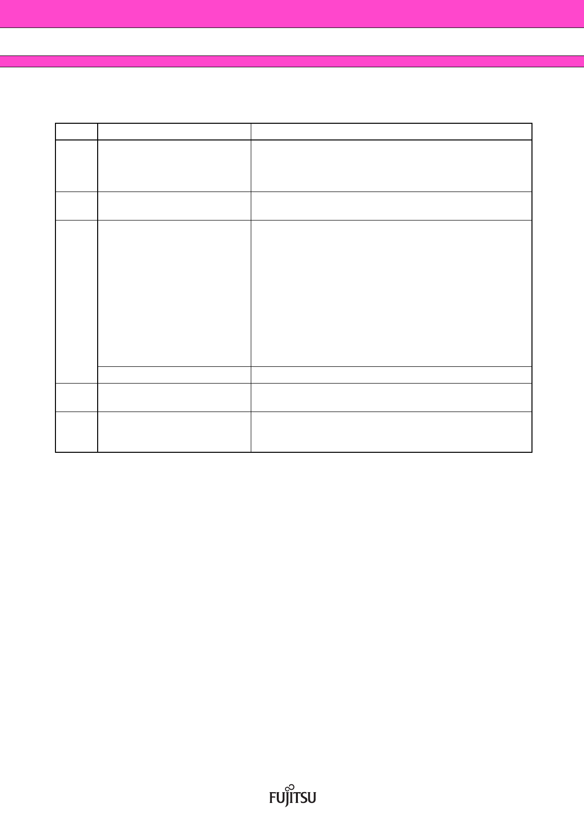
■ MAJOR CHANGES IN THIS EDITION
A change on a page is indicated by a vertical line drawn on the left side of that page.
Page Section Change Results
1
■ FEATURES Revised the Data retention
10 years ( + 85 °C)
→10 years ( + 85 °C), 95 years ( + 55 °C),
over 200 years ( + 35 °C)
10
■ COMMAND
• RDID
Deleted the following description:
“RDID command is applicable to “Up to 33 MHz operation”.”
17
■ POWER ON/OFF SEQUENCE Revised the following description:
“V
DD pin is required to be rising from 0 V because turning the
power on from an intermediate level may cause
malfunctions, when the power is turned on.”
→ “If V
DD falls down below 2.0 V, VDDin is required to be started
from 1.0 V or less to prevent malfunctions when the power is
turned on again (see the figure below).”
Moved the following description under the table:
“If the device does not operate within the specified conditions of
read cycle, write cycle or power on/off sequence, memory data
can not be guaranteed.”
■ FRAM CHARACTERISTICS Revised the table and Note
18
■ ESD AND LATCH-UP Revised the following description:
“occurred” → “occur”
21
■ RESTRICTED SUBSTANCES Revised the following description:
“the below regulations” → “the regulations below”
“as belows” → “as follows”
Page 35
MB85RS256B
DS501-00021-2v0-E 35
MEMO
Page 36

MB85RS256B
FUJITSU SEMICONDUCTOR LIMITED
Nomura Fudosan Shin-yokohama Bldg. 10-23, Shin-yokohama 2-Chome,
Kohoku-ku Yokohama Kanagawa 222-0033, Japan
Tel: +81-45-415-5858
http://jp.fujitsu.com/fsl/en/
For further information please contact:
North and South America
FUJITSU SEMICONDUCTOR AMERICA, INC.
1250 E. Arques Avenue, M/S 333
Sunnyvale, CA 94085-5401, U.S.A.
Tel: +1-408-737-5600 Fax: +1-408-737-5999
http://us.fujitsu.com/micro/
Europe
FUJITSU SEMICONDUCTOR EUROPE GmbH
Pittlerstrasse 47, 63225 Langen, Germany
Tel: +49-6103-690-0 Fax: +49-6103-690-122
http://emea.fujitsu.com/semiconductor/
Korea
FUJITSU SEMICONDUCTOR KOREA LTD.
902 Kosmo Tower Building, 1002 Daechi-Dong,
Gangnam-Gu, Seoul 135-280, Republic of Korea
Tel: +82-2-3484-7100 Fax: +82-2-3484-7111
http://kr.fujitsu.com/fsk/
Asia Pacific
FUJITSU SEMICONDUCTOR ASIA PTE. LTD.
151 Lorong Chuan,
#05-08 New Tech Park 556741 Singapore
Tel : +65-6281-0770 Fax : +65-6281-0220
http://sg.fujitsu.com/semiconductor/
FUJITSU SEMICONDUCTOR SHANGHAI CO., LTD.
30F , K erry Parkside, 1155 Fang Dian Road, Pudong District,
Shanghai 201204, China
Tel : +86-21-6146-3688 Fax : +86-21-6146-3660
http://cn.fujitsu.com/fss/
FUJITSU SEMICONDUCTOR PACIFIC ASIA LTD.
2/F, Green 18 Building, Hong Kong Science Pa rk,
Shatin, N.T., Hong Kong
Tel : +852-2736-3232 Fax : +852-2314-4207
http://cn.fujitsu.com/fsp/
Specifications are subject to change without notice. For further information please contact each office.
All Rights Reserved.
The contents of this document are subject to change without notice.
Customers are advised to consult with sales representatives before ordering.
The information, such as descriptions of function and application circuit examples, in this document are presented solely for the purpose
of reference to show examples of operations and uses of FUJITSU SEMICONDUCTOR device; FUJITSU SEMICONDUCTOR does
not warrant proper operation of the device with respect to use based on such information. When you develop equipment incorporating
the device based on such information, you must assume any responsibility arising out of such use of the information.
FUJITSU SEMICONDUCTOR assumes no liability for any damages whatsoever arising out of the use of the information.
Any information in this document, including descriptions of function and schematic diagrams, shall not be construed as license of the use
or exercise of any intellectual property right, such as patent right or copyright, or any other right of FUJITSU SEMICONDUCTOR or any
third party or does FUJITSU SEMICONDUCTOR warrant non-infringement of any third-party's intellectual property right or other right
by using such information. FUJITSU SEMICONDUCTOR assumes no liability for any infringement of the intellectual property rights or
other rights of third parties which would result from the use of information contained herein.
The products described in this document are designed, developed and manufactured as contemplated for general use, including without
limitation, ordinary industrial use, general office use, personal use, and household use, but are not designed, developed and manufactured
as contemplated (1) for use accompanying fatal risks or dangers that, unless extremely high safety is secured, could have a serious effect
to the public, and could lead directly to death, personal injury, severe physical damage or other loss (i.e., nuclear reaction control in
nuclear facility, aircraft flight control, air traffic control, mass transport control, medical life support system, missile launch control in
weapon system), or (2) for use requiring extremely high reliability (i.e., submersible repeater and artificial satellite).
Please note that FUJITSU SEMICONDUCTOR will not be liable against you and/or any third party for any claims or damages aris-
ing in connection with above-mentioned uses of the products.
Any semiconductor devices have an inherent chance of failure. You must protect against injury, damage or loss from such failures
by incorporating safety design measures into your facility and equipment such as redundancy, fire protection, and prevention of over-
current levels and other abnormal operating conditions.
Exportation/release of any products described in this document may require necessary procedures in accordance with the regulations
of the Foreign Exchange and Foreign Trade Control Law of Japan and/or US export control laws.
The company names and brand names herein are the trademarks or registered trademarks of their respective owners.
Edited: Sales Promotion Department
 Loading...