

Page 1

FUJITSU SEMICONDUCTOR
SUPPORT SYSTEM
SS01-00027-1E
F2MC Family
BGM ADAPTER
MB2146-09B-E
OPERATION MANUAL
Page 2

PREFACE
Thank you for purchasing the F2MC * family BGM adapter (model number: MB2146-09B-E).
The product is a development support tool for developing and evaluating applied products which use
FUJITSU SEMICONDUCTOR microcontrollers (hereafter MCUs) that have a BDSU module.
This manual describes how to handle the F
the product.
For information on the MCUs supported by this product, contact the their sales or support representative.
* : F
■ For your safety
This manual contains important information required for using the product safely. Be sure to read
through the manual before using the product and follow the instructions contained therein to use it
correctly.
In particular, carefully read “■ Caution of the products described in this manual” at the beginning
of this manual to understand the requirements for safe use of the product before using it.
After reading the manual, keep it handy for future reference.
■ Related manuals
You should refer to the following manuals as well:
2
MC family BGM adapter. Be sure to read it before using
2
MC is the abbreviation of FUJITSU Flexible Microcontroller.
• “HARDWARE MANUAL” for each type of microcontroller
• “DATA SHEET” for each type of microcontroller
• “S
OFTUNE Workbench OPERATION MANUAL”
• “S
OFTUNE Workbench USER’S MANUAL”
• “S
OFTUNE Workbench COMMAND REFERENCE MANUAL”
■ European RoHS compliance
Products with a -E suffix on the part number are European RoHS compliant products.
■ Notice on this document
All information included in this document is current as of the date it is issued. Such information is
subject to change without any prior notice.
Please confirm the latest relevant information with the sales representatives.
i
i
Page 3
■ Caution of the products described in this document
The following precautions apply to the product described in this manual.
WARNING
Electric shock,
Damage
Electric shock,
Damage
CAUTION
Cuts, Damage
Indicates a potentially hazardous situation which, if not avoided appropriately,
could result in death or serious injury and/or a fault in the user’s system.
Before performing any operation described in this manual, turn off all the power
supplies to the system. Performing such an operation with the power on may
cause an electric shock or device fault.
Once the product has been turned on, do not touch any metal part of it.
Doing so may cause an electric shock or device fault.
Indicates a potentially hazardous situation which, if not avoided appropriately, may
result in minor or moderate injury and/or damage to the product or the equipment
to which the product is connected, to software resources such as data, or to other
properties.
Before moving the product, be sure to turn off all the power supplies and unplug the
cables. Watch your steps when carrying the product. Do not use the product at an
unstable location such as a place exposed to strong vibration or a sloping surface.
Doing so may let the product fall, resulting in an injury or fault.
Damage
Damage
Damage
Damage
Damage
Damage
Damage
Neither put anything on or apply shock to the product. Once the product has been
powered, do not carry it. Doing either may cause a fault due to a load or shock.
Since the product contains many electronic components, keep it away from direct
sunlight, high temperature, and high humidity to prevent condensation. Do not use
or store the product where it is exposed to much dust or a strong magnetic or electric field for an extended period of time.
An adverse operating or storage environment can cause a fault.
Use the product within the ranges of its general specifications.
Operating it outside the range of any general specification may cause a fault.
To prevent electrostatic breakdown, do not let your finger or an object touch any
metal part of the connector. Before handling the product, touch a metal object (such
as a door knob) to discharge static electricity from your body.
Before turning the power on, be sure to finish making all the required connections.
To set up and use the product, follow the instructions given in this document.
Using the product incorrectly or inappropriately may cause a fault.
Before plugging or unplugging any cable for this product, be sure to turn the power
supply off. When unplugging the cable, remove it while holding the connector without pulling the cable itself. Pulling the cable itself or bending it may expose or disconnect the cable core, resulting in a fault.
Re-transporting the product may damage it to cause a fault. Keep the packaging
materials used for shipment of the product and use them when re-transporting it.
ii
Page 4

Copyright ©2010 FUJITSU SEMICONDUCTOR LIMITED All rights reserved
• The contents of this document are subject to change without notice.
Customers are advised to consult with sales representatives before ordering.
• The information, such as descriptions of function and application circuit examples, in this document are presented solely for the purpose of reference to show examples of operations and uses of FUJITSU SEMICONDUCTOR semiconductor device; FUJITSU SEMICONDUCTOR does not warrant proper operation of the device with respect to use
based on such information. When you develop equipment incorporating the device based on such information, you
must assume any responsibility arising out of such use of the information. FUJITSU SEMICONDUCTOR assumes no
liability for any damages whatsoever arising out of the use of the information.
• Any information in this document, including descriptions of function and schematic diagrams, shall not be construed
as license of the use or exercise of any intellectual property right, such as patent right or copyright, or any other right
of FUJITSU SEMICONDUCTOR or any third party or does FUJITSU SEMICONDUCTOR warrant non-infringement of any third-party's intellectual property right or other right by using such information. FUJITSU SEMICONDUCTOR assumes no liability for any infringement of the intellectual property rights or other rights of third parties
which would result from the use of information contained herein.
• The products described in this document are designed, developed and manufactured as contemplated for general use,
including without limitation, ordinary industrial use, general office use, personal use, and household use, but are not
designed, developed and manufactured as contemplated (1) for use accompanying fatal risks or dangers that, unless
extremely high safety is secured, could have a serious effect to the public, and could lead directly to death, personal
injury, severe physical damage or other loss (i.e., nuclear reaction control in nuclear facility, aircraft flight control, air
traffic control, mass transport control, medical life support system, missile launch control in weapon system), or (2)
for use requiring extremely high reliability (i.e., submersible repeater and artificial satellite).
Please note that FUJITSU SEMICONDUCTOR will not be liable against you and/or any third party for any claims or
damages arising in connection with above-mentioned uses of the products.
• Any semiconductor devices have an inherent chance of failure. You must protect against injury, damage or loss from
such failures by incorporating safety design measures into your facility and equipment such as redundancy, fire protection, and prevention of over-current levels and other abnormal operating conditions.
• Exportation/release of any products described in this document may require necessary procedures in accordance with
the regulations of the Foreign Exchange and Foreign Trade Control Law of Japan and/or US export control laws.
• The company names and brand names herein are the trademarks or registered trademarks of their respective owners.
iii
i
Page 5
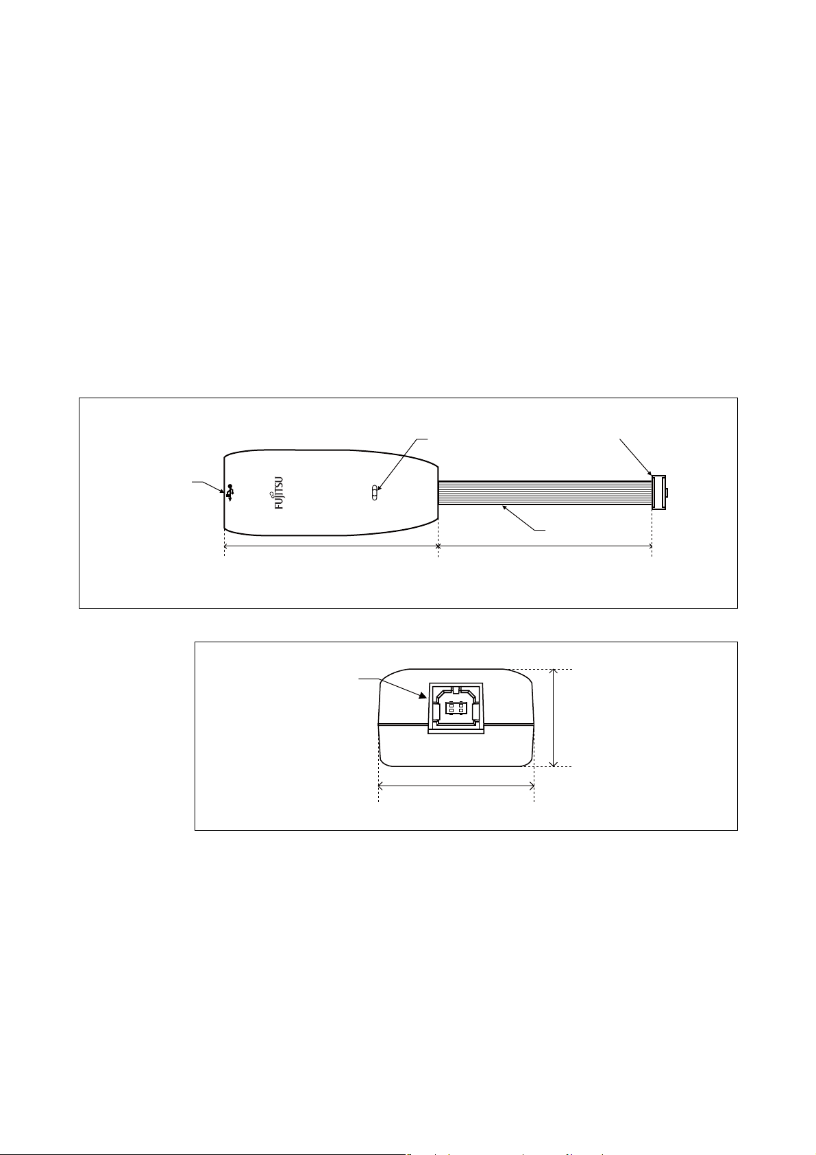
1. Checking the Delivered Product
Interface cable
User interface
connector
USB connector
POWER LED
100mm
100mm
25mm
USB connector
40mm
Before using the product, make sure that the package contains the following items:
• BGM adapter*: 1
• USB cable (2.0m): 1
• Operation manual (Japanese version): 1
• Operation manual (English version - This document): 1
* : Referred to as the adapter.
2. Optional Parts
A variety of optional parts are available for this adapter that may be purchased separately as needed.
Consult a their sales or support representative for details.
3. Appearance and Part Names
Figures 1 and 2 show the adapter appearance, major dimensions and part names.
Figure 1 Adapter appearance (top view)
Figure 2 Adapter appearance (front view)
1
Page 6

4. System Configuration
Host
computer
Adapter
User
interface
connector
Adapter
interface
connector
MCU
User system
*1
*2
*1 : USB cable
*2 : Interface cable (flat cable of the adapter)
Host
computer
Adapter
User
interface
connector
Adapter
interface
connector
MCU with
built-in flash
memory
User system
*1
*2
*1 : USB cable
*2 : Interface cable (flat cable of the adapter)
■ Using the adapter as an emulator system
Connect the adapter between the host computer and the user system so that the adapter can serve as
an emulator under control of the host computer. For using emulator debugger software on the host
computer, refer to the "S
Figure 3 shows the system configuration when the adapter is used as an emulator system.
Figure 3 System configuration (emulator system)
■ Using the adapter as a USB programmer
The adapter connects the host computer and the serial interface of MCU with built-in flash memory
made by FUJITSU SEMICONDUCTOR, and writes data in a built-in flash memory.
For information on the USB programmer, contact the their sales or support representative.
Figure 4 shows the system configuration when the adapter is used as a USB programmer.
OFTUNE Workbench OPERATION MANUAL".
Figure 4 System configuration (USB programmer)
2
Page 7

5. Connections
Connection to the USB
connector of the adapter
Adapter
Adapter
User interface connector
User system
Index mark (pin 1)
Adapter interface connector on the user system
■ Connection to the host computer
Connect the adapter to the host computer using the USB cable.
Figure 5 shows how to connect the USB cable.
■ Connection to the user system
Connect the adapter to the user system.
Plug the user interface connector of the adapter into the adapter interface connector on the user system.
When connecting the user interface connector, align the index marks (pin 1) on each of the connectors.
For the specifications of the adapter interface connector, see “■ Adapter interface specifications” in
Section 6 “Specifications”.
Figure 6 shows how to connect the adapter to the user system.
Figure 5 Connecting the USB cable
Figure 6 Connecting to the user system
3
Page 8

6. Specifications
■ General specifications
Table 1 lists the general specifications of the adapter.
Item Specification
Table 1 General specifications
Name
2
F
MC family BGM adapter
Model number MB2146-09B-E
Power supply
specifications
Adapter power input Max: 50mA (uses USB BUS power)
User power input
+ 2.7V to + 5.5V *
1
, Max: 20mA*
[Green]: On when only adapter power is supplied
POWER LED indication
[Red]: On when only user power is supplied.
(with the USB cable connected).
[Orange]:On when both adapter power and user power are supplied.
User interface connector *
3
MIL standard compliant key type (with center key)
Operating temperature / humidity +5 °C to +35 °C / 20% to 80% (no condensation)
Storage temperature / humidity 0 °C to +70 °C / 20% to 80% (no condensation)
Adapter case: 40mm (W) × 100mm (D) × 25mm (H) (excluding protrusions)
Dimensions
Interface cable length: 100mm (excluding user interface connector)
Weight 55g
*1 : The maximum and minimum voltages depends on the MCU used.
For details, contact the their sales or support representative.
*2 : Does not include the power consumption of the MCU.
*3 : The part number of the connector is: FAS-1001-2101-0BF (Yamaichi Electronics Co., Ltd.)
2
■ USB line specifications
Table 2 lists the USB line specifications of the adapter.
Conforming standard USB1.1
Communication method Full speed bulk transfer
Data transfer rate 12Mbps
Connector shape Series B
Power supply BUS Powered
Table 2 USB line specifications
Item Description
4
Page 9

■ Tool reset specifications
A tool reset is a hardware reset by the adapter to reset the entire system of the MCU (including the
BDSU module) on the user system.
When both of the adapter power and MCU’s user power are turned on, the tool reset is canceled automatically to enable the MCU to be evaluated.
The following shows how to generate a tool reset and how long it remains in effect.
• Tool reset generation methods and reset “L” pulse width
1. Turn the MCU user power from “OFF” to “ON” (power-on reset).
The reset remains in effect for about 16ms to 70ms after the MCU user power is supplied.
2. Turn the adapter power from “OFF” to “ON” (by unplugging and plugging the USB cable).
The reset remains in effect for about 32ms to 140ms after the adapter power is supplied.
If an uncontrollable malfunction occurs in the user system and adapter that cannot be recovered using
tool reset generation method 1, execute tool reset generation method 2.
5
Page 10

■ Adapter interface specifications
The pinouts of the adapter interface connectors mounted on the user system are shown in Tables 3
and 4. The recommended connectors are listed in Table 5, and the pin configuration is shown in Figure 7.
When the adapter interface connector is mounted on the user system, connect the MCU to the adapter
interface connector according to the following specifications.
Table 3 Adapter interface connector pinout (emulator system)
Connector
pin
number
1
Input / output
BGMA *
1
← MCU *
Evaluation MCU
connection
pin name
2
UVCC User power supply input Connected to the MCUs Vcc pin.
Function Remarks
2 - GND Vss pin Connected to the MCUs Vss pin.
3 BGMA → MCU TRESETX Tool reset output
4 BGMA → MCU DMDX Mode change output
BDSU, Initialization of users logic,
open collector output
0: Debug mode
1: Free run mode
5 BGMA ← MCU SOUT Serial data input SD for UART
6 BGMA ← MCU EXC External clock input Base clock for UART
7 BGMA → MCU SIN Serial data output RD for UART
8 - NC - Not used and not connected
9 - GND Vss pin Connected to the MCUs Vss pin.
10 BGMA ← MCU UVCC User power supply input Connected to the MCUs Vcc pin.
*1 : “BGMA” represents the BGM adapter.
*2 : “MCU” represents the evaluation MCU.
Table 4 Adapter interface connector pinout (USB programmer)
Connector
pin
number
1
Input / output
BGMA *
1
← MCU *
Evaluation MCU
connection
pin name
2
UVCC User power supply input Connected to the MCUs Vcc pin.
Function Remarks
2 - GND Vss pin Connected to the MCUs Vss pin.
3BGMA → MCU RSTX Tool reset output
BDSU, Initialization of users logic,
open collector output
4 - NC Mode change output Not used and not connected
5BGMA ← MCU
6BGMA → MCU
7BGMA → MCU
UCKx *
UOx *
UIx *
3
3
Serial data input SD for UART
3
Synchronous clock output Base clock for UART
Serial data output RD for UART
8 - NC - Not used and not connected
9 - GND Vss pin Connected to the MCUs Vss pin.
10 BGMA ← MCU UVCC User power supply input Connected to the MCUs Vcc pin.
*1 : “BGMA” represents the BGM adapter.
*2 : “MCU” represents the evaluation MCU.
*3 : Refer to the specifications of each of the MCUs for the serial port number that corresponds to the serial interface
for the USB programmer.
6
Page 11

Table 5 Recommended adapter interface connectors
Index mark
10pin
9pin
2pin
1pin
(TOP VIEW)
* : The pin names of the user interface connector show the pin names to connect to the evaluation
MCU on the emulator system.
To internal adapter
control CPU
User interface
connector*
To supply voltage
monitoring IC
Part number Specifications Manufacturer
FAP-1001-2202-0BF Right-angle solder dip Housing provided, Middle latch provided
FAP-1001-2204-0BF Straight solder dip Housing provided, Middle latch provided
FAP-10-08#2-0BF Right-angle solder dip Housing provided, Latch not provided
FAP-10-08#4-0BF Straight solder dip Housing provided, Latch not provided
Figure 7 Adapter interface connector pin configuration
UVCC
Yamaichi Electronics
Co., Ltd.
10kΩ 10kΩ
+3.3V
TC7MBD3244AFK
Figure 8 User interface circuitry
10kΩ 10kΩ
+5V
10kΩ
NNCD5.6LH-A
3
TRESETX
5
SOUT
6
EXC
7
SIN
7
Page 12

Connector
pin number
Circuit type
Table 6 DC specifications of the user interface
I
OH*
(mA)
1
IOL*2
(mA)
I
LI*
(μA)
3
Resistor connection Remarks
3 Open drain output -
64.0 *
4
5CMOS input - -
7CMOS output
- 2.0 *
- 2.0 *
4
4
4.0 *
4.0 *
4
4
1 *
± 5 *
± 5 *
Connected to UVCC
4
by 10kΩ
4
4
See Figure 86 CMOS input/output
-
*1 : The “H” level output current.
*2 : The “L” level output current.
*3 : The input leakage current.
*4 : Does not include the current through the pull-up resistance.
*5 : The voltage monitoring IC controls the on/off connection to the GND via bus switch.
Connected to GND via
bus switch*
5
8
Page 13

SS01-00027-1E
FUJITSU SEMICONDUCTOR • SUPPORT SYSTEM
2
F
MC Family
BGM ADAPTER
MB2146-09B-E
OPERATION MANUAL
April 2010 the first edition
Published FUJITSU SEMICONDUCTOR LIMITED
Edited Sales Promotion Department
Page 14

 Loading...