

Page 1

FUJITSU SEMICONDUCTOR
DATA SHEET
ASSP
Dual Serial Input
PLL Frequency Synthesizer
MB15F72UL
DESCRIPTION
■■■■
The Fujitsu MB15F72UL is a serial input Phase Locked Loop (PLL) frequency synthesizer with a 1300 MHz and
a 350 MHz prescalers. A 64/65 or a 128/129 for the 1300 MHz prescaler, and a 8/9 or a 16/17 for the 350 MHz
prescaler can be selected for the prescaler that enables pulse swallow operation.
The BiCMOS process is used, as a result a supply current is typically 2.5 mA at 2.7 V. The supply voltage range
is from 2.4 V to 3.6 V. A refined charge pump supplies well-balanced output current with 1.5 mA and 6 mA
selectable by serial data. The data fo rmat is the same as the previous one MB15F02SL, MB12F72SP. Fast loc king
is achieved for adopting the new circuit.
The new package (BCC20) decreases a mount area of MB15F72UL more than 30% comparing with the former
BCC16 (for dual PLL) .
DS04-21367-1E
MB15F72UL is ideally suited for wireless mobile communications, such as CDMA.
FEATURES
■■■■
• High frequency operation : RF synthesizer : 1300 MHz Max.
: IF synthesizer : 350 MHz Max.
• Low power supply voltage : V
• Ultra low power supply current : ICC = 2.5 mA Typ.
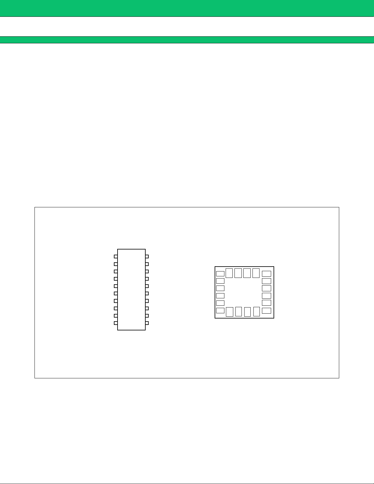
PACKAGES
■■■■
20-pin plastic TSSOP 20-pad plastic BCC
(FPT-20P-M06) (LCC-20P-M05)
CC = 2.4 to 3.6 V
(VCC = Vp = 2.7 V, SWIF = SWRF = 0, Ta = +25 °C, in IF, RF locking state)
(Continued)
Page 2
MB15F72UL
(Continued)
• Direct power saving function : Power supply current in power saving mode
Typ. 0.1 µA (VCC = Vp = 2.7 V, Ta = +25 °C)
Max. 10 µA (V
• Software selectable charge pump current : 1.5 mA/6.0 mA Typ.
• Dual modulus prescaler : 1300 MHz prescaler (64/65 or 128/129 ) /350 MHz prescaler (8/9 or 16/17)
• 23 bit shift resister
• Serial input 14-bit programmable reference divider : R = 3 to 16,383
• Serial input programmable divider consisting of :
- Binary 7-bit swallow counter : 0 to 127
- Binary 11-bit programmable counter : 3 to 2,047
•On−chip phase control for phase comparator
•On−chip phase comparator for fast lock and low noise
• Built-in digital locking detector circuit to detect PLL locking and unlocking.
• Operating temperature : Ta = −40 °C to +85 °C
• Serial data format compatible with MB15F02SL
• Small package BCC20 (3.4 mm × 3.6 mm × 0.6 mm)
PIN ASSIGNMENTS
■■■■
CC = Vp = 2.7 V)
(TSSOP-20)
TOP VIEW
fin
PSIF
VpIF
DoIF
1
2
3
IF
4
5
6
7
8
9
10
OSCIN
GND
XfinIF
GNDIF
VCCIF
LD/fout
(FPT-20P-M06)
20
19
18
17
16
15
14
13
12
11
Clock
Data
LE
fin
RF
XfinRF
GNDRF
VCCRF
PSRF
VpRF
Do
RF
finIF
XfinIF
GND
VCCIF
PSIF
VpIF
(BCC-20)
TOP VIEW
OSCIN
GND
1
19 18
20
2
3
IF
4
5
6
7
DoIF
LD/fout
(LCC-20P-M05)
8
Clock
9
Do
RF
Data
17
10
VpRF
16
15
14
13
12
11
LE
fin
RF
XfinRF
GNDRF
VCCRF
PSRF
2
Page 3

PIN DESCRIPTION
■■■■
MB15F72UL
Pin no.
TSSOP BCC
119OSC
Pin name I/O Descriptions
The programmable reference divider input. TCXO should be connected with an
I
IN
AC coupling capacitor.
220GND Ground for OSC input buffer and the shift register circuit.
31fin
42Xfin
53GND
64V
IF
IF
IF
CCIF
Prescaler input pin for the IF-PLL.
I
Connection to an external VCO should be via AC coupling.
Prescaler complimentary input pin for the IF-PLL section.
I
This pin should be grounded via a capacitor.
Ground for the IF-PLL section.
Power supply voltage input pin for the IF-PLL section (except for the charge
pump circuit) , the OSC input buffer and the shift register circuit.
Power saving mode control for the IF-PLL section. This pin must be set at “L”
75PS
86Vp
97D
I
IF
Power supply voltage input pin for the IF-PLL charge pump.
IF
OIF
when the power supply is started up. (Open is prohibited.)
PS
= “H” ; Normal mode / PSIF = “L” ; Power saving mode
IF
O Charge pump output pin for the IF-PLL section.
Lock detect signal output (LD) /phase comparator monitoring
10 8 LD/fout O
output (fout) pins.The output signal is selected by LDS bit in the serial data.
LDS bit = “H” ; outputs fout signal / LDS bit = “L” ; outputs LD signal
11 9 D
12 10 Vp
ORF
O Charge pump output pin for the RF-PLL section.
Power supply voltage input pin for the RF-PLL charge pump.
RF
Power saving mode control pin for the RF-PLL section. This pin must be set at
13 11 PS
14 12 V
CCRF
15 13 GND
16 14 Xfin
17 15 fin
RF
RF
RF
I
“L” when the power supply is started up. (Open is prohibited.)
PS
= “H” ; Normal mode / PSRF = “L” ; Power saving mode
RF
Power supply voltage input pin for the RF-PLL section (except for the charge
pump circuit)
Ground for the RF-PLL section
RF
Prescaler complimentary input pin for the RF-PLL section.
I
This pin should be grounded via a capacitor.
Prescaler input pin for the RF-PLL.
I
Connection to an external VCO should be via AC coupling.
Load enable signal input pin (with the schmitt trigger circuit)
18 16 LE I
When LE is set “H”, data in the shift register is transferred to the
corresponding latch according to the control bit in the serial data.
Serial data input pin (with the schmitt trigger circuit)
19 17 Data I
Data is transferred to the corresponding latch (IF-ref. counter, IF-prog. counter,
RF-ref. counter, RF-prog. counter) according to the control bit in
the serial data.
20 18 Clock I
Clock input pin for the 23-bit shift register (with the schmitt trigger circuit)
One bit of data is shifted into the shift register on a rising edge of the clock.
3
Page 4

MB15F72UL
■■■■ BLOCK DIA GRAM
PSIF
finIF
XfinIF
OSCIN
finRF
XfinRF
7
(5)
3
(1)
4
(2)
1
(19)
(15)
17
16
( )
14
Intermittent
mode control
(IF-PLL)
Prescaler
(IF-PLL)
(8/9, 16/17
OR
Prescaler
(RF-PLL)
(64/65, 128/129)
3 bit latch
LDS
SWIF
7 bit latch 11 bit latch
Binary 7-bit
swallow counter
FCIF
(IF-PLL)
Binary 11-bit
programmable
counter (IF-PLL)
2 bit latch 14 bit latch 1 bit latch
T1 T2
Binary 14-bit pro-
grammable ref.
counter(IF-PLL)
C/P setting
counter
frIF
frRF
T1 T2
Binary 14-bit pro-
grammable ref.
counter (RF-PLL))
C/P setting
counter
2 bit latch 14 bit latch 1 bit latch
VCCIF GNDIF
(4)
6 5
fpIF
Phase
comp.
(IF-PLL)
(3)
Lock Det.
(IF-PLL)
LDIF
AND
LD
RF
Lock Det.
(RF-PLL)
VpIF
8
Charge
pump
(IF-PLL)
(6)
Current
Tuning
Selector
LD
frIF
frRF
fpIF
fpRF
Switch
Fast
lock
(7)
10
(8)
9
DoIF
LD/
fout
PSRF
LE
Data
Clock
13
(11)
18
(16)
(17)
19
20
(18)
Intermittent
mode control
(RF-PLL)
Schmitt
circuit
Schmitt
circuit
Schmitt
circuit
Latch selector
C
C
N
N
23-bit shift register
1
2
LDS
SWRF
3 bit latch
Binary 7-bit
swallow counter
FCRF
(RF-PLL)
7 bit latch 11 bit latch
Binary 11-bit
programmable
counter (RF-PLL)
(20)2 14
GND
Phase
comp.
(RF-PLL)
fpRF
(12) (13) (10)
V
CCRF
15 12
GNDRF
Tuning
Fast lock
Charge
pump
(RF-PLL)
VpRF
Current
Switch
11
(9)
DoRF
O : TSSOP
( ) : BCC
4
Page 5

■■■■ ABSOLUTE MAXIMUM RATINGS
MB15F72UL
Parameter Symbol
Unit
Min. Max.
Rating
CC −0.5 4.0 V
V
Power supply voltage
Vp V
Input voltage V
I −0.5 VCC + 0.5 V
CC 4.0 V
LD/fout VO GND VCC V
Output voltage
Do
IF, DoRF VDO GND Vp V
Storage temperature Tstg −55 +125 °C
WARNING: Semiconductor devices can be permanently damaged by application of stress (voltage, current,
temperature, etc.) in excess of absolute maximum ratings. Do not exceed these ratings.
■■■■ RECOMMENDED OPERATING CONDITIONS
Parameter Symbol
Min. Typ. Max.
V
CC 2.4 2.7 3.6 V VCCRF = VCCIF
Power supply voltage
Vp VCC 2.7 3.6 V
Input voltage V
I GND VCC V
Operating temperature Ta −40 +85 °C
Value
Unit Remarks
Note : • VCCRF, VpRF, VCCIF and VpIF must supply equal voltage.
Even if either RF-PLL or IF-PLL is not used, power must be supplied to V
CCRF, VpRF, VCCIF and VpIF to keep
them equal.
It is recommended that the non-use PLL is controlled by power saving function.
• Although this device contains an anti-static element to prevent electrostatic breakdown and the circuitry
has been improved in electrostatic protection, observe the f ollowing precautions when handling the device .
• When storing and transporting the device, put it in a conductive case.
• Before handling the de vice, confirm the (jigs and) tools to be used have been uncharged (grounded) as
well as yourself. Use a conductive sheet on working bench.
• Before fitting the device into or removing it from the socket, turn the power supply off.
• When handling (such as transporting) the device mounted board, protect the leads with a conductive
sheet.
WARNING: The recommended operating conditions are required in order to ensure the normal operation of the
semiconductor device. All of the device’s electrical characteristics are warranted when the device is
operated within these ranges.
Always use semiconductor devices within their recommended operating condition ranges. Operation
outside these ranges may adversely affect reliability and could result in device failure.
No warranty is made with respect to uses, operating conditions, or combinations not represented on
the data sheet. Users considering application outside the listed conditions are advised to contact their
FUJITSU representatives beforehand.
5
Page 6

MB15F72UL
ELECTRICAL CHARACTERISTICS
■■■■
Parameter
Power supply current
Power saving current
Operating frequency
fin
IF
fin
RF
OSC
Sym-
bol
I
CCIF
I
CCRF
I
PSIF
I
PSRF
*3
finIFIF PLL 50 350 MHz
*3
finRFRF PLL 100 1300 MHz
f
IN
OSC
(VCC = 2.4 V to 3.6 V, Ta = −40 °C to +85 °C)
Condition
Min. Typ. Max.
finIF = 270 MHz
*1
V
= VpIF = 2.7 V
CCIF
finRF = 910 MHz
*1
V
= VpRF = 2.7 V
CCRF
0.6 1.0 1.7 mA
1.0 1.5 2.5 mA
PSIF = PSRF = “L” 0.1
PSIF = PSRF = “L” 0.1
3 40 MHz
Value
*2
*2
Unit
10 µA
10 µA
Input sensitivity
“H” level input voltage
fin
IF
fin
RF
OSC
Data,
PfinIFIF PLL, 50 Ω system −15 +2dBm
PfinRFRF PLL, 50 Ω system −15 +2dBm
V
IN
LE,
“L” level input voltage V
“H” level input voltage
“L” level input voltage V
“H” level input current
Clock
PS
IF
PS
RF
Data,
LE,
,
I
Clock,
PS
,
“L” level input current I
PS
IF
RF
“H” level input current
OSC
IN
“L” level input current I
“H” level output voltage
V
LD/fout
“L” level output voltage V
“H” level output voltage
Do
Do
IF
RF
V
,
“L” level output voltage V
OSC
V
Schmitt trigger input 0.7 VCC + 0.4 V
IH
Schmitt trigger input 0.3 VCC − 0.4 V
IL
V
IH
IL
*4
IH
*4
IL
I
IH
*4
IL
VCC = Vp = 2.7 V,
OH
I
= −1 mA
OH
OLVCC
DOH
DOL
= Vp = 2.7 V, IOL = 1 mA 0.4 V
VCC = Vp = 2.7 V,
I
= −0.5 mA
DOH
VCC = Vp = 2.7 V,
I
= 0.5 mA
DOL
0.5 V
0.7 V
CC
V
0.3 V
−1.0 +1.0 µA
−1.0 +1.0 µA
0 +100 µA
−100 0 µA
− 0.4 V
V
CC
Vp − 0.4 V
0.4 V
CC
CC
VP −
V
P
High impedance
cutoff current
Do
Do
,
IF
RF
“H” level output current
LD/fout
“L” level output current I
6
VCC = Vp = 2.7 V
I
OFF
V
= 0.5 V to Vp − 0.5 V
OFF
*4
I
VCC = Vp = 2.7 V −1.0 mA
OH
VCC = Vp = 2.7 V 1.0 mA
OL
2.5 nA
(Continued)
Page 7

(Continued)
Parameter Symbol Condition
MB15F72UL
(VCC = 2.4 V to 3.6 V, Ta = −40 °C to +85 °C)
Value
Unit
Min. Typ. Max.
“H” level output
current
“L” level output
current
Charge pump
current rate
*8
Do
IF
I
Do
RF
Do
IF
Do
RF
I
DOL/IDOHIDOMT
vs. V
vs.Ta I
DOH
*8
I
DOL
DOIDOVD
DOTA
VCC = Vp = 2.7 V,
*4
V
= Vp / 2,
DOH
Ta = +25 °C
VCC = Vp = 2.7 V,
V
= Vp / 2,
DOL
Ta = +25 °C
*5
VDO = Vp / 2 3 %
*6
0.5 V ≤ VDO ≤ Vp − 0.5 V 10 %
−40 °C ≤ Ta ≤ +85 °C,
*7
V
= Vp / 2
DO
CS bit = “H” −8.2 −6.0 −4.1 mA
CS bit = “L” −2.2 −1.5 −0.8 mA
CS bit = “H” 4.1 6.0 8.2 mA
CS bit = “L” 0.8 1.5 2.2 mA
5 %
*1 : Conditions ; fosc = 12.8 MHz, Ta = +25 °C, SW = “L” in locking state.
*2 : V
PS
= VpIF = V
CCIF
= PSRF = GND, VIH = VCC VIL = GND (at CLK, Data, LE)
IF
= VpRF = 2.7 V, fosc = 12.8 MHz, Ta = +25 °C, in power saving mode
CCRF
*3 : AC coupling. 1000 pF capacitor is connected under the condition of Min. operating frequency.
*4 : The symbol “–” (minus) means the direction of current flow.
*5 : V
*6 : V
*7 : V
= Vp = 2.7 V, Ta = +25 °C (||I3| − |I4||) / [ (|I3| + |I4|) / 2] × 100 (%)
CC
= Vp = 2.7 V, Ta = +25°C [ (||I2| − |I1||) / 2] / [ (|I1| + |I2|) / 2] × 100 (%) (Applied to both l
CC
= Vp = 2.7 V, [||I
CC
DO (+85°C)
| − |I
DO (–40°C)
|| / 2] / [|I
DO (+85°C)
| + |I
DO (–40°C)
| / 2] × 100 (%) (Applied to both I
DOL
*8 : When Charge pump current is measured, set LDS = “L” , T1 = “L” and T2 = “H”.
and l
DOL
)
DOH
and I
DOH
)
I1
IDOL
IDOH
0.5
I3
I4
Vp/2
Charge pump output voltage (V)
I2
I1
VpVp − 0.5
7
Page 8

MB15F72UL
FUNCTIONAL DESCRIPTION
■■■■
1. Pulse swallow function :
f
= [ (P × N) + A] × f
VCO
f
: Output frequency of external voltage controlled oscillator (VCO)
VCO
P : Preset divide ratio of dual modulus prescaler (8 or 16 for IF-PLL, 64 or 128 for RF-PLL)
N : Preset divide ratio of binary 11-bit programmable counter (3 to 2,047)
A : Preset divide ratio of binary 7-bit swallow counter (0 ≤ A ≤ 127, A < N)
f
: Reference oscillation frequency (OSCIN input frequency)
OSC
R : Preset divide ratio of binary 14-bit programmable reference counter (3 to 16,383)
2. Serial Data Input
The serial data is entered using three pins, Data pin, Clock pin, and LE pin. Programmable dividers of IF/
RF-PLL sections, and programmable reference dividers of IF/RF-PLL sections are controlled individually.
The serial data of binary data is entered through Data pin.
On a rising edge of Clock, one bit of the serial data is transferred into the shift register. On a rising edge of load
enable signal, the data stored in the shift register is transf erred to one of latches depending upon the control bit
data setting.
OSC
÷ R
The programmable
reference counter
for the IF-PLL
The programmable
reference counter
for the RF-PLL
The programmable
counter and the swallow
counter for the IF-PLL
The programmable
counter and the swallow
counter for the RF-PLL
CN1 0 1 0 1
CN2 0 0 1 1
Shift Register Configuration
(1)
•
Programmable Reference Counter
(LSB)
(MSB)Data Flow
1 2 3 4 5 6 7 8 9 10 11 12 13 14 15 16 17 18 19 20 21 22 23
CN1 CN2 T1 T2 R1 R2 R3 R4 R5 R6 R7 R8 R9 R10 R11 R12 R13 R14 CS X X X X
CS : Charge pump current select bit
R1 to R14 : Divide ratio setting bits for the programmable reference counter (3 to 16,383)
T1, T2 : LD/fout output setting bit.
CN1, CN2 : Control bit
X : Dummy bits (Set “0” or “1”)
Note : Data input with MSB first.
8
Page 9

MB15F72UL
•
Programmable Counter
(LSB)
1 2 3 4 5 6 7 8 9 101112131415161718192021 22 23
IF/
CN1 CN2 LDS
SW
RF
IF/
FC
A1 A2 A3 A4 A5 A6 A7 N1 N2 N3 N4 N5 N6 N7 N8 N9 N10 N11
RF
A1 to A7 : Divide ratio setting bits for the swallow counter (0 to 127)
N1 to N11 : Divide ratio setting bits for the programmable counter (3 to 2,047)
LDS : LD/fout signal select bit
SW
FC
IF/RF
IF/RF
: Divide ratio setting bit for the prescaler (IF : SWIF, RF : SWRF)
: Phase control bit for the phase detector (IF : FCIF, RF : FCRF)
CN1, CN2 : Control bit
Note : Data input with MSB first.
Data Flow
(MSB)
(2) Data setting
• Binary 14-bit Programmable Reference Counter Data Setting (R1 to R14)
Divide ratio R14 R13 R12 R11 R10 R9 R8 R7 R6 R5 R4 R3 R2 R1
300000000000011
4
•
•
•
16383
0
1
0
0
•
•
•
•
•
•
•
•
•
1
1
0
•
•
•
1
0
0
•
•
•
1
1
0
0
•
•
•
•
•
•
•
•
•
1
1
0
•
•
•
1
0
•
•
•
1
0
1
0
•
•
•
•
•
•
•
•
•
1
1
1
Note : Divide ratio less than 3 is prohibited.
• Binary 11-bit Programmable Counter Data Setting (N1 to N11)
Divide ratio N11 N10 N9 N8 N7 N6 N5 N4 N3 N2 N1
300000000011
4
•
•
•
2047
0
•
•
•
1
0
•
•
•
1
0
0
•
•
•
•
•
•
1
1
0
•
•
•
1
0
•
•
•
1
0
•
•
•
1
0
•
•
•
1
1
•
•
•
1
0
0
•
•
•
•
•
•
1
1
Note : Divide ratio less than 3 is prohibited.
• Binary 7-bit Swallow Counter Data Setting (A1 to A7)
Divide ratioA7A6A5A4A3A2A1
0 0 000000
0
•
•
•
1
1
•
•
•
127
0
0
0
0
0
0
1
•
•
•
1
•
•
•
•
•
•
•
•
•
•
•
•
•
•
•
•
•
•
1
1
1
1
1
1
9
Page 10

MB15F72UL
• Prescaler Data Setting (SW)
Divide ratio SW
====
“1” SW
Prescaler divide ratio IF-PLL 8/9 16/17
Prescaler divide ratio RF-PLL 64/65 128/129
• Charge Pump Current Setting (CS)
Current value CS
±6.0 mA 1
±1.5 mA 0
• LD/fout output Selectable Bit Setting
LD/fout pin state LDS T1 T2
000
====
“0”
LD output
010
011
fr
IF
fr
fp
fp
RF
IF
RF
fout
outputs
• Phase Comparator Phase Switching Data Setting (FC
100
110
101
111
, FCRF)
IF
FC
IF
====
“1” FCRF
====
“1” FCIF
====
Phase comparator input
Do
IF
Do
RF
Do
fr > fp H L
fr < fp L H
fr = fp Z Z
Z : High-impedance
Depending upon the VCO and LPF polarity, FC bit should be set.
(1) VCO polarity FC = “1”
(2) VCO polarity FC = “0”
VCO Output
Frequency
“0” FCRF
IF
High
Do
====
RF
“0”
(1)
10
Note : Give attention to the polarity for using active type LPF.
LPF Output voltage
(2)
Max.
Page 11

MB15F72UL
3. Power Saving Mode (Intermittent Mode Control Circuit)
Status PS
Normal mode H
Power saving mode L
The intermittent mode control circuit reduces the PLL power consumption.
By setting the PS pins low, the device enters into the power saving mode, reducing the current consumption.
See the Electrical Characteristics chart for the specific value.
The phase detector output, Do, becomes high impedance.
For the dual PLL, the lock detector, LD, is as shown in the LD Output Logic table.
Setting the PS pins high, releases the power saving mode, and the device works normally.
The intermittent mode control circuit also ensures a smooth startup when the device returns to normal operation.
When the PLL is returned to normal operation, the phase comparator output signal is unpredictable. This is
because of the unknown relationship between the comparison frequency (fp) and the reference frequency (fr)
which can cause a major change in the comparator output, resulting in a VCO frequency jump and an increase
in lockup time.
/PSRF pins
IF
To prevent a major VCO frequency jump, the intermittent mode control circuit limits the magnitude of the error
signal from the phase detector when it returns to normal operation.
Notes • When power (V
) is first applied, the device must be in standb y mode, PSIF = PSRF = Low, f or at least 1 µs.
CC
• PS pins must be set at “L” at Power-ON.
ONOFF
V
CC
tV 1 s
Clock
Data
LE
PS
IF
PSRF
(1) (2) (3)
t
PS > 100 ns
(1) PSIF = PSRF = “L” (power saving mode) at Power-ON
(2) Set serial data at least 1 µs after the power supply becomes stable (V
(3) Release power saving mode (PS
, PSRF : “L” → “H”) at least 100 ns after setting serial
IF
≥ 2.2 V) .
CC
data.
11
Page 12

MB15F72UL
4. Serial Data Input Timing
Frequency multiplier setting is performed through a serial interface using the Data pin, Clock pin, and LE pin.
Setting data is read into the shift register at the rise of the clock signal, and transferred to a latch at the rise of
the LE signal. The following diagram shows the data input timing.
1st data 2nd data
Control bit Invalid data
Data
Clock
t1 t2 t3
t
7
LE
Parameter Min. Typ. Max. Unit
t
1 20 ns
t
2 20 ns
t3 30 ns
t
4 30 ns
LSBMSB
t6
t4 t5
Parameter Min. Typ. Max. Unit
t
5 100 ns
t
6 20 ns
t7 100 ns
12
Note : LE should be “L” when the data is transferred into the shift register.
Page 13

PHASE COMPARATOR OUTPUT WAVEFORM
■■■■
frIF/frRF
fpIF/fpRF
tWU tWL
LD
(FC bit = "1")
DoIF/DoRF
Z
H
MB15F72UL
L
(FC bit = "0")
DoIF/DoRF
Z
H
L
• LD Output Logic
IF-PLL section RF-PLL section LD output
Locking state/Power saving state Locking state/Power saving state H
Locking state/Power saving state Unlocking state L
Unlocking state Locking state/Power saving state L
Unlocking state Unlocking state L
Notes : • Phase error detection range = −2π to +2π
• Pulses on Do
• LD output becomes low when phase error is t
• LD output becomes high when phase error is t
/DoRF signals are output to prevent dead zone during locking state.
IF
or more.
WU
or less and continues to be so for three cycles
WL
or more.
• t
and tWL depend on OSCIN input frequency as follows.
WU
t
≥ 2/fosc : e.g. tWU ≥ 156.3 ns when fosc = 12.8 MHz
WU
t
≤ 4/fosc : e.g. tWL ≤ 312.5 ns when fosc = 12.8 MHz
WU
13
Page 14

MB15F72UL
TEST CIRCUIT (for Measuring Input Sensitivity fin/OSC
■■■■
fout
VCCIF
GNDRF
VCCIF
0.1 µF0.1 µF
1000 pF
1000 pF
XfinIFGNDIF
finRFXfinRF
IF
(divide ratio setting)
VpIF
LD/
fout
10987654321
11 12 13 14 15 16 17 18 19 20
DoRF
DoIF
VpRF
VpIF
PSRF
PSIF
VCCRF
1000 pF
GNDfin
Controller
IN
)
50 Ω
OSCIN
ClockDataLE
Oscilloscope
S.G.
1000 pF
50 Ω
S.G.
VpRF
VCCRF
0.1 µF0.1 µF
Note : Terminal number shows that of TSSOP-20.
1000 pF
50 Ω
S.G.
14
Page 15

■■■■ TYPICAL CHARACTERISTICS
fin input sensitivity
1.
RF-PLL input sensitivity vs. Input frequency
10
0
−10
−20
−30
PfinRF (dBm)
−40
−50
0 200 400 600 800 1000 1200 1400 1600 1800 2000 2200 2400
SPEC
fin
RF (MHz)
MB15F72UL
VCC = 2.4 V
V
CC = 2.7 V
V
CC = 3.0 V
CC = 3.6 V
V
SPEC
IF-PLL input sensitivity vs. Input frequency
10
0
−10
−20
−30
PfinIF (dBm)
−40
−50
0 100 200 300 400 500 600 700 800
SPEC
fin
IF (MHz)
VCC = 2.4 V
V
CC = 2.7 V
V
CC = 3.0 V
V
CC = 3.6 V
SPEC
15
Page 16

MB15F72UL
2.
OSCIN input sensitivity
10
0
−10
(dBm)
OSC
−20
−30
−40
Input sensitivity V
−50
−60
0 50 100 150 200 250 300
SPEC
Input sensitivity vs. Input frequency
Input frequency f
OSC
(MHz)
VCC = 2.4 V
V
CC = 2.7 V
V
CC = 3.0 V
CC = 3.6 V
V
SPEC
16
Page 17

3. RF-PLL Do output current
• 1.5 mA mode
MB15F72UL
IDO - VDO
10.0
VCC = Vp = 2.7 V
0
• 6.0 mA mode
Charge pump output current IDO (mA)
−10.0
1.0 3.00.0 2.0
Charge pump output voltage VDO (V)
DO - VDO
I
10.0
VCC = Vp = 2.7 V
0
Charge pump output current IDO (mA)
−10.0
0.0 2.0
1.0 3.0
Charge pump output voltage V
DO (V)
17
Page 18

MB15F72UL
4.IF-
PLL Do output current
• 1.5 mA mode
Charge pump output current IDO (mA)
−10.0
IDO − VDO
10.0
0
VCC = VP = 2.7 V
1.0 3.00.0
2.0
Charge pump output voltage VDO (V)
• 6.0 mA mode
Charge pump output current IDO (mA)
−10.0
I
DO − VDO
10.0
VCC = Vp = 2.7 V
0
0.0 2.0
1.0 3.0
Charge pump output voltage VDO (V)
18
Page 19

5.
fin input impedance
fin
input impedance
RF
4 : 8.252 Ω−58.291 Ω 2.1 pF
1 300.140 000 MHz
MB15F72UL
332.28
1
:
−
2
:
−
3
:
−
1
811.72
100 MHz
21.805
182.83
500 MHz
9.6133
83.98
1 GHz
Ω
Ω
Ω
Ω
Ω
Ω
2
4
3
START 100.000 000 MHz STOP 1 500.000 000 MHz
fin
input impedance
IF
4
: 21.344 Ω−181.55 Ω 1.7532 pF
500.000 000 MHz
2
3
4
939.62
1
:
2
:
−
3
:
−
1
1.135
−
50 MHz
332.03
802.69
100 MHz
45.953
303.47
300 MHz
Ω
Ω
Ω
Ω
Ω
Ω
START 50.000 000 MHz STOP 500.000 000 MHz
19
Page 20

MB15F72UL
6. OSC
IN
input impedance
OSC
input impedance
IN
4 : 25.125 Ω−686.59 Ω 2.318 pF
100.000 000 MHz
2
4
1
3
10.781 k
1
:
13.358 k
−
1.534 k
2
:
6.5593 k
−
3
119.25
:
1.7281 k
−
Ω
Ω
3 MHz
Ω
Ω
10 MHz
Ω
Ω
40 MHz
START 3.000 000 MHz STOP 100.000 000 MHz
20
Page 21

■■■■ REFERENCE INFORMATION
for Lock-up Time, Phase Noise and Reference Leakage
(
MB15F72UL
)
S.G.
Spectrum
Analyzer
• PLL Reference Leakage
Test Circuit
IN
OSC
fin
ATTEN 10 dB
RL 0 dBm
∆MKR
12.7 kHz
D
−70.33 dB
S
fVCO = 720.5 MHz
K
V = 31
O
D
LPF
fr = 12.5 kHz
f
OSC = 19.2 MHz
CC = 3.0 V
V
V
VCO = 3.0 V
Ta = +25 °C
CP : 6 mA mode
LPF
9.1 kΩ
VCO
VAVG 24
10 dBm
6800 pF
∆MKR −70.33 dB
12.7 kHz
∗
2 k
Ω
0.1 µF
3300 pF
• PLL Phase Noise
CENTER 720.5000 MHz
∗
RBW 1.0 kHz VBW 1.0 kHz
ATTEN 10 dB
RL 0 dBm
∆MKR
3.07 kHz
D
−50.16 dB
S
CENTER 720.5000 MHz
∗
RBW 100 Hz VBW 100 Hz
VAVG 34
10 dBm
SPAN 200.0 kHz
SWP 500 ms
∆MKR −50.16 dB
3.07 kHz
SPAN 20.0 kHz
SWP 1.60 s
(Continued)
21
Page 22

MB15F72UL
(Continued)
• PLL Lock Up time
720.5 MHz→757.5 MHz within ± 1 kHz
Lch→Hch 2.533 ms
757.504500 MHz
757.500500 MHz
757.496500 MHz
−5.000 ms 0.00 s
1.000 ms/div
5.000 ms
• PLL Lock Up time
757.5 MHz→720.5 MHz within ± 1 kHz
Hch→Lch 2.511 ms
720.504250 MHz
720.500250 MHz
720.496250 MHz
−5.000 ms 0.00 s
1.000 ms/div
5.000 ms
22
Page 23

■■■■ APPLICATION EXAMPLE
MB15F72UL
from controller
OSCIN
OUTPUT
GND
1000 pF1000 pF
VCO LPF
1000 pF
0.1 µF
VCCIF
2.7 V
2.7 V
VCCRFfinRF
PSIF VpIF
1000 pF
LEDataClock
18 1720 19 16 15 14 13 12 11
MB15F72UL
3412 5678910
finIF XfinIF
GNDIF
1000 pF
2.7 V
0.1 µF
PSRF VpRF XfinRF GNDRF
2.7 V
DoIF
DoRF
LD/fout
Lock Det.
0.1 µF
LPF
TCXO
OUTPUT
0.1 µF
VCO
Notes : • Clock, Data, LE : The schmitt trigger circuit is provided (insert a pull-down or pull-up register
to prevent oscillation when open-circuit in the input) .
• The terminal number shows that of TSSOP-20.
23
Page 24

MB15F72UL
USAGE PRECAUTIONS
■■■■
(1) V
(2) To protect against damage by electrostatic discharge, note the following handling precautions :
ORDERING INFORMATION
■■■■
, VpRF, V
CCRF
Even if either RF-PLL or IF-PLL is not used, power must be supplied to V
keep them equal. It is recommended that the non-use PLL is controlled by power saving function.
-Store and transport devices in conductive containers.
-Use properly grounded workstations, tools, and equipment.
-Turn off power before inserting or removing this device into or from a socket.
-Protect leads with conductive sheet, when transporting a board mounted device.
Part number Package Remarks
and VpIF must be equal voltage.
CCIF
CCRF
, VpRF, V
CCIF
and VpIF to
MB15F72ULPFT
MB15F72ULPVA
20-pin plastic TSSOP
(FPT-20P-M06)
20-pad plastic BCC
(LCC-20P-M05)
24
Page 25

PACKAGE DIMENSIONS
■■■■
MB15F72UL
20-pin plastic TSSOP
(FPT-20P-M06)
*
6.50±0.10(.256±.004)
20
INDEX
LEAD No.
1 10
0.65(.026)
Note 1) * : These dimensions do not include resin protrusion.
Note 2) Pins width and pins thickness include plating thickness.
0.17±0.05
(.007±.002)
11
*
0.10(.004)
0.24±0.08
(.009±.003)
4.40±0.10 6.40±0.20
(.252±.008)(.173±.004)
0.13(.005)
Details of "A" part
1.05±0.05
(.041±.002)
"A"
M
0~8°
(0.50(.020))
0.45/0.75
(.018/.030)
(Mounting height)
+0.03
0.07
–0.07
(Stand off)
0.25(.010)
.003
+.001
–.003
C
1999 FUJITSU LIMITED F20026S-2C-2
Dimensions in mm (inches)
(Continued)
25
Page 26

MB15F72UL
(Continued)
20-pad plastic BCC
(LCC-20P-M05)
3.60±0.10(.142±.004)
1116
INDEX AREA
16
0.05(.002)
3.40±0.10
(.134±.004)
Details of "A" part
0.50±0.10
(.020±.004)
(.024±.004)
0.60±0.10
0.55±0.05
(.022±.002)
(Mounting height)
2.70(.106)
0.075±0.025
(.003±.001)
(Stand off)
Details of "B" part
0.50±0.10
(.020±.004)
0.25±0.10
(.010±.004)
TYP
0.30±0.10
(.012±.004)
3.00(.118)TYP
0.25±0.10
(.010±.004)
11 16
"D"
"B""A" "C"
0.50(.020)
TYP
2.80(.110)REF
Details of "C" part
0.50±0.10
(.020±.004)
C0.20(.008)
0.60±0.10
(.024±.004)
Details of "D" part
0.30±0.10
(.012±.004)
0.50(.020)
TYP
16
0.40±0.10
(.016±.004)
C
2001 FUJITSU LIMITED C20056S-c-2-1
Dimensions in mm (inches)
26
Page 27

MB15F72UL
FUJITSU LIMITED
For further information please contact:
Japan
FUJITSU LIMITED
Marketing Division
Electronic Devices
Shinjuku Dai-Ichi Seimei Bldg. 7-1,
Nishishinjuku 2-chome, Shinjuku-ku,
Tokyo 163-0721, Japan
Tel: +81-3-5322-3353
Fax: +81-3-5322-3386
http://edevice.fujitsu.com/
North and South America
FUJITSU MICROELECTRONICS, INC.
3545 North First Street,
San Jose, CA 95134-1804, U.S.A.
Tel: +1-408-922-9000
Fax: +1-408-922-9179
Customer Response Center
Mon. - Fri.: 7 am - 5 pm (PST)
Tel: +1-800-866-8608
Fax: +1-408-922-9179
http://www.fujitsumicro.com/
Europe
FUJITSU MICROELECTRONICS EUR OPE GmbH
Am Siebenstein 6-10,
D-63303 Dreieich-Buchschlag,
Germany
Tel: +49-6103-690-0
Fax: +49-6103-690-122
http://www.fujitsu-fme.com/
Asia Pacific
FUJITSU MICROELECTRONICS ASIA PTE. LTD.
#05-08, 151 Lorong Chuan,
New Tech Park,
Singapore 556741
Tel: +65-281-0770
Fax: +65-281-0220
http://www.fmal.fujitsu.com/
Korea
FUJITSU MICROELECTRONICS K OREA LTD.
1702 KOSMO TOWER, 1002 Daechi-Dong,
Kangnam-Gu,Seoul 135-280
Korea
Tel: +82-2-3484-7100
Fax: +82-2-3484-7111
All Rights Reserved.
The contents of this document are subject to change without notice.
Customers are advised to consult with FUJITSU sales
representatives before ordering.
The information and circuit diagrams in this document are
presented as examples of semiconductor device applications, and
are not intended to be incorporated in devices for actual use. Also,
FUJITSU is unable to assume responsibility for infringement of
any patent rights or other rights of third parties arising from the use
of this information or circuit diagrams.
The products described in this document are designed, and
manufactured as contemplated for general use, including without
limitation, ordinary industrial use, general office use, personal use,
and household use, but are not designed, developed and
manufactured as contemplated (1) for use accompanying fatal risks
or dangers that, unless extremely high safety is secured, could have
a serious effect to the public, and could lead directly to death,
personal injury, severe physical damage or other loss (i.e., nuclear
reaction control in nuclear facility, aircraft flight control, air traffic
control, mass transport control, medical life support system, missile
launch control in weapon system), or (2) for use requiring
extremely high reliability (i.e., submersible repeater and artificial
satellite).
Please note that Fujitsu will not be liable against you and/or any
third party for any claims or damages arising in connection with
above-mentioned uses of the products.
Any semiconductor devices have inherently a certain rate of failure.
You must protect against injury, damage or loss from such failures
by incorporating safety design measures into your facility and
equipment such as redundancy, fire protection, and prevention of
over-current levels and other abnormal operating conditions.
If any products described in this document represent goods or
technologies subject to certain restrictions on export under the
Foreign Exchange and Foreign Trade Control Law of Japan, the
prior authorization by Japanese government should be required for
export of those products from Japan.
F0106
FUJITSU LIMITED Printed in Japan
 Loading...