

Page 1

C141-C011-01EN
MAW3073, MAW3147, MAW3300 NP/NC
SERIES
MAX3036, MAX3073, MAX3147 NP/NC
SERIES
DISK DRIVES
SCSI PHYSICAL INTERFACE SPECIFICATIONS
Page 2

This Product is designed, developed and manufactured as contemplated for general use, including
without limitation, general office use, personal use and household use, but is not designed,
developed and manufactured as contemplated for use accompanying fatal risks or dangers that,
unless extremely high safety is secured, could lead directly to death, personal injury, severe
physical damage or other loss (hereinafter “High Safety Required Use”), including without
limitation, nuclear power core control, airplane control, air traffic control, mass transport operation
control, life support, weapon launching control. You shall not use this Product without securing the
sufficient safety required for the High Safety Required Use. If you wish to use this Product for
High Safety Required Use, please consult with our sale person in charge before such use
The contents of this manual is subject to change without prior notice.
All Rights Reserved. Copyright 2005 FUJITSU LIMITED
Page 3

FOR SAFE OPERATION
Handling of This manual
This manual conta ins important information for using this p roduct. Read thoroughly before using
the product . Use this product only after thoroughly reading and understanding especially the
section “Important Alert Items” in this manual. Keep this manual handy, and keep it carefully.
FUJITSU makes every effort to prevent users and bystanders from being injured or from suffering
damage to their property. Use the product according to this manual.
(Proceed to the Copyright Page)
C141-C011 i
Page 4

Related Standards
Specifications and functions of products covered by this manual comply with the following
standards.
Standard (Text) No. Name Enacting Organization
T10/1365D Rev 10 Working Draft
American National Standard Information
Technology --- SCSI Parallel Interface 4
American National
Standards Institute
(ANSI)
ii C141-C011
Page 5

REVISION RECORD
Edition
01 July, 2005 Initial release
Date
published
Revised contents
Specification No.: C141-C011
C141-C011 iii
Page 6

This page is intentionally left blank.
Page 7

PREFACE
This manual explains the MAW3073/MAW3147/MAW3300/MAX3036/MAX3073/MAX3147 NP/NC
series 3-1/2" intelligent disk drives each having the built-in SCSI controller.
This manual details the specifications and functions of the Small Computer System Interface (SCSI) to
connect the above listed disk drives to the user system. Also, the manual details various SCSI command
specifications and the command processing functions, and provides the information required to creation of
host system software. This manual is i nt ended to be use d by the users who have the basi c knowledge of
computer system operations.
The following lists the manual configuration and the contents of each chapter. The caution labels and
markings are also explained.
Manual Configuration and Contents
This manual consists of the following three chapters, and the terminologies and abbreviations sections.
Chapter 1 SCSI Bus
This chapter describes the configuration, physical and electrical requirements, interface protocol, and other
operations of the Small Computer System Interface (SCSI) which connects the
MAW3073/MAW3147/MAW3300/MAX3036/MAX3073/MAX3147 NP/NC series intelligent disk drives
to the user system.
Chapter 2 SCSI Messages
This chapter describes the type and explanation of messages defined for SCSI bus operations.
Chapter 3 ERROR Recovery
This chapter describes error recovery processing executed by the MAW3073/MAW3147/MAW3300/
MAX3036/MAX3073/MAX3147 NP/NC series intelligent disk drives in response to various errors on the
SCSI bus.
Glossary
This section explains the terminologies the reader must understand to read this manual.
Abbreviations
This section lists the abbreviated terms and their full words used in this manual.
C141-C011 v
Page 8

CONVENTIONS
This manual uses the following conventions:
NOTE: NOTE indicates the information useful for the user to operate the system.
Important information
The important information is provided with the "Important" title. The important information text is
centered so t hat the reader can distinguish it from other manual texts. The following gives an exampl e:
IMPORTANT
The IDD operates as a target (TARG) on the SCSI bus. The IDD is
called "TARG" in this chapter except when clear identification is
required.
Notations
A decimal value is indicated as it is in this manual.
A hexadecimal value is indicated in the X'17B9' or 17B9h or 17B9H notation.
A binary value is indicated in the notation similar to "010."
The disk drive model name has a different suffix depending on its SCSI electrical characteristics, capacity,
data format used during shipment and others. The following typical model name is used except when the
model needs to be distinguished. Also, the disk unit may be refe rred to as the "IDD" or "unit" in this
manual.
vi C141-C011
Page 9

Note 1: Model name
M AW
3 300 NC
Interface type NP: Low-Voltage Differential, 16-bit SCSI Ultra-320,
68-pin connector
NC: Low-Voltage Differential, 16-bit SCSI Ultra-320,
SCA-2 connector
Formatted capacity (1,000 MB units)
Disk size
Type AW: 1-inch height (10,025 rpm)
AX: 1-inch height (15,000 rpm)
Note 2: Typical model name
Type model name Model name
MAW3300 MAW3300NP, MAW3300NC
MAW3147 MAW3147NP, MAW3147NC
MAW3073 MAW3073NP, MAW3073NC
MAX3147 MAX3147NP, MAX3147NC
MAX3073 MAX3073NP, MAX3073NC
MAX3036 MAX3036NP, MAX3036NC
Requesting for User's Comments
Please use the User's Comment Form attached to the end of this manual to identify user comments including
error, inaccurate and misleading information of this manual. Contact to your Fujitsu representative for
additional comment forms if required.
C141-C011 vii
Page 10

MANUAL ORGANIZATION
Product/
Maintenance Manual
• General Description
• Specifications
• Data Format
• Installation Requirements
• Installation
• Diagnostics and Maintenance
• Error Analysis
• Principle of Operation
SCSI Physical
Interface
Specifications
• SCSI Bus
• SCSI Message
• Error Recovery
• Command Processing
SCSI Logical
Interface
Specifications
• Data Buffer M anagement
• Command Specifications
• Parameter Data Formats
• Sense Data and Error Recovery Methods
• Disk Media Mana gement
viii C141-C011
Page 11

CONTENTS
page
CHAPTER 1
1.1 System Configuration.......................................................................................................................1-1
1.2 Interface Signal Definition...............................................................................................................1-3
1.3 Physical Requirements......................................................................................................................1-7
1.3.1 Interface connector.........................................................................................................................1-8
1.3.2 Interface cable..............................................................................................................................1-15
1.4 Electrical Requirements..................................................................................................................1-17
1.4.1 Single-Ended type ........................................................................................................................1-17
1.4.2 Low-Voltage Differential type .....................................................................................................1-20
1.4.3 Internal terminal resistor and power supply for terminating resistor............................................1-23
1.4.4 Usage in 8-bit/16-bit transfer mode..............................................................................................1-25
1.4.5 Signal driving conditions..............................................................................................................1-26
1.5 Timing Rule....................................................................................................................................1-28
1.5.1 Timing value ................................................................................................................................1-28
1.5.2 Measurement point.......................................................................................................................1-42
1.6 Bus Phases......................................................................................................................................1-47
1.6.1 BUS FREE phase.........................................................................................................................1-48
SCSI BUS ........................................................................................................................1-1
1.6.2 ARBITRATION phase.................................................................................................................1-49
1.6.2.1 Normal ARBITRATION..............................................................................................................1-49
1.6.2.2 QAS ARBITRATION..................................................................................................................1-52
1.6.3 SELECTION phase......................................................................................................................1-54
1.6.4 RESELECTION phase.................................................................................................................1-58
1.6.5 INFORMATION TRANSFER phases.........................................................................................1-61
1.6.5.1 Asynchronous transfer mode........................................................................................................1-62
1.6.5.2 Synchronous mode .......................................................................................................................1-65
1.6.5.3 Paced transfer...............................................................................................................................1-75
1.6.5.4 Wide mode transfer (16-bit SCSI)................................................................................................1-86
1.6.6 COMMAND phase.......................................................................................................................1-87
1.6.7 DATA phase.................................................................................................................................1-87
1.6.8 STATUS phase.............................................................................................................................1-89
1.6.9 MESSAGE phase.........................................................................................................................1-89
1.6.10 Signal requirements concerning transition between bus phases...................................................1-90
1.6.11 Time monitoring feature...............................................................................................................1-92
C141-C011 ix
Page 12

Bus Conditions...............................................................................................................................1-93
1.7
1.7.1 ATTENTION condition...............................................................................................................1-93
1.7.2 RESET condition .........................................................................................................................1-96
1.8 Bus Phase Sequence.......................................................................................................................1-97
1.8.1 Bus Phase Sequence with Information Units Disabled.................................................................1-97
1.8.2 Phase sequences with information unit enabled .........................................................................1-105
1.8.2.1 Phase sequences for physical reconnection or selection without using attention condition........1-105
1.8.2.2 Phase sequences for selection using attention condition ............................................................1-106
1.9 SPI information units....................................................................................................................1-107
1.9.1 SPI information unit overview....................................................................................................1-107
1.9.2 Information unit transfer logical operations...............................................................................1-107
1.9.3 SPI information units..................................................................................................................1-113
1.9.3.1 SPI command information unit................................................................................................... 1-113
1.9.3.2 SPI L_Q information unit...........................................................................................................1-116
1.9.3.3 SPI data information unit............................................................................................................1-119
1.9.3.4 SPI data stream information unit................................................................................................1-119
1.9.3.5 SPI status information unit.........................................................................................................1-121
1.10 SCAM...........................................................................................................................................1-124
1.10.1 SCAM operations................................................................................................................ .......1-124
1.11 Ultra SCSI ....................................................................................................................................1-129
1.11.1 Outline........................................................................................................................................1-129
1.11.2 Device connection......................................................................................................................1-129
1.11.3 Electrical characteristics of SCSI parallel interface...................................................................1-130
1.12 Low-Voltage Differential .............................................................................................................1-134
1.12.1 Ultra2-SCSI................................................................................................................................1-134
1.12.2 Ultra-160....................................................................................................................................1-134
1.12.3 Ultra-320....................................................................................................................................1-134
1.12.4 LVD driver characteristics.........................................................................................................1-135
1.12.5 LVD receiver characteristics......................................................................................................1-135
1.12.6 LVD capacitive loads.................................................................................................................1-137
1.12.7 System level requirements for LVD SCSI drivers and receivers................................................1-138
1.13 SCSI bus fairness..........................................................................................................................1-139
CHAPTER 2 SCSI MESSAGE.............................................................................................................2-1
2.1 Message System...............................................................................................................................2-1
2.1.1 Message format ..............................................................................................................................2-1
2.1.2 Message type..................................................................................................................................2-3
x C141-C011
Page 13

Message protocol ...........................................................................................................................2-4
2.1.3
2.2 SCSI Pointer.....................................................................................................................................2-5
2.3 Message Explanation........................................................................................................................2-8
2.3.1 TASK COMPLETE message: X'00'(T→I)...................................................................................2-8
2.3.2 SAVE DATA POINTER message: X'02'(T→I)............................................................................2-8
2.3.3 RESTORE POINTERS message: X'03' (T→1) ............................................................................2-8
2.3.4 DISCONNECT message: X'04' (T→I)...........................................................................................2-8
2.3.5 INITIATOR DETECTED ERROR message: X'05'(I→T)............................................................2-9
2.3.6 ABORT TASK SET message: X'06' (I→T)..................................................................................2-9
2.3.7 MESSAGE REJECT message: X'07'(I↔ T)................................................................................2-10
2.3.8 NO OPERATION message: X'08' (I→T)...................................................................................2-10
2.3.9 MESSAGE PARITY ERROR message: X'09' (I →T).................................................................2-10
2.3.10 LINKED TASK COMPLETE message: X'0A'(T→I).................................................................2-11
2.3.11 TARGET RESET message: X'0C' (I→T) ...................................................................................2-11
2.3.12 ABORT TASK message: X'0D' (I→T).......................................................................................2-11
2.3.13 CLEAR TASK SET message: X'0E'(I→T).................................................................................2-11
2.3.14 CONTINUE TASK message: X'12' (I→T).................................................................................2-12
2.3.15 TARGET TRANSFER DISABLE message : X'13' (I→T)..........................................................2-12
2.3.16 LOGICAL UNIT RESET message : X'1C' (I→T).......................................................................2-13
2.3.17 Task attribute messages................................................................................................................2-13
2.3.18 IGNORE WIDE RESIDUE message: X'23' (T→I).....................................................................2-14
2.3.19 IDENTIFY message: X'80' to X'FF' (I↔T) ................................................................................2-15
2.3.20 SYNCHRONOUS DATA TRANSFER REQUEST message (I↔T)..........................................2-16
2.3.21 WIDE DATA TRANSFER REQUEST message (I↔T) .............................................................2-24
2.3.22 PARALLEL PROTOCOL REQUEST message (I↔T)...............................................................2-28
CHAPTER 3 ERROR RECOVERY....................................................................................................3-1
3.1 Error Conditions and Retry Procedure.............................................................................................3-1
3.2 Recovery Control..............................................................................................................................3-6
GLOSSARY ....................................................................................................................................GL - 1
ABBREVIATION.................................................................................................................................AB - 1
C141-C011 xi
Page 14

FIGURES
page
Figure 1.1
Figure 1.2 Interface signals...................................................................................................................1-3
Figure 1.3 DATA BUS and SCSI ID....................................................................................................1-4
Figure 1.4 SCSI interface connector (IDD side) (16-bit SCSI).............................................................1-8
Figure 1.5 SCSI interface connector (cable side) (16-bit SCSI) ...........................................................1-9
Figure 1.6 Single-ended connector pin assignment (16-bit SCSI).......................................................1-10
Figure 1.7 Low-Voltage-Differential connector pin assignment (16-bit SCSI)...................................1-11
Figure 1.8 SCA-2 type, 16-bit SCSI interface connector (IDD side).................................................. 1-12
Figure 1.9 SCA-2 Type, single-ended 16-bit SCSI connector signal assignment ...............................1-13
Figure 1.10 SCA Type, Low-Voltage-Differential connector signal assignment.................................. 1-14
Figure 1.11 Connection of interface cable ............................................................................................1-16
Figure 1.12 Single-Ended SCSI termination circuit-1...........................................................................1-17
Figure 1.13 Single-Ended SCSI termination circuit-2...........................................................................1-18
Figure 1.14 LVD SCSI termination circuit...........................................................................................1-20
Example of SCSI configuration...........................................................................................1-2
Figure 1.15 Circuit for mated indications..............................................................................................1-23
Figure 1.16 16-bit SCSI (not SCA2) terminating resistor circuit..........................................................1-24
Figure 1.17 Receiver de-skew parameters.............................................................................................1-38
Figure 1.18 Transmitter skew................................................................................................................1-40
Figure 1.19 Transmitter time asymmetry ..............................................................................................1-41
Figure 1.20 Fast-5/10 Measurement Point............................................................................................1-42
Figure 1.21 Fast-20 Measurement Point...............................................................................................1-43
Figure 1.22 LVD ST Data Transfer measurement point.......................................................................1-44
Figure 1.23 LVD DT Data Transfer measurement point.......................................................................1-45
Figure 1.24 LVD mode DT paced transfer easurement point................................................................1-46
Figure 1.25 BUS FREE phase...............................................................................................................1-48
Figure 1.26 ARBITRATION phase......................................................................................................1-51
Figure 1.27 QAS phase.........................................................................................................................1-54
Figure 1.28 SELECTION phase............................................................................................................1-57
Figure 1.29 RESELECTION phase ......................................................................................................1-60
Figure 1.30 INFORMATION TRANSFER phase (phase control).......................................................1-61
Figure 1.31 Transfer in asynchronous mode .........................................................................................1-64
Figure 1.32 ST transfer in synchronous mode.......................................................................................1-68
Figure 1.33 Data Group Pad field and pCRC field transfer ..................................................................1-74
xii C141-C011
Page 15

Figure 1.34
Figure 1.35 DT DATA OUT phase training pattern .............................................................................1-80
Figure 1.36 Usage of P1 to establish data valid and data invalid states................................................1-81
Figure 1.37 READ STREAM and WRITE FLOW...............................................................................1-84
Figure 1.38 Data sequence at data transfer............................................................................................1-87
Figure 1.39 Data transfer rate in synchronous mode.............................................................................1-89
Figure 1.40 Switching direction of transfer over data bus.....................................................................1-91
Figure 1.41 ATTENTION condition.....................................................................................................1-95
Figure 1.42 condition ...............................................................................................................................1-97
Figure 1.43 Bus phase sequence ..........................................................................................................1-98
Figure 1.44 Example of bus phase transition at execution of a single command................................1-100
Figure 1.45 Phase sequences for physical reconnection or selection without
Figure 1.46 Phase sequences for selection with attention condition
Figure 1.47 SPI information unit sequence during initial connection .................................................1-109
Figure 1.48 SPI information unit sequence during data type transfers ................................................1-110
Figure 1.49 SPI information unit sequence during data stream type transfers....................................1-111
DT DATA IN phase training pattern .................................................................................1-78
using attentioncondition with information unit transfers enabled ....................................1-105
with information unit transfers enabled............................................................................1-106
Figure 1.50 SPI information unit sequence during status transfers.....................................................1-112
Figure 1.51 State of level-1 SCAM target...........................................................................................1-126
Figure 1.52 State of level-2 SCAM target...........................................................................................1-127
Figure 1.53 Comparison of active negate current and voltage ............................................................1-132
Figure 1.54 Single-ended test circuit...................................................................................................1-133
Figure 1.55 LVD transceiver architecture...........................................................................................1-135
Figure 1.56 Connection to the LVD receivers.....................................................................................1-136
Figure 1.57 Differential SCSI bus capacitive loading .........................................................................1-137
Figure 2.1 Message format....................................................................................................................2-2
Figure 2.2 SCSI pointer configuration.................................................................................................. 2-7
C141-C011 xiii
Page 16

TABLES
page
Table 1.1
Table 1.2 Single-Ended maximum distance between terminators........................................................1-7
Table 1.3 LVD maximum distance between terminators .....................................................................1-8
Table 1.4 SE and LVD Transmission line impedance of cable at maximum
Table 1.5 Attenuation Requiaments for SCSI cable media................................................................1-15
Table 1.6 Output characteristic..........................................................................................................1-19
Table 1.7 Input characteristic.............................................................................................................1-19
Table 1.8 LVD DIFFSENS driver specifications...............................................................................1-21
Table 1.9 DIFFSENS receiver operating requirements......................................................................1-21
Table 1.10 Requirements for terminating resistor power supply..........................................................1-23
Table 1.11 Setting set up pin, 16-bit (wide)/8-bit (narrow) mode........................................................1-25
Table 1.12 Signal status at receiving end.............................................................................................1-26
Table 1.13 Signal driving method........................................................................................................1-26
Table 1.14 Bus phases and signal sources ........................................................................................... 1-27
Table 1.15 SCSI bus control timing values..........................................................................................1-28
Table 1.16 SCSI bus data & information phase ST timing values.......................................................1-29
INFORMATION TRANSFER phase identification............................................................1-6
indicated data transfer rate.................................................................................................1-15
Table 1.17 Miscellaneous SCSI bus data & information phase DT timing values...............................1-29
Table 1.18 SCSI bus data & information phase DT timing values ......................................................1-30
Table 1.19 Receive SCSI bus data & information phase DT timing values......................................... 1-31
Table 1.20 Parameters used for fast synchronous data transfer mode..................................................1-88
Table 1.21 Retry count setting for RESELECTION phase..................................................................1-92
Table 1.22 SPI command information unit........................................................................................1-114
Table 1.23 TASK ATTRIBUT E........................................................................................................1-114
Table 1.24 TASK MANAGEMENT FUNCTIONS..........................................................................1-115
Table 1.25 SPI L_Q information unit ................................................................................................1-116
Table 1.26 TYPE...............................................................................................................................1-117
Table 1.27 BIDI DIRECTION...........................................................................................................1-118
Table 1.28 SPI data information unit.................................................................................................1-119
Table 1.29 SPI data stream information unit......................................................................................1-120
Table 1.30 SPI status information unit...............................................................................................1-121
Table 1.31 PACKETIZED FAILURES field.....................................................................................1-122
Table 1.32 PACKETIZED FAILURE CODE ...................................................................................1-123
xiv C141-C011
Page 17

Table 1.33
Table 1.34 System level requirements...............................................................................................1-139
Table 2.1 SCSI message ......................................................................................................................2-3
Table 2.2 Extended message................................................................................................................2-4
Table 2.3 Definition of data transfer mode by message exchange.....................................................2-17
Table 2.4 Synchronous mode data transfer request setting................................................................2-19
Table 2.5 Transfer mode setup request from INIT to IDD ................................................................2-21
Table 2.6 Transfer mode setup request from IDD to INIT ................................................................2-23
Table 2.7 Data bus width defined by message exchange ...................................................................2-25
Table 2.8 Wide mode setting request from the INIT to the IDD .......................................................2-27
Table 2.9 Wide mode setting request from the IDD to the INIT .......................................................2-28
Table 2.10 TRANSFER PERIOD FACTOR field...............................................................................2-29
Table 2.11 Valid protocol options bit combinations............................................................................2-31
Table 2.12 PARALLEL PROTOCOL REQUEST message implied agreement..................................2-33
Table 3.1 Retry procedure for SCSI error............................................................................................3-7
Maximum capacitance.....................................................................................................1-138
C141-C011 xv
Page 18

This page is intentionally left blank.
Page 19

CHAPTER 1 SCSI BUS
1.1 System Configuration
1.2 Interface Signal Definition
1.3 Physical Requirements
1.4 Electrical Requirements
1.5 Timing Rule
1.6 Bus Phases
1.7 Bus Conditions
1.8 Bus Phase Sequence
1.9 SPI information units
1.10 SCAM
1.11 Ultra SCSI
1.12 Low-Voltage Differential
1.13 SCSI Bus Fairness
This chapter describes the configuration, physical and electrical characteristics, interface protocol, and
operations of SCSI buses.
Note:
The IDD operates as a target (TARG) on the SCSI bus. The IDD is called "TARG" in this
chapter except when clear identification is required.
1.1 System Configuration
Up to 16-bit SCSI series models can be connected to the system via the SCSI bus. Figure 1.1 gives
an example of multi-host system configuration.
Each SCSI device operates as an initiator (INIT) or a target (TARG). Only a single INIT and a
single TARG selected by this INIT can operate simultaneously on the SCSI bus.
The system configuration allows any combination of a SCSI device to operate as the INIT and a
SCSI device to operate as the TARG. Also, any device having both the INIT and TARG functions
can be used on the SCSI bus.
Each SCSI device is assigned a unique address (or SCSI ID). The SCSI ID corresponds to a bit
number of the SCSI data bus. While the INIT uses a logical unit number (LUN) to select an I/O
unit to be connected under TARG control.
C141-C011 1-1
Page 20
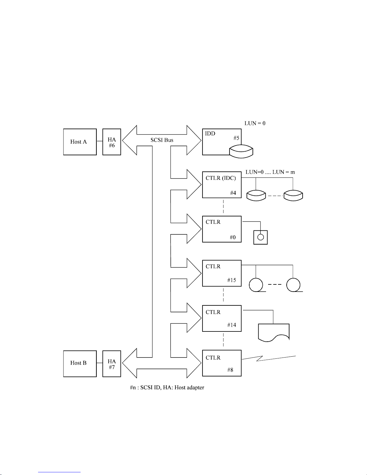
Any SCSI ID of the IDD can be selected using the setup pins. However, the LUN is fixed to zero
(0). The SCSI ID can be 0 to 15.
Note:
The maximum number of SCSI devices and the maximum cable length are limited depending
on the selected SCSI data transfer mode and the SCSI transceiver type. Appropriate SCSI
devices and cable length must be determined for each system.
1-2 C141-C011
Figure 1.1 Example of SCSI configuration
Page 21
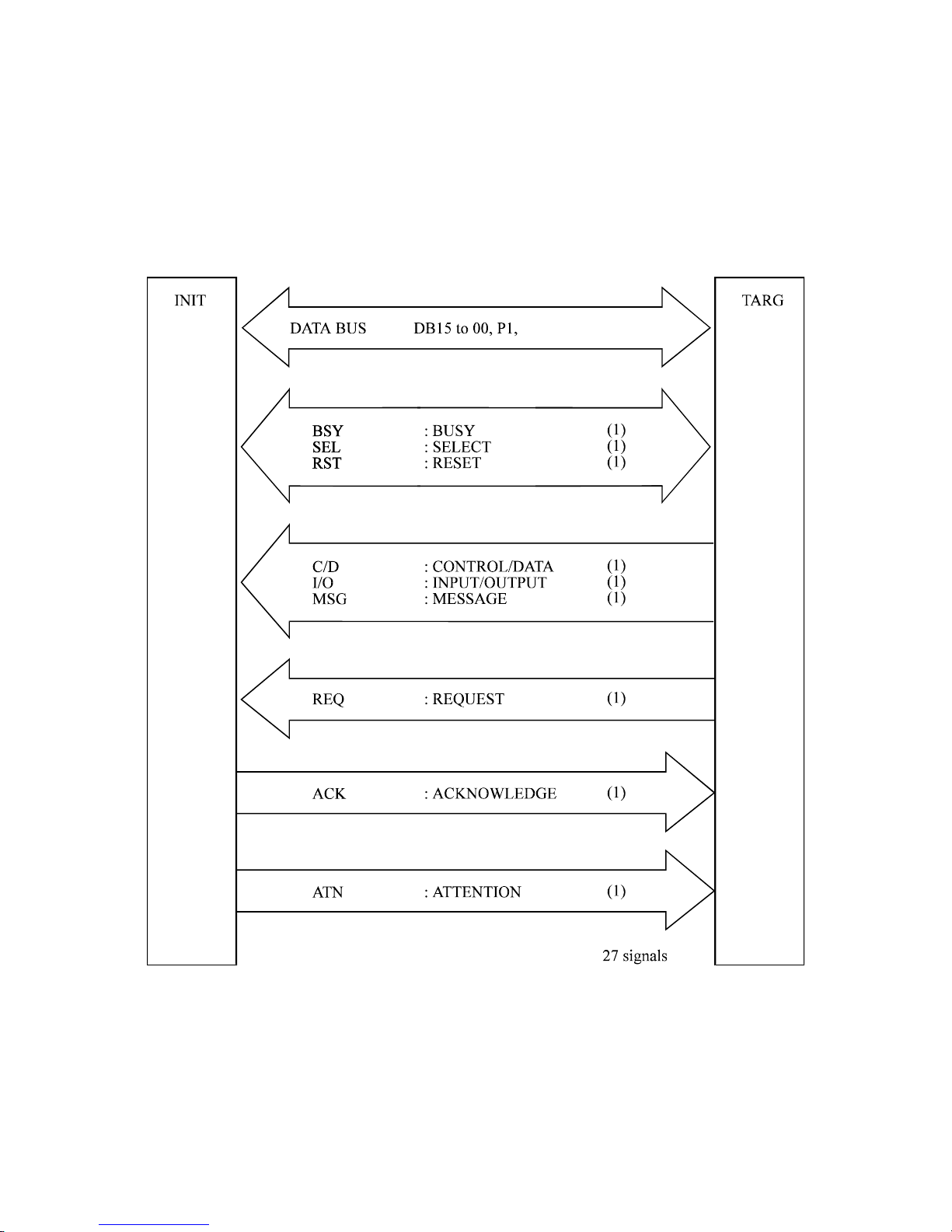
1.2 Interface Signal Definition
Figure 1.2 shows interface signal types. The SCSI bus consists of 27 signal lines. The 27 signal
lines consist of data buses (2 bytes plus two odd parity bits) and 9 control signal lines.
The SCSI bus can be a single-ended or low voltage differential(LVD) interface depending on the
model used. Their physical and electrical characteristics are detailed in Sections 1.3 and 1.4.
P_CRCA (18)
C141-C011 1-3
Figure 1.2 Interface signals
Page 22
(1) DB15 to DB00, P1, P_CRCA (Data buses)
The 16-bit SCSI system uses a bidirectional data bus consisting of two-byte data and two odd
parity bits.
MSB (2
15
): DB15, LSB (20): DB00
The data bus is used to transfer a command, data, a status, or a message in the INFORMATION
TRANSFER phase. However, DB15 to DB08 and P1 are used for data transfer only. The data is
transferred only after the WIDE DATA TRANSFER REQUEST or PARALLEL PROTOCOL
REQUEST message has been exchanged and the 16-bit data transfer mode has been established
between the INIT and TARG.
In the ARBITRATION phase, the data bus is used to send a SCSI ID to determine the bus
arbitration priority. In the SELECTION or RESELECTION phase, the data bus is used to send a
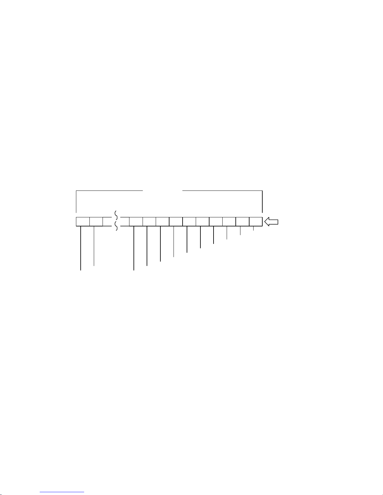
SCSI ID of the INIT and TARG. Figure 1.3 shows the relationship between the data buses and
SCSI IDs.
(16 bit SCSI)
DB15 DB14 DB9 DB8 DB7 DB6 DB5 DB4 DB3 DB2 DB1 DB0
SCSI ID #0
SCSI ID #1
SCSI ID #2
SCSI ID #3
SCSI ID #4
SCSI ID #5
SCSI ID #6
SCSI ID #14
SCSI ID #15
SCSI ID #9
SCSI ID #7
SCSI ID #8
Data bus
Figure 1.3 DATA BUS and SCSI ID
(a) DB15 to 0
Sixteen data-bit signals that form the 16-bit DATA BUS.
(b) DB7 to 0
Eight data-bit signals that form the 16-bit DATA BUS.
(c) P1 (ST DATA phase)
A signal sourced by the SCSI device driving the data bus during ST DATA phases. This signal is
associated with the DB(15-8) signals and is used to detect the presence of an odd number of bit
errors within the byte. The parity bit is driven such that the number of logical ones in the byte plus
the parity bit is odd.
1-4 C141-C011
Page 23

(d) P1 (data group transfer enabled)
A signal that shall be continuously negated by the SCSI device driving the DB(15-0) signals and
shall be ignored by the SCSI device receiving the DB(15-0) signals during DT DATA phases.
(e) P1 (information unit and paced transfer enabled)
A signal that is sourced by SCSI device to indicate the data valid or data invalid state.
(f) P_CRCA (PARITY/CRC AVAILABLE) (SELECTION phase, ST DATA phase, COMMAND phase,
MESSAGE phase, or STATUS phase)
A signal sourced by the SCSI device driving the data bus during these phases. This signal is
associated with the DB(7-0) signals and is used to detect the presence of an odd number of bit
errors within the byte. The parity bit is driven such that the number of logical ones in the byte plus
the parity bit is odd.
The parity bits (P1 and P_CRCA) is optional for the system. The IDD handles the data bus parity
as follows:
• The IDD has the data bus parity check function, and can enable or disable the parity check.
See Section 5.3.2 "SCSI Parity" of the Product Manual for setup details.
• When valid data is sent to the data bus from the IDD, the parity data is always guaranteed
except for the ARBITRATION phase.
(g) P_CRCA (data group transfer enabled)
A signal sourced by a target during DT DATA phases to control whether a data group field is a pad
field, pCRC field, or data field. When asserted the data group field shall be pad or pCRC fields
that shall not be transferred to the ULP. When negated the data group field shall be a data field that
shall be transferred to the ULP.
Note:
ULP is "Upper Level Protocol".
(h) P_CRCA (information unit and paced transfer enabled)
During DT DATA phases when information unit transfers are enabled this signal is referred to as
P_CRCA and is sourced by the SCSI target port. Depending on the negotiated condition of read
streaming and write flow control the SCSI initiator port and SCSI target port usage for P_CRCA is
different. When information unit transfers are enabled the SCSI target port and SCSI initiator port
shall use the P_CRCA signal.
C141-C011 1-5
Page 24

(2) BSY (BUSY)
The BSY signal indicates that the SCSI bus is in use. In the ARBITRATION phase, this signal is
used to request for the bus usage priority.
(3) SEL (SELECT)
The SEL signal is used by the INIT to select a TARG (in the SELECTION phase) or by the TARG
to reselect an INIT (in the RESELECTION phase).
(4) C/D (CONTROL/DATA)
This is a combination of I/O and MSG signals, and specifies a type of information transferred on
the data bus. The C/D signal is always driven by the TARG (see Table 1.1).
(5) I/O (INPUT/OUTPUT)
The I/O signal specifies the information transmission direction on the data bus. It is also used to
identify the SELECTION phase or RESELECTION phase. This signal is always driven by the
TARG (see Table 1.1).
(6) MSG (MESSAGE)
A signal sourced by a target to indicate the MESSAGE phase or a DT DATA phase depending on
whether C/D is true or false. Asserted indicates MESSAGE or DT DATA (see Table 1.1).
Table 1.1 INFORMATION TRANSFER phase identification
Signal
C/D MSG I/O
0 0 0 ST DATA OUT INIT -> TARG
0 0 1 ST DATA IN INIT <- TARG
0 1 0 DT DATA OUT INIT -> TARG
0 1 1 DT DATA IN INIT <- TARG
Phase Direction Comment
ST Data phase
Data phase
DT Data phase
1 0 0 COMMAND INIT -> TARG
1 0 1 STATUS INIT <- TARG
1 1 0 MESSAGE OUT INIT -> TARG
1 1 1 MESSAGE IN INIT <- TARG
MESSAGE
1-6 C141-C011
Page 25

(7) REQ (REQUEST)
This is a transmission request from the TARG to the INIT in the INFORMATION TRANSFER
phase.
(8) ACK (ACKNOWLEDGE)
The ACK signal is a response to the REQ signal sent from the INIT to TARG in the
INFORMATION TRANSFER phase.
(9) ATN (ATTENTION)
The ATN signal indicates that the INIT has a message to be sent to the TARG. It is used to
generate an ATTENTION condition.
(10) RST (RESET)
The RST signal is a Reset signal to clear all SCSI devices on the bus (to the RESET condition).
1.3 Physical Requirements
All SCSI devices are connected to each other in a daisy chain. Both ends of the interface cable are
terminated with resistor.
Tables 1.2 and 1.3 define the SCSI bus electrical characteristics (for interface signal
driver/receiver).
Table 1.2 Single-Ended maximum distance between terminators
Maximum distance between
Number of
terminators (meters)
attached devices
FAST-5 FAST-10 FAST-20
2 to 4 devices 6 3 3
5 to 8 devices 6 3 1.5
9 to 16 devices 6 3 N/A
C141-C011 1-7
Page 26
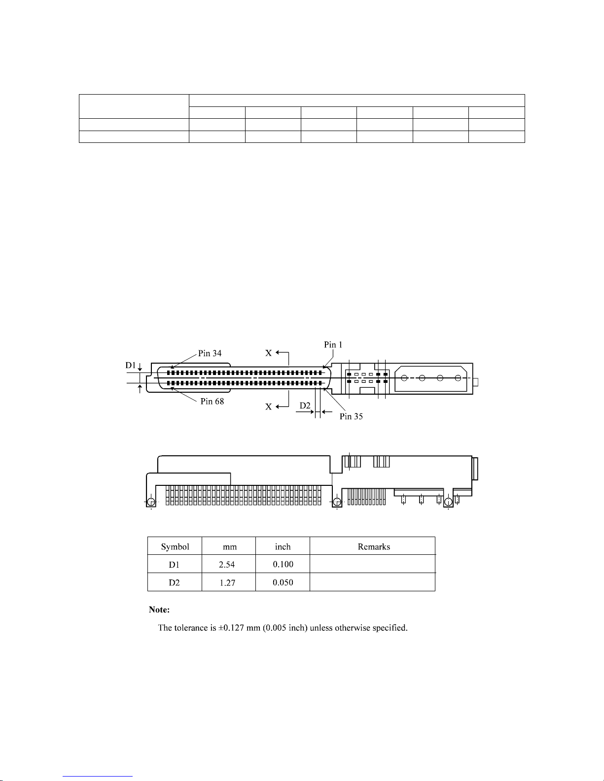
Table 1.3 LVD maximum distance between terminators
Interconnect
Fast-5 Fast-10 Fast-20 Fast-40 Fast-80 Fast-160
Maximum distance between terminators (meters)
Point-to-point 25 25 25 25 25 25
Multidrop 12 12 12 12 12 12
1.3.1 Interface connector
(1) Interface connector of the 16-bit SCSI
The IDD 16-bit SCSI bus connector is nonshielded 68-pin, consisting of two 34-pin rows with
adjacent pins 1.27 mm (0.05 inch) part (Figure 1.4).
For the interface cable connector, use a nonshielded 68-contact socket consisting of two 34-contact
rows points with adjacent contact points 1.27 mm (0.05 inch) apart (Figure 1.5).
Figure 1.6 shows single-ended interface connector signal assignment.
Figure 1.7 shows low-voltage-differential interface connector signal assignment.
Figure 1.4 SCSI interface connector (IDD side) (16-bit SCSI)
1-8 C141-C011
Page 27
M
M
Figure 1.5 SCSI interface connector (cable side) (16-bit SCSI)
C141-C011 1-9
0.396
0.61
5.16
0.001
Page 28

Pin No. Signal Signal Pin No.
01 GND -DB12 35
02 GND -DB13 36
03 GND -DB14 37
04 GND -DB15 38
05 GND -DBP1 39
06 GND -DB00 40
07 GND -DB01 41
08 GND -DB02 42
09 GND -DB03 43
10 GND -DB04 44
11 GND -DB05 45
12 GND -DB06 46
13 GND -DBP7 47
14 GND -P_CRCA 48
15 GND GND 49
16 GND GND 50
17 TERMPWR * TERMPWR * 51
18 TERMPWR * TERMPWR * 52
19 (reserved) (reserved) 53
20 GND GND 54
21 GND -ATN 55
22 GND GND 56
23 GND -BSY 57
24 GND -ACK 58
25 GND -RST 59
26 GND -MSG 60
27 GND -SEL 61
28 GND -C/D 62
29 GND -REQ 63
30 GND -I/O 64
31 GND -DB08 65
32 GND -DB09 66
33 GND -DB10 67
34 GND -DB11 68
* Terminating resistor power
Figure 1.6 Single-ended connector pin assignment (16-bit SCSI)
1-10 C141-C011
Page 29

Pin No. Signal Signal Pin No.
01 +DB(12) -DB(12) 35
02 +DB(13) -DB(13) 36
03 +DB(14) -DB(14) 37
04 +DB(15) -DB(15) 38
05 +DB(P1) -DB(P1) 39
06 +DB(0) -DB(0) 40
07 +DB(1) -DB(1) 41
08 +DB(2) -DB(2) 42
09 +DB(3) -DB(3) 43
10 +DB(4) -DB(4) 44
11 +DB(5) -DB(5) 45
12 +DB(6) -DB(6) 46
13 +DB(7) -DB(7) 47
14 +P_CRCA -P_CRCA 48
15 GROUND GROUND 49
16 DIFFSENS GROUND 50
17 TERMPWR * TERMPWR * 51
18 TERMPWR * TERMPWR * 52
19 RESERVED RESERVED 53
20 GROUND GROUND 54
21 +ATN -ATN 55
22 GROUND GROUND 56
23 +BSY -BSY 57
24 +ACK -ACK 58
25 +RST -RST 59
26 +MSG -MSG 60
27 +SEL -SEL 61
28 +C/D -C/D 62
29 +REQ -REQ 63
30 +I/O -I/O 64
31 +DB(8) -DB(8) 65
32 +DB(9) -DB(9) 66
33 +DB(10) -DB(10) 67
34 +DB(11) -DB(11) 68
* Terminating resistor power
Figure 1.7 Low-Voltage-Differential connector pin assignment (16-bit SCSI)
C141-C011 1-11
Page 30
(2) Interface connector of SCA-2 type 16-bit SCSI
The 16-bit, SCA-2 type SCSI bus connectors of the IDD are 80-pin, unshielded connectors, each
having two rows of 40 parallel pins (separated 1.27 mm or 0.05" from each other) (see Figure 1.8).
Figure 1.9 shows the pin assignment of 16-bit, SCA-2 type single-ended SCSI interface connector.
Figure 1.8 SCA-2 type, 16-bit SCSI interface connector (IDD side)
1-12 C141-C011
Page 31

Pin No. Signal Signal Pin No.
01 +12V (CHARGE) 12V RETURN (GND) 41
02 +12V 12V RETURN (GND) 42
03 +12V 12V RETURN (GND) 43
04 +12V MATED1 44
05 reserved (N.C.) reserved (N.C.) 45
06 reserved (N.C.) GND 46
07 -DB11 GND 47
08 -DB10 GND 48
09 -DB09 GND 49
10 -DB08 GND 50
11 -I/O GND 51
12 -REQ GND 52
13 -C/D GND 53
14 -SEL GND 54
15 -MSG GND 55
16 -RST GND 56
17 -ACK GND 57
18 -BSY GND 58
19 -ATN GND 59
20 -P_CRCA GND 60
21 -DB07 GND 61
22 -DB06 GND 62
23 -DB05 GND 63
24 -DB04 GND 64
25 -DB03 GND 65
26 -DB02 GND 66
27 -DB01 GND 67
28 -DB00 GND 68
29 -DBP1 GND 69
30 -DB15 GND 70
31 -DB14 GND 71
32 -DB13 GND 72
33 -DB12 GND 73
34 5V 5V RETURN (MATED2) 74
35 5V 5V RETURN (GND) 75
36 5V (CHARGE) 5V RETURN (GND) 76
37 Reserved -LED 77
38 RMT_START DLYD_START 78
39 SCSI ID0 SCSI ID1 79
40 SCSI ID2 SCSI ID3 80
Note:
Signal in parentheses indicates for SCA-2 type.
Figure 1.9 SCA-2 Type, single-ended 16-bit SCSI connector signal assignment
C141-C011 1-13
Page 32

Pin No. Signal Signal Pin No.
01 +12V (CHARGE) 12V RETURN (GND) 41
02 +12V 12V RETURN (GND) 42
03 +12V 12V RETURN (GND) 43
04 +12V MATED1 44
05 reserved(N.C.) reserved(N.C.) 45
06 reserved(N.C.) DIFFSENS 46
07 -DB(11) +DB(11) 47
08 -DB(10) +DB(10) 48
09 -DB(9) +DB(9) 49
10 -DB(8) +DB(8) 50
11 -I/O +I/O 51
12 -REQ +REQ 52
13 -C/D +C/D 53
14 -SEL +SEL 54
15 -MSG +MSG 55
16 -RST +RST 56
17 -ACK +ACK 57
18 -BSY +BSY 58
19 -ATN +ATN 59
20 -P_CRCA +P_CRCA 60
21 -DB(7) +DB(7) 61
22 -DB(6) +DB(6) 62
23 -DB(5) +DB(5) 63
24 -DB(4) +DB(4) 64
25 -DB(3) +DB(3) 65
26 -DB(2) +DB(2) 66
27 -DB(1) +DB(1) 67
28 -DB(0) +DB(0) 68
29 -DB(P1) +DB(P1) 69
30 -DB(15) +DB(15) 70
31 -DB(14) +DB(14) 71
32 -DB(13) +DB(13) 72
33 -DB(12) +DB(12) 73
34 +5V 5V RETURN (MATED2) 74
35 +5V 5V RETURN (GND) 75
36 +5V (CHARGE) 5V RETURN (GND) 76
37 Reserved -LED 77
38 RMT_START DLYD_START 78
39 SCSI ID0 SCSI ID1 79
40 SCSI ID2 SCSI ID3 80
Figure 1.10 SCA Type, Low-Voltage-Differential connector signal assignment
1-14 C141-C011
Page 33

1.3.2 Interface cable
Use the twisted-pair interface cables satisfying the requirements of Tables 1.4 and 1.5.
Table 1.4 SE and LVD Transmission line impedance of cable at maximum indicated data transfer
rate
Description
Local SE transmission line
impedance
Local differential
transmission line impedance
Minimum Maximum Minimum Maximum
All
84 Ohms (78
Ohms) (Note)
96 Ohms 110 Ohms 135 Ohms
Note:
If SCSI loads attached to the cable media are separated by more than 1.0 m use the value of 78
Ohms.
Table 1.5 Attenuation Requiaments for SCSI cable media
Distance between
SCSI bus
terminators (meters)
0 to 9
0 to 12
>12 to 25
Distances are consistent with these
minimum size conductors when used
with high quality dielectrics
0.0324 mm
0.05092 mm
0.05092 mm
0.08042 mm
0.05092 mm
0.08042 mm
2
(32 AWG) solid/
2
(30 AWG) stranded
2
(30 AWG) solid/
2
(28 AWG) stranded
2
(30 AWG) solid/
2
(28 AWG) stranded
Notes
multiple loads allowed
multiple loads allowed
point to point only
A twisted-pair cable must consist of pin n and pin n+1 (where "n" is an odd number) of the
interface connector. Use the SCSI bus cables having the same impedance characteristics to
minimize the signal reflection but keep the highest possible transmission characteristics.
If SCSI devices are connected to the terminals other than the interface cable ends, use the cable
branch at the SCSI connectors. No more SCSI cable can be connected to the last SCSI device
(which is connected to the SCSI bus) except when it is terminated with the terminator (see Figure
1.11).
The interface cable must have the stub length less than 0.1 meter for the single-ended SCSI cable.
Separate the stabs at least 0.3 meter from each other. (Keep the stab at least 30 cm away from a
SCSI device.)
C141-C011 1-15
Page 34

(a) Connection to a middle point of the cable
(b) Connection to the end of the cable.
1-16 C141-C011
Figure 1.11 Connection of interface cable
Page 35

1.4 Electrical Requirements
1.4.1 Single-Ended type
(1) Termination circuit
All signals except for RESERVE, GND, or TERMPWR should be terminated at both ends of the
bus. Each signal should be terminated by one of the following methods. Figures 1.12 and 1.13
show the termination circuit.
a) Each signal must connect to the TERMPWR signal through 220 Ω (within ±5%) resistor, and
connect to ground through 330 Ω (within ±5%) resistor.
b) The termination circuit of each signal shall satisfy the following conditions.
1) The terminators should be powered by the TERMPWR line. The circuit may receive
additional power from other sources but not require such additional power for proper
operation;
2) Each terminator should source current to the signal line whenever its terminal voltage is
below 2.5 VDC and this current should not exceed 22.4 mA for any line voltage at or
above 0.5 VDC and 25.4 mA for any line voltage between 0.5 VDC and 0.2 VDC even
when all other signal lines are driven at 4.0 VDC;
3) The voltage on all released signal lines should be at least 2.5 VDC;
4) These conditions should be met with any conforming configuration of TARGs and INITs
as long as at least one SCSI device is supplying TERMPWR;
5) The terminator at each end of the SCSI bus should add a maximum of 25 pF capacitance
to each signal;
6) The terminator may not source current to the signal line whenever its terminal voltage is
above 3.24 VDC except terminators may source current when the voltage is above 3.24
VDC in applications where the bus is less than 0.3 m;
Figure 1.12 Single-Ended SCSI termination circuit-1
C141-C011 1-17
Page 36

The IDD uses the terminator circuit satisfying conditions (b) above. The INIT terminator circuit is
also recommended to meet conditions (b) above.
DB
(P_CRCA)
Figure 1.13 Single-Ended SCSI termination circuit-2
1-18 C141-C011
Page 37

(2) Driver and receiver
For the interface signal driver, an open-collector or tri-state buffer that satisfies the following
output characteristics is used. All signals are negative logic (true = "L").
The receiver and non-driver of the SCSI device under the power-on state should satisfy the
following input characteristics on each signal.
Table 1.6 Output characteristic
Driver Type Value Min Max Notes
Passive Negation VOL 0.0 0.5 @IOL=48mA
VOH 2.5 5.25
Active Negation VOL 0.0 0.5 @IOL=48mA
VOH 2.5 3.7
Table 1.7 Input characteristic
Maximum
transfer mode
Min Max Notes
VIL [VDC] - 0.8
VIH [VDC] 2.0 -
Fast-5 IIL [mA] -0.4 0.0 @VI= 0.5VDC
IIH [mA] 0.0 0.1 @VI= 2.7VDC
Minimum input hysteresis [VDC] 0.2 -
VIL [VDC] - 0.8
VIH [VDC] 2.0 - @VI= 0.5VDC
Fast-10
I
IL [µA]
I
IH [µA]
-20 20 @V
-20 20
I= 2.7VDC
Minimum input hysteresis [VDC] 0.3 -
VIL [VDC] - 1.0
VIH [VDC] 1.9 -
Fast-20
I
IL [µA]
-20 20 @V
I= 0.5VDC
Minimum input hysteresis [VDC] 0.3 -
C141-C011 1-19
I
IH [µA]
-20 20 @V
I= 2.7VDC
Page 38

Note:
The SCSI device under the power-off state should satisfy the characteristics of I
and IIH.
IL
[Recommended circuit example]
Driver: MB463 (Fujitsu) or SN7438 (TI) (Open-collector NAND gate)
Receiver: SN74LS240 or SN74LS19 (TI) (Shumitt trigger input inverter)
1.4.2 Low-Voltage Differential type
(1) Termination circuit
All signals except for GROUND and TERMPWR should be terminated at both ends of the bus.
Each signal should be terminated. Figure 1.14 shows the termination circuit.
Figure 1.14 LVD SCSI termination circuit
(P_CRCA)
(P_CRCA)
1-20 C141-C011
Page 39

(2) DIFFSENS
a) DIFFSENS driver
The LVD DIFFSENS driver sets a voltage level on the DIFFSENS line that uniquely defines a
LVD transmission mode. LVD terminators and multimode terminators shall provide a LVD
DIFFSENS driver according to the specifications in Table 1.8.
Table 1.8 LVD DIFFSENS driver specifications
Value Max. Nominal Min Notes
VO [V] when IO=0
1.4 1.3 1.2
(shorted to ground) to 5mA
IOS [mA] 15 5 - With TERMPWR at operational levels
and V
=0.
O
|Input current DC|(µA)
Input sink current D.C. (µA) at
V
=2.75V
O
10 - - With terminator disabled.
200 - 20 Required to prevent the line from
floating and to ensure the HVD
DIFFSENS driver dominate the LVD
b) DIFFSENS receiver
LVD SCSI devices shall incorporate a LVD DIFFSENS receiver that detects the voltage level
on the DIFFSENS line for purposes of informing the device of the transmission mode being
used by the bus. The LVD DIFFSENS receiver shall be capable of detecting SE and LVD
SCSI devices. Table 1.9 define the receiver input levels for each of the two modes.
Table 1.9 DIFFSENS receiver operating requirements
V
range Sensed differential drive type
IN
-0.35 ~ +0.5V SE
+0.7 ~ +1.9V LVD
The input resistance requirement is for purposes of providing ground reference if no DIFFSENS
drivers are connected to the bus and to ensure that the DIFFSENS receivers do not load the
DIFFSENS drivers excessively and to ensure that SE mode is detected.
Devices shall not allow the signal drivers to leave the high impedance state during initial power on
until both of the following conditions are satisfied:
C141-C011 1-21
Page 40

a) The device is capable of logical operation for at least 100 ms, and
Notes:
The 100 ms delay allows time for the DIFFSENS pin to connect after the initial power
connection (in the case of insertion of a device into an active system), or allows time for
the power distribution system to settle.
b) The DIFFSENS mode detected has remained stable for an additional 100 ms after a) is
achieved.
A device shall not change its present signal driver or receiver mode based on the DIFFSENS
voltage level unless a new mode is sensed continuously for at least 100 ms.
(3) MATED Signals
If MATED 1 and MATED 2 signals are not mated then one or more short pins are not mated. If
MATED 1 and MATED 2 signals are mated then the mated condition of the short pins is
indeterminate. The MATED 1 and MATED 2 signals may indicate to the SCSI device that the
SCSI device is seated in an SCA-2 connector and it may begin power on processing. The signal
requirements are indicated below, but may be met by the circuit.
a) MATED 2/Drive Side
The signal is attached to signal ground on the SCSI device side.
b) MATED 2/Backplane Side
The signal is attached either directly or through optional logic in such a manner that the
MATED 1 signal is held to a ground level when the MATED 2 connection is completed. The
SCSI device shall sink no more than 100 mA to ground through the MATED 2 pin if optional
logic is used.
c) MATED 1/Drive Side
The MATED 1 signal shall be sensed by the SCSI device. When the MATED 1 connection is
determined to be at a ground level, the SCSI device may assume that the SCSI device has been
partially mated. Assuming the mating process continues uninterrupted until competition,
including sensing of the SCSI ID Selection signals and the motor start controls, then normal
power on procedures may begin 250 msec after the MATED 1 signal is observed to transition
to the ground level. When the MATED 1 connection is determined to be at the open level, the
SCSI device is not mated. The MATED 1 signal is tied up to a TTL positive level when the
SCSI device is not installed. If the SCSI device is mated and operating, it may optionally
detect the open level of MATED 1 as an indication that the SCSI device is partially unmated
and may be about to be removed. If the SCSI device supports detection of the open level of
MATED 1 to prepare itself for power removal or for physical removal from the enclosure, the
detection shall occur within 1 second from the time that the Mated 1 open level occurs at the
SCSI device.
1-22 C141-C011
Page 41

(4) MATED 1/Backplane Side
The signal shall be held to a ground level when the MATED 2 connection is completed. The
MATED 1 signal shall be held to the open level when the MATED 2 connection is not completed.
MATED 2
connection
Figure 1.15 Circuit for mated indications
1.4.3 Internal terminal resistor and power supply for terminating resistor
The TERMPWR signal of the interface connector supplies the power to the terminating resistor
circuit connected to both ends of the cable. To attach a terminating resistor to an external SCSI
device or to cut the power of SCSI device having a terminator, the terminator power must be
supplied to the TERMPWR line from any of SCSI devices of the bus. The SCSI device (such as a
host adapter) which always operates as the INIT should supply the power. The terminating resistor
power shall be supplied to the TERMPWR line through a diode to prevent a reverse current.
Table 1.10 lists the requirements for terminating the resistor power supply (Vterm).
Table 1.10 Requirements for terminating resistor power supply
Terminator Type
Terminator Power
Characteristics
I
(A)@V
min
0.6 0.6 0.5 0.65
min
0.2V dropout
SE (P Cable)
regulator
SE and LVD
LVD
type
(Multimode)
V
min
V
max
(V)@I
(V)@ all
2.7 4.0 3.0 3.0
min
conditions
C141-C011 1-23
5.25 5.25 5.25 5.25
Page 42

Figure 1.16 shows the configuration of a SCSI terminating resistor circuit. The circuit shall be set
in either mode (by the CN2 setup pin) depending on the IDD system requirements.
23 24
16-bit SCSI (P-connector) setting terminal
CN2 23-24pin
Supply TERMPWR to SCSI Bus Short
Don’t supply TERMPWR to SCSI Bus Open
Figure 1.16 16-bit SCSI (not SCA2) terminating resistor circuit
Notes:
All series have no internal terminator circuit. If the terminator circuit is needed, you
should add the external circuit on your system.
1-24 C141-C011
Page 43

1.4.4 Usage in 8-bit/16-bit transfer mode
When the IDD is used as 8-bit SCSI device, it is connected terminating resistor circuit to upper 8-
bit and parity (DB08 to DB15 and DBP1) or short set up pin (CN2 13-14). When the IDD is used
as 16-bit SCSI device, leave the set up pin Jumper setting “8/16” open. Table 1.11 shows the
guide. Jumper setting is available only for MP series.
Table 1.11 Setting set up pin, 16-bit (wide)/8-bit (narrow) mode
Transfer mode Jumper setting “8/16” DB08 to DB15 and DBP1
Short Don’t care.
8bit (narrow)
Open
Should be terminated
externally.
16bit (wide) Should be opened Don’t care.
C141-C011 1-25
Page 44

1.4.5 Signal driving conditions
(1) Signal status value
Table 1.12 shows the correspondence between the input interface signal level at the receiving end
and its logic state.
Table 1.12 Signal status at receiving end
Single-ended type signal state
Logic state
True, "1", or
asserted
False, "0", negated
or released
Asynchronous, Fast-
5, Fast-10
Low (less than 0.8
VDC)
High (more than 2.0
VDC)
Fast-20
Low (less than 1.0
VDC)
High (more than 1.9
VDC)
LVD type signal
state
Low (-3.6 to -0.030
VDC)
High (0.030 to 3.6
VDC)
(2) Signal driving method
Two driving methods are available: "OR-tied" type and "non-OR-tied" type as indicated in Table
1.13.
Table 1.13 Signal driving method
Driving method
Signal status
False (*1) No SCSI device drives a signal.
The signal becomes false when
the terminating resistor circuit
"OR-tied" type "non-OR-tied" type
A particular SCSI device drives
the signal false. Otherwise, no
SCSI device drives the signal.
is biased.
True A SCSI device drives the signal true
*1 In this manual, the signal is said to be false if one of the following conditions is satisfied.
1. The signal is actually driven by a SCSI device to become false (non-OR-tied type).
2. No SCSI device is driving the signal (OR-tied type or non-OR-tied type).
If the BSY, SEL and RST signals may be driven by two or more SCSI devices simultaneously in
the interface operating sequence, they must be driven in the OR-tied method. All signals except
for SEL, BSY, RST and DB(P_CRCA, P1) are not driven by multiple SCSI devices
simultaneously. However, the DBP signals must be driven false in the ARBITRATION phase. All
signals driven in OR-tied and non-OR-tied method can be mixed on the same signal line of SCSI
bus except for BSY, SEL and RST signals.
1-26 C141-C011
Page 45

(3) Signal sources
Table 1.14 lists SCSI device types (or signal sources) which can drive signals in each interface
operating phase.
Table 1.14 Bus phases and signal sources
I/O,
BSY SEL
REQ,
C/D,
ACK,
ATN
DB7-0
DB15-8,
DBP1
P_CRCA RST
MSG
BUS FREE N N N N N N N A
ARBITRATION A W N N ID ID ID A
QAS ARBITRATION PT W N N ID ID ID ID
SELECTION I&T I N I I I I A
RESELECTION I&T T T I T T T A
COMMAND T N T I I N I A
ST DATA IN T N T I T T T A
ST DATA OUT T N T I I I I A
DT DATA IN T N T I T T T A
DT DATA OUT T N T I I I T A
STATUS T N T I T N T A
MESSAGE IN T N T I T N T A
MESSAGE OUT T N T I I N I A
A: Any SCSI device can drive the signal. Also, two or more SCSI devices may drive the signal
simultaneously.
I: Only the INIT SCSI device drives the signal.
I&T: The INIT and TARG SCSI devices drive the signal in the interface operating sequence.
INIT, TARG or both can drive this signal according to the interface sequence.
I or T: The INIT or TARG SCSI device (or both devices) may drive the signal depending on the
I/O signal status and bus width.
ID: Each SCSI device which is actively arbitrating the bus drives a unique data bit
(SCSI ID). The parity bit may be undriven or driven to the true state, but must never be
driven to the false state.
N: Not be driven by any SCSI device.
T: Only the TARG SCSI device drives the signal.
W: Only a single SCSI device selected through arbitration drives the signal.
C141-C011 1-27
Page 46

1.5 Timing Rule
1.5.1 Timing value
Table 1.15, 16, 17 give the timing required for operations on the SCSI bus.
Table 1.15 SCSI bus control timing values
Timing description Type Timing values
1 Arbitration delay Min
2.4 µs
2 Bus clear delay Max 800 ns
3 Bus free delay Min 800 ns
4 Bus set delay Max
1.6 µs
5 Bus settle delay Min 400 ns
6 Cable skew (1) Max 4 ns
7 Data release delay Max 400 ns
8 DIFFSENS voltage filter time Min 100 ms
9 Physical disconnection delay Min
200 µs
10 Power on to selection (2) Max 10 s
11 QAS arbitration delay Min 1000 ns
12 QAS assertion delay Max 200 ns
13 QAS release delay Max 200 ns
14 QAS non-DATA phase REQ(ACK)
Min 50 ns
peiod
15 Reset delay Min 200 ns
16 Reset hold time Min
25 µs
Note: (1) Cable Skew is measured at each device connection with the transmitted skew subtracted from
the received skew. (2) This is a recommended time. It is not mandatory.
1-28 C141-C011
Page 47

Table 1.16 SCSI bus data & information phase ST timing values
Timing description Type
Async Fast-5 Fast-10 Fast-20 Fast-40
Timing values [ns] (5)
1 ATN Transmit Setup Time min. 90 33 33 21.5 19.25
2 ATN Receive Setup Time min. 45 17 17 8.5 6.75
3 Cable Skew (3) max. 4 4 4 3 2.5
4 Receive Assertion Period (4) min. N/A 70 22 11 6.5
5 Receive Hold Time (4) min. N/A 25 25 11.5 4.75
6 Receive Negation Period (4) min. N/A 70 22 11 6.5
7 Receive Setup Time (4) min. N/A 15 15 6.5 4.75
8 Receive REQ (ACK) Period Tolerance min. N/A 1.1 1.1 1.1 1.1
9 Signal Timing Skew max. 8 8 8 5 4.5
10 REQ (ACK) Period min. N/A 200 100 50 25
11 Transmit Assertion Period (4) min. N/A 80 30 15 8
12 Transmit Hold Time (4) min. N/A 53 33 16.5 9.25
13 Transmit Negation Period (4) min. N/A 80 30 15 8
14 Transmit Setup Time (4) min. N/A 23 23 11.5 9.25
15 Transmit REQ (ACK) Period Tolerance max. N/A 1 1 1 1
Note: (3) Cable Skew is measured at each device connection with the transmitted skew subtracted from
the received skew. (4) See Fig.1-17,18,19 for measurement points for the timing specifications. (5)
SCSI bus timing values specified by the maximum transfer rate for the given range shall apply
even if a slower transfer rate within the given range is negotiated.
Table 1.17 Miscellaneous SCSI bus data & information phase DT timing values
Timing description Type
Fast-10 Fast-20 Fast-40 Fast-80 Fast-160
Timing values [ns] (7)
1 Cable skew(6) Max 4 3 2.5 2.5 2.5
2 REQ(ACK) period Nominal 200 100 50 25 12.5
3 Residual Skew Error(8) Max N/A N/A N/A N/A ±0.15
4 De-skewed data valid window(9) Min N/A N/A N/A N/A ±2.1
5 Skew correction range(9) Min N/A N/A N/A N/A ±3.65(10)
6 Signal timing skew Max 26.8 13.4 6.7 3.35 4.85
7 Strobe Offset Tolerance Max N/A N/A N/A N/A ±0.125
Fast-160 SCSI devices shall not change timing parameters between training or reset events.
Note: (6)Cable skew is measured at each SCSI device connection within the same bus segment with the
transmitted skew subtracted from the received skew. (7) SCSI bus timing values specified by the
maximum transfer rate for the given range shall apply even if a slower transfer rate within the
given range is negotiated. (8) Calculated assuming timing budget shown in table 46. (9) Measured
at the receiver terminal using clean input signals with 500 mV peak amplitude and 1 ns rise and fall
time between 20 % and 80 % of the signal. (10) Relative to the REQ(ACK) clocking signal.
C141-C011 1-29
Page 48

Table 1.18 SCSI bus data & information phase DT timing values
Timing description Type
Fast-10 Fast-20 Fast-40 Fast-80 Fast-160
Timing values [ns] (12)
1 ATN transmit setup time Min 48.4 29.2 19.6 14.8 14
2 Flow control transmit hold time Min 38.4 19.2 9.6 4.8 1.4
3 Flow control transmit setup time Min 48.4 29.2 19.6 14.8 1.4
4 pCRC transmit hold time Min 38.4 19.2 9.6 4.8 N/A
5 pCRC transmit setup time Min 48.4 29.2 19.6 14.8 N/A
6 Transmit assertion period (11) Min 92 46 23 11.5 5.69
7 Transmit hold time (11) Min 38.4 19.2 9.6 4.8 4.77
8 Transmit ISI Compensation Max N/A N/A N/A N/A 1.0
9 Transmit negation period (11) Min 92 46 23 11.5 5.69
10 Transmit REQ(ACK) period tolerance Max 0.6 0.6 0.6 0.6 0.06
11 Transmit REQ assertion period with
Min 97.5 54 35.5 24 N/A
P_CRCA transitioning
12 Transmit REQ negation period with
Min 97.5 54 35.5 24 N/A
P_CRCA transitioning
13 Transmit setup time (11) Min 38.4 19.2 9.6 4.8 -1.48
14 Transmitter skew Max N/A N/A N/A N/A ±0.75
15 Transmitter time asymmetry Max N/A N/A N/A N/A ±0.25
Fast-160 SCSI devices shall not change timing parameters between training or reset events.
Note: (6) Cable Skew is measured at each device connection with the transmitted skew subtracted from
the received skew. (7) See Fig.1-20 for measurement points for the timing specifications. (8) SCSI
bus timing values specified by the maximum transfer rate for the given range shall apply even if a
slower transfer rate within the given range is negotiated.
1-30 C141-C011
Page 49

Table 1.19 Receive SCSI bus data & information phase DT timing values
Timing description Type
Fast-10 Fast-20 Fast-40 Fast-80 Fast-160
Timing values [ns] (15)
1 ATN receive setup time Min 13.6 7.8 4.9 3.45 3
2 Flow control receive hold time Min 11.6 5.8 2.9 1.45 3
3 Flow control receive setup time Min 18.6 12.8 9.9 8.45 3
4 PCRC receive hold time Min 11.6 5.8 2.9 1.45 N/A
5 PCRC receive setup time Min 18.6 12.8 9.9 8.45 N/A
6 Receive assertion period (14) Min 80 40 20 8.5 4.74
7 Receive hold time (14) Min 11.6 5.8 2.9 1.45 -0.08
8 Receive negation period (14) Min 80 40 20 8.5 4.74
9 Receive setup time (14) Min 11.6 5.8 2.9 1.45 -6.33
10 Receive REQ(ACK) period tolerance Min 0.7 0.7 0.7 0.7 0.06
11 Receive REQ assertion period with P_CRCA
Min 85.5 48 32.5 21 N/A
transitioning
12 Receive REQ negation period with P_CRCA
Min 85.5 48 32.5 21 N/A
transitioning
13 Receive Skew Compensation Max N/A N/A N/A N/A 4.4
14 Receive Internal Hold Time Min N/A N/A N/A N/A 0.345
15 Receive Internal Setup Time Min N/A N/A N/A N/A 0.345
Fast-160 SCSI devices shall not change timing parameters between training or reset events.
Note: (14) See Fig.1-20,21,22,23,24 for measurement points for the timing specifications. (15) SCSI bus
timing values specified by the maximum transfer rate for the given range shall apply even if a
slower transfer rate within the given range is negotiated.
C141-C011 1-31
Page 50

(1) ATN transmit setup time
The minimum time provided by the transmitter between the assertion of the ATN signal and the
negation of the ACK signal.
Specified to provide the increased ATN receive setup time, subject to intersymbol interference,
cable skew, and other distortions.
(2) ATN receive setup time
The minimum time required at the receiver between the assertion of the ATN signal and the
negation of the ACK signal to recognize the assertion of an Attention Condition.
Specified to ease receiver timing requirements.
(3) Arbitration delay
The minimum time a SCSI device shall wait from asserting the BSY signal for arbitration until the
DATA BUS is examined to see if arbitration has been won. There is no maximum time.
(4) Bus clear delay
The maximum time that for a SCSI device to release all SCSI signals after:
a) The BUS FREE phase is detected (the BSY and SEL signals are both false for a bus settle
delay);
b) The SEL signal is received from another SCSI device during the ARBITRATION phase;
c) The transition of the RST signal to true.
For item a) above, the maximum time for a SCSI device to release all SCSI bus signals is 1200 ns
from the BSY and SEL signals first becoming both false. If a SCSI device requires more than a
bus settle delay to detect BUS FREE phase, it shall release all SCSI bus signals within a bus clear
delay minus the excess time.
(5) Bus free delay
The minimum time that a SCSI device shall wait from its detection of the BUS FREE phase (BSY
and SEL both false for a bus settle delay) until its assertion of the BSY signal in preparation for
entering the ARBITRATION phase.
(6) Bus set delay
The maximum time for a SCSI device to assert the BSY signal and its SCSI ID after it detects a
BUS FREE phase for the purpose of entering the ARBITRATION phase.
(7) Bus settle delay
The minimum time to wait for the bus to settle after changing certain control signals as called out
in the protocol definitions.
Provides time for a signal transition to propagate from the driver to the terminator and back to the
driver.
1-32 C141-C011
Page 51

(8) Cable skew
The maximum difference in propagation time allowed between any two SCSI bus signals measured
between any two SCSI devices excluding any signal distortion skew delays.
(9) Data release delay
The maximum time for an initiator to release the DATA BUS, DB(P_CRCA), DB(P1) signals
following the transition of the I/O signal from false to true.
(10) DIFFSENS voltage filter time
The minimum time DIFFSENS voltage shall be sensed continuously within the voltage range of a
valid SCSI bus mode.
(11) Physical Disconnection delay
The minimum time that a target shall wait after releasing BSY before participating in an
ARBITRATION phase when honoring a DISCONNECT message from the initiator.
(12) Power on to selection
The recommended maximum time from power application until a SCSI target is able to respond
with appropriate status and sense data to the TEST UNIT READY, INQUIRY, and REQUEST
SENSE commands (See SCSI-3 Primary Commands Standard.)
(13) Reset delay
The minimum time that the RST signal shall be continuously true before the SCSI device shall
initiate a reset.
(14) Reset hold time
The minimum time that the RST signal is asserted. There is no maximum time.
(15) Reset to selection
The recommended maximum time from after a reset condition until a SCSI target is able to
respond with appropriate status and sense data to the TEST UNIT READY, INQUIRY, and
REQUEST SENSE commands (See SCSI-3 Primary Commands Standard).
(16) Selection abort time
The maximum time that SCSI device shall take from its most recent detection of being selected or
reselected until asserting the BSY signal in response. This time-out is required to ensure that a
target or initiator does not assert the BSY signal after a SELECTION or RESELECTION phase
has been aborted.
(17) Selection time-out delay
The minimum time that an initiator or target should wait for a assertion of the BSY signal during
the SELECTION or RESELECTION phase before starting the time-out procedure. Note that this
is only a recommended time period.
C141-C011 1-33
Page 52

(18) System deskew delay
The minimum time that a SCSI device should wait after receiving a SCSI signal to ensure that any
signals transmitted at the same time are valid. The system deskew delay shall not be applied to the
synchronous data transfers.
(19) Receive assertion period
The minimum time required at a SCSI device receiving a REQ signal for the signal to be asserted
while using synchronous data transfers provided P_CRCA is not transitioning with pCRC
protection enabled. Also, the minimum time required at a SCSI device receiving an ACK signal
for the signal to be asserted while using synchronous data transfers. For SE fast-5 and fast-10
operation, the time period is measured at the 0.8 V level. For SE fast-20 operation the period is
measured at the 1.0 V level. For LVD see figure 1.19 and 1.20 for signal measurement points.
(20) Receive hold time
For ST data transfers the minimum time required at the receiving SCSI device between the
assertion of the REQ or ACK signal and the changing of the DB(15-0, P_CRCA, and/or P1)
signals while using synchronous data transfers, provided P_CRCA is not transitioning with pCRC
protection enabled.
For DT data transfers the minimum time required at the receiving SCSI device between the
transition (i.e. assertion or negation) of the REQ or ACK signals and the changing of the DB(15-0,
P_CRCA, and/or P1) signals while using synchronous data transfers.
(21) Receive negation period
The minimum time required at a SCSI device receiving a REQ signal for the signal to be negated
while using synchronous data transfers. Also, the minimum time required at a SCSI device
receiving an ACK signal for the signal to be asserted while using synchronous data transfers. For
SE fast-5 and fast-10 operation, the time period is measured at the 2.0 V level. For SE fast-20
operation the period is measured at the 1.9 V level. For LVD see figure 1.19 and figure 1.20 for
signal measurement points.
(22) Receive setup time
For ST data transfers the minimum time required at the receiving SCSI device between the
changing of the DB(15-0, P_CRCA, and/or P1) signals and the assertion of the REQ or ACK
signal while using synchronous data transfers.
For DT data transfers the minimum time required at the receiving SCSI device between the
changing of the DB(15-0, P_CRCA, and/or P1) signals and the transition of the REQ or ACK
signals while using synchronous data transfers.
(23) Receive REQ(ACK) period tolerance
The minimum tolerance that a SCSI device should allow to be subtracted from the REQ(ACK)
period. The tolerance comprises the Transmit REQ(ACK) tolerance plus a measurement error due
to noise.
1-34 C141-C011
Page 53

(24) Signal timing skew
The maximum signal timing skew occurs when transferring random data and in combination with
interruptions of the REQ or ACK signal transitions (e.g., pauses caused by offsets). The signal
timing skew includes cable skew (measured with 0101...patterns) and signal distortion skew caused
by random data patterns and transmission line reflections. The receiver detection range is the part
of the signal between the “may detect” level and the “shall detect” level on either edge.
(25) REQ (ACK) period
The REQ (ACK) period during synchronous data transfers is measured from an assertion edge of
the REQ (ACK) signal to the next assertion edge of the signal. In DT DATA phases the nominal
transfer period for data is half that of the REQ (ACK) period during synchronous data transfers
since data is qualified on both the assertion and negation edges of the REQ (ACK) signal. In ST
DATA phases the nominal transfer period for data is equal to the REQ (ACK) period during
synchronous data transfers since data is only qualified the assertion edge of the REQ (ACK) signal.
(26) Transmit assertion period
The minimum time that a target shall assert the REQ signal while using synchronous data transfers
provided P_CRCA is not transitioning with pCRC protection enabled. Also, the minimum time
that an initiator shall assert the ACK signal while using synchronous data transfers.
(27) Transmit hold time
For ST data transfers the minimum time provided by the transmitting SCSI device between the
assertion of the REQ or ACK signal and the changing of the DB(15-0, P_CRCA, and/or P1)
signals while using synchronous data transfers.
For DT data transfers the minimum time provided by the transmitting SCSI device between the
transition (i.e. assertion or negation) of the REQ or ACK signals and the changing of the DB(15-0,
P_CRCA, and/or P1) signals while using synchronous data transfers.
(28) Transmit negation period
The minimum time that a target shall negate the REQ signal while using synchronous data transfers
provided P_CRCA is not transitioning with pCRC protection enabled. Also, the minimum time
that an initiator shall negate the ACK signal while using synchronous data transfers.
(29) Transmit setup time
For ST data transfers the minimum time provided by the transmitting SCSI device between the
changing of the DB(15-0, P_CRCA, and/or P1) signals and the assertion of the REQ or ACK
signal while using synchronous data transfers.
For DT data transfers the minimum time provided by the transmitting SCSI device between the
changing of the DB(15-0, P_CRCA, and/or P1) signals and the transition of the REQ or ACK
signal while using synchronous data transfers.
C141-C011 1-35
Page 54

(30) Transmit REQ (ACK) period tolerance
The maximum tolerance that a SCSI device may subtract from the negotiated synchronous period.
The tolerance comprises the transmit REQ (ACK) tolerance plus a measurement error due to noise.
(31) pCRC Receive hold time
The minimum time required at the receiver between the transition of the REQ signal and the
transition of the P_CRCA signal while pCRC protection is enabled.
(32) pCRC Receive setup time
The minimum time required at the receiver between the transition of the P_CRCA signal and the
transition of the REQ signal while pCRC protection is enabled.
Specified to ease receiver timing requirements and ensure that this signal, which is outside CRC
protection, is received correctly.
(33) pCRC Transmit hold time
The minimum time provided by the transmitter between the transition of the REQ signal and the
transition of the P_CRCA signal while pCRC protection is enabled.
(34) pCRC Transmit setup time
The minimum time provided by the transmitter between the transition of the P_CRCA signal and
the transition of the REQ signal while pCRC protection is enabled.
Specified to provide the increased receive setup time, subject to intersymbol interference, cable
skew, and other distortions.
(35) Receive REQ assertion period with P_CRCA transitioning
The minimum time required at a SCSI device receiving a REQ signal for the signal to be asserted
while using synchronous data transfers with P_CRCA transitioning with pCRC protection enabled.
Specified to ensure that the assertion period is longer than the receive hold time plus the receive
setup time.
(36) Receive REQ negation period with P_CRCA transitioning
The minimum time required at a SCSI device receiving an REQ signal for the signal to be negated
while using synchronous data transfers with P_CRCA transitioning with pCRC protection enabled.
Specified to ensure that the negation period is longer than the receive hold time plus the receive
setup time.
1-36 C141-C011
Page 55

(37) Transmit REQ assertion period with P_CRCA transitioning
The minimum time that a target shall assert the REQ signal during a DT DATA phase while
transitioning P_CRCA with pCRC protection enabled.
Specified to provide the increased receive REQ assertion period, subject to loss on the
interconnect.
(38) Transmit REQ negation period with P_CRCA transitioning
The minimum time that a target shall negate the REQ signal during a DT DATA phase while
transitioning P_CRCA with pCRC protection enabled.
Specified to provide the increased receive REQ negation period, subject to loss on the
interconnect.
(39) QAS arbitration delay
The minimum time a SCSI device with QAS enabled (see 1.6.2.2) shall wait from the detection of
the MSG, C/D, and I/O signals being false to start QAS until the DATA BUS is examined to see if
QAS has been won (see 1.6.2.2).
(40) QAS assertion delay
The maximum time allowed for a SCSI device to assert certain signals during QAS.
(41) QAS release delay
The maximum time allowed for a SCSI device to release certain signals during QAS.
(42) QAS non-DATA phase REQ(ACK) period
The minimum time a QAS-capable SCSI INIT port shall ensure the REQ and ACK signals are
asserted and that data is valid during COMMAND, MESSAGE, and STATUS phases.
(43) Residual skew error
The maximum timing error between the deskewed data and REQ or ACK internal to the receiving
SCSI device after skew compensation.
C141-C011 1-37
Page 56

(44) De-skewed data valid window
The minimum difference in time allowed between the rising or falling edge of a "1010..." pattern
on the DATA BUS or DB(P1) and its clocking signal on the ACK or REQ signal as measured at
their zero-crossing points after skew compensation is applied by the receiver without allowing any
error in the received data (see Fig.1-17). The de-skewed data valid window shall be equal to:
± [(data transfer period) - (residual skew error) - (strobe offset tolerance) - (clock jitter) - (receiver
amplitude skew) - (chip noise) - (system noise at receiver) - (receiver asymmetry)] / 2.
Figure 1.17 Receiver de-skew parameters
(45) Skew correction range
The minimum skew correction capability of the receiver of a signal on the DATA BUS or DB(P1)
relative to the ACK or REQ signal as measured at the receiver's connector. The skew correction
range shall be equal to ± [(transmitter chip skew) + (cable skew) + (two times trace skew)] relative
to the corresponding ACK or REQ clock signal for that transition. Receiver chip skew is not
included, as it is internal to the receiver.
(46) Strobe offset tolerance
The time tolerance of centering the compensated REQ or ACK strobe in the transfer period during
the training pattern.
(47) Flow control receive hold time
The maximum time required by the SCSI INIT port between the assertion of the REQ signal
corresponding to the last iuCRC transfer of a SPI data stream information unit and the changing of
the P_CRCA signal.
1-38 C141-C011
Page 57

(48) Flow control receive setup time
The maximum time required by the SCSI INIT port between the assertion of the P_CRCA signal
and the assertion of the REQ signal corresponding to the last iuCRC transfer of a SPI data stream
information unit. Also, the maximum time required by the SCSI INIT port between the negation of
the P_CRCA signal and the assertion of the REQ signal corresponding to any valid data transfer of
a SPI L_Q information unit.
(49) Flow control transmit hold time
The minimum time provided by the SCSI TARG port between the assertion of the REQ signal
corresponding to the last iuCRC transfer of a SPI data stream information unit and the changing of
the P_CRCA signal. Specified to provide the increased P_CRCA receive setup time, subject to
intersymbol interference, cable skew, and other distortions.
(50) Flow control transmit setup time
The minimum time provided by the SCSI TARG port between the assertion of the P_CRCA signal
and the assertion of the REQ signal corresponding to the last iuCRC transfer of a SPI data stream
information unit. Also, the minimum time provided by the SCSI TARG port between the negation
of the P_CRCA signal and the assertion of the REQ signal corresponding to any valid data transfer
of a SPI L_Q information unit. Specified to provide the increased P_CRCA receive setup time,
subject to intersymbol interference, cable skew, and other distortions.
(51) Receive internal hold time
The minimum time provided for hold time in the receive data detector after allowance for timing
errors and timing compensation from all sources measured from the worse case bit (i.e., data or
parity) to the compensated offset strobe.
Note: This time may not be observable to other than the SCSI device designer.
(52) Receive internal setup time
The minimum time provided for setup time in the receive data detector after allowance for timing
errors and timing compensation from all sources measured from the worse case bit (i.e., data or
parity) to the compensated offset strobe.
Note: This time may not be observable to other than the SCSI device designer.
(53) Receive Skew Compensation
The effective reduction in worse case timing skew of data, parity, and strobe signals provided by
the receiving SCSI device but not directly observable at the receiving SCSI device connector.
C141-C011 1-39
Page 58

(54) Transmit ISI Compensation
The effective reduction in worse case ISI timing shift provided by the transmitting SCSI device as
seen at the receiving SCSI device connector.
(55) Transmitter skew
The maximum difference in time allowed between the rising or falling edge of a "1010..." pattern
on the DATA BUS or DB(P1) signal and its clocking signal on the ACK or REQ signal as
measured at their zero-crossing points (see Fig.1-18).
Figure 1.18 Transmitter skew
1-40 C141-C011
Page 59

(56) Transmitter time asymmetry
The maximum time on DATA BUS, DB(P1), ACK, or REQ signal from any transition edge to the
subsequent transition edge during a "1010..." pattern, as measured at their zero-crossing points,
minus the data transfer period (see Fig.1-19).
Figure 1.19 Transmitter time asymmetry
C141-C011 1-41
Page 60

1.5.2 Measurement point
(1) SE Fast-5/10
The measurement point of Fast-5/10 is different from that of Fast-20. The Figure 1.20 is the Fast-
5/10 measurement point.
1-42 C141-C011
Figure 1.20 Fast-5/10 Measurement Point
Page 61

(2) SE Fast-20
Figure 1.21 is the Fast-20 measurement point.
C141-C011 1-43
Figure 1.21 Fast-20 Measurement Point
Page 62

(3) LVD ST Data Transfer
Figure 1.22 is the LVD ST Data Transfer measurement point.
**
*
**
*
** Use the crossing that yield the shorter Assertion Period
and Negation Period.
Figure 1.22 LVD ST Data Transfer measurement point
Notes:
1. V
- negated signal
N
2. V
- asserted signal
A
3. t
= 1.25ns minimum
m
4. V
or VN are required to drive the 100 mV at the leading edge of the transition. Those signals shall be at
A
least |100 mV| for at least t
before and after the transition.
m
5. Differential voltage signals in all cases.
6. t
and tar shall be less than 3 ns.
af
7. Any signal structure may occur at the receiver while in the t
or tar region including slope reversal.
af
1-44 C141-C011
Page 63

(4) LVD DT Data Transfer
Figure 1.23 is the LVD DT Data Transfer measurement point.
*
*
*
*
Figure 1.23 LVD DT Data Transfer measurement point
Notes:
1. V
- negated signal
N
2. V
- asserted signal
A
3. t
= 1.25ns minimum
m
4. V
or VN are required to drive the 100 mV at the leading edge of the transition. Those signals shall be at
A
least |100 mV| for at least t
before and after the transition.
m
5. Differential voltage signals in all cases.
6. t
and tar shall be less than 3 ns.
af
7. Any signal structure may occur at the receiver while in the t
or tar region including slope reversal.
af
C141-C011 1-45
Page 64

(5) LVD Paced Transfer
Fig.1-24 is the LVD Paced Transfer measurement point.
Figure 1.24 LVD mode DT paced transfer easurement point
1-46 C141-C011
Page 65

1.6 Bus Phases
The SCSI bus must be in one of the following eight phases:
• BUS FREE phase
• ARBITRATION phase
• SELECTION phase
• RESELECTION phase
• COMMAND phase
• DATA phase
INFORMATION TRANSFER phase
• STATUS phase
• MESSAGE phase
The SCSI bus can never be in more than one phase at any given time.
Note:
In the following bus phase conditions, signals are false unless otherwise defined. Signals on
the timing charts are assumed to be positive logic (or active high).
C141-C011 1-47
Page 66

1.6.1 BUS FREE phase
All SCSI devices do not use the bus in the BUS FREE phase. SCSI devices shall detect the BUS
FREE phase after SEL and BSY signals are both false for one Bus Settle Delay.
SCSI devices which have detected the BUS FREE phase shall release all bus signals within one
Bus Clear Delay after BSY and SEL signals become false for Bus Settle Delay. If a SCSI device
requires more than Bus Settle Delay to detect the BUS FREE phase, it shall release all bus signals
within the following period (t):
t = Bus Clear Delay - Period required for BUS FREE phase detection + Bus Settle Delay
The maximum time allowed for releasing the bus after both SEL and BSY becomes false is Bus
Settle Delay + Bus Clear Delay.
Figure 1.25 shows the BUS FREE phase.
1-48 C141-C011
Figure 1.25 BUS FREE phase
Page 67

The SCSI bus enters the BUS FREE phase when the TARG stops the BSY signal in one of the
following events:
• When RESET condition has been detected.
• When TARG has received the following message normally.
ABORT TASK, ABORT TASK SET, CLEAR TASK SET,
LOGICAL UNIT RESET, TARG RESET, CLEAR ACA
• When TARG has transmitted the following message normally.
DISCONNECT, TASK COMPLETE
• When a transceiver mode change.
• When the release of the SEL signal after a SELECTION or RESELECTION phase time-out.
In any case other than above, if the TARG negates the BSY signal to enter a BUS FREE phase, the
TARG informs the INIT that it has detected an ERROR condition of the SCSI bus. The TARG
can enter a BUS FREE phase forcibly regardless of ATN signal status; the INIT must treat that
phase transition as indicating the abnormal end of command. The TARG clears all hold data or
status and terminates the command being executed. It can then create sense data indicating the
detailed error condition. If the INIT detects a BUS FREE phase when it is not expected, it should
issue a REQUEST SENSE command to read the sense data.
1.6.2 ARBITRATION phase
1.6.2.1 Normal ARBITRATION
The ARBITRATION phase allows one SCSI device to gain control of the SCSI bus. The SCSI
device that gets control of the SCSI bus can start the operation as INIT or TARG.
This is an optional system bus phase. This phase is required for the system that has two or more
INITs or uses the RESELECTION phase.
Arbitration is mandatory and requires the detection of a Bus Free phase on the SCSI bus before
starting.
SCSI device with arbitration fairness enabled shall maintain a fairness register which records the
SCSI IDs of devices that need a chance to arbitrate. (see 1.12).
Fairness in arbitration is enabled in targets by the Disconnect-Reconnect mode page.
Figure 1.26 shows the ARBITRATION phase, and the following explains how the SCSI device
gets control of the SCSI bus.
1) The SCSI device shall wait for BUS FREE phase. (see Section 1.6.1).
2) The SCSI device shall wait at least Bus Free Delay after the BUS FREE phase detection before
driving any signal.
C141-C011 1-49
Page 68

3) Then the SCSI device that arbitrates the bus asserts the DATA BUS bit corresponding to its
own SCSI ID and BSY signal (*1) within Bus Set Delay after the last observation of the BUS
FREE phase.
4) After waiting at least Arbitration Delay since the SCSI device asserted BSY signal, the SCSI
device shall examine the value on the DATA BUS to determine the priority of the bus
arbitration (*1).
Bus arbitration priority: DB7 (ID#7) > DB6 (ID#6) >... >DB0 (ID#0) >DB15 (ID#15) >DB14
(ID#14) >... >DB8 (ID#8)
• When the SCSI device detects any ID bit which is assigned higher priority than its own
SCSI ID, the SCSI de vice shall release its signals (BSY and its SCSI I D) then may return
to step (1).
• T he SCSI device which detects no higher SCSI ID bit on the DATA BUS can obtain the
bus control, then it shall assert SEL signal.
• Any other SCSI device that is participating in the ARBITRATION phase shall release its
signals within Bus Clear Delay after SEL signal becomes true, then may return to step (1).
5) The SCSI device which wins arbitration shall wait at least Bus Clear Delay + Bus Settle Delay
after asserting SE L si gnal before changi ng any signal state.
*1: When an SCSI device sends its SCSI ID to the DATA BUS, it asserts only the bit at the
position corresponding to its own ID and leaves the other or fifteen bits false. The parity bit
(DBP_CRCA or DBP1 signal) may be released or asserted, but must not be actively driven
false. The parity bit on the DATA BUS is unpredictable during an ARBITRATION phase.
1-50 C141-C011
Page 69

C141-C011 1-51
Figure 1.26 ARBITRATION phase
Page 70

1.6.2.2 QAS ARBITRATION
(1) QAS protocol
QAS allows a TARG with an information unit transfer agreement in effect and QAS enabled (see
2.3.22 that is currently connected to an INIT that has QAS enabled to transfer control of the bus to
another SCSI device that has QAS enabled without an intervening BUS FREE phase. SCSI devices
that participate in QAS arbitration shall report that capability in the INQUIRY command.
Before the INIT may use QAS that INIT shall negotiate, using the PPR message, the use of the
QAS phase with each TARG that has indicated support of QAS. Any time the INIT's negotiation
required flag is true (see 4.12) that INIT shall renegotiate to enable QAS. SCSI devices that
support QAS shall implement the fairness algorithm (see 1.13) during all QAS arbitrations. SCSI
devices shall negotiate the use of QAS with a particular SCSI device before using QAS to select or
reselect that SCSI device. Also, TARG shall have negotiated the use of QAS with a particular INIT
before using QAS REQUEST message to do a physical disconnect from that INIT, and INIT shall
have negotiated the use of QAS with a particular TARG before accepting a QAS REQUEST
message from that TARG. If the INIT receives a QAS REQUEST message from a TARG that has
not negotiated the use of QAS, then the INIT shall create an attention condition for the QAS
REQUEST message, and shall report MESSAGE REJECT on the following MESSAGE OUT
phase.
In an environment where some SCSI devices have QAS enabled and other SCSI devices do not, it
is possible for the SCSI devices that have QAS enabled to prevent SCSI devices that do not have
QAS enabled from arbitrating for the bus. This occurs when SCSI devices that have QAS enabled
never go to a BUS FREE phase.
A QAS INIT may interrupt a sequence of QAS cycles to force a normal arbitration with the
following proc edure:
1) Perform a QAS arbitration;
2) On winning QAS arbitration, continue driving the INIT ID on the DATA BUS instead of
asserting SEL to enter selection phase;
3) Wait until the TARG transitions to BUS FREE (i.e., after two QAS arbitration delays);
4) After detecting BSY false, release the DATA BUS; and
5) After one bus settle delay from when the TARG drove BSY false, the bus is in BUS FREE
phase. The INIT port may then arbitrate using normal arbitration and perform a selection if it
wins.
(2) QAS phase
The procedure for a TARG with both information unit transfers and QAS enabled to Indicate it
wants to release the bus after a DT DATA phase is as follows:
1) The TARG changes to a MESSAGE IN phase and issue a single QAS REQUEST message
(see 2.3.22) and wait for ACK to be true.
2) After detection of the ACK signal being false and if the INIT did not create an attention
condition, the TARG releases all SCSI signals except the BSY, MSG, C/D, I/O, and REQ
signals. Then the TARG negates the MSG, C/D, and I/O signals within two system deskew
delays. The TARG waits two system deskew delays after negating the C/D, I/O, and MSG
signals before releasing the REQ signal.
3) If the INIT did not create an attention condition then the INIT shall release all SCSI signals
except ACK and ATN within two system deskew delays after detecting MSG, C/D, and I/O
signals false.
1-52 C141-C011
Page 71

4) If the INIT creates an attention condition then the TARG will go to a MESSAGE OUT phase,
receive all the message bytes, and cause an unexpected bus free by generating a BUS FREE
phase.
5) If the TARG detects the SEL signal being true, the TARG will release the BSY, MSG, C/D,
and I/O signals within one QAS release delay.
6) After waiting at least one QAS arbitration delay from negating the SCSI MSG, C/D, and I/O
signals in step 2), if there are no SCSI ID bits true the TARG will transition to the BUS FREE
phase.
7) After waiting at least one QAS arbitration delay from negating the MSG, C/D, and I/O signals
in step 2), if there are any SCSI ID bits true the TARG will wait at least a second QAS
arbitration delay. If the SEL signal is not true by the end of the second QAS arbitration delay
the TARG transitions to the BUS FREE phase.
Note :
The release of MSG, C/D, and I/O may cause release glitches; Step 5) above ensures these
glitches occur at a time when no connection is established on the bus so that they do not
interfere with proper operation.
The procedure for a SCSI device with QAS enabled to obtain control of the SCSI bus via QAS is
as follows:
1) The SCSI device shall first wait for MESSAGE IN phase to occur following a DT DATA
phase with a single QAS REQUEST message. When the SCSI device detects the ACK signal
being false for the QAS REQUEST message and the attention condition is cleared it shall
begin the QAS phase.
2) The SCSI device shall wait a minimum of two system deskew delays after detection of the
MSG, C/D, and I/O signals being fa l s e before driving any signal.
3) Following the delay in step 2), the SCSI device may arbitrate for the SCSI bus by asserting its
own SCSI ID within one QAS assertion delay from detection of the MSG, C/D, and I/O signals
being false. If arbitration fairness is enabled, the SCSI device shall not arbitrate until its
fairness register is cleared.
4) After waiting at least one QAS arbitration delay, measured from the detection of the MSG,
C/D, and I/O signals being negated, the SCSI device shall examine the DATA BUS.
A) If no higher priority SCSI ID bit is true on the DATA BUS and the fairness algorithm
allowed the SCSI device to participate, then the SCSI device has won the arbitration and
it shall assert the SEL signal.
B) If a higher priority SCSI ID bit is true on the DATA BUS or the fairness algorithm
prevented the SCSI device from participating in QAS arbitration, then the SCSI device
has lost the arbitration.
C) Any SCSI device other than the winner has lost the arbitration and shall release its SCSI
ID bit after two system deskew delays and within one QAS release delay after detection of
the SEL signal being true. A SCSI device that loses arbitration may return to step 1).
5) The SCSI device that wins arbitration shall wait at least one QAS arbitration delay after
asserting the SEL signal before changing a ny signal s.
6) After the QAS arbitration delay in step 4), SCSI devices with arbitration fairness enabled that
are not arbitrating shall start sampling the DATA BUS to determine the SCSI devices that are
attempting arbitration, the SCSI device that won, and the SCSI devices that lost. This sampling
shall continue for one bus settle delay plus two system deskew delays. The SCSI devices shall
update their fairness register with all device IDs that lost arbitration.
C141-C011 1-53
Page 72

The SCSI ID bit is a single bit on the DATA BUS that corresponds to the SCSI device's unique
SCSI address. All other DATA BUS bits shall be released by the SCSI device. The DB(P_CRCA)
and DB(P1) are not valid during the QAS phase. During the QAS phase, DB(P_CRCA), and
DB(P1) may be released or asserted, but shall not be actively driven false.
Figure 1.27 QAS phase
1.6.3 SELECTION phase
An INIT selects a TARG (a single SCSI unit) in the SELECTION phase.
Note:
I/O signal is false during a SELECTION phase. (The I/O signal identifies the phase as
SELECTION or RESELECTION).
(1) Start sequence without ARBITRATION phase
In systems with the ARBITRATION phase not implemented, the INIT starts the SELECTION
phase in the following sequence (see Figure 1.28).
1) The INIT shall wait for at least Bus Clear Delay after BUS FREE phase detection.
2) Then the INIT asserts SCSI IDs of desired TARG and INIT itself on the DATA BUS.
1-54 C141-C011
Page 73

Note:
If single INIT operates without the RESELECTION phase, it is allowed to assert only the
TARG's SCSI ID.
3) After waiting at least Deskew Delay × 2, the INIT asserts SEL signal and waits the response
(BSY signal) from the TARG.
(2) Start sequence with ARBITRATION phase
In systems with ARBITRATION phase implemented, the INIT starts the SELECTION phase in the
following sequence (see Figure 1.28).
1) The INIT shall wait for at least Bus Clear Delay + Bus Settle Delay after turning SEL signal on
during the ARBITRATION phase.
2) Then the INIT asserts SCSI IDs of the desired TARG and INIT itself on the DATA BUS.
Note:
If single INIT operates without RESELECTION phase, it is allowed to assert only the TARG's
SCSI ID.
3) The INIT releases BSY signal after waiting at least Deskew Delay × 2. The INIT shall then
wait at least Bus Settle Delay before looking for the response (BSY signal) from the TARG.
(3) Selection enabled parity protection and using/without using attention condition
1) The INIT sets the DATA BUS to a value that is the OR of INIT's SCSI ID bit, the TARG's
SCSI ID bit, and the appr opriate parity bit(s) (i.e. , DB(P_CRCA and/or P1)).
2) In the case of selection using attention condition, the INIT should create an attention condition
(indicating that a MESSAGE OUT phase is to follow the SELECTION phase).
But in the case of selection without using attention condition, the INIT should clear an
attention condition
3) The INIT waits at least two System Deskew Delays and releases the BSY signal.
4) The INT then wait at least one Bus Settle Delay before attempting to detect an assertion of the
BSY signal from the TARG.
(4) Response sequence
When an SCSI device (TARG) detects that the SEL signal and the data bus bit (DBn)
corresponding to the own SCSI ID are true and both BSY and I/O signals are false for at least Bus
Settle Delay, the SCSI device shall recognize that it is selected in the SELECTION phase. At this
time, the selected TARG may sample all bits on the SCSI bus to identify the INIT's SCSI ID.
C141-C011 1-55
Page 74

The TARG must response to the INIT by asserting the BSY signal within Selection Abort Time
since the TARG detects that the TARG is selected. If the SCSI ID with three or more bits is
detected, or if a parity error is detected under the system that the parity bit is enabled, the TARG
shall not respond to the SELECTION phase.
At least Deskew Delay × 2 after the BSY signal (asserted by the TARG) detection, the INIT shall
release SEL signal. The values on the DATA BUS can be changed after this time.
Note:
When Selection without using attention condition, if an INIT detects an unexpected
COMMAND phase, it invalidates all prior negotiations with the selected TARG.
In this case, the INIT should create an attention condition and on the corresponding
MESSAGE OUT phase should issue an ABORT TASK message.
On the next selection of the TARG that received the ABORT TASK message the INIT
should do a selection using the attention condition.
With using attention condition, if an information unit transfer agreement is in effect for
the connecting INIT the TARG proceeds to a MESSAGE OUT phase. If the first message
received by the TARG during the MESSAGE OUT phase is not a TARGET RESET
message or a PPR message the TARG will change to a MESSAGE IN phase and issue a
MESSAGE REJECT message then originate WDTR negotiation with the TRANSFER
WIDTH EXPONENT field set to 00h.
(5) Timeout procedure
If the INIT cannot detect the response from TARG when the Selection Timeout Delay or longer
has passed after st arting the SELECT ION phase, the timeout procedur e shall be performed through
one of the following schemes:
a) The case of creating Reset condition
The INI T should assert the RST signal.
b) The case of no response from the selected TARG
1) The INIT should continue asserting the SEL signal.
2) If the INIT cr eates an attention condition, The INIT should keep ATN signal asserted.
3) The INIT should release DB(15-0 ,P_CRCA,and/or P 1).
4) If the INIT has not detected the BSY signal to be true after at least one Selection Abort
Time plus two System Deskew Delays, the INIT should release the SEL signal and ATN
signal (if Selection using attention condition) allowing the SCSI bus to go to the BUS
FREE phase.
5) SCSI devices should ensure that when responding to selection was still valid within one
Selection Abort Time of their assertion of the BSY signal.
6) Failure to comply with this requirement could result in an improper selection (two TARG
connected to the same INIT, wrong TARG connected to an INIT, or a TARG connected to
no INIT).
1-56 C141-C011
Page 75

Min. System Deskew Delay × 2 Min. System Deskew Delay × 2
Min. System Deskew Delay × 2
Min. System Deskew Delay × 2
Figure 1.28 SELECTION phase
C141-C011 1-57
Page 76

1.6.4 RESELECTION phase
The SCSI device operated as a TARG selects an INIT in the RESELECTION phase. This phase is
an option for the system, and this phase can only be used in systems with the ARBITRATION
phase implemented.
When the TARG re-starts the command processing under the disconnection on the SCSI bus, the
TARG reconnects with the INIT using this phase.
(1) Start sequence
A TARG performs the RESELECTION phase in the following sequence after obtaining control of
the SCSI bus through the ARBITRATION phase (see Figure 1.29).
(a) Parity Protection is disabled
1) TARG waits at least Bus Clear Delay + Bus Settle Delay after asserting the SEL signal in
the ARBITRATION phase.
2) The TARG asserts the I/O signal with sending the SCSI IDs of the TARG itself and INIT
to the SCSI bus (the SCSI device that gets the bus usage right by asserting the I/O signal is
recognized as a TARG).
3) The T ARG releases the BSY signal after waiting at least Deskew Delay × 2, and the
TARG shall then wait the response (BSY signal) from the INIT after at least Bus Settle
Delay passed.
(b) Parity Protection Enabled
1) The SCSI device that won arbitration has both the BSY and SEL signals asserted and has
delayed at least one Bus Clear Delay plus one Bus Settle Delay before ending the
ARBIT RATION phase.
2) The SCSI device that won arbitration identifies itself as a TARG by asserting the I/O
signal.
3) The T ARG also sets the DATA BUS to a value that is the logical OR of TARG's SCSI ID
bit, the INIT's SCSI ID bit and the appropriate parity bit(s).
4) The T ARG waits at least two System Deskew Delays and releases the BSY signal.
5) The TARG then waits at least one Bus Settle Delay before attempting to detect an assertion
of the BSY signal by the INIT.
1-58 C141-C011
Page 77

(2) Response sequence
If a SCSI unit (INIT to be selected) detects the SEL and I/O signals and data bus bit (DBn)
corresponding to the own SCSI ID are all true and if it detects the BSY signal which is false for at
least Bus Settle Delay, the SCSI unit shall recognize that it is selected in the RESELECTION
phase. At this time, the selected INIT samples all bits on the data bus to identify the TARG's SCSI
ID.
The INIT shall respond to the TARG by asserting the BSY signal within Selection Abort Time
from the INIT detects that it is selected.
If the SCSI ID in other than two or bits is detected on the data bus or if a parity error is detected on
the system where the parity bit is enabled on the data bus, the INIT shall not respond to the
RESELECTION phase.
When TARG detects the response (BSY signal) from INIT, the TARG asserts BSY signa l a nd
waits at least Deskew Delay × 2, then the TARG releases SEL signal. At this time, the TARG may
change the I/O signal state and value on the SCSI bus.
The INIT shall release the BSY signal after making sure that the SEL signal becomes false.
The TARG should continue asserting the BSY signal until the TARG relinquishes the SCSI bus.
Note:
When the TARG is asserting the BSY signal, a transmission line phenomenon known as a
wired-OR glitch may cause the BSY signal to appear false for up to a round-trip
propagation delay following the release of the BSY signal by the INIT.
This is the reason why the BUS FREE phase is recognized only after both the BSY and
SEL signals are continuously false for a minimum of one Bus Settle Delay.
C141-C011 1-59
Page 78

(3) Timeout procedure
If the TARG cannot detect a response (BSY signal) from the INIT when the Selection Timeout
Delay or longer has passed after starting the RESELECTION phase, the timeout procedure shall be
performed tho ugh one of the follo wing schemes:
1) The T ARG asserts the T RUE signal and generates an RESET condition.
2) The INIT maintains SEL and I/O signals true and stops sending the SCSI ID to the data bus.
Subsequently, the INIT waits for the response from TARG for at least Selection Abort Time +
Deskew Delay × 2. If no response is detected, the INIT releases the SEL and I/O signals
allowing the SCSI bus to go to the BUS FREE phase. If the INIT detects the response from
the TARG during this period, the INIT considers the SELECTION phase to have completed
normally.
The IDD performs process 2) above as RESELECTION phase time-out processing.
Min. System Deskew Delay × 2
+SEL
Figure 1.29 RESELECTION phase
1-60 C141-C011
Page 79

1.6.5 INFORMATION TRANSFER phases
The COMMAND, DATA, STATUS and MESSAGE phases are generally called the
INFORMATION TRANSFER phase. This phase can transfer the control information and data
between the INIT and TARG via the data bus.
The type of INFORMATION TRANSFER phase is determined by the combination of C/D, I/O,
and MSG signals (see Table 1.1). Since these three signals are specified by the TARG, phase
transition is controlled by the SCSI device operating as a TARG. The INIT can request the TARG
to initiate a MESSAGE OUT phase by sending an ATN signal. Besides, the TARG can change the
bus phase to BUS FREE by ceasing the transmission of BSY signal.
During INFORMATION TRANSFER phase, the information transfer is controlled by the REQ
and ACK signals. The TARG sends the REQ signal to request for information transfer, and the
INIT responds to it with the ACK signal. A pair of REQ and ACK signals is used to transfer a
single-byte information on the 8-bit SCSI bus or two-byte information on the 16-bit SCSI bus.
There are two types of information transfer modes: synchronous and asynchronous transfer modes.
They differ from each other by their REQ signal transmission and ACK signal response methods
(called the REQ/ACK handshaking). Also, the 16-bit SCSI bus can transfer 16-bit wide data only
in the DATA phase.
The 16-bit SCSI bus can transfer 16-bit wide data only in the DATA phase except alternate error
detection for the asynchronous information phase (COMMAND, MESSAGE and STATUS). The
detail of these phases is described below section.
The target shall not transition into an information transfer phase unless the REQ/ACK signals are
negated. The target shall not transition from an information transfer phase into another information
transfer phase unless the REQ/ACK signals are negated. During INFORMATION TRANSFER
phase, the TARG shall keep the BSY signal true but keep the SEL signal false. The TARG shall
establish the status of C/D, I/O and MSG signals (which determine the phase type) at least Bus
Settle Delay before the leading edge of REQ signal which requests to transfer the first byte. The
TARG shall keep the status until it detects the trailing edge of the ACK signal which corresponds
to the last byte in that phase (see Figure 1.30).
Figure 1.30 INFORMATION TRANSFER phase (phase control)
C141-C011 1-61
Page 80

Notes:
1. After the ACK signal becomes false in the current INFORMATION TRANSFER phase,
the TARG can start preparing a new phase by changing the status of C/D, I/O and MSG
signals. The status of these three signals can change in any order or at once. The status
of one signal may change more than once; however, the TARG should change the status
of each signal only once.
2. A new INFORMATION TRANSFER phase starts when the REQ signal requesting to
transfer the first byte in that phase becomes true. The phase ends when one of C/D, I/O
and MSG signals changes after the ACK signal has changed to false. The period after the
end of phase to the start of next phase (which starts when the REQ signal becomes true) is
not defined.
3. The INIT can predict the next new phase (expected phase) by reading the status change of
C/D, I/O or MSG signal or by reading the type of previously executed phase. However,
the expected phase is made valid only when the REQ signal is changed to true.
1.6.5.1 Asynchronous transfer mode
In asynchronous transfer mode, the INIT and TARG control the information transfer by checking
the status change of REQ and ACK signals (between true and false state) by each other (it is called
the interlock control). The asynchronous transfer can be used in all types of INFORMATION
TRANSFER phase (such as COMMAND, DATA, STATUS and MESSAGE). Figure 1.31 shows
the timing of asynchronous transfer.
If the wide mode data transfer is established between the INIT and TARG, the two-byte data
(DB15 to DB0, DBP1, DBP_CRCA) is transferred on the 16-bit SCSI bus. Otherwise, single-byte
data (DB7 to DB0, DBP_CRCA) is transfer red.
a. Transfer from TARG to INIT
The TARG determines the information transfer direction by the I/O signal. If the I/O signal is
true, the information of the data bus is transferred from the TARG to the INIT. The following
explains the information transfer sequence.
1) The TARG asserts the REQ signal at least one System Deskew Delay + Cable Skew
Delay after sending valid information on the data bus. It must maintain the state of the
data bus until the ACK signal becomes true on the TARG.
2) The INIT fetches the data from the data bus after the REQ signal becomes true. It asserts
the ACK signal to report the completion of reception.
3) After the ACK signal becomes true on the TARG, the TARG negates the REQ signal and
the TARG may change or release the DB(7-0, P_CRCA) or DB(15-0, P_CRCA, P1)
signals.
4) The INIT negates the ACK signal after the REQ signal becomes false.
5) After the ACK signal becomes false, the TARG proceeds to the next byte transfer stage.
1-62 C141-C011
Page 81

b. Transfer from INIT to TARG
When the I/O signal is false, the information of the data bus is transferred from the INIT to the
TARG. The following explains the information transfer sequence.
1) The TARG asserts the REQ signal to request the INIT for information transfer.
2) The INIT asserts the ACK signal at least one System Deskew Delay + Cable Skew Delay
after sending valid information of the requested type on the data bus. The information on
the data bus must be maintained until the REQ signal becomes false on the INIT.
3) The TARG fetches data from the data bus after the ACK signal becomes true, and negates
the REQ signal to report the completion of reception.
4) When the REQ signal becomes false on the INIT, the INIT negates the ACK signal. After
that, the INIT may release or change the DB (7-0, P_CRCA) o r DB(15-0, P_CRCA, P1)
signals.
5) After the ACK signal becomes false, the TARG proceeds to the next byte transfer stage.
C141-C011 1-63
Page 82

Min.
System Deskew Delay + Cable Skew Delay
Min.
System Deskew Delay + Cable Skew Delay
Figure 1.31 Transfer in asynchronous mode
1-64 C141-C011
Page 83

c. Improved Error Detection for the Asynchronous Information Phases (AIP)
The COMMAND, MESSAGE and STATUS asynchronous information transfer phases except
DATA phase only transfer information on the lower eight data bits of a SCSI bus with only
normal parity protection on those transfers. In this improved detection additional check
information can be transferred on the upper eight data bits. This error detection can improve
error detection capabilities. Since the upper eight data bits of the SCSI bus are used for this
scheme, this error detection method is only available on wide SCSI devices that are on wide
SCSI buses.
The additional check information is called "protection code". This code contains 21-bit code
word and covered signals of the 16-bit SCSI data bus. Protection code checking is enabled or
disabled on an I_T nexus basis. Protection code checking is disabled in the following case:
- After a power cycle
- After a hard reset
- After a TARGET RESET message
- After a change in the transceiver mode (i.e, LVD mode to MSE mode)
A SCSI device enables protection code checking for an I_T nexus when it detects that valid
protection code data is being transmitted on the upper byte of the SCSI bus. The following are
some possible times when a SCSI device could try to enable protection code checking:
- During the first COMMAND, MESSAGE or STATUS phase
- After a UNIT ATTENTION conditio n
- During the MESSAGE phase of a negotiation
Protection code errors are handled exactly parity errors during COMMAND, MESSAGE or
STATUS phases. But this parity error outputs will be logically OR'd into the existing parity
error logic. There are the some kinds of "parity error" as follows:
- DT mode CRC error
- DBP1, DB15-8 negated
- DBP1 , P_CRCA parity error
- Protection code error
The kind of parity error isn't determined and when the device detected parity error, the device
proceeds to the next procedure without retry. The detail of the procedure is discribed in
CHAPTER 3, ERROR RECOVERY.
1.6.5.2 Synchronous mode
Synchronous data transfer is optional and is only used in DATA phases. It shall be used in a
DATA phase if a synchronous data transfer agreement has been established. The agreement
specifies the REQ/ACK offset and the minimum transfer period.
When synchronous data transfers are being used data may be transferred using ST data transfers or,
optionally, DT data transfers. DT data transfers shall only be used on 16 bit wide buses that
transmit and receive data using LVD transceivers.
The synchronous transfer mode allows information transfer with REQ and ACK signal check by
their pulse count (called the offset interlock). This mode can be used in the DATA phase only.
C141-C011 1-65
Page 84

Note:
1. The IDD supports up to 20 MHz (40 MHz on LVD) of synchronous data transfer (see
Table 1.7).
2. The default data transfer mode is asynchronous. When the power is first turned on, the
system is reset, or after the TARGET RESET message has been issued, data is transferred
in the asynchronous mode only. It continues until the synchronous transfer mode is
selected by the message exchange explained below.
(1) ST synchronous data transfer
The ST synchronous data transfer is available only when it has been defined between the INIT and
TARG by exchanging the SYNCHRONOUS DATA TRANSFER REQUEST or PARALLEL
PROTOCOL REQUEST message with each other. The following data transfer parameters are
determined and the possible transfer rates between the SCSI units are defined by this message
exchange.
• REQ/ACK Offset: Number of REQ signals that the TARG can send before receiving the ACK
signal.
• Transfer Period: Minimum repetition cycle of REQ and ACK signals.
The TARG can send multiple REQ signal pulses before receiving an ACK signal response if these
pulses do not exceed the limit specified by the REQ/ACK Offset parameter. When the difference
between the REQ and ACK signal pulses has reached this limit at the TARG, the TARG shall not
send a REQ pulse until it receives the leading edge of the next ACK pulse. The data transfer in
DATA phase can complete normally only when the REQ and ACK signal pulses become equal to
each other.
(a) The case of the I/O signal is true (transfer to the INIT)
1) The TARG first drive s the DB(7-0,P_CRCA) or DB(15-0 ,P_CRCA,P1) signals to their
values.
2) The T ARG waits at least one Transmit Setup Time.
3) The TARG asserts the REQ signal.
4) The DB(7-0,P_CRCA) or DB(15-0,P_CRCA,P1) signals are held valid for a minimum of
one Transmit Hold Time after the assertion of the REQ signal.
5) The TARG asserts the REQ signal fo r a minimum of one Transmit Assertion Period.
6) The T ARG may then negate the REQ signal and change or release the DB(7-0,P_CRCA)
or DB(15-0,P_CRCA,P1) signals.
7) The INIT reads the value on the DB(7-0,P_CRCA) or DB(15-0,P_CRCA,P1) signals
within one Receive Hold Time of the transition of the REQ signal to true.
8) The INIT then responds with an ACK assertion.
1-66 C141-C011
Page 85

(b) The case of the I/O signal is false (transfer to the TARG)
1) The INIT detects a REQ assertion.
2) The INIT firs t drives the DB(7-0,P_CRCA) or DB( 15-0,P_CRCA,P1) signals to their
values.
3) The INIT delays at least one Transmit Setup Time.
4) The INIT assert s the ACK signal.
5) The INIT ho lds the DB(7-0,P_CRCA) or DB(1 5-0,P_CRCA,P1) signals valid for at least
one Transmit Hold Time after the assertion of the ACK signal.
6) The INIT asserts the ACK signal for a minimum of one Transmit Assertion Period.
7) The INIT may then negate the ACK signal and change or release the DB(7-0,P_CRCA) or
DB(15-0,P_CRCA,P1) signals.
8) The TARG reads the value of the DB(7-0,P_CRCA) or DB(15-0,P_CRCA,P1) signals
within one Receive Hold Time of the transition of the ACK signal to true.
Figure 1.32 shows the timing requirements for ST synchronous mode.
C141-C011 1-67
Page 86

[Timing rule for TARG to INIT]
I/O
REQ
ACK
DB
Min. Transmit
Assertion Period
Min. Receive
Hold Time
Min. Transmit
[Timing rule for INIT to TARG]
I/O
REQ
ACK
DB
Figure 1.32 ST transfer in synchronous mode
Setup Time
Min. Transmit
Setup Time
Min. Transmit
Hold Time
Min. Transmit
Assertion Period
Min. Receive
Hold Time
Min. Transmit
Hold Time
1-68 C141-C011
Page 87

(2) DT synchronous data transfer
When a DT data transfer agreement has been established the target shall only use the DT DATA
IN phase and DT DATA OUT phase for data transfers. The DT synchronous data transfer is
available only when it has been defined between the INIT and TARG by exchanging the
PARALLEL PROTOCOL REQUEST message with each other.
During DT data transfers data shall be clocked on both the assertion and negation of the REQ and
ACK signal lines. References to REQ/ACK transitions in this subclause refer to either an assertion
or a negation of the REQ or ACK signal.
The REQ/ACK offset specifies the maximum number of REQ transitions that shall be sent by the
target in advance of the number of ACK transitions received from the initiator, establishing a
pacing mechanism. If the number of REQ transitions exceeds the number of ACK transitions by
the REQ/ACK offset, the target shall not transition the REQ signal until after the next ACK
transition is received. For successful completion of the DT DATA phase the number of ACK and
REQ transitions shall be equal and both REQ and ACK shall be negated.
Note:
The differences from the ST DATA Synchronous mode are the following: (ST DATA Sync
Mode)
1. Only LVD, up to Fast-80 transfer (up to Fast-20, Fast-40 on LVD)
2. 16 bits transfer only (Either 8 bit or 16 bit transfer is available)
3. MSG signal is asserted (MSG signal negated)
4. P_CRCA, P1 signals are used as Data Group Transfer enabled.
5. Both edges of the REQ / ACK are available in the data transmission (Only trailing edge is
available)
Data group contains three fields. They are Data field, Pad field, pCRC field. The following
description is about each field transfer.
(a) Data Group Data field transfer from TARG to INIT
The TARG specifies the data transfer direction using the I/O signal. When the I/O signal is true,
data is transferred from the TARG to the INIT. And MSG signal determines the kind of DATA
phase. When the MSG signal is true, the DATA phase is DT DATA phase. The following explains
the transmission sequence. The target shall not transition the REQ signal when the P_CRCA signal
is asserted for the current data group until the initiator has responded with all ACK transitions for
the previous data groups.
1) TARG drives the DB(15-0) signals to their desired values and shall negate the P_CRCA
signal.
2) TARG waits at least the longer of a pCRC transmit setup time from the negation of
P_CRCA or a transmit setup time from DB(15-0) signals being driven with valid data.
3) TARG transits the REQ signal and holds the DB(15-0) signals valid for a minimum of a
transmit hold time and the P_CRCA signal for a minimum of a pCRC transmit hold time.
4) TARG holds the REQ signal for at least a transmit assrttion period if asserted or a transmit
negation per iod if negated.
C141-C011 1-69
Page 88

5) INIT fetches the values from DB(15-0) signals within a receive hold time of the transition
of the REQ signal and it also fetches the value from the P_CRCA signal within a pCRC
receive hold time of the transition of the REQ signal. Then INIT responds with an ACK
transition.
(b) Data Group Data field transfer from INIT to TARG
When the I/O signal is false, data is transferred from the INIT to the TARG. Other condition is the
same in the section (a).
1) INIT drives the DB(15-0) signals to their desired values after detecting a REQ transition
with P_CRCA signal negated.
2) INIT waits at least a transmit setup time and transits ACK signal.
3) INIT holds the DB(15-0) signals valid for at least a transmit hold time and ACK signal for
a minimum of a transmit assertion period if asserted or a transmit negation period if
negated.
4) TARG fetches the value of the DB(15-0) signals within a receive hold time of the
transition of the ACK.
(c) Data Group Pad field and pCRC field transfer from TARG to INIT
The target determines a pad field is required if the I/O signal is true, the target has completed the
data field transfer of the current data group, and REQ signal is asserted. (Pad field required)
1) TARG waits at least one pCRC transmit hold time since the last REQ assertion to assert
P_CRCA.
2) TARG waits at least one transmit hold time since the last REQ assertion to assert the
DB(15-0) signals to their desired pad values.
3) TARG waits at least the longer of a pCRC transmit setup time from the assertion of
P_CRCA or a transmit setup time from DB(15-0) being driven with valid pad data.
4) TARG waits until the initiator has responded with all ACK transitions for the previous
data group.
5) TARG waits at least one transmit REQ assertion period with P_CRCA transitioning since
the last REQ assertion.
6) TARG negates the REQ signal hold the D B(15-0) signals valid for a minimum of one
transmit hold time and holds the REQ signal negated for a minimum of a transmit negation
period.
7) TARG drives the DB( 15-0) signals to their de sired pCRC values and waits at least one
transmit setup time.
8) TARG asserts the REQ signal and holds the DB(15-0) signals for a minimum of one
transmit hold time and the REQ signal asserted for a minimum of a transmit assertion
period.
1-70 C141-C011
Page 89

9) TARG drives the DB( 15-0) signals to their de sired pCRC values and waits at least one
transmit setup time.
10) TARG negates the REQ signal and hol ds the DB(15 -0) signals for a minimum of one
transmit hold time and the P_CRCA signal asserted for at least a pCRC transmit hold time.
11) TARG holds the REQ signal negated for at least one transmit REQ negation period with
P_CRCA transitioning since the last REQ negation.
If the target determines no pad field is required, the the transmission sequence is the following
way.
1) TARG waits at least one pCRC transmit hold time since the last REQ negation to assert
P_CRCA.
2) TARG waits at least one transmit hold time since the last REQ negation to assert the
DB(15-0) signals to their desired pCRC values.
3) TARG waits at least the longer of a pCRC transmit setup time from the assertion of
P_CRCA or a transmit setup time from DB(15-0) being driven with valid pCRC data.
4) TARG waits until the INIT has responded with all ACK transitions for the previous data
group.
5) TARG waits at least one transmit REQ negation period with P_CRCA transitioning since
the last REQ negation.
6) TARG asserts the REQ signal and holds the DB(15-0) signals valid for a minimum of one
transmit hold time and the REQ signal asserted for a minimum of a transmit assertion
period.
7) TARG drives the DB( 15-0) signals to their de sired pCRC values and waits at least one
transmit setup time.
8) TARG negates the REQ signal and hold s t he DB(15-0) signals for a minimum of one
transmit hold time and the P_CRCA signal asserted for a minimum of one pCRC transmit
hold time.
9) TARG holds the REQ signal negated for at least one transmit REQ negation period with
P_CRCA transitioning since the last REQ negation.
After either of the above sequence is complete the TARG has ended a data Group.
INIT fetches the values from the DB(15-0) signals within one receive hold time of the
REQ signal. And then responds with an ACK transition.
The INIT continues to use the pad bytes, if any, for checking against the computed pCRC
for the current data group. Upon receipt of the last byte of the pCRC field, the received
pCRC and computed pCRC shall be compared. If they do match (i.e., no pCRC error).
then the INIT negates the ACK signal.
C141-C011 1-71
Page 90

If received pCRC and computed pCRC do not match (i.e., a pCRC error is detected), or if
an improperly formatted data group is transferred, then the INIT creates an attention
condition or before the last transfer of the pCRC field. When the TARG switches to a
MESSAGE OUT phase the INIT sends an INITIATOR DETECTED ERROR message to
the TARG. This message notifies the TARG that data contained within the data group was
invalid.
If the TARG does not retry transferring the information transfer or it exhausts its retry
limit the TARG goes into a STATUS phase and send a CHECK CONDITION status with
a sense key set to ABORTED COMMAND and an additional sense code set to
INITIATOR D ETECTED E RRO R MESSAGE RECEIVED for the task associated with
the received INITIATOR DETECTED ERROR message.
(d) Data Group Pad field and pCRC field transfer from INIT to TARG
If the I/O signal is false (transfer to the target), the INIT determines the data field transfer is
complete by detecting an assertion of the P_CRCA signal. If the REQ signal is asserted (i.e., pad
field required) the INIT shall first transfer the two pad bytes, then the four pCRC bytes. If the REQ
signal is negated (i.e., no pad field required) the INIT shall transfer the four pCRC bytes.
Pad field data and pCRC field data are transferred using the same negotiated values as the data
field data.
The TARG may continue to send REQs, up to the negotiated offset, for the next data group. The
TARG shall not transition REQ with P_CRCA asserted until the initiator has responded with all
ACK transitions for the previous data group.
When the INIT de tects an assertion of the P_CRCA signal and the REQ signal is asserted (i.e., pad
field required), the transmission sequence is the following way.
1) Transfer data bytes for all outstanding REQs received prior to the REQ that had the
P_CRCA signal asserted. INIT drives the DB(15-0) signals to their desired pad values.
2) INIT delays at least one transmit setup time, negates the ACK signal and holds the DB(15-
0) signals valid for a minimum of one transmit hold time and the ACK signal negated for a
minimum of a transmit assertion period.
3) INIT drives the DB(15-0) signals to their desired pCRC values, delays at least one
transmit setup time, asserts the ACK signal and holds the DB(15-0) signals valid for a
minimum of one transmit hold time and the ACK signal asserted for a minimum of a
transmit assertion period.
4) INIT drives the DB(15-0) signals to their desired pCRC values and delays at least one
transmit setup time.
5) INIT negates the ACK signal and ho l ds the DB(15 -0) signals valid for a minimum of one
transmit hold time and the ACK signal negated for a minimum of a transmit assertion
period.
1-72 C141-C011
Page 91

When the INIT detects an assertion of the P _CRCA signal and the REQ signal is negated (i.e., no
pad field required),
1) INIT transfers data bytes for all outstanding REQs received prior to the REQ that had the
P_CRCA signal asserted. INIT drives the DB(15-0) signals to their d esired pCRC values.
2) INIT delays at least one transmit setup time, asserts the ACK signal and holds the DB(15-
0) signals valid for a minimum of one transmit hold time and the ACK signal asserted for a
minimum of a transmit assertion period.
3) INIT drives the DB(15-0) signals to their desired pCRC va lues and delays at least one
transmit setup time.
4) INIT negates the ACK signal and holds the DB(15-0) signals valid for a minimum of one
transmit hold time and the ACK signal negated for a minimum of a transmit assertion
period.
After either of the above sequence is complete the TARG has ended a data group.
As a result of a data group always being an even number of transfers, the REQ and ACK
signals are negated both before and after the transmission of the data group. The TARG
fetches the value of the DB(15-0) signals within one receive hold time of the transition of
the ACK signal.
The INIT uses the pad bytes, if any, in the generation of the transmitted pCRC. The
TARG then uses those pad bytes, if any, for checking against the computed pCRC for the
current data group. Upon receipt of the last byte of the pCRC field, the received pCRC
and computed pCRC is compared.
If received pCRC and computed pCRC do not match (i.e., a pCRC error is detected), or if
an improperly formatted data group is transferred, then the associated data group is
considered invalid.
If the TARG does not retry transferring the information transfer or it exhausts its retry
limit the TARG goes into a STATUS phase and send a CHECK CONDITION status with
a sense key set to ABORTED COMMAND and an additional sense code set to SCSI
PARITY ERROR for the task associated with the pCRC error.
C141-C011 1-73
Page 92

<Pad field required>
transmit REQ assertion
period with pCRCA
+ 100 mV
0 V
REQ
- 100 mV
transitioning
transmit setup
transmit hold
transmit negation
period
transmit assertion
period
transmit REQ negation
period with pCRCA
transitioning
DB15-0
+ 100 mV
data value pad value pCRC value pCRC value
P_CRCA
- 100 mV
pCRC
transmit hold
<Pad field no required>
REQ
DB15-0
P_CRCA
pCRC
transmit setup
+ 100 mV
0 V
- 100 mV
+ 100 mV
- 100 mV
+ 100 mV
0 V
- 100 mV
pCRC
transmit hold
pCRC value pCRC valuedata value
+ 100 mV
ACK
0 V
- 100 mV
Figure 1.33 Data Group Pad field and pCRC field transfer
1-74 C141-C011
receive
setup
receive
hold
pCRC receive
setup
pCRC receive
hold
Page 93

1.6.5.3 Paced transfer
(1) Paced transfer overview
If a paced transfer agreement has been established it shall be used in DT DATA phase and
information unit transfers shall be used. The transfer agreement also specifies the REQ/ACK offset
and the transfer period.
When paced transfers are being used data shall be transferred using DT data transfers on 16-bit
wide buses that transmit and receive data using LVD transceivers.
If driver precompensation is enabled at the SCSI device, that SCSI device shall apply driver
precompensation to all the data, parity, REQ, and ACK signals.
During paced DT data transfers, if the phase of the P1 signal indicates data is valid (see 1.6.5.3.3)
on REQ or ACK assertions, data shall be clocked by the originating SCSI device by both the
assertion and negation of the REQ or ACK signal lines. The receiving SCSI device shall clock DT
data on both the assertion and negation of the REQ or ACK signal line after having been proc essed
by the receiving SCSI device. If the phase of the P1 signal indicates data is invalid on REQ or
ACK assertions, data shall not be clocked by the originating SCSI device and shall be ignored by
the receiving SCSI device. If driver precompensation is enabled at the originating SCSI device, the
originating SCSI device shall apply driver precompensation to all the data signals, the P_CRCA
signal, the P1 signal, and the REQ, and or ACK signal. For paced DT DATA IN phases the
REQ/ACK offset specifies the maximum number of data valid state REQ assertions that shall be
sent by the TARG in advance of the number of ACK assertions received from the INIT. If the
number of data valid state REQ assertions exceeds the number of ACK assertions by the
REQ/ACK offset, the TARG will change P1 to enable the data invalid state prior to the next
assertion of REQ and will not change P1 to enable a data valid state until after the next ACK
assertion is received. For successful completion of a paced DT DATA IN phase the number of data
valid state REQ assertions and ACK assertions shall be equal. Each assertion indicates a single 32bit data transfer.
For paced DT DATA OUT phases the REQ/ACK offset specifies the maximum number of REQ
assertions that will be sent by the TARG in advance of the number of data valid state ACK
assertions received from the INIT. If the number of REQ assertions exceeds the number of data
valid state ACK assertions by the REQ/ACK offset, the TARG will not assert REQ until after the
next data valid state ACK assertion is received. For successful completion of a paced DT DATA
OUT phase the number of REQ assertions and data valid state ACK assertions shall be equal. Each
assertion indicates a single 32-bit data transfer. Implementors shall not use the following
subclauses for timing requirements.
(2) Paced transfer training pattern
If retain training information is disabled a training pattern shall be transferred at the start of the
first DT data phase for each data transfer direction after each physical connect and physical
reconnect. The training pattern shall not be transferred again until after a physical disconnection
occurs.
If the retain training information is enabled a training pattern shall be transferred at the start of the
first DT data phase for each data transfer direction after the retain training information is enabled.
The SCSI device shall save training configuration values for each I_T nexus that has negotiated to
retain training i nformation. The SCSI device shall use the saved training configuration values for
all paced transfers. The TARG retrains an I_T nexus if it determines the training configuration
values are invalid, without having to renegotiate the retain training information protocol option.
C141-C011 1-75
Page 94

If the retain training information is enabled and a port changes from a INIT to a TARG that TARG
shall retrain if the saved training configuration values were saved while the port was a INIT.
The receiving SCSI device shall use some or all elements of the training pattern to achieve
deskewing. The transmitting SCSI device shall not make an intentional shift in relative timing
between the data bus signals and the REQ or ACK signal during the DT data phase.
Note :
The requirement to not intentionally change relative timing does not include the effects of ISI,
noise, or jitter.
The training pattern consists of three sections; A, B, and C. Each section contains a different
pattern that may be used to train circuits within a receiver.
(a) DT DATA IN phase training pattern
The TARG indicates a training pattern is going to occur on a DT DATA IN phase by:
1) Releasing SEL for a minimum of two system deskew delays;
2) asserting the SEL signal a minimum of two system deskew delays; and
3) then asserting the REQ signal.
The TARG begins the section A of its training sequence by transmitting the following training
pattern:
Start of section A:
1) if precompensation is enabled then set the drivers to the strong driver state;
2) simultaneously assert REQ, P1, P_CRCA, and DB(15-0) signals;
3) wait the equivalent of 32 transfer periods (e.g., 200 ns at fast-160);
4) simultaneously negate REQ, P1, P_CRCA, and DB(15-0) signals;
5) wait the equivalent of 32 transfer periods;
6) set precompensation to negotiated state;
7) negate SEL signal;
8) simultaneously assert and negate REQ, P1, P_CRCA, and DB(15-0) signals at the
negotiated transfer period 64 times, (e.g., (2 x 6,25 ns) x 64 = 800 ns at fast-160);
Start of section B:
1) wait the equivalent of 192 transfer periods from the first assertion of REQ in step 2 of
section A (e.g., 1200 ns at fast-160);
2) keep the P1, P_CRCA, and DB(15-0) signals negated while continuing to asse rt and
negate REQ at the negotiated transfer period for the equivalent of 8 transfer periods (e.g.,
50 ns at fast-160);
1-76 C141-C011
Page 95

3) keep the P1, P_CRCA, DB(15-0), and REQ signals negated for the equivalent of 8
additional transfer periods;
4) simultaneously assert and negate P1, P_CRCA, and DB(15-0) signals at twice the
negotiated transfer period (i.e., simultaneously repeat a 1100b bit pattern 12 times on each
signal) while asserting and negating REQ at the negotiated transfer period 24 times (e.g.,
(2 x 6,25 ns) x 24 = 300 ns at fast-160);
Start of section C:
5) assert and negate REQ at the negotiated transfer period 64 times and at the same time
assert and negate P1 at twice the negotiated transfer period while repeating a
0000010011111011b bit pattern eight times on each of the P_CRCA and DB(15-0)
signals (e.g., (2 x 6,25 ns) x 64 = 800 ns at fast-160); and
The INIT shall begin its training pattern independent of the start of the TARGs training pattern if it
detects the SEL, MSG, and I/O true and C/D false on the first assertion of the REQ signal. The
INIT shall transmit the following training pattern:
1) assert ACK signal within 200 ns of the first REQ assertion;
2) if precompensation is enabled then set the drivers to the strong driver state;
3) wait the equivalent of 32 transfer periods (e.g., 200 ns at fast-160);
4) negate ACK signal;
5) wait the equivalent of 32 transfer periods (e.g., 200 ns at fast-160);
6) set precompensation to negotiated state; and
7) assert and negate ACK signal at the negotiated transfer period 32 times, (e.g., (2 x 6,25) x
32 = 400 ns at fast-160).
At the completion of its training pattern the TARG continues asserting and negating the REQ
signal at the negotiated transfer period (e.g., 6,25 ns transfer period at fast-160) and the P1 signal
at twice the negotiated transfer period (e.g., 12,5 ns transfer period at fast-160). When the TARG
is ready to transfer data it shall reverse the phase of P1.
C141-C011 1-77
Page 96

Figure 1.34 DT DATA IN phase training pattern
(b) DT DATA OUT phase training pattern
The TARG requests a training pattern on a DT DATA OUT phase by asserting the SEL signal a
minimum of two system deskew delays before asserting the REQ signal. The TARG begins its
training sequence by transmitting the following training pattern:
1) if precompensation is enabled then set the drivers to the strong driver state;
2) simultaneously assert REQ and P_CRCA signals;
3) wait the equivalent of 32 transfer periods (e.g., 200 ns at fast-160);
4) simultaneously negate REQ and P_CRCA signals;
5) wait 32 the equivalent of transfer periods (e.g., 200 ns at fast-160);
6) set precompensation to negotiated state;
7) negate SEL signal;
8) simultaneously assert and negate REQ and P_CRCA signals at the negotiated transfer
period 32 times, (e.g., (2 x 6,25) x 32 = 400 ns at fast-160);
9) negate REQ and P_CRCA for at least the equivalent of 16 transfer periods (e.g., 100 ns at
fast-160); and
10) the TARG shall begin asserting and negating REQ to indicate to the INIT valid data may
be sent. The number of REQ assertions shall not exceed the negotiated REQ/ACK offset.
1-78 C141-C011
Page 97

The INIT shall begin the section A of its training pattern independent of the start of the TARGs
training pattern if it detects the SEL and MSG true, and C/D and I/O false on the first assertion of
the REQ signal. The INIT shall transmit the following training pattern:
Start of section A:
1) if precompensation is enabled then set the drivers to the strong driver state;
2) simultaneously assert ACK, P1, and DB(15-0) signals within the equivalent of 32 transfer
periods of the first REQ assertion (e.g., 200 ns at fast-160);
3) wait the equivalent of 32 transfer periods (e.g., 200 ns at fast-160);
4) simultaneously negate ACK, P1, and DB(15-0) signals;
5) wait the equivalent of 32 transfer periods;
6) set precompensation to negotiated state;
7) simultaneously assert and negate ACK, P1, and DB(15-0) signals at the negotiated
transfer period 64 times, (e.g., (2 x 6,25) x 64 = 800 ns at fast-160);
Start of section B:
1) wait the equivalent of 192 transfer periods from the first assertion of ACK in step 2 of
section A (e.g., 1200 ns at fast-160);
2) keep the P1, and DB(15-0 ) signals negated while continuing to assert and negate ACK at
the negotiated transfer period for the equivalent of 8 transfer periods (e.g., 50 ns at fast-
160);
3) keep the P1, DB(15-0), and ACK signals negated for the equivalent of 8 additional
transfer periods;
4) simultaneously assert and negate P1 and DB(15-0) signals at twice the negotiated transfer
period (i.e., simultaneously repeat a 1100b bit pattern 12 times on each signal) while
asserting and negating ACK at the negotiat ed transfer period 24 ti mes (e.g., (2 x 6,25 ns)
x 24 = 300 ns at fast-160); and
Start of section C:
5) assert and negate ACK at the negotiated transfer period 64 times and at the same time
assert and negate P1 at twice the negotiated transfer period while repeating a
0000010011111011b bit pattern eight times on each of the DB(15-0) signals (e.g., (2 x
6,25 ns) x 64 = 800 ns at fast-160).
At the completion of its training pattern the INIT continues asserting and negating the ACK signal
at the negotiated transfer period (e.g., 6,25 ns transfer period at fast-160) and the P1 signal at twice
the negotiated transfer period (e.g., 12,5 ns transfer period at fast-160). When the INIT is ready to
transfer data and the REQ/ACK offset value is not zero it shall reverse the phase of P1.
C141-C011 1-79
Page 98

Figure 1.35 DT DATA OUT phase training pattern
(3) P1 data valid/invalid state transitions
The transmitting SCSI device port shall indicate the start of a data valid state by reversing the
phase of the P1 signal coincident with a REQ or ACK assertion. This is accomplished by
withholding the next transition of P1 at the start of the first two transfer periods of valid data.
Beginning with the third valid data word, P1 shall be toggled every two transfer periods, coincident
with a REQ or ACK assertion. The minimum duration of the data valid state is two transfer
periods, and the data valid state shall consist of an even number of transfer periods. Anytime the
sending SCSI device port pauses the sending of data, it shall reverse the phase of P1 by
withholding the next transition of P1 at the start of the first two transfer periods that have invalid
data.
Beginning with the third transfer period with invalid data, P1 shall be toggled every two transfer
periods until valid data is sent. The data invalid state shall have at least one transition of P1 before
changing states. The minimum data invalid time is four transfer periods. This ensures a maximum
run length of three cycles for P1. The data invalid state shall last an even number of transfer
periods.
From the data invalid state, the sending SCSI device port may resume send i ng data by reversing
the phase of P1 again.
P1 has the same transmit setup and hold time requirements as data and shall always be detected by
the receiving device on the assertion edge of the delayed clocked REQ or ACK signal.
See Figure.1.36 for examples of how the P1 signal is used to determine when the REQ or ACK
transition clocks valid data.
1-80 C141-C011
Page 99

Figure 1.36 Usage of P1 to establish data valid and data invalid states
(a) Starting pacing transf ers at end of training pattern
See (2) Paced transfer training pattern for the description of starting a data valid state after a
training pattern.
(b) Starting pacing transfers with no training pattern
Before starting the DT DATA IN phase the TARG will wait at least two system deskew delays
after the SEL signal is negated before the first assertion of the REQ signal.
The DT DATA IN phase without training starts on the first assertion of REQ if the SEL is not
asserted.
The TARG begins pacing transfers only after meeting all the following:
a) signal restrictions between information transfer phases;
b) the signal restrictions between a RESELECTION phase and a DT DATA IN phase;or
c) the signal restrictions between a SELECTION phase and a DT DATA OUT phase.
The TARG begins pacing transfers by:
1) simultaneously with the assertion of REQ the TARG shall begin asserting and negating P1
at twice the negotiated transfer period (e.g., 12,5 ns for fast-160);
2) TARG asserts and negates P1 at least 8 times (e.g., (2 x 6,25 ns) x 8 = 100 ns at fast-160);
and
C141-C011 1-81
Page 100

3) the TARG may establish a data valid state by changing the phase of P1.
The DT DATA OUT phase without training starts on the first assertion of REQ if the SEL is not
asserted.
The TARG begins pacing transfers only after meeting all the following:
a) signal restrictions between information transfer phases;
b) the signal restrictions between a RESELECTION phase and a DT DATA IN phase; or
c) the signal restrictions between a SELECTION phase and a DT DATA OUT phase.
The INIT shall begin pacing transfers by:
1) simultaneously with the assertion of ACK the INIT shall begin asserting and negating P1
at twice the negotiated transfer period (e.g., 12,5 ns for fast-160);
2) INIT shall assert and negate P1 at least 8 times (e.g., (2 x 6,25 ns) x 8 = 100 ns at fast-
160); and
3) the INIT may establish a data valid state by changing the phase of P1.
(c) Ending pacing transfers
After transmitting the last data word of a DT DATA IN phase the TARG ends pacing by waiting
for all REQs to be responded to by ACKs then negate the REQ and P1 signals. After the TARG
stops asserting and negating REQ it will not assert REQ again until the requirements in 10.12 are
met.
After transmitting the last data word of a DT DATA OUT phase the INIT shall;
a) continue asserting and negating the ACK and P1 signals until it detects a change to the
C/D, I/O, or MSG signals; and
b) negate the ACK and P1 signals within 200 ns of detecting a change to the C/D, I/O, or
MSG signals;
When the TARG changes from a DT DATA OUT phase to any other phase it will wait at least a
bus settle delay plus a data release delay before asserting REQ and ignore any ACK transitions for
at least a bus settle delay plus a data release delay after transitioning the C/D, I/O, or MSG signals.
(4) Paced information unit transfer
Information units shall be transferred on the DT DATA OUT phase and the DT DATA IN phase,
and the information units' embedded iuCRC sha ll be used to detect info rmation unit data errors. If
the I/O signal is true (i.e., transfer to the INIT) and the phase of the P1 signal indicates data is
valid, to transfer SPI information units the TARG:
1) drives the DB(15-0) signals to their values simultaneous with the next REQ signal
assertion;
2) holds the DB(15-0) signals valid for a minimum of one transmit hold time;
1-82 C141-C011
 Loading...