

Page 1

FUJITSU SEMICONDUCTOR
CONTROLLER MANUAL
MB89202/F202RA Series
HARDWARE MANUAL
CM25-10153-2E
F2MC-8L
8-BIT MICROCONTROLLER
Page 2

Page 3

F2MC-8L
8-BIT MICROCONTROLLER
MB89202/F202RA Series
HARDWARE MANUAL
Be sure to refer to the “Check Sheet” for the latest cautions on development.
“Check Sheet” is seen at the following support page
URL:http://www.fujitsu.com/global/services/microelectronics/product/micom/support/index.html
“Check Sheet” lists the minimal requirement items to be checked to prevent problems beforehand in system development.
FUJITSU LIMITED
Page 4

Page 5

PREFACE
■ Purpose of This Manual and Intended Reader
The MB89202/F202RA series was developed as one of the general-purpose products of the
2
F
MC-8L family, which contains original 8-bit one-chip microcontrollers for use with ASICs
(application specific ICs). The MB89202/F202RA series can be used in a wide range of
products from consumer products to industrial products .
This manual explains the functions and operations of the MB89202/F202RA series for product
development.
2
The F
Note: F
■ Trademark
The company names and brand names herein are the trademarks or registered trademarks of
their respective owners.
■ Structure of This Manual
MC-8L Programming Manual contains details of the programming instructions.
2
MC, an abbreviation for FUJITSU Flexible Microcontroller, is a registered trademark of
FUJITSU LIMITED.
This manual consists of the following 17 chapters and appendix.
CHAPTER 1 OVERVIEW
This chapter describes the features and basic specification of the MB89202/F202RA series.
CHAPTER 2 HANDLING DEVICES
This chapter describes the precautions to be taken when handling the MB89202/F202RA
series.
CHAPTER 3 CPU
This chapter describes the functions and operation of the CPU.
CHAPTER 4 I/O PORTS
This chapter describes the functions and operation of the I/O ports.
CHAPTER 5 TIME-BASE TIMER
This chapter describes the functions an d operation of the time-base timer.
CHAPTER 6 WATCHDOG TIMER
This chapter describes the functions an d operation of the watchdog timer.
CHAPTER 7 8-BIT PWM TIMER
This chapter describes the functions an d operation of the 8-bit PWM timer.
CHAPTER 8 8/16-BIT CAPTURE TIMER/COUNTER
This chapter describes the functions and operation of the 8/16-bit capture timer/coun ter.
CHAPTER 9 12-BIT PPG TIMER
This chapter describes the functions and operation of the 12-bit PPG timer.
i
Page 6

CHAPTER 10 EXTERNAL INTERRUPT CIRCUIT 1 (EDGE)
This chapter describes the functions and operation of external interrupt circuit 1 (edge).
CHAPTER 11 EXTERNAL INTERRUPT CIRCUIT 2 (LEVEL)
This chapter describes the functions and operation of external interrupt circuit 2 (level).
CHAPTER 12 A/D CONVERTER
This chapter describes the functions and operation of the A/D converter.
CHAPTER 13 UART
This chapter describes the functions and operation of UART.
CHAPTER 14 8-BIT SERIAL I/O
This chapter describes the functions and operation of the 8-bit serial I/O.
CHAPTER 15 BUZZER OUTPUT
This chapter describes the functions and ope ration of the buzzer output.
CHAPTER 16 WILD REGISTER FUNCTIONS
This chapter describes the functions and operation of the wild registers.
CHAPTER 17 FLASH MEMORY
This chapter describes the functions and operation of the flash memory.
APPENDIX
This appendix shows the I/O map and instructions list.
ii
Page 7

• The contents of this document are subject to change without notice.
Customers are advised to consult with sales representatives before ordering.
• The information, such as descriptions of function and application circuit examples, in this document are presented
solely for the purpose of reference to show examples of operations and uses of FUJITSU semiconductor device;
FUJITSU does not warrant proper operation of the device with respect to use based on such information. When you
develop equipment incorporating the device based on such information, you must assume any responsibility arising out
of such use of the information. FUJITSU assumes no liability for any damages whatsoever arising out of the use of the
information.
• Any information in this document, including descriptions of function and schematic diagrams, shall not be construed
as license of the use or exercise of any intellectual property right, such as patent right or copyright, or any other right
of FUJITSU or any third party or does FUJITSU warrant non-infringement of any third-party's intellectual property
right or other right by using such information. FUJITSU assumes no liability for any infringement of the intellectual
property rights or other rights of third parties which would result from the use of information contained herein.
• The products described in this document are designed, developed and manufactured as contemplated for general use,
including without limitation, ordinary industrial use, general office use, personal use, and household use, but are not
designed, developed and manufactured as contemplated (1) for use accompanying fatal risks or dangers that, unless
extremely high safety is secured, could have a serious effect to the public, and could lead directly to death, personal
injury, severe physical damage or other loss (i.e., nuclear reaction control in nuclear facility, aircraft flight control, air
traffic control, mass transport control, medical life support system, missile launch control in weapon system), or (2) for
use requiring extremely high reliability (i.e., submersible repeater and artificial satellite).
Please note that FUJITSU will not be liable against you and/or any third party for any claims or damages arising in
connection with above-mentioned uses of the products.
• Any semiconductor devices have an inherent chance of failure. You must protect against injury, damage or loss from
such failures by incorporating safety design measures into your facility and equipment such as redundancy, fire
protection, and prevention of over-current levels and other abnormal operating conditions.
• Exportation/release of any products described in this document may require necessary procedures in accordance with
the regulations of the Foreign Exchange and Foreign Trade Control Law of Japan and/or US export control laws.
• The company names and brand names herein are the trademarks or registered trademarks of their respective owners.
Copyright© 2005-2008 FUJITSU LIMITED All rights reserved
iii
Page 8
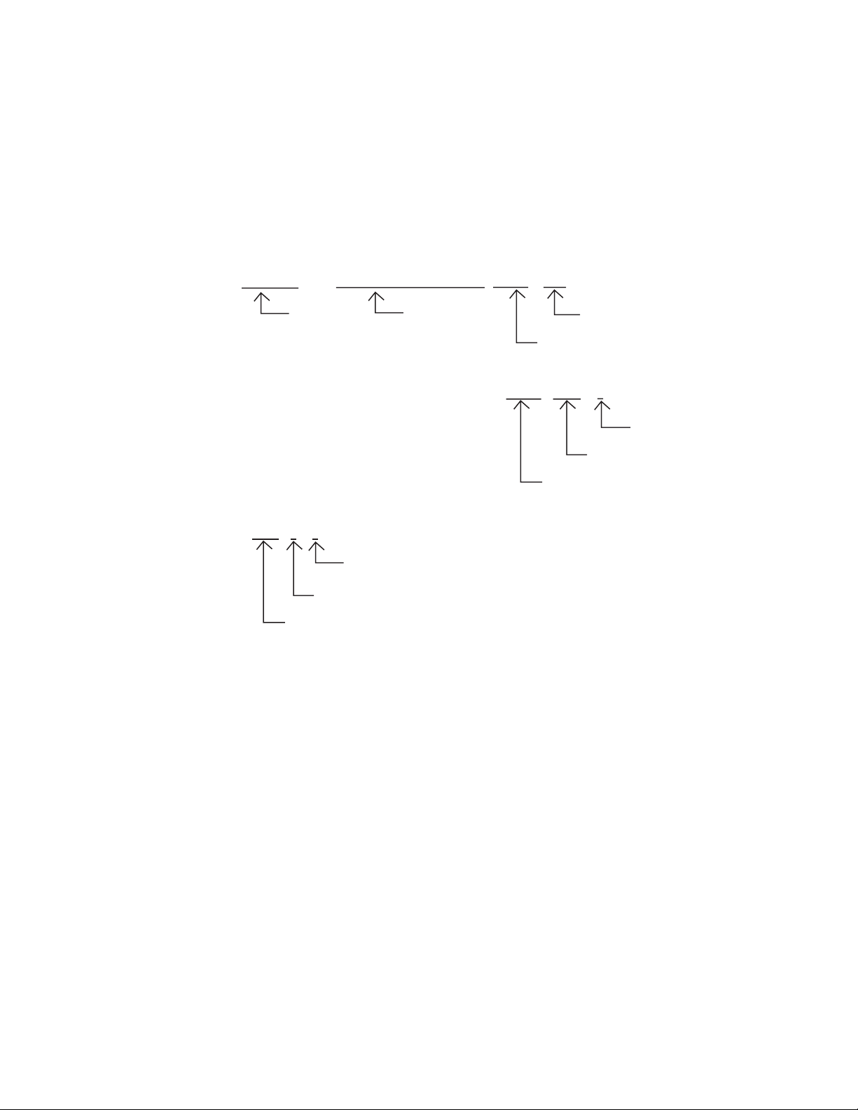
READING THIS MANUAL
■ Example Notation of Register Names and Pin Names
❍ Example notation of register names and bit names
By writing 1 into the sleep bit of the standby control register (STBC : SLP), ...
Bit name
Prohibit the output of interrupt request of the time-base timer (TBTC : TBIE = 0).
If interrupt enabled (CCR : I = 1) is specified, the interrupt is accepted.
Current state
Bit abbreviation
Register abbreviation
❍ Example notation of multi-use pins
P33/EC pin
Some pins can switch functions according to a setting made by a program or other method.
These pins are called multi-use pins. For multi-use pins, the names corresponding to
functions are listed and divided by /.
Register name
Register abbreviation
Bit abbreviation
Bit abbreviation
Register abbreviation
Setting data
iv
Page 9

CONTENTS
CHAPTER 1 OVERVIEW ................................................................................................... 1
1.1 Features of MB89202/F202RA Series ................................................................................................ 2
1.2 MB89202/F202RA Series Product Lineup .......................................................................................... 4
1.3 Differences between Models ............................ ... ... ... .... ...................................... .... ... ... ... .................. 6
1.4 Block Diagram of MB89202/F202RA Series ....................................................................................... 7
1.5 Pin Assignment ................................................................................................................................... 8
1.6 Package Dimensions ........................................................................................................................ 10
1.7 Pin Functions Description ................................................................................................................. 12
1.8 I/O Circuit Types ............................................................................................................................... 14
CHAPTER 2 HANDLING DEVICES ................................................................................ 17
2.1 Precautions on Handling Devices ..................................................................................................... 18
CHAPTER 3 CPU ............................................................................................................ 21
3.1 Memory Space .............. ... .... ... ... ....................................... ... ... .......................................................... 22
3.1.1 Specific-purpose Areas ............................................................................................................... 24
3.1.2 Location of 16-bit Data on Memory ............................................................................................. 26
3.2 Dedicated Register ........................................................................................................................... 27
3.2.1 Condition Code Register (CCR) .................................................................................................. 29
3.2.2 Register Bank Pointer (RP) ............................................... .... ... ... ................................................ 31
3.3 General-Purpose Registers . ... ... ... .... ... ....................................... ... ... ... ... .......................................... 32
3.4 Interrupts ....................... ............. ............. ............. ............. ............. ............. ............ .......................... 34
3.4.1 Interrupt Level Setting Registers (ILR1 to ILR4) .......................................................................... 36
3.4.2 Steps in the Interrupt Operation .................................................................................................. 37
3.4.3 Multiple Interrupts ........................................................................................................................ 39
3.4.4 Interrupt Processing Time ................. ... ... ....................................... ... .... ... ... ................................ 40
3.4.5 Stack Operation at Interrupt Processing ...................................................................................... 41
3.4.6 Stack Area for Interrupt Processing ............................................................................................. 42
3.5 Reset ................................................................................................................................................ 43
3.5.1 Reset Flag Register (RSFR) ........................................................................................................ 45
3.5.2 External Reset Pin ....................................................................................................................... 47
3.5.3 Reset Operation ................... ... .... ... ... ... ....................................... ... ... .... ...................................... 48
3.5.4 State of Each Pin at Reset .......................... ... ....................................... ... ... ... .... ... ...................... 50
3.6 Clock .................................... .......................................... ................................................................... 51
3.6.1 Clock Generator .......................................................................................................................... 53
3.6.2 Clock Controller ........................................................................................................................... 54
3.6.3 System Clock Control Register (SYCC) ......................................... ... ....................................... .. . 56
3.6.4 Clock Mode .................................................................................................................................. 58
3.6.5 Oscillation Stabilization Wait Time .............................................................................................. 60
3.7 Standby Mode (Low-Power Consumption Mode) ............................................................................. 62
3.7.1 Operations in Standby Mode ....................................................................................................... 63
3.7.2 Sleep Mode ................................................................................................................................. 64
3.7.3 Stop Mode ................................................................................................................................... 65
v
Page 10

3.7.4 Standby Control Register (STBC) ........... .... ...................................... .... ... ... ... ............................. 66
3.7.5 Diagram for State Transition in Standby Mode ............................................................................ 68
3.7.6 Notes on Standby Mode .......................... .... ...................................... .... ... ... ................................ 70
3.8 Memory Access Mode ............... ... .... ... ... ... ... ....................................... ... .... ... ... ................................ 72
CHAPTER 4 I/O PORTS .................................................................................................. 75
4.1 Overview of I/O Ports ........................................................................................................................ 76
4.2 Port 0 ............................... .... ...................................... .... ... ... ............................................................. 78
4.2.1 Registers of Port 0 (PDR0, DDR0, and PUL0) ............................................................................ 80
4.2.2 Operations of Port 0 Functions .................................................................................................... 82
4.3 Port 3 ............................... .... ...................................... .... ... ... ............................................................. 84
4.3.1 Registers of Port 3 (PDR3, DDR3, PUL3) ................................................................................... 86
4.3.2 Operations of Port 3 Functions .................................................................................................... 88
4.4 Port 4 ............................... .... ...................................... .... ... ... ............................................................. 90
4.4.1 Registers of Port 4 (PDR4) .......................................................................................................... 92
4.4.2 Operations of Port 4 Functions .................................................................................................... 93
4.5 Port 5 ............................... .... ...................................... .... ... ... ............................................................. 94
4.5.1 Registers of Port 5 (PDR5, DDR5, PUL5) ................................................................................... 96
4.5.2 Operations of Port 5 Functions .................................................................................................... 98
4.6 Port 6 ............................... .... ...................................... .... ... ... ........................................................... 100
4.6.1 Registers of Port 6 (PDR6, DDR6, PUL6) ................................................................................. 103
4.6.2 Operations of Port 6 Functions .................................................................................................. 105
4.7 Port 7 ............................... .... ...................................... .... ... ... ........................................................... 107
4.7.1 Registers of Port 7 (PDR7, DDR7, PUL7) ................................................................................. 109
4.7.2 Operations of Port 7 Functions .................................................................................................. 111
4.8 Programming Example of I/O Port .................................................................................................. 113
CHAPTER 5 TIME-BASE TIMER .................................................................................. 115
5.1 Overview of Time-base Timer . ... ... .... ... ....................................... ... ... .............................................. 116
5.2 Configuration of Time-base Timer .................................................................................................. 118
5.3 Time-base Timer Control Register (TBTC) ..................................................................................... 119
5.4 Interrupt of Time-base Timer ............ ... ....................................... ... ... ... ... ........................................ 121
5.5 Operations of Time-base Timer Functions ..................................................................................... 122
5.6 Notes on Using Time-base Timer ................................................................................................... 124
5.7 Program Example for Time-base Timer .......................................................................................... 125
CHAPTER 6 WATCHDOG TIMER ................................................................................ 127
6.1 Overview of Watchdog Timer ..................................................................... ... ... ... .... ... .................... 128
6.2 Configuration of Watchdog Timer ................................................................................................... 129
6.3 Watchdog Control Register (WDTC) .............................................................................................. 130
6.4 Operations of Watchdog Timer Functions ...................................................................................... 131
6.5 Notes on Using Watchdog Timer .................................................................................................... 132
6.6 Program Example for Watchdog Timer .......................................................................................... 133
vi
Page 11

CHAPTER 7 8-BIT PWM TIMER ................................................................................... 135
7.1 Overview of 8-bit PWM Timer ......................................................................................................... 136
7.2 Configuration of 8-bit PWM Timer .................................................................................................. 139
7.3 Pin of 8-bit PWM Timer ................................................................................................................... 141
7.4 Registers of 8-bit PWM Timer ......................................................................................................... 142
7.4.1 PWM Control Register (CNTR) ............... .... ... ... ... .... ... ... ....................................... ... ... ... .... ... . ... 143
7.4.2 PWM Compare Register (COMR) ..................................... .... ... ...................................... .... ... ... . 145
7.5 Interrupt of 8-bit PWM Timer .................................. ... .... ... ....................................... ... ... ... .............. 147
7.6 Operations of the Interval Timer Functions ..................................................................................... 148
7.7 Operations of the 8-bit PWM Timer Functions ................................................................................ 150
7.8 States in Each Mode During Operation .......................................................................................... 152
7.9 Notes on Using 8-bit PWM Timer ................................................................................................... 155
7.10 Program Example for PWM Timer .................................................................................................. 157
CHAPTER 8 8/16-BIT CAPTURE TIMER/COUNTER ................................................... 161
8.1 Overview of 8/16-bit Capture Timer/Counter .................................................................................. 162
8.2 Configuration of 8/16-bit Capture Timer/Counter ............................................................................ 166
8.3 Pins of 8/16-bit Capture Timer/Counter .......................................................................................... 168
8.4 Registers of 8/16-bit Capture Timer/Cou n te r ....................................................... .... ... ... ................. 170
8.4.1 Capture Control Register (TCCR) ............................................................................................. 171
8.4.2 Timer 0 Control Register (TCR0) ............................................................................................... 173
8.4.3 Timer 1 Control Register (TCR1) ............................................................................................... 175
8.4.4 Timer Output Control Register (TCR2) ...................................................................................... 177
8.4.5 Timer 0 Data Register (TDR0) ................................................................................................... 178
8.4.6 Timer 1 Data Register (TDR1) ................................................................................................... 180
8.4.7 Capture Data Registers H and L (TCPH and TCPL) ................................................................. 182
8.5 8/16-bit Capture Timer/Counter of Int er ru p ts ........................................................... ... .................... 183
8.6 Explanation of Operations of Interval Time r Fu n c tio ns .. ...................................... .... ... .................... 185
8.7 Operation of Counter Functions . ... ....................................... ... .... ... ...................................... ........... 189
8.8 Functions of Operations of Capture Fun c tio n s .................................... ....................................... ... . 193
8.9 8/16-bit Capture Timer/Counter Operation in Each Mode .............................................................. 197
8.10 Notes on Using 8/16-bit Capture Timer/Counter ............................................................................ 198
8.11 Program Example for 8/16-bit Capture Timer/Counter ................................................................... 200
CHAPTER 9 12-BIT PPG TIMER .................................................................................. 205
9.1 Overview of 12-bit PPG Timer ........................................................................................................ 206
9.2 Configuration of 12-bit PPG Timer Circuit ...................................................................................... 209
9.3 Pin of 12-bit PPG Timer .................................................................................................................. 211
9.4 Registers of 12-bit PPG Timer ................ ... ... .... ...................................... .... ... ... ... ........................... 213
9.4.1 12-bit PPG Control Register 1 (RCR21) .................................................................................... 214
9.4.2 12-bit PPG Control Register 2 (RCR22) .................................................................................... 215
9.4.3 12-bit PPG Control Register 3 (RCR23) .................................................................................... 216
9.4.4 12-bit PPG Control Register 4 (RCR24) .................................................................................... 218
9.5 Operations of 12-bit PPG Timer Functions ..................................................................................... 219
9.6 Notes on Using 12-bit PPG Timer .................................................................................................. 221
9.7 Program Example for 12-bit PPG Timer ......................................................................................... 223
vii
Page 12

CHAPTER 10 EXTERNAL INTERRUPT CIRCUIT 1 (EDGE) ......................................... 225
10.1 Overview of External Interrupt Circuit 1 ............................... ... ....................................... ... ... ........... 226
10.2 Configuration of External Interrupt Circuit 1 .................................................................................... 227
10.3 Pins of External Interrupt Circuit 1 .................................................................................................. 229
10.4 Registers of External Interrupt Circuit 1 .......................................................................................... 231
10.4.1 External Interrupt Control Register 1 (EIC1) .............................................................................. 232
10.4.2 External Interrupt Control Register 2 (EIC2) .............................................................................. 235
10.5 Interrupt of External Interrupt Circuit 1 ................................. ... .... ...................................... .............. 237
10.6 Operations of External Interrupt Circuit 1 ....................................................................................... 239
10.7 Program Example for External Interrupt Circuit 1 ........................................................................... 241
CHAPTER 11 EXTERNAL INTERRUPT CIRCUIT 2 (LEVEL) ....................................... 243
11.1 Overview of External Interrupt Circuit 2 ............................... ... ....................................... ... ... ........... 244
11.2 Configuration of External Interrupt Circuit 2 .................................................................................... 245
11.3 Pins of External Interrupt Circuit 2 .................................................................................................. 246
11.4 Registers of External Interrupt Circuit 2 .......................................................................................... 249
11.4.1 External Interrupt 2 Control Register (EIE2) .............................................................................. 250
11.4.2 External Interrupt 2 Flag Register (EIF2) ................................................................................... 252
11.5 Interrupt of External Interrupt Circuit 2 ................................. ... .... ...................................... .............. 253
11.6 Operations of External Interrupt Circuit 2 ....................................................................................... 254
11.7 Program Example for External Interrupt Circuit 2 ........................................................................... 256
CHAPTER 12 A/D CONVERTER .................................................................................... 259
12.1 Overview of A/D Converter ............................................ ... ... ... .... ...................................... .............. 260
12.2 Configuration of A/D Converter ....................................................................................................... 261
12.3 Pins of A/D Converter ..................................................................................................................... 263
12.4 Registers of A/D Converter ............................................................................................................. 265
12.4.1 A/D Control Register 1 (ADC1) .................................................................................................. 266
12.4.2 A/D Control Register 2 (ADC2) .................................................................................................. 268
12.4.3 A/D Data Register (ADDH and ADDL) ...................................................................................... 270
12.4.4 A/D Enable Register (ADEN) ..................................................................................................... 271
12.5 Interrupt of A/D Converter .......................................... .... ... ... ....................................... ... .. ............... 272
12.6 Operations of A/D Converter Functions .......................................................................................... 273
12.7 Notes on Using A/D Converter ....................................................................................................... 275
12.8 Program Example for A/D Converter .............................................................................................. 277
CHAPTER 13 UART ........................................................................................................ 279
13.1 Overview of UART .......................................................................................................................... 280
13.2 Configuration of UART .................................................................................................................... 284
13.3 Pins of UART .................................................................................................................................. 287
13.4 Registers of UART ........................ .... ...................................... .... ... ... ... ........................................... 289
13.4.1 Serial Mode Control Register (SMC) ......................................................................................... 290
13.4.2 Serial Rate Control Register (SRC) ........................................................................................... 292
13.4.3 Serial Status and Data Register (SSD) ..................................................................................... 294
13.4.4 Serial Input Data Register (SIDR) ............................................................................................. 297
13.4.5 Serial Output Data Register (SODR) ................................................. .... ... ................................. 298
13.4.6 Clock Divider Selection Register (UPC) .................................................................................... 299
viii
Page 13

13.4.7 Serial Switch Register (SSEL) ................................................................................................... 301
13.5 Interrupt of UART ....................................................... .... ... ... ... ........................................................ 303
13.6 Operations of UART Functions ....................................................................................................... 304
13.6.1 Transmission Operations (Operating Mode 0, 1, 2, and 3) ....................................................... 306
13.6.2 Reception Operations (Operating Mode 0, 1, or 3) ................................................................... 307
13.6.3 Reception Operations (Operating Mo d e 2 Only) ............................ ... .... ... ... .............................. 309
13.7 Program Example for UART ........................................................................................................... 311
CHAPTER 14 8-BIT SERIAL I/O ..................................................................................... 313
14.1 Overview of 8-Bit Serial I/O ............................................................................................................ 314
14.2 Configuration of 8-Bit Serial I/O ...................................................................................................... 315
14.3 Pins of 8-Bit Serial I/O .................................................................................................................... 317
14.4 Registers of 8-Bit Serial I/O .............. ...................................... .... ... ... ... ........................................... 319
14.4.1 Serial Mode Register (SMR) ...................................................................................................... 320
14.4.2 Serial Data Register (SDR) ....................................................................................................... 323
14.5 Interrupt of 8-Bit Serial I/O ............................................. ...................................... .... ... .................... 324
14.6 Operations of Serial Output Functions ............................................................................................ 325
14.7 Operations of Serial Input Functions .............................................................................................. 327
14.8 8-Bit Serial I/O Operation in Each Mode ......................................................................................... 329
14.9 Notes on Using 8-Bit Serial I/O ....................................................................................................... 333
14.10 Example of 8-Bit Serial I/O Connection .......................................................................................... 334
14.11 Program Example for 8-Bit Serial I/O ............................................................................................. 336
CHAPTER 15 BUZZER OUTPUT .................................................................................... 339
15.1 Overview of the Buzzer Output ....................................................................................................... 340
15.2 Configuration of the Buzzer Output ................................................................................................ 341
15.3 Pin of the Buzzer Output ................................................................................................................. 342
15.4 Buzzer Register (BZCR) ......................................... ... ....................................... ... .... ... .................... 343
15.5 Program Example for Buzzer Output .............................................................................................. 345
CHAPTER 16 WILD REGISTER FUNCTION .................................................................. 347
16.1 Overview of the Wild Register Function .......................................................................................... 348
16.2 Configuration of the Wild Register Function ................................................................................... 349
16.3 Registers of the Wild Register Function ......................................................................................... 350
16.3.1 Data Setting Registers (WRDR0 and WRDR1) ......................................................................... 351
16.3.2 Higher Address Set Registers (WRARH0 and WRARH1) ......................................................... 352
16.3.3 Lower Address Set Registers (WRARL0 and WRARL1) ........................................................... 353
16.3.4 Address Comparison EN Register (WREN) .............................................................................. 354
16.3.5 Data Test Set Register (WROR) ............................................................................................... 355
16.4 Operations of the Wild Register Functions ..................................................................................... 356
ix
Page 14

CHAPTER 17 FLASH MEMORY ..................................................................................... 357
17.1 Overview of Flash Memory ............................................................................................................. 358
17.2 Flash Memory Control Status Register (FMCS) ............................................................................. 359
17.3 Starting the Flash Memory Automatic Algorithm ............................................................................ 361
17.4 Confirming the Automatic Algorithm Execution State ..................................................................... 362
17.4.1 Data Polling Flag (DQ7) ............................................................................................................ 363
17.4.2 Toggle Bit Flag (DQ6) . .... ... ... ... ....................................... ... .... ... ... .............................................. 364
17.4.3 Timing Limit Exceeded Flag (DQ5) ........................................................................................... 365
17.4.4 Toggle Bit-2 Flag (DQ2) .................... ... ... .... ...................................... .... ... ... ... ........................... 366
17.5 Detailed Explanation of Writing to Erasing Flash Memory .............................................................. 367
17.5.1 Setting The Read/Reset State ................................................................................................... 368
17.5.2 Writing Data ............. ....................................... ... ... .... ... ....................................... ... .................... 369
17.5.3 Erasing All Data (Erasing Chips) ............................................................................................... 371
17.6 Flash Security Feature .................................................................................................................... 372
17.7 Notes on using Flash Memory ........................................................................................................ 373
APPENDIX ......................................................................................................................... 375
APPENDIX A I/O Map .......... ..................................................................................................................... 376
APPENDIX B Overview of the Instructions ............................................................................ .................... 380
B.1 Addressing ..................................................................................................................................... 383
B.2 Special Instructions ........................................................................................................................ 387
B.3 Bit Manipulation Instructions (SETB and CLRB) ............................................................................ 391
B.4 F
B.5 Instruction Map ............................................................................................................................... 399
APPENDIX C Mask Options ...................................................................................................................... 400
APPENDIX D Programming EPROM with Evaluation Chip ........................................................................ 401
APPENDIX E Pin State of the MB89202/F202RA Series .......................................................................... 402
2
MC-8L Instructions List ............................................................................................................... 392
INDEX...................................................................................................................................403
x
Page 15

Main changes in this edition
Page Changes (For details, refer to main body.)
-
6 1.3 Differences between
Models
12 1.7 Pin Functions RST
19 2.1 Precautions on
Handling Devices
24 3.1.1 Specific-purpose
Areas
-
The followings product name is changed.
(MB89202 → MB89202/F202RA)
The followings term is changed.
(source oscillation → oscillation frequency)
"Notes:" is changed.
(The followings sentence is deleted.
• At turning on the power, when the device is used without inputting the external
"
reset, select "reset output supported" and "power-on reset supported" by mask
option.")
The followings package is changed in Table 1.3-1.
(FPT-34P-M03 → FPT-32P-M03)
"● External pull-up for the External Reset Pin (RST
changed.
The summary is changed.
"■ General-purpose Register Area (address: 0100
"■ Vector Table Area (Address: FFC0
pin in Table 1.7-1 is changed.
) of MB89F202/F202RA" is
to 01FFH)" is changed.
H
to FFFFH)" is changed.
H
44 3.5 Reset "● Power-on reset" is changed.
"Note:" is deleted.
56 3.6.3 System Clock
57 Table 3.6-1 is changed.
130 6.3 Watchdog Control
186 8.6 Explanation of
264 12.3 Pins of A/D
308 13.6.2 Reception
Control Register (SYCC)
Register (WDTC)
Operations of Interval
Timer Functions
Converter
Operations (Operating
Mode 0, 1, or 3)
Figure 3.6-5 is changed.
Figure 6.3-1 is changed.
"● 8-bit mode"is changed.
(The followings sentence is deleted.
"The initial value of the square wave output is "L" level. The square wa ve output is
initialized by writing "0" to the TSTR bit of the timer control register (TCR).")
"■ Block Diagram of the Pins Related to the A/D Converter" is changed.
("Note:" is deleted.)
"■ Reception Operations (Operating Mode 0, 1, or 3)" is changed.
("Note:" is changed.)
xi
Page 16

Page Changes (For details, refer to main body.)
310 13.6.3 Reception
Operations (Operating
"■ Reception Operations (Operating Mode 2 Only)" is changed.
("Note:" is changed.)
Mode 2 Only)
358 17.1 Overview of Flash
"■ High voltage supply on RST
Memory
370 17.5.2 Writing Data Figure 17.5-1 is changed.
(F555 → F554)
394
2
MC-8L
B.4 F
Instructions List
Table B.4-2 is changed.
("No.22 DECW A" is changed.)
The vertical lines marked in the left side of the page show the changes.
pin (applicable to MB89F202RA only)" is added.
xii
Page 17

CHAPTER 1
OVERVIEW
This chapter describes the features and basic
specification of the MB89202/F202RA series.
1.1 Features of MB89202/F202RA Series
1.2 MB89202/F202RA Series Product Lineup
1.3 Differences between Models
1.4 Block Diagram of MB89202/F202RA Series
1.5 Pin Assignment
1.6 Package Dimensions
1.7 Pin Functions Description
1.8 I/O Circuit Types
1
Page 18

CHAPTER 1 OVERVIEW
1.1 Features of MB89202/F202RA Series
The MB89202/F202RA series contains general-purpose single-chip microcontroller s that
incorporate a full range of peripheral functions such as A/D converter, UART, PWM
timer, PPG, capture timer/counter and external interrupts as well as a compact
instruction set.
■ Features of MB89202/F202RA Series
● F2MC-8L CPU core
• Instruction set most suitable for controllers
• Multiplication and division instruction
• 16-bit operation
• Branch instruction by bit test
• Bit operation instruction, and others
● 4-system timers
• 8/16-bit capture timer/counter (8-bit capture timer/counter + 8-bit timer or 16-bit capture timer/counter)
• 8-bit PWM timer (also available as an interval timer)
• 21-bit time-base timer
• Watchdog timer
● 10-bit A/D converter
•10-bit A/D × 8 channels
• Activation by 8/16-bit capture timer/counter output is possible.
● Programmable pulse generator (PPG)
• Pulse width and cycle are software selectable (12-bit PPG).
● UART
• 6, 7, or 8 transfer data length
● 8-bit serial I/O
• Available when switched from UART
• LSB first/MSB first selectability
● External interrupts
• External interrupt 1 (edge detection × 3 pins) has three independent inputs and can be used for wake-up
from low-power consumption mode. (The edge detection can be sel ected from rising -edge, falli ng-edge,
and both-edge modes.)
2
Page 19

• External interrupt 2 (level d etection × 8 pins, 1 channel) has eight independent inputs and can be used
for wake-up from low-power consumption mode. (L level detection function is supported.)
● Low-power consumption modes (standby modes)
• Stop mode (The oscillation is stopped so that current cons umption is minimal.)
• Sleep mode (The CPU is stopped so that the current consumption is reduced by one-third of normal
consumption.)
● Up to 26 pins of I/O ports
• General-purpose I/O ports (CMOS): 26 pins (4 of which can be used as N-ch open-drain I/O ports.)
● Wild registers
• 2-byte data at two addresses are available.
• When a specific address or data is used on a wild register, the data in the ROM area is changed.
● 16 KB Flash with read protection
• Once the protection code is written in the specified address, the FLASH content cannot be read by
parallel/serial programmer.
CHAPTER 1 OVERVIEW
3
Page 20

CHAPTER 1 OVERVIEW
1.2 MB89202/F202RA Series Product Lineup
Four MB89202 series models are available. Table 1.2-1 shows the models and Table 1.22 shows the CPU and peripheral functions.
■ MB89202/F202RA Series Models
Table 1.2-1 MB89202/F202RA Series Models
MB89201 MB89F202/F202RA MB89V201
Classification
ROM size
RAM size 512 × 8 bits
Low-power consumption
(standby mode)
Process CMOS
Operating voltage
*1: The minimum operating voltage varies with conditions such as operating frequency, functions, and connecting
ICE.
*2: MBM27C256A is used as the external ROM.
*1
Evaluation product
(for development)
32K × 8 bits
(External EPROM
2.7V to 5.5V 3.5V to 5.5V 2.2V to 5.5V
*2
)
Flash memory product
(read protection)
16K × 8 bits
(Internal Flash)
Sleep mode and stop mode
Mask ROM product
16K × 8 bits
(Internal mask ROM)
4
Page 21

Table 1.2-2 CPU and Peripheral Functions of MB89202/F202RA Series
Item Specification
Number of basic instructions: 136 instructions
Instruction bit length: 8 bits
CPU function
Instruction length: 1 to 3 bytes
Data bit length: 1, 8, or 16 bits
Minimum instruction execution time: 0.32 to 5.1 µs (at 12.5 MHz)
Interrupt processing time: 2.88 to 46.1 µs (at 12.5 MHz)
CHAPTER 1 OVERVIEW
Periphera
l function
Port
21-bit
time-base
General-purpose I/O port: 26 pins (Also serve as peripherals. 4 of which can be used as N-ch
open-drain I/O ports.)
21 bits
Interrupt cycle: 0.66 ms, 2.64 ms, 21 ms, or 335.5 ms with 12.5MHz main clock
timer
Watchdog
Reset occurrence cycle: When the main clock is at 12.5 MHz (minimum 335.5 ms)
timer
8-bit
PWM
timer
8/16-bit
capture
timer/
8-bit interval timer operation (Square wave output is supported. Operating clock cycle:
1 t
INST
, 16 t
INST
, 64 t
, and 8/16-bit capture timer/counter output)
INST
8-bit resolution PWM operation (Conversion cycle:
256 t
INST
, 4096 t
INST
, 16384 t
8-bit capture timer/counter × 1 channel + 8-bit timer or 16-bit capture timer/counter × 1 channel
When timer 0 or a 16-bit counter is operating, event-counting operation by external clock input
and square wave output are supported.
counter
UART Transfer data length: 6, 7, or 8 bits
8-bit serial
I/O
12-bit
8 bits length, LSB first/MSB first selectability
One clock selectable from four operation clocks
(one external shift clock, three internal shift clocks: 2 t
Output frequency: Pulse width and cycle are selectable.
PPG timer
and 256 times 8/16-bit capture timer/counter output)
INST
INST
, 8 t
INST
, 32 t
INST
)
External
interrupt 1
(wake-up)
External
interrupt 2
3 channels (interrupt vector, request flag, and request output enable)
Edge selectability (selectable from rising edge, falling edge, and both-edge modes)
Also available for wake-up from stop or sleep (Edge detection is also available in stop mode.)
8 inputs 1 channel (L level interrupt and input enable are independent.)
Also available for wake-up from stop or sleep (Level detection is also available in stop mode.)
(wake-up)
10-bit A/D
converter
Wild
10-bit resolution × 8 channels
A/D conversion function (Conversion time: 38 t
INST
)
Continuous activation by 8/16-bit capture timer/counter output or time-base timer output.
8-bit × 2
register
Note:
The oscillation is 12.5 MHz unless another condition such as the main clock maximum speed, the clock
cycle value, or conversion time is stated.
5
Page 22

CHAPTER 1 OVERVIEW
1.3 Differences between Models
This section describes the precautions to be taken when selecting a MB89202/F202RA
series model.
■ Precautions when Selecting a Model
Table 1.3-1 Differences between Mod els
Package MB89201 MB89F202/F202RA MB89V202
DIP-32P-M06
FPT-32P-M03
FPT-64P-M03
● Current consumption
• When operated at a low speed, the current consumption of a model with a flash is greater than that of a
model with a mask ROM, though the current consumption in sleep or stop mode is the same.
Notes:
• For details on each package, see Section "1.6 Package Dimensions ".
• For details on current consumption and electrical characteristics of A/D converter, see the electrical
characteristics in the Data Sheet.
6
Page 23

1.4 Block Diagram of MB89202/F202RA Series
Figure 1.4-1 shows the block diagram of the MB89202/F202RA series.
■ Block Diagram of MB89202/F202RA Series
Figure 1.4-1 Block Diagram of MB89202/F202RA Series
CHAPTER 1 OVERVIEW
RST
P60, P61
1
*
P70
to
1
*
P04 / INT24
to
P07 / INT27
P02 / INT22 / AN6,
P03 / INT23 / AN7
P00 / INT20 / AN4,
P01 / INT21 / AN5
*1P40 / AN0
to
1
P43 / AN3
*
P72
X0
X1
Main clock
oscillator
Clock controller
Reset circuit
Port 6
2
CMOS I/O port
3
4
2
2
4
CMOS I/O port
Port 7
CMOS I/O port
8
4
4
External
interrupt2
(wake-up)
10-bit A/D
converter
Port 4 Port 0
CMOS I/O port
(N-ch OD)
Time-base timer
UART prescaler
Internal bus
serial I/O
capture timer/
External interrupt1
CMOS I/O port
8-bit PWM
UART
8-bit
8/16-bit
counter
Serial function switching
3
Port 5Port 3
P50 / PWM
P30 / UCK / SCK
P31 / UO / SO
P32 / UI / SI
P33 / EC
P34 / TO / INT10
P35 / INT11
P36 / INT12
512 or 256 bytes RAM
Other pins
VCC, VSS, C
1
: Large-current drive type
*
2
*
: Check section "3.1 Memory Space"
F2MC - 8 L CPU
16K or 8K bytes ROM
Wild register
2
*
12-bit PPG
P37 / BZ / PPG
2
*
Buzzer output
CMOS I/O port
7
Page 24

CHAPTER 1 OVERVIEW
1.5 Pin Assignment
Figure 1.5-1 and Figure 1.5-2 show the pin assignment of the MB89202/F202RA series.
■ Pin Assignment of DIP-32P-M06
Figure 1.5-1 Pin Assignment of DIP-32P-M06
P04/INT24
P05/INT25
P06/INT26
P07/INT27
P60
P61
RST
X0
X1
SS
V
P37/BZ/PPG
P36/INT12
P35/INT11
P34/TO/INT10
P33/EC
C
* : Large-current drive type
1
2
3
4
5
6
7
8
9
10
11
12
13
14
15
16
32
31
30
29
28
27
26
25
24
23
22
21
20
19
18
17
V
CC
P03/INT23/AN7
P02/INT22/AN6
P01/INT21/AN5
P00/INT20/AN4
P43/AN3*
P42/AN2*
P41/AN1*
P40/AN0*
P72*
P71*
P70*
P50/PWM
P30/UCK/SCK
P31/UO/SO
P32/UI/SI
8
Page 25

■
Pin Assignment of FPT-34P-M03
Figure 1.5-2 Pin Assignment of FPT-34P-M03
P04/INT24
P05/INT25
P06/INT26
P07/INT27
P37/BZ/PPG
P36/INT12
P35/INT11
P34/TO/INT10
P33/EC
P60
P61
RST
X0
X1
SS
V
N.C.
CHAPTER 1 OVERVIEW
CC
1
2
3
4
5
6
7
8
9
10
11
12
13
14
15
16
C
17
34
33
32
31
30
29
28
27
26
25
24
23
22
21
20
19
18
V
P03/INT23/AN7
P02/INT22/AN6
P01/INT21/AN5
P00/INT20/AN4
*
P43/AN3
*
P42/AN2
*
P41/AN1
*
P40/AN0
*
P72
*
P71
*
P70
N.C.
P50/PWM
P30/UCK/SCK
P31/UO/SO
P32/UI/SI
* : Large-current drive type
Note: N.C.: Do not use because it is connected internally.
9
Page 26

CHAPTER 1 OVERVIEW
1.6 Package Dimensions
Two different packages are available for MB89202/F202RA series.
Figure 1.6-1 and Figure 1.6-2 show package dimensions.
■ Package Dimension of DIP-32P-M06
Figure 1.6-1 Package Dimension of DIP-32P-M06
32-pin plastic SH-DIP Lead pitch 1.778 mm
Low space 10.16 mm
(DIP-32P-M06)
32-pin plastic SH-DIP
(DIP-32P-M06)
INDEX
+0.70
4.70
–0.20
+.028
.185
–.008
+0.20
3.30
–0.30
+.008
.130
–.012
1.27(.050)
MAX.
C
2003 FUJITSU LIMITED D32018S-c-1-1
*28.00
1.102
1.778(.070)
Sealing method
Note 1)* : These dimensions do not include resin protrusion.
+0.20
–0.30
+.008
–.012
0.48
.019
Note 2) Pins width and pins thickness include plating thickness.
±0.25
*8.89
(.350±.010)
+0.30
1.02
–0.20
+.012
–.008
.040
0.51(.020)
MIN.
+0.03
0.27
–0.07
+.001
.011
+0.08
–0.12
+.003
–.005
0.25(.010)
M
–.003
Dimensions in mm (inches).
Note: The values in parentheses are reference values
Plastic mold
10.16(.400)
0~15˚
10
Please confirm the latest Package dimension by following URL.
http://edevice.fujitsu.com/fj/DATASHEET/ef-ovpklv.html
Page 27

■
Package Dimension of FPT-34P-M03
Figure 1.6-2 Package Dimension of FPT-34P-M03
34-pin plastic SSOP Lead pitch 0.65 mm
CHAPTER 1 OVERVIEW
(FPT-34P-M03)
34-pin plastic SSOP
(FPT-34P-M03)
1
*
11.00±0.10(.433±.004)
34 18
INDEX
Note 1)*1 : Resin protrusion. (Each side : +0.15 (.006) Max).
Note 2)*2 : These dimensions do not include resin protrusion.
Note 3)Pins width and pins thickness include plating thickness.
Note 4) Pins width do not include tie bar cutting remainder.
2
*
6.10±0.10 8.10±0.20
(.240±.004) (.319±.008)
Package width
package length
Lead shape
Sealing method
×
6.10 × 11.00 mm
Gullwing
Plastic mold
Mounting height 1.45 mm MAX
Code
(Reference)
P-SSOP34-6.1×11-0.65
0.17±0.03
(.007±.001)
Details of "A" part
+0.20
–0.10
1.25
+.008
–.004
.049
0.25(.010)
(Mounting height)
1 17
0.65(.0265)
0.10(.004)0.10(.004)
C
2003 FUJITSU LIMITED F34003S-c-2-3
0.24
.009
+0.08
–0.07
0.10(.004)
+.003
–.003
"A"
M
Please confirm the latest Package dimension by following URL.
http://edevice.fujitsu.com/fj/DATASHEET/ef-ovpklv.html
0~8
˚
0.50±0.20
(.020±.008)
0.60±0.15
(.024±.006)
Dimensions in mm (inches).
Note: The values in parentheses are reference values
0.10±0.10
(.004±.004)
(Stand off)
11
Page 28

CHAPTER 1 OVERVIEW
1.7 Pin Functions Description
Table 1.7-1 describes the I/O pins and functions.
The letters in the circuit type column shown in Table 1.7-1 correspond to the letters in
the Circuit Type column shown in Table 1.8-1 .
■ Pin Functions Description
Table 1.7-1 Pin Functions Description (1/2)
SHDIP32
Pin No.
*1
SSOP34
Pin
name
*2
Circuit
type
Function
8 8 X0 A Pins for connecting the crystal for the main clock. To use an
99X1
5, 6 5, 6 P60,
H / E General-purpose CMOS input port.
external clock, input the signal to X0 and leave X1 open.
P61
77RST
C Reset I/O pin.
This pin serves as an N-ch open-drain reset output and a reset input
as well. The reset is a hysteresis input.
It outputs the "L" signal in response to an internal reset request.
Also, it initializes the internal circuit upon input of the "L" signal.
28, 29 30, 31 P00/
INT20
AN4,
P01/
INT21
G General-purpose CMOS I/O ports.
/
These pins also serve as an input (wake-up input) of external
interrupt 2 or as an 10-bit A/D converter analog input. The input of
external interrupt 2 is a hysteresis input.
/
AN5
30, 31 32, 33 P02/
INT22
AN6,
P03/
INT23
G General-purpose CMOS I/O ports.
/
These pins also serve as an input (wake-up input) of external
interrupt 2 or as an 10-bit A/D converter analog input. The input of
external interrupt 2 is a hysteresis input.
/
AN7
1 to 4 1 to 4 P04/
19 20 P30/
18 19 P31/
12
INT24
to
P07/
INT27
UCK/
SCK
UO/SO
D General-purpose CMOS I/O ports.
These pins also serve as an input (wake-up input) of external
interrupt 2. The input of external interrupt 2 is a hysteresis input.
B General-purpose CMOS I/O ports.
This pin also serves as the clock I/O pin for the UART or 8-bit
serial I/O. The resource is a hysteresis input.
E General-purpose CMOS I/O ports.
This pin also serves as the data output pin for the UART or 8-bit
serial I/O.
Page 29

Table 1.7-1 Pin Functions Description (2/2)
CHAPTER 1 OVERVIEW
SHDIP32
Pin No.
*1
SSOP34
Pin
name
*2
Circuit
type
Function
17 18 P32/UI/SIB General-purpose CMOS I/O ports.
This pin also serves as the data input pin for the UART or 8-b it
serial I/O. The resource is a hysteresis input.
15 15 P33/EC B General-purpose CMOS I/O ports.
This pin also serves as the external clock input pin for the 8/16-bit
capture timer/counter. The resource is a hysteresis input.
14 14 P34/
TO/
INT10
B General-purpose CMOS I/O ports.
This pin also serves as the output pin for the 8/16-bit capture timer/
counter or as the input pin for external interrupt 1. The resource is a
hysteresis input.
13 13 P35/
INT11
B General-purpose CMOS I/O ports.
These pins also serve as the input pin for external interrupt 1. The
resource is a hysteresis input.
12 12 P36/
INT12
B General-purpose CMOS I/O ports.
These pins also serve as the input pin for external interrupt 1. The
resource is a hysteresis input.
11 11 P37/
BZ/
PPG
E General-purpose CMOS I/O ports.
This pin also serves as the buzzer output pin or the 12-bit PPG
output pin.
20 21 P50/
PWM
24 to 27 26 to 29 P40/
AN0 to
P43/
E General-purpose CMOS I/O ports.
This pin also serves as the 8-bit PWM timer output pin.
F General-purpose CMOS I/O ports.
These pins can also be used as N-ch open-drain ports.
These pins also serve as 10-bit A/D converter analog input pins.
AN3
21 to 23 23 to 25 P70 to
E General-purpose CMOS I/O ports.
P72
32 34 V
10 10 V
CC
SS
-- Power supply pin
-- Power (GND) pin
16 17 C -- MB89F202/F202RA:
Capacitance pin for regulating the power supply.
Connect an external ceramic capacitor of about 0.1µF.
MB89202:
This pin is not internally connected. It is unnecessary to connect
a capacitor.
-- 16, 22 N.C. -- Internally connected pins
Be sure to leave it open.
*1 : DIP-32P-M06
*2 : FPT-34P-M03
13
Page 30

CHAPTER 1 OVERVIEW
1.8 I/O Circuit Types
Table 1.8-1 describes the I/O circuit types.
The letters in the circuit column shown in Table 1.8-1 correspond to the letters in the
circuit type column shown in Table 1.7-1 .
■ I/O Circuit Types
Table 1.8-1 I/O Circuit Types (1/2)
Types Circuit Remarks
A At an oscillation feedback resistance of
approximately 500 kΩ
X1
X0
Standby control signal
B CMOS output
Hysteresis input
Pull-up resistor optional
Input enable
P-ch
P-ch
N-ch
Port / Resource
C At an output pull-up resistor (P-ch) of
P-ch with pull-up, not
available for
MB89F202/F202RA
approximately 50 kΩ/5.0 V
(not available for MB89F202/F202RA)
N-ch open-drain reset output
Hysteresis input
High voltage input tolerable in MB90F202RA
N-ch
Reset
14
Page 31

Table 1.8-1 I/O Circuit Types (2/2)
Types Circuit Remarks
D CMOS output
P-ch
P-ch
N-ch
CMOS input
Hysteresis input (Resource input)
Pull-up resistor optional
CHAPTER 1 OVERVIEW
Input enable
Input enable
Port
Resource
E CMOS output
CMOS input
P-ch
Pull-up resistor optional
P70 to P72 are large current drive type
P-ch
N-ch
Input enable
Port
F CMOS output
CMOS input
P-ch
Open-drain control
Analog input
N-ch open-drain output available
P40 to P43 are large current drive type
Input enable
N-ch
Analog input
Port
A/D enable
G CMOS output
P-ch
CMOS input
Hysteresis input (Resource input)
Analog input
P-ch
N-ch
Input enable
Input enable
Analog input
A/D enable
Port
Resource
HCMOS input
Input enable
Port
15
Page 32

CHAPTER 1 OVERVIEW
16
Page 33

CHAPTER 2
HANDLING DEVICES
This chapter describes the precautions to be taken when
handling general-purpose one-chip microcontrollers.
2.1 Precautions on Handling Devices
17
Page 34

CHAPTER 2 HANDLING DEVICES
2.1 Precautions on Handling Devices
This section describes the precautions to be taken when handling the power supply
voltage, pins, and other device items.
■ Precautions on Handling Devices
● Ensure that the voltage does not exceed the maximum ratings. (Preventing latch-up)
A latch-up may occur if a voltage higher than Vcc or lower than Vss is applied to input or output pins other
than middle- or high-level resistant pins, or if voltage exceeding the rated value is applied between Vcc and
Vss.
When a latch-up occurs, the supply current increases rapidly, occasionally resulting in overheating.
Therefore, ensure that the voltage does not exceed the maximum ratings when using the microcontrollers.
● Stabilize the supply voltage as much as possible
Although the specified Vcc supply voltage operating range is assured, a sudden change in the supply
voltage within the specified range may result in a malfunction.
The following stabilization guidelines are recommended: The Vcc ripple (P-P value) at the supply
frequency (50 Hz to 60 Hz) should be less than 10% o f the typical Vcc value, and the transient fluctuation
rate should be less than 0.1 V/ms at the time of momentary fluctuation when switching the power supply.
● Handling unused input pins
Leaving unused input pins open may result in a malfunction or equipment damage due to a latch-up.
Therefore, set these pins to pull-up or pull-down via resistors of 2 kΩ or hi gher.
● Handling the N.C. pins
Ensure that the N.C. (internally connected) pins are opened before using.
● Precautions on using an external clock
When an external clock is used, the oscillation stabilization wait time is also provided for power-on reset
and stop mode release.
● Wild register function
Because wild registers cannot be debugged on MB89V201, check operation on an actual MB89F202/
F202RA.
18
● Program execution on RAM
When MB89V201 is used, a program cannot be executed on RAM.
Page 35

CHAPTER 2 HANDLING DEVICES
● Note to Noise in the External Reset Pin (RST
If the reset pulse applied to the external reset pin (RST
malfunctions. Use caution so that the reset pulse less than the specifications will not be f ed to the external
reset pin (RST
● External pull-up for the External Reset Pin (RST
Internal pull-up control for RST
control in MB89F202/F202RA, an external pull-up (recommend 100 kΩ) for RST
For MB89F202RA only, high voltage must be applied to RST
typical high voltage is 10 V.
● Step-down circuit stabilization time
The MB89202/F202RA series consists of the products listed in Table 2.1-1 "Pin Processing for the
Products with and without a Step-down Circuit". The operation characteristic depends on whether a product
contains a step-down circuit.
Table 2.1-1 Pin Processing for the Products with and without a Step-down Circuit
Product name Operating voltage Step-down circuit
).
is not available for MB89F202/F202RA. To ensure proper external reset
MB89V201 2.7 V to 5.5 V Not contained
)
) does not meet the specifications, it may cause
) of MB89F202/F202RA
pin must be required.
during flash memory program / erase. The
MB89202 2.2 V to 5.5 V Not contained
MB89F202/F202RA 3.5 V to 5.5 V Contained
These products use the same internal resources. However, the operation sequence after power-on reset
depends on whether a product contains a step-down circuit. Figure 2.1-1 shows the sequence of operations
after the power-on reset for each model.
19
Page 36

CHAPTER 2 HANDLING DEVICES
Figure 2.1-1 Operation Sequences after Power-on Reset between Product Types
Power supply (VCC)
CPU operation of
product with a step-down
circuit (MB89F202/F202RA)
CPU operation of
product without a
step-down circuit
(MB89202 and MB89V201)
F
: Main oscillation frequency
CH
As shown in Figure 2.1-1 , the start of CPU operation of a product with a step-down circuit is slower th an
that of the product without a step-down circuit. This is because time is required for the step-down circuit to
stabilize prior to normal operation of the step-down circuit.
Step-down circuit stabilization time (217/FCH) +
Oscillation stabilization wait time (2
Oscillation stabilization
wait time (2
18
/FCH)
Start of CPU operation of
product without a step-down
circuit (reset vector)
18
/FCH)
Start of the CPU operation of
product with a step-down
circuit (reset vector)
20
Page 37

CHAPTER 3
CPU
This chapter describes the functions and operations of
the CPU.
3.1 Memory Space
3.2 Dedicated Register
3.3 General-Purpose Registers
3.4 Interrupts
3.5 Reset
3.6 Clock
3.7 Standby Mode (Low-Power Consumption Mode)
3.8 Memory Access Mode
21
Page 38

CHAPTER 3 CPU
3.1 Memory Space
The MB89202/F202RA series has 64-KB memory space that consists of the I/O area,
RAM area, ROM area, and external area. P a rt of the memory space is applied for specific
use such as general-purpose registers or a vector table.
■ Configuration of Memory Space
● I/O area (address: 0000H to 007FH)
The control registers and data registers for built-in peripheral functions are assigned.
The I/O area is assigned as part of the memory space, thus access to the I/O area can be obtained in the
same manner as access to memory. Also, direct addressing provides high-speed access.
● RAM area
Static RAM is equipped as the internal data area.
The size of internal RAM depends on the model.
Direct addressing allows high-speed access to an area from 80
range of the area.)
100
H
If a reset occurs while data is being written into RAM, the data being written cannot be guaranteed.
● ROM area
ROM is equipped as the internal program area.
The size of internal ROM depends on the model.
FFC0
to 1FFH can be used as the general-purpose register area.
to FFFFH are usable as a vector table or another feature.
H
to FFH. (Some models restrict the usable
H
22
Page 39

■
Memory Map
0000
Figure 3.1-1 Memory Map
MB89V201 MB89202 MB89F202/F202RA
H
0000H
0000H
CHAPTER 3 CPU
0080H
0100H
0200H
0280H
8000H
FFFFH
I/O
0080H
RAM 512 bytes
0100H
Register
0200H
0280H
Not available Not available
C000H
External EPROM
32 KB
FFFFH
I/O I/O
RAM 512 bytes RAM 512 bytes
Register
ROM 16 KB Flash 16 KB
0080H
0100H
Register
0200H
0280H
Not available
C000H
FFFFH
23
Page 40

CHAPTER 3 CPU
3.1.1 Specific-purpose Areas
In addition to the I/O area, the general-purpose register area and vector table area are
available as areas for specific applications.
■ General-purpose Register Area (Address: 0100
• This area is used for 8-bit arithmetic operations and transfer. Supplementary registers are provided.
• Since this area is allocated to a part of the RAM area, it can also be used as normal RAM.
• When this area is used as a general-purpose register, it can be accessed faster using shorter instructions
by general-purpose register addressing.
For details, see Section "3.2.2 Register Bank Pointer (RP) " and Section "3.3 General-Purpose Registers ".
■
Vector Table Area (Address: FFC0H to FFFFH)
• This area is used as vector tables of the vector call instructions, interrupts, and reset.
• This area is allocated to the highest ranges of the ROM area, and the start address of the corresponding
processing routine is set to the address of each vector table.
Table 3.1-1 provides the reference addresses in the vector table that correspond to the vector instruct ions,
interrupts, and reset.
For details, see Section "3.4 Interrupts ", Section "3.5 Reset ", and "CALLV #vct" in APPENDIX "B.2
Special Instructions ".
Table 3.1-1 Vector Table (1/2)
Address in the vector table
Vector call instruction
Upper digits Lower digits
to 01FFH)
H
24
CALLV #0
CALLV #1
CALLV #2
CALLV #3
CALLV #4
CALLV #5
FFC0
FFC2
FFC4
FFC6
FFC8
FFCA
CALLV #6 FFCC
CALLV #7
FFCE
IRQF FFDC
IRQE FFDE
IRQD FFE0
IRQC FFE2
H
H
H
H
H
H
H
H
H
H
H
H
FFC1
FFC3
FFC5
FFC7
FFC9
FFCB
FFCD
FFCF
FFDD
FFDF
FFE1
FFE3
H
H
H
H
H
H
H
H
H
H
H
H
Page 41

Table 3.1-1 Vector Table (2/2)
Vector call instruction
CHAPTER 3 CPU
Address in the vector table
Upper digits Lower digits
IRQB FFE4
IRQA FFE6
IRQ9 FFE8
IRQ8 FFEA
IRQ7 FFEC
IRQ6 FFEE
IRQ5 FFF0
IRQ4 FFF2
IRQ3 FFF4
IRQ2 FFF6
IRQ1 FFF8
IRQ0 FFFA
H
H
H
H
H
H
H
H
H
H
H
H
FFE5
FFE7
FFE9
FFEB
FFED
FFEF
FFF1
FFF3
FFF5
FFF7
FFF9
FFFB
Mode data - * FFFD
Reset vector FFFE
H
FFFF
H
H
H
H
H
H
H
H
H
H
H
H
H
H
*: For MB89202 / MB89V201, FFFCH is prohibited. (Use "FFH".)
For MB89F202/F202RA, write "01
otherwise write "FF
".
H
" to FFFCH to activate read protection,
H
25
Page 42

CHAPTER 3 CPU
3.1.2 Location of 16-bit Data on Memory
Upper digits of 16-bit data and stack data are stored in lower addresses on memory.
■ 16-bit Data Storage State on RAM
When 16-bit data is written into RAM, the upper byte of the data is stored with a lower address and the
lower byte of the data is stored with the next address. 16-bit data is read in the same manner.
Figure 3.1-2 shows the location of 16-bit data on RAM.
Figure 3.1-2 Location of 16-bit Data on RAM
Before
written
1234
H
A
■
16-bit Operand Storage State
When 16 bits are specified for operands in instructions, upper bytes are also stored in addresses close to
operation codes (instructions) and lower bytes are stored in the following addresses.
Operands that indicate memory addresses and 16-bit immediate data are handled in the same manner as
stated above.
Figure 3.1-3 shows the locations of 16-bit data in instructions.
Figure 3.1-3 Location of 16-bit Data in Instructions
[Example] MOV A, 5678H
Memory
MOV W A, #1234H
XXX0HXX XX
XXX2
XXX5
XXX8
0080
H
0081
H
0082
H
0083
H
H
60
H
E4 12 34
H
XX
MOVW 0081H, A
Processed through assembler
.
.
.
78
56
.
.
.
After
written
A
1234
H
; Extend address
; 16-bit immediate data
; Extend address
; 16-bit immediate data
Memory
H
12
34
H
0080
0081
0082
0083
H
H
H
H
■
16-bit Data Storage State in Stack
The upper byte of data for a 16-bit register put in the stack due to an interrupt is also stored with a lower
address.
26
Page 43

CHAPTER 3 CPU
3.2 Dedicated Register
The dedicated register in the CPU consists of a program counter (PC), two arithmetic
operation registers (A and T), three address pointers (IX, EP, and SP), and program
status (PS) register. The size of each register is 16 bits.
■ Dedicated Register Configuration
The dedicated register in the CPU consists of seven 16-bit registers. Some registers allow only the lower 8
bits to be used.
Figure 3.2-1 shows the configuration of the dedicated register.
Figure 3.2-1 Configuration of Dedicated Register
Initial value
FFFD
H
Undefined
Undefined
Undefined
Undefined
Undefined
Flag I = 0
IL1 and IL0 = 11
The other bits are undefined.
■
Functions of the Dedicated Register
16 bits
PC
A:
T:
IX :
EP :
SP :
RP CCR :
PS
● Program counter (PC)
The size of the program counter is 16 bits. It indicates the memory address at which the CPU is currently
handling an instruction. The program counter is update d with an instruction executed, interrupt, or reset.
The initial value specified after the reset operation is the mode data read address (FFFD
:
Program counter
Indicates the current instruction stored position.
Accumulator
Temporary register that handles arithmetic operations and
data transfer.
Temporary accumulator
Handles arithmetic operations together with the accumulator.
Index register
Indicates index address.
Extra-pointer
Indicates memory address.
Stack pointer
Indicates the current position in the stack.
Program status register
Stores the register bank pointer and condition code.
).
H
● Accumulator (A)
The accumulator is a 16-bit arithmetic operation register. It handles arithmetic operations or data transfer
using data on memory or data in another register such as temporary accumulator (T). The accumulator
allows data in it to be used as a word (16 bits) or bytes (8 bits). When arithmetic operations or data transfer
is handled in the unit of a byte, only the lower 8 bits (AL) of the accumulator are used; the upper 8 bits
(AH) remain unchanged. The initial value specified after the reset operation is undefined.
27
Page 44

CHAPTER 3 CPU
● Temporary Accumulator (T)
The temporary accumulator is an auxiliary 16-bit arithmetic operation register. It handles arithmetic
operations using data in the accumulator (A). When arithmetic operations in the accumulator (A) are
handled in word units (16 bits), data in the temporary accumulator is handled in word units. Otherwise, it is
handled in byte units (8 bits). When arithmetic operations are handled in byt e units, only the lower 8 bits
(TL) in the temporary accumulator are used; the upper 8 bits (TH) are not used.
When an MOV instruction is used to transfer data into the accumulator (A), data stored in the accumulator
is automatically transferred to the temporary accumulator before it is transferred. For data transfer in byte
units, the upper 8 bits of the temporary accumulator (TH) does not change. The initial value of the
temporary accumulator specified after the reset operation is undefined.
● Index register (IX)
The index register is a 16-bit register that stores an index address. The index register is used together with a
1-byte offset (-128 to +127). It generates a memory address for accessing data by adding a sign-extended
offset to the index address. The initial value of the index register specified after the reset operation is
undefined.
● Extra-pointer (EP)
The extra-pointer is a 16-bit register. Data in the extra-pointer is handled as the memory address for
accessing data. The initial value of the extra-pointer specified after the reset operation is undefined.
● Stack pointer (SP)
The stack pointer is a 16-bit register that stores an address that is used to call an interrupt or subroutine, or
to which a stack/recovery instruction makes a reference. While a program is being executed, the value of
the stack pointer indicates the address of the latest data put in the stack. The initial value of the stack
pointer specified after the reset operation is undefined.
● Program status (PS) register
The program status is a 16-bit control register. The upper 8 bits of the program status register is the register
bank pointer (RP) used to indicate the address of a general-purpose register bank.
The lower 8 bits are the condition code register (CCR) that composes flags for indicating the CPU status.
Because these 8-bit registers comprise the program status register, they cannot be accessed. (Only
instructions MOVW A, PS and MOVW PS, A access the program status register.)
Note:
For details on how to use the dedicated register, see the F
Manual.
2
MC-8L MB89600 Series Programming
28
Page 45
CHAPTER 3 CPU
3.2.1 Condition Code Register (CCR)
The condition code register (CCR) is the lower 8 bits of the program status register
(PS). The condition code register consists of bits (C, V, Z, N, and H) for indicating the
results of arithmetic operations or data to be transferred and control bits (I, IL1, and IL0)
for controlling the acceptance of interrupt requests.
■ Configuration of the Condition Code Register (CCR)
Figure 3.2-2 Configuration of Condition Code Register
RP CCR
bit15 bit14bit13 bit12 bit11 bit10 bit9 bit8 bit7 bit6 bit5 bit4 bit3 bit2 bit1 bit0 CCR initial value
PS R4 R3 R2 R1 R0
Half carry flag
Interrupt enable flag
Interrupt level bits
Negative flag
Zero flag
Overflow flag
Carry flag
X: Undefined
- - -
H I IL1 IL0 N Z V C
X011XXXX
B
■
Bits for Indicating Arithmetic Operation Results
● Half carry flag (H)
When a carry from bit3 to bit4 or a borrow from bit4 to bit3 occurs as a result of an arithmetic operation,
the half carry flag is set to "1". Otherwise, the half carry flag is cleared with "0". The half carry flag is
intended only for decimal adjustment instructions, and thus should not be used for operations other than
addition or subtraction.
● Negative flag (N)
When the highest bit becomes "1" as a result of an arithmetic operation, the negative flag is set to "1".
When it becomes "0", it is cleared with "0".
● Zero flag (Z)
When the result of an arithmetic operation is "0", the zero flag is set to "1". Otherwise, the zero flag is
cleared with "0".
● Overflow flag (V)
When a complement on 2 overflow occurs as a result of an arithmetic operation, the overflow flag is set to
"1". Otherwise, the overflow flag is cleared with "0".
● Carry flag (C)
When a carry from bit7 or a borrow to bit7 occurs as a result of an arithmetic operation, the carry flag is set
to "1". Otherwise, the carry flag is cleared with "0". The shift instruction causes the value to be shifted out.
29
Page 46

CHAPTER 3 CPU
Figure 3.2-3 shows how the shift commands change the carry flag.
Figure 3.2-3 Change of the Carrier Flag by the Shift Commands
- Shift to the left (ROLC) - Shift to the right (RORC)
bit7 bit0 bit7 bit0
C C
Note:
The condition code register is part of the program status register (PS), and thus is not allowed to access
only the condition code register.
It is uncommon to fetch and use only some of the flag bits directly. Normally, branch instructions (such as
BNZ) or decimal adjustment instructions (such as DAA and DAS) use them indirectly. The initial valu es of
these flags specified after the reset operation are undefined.
■
Bits for Controlling Acceptance of Interrupts
● Interrupt enable flag (I)
When this flag is "1", interrupts are allowed and the CPU accepts interrupts.
When this flag is "0", interrupts are prohibited and the CPU does not accept interrupts.
The initial value of the interrupt enable flag after the reset operation is "0".
Normally, the SETI instruction sets the interrupt enable flag to "1", and the CLRI instruction sets it to "0"
to clear.
● Interrupt level bits (IL1 and IL0)
These bits indicate the level of an interrupt the CPU is accepting, then it is compared with the values in the
interrupt level setting registers (ILR1 to 4) which is specified as the level of i nterrupt requests of peripheral
functions (IRQ0 to IRQF).
When the interrupt enable flag is turned on (I = 1), and if an interrupt is requested with an in terrupt level
value lower than that of these bits, the CPU accepts the interrupt. Table 3.2-1 provides interrupt level
intensities. The initial value of the interrupt level specified after the reset operation is 11
Table 3.2-1 Interrupt Levels
IL1 IL0 Interrupt level Intensity
00
01
.
B
1
High
30
10 2
11 3
Low (no interrupts allowed)
Note:
When the CPU is not handling an interrupt (handling the main program), the interru pt level bits (IL1
and IL0) are normally set to 11
.
B
For details on interrupts, see Section "3.4 Interrupts ".
Page 47

CHAPTER 3 CPU
3.2.2 Register Bank Pointer (RP)
The register bank pointer (RP) is the upper 8 bits of the program status register (PS).
The register bank pointer indicates the general-purpose register bank address being
used, and the address is converted to the actual address in general-purpose register
addressing.
■ Configuration of the Register Bank Pointer (RP)
Figure 3.2-4 shows the configuration of the register bank pointer.
Figure 3.2-4 Configuration of Register Bank Pointer
RP CCR
bit15 bit14 bit13 bit12 bit11 bit10
PS R4 R3 R2 R1 R0
X: Undefined
The register bank pointer indicates the address of the register bank being used. Figure 3.2-5 shows the rule
of conversion from the register bank pointer bits to the actual address.
Figure 3.2-5 Rule of Conversion from the RP Bits to the Actual Address
"0" "0" "0" "0" "0"
"0"
Address
generated
A15 A14 A13 A12 A11 A10 A9 A8 A7 A6 A5 A4 A3 A2 A1 A0
The register bank pointer specifies a memory block (register bank) used as a general-purpose register in the
RAM area. There are 32 register banks. Setting a value (from 0 to 31) in the upper five bits o f the register
bank pointer specifies a register bank. One register bank contains eight 8-bit general-purpose regist ers that
are selected with the lower 3 bits of an operation code.
The register bank pointer allows a range of 0100
register area. However, some models restrict the usable range when only internal RAM is used. The initial
value of the register bank pointer specified after the reset operation is undefined.
Note:
Be sure to set up the register bank pointer (RP) before using general-purpose registers.
bit9 bit8 bit7
-- -
"0"
bit6 bit5 bit4 bit3 bit2 bit1 bit0
H I IL1 IL0 N Z V C
RP upper bits
R4 R3 R2 R1 R0 b2 b1 b0
"1"
to 01FFH (maximum) to be used as the general-purpose
H
Lower bits of operation code
RP initial value
XXXXXXXX
B
The register bank pointer is part of the program status register (PS), and thus is not allowed to access
only the register bank pointer.
31
Page 48

CHAPTER 3 CPU
3.3 General-Purpose Registers
The general-purpose registers are memory blocks. Eight 8-bits comprise a bank.
The register bank pointer (RP) specifies a register bank.
Although up to 32 banks can be used, some banks can be expanded onto external RAM
if the capacity of internal RAM is not sufficient for all 32 banks.
The general-purpose registers are effective for processing interrupts, vector calls, or
subroutine calls.
■ Configuration of the General-purpose Registers
• Each general-purpose register consists of 8 bits. The general-purpose registers are placed in the register
banks at the general-purpose register area (on RAM).
• One bank contains eight registers (R0 to R7), and up to 32 banks can be used. However, some models
restrict the number of usable banks when only internal RAM is used.
• The register bank pointer (RP) specifies the register bank being used. The lower three bits of an
operation code indicate general-purpose register 0 (R0) to general-purpose register 7 (R7).
Figure 3.3-1 shows the configuration of the register banks.
Figure 3.3-1 Configuration of Register Bank
100H* R0 000
R1 001
R2 010
R3 011
R4 100
R5 101
Bank 0
(RP=00000---
B
)
R6 110
R7 111
108H*
R0 000
R1 001
.
.
.
.
Bank 1
(RP=00001---
B
)
R7 111
1F8
1FF
.
.
.
.
.
*
H
H
*
R0 000
.
.
R7 111
.
.
.
.
.
.
.
Bank 2
to
Bank 30
Ban 31
(RP=11111---
B
)
32 banks (on the RAM area)
The number of usable banks
is dependent on the size
of the usable RAM area.
32
*: Address at the top of the register banks = 0100
For details on the general-purpose register area on each model, see Section "3.1.1 Specific-purpose Areas ".
+ 8 × (upper 5 bits of RP)
H
Page 49

■
Features of the General-purpose Registers
The general-purpose registers have the following features:
• High-speed access with short instructions (general-purpose register addressing)
• Register banks (in blocks) that allow data to be easily conserved and partitioned in the unit of function
The general-purpose registers allow specific register banks to be statically assigned with the interrupt
processing routine or vector call (CALLV #0 to #7) processing routine. For example, it can be used such
that the fourth register bank is always used for the second interrupt.
For interrupts, unless data in a specific register bank that corresponds to an interrupt processing is
incorrectly overwritten by another routine, simply specifying the specific register bank at the beginning of
the interrupt processing routine stores the data contained in the general-purpose registers before
interruption. This feature allows data in general-purpose registers to avoid being put i n the stack and all ows
interrupts to be handled efficiently at high speed.
For subroutine calls, in addition to conservation of data in general-purp ose registers, the register banks can
implement re-entrant programs (reloadable programs with variable addresses unfixed) that are usually
created using the index register (IX) or another function.
Note:
A program must be created so that the values of the interrupt level bits in the con dition code register
(CCR: IL1 and IL0) do not change when the register bank pointer (RP) is rewritten to specify a register
bank in the interrupt processing routine.
CHAPTER 3 CPU
33
Page 50

CHAPTER 3 CPU
3.4 Interrupts
The MB89202/F202RA series supports 12 interrupt request inputs corresponding to
peripheral functions and allows an interrupt level to be assigned to each of the inputs.
The interrupt controller compares levels of interrupts generated by peripheral functions
when output of interrupt requests is allowed for peripheral functions. The CPU performs
the interrupt operation according to its interrupt acceptance settings. The CPU cancels
standby mode on reception of an interrupt request, then returns to the interrupt
operation or normal operation.
■ Interrupt Requests from Peripheral Functions
Table 3.4-1 lists the interrupt requests that correspond to peripheral functions. When the CPU accepts an
interrupt, the CPU takes a branch to the interrupt processing routine using the address in the interrupt
vector table corresponding to the interrupt request as the branch address.
The interrupt level setting registers (ILR1, 2, 3, and 4) allow one of four interrupt processing intensities to
be assigned to each interrupt request.
Interrupt requests with levels equal to or less than that of an interrupt request being han dled in the interrupt
processing routine are usually handled after the current interrupt processing routine ends. If interrupt
requests with the same assigned level are generated simultaneously, IRQ0 has priority.
Table 3.4-1 Interrupt Requests and Interrupt Vectors (1/2)
Address in the
vector table
Interrupt request
Upper
digits
IRQ0 (External interrupt INT10) FFFA
IRQ1 (External interrupt INT11) FFF8
IRQ2 (External interrupt INT12) FFF6
IRQ3 (8/16-bit capture timer/counter’s timer) FFF4
IRQ4 (8/16-bit capture timer/counter’s capture) FFF2
IRQ5 (Transmission with UART) FFF0
IRQ6 (Reception with UART ) FFEE
IRQ7 (Time-base timer) FFEC
IRQ8 (A/D converter) FFEA
H
H
H
H
H
H
H
H
H
Lower
digits
FFFB
FFF9
FFF7
FFF5
FFF3
FFF1
FFEF
FFED
FFEB
Names of bits in
the interrupt
level setting
registers
H
H
H
H
H
H
H
H
H
L01, L00
L11, L10
L21, L20
L31, L30
L41, L40
L51, L50
L61, L60
L71, L70
L81, L80
Priority at
identical level (at
simultaneous
occurrence)
High
IRQ9 (8-bit PWM) FFE8
IRQA (External interrupt 2) FFE6
34
FFE9
H
H
FFE7
H
H
L91, L90
LA1, LA0
Low
Page 51

Table 3.4-1 Interrupt Requests and Interrupt Vectors (2/2)
CHAPTER 3 CPU
Address in the
vector table
Interrupt request
Upper
digits
IRQB (Flash interface) FFE4
IRQC (8-bit serial I/O) FFE2
IRQD (Unused) FFE0
IRQE (Unused) FFDE
IRQF (Unused) FFDC
Names of bits in
the interrupt
Lower
digits
FFE5
H
FFE3
H
FFE1
H
FFDF
H
FFDD
H
level setting
registers
H
H
H
H
H
LB1, LB0
LC1, LC0
LD1, LD0
LE1, LE0
LF1, LF0
Priority at
identical level (at
simultaneous
occurrence)
High
Low
35
Page 52

CHAPTER 3 CPU
3.4.1 Interrupt Level Setting Registers (ILR1 to ILR4)
For the interrupt level setting registers (ILR1, 2, 3, and 4), 16 two-bit data items
corresponding to interrupt requests sent from peripheral functions are assigned.
Interrupt levels can be specified in these 2-bits (interrupt level setting bits).
■ Configuration of the Interrupt Level Setting Registers (ILR1 to ILR4)
Figure 3.4-1 Configuration of Interrupt Level Setting Register
Register Address (Initial value)
ILR1 007B
ILR2 007C
ILR3 007D
ILR4 007E
W: Write only
bit7 bit6 bit5 bit4 bit3 bit2 bit1 bit0
H
L31 L30 L21 L20 L11 L10 L01 L00 1111 1111
(W) (W) (W) (W) (W) (W) (W) (W)
H
L71 L70 L61 L60 L51 L50 L41 L40 1111 1111
(W) (W) (W) (W) (W) (W) (W) (W)
H
LB1 LB0 LA1 LA0 L91 L90 L81 L80 1111 1111
(W) (W) (W) (W) (W) (W) (W) (W)
H
LF1 LF0 LE1 LE0 LD1 LD0 LC1 LC0 1111 1111
(W) (W) (W) (W) (W) (W) (W) (W)
For each interrupt request, 2 bits of the interrupt level setting registers are assigned. The values specified in
the interrupt level setting registers are the intensities for processing the interrupts (interrupt levels 1 to 3).
Interrupt level setting bits are compared with interrupt level bits in the condition code register (CCR: IL1
and IL0).
When interrupt level 3 is specified, the CPU does not accept interrupt requests.
Table 3.4-2 provides the relationship between interrupt level setting bits and interrupt levels.
Table 3.4-2 Relationship between Interrupt Level Setting Bits and Interrupt Levels
B
B
B
B
L01 to LF1 L00 to LF0 Requested interrupt level Priority
00
01
10 2
11 3
1
Low (no interrupt)
Notes:
• When the main program is being executed, the interrupt level bits in the condition code register
(CCR: IL1 and IL0) are normally set to 11
.
B
• The ILR1 to ILR4 registers are write-only enabled, an d t hus the bi t manip ulati on instr uctions ( SETB
and CLRB) cannot be used.
36
High
Page 53

CHAPTER 3 CPU
3.4.2 Steps in the Interrupt Operation
When an interrupt request is generated in a peripheral function, the interrupt controller
notifies the CPU of its interrupt level. If the CPU can accept an interrupt, the CPU
temporarily stops the program that is handling and starts the interrupt processing
routine.
■ Steps in the Interrupt Operation
The steps for processing an interrupt are: occurrence of a source of an interrupt in a peripheral function,
designation of the interrupt request flag bit (request F/F), check on the interrupt request enable bit (enable
F/F), check on the interrupt level (ILR1, 2, 3, or 4, and CCR: IL1 and IL0), check on another request with
the same level, and check on the interrupt enable flag (CCR: I).
Figure 3.4-2 shows the steps in the interrupt operation.
Figure 3.4-2 Steps in the Interrupt Operation
Main
ILIPS
Operation
Unit
Internal bus
Check
Comparator
MB89202 CPU
RAM
Enable
F/F
Source
F/F
AND
.
.
.
Interrupt
controller
Level comparator
program
Cancellation
of a reset
Initial setting
for interrupt
Execution
of main
program
PC and
PS saved
Level
check
Occurrence of
interrupt
Interrupt
processing
routine
Update of IL
Request
cleared
Interrupt
processing
PC and PS
restored
RETI
PC and PS
Peripheral
restored
➀ After a reset, all interrupt requests are prohibited.
Initialize the peripheral functions that generate interrupts using a initialization program for peripheral
functions, specify interrupt levels in the interrupt level setting registers (ILR 1 to ILR4) concerned, then
start up the peripheral functions.
Interrupt levels 1, 2, and 3 can be specified. Level 1 is the highest level, and level 2 is the second
highest level. Level 3 prohibits interrupts from the peripheral functions to which it is assigned.
➁ Run the main program. (For a multiple-interrupt, run the interrupt processing routine.)
➂ When a peripheral function generates a source of an interrupt, the interrupt request flag bit for
peripheral function (request F/F) is set to "1 ". If th e in terrupt request enable bit fo r a periph eral fun ctio n
is turned on (enable F/F = 1) at that time, an interrupt request is output to the interrupt controller.
37
Page 54

CHAPTER 3 CPU
➃ The interrupt controller is always monitoring interrupt request s from peripheral functions. The interrupt
➄ The CPU checks the value in the interrupt enable flag (CCR: I) when the priority of the interrupt level
➅ Put the values in th e program counter (PC) and p rogram status (PS) in the stack, fetch the start address
➆ Finally, restore the values of the program counter (PC) and program status (PS) put into the stack with
Standby mode (low-power consumption mode) is cancelled by an interrupt. For details, see Section "3.7
Standby Mode (Low-Power Consumption Mode) ".
controller notifies the CPU of the highest interrupt level interrupt among levels corresponding to
interrupt requests currently generated. If different requests are made wi th the same interrupt level, the
interrupt controller also determines their priorities.
that is received is higher (the level value is lower) than the level specified in the interrupt level bits in
the condition code register (CCR: IL1 and IL0). The CPU then accepts the interrupt when the enable
flag is turned on (CCR: I = 1).
of the interrupt processing routine from the interrupt vector table concerned, change the value of the
interrupt level bits in the condition code register (CCR: IL1 and IL0) to the value of the interrupt level
accepted, and then start the interrupt processing routine.
the RETI instruction, then execute an instruction following the instruction executed immediately before
the interruption.
Notes:
• An interrupt request flag bit for a peripheral function is not automatically cleared even if the
interrupt request is accepted. Therefore, it is necessary to clear the bit using a program in the
interrupt processing routine (by writing "0" into the interrupt request flag bit normally).
• Clearing an interru pt request flag bit at the beginning of the interrupt processing routine allows the
peripheral function that generated the interrupt to re -generate an interrupt (set an interrupt request
flag bit again) while the interrupt processing routine is being executed. However, the re-generated
interrupt is normally accepted after the interrupt processing routine ends its current cycle.
38
Page 55

CHAPTER 3 CPU
3.4.3 Multiple Interrupts
Multiple interrupts are allowed by setting different levels into the interrupt level setting
registers (ILR1 to ILR4) for multiple interrupt requests from peripheral functions.
■ Multiple Interrupts
When an interrupt request with a higher interrupt level is generated while the interrupt processing rou tine is
operating, the current interrupt processing cycle is stopped to accept the higher-level interrupt request.
Interrupt levels 1, 2, and 3 can be specified. Level 3 prohibits the CPU from accepting interrupts.
● Example of multiple interrupts
As an example of multiple-interrupt processing, suppose a case in which a timer interrupt has preced ence
using the A/D interrupt, and the A/D interrupt level is set to level 2 and the timer inter rupt level is set to
level 1. Figure 3.4-3 shows the sequence performed when an external interrupt is generated whil e an A/D
interrupt is being processed.
Figure 3.4-3 Example of Multiple Interrup t s
Main program
Initializes
peripherals
A/D interrupt
generated
Main
program
restarts
Interrupt
level 2
A/D interrupt
processing
Stop
processing
Resumes
processing
Timer interrupt
generated
A/D interrupt
processed
Return from A/D
interrupt processing
Interrupt
level 1
Timer interrupt
processing
Timer interrupt
processed
Return from
timer interrupt
processing
• In the A/D interrupt processing, the interrupt level bits in the condition code register (CCR: IL1 and
IL0) are set to the same value as the value in the interrupt level setting register corresponding t o the A/
D interrupt (ILR1, 2, 3, or 4) (i.e., 2 in this example). If an interrupt request wit h a hig her inter rupt lev el
specified is generated (1 in this example), processing for the higher interrupt level is effected first.
• To temporarily prohibit multiple interru pts in the A/D interrupt processing, turn off t he interrupt enable
flag (CCR: I = 0) in the condition code register, or set 00
to the interrupt level bits (IL1 and IL0).
B
• Executing the return instruction (RETI) after interrupt processing restores the values of the program
counter (PC) and program status (PS) and ensures resumption of the interrupted program.
• The value in the condition code register (CCR ) is returned to the value used before interruption when
the program status (PS) value is restored.
39
Page 56

CHAPTER 3 CPU
3.4.4 Interrupt Processing Time
From when an interrupt request is generated to when control is transferred to the
interrupt processing routine, both the time to quit the instruction being executed and
the time to manage the interrupt (required to prepare interrupt processing) are required.
The total time must be within 30 instruction cycles.
■ Interrupt Processing Time
From when an interrupt request is generated and accepted to when the interrupt processing routine starts,
sufficient time is required to wait for an interrupt request sample and to manage the interrupt.
● Interrupt request sample wait time
Generation of an interrupt request is checked by sampling an interrupt request at the last cycle of each
instruction. Therefore, the CPU cannot identify an interrupt request while it is executing an instruction. The
wait time becomes maximum when an interrupt request is generated immediately after the CPU executes
the DIVU instruction (21 instruction cycles) with the longest instruction cycle.
● Interrupt handling time
After accepting an interrupt, the CPU needs 9 instruction cycles for interrupt processing preparation to:
• Save the values in the program counter (PC) and program status (PS)
• Set the address at the beginning of the interrupt processing routine (interrupt vector) into the PC
• Update the interrupt level bits (PS: CCR: IL1 and IL0) in the program status (PS).
Figure 3.4-4 shows the interrupt processing time.
CPU performs
Interrupt wait
time
: Last instruction in which an interrupt is sampled
When an interrupt request is generated immediately after the DIVU instruction having the longest
instruction cycle (21 instruction cycles), 30 instruction cycles (21 instructions + 9 instructions) are required
for the interrupt processing time. However, if the DIVU instruction and MULU instruction are not used in
the program, a maximum of 15 (6 instructions + 9 instructions) instructions are required for the instructio n
processing time.
Figure 3.4-4 Interrupt Processing Time
Execution of
general instruction
Interrupt request
sample wait time
Interrupt request is generated
Interrupt handling
Interrupt handling time
(9 instruction cycles)
Interrupt processing
routine
40
An instruction cycle is changed by clock speed switching (gears). For details, see Section "3.6 Clock ".
Page 57

CHAPTER 3 CPU
3.4.5 Stack Operation at Interrupt Processing
This section describes how values in registers are saved and restored at interrupt
processing.
■ Stack Operation at the Beginning of Interrupt Processing
After accepting an interrupt, the CPU automatically saves the values in the program counter (PC) and
program status (PS) in the stack.
Figure 3.4-5 shows the stack operation at the beginning of interrupt processing.
Figure 3.4-5 Stack Operation at the Beginning of Interrupt Processing
Immediately before
interruption
Address
PS
0870H
E000H
PC
SP
0280H
■
Stack Operation at the End of Interrupt Processing
027C
027D
027E
027F
0280
0281
H
H
H
H
H
H
Memory
XX
H
XX
H
XX
H
XXH
XX
H
XX
H
When the return instruction (RETI) is executed at the end of interrupt processing, the values in the program
status (PS) and the program counter (PC) are restored from the stack in that order (which is o pposite to th at
at the beginning of interrupt processing). This operation restores the values in the PS and PC to those
values used before interruption.
Note:
Values in the accumulator (A) and temporary accumulator (T) are not automatically saved in the stack.
Therefore, save and restore the values using the PUSHW and POPW instructions.
Immediately after
interruption
SP
027C
H
0870
PS
PC
E000
H
H
Address
027C
H
027DH70
027E
H
027F
H
0280
H
0281
H
Memory
08
H
H
E0
H
00
H
XX
H
XX
H
PS
PC
41
Page 58

CHAPTER 3 CPU
3.4.6 Stack Area for Interrupt Processing
A stack area on RAM is used for interrupt processing. The value in the stack pointer
(SP) is used as the start address of the stack area.
■ Stack Area for Interrupt Processing
The stack area is used to save/restore the value in the program counter (PC) when executing the subroutine
call instruction (CALL) or vector call instruction (CALLV) or temporarily save and restore values in
registers or other storage with the PUSHW and POPW instruction.
• Locate the stack area on RAM together with the data area.
• It is recommended that the initial settings be specified such that the stack pointer (SP) indicates the
highest address of RAM and that the data area be set up from the lowest address of RAM.
Figure 3.4-6 is an example showing the stack area.
Figure 3.4-6 Stack Area fo r Interrupt Processing
0000
H
I/O
Data area
0080
H
RAM
Generalpurpose
Stack
register
area
Value recommended for SP
0280
H
Access
(When the highest RAM address
is 027F
H)
prohibited
ROM
FFFF
H
Note:
For the stack area, interrupts, subroutine calls, or PUSHW instruction use addresses in descending
order, and the return instructions (RETI and RET) or the POPW instruction releases addresses in the
stack area in ascending order. When a lower address is used in the stack area due to multiple interrupts
or subroutine calls, make arrangements so that the stack area does not overlap with the data area and
general-purpose register area containing other data.
42
Page 59

CHAPTER 3 CPU
3.5 Reset
There are four sources of reset:
• External reset
• Software reset
• Watchdog reset
• Power-on reset
Oscillation stabilization wait time is not applied in some operating modes when a reset
occurs or in some option settings.
■ Reset Sources
Table 3.5-1 Reset Sources
Reset source Reset condition
External reset The external reset pin is "L" level.
Software reset
Watchdog reset The watchdog timer overflows.
Power-on reset Power is turned on.
● External reset
External reset occurs when "L" level is input to the external reset pin (RST
"H" level, the external reset is cancelled.
For external reset when power is turned on or in stop mode, the reset operation is performed after
oscillation stabilization wait time is up or the external reset is cancelled.
The external reset pin functions as the reset output pin in accordance with option settings.
● Software reset
Software reset generates a 4-instruction cycle reset by writi ng "0" into the software reset bit i n the standby
control register (STBC: RST). Software reset does not wait until oscillation stabilization wait time has
expired.
● Watchdog reset
"0" is written into the software reset bit in the standby control register (STBC:
RST).
). When the reset pin becomes
Watchdog reset generates a 4-instruction cycle reset when no data is written into the watchdog control
register (WDTC) within a specified time after the watchdog timer is activated. Watchdog reset does not
wait until oscillation stabilization wait time is up.
43
Page 60

CHAPTER 3 CPU
● Power-on reset
Power-on reset occurs when power is turned on. Power-on reset occurs after oscillation stabilization wait
time has expired.
Power-on reset requires an external reset circuit.
■
Reset Sources and Oscillation Stabilization Wait Time
Operations in oscillation stabilization wait time depend on the operating mode used when a reset occurs.
After a reset, active mode is set regardless of the operating mode applied before the reset (standby mode)
and reset source. Therefore, if a reset occurs while oscillation is being stopped or within the oscillation
stabilization wait time, the oscillation stabilization wait reset mode is set.
Software reset and watchdog reset do not apply oscillation stabilization wait time.
Table 3.5-2 shows the relationship between reset sources, oscillat ion stabilization wait time, and the reset
operation (mode fetch).
Table 3.5-2 Relationship between the Reset Sources and Oscillation Stabilization Wait Time
Reset source Operating mode Reset operation and oscillation stabilization wait time
External reset
Software reset and
watchdog reset
Power-on reset
* External reset in active mode does not apply oscillation stabilization wait time. The reset operation is performed after
cancellation of external reset.
*
When power is
turned on or stop
mode
Active mode
When power is
turned on
The reset operation is performed when external reset is cancelled after
oscillation stabilization wait time has expired.
The reset operation is performed following the generation of a 4instruction cycle reset.
The reset operation is performed after power is turned on and
oscillation stabilization wait time has expired.
44
Page 61

CHAPTER 3 CPU
3.5.1 Reset Flag Register (RSFR)
The reset flag register (RSFR) allows confirmation of the source for a generated reset.
■ Configuration of the Reset Flag Register (RSFR)
Figure 3.5-1 Configuration of Reset Flag Register (RSFR)
Address
000E
H
R : Read only
X : Undefined
bit7 bit6 bit5 bit4 bit3 bit2 bit1 bit0
ERST
WDOG
SFTR
SFTR
0
1
WDOG
0
1
ERST
0
1
PONR
0
1
The source is software reset.
The source is watchdog reset.
The source is external reset.
The source is power-on reset.
PONR
RRRR
: Unused
Initial value
XXXX----
Software reset flag bit
When read
Watchdog reset flag bit
When read
External reset flag bit
When read
Power-on reset flag bit
When read
B
When written
Does not affect
operations
When written
Does not affect
operations
When written
Does not affect
operations
When written
Does not affect
operations
45
Page 62

CHAPTER 3 CPU
Table 3.5-3 Explanation of Functions of Each Bit in the Reset Flag Register (RSFR)
Bit name Description
bit7
bit6
bit5
bit4
bit3
to
bit0
PONR:
Power-on reset flag
bit
ERST:
External reset flag bit
WDOG:
Watchdog reset flag
bit
SFTR:
Software reset flag
bit
Unused bits
"1" is set to this bit when power-on reset occurs.
"1" is set to this bit after power is turned on.
This bit is cleared with "0" after being read.
Writing a value to this bit has no significance.
"1" is set to this bit when external reset occurs.
"1" is set to this bit while other reset flags are maintained when all
other reset flags have been set before the external reset flag is set.
This bit is cleared with "0" after being read.
Writing a value to this bit has no significance.
"1" is set to this bit when watchdog reset occurs.
"1" is set to this bit while other reset flags are maintained when all
other reset flags have been set before the watchdog reset flag is set.
This bit is cleared with "0" after being read.
Writing a value to this bit has no significance.
"1" is set to this bit when software reset occurs.
"1" is set to this bit while other reset flags are maintained when all
other reset flags have been set before the software reset flag is set.
This bit is cleared with "0" after being read.
Writing a value to this bit has no significance.
The values read out are undefined.
Writing data to these bits does not affect operations.
Note:
A reset source flag is set when a reset source is generated. When the reset source flag register is read, all
bits in the reset source flag register are cleared. Therefore, to determine the source of a reset, read this
register using the initial value setting routine after the reset.
46
Page 63

CHAPTER 3 CPU
3.5.2 External Reset Pin
The external reset pin generates a reset by "L" level input. When an option setting for
enabling reset output is selected, the "L" level signal is output depending on the
internal reset source.
■ Block Diagram of External Reset Pin
The external reset pin (RST) on models with supported reset output has hysteresis input and pull-up N-ch
open drain output.
The external reset pin on models without supported reset output is used only as the pin dedicated to reset
input.
Figure 3.5-2 is a block diagram of the external reset pin.
Figure 3.5-2 Block Diagram of External Reset Pin
Pull-up resistor
Approx. 50kΩ for 5 V
(Not available for
MB89F202)
P-ch
Pin Internal reset source
RST
■
Function of the External Reset Pin
The external reset pin (RST) generates an internal reset signal by making use of "L" level input.
The RST
time applied following a reset. The internal reset source may be software reset, watchdog reset, or poweron reset.
Note:
outputs the "L" level signal according to the internal reset source and oscillation stabilization wait
External reset input is accepted asynchronously regardless of the internal clock.
Initialization of the internal circuits requires a clock. In particular, for operations with an external clock,
the clock must be input when a reset signal is input.
Internal pull-up control for RST
reset control in MB89F202/F202RA, an external pull-up (recommend 100 kΩ) for RST
required.
N-ch
Internal reset signal
is not available for MB89F202/F202RA. To ensure proper external
pin must be
47
Page 64

CHAPTER 3 CPU
3.5.3 Reset Operation
The CPU reads the mode data (mode fetch) and reset vector from internal ROM
according to the mode pin settings following the cancellation of a reset. For a return
triggered by a reset when power is turned on and in stop mode, the CPU fetches the
mode after oscillation stabilization wait time has expired. When a reset occurs, the
contents in RAM cannot be guaranteed.
■ Overview of the Reset Operation
Figure 3.5-3 Reset Operation Flow
Being reset
Mode fetch
(reset operation)
Software reset
Watchdog reset
State of reset waiting for stabilization
of oscillation
External reset input
Power-on
reset selected?
NO
When power
is turned on or in stop
State of reset waiting for stabilization
of oscillation
External reset
state cancelled?
Mode data fetch
Power-on reset
YES
mode?
YES
State of reset waiting for stabilization
of oscillation
NO
YES
48
Normal operation
(RUN mode)
Reset vector fetch
Instruction code fetched from the address that
indicates the reset vector; the instruction is then
executed.
Page 65

■
Mode Fetch
CHAPTER 3 CPU
The CPU reads the mode data and reset vector from internal ROM following the can cellation of the reset.
● Mode data (address: FFFD
Set single-chip mode (00
● Reset vector (address: FFFE
Specify the address at which execution is to be started after the reset operation is completed. The CPU
starts executing instructions from the specified address.
■
State of Reset Waiting for Stabilization of Oscillation
The CPU performs a reset operation for a reset when power is turned on or an external reset in stop mode
when the oscillation stabilization wait time specified with option settings has expired. I n this case, if the
external reset input is not cancelled, the CPU performs the reset operation following cancellation of the
external reset.
When an external clock is used, oscillation stabili zation wait time is applied, and thus input of an external
clock is required at a reset.
The time-base timer generates oscillation stabilization wait time.
■
Influence from a Reset of Contents in RAM
When reset conditions occur, the CPU stops handling the current instruction, then enters the reset state. The
contents in RAM does not change even after a reset. However, if a reset occurs while 16-bit data is being
written, the upper byte (only) is written; the lower byte may be unwritten. If a reset occurs im mediately
after, immediately before, or while data is written, th e contents in the address to which data is written at
that time is not guaranteed.
)
H
) to the mode data.
H
(highest)/FFFFH (lowest))
H
49
Page 66

CHAPTER 3 CPU
3.5.4 State of Each Pin at Reset
The state of each pin is initialized by a reset.
■ States of Pins during Reset
When a reset occurs, most I/O pins (resource pins) become Hi-Z, and the CPU reads the mode data from
internal ROM.
States of Pins after the CPU Reads the Mode Data
■
Most of the I/O pins remain Hi-Z immediately after the CPU reads the mode data.
For pin states established by some thing other than a reset, see "APPENDIX E Pin State of the MB89202/
F202RA Seri es " for details.
Note:
For pins that are Hi-Z when a reset source is generated, set up the devices connected with the pins such
that they do not malfunction.
50
Page 67

CHAPTER 3 CPU
3.6 Clock
The clock generator includes the oscillation circuit. A high-speed clock is generated by
connecting an external resonator for oscillation frequency. Alternatively, when the
clock is supplied from an external source, a clock signal can be connected to the clock
input pin.
The clock controller manages the speed and supply of the clock in active mode and
standby mode.
■ Clock Supply Map
The clock controller manages oscillation of the clock and provision of the cl ock to the CPU and peri pheral
circuits (peripheral functions). Thus, the operating clo ck for the CPU or peripheral circuits is affected by
clock speed switching (gears) and setting in standby mode (sleep/stop).
To peripheral functions, a divided frequency output of the free-run counter operating with the clock for
peripheral circuits is provided.
However, the divided frequency output of the time-base timer operating with 1/2 frequency of the
oscillation frequency is not affected by the gear.
Figure 3.6-1 shows the clock supply map.
51
Page 68

CHAPTER 3 CPU
X0 pin
X1 pin
Oscillation
control
Oscillation
circuit
Stop mode
1/4 frequency
1/8 frequency
1/16 frequency
1/64 frequency
Figure 3.6-1 Clock Supply Map
F
CH
1/2
frequency
Clock controller
Gears
Sleep, stop, oscillation
stabilization wait
Time-base timer
Supplied to
CPU
(*3)
7
3
Continuous
conversion
Continuous
conversion
Conversion/
comparison
UART
prescaler
3
Watchdog timer
8/16-bit capture
timer/counter
8-bit PWM timer
A/D converter
UART
8-bit serial I/O
(*2)
(*2)
(*1)
(*2)
(*2)
(*4)
8
Serial switch
EC pin
T0 pin
PWM pin
AN pin
UCK/SCK pin
U0/S0 pin
UI/SI pin
1t
Stop
Free-run counter
F
: Oscillation frequency
CH
t
: Instruction cycle
INST
: Not affected by the gear.
*1
: The gear affects the operating speed or other settings.
*2
: The time-base timer stops when the oscillation frequency clock halts.
*3
: Output of the time-base timer is selectable when the A/D converter is activated continuously.
*4
INST
Supplied to
peripheral circuits
1t
INST
(*2)
4
4
External interrupt 1
External interrupt 2
Oscillation
stabilization
wait time
Buzzer
12-bit PPG PPG pin
Other operations are affected by the gear.
(*1)
(*2)
(*2)
(*2)
(*1)
BZ pin
3
INT1 pin
8
INT2 pin
52
Page 69

CHAPTER 3 CPU
3.6.1 Clock Generator
The clock generator enables oscillation in active mode and disables oscillation in stop
mode.
■ Clock Generator
● For a crystal resonator or ceramic resonator
Connect it as shown in Figure 3.6-2 .
Figure 3.6-2 Example of Connecting a Crystal Resonator or Ceramic Resonator
MB89202/F202RA series
● For an external clock
Connect it to the X0 pin and open the X1 pin as shown in Figure 3.6-3 .
Figure 3.6-3 Example of Connecting an External Clock
Oscillation circuit
X0
Oscillation circuit
X0 X1
X1
MB89202/F202RA series
Open
53
Page 70

CHAPTER 3 CPU
3.6.2 Clock Controller
The clock controller consists of the following six blocks:
• Oscillation circuit
• System clock selector
• Clock controller
• Oscillation stabilization wait time selector
• System clock control register (SYCC)
• Standby control register (STBC)
■ Block Diagram of Clock Controller
Figure 3.6-4 is a block diagram of the clock controller.
Figure 3.6-4 Block Diagram of Clock Controller
Standby control register (STBC)
SLP SPL RST
STP
1/2 frequency
Pin control
Stop
Sleep
Clock for time-base
timer
Clock
generator
From the
time-base
timer
SCM
System clock control register (SYCC)
F
CH
: Oscillation frequency
t
: Instruction cycle
INST
System clock selector
Pre-scaler
1/4 frequency
1/8 frequency
1/16 frequency
1/64 frequency
Selector
Clock
control
circuit
Supplied to the CPU
1t
INST
Supplied to peripheral
circuits
1t
INST
14
2
/F
17
2
/F
18
/F
2
CH
CH
CH
Oscillation
stabilization
wait time
selector
WT0 CS1CS0
WT1
54
Page 71

● Oscillator
Oscillation circuit that halts oscillation in stop mode.
● System clock selector
Selects one of four frequency-divided source clocks to be supplied to the clock control circuit.
● Clock controller
Controls the operating clock supplied to the CPU and peripheral circuits according to the active (RUN)
mode and standby mode (sleep, stop).
It also stops supply of the clock to the CPU until the clock supply stop signal for the oscillation
stabilization wait time selector is cancelled.
● Oscillation stabilization wait time selector
Selects one of three oscillation stabilization wait time periods generated by the time-base timer according to
the standby mode or a reset, then outputs the clock supply stop signal to the CPU by using the selected time
period.
CHAPTER 3 CPU
● System clock control register (SYCC)
Selects the clock speed and oscillation stabilization wait time setting, then checks the clock state.
● Standby control register (STBC)
Controls transition from active (RUN) mode to standby mode, pin state settings at stop mode, and software
reset.
55
Page 72

CHAPTER 3 CPU
3.6.3 System Clock Control Register (SYCC)
The system clock control register (SYCC) manages clock settings such as selection of
the clock speed and oscillation stabilization wait time.
■ Configuration of the System Clock Control Register (SYCC)
Figure 3.6-5 Configuration of System Clock Control Register (SYCC)
Address
0007
bit7 bit6 bit5 bit4 bit3bit2 bit1 bit0
H
R/W : Readable/Writable
R : Read only
: Unused
M : Mask option
: Initial value
WT0 CS1
WT1SCM
CS0 1--MM-00
R/WR R/W R/W R/W
CS1CS0
0
0
0 1 16/F
108/F
1
1
WT1 WT0
00
01
10
11
SCM
Clock stopping or waiting for stabilization of oscillation
0
Active mode
1
Initial value
B
Clock speed selection bits
Instruction cycle (when F
(5.12 µs)
64/F
CH
(1.28 µs)
CH
(0.64 µs)
CH
(0.32 µs)
4/F
CH
is 12.5 MHz)
CH
Oscillation stabilization wait time selection bits
Oscillation stabilization wait time according to
output of the time-base timer (when F
CH is 12.5 MHz)
Setting prohibited
14
Approx. 2
Approx. 2
Approx. 2
/FCH (approx. 1.31 ms)
17
/FCH (approx. 10.5 ms)
18
/FCH (approx. 21.0 ms)
System clock monitor bit
56
Page 73

CHAPTER 3 CPU
Table 3.6-1 Explanation of Functions of Each Bit in the System Clock Control Register (SYCC)
Bit name Description
Used to check the current clock mode.
When this bit is 0, the clock is stopping or waiting for stabilization of oscillation.
bit7
SCM: System clock
monitor bit
When this bit is 1, operations are performed in active mode.
Note:
This bit is read-only enabled. Writing a value to this bit does not affect
operation.
bit6,
bit5
Unused bits
WT1, WT0:
bit4,
bit3
Oscillation
stabilization wait time
selection bits
bit2 Unused bi t
bit1,
bit0
Instruction Cycle (t
■
CS1, CS0:
Clock speed selection
bits
For instruction cycles (minimum instruction run time), a 1/4, 1/8, 1/16, or 1/64 frequency can be selected
using the clock speed selection bits (CS1 and CS0).
In active mode, when the oscillation frequency (F
speed (SYCC: CS1 and CS0 = 11
INST
Values in these bi ts are undefined when read.
Writing values into these bits does not affect operation.
Used to select an oscillation stabilization wait time setting.
When external interrupt causes a return from stop mode to active mode, the
oscillation stabilization wait time setting selected by these bits is applied.
The initial values of these bits are determined by options. Therefore, when an
oscillation stabilization wait time setting is to be applied for a reset, it is selected by
options.
Note:
Change values in these bits after confirming that the clock is not waiting for
stabilization of oscillation using the SCM bit.
This bit is always "1" when read.
Note:
Specify "1".
Used to select the clock speed in active mode.
One of four operating clock speeds (gears) can be specified for the CPU and
peripheral functions. However, these bits do not affect the operating clock for the
time-base timer.
)
) is 12.5 MHz, the instruction cycle for the maximum
CH
) is 4/FCH (= about 0.32 µs).
B
57
Page 74

CHAPTER 3 CPU
3.6.4 Clock Mode
The clock speed is switched by selecting one of four frequency-divided source clocks
(gears).
■ Operations in Each Clock Mode
Table 3.6-2 Operations in Each Clock Mode
Clock speed
SYCC register
(SYCC: CS1
and CS0)
High
(1, 1)
speed
(1, 0)
(0, 1)
(0, 0)
Low
speed
Operating clock in each block
Standby
mode
RUN
Clock
Generated
CPU
F
CH
time-base
timer
Peripheral
function
/4
F
/2 FCH/4
CH
Cause that cancels
standby mode
(excepting reset)
Interrupt request
Sleep
Stopped
Stop Stopped Stopped Stopped External interrupt
RUN
Generated
CH
/8
F
/2 FCH/8
CH
Interrupt request
F
Sleep
Stopped
Stop Stopped Stopped Stopped External interrupt
RUN
Generated
CH
/16
FCH/2 FCH/16
Interrupt request
F
Sleep
Stopped
Stop Stopped Stopped Stopped External interrupt
RUN
Generated
CH
/64
F
/2 FCH/64
CH
Interrupt request
F
Sleep
Stopped
Stop Stopped Stopped Stopped External interrupt
Each clock mode allows transition to a corresponding standby (sleep/stop) mode. For details of standb y
mode, see Section "3.7 Standby Mode (Low-Power Consumption Mode) ".
Gears (Clock Speed Switching Function)
■
Writing one of 00B to 11B into the clock speed selection bits (SYCC: CS1 and CS0) in the system clock
control register selects one of four clock speeds.
The CPU and peripheral circuits operate using the clock speed selected. However, the gear does not affect
the time-base timer.
Power consumption can be reduced by lowering the clock speed.
58
Page 75

■
Operations in Active Mode
In active (RUN) mode, the oscillator is generating a clock. The CPU, time-base timer, and other peripheral
circuits operate using the clock.
In active mode, all clock speeds except the time-base timer clock speed can be changed (using gears). In
active mode, specifying standby mode results in a transition to sleep mode or stop mode.
Operations always start in RUN mode after a reset (any type). (Operating modes are cancelled by a reset.)
Note:
Do not rewrite the values in the oscillation stabilization wait time selection bits (SYCC: WT1 and WT0)
while the clock is waiting for stabilization of oscillation . Using the system clock monitor bits, change
the values in these bits after checking that SYCC: SCM is "1".
CHAPTER 3 CPU
59
Page 76
CHAPTER 3 CPU
3.6.5 Oscillation Stabilization Wait Time
Oscillation stabilization wait time is to be applied when power is turned on to start the
clock in RUN mode while the clock is stopped in stop mode.
■ Oscillation Stabilization Wait Time
A ceramic or crystal resonator normally requires several or several tens of milli-seconds from oscillation
start to oscillation stabilization at a specific cycle (oscillation frequency).
Thus, CPU operation must be prohibited immediately after the start of oscillation, and the clock is to be
supplied to the CPU when oscillation is stable following the expiration of oscillation stabilization wait
time.
The period during which oscillation becomes stable is dependent on the type of oscillator (such as crystal or
ceramic) connected to the oscillation circuit (clock generator). Therefore, an oscillation stabilization wait
time setting appropriate to the oscillator used must be selected.
Figure 3.6-6 shows changes in a frequency generated by an resonator from generation to stabilization.
Figure 3.6-6 Changes of a Frequency after Gene ration
Duration required for a resonator
starts oscillation
X1
Start of oscillation Oscillation stabilizes
■
Oscillation Stabilization Wait Time
Oscillation stabilization wait time is to be applied to start the clock in active mode while the clock is
stopped.
Oscillation stabilization wait time is the duration from w hen the counter of the time-base timer is cleared to
when the specified bits overflow.
● Oscillation stabilization wait time during operation
Oscillation
stabilization wait time
Normal operation
Return from stop mode
or reset operation
60
For oscillation stabilization wait time applied for a return from stop mode to active (RUN) mode due to
external interrupt, one of three oscillation stabilization wait time settings can be selected using the
oscillation stabilization wait time selection bits in the system clock control register (SYCC: WT1 and
WT0).
Page 77

CHAPTER 3 CPU
● Oscillation stabilization wait time at a reset
Option settings specify oscillation stabilization wait time at a reset (initial values of WT1 and WT0).
Cancellation of stop mode by external reset also applies oscillation stabilization wait time.
Table 3.6-3 shows the relationship between the active mode operation start conditions and oscillation
stabilization wait time.
Table 3.6-3 Active Mode Operation Start Conditions and Oscillation Stabilization Wait Time
Active mode operation start
condition
Selection of oscillation stabilization wait
time
When power is turned
on
Option settings SYCC: WT1, WT0
Cancellation of stop mode
External reset External interrupt
61
Page 78

CHAPTER 3 CPU
3.7 Standby Mode (Low-Power Consumption Mode)
The MB89202/F202RA series supports sleep mode and stop mode in standby mode.
Tr ansition to standby mode is controlled by the standby control register (STBC)
settings.
In active mode, transition to sleep mode or stop mode is allowed.
In standby mode, operation of the CPU and peripheral functions is stopped to reduce
power consumption.
This section describes the relationship between standby mode and clock mode and
explains block operations in standby mode.
■ Standby Mode
In active mode, power consumption is reduced by lowe ring the speed of the operating clock for the CPU
and peripheral circuits using clock speed switching (gears). Howev er, in standby mode, th e clock controller
stops supply of the clock to the CPU (sleep mode) or stops oscillation of the source (stop mode) to reduce
power consumption.
● Sleep mode
In sleep mode, the CPU and watchdog timer are stopped. Peripheral functio ns operate using the normal
clock.
● Stop mode
In stop mode, the CPU and peripheral functions are stopped, and the clock does not oscillate. All the
functions except for external interrupt halt.
62
Page 79

CHAPTER 3 CPU
3.7.1 Operations in Standby Mode
This section describes CPU and peripheral function operation in standby mode.
■ Operations in Standby Mode
Table 3.7-1 Operations of the CPU and Peripheral Functions in Standby Mode
CPU
Peripheral
function
Function RUN Sleep
Clock Active Active Stopped Stopped
Instruction Active Stopped Stopped Stopped
ROM
Active Holding Holding Holding
RAM
I/O port Active Holding Holding Hi-Z
Time-base timer Active Active Stopped Stopped
Watchdog timer Active Stopped Stopped Stopped
8-bit PWM timer/counter Active Active Stopped Stopped
8/16-bit capture timer/counter Active Active Stopped Stopped
UART Active Active Stopped Stopped
8-bit serial I/O Active Active Stopped Stopped
12-bit PPG Active Active Stopped Stopped
Buzzer Active Active Stopped Stopped
Stop
(SPL=0)
Stop
(SPL=1)
External interrupt 1 and 2 Active Active Active Active
A/D converter Active Active Stopped Stopped
● State of pins in standby mode
The state of most I/O pins can remain the same as those set immediately before transition to stop mode or
set to Hi-Z using the pin state setting bit in the standb y control register (STBC: SPL), regardless of clock
mode.
Note:
For details on pin states in standby mode, see "APPENDIX E Pin State of the MB89202/F202RA
Series ".
63
Page 80

CHAPTER 3 CPU
3.7.2 Sleep Mode
This section describes sleep mode.
■ Operations Relating to Sleep Mode
● Transition to sleep mode
In sleep mode, the operating clock for CPU is stopped. Although the CPU stops storing data in the registers
and RAM used immediately before transition to sleep mode, peripheral functions, excepting the watchdog
timer, continue to operate.
Writing "1" to the sleep bit in the standby control register (STBC: SLP) results in a transition to sleep
mode. Any attempt to write "1" into the SLP bit while an interrupt request is being generated fails,
transition to sleep mode cannot be made, and instructions are processed continuously. (Even after the
interrupt is processed completely, transition to sleep mode is not possible.)
● Cancellation of sleep mode
Sleep mode is cancelled by a reset or interrupt from a peripheral function.
Pin states are initialized by the reset operation.
When an interrupt request with an interrupt level higher than 11
external interrupt circuit in sleep mode, sleep mode is cancelled regardless of the CPU interrupt enable flag
(CCR: I) or interrupt level bits (CCR: IL1 and IL0).
When sleep mode is cancelled, a normal interrupt operation is performed, and if interrupts are acceptable,
interrupt processing is performed. Otherwise, if interrupts are unacceptable, the processing resumes starting
from an instruction next to the instruction which was issued immediately before transition to sleep mode.
is generated in a peripheral function or
B
64
Page 81

3.7.3 Stop Mode
This section describes the stop mode.
■ Operations Relating to Stop Mode
● Transition to stop mode
In stop mode, the oscillation frequency is stopped. Most functions stop storing data in the registers and
RAM used immediately before transition to stop mode.
The clock circuit stops oscillating, the peripheral functions and CPU stop operating, but the external
interrupt circuit continues to operate.
Writing "1" to the stop bit in the standby control register (STBC: STP) causes a transition to st op mode. At
that time, if the pin state setting bit (STBC: SPL) is "0", the states of the external p ins are main tained . If the
pin state setting bit is "1", the states of the external pins are set to Hi-Z (the states of pins for which a pullup resistor is specified in the pull-up setting resistor are set to level "H").
An attempt to write "1" into the STP bit while an int erru pt request is being generated fails, transition to stop
mode cannot made, and instructions are processed continuously. (Even after the interrupt is processed
completely, transition to stop mode is not made.)
For a transition to stop mode, prohibit the time-base timer interrupt request output (TBTC: TBIE = 0) when
necessary.
CHAPTER 3 CPU
● Cancellation of stop mode
Stop mode is cancelled by a reset or external interrupt.
When a reset occurs in stop mode, the reset operation is performed after oscillation stabilization wait time.
pin states are initialized by the reset operation.
When an interrupt request with an interrupt level higher than 11
circuit in stop mode, stop mode is cancelled regardless of the CPU interrupt enable flag (CCR: I) or
interrupt level bits (CCR: IL1 and IL0).
When stop mode is cancelled and oscillation stabilization wait time has expired, a normal interrupt
operation is performed. Then, if interrupts are acceptable, interrupt processing is performed. Otherwise, an
instruction following the instruction immediately before tran sitio n to stop mode is managed.
When an external interrupt cancels stop mode, part of the peripheral functions are restarted with data stored
before the beginning of sleep mode. Therefore, the initial interval of the i nterval timer and other similar
settings are rendered unknown. The peripheral functions must be initialized after returning from stop mode.
Note:
Among interrupts, only an interrupt request from the external interrupt circuit cancels the stop mode.
is generated in an external interrupt
B
65
Page 82

CHAPTER 3 CPU
3.7.4 Standby Control Register (STBC)
The standby control register (STBC) contr ols transition to sleep /stop modes, pin state
settings in stop mode, and software reset.
■ Standby Control Register (STBC)
Figure 3.7-1 Standby Control Register (STBC)
Address
0008
bit7 bit6 bit5 bit4 bit3 bit2 bit1 bit0
STP SLP SPL RST RESV
H
R/W R/W R/W R/W R
RESV
0
1
RST
0
1
SPL
0
1
SLP
0
1
Initial value
00010---
When read
Always "0"
When read
Always "1"
Pin state setting bit
Pin states applied are maintained in stop mode.
Pin states are set to Hi-Z in stop mode.
When read
Always "0" Does not affect operations
B
Reserved bit
When written
Does not affect operations
Software reset bit
When written
4-instruction reset signal
generated.
Does not affect operations
Sleep bit
When written
Transition to sleep mode
66
: Readable/Writable
R/W
Read only
:
R
: Unused
: Initial value
STP
0
1
When read
Always "0"
Stop bit
When written
Does not affect operations
Transition to stop mode
Page 83

Table 3.7-2 Explanation of Functions of Each Bit in the Standby Control Register (STBC)
Bit name Description
This bit specifies transition to stop mode.
bit7
bit6
bit5
bit4
STP:
Stop bit
SLP:
Sleep bit
SPL:
pin state setting bit
RST:
Software reset bit
Writing "1" into this bit allows transition to stop mode.
Writing "0" into this bit does not affect operations.
This bit is always read with the value of "0".
This bit specifies transition to sleep mode.
Writing "1" into this bit allows transition to sleep mode.
Writing "0" into this bit does not affect operations.
This bit is always read with the value of "0".
This bit specifies external pin states in stop mode.
Writing "0" into this bit maintains states (levels) of the external pins at transition to
stop mode.
Writing "1" into this bit sets states of the external pins to Hi-Z (states of pins for
which a pull-up resistor is specified are set to level "H").
This bit becomes "0" after a reset.
This bit specifies software reset.
Writing "0" into this bit generates a source of 4-instruction cycle internal reset.
Writing "1" into this bit does not affect operations.
This bit is always read with the value of "1".
CHAPTER 3 CPU
bit3
bit2 to bit0 Unused bits
RESV:
Reserved bit
This bit is always read with the value of "0".
Writing a value into this bit does not affect operations.
Values read out of these bits are undefined.
Writing values into these bits does not affect operations.
67
Page 84

CHAPTER 3 CPU
3.7.5 Diagram for State Transition in Standby Mode
Figure 3.7-2 shows the state transition diagram in standby mode.
■ Diagram for State Transition in Standby Mode
Figure 3.7-2 State Transition Diagram
Power turned on
Power-on reset
Oscillation
stabilization wait
reset mode
(10)
Oscillation
stabilization wait
(1)
(2)
(3)
(4)
(5)
(6)
(7)
(8) (9)
(10) (11)
: Cancellation of reset input
: Reset sources (multiple)
: Transition to sleep mode by the sta
: External reset input
: Transition to stop mode by the standby control register (STBC: STP = 1)
: Interrupt request
: External interrupt request
: Time-base timer overflow (end of oscillation stabilization wait time)
: External reset input
(8)
(9)
(11)
(7)
Reset mode
(4)
(1) (2)
(3)
RUN mode Sleep mode
(6)
(5)
Stop mode
ndby control register (STBC: SLP = 1)
68
Page 85

● Transition to and cancellation of clock mode (non-standby mode)
Table 3.7-3 Transition to and Cancellation of Clock Mode
State transition Transition conditions
CHAPTER 3 CPU
Transition to active mode after
power-on reset
Reset in RUN mode (2) External reset, software reset, or watchdog reset
● Transition to and cancellation of standby mode
Table 3.7-4 Transition to and Cancellation of Standby Mode
State transition Transition conditions
Transition to sleep mode (3) STBC: SLP=1
Cancellation of sleep mode
Transition to stop mode (5) STBC: STP=1
Cancellation of stop mode
(9) End of oscillation stabilization wait time (output of time-base timer)
(1) Cancellation of reset input
(6) Interrupt (each type)
(4) External reset
(7) External interrupt
(8) End of oscillation stabilization wait time (output of the time-base timer)
(10) External reset
(11) External reset (during oscillation stabilization wait)
Note:
In standby mode, the CPU and watchdog timer stop. Thus, software and watchdog resets do not occur.
69
Page 86

CHAPTER 3 CPU
3.7.6 Notes on Standby Mode
Even if the standby control register (STBC) sets standby mode, transition to standby
mode is not allowed when a peripheral function generates an interrupt request. When
an interrupt causes a return from standby mode to active mode, subsequent operations
depend on whether interrupt requests are acceptable.
■ Transition to Standby Mode and Interrupt
When an interrupt request with an interrup t level higher than 11B is generated in a peripheral function to
the CPU, an attempt to write "1" into the stop bit (STBC: STP) or sleep bit (SLP) in the standby control
register is ignored. Therefore, any attempt at transition to standby mode fails. (Even after the interrupt is
processed, transition to standby mode is not allowed.)
This type of rejection does not depend on whether the CPU can accept interrupts.
Even if the CPU is processing an interrupt, transition to st andby mode is allowed when the request fl ag bit
for the interrupt has been cleared and there are no other interrupt requests to be processed.
■
Cancellation of Standby Mode by an Interrupt
When an interrupt request with an interrupt level higher than 11B is generated in a peripheral function or
another component in sleep mode or stop mode, standby mode is cancell ed. This operat ion does not depen d
on whether the CPU can accept interrupts.
After cancellation of standby mode, the CPU normally takes a branch to the interrupt processing routine if
the priority of the interrupt level setting regist er (ILR1 to ILR4) corresponding to the interrupt request is
higher than the level specified in the interrupt level bits (CCR: IL1 and IL0) in the condition code register
and if the interrupt enable flag is turned on (CCR: I = 1). Otherwise, an instruction is managed following
the instruction causing standby mode to be set.
To prohibit a branch to the interrupt processing routine immediately after return, interrupts must be
prohibited before standby mode is set.
■
Notes on Setting Standby Mode
For setting standby mode using the standby control regist er (STBC), use th e settings specified in Table 3.75 . When 1 is set to both bits at the same time, stop mode has precedence over sleep mode. However, it is
recommended that "1" not be set to the bits at the same time.
Table 3.7-5 Low-power Consumption Mode Established using the Standby Control
Register (STBC)
STBC register
STP(bit7) SLP(bit6)
Mode
70
00 Active
0 1 Sleep
10 Stop
Page 87

■
Oscillation Stabilization Wait Time
The oscillator for oscillation frequency stops in stop mode, t hus oscillation stabilization wait time m ust be
applied after the oscillator is activated.
Use one of three clock oscillation stabilization wait time settings generated by the time-base timer.
If the interval selected for the time-base timer is shorter than the oscillation stabilization wait time, an
interval timer interrupt request is generated during oscillation stabilization wait time. To prevent this from
occurring, disable output of time-base timer interrupt requests (TBTC: TBIE = 0) before transition to stop
mode when necessary.
CHAPTER 3 CPU
71
Page 88

CHAPTER 3 CPU
3.8 Memory Access Mode
The MB89202/F202RA series supports only single-chip mode for access to memory.
■ Single-chip Mode
In single-chip mode, only internal RAM and ROM are used. The CPU can access only the internal I/O area,
RAM area, and ROM area.
Mode Data
■
Set 00H into the mode data in internal ROM to select single-chip mode.
Figure 3.8-1 Configuration of Mode Data
Address
FFFD
Operations for Selecting Memory Access Mode
■
bit7 bit6 bit5 bit4 bit3 bit2 bit1 bit0
H
Other than 00
Only single-chip mode is selectable.
Table 3.8-1 provides the settings for the mode pins and mode data.
Table 3.8-1 Settings for Mod e Data
Memory access mode Mode data
Single-chip mode 00
Value
00
H
H
Operation
Selects single-chip mode.
Reserved. Do not specify this value.
H
72
Other modes Prohibited
Figure 3.8-2 shows the operations for selecting memory access.
Page 89
Figure 3.8-2 Operations for Selecting Memory Access
Wait for cancellation of
the reset source
(external reset or
oscillation stabilization
wait time)
CHAPTER 3 CPU
Source of a reset is generated.
I/O pins are high
impedance.
Being reset
Mode fetch
Check of the mode data
Setup of I/O pin
functions at execution
of program (RUN mode)
Prohibited
Other
settings
Mode data and reset vector are
fetched from internal ROM.
Mode data
Single-chip mode (00
I/O settings for each I/O pin using
the port direction register (DDR)
and other measures
I/O pins are available
as ports.
)
H
73
Page 90

CHAPTER 3 CPU
74
Page 91

CHAPTER 4
I/O PORTS
This chapter describes the functions and operations of
I/O ports.
4.1 Overview of I/O Ports
4.2 Port 0
4.3 Port 3
4.4 Port 4
4.5 Port 5
4.6 Port 6
4.7 Port 7
4.8 Programming Example of I/O Port
75
Page 92

CHAPTER 4 I/O PORTS
4.1 Overview of I/O Ports
Six I/O ports (comprising 26 pins) are available as general-purpose I/O ports (parallel I/O
ports).
These ports also serve peripherals (as I/O pins for specific peripheral functions).
■ Functions of I/O Ports
The I/O ports function to output data from the CPU to I/O pins via their port data register (PDR ) and send
signals input to I/O pins to the CPU. For some po rts, the I/O direction of I/O pi ns can be set by optionally
setting the bits of the port data direction register (DDR), with the bits corresponding to the pins.
The functions of the ports and peripherals for which the ports may serve are summarized below.
• Port 0:General-purpose I/O port may also serve peripherals (external interrupt 2 and analog input pins)
• Port 3:General-purpose I/O port may also serve peripherals (12-bit PPG, external interrupt 1, UART, 8bit serial I/O, 8/16-bit timers, and buzzer output pin)
• Port 4:General-purpose I/O port of a type switched between CMOS push-pull and N-ch open-drain may
also serve peripherals (analog input pins)
• Port 5:General-purpose I/O port may also serve peripherals (8-bit PWM pin)
• Port 6:General-purpose I/O port (for MB89F202/F202RA, P61, P60 are input port)
• Port 7:General-purpose I/O port
Table 4.1-1 lists the functions of the ports, and Table 4.1-2 lists the register of ports.
Table 4.1-1 Functions of Ports
Port
name
Port 0
Port 3
Port 4
Port 5 P50/PWM
Port 6
Port 7 P70
Pin name
P00/INT20
AN4 to
P07/INT27
P30/UCK/SCK
to
P37/BZ/PPG
P40/AN0
to
P43/AN3
P60,
P61
to
P72
/
Input
form
Hysteresis
CMOS
analog
CMOS
hysteresis
CMOS
analog
CMOS
hysteresis
CMOS
hysteresis
CMOS CMOS - - - - - P72 P71 P70
Output
form
CMOS
push-pull
CMOS
push-pull
or N-ch
open-drain
CMOS
push-pull
CMOS
push-pull
or N-ch
open-drain
bit7 bit6 bit5 bit4 bit3 bit2 bit1 bit0
P07 P06 P05 P04 P03 P02 P01 P00
INT27
P37 P36 P35 P34 P33 P32 P31 P30
BZ/
PPG
INT26 INT25 INT24
INT12 INT11
----
------ -
------
TO/
INT10
AN7 AN6 AN5 AN4
INT23 INT22 INT21 INT20
EC UI/SI UO/SO
P43 P42 P41 P40
AN3 AN2 AN1 AN0
P61 P60
--
UCK/
PWM
SCK
P50
76
Page 93

Table 4.1-2 Registers of Ports
Register name Read/Write Address Initial value
CHAPTER 4 I/O PORTS
Port 0 data register (PDR0) R/W 0000
Port 0 data direction register (DDR0) W
*1
0001
Port 0 pull-up setting register (PUL0) R/W 0070
Port 3 data register (PDR3) R/W 000C
Port 3 data direction register (DDR3) W
*1
000D
Port 3 pull-up setting register (PUL3) R/W 0071
Port 4 data register (PDR4) R/W 000F
Port 4 data direction register (DDR4) R/W 0010
Port 4 output form setting register (OUT4) R/W 0011
Port 5 data register (PDR5) R/W 0012
Port 5 data direction register (DDR5) R/W 0013
Port 5 pull-up setting register (PUL5) R/W 0072
Port 6 data register (PDR6) R/W 0060
Port 6 data direction register
*2
(DDR6) R/W 0061
Port 6 pull-up setting register (PUL6) R/W 0062
H
H
H
H
H
H
H
H
H
H
H
H
H
H
H
XXXXXXXX
00000000
00000000
B
B
XXXXXXXX
00000000
00000000
B
B
----XXXX
----0000
----0000
-------X
-------0
-------0
------XX
------00
------00
B
B
B
B
B
B
B
B
B
B
B
Port 7 data register (PDR7) R/W 0063
Port 7 data direction register (DDR7) R/W 0064
Port 7 pull-up setting register (PUL7) R/W 0065
R/W : Readable and Writable
W : Write only
X : Undefined
*1 : DDR0 and DDR3 cannot be used for bit manipulation instructions.
*2 : DDR6 is not used in MB89F202/F202RA.
H
H
H
-----XXX
-----000
-----000
B
B
B
77
Page 94

CHAPTER 4 I/O PORTS
4.2 Port 0
Port 0 is a general-purpose I/O port and may also serve as peripheral inputs. The pins of
this port can be used for peripherals or normal port function that can be selected
according to the setting of a bit corresponding to the pin on a specific register.
This section mainly explains the general-purpose I/O function of the port.
This section also describes the structure, pins, and associated registers of port 0 and
provides a block diagram of pins.
■ Structure of Port 0
Port 0 comprises the following four elements:
• General-purpose I/O pins, external interrupt 2, and analog input pins (P00/INT20
• Port 0 data register (PDR0)
• Port 0 data direction register (DDR0)
• Port 0 pull-up setting register (PUL0)
■
Pins of Port 0
Port 0 has eight general-purpose I/O pins. When used as input pins at the same time, these pins can be also
used as external interrupt input pins.
Table 4.2-1 lists the pins of port 0.
Table 4.2-1 Pins of Port 0
Port
name
Port 0
Pin name Function
P00/INT20
P01/INT21
P02/INT22
P03/INT23/AN7
P04/INT24
P05/INT25
P06/INT26
P07/INT27
/AN4
/AN5
/AN6
P00 general-
purpose I/O
P01 general-
purpose I/O
P02 general-
purpose I/O
P03 general-
purpose I/O
P04 general-
purpose I/O
P05 general-
purpose I/O
P06 general-
purpose I/O
P07 general-
purpose I/O
Peripherals for which a pin
may serve
: external interrupt input 20
INT20
AN4 : analog input 4
: external interrupt input 21
INT21
AN5 : analog input 5
INT22
: external interrupt input 22
AN6 : analog input 6
INT23
: external interrupt input 23
AN7 : analog input 7
: external interrupt input 24
INT24
INT25
: external interrupt input 25
: external interrupt input 26
INT26
: external interrupt input 27
INT27
/AN4 to P07/INT27)
Input and output form
Input Output
Analog CMOS
hysteresis
CMOS
CMOS
hysteresis
Circuit
type
G
D
78
For circuit type, see Section "1.7 Pin Functions Description " and "1.8 I/O Circuit Types ".
For pin operation when used as analog input, see "CHAPTER 12 A/D CONVERTER ".
Page 95

■
Block Diagram of Port 0
CHAPTER 4 I/O PORTS
Figure 4.2-1 Block Diagram of Port 0
Note:
A/D converter
channel select
To A/D
converter's
analog input
External
interrupt
External
interrupt
PDR
PDR read
Internal data bus
PDR read
(when read-modify-write is
performed)
PDR write
DDR write
PUL read
PUL write
SPL: Pin status setting bit of standby control register (STBC)
Output latch
DDR
PUL
Stop mode
(SPL=1)
A/D converter
enable bit
Pch
Nch
A/D input occurring
From external
interrupt enable
Stop mode
(SPL=1)
No A/D input
Pull-up
resistor
Pins
When the A/D converter is used, deselect pull-up action for pins P03/INT23
Pins set to be used as analog input pins must not be used as an output port.
■
Registers PDR0, DDR0, and PUL0 of Port 0
Registers PDR0, DDR0, and PUL0 are associated with port 0.
The bits of these registers correspond to the pins of port 0 in one-to-one correspondence.
Table 4.2-2 tabulates the correspondence between the pins and the bits of the port 0 registers.
Table 4.2-2 Correspondence between the Pins and the Bits of the Port 0 Registers
Port name Bits of associated registers and corresponding pins
PDR0, DDR0, PUL0 bit7 bit6 bit5 bit4 bit3 bit2 bit1 bit0
Port 0
Pin corresponding to bit P07 P06 P05 P04 P03 P02 P01 P00
/AN7 to P00/INT20/AN4.
79
Page 96

CHAPTER 4 I/O PORTS
4.2.1 Registers of Port 0 (PDR0, DDR0, and PUL0)
This section describes the registers associated with port 0.
■ Functions of Port 0 Registers
● Port 0 da ta reg i ste r (PD R0)
The PDR0 register indicates the state of the output latch. For a pin set to function as an output port, the
same value ("0" or "1") as the value state of the output pin can be read from this register. If the pin is set to
function as an input port, however, its output latch value cannot be read from the register.
Note:
When a bit manipulation instruction (SETB, CLRB) is executed, the output latch values, not the value
states of the pins, are read; thus, output latch values, other than those for bits to be manipulated, do no t
change.
● Port 0 data direction register (DDR0)
The DDR0 register sets the I/O direction of each pin per bit.
When a bit of the DDR0 register corresponding to a pin of port 0 is set to "1", the pin fun c tio ns as an output
port. When the bit is set to "0", the pin functions as an input port.
Note:
Because the DDR0 register is write only, bit manipulation instructions (SETB, CLRB) do not apply.
● Setting a port pin to serve external interrupt inputs
If a pin of port 0 is used as an external interrupt input pin, enable the external interrupt circuit operation and
set the pin to function as an input port. When the pin is set in this mode, its output latch value has no
significance.
● Setting a port pin to serve analog inputs
If a pin of port 0 is used as an analog input pin, write "0" for the bit corresponding to the pin on the DDR0
register. The output transistor is then set to OFF and the pin is set in the Hi-Z state.
Set the bit of the ADEN register of the A/D converter to "1", the bit corresp onding to the analog input pi n
in use.
● Setting the input to a peripheral enable
80
If a peripheral with an input pin is used, set the pin of port 0 for the input to the peripheral to function as an
input port. In this mode, the corresponding output latch value has no significance.
Page 97

Table 4.2-3 lists the functions of the port 0 registers.
Table 4.2-3 Functions of Port 0 Registers
CHAPTER 4 I/O PORTS
Register
name
Data
0
When being
read
Pin state is
"L" level.
Port 0 data
register (PDR0)
Pin state is
1
"H" level.
0
Port 0 data
direction
register (DDR0)
Read
prohibited
(write only)
1
R/W: Readable/Writable
W : Write only
X : Undefined
● Port 0 pull-up setting register (PUL0)
When being written
Output latch of "0" is set and
"L" level is output to the pin
in output port mode.
Output latch of "1" is set and
"H" level is output to the pin
in output port mode.
Output transistor operation
is disabled and the pin is set
to serve as an input pin.
Output transistor operation
is enabled and the pin is set
to serve as output pin.
Read/
Write
Address Initial value
R/W 0000
W 0001
H
H
XXXXXXXX
00000000
B
B
The bits of the pull-up setting register correspond to the pins of port 0 in one-to-one correspondence. Wh en
the pull-up resistor is selected by using the pull-up setting register, the pin will be at "H" level (pull-up
state) instead of Hi-Z during stop (SPL = 1). During a reset, however, the pull-up is invalid and the pin
remains at Hi-Z.
Figure 4.2-2 shows the pull-up resistor settings assigned t o the values of the bits of the port 0 pull-up
register.
Figure 4.2-2 Pull-up Resistor Settings (PUL0)
Address
0070
R/W
bit7 bit6 bit5 bit4 bit3 bit2 bit1 bit0
PUL07
H
PUL06
R/W R/W R/W R/W R/W R/W R/W R/W
: Readable/Writable
: Initial value
PUL04 PUL03 PUL02 PUL01 PUL00
PUL05
0
1
0
1
PUL03
P03 pull-up OFF
P03 pull-up ON P02 pull-up ON
PUL07 PUL06 PUL05
P07 pull-up OFF P06 pull-up OFF P05 pull-up OFF P04 pull-up OFF
P07 pull-up ON P06 pull-up ON
Initial value
00000000
PUL02 PUL01
P02 pull-up OFF P01 pull-up OFF P00 pull-up OFF
B
PUL00
P01 pull-up ON P00 pull-up ON
PUL04
P05 pull-up ON P04 pull-up ON
81
Page 98

CHAPTER 4 I/O PORTS
4.2.2 Operations of Port 0 Functions
This section describes the operation of port 0.
■ Operation of Port 0
● Operation in output po rt mode
When "1" is written to a bit of the DDR0 register, the bit corresponding to a pin of port 0, the pin functions
as an output port.
In output port mode, the output transistor operation is enabled and the output latch data is output to the pin.
Once data has been written into the PDR0 register, the written data is held in the o utput latch and output t o
the pin as it is.
The value state of the pin can be read by reading the PDR0 register.
● Operation in input port mode
When "0" is written to a bit of the DDR0 register, the bit corresponding to a pin of port 0, the pin functions
as an input port.
In input port mode, the output transistor is OFF and the pin status is Hi-Z.
Once data has been written into the PDR0 register, the written data is held in the out put latch but is not
output to the pin.
The value state of the pin can be read by reading the PDR0 register.
● Operation in external interrupt input mode
Set a bit of the DDR0 register to "0", the bit corresponding to a pin of port 0 that is to serve as an ex ternal
interrupt input pin, to set the pin to function as an input port.
The value state of the pin can be read by reading the PDR0 register regardless of whether external interrupt
inputs or interrupt request outputs are enabled or disabled.
● Operation in analog input mode
To use a pin of port 0 as analog input and to inhibit output transistor operati on, set the bit correspondi ng to
the analog input pin to "0" on the DDR0 register. The value state of the pin can be read by reading the
PDR0 register.
Set the bit of the ADEN register of the A/D converter to "1", the bit corresp onding to the analog input pi n
in use.
82
● Operation when a reset is performed
When the CPU is reset, the bits of the DDR0 register are initialized to "0". Thus, all output transistors
become OFF and the pins become Hi-Z.
However, CPU resets do not initialize the PDR0 register. If a pin is used as an output port after the reset,
reinitialize the PDR0 register to contain new output data in the bit position corresponding to the pin and
then set the corresponding bit of the DDR0 register so that the pin will function as an output port.
Page 99

CHAPTER 4 I/O PORTS
● Operation in stop mode
When the pin state setting bit of the standby control register (STBC: SPL) is "1" and when the stop mode is
entered, the output transistor is turned OFF and the pin becomes Hi-Z because the output transistor is
forcibly turned OFF without respect to the value existing on the DDR0 register in the bit position
corresponding to the pin.
Input remains fixed to prevent leaks by input open.
Table 4.2-4 summarizes the operating modes of the pins of port 0.
Table 4.2-4 Operating Modes of Pins of Port 0
Pin name Normal operation, sleep, stop (SPL = 0) Stop (SPL = 1) At a reset
P00/INT20
P03/INT23
P04/INT24
P07/INT27
SPL : Pin state setting bit of standby control register (STBC: SPL)
Hi-Z: High impedance
to
to
/AN4
/AN7
Note:
General-purpose I/O port may also serve
external interrupt inputs or analog inputs
General-purpose I/O port may also serve
external interrupt inputs
When the pull-up resistor is selected by using the pull-up setting register, the pin state will be "H" level
instead of Hi-Z in stop mode (SPL = 1). During a reset, however, th e pull-up is invalid with the pin
remaining at Hi-Z.
Hi-Z
(External interrupt input)
Hi-Z
83
Page 100

CHAPTER 4 I/O PORTS
4.3 Port 3
Port 3 is a general-purpose I/O port and may also serve as input pins for external
interrupts as well as input and output pins for peripherals.
This section mainly explains the general-purpose I/O function of the port.
This section also describes port 3 concerning to the structure, pins, a block diagram of
pins, and associated registers.
■ Structure of Port 3
Port 3 comprises the following four elements:
• General-purpose I/O pins, external interrupt 1 input pins, and input/output pins for peripherals (P30/
UCK/SCK to P37/BZ/PPG)
• Port 3 data register (PDR3)
• Port 3 data direction register (DDR3)
• Port 3 pull-up setting register (PUL3)
■
Pins of Port 3
Port 3 has eight CMOS I/O pins. These pins can be used as both input pins and external interrupt input pins
at the same time. These pins cannot be used as a general-purpose I/O port when being used for peripherals.
Table 4.3-1 lists the pins of port 3.
Table 4.3-1 Pins of Port 3
Port
name
Port 3
Pin name Function Peripherals for which the pin may serve
P30/UCK/SCK
P31/UO/SO
P32/UI/SI
P33/EC
P34/TO/INT10
P35/INT11
P36/INT12
P37/BZ/PPG
P30 general-purpose
I/O
P31 general-purpose
I/O
P32 general-purpose
I/O
P33 general-purpose
I/O
P34 general-purpose
I/O
P35 general-purpose
I/O
P36 general-purpose
I/O
P37 general-purpose
I/O
UCK
SCK
UO
SO
UI
SI
EC 8/16-bit timer and counter clock inputs
TO
INT10
INT11 External interrupt input 11
INT12 External interrupt input 12
BZ
PPG
UART clock I/O
8-bit serial I/O clock I/O
UART data output
8-bit serial I/O data output
UART data input
8-bit serial I/O data input
8/16-bit timer and counter timer outputs
External interrupt input 10
Buzzer output
12-bit PPG output
Input and output form
Input Output
CMOS
hysteresis
CMOS E
CMOS
hysteresis
CMOS
CMOS
hysteresis
CMOS E
Circuit
type
B
B
84
For circuit type, see "1.7 Pin Functions Description ".
 Loading...