

Page 1
查询FAR-F3DA-44M736-G201供应商
FUJITSU SEMICONDUCTOR
DATA SHEET
DS04-20100-3E
ASSP
TIMING EXTRACTION BANDPASS FILTER
(1.5 to 100MHz)
F1/F2/F3 SERIES
DESCRIPTION
■
The F1, F2 and F3 Series were developed as timing extraction filters for primary, secondary, and tertiary digital
communication devices.
This new all-solid-state bandpass filter (BPF) uses a piezoelectric with a large electromechanical coefficient
(lithium tantalate: LiTaO
3). The filter has a wide bandwidth, and is very stable.
FEATURES
■
• Wide frequency range 1.5 to 100MHz
• Wide fractional bandwidth (%): 0.1 to 2.5
• Low insertion loss: 6dB or less
• Excellent temperature characteristics: 1.5 to 35MHz: ±400ppm or less (0 to 60°C)
36 to 100MHz: –30ppm/°C (0 to 60°C)
• Small frequency deviation ∆f
• Highly reliable hermetically sealed package
• Compatible with small 14-pin DIP IC
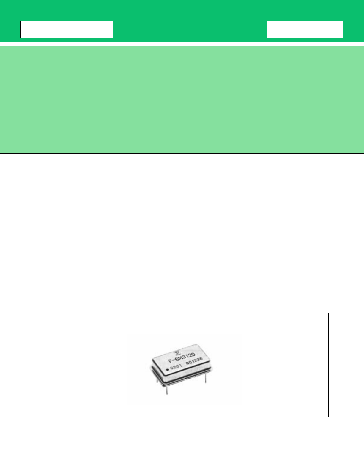
PACKAGE
■
O < ±500ppm eliminating the need for adjustment
14-PIN DIP SIZE METAL CASE
Page 2
F1/F2/F3 SERIES
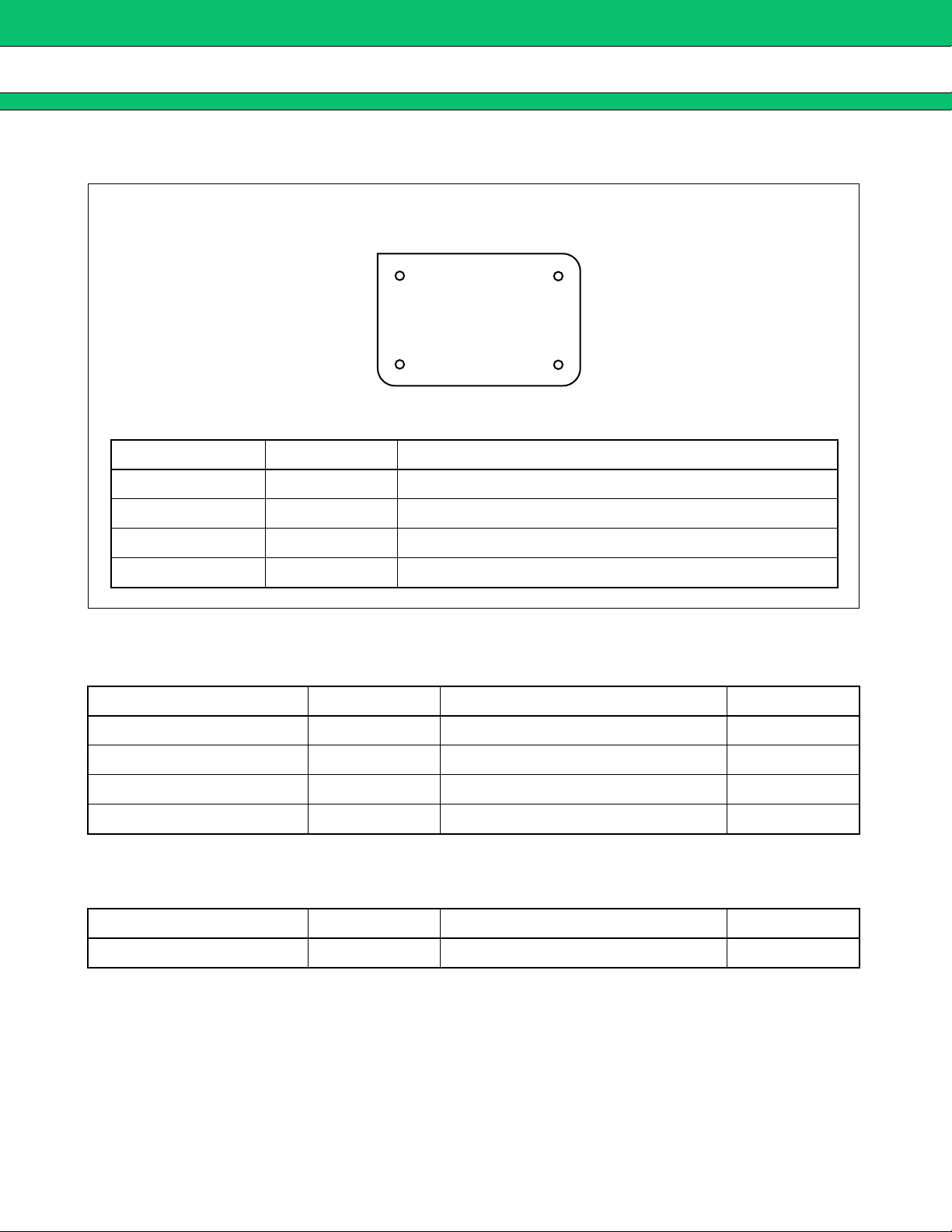
PIN ASSIGNMENT
■
(BOTTOM VIEW)
Pin No. Pin name Description
1 IN Input pin
7 GND Ground pin
8 NC No connection
14 OUT Output pin
MAXIMUM RATINGS
■
Item Symbol Rating
14
1
7
8
Unit
Operating temperature Ta –20 to 80 °C
Storage temperature Tstg –40 to 80 °C
Insulation resistance IR 100 (100V DC) MΩ
Frequency ra nge –– 1.5 to 100 MHz
RECOMMENDED OPERATING CONDITIONS
■
Item Symbol Rating
Operating temperature Ta 0 to 70 °C
2
Unit
Page 3
F1/F2/F3 SERIES
STANDARD FREQUENCY
■
Series Standard frequency Application Remarks
1.544MHz For the U.S. and Japan (primary group)
2.048MHz For Europe (primary group)
3.088MHz For the U.S. and Japan (primary group) 1.544 × 2
3.152MHz For the U.S. and Japan (primary group)
F1
F2
F3 44.736MHz For the U.S. (tertiary group)
4.096MHz For Europe (primary group) 2.048 × 2
6.312MHz For the U.S. and Japan (secondary group)
8.192MHz For the U.S. and Japan (secondary group)
8.448MHz For Europe (secondary group)
12.624MHz For the U.S. and Japan (secondary group) 6.312 × 2
16.384MHz For the U.S. and Japan (secondary group) 8.192 × 2
16.896MHz For Europe (secondary group) 8.448 × 2
32.064MHz For Japan (tertiary group)
34.368MHz For Europe (tertiary group)
3
Page 4

F1/F2/F3 SERIES
ELECTRICAL CHARACTERISTICS
■
F1 Series
Item Symbol Condition
Rating
Unit Remarks
Min. Typical Max.
Frequency deviation ∆fO –– –500 –– +500 ppm fO standard
Load Q Q –– 1000 –– 40 ––
Insertion loss
Stop band attenuation AOUT fO ± 10MHz 20 –– –– dB
Frequency stability with
temperature
IL
∆f (Ta) –– –400 –– +400 ppm
–– –– –– 6 dB
25°C standard,
Ta = 0 to 70°C
F2 Series
Rating
Item Symbol Condition
Unit Remarks
Min. Typical Max.
Frequency deviation ∆fO –– –500 –– +500 ppm fO standard
Load Q Q –– 1000 –– 40 ––
Insertion loss
Stop band attenuation AOUT fO ± 10MHz 20 –– –– dB
Frequency stability with
temperature
IL
∆f (Ta) –– –400 –– +400 ppm
–– –– –– 6 dB
25°C standard,
Ta = 0 to 70°C
F3 Series
Item Symbol Condition
Frequency deviation ∆fO –– –500 –– +500 ppm fO standard
Load Q Q –– 200 –– 50 ––
Insertion loss
Stop band attenuation AOUT fO ± 10MHz 20 –– –– dB
Frequency stability with
temperature
IL
∆f (Ta) –– –1350 –– 750 ppm
–– –– –– 6 dB
Min. Typical Max.
Unit Remarks
25°C standard,
Ta = 0 to 70°C
Rating
4
Page 5

ELECTRICAL CHARACTERISTICS
■
F1/F2/F3 SERIES
No.
1 1.544 FAR-F1DA-1M5440-G201 110 ±20 3 or less –90±20 790
2 1.544 FAR-F1DA-1M5440-G202 110 ±20 3 or less –90±20 1000
3 1.544 FAR-F1DA-1M5440-G203 60 ±10 3 or less –95±10 2035/20pF
4 1.544 FAR-F1DA-1M5440-G205 110 ±20 3 or less –90±20 2000
5 2.048 FAR-F1DA-2M0480-G201 40 ±10 3 or less –90±10 2035
6 2.048 FAR-F1DA-2M0480-G202 100 ±20 3 or less –90±20 1000
7 3.088 FAR-F1DA-3M0880-G201 150 ±20 3 or less –90±20 640
8 3.152 FAR-F1DA-3M1520-G201 85 ±15 3 or less –90±15 1285
9 4.096 FAR-F1DA-4M0960-G201 110 ±20 3 or less –90±20 750
10 6.312 FAR-F1DA-6M3120-G201 110 ±20 3 or less –90±20 985
11 6.312 FAR-F1DA-6M3120-G202 110 ±20 3 or less –90±20 1000
12 8.192 FAR-F1DA-8M1920-G201 100 ±20 3 or less –90±20 980
13 8.448 FAR-F1DA-8M4480-G201 110 ±20 3 or less –90±20 980
14 12.624 FAR-F1DA-12M624-G201 100 ±20 3 or less –90±20 590
Standard
frequency
(MHz)
Part number
Load Q
Insertion
loss, IL (dB)
Phase
rotation θ
(degree)
Terminating
impedance
Z (Ω)
Specification
15 16.384 FAR-F1DA-16M384-G201 100 ±20 3 or less –90±20 410
16 16.896 FAR-F1DA-16M896-G201 100 ±20 3 or less –90±20 390
17 32.064 FAR-F2DA-32M064-G201 100 ±10 3 or less –90±15 100
18 34.368 FAR-F2DA-34M368-G201 100 ±10 3 or less –90±15 100
19 44.736 FAR-F3DA-44M736-G201 65 ±15 6 or less 38±10 105
TEST CIRCUIT
■
50Ω Z
OSC
Z
50Ω
LM
5
Page 6

F1/F2/F3 SERIES
CHARACTERISTICS SAMPLE
■
Pass band characteristic Stop band characteristic
A : T/R (dB) B : θ 0 MKR 1544000.000Hz
A MAX 0.000 dB GAIN –722.721mdB
B MAX 180.0 deg PHASE –93.1330deg
A/DIV
B MIN
1.000
–180.0
dB CENTER
deg SPAN
1544000.000Hz
50000.000Hz
Temperature characteristic
1000
A : T/R (dB) B : θ 0 MKR 1544000.000Hz
A MAX 0.000 dB GAIN –724.276mdB
B MAX 180.0 deg PHASE deg
A/DIV 5.000 dB CENTER 1544000.000Hz
B MIN –180.0 deg SPAN 200000.000Hz
F3 Series
F2 Series
F1 Series
–1000
Frequency change (ppm)
–20 0 20 40 60 80
Temperature (°C)
PART NUMBERING SYSTEM
■
[Example]
FAR–F1
DA– –G
➀➁ ➂
➀ Series designation
➁ Frequency designation: The standard frequency is designated in six alphanumeric characters. M is used
to designate the decimal point in MHz. Refer to “ELECTRIC CHARA CTERISTICS”
in detail
Example: 1.544MHz: 1M5440
➂ Serial number: The serial number is assigned from 201 to 999 (201 is normal).
6
Page 7

MARKING
■
F1/F2/F3 SERIES
DIMENSIONS
■
20.8 max (0.819)
18.3 (0.720)
Fujitu logo
F
No. 1 pin position
Standard frequency
F-1M5440
G201
ЧЧЧЧЧЧ
Lot number
10.7 (0.421)
Unit: mm (in.)
15.2 (0.598)
1
14
ø0.5 (0.020)
7
8
Hmax
5.5
(0.217)
7.6 (0.299)
13.1 max (0.516)
Series
F1 < 3 MHz
F1 ≥ 3 MHz
F2
F3
H
8.5 (0.335)
5.8 (0.228)
5.8 (0.228)
5.8 (0.228)
7
Page 8

FUJITSU LIMITED
For further information please contact:
Japan
FUJITSU LIMITED
Corporate Global Business Support Division
Electronic Devices
KAWASAKI PLANT, 4-1-1, Kamikodanaka
Nakahara-ku, Kawasaki-shi
Kanagawa 211-88, Japan
Tel: (044) 754-3763
Fax: (044) 754-3329
North and South America
FUJITSU MICROELECTRONICS, INC.
Semiconductor Division
3545 North First Street
San Jose, CA 95134-1804, U.S.A.
Tel: (408) 922-9000
Fax: (408) 432-9044/9045
Europe
FUJITSU MIKROELEKTRONIK GmbH
Am Siebenstein 6-10
63303 Dreieich-Buchschlag
Germany
Tel: (06103) 690-0
Fax: (06103) 690-122
Asia Pacific
FUJITSU MICROELECTRONICS ASIA PTE. LIMITED
#05-08, 151 Lorong Chuan
New Tech Park
Singapore 556741
Tel: (65) 281-0770
Fax: (65) 281-0220
All Rights Reserved.
The contents of this document are subject to change without
notice. Customers are advised to consult with FUJITSU sales
representatives before ordering.
The information and circuit diagrams in this document presented
as examples of semiconductor device applications, and are not
intended to be incorporated in devices for actual use. Also,
FUJITSU is unable to assume responsibility for infringement of
any patent rights or other rights of third parties arising from the
use of this information or circuit diagrams.
FUJITSU semiconductor devices are intended for use in
standard applications (computers, office automation and other
office equipment, industrial, communications, and measurement
equipment, personal or household devices, etc.).
CAUTION:
Customers considering the use of our products in special
applications where failure or abnormal operation may directly
affect human lives or cause physical injury or property damage,
or where extremely high levels of reliability are demanded (such
as aerospace systems, atomic energy controls, sea floor
repeaters, vehicle operating controls, medical devices for life
support, etc.) are requested to consult with FUJITSU sales
representatives before such use. The company will not be
responsible for damages arising from such use without prior
approval.
Any semiconductor devices have inherently a certain rate of
failure. You must protect against injury, damage or loss from
such failures by incorporating safety design measures into your
facility and equipment such as redundancy, fire protection, and
prevention of over-current levels and other abnormal operating
conditions.
24
If any products described in this document represent goods or
technologies subject to certain restrictions on export under the
Foreign Exchange and Foreign Trade Control Law of Japan, the
prior authorization by Japanese government should be required
for export of those products from Japan.
F9703
FUJITSU LIMITED Printed in Japan
Page 9

Copyright © Each Manufacturing Company.
All Datasheets cannot be modified without permission.
This datasheet has been download from :
www.AllDataSheet.com
100% Free DataSheet Search Site.
Free Download.
No Register.
Fast Search System.
www.AllDataSheet.com
 Loading...