

Page 1

Mainboard D3488
Page 2

Congratulations, you have bought an innovative
Fujitsu product.
The latest information about our products, tips, updates etc. can be found on the Internet
at: http://www.fujitsu.com/fts
For driver updates, go to: http://support.ts.fujitsu.com/download
Should y
● our Hotline/Service Desk (http://support.ts.fujitsu.com/contact/servicedesk
● your sales partner
● your sales outlet
We hope you enjoy working with your new Fujitsu system!
ou have any technical questions, please contact:
)
Page 3

Page 4

Published by / Contact Address in the EU
Fujitsu Technology Solutions GmbH
Mies-van-der-Rohe-Straße 8
80807 Munich, Germany
http://www.fujitsu.com/fts
Copyright
© Fujitsu Technology Solutions GmbH 2017. All rights reserved.
Publication Date
10/2017
Order No.: A26361-D3488-Z320-1-7419, edition 1
Page 5

Mainboard D3488
Technical Description
Deutsch 1
English 39
Page 6

Page 7

Mainboard D3488 Deutsch - 1
Inhalt
Übersicht über das Mainboard D3488 ..............................................................................................3
Mainboard D3488................................................................................................................................ 5
Handbuchkonventionen........................................................................................................................ 5
Wichtige Hinweise ................................................................................................................................ 6
Allgemeine Informationen im Zusammenhang mit Boards........................................................... 6
Hardware-Spezifikationen .................................................................................................................... 8
Systemsicherheitsfunktionen................................................................................................................ 9
Grundlegende Sicherheitsfunktionen ........................................................................................... 9
Trusted Platform Module (TPM) ...................................................................................................9
Auswahl der korrekten Teile für das System................................................................................. 10
Betrachtungen zur CPU (Central Processor Unit).............................................................................. 10
Systemspeicherschnittstelle ............................................................................................................... 10
BIOS POST-Codes (Port 80-Statusanzeigen).................................................................................... 11
Betrachtungen zur Stromversorgung.................................................................................................. 18
Installation des Boards .................................................................................................................... 19
Intrusion-Anschluss (intern)................................................................................................................ 19
PC2009 PSU-Anschluss (PC2009) .................................................................................................... 19
Frontpanel-Stiftleiste (intern) .............................................................................................................. 20
Kommunikationsanschlüsse............................................................................................................... 20
Anschlüsse für Speichergeräte........................................................................................................... 22
Anschlüsse für Systemüberwachung und -verwaltung...................................................................... 22
Konfigurations-Jumper auf der Frontpanel-Stiftleiste ......................................................................... 23
COM1-Anschluss................................................................................................................................ 23
Speicherinstallation ............................................................................................................................ 24
Vorgehen bei der Speicherinstallation................................................................................................ 26
Prozessor tauschen / zweiten Prozessor einbauen............................................................................ 28
Abdeckung des Prozessorsockels entfernen ............................................................................. 28
Prozessor ausbauen .................................................................................................................. 29
Prozessor in Prozessorrahmen einbauen .................................................................................. 30
Wärmeleitpaste auftragen .......................................................................................................... 31
Prozessor in Prozessorrahmen auf Kühlkörper montieren......................................................... 32
Installation von Add-In-Karten ............................................................................................................ 34
Anschließen von externen Geräten .................................................................................................... 35
Externe Anschlüsse.................................................................................................................... 35
Austauschen der Lithium-Batterie .............................................................................................. 36
BIOS-Update ...................................................................................................................................... 37
Wann sollte ein BIOS-Update durchgeführt werden?................................................................. 37
Wie funktioniert ein BIOS-Update?..................................................................................................... 37
BIOS Recovery................................................................................................................................... 37
Glossar .............................................................................................................................................. 38
Fujitsu 1
Page 8

2 - Deutsch Mainboard D3488
Bemerkung
Hinweise zur Produktbeschreibung entsprechen den Designvorgaben von Fujitsu und werden zu
Vergleichszwecken zur Verfügung gestellt. Die tatsächlichen Ergebnisse können aufgrund mehrerer
Faktoren abweichen. Änderungen an technischen Daten ohne Ankündigung vorbehalten. Fujitsu
weist jegliche Verantwortung bezüglich technischer oder redaktioneller Fehler bzw. Auslassungen
von sich.
Warenzeichen
Fujitsu und das Fujitsu-Logo sind eingetragene Warenzeichen von Fujitsu Limited in Japan und in
anderen Ländern.
Intel ist eine Marke der Intel Corporation in den USA und/oder anderen Ländern.
Microsoft und Windows sind registrierte oder nicht registrierte Marken der Microsoft Corporation in
den USA und/oder in anderen Ländern.
PCI EXPRESS und PCIE sind registrierte Marken der PCI-SIG in den USA und in anderen Ländern.
SATA ist ein Produktname der SATA-IO.
Andere erwähnte Produkt- und Firmennamen sind Marken oder eingetragene Marken der
entsprechenden Firmen oder Markeninhaber.
Copyright
Ohne vorherige schriftliche Genehmigung von Fujitsu darf kein Teil dieser Veröffentlichung kopiert,
reproduziert oder übersetzt werden.
Ohne schriftliche Genehmigung von Fujitsu darf kein Teil dieser Veröffentlichung auf irgendeine
elektronische Art und Weise gespeichert oder übertragen werden.
2 Fujitsu
Page 9

Mainboard D3488 Deutsch - 3
Übersicht über das Mainboard D3488
POWER
2x
USB 3.0
LAN
2x USB 3.0
LAN
2x USB 3.0
25MHz Crystal
Audio
FAN 3
25MHz
Crystal
SLOT7 PCle x8 (CPU1)
SLOT6 PCle x16 (CPU0)
SLOT5 PCle x8 (CPU0)
SLOT4 PCle x16 (CPU1)
SLOT3 PCle x16 (CPU0)
SLOT2 PCle x16 (CPU1)
PCI 32bit
Front
Audio
External connectors rear
CH-M 1
CH-L 1
CH-K 1
CH-K 2
CH-G 2
CH-G 1
CH-H 1
CH-J 1
CPU 1
OCP
FAN5
FAN 2
VROC
Intrusion
12VSTBY
32kHZ
Crystal
25MHZ
Crystal
USB2.0
Stick
PC 2009
POWER
PCH
48MHZ
Crystal
SLOT8 PCIe x8 Gen 3
CPU 0
TPM
TPM con.
M.2 PCls/SATA
CH-C 1
CH-B 1
CH-A 1
CH-A 2
CH-D 2
CH-D 1
CH-E 1
CH-F 1
2x USB 3.0 Front
FAN6
sSATA1/0
Battery
Intern USB2.0
SATA
4-7
Drive
Power
Front
SATA
FAN 1
POWER
SCSI
LED
0-3
POWER
Frontpanel
FAN 5 =
AN 1 = CPU0-fan
F
AN 2 = CPU1-fan
F
AN 3 = Rear-fan
F
FAN 6 =
Door-fan
Front-fan
PC 2009 = PSU-fan
Fujitsu 3
Page 10

4 – Deutsch Mainboard D3488
Risk of Explosion if battery is replaced by an incorrect type.
!
Dispose of used batteries according to the instructions.
Il y a risque d’explosion si la batterie est remplacée par une batterie de type incorrect.
!
Mettre au rebut les batteries usagées conformément aux instructions.
Explosionsgefahr, wenn die Batterie mit einem inkorrekten Batterietyp ersetzt wird.
!
Alte Batterien gemäß Gebrauchsanweisung entsorgen.
4 Fujitsu
Page 11

Mainboard D3488 Deutsch - 5
Mainboard D3488
Basierend auf dem Intel® C624 Chipsatz zeichnet sich das D3488 durch eine Reihe hochmoderner
Technologien aus. Dazu zählen: Support für die Intel Xeon® Prozessor-Serien im LGA3647
P0 Sockel, multiple PCI-Express Busse, 6-Channel DDR4 Speicherdesign, Onboard PCI-Express
Gigabit Ethernet, SATA-Ports und multiple USB 2.0 / 3.0- (Universal Serial Bus) Anschlüsse.
Zum Öffnen der Handbücher muss das Programm Acrobat Reader installiert sein. Das
Programm ist auf der CD-ROM in folgendem Verzeichnis abgelegt: utls/acrobat.
i
Weitere Einzelheiten entnehmen Sie bitte den entsprechenden "readme.txt"-Dateien.
Handbuchkonventionen
Bedeutung der in diesem Handbuch verwendeten Symbole und Schriftarten:
kennzeichnet Hinweise, deren Nichtbeachtung die Gesundheit gefährdet oder zu
!
Sachschäden führt.
kennzeichnet zusätzliche Informationen und Tipps für den sachgerechten Umgang mit
i
dem System.
► Mit diesem Symbol folgenden Texten werden Aktivitäten beschrieben, die in der aufgelisteten
Reihenfolge durchgeführt werden müssen.
Dieses Symbol signalisiert, dass die Eingabetaste gedrückt werden muss.
Text in dieser Schriftart kennzeichnet Bildschirmausgaben.
Text in dieser Fettschrift steht für Eingaben, die über die Tastatur erfolgen.
Text in Kursivschrift kennzeichnet Befehle oder Menüpunkte.
Mit "Anführungszeichen" werden Kapitelnamen oder Begriffe gekennzeichnet.
Fujitsu 5
Page 12
6 – Deutsch Mainboard D3488
Wichtige Hinweise
Zum Zugriff auf das installierte Mainboard muss das System geöffnet werden. Wie das System
auseinandergebaut und wieder zusammengesetzt wird, ist im begleitenden Bedienerhandbuch
beschrieben.
Zur Vermeidung von Interferenzen müssen die Verbindungskabel für die Peripherie entsprechend
abgeschirmt sein.
Allgemeine Informationen im Zusammenhang mit Boards
Zur Vermeidung von Schäden am Mainboard und der darauf installierten Komponenten und
Leiterplatten ist beim Einfügen und Entfernen von Boards äußerste Sorgfalt angebracht. Achten Sie
besonders darauf, dass Erweiterungs-Boards gerade in die Steckplätze eingesetzt werden, damit
Komponenten oder Leiterplatten auf dem Mainboard und auch andere Komponenten (wie z. B. EMIFederkontakte) nicht beschädigt werden.
Ziehen Sie den Stecker aus der Hauptsteckdose, so dass System und Mainboard vollständig von der
Hauptstromversorgung getrennt sind.
Achten Sie beim Austausch des Mainboards oder darauf installierter Komponenten (z. B.
Speichermodule oder Prozessoren) besonders auf die Verriegelungsmechanismen (Arretierungen,
Zentrierungsstifte).
Verwenden Sie zum Aushebeln niemals scharfkantige Objekte (Schraubendreher).
Bitte beachten Sie die Sicherheitshinweise aus dem Bedienerhandbuch zu Ihrem System.
!
Ein unsachgemäßer Austausch der Lithium-Batterie birgt ein Explosionsrisiko.
Die Komponenten können während des Betriebs sehr heiß werden. Vermeiden Sie bei
Erweiterungen des Mainboards eine Berührung der Komponenten. Es besteht
Verbrennungsgefahr!
Beachten Sie bei der Installation des Boards die spezifischen Anweisungen aus dem
Handbuch für das Empfangsgerät.
Bei Schäden am System durch unsachgemäßes Vorgehen bei der Installation oder beim
Austauschen von Erweiterungen verliert die Garantie ihre Gültigkeit. Informationen zu
i
zulässigen Erweiterungen erhalten Sie über Ihre Verkaufsniederlassung oder über das
Kundenservicezentrum.
Boards mit elektrostatisch empfindlichen Geräten (Electrostatic Sensitive Devices
(ESD)) sind durch ein Etikett entsprechend gekennzeichnet.
Bitte beachten Sie beim Umgang mit Boards, auf denen sich solche ESDs befinden,
unbedingt Folgendes:
● Vor der Arbeit müssen Sie immer für eine statische Entladung (z. B. durch
Berühren eines geerdeten Objekts) sorgen.
● Die verwendeten Geräte und Werkzeuge dürfen nicht statisch aufgeladen sein.
● Ziehen Sie den Stecker aus der Stromhauptversorgung, bevor Sie Boards, die
ESDs enthalten, einfügen oder entfernen.
● Fassen Sie Boards mit ESDs stets an den Rändern an.
● Vermeiden Sie bei mit ESDs ausgestatteten Boards unbedingt die Berührung
von Kontakten und Leitern.
6 Fujitsu
Page 13

Mainboard D3488 Deutsch - 7
Hinweis für die USA
Compliance Information Statement (Declaration of Conformity Procedure) DoC
FCC Part 15: Dieses Gerät erfüllt die Anforderungen des Abschnitts 15 der FCC-
Bestimmungen.
Das Gerät darf nur unter den folgenden Bedingungen betrieben werden:
1) Das Gerät darf keine Störungen verursachen.
2) Dieses Gerät muss sämtliche empfangene Störungen aufnehmen, einschließlich solcher, die
einen unerwünschten Betrieb verursachen. Durch Ein- oder Ausschalten des Geräts kann
getestet werden, ob es zu Störungen des Rundfunk- oder Fernsehempfangs kommt. Derartige
Störungen lassen sich durch eine oder mehrere der nachfolgend aufgeführten Maßnahmen
beheben:
– Die Empfangsantenne neu ausrichten oder an einem anderen Ort aufstellen.
– Die Distanz zwischen dem Gerät und dem Receiver vergrößern.
– Das Equipment an einem vom Receiver unabhängigen Stromkreislauf anschließen.
– Den Händler oder einen Rundfunk-/Fernsehmechaniker zu Rate ziehen.
Hinweis für Kanada
i
Dieses Gerät entspricht den Grenzwerten für Geräte der "Klasse B" wie in den Vorschriften
der Norm des Canadian Department of Communications Radio Interference Regulations
für Störung verursachende Geräte festgelegt. (Cet appareil est conforme aux norms de
Classe B d’interference radio tel que specifie par le Ministere Canadien des
Communications dans les reglements d’ineteference radio.)
VORSICHT: Dieses Gerät wird mit einer Lithium-Batterie geliefert. Unter keinen
Umständen darf die Batterie durchstochen, mechanisch manipuliert oder Feuer ausgesetzt
!
werden. Bei unsachgemäßem Austausch der Batterie besteht Explosionsgefahr. Ein
Austausch darf nur mit dem gleichen oder mit einem durch den Hersteller empfohlenen
gleichartigen Typ erfolgen. Die gebrauchte Batterie gemäß den Anweisungen des
Herstellers und in Übereinstimmung mit den lokalen Bestimmungen entsorgen.
Fujitsu 7
Page 14

8 – Deutsch Mainboard D3488
Hardware-Spezifikationen
CPU – LGA3647 P0 Sockel
● Bis zu zwei CPU-Sockel
● Intel® Xeon Prozessoren im LGA3647 P0
Paket
● Intel® QuickPath Architektur zwischen
CPUs
● Integrierter Speicher-Controller
Hauptspeicher
● Sechskanal DDR4-Speicherarchitektur pro
CPU
● Sechzehn DDR4-Speicher-Sockel
● Support für gepufferte ECC-
Speichermodule (RDIMM)
● Support für ECC LR-Speichermodule
● Unterstützung für DDR4
2133/2400/2667Speicherschnittstellen
● Maximaler Speicher bis zu 1 TB
● DIMMS, die nicht dem JEDEC-Standard
entsprechen, werden nicht unterstützt
Chips auf dem Board
● Intel® C624 Chipsatz
● Realtek Audio ALC 671
● Intel I219LM Jacksonville LAN
● Intel I210 Springville LAN
● Infineon SLB 9670 TPM 2.0
Audio
● Realtek ALC 671
● Host-basiertes Audio mit 2-Kanal HD
Audio
● Stereokopfhörerausgang (ca. 50 mW bei
32 Ω)
● Sound über interne Systemlautsprecher
● Interner Anschluss: Frontblende
● Externe Anschlüsse:
Stereomikrofoneingang,
Stereoleitungsein- und -ausgang
LAN – 10/100/1000 Ethernet Controller
● WakeOnLAN durch Magic-Packet™
● PXE-Support
● Support für Jumbo-Frames
Storage-Geräte
● 10 serielle ATA-Anschlüsse
BIOS-Merkmale
● System- und BIOS-Kennwort
● Festplattenkennwort
● Support für die Wiederherstellung des
BIOS (Recovery BIOS)
● Bootsequenzkontrolle für jedes Floppy-
und Festplattenlaufwerk
● Serieller Zugriffsschutz
● Bootsektor-Viruswarnung
● Schreibgeschützter Flash-Speicher zum
Schutz vor Viren
● Schreibgeschütztes SPD EEPROM zum
Schutz vor Viren
Erweiterte Sicherheitsmerkmale
● Trusted Platform Module 2.0
● USB Dynamic Security an allen externen
Anschlüssen
Basissystemüberwachung und -verwaltung
● Wake on LAN
● USB-Kurzschlusserkennung
Advanced Fan Control
●
Erweiterte Systemüberwachung und verwaltung
● Fujitsu Technology Solutions System
Management
● Fujitsu Technology Solutions Thermal
Management
● Automatic System Reset (ASR,
automatisches Zurücksetzen des
Systems)
● Bestandserkennung
● ASF2.0 Unterstützung
8 Fujitsu
Page 15

Mainboard D3488 Deutsch - 9
Kommunikation
● Interner Anschluss: 2x USB 3.0,
4x USB 2.0, 1x USB 2.0
Standardanschluss (für Memorystick)
● Externer Anschluss (I/O Shield)
6x USB 3.0, Rückseite
Energieverwaltung
● Support für ACPI (Speichern im RAM / auf
Disk)
Umweltschutz
● Gesockelte Batterie (recyclingfähig)
Formfaktor, Steckplätze, Kompatibilitätsliste
● Formfaktor: AT03 extended
● Steckplätze: 8 Steckplätze (Details dem
Blockdiagramm entnehmen)
● Kompatibel mit ACPI, BBS DMI, IAPC,
PCI 2.3, WfM, ASF2.0, DASH1.1
Systemsicherheitsfunktionen
Grundlegende Sicherheitsfunktionen
Eine vollständige Beschreibung der grundlegenden Sicherheitsfunktionen ist in der BIOSSpezifikation zu finden.
Trusted Platform Module (TPM)
Bei Trusted Platform Modules handelt es sich um eine Sicherheitslösung der Trusted Computing
Group (TCG) zur Steigerung der Systemsicherheit. Das TPM befindet sich auf dem Motherboard und
nutzt zur Kommunikation mit dem Rest der Plattform den SPI-Bus.
D3488
Chip-Anbieter und -Typ: Infineon SLB 9670
Merkmal: TPM 2.0 kompatibles Trusted Platform Module
Jumper für die Aktivierung/Deaktivierung der TPM-Funktionalität
Fujitsu 9
Page 16

10 – Deutsch Mainboard D3488
Auswahl der korrekten Teile für das System
Vor der Installation dieses Motherboards in ein System müssen Sie sicherstellen, dass die
maßgeblichen Systemteile folgenden Basisrichtlinien und -anforderungen entsprechen:
Betrachtungen zur CPU (Central Processor Unit)
● Einzel-/Dualprozessorsystem
Das D3488 unterstützt bis zu zwei Intel® Xeon® Prozessoren in einem LGA3647 Sockel.
Einzelprozessorsystem:
Wenn nur ein Prozessor auf dem D3488 eingesetzt wird, muss dieser im Sockel CPU0
installiert werden.
Dualprozessorsystem:
Das D3488 unterstützt nur solche dualen Prozessorkonfigurationen, in denen beide
Prozessoren mit der gleichen QPI-Frequenz, Core-Frequenz, operieren und über eine gleiche
interne Cache-Größe verfügen. Das Mischen von Prozessoren, die nicht mit der gleichen QPIFrequenz, Core-Frequenz, operieren, kann zum Versagen des Systembetriebs oder zu
Schäden an den Prozessoren und/oder dem Motherboard führen.
● Quick Path Interconnect (QPI)
Der Host-Bus des Prozessors, auch als Quick Path Interconnect (QPI) bezeichnet, arbeitet
selbstständig mit einer Frequenz von bis zu 9.6 GT/s.
Systemspeicherschnittstelle
● Technologie
Buffered Single-, Dual oder Quad-Rank (LR-DIMM) DDR4 2133/2400/2667 Module mit und
ohne ECC
● Anschluss
288-polig, 1,2 V / 2,5 V / 72 Bit
10 Fujitsu
Page 17

Mainboard D3488 Deutsch - 11
BIOS POST-Codes (Port 80-Statusanzeigen)
BIOS-POST-Codes werden auf dem LCD-Display (angeschlossen an den LCD-Anschluss) oder
onboard über 8 gelbe LEDs (L0 - L7, L0 ist niedrigste Bit, L7 das höchste) angezeigt.
Kontrollpunktbereiche
Bereich der
Statuscodes
0x01 – 0x0B SEC-Ausführung
0x0C – 0x0F SEC-Fehler
0x10 – 0x2F PEI-Ausführung bis und inklusive Speichererkennung
0x30 – 0x4F PEI-Ausführung nach Speichererkennung
0x50 – 0x5F PEI-Fehler
0x60 – 0x8F DXE-Ausführung bis BDS
0x90 – 0xCF BDS-Ausführung
0xD0 – 0xDF DXE-Fehler
0xE0 – 0xE8 S3 Resume (PEI)
0xE9 – 0xEF Fehler bei S3 Resume (PEI)
0xF0 – 0xF8 Recovery / Wiederherstellung (PEI)
0xF9 – 0xFF Fehler bei Recovery / Wiederherstellung (PEI)
Beschreibung
Standardkontrollpunkte
SEC-Phase
Statuscode Beschreibung
0x00 Nicht verwendet
Progress-Codes
0x01 Power on. Typermittlung zurücksetzen (soft/hard).
0x02 AP-Initialisierung vor dem Laden des Microcodes
0x03 North-Bridge-Initialisierung vor dem Laden des Microcodes
0x04 South-Bridge-Initialisierung vor dem Laden des Microcodes
0x05 OEM-Initialisierung vor dem Laden des Microcodes
0x06 Laden des Microcodes
0x07 AP-Initialisierung nach dem Laden des Microcodes
0x08 North-Bridge-Initialisierung nach dem Laden des Microcodes
0x09 South-Bridge-Initialisierung nach dem Laden des Microcodes
Fujitsu 11
Page 18

12 – Deutsch Mainboard D3488
0x0A OEM-Initialisierung nach dem Laden des Microcodes
0x0B Cache-Initialisierung
SEC-Fehlercodes
0x0C – 0x0D Reserviert für zukünftige AMI-SEC-Fehlercodes
0x0E Microcode nicht gefunden
0x0F Microcode nicht geladen
SEC-Beep-Codes
Keine
SEC-Phase
Statuscode Beschreibung
Progress-Codes
0x10 PEI-Core wurde gestartet
0x11 Pre-Memory-CPU-Initialisierung wurde gestartet
0x12 Pre-Memory-CPU-Initialisierung (CPU-Modul-spezifisch)
0x13 Pre-Memory-CPU-Initialisierung (CPU-Modul-spezifisch)
0x14 Pre-Memory-CPU-Initialisierung (CPU-Modul-spezifisch)
0x15 Pre-Memory-North-Bridge-Initialisierung wurde gestartet
0x16 Pre-Memory-North-Bridge-Initialisierung (North-Bridge-Modul-spezifisch)
0x17 Pre-Memory-North-Bridge-Initialisierung (North-Bridge-Modul-spezifisch)
0x18 Pre-Memory-North-Bridge-Initialisierung (North-Bridge-Modul-spezifisch)
0x19 Pre-Memory-South-Bridge-Initialisierung wurde gestartet
0x1A Pre-Memory-South-Bridge-Initialisierung (South-Bridge-Modul-spezifisch)
0x1B Pre-Memory-South-Bridge-Initialisierung (South-Bridge-Modul-spezifisch)
0x1C Pre-Memory-South-Bridge-Initialisierung (South-Bridge-Modul-spezifisch)
0x1D – 0x2A OEM-Pre-Memory-Initialisierungscodes
0x2B Speicherinitialisierung. Lesen der Serial Presence Detect (SPD) Daten
0x2C Speicherinitialisierung. Ermittlung der Speicherpräsenz
0x2D Speicherinitialisierung. Speicher-Timing-Informationen werden programmiert
0x2E Speicherinitialisierung. Speicher wird konfiguriert
0x2F Speicherinitialisierung (andere).
0x30 Reserviert für ASL (siehe Abschnitt "ASL Statuscodes")
0x31 Speicher installiert
0x32 CPU-Post-Memory-Initialisierung wurde gestartet
0x33 CPU-Post-Memory-Initialisierung. Cache-Initialisierung
0x34 CPU-Post-Memory-Initialisierung. Initialisierung der Applikationsprozessor(en)
(AP)
12 Fujitsu
Page 19

Mainboard D3488 Deutsch - 13
0x35 CPU-Post-Memory-Initialisierung. Auswahl des Boot-Strap-Prozessors (BSP)
0x36 CPU-Post-Memory-Initialisierung. Initialisierung des System-Management-
0x37 Post-Memory-North-Bridge-Initialisierung wurde gestartet
0x38 Post-Memory-North-Bridge-Initialisierung (North-Bridge-Modul-spezifisch)
0x39 Post-Memory-North-Bridge-Initialisierung (North-Bridge-Modul-spezifisch)
0x3A Post-Memory-North-Bridge-Initialisierung (North-Bridge-Modul-spezifisch)
0x3B Post-Memory-South-Bridge-Initialisierung wurde gestartet
0x3C Post-Memory-South-Bridge-Initialisierung (South-Bridge-Modul-spezifisch)
0x3D Post-Memory-South-Bridge-Initialisierung (South-Bridge-Modul-spezifisch)
0x3E Post-Memory-South-Bridge-Initialisierung (South-Bridge-Modul-spezifisch)
0x3F-0x4E OEM-Post-Memory-Initialisierungscodes
0x4F DXE IPL wurde gestartet
PEI-Fehlercodes
0x50 Fehler bei der Speicherinitialisierung. Ungültiger Speichertyp oder inkompatible
0x51 Fehler bei der Speicherinitialisierung. SPD Lesen fehlgeschlagen
0x52 Fehler bei der Speicherinitialisierung. Ungültige Speichergröße oder nicht
0x53 Fehler bei der Speicherinitialisierung. Kein verwendbarer Speicher identifiziert.
0x54 Nicht spezifizierter Fehler bei der Speicherinitialisierung.
0x55 Speicher nicht installiert
0x56 Ungültige/r CPU-Typ oder -Geschwindigkeit
0x57 CPU-Diskrepanz
0x58 CPU-Selbsttest fehlgeschlagen oder möglicher CPU-Cache-Fehler
0x59 CPU-Microcode nicht gefunden oder Microcode-Update fehlgeschlagen
0x5A Interner CPU-Fehler
0x5B Reset PPI nicht verfügbar
0x5C-0x5F Reserviert für zukünftige AMI-Fehlercodes
S3 Resume-Progress-Codes
0xE0 S3 Resume wurde gestartet (S3 Resume PPI wurde vom DXE IPL aufgerufen)
0xE1 Ausführung S3 Boot Script
0xE2 Video-Repost
0xE3 OS S3 Wake Vector Call
0xE4-0xE7 Reserviert für zukünftige AMI-Progresscodes
selection
Modus (SMM)
Speichergeschwindigkeit
passende Speichermodule.
Fujitsu 13
Page 20

14 – Deutsch Mainboard D3488
S3 Resume-Fehlercodes
0xE8 S3 Resume fehlgeschlagen
0xE9 S3 Resume PPI nicht gefunden
0xEA Fehler S3 Resume Boot Script
0xEB Fehler S3 OS Wake
0xEC-0xEF Reserviert für zukünftige AMI-Fehlercodes
Recovery-Progress-Codes
0xF0 Wiederherstellbedingung von Firmware ausgelöst (Auto recovery)
0xF1 Wiederherstellbedingung vom Anwender ausgelöst (Forced recovery)
0xF2 Wiederherstellungsprozess wurde gestartet
0xF3 Wiederherstellungs-Firmware-Image wurde gefunden
0xF4 Wiederherstellungs-Firmware-Image wurde geladen
0xF5-0xF7 Reserviert für zukünftige AMI-Progresscodes
Recovery-Fehlercodes
0xF8 Recovery PPI ist nicht verfügbar
0xF9 Recovery Capsule wurde nicht gefunden
0xFA Ungültige Recovery Capsule
0xFB – 0xFF Reserviert für zukünftige AMI-Fehlercodes
PEI-Beep-Codes
Wiederholungen
der akustischen
Signale (BeepCode)
1 Speicher nicht installiert
1 Speicher wurde zwei Mal installiert (Routine InstallPeiMemory im PEI Core
2 Wiederherstellung wurde gestartet
3 DXEIPL wurde nicht gefunden
3 DXE Core Firmware Volume wurde nicht gefunden
4 Wiederherstellung fehlgeschlagen
4 S3 Resume fehlgeschlagen
7 Reset PPI nicht verfügbar
Beschreibung
wurde zwei Mal aufgerufen)
14 Fujitsu
Page 21

Mainboard D3488 Deutsch - 15
DXE-Phase
Statuscode Beschreibung
0x60 DXE Core wurde gestartet
0x61 NVRAM-Initialisierung
0x62 Installation der South Bridge Runtime Services
0x63 CPU-DXE-Initialisierung wurde gestartet
0x64 CPU-DXE-Initialisierung (CPU-Modul-spezifisch)
0x65 CPU-DXE-Initialisierung (CPU-Modul-spezifisch)
0x66 CPU-DXE-Initialisierung (CPU-Modul-spezifisch)
0x67 CPU-DXE-Initialisierung (CPU-Modul-spezifisch)
0x68 PCI-Host-Bridge-Initialisierung
0x69 North-Bridge-DXE-Initialisierung wurde gestartet
0x6A North-Bridge-DXE-SMM-Initialisierung wurde gestartet
0x6B North-Bridge-DXE-Initialisierung (North-Bridge-Modul-spezifisch)
0x6C North-Bridge-DXE-Initialisierung (North-Bridge-Modul-spezifisch)
0x6D North-Bridge-DXE-Initialisierung (North-Bridge-Modul-spezifisch)
0x6E North-Bridge-DXE-Initialisierung (North-Bridge-Modul-spezifisch)
0x6F North-Bridge-DXE-Initialisierung (North-Bridge-Modul-spezifisch)
0x70 South-Bridge-DXE-Initialisierung wurde gestartet
0x71 South-Bridge-DXE-SMM-Initialisierung wurde gestartet
0x72 South-Bridge-Geräte-Initialisierung
0x73 South-Bridge-DXE-Initialisierung (South-Bridge-Modul-spezifisch)
0x74 South-Bridge-DXE-Initialisierung (South-Bridge-Modul-spezifisch)
0x75 South-Bridge-DXE-Initialisierung (South-Bridge-Modul-spezifisch)
0x76 South-Bridge-DXE-Initialisierung (South-Bridge-Modul-spezifisch)
0x77 South-Bridge-DXE-Initialisierung (South-Bridge-Modul-spezifisch)
0x78 ACPI-Modul-Initialisierung
0x79 CSM-Initialisierung
0x7A – 0x7F Reserviert für zukünftige AMI-DXE-Fehlercodes
0x80 – 0x8F OEM-DXE-Initialisierungscodes
0x90 Phase Boot Device Selection (BDS) wurde gestartet
0x91 Treiberanschluss wurde gestartet
0x92 PCI-Bus-Initialisierung wurde gestartet
0x93 PCI-Bus-Hot-Plug-Controller-Initialisierung
0x94 PCI Bus Enumeration
0x95 PCI Bus Request Resources
Fujitsu 15
Page 22

16 – Deutsch Mainboard D3488
0x96 PCI Bus Assign Resources
0x97 Console Output Devices Connect
0x98 Console Input Devices Connect
0x99 Super-IO-Initialisierung
0x9A USB-Initialisierung wurde gestartet
0x9B USB Reset
0x9C USB Detect
0x9D USB Enable
0x9E – 0x9F Reserviert für zukünftige AMI-Fehlercodes
0xA0 IDE-Initialisierung wurde gestartet
0xA1 IDE Reset
0xA2 IDE Detect
0xA3 IDE Enable
0xA4 SCSI-Initialisierung wurde gestartet
0xA5 SCSI Reset
0xA6 SCSI Detect
0xA7 SCSI Enable
0xA8 Setup Verifying Password
0xA9 Setup Start
0xAA Reserviert für ASL (siehe Abschnitt "ASL Statuscodes")
0xAB Setup Input Wait
0xAC Reserviert für ASL (siehe Abschnitt "ASL Statuscodes")
0xAD Ready To Boot Event
0xAE Legacy Boot Event
0xAF Exit Boot Services Event
0xB0 Runtime Set Virtual Address MAP Begin
0xB1 Runtime Set Virtual Address MAP End
0xB2 Legacy Option ROM Initialization
0xB3 System Reset
0xB4 USB Hot Plug
0xB5 PCI Bus Hot Plug
0xB6 NVRAM Clean-up
0xB7 Configuration Reset (Reset der NVRAM-Einstellungen)
0xB8 – 0xBF Reserviert für zukünftige AMI-Codes
0xC0 – 0xCF OEM-BDS-Initialisierungscodes
16 Fujitsu
Page 23

Mainboard D3488 Deutsch - 17
DXE-Fehlercodes
0xD0 CPU-Initialisierungsfehler
0xD1 North-Bridge-Initialisierungsfehler
0xD2 South-Bridge-Initialisierungsfehler
0xD3 Einige Architekturprotokolle sind nicht verfügbar
0xD4 Fehler bei der PCI-Resource-Zuordnung. Keine verfügbaren Resourcen
0xD5 Kein Speicherplatz für Legacy Option ROM
0xD6 Console Output Devices nicht gefunden
0xD7 Console Input Devices nicht gefunden
0xD8 Ungültiges Passwort
0xD9 Fehler beim Laden der Boot Option (LoadImage hat Fehler zurückgegeben)
0xDA Boot Option fehlgeschlagen (StartImage hat Fehler zurückgegeben)
0xDB Flash-Update fehlgeschlagen
0xDC Reset-Protokol nicht verfügbar
DXE-Beep-Codes
Wiederholungen
der akustischen
Signale (BeepCode)
1 Ungültiges Passwort
4 Einige Architekturprotokolle sind nicht verfügbar
5 Console Output Devices nicht gefunden
5 Console Input Devices nicht gefunden
6 Flash-Update fehlgeschlagen
7 Reset-Protokol nicht verfügbar
8 Platform-PCI-Resourcenanforderungen nicht erfüllt
1 Ungültiges Passwort
Beschreibung
Für OEM reservierte Kontrollpunktbereiche
Statuscode Beschreibung
0x05 OEM-SEC-Initialisierung vor dem Laden des Microcodes
0x0A OEM-SEC-Initialisierung nach dem Laden des Microcodes
0x1D – 0x2A OEM-Pre-Memory-Initialisierungscodes
0x3F – 0x4E OEM-PEI-Post-Memory-Initialisierungscodes
0x80 – 0x8F OEM-DXE-Initialisierungscodes
0xC0 – 0xCF OEM-BDS-Initialisierungscodes
Fujitsu 17
Page 24
18 – Deutsch Mainboard D3488
Betrachtungen zur Stromversorgung
Netzstecker
Das D3488 wird mit einem 12 V Netzteil betrieben.
12 V-Netzstecker
Pin 1Pin 9
16-poliger Board-Netzstecker 12-poliger Board-Netzstecker
Pin 5
Pin 1
Pin 1Pin 7
8-poliger Stecker zur Versorgung der Laufwerke
18 Fujitsu
Page 25

Mainboard D3488 Deutsch - 19
Installation des Boards
Pin 1
Pin 4
Dieser 4-polige Lüfteranschluss unterstützt die Geschwindigkeitsüberwachung
Auf dem D3488 sind sechs 4-polige Lüfteranschlüsse implementiert. Über diese Anschlüsse können
Lüfter zur Kühlung von Gehäuse und Prozessor mit dem Motherboard verbunden werden. Kühlende
Lüfter tragen zur Systemstabilität und -zuverlässigkeit während der Lebensdauer des Produkts bei.
Pin1: GND
Pin2: +12V Power
Pin3: FAN Sense
Pin4: Fan PWM
Intrusion-Anschluss (intern)
Pin 1
PIN Signal
1 GND
2 open
3 Intrusion switch present
PC2009 PSU-Anschluss (PC2009)
Pin 1
PIN Signal
1 FASTPROCHOT PSU L
2 PS Fan PWM
3 Nicht angeschlossen
4 PS Fan Sense
5 Nicht angeschlossen
6 Nicht angeschlossen
7 Nicht angeschlossen
8 Nicht angeschlossen
Fujitsu 19
Page 26

20 – Deutsch Mainboard D3488
Frontpanel-Stiftleiste (intern)
In der Regel verfügt ein Gehäuse über einige Kontroll- oder Signalkabel, die an ein Motherboard für
die Festplatten-LED, Netz-LED, den Betriebsschalter und die Reset-Taste angeschlossen werden
können.
Für solche Zwecke wurde der Frontblendenanschluss auf dem D3488 implementiert.
Pin 1
POL Signal POL Signal
1 HD-LED + 2 Power LED +
3 HD-LED - 4 Power LED -
5 GND 6 Power-Button
Pin 2
7 RST L 8 GND
9 Chassis Detect WS L 10 Key
11 Chassis Detect Baku L 12 GND
13 LED1 + (for USB Security) 14 LED1 -
15 Power Button (only S5, not
working in low power S5)
17 Speaker + 18 Password Skip
19 GND 20 GND (0,1K)
21 Key 22 GND (0,1K)
23 Speaker - 24 Recover BIOS
16 Power Button (only S5, not
working in low power S5)
Kommunikationsanschlüsse
USB 2.0-Anschluss (extern)
POL Signal
Pin 1
Pin 1
USB 2.0-Anschluss (intern) – Intern/Vorderseite
Pin 1 Pin 2
20 Fujitsu
1 VCC AUX (abgesichert)
2 Data negative
3 Data positive
4 GND
POL Signal POL Signal
1 VCC AUX 2 VCC AUX
3 Data negative Port X 4 Data negative Port Y
5 Data positive Port X 6 Data positive Port Y
7 GND 8 GND
9 Key 10 NC
Page 27

Mainboard D3488 Deutsch - 21
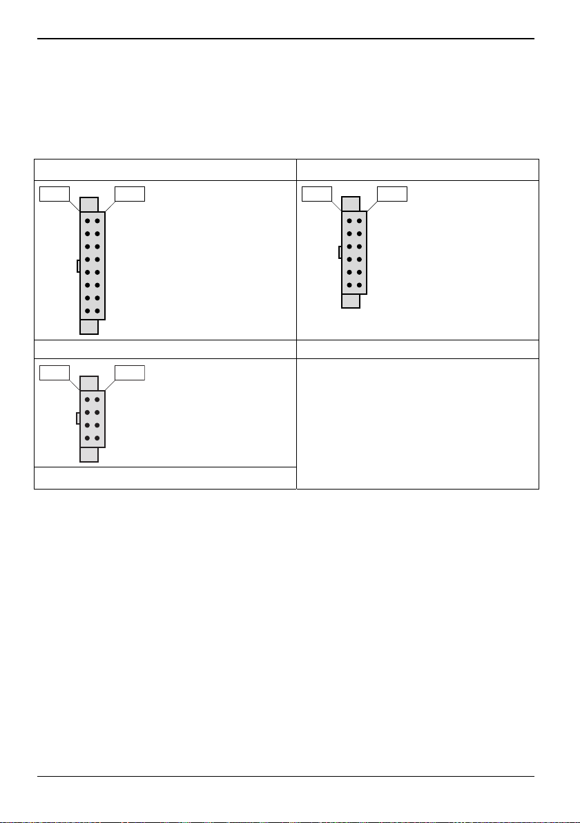
USB 2.0-Anschluss (intern)
POL Signal
Pin 1
USB 3.0-Anschluss (intern) – Intern/Vorderseite
Pin 1
Pin 10 Pin 11
Pin 19
High Definition Audio Frontpanel-Stiftleiste (intern)
Pin 1 Pin 2
1 VCC AUX (abgesichert)
2 Data negative
3 Data positive
4 GND
POL Signal POL Signal
1 VBus 20 Key
2 USB 3.0 Port 2 RX Neg 19 VBus
3 USB 3.0 Port 2 RX Pos 18 USB 3.0 Port 1 RX Neg
4 GND 17 USB 3.0 Port 1 RX Pos
5 USB 3.0 Port 2 TX Neg 16 GND
6 USB 3.0 Port 2 TX Pos 15 USB 3.0 Port 1 TX Neg
7 GND 14 USB 3.0 Port 1 TX Pos
8 USB 2.0 Port 2 Data Neg 13 GND
9 USB 2.0 Port 2 Data Pos 12 USB 2.0 Port 1 Data Neg
10 Überstrom 11 USB 2.0 Port 1 Data Pos
POL Signal POL Signal
1 HDA Port 1 Left 2 Analog GND
3 HDA Port 1 Right 4 FP Presence Detect
5 HDA Port 2 Left 6 Jack Sense Port 1
7 Jack Sense common 8 Key
9 HDA Port 2 Right 10 Jack Sense Port 1
Fujitsu 21
Page 28

22 – Deutsch Mainboard D3488
Anschlüsse für Speichergeräte
Serial ATA-Anschluss (Intern weiß)
1
POL Signal
1 GND
2 Transmit data negative
3 Receive data negative
4 GND
5 Transmit data positive
6 GND
7 Receive data positive
Anschlüsse für Systemüberwachung und
-verwaltung
SCSI LED-Anschluss (Intern)
Pin 1
POL Signal
1 Nicht angeschlossen
2 SCSI-ON LED (Low Aktiv)
3 SCSI-ON LED (Low Aktiv)
4 Nicht angeschlossen
22 Fujitsu
Page 29

Mainboard D3488 Deutsch - 23
Konfigurations-Jumper auf der Frontpanel-Stiftleiste
Standard-Jumper-Position (Recovery BIOS deaktiviert)
Pin 18
Recovery BIOS aktiviert
Pin 18
Pin 1
Pin 2
COM1-Anschluss
COM1-Anschluss
Pin 1 Pin 2
PIN Signal PIN Signal
1 DCD 1 2 DSR 1
3 SIN 1 4 RTS 1
5 SOUT 1 6 CTS 1
7 DTR 1 8 RI 1
9 GND
Fujitsu 23
Page 30

24 – Deutsch Mainboard D3488
Speicherinstallation
Vor der Installation muss sichergestellt werden, dass der einzusetzende Speicher kompatibel mit
dem Motherboard und dem Prozessor ist. Das D3488-Board unterstützt bis zu zwölf 288-polige,
1,2 V / 2,5 V, 2133/2400/2667 MHz DDR4-Module.
Hier einige Kernpunkte, die Sie vor der Speicherinstallation auf dem D3488 beachten
müssen:
● Folgende Speichermodule werden unterstützt: 4 GB, 8 GB, 16 GB, 32 GB, 64GB registered
und LR-DIMM ECC Module
● Alle installierten Speichermodule werden automatisch erkannt - eine Jumper-Einstellung ist
nicht erforderlich.
● Das D3488 unterstützt bis zu 1 TB an Speicher.
● Module mit unterschiedlichen Timing-Parametern können im gleichen Kanal in
unterschiedlichen Steckplätzen installiert werden, jedoch wird nur das Timing, das das
langsamste Modul unterstützt, auf alle anderen angewendet.
Zum Erzielen der maximalen Leistung die Module in nachstehender Reihenfolge einsetzen.
Wenn nur eine CPU bestückt wird, CPU 0 wie folgt bestücken:
1
CH-C 1
CH-B 1
CH-A 1
5
CH-A 2
3
7
CPU 0
LGA3647
CH-D 2
6
CH-D 1
CH-E 1
CH-F 1
2
8
4
24 Fujitsu
Page 31

Mainboard D3488 Deutsch - 25
Wenn beide CPU bestückt werden, CPU 0 und CPU 1 wie folgt bestücken:
2
CH-M 1
CH-L 1
CH-K 1
10
CH-K 2
CPU 1
LGA3647
CH-G 2
16
CH-G 1
CH-H 1
8
CH-J 1
Wenn zwei Speichermodule mit unterschiedlicher Rank-Anzahl im selben Kanal installiert
werden, muss das Modul mit der höheren Rank-Anzahl im am weitesten von der CPU
i
liegenden Speichersteckplatz installiert werden.
Wird ein Systemupgrade durchgeführt und dabei ein zusätzliches Speichermodul zu einem
Kanal mit einem vorhandenen Modul hinzugefügt, müssen die Module dabei
möglicherweise getauscht werden, damit das Speichermodul mit der höheren Rank-Anzahl
in diesem Speicherkanal außen (weiter weg von der CPU) liegt.
6
14
1
CH-C 1
CH-B 1
CH-A 1
9
CH-A 2
5
13
CPU 0
LGA3647
12
4
CH-D 2
15
CH-D 1
CH-E 1
7
CH-F1
11
3
Fujitsu 25
Page 32

26 – Deutsch Mainboard D3488
Vorgehen bei der Speicherinstallation
Bei der Installation von Speichermodulen müssen Sie darauf achten, dass die Module korrekt am
Speichersockel ausgerichtet sind. Auf den Speichermodulen sollten sich kleine Kerben befinden, die
zu den Kerben im Speichersockel passen. DDR-Module verfügen nur über eine Kerbe, die sich
unmittelbar neben dem Mittelpunkt des Moduls/Sockels befindet. Die Installationsmethode für
Speichermodule wird detailliert in den folgenden Diagrammen illustriert.
Installieren eines Speichermoduls
► Drücken Sie die Halterungen auf beiden Seiten des Speichersteckplatzes nach außen.
► Das Speichermodul in Position (1) einfügen.
► Gleichzeitig die Seitenhalterungen nach oben schnippen, bis das Speichermodul in der
Position (2) einrastet.
26 Fujitsu
Page 33

Mainboard D3488 Deutsch - 27
Entfernen eines Speichermoduls
► Die Klammern rechts und links am Speichersteckplatz nach außen drücken (1).
► Das Speichermodul aus dem Speichersteckplatz (2) ziehen.
Mitunter kann schwierig sein, ein Modul in die korrekte Position zu bringen. Dies ist jedoch
nur äußerst selten der Fall. Setzen Sie das Motherboard auf seine antistatische
i
Schutzhülle und auf eine ebene Oberfläche, um Schäden und Verbiegungen vorzubeugen.
Fahren Sie dann mit der Speicherinstallation fort.
Zur Vermeidung von Schäden an Motherboard oder Erweiterungsgerät vor der
Durchführung von Systemänderungen das Motherboard stets von der Stromversorgung
!
trennen.
Fujitsu 27
Page 34

28 – Deutsch Mainboard D3488
Prozessor tauschen / zweiten Prozessor einbauen
Unterstützte Prozessoren:
● Bis zu zwei Intel® Xeon® CPU (Platinum, Gold, Silver, Bronze)
● Zwei Sockel P0 LGA 3647
● Max. 165 W
● Beide Prozessoren müssen vom selben Typ sein, d. h. die Anzahl der internen Prozessorkerne
● sowie die Taktrate und QPI-Frequenz müssen die selben sein.
Abdeckung des Prozessorsockels entfernen
► Bauen Sie den Kühlkörper aus.
Nutzen Sie für den Betrieb mit zwei Prozessoren ein geeignetes
Multiprozessor-Betriebssystem.
i
Fassen Sie auf keinen Fall die Unterseite des Prozessors an. Schon leichte
Verunreinigungen wie Fett von der Haut können die Funktion des Prozessors
!
beeinträchtigen oder den Prozessor zerstören.
Die Abdeckung des Prozessorsockels muss nur beim Upgrade mit einem zweiten
Prozessor entfernt werden.
i
1
► Entfernen Sie die Abdeckung des Prozessorsockels (1) und verwahren Sie diese.
28 Fujitsu
Page 35

Mainboard D3488 Deutsch - 29
Prozessor ausbauen
Die nachfolgenden Schritte müssen nur bei einem Prozessortausch, nicht bei einem
Upgrade mit einem zweiten Prozessor durchgeführt werden.
i
1
1
1
1
► Rasten Sie den Prozessorrahmen aus (1).
Durch Wärmeleitpaste zwischen Prozessor und Kühlkörper kann der Prozessor am
Kühlkörper festkleben.
i
► Bewegen Sie den Prozessorrahmen vorsichtig vor und zurück, bis sich der Prozessorrahmen
vom Kühlkörper löst.
► Heben Sie den Prozessorrahmen vom Kühlkörper ab.
Der Prozessor darf nur mit der glatten Seite auf einer nicht leitfähigen,
antistatischen Fläche abgelegt werden.
!
Prozessor niemals auf der Ablagefläche hin- und herbewegen.
Fujitsu 29
Page 36

30 – Deutsch Mainboard D3488
3
1
► Drücken Sie die Rastnasen (1) in Pfeilrichtung (2) und heben Sie den Prozessor vom
Prozessorrahmen ab (3).
► Entfernen Sie mit einem fusselfreien Tuch eventuell vorhandene Reste von alter Wärmepaste
von der Oberfläche des Kühlkörpers und von der glatten Seite des Prozessors.
► Bewahren Sie den Prozessor an einem geeigneten Platz auf.
2
2
3
1
Prozessor in Prozessorrahmen einbauen
Stellen Sie sicher, dass die Modellnummer, die auf der Oberfläche des Prozessors
aufgedruckt ist, den Anforderungen entspricht: Beide Prozessoren müssen vom selben
i
Typ sein, d. h. die Anzahl der internen Prozessorkerne sowie Taktrate und QPI-Frequenz
müssen identisch sein.
b
a
1
1
30 Fujitsu
Page 37

Mainboard D3488 Deutsch - 31
► Halten Sie den Prozessor mit Daumen und Zeigefinger und setzen Sie ihn so in den
Prozessorrahmen, dass die Markierung des Prozessors (a) mit der Markierung am
Prozessorrahmen (b) von der Lage her übereinstimmt.
► Der Prozessor muss einrasten (1).
Wärmeleitpaste auftragen
Mischen Sie keine unterschiedlichen Arten von Wärmeleitpasten.
!
Wenn das Kit für ein Prozessor-Upgrade oder einen Prozessor-Tausch einen neuen
Kühlkörper enthält, ist auf der Unterseite des Kühlkörpers bereits eine dünne Schicht
i
Wärmeleitpaste aufgetragen. In diesem Fall ist keine weitere Wärmeleitpaste auf dem
Prozessor erforderlich.
3
1
1
1
Eine Spritze mit Wärmeleitpaste (FTS FSP: P304000004) enthält eine ausreichende Menge für den
Tausch von 3 Prozessoren. Seitlich auf der Spritze befinden sich drei kurze und drei lange
Markierungen.
► Verwenden Sie pro Tausch eines Prozessors die Menge an Wärmeleitpaste, die sich zwischen
zwei langen Markierungen befindet (ca. 0,7 g).
Fujitsu 31
Page 38

32 – Deutsch Mainboard D3488
1
► Bringen Sie die oben definierte Menge Wärmeleitpaste in der Mitte des Prozessors auf (1).
Bei der Montage des Kühlkörpers wird die Masse gleichmäßig verteilt.
i
Prozessor in Prozessorrahmen auf Kühlkörper montieren
► Falls vorhanden, entfernen Sie die Schutzkappe vom Kühlkörper und verwahren Sie diese.
Ein am Kühlkörper montierter Prozessor kann, je nach Positionierung des Prozessors auf
dem Kühlkörper, nur an Prozessor-Position 1 oder an Prozessor-Position 2 montiert
i
werden. Eine falsche Montage wird durch Kodierstifte verhindert.
► Platzieren Sie den Prozessorrahmen auf dem Kühlkörper.
32 Fujitsu
Page 39

Mainboard D3488 Deutsch - 33
1
1
1
1
► Drücken Sie den Prozessorrahmen mit dem Prozessor vorsichtig auf den Kühlkörper.
► Der Prozessorrahmen muss einrasten (1).
► Bauen Sie den Kühlkörper wieder ein.
Fujitsu 33
Page 40

34 – Deutsch Mainboard D3488
Installation von Add-In-Karten
Prüfen Sie vor der Installation von Add-In-Karten, ob diese vollständig kompatibel mit dem
Motherboard sind.
SLOT7 PCle x8 CPU1 (GEN3)
SLOT6 PCle x16 CPU0 (GEN3)
SLOT5 PCle x8 CPU0 (GEN3)
SLOT4 PCle x16 CPU1 (GEN3)
SLOT3 PCle x16 CPU0 (GEN3)
SLOT2 PCle x16 CPU1 (GEN3)
SLOT1 PCI 32 / 33MHz
Einfach den passenden Steckplatz für die Add-In-Karte suchen und die Karte fest einfügen. Wenn
sich Add-In-Karten (oder andere Komponenten) nicht ordnungsgemäß in einen Steckplatz einsetzen
lassen, niemals Gewalt anwenden. Es ist besser, Sie wählen einen anderen Steckplatz aus oder
tauschen die fehlerhafte Karte um, als das Motherboard und die Add-In-Karte zu beschädigen.
34 Fujitsu
Es hat sich als gute Praxis erwiesen, wenn Add-In-Karten statt direkt nebeneinander in
gestaffelter Form installiert werden. Auf diese Weise herrscht innerhalb des Gehäuses
i
eine bessere Luftzirkulation, die sich positiv auf die Kühlung aller installierten Geräte
auswirkt.
Zur Vermeidung von Schäden am Motherboard oder dem Erweiterungsgerät müssen sie
das Motherboard vor der Durchführung von Systemänderungen stets von der
!
Stromversorgung trennen.
Page 41

Mainboard D3488 Deutsch - 35
Anschließen von externen Geräten
Das Anschließen von externen Geräten an das Motherboard ist eine einfache Aufgabe. Zu den
Standardkomponenten, die üblicherweise an das Motherboard angeschlossen werden, zählen
Tastatur-, Maus- und Druckerkabel. In nachstehendem Diagramm wird der ATX-Port-Stack für
folgendes Board im Detail illustriert:
D3488
Line
LAN
-in
w/
AMT
USB
Port
-out
MIC
x8
Gen3
CPU1
x16
x8
Gen3
Gen3
CPU0
CPU0
Kopfhörer / SPDIF, gelb
x16
Gen3
CPU1
x16
Gen3
CPU0
x16
Gen3
CPU1 PCI-32
LAN
USB
Port
2xUSB
Externe Anschlüsse
Die Positionen der externen Anschlüsse am Motherboard wurden am Anfang des Handbuchs
angegeben.
Firewire, weiß
LAN
LAN-Anschluss (RJ-45)
Audio-Eingang (Line in), hellblau
Audio-Ausgang (Line out), hellgrün
Serielle Schnittstelle, türkis
Mikrofonbuchse (mono), rosa
USB 2.0 - Universal Serial Bus,
schwarz
USB 3.0 - Universal Serial Bus, blau
e-SATA-Anschluss
Der LAN RJ45-Anschluss verfügt über zwei LEDs (Light Emitting Diodes).
Linke LED Rechte LED
Grün: Verbindung eingerichtet Aus: 10 Mbit/s
Grün blinkend: Aktive LAN-Verbindung Grün: 100 Mbit/s
Gelb: 1000 Mbit/s
Die Ports wurden so konzipiert, dass sie Anschlüsse nur in eine Richtung zulassen.
Dennoch sollten Sie beim Anschließen mit Vorsicht vorgehen. Beim fehlerhaften
i
Anschließen können die Pole unter Umständen durch Verbiegen oder Brechen beschädigt
werden.
Fujitsu 35
Page 42

36 – Deutsch Mainboard D3488
Austauschen der Lithium-Batterie
Die installierte Lithium-Batterie versorgt den CMOS-Speicher mit Strom, damit die
Systeminformationen permanent gespeichert bleiben. Wenn die Batterie leer oder fast leer ist, wird
dem Benutzer eine entsprechende Fehlermeldung angezeigt. Die Lithium-Batterie muss dann
ausgetauscht werden.
Ein unsachgemäßer Austausch der Lithium-Batterie birgt ein Explosionsrisiko!
!
Die Lithium-Batterie darf nur durch eine identische Batterie oder durch einen vom
Hersteller empfohlenen Typ ausgetauscht werden.
Gebrauchte Lithium-Batterien niemals in den normalen Hausmüll geben. Sie müssen in
Übereinstimmung mit den lokalen Vorschriften für Sondermüll entsorgt werden.
Stellen Sie sicher, dass Sie die Batterie korrekt einsetzen. Der Pluspol muss nach oben
weisen!
Die Halterung für die Lithium-Batterie ist in verschiedenen Ausführungen zu finden, die aber auf
gleiche Weise funktionieren.
1
2
1
► Die Klammer in Pfeilrichtung (1) drücken.
Die Batterie springt leicht aus der Halterung.
► Die Batterie entfernen (2).
► Die neue Lithium-Batterie (identischen Typs) in die Halterung (3) schieben und nach unten
drücken, bis sie einrastet (4).
2
3
3
36 Fujitsu
Page 43

Mainboard D3488 Deutsch - 37
BIOS-Update
Wann sollte ein BIOS-Update durchgeführt werden?
Fujitsu Technology Solutions stellt neue BIOS-Versionen zur Verfügung, um die Kompatibilität zu
neuen Betriebssystemen, zu neuer Software oder zu neuer Hardware zu gewährleisten. Außerdem
können neue BIOS-Funktionen integriert werden.
Ein BIOS-Update sollte auch immer dann durchgeführt werden, wenn ein Problem besteht, das sich
durch neue Treiber oder neue Software nicht beheben lässt.
Wie funktioniert ein BIOS-Update?
BIOS-Update unter Windows mit dem Utility DeskFlash
Ein BIOS-Update kann mit dem Utility DeskFlash auch direkt unter Windows durchgeführt werden.
DeskFlash befindet sich auf der CD "Drivers & Utilities" (unterDeskUpdate).
BIOS Recovery
Alle BIOS-Einstellungen werden auf die Standardwerte zurückgesetzt.
i
► Das Gehäuse wie im Bedienerhandbuch beschrieben öffnen.
► Den Recovery BIOS-Jumper schließen (siehe Seite 23).
Das Gehäuse wie im Bedienerhandbuch beschrieben schließen.
►
► Eine BIOS Recovery Disk einfügen und den PC starten.
► Auf die Signale des Summers oder Lautsprechers achten. Das BIOS wurde erfolgreich
wiederhergestellt, wenn durchgehend schnell wiederholte Signaltöne zu hören sind.
► Schalten Sie das System aus.
► Das Gehäuse wie im Bedienerhandbuch beschrieben öffnen.
► Den Recovery BIOS-Jumper entfernen.
► Das Gehäuse wie im Bedienerhandbuch beschrieben schließen.
► Die Floppy-Disk aus dem Laufwerk entfernen.
► Den PC starten und das BIOS Setup aufrufen.
► Im Menü "Advanced" die Option "Reset Configuration" wählen und die Einstellung auf "Yes"
setzen.
► Die Änderungen speichern und das Setup beenden.
Die Wiederherstellung des BIOS ist damit abgeschlossen. Das System führt einen Neustart aus.
Fujitsu 37
Page 44

38 – Deutsch Mainboard D3488
Glossar
Die nachfolgend aufgelisteten Begriffe und Abkürzungen stellen nur eine Auswahl der kompletten
Liste mit allgemeinen technischen Begriffen und Abkürzungen dar. Nicht alle hier aufgelisteten
technischen Begriffe und Abkürzungen beziehen sich auf das hier beschriebene Motherboard.
AC’97 Audio Codec ’97 MCH Memory Controller Hub
ACPI Advanced Configuration and Power
ADD Advanced Digital Display NCQ Native Command Qeueing
AMT Active Management Technology NIC Networking Interface Card
AoL Alert on LAN PCI-Bus Peripheral Component
ASF Alert Specification Forum PECI Peripheral Environmental Control
ATA Advanced Technology Attachment PSC Permanent Server Control
BIOS Basic Input Output System PXE Preboot eXecution Environment
BMC Baseboard Management Controller QPI QuickPath Interconnect
CCR Chip Card Reader RAID Redundant Array of
CPU Central Processing Unit RAM Random Access Memory
CSA Communications Streaming
DASH Desktop and Mobile Architecture for
DDR Double Data Rate RIMM RAMBUS Inline Memory Module
DIMM Dual Inline Memory Module RSB Remote Server Management
DMI Direct Media Interface RTC Real Time Clock
DVO Digital Video Out SAS Serial Attached SCSI
ECC Error Correcting Code SATA Serial ATA
EEPR
OM
FDC Floppy Disc Controller SCSI Small Computer System Interface
FIFO First-In First-Out SD RAM Synchronous Dynamic RAM
FSB Front Side Bus SDVO Serial Digital Video Out
FWH Firmware Hub SG RAM Synchronous Graphic RAM
GMCH Graphics and MemoryController Hub SM & TM System Monitoring & Thermal
GPA Graphics Performance Accelerator SMBus System Management Bus
HDA High Definition Audio SG RAM Synchronous Graphic RAM
IAPC Instantly Available Power Managed
ICH I/O Controller Hub SVGA Super VGA
IDE Intelligent Drive Electronics TPM Trusted Platform Module
IPSec Internet Protocol Security TCG Trusted Computing Group
ISA -Bus Industrial Standard Architecture
LAN Local Area Network VGA Video Graphics Adapter
LSA LAN Desk Service Agent WOL Wake on LAN
Interface
Architecture
System Hardware
Electrical Eraseable Programmable
Read Only Memory
Desktop PC Design
– Bus
MMX MultiMedia eXtension
Interconnect Bus
Interface
Inexpensive/Independent Disks
RAMDAC RAM Digital Analog Converter
RD RAM RAMBUS Dynamic RAM
Board
SB SoundBlaster
Management
SPI Serial Peripheral Interface
USB Universal Serial Bus
38 Fujitsu
Page 45

Mainboard D3488 English - 1
Content
Overview Mainboard D3488............................................................................................................... 3
Mainboard D3488................................................................................................................................ 5
Notational conventions ......................................................................................................................... 5
Important notes..................................................................................................................................... 6
Information about boards ............................................................................................................. 6
Hardware Specifications....................................................................................................................... 8
System security features ...................................................................................................................... 9
Basic security features ................................................................................................................. 9
Trusted Platform Module (TPM) ...................................................................................................9
Choose Proper Parts for Your System ........................................................................................... 10
Central Processor Unit (CPU) Considerations ................................................................................... 10
System Memory Interface................................................................................................................... 10
BIOS POST-Codes (Port 80 status indicators)................................................................................... 11
Power Supply Considerations ............................................................................................................ 18
Board Installation ............................................................................................................................. 19
Intrusion connector (internal).............................................................................................................. 19
PC2009 PSU Connector (PC2009) .................................................................................................... 19
Front panel pin connector (internal).................................................................................................... 20
Communication connectors................................................................................................................ 20
Ports for memory devices................................................................................................................... 22
System monitoring and management connectors .............................................................................. 22
Configuration jumper on front panel pin connector............................................................................. 22
COM1 Ports........................................................................................................................................ 23
Installing the Memory ......................................................................................................................... 24
Memory Installation Procedure........................................................................................................... 26
Replace the processor / install a second processor........................................................................... 28
Remove the processor base cover............................................................................................. 28
Remove the processor ............................................................................................................... 29
Fit the processor into the processor frame................................................................................. 30
Apply the heat-conducting paste ................................................................................................ 31
Fit the processor in the processor frame on the heat sink ......................................................... 32
Installing Add-In Cards ....................................................................................................................... 34
Connecting External Devices ............................................................................................................. 35
External ports ............................................................................................................................. 35
Replacing lithium battery ............................................................................................................ 36
BIOS update ....................................................................................................................................... 37
When should a BIOS update be carried out?............................................................................. 37
How does a BIOS update work? ........................................................................................................ 37
BIOS Recovery................................................................................................................................... 37
Glossary ............................................................................................................................................ 38
Fujitsu 39
Page 46

2 - English Mainboard D3488
Remarks
Product description information corresponds to the design requirements of Fujitsu and is
provided for the purposes of comparison. The actual results may differ due to several actors.
Subject to changes to technical data without prior notification. Fujitsu accepts no responsibility
with regard to technical or editorial mistakes or omissions.
Trademarks
Fujitsu and the Fujitsu logo are registered trademarks of Fujitsu Limited in Japan and in other
countries.
Intel is a trademark of the Intel Corporation in the USA and/or other countries.
Microsoft and Windows are registered or unregistered trademarks of the Microsoft Corporation
in the USA and/or in other countries.
PCI EXPRESS and PCIE are registered trade marks of the PCI SIG in the USA and in other
countries.
SATA is a product name of the SATA-IO.
Other product names and company names mentioned are trademarks or registered
trademarks of the corresponding companies or trademark owners.
Copyright
No part of this publication may be copied, reproduced or translated without the prior written
consent of Fujitsu.
No part of this publication may be saved or transferred by any electronic means without the
written approval of Fujitsu.
40 Fujitsu
Page 47

Mainboard D3488 English - 3
Overview Mainboard D3488
POWER
2x
USB 3.0
LAN
2x USB 3.0
LAN
2x USB 3.0
25MHz Crystal
Audio
FAN 3
25MHz
Crystal
SLOT7 PCle x8 (CPU1)
SLOT6 PCle x16 (CPU0)
SLOT5 PCle x8 (CPU0)
SLOT4 PCle x16 (CPU1)
SLOT3 PCle x16 (CPU0)
SLOT2 PCle x16 (CPU1)
PCI 32bit
Front
Audio
External connectors rear
CH-M 1
CH-L 1
CH-K 1
CH-K 2
CH-G 2
CH-G 1
CH-H 1
CH-J 1
CPU 1
OCP
FAN5
FAN 2
VROC
Intrusion
12VSTBY
32kHZ
Crystal
25MHZ
Crystal
USB2.0
Stick
PC 2009
POWER
PCH
48MHZ
Crystal
SLOT8 PCIe x8 Gen 3
CPU 0
TPM
TPM con.
M.2 PCls/SATA
CH-C 1
CH-B 1
CH-A 1
CH-A 2
CH-D 2
CH-D 1
CH-E 1
CH-F 1
2x USB 3.0 Front
FAN6
sSATA1/0
Battery
Intern USB2.0
SATA
4-7
Drive
Power
Front
SATA
FAN 1
POWER
SCSI
LED
0-3
POWER
Frontpanel
FAN 5 =
AN 1 = CPU0-fan
F
AN 2 = CPU1-fan
F
AN 3 = Rear-fan
F
FAN 6 =
Door-fan
Front-fan
PC 2009 = PSU-fan
Fujitsu 41
Page 48

4 – English Mainboard D3488
Risk of Explosion if battery is replaced by an incorrect type.
!
Dispose of used batteries according to the instructions.
Il y a risque d’explosion si la batterie est remplacée par une batterie de type incorrect.
!
Mettre au rebut les batteries usagées conformément aux instructions.
Explosionsgefahr, wenn die Batterie mit einem inkorrekten Batterietyp ersetzt wird.
!
Alte Batterien gemäß Gebrauchsanweisung entsorgen.
42 Fujitsu
Page 49

Mainboard D3488 English - 5
Mainboard D3488
Based on the Intel® C624 chipset, the D3488 is characterised by a range of ultra-modern
technologies. These include: Support for the Intel Xeon® processor series in the LGA3647 P0
socket, multiple PCI-Express buses, 6 Channel DDR4 memory design, Onboard PCI-Express
Gigabit Ethernet, SATA ports and multiple USB 2.0 / 3.0 (Universal Serial Bus) ports.
The programme Acrobat Reader must be installed to be able to open the manuals. You will
find the programme on the CD-ROM directory: utls/acrobat.
i
For more details please read the according readme.txt files.
Notational conventions
The meanings of the symbols and fonts used in this manual are as follows:
► Text which follows this symbol describes activities that must be performed in the order shown.
This symbol indicates that you must press the Enter key.
Text in this typeface indicates screen outputs.
Text in this bold typeface indicates the entries you make via the keyboard.
Text in italics indicates commands or menu items.
"Quotation marks" indicate names of chapters or terms.
indicates information which is important for your health or for preventing physical damage.
!
indicates additional information which is required to use the system properly.
i
Fujitsu 43
Page 50

6 – English Mainboard D3488
Important notes
With the mainboard installed you must open the system to access the mainboard. How to dismantle
and reassemble the system is described in the operating manual accompanying the system.
Connecting cables for peripherals must be adequately shielded to avoid interference.
Information about boards
To prevent damage to the mainboard, the components and conductors on it, please take great care
when you insert or remove boards. Take great care to ensure that extension boards are slotted in
straight, without damaging components or conductors on the mainboard, or any other components,
for example EMI spring contacts.
Remove the plug from the mains outlet so that system and mainboard are totally disconnected from
the mains voltage.
Be careful with the locking mechanisms (catches, centring pins etc.) when you replace the
mainboard or components on it, for example memory modules or processors.
Never use sharp objects (screwdrivers) for leverage.
Observe the safety notes in the operating manual of your system.
!
Incorrect replacement of the lithium battery may lead to a risk of explosion.
Components can become very hot during operation. Ensure you do not touch components
when making extensions to the mainboard. There is a danger of burns!
When installing the board, refer to the specific installation information in the manual for the
receiving device.
The warranty is invalidated if the system is damaged during the installation or replacement
of expansions. Information on which expansions you can use is available from your sales
i
outlet or the customer service centre.
Boards with electrostatic sensitive devices (ESD) are identifiable by the label shown.
When you handle boards fitted with ESDs, you must, under all circumstances,
observe the following:
● You must always discharge static build up (e.g. by touching a grounded object)
before working.
● The equipment and tools you use must be free of static charges.
● Remove the power plug from the mains supply before inserting or removing
boards containing ESDs.
● Always hold boards with ESDs by their edges.
● Never touch pins or conductors on boards fitted with ESDs.
44 Fujitsu
Page 51

Mainboard D3488 English - 7
Operation is subject to the following conditions:
1) This device may not cause harmful interference, and
2) This device must accept any interference received including interference that may cause
undesired operation. If this equipment does cause harmful interference to radio or television
reception, which can be determined by turning the equipment off and on, the user is
encouraged to try one or more of the following measures:
– Reorient or relocate the receiving antenna.
– Increase the separation between the equipment and the receiver.
– Plug the equipment into an outlet on a circuit different from that of the receiver.
– Consult the dealer on an experienced radio/television technician for help.
i
!
Notice for the USA
Compliance Information Statement (Declaration of Conformity Procedure) DoC
FCC Part 15: This device complies with part 15 of the FCC Rules:
Notice for Canada
This apparatus complies with the Class B limits for radio interference as specified in the
Canadian Department of Communications Radio Interference Regulations. (Cet appareil
est conforme aux norms de Classe B d’interference radio tel que specifie par le Ministere
Canadien des Communications dans les reglements d’ineteference radio.)
CAUTION: Lithium battery included with this board. Do not puncture, mutilate, or dispose
of battery in fire. Danger of explosion if battery is incorrectly replaced. Replace only with
the same or equivalent type recommended by manufacturer. Dispose of used battery
according to manufacturer instructions and in accordance with your local regulations.
Fujitsu 45
Page 52

8 – English Mainboard D3488
Hardware Specifications
CPU – LGA3647 P0 socket
● Up to two CPU-sockets
● Intel® Xeon Processors in the
LGA3647 P0 package
● Intel® QuickPath architecture between
CPUs
● Integrated memory controller
Main memory
● Six channel DDR4 memory architecture
per CPU
● Sixteen DDR4 memory sockets
● Support for buffered ECC memory
modules (RDIMM)
● Support for ECC LR memory modules
● Supports DDR4 2133/2400/2667 memory
interface
● Up to 1 TB max. memory
● Non JEDEC standard DIMMS are not
supported
Chips on board
● Intel® C624 chipset
● Realtek Audio ALC 671
● Intel I219LM Jacksonville LAN
● Intel I210 Springville LAN
● Infineon SLB 9670 TPM 2.0
Audio
● Realtek ALC 671
● Host based Audio with 2-channel HD
Audio
● Stereo Head-Phone Out (approx. 50 mW
at 32 Ω)
● Sound via internal system speaker
● Internal connector: Frontpanel
● External connectors: Stereo Microphone
Input, Stereo Line Input, Stereo Line
Output
LAN – 10/100/1000 Ethernet Controller
● WakeOnLAN by Magic-Packet
● PXE support
● Support for Jumbo-Frames
Storage Devices
● 10 serial ATA ports
BIOS features
● System and BIOS password
● Harddisk password
● Recovery BIOS support
● Boot sequential control for each floppy and
HDD drive
● Serial access protection
● Bootsector virus warning
● Flash write protection against virus
● SPD EEPROM write protection against
virus
Advanced security features
● Trusted Platform Module 2.0
● USB Dynamic Security at all external ports
Basic system monitoring and management
● Wake on LAN
● USB voltage short detection
● Advanced Fan Control
Advanced system monitoring and
management
● Fujitsu Technology Solutions System
Management
● Fujitsu Technology Solutions Thermal
Management
● Automatic system reset (ASR)
● Inventory identification
● ASF2.0 support
Power Management
● ACPI (Save to RAM / Disk) support
TM
46 Fujitsu
Page 53

Mainboard D3488 English - 9
Communication
● Internal connector: 2x USB 3.0,
4x USB 2.0, 1x USB 2.0 standard
connector (for memory stick)
● External port (I/O Shield) 6x USB 3.0, rear
Environmental protection
● Socketed battery (recyclable)
Form factor, slots, compatibility list
● Form factor: AT03 extended
● Slots: 8 slots (details see block diagram)
● Compatible to ACPI, BBS DMI, IAPC,
PCI 2.3, WfM, ASF2.0, DASH1.1
System security features
Basic security features
For a complete description of the basic security features have a look at the BIOS Specification.
Trusted Platform Module (TPM)
Trusted Platform Modules are a Trusted Computing Group (TCG) security solution to increase the
system security. The TPM resides on the motherboard and uses the SPI bus to communicate with
the rest of the platform.
D3488
Chip vendor and type: Infineon SLB 9670
Feature: TPM 2.0 compliant Trusted Platform Module
Jumper for enabling/disabling the TPM functionality
Fujitsu 47
Page 54

10 – English Mainboard D3488
Choose Proper Parts for Your System
Before you installing a system with this motherboard, make sure your major system parts meet the
following basic guidelines and requirements:
Central Processor Unit (CPU) Considerations
● Single/Dual Processor System
The D3488 supports up to two Intel® Xeon® processors in an LGA3647 socket.
Single Processor System:
When only installing a single processor on D3488, the processor must be installed in the CPU0
socket.
Dual Processor System:
D3488 supports dual processor configurations only in which both processors operate with the
same QPI frequency, core frequency, and have the same internal cache sizes. Mixing
processors operating at different QPI frequency, core frequency, or cache sizes may cause
system non-operation or damages on processors and/or the motherboard.
● Quick Path Interconnect (QPI)
The processor host bus, or called Quick Path Interconnect (QPI), auto-operates at a frequency
up to 9.6 GT/s.
System Memory Interface
● Technology
Buffered single, dual, or quad rank (LR-DIMM) DDR4 DDR4 2133/2400/2667 modules with or
without ECC
● Connector
288 Pin, 1.2 V / 2.5 V / 72 Bit
48 Fujitsu
Page 55

Mainboard D3488 English - 11
BIOS POST-Codes (Port 80 status indicators)
BIOS-POST codes are visible on the LCD-display (connected to the LCD-connector) or onboard via
8 yellow LEDs (L0-L7, L0 is the lowest bit, L7 the highest).
Checkpoint Ranges
Status Code
Range
0x01 – 0x0B SEC execution
0x0C – 0x0F SEC errors
0x10 – 0x2F PEI execution up to and including memory detection
0x30 – 0x4F PEI execution after memory detection
0x50 – 0x5F PEI errors
0x60 – 0x8F DXE execution up to BDS
0x90 – 0xCF BDS execution
0xD0 – 0xDF DXE errors
0xE0 – 0xE8 S3 Resume (PEI)
0xE9 – 0xEF S3 Resume errors (PEI)
0xF0 – 0xF8 Recovery (PEI)
0xF9 – 0xFF Recovery errors (PEI)
Description
Standard Checkpoints
SEC Phase
Status Code Description
0x00 Not used
Progress Codes
0x01 Power on. Reset type detection (soft/hard).
0x02 AP initialization before microcode loading
0x03 North Bridge initialization before microcode loading
0x04 South Bridge initialization before microcode loading
0x05 OEM initialization before microcode loading
0x06 Microcode loading
0x07 AP initialization after microcode loading
0x08 North Bridge initialization after microcode loading
0x09 South Bridge initialization after microcode loading
Fujitsu 49
Page 56

12 – English Mainboard D3488
0x0A OEM initialization after microcode loading
0x0B Cache initialization
SEC Error Codes
0x0C – 0x0D Reserved for future AMI SEC error codes
0x0E Microcode not found
0x0F Microcode not loaded
SEC Beep Codes
None
SEC Phase
Status Code
Progress Codes
0x10 PEI Core is started
0x11 Pre-memory CPU initialization is started
0x12 Pre-memory CPU initialization (CPU module specific)
0x13 Pre-memory CPU initialization (CPU module specific)
0x14 Pre-memory CPU initialization (CPU module specific)
0x15 Pre-memory North Bridge initialization is started
0x16 Pre-Memory North Bridge initialization (North Bridge module specific)
0x17 Pre-Memory North Bridge initialization (North Bridge module specific)
0x18 Pre-Memory North Bridge initialization (North Bridge module specific)
0x19 Pre-memory South Bridge initialization is started
0x1A Pre-memory South Bridge initialization (South Bridge module specific)
0x1B Pre-memory South Bridge initialization (South Bridge module specific)
0x1C Pre-memory South Bridge initialization (South Bridge module specific)
0x1D – 0x2A OEM pre-memory initialization codes
0x2B Memory initialization. Serial Presence Detect (SPD) data reading
0x2C Memory initialization. Memory presence detection
0x2D Memory initialization. Programming memory timing information
0x2E Memory initialization. Configuring memory
0x2F Memory initialization (other).
0x30 Reserved for ASL (see ASL Status Codes section below)
0x31 Memory Installed
0x32 CPU post-memory initialization is started
0x33 CPU post-memory initialization. Cache initialization
0x34 CPU post-memory initialization. Application Processor(s) (AP) initialization
Description
50 Fujitsu
Page 57

Mainboard D3488 English - 13
0x35 CPU post-memory initialization. Boot Strap Processor (BSP) selection
0x36 CPU post-memory initialization. System Management Mode (SMM) initialization
0x37 Post-Memory North Bridge initialization is started
0x38 Post-Memory North Bridge initialization (North Bridge module specific)
0x39 Post-Memory North Bridge initialization (North Bridge module specific)
0x3A Post-Memory North Bridge initialization (North Bridge module specific)
0x3B Post-Memory South Bridge initialization is started
0x3C Post-Memory South Bridge initialization (South Bridge module specific)
0x3D Post-Memory South Bridge initialization (South Bridge module specific)
0x3E Post-Memory South Bridge initialization (South Bridge module specific)
0x3F-0x4E OEM post memory initialization codes
0x4F DXE IPL is started
PEI Error Codes
0x50 Memory initialization error. Invalid memory type or incompatible memory speed
0x51 Memory initialization error. SPD reading has failed
0x52 Memory initialization error. Invalid memory size or memory modules do not
0x53 Memory initialization error. No usable memory detected
0x54 Unspecified memory initialization error.
0x55 Memory not installed
0x56 Invalid CPU type or Speed
0x57 CPU mismatch
0x58 CPU self test failed or possible CPU cache error
0x59 CPU micro-code is not found or micro-code update is failed
0x5A Internal CPU error
0x5B reset PPI is not available
0x5C-0x5F Reserved for future AMI error codes
S3 Resume Progress Codes
0xE0 S3 Resume is stared (S3 Resume PPI is called by the DXE IPL)
0xE1 S3 Boot Script execution
0xE2 Video repost
0xE3 OS S3 wake vector call
0xE4-0xE7 Reserved for future AMI progress codes
S3 Resume Error Codes
0xE8 S3 Resume Failed
0xE9 S3 Resume PPI not Found
match.
Fujitsu 51
Page 58

14 – English Mainboard D3488
0xEA S3 Resume Boot Script Error
0xEB S3 OS Wake Error
0xEC-0xEF Reserved for future AMI error codes
Recovery Progress Codes
0xF0 Recovery condition triggered by firmware (Auto recovery)
0xF1 Recovery condition triggered by user (Forced recovery)
0xF2 Recovery process started
0xF3 Recovery firmware image is found
0xF4 Recovery firmware image is loaded
0xF5-0xF7 Reserved for future AMI progress codes
Recovery Error Codes
0xF8 Recovery PPI is not available
0xF9 Recovery capsule is not found
0xFA Invalid recovery capsule
0xFB – 0xFF Reserved for future AMI error codes
PEI Beep Codes
# of Beeps Description
1 Memory not Installed
1 Memory was installed twice (InstallPeiMemory routine in PEI Core called twice)
2 Recovery started
3 DXEIPL was not found
3 DXE Core Firmware Volume was not found
4 Recovery failed
4 S3 Resume failed
7 Reset PPI is not available
DXE Phase
Status Code Description
0x60 DXE Core is started
0x61 NVRAM initialization
0x62 Installation of the South Bridge Runtime Services
0x63 CPU DXE initialization is started
0x64 CPU DXE initialization (CPU module specific)
0x65 CPU DXE initialization (CPU module specific)
0x66 CPU DXE initialization (CPU module specific)
0x67 CPU DXE initialization (CPU module specific)
52 Fujitsu
Page 59

Mainboard D3488 English - 15
0x68 PCI host bridge initialization
0x69 North Bridge DXE initialization is started
0x6A North Bridge DXE SMM initialization is started
0x6B North Bridge DXE initialization (North Bridge module specific)
0x6C North Bridge DXE initialization (North Bridge module specific)
0x6D North Bridge DXE initialization (North Bridge module specific)
0x6E North Bridge DXE initialization (North Bridge module specific)
0x6F North Bridge DXE initialization (North Bridge module specific)
0x70 South Bridge DXE initialization is started
0x71 South Bridge DXE SMM initialization is started
0x72 South Bridge devices initialization
0x73 South Bridge DXE Initialization (South Bridge module specific)
0x74 South Bridge DXE Initialization (South Bridge module specific)
0x75 South Bridge DXE Initialization (South Bridge module specific)
0x76 South Bridge DXE Initialization (South Bridge module specific)
0x77 South Bridge DXE Initialization (South Bridge module specific)
0x78 ACPI module initialization
0x79 CSM initialization
0x7A – 0x7F Reserved for future AMI DXE codes
0x80 – 0x8F OEM DXE initialization codes
0x90 Boot Device Selection (BDS) phase is started
0x91 Driver connecting is started
0x92 PCI Bus initialization is started
0x93 PCI Bus Hot Plug Controller Initialization
0x94 PCI Bus Enumeration
0x95 PCI Bus Request Resources
0x96 PCI Bus Assign Resources
0x97 Console Output devices connect
0x98 Console input devices connect
0x99 Super IO Initialization
0x9A USB initialization is started
0x9B USB Reset
0x9C USB Detect
0x9D USB Enable
0x9E – 0x9F Reserved for future AMI codes
0xA0 IDE initialization is started
0xA1 IDE Reset
Fujitsu 53
Page 60

16 – English Mainboard D3488
0xA2 IDE Detect
0xA3 IDE Enable
0xA4 SCSI initialization is started
0xA5 SCSI Reset
0xA6 SCSI Detect
0xA7 SCSI Enable
0xA8 Setup Verifying Password
0xA9 Start of Setup
0xAA Reserved for ASL (see ASL Status Codes section below)
0xAB Setup Input Wait
0xAC Reserved for ASL (see ASL Status Codes section below)
0xAD Ready To Boot event
0xAE Legacy Boot event
0xAF Exit Boot Services event
0xB0 Runtime Set Virtual Address MAP Begin
0xB1 Runtime Set Virtual Address MAP End
0xB2 Legacy Option ROM Initialization
0xB3 System Reset
0xB4 USB hot plug
0xB5 PCI bus hot plug
0xB6 Clean-up of NVRAM
0xB7 Configuration Reset (reset of NVRAM settings)
0xB8 – 0xBF Reserved for future AMI codes
0xC0 – 0xCF OEM BDS initialization codes
DXE Error Codes
0xD0 CPU initialization error
0xD1 North Bridge initialization error
0xD2 South Bridge initialization error
0xD3 Some of the Architectural Protocols are not available
0xD4 PCI resource allocation error. Out of Resources
0xD5 No Space for Legacy Option ROM
0xD6 No Console Output Devices are found
0xD7 No Console Input Devices are found
0xD8 Invalid password
0xD9 Error loading Boot Option (LoadImage returned error)
0xDA Boot Option is failed (StartImage returned error)
54 Fujitsu
Page 61

Mainboard D3488 English - 17
0xDB Flash update is failed
0xDC Reset protocol is not available
DXE Beep Codes
# of Beeps Description
1 Invalid password
4 Some of the Architectural Protocols are not available
5 No Console Output Devices are found
5 No Console Input Devices are found
6 Flash update is failed
7 Reset protocol is not available
8 Platform PCI resource requirements cannot be met
1 Invalid password
OEM-Reserved Checkpoint Ranges
Status Code Description
0x05 OEM SEC initialization before microcode loading
0x0A OEM SEC initialization after microcode loading
0x1D – 0x2A OEM pre-memory initialization codes
0x3F – 0x4E OEM PEI post memory initialization codes
0x80 – 0x8F OEM DXE initialization codes
0xC0 – 0xCF OEM BDS initialization codes
Fujitsu 55
Page 62

18 – English Mainboard D3488
Power Supply Considerations
Power Connectors
The D3488 is operated with a 12 V power supply.
12 V Power Connectors
Pin 1Pin 9
16-pin board power connector 12-pin board power connector
Pin 5
Pin 1
Pin 1Pin 7
8-pin connector to supply the drives
56 Fujitsu
Page 63

Mainboard D3488 English - 19
Board Installation
Pin 1
Pin 4
This 4-pin fan connector supports tachometer monitoring.
There are six 4-pin fan connectors on D3488. Use these connectors to connect chassis and
processor cooling fans to your motherboard. Cooling fans can keep the system stable and reliable for
its product’s life.
Pin1: GND
Pin2: +12V Power
Pin3: FAN Sense
Pin4: Fan PWM
Intrusion connector (internal)
Pin 1
PIN Signal
1 GND
2 open
3 Intrusion switch present
PC2009 PSU Connector (PC2009)
Pin 1
PIN Signal
1 FASTPROCHOT PSU L
2 PS Fan PWM
3 Not connected
4 PS Fan Sense
5 Not connected
6 Not connected
7 Not connected
8 Not connected
Fujitsu 57
Page 64

20 – English Mainboard D3488
Front panel pin connector (internal)
Normally, a chassis has some control or signal wires can be connected onto a motherboard for hard
drive LED, Power LED, power button, and reset button; The front panel connector has been
implemented on D3488 for such purposes.
Pin 1
PIN Signal PIN Signal
1 HD-LED + 2 Power LED +
3 HD-LED - 4 Power LED -
Pin 2
5 GND 6 Power Button
7 RST L 8 GND
9 Chassis Detect WS L 10 Key
11 Chassis Detect Baku L 12 GND
13 LED1 + (for USB Security) 14 LED1 -
15 Power Button (only S5, does
not work in low power S5)
17 Speaker + 18 Password Skip
19 GND 20 GND (0,1K)
21 Key 22 GND (0,1K)
23 Speaker - 24 Recover BIOS
16 Power Button (only S5, does
not work in low power S5)
Communication connectors
USB 2.0 port (external)
PIN Signal
Pin 1
Pin 1
USB 2.0 port (internal) – Internal/Front
Pin 1 Pin 2
58 Fujitsu
1 VCC AUX (safe mode)
2 Data negative
3 Data positive
4 GND
PIN Signal PIN Signal
1 VCC AUX 2 VCC AUX
3 Data negative Port X 4 Data negative Port Y
5 Data positive Port X 6 Data positive Port Y
7 GND 8 GND
9 Key 10 NC
Page 65

Mainboard D3488 English - 21
USB 2.0 port (internal)
PIN Signal
Pin 1
USB 3.0 port (internal) – Internal/Front
Pin 1
Pin 10 Pin 11
Pin 19
High Definition Audio Front Panel Pin Connector (internal)
Pin 1 Pin 2
1 VCC AUX (safe mode)
2 Data negative
3 Data positive
4 GND
PIN Signal PIN Signal
1 VBus 20 Key
2 USB 3.0 Port 2 RX Neg 19 VBus
3 USB 3.0 Port 2 RX Pos 18 USB 3.0 Port 1 RX Neg
4 GND 17 USB 3.0 Port 1 RX Pos
5 USB 3.0 Port 2 TX Neg 16 GND
6 USB 3.0 Port 2 TX Pos 15 USB 3.0 Port 1 TX Neg
7 GND 14 USB 3.0 Port 1 TX Pos
8 USB 2.0 Port 2 Data Neg 13 GND
9 USB 2.0 Port 2 Data Pos 12 USB 2.0 Port 1 Data Neg
10 Over Current 11 USB 2.0 Port 1 Data Pos
PIN Signal PIN Signal
1 HDA Port 1 Left 2 Analog GND
3 HDA Port 1 Right 4 FP Presence Detect
5 HDA Port 2 Left 6 Jack Sense Port 1
7 Jack Sense common 8 Key
9 HDA Port 2 Right 10 Jack Sense Port 1
Fujitsu 59
Page 66

22 – English Mainboard D3488
Ports for memory devices
Serial ATA port (internal, white)
1
POL Signal
1 GND
2 Transmit data negative
3 Receive data negative
4 GND
5 Transmit data positive
6 GND
7 Receive data positive
System monitoring and management connectors
SCSI LED connector (Internal)
Pin 1
PIN Signal
1 Not connected
2 SCSI-ON LED (low active)
3 SCSI-ON LED (low active)
4 Not connected
Configuration jumper on front panel pin connector
Standard jumper position (Recovery BIOS deactivated)
Pin 18
Recovery BIOS enabled
Pin 18
60 Fujitsu
Pin 1
Pin 2
Page 67

Mainboard D3488 English - 23
COM1 Ports
COM1 port
Pin 1 Pin 2
PIN Signal PIN Signal
1 DCD 1 2 DSR 1
3 SIN 1 4 RTS 1
5 SOUT 1 6 CTS 1
7 DTR 1 8 RI 1
9 GND
Fujitsu 61
Page 68

24 – English Mainboard D3488
Installing the Memory
Before attempting to install any memory, make sure that the memory you have is compatible with the
motherboard as well as the processor. The D3488 board supports up to twelve 288-pin 1.2 V / 2.5 V,
2133/2400/2667 MHz DDR4 modules.
Here are a few key points to note before installing memory into your D3488:
● The following memory modules are supported: 4 GB, 8 GB, 16 GB, 32 GB, 64 GB registered
and LR-DIMM ECC modules
● All installed memory will be automatically detected - no need to set any jumpers
● The D3488 supports up to 1 TB of memory
● Modules with different timing parameters can be installed on different slots within the same
channel, but only timings that support the slowest Module will be applied to all.
To reach maximal performance, plugging the modules in the following sequence.
If only one CPU is equipped, equip CPU 0 as follows:
1
CH-C 1
CH-B 1
CH-A 1
5
CH-A 2
3
7
CPU 0
LGA3647
CH-D 2
6
CH-D 1
CH-E 1
CH-F 1
2
8
4
62 Fujitsu
Page 69

Mainboard D3488 English - 25
If both CPUs are equipped, equip CPU 0 and CPU 1 as follows:
2
CH-M 1
CH-L 1
CH-K 1
10
CH-K 2
CPU 1
LGA3647
CH-G 2
16
CH-G 1
CH-H 1
8
CH-J 1
When two memory modules with a different number of ranks are populated in one memory
channel, then the module with the higher number of ranks must be populated in the
i
memory slot further away from the CPU.
If the system is upgraded and an additional memory module is added to a channel with an
existing module, it might be necessary to swap modules so that the module with the higher
number of ranks is populated on the outside (further away from the CPU) of that memory
channel.
6
14
1
CH-C 1
CH-B 1
CH-A 1
9
CH-A 2
5
13
CPU 0
LGA3647
12
4
CH-D 2
15
CH-D 1
CH-E 1
7
CH-F1
11
3
Fujitsu 63
Page 70

26 – English Mainboard D3488
Memory Installation Procedure
When installing memory modules, make sure the modules align properly with the memory socket.
There should be keys (small indents) on your memory modules that fit according to the keys in the
memory socket. DDR modules and sockets have only one key, which is slightly near the center of
the module/socket. The method of installing memory modules is detailed in the following diagrams.
Installing a memory module
► Push the holders on each side of the memory slot outwards.
► Insert the memory module into the location (1).
► At the same time flip the lateral holders upwards until the memory module snaps in place (2).
64 Fujitsu
Page 71

Mainboard D3488 English - 27
Removing a memory module
► Push the clips on the right and left of the memory slot outward (1).
► Pull the memory module out of the memory slot (2).
When installing memory, a module may require a considerable amount of force to seat
properly, although this is very rare. To avoid bending and damaging your motherboard,
i
place it on its anti-static bag and onto a flat surface, and then proceed with memory
installation.
You must unplug the power connector to the motherboard before performing system
hardware changes, to avoid damaging the board or expansion device.
!
Fujitsu 65
Page 72

28 – English Mainboard D3488
Replace the processor / install a second processor
Processors supported
● Up to two Intel® Xeon® CPUs (Platinum, Gold, Silver, Bronze)
● Two bases, type P0 LGA 3647
● Maximum power: 165 W
● Both processors must be of the same type, i.e. the number of the internal processor cores,
● and the clock rate and Intel QuickPath Interconnect (QPI) frequency must be the same.
Use a suitable multiprocessor operating system for operation with two processors.
i
Remove the processor base cover
► Remove the heat sink.
Never touch the underside of the processor. Even minor soiling such as grease from the
skin can impair the processor’s operation or destroy the processor.
!
The processor base cover must only be removed when upgrading
i
with a second processor.
1
► Remove the cover of the processor base (1) and keep it in a safe place.
66 Fujitsu
Page 73

Mainboard D3488 English - 29
Remove the processor
The following steps only need to be completed when a processor is being replaced, and
not with an upgrade when a second processor is fitted.
i
1
1
1
1
► Release the processor frame from its locking slots (1).
The processor can be stuck firmly to the heat sink by applying heat-conducting paste
between the processor and the heat sink.
i
► Carefully move the processor frame forwards and backwards until the processor frame is
detached from the heat sink.
► Remove the processor frame from the heat sink.
The processor must only be placed on a non-conductive, antistatic surface on its flat side.
Never move the processor around on the surface where it was placed.
!
Fujitsu 67
Page 74

30 – English Mainboard D3488
3
1
► Press the latches (1) in the direction of the arrow (2) and lift the processor out of the processor
frame (3).
► Use a lint-free cloth to remove any traces of old heat-conducting paste from the surface of the
heat sink and from the flat side of the processor.
► Keep the processor in a suitable place.
2
2
3
1
Fit the processor into the processor frame
Make sure that the model number printed on the outside of the processor complies with the
requirements: Both processors must be of the same type, i.e. the number of internal
i
processor cores, and the clock rate and Intel QuickPath Interconnect (QPI) frequency must
be identical.
b
a
1
1
► Hold the processor between your thumb and index finger and insert it into the processor frame
so that the marking on the processor (a) is aligned with the marking on the processor frame (b).
68 Fujitsu
Page 75

Mainboard D3488 English - 31
► The processor must lock into place (1).
Apply the heat-conducting paste
Do not mix different types of heat-conducting paste.
!
If the kit for a processor upgrade or a processor replacement contains a new heat sink, a
thin layer of heat-conducting paste will already be applied to the underside of the heat sink.
i
In this case, no more heat-conducting paste will be required on the processor.
3
1
1
1
A syringe with heat-conducting paste (FTS FSP code no.: P304000004) contains a sufficient amount
of paste for replacing 3 processors. On the side of the syringe, there are three short and three long
markings.
► Use the amount of heat-conducting paste between two long markings on the syringe (about 0.7
grams) each time you replace a processor.
Fujitsu 69
Page 76

32 – English Mainboard D3488
1
► Apply the amount of heat-conducting paste defined above on the middle of the processor (1).
When installing the heat sink, the mass must be evenly distributed.
i
Fit the processor in the processor frame on the heat sink
► Remove the protective cap, if there is one, from the heat sink and keep it in a safe place.
Depending on the positioning of the processor on the heat sink, a processor mounted on a
heat sink can only be installed in processor position 1 or in processor position 2. Incorrect
i
assembly is prevented by coding pins.
► Place the processor frame on the heat sink.
70 Fujitsu
Page 77

Mainboard D3488 English - 33
1
1
1
1
► Press the processor frame with the processor carefully onto the heat sink.
► The processor frame must lock into place (1).
► Install the heat sink again.
Fujitsu 71
Page 78

34 – English Mainboard D3488
Installing Add-In Cards
Before installing add-in cards, please check if they are fully compatible with your motherboard.
SLOT7 PCle x8 CPU1 (GEN3)
SLOT6 PCle x16 CPU0 (GEN3)
SLOT5 PCle x8 CPU0 (GEN3)
SLOT4 PCle x16 CPU1 (GEN3)
SLOT3 PCle x16 CPU0 (GEN3)
SLOT2 PCle x16 CPU1 (GEN3)
SLOT1 PCI 32 / 33MHz
Simply find the appropriate slot for your add-in card and insert the card firmly. Do not force any addin
cards (or anything else) into any slots if they won’t seat in place. It’s better to try another slot or return
the faulty card rather than damaging both the motherboard and the add-in card.
72 Fujitsu
It’s a good practice to install add-in cards in a staggered manner, rather than directly
adjacent to each other. This allows air to more easily circulate within the chassis, providing
!
improved cooling for all installed devices.
You must unplug the power connector to the motherboard before performing system
hardware changes, to avoid damaging the board or expansion device.
i
Page 79

Mainboard D3488 English - 35
Connecting External Devices
Connecting external devices to the motherboard is an easy task. The standard devices you should
expect to plug into the motherboard are keyboards, mouse, and printer cables. The following
diagram will detail the ATX port stack for the following board:
D3488
Line
LAN
-in
w/
AMT
USB
Port
-out
MIC
x8
Gen3
CPU1
x16
Gen3
CPU0
x8
Gen3
CPU0
x16
Gen3
CPU1
x16
Gen3
CPU0
x16
Gen3
CPU1 PCI-32
Earphone / SPDIF, yellow
Microphone jack (mono), pink
USB 2.0 - Universal Serial Bus, black
USB 3.0 - Universal Serial Bus, blue
e-SATA-Anschluss
LAN
USB
Port
2xUSB
External ports
The location of the external connections of your mainboard is specified at the beginning of the
manual.
Firewire, white
LAN
The LAN RJ45 connector has two LEDs (light emitting diodes).
Left LED Right LED
Link established Off: Off: 10 Mbit/s
Blinking green: LAN connection is active Green: 100 Mbit/s
Yellow: 1000 Mbit/s
LAN port (RJ-45)
Audio input (Line in), light blue
Audio output (Line out), light green
Serial interface, turquoise
While the ports have been created to accept connectors in only one direction, make sure to
be careful when inserting connectors. At times, attaching connectors in the incorrect
i
orientation can damage, bend and or break the pins.
Fujitsu 73
Page 80

36 – English Mainboard D3488
Replacing lithium battery
In order to permanently save the system information, a lithium battery is installed to provide the
CMOS-memory with a current. A corresponding error message notifies the user when the charge is
too low or the battery is empty. The lithium battery must then be replaced.
Incorrect replacement of the lithium battery may lead to a risk of explosion!
!
The lithium battery may be replaced only with an identical battery or with a type
recommended by the manufacturer.
Do not throw lithium batteries into the household waste. They must be disposed of in
accordance with local regulations concerning special waste.
Make sure that you insert the battery the right way round. The plus pole must be on the
top!
The lithium battery holder exists in different designs that function in the same way.
1
2
1
► Press the catch in the direction of the arrow (1).
The battery jumps out of the holder slightly.
► Remove the battery (2).
► Push the new lithium battery of the identical type into the holder (3) and press it downward until
it engages (4).
2
3
3
74 Fujitsu
Page 81

Mainboard D3488 English - 37
BIOS update
When should a BIOS update be carried out?
Fujitsu Technology Solutions makes new BIOS versions available to ensure compatibility to new
operating systems, new software or new hardware. In addition, new BIOS functions can also be
integrated.
A BIOS update should always also be carried out when a problem exists that cannot be solved with
new drivers or new software.
How does a BIOS update work?
BIOS update under Windows with DeskFlash utility:
A BIOS update can also be carried out directly under Windows with the DeskFlash utility. DeskFlash
is contained on the “Drivers & Utilites” CD (under DeskUpdate).
BIOS Recovery
Opening the casing as described in the operating manual.
i
► Close the Recovery BIOS jumper (see Page 22).
►
Close the casing as described in the operating manual.
► Insert a BIOS Recovery Disk and start the PC.
► Note the signals issued from the buzzer or loudspeaker. You have successfully restored the
BIOS if you hear continuously fast repeated beeps.
► Power off your system.
► Open the casing as described in the operating manual.
► Remove the Recovery BIOS jumper.
► Close the casing as described in the operating manual.
► Remove the floppy disk from the drive.
► Start the PC and invoke BIOS Setup.
► Select the menu item Reset configuration in the menu Advanced and change the setting to
Yes.
► Save the change and terminate BIOS Setup.
The BIOS recovery has now been completed. The system restarts.
Fujitsu 75
Page 82

38 – English Mainboard D3488
Glossary
The technical terms and abbreviations given below represent only a selection of the full list of
common technical terms and abbreviations. Not all technical terms and abbreviations listed here are
valid for the described mainboard.
AC’97 Audio Codec ’97 MCH Memory Controller Hub
ACPI Advanced Configuration and Power
ADD Advanced Digital Display NCQ Native Command Qeueing
AMT Active Management Technology NIC Networking Interface Card
AoL Alert on LAN PCI-Bus Peripheral Component
ASF Alert Specification Forum PECI Peripheral Environmental Control
ATA Advanced Technology Attachment PSC Permanent Server Control
BIOS Basic Input Output System PXE Preboot eXecution Environment
BMC Baseboard Management Controller QPI QuickPath Interconnect
CCR Chip Card Reader RAID Redundant Array of
CPU Central Processing Unit RAM Random Access Memory
CSA Communications Streaming
DASH Desktop and Mobile Architecture for
DDR Double Data Rate RIMM RAMBUS Inline Memory Module
DIMM Dual Inline Memory Module RSB Remote Server Management
DMI Direct Media Interface RTC Real Time Clock
DVO Digital Video Out SAS Serial Attached SCSI
ECC Error Correcting Code SATA Serial ATA
EEPR
OM
FDC Floppy Disc Controller SCSI Small Computer System Interface
FIFO First-In First-Out SD RAM Synchronous Dynamic RAM
FSB Front Side Bus SDVO Serial Digital Video Out
FWH Firmware Hub SG RAM Synchronous Graphic RAM
GMCH Graphics and MemoryController Hub SM & TM System Monitoring & Thermal
GPA Graphics Performance Accelerator SMBus System Management Bus
HDA High Definition Audio SG RAM Synchronous Graphic RAM
IAPC Instantly Available Power Managed
ICH I/O Controller Hub SVGA Super VGA
IDE Intelligent Drive Electronics TPM Trusted Platform Module
IPSec Internet Protocol Security TCG Trusted Computing Group
ISA -Bus Industrial Standard Architecture
LAN Local Area Network VGA Video Graphics Adapter
LSA LAN Desk Service Agent WOL Wake on LAN
Interface
Architecture
System Hardware
Electrical Eraseable Programmable
Read Only Memory
Desktop PC Design
– Bus
MMX MultiMedia eXtension
Interconnect Bus
Interface
Inexpensive/Independent Disks
RAMDAC RAM Digital Analog Converter
RD RAM RAMBUS Dynamic RAM
Board
SB SoundBlaster
Management
SPI Serial Peripheral Interface
USB Universal Serial Bus
76 Fujitsu
 Loading...