

Page 1

Am41DL32x4G
Data Sheet
July 2003
The following document specifies Spansion memory products that are now offered by both Advanced
Micro Devices and Fujitsu. Although the docu ment is ma rked with the name o f the comp any that o riginally developed the specification, these products will be offered to customers of both AMD and
Fujitsu.
Continuity of Specifications
There is no change to this datasheet as a result of offering the device as a Spansion product. Any
changes that have been made are the result of normal datasheet improvement and are noted in the
document revision summary, where supported. Future routine revisions will occur when appropriate,
and changes will be noted in a revision summary.
Continuity of Ordering Part Numbers
AMD and Fujitsu continue to support existing part numbers beginning with “Am” and “MBM”. To order
these products, please use only the Ordering Part Numbers listed in this document.
For More Information
Please contact your local AMD or Fujitsu sales office for additional information about Spansion
memory solutions.
Publication Number 25559 Revision A Amendment 0 Issue Date November 12, 2001
Page 2

PRELIMINARY
Am41DL32x4G
Stacked Multi-Chip Package (MCP) Flash Memory and SRAM
32 Megabit (4 M x 8-Bit/2 M x 16-Bit) CMOS 3.0 Volt-only, Simultaneous Operation Flash
Memory and 4 Mbit (512 K x 8-Bit/256 K x 16- Bit) Static RAM
DISTINCTIVE CHARACTERISTICS
MCP Features
■ Power supply voltage of 2.7 to 3.3 volt
■ High performance
— Access time as fast as 70 ns
■ Package
— 73-Ball FBGA
■ Operating Temperatu r e
— –40°C to +85°C
Flash Memory Features
ARCHITECTURAL ADVANTAGES
■ Simultaneous Read/Write operations
— Data can be continuously read from one bank while
executing erase/program functions in other bank
— Zero latency between read and write operations
■ Secured Silicon (SecSi) Sector: Extra 256 Byte sector
— Factory locked and identifiable: 16 bytes available for
secure, random factory Electronic Serial Number; verifiable
as factory locked through autoselect function.
— Customer lockable: Sector is one-time programmable. Once
locked, data cannot be changed
■ Zero Power Operation
— Sophisticated power management circuits reduce power
consumed during inactive periods to nearly zero
■ Top or bottom boot block
■ Manufactured on 0.17 µm process technology
■ Compatible with JEDEC standards
— Pinout and software compatible with single-power-supply
flash standard
PERFORMANCE CHARACTERISTICS
■ High performance
— Access time as fast as 70 ns
— Program time: 4 µs/word typical utilizing Accelerate function
■ Ultra low power consumption (typical values)
— 2 mA active read current at 1 MHz
— 10 mA active read current at 5 MHz
— 200 nA in standby or automatic sleep mode
■ Minimum 1 million write cycles guaranteed per sector
■ 20 Year data retentio n at 12 5 °C
— Reliable operation for the life of the system
SOFTWARE FEATURES
■ Data Ma na gement Softw ar e (D M S)
— AMD-supplied software manages data programming and
erasing, enabling EEPROM emulation
— Eases sector erase limitations
■ Supports Common Flash Memory Interface (CFI)
■ Erase Suspend/Erase Resume
— Suspends erase operations to allow programming in same
bank
■ Data# Polling and Toggle Bits
— Provides a software method of detecting the status of
program or erase cycles
■ Unlock Bypass Program comma nd
— Reduces overall programming time when issuing multiple
program command sequences
HARDWARE FEATURES
■ Any combination of sectors can be erased
■ Ready/B u s y# ou tp u t (RY/BY #)
— Hardware method for detecting program or erase cycle
completion
■ Hardware reset pin (RESET#)
— Hardware method of resetting the internal state machine to
reading array data
■ WP#/ACC input pin
— Write protec t (WP# ) func ti on all ows p rot ecti on of two o ute rmost
boot secto rs, reg ardle ss of s ect or prot ect stat us
— Acceleration (ACC) function accelerates program timing
■ Sector protection
— Hardware method of locking a sector, either in-system or
using programming equipment, to prevent any program or
erase operation within that sector
— Temporary Sector Unprotect allows changing data in
protected sectors in-system
SRAM Features
■ Power dissipation
— Operating: 22 mA maximum
— Standby: 10 µA maximum
■ CE1s# an d CE 2s Chip S ele ct
■ Power down features using CE1s# and CE2s
■ Data retention supply voltage: 1.5 to 3.3 volt
■ Byte data control: LB#s (DQ7–DQ0), UB#s (DQ15–DQ8)
This document contains information on a product under development at Advanced Micro Devices. The information
is intended to help you ev aluate thi s product. AMD res erves the righ t to change or dis continue wor k on this propos ed
product without notice.
Refer to AMD’s Website (www.amd.com) for the la test information.
Publication# 25559 Rev: A Amendment/0
Issue Date: November 12, 2001
Page 3
PRELIMINARY
GENERAL DESCRIPTION
Am29DL32xG Features
The Am29DL322G/323G/324G consists of 32 megabit,
3.0 volt-only flash memory devices, organized as
2,097,152 w or ds of 16 b its ea c h or 4, 194 ,30 4 bytes of
8 bits each. Word mode data appears on DQ0–DQ15;
byte mode data appears on DQ7–DQ0. The dev i ce is
designed to be programmed in-system with the standard 3.0 vo lt V
supply, and can also be programmed
CC
in standard EPROM programmers.
The devices ar e avai la ble wit h ac ces s times of 85 an d
70 ns. The device is offered in a 73-ball FBGA package. Standard control pins—chip en abl e (CE# f), write
enable (WE#), and output enable (OE#)—control no rmal read and write operations, and avoid bus
contention is sues .
The devices requires only a single 3.0 volt power
supply for both read and write functions. Internally
generate d a nd regu la ted vo ltages are provided for th e
program and eras e ope r ations .
Simultaneous Read/W rite Oper ations with
Zero Latency
The Simulta neous Rea d/Write archit ecture prov ides
simultaneous operation by di viding th e memory
space into two banks. The device can improve overall
system performance by allowing a host system to program or erase in one bank, then immediately and
simultaneo us ly re ad from t he oth er b an k, with ze ro l atency. This releases the system fr om waiting for the
completion of program or erase operations.
The Am29DL32xG device family uses multiple bank
architectures to provide flexibility for different applications. Three devices are av ailable with the f ollowing
bank sizes:
Device Bank 1 Bank 2
DL322 4 28
DL323 8 24
DL324 16 16
The Secured Silicon (SecSi) Sector is an extra 256
byte secto r capa ble of bei ng pe rmanen tly locked by
AMD or customers. The SecSi Secto r Indicator Bit
(DQ7) is permanently set to a 1 if the part is fa c tory
locked, and set to a 0 if customer lockable. Thi s
way, customer lockable parts can never be used to replace a factory locked part.
Factory lo cked par ts provide several options. Th e
SecSi Sector may store a secure, random 16 byte
ESN (Electronic Serial Number). Customer Lockable
devices are one-time programma ble and one-time
lockable.
DMS (Data Managemen t Software) allows systems
to easily take adva ntage of the ad van ced ar chitec ture
of the simultaneous read/write product line by allowing
removal of EEPROM devices. DMS will also allow the
system software to be simplified , as it will perform all
functions necessary to modify data in file structur es,
as opposed to single-byte modifications. To write or
update a particular piece of data (a phone number or
configuration data, for example), the user only needs
to state which piece of da ta is to be update d, and
where the up date d data is locate d in the syste m. Thi s
is an advantage compared to system s where
user-written software must keep track of the old data
location, statu s, logical to ph ysical tr anslati on of the
data onto the F lash mem ory device (or memory devices), and more. Using DMS , user-writte n software
does not need to interface with the Flash memory directly. Instead, the user's software accesses the Flas h
memory by c alli ng one of o nl y si x func ti on s. AM D pro vides this software to simplify system design and
software integration efforts.
The device offers complete compatibility with the
JEDEC single-power-supply Flash command set
standard. Commands are written to the command
register using standard microprocessor write timings.
Reading data out of the device is similar to reading
from other Flash or EPROM devices.
The host system can dete ct whether a program o r
erase operation is complete by using the device sta-
tus bits: RY/BY# pin, DQ7 (Data# Polling) and
DQ6/DQ2 (toggle bits ). After a program or erase cycle
has been completed, the device automatically returns
to reading array data.
The sector erase archit ecture allows memory sectors to be erased and reprog ramme d withou t affecting
the data contents of other sectors. The device is fully
erased when shipped from the factory.
Hardware data protection measures include a l ow
detector th at autom atical ly inhibi ts write opera-
V
CC
tions during power transitions. The hardware sector
protection feature disables both program and erase
operations in any combination of the sectors of memory. This can be achieved in-system or via
programming equipment.
The device offers two power-sa ving feature s. When
addresses have been stabl e for a speci fied am ount of
time, the d evice enters the aut omatic sle ep mode.
The system can also place the device into the
standby mo de. Power con sumptio n is greatly reduced in both modes.
2 Am41DL32x4G November 12, 2001
Page 4

PRELIMINARY
TABLE OF CONTENTS
Product Selector Guide . . . . . . . . . . . . . . . . . . . . . 5
MCP Block Diagram. . . . . . . . . . . . . . . . . . . . . . . . 5
Flash Memory Block Diagram. . . . . . . . . . . . . . . . 6
Connection Diagram . . . . . . . . . . . . . . . . . . . . . . . .7
Special Handling Instructions for FBGA Package ....................7
Pin Description . . . . . . . . . . . . . . . . . . . . . . . . . . . . 8
Logic Symbol . . . . . . . . . . . . . . . . . . . . . . . . . . . . . 8
Ordering Information . . . . . . . . . . . . . . . . . . . . . . .9
Device Bus Operations . . . . . . . . . . . . . . . . . . . . 10
Table 1. De vi ce Bus Operations — F l ash Word Mode, CI O f = VIH;
SRAM Word Mode, CIOs = V
Table 2. De vi ce Bus Operations — F l ash Word Mode, CI O f = V
SRAM Byte Mode, CIOs = V
Table 3. De vi ce Bus Operations — Flash Byte Mode , CI Of = V
SRAM Word Mode, CIOs = V
Table 4. Device Bus Operations—Flash Byte Mode, CIOf = V
Byte Mode, CIOs = V
SS
Word/Byte Configuration ........................................................15
Requirements for Reading Array Data ...................................15
Writing Commands/Command Sequences ............................15
Accelerated Program Operation ..........................................15
Autoselect Functions ...........................................................15
Simultaneous Read/Write Operations with Zero Latency .......15
Standby Mode ........................................................................16
Automatic Sleep Mode .................................. ....................... ..16
RESET#: Hardware Reset Pin ...............................................16
Output Disable Mode ..............................................................16
Table 5. Device Bank Division ........................................................16
Table 6. Top Boot Sector Addresses .............................................17
Top Boot SecSi Sector Addresses............................................. 18
Bottom Boot SecSi Sector Addresses................ ............... ......... 20
Autoselect Mode .....................................................................21
Sector/Sector Block Protection and Unprotection .................. 2 1
Table 10. Top Boot Sector/Sector Block Addresses
for Protection/Unprotection .............................................................21
Write Protect (WP#) ................................................................21
Temporary Sector/Sector Block Unprotect .............................22
Figure 1. Temporary Sector Unprotect Operation........................... 22
Figure 2. In-System Sector/Sector Block Protect and Unprotect Algo-
rithms.............................................................................................. 23
SecSi (Secured Silicon) Sector Flash Memory Region ..........24
Factory Locked: SecSi Sector Programmed and Protected At
the Factory ..........................................................................24
Customer Lockable: SecSi Sector NOT Programmed or Pro-
tected At the Factory ........................................................... 2 4
Hardware Data Protection ......................................................24
Write Inhibit ...........................................................24
Low V
CC
Write Pulse “Glitch” Protection ............................................24
Logical Inhibit ......................................................................25
Power-Up Write Inhibit .........................................................25
Common Flash Memory Interface (CFI) . . . . . . .25
Table 11. CFI Query Identification String........................................ 25
System Interface String................................................................... 26
Table 13. Device Geometry Definition............................................ 26
Table 14. Primary Vendor-Specific Extended Query...................... 27
Command Definitions . . . . . . . . . . . . . . . . . . . . . .28
Reading Array Data ................................................................28
Reset Command .....................................................................28
..................................................... 11
CC
......................................................12
SS
.....................................................13
CC
..................................................................14
;
IH
;
SS
; SRAM
IL
Autoselect Command Sequence ............................................28
Enter SecSi Sector/Exit SecSi Sector Command Sequence ..29
Byte/Word Program Command Sequence .............................29
Unlock Bypass Command Sequence ..................................29
Figure 3. Program Operation......................................................... 30
Chip Erase Command Sequence ...........................................30
Sector Erase Command Sequence ........................................30
Erase Suspend/Erase Resume Commands ...........................31
Figure 4. Erase Operation.............................................................. 31
Table 15. Command Definitions (Flash Word Mode)...................... 32
Table 16. Autoselect Device IDs (Word Mode) ..............................32
Table 17. Command Definitions (Flash Byte Mode)....................... 33
Table 18. Autoselect Device IDs (Byte Mode) ...............................33
Write Operation Status . . . . . . . . . . . . . . . . . . . . 34
DQ7: Data# Polling ..................... ....................... .....................34
Figure 5. Data# Polling Algorithm .................................................. 34
RY/BY#: Ready/Busy# ............................................................35
DQ6: Toggle Bit I ....................................................................35
Figure 6. Toggle Bit Algorithm........................................................ 35
DQ2: Toggle Bit II ...................................................................36
Reading Toggle Bits DQ6/DQ2 ...............................................36
DQ5: Exceeded Timing Limits ................................................36
DQ3: Sector Erase Timer .......................................................36
Table 19. Write Operation Status ...................................................37
Absolute Maximum Ratings . . . . . . . . . . . . . . . . 38
Operating Ranges. . . . . . . . . . . . . . . . . . . . . . . . . 38
Industrial (I) Devices ............................................................38
f/VCCs Supply Voltage ........................ ...... ...... ...............38
V
CC
DC Characteristics . . . . . . . . . . . . . . . . . . . . . . . . 39
CMOS Compatible ............................ ..... ....................... ...... ....39
SRAM DC and Operating Characteristics . . . . . 40
Zero-Power Flash .................................................................41
Figure 9. I
Currents)........................................................................................ 41
Figure 10. Typical I
Current vs. Time (Showing Ac tiv e and Auto mati c Sle ep
CC1
vs. Frequency............................................ 41
CC1
Test Conditions . . . . . . . . . . . . . . . . . . . . . . . . . . 42
Figure 11. Test Setup.................................................................... 42
Table 20. Test Specifications .........................................................42
Key To Switching Waveforms . . . . . . . . . . . . . . . 42
Figure 12. Input Waveforms and Measurement Levels................. 42
AC Characteristics . . . . . . . . . . . . . . . . . . . . . . . . 43
SRAM CE#s Timing ................................................................43
Figure 13. Timing Diagram for Alter nating Between SRAM to Fl ash. .
43
Flash Read-Only Operations .................................................44
Figure 14. Read Operation Timings............................................... 44
Hardware Reset (RESET#) ....................................................45
Figure 15. Reset Timings........................ ............... ............... ......... 45
Flash Word/Byte Configuration (CIOf) ....................................46
Figure 16. CIOf Timings for Read Operations................................ 46
Figure 17. CIOf Timings for Write Operations................................ 46
Flash Erase and Program Operations ....................................47
Figure 18. Program Operation Timings.......................................... 48
Figure 19. Accelerated Program Timing Diagram.......................... 4 8
Figure 20. Chip/Sector Erase Operation Timings.......................... 4 9
Figure 21. Back-to-back Read/Write Cycle Timings...................... 50
Figure 22. Data# Polling Timings (During Embedded Algorithms). 50
Figure 23. Toggle Bit Timings (During Embedded Algorithms)...... 5 1
November 12, 2001 Am41DL32x4G 3
Page 5

PRELIMINARY
Figure 24. DQ2 vs. DQ6.................................................................. 51
Temporary Sector/Sector Block Unprotect .............................52
Figure 25. Te m porary Sector/Se ct or Block Unprotect
Timing Diagram................................. ............... ............... ............... . 52
Figure 26. Se ct or/Sector Block P rotect and Unprote ct
Timing Diagram................................. ............... ............... ............... . 53
Alternate CE#f Controlled Erase and Program Operations ....54
Figure 27. Flash Alternate CE#f Controlled Write (Erase/Program) Op-
eration Timings........... ............... .... ............... ............... ............... ..... 55
SRAM Read Cycle ..................................................................56
Figure 28. SR AM Read Cycle—Address Controlled....................... 56
Figure 29. SRAM Read Cycle......................................................... 57
SRAM Write Cycle ..................................................................58
Figure 30. SR AM W r ite Cycle—WE# Control............. ............... ..... 58
Figure 31. SRAM Write Cycle—CE1#s Control ............................. 5 9
Figure 32. SRAM Write Cycle—UB#s and LB#s Control............... 60
Flash Erase And Programming Performance ........................61
Flash Latchup Characteristics. . . . . . . . . . . . . . . 61
Package Pin Capacitance . . . . . . . . . . . . . . . . . . 61
Flash Data Retention . . . . . . . . . . . . . . . . . . . . . . 61
SRAM Data Retention . . . . . . . . . . . . . . . . . . . . . 62
Figure 33. CE1#s Controlled Data Retention Mode....................... 62
Figure 34. CE2s Controlled Data Retention Mode......................... 62
Physical Dimensions . . . . . . . . . . . . . . . . . . . . . . 63
FLB073—73-Ball Fine-Pitch Grid Array 8 x 11.6 mm .............63
Revision Summary . . . . . . . . . . . . . . . . . . . . . . . . 64
Revision A (October 25, 2001) ...............................................64
4 Am41DL32x4G November 12, 2001
Page 6
PRELIMINARY
PRODUCT SELECTOR GUIDE
Part Number Am41DL32x4G
Speed
Options
Max Access Time (ns) 70 85 70 85
CE# Access (ns) 70 85 70 85
OE# Access (ns) 30 40 35 45
Standard V oltage Ra nge:
V
= 2.7–3.3 V
CC
Flash Memory SRAM
70 85 70 85
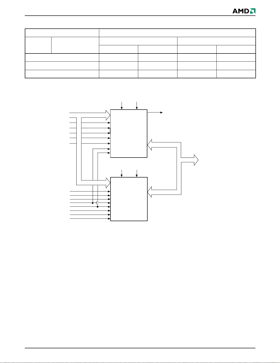
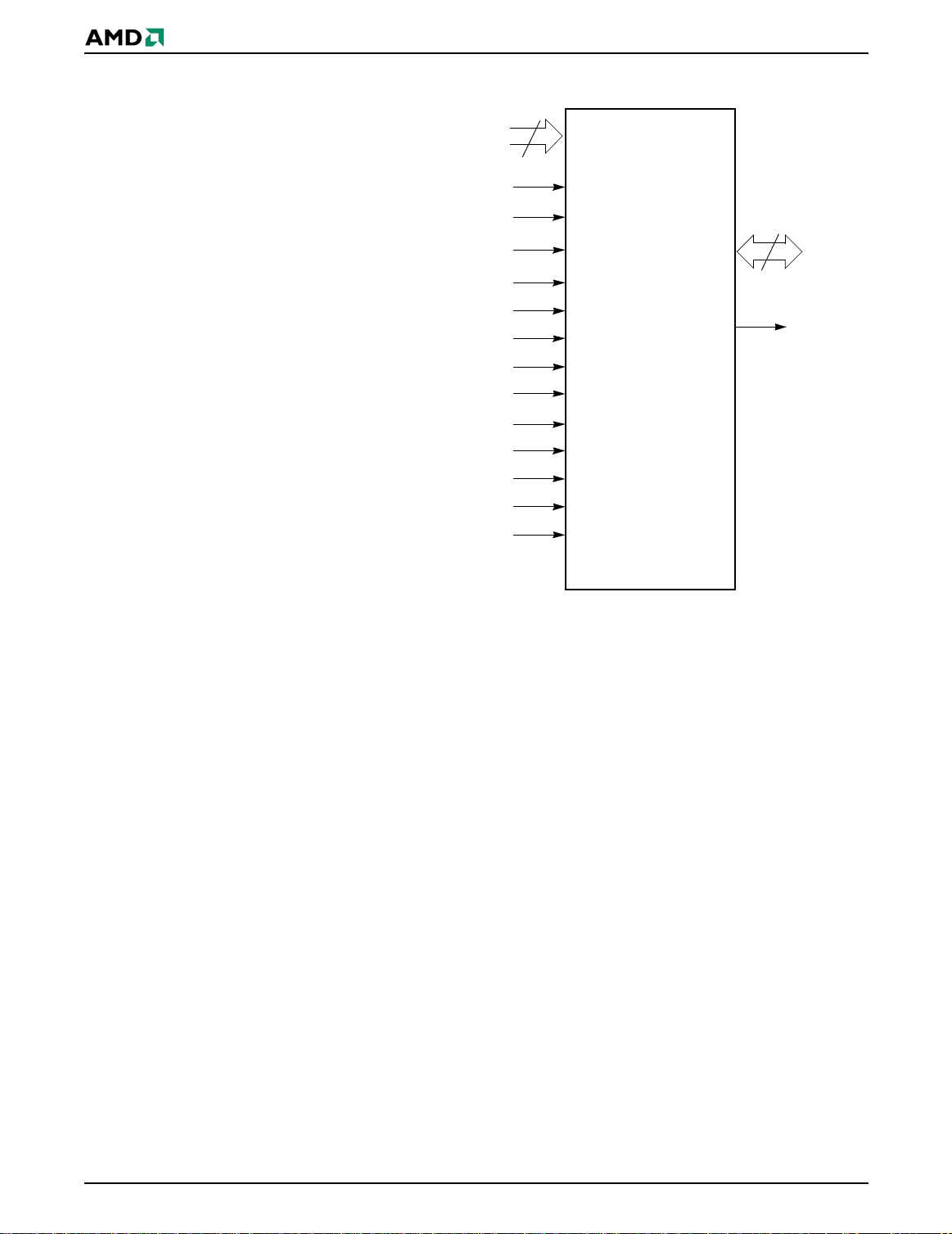
MCP BLOCK DIAGRAM
32 M Bit
CCQ
V
SS
VSS/V
DQ15/A-1 to DQ0
SSQ
RY/BY#
DQ15/A-1 to DQ0
A20 to A0
A
–
WP#/ACC
RESET#
CE#f
CIOf
VCCf
A20 to A0
1
Flash Memory
VCCs/V
SA
LB#s
UB#s
WE#
OE#
CE1#s
CE2s
CIOs
A0 to A19
A17 to A0
4 M Bit
Static RAM
DQ15/A-1 to DQ0
November 12, 2001 Am41DL32x4G 5
Page 7
PRELIMINARY
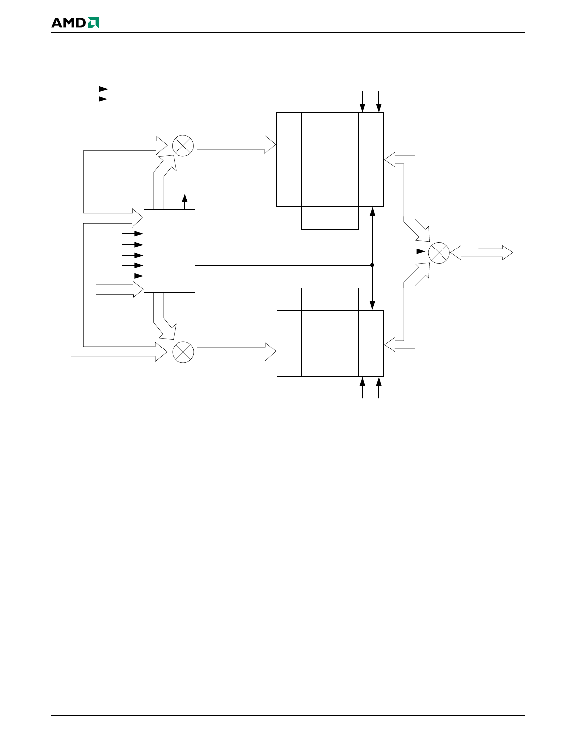
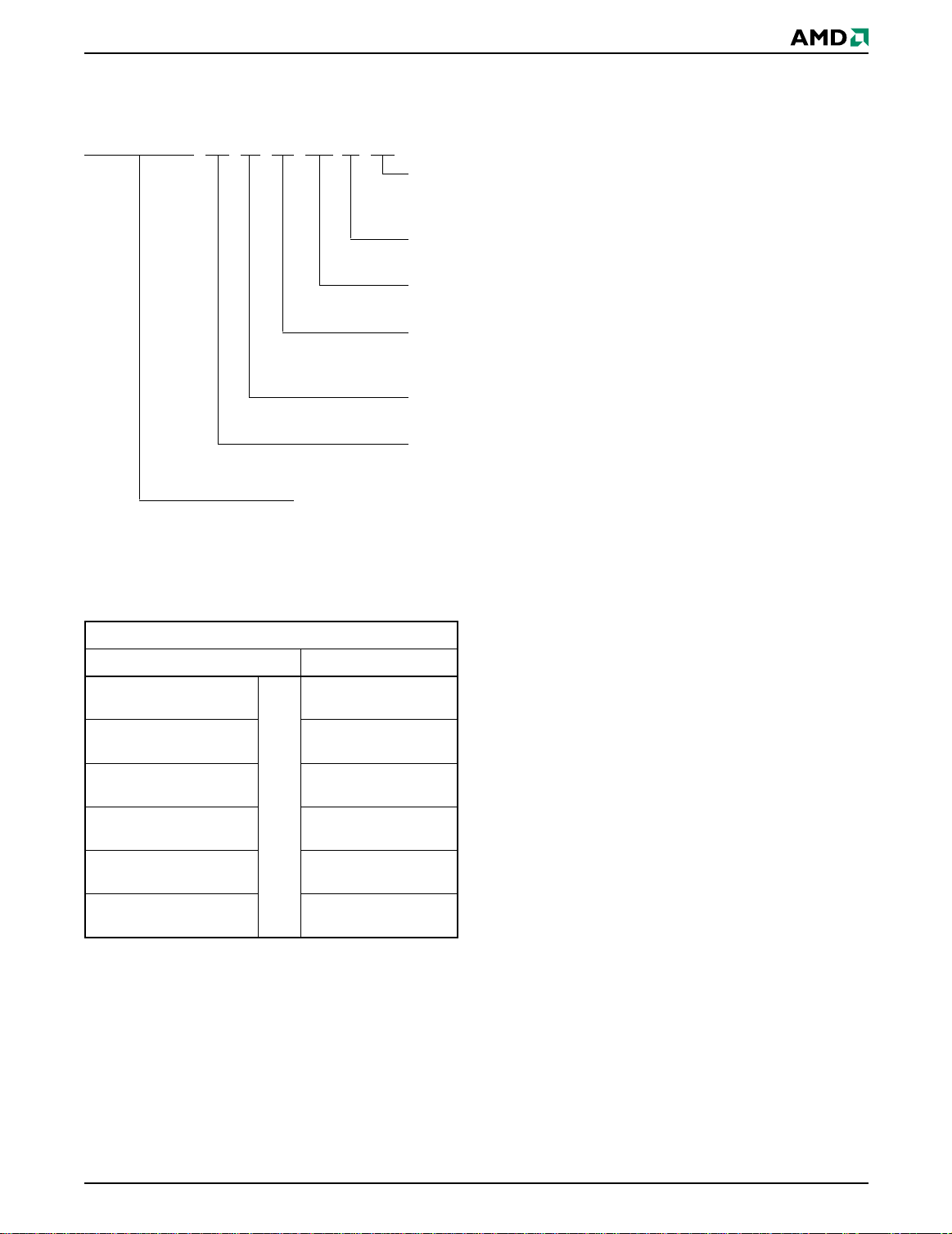
FLASH MEMORY BLOCK DIAGRAM
V
V
CC
SS
A20–A0
A20–A0
RESET#
WE#
CE#
CIOf
WP#/ACC
DQ15–DQ0
A20–A0
RY/BY#
A20–A0A20–A0
STATE
CONTROL
&
COMMAND
REGISTER
Upper Bank Address
Lower Bank Address
Y-Decoder
Status
Control
Y-Decoder
Upper Bank
X-Decoder
X-Decoder
Lower Bank
OE# CIOf
Latches and Control Logic
Latches and
Control Logic
DQ15–DQ0
DQ15–DQ0 DQ15–DQ0
OE# CIOf
6 Am41DL32x4G November 12, 2001
Page 8
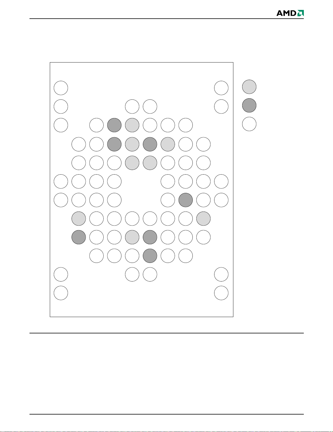
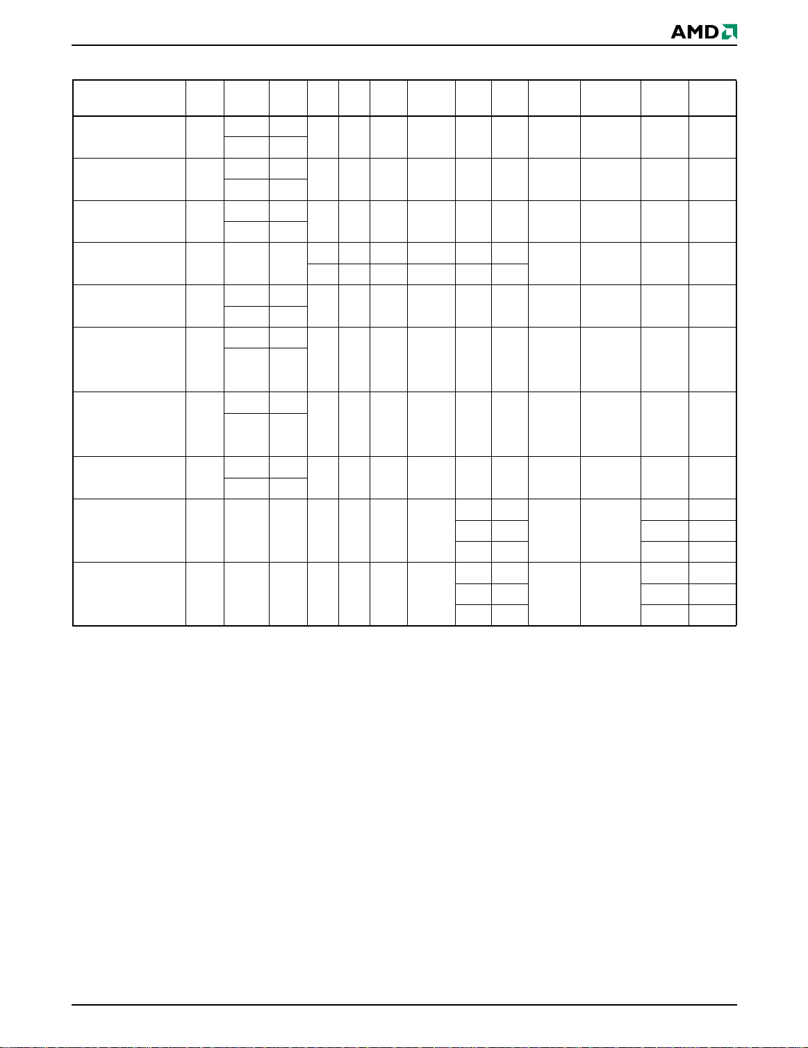
CONNECTION DIAGRAM
PRELIMINARY
73-Ball FBGA
Top View
A1
NC
B1
NC
C1
NC
F1
NC
G1
NC
L1
NC
M1
NC
D2
A3
E2
A2
F2
A1
G2
A0
H2
CE#f
J2
CE1#s
C3
A7
D3
A6
E3
A5
F3
A4
G3
V
SS
H3
OE#
J3
DQ0
K3
DQ8
C4
LB#
D4
UB#
E4
A18
F4
A17
G4
DQ1
H4
DQ9
J4
DQ10
K4
DQ2
B5
NC
C5
WP#/ACC
D5
RESET#
E5
RY/BY#
H5
DQ3
J5
V
f
CC
K5
DQ11
L5
NC
B6
NC
C6
WE#
D6
CE2s
E6
A20
H6
DQ4
J6
V
CC
K6
CIOs
L6
NC
A10
NC
B10
NC
C7
A8
D7
A19
E7
A9
F7
A10
G7
DQ6
H7
DQ13
J7
s
DQ12
K7
DQ5
C8
A11
D8
A12
E8
A13
F8
A14
G8
SA
H8
DQ15/A-1
J8
DQ7
K8
DQ14
D9
A15
E9
NC
F9
NC
G9
A16
H9
CIOf
J9
V
SS
F10
NC
G10
NC
Flash only
SRAM only
Shared
L10
NC
M10
NC
Special Handling Instructions for FBGA Package
Special handling i s required for Flas h Memory products in FBGA packages.
Flash memory devices in FBGA pac kages may be
damaged if exposed to ultrasonic c leaning methods.
The package and/or data integrity may be compromised if the package body is exposed to temperatures
above 150°C for prolonged periods of time.
November 12, 2001 Am41DL32x4G 7
Page 9
PRELIMINARY
PIN DESCRIPTION
A17–A0 = 18 Address Inputs (Common)
A-1, A20–A18 = 4 Addres s Input s (Flas h)
SA = Highest Order Address Pin (SRAM)
Byte mode
DQ15–DQ0 = 16 Data Inputs/Output s (Com mon )
CE#f = Chip Enable (Flash)
CE#s = Chip Enable (SRAM)
OE# = Output Enable (Common)
WE# = Write Enable (Common)
RY/BY# = Ready/Busy Output
UB#s = Upper Byte Control (SRAM)
LB#s = Lower Byte Control (SRAM)
CIOf = I/O Configur at ion (Fla sh)
CIOf = V
CIOf = V
CIOs = I/O Con figur at io n (SRA M)
CIOs = V
CIOs = V
RESET# = Hardware Reset Pin, Active Low
= Word mode (x16),
IH
= Byte mode (x8)
IL
= Word mode (x16),
IH
= Byte mode (x8)
IL
LOGIC SYMBOL
19
A18–A0
A-1, A20–A18
SA
CE#f
CE1#s
CE2s
OE#
WE#
WP#/ACC
RESET#
UB#s
LB#s
CIOf
CIOs
16 or 8
DQ15–DQ0
RY/BY#
WP#/ACC = Hardware Write Protect/
Acceleration Pin (Flash)
V
f = Flash 3.0 volt-only single power
CC
supply (see Product Selector Guide
for speed options and voltage sup-
ply tolerances)
s = SRAM Power Supply
V
CC
V
SS
= Device Ground (Common)
NC = Pin Not Connected Internally
8 Am41DL32x4G November 12, 2001
Page 10
PRELIMINARY
ORDERING INFORMATION
The order number (Valid Combination) is formed by the following:
Am41DL32x 4 G T 70 I T
TAPE AND REEL
T = 7 inches
S=13 inches
TEMPERATURE RANGE
I = Industrial (–40
SPEED OPTION
See Product Selector Guide and Valid Combinations
BOOT CODE SECTOR ARCHITECTURE
T=Top sector
B = Botto m sector
PROCESS TECHNOLOGY
G = 0.17 µm
SRAM DEVICE DENSITY
4= 4 Mbits
AMD DEVICE NUMBER/DESCRIPTION
Am41DL32x4G
Stacked Multi-Chip Package (MCP) Flash Memory and SRAM
Am29DL32xG 32 Megabit (4 M x 8-Bit/2 M x 16-Bit) CMOS 3.0 Volt-only, Simultaneous Operation
Flash Memory and 4 Mbit (512 K x 8-Bit/256 K x 16-Bit) Static RAM
°C to +85°C)
Valid Combinations
Order Number Package Marking
Am41DL3224GT70I
Am41DL3224GB70I
Am41DL3224GT85I
Am41DL3224GB85I
Am41DL3234GT70I
Am41DL3234GB70I
T, S
Am41DL3234GT85I
Am41DL3234GB85I
Am41DL3244GT70I
Am41DL3244GB70I
Am41DL3244GT85I
Am41DL3244GB85I
M41000001W
M41000001X
M41000001Y
M41000001Z
M410000020
M410000021
M410000022
M410000023
M410000024
M410000025
M410000026
M410000027
Valid Combinations
Valid Combinations list configurations planned to be supported in volume for this device. Consult the local AMD sales office to confi rm
availability of specific valid combinations and to ch eck on newl y released combinations
November 12, 2001 Am41DL32x4G 9
Page 11

PRELIMINARY
DEVICE BUS OPERATIONS
This section describes the requirements and use of
the device bus operations, which are initiated through
the internal command register. The command register
itself does not occupy any addressable memory location. The register is a latch used to store the
commands, along with the address and data information neede d to ex ecu te the co mm an d. T he conte nts of
the register serve as inputs to th e internal state machine. The state machine outputs dictate the function
of the device. Tables 1 through 3 li st the dev ice bus
operations, the inputs and control levels they require,
and the resulting output. The following subsections describe each of these operations in further detail.
10 Am41DL32x4G November 12, 2001
Page 12
PRELIMINARY
Table 1. Device Bus Operations—Flash Word Mode, CIOf = VIH; SRAM Word Mode, CIOs = VCC
Operation
(Notes 1, 2)
Read from Flash L
Write to Flash L
Standby
Output Disable L L H
Flash Hardware
Reset
Sector Prote ct
(Note 5)
CE#f CE1#s CE2s OE# WE# SA Addr. LB#s UB#s RESET#
V
CC
0.3 V
HX
XL
HX
XL
HX
±
XL
LH X A
HL X A
XX X X X X
HHXXLX
HH X X X L
HX
X
L
XL
HX
XL
X X X X X X L L/H High-Z High-Z
SADD,
HL X
A6 = L,
A1 = H,
A0 = L
Sector Unprotect
(Note 5)
Temporary Sector
Unprotect
L
X
HX
XL
HX
XL
HL X
XX X X X X V
SADD,
A6 = H,
A1 = H,
A0 = L
Read from SRAM H L H L H X A
Write to SRAM H L H X L X A
WP#/ACC
(Note 4)
XX H L/H D
IN
XX H (Note 4)DIND
IN
V
±
CC
0.3 V
H High-Z High-Z
H L/H High-Z High-Z
XX V
XX V
ID
ID
ID
L/H D
(Note 6) D
(Note 6) D
LL
H L High-Z D
IN
HX
LH D
LL
H L High-Z D
IN
HX
LH DINHigh-Z
DQ7–
DQ0
OUT
IN
IN
IN
D
OUT
OUT
D
IN
DQ15–
DQ8
D
OUT
IN
X
X
High-Z
D
OUT
OUT
High-Z
D
IN
IN
Legend: L = Logic Low = VIL, H = Logic High = VIH, VID = 11.5–12.5 V, VHH = 9.0 ± 0.5 V, X = Don’t Care, SA = SRAM Address
Input, Byte Mode, SADD = Flash Sector Address, A
= Address In, DIN = Data In, D
IN
= Data Out
OUT
Notes:
1. Other operations except for those indicated in this column are inhibited.
2. Do not apply CE#f = V
, CE1#s = VIL and CE2s = VIH at the same time.
IL
3. Don’t care or open LB#s or UB#s.
4. If WP#/ACC = V
If WP#/ACC = V
, the boot sectors will be pr ot ected . I f WP#/ ACC = VIH the boot sectors protect ion will be removed.
IL
(9V), the program ti me wi ll be reduced by 40%.
ACC
5. The sector protect and sector unpr ot ect f uncti ons may als o be implemented via prog ramming equipm ent . S ee t he “Sector /Sec tor
Block Protection and Unpr otection” section.
6. If WP#/ACC = V
depends on whether they were l ast p rotec t ed or unprot ec ted usi ng t he me thod des cr ibed in “Sect or/Sector Bl ock Prot ec tion and
Unprotection”. If WP#/A CC = V
, the two outermost b oot sect or s remai n pr otected. If WP#/ACC = VIH, the two outermost boot se ctor pr otecti on
IL
all sectors will be unpr ot ec ted.
HH,
November 12, 2001 Am41DL32x4G 11
Page 13
PRELIMINARY
Table 2. Device Bus Operations—Flash Word Mode, CIOf = VIH; SRAM Byte Mode, CIOs = VSS
Operation
(Notes 1, 2)
Read from Flash L
Write to Flash L
Standby
CE#f CE1#s CE2s OE# WE# SA Addr.
V
CC
0.3 V
HX
XL
HX
XL
HX
±
XL
LHX A
HLX A
XXX X X X
Output Disable L L H H H SA X DNU DNU H L/H High-Z High-Z
Flash Hardware
Reset
Sector Protect
(Note 5)
X
L
HX
XL
HX
XL
XXX X X X L L/HHigh-ZHigh-Z
SADD,
HLX
A6 = L,
A1 = H,
A0 = L
Secto r Unprotect
(Note 5)
Temporary Sector
Unprotect
L
X
HX
XL
HX
XL
HLX
XXX A
SADD,
A6 = H,
A1 = H,
A0 = L
Read from SRAM H L H L H SA A
Write to SRAM H L H X L SA A
Legend: L = Logic Low = VIL, H = Logic High = VIH, VID = 11.5–12.5 V, VHH = 9.0 ± 0.5 V, X = Don’t Care, SA = SRAM Address
Input, Byte Mode, SADD = Flash Sector Address, A
= Address In, DIN = Data In, D
IN
Notes:
1. Other operations except for those indicated in this column are inhibited.
2. Do not apply CE#f = V
, CE1#s = VIL and CE2s = VIH at the same time.
IL
3. Don’t care or open LB#s or UB#s.
4. If WP#/ACC = V
If WP#/ACC = V
, the boot sectors will be pr ot ected . I f WP#/ ACC = VIH the boot sectors protect ion will be removed.
IL
(9V), the program ti me wi ll be reduced by 40%.
ACC
5. The sector protect and sector unpr ot ect f uncti ons may als o be implemented via prog ramming equipm ent . S ee t he “Sec tor/Sector
Block Protection and Unpr otection” section.
6. If WP#/ACC = V
, the two outermost b oot sect or s remai n pr otected. If WP#/ACC = VIH, the two outermost boot se ctor pr otecti on
IL
depends on whether they were l ast p rotec t ed or unprot ec ted usi ng t he me thod des cr ibed in “Sect or/S ector Bl ock Pr otec t ion an d
Unprotection”. If WP#/ACC = V
all sectors will be unpr ot ec ted.
HH,
IN
IN
IN
IN
IN
LB#s
(Note 3)
UB#s
(Note 3)
RESET#
XXHL/HD
X X H (Note 3) D
V
0.3 V
XXV
XXV
CC
±
ID
ID
WP#/ACC
(Note 4)
DQ7–
DQ0
OUTDOUT
IN
H High-Z High-Z
L/H D
(Note 6) D
IN
IN
XXVID(Note 6) DINHigh-Z
XXH XD
OUT
XXH XDINHigh-Z
= Data Out, DNU = Do Not Use
OUT
DQ15–
DQ8
D
IN
X
X
High-Z
12 Am41DL32x4G November 12, 2001
Page 14
PRELIMINARY
Table 3. Device Bus Operations—Flash Byte Mode, CIOf = VSS; SRAM Word Mode, CIOs = VCC
Operation
(Not es 1, 2)
Read from Flash L
Write to Flash L
Standby
CE#f CE1#s CE2s OE#
V
CC
0.3 V
HX
XL
HX
XL
HX
±
XL
LHX A
HLX A
XXX X X X
WE# SA Addr.
Output Disable L L H H H X X
Flash Hardware
Reset
Sector Protect
(Note 5)
X
L
HX
XL
HX
XL
X X X X X X L L/H High-Z High-Z
SADD,
HLX
A6 = L,
A1 = H,
A0 = L
Sector
Unprotect
(Note 5)
Temporary
Sector
Unprotect
Read from
SRAM
HX
L
XL
HLX
Hx
X
XL
XXX A
HLHLHXA
SADD,
A6 = L,
A1 = H,
A0 = L
Write to SRAM H L H X L X A
IN
IN
IN
IN
IN
LB#s
(Note 3)
UB#s
(Note 3)
RESET#
WP#/ACC
(Note 4)
XXHL/HD
XXH
V
0.3 V
LX
XL
XXV
XXV
(Not e 3)
±
CC
H High-Z High-Z
H L/H High-Z High-Z
ID
ID
L/H D
(Note 6) D
XXVID(Note 6) D
LL
HL High-ZD
HX
LH D
LL
HL High-ZD
HX
LH DINHigh-Z
DQ7–
DQ0
OUT
D
IN
IN
IN
IN
D
OUT
OUT
D
IN
DQ15–
DQ8
High-Z
High-Z
X
X
High-Z
D
OUT
OUT
High-Z
D
IN
IN
Legend: L = Logic Low = VIL, H = Logic High = VIH, VID = 11.5–12.5 V, VHH = 9.0 ± 0.5 V, X = Don’t Care, SA = SRAM Address
Input, Byte Mode, SADD = Flash Sector Address, A
= Address In (for Flash Byte Mode, DQ15 = A-1), DIN = Data In, D
IN
OUT
=
Data Out
Notes:
1. Other operations except for those indicated in this column are inhibited.
2. Do not apply CE#f = V
, CE1#s = VIL and CE2s = VIH at the same time.
IL
3. Don’t care or open LB#s or UB#s.
4. If WP#/ACC = V
If WP#/ACC = V
, the boot sectors will be pr ot ected . I f WP#/ ACC = VIH the boot sectors protect ion will be removed.
IL
(9V), the program ti me wi ll be reduced by 40%.
ACC
5. The sector protect and sector unpr ot ect f uncti ons may als o be implemented via prog ramming equipm ent . S ee t he “Sec tor/Sector
Block Protection and Unpr otection” section.
6. If WP#/ACC = V
, the two outermost b oot sect or s remai n pr otected. If WP#/ACC = VIH, the two outermost boot se ctor pr otecti on
IL
depends on whether they were l ast p rotec t ed or unprot ec ted usi ng t he me thod des cr ibed in “Sect or/S ector Bl ock Pr otec t ion an d
Unprotection”. If WP#/ACC = V
all sectors will be unpr ot ec ted.
HH,
November 12, 2001 Am41DL32x4G 13
Page 15

PRELIMINARY
Table 4. Device Bus Operations—Flash Byte Mode, CIOf = VIL; SRAM Byte Mode, CIOs = VSS
Operation
(Not es 1, 2)
CE#f CE1#s CE2s OE#
Read from Flash L
Write to Flash L
Standby
V
0.3 V
CC
HX
XL
HX
XL
HX
±
XL
WE# SA Addr.
LH X A
HL X A
IN
IN
LB#s
(Note 3)
UB#s
(Note 3)
XXHL/HD
XXH
XX X X X X
RESET#
V
±
CC
0.3 V
WP#/ACC
(Note 4)
(Note 3)
H High-Z High-Z
DQ7–
DQ0
Output Disable H L H H H SA X DNU DNU H L/H High-Z High-Z
Flash Hardware
Reset
Sector Protect
(Note 5)
X
L
HX
XL
HX
XL
X X X X X X L L/H High-Z High-Z
SADD,
HL X
A6 = L,
A1 = H,
XXV
ID
L/H D
A0 = L
HX
Sector Unprotect
(Note 5)
Temporary
Sector Unprotect
L
X
XL
HX
XL
HL X
XX X A
Read from SRAM H L H L H SA A
Write to SRAM H L H X L SA A
SADD,
A6 = L,
A1 = H,
A0 = L
IN
IN
IN
XXV
ID
(Note 6) D
XXVID(Note 6) D
XXH XD
XXH XDINHigh-Z
Legend: L = Logic Low = VIL, H = Logic High = VIH, VID = 11.5–12.5 V, VHH = 9.0 ± 0.5 V, X = Don’t Care, SA = SRAM Address
Input, Byte Mode, SADD = Flash Sector Address, A
= Address In (for Flash Byte Mode, DQ15 = A-1), DIN = Data In, D
IN
Data Out, DNU = Do Not Use
Notes:
1. Other operations except for those indicated in this column are inhibited.
2. Do not apply CE#f = V
, CE1#s = VIL and CE2s = VIH at the same time.
IL
3. Don’t care or open LB#s or UB#s.
4. If WP#/ACC = V
If WP#/ACC = V
, the boot sectors will be pr ot ected . I f WP#/ ACC = VIH the boot sectors protect ion will be removed.
IL
(9V), the program ti me wi ll be reduced by 40%.
ACC
5. The sector protect and sector unpr ot ect f uncti ons may als o be implemented via prog ramming equipm ent . S ee t he “Sec tor/Sector
Block Protection and Unpr otection”.
6. If WP#/ACC = V
, the two outermost b oot sect or s remai n pr otected. If WP#/ACC = VIH, the two outermost boot se ctor pr otecti on
IL
depends on whether they were l ast p rotec t ed or unprot ec ted usi ng t he me thod des cr ibed in “Sect or/S ector Bl ock Pr otec t ion an d
Unprotection”. If WP#/ACC = V
all sectors will be unpr ot ec ted.
HH,
D
OUT
IN
IN
IN
IN
OUT
DQ15–
DQ8
High-Z
High-Z
X
X
High-Z
High-Z
=
OUT
14 Am41DL32x4G November 12, 2001
Page 16

PRELIMINARY
Word/Byte Configuration
The CIOf pin controls whether the device data I/O pins
operate in the byte or word configuration. If the CIOf
pin is set at logic ‘1’, the device is in word configuration, DQ15–DQ0 are active and controlled by CE# and
OE#.
If the CIOf pin is set at logic ‘0’, the dev ice is in byte
configur atio n, a nd o nly data I/O pin s DQ 7–DQ0 are
active and controlled by CE# and OE#. The data I/O
pins DQ14–DQ8 are tri-stated, and the DQ15 pin is
used as an input for the LSB (A-1) address function.
Requirements for Reading Array Data
To read array data from the outputs, the system must
drive the CE# f a nd O E# pins to V
. CE#f is the po wer
IL
control an d se lec ts t he d ev ice . O E# i s th e ou tpu t c ontrol and gates array data to the output pins. WE#
should remain at V
. The CIOf pin determines
IH
whether the devi ce outputs arr ay data in words or
bytes.
The internal state machine is set for reading array data
upon device power-up, or after a hardware reset. This
ensures that no spuri ous alteration of the mem ory
content occurs during th e power tr ansition . No command is necessary in this mode to obtain array data.
Standard mi cropr oce ssor re ad cycles that as sert va lid
addresse s o n t he devi ce ad dres s i npu ts pr od uc e vali d
data on the device data outputs. Each bank remains
enabled fo r read acces s until the comm and regis ter
contents are altered.
See “Requirements for Reading Array Data” for more
information. Refer to the AC Flash Read-Only Operations table for timing specifications and to Figure 14 for
the timing diagram. I
in the DC Characteri stics
CC1
table represents the active current specification for
reading array data.
Writing Commands/Command Sequences
To write a command or comm an d sequ enc e ( whi ch includes programming data to the device and erasing
sectors of memory), the system must drive WE# and
CE#f to V
For program operations, the CIOf pin determines
whether the device accepts program data in bytes or
words. Refer to “Word/Byte Configuration” for more
information.
The devic e fea ture s an Unlock Bypa ss m od e to fa cilitate faste r programmin g. Once a bank ent ers the
Unlock Bypass mode, only two write cycles are required to program a word or byte, instead of four. The
“Word/Byte Configuration” section has details on pro-
gramming data to the device using both standard and
Unlock Bypass command sequences.
, and OE# to VIH.
IL
An erase operation can erase one sector, multiple sectors, or the entire device. Tables 6–9 indicat e the
address space that each sector occupies. The device
address spa ce is divi ded i nto two ba nks: Ba nk 1 c ontains the boot/par am ete r sec tors , and Ban k 2 conta in s
the larger, code sectors of uniform size. A “bank address” is the add res s bits requ ire d to un iq uel y select a
bank. Similarly, a “sector address” is the address bits
required to uniquely select a sector.
in the DC Ch arac te ris tics ta ble represents the ac-
I
CC2
tive current specification for the write mod e. The AC
Characteristics section contains timing specification
tables and timing diagrams for write operations.
Accelerated Program Operation
The device offers accelerated program operations
through the AC C fun ct ion. T his is on e of two functions
provided by the WP#/ACC pin. This function is primarily intended to allow faster manufacturing throughput
at the factory.
If the system asserts V
on this pin, the de vice a uto-
HH
matically en ters the af oreme ntioned Un lock Bypa ss
mode, temporarily unprotects any pr otected sectors,
and uses the higher voltage on the pin to reduce the
time required for program ope rations. The system
would use a two-cycle pr ogram com mand s equence
as required by the Unloc k Bypass m ode. Rem oving
from the WP#/ACC pin returns the device to nor-
V
HH
mal operation. Note that the WP#/ACC pin mu st not
be at V
for operations other than accelerate d pro-
HH
gramming, or device damage may result. In addition,
the WP#/ACC pin must not be left floating or un connected; inconsistent behavior of the device may result.
Autoselect Functions
If the system writes the autoselect command sequence, the device enters the autoselect mo de. The
system can the n rea d au tos e le ct co des fro m th e i nte rnal register (which is separate from the memory array)
on DQ7–DQ0. Standard read cycle timings apply in
this mode . Refe r to th e Au tosel ec t Mode and A uto select Command Sequence sections for more
information.
Simultaneous Read/Write Operations with Zero Latency
This device is capable of reading data from one bank
of memory while programming or erasing in the other
bank of memory. An erase operation may also be suspended to rea d from or prog ram to anoth er locati on
within the same bank (except the sector b eing
erased). Figure 21 shows how read and write cycles
may be initiated for simultaneous operation with zero
latency. I
CC6
and I
represent the current specifications for read-while-program and read-while-erase, respectively.
in the DC Characteristics table
CC7
November 12, 2001 Am41DL32x4G 15
Page 17
PRELIMINARY
Standby Mode
When the syste m is not rea ding or wr iting to the device, it can place the de vice in the standby mode. In
this mode, current consumption is greatly reduced,
and the outputs are placed in the high impedance
state, independent of the OE# input.
The devi ce en ter s t he CM OS st and by m od e w hen th e
CE#f and RESET# pins are both held at V
± 0.3 V.
CC
(Note that this is a more restricted voltage range than
.) If CE#f and RESE T# are held at VIH, but not
V
IH
within V
± 0.3 V, the device will b e in the stan dby
CC
mode, but the s tandby cu rrent will be greater. The device requires standard access time (t
) for read
CE
access when the device is in either of these standby
modes, before it is ready to read data.
If the device is desele cted during er asur e or prog ramming, the device draws active current until the
operation is completed.
in the DC Characteristics table represents the
I
CC3
standby current specification.
Automatic Sleep Mode
The automatic sleep mode minimizes Flash device energy consumption. The device automatically enables
this mode when addresses remain stable for t
ACC
+
30 ns. The automatic sleep mode is independent of
the CE# f, WE#, an d OE# co nt r ol si gn al s . S tan da r d ad dress access timings provide new data when
addresses are changed. While in sleep mode, output
data is latched and always available to the system.
in the DC Characteristics table represents the
I
CC4
automatic sleep mode current specification.
RESET#: Hardware Reset Pin
The RESET# pin provides a hardware m ethod of resetting the device to reading array data. When the
RESET# pin is driven low for at least a p eriod of t
RP
the device immediately terminates any operation in
progress, tristates all output pins, and ignores all
read/write commands for the duration of the RESET#
pulse. The de vice also resets th e internal state ma chine to read ing array data. The ope ration tha t was
interrupted should be reinitiated once the device is
ready to accept an other c ommand sequen ce, to ensure data integrity.
Current is reduced for the duration of the RESET#
pulse. When RESE T# is h eld at V
vice draws CMOS standby current (I
held at V
but not within V
IL
± 0.3 V, the standby cur-
SS
± 0.3 V, the de-
SS
). If RESET# is
CC4
rent will be greater.
The RESET# pin may be tied to the system reset cir-
cuitry. A system reset would thus also reset the Flash
memory, enabling the system to read the boot-up firmware from the Flash memory.
If RESET# is asserted during a program or erase operation, the RY/BY# pin remains a “0” (busy) until the
internal reset operation is complete, which requires a
time of t
(during Embedded Algorithms). The
READY
system can thus monitor RY/BY# to determine
whether the res e t op erat io n i s c om plete . If RESET# is
asserted when a program or erase operation is not executing (RY/BY# pin is “1”), the re set operat ion is
completed within a time of t
ded Algorithms). The system can read data t
the RESET# pin returns to V
(not during Embed-
READY
.
IH
RH
after
Refer to the AC Characteristics tables for RESET# parameters and to Figure 15 for the timing diagram.
Output Disable Mode
When the OE# input is at VIH, output from the device is
disabled. The output pins are placed in the high
impedance state.
,
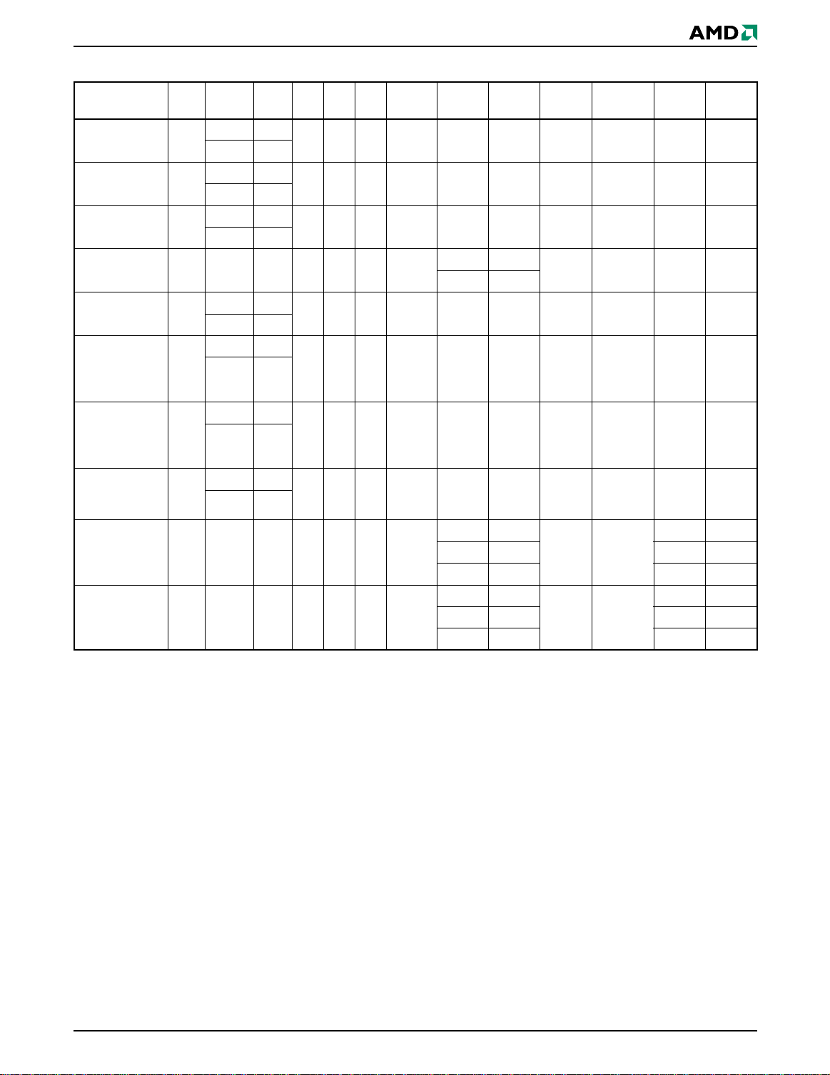
Table 5. Device Bank Division
Device
Part Number
Am29DL322G 4 Mbit
Am29DL323G 8 Mbit
Am29DL324G 16 Mbit
Megabits Sector Sizes Me ga bits Sector Sizes
Bank 1 Bank 2
Eight 8 Kbyte/4 Kword,
seven 64 Kbyte/32 Kword
Eight 8 Kbyte/4 Kword,
fifteen 64 Kbyte/32 Kword
Eight 8 Kbyte/4 Kword,
thirty-one 64 Kbyte/32 Kword
28 Mbit
24 Mbit
16 Mbit
Fifty-six
64 Kbyte/32 Kword
Forty-eight
64 Kbyte/32 Kword
Thirty-two
64 Kbyte/32 Kword
16 Am41DL32x4G November 12, 2001
Page 18
PRELIMINARY
Sector
Am29DL324GT
Am29DL323GT
Am29DL322GT
SA0 000000xxx 64/32 000000h–00FFFFh 000000h–07FFFh
SA1 000001xxx 64/32 010000h–01FFFFh 008000h–0FFFFh
SA2 000010xxx 64/32 020000h–02FFFFh 010000h–17FFFh
SA3 000011xxx 64/32 030000h–03FFFFh 018000h–01FFFFh
SA4 000100xxx 64/32 040000h–04FFFFh 020000h–027FFFh
SA5 000101xxx 64/32 050000h–05FFFFh 028000h–02FFFFh
SA6 000110xxx 64/32 060000h–06FFFFh 030000h–037FFFh
SA7 000111xxx 64/32 070000h–07FFFFh 038000h–03FFFFh
SA8 001000xxx 64/32 080000h–08FFFFh 040000h–047FFFh
SA9 001001xxx 64/32 090000h–09FFFFh 048000h–04FFFFh
SA10 001010xxx 64/32 0A0000h–0AFFFFh 050000h–057FFFh
SA11 001011xxx 64/32 0B0000h–0BFFFFh 058000h–05FFFFh
SA12 001100xxx 64/32 0C0000h–0CFFFFh 060000h–067FFFh
SA13 001101xxx 64/32 0D0000h–0DFFFFh 068000h–06FFFFh
SA14 001110xxx 64/32 0E0000h–0EFFFFh 070000h–077FFFh
SA15 001111xxx 64/32 0F0000h–0FFFFFh 078000h–07FFFFh
Bank 2
Bank 2
Bank 1
SA16 010000xxx 64/32 100000h–10FFFFh 080000h–087FFFh
SA17 010001xxx 64/32 110000h–11FFFFh 088000h–08FFFFh
SA18 010010xxx 64/32 120000h–12FFFFh 090000h–097FFFh
SA19 010011xxx 64/32 130000h–13FFFFh 098000h–09FFFFh
SA20 010100xxx 64/32 140000h–14FFFFh 0A0000h–0A7FFFh
SA21 010101xxx 64/32 150000h–15FFFFh 0A8000h–0AFFFFh
SA22 010110xxx 64/32 160000h–16FFFFh 0B0000h–0B7FFFh
SA23 010111xxx 64/32 170000h–17FFFFh 0B8000h–0BFFFFh
SA24 011000xxx 64/32 180000h–18FFFFh 0C0000h–0C7FFFh
Bank 2
SA25 011001xxx 64/32 190000h–19FFFFh 0C8000h–0CFFFFh
SA26 011010xxx 64/32 1A0000h–1AFFFFh 0D0000h–0D7FFFh
SA27 011011xxx 64/32 1B0000h–1BFFFFh 0D8000h–0DFFFFh
SA28 011100xxx 64/32 1C0000h–1CFFFFh 0E0000h–0E7FFFh
SA29 011101xxx 64/32 1D0000h–1DFFFFh 0E8000h–0EFFFFh
SA30 011110xxx 64/32 1E0000h–1EFFFFh 0F0000h–0F7FFFh
SA31 011111xxx 64/32 1F0000h–1FFFFFh 0F8000h–0FFFFFh
SA32 100000xxx 64/32 200000h–20FFFFh 100000h–107FFFh
SA33 100001xxx 64/32 210000h–21FFFFh 108000h–10FFFFh
SA34 100010xxx 64/32 220000h–22FFFFh 110000h–117FFFh
SA35 100011xxx 64/32 230000h–23FFFFh 118000h–11FFFFh
SA36 100100xxx 64/32 240000h–24FFFFh 120000h–127FFFh
SA37 100101xxx 64/32 250000h–25FFFFh 128000h–12FFFFh
SA38 100110xxx 64/32 260000h–26FFFFh 130000h–137FFFh
SA39 100111xxx 64/32 270000h–27FFFFh 138000h–13FFFFh
SA40 101000xxx 64/32 280000h–28FFFFh 140000h–147FFFh
SA41 101001xxx 64/32 290000h–29FFFFh 148000h–14FFFFh
SA42 101010xxx 64/32 2A0000h–2AFFFFh 150000h–157FFFh
SA43 101011xxx 64/32 2B0000h–2BFFFFh 158000h–15FFFFh
SA44 101100xxx 64/32 2C0000h–2CFFFFh 160000h–167FFFh
SA45 101101xxx 64/32 2D0000h–2DFFFFh 168000h–16FFFFh
SA46 101110xxx 64/32 2E0000h–2EFFFFh 170000h–177FFFh
SA47 101111xxx 64/32 2F0000h–2FFFFFh 178000h–17FFFFh
Ta ble 6. Top Boot Sector Addresses
Sector Address
A20–A12
Sector Size
(Kbytes/Kwords)
(x8)
Address Range
(x16)
Address Range
November 12, 2001 Am41DL32x4G 17
Page 19
PRELIMINARY
Table 6. Top Boot Sector Addresses (Continued)
Sector
Am29DL324GT
Am29DL323GT
Am29DL322GT
SA48 110000xxx 64/32 300000h–30FFFFh 180000h–187FFFh
SA49 110001xxx 64/32 310000h–31FFFFh 188000h–18FFFFh
SA50 110010xxx 64/32 320000h–32FFFFh 190000h–197FFFh
SA51 110011xxx 64/32 330000h–33FFFFh 198000h–19FFFFh
SA52 110100xxx 64/32 340000h–34FFFFh 1A0000h–1A7FFFh
Bank 2
SA53 110101xxx 64/32 350000h–35FFFFh 1A8000h–1AFFFFh
SA54 110110xxx 64/32 360000h–36FFFFh 1B0000h–1B7FFFh
SA55 110111xxx 64/32 370000h–37FFFFh 1B8000h–1BFFFFh
SA56 111000xxx 64/32 380000h–38FFFFh 1C0000h–1C7FFFh
SA57 111001xxx 64/32 390000h–39FFFFh 1C8000h–1CFFFFh
SA58 111010xxx 64/32 3A0000h–3AFFFFh 1D0000h–1D7FFFh
SA59 111011xxx 64/32 3B0000h–3BFFFFh 1D8000h–1DFFFFh
Bank 1
Bank 1
SA60 111100xxx 64/32 3C0000h–3CFFFFh 1E0000h–1E7FFFh
SA61 111101xxx 64/32 3D0000h–3DFFFFh 1E8000h–1EFFFFh
SA62 111110xxx 64/32 3E0000h–3EFFFFh 1F0000h–1F7FFFh
SA63 111111000 8/4 3F0000h–3F1FFFh 1F8000h–1F8FFFh
Bank 1
SA64 111111001 8/4 3F2000h–3F3FFFh 1F9000h–1F9FFFh
SA65 111111010 8/4 3F4000h–3F5FFFh 1FA000h–1FAFFFh
SA66 111111011 8/4 3F6000h–3F7FFFh 1FB000h–1FBFFFh
SA67 111111100 8/4 3F8000h–3F9FFFh 1FC000h–1FCFFFh
SA68 111111101 8/4 3FA000h–3FBFFFh 1FD000h–1FDFFFh
SA69 111111110 8/4 3FC000h–3FDFFFh 1FE000h–1FEFFFh
SA70 11 1111111 8/4 3FE000h–3FFFFFh 1FF000h–1FFFFFh
Sector Address
A20–A12
Sector Size
(Kbytes/Kwords)
(x8)
Address Range
(x16)
Address Range
Note: The address range is A20:A-1 in byte mode (BYTE#=VIL) or A20:A0 in word mode (BYTE#=VIH). The bank address bits are A20–A18 for
Am29DL322GT, A20 and A19 for Am29DL323GT, and A20 for Am29DL324GT.
Table 7. Top Boot SecSi Sector Addresses
Device
Am29DL322GT, Am29DL323GT,
Am29DL324GT
Sector Address
A20–A12
111111xxx 256/128 3FE000h–3FE0FFh 1FF000h–1FF07Fh
Sector Size
(bytes/words)
(x8)
Address Range
(x16)
Address Range
18 Am41DL32x4G November 12, 2001
Page 20
PRELIMINARY
Table 8. Bottom Boot Sector Addresses
Sector
Am29DL324GB
Am29DL323GB
Am29DL322GB
SA0 000000000 8/4 000000h-001FFFh
SA1 000000001 8/4 002000h-003FFFh
SA2 000000010 8/4 004000h-005FFFh
SA3 000000011 8/4 006000h-007FFFh
SA4 000000100 8/4 008000h-009FFFh
SA5 000000101 8/4 00A000h-00BFFFh
SA6 000000110 8/4 00C000h-00DFFFh
SA7 000000111 8/4 00E000h-00FFFFh
Bank 1
SA8 000001xxx 64/32 010000h-01FFFFh
SA9 000010xxx 64/32 020000h-02FFFFh
SA10 000011xxx 64/32 030000h-03FFFFh
SA11 000100xxx 64/32 040000h-04FFFFh
Bank 1
Bank 1
Bank 2
SA12 000101xxx 64/32 050000h-05FFFFh
SA13 000110xxx 64/32 060000h-06FFFFh
SA14 000111xxx 64/32 070000h-07FFFFh
SA15 001000xxx 64/32 080000h-08FFFFh
SA16 001001xxx 64/32 090000h-09FFFFh
SA17 001010xxx 64/32 0A0000h-0AFFFFh
SA18 001011xxx 64/32 0B0000h-0BFFFFh
SA19 001100xxx 64/32 0C0000h-0CFFFFh
SA20 001101xxx 64/32 0D0000h-0DFFFFh
SA21 001110xxx 64/32 0E0000h-0EFFFFh
SA22 001111xxx 64/32 0F0000h-0FFFFFh
SA23 010000xxx 64/32 100000h-10FFFFh
SA24 010001xxx 64/32 110000h-11FFFFh
SA25 010010xxx 64/32 120000h-12FFFFh
SA26 010011xxx 64/32 130000h-13FFFFh
SA27 010100xxx 64/32 140000h-14FFFFh
Bank 2
SA28 010101xxx 64/32 150000h-15FFFFh
SA29 010110xxx 64/32 160000h-16FFFFh
SA30 010111xxx 64/32 170000h-17FFFFh
SA31 011000xxx 64/32 180000h-18FFFFh
SA32 011001xxx 64/32 190000h-19FFFFh
SA33 011010xxx 64/32 1A0000h-1AFFFFh
SA34 011011xxx 64/32 1B0000h-1BFFFFh
SA35 011100xxx 64/32 1C0000h-1CFFFFh
SA36 011101xxx 64/32 1D0000h-1DFFFFh
SA37 011110xxx 64/32 1E0000h-1EFFFFh
SA38 0111 11xxx 64/32 1F0000h-1FFFFFh
Sector Address
A20–A12
Sector Size
(Kbytes/Kwords)
(x8)
Address Range
(x16)
Address Range
000000h–000FFFh
001000h–001FFFh
002000h–002FFFh
003000h–003FFFh
004000h–004FFFh
005000h–005FFFh
006000h–006FFFh
007000h–007FFFh
008000h–00FFFFh
010000h–017FFFh
018000h–01FFFFh
020000h–027FFFh
028000h–02FFFFh
030000h–037FFFh
038000h–03FFFFh
040000h–047FFFh
048000h–04FFFFh
050000h–057FFFh
058000h–05FFFFh
060000h–067FFFh
068000h–06FFFFh
070000h–077FFFh
078000h–07FFFFh
080000h–087FFFh
088000h–08FFFFh
090000h–097FFFh
098000h–09FFFFh
0A0000h–0A7FFFh
0A8000h–0AFFFFh
0B0000h–0B7FFFh
0B8000h–0BFFFFh
0C0000h–0C7FFFh
0C8000h–0CFFFFh
0D0000h–0D7FFFh
0D8000h–0DFFFFh
0E0000h–0E7FFFh
0E8000h–0EFFFFh
0F0000h–0F7FFFh
0F8000h–0FFFFFh
November 12, 2001 Am41DL32x4G 19
Page 21

PRELIMINARY
Ta ble 8. Bottom Boot Sector Addresses (Continued)
Sector
Am29DL324GB
Am29DL323GB
Am29DL322GB
SA39 100000xxx 64/32 200000h-20FFFFh 100000h–107FFFh
SA40 100001xxx 64/32 210000h-21FFFFh 108000h–10FFFFh
SA41 100010xxx 64/32 220000h-22FFFFh 110000h–117FFFh
SA42 100011xxx 64/32 230000h-23FFFFh 118000h–11FFFFh
SA43 100100xxx 64/32 240000h-24FFFFh 120000h–127FFFh
SA44 100101xxx 64/32 250000h-25FFFFh 128000h–12FFFFh
SA45 100110xxx 64/32 260000h-26FFFFh 130000h–137FFFh
SA46 100111xxx 64/32 270000h-27FFFFh 138000h–13FFFFh
SA47 101000xxx 64/32 280000h-28FFFFh 140000h–147FFFh
SA48 101001xxx 64/32 290000h-29FFFFh 148000h–14FFFFh
SA49 101010xxx 64/32 2A0000h-2AFFFFh 150000h–157FFFh
SA50 101011xxx 64/32 2B0000h-2BFFFFh 158000h–15FFFFh
SA51 101100xxx 64/32 2C0000h-2CFFFFh 160000h–167FFFh
SA52 101101xxx 64/32 2D0000h-2DFFFFh 168000h–16FFFFh
SA53 101110xxx 64/32 2E0000h-2EFFFFh 170000h–177FFFh
SA54 101111xxx 64/32 2F0000h-2FFFFFh 178000h–17FFFFh
Bank 2
Bank 2
SA55 111000xxx 64/32 300000h-30FFFFh 180000h–187FFFh
Bank 2
SA56 110001xxx 64/32 310000h-31FFFFh 188000h–18FFFFh
SA57 110010xxx 64/32 320000h-32FFFFh 190000h–197FFFh
SA58 110011xxx 64/32 330000h-33FFFFh 198000h–19FFFFh
SA59 110100xxx 64/32 340000h-34FFFFh 1A0000h–1A7FFFh
SA60 110101xxx 64/32 350000h-35FFFFh 1A8000h–1AFFFFh
SA61 110110xxx 64/32 360000h-36FFFFh 1B0000h–1B7FFFh
SA62 110111xxx 64/32 370000h-37FFFFh 1B8000h–1BFFFFh
SA63 111000xxx 64/32 380000h-38FFFFh 1C0000h–1C7FFFh
SA64 111001xxx 64/32 390000h-39FFFFh 1C8000h–1CFFFFh
SA65 111010xxx 64/32 3A0000h-3AFFFFh 1D0000h–1D7FFFh
SA66 111011xxx 64/32 3B0000h-3BFFFFh 1D8000h–1DFFFFh
SA67 111100xxx 64/32 3C0000h-3CFFFFh 1E0000h–1E7FFFh
SA68 111101xxx 64/32 3D0000h-3DFFFFh 1E8000h–1EFFFFh
SA69 111110xxx 64/32 3E0000h-3EFFFFh 1F0000h–1F7FFFh
SA70 111111xxx 64/32 3F0000h-3FFFFFh 1F8000h–1FFFFFh
Sector Address
A20–A12
Sector Size
(Kbytes/Kwords)
(x8)
Address Range
(x16)
Address Range
Note: The address range is A20:A-1 in byte mode (BYTE#=VIL) or A20:A0 in word mode (BYTE#=VIH). The bank address bits
are A20–A18 for Am29DL322GB, A20 and A19 for Am29DL323GB, and A20 for Am29DL324GB.
Ta ble 9. Bottom Boot SecSi Sector Addresses
Device
Am29DL322GB, Am29DL323GB
Am29DL324GB
Sector Address
A20–A12
,
000000xxx 256/128 000000h-0000FFh 00000h-0007Fh
Sector Size
(bytes/words)
(x8)
Address Range
(x16)
Address Range
20 Am41DL32x4G November 12, 2001
Page 22

PRELIMINARY
Autoselect Mod e
The autoselect mode provides manufacturer and device identifica tion, and s ector prote ction verification,
through identifier codes output on DQ7–DQ0. This
mode is primarily intended for programming equipment to automatically match a device to be
programmed with its corresponding programming
algorithm.
The autoselect codes can also be accessed in-system
through the command register. The host system can
issue the autoselect command via the command register, as shown in Tables 15 and 17. This method does
not require V
. Refer to the Auto se lect Com ma nd S e-
ID
quence section for more information.
Sector/Sector Block Protection and Unprotection
(Note: For the following discussion, the term “sector”
applies to both sectors and sector blocks. A sector
block consists of two or more adjacent sectors that are
protected or unprotected at the same time (see Table
10).
Table 10. Top Boot Sector/Sector Block
Addresses for Protection/Unprotection
Sector A20–A12
SA0
SA1-SA3
SA4-SA7
SA8-SA11
SA12-SA15
SA16-SA19
SA20-SA23
SA24-SA27
SA28-SA31
SA32-SA35
SA36-SA39
SA40-SA43
SA44-SA47
SA48-SA51
SA52-SA55
SA56-SA59
SA60-SA62
SA63
SA64
SA65
SA66
000000XXX 64 Kbytes
000001XXX,
000010XXX
000011XXX
0001XXXXX 256 (4x64) Kbytes
0010XXXXX 256 (4x64) Kbytes
0011XXXXX 256 (4x64) Kbytes
0100XXXXX 256 (4x64) Kbytes
0101XXXXX 256 (4x64) Kbytes
0110XXXXX 256 (4x64) Kbytes
0111XXXXX 256 (4x64) Kbytes
1000XXXXX 256 (4x64) Kbytes
1001XXXXX 256 (4x64) Kbytes
1010XXXXX 256 (4x64) Kbytes
1011XXXXX 256 (4x64) Kbytes
1100XXXXX 256 (4x64) Kbytes
1101XXXXX 256 (4x64) Kbytes
1110XXXXX 256 (4x64) Kbytes
111100XXX,
111101XXX,
111110XXX
111111000 8 Kbytes
111111001 8 Kbytes
111111010 8 Kbytes
111111011 8 Kbytes
Sector/
Sector Block Size
192 (3x64) Kbytes
192 (4x64) Kbytes
Sector A20–A12
SA67 111111100 8 Kbytes
SA68
SA69
SA70
111111101 8 Kbytes
111111110 8 K by tes
111111111 8 Kbytes
Sector/
Sector Block Size
The hardware sector protection feature disables both
program and erase operations in any sector. The hardware sector unprotection feature re-enables both
program an d er ase ope rat ions i n pre vious ly pr otect ed
sectors. Note that the sector unprotect algorithm unprotects all sectors in parallel. All previously protected
sectors must be individually re-protected. To change
data in protected sectors efficiently, the temporary
sector un protect function is available. See “Temporary
Sector/Sector Block Unprotect”.
Sector protection and unprotection can be implemented as follows.
Sector prote c tion an d u npr o tec ti on requi res V
on the
ID
RESET# pin only, and can be implemented either
in-system or via programm ing equipment. Fig ure 2
shows the algorithms and Figure 26 shows the timing
diagram. This method uses standard microprocessor
bus cycle timi ng. For sector un prot ect, all unpro tected
sectors must first be protected prior to the first sector
unprotect write cycle.
The device is shipped with all sectors unprotected.
It is possible to determine whether a sector is pro-
tected or unprotected. See the Autos elect Mode
section for details.
Write Protect (WP#)
The Write Pro tect function pr ovides a hardw are
method of protecting certain boot sectors without
using V
WP#/ACC pin.
If the system asserts V
vice disables program and erase functions in the two
“outermost” 8 Kbyte boot sectors independently of
whether those sectors were protected or unprotected
using the m et hod d escrib ed i n “Sector/Sector Blo ck
Protection and Unprotection”. The two outermost 8
Kbyte boot sectors are the two sectors containing the
lowest addresses in a top-boot-configured device, or
the two sectors containing the highest addresses in a
top-boot-configured device.
If the system asserts V
vice reverts to whether the two outermost 8 Kbyte boot
sectors were last set to be protected or unprotected.
That is, sector pr ote ct ion or unp rote ct ion for the se two
sectors depends on whether they were last protected
or unprotect ed using the me thod descr ibed in “Sec-
tor/Sector Block Protection and Unprotection”.
. This function is one of two provided by the
ID
on the WP#/AC C pi n, th e de -
IL
on the WP#/ACC pi n, the de -
IH
November 12, 2001 Am41DL32x4G 21
Page 23

PRELIMINARY
Note that the WP#/ACC pin must not be left floating or
unconne cted; inc onsis tent be havior of th e devi ce may
result.
Temporary Sector/Sector Block Unprotect
(Note: For the following discussion, the term “sector”
applies to both sectors and sector blocks. A sector
block consists of two or more adjacent sectors that are
protected or unprotected at the same time (see Table
10).
This feature all ows tempo rary unprote ction of previ-
ously protected sectors to change data in-system. The
Sector Un prote ct m ode i s ac ti vated b y s etting th e RESET# pin to V
formerly pr otected sec tors can be programm ed or
erased by se lectin g the sector addres ses. On ce V
removed from the RESET# pin, all the previously protected sectors are protected again. Figure 1 shows the
algorithm, and Figure 25 shows the timing diagrams,
for this feature.
(11.5 V – 12.5 V). During this mode,
ID
is
ID
START
RESET# = V
(Note 1)
Perform Erase or
Program Operations
RESET# = V
Temporary Sector
Unprotect Comp leted
(Note 2)
Notes:
1. All protected sectors unprotected (If WP#/ACC = V
outermost boot sectors will remain protected).
2. All previously protected sectors are protected once
again.
ID
IH
,
IL
Figure 1. Temporary Sector Unprotect Operation
22 Am41DL32x4G November 12, 2001
Page 24

PRELIMINARY
Temporary Sector
Unprotect Mode
Increment
PLSCNT
No
PLSCNT
= 25?
Yes
Device failed
Sector Protect
Algorithm
START
PLSCNT = 1
RESET# = V
Wait 1 µs
No
First Write
Cycle = 60h?
Set up sector
address
Sector Protect:
Write 60h to sector
address with
A6 = 0, A1 = 1,
A0 = 0
Wait 150 µs
Verify Sector
Protect: Write 40h
to sector address
with A6 = 0,
A1 = 1, A0 = 0
Read from
sector address
with A6 = 0,
A1 = 1, A0 = 0
No
Data = 01h?
Protect another
sector?
Remove V
from RESET#
Write reset
command
Sector Protect
complete
Yes
Yes
No
START
Protect all sectors:
The indicated portion
of the sector protect
ID
Reset
PLSCNT = 1
Yes
ID
algorithm must be
performed for all
unprotected sectors
prior to issuing the
first sector
unprotect address
Increment
PLSCNT
No
PLSCNT
= 1000?
Yes
Device failed
Sector Unprotect
PLSCNT = 1
RESET# = V
Wait 1 µs
First Write
Cycle = 60h?
No
All sectors
protected?
Set up first sector
address
Sector Unprotect:
Write 60h to sector
address with
A6 = 1, A1 = 1,
A0 = 0
Wait 15 ms
Verify Sector
Unprotect: Write
40h to sector
address with
A6 = 1, A1 = 1,
A0 = 0
Read from
sector address
with A6 = 1,
A1 = 1, A0 = 0
No
Data = 00h?
Last sector
verified?
Remove V
from RESET#
Yes
Yes
Yes
Yes
ID
No
Temporary Sector
Unprotect Mode
Set up
next sector
address
No
ID
Algorithm
Write reset
command
Sector Unprotect
complete
Note: The term “sector” in the figure applies to both sectors and sector blocks.
Figure 2. In-System Sector/Sector Block Protect and Unprotect Algorithms
November 12, 2001 Am41DL32x4G 23
Page 25

PRELIMINARY
SecSi (Secured Silicon) Sector Flash Memory Region
The SecSi (Secured Silicon) Sector feature provides a
Flash memory region that enables per manent part
identification throu gh an Electroni c Serial Number
(ESN). The SecSi Sector uses a SecSi Sector Indicator Bit to indicate whether or not the Sec Si Sector is
locked when shipped from the factory. This bit is permanently se t at the factory an d cannot be chan ged,
which prevents cloning of a fa ctory locked pa rt. This
ensures the security of the ESN onc e the produc t is
shipped to the field.
AMD offers the device with the SecSi Sector either
factory locked or customer lockable. The factory-locked version is always protected when shipped
from the factor y, and has the SecSi S ector Indicato r
Bit perman ently set to a “1.” The customer-lockable
version is shipped with the unprotected, allowing customers to utilize the that sector in any manner they
choose. The customer-lockable version has the SecSi
Sector Indicator Bit permanently set to a “0.” Thus, the
SecSi Sector Indicat or Bit pre vents c ustomer -loc kable
devices from being used to repl ace devices that are
factory locked .
The system accesses the SecSi Sector through a
command sequence (see “Enter SecSi Se ctor/Exit
SecSi Sector Command Sequence”). After the system
has written the Enter SecSi Sector command sequence, it may read the SecSi Sector by using the
addresses normally occupied by the boot sectors. This
mode of operation c ontinues un til the sys tem issues
the Exit SecSi Sector command sequence, or until
power is remove d from the device. O n power-up, or
following a hardware reset, the device reverts to sending commands to the boot sectors.
Factory Locked: SecSi Sector Programmed and Protected At the Factory
In a factory locked device, the SecSi Sector is protected when the device is shipped from the factory.
The SecSi Sector cannot be modified in any way. The
device is available preprogrammed with a random, secure ESN only.
In the Top Boot device the ESN is located at addresses 1FF000h–1FF007h in word mode (or addresses 3FE000h–3FE00Fh in byte mode). In the
Bottom Boot device the ESN is located at addresses
00000h–00007Fh in word mode (or
000000h–0000FFh in byte mode).
Customer Lockable: SecSi Sector NOT Programmed or Protected At the Factory
If the security feature is not required, the SecSi Sector
can be treated as an additional Flash memory space,
expanding the size of the availabl e Flash array. The
SecSi Secto r c an be r ead any nu mber of tim es, but
can be programmed and locked only once, and cannot
be erased. Note that the accelerated programming
(ACC) and unlock bypass functions are not available
when programming the SecSi Sector.
The SecSi Sector area can be protected using one of
the following procedures:
■ Write the three-cycle Enter SecSi Sector Region
command sequ en ce , and then fo llow the in-s y stem
sector protect algorithm as shown in Figure 2, except that RE SET # ma y be at e it her V
or VID. This
IH
allows in-system protection of the without raising
any device pin to a high voltage. Note that this
method is only applicable to the SecSi Sector.
■ Write the three-cycle Enter SecSi Sector Region
command sequence, and then use the alternate
method of s ector prote ction de scribed in the “Sec-
tor/S ector Block Pro tecti on and Unprote ction”.
Once the SecSi Sector is locked and verified, the system must write the Exit SecSi Sector Region
command sequenc e to return to reading and writing
the remainder of the arr ay.
The SecSi Sector protection must be used with caution since, once protected, there is no procedure
available for unprotecting the SecSi Sector area and
none of th e bits in the Sec Si Sec tor m emory space
can be modified in any way.
Hardware Data Protection
The command se qu enc e requi reme nt of un lo ck cy cle s
for programming or erasing p rovides da ta protection
against inadvertent writes (refer to Tables 15 and 17
for command definitions). In addition, the following
hardware data protection measures prevent accidental
erasure or programming, which might otherwise be
caused by spurio us system leve l signals during V
power-up an d p owe r -down tr a nsit ions , o r from s yst em
noise.
Low V
When V
Write Inhibit
CC
is less than V
CC
, the device does not ac-
LKO
cept any w rite cyc les. Thi s pro tects data during V
power-up and power-down. The command register
and all internal program/erase circuits are disabled,
and the de vice r esets to re ading arra y da ta. Sub sequent writes are ignored until V
is greater than V
CC
The system must provide the proper signals to the
control pins to prevent unintentional writes when V
is greater than V
LKO
.
Write Pulse “Glitch” Pro tect ion
Noise pulses of less than 5 ns (typical) on OE#, CE#f
or WE# do not initiate a write cycle.
CC
CC
LKO
CC
.
24 Am41DL32x4G November 12, 2001
Page 26

PRELIMINARY
Logical Inhibit
Write cycles are inhibited by holding any one of OE# =
, CE#f = VIH or WE# = VIH. To initiate a write cycle,
V
IL
CE#f and WE# must be a logical zero while OE# is a
logical one.
Power-Up Write Inhibit
If WE# = CE#f = V
and OE# = VIH during power up,
IL
the device does not accept comman ds on the rising
edge of WE#. The internal state machine is automatically reset to reading array data on power-up.
COMMON FLASH MEMORY INTERFACE (CFI)
The Common Flash Interface (CFI) specification outlines device and host system software interrogation
handshake, which allows specific vendor-specified
software al gorithms to be used for entire famili es of
devices. Software support can then be device-independent, JEDEC ID-independent, and forward- and
backward-compatible for the specified flash device
families. Flash vendors can standardize their existing
interfaces for long-term compatibility.
Table 11. CFI Query Identification String
This device enters the CFI Query mode when the system writes the CFI Query command, 98h, to address
55h in word mode (or address AAh in byte mode), any
time the device is ready to read array data. The system can read CFI information at the addresses given
in Tables 11–14. To terminate reading CFI data, the
system must write the reset command. The CFI Query
mode is not accessible when the device is executing
an Embedded Program or embedded erase algorithm.
The system can also write the CFI query command
when the device is in the autoselect mode. The device
enters the CFI query mode, and the system can read
CFI data at the addresses given in Tables 11–14. The
syste m m us t w r i t e t h e r ese t c o mm and to r e t urn t he d evice to the autoselect mode.
For further information, please refer to the CFI Specification and CFI Publication 100, available via the
World Wide Web at http://www.amd.com/us-en/assets
/content_type/Do wnloa dableAs sets/cfia md1.pd f and
http://www.amd.com/us-en/assets/content_type/Down
loadableAssets/cfi100.pdf. Alternatively, contact an
AMD representative for copies of these documents.
Addresses
(Word Mode)
10h
11h
12h
13h
14h
15h
16h
17h
18h
19h
1Ah
Addresses
(Byte Mode)
20h
22h
24h
26h
28h
2Ah
2Ch
2Eh
30h
32h
34h
Data Description
0051h
0052h
0059h
0002h
0000h
0040h
0000h
0000h
0000h
0000h
0000h
Query Unique ASCII string “QRY”
Primary OEM Command Set
Address for Primary Extended Table
Alternate OEM Command Set (00h = none exists)
Address for Alternate OEM Extended Table (00h = none exists)
November 12, 2001 Am41DL32x4G 25
Page 27

PRELIMINARY
Table 12. System Interface String
Addresses
(Word Mode)
1Bh 36h 0027h
1Ch 38h 0036h
1Dh 3Ah 0000h V
1Eh 3Ch 0000h V
Addresses
(Byte Mode)
Data Description
V
Min. (write/erase)
CC
D7–D4: volt, D3–D0: 100 millivolt
V
Max. (write/erase)
CC
D7–D4: volt, D3–D0: 100 millivolt
Min. voltage (00h = no VPP pin pre sent)
PP
Max. voltage (00h = no VPP pin present)
PP
1Fh 3Eh 0004h Typical timeout per single byte/word write 2
20h 40h 0000h Typical timeout for Min. size buffer write 2
21h 42h 000Ah Typical timeout per individual block erase 2
22h 44h 0000h Typical timeout for full chip erase 2
23h 46h 0005h Max. timeout for byte/word write 2
24h 48h 0000h Max. timeout for buffer write 2
N
25h 4Ah 0004h Max. timeout per individual block erase 2
26h 4Ch 0000h Max. timeout for full chip erase 2
Table 13. Device Geometry Definition
Addresses
(Word Mode)
27h 4Eh 0016h Device Size = 2
Addresses
(Byte Mode)
Data Description
N
byte
N
µs
N
µs (00h = not supported)
N
ms
N
ms (00h = not supported)
N
times typical
times typical
N
times typical
N
times typical (00h = not supported)
28h
29h
2Ah
2Bh
50h
52h
54h
56h
0002h
0000h
0000h
0000h
Flash Device Interface description (refer to CFI publication 100)
Max. number of byte in multi-byte write = 2
N
(00h = not supported)
2Ch 58h 0002h Number of Erase Block Regions within device
2Dh
2Eh
2Fh
30h
31h
32h
33h
34h
35h
36h
37h
38h
39h
3Ah
3Bh
3Ch
5Ah
5Ch
5Eh
60h
62h
64h
66h
68h
6Ah
6Ch
6Eh
70h
72h
74h
76h
78h
0007h
0000h
0020h
0000h
003Eh
0000h
0000h
0001h
0000h
0000h
0000h
0000h
0000h
0000h
0000h
0000h
Erase Block Region 1 Information
(refer to the CFI specification or CFI publication 100)
Erase Block Region 2 Information
Erase Block Region 3 Information
Erase Block Region 4 Information
26 Am41DL32x4G November 12, 2001
Page 28

PRELIMINARY
Table 14. Primary Vendor-Specific Extended Query
Addresses
(Word Mode)
40h
41h
42h
43h 86h 0031h Major version number, ASCII
44h 88h 0033h Minor version number, ASCII
45h 8Ah 0004h
46h 8Ch 0002h
47h 8Eh 0001h
48h 90h 0001h
49h 92h 0004h
4Ah 94h
4Bh 96h 0000h
4Ch 98h 0000h
4Dh 9Ah 0085h
4Eh 9Ch 0095h
4Fh 9Eh 000Xh
Addresses
(Byte Mode)
80h
82h
84h
Data Description
0050h
0052h
0049h
00XXh
(See Note)
Query-unique ASCII string “PRI”
Address Sensitive Unlock (Bits 1-0)
0 = Required, 1 = Not Required
Silicon Revision Number (Bits 7-2)
Erase Suspend
0 = Not Supported, 1 = To Read Only, 2 = To Read & Write
Sector Protect
0 = Not Supported, X = Number of sectors in per group
Sector Temporary Unprotect
00 = Not Supported, 01 = Supported
Sector Protect/Unprotect scheme
04 = 29LV800 mode
Simultaneous Operation
00 = Not Supported, X= Number of Sectors in Bank 2 (Uniform Bank)
Burst Mode Type
00 = Not Supported, 01 = Supported
Page Mode Type
00 = Not Supported, 01 = 4 Word Page, 02 = 8 Word Page
ACC (Acceleration) Supply Minimum
00h = Not Supported, D7-D4: Volt, D3-D0: 100 mV
ACC (Acceleration) Supply Maximum
00h = Not Supported, D7-D4: Volt, D3-D0: 100 mV
Top/Bottom Boot Sector Flag
02h = Bottom Boot Device, 03h = To p Boot Device
Note:
The number of sectors in Bank 2 is device dependent. Am29DL322 = 38h, Am29DL323 = 30h, Am29DL324 = 20h.
November 12, 2001 Am41DL32x4G 27
Page 29

PRELIMINARY
COMMAND DEFINITIONS
Writing specific address and data commands or sequences into the command register initiates device
operations. Tables 15 and 17 define the valid register
command s equ en ce s . Writi ng incorrect address and
data values or writing them in the improper sequence resets the device to reading array data.
All addresses are latched on the falling edge of WE#
or CE#f, whichever happens later. All data is latched
on the rising edge of WE# or CE#f, whichever happens first. Refer to the AC Characteristics section for
timing diagrams.
Reading Array Data
The device is automatically set to reading array data
after device power-up. No commands are required to
retrieve data. E ach bank is ready t o read ar ray da ta
after completing an Embedded Program or Embedded
Erase algorithm.
After the device accepts an Erase Suspend command,
the corresponding bank enters the erase-suspend-read mode, after which the syste m can read
data from any non-erase-suspended sector within the
same bank. After completing a programming operation
in the Erase Suspend mode, the system may once
again read array data with the same exception. See
the Erase Sus pend/Eras e Resume Comma nds section for more information.
The system must issue the reset comm an d to ret ur n a
bank to the read (or erase-suspend-read) mode if DQ5
goes high duri ng an activ e progr am o r era se op eration, or if the bank is in the autoselect mode. See the
next section, Reset Command, for more information.
See also Re qui remen ts fo r Rea ding Ar ray Data i n the
“Device Bu s Operatio ns” section for more information.
The Flash R ead -Only Ope ratio ns table pro vides the
read para meters, a nd Figur e 14 sho ws the timing
diagram.
Reset Command
Writing the reset command resets the banks to the
read or era se-suspend -read mo de. Add ress bi ts are
don’t cares for this command.
The reset command may be written between the sequence cycles in an erase command sequence before
erasing b egi ns. T his resets the bank t o w hi ch th e s y stem was writing to reading array data. O nce erasure
begins, however, the device ignores reset commands
until the operation is complete.
The reset command may be written between the
sequence cycles in a program command sequence
before programming begins. This resets the bank to
which the system was writing to reading array data. If
the program command sequence is written to a bank
that is in the Erase Su spend mo de, writing the reset
command returns that bank to the erase-suspend-read mode. Once pr ogramming begins,
however, the device i gn or es r es et com man ds u nti l t he
operation is compl ete .
The reset command may be written between the sequence cycles in an autoselect command sequence.
Once in the auto select mode, the reset comma nd
must be written to return to reading array data. If a
bank entered the autoselect mode while in the Erase
Suspend mode, writing the reset command returns
that bank to the erase-suspend-read mode.
If DQ5 goes high during a program or erase operation,
writing the reset command returns the banks to reading array data (or erase-suspend-read mode if that
bank was in Erase Suspend).
Autoselect Command Sequence
The autoselect command sequence allows the host
system to access the manufacturer and device codes,
and determ ine whethe r or not a secto r is prot ected.
Ta bles 15 an d 17 show the add res s and dat a req uirements. The autoselect command sequence may be
written to an addr e ss wi thin a b ank th at i s eith er in the
read or erase-suspend-read mode. The autoselect
command may not b e written wh ile the device is actively programming or erasing in the other bank.
The autoselect comma nd sequ ence is initiated by first
writing t wo unlo ck cy cles . Th is i s f ollo wed by a t hird
write cycle that contains the bank address and the autoselect command. The bank then enters the
autoselect mode. The system may read at any address within the same bank any number of times
without initiating ano ther autoselect comm and
sequence:
■ A read cycle at address (BA)XX00h (where BA is
the bank address) returns the manufacturer code.
■ A read cycle at address (BA)XX01h in word mode
(or (BA)XX02h in byte mode) returns the device
code.
■ A read cycle to an address containing a sector address (SA) with in the same ba nk, and the address
02h on A7–A0 in word mode (or the address 04h on
A6–A-1 in byte mode) returns 01h if the sector is
protected, or 00h if it is unprotected. (Refer to Tables 6–9 for valid sector addresses).
The system must writ e the r eset co mm an d to retur n to
reading array data (or erase-susp end-read mode if the
bank was previously in Erase Suspend).
28 Am41DL32x4G November 12, 2001
Page 30

PRELIMINARY
Enter SecSi Sector/Exit SecSi Sector Command Sequence
The syste m can ac c es s the S ec S i Se ctor regi on by i ssuing the three-cycle Enter SecSi Sector command
sequence. The device continues to access the SecSi
Sector region until the system issues the four-cycle
Exit SecSi Sect or c om mand se quen ce. The Exit SecSi
Sector command sequence returns the device to normal operation. Tables 15 and 17 show the address
and data requirements for both command sequences.
See also “SecSi (Secure d Silic on) Se ctor Flas h Memory Region” for further information. Note that a
hardware reset (RESET#=V
) will reset the device to
IL
reading array data.
Byte/Word Program Command Sequence
The system may program the device by word or byte,
depending on the state of the CIOf pin. Programming
is a four-bus-cycle operation. The program command
sequen ce is initi ated by writing tw o unlock write cy cles, followed by the program s et-up command . The
program address and data are written next, which in
turn initiate the Embedded Program algorithm. The
system is not required to pro vide fu rther contr ols or
timings. The device automatically p rovides internally
generated program pulses and verifies the programmed cell margin . Tables 15 and 17 show the
address and data requirements for the byte program
command sequence.
When the Embedded Program algorithm is complete,
that bank then retur ns to read ing array data and addresses are no longer latched. The system can
determine the status of the program operation by
using DQ7, DQ6, or RY/BY#. Refer to the Write Operation Status section for information on these status
bits.
Any commands written to the device during the Embedded Program Algorithm are ignored. Note that a
hardware reset immediately terminates the program
operation. T he p rogram com mand sequenc e sh ould
be reinitiated once that bank has returned to reading
array data, to ensure data integrity.
Programming is allowed in any sequence and across
sector boundarie s. A bit cannot be programmed
from “0” back to a “1.” Attempting to do so may
cause that bank to set DQ5 = 1, or cause the DQ7 and
DQ6 status bits to indicate the operation was success-
ful. However, a succeeding read will show that the
data is still “0.” Only erase ope rations can conv ert a
“0” to a “1.”
Unlock Bypass Command Sequence
The unlock bypass feature allows the system to program bytes or wo rds to a bank faster th an using the
standard program command sequence. The unlock
bypass command sequence is initiated by first writing
two unlock cycles. This is followed by a third write
cycle containing the unlock bypass command, 20h.
That bank then enter s the unlock by pass mode. A
two-cycle unlock bypass program command sequence
is all that is requi re d to progra m i n thi s mod e. T h e fi rst
cycle in this sequence contains the unlock bypass program command, A0h; the second cycle contai ns the
program address and data. A dditional data is programmed in the same manner. This mode dispenses
with the initial two unlock cycles required in the standard program command sequence, resulting in faster
total programming time. Tables 15 and 17 show the requirements for the command sequence.
During the unlock bypass mode, only the Unlock Bypass Program and Unlock B ypass Reset co mmands
are valid. To exit the unlock bypass mode, th e syste m
must issue the two-cycle unlock bypass r eset command sequence. The first cycle must contain the bank
address and the data 90h. The second cycle need
only contain the data 00h. The bank then returns to
the reading array dat a.
The device offers accelerated program operations
through the WP#/ACC pin. When the system asserts
on the WP#/ AC C pi n, th e d ev ic e aut om at ic al l y en-
V
HH
ters the Unlock Bypass mode. The system may then
write the two-cycle Unlock Bypass program command
sequence. The device uses the higher voltage on the
WP#/ACC pin to a ccelera te the o peration. Note that
the WP#/ACC pin mus t not be a t V
any operation
HH
other than accelerated programming, or device damage may result. In addition, the WP#/ACC pin must not
be left floating or unconnected; inconsistent behavior
of the device may result.
Figure 3 illustrates the algorithm for the program operation. Refer to the Flash Erase and Program
Operations table in the AC Characteristics section for
parameters, and Figure 18 for timing diagrams.
November 12, 2001 Am41DL32x4G 29
Page 31

PRELIMINARY
START
Write Program
Command Sequence
Data Poll
Embedded
Program
algorithm
in progress
Increment Address
Note: See Tables 15 and 17 for progra m c ommand
sequence.
No
from System
Verify Data?
Yes
Last Address?
Yes
Programming
Completed
No
Figure 3. Program Operation
Chip Erase Command Sequence
Chip erase is a six bus cycle operation. The chip erase
command sequence is initiated by writing two unlock
cycles, fol lo wed by a set- up c om ma nd. Two additio na l
unlock write cycles are then followed by the chip erase
command , whi ch in turn i nv ok es th e Em be dd ed E r ase
algorithm. The device does not require the system to
preprogram prior to erase. The Embedded Erase algorithm a ut o ma t ica lly prep r ogr a ms an d ve r i f ie s th e en t i re
memory for an all zero data pattern prior to electrical
erase. The system is not required to provide any controls or timings during these operations. T ables 15 and
17 show the address and data requirements for the
chip erase command sequence.
When the Embedded Erase algorithm is complete,
that bank re tur n s to r ea din g a rra y data and addresses
are no longer latched. The system can determine the
status of the e rase oper ation by us ing DQ7, DQ6,
DQ2, or RY/BY#. Refer to the Write Operation Status
section for information on these status bits.
Any commands written during the chip erase operation
are ignored . How ever, note th at a hardware reset immediately terminates the erase operation. If that
occurs, the chip erase command sequence should be
reinitiated once that ban k has returned to reading
array data, to ensure data integrity.
Figure 4 illustrates the algorithm fo r the erase operation. Refer to the Flash Erase and Program
Operations tables in the AC Characteristics section for
parameters, and Figure 20 section for timing
diagrams.
Sector Erase Command Sequence
Sector erase is a six bus cycle operation. The sector
erase command seque nce is initiated by writi ng two
unlock cycles, followed by a set-up command. Two additional unlock cycles are written, and are then
followed by the address of the sector to be erased,
and the sector erase c ommand. Tables 15 and 17
show the address and data requirements for the sector erase command sequence.
The device does not require the system to preprogram
prior to erase. The Embedded Erase algorithm automatically programs and verifies the entire memory for
an all zero data pattern prior to electrical erase. The
system is not required to provide any controls or timings during these operations.
After the command sequence is written, a sector erase
time-out of 50 µs occurs. During the time-out period,
additional sector addresses and sector erase commands may be written. Loading the sector erase buffer
may be done in any sequence, and the number of sectors may be from one s ector to a ll secto rs. The ti me
between these additional cycles must be less than
50 µs, otherwi se eras ure may be gi n. A ny se ct or er ase
address and command following the e xceeded
time-out may or may not be accepted. It is recommended that processor interrupts be disabled during
this time to ensure all commands are accepted. T he
interrupts can be re-enabled after the last Sector
Erase command is written. Any command other than
Sector Erase or Erase Suspend during the
time-out period resets that b ank to read ing array
data. The system must rewrite the command se-
quence and any additional addresses and commands.
The system can monitor DQ3 to determine if the sec-
tor erase timer has timed out (See the section on DQ3:
Sector Erase Timer .). The time-out begins from the rising edge of the final WE# pulse in the command
sequence.
When the Embedded Erase algorithm is complete, the
bank retur ns to re ading array data and ad dre sses ar e
no longer latched. Note that while the Embedded
Erase operation is in progre ss, the s ystem c an read
data from the non-erasing bank. The system can de-
30 Am41DL32x4G November 12, 2001
Page 32

PRELIMINARY
termine the status of the e rase operation by readi ng
DQ7, DQ6, DQ2, or RY/BY# in the erasing bank.
Refer to the Write Operation Status section for information on these status bits.
Once the sector erase operation has begun, only the
Erase Suspend command is valid. All other commands a re ig nored. Howev er, note that a hardware
reset immed iatel y terminates the erase operation . If
that occurs, th e sector erase c ommand seque nce
should be r einitiate d once th at bank has return ed to
reading array data, to ensure data integrity.
Figure 4 illustrates the algorithm f or the erase operation. Refer to the Flash Erase and Program
Operations tables in the AC Characteristics section for
parameters, and Figure 20 section for timing
diagrams.
Erase Suspend/Erase Resume Commands
The Erase S uspend command , B0h, allows th e system to interrupt a sector erase operation and then read
data from, or pro gr am dat a to , an y sec to r not s e lecte d
for erasure. The bank address is required when writing
this command. This command is valid only during the
sector erase operation, including the 50 µs time-out
period during the sector erase command sequence.
The Erase Suspend command is ignored if written during the chip erase operation or Embedded Program
algorithm.
When the Erase Suspend command is written during
the sector erase operation, the device requires a maximum of 20 µs to suspend the erase operation.
However, when the Erase Suspend command is written during the sector erase tim e-out, the device
immediately termina tes the time-ou t period and suspends the erase operation.
mode. The system can determine the status of the
program operation using the DQ7 or DQ6 status bits,
just as in the standard Byte Program operation.
Refer to the Write Operation Status section for more
information.
In the erase-sus p end -re ad mod e, th e s yste m c an also
issue the autoselect command sequence. Refer to the
Autoselect Mode and Autoselect Command Sequence
sections for details.
To re sume the sector erase operation, the system
must write the Erase Resume command. The bank
address o f the erase- suspend ed bank is required
when writing this command. Further writes of the Resume command are ignored. Another Erase Suspend
command can be written after the chip has resu med
erasing.
START
Write Erase
Command Sequence
(Notes 1, 2)
Data Poll to Erasing
Bank from System
No
Data = FFh?
Embedded
Erase
algorithm
in progress
After the erase operation has been suspended, the
Yes
bank enters the erase-suspend-read mode. The system can read d ata fr om o r pr o gram d ata to any sector
not selected for erasure. (The device “erase sus-
Erasure Completed
pends” all sectors select ed for erasur e.) Readin g at
any addre ss within er ase-susp ended sec tors produces stat us infor mation on DQ 7–DQ0. The system
can use DQ7, or DQ6 and DQ2 together, to determine
if a sector is actively eras ing or is erase-suspe nded.
Refer to the Write Operation Status section for infor-
Notes:
1. See Tables 15 and 17 for erase command sequence.
2. See the section on DQ3 for information on the sector
erase timer.
mation on these status bits.
After an erase-suspended program operation is com-
Figure 4. Erase Operation
plete, the bank r eturns to the erase-suspe nd-read
November 12, 2001 Am41DL32x4G 31
Page 33

PRELIMINARY
Table 15. Command Definitions (Flash Word Mode)
Command
Sequence
(Note 1)
First Second Third Fourth Fifth Sixth
Cycles
Addr Data Addr Data Addr Data Addr Data Addr Data Addr Data
Read (Note 6) 1 RA RD
Reset (Note 7) 1 XXX F0
Manufacturer ID 4 555 AA 2AA 55 (BA) 555 90 (BA)X00 0001
Device ID 4 555 AA 2AA 55 (BA)555 90 (BA)X01 see Table 16
SecSi Sector Factory
Protect (Note 9)
Sector Protect Verify
(Note 10)
Autoselect (Note 8)
4 555 AA 2AA 55 (BA)555 90 (BA)X03 0082/0002
4 555 AA 2AA 55 (BA)555 90
Enter SecSi Sector Region 3 555 AA 2AA 55 555 88
Exit SecSi Sector Region 4 555 AA 2AA 55 555 90 XXX 00
Program 4 555 AA 2AA 55 555 A0 PA PD
Unlock Bypass 3 555 AA 2AA 55 555 20
Unlock Bypass Program
(Note 11)
2 XXX A0 PA PD
Unlock Bypass Reset (Note 12) 2 BA 90 XXX 00
Chip Erase 6 555 AA 2AA 55 555 80 555 AA 2AA 55 555 10
Sector Erase 6 555 AA 2AA 55 555 80 555 AA 2AA 55 SADD 30
Erase Suspend (Note 13) 1 BA B0
Erase Resume (Note 14) 1 BA 30
CFI Query (Note 15) 1 55 98
Legend:
X = Don’t care
RA = Address of the memory location to be read.
RD = Data read from location RA during read operation.
PA = Address of the memory location to be programmed. Addresses
latch on the falling edge of the WE# or CE#f pulse, whichever happens
later.
Bus Cycles (Notes 2–5)
(SADD)
X02
PD = Data to be programmed at location PA. Data latches on the rising
edge of WE# or CE#f pulse, whichever happens first.
SADD = Address of the sector to be verified (in autoselect mode) or
erased. Address bits A20–A12 uniquely select any sector.
BA = Address of the bank that is being switched to autoselect mode, is
in bypass mode, or is being erased.
0000/0001
Notes:
1. See Table 1 for description of bus operations.
2. All values are in hexadecimal.
3. Exc ept for the re ad cycle and the fourth cycle of the au toselect
command sequence, all bus cycle s are write cyc les.
4. Data bits DQ15–DQ8 are don’t care in command sequences,
except for RD and PD.
5. Unless otherwise noted, address bits A20–A12 are don’t cares.
6. No un lock or comma nd cycles required when ba nk is in read
mode.
7. The Reset command is required to return t o reading array data
(or to the erase-suspend-read mode if previ ously in Erase
Suspend) when a bank is i n the autoselect mode, or if DQ5 goes
high (while the bank is providing status information).
8. The fourth cycle of the autosel ect command sequenc e is a read
cycle. The system must provide the bank address to obtain the
manufacturer ID, d evice ID, or SecSi Sector factory protect
information. See the Autoselect Command Sequence section for
more inf ormation.
9. The data is 80h for factory locked and 00h for not factory locked.
10. The data is 00h for an unprotected sector/sector block and 01h
for a protected sector/secto r block.
11. The Unlock Bypass command is required prior to the Unlock
Bypass Program command.
12. The Unlock Bypass Reset command is required to return to
reading array data when the bank is in the unlock bypass mode.
13. The system may read and program in non-erasing secto rs , or
enter the autoselect mode, when in the Erase Suspend mode.
The Erase Suspend command is valid only during a sector erase
operation, and requires the bank address.
14. The Erase Resume command is valid only during the Erase
Suspen d mo de, and require s the bank address.
15. Command is valid when device is ready to read array data or when
device is in autoselect mode.
Table 16. Autoselect Device IDs (Word Mode)
Device Autoselect Device ID
Am29DL322G 2255h (T) , 2256h (B)
Am29DL323G 2250h (T) , 2253h (B)
Am29DL324G 225Ch (T), 22 5Fh (B)
T = Top Boot Sector, B = Bottom Boot Sector
32 Am41DL32x4G November 12, 2001
Page 34

PRELIMINARY
Ta ble 17. Command Definitions (Flash Byte Mode)
Command
Sequence
(Note 1)
First Second Third Fourth Fifth Sixth
Cycles
Addr Data Addr Data Addr Data Addr Data Addr Data Addr Data
Read (Note 6) 1 RA RD
Reset (Note 7) 1 XXX F0
Manufacturer ID 4 AAA AA 555 55
Device ID 6 AAA AA 555 55
SecSi Sector Factory Protect
(Note 9)
Sector Protect Verify
Autoselect (Note 8)
(Note 10)
4 AAA AA 555 55
4 AAA AA 555 55
Enter SecSi Sector Region 3 AAA AA 555 55 AAA 88
Exit SecSi Sector Region 4 AAA AA 555 55 AAA 90 XXX 00
Program 4 AAA AA 555 55 AAA A0 PA PD
Unlock Bypass 3 AAA AA 555 55 AAA 20
Unlock Bypass Program (Note 11) 2 XXX A0 PA PD
Unlock Bypass Reset (Note 12) 2 XXX 90 XXX 00
Chip Erase 6 AAA AA 555 55 AAA 80 AAA AA 555 55 AAA 10
Sector Erase 6 AAA AA 555 55 AAA 80 AAA AA 555 55 SADD 30
Erase Suspend (Note 13) 1 BA B0
Erase Resume (Note 14) 1 BA 30
CFI Query (Note 15) 1 55 98
Legend:
X = Don’t care
RA = Address of the memory location to be read.
RD = Data read from location RA during read operation.
PA = Address of the memory location to be programmed. Addresses
latch on the falling edge of the WE# or CE#f pulse, whichever happens
later.
Bus Cycles (Notes 2–5)
(BA)
90 (BA) 00 01
AAA
(BA)
90 (BA) 02
AAA
(BA)
90
AAA
(BA)
AAA
PD = Data to be programmed at location PA. Data latches on the rising
edge of WE# or CE#f pulse, whichever happens first.
SADD = Address of the sector to be verified (in autoselect mode) or
erased. Address bits A20–A12 uniquely select any sector.
BA = Address of the bank that is being switched to autoselect mode, is
in bypass mode, or is being erased.
90
(SADD)
(BA)
X06
X04
see T able
18
82/02
00
01
Notes:
1. See Table 1 for description of bus operations.
2. All values are in hexadecimal.
3. Exc ept for the re ad cycle and the fourth cycle of the au toselect
command sequence, all bus cycle s are write cyc les.
4. Data bits DQ15–DQ8 are don’t care in command sequences,
except for RD and PD.
5. Unless otherwise noted, address bits A20–A12 are don’t cares.
6. No un lock or comma nd cycles required when ba nk is in read
mode.
7. The Reset command is required to return t o reading array data
(or to the erase-suspend-read mode if previ ously in Erase
Suspend) when a bank is i n the autoselect mode, or if DQ5 goes
high (while the bank is providing status information).
8. The fourth cycle of the autosel ect command sequenc e is a read
cycle. The system must provide the bank address to obtain the
manufacturer ID, d evice ID, or SecSi Sector factory protect
information. Data bits DQ15–DQ8 are don’t care. See the
Autoselect Command Sequence section for more information.
9. The data is 80h for factory locked and 00h for not factory locked.
10. The data is 00h for an unprotected sector/sector block and 01h
for a protected sector/secto r block.
11. The Unlock Bypass command is required prior to the Unlock
Bypass Program command.
12. The Unlock Bypass Reset command is required to return to
reading array data when the bank is in the unlock bypass mode.
13. The system may read and program in non-erasing secto rs , or
enter the autoselect mode, when in the Erase Suspend mode.
The Erase Suspend command is valid only during a sector erase
operation, and requires the bank address.
14. The Erase Resume command is valid only during the Erase
Suspen d mo de, and require s the bank address.
15. Command is valid when device is ready to read array data or when
device is in autoselect mode.
Table 18. Autoselect Device IDs (Byte Mode)
Device Autoselect Device ID
Am29DL322G 55h (T), 56h (B)
Am29DL323G 50h (T), 53h (B)
Am29DL324G 5Ch (T), 5Fh (B )
T = Top Boot Sector, B = Bottom Boot Sector
November 12, 2001 Am41DL32x4G 33
Page 35

PRELIMINARY
WRITE OPERATION STATUS
The device pr ovide s sever al bits to determi ne the s tatus of a p rogr a m o r er as e op erati on : D Q2 , D Q 3, D Q 5,
DQ6, and DQ7. Table 19 and the following subsections describe the function of these bits. DQ7 and DQ6
each offer a method for determining whether a program or erase operation is complete or in progress.
The device also provides a hardware-based output
signal, RY/BY#, to determine whether an Embedded
Program or Erase operation is in progress or has been
completed.
DQ7: Data# Polling
The Data# Polling bit, DQ7, indicates to the host system whether an Embedded Program or Erase
algorithm is in progress or completed, or whether a
bank is in Erase Suspend. Data# Polling is valid after
the rising edge of the final WE# pulse in the command
sequence.
During the Embedded Program algorithm, the device
outputs on DQ7 the complement of the datum programmed to DQ7. This DQ7 status also applies to
programming during Erase S uspen d. Whe n the E mbedded Program algorithm is complete, the device
outputs the datum programmed to DQ7. T he system
must provi de the pro gr am add res s to read v alid sta tus
information on DQ7. If a program address falls within a
protected sec tor, Data# Po lling on DQ 7 i s act ive for
approximately 1 µs, then that bank returns to reading
array data.
During the Embedded Erase algorithm, Data# Polling
produces a “0” on DQ7. Whe n the Em bedded Eras e
algorithm is complete, or if the bank enters the Erase
Suspend mode, Data# Polling produces a “1” on DQ7.
The system mu st prov id e an a ddre ss withi n an y of the
sectors selected for erasure to read valid status information on DQ7.
After an erase command sequence is written, if all
sectors sel ected for erasing are prot ec ted , Dat a# P olling on D Q7 is ac tive fo r appr oxima tely 100 µs, the n
the bank returns to reading array data. If not all selected sectors are protected, the Embedded Erase
algorithm erases the unprotected sectors, and ignores
the selected sectors that are protected. However, if the
system reads DQ7 at an address within a protected
sector, the status may not be valid.
Just prior to th e comp letion of an Em bedd ed Progra m
or Erase operation, DQ 7 m ay c h an ge as ync h ro no usly
with DQ0–DQ6 while Output Enable (OE#) is assert ed
low. That is, the device may change from providing
status information to valid data on DQ7. Depending on
when the system samples the DQ7 output, it may read
the status or valid data. Even if the device has c om-
pleted the program o r erase oper ation and DQ 7 has
valid data, the data outputs on DQ6–DQ0 may be still
invali d. Valid da ta on DQ 7–DQ0 will appear on successive read cycles.
Ta bl e 1 9 sho w s th e o utp uts fo r Da ta# P olli ng on DQ 7.
Figure 5 shows th e D ata # P ol ling alg ori thm . F igur e 22
in the AC Characteristics section shows the Data#
Polling timing diagram.
START
Read DQ7–DQ0
Addr = VA
DQ7 = Data?
No
No
Notes:
1. VA = Valid address for programming. During a sector
erase operation, a valid address is any sector address
within the sector being erased. During chip erase, a
valid address is any non-protected sector address.
2. DQ7 should be rechecked even if DQ5 = “1” because
DQ7 may change simultaneously with DQ5.
DQ5 = 1?
Yes
Read DQ7–DQ0
Addr = VA
DQ7 = Data?
No
FAIL
Yes
Yes
PASS
Figure 5. Data# Polling Algorithm
34 Am41DL32x4G November 12, 2001
Page 36

PRELIMINARY
RY/BY#: Ready/Busy#
The RY/BY# is a dedicated, open-drain output pin
which indicates whether an Embedded Algorithm is in
progress or complete. The RY/BY# status is valid after
the rising edge of the final WE# pulse in the command
sequenc e. Sin c e R Y / BY# is an op en -d r ai n out pu t , sev eral RY/BY# pins can be tied together in parallel with a
pull-up resistor to V
CC
.
If the outp ut is l ow (B usy ), the de vi ce is ac tivel y era sing or programming. (This includes programming in
the Erase Suspend mode.) If the output is high
(Ready), the device is re ading array data, the standby
mode, or one of the banks is in the erase-suspend-read mode.
Table 19 shows the outputs for RY/BY#.
DQ6: Toggle Bit I
Toggle Bit I on DQ6 indicates whether an Embedded
Program or Erase algorithm is in progress or complete, or whether the device has entered the Erase
Suspend mod e. Toggle Bit I may be read at any address, and is valid after the rising edge of the final
WE# pulse in the command sequence (prior to the
program or erase operation), and during the sector
erase time-out.
DQ6 also toggles during the erase-suspend-program
mode, and stops toggling once the Embedded Program algorithm is complete.
Tab le 19 show s the o utputs fo r Toggle Bit I on DQ6.
Figure 6 shows the toggle bit algorithm. Figure 23 in
the “AC Characteristics” section shows the toggle bit
timing diagrams. Figure 24 shows the differences between DQ2 and DQ6 in graphical form. See also the
subsection on DQ2: Toggle Bit II.
START
Read DQ7–DQ0
Read DQ7–DQ0
Toggle Bit
= Toggle?
No
During a n Em be dd ed P r og ram o r E ras e a lg or ithm operation, successive read cycles to any address cause
DQ6 to toggle. The system may use either OE# or
CE#f to control the read cycles. When the operation is
complete, DQ6 st ops toggling.
After an erase command sequence is written, if all
sectors selected for erasing ar e protected, DQ 6 toggles for app roxi mate ly 100 µs , then return s to read ing
array data. If not all selected sectors are protected, the
Embedded Erase algorithm erases the unprotected
sectors, and ignore s the selected sectors that are
protected.
The system can use DQ6 and DQ2 together to determine whether a sector is actively eras ing or is
erase-sus pen de d. W he n th e de v ice i s act iv ely eras in g
(that is, the Embedded Erase algorithm is in progress),
DQ6 toggles. When the device enters the Erase Suspend mode, DQ 6 s top s toggl i ng. Howe ve r, the system
must also use DQ2 to determ ine which sectors are
erasing or erase-suspended. Alternatively, the system
can use DQ7 (see the subsection on DQ7: Data#
Polling).
If a program address falls within a protected sector,
DQ6 toggles for approximately 1 µs after the program
command sequ en ce is written, then retur ns to read in g
array data.
Yes
No
Note: The system should re check the to ggle bit even if DQ5
= “1” because the toggle bit may stop toggling as DQ5
changes to “1.” See the subsections on DQ6 and DQ2 for
more information.
DQ5 = 1?
Yes
Read DQ7–DQ0
Twice
Toggle Bit
= Toggle?
Yes
Program/Erase
Operation Not
Complete, Write
Reset Command
No
Program/Erase
Operation Complete
Figure 6. Toggle Bit Algorithm
November 12, 2001 Am41DL32x4G 35
Page 37

PRELIMINARY
DQ2: Toggle Bit II
The “Toggle Bit II” on DQ 2, w hen us ed with DQ 6, ind icates wheth er a particu lar sect or is activel y erasing
(that is, the Embedded Erase algorithm is in progress),
or whether that sector is erase-suspended. Toggle Bit
II is valid after the rising edge of the final WE# pulse in
the command sequence.
DQ2 toggles when the system reads at add resses
within those sectors that have been selected for erasure. (The system may use either OE# or CE#f to
control the read cycles.) But DQ2 cannot distinguish
whether the sector is actively erasing or is erase-suspended. DQ6, by c omparison , indicates whethe r the
device is ac tivel y eras ing , or is in E rase S usp end, b ut
cannot distinguish which sectors are selected for erasure. Thus, both status bits are required for sector and
mode information. Refer to Table 19 to compare outputs for DQ2 and DQ6.
Figure 6 shows the toggle bit algorithm in flowchart
form, and the sec tion “DQ2 : Toggle Bit II” e x plai ns th e
algorithm. See also the DQ6: Toggle Bit I subsection.
Figure 23 show s the togg le bi t timi ng di agram . Fig ure
24 shows the differences between DQ2 and DQ6 in
graphical form.
Reading Toggle Bits DQ6/DQ2
Refer to Figure 6 for the following discussion. Whenever the system initially begins reading toggle bit
status, it must read DQ7–DQ0 at least twice in a row
to determine whether a toggle bit is toggling. Typically,
the system would note and store the value of the toggle bit after the first read. After the second read, the
system wo uld c om pa re th e n ew va lu e o f th e t ogg le bi t
with the first. If the toggle bit is not toggling, the device
has completed the program or erase operation. The
system can read array data on DQ7–DQ0 on the following read cycle.
However, if after the initial two read cycles, the system
determines that the toggle bit is still toggling, the system also should note whether the value of DQ5 is high
(see the sectio n on DQ5). If it is, the sys tem should
then determine again whether the toggle bit is toggling, since the toggle bit may have stopped toggling
just as DQ5 went high. If the toggle bit is no longer
toggling, the device has successfully completed the
program or erase operation. If it is still toggling, the device did no t comp le ted the ope r ati on successfully, and
the system must write the reset command to return to
reading array data.
The remaining scenario is that the system initially determines that the tog gle bit is toggling and DQ5 has
not gone high . The syst em m ay co ntinu e to moni tor
the toggle bi t and DQ5 thro ugh success ive read cy-
cles, deter mining the s tatus as de scribed in t he
previous paragraph. Alternatively, it may choose to
perform other system tasks. In this case, the system
must start at the be gi nning of the algo r ithm wh en i t returns to determine the status of the operation (top of
Figure 6).
DQ5: Exceeded Timing Limits
DQ5 indicates whether the program or erase tim e
has exceeded a specified internal pulse count limit.
Under these conditions DQ5 produces a “1,” indicating
that the program or erase cycle was not successfully
completed.
The device may output a “1” on DQ5 if the system tries
to program a “1” to a location that was previously programm ed to “0.” Only an erase operation can
change a “0” back to a “1.” Under this condition, the
device halts the operation, and when the timing limit
has been exceeded, DQ5 produces a “1.”
Under both thes e conditi ons, the sys tem must wr ite
the reset command to return to reading array data (or
to the erase-suspend-read mode if a bank was previously in the erase-su sp end -pr og ram mode).
DQ3: Sector Erase Timer
After writing a sector erase command sequence, the
system may read DQ3 to determine whether o r not
erasure has begun. (The sector erase timer does not
apply to th e chip erase c ommand.) If ad ditional
sectors are selected for erasure, the entire time-out
also applies after each add itional sector erase command. When the time-out period is complete, DQ3
switches from a “0” to a “1.” If the time between additional sector erase commands from the system can be
assumed to be less than 50 µs, the system need not
monitor DQ 3. See also the Se ctor Eras e Comman d
Sequence section.
After the sector erase command is written, the system
should re ad th e status of DQ7 (D a ta# Po ll ing) or DQ6
(Toggle Bit I) to ensure that the device has accepted
the command sequence, and then read DQ3. If DQ3 is
“1,” the Embedded Er as e algor i thm ha s begun; all further commands (except Erase Suspend) are ignored
until the erase operation is complete. If DQ3 is “0,” the
device will accept additional sector erase commands.
To ensure the comman d has been accepted, the system software should check the status of DQ3 prior to
and following e ach subseq uent sec tor erase c ommand. If DQ3 is high on the second status check, the
last command might not have been accepted.
Ta bl e 1 9 s ho ws the s tatu s of D Q 3 rel at ive to the other
status bits.
36 Am41DL32x4G November 12, 2001
Page 38

PRELIMINARY
Table 19. Wr it e Ope ratio n St a tus
Status
Standard
Mode
Erase
Suspend
Mode
Notes:
1. DQ5 switches to ‘1’ when an Embedded Program or Embedded Erase operation has exceeded the maximum timing limits.
Refer to the section on DQ5 for more information.
2. DQ7 and DQ2 require a valid address when reading status information. Refer to the appropriate subsection for further
details.
3. When reading write op erat ion sta tus bit s, the sy stem must always provide t he bank add ress wher e the Embe dded Alg orith m
is in progress. The device outputs array data if the system addresses a non-busy bank.
Embedded Program Algo ri thm DQ7# Toggle 0 N/A No toggle 0
Embedded Erase Algor ithm 0 Toggl e 0 1 Toggle 0
Erase
Erase-Suspend-
Read
Erase-Suspend-Program DQ7# Toggle 0 N/A N/A 0
Suspended Sector
Non-Erase
Suspended Sector
DQ7
(Note 2)
1 No toggle 0 N/A Toggle 1
Data Data Data Data Data 1
DQ6
DQ5
(Note 1)
DQ3
DQ2
(Note 2)
RY/BY#
November 12, 2001 Am41DL32x4G 37
Page 39

PRELIMINARY
ABSOLUTE MAXIMUM RATINGS
Storage Temperature
Plastic Packages . . . . . . . . . . . . . . . –55°C to +125°C
Ambient Temperature
with Power Applied . . . . . . . . . . . . . . –40°C to +85°C
Voltage with Respec t to Ground
f/VCCs (Note 1) . . . . . . . . . . . .–0.3 V to +4.0 V
V
CC
RESET# (Note 2) . . . . . . . . . . . .–0.5 V to +12.5 V
WP#/ACC . . . . . . . . . . . . . . . . . .–0.5 V to +10.5 V
All other pins (Note 1). . . . . . –0.5 V to V
Output Short Circuit Current (Note 3) . . . . . . 200 mA
Notes:
1. Minimum DC voltage on input or I/O pins is –0.5 V.
During voltage transitions, input or I/O pins may
overshoot V
Maximum DC voltage on input or I/O pins is V
See Figure 7. Durin g vol tage transiti ons , input or I/O pins
may overshoot t o V
Figure 8.
2. Minimum DC input voltage on pins OE#, RESET#, and
WP#/ACC is –0.5 V. During voltage transitions, OE#,
WP#/ACC, and RESET# may overshoot V
for periods of up to 20 ns. See Figure 7. Maximum DC
input voltage on pin RESET# is +12.5 V which may
overshoot to +14.0 V for periods up to 20 ns. Maximum
DC input voltage on WP#/ACC is +9.5 V which may
overshoot to +12.0 V for periods up to 20 ns.
3. No more than one output may be shorted to ground at a
time. Duration of the short circuit should not be greater
than one second.
Stresses above those listed under “Absolute Maximum
Ratings” may cause permanent damage to the device. This
is a stress rat ing only ; functio nal oper ation of the d evice at
these or any ot her condit ions abo ve those in dicated in the
operational sec tions of this data sheet is not imp lied.
Exposure of the device to absolute m aximum rating
conditions for extended periods may affect device reliability.
to –2.0 V for periods of up to 20 ns.
SS
+2.0 V for pe ri ods u p t o 20 ns. See
CC
+0.5 V
CC
+0.5 V.
CC
to –2.0 V
SS
OPERATING RANGES
Industrial (I) Devices
Ambient Temperature (T
f/VCCs Supply Voltage
V
CC
f/VCCs for standard voltage range. . 2.7 V to 3.3 V
V
CC
Operating r anges def ine tho se li mit s betwe en whic h t he func tionality of the device is guaranteed.
) . . . . . . . . .–40°C to +85°C
A
20 ns
+0.8 V
–0.5 V
–2.0 V
20 ns
Figure 7. Maximum Negative
Overshoot Waveform
20 ns
V
CC
+2.0 V
V
CC
+0.5 V
2.0 V
20 ns
20 ns
20 ns
Figure 8. Maximum Positive
Overshoot Waveform
38 Am41DL32x4G November 12, 2001
Page 40

DC CHARACTERISTICS
CMOS Compatible
PRELIMINARY
Parameter
Symbol
I
LI
I
LIT
I
LO
I
LIA
I
f
CC1
I
f
CC2
I
fFlash VCC Standby Current (Note 2)
CC3
I
fFlash VCC Reset Current (Note 2)
CC4
I
f
CC5
f
I
CC6
Parameter Description Test Conditions Min Typ Max Unit
Input Load Current
RESET# Input Load Current VCC = V
Output Leakage Current
ACC Input Leakage Current
Flash V
Active Read Current
CC
(Notes 1, 2)
Flash V
Active Write Current
CC
(Notes 2, 3)
Flash V
Current Automatic Sleep
CC
Mode (Notes 2, 4)
Flash V
Active
CC
Read-While-Program Current (Notes
1, 2)
I
I
CC7
CC8
Flash V
f
Current (Notes 1, 2)
Flash V
Program-While-Erase-Suspended
f
Active Read-While-Erase
CC
Active
CC
Current (Notes 2, 5)
I
ACC
V
V
ACC Accelerated Program Current,
Word or Byte
Input Low Voltage –0.2 0.8 V
IL
Input High Voltage 2.4 VCC + 0.2 V
IH
Vol tage f or WP#/ACC Progr am
V
Acceleration and Sector
HH
Protection/Unprotection
Voltage for Sector Protection,
V
Autoselect and Temporary Sector
ID
Unprotect
V
V
V
V
Output Low Voltage
OL
OH1
Output High Voltage
OH2
Flash Low VCC Lock-Out Voltage
LKO
(Note 5)
= VSS to VCC,
V
IN
V
= VCC
CC
V
OUT
V
CC
V
CC
WP#/ACC = V
CE#f = V
max
; RESET# = 12.5 V 35 µA
CC max
= VSS to VCC,
= V
CC max
= V
,
CC max
OE# = VIH,
IL,
ACC max
Byte Mode
CE#f = V
OE# = VIH,
IL,
Word Mode
CE#f = V
V
CC
WP#/ACC = V
V
CC
0.3 V , WP #/ ACC = V
VCCf = V
V
= V
IL
CE#f = V
CE#f = V
CE#f = V
CE#f = V
I
= 4.0 mA, VCCf = VCCs =
OL
V
CC min
I
= –2.0 mA, VCCf = VCCs =
OH
V
CC min
OE# = VIH, WE# = V
IL,
f = V
CC max
f = V
CC max
CC max
± 0.3 V
SS
OE# = V
IL,
, OE# = V
IL
, OE#f = V
IL
, OE# = V
IL
, CE#f, RESET#,
f ± 0.3 V
CC
, RESET# = V
CC
, VIH = V
IH
IH
IH
IH
IOH = –100 µA, VCC = V
±1.0 µA
±1.0 µA
35 µA
5 MHz 10 16
1 MHz 2 4
5 MHz 10 16
1 MHz 2 4
IL
15 30 mA
0.2 5 µA
±
f ± 0.3 V
± 0.3 V;
CC
SS
0.2 5 µA
0.2 5 µA
Byte 21 45
Word 21 45
Byte 21 45
Word 21 45
17 35 mA
ACC pin 5 10 mA
V
pin 15 30 mA
CC
8.5 9.5 V
11.5 12.5 V
0.45 V
0.85 x
V
CC
CC min
VCC–0.4
2.3 2.5 V
mA
mA
mA
V
November 12, 2001 Am41DL32x4G 39
Page 41

PRELIMINARY
Notes:
1. The I
2. Maximum I
3. I
current listed is typically less than 2 mA/MHz, with OE# at VIH.
CC
specification s are t es ted wit h VCC = VCCmax.
CC
active while Embedded E rase or Emb edded P rogram i s i n pr ogre ss.
CC
4. Automatic sleep mode enables the low pow er mode whe n addresses remain stable for t
200 nA.
5. Not 100% tested.
SRAM DC AND OPERATING CHARACTERISTI CS
+ 30 ns. T ypical sleep mode c urrent is
ACC
Parameter
Symbol
I
LI
I
LO
I
CC
I
s Average Operating Current
CC1
s Average Operating Current
I
CC2
V
OL
V
OH
I
SB
I
SB1
Parameter Description Test Conditions Min Typ Max Unit
Input Leakage Current VIN = VSS to V
Output Leakage Current
Operating Power Supply Current
Output Low Voltage IOL = 2.1 mA 0.4 V
Output High Voltage IOH = –1.0 mA 2.4 V
Standby Current (TTL)
Standby Current (CMOS)
CC
CE1#s = V
V
or WE# = VIL, VIO= VSS to V
IH
= 0 mA, CE1#s = VIL, CE2s =
I
IO
WE# = V
, CE2s = VIL or OE# =
IH
, VIN = VIH or V
IH
IL
CC
Cycle time = 1 µs, 100% duty,
= 0 mA, CE1#s ≤ 0.2 V,
I
IO
CE2 ≥ V
V
IN
Cycle time = Min., I
100% duty , CE1# s = V
V
IH
CE1#s = V
inputs = V
CE1#s ≥ V
– 0.2 V, VIN ≤ 0.2 V or
CC
≥ VCC – 0.2 V
, VIN = VIL = or V
CE2 = VIL, Other
IH,
or V
IH
IL
– 0.2 V, CE2 ≥ VCC –
CC
= 0 mA,
IO
, CE2s =
IL
IH
0.2 V (CE1#s con troll ed) or CE2 ≤
0.2 V (CE2s controlled), CIOs =
V
or VCC, Other input = 0 ~ V
SS
CC
–1.0 1.0 µA
–1.0 1.0 µA
3mA
3mA
22 mA
0.3 mA
10 µA
40 Am41DL32x4G November 12, 2001
Page 42

DC CHARACTERISTICS
Zero-Power Flash
25
20
15
10
Supply Current in mA
5
0
0 500 1000 1500 2000 2500 3000 3500 4000
Note: Addresses are switching at 1 MHz
Figure 9. I
Current vs. Time (Showing Active and Automatic Sleep Currents)
CC1
PRELIMINARY
Time in ns
12
10
8
6
4
Supply Current in mA
2
0
12345
Note: T = 25 °C
Frequency in MHz
Figure 10. Typical I
vs. Frequency
CC1
3.3 V
2.7 V
November 12, 2001 Am41DL32x4G 41
Page 43

TEST CONDITIONS
PRELIMINARY
3.3 V
Table 20. Test Specifications
Test Condition 70, 85 ns Unit
Output Load 1 TTL gate
Output Load Capacitance, C
(including jig capacitance)
Input Rise and Fall Times 5 ns
Input Pulse Levels 0.0–3.0 V
Input timing measurement reference
levels
Output timing measurement
reference levels
Device
Under
Test
C
L
Note: Diodes are IN3064 or equivalent
6.2 kΩ
2.7 kΩ
Figure 11. Test Setup
KEY TO SWITCHING WAVEFORMS
WAVEFORM INPUTS OUTPUTS
Steady
Changing from H to L
Changing from L to H
L
30 pF
1.5 V
1.5 V
3.0 V
0.0 V
Don’t Care, Any Change Permitted Changing, State Unknown
Does Not Apply Center Line is High Impedance State (High Z)
1.5 V 1.5 V
Figure 12. Input Waveforms and Measurement Levels
KS000010-PAL
OutputMeasurement LevelInput
42 Am41DL32x4G November 12, 2001
Page 44

AC CHARACTERISTICS
SRAM CE#s Timing
PRELIMINARY
Parameter
JEDEC Std
— t
CCR
CE#f
CE1#s
CE2s
Description
CE#s Recover Ti me — Min 0 ns
t
CCR
t
CCR
Test Setup All Speeds Unit
t
CCR
t
CCR
Figure 13. Timing Diagram for Alternating Between SRAM to Flash
November 12, 2001 Am41DL32x4G 43
Page 45

AC CHARACTERISTICS
Flash Read-Only Operations
PRELIMINARY
Parameter
Speed Options
Test Setup
JEDEC Std 70 85
t
AVAV
t
AVQV
t
ELQV
t
GLQV
t
EHQZ
t
GHQZ
t
AXQX
Description
t
Read Cycle Time (Note 1) Min 70 85 ns
RC
t
Address to Output Delay CE#f, OE# = VILMax 70 85 ns
ACC
t
Chip Enable to Output Delay OE# = V
CE
t
Output Enable to Output Delay Max 30 40 ns
OE
t
Chip Enable to Output High Z (Note 1) Max 16 ns
DF
t
Output Enable to Output High Z (Note 1) Max 16 ns
DF
Output Hold Time From Addresses, CE#f or
t
OH
OE#, Whichever Occurs First
Max 70 85 ns
IL
Min 0 ns
Read Min 0 ns
Output Enabl e Hold T ime
t
OEH
(Note 1)
Toggle and
Data# Polling
Min 10 ns
Notes:
1. Not 100% tested.
2. See Figure 11 and Table 20 for test specificati ons.
t
RC
Addresses
Addresses Stable
t
ACC
CE#f
t
RH
OE#
WE#
t
RH
t
OEH
t
OE
t
CE
t
OH
t
DF
HIGH Z
Outputs
Output Valid
Unit
HIGH Z
RESET#
RY/BY#
0 V
Figure 14. Read Operation Timings
44 Am41DL32x4G November 12, 2001
Page 46

AC CHARACTERISTICS
Hardware Reset (RESET#)
PRELIMINARY
Parameter
JEDEC Std
t
t
RESET# Pin Low (During Embedded Algorithms)
Ready
to Read Mode (See Note)
RESET# Pin Low (NOT During Embedded
Ready
Algorithms) to Read Mode (See Note)
t
RESET# Pu lse Width Min 500 ns
RP
t
Reset High Time Before Read (See Note) Min 50 ns
RH
t
RESET# Low to Standby Mode Min 20 µs
RPD
t
RY/BY# Recovery Time Min 0 ns
RB
Note: Not 100% tested.
RY/BY#
CE#f, OE#
RESET#
Description All Speeds Unit
Max 20 µs
Max 500 ns
t
RH
t
RP
t
Ready
Reset Timings NOT during Embedded Algorithms
Reset Timings during Embedded Algorithms
t
Ready
RY/BY#
t
RB
CE#f, OE#
RESET#
t
RP
Figure 15. Reset Timings
November 12, 2001 Am41DL32x4G 45
Page 47

PRELIMINARY
AC CHARACTERISTICS
Flash Word/Byte Configuration (CIOf)
Parameter Speed Options
JEDEC Std Description 70 85
t
ELFL/tELFH
t
FLQZ
t
FHQV
CE#f to CIOf Switching Low or High Max 5 ns
CIOf Switching Low to Output HIGH Z Max 16 ns
CIOf Switching High to Output Active Min 70 85 ns
CE#f
OE#
CIOf
CIOf
Switching
DQ0–DQ14
ELFL
Data Output
(DQ0–DQ14)
Data Output
(DQ7–DQ0)
t
from word
to byte
mode
DQ15/A-1
t
FLQZ
DQ15
Output
Address
Input
Unit
t
ELFH
CIOf
CIOf
Switching
from byte
to word
DQ0–DQ14
Data Output
(DQ7–DQ0)
Data Output
(DQ0–DQ14)
mode
DQ15/A-1
Address
Input
t
FHQV
DQ15
Output
Figure 16. CIOf Timings for Read Operations
CE#f
The falling edge of the last WE# signal
WE#
CIOf
t
SET
(tAS)
t
HOLD
(tAH)
Note: Refer to the Erase/Program Operations table for tAS and tAH specifications.
Figure 17. CIOf Timings for Write Operations
46 Am41DL32x4G November 12, 2001
Page 48

PRELIMINARY
AC CHARACTERISTICS
Flash Erase and Program Operations
Parameter Speed Options
JEDEC Std Description 70 85
t
AVAV
t
AVWL
t
WLAX
t
DVWH
t
WHDX
t
t
t
WC
t
AS
ASO
t
AH
AHT
t
DS
t
DH
Write Cycle Time (Note 1) Min 70 85 ns
Address Setup Time (WE# to Address) Min 0 ns
Address Setup Time to OE# or CE#f Low During Toggle Bit
Polling
Min 15 ns
Address Hold Time (WE# to Address) Min 45 ns
Address Hold T ime Fro m CE#f or OE# High During Toggle Bit
Polling
Min 0 ns
Data Setup Time Min 35 45 ns
Data Ho ld Time Min 0 ns
Read Min 0 ns
t
GHEL
t
GHWL
t
WLEL
t
ELWL
t
EHWH
t
WHEH
t
WLWH
t
ELEH
t
WHDL
t
OEH
t
OEPH
t
GHEL
t
GHWL
t
t
t
t
t
t
t
WPH
t
SR/W
OE# Hold Time
Toggle and Data# Polling Min 10 ns
Output Enable High During Toggle Bit Polling Min 20 ns
Read Recovery Time Before Write (OE# High to CE#f Low) Min 0 ns
Read Recovery Time Before Write (OE# High to WE# Low) Min 0 ns
WE# Setup Time (CE#f to WE#) Min 0 ns
WS
CE#f Setup Time (WE# to CE#f) Min 0 ns
CS
WE# Hold Time (CE#f to WE#) Min 0 ns
WH
CE#f Hold Time (CE#f to WE#) Min 0 n s
CH
Write Pulse Width Min 30 35 ns
WP
CE#f Pulse Width Min 30 35 ns
CP
Write Pulse Width High Min 30 ns
Latency Between Read and Write Operations Min 0 ns
Byte Typ 5
t
WHWH1
t
WHWH1
Programming Operation (Note 2)
Word Typ 7
Unit
µs
t
WHWH1
t
WHWH2
t
WHWH1
t
WHWH2
t
VCS
t
t
BUSY
Accelerated Programming Operation,
Word or Byte (Note 2)
Typ 4 µs
Sector Erase Operation (Note 2) Typ 0.4 sec
VCCf Setup Time (Note 1) Min 50 µs
Write Recovery Time From RY/BY# Min 0 ns
RB
Program/Erase Valid To RY/BY# Delay Max 90 ns
Notes:
1. Not 100% tested.
2. See the “Flash Erase And Programming Performance” section for more informat ion.
November 12, 2001 Am41DL32x4G 47
Page 49

AC CHARACTERISTICS
PRELIMINARY
Addresses
CE#f
OE#
WE#
Data
RY/BY#
V
CC
Program Command Sequence (last two cycles)
DH
t
AS
PA PA
t
AH
t
CH
t
WPH
PD
t
BUSY
t
WC
555h
t
GHWL
t
CS
t
WP
t
DS
t
A0h
Read Status Data (last two cycles)
PA
t
WHWH1
Status
D
OUT
t
RB
f
t
VCS
otes:
. PA = program address, PD = program data, D
. Illustration shows device in word mode.
Figure 18. Program Operation Timings
V
HH
V
or V
IL
WP#/ACC
IH V
t
VHH
Figure 19. Accelerated Program Timing Diagram
is the true data at the program address.
OUT
t
VHH
IL
or V
IH
48 Am41DL32x4G November 12, 2001
Page 50

AC CHARACTERISTICS
Erase Command Sequence (last two cycles) Read Status Data
PRELIMINARY
t
AS
555h for chip erase
VA
t
AH
VA
Addresses
t
WC
2AAh SADD
CE#f
t
GHWL
t
t
WP
t
DS
55h
CH
t
WPH
t
DH
30h
10 for Chip Erase
t
BUSY
t
WHWH2
In
Progress
Complete
t
RB
OE#
WE#
Data
t
CS
RY/BY#
t
VCS
f
V
CC
Notes:
1. SA = sector address (for Sector Erase), VA = Vali d Addr es s for r eading status data (see “Write Operation Status”).
2. These waveforms are for the word mode.
Figure 20. Chip/Sector Erase Operation Timings
November 12, 2001 Am41DL32x4G 49
Page 51

AC CHARACTERISTICS
PRELIMINARY
Addresses
CE#f
OE#
WE#
Data
t
WPH
t
WC
Valid PA
t
AH
t
WP
t
DS
Valid
In
t
DH
t
OEH
t
RC
Valid RA
t
ACC
t
CE
t
SR/W
t
OE
t
OH
Valid
Out
Read Cycle
t
DF
t
GHWL
Figure 21. Back-to-back Read/Write Cycle Timings
t
WC
Valid PA
Valid
In
CE#f Controlled Write CyclesWE# Controlled Write Cycle
t
CPH
t
WC
Valid PA
Valid
t
CP
In
t
RC
Addresses
CE#f
VA
t
ACC
t
CE
t
CH
t
OE
VA VA
OE#
t
OEH
t
DF
WE#
t
DQ7
DQ6–DQ0
t
BUSY
OH
Complement
Status Data
Complement
Status Data
True
True
Valid Data
Valid Data
High Z
High Z
RY/BY#
Note: VA = Valid address. Illustration shows first status cycle after command sequence, last status read cycle, and array data
read cycle.
Figure 22. Data# Polling Timings (During Embedded Algorithms)
50 Am41DL32x4G November 12, 2001
Page 52

AC CHARACTERISTICS
PRELIMINARY
t
AHT
Addresses
t
CE#f
t
OEH
WE#
OE#
t
DH
DQ6/DQ2 Valid Data
RY/BY#
Valid Data
(first read) (second read) (stops toggling)
Valid
Status
t
OEPH
ASO
t
OE
Valid
Status
t
CEPH
t
t
AHT
AS
Valid
Status
Note: VA = Valid address; not required for DQ6. Illustration shows first two status cycle after command sequence, last status
read cycle, and array data read cycle
Figure 23. Toggle Bit Timings (During Embedded Algorithms)
Enter
Embedded
Erasing
WE#
Erase
Erase
Suspend
Erase Suspend
Suspend Program
Read
Enter Erase
Erase
Suspend
Program
Erase Suspend
Read
Erase
Resume
Erase
Erase
Complete
DQ6
DQ2
Note: DQ2 toggles only when read at an address within an erase-suspended sector. The system may use OE# or CE#f to
toggle DQ2 and DQ6.
Figure 24. DQ2 vs. DQ6
November 12, 2001 Am41DL32x4G 51
Page 53

PRELIMINARY
AC CHARACTERISTICS
Temporary Sector/Sector Block Unprotect
Parameter
JEDEC Std Description
t
VID Rise and Fall Time (See Note) Min 500 ns
VIDR
t
VHH Rise and Fall Time (See Note) M in 250 ns
VHH
RESET# Setup Time for Temporary
t
RSP
Sector/Sector Block Unprotect
RESET# Hold Time from RY/BY# High for
t
RRB
Temporary Sector/Sector Block Unprotect
Note: Not 100% tested.
V
ID
RESET#
VSS, VIL,
or V
IH
t
CE#f
WE#
VIDR
t
RSP
All Speed Options Unit
Min 4 µs
Min 4 µs
Program or Erase Command Sequence
t
RRB
t
VIDR
V
VSS, VIL,
or V
ID
IH
RY/BY#
Figure 25. Temporary Sector/Sec tor Block Unprotect
Timing Diagram
52 Am41DL32x4G November 12, 2001
Page 54

AC CHARACTERISTICS
V
ID
V
RESET#
IH
PRELIMINARY
SADD, A6,
A1, A0
Valid* Valid* Valid*
Sector/Sector Block Protect or Unprotect Verify
Data
60h 60h 40h
Sector/Sector Block Protect: 150 µs,
Sector/Sector Block Unprotect: 15 ms
1 µs
CE#f
WE#
OE#
* For sector protect, A6 = 0, A1 = 1, A0 = 0. For sector unprotect, A6 = 1, A1 = 1, A0 = 0.
Figure 26. Sector/Sector Block Protect and Unprotect
Timing Diagram
Status
November 12, 2001 Am41DL32x4G 53
Page 55

PRELIMINARY
AC CHARACTERISTICS
Alternate CE#f Con tro lled Erase and Pro gr am Opera tions
Parameter Speed Options
JEDEC Std Description 70 85
t
AVAV
t
AVWL
t
ELAX
t
DVEH
t
EHDX
t
GHEL
t
WLEL
t
EHWH
t
ELEH
t
EHEL
t
WHWH1
t
WC
t
AS
t
ASO
t
AH
t
AHT
t
DS
t
DH
t
GHEL
t
WS
t
WH
t
CP
t
CPH
t
WHWH1
Write Cycle Time (Note 1) Min 70 85 ns
Address Setup Time (WE# to Address) Min 0 ns
Address Setup Time to CE#f Low During Toggle
Bit Polling
Min 15 ns
Address Hold Time Min 45 ns
Address Hol d t im e fr om CE#f or OE # High Duri ng
Toggle Bit Polling
Min 0 ns
Data Setup Time Min 35 45 ns
Data Hold Time Min 0 ns
Read Recovery Time Before Write
(OE# High to WE# Low)
Min 0 ns
WE# Setup Time Min 0 ns
WE# Hold Time Min 0 ns
CE#f Pulse Width Min 30 35 ns
CE#f Pu lse Width High Min 3 0 ns
Programming Operation
(Note 2)
Byte Typ 5
Word Typ 7
Unit
µs
t
WHWH1
t
WHWH2
t
WHWH1
t
WHWH2
Accelerated Programming Operation,
Word or Byte (Note 2)
Typ 4 µs
Sector Erase Operation (Note 2) Typ 0.4 sec
Notes:
1. Not 100% tested.
2. See the “Flash Erase And Programming Performance” section for more informat ion.
54 Am41DL32x4G November 12, 2001
Page 56

AC CHARACTERISTICS
PRELIMINARY
Addresses
WE#
OE#
CE#f
Data
RESET#
555 for program
2AA for erase
t
WC
t
WH
t
WS
t
RH
PA for program
SADD for sector erase
555 for chip erase
t
AS
t
t
GHEL
t
CP
t
CPH
t
DS
t
DH
A0 for program
55 for erase
AH
t
BUSY
PD for program
30 for sector erase
10 for chip erase
Data# Polling
t
WHWH1 or 2
PA
DQ7# D
OUT
RY/BY#
Notes:
1. Figure indicates last two bus cycles of a program or erase operation.
2. PA = program address, SA = se ctor address , PD = pr ogram data.
3. DQ7# is the complement of the data written t o the device. D
is the data written to t he dev ice .
OUT
4. Waveforms are for the word mode.
Figure 27. Flash Alternate CE#f Controlled Write (Erase/Program) Operation Timings
November 12, 2001 Am41DL32x4G 55
Page 57

AC CHARACTERISTICS
SRAM Read Cycle
PRELIMINARY
Parameter
Symbol
t
RC
t
AA
t
, t
CO1
t
OE
t
BA
t
, t
LZ1
t
BLZ
t
OLZ
t
, t
HZ1
t
BHZ
t
OHZ
t
OH
Description
Read Cycle Time Min 70 85 ns
Address Access Time Max 70 85 ns
Chip Enable to Output Max 70 85 ns
CO2
Output Enable Access Time Max 35 45 ns
LB#s, UB#s to Access Time Max 70 85 ns
Chip Enable (CE1#s Low and CE2s High) to Low-Z
LZ2
Output
UB#, LB# Enable to Low-Z Output Min 10 ns
Output Enable to Low-Z Output Min 5 ns
Chip Disable to High-Z Output Max 25 ns
HZ2
UB#s, LB#s Disable to High-Z Output Max 25 ns
Output Disable to High-Z Output Max 25 ns
Output Data Hold from Address Change Min 10 ns
Address
Data Out Previous Data Valid
Speed Options
Unit
70 85
Min 10 ns
t
RC
t
t
OH
AA
Data Valid
Note: CE1#s = O E# = VIL, CE2s = WE# = VIH, UB#s and/or LB#s = V
Figure 28. SRAM Read Cycle—Address Controlled
IL
56 Am41DL32x4G November 12, 2001
Page 58

AC CHARACTERISTICS
Address
CS#1
PRELIMINARY
t
RC
t
AA
t
CO1
t
OH
CS2
UB#, LB#
OE#
Data Out
High-Z
Figure 29. SRAM Read Cycle
Notes:
1. WE# = V
2. t
and t
HZ
voltage levels .
3. At any given temperature and voltage condition, t
interconnectio n.
, if CIOs is low, ignore UB#s/LB#s timing.
IH
are defined as the time at which the outputs achi eve the open ci rc uit c onditions and are not ref er ence d to out put
OHZ
t
CO2
t
BA
t
OE
t
OLZ
t
BLZ
t
LZ
(Max.) is less than tLZ (Min.) both for a given devic e and from device to dev ice
HZ
Data Valid
t
BHZ
t
OHZ
t
HZ
November 12, 2001 Am41DL32x4G 57
Page 59

AC CHARACTERISTICS
SRAM Write Cycle
PRELIMINARY
Parameter
Symbol
t
WC
t
Cw
t
AS
t
AW
t
BW
t
WP
t
WR
t
WHZ
t
DW
t
DH
t
OW
Address
CS1#s
CS2s
UB#s, LB#s
WE#
Data In
Data Out
Description
Unit
70 85
Write Cycle Time Min 70 85 ns
Chip Enable to End of Write Min 60 70 ns
Address Setup Time Min 0 ns
Address Valid to End of Write Min 60 70 ns
UB#s, LB#s to End of Write Min 60 70 ns
Write Pulse Time Min 50 60 ns
Write Recove ry Time Min 0 ns
Min 0 0
Speed Options
Write to Output High-Z
ns
Max 20 25
Data to Write Time Overlap Min 30 35 ns
Data Hold from Write Time Min 0 ns
End Write to Output Low-Z min 5 ns
t
WC
t
t
AS
(See Note 4)
High-Z
CW
(See Note 2)
t
AW
t
CW
(See Note 2)
t
BW
t
(See Note 5)
t
BW
WP
t
DW
Data Valid
t
(See Note 3)
WR
t
DH
t
OW
High-Z
Data Undefined
Notes:
1. WE# controlled, if CIOs is low, ignore UB#s and LB#s timing.
2. t
is measured from CE1#s going low to t he e nd of wri te.
CW
3. t
is measured from the end of wr ite t o th e addr ess cha nge. tWR applied in case a write ends as CE1#s or WE# going high.
WR
4. t
is measured from the address val id to t h e beginning of write.
AS
5. A write occurs during t h e ov er lap (t
) of low CE# 1 a nd low WE#. A wr ite begins whe n CE 1#s goe s low and WE# goes low when
WP
asserting UB#s or LB#s for a sing le by t e oper ation or simultaneously ass er ting UB #s an d LB#s for a double byte operation. A
write ends at the earl ies t tra nsi t ion when CE1#s goes high and WE# goes h igh. T he t
is measured from the beg inni ng of wr ite
WP
to the end of write.
Figure 30. SRAM Write Cycle—WE# Control
58 Am41DL32x4G November 12, 2001
Page 60

AC CHARACTERISTICS
Address
CE1#s
CE2s
UB#s, LB#s
WE#
Data In
PRELIMINARY
t
WC
t
(See Note 2 )
AS
t
CW
(See Note 3)
t
AW
t
BW
(See Note 5)
t
WP
t
DW
Data Valid
t
(See Note 4)
WR
t
DH
Data Out
High-Z High-Z
Notes:
1. CE1#s controlled, if CIOs is low, ignore UB#s and LB#s timing.
2. t
is measured from CE1#s going low to t he e nd of wri te.
CW
3. t
is measured from the end of wr ite t o th e addr ess cha nge. tWR applied in case a write ends as CE1#s or WE# going high.
WR
4. t
is measured from the address val id to t h e beginning of write.
AS
5. A write occurs during t h e ov er lap (t
) of low CE# 1 a nd low WE#. A wr ite begins whe n CE 1#s goe s low and WE# goes low when
WP
asserting UB#s or LB#s for a sing le by t e oper ation or simultaneously ass er ting UB #s an d LB#s for a double byte operation. A
write ends at the earl ies t tra nsi t ion when CE1#s goes high and WE# goes h igh. T he t
is measured from the beg inni ng of wr ite
WP
to the end of write.
Figure 31. SRAM Write Cycle—CE1#s Control
November 12, 2001 Am41DL32x4G 59
Page 61

AC CHARACTERISTICS
Address
CE1#s
CE2s
UB#s, LB#s
WE#
Data In
PRELIMINARY
t
WC
t
(See Note 2)
t
AW
t
CW
t
AS
(See Note 4)
(See Note 5)
CW
(See Note 2)
t
BW
t
WP
t
DW
t
Data Valid
(See Note 3)
WR
t
DH
Data Out
High-Z
High-Z
Notes:
1. UB#s and LB#s controlled, CIOs must be high.
2. t
is measured from CE1#s going low to t he e nd of wri te.
CW
3. t
is measured from the end of wr ite t o th e addr ess cha nge. tWR applied in case a write ends as CE1#s or WE# going high.
WR
4. t
is measured from the address val id to t h e beginning of write.
AS
5. A write occurs during t h e ov er lap (t
) of low CE# 1 a nd low WE#. A wr ite begins whe n CE 1#s goe s low and WE# goes low when
WP
asserting UB#s or LB#s for a sing le by t e oper ation or simultaneously ass er ting UB #s an d LB#s for a double byte operation. A
write ends at the earl ies t tra nsi t ion when CE1#s goes high and WE# goes h igh. T he t
is measured from the beg inni ng of wr ite
WP
to the end of write.
Figure 32. SRAM Write Cycle—UB#s and LB#s Control
60 Am41DL32x4G November 12, 2001
Page 62

PRELIMINARY
Flash Erase And Programming Performance
Param eter Typ (Note 1) Max ( Note 2) Unit Comments
Sector Erase Time 0.4 5 sec
Chip Erase Tim e 28 sec
Excludes 00h program mi ng
prior to erasure (Note 4)
Byte Program Time 5 150 µs
Word Program Time 7 210 µs
Accelerated Byte/Word Program Time 4 120 µs
Chip Program T ime
(Note 3)
Byte Mode 21 63
sec
Word Mode 14 42
Excludes s yst em level
overhead (Note 5)
Notes:
1. Typical program and erase times assume the following conditions: 25°C, 3.0 V V
, 1,000,000 cycles. Additionally,
CC
programming typicals assume checkerboard pattern.
2. Under worst case conditions of 90°C, V
= 2.7 V, 1, 0 00, 000 c ycles .
CC
3. The typical chip programming time is co nsi dera bly les s than the maximum chip programming time l is t ed, si nce m ost by tes
program faster than t he m axi mum program times listed.
4. In the pre-programming step of the Embedded E ra se algor it hm, al l by t es are pr ogr ammed t o 00h before erasure.
5. System-level overhead is the time required to execute the two- or four-bus-cycle sequ ence for the program command. See T ables
15 and 17 or further i nfor mation on command definitions .
6. The device has a minimum erase and program cycle endurance of 1,000,000 cycles.
FLASH LATCHUP CHARACTERISTICS
Description Min Max
Input voltage with respect to V
(including OE#, and RESET#)
Input voltage with respect to V
V
Current –100 mA +100 mA
CC
on all pins except I/O pins
SS
on all I/O pins –1.0 V VCC + 1.0 V
SS
–1.0 V 12.5 V
Note: Includes all pins except VCC. Test conditions: VCC = 3.0 V, one pin at a time.
PACKAGE PIN CAPACITANCE
Parameter
Symbol Description
C
IN
C
OUT
C
IN2
C
IN3
Input Capacitance VIN = 0 1114pF
Outp ut Capacitance V
Control Pin Capacitance VIN = 0 1416pF
WP#/ACC Pin Capacita nce VIN = 0 1720pF
Note: 7.Test conditions TA = 25°C, f = 1.0 MHz.
Test Setup Typ Max Unit
= 0 1216pF
OUT
FLASH DATA RETENTION
Parameter Description Te st Conditions Min Unit
Minimum Pattern Data Retention Time
150°C 10 Years
125°C 20 Years
November 12, 2001 Am41DL32x4G 61
Page 63

SRAM DATA RETENTION
PRELIMINARY
Parameter
Symbol
V
DR
I
DR
t
SDR
t
RDR
Parameter Desc ript i on
VCC for Data Retention CS1#s ≥ VCC – 0.2 V (Note 1) 1.5 3.3 V
Data Retention Current
Data Retention Set-Up Time
Recovery Time t
Notes:
1. CE1#s ≥ V
– 0.2 V, CE2s ≥ VCC – 0.2 V (CE1#s controlled) or CE2s ≤ 0.2 V (CE2s controlled), CIOs = VSS or VCC.
CC
2. Typical values are not 100% tested.
V
CC
2.7V
2.2V
V
DR
CE1#s
GND
t
SDR
Test Setup
= 3.0 V, CE1#s ≥ VCC – 0.2 V
V
CC
(Note 1)
See data retention waveforms
Data Retention Mode
CE1#s
≥ V
- 0.2 V
CC
Min Typ Max Unit
1.0
(Note 2)
10 µA
0ns
RC
t
RDR
ns
V
CC
2.7 V
CE2s
V
DR
0.4 V
GND
Figure 33. CE1#s Controlled Data Retention Mode
Data Retention Mode
t
SDR
CE2s < 0.2 V
Figure 34. CE2s Controlled Data Retention Mode
t
RDR
62 Am41DL32x4G November 12, 2001
Page 64

PRELIMINARY
PHYSICAL DIMENSIONS
FLB073—73-Ball Fine-Pitch Grid Array 8 x 11.6 mm
November 12, 2001 Am41DL32x4G 63
Page 65

REVISION SUMMARY
Revision A (October 25, 2001)
Initial release.
PRELIMINARY
Trademarks
Copyright © 2001 Advanced Micro Devices, Inc. All rights reserved.
AMD, the AMD logo, and combinations thereof are registered trademarks of Advanced Micro Devices, Inc.
ExpressFlash is a trademark of Advanced Micro Devices, Inc.
Product names used in this publication are for identification purposes only and may be trademarks of their respective companies.
64 Am41DL32x4G November 12, 2001
 Loading...