

Page 1

Am29SL800D
Data Sheet
The following document contains information on Spansion memory products. Although the document
is marked with the name of the company that originally developed the specification, Spansion will
continue to offer these products to existing customers.
Continuity of Specifications
There is no change to this data sheet as a result of offering the device as a Spansion product. Any
changes that have been made are the result of normal data sheet improvement and are noted in the
document revision summary, where supported. Fut ure routine revi sions will occur when appropriate,
and changes will be noted in a revision summary.
Continuity of Ordering Part Numbers
Spansion continues to support existing part numbers beginning with “ Am” and “MBM”. To order these
products, please use only the Ordering Part Numbers listed in this document.
For More Information
Please contact your local sales office for additional information about Spansion memory solutions.
Publication Number 27546 Revision A Amendment 6 Issue Date January 23, 2007
Page 2

THIS PAGE LEFT INTENTIONALLY BLANK.
Page 3

DATA SHEET
Am29SL800D
8 Megabit (1 M x 8-Bit/512 K x 16-Bit)
CMOS 1.8 Volt-only Super Low Voltage Flash Memory
DISTINCTIVE CHARACTERISTICS
Single Power Supply Operation
— 1.65 to 2.2 V for read, program, and erase
operations
— Ideal for battery-powered applications
Manufactured on 0.23 µm Process Technology
— Compatible with 0.32 µm Am29SL800C device
High Performance
— Access times as fast as 90 ns
Ultra Low Power Consumption (Typical Values at
5 MHz)
— 0.2 µA Automatic Sleep Mode current
— 0.2 µA standby mode current
— 5 mA read current
— 15 mA program/erase current
Flexible Sector Architecture
— One 16 Kbyte, two 8 Kbyte, one 32 Kbyte, and
fifteen 64 Kbyte sectors (byte mode)
— One 8 Kword, two 4 Kword, one 16 Kword, and
fifteen 32 Kword sectors (word mode)
— Supports full chip erase
— Sector Protection Features:
A hardware method of locking a sector to prevent any
program or erase operations within that sector
Sectors can be locked in-system or via programming
equipment
Temporary Sector Unprotect feature allows code
changes in previously locked sectors
Unlock Bypass Program Command
— Reduces overall programming time when issuing
multiple program command sequences
Embedded Algorithms
— Embedded Erase algorithm automatically
preprograms and erases the entire chip or any
combination of designated sectors
— Embedded Program algorithm automatically
writes and verifies data at specified addresses
Minimum 1,000,000 Erase Cycle Guarantee Per
Sector
20-Year Data Retention at 125°C
Package Option
— 48-pin TSOP
— 48-ball FBGA
Compatibility with JEDEC Standards
— Pinout and software compatible with single-
power supply Flash
— Superior inadvertent write protection
Data# Polling and Toggle Bits
— Provides a software method of detecting program
or erase operation completion
Ready/Busy# Pin (RY/BY#)
— Provides a hardware method of detecting
program or erase cycle completion
Erase Suspend/Erase Resume
— Suspends an erase operation to read data from,
or program data to, a sector that is not being
erased, then resumes the erase operation
Hardware Reset Pin (RESET#)
— Hardware method to reset the device to reading
array data
Top or Bottom Boot Block Configurations
Available
This Data Sheet states AMD’s current specifications regarding the Products described herein. This Data Sheet may
be revised by subsequent versions or modifications due to changes in technical specifications.
Publication# 27546 Rev: A Amendment/6
Issue Date: January 23, 2007
Page 4

DATA SHEET
GENERAL DESCRIPTION
The Am29SL800D is an 8 Mbit, 1.8 V volt-only Flashmemory organized as 1,048,576 bytes or 524,288
words. The device is offered in 48-pin TSOP and 48ball FBGA packages. The word-wide data (x16)
appears on DQ15–DQ0; the byte-wide (x8) data
appears on DQ7–DQ0. This device is designed to be
programmed and erased in-system with a single 1.8
volt V
The device can also be programmed in standard
EPROM programmers.
The standard device offers access times of 90, 100,
120, and 150 ns, allowing high speed microprocessors
to operate without wait states. To eliminate bus contention, the device has separate chip enable (CE#), write
enable (WE#) and output enable (OE#) controls.
The device requires only a single 1.8 volt power
supply for both read and write functions. Internally
generated and regulated voltages are provided for the
program and erase operations.
The device is entirely command set compatible with the
JEDEC single-power-supply Flash standard. Commands are written to the command register using
standard microprocessor write timings. Register contents serve as input to an internal state-machine that
controls the erase and programming circuitry. Write
cycles also internally latch addresses and data needed
for the programming and erase operations. Reading
data out of the device is similar to reading from other
Flash or EPROM devices.
Device programming occurs by executing the program
command sequence. This initiates the Embedded
Program algorithm—an internal algorithm that automatically times the program pulse widths and verifies
proper cell margin. The Unlock Bypass mode facilitates faster programming times by requiring only two
write cycles to program data instead of four.
supply. No V
CC
is for write or erase operations.
PP
During erase, the device automatically times the erase
pulse widths and verifies proper cell margin.
The host system can detect whether a program or
erase operation is complete by observing the RY/BY#
pin, or by reading the DQ7 (Data# Polling) and DQ6
(toggle) status bits. After a program or erase cycle has
been completed, the device is ready to read array data
or accept another command.
The sector erase architecture allows memory sectors
to be erased and reprogrammed without affecting the
data contents of other sectors. The device is fully
erased when shipped from the factory.
Hardware data protection measures include a low
V
detector that automatically inhibits write opera-
CC
tions during power transitions. The hardware sector
protection feature disables both program and erase
operations in any combination of the sectors of
memory. This can be achieved in-system or via programming equipment.
The Erase Suspend feature enables the user to put
erase on hold for any period of time to read data from,
or program data to, any sector that is not selected for
erasure. True background erase can thus be achieved.
The hardware RESET# pin terminates any operation
in progress and resets the internal state machine to
reading array data. The RESET# pin may be tied to the
system reset circuitry. A system reset would thus also
reset the device, enabling the system microprocessor
to read the boot-up firmware from the Flash memory.
The device offers two power-saving features. When
addresses have been stable for a specified amount of
time, the device enters the automatic sleep mode.
The system can also place the device into the standby
mode. Power consumption is greatly reduced in both
these modes.
Device erasure occurs by executing the erase
command sequence. This initiates the Embedded
Erase algorithm—an internal algorithm that automatically preprograms the array (if it is not already
programmed) before executing the erase operation.
AMD’s Flash technology combines years of Flash
memory manufacturing experience to produce the
highest levels of quality, reliability and cost effectiveness. The device electrically erases all bits within a
sector simultaneously via Fowler-Nordheim tunneling.
The data is programmed using hot electron injection.
2 Am29SL800D 27546A6 January 23, 2007
Page 5

DATA SHEET
TABLE OF CONTENTS
Product Selector Guide . . . . . . . . . . . . . . . . . . . . . 4
Block Diagram . . . . . . . . . . . . . . . . . . . . . . . . . . . . 4
Connection Diagrams . . . . . . . . . . . . . . . . . . . . . . . 5
Special Handling Instructions for FBGA Packages .................. 5
Pin Configuration . . . . . . . . . . . . . . . . . . . . . . . . . . 6
Logic Symbol . . . . . . . . . . . . . . . . . . . . . . . . . . . . 6
Ordering Information . . . . . . . . . . . . . . . . . . . . . . . 7
Standard Products .................................................................... 7
Device Bus Operations . . . . . . . . . . . . . . . . . . . . . 8
Table 1. Am29SL800D Device Bus Operations ................................8
Word/Byte Configuration .......................................................... 8
Requirements for Reading Array Data ..................................... 8
Writing Commands/Command Sequences .............................. 8
Program and Erase Operation Status ...................................... 9
Standby Mode .......................................................................... 9
Automatic Sleep Mode ............................................................. 9
RESET#: Hardware Reset Pin ................................................. 9
Output Disable Mode .............................................................. 10
Table 2. Am29SL800DT Top Boot Block Sector Address Table .....10
Table 3. Am29SL800DB Bottom Boot Block Sector Address Table 11
Autoselect Mode ..................................................................... 12
Table 4. Am29SL800D Autoselect Code (High Voltage Method) ...12
Sector Protection/Unprotection ............................................... 12
Temporary Sector Unprotect ..................................................12
Figure 1. In-System Sector Protect/Unprotect Algorithms .............. 13
Figure 2. Temporary Sector Unprotect Operation ........................... 14
Hardware Data Protection ......................................................14
Command Definitions . . . . . . . . . . . . . . . . . . . . . 14
Reading Array Data ................................................................ 14
Reset Command ..................................................................... 14
Autoselect Command Sequence ............................................ 15
Word/Byte Program Command Sequence .............................15
Figure 3. Program Operation .......................................................... 16
Chip Erase Command Sequence ........................................... 16
Sector Erase Command Sequence ........................................ 16
Erase Suspend/Erase Resume Commands ........................... 17
Figure 4. Erase Operation............................................................... 18
Table 5. Am29SL800D Command Definitions ................................19
Write Operation Status . . . . . . . . . . . . . . . . . . . . . 20
DQ7: Data# Polling ................................................................. 20
Figure 5. Data# Polling Algorithm ................................................... 20
RY/BY#: Ready/Busy# ........................................................... 21
DQ6: Toggle Bit I .................................................................... 21
DQ2: Toggle Bit II ................................................................... 21
Reading Toggle Bits DQ6/DQ2 .............................................. 21
Figure 6. Toggle Bit Algorithm......................................................... 22
DQ5: Exceeded Timing Limits ................................................ 22
DQ3: Sector Erase Timer .......................................................22
Table 6. Write Operation Status ..................................................... 23
Absolute Maximum Ratings . . . . . . . . . . . . . . . . 24
Figure 7. Maximum Negative Overshoot Waveform ...................... 24
Figure 8. Maximum Positive Overshoot Waveform ........................ 24
Operating Ranges . . . . . . . . . . . . . . . . . . . . . . . . . 24
DC Characteristics . . . . . . . . . . . . . . . . . . . . . . . . 25
Table 7. CMOS Compatible ........................................................... 25
Zero Power Flash ...................................................................26
Figure 9. I
Sleep Currents) .............................................................................. 26
Figure 10. Typical I
Current vs. Time (Showing Active and Automatic
CC1
vs. Frequency ........................................... 26
CC1
Test Conditions. . . . . . . . . . . . . . . . . . . . . . . . . . . 27
Figure 11. Test Setup..................................................................... 27
Table 8. Test Specifications ........................................................... 27
Table 9. Key to Switching Waveforms ........................................... 27
Figure 12. Input Waveforms and Measurement Levels ................. 27
AC Characteristics . . . . . . . . . . . . . . . . . . . . . . . . 28
Table 10. Read Operations ............................................................ 28
Figure 13. Read Operations Timings ............................................. 28
Table 11. Hardware Reset (RESET#) ............................................ 29
Figure 14. RESET# Timings .......................................................... 29
Table 12. Word/Byte Configuration (BYTE#) ................................. 30
Figure 15. BYTE# Timings for Read Operations............................ 30
Figure 16. BYTE# Timings for Write Operations ............................ 30
Table 13. Erase/Program Operations ............................................ 31
Figure 17. Program Operation Timings .......................................... 32
Figure 18. Chip/Sector Erase Operation Timings .......................... 33
Figure 19. Data# Polling Timings (During Embedded Algorithms). 34
Figure 20. Toggle Bit Timings (During Embedded Algorithms)...... 34
Figure 21. DQ2 vs. DQ6................................................................. 35
Table 14. Temporary Sector Unprotect .......................................... 35
Figure 22. Temporary Sector Unprotect Timing Diagram .............. 35
Figure 23. Sector Protect/Unprotect Timing Diagram .................... 36
Table 15. Alternate CE# Controlled Erase/Program Operations .... 37
Figure 24. Alternate CE# Controlled Write Operation Timings ...... 38
Erase and Programming Performance . . . . . . . 39
Table 16. Erase and Programming Performance ........................... 39
Table 17. Latchup Characteristics .................................................. 39
Table 18. TSOP Pin Capacitance .................................................. 39
Table 19. Data Retention ............................................................... 39
Physical Dimensions . . . . . . . . . . . . . . . . . . . . . . 40
TS 048—48-Pin Standard TSOP ............................................ 40
FBA048—48-Ball Fine-Pitch Ball Grid Array (FBGA)
8.15 X 6.15 mm Package .......................................................41
FBC048—48-Ball Fine-Pitch Ball Grid Array (FBGA)
9 x 8 mm Package .................................................................. 42
VBK048—48 Ball Fine-Pitch Ball Grid Array (FBGA) .............43
8.15 x 6.15 mm ....................................................................... 43
Revision Summary . . . . . . . . . . . . . . . . . . . . . . . . 44
January 23, 2007 27546A6 Am29SL800D 3
Page 6
DATA SHEET
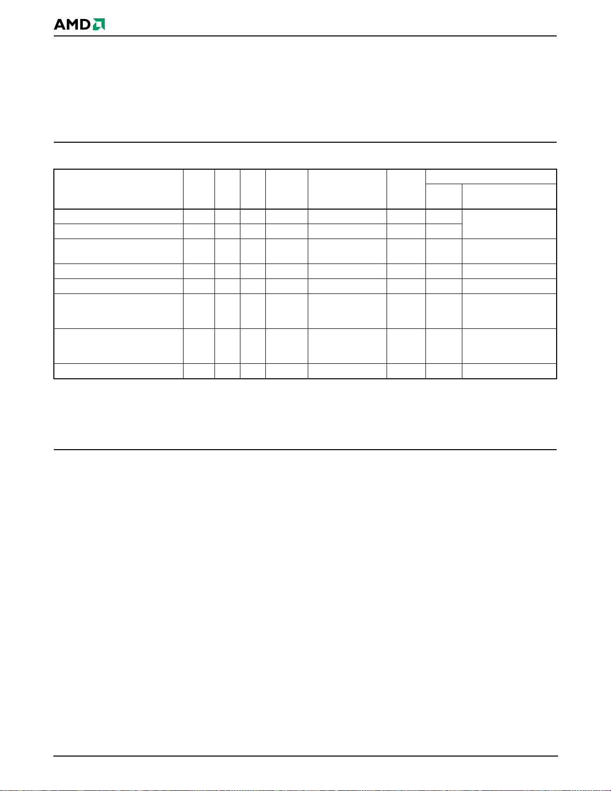
PRODUCT SELECTOR GUIDE
Family Part Number Am29SL800D
Speed Options
Max access time, ns (t
Max CE# access time, ns (t
Max OE# access time, ns (t
)90 (Note 2) 100 120 150
ACC
)90 (Note 2) 100 120 150
CE
) 30355065
OE
Notes:
1. See “AC Characteristics” for full specifications.
min. = 1.7 V
2. V
CC
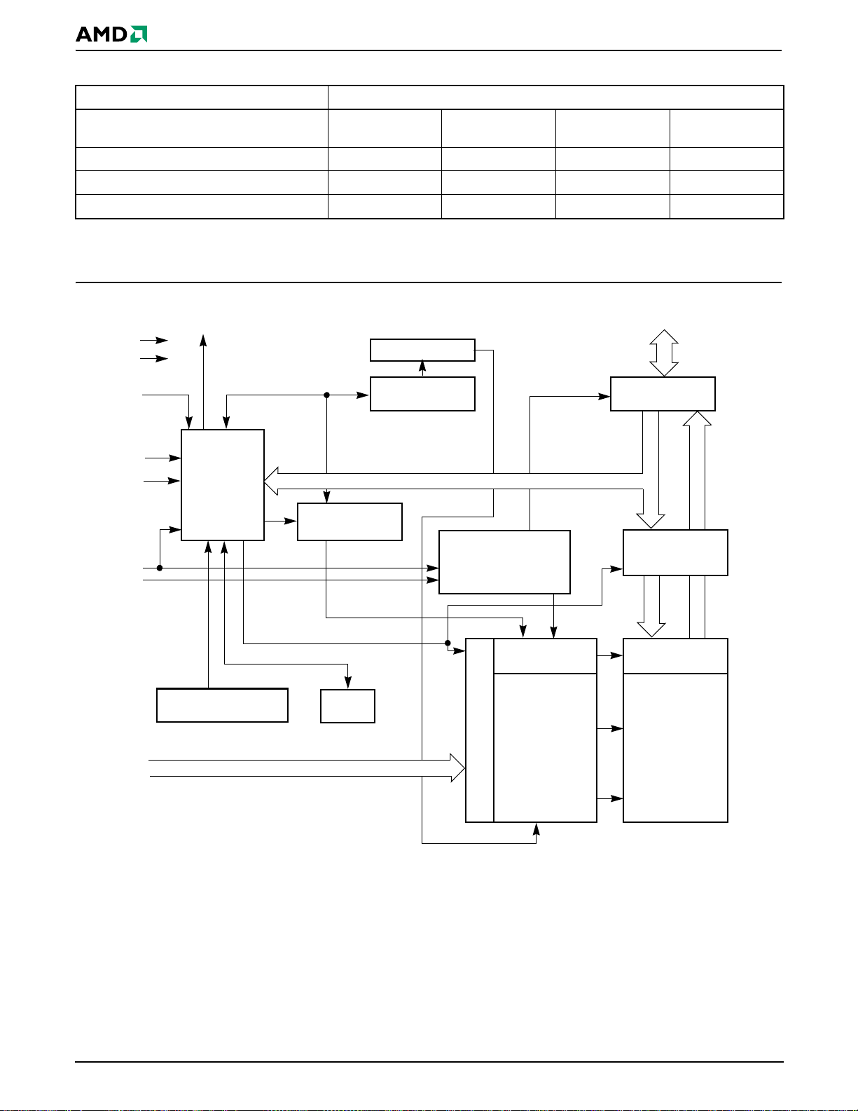
BLOCK DIAGRAM
RY/BY#
V
CC
V
SS
RESET#
WE#
BYTE#
CE#
OE#
State
Control
Command
Register
(Note 2) 100 120 150
PGM Voltage
Generator
90
Sector Switches
Erase Voltage
Generator
Chip Enable
Output Enable
Logic
DQ0–DQ15 (A-1)
Input/Output
STB
Buffers
Data
Latch
A0–A18
VCC Detector
Timer
STB
Y-Decoder
X-Decoder
Address Latch
Y-Gating
Cell Matrix
4 Am29SL800D 27546A6 January 23, 2007
Page 7
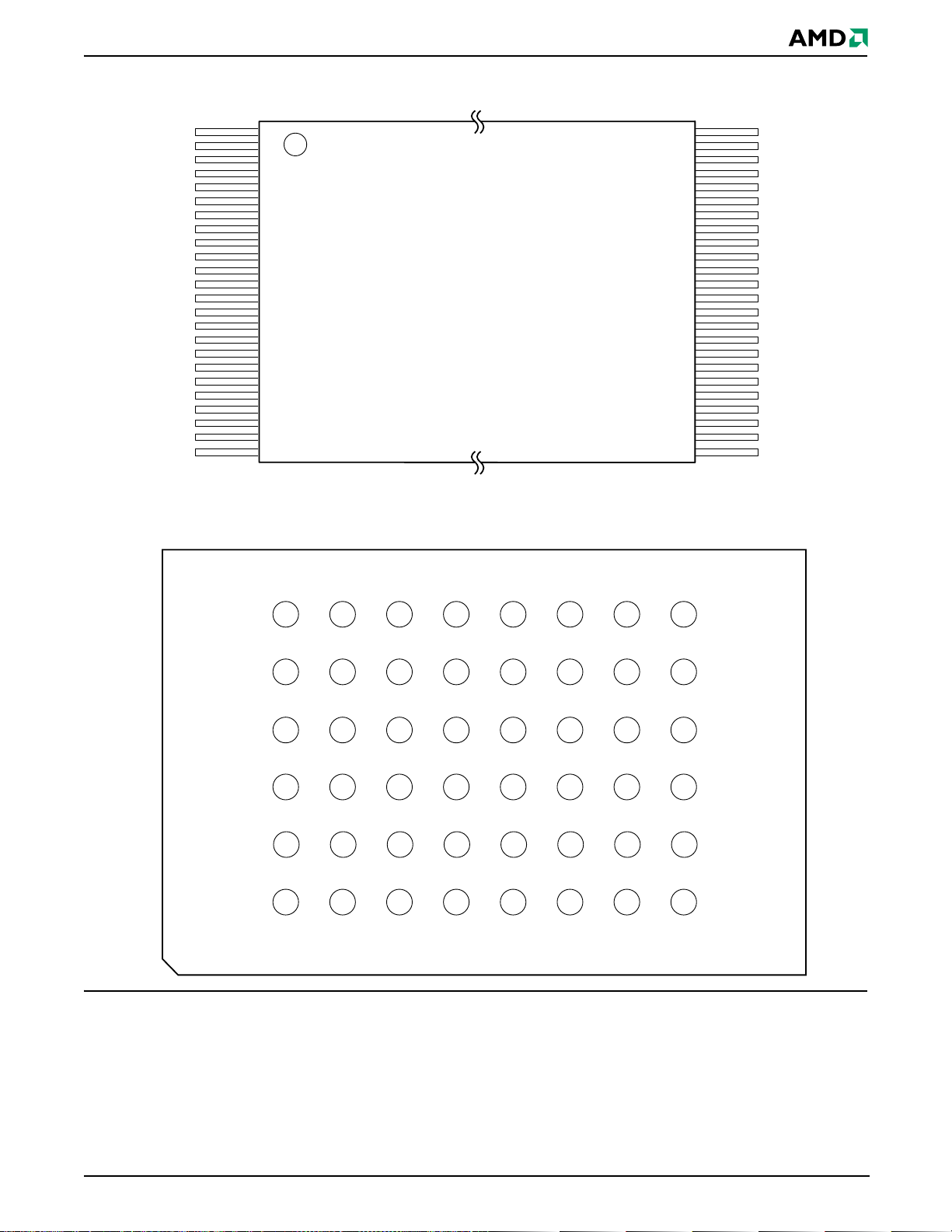
CONNECTION DIAGRAMS
DATA SHEET
A15
A14
A13
A12
A11
A10
A9
A8
NC
NC
WE#
RESET#
NC
NC
RY/BY#
A18
A17
A7
A6
A5
A4
A3
A2
A1
1
2
3
4
5
6
7
8
9
10
11
12
13
14
15
16
17
18
19
20
21
22
23
24
Standard TSOP
48-Ball FBGA
(Top View, Balls Facing Down)
48
47
46
45
44
43
42
41
40
39
38
37
36
35
34
33
32
31
30
29
28
27
26
25
A16
BYTE#
V
SS
DQ15/A-1
DQ7
DQ14
DQ6
DQ13
DQ5
DQ12
DQ4
V
CC
DQ11
DQ3
DQ10
DQ2
DQ9
DQ1
DQ8
DQ0
OE#
V
SS
CE#
A0
A6 B6 C6 D6 E6 F6 G6 H6
A5 B5 C5 D5 E5 F5 G5 H5
A4 B4 C4 D4 E4 F4 G4 H4
A3 B3 C3 D3 E3 F3 G3 H3
A2 B2 C2 D2 E2 F2 G2 H2
A1 B1 C1 D1 E1 F1 G1 H1
Special Handling Instructions for FBGA Packages
Special handling is required for Flash Memory products
in molded packages (TSOP and BGA). The package
BYTE#A16A15A14A12A13
CE#A0A1A2A4A3
DQ15/A-1 V
DQ13 DQ6DQ14DQ7A11A10A8A9
V
CC
DQ11 DQ3DQ10DQ2NCA18NCRY/BY#
DQ9 DQ1DQ8DQ0A5A6A17A7
OE# V
SS
DQ4DQ12DQ5NCNCRESET#WE#
SS
and/or data integrity may be compromised if the
package body is exposed to temperatures about 150
°C
for prolonged periods of time.
January 23, 2007 27546A6 Am29SL800D 5
Page 8
DATA SHEET
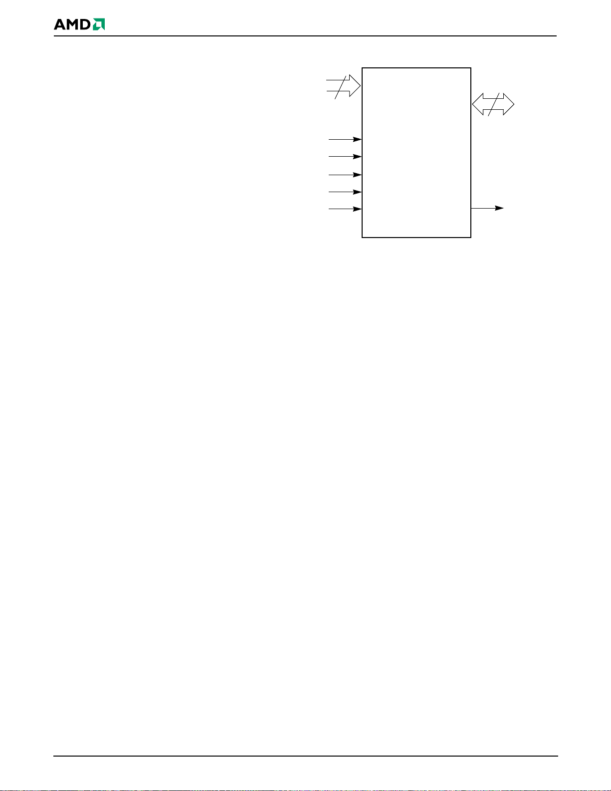
PIN CONFIGURATION
A0–A18 = 19 addresses
DQ0–DQ14 = 15 data inputs/outputs
DQ15/A-1 = DQ15 (data input/output, word mode),
A-1 (LSB address input, byte mode)
BYTE# = Selects 8-bit or 16-bit mode
CE# = Chip enable
OE# = Output enable
WE# = Write enable
RESET# = Hardware reset pin, active low
RY/BY# = Ready/Busy# output
V
= 1.65–2.2 V single power supply
CC
V
SS
NC = Pin not connected internally
= Device ground
LOGIC SYMBOL
19
A0–A18
CE#
OE#
WE#
RESET#
BYTE# RY/BY#
DQ0–DQ15
(A-1)
16 or 8
6 Am29SL800D 27546A6 January 23, 2007
Page 9

DATA SHEET
ORDERING INFORMATION
Standard Products
AMD standard products are available in several packages and operating ranges. The order number (Valid Combination) is formed by a combination of the elements below.
Am29SL800D T -100 E C
TEMPERATURE RANGE
C = Commercial (0°C to +70°C)
D = Commercial (0°C to +70°C) with Pb-free package
I = Industrial (–40
F = Industrial (–40
PACKAGE TYPE
E = 48-Pin Thin Small Outline Package (TSOP)
Standard Pinout (TS 048)
VU = 48-ball Fine-Pitch Ball Grid Array (FBGA)
0.80mm pitch, 8.15 x 6.15 mm package (VBK048)
WA = 48-Ball Fine-Pitch Ball Grid Array (FBGA)
0.80 mm pitch, 8.15 x 6.15 mm package (FBA048)
WC = 48-Ball Fine-Pitch Ball Grid Array (FBGA)
0.80 mm pitch, 9 x 8 mm package (FBC048)
SPEED OPTION
See Product Selector Guide and Valid Combinations
°C to +85°C)
°C to +85°C) with Pb-free package
BOOT CODE SECTOR ARCHITECTURE
T = Top Sector
B = Bottom Sector
DEVICE NUMBER/DESCRIPTION
Am29SL800D
8 Megabit (1 M x 8-Bit/512 K x 16-Bit) CMOS Flash Memory
1.8 Volt-only Read, Program, and Erase
Valid Combinations
Valid Combinations list configurations planned to be supported in volume for this device. Consult the local AMD sales office to confirm
availability of specific valid combinations and to check on newly released combinations.
Valid Combinations for TSOP Packages
AM29SL800DT90,
AM29SL800DB90
AM29SL800DT100,
AM29SL800DB100
EC, EI, ED, EF
AM29SL800DT120,
AM29SL800DB120
AM29SL800DT150,
AM29SL800DB150
Valid Combinations for FBGA Packages
Order Number Package Marking
WAC, WAD
AM29SL800DT90,
AM29SL800DB90
AM29SL800DT100,
AM29SL800DB100
AM29SL800DT120,
AM29SL800DB120
AM29SL800DT150,
AM29SL800DB150
Am29SL800DT120 VUF
WAI, WAF
WCC, WCD,
WCI, WCF
WAC, WAD
WAI, WAF
WCC, WCD,
WCI, WCF
WAC, WAD
WAI, WAF
WCC, WCD,
WCI, WCF
WAC, WAD
WAI, WAF
WCC, WCD,
WCI, WCF
A800DT90U,
A800DB90U
A800DT90P,
A800DB90P
A800DT10U,
A800DB10U
A800DT10P,
A800DB10P
A800DT12U,
A800DB12U
A800DT12P,
A800DB12P
A800DT15U,
A800DB15U
A800DT15P,
A800DB15P
A800DT12V
A800DB12V
C, I,
D, F
January 23, 2007 27546A6 Am29SL800D 7
Page 10
DATA SHEET
DEVICE BUS OPERATIONS
This section describes the requirements and use of the
device bus operations, which are initiated through the
internal command register. The command register
itself does not occupy any addressable memory location. The register is composed of latches that store the
commands, along with the address and data informa-
tion needed to execute the command. The contents of
the register serve as inputs to the internal state
machine. The state machine outputs dictate the function of the device. Tabl e 1 lists the device bus
operations, the inputs and control levels they require,
and the resulting output. The following subsections
describe each of these operations in further detail.
Table 1. Am29SL800D Device Bus Operations
DQ8–DQ15
Operation CE# OE# WE# RESET#
Read L L H H A
Write L H L H A
V
±
Standby
Output Disable L H H H X High-Z High-Z High-Z
Reset X X X L X High-Z High-Z High-Z
Sector Protect (Note) L H L V
Sector Unprotect (Note) L H L V
Temporary Sector Unprotect X X X V
CC
0.2 V
XX
V
CC
0.2 V
±
ID
ID
ID
Addresses
(Note 1)
IN
IN
X High-Z High-Z High-Z
Sector Address, A6 =
L, A1 = H,
A0 = L
Sector Address, A6 =
H, A1 = H,
A0 = L
A
IN
DQ0–
DQ7
D
OUT
D
IN
D
IN
D
IN
D
IN
BYTE#
= V
IH
D
OUT
D
IN
XX
XX
D
IN
Legend:
L = Logic Low = VIL, H = Logic High = VIH, VID = 10 ± 1.0 V, X = Don’t Care, AIN = Address In, DIN = Data In, D
= Data Out
OUT
Notes:
1. Addresses are A18:A0 in word mode (BYTE# = VIH), A18:A-1 in byte mode (BYTE# = VIL).
2. The sector protect and sector unprotect functions may also be implemented via programming equipment.
BYTE#
= V
DQ8–DQ14 = High-Z,
DQ15 = A-1
High-Z
IL
Word/Byte Configuration
The BYTE# pin controls whether the device data I/O
pins DQ15–DQ0 operate in the byte or word configuration. If the BYTE# pin is set at logic ‘1’, the device is in
word configuration, DQ15–DQ0 are active and controlled by CE# and OE#.
If the BYTE# pin is set at logic ‘0’, the device is in byte
configuration, and only data I/O pins DQ0–DQ7 are
active and controlled by CE# and OE#. The data I/O
pins DQ8–DQ14 are tri-stated, and the DQ15 pin is
used as an input for the LSB (A-1) address function.
Requirements for Reading Array Data
To read array data from the outputs, the system must
drive the CE# and OE# pins to V
control and selects the device. OE# is the output
control and gates array data to the output pins. WE#
should remain at V
. The BYTE# pin determines
IH
whether the device outputs array data in words or
bytes.
The internal state machine is set for reading array data
upon device power-up, or after a hardware reset. This
. CE# is the power
IL
ensures that no spurious alteration of the memory
content occurs during the power transition. No
command is necessary in this mode to obtain array
data. Standard microprocessor read cycles that assert
valid addresses on the device address inputs produce
valid data on the device data outputs. The device
remains enabled for read access until the command
register contents are altered.
See Reading Array Data‚ on page 14 for more information. Refer to the AC Read Operations table for timing
specifications and to Figure 13, on page 28 for the
timing diagram. I
in the DC Characteristics table
CC1
represents the active current specification for reading
array data.
Writing Commands/Command Sequences
To write a command or command sequence (which
includes programming data to the device and erasing
sectors of memory), the system must drive WE# and
CE# to V
For program operations, the BYTE# pin determines
whether the device accepts program data in bytes or
, and OE# to VIH.
IL
8 Am29SL800D 27546A6 January 23, 2007
Page 11

DATA SHEET
words. Refer to Word/Byte Configuration‚ on page 8
for more information.
The device features an Unlock Bypass mode to facilitate faster programming. Once the device enters the
Unlock Bypass mode, only two write cycles are
required to program a word or byte, instead of four. The
Word/Byte Program Command Sequence‚ on page 15
has details on programming data to the device using
both standard and Unlock Bypass command
sequences.
An erase operation can erase one sector, multiple sectors, or the entire device. Tables 2 and 3 indicate the
address space that each sector occupies. A “sector
address” consists of the address bits required to
uniquely select a sector. The Command Definitions‚ on
page 14 has details on erasing a sector or the entire
chip, or suspending/resuming the erase operation.
After the system writes the autoselect command
sequence, the device enters the autoselect mode. The
system can then read autoselect codes from the
internal register (which is separate from the memory
array) on DQ7–DQ0. Standard read cycle timings apply
in this mode. Refer to the Autoselect Mode‚ on page 12
and Autoselect Command Sequence‚ on page 15 sec-
tions for more information.
I
in the DC Characteristics table represents the
CC2
active current specification for the write mode. AC
Characteristics‚ on page 28 contains timing specifica-
tion tables and timing diagrams for write operations.
Program and Erase Operation Status
During an erase or program operation, the system may
check the status of the operation by reading the status
bits on DQ7–DQ0. Standard read cycle timings and I
CC
read specifications apply. Refer to Write Operation
Status‚ on page 20 for more information, and to “AC
Characteristics” for timing diagrams.
Standby Mode
When the system is not reading or writing to the device,
it can place the device in the standby mode. In this
mode, current consumption is greatly reduced, and the
outputs are placed in the high impedance state, independent of the OE# input.
The device enters the CMOS standby mode when the
CE# and RESET# pins are both held at V
(Note that this is a more restricted voltage range than
V
.) If CE# and RESET# are held at VIH, but not within
IH
V
± 0.2 V, the device will be in the standby mode, but
CC
the standby current will be greater. The device requires
standard access time (t
) for read access when the
CE
device is in either of these standby modes, before it is
ready to read data.
CC
± 0.2 V.
The device also enters the standby mode when the
RESET# pin is driven low. Refer to the next section,
RESET#: Hardware Reset Pin.
If the device is deselected during erasure or programming, the device draws active current until the
operation is completed.
I
in Table 7 on page 25 represents the standby
CC3
current specification.
Automatic Sleep Mode
The automatic sleep mode minimizes Flash device
energy consumption. The device automatically enables
this mode when addresses remain stable for t
ACC
+ 50
ns. The automatic sleep mode is independent of the
CE#, WE#, and OE# control signals. Standard address
access timings provide new data when addresses are
changed. While in sleep mode, output data is latched
and always available to the system. I
in Ta b le 7 o n
CC4
page 25 represents the automatic sleep mode current
specification.
RESET#: Hardware Reset Pin
The RESET# pin provides a hardware method of resetting the device to reading array data. When the
RESET# pin is driven low for at least a period of t
device immediately terminates any operation in
progress, tristates all output pins, and ignores all
read/write commands for the duration of the RESET#
pulse. The device also resets the internal state
machine to reading array data. The operation that was
interrupted should be reinitiated once the device is
ready to accept another command sequence, to
ensure data integrity.
Current is reduced for the duration of the RESET#
pulse. When RESET# is held at V
draws CMOS standby current (I
at V
but not within VSS±0.2 V, the standby current is
IL
±0.2 V, the device
SS
). If RESET# is held
CC4
greater.
The RESET# pin may be tied to the system reset circuitry. A system reset would thus also reset the Flash
memory, enabling the system to read the boot-up firmware from the Flash memory.
If RESET# is asserted during a program or erase operation, the RY/BY# pin remains a “0” (busy) until the
internal reset operation is complete, which requires a
time of t
(during Embedded Algorithms). The
READY
system can thus monitor RY/BY# to determine whether
the reset operation is complete. If RESET# is asserted
when a program or erase operation is not executing
(RY/BY# pin is “1”), the reset operation is completed
within a time of t
rithms). The system can read data t
RESET# pin returns to V
(not during Embedded Algo-
READY
.
IH
RH
, the
RP
after the
January 23, 2007 27546A6 Am29SL800D 9
Page 12
DATA SHEET
Refer to the Table 10 on page 28 for RESET# parame-
ters and to Figure 14, on page 29 for the timing
diagram.
Output Disable Mode
When the OE# input is at VIH, output from the device is
disabled. The output pins are placed in the high impedance state.
Table 2. Am29SL800DT Top Boot Block Sector Address Table
Sector Size
(Kbytes/
Sector A18 A17 A16 A15 A14 A13 A12
SA00000XXX 64/32 00000h–0FFFFh 00000h–07FFFh
SA10001XXX 64/32 10000h–1FFFFh 08000h–0FFFFh
SA20010XXX 64/32 20000h–2FFFFh 10000h–17FFFh
SA30011XXX 64/32 30000h–3FFFFh 18000h–1FFFFh
SA40100XXX 64/32 40000h–4FFFFh 20000h–27FFFh
SA50101XXX 64/32 50000h–5FFFFh 28000h–2FFFFh
SA60110XXX 64/32 60000h–6FFFFh 30000h–37FFFh
SA70111XXX 64/32 70000h–7FFFFh 38000h–3FFFFh
SA81000XXX 64/32 80000h–8FFFFh 40000h–47FFFh
Kwords)
Address Range (in hexadecimal)
(x8)
Address Range
Address Range
(x16)
SA91001XXX 64/32 90000h–9FFFFh 48000h–4FFFFh
SA101010XXX 64/32 A0000h–AFFFFh 50000h–57FFFh
SA111011XXX 64/32 B0000h–BFFFFh 58000h–5FFFFh
SA121100XXX 64/32 C0000h–CFFFFh 60000h–67FFFh
SA131101XXX 64/32 D0000h–DFFFFh 68000h–6FFFFh
SA141110XXX 64/32 E0000h–EFFFFh 70000h–77FFFh
SA1511110XX 32/16 F0000h–F7FFFh 78000h–7BFFFh
SA161111100 8/4 F8000h–F9FFFh 7C000h–7CFFFh
SA171111101 8/4 FA000h–FBFFFh7D000h–7DFFFh
SA18111111X 16/8 FC000h–FFFFFh 7E000h–7FFFFh
10 Am29SL800D 27546A6 January 23, 2007
Page 13
DATA SHEET
Table 3. Am29SL800DB Bottom Boot Block Sector Address Table
Sector Size
(Kbytes/
Sector A18 A17 A16 A15 A14 A13 A12
SA0000000X 16/8 00000h–03FFFh 00000h–01FFFh
SA10000010 8/4 04000h–05FFFh 02000h–02FFFh
SA20000011 8/4 06000h–07FFFh 03000h–03FFFh
SA300001XX 32/16 08000h–0FFFFh 04000h–07FFFh
SA40001XXX 64/32 10000h–1FFFFh 08000h–0FFFFh
SA50010XXX 64/32 20000h–2FFFFh 10000h–17FFFh
SA60011XXX 64/32 30000h–3FFFFh 18000h–1FFFFh
SA70100XXX 64/32 40000h–4FFFFh 20000h–27FFFh
SA80101XXX 64/32 50000h–5FFFFh 28000h–2FFFFh
SA90110XXX 64/32 60000h–6FFFFh 30000h–37FFFh
SA100111XXX 64/32 70000h–7FFFFh 38000h–3FFFFh
SA111000XXX 64/32 80000h–8FFFFh 40000h–47FFFh
SA121001XXX 64/32 90000h–9FFFFh 48000h–4FFFFh
SA131010XXX 64/32 A0000h–AFFFFh 50000h–57FFFh
SA141011XXX 64/32 B0000h–BFFFFh 58000h–5FFFFh
Kwords)
Address Range (in hexadecimal)
(x8)
Address Range
Address Range
(x16)
SA151100XXX 64/32 C0000h–CFFFFh 60000h–67FFFh
SA161101XXX 64/32 D0000h–DFFFFh 68000h–6FFFFh
SA171110XXX 64/32 E0000h–EFFFFh 70000h–77FFFh
SA181111XXX 64/32 F0000h–FFFFFh 78000h–7FFFFh
Note for Tables 2 and 3: Address range is A18:A-1 in byte mode and A18:A0 in word mode. See “Word/Byte Configuration” section for more
information.
January 23, 2007 27546A6 Am29SL800D 11
Page 14

DATA SHEET
Autoselect Mode
The autoselect mode provides manufacturer and
device identification, and sector protection verification,
through identifier codes output on DQ7–DQ0. This
mode is primarily intended for programming equipment
to automatically match a device to be programmed with
its corresponding programming algorithm. However,
the autoselect codes can also be accessed in-system
through the command register.
When using programming equipment, the autoselect
mode requires VID on address pin A9. Address pins
A6, A1, and A0 must be as shown in Table 4. In addition, when verifying sector protection, the sector
Description Mode CE# OE# WE#
Manufacturer ID: AMD L L H X X V
Device ID:
Am29SL800D
(Top Boot Block)
Device ID:
Am29SL800D
(Bottom Boot Block)
Sector Protection Verification L L H SA X V
Table 4. Am29SL800D Autoselect Code (High Voltage Method)
A11
A18
to
to
A10 A9
A12
Word L L H
Byte L L H X EAh
Word L L H
Byte L L H X 6Bh
XXV
XXV
address must appear on the appropriate highest order
address bits (see Table 2 on page 10 and Tab le 3 on
page 11). Ta bl e 4 shows the remaining address bits
that are don’t care. When all necessary bits have been
set as required, the programming equipment may then
read the corresponding identifier code on DQ7–DQ0.
To access the autoselect codes in-system, the host
system can issue the autoselect command via the
command register, as shown in Table 5 on page 19.
This method does not require VID. See Command
Definitions‚ on page 14 for details on using the autose-
lect mode.
A8
to
A7 A6
X L X L L X 01h
ID
XLXLH
ID
XLXLH
ID
XLXHL
ID
A5
to
A2 A1 A0
DQ8
to
DQ15
22h EAh
22h 6Bh
X 01h (protected)
X
DQ7
to
DQ0
00h
(unprotected)
L = Logic Low = VIL, H = Logic High = VIH, SA = Sector Address, X = Don’t care.
Sector Protection/Unprotection
The hardware sector protection feature disables both
program and erase operations in any sector. The hardware sector unprotection feature re-enables both
program and erase operations in previously protected
through AMD’s ExpressFlash™ Service. Contact an
AMD representative for details.
It is possible to determine whether a sector is protected
or unprotected. See Autoselect Mode‚ on page 12 for
details.
sectors. Sector protection/unprotection can be implemented via two methods.
Sector Protection/ Unprotection requires V
on the
ID
RESET# pin only, and can be implemented either insystem or via programming equipment. Figure 1, on
page 13 shows the algorithms and Figure 23, on page
36 shows the timing diagram. For sector unprotect, all
unprotected sectors must first be protected prior to the
first sector unprotect write cycle.
Temporary Sector Unprotect
This feature allows temporary unprotection of previously protected sectors to change data in-system. The
Sector Unprotect mode is activated by setting the
RESET# pin to V
tected sectors can be programmed or erased by
selecting the sector addresses. Once V
from the RESET# pin, all the previously protected
sectors are protected again. Figure 2, on page 14
The device is shipped with all sectors unprotected.
AMD offers the option of programming and protecting
shows the algorithm, and Figure 22, on page 35 shows
the timing diagrams, for this feature.
sectors at its factory prior to shipping the device
. During this mode, formerly pro-
ID
is removed
ID
12 Am29SL800D 27546A6 January 23, 2007
Page 15

DATA SHEET
Temporary Sector
Unprotect Mode
Increment
PLSCNT
START
PLSCNT = 1
RESET# = V
Wait 1 ms
No
First Write
Cycle = 60h?
Set up sector
address
Sector Protect:
Write 60h to sector
address with
A6 = 0, A1 = 1,
Wait 150 µs
Verify Sector
Protect: Write 40h
to sector address
with A6 = 0,
A1 = 1, A0 = 0
A0 = 0
Yes
START
Protect all sectors:
The indicated portion
of the sector protect
ID
Reset
PLSCNT = 1
algorithm must be
performed for all
unprotected sectors
prior to issuing the
first sector
unprotect address
PLSCNT = 1
RESET# = V
Wait 1 ms
First Write
Cycle = 60h?
No
All sectors
protected?
Set up first sector
address
Sector Unprotect:
Write 60h to sector
address with
A6 = 1, A1 = 1,
Wait 15 ms
A0 = 0
Yes
Yes
ID
No
Temporary Sector
Unprotect Mode
No
PLSCNT
= 25?
Yes
Device failed
Sector Protect
Algorithm
sector address
A1 = 1, A0 = 0
No
Protect another
Remove VID
from RESET#
Sector Protect
Read from
with A6 = 0,
Data = 01h?
Yes
sector?
No
Write reset
command
complete
Yes
Increment
PLSCNT
No
PLSCNT
= 1000?
Yes
Device failed
Sector Unprotect
Algorithm
Verify Sector
Unprotect: Write
40h to sector
address with
A6 = 1, A1 = 1,
Read from
sector address
with A6 = 1,
A1 = 1, A0 = 0
No
Data = 00h?
Remove VID
from RESET#
Write reset
A0 = 0
Last sector
verified?
command
Yes
Yes
No
Set up
next sector
address
Sector Unprotect
complete
Figure 1. In-System Sector Protect/Unprotect Algorithms
January 23, 2007 27546A6 Am29SL800D 13
Page 16

DATA SHEET
START
RESET# = V
(Note 1)
Perform Erase or
Program Operations
RESET# = V
Temporary Sector
Unprotect Completed
(Note 2)
Notes:
1. All protected sectors unprotected.
2. All previously protected sectors are protected once again.
ID
IH
for command definitions). In addition, the following
hardware data protection measures prevent accidental
erasure or programming, which might otherwise be
caused by spurious system level signals during V
CC
power-up and power-down transitions, or from system
noise.
Low V
When V
accept any write cycles. This protects data during V
Write Inhibit
CC
is less than V
CC
, the device does not
LKO
CC
power-up and power-down. The command register and
all internal program/erase circuits are disabled, and the
device resets. Subsequent writes are ignored until V
is greater than V
. The system must provide the
LKO
CC
proper signals to the control pins to prevent unintentional writes when V
is greater than V
CC
LKO
.
Write Pulse “Glitch” Protection
Noise pulses of less than 5 ns (typical) on OE#, CE# or
WE# do not initiate a write cycle.
Logical Inhibit
Write cycles are inhibited by holding any one of OE# =
V
, CE# = VIH or WE# = VIH. To initiate a write cycle,
IL
CE# and WE# must be a logical zero while OE# is a
logical one.
Figure 2. Temporary Sector Unprotect Operation
Hardware Data Protection
The command sequence requirement of unlock cycles
for programming or erasing provides data protection
against inadvertent writes (refer to Table 5 on page 19
COMMAND DEFINITIONS
Writing specific address and data commands or
sequences into the command register initiates device
operations. Table 5 on page 19 defines the valid reg-
ister command sequences. Writing incorrect address
and data values or writing them in the improper
sequence may place the device in an unknown state. A
reset command is then required to return the device to
reading array data.
All addresses are latched on the falling edge of WE# or
CE#, whichever happens later. All data is latched on
the rising edge of WE# or CE#, whichever happens
first. Refer to the appropriate timing diagrams in the
AC Characteristics‚ on page 28 section.
Reading Array Data
The device is automatically set to reading array data
after device power-up. No commands are required to
retrieve data. The device is also ready to read array
data after completing an Embedded Program or
Embedded Erase algorithm.
Power-Up Write Inhibit
If WE# = CE# = V
and OE# = VIH during power up, the
IL
device does not accept commands on the rising edge
of WE#. The internal state machine is automatically
reset to reading array data on power-up.
After the device accepts an Erase Suspend command,
the device enters the Erase Suspend mode. The
system can read array data using the standard read
timings, except that if it reads at an address within
erase-suspended sectors, the device outputs status
data. After completing a programming operation in the
Erase Suspend mode, the system may once again
read array data with the same exception. See Erase
Suspend/Erase Resume Commands‚ on page 17 for
more information on this mode.
The system must issue the reset command to reenable the device for reading array data if DQ5 goes
high, or while in the autoselect mode. See Reset Com-
mand‚ on page 14.
See also Requirements for Reading Array Data‚ on
page 8 for more information. Table 10 on page 28 pro-
vides the read parameters, and Figure 12, on page 27
shows the timing diagram.
Reset Command
Writing the reset command to the device resets the
device to reading array data. Address bits are don’t
care for this command.
14 Am29SL800D 27546A6 January 23, 2007
Page 17

DATA SHEET
The reset command may be written between the
sequence cycles in an erase command sequence
before erasing begins. This resets the device to reading
array data. Once erasure begins, however, the device
ignores reset commands until the operation is
complete.
The reset command may be written between the
sequence cycles in a program command sequence
before programming begins. This resets the device to
reading array data (also applies to programming in
Erase Suspend mode). Once programming begins,
however, the device ignores reset commands until the
operation is complete.
The reset command may be written between the
sequence cycles in an autoselect command sequence.
Once in the autoselect mode, the reset command must
be written to return to reading array data (also applies
to autoselect during Erase Suspend).
If DQ5 goes high during a program or erase operation,
writing the reset command returns the device to
reading array data (also applies during Erase
Suspend).
Autoselect Command Sequence
The autoselect command sequence allows the host
system to access the manufacturer and devices codes,
and determine whether or not a sector is protected.
Table 5 on page 19 shows the address and data
requirements. This method is an alternative to that
shown in Table 4 on page 12, which is intended for
PROM programmers and requires V
A9.
The autoselect command sequence is initiated by
writing two unlock cycles, followed by the autoselect
command. The device then enters the autoselect
mode, and the system may read at any address any
number of times, without initiating another command
sequence. A read cycle at address XX00h retrieves the
manufacturer code. A read cycle at address 01h in
word mode (or 02h in byte mode) returns the device
code. A read cycle containing a sector address (SA)
and the address 02h in word mode (or 04h in byte
mode) returns 01h if that sector is protected, or 00h if it
is unprotected. Refer to Table 2 on page 10 and Ta b le 3
on page 11 for valid sector addresses.
The system must write the reset command to exit the
autoselect mode and return to reading array data.
on address bit
ID
Word/Byte Program Command Sequence
The system may program the device by word or byte,
depending on the state of the BYTE# pin. Programming is a four-bus-cycle operation. The program
command sequence is initiated by writing two unlock
write cycles, followed by the program set-up command.
The program address and data are written next, which
in turn initiate the Embedded Program algorithm. The
system is not required to provide further controls or timings. The device automatically generates the program
pulses and verifies the programmed cell margin.
Table 5 on page 19 shows the address and data
requirements for the byte program command
sequence.
When the Embedded Program algorithm is complete,
the device then returns to reading array data and
addresses are no longer latched. The system can
determine the status of the program operation by using
DQ7, DQ6, or RY/BY#. See Table on page 20 for infor-
mation on these status bits.
Any commands written to the device during the
Embedded Program Algorithm are ignored. Note that a
hardware reset immediately terminates the programming operation. The Byte Program command
sequence should be reinitiated once the device has
reset to reading array data, to ensure data integrity.
Programming is allowed in any sequence and across
sector boundaries. A bit cannot be programmed
from a “0” back to a “1”. Attempting to do so may halt
the operation and set DQ5 to “1”, or cause the Data#
Polling algorithm to indicate the operation was successful. However, a succeeding read will show that the
data is still “0”. Only erase operations can convert a “0”
to a “1”.
Unlock Bypass Command Sequence
The unlock bypass feature allows the system to
program bytes or words to the device faster than using
the standard program command sequence. The unlock
bypass command sequence is initiated by first writing
two unlock cycles. This is followed by a third write cycle
containing the unlock bypass command, 20h. The
device then enters the unlock bypass mode. A twocycle unlock bypass program command sequence is all
that is required to program in this mode. The first cycle
in this sequence contains the unlock bypass program
command, A0h; the second cycle contains the program
address and data. Additional data is programmed in
the same manner. This mode dispenses with the initial
two unlock cycles required in the standard program
command sequence, resulting in faster total programming time. Table 5 on page 19 shows the requirements
for the command sequence.
During the unlock bypass mode, only the Unlock
Bypass Program and Unlock Bypass Reset commands
are valid. To exit the unlock bypass mode, the system
must issue the two-cycle unlock bypass reset
command sequence. The first cycle must contain the
data 90h; the second cycle the data 00h. Addresses
are don’t cares. The device then returns to reading
array data.
January 23, 2007 27546A6 Am29SL800D 15
Page 18

DATA SHEET
Figure 3 illustrates the algorithm for the program oper-
ation. See Table 13 on page 31 for parameters, and to
Figure 17, on page 32 for timing diagrams.
START
Write Program
Command Sequence
Data Poll
Embedded
Program
algorithm
in progress
Increment Address
1. See Table 5 for program command sequence.
No
from System
Verify Data?
Yes
Last Address?
Yes
Programming
Completed
No
Chip Erase Command Sequence
Chip erase is a six bus cycle operation. The chip erase
command sequence is initiated by writing two unlock
cycles, followed by a set-up command. Two additional
unlock write cycles are then followed by the chip erase
command, which in turn invokes the Embedded Erase
algorithm. The device does not require the system to
preprogram prior to erase. The Embedded Erase algorithm automatically preprograms and verifies the entire
memory for an all zero data pattern prior to electrical
erase. The system is not required to provide any controls or timings during these operations. Ta bl e 5 o n
page 19 shows the address and data requirements for
the chip erase command sequence.
Any commands written to the chip during the
Embedded Erase algorithm are ignored. Note that a
hardware reset during the chip erase operation immediately terminates the operation. The Chip Erase
command sequence should be reinitiated once the
device has returned to reading array data, to ensure
data integrity.
The system can determine the status of the erase operation by using DQ7, DQ6, DQ2, or RY/BY#. See “Write
Operation Status” for information on these status bits.
When the Embedded Erase algorithm is complete, the
device returns to reading array data and addresses are
no longer latched.
Figure 4, on page 18 illustrates the algorithm for the
erase operation. See Table 13 on page 28 for parame-
ters, and to Figure 10, on page 26 for timing diagrams.
Figure 3. Program Operation
Sector Erase Command Sequence
Sector erase is a six bus cycle operation. The sector
erase command sequence is initiated by writing two
unlock cycles, followed by a set-up command. Two
additional unlock write cycles are then followed by the
address of the sector to be erased, and the sector
erase command. Table 5 shows the address and data
requirements for the sector erase command sequence.
The device does not require the system to preprogram
the memory prior to erase. The Embedded Erase algorithm automatically programs and verifies the sector for
an all zero data pattern prior to electrical erase. The
system is not required to provide any controls or
timings during these operations.
After the command sequence is written, a sector erase
time-out of 50 µs begins. During the time-out period,
additional sector addresses and sector erase commands may be written. Loading the sector erase buffer
may be done in any sequence, and the number of
sectors may be from one sector to all sectors. The time
between these additional cycles must be less than 50
µs, otherwise the last address and command might not
be accepted, and erasure may begin. It is recommended that processor interrupts be disabled during
16 Am29SL800D 27546A6 January 23, 2007
Page 19

DATA SHEET
this time to ensure all commands are accepted. The
interrupts can be re-enabled after the last Sector Erase
command is written. If the time between additional
sector erase commands can be assumed to be less
than 50 µs, the system need not monitor DQ3. Any
command other than Sector Erase or Erase
Suspend during the time-out period resets the
device to reading array data. The system must
rewrite the command sequence and any additional
sector addresses and commands.
The system can monitor DQ3 to determine if the sector
erase timer has timed out. (See DQ3: Sector Erase
Timer‚ on page 22.) The time-out begins from the rising
edge of the final WE# pulse in the command sequence.
Once the sector erase operation has begun, only the
Erase Suspend command is valid. All other commands
are ignored. Note that a hardware reset during the
sector erase operation immediately terminates the
operation. The Sector Erase command sequence
should be reinitiated once the device has returned to
reading array data, to ensure data integrity.
When the Embedded Erase algorithm is complete, the
device returns to reading array data and addresses are
no longer latched. The system can determine the
status of the erase operation by using DQ7, DQ6, DQ2,
or RY/BY#. (Refer to Write Operation Status‚ on
page 20 for information on these status bits.)
Figure 4, on page 18 illustrates the algorithm for the
erase operation. Refer to the Table 16 on page 39for
parameters, and to Figure 18, on page 33 for timing
diagrams.
Erase Suspend/Erase Resume Commands
The Erase Suspend command allows the system to
interrupt a sector erase operation and then read data
from, or program data to, any sector not selected for
erasure. This command is valid only during the sector
erase operation, including the 50 µs time-out period
during the sector erase command sequence. The
Erase Suspend command is ignored if written during
the chip erase operation or Embedded Program algorithm. Writing the Erase Suspend command during the
Sector Erase time-out immediately terminates the
time-out period and suspends the erase operation.
Addresses are “don’t-cares” when writing the Erase
Suspend command.
When the Erase Suspend command is written during a
sector erase operation, the device requires a maximum
of 20 µs to suspend the erase operation. However,
when the Erase Suspend command is written during
the sector erase time-out, the device immediately terminates the time-out period and suspends the erase
operation.
After the erase operation has been suspended, the
system can read array data from or program data to
any sector not selected for erasure. (The device “erase
suspends” all sectors selected for erasure.) Normal
read and write timings and command definitions apply.
Reading at any address within erase-suspended
sectors produces status data on DQ7–DQ0. The
system can use DQ7, or DQ6 and DQ2 together, to
determine if a sector is actively erasing or is erase-suspended. See Write Operation Status‚ on page 20 for
information on these status bits.
After an erase-suspended program operation is complete, the system can once again read array data within
non-suspended sectors. The system can determine
the status of the program operation using the DQ7 or
DQ6 status bits, just as in the standard program operation. See Write Operation Status‚ on page 20 for
more information.
The system may also write the autoselect command
sequence when the device is in the Erase Suspend
mode. The device allows reading autoselect codes
even at addresses within erasing sectors, since the
codes are not stored in the memory array. When the
device exits the autoselect mode, the device reverts to
the Erase Suspend mode, and is ready for another
valid operation. See Autoselect Command Sequence‚
on page 15 for more information.
The system must write the Erase Resume command
(address bits are don’t care) to exit the erase suspend
mode and continue the sector erase operation. Further
writes of the Resume command are ignored. Another
Erase Suspend command can be written after the
device has resumed erasing.
January 23, 2007 27546A6 Am29SL800D 17
Page 20

Write Erase
Command Sequence
Data Poll
from System
No
Data = FFh?
DATA SHEET
START
Embedded
Erase
algorithm
in progress
Yes
Erasure Completed
Notes:
1. See Table 5 for erase command sequence.
2. See “DQ3: Sector Erase Timer” for more information.
Figure 4. Erase Operation
18 Am29SL800D 27546A6 January 23, 2007
Page 21

DATA SHEET
Table 5. Am29SL800D Command Definitions
Command
Sequence
(Note 1)
Read (Note 6) 1 RA RD
Reset (Note 7) 1 XXX F0
Manufacturer ID
Device ID,
Top Boot Block
Device ID,
Bottom Boot Block
Sector Protect Verify
(Note 9)
Autoselect (Note 8)
Extension
Program
Unlock Bypass
Unlock Bypass Program (Note 10) 2 XXX A0 PA PD
Unlock Bypass Reset (Note 11) 2 XXX 90 XXX 00
Chip Erase
Sector Erase
Erase Suspend (Note 12) 1 XXX B0
Erase Resume (Note 13) 1 XXX 30
Legend:
X = Don’t care
RA = Address of the memory location to be read.
RD = Data read from location RA during read operation.
PA = Address of the memory location to be programmed. Addresses
latch on the falling edge of the WE# or CE# pulse, whichever
happens later.
Word
Byte AAA 555 AAA
Word
Byte AAA 555 AAA X02 EA
Word
Byte AAA 555 AAA X02 6B
Word
Byte AAA 555 AAA
Word
Byte AAA 555 AAA X04
Word
Byte AAA 555 AAA
Word
Byte AAA 555 AAA
Word
Byte AAA 555 AAA AAA 555 AAA
Word
Byte AAA 555 AAA AAA 555
First Second Third Fourth Fifth Sixth
Cycles
Addr Data Addr Data Addr Data Addr Data Addr Data Addr Data
555
4
555
4
555
4
555
4
555
4
555
4
555
3
555
6
555
6
AA
AA
AA
AA
AA
AA
AA
AA
AA
2AA
2AA
2AA
2AA
2AA
2AA
2AA
2AA
2AA
Bus Cycles (Notes 2-5)
55
55
55
55
55
55
55
55
55
555
555
555
555
555
555
555
555
555
PD = Data to be programmed at location PA. Data latches on the
rising edge of WE# or CE# pulse, whichever happens first.
SA = Address of the sector to be verified (in autoselect mode) or
erased. Address bits A18–A12 uniquely select any sector.
90 X00 01
X01 22EA
90
X01 226B
90
XX00
(SA)
X02
(SA)
X04
X03
555
555
XX01
00
01
TBD
TBD
TBD
TBD
AA
AA
90
90
A0 PA PD
20
80
80
2AA
2AA
555
55
55 SA 30
10
Notes:
1. See Table 1 for description of bus operations.
2. All values are in hexadecimal.
3. Except when reading array or autoselect data, all bus cycles are
write operations.
4. Data bits DQ15–DQ8 are don’t cares for unlock and command
cycles.
5. Address bits A18–A11 are don’t cares for unlock and command
cycles, unless SA or PA required.
6. No unlock or command cycles required when reading array data,
unless SA or PA required.
7. The Reset command is required to return to reading array data
when device is in the autoselect mode, or if DQ5 goes high (while
the device is providing status data).
8. The fourth cycle of the autoselect command sequence is a read
cycle.
January 23, 2007 27546A6 Am29SL800D 19
9. The data is 00h for an unprotected sector and 01h for a protected
sector.
See “Autoselect Command Sequence” for more
information.
10. The Unlock Bypass command is required prior to the Unlock
Bypass Program command.
11. The Unlock Bypass Reset command is required to return to
reading array data when the device is in the unlock bypass mode.
12. The system may read and program in non-erasing sectors, or enter the
autoselect mode, when in the Erase Suspend mode. The Erase Suspend
command is valid only during a sector erase operation.
13. The Erase Resume command is valid only during the Erase Suspend
mode.
Page 22

DATA SHEET
WRITE OPERATION STATUS
The device provides several bits to determine the
status of a write operation: DQ2, DQ3, DQ5, DQ6,
DQ7, and RY/BY#. Table 6 and the following subsections describe the functions of these bits. DQ7,
RY/BY#, and DQ6 each offer a method for determining
whether a program or erase operation is complete or in
progress. These three bits are discussed first.
DQ7: Data# Polling
The Data# Polling bit, DQ7, indicates to the host
system whether an Embedded Algorithm is in progress
or completed, or whether the device is in Erase Suspend. Data# Polling is valid after the rising edge of the
final WE# pulse in the program or erase command
sequence.
page 34, Data# Polling Timings (During Embedded
Algorithms), illustrates this.
Table 6 on page 23 shows the outputs for Data# Polling
on DQ7. Figure 5 shows the Data# Polling algorithm.
START
Read DQ7–DQ0
Addr = VA
During the Embedded Program algorithm, the device
outputs on DQ7 the complement of the datum programmed to DQ7. This DQ7 status also applies to
programming during Erase Suspend. When the
Embedded Program algorithm is complete, the device
outputs the datum programmed to DQ7. The system
must provide the program address to read valid status
information on DQ7. If a program address falls within a
protected sector, Data# Polling on DQ7 is active for
approximately 1 µs, then the device returns to reading
array data.
During the Embedded Erase algorithm, Data# Polling
produces a 0 on DQ7. When the Embedded Erase
algorithm is complete, or if the device enters the Erase
Suspend mode, Data# Polling produces a 1 on DQ7.
This is analogous to the complement/true datum output
described for the Embedded Program algorithm: the
erase function changes all the bits in a sector to 1; prior
to this, the device outputs the complement, or 0. The
system must provide an address within any of the
sectors selected for erasure to read valid status information on DQ7.
After an erase command sequence is written, if all
sectors selected for erasing are protected, Data#
Polling on DQ7 is active for approximately 100 µs, then
the device returns to reading array data. If not all
selected sectors are protected, the Embedded Erase
algorithm erases the unprotected sectors, and ignores
the selected sectors that are protected.
When the system detects DQ7 has changed from the
complement to true data, it can read valid data at DQ7–
DQ0 on the following read cycles. This is because DQ7
may change asynchronously with DQ0–DQ6 while
Output Enable (OE#) is asserted low. Figure 19, on
DQ7 = Data?
No
No
Notes:
1. VA = Valid address for programming. During a sector erase
operation, a valid address is an address within any sector
selected for erasure. During chip erase, a valid address is any
non-protected sector address.
2. DQ7 should be rechecked even if DQ5 = “1” because DQ7 may
change simultaneously with DQ5.
DQ5 = 1?
Yes
Read DQ7–DQ0
Addr = VA
DQ7 = Data?
No
FAIL
Figure 5. Data# Polling Algorithm
Yes
Yes
PASS
20 Am29SL800D 27546A6 January 23, 2007
Page 23

DATA SHEET
RY/BY#: Ready/Busy#
The RY/BY# is a dedicated, open-drain output pin that
indicates whether an Embedded Algorithm is in
progress or complete. The RY/BY# status is valid after
the rising edge of the final WE# pulse in the command
sequence. Since RY/BY# is an open-drain output,
several RY/BY# pins can be tied together in parallel
with a pull-up resistor to V
If the output is low (Busy), the device is actively erasing
or programming. (This includes programming in the
Erase Suspend mode.) If the output is high (Ready),
the device is ready to read array data (including during
the Erase Suspend mode), or is in the standby mode.
Table 6 on page 23 shows the outputs for RY/BY#.
Figure 14, on page 29, Figure 17, on page 32, and
Figure 18, on page 33 shows RY/BY# for reset, pro-
gram, and erase operations, respectively.
CC
.
DQ6: Toggle Bit I
Toggle Bit I on DQ6 indicates whether an Embedded
Program or Erase algorithm is in progress or complete,
or whether the device has entered the Erase Suspend
mode. Toggle Bit I may be read at any address, and is
valid after the rising edge of the final WE# pulse in the
command sequence (prior to the program or erase
operation), and during the sector erase time-out.
During an Embedded Program or Erase algorithm
operation, successive read cycles to any address
cause DQ6 to toggle (The system may use either OE#
or CE# to control the read cycles). When the operation
is complete, DQ6 stops toggling.
After an erase command sequence is written, if all
sectors selected for erasing are protected, DQ6 toggles
for approximately 100 µs, then returns to reading array
data. If not all selected sectors are protected, the
Embedded Erase algorithm erases the unprotected
sectors, and ignores the selected sectors that are
protected.
The system can use DQ6 and DQ2 together to determine whether a sector is actively erasing or is erasesuspended. When the device is actively erasing (that is,
the Embedded Erase algorithm is in progress), DQ6
toggles. When the device enters the Erase Suspend
mode, DQ6 stops toggling. However, the system must
also use DQ2 to determine which sectors are erasing
or erase-suspended. Alternatively, the system can use
DQ7 (see the subsection on DQ7: Data# Polling).
If a program address falls within a protected sector,
DQ6 toggles for approximately 1 µs after the program
command sequence is written, then returns to reading
array data.
DQ6 also toggles during the erase-suspend-program
mode, and stops toggling once the Embedded
Program algorithm is complete.
Table 6 on page 23 shows the outputs for Toggle Bit I
on DQ6. Figure 6, on page 22 shows the toggle bit
algorithm. Figure 20, on page 34 shows the toggle bit
timing diagrams. Figure 21, on page 35 shows the dif-
ferences between DQ2 and DQ6 in graphical form. See
also the subsection on DQ2: Toggle Bit II.
DQ2: Toggle Bit II
The Toggle Bit II on DQ2, when used with DQ6, indi-
cates whether a particular sector is actively erasing
(that is, the Embedded Erase algorithm is in progress),
or whether that sector is erase-suspended. Toggle Bit
II is valid after the rising edge of the final WE# pulse in
the command sequence. The device toggles DQ2 with
each OE# or CE# read cycle.
DQ2 toggles when the system reads at addresses
within those sectors that have been selected for erasure. But DQ2 cannot distinguish whether the sector is
actively erasing or is erase-suspended. DQ6, by comparison, indicates whether the device is actively
erasing, or is in Erase Suspend, but cannot distinguish
which sectors are selected for erasure. Thus, both
status bits are required for sector and mode information. Refer to Table 6 on page 23 to compare outputs
for DQ2 and DQ6.
Figure 6, on page 22 shows the toggle bit algorithm in
flowchart form, and the section DQ2: Toggle Bit II
explains the algorithm. See also the DQ6: Toggle Bit I
subsection. Figure 20, on page 34 shows the toggle bit
timing diagram. Figure 21, on page 35 shows the differ-
ences between DQ2 and DQ6 in graphical form.
Reading Toggle Bits DQ6/DQ2
Refer to Figure 6, on page 22 for the following discussion. Whenever the system initially begins reading
toggle bit status, it must read DQ7–DQ0 at least twice
in a row to determine whether a toggle bit is toggling.
Typically, the system would note and store the value of
the toggle bit after the first read. After the second read,
the system would compare the new value of the toggle
bit with the first. If the toggle bit is not toggling, the
device has completed the program or erase operation.
The system can read array data on DQ7–DQ0 on the
following read cycle.
However, if after the initial two read cycles, the system
determines that the toggle bit is still toggling, the
system also should note whether the value of DQ5 is
high (see the section on DQ5). If it is, the system
should then determine again whether the toggle bit is
toggling, since the toggle bit may have stopped toggling just as DQ5 went high. If the toggle bit is no longer
toggling, the device has successfully completed the
program or erase operation. If it is still toggling, the
device did not completed the operation successfully,
and the system must write the reset command to return
to reading array data.
January 23, 2007 27546A6 Am29SL800D 21
Page 24

DATA SHEET
The remaining scenario is that the system initially
determines that the toggle bit is toggling and DQ5 has
not gone high. The system may continue to monitor the
toggle bit and DQ5 through successive read cycles,
determining the status as described in the previous
paragraph. Alternatively, it may choose to perform
other system tasks. In this case, the system must start
at the beginning of the algorithm when it returns to
determine the status of the operation (top of Figure 6).
START
Read DQ7–DQ0
Read DQ7–DQ0
No
No
Toggle Bit
= Toggle?
Yes
DQ5 = 1?
Yes
Read DQ7–DQ0
Twice
DQ5: Exceeded Timing Limits
DQ5 indicates whether the program or erase time has
exceeded a specified internal pulse count limit. Under
these conditions DQ5 produces a 1. This is a failure
condition that indicates the program or erase cycle was
not successfully completed.
The DQ5 failure condition may appear if the system
tries to program a 1 to a location that is previously programmed to 0. Only an erase operation can change
a 0 back to a 1. Under this condition, the device halts
the operation, and when the operation has exceeded
the timing limits, DQ5 produces a 1.
Under both these conditions, the system must issue the
reset command to return the device to reading array
data.
DQ3: Sector Erase Timer
After writing a sector erase command sequence, the
system may read DQ3 to determine whether or not an
erase operation has begun. (The sector erase timer
does not apply to the chip erase command.) If additional sectors are selected for erasure, the entire timeout also applies after each additional sector erase command. When the time-out is complete, DQ3 switches
from 0 to 1. If the time between additional sector erase
commands from the system can be assumed to be less
than 50 µs, the system need not monitor DQ3. See also
Sector Erase Command Sequence‚ on page 16.
Toggle Bit
= Toggle?
Yes
Program/Erase
Operation Not
Complete, Write
Reset Command
No
Program/Erase
Operation Complete
Notes:
1. Read toggle bit twice to determine whether or not it is toggling.
See text.
2. Recheck toggle bit because it may stop toggling as DQ5 changes
to “1”. See text
Figure 6. Toggle Bit Algorithm
After the sector erase command sequence is written,
the system should read the status on DQ7 (Data#
Polling) or DQ6 (Toggle Bit I) to ensure the device has
accepted the command sequence, and then read DQ3.
If DQ3 is 1, the internally controlled erase cycle has
begun; all further commands (other than Erase Suspend) are ignored until the erase operation is complete.
If DQ3 is 0, the device will accept additional sector
erase commands. To ensure the command has been
accepted, the system software should check the status
of DQ3 prior to and following each subsequent sector
erase command. If DQ3 is high on the second status
check, the last command might not have been
accepted. Figure 6 shows the outputs for DQ3.
22 Am29SL800D 27546A6 January 23, 2007
Page 25

DATA SHEET
Table 6. Write Operation Status
Standard
Mode
Erase
Suspend
Mode
DQ7
Operation
Embedded Program Algorithm DQ7# Toggle 0 N/A No toggle 0
Embedded Erase Algorithm 0 Toggle 0 1 Toggle 0
Reading within Erase
Suspended Sector
Reading within Non-Erase
Suspended Sector
Erase-Suspend-Program DQ7# Toggle 0 N/A N/A 0
(Note 2) DQ6
1 No toggle 0 N/A Toggle 1
Data Data Data Data Data 1
DQ5
(Note 1) DQ3
DQ2
(Note 2) RY/BY#
Notes:
1. DQ5 switches to ‘1’ when an Embedded Program or Embedded Erase operation has exceeded the maximum timing limits. See “DQ5:
Exceeded Timing Limits for more information.
2. DQ7 and DQ2 require a valid address when reading status information. Refer to the appropriate subsection for further details.
January 23, 2007 27546A6 Am29SL800D 23
Page 26

DATA SHEET
ABSOLUTE MAXIMUM RATINGS
Storage Temperature
Plastic Packages...............................–65°C to +150°C
Ambient Temperature
with Power Applied............................–65°C to +125°C
Voltage with Respect to Ground
V
(Note 1) ................................ –0.5 V to +2.5 V
CC
A9, OE#,
and RESET# (Note 2)................ –0.5 V to +11.0 V
All other pins (Note 1) ........... –0.5 V to V
Output Short Circuit Current (Note 3) ............. 100 mA
Notes:
1. Minimum DC voltage on input or I/O pins is –0.5 V. During voltage
transitions, input or I/O pins may overshoot V
periods of up to 20 ns. See Figure 7. Maximum DC voltage on
input or I/O pins is V
or I/O pins may overshoot to V
See Figure 8.
2. Minimum DC input voltage on pins A9, OE#, and RESET# is –0.5
V. During voltage transitions, A9, OE#, and RESET# may
overshoot V
DC input voltage on pin A9 is +11.0 V which may overshoot to
12.5 V for periods up to 20 ns.
3. No more than one output may be shorted to ground at a time.
Duration of the short circuit should not be greater than one
second.
Stresses above those listed under “Absolute Maximum Ratings” may
cause permanent damage to the device. This is a stress rating only;
functional operation of the device at these or any other conditions
above those indicated in the operational sections of this data sheet is
not implied. Exposure of the device to absolute maximum rating
conditions for extended periods may affect device reliability.
to –2.0 V for periods of up to 20 ns. See Maximum
SS
+0.5 V. During voltage transitions, input
CC
+2.0 V for periods up to 20 ns.
CC
SS
+0.5 V
CC
to –2.0 V for
20 ns
0.0 V
–0.5 V
–2.0 V
20 ns
20 ns
Figure 7. Maximum Negative Overshoot Waveform
20 ns
V
CC
+2.0 V
V
CC
+0.5 V
2.0 V
20 ns
20 ns
Figure 8. Maximum Positive Overshoot Waveform
OPERATING RANGES
Commercial (C) Devices
Ambient Temperature (T
Industrial (I) Devices
Ambient Temperature (T
V
Supply Voltages
CC
V
, 90ns speed option ...................+1.70 V to +2.2 V
CC
V
, All other speed options ............+1.65 V to +2.2 V
CC
Operating ranges define those limits between which the functionality
of the device is guaranteed.
).......................0°C to +70°C
A
)...................–40°C to +85°C
A
24 Am29SL800D 27546A6 January 23, 2007
Page 27

DATA SHEET
DC CHARACTERISTICS
Table 7. CMOS Compatible
Parameter Description Test Conditions Min Typ Max Unit
V
= VSS to VCC,
IN
V
= VCC
CC
CC max
V
= VSS to VCC,
OUT
V
= V
CC
CC max
CE# = V
IL,
Byte Mode
CE# = V
IL,
Word Mode
max
±1.0 µA
; A9 = 11.0 V 35 µA
±1.0 µA
OE#
= VIH,
5 MHz 5 10
1 MHz 1 3
OE#
= VIH,
5 MHz 5 10
1 MHz 1 3
I
I
I
CC1
I
LIT
LO
LI
Input Load Current
A9 Input Load Current VCC = V
Output Leakage Current
VCC Active Read Current
(Notes 1, 2)
mA
V
V
V
V
V
I
CC2
I
CC3
I
CC4
I
CC5
V
V
V
IL
IH
ID
OL1
OL2
OH1
OH2
LKO
VCC Active Write Current
(Notes 2, 3, 5)
VCC Standby Current (Note 2) CE#, RESET# = V
VCC Reset Current (Note 2) RESET# = VSS ± 0.2 V 0.2 5 µA
Automatic Sleep Mode
(Notes 2, 3)
Input Low Voltage –0.5 0.3 x V
Input High Voltage 0.7 x V
Voltage for Autoselect and
Temporary Sector Unprotect
Output Low Voltage
Output High Voltage
Low VCC Lock-Out Voltage (Note 4) 1.2 1.5 V
CE# = V
VIH = V
V
IL
V
CC
I
OL
IOL = 100 μA, VCC = V
I
OH
IOH = –100 μA, VCC = V
OE#
IL,
= VIH
± 0.2 V 0.2 5 µA
CC
± 0.2 V;
CC
= V
± 0.2 V
SS
= 2.0 V 9.0 11.0 V
= 2.0 mA, VCC = V
= –2.0 mA, VCC = V
CC min
0.1 V
CC min
0.85 x V
CC min
V
CC min
Notes:
1. The ICC current listed is typically less than 1 mA/MHz, with OE# at VIH. Typical VCC is 2.0 V.
2. The maximum I
active while Embedded Erase or Embedded Program is in progress.
3. I
CC
specifications are tested with V
CC
4. Automatic sleep mode enables the low power mode when addresses remain stable for t
5. Not 100% tested.
= VCCmax.
CC
ACC
15 30 mA
0.2 5 µA
CC
CC
–0.1 V
CC
VCC + 0.3 V
+ 50 ns.
CC
0.25 V
V
V
January 23, 2007 27546A6 Am29SL800D 25
Page 28

DATA SHEET
DC CHARACTERISTICS (Continued)
Zero Power Flash
20
15
10
5
Supply Current in mA
0
0 500 1000 1500 2000 2500 3000 3500 4000
Time in ns
Note: Addresses are switching at 1 MHz
Figure 9. I
CC1
10
8
6
4
Supply Current in mA
2
0
12345
Current vs. Time (Showing Active and Automatic Sleep Currents)
2.2 V
1.8 V
Frequency in MHz
Note: T = 25 °C
Figure 10. Typical I
26 Am29SL800D 27546A6 January 23, 2007
vs. Frequency
CC1
Page 29

TEST CONDITIONS
DATA SHEET
Table 8. Test Specifications
Test Condition
Output Load 1 TTL gate
Device
Under
Tes t
C
L
Output Load Capacitance, C
(including jig capacitance)
Input Rise and Fall Times 5 ns
Input Pulse Levels 0.0–2.0 V
Input timing measurement
reference levels
Output timing measurement
reference levels
L
Figure 11. Test Setup
Table 9. Key to Switching Waveforms
WAVEFORM INPUTS OUTPUTS
Steady
-90,
-100
30 100 pF
-120,
-150 Unit
1.0 V
1.0 V
2.0 V
0.0 V
Changing from H to L
Changing from L to H
Don’t Care, Any Change Permitted Changing, State Unknown
Does Not Apply Center Line is High Impedance State (High Z)
1.0 V 1.0 V
Figure 12. Input Waveforms and Measurement Levels
OutputMeasurement LevelInput
January 23, 2007 27546A6 Am29SL800D 27
Page 30

AC CHARACTERISTICS
DATA SHEET
Table 10. Read Operations
Parameter
JEDEC Std Test Setup -90 -100 -120 -150 Unit
t
AVAV
t
AVQ V
t
ELQV
t
GLQV
t
EHQZ
t
GHQZ
t
t
ACC
t
t
t
t
RC
CE
OE
DF
DF
Output Enable to Output Delay Max 30 35 50 65 ns
Chip Enable to Output High Z (Note 1) Max 16 ns
Output Enable to Output High Z (Note 1) Max 16 ns
Description
Read Cycle Time (Note 1) Min
CE# = V
Address to Output Delay
Chip Enable to Output Delay OE# = V
OE# = V
IL
IL
IL
Max
Max
(Note 3)
(Note 3)
(Note 3)
90
90
90
Speed Options
100 120 150 ns
100 120 150 ns
100 120 150 ns
Read Min 0 ns
Output Enable
Hold Time (Note 1)
Toggle and
Data# Polling
Output Hold Time From Addresses, CE# or OE#,
Whichever Occurs First (Note 1)
Min 30 ns
Min 0 ns
t
AXQX
t
OEH
t
OH
Notes:
1. Not 100% tested.
2. See Figure 11, on page 27 and Table 8 on page 27 for test specifications
3. V
min. = 1.7V
CC
.
t
RC
Addresses
CE#
OE#
WE#
Outputs
RESET#
RY/BY#
0 V
Addresses Stable
t
ACC
t
OE
t
OEH
t
CE
HIGH Z
Figure 13. Read Operations Timings
Output Valid
t
D
t
O
HIGH Z
28 Am29SL800D 27546A6 January 23, 2007
Page 31

AC CHARACTERISTICS
Parameter
t
READY
t
READY
t
Note: Not 100% tested.
RESET# Pin Low (During Embedded Algorithms) to Read or Write
RESET# Pin Low (NOT During Embedded Algorithms) to Read or
t
RP
t
RH
RPD
t
RB
RESET# High Time Before Read (see Note) Min 200 ns
RY/BY#
DATA SHEET
Table 11. Hardware Reset (RESET#)
Description All Speed OptionsJEDEC Std Unit
(see Note)
Write (see Note)
RESET# Pulse Width Min 500 ns
RESET# Low to Standby Mode Min 20 µs
RY/BY# Recovery Time Min 0 ns
Max 20 µs
Max 500 ns
CE#, OE#
RESET#
RY/BY#
CE#, OE#
RESET#
t
RH
t
RP
t
Ready
Reset Timings NOT during Embedded Algorithms
Reset Timings during Embedded Algorithms
t
Ready
t
RP
Figure 14. RESET# Timings
t
RB
January 23, 2007 27546A6 Am29SL800D 29
Page 32

AC CHARACTERISTICS
DATA SHEET
Table 12. Word/Byte Configuration (BYTE#)
Parameter
JEDEC Std -90 -100 -120 -150 Unit
t
ELFL/tELFH
t
FLQZ
t
FHQV
BYTE#
Switching
from word
to byte
mode
CE# to BYTE# Switching Low or High Max 10 ns
BYTE# Switching Low to Output HIGH Z Max 50 50 60 60 ns
BYTE# Switching High to Output Active Min 90 100 120 150 ns
CE#
OE#
BYTE#
DQ0–DQ14
DQ15/A-1
Description
t
ELFL
Data Output
(DQ0–DQ14)
DQ15
Output
t
FLQZ
Speed Options
Data
Output
Address
Input
t
ELFH
BYTE#
BYTE#
Switching
from byte to
word mode
DQ0–DQ14
DQ15/A-1
Data
Output
Address
Input
t
FHQV
Data Output
(DQ0–DQ14)
DQ15
Output
Figure 15. BYTE# Timings for Read Operations
CE#
The falling edge of the last WE# signal
WE#
BYTE#
t
SET
(tAS)
t
HOLD
(tAH)
Note: Refer to the Erase/Program Operations table for tAS and tAH specifications.
Figure 16. BYTE# Timings for Write Operations
30 Am29SL800D 27546A6 January 23, 2007
Page 33

DATA SHEET
AC CHARACTERISTICS
Table 13. Erase/Program Operations
Parameter Speed Options
JEDEC Std Description -90 -100 -120 -150 Unit
t
AVAV
t
AVW L
t
WLAX
t
DVW H
t
WHDX
t
GHWL
t
ELWL
t
WHEH
t
WLWH
t
WHWL
t
WHWH1
t
WC
t
AS
t
AH
t
DS
t
DH
t
OES
t
GHWL
t
CS
t
CH
t
WP
t
WPH
t
WHWH1
Write Cycle Time (Note 1) Min 90 100 120 150 ns
Address Setup Time Min 0 ns
Address Hold Time Min 45 50 60 70 ns
Data Setup Time Min 45 50 60 70 ns
Data Hold Time Min 0 ns
Output Enable Setup Time Min 0 ns
Read Recovery Time Before Write
(OE# High to WE# Low)
Min 0 ns
CE# Setup Time Min 0 ns
CE# Hold Time Min 0 ns
Write Pulse Width Min 45 50 60 70 ns
Write Pulse Width High Min 30 ns
Byte Typ 5
Programming Operation (Notes 1, 2)
Word Typ 7
µs
t
WHWH2
t
WHWH2
t
VCS
t
RB
t
BUSY
Sector Erase Operation (Notes 1, 2) Typ 0.7 sec
VCC Setup Time Min 50 µs
Recovery Time from RY/BY# Min 0 ns
Program/Erase Valid to RY/BY# Delay Max 200 ns
Notes:
1. Not 100% tested.
2. See the Table 16 on page 39 for more information.
January 23, 2007 27546A6 Am29SL800D 31
Page 34

AC CHARACTERISTICS
DATA SHEET
Addresses
CE#
OE#
WE#
Data
RY/BY#
V
CC
t
VCS
Program Command Sequence (last two cycles)
t
WC
555h
t
CS
t
WP
t
DS
A0h
t
AS
PA PA
t
AH
t
CH
t
WPH
t
D
PD
t
BUSY
Read Status Data (last two cycles)
PA
t
WHWH1
Status
D
OUT
t
RB
Notes:
1. PA = program address, PD = program data, D
2. Illustration shows device in word mode.
Figure 17. Program Operation Timings
is the true data at the program address.
OUT
32 Am29SL800D 27546A6 January 23, 2007
Page 35

AC CHARACTERISTICS
Erase Command Sequence (last two cycles) Read Status Data
t
Addresses
CE#
OE#
WE#
Data
2AAh SA
t
CS
WC
DATA SHEET
t
AS
VA
555h for chip erase
t
CH
t
W
t
WP
t
D
t
D
55h
t
AH
30h
10 for Chip Erase
t
BUSY
t
WHWH
In
Progress
VA
Complete
t
RB
RY/BY#
t
VCS
V
CC
Notes:
1. SA = sector address (for Sector Erase), VA = Valid Address for reading status data (see “Write Operation Status”).
2. Illustration shows device in word mode.
Figure 18. Chip/Sector Erase Operation Timings
January 23, 2007 27546A6 Am29SL800D 33
Page 36

AC CHARACTERISTICS
Addresses
t
ACC
CE#
t
CH
OE#
t
OEH
WE#
DQ7
t
CE
t
VA
t
RC
OE
DATA SHEET
t
DF
t
OH
Complement
VA VA
Complement
Tr u e
Valid Data
High Z
DQ0–DQ6
t
BUSY
Status Data
Status Data
Tr u e
Valid Data
RY/BY#
Note: VA = Valid address. Illustration shows first status cycle after command sequence, last status read cycle, and array data read cycle.
Figure 19. Data# Polling Timings (During Embedded Algorithms)
t
RC
Addresses
t
ACC
t
CE
VA
VA VA
VA
CE#
t
CH
t
OE
OE#
t
OEH
t
DF
WE#
t
OH
DQ6/DQ2
t
BUS
High Z
Valid Status
(first read) (second read) (stops toggling)
Valid DataValid StatusValid Status
RY/BY#
High Z
Note: VA = Valid address; not required for DQ6. Illustration shows first two status cycle after command sequence, last status read cycle, and
array data read cycle.
Figure 20. Toggle Bit Timings (During Embedded Algorithms)
34 Am29SL800D 27546A6 January 23, 2007
Page 37

DATA SHEET
AC CHARACTERISTICS
Enter
Embedded
Erasing
WE#
DQ6
DQ2
Note: The system may use CE# or OE# to toggle DQ2 and DQ6. DQ2 toggles only when read at an address within an erase-suspended sector.
Parameter
t
t
VID Rise and Fall Time Min 500 ns
VIDR
RESET# Setup Time for Temporary Sector
RSP
Unprotect
Erase
Erase
Suspend
Enter Erase
Suspend Program
Erase Suspend
Read
Erase
Suspend
Program
Erase Suspend
Figure 21. DQ2 vs. DQ6
Table 14. Temporary Sector Unprotect
Min 4 µs
Erase
Resume
Erase
Read
All Speed OptionsJEDEC Std Description Unit
Erase
Complete
10 V
RESET#
0 or 1.8 V
t
VIDR
t
VIDR
0 or 1.8 V
Program or Erase Command Sequence
CE#
WE#
t
RSP
RY/BY#
Figure 22. Temporary Sector Unprotect Timing Diagram
January 23, 2007 27546A6 Am29SL800D 35
Page 38

AC CHARACTERISTICS
V
ID
V
RESET#
IH
DATA SHEET
SA, A6,
A1, A0
Valid* Valid* Valid*
Sector Protect/Unprotect Verify
Data
60h 60h 40h
1 µs
Sector Protect: 150 µs
Sector Unprotect: 15 ms
CE#
WE#
OE#
* For sector protect, A6 = 0, A1 = 1, A0 = 0. For sector unprotect, A6 = 1, A1 = 1, A0 = 0.
Figure 23. Sector Protect/Unprotect Timing Diagram
Status
36 Am29SL800D 27546A6 January 23, 2007
Page 39

AC CHARACTERISTICS
Table 15. Alternate CE# Controlled Erase/Program Operations
DATA SHEET
Parameter
JEDEC Std -90 -100 -120 -150 Unit
t
AVAV
t
AVE L
t
ELAX
t
DVE H
t
EHDX
t
GHEL
t
WLEL
t
EHWH
t
ELEH
t
EHEL
t
WHWH1
t
WHWH2
t
t
t
t
t
t
OES
t
GHEL
t
t
t
t
CPH
t
WHWH1
t
WHWH2
Description
Write Cycle Time (Note 1) Min 90 100 120 150 ns
WC
Address Setup Time Min 0 ns
AS
Address Hold Time Min 45 50 60 70 ns
AH
Data Setup Time Min 45 50 60 70 ns
DS
Data Hold Time Min 0 ns
DH
Output Enable Setup Time Min 0 ns
Read Recovery Time Before Write
(OE# High to WE# Low)
WE# Setup Time Min 0 ns
WS
WE# Hold Time Min 0 ns
WH
CE# Pulse Width Min 45 50 60 70 ns
CP
Min 0 ns
CE# Pulse Width High Min 30 ns
Programming Operation
(Notes 1, 2)
Byte Typ 5
Word Typ 7
Sector Erase Operation (Notes 1, 2) Typ 0.7 sec
Speed Options
Notes:
1. Not 100% tested.
2. See the “Erase and Programming Performance” section for more information.
µs
January 23, 2007 27546A6 Am29SL800D 37
Page 40

AC CHARACTERISTICS
555 for program
2AA for erase
DATA SHEET
PA for program
SA for sector erase
555 for chip erase
Data# Polling
Addresses
t
WC
t
WH
t
AS
t
AH
WE#
t
GHEL
OE#
t
WHWH1 or 2
t
BUS
CE#
t
WS
t
CP
t
CPH
t
DS
t
DH
Data
t
RH
A0 for program
55 for erase
PD for program
30 for sector erase
10 for chip erase
RESET#
RY/BY#
Notes:
1. PA = program address, PD = program data, DQ7# = complement of the data written, D
2. Figure indicates the last two bus cycles of command sequence.
3. Word mode address used as an example.
Figure 24. Alternate CE# Controlled Write Operation Timings
PA
DQ7# D
= data written
OUT
OUT
38 Am29SL800D 27546A6 January 23, 2007
Page 41

DATA SHEET
ERASE AND PROGRAMMING PERFORMANCE
Table 16. Erase and Programming Performance
Parameter Typ (Note 1) Max (Note 2) Unit Comments
Sector Erase Time 0.7 15 s
Chip Erase Time 14 s
Byte Programming Time 5 150 µs
Word Programming Time 7 210 µs
Chip Programming Time
(Note 3)
Byte Mode 5.3 16 s
Word Mode 3.7 11 s
Notes:
1. Typical program and erase times assume the following conditions: 25°C, 2.0 V VCC, 1,000,000 cycles. Additionally, programming typicals
assume checkerboard pattern.
2. Under worst case conditions of 90°C, V
3. The typical chip programming time is considerably less than the maximum chip programming time listed, since most bytes program faster
than the maximum program times listed.
4. In the pre-programming step of the Embedded Erase algorithm, all bytes are programmed to 00h before erasure.
5. System-level overhead is the time required to execute the two- or four-bus-cycle sequence for the program command. See Table 5 for further
information on command definitions.
6. The device has a minimum guaranteed erase and program cycle endurance of 1,000,000 cycles.
= 1.8 V, 1,000,000 cycles.
CC
Excludes 00h programming prior
to erasure (Note 4)
Excludes system level overhead
(Note 5)
Table 17. Latchup Characteristics
Description Min Max
Input voltage with respect to V
(including A9, OE#, and RESET#)
Input voltage with respect to V
Includes all pins except V
V
. Test conditions: VCC = 1.8 V, one pin at a time.
CC
on all pins except I/O pins
SS
on all I/O pins –0.5 V VCC + 0.5 V
SS
Current –100 mA +100 mA
CC
–1.0 V 11.0 V
Table 18. TSOP Pin Capacitance
Parameter Symbol Parameter Description Test Setup Typ Max Unit
C
IN
C
OUT
C
IN2
Input Capacitance VIN = 0 6 7.5 pF
Output Capacitance V
= 0 8.5 12 pF
OUT
Control Pin Capacitance VIN = 0 7.5 9 pF
Notes:
1. Sampled, not 100% tested.
2. Test conditions T
= 25°C, f = 1.0 MHz.
A
Table 19. Data Retention
Parameter Test Conditions Min Unit
150°C 10 Years
Minimum Pattern Data Retention Time
125°C 20 Years
January 23, 2007 27546A6 Am29SL800D 39
Page 42

PHYSICAL DIMENSIONS
TS 048—48-Pin Standard TSOP
DATA SHEET
Dwg rev AA; 10/99
40 Am29SL800D 27546A6 January 23, 2007
Page 43

DATA SHEET
PHYSICAL DIMENSIONS
FBA048—48-Ball Fine-Pitch Ball Grid Array (FBGA)
8.15 X 6.15 mm Package
Dwg rev AF; 10/99
January 23, 2007 27546A6 Am29SL800D 41
Page 44

DATA SHEET
PHYSICAL DIMENSIONS
FBC048—48-Ball Fine-Pitch Ball Grid Array (FBGA)
9 x 8 mm Package
Dwg rev AF; 10/99
42 Am29SL800D 27546A6 January 23, 2007
Page 45

DATA SHEET
PHYSICAL DIMENSIONS
VBK048—48 Ball Fine-Pitch Ball Grid Array (FBGA)
8.15 x 6.15 mm
0.10
(4X)
A
e
E
B
A2
6
fb
f 0.08
f 0.15
C0.10
PIN A1
CORNER
A
INDEX MARK
10
D
TOP VIEW
H
M
C
M
BA
C
BOTTOM VIEW
D1
6
5
4
3
2
1
BCDEFG
A
7
SD
7
SE
E1
A1 CORNER
A1
SEATING PLAN E
C
SIDE VIEW
PACKAGE VBK 048
JEDEC N/A
8.15 mm x 6.15 mm NOM
PACKAG E
SYMBOL MIN NOM MAX NOT E
A --- --- 1.00 OVERALL THICKNESS
A1 0.18 --- --- BALL HEIGHT
A2 0.62 --- 0.76 BODY THICKNESS
D 8.15 BSC. BODY SIZE
E 6.15 BSC. BODY SIZE
D1 5.60 BSC. BALL FOOTPRINT
E1 4.00 BSC. BALL FOOTPRINT
MD 8 ROW MATRIX SIZE D DIRECTION
ME 6 ROW MATRIX SIZE E DIRECTION
N 48 TOTAL BALL COUNT
fb 0.35 --- 0.43 BALL DIAMETER
e 0.80 BSC. BALL PITCH
SD / SE 0.40 BSC. SOLDER BALL PLACEMEN T
--- DEPOPULATED SOLDER BALLS
C0.08
NOTES
:
1.
DIMENSIONING AND TOLERANCING PER ASME Y14.5M-1994.
2. ALL DIMENSIONS ARE IN MILLIMETERS.
3.
BALL POSITION DESIGNATION PER JESD 95-1, SPP-010 (EXCEPT
AS NOTED).
4. e REPRESENTS THE SOLDER BALL GRID PITCH.
5. SYMBOL "MD" IS THE BALL ROW MATRIX SIZE IN THE
"D" DIRECTION.
SYMBOL "ME" IS THE BALL COLUMN MATRIX SIZE IN THE
"E" DIRECTION.
N IS THE TOTAL NUMBER OF SOLDER BALLS.
6 DIMENSION "b" IS MEASURED AT THE MAXIMUM BALL
DIAMETER IN A PLANE PARALLEL TO DATUM C.
7 SD AND SE ARE MEASURED WITH RESPECT TO DATUMS
A AND B AND DEFINE THE POSITION OF THE CENTER
SOLDER BALL IN THE OUTER ROW.
WHEN THERE IS AN ODD NUMBER OF SOLDER BALLS IN
THE OUTER ROW PARALLEL TO THE D OR E DIMENSION,
RESPECTIVELY, SD OR SE = 0.000.
WHEN THERE IS AN EVEN NUMBER OF SOLDER BALLS IN
THE OUTER ROW, SD OR SE = e/2
8. NOT USED.
9. "+" INDICATES THE THEORETICAL CENTER OF DEPOPULATED
BALLS.
10
A1 CORNER TO BE IDENTIFIED BY CHAMFER, LASER OR INK
MARK, METALLIZED MARK INDENTATION OR OTHER MEANS.
3338 \ 16-038.25b
January 23, 2007 27546A6 Am29SL800D 43
Page 46

DATA SHEET
REVISION SUMMARY
Revision A (February 4, 2003)
Initial release.
Revision A+1 (March 17, 2003)
Ordering Information
Corrected typo in table.
Corrected typo to OPNs.
Revision A+2 (June 10, 2004)
Ordering Information
Added Pb-free package OPNs.
Revision A+3 (October 27, 2004)
Updated VCC values
Revision A+4 (April 27, 2005)
Added VBK048 package.
Added Colophon.
Updated Trademark.
Revision A+5 (February 17, 2006)
Global
Removed Reverse TSOP throughout.
Revision A6 (January 23, 2007)
Erase and Program Operations table
Changed t
to a maximum specification.
BUSY
Colophon
The products described in this document are designed, developed and manufactured as contemplated for general use, including without limitation, ordinary industrial use, general office use, personal use, and household use, but are not designed, developed and manufactured as contemplated (1) for any use that includes fatal risks or dangers that, unless extremely high safety is secured, could have a serious effect to the
public, and could lead directly to death, personal injury, severe physical damage or other loss (i.e., nuclear reaction control in nuclear facility,
aircraft flight control, air traffic control, mass transport control, medical life support system, missile launch control in weapon system), or (2) for
any use where chance of failure is intolerable (i.e., submersible repeater and artificial satellite). Please note that Spansion Inc. will not be liable
to you and/or any third party for any claims or damages arising in connection with above-mentioned uses of the products. Any semiconductor
devices have an inherent chance of failure. You must protect against injury, damage or loss from such failures by incorporating safety design
measures into your facility and equipment such as redundancy, fire protection, and prevention of over-current levels and other abnormal operating
conditions. If any products described in this document represent goods or technologies subject to certain restrictions on export under the Foreign
Exchange and Foreign Trade Law of Japan, the US Export Administration Regulations or the applicable laws of any other country, the prior authorization by the respective government entity will be required for export of those products.
Trademarks
Copyright © 2003–2005 Advanced Micro Devices, Inc. All rights reserved. AMD, the AMD logo, and combinations thereof are registered trademarks of Advanced Micro Devices, Inc. ExpressFlash is a trademark of Advanced Micro Devices, Inc. Product names used in this publication are
for identification purposes only and may be trademarks of their respective companies.
Copyright © 2006–2007 Spansion Inc. All Rights Reserved. Spansion, the Spansion logo, MirrorBit, ORNAND, HD-SIM, and combinations
thereof are trademarks of Spansion Inc. Other names are for informational purposes only and may be trademarks of their respective owners.
44 Am29SL800D 27546A6 January 23, 2007
 Loading...