

Page 1

Am29DL640G
Data Sheet
RETIRED
PRODUCT
This product has been retired and is not recommended for designs. For new and current designs,
S29JL064H (for TSOP packa ges) and S29PL064J (for FBGA packages) supersed e AM29DL640G as
the factory-recommended migration path. Please refer to each res pective datasheets f or specifica tions and ordering information. Availability of this docum ent is re tained for ref eren ce and historical
purposes only.
April 2005
The following document specifies Spansion memory products that are now offered by both Advanced
Micro Devices and Fujitsu. Although the documen t is marked with the name of the company that
originally developed the specification, these products will be offered to customers of both AMD and
Fujitsu.
Continuity of Specifications
There is no change to this datasheet as a result of offering the device as a Spansion product. Any
changes that have been made are the result of normal datasheet improvement and are noted in the
document revision summary, where supported. Future routine revisions will occur when appropriate, and changes will be noted in a revision summary.
For More Information
Please contact your local AMD or Fujitsu sales office for additional inf ormation about Spansion
memory solutions.
Publication Number 25693 Revision B Amendment 5 Issue Date June 6, 2005
Page 2

THIS PAGE LEFT INTENTIONALLY BLANK.
Page 3

Am29DL640G
64 Megabit (8 M x 8-Bit/4 M x 16-Bit)
CMOS 3.0 Volt-only, Simultaneous Read/Write Flash Memory
This product has been retired and is not recommended for designs. For new and current designs, S29JL064H (for TSOP packages) and S29PL064J (for FBGA packages) supersede
AM29DL640G as the factory-reco mmended m igration path. Ple ase ref er to ea ch res pectiv e data sheets f or s pecifi cations a nd or deri ng inf ormation. Availability of this document is retained
for reference and historical purposes only.
DISTINCTIVE CHARACTERISTICS
ARCHITECTURAL ADVANTAGES
■ Simultaneous Read/Write operations
— Data can be continuously read from one bank while
executing erase/program functions in another bank.
— Zero latency between read and write operations
TM
■ Flexible Bank
— Read may occur in any of the three banks not being
written or erased.
— Four banks may be grouped by customer to achieve
desired bank divisions.
■ Boot Sectors
— Top and bottom boot sectors in the same device
— Any combination of sectors can be erased
■ Manufactured on 0.17 µm process technology
■ SecSi™ (Secured Silicon ) Sect or : Ext ra 256 Byte
sector
— Factory locked and identifiable: 16 bytes available for
secure, random factory Electronic Serial Number;
verifiable as factory locked through autoselect
function. ExpressFlash option allows entire sector to
be available for factory-secured data
— Customer lockable: One-time programmable only.
Once locked, data cannot be changed
■ Zero Power Operation
— Sophisticated power management circuits reduce
power consumed during inactive periods to nearly
zero.
■ Compatible with JEDEC standards
— Pinout and software compatible with
single-power-supply flash standard
architecture
PACKAGE OPTIONS
■ 63-ball Fine Pitch BGA
■ 64-ball Fortified BGA
■ 48-pin TSOP
PERFORMANCE CHARACTERISTICS
■ High performance
— Access time as fast as 70 ns
— Program time: 4 µs/word typical utilizing Accelerate
function
■ Ultra low power consumption (typical values)
— 2 mA active read current at 1 MHz
— 10 mA active read current at 5 MHz
— 200 nA in standby or automatic sleep mode
■ Minimum 1 million erase cycles guaranteed per
sector
■ 20 year data retention at 125°C
— Reliable operation for the life of the system
SOFTWARE FEATURES
■ Data Management Softwa re (DM S)
— AMD-supplied software manages data programming,
enabling EEPROM emulation
— Eases historical sector erase flash limitations
■ Supports Common Flash Memory Interface (CFI)
■ Erase Suspend/Erase Resume
— Suspends erase operations to allow reading from
other sectors in same bank
■ Data# Polling and Toggle Bits
— Provides a software method of detecting the status of
program or erase cycles
■ Unlock Bypass Program command
— Reduces overall programming time when issuing
multiple program command sequences
HARDW ARE FEATURES
■ Ready/Busy# output (RY/BY#)
— Hardware method for detecting program or erase
cycle completion
■ Hardware reset pin (RESET#)
— Hardware method of resetting the internal state
machine to the read mode
■ WP#/ACC input pin
— Write protect (WP#) function protects sectors 0, 1,
140, and 141, regardless of sector protect status
— Acceleration (ACC) function accelerates program
timing
■ Sector protection
— Hardware method of locking a sector, either
in-system or using programming equipment, to
prevent any program or erase operation within that
sector
— Temporary Sector Unprotect allows changing dat a in
protected sectors in-system
Publication# 25693 Rev: B Amendment 5
Issue Date: June 6, 2005
Refer to AMD’s Website (www.amd.com) for the latest information.
Page 4
GENERAL DESCRIPTION
The Am29DL640G is a 64 megabit, 3.0 volt-only flash
memory device, organized as 4,194,304 words of 16
bits each or 8,388,608 bytes of 8 bits each. Word
mode data appears on DQ15–DQ0; byte mode data
appears on DQ7–DQ0. The device is designed to be
programmed in-system with the standard 3.0 volt V
CC
supply, and can also be programmed in standard
EPROM programmers.
The device is available with an access time of 70, 90,
or 120 ns and is offered in 48-pin TSOP, 63-ball
Fine-Pitch BGA , and 64 -bal l Fortifi ed B GA packages.
Standard control pins—chip enable (CE#), write enable (WE#), and output enable (OE#)—control normal
read and write operations, and avoid bus contentio n
issues.
The device requires only a single 3.0 volt power sup-
ply for both read and write functions. Internally generated and regulate d voltages are provided for the
program and erase operations.
Simultaneous Read/Write Operations with
Zero Latency
The Simult aneous R ead/W rite a rchitect ure pr ovides
simultaneous operation by dividing the memory
space into four banks, two 8 Mb banks with small and
large sectors, and two 24 Mb banks of large sectors.
Sector addresse s are fixed, system so ftware can be
used to form user-defined bank groups.
During an Erase/Program operation, any of the three
non-busy banks may be read from. Note that only two
banks can operate simultaneously. The device can improve overall system performance by allowing a host
system to program or erase in one bank, then
immediately and simultaneousl y read from the other
bank, with zero latency. This releases the system from
waiting for the completion of program or erase
operations.
The Am29DL64 0G can be orga nized as both a to p
and bottom boot sector configuration.
Bank Megabits Sector Sizes
Bank 1 8 Mb
Bank 2 24 Mb Forty-eight 64 Kbyte/32 Kword
Bank 3 24 Mb Forty-eight 64 Kbyte/32 Kword
Bank 4 8 Mb
Eight 8 Kbyte/4 Kword,
Fifteen 64 Kbyte/32 Kword
Eight 8 Kbyte/4 Kword,
Fifteen 64 Kbyte/32 Kword
Am29DL640G Features
The SecSi™ (Secured Silicon) Sector is an extra
256 byte sector capable of being permanently locked
by AMD or customers. The SecSi Indicator Bit (DQ7)
is permanently set to a 1 if the part is factory locked,
and set to a 0 if customer lockable. This way, cus-
tomer lockable parts can never be used to replace a
factory locked part.
Factory locked part s provide several options. The
SecSi Sector may store a secure, random 16 byte
ESN (Electronic Serial Number), customer code (programmed through AMD’s ExpressFlash service), or
both. Customer Lockable parts may utilize the SecSi
Sector as bonus space, read ing an d writin g like any
other flash sector, or may permanently lock their own
code there.
DMS (Data Management Software) allows systems
to easily take advantage of the advanced architecture
of the simultaneous read/write product line by allowing
removal of EEPROM devices. DMS will also allow the
system software to be simplified, as it will perform all
functions necessary to modify data in file str uctures,
as opposed to single-byte modifications. To write or
update a particular p iece of data ( a phon e number or
configuration data, for example), the user only needs
to state which piece of data is to be updated, and
where the updated data is located in the system. This
is an advantage compared to systems where
user-written software must keep track of the old data
location, status, logical to physical translation of the
data onto the Flash memory device (or memory devices), and more. Using DMS, user-written software
does not need to interface with the Flash memory directly. Instead, the user's software accesses the Flash
memory by calling one of only six functions. AMD provides this software to simplify system design and software integration efforts.
The device offers complete compatibility with the
JEDEC single-power-supply Flash command set
standard. Commands are wr itten to the comma nd
register using standard microprocessor write timings.
Reading data out of the device is similar to reading
from other Flash or EPROM devices.
The host system can detect whether a program or
erase operation is complete by using the device sta-
tus bits: RY/BY# pin, DQ7 (Data# Polling) and
DQ6/DQ2 (toggle bits). After a program or erase cycle
has been completed, the device automatically re tur ns
to the read mode.
The sector erase architecture allows memory sectors to be erased and reprogrammed without affecting
the data contents of other sectors. The device is fully
erased when shipped from the factory.
Hardware data protection measures include a low
detector that automatically inhibits write opera-
V
CC
tions during power transitions. The hardware sector
protection feature disables both program and erase
operations in any combination of the sector s of memory. This can be achieved in-system or via programming equipment.
The device offers two power-saving features. When
addresses have been stable for a specified amount of
time, the device enters the automatic sleep mode.
The system can also place the device into the
standby mode. Power consumption is greatly reduced in both modes.
2 Am29DL640G June 6, 2005
Page 5

TABLE OF CONTENTS
Product Selector Guide. . . . . . . . . . . . . . . . . . . . . 5
Block Diag ra m . . . . . . . . . . . . . . . . . . . . . . . . . . . . 5
Connection Diagrams . . . . . . . . . . . . . . . . . . . . . . 6
Connection Diagrams . . . . . . . . . . . . . . . . . . . . . . 7
Special Handling Instructions for BGA Packages .....................7
Pin Description. . . . . . . . . . . . . . . . . . . . . . . . . . . . 8
Logic Symbol . . . . . . . . . . . . . . . . . . . . . . . . . . . . . 8
Ordering Information. . . . . . . . . . . . . . . . . . . . . . . 9
Device Bus Operations . . . . . . . . . . . . . . . . . . . . 10
Table 1. Am29DL640G Device Bus Operati o n s ..............................10
Word/Byte Configuration ........................................................ 10
Requirements for Reading Array Data ...................................10
Writing Commands/Command Sequences ............................11
Accelerat ed P ro g r a m Op era t io n ...... ... .. ................. .. ...............11
Autoselect Functions ..............................................................11
Simultaneous Read/Write Operations with Zero Latency .......11
Standby Mode........................................................................ 11
Automatic Sleep Mode ...........................................................12
RESET#: Hardware Reset Pin ...............................................12
Output Disable Mode ..............................................................12
Table 2. Am29DL640G Sector Architecture ....................................12
Table 3. Bank Address ....................................................................15
Table 4. SecSi
Autoselect Mode..................................................................... 15
Table 5. Am29DL640G Autoselect Codes, (High Voltage Method) 16
Sector/Sector Block Protection and Unprotection.................. 17
Table 6. Am29DL640G Boot Sector/Sector Block Addresses for
Protection/Unprotection ...................................................................17
Write Protect (WP#) ................................................................17
Table 7. WP#/ACC Modes ..............................................................18
Temporary Sector Unprotect ..................................................18
Figure 1. Temporary Sector Unprotect Operation........................... 18
Figure 2. In-System Sect o r Pr ot e ct/Unprotect Algorithms.............. 19
SecSi™ (Secured Silicon) Sector
Flash Memory Region ............................................................ 20
Figure 3. SecSi Sector Protect Verify.............................................. 21
Hardware Data Protection ......................................................21
Low VCC Write In h ibi t ................. ................ ... ................ ... .....21
Write Pulse “Glitch” Protection ...............................................21
Logical Inhibit ..........................................................................21
Power-Up Write Inhibit ............................................................21
Common Flash Memory Interface (CFI). . . . . . . 21
Table 8. CFI Query Identification String.......................................... 22
Table 9. System Interface String......................................................22
Table 10. Device Geometry Definit ion.................................... ........ 23
Table 11. Primary Vendor-Specific Extended Query...................... 24
Command Definitions . . . . . . . . . . . . . . . . . . . . . 25
Reading Array Data ................................................................25
Reset Command ............................................ .........................25
Autoselect Command Sequence ....................... .....................25
Enter SecSi™ Sector/Exit SecSi Sector
Command Sequence ..............................................................25
Byte/Word Program Command Sequence .............................26
Unlock Bypass Command Sequence .....................................26
Figure 4. Program Operat io n.................................... ...................... 27
Chip Erase Command Sequence ...........................................27
Sector Erase Command Sequence ........................................27
Figure 5. Erase Operation........... ................................... ................. 28
TM
Sector Addresses................................................15
Erase Suspend/Erase Resume Commands ...........................28
Table 12. Am29DL640G Command Definitions............................. 29
Write Operation Status. . . . . . . . . . . . . . . . . . . . . 30
DQ7: Data# Po l lin g ............. .. .. ................. ................ ...............30
Figure 6. Data# Polling Algorithm................. ................................. 30
RY/BY#: Ready/Busy#............................................................ 31
DQ6: Toggle Bit I ....................................................................31
Figure 7. Toggle Bit Algorithm........................................................ 31
DQ2: Toggle Bit II ...................................................................32
Reading Toggle Bits DQ6/DQ2 ...............................................32
DQ5: Exceeded Timing Limits ................................................32
DQ3: Sector Era s e Time r ..................... ... ................ ... ............32
Table 13. Write Operation Sta tus ............. .................................. .... 33
Absolute Maximum Ratings. . . . . . . . . . . . . . . . . 34
Figure 8. Maximum Negative Overshoot Waveform...................... 34
Figure 9. Maximum Positi ve Overshoot Waveform........................ 34
DC Characteristics . . . . . . . . . . . . . . . . . . . . . . . . 35
Figure 10. I
AutomaticSleep Currents)................................... .......................... 36
Figure 11. Typical I
Current vs. Time (Showing Active and
CC1
vs. Frequency............................................ 36
CC1
Test Conditions. . . . . . . . . . . . . . . . . . . . . . . . . . . 37
Figure 12. Test Setup.................................................................... 37
Figure 13. Input Waveforms and Measurement Levels................. 37
AC Characteristics . . . . . . . . . . . . . . . . . . . . . . . . 38
Read-Only Operations ........................................................... 38
Figure 14. Read Operation Timings.. .............................. ............... 38
Hardware Reset (RESET#) .................................... .. ..............39
Figure 15. Reset Timings............................................................... 39
Word/Byte Configuration (BYTE#) ..........................................40
Figure 16. BYTE# Timings for Read Operations............................ 40
Figure 17. BYTE# Timings for Write Operations............................ 40
Erase and Program Operations .............................................. 41
Figure 18. Program Operation Timings.......................................... 42
Figure 19. Accelerated Program Timing Diagram.......................... 42
Figure 20. Chip/Sector Erase Operation Timings .......................... 43
Figure 21. Back-to-back Read/Write Cycle Timings ...................... 44
Figure 22. Data# Polling Timings (During Embedded Algorithms). 44
Figure 23. Toggle Bit Timings (During Embedded Algorithms)...... 45
Figure 24. DQ2 vs. DQ6.............................................. ................... 45
Temporary Sector Unprotect ..................................................46
Figure 25. Temporary Sector Unprotect Timing Diagram.............. 46
Figure 26. Sector/Sector Block Protect and
Unprotect Timing Diagram............................................................. 47
Alternate CE# Controlled Erase and Program Operations .....48
Figure 27. Alternate CE# Controlled Write (Erase/Program)
OperationTimings.......................................................................... 49
Erase And Programming Performan ce. . . . . . . . 50
Latchup Characteristics. . . . . . . . . . . . . . . . . . . . 50
TSOP & BGA Pi n C a pa citance. . . . . . . . . . . . . . . 50
Data Retention. . . . . . . . . . . . . . . . . . . . . . . . . . . . 50
Physical Dimensions . . . . . . . . . . . . . . . . . . . . . . 52
FBE063—63-Ball Fine-Pitch Ball Grid Array (FBGA)
12 x 11 mm package ..............................................................52
LAA064—64-Ball Fortified Ball Grid Array (FBGA)
13 x 11 mm package ..............................................................53
TS 048—48-Pin S ta n dar d TSOP . .. ... ................ ... ................ ...54
Revision Summary . . . . . . . . . . . . . . . . . . . . . . . . 55
June 6, 2005 Am29DL640G 3
Page 6
PRODUCT SELECTOR GUIDE
Part Number Am29DL640G
Speed Option Standard Voltage Range: V
Max Access Time (ns), t
CE# Access (ns), t
OE# Access (ns), t
ACC
CE
OE
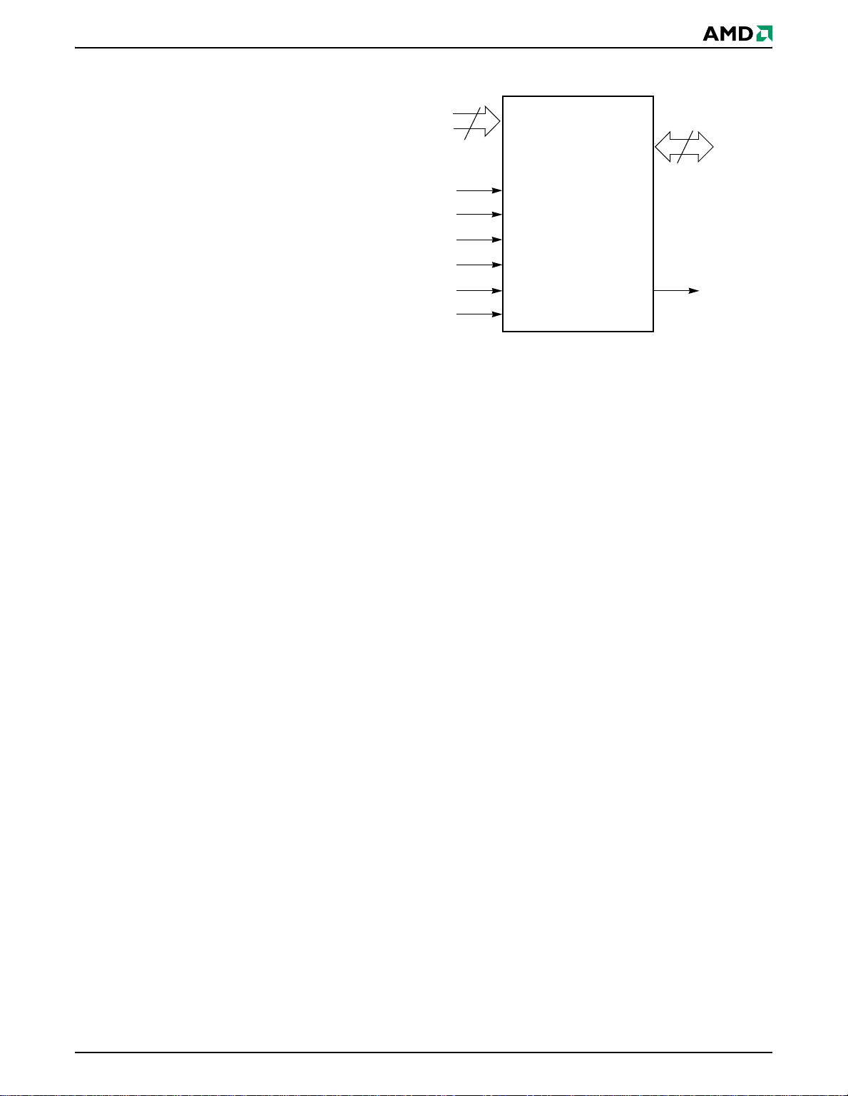
BLOCK DIAGRAM
V
CC
V
SS
Mux
A21–A0
A21–A0
RESET#
WE#
CE#
BYTE#
WP#/ACC
DQ0–DQ15
RY/BY#
A21–A0A21–A0
STATE
CONTROL
&
COMMAND
REGISTER
Bank 1 Address
Bank 2 Address
= 2.7–3.6 V 70 90 120
CC
70 90 120
70 90 120
30 35 50
OE# BYTE#
Bank 1
X-Decoder
Y-gate
Bank 2
X-Decoder
Status
Control
X-Decoder
DQ15–DQ0
DQ15–DQ0
DQ15–DQ0
Mux
A21–A0
Mux
Bank 3 Address
Bank 4 Address
Bank 3
X-Decoder
Bank 4
Y-gate
DQ15–DQ0
DQ15–DQ0
4 Am29DL640G June 6, 2005
Page 7
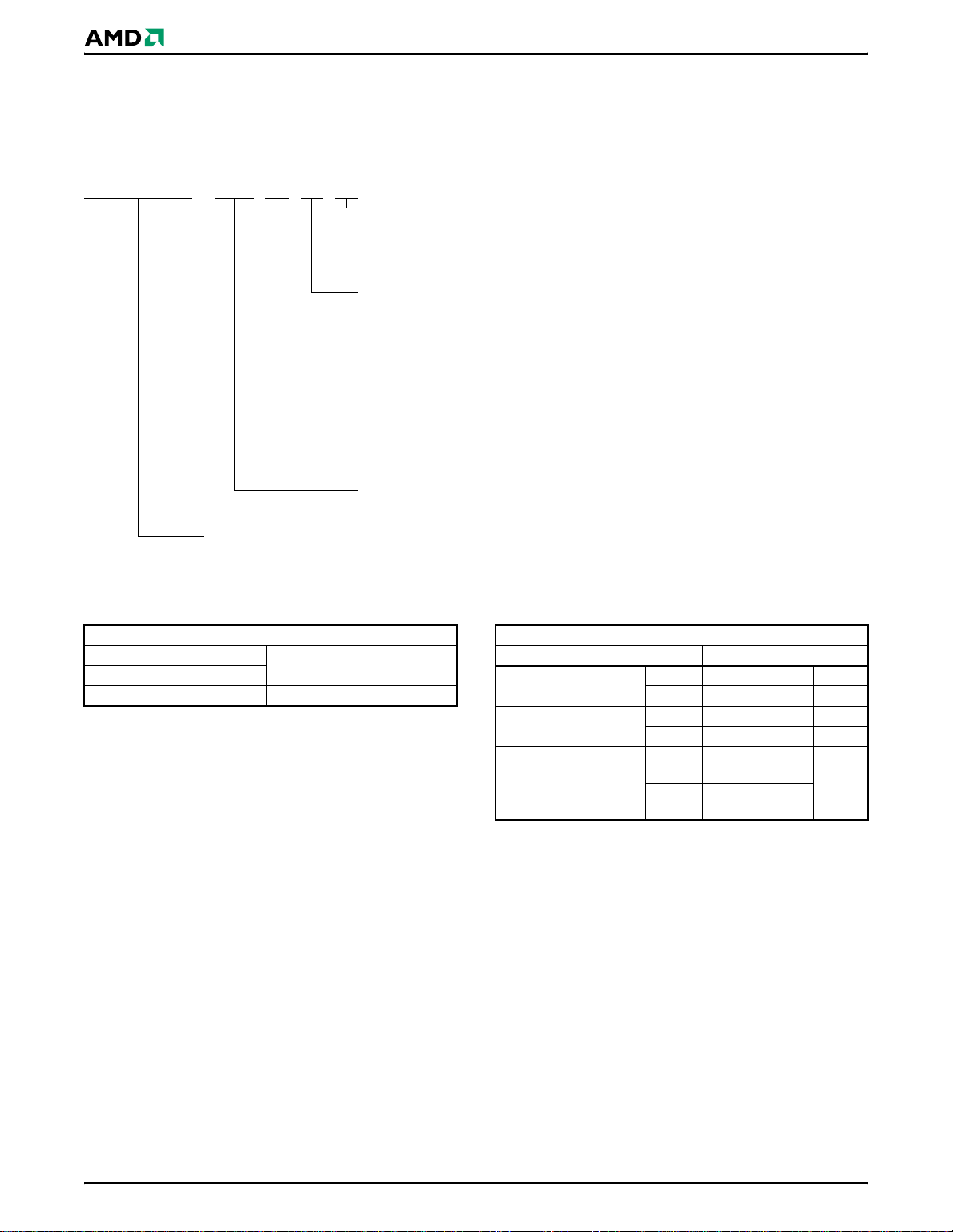
CONNECTION DIAGRAMS
RESET#
WP#/ACC
RY/BY#
A8 B8
A15
A14
A13
A12
A11
A10
A9
A8
A19
A20
WE#
A21
A18
A17
A7
A6
A5
A4
A3
A2
A1
1
2
3
4
5
6
7
8
9
10
11
12
13
14
15
16
17
18
19
20
21
22
23
24
48-Pin Standard TSOP
63-Ball Fine-Pitch BGA (FBGA)
Top View, Balls Facing Down
48
47
46
45
44
43
42
41
40
39
38
37
36
35
34
33
32
31
30
29
28
27
26
25
A16
BYTE#
V
DQ15/A-1
DQ7
DQ14
DQ6
DQ13
DQ5
DQ12
DQ4
V
DQ11
DQ3
DQ10
DQ2
DQ9
DQ1
DQ8
DQ0
OE#
V
CE#
A0
L8
NC* NC*NC* NC*
SS
CC
SS
M8
C7 D7A7 B7
NC* NC*
C6 D6 E6 F6 G6 H6 J6 K6
C5 D5 E5 F5 G5 H5 J5 K5
C4 D4 E4 F4 G4 H4 J4 K4
C3 D3 E3 F3 G3 H3 J3 K3
A2
A1 B1
NC* NC* NC* NC*
C2 D2 E2 F2 G2 H2 J2 K2
* Balls are shorted together via the substrate but not connected to the die.
E7 F7 G7 H7 J7 K7 L7
BYTE#A16A15A14A12A13
DQ15/A
DQ13 DQ6DQ14DQ7A11A10A8A9
V
CC
DQ11 DQ3DQ10DQ2A20A18WP#/ACCRY/BY#
DQ9 DQ1DQ8DQ0A5A6A17A7
CE#A0A1A2A4A3
OE#
V
-
1
DQ4DQ12DQ5A19A21RESET#WE#
V
SS
SS
NC* NC*
L2
NC* NC*NC*
L1
M7
M2
M1
June 6, 2005 Am29DL640G 5
Page 8
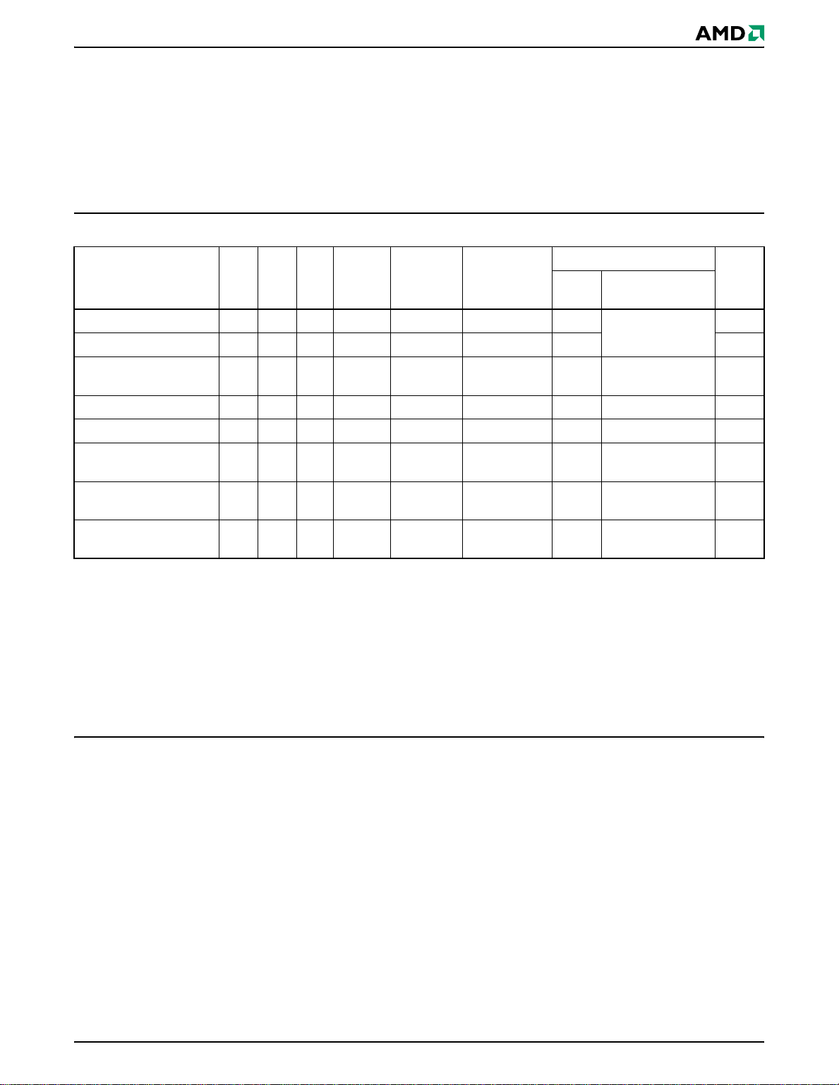
CONNECTION DIAGRAMS
64-Ball Fortified BGA
Top View, Balls Facing Down
A8
NC
A7
A13
A6
A9
A5
WE#
A4
RY/BY#
A3
A7
A2
A3
A1
NC
B8 C8 D8 E8 F8 G8 H8
NCNCNC
B7 C7 D7 E7 F7 G7 H7
B6 C6 D6 E6 F6 G6 H6
B5 C5 D5 E5 F5 G5 H5
B4 C4 D4 E4 F4 G4 H4
B3 C3 D3 E3 F3 G3 H3
B2 C2 D2 E2 F2 G2 H2
B1 C1 D1 E1 F1 G1 H1
SS
DQ15BYTE#A16A15A14A12
DQ13DQ14DQ7A11A10A8
DQ12DQ5A19A21RESET#
CC
OE#CE#A0A1A2A4
NCNCNCV
V
SS
DQ6
DQ4V
DQ3DQ11DQ10DQ2A20A18WP#/ACC
DQ1DQ9DQ8DQ0A5A6A17
V
SS
NCNCNCNCNCNCNC
Special Handling Instructions for BGA
Packages
Special handling is required for Flash Memory products
and/or data integrity may be compromised if th e
package body is exposed to temperatures above
°C for prolonged periods of time.
150
in molded packages (TSOP and BGA). The package
6 Am29DL640G June 6, 2005
Page 9
PIN DESCRIPTION
A21–A0 = 22 Addresses
DQ14–DQ0 = 15 Data Inputs/Outputs (x16-only de-
vices)
DQ15/A-1 = DQ15 (Data Input/Out put, word mode)
A-1 (LSB Address Input, byte mode)
CE# = Chip Enable
OE# = Output Enable
WE# = Write Enable
WP#/ACC = Hardware Write Protect/
Acceleration Pin
RESET# = Hardware Reset Pin, Active Low
BYTE# = Selects 8-bit or 16-bit mode
RY/BY# = Ready/Busy Output
= 3.0 volt-only single power supply
V
CC
V
SS
NC = Pin Not Connected Internally
(see Product Selector Guide for speed
options and voltage supply t olerances)
= Devi ce Ground
LOGIC SYMBOL
22
A21–A0
CE#
OE#
WE#
WP#/ACC
RESET#
BYTE#
16 or 8
DQ15–DQ0
(A-1)
RY/BY#
June 6, 2005 Am29DL640G 7
Page 10
ORDERING INFORMATION
Standard Pro ducts
AMD standard products are available in several packages and operating ranges. The order number (Valid Combination) is
formed by a combination of the following:
Am29DL640G 70 E I
OPTIONAL PROCESSING
Blank = Standard Processing
N = 16-byte ESN devices
(Contact an AMD representative for more information)
TEMPERATURE RANGE
I = Industrial (–40
E = Extended (–55°C to +125°C)
PACKAGE TYPE
E = 48-Pin Thin Small Outline Package
(TSOP) Standard Pinout (TS 048)
PC = 64-Ball Fortified Ball Grid Array
1.0 mm pitch, 13 x 11 mm package (LAA064)
WH = 63-Ball Fine-P itch Ball Grid Array
0.80 mm pitch, 12 x 11 mm package (FBE063)
SPEED OPTION
See Product Selector Guide and Valid Combinations
°C to +85°C)
DEVICE NUMBER/DESCRIPTION
Am29DL640G
64 Megabit (8 M x 8-Bit/4 M x 16-Bit) CMOS Flash Memory
3.0 Volt-only Read, Program, and Erase
Valid Combinations for TSOP Packages
Am29DL640G70
Am29DL640G90
Am29DL640G120 EI, EE
Valid Combinations
Valid Combinations list configurations planned to be supported in
volume for this device. Consult the local AMD sales office to confirm availability of specific valid combinations and to check on
newly released combinations.
EI
Valid Combinations for BGA Packages
Order Number Package Marking
Am29DL640G70
Am29DL640G90
Am29DL640G120
PCI D640G70P I
WHI D640G70V
PCI D640G90P
WHI D640G90V
PCI,
D640G12P
WHI
PCE,
WHE
D640G12V
I, E
8 Am29DL640G June 6, 2005
Page 11
DEVICE BUS OPERATIONS
This section describes the requirements and use of
the device bus operations, which are initiated through
the internal command register. The command register
itself does not occupy any addre ssable memor y location. The register is a latch used to store the commands, along with the address and da ta information
needed to execute the command. The contents of the
Table 1. Am29DL640G Device Bus Operations
register serve as in puts to the inter nal state machine.
The state machine outputs dictate the function of the
device. Table 1 lists the device bus operations, the inputs and control levels they require, and the resulting
output. The following subsections describe each of
these operations in further detail.
DQ15–DQ8
Addresses
Operation CE# OE# WE# RESET# WP#/ACC
Read L L H H L/H A
Write L H L H (Note 3) A
±
V
Standby
Output Disable L H H H L/H X High-Z High-Z High-Z
Reset X X X L L/H X High-Z High-Z High-Z
Sector Protect (Note 2) L H L V
Sector Unprotect (Note 2) L H L V
Temporary Sector
Unprotect
CC
0.3 V
XX
XXX V
VCC ±
0.3 V
ID
ID
ID
L/H X High-Z High-Z High-Z
L/H
(Note 3)
(Note 3) A
(Note 2)
IN
IN
SA, A6 = L,
A1 = H, A0 = L
SA, A6 = H,
A1 = H, A0 = L
IN
BYTE#
= V
IH
D
OUT
D
IN
XXD
XXD
D
IN
BYTE#
= V
IL
DQ8–DQ14 =
High-Z, DQ15 = A-1
High-Z D
DQ7–
DQ0
D
OUT
D
IN
IN
IN
IN
Legend: L = Logic Low = VIL, H = Logic Hi g h = VIH, VID = 11.5–12.5 V, VHH = 9.0 ± 0.5 V, X = Don’t Care, SA = Sector Address,
= Address In, DIN = Data In, D
A
IN
= Data Out
OUT
Notes:
1. Addresses are A21:A0 in word mode (BYTE# = V
), A21:A-1 in byte mode (BYTE# = VIL).
IH
2. The sector prot ect a nd sect or unpr otect functi ons may also be implemented via prog r amming e quipment. See the “Sec tor/Sec tor Block Protection and Unprote ction” secti on.
3. If WP#/ACC = V
, sectors 0, 1, 140, and 141 remain protected. If WP#/ACC = VIH, protection on sectors 0, 1, 140, and 141
IL
depends on whether they were last protected or unprotected using the method described in “Sector/Sector Block Protection
and Unprotection”. If WP#/ACC = V
, all sectors will be unprotected.
HH
Word/Byte Configuration
The BYTE# pin controls whether the device data I/O
pins operate in the byte or word co nfiguration. If th e
BYTE# pin is set at logic ‘1’, the device is in word configuration, DQ15–DQ0 are active and control led by
CE# and OE#.
If the BYTE# pin is set at logic ‘0’, the device is in byte
configuration, and only data I/O pins DQ7–DQ0 are
active and controlled by CE# and OE#. The data I/O
pins DQ14–DQ8 are tri-stated, and the DQ15 pin is
used as an input for the LSB (A-1) address function.
Requirements for Reading Array Data
To read array data from the outputs, the system must
drive the CE# and OE# pins to V
control and selects the device. OE# is the output control and gates array data to the output pins. WE#
should remain at V
. The BYTE# pin determines
IH
whether the device outputs array data in words or
bytes.
The internal state machine is set for rea ding arr ay data
upon device power-up, or after a hardware reset. This
ensures that no spurious alteration of the memory
. CE# is the power
IL
content occurs during the power transition. No command is necessary in this mode to obtain array data.
Standard microprocessor read cycles that assert valid
June 6, 2005 Am29DL640G 9
Page 12

addresses on the device address inputs produce valid
data on the device data outputs. Each bank remains
enabled for read access until the command register
contents are altered.
Refer to the AC Read-Only Operations table for timing
specifications and to Figure 14 for the timing diagram.
in the DC Characteristics table represents the ac-
I
CC1
tive current specification for reading array data.
Writing Commands/Command Sequences
To write a command or command sequence (which includes programming data to the device and erasing
sectors of memory), the system must drive WE# and
CE# to V
For program operations, the BYTE# pin determines
whether the device accepts program data in bytes or
words. Refer to “Word/Byte Configuration” for more information.
The device features an Unlock Bypass mode to facilitate faster programming. Once a bank enters the Unlock Bypass mode, only two write cycles are required
to program a word or byte, instead of four. The
“Byte/Word Program Command Se quence” sec tion
has details on programming data to the device using
both standard and Unlock Bypass command sequences.
An erase operation can erase one sector, multiple sectors, or the entire de vi ce. Table 2 indicates the address
space that each sector occupies. Similar ly, a “sector
address” is the address bits required to uniquel y select
a sector. The “Com mand D efin itions” sectio n ha s details on erasing a sector or the entire chip, or suspending/resuming the erase operation.
The device address space is divided into four bank s. A
“bank address” is the address bits required to uniquely
select a bank.
I
CC2
tive current specification for the write mode. The AC
Characteristics section contains timing specification
tables and timing diagrams for write operations.
Accelerated Program Operation
The device offers accelerated program operations
through the ACC function. This is one of two functions
provided by the WP#/ACC pin. This function is pr imarily intended to allow faster manufacturing throug hput
at the factory.
If the system as ser t s V
matically enters the aforementioned Unlock Bypass
mode, temporarily unprotects any protected s ectors,
and uses the higher voltage on the pin to reduce the
time required for program operations. The system
would use a two-cycle program comman d sequenc e
, and OE# to VIH.
IL
in the DC Characteristics table represents the ac-
on this pin, the device auto-
HH
as required by the Unlock Bypass mode. Removing
from the WP#/ACC pin retur ns the device to nor-
V
HH
mal operation. Note that V
must not be asserted on
HH
WP#/ACC for operations other than accelerated programming, or device damage may result. In addition,
the WP#/ACC pin must not be left floating or un connected; inconsistent behavior of the device may result.
See “Write Protect (WP#)” on page 16 for related information.
Autoselect Functions
If the system writes the autoselect command sequence, the device enters the autoselect mod e. The
system can then read autoselect codes from the internal register (which is separate from the memory array)
on DQ15–DQ0. Standard read cycle timings apply in
this mode. Refer to the Autoselect Mode and Autoselect Command Sequence sections for more information.
Simultaneous Read/Write Operations with
Zero Lat ency
This device is capa ble of reading data from one bank
of memory while programming or erasing in the other
bank of memory. An erase operation may also be suspended to read from or program to another location
within the same bank (except the s ector being
erased). Figure 21 shows how read and write cycles
may be initiated for simultaneous operation with zero
latency. I
CC6
and I
in the DC Characteristics table
CC7
represent the current specifications for read-while-program and read-while-erase, respectively.
Standby Mode
When the system is no t reading or wr iting to the de vice, it can place the device in the standby mode. In
this mode, current consum ption is greatly reduced,
and the outputs are placed in the high impedance
state, independent of the OE# input.
The device enters the CMOS standby mode when the
CE# and RESET# pins are both held at V
(Note that this is a more restricte d voltage range than
.) If CE# and RESET# are held at VIH, but not within
V
IH
± 0.3 V, the device will be in the standby mode,
V
CC
but the standby current will be greater. The device requires standard access time (t
) for read access
CE
when the device is in either of these standby modes,
before it is ready to read data.
If the device is deselected during erasure or programming, the device draws active current until the
operation is completed.
in the DC Characteristics table represents th e
I
CC3
standby current specification.
± 0.3 V.
CC
10 Am29DL640G June 6, 2005
Page 13
Automatic Sleep Mode
The automatic sleep mode minimizes Fl ash device energy consumption. The device automatically enables
this mode when addresses remain stable for t
ACC
+
30 ns. The automatic sleep mode is independent of
the CE#, WE#, and OE# control signals. Standard address access timings provide new data when addresses ar e change d. While i n sleep m ode, outpu t
data is latched and always available to the system.
in the DC Character istics table represents the
I
CC5
automatic sleep mode current specification.
RESET#: Hardware Reset Pin
The RESET# pin provides a hardware method of r esetting the device to reading array data. When the RESET# pin is driven low for at least a period of t
device immediately ter minates any operation in
progress, tristates all output pins, and ignores all
read/write com mands for the durati on of the RESE T#
pulse. The device also resets the internal state machine to reading array data. The operation that was interrupted should be reinitiated once the device is
ready to accept another command sequence, to ensure data integrity.
Current is reduced for the duration of the RESET#
pulse. When RESET# is held at V
±0.3 V, the device
SS
RP
, the
draws CMOS standby cu rrent ( I
but not within VSS±0.3 V, the standby current will
at V
IL
). If RESET# is held
CC4
be greater.
The RESET# pin may be tied to the system reset cir-
cuitry. A system reset would thus also reset the Flash
memory, enabling the system to read the boot-up firmware from the Flash memory.
If RESET# is asserted during a program or erase operation, the RY/BY# pin re mains a “0” ( busy) until the
internal reset operation is complete, which requires a
time of t
(during Embedded Algorithms). The sys-
READY
tem can thus monitor RY/BY# to deter mine w hether
the reset operation is c omplete. If RESET# is asserted
when a program or erase operation is not executing
(RY/BY# pin is “1”), the reset operation is completed
within a time of t
rithms). The system can read d ata t
SET# pin returns to V
(not during Embedde d Algo-
READY
.
IH
after the RE-
RH
Refer to the AC Characteristics tables for RESET# parameters and to Figure 15 for the timing diagram.
Output Disable Mode
When the OE# input is at VIH, output from the devic e is
disabled. The output pins are placed in the high
impedance state.
Bank Sector
Bank 1
Table 2. Am29DL640G Sector Architecture
Sector Address
A21–A12
SA0 0000000000 8/4 000000h–001FFFh 00000h–00FFFh
SA1 0000000001 8/4 002000h–003FFFh 01000h–01FFFh
SA2 0000000010 8/4 004000h–005FFFh 02000h–02FFFh
SA3 0000000011 8/4 006000h–007FFFh 03000h–03FFFh
SA4 0000000100 8/4 008000h–009FFFh 04000h–04FFFh
SA5 0000000101 8/4 00A000h–00BFFFh 05000h–05FFFh
SA6 0000000110 8/4 00C000h–00DFFFh 06000h–06FFFh
SA7 0000000111 8/4 00E000h–00FFFFFh 07000h–07FFFh
SA8 0000001xxx 64/32 010000h–01FFFFh 08000h–0FFFFh
SA9 0000010xxx 64/32 020000h–02FFFFh 10000h–17FFFh
SA10 0000011xxx 64/32 030000h–03FFFFh 18000h–1FFFFh
SA11 0000100xxx 64/32 040000h–04FFFFh 20000h–27FFFh
SA12 0000101xxx 64/32 050000h–05FFFFh 28000h–2FFFFh
SA13 0000110xxx 64/32 060000h–06FFFFh 30000h–37FFFh
SA14 0000111xxx 64/32 070000h–07FFFFh 38000h–3FFFFh
SA15 0001000xxx 64/32 080000h–08FFFFh 40000h–47FFFh
SA16 0001001xxx 64/32 090000h–09FFFFh 48000h–4FFFFh
SA17 0001010xxx 64/32 0A0000h–0AFFFFh 50000h–57FFFh
SA18 0001011xxx 64/32 0B0000h–0BFFFFh 58000h–5FFFFh
SA19 0001100xxx 64/32 0C0000h–0CFFFFh 60000h–67FFFh
SA20 0001101xxx 64/32 0D0000h–0DFFFFh 68000h–6FFFFh
SA21 0001101xxx 64/32 0E0000h–0EFFFFh 70000h–77FFFh
SA22 0001111xxx 64/32 0F0000h–0FFFFFh 78000h–7FFFFh
Sector Size
(Kbytes/Kwords)
(x8)
Address Range
(x16)
Address Range
June 6, 2005 Am29DL640G 11
Page 14
Bank Sector
SA23 0010000xxx 64/32 100000h–00FFFFh 80000h–87FFFh
SA24 0010001xxx 64/32 110000h–11FFFFh 88000h–8FFFFh
SA25 0010010xxx 64/32 120000h–12FFFFh 90000h–97FFFh
SA26 0010011xxx 64/32 130000h–13FFFFh 98000h–9FFFFh
SA27 0010100xxx 64/32 140000h–14FFFFh A0000h–A7FFFh
SA28 0010101xxx 64/32 150000h–15FFFFh A8000h–AFFFFh
SA29 0010110xxx 64/32 160000h–16FFFFh B0000h–B7FFFh
SA30 0010111xxx 64/32 170000h–17FFFFh B8000h–BFFFFh
SA31 0011000xxx 64/32 180000h–18FFFFh C0000h–C7FFFh
SA32 0011001xxx 64/32 190000h–19FFFFh C8000h–CFFFFh
SA33 0011010xxx 64/32 1A0000h–1AFFFFh D0000h–D7FFFh
SA34 0011011xxx 64/32 1B0000h–1BFFFFh D8000h–DFFFFh
SA35 0011000xxx 64/32 1C0000h–1CFFFFh E0000h–E7F FFh
SA36 0011101xxx 64/32 1D0000h–1DFFFFh E8000h–EFFFFh
SA37 0011110xxx 64/32 1E0000h–1EFFFFh F0000h–F7FFFh
SA38 0011111xxx 64/32 1F0000h–1FFFFFh F8000h–FFFFFh
SA39 0100000xxx 64/32 200000h–20FFFFh F9000h–107FFFh
SA40 0100001xxx 64/32 210000h–21FFFFh 108000h–10FFFFh
SA41 0100010xxx 64/32 220000h–22FFFFh 110000h–117FFFh
SA42 0101011xxx 64/32 230000h–23FFFFh 118000h–11FFFFh
SA43 0100100xxx 64/32 240000h–24FFFFh 120000h–127FFFh
SA44 0100101xxx 64/32 250000h–25FFFFh 128000h–12FFFFh
SA45 0100110xxx 64/32 260000h–26FFFFh 130000h–137FFFh
Bank 2
SA46 0100111xxx 64/32 270000h–27FFFFh 138000h–13FFFFh
SA47 0101000xxx 64/32 280000h–28FFFFh 140000h–147FFFh
SA48 0101001xxx 64/32 290000h–29FFFFh 148000h–14FFFFh
SA49 0101010xxx 64/32 2A0000h–2AFFFFh 150000h–157FFFh
SA50 0101011xxx 64/32 2B0000h–2BFFFFh 158000h–15FFFFh
SA51 0101100xxx 64/32 2C0000h–2CFFFFh 160000h–167FFFh
SA52 0101101xxx 64/32 2D0000h–2DFFFFh 168000h–16FFFFh
SA53 0101110xxx 64/32 2E0000h–2EFFFFh 170000h–177FFFh
SA54 0101111xxx 64/32 2F0000h–2FFFFFh 178000h–17FFFFh
SA55 0110000xxx 64/32 300000h–30FFFFh 180000h–187FFFh
SA56 0110001xxx 64/32 310000h–31FFFFh 188000h–18FFFFh
SA57 0110010xxx 64/32 320000h–32FFFFh 190000h–197FFFh
SA58 0110011xxx 64/32 330000h–33FFFFh 198000h–19FFFFh
SA59 0100100xxx 64/32 340000h–34FFFFh 1A0000h–1A7FFFh
SA60 0110101xxx 64/32 350000h–35FFFFh 1A8000h–1AFFFFh
SA61 0110110xxx 64/32 360000h–36FFFFh 1B0000h–1B7FFFh
SA62 0110111xxx 64/32 370000h–37FFFFh 1B8000h–1BFFFFh
SA63 0111000xxx 64/32 380000h–38FFFFh 1C0000h–1C7FFFh
SA64 0111001xxx 64/32 390000h–39FFFFh 1C8000h–1CFFFFh
SA65 0111010xxx 64/32 3A0000h–3AFFFFh 1D0000h–1D7FFFh
SA66 0111011xxx 64/32 3B0000h–3BFFFFh 1D8000h–1DFFFFh
SA67 0111100xxx 64/32 3C0000h–3CFFFFh 1E0000h–1E7FFFh
SA68 0111101xxx 64/32 3D0000h–3DFFFFh 1E8000h–1EFFFFh
SA69 0111110xxx 64/32 3E0000h–3EFFFFh 1F0000h–1F7FFFh
SA70 0111111xxx 64/32 3F0000h–3FFFFFh 1F8000h–1FFFFFh
Table 2. Am29DL640G Sector Architecture (Continued)
Sector Address
A21–A12
Sector Size
(Kbytes/Kwords)
(x8)
Address Range
(x16)
Address Range
12 Am29DL640G June 6, 2005
Page 15
Bank Sector
SA71 1000000xxx 64/32 400000h–40FFFFh 200000h–207FFFh
SA72 1000001xxx 64/32 410000h–41FFFFh 208000h–20FFFFh
SA73 1000010xxx 64/32 420000h–42FFFFh 210000h–217FFFh
SA74 1000011xxx 64/32 430000h–43FFFFh 218000h–21FFFFh
SA75 1000100xxx 64/32 440000h–44FFFFh 220000h–227FFFh
SA76 1000101xxx 64/32 450000h–45FFFFh 228000h–22FFFFh
SA77 1000110xxx 64/32 460000h–46FFFFh 230000h–237FFFh
SA78 1000111xxx 64/32 470000h–47FFFFh 238000h–23FFFFh
SA79 1001000xxx 64/32 480000h–48FFFFh 240000h–247FFFh
SA80 1001001xxx 64/32 490000h–49FFFFh 248000h–24FFFFh
SA81 1001010xxx 64/32 4A0000h–4AFFFFh 250000h–257FFFh
SA82 1001011xxx 64/32 4B0000h–4BFFFFh 258000h–25FFFFh
SA83 1001100xxx 64/32 4C0000h–4CFFFFh 260000h–267FFFh
SA84 1001101xxx 64/32 4D0000h–4DFFFFh 268000h–26FFFFh
SA85 1001110xxx 64/32 4E0000h–4EFFFFh 270000h–277FFFh
SA86 1001111xxx 64/32 4F0000h–4FFFFFh 278000h–27FFFFh
SA87 1010000xxx 64/32 500000h–50FFFFh 280000h–28FFFFh
SA88 1010001xxx 64/32 510000h–51FFFFh 288000h–28FFFFh
SA89 1010010xxx 64/32 520000h–52FFFFh 290000h–297FFFh
SA90 1010011xxx 64/32 530000h–53FFFFh 298000h–29FFFFh
SA91 1010100xxx 64/32 540000h–54FFFFh 2A0000h–2A7FFFh
SA92 1010101xxx 64/32 550000h–55FFFFh 2A8000h–2AFFFFh
SA93 1010110xxx 64/32 560000h–56FFFFh 2B0000h–2B7FFFh
Bank 3
SA94 1010111xxx 64/32 570000h–57FFFFh 2B8000h–2BFFFFh
SA95 1011000xxx 64/32 580000h–58FFFFh 2C0000h–2C7FFFh
SA96 1011001xxx 64/32 590000h–59FFFFh 2C8000h–2CFFFFh
SA97 1011010xxx 64/32 5A0000h–5AFFFFh 2D0000h–2D7FFFh
SA98 1011011xxx 64/32 5B0000h–5BFFFFh 2D8000h–2DFFFFh
SA99 1011100xxx 64/32 5C0000h–5CFFFFh 2E0000h–2E7FFFh
SA100 1011101xxx 64/32 5D0000h–5DFFFFh 2E8000h–2EFFFFh
SA101 1011110xxx 64/32 5E0000h–5EFFFFh 2F0000h–2FFFFFh
SA102 1011111xxx 64/32 5F0000h–5FFFFFh 2F 8000h–2FFFFFh
SA103 1100000xxx 64/32 600000h–60FFFFh 300000h–307FFFh
SA104 1100001xxx 64/32 610000h–61FFFFh 308000h–30FFFFh
SA105 1100010xxx 64/32 620000h–62FFFFh 310000h–317FFFh
SA106 1100011xxx 64/32 630000h–63FFFFh 318000h–31FFFFh
SA107 1100100xxx 64/32 640000h–64FFFFh 320000h–327FFFh
SA108 1100101xxx 64/32 650000h–65FFFFh 328000h–32FFFFh
SA109 1100110xxx 64/32 660000h–66FFFFh 330000h–337FFFh
SA110 1100111xxx 64/32 670000h–67FFFFh 338000h–33FFFFh
SA111 1101000xxx 64/32 680000h–68FFFFh 340000h–347FFFh
SA112 1101001xxx 64/32 690000h–69FFFFh 348000h–34FFFFh
SA113 1101010xxx 64/32 6A0000h–6AFFFFh 350000h–357FFFh
SA114 1101011xxx 64/32 6B0000h–6BFFFFh 358000h–35FFFFh
SA115 1101100xxx 64/32 6C0000h–6CFFFFh 360000h–367FFFh
SA116 1101101xxx 64/32 6D0000h–6DFFFFh 368000h–36FFFFh
SA117 1101110xxx 64/32 6E0000h–6EFFFFh 370000h–377FFFh
SA118 1101111xxx 64/32 6F0000h–6FFFFFh 378000h–37FFFFh
Table 2. Am29DL640G Sector Architecture (Continued)
Sector Address
A21–A12
Sector Size
(Kbytes/Kwords)
(x8)
Address Range
(x16)
Address Range
June 6, 2005 Am29DL640G 13
Page 16
Bank Sector
SA119 1110000xxx 64/32 700000h–70FFFFh 380000h–387FFFh
SA120 1110001xxx 64/32 710000h–71FFFFh 388000h–38FFFFh
SA121 1110010xxx 64/32 720000h–72FFFFh 390000h–397FFFh
SA122 1110011xxx 64/32 730000h–73FFFFh 398000h–39FFFFh
SA123 1110100xxx 64/32 740000h–74FFFFh 3A0000h–3A7FFFh
SA124 1110101xxx 64/32 750000h–75FFFFh 3A8000h–3AFFFFh
SA125 1110110xxx 64/32 760000h–76FFFFh 3B0000h–3B7FFFh
SA126 1110111xxx 64/32 770000h–77FFFFh 3B8000h–3BFFFFh
SA127 1111000xxx 64/32 780000h–78FFFFh 3C0000h–3C7FFFh
SA128 1111001xxx 64/32 790000h–79FFFFh 3C8000h–3CFFFFh
SA129 1111010xxx 64/32 7A0000h–7AFFFFh 3D0000h–3D7FFFh
Bank 4
SA130 1111011xxx 64/32 7B0000h–7BFFFFh 3D8000h–3DFFFFh
SA131 1111100xxx 64/32 7C0000h–7CFFFFh 3E0000h–3E7FFFh
SA132 1111101xxx 64/32 7D0000h–7DFFFFh 3E8000h–3EFFFFh
SA133 1111110xxx 64/32 7E0000h–7EFFFFh 3F0000h–3F7FFFh
SA134 1111111000 8/4 7F0000h–7F1FFFh 3F8000h–3F8FFFh
SA135 1111111001 8/4 7F2000h–7F3FFFh 3F9000h–3F9FFFh
SA136 1111111010 8/4 7F4000h–7F5FFFh 3FA000h–3FAFFFh
SA137 1111111011 8/4 7F6000h–7F7FFFh 3FB000h–3FBFFFh
SA138 1111111100 8/4 7F8000h–7F9FFFh 3FC000h–3FCFFFh
SA139 1111111101 8/4 7FA000h–7FBFFFh 3FD000h–3FDFFFh
SA140 1111111110 8/4 7FC000h–7FDFFFh 3FE000h–3FEFFFh
SA141 1111111111 8/4 7FE000h–7FFFFFh 3FF000h–3FFFFFh
Table 2. Am29DL640G Sector Architecture (Continued)
Sector Address
A21–A12
Sector Size
(Kbytes/Kwords)
(x8)
Address Range
(x16)
Address Range
Note: The address range is A21:A-1 in byte mode (BYTE#=VIL) or A21:A0 in word mode (BYTE#=VIH).
Table 3. Bank Address
Bank A21–A19
1 000
2 001, 010, 011
3 100, 101, 110
4 111
TM
Table 4. SecSi
Device Sector Size
Am29DL640G 256 bytes 000000h–0000FFh 00000h–0007Fh
Autoselect Mode
The autoselect mode provides manufacturer and device identification, a nd sector pr otection verificatio n,
through identifier codes output on DQ7–DQ0. This
mode is prima rily intende d for programming equipment to automatically match a device to be programmed with its corresponding programming
algorithm. However, the autoselect codes can also be
accessed in-system through the command register.
When using programming equipment, the autoselect
mode requires V
must be as shown in Table 5. In addition, when verifying sector protection, the sector address must appea r
on the appropriate highest order address bits (see
on address pin A9. Address pins
ID
Sector Addresses
(x8)
Address Range
Table 2). Table 5 shows the remaining address bits
that are don’t care. When all necessary bits have been
set as required, the programming equipment ma y then
read the corresponding identifier code on DQ7–DQ0.
However, the autoselect codes can also be accessed
in-system through the command register, for instances
when the Am29DL640 is erased or programmed in a
system without access to high voltage on the A9 pin.
The command sequence is illustrated in Table 12.
Note that if a Bank Address (BA) on address bits A21,
A20, and A19 is asserted during the third write cycle of
the autoselect command, the host system can read
autoselect data from that bank and then immediately
read array data from the other bank, without exit ing the
autoselect mode.
(x16)
Address Range
14 Am29DL640G June 6, 2005
Page 17
To access the autoselect codes in-system, the host
system can issue the autoselect command via the
does not require V
mand Sequence section for more information.
. Refer to the Autoselect Com-
ID
command register, as shown in Table 12. This method
Table 5. Am29DL640G Autoselect Codes, (High Voltage Method)
A21
A11
to
Description CE# OE# WE#
Manufacturer ID:
AMD
Read Cycle 1
Read Cycle 2 L H H H L 22h 02h
Device I D
Read Cycle 3 L H H H H 22h 01h
Sector Protection
Verification
SecSi Indicator Bit
(DQ7)
Legend:
L = Logic Low = VIL, H = Logic High = VIH, BA = Bank Address, SA = Sector Address, X = Don’t care
LLHBAX
LLHBAX
LLHSAX
LLHBAX
A12
to
A10 A9
A8
to
A7 A6
V
XLXLLLL X X 01h
ID
V
X
ID
V
XLX HL X X
ID
V
XLXLLHH X X
ID
A5
to
A4 A3 A2 A1 A0
L
LLLH22h
X
DQ15 to DQ0
BYTE#
= V
.
IH
BYTE#
= V
X
DQ7
to
IL
DQ0
7Eh
01h (protected),
00h (unprotected)
81h (factory locked),
01h (not factory
locked)
June 6, 2005 Am29DL640G 15
Page 18

Sector/Sector Block Protection and Unprotection
(Note: For the following discussion, the term “sector”
applies to both sectors and sector blocks. A sector
block consists of two or more adjacent sectors that are
protected or unprotected at the same time (see Table
6).
The hardware sector protection feature disables both
program and erase operations in an y se ctor. The hardware sector unprotecti on feature re-enables both pr ogram and erase operations in previously protected
sectors. Sector protection/unprotection can be implemented via two methods.
Table 6. Am29DL640G Boot Sector/Sector Block
Addresses for Protection/Unprotection
Sector A21–A12
SA0 0000000000 8 Kbytes
SA1 0000000001 8 Kbytes
SA2 0000000010 8 Kbytes
SA3 0000000011 8 Kbytes
SA4 0000000100 8 Kbytes
SA5 0000000101 8 Kbytes
SA6 0000000110 8 Kbytes
SA7 0000000111 8 Kbytes
SA8–SA10
SA11–SA14 00001XXXXX 256 (4x64) Kbytes
SA15–SA18 00010XXXXX 256 (4x64) Kbytes
SA19–SA22 00011XXXXX 256 (4x64) Kbytes
SA23–SA26 00100XXXXX 256 (4x64) Kbytes
SA27-SA30 00101XXXXX 256 (4x64) Kbytes
SA31-SA34 00110XXXXX 256 (4x64) Kbytes
SA35-SA38 00111XXXXX 256 (4x64) Kbytes
SA39-SA42 01000XXXXX 256 (4x64) Kbytes
SA43-SA46 01001XXXXX 256 (4x64) Kbytes
SA47-SA50 01010XXXXX 256 (4x64) Kbytes
SA51-SA54 01011XXXXX 256 (4x64) Kbytes
SA55–SA58 01100XXXXX 256 (4x64) Kbytes
SA59–SA62 01101XXXXX 256 (4x64) Kbytes
SA63–SA66 01110XXXXX 256 (4x64) Kbytes
SA67–SA70 01111XXXXX 256 (4x64) Kbytes
SA71–SA74 10000XXXXX 256 (4x64) Kbytes
SA75–SA78 10001XXXXX 256 (4x64) Kbytes
SA79–SA82 10010XXXXX 256 (4x64) Kbytes
SA83–SA86 10011XXXXX 256 (4x64) Kbytes
SA87–SA90 10100XXXXX 256 (4x64) Kbytes
SA91–SA94 10101XXXXX 256 (4x64) Kbytes
SA95–SA98 10110XXXXX 256 (4x64) Kbytes
0000001XXX,
0000010XXX,
0000011XXX,
Sector/
Sector Block Size
192 (3x64) Kbytes
Sector A21–A12
SA99–SA102 10111XXXXX 256 (4x64) Kbytes
SA103–SA106 11000XXXXX 256 (4x64) Kbytes
SA107–SA110 11001XXXXX 256 (4x64) Kbytes
SA111–SA114 11010XXXXX 256 (4x64) Kbytes
SA115–SA118 11011XXXXX 256 (4x64) Kbytes
SA119–SA122 11100XXXXX 256 (4x64) Kbytes
SA123–SA126 11101XXXXX 256 (4x64) Kbytes
SA127–SA130 11110XXXXX 256 (4x64) Kbytes
SA131–SA133
SA134 1111111000 8 Kbytes
SA135 1111111001 8 Kbytes
SA136 1111111010 8 Kbytes
SA137 1111111011 8 Kbytes
SA138 1111111100 8 Kbytes
SA139 1111111101 8 Kbytes
SA140 1111111101 8 Kbytes
SA141 1111111111 8 Kbytes
1111100XXX,
1111101XXX,
1111110XXX
Sector protection/sector unprotection requires V
Sector/
Sector Block Size
192 (3x64) Kbytes
on
ID
the RESET# pin o nly, and can be implemented either
in-system or via programming equipment. Figure 2
shows the algorithms and Fig ure 26 shows the timing
diagram. For sector unprotect, all unprotected sectors
must first be protected prior to the first sector unprotect write cycle. Note that the sector unpro tect algo-
rithm unprotects all sectors i n parallel. All previously
protected sectors must be individually re-protected. To
change data in protected sectors efficiently, the temporary sector unprotect function is available. See
“Temporary Sector Unprotect”.
The device is shipped with all s ectors unprotecte d.
AMD offers the option of programm ing and pro tecting
sectors at its factory prior to shipping the device
through AMD’s ExpressFlash™ Service. Contact an
AMD representative for details.
It is possible to determine whether a sector is protected or unprotected. See the Autoselect Mode section for details.
Write Protect (WP#)
The Write Protect function provides a hardware
method of protecting without using V
one of two provided by the WP#/ACC pin.
If the system a s se rts V
on the WP#/ACC pin, the de-
IL
vice disables program and erase functions in sectors
0, 1, 140, and 141, independently of whether those
sectors were protected or unprotected using the
method described in “Sector/Sector Block Protection
and Unprotection”.
. This function is
ID
16 Am29DL640G June 6, 2005
Page 19

If the system asse rts V
on the WP#/ACC pin, the de-
IH
vice reverts to whether sectors 0, 1, 140, and 141
were last set to be protected or unprotected. That is,
sector protection or unprotection for these sectors depends on whether they were last protected or unprotected using the method described in “Sector/S ector
Block Protection and Unprotection”.
Note that the WP#/ACC pin must not be left floating or
unconnected; inconsistent behavior of the device may
result.
Table 7. WP#/ACC Modes
WP# Input
Voltage
V
IL
V
IH
V
HH
Disables programming and erasing in
SA0, SA1, SA140, and SA141
Enables programming and erasing in
SA0, SA1, SA140, and SA141
Enables accelerated programming
(ACC). See “Accelerated Program
Operation” on page 10.
Device
Mode
Temporary Sector Unprotect
(Note: For the following discussion, the term “sector”
applies to both sectors and sector blocks. A sector
block consists of two or more adjacent sectors that are
protected or unprotected at the same time (see Table
6).
This feature allows temporary unprotection of previ-
ously protected sectors to change data in-system. The
Sector Unprotect mode is activated by setting the RESET# pin to V
sectors can be programmed or erased by selecting the
sector addresses. Once V
SET# pin, all the previously protected s ectors are
protected again. Figure 1 shows the algorithm, and
Figure 25 shows the timing diagram s, for this feature.
If the WP#/ACC pin is at V
141 will remain protected during the Temporary sector
Unprotect mode.
. During this mode, formerly protected
ID
is removed from the RE-
ID
, sectors 0, 1, 140, and
IL
START
RESET# = V
(Note 1)
Perform Erase or
Program Operations
RESET# = V
Temporary Sector
Unprotect Completed
(Note 2)
Notes:
1. All protected sectors unprotected (If WP#/ACC = V
sectors 0, 1, 140, and 141 will remain protected).
2. All previously protected sectors are protected once again.
ID
IH
,
IL
Figure 1. Temporary Sector Unprotect Operation
June 6, 2005 Am29DL640G 17
Page 20

r
S
Temporary Sector
Unprotect Mode
Increment
PLSCNT
No
PLSCNT
= 25?
Yes
Device failed
ector Protect
Algorithm
START
PLSCNT = 1
RESET# = V
Wait 1 μs
No
First Write
Cycle = 60h?
Set up sector
address
Sector Protect:
Write 60h to sector
address with
A6 = 0, A1 = 1,
A0 = 0
Wait 150 µs
Verify Sector
Protect: Write 40h
to sector address
with A6 = 0,
A1 = 1, A0 = 0
Read from
sector address
with A6 = 0,
A1 = 1, A0 = 0
No
Data = 01h?
Protect another
sector?
Remove V
from RESET#
Write reset
command
Sector Protect
complete
Yes
Yes
No
START
Protect all sectors:
The indicated portion
of the sector protect
ID
Reset
PLSCNT = 1
Yes
ID
algorithm must be
performed for all
unprotected sectors
prior to issuing the
first sector
unprotect address
Increment
PLSCNT
No
PLSCNT
= 1000?
Yes
Device failed
Sector Unprotect
PLSCNT = 1
RESET# = V
Wait 1 μs
First Write
Cycle = 60h?
No
All sectors
protected?
Set up first sector
address
Sector Unprotect:
Write 60h to sector
address with
A6 = 1, A1 = 1,
A0 = 0
Wait 15 ms
Verify Sector
Unprotect: Write
40h to sector
address with
A6 = 1, A1 = 1,
A0 = 0
Read from
sector address
with A6 = 1,
A1 = 1, A0 = 0
No
Data = 00h?
Last sector
verified?
Remove V
from RESET#
Yes
Yes
Yes
Yes
ID
No
Temporary Secto
Unprotect Mode
Set up
next sector
address
No
ID
Algorithm
Write reset
command
Sector Unprotect
complete
Figure 2. In-System Sector Protect/Unprotect Algorithms
18 Am29DL640G June 6, 2005
Page 21

SecSi™ (Secured Silicon) Sector
Flash Memory Region
The SecSi (Secured Silicon) Sector feature provides a
Flash memory region that enables permanent part
identification through an Electronic Serial Number
(ESN). The SecSi Sector is 256 bytes in length, an d
uses a SecSi Sector Indicator Bit (DQ7) to indicate
whether or not the SecSi Sector is locked when
shipped from the factory. This bit is per manently set at
the factory and cannot be changed, which prevents
cloning of a factory locked part. This ensures the security of the ESN once the product is shipped to the field.
AMD offers the device with the SecSi Sector either
factory locked or customer lockable. The factory-locked version is always protected when s hipped
from the factory, and has the SecSi ( Secured Silic on)
Sector Indicator Bit permanently set to a “1.” The customer-lockable version is shipped with the SecSi Sector unprotected, allowing customers to utilize the that
sector in any manner they choose. The customer-lockable version has the SecSi (Secured Silicon) Sector
Indicator Bit permanently set to a “0.” Thus, the SecSi
Sector Indicator Bit prevents customer-lockable devices from being used to replace devices that are factory locked.
The system accesses the SecSi Sector Secure
through a command sequence (see “Enter SecSi™
Sector/Exit SecSi Sector Command Sequence”). After
the system has written the Enter SecSi Sector command sequence, it may read the SecSi Sector by
using the addresses normally occupied by the boot
sectors. This mode of ope ration continues until the
system issues the Exit SecSi Sector command sequence, or until power is removed from the device. On
power-up, or following a hardware reset, the device reverts to sending commands to the first 256 bytes of
Sector 0. Note that the ACC function an d unlock by-
pass modes are not available when the SecSi Sector
is enabled.
Factory Locked: SecSi Sector Programmed and Protected At the Factory
In a factory locked device, the SecSi Sector is protected when the device is shipped from the factory.
The SecSi Sector cannot be modified in any way. The
device is preprogrammed with both a random number
and a secure ESN. The 8-word random number is at
addresses 000000h–000007h in word mode (or
000000h–00000Fh in byte mod e). The secure ESN is
programmed in the next 8 words at addresses
000008h–00000Fh (or 000010h–00001Fh in byte
mode). The device is available preprogrammed with
one of the following:
■ A random, secure ESN only
■ Customer code through the ExpressFlash service
■ Both a random, secure ESN and customer code
through the ExpressFlash service.
Customers may opt to have their code programmed by
AMD through the AMD ExpressFlash ser vice. AMD
programs the customer’s code, with or without the random ESN. The devices are then shipped from AMD’s
factory with the SecSi Sector permanently locked.
Contact an AMD representative for details on using
AMD’s ExpressFlash service.
Customer Lockable: SecSi Sector NOT Programmed or Protected at the Factory
If the security feature is not required, the SecSi Sector
can be treated as an add itional Fl ash mem or y space.
The SecSi Sector can be re ad any number of times,
but can be programmed and locked only once. Note
that the accelerated programming (ACC) and un lock
bypass functions are not available when programming
the SecSi Sector.
The SecSi Sector area ca n be protecte d using one of
the following procedures:
■ Write the three-cycle Enter SecSi Sector Region
command sequence, and then follow the in-system
sector protect algorithm as shown in Figur e 2, except that RESET# may be at either V
allows in-system protection of t he SecSi Sector Region without raising any dev ice pin to a high volta ge.
Note that this method is only applicab le to the SecSi
Sector.
■ To verify the protect/unprotect status of the SecSi
Sector, follow the algorithm shown in Figure 3.
Once the SecSi Sector is locked and verified, the system must write the Exit SecSi Sector Region command sequence to return to reading and writing the
remainder of the array.
The SecSi Sector lock must be used with caution
since, once locked, there is no procedure available for
unlocking the SecSi Sector area and none of the bits
in the SecSi Sector memory space can be modified in
any way.
or VID. This
IH
June 6, 2005 Am29DL640G 19
Page 22

CE# and WE# must be a logical zero while OE# is a
logical one.
START
RESET# =
or V
V
IH
ID
Wait 1 μs
Write 60h to
any address
Write 40h to SecSi
Sector address
with A6 = 0,
A1 = 1, A0 = 0
Read from SecSi
Sector address
with A6 = 0,
A1 = 1, A0 = 0
If data = 00h,
SecSi Sector is
unprotected.
If data = 01h,
SecSi Sector is
protected.
Remove VIH or V
from RESET#
Write reset
command
SecSi Sector
Protect Verify
complete
ID
Figure 3. SecSi Sector Protect Verify
Hardware Data Protection
The command sequence requirement of unlock cycles
for programming or erasing provide s data protec tion
against inadvertent writes (refer to Table 12 for command definitions). In addition, the following hardware
data protection measures prevent accidental erasure
or programming, which might otherwise be cau sed by
spurious system level signals during V
and power-down transitions, or from system noise.
power-up
CC
Power-Up Write Inhibit
If WE# = CE# = V
and OE# = VIH during power up,
IL
the device does not accept commands on the rising
edge of WE#. The intern al state machi ne is automatically reset to the read mode on power-up.
COMMON FLASH MEMORY INTERFACE
(CFI)
The Common Flash Interface (CFI) specification outlines device and host system software interrogation
handshake, which allows specific vendor-specified
software algorithms to be used for entire families of
devices. Software support can then be device-independent, JEDEC ID-independent, and forward- and
backward-compatible for the specified flash device
families. Flash vendors can standardize their existing
interfaces for long-term compatibility.
This device enters the CFI Query mode when the system writes the CFI Query command, 98h, to address
55h in word mode (or address AAh in byte mode), any
time the device is ready to read array data. The
system can read CFI information at the addresses
given in Tables 8–11. To terminate reading CFI data,
the system must write the reset command.The CFI
Query mode is not accessible when the device is executing an Embedded Program or embedded Erase algorithm.
The system can also write the CFI quer y command
when the device is in the autoselect mode. The device
enters the CFI query mode, and the system can read
CFI data at the addresses given in Tables 8–11. The
system must write the reset command to return the
device to reading array data.
Low V
When V
cept any write cycles. This protects data during V
power-up and power-down. The command register
and all internal program/erase circuits are disabled,
Write Inhibit
CC
is less than V
CC
, the device does not ac-
LKO
CC
For further information, please refer to the CFI Specification and CFI Publication 100, a vailable via the World
Wide Web at http:// www.amd.com/fla sh/cfi. Alte rnatively, contact an AMD representative for copies of
these documents.
and the device resets to the read mode. Subsequent
writes are ignored until V
is greater than V
CC
LKO
. The
system must provide the proper signals to the control
pins to prevent unintentional writes when V
greater than V
LKO
.
CC
is
Write Pulse “Glitch” Protection
Noise pulses of less than 5 ns (typical) on OE#, CE#
or WE# do not initiate a write cycle.
Logical Inhibit
Write cycles are inhibited by holding any one of OE# =
, CE# = VIH or WE# = VIH. To initiate a write cycle,
V
IL
20 Am29DL640G June 6, 2005
Page 23

Table 8. CFI Query Identification String
Addresses
(Word Mode)
10h
11h
12h
13h
14h
15h
16h
17h
18h
19h
1Ah
Addresses
(Byte Mode) Data Description
20h
22h
24h
26h
28h
2Ah
2Ch
2Eh
30h
32h
34h
0051h
0052h
0059h
0002h
0000h
0040h
0000h
0000h
0000h
0000h
0000h
Query Unique ASCII string “QRY”
Primary OEM Command Set
Address for Primary Extended Table
Alternate OEM Command Set (00h = none exists)
Address for Alternate OEM Extended Table (00h = none exists)
Table 9. System Interface String
Addresses
(Word Mode)
1Bh 36h 0027h
1Ch 38h 0036h
1Dh 3Ah 0000h V
1Eh 3Ch 0000h V
1Fh 3Eh 0004h Typical timeout per single byte/word write 2
20h 40h 0000h Typical timeout for Min. size buffer write 2
21h 42h 000Ah Typical timeout per individual block erase 2
22h 44h 0000h Typical timeout for full chip erase 2
23h 46h 0005h Max. timeout for byte/word write 2
24h 48h 0000h Max. timeout for buffer write 2
25h 4Ah 0004h Max. timeout per individual block erase 2
26h 4Ch 0000h Max. timeout for full chip erase 2
Addresses
(Byte Mode) Data Description
Min. (write/erase)
V
CC
D7–D4: volt, D3–D0: 100 millivolt
Max. (write/erase)
V
CC
D7–D4: volt, D3–D0: 100 millivolt
Min. voltage (00h = no VPP pin present)
PP
Max. voltage (00h = no VPP pin present)
PP
N
N
µs
N
µs (00h = not supported)
N
ms
N
ms (00h = not supported)
N
times typical
times typical
N
times typical
N
times typical (00h = not supported)
June 6, 2005 Am29DL640G 21
Page 24

Table 10. Device Geometry Definition
Addresses
(Word Mode)
27h 4Eh 0017h Device Size = 2
28h
29h
2Ah
2Bh
Addresses
(Byte Mode) Data Description
N
byte
50h
52h
54h
56h
0002h
0000h
0000h
0000h
Flash Device Interface description (refer to CFI publication 100)
Max. number of byte in multi-byte write = 2
(00h = not supported)
2Ch 58h 0003h Number of Erase Block Regions within device
2Dh
2Eh
2Fh
30h
31h
32h
33h
34h
35h
36h
37h
38h
39h
3Ah
3Bh
3Ch
5Ah
5Ch
5Eh
60h
62h
64h
66h
68h
6Ah
6Ch
6Eh
70h
72h
74h
76h
78h
0007h
0000h
0020h
0000h
007Dh
0000h
0000h
0001h
0007h
0000h
0020h
0000h
0000h
0000h
0000h
0000h
Erase Block Region 1 Information
(refer to the CFI specification or CFI publication 100)
Erase Block Region 2 Information
(refer to the CFI specification or CFI publication 100)
Erase Block Region 3 Information
(refer to the CFI specification or CFI publication 100)
Erase Block Region 4 Information
(refer to the CFI specification or CFI publication 100)
N
22 Am29DL640G June 6, 2005
Page 25

Table 11. Primary Vendor-Specific Extended Query
Addresses
(Word Mode)
40h
41h
42h
43h 86h 0031h Major version number, ASCII (reflects modifications to the silicon)
44h 88h 0033h Minor version number, ASCII (reflects modifications to the CFI table)
45h 8Ah 0004h
46h 8Ch 0002h
47h 8Eh 0001h
48h 90h 0001h
49h 92h 0004h
4Ah 94h 0077h
4Bh 96h 0000h
4Ch 98h 0000h
4Dh 9Ah 0085h
4Eh 9Ch 0095h
4Fh 9Eh 0004h
50h A0h 0001h
57h AEh 0004h
58h B0h 0017h
59h B2h 0030h
5Ah B4h 0030h
5Bh B6h 0017h
Addresses
(Byte Mode) Data Description
80h
82h
84h
0050h
0052h
0049h
Query-unique ASCII string “PRI”
Address Sensitive Unlock (Bits 1-0)
0 = Required, 1 = Not Required
Silicon Revision Number (Bits 7-2)
Erase Suspend
0 = Not Supported, 1 = To Read Only, 2 = To Read & Write
Sector Protect
0 = Not Supported, X = Number of sectors in per group
Sector Temporary Unprotect
00 = Not Supported, 01 = Supported
Sector Protect/Unprotect scheme
01 =29F040 mode, 02 = 29F016 mode, 03 = 29F400, 04 = 29LV800
mode
Simultaneous Operation
00 = Not Supported, X = Number of Sectors (excluding Bank 1)
Burst Mode Type
00 = Not Supported, 01 = Supported
Page Mode Type
00 = Not Supported, 01 = 4 Word Page, 02 = 8 Word Page
ACC (Acceleration) Supply Minimum
00h = Not Supported, D7-D4: Volt, D3-D0: 100 mV
ACC (Acceleration) Supply Maximum
00h = Not Supported, D7-D4: Volt, D3-D0: 100 mV
Top/Bottom Boot Sector Flag
00h = Uniform device, 01h = 8 x 8 Kbyte Sectors, Top And Bottom Boot
with Write Protect, 02h = Bottom Boot Device, 03h = Top Boot Device,
04h = Both Top and Bottom
Program Suspend
0 = Not supported, 1 = Supported, but not tested
Bank Organization
00 = Data at 4Ah is zero, X = Number of Banks
Bank 1 Region Information
X = Number of Sectors in Bank 1
Bank 2 Region Information
X = Number of Sectors in Bank 2
Bank 3 Region Information
X = Number of Sectors in Bank 3
Bank 4 Region Information
X = Number of Sectors in Bank 4
June 6, 2005 Am29DL640G 23
Page 26

COMMAND DEFINITIONS
Writing specific address and data commands or sequences into the command register initiates device operations. Table 12 d efines the valid register comm and
sequences. Writing incorrect address and data values
or writing them in the i mproper sequenc e may place
the device to an unknown state. A reset command is
required to return the device to read array data.
All addresses are latched on the falling edge of WE#
or CE#, whichever happens later. All data is latc hed on
the rising edge of WE# or CE#, whichever happens
first. Refer to the AC Characteristics section for timing
diagrams.
Reading Array Data
The device is automatically set to reading array data
after device power-up. No commands are required to
retrieve data. Each bank is ready to read array data
after completing an Embedded Program or Embedded
Erase algorithm.
After the device accepts an Er ase Suspend command,
the corresponding bank enters the erase-suspend-read mode, after which the system can read
data from any non-erase-suspended s ector wi thin the
same bank. The system can read array data using the
standard read timing, except that if it reads at an address within erase-suspended sectors, the device outputs status data. After completing a programmin g
operation in the Erase Suspend mode, the system
may once again read array data with the same exception. See the Erase Suspend/Erase Resume Commands section for more information.
The system must issue the reset command to return a
bank to the read (or erase-s uspend-read) mode if DQ5
goes high during an active program or erase operation, or if the ban k is in the autosele ct mode. See the
next section, Reset Command, for more information.
before programming begins. This re sets the bank to
which the system was writing to the rea d mode. If the
program command sequence is w ritten to a ba nk that
is in the Erase Suspend mode, writing the reset
command returns that bank to the erase-suspend-read mode. Once programming begins, how e v er,
the device ignores reset commands until the operation
is complete.
The reset command may be written between the sequence cycles in an autoselect command sequence.
Once in the autoselect mode, the reset command
must be written to return to the read mode. If a bank
entered the autoselect mode while in the Erase Suspend mode, writing the reset command returns that
bank to the erase-suspend-read mode.
If DQ5 goes high during a program or erase operation,
writing the reset command returns the banks to the
read mode ( or erase- suspen d-read mode i f that ba nk
was in Erase Suspend).
Autoselect Command Sequence
The autoselect command sequence allows the host
system to access the manufacturer and device codes,
and determine whether or not a sector is protected.
The autoselect command sequence may be written to
an address within a bank that is either in the read or
erase-suspend-read mode. The autoselect command
may not be written w hile the device is ac tively programming or erasing in the other bank.
The autoselect command sequence is initiated by first
writing two unlock cycles. This is followed by a third
write cycle that contains the bank address and the autoselect com mand . The ba nk th en ent ers the autos elect mode. The system may read any number of
autoselect codes without reinitiating the command sequence.
See also Requireme nts for Reading Array Data in the
Device Bus Operations section for more information.
The Read-Only Operations table provides the read parameters, and Figure 14 shows the timing diagram.
Reset Command
Writing the rese t command resets the banks to the
read or erase-su spend-read mode. Addre ss bits are
don’t cares for this command.
The reset command may be written between the sequence cycles in an erase command sequence before
erasing begins. This resets the bank to which the system was writing to the read mode. Once erasure begins, however, the device ignores reset commands
until the operation is complete.
The reset command may be wr itten between the
sequence cycles in a program command sequence
24 Am29DL640G June 6, 2005
Table 12 shows the address and data requiremen ts.
To determine sector protection inf ormation, the sy stem
must write to the appropriate bank address (BA) and
sector address (SA). Table 2 shows the address range
and bank number associated with each sector.
The system must write the reset command to return to
the read mode (or e rase-suspend-read mod e if the
bank was previously in Erase Suspend).
Enter SecSi™ Sector/Exit SecSi Sector
Command Sequence
The SecSi Sector region provides a secured data area
containing a random, sixt een-byte electr onic ser ial
number (ESN). The system can access the SecSi
Sector region by issuing the three-cycle Enter SecSi
Sector command sequence. The device continues to
access the SecSi Sector region until the system is-
Page 27

sues the four-cycle Exit SecSi Sector command sequence. The Exit SecSi Sector command sequence
returns the device to normal operation. The SecSi
Sector is not accessible when the device is executing
an Embedded Program or embedded Erase algorithm.
Table 12 shows the address and data requirements for
both command sequences. See als o “SecSi™ (Secured Silicon) Sec tor Flash Mem or y Reg ion” for fur ther
information. Note that the ACC function and unlock by-
pass modes are not available when the SecSi Sector
is enabled.
Byte/Word Program Command Sequence
The system may program the device by word or byte,
depending on the state of the BYTE# pin. Programming is a four-bus-cycle operation. The program command sequence is initiated by writing two unlock write
cycles, followed by the program set-up command. The
program address and data are written n ext, which in
turn initiate the Embedded Pro gram algorithm. The
system is not required to provide further controls or
timings. The device automatically provides internally
generated program pulses and verifies the programmed cell margin. Table 12 shows the address and
data requirements for the byte program command sequence.
When the Em bedded Program a lgorith m is c omple te,
that bank then retur ns to the read mode an d addresses are no longer latched. The system can determine the status of the program operation by using
DQ7, DQ6, or RY/BY#. Refer to the Write Operation
Status section for information on these status bits.
Any commands written to the device during the Embedded Program Algorithm are ignored. Note that a
hardware reset immediately terminates the program
operation. SecSi secto r, autoselect, and CFI are not
allowed. The program command sequence should be
reinitiated once that bank has returned to the read
mode, to ensure data integrity. Note that the SecSi
Sector, autoselect, and CFI functions are unavailable
when a program operation is in progress.
Programming is allowed in any sequence and across
sector boundaries. A bit cannot be programmed
from “0” back to a “1.” Attemp ting to do so may
cause that bank to set DQ5 = 1, or cause the DQ7 and
DQ6 status bits to indicate the operation was successful. However, a succeeding read will show that the
data is still “0.” Only erase operations can con vert a “0”
to a “1.”
Unlock Bypass Command Sequence
The unlock bypass feature allows the system to program bytes or word s to a bank faster than u sing the
standard program command sequence. The unlock
bypass command sequ ence is initiated by first wr iting
two unlock cycles. This is followed by a third write
cycle containing the unlock bypass command, 20h.
That bank then enters the unlock bypass mode. A
two-cycle unlock bypass program command sequence
is all that is required to program in this mode. The first
cycle in this sequence contains the unlock bypass program command, A0h; the s econd cycle co ntains the
program address and data. Additional data is programmed in the same manner. This mode dispenses
with the initial two unlock cycles required in the standard program command sequence, resulting in faster
total programming time. Table 12 shows the requirements for the command sequence.
During the unlock bypass mode, only the Unlock Bypass Program and Unlock Bypass Reset com mands
are valid. To exit the unlock bypass mode, the system
must issue the two-cycle unlock bypass reset command sequence. See Table 12.
The device offers accelerated program operations
through the WP#/ACC pin. When the system asserts
on the WP#/ACC pin, the device automatically en-
V
HH
ters the Unlock Bypass mode. The system may then
write the two-cycle Unlock Bypass program command
sequence. The device uses the higher voltage on the
WP#/ACC pin to acce lerate the op eration. Note that
the WP#/ACC pin must not be at V
any operation
HH
other than accelerated programming, or device damage may result. In addition, t he WP#/ACC pin must not
be left floating or unconnected; inconsistent behavior
of the device may result.
Figure 4 illustrates the algorithm for the program operation. Refer to the Erase and Program Operations
table in the AC Characteristics section for parameters,
and Figure 18 for timing diagrams.
June 6, 2005 Am29DL640G 25
Page 28

START
Any commands written during the chip eras e o per ation
are ignored. However, note that a hardware reset im-
mediately terminates the erase operation. If that occurs, the chip erase command sequence should be
reinitiated once that bank has retur ned to reading
array data, to ensure data integrity.
Write Program
Command Sequence
Data Poll
Embedded
Program
algorithm
in progress
Increment Address
Note: See Table 12 for program command sequence.
No
from System
Verify Data?
Yes
Last Address?
Yes
Programming
Completed
No
Figure 4. Program Operation
Chip Erase Command Sequence
Chip erase is a six bus cycle oper ation. The chip er ase
command sequence is initiated by writing two unlock
cycles, followed by a set-up command. Two additional
unlock write cycles are then followed by the chip erase
command, which in turn invokes the Embedded Erase
algorithm. The device does not require the system to
preprogram prior to erase . The Embedded Erase algorithm automatically preprograms and ve rifies the entire
memory for an all zero data pattern prior to electrical
erase. The system is not required to provide any controls or timings during these operations. Table 12
shows the address and data requirements for the chip
erase command sequence.
When the Embedded Erase algorithm is complete,
that bank returns to the read mode and addresses are
no longer latched. The system can determine the status of the erase operation by using DQ7, DQ6, DQ2,
or RY/BY#. Refer to the Write Operation Status section for information on these s tatus bits. Note th at the
SecSi Sector, autoselect, and CFI functions are unavailable whe n a program operation is in progress.
Figure 5 illustrates the algorithm for the erase operation. Refer to the Erase and Program Operations tables in the AC Characteristics section for parameters,
and Figure 20 section for timing diagrams .
Sector Erase Command Sequence
Sector erase is a six bus cycle operation. The sector
erase command sequence is initiated by writing two
unlock cycles, followed by a set-up command. Two additional unlock cycles are written, and are then followed by the address of the sector to be erased, and
the sector erase command. Table 12 shows the address and data requirements for the sector erase command sequence.
The device does not require the s ys tem to preprogram
prior to erase. The Embedded Erase algorithm automatically programs and verifies the entire m emor y for
an all zero data pattern prior to electr ical erase. The
system is not required to provide any controls or timings during these operations.
After the command sequence is written, a sector erase
time-out of tSEA µs occurs. During the time-out period, additional sector addresses and sector erase
commands may be written. Loading the sector erase
buffer may be done in any sequence, and the number
of sectors may be from one sector to all sectors. The
time between these additional cycles must be less
than 80 µs, otherwise erasure may begin. Any sector
erase address and command following the exceeded
time-out may or may not be accepted. It is recommended that processor interrupts be disabled during
this time to ensure all comm ands are accepted. Th e
interrupts can be re-enabled after the last Sector
Erase command is written. Any command other than
Sector Erase or Erase Suspend during the
time-out period resets that bank to the read mode.
No SecSi sector, autoselect, or CFI is available. The
system must rewrite the command sequence and any
additional addresses and commands.
The system can mon itor DQ3 to dete rm ine if the sector erase timer has ti med out (See the sect ion on DQ3:
Sector Erase Timer.). The time-out begins from the rising edge of the fina l WE# pulse in the command
sequence.
When the Embedded Erase algorithm is complete, the
bank returns to reading array data and addresses are
no longer latched. Note that while the Embedded
Erase operation is in progress, the system can read
data from the non-erasing bank. The system can de-
26 Am29DL640G June 6, 2005
Page 29

termine the status of the erase operatio n by reading
DQ7, DQ6, DQ2, or RY/BY# in the erasing bank. Ref er
to the Write Operation Status section for information
on these status bits.
Once the sector erase operation has begun, only the
Erase Suspend command is valid. All other commands are ignored. However, note that a hardware
reset immediately terminates the erase operation. If
that occurs, the sector e rase command sequ ence
should be reinit iated once tha t bank has return ed to
reading array data, to ensure data integrity.
Figure 5 illustrates the algorithm for the erase operation. Refer to the Erase and Program Operations tables in the AC Characteristics section for parameters,
and Figure 20 section for timing diagrams.
START
Write Erase
Command Sequence
(Notes 1, 2)
for erasure. The ban k address is required when writing
this command . This c omman d is valid on ly dur ing th e
sector erase operation, including the tSEA µs time-out
period during the sector erase command sequence.
The Erase Suspend command is ignored if written during the chip erase operation or Embedded Program
algorithm.
When the Erase Suspend command is written during
the sector erase operation, the device requires a maximum of tSEL µs to suspend the erase operation.
However, when the Erase Suspend command is written during the sector erase time-out, the device immediately terminates the time-out period and sus pends
the erase operation. Addresses are “don’t-cares”
when writing the Erase suspend command.
After the erase operation has been suspended, the
bank enters the erase-suspend-read mode. The system can read data from or program data to any sector
not selected for erasure. (The device “erase suspends” all sectors selected for erasure.) Reading at
any address withi n erase-suspended sectors produces status information on DQ7–DQ0. The system
can use DQ7, or DQ6 and DQ2 together, to determine
if a sector is actively erasing or is erase-sus pended.
Refer to the Write Operation Status section for information on these status bits.
Data Poll to Erasing
Bank from System
No
Notes:
1. See Table 12 for erase command seque nce.
2. See the section on DQ3 for information on the sector erase timer.
Data = FFh?
Yes
Erasure Completed
Embedded
Erase
algorithm
in progress
Figure 5. Erase Operation
Erase Suspend/Erase Resume
Commands
The Erase Suspend command, B0h, allows the system to interrupt a sector erase operation and then read
data from, or program data to, any sector not selected
After an erase-s uspende d program ope ration is com plete, the bank returns to the erase-suspend-read
mode. The system can deter mine the s tatus of the
program operation using the DQ7 or DQ6 status bits,
just as in the standard Byte Program operation.
Refer to the Write Operation Status section for more
information.
In the erase-suspend-read mode, the system can also
issue the autoselect comm and sequenc e. The device
allows reading autoselect codes even at addresses
within erasing sectors, since the codes ar e not stored
in the memory array. When the device exits the autoselect mode, the device reverts to the Erase Suspend mode, and is ready for another valid operation.
Refer to the Autoselect Mode and Autoselect Command Sequence sections for details.
To resume the sector erase operation, the system
must write the Erase Resume command (address bits
are don’t care). The bank address of the erase-suspended bank is required when writing this command.
Further writes of the Resume command are ignored.
Another Erase Suspend command ca n be written after
the chip has resumed erasing.
June 6, 2005 Am29DL640G 27
Page 30

Table 12. Am29DL640G Command Definitions
Command
Sequence
(Note 1)
Read (Note 6) 1 RA RD
Reset (Note 7) 1 XXX F0
Manufacturer ID
Device ID (Note 9)
SecSi Sector Factory
Protect (Note 10)
Sector/Sector Block
Autoselect (Note 8)
Protect Verify
(Note 11)
Enter SecSi Sector Region
Exit SecSi Sector Region
Program
Unlock Bypass
Unlock Bypass Program (Note 12) 2 XXX A0 P A PD
Unlock Bypass Reset (Note 13) 2 XXX 90 XXX 00
Chip Erase
Sector Erase
Erase Suspend (Note 14) 1 BA B0
Erase Resume (Note 15) 1 BA 30
CFI Query (Note 16)
Legend:
X = Don’t care
RA = Address of the memory location to be read.
RD = Data re ad from locatio n RA during read operation.
PA = Address of the memory location to be programmed. Add resse s
latch on the falling edge of the WE# or CE# pulse, whichever happens
later.
Word
Byte AAA 555 (BA)AAA
Word
Byte AAA 555 (BA)AAA (BA)X02 (BA)X1C (BA)X1E
Word
Byte AAA 555 (BA)AAA (BA)X06
Word
Byte AAA 555 (BA)AAA (SA)X04
Word
Byte AAA 555 AAA
Word
Byte AAA 555 AAA
Word
Byte AAA 555 AAA
Word
Byte AAA 555 AAA
Word
Byte AAA 555 AAA AAA 555 AAA
Word
Byte AAA 555 AAA AAA 555
Word
Byte AA
First Second Third Fourth Fifth Sixth
Cycles
Addr Data Addr Data Addr Data Addr Data Addr Data Addr Data
555
4
555
6
555
4
555
4
555
3
555
4
555
4
555
3
555
6
555
6
55
1
AA
AA
AA
AA
AA
AA
AA
AA
AA
AA
98
2AA
2AA
2AA
2AA
2AA
2AA
2AA
2AA
2AA
2AA
55
55
55
55
55
55
55
55
55
55
Bus Cycles (Notes 2–5)
(BA)555
(BA)555
(BA)555
(BA)555
555
555
555
555
555
555
PD = Data to be programmed at loca tion PA. Data latches on the rising
edge of WE# or CE# pulse, whichever happens first.
SA = Address of the sector to be verified (in autoselect mode) or
erased. Address bits A21–A12 uniquely select any sector. Refer to
Table 2 for information on sector addresses.
BA = Address of the bank that is being switched to autoselect mode, is
in bypass mode, or is being erased. A21–A19 uniquely select a bank.
90 (BA)X00 01
(BA)X01
90
(BA)X03
90
(SA)X02
90
88
90 XXX 00
A0 PA PD
20
555
80
555
80
7E
81/01
00/01
AA
AA
(BA)X0E
2AA
2AA
(BA)X0F
02
555
55
55 SA 30
01
10
Notes:
1. See Table 1 for description of bus operations.
2. All values are in hexadecimal.
3. Except for the read cycle and the fourth cycle of the autoselect command sequence, all bus cycles are write cycles.
4. Data bits DQ15–DQ8 are don’t care in command sequences,
except for RD and PD.
5. Unless otherwise noted, address bits A21–A11 are don’t cares for
unlock and command cycles, unless SA or PA is required.
6. No unlock or command cycles required when bank is reading array data.
7. The Reset command is required to return to the read mode (or to the erase-suspend-read mode if previously in Erase Suspend) when a bank is in the autoselect mode, or if DQ5 goes high (while the bank is providing status information).
8. The fourth cycle of the autoselect command sequence is a read
cycle. The system must provide the bank address to obtain the
manufacturer ID, device ID, or SecSi Sector factory protect
information. Data bits DQ15–DQ8 are don’t care. See the
Autoselect Command Sequence section for more information.
9. The device ID must be read across the fourth, fifth, and sixth cycles.
10. The data is 81h for factory locked and 01h for not factory locked.
11. The data is 00h for an unprotected sector/sector block and 01h for a protected sector/sector block.
12. The Unlock Bypass command is required prior to the Unlock Bypass Program command.
13. The Unlock Bypass Reset command is required to return to the read mode when the bank is in the unlock bypass mode.
14. The system may read and program in non-erasing sectors, or enter the autoselect mode, when in the Erase Suspend mode. The Erase Suspend command is valid only during a sector erase operation, and requires the bank address.
15. The Erase Resume command is valid only during the Erase Suspend mode, and requires the bank address.
16. Command is valid when device is ready to read array data or when device is in autos ele ct mode.
28 Am29DL640G June 6, 2005
Page 31

WRITE OPERATION STATUS
The device pro vides se ver al bits to determine the stat us of a
program or erase operation: DQ2, DQ3, DQ5, DQ 6, an d
DQ7. Table 13 and the following subsections describe the
function of these bits. DQ7 and DQ6 eac h offer a metho d for
determining whether a program or erase operation is complete or in progress. The device also provides a ha rdware-based output signal, RY/BY#, to determine whether
an Embedded Progr am or Era se oper ati on is in prog ress or
has been completed.
DQ7: Data# Polling
The Data# Polling bit, DQ7, indicates to the host system
whether an E m bedded Program o r Erase algorit hm i s i n
progress or completed, or whether a bank is in Erase Suspend. Data# Polling is valid after the rising edge of the final
WE# pulse in the command sequen ce.
During the Embedded Program algorithm, the dev i ce outputs on DQ7 the complement of the dat um prog r ammed to
DQ7. This DQ7 status also applies to programming during
Erase Suspend. When the Embedd ed Prog ram algorithm is
complete, the device outputs the datum programmed to
DQ7. The system must provide the program address to
read valid status inf ormation on DQ7. If a progr am address
falls within a protected sector, Data# Polling on DQ7 is active for approximately tPSP µs, then that bank returns to the
read mode.
During the E mbedd ed Erase algor ithm , Data# Polling
produces a “0” on DQ 7. When the Embed ded Erase
algorithm is complete, or if the bank enters the Erase
Suspend mode, Data# Polling produces a “1” on DQ7.
The system must provide an address within any of the
sectors selected for erasure to read valid s tatus information on DQ7.
vice has completed the program or erase operation
and DQ7 has valid data, the data outputs on
DQ15–DQ0 may be still invalid. Valid data on
DQ15–DQ0 (or DQ7–DQ0 for x8-only device) will appear on successive read cycles.
Table 13 shows the outputs for Data# Polling on DQ7.
Figure 6 shows the Data# Polling algorithm. Figure 22
in the AC Characteristics section shows the Data#
Polling timing diagr am.
START
Read DQ7–DQ0
Addr = VA
Yes
No
DQ7 = Data?
No
DQ5 = 1?
Yes
Read DQ7–DQ0
Addr = VA
After an erase comm and sequen ce is written, if all
sectors selected for erasing are protected, Data# Polling on DQ7 is active for approximately tASP µs, then
the bank returns to the read mode. If not all selected
DQ7 = Data?
Yes
sectors are protected, the Embedded Erase algorithm
erases the unprotected sectors, and ignores the se-
No
lected sectors that are protected. H owever, if the system reads DQ7 at an address withi n a protected
FAIL
PASS
sector, the status may not be valid.
When the system detects D Q7 has ch anged from th e
complement to tru e data, it can read valid data at
DQ15–DQ0 (or DQ7–DQ0 for x8-only device) on the
following read cycles. J ust prior to the completion of an
Embedded Program or Erase operation, DQ7 may
change asynchronously with DQ15–DQ8 (DQ7–DQ0
for x8-only device) while Output Enable (OE#) is as -
Notes:
1. VA = Valid address for programming. During a sector erase operation, a valid address is any sector address within the sector being erased. During chip erase, a valid address is any non-protected sector address.
2. DQ7 should be rechecked even if DQ5 = “1” because DQ7 may change simultaneously with DQ5.
serted low. That is, the device may change from providing status information to valid data on DQ7.
Depending on when the system samples the DQ7 output, it may read the status or valid dat a. Even if the de-
Figure 6. Data# Polling Algorithm
June 6, 2005 Am29DL640G 29
Page 32

e
5
RY/BY#: Ready/Busy#
The RY/BY# is a dedicated, open-drain output pin
which indicates whether an Embedded Algorithm is in
progress or complete. The RY/BY# status is valid after
the rising edge of the final WE# pulse in the command
sequence. Since RY/BY# is an open-drain out put, several RY/BY# pins can be tied together in parallel with a
pull-up resistor to V
CC
.
If the output is low (Busy), the device is actively erasing or programming. (This includes programming in
the Erase Suspend mode.) If the output is high
(Ready), the device is in the read mode, the standby
mode, or one of the banks is in the erase-suspend-read mode.
Table 13 shows the outputs for RY/BY#.
DQ6: Toggle Bit I
Toggle Bit I on DQ6 indicates whether an Embedded
Program or Erase algorithm is in progress or complete, or whether the device has entered the Erase
Suspend mode. Toggle Bit I may be read at any address, and is valid after the rising edge of the final
WE# pulse in the c ommand seque nce (prior to th e
program or erase operation), and during the sector
erase time-out.
DQ6 also toggles during the erase-suspend-program
mode, and stops toggling once the Embedded Program algorithm is complete.
Table 13 shows the outputs for Toggle Bit I on DQ6.
Figure 7 shows the toggle bit algorithm. Figure 23 in
the “AC Characteristics” section shows the toggle bit
timing diagrams. Figure 24 shows the differences between DQ2 and DQ6 in graphical form. See also the
subsection on DQ2: Toggle Bit II.
START
Read Byte
(DQ7–DQ0)
Address =VA
Read Byte
(DQ7–DQ0)
Address =VA
Toggle Bit
= Toggle?
No
During an Embedded Program or Erase algorithm operation, successive read cycles to any address caus e
DQ6 to toggle. The system may use either OE# or
CE# to control the read cycles. When the operation is
complete, DQ6 stops toggling.
After an erase comm and sequen ce is written, if all
sectors selected for erasing are pro tected, DQ6 toggles for approximately tASP µs, then returns to reading array data. If not all selected sectors are protected,
the Embedded Erase algorithm e rases the unprotected sectors, and ignores the selected sectors that
are protected.
The system can use D Q6 and DQ 2 together to determine whether a sector is actively erasing or is
erase-suspended. When the device is actively erasing
(that is, the Embedded Eras e algorithm is in pr og ress),
DQ6 toggles. When the device ente rs the E rase Suspend mode, DQ6 stops toggling. However, the system
must also use DQ2 to deter mine which sec tors are
erasing or erase-suspended. Alternatively, the system
can use DQ7 (see the subsection on DQ7: Data# Polling).
If a program address falls within a protected sector,
DQ6 toggles for approximately tPSP µs after the program command s equence is wri tten, then return s to
reading array data.
Yes
No
Note: The system should recheck the toggle bit even if DQ
= “1” because the toggle bit may stop toggling as DQ5
changes to “1.” See the subsections on DQ6 and DQ2 for
more information.
DQ5 = 1?
Yes
Read Byte Twice
(DQ7–DQ0)
Address = VA
Toggle Bit
= Toggle?
Yes
Program/Erase
Operation Not
Complete, Write
Reset Command
No
Program/Erase
Operation Complet
Figure 7. Toggle Bit Algorithm
30 Am29DL640G June 6, 2005
Page 33

DQ2: Toggle Bit II
The “Toggle Bit II” on DQ2, when used with DQ6, indicates whether a particular sector is actively erasing
(that is, the Embedded Eras e algorithm is in pr og ress),
or whether that sector is erase-suspende d. Toggle Bit
II is valid after the rising edge of the final WE# pulse in
the command sequence.
DQ2 toggles when the system reads at addresses
within those sectors that have been selected for erasure. (The system may use either OE# or CE# to control the read cycles.) But DQ2 cannot distinguish
whether the sector is a ctively erasing or is erase-suspended. DQ6, by comparis on, indicates whe ther the
device is actively erasing, or is in Erase Suspend, but
cannot distinguish which se ctors are s elected for erasure. Thus, both status bits are required for sector and
mode information. Refer to Table 13 to compare outputs for DQ2 and DQ6.
Figure 7 shows the toggle bit algorithm in flowchart
form, and the section “DQ2: Toggle Bit II” explains the
algorithm. See also the DQ6: Toggle Bit I subsection.
Figure 23 shows the toggle bit timi ng diagram. Figur e
24 shows the differences between DQ2 and DQ6 in
graphical form.
Reading Toggle Bits DQ6/DQ2
Refer to Figure 7 for the following discussion. Whenever the system initially begins reading toggle bit status, it must read DQ15–DQ0 (or DQ7–DQ0 for x8-only
device) at least twice in a row to determine whether a
toggle bit is toggling. Typically, the system would note
and store the value of the toggle bit after the first read.
After the second read, the system would compare the
new value of the toggle bit with the first. If the toggle bit
is not toggling, the device has completed the program
or erase operation. The system can read arra y data on
DQ15–DQ0 (or DQ7–DQ0 for x8-only device) on the
following read cycle.
However, if after the initial two read cycles, the system
determines that the toggle bit is still toggling, the system also should note whether the value of DQ5 is high
(see the section on DQ5). If it is, the system should
then determine aga in whether the toggle bit is toggling, since the toggle bit may have stopped toggling
just as DQ5 went high. If the toggle bit is no longer
toggling, the device has successfully completed the
program or erase operation. If it is still toggling, the device did not completed the operation successfully, and
the system must write the reset command to return to
reading array data.
The remaining scenario is that the system initially determines that the toggle bit is toggling and DQ5 has
not gone high. The system may continue to monitor
the toggle bit and DQ5 through successive read cycles, determining the status as described in the previous paragraph. Alternatively, it may choose to perform
other system tasks. In this case, the system must start
at the beginning of the algorithm when it returns to determine the status of the operation (top of Figure 7).
DQ5: Exceeded Timing Limits
DQ5 indicates whether the p rogram or erase time has
exceeded a specif ied internal pulse count limit. Unde r these
conditions DQ5 produces a “1,” indicating that the program
or erase cycle was not successfully completed.
The device may out put a “1” on DQ5 if t he syst em tries
to program a “1” to a location that was previously programmed to “0.” Only an erase operation can
change a “0” back to a “1.” Under this condition, the
device halts the operation, and when the timing lim it
has been exceeded, DQ5 produces a “1.”
Under both these conditions, the system must write
the reset command to return to the read mode (or to
the erase-suspend-read mode if a bank was previously in the erase-suspend-program mode).
DQ3: Sector Erase Timer
After writing a sector erase command sequence, the
system may read DQ3 to determine whether or not
erasure has begun. (The sector erase timer does not
apply to the chip erase comm and.) If additional
sectors are selected for erasure, the entire time-out
also applies a fter each a dditional s ector erase command. When the tim e-out period is complete, DQ3
switches from a “0” to a “1.” If the time between additional sector erase commands from the system can be
assumed to be less than tSEA µs, the system need
not monitor DQ3. See also the Sector Erase Command Sequence section.
After the sector erase command is written, the system
should read the status of DQ7 (Data# Polling) or DQ6
(Toggle Bit I) to ensure that the device has accepted
the command sequence, and then read DQ3. If DQ3 is
“1,” the Embedded Erase algorithm has begun; all further commands (except Erase Suspend) are ignored
until the erase operation is complete. If DQ3 is “0,” the
device will accept a dditional sector e rase co mmands.
To ensure the command has been accepted, the system software should check the status of DQ3 prior to
and following each subsequent sector e rase command. If DQ3 is high on th e second s tatus check, the
last command might not have been accepted.
Table 13 shows the status of DQ3 relative to the other
status bits.
June 6, 2005 Am29DL640G 31
Page 34

Table 13. Write Operation Status
DQ7
Status
Standard
Mode
Erase
Suspend
Mode
Notes:
1. DQ5 switches to ‘1’ when an Embedded Program or Embedded Erase operation has exceeded the maximum timing limits. Refer to the section on DQ5 for more information.
2. DQ7 and DQ2 require a valid address when reading status information. Refer to the appropriate subsection for further details.
3. When reading write operation status bits, the system must always provide the bank address where the Embedded Algorithm is in progress. The device outputs array data if the system addresses a non-busy bank.
Embedded Program Algor ithm DQ7# Toggle 0 N/A No toggle 0
Embedded Erase Algor ithm 0 Toggle 0 1 Toggle 0
Erase
Erase-Suspend-
Read
Erase-Suspend-Program DQ7# Toggle 0 N/A N/A 0
Suspended Sector
Non-Erase
Suspended Sector
(Note 2) DQ6
1 No toggle 0 N/A Toggle 1
Data Data Data Data Data 1
DQ5
(Note 1) DQ3
DQ2
(Note 2) RY/BY#
32 Am29DL640G June 6, 2005
Page 35

ABSOLUTE MAXIMUM RATINGS
Storage Temperature
Plastic Packages . . . . . . . . . . . . . . . –65
Ambient Temperature
with Power Applied. . . . . . . . . . . . . . –65
Voltage with Respect to Ground
(Note 1) . . . . . . . . . . . . . . . . .–0.5 V to +4.0 V
V
CC
A9, OE#, and RESET#
(Note 2). . . . . . . . . . . . . . . . . . . .–0.5 V to +12.5 V
WP#/ACC . . . . . . . . . . . . . . . . . .–0.5 V to +10.5 V
All other pins (Note 1). . . . . . –0.5 V to V
Output Short Circuit Current (Note 3) . . . . . . 200 mA
Notes:
1. Minimum DC voltage on input or I/O pins is –0.5 V.
During voltage transitions, input or I/O pins may
overshoot V
Maximum DC voltage on input or I/O pins is V
See Figure 8. During voltage transitions, input or I/O pins
may overshoot to V
Figure 9.
2. Minimum DC input voltage on pins A9, OE#, RESET#,
and WP#/ACC is –0.5 V. During voltage transitions, A9,
OE#, WP#/ACC, and RESET# may overshoot V
–2.0 V for periods of up to 20 ns. See Figure 8. Maximum
DC input voltage on p in A9 is +12.5 V w hich may
overshoot to +14.0 V for periods up to 20 ns. Maximum
DC input voltage on WP#/ACC is +9.5 V which may
overshoot to +12.0 V for periods up to 20 ns.
3. No more than on e output may be shor ted to ground at a time. Duration of the shor t circuit shou ld not be greater than one second.
Stresses above those listed under “Absolute Maximum
Ratings” may cause permanent damage to the device. This
is a stress rating only; functional operation of t he device at
these or any other conditions above those indicated in the
operational sections of this data sheet is not implied.
Exposure of the device to absolute maximum rating
conditions for extended periods may affect device reliability.
to –2.0 V for periods of up to 20 ns.
SS
+2.0 V f o r pe ri od s u p t o 2 0 ns. See
CC
°C to +150°C
°C to +125°C
+0.5 V
CC
+0.5 V.
CC
to
SS
+0.8 V
–0.5 V
–2.0 V
V
+2.0 V
V
+0.5 V
2.0 V
20 ns
20 ns
Figure 8. Maximum Negative
Overshoot Waveform
20 ns
CC
CC
20 ns
Figure 9. Maximum P ositive
Overshoot Waveform
20 ns
20 ns
OPERATING RANGES
Industrial (I) Devices
Ambient Temperature (T
Extended (E) Devices
Ambient Temperature (T
V
Supply Voltages
CC
for standard voltage range . . . . . . .2.7 V to 3.6 V
V
CC
Operating ranges define those limits between which the
functionality of the device is guaranteed.
June 6, 2005 Am29DL640G 33
) . . . . . . . . . –40°C to +85°C
A
) . . . . . . . . –55°C to +125°C
A
Page 36

DC CHARACTERISTICS
CMOS Compatible
Parameter
Symbol Parameter Description Test Conditions Min Typ Max Unit
= VSS to VCC,
V
Input Load Current
LI
A9 Input Load Current VCC = V
Output Leakage Curren t
Reset Leakage Current VCC = V
VCC Active Read Current
(Notes 1, 2)
VCC Active Write Current (Notes 2, 3) CE# = VIL, OE# = VIH, WE# = V
VCC Standby Current (Note 2) CE#, RESET# = VCC ± 0.3 V 0.2 5 µA
VCC Reset Current (Note 2) RESET# = V
Automatic Sleep Mode (Notes 2, 4)
VCC Active Read-While-Program
Current (Notes 1, 2)
VCC Active Read-While-Erase
Current (Notes 1, 2)
I
I
I
I
I
I
I
I
I
LIT
I
LO
I
LR
CC1
CC2
CC3
CC4
CC5
CC6
CC7
VCC Active
I
CC8
Program-While-Erase-Suspended
Current (Notes 2, 5)
V
V
Input Low Voltage –0.5 0.8 V
IL
Input High Voltage 0.7 x V
IH
Voltage for WP#/ACC Sector
V
Protect/Unprotect and Program
HH
Acceleration
V
V
V
OH1
V
OH2
V
LKO
Voltage for Autoselect and
ID
Temporary Sector Unprotect
Output Low Voltage IOL = 4.0 mA, VCC = V
OL
Output High Voltage
Low VCC Lock-Out Voltage (Note 5) 2.3 2.5 V
Notes:
1. The I
2. Maximum I
3. I
current listed is typically less than 2 mA/MHz, with OE# at VIH.
CC
specifications are tested with VCC = VCCmax.
CC
active while Embedded Erase or Embedded Program is in progress.
CC
4. Au tomatic sl eep mode enab les the lo w po wer mode when addresses remain st abl e f or t
200 nA.
5. Not 100% tested.
IN
= VCC
V
CC
V
OUT
V
CC
CE# = V
Byte Mode
CE# = V
Word Mode
V
IH
V
IL
CE# = V
CE# = V
CE# = V
V
CC
V
CC
= –2.0 mA, VCC = V
I
OH
IOH = –100 µA, VCC = V
max
; A9 = 12.5 V 35 µA
CC max
= VSS to VCC,
= V
CC max
; RESET= 12.5 V 35 µA
CC max
OE# = VIH,
IL,
5 MHz 10 16
1 MHz 2 4
OE# = VIH,
IL,
5 MHz 10 16
1 MHz 2 4
15 30 mA
0.2 5 µA
17 35 mA
CC
= V
= V
± 0.3 V;
CC
± 0.3 V
SS
OE# = V
IL,
, OE# = V
IL
, OE# = V
IL
IL
± 0.3 V 0.2 5 µA
SS
Byte 21 45
IH
Word 21 45
Byte 21 45
IH
Word 21 45
IH
= 3.0 V ± 10% 8.5 9.5 V
= 3.0 V ± 10% 11.5 12.5 V
0.45 V
CC min
0.85 V
CC min
V
CC min
ACC
CC
–0.4
CC
+ 30 ns. Typical sleep mode current is
±1.0 µA
±1.0 µA
VCC + 0.3 V
mA
mA
mA
V
34 Am29DL640G June 6, 2005
Page 37

DC CHARACTERISTICS
N
N
Zero-Power Flash
25
20
15
10
Supply Current in mA
5
0
0 500 1000 1500 2000 2500 3000 3500 4000
Time in ns
ote: Addresses are switching at 1 MHz
Figure 10. I
Current vs. Time (Showing Active and Automatic Sleep Currents)
CC1
12
10
8
6
4
Supply Current in mA
2
3.6 V
2.7 V
0
12345
Frequency in MHz
ote: T = 25 °C
Figure 11. Typical I
vs. Frequency
CC1
June 6, 2005 Am29DL640G 35
Page 38

TEST CONDITIONS
3.3 V
Table 14. Test Specificati ons
Test Condition 70 90, 120 Unit
Device
Under
Test
C
L
Note: Diodes are IN3064 or equivalent
6.2 kΩ
Figure 12. Test Setup
KEY TO SWITCHING WAVEFORMS
WAVEFORM INPUTS OUTPUTS
2.7 kΩ
Output Load 1 TTL gate
Output Load Capacitance, C
(including jig capacitance)
Input Rise and Fall Times 5 ns
Input Pulse Levels 0.0–3.0 V
Input timing measurement
reference levels
Output timing measurement
reference levels
Steady
Changing from H to L
Changing from L to H
L
30 100 pF
1.5 V
1.5 V
3.0 V
0.0 V
Don’t Care, Any Change Permitted Changing, State Unknown
Does Not Apply Center Line is High Impedance State (High Z)
1.5 V 1.5 V
Figure 13. Input Wavef orms and Measurement Levels
OutputMeasurement LevelInput
36 Am29DL640G June 6, 2005
Page 39

AC CHARACTERISTICS
Read-Only Operations
Parameter
JEDEC Std. 70 90 120 Unit
t
AVAV
t
AVQV
t
ELQV
t
GLQV
t
EHQZ
t
GHQZ
t
AXQX
Description Test Setup
t
Read Cycle Time (Note 1) Min 70 90 120 ns
RC
t
Address to Output Delay
ACC
t
Chip Enable to Output Delay OE# = V
CE
t
Output Enable to Output Delay Max 30 35 50 ns
OE
t
Chip Enable to Output High Z (Notes 1, 3) Max 16 ns
DF
t
Output Enable to Output High Z (Notes 1, 3) Max 16 ns
DF
Output Hold Time From Addresses, CE# or OE#,
t
OH
Whichever Occurs First
CE#,
OE# = V
Max 70 90 120 ns
IL
Max 70 90 120 ns
IL
Min 0 ns
Speed Options
Read Min 0 ns
Output Enable Hold Time
t
OEH
(Note 1)
Toggle and
Data# Polling
Min 10 ns
Notes:
1. Not 100% tested.
2. See Figure 12 and Table 14 for test specificat ions
3. Measurements performed by placing a 50 ohm termination on the data pin with a bias of V
the data bus driven to V
.
/2 is taken as t
CC
DF
/2. The time from OE# high to
CC
Addresses
CE#
OE#
WE#
Outputs
RESET#
RY/BY#
0 V
t
RC
Addresses Stable
t
ACC
t
RH
t
RH
t
OEH
t
OE
t
CE
HIGH Z
Figure 14. Read Operation Timings
t
OH
Output Valid
t
DF
HIGH Z
June 6, 2005 Am29DL640G 37
Page 40

AC CHARACTERISTICS
Hardware Reset (RESET#)
Parameter
Description All Speed Options UnitJEDEC Std
t
Ready
t
Ready
t
RP
t
RH
t
RPD
t
RB
Note: Not 100% tested.
RY/BY#
CE#, OE#
RESET#
RESET# Pin Low (During Embedded Algorithms)
to Read Mode (See Note)
RESET# Pin Low (NOT During Embedded
Algorithms) to Read Mode (See Note)
Max 20 µs
Max 500 ns
RESET# Pulse Width Min 500 ns
Reset High Time Before Read (See Note) Min 50 ns
RESET# Low to Standby Mode Min 20 µs
RY/BY# Recovery Time Min 0 ns
t
RH
t
RP
t
Ready
RY/BY#
CE#, OE#
RESET#
Reset Timings NOT during Embedded Algorithms
Reset Timings during Embedded Algorithms
t
Ready
t
RP
Figure 15. Reset Timings
t
RB
38 Am29DL640G June 6, 2005
Page 41

AC CHARACTERISTICS
Word/Byte Configuration (BYTE#)
Parameter Speed Options
JEDEC Std. Description 70 90 120 Unit
t
ELFL/tELFH
t
FLQZ
t
FHQV
BYTE#
Switching
from word
to byte
mode
CE# to BYTE# Switching Low or High Max 5 ns
BYTE# Switching Low to Output HIGH Z Max 16 ns
BYTE# Switching High to Output Active Min 70 90 120 ns
CE#
OE#
BYTE#
t
DQ14–DQ0
DQ15/A-1
ELFL
t
ELFH
Data Output
(DQ14–DQ0)
DQ15
Output
t
FLQZ
Data Output
(DQ7–DQ0)
Address
Input
BYTE#
BYTE#
Switching
from byte
to word
DQ14–DQ0
Data Output
(DQ7–DQ0)
mode
DQ15/A-1
Address
Input
t
FHQV
Figure 16. BYTE# Timings for Read Operations
CE#
The falling edge of the last WE# signal
WE#
BYTE#
t
SET
(tAS)
t
HOLD
(tAH)
Note: Refer to the Erase/Program Operations table for tAS and tAH specifications.
Figure 17. BYTE# Timings for Write Operations
Data Output
(DQ14–DQ0)
DQ15
Output
June 6, 2005 Am29DL640G 39
Page 42

AC CHARACTERISTICS
Erase and Program Operations
Parameter Speed Options
JEDEC Std Description 70 90 120 Unit
t
AVAV
t
AVWL
t
WLAX
t
DVWH
t
WHDX
t
GHWL
t
ELWL
t
WHEH
t
WLWH
t
WHDL
t
WHWH1
t
WC
t
AS
t
ASO
t
AH
t
AHT
t
DS
t
DH
t
OEPH
t
GHWL
t
CS
t
CH
t
WP
t
WPH
t
SR/W
t
WHWH1
Write Cycle Time (Note 1) Min 70 90 120 ns
Address Setup Time Min 0 ns
Address Setup Time to OE# low during toggle bit polling Min 15 ns
Address Hold Time Min 40 45 50 ns
Address Hold Time From CE# or OE# high
during toggle bit polling
Min 0 ns
Data Setup Time Min 40 45 50 ns
Data Hold Time Min 0 ns
Output Enable High during toggle bit polling Min 20 ns
Read Recovery Time Before Write
(OE# High to WE# Low)
Min 0 ns
CE# Setup Time Min 0 ns
CE# Hold Time Min 0 ns
Write Pulse Width Min 30 35 50 ns
Write Pulse Width High Min 30 30 30 ns
Latency Between Read and Write Operations Min 0 ns
Byte Typ 5
Programming Operation (Note 2)
µs
Word Typ 7
t
WHWH1
t
WHWH2
t
WHWH1
t
WHWH2
t
VCS
t
RB
t
BUSY
Accelerated Programming Operation,
Word or Byte (Note 2)
Sector Erase Operation (Note 2) Typ 0.4 sec
VCC Setup Time (Note 1) Min 50 µs
Write Recovery Time from RY/BY# Min 0 ns
Program/Erase Valid to RY/BY# Delay Max 90 ns
tSEA Sector Erase Accept Time-Out Max 80
tESL Erase Suspend Latency Max 35
tPSP
tASP
Toggle Time During Programming Within a
Protected Sector
Toggle Time During
Sector Protection
Notes:
1. Not 100% tested.
2. See the “Erase And Programming Performance” section for more information.
Typ 4 µs
TYP 1
TYP 100
40 Am29DL640G June 6, 2005
Page 43

AC CHARACTERISTICS
W
Addresses
CE#
OE#
WE#
Data
RY/BY#
V
CC
Program Command Sequence (last two cycles)
DH
t
AS
PA PA
t
CH
t
WPH
t
WC
555h
t
CS
t
WP
t
DS
t
A0h
t
VCS
Read Status Data (last two cycles)
PA
t
AH
t
WHWH1
PD
t
BUSY
Status
D
OUT
t
RB
otes:
. PA = program address, PD = program data, D
. Illustration shows device in word mode.
Figure 18. Program Operation Timings
V
HH
V
or V
IL
P#/ACC
IH V
t
VHH
Figure 19. Accelerated Program Timing Diagram
is the true data at the program address.
OUT
t
VHH
IL
or V
IH
June 6, 2005 Am29DL640G 41
Page 44

AC CHARACTERISTICS
N
1
2
Erase Command Sequence (last two cycles) Read Status Data
t
AS
555h for chip erase
VA
t
AH
VA
Addresses
t
WC
2AAh SA
CE#
t
t
WP
t
DS
55h
CH
t
WPH
t
DH
30h
10 for Chip Erase
t
BUSY
t
WHWH2
In
Progress
Complete
OE#
WE#
Data
t
CS
RY/BY#
t
VCS
V
CC
otes:
. SA = sector address (for Sector Erase), VA = Valid Address for r eading s tatus data (see “Write Operation Status”.
. These waveforms are for the wor d mode .
Figure 20. Chip/Sector Erase Operation Timings
t
RB
42 Am29DL640G June 6, 2005
Page 45

AC CHARACTERISTICS
A
N
r
ddresses
CE#
OE#
WE#
Data
t
WPH
t
WC
Valid PA
t
AH
t
WP
t
DS
Valid
t
DH
In
t
OEH
t
RC
Valid RA
t
ACC
t
CE
t
SR/W
t
OE
t
OH
Valid
Out
Read Cycle
t
DF
t
GHWL
Figure 21. Back-to-back Read/Write Cycle Timings
t
WC
Valid PA
CE# or CE2# Controlled Write CyclesWE# Controlled Write Cycle
Valid
In
t
CPH
t
WC
Valid PA
Valid
t
CP
In
t
RC
Addresses
t
ACC
VA
t
CE
VA VA
CE#
t
CH
t
OE
OE#
t
OEH
t
DF
WE#
t
OH
DQ7
DQ0–DQ6
t
BUSY
Complement
Status Data
Complement
Status Data
True
True
Valid Data
Valid Data
High Z
High Z
RY/BY#
ote: VA = Valid address. Illustration shows first status cycle after command sequence, last status read cycle, and array data
ead cycle.
Figure 22. Data# Polling Timings (During Emb e dded A lgori thm s )
June 6, 2005 Am29DL640G 43
Page 46

AC CHARACTERISTICS
A
a
N
r
N
le
D
ddresses
CE#
WE#
OE#
DQ6/DQ2
RY/BY#
t
t
DH
Valid Data
OEH
t
AHT
t
ASO
t
OEPH
t
OE
Valid
Status
(first read) (second read) (stops toggling)
Valid
Status
t
CEPH
t
t
AS
AHT
Valid
Status
Valid Dat
ote: VA = Valid address; not required for DQ6. Illustration shows first two status cycle after command sequence, last status
ead cycle, and array data read cycle
Figure 23. Toggle Bit Timings (During Embedded Algorithms)
Enter
Embedded
Erasing
WE#
Erase
Erase
Suspend
Erase Suspend
Suspend Program
Read
Enter Erase
Erase
Suspend
Program
Erase Suspend
Read
Erase
Resume
Erase
Erase
Complete
DQ6
DQ2
ote: DQ2 toggles only when read at an address within an erase-suspended sector. The system may use OE# or CE# to togg
Q2 and DQ6.
Figure 24. DQ2 vs. DQ6
44 Am29DL640G June 6, 2005
Page 47

AC CHARACTERISTICS
R
,
Temporary Sector Unprotect
Parameter
All Speed OptionsJEDEC S td Description Unit
t
VIDR
t
VHHVHH
t
RSP
t
RRB
Note: Not 100% tested.
V
ID
ESET#
VSS, VIL,
or V
IH
CE#
WE#
VID Rise and Fall Time (See Note) Min 500 ns
Rise and Fall Time (See Note) Min 250 ns
RESET# Setup Time for Temporary Sector
Unprotect
RESET# Hold Time from RY/BY# High for
Temporary Sector Unprotect
t
VIDR
Min 4 µs
Min 4 µs
V
ID
VSS, V
IL
or V
IH
t
VIDR
Program or Erase Command Sequence
t
RSP
t
RRB
RY/BY#
Figure 25. Temporary Sector Unprotect Timing Diagram
June 6, 2005 Am29DL640G 45
Page 48

AC CHARACTERISTICS
R
V
ID
V
ESET#
IH
SA, A6,
A1, A0
Valid* Valid* Valid*
Sector Group Protect/Unprotect Verify
Data
60h 60h 40h
1 µs
CE#
Sector Group Protect: 150 µs
Sector Group Unprotect: 15 ms
WE#
OE#
* For sector protect, A6 = 0, A1 = 1, A0 = 0. For sector unprotect, A6 = 1, A1 = 1, A0 = 0.
Figure 26. Sector/Sector Block Protect and
Unprotect Timing Diagram
Status
46 Am29DL640G June 6, 2005
Page 49

AC CHARACTERISTICS
Alternate CE# Controlled Erase and Program Operations
Parameter Speed Op tion s
JEDEC Std. Description 70 90 120 Unit
t
AVAV
t
AVWL
t
ELAX
t
DVEH
t
EHDX
t
GHEL
t
WLEL
t
EHWH
t
ELEH
t
EHEL
t
WHWH1
t
WHWH1
t
WHWH2
t
WC
t
AS
t
AH
t
DS
t
DH
t
GHEL
t
WS
t
WH
t
CP
t
CPH
t
WHWH1
t
WHWH1
t
WHWH2
Write Cycle Time (Note 1) Min 70 90 120 ns
Address Setup Time Min 0 ns
Address Hold Time Min 40 45 50 ns
Data Setup Time Min 40 45 50 ns
Data Hold Time Min 0 ns
Read Recovery Time Before Write
(OE# High to WE# Low)
WE# Setup Time Min 0 ns
WE# Hold Time Min 0 ns
CE# Pulse Width Min 40 45 50 ns
CE# Pulse Width High Min 30 ns
Programming Operation
(Note 2)
Byte Typ 5
Word Typ 7
Accelerated Programming Operation,
Word or Byte (Note 2)
Sector Erase Operation (Note 2) Typ 0.4 sec
Notes:
1. Not 100% tested.
2. See the “Erase And Programming Performance” section for more information.
Min 0 ns
µs
Typ 4 µs
June 6, 2005 Am29DL640G 47
Page 50

AC CHARACTERISTICS
N
1
2
3
4
Addresses
WE#
OE#
CE#
Data
RESET#
555 for program
2AA for erase
t
WC
t
WH
t
WS
t
RH
PA for program
SA for sector erase
555 for chip erase
t
AS
t
GHEL
t
CP
t
CPH
t
DS
t
DH
A0 for program
55 for erase
t
AH
t
PD for program
30 for sector erase
10 for chip erase
t
BUSY
Data# Polling
WHWH1 or 2
PA
DQ7# D
OUT
RY/BY#
otes:
. Figure indicates last two bus cycles of a program or erase operation.
. PA = program address, SA = sector address, PD = progr am d ata.
. DQ7# is the complement of the data written to the device. D
is the data written to the de vi ce .
OUT
. Waveforms are for the word mode.
Figure 27. Alternate CE# Controlled Write (Erase/Program) Operation Timings
48 Am29DL640G June 6, 2005
Page 51

ERASE AND PROGRAMMING PERFORMANCE
Parameter Typ (Note 1) Max (Note 2) Unit Comments
Sector Erase Time 0.4 5 sec
Chip Erase Time 56 sec
Excludes 00h programming
prior to erasure (Note 4)
Byte Program Time 5 150 µs
Accelerated Byte/Word Program Time 4 120 µs
Word Program Time 7 210 µs
Chip Program Time
(Note 3)
Byte Mode 42 126
sec
Word Mode 28 84
Excludes system level
overhead (Note 5)
Notes:
1. Typical program and erase times assume the following conditions: 25
°C, 3.0 V V
, 1,000,000 cycles. Additionally,
CC
programming typicals assume checkerboard pattern.
2. Under worst case co nditi ons of 90
°C, V
= 2.7 V, 1,000,000 cycles.
CC
3. The typical chi p prog r ammi ng time is c onsider ably less than the maximum chip prog r amming time list ed, si nce most b yt es program fast er tha n the max im um prog r am t imes l isted.
4. In the pre-pro gr ammi ng step of t he Embedded Er as e algorithm, all b yt es are prog r ammed to 00h before erasure.
5. System-level over head is the t ime r equired to execute the two- or four-bus-cycle sequence for the program command. See Table 12 for further information on command definitions.
6. The device has a minimum erase and program cycle endurance of 1,000,000 cycles.
LATCHUP CHARACTERISTICS
Description Min Max
Input voltage with respect to V
(including A9, OE#, and RESE T#)
Input voltage with respect to V
V
Current –100 mA +100 mA
CC
on all pins except I/O pins
SS
on all I/O pins –1.0 V VCC + 1.0 V
SS
–1.0 V 12.5 V
Note: Includes all pins except VCC. Test conditions: VCC = 3.0 V, one pin at a time.
TSOP & BGA PIN CAPACITANCE
Parameter Symbol Parameter Description Test Setup Typ Max Unit
TSOP 6 7.5 pF
C
IN
Input Capacitance VIN = 0
Fine-pitch BGA 4.2 5.0 pF
TSOP 8.5 12 pF
C
OUT
Output Capacitance V
OUT
= 0
Fine-pitch BGA 5.4 6.5 pF
TSOP 7.5 9 pF
C
IN2
Control Pin Capacitance VIN = 0
Fine-pitch BGA 3.9 4.7 pF
Notes:
1. Sampled, not 100% tested.
2. Test conditions T
= 25°C, f = 1.0 MHz.
A
DATA RETENTION
Parameter Description Test Conditions Min Unit
150
°C10Years
Minimum Pattern Data Retention Tim e
125
°C20Years
June 6, 2005 Am29DL640G 49
Page 52

PHYSICAL DIMENSIONS
FBE063—63-Ball Fine-Pitch Ball Grid Array (FBGA) 12 x 11 mm package
Dwg rev AF; 10/99
50 Am29DL640G June 6, 2005
Page 53

PHYSICAL DIMENSIONS
LAA064—64-Ball Fortified Ball Grid Array (
FBGA) 13 x 11 mm package
June 6, 2005 Am29DL640G 51
Page 54

PHYSICAL DIMENSIONS
TS 048—48-Pin Standard TSOP
Dwg rev AA; 10/99
52 Am29DL640G June 6, 2005
Page 55

REVISION SUMMARY
Revision A (November 7, 2001)
Initial release.
Revision A+1 (April 15, 2002)
Global
Changed data sheet status from Advance Information
to Preliminary.
Ordering Information
Changed package marking for Fortified BGA (ordering
designator is PC).
Revision A+2 (June 7, 2002)
Global
Added 65 ns speed option.
Revision B (September 13, 2002)
Global
Removed Preliminary designation from data sheet.
Revision B+1 (October 21, 2002)
Noted that the SecSi Sector, autoselect, and CFI functions are unavailable when a program or erase operation is in progress.
Common Flash Memory Interface (CFI)
Changed wording in last sentence of third paragraph
from, “...the autoselect mode.” to “...reading array
data.”
Changed CFI website address.
Command Definitions
Changed wordi ng in las t sentence of first para graph
from, “...resets the device to reading array data.”
to...”may place the device to an unknown state. A reset
command is then required to return the device to reading array data.”
Table 12. Am29DL640G Command Definitions
Changed the first address of the unlock bypass reset
command sequence from BA to XXX.
CMOS Compatible
Added I
Deleted I
parameter to table.
LR
parameter from table.
ACC
Connection Diag rams
On 64-ball Fortified BGA package, changed first row
and last row to NC in pin diagram.
On 48-ball Fine-pitch BGA package, applied note with
asterisk to top left hand NC balls.
Special Handling Instructi ons
Changed wording to include TSOP and BGA packages.
Ordering Information
Removed FBGA designation from the PC and WH
package type.
SecSi Sector Flash Memory Region, and Enter SecSi Sector/Exit SecSi Sector Command Sequence
Noted that the A
are not available when the SecSi sector is enabled.
Byte/Word Program Command Sequence, Sector
Erase Command Sequenc e, an d Chip E rase C ommand Sequence
function and unlock bypass modes
CC
AC Characteristics and Read-Only Operations
Changed the Chip Enable to Output High Z and Output Enable to Output High Z Speed Option s from 30
ns to 16 ns.
Word/Byte Configuration
Changed BYTE# Switching Low to Output High Z
Speed Options from 30 ns to 16 ns.
TSOP Pin Capacitance
Changed all typicals and maximums in table.
Added fine-pitch BGA capacitance.
Global
Removed 65 ns speed option.
Revision B+2 (November 11, 2002)
Customer Lockable: SecSi Sector NOT Programmed or Protected at the factory.
Added second bullet, SecSi sector-protect.
June 6, 2005 Am29DL640G 53
Page 56

Revision B3 (July 21, 2004)
“Am29DL640G Autoselect Codes, (High Voltage Method)” on page 15
Replaced “80h (factory locked), 00h (not factory
locked)” with “81h (factory locked), 01h (not factory
locked)”.
“Am29DL640G Command Definitions” on page 28
In SecSI Sector Factory Protect row, Data column Replaced “80/00” with “81/01.
(Note 10) - Rep laced “The data is 80 h for factory
locked and 00h f or no t factory locked” with “The data is
81h for factory locked and 01h for not factory locked”.
Global Changes
Replaced “80 µ” with “tSEA µ”.
Replaced “20 µ” with “tSEL µ”.
Replaced “1µ” with “tPSP µ”.
Replaced “100 µ” with “tASP µ”.
Replaced “50 µ” with “tSEA µ”.
“Erase and Program Operations” on page 40
Added last four columns to table .
Revision B4 (October 15, 2004)
Cover p age and Title page
Added notation to superseding documents.
Revision B5(June 6, 2005)
Modified disclaimers
Colophon
The products described in this document are designed, developed and manufactured as contemplated for general use, including without limitation, ordinary industrial use, general office use, personal use, and household use, but are not designed, developed and manufactured as contemplated (1) for any use that includes fatal risks or dangers that, unless extremely high safety is secured, could have a serious effect to the
public, and could lead directly to death, personal injury, severe physical damage or other loss (i.e., nuclear reaction control in nuclear facility,
aircraft flight control, air traffic control, mass transport control, medical life support system, missile launch control in weapon system), or (2) for
any use where chance of failure is intolerable (i.e., submersible repeater and artificial satellite). Please note that Spansion will not be liable to
you and/or any third party for any claims or damages arising in connection with above-mentioned uses of the products. Any semiconductor devices have an inherent chance of failur e . You must protect against injury, damage or loss from such failur es by incorporating safety design measures into your facility and equipment such as redundancy, fire protection, and prevention of over-current levels and other abnormal operating
conditions. If any produc ts described in thi s document repres ent goods or technologies subject to certain restrictions on e xport under the Forei gn
Exchange and Foreign Trade Law of Japan, the US Export Administration Regulations or the applicable laws of any other country, the prior authorization by the respective government entity will be required for export of those products.
Trademarks and Notice
Copyright © 2005 Advanced Micro Devices, Inc. All rights reserved.
AMD, the AMD logo, and combinations thereof are registered trademarks of Advanced Micro Devices, Inc.
ExpressFlash is a trademark of Advanced Micro Devices, Inc.
Product names used in this publication are for identification purposes only and may be trademarks of their respective companies.
54 Am29DL640G June 6, 2005
 Loading...