


English Version
ENGLISH
Preface
Thank you for purchasing our DeviceNet Communications Card OPC-G1-DEV.
Mounting this communications card on your FRENIC-MEGA allows you to connect the FRENIC-MEGA to a
DeviceNet master unit (e.g., PC and PLC) and control it as a slave unit using the run command, speed
command, and access to function codes.
This communications card has the following features:
• Data Rate (baud rate): 125 kbps, 250 kbps, 500 kbps
• I/O Message: Polling and Change of State supported
• Applicable Profile: AC Drive profile
• Reading and writing all the function codes applicable to the FRENIC-MEGA (I/O Message (User Defined
Assembly Instance or Access to Function Codes Instance) and Explicit Message)
This product has been tested by ODVA authorized Independent Test Lab and found to comply with ODVA’s
DeviceNet Conformance Test Version 20.
Certification Logo Mark:
DeviceNet
This instruction manual does not contain inverter handling instructions. Read through this instruction manual in
conjunction with the FRENIC-MEGA Instruction Manual and be familiar with proper handling and operation of
this product. Improper handling might result in incorrect operation, a short life, or even a failure of this product.
Keep this manual in a safe place.
Related Publications
Listed below are the other materials related to the use of the DeviceNet communications card "OPC-G1-DEV."
Read them in conjunction with this manual as necessary.
• RS-485 Communication User's Manual)
• FRENIC-MEGA Instruction Manual
The materials are subject to change without notice. Be sure to obtain the latest editions for use.
is a trademark of Open DeviceNet Vendor Association, Inc. (ODVA).
• Read through this instruction manual and be familiar with the DeviceNet communications card before
proceeding with installation, connections (wiring), operation, or maintenance and inspection.
• Improper handling might result in incorrect operation, a short life, or even a failure of this product as
well as the motor.
• Deliver this manual to the end user of this product. Keep this manual in a safe place until this product
is discarded.
Safety precautions
Read this manual thoroughly before proceeding with installation, connections (wiring), operation, or
maintenance and inspection. Ensure you have sound knowledge of the device and familiarize yourself with all
safety information and precautions before proceeding to operate the inverter.
Safety precautions are classified into the following two categories in this manual.
Failure to heed the information indicated by this symbol may lead to
dangerous conditions, possibly resulting in death or serious bodily
Failure to heed the information contained under the CAUTION title can also result in serious consequences.
These safety precautions are of utmost importance and must be observed at all times.
injuries.
Failure to heed the information indicated by this symbol may lead to
dangerous conditions, possibly resulting in minor or light bodily injuries
and/or substantial property damage.
1
ENGLISH
Installation and wiring
• Before starting installation and wiring, turn OFF the power and wait at least five minutes for inverters
with a capacity of 22 kW or below, or at least ten minutes for inverters with a capacity of 30 kW or
above. Make sure that the LED monitor and charging lamp are turned OFF. Further, make sure,
using a multimeter or a similar instrument, that the DC link bus voltage between the terminals P(+)
and N(-) has dropped to the safe level (+25 VDC or below).
• Qualified electricians should carry out wiring.
Otherwise, an electric shock could occur.
• Do not use the product that is damaged or lacking parts.
Doing so could cause a fire, an accident, or injuries.
• Prevent lint, paper fibers, sawdust, dust, metallic chips, or other foreign materials from getting into
the inverter and the communications card.
Otherwise, a fire or an accident might result.
• Incorrect handling in installation/removal jobs could cause a failure.
A failure might result.
• Noise may be emitted from the inverter, motor and wires. Implement appropriate measure to prevent
the nearby sensors and devices from malfunctioning due to such noise.
Otherwise, an accident could occur.
Operation
• Be sure to install the front cover before turning the inverter's power ON. Do not remove the cover
when the inverter power is ON.
Otherwise, an electric shock could occur.
• Do not operate switches with wet hands.
Doing so could cause an electric shock.
• If you configure the function codes wrongly or without completely understanding FRENIC-MEGA
Instruction Manual and the FRENIC-MEGA User's Manual, the motor may rotate with a torque or at a
speed not permitted for the machine. Confirm and adjust the setting of the function codes before
running the inverter.
Otherwise, an accident could occur.
Maintenance and inspection, and parts replacement
• Before proceeding to the maintenance/inspection jobs, turn OFF the power and wait at least five
minutes for inverters with a capacity of 22 kW or below, or at least ten minutes for inverters with a
capacity of 30 kW or above. Make sure that the LED monitor and charging lamp are turned OFF.
Further, make sure, using a multimeter or a similar instrument, that the DC link bus voltage between
the terminals P(+) and N(-) has dropped to the safe level (+25 VDC or below).
Otherwise, an electric shock could occur.
• Maintenance, inspection, and parts replacement should be made only by qualified persons.
• Take off the watch, rings and other metallic objects before starting work.
• Use insulated tools.
Otherwise, an electric shock or injuries could occur.
2

Disposal
• Treat the communications card as an industrial waste when disposing of it.
Otherwise injuries could occur.
Others
• Never modify the communications card.
Doing so could cause an electric shock or injuries.
Icons
The following icons are used throughout this manual.
This icon indicates information which, if not heeded, can result in the product not operating to full
efficiency, as well as information concerning incorrect operations and settings which can result in
accidents.
This icon indicates information that can prove handy when performing certain settings or operations.
This icon indicates a reference to more detailed information.
ENGLISH
3

Table of Contents
Preface .................................................................... 1
Safety precautions............................................................ 1
Chapter 1 BEFORE USING THE COMMUNICATIONS
Chapter 2 BASIC FUNCTIONS AND SETTINGS.............. 6
Chapter 3 INSTALLATION AND REMOVAL OF THE
Chapter 4 WIRING AND CABLING .................................. 11
Chapter 5 CONFIGURING INVERTER'S FUNCTION
Chapter 6 ESTABLISHING A DeviceNet
Chapter 7 I/O MESSAGE ................................................ 16
CARD................................................................ 5
1.1 Acceptance Inspection ............................................ 5
1.2 Applicable Inverters ................................................. 5
2.1 Parts Names............................................................ 6
2.2 DIP Switch ............................................................... 6
2.3 LED Status Indicators.............................................. 7
2.4 DeviceNet Terminal Block........................................ 7
COMMUNICATIONS CARD ............................. 8
3.1 Installing the Communications Card ........................ 8
3.2 Removing the Communications Card.................... 10
4.1 Basic Connection Diagram .....................................11
4.2 Wiring for DeviceNet Terminal Block ..................... 12
4.3 Wiring to Inverter ................................................... 12
CODES FOR DeviceNet COMMUNICATION . 14
COMMUNICATIONS LINK ............................. 15
7.1 Overview ............................................................... 16
7.2 I/O Assembly Instances: Selection and Setup ....... 17
7.2.1 Basic Speed Control Instance ...................... 17
7.2.2 Extended Speed Control Instance
(factory default) ............................................ 18
7.2.3 Fuji Drive Assembly Instance ....................... 19
7.2.4 User Defined Assembly Instance ................. 20
7.2.5 Access to Function Codes ........................... 22
7.3 An Example of Actual I/O Communication Data .... 24
7.3.1 Extended Speed Control Instance................ 24
7.4 I/O Assembly Instances Assigned to Word
Variables (For reference) ....................................... 26
7.4.1 Basic Speed Control Instance ...................... 26
7.4.2 Extended Speed Control Instance................ 26
7.4.3 Fuji Drive Assembly Instance ....................... 26
7.4.4 User Defined Assembly Instance ................. 27
7.4.5 Access to Function Codes ........................... 27
Chapter 8 EXPLICIT MESSAGE ..................................... 28
8.1 Overview................................................................ 28
8.2 Objects to be Used in Explicit Message................. 28
8.3 Error Code List for Explicit Message Errors........... 33
Chapter 9 INVERTER REACTION TO DeviceNet
Chapter 10 ALARM CODE LIST........................................ 35
Chapter 11 TROUBLESHOOTING.................................... 36
Chapter 12 SPECIFICATIONS.......................................... 37
COMMUNICATIONS ERRORS ...................... 34
12.1 General Specifications......................................... 37
12.2 DeviceNet Specifications..................................... 37
4
Chapter 1 BEFORE USING THE COMMUNICATIONS CARD
1.1 Acceptance Inspection
Unpack the package and check the following:
(1) A communications card, two screws (M3 × 8), and the DeviceNet Communications Card Instruction Manual
(this manual) are contained in the package.
(2) The communications card is not damaged during transportation--no defective parts, dents or warps.
(3) The model name "OPC-G1-DEV" is printed on the communications card. (See Figure 2.1.)
If you suspect the product is not working properly or if you have any questions about your product, contact the
shop where you bought the product or your local Fuji branch office.
Neither an EDS file nor a terminating resistor comes with the communications card.
- An EDS file is required for registering the communications card to the configurator designed for
DeviceNet master node settings. It is available as a free download from our website at:
http://web1.fujielectric.co.jp/Kiki-Info-EN/User/index.html
(Fuji Electric FA Components & Systems Co., Ltd. Technical Information)
Before downloading, you are requested to register as a member (free of charge).
- A terminating resistor of the following specifications must be used: 121 ohm ±1%, 1/4 watt,
metal-film resistor
1.2 Applicable Inverters
The DeviceNet communications card is applicable to the following inverters and ROM version.
Table 1.1 Applicable Inverter and ROM Version
Series Inverter type Applicable motor rating ROM version
FRENIC-MEGA FRNG1- All capacities 0500 or later
* The boxes replace alphanumeric letters depending on the nominal applied motor, enclosure, power supply voltage, etc.
To check the inverter's ROM version, use Menu #5 "Maintenance Information" on the keypad. (Refer to the
FRENIC-MEGA Instruction Manual, Chapter 3, Section 3.4.6 "Reading maintenance information."
Table 1.2 Checking Inverter ROM Version
Display on LED Monitor Item Description
5_14
Inverter's ROM version Shows the inverter's ROM version as a 4-digit code.
ENGLISH
5
Chapter 2 BASIC FUNCTIONS AND SETTINGS
2.1 Parts Names
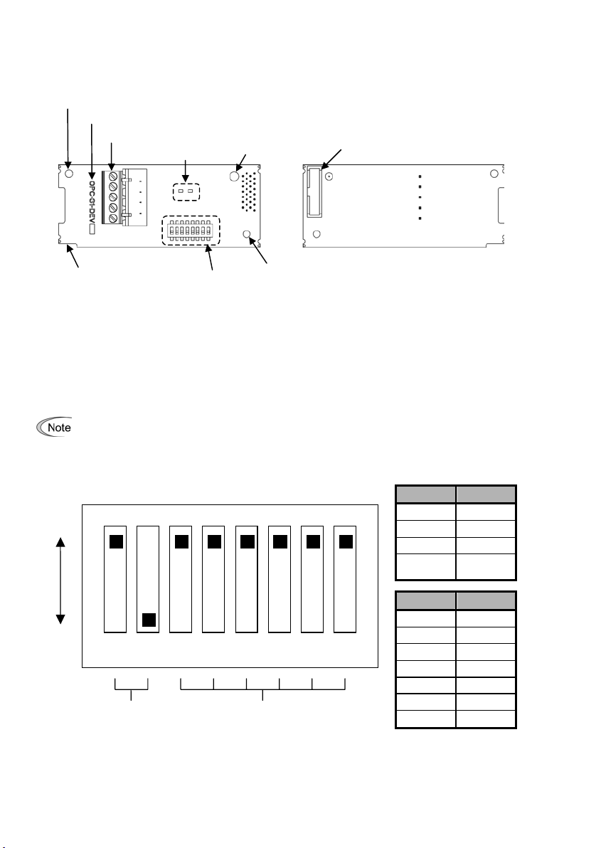
Figure 2.1 shows the names of the parts on the DeviceNet communications card.
Screw hole (left)
(Front) (Back)
2.2 DIP Switch
The DIP switch specifies the communication data rate (baud rate) and the node address (MAC ID) on DeviceNet.
It offers a choice of three baud rates (125 kbps, 250 kbps, and 500 kbps) and a choice of node address (MAC
ID) ranging from 0 to 63.
The default configuration of the DIP switch at factory shipment is: Data rate = 500 kbps, Node address = 63.
Model name
DeviceNet terminal block
LED status indicators
Positioning cutout
Figure 2.1 Names of Parts on DeviceNet Communications Card (OPC-G1-DEV)
DIP switch (SW1)
Release knob
Screw hole (right)
CN1
Before accessing the DIP switch, make sure that the inverter is turned OFF.
DR (bps) DIP 1-2
125K 00
ON
OFF
1 2 3 4 5 6 7 8
Data Rate (DR) Node Address (NA)
Figure 2.2 DIP Switch Configuration (showing an example of Data rate = 500 kbps and Node address = 63)
250K 01
500K 10
Not
allowed
NA DIP 3-8
0 000000
1 000001
2 000010
3 000011
… …
62 111110
63 111111
11
6
2.3 LED Status Indicators
The communications card has two LED status indicators shown below. They indicate the status of the
communications card.
- MS (Module Status)
Indicates the hardware status of the DeviceNet communications card.
- NS (Network Status)
Indicates the communication status on DeviceNet.
The tables below show the states of the LEDs and their meanings.
Table 2.1 MS LED state
MS LED Stat us Meaning Note
Blinks between
green and red*
Self-diagnostic test
1
OFF Power OFF Powered OFF The inverter issues
Running self-diagnostic test
upon power-on
This test takes 1 second.
er4
Lights in green Hardware normal Hardware working normally –
Lights in red
Hardware error
Communications card not
properly mounted or
hardware failure
The inverter issues
er4
Table 2.2 NS LED state
NS LED Stat us Meaning Note
Blinks between
green and red*
Self-diagnostic test
1
Running self-diagnostic test
upon power-on
This test takes 1 second.
OFF Offline DeviceNet being offline –
DeviceNet cabling correct and
Blinks in green
Lights in green
Blinks in red
Lights in red
1
Blinks in the pattern specified in the DeviceNet specifications.
*
2
*
er5
cannot be reset until the NS LED comes to stay on in green. A setting for ignoring
a connection error is detected. For details, refer to Chapter 9 "INVERTER REACTION TO DeviceNet
COMMUNICATIONS ERRORS."
Online
Connection established
Connection timeout
Connection error
communications card not
communicating on the
DeviceNet network
Communications card
communicating normally on
the DeviceNet network
Connection timeout between
the communications card and
the master
- Too short communication
cycle time
Improper DeviceNet cabling,
or improper settings
- Node address double
assigned
- Data rate mismatch
- Bus-off state detected
- Power supply cable for the
DeviceNet unconnected
- Improper wiring for the
DeviceNet terminal block
Waiting for a request from
the master
–
The inverter issues
The inverter issues
er5
is also available even if
er5
er5
2.4 DeviceNet Terminal Block
The DeviceNet terminal block is used to connect the DeviceNet cable.
For details, refer to Chapter 4 "WIRING AND CABLING."
.
.
ENGLISH
*2
*2
7
Chapter 3 INSTALLATION AND REMOVAL OF THE COMMUNICATIONS CARD
Before starting installation and wiring, turn OFF the power and wait at least five minutes for inverters with a
capacity of 22 kW or below, or at least ten minutes for inverters with a capacity of 30 kW or above. Make
sure that the LED monitor and charging lamp are turned OFF. Further, make sure, using a multimeter or a
similar instrument, that the DC link bus voltage between the terminals P(+) and N(-) has dropped to the safe
level (+25 VDC or below).
Otherwise, an electric shock could occur.
• Do not use the product that is damaged or lacking parts.
Doing so could cause a fire, an accident, or injuries.
• Prevent lint, paper fibers, sawdust, dust, metallic chips, or other foreign materials from getting into
the inverter and the communications card.
Otherwise, a fire or an accident might result.
• Incorrect handling in installation/removal jobs could cause a failure.
A failure might result.
3.1 Installing the Communications Card
Before mounting the communications card, perform the wiring for the main circuit terminals and
control circuit terminals.
(1) Remove the front cover from the inverter and expose the control printed circuit board (control PCB). As
shown in Figure 3.1, the communications card can be connected to any one of the three option connection
ports (A-, B-, and C-ports) on the inverter.
To remove the front cover, refer to the FRENIC-MEGA Instruction Manual, Chapter 2, Section 2.3.
For inverters with a capacity of 30 kW or above, open also the keypad enclosure.
(2) Insert connector CN1 on the back of the communications card (Figure 2.1) into any of the A-port (CN4),
B-port (CN5), and C-port (CN6) on the inverter's control PCB. Then tighten the two screws that come with
the card. (Figure 3.3)
Check that the positioning cutout (shown in Figure 2.1) is fitted on the tab ( in Figure 3.2) and
connector CN1 is fully inserted ( in Figure 3.2). Figure 3.3 shows the communications card
correctly mounted.
(3) Perform wiring on the communications card.
For details, refer to Chapter 4 "WIRING AND CABLING."
(4) Put the front cover back into place.
To put back the front cover, refer to the FRENIC-MEGA Instruction Manual, Chapter 2, Section 2.3.
For inverters with a capacity of 30 kW or above, close also the keypad enclosure.
8
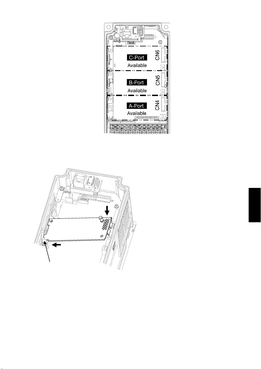
Figure 3.1 In the case of 0.4 kW
Fit the positioning cutout of the
communications card over the tab on the
inverter to determine the mounting position.
Insert connector CN1 on the communications
card into the corresponding port on the
inverter's control PCB.
Note: Be sure to follow the order of and .
Inserting CN1 first may lead to
insufficient insertion, resulting in a
contact failure.
ENGLISH
Tab
Figure 3.2 Mounting the Communications Card (to B-port)
9
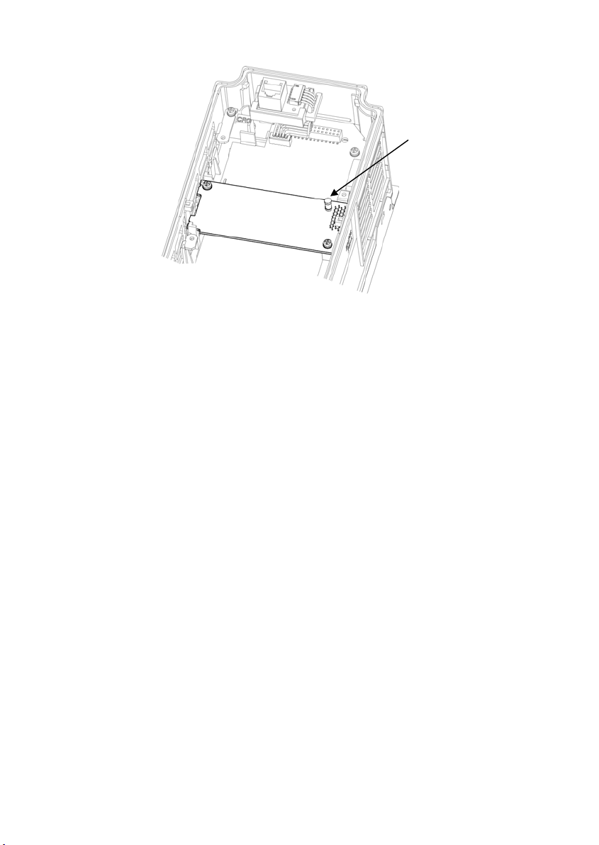
(Release knob)
Figure 3.3 Mounting Completed (on B-port)
3.2 Removing the Communications Card
Remove the two screws that secure the communications card and pull the release knob (shown above) to take
the communications card out of the inverter.
10
Chapter 4 WIRING AND CABLING
• Before starting installation and wiring, turn OFF the power and wait at least five minutes for inverters with
a capacity of 22 kW or below, or at least ten minutes for inverters with a capacity of 30 kW or above.
Make sure that the LED monitor and charging lamp are turned OFF. Further, make sure, using a
multimeter or a similar instrument, that the DC link bus voltage between the terminals P(+) and N(-) has
dropped to the safe level (+25 VDC or below).
• Qualified electricians should carry out wiring.
Otherwise, an electric shock could occur.
• In general, the covers of the control signal wires are not specifically designed to withstand a high voltage
(i.e., reinforced insulation is not applied). Therefore, if a control signal wire comes into direct contact with
a live conductor of the main circuit, the insulation of the cover might break down, which would expose the
signal wire to a high voltage of the main circuit. Make sure that the control signal wires will not come into
contact with live conductors of the main circuit.
Failure to observe this precaution could cause an electric shock or an accident.
Noise may be emitted from the inverter, motor and wires. Take appropriate measures to prevent the nearby
sensors and devices from malfunctioning due to such noise.
An accident could occur.
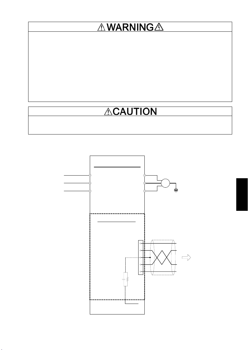
4.1 Basic Connection Diagram
FRENIC-MEGA
L1/R
L2/S
L3/T
U
V
W
Motor
M
G
OPC-G1-DEV
DeviceNet
terminal block
V-
CAN L
Shield
CAN H
V+
* Mounting the communications card connects to the grounding zG.
Figure 4.1 Basic Connection Diagram
11
z
*
G
DeviceNet cable
To
DeviceNet
ENGLISH
約
A
4.2 Wiring for DeviceNet Terminal Block
(1) To connect the communications card to DeviceNet, use a DeviceNet thin cable complying with the
DeviceNet specifications. Also observe the wiring lengths specified in the DeviceNet specifications.
The recommended DeviceNet cable is TDN24U made by SWCC Showa Device Technology, Co.,
Ltd.
Proper installation of the cable requires specialist knowledge. Be sure to refer to the DeviceNet
specifications or DeviceNet construction manual (both are published by ODVA) beforehand.
(2) Wiring around the DeviceNet terminal block (TERM1)
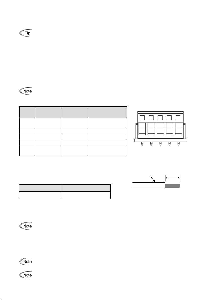
The terminal block uses a pluggable 5-pin connector as shown in Figure 4.2. It has five labels
corresponding to the five pins. Each label has an ID color corresponding to the wire (core) to be connected
to its pin. Make sure that the ID colors of the wires and labels match. Table 4.1 shows the correspondence
between the pin numbers and the ID colors.
A typical connector that matches this terminal block is Phoenix Contact MSTB 2.5/5-ST-5.08 AU.
The Phoenix Contact TMSTBP 2.5/5-ST-5.08 AU and TFKC 2.5/5-STF-5.08 AU (spring-cage
connection type) connectors for multidrop connection cannot be used.
Table 4.2 lists the recommended terminal screw size and its tightening torque, and Figure 4.3 shows the
recommended strip length of the cable wire end.
Table 4.2 Recommended Tightening Torque of the
(3) Terminating resistor
DeviceNet requires a terminating resistor to be installed externally on each end of the trunk line. Check that
the trunk line is terminated on both ends; if not, install a terminating resistor(s) on the missing end(s).
4.3 Wiring to Inverter
Table 4.1 Pin Layout on DeviceNet Terminal Block
Pin #
ID Color of
Wire Sheath
1 Black V- Power supply
Pin
Assignment
Description
(24 VDC, - side)
1 2 3 4 5
2 Blue CANL Signal line (- side)
3 Metallic SD Cable shield
4 White CANH Signal line (+ side)
5 Red V+ Power supply
Terminal Screws for the DeviceNet Terminal Block
Terminal screw size
M3 0.5 to 0.6 N·m
Terminating resistors do not come with the communications card. A pair of resistors with the
following specifications is separately necessary.
Tightening torque
(24 VDC, + side)
Figure 4.2 Connectors on the
Figure 4.3 Recommended Strip Length
DeviceNet Terminal Block
電線Cable wire
of the Cable Wire End for
Terminal Connection
121 ohm ±1%, 1/4 watt, metal-film resistor
Route the wiring of the DeviceNet cable as far from the wiring of the main circuit as possible.
Otherwise electric noise may cause malfunctions.
Route the wires, taking care not to let them go over the control PCB, as shown in Figure 4.4.
Otherwise, malfunctions may occur.
pprox.
6mm
6.0 mm
12
 Loading...