

Page 1
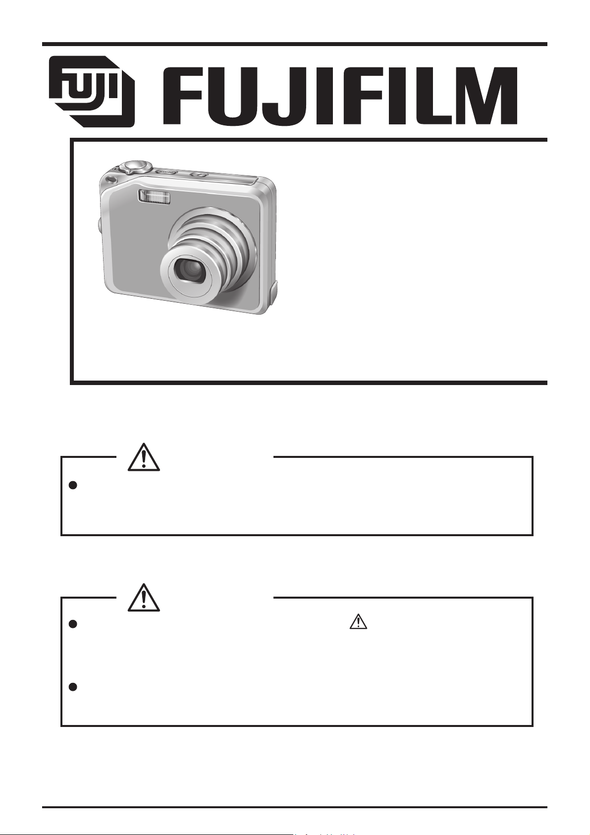
DIGITAL CAMERA
FinePix V10
TROUBLESHOOTING GUIDE
CAUTION
BECAUSE THIS PRODUCTIS RoHS LEAD-FREE COMPLIANT, USE THE
DESIGNATED AFTER-SELES PARTS AND THE DESIGNATED LEAD-FREE SOLDER
WHEN PERFORMING REPAIRS. (Refer to page 3 to page 5)
WARNING
THE COMPONENTS IDENTIFIED WITH THE MARK “ ” ON THE SCHEMATIC
DIAGRAM AND IN THE PARTS LIST ARE CRITICAL FOR SAFETY.
PLEASE REPLACE ONLY WITH THE COMPONENTS SPECIFIED ON THE SCHEMATIC
DIAGRAM AND IN THE PARTS LIST.
IF YOU USE PARTS NOT SPECIFIED, IT MAY RESULT IN A FIRE AND AN
ELECTRICAL SHOCK.
FUJI PHOTO FILM CO., LTD.
Ref.No.:ZM00621-400
Printed in Japan 2006.03
Page 2
FinePix V10 TROUBLESHOOTING GUIDE
SAFETY CHECK-OUT
After correcting the original problem, perform the following
safety check before return the product to the customer.
1. Check the area of your repair for unsoldered or poorly
soldered connections. Check the entire board surface
for solder splasher and bridges.
2. Check the interboard wiring to ensure that no wires are
“pinched” or contact high-wattage resistors.
3. Look for unauthorized replacement parts, particularly
transistors, that were installed during a previous repair.
Point them out to the customer and recommend their
replacement.
4. Look for parts which, though functioning, show obvious
signs of deterioration. Point them out to the customer
and recommend their replacement.
5. Check the B + voltage to see it is at the values
specified.
6. Make leakage - current measurements to determine
that exposed parts are acceptably insulated from the
supply circuit before returning the product to the
customer.
7. CAUTION: FOR CONTINUED
PROTECTION AGAINST FIRE
HAZARD, REPLACE ONLY WITH
SAME TYPE 2.5 AMPERES 125V
FUSE.
2.5A 125V
2.5A 125V
8. WARNING:
RISK OF FIREREPLACE FUSE
AS MARKED
ATTENTION: AFIN D'ASSURER
UNE PROTECTION
PERMANENTE CONTRE LES
RISQUES D'INCENDIE,
REMPLACER UNIQUEMENT
PAR UN FUSIBLE DE MEME,
TYPE 2.5 AMPERES, 125 VOLTS.
TO REDUCE THE ELECTRIC
SHOCK, BE CAREFUL TO
TOUCH THE PARTS.
WARNING!
HIGH VOLTAGE
2
Page 3

FinePix V10 TROUBLESHOOTING GUIDE
RoHS lead-free compliance
Because this product is RoHS lead-free compliant, use the designated after-sales parts and the designated lead-free solder
when performing repairs.
<Background & Overview>
With the exception of parts and materials expressly excluded from the RoHS directive (*1), all the internal connections and
component parts and materials used in this product are lead-free compliant (*2) under the European RoHS directive.
*1: Excluded items (list of the main lead-related items)
• Lead included in glass used in fluorescent tubes, electronic components and cathode-ray tubes
• Lead in high-melting-point solder (i.e. tin-lead solder alloys that contain 85% lead or more)
• Lead in ceramic electronic parts (piezo-electronic devices)
• Mercury contained in fluorescent tubes is also excluded.
*2: Definition of lead-free
A lead content ratio of 0.1 wt% or less in the applicable locations (solder, terminals, electronic components, etc.)
<Reference>
RoHS: The name of a directive issued by the European Parliament aimed at restricting the use of
certain designated hazardous substances included in electrical and electronic equipment.
Designated substances (6): Lead, mercury, cadmium, hexavalent chromium, polybrominated biphenyls (PBBs) and
polybrominated diphenyl ether (PBDE)
<Lead-free soldering>
When carrying out repairs, use a designated lead-free solder, bearing in mind the differing work practices for conventional
solder (eutectic) and lead-free solder.
Differences in the soldering work for lead-free and eutectic solder
When the soldering work practices for eutectic solder and lead-free solder are compared, the main differences are as shown
below. In particular, when lead-free solder is used, the solder tends to be less workable than when eutectic solder is used.
Accordingly, the soldering techniques used must take that into account.
Difference
The solder starts melting later.
1
Poor wetting
2
Solder feed rate is difficult to control.
3
Wetting the insides of through holes is especially
4
difficult.
5
During repairs (or modifications) removing solder
from inside through holes is difficult.
6
There is serious carbonization of the soldering iron.
The surface is not glossy.
7
The initial melting point of lead-free solder is high, so you
have to get used to it.
Move the tip of the soldering iron around to heat the entire
connection to the melting temperature and assist wetting.
Use the solder (wire) diameter and soldering iron that are
best suited to connection being soldered.
First apply solder to the area immediately around the
through hold and then feed the solder into the hole.
Use a suitable wicking wire (with a suitable method and
heating) and a suction tool.
Either put solder onto the soldering iron tip after completing
the work, or turn the iron off frequently.
Learn to recognize the appearance of the surface.
Countermeasure
3
Page 4

FinePix V10 TROUBLESHOOTING GUIDE
Setting temperature during lead-free soldering
• Lead-free solder melting temperature
The melting point of eutectic (Sn-Pb) solder is 183°C, while the melting point of lead-free solder (Sn-Ag-Cu) is 30°C higher
at 220°C.
• Soldering iron tip temperature
The temperature setting for the soldering iron used should be such that the tip of the soldering iron is at the correct
bonding temperature for the connection. This temperature is normally set at around 100°C higher than the melting point of
the solder.
However, the actual temperature should take into account the shape and size of the soldering iron tip, the heat tolerance
of the connection and the workability of that temperature.
• Correct bonding temperature
The correct bonding temperature refers not to the temperature of the heat source, but to the bonding temperature that will
give the best bond strength.
Precautions when soldering with lead-free solder
• Soldering iron maintenance
Because of the high soldering iron temperature in lead-free soldering, there is rapid carbonization of the flux adhering to
the tip of the soldering iron.
(1) Always cover the tip of the soldering iron with solder when it is not being used.
(2) If the tip is black from carbonization, wipe it gently with a paper towel soaked in alcohol until the solder will wet.
• Uniform heating of the board and components
To ensure that the lead-free solder wets the entire surface of the pattern and the lands despite its poor wetting
characteristics, you must move the tip of the soldering iron over a wide area to raise the temperature of the entire
connection.
Soldering iron
A soldering iron with a temperature control is best.
4
Page 5
FinePix V10 TROUBLESHOOTING GUIDE
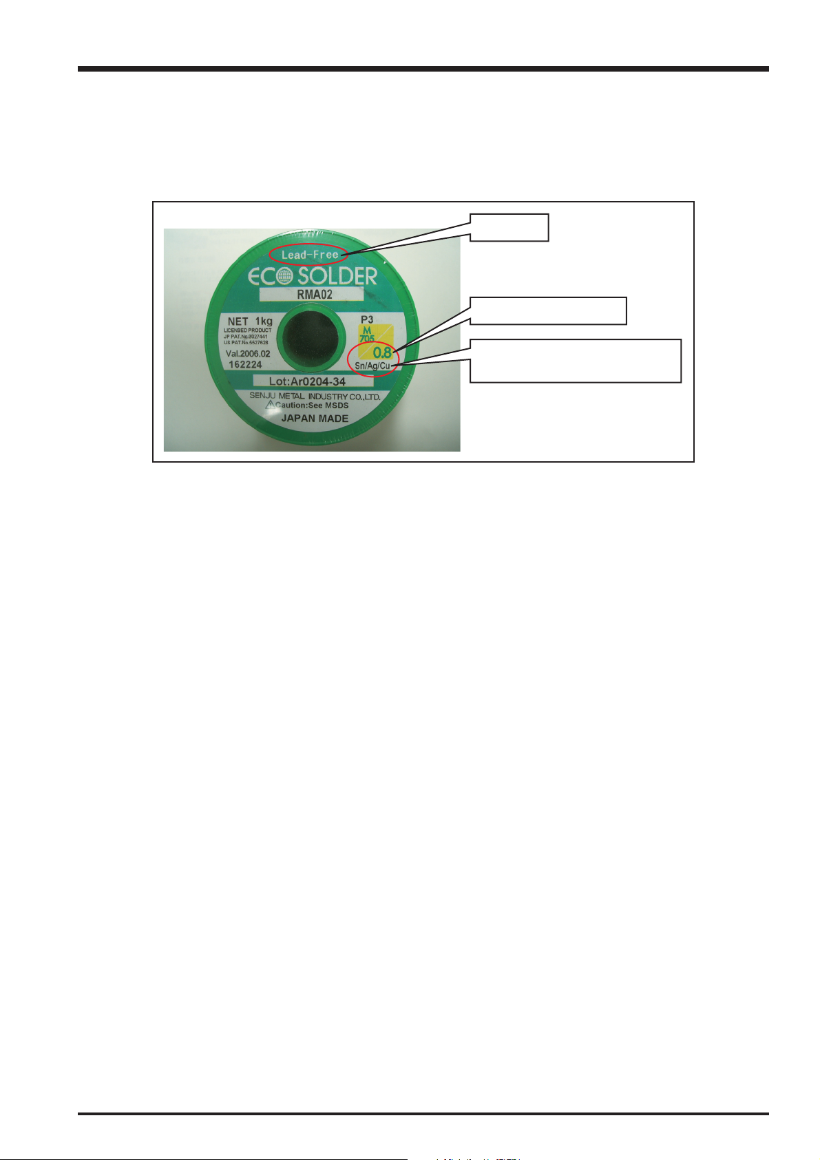
Solder wire (thread)
Use the lead-free solders specified below.
Solder type: Sn96.5Ag3Cu0.5 (Displayed symbol: SnAgCu)
Wire diameter: 0.6, 0.8 or 1.0 mm
Sample:
lead-free
Wire diameter 0.8mm
Solder type (Displayed symbol)
SnAgCu
Flux
Conventional flux can be used.
Solder application wires (mesh, wicking wire, etc.)
Conventional application wires can be used.
5
Page 6

MEMO
FinePix V10 TROUBLESHOOTING GUIDE
6
Page 7

FinePix V10 TROUBLESHOOTING GUIDE
CONTENTS
CONTENTS
1. Names of internal Components .................................................................................. 8
2. Overall connection Diagram........................................................................................ 9
3. Mounted Parts Diagrams (MAIN PWB ASSY) .......................................................... 10
4. Mounted Parts Diagrams (SUB PWB ASSY) ............................................................ 11
5. Information on problems identified in production during inspection.......................... 13
6. Information on problems arising in production during adjustment ............................ 17
7
Page 8

FinePix V10 TROUBLESHOOTING GUIDE
1. Names of internal Components
R PANEL CONST
SUB PWB ASSY
F PANEL CONST
FLASH CONST
MIC ASSY
MAIN PWB ASSY
LENS ASSY
SPEAKER ASSY
BOTTOM CASE CONST
8
Page 9

FinePix V10 TROUBLESHOOTING GUIDE
2. Overall connection Diagram
9
Page 10

3. Mounted Parts Diagrams (MAIN PWB ASSY)
A
B
FinePix V10 TROUBLESHOOTING GUIDE
C
D
E
10
F
1
23456789
Page 11

FinePix V10 TROUBLESHOOTING GUIDE
A
B
4. Mounted Parts Diagrams (SUB PWB ASSY)
C
D
E
1
23456789
11
Page 12

MEMO
FinePix V10 TROUBLESHOOTING GUIDE
12
Page 13

FinePix V10 TROUBLESHOOTING GUIDE
5. Information on problems identified in production
during inspection
Main category Problem details Cause
LCD
Sounds/Beeps
LCD image white.
LCD image white.
LCD image white.
LCD image white.
LCD image (solarized).
LCD image too dark.
LCD image not displayed.
LCD image not displayed.
Vertical lines on the LCD.
LCD backlight fails to light.
Bright points on the LCD.
W BEEP does not sound.
W BEEP does not sound.
W BEEP does not sound.
W BEEP does not sound.
W BEEP does not sound.
No movie sound.
No movie sound.
Cannot record sound.
MAIN PWB R209 (LCDCLK) soldering defect.
Solder bridging in MAIN
PWB Q303.
SUB PWB R454 dislodged.
SUB PWB CN451 inserted
at an angle.
MAIN PWB FB205
soldering defect.
Part defective.
SUB PWB IC602 defective.
SUB PWB CN801
soldering defect.
Part defective.
Part defective.
Part defective.
MAIN PWB IC205 part
defective.
SUB PWB IC701 part
defective.
Speaker part defective.
SUB PWB CN702 not
inserted fully.
Connection error between
SUB PWB CN701 and
CN702.
MAIN PWB IC205 part
defective.
MAIN PWB CN551
damaged.
Microphone part defective.
Repair location ref. no
M221: Resolder the
MAIN PWB R209.
M221: Resolder the
MAIN PWB Q303.
M226: Re-fit the
SUB PWB R454.
M226: Re-insert the
SUB PWB CN451.
M221: Resolder the
MAIN PWB FB205.
M304: Replace the
LCD CONST.
M226: Replace the SUB PWB.
M226: Resolder the
SUB PWB CN801.
M304: Replace the
LCD CONST.
M304: Replace the
LCD CONST.
M304: Replace the
LCD CONST.
M221: Replace the MAIN PWB.
M226: Replace the SUB PWB.
M217: Replace the SPEAKER.
M226: Re-insert the
SUB PWB CN702.
M226: Re-insert SUB PWB
CN701 and CN702.
M221: Replace the MAIN PWB.
M221: Replace the
MAIN PWB CN551.
M216: Replace the MIC.
PWB
diagram
B-8
B-3
C-1
---
C-8
---
---
B-2
---
---
---
---
---
---
E-2
E-2
---
B-7
---
13
Page 14

FinePix V10 TROUBLESHOOTING GUIDE
Main category Problem details Cause
Image quality
Functions
Operation
Black smearing on the
CCD.
Live image quality coarse.
Live image quality defective
(reddish).
Live image quality defective
(solarized).
Live image quality defective
(appears pink).
Vertical lines on the live
image.
Horizontal lines on the live
image.
Resolution blurred or
shifted.
Quality problems in
recorded images.
LED lighting defect.
LED lighting defect
(self-timer).
No TV monitor output.
No TV monitor output.
USB communication fails.
USB communication fails.
USB communication fails.
USB communication fails
(red LED does not light).
Battery fails to lock.
Read error.
Battery difficult to load.
Shutter button operation
defect.
Mode switch setting cannot
be changed.
Mode switch setting cannot
be changed.
Mode switch setting cannot
be changed.
Soiling on the CCD
surface.
SUB PWB CN451 inserted
incompletely or at an angle.
MAIN PWB CN551
damaged.
SUB PWB IC602 defective.
Part defective.
Part defective.
Part defective.
Part defective.
Part defective.
Assembly error.
MAIN PWB IC205 part
defective.
Soldering defect in MAIN
PWB CN151 or FB151.
MAIN PWB C221 soldering
defect.
MAIN PWB IC205 part
defective.
MAIN PWB FB151
soldering defect.
MAIN PWB CN151
soldering defect.
MAIN PWB D407 soldering
defect.
Part defective.
Card connector soldering
defect.
Assembly error.
Part defective.
Switch defective (SW201).
Switch defective (SW202).
Part defective.
Repair location ref. no
M227: Replace the LENS ASSY.
M226: Re-insert the
SUB PWB CN451.
M221: Replace the
MAIN PWB CN551.
M226: Replace the SUB PWB.
M227: Replace the LENS ASSY.
M227: Replace the LENS ASSY.
M227: Replace the LENS ASSY.
M227: Replace the LENS ASSY.
M227: Replace the LENS ASSY.
M221: Re-assemble the
MAIN PWB.
M221: Replace the MAIN PWB.
M221: Resolder the MAIN PWB
CN151 or FB151.
M221: Resolder the
MAIN PWB C221.
M221: Replace the MAIN PWB.
M221: Resolder the
MAIN PWB FB151.
M221: Resolder the
MAIN PWB CN151.
M221: Resolder the
MAIN PWB D405.
M209: Replace the
BATTERY LOCK.
M221: Resolder the
MAIN PWB CN251.
M210: Re-assemble the
BATTERY FRAME.
M227: Replace the LENS ASSY.
M212: Replace the
RELEASE KEY UNIT.
M212: Replace the
RELEASE KEY UNIT.
M212: Replace the
RELEASE KEY UNIT.
PWB
diagram
---
C-8
B-7
---
---
---
---
---
---
---
---
A-8
C-8
---
A-8
A-8
C-7
---
B-1
---
---
---
---
---
14
Page 15

FinePix V10 TROUBLESHOOTING GUIDE
Main category Problem details Cause
Power supply
Camera will not turn on in
Camera mode.
Camera power cuts out.
Camera power cuts out
(current: 0.84 A).
The camera does not turn
on.
The camera does not turn
on.
The camera does not turn on
(no USB communication).
The camera does not turn on
(no USB communication).
The camera does not turn
on (current: 0 A).
The camera does not turn
on (current: 0 A).
The camera does not turn
on (current: 0 A).
The camera does not turn
on (current: 0 A).
The camera does not turn
on (current: 0 A).
The camera does not turn
on (current: 0 A).
The camera does not turn
on (current: 0 A).
The camera does not turn
on (current: 0 A).
The camera does not turn
on (current: 0 A).
Battery charge depletion
defect.
Operation freezes.
The camera does not turn
on (0.19 A current flows
continuously).
The camera does not turn
on (current short-circuits).
The camera does not turn
on (current short-circuits).
The camera does not turn
on under battery power.
The camera does not turn
on under battery power.
SUB PWB CN751 inserted
incompletely or at an angle.
Camera assembly error.
MAIN PWB part defective.
MAIN PWB D154
damaged.
Wire breakage in the MAIN
PWB F304.
MAIN PWB IC205 part
defective.
MAIN PWB CN151
soldering defect.
MAIN PWB X201 part
defective.
MAIN PWB F152 soldering
defect or wire breakage.
MAIN PWB FB154
soldering defect.
MAIN PWB CN551
soldering defect.
Assembly error.
Assembly error.
MAIN PWB X401 part
defective.
SUB PWB CN751 inserted
incompletely or at an angle.
Wire breakage in MAIN
PWB F351.
Part defective.
MAIN PWB IC206 part
defective.
MAIN PWB IC204 part
defective.
MAIN PWB part defective.
Solder short-circuit in the
MAIN PWB R341-C522.
BATTERY FRAME
assembly error.
MAIN PWB assembly error.
Repair location ref. no
M226: Re-insert
SUB PWB CN751.
Completely disassemble and
then re-assemble.
M221: Replace the MAIN PWB.
M221: Replace the
MAIN PWB D154.
M221: Replace the
MAIN PWB F304.
M221: Replace the MAIN PWB.
M221: Resolder the
MAIN PWB CN151.
M221: Replace the
MAIN PWB X201.
M221: Resolder or replace the
MAIN PWB F152.
M221: Resolder the
MAIN PWB FB154.
M221: Resolder the
MAIN PWB CN551.
M217: Re-assemble the
SPEAKER.
M216: Re-assemble the MIC.
M221: Replace the
MAIN PWB X401.
M226: Re-insert the
SUB PWB CN751.
M221: Replace the
MAIN PWB F351.
M227: Replace the LENS ASSY.
M222: Replace the MAIN PWB.
M221: Replace the MAIN PWB.
M221: Replace the MAIN PWB.
M221: Resolder the
MAIN PWB R341-C522.
M210: Re-assemble the
BATTERY FRAME.
M221: Re-assemble the
MAIN PWB.
PWB
diagram
A-7
---
---
A-8
B-2
---
A-8
C-8
E-1
F-9
B-7
---
---
C-8
A-7
A-7
---
---
---
---
B-4
---
---
15
Page 16

FinePix V10 TROUBLESHOOTING GUIDE
Main category Problem details Cause
Lens
Shutter operation defect.
Zoom error.
Zoom error.
Abnormal noise during
zoom operation.
Focusing error.
Focusing error.
Lens barrier operation
defect (lower side fails to
open).
Lens barrier operation
defect (fails to open).
Part defective.
MAIN PWB CN551
damaged.
Part defective.
Part defective.
Part defective.
SUB PWB IC602 defective.
Part defective.
Part defective.
Repair location ref. no
M227: Replace the LENS ASSY.
M221: Replace the
MAIN PWB CN551.
M227: Replace the LENS ASSY.
M227: Replace the LENS ASSY.
M227: Replace the LENS ASSY.
M226: Replace the SUB PWB.
M227: Replace the LENS ASSY.
M227: Replace the LENS ASSY.
PWB
diagram
---
B-7
---
---
---
---
---
---
16
Page 17

FinePix V10 TROUBLESHOOTING GUIDE
6. Information on problems arising in production during
adjustment
Adjustment Problem details Cause
AF Adj.
CAM Adj.
STEP655 (ZBL error)
STEP660 (ZRP error)
STEP802 (AF search NG)
STEP806
(AF peak detect NG)
STEP1643
(Sensitivity OFD G NG)
STEP1644
(Sensitivity OFD R/G NG)
STEP1644
(Sensitivity OFD R/G NG)
STEP1645
(Sensitivity OFD B/G NG)
STEP1713 (WB-Hi[no] NG)
STEP307
(Shutter ADJ [OPEN] NG)
STEP3100
(Zoom Control NG)
STEP331 (Smear [S] NG
(h0180~h0300))
STEP331 (Smear [S] NG
(h0180~h0300))
STEP337 (Measure [E] NG
(h0400~h2000))
STEP337 (Measure [E] NG
(h0400~h2000))
STEP337 (Measure [E] NG
(h0400~h2000))
STEP337 (Measure [E] NG
(h0400~h2000))
STEP337 (Measure [E] NG
(h0400~h2000))
STEP337 (Measure [E] NG
(h0400~h2000))
STEP339 (Value [B] NG
(h0180~h0300))
STEP339 (Value [B] NG
(h0180~h0300))
STEP342 (Shutter ADJ
[small aperture] NG)
STEP3884
(delta C NG POS:1)
STEP3884
(delta C NG POS:1)
STEP3885
(color NG POS:1)
STEP3888
(delta C NG POS:5)
Lens-related.
Lens-related.
Lens-related.
Lens-related.
SUB PWB IC602 defective.
SUB PWB IC602 defective.
Lens-related.
Lens-related.
Lens-related.
SUB PWB IC602 defective.
Lens-related.
SUB PWB IC602 defective.
Lens-related.
Solder bridging in the MAIN
PWB CN551.
MAIN PWB CN551
damaged.
SUB PWB CN601 not
locked or incompletely
locked.
SUB PWB FB601 soldering
defect.
SUB PWB IC602 defective.
Lens-related.
SUB PWB assembly error.
Lens-related.
SUB PWB R651 damaged.
SUB PWB IC602 defective.
Lens-related.
Lens-related.
Lens-related.
Repair location ref. no
M227: Replace the LENS ASSY.
M227: Replace the LENS ASSY.
M227: Replace the LENS ASSY.
M227: Replace the LENS ASSY.
M226: Replace the SUB PWB.
M226: Replace the SUB PWB.
M228: Replace the LENS ASSY.
M228: Replace the LENS ASSY.
M228: Replace the LENS ASSY.
M226: Replace the SUB PWB.
M228: Replace the LENS ASSY.
M226: Replace the SUB PWB.
M228: Replace the LENS ASSY.
M221: Repair the solder on the
MAIN PWB CN551.
M221: Replace the
MAIN PWB CN551.
M226: Re-insert the
SUB PWB CN601.
M226: Resolder the
SUB PWB FB601.
M226: Replace the SUB PWB.
M228: Replace the LENS ASSY.
Re-assemble the SUB PWB.
M228: Replace the LENS ASSY.
M226: Replace the
SUB PWB R651.
M226: Replace the SUB PWB.
M228: Replace the LENS ASSY.
M228: Replace the LENS ASSY.
M227: Replace the LENS ASSY.
PWB
diagram
---
---
---
---
---
---
---
---
---
---
---
---
---
B-7
B-7
C-7
D-4
---
---
---
---
D-3
---
---
---
---
17
Page 18

FinePix V10 TROUBLESHOOTING GUIDE
Adjustment Problem details Cause
CAM Adj.
CCD Data
Input
CCD L.D. Adj.
STEP411
(ISO sensitivity adjustment
NG (h014F~h021D))
STEP411 (ISO sensitivity
adjustment NG
(h014F~h021D))
STEP453 (WB[LB145]
adjustment NG)
STEP252 (OFD adjustment
NG (GreenLine))
STEP252 (OFD adjustment
NG (GreenLine))
STEP252 (OFD adjustment
NG (GreenLine))
STEP252 (OFD adjustment
NG (GreenLine))
STEP252 (OFD adjustment
NG (GreenLine))
STEP252 (OFD adjustment
NG (GreenLine))
STEP252 (OFD adjustment
NG (GreenLine))
STEP252 (OFD adjustment
NG (GreenLine))
STEP252 (OFD adjustment
NG (GreenLine))
STEP252 (OFD adjustment
NG (GreenLine))
STEP252 (OFD adjustment
NG (GreenLine))
STEP255
(REC OFD Adjustment NG)
STEP255
(REC OFD Adjustment NG)
STEP255
(REC OFD Adjustment NG)
STEP265
(MV OFD adjustment NG)
STEP4562 (Line defect
data NG (h00~h40)
STEP4562 (Line defect
data NG (h00~h40)
STEP4562 (Line defect
data NG (h00~h40)
STEP4562 (Line defect
data NG (h00~h40)
STEP4652
(Noise inspection NG)
SUB PWB IC602 defective.
Lens-related.
Lens-related.
MAIN PWB CN551 not
inserted fully.
MAIN PWB CN551
soldering defect.
SUB PWB CN601 not
locked or incompletely
locked.
SUB PWB CN601 not
inserted fully.
Wire breakage in MAIN
PWB F304.
MAIN PWB FB201
damaged.
MAIN PWB IC205 part
defective.
SUB PWB IC602 defective.
MIC assembly error.
SUB PWB R626 damaged.
Lens-related.
Solder bridging in the MAIN
PWB CN551.
SUB PWB D602 damaged.
Lens-related.
Lens-related.
SUB PWB CN601 inserted
at an angle.
MAIN PWB CN551
damaged.
SUB PWB IC602 defective.
Lens-related.
Lens-related.
Repair location ref. no
M226: Replace the SUB PWB.
M227: Replace the LENS ASSY.
M227: Replace the LENS ASSY.
M221: Re-insert the
MAIN PWB CN551.
M221: Repair the solder on
MAIN PWB CN551.
M226: Re-insert the
SUB PWB CN601.
M221: Re-insert the
MAIN PWB CN601.
M221: Replace the
MAIN PWB F304.
M221: Replace the
MAIN PWB FB201.
M221: Replace the MAIN PWB.
M226: Replace the SUB PWB.
M216 Re-assemble the MIC.
M226: Replace the
SUB PWB R626.
M228: Replace the LENS ASSY.
M221: Repair the solder on the
MAIN PWB CN551.
M226: Replace the
SUB PWB D602.
M228: Replace the LENS ASSY.
M228: Replace the LENS ASSY.
M226: Re-insert the
SUB PWB CN601.
M221: Replace the
MAIN PWB CN551.
M226: Replace the SUB PWB.
M227: Replace the LENS ASSY.
M227: Replace the LENS ASSY.
PWB
diagram
---
---
---
B-7
B-7
C-7
E-7
B-2
A-7
---
---
---
C-6
---
B-7
D-4
---
---
C-7
B-7
---
---
---
18
Page 19

FinePix V10 TROUBLESHOOTING GUIDE
Adjustment Problem details Cause
Flash Adj. STEP1240
(Flash CHARGE 1 NG)
STEP1240
(Flash CHARGE 1 NG)
STEP1240
(Flash CHARGE 1 NG)
STEP1241
(Flash luminescence 1 NG)
STEP1241
(Flash luminescence 1 NG)
STEP1241
(Flash luminescence 1 NG)
STEP1241
(Flash luminescence 1 NG)
STEP1241
(Flash luminescence 1 NG)
STEP1241
(Flash luminescence 1 NG)
STEP1241
(Flash luminescence 1 NG)
STEP1241
(Flash luminescence 1 NG)
STEP1243
(Flash luminescence 2 NG)
STEP1245
(Flash luminescence 3 NG)
STEP1245
(Flash luminescence 3 NG)
STEP1249
(Flash luminescence 5 NG)
STEP1251
(Flash luminescence 6 NG)
STEP1253 (Flash
luminescence average NG)
STEP1253 (Flash
luminescence average NG)
STEP1253 (Flash
luminescence average NG)
MAIN PWB IC205 part
defective.
MAIN PWB T401 soldering
defect.
Main capacitor polarity
reversed.
MAIN PWB IC205 part
defective.
SUB PWB IC602 defective.
Battery terminal soldering
defect.
FLASH CONST damaged.
MAIN PWB T401 part
defective.
Xenon tube defective.
Xenon tube soldering
defect.
Trigger coil damaged.
Xenon tube soldering
defect.
C852 in the FLASH
CONST damaged.
FLASH CONST damaged.
Trigger coil damaged.
FLASH CONST damaged.
FLASH CONST damaged.
Xenon tube defective.
Xenon tube soldering
defect.
Repair location ref. no
M221: Replace the MAIN PWB.
Resolder the MAIN PWB T401.
Correct the polarity and then
resolder.
M221: Replace the MAIN PWB.
M226: Replace the SUB PWB.
Resolder the battery terminals.
M218: Replace the
FLASH CONST.
MAIN PWB T401 damaged.
M219: Replace the Xe-LIGHT.
M219: Resolder the Xe-LIGHT.
M218: Replace the
FLASH CONST.
M219: Resolder the Xe-LIGHT.
Replace C852 in the
FLASH CONST.
M218: Replace the
FLASH CONST.
M218: Replace the
FLASH CONST.
M218: Replace the
FLASH CONST.
M218: Replace the
FLASH CONST.
M219: Replace the Xe-LIGHT
M219: Resolder the Xe-LIGHT.
PWB
diagram
---
---
---
---
---
B-4
---
C-6
---
---
---
---
---
---
---
---
---
---
---
19
Page 20

FinePix V10 TROUBLESHOOTING GUIDE
Adjustment Problem details Cause
Video Adj. STEP2702
(PLAY mode NG)
STEP2702
(PLAY mode NG)
STEP2702
(PLAY mode NG)
STEP2711
(NTSC BLK level NG)
STEP2711
(NTSC BLK level NG)
STEP2721
(NTSC Y gain NG)
STEP2721
(NTSC Y gain NG)
STEP2884
(PAL R HUE NG)
STEP2931
(STB Y gain NG)
STEP2931
(STB Y gain NG)
STEP2940
(STB WB R-Y NG)
MAIN PWB CN551
soldering defect.
MAIN PWB FB202
damaged.
MAIN PWB part defective.
MAIN PWB C104
damaged.
MAIN PWB X201 part
defective.
MAIN PWB C103
damaged.
MAIN PWB FB152
soldering defect.
Lens-related.
MAIN PWB IC205 part
defective.
SUB PWB IC602 defective.
SUB PWB IC602 defective.
Repair location ref. no
M221: Resolder the
MAIN PWB CN551.
M221: Replace the
MAIN PWB FB202.
M221: Replace the MAIN PWB.
M221: Replace the
MAIN PWB C104.
M221: Replace the
MAIN PWB X201.
M221: Replace the
MAIN PWB C103.
M221: Resolder the
MAIN PWB FB152.
M228: Replace the LENS ASSY.
M221: Replace the MAIN PWB.
M226: Replace the SUB PWB.
M226: Replace the SUB PWB.
PWB
diagram
---
B-7
---
D-9
C-8
C-9
A-8
---
---
---
---
20
Page 21

FUJI PHOTO FILM CO., LTD.
26-30, Nishiazabu 2-chome, Minato-ku, Tokyo 106-8620, Japan.
 Loading...