


FA5500AP/AN, FA5501AP/AN
Quality is our message
Quality is our message
Quality is our messageQuality is our message
FUJI Power Supply Control IC
Power Factor Correction
FA5500AP/AN
FA5501AP/AN
1
November `02
Fuji Electric Co., Ltd.
Matsumoto Factory

FA5500AP/AN, FA5501AP/AN
1.This Data Book contains the product specifications, characteristics, data, materials, and structures
as of November 2002. The contents are subject to change without notice for specification changes
or other reasons. When using a product listed in this Data Book, be sure to obtain the latest
specifications.
2. All applications described in this Data Book exemplify the use of Fuji's products for your reference
only. No right or license, either express or implied, under any patent, copyright, trade secret or other
intellectual property right owned by Fuji Electric Co., Ltd. is (or shall be deemed) granted. Fuji
makes no representation or warranty, whether express or implied, relating to the infringement or
alleged infringement of other's intellectual property rights which may arise from the use of the
applications descri bed herein.
3. Although Fuji Electric is enhancing product quality and reliability, a small percentage of
semiconductor products may become faulty. When using Fuji Electric semiconductor products in
your equipment, you are requested to take adequate safety measures to prevent the equipment
from causing a physical injury, fire, or other problem if any of the products become faulty. It is
recommended to make your design fail-safe, f la m e ret ardant , and free of malfunction.
4.The products introduced in this Data Book are intended for use in the following electronic and
electrical equipment w h i ch has normal reliability requirements.
• Computers • OA equipment • Communications equip me nt (t erminal devices)
• Measurement equipment • Machine tools • Audiovisual equipment • Electrical home
appliances • Personal equipment • Industrial robots etc.
5.If you need to use a product in this Data Book for equipment requiring higher reliability than normal,
such as for the equipment listed below, it is imperative to contact Fuji Electric to obtain prior
approval. When using these products for such equipment, take adequate measures such as a
backup system to prevent the equipment from malfunctioning even if a Fuji's product incorporated in
the equipment becomes f ault y.
• Transportation equipment (mounted on cars and ships) • Trunk communications equipment
• Traffic-signal control equipment • Gas leakage detectors with an auto-shut-off feature
• Emergency equipment for respondi ng t o disasters and anti-burglary dev ices • Safety devices
6. Do not use products in this Data Book for the equipment requiring strict reliability such as (without
limitation)
• Space equipment • Aeronautic equipment • Atomic control equipment
• Submarine repeater equipment • Medical equipment
7. Copyright © 1995 by Fuji Electric Co., Ltd. All rights reserved. No part of this Data Book may be
reproduced in any form or by any means without the express permission of Fuji Electric.
8. If you have any question about any portion in this Data Book, ask Fuji Electric or its sales agents
before using the product. Neither Fuji nor its agents shall be liable for any injury caused by any use
of the products not in accordance with i nst ruct i ons set forth herein.
WARNING
Quality is our message
Quality is our message
Quality is our messageQuality is our message
2

FA5500AP/AN, FA5501AP/AN
Quality is our message
Quality is our message
Quality is our messageQuality is our message
CONTENTS
1. Description ……………. 4
2. Features ……………. 4
3. Outline ……………. 4
4. Types of FA5500A/01A ……………. 4
5. Block diagram ……………. 5
6. Pin assignment ……………. 5
7. Ratings and c h aracteristics ……………. 6 – 8
8. Characteristic c ur ves ……………. 9 – 12
Pages
9. Description of PFC converter ……………. 13 – 14
10. Description of e ac h circuit ……………. 15 – 18
11. Design advice ……………. 19 –25
12. Example of a p pl ic ation circuit ……………. 26
Note
• Parts tolerance and characteristics are not defined in all application described in this Data book. When design an
actual circuit for a product, you must determine parts tolerances and characteristics for safe and economical
operation.
3
FA5500AP/AN, FA5501AP/AN
Quality is our message
Quality is our message
Quality is our messageQuality is our message
1. Description
FA5500A/FA5501A are control ICs for a power factor correction converter using critical conduction mode of operation.
This IC uses a CMOS device with high dielectric strength (30V) to implement low power consumption. These ICs contain
compensated current sense comparator for light load and open/short protection at feedback (FB) pin. Compensated current
sense comparator for light load keeps output voltage constant from no-load to full-load. Open/short protection at FB pin
stops output pulses when voltage divider to detect output voltage becomes fault.
2. Features
• Low current consumption by CMOS process
Start-up : 20µA(max.), Operating : 1mA(typ.)
• Drive circuit for connecting a power MOSFET directly
• Output peak current, source : 500mA, sink : 1000mA
• Compensated current sense compar ator for light load
• Open/short protection at feedback (FB) pin
• Undervoltage Lockout
FA5500A: 11.5V ON / 9V OFF FA5501A:13V ON / 9V OFF
• Overvoltage protection
• Restart timer
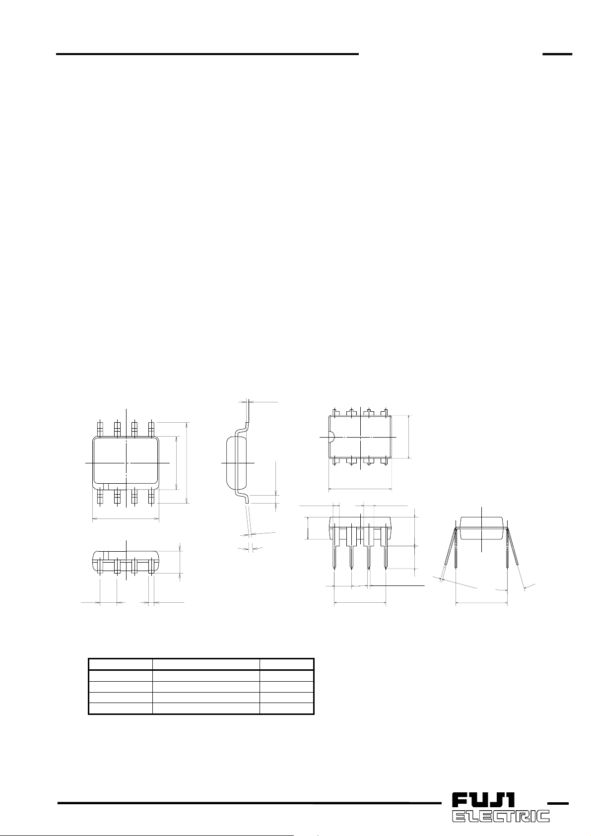
• Package: DIP-8 / SOP-8
3. Outline
SOP-8 DIP-8
5
4
0.4 ±0.1
3.9
6 ±0.2
8
1
4.9
1.27
4. Types of FA5500A/01A
Type Startup Threshold Package
FA5500AP 11.5V(typ.) DIP-8
FA5500AN 11.5V(typ.) SOP-8
FA5501AP 13V(typ.) DIP-8
FA5501AN 13V(typ.) SOP-8
1.8 MAX
0.18 ±0.08
0.65 ±0.25
+0.10
0.20
-0.05
oo
80 −
1.0 ±0.3
3.3
8
1
2.54
2.54×3=7.62
9.3
5
4
1.5 ±0.3
0.46 ±0.1
6.4
3 MIN 4.5 MAX
0.25
+0.1
- 0.05
7.62
oo
150 −
4
FA5500AP/AN, FA5501AP/AN
5. Block diagram
Quality is our message
Quality is our message
Quality is our messageQuality is our message
FB
COMP
2.5µA
GND
MUL
VREF(2.5V)
+
1
2
6
ERRAMP
-
+
-
-
+
+
-
VOS(2.0V)
VSP(0.3V)
SP
VOVP
(1.09VREF)
OVP
MUL
AOC
VREF(2.5V)
VDD(5.0V)
VOVP(1.09VREF)
VZCD(1.5V/1.33V)
VOS(2.0V)
VSP(0.3V)
+
-
+
-
VZCD(1.5V/1.33V)
54
REF
R
S
R
TIMER
R
Q
VCC
83
UVLO
SP
OVP
7
OUT
ZCDIS
6. Pin assignment
OUTVCC GND ZCD
8765
1234
FB COMP MUL IS
Pin No. Pin
symbol
1 FB Voltage Feedback Input Input for monitoring PFC output voltage
2 COMP Compensation Output of error amplifier
3 MUL Multiplier Input Input of multiplier for monitoring sinusoidal
4 IS Current Sense Input Input for sensing MOSFET current signal
5 ZCD Zero Current Detect Input Input for detecting that the inductor current
6 GND Ground Ground
7 OUT Output Output for direct driving a power MOSFET
8 VCC Power Supply Power supply for IC
Function Description
waveform
reaches zero
5
FA5500AP/AN, FA5501AP/AN
Quality is our message
Quality is our message
Quality is our messageQuality is our message
7. Ratings and characteristics
The contents are subject to change without notice. When using a product, be sure to obtain the latest specifications.
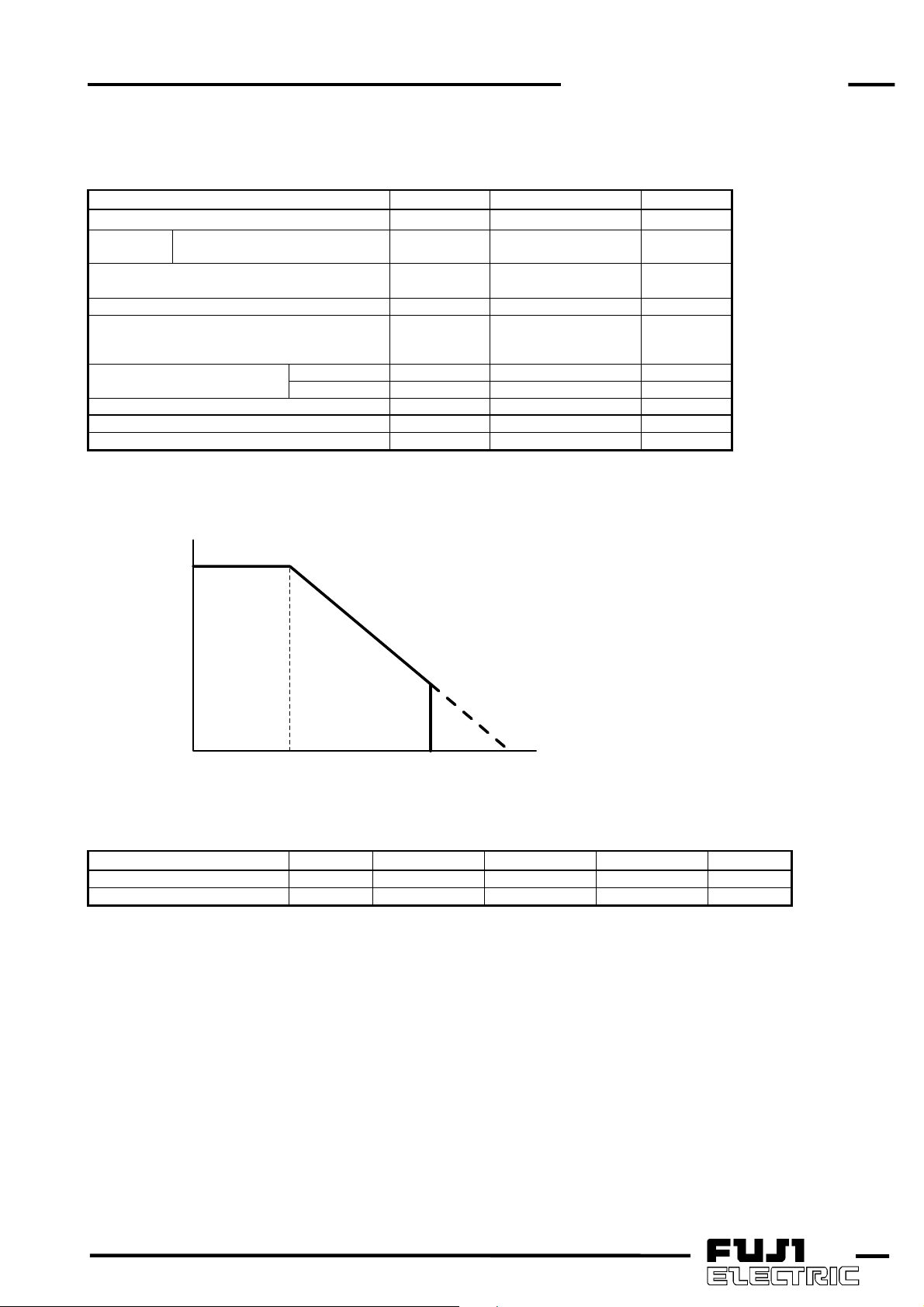
(1) Absolute Maximum Ratings
Item Symbol
Total Power Supply and Zener Current Icc+Iz 30 mA
Supply
Voltage
Output Current Sink
Source
Input voltage(IS,MUL,FB) Vin -0.3 to 5 V
Zero Current Detect Input
High State Forward Current
Low State Reverse Current
Operating Ambient Temperature Ta -30 to +105 °C
Operating Junction Temperature Tj +150 °C
Storage Temperature Tstg -55 to +150 °C
Maximum dissipation curve
400mW(SOP)
800mW(DIP)
Zener Clamp (Icc+Iz<30mA) Vcc Self Limiting V
Io
Iin
DIP-8 Pd1 800 mW Power dissipation
SOP-8 Pd2 400 mW
Ratings Unit
+1000
-500
-50
10
mA
mA
mA
Maximum dissipation Pd [mW]
-30 25 105 150
Ambience temperature Ta(°C)
(2) Recommended Operating Conditions
Item Symbol Min Typ Max Unit
Supply Voltage Vcc 10 12 28 V
ZCD pin current Izcd ±3 mA
6
FA5500AP/AN, FA5501AP/AN
Quality is our message
Quality is our message
Quality is our messageQuality is our message
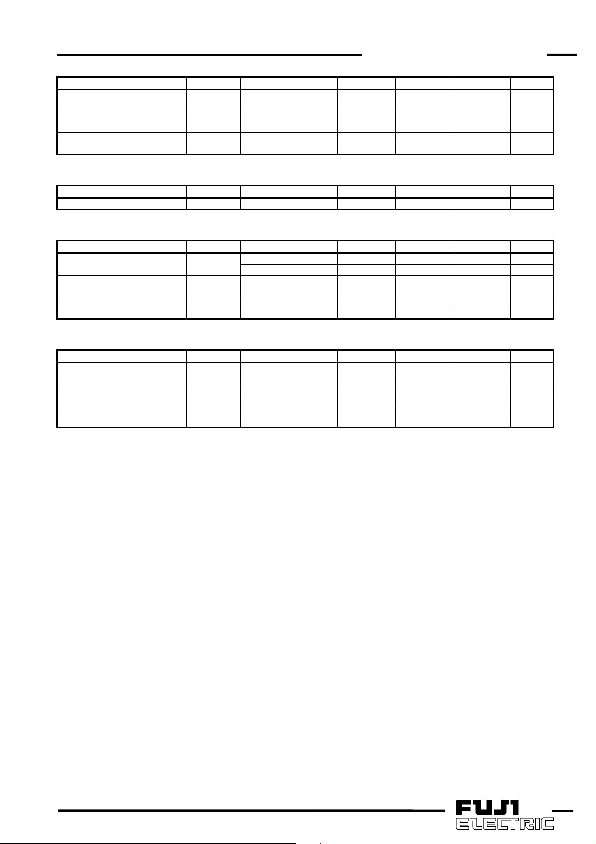
(3) Electrical Characteristics (Unless otherwise specified, Ta=25°C and Vcc=12V)
ERROR AMPLIFIER(FB,COMP Pin)
Item Symbol Condition Min Typ Max Unit
Voltage Feedback Input
Threshold
Line Regulation Regline
Temperature stability VdT Ta=-30°C to +105°C ±0.5 mV/°C
Transconductance Gm Ta=25°C 70 90 120 µmho
Output Current Io
OVERVOLTAGE COMPARATER (FB Pin)
Item Symbol Condition Min Typ Max Unit
Input Threshold Vthovp 1.075Vfb 1.09Vfb 1.105Vfb V
FB SHORT COMPARATOR(FB Pin)
Item Symbol Condition Min Typ Max Unit
Input Threshold Vthsht 0.1 0.3 0.5 V
Pulldown Current Ifb 0.5 2.5 5 µA
MULTIPLIER(COMP,MUL Pin)
Item Symbol Condition Min Typ Max Unit
Input Threshold
Pin2(COMP)
Dynamic Input Voltage Range
Pin3(MUL)
Pin2(COMP)
Gain K
K=Pin4Threshold/{Vpin3(Vpin2-Vthcomp)}
Vfb Ta=25°C 2.465 2.500 2.535 V
Vcc=12V to 28V
Ta=25°C
Source(Vfb=2.3V)
Sink(Vfb=2.7V)
Vthcomp 1.79 2.04 - V
Vpin3
Vpin2
Vpin3=0.5V
Vpin2=Vthcomp
+1.0V
-50 -20 - mV
-
-
0 to 2.5
Vthcomp to
Vthcomp
+1.0
0.53 0.75 0.97 1/V
10
10
0 to 3.5
Vthcomp to
Vthcomp
+1.5
-
-
-
µA
V
ZERO CURRENT DETECTOR (ZCD Pin)
Item Symbol Condition Min Typ Max Unit
Input Threshold Voltage Vthzcd Vin increasing 1.33 1.50 1.87 V
Hysteresis Vh Vin decreasing 100 170 300 mV
Input Clamp Voltage
“H” state
“L” state
CURRENT SENSE COMPARATOR (IS Pin)
Item Symbol Condition Min Typ Max Unit
Maximum Current Sense
Input Threshold
Delay to Output Tphl - 170 400 ns
Vih
Vil
Vthis
Idet=+3.0mA
Idet=-3.0mA
Vpin1=1.0V
Vpin3=3.0V
7.0
0.3
1.3 1.5 1.8 V
7.6
0.6
-
1.0
V
7
FA5500AP/AN, FA5501AP/AN
DRIVE OUTPUT (OUT Pin)
Item Symbol Condition Min Typ Max Unit
Output Voltage Low State Vol
Output Voltage High State Voh
Output Voltage Rise Time Tr CL=1.0nF - 50 120 ns
Output Voltage Fall Time Tf CL=1.0nF - 25 100 ns
RESTART TIMER
Item Symbol Condition Min Typ Max Unit
Restart Time Delay Tdly 100 200 - µs
UNDERVOLTAGE LOCKOUT (VCC Pin)
Item Symbol Condition Min Typ Max Unit
Startup Threshold Von
Minimum Operating Voltage
After Turn-On
Hysteresis Vhysvcc
TOTAL DEVICE (VCC Pin)
Item Symbol Condition Min Typ Max Unit
Power Supply Zener Voltage Vz Icc=25mA 30 33 36 V
Startup Power Supply Current Istart Vcc=8.0V - - 20 µA
Operating Power Supply
Current
Dynamic Operating Power
Supply Current
Voff
Icc Vcc=12V 1.0 2.0 mA
Iop 50kHz,CL=1.0nF 2.0 4.0 mA
Vcc=12V
Isink=200mA
Vcc=12V
Isouce=200mA
FA5500A 10 11.5 13 V
FA5501A 11.5 13 14.5 V
FA5500A 1.8 2.5 3.2 V
FA5501A 3.3 4 4.7 V
Quality is our message
Quality is our message
Quality is our messageQuality is our message
- 1.2 3.3 V
7.8 8.4 V
8 9 10 V
8
 Loading...