

Page 1
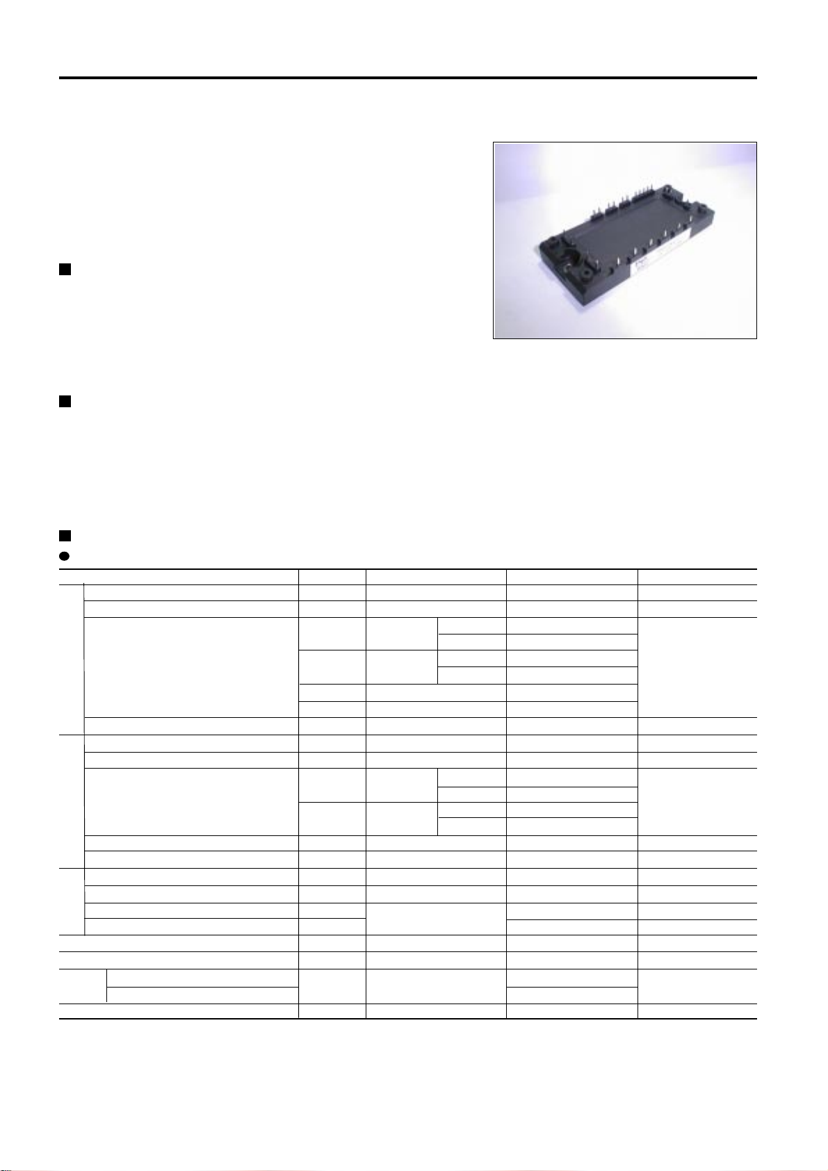
7MBR50UA120
IGBT MODULE (U series)
1200V / 50A / PIM
Features
· Low VCE(sat)
· Compact Package
· P.C. Board Mount Module
· Converter Diode Bridge Dynamic Brake Circuit
Applications
· Inverter for Motoe Drive
· AC and DC Servo Drive Amplifier
· Uninterruptible Power Supply
IGBT Modules
Maximum ratings and characteristics
Absolute maximum ratings (T c=25°C unless otherwise specified)
Item Symbol Condition Rating Unit
Collector-Emitter voltage
Gate-Emitter voltage
Collector current
Collector power disspation
Collector-Emitter voltage
Gate-Emitter voltage
Collector current
Collector power disspation
Repetitive peak reverse voltage
Repetitive peak reverse voltage
Average output current
Surge current (Non-Repetitive)
Converter Brake Inverter
I2t (Non-Repetitive)
Operating junction temperature
Storage temperature
Isolation between terminal and copper base *2
voltage between thermistor and others *3
Mounting screw torque
*1 Recommendable value : 2.5 to 3.5 N·m (M5)
*2 All terminals should be connected together when isolation test will be done.
*3 Two thermistor terminals should be connected together, each other terminals should be
connected together and shorted to base plate when isolation test will be done.
VCES
VGES
IC
ICP
-IC
-IC pulse
PC
VCES
VGES
IC
ICP
PC
VRRM
VRRM
IO
IFSM
I2t
Tj
Tstg
Viso
Continuous
1ms
Duty=70%
1ms
1 device
Continuous
1ms
1 device
50Hz/60Hz sine wave
Tj=150°C, 10ms
half sine wave
AC : 1 minute
Tc=25°C
Tc=80°C
Tc=25°C
Tc=80°C
Tc=25°C
Tc=80°C
Tc=25°C
Tc=80°C
1200
±20
50
35
100
70
50
100
205
1200
±20
25
15
50
30
115
1200
1600
50
260
338
+150
-40 to +125
AC 2500
AC 2500
3.5 *1
V
V
A
W
V
V
A
W
V
V
A
A
A2s
°C
°C
V
N·m
Page 2
IGBT Module
7MBR50UA120
Electrical characteristics (Tj=25°C unless otherwise specified)
Item Symbol Condition Characteristics Unit
Min. Typ. Max.
Zero gate voltage collector current
Gate-Emitter leakage current
Gate-Emitter threshold voltage
Collector-Emitter saturation voltage
Input capacitance
Turn-on time
Turn-off time
Forward on voltage
Reverse recovery time
Zero gate voltage collector current
Gate-Emitter leakage current
Collector-Emitter saturation voltage
Turn-on time
Turn-off time
Reverse current
Forward on voltage
Reverse current
Resistance
B value
Thermistor Converter Brake Inverter
ICES
IGES
VGE(th)
VCE(sat)
(terminal)
VCE(sat)
(chip)
Cies
ton
tr
tr(i)
toff
tf
VF
(terminal)
VF
(chip)
trr
ICES
IGES
VCE(sat)
(terminal)
VCE(sat)
(chip)
ton
tr
toff
tf
IRRM
VFM
IRRM
R
B
VCE=1200V, VGE=0V
VCE=0V, VGE=±20V
VCE=20V, IC=50mA
VGE=15V
Ic=50A
Tj=25°C
Tj=125°C
Tj=25°C
Tj=125°C
V
GE=0V, VCE=10V, f=1MHz
VCC=600V
IC=50A
VGE=±15V
RG= 33 Ω
VGE= 0 V
IF=50A
Tj=25°C
Tj=125°C
Tj=25°C
Tj=125°C
IF=50A
VCE=1200V, VGE=0V
VCE=0V, VGE=±20V
IC=25A
VGE=15V
Tj=25°C
Tj=125°C
Tj=25°C
Tj=125°C
VCC=600V
IC=25A
VGE=±15V
RG= 68 Ω
VR=1200V
IF=50 A terminal
VGE=0V chip
VR=1600V
T=25°C
T=100°C
T=25/50°C
1.0
200
4.5 6.5 8.5
2.40 2.80
2.75
2.00 2.40
2.35
4
0.53 1.20
0.43 0.60
0.03
0.37 1.00
0.07 0.30
2.40 2.80
2.65
2.00 2.40
2.25
0.35
1.0
200
2.30 2.80
2.75
2.10 2.60
2.55
0.53 1.20
0.43 0.60
0.37 1.00
0.07 0.30
1.0
1.55 1.90
1.40
1.0
5000
465 495 520
3305 3375 3450
mA
nA
V
V
nF
µs
V
µs
mA
nA
V
µs
mA
V
mA
Ω
K
Thermal resistance Characteristics
Item Symbol Condition Characteristics Unit
Min. Typ. Max.
Inverter IGBT
Thermal resistance ( 1 device ) Rth(j-c)
Inverter FWD
Brake IGBT
Converter Diode
Contact thermal resistance * Rth(c-f)
* This is the value which is defined mounting on the additional cooling fin with thermal compound
With thermal compound
0.60
0.95
1.07 °C/W
0.90
0.05
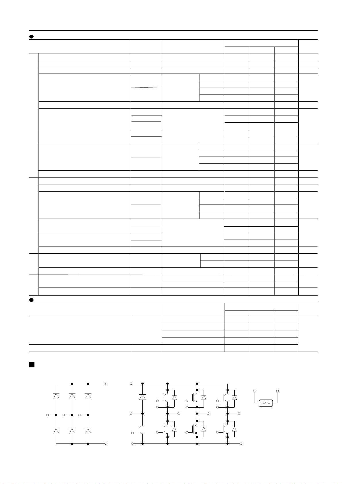
Equivalent Circuit Schematic
1(R)
[Converter]
2(S) 3(T)
21(P)
23(N)
22(P1)
7(B)
[Brake] [Inverter]
14(Gb)
24(N1)
20(Gu)
19(Eu)
13(Gx)
18(Gv)
4(U)
12(Gy)
17(Ev)
16(Gw)
15(Ew)
5(V) 6(W)
11(Gz)
[Thermistor]
89
10(En)
Page 3
IGBT Module
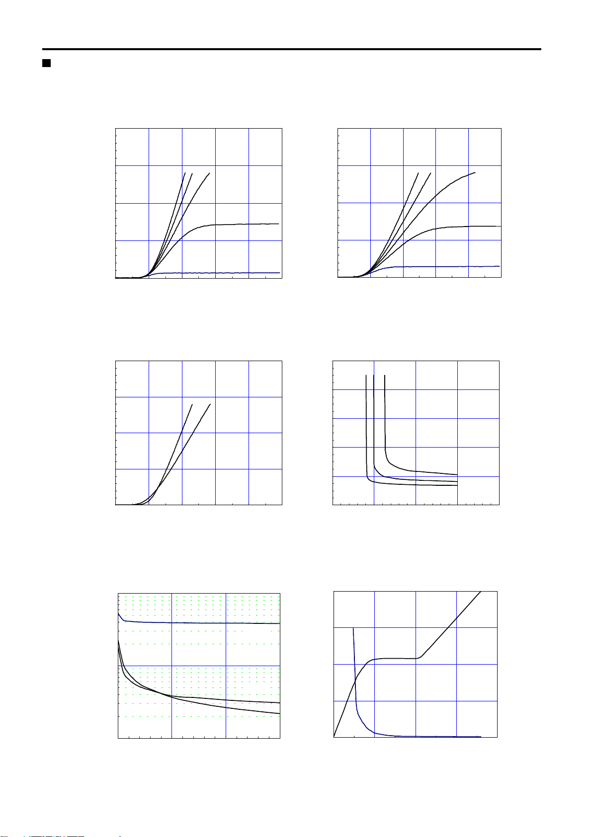
Characteristics (Representative)
[ Inve rter ] [ Inve rter ]
Collector current vs. Collector-Emitter voltage (typ.)
Tj= 25°C / chip
100
7MBR50UA120
Collector current vs. Collector-Emitter voltage (typ.)
Tj= 125°C / chip
100
75
50
Collector current : Ic [A]
25
0
012345
Collector current vs. Collector-Emitter voltage (typ.)
100
75
50
VGE=20V 15V 12V
10V
8V
Collector-Emitter voltage : VCE [V]
75
50
Collector current : Ic [A]
25
0
012345
Collector-Emitter voltage : VCE [V]
[ Inve rter ] [ Inve rter ]
Collector-Emitter voltage vs. Gate-Emitter voltage (typ.)
VGE=15V / chip Tj=25°C / chip
10
Tj=25°C
Tj=125°C
8
6
4
VGE=20V15V
12V
10V
8V
Collector current : Ic [A]
25
0
012345
Collector-Emitter voltage : VCE [V]
[ Inve rter ] [ Inve rter ]
Capacitance vs. Collector-Emitter voltage (typ.) Dynamic Gate charge (typ.)
10.0
1.0
Capacitance : Cies, Coes, Cres [ nF ]
0.1
0 102030
Collector-Emitter voltage : VCE [V]
Cies
Cres
Coes
2
Collector - Emitter voltage : VCE [ V ]
0
5 10152025
Gate - Emitter voltage : VGE [ V ]
Ic=70A
Ic=35A
Ic=17.5A
Vcc=600V, Ic=50A, Tj= 25°CVGE=0V, f= 1MHz, Tj= 25°C
VGE
Gate - Emitter voltage : VGE [ 5V/div ]
Collector-Emitter voltage : VCE [ 200V/div ]
0
0 50 100 150 200
Gate charge : Qg [ nC ]
VCE
Page 4

IGBT Module 7MBR50UA120
[ Inverte r ] [ Inve rte r ]
Switching time vs. Collector current (typ.)
Vcc=600V, VGE=±15V, Rg=33Ω, Tj= 25°C
10000
Switching time vs. Collector current (typ.)
Vcc=600V, VGE=±15V, Rg=33Ω, Tj=125°C
10000
1000
100
Switching time : ton, tr, toff, tf [ nsec ]
10
0 10203040506070
Collector current : Ic [ A ]
[ Inverte r ] [ Inve rte r ]
Switching time vs. Gate resistance (typ.)
Vcc=600V, Ic=50A, VGE=±15V, Tj= 25°C
10000
1000
100
Switching time : ton, tr, toff, tf [ nsec ]
10
10.0 100.0 1000.0
Gate resistance : Rg [ Ω ]
tr
ton
toff
tf
ton
tr
toff
tf
1000
100
Switching time : ton, tr, toff, tf [ nsec ]
10
0 10203040506070
Collector current : Ic [ A ]
Switching loss vs. Collector current (typ.)
Vcc=600V, VGE=±15V, Rg=33
20
16
12
8
4
Switching loss : Eon, Eoff, Err [ mJ/pulse ]
0
0 102030405060708090
Collector current : Ic [ A ]
toff
ton
tr
tf
Ω
Eon(125 °C)
Eon(25°C)
Eoff(125°C)
Eoff(2 5°C)
Err(125°C)
Err(25°C)
[ Inverter ] [ Inverter ]
Switching loss vs. Gate resistance (typ.)
Vcc=600V, Ic=50A, VGE=±15V, Tj= 125°C
30
20
10
Switching loss : Eon, Eoff, Err [ mJ/pulse ]
0
1.0 10.0 100.0 1000.0
Gate resist ance : Rg [ Ω ]
Eon
Eoff
Err
Reverse bias safe operating area (max.)
+VGE=15V,-VGE <= 15V, RG >= 33Ω ,Tj <= 125°C
150
100
50
Collector current : Ic [ A ]
0
0 400 800 1200
Collector - Emitter voltage : VCE [ V ]
Page 5

IGBT Module 7MBR50UA120
]
[ Inverter ] [ Inverter ]
Forward current vs. Forward on voltage (typ.)
chip
75
1000
Reverse recovery character ist ics (t y p .)
Vcc=600V, VGE=±15V, Rg=33
Ω
50
25
Forward current : IF [ A ]
0
01234
Tj=25°C
Tj=125°C
Forward on volt age : VF [ V ]
[ Converter ]
Forward current vs. Forward on voltage (typ.)
chip
75
Tj=25°C
50
Tj=125°C
100
Reverse recovery current : Irr [ A ]
Reverse recovery time : trr [ nsec ]
10
0 10203040506070
Forward current : IF [ A ]
trr (125°C)
trr (25°C)
Irr (125°C)
Irr (25°C)
25
Forward current : IF [ A ]
0
0.0 0.5 1.0 1.5 2.0 2.5
Forward on voltage : VFM [ V ]
Tr ans ient t hermal resist ance (max.)
10.000
1.000
0.100
Thermal resistanse : Rth(j-c) [ °C/W ]
0.010
0.001 0.010 0.100 1.000
Pulse width : Pw [ sec ]
IGBT [Brak e]
FWD[Inv erter
IGBT [Inv erter]
[ Thermistor ]
Temp erat ure charact erist ic (t y p.)
100
10
Resistance : R [ kΩ ]
1
0.1
-60 -40 -20 0 20 40 60 80 100 120 140 160 180
Temperatur e [°C ]
Page 6

IGBT Module
Collect or current vs. Collect or-Emitter voltage (t y p .)
40
[ Brake ] [ Brake ]
Collect or current vs. Collect or-Emitter voltage (t y p .)
Tj= 25°C / chip
40
Tj= 125°C / chip
7MBR50UA120
VGE=20V 15V 12V
30
20
Collector current : Ic [A]
10
0
012345
Collector-Emit ter voltage : VCE [V]
[ Brake ] [ Brake ]
VGE=15V / chip
40
Tj=25°C
30
Tj=125°C
20
10V
8V
VGE=20V 15V 12V
30
20
Collector current : Ic [A]
10
0
012345
Collector-Emitter voltage : VCE [V]
Collector-Emitter voltage vs. Gate-Emitter voltage (typ .)Collect or current vs. Collect or-Emitter voltage (t y p .)
Tj=25°C / chip
10
8
6
4
10V
8V
Collector current : Ic [A]
10
0
012345
Collector-Emit ter voltage : VCE [V]
[ Brake ] [ Brake ]
Cap acit ance vs . Collect or-Emit t er voltage (ty p .)
VGE=0V, f= 1MHz, Tj= 25°C
10.0
Cies
1.0
Capacitance : Cies, Coes, Cres [ nF ]
0.1
01020
Coes
Collector-Emit ter voltage : VCE [V]
Cre s
2
Collector - Emitter voltage : VCE [ V ]
0
510152025
Gat e - E m i t t e r v ol t age : VGE [ V ]
Ic=30A
Ic=15A
Ic=7.5A
Dynamic Gate charge (typ .)
Vcc=600V, Ic=25A, T j= 25°C
VGE
Gate - Emitter voltage : VGE [ 5V/div ]
Collector-Emitter voltage : VCE [ 200V/div ]
0
020406080100
Gate charge : Qg [ nC ]
VCE
Page 7

IGBT Module 7MBR50UA120
Outline Drawings, mm
 Loading...