

Page 1

S90-555 M/OCT 2001
File: SERVICE MANUAL - SECTION 90
Replaces: NOTHING (New Manual)
Dist: 3, 3a, 3b, 3c
MAINTENANCE
FRICK QUANTUM™
CONDENSER/VESSEL
CONTROL PANEL
VERSION 2.1x
Page 2

S90-555 M FRICK QUANTUM™ CONDENSER/VESSEL CONTROL PANEL
Page 2 MAINTENANCE
Table of Contents
Quantum™ Identification _____________________________________________________________ 4
Quantum™ 3 ___________________________________________________________________ 4
Quantum™ 4 ___________________________________________________________________ 4
Troubleshooting ____________________________________________________________________ 4
The Quantum™ Control Panel______________________________________________________ 4
General Information ___________________________________________________________ 4
What To Do Before Calling The Factory ___________________________________________ 5
What Should Occur When Powering Up The Panel __________________________________ 5
What If The “Home” Screen Is Not Shown __________________________________________ 5
Troubleshooting GCU Board Analog And Digital Problems ________________________________ 7
“About” Screen _______________________________________________________________ 7
Diagnosing A GCU Board Problem _______________________________________________ 7
Troubleshooting Digital Inputs And Outputs ______________________________________ 8
Troubleshooting Analog Inputs And Outputs _____________________________________ 9
Adding And Replacing Boards ______________________________________________________ 9
Quantum™ __________________________________________________________________ 9
GCU Boards _________________________________________________________________ 9
Display Replacement _________________________________________________________ 10
Troubleshooting A Problem That Appears Unexplainable ________________________________ 10
Jumper And Dipswitch Settings _______________________________________________________ 11
Digital Board (Optional) __________________________________________________________ 11
Digital I/O Board Communications Settings ________________________________________ 11
Digital I/O Board Dipswitch Settings (DP1) ________________________________________ 11
Condenser / Vessel (GCU) Board:__________________________________________________ 12
Communications Port Connections ______________________________________________ 12
Additional Communications Jumper Configurations _________________________________ 12
GCU Board Dipswitch Settings _________________________________________________ 12
Vessel GCU Board Analog I/O Jumper Settings _______________________________________ 13
Analog Output Configurations __________________________________________________ 14
Condenser GCU Board Analog I/O Jumper Settings ____________________________________ 14
Analog Output Configurations __________________________________________________ 16
Quantum™ 3 Main Processor Board ___________________________________________________ 17
Motherboard Jumpers ___________________________________________________________ 17
Communications Board Jumpers ___________________________________________________ 18
Com-1 ____________________________________________________________________ 18
Com-2 ____________________________________________________________________ 18
Com-3 ____________________________________________________________________ 18
Communications Wiring __________________________________________________________ 18
Quantum™ 4 Main Processor Board ___________________________________________________ 19
Motherboard Jumpers ___________________________________________________________ 19
Communications Board Jumpers ___________________________________________________ 20
Com-1 ____________________________________________________________________ 20
Com-2 ____________________________________________________________________ 20
Communications Wiring __________________________________________________________ 20
Drawing Reference Table ___________________________________________________________ 21
Quantum™ Panel DC Power Supply Diagram (Condor) _________________________________ 22
Quantum™ Panel DC Power Supply Diagram (Power-One) ______________________________ 22
Quantum™ Control Center Assembly _______________________________________________ 23
Vessel Control Center Assembly __________________________________________________ 285
Wiring Diagram – Vessel W/O MOA ________________________________________________
Wiring Diagram – Vessel With MOA ________________________________________________ 37
Condenser Control Center Assembly _______________________________________________ 43
Wiring Diagram – Condenser______________________________________________________ 53
Quantum™ 3 Communications Wiring Diagrams ______________________________________ 59
31
Page 3
MAINTENANCE Page 3
FRICK QUANTUM™ CONDENSER/VESSEL CONTROL PANEL S90-555 M
Rs-485 Communications ______________________________________________________ 59
Rs-422 Communications ______________________________________________________ 59
Rs-232 Communications ______________________________________________________ 59
Quantum™ 4 Communications Wiring Diagrams ______________________________________ 60
Rs-485 Communications ______________________________________________________ 60
Rs-422 Communications ______________________________________________________ 60
Rs-232 Communications ______________________________________________________ 60
Convenser/Vessel Recommended Spare Parts __________________________________________ 61
Quantum™ Control Panel ________________________________________________________ 61
Remote Panel _________________________________________________________________ 61
Display Assembly Component Replacement Guide ____________________________________ 61
QUANTUM™ PUBLICATIONS
S90-555 CS Frick Quantum™ Condenser/Vessel Control
S90-555 O Frick Quantum™ Condenser/Vessel Control
E90-555 SD Frick Quantum™ Condenser/Vessel Control
DANGER
!
Panel COMMUNICATIONS SETUP (setup
and wiring for data communication using
available protocols)
Panel OPERATION
Panel SETPOINT DATA SHEETS
Indicates an imminently
hazardous situation which, if not
avoided, will result in death or
serious injury.
WARNING
!
CAUTION
!
NOTE: Indicates an operating procedure, practice, etc., or
portion thereof which is essential to highlight.
Indicates a potentially hazardous
situation or practice which, if not
avoided, will result in death or
serious injury.
Indicates a potentially hazardous
situation or practice which, if not
avoided, will result in damage to
equipment and/or minor injury.
Page 4
S90-555 M FRICK QUANTUM™ CONDENSER/VESSEL CONTROL PANEL
Page 4 MAINTENANCE
Quantum™ Identification
Frick Controls has over the years, strived to remain on the
cutting edge of microprocessor technology and
development. And because of the ever-increasing speed,
memory, features, and power of microprocessors, Frick
Controls will, from time to time, introduce the latest
advancement in microprocessor control technology.
Our microprocessor family has shared the name
Quantum™ over the past five years. There are currently
four controllers within this family. The first two of these
controllers (known as Quantum™ 1 and Quantum™ 2) are
no longer in production, and as such, will not be further
mentioned in this manual. The two current members in
production of the Quantum™ family are the Quantum™ 3,
and the Quantum™ 4. It is critical to the end user to be
able to identify the differences between these controllers.
Throughout this manual, the two different controllers will
be talked about for the most part as one (as they do
function the same). Where there is a difference between
these boards, as in jumpers or wiring, the different models
will be identified by name. This is why it is important for
you to be aware of which board you have.
Quantum™ 3
Quantum™ 4
TROUBLESHOOTING
THE QUANTUM™ CONTROL PANEL
This section contains information on troubleshooting and
making corrections to the boards and control circuits of the
Quantum™. Reference the drawings at the end of this
manual.
GENERAL INFORMATION:
The components within the control panel can be
inadvertently damaged by static electricity or
mishandling. Only qualified technicians should
directly handle these components.
1. DO NOT attempt to make corrections to the power
supply without shutting off power to the control
panel. Accidental shorts can irreparably damage
the processor boards or the display screen.
2. DO NOT HANDLE the panel boards when their
cables are disconnected without first attaching a
properly grounded wrist ground strap to prevent
static electrical discharge from your body.
Most problems encountered with the microprocessor and
control circuits will be the result of a wiring fault, a bl own
fuse, faulty I/O module or failure of a peripheral control
such as a solenoid coil or a pressure transducer. Faults in
the computer, while possible, are unlikely. If a fault
develops in the computer, the probability is that all
functions will cease and the display screen will go blank.
The control system consists of an AC (high voltage) sid e,
which can be either 120 volts, or 230 volts, and a DC (low
voltage) side. The AC side actuates solenoids, relays,
alarms, and other electromechanical functions. The DC
side operates the computer and it's various sensors.
When working within the panel, the AC high voltage
side, which can be either nominal 120 VAC or nominal
230 VAC, CAN CAUSE INJURY OR DEATH.
To troubleshoot the low-voltage side of the control circuits,
it is necessary to have the following tools:
1. Accurate digital multimeter*
2. Small wire stripper
3. Small screwdriver
4. Small snip nose pliers
5. Wrist Grounding strap*
6. Static free grounded work surface
Note: Proper panel voltage refers to the AC (high voltage) that has been supplied to the panel, which could
be either nominal 120 VAC or nominal 230 VAC
(Reference the Control Panel Power Specifications).
Some problems that are encountered involve
troubleshooting digital inputs and outputs.
The Digital I/O (Input/Output) board has six connectors
labeled P1 through P6. The input and output modules are
wired into a DIO connector plug. Position 3 provides 120
VAC power and position 4 is neutral.
The GCU Board has three digital inputs connectors,
labeled J7, J9, and J10. Each of these connectors has 16
pins. J10 is utilized for AC inputs, and use odd pin
numbers for 120 VAC signals, even pins for neutral. J9
and J10 are for AC outputs, and use even pins for 120
VAC hot, odd pins are for 120 VAC signals.
Page 5

FRICK QUANTUM™ CONDENSER/VESSEL CONTROL PANEL S90-555 M
MAINTENANCE Page 5
WHAT TO DO BEFORE CALLING THE FACTORY
The “Home” screen is shown.
When someone calls in to the factory with a Quantum™
related problem, many times there isn't enough
information provided. An example of this is the statement
that the Panel is not “booting” (the main processor board
is not starting). Unfortunately, this description is usually
vague and only means that there is nothing on the display.
A blank screen could be the result of many different
problems. Following is a list of possible reasons for no
display:
No power
Loose or Faulty Display Cable or Inverter Cable
Bad Display
Bad Backlight Inverter
Bad Backlight Fluorescent Tube
Faulty CPU Board
Wrong Combination of Display, Cable, Inverter,
or Software
Before calling the factory for assistance, review the
following information and try to discover what the problem
is, and resolve it.
WHAT SHOULD OCCUR WHEN POWERING UP
THE PANEL
The first thing that should be checked when
troubleshooting the Quantum™ is it’s powering up
sequence.
When powering up the Quantum™ the following sequence
of events are indicative of a properly working main
processor board:
Quantum™ 3
The LED’s for +5V, +12V, and –12V will turn
on solid. (Lower left corner of Main PCB)
LED KB will begin to blink. (Left side of Main
PCB)
Several initialization screens will appear
(these will look very similar to the way the
screen of a desktop computer appears when
it is booting.
The last of the initialization screens is the
“System Configuration” screen.
The screen will go blank for several seconds.
The “Home” screen is shown.
After the Quantum™ has properly powered up,
the following sequence of events is indicative of
proper communication to the GCU board:
The TX/RX LED’s near the white connector
will begin to blink.
The GCU board TX/RX lights should be
blinking.
Each GCU board should have the power
LED (next to the white connector) lighted
and the “Status” LED (next to the blue DIP
switch) should be blinking.
Quantum™ 4
Green PWR (Power) LED will turn on solid
(upper right corner of main PCB).
Red FLASH LED will begin to intermittently
during the Boot process. It will then go out
once the “Home” screen appears.
LED D8 (on the smaller board) will start to
blink at the rate of about once per second. It
will continue to blink after the Quantum™
has booted.
Once the screen displays “Loading…”, LED's
D4 , D5, D7 and D8 will be on solid.
The “Home” screen will appear.
After the Quantum™ has properly powered up,
the following sequence of events is indicative of
proper communication to the analog and digital
boards:
The TX/RX LED’s near the white connector
will begin to blink.
The GCU board TX/RX lights should be
blinking.
Each GCU board should have the power
LED (next to the white connector) lighted
and the “Status” LED (next to the blue DIP
WHAT IF THE “HOME” SCREEN IS NOT SHOWN
switch) should be blinking.
If the “Home” screen is not shown, check the following
items:
Quantum™ 3
1. If no LED’s are lighted, then check power AC
and DC.
2. Check if the lighting of the LED’s is occurring
as described in the “What Should Occur
When Powering Up The Panel” section.
If the powering up sequence continues
to repeat without displaying the “Home”
screen, then there is a booting problem.
3. Check if an error message is displayed when
booting.
Be sure to write down any error
4. Check that the software is OK:
messages that appear.
Is the correct software installed?
Did you just install new software?
If you need to clear the numerical
setpoint and calibration areas of
memory for any reason, clear the
memory as described in the S90-555
FSI publication. NOTE: This
information will be replaced by
factory default values, so any
setpoint and calibration data values
that need to be customized must be
reentered.
Page 6

S90-555 M FRICK QUANTUM™ CONDENSER/VESSEL CONTROL PANEL
Page 6 MAINTENANCE
5. Check for bad connections.
6. Check the display. If the CPU board is
booting but you have no display, check the
following:
When working with the display, be
extremely cautious of the backlight
inverter board. This board is mounted
next to the display, and is used to
generate high voltage to drive the
displays fluorescent tube.
Check the LCD backlight tube. Look
very closely at the display to see if
anything is visible in the dark screen.
You will need good lighting and look for
any “ghost” type image. If it appears that
there is something on the screen but
very dark, the problem maybe the LCD
backlight tube. On the LG Philips, NEC
and Sharp displays this tube is field
replaceable. On the Samsung LCD
display, it is not available and the
display will have to be replaced. You
must take the display apart to identify
the display manufacturer.
Verify that both the display cable and
the inverter cable are firmly seated. It
may be necessary to remove the video
cable from the back of the LCD display
and reseat it to be sure it is connected
properly. Note: This is a small
connector and caution should be
observed so that it is not damaged
due to excessive force.
Check the backlight inverter connector
(P4). When the Quantum board is
mounted in the panel, this connector is
located at the middle left of the board.
The pins on the right side are odd
numbered, with pin P(1) at the bottom pin P(9) at the top. The pins on the left
side are even numbered, with pin P(2)
at the bottom - pin P(10) at the top. After
the Quantum has booted, pin P(3)
should measure +2.4Vdc, pins P(4) and
P(5) are DC grounds, and pins P(6) and
P(7) should measure +12Vdc. A bad
inverter will also cause a dark display.
Reference the “Display Assembly
Component Replacement Guide” at the
end of this manual, and check that the
LCD, LCD cable, and software versions
are matched correctly.
Quantum™ 4
1. If no LED’s are lighted, then check power AC
2. Check if the lighting of the LED’s is occurring
3. Check if an error message is displayed when
4. Check that the software is OK:
5. Check for bad connections.
6. Check the display. If the CPU board is
and DC.
as de-scribed in the “What Should Occur
When Powering Up The Panel” section.
If the powering up sequence continues
to repeat without displaying the “Home”
screen, then there is a booting problem.
booting.
Be sure to write down any error
messages that appear.
Is the correct software installed?
Did you just install new software?
If you need to clear the numerical
setpoint and calibration areas of
memory for any reason, clear the
memory as described in the S90-555
FSI publication. NOTE: This
information will be replaced by
factory default values, so any
setpoint and calibration data values
that need to be customized must be
reentered.
booting but you have no display, check the
following:
When working with the display, be
extremely cautious of the backlight
inverter board. This board is mounted
next to the display, and is used to
generate high voltage to drive the
displays fluorescent tube.
Check the LCD backlight tube. Look
very closely at the display to see if
anything is visible in the dark screen.
You will need good lighting and look for
any “ghost” type image. If it appears that
there is something on the screen but
very dark, the problem maybe the LCD
backlight tube. On the LG Philips, NEC
and Sharp displays this tube is field
replaceable. On the Samsung LCD
display, it is not available and the
display will have to be replaced. You
must take the display apart to identify
the display manufacturer.
Verify that both the display cable and
the inverter cable are firmly seated. It
may be necessary to remove the video
cable from the back of the LCD display
and reseat it to be sure it is connected
properly. Note: This is a small
connector and caution should be
observed so that it is not damaged
due to excessive force.
Reference the “Display Assembly
Component Replacement Guide” at the
end of this manual, and check that the
LCD, LCD cable, and software versions
are matched correctly.
Page 7
FRICK QUANTUM™ CONDENSER/VESSEL CONTROL PANEL S90-555 M
MAINTENANCE Page 7
TROUBLESHOOTING GCU BOARD ANALOG AND DIGITAL PROBLEMS
The information that follows in this section can help locate
problems that can occur with GCU Analog and Digital
input and output circuit boards.
“About” Screen
The “About” screen shows any Condenser and Vessel
GCU board(s) that have been detected. If a board has lost
communications, the affected boards will continue to run
their internal programs.
Diagnosing a GCU Board Problem
The GCU Board (both Condenser and Vessel) have builtin features that help to troubleshoot faulty boards.
Following is a description of the built-in features:
1. The GCU Board has a “Status” LED indicator on
the board that blinks when the board’s software is
running.
If the “Status” LED is not blinking, check to
ensure that the EPROM is installed properly.
2. There are also 5 volt and 12 volt power LED's
that light when DC power is applied to the board.
If the either power LED is n ot lighted, check
the power harness for proper connectivity.
If the harness appears to be good, then
measure the voltages at the output of the DC
power supply.
3. The main indication of communications is the
RX/TX LED’s on the GCU board. These LED’s
should blink in response to the blinking of the
main processor board’s I/O communication
activity RX/TX LED’s. If the RX LED on the GCU
board is blinking but the board was not detected
on the “About” screen, or an I/O Comm failure
occurs, check the address of the board.
Reference the “JUMPER AND DIPSWITCH
SETTINGS” section later in this manual. This
section contains the dipswitch settings for
addressing all GCU Boards. When these
switches are properly set, the main
processor board is able to serially
communicate with each board and provide
data exchange.
Page 8

S90-555 M FRICK QUANTUM™ CONDENSER/VESSEL CONTROL PANEL
Page 8 MAINTENANCE
“Condenser Service” - SCREEN - GCU Board Inputs and Outputs
“Vessel Service” - SCREEN - GCU Board Inputs and Outputs
Troubleshooting Digital Inputs and Outputs
The “Service Screen” (individual service screens are
available for both Condenser and Vessel) has been
provided to view the raw data from a GCU Board. There is
a separate screen for each of the GCU Boards that are
present. Digital values are shown as ON or OFF.
Checking the Digital Inputs and Outputs
Some problems that are encountered involve
troubleshooting the digital inputs and outputs. The Digital
I/O (Input / Output) boards have three Digital I/O (DIO)
board connectors labeled J7, J9 and J10. The input and
output modules are wired to a connector plug:
Input Module
On the input module, positions 1, 3, 5, 7, 9, 11,
13, and 15 provides neutral on the DIO
connectors. Positions 2, 4, 6, 8, 10, 12, 14, and
16 are signal connections. Input modules can
only occupy the eight positions adjacent to
connector J10.
Output Module
On the output module, positions 1, 3, 5, 7, 9, 11,
13, and 15 provides signal connections. Positions
2, 4, 6, 8, 10, 12, 14, and 16 are 120 volt AC on
the DIO connectors. Output modules can only
occupy the sixteen positions adjacent to
connectors J7 and J9. Notice also, that these
sixteen positions have fuses associated with
them.
Page 9

FRICK QUANTUM™ CONDENSER/VESSEL CONTROL PANEL S90-555 M
MAINTENANCE Page 9
An LED is associated with each I/O module and displays
the state of each module. A lighted LED represents an
Input that is “High” or an Output that is “On”.
If a properly configured GCU I/O is not responding
correctly, first look at the board on the appropriate
“Service Screen” (Condenser or Vessel) and check if the
module is on. If it is not on, check if the LED on the board
is also not lit. If the LED is not lit, then check the fuse. If
the fuse is OK, then check the module.
FUSE TESTING AND REPLACEMENT
1. Open the panel door.
2. Turn off circuit breaker 1CB.
3. Remove the questionable fuse.
4. Check the questionable fuse using a volt meter or
other reliable method. If the fuse is faulty, replace
the fuse with a new plug-type fuse (Part #
333Q0001326).
5. Turn on circuit breaker 1CB.
Input and Output Module Testing and
Replacement
1. Open the panel door.
2. Turn circuit breaker 1CB off.
3. Replace the questionable module.
4. Turn on circuit breaker 1CB.
5. If it is an output module, check for proper panel
voltage on the DIO connector plug. Check the
voltage between neutral the associated signal
position to the output module.
6. If it is an input module, check if the associated
LED is on when power is applied to the module.
Troubleshooting an Output
1. Make sure the LED associated with the output is
on when power is applied to the module.
2. If the LED is not on when it should be and there
is no operating condition preventing it, contact
the Frick Service Department.
3. If the LED is on when it should be, check for
proper panel voltage on the DIO connector plug.
Check the voltage between the neutral and the
associated position to the output module.
4. If the voltage is OK, check for proper panel
voltage between the associated position to the
output module on the DIO connector and the
associated position on the terminal strip.
5. If the voltage is OK, check the wiring external to
the panel.
6. If voltage is not OK, check the fuse.
7. If the fuse is OK then check the module.
8. If the module is OK, check for proper panel
voltage on the DIO connector plug between any
Troubleshooting an Input
odd numbered position (Hot) and neutral.
1. Ensure that the LED associated with the input is
on when power is applied to the module.
2. If the LED is on, and there is good in put voltage,
then the module is good.
3. If the LED is on and there is no input voltage,
replace the input module.
Troubleshooting Analog Inputs and Outputs
The “Service Screen” (both Condenser and Vessel) h ave
been provided to view the raw analog data from a GCU
Board. There is a separate screen for each of the GCU
Boards that are present. Analog values are converted from
binary to show volts. The error factor is .05 volts.
Checking Analog Inputs and Outputs
The GCU boards have numerous jumpers that must be
properly selected. There are eleven an alog input channels
that can be selected for 4-20ma, Resistance, 0-5Vdc, or
ICTD. All of these jumper settings are listed later in this
manual (Jumper and Dipswitch Settings Section). Besides
properly setting the hardware jumpers, each transducer
must be calibrated through the appropriate sensor
calibration screen. Improper setup of either the hard ware
or software will result in improper operation or range.
The most common fault associated with the reading of the
analog channels other than hardware or software setup
problems fall into one of the following categories: Sensor
fault, wiring problem, improper grounding of system.
An open wire, shorted wire, or faulty sensor will usually
give a reading at either the minimum, or maximum e nd of
the range scale. An erratic reading or a reading that
seems to float up and down is usually indicative of a
grounding problem. When a single transducer or cable is
shorted to earth (or system) ground, this can show up as a
whole assortment of problem channels. The easiest way
to find a short to earth problem is to disconnect all the
sensor plugs and ohm out each plug screw terminal to
earth for open (infinite) impedance. All sensors should
read open to earth.
ADDING AND REPLACING BOARDS
QUANTUM™
The procedure to replace the main board is outlined
below:
1. Shut off control power.
2. Remove the old board from the machine and the
new board from its packing and place both on an
anti-static surface.
3. Then install the modified replacement board in
the panel.
4. Verify that all jumpers are installed properly.
5. Follo w the directions in th e Factory Setup manu al
(S90-555 FSI) for the procedure to load a
program Flash Card.
The procedure to replace a GCU board is outlined below:
1. Shut off control power.
2. Remove the old board from the enclosure and
the new board from its packing and place bot h on
an anti-static surface.
3. Remove any required chip(s) from the defective
board and install them in the replacement board.
Align the notch at the end of the EPROM with the
notch in the socket.
Ensure that the GCU EPROM (installed into
GCU BOARDS
U22), has the proper label affixed to it. If the
GCU board being installed is to control a
vessel, then the EPROM label must be
printed with the words “GCU VESSEL”.
Likewise, if the GCU board is being installed
to control a condenser, then the EPROM
label must be printed with the words "GCU
Page 10

S90-555 M FRICK QUANTUM™ CONDENSER/VESSEL CONTROL PANEL
Page 10 MAINTENANCE
CONDENSER". Additionally, the Version
number should match between all GCU
EPROMS, as well as the program version of
the Quantum (as shown on the
“About…”screen). As an example, if the
Quantum version is 2.11, then all GCU
boards must have version 2.11. The GCU
boards may have an additional digit in the
version number, such as 2.112. This final
digit is not critical with the compatibility of the
system.
4. Ensure that all jumpers, dip switches, I/O
modules and components are properly setup on
the new board as it was on the old board.
5. Install the modified replacement board in the
enclosure.
After replacing a GCU board, it will automatically be
detected after the Quantum power has been cycled off
then on. It will then be necessary to re-ente r all setpoints
and calibration data to the board. Refer to the Factory
Setup Instructions for more information (S90-555 FSI).
DISPLAY REPLACEMENT
1. Shut off control power.
2. Remove the defective display.
3. Install the new display.
TROUBLESHOOTING A PROBLEM THAT
When there is a problem that makes no sense due to
unexplainable things happening, then check the following:
APPEARS UNEXPLAINABLE
1. It is important to know if the unit ever worked
properly.
2. If the unit used to work properly, try to determine
when the problem first showed up.
3. It is important to know if the problem occurs
randomly, frequently, or all the time.
4. Check what the temperature is in the engine
room and at the panel. Is it very hot or very cold?
Make sure that the motor is not blowing
exhaust air on the control panel.
5. If it just started to act up, then check if there was
recently a severe lightning storm, fire, flood, or a
plant accident. If any of the following conditions
are possible, then check for it:
Has any liquid leaked into the panel or
conduit?
6. If it just started to act up, then check if anything
was recently changed in the system (i.e. software
or hardware.)
7. If it just started to act up, then check if any
service was recently done to the electrical
system?
8. If there is communication wiring connecting the
panel to another panel or device, then check the
following:
If the Quantum™ is unexplainably shutting
down, try disconnecting the communications
cable to see if the problem goes away.
Check if the communications cable shields
are tied to machine ground at only one
location.
Check that you are using the Frick
recommended communications cable. See
manual to match proper cable with type of
communications (i.e., RS-422, RS-232, RS485, or some other type of factory
communication bus system.)
9. If this is an older plant, has the plant wiring been
brought up to code?
10. Do you have power wiring mixed with control
wiring?
11. Do you have power wiring mixed with sensor
wiring?
12. Do you have power wiring mixed with
communications wiring?
13. Check that the pressure transducers are properly
grounded. The two types of transducers you may
have are as follows: an older type has an 8 to 10
inch 3-conductor pigtail coming out of the
transducer. This type will have the attaching
cable’s shield cut off and insulated at the
transducer end. The shield is then tied to a panel
ground terminal in the panel. The newer type has
the cable as an integral part of the housing and
has the shield crimped to the case at the
transducer end. This type of transducer has the
cable’s shield cut off and insulated in the control
panel.
14. Check that temperature transducers are properly
grounded. Temperature probes usually have t wo
short wires coming out of the sensor, and are tied
to a shielded cable at the thermal well head. The
shield is grounded at the temperature probe and
insulated at the panel end.
15. Check if one of the temperature probes has a
signal wire shorted to machine ground. To do
this, first pull the orange plug from the micro
board and then use an Ohmmeter and check
each white wire to machine ground and each
black wire to machine ground.
16. Ensure that all inductive loads (i.e. Coils,
Solenoids, or Relays, etc.) connected to the I/O
output modules have surge suppressers across
them, preferably at the devices and not at the
panel end.
17. If the control settings unexplainably change, it
may be a noise problem affecting the keypad’s
input circuit. Check if it works OK with the keypad
cable disconnected. If it works OK, then check
the grounding as described above. If the
grounding is OK, then replace the keypad.
18. Make sure that you have a continuous ground
back to the power source. The ground connection
must be aluminum or copper. A conduit ground
will not work
19. Make sure that there is no AC wiring lying next to
printed circuit boards.
20. Unexplainable auxiliary failures are usually
indicative of noise due to wiring problems (i.e.
incorrect earth grounds, mixed power and control
wiring, unsuppressed coils, etc)
Page 11
FRICK QUANTUM™ CONDENSER/VESSEL CONTROL PANEL S90-555 M
MAINTENANCE Page 11
JUMPER AND DIPSWITCH SETTINGS
DIGITAL BOARD (Optional)
DIGITAL I/O BOARD COMMUNICATIONS SETTINGS
J5
J7
J8
J9
J10
In
out*
In
out*
In
out*
In
out*
In
out*
120 ohm long communications line termination.
No termination. (standard setting)
RS-422/485 transmit pull-up for long communications lines.
No pull-up. (standard setting)
RS-422 transmit pull-up for long communications lines.
No pull-up. (standard setting)
RS-422/485 receive pull-down for long communications lines.
No pull-down. (standard setting)
RS-422 receive pull-down for long communications lines.
No pull-down. (standard setting)
* = standard setting
DIGITAL I/O BOARD DIPSWITCH SETTINGS (DP1)
SW1 SW2 SW3 SW4 SW5 SW6
Board #1 on on on on off on
Board #2 off on on on off on
Board #3 on off on on off on
Board #4 off off on on off on
Board #5 on on off on off on
Board #6 off on off on off on
Page 12
S90-555 M FRICK QUANTUM™ CONDENSER/VESSEL CONTROL PANEL
Page 12 MAINTENANCE
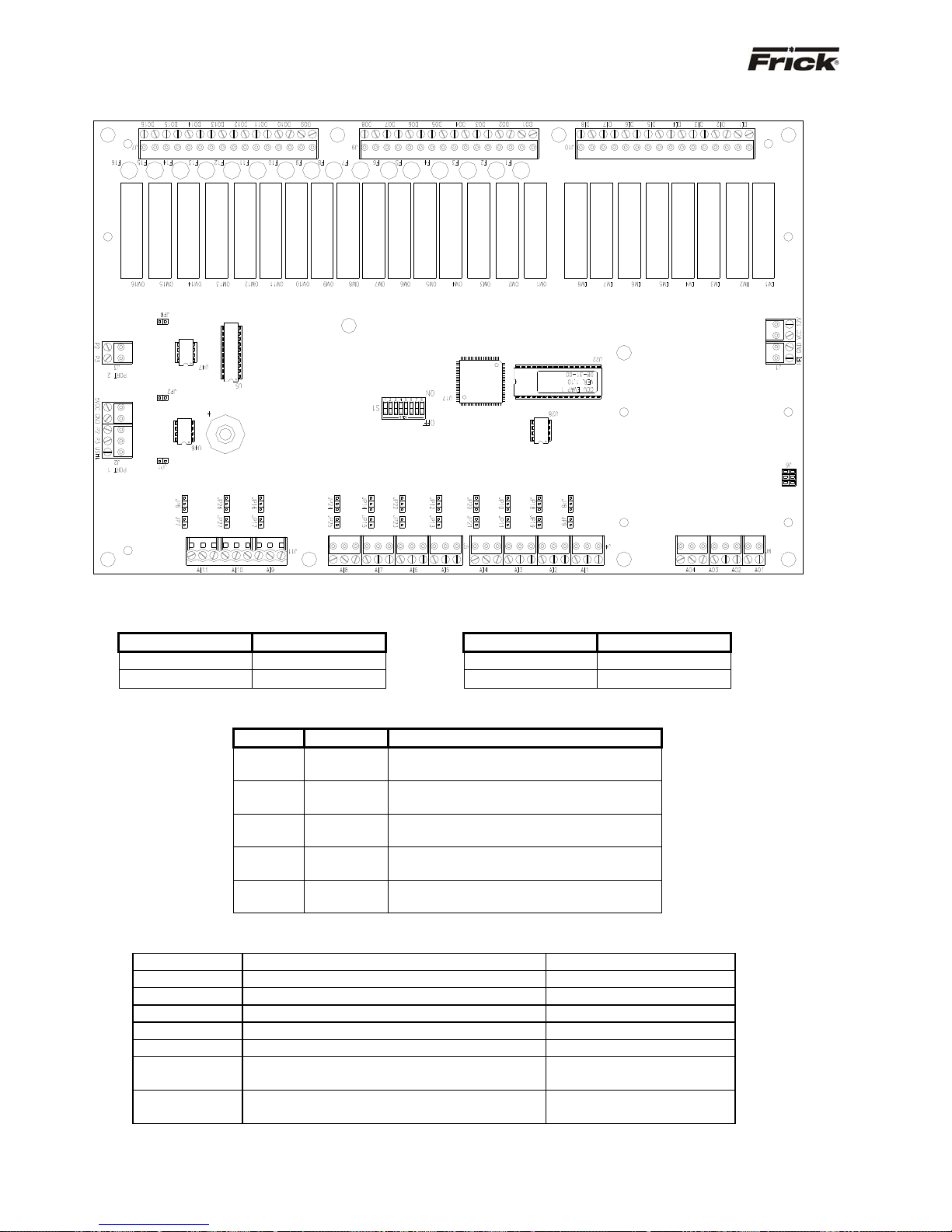
PICTORIAL DRAWING OF CONDENSER / VESSEL (GCU) BOARD:
Communications Port Connections
Comm. Port 1 Comm. Port 2
Connector Function Connector Function
J2-P2
J2-P3
Com-
Com+
J3-P2
J3-P3
Additional Communications Jumper Configurations
Com-
Com+
Jumper Setting Function
JP1
JP2
JP3
JP4
JP5
Installed
Removed
Installed
Removed
Installed
Removed
Installed
Removed
Installed
Removed
GCU Board Dipswitch Settings
Port 1 RS-485 pull-up resistor
No pull-up resistor (standard setting)
Port 1 RS-485 pull-down resistor
No pull-down resistor (standard setting)
Port 2 RS-485 pull-up resistor
No pull-up resistor (standard setting)
Port 2 RS-485 pull-down resistor
No pull-down resistor (standard setting)
PFI pull-up resistor (standard setting)
No pull-up resistor
Switch # 1 Not Used N/A
Switch # 2 Not Used N/A
Switch # 3 Not Used N/A
Switch # 4 Not Used N/A
Switch # 5 Not Used N/A
Switch # 6 Not Used N/A
Switch # 7 Baud Rate Selection
Switch # 8 Baud Rate Selection
off / open *
on / closed
off / open
on / closed *
* = standard setting
Page 13
V
A
V
A
V
A
A
V
A
V
A
A
A
MAINTENANCE Page 13
FRICK QUANTUM™ CONDENSER/VESSEL CONTROL PANEL S90-555 M
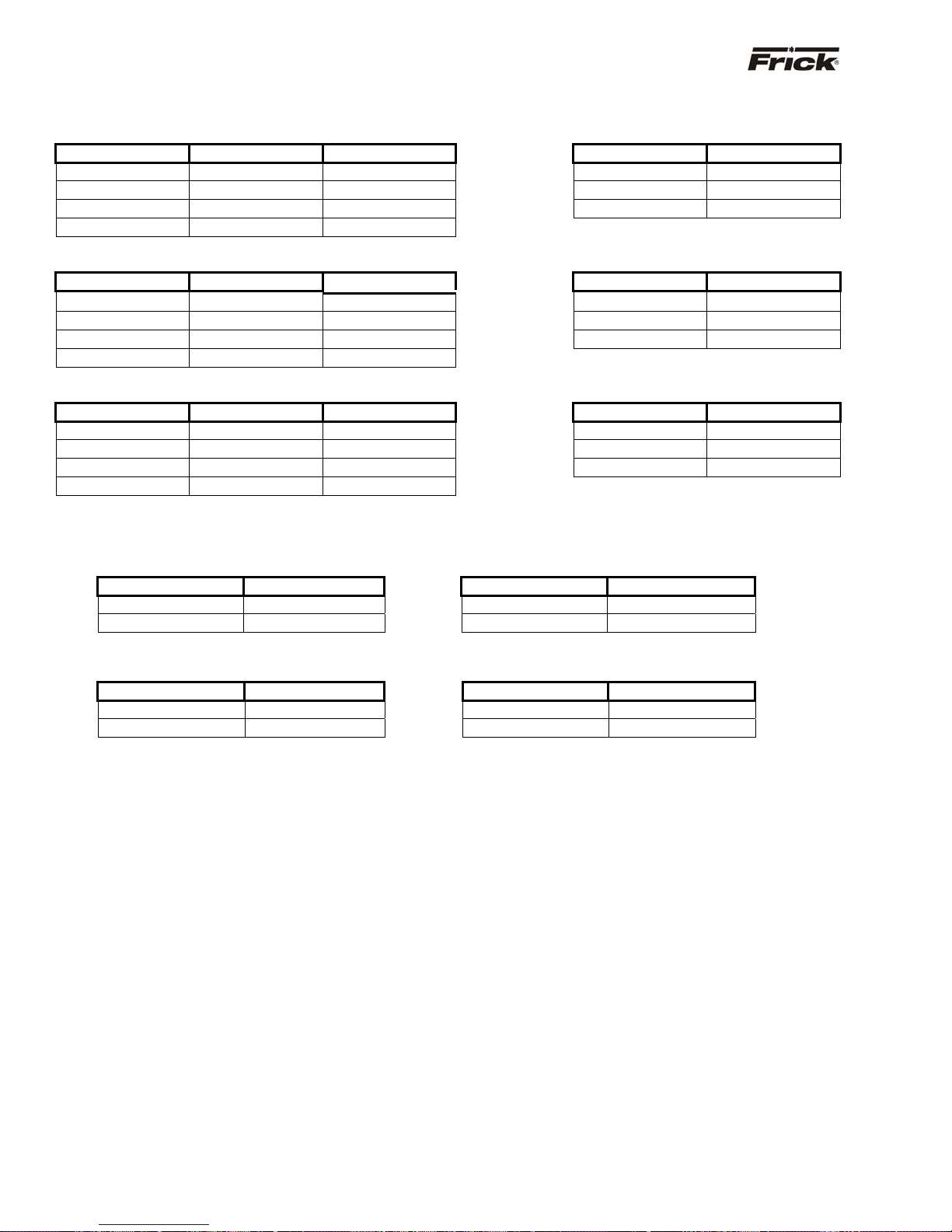
Vessel GCU Board Analog I/O Jumper Settings
Analog Input 1 -
Input Function JP8 JP9 Connector Function
0 – 5 VDC Out Out J4-10 +12 VDC
Resistance 1 - 2 Out J4-11 Input Signal
4 – 20 ma * Out * 1 – 2 * J4-12 GND
ICDT 2 - 3 Out
Analog Input 2 -
Input Function JP18 JP19 Connector Function
0 – 5 VDC Removed Removed J4-7 +12 VDC
Resistance 1 - 2 Removed J4-8 Input Signal
4 – 20 ma * Removed * 1 – 2 * J4-9 GND
ICDT 2 - 3 Removed
Analog Input 3 -
Input Function JP10 JP11 Connector Function
0 – 5 VDC Removed Removed J4-4 +12 VDC
Resistance 1 - 2 Removed J4-5 Input Signal
4 – 20 ma * Removed * 1 – 2 * J4-6 GND
ICDT 2 - 3 Removed
Analog Input 4 - Vessel Pressure #1
Input Function JP20 JP21 Connector Function
0 – 5 VDC * Removed * Removed * J4-1 +12 VDC
Resistance 1 - 2 Removed J4-2 Input Signal
4 – 20 ma Removed 1 – 2 J4-3 GND
ICDT 2 - 3 Removed
Analog Input 5 -
Input Function JP12 JP13 Connector Function
0 – 5 VDC * Removed * Removed * J5-10 +12 VDC
Resistance 1 - 2 Removed J5-11 Input Signal
4 – 20 ma Removed 1 – 2 J5-12 GND
ICDT 2 - 3 Removed
Analog Input 6 -
Input Function JP22 JP23 Connector Function
0 – 5 VDC * Removed * Removed * J5-7 +12 VDC
Resistance 1 - 2 Removed J5-8 Input Signal
4 – 20 ma Removed 1 – 2 J5-9 GND
ICDT 2 - 3 Removed
Analog Input 7 - Refrigeration Pump Pressure #1
Input Function JP14 JP15 Connector Function
0 – 5 VDC * Removed * Removed * J5-4 +12 VDC
Resistance 1 - 2 Removed J5-5 Input Signal
4 – 20 ma Removed 1 – 2 J5-6 GND
ICDT 2 - 3 Removed
Analog Input 8 - Refrigeration Pump Pressure #2
Input Function JP24 JP25 Connector Function
0 – 5 VDC * Removed * Removed * J5-1 +12 VDC
Resistance 1 - 2 Removed J5-2 Input Signal
4 – 20 ma Removed 1 – 2 J5-3 GND
ICDT 2 - 3 Removed
essel Level #1
essel Level #2
essel Level #3
essel Pressure #2
essel Pressure #3
nalog Input 1 Sensor Wiring
nalog Input 2 Sensor Wiring
nalog Input 3 Sensor Wiring
nalog Input 4 Sensor Wiring
nalog Input 5 Sensor Wiring
nalog Input 6 Sensor Wiring
nalog Input 7 Sensor Wiring
nalog Input 8 Sensor Wiring
Page 14
A
A
A
S90-555 M FRICK QUANTUM™ CONDENSER/VESSEL CONTROL PANEL
Page 14 MAINTENANCE
Vessel GCU Board Analog I/O Jumper Settings (Continued)
Analog Input 9 - Refrigeration Pump Pressure #3
Input Function JP16 JP17 Connector Function
0 – 5 VDC * Removed * Removed * J11-7 +12 VDC
Resistance 1 - 2 Removed J11-8 Input Signal
4 – 20 ma Removed 1 – 2 J11-9 GND
ICDT 2 - 3 Removed
Analog Input 10 - Analog Auxiliary 1
Input Function JP26 JP27 Connector Function
0 – 5 VDC * Removed * Removed * J11-4 +12 VDC
Resistance 1 - 2 Removed J11-5 Input Signal
4 – 20 ma Removed 1 – 2 J11-6 GND
ICDT 2 - 3 Removed
Analog Input 11 - Analog Auxiliary 1
Input Function JP6 JP7 Connector Function
0 – 5 VDC * Removed * Removed * J11-1 +12 VDC
Resistance 1 - 2 Removed J11-2 Input Signal
4 – 20 ma Removed 1 – 2 J11-3 GND
ICDT 2 - 3 Removed
Analog Output Configurations
Analog Output 1 Sensor Wiring -
Analog Output 2 Sensor Wiring -
Vessel #1 Modulating Valve
Connector Function Connector Function
J8-8 Output Signal J8-6 Output Signal
J8-7 GND J8-5 GND
Analog Output 3 Sensor Wiring -
Analog Output 4 Sensor Wiring -
Vessel #2 Modulating Valve
Vessel #3 Modulating Valve
Connector Function Connector Function
J8-4 Output Signal J8-2 Output Signal
J8-3 GND J8-1 GND
nalog Input 9 Sensor Wiring
nalog Input 10 Sensor Wiring
nalog Input 11 Sensor Wiring
Future
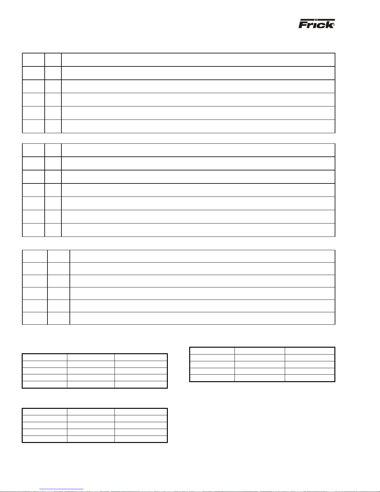
Condenser GCU Board Analog I/O Jumper Settings
Page 15
A
A
A
A
A
A
A
A
A
MAINTENANCE Page 15
FRICK QUANTUM™ CONDENSER/VESSEL CONTROL PANEL S90-555 M
nalog Input 1 - Condenser Pressure
Input Function JP8 JP9 Connector Function
0 – 5 VDC * Out * Out * J4-10 +12 VDC
Resistance 1 - 2 Out J4-11 Input Signal
4 – 20 ma Out 1 – 2 J4-12 GND
ICDT 2 - 3 Out
Analog Input 2 - Outside Air Temperature
Input Function JP18 JP19 Connector Function
0 – 5 VDC Removed Remov ed J4-7 +12 VDC
Resistance 1 - 2 Removed J4-8 Input Signal
4 – 20 ma Removed 1 – 2 J4-9 GND
ICDT * 2 - 3 * Removed *
Analog Input 3 - Outside Air Humidity
Input Function JP10 JP11 Connector Function
0 – 5 VDC Removed Removed J4-4 +12 VDC
Resistance 1 - 2 Removed J4-5 Input Signal
4 – 20 ma * Removed * 1 – 2 * J4-6 GND
ICDT 2 - 3 Removed
Analog Input 4 - Condenser Drain Temp. (Refrigerant)
Input Function JP20 JP21 Connector Function
0 – 5 VDC Removed Removed J4-1 +12 VDC
Resistance 1 - 2 Removed J4-2 Input Signal
4 – 20 ma Removed 1 – 2 J4-3 GND
ICDT * 2 - 3 * Removed *
Analog Input 5 - Future
Input Function JP12 JP13 Connector Function
0 – 5 VDC Removed Remov ed J5-10 +12 VDC
Resistance 1 - 2 Removed J5-11 Input Signal
4 – 20 ma * Removed * 1 – 2 * J5-12 GND
ICDT 2 - 3 Removed
Analog Input 6 - Future
Input Function JP22 JP23 Connector Function
0 – 5 VDC Removed Remov ed J5-7 +12 VDC
Resistance 1 - 2 Removed J5-8 Input Signal
4 – 20 ma * Removed * 1 – 2 * J5-9 GND
ICDT 2 - 3 Removed
Analog Input 7 - Future
Input Function JP14 JP15 Connector Function
0 – 5 VDC Removed Remov ed J5-4 +12 VDC
Resistance 1 - 2 Removed J5-5 Input Signal
4 – 20 ma * Removed * 1 – 2 * J5-6 GND
ICDT 2 - 3 Removed
Analog Input 8 - Future
Input Function JP24 JP25 Connector Function
0 – 5 VDC Removed Remov ed J5-1 +12 VDC
Resistance 1 - 2 Removed J5-2 Input Signal
4 – 20 ma * Removed * 1 – 2 * J5-3 GND
ICDT 2 - 3 Removed
nalog Input 1 Sensor Wiring
nalog Input 2 Sensor Wiring
nalog Input 3 Sensor Wiring
nalog Input 4 Sensor Wiring
nalog Input 5 Sensor Wiring
nalog Input 6 Sensor Wiring
nalog Input 7 Sensor Wiring
nalog Input 8 Sensor Wiring
Page 16
A
A
A
A
A
S90-555 M FRICK QUANTUM™ CONDENSER/VESSEL CONTROL PANEL
Page 16 MAINTENANCE
Condenser GCU Board Analog I/O Jumper Settings (Continued)
Analog Input 9 - Future
Input Function JP16 JP17 Connector Function
0 – 5 VDC Removed Remov ed J11-7 +12 VDC
Resistance 1 - 2 Removed J11-8 Input Signal
4 – 20 ma * Removed * 1 – 2 * J11-9 GND
ICDT 2 - 3 Removed
Analog Input 10 - Future
Input Function JP26 JP27 Connector Function
0 – 5 VDC Removed Remov ed J11-4 +12 VDC
Resistance 1 - 2 Removed J11-5 Input Signal
4 – 20 ma * Removed * 1 – 2 * J11-6 GND
ICDT 2 - 3 Removed
Analog Input 11 - Future
Input Function JP6 JP7 Connector Function
0 – 5 VDC Removed Remov ed J11-1 +12 VDC
Resistance 1 - 2 Removed J11-2 Input Signal
4 – 20 ma * Removed * 1 – 2 * J11-3 GND
ICDT 2 - 3 Removed
Analog Output Configurations
Analog Output 1 Sensor Wiring -
Variable Fan 1
Connector Function Connector Function
J8-8 Output Signal J8-6 Output Signal
J8-7 GND J8-5 GND
Analog Output 3 Sensor Wiring -
Variable Fan 3
Connector Function Connector Function
J8-4 Output Signal J8-2 Output Signal
J8-3 GND J8-1 GND
nalog Output 2 Sensor Wiring -
Variable Fan 2
nalog Output 4 Sensor Wiring -
Variable Fan 4
nalog Input 9 Sensor Wiring
nalog Input 10 Sensor Wiring
nalog Input 11 Sensor Wiring
Page 17

FRICK QUANTUM™ CONDENSER/VESSEL CONTROL PANEL S90-555 M
MAINTENANCE Page 17
QUANTUM™ 3 MAIN PROCESSOR BOARD
Quantum™ 3 Motherboard Jumpers
LK1-1 LK1-2 COM3 IRQ Routing (DO NOT MODIFY)
A * A * RS-232 Interface Selected
A B Not Valid Combination
B A Not Valid Combination
B B Touchscreen Controller Interface Selected
LK2 COM3 IRQ Routing (DO NOT MODIFY)
A IRQ4
B * IRQ11
LK3 COM4 IRQ Routing (DO NOT MODIFY)
A IRQ3
B * IRQ10
LK4 RS-422 Termination (DO NOT MODIFY)
In * RS-422 Terminated
Out RS-422 Terminated
LK5 RS-485 Receiver (DO NOT MODIFY)
In RS-485 Receiver Enabled
Out * RS-485 Receiver Disabled
LK6 RS-485 Termination (DO NOT MODIFY)
In * RS-485 Terminated
Out RS-485 Not Terminated
* Standard Setting
LK7 Watc hdog Ti me r Enable
In Enabled
Out * Disabled
LK8 Watchdog timer Enable
In 2 second timeout
Out * 8 second timeout
LK9 Clear CMOS/Battery Disable (DO NOT MODIFY)
A Battery Backup Enabled
B * Battery Backup Disabled (CMOS RAM Clear ed)
LK10 LCD Backlight Voltage Supply Voltage
A +5V Backlight
B * +12V Backlight
LK11 LCD Panel Power Supply Voltage
A * +5V Supply (Samsung, NEC or Sharp Displays)
B +3.3V Supply (LG Phillips Display)
LK12 User Application Link (DO NOT MODIFY)
In * Bit 1 of 259H "Logic 1"
Out Bit 1 of 259H "Logic 0"
LK13 User Application Link (DO NOT MODIFY)
In * Bit 2 of 259H "Logic 1"
Out Bit 2 of 259H "Logic 0"
Page 18
(
g)
p
p
S90-555 M FRICK QUANTUM™ CONDENSER/VESSEL CONTROL PANEL
Page 18 MAINTENANCE
Quantum™ 3 Communications Board Jumpers
COM-1 (Jumpers located adjacent to connector TB1)
In*
Link 1
Link 2
Link 3
Link 4
Link 5
Link 16
Pull down Rx- / Tx- (RS485) or Rx- (RS422) line to GND (0V) via a 10K resistor. (standard setting)
out
No pull down
in
Terminate Rx / Tx (RS485) or Rx (RS422) lines with a 120W resistor. (standard setting)
out*
No termination (standard setting)
in*
Pull up Rx+ / Tx+ (RS485) or Rx+ (RS422) line to VCC (5V) via a 10K resistor. (standard setting)
out
No termination.
in*
Pull down Tx- (RS422) line to GND (0V) via a 10K resistor. (standard setting)
out
No pull down.
in*
Pull up COM2 Tx+ (RS422) line to VCC (5V) via a 10K resistor. (standard setting)
out
No pull down.
A* B RS485 (standard setting)
RS422
COM-2 (Jumpers located adjacent to connector TB2)
In*
Link 6
Link 7
Link 8
Link 9
Link 10
Link 17
Link 19
Pull down Rx- / Tx- (RS485) or Rx- (RS422) line to GND (0V) via a 10K resistor. (standard setting)
out
No pull down
in
Terminate Rx / Tx (RS485) or Rx (RS422) lines with a 120W resistor. (standard setting)
out*
No termination (standard setting)
in*
Pull up Rx+ / Tx+ (RS485) or Rx+ (RS422) line to VCC (5V) via a 10K resistor. (standard setting)
out
No termination.
in*
Pull down Tx- (RS422) line to GND (0V) via a 10K resistor. (standard setting)
out
No pull down.
in*
Pull up COM2 Tx+ (RS422) line to VCC (5V) via a 10K resistor. (standard setting)
out
No pull down.
A* B RS485 (standard setting)
RS422
in*
Select RS422/RS485 comms mode. (standard setting)
out
Select RS232 comms mode.
COM-3 (Jumpers located adjacent to connector TB3)
In*
Link 11
Link 12
Link 13
Link 14
Link 15
Link 18
out
out*
out
out
out
Pull down Rx- / Tx- (RS485) or Rx- (RS422) line to GND (0V) via a 10K resistor. (standard setting)
No pull down
in
Terminate Rx / Tx (RS485) or Rx (RS422) lines with a 120W resistor. (standard setting)
No termination
in*
Pull up Rx+ / Tx+ (RS485) or Rx+ (RS422) line to VCC (5V) via a 10K resistor. (standard setting)
standard settin
No termination.
in*
Pull down Tx- (RS422) line to GND (0V) via a 10K resistor. (standard setting)
ull down.
No
in*
Pull up COM2 Tx+ (RS422) line to VCC (5V) via a 10K resistor. (standard setting)
No
ull down.
A* B RS485 (standard setting)
RS422
Quantum™ 3 Communications Wiring
TB1 - COM1 RS-485/422 (Used for Sequencing):
4-way screw terminal
Pin Signal (RS-422) Signal (RS-485)
4 COM1 TX+ 3 COM1 TX- 2 COM1 RX+ COM1 TX+ / RX+
1 COM1 RX- COM1 TX- / RX-
TB2 - COM2 RS-485/422 (Standard Communications):
4-way screw terminal
Pin Signal (RS-422) Signal (RS-485)
4 COM2 TX+ 3 COM2 TX- 2 COM2 RX+ COM2 TX+ / RX+
1 COM2 RX- COM2 TX- / RX-
TB3- COM3 RS-485/422: 4-way screw terminal
Pin Signal (RS-422) Signal (RS-485)
4 COM3 TX+ 3 COM3 TX- 2 COM3 RX+ COM3 TX+ / RX+
1 COM3 RX- COM3 TX- / RX-
Page 19
3
45670
2
A
T
FRICK QUANTUM™ CONDENSER/VESSEL CONTROL PANEL S90-555 M
MAINTENANCE Page 19
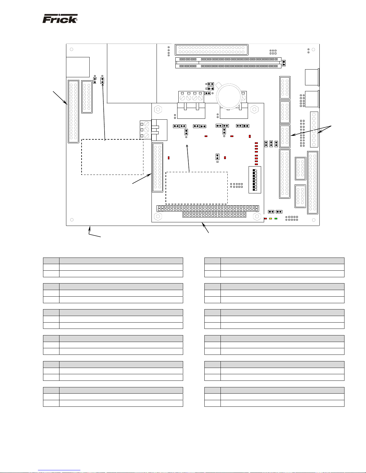
QUANTUM™ 4 MAIN PROCESSOR BOARD
LCD
Display &
Inverter
Cable
(Plugs into
PL15)
PL5
Flash Card
LK4
LK3
A
B
PL11
PL15
This assembly is shipped with LK4
set to "B" position for an LG Phillips
display (11.75" backplate).
If using a Samsung, NEC or Sharp
Display, set LK4 to position "A"
(12.75" backplate).
Socket
(Located
board)
Keypad Cable
plugs into PL1
Bottom board is the
Processor Board
under
COM-2
RS-232
PL3
TB3
PL1
PL3
Quantum 4 Motherboard Jumpers
LK1 Watchdog timer timeout selection
In 2 second timeout
Out * 8 second timeout
LK2 Watchdog timer Enable
In * Enabled
Out Disabled
LK3 Backlight Voltage
A +5V Backlight
B * +12V Backlight
LK4 LCD Panel Power Supply Voltage
A +5V Supply (Samsung, NEC or Sharp Displays)
B * +3.3V Supply (LG Phillips Display)
LK5 COM4 IRQ Routing (DO NOT MODIFY)
A IRQ3
B * IRQ10
LK6 COM3 IRQ Routing (DO NOT MODIFY)
A IRQ4
B * IRQ11
* Standard Setting
PL4
B
A
LK5
LK4LK3
LK17
LK6
LK7
B2
TB1
LK2
LK6LK5
B
A
D1
B
LK11
COM-2
RS-422
RS-485
LK1
D8
To set Comm-2 for RS-232
operation, set LK17 to "A" position.
To set Comm-2 for RS-422/485
operation, set LK17 to "B" position.
PL4
Communications Board
LK7 Clear CMOS / Battery Disable (DO NOT MODIFY)
A * Battery Backup Enabled
B Battery Backup Disabled (CMOS RAM Cleared)
LK8 RS-485 Receiver (DO NOT MODIFY)
In * RS-485 Receiver Enabled
Out RS-485 Receiver Disabled
LK9 RS-485 Termination (DO NOT MODIFY)
In * RS-485 Terminated
Out RS-485 Not Terminated
LK10 RS-422 Termination (DO NOT MODIFY)
In RS-422 Terminated
Out * RS-42 2 Terminated
LK11 User Application Link (DO NOT MODIFY)
In * Bit 1 of 259H "Logic 1"
Out Bit 1 of 259H "Logic 0"
LK12 User Application Link (DO NOT MODIFY)
In * Bit 2 of 259H "Logic 1"
Out Bit 2 of 259H "Logic 0"
LK7
B
A
LK16
LK8
D6
LK10LK9
D2
PL2
Top board is the
PL2
COM-1
RS-422
RS-485
PORT 80H
D3
D4
D5
D7
D8
D10
D11
D12
D13
1 2 3 4 5 6 7 8
SW1
PL1
PL24
PL8
PL13
PL18
PL19
LK1
PL7
PL9
PL12
PL17
Power - I/O
Comm.
Harness
(Plugs into
PL12 &
PL14)
LK2
PL6
PL10
PL14
LK8
LK10
1
LK9
O
PL16
LK12
LK11
PWR
FLASH
SUSP
Page 20

S90-555 M FRICK QUANTUM™ CONDENSER/VESSEL CONTROL PANEL
Page 20 MAINTENANCE
Quantum™ 4 Communications Board Jumpers
Com-1 (TB1)
In
Link 2
Link 7
Link 8
Link 9
Link 10
Link 16
* = standard setting
Com-2 (TB2 - TB3)
Link 1
Link 3
Link 4
Link 5
Link 6
Link 11
Link 17
* = standard setting
TB1 - COM1 RS-485/422 (Used for Sequencing):
Pin Signal (RS-422) Signal (RS-485)
4 COM1 TX+ 3 COM1 TX- 2 COM1 RX+ COM1 TX+ / RX+
1 COM1 RX- COM1 TX- / RX-
TB2 - COM2 RS-485/422 (Standard Communications):
Pin Signal (RS-422) Signal (RS-485)
4 COM2 TX+ 3 COM2 TX- 2 COM2 RX+ COM2 TX+ / RX+
1 COM2 RX- COM2 TX- / RX-
Terminate COM1 Rx / Tx (RS-485) or COM1 Rx (RS-422) lines with a 120W resistor.
out*
No termination (standard setting)
In*
Pull down COM1 Rx- / Tx- (RS-485) or COM1 Rx- (RS-422) line to GND (0V) via a 10K res. (std. setting)
Out
No pull down
in*
Pull up COM1 Rx+ / Tx+ (RS-485) or COM1 Rx+ (RS-422) line to VCC (5V) via a 10K res.. (std. setting)
out
No termination.
in*
Pull down COM1 Tx- (RS-422) line to GND (0V) via a 10K resistor. (standard setting)
out
No pull down.
in*
Pull up COM1 Tx+ (RS-422) line to VCC (5V) via a 10K resistor. (standard setting)
out
No pull down.
A* B COM1 RS-485 (TB1) (standard setting)
COM1 RS-422 (TB1)
In
Terminate COM2 Rx / Tx (RS-485) or COM2 Rx (RS-422) lines with a 120W resistor.
out*
No termination (standard setting)
In*
Pull down COM2 Rx- / Tx- (RS-485) or COM2 Rx- (RS-422) line to GND (0V) via a 10K res. (std. setting)
Out
No pull down
in*
Pull up COM2 Rx+ / Tx+ (RS-485) or COM2 Rx+ (RS-422) line to VCC (5V) via a 10K res. (std. setting)
out
No termination.
in*
Pull down COM2 Tx- (RS-422) line to GND (0V) via a 10K resistor. (standard setting)
out
No pull down.
in*
Pull up COM2 Tx+ (RS-422) line to VCC (5V) via a 10K resistor. (standard setting)
out
No pull down.
A* B COM2 RS-485 (TB2) (standard setting)
COM2 RS-422 (TB2)
A
Select RS-232 comms mode for COM2 (TB3).
B*
Select RS-422/RS-485 comms mode for COM2 (TB2). (standard setting)
Quantum™ 4 Communications Wiring
TB3- COM2 RS-232 (Standard Communications):
4-way screw terminal
4-way screw terminal
3-way screw terminal
Pin Signal (RS-422)
3 Ground
2 RX
1 TX
Page 21

MAINTENANCE Page 21
FRICK QUANTUM™ CONDENSER/VESSEL CONTROL PANEL S90-555 M
DRAWING REFERENCE TABLE
DRAWING NAME DRAWING NUMBER
Quantum™ Panel DC Power Supply Diagram (Condor) N/A
Quantum™ Panel DC Power Supply Diagram (Power One) N/A
Quantum™ Control Center Assembly 649D4587
Vessel Control Center Assembly 640D0160
Wiring Diagram – Vessel W/O MOA 640D0158
Wiring Diagram – Vessel With MOA 640D0159
Condenser Control Center Assembly 640D0163
Wiring Diagram – Condenser 640D0161
Quantum™ 3 Communications Wiring Diagrams N/A
Quantum™ 4 Communications Wiring Diagrams N/A
The drawings that appear on the following pages are for reference purposes only, and are based upon the latest
revision available at the time of this printing.
Page 22

S90-555 M FRICK QUANTUM™ CONDENSER/VESSEL CONTROL PANEL
Page 22 MAINTENANCE
QUANTUM™ PANEL DC POWER SUPPLY DIAGRAM (CONDOR)
7.25
Replacement Part # 640C0022G01
R51
13
J1
5
+5V ADJ
F1
3.15
1
INPUT: J1 INPUT: J2
AMP P/N: 640445-5
.312 CTR CONNECTOR, 3 CIRCUITS
Pin 1 AC GROUND PIN 1 OUTPUT #1
Pin 3 AC NEUTRAL PIN 2 OUTPUT #1
PIN 5 AC LINE PIN 3 OUTPUT #1
PIN 4 COMMON
OUTPUT 1 +5.1V PIN 5 COMMON
OUTPUT 2 +24V PIN 6 COMMON
OUTPUT 3 -12V PIN 7 COMMON
OUTPUT 4 12V PIN 8 OUTPUT #2
PIN 9 OUTPUT #2
MATING CONNECTORS: MOLEX
HOUSING CONTACT
INPUT 26-03-4050 08-52-0113
OUTPUT 26-03-4131 08-52-0113
J2
1
AMP P/N: 1-640445-3
.156 CTR CONNECTOR, 13 CIRCUITS
PIN 10 POWER FAIL
PIN 11 OUTPUT #3
PIN 12 COMMON
PIN 13 OUTPUT #4
4.50
QUANTUM™ PANEL D.C. POWER SUPPLY DIAGRAM (POWER-ONE)
(+12V) ADJ
(+5V) ADJ
Replacement Part # 640C0022G11
V2
V1
7
Pin 7 J1
Pin 3 TB1 Pin 1
3
TB2 Pin 1
1
1
POWER FAILURE
GND
NEUTRAL
HOT
V4 (+12)
V3 (-12V)
V2 (+12V)
GND
GND
V1 (+5V)
V1 (+5V)
GND
SIGNAL
TB1
Pin 1
Pin 3
TB2
Pin 1
Pin 7
J1
Page 23

MAINTENANCE Page 23
FRICK QUANTUM™ CONDENSER/VESSEL CONTROL PANEL S90-555 M
QUANTUM™ CONTROL CENTER ASSEMBLY (SHEET 1 OF 2)
Page 24

S90-555 M FRICK QUANTUM™ CONDENSER/VESSEL CONTROL PANEL
Page 24 MAINTENANCE
QUANTUM™ CONTROL CENTER ASSEMBLY (SHEET 2 OF 2)
Page 25

MAINTENANCE Page 25
FRICK QUANTUM™ CONDENSER/VESSEL CONTROL PANEL S90-555 M
VESSEL CONTROL CENTER ASSEMBLY (Sheet 1 of 6)
Page 26

S90-555 M FRICK QUANTUM™ CONDENSER/VESSEL CONTROL PANEL
Page 26 MAINTENANCE
VESSEL CONTROL CENTER ASSEMBLY (Sheet 2 of 6)
Page 27

MAINTENANCE Page 27
FRICK QUANTUM™ CONDENSER/VESSEL CONTROL PANEL S90-555 M
VESSEL CONTROL CENTER ASSEMBLY (Sheet 3 of 6)
Page 28

S90-555 M FRICK QUANTUM™ CONDENSER/VESSEL CONTROL PANEL
Page 28 MAINTENANCE
VESSEL CONTROL CENTER ASSEMBLY (Sheet 4 of 6)
Page 29

MAINTENANCE Page 29
FRICK QUANTUM™ CONDENSER/VESSEL CONTROL PANEL S90-555 M
VESSEL CONTROL CENTER ASSEMBLY (Sheet 5 of 6)
Page 30

S90-555 M FRICK QUANTUM™ CONDENSER/VESSEL CONTROL PANEL
Page 30 MAINTENANCE
VESSEL CONTROL CENTER ASSEMBLY (Sheet 6 of 6)
Page 31

MAINTENANCE Page 31
FRICK QUANTUM™ CONDENSER/VESSEL CONTROL PANEL S90-555 M
WIRING DIAGRAM – VESSEL W/O MOA (Sheet 1 of 6)
Page 32

S90-555 M FRICK QUANTUM™ CONDENSER/VESSEL CONTROL PANEL
Page 32 MAINTENANCE
WIRING DIAGRAM – VESSEL W/O MOA (Sheet 2 of 6)
Page 33

MAINTENANCE Page 33
FRICK QUANTUM™ CONDENSER/VESSEL CONTROL PANEL S90-555 M
WIRING DIAGRAM – VESSEL W/O MOA (Sheet 3 of 6)
Page 34

S90-555 M FRICK QUANTUM™ CONDENSER/VESSEL CONTROL PANEL
Page 34 MAINTENANCE
WIRING DIAGRAM – VESSEL W/O MOA (Sheet 4 of 6)
Page 35

MAINTENANCE Page 35
FRICK QUANTUM™ CONDENSER/VESSEL CONTROL PANEL S90-555 M
WIRING DIAGRAM – VESSEL W/O MOA (Sheet 5 of 6)
Page 36

S90-555 M FRICK QUANTUM™ CONDENSER/VESSEL CONTROL PANEL
Page 36 MAINTENANCE
WIRING DIAGRAM – VESSEL W/O MOA (Sheet 6 of 6)
Page 37

FRICK QUANTUM™ CONDENSER/VESSEL CONTROL PANEL S90-555 M
MAINTENANCE Page 37
WIRING DIAGRAM – VESSEL WITH MOA (Sheet 1 of 6)
Page 38

S90-555 M FRICK QUANTUM™ CONDENSER/VESSEL CONTROL PANEL
Page 38 MAINTENANCE
WIRING DIAGRAM – VESSEL WITH MOA (Sheet 2 of 6)
Page 39

MAINTENANCE Page 39
FRICK QUANTUM™ CONDENSER/VESSEL CONTROL PANEL S90-555 M
WIRING DIAGRAM – VESSEL WITH MOA (Sheet 3 of 6)
Page 40

S90-555 M FRICK QUANTUM™ CONDENSER/VESSEL CONTROL PANEL
Page 40 MAINTENANCE
WIRING DIAGRAM – VESSEL WITH MOA (Sheet 4 of 6)
Page 41

MAINTENANCE Page 41
FRICK QUANTUM™ CONDENSER/VESSEL CONTROL PANEL S90-555 M
WIRING DIAGRAM – VESSEL WITH MOA (Sheet 5 of 6)
Page 42

S90-555 M FRICK QUANTUM™ CONDENSER/VESSEL CONTROL PANEL
Page 42 MAINTENANCE
WIRING DIAGRAM – VESSEL WITH MOA (Sheet 6 of 6)
Page 43

MAINTENANCE Page 43
FRICK QUANTUM™ CONDENSER/VESSEL CONTROL PANEL S90-555 M
CONDENSER CONTROL CENTER ASSEMBLY (Sheet 1 of 10)
Page 44

S90-555 M FRICK QUANTUM™ CONDENSER/VESSEL CONTROL PANEL
Page 44 MAINTENANCE
CONDENSER CONTROL CENTER ASSEMBLY (Sheet 2 of 10)
Page 45

MAINTENANCE Page 45
FRICK QUANTUM™ CONDENSER/VESSEL CONTROL PANEL S90-555 M
CONDENSER CONTROL CENTER ASSEMBLY (Sheet 3 of 10)
Page 46

S90-555 M FRICK QUANTUM™ CONDENSER/VESSEL CONTROL PANEL
Page 46 MAINTENANCE
CONDENSER CONTROL CENTER ASSEMBLY (Sheet 4 of 10)
Page 47

FRICK QUANTUM™ CONDENSER/VESSEL CONTROL PANEL S90-555 M
MAINTENANCE Page 47
CONDENSER CONTROL CENTER ASSEMBLY (Sheet 5 of 10)
Page 48

S90-555 M FRICK QUANTUM™ CONDENSER/VESSEL CONTROL PANEL
Page 48 MAINTENANCE
CONDENSER CONTROL CENTER ASSEMBLY (Sheet 6 of 10)
Page 49

MAINTENANCE Page 49
FRICK QUANTUM™ CONDENSER/VESSEL CONTROL PANEL S90-555 M
CONDENSER CONTROL CENTER ASSEMBLY (Sheet 7 of 10)
Page 50

S90-555 M FRICK QUANTUM™ CONDENSER/VESSEL CONTROL PANEL
Page 50 MAINTENANCE
CONDENSER CONTROL CENTER ASSEMBLY (Sheet 8 of 10)
Page 51

MAINTENANCE Page 51
FRICK QUANTUM™ CONDENSER/VESSEL CONTROL PANEL S90-555 M
CONDENSER CONTROL CENTER ASSEMBLY (Sheet 9 of 10)
Page 52

S90-555 M FRICK QUANTUM™ CONDENSER/VESSEL CONTROL PANEL
Page 52 MAINTENANCE
CONDENSER CONTROL CENTER ASSEMBLY (Sheet 10 of 10)
Page 53

MAINTENANCE Page 53
FRICK QUANTUM™ CONDENSER/VESSEL CONTROL PANEL S90-555 M
WIRING DIAGRAM – CONDENSER (Sheet 1 of 6)
Page 54

S90-555 M FRICK QUANTUM™ CONDENSER/VESSEL CONTROL PANEL
Page 54 MAINTENANCE
WIRING DIAGRAM – CONDENSER (Sheet 2 of 6)
Page 55

MAINTENANCE Page 55
FRICK QUANTUM™ CONDENSER/VESSEL CONTROL PANEL S90-555 M
WIRING DIAGRAM – CONDENSER (Sheet 3 of 6)
Page 56

S90-555 M FRICK QUANTUM™ CONDENSER/VESSEL CONTROL PANEL
Page 56 MAINTENANCE
WIRING DIAGRAM – CONDENSER (Sheet 4 of 6)
Page 57

MAINTENANCE Page 57
FRICK QUANTUM™ CONDENSER/VESSEL CONTROL PANEL S90-555 M
WIRING DIAGRAM – CONDENSER (Sheet 5 of 6)
Page 58

S90-555 M FRICK QUANTUM™ CONDENSER/VESSEL CONTROL PANEL
Page 58 MAINTENANCE
WIRING DIAGRAM – CONDENSER (Sheet 6 of 6)
Page 59

(
)
V
To Customer
Remote
Computer / DCS
System
To Customer
Remote
Computer / DCS
System
Quantum
Controller
FRICK QUANTUM™ CONDENSER/VESSEL CONTROL PANEL S90-555 M
MAINTENANCE Page 59
QUANTUM™ 3 COMMUNICATIONS WIRING DIAGRAMS
TO CUSTOMER REMOTE COMPUTER/DCS
RS-485 COMMUNICATIONS
-RX/-TX
+RX/+TX
Belden #8761
#22 AWG or Equal
BLK
CLR
COM2
(TB2)
1
2
3
4
QUANTUM™ QUANTUM™
Belden #8761
#22 AWG or Equal
BLK
CLR
BLK
CLR
COM2
(TB2)
1
2
3
4
Belden #8761
#22 AWG or Equal
BLK
CLR
COM2
(TB2)
BLK
CLR
1
2
3
4
QUANTUM™
-RX/-TX
+RX/+TX
TO CUSTOMER REMOTE COMPUTER/DCS
-TX
+TX
-RX
+RX
Belden #8777
#22 AWG or Equal
BLK
GRN
Belden #8777
#22 AWG or Equal
BLK
RED
RS-422 COMMUNICATIONS
COM2
(TB2)
1
2
Belden #8777
#22 AWG or Equal
BLK
GRN
Belden #8777
#22 AWG or Equal
3
BLK
RED
4
QUANTUM™
COM2
(TB2)
BLK
GRN
BLK
RED
Belden #8777
#22 AWG or Equal
1
BLK
GRN
2
Belden #8777
#22 AWG or Equal
3
BLK
RED
4
QUANTUM™ QUANTUM™
COM2
TB2
BLK
GRN
BLK
RED
-RX
1
+RX
2
-TX
3
+TX
4
TO CONDENSER / VESSEL (GCU) BOARDS
-RX / -TX
+RX / +TX
BLK
RED
RS-232 COMMUNICATIONS
PORT 1
(J-2)
BLK
RED
P2
P3
BLK
RED
PORT 1
(J-2)
BLK
RED
P2
P3
CONDENSER
ESSEL PANEL
Page 60

(
S90-555 M FRICK QUANTUM™ CONDENSER/VESSEL CONTROL PANEL
Page 60 MAINTENANCE
QUANTUM™ 4 COMMUNICATIONS WIRING DIAGRAMS
TO CUSTOMER REMOTE COMPUTER/DCS
RS-485 COMMUNICATIONS
To Customer
Remote
Computer / DCS
System
-RX/-TX
+RX/+TX
Belden #8761
#22 AWG or Equal
BLK
CLR
COM2
(TB2)
1
2
3
4
QUANTUM™ QUANTUM™ QUANTUM™
Belden #8761
#22 AWG or Equal
BLK
CLR
BLK
CLR
COM2
(TB2)
#22 AWG or Equal
1
BLK
2
CLR
3
4
Belden #8761
TO CUSTOMER REMOTE COMPUTER/DCS
RS-422 COMMUNICATIONS
COM2
(TB2)
BLK
GRN
BLK
RED
Belden #8777
#22 AWG or Equal
1
BLK
GRN
2
Belden #8777
#22 AWG or Equal
3
BLK
RED
4
QUANTUM™ QUANTUM™
To Customer
Remote
Computer / DCS
System
-TX
+TX
-RX
+RX
Belden #8777
#22 AWG or Equal
BLK
GRN
Belden #8777
#22 AWG or Equal
BLK
RED
COM2
(TB2)
1
2
3
4
QUANTUM™
Belden #8777
#22 AWG or Equal
BLK
GRN
Belden #8777
#22 AWG or Equal
BLK
RED
TO CONDENSER / VESSEL (GCU) BOARDS
RS-232 COMMUNICATIONS
Quantum
Controller
-RX / -TX
+RX / +TX
BLK
RED
BLK
RED
PORT 1
(J-2)
P2
P3
BLK
RED
CONDENSER
COM2
(TB2)
BLK
CLR
BLK
GRN
BLK
RED
BLK
RED
COM2
TB2)
PORT 1
(J-2)
1
-RX/-TX
2
+RX/+TX
3
4
1
2
3
4
P2
P3
VESSEL PANEL
-RX
+RX
-TX
+TX
Page 61

FRICK QUANTUM™ CONDENSER/VESSEL CONTROL PANEL S90-555 M
MAINTENANCE Page 61
CONVENSER/VESSEL RECOMMENDED SPARE PARTS
QUANTUM™ CONTROL PANEL
Part Number Description Spare-1 Spare-2 Spare-3
649D4824H01 Display cable (Quantum™ 4, see chart below) yes
649C1091G04 Main Pentium processor circuit board (Quantum™ 4) yes 1
649C1092G04 Main Pentium processor circuit board (Quantum™ 3) yes 1
649C1078H01 10.4"diag. LCD color VGA display assembly with backlight yes
649B0862H01 Wire Harness Adapter (Quantum™ 4) yes
649A0883H10 Circuit Breaker, 10A yes
640D0060H01 Keypad/overlay yes
640B0065H01 Display Cable (Quantum™ 3 & LG Phillips display, see chart below) yes
640B0049H01 AC Power Cable Harness for Quantum™ yes
640B0048H01 Power Cable Harness, I/O, DC, Condor yes
640B0045H01 Display Cable (Quantum™ 3 & Sharp display, see chart below) yes
640B0032H01 Back light (CCFT) inverter cable (Quantum™ 3) yes
640B0031H01 Keypad cable yes
640C0039H02 Cable Harness, Power yes
333Q0001637 DC Power Supply, Condor yes yes
333Q0001582 Inverter, for Sharp & LG Phillips yes
333Q0001418 Corcom RF Line Filter yes yes yes
333Q0001649 On/off power switch contact block yes yes
333Q0001764 On/off power switch yes yes
333Q0001786 Battery, 3V, Varta # CR2032
REMOTE PANEL
Part Number Description Spare-1 Spare-2 Spare-3
649B0776H01 HOA Switch Module, 120 v (Optional) yes
649A0883H03 Circuit Breaker, 3A (Optional w/Heater) yes
649A0883H10 Circuit Breaker, 10A yes
640D0117H01 Control, GCU Board yes
640D0062H01 Digital Input/output circuit board (Optional) yes
640C0056H01 Wire Harness, DC Power, Condor GSC25A Power Supply yes
640B0066H01 Wire Harness, Power & Comm. To Digital Board (Optional) yes
640B0060H01 DC Power Supply, Condor yes yes
640B0059H01 Wire harness , AC power yes
640C0049H01 Wire harness , DC power yes
333Q0001179 Heater, Flex, 150W, 120VAC, Built-in thermostat (Optional) yes
333Q0000116 Input Module 120 volt AC yes yes yes
111Q0281061 Output Module 120/240 volt AC yes yes yes
Note 1 – These processor boards are listed for reference. Each Quantum™ Control will have only one of these
boards. Order only the replacement board that is applicable to your controller, not both boards.
Spare-1 - Normal spare parts kept on hand. Operation can wait more than 24 hours to receive replacement parts.
Spare-2 - Additional spare parts kept on hand. Operation must have parts in less than 24 hours.
Spare-3 - Critical operation. Plant must have continuous operation.
DISPLAY ASSEMBLY COMPONENT REPLACEMENT GUIDE
MANUFACTURER
DESCRIPTION
SAMSUNG
NEC
(OBSOLETE)
10.4” TFT Display 333Q0001180 333Q0001494 333Q0001581 649C1078H01
Backlight Inverter
333Q0001582 (OR
333Q0001181)
333Q0001495 333Q0001582 333Q0001582
Cable - CPU to Display (Quantum™ 3) 640B0036H01 640B0043H01 640B0045H01 640B0065H01
Cable - CPU to Inverter (Quantum™ 3) 640B0032H01 640B0044H01 640B0032H01 640B0032H01
Cable - CPU to Display/Inverter (Quantum™ 4) 649D4824H01 SEE NOTE "A" 649D4824H01 649D4824H01
Replacement - Backlight Not Available 333Q0001587 333Q0001588 333Q0001785
Display Replacement Assy. 640C0021G01
NOTE : When upgrading from a Quantum™ 3 w ith an NEC Display, to the Quantum™ 4, the displa y will need to be upgraded also.
Order 640C0052G01 to replace the display. The LK4 jumper will need to be in the "A" position.
640C0021G01
Rev (A)
SHARP LG PHILIPS
(CURRENT)
640C0021G01
Rev (B)
640C0052G01
Page 62

S90-555 M FRICK QUANTUM™ CONDENSER/VESSEL CONTROL PANEL
Page 62 MAINTENANCE
YORK Refrigeration
100 CV Avenue, P.O. Box 997 Waynesboro, Pennsylvania USA 17268-0997
Phone: 717-762-2121
Printed in U.S.A.
Subject To Change Without Notice
Fax: 717-762-8624 www.frickcold.com
 Loading...