

Page 1

Symphony™ DSP56724/DSP56725
Multi-Core Audio Processors
Reference Manual
Document Number: DSP56724RM
Rev. 0
6/2008
Page 2

How to Reach Us:
Home Page:
www.freescale.com
Web Support:
http://www.freescale.com/support
USA/Europe or Locations Not Listed:
Freescale Semiconductor, Inc.
Technical Information Center, EL516
2100 East Elliot Road
Tempe, Arizona 85284
+1-800-521-6274 or
+1-480-768-2130
www.freescale.com/support
Europe, Middle East, and Africa:
Freescale Halbleiter Deutschland GmbH
Technical Information Center
Schatzbogen 7
81829 Muenchen, Germany
+44 1296 380 456 (English)
+46 8 52200080 (English)
+49 89 92103 559 (German)
+33 1 69 35 48 48 (French)
www.freescale.com/support
Japan:
Freescale Semiconductor Japan Ltd.
Headquarters
ARCO Tower 15F
1-8-1, Shimo-Meguro, Meguro-ku
Tokyo 153-0064
Japan
0120 191014 or
+81 3 5437 9125
[email protected]
Asia/Pacific:
Freescale Semiconductor China Ltd.
Exchange Building 23F
No. 118 Jianguo Road
Chaoyang District
Beijing 100022
China
+86 010 5879 8000
[email protected]
For Literature Requests Only:
Freescale Semiconductor
Literature Distribution Center
P.O. Box 5405
Denver, Colorado 80217
+1-800 441-2447 or
+1-303-675-2140
Fax: +1-303-675-2150
LDCForFreescaleSemiconductor
@hibbertgroup.com
Information in this document is provided solely to enable system and software implementers to use
Freescale Semiconductor products. There are no express or implied copyright licenses granted
hereunder to design or fabricate any integrated circuits or integrated circuits based on the information
in this document.
Freescale Semiconductor reserves the right to make changes without further notice to any products
herein. Freescale Semiconductor makes no warranty, representation or guarantee regarding the
suitability of its products for any particular purpose, nor does Freescale Semiconductor assume any
liability arising out of the application o r use of any product or circuit, and specifically disclaims any
and all liability, including without limitation consequential or incidental damages. “Typical” parameters
that may be provided in Freescale Semiconductor data sheets and/or specifications can and do vary
in different applications and actual performance may vary over time. All operating parameters,
including “Typicals”, must be validated for each customer application by customer’s technical experts.
Freescale Semiconductor does not convey any license under its patent rights nor the rights of others.
Freescale Semiconductor products are not designed, intended, or author ized for use as components
in systems intended for surgical implant into the b ody, or other applications intended to support or
sustain life, or for any other application in which the failure of the Freescale Semiconductor product
could create a situation where personal injury or death may occur. Should Buyer purchase or use
Freescale Semiconductor products for any such unintended or unauthorized application, Buyer shall
indemnify and hold Freescale Semiconductor and its officers, emp loyees, subsidiaries, affiliates, and
distributors harmless against all claims, costs, damages, and expenses, and reasonable attorney
fees arising out of, directly or indirectly, any claim of personal injur y or death associated with such
unintended or unauthorized use, even if such claim alleges that Freescale Semiconductor was
negligent regarding the design or manufacture of the part.
Freescale™ and the Freescale logo are trademarks of Freescale Semiconductor, Inc. All other
product or service names are the property of their respective owners.
© Freescale Semiconductor, Inc. 2008. All rights reserved.
Document Number: DSP56724RM
Rev. 0, 06/16/2008
Page 3

Contents
Chapter 1
Introduction
1.1 Overview. . . . . . . . . . . . . . . . . . . . . . . . . . . . . . . . . . . . . . . . . . . . . . . . . . . . . . . . . . . . . . . . . . . 1-1
1.2 Block Dia g ram . . . . . . . . . . . . . . . . . . . . . . . . . . . . . . . . . . . . . . . . . . . . . . . . . . . . . . . . . . . . . . 1-3
1.3 Features. . . . . . . . . . . . . . . . . . . . . . . . . . . . . . . . . . . . . . . . . . . . . . . . . . . . . . . . . . . . . . . . . . . . 1-4
1.4 Overview of Peripherals . . . . . . . . . . . . . . . . . . . . . . . . . . . . . . . . . . . . . . . . . . . . . . . . . . . . . . . 1-5
1.4.1 Direct Memory Access Controller (DMA, DMA _1) . . . . . . . . . . . . . . . . . . . . . . . . . . . . . . 1-5
1.4.2 P ro g r a m In t e r ru p t Co n troller (PIC, PIC_ 1 ) . . . . . . . . . . . . . . . . . . . . . . . . . . . . . . . . . . . . . 1-5
1.4.3 Enhanced Serial Audio Interfaces (ESAI, ESAI_1, ESAI_2, ESAI_3) . . . . . . . . . . . . . . . . 1-6
1.4.4 Serial Host Interfaces (SHI, SHI_1) . . . . . . . . . . . . . . . . . . . . . . . . . . . . . . . . . . . . . . . . . . . 1-6
1.4.5 Tr i p l e Ti m e r s (TEC, TEC_1 ) . . . . . . . . . . . . . . . . . . . . . . . . . . . . . . . . . . . . . . . . . . . . . . . . 1-6
1.4.6 Watch Dog Timers (WDT, W D T_1) . . . . . . . . . . . . . . . . . . . . . . . . . . . . . . . . . . . . . . . . . . 1-6
1.4.7 Core Integration Modules (CIM, CIM_1) . . . . . . . . . . . . . . . . . . . . . . . . . . . . . . . . . . . . . . 1-7
1.4.8 Sony/Philips Digital Interface (S/PDIF). . . . . . . . . . . . . . . . . . . . . . . . . . . . . . . . . . . . . . . . 1-7
1.4.9 Asynchronous Sample Rate Converter (ASRC) . . . . . . . . . . . . . . . . . . . . . . . . . . . . . . . . . . 1-7
1.4.10 Externa l Me m o ry Control l e r (EMC) . . . . . . . . . . . . . . . . . . . . . . . . . . . . . . . . . . . . . . . . . . 1-7
1.4.11 Clock Generation Module (CGM) . . . . . . . . . . . . . . . . . . . . . . . . . . . . . . . . . . . . . . . . . . . . 1-7
1.4.12 Shared Memory. . . . . . . . . . . . . . . . . . . . . . . . . . . . . . . . . . . . . . . . . . . . . . . . . . . . . . . . . . . 1-8
1.4.13 Inter- C o r e Co m mu n i cation (ICC). . . . . . . . . . . . . . . . . . . . . . . . . . . . . . . . . . . . . . . . . . . . . 1-8
1.4.14 Shared Bus Arbiters . . . . . . . . . . . . . . . . . . . . . . . . . . . . . . . . . . . . . . . . . . . . . . . . . . . . . . . 1-8
1.4.15 Chip Configuration Module . . . . . . . . . . . . . . . . . . . . . . . . . . . . . . . . . . . . . . . . . . . . . . . . . 1-8
1.4.16 JTAG Controller . . . . . . . . . . . . . . . . . . . . . . . . . . . . . . . . . . . . . . . . . . . . . . . . . . . . . . . . . . 1 -9
Chapter 2
Signal Descriptions
2.1 Signal Groupings . . . . . . . . . . . . . . . . . . . . . . . . . . . . . . . . . . . . . . . . . . . . . . . . . . . . . . . . . . . . 2-1
2.2 Signal s in Each Functi o n a l G ro u p . . . . . . . . . . . . . . . . . . . . . . . . . . . . . . . . . . . . . . . . . . . . . . . 2- 5
2.2.1 Power . . . . . . . . . . . . . . . . . . . . . . . . . . . . . . . . . . . . . . . . . . . . . . . . . . . . . . . . . . . . . . . . . . 2-5
2.2.2 Ground . . . . . . . . . . . . . . . . . . . . . . . . . . . . . . . . . . . . . . . . . . . . . . . . . . . . . . . . . . . . . . . . . 2-5
2.2.3 SCAN . . . . . . . . . . . . . . . . . . . . . . . . . . . . . . . . . . . . . . . . . . . . . . . . . . . . . . . . . . . . . . . . . . 2 -6
2.2.4 Clock and P LL . . . . . . . . . . . . . . . . . . . . . . . . . . . . . . . . . . . . . . . . . . . . . . . . . . . . . . . . . . . 2- 6
2.2.5 Reset P i n. . . . . . . . . . . . . . . . . . . . . . . . . . . . . . . . . . . . . . . . . . . . . . . . . . . . . . . . . . . . . . . . 2-7
2.2.6 Int e r rupt and Mod e Co n trol . . . . . . . . . . . . . . . . . . . . . . . . . . . . . . . . . . . . . . . . . . . . . . . . . 2-7
2.2.7 DS P Co r e -1 Non-Ma sk ab le Interr u p t (NMI1) . . . . . . . . . . . . . . . . . . . . . . . . . . . . . . . . . . . 2-9
2.2.8 Serial Host Interface (SHI and SHI_1). . . . . . . . . . . . . . . . . . . . . . . . . . . . . . . . . . . . . . . . . 2-9
2.2.9 Enhanc ed Serial Audio Interface Signals (ESAI, ESAI_1, ESAI_2, ESAI_3) . . . . . . . . . 2-13
2.2.10 Watch Do g Ti m e r (WDT). . . . . . . . . . . . . . . . . . . . . . . . . . . . . . . . . . . . . . . . . . . . . . . . . . 2-24
2.2.11 Externa l Me m o ry Control l e r (EMC) . . . . . . . . . . . . . . . . . . . . . . . . . . . . . . . . . . . . . . . . . 2-25
2.2.12 S/PDIF Audio Interface Signals . . . . . . . . . . . . . . . . . . . . . . . . . . . . . . . . . . . . . . . . . . . . . 2-28
2.2.13 Dedicat e d P o rt G GPIOs. . . . . . . . . . . . . . . . . . . . . . . . . . . . . . . . . . . . . . . . . . . . . . . . . . . 2- 28
2.2.14 JTAG/On CE Interface Signals . . . . . . . . . . . . . . . . . . . . . . . . . . . . . . . . . . . . . . . . . . . . . . 2-29
Symphony DSP56724/DSP56725 Multi-Core Audio Processors Reference Manual, Rev. 0
Freescale Semiconductor iii
Page 4

Chapter 3
Memory Map
3.1 Overview. . . . . . . . . . . . . . . . . . . . . . . . . . . . . . . . . . . . . . . . . . . . . . . . . . . . . . . . . . . . . . . . . . . 3-1
3.2 Data and Pr o g ram Memory Ma p s. . . . . . . . . . . . . . . . . . . . . . . . . . . . . . . . . . . . . . . . . . . . . . . . 3-2
3.3 Peripheral Regist er Memory Map. . . . . . . . . . . . . . . . . . . . . . . . . . . . . . . . . . . . . . . . . . . . . . . . 3-3
Chapter 4
DSP56300 Platform
4.1 Overview. . . . . . . . . . . . . . . . . . . . . . . . . . . . . . . . . . . . . . . . . . . . . . . . . . . . . . . . . . . . . . . . . . . 4-1
4.2 DSP56300 Core Features . . . . . . . . . . . . . . . . . . . . . . . . . . . . . . . . . . . . . . . . . . . . . . . . . . . . . . 4-2
4.3 DSP56300 Block Descriptions . . . . . . . . . . . . . . . . . . . . . . . . . . . . . . . . . . . . . . . . . . . . . . . . . . 4-3
4.3.1 Data AL U . . . . . . . . . . . . . . . . . . . . . . . . . . . . . . . . . . . . . . . . . . . . . . . . . . . . . . . . . . . . . . . 4-3
4.3.2 Address Generation Unit (AGU) . . . . . . . . . . . . . . . . . . . . . . . . . . . . . . . . . . . . . . . . . . . . . 4-4
4.3.3 P ro g r a m Co n trol Unit ( PCU) . . . . . . . . . . . . . . . . . . . . . . . . . . . . . . . . . . . . . . . . . . . . . . . . 4-5
4.3.4 Inter n a l Bu ses . . . . . . . . . . . . . . . . . . . . . . . . . . . . . . . . . . . . . . . . . . . . . . . . . . . . . . . . . . . . 4 -5
4.3.5 OnCE Module. . . . . . . . . . . . . . . . . . . . . . . . . . . . . . . . . . . . . . . . . . . . . . . . . . . . . . . . . . . . 4-6
Chapter 5
Core Configuration
5.1 Introduction. . . . . . . . . . . . . . . . . . . . . . . . . . . . . . . . . . . . . . . . . . . . . . . . . . . . . . . . . . . . . . . . . 5- 1
5.2 Operat i n g Mo d e Reg ister (OMR ) . . . . . . . . . . . . . . . . . . . . . . . . . . . . . . . . . . . . . . . . . . . . . . . . 5-1
5.3 Status Register (SR) . . . . . . . . . . . . . . . . . . . . . . . . . . . . . . . . . . . . . . . . . . . . . . . . . . . . . . . . . . 5-3
5.4 DSP Cores Operatin g Mo d e s . . . . . . . . . . . . . . . . . . . . . . . . . . . . . . . . . . . . . . . . . . . . . . . . . . . 5 - 6
5.5 Interr u p t Pr iority Registers . . . . . . . . . . . . . . . . . . . . . . . . . . . . . . . . . . . . . . . . . . . . . . . . . . . . . 5-9
5.6 DMA Request Sources . . . . . . . . . . . . . . . . . . . . . . . . . . . . . . . . . . . . . . . . . . . . . . . . . . . . . . . 5- 1 9
5.7 Chip ID Re g ister . . . . . . . . . . . . . . . . . . . . . . . . . . . . . . . . . . . . . . . . . . . . . . . . . . . . . . . . . . . . 5-2 0
Chapter 6
Core Integration Module (CIM, CIM_1)
6.1 Overview. . . . . . . . . . . . . . . . . . . . . . . . . . . . . . . . . . . . . . . . . . . . . . . . . . . . . . . . . . . . . . . . . . . 6-1
6.1.1 Memory Map . . . . . . . . . . . . . . . . . . . . . . . . . . . . . . . . . . . . . . . . . . . . . . . . . . . . . . . . . . . . 6-2
6.1.2 Reg i ster Summary . . . . . . . . . . . . . . . . . . . . . . . . . . . . . . . . . . . . . . . . . . . . . . . . . . . . . . . . . 6-2
6.2 Regist e r Descrip t i o n s . . . . . . . . . . . . . . . . . . . . . . . . . . . . . . . . . . . . . . . . . . . . . . . . . . . . . . . . . 6-3
6.2.1 Chip ID Regis ter (CHIDR ) . . . . . . . . . . . . . . . . . . . . . . . . . . . . . . . . . . . . . . . . . . . . . . . . . . 6-3
6.2.2 DMA S t a l l Re g is t e r (DMAS) . . . . . . . . . . . . . . . . . . . . . . . . . . . . . . . . . . . . . . . . . . . . . . . . 6-4
6.2.3 OnCE Global Data Bus Register (OGDB) . . . . . . . . . . . . . . . . . . . . . . . . . . . . . . . . . . . . . . 6-5
Chapter 7
Clock Generation Module (CGM)
7.1 Introduction. . . . . . . . . . . . . . . . . . . . . . . . . . . . . . . . . . . . . . . . . . . . . . . . . . . . . . . . . . . . . . . . . 7- 1
7.1.1 Overview of Modes . . . . . . . . . . . . . . . . . . . . . . . . . . . . . . . . . . . . . . . . . . . . . . . . . . . . . . . 7- 1
7.1.2 Features. . . . . . . . . . . . . . . . . . . . . . . . . . . . . . . . . . . . . . . . . . . . . . . . . . . . . . . . . . . . . . . . . 7 -2
Symphony DSP56724/DSP56725 Multi-Core Audio Processors Reference Manual, Rev. 0
iv Freescale Semiconductor
Page 5

7.1.3 Modes of Operation . . . . . . . . . . . . . . . . . . . . . . . . . . . . . . . . . . . . . . . . . . . . . . . . . . . . . . . 7-2
7.1.4 Ext e rnal Signa l D escripti o n . . . . . . . . . . . . . . . . . . . . . . . . . . . . . . . . . . . . . . . . . . . . . . . . . 7-4
7.2 Functional Descripti o n . . . . . . . . . . . . . . . . . . . . . . . . . . . . . . . . . . . . . . . . . . . . . . . . . . . . . . . . 7-4
7.2.1 Clock s. . . . . . . . . . . . . . . . . . . . . . . . . . . . . . . . . . . . . . . . . . . . . . . . . . . . . . . . . . . . . . . . . . 7-4
7.2.2 Reset . . . . . . . . . . . . . . . . . . . . . . . . . . . . . . . . . . . . . . . . . . . . . . . . . . . . . . . . . . . . . . . . . . . 7-4
7.2.3 Interru p t s. . . . . . . . . . . . . . . . . . . . . . . . . . . . . . . . . . . . . . . . . . . . . . . . . . . . . . . . . . . . . . . . 7-4
7.2.4 Int e r n a l PL L Block . . . . . . . . . . . . . . . . . . . . . . . . . . . . . . . . . . . . . . . . . . . . . . . . . . . . . . . . 7-4
7.2.5 Low P o w e r Div ider. . . . . . . . . . . . . . . . . . . . . . . . . . . . . . . . . . . . . . . . . . . . . . . . . . . . . . . . 7- 6
7.3 Memory Map and Register Definition . . . . . . . . . . . . . . . . . . . . . . . . . . . . . . . . . . . . . . . . . . . . 7-7
7.3.1 Memory Map . . . . . . . . . . . . . . . . . . . . . . . . . . . . . . . . . . . . . . . . . . . . . . . . . . . . . . . . . . . . 7-7
7.3.2 Reg i ster Summary . . . . . . . . . . . . . . . . . . . . . . . . . . . . . . . . . . . . . . . . . . . . . . . . . . . . . . . . . 7-7
7.3.3 Reg i ster Des c ri p t i o n s . . . . . . . . . . . . . . . . . . . . . . . . . . . . . . . . . . . . . . . . . . . . . . . . . . . . . . 7 -7
Chapter 8
General Purpose Input/Output (GPIO)
8.1 Introduction . . . . . . . . . . . . . . . . . . . . . . . . . . . . . . . . . . . . . . . . . . . . . . . . . . . . . . . . . . . . . . . . 8-1
8.2 Programming Model. . . . . . . . . . . . . . . . . . . . . . . . . . . . . . . . . . . . . . . . . . . . . . . . . . . . . . . . . . 8-1
8.2.1 P o rt C, Port E, Por t C1, Po rt E1 Signal s a n d Re g i st e r s . . . . . . . . . . . . . . . . . . . . . . . . . . . . 8-2
8.2.2 P o rt H Si g n als and Regi st ers . . . . . . . . . . . . . . . . . . . . . . . . . . . . . . . . . . . . . . . . . . . . . . . . 8-2
8.2.3 P o rt H 1 Si g n als and Regi st ers . . . . . . . . . . . . . . . . . . . . . . . . . . . . . . . . . . . . . . . . . . . . . . . 8-4
8.2.4 P o rt A Si g n als and Regi st ers . . . . . . . . . . . . . . . . . . . . . . . . . . . . . . . . . . . . . . . . . . . . . . . . 8-7
8.2.5 P o rt G Si g n als and Regi st ers . . . . . . . . . . . . . . . . . . . . . . . . . . . . . . . . . . . . . . . . . . . . . . . . 8-9
8.2.6 Timer Event Counter Signals . . . . . . . . . . . . . . . . . . . . . . . . . . . . . . . . . . . . . . . . . . . . . . . 8-10
Chapter 9
Enhanced Serial Audio Interface (ESAI, ESAI_1, ESAI_2, ESAI_3)
9.1 ESAI Data and Contro l Pins. . . . . . . . . . . . . . . . . . . . . . . . . . . . . . . . . . . . . . . . . . . . . . . . . . . . 9-3
9.1.1 S eri a l Transmit 0 Da ta Pin (SDO0 ) . . . . . . . . . . . . . . . . . . . . . . . . . . . . . . . . . . . . . . . . . . . 9-3
9.1.2 S eri a l Transmit 1 Da ta Pin (SDO1 ) . . . . . . . . . . . . . . . . . . . . . . . . . . . . . . . . . . . . . . . . . . . 9-3
9.1.3 S eri a l Transmit 2 / Re c eive 3 Data Pi n (S D O 2 / SDI3) . . . . . . . . . . . . . . . . . . . . . . . . . . . . . . 9-3
9.1.4 S eri a l Transmit 3 / Re c eive 2 Data Pi n (S D O 3 / SDI2) . . . . . . . . . . . . . . . . . . . . . . . . . . . . . . 9-4
9.1.5 S eri a l Transmit 4 / Re c eive 1 Data Pi n (S D O 4 / SDI1) . . . . . . . . . . . . . . . . . . . . . . . . . . . . . . 9-4
9.1.6 S eri a l Transmit 5 / Re c eive 0 Data Pi n (S D O 5 / SDI0) . . . . . . . . . . . . . . . . . . . . . . . . . . . . . . 9-4
9.1.7 Rec eiver Seri al Clock (SCKR) . . . . . . . . . . . . . . . . . . . . . . . . . . . . . . . . . . . . . . . . . . . . . . . 9-5
9.1.8 Transmitter Serial Clock (SCKT). . . . . . . . . . . . . . . . . . . . . . . . . . . . . . . . . . . . . . . . . . . . . 9-6
9.1.9 F ram e S y n c fo r Re c ei v e r (FSR) . . . . . . . . . . . . . . . . . . . . . . . . . . . . . . . . . . . . . . . . . . . . . . 9-7
9.1.10 Frame Sync for Transmitter (FST) . . . . . . . . . . . . . . . . . . . . . . . . . . . . . . . . . . . . . . . . . . . . 9-8
9.1.11 High Frequency Clock for Transmitter (HCKT) . . . . . . . . . . . . . . . . . . . . . . . . . . . . . . . . . 9-8
9.1.12 High Frequency Clock for Receiver (HCKR) . . . . . . . . . . . . . . . . . . . . . . . . . . . . . . . . . . . 9-8
9.2 ESAI Pro g ramming Mod el . . . . . . . . . . . . . . . . . . . . . . . . . . . . . . . . . . . . . . . . . . . . . . . . . . . . . 9 -9
9.2.1 ESAI Transmitter Clock Control Register (TCCR) . . . . . . . . . . . . . . . . . . . . . . . . . . . . . . . 9-9
9.2.2 ESAI Transmit Control Register (TCR). . . . . . . . . . . . . . . . . . . . . . . . . . . . . . . . . . . . . . . 9-13
9.2.3 ESAI Receive Clock Control Register (RCC R) . . . . . . . . . . . . . . . . . . . . . . . . . . . . . . . . . 9-23
9.2.4 ESAI Receive Control Register (RCR) . . . . . . . . . . . . . . . . . . . . . . . . . . . . . . . . . . . . . . . 9-27
Symphony DSP56724/DSP56725 Multi-Core Audio Processors Reference Manual, Rev. 0
Freescale Semiconductor v
Page 6

9.2.5 ESA I Common Con t r o l Register (S A ICR) . . . . . . . . . . . . . . . . . . . . . . . . . . . . . . . . . . . . . 9-32
9.2.6 ESA I Status Re gister (SA IS R) . . . . . . . . . . . . . . . . . . . . . . . . . . . . . . . . . . . . . . . . . . . . . . 9-34
9.2.7 ESAI Receive Shift Registers. . . . . . . . . . . . . . . . . . . . . . . . . . . . . . . . . . . . . . . . . . . . . . . 9-41
9.2.8 ESAI Receive Data Registers (RX3, RX2, RX1, RX0) . . . . . . . . . . . . . . . . . . . . . . . . . . . 9-41
9.2.9 ESAI Transmit Shift Registers . . . . . . . . . . . . . . . . . . . . . . . . . . . . . . . . . . . . . . . . . . . . . . 9-41
9.2.10 ESAI Transmit Data Registers (TX5, TX4, TX3, TX2,TX1,TX0) . . . . . . . . . . . . . . . . . . 9-41
9.2.11 ESAI Tim e Slo t Register (TSR) . . . . . . . . . . . . . . . . . . . . . . . . . . . . . . . . . . . . . . . . . . . . . 9-41
9.2.12 Transmi t S lo t Mask Regist ers (TSMA, TSMB) . . . . . . . . . . . . . . . . . . . . . . . . . . . . . . . . . 9-41
9.2.13 Receiv e Sl o t Ma sk Re g i sters (RSMA, RSMB) . . . . . . . . . . . . . . . . . . . . . . . . . . . . . . . . . 9-43
9.3 Operat in g Mo d es. . . . . . . . . . . . . . . . . . . . . . . . . . . . . . . . . . . . . . . . . . . . . . . . . . . . . . . . . . . . 9-4 4
9.3.1 ESAI Aft e r Reset . . . . . . . . . . . . . . . . . . . . . . . . . . . . . . . . . . . . . . . . . . . . . . . . . . . . . . . . 9- 4 4
9.3.2 ESAI Initialization . . . . . . . . . . . . . . . . . . . . . . . . . . . . . . . . . . . . . . . . . . . . . . . . . . . . . . . 9 -44
9.3.3 ESA I Interrup t Re q u ests. . . . . . . . . . . . . . . . . . . . . . . . . . . . . . . . . . . . . . . . . . . . . . . . . . . 9-45
9.3.4 Op e r a t i n g Mo d e s— N o rmal, Netw o rk and On-D e m a n d. . . . . . . . . . . . . . . . . . . . . . . . . . . 9- 4 6
9.3.5 Seria l I /O Flags. . . . . . . . . . . . . . . . . . . . . . . . . . . . . . . . . . . . . . . . . . . . . . . . . . . . . . . . . . 9-4 7
9.4 GPIO—Pi n s a n d Reg isters . . . . . . . . . . . . . . . . . . . . . . . . . . . . . . . . . . . . . . . . . . . . . . . . . . . . 9-4 8
9.4.1 Po rt C C on trol Regist er (PCRC). . . . . . . . . . . . . . . . . . . . . . . . . . . . . . . . . . . . . . . . . . . . . 9-48
9.4.2 Po rt C Direction Re g i st er (PRRC) . . . . . . . . . . . . . . . . . . . . . . . . . . . . . . . . . . . . . . . . . . . 9-48
9.4.3 Po rt C Data Regist er (PDRC) . . . . . . . . . . . . . . . . . . . . . . . . . . . . . . . . . . . . . . . . . . . . . . . 9-49
9.5 ESAI Initialization Examples. . . . . . . . . . . . . . . . . . . . . . . . . . . . . . . . . . . . . . . . . . . . . . . . . . 9- 5 0
9.5.1 Initializing the ESAI Using Individual Reset . . . . . . . . . . . . . . . . . . . . . . . . . . . . . . . . . . . 9-50
9.5.2 Initializing Only the ESAI Transmitter Section . . . . . . . . . . . . . . . . . . . . . . . . . . . . . . . . . 9-50
9.5.3 Initializing Only the ESAI Receiver Section . . . . . . . . . . . . . . . . . . . . . . . . . . . . . . . . . . . 9-51
9.6 ESAI/ES A I_2 and ESAI_1/ESAI_3 Pin Swit c h . . . . . . . . . . . . . . . . . . . . . . . . . . . . . . . . . . . 9-51
9.7 Internal Clock Connections Between ESAI and ESAI_1, ESAI_2 and ESAI_3 . . . . . . . . . . . 9-52
Chapter 10
Serial Host Interface (SHI, SHI_1)
10.1 Introduction. . . . . . . . . . . . . . . . . . . . . . . . . . . . . . . . . . . . . . . . . . . . . . . . . . . . . . . . . . . . . . . . 1 0 -1
10.2 Serial Host Interface Inte rnal Arch ite ctu re. . . . . . . . . . . . . . . . . . . . . . . . . . . . . . . . . . . . . . . . 10-2
10.3 SH I Clock Generator . . . . . . . . . . . . . . . . . . . . . . . . . . . . . . . . . . . . . . . . . . . . . . . . . . . . . . . . 10-3
10.3.1 Serial Host Interface Programming Model. . . . . . . . . . . . . . . . . . . . . . . . . . . . . . . . . . . . . 10-3
10.3.2 SHI Input / O u t p u t Shift Reg i ster (IOSR )— H o st Side. . . . . . . . . . . . . . . . . . . . . . . . . . . . . 10-5
10.3.3 SHI Host Transmit Data Register (HTX)—DSP Side . . . . . . . . . . . . . . . . . . . . . . . . . . . . 10-6
10.3.4 SHI Host Rec eive Data F IF O (H RX)—DSP Si d e . . . . . . . . . . . . . . . . . . . . . . . . . . . . . . . 10-6
10.3.5 SHI Slav e Address Regi st er (HSAR)— D S P Side . . . . . . . . . . . . . . . . . . . . . . . . . . . . . . . 10-7
10.3.6 HSAR I
10.3.7 SHI Clock Co n t ro l Regist er (HCKR)—DS P Si d e . . . . . . . . . . . . . . . . . . . . . . . . . . . . . . . 10-7
10.3.8 SHI Contr o l/ S t a t u s Register (H CS R)—DSP Sid e . . . . . . . . . . . . . . . . . . . . . . . . . . . . . . 10-10
10.4 Cha racteri st i c s Of The SPI Bu s . . . . . . . . . . . . . . . . . . . . . . . . . . . . . . . . . . . . . . . . . . . . . . . 10-17
10.5 Characteristics Of The I
10.5.1 Overview. . . . . . . . . . . . . . . . . . . . . . . . . . . . . . . . . . . . . . . . . . . . . . . . . . . . . . . . . . . . . . 1 0 -18
10.5.2 I2C Data Tra n sfer Form at s . . . . . . . . . . . . . . . . . . . . . . . . . . . . . . . . . . . . . . . . . . . . . . . . 1 0 - 2 0
10.6 SH I P ro g ramming Considerations . . . . . . . . . . . . . . . . . . . . . . . . . . . . . . . . . . . . . . . . . . . . . 10-20
2
C Slave Address (HA[6:3], HA1)—Bits 23–20,18 . . . . . . . . . . . . . . . . . . . . . . . 10- 7
2
C Bus . . . . . . . . . . . . . . . . . . . . . . . . . . . . . . . . . . . . . . . . . . . . . . . 1 0 -18
Symphony DSP56724/DSP56725 Multi-Core Audio Processors Reference Manual, Rev. 0
vi Freescale Semiconductor
Page 7

10.6.1 SPI Sla v e Mode . . . . . . . . . . . . . . . . . . . . . . . . . . . . . . . . . . . . . . . . . . . . . . . . . . . . . . . . 1 0 -21
10.6.2 SPI Master Mode . . . . . . . . . . . . . . . . . . . . . . . . . . . . . . . . . . . . . . . . . . . . . . . . . . . . . . . 10-22
10.6.3 I2C Slave Mode. . . . . . . . . . . . . . . . . . . . . . . . . . . . . . . . . . . . . . . . . . . . . . . . . . . . . . . . . 10-23
10.6.4 I2C Master Mo d e . . . . . . . . . . . . . . . . . . . . . . . . . . . . . . . . . . . . . . . . . . . . . . . . . . . . . . . 10-25
10.6.5 SHI Oper a t i o n Dur ing DSP Stop . . . . . . . . . . . . . . . . . . . . . . . . . . . . . . . . . . . . . . . . . . . 10-27
10.7 SH I P in - O u t s for Devic e Packages. . . . . . . . . . . . . . . . . . . . . . . . . . . . . . . . . . . . . . . . . . . . . 10-27
10.7.1 SHI Pin-Outs for Small Pin Count Packages . . . . . . . . . . . . . . . . . . . . . . . . . . . . . . . . . . 10-27
Chapter 11
Triple Timer Module (TEC, TEC_1)
11.1 Introduction. . . . . . . . . . . . . . . . . . . . . . . . . . . . . . . . . . . . . . . . . . . . . . . . . . . . . . . . . . . . . . . . 1 1 -1
11.1.1 Overview. . . . . . . . . . . . . . . . . . . . . . . . . . . . . . . . . . . . . . . . . . . . . . . . . . . . . . . . . . . . . . . 1 1 -1
11.1.2 Triple Timer Module Block Diagram . . . . . . . . . . . . . . . . . . . . . . . . . . . . . . . . . . . . . . . . . 11-1
11.2 Ind i v i d u a l Ti m e r Block Diagram . . . . . . . . . . . . . . . . . . . . . . . . . . . . . . . . . . . . . . . . . . . . . . . 11-2
11.3 Op e ration . . . . . . . . . . . . . . . . . . . . . . . . . . . . . . . . . . . . . . . . . . . . . . . . . . . . . . . . . . . . . . . . . 11-3
11.3.1 Timer After Reset . . . . . . . . . . . . . . . . . . . . . . . . . . . . . . . . . . . . . . . . . . . . . . . . . . . . . . . . 11-3
11.3.2 Timer Initialization . . . . . . . . . . . . . . . . . . . . . . . . . . . . . . . . . . . . . . . . . . . . . . . . . . . . . . . 11-3
11.3.3 Timer Exceptions . . . . . . . . . . . . . . . . . . . . . . . . . . . . . . . . . . . . . . . . . . . . . . . . . . . . . . . . 11-4
11.4 Op e rating Mode . . . . . . . . . . . . . . . . . . . . . . . . . . . . . . . . . . . . . . . . . . . . . . . . . . . . . . . . . . . . 11-4
11.4.1 Timer GPI O (Mode 0) . . . . . . . . . . . . . . . . . . . . . . . . . . . . . . . . . . . . . . . . . . . . . . . . . . . . 11-5
11.4.2 Reserv e d Mo d e s . . . . . . . . . . . . . . . . . . . . . . . . . . . . . . . . . . . . . . . . . . . . . . . . . . . . . . . . . 11- 6
11.4.3 Special Cases . . . . . . . . . . . . . . . . . . . . . . . . . . . . . . . . . . . . . . . . . . . . . . . . . . . . . . . . . . . 11 -6
11.4.4 DMA Trig g er . . . . . . . . . . . . . . . . . . . . . . . . . . . . . . . . . . . . . . . . . . . . . . . . . . . . . . . . . . . 11-6
11.5 Triple Timer Module Programming Model . . . . . . . . . . . . . . . . . . . . . . . . . . . . . . . . . . . . . . . 11-7
11.5.1 Prescaler Counter . . . . . . . . . . . . . . . . . . . . . . . . . . . . . . . . . . . . . . . . . . . . . . . . . . . . . . . . 1 1 -7
11.5.2 Timer Pr escaler Lo ad R eg ister (TPL R) . . . . . . . . . . . . . . . . . . . . . . . . . . . . . . . . . . . . . . . 11-8
11.5.3 Timer Prescaler Count Register (TPCR) . . . . . . . . . . . . . . . . . . . . . . . . . . . . . . . . . . . . . . 11-9
11.5.4 Timer Co n t ro l / Status Register (TCSR). . . . . . . . . . . . . . . . . . . . . . . . . . . . . . . . . . . . . . . . 11-9
11.5.5 Timer Loa d Re g i st er (TLR) . . . . . . . . . . . . . . . . . . . . . . . . . . . . . . . . . . . . . . . . . . . . . . . 11-12
11.5.6 Timer Co m p are Register (TCPR). . . . . . . . . . . . . . . . . . . . . . . . . . . . . . . . . . . . . . . . . . . 11-12
11.5.7 Timer Count Register (TCR) . . . . . . . . . . . . . . . . . . . . . . . . . . . . . . . . . . . . . . . . . . . . . . 11-12
Chapter 12
Watchdog Timer (WDT, WDT_1)
12.1 Introduction. . . . . . . . . . . . . . . . . . . . . . . . . . . . . . . . . . . . . . . . . . . . . . . . . . . . . . . . . . . . . . . . 1 2 -1
12.2 WDT Pin-Outs for Differ e n t D ev i c e Packages. . . . . . . . . . . . . . . . . . . . . . . . . . . . . . . . . . . . . 1 2 - 1
12.3 WDT Registers . . . . . . . . . . . . . . . . . . . . . . . . . . . . . . . . . . . . . . . . . . . . . . . . . . . . . . . . . . . . . 12 -3
12.3.1 Watchdog Control Register (WCR). . . . . . . . . . . . . . . . . . . . . . . . . . . . . . . . . . . . . . . . . . 12-3
12.3.2 Watchdog Counter and WCNTR Register . . . . . . . . . . . . . . . . . . . . . . . . . . . . . . . . . . . . . 12-4
12.3.3 Watchdog Modulus Register (WMR) . . . . . . . . . . . . . . . . . . . . . . . . . . . . . . . . . . . . . . . . 12-4
12.3.4 Watchdog Service Register (WSR) . . . . . . . . . . . . . . . . . . . . . . . . . . . . . . . . . . . . . . . . . . 12-5
12.4 Watchdog Operating Modes . . . . . . . . . . . . . . . . . . . . . . . . . . . . . . . . . . . . . . . . . . . . . . . . . . 12-6
12.4.1 Wait Mod e. . . . . . . . . . . . . . . . . . . . . . . . . . . . . . . . . . . . . . . . . . . . . . . . . . . . . . . . . . . . . 12- 6
12.4.2 Debug Mod e . . . . . . . . . . . . . . . . . . . . . . . . . . . . . . . . . . . . . . . . . . . . . . . . . . . . . . . . . . . 12-6
Symphony DSP56724/DSP56725 Multi-Core Audio Processors Reference Manual, Rev. 0
Freescale Semiconductor vii
Page 8

12.4.3 Stop Mo d e. . . . . . . . . . . . . . . . . . . . . . . . . . . . . . . . . . . . . . . . . . . . . . . . . . . . . . . . . . . . . . 1 2 -6
Chapter 13
Inter-Core Communication (ICC)
13.1 Introduction. . . . . . . . . . . . . . . . . . . . . . . . . . . . . . . . . . . . . . . . . . . . . . . . . . . . . . . . . . . . . . . . 1 3 -1
13.1.1 Overview. . . . . . . . . . . . . . . . . . . . . . . . . . . . . . . . . . . . . . . . . . . . . . . . . . . . . . . . . . . . . . . 1 3 -1
13.1.2 Features. . . . . . . . . . . . . . . . . . . . . . . . . . . . . . . . . . . . . . . . . . . . . . . . . . . . . . . . . . . . . . . . 13-3
13.2 Memory Map and Register Definition . . . . . . . . . . . . . . . . . . . . . . . . . . . . . . . . . . . . . . . . . . . 13-3
13.2.1 Memory Map . . . . . . . . . . . . . . . . . . . . . . . . . . . . . . . . . . . . . . . . . . . . . . . . . . . . . . . . . . . 13 - 3
13.2.2 Register Descri p t i o n s . . . . . . . . . . . . . . . . . . . . . . . . . . . . . . . . . . . . . . . . . . . . . . . . . . . . . 1 3 -5
13.3 Programming Model. . . . . . . . . . . . . . . . . . . . . . . . . . . . . . . . . . . . . . . . . . . . . . . . . . . . . . . . 13 -13
13.3.1 Inter- Co re Maskab l e Interrupts. . . . . . . . . . . . . . . . . . . . . . . . . . . . . . . . . . . . . . . . . . . . . 13-13
13.3.2 Inter- Co re Non-Ma sk a b l e Interru p t s . . . . . . . . . . . . . . . . . . . . . . . . . . . . . . . . . . . . . . . . 13-14
13.3.3 Polli n g. . . . . . . . . . . . . . . . . . . . . . . . . . . . . . . . . . . . . . . . . . . . . . . . . . . . . . . . . . . . . . . . 13-15
13.3.4 Error In t e rru p t s . . . . . . . . . . . . . . . . . . . . . . . . . . . . . . . . . . . . . . . . . . . . . . . . . . . . . . . . . 1 3 - 1 5
13.3.5 Reset . . . . . . . . . . . . . . . . . . . . . . . . . . . . . . . . . . . . . . . . . . . . . . . . . . . . . . . . . . . . . . . . . 13-16
Chapter 14
Shared Bus Arbiter
14.1 Introduction. . . . . . . . . . . . . . . . . . . . . . . . . . . . . . . . . . . . . . . . . . . . . . . . . . . . . . . . . . . . . . . . 1 4 -1
14.1.1 Overview. . . . . . . . . . . . . . . . . . . . . . . . . . . . . . . . . . . . . . . . . . . . . . . . . . . . . . . . . . . . . . . 1 4 -1
14.1.2 Features. . . . . . . . . . . . . . . . . . . . . . . . . . . . . . . . . . . . . . . . . . . . . . . . . . . . . . . . . . . . . . . . 14-1
14.2 Memory Map and Register Definition . . . . . . . . . . . . . . . . . . . . . . . . . . . . . . . . . . . . . . . . . . . 14-2
14.3 Fun ctional D e scriptio n . . . . . . . . . . . . . . . . . . . . . . . . . . . . . . . . . . . . . . . . . . . . . . . . . . . . . . . 14 -2
14.3.1 Share d Bus Arb i tration . . . . . . . . . . . . . . . . . . . . . . . . . . . . . . . . . . . . . . . . . . . . . . . . . . . . 14-2
Chapter 15
Shared Memory (Shared Memory)
15.1 Ov e rv i ew. . . . . . . . . . . . . . . . . . . . . . . . . . . . . . . . . . . . . . . . . . . . . . . . . . . . . . . . . . . . . . . . . . 1 5 -1
15.2 B lo ck Diagram . . . . . . . . . . . . . . . . . . . . . . . . . . . . . . . . . . . . . . . . . . . . . . . . . . . . . . . . . . . . . 15-1
Chapter 16
Shared Peripheral Bus
16.1 Introduction. . . . . . . . . . . . . . . . . . . . . . . . . . . . . . . . . . . . . . . . . . . . . . . . . . . . . . . . . . . . . . . . 1 6 -1
16.1.1 Features. . . . . . . . . . . . . . . . . . . . . . . . . . . . . . . . . . . . . . . . . . . . . . . . . . . . . . . . . . . . . . . . 16-1
16.2 Memory Map and Register Definition . . . . . . . . . . . . . . . . . . . . . . . . . . . . . . . . . . . . . . . . . . . 16-2
16.3 Fun ctional D e scriptio n . . . . . . . . . . . . . . . . . . . . . . . . . . . . . . . . . . . . . . . . . . . . . . . . . . . . . . . 16 -2
Chapter 17
EMC Burst Buffer
17.1 Introduction. . . . . . . . . . . . . . . . . . . . . . . . . . . . . . . . . . . . . . . . . . . . . . . . . . . . . . . . . . . . . . . . 1 7 -1
17.1.1 Overview. . . . . . . . . . . . . . . . . . . . . . . . . . . . . . . . . . . . . . . . . . . . . . . . . . . . . . . . . . . . . . . 1 7 -2
Symphony DSP56724/DSP56725 Multi-Core Audio Processors Reference Manual, Rev. 0
viii Freescale Semiconductor
Page 9

17.1.2 Features. . . . . . . . . . . . . . . . . . . . . . . . . . . . . . . . . . . . . . . . . . . . . . . . . . . . . . . . . . . . . . . . 17-3
17.2 Memory Map and Register Definition . . . . . . . . . . . . . . . . . . . . . . . . . . . . . . . . . . . . . . . . . . . 17-3
17.3 Fun ctional D e scriptio n . . . . . . . . . . . . . . . . . . . . . . . . . . . . . . . . . . . . . . . . . . . . . . . . . . . . . . . 17 -3
17.3.1 Burst Con t rol. . . . . . . . . . . . . . . . . . . . . . . . . . . . . . . . . . . . . . . . . . . . . . . . . . . . . . . . . . . . 17-3
17.3.2 Read Ac c ess . . . . . . . . . . . . . . . . . . . . . . . . . . . . . . . . . . . . . . . . . . . . . . . . . . . . . . . . . . . . 1 7 -5
17.3.3 Write Access. . . . . . . . . . . . . . . . . . . . . . . . . . . . . . . . . . . . . . . . . . . . . . . . . . . . . . . . . . . . 1 7 - 6
Chapter 18
S/PDIF—Sony/Philips Digital Interface
18.1 Introduction. . . . . . . . . . . . . . . . . . . . . . . . . . . . . . . . . . . . . . . . . . . . . . . . . . . . . . . . . . . . . . . . 1 8 -1
18.1.1 Features. . . . . . . . . . . . . . . . . . . . . . . . . . . . . . . . . . . . . . . . . . . . . . . . . . . . . . . . . . . . . . . . 18-3
18.1.2 Externa l Si g n a l D escripti o n . . . . . . . . . . . . . . . . . . . . . . . . . . . . . . . . . . . . . . . . . . . . . . . . 18-3
18.1.3 Memory Map . . . . . . . . . . . . . . . . . . . . . . . . . . . . . . . . . . . . . . . . . . . . . . . . . . . . . . . . . . . 18 - 4
18.2 R e g i st e r Descrip t i o n s . . . . . . . . . . . . . . . . . . . . . . . . . . . . . . . . . . . . . . . . . . . . . . . . . . . . . . . . 18-5
18.2.1 S/PDIF Co n fi g u r a t i o n Re g i st e r (S CR) . . . . . . . . . . . . . . . . . . . . . . . . . . . . . . . . . . . . . . . . 18-5
18.2.2 CDText Co n tr o l Re g i st e r (SRCD) . . . . . . . . . . . . . . . . . . . . . . . . . . . . . . . . . . . . . . . . . . . 18-6
18.2.3 PhaseC o n fi g Reg ister (SRPC) . . . . . . . . . . . . . . . . . . . . . . . . . . . . . . . . . . . . . . . . . . . . . . 18-7
18.2.4 Interr u p t Reg isters (SI E, SIS, SIC). . . . . . . . . . . . . . . . . . . . . . . . . . . . . . . . . . . . . . . . . . . 18-7
18.2.5 S/PDIF Reception Registers . . . . . . . . . . . . . . . . . . . . . . . . . . . . . . . . . . . . . . . . . . . . . . . . 18-9
18.2.6 S/PDIF Transmiss i o n Reg isters . . . . . . . . . . . . . . . . . . . . . . . . . . . . . . . . . . . . . . . . . . . . 18 -11
18.2.7 S/PDIF Fr eq Me as Register (SRFM). . . . . . . . . . . . . . . . . . . . . . . . . . . . . . . . . . . . . . . . . 18- 1 4
18.2.8 SPDIFTx Clk Regist e r (STC) . . . . . . . . . . . . . . . . . . . . . . . . . . . . . . . . . . . . . . . . . . . . . . 18- 14
18.3 S/PDIF Receiver . . . . . . . . . . . . . . . . . . . . . . . . . . . . . . . . . . . . . . . . . . . . . . . . . . . . . . . . . . . 18- 1 5
18.3.1 Audio Data Recepti o n. . . . . . . . . . . . . . . . . . . . . . . . . . . . . . . . . . . . . . . . . . . . . . . . . . . . 18-15
18.3.2 Channel Status Reception . . . . . . . . . . . . . . . . . . . . . . . . . . . . . . . . . . . . . . . . . . . . . . . . . 18-18
18.3.3 User Bit Reception . . . . . . . . . . . . . . . . . . . . . . . . . . . . . . . . . . . . . . . . . . . . . . . . . . . . . . 18-1 8
18.3.4 Validity Flag Reception . . . . . . . . . . . . . . . . . . . . . . . . . . . . . . . . . . . . . . . . . . . . . . . . . . 18-20
18.3.5 S/PDIF Receiver Interrupt Exception Definition . . . . . . . . . . . . . . . . . . . . . . . . . . . . . . . 18-21
18.3.6 Standa rd s Compliance . . . . . . . . . . . . . . . . . . . . . . . . . . . . . . . . . . . . . . . . . . . . . . . . . . . 18-22
18.3.7 S/PDIF PL O CK D et e c t i o n a n d Rxc lk O u t p u t . . . . . . . . . . . . . . . . . . . . . . . . . . . . . . . . . 18 - 2 2
18.3.8 Measur i n g the Fr e q u en cy of SPDIF _ RcvClk . . . . . . . . . . . . . . . . . . . . . . . . . . . . . . . . . . 18- 2 2
18.4 S/PDIF Transmitter. . . . . . . . . . . . . . . . . . . . . . . . . . . . . . . . . . . . . . . . . . . . . . . . . . . . . . . . . 18-22
18.4.1 Audio Dat a Transmi ssi o n . . . . . . . . . . . . . . . . . . . . . . . . . . . . . . . . . . . . . . . . . . . . . . . . . 18-23
18.4.2 Channel S t a t u s Transmis si o n . . . . . . . . . . . . . . . . . . . . . . . . . . . . . . . . . . . . . . . . . . . . . . 18-24
18.4.3 Validi t y Fl ag Transmiss i o n. . . . . . . . . . . . . . . . . . . . . . . . . . . . . . . . . . . . . . . . . . . . . . . . 18-24
Chapter 19
Asynchronous Sample Rate Converter
19.1 Introduction. . . . . . . . . . . . . . . . . . . . . . . . . . . . . . . . . . . . . . . . . . . . . . . . . . . . . . . . . . . . . . . . 1 9 -1
19.1.1 Overview. . . . . . . . . . . . . . . . . . . . . . . . . . . . . . . . . . . . . . . . . . . . . . . . . . . . . . . . . . . . . . . 1 9 -2
19.1.2 Features. . . . . . . . . . . . . . . . . . . . . . . . . . . . . . . . . . . . . . . . . . . . . . . . . . . . . . . . . . . . . . . . 19-3
19.1.3 Modes of Operation . . . . . . . . . . . . . . . . . . . . . . . . . . . . . . . . . . . . . . . . . . . . . . . . . . . . . . 19 -4
19.2 Mem o r y M ap a n d Reg i ster Definitions . . . . . . . . . . . . . . . . . . . . . . . . . . . . . . . . . . . . . . . . . . 19 -5
19.2.1 Memory Map . . . . . . . . . . . . . . . . . . . . . . . . . . . . . . . . . . . . . . . . . . . . . . . . . . . . . . . . . . . 19 - 5
Symphony DSP56724/DSP56725 Multi-Core Audio Processors Reference Manual, Rev. 0
Freescale Semiconductor ix
Page 10

19.2.2 Register Descri p t i o n s . . . . . . . . . . . . . . . . . . . . . . . . . . . . . . . . . . . . . . . . . . . . . . . . . . . . . 1 9 -7
19.3 I n t e rru p t s. . . . . . . . . . . . . . . . . . . . . . . . . . . . . . . . . . . . . . . . . . . . . . . . . . . . . . . . . . . . . . . . . 1 9 - 2 7
19.4 DMA Reques ts . . . . . . . . . . . . . . . . . . . . . . . . . . . . . . . . . . . . . . . . . . . . . . . . . . . . . . . . . . . . 19- 2 7
19.5 Fun ctional D e scriptio n . . . . . . . . . . . . . . . . . . . . . . . . . . . . . . . . . . . . . . . . . . . . . . . . . . . . . . 19 -28
19.5.1 Algorit h m D e scriptio n . . . . . . . . . . . . . . . . . . . . . . . . . . . . . . . . . . . . . . . . . . . . . . . . . . . 19-28
Chapter 20
Chip Configuration Module
20.1 Introduction. . . . . . . . . . . . . . . . . . . . . . . . . . . . . . . . . . . . . . . . . . . . . . . . . . . . . . . . . . . . . . . . 2 0 -1
20.1.1 Modes of Operation . . . . . . . . . . . . . . . . . . . . . . . . . . . . . . . . . . . . . . . . . . . . . . . . . . . . . . 20 -1
20.2 Memory Map and Register Definition . . . . . . . . . . . . . . . . . . . . . . . . . . . . . . . . . . . . . . . . . . . 20-1
20.2.1 Memory Map . . . . . . . . . . . . . . . . . . . . . . . . . . . . . . . . . . . . . . . . . . . . . . . . . . . . . . . . . . . 20 - 1
20.2.2 Register Descri p t i o n s . . . . . . . . . . . . . . . . . . . . . . . . . . . . . . . . . . . . . . . . . . . . . . . . . . . . . 2 0 -3
20.3 Programming Model. . . . . . . . . . . . . . . . . . . . . . . . . . . . . . . . . . . . . . . . . . . . . . . . . . . . . . . . 20 -15
20.3.1 ESAI/ESAI_1/ESAI_2/ESAI_3 Pin-Switching and Internal Connections . . . . . . . . . . . 20-15
20.3.2 ESAI_2 Da ta and SPDIF Data Pin Mux. . . . . . . . . . . . . . . . . . . . . . . . . . . . . . . . . . . . . . 2 0 - 1 5
20.3.3 Soft Re se t . . . . . . . . . . . . . . . . . . . . . . . . . . . . . . . . . . . . . . . . . . . . . . . . . . . . . . . . . . . . . 20-16
20.3.4 Reset . . . . . . . . . . . . . . . . . . . . . . . . . . . . . . . . . . . . . . . . . . . . . . . . . . . . . . . . . . . . . . . . . 20-17
20.3.5 ESAI Pin Sw i t c h an d In t e r n a l Clock Conn ec t i o n s . . . . . . . . . . . . . . . . . . . . . . . . . . . . . . 20 - 1 7
Chapter 21
External Memory Controller (EMC)
21.1 Introduction. . . . . . . . . . . . . . . . . . . . . . . . . . . . . . . . . . . . . . . . . . . . . . . . . . . . . . . . . . . . . . . . 2 1 -1
21.1.1 Features. . . . . . . . . . . . . . . . . . . . . . . . . . . . . . . . . . . . . . . . . . . . . . . . . . . . . . . . . . . . . . . . 21-2
21.2 Ext e r n a l Si g n a l D escripti o n s . . . . . . . . . . . . . . . . . . . . . . . . . . . . . . . . . . . . . . . . . . . . . . . . . . 21 -3
21.2.1 Detail ed Si g n a l D escripti o n s . . . . . . . . . . . . . . . . . . . . . . . . . . . . . . . . . . . . . . . . . . . . . . . 21-4
21.3 Memory Map and Register Definition . . . . . . . . . . . . . . . . . . . . . . . . . . . . . . . . . . . . . . . . . . . 21-7
21.3.1 Memory Map . . . . . . . . . . . . . . . . . . . . . . . . . . . . . . . . . . . . . . . . . . . . . . . . . . . . . . . . . . . 21 - 7
21.3.2 Register Descri p t i o n s . . . . . . . . . . . . . . . . . . . . . . . . . . . . . . . . . . . . . . . . . . . . . . . . . . . . . 2 1 -9
21.4 Fun ctional D e scriptio n . . . . . . . . . . . . . . . . . . . . . . . . . . . . . . . . . . . . . . . . . . . . . . . . . . . . . . 21 -39
21.4.1 Basic Architecture. . . . . . . . . . . . . . . . . . . . . . . . . . . . . . . . . . . . . . . . . . . . . . . . . . . . . . . 21-4 0
21.4.2 General -Purpose Chip-Sel e ct Ma c h i n e (GPCM) . . . . . . . . . . . . . . . . . . . . . . . . . . . . . . . 2 1 -42
21.4.3 SDRAM Ma c h i n e . . . . . . . . . . . . . . . . . . . . . . . . . . . . . . . . . . . . . . . . . . . . . . . . . . . . . . . 21-56
21.4.4 User-P ro g rammabl e Ma c h i n es (UPMs) . . . . . . . . . . . . . . . . . . . . . . . . . . . . . . . . . . . . . . 21-66
21.5 Application Information . . . . . . . . . . . . . . . . . . . . . . . . . . . . . . . . . . . . . . . . . . . . . . . . . . . . . 21-87
21.5.1 Interf a cing to Perip h erals . . . . . . . . . . . . . . . . . . . . . . . . . . . . . . . . . . . . . . . . . . . . . . . . . 21-87
21.5.2 Bus Turnaround . . . . . . . . . . . . . . . . . . . . . . . . . . . . . . . . . . . . . . . . . . . . . . . . . . . . . . . . 21-90
21.5.3 Interf ac i n g to SDRAM . . . . . . . . . . . . . . . . . . . . . . . . . . . . . . . . . . . . . . . . . . . . . . . . . . . 21-91
Chapter 22
JTAG Controller
22.1 Ov e rv i ew. . . . . . . . . . . . . . . . . . . . . . . . . . . . . . . . . . . . . . . . . . . . . . . . . . . . . . . . . . . . . . . . . . 2 2 -1
22.2 Fe a t u res. . . . . . . . . . . . . . . . . . . . . . . . . . . . . . . . . . . . . . . . . . . . . . . . . . . . . . . . . . . . . . . . . . . 22-2
22.3 Ext e r n a l Si g n a l D escripti o n s . . . . . . . . . . . . . . . . . . . . . . . . . . . . . . . . . . . . . . . . . . . . . . . . . . 22 -4
Symphony DSP56724/DSP56725 Multi-Core Audio Processors Reference Manual, Rev. 0
x Freescale Semiconductor
Page 11
About This Book
The Symphony™ DSP56724/DSP56725 Multi-Core Audio Processors Reference Manual describes the
features and operation of the SymphonyTM DSP56724/DSP56725 Multi-Core Audio Processors,
including, for example, their main features, architecture, function blocks, operation modes, pin signals,
clocks, interrupts, DMA operations, and memory maps.
The DSP56724/DSP56725 Multi-Core Audio Processors are devices of the DSP5672x family of
programmable CMOS DSPs, designed using dual DSP56300 24-bit cores. The DSP56724/DSP56725 are
intended for automotive, consumer, and professional audio applications that require high performance for
audio processing. Potential applications include A/V receivers, car audio/amplifiers, and professional
audio equipment.
Revision History
The following table summarizes revisions to this document.
Table 1. Revision History
Revision Description
0 Initial release
Audience
The Symphony DSP56724/DSP56725 Multi-Core Audio Processors Reference Manual provides to the
design engineer the necessary data to success fully integrate t he proces sor s into a wide variety of
applications.
The intended audience for this document includes system architects, system modeling teams, IC designers,
software architects/designers, and the platform integration and testing teams. The level of detail in this
document is intended to provide the reader with sufficient information to validate the capabilities of the
processes in the targeted applications.
Organization
This reference manual is organized into chapters that describe the operation and programming of the
processors. It includes brief summaries of the major components, as well as listings of the memory maps
for the processors and shared memories.
Symphony DSP56724/DSP56725 Multi-Core Audio Processors Reference Manual, Rev. 0
Freescale Semiconductor xi
Page 12

About This Book
This manual also contains chapters that describe the operations and configuration of the peripherals,
including the modules that provide bootmodes, memory, and connectivity.
Suggested Reading
The DSP56300 Family Manual (DSP56300FM) is suggested for a complete description of the Symphony
DSP56724/DSP56725 Multi-Core Audio Processors, and is necessary to design with the devices. This
document is helpful when used in conjunction with this reference manual.
Conventions
This reference manual uses the following conventions:
• OVERBAR is used to indicate a signal that is active when pulled low: for example, RESET.
• Logic level one is a voltage that corresponds to Boolean true (1) state.
• Logic level zero is a voltage that corresponds to Boolean false (0) state.
•To set a bit or bits means to establish logic level one.
•To clear a bit or bits means to establish logic level zero.
•A signal is an electronic construct whose state conveys or changes in state convey information.
•A pin is an external physical connection. The s ame pin can be used to connect a number of signals.
• Asserted means that a discrete signal is in active logic state.
— Active low signals change from logic level one to logic level zero.
— Active high signals change from logic level zero to logic level one.
• Negated means that an asserted discrete signal changes logic state.
— Active low signals change from logic level zero to logic level one.
— Active high signals change from logic level one to logic level zero.
• LSB means least significant bit or bits, and MSB means most significant bit or bits. R eferences to
low and high bytes or words are spelled out.
• Numbers preceded by a percent sign (%) are binary. Numbers preceded by a 0x are hexadecimal.
• Courier monospaced type indicate commands, command parameters, code examples, expressions,
data types, and directives.
• Italic type indicates replaceable command parameters.
Symphony DSP56724/DSP56725 Multi-Core Audio Processors Reference Manual, Rev. 0
xii Freescale Semiconductor
Page 13

Chapter 1 Introduction
1.1 Overview
The SymphonyTM DSP56724 and DSP56725 Multi-Core Audio Processors are devices of the DSP5672x
family of programmable CMOS DSPs, designed using multiple DSP56300 24-bit cores. The DSP56724
and DSP56725 are intended for automotive, consumer, and professional audio applications that require
high performance for audio processing. These processors also support professional audio applications,
including audio recording, signal processing and digital audio synthesis. Potential applications include
A/V receivers, car audio/amplifiers, and professional audio equipment. Additional device features include
support for digital audio compression/decompression, sound field processing, acoustic equalization and
other digital audio algorithms. With two DSP56300 cores, the DSP56724 (or DSP56725) device can
replace two DSP devices in designs, providing high MIPs and lower cost.
DSP56724/DSP56725 features include:
• Two DSP56300 enhanced cores: 400 MIPs (200 MIPs/core) with a 200 MHz clock; each core
includes:
— Highly parallel instruction set
— Hardware debugging support (JTAG TAP, OnCETM module)
— Eight-channel DMA controller
— Wait and Stop low-power standby modes
• Configurable and flexible arbitration method for the shared peripherals and shared memory blocks
• Powerful audio data communication ability:
— Four Enhanced Serial Audio Interface (ESAI) modules to transmit and receive audio data. Two
ESAI modules are provided for each core. For each ESAI, up to 4 receivers and up to 6
transmitters, master or slave. Protocols include I
AC97, network and other programmable protocols.
— One S/PDIF module is shared by the two cores to transmit and receive audio data in IEC958
format.
• Powerful host communication port: Two Serial Host Interface (SHI, SHI_1) modules, with one
module for each core. SHIs support SPI and I2C protocols, multi-master capability in I2C mode,
10-word receive FIFO, and support for 8, 16 and 24-bit words.
• Two triple-timer modules (TEC, TEC_1), with one timer module for each core.
• T wo watchdog timer modules (WDT, WDT_1), with one watchdog timer module for each core, to
prevent code runaway problems.
• An External Memory Controller (EMC) that can be accessed by both DSP cores, which supports
SDRAM, SRAM, EPROM, flash EPROM, burstable RAM, regular DRAM devices, and extended
2
S, Left-Justified, Right-Justified, Sony,
Symphony DSP56724/DSP56725 Multi-Core Audio Processors Reference Manual, Rev. 0
Freescale Semiconductor 1-1
Page 14

Introduction
data output DRAM devices. Note that the EMC is only available on DSP56724 devices, and is not
available on DSP56725 devices. The EMC includes:
— High performance SDRAM machine
— A general-purpose chip-select machine (GPCM)
— Up to three user-programmable machines (UPMs)
• A seamless hardware Asynchronous Sampling Rate Converter (ASRC) that is accessible to both
cores, to support different sample rate audio data transmission reception. Three data sampling rate
convert pairs can be supported at the same time. Different pairs can be used by different cores at
the same time.
• Inter-Core Communication (ICC) module:
— 32K shared memory between the two DSP56300 cores
— Supports a flexible arbitration system which allows multiple methods of arbitration
— Non-maskable and maskable interrupts between the two cores
— Poll data registers for simple data transfers
• Includes as many as 79 GP IO pins, s hared with other peripherals function pins; the actual number
is different for different device packages.
Symphony DSP56724/DSP56725 Multi-Core Audio Processors, Rev. 0
1-2 Freescale Semiconductor
Page 15
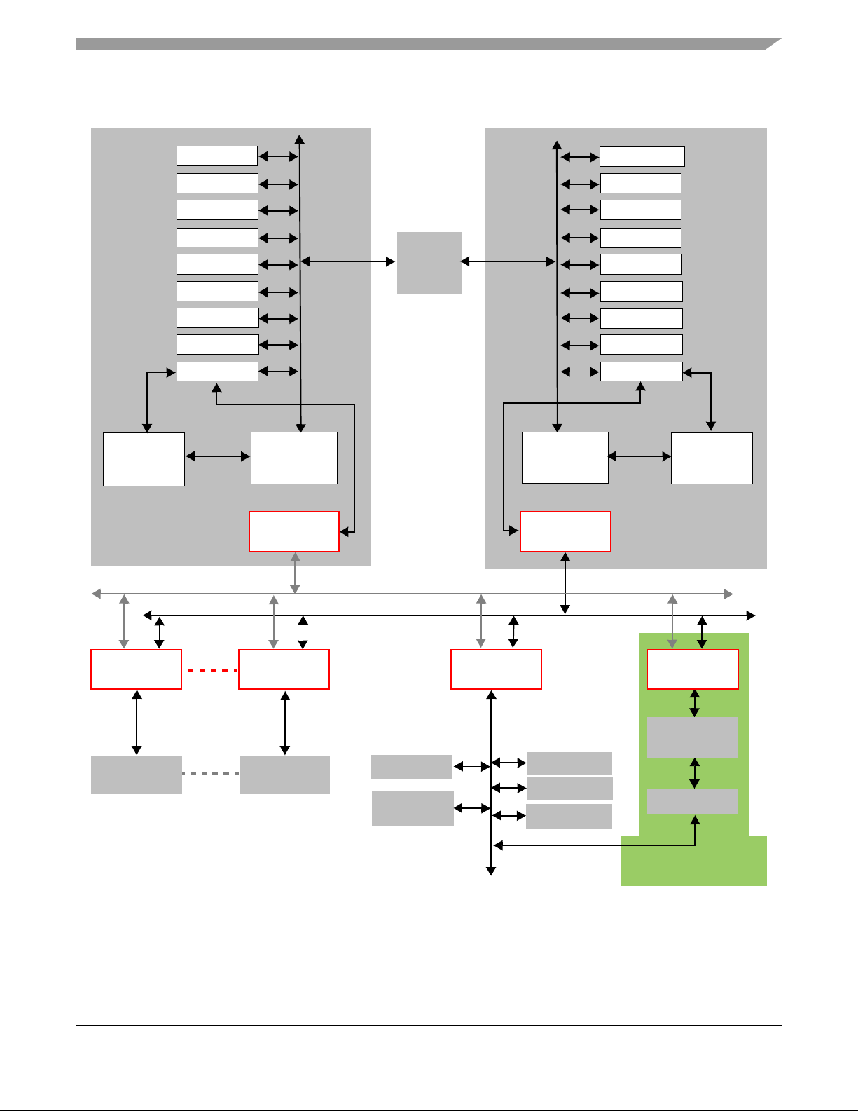
1.2 Block Diagram
DSP56300
Core-1
DSP56300
Core-0
Internal
Memory #0
S/PDIF
EMC
ESAI
Dedicated
Peripheral
Bus
Memory
Bus
Shared Bus#0
Shared Bus #1
Memory Bus
ESAI_1
SHI
TEC
PIC
DMA
WDT
CIM
ESAI_2
ESAI_3
SHI_1
TEC_1
PIC_1
DMA_1
WDT_1
CIM_1
Internal
Memory #1
GPIO A, G
Chip
Configuration
Shared Bus
Arbiter 7
Shared Mem0
(8K)
Core-0 Core-1
Memory Bus
Shared Mem7
(8K)
GPIO_1
GPIO
Inter-Core
Comm.
(ICC)
CGM
ASRC
Memory
Bus
Dedicated
Peripheral
Bus
Shared Bus
Arbiter 0
Shared Bus
Arbiter 9
Shared Bus
Arbiter 8
EMC Burst
Buffer
Shared
Peripheral Bus
Core/DMA
Arbiter
Core/DMA
Arbiter
The EMC is only available
on the DSP56724.
Introduction
Freescale Semiconductor 1-3
Symphony DSP56724/DSP56725 Multi-Core Audio Processors, Rev. 0
Figure 1-1. DSP56724/DSP56725 Block Diagram
Page 16

Introduction
1.3 Features
In addition to high MIPS, the DSP56724/DSP56725 provides powerful and flexible audio data
communications and supports a wide variety of audio applications. This section provides a brief
description of the DSP56724/DSP56725 processor features.
The DSP56724/DSP56725 has two DSP56300 DSP cores. The high throughput of the DSP56300 family
of processors makes them well-suited for high-speed control, efficient signal processing, numeric
processing, and audio applications. Benefits of using DSP56300 cores include:
• Speed: The DSP56300 family supports most high-performance DSP applications.
• Precision: The data paths are 24 bits wide, providing 144 dB of dynamic range. Intermediate
results held in the 56-bit accumulators can range over 336 dB.
• Parallelism: Each on-chip execution unit, memory, and peripheral operates independently and in
parallel with the other units through a sophisticated bus system. The Data ALU, AGU, and program
controller operate in parallel so that the following operations can execute in a single instruction:
— An instruction pre-fetch
— A 24-bit × 24-bit multiplication
— A 54-bit addition
— Two data moves
— Two address-pointer updates using either linear or modulo arithmetic
• Flexibility: While many other DSPs require external communication devices to interface with
peripheral circuits (such as A/D converters, D/A converters, or processors), the DSP56300 family
provides on-chip serial and parallel interfaces that support various configurations of memory and
peripheral modules. The peripherals are interfaced to the DSP56300 family core through a
peripheral interface bus that provides a common interface to many different peripherals.
• Sophisticated Debugging: Freescale’s On-Chip Emulation (OnCE) technology allows simple,
inexpensive, and speed-independent access to the internal registers for debugging. With the OnCE
module, you can easily determine the exact status of the registers and memory locations, plus
identify which instructions were executed last.
• Phase Locked Loop (PLL)-Based Clocking: The PLL allows the chip to use almost any availa ble
external system clock for full-speed operation, while also supplying an output clock synchronized
to a synthesized internal core clock. It improves the synchronous timing of the external memory
port, eliminating the timing skew common on other processors.
• Invisible Pipeline: The seven-stage instruction pipeline is essentially invisible to the programmer ,
allowing straightforward program development in either assembly language or high-level
languages such as C or C++.
• Similar Instruction Set: The instruction mnemonics are similar to those used for microcontroller
units, making an easy transition from programming microprocessors to programming the device.
New microcontroller ins tructions, addressing modes, and bit field instructions allow for significant
decreases in program code size. The orthogonal syntax controls the parallel execution units. The
hardware DO loop and the repeat (REP) instructions make writing straight-line code obsolete.
• Low Power: Designed in CMOS, the DSP56300 family consumes very little power . T wo additional
low-power modes, Stop and Wait, further reduce power requirements. Wait is a low-power mode
Symphony DSP56724/DSP56725 Multi-Core Audio Processors, Rev. 0
1-4 Freescale Semiconductor
Page 17

in which the DSP56300 core shuts down, but the peripherals and interrupt controller continue to
operate, so that an interrupt can bring the chip out of Wait mode. In Stop mode, even more of
circuitry is shut down for the lowest power consumption. Several different methods are available
to bring the chip out of Stop mode: hardware RESET, IRQA, and DE.
1.4 Overview of Peripherals
The peripherals include the following:
•DMA
•PIC
•ESAI
•SHI
•TEC
•WDT
•CIM
•S/PDIF
•ASRC
Introduction
•EMC
•CGM
• Shared memory
•ICC
• Shared bus arbiters
• Chip configuration module
• JTAG controller
1.4.1 Direct Memory Access Controller (DMA, DMA_1)
The DMA controller enables data transfers without any interactions with the DSP cores. During DMA
accesses, it supports any combination of source and destination between internal memory, internal
peripheral I/O, and external memory. DMA features include:
• Eight DMA channels supporting internal and external accesses
• One-, two-, and three-dimensional transfers (including circular buffering)
• End-of-block-transfer interrupts
• Triggering from interrupt lines and all peripherals
1.4.2 Program Interrupt Controller (PIC, PIC_1)
The Program Interrupt Controller arbitrates among all interrupt requests (internal interrupts and the five
external re q ue sts IRQA, IRQB, IRQC, IRQD, and NMI), and generates the appropriate interrupt vector
address.
Symphony DSP56724/DSP56725 Multi-Core Audio Processors, Rev. 0
Freescale Semiconductor 1-5
Page 18

Introduction
The Program Interrupt Controller supports the following:
• Both non-maskable and maskable interrupts
• Up to 18 DMA interrupts and 24 Peripheral interrupts
• Up to 9 non-maskable interrupts
1.4.3 Enhanced Serial Audio Interfaces (ESAI, ESAI_1, ESAI_2, ESAI_3)
The enhanced serial audio interfaces provide full-duplex serial GPIO pins or serial communications with
a variety of serial devices, including one or more industry-standard codecs, other DSPs, microprocessors
and other peripherals that implement the serial peripheral interface (SPI) serial protocol. Each ESAI
consists of independent transmitter and receiver sections, each with its own clock generator, and is a
superset of the DSP56300 family ESSI peripherals and the DSP56000 family SAI peripherals.
1.4.4 Serial Host Interfaces (SHI, SHI_1)
Each serial host interface provides a path for communications and program/coefficient data transfers
between the DSP core and an external host processor. The SHI can interface direc tly to either of two
well-known and widely used synchronous serial buses: the SPI bus and t he Phillips inter -integrated-circuit
control (I2C) bus. The SHI supports either the SPI or I2C bus protocol, as required, from a slave or a
single-master device. To minimize DSP overhead, the SHI supports single-, double- and triple-byte data
transfers. The SHI has a 10-word receive FIFO that permits receiving up to 30 bytes before generating a
receive interrupt, reducing the overhead for data reception.
1.4.5 Triple Timers (TEC, TEC_1)
Each Triple T imer is composed of a common 21-bit prescaler and three independent and identical general
purpose 24-bit timer event counters, with each timer having its own register set. Each timer can use internal
or external clocking, and can also interrupt the DSP after a specified number of events (clocks). Each of
the three timers can signal an external device after counting internal events. Each timer can also be used
to trigger DMA transfers after a specified number of events (clocks) have occurred.
Each of the three timers connects to the external world through bidirectional pins (TIO0, TIO1 and TIO2).
When a TIO pin is configured as input, the timer functions as an external event counter or can measure
external pulse width/signal period. When a TIO pin is used as output, the timer is functioning as either a
timer, a watchdog or a P ulse Width Modulator. When a TIO pin is not used by the timer, it can be used as
a General Purpose Input/Output Pin. Not all timer pins are available on all packages.
1.4.6 Watch Dog Timers (WDT, WDT_1)
Each watchdog timer is a 16-bit timer used to help software recover from runaway code. The timer is a
free-running down-counter used to generate a reset on underflow. Software must periodically service the
watchdog timer to restart the count down
.
Symphony DSP56724/DSP56725 Multi-Core Audio Processors, Rev. 0
1-6 Freescale Semiconductor
Page 19

Introduction
1.4.7 Core Integration Modules (CIM, CIM_1)
Each DSP core has a Core Integration Module. Each core integration module includes a chip ID register,
DMA stall monitor function, and OnCE global data bus (GDB) register.
1.4.8 Sony/Philips Digital Interface (S/PDIF)
The Sony/Philips Digital Interface (S/PDIF) audio module is a transceiver that allows the DSP to r eceive
and transmit digital audio via this module. There is one S/PDIF in each DSP56724/DSP56725 device,
shared by the two DSP cores. The DSP provides a single S/PDIF receiver with four multiplexed inputs,
and one S/PDIF transmitter with two outputs. The S/PDIF module can also transmit and receive the
S/PDIF channel status (CS) and user (U) data. Not all S/PDIF pins are available on all packages.
1.4.9 Asynchronous Sample Rate Converter (ASRC)
Incoming audio data to the DSP can be received from various sources at different sampling rates. Outgoing
audio data from the DSP can have different sampling rates, and additionally, it can be associated with
output clocks that are asynchronous to the input clocks. The Asynchronous Sample Rate Converter
(ASRC) converts the sampling rate of a signal associated to an input clock into a signal associated to a
different output clock.
The ASRC supports concurrent sample rate conversion of up to 10 channels of about 120 dB THD+N. The
sample rate conversion of each channel is associated to a pair of incoming and outgoing sampling rates.
The ASRC supports up to three sampling rate pairs. Although there is only one ASRC in the
DSP56724/DSP56725 device (shared by the two DSP cores), the three sample rate pairs can be used by
both DSP cores at the same time. The ASRC is hard-c ode d and imple mente d a s a c o-proce s sor, requiring
minimal CPU or DSP controller intervention.
1.4.10 External Memory Controller (EMC)
There is one EMC in each DSP56724 device, shared by the two DSP cores. Both cores can access external
memory using the EMC. (DSP56725 devices do not have an EMC.) The EMC provides a seamless
interface to many types of memory devices and peripherals over a shared address and data bus and
dedicated control signals. The memory controller in the EMC controls a parameteriz ed number of memory
banks shared by a high performance SDRAM machine, a general-purpose chip- select machi ne (GPCM),
and up to three user-programmable machines (UPMs).
With external latching, it supports connections to synchronous DRAM (SDRAM), SRAM, EPROM, flash
EPROM, burstable RAM, regular DRAM devices, extended data output DRAM devices, and other
peripherals. Support signals for external address latch (LALE) allows multiplexing of address with data
lines in devices with strict pin count limitations.
1.4.11 Clock Generation Module (CGM)
The Clock Generation Module generates all clocks in the DSP56724/DSP56725 device; the output is a
series of gated clocks. The CGM uses a low jitter phase-locked loop (PLL). The PLL has a wide range of
Symphony DSP56724/DSP56725 Multi-Core Audio Processors, Rev. 0
Freescale Semiconductor 1-7
Page 20

Introduction
frequency multiplications (1 to 256), predivider factors (1 to 32) and output divider (1 to 8). The CGM also
has a power saving clock divider (2i: i = 0 to 7).
In functional mode, the PLL control register (P CTL) sits on the Shared Peripheral bus; both DSP cores can
read and write these registers to change the chip’s working frequency. Additionally, each core can
independently enter stop or wait mode to save power. The shared peripherals enter power-saving mode
only when both DSP cores enter the stop mode.
1.4.12 Shared Memory
The shared memory is a shared memory space accessible by either DSP Core-0 or DSP Core-1. The
DSP56724/DSP56725 shared memory has four 8K x 24 words memory blocks for a total of 32K shared
words and is located starting from $030000. It can be accessed as X or Y memory (with zero wait states)
or as P memory (with 1 wait state).
The 8K x 24 words blocks are single port SRAMs; the Shared Bus Arbiter perform arbitration when the
two DSP cores try to access the same 8K x 24 SRAM block at the same time. No bus contentions occur
when the two DSP cores access different 8K x 24 SRAM blocks simultaneously.
1.4.13 Inter-Core Communication (ICC)
Using the inter-core communication module, each DSP core can issue a maskable interrupt or
non-maskable interrupt to the other core, and each core has its own write data register (which passes data
to the other core when the interrupt is generated). There are also poll data registers for inter-core data
exchange in the ICC. The ICC module interfaces with both cores’ dedicated peripheral buses.
1.4.14 Shared Bus Arbiters
The Shared Bus Arbiter provides arbitration between the two DSP cores for the shared peripherals, shared
memory and shared external memory interface (if available). It is a configurable arbiter, so users can
choose the arbitration method via the appropriate chip configuration registers. The Shared Bus Arbiter
supports using one of three arbitration schemes:
• Always round-robin method
• DSP Core-0 always has high priority
• DSP Core-1 always has high priority
1.4.15 Chip Configuration Module
The Chip Configuration module contains several registers which establish the mode of operation for
various internal blocks, modules, and some of the peripherals. These registers include:
• Control bits of Shared Bus Arbiters
• EMC Burst Mode control bits
• Pin mux/switch control of ESAI, S/PDIF, S/PDIF Rx Clock output mux on ESAI HCKR pins
• Shared peripherals Soft Reset triggering and auto-release
Symphony DSP56724/DSP56725 Multi-Core Audio Processors, Rev. 0
1-8 Freescale Semiconductor
Page 21

Introduction
• EMC PLL control and status
1.4.16 JTAG Controller
In the DSP56724/DSP56725 devices, two separate DSP cores are supported, each with their own OnCE
and JTAG TAP controller. The two JTAG TAPs are daisy-chained, and appear to be two separate single
core devices to the outside world.
Symphony DSP56724/DSP56725 Multi-Core Audio Processors, Rev. 0
Freescale Semiconductor 1-9
Page 22

Introduction
Symphony DSP56724/DSP56725 Multi-Core Audio Processors, Rev. 0
1-10 Freescale Semiconductor
Page 23
Chapter 2 Signal Descriptions
2.1 Signal Groupings
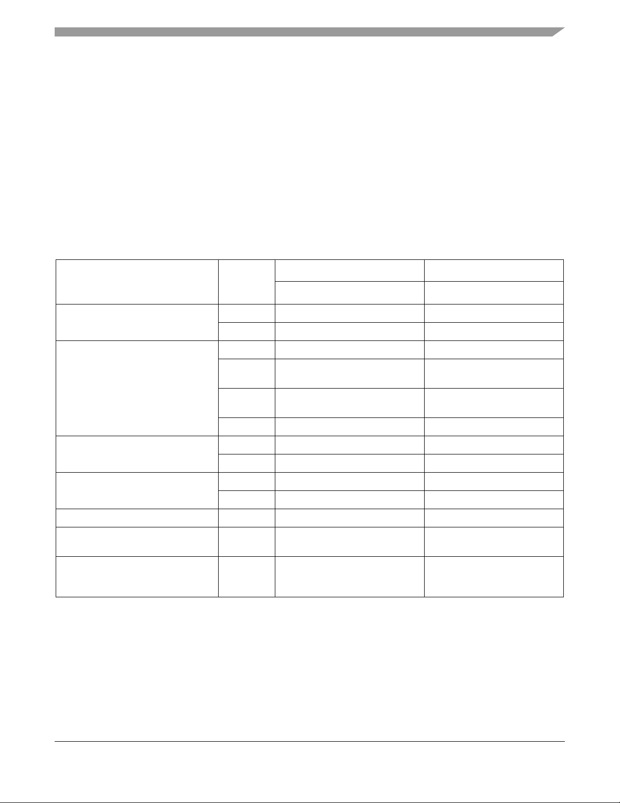
Each product (DSP56724, DSP56725) is available in a variety of packages, which affects whether some
modules use dedicated or shared external pins. See Table 2-1.
Table 2-1. DSP56724/DSP56725 Shared/Dedicated Pins
DSP56724 DSP56725
Function Module
144-pin 80-pin
Timers TEC None None
TEC_1 None None
Enhanced Serial Audio Interface ESAI No SDO0, SDO1 No SDO0, SDO1
ESAI_1 No SDO0, SDO1, FST, FSR,
SCKT, SCKR, HCKT, HCKR
ESAI_2 No SDO0, SDO1, FST, FSR,
SCKT, SCKR, HCKT, HCKR
ESAI_3 No SDO0, SDO1 No SDO0, SDO1, HCKR
Serial Host Interface SHI All All
SHI_1 Only SS, others muxed with SHI Only SS; others muxed with SHI
Watchdog Timer WDT All All
WDT_1 Muxed with WDT Muxed with WDT
General Purpose I/O GPIO Only PG1, PG2 None
Sony/Philips Digital Interface Format S/PDIF Only SPDIFIN and SPDIFOUT1 None;muxed with ESAI_2’s
External Memory Controller EMC All Not applicable, because
1
Clock and Frame Sync signals can be shared with ESAI.
2
Clock and Frame Sync signals can be shared with ESAI_3.
1
2
No SDO0, SDO1, FST, FSR,
SCKT, SCKR, HCKT, HCKR
No SDO0, SDO1, FST, FSR,
SCKT, SCKR, HCKT, HCKR
SDO2, SDO3
DSP56725 does not have an
EMC module.
1
3
Symphony DSP56724/DSP56725 Multi-Core Audio Processors Reference Manual, Rev. 0
Freescale Semiconductor 2-1
Page 24
Signal Descriptions
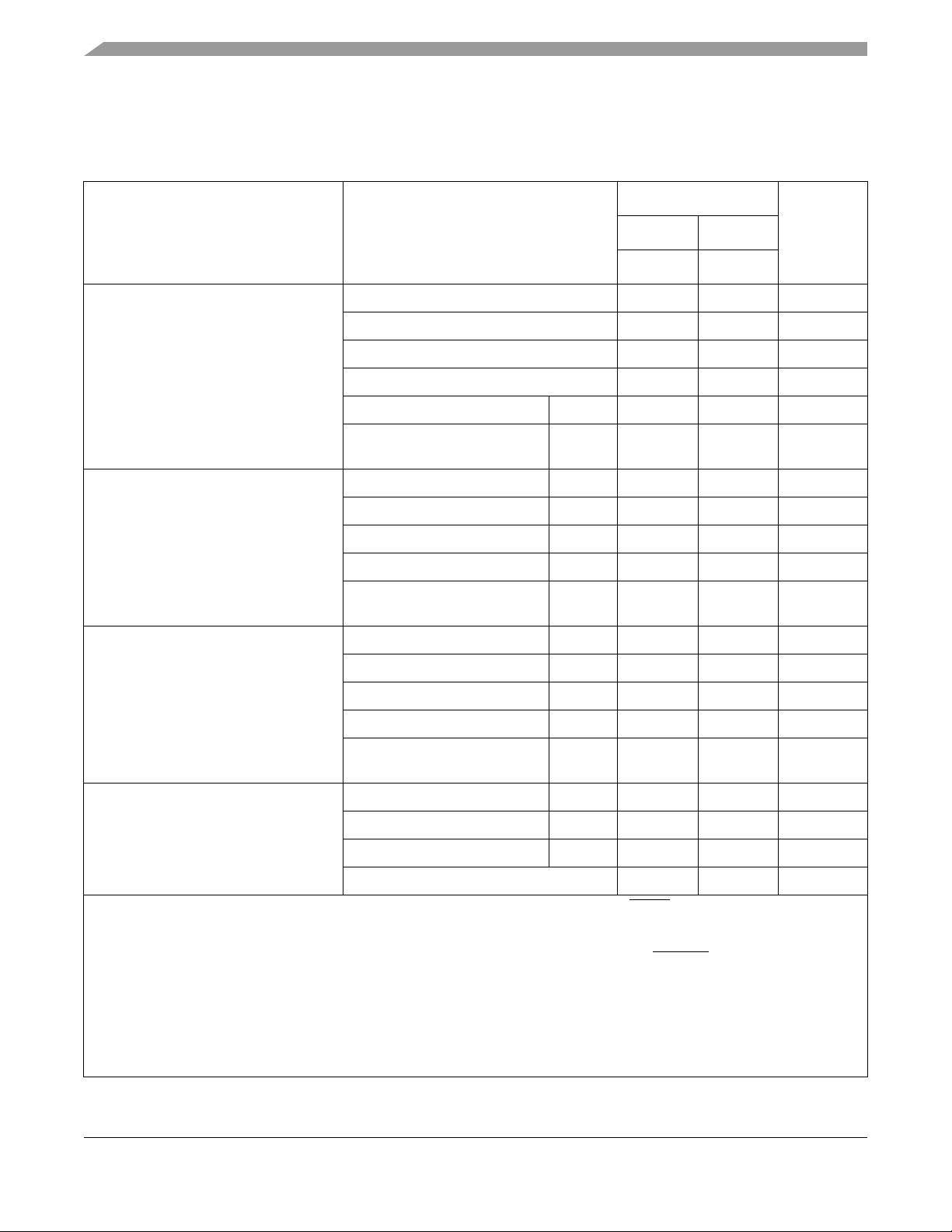
The input and output signals of the DSP56724/DSP56725 are organized into functional groups, as listed
in Table 2-2.
Table 2-2. DSP56724/DSP56725 Signal Groups
Number of Signals
Signal Group Signal
DSP56724 DSP56725
144-Pin 80-Pin
Detailed
Description
Power, Ground, Scan, Clock, Interrupts Power (V
)2113Table 2 -3
DD
Ground (GND) 21 18 Tab le 2 -4
Scan Pins 1 1 Tab le 2 -5
Reset Pin 1 1 Tab le 2 -7
Clock and PLL Port G
Shared External Interrupt Pins /
Por t G
Mode Control
DSP Core-0 Peripheral Pins SHI Port H
ESAI Port C
ESAI_1 Port E
TEC – 0 0 —
WDT No GPIO
Function
DSP Core-1 Peripheral Pins SHI_1 Port H1
ESAI_2 Port C1
ESAI_3 Port E1
TEC_1 – 0 0 —
8
8
44Table 2 -6
55Table 2 -8
Table 2 -9
1
2
3
55Ta b le 2 - 1 1
10 10 Tab l e 2 - 1 3
44Ta b le 2 - 1 4
11Ta b le 2 - 1 7
4
5
6
11Ta b le 2 - 1 2
44Ta b le 2 - 1 5
10 9 Ta bl e 2 - 1 6
WDT_1 No GPIO
00—
Function
Por t A
8
7
8
20Ta b le 2 - 1 9
48 0 Ta bl e 2 - 1 8
20Ta b le 2 - 2 0
Pins of Shared Peripherals SPDIF Port G
9
EMC
GPIO PORT G and Mode Pins Port G
JTAG/OnCE Portfor the two DSP Cores 4 4 Tab le 2 - 2 1
Note: 1. Port H signals are the GPIO port signals that are multiplexed with the SHI HREQ
signal.
2. Port C signals are the GPIO port signals that are multiplexed with the ESAI signals.
3. Port E signals are the GPIO port signals that are multiplexed with the ESAI_1 signals.
4. Port H1 signals are the GPIO port signals that are multiplexed with the SHI_1 HREQ_1
signals.
5. Port C1 signals are the GPIO port signals that are multiplexed with the ESAI_2 signals.
6. Port E1 signals are the GPIO port signals that are multiplexed with the ESAI_3 signals.
7. Port A signals are the GPIO port signals that are multiplexed with the EMC.
8. Port G signals are the GPIO port signals that are multiplexed with S/PDIF, shared external maskable interrupts,
and PLL lock output signals.
9. DSP56724 products have an EMC; DSP56725 products do not have an EMC.
Symphony DSP56724/DSP56725 Multi-Core Audio Processors, Rev. 0
2-2 Freescale Semiconductor
Page 25
Signal Descriptions
60 WDT
59 PINIT/NMI
58 TDO
57 TDI
56 TCK
55 TMS
54 CORE_GND
53 CORE_VDD
52 SDO4/SDI1
51 SDO5/SDI0
50 IO_GND
49 IO_VDD
48 EXTAL
47 XTAL
46 PLLP_GND
45 PLLD_GND
44 PLLD_VDD
43 PLLA_GND
42 PLLA_VDD
41 PLLP_VDD
FST_3 21
HCKT_3 22
SDO2_1/SDI3_1 23
SDO3_1/SDI2_1 24
CORE_VDD 25
CORE_GND 26
SDO4_1/SDI1_1 27
SDO5_1/SDI0_1 28
FSR 29
SCKR 30
HCKR 31
SCKT 32
IO_VDD 33
IO_GND 34
CORE_VDD 35
CORE_GND 36
FST 37
HCKT 38
SDO2/SDI3 39
SDO3/SDI2 40
SDO2_3/SDI3_3 1
SDO3_3/SDI2_3 2
SDO4_3/SDI1_3 3
SDO5_3/SDI0_3 4
IO_VDD 5
IO_GND 6
CORE_VDD 7
CORE_GND 8
SPDIFIN1/SDO2_2/SDI3_2 9
SPDIFOUT1/SDO3_2/SDI2_210
SDO4_2/SDI1_2 11
SDO5_2/SDI0_2 12
FSR_3 13
SCKR_3 14
SCKT_3 15
GND 16
GND 17
GND 18
GND 19
GND 20
80 SCAN
79 MODA0/IRQA
78 MODB0/IRQB
77 MODC0/PLOCK
76 IO_GND
75 IO_VDD
74 CORE_GND
73 CORE_VDD
72 MODA1/IRQC
71 MODB1/IRQD
70 MODC1/NMI_1
69 SS/HA2
68 HREQ
/PH4
67 SCK/SCL
66 MOSI/HA0
65 MISO/SDA
64 SS_1
/HA2_1
63 RESET
62 CORE_GND
61 CORE_VDD
DSP56725
80-Pin
Figure 2-1. DSP56725 80-Pin Package Pin-Out
Symphony DSP56724/DSP56725 Multi-Core Audio Processors, Rev. 0
Freescale Semiconductor 2-3
Page 26
Signal Descriptions
108 IO_GND
107 IO_VDD
106 WDT
105 PINIT/NMI
104 TDO
103 TDI
102 TCK
101 TMS
100 SDO2_1/SDI3_1
99 SDO3_1/SDI2_1
98 SDO4_1/SDI1_1
97 SDO5_1/SDI0_1
96 CORE_GND
95 CORE_VDD
94 FSR
93 SCKR
92 HCKR
91 SCKT
90 FST
89 HCKT
88 SDO2/SDI3
87 SDO3/SDI2
86 SDO4/SDI1
85 SDO5/SDI0
84 SPDIFOUT1
83 SPDIFIN1
82 IO_GND
81 IO_VDD
80 EXTAL
79 XTAL
78 PLLP_GND
77 PLLD_GND
76 PLLD_VDD
75 PLLA_GND
74 PLLA_VDD
73 PLLP_VDD
LSYNC_IN 37
LSYNC_OUT 38
LAD23 39
LAD22 40
LAD21 41
LAD20 42
LAD19 43
LAD18 44
LAD17 45
CORE_VDD 46
CORE_GND 47
IO_VDD 48
IO_GND 49
LAD16 50
LAD15 51
LAD14 52
LAD13 53
LAD12 54
LAD11 55
LAD10 56
LAD9 57
IO_VDD 58
IO_GND 59
CORE_VDD 60
CORE_GND 61
LAD8 62
LAD7 63
LAD6 64
LAD5 65
LAD4 66
LAD3 67
LAD2 68
LAD1 69
LAD0 70
IO_GND 71
IO_VDD 72
CORE_VDD 1
CORE_GND 2
LALE 3
LCS0
4
LCS1
5
LCS2 6
LCS3
7
LCS4
8
LCS5 9
LCS6 10
LCS7 11
IO_VDD 12
IO_GND 13
CORE_VDD 14
CORE_GND 15
LWE
16
LOE
17
LGPL5 18
LSDA10 19
LCKE 20
LCLK 21
LBCTL 22
LSDWE
23
LSDCAS 24
LGTA 25
LA0 26
LA1 27
LA2 28
IO_VDD 29
IO_GND 30
PLLP1_GND 31
PLLP1_VDD 32
PLLD1_GND 33
PLLD1_VDD 34
PLLA1_GND 35
PLLA1_VDD 36
144 SCAN
143 MODA0/IRQA
142 MODB0/IRQB
141 MODC0/PLOCK
140 MODD0/PG1
139 FSR_3
138 SCKR_3
137 HCKR_3
136 SCKT_3
135 FST_3
134 HCKT_3
133 IO_GND
132 IO_VDD
131 CORE_GND
130 CORE_VDD
129 MODA1/IRQC
128 MODB1/IRQD
127 MODC1/NMI_1
126 MODD1/PG2
125 SDO2_2/SDI3_2
124 SDO3_2/SDI2_2
123 SDO4_2/SDI1_2
122 SDO5_2/SDI0_2
121 SDO2_3/SDI3_3
120 SDO3_3/SDI2_3
119 SDO4_3/SDI1_3
118 SDO5_3/SDI0_3
117 SS
/HA2
116 HREQ/PH4
115 SCK/SCL
114 MOSI/HA0
113 MISO/SDA
112 SS_1/HA2_1
111 RESET
110 CORE_GND
109 CORE_VDD
DSP56724
144-Pin
Figure 2-2. DSP56724 144-Pin Package Pin-Out
Symphony DSP56724/DSP56725 Multi-Core Audio Processors, Rev. 0
2-4 Freescale Semiconductor
Page 27
2.2 Signals in Each Functional Group
2.2.1 Power
Table 2 - 3 . Powe r P i n s
Power Name Description
Signal Descriptions
PLLA_VDD
PLLP_VDD
PLLA1_VDD
PLLP1_VDD
PLLD_VDD
PLLD1_VDD
CORE_VDD Core Power
IO_VDD I/O Power
PLL Power
The voltage (3.3 V) should be well-regulated and the input should be provided with an extremely low impedance
path to the 3.3 V
PLL Power
The voltage (1.0 V) should be well-regulated and the input should be provided with an extremely low impedance
path to the 1.0 V
The voltage (1.0 V) should be well-regulated and the input should be provided with an extremely low impedance
path to the 1.0 V
The voltage (3.3 V) should be well-regulated and the input should be provided with an extremely low impedance
path to the 3.3 V
Timer I/O, and other IO signals. The user must provide adequate external decoupling capacitors.
power rail. The user must provide adequate external decoupling capacitors.
DD
power rail. The user must provide adequate external decoupling capacitors.
DD
power rail. The user must provide adequate decoupling capacitors.
DD
power rail. This is an isolated power for the SHI, SHI_1, ESAI, ESAI_1, ESAI_2, ESAI_3,
DD
2.2.2 Ground
Table 2-4. Ground Pins
Ground Name Description
PLLA_GND
PLLP_GND
PLLA1_GND
PLLP1_GND
PLL Ground
The PLL ground should be provided with an extremely low-impedance path to ground. The user must provide
adequate external decoupling capacitors.
PLLD_GND
PLLD1_GND
CORE_GND Core Ground
IO_GND I/O Ground
GND Ground
Freescale Semiconductor 2-5
PLL Ground
The PLL ground should be provided with an extremely low-impedance path to ground. The user must provide
adequate external decoupling capacitors.
The Core ground should be provided with an extremely low-impedance path to ground. This connection must
be tied externally to all other chip ground connections. The user must provide adequate external decoupling
capacitors.
IO_GND is an isolated ground for the SHIs, ESAIs, Timer I/O and LIBU IO. This connection must be tied
externally to all other chip ground connections. The user must provide adequate external decoupling
capacitors.
This connection must be tied externally to all other chip ground connections. The user must provide adequate
external decoupling capacitors.
Symphony DSP56724/DSP56725 Multi-Core Audio Processors, Rev. 0
Page 28
Signal Descriptions
2.2.3 SCAN
Table 2-5. SCAN Signals
Signal
Name
SCAN Input Input SCAN
Type
State During
Reset
Manufacturing test pin. This pin should be pulled low.
Uses internal pull-down resistor.
2.2.4 Clock and PLL
Table 2-6. Clock and PLL Signals
Signal
Name
EXTAL Input Input External Clock / Crystal Input
XTAL Output Chip Driven Crystal Output
PLOCK Output MODC0
Type
State During
Reset
Input
An external clock source must be connected to EXTAL to supply the clock to the
internal clock generator and PLL.
Connects the internal Crystal Oscillator output to an external crystal. If an external
clock is used, leave XTAL unconnected.
PLL Lock/GPIO Port G Pin 0
During assertion of RESET
RESET
is de-asserted, the state of the PLOCK pin is latched into the Core-0 (MDC
of Core-0’s OMR). After RESET
when the internal PLL is locked.
Description
Description
, the PLOCK pin acts as a mode pin input, and when
is de-asserted, PLOCK is output “0”; and goes high
MODC0 Input MODC0
MODA0, MODB0, MODC0, and MODD0 levels select one of 16 initial chip operating
modes of DSP Core-0, and are latched into the DSP Core-0’s OMR when the
RESET
PG0 Input, Output,
Disconnected
PINIT/NMI
Input Input PLL Initial/Nonmaskable Interrupt for DSP Core-0
or
GPIO Port G0
When the PLOCK is configured as GPIO, this pin is individually programmable as
input, output, or internally disconnected.
Uses an internal pull-up resistor.
During assertion of RESET
(PEN) bit of the PLL control register, determining whether the PLL is enabled or
disabled.
After RESET
Schmitt-trigger input is a negative-edge-triggered nonmaskable interrupt (NMI)
request for DSP Core-0, internally synchronized to the internal system clock.
Uses an internal pull-up resistor.
signal is de-asserted.
, the value of PINIT/NMI is written into the PLL Enable
de-assertion and during normal instruction processing, the PINIT/NMI
Symphony DSP56724/DSP56725 Multi-Core Audio Processors, Rev. 0
2-6 Freescale Semiconductor
Page 29
Signal Descriptions
2.2.5 Reset Pin
Assert Reset to low and then high, to force a reset of the DSP cores. Table 2-7 provides the Reset pin
description information.
Table 2-7. Reset Pin
Signal
Name
RESET
State During
Type
Input Input RESET is an active-low, Schmitt-trigger input. When asserted, the chip is placed in the Reset
Reset
state and the internal phase generator is reset. The Schmitt-trigger input allows a slowly rising
input (such as a capacitor charging) to reset the chip reliably. When the RESET
de-asserted, the initial two cores operating modes are latched from the MODA0, MODB0,
MODC0, MODD0, MODA1, MODB1, MODC1, and MODD1 inputs. The RESET
asserted during power up. A stable EXTAL signal must be supplied while RESET
asserted. Uses an internal pull-up resistor.
Description
signal is
signal must be
is being
2.2.6 Interrupt and Mode Control
The interrupt and mode control signals select the operating mode of the DSP cores as the cores come out
of hardware reset. After RESET is de-asserted, these inputs are used as hardware interrupt request lines.
Table 2-8. Interrupt and Mode Control
Signal Name Type
MODA0/IRQA
Input MODA0
State During
Reset
Input
Description
Mode Select A0/External Interrupt Request A
MODA0/IRQA
the DSP clock. MODA0/IRQA
hardware reset, and becomes a two-core shared, level-sensitive or
negative-edge-triggered, maskable interrupt request input during normal
instruction processing, This pin can also be programmed as GPIO.
MODA0, MODB0, MODC0, and MODD0 levels select one of 16 initial chip
operating modes, and are latched into the DSP Core-0’s OMR when the RESET
signal is de-asserted. If the processor is in the stop standby state and the
MODA0/IRQA
is an active-low Schmitt-trigger input, internally synchronized to
selects the initial Core-0 operating mode during
pin is pulled to GND, the processor will exit the stop state.
PG5 In put, Output,
or
Disconnected
MODB0/IRQB
Freescale Semiconductor 2-7
Input MODB0
Input
Symphony DSP56724/DSP56725 Multi-Core Audio Processors, Rev. 0
GPIO Port G5
When the MODA0/IRQA
programmable as input, output, or internally disconnected; and can be controlled
by either of the two cores. Uses an internal pull-up resistor.
Mode Select B0/External Interrupt Request B
MODB0/IRQB
the DSP clock. MODB0/IRQB
during hardware reset and becomes a two-core shared, level-sensitive or
negative-edge-triggered, maskable interrupt request input during normal
instruction processing. This pin can also be programmed as GPIO.
MODA0, MODB0, MODC0, and MODD0 levels select one of 16 initial chip
operating modes, and are latched into the DSP Core-0’s OMR when the RESET
signal is de-asserted.
is an active-low Schmitt-trigger input, internally synchronized to
is configured as GPIO, this signal is individually
selects the initial DSP Core-0 operating mode
Page 30
Signal Descriptions
Table 2-8. Interrupt and Mode Control (Continued)
Signal Name Type
PG6 In put, Output,
or
Disconnected
MODA1/IRQC
PG7 In put, Output,
MODB1/IRQD
Input MODA1
or
Disconnected
Input MODB1
State During
Reset
Input
Input
Description
GPIO Port G6
When the MODB0/IRQB
programmable as input, output, or internally disconnected; and can be controlled
by either of the two cores. Uses an internal pull-up resistor.
Mode Select A1/External Interrupt Request C
MODA1/IRQC
the DSP clock. MODA1/IRQC
during hardware reset and becomes a level-sensitive or negative-edge-triggered,
maskable interrupt request input during normal instruction processing. This pin
can also be programmed as GPIO.
MODA1, MODB1, MODC1, and MODD1 levels select one of 16 initial chip
operating modes, and are latched into the DSP Core-1 OMR when the RESET
signal is de-asserted.
GPIO Port G7
When the MODA1/IRQC
programmable as input, output, or internally disconnected; and this signal can be
controlled by either of the two cores. Uses an internal pull-up resistor.
Mode Select B1/External Interrupt Request D
MODB1/IRQD
the DSP clock. MODB1/IRQD
during hardware reset and becomes a level-sensitive or negative-edge-triggered,
maskable interrupt request input during normal instruction processing. This pin
can also be programmed as GPIO.
MODA1, MODB1, MODC1, and MODD1 levels select one of 16 initial chip
operating modes, and are latched into the DSP Core-1 OMR when the RESET
signal is de-asserted.
is an active-low Schmitt-trigger input, internally synchronized to
is an active-low Schmitt-trigger input, internally synchronized to
is configured as GPIO, this signal is individually
selects the initial DSP Core-0 operating mode
is configured as GPIO, this signal is individually
selects the initial DSP Core-1 operating mode
PG8 In put, Output,
or
Disconnected
Symphony DSP56724/DSP56725 Multi-Core Audio Processors, Rev. 0
GPIO Port G8
When the MODB1/IRQD
programmable as input, output, or internally disconnected; and can be controlled
by either of the two cores. Uses an internal pull-up resistor.
is configured as GPIO, this signal is individually
2-8 Freescale Semiconductor
Page 31
2.2.7 DSP Core-1 Non-Maskable Interrupt (NMI1)
DSP Core-1 has a dedicated NMI pin.
Table 2-9. Non-Maskable Interrupt for DSP Core-1 (NMI1)
Signal Descriptions
Signal Name Type
NMI1
MODC1 Input Operating modes
State During
Reset
Input MODC1
Input
Description
Nonmaskable interrupt for DSP Core-1
After RESET
Schmitt-trigger input is a negative-edge-triggered nonmaskable interrupt request for DSP
Core-1, and is internally synchronized to the internal system clock.
MODA1, MODB1, MODC1, and MODD1 levels select one of 16 initial chip operating
modes of DSP Core-1, and are latched into the DSP Core-1’s OMR when the RESET
signal is de-asserted.
Uses an internal pull-up resistor.
deassertion and during normal instruction processing, the NMI1
2.2.8 Serial Host Interface (SHI and SHI_1)
There are two SHI modules in each DSP56724/DSP56725 device: SHI and SHI_1. SHI is used by DSP
Core-0, while SHI_1 is used by DSP Core-1. Each of the two SHI modules has five I/O signals that can be
configured in either SPI or I2C mode.
In the DSP56724 144-pin and DSP56725 80-pin packages, the two SHI modules share one group of SHI
pins, with separate SS/HA2 and SS_1/HA2_1 pins.
Table 2-10. DSP56724/DSP56725 SHI Pin Configuration
Product Package SHI Pin Configuration
DSP56724 144-pin Both SHI modules (SHI, SHI_1) share one group of SHI pins, except for the SS
DSP56725 80-pin Both SHI modules (SHI, SHI_1) share one group of SHI pins, except for the SS
Symphony DSP56724/DSP56725 Multi-Core Audio Processors, Rev. 0
pin.
pin.
Freescale Semiconductor 2-9
Page 32
Signal Descriptions
Table 2-11. Serial Host Interface Signals (SHI)
Signal
Name
Signal Type
SCK Input or
Output
SCL Input or
Output
State
During
Reset
Tri-stated SPI Serial Clock
When the SPI is configured as a master, the SCK signal is an output; when the SPI
is configured as a slave, the SCK signal is a Schmitt-trigger input.
When the SPI is configured as a master, the SCK signal is derived from the internal
SHI clock generator.
When the SPI is configured as a slave, the SCK signal is an input, and the clock
signal from the external master synchronizes the data transfer. The SCK signal is
ignored by the SPI if it is defined as a slave and the slave select (SS
asserted.
In both the master and slave SPI devices, data is shifted on one edge of the SCK
signal and is sampled on the opposite edge where data is stable. Edge polarity is
determined by the SPI transfer protocol.
2
I
C Serial Clock
SCL carries the clock for I
configured as a master, SCL is an open-drain output; when the SPI is configured as
a slave, SCL is a Schmitt-trigger input.
SCL should be connected to V
This signal is tri-stated during hardware, software and individual reset. Thus, there
is no need for an external pull-up in this state.
This pin is shared by SHI and SHI_1 in DSP56725 80-pin and DSP56724 144-pin
packages.
Uses an internal pull-up resistor.
Description
) signal is not
2
C bus transactions in the I2C mode. When the SPI is
through a pull-up resistor.
DD
MISO Input or
Output
SDA Input or
Open-drain
Output
Tri-stated SPI Master-In-Slave-Out
When the SPI is configured as a master, MISO is the master data input line. The
MISO signal is used in conjunction with the MOSI signal for transmitting and
receiving serial data.
When the SPI is configured as a master, MISO is a Schmitt-trigger input; when the
SPI is configured as a slave, MISO is an output, and is tri-stated when SS
deasserted.
An external pull-up resistor is not required for SPI operation.
2
I
C Data and Acknowledge
2
In I
C mode, SDA is a Schmitt-trigger input when receiving and an open-drain output
when transmitting. SDA should be connected to V
SDA carries the data for I
high period of SCL. The data in SDA is only allowed to change when SCL is low.
When the bus is free, SDA is high.
In start and stop events, the SDA line is only allowed to change during the time SCL
is high.
A start event is a high-to-low transition of the SDA line while SCL is high. A stop event
is a low-to-high transition of SDA while SCL is high.
This signal is tri-stated during hardware, software and individual reset. Thus, there
is no need for an external pull-up in this state.
This pin is shared by SHI and SHI_1 in DSP56725 80-pin and DSP56724 144-pin
packages.
Uses an internal pull-up resistor.
is
through a pull-up resistor.
2
C transactions. The data in SDA must be stable during the
DD
Symphony DSP56724/DSP56725 Multi-Core Audio Processors, Rev. 0
2-10 Freescale Semiconductor
Page 33
Table 2-11. Serial Host Interface Signals (SHI) (Continued)
Signal Descriptions
Signal
Name
Signal Type
MOSI Input or
State
During
Reset
Tri-stated SPI Master-Out-Slave-In
Output
HA0 Input I
SS
Input Tri-stated SPI Slave Select
Description
When the SPI is configured as a master, MOSI is the master data output line. The
MOSI signal is used in conjunction with the MISO signal for transmitting and
receiving serial data.
When the SPI is configured as a slave, MOSI is the slave data input line, and is a
Schmitt-trigger input.
2
C Slave Address 0
When configured for I
and is a Schmitt-trigger input.
When configured for I
2
C slave mode, HA0 is used to form the slave device address,
2
C master mode, HA0 is ignored.
This signal is tri-stated during hardware, software and individual reset. Thus, there
is no need for an external pull-up in this state.
This pin is shared by SHI and SHI_1 in DSP56725 80-pin and DSP56724 144-pin
packages.
Uses an internal pull-up resistor.
When configured for SPI Slave mode, SS
is used to enable the SPI slave for transfer,
and is an active low Schmitt-trigger input.
When configured for SPI master mode, SS
If SS
is asserted while configured in SPI master mode, a bus error condition is
flagged. If SS
is de-asserted while configured in SPI master mode, the SHI ignores
should be kept de-asserted (pulled high).
SCK clocks and keeps the MISO output signal in the high-impedance state.
HA2 Input I
2
C Slave Address 2
When configured for I
and is a Schmitt-trigger input.
When configured for I
2
C slave mode, HA2 is used to form the slave device address,
2
C master mode, HA2 is ignored.
This signal is tri-stated during hardware, software and individual reset. Thus, there
is no need for an external pull-up in this state.
Uses an internal pull-up resistor.
Symphony DSP56724/DSP56725 Multi-Core Audio Processors, Rev. 0
Freescale Semiconductor 2-11
Page 34
Signal Descriptions
Table 2-11. Serial Host Interface Signals (SHI) (Continued)
Signal
Name
Signal Type
HREQ Input or
Output
Input, Output,
or
Disconnected
State
During
Reset
Tri-stated SHI_1’s Host Request
When configured for SPI master mode, this signal is an active low Schmitt-trigger
input. When asserted by the external slave device, HREQ
data word transfer by the master. After finishing the data word transfer, the master
will await the next assertion of HREQ
also be programmed as GPIO.
When configured for SPI slave mode, this signal is an active low output. HREQ
asserted to indicate that the SHI is ready for the next data word transfer; HREQ
de-asserted at the first clock pulse of the new data word transfer.
PH4 Port H4
When HREQ
input, output, or internally disconnected.
This signal is tri-stated during hardware, software and individual reset, or when the
HREQ1-HREQ0 bits in the HCSR are cleared. There is no need for an external
pull-up in this state.
This pin is shared by SHI and SHI_1 in DSP56725 80-pin and DSP56724 144-pin
packages.
Uses an internal pull-up resistor.
Description
will trigger the start of the
to proceed to the next transfer. This pin can
is
is
is configured as GPIO, this signal is individually programmable as
Table 2-12. Serial Host Interface Signals (SHI_1)
Signal
Name
SS_1
Signal Type
Input Tri-stated SHI_1’s SPI Slave Select
HA2_1 Input SHI_1’s I
State
during
Reset
When configured for SPI_1 Slave mode, SS_1
for transfer, and is an active low Schmitt-trigger input.
When configured for SPI_1 master mode, SS_1
(pulled high). If SS
error condition is flagged. If SS_1
master mode, the SHI_1 ignores SCK_1 clocks and keeps the MISO_1 output
signal in the high-impedance state
When configured for I
address, and is a Schmitt-trigger input.
When configured for I
This signal is tri-stated during hardware, software and individual reset. Thus,
there is no need for an external pull-up resistor in this state.
Uses an internal pull-up resistor.
is asserted while configured in SPI_1 master mode, a bus
2
C Slave Address 2
2
C slave mode, HA2_1 is used to form the slave device
2
C master mode, HA2_1 is ignored.
Description
is used to enable the SPI_1 slave
should be kept de-asserted
is de-asserted while configured in SPI_1
Symphony DSP56724/DSP56725 Multi-Core Audio Processors, Rev. 0
2-12 Freescale Semiconductor
Page 35
Signal Descriptions
2.2.9 Enhanced Serial Audio Interface Signals (ESAI, ESAI_1, ESAI_2, ESAI_3)
There are four groups of ESAI pins: ESAI, ESAI_1, ESAI_2 and ESAI_3. ESAI and ESAI_1 pins are used
by the DSP Core-0. ESAI_2 and ESAI_3 are used by DSP Core-1. The next four tables show the pins for
each ESAI group.
Pin switching between ESAI modules features are supported: ESAI can switch pins with ESAI_2, and
ESAI_1 can switch pins with ESAI_3. The switch controls are pin by pin.
Table 2-13. Enhanced Serial Audio Interface Signals (ESAI)
Signal Name Signal Type
HCKR Input or Output GPIO
PC2 Input, Output, or
Disconnected
SRCK Output S/PDIF Receive Clock— This Pin can be used as S/PDIF receive clock
HCKT Input or Output GPIO
PC5 Input, Output, or
Disconnected
State during
Reset
Disconnected
Disconnected
Description
ESAI’s High Frequency Clock for Receiver
When programmed as an input, this signal provides a high frequency clock
source for the ESAI receiver (as an alternative to the DSP core clock).
When programmed as an output, this signal can serve as a high-frequency
sample clock (for example, for DACs or as an additional system clock.
GPIO Port C2
When the ESAI is configured as GPIO, this signal is individually
programmable as input, output, or internally disconnected.
output; this clock is generated by the internal S/PDIF’s DPLL, controlled
by the ERC0 bits in Pin MUX Control Register of the Chip Configuration
Module.
The default state after reset is GPIO disconnected.
Uses an internal pull-down resistor.
ESAI’s High Frequency Clock for Transmitter
When programmed as an input, this signal provides a high frequency clock
source for the ESAI transmitter (as an alternative to the DSP core clock).
When programmed as an output, this signal can serve as a high frequency
sample clock (for example, for external DACs) or as an additional system
clock.
GPIO Port C5
When the ESAI is configured as GPIO, this signal is individually
programmable as input, output, or internally disconnected.
STCLK Input S/PDIF Transmit Clock— This Pin can be used as S/PDIF transmit clock
input; controlled by the ClkSrc_Sel bits in the S/PDIF PhaseConfig
Register.
The default state after reset is GPIO disconnected.
Uses an internal pull-down resistor.
Symphony DSP56724/DSP56725 Multi-Core Audio Processors, Rev. 0
Freescale Semiconductor 2-13
Page 36
Signal Descriptions
Table 2-13. Enhanced Serial Audio Interface Signals (ESAI) (Continued)
Signal Name Signal Type
FSR Input or Output GPIO
PC1 Input, Output, or
Disconnected
FST Input or Output GPIO
State during
Reset
Disconnected
Disconnected
Description
ESAI’s Frame Sync for Receiver
This is the receiver frame sync input/output signal.
In the asynchronous mode (SYN=0), the FSR pin operates as the frame
sync input or output used by all the enabled receivers.
In the synchronous mode (SYN=1), the FSR pin operates as either the
serial flag 1 pin (TEBE=0), or as the transmitter external buffer enable
control (TEBE=1, RFSD=1).
When the FSR pin is configured as serial flag pin, its direction is
determined by the RFSD bit in the RCCR register.
When configured as the output flag OF1, the FSR pin will reflect the value
of the OF1 bit in the SAICR register, and the data in the OF1 bit will show
up at the pin synchronized to the frame sync in normal mode or to the slot
in network mode.
When configured as the input flag IF1, the data value at the FSR pin will be
stored in the IF1 bit in the SAISR register, synchronized by the frame sync
in normal mode or by the slot in network mode.
GPIO Port C1
When the ESAI is configured as GPIO, this signal is individually
programmable as input, output, or internally disconnected.
The default state after reset is GPIO disconnected.
Uses an internal pull-down resistor.
ESAI’s Frame Sync for Transmitter
This is the transmitter frame sync input/output signal.
For synchronous mode, this signal is the frame sync for both transmitters
and receivers.
For asynchronous mode, FST is the frame sync for the transmitters only.
The direction is determined by the transmitter frame sync direction (TFSD)
bit in the ESAI transmit clock control register (TCCR).
PC4 Input, Output, or
Disconnected
Symphony DSP56724/DSP56725 Multi-Core Audio Processors, Rev. 0
2-14 Freescale Semiconductor
GPIO Port C4
When the ESAI is configured as GPIO, this signal is individually
programmable as input, output, or internally disconnected.
The default state after reset is GPIO disconnected.
Uses an internal pull-down resistor.
Page 37

Table 2-13. Enhanced Serial Audio Interface Signals (ESAI) (Continued)
Signal Descriptions
Signal Name Signal Type
SCKR Input or Output GPIO
PC0 Input, Output, or
Disconnected
SCKT Input or Output GPIO
State during
Disconnected
Disconnected
Reset
Description
ESAI’s Receiver Serial Clock
SCKR provides the receiver serial bit clock for the ESAI. The SCKR
operates as a clock input or output used by all the enabled receivers in the
asynchronous mode (SYN=0), or as serial flag 0 pin in the synchronous
mode (SYN=1).
When the SCKR pin is configured as serial flag pin, its direction is
determined by the RCKD bit in the RCCR register.
When configured as the output flag OF0, the SCKR pin will reflect the value
of the OF0 bit in the SAICR register, and the data in the OF0 bit will show
up at the pin synchronized to the frame sync in normal mode or to the slot
in network mode.
When configured as the input flag IF0, the data value at the SCKR pin will
be stored in the IF0 bit in the SAISR register, synchronized by the frame
sync in normal mode or by the slot in network mode.
GPIO Port C0
When the ESAI is configured as GPIO, this signal is individually
programmable as input, output, or internally disconnected.
The default state after reset is GPIO disconnected.
Uses an internal pull-down resistor.
ESAI’s Transmitter Serial Clock
SCKT provides the serial bit rate clock for the ESAI. SCKT is a clock input
or output used by all enabled transmitters and receivers in synchronous
mode, or by all enabled transmitters in asynchronous mode.
PC3 Input, Output, or
Disconnected
SDO5 Output GPIO
Disconnected
SDI0 Input ESAI’s Serial Data Input 0
PC6 Input, Output, or
Disconnected
GPIO Port C3
When the ESAI is configured as GPIO, this signal is individually
programmable as input, output, or internally disconnected.
The default state after reset is GPIO disconnected.
Uses an internal pull-down resistor.
ESAI’s Serial Data Output 5
When programmed as a transmitter, SDO5 is used to transmit data from
the TX5 serial transmit shift register.
When programmed as a receiver, SDI0 is used to receive serial data into
the RX0 serial receive shift register.
GPIO Port C6
When the ESAI is configured as GPIO, this signal is individually
programmable as input, output, or internally disconnected. After the Reset
pin is deasserted, this pin’s function is GPIO disconnected.
The default state after reset is GPIO disconnected.
Uses an internal pull-down resistor.
Symphony DSP56724/DSP56725 Multi-Core Audio Processors, Rev. 0
Freescale Semiconductor 2-15
Page 38

Signal Descriptions
Table 2-13. Enhanced Serial Audio Interface Signals (ESAI) (Continued)
Signal Name Signal Type
SDO4 Output GPIO
SDI1 Input ESAI’s Serial Data Input 1
PC7 Input,
Output, or
Disconnected
SDO3 Output GPIO
SDI2 Input ESAI’s Serial Data Input 2
PC8 Input, Output, or
Disconnected
State during
Reset
Disconnected
Disconnected
ESAI’s Serial Data Output 4
When programmed as a transmitter, SDO4 is used to transmit data from
the TX4 serial transmit shift register.
When programmed as a receiver, SDI1 is used to receive serial data into
the RX1 serial receive shift register.
GPIO Port C7
When the ESAI is configured as GPIO, this signal is individually
programmable as input, output, or internally disconnected. After the Reset
pin is deasserted, this pin’s function is GPIO disconnected
The default state after reset is GPIO disconnected.
Uses an internal pull-down resistor.
ESAI’s Serial Data Output 3
When programmed as a transmitter, SDO3 is used to transmit data from
the TX3 serial transmit shift register.
When programmed as a receiver, SDI2 is used to receive serial data into
the RX2 serial receive shift register.
GPIO Port C8
When the ESAI is configured as GPIO, this signal is individually
programmable as input, output, or internally disconnected.
Description
The default state after reset is GPIO disconnected.
Uses an internal pull-down resistor.
SDO2 Output GPIO
Disconnected
SDI3 Input ESAI’s Serial Data Input 3
PC9 Input,Output, or
Disconnected
ESAI’s Serial Data Output 2
When programmed as a transmitter, SDO2 is used to transmit data from
the TX2 serial transmit shift register
When programmed as a receiver, SDI3 is used to receive serial data into
the RX3 serial receive shift register.
GPIO Port C9
When the ESAI is configured as GPIO, this signal is individually
programmable as input, output, or internally disconnected.
The default state after reset is GPIO disconnected.
Uses an internal pull-down resistor.
Symphony DSP56724/DSP56725 Multi-Core Audio Processors, Rev. 0
2-16 Freescale Semiconductor
Page 39

Table 2-14. Enhanced Serial Audio Interface Signals (ESAI_1)
Signal Descriptions
Signal Name Signal Type
SDO5_1 Output GPIO
SDI0_1 Input ESAI_1’s Serial Data Input 0
PE6 Input, Output, or
Disconnected
SDO4_1 Output GPIO
SDI1 Input ESAI_1’s Serial Data Input 1
PE7 Input,
Output, or
Disconnected
State during
Reset
Disconnected
Disconnected
ESAI_1’s Serial Data Output 5
When programmed as a transmitter, SDO5_1 is used to transmit data from
the TX5 serial transmit shift register.
When programmed as a receiver, SDI0_1 is used to receive serial data
into the RX0 serial receive shift register.
GPIO Port E6
When the ESAI_1 is configured as GPIO, PE6 is individually
programmable as input, output, or internally disconnected.
The default state after reset is GPIO disconnected.
Uses an internal pull-down resistor.
ESAI_1’s Serial Data Output 4
When programmed as a transmitter, SDO4_1 is used to transmit data from
the TX4 serial transmit shift register.
When programmed as a receiver, SDI1 is used to receive serial data into
the RX1 serial receive shift register.
GPIO Port E7
When the ESAI_1 is configured as GPIO, PE7 is individually
programmable as input, output, or internally disconnected.
Description
The default state after reset is GPIO disconnected.
Uses an internal pull-down resistor.
SDO3_1 Output GPIO
Disconnected
SDI2_1 Input ESAI_1’s Serial Data Input 2
PE8 Input, Output, or
Disconnected
ESAI_1’s Serial Data Output 3
When programmed as a transmitter, SDO3_1 is used to transmit data from
the TX3 serial transmit shift register.
When programmed as a receiver, SDI2_1 is used to receive serial data
into the RX2 serial receive shift register.
GPIO Port E8
When the ESAI_1 is configured as GPIO, PE8 is individually
programmable as input, output, or internally disconnected.
The default state after reset is GPIO disconnected.
Uses an internal pull-down resistor.
Symphony DSP56724/DSP56725 Multi-Core Audio Processors, Rev. 0
Freescale Semiconductor 2-17
Page 40
Signal Descriptions
Table 2-14. Enhanced Serial Audio Interface Signals (ESAI_1) (Continued)
Signal Name Signal Type
SDO2_1 Output GPIO
SDI3_1 Input ESAI_1’s Serial Data Input 3
PE9 Input,Output, or
Disconnected
State during
Reset
Disconnected
ESAI_1’s Serial Data Output 2
When programmed as a transmitter, SDO2_1 is used to transmit data from
the TX2 serial transmit shift register.
When programmed as a receiver, SDI3_1 is used to receive serial data
into the RX3 serial receive shift register.
GPIO Port E9
When the ESAI_1 is configured as GPIO, PE9 is individually
programmable as input, output, or internally disconnected.
The default state after reset is GPIO disconnected.
Uses an internal pull-down resistor.
Table 2-15. Enhanced Serial Audio Interface Signals (ESAI_2)
Signal Name Signal Type
SDO5_2 Output GPIO
SDI0_2 Input ESAI_2’s Serial Data Input 0
State during
Reset
Disconnected
ESAI_2’s Serial Data Output 5
When programmed as a transmitter, SDO5_2 is used to transmit data
from the TX5 serial transmit shift register.
When programmed as a receiver, SDI0_2 is used to receive serial data
into the RX0 serial receive shift register.
Description
Description
PC6_1 Input, Output, or
Disconnected
SDO4_2 Output GPIO
Disconnected
SDI1 Input ESAI_2’s Serial Data Input 1
PC7_1 Input,
Output, or
Disconnected
GPIO Port C6_1
When the ESAI_2 is configured as GPIO, PC6_1 is individually
programmable as input, output, or internally disconnected.
The default state after reset is GPIO disconnected.
Uses internal pull-down resistor in the DSP56724 144-pin package.
Uses internal pull-up resistor in DSP56725 80-pin and 144-pin packages.
ESAI_2’s Serial Data Output 4
When programmed as a transmitter, SDO4_2 is used to transmit data
from the TX4 serial transmit shift register.
When programmed as a receiver, SDI1 is used to receive serial data into
the RX1 serial receive shift register.
GPIO Port C7_1
When the ESAI_2 is configured as GPIO, PC7_1 is individually
programmable as input, output, or internally disconnected.
The default state after reset is GPIO disconnected.
Uses internal pull-down resistor in the DSP56724 144-pin package.
Uses internal pull-up resistor in DSP56725 80-pin and 144-pin packages.
Symphony DSP56724/DSP56725 Multi-Core Audio Processors, Rev. 0
2-18 Freescale Semiconductor
Page 41
Table 2-15. Enhanced Serial Audio Interface Signals (ESAI_2) (Continued)
Signal Descriptions
Signal Name Signal Type
SDO3_2 Output GPIO
SDI2_2 Input ESAI_2’s Serial Data Input 2
PC8_1 Input, Output, or
Disconnected
SPDIFOUT1 Input S/PDIF Audio Output Line1— In DSP56725 80-Pin Package, this pin
SDO2_2 Output GPIO
SDI3_2 Input ESAI_2’s Serial Data Input 3
State during
Reset
Disconnected
Disconnected
Description
ESAI_2’s Serial Data Output 3
When programmed as a transmitter, SDO3_2 is used to transmit data
from the TX3 serial transmit shift register.
When programmed as a receiver, SDI2_2 is used to receive serial data
into the RX2 serial receive shift register.
GPIO Port C8_1
When the ESAI_2 is configured as GPIO, PC8_1 is individually
programmable as input, output, or internally disconnected.
can be used as S/PDIF Output Line 1. Controlled by the spdifout_en bit
of the Pin MUX Control Register.
The default state after reset is GPIO disconnected.
Uses internal pull-down resistor in the DSP56724 144-pin package.
Uses internal pull-up resistor in DSP56725 80-pin and 144-pin packages.
ESAI_2’s Serial Data Output 2
When programmed as a transmitter, SDO2_2 is used to transmit data
from the TX2 serial transmit shift register
When programmed as a receiver, SDI3_2 is used to receive serial data
into the RX3 serial receive shift register.
PC9_1 Input,Output, or
Disconnected
SPDIFIN1 Input S/PDIF Audio Input Line1— In DSP56725 80-Pin Package, this pin can
GPIO Port C9_1
When the ESAI_2 is configured as GPIO, PC9_1 is individually
programmable as input, output, or internally disconnected.
be used as S/PDIF Input Line 1. Controlled by the spdifin1_en bit of the
Pin MUX Control Register.
The default state after reset is GPIO disconnected.
Uses internal pull-down resistor in the DSP56724 144-pin package.
Uses internal pull-up resistor in DSP56725 80-pin and 144-pin packages.
Symphony DSP56724/DSP56725 Multi-Core Audio Processors, Rev. 0
Freescale Semiconductor 2-19
Page 42
Signal Descriptions
Table 2-16. Enhanced Serial Audio Interface Signals (ESAI_3)
Signal Name Signal Type
HCKR_3 Input or Output GPIO
PE2_1 Input, Output, or
Disconnected
SRCK Output S/PDIF Receive Clock— This Pin can be used as S/PDIF receive clock
HCKT_3 Input or Output GPIO
State during
Reset
Disconnected
Disconnected
Description
ESAI_3’s High Frequency Clock for Receiver
When programmed as an input, HCKR_3 provides a high frequency clock
source for the ESAI receiver (as an alternative to the DSP core clock).
When programmed as an output, HCKR_3 can serve as a high-frequency
sample clock (for example, for external DACs) or as an additional system
clock.
GPIO Port E2_1
When the ESAI_3 is configured as GPIO, PE2_1 is individually
programmable as input, output, or internally disconnected.
output; this clock is generated by the internal S/PDIF’s DPLL, S/PDIF
Receive Clock output controlled by the ERC3 bits in Pin MUX Control
Register of the Chip Configuration Module.
The default state after reset is GPIO disconnected.
Uses an internal pull-down resistor.
ESAI_3’s High Frequency Clock for Transmitter
When programmed as an input, HCKT_3 provides a high frequency clock
source for the ESAI_3 transmitter (as an alternative to the DSP core
clock).
When programmed as an output, HCKT_3 can serve as a high frequency
sample clock (for example, for external DACs) or as an additional system
clock.
PE5_1 Input, Output, or
Disconnected
STCLK Input S/PDIF Transmit Clock— This Pin can be used as S/PDIF transmit
GPIO Port E5_1
When the ESAI_3 is configured as GPIO, PE5_1 is individually
programmable as input, output, or internally disconnected.
clock input; controlled by the ClkSrc_Sel bits in the S/PDIF PhaseConfig
Register.
The default state after reset is GPIO disconnected.
Uses an internal pull-down resistor.
Symphony DSP56724/DSP56725 Multi-Core Audio Processors, Rev. 0
2-20 Freescale Semiconductor
Page 43
Table 2-16. Enhanced Serial Audio Interface Signals (ESAI_3) (Continued)
Signal Descriptions
Signal Name Signal Type
FSR_3 Input or Output GPIO
PE1_1 Input, Output, or
Disconnected
FST_3 Input or Output GPIO
State during
Disconnected
Disconnected
Reset
Description
ESAI_3’s Frame Sync for Receiver
FSR_3 is the receiver frame sync input/output signal.
In the asynchronous mode (SYN=0), the FSR_3 pin operates as the
frame sync input or output used by all the enabled receivers.
In the synchronous mode (SYN=1), the FSR_3 pin operates as either the
serial flag 1 pin (TEBE=0), or as the transmitter external buffer enable
control (TEBE=1, RFSD=1).
When the FSR_3 pin is configured as serial flag pin, its direction is
determined by the RFSD bit in the RCCR register.
When configured as the output flag OF1, the FSR_3 pin will reflect the
value of the OF1 bit in the SAICR register, and the data in the OF1 bit will
show up at the pin synchronized to the frame sync in normal mode or to
the slot in network mode.
When configured as the input flag IF1, the data value at the FSR_3 pin will
be stored in the IF1 bit in the SAISR register, synchronized by the frame
sync in normal mode or by the slot in network mode.
GPIO Port E1_1
When the ESAI_3 is configured as GPIO, PE1_1 is individually
programmable as input, output, or internally disconnected.
The default state after reset is GPIO disconnected.
Uses an internal pull-down resistor.
ESAI_3’s Frame Sync for Transmitter
FST_3 is the transmitter frame sync input/output signal.
For synchronous mode, FST_3 is the frame sync for both transmitters and
receivers.
For asynchronous mode, FST_3 is the frame sync for the transmitters
only.
The direction is determined by the transmitter frame sync direction
(TFSD) bit in the ESAI_3 transmit clock control register (TCCR).
PE4_1 Input, Output, or
Disconnected
Symphony DSP56724/DSP56725 Multi-Core Audio Processors, Rev. 0
Freescale Semiconductor 2-21
GPIO Port E4_1
When the ESAI_3 is configured as GPIO, PE4_1 is individually
programmable as input, output, or internally disconnected.
The default state after reset is GPIO disconnected.
Uses an internal pull-down resistor.
Page 44

Signal Descriptions
Table 2-16. Enhanced Serial Audio Interface Signals (ESAI_3) (Continued)
Signal Name Signal Type
SCKR_3 Input or Output GPIO
PE0_1 Input, Output, or
Disconnected
SCKT_3 Input or Output GPIO
State during
Disconnected
Disconnected
Reset
Description
ESAI_3’s Receiver Serial Clock
SCKR_3 provides the receiver serial bit clock for the ESAI_3. The
SCKR_3 pin operates as a clock input or output used by all the enabled
receivers in the asynchronous mode (SYN=0), or as serial flag 0 pin in the
synchronous mode (SYN=1).
When the SCKR_3 pin is configured as serial flag pin, its direction is
determined by the RCKD bit in the RCCR register.
When configured as the output flag OF0, the SCKR_3 pin will reflect the
value of the OF0 bit in the SAICR register, and the data in the OF0 bit will
show up at the pin synchronized to the frame sync in normal mode or to
the slot in network mode.
When configured as the input flag IF0, the data value at the SCKR_3 pin
will be stored in the IF0 bit in the SAISR register, synchronized by the
frame sync in normal mode or by the slot in network mode.
GPIO Port E0_1
When the ESAI_3 is configured as GPIO, PE0_1 is individually
programmable as input, output, or internally disconnected.
The default state after reset is GPIO disconnected.
Uses an internal pull-down resistor.
ESAI_3’s Transmitter Serial Clock
SCKT_3 provides the serial bit rate clock for the ESAI_3. SCKT_3 is a
clock input or output used by all enabled transmitters and receivers in
synchronous mode, or by all enabled transmitters in asynchronous mode.
PE3_1 Input, Output, or
Disconnected
SDO5_3 Output GPIO
Disconnected
SDI0_3 Input ESAI_3’s Serial Data Input 0
PE6_1 Input, Output, or
Disconnected
GPIO Port E3_1
When the ESAI_3 is configured as GPIO, PE3_1 is individually
programmable as input, output, or internally disconnected.
The default state after reset is GPIO disconnected.
Uses an internal pull-down resistor.
ESAI_3’s Serial Data Output 5
When programmed as a transmitter, SDO5_3 is used to transmit data
from the TX5 serial transmit shift register.
When programmed as a receiver, SDI0_3 is used to receive serial data
into the RX0 serial receive shift register.
GPIO Port E6_1
When the ESAI_3 is configured as GPIO, PE6_1 is individually
programmable as input, output, or internally disconnected. After the Reset
pin is deasserted, this pins function is GPIO disconnected.
The default state after reset is GPIO disconnected.
Uses internal pull-down resistor in the DSP56724 144-pin package.
Uses an internal pull-up resistor in DSP56725 80-pin and 144-pin
packages.
Symphony DSP56724/DSP56725 Multi-Core Audio Processors, Rev. 0
2-22 Freescale Semiconductor
Page 45
Table 2-16. Enhanced Serial Audio Interface Signals (ESAI_3) (Continued)
Signal Descriptions
Signal Name Signal Type
SDO4_3 Output GPIO
SDI1 Input ESAI_3’s Serial Data Input 1
PE7_1 Input,
Output, or
Disconnected
SDO3_3 Output GPIO
SDI2_3 Input ESAI_3’s Serial Data Input 2
PE8_1 Input, Output, or
Disconnected
State during
Reset
Disconnected
Disconnected
ESAI_3’s Serial Data Output 4
When programmed as a transmitter, SDO4_3 is used to transmit data
from the TX4 serial transmit shift register.
When programmed as a receiver, SDI1 is used to receive serial data into
the RX1 serial receive shift register.
GPIO Port E7_1
When the ESAI_3 is configured as GPIO, PE7_1 is individually
programmable as input, output, or internally disconnected. After Reset pin
is deasserted, this pins function is GPIO disconnected
The default state after reset is GPIO disconnected.
ESAI_3’s Serial Data Output 3
When programmed as a transmitter, SDO3_3 is used to transmit data
from the TX3 serial transmit shift register.
When programmed as a receiver, SDI2_3 is used to receive serial data
into the RX2 serial receive shift register.
GPIO Port E8_1
When the ESAI_3 is configured as GPIO, PE8_1 is individually
programmable as input, output, or internally disconnected.
Description
The default state after reset is GPIO disconnected.
Uses an internal pull-down resistor in the DSP56724 144-pin package.
Uses an internal pull-up resistor in the DSP56725 80-pin package.
SDO2_3 Output GPIO
Disconnected
SDI3_3 Input ESAI_3’s Serial Data Input 3
PE9_1 Input,Output, or
Disconnected
ESAI_3’s Serial Data Output 2
When programmed as a transmitter, SDO2_3 is used to transmit data
from the TX2 serial transmit shift register
When programmed as a receiver, SDI3_3 is used to receive serial data
into the RX3 serial receive shift register.
GPIO Port E9_1
When the ESAI_3 is configured as GPIO, PE9_1 is individually
programmable as input, output, or internally disconnected.
The default state after reset is GPIO disconnected.
Uses internal pull-down resistor in the DSP56724 144-pin package.
Uses an internal pull-up resistor in the DSP56725 80-pin package.
Symphony DSP56724/DSP56725 Multi-Core Audio Processors, Rev. 0
Freescale Semiconductor 2-23
Page 46
Signal Descriptions
2.2.10 Watch Dog Timer (WDT)
The block WDT pin is used by DSP Core-0.
Table 2-17. WDT Signal
Signal
Name
WDT
Type
Output WDT output This signal is asserted low when the hardware watchdog timer counts down
State after
Reset
Description
to zero. This pin is controlled by both WDT and WDT_1 modules, and is
asserted when the watchdog timer counts down to zero in either WDT or
WDT_1 modules.
Symphony DSP56724/DSP56725 Multi-Core Audio Processors, Rev. 0
2-24 Freescale Semiconductor
Page 47
Signal Descriptions
2.2.11 External Memory Controller (EMC)
There is an external memory interface controller (EMC) in the DSP56724. (There is no EMC in the
DSP56725.) The EMC module is shared by both DSP cores. All of the EMC signals are available in the
DSP56724 144-pin package.
Table 2-18. External Memory: EMC Signals
Signal Name Type
LALE Output LALE
LCS
[7:0] Output LCS[7:0]
LWE
/
LSDDQM
Output LWE/
State during
Reset
function
function
LSDDQM
Description
External Address Latch Enable
The EMC provides control for an external address latch, which allows address
and data to be multiplexed on the device pins.
Asserted
memory-controller transaction. If ORx[EAD] = 1, LALE is asserted for (
bus clock cycles.
in the CRR. Note that no other control signals are asserted when LALE is
asserted.
Negated
phase. LALE is negated 1/2 bus clock cycle earlier than the next positive edge
of bus clock, to get additional hold time for external latch device.
Uses an internal pull-down resistor.
Chip Selects
Eight mutually exclusive chip selects are provided.
Asserted/Negated
connected to the EMC. LCS[
corresponding to the chip select for memory bank 0, which has the memory type
and attributes defined by BR0 and OR0.
Uses an internal pull-up resistor.
GPCM Write Enable / SDRAM Data Mask
Asserted/Negated
SDRAM operation, LSDDQM functions as the DQM or data mask signals
provided by JEDEC-compliant SDRAM devices. When the EMC wishes to mask
a write or disable read data output from the SDRAM, LSDDQM is driven high.
Uses an internal pull-up resistor.
—LALE is asserted for at least 1/2 bus clock cycle for each
N
+1/2)
N
is the number of bus clock cycles defined by the EADC field
—LALE is negated at the negative edge of bus clock during address
—Used to enable specific memory devices or peripherals
7:0] are provided on a per-bank basis, with LCS0
—For GPCM operation, LWE is asserted for writing. For
LSDA10/
LGPL0
LSDWE
Freescale Semiconductor 2-25
/
LGPL1
Output LSDA10/
LGPL0
Output LSDWE/
LGPL1
Symphony DSP56724/DSP56725 Multi-Core Audio Processors, Rev. 0
SDRAM A10 / General Purpose Line 0
Asserted/Negated
10. When the row address is driven, this signal drives the value of address bit
10.
When the column address is driven, this signal forms part of the SDRAM
command. This signal is one of six general purpose signals when in UPM mode
and drives a value programmed in the UPM array.
Uses an internal pull-up resistor.
SDRAM Write Enable / General-Purpose Line 1
Asserted/Negated
and acts as the SDRAM write enable when accessing SDRAM.This signal is one
of six general purpose signals when in UPM mode, and drives a value
programmed in the UPM array.
Uses an internal pull-up resistor.
—For SDRAM accesses, this signal represents address bit
—This signal is connected to the SDRAM device WE input
Page 48
Signal Descriptions
Table 2-18. External Memory: EMC Signals (Continued)
Signal Name Type
LOE/
LSDRAS/
LGPL2
LSDCAS
LGPL3
LGPL4/
UPWAIT
LGPL5 Input/Output LGPL5 General-Purpose Line 5
LGTA
/
/
Output LOE
Output LSDCAS/
Input/Output LGTA
State during
Reset
/
LSDRAS/
LGPL2
LGPL3
/
LGPL4/
UPWAIT
GPCM Output Enable / SDRAM RAS / General-Purpose Line 2
Asserted/Negated
accessing memory/devices in GPCM mode. For SDRAM accesses, this signal
is the row address strobe (RAS). This signal is one of six general purpose lines
when in UPM mode, and drives a value programmed in the UPM array.
Uses an internal pull-up resistor.
SDRAM CAS / General-Purpose Line 3
Asserted/Negated
This signal is one of six general purpose signals when in UPM mode, and drives
a value programmed in the UPM array.
Uses an internal pull-up resistor.
GPCM Terminate Access / General-Purpose Line 4 / UPM Wait
Asserted/Negated
transaction termination. This signal may also be configured as one of six general
purpose output signals when in UPM mode or as an input to force the UPM
controller to wait for the memory/device.
Uses an internal pull-up resistor.
Asserted/Negated
UPM mode, and drives a value programmed in the UPM array.
Uses an internal pull-up resistor.
Description
—This signal controls the output buffer of memory when
—In SDRAM mode, drives the column address strobe (CAS).
—This signal is an input in GPCM mode and is used for
—This signal is one of six general purpose signals when in
LBCTL Output LBCTL Data Buffer Control
When a GPCM- or UPM-controlled bank is accessed, the memory controller
activates a data buffer control signal (BCTL) for the external memory. Access to
an SDRAM machine-controlled bank does not activate the buffer control. The
buffer control can be disabled by setting ORx[BCTLD].
Asserted/Negated
for a bus transceiver connected to the LAD lines. Because LBCTL remains high
after reset and during address phases, an external data buffer must not drive the
LAD lines in conflict with the EMC when LBCTL is high.
Uses an internal pull-up resistor.
LA[2:0] Output GPIO
Disconnected
External Memory Non-Multiplexed Address LSBs
All bits driven on LA[2:0] are defined for 24-bit port sizes.
Asserted/Negated
to three least significant bits of the RAM address always appear on the
dedicated address pins LA[2:0]. These may be used, unlatched, in place of
LAD[2:0], to connect the three least significant bits of the address for address
phases. For some RAM devices, such as fast-page DRAM, LA[2:0] serve as the
column address offset during a burst access.
PA[26:24] Input or
Output or
Disconnected
GPIO Port A, Pin26–Pin24
When the EMC is configured as GPIO, these signals are individually
programmable as input, output, or internally disconnected. PA24 is multiplexed
with LA0; PA25 is multiplexed with LA1; PA26 is multiplexed with LA2.
The default state after reset for these signals is GPIO disconnected.
Internal Pull-Down Resistor for these 3 signals.
—The LBCTL pin normally functions as a Write/Read control
—Even though the EMC shares an address and data bus, up
Symphony DSP56724/DSP56725 Multi-Core Audio Processors, Rev. 0
2-26 Freescale Semiconductor
Page 49
Table 2-18. External Memory: EMC Signals (Continued)
Signal Descriptions
Signal Name Type
LAD[23:0] Input/Output GPIO
PA[23:0] Input or
Output or
Disconnected
LCKE Output LCKE External Memory Clock Enable
State during
Reset
Disconnected
Multiplexed Address and Data Bus
For configuration of a port size in BRx[PS] as 32 bits, all of LAD[23:0] needs to
be connected to the external RAM data bus, with LAD[23] occupying the most
significant bit.
Asserted/Negated
through which external RAM devices transfer data and receive addresses.
Assertion/Negation
RAM address for the access to follow. External logic should propagate the
address on LAD[23:0] while LALE is asserted, and latch the address upon
negation of LALE. After LALE is negated, LAD[23:0] are either driven by write
data or are made high-impedance by the EMC to sample read data driven by an
external device. Following the last data transfer of a write access, LAD[23:0] are
again taken into a high-impedance state.
GPIO Port A, Pin[23:0]
When the EMC is configured as GPIO, these signals are individually
programmable as input, output, or internally disconnected. PA23 is multiplexed
with LAD23, PA22 is multiplexed with LAD22,..., and PA0 is multiplexed with
LAD0.
The default state after reset for these signals is GPIO disconnected.
Internal Pull-Down Resistor for these signals.
Asserted/Negated
JEDEC-standard SDRAM devices. This signal is asserted during normal
SDRAM operation.
Uses an internal pull-up resistor.
—LAD[23:0] is the shared 24-bit address and data bus
—During assertion of LALE, LAD[23:0] are driven with the
—LCKE is the bus clock enable signal (CKE) for
Description
LCLK Output LCLK External Memory Clocks
Asserted/Negated
phase-locked loop (PLL) is enabled (see CRR[DBYP]), the bus clock phase is
shifted earlier than transitions on other EMC signals (such as LAD[23:0] and
LCSx) by a time delay matching the delay of the PLL timing loop set up between
LSYNC_OUT and LSYNC_IN.
Uses an internal pull-down resistor.
LSYNC_OUT
Output LSYNC_OUT PLL Synchronization Out
Asserted/Negated
should be propagated through a passive timing loop and returned to LSYNC_IN
for achieving correct PLL lock.
Assertion/Negation
compensates for the round-trip flight time of LCLK and clocked drivers in the
system. No load other than a timing loop should be placed on LSYNC_OUT.
Uses an internal pull-down resistor.
LSYNC_IN
Input LSYNC_IN PLL Synchronization Input
Asserted/Negated
Uses an internal pull-down resistor.
—LCLK drive external memory clock signal. If the EMC
—A replica of the bus clock, appearing on LSYNC_OUT
—The time delay of the timing loop should be such that it
—See the description of LSYNC_OUT.
Symphony DSP56724/DSP56725 Multi-Core Audio Processors, Rev. 0
Freescale Semiconductor 2-27
Page 50
Signal Descriptions
2.2.12 S/PDIF Audio Interface Signals
Table 2-19. Digital Audio Interface: S/PDIF Signals
Signal
Name
SPDIFIN1 Input GPIO
PG9 Input, Output or
SPDIFOUT1 Input GPIO
PG13 Input or Output
Type
Disconnected
or
Disconnected
State During
Reset
Disconnected
Disconnected
Description
S/PDIF Input Line 1
IEC958 data in biphase mark format.
GPIO Port G9
When the S/PDIF is configured as GPIO, these signals are individually
programmable as input, output, or internally disconnected.
This signal can used by the GPIO port G function.
GPIO functions are controlled by GPIO port G registers. There is a bit in the
chip
configuration registers that set it to S/PDIF.
The default state after reset for these signals is GPIO disconnected.
Uses an internal pull-down resistor.
This pin is only available in the DSP56724 and DSP56725 144-pin package.
Audio Data Output Line 1
IEC958 data in biphase mark format. (Consumer C channel).
GPIO Port G13
When the S/PDIF is configured as GPIO, these signals are individually
programmable as input, output, or internally disconnected.
This signal can used by the GPIO port G function.
GPIO functions are controlled by GPIO port G registers. There is a bit in the
chip
configuration registers that set it to S/PDIF.
The default state after reset for these signals is GPIO disconnected.
Uses an internal pull-down resistor.
This pin is only available in the DSP56724 and DSP56725 144-pin package.
2.2.13 Dedicated Port G GPIOs
Table 2-20. Dedicated Port G Signals and Mode Pins
Signal Name Type
PG1 I nput, Output, or
Disconnected
MODD0 Input MODA0 MODB0, MODC0, and MODD0 levels select one of 16 initial chip
State During
Reset
MODD0 Input Port G1
When the PLOCK is configured as GPIO, this signal is individually
programmable as input, output, or internally disconnected.
operating modes of DSP Core-0, and are latched into the DSP Core-0’s
OMR when the RESET
Uses an internal pull-down resistor.
This signal is only available in the DSP56724 144-pin package. This signal
is not available in the DSP56725 80-pin package.
Description
signal is deasserted.
Symphony DSP56724/DSP56725 Multi-Core Audio Processors, Rev. 0
2-28 Freescale Semiconductor
Page 51
Table 2-20. Dedicated Port G Signals and Mode Pins (Continued)
Signal Descriptions
Signal Name Type
PG2 I nput, Output, or
Disconnected
MODD1 Input MODA1, MODB1, MODC1, and MODD1 levels select one of 16 initial chip
State During
Reset
MODD1 Input Port G2
When the PLOCK is configured as GPIO, this signal is individually
programmable as input, output, or internally disconnected.
operating modes of DSP Core-1, and are latched into the DSP Core-1’s
OMR when the RESET
Uses an internal pull-down resistor.
This signal is only available in the DSP56724 144-pin package. This signal
is not available in the DSP56725 80-pin package.
Description
signal is deasserted.
2.2.14 JTAG/OnCE Interface Signals
Table 2-21. JTAG/OnCE Interface
Signal
Name
TCK Input Input Test Clock
TDI Input Input Test Data Input
Signal
Type
State During
Reset
Description
TCK is a test clock input signal used to synchronize the JTAG test logic. It uses an
internal pull-up resistor.
TDI is a test data serial input signal used for test instructions and data. TDI is sampled
on the rising edge of TCK and uses an internal pull-up resistor.
TDO Output Tri-Stated Test Data Output
TDO is a test data serial output signal used for test instructions and data. TDO is
tri-statable and is actively driven in the shift-IR and shift-DR controller states. TDO
changes on the falling edge of TCK.
TMS Input Input Test Mode Select
TMS is an input signal used to sequence the test controller’s state machine. TMS is
sampled on the rising edge of TCK and uses an internal pull-up resistor.
Symphony DSP56724/DSP56725 Multi-Core Audio Processors, Rev. 0
Freescale Semiconductor 2-29
Page 52

Signal Descriptions
Symphony DSP56724/DSP56725 Multi-Core Audio Processors, Rev. 0
2-30 Freescale Semiconductor
Page 53

Chapter 3
Internal I/O
Y ROM
External Memory
Internal RAM
X ROM
External Memory
Internal RAM
Program ROM
External Memory
Internal RAM
Reserved
$000000
$038000
$FFF000
$F80000
Shared Memory Shared Memory
Internal I/O
$030000
$FFFFFF
Program Memory
Space
X Data Memory
Space
Y Data Memory
Space
Reserved
Reserved
Shared Memory
$040000
$038000
$040000
Memory Map
3.1 Overview
The memory space of each DSP56300 core is partitioned into three main parts: program memory space,
X data memory space, and Y data memory space. The data memory space is divided into X and Y data
memory to work with the two address ALUs and to feed two operands simultaneously to the data ALU.
Memory space includes internal RAM and ROM, and can be expanded off-chip.
Figure 3-1 shows the memory address allocations for the DSP56724 and DSP 56725 DSPs.
Figure 3-1. DSP56724 and DSP56725 Memory Address Allocation
In the DSP56724/DSP56725, the lowest addresses are used for on-chip internal Program, X, and Y RAM.
The DSP56724 supports using a memory switch mode to increase the size of program RAM as needed.
Some X RAM bank(s) and/or Y RAM bank(s) can be switched to Program RAM. Program, X, and Y RAM
allocation on each DSP can be configured as five types of memory maps: a default mode plus four
additional memory maps based on two bit settings (MSW0, MSW1).
Four blocks of 8K shared memory (RAM) are accessible in the DSP56724/DSP56725. The shared
memory blocks occupy addresses from $030000 to $037FFF (including $037F FF), accessible by both DSP
cores. When the DSP cores access the shar ed memor y, the Program, X, and Y memory addresses are
mapped into same physical location, which means that there is no difference in accessing the shared
memory from Program, X, or Y memory space.
External Memory addresses from $040000 are used for internal RAM/ROM expansion. In the DSP56724,
the expansion is implemented via the EMC module, using the EMC’s external interface signals.
Freescale Semiconductor 3-1
Symphony DSP56724/DSP56725 Multi-Core Audio Processors Reference Manual, Rev. 0
Page 54
Memory Map
On-chip peripherals are connected to the core using the peripheral bus or Shared Peripheral bus. The
on-chip peripherals use the addresses above $FFF000 (including $FFF000).
3.2 Data and Program Memory Maps
The on-chip memory configuration for each DSP is affected by the state of the memory switch control bits
in the Operating Mode Register (OMR). These bits are the Master Memory Switch Mode (MS) bit, the
Memory Switch Mode 0 (MSW0) bit, and the Memory Switch Mode 1 (MSW1) bit.
Table 3-1. Core-0 Configuration
Bit Settings Memory Space
MSW1 MSW0 MS Program RAM X Data RAM Y Data RAM
— — 0 4 K 28 K 24 K
00140 K8 K8 K
0 1 1 24 K 16 K 16 K
1 0 1 16 K 24 K 16 K
1 1 1 8 K 24 K 24 K
Table 3-2. Core-1 Configuration
Bit Settings Memory Space
MSW1 MSW0 MS Program RAM X Data RAM Y Data RAM
— — 0 2 K 12 K 10 K
00116 K4 K4 K
01112 K8 K4 K
1018 K8 K8 K
1 1 1 4 K 12 K 8 K
Table 3-3. DSP Core-0 Memory Map Locations
Configuration Program RAM X Data RAM Y Data RAM
MSW = NA, MS = 0 4 K 28 K 24 K
1 × 4 K block 1 × 4 K block
3 × 8 K block
$000000 – $000FFF $000000 – $006FFF $000000 – $005FFF
MSW1 = 1, MSW0 = 1, MS = 1 8 K 24 K 24 K
$000000 – $001FFF $000000 – $005FFF $000000 – $005FFF
3 × 8 K block
MSW1 = 1, MSW0 = 0, MS = 1 16 K 24 K 16 K
$000000 – $003FFF $000000 – $005FFF $000000 – $003FFF
Symphony DSP56724/DSP56725 Multi-Core Audio Processors, Rev. 0
3-2 Freescale Semiconductor
Page 55
Memory Map
Table 3-3. DSP Core-0 Memory Map Locations (Continued)
Configuration Program RAM X Data RAM Y Data RAM
MSW1 = 0, MSW0 = 1, MS = 1 24 K 16 K 16 K
$000000 – $005FFF $000000 – $003FFF $000000 – $003FFF
MSW1 = 0, MSW0 = 0, MS = 1 40 K 8 K 8 K
$000000 – $009FFF $000000 – $001FFF $000000 – $001FFF
Table 3-4. DSP Core-1 Memory Map Locations
Configuration Program RAM X Data RAM Y Data RAM
MSW = NA, MS = 0 2 K 12 K 10 K
1 × 2K block 3 × 4 K block 1 × 4 K block
$000000 – $007FFF $000000 – $002FFF $000000 – $0027FF
MSW1 = 1, MSW0 = 1, MS = 1 4 K 12 K 8 K
$000000 – $000FFF $000000 – $002FFF $000000 – $001FFF
MSW1 = 1, MSW0 = 0, MS = 1 8 K 8 K 8 K
$000000 – $001FFF $000000 – $001FFF $000000 – $001FFF
MSW1 = 0, MSW0 = 1, MS = 1 12 K 8 K 4 K
$000000 – $002FFF $000000 – $001FFF $000000 – $000FFF
MSW1 = 0, MSW0 = 0, MS = 1 16 K 4 K 4 K
$000000 – $003FFF $000000 – $000FFF $000000 – $000FFF
3.3 Peripheral Register Memory Map
The dedicated and shared peripherals for each DSP core are the same, and the peripherals’ register memory
map for the both cores are the same.
DSP Core-0’s on-chip peripherals X-Memory map are listed in Table 3-7 DSP Core-0’s on-chip
peripheral’s Y-Memory Map is listed in Table 3-8.
The X-Memory map and Y-Memory map of DSP Core-1 are essentially the same as the DSP Core-0; the
difference being the names of the dedicated peripherals. For example, DSP Core-0 is PIC, while DSP
Core-1 is PIC_1.
Symphony DSP56724/DSP56725 Multi-Core Audio Processors, Rev. 0
Freescale Semiconductor 3-3
Page 56
Memory Map
Legend for the following tables: Yellow indicates a dedicated peripheral, while blue indicates a shared
peripheral.
Table 3-5. X-Memory Map for DSP Core-0 and Core-1
Blocks
Address Range
DSP Core-0 DSP Core-1
X: $FF_FFFF–$FF_FFFD PIC PIC_1
X: $FF_FFFC CIM CIM_1
X: $FF_FFFB–$FF_FFF9 PIC PIC_1
X: $FF_FFF8–$FF_FFF5 CIM CIM_1
X: $FF_FFF4–$FF_FFD0 DMA Control and DMA channels DMA_1 Control and DMA_1 channels
X: $FF_FFBF–$FF_FFA0 ESAI, GPIO PORT C ESAI_2, GPIO PORT C1
X: $FF_FF9A–$FF_FF98 GPIO port H GPIO port H
X: $FF_FF97–$FF_FF90 SHI SHI_1
X: $FF_FF8F–$FF_FF80 Triple Timer (TEC) Triple Timer (TEC_1)
X: $FF_FF7F–$FF_FF7C CGM
X: $FF_FF7B–$FF_FF78 Reserved
X: $FF_FF77–$FF_FF60 S/PDIF
X: $FF_FF5F–$FF_FE6C Reserved
X: $FF_FE6B–$FF_FE00 EMC
X: $FF_FDFF–$FF_E000 Reserved
Table 3-6. Y-Memory Map for DSP Core-0 and Core-1
Blocks
Address Range
DSP Core-0 DSP Core-1
Y: $FF_FFFF–$FF_FFF8 GPIO Port G
Y: $FF_FFF7–$FF_FFF0 GPIO Port A
Y: $FF_FFEF–$FF_FFE8 Reserved
Y: $FF_FFE7–$FF_FFE0 Chip Configuration Registers
Y: $FF_FFDF–$FF_FFDC Reserved Reserved
Y:$FF_FFDB–$FF_FFD0 ICC ICC
Y: $FF_FFCF–$FF_FFCB Reserved Reserved
Y: $FF_FFCA ESAI/ESIA_1 internal clock control ESAI_2/ESIA_3 internal clock control
Y: $FF_FFC9 Reserved Reserved
Y: $FF_FFC8 EMC/ICC Error Status Register EMC/ICC Error Status Register
Y: $FF_FFC8–$FF_FFC4 Reserved Reserved
Symphony DSP56724/DSP56725 Multi-Core Audio Processors, Rev. 0
3-4 Freescale Semiconductor
Page 57
Table 3-6. Y-Memory Map for DSP Core-0 and Core-1 (Continued)
Blocks
Address Range
DSP Core-0 DSP Core-1
Y: $FF_FFC3–$FF_FFC0 WDT WDT_1
Y: $FF_FFBF–$FF_FFB0 Reserved Reserved
Y: $FF_FFAF–$FF_FFA0 Reserved Reserved
Y:$FF_FF9F–$FF_FF80 ESAI_1 ESAI_3
Y:$FF_FF7F–$FF_FC40 Reserved
Y:$FF_FC3F–$FF_FC00 ASRC
Y:$FF_FBFF–$FF_E000 Reserved
Table 3-7. Detailed Device X-Memory Map
Memory Map
Peripherals Address Register Name
PIC, PIC_1 X: $FF_FFFF Interrupt Priority Register Core (IPR-C)
X: $FF_FFFE Interrupt Priority Register Peripheral (IPR-P)
X: $FF_FFFD Reserved
CIM, CIM_1
PIC, PIC_1
CIM, CIM_1
DMA, DMA_1
X: $FF_FFFC OnCE Global Data Register (OGDB)
X: $FF_FFFB Interrupt Priority Register Core (IPR_C1)
X: $FF_FFFA Interrupt Priority Register Peripheral (IPR_P1)
X: $FF_FFF9 Reserved
X: $FF_FFF8 DMA stall register (DMAS).
X: $FF_FFF6 Reserved
X: $FF_FFF5 CHIP ID Register (CHIDR)
X: $FF_FFF4 DMA Status Register (DSTR)
X: $FF_FFF3 DMA Offset Register 0 (DOR0)
X: $FF_FFF2 DMA Offset Register 1 (DOR1)
X: $FF_FFF1 DMA Offset Register 2 (DOR2)
X: $FF_FFF0 DMA Offset Register 3 (DOR3)
1
DMA, DMA_1
Channel 0
Freescale Semiconductor 3-5
X: $FF_FFEF DMA Source Address Register (DSR0)
X: $FF_FFEE DMA Destination Address Register (DDR0)
X: $FF_FFED DMA Counter (DCO0)
X: $FF_FFEC DMA Control Register (DCR0)
Symphony DSP56724/DSP56725 Multi-Core Audio Processors, Rev. 0
Page 58
Memory Map
Table 3-7. Detailed Device X-Memory Map (Continued)
Peripherals Address Register Name
DMA, DMA_1
Channel 1
X: $FF_FFEB DMA Source Address Register (DSR1)
X: $FF_FFEA DMA Destination Address Register (DDR1
X: $FF_FFE9 DMA Counter (DCO1)
X: $FF_FFE8 DMA Control Register (DCR1)
DMA, DMA_1
Channel 2
X: $FF_FFE7 DMA Source Address Register (DSR2)
X: $FF_FFE6 DMA Destination Address Register (DDR2)
X: $FF_FFE5 DMA Counter (DCO2)
X: $FF_FFE4 DMA Control Register (DCR2)
DMA, DMA_1
Channel 3
X: $FF_FFE3 DMA Source Address Register (DSR3)
X: $FF_FFE2 DMA Destination Address Register (DDR3)
X: $FF_FFE1 DMA Counter (DCO3)
X: $FF_FFE0 DMA Control Register (DCR3)
DMA, DMA_1
Channel 4
X: $FF_FFDF DMA Source Address Register (DSR4)
X: $FF_FFDE DMA Destination Address Register (DDR4)
X: $FF_FFDD DMA Counter (DCO4)
1
DMA, DMA_1
Channel 5
DMA, DMA_1
Channel 6
DMA, DMA_1
Channel 7
GPIO Port C,
Port C1
X: $FF_FFDC DMA Control Register (DCR4)
X: $FF_FFDB DMA Source Address Register (DSR5)
X: $FF_FFDA DMA Destination Address Register (DDR5)
X: $FF_FFD9 DMA Counter (DCO5)
X: $FF_FFD8 DMA Control Register (DCR5)
X: $FF_FFD7 DMA Source Address Register (DSR6)
X: $FF_FFD6 DMA Destination Address Register (DDR6)
X: $FF_FFD5 DMA Counter (DCO6)
X: $FF_FFD4 DMA Control Register (DCR6)
X: $FF_FFD3 DMA Source Address Register (DSR7)
X: $FF_FFD2 DMA Destination Address Register (DDR7)
X: $FF_FFD1 DMA Counter (DCO7)
X: $FF_FFD0 DMA Control Register (DCR7)
X: $FF_FFBF PORT C/C1 Control Register (PCRC)
X: $FF_FFBE PORT C/C1 Direction Register (PRRC)
X: $FF_FFBD PORT C/C1 GPIO Data Register (PDRC)
Symphony DSP56724/DSP56725 Multi-Core Audio Processors, Rev. 0
3-6 Freescale Semiconductor
Page 59
Table 3-7. Detailed Device X-Memory Map (Continued)
Memory Map
Peripherals Address Register Name
1
ESAI, ESAI_2 X: $FF_FFBC ESAI/ESAI_2 Receive Slot Mask Register B (RSMB)
X: $FF_FFBB ESAI/ESAI_2 Receive Slot Mask Register A (RSMA)
X: $FF_FFBA ESAI/ESAI_2 Transmit Slot Mask Register B (TSMB)
X: $FF_FFB9 ESAI/ESAI_2 Transmit Slot Mask Register A (TSMA)
X: $FF_FFB8 ESAI/ESAI_2 Receive Clock Control Register (RCCR)
X: $FF_FFB7 ESAI/ESAI_2 Receive Control Register (RCR)
X: $FF_FFB6 ESAI/ESAI_2 Transmit Clock Control Register (TCCR)
X: $FF_FFB5 ESAI/ESAI_2 Transmit Control Register (TCR)
X: $FF_FFB4 ESAI/ESAI_2 Common Control Register (SAICR)
X: $FF_FFB3 ESAI/ESAI_2 Status Register (SAISR)
X: $FF_FFB2
Reserved
to
X: $FF_FFAC
X: $FF_FFAB ESAI/ESAI_2 Receive Data Register 3 (RX3)
X: $FF_FFAA ESAI/ESAI_2 Receive Data Register 2 (RX2)
X: $FF_FFA9 ESAI/ESAI_2 Receive Data Register 1 (RX1)
ESAI, ESAI_2
GPIO port H/H1
X: $FF_FFA8 ESAI/ESAI_2 Receive Data Register 0 (RX0)
X: $FF_FFA7 Reserved
X: $FF_FFA6 ESAI/ESAI_2 Time Slot Register (TSR)
X: $FF_FFA5 ESAI/ESAI_2 Transmit Data Register 5 (TX5)
X: $FF_FFA4 ESAI/ESAI_2 Transmit Data Register 4 (TX4)
X: $FF_FFA3 ESAI/ESAI_2 Transmit Data Register 3 (TX3)
X: $FF_FFA2 ESAI/ESAI_2 Transmit Data Register 2 (TX2)
X: $FF_FFA1 ESAI/ESAI_2 Transmit Data Register 1 (TX1)
X: $FF_FFA0 ESAI/ESAI_2 Transmit Data Register 0 (TX0)
X: $FF_FF9F
Reserved
to
X: $FF_FF9B
X: $FF_FF9A Port H Control Register (PCRH)
X: $FF_FF99 Port H Direction Register (PRRH)
X: $FF_FF98 Port H GPIO Data Register (PDRH)
Symphony DSP56724/DSP56725 Multi-Core Audio Processors, Rev. 0
Freescale Semiconductor 3-7
Page 60
Memory Map
Table 3-7. Detailed Device X-Memory Map (Continued)
Peripherals Address Register Name
SHI, SHI_1 X: $FF_FF97
Reserved
to
X: $FF_FF95
X: $FF_FF94 SHI Receive FIFO (HRX)
X: $FF_FF93 SHI Transmit Register (HTX)
X: $FF_FF92 SHI I2C Slave Address Register (HSAR)
X: $FF_FF91 SHI Control/Status Register (HCSR)
X: $FF_FF90 SHI Clock Control Register (HCKR)
TEC, TEC_1
X: $FF_FF8F Timer 0 Control/Status Register (TCSR0)
X: $FF_FF8E Timer 0 Load Register (TLR0)
X: $FF_FF8D Timer 0 Compare Register (TCPR0)
X: $FF_FF8C Timer 0 Count Register (TCR0)
X: $FF_FF8B Timer 1 Control/Status Register (TCSR1)
X: $FF_FF8A Timer 1 Load Register (TLR1)
X: $FF_FF89 Timer 1 Compare Register (TCPR1)
X: $FF_FF88 Timer 1 Count Register (TCR1)
1
CGM
X: $FF_FF87 Timer 2 Control/Status Register (TCSR2)
X: $FF_FF86 Timer 2 Load Register (TLR2)
X: $FF_FF85 Timer 2 Compare Register (TCPR2)
X: $FF_FF84 Timer 2 Count Register (TCR2)
X: $FF_FF83 Timer Prescaler Load Register (TPLR)
X: $FF_FF82 Timer Prescaler Count Register (TPCR)
X: $FF_FF81
Reserved
to
X: $FF_FF80
X: $FF_FF7F Reserved
X: $FF_FF7E The ASRC internal generated reference clock divisor (ASCDR)
X: $FF_FF7D PLL Control Register (PCTL)
X: $FF_FF7C Shared Peripheral Clock Enable Register (SPENA)
X: $FF_FF7B
Reserved
to
X: $FF_FF75
Symphony DSP56724/DSP56725 Multi-Core Audio Processors, Rev. 0
3-8 Freescale Semiconductor
Page 61
Table 3-7. Detailed Device X-Memory Map (Continued)
Memory Map
Peripherals Address Register Name
S/PDIF X: $FF_FF74 S/PDIF Transmit Clock Control Register (STC)
X: $FF_FF73
Reserved
to
X: $FF_FF72
X: $FF_FF71 Frequency Measurement (SRFM)
X: $FF_FF70 S/PDIF Transmit Professional C Channel Lo (STCSPL)
X: $FF_FF6F S/PDIF Transmit Professional C Channel Hi (STCSPH)
X: $FF_FF6E S/PDIF Transmit Consumer C Channel Lo (STCSCL)
X: $FF_FF6D S/PDIF Transmit Consumer C Channel Hi (STCSCH)
X: $FF_FF6C S/PDIF Transmit Right Channel (STR)
X: $FF_FF6B S/PDIF Transmit Left Channel (STL)
X: $FF_FF6A S/PDIF Receiver Q Channel (SRQ)
X: $FF_FF69 S/PDIF Receiver U Channel (SRU)
X: $FF_FF68 S/PDIF Receiver Channel Status 24–47(SRCSL)
X: $FF_FF67 S/PDIF Receiver Channel Status 00–23 (SRCSH)
X: $FF_FF66 S/PDIF Receiver Right (SRR)
1
X: $FF_FF65 S/PDIF Receiver Left (SRL)
X: $FF_FF64 S/PDIF Interrupt STAT/CLR (SIS/SIC)
X: $FF_FF63 S/PDIF Interrupt Register (SIE)
X: $FF_FF62 S/PDIF Phase Configuration Register (SRPC)
X: $FF_FF61 S/PDIF CD Text Control Register (SRCD)
X: $FF_FF60 S/PDIF Configuration Register (SCR)
X: $FF_FF5F
Reserved
to
X: $FF_FE70
Symphony DSP56724/DSP56725 Multi-Core Audio Processors, Rev. 0
Freescale Semiconductor 3-9
Page 62
Memory Map
Table 3-7. Detailed Device X-Memory Map (Continued)
Peripherals Address Register Name
EMC X: $FF_FE6F
Reserved
to
X: $FF_FE6C
X: $FF_FE6B EMC Clock Ratio Register high part (CRRH)
X: $FF_FE6A EMC Clock Ratio Register low part (CRRL)
X: $FF_FE69 EMC Configuration Register high part (BCRH)
X: $FF_FE68 EMC Configuration Register low part (BCRL)
X: $FF_FE67
Reserved
to
X: $FF_FE62
X: $FF_FE61 EMC Transfer Error Address Register high part (TEARH)
X: $FF_FE60 EMC Transfer Error Address Register low part (TEARL)
X: $FF_FE5F EMC Transfer Error Attributes Register high part (TEATRH)
X: $FF_FE5E EMC Transfer Error Attributes Register low part (TEATRL)
X: $FF_FE5D EMC Transfer Error Interrupt Register (TEIR)
X: $FF_FE5C Reserved
X: $FF_FE5B EMC Transfer Error Disable Register (TEDR)
1
X: $FF_FE5A Reserved
X: $FF_FE59 EMC Transfer Error Status Register (TESR)
X: $FF_FE58 Reserved
X: $FF_FE57
Reserved
to
X: $FF_FE54
X: $FF_FE53 SDRAM Refresh Timer (SRT)
X: $FF_FE52 Reserved
X: $FF_FE51 EMC UPM Refresh Timer (URT)
X: $FF_FE50 Reserved
X: $FF_FE4F
Reserved
to
X: $FF_FE4C
X: $FF_FE4B EMC SDRAM Mode Register high part (SDMRH)
X: $FF_FE4A EMC SDRAM Mode Register low part (SDMRL)
X: $FF_FE49
Reserved
to
X: $FF_FE46
X: $FF_FE45 EMC UPM Data Register high part (MDRH)
X: $FF_FE44 EMC UPM Data Register low part (MDRL)
Symphony DSP56724/DSP56725 Multi-Core Audio Processors, Rev. 0
3-10 Freescale Semiconductor
Page 63
Table 3-7. Detailed Device X-Memory Map (Continued)
Memory Map
Peripherals Address Register Name
1
EMC X: $FF_FE43 EMC Memory Refresh Timer Prescaler Register (MRTPR)
X: $FF_FE42
Reserved
to
X: $FF_FF3E
X: $FF_FE3D EMC UPMC Mode Register high part (MCMRH)
X: $FF_FE3C EMC UPMC Mode Register low part (MCMRL)
X: $FF_FE3B EMC UPMB Mode Register high part (MBMRH)
X: $FF_FE3A EMC UPMB Mode Register low part (MBMRL)
X: $FF_FE39 EMC UPMA Mode Register high part (MAMRH)
X: $FF_FE38 EMC UPMA Mode Register low part (MAMRL)
X: $FF_FE37
Reserved
to
X: $FF_FE36
X: $FF_FE35 EMC UPM Address Register high part (MARH)
X: $FF_FE34 EMC UPM Address Register low part (MARL)
X: $FF_FE33
Reserved
to
X: $FF_FE20
X: $FF_FE1F EMC Options Register 7 high part (ORH7)
X: $FF_FE1E EMC Options Register 7 low part (ORL7)
X: $FF_FE1D EMC Base Register 7 high part (BRH7)
X: $FF_FE1C EMC Base Register 7 low part (BRL7)
X: $FF_FE1B EMC Options Register 6 high part (ORH6)
X: $FF_FE1A EMC Options Register 6 low part (ORL6)
X: $FF_FE19 EMC Base Register 6 high part (BRH6)
X: $FF_FE18 EMC Base Register 6 low part (BRL6)
X: $FF_FE17 EMC Options Register 5 high part (ORH5)
X: $FF_FE16 EMC Options Register 5 low part (ORL5)
X: $FF_FE15 EMC Base Register 5 high part (BRH5)
X: $FF_FE14 EMC Base Register 5 low part (BRL5)
X: $FF_FE13 EMC Options Register 4 high part (ORH4)
X: $FF_FE12 EMC Options Register 4 low part (ORL4)
X: $FF_FE11 EMC Base Register 4 high part (BRH4)
X: $FF_FE10 EMC Base Register 4 low part (BRL4)
Symphony DSP56724/DSP56725 Multi-Core Audio Processors, Rev. 0
Freescale Semiconductor 3-11
Page 64
Memory Map
Table 3-7. Detailed Device X-Memory Map (Continued)
Peripherals Address Register Name
EMC X: $FF_FE0F EMC Options Register 3 high part (ORH3)
X: $FF_FE0E EMC Options Register 3 low part (ORL3)
X: $FF_FE0D EMC Base Register 3 high part (BRH3)
X: $FF_FE0C EMC Base Register 3 low part (BRL3)
X: $FF_FE0B EMC Options Register 2 high part (ORH2)
X: $FF_FE0A EMC Options Register 2 low part (ORL2)
X: $FF_FE09 EMC Base Register 2 high part (BRH2)
X: $FF_FE08 EMC Base Register 2 low part (BRL2)
X: $FF_FE07 EMC Options Register 1 high part (ORH1)
X: $FF_FE06 EMC Options Register 1 low part (ORL1)
X: $FF_FE05 EMC Base Register 1 high part (BRH1)
X: $FF_FE04 EMC Base Register 1 low part (BRL1)
X: $FF_FE03 EMC Options Register 0 high part (ORH0)
X: $FF_FE02 EMC Options Register 0 low part (ORL0)
X: $FF_FE01 EMC Base Register 0 high part (BRH0)
1
X: $FF_FE00 EMC Base Register 0 low part (BRL0)
X: $FF_FDFF
Reserved
to
X: $FF_F000
1
Includes short name and long name.
Table 3-8. Detailed Device Y-Memory Map
Peripherals Address Register Name
GPIO PORT G Y:$FF_FFFF Reserved
Y: $FF_FFFE Port G Control Register 1(PCRG1)
Y: $FF_FFFD Port G GPIO Direction Register 1(PRRG1)
Y: $FF_FFFC Port G GPIO Data Register 1(PDRG1)
Y:$FF_FFFB Reserved
Y: $FF_FFFA Port G Control Register (PCRG)
Y: $FF_FFF9 Port G GPIO Direction Register (PRRG)
Y: $FF_FFF8 Port G GPIO Data Register (PDRG)
1
Symphony DSP56724/DSP56725 Multi-Core Audio Processors, Rev. 0
3-12 Freescale Semiconductor
Page 65
Table 3-8. Detailed Device Y-Memory Map (Continued)
Memory Map
Peripherals Address Register Name
GPIO PORT A Y:$FF_FFF7 Reserved
Y:$FF_FFF6 Port A Control Register 1 (PCRA_1)
Y:$FF_FFF5 Port A GPIO Direction Register 1 (PRRA_1)
Y: $FF_FFF4 Port A GPIO Data Register 1 (PDRA_1)
Y: $FF_FFF3 Reserved
Y: $FF_FFF2 Port A Control Register (PCRA)
Y: $FF_FFF1 Port A GPIO Direction Register (PRRA)
Y: $FF_FFF0 Port A GPIO Data Register (PDRA)
Y:$FF_FFEF
Reserved
to
Y:$FF_FFE7
Chip
Configuration
Y:$FF_FFE6 External Memory Burst Control Register (EMBC)
Y:$FF_FFE5 EMC PLL Status & Control Register (PSC)
Y:$FF_FFE4 Chip Pin Mux Control (PMCR)
Y:$FF_FFE3 ESAI Pin Switch Control Register (EPSC)
Y:$FF_FFE2 Once Debug and Burst Control Register (ODBC)
1
Y:$FF_FFE1 Shared Peripheral Software Reset Control Register (SPSR)
Y:$FF_FFE0 Shared Bus Arbiters Control Register (OACR)
Y: $FF_FFDF
Reserved
to
Y:$FF_FFDC
Symphony DSP56724/DSP56725 Multi-Core Audio Processors, Rev. 0
Freescale Semiconductor 3-13
Page 66
Memory Map
Table 3-8. Detailed Device Y-Memory Map (Continued)
Peripherals Address Register Name
ICC
Inter-Core
Communication
Y:$FF_FFDB ICC Data Register 1 (ICDR1)
For non-maskable interrupt
Y:$FF_FFDA ICC Control Register 1 (ICCR1)
For non-maskable interrupt
Y:$FF_FFD9 ICC Data Register 2 (ICDR2)
For non-maskable Interrupt
Y:$FF_FFD8 ICC Control Register 2 (ICCR2)
For non-maskable Interrupt
Y:$FF_FFD7 ICC Data Register 3 (ICDR3)
For maskable Interrupt
Y:$FF_FFD6 ICC Control Register 3 (ICCR3).
For maskable Interrupt
Y:$FF_FFD5 ICC Acknowledge Registers3 (ICAR3)
The other core’s acknowledge for the maskable interrupt
Y:$FF_FFD4 ICC Data Register 4 (ICDR4)
For maskable Interrupt
Y:$FF_FFD3 ICC Control Register 4 (ICCR4)
For maskable Interrupt
Y:$FF_FFD2 ICC Acknowledge Register 4 (ICAR4)
Acknowledge for the maskable interrupt
to
the other core.
to
the other core.
from
the other core.
from
the other core.
to
the other core.
to
the other core.
from
the other core.
from
the other core.
from
the other core.
1
to
the other core.
WDT,WDT_1
Y:$FF_FFD1 ICC Poll Register 1(ICPR1)
Read poll data
Y:$FF_FFD0 ICC Poll Register 2 (ICPR2)
Write poll data
Y: $FF_FFCF
to
Y: $FF_FFCB
Y: $FF_FFCA ESAI Internal Clock Connect Control Register
Y: $FF_FFC9 Reserved
Y: $FF_FFC8 EMC/ICC Error Status Register
Y: $FF_FFC7
to
Y: $FF_FFC4
Y: $FF_FFC3 Watchdog Service Register (WSR)
Y: $FF_FFC2 Watchdog Count Register (WCNTR)
Y: $FF_FFC1 Watchdog Modulus Register (WMR)
Y: $FF_FFC0 Watchdog Control Register (WCR)
Y: $FF_FFBF
to
Y: $FF_FFA0
Reserved
Reserved
Reserved
from
the other core.
to
the other core.
Symphony DSP56724/DSP56725 Multi-Core Audio Processors, Rev. 0
3-14 Freescale Semiconductor
Page 67
Table 3-8. Detailed Device Y-Memory Map (Continued)
Memory Map
Peripherals Address Register Name
ESAI_1,ESAI_3 Y:$FFFF9F Port E/E1 Control Register (PCRE)
Y:$FFFF9E Port E/E1 Direction Register (PPRE)
Y:$FFFF9D Port E/E1 GPIO Data Register (PDRE)
Y:$FFFF9C ESAI_1/3 Receive Slot Mask Register B (RSMB_1)
Y:$FFFF9B ESAI_1/3 Receive Slot Mask Register A (RSMA_1)
Y:$FFFF9A ESAI_1/3 Transmit Slot Mask Register B (TSMB_1)
Y:$FFFF99 ESAI_1/3 Transmit Slot Mask Register A (TSMA_1)
Y:$FFFF98 ESAI_1/3 Receive Clock Control Register (RCCR_1)
Y:$FFFF97 ESAI_1/3 Receive Control Register (RCR_1)
Y:$FFFF96 ESAI_1/3 Transmit Clock Control Register (TCCR_1)
Y:$FFFF95 ESAI_1/3 Transmit Control Register (TCR_1)
Y:$FFFF94 ESAI_1/3 Common Control Register (SAICR_1)
Y:$FFFF93 ESAI_1/3 Status Register (SAISR_1)
Y:$FFFF92
Reserved
to
Y:$FFFF8C
1
ASRC
Y:$FFFF8B ESAI_1/3 Receive Data Register 3 (RX3_1)
Y:$FFFF8A ESAI_1/3 Receive Data Register 2 (RX2_1)
Y:$FFFF89 ESAI_1/3 Receive Data Register 1 (RX1_1)
Y:$FFFF88 ESAI_1/3 Receive Data Register 0 (RX0_1)
Y:$FFFF87 Reserved
Y:$FFFF86 ESAI_1/3 Time Slot Register (TSR_1/3)
Y:$FFFF85 ESAI_1/3 Transmit Data Register 5 (TX5_1)
Y:$FFFF84 ESAI_1/3 Transmit Data Register 4 (TX4_1)
Y:$FFFF83 ESAI_1/3 Transmit Data Register 3 (TX3_1)
Y:$FFFF82 ESAI_1/3 Transmit Data Register 2 (TX2_1)
Y:$FFFF81 ESAI_1/3 Transmit Data Register 1 (TX1_1)
Y:$FFFF80 ESAI_1/3 Transmit Data Register 0 (TX0_1)
Y:$FF_FF7F
Reserved
to
Y:$FF_FC1E
Y: $FF_FC1D Data Output Register for Pair C (ASRDOC)
Y: $FF_FC1C Data Input Register for Pair C (ASRDIC)
Y: $FF_FC1B Data Output Register for Pair B (ASRDOB)
Symphony DSP56724/DSP56725 Multi-Core Audio Processors, Rev. 0
Freescale Semiconductor 3-15
Page 68
Memory Map
Table 3-8. Detailed Device Y-Memory Map (Continued)
Peripherals Address Register Name
ASRC Y: $FF_FC1A Data Input Register for Pair B (ASRDIB)
Y: $FF_FC19 Data Output Register for Pair A (ASRDOA)
Y: $FF_FC18 Data Input Register for Pair A (ASRDIA)
Y: $FF_FC17 Channel Counter Register (ASRCCR)
Y: $FF_FC16 Reserved
Y: $FF_FC15 Taskque FIFO Register 1 (ASRTFR1)
Y: $FF_FC14 Parameter Register 5(ASRPM5)
Y: $FF_FC13 Parameter Register 4(ASRPM4)
Y: $FF_FC12 Parameter Register 3(ASRPM3)
Y: $FF_FC11 Parameter Register 2(ASRPM2)
Y: $FF_FC10 Parameter Register 1(ASRPM1)
Y: $FF_FC0F Debug Control Register -1 (ASRDCR-1).
Y: $FF_FC0E Debug Control Register (ASRDCR).
Y: $FF_FC0D Memory Access Data Register (ASRMAD)
Y: $FF_FC0C Memory Access Address Register (ASRMAA)
1
Y: $FF_FC0B
to
Y: $FF_FC09
Y: $FF_FC08 ASRC Status Register (ASRSTR)
Y: $FF_FC07 ASRC Clock Divider Register (ASRCDR-2)
Y: $FF_FC06 ASRC Clock Divider Register (ASRCDR-1)
Y: $FF_FC05 ASRC Clock Source Register (ASRCSR)
Y: $FF_FC04 Filter Configuration Status Register (ASRCFG)
Y: $FF_FC03 Channel Number Configuration Register (ASRCNCR)
Y: $FF_FC02 Interrupt Enable Mask Register (ASRIEM)
Y: $FF_FC01 Interrupt Enable Register (ASRIER)
Y: $FF_FC00 ASRC Control Register (ASRCTR)
Y:$FF_FBFF
to
Y:$FF_F000
1
Include short name and long name.
Reserved
Reserved
Symphony DSP56724/DSP56725 Multi-Core Audio Processors, Rev. 0
3-16 Freescale Semiconductor
Page 69

Chapter 4 DSP56300 Platform
4.1 Overview
The DSP56724 and DSP56725 have two DSP56300 platforms, which are identical. Each DSP56300
platform includes a DSP56300 core, a direct memory access unit (DMA), a program interrupt controller
(PIC), and a Co re /D MA Arb ite r.
Figure 4-1 provides the block diagram for the DSP56300 Core in DSP56724 and DSP56725.
Symphony DSP56724/DSP56725 Multi-Core Audio Processors Reference Manual, Rev. 0
Freescale Semiconductor 4-1
Page 70
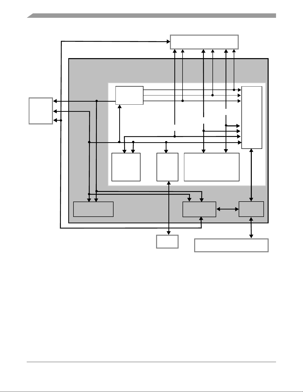
DSP56300 Platform
OnCE™
Address
Generate
Unit (AGU)
Internal
Data Bus
Switch
Internal Memory Blocks
(RAMs/ROMs)
Program
Control Unit
(PCU)
Direct Memory
Access(DMA)
Program Interrupt
Controller (PIC)
Core/DMA
Arbiter
JTAG
External Memory, Shared Memory &
Shared Peripherals Expansion
Dedicated
Peripherals
GDB
24-Bit DSP56300
Core
PAB
PA B
XAB
YA B
GDB
XAB
YAB
Two 56-Bit Accumulators
56-Bit Barrel Shifter
24 x 24 + 56 --> 56-Bit MAC
DSP56300
Platform
Data ALU
Shared
Bus
DAB and DDB
YDB
XDB
PDB
PIO_EB
YDB
XDB
PDB
AB = Address bus
DB = Data bus
GDB = Global data bus
Figure 4-1. DSP56300 Core in DSP56724/DSP56725
The dedicated peripheral bus interface includes PM_EB and GDB signals, and connects to dedicated
peripherals. Peripherals can also be connected via the shared bus.
The DSP56300 core is a high-performance, single clock-cycle-per-instruction engine that provides up to
twice the performance of Freescale's popular DSP56000 core family, while also retaining code
compatibility with it.
4.2 DSP56300 Core Features
The DSP56300 core family provides a new level of performance in speed and power, provided by its rich
instruction set and low power dissipation, thus enabling a new generation of wireless, telecommuni cations
and multimedia products. Significant architectural enhancements to the DSP56300 core family include a
4-2 Freescale Semiconductor
Symphony DSP56724/DSP56725 Multi-Core Audio Processors, Rev. 0
Page 71

DSP56300 Platform
barrel shifter, 24-bit addressing, an instruction patch module and direct memory access (DMA).
DSP56300 core features include:
• DSP56300 modular chassis
• 250 million instructions per second (MIPS) with a 150 MHz clock with 1.2 V internal logic supply
• Object code-compatible with DSP56000 core
• Data ALU with 24 × 24 bit multiplier-accumulator and 56-bit barrel shifter plus support for 16-bit
arithmetic
• Program control with support for position-independent code and instruction patches
• 8-channel DMA controller
• Support for internal address-tracing plus OnCE for hardware/software debugging
• STOP and WAIT low-power standby modes
4.3 DSP56300 Block Descriptions
The DSP56300 core provides five main functional blocks:
• Data arithmetic logic unit (Data ALU)
• Address generation unit (AGU)
• Program control unit (PCU)
• Internal Data Bus Switch
• OnCE module
DSP56300 core features are described fully in the DSP56300 Family Manual.
4.3.1 Data ALU
The Data ALU performs all the arithmetic and logical operations on data operands in the DSP56300 core.
Data ALU features include:
• Fully pipelined 24-bit × 24-bit paralle l multiplier-accumulator (MAC)
• Bit field unit, comprising a 56-bit parallel barrel shifter (fast shift and normalization, bit strea m
generation and parsing)
• Conditional ALU instructions
• 24-bit or 16-bit arithmetic support under software control
• Four 24-bit input general purpose registers: X1, X0, Y1 and Y0
• Six Data ALU registers (A2, A1, A0, B2, B1 and B0), that are concatenated into two general
purpose 56-bit accumulators (A and B), plus accumulator shifters
• Two data bus shifter/limiter circ uits
Symphony DSP56724/DSP56725 Multi-Core Audio Processors, Rev. 0
Freescale Semiconductor 4-3
Page 72

DSP56300 Platform
4.3.1.1 Data ALU Registers
The Data ALU registers can be read or written over the X memory data bus (XDB) and the Y memory data
bus (YDB), as 24- or 48-bit operands (or as 16- or 32-bit operands in 16-bit arithmetic mode). The source
operands for the Data ALU, which can be 24, 48, or 56 bits (16, 32, or 40 bits in 16-bit arithme tic mode ),
always originate from Data ALU registers. The results of all Data ALU operations are stored in an
accumulator.
All the Data ALU operations are performed in two clock cycles (in pipeline fashion) so that a new
instruction can be initiated on every cloc k, yielding an effective exec ution rate of one instruction per cloc k
cycle. The destination of every arithmetic operation can be used as a source operand for the immediately
following arithmetic operation without a time penalty (without a pipeline stall).
4.3.1.2 Multiplier-Accumulator (MAC)
The MAC unit comprises the main arithmetic processing unit of the DSP56300 core and performs all of
the calculations on data operands. For arithmetic instructions, the MAC accepts as many as three input
operands and outputs one 56-bit result with the following form: Extension:Most Significant Product:L east
Significant Product (EXT:MSP:LSP).
The multiplier exec utes 24-bit × 24-bit, parallel, f ractional mul tiplies, betwe en two’s-complement signed,
unsigned, or mixed operands. The 48-bit product is right-justified and added to the 56-bit contents of either
the A or B accumulator. A 56-bit result can be stored as a 24-bit operand. The LSP can either be truncated
or rounded into the MSP. Rounding is performed if specified.
4.3.2 Address Generation Unit (AGU)
The Address Generation Unit performs effective address calculations using integer arithmetic necessary
to address data operands in memory, and contains the registers used to generate the addresses. The AGU
implements four types of arithmetic (linear, modulo, multiple wrap-around modulo, reverse-carry), and
operates in parallel with other chip resources to minimize address-generation overhead.
The AGU is divided into two halves, each with its own Address ALU. Each Address ALU has four s ets of
register triplets. Each register triplet is composed of an address register, an offset register and a modifier
register. The two Address ALUs are identical. Each Address ALU contains a full 24-bit adder (called an
offset adder).
A second full adder (called a modulo adder) adds the summed result of the first full adder to a modulo
value that is stored in its respective modifier register. A third full adder (called a reverse-carry adder) is
also provided.
The offset adder and the reverse-carry adder are in parallel and share common inputs. The only difference
between the offset and reverse-carry adders is that the carry propagates in opposite directions. Test logic
determines which of the three summed results of the full adders is output.
Each Address ALU can update one address register (from its respective address register file) during one
instruction cycle. The contents of the associated modifier register specifies the type of arithmetic to be used
in the address register update calculation. The modifier value is decoded in the Address ALU.
Symphony DSP56724/DSP56725 Multi-Core Audio Processors, Rev. 0
4-4 Freescale Semiconductor
Page 73

DSP56300 Platform
4.3.3 Program Control Unit (PCU)
The Program control unit performs instruction prefetch, instruction decoding, hardware DO loop control
and exception processing. The PCU implements a seven-stage pipeline and controls the different
processing states of the DSP56300 core. The PCU consists of three hardware blocks:
• Program decode controller (PDC)
• Program address generator (PAG)
• Program interrupt controller (PIC)
The Program Decode controller decodes the 24-bit instruction loaded into the instruction latch and
generates all signals necessary for pipeline control. The Program Address Generator contains all the
hardware needed for program address generation, system stack and loop control. The Program Interrupt
Controller arbitrates among all interrupt requests (internal interrupts, as well as the five external requests:
IRQA, I R Q B, IRQC, IRQ D and NMI) and generates the appropriate interrupt vector address.
PCU features include:
• Position-independent code support
• Addressing modes optimized for DSP applications (including immediate of fs ets)
• On-chip instruction cache controller
• On-chip memory-expandable hardware stack
• Nested hardware DO loops
• Fast auto-return interrupts
The PCU implements its functions using the following registers:
• PC: Program Counter Register
• SR: Status Register
• LA: Loop Address Register
• LC: Loop Counter Register
• VBA: Vector Base Address Register
• SZ: Stack Size Register
• SP: Stack Po i nter
• OMR: Operating Mode Register
• SC: Stack Counter Register
The PCU also includes a hardware system stack (SS).
4.3.4 Internal Buses
To provide data exchange between blocks, the following buses are implemented:
• Peripheral input/output expansion bus (PIO_EB) to peripherals
• Global data bus (GDB) between registers in the DMA, AGU, OnCE, and PCU, as well as the
memory-mapped registers in the peripherals
• DMA data bus (DDB), which carries DMA data between memories and/or peripherals
Symphony DSP56724/DSP56725 Multi-Core Audio Processors, Rev. 0
Freescale Semiconductor 4-5
Page 74

DSP56300 Platform
• DMA address bus (DAB), which carries DMA addresses to memories and peripherals
• Program Data Bus (PDB), which carries program data between the core and internal memory
• X memory Data Bus (XDB), which carries X data between the core and internal memory
• Y memory Data Bus (YDB), which carries Y data between the core and internal memory
• Program address bus (PAB), which carries program memory addresses throughout the core
• X memory address bus (XAB), which carries X memory addresses throughout the core
• Y memory address bus (YAB), which carries Y memory addresses throughout the core
• Shared Bus for external memory expansion or external shared memory-mapped peripherals or
memory . The Shared Bus is an enhanced feature which replaces the Port A external memory
interface from the DSP56300 family. All accesses via the Shared Bus behave as a zero wait state
SSRAM access from the Port A external memory inter fac e, potenti all y extended by a transfer
acknowledge. For this reason, all Program memory accesses by the DSP core over the Shared Bus
take one additional wait state to complete.
All internal buses on the DSP56300 family members are 24-bit buses.
4.3.5 OnCE Module
An On-chip Emulation (OnCE) port supports hardware and software development on the DSP56300 core
processor. It allows non-intrusive interaction with the core and its peripherals, so that developers can
examine registers, memory , or on-chip peripherals. This facilitate s hardware and software development on
the DSP56300 core processor. OnCE module functions are provided through the JTAG TAP pins.
Symphony DSP56724/DSP56725 Multi-Core Audio Processors, Rev. 0
4-6 Freescale Semiconductor
Page 75
Chapter 5 Core Configuration
5.1 Introduction
This chapter contains configuration details specific to the two DSP cores of the DSP56724/DSP56725
device, which includes:
• Operating modes register (OMR)
• Status Register (SR)
• Operating modes
• Interrupt sources and priorities
• DMA request sources
• Chip ID
For more information about specific registers or modules in the DSP56300 core, see the DSP56300 Family
Manual (DSP56300FM).
5.2 Operating Mode Register (OMR)
Both DSP cores have the operating mode register (OMR) as shown in Table 5-1. See the DSP56300
Family Manual (DSP56300FM) for a description of the all of the OMR bits.
Table 5-1. Operating Mode Register (OMR)
SCS EOM COM
23222120191817161514131211109876543210
MSW 1: 0 SEN WRP EOV EUN XYS CDP1:0 MS SD MD MC MB MA
Reset:
0 0 0 0 0 0 0 0 0 00000 110000****
Note: After reset, these bits reflect the corresponding value of the mode input (that is, MODD, MODC, MODB, or
MODA, respectively).
- Reserved bit. Read as zero, should be written with zero for future compatibility
Symphony DSP56724/DSP56725 Multi-Core Audio Processors Reference Manual, Rev. 0
Freescale Semiconductor 5-1
Page 76
Core Configuration
OMR (Table 5-1) is a 24-bit register that is partitioned into the following three bytes:
• OMR[23:16], System Stack Control/Status (SCS) Byte: Controls and monitors the stack extension
in the data memory. The SCS byte is referenced implicitly by an instruction such as DO, JSR, or
RTI, or referenced directly by the MOVEC instruction.
• OMR[15:8], Extended Chip Operating Mode (EOM) Byte: Determines the operating mode of the
chip. This byte is affected onl y by hardware reset and by instructions directly referencing the OMR
(that is, ANDI, ORI, and other instructions, such as MOVEC, that specify OMR as a destination).
• OMR[7:0], Chip Operating Mode (COM) Byte: Determines the operating mode of the chip. This
byte is affected only by hardware reset and by instructions directly referencing the OMR (that is,
ANDI, ORI, and other instructions, such as MOVEC, that specify OMR as a destination). During
hardware reset, the chip operating mode bits (MD, MC, MB, and MA) are loaded from the external
mode select pins MODD, MODC, MODB, and MODA, respectively.
Table 5-2. Operation Mode Register Bit Definitions
Bit
Number
23
22:21 MSW1,
20 SEN 0 Stack Extension Enable
19 WRP 0 Extended Stack Wrap Flag
18 EOV 0 Extended Stack Overflow Flag
17 ENU
16 XYS 0 Stack Extension Space Select
15:10 0 Reserved
9:8 CDP1:0 2’b11 Core-DMA Priority 1,0
Bit
Name
MSW0
Reset
Value
0 Reserved
Write to zero for future compatibility.
0 Memory Switch Mode 1, Memory Switch Mode 0
See the
document.
See the
See the
See the
0 Extended Stack Underflow Flag
See the
See the
Write to zero for future compatibility.
Specifies the priority between core accesses and DMA accesses to the on-chip shared memory,
shared peripherals and external memory bus. For a detailed description of the priority, see the
DSP56300 FM 5.4.1.1 Operation Mode Register (OMR)
DSP56300 FM 5.4.1.1 Operation Mode Register(OMR)
DSP56300 FM 5.4.1.1 Operation Mode Register(OMR)
DSP56300 FM 5.4.1.1 Operation Mode Register(OMR)
DSP56300 FM 5.4.1.1 Operation Mode Register(OMR)
DSP56300 FM 5.4.1.1 Operation Mode Register(OMR)
DSP56300 FM 5.4.1.1 Operation Mode Register(OMR)
Description
, and Chapter 3 of this
and
5.4.1.2 Status Register (SR).
7MS0Master Memory Switch Mode
See the
6SD0Stop Delay
See the
5:4 0 Reserved
Write to zero for future compatibility.
Symphony DSP56724/DSP56725 Multi-Core Audio Processors, Rev. 0
5-2 Freescale Semiconductor
DSP56300 FM 5.4.1.1 Operation Mode Register(OMR)
DSP56300 FM 5.4.1.1 Operation Mode Register(OMR)
Page 77
Table 5-2. Operation Mode Register Bit Definitions (Continued)
Core Configuration
Bit
Number
3MD*Operating Mode D
2MC*Operating Mode C
1MB*Operating Mode B
0MA*Operating Mode A
Bit
Name
Reset
Value
See the
See the
See the
See the
Description
DSP56300 FM 5.4.1.1 Operation Mode Register(OMR)
DSP56300 FM 5.4.1.1 Operation Mode Register(OMR)
DSP56300 FM 5.4.1.1 Operation Mode Register(OMR)
DSP56300 FM 5.4.1.1 Operation Mode Register(OMR)
5.3 Status Register (SR)
The Status Register (SR) (Table 5-3) is a 24-bit register that consists of three 8-bit control registers. These
three registers are defined within the SR primarily for compatibility with other Freescale DSPs.
• Extended Mode Register (EMR) (SR[23:16]):
Defines the current system state of the processor . The EMR bits are affected by hardware reset,
exception processing, DO FOREVER instructions, ENDDO (end current DO loop) instructions,
BRKcc instructions, RTI (return from interrupt) instructions, TRAP instructions, and instr uct ions
that specify the Status Register (SR) as their destination (for example, MOVEC). During hardware
reset, all EMR bits are cleared.
• Mode Register (MR) (SR[15:8]):
Defines the current system state of the processor . The MR bits are affected by hardware reset,
exception processing, DO instructions, ENDDO (end current DO loop) instructions, RTI (return
from interrupt) instructions, TRAP instructions, and instructions that directly reference the Mode
Register (MR) (for example, ANDI, ORI, or instructions, such as MOVEC, that specify the Status
Register (SR) as the destination). During hardware reset, the interrupt mask bits are set and all other
bits are cleared.
• Condition Code Register (CCR) (SR[7:0]):
Defines the res ults of pre vious arithmetic c omputations. The CCR register bits are affected by Data
Arithmetic Logic Unit (Data ALU) operations, parallel move operations, instructions that directly
reference the CCR register (ORI and ANDI), and by instructions that specify the Status Register
(SR) as a destination (for example, MOVEC). Parallel move operations affect only the S and L bits
of the CCR register. During hardware reset, all CCR register bits are cleared.
The Status Register is pushed onto the System Stack when the following conditions are true:
• Program looping is initialized
• A JSR is performed, including long interrupts
Symphony DSP56724/DSP56725 Multi-Core Audio Processors, Rev. 0
Freescale Semiconductor 5-3
Page 78
Core Configuration
.
Table 5-3. Status Register (SR)
Extended Mode Register (EMR) Mode Register (MR) Condition Code Register (CCR)
23222120191817161514131211109876543210
CP[1:0]
RM
SM EMA SA FV LF S[1:0] I[1:0] S L E U N Z V C
Reset:
1 1 0 0 0 0 0 0 000000 1100000000
Table 5-4. Status Register Bit Definitions
Bit Name
23:22 CP[1:0] 1 Core Priority:
Reset
Value
Description
Under the control of CDP[1:0] bits in the Operating Mode Register (OMR), the Core Priority bits
(CP1, CP0) specify the priority of core accesses to the internal shared memory, peripherals, as
well as the external memory bus.
The CP[1:0]bits are compared against the priority bits of the active DMA channel:
• If the core priority is greater than the DMA priority, the DMA waits for a free time slot on the
external shared bus.
• If the core priority is less than the DMA priority, the core waits for a free time slot on the
external shared bus.
• If the core priority equals the DMA priority, the core and DMA take turns accessing in a
round-robin pattern (for example, ... P, X, Y, DMA, P, X, Y, ...).
The core priority bits are set during hardware reset.
Priority
Mode
Core
Priority
DMA
Priority
OMR
(CDP[1:0])
SR (CP[1:])
00 00
Dynamic
0
(Lowest)
10001
Determined by
DCRn (DPR[1:0])
for acti ve DMA
channels.
20010
3
00 11
(Highest)
Core < DMA 01 xx
Static
Core = DMA 10 xx
Core > DMA 11 xx
21 RM 0 Rounding Mode
See the
DSP56300 Family Manual 5.4.1.2 Status Register (SR).
20 SM 0 Arithmetic Saturation Mode
See the
DSP56300 Family Manual 5.4.1.2 Status Register (SR).
19 0Reserved
Write zeroes for future compatibility.
Symphony DSP56724/DSP56725 Multi-Core Audio Processors, Rev. 0
5-4 Freescale Semiconductor
Page 79
Table 5-4. Status Register Bit Definitions (Continued)
Core Configuration
Bit Name
Reset
Value
18 EMA 0 Extended Modulo Addressing
Control bit to enable modulo ranges of up to 24 bits when enabled (when bit is set).
When 24 bit modulo addressing is enabled:
• A linear modifier requires Mn = $FFFFFF;
• A reverse-carry modifier requires Mn = $000000;
• A modulo modifier requires Mn = modulus - 1, where modulus can range from 2 to 2
• A multiple wrap-around modulo modifier requires bit 23 of Mn to be set, bit 22 to be clear, and
the remaining bits set to one less than the modulus (which must be a power of two from 2
22
to 2
).
When disabled, the existing 16-bit modulo range is supported for backwards compatibility, as
defined in the
DSP56300 Family Manual
If an RTI instruction is executed and EMA changes due to restoring the Status Register from the
stack, the first instruction after RTI does not use the correct value of EMA. It is recommended
that EMA be restored from the stack before executing an RTI instruction.
17 SA 0 Sixteen-Bit Arithmetic Mode
See the
DSP56300 Family Manual 5.4.1.2 Status Register (SR).
16 FV 0 DO FOREVER Flag
See the
DSP56300 Family Manual 5.4.1.2 Status Register (SR).
15 LF 0 DO Loop Flag
See the
DSP56300 Family Manual 5.4.1.2 Status Register (SR).
14-12 0Reserved
Write to zero for future compatibility.
Description
.
23
;
1
11-10 S[1:0] 0 Scaling Mode
See the
DSP56300 Family Manual 5.4.1.2 Status Register (SR).
9-8 I[1:0] 0 Interrupt Mask
See the
DSP56300 Family Manual 5.4.1.2 Status Register (SR).
7S0Scaling
See the
DSP56300 Family Manual 5.4.1.2 Status Register (SR).
6L0Limit
See the
DSP56300 Family Manual 5.4.1.2 Status Register (SR).
5E0Extension
See the
DSP56300 Family Manual 5.4.1.2 Status Register (SR).
4U0Unnormalized
See the
DSP56300 Family Manual 5.4.1.2 Status Register (SR).
3N0Negative
See the
DSP56300 Family Manual 5.4.1.2 Status Register (SR).
2Z0Zero
See the
DSP56300 Family Manual 5.4.1.2 Status Register (SR).
1V0Overflow
See the
DSP56300 Family Manual 5.4.1.2 Status Register (SR).
0C0Carry
See the
DSP56300 Family Manual 5.4.1.2 Status Register (SR).
Symphony DSP56724/DSP56725 Multi-Core Audio Processors, Rev. 0
Freescale Semiconductor 5-5
Page 80
Core Configuration
5.4 DSP Cores Operating Modes
The operating modes are defined in Table 5-5 and Table 5-6. During reset, C ore-0’ s OMR: MA , MB, MC,
MD bits are latched from the MODA0, MODB0, MODC0, and MODD0 pins. During reset, Core-1’s
OMR:MA, MB, MC, MD bits are latched from MODA1, MODB1,MODC1, and MODD1 pins.
Table 5-5. Core-0 Operating Modes in DSP56724
DSP56724 External Pins
MODD0 MODC0 MODB0 MODA0
Mode
OMR:MD OMR:MC OMR:MB OMR:MA
0 0 0 0 0 $FF_FFFE Boot via SHI (SPI)
1 0 0 0 1 Boot via SHI (I2C Filter)
2 0 0 1 0 Jump to PROM (SPI)
3 0 0 1 1 Jump to PROM (I2C Filter)
40 1 0 0 Boot via Core-1
5 0 1 0 1 Boot via SHI Master (SPI-EEPROM)
6 0 1 1 0 Boot via SHI Master (I2C-EEPROM)
Reset
Vecto r
Description
7 0 1 1 1 Boot via GPIO Master (SPI-EEPROM)
PE6/PE7/PE8/PE9
8 1 0 0 0 Boot via External Memory word-wide.
Not available for DSP56725.
9 1 0 0 1 Boot via External Memory byte-wide.
Not available for DSP56725.
A 1 0 1 0 Reserved
B 1 0 1 1 Reserved
C 1 1 0 0 Reserved
D 1 1 0 1 Reserved
E 1 1 1 0 Reserved
F 1 1 1 1 Reserved
Symphony DSP56724/DSP56725 Multi-Core Audio Processors, Rev. 0
5-6 Freescale Semiconductor
Page 81
Table 5-6. Core-1 Operating Modes in DSP56724
DSP56724 External Pins
Core Configuration
Mode
Reset Vector DescriptionMODD1 MODC1 MODB1 MODA1
OMR:MD OMR:MC OMR:MB OMR:MA
0 0 0 0 0 $FFFFFE Boot via SHI (SPI)
1 0 0 0 1 Boot via SHI (I2C Filter)
2 0 0 1 0 Jump to PROM (SPI)
3 0 0 1 1 Jump to PROM (I2C Filter)
4 0 1 0 0 Boot via Core-0
5 0 1 0 1 Boot via SHI Master (SPI-EEPROM)
6 0 1 1 0 Boot via SHI Master (I2C-EEPROM)
7 0 1 1 1 Boot via GPIO Master (SPI-EEPROM)
PE6/PE7/PE8/PE9
8 1 0 0 0 Boot via External Memory word-wide.
Not available in DSP56725 packages.
9 1 0 0 1 Boot via External Memory byte-wide.
Not available in DSP56725 packages.
A 1 0 1 0 Reser ved
B1 0 1 1 Reserved
C 1 1 0 0 Reserved
D1 1 0 1 Reserved
E 1 1 1 0 Reser ved
F1 1 1 1 Reserved
Table 5-7. DSP56724 Core-0/Core-1 Boot Modes
Mode Name Description
Mode 0 Boot via SHI (SPI) In Mode 0, the internal PRAM is loaded from the Serial Host Interface (SHI). The SHI
operates in the SPI slave mode, with 24-bit word width.
The bootstrap code expects to read a single 24-bit word specifying the number of program
words, another 24-bit word specifying the address to start loading the program words, and
then a 24-bit word for each program word to be loaded.
The program words will be stored in contiguous PRAM memory locations starting at the
specified starting address. After reading the program words, program execution starts from
the same address where loading started.
Mode 1 Boot via SHI
2
(I
C Filter)
Mode 1 boot mode uses the same operation as Mode 0
the SHI interface operates in the I
2
C slave mode, with HCKFR set to 1 and the 100 ns filter
enabled.
Mode 2 Jump to PROM (SPI) The DSP starts fetching instructions from the starting address of the on-chip Program
ROM. SHI operates in SPI slave mode.
(Boot via SHI (SPI)), except that
Symphony DSP56724/DSP56725 Multi-Core Audio Processors, Rev. 0
Freescale Semiconductor 5-7
Page 82
Core Configuration
Table 5-7. DSP56724 Core-0/Core-1 Boot Modes (Continued)
Mode Name Description
Mode 3 Jump to PROM
2
(I
C Filter)
The DSP starts fetching instructions from the starting address of the on-chip Program
ROM. SHI operates in I2C mode with the 100 ns filter enabled.
Mode 4 Boot from Other Core When bit 23 of the ICPR1 register (Y:$FFFFFD1) is set, the DSP starts fetching
instructions from the shared memory area. The DSP fetches instructions from the shared
memory starting at the address indicated in bits 17–0 of the ICPR1 register.
The bootstrap code expects to read a 24-bit word specifying the number of program words,
another 24-bit word specifying the address to start loading the program words, and then a
24-bit word for each program word to be loaded.
The program words will be stored in contiguous PRAM memory locations starting at the
specified starting address. After reading the program words, program execution starts from
the same address where loading started.
Mode 5 Boot via SHI Master
(SPI-EEPROM)
In Mode 5, the internal memory (PRAM, XRAM, or YRAM) is loaded from an external serial
EEPROM or FLASH in SPI mode.
PH4 (HREQ) is used to determine the range of memory to be loaded. When PH4 is
cleared, the 2-byte addressing format is used. When PH4 is set, the 3-byte addressing
format is used.
Mode 5 supports using ST M95xxx, M25Pxx and the Atmel AT25xxx family of
FLASH/EEPROM memories.
Mode 6 Boot via SHI Master
2
(I
C-EEPROM)
In Mode 6, the internal memory (PRAM, XRAM, or YRAM) is loaded from an external serial
EPROM in I2C mode with the 100 ns filter enabled.
Mode 6 supports using ST M24256 and the Atmel AT24C256 memories.
Mode 7 Boot via GPIO
(SPI-EEPROM/FLASH)
In Mode 7, the internal memory (PRAM, XRAM, or YRAM) is loaded from an external serial
EPROM in SPI mode via the GPIO pins.
(Core-0 GPIO pins: PE6 - Chip Select, PE7 - Data in, PE8 - Data out and PE9 - clock)
or
(Core-1 GPIO pins: PC6_2 - Chip Select, PC7_2 - Data in, PC8_2 - Data out and PC9_2clock)
Mode 7 supports using ST M95256 and Atmel AT25256 memories.
Mode 8 Boot via EMC
(Word-Wide
EERPOM/FLASH)
In Mode 8, the internal memory (PRAM) is loaded from an external EEPROM or FLASH in
word-wide mode.
The bootstrap code reads the first word in external memory (address $800000). The
bootstrap code expects to read a 24-bit word specifying the number of program words,
another 24-bit word specifying the address to start loading the program words, and then a
24-bit word for each program word to be loaded.
The program words will be stored in contiguous PRAM memory locations starting at the
specified starting address. After reading the program words, program execution starts from
the same address where loading started.
Mode 9 Boot via EMC
(Byte-Wide
Mode 9 boot mode uses the same operation as Mode 8, except that the data is accessed
in byte-wide mode, and three bytes form a 24-bit word with big-endian format.
EERPOM/FLASH)
Mode A Reserved
Mode B Reserved
Mode C Reserved
Mode D Reserved
Mode E Reserved
Mode F Reserved
Symphony DSP56724/DSP56725 Multi-Core Audio Processors, Rev. 0
5-8 Freescale Semiconductor
Page 83
Core Configuration
5.5 Interrupt Priority Registers
There are two PIC blocks in the DSP56724/DSP56725 device, with one PIC block for each DSP core. The
PIC has also been enhanced to support additional DMA and peripheral interrupts. T wo additional registers
(IPR-C1, IPR-P1) have been added to the PIC to a llow an additional 12 DMA interrupts and an additional
12 peripheral interrupts.
• IPR-C is dedicated for DSP56724/DSP56725: 4 external interrupts and the first 6 DMA channels
interrupts.
• IPR-P is dedicated for DSP56724/DSP56725: 12 peripheral interrupt requests.
• IPR-C1 is dedicated for an additional 12 DMA channels interrupts; only 2 additional DMA
channels are used in the DSP56724/DSP56725.
• IPR-P1 is dedicated for an additional 12 peripheral interrupt sources; only parts of the additional
interrupts are used in the DSP56724/DSP56725.
The Interrupt Priority registers are shown in Figure 5-1 through Figure 5-8. The Interrupt Priority Level
bits are defined in Table 5-8 and Table 5-9. The interrupt priorities are shown in Table 5-10. The interrupt
vectors are shown in Table 5-11.
Table 5-8. Peripherals and DMA Interrupt Priority Level Bits
IPL bits
Interrupts Enabled Interrupt Priority Level
(x)xxL1 (x)xxL0
00 No —
1Yes 0
10 Yes 1
1Yes 2
Table 5-9. External Interrupts Priority Level Bits
IPL bits
Interrupts Enabled Interrupt Priority Level Interrupt Trigger Mode
IxL2 IxL1 IxL0
0 0 0 No — Level Triggered
1Yes 0
10 Yes 1
1Yes 2
1 0 0 No — Negative Edge Triggered
1Yes 0
10 Yes 1
1Yes 2
Symphony DSP56724/DSP56725 Multi-Core Audio Processors, Rev. 0
Freescale Semiconductor 5-9
Page 84
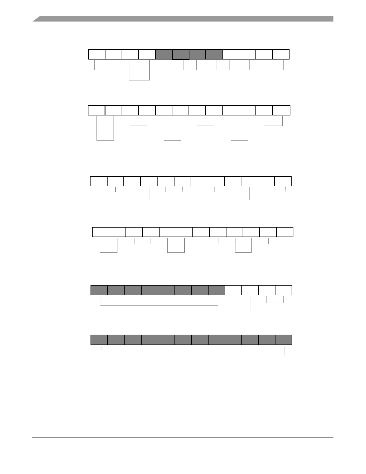
Core Configuration
ESL0ESL1SHL0SHL1
23
22
21 20 19 18 17 16 15 14 13 12
01234567
8
91011
ESAI IPLSHI IPLReservedReservedESAI_1 IPL
ESL11 TAL0TAL1
EMC/ICC Error IPL
TRIPLE TIMER IPL
ESL10
SPDIF Rx IPL
SPRL0SPRL1SPTL0SPTL1ICIL0ICIL1ICAL0ICAL1 ASL0ASL1
SPDIF Tx IPL
ASRC Rx IPL
ICC INT IPL
ICC ACK INT IPL
LIEL0LIEL1
IAL0IAL1IAL2IBL0IBL1IBL2ICL0ICL1ICL2
01234567
8
91011
IRQA IPL
IRQA mode
IRQB IPL
IRQB mode
IRQC IPL
IRQC mode
IRQD IPL
D0L0D0L1D1L0D1L1
23
22
21 20 19 18 17 16 15 14 13 12
DMA ch0 IPL
DMA ch1 IPL
D2L0D2L1D3L0D3L1D4L0D4L1D5L0D5L1
DMA ch2 IPL
DMA ch3 IPL
DMA ch4 IPL
DMA ch5 IPL
IDL2 IDL1 IDL0
IRQD mode
D6L0D6L1D7L0D7L1
01234567
8
91011
DMA ch6 IPL
DMA ch7 IPL
1312141516171819
20
212223
Reserved
Reserved
Figure 5-1. Core-0 Interrupt Priority Register P
Figure 5-2. Core-0 Interrupt Priority Register C
Figure 5-3. Core-0 Interrupt Priority Register C1
5-10 Freescale Semiconductor
Symphony DSP56724/DSP56725 Multi-Core Audio Processors, Rev. 0
Page 85
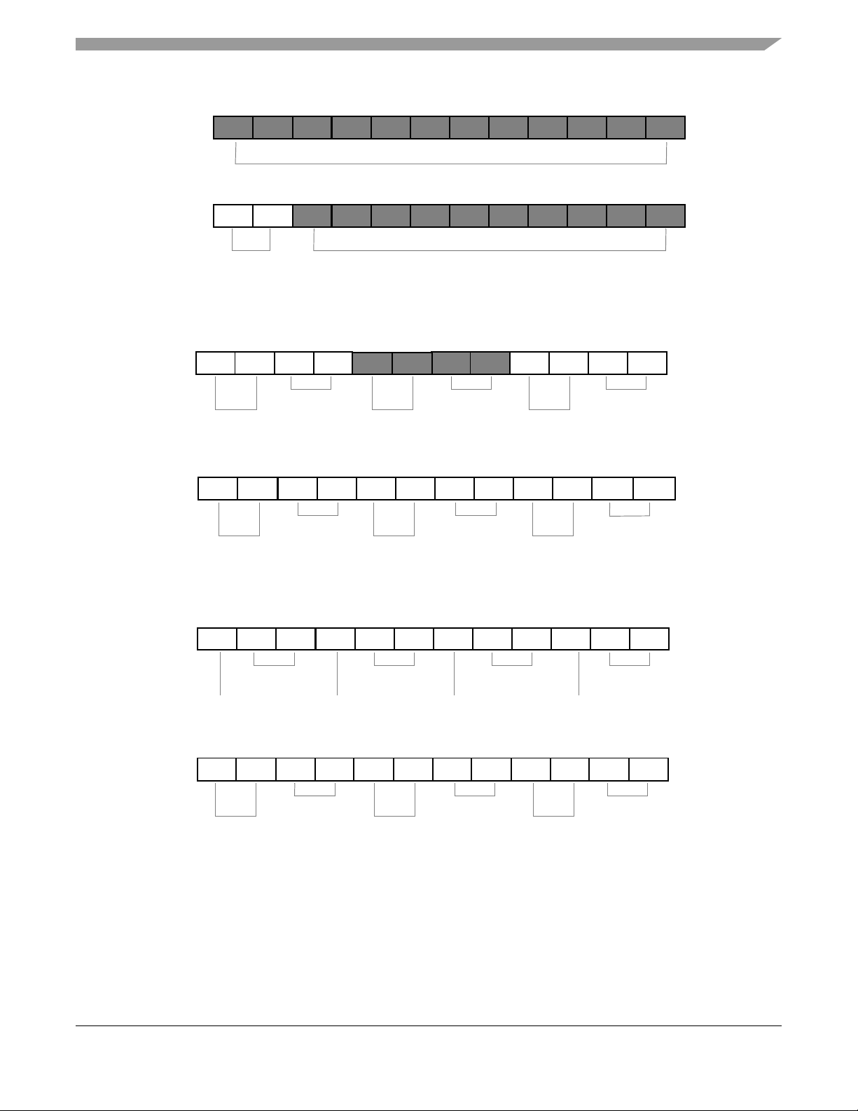
Figure 5-4. Core-0 Interrupt Priority Register P1
01234567
8
91011
1312141516171819
20
212223
Reserved
Reserved
STIL00STIL01
Core-0
Always-ON
INT IPL
ESL20ESL21SHL10SHL11
23
22
21 20 19 18 17 16 15 14 13 12
01234567
8
91011
ESAI_2 IPL
SHI_1 IPLReservedESAI_3 IPL
ESL31 TAL10TAL11
EMC/ICC Error INT IPL
TIMER_1 IPL
ESL30
SPDIF Rx IPL
SPRL0SPRL1SPTL0SPTL1ICIL0ICIL1ICAL0ICAL1 ASL0ASL1
SPDIF Tx IPL
ASRC Rx IPL
ICC INT IPL
ICC ACK INT IPL
LIEL0LIEL1
Reserved
IAL0IAL1IAL2IBL0IBL1IBL2ICL0ICL1ICL2
01234567
8
91011
IRQA IPL
IRQA mode
IRQB IPL
IRQB mode
IRQC IPL
IRQC mode
IRQD IPL
D0L0D0L1D1L0D1L1
23
22
21 20 19 18 17 16 15 14 13 12
DMA1 ch0 IPL
DMA1 ch1 IPL
D2L0D2L1D3L0D3L1D4L0D4L1D5L0D5L1
DMA1 ch2 IPL
DMA1 ch3 IPL
DMA1 ch4 IPL
DMA1 ch5 IPL
IDL2 IDL1 IDL0
IRQD mode
Core Configuration
Figure 5-5. Core-1 Interrupt Priority Register P
Figure 5-6. Core-1 Interrupt Priority Register C
Freescale Semiconductor 5-11
Symphony DSP56724/DSP56725 Multi-Core Audio Processors, Rev. 0
Page 86
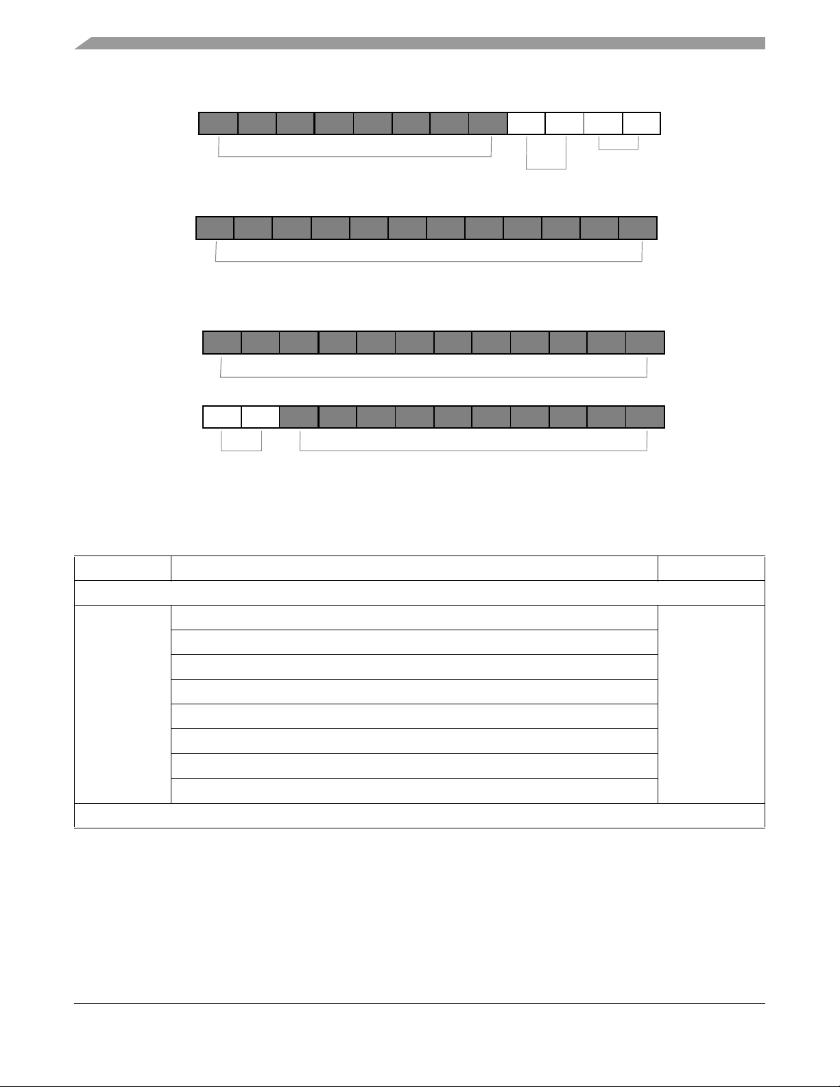
Core Configuration
D6L0D6L1D7L0D7L1
01234567
8
91011
DMA1 ch6 IPL
DMA1 ch7 IPL
1312141516171819
20
212223
Reserved
Reserved
01234567
8
91011
1312141516171819
20
212223
STIL10
STIL11
Reserved
Reserved
Core-1
Always-On
INT IPL
Figure 5-7. Core-1 Interrupt Priority Register C1
Figure 5-8. Core-1 Interrupt Priority Register P1
Table 5-10. Interrupt Sources Priorities within an IPL
Priority Level Interrupt Source Group
Level 3 (non-maskable)
Highest RESET
Stack Error
Illegal Instruction
Debug Request Interrupt
Trap
Non-Maskable Interrupt (NMI) from External
DMA Stall Interrupt
Lowest Inter-Core Non-Maskable Interrupt (from the other core)
Level 0-2 (maskable)
Symphony DSP56724/DSP56725 Multi-Core Audio Processors, Rev. 0
5-12 Freescale Semiconductor
Page 87
Core Configuration
Table 5-10. Interrupt Sources Priorities within an IPL (Continued)
Priority Level Interrupt Source Group
Highest IRQA IRQ
IRQB
IRQC
IRQD
DMA Channel 0 DMA
DMA Channel 1
DMA Channel 2
DMA Channel 3
DMA Channel 4
DMA Channel 5
DMA Channel 6
DMA Channel 7
Highest ESAI/ESAI_2 Receive Data With Exception ESAI/ESAI_2
ESAI/ESAI_2 Receive Even Data
ESAI/ESAI_2 Receive Data
ESAI/ESAI_2 Receive Last Slot
ESAI/ESAI_2 Transmit Data with Exception Status
ESAI/ESAI_2 Transmit Last Slot
ESAI/ESAI_2 Transmit Even Data
ESAI/ESAI_2 Transmit Data
SHI/SHI_1 Bus Error SHI/SHI_1
SHI/SHI_1 Receive Overrun Error
SHI/SHI_1 Transmit Underrun Error
SHI/SHI_1 Receive FIFO Full
SHI/SHI_1 Transmit Data
SHI/SHI_1 Receive FIFO Not Empty
Symphony DSP56724/DSP56725 Multi-Core Audio Processors, Rev. 0
Freescale Semiconductor 5-13
Page 88
Core Configuration
Table 5-10. Interrupt Sources Priorities within an IPL (Continued)
Priority Level Interrupt Source Group
Highest TEC/TEC_1 Timer0 Overflow TEC/TEC_1
TEC/TEC_1 Timer0 Compare
TEC/TEC_1 Timer1 Overflow
TEC/TEC_1 Timer1 Compare
TEC/TEC_1 Timer2 Overflow
TEC/TEC_1 Timer2 Compare
ESAI_1/3 Receive Data ESAI_1/3
ESAI_1/3 Receive Even Data
ESAI_1/3 Receive Data With Exception
ESAI_1/3 Receive Last Slot
ESAI_1/3 Transmit Data
ESAI_1/3 Transmit Even Data
ESAI_1/3 Transmit Data with Exception Status
ESAI_1/3 Transmit Last Slot
S/PDIF RcvChannelNew S/PDIF
S/PDIF RcvValidityBitNotSet
S/PDIF RcvIllegalSymbol
S/PDIF RcvParityError
S/PDIF RxUChannelFull
S/PDIF RxUChannelOver
S/PDIF RxQChannelFull
S/PDIF RxQChannelOver
S/PDIF RxUQSyncFound
S/PDIF RxUQFrameError
S/PDIF Rx Over/Under
S/PDIF Rx Resync
S/PDIF Lock Loss
S/PDIF Rcv FIFO Full
S/PDIF Lock Interrupt
S/PDIF Tx UnderOver
S/PDIF Tx Resync
S/PDIF Tx FIFO Empty
Symphony DSP56724/DSP56725 Multi-Core Audio Processors, Rev. 0
5-14 Freescale Semiconductor
Page 89
Core Configuration
Table 5-10. Interrupt Sources Priorities within an IPL (Continued)
Priority Level Interrupt Source Group
Highest ASRC FP Wait State Interrupt ASRC
ASRC Overload Interrupt
ASRC Data Output C Interrupt
ASRC Data Output B Interrupt
ASRC Data Output A Interrupt
ASRC Data Input C Interrupt
ASRC Data Input B Interrupt
ASRC Data Input A Interrupt
Inter-Core Maskable Interrupt
(from the other core)
Inter-Core Maskable Acknowledge interrupt
(from the other core)
EMC/ICC Access Error Interrupt
Lowest Always Active Interrupt
Table 5-11. Reset and Interrupt Vector Summary
Interrupt Starting Address Priority Level Range Description Notes
VBA: $00 3 RESET
VBA: $02 3 Stack Error
VBA: $04 3 Illegal Instruction
VBA: $06 3 Debug Request Interrupt
VBA: $08 3 Trap
VBA: $0A 3 Non-Maskable Interrupt (NMI)
(external)
VBA: $0C 3 Reserved
VBA: $0E 3 DMA Stall Interrupt CIM interrupt for Core-0 and
CIM_1 interrupt for Core-1
Inter-Core
VBA: $10 0-2 IRQA Shared by both cores.
VBA: $12 0-2 IRQB
VBA: $14 0-2 IRQC
VBA: $16 0-2 IRQD
Symphony DSP56724/DSP56725 Multi-Core Audio Processors, Rev. 0
Freescale Semiconductor 5-15
Page 90
Core Configuration
Table 5-11. Reset and Interrupt Vector Summary (Continued)
Interrupt Starting Address Priority Level Range Description Notes
VBA: $18 0-2 DMA Channel 0 DMA Interrupts for Core-0
VBA: $1A 0-2 DMA Channel 1
VBA: $1C 0-2 DMA Channel 2
VBA: $1E 0-2 DMA Channel 3
VBA: $20 0-2 DMA Channel 4
VBA: $22 0-2 DMA Channel 5
VBA: $24 0-2 DMA Channel 6
VBA: $26 0-2 DMA Channel 7
and DMA_1 interrupts for
Core-1.
VBA: $28 3 Inter-Core Non-Maskable Interrupt
(from the other core)
VBA: $2A 0-2 Inter-Core Maskable Interrupt
(from the other core)
VBA: $2C 0-2 Inter-Core Maskable Acknowledge
Interrupt (from the other core)
VBA: $2E 0-2 Reserved
VBA: $30 0-2 ESAI/ESAI_2 Receive Data ESAI Output interrupts to
VBA: $32 0-2 ESAI/ESAI_2 Receive Even Data
VBA: $34 0-2 ESAI/ESAI_2 Receive Data With
Exception
VBA: $36 0-2 ESAI/ESAI_2 Receive Last Slot
VBA: $38 0-2 ESAI/ESAI_2 Transmit Data
VBA: $3A 0-2 ESAI/ESAI_2 Transmit Even Data
VBA: $3C 0-2 ESAI/ESAI_2 Transmit Data with
Exception Status
VBA: $3E 0-2 ESAI/ESAI_2 Transmit Last Slot
VBA: $40 0-2 SHI/SHI_1 Transmit SHI Output interrupts to
VBA: $42 0-2 SHI/SHI_1 Transmit Underrun Error
VBA: $44 0-2 SHI/SHI_1 Receive FIFO Not Empty
ICC interrupts for Core-0
and Core-1
Core-0;
ESAI_2 Output interrupts to
Core-1.
Core-0:
SHI_1 Output interrupts to
Core-1.
VBA: $46 0-2 Reserved
VBA: $48 0-2 SHI/SHI_1 Receive FIFO Full
VBA: $4A 0-2 SHI/SHI_1 Receive Overrun Error
VBA: $4C 0-2 SHI/SHI_1 Bus Error
VBA: $4E 0-2 Reserved
VBA: $50 0-2
VBA: $52 0-2
Symphony DSP56724/DSP56725 Multi-Core Audio Processors, Rev. 0
5-16 Freescale Semiconductor
Page 91
Core Configuration
Table 5-11. Reset and Interrupt Vector Summary (Continued)
Interrupt Starting Address Priority Level Range Description Notes
VBA: $54 0-2 TEC/TEC_1 Timer0 Compare TEC Output interrupts to
VBA: $56 0-2 TEC/TEC_1 Timer0 Overflow
VBA: $58 0-2 TEC/TEC_1 Timer1 Compare
VBA: $5A 0-2 TEC/TEC_1 Timer1 Overflow
VBA: $5C 0-2 TEC/TEC_1 Timer2 Compare
VBA: $5E 0-2 TEC/TEC_1 Timer2 Overflow
VBA: $60 0-2 Reserved
VBA: $62 0-2
VBA: $66 0-2 Reserved
VBA: $68 0-2
VBA: $6A 0-2
VBA: $6C 0-2
VBA: $6E 0-2
Core-0;
TEC_1 Output interrupts to
Core-1.
VBA: $70 0-2 ESAI_1/3 Receive Data ESAI_1 Output interrupts to
VBA: $72 0-2 ESAI_1/3 Receive Even Data
VBA: $74 0-2 ESAI_1/3 Receive Data With Exception
VBA: $76 0-2 ESAI_1/3 Receive Last Slot
VBA: $78 0-2 ESAI_1/3 Transmit Data
VBA: $7A 0-2 ESAI_1/3 Transmit Even Data
VBA: $7C 0-2 ESAI_1/3 Transmit Data with Exception
Status
VBA: $7E 0-2 ESAI_1/3 Transmit Last Slot
Core-0;
ESAI_3 Output interrupts to
Core-1.
Symphony DSP56724/DSP56725 Multi-Core Audio Processors, Rev. 0
Freescale Semiconductor 5-17
Page 92
Core Configuration
Table 5-11. Reset and Interrupt Vector Summary (Continued)
Interrupt Starting Address Priority Level Range Description Notes
VBA: $80 0-2 S/PDIF RcvCChannelNew S/PDIF
VBA: $82 0-2 S/PDIF RcvValidityBitNotSet
VBA: $84 0-2 S/PDIF RcvIllegalSymbol
VBA: $86 0-2 S/PDIF RcvParityError
VBA: $88 0-2 S/PDIF RxUChannelFull
VBA: $8A 0-2 S/PDIF RxUChannelOver
VBA: $8C 0-2 S/PDIF RxQChannelFull
VBA: $8E 0-2 S/PDIF RxQChannelOver
VBA: $90 0-2 S/PDIF RxUQSyncFound
VBA: $92 0-2 S/PDIF RxUQFrameError
VBA: $94 0-2 S/PDIF Rx Over/Under
VBA: $96 0-2 S/PDIF Rx Resync
VBA: $98 0-2 S/PDIF Lock Loss
VBA: $9A 0-2 S/PDIF Rcv FIFO Full
VBA: $9C 0-2 S/PDIF Lock Interrupt
VBA: $9E 0-2 Reserved
VBA: $A0 0-2 S/PDIF Tx Over/Under
VBA: $A2 0-2 S/PDIF Tx Resync
VBA: $A4 0-2 Reserved
VBA: $A6 0-2 Reserved
VBA: $A8 0-2 Reserved
VBA: $AA 0-2 S/PDIF Tx FIFO Empty
VBA: $AC to VBA: $AE 0-2 Reserved
VBA: $B0 0-2 ASRC Data Input A Interrupt ASRC
VBA: $B2 0-2 ASRC Data Input B Interrupt
VBA: $B4 0-2 ASRC Data Input C Interrupt
VBA: $B6 0-2 ASRC Data output A Interrupt
VBA: $B8 0-2 ASRC Data output B Interrupt
VBA: $BA 0-2 ASRC Data output C Interrupt
VBA: $BC 0-2 ASRC Overload Interrupt
VBA: $BE 0-2 ASRC Internal FP Wait States
Symphony DSP56724/DSP56725 Multi-Core Audio Processors, Rev. 0
5-18 Freescale Semiconductor
Page 93
Core Configuration
Table 5-11. Reset and Interrupt Vector Summary (Continued)
Interrupt Starting Address Priority Level Range Description Notes
VBA: $C0
to
VBA: $FA
VBA: $FC 0-2 Always-On Interrupt (Always active,
VBA: $FE 0-2 EMC/ICC Access Error Interrupt
0-2 Reserved
users can mask it or enable it by setting
the corresponding Priority bits in IPRP1
bit 23 and 22.)
5.6 DMA Request Sources
In previous DSP563xx products, 6 DMA channels were supported. In the DSP56724/DSP56725 , the DMA
blocks are updated, and up to 8 DMA channels can be supported.
Additional registers for the additional two DMA channels are included in the DMA modules. In the
DSP56724/DSP56725, each DMA channel receives its own 32 request lines, allowing more flexibility in
the DMA request sources for the different channels, and potentially support for a greater number of DMA
request sources.
Each DMA channel’s Request Source bits (DRS4-DRS0 bits in the DMA Control/Status registers) encode
the source of DMA requests used to trigger the DMA channels’ transfers. The DMA request sources may
be internal peripherals, or external devices requesting service through the IRQA
pins.
, IRQB, I RQC and IRQD
The additional registers for the two additional DMA channels are the same as the registers for the other
DMA channels. The previous section shows the addresses of these registers. The DMA status register is
slightly different with 8 channels of DMA:
• DSTR[6]: DTD6, DMA channel 6 (the seventh channel) transfer has finished.
• DSTR[7]: DTD7, DMA channel 7 (the eighth channel) transfer has finished.
• DSTR[10:9]: DCH[2:0]; when DCH[2:0] = 6, it indicates that the active channel is DMA channel
6; when DCH[2:0] = 7, it indicates that the active channel is DMA channel 7.
Table 5-12 shows the DMA request sources for all of the 8 DMA channels. All of the 34 DMA request
lines are covered by two request line subsets: one line subset is for DMA channels 0–5, while the other
line subset is for DMA channels 6–7. External request lines are only supported by DMA channel 0–5.
Table 5-12. DMA Request Sources
Source Select Bits BSR[4:0]
of DMA Channel 0–5
1 External IRQA 0_0000 No support for these requests.
2 External IRQB 0_0001
3 External IRQC 0_0010
4 External IRQD 0_0011
5 Transfer Done from DMA Channel 0
0_0100 0_0100
Source Select Bits BSR[4:0]
of DMA Channel 6–7
Symphony DSP56724/DSP56725 Multi-Core Audio Processors, Rev. 0
Freescale Semiconductor 5-19
Page 94
Core Configuration
Table 5-12. DMA Request Sources (Continued)
Source Select Bits BSR[4:0]
of DMA Channel 0–5
6 Transfer Done from DMA Channel 1 0_0101 0_0101
7 Transfer Done from DMA Channel 2
8 Transfer Done from DMA Channel 3
9 Transfer Done from DMA Channel 4
10 Transfer Done from DMA Channel 5
11 Transfer Done from DMA Channel 6 No support for these requests. 0_0000
12 Transfer Done from DMA Channel 7 0_0001
13 Reserved 0_1010 0_1010
14 ESAI/ESAI_2 receive data(RDF=1)
15 ESAI/ESAI_2 transmit data(TDE=1)
16 SHI HTX Empty
17 SHI FIFO Not Empty
18 SHI FIFO Full
19 TIMER0 1_0010 1_0010
20 TIMER1 1_0011 1_0011
21 TIMER2 1_0100 1_0100
22 ESAI_1/ESAI_3 Receive Data (RDF=1) 1_0101 1_0101
23 ESAI_1/ESAI_3 Transmit Data (TDE=1) 1_0110 1_0110
24 S/PDIF Xmt (SPDIFTxEmpty = 1) 1_0111 1_0111
25 SPDIF Rcv (PDIR1 full = 1) 1_1000 1_1000
26 Reserved 1_1001 1_1001
27 ASRC Rx 0 1_1010 1_1010
28 ASRC Rx 1 1_1011 1_1011
29 ASRC Rx 2 1_1100 1_1100
30 ASRC Tx 0 1_1101 1_1101
31 ASRC Tx 1 1_1110 1_1110
32 ASRC Tx 2 1_1111 1_1111
0_0110 0_0110
0_0111 0_0111
0_1000 0_1000
0_1001 0_1001
0_1011 0_1011
0_1100 0_1100
0_1101 0_1101
0_1110 0_1110
0_1111 0_1111
Source Select Bits BSR[4:0]
of DMA Channel 6–7
5.7 Chip ID Register
For more information about the CHIP ID Register (CHIDR), see Chapter 6, “Core Integration Module
(CIM, CIM_1).”
Symphony DSP56724/DSP56725 Multi-Core Audio Processors, Rev. 0
5-20 Freescale Semiconductor
Page 95
Chapter 6
DMA Stall Register
(DMAS)
Peripheral Bus
Chip ID Register
(CHIDR)
OnCE GDB Register
(OGDB)
Core Integration Module
Core Integration Module (CIM, CIM_1)
6.1 Overview
There are two Core Integration Module (CIM) modules in the DSP56724/DSP56725 devices: CIM and
CIM_1. CIM is used by DSP Core-0, while CIM_1 is used by DSP Core-1. Both CIM blocks are identical,
so only one CIM block is described in detail here.
The CIM block contains three registers: Chip ID number register, OnCE global data bus (GDB) register,
and DMA Stall register. In more detail:
• The Chip ID Register contains the chip ID number.
• The CIM includes a DMA Monitor that optionally supports a non-maskable interrupt after the
DMA has been stalled due to int ernal memory contention, for mor e than N cycles (where N can be
from 2 to 224 cycles).
• The OnCE GDB register is a 24 bit register that can be read through the J TAG port, and is used for
passing data between the chip and an external command controller.
Figure 6-1. Core Integration Module Block Diagram
Freescale Semiconductor 6-1
Symphony DSP56724/DSP56725 Multi-Core Audio Processors Reference Manual, Rev. 0
Page 96
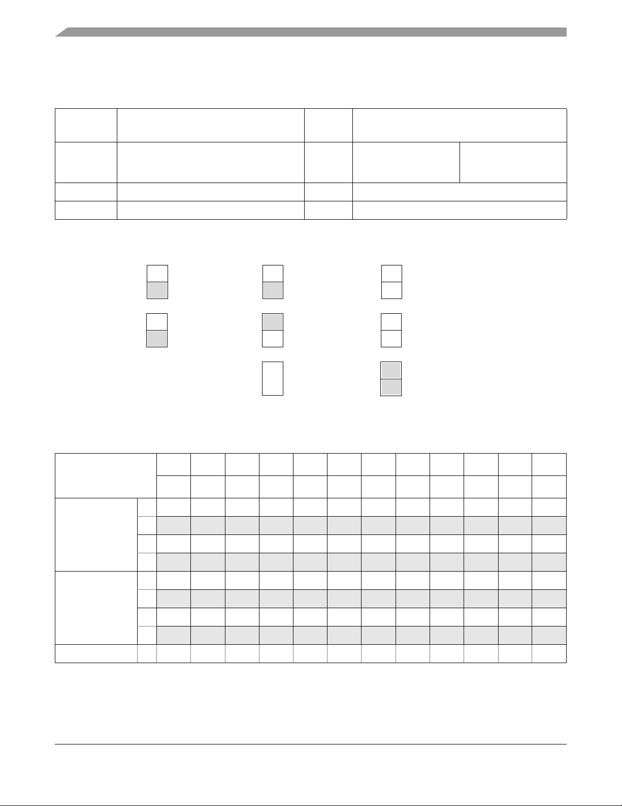
Core Integration Module (CIM, CIM_1)
1
Always reads “1”
0
Always reads “0”
Bit R/W bit
Bit
Read-only bit
Bit
Write-only bit
N/A
Bit
Write “1” to clear
Bit
Self-clearing bit
w1c
0
How to read Ta b l e 6 - 2 :
For each register, there are 4 rows.
The first 2 rows are for bits 23–12,
and the last 2 rows are for bits 11–0.
6.1.1 Memory Map
Table 6-1. CIM Memory Map
Offset or
Address
X:$FFFFF5 Chip ID Register (CHIDR) R DSP56724 device:
X:$FFFFF8 DMA Stall Register (DMAS) R/W 0x000000
X:$FFFFFC OnCE Global Data Bus Register (OGDB) R/W 0x000000
Register Access Reset Value
0x000724 for Core-0
0x010724 for Core-1
6.1.2 Register Summary
DSP56725 device:
0x000725 for Core-0
0x010725 for Core-1
Register
DSP56724 Core-0
Chip ID Register
(CHIDR)
X:$FFFFF5
DSP56724 Core-1
Chip ID Register
(CHIDR)
X:$FFFFF5
Figure 6-2. Legend for Table 6-2
Table 6-2. CIM Register Summary
23 22 21 20 19 18 17 16 15 14 13 12
11109876543210
R000000000000
W
R011100100000
W
R000000010000
W
R011100100000
W
6-2 Freescale Semiconductor
Symphony DSP56724/DSP56725 Multi-Core Audio Processors, Rev. 0
Page 97
Register
Core Integration Module (CIM, CIM_1)
Table 6-2. CIM Register Summary (Continued)
23 22 21 20 19 18 17 16 15 14 13 12
11109876543210
DSP56725 Core-0
Chip ID Register
(CHIDR)
X:$FFFFF5
DSP56725 Core-1
Chip ID Register
(CHIDR)
X:$FFFFF5
DMA Stall
Register (DMAS)
Y:$FFFFF8
OnCE GDB
Register (OGDB)
Y:$FFFFFC
R000000000000
W
R011100100001
W
R000000010000
W
R011100100001
W
R
D23 D22 D21 D20 D19 D18 D17 D16 D15 D14 D13 D12
W
R
D11 D10 D9 D8 D7 D6 D5 D4 D3 D2 D1 D0
W
R
O23 O22 O21 O20 O19 O18 O17 O16 O15 O14 O13 O12
W
R
O11 O10 O9 O8 O7 O6 O5 O4 O3 O2 O1 O0
W
6.2 Register Descriptions
6.2.1 Chip ID Register (CHIDR)
The Chip ID Register is a 24-bit read-only register that contains the Chip ID number. There is a Chip ID
Register for each DSP core in the DSP5672x.
• For the DSP56724, the Chip ID Register value is 0x000724 for Core-0 and 0x010724 for Core-1.
• For the DSP56725, the Chip ID Register value is 0x000725 for Core-0 and 0x010725 for Core-1.
Symphony DSP56724/DSP56725 Multi-Core Audio Processors, Rev. 0
Freescale Semiconductor 6-3
Page 98
Core Integration Module (CIM, CIM_1)
Table 6-3. Chip ID Register for DSP56724 Core-0
23 22 21 20 19 18 17 16 15 14 13 12
11109876543210
Chip ID Register
for DSP56724
Core-0
(CHIDR)
R000000000000
W
R011100100000
W
Table 6-4. Chip ID Register for DSP56724 Core-1
23 22 21 20 19 18 17 16 15 14 13 12
11109876543210
Chip ID Register
for DSP56724
Core-1
(CHIDR)
R000000010000
W
R011100100000
W
Table 6-5. Chip ID Register for DSP56725 Core-0
23 22 21 20 19 18 17 16 15 14 13 12
11109876543210
Chip ID Register
for DSP56725
Core-0
(CHIDR)
R000000000000
W
R011100100001
W
Table 6-6. Chip ID Register for DSP56725 Core-1
23 22 21 20 19 18 17 16 15 14 13 12
11109876543210
Chip ID Register
for DSP56725
Core-1
(CHIDR)
R000000010000
W
R011100100001
W
6.2.2 DMA Stall Register (DMAS)
The DMA Stall Register is 24-bit read/write register that defines the threshold value of DMA counter of
CIM. The DMA Stall Register and an associated interrupt (DMA Stall non-maskable interrupt) allow a
Symphony DSP56724/DSP56725 Multi-Core Audio Processors, Rev. 0
6-4 Freescale Semiconductor
Page 99
Core Integration Module (CIM, CIM_1)
limit to be placed on the number of cycles that the DMA is stalled, due to internal memory contention for
a single DMA memory access.
• When the DMA Stall Register is set to zero, the DMA Stall Interrupt is disabled.
• When the DMA Stall Register is set to a non-zero value, a stall counter will keep track of the
number of cycles the DMA is stalled due to internal memory contention for a single memory
access. If the stall counter is ever larger than the value stored in the DMA Stall Register, the DMA
Stall non-maskable Interrupt will be asserted.
• The DMA Stall Interrupt remains asserted until the internal memory contenti on ends (us ual ly due
to the interrupt routine) or until the DMA Stall Register is written with zero. The stall counter clears
when the internal memory contention ends or when the DMA Stall Register is written with zero.
Table 6-7. DMA Stall Register (DMAS)
23 22 21 20 19 18 17 16 15 14 13 12
11109876543210
DMA Stall
Register
(DMAS)
R
D23 D22 D21 D20 D19 D18 D17 D16 D15 D14 D13 D12
W
R
D11 D10 D9 D8 D7 D6 D5 D4 D3 D2 D1 D0
W
6.2.3 OnCE Global Data Bus Register (OGDB)
The OnCE GDB Register is 24-bit read/write register that can be read through the JT AG port, and is used
for passing data between the chip and an external command controller.
Table 6-8. OnCE GDB Register (OGDB)
23 22 21 20 19 18 17 16 15 14 13 12
11109876543210
OnCE GDB
Register
(OGDB)
R
O23 O22 O21 O20 O19 O18 O17 O16 O15 O14 O13 O12
W
R
O11 O10 O9 O8 O7 O6 O5 O4 O3 O2 O1 O0
W
Symphony DSP56724/DSP56725 Multi-Core Audio Processors, Rev. 0
Freescale Semiconductor 6-5
Page 100

Core Integration Module (CIM, CIM_1)
Symphony DSP56724/DSP56725 Multi-Core Audio Processors, Rev. 0
6-6 Freescale Semiconductor
 Loading...