

Page 1

HW Getting Started Guide
MPC8349EA MDS
Processor Board
Nov 2006: Rev. A
Contents
Contents. . . . . . . . . . . . . . . . . . . . . . . . . . . . . . . . . . . . . . . . . . . . . . . . . . . . . . . . . . . . . . . . . . . . . . . . . . . . . . . . . . 1
About This Document . . . . . . . . . . . . . . . . . . . . . . . . . . . . . . . . . . . . . . . . . . . . . . . . . . . . . . . . . . . . . . . . . . . . . . . 1
Required Reading . . . . . . . . . . . . . . . . . . . . . . . . . . . . . . . . . . . . . . . . . . . . . . . . . . . . . . . . . . . . . . . . . . . . . . . . . . 1
Definitions, AcroRev. And Abbreviations . . . . . . . . . . . . . . . . . . . . . . . . . . . . . . . . . . . . . . . . . . . . . . . . . . . . . . . . . 1
Step 1: Check HW kit contents . . . . . . . . . . . . . . . . . . . . . . . . . . . . . . . . . . . . . . . . . . . . . . . . . . . . . . . . . . . . . . . 2
Step 2: Connect plastic spacers . . . . . . . . . . . . . . . . . . . . . . . . . . . . . . . . . . . . . . . . . . . . . . . . . . . . . . . . . . . . . . 3
Step 3: Check Switches and Jumpers . . . . . . . . . . . . . . . . . . . . . . . . . . . . . . . . . . . . . . . . . . . . . . . . . . . . . . . . . . 3
Step 4: Assemble and connect the power supply kit. . . . . . . . . . . . . . . . . . . . . . . . . . . . . . . . . . . . . . . . . . . . . . . 6
Step 5: Perform initial board power up. . . . . . . . . . . . . . . . . . . . . . . . . . . . . . . . . . . . . . . . . . . . . . . . . . . . . . . . . . 6
Step 6: Connect the JTAG connectivity unit to the board. . . . . . . . . . . . . . . . . . . . . . . . . . . . . . . . . . . . . . . . . . . . 6
Step 7: Attach remaining cables to the board according to your development needs. . . . . . . . . . . . . . . . . . . . . . 7
About This Document
This document shows how to connect the MPC8349EA MDS processor board and verify its basic operation, in a step by step
format. Settings for switches and jumpers are shown, as well as instructions for connecting peripheral devices. In addition,
instructions for connecting the MPC8349EA MDS processor board to an Integrated Development Environment (IDE), such as
Freescale’s CodeWarrior
version of the board has a faster DDR2 (400MHz), and a flash memory of 32MB.
®
are included, but instructions for working with the IDE are beyond the scope of this document. This
Required Reading
It is assumed that the reader is familiar with the MPC8349EA chip, and the contents of the MPC8349EA Reference Manual.
Definitions, AcroRev. And Abbreviations
BCSR board control and status register LED light emitting diode
BMS boot memory space PCI peripheral component interconnect
CFG_RS bit in RCW register PCI_SYNC_OUT chip pin
CLKDIV clock division PIB platform I/O board
CLKIN clock input PLL phase lock loop
COP debug port in PowerPC RCW reset configuration words
DDR double data rate DRAM ROM read-only memory
DIP dual in-line package SHMOO sweep test (of frequency and core voltage)
I2C Philips serial port TLE bit in RCW register
JTAG IEEE standard 1149.1 TSEC triple speed ethernet controller
MPC8349EA MDS Processor Board HW Getting Started Guide, Rev. A
Freescale Semiconductor Page 1 of 8
Page 2

Step 1: Check HW kit contents
1. MPC8349EA MDS Processor
Board
2. AC/DC 5V/5A universal power
supply kit
3. RS232 standard serial cable
with two 9-pin
connectors-extends the
Freescale adaptor cable
4. Freescale adaptor cable (joined)
with one RJ45 and two RS232
connectors:
a) RJ45 10-pin plug
b) RS232 9-pin D-type
connector
5. USB adaptor and connector:
a Mini USB adaptor: 5-pin
(male) and 4-pin (female)
b USB cable with two
connectors: standardA and
miniB.
6. Ethernet cables (2) with RJ45-8
connectors
Not shown:
7. Four sets of plastic spacers
(male/female)
8. One Allen wrench
9. CodeWarrior SW kit (includes
JTAG connectivity unit)
10. MPC8349EA MDS Processor
Board documentation
MPC8349EA MDS Processor Board
HW Getting Started Guide
2
1
5a
4a
6
5b
3
4b
MPC8349EA MDS Processor Board HW Getting Started Guide, Rev. A
Page 2 of 8 Freescale Semiconductor
Page 3

Step 2: Connect plastic spacers
Four sets of plastic spacers screw
into holes located at (approximately)
the four corners of the board.The
spacers raise and stabilize the board.
1. From under the board, insert a
spacer into one of the board's four
spacer holes.
2. Attach a female spacer onto the
male spacer.
3. Repeat for the three remaining pairs
of spacers.
Step 3: Check Switches and Jumpers
The MPC8349EA MDS Processor
Board has two rows of Dual-In-Line
Package (DIP) switches.The default
DIP-switch positions set-up the
MPC8349EA MDS Processor Board
clock mode as shown in the table
below:
Plastic Screw
SW5
SW7
SW6
Plastic Spacer
SW4
SW3
MPC8349EA MDS Processor
Board Clock Mode
e300 Core Frequency 533 MHz
CCB 266 MHz
DDR2
(can be changed to 400MHz)(
Local Bus 133 MHz
266 MHz
SW2
Socket for MPC8349EA
JP1
Switches SW3,4,6,7
SW5
MPC8349EA MDS Processor Board HW Getting Started Guide, Rev. A
Freescale Semiconductor Page 3 of 8
Page 4
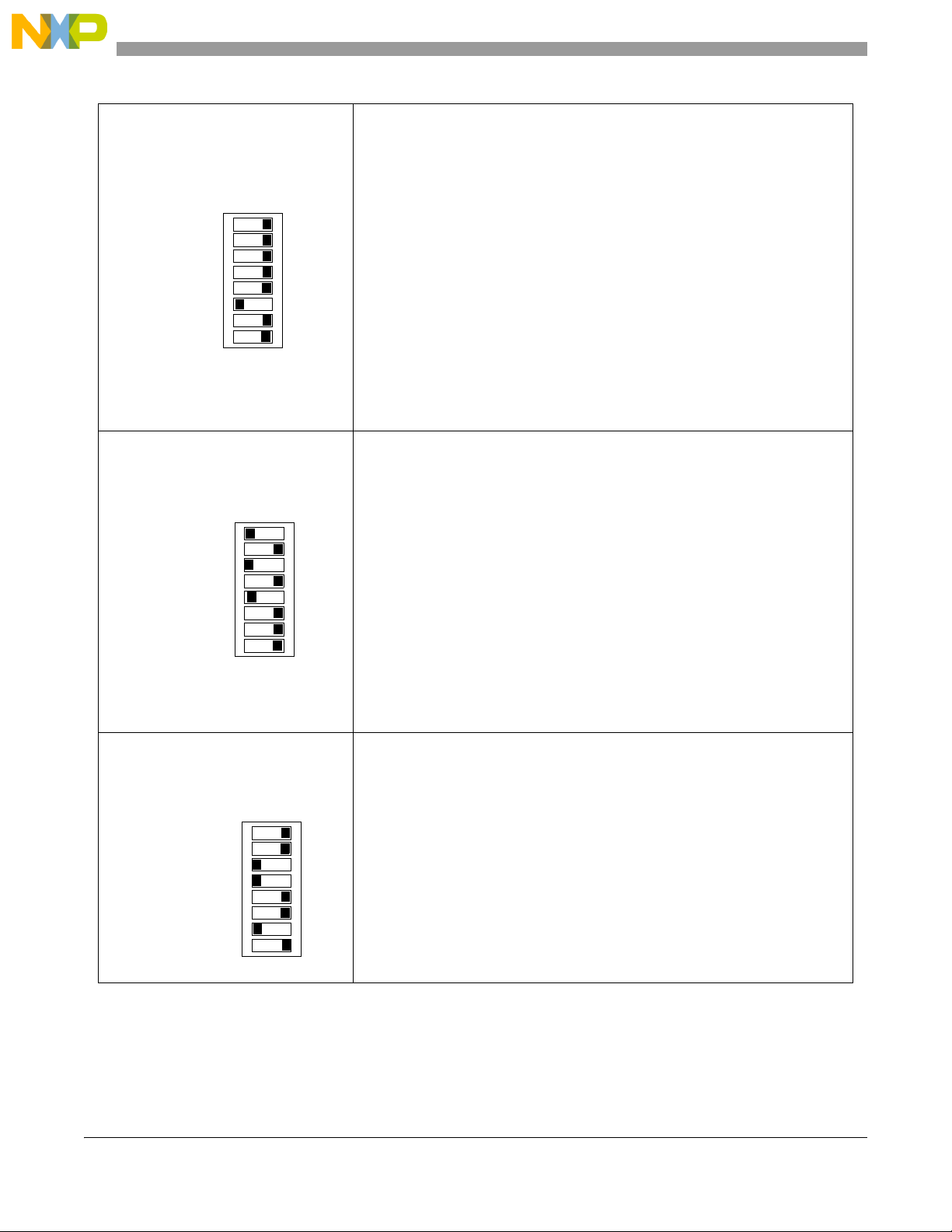
Step 3.a: SW3 Configuration Set 1
1 <- ->0
1: CFG_RS0 ON
2: CFG_RS1
3: CFG_RS2
4: CLKDIV
5: SPMF0
6: SPMF1
7: SPMF2
8: SPMF3
The "On" DIP Switch position
corresponds to a signal value of
“zero”.
123 4 567 8
SW3.1-SW3.3
CFG_RS sets the Reset Configuration Words Source
ON: value of zero
factory setting: '000' when RCW is fetched from the local bus
DIP-switch SW9/3 FCFG: chooses between BCSR or Flash RCW source
SW3.4
CLKDIV selects the relationship between CLKIN and PCI_SYNC_OUT
if the MPC8349 is configured as a PCI Agent (factory setting) then CLK_DIV
is low
SW3.5-SW3.8
SPMF selects System PLL Multiplication Factor
factory setting: '0100'
clock ratio: csb_clk/CLKIN = 4 (csb_clk = 266MHz) or csb_clk/PCI_CLK = 4
Factory default setting: 00000101
Step 3.b: SW4 Configuration Set 2
1 <- ->0
1: TSEC1-0 O N
2: TSEC1-1
3: TSEC2-0
4: TSEC2-1
5: BMS
6: TLE
7: PCI64
8: FCFG
123 4 56 7 8
Step 3.c: SW6 Configuration Set 3
1 <- ->0
1: BOOT SEQ0 ON
2: BOOT SEQ1
3: ROMLOC0
4: ROMLOC1
5: ROMLOC2
6: DDRCM
7: LBIUCM
8: SWEN
123 4 56 7 8
SW4.1-SW4.2: TSEC1/TSEC2
Selects the protocol used by the two-port TSEC controller
factory setting: enters GMII mode when TSEC1 and TSEC2 initiate similar
2’b10
SW4.5: BMS: Selects boot memory space
factory setting is ‘1’ when boot memory resides in upper eight Mbytes at
0xFF80_0000 to 0xFFFF_FFFF
SW4.6 TLE: Selects endian mode
factory setting: '0'; big endian mode
SW4.7: PCI64: Selects PCI width
factory setting: '0'; 32-bit width
SW4.8: FCFG: Sets RCW source on local bus
‘0’: BCSR source; setting uses values from SW3 and SW6.
‘1’: Flash source - setting is burned in flash memory
Factory setting: ‘0’
Factory default setting: 10101000
SW6.1-SW6.2: Boot sequencer configuration
Boot sequencer loads configuration data from the serial ROM.
Factory setting: ‘00’; disables access to I2C ROM.
SW6.3-SW6.5: Boot ROM location
Factory setting: ‘110’; provides flash boot on local bus
SW6.6 DDR: Clock mode
Factory setting: ‘0’; operates with DDR clock (identical to csb_clk)
SW6.7: Local bus clock mode
Factory setting: ‘1’; operates with local bus clock - half of csb_clk
SW6.8: Software watchdog
Factory setting: ‘0’; with software watchdog disabled
Factory default setting: 00110010
MPC8349EA MDS Processor Board HW Getting Started Guide, Rev. A
Page 4 of 8 Freescale Semiconductor
Page 5
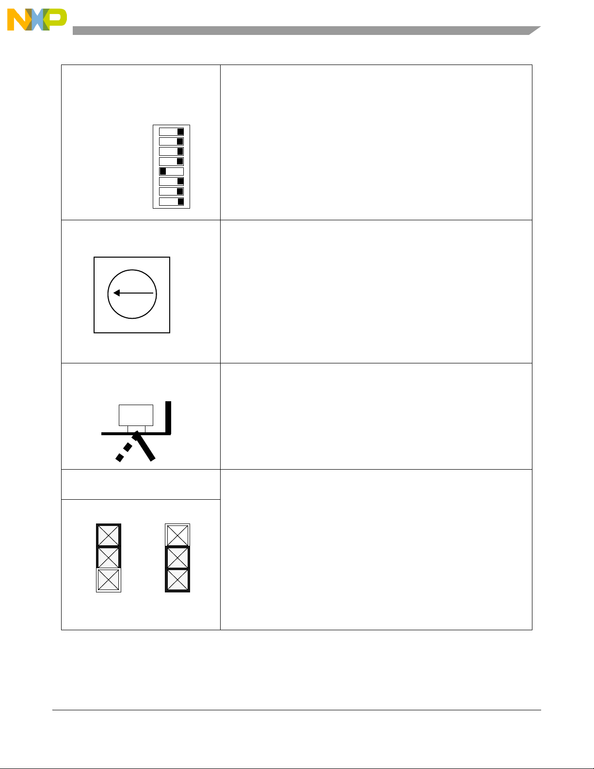
Step 3.d: SW7 Configuration Set 4
1 <- ->0
1: COREPLL0 ON
2: COREPLL1
3: COREPLL2
4: COREPLL3
5: COREPLL4
6: COREPLL5
7: COREPLL6
8: COREDIS
123 4 56
7
8
SW7.1-SW7.7: Core PLL setting
Sets the ratio between the e300 core clock and the internal csb_clk
Factory setting: ‘000010000’ for core_clk = 533MHz
Recommended secondary setting: ‘00000110’ for core_clk = 500MHz
SW7.8: Core disable
Factory setting: '0'; core enabled for boot operation
Factory default setting: 00001000
Step 3.e: SW2 Software Option
0
5
Step 3.f: SW5 Power Switch
PCB
ON
Step 3.g: JP1: Internal/External Clock
1
2
3
1
2
3
SW2: Software option
Software BCS rotary-switch SW2 positions (0-7) enable program flow change
Switch status can be seen in BCSR10[2-4]
Factory setting: ‘0’
SW5: power switch
ON: power from an external 5V power supply via the P10 power jack
combined mode: powered from +5V on PIB power supply through riser
connectors (regardless of SW5 position)
board plugged as a PCI add-in card: PC internal power supply will provide 5V
via PCI edge connector (regardless of SW5 position)
JP1
Selects the source for the CLOCKIN signal
• If a jumper is located between JP1 pins 1-2 (factory setting), the processor is
clocked from the on-board clock oscillator (U21 socket)
• If a jumper is located between JP1 pins 2-3, the processor is clocked from an
external source (via P5)
• The SHMOO mode clock source is I2C; manually programmed clock
synthesizer residing on PIB
Internal
Clock Source
External
Clock Source
MPC8349EA MDS Processor Board HW Getting Started Guide, Rev. A
Freescale Semiconductor Page 5 of 8
Page 6
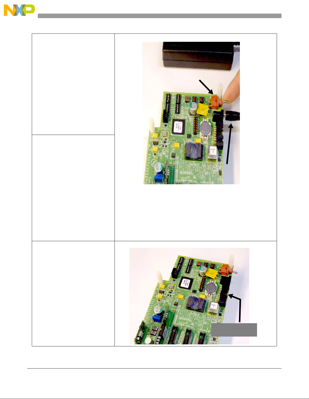
Step 4: Assemble and connect the power supply kit.
Note:
Move power switch to OFF.
Assemble the AC/DC power supply kit:
• power cable with country-specific
wall outlet plug
• power supply unit and cable with jack
(for board connection)
1. Connect the AC/DC power supply
cable with jack to the board.
2. Plug the power cable into the wall
outlet.
Step 5: Perform initial board power up.
Note:
To prevent damage to the JTAG
connectivity unit connect the unit
only after initial board reset.
1. Move the power switch to ON. LED1
briefly displays green light.
2. Check for completion of the reset
sequence-indicated by a single flash
of LED1 (green) and LED2 (red).
The location of LED1 and LED2 is
marked in the figure of
page 7.
3. Shut off the power-move the power
switch to OFF.
Step 7 on
AC/DC Power Supply
ON/OFF Switch
Power Supply Cable
Step 6: Connect the JTAG connectivity unit to the board.
The JTAG connectivity unit enables
CodeWarrior SW work with the
board.
1. Connect the JTAG connectivity unit
to the JTAG/COP 14-pin connector.
2. Move the power switch to ON.
3. Check for completion of the reset
sequence (see
4. Continue as per the instructions in
the Kit Configuration Guide.
Page 6 of 8 Freescale Semiconductor
Step 5 on page 6).
JTAG/COP 14-Pin
Connector
MPC8349EA MDS Processor Board HW Getting Started Guide, Rev. A
Page 7
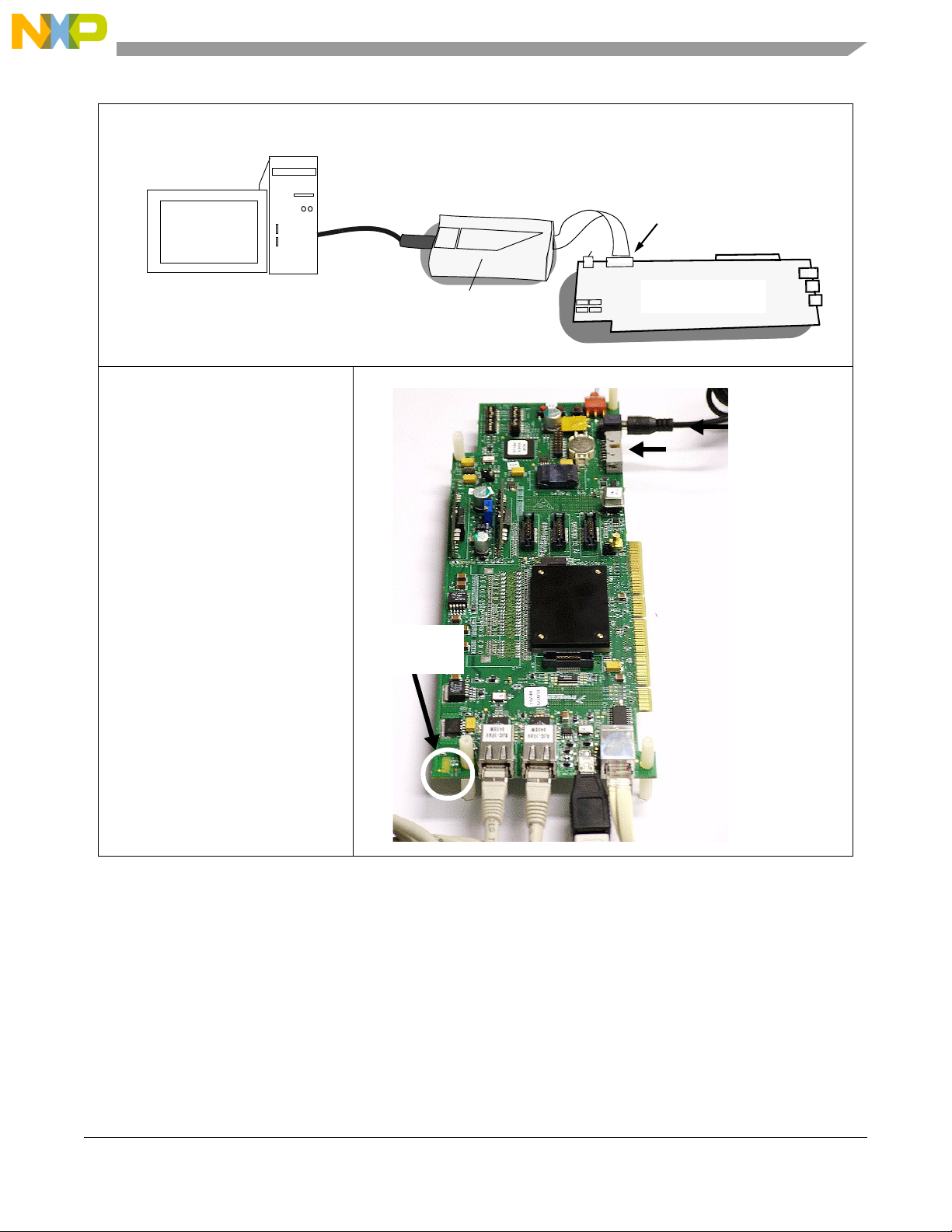
PC with
CodeWarrior
installed
C
o
d
e
W
a
r
r
i
SB
o
T
A
P
U
JTAG
Connectivity Unit
JTAG/COP 14-Pin
Connector
r
MPC8349EA MDS
Processor Board
Step 7: Attach remaining cables to the board according to your development needs.
Connect the remaining cables to the
board as per user development
needs and planned board use:
1. JTAG/COP connector for JTAG
connectivity unit-included in the
CodeWarrior SW kit
2. Serial port for the joined Freescale
adaptor cable with one RJ45 and
two RS232 connectors:
a RJ45 10-pin plug-plugs into the
serial port
b RS232 9-pin D-type connector
3. USB port for USB adaptor and
connector:
a mini USB adaptor: 5-pin (male)
and 4-pin (female)
b USB cable with two connectors:
standardA and miniB.
4. Ethernet ports for the two Ethernet
cables with RJ45-8 pin connectors.
Reset LEDs
LED1 (green)
LED2 (red)
Power Supply
Port
JTAG/COP
Connector
1
44
3
2
3
MPC8349EA MDS Processor Board HW Getting Started Guide, Rev. A
Freescale Semiconductor Page 7 of 8
Page 8

How to Reach Us:
USA/Europe/Locations Not Listed:
Freescale Semiconductor Literature Distribution
Center
P.O. Box 5405
Denver, Colorado 80217
1-800-521-6274 or 480-768-2130
Japan:
Freescale Semiconductor Japan Ltd.
Technical Information Center
3-20-1, Minami-Azabu, Minato-ku
Tokyo 106-8573, Japan
81-3-3440-3569
Asia/Pacific:
Freescale Semiconductor Hong Kong Ltd.
2 Dai King Street
Tai Po Industrial Estate
Tai Po, N.T., Hong Kong
852-26668334
Home Page:
www.freescale.com
Information in this document is provided solely to enable system and software implementers to use
Freescale Semiconductor products. There are no express or implied copyright licenses granted
hereunder to design or fabricate any integrated circuits or integrated circuits based on the information
in this document.
Freescale Semiconductor reserves the right to make changes without further notice to any products
herein. Freescale Semiconductor makes no warranty, representation or guarantee regarding the
suitability of its products for any particular purpose, nor does Freescale Semiconductor assume any
liability arising out of the application or use of any product or circuit, and specifically disclaims any
and all liability, including without limitation consequential or incidental damages. “Typical” parameters
that may be provided in Freescale Semiconductor data sheets and/or specifications can and do vary
in different applications and actual performance may vary over time. All operating parameters,
including “Typicals”, must be validated for each customer application by customer’s technical
experts. Freescale Semiconductor does not convey any license under its patent rights nor the rights
of others. Freescale Semiconductor products are not designed, intended, or authorized for use as
components in systems intended for surgical implant into the body, or other applications intended to
support or sustain life, or for any other application in which the failure of the Freescale Semiconductor
product could create a situation where personal injury or death may occur. Should Buyer purchase
or use Freescale Semiconductor products for any such unintended or unauthorized application,
Buyer shall indemnify and hold Freescale Semiconductor and its officers, employees, subsidiaries,
affiliates, and distributors harmless against all claims, costs, damages, and expenses, and
reasonable attorney fees arising out of, directly or indirectly, any claim of personal injury or death
associated with such unintended or unauthorized use, even if such claim alleges that Freescale
Semiconductor was negligent regarding the design or manufacture of the part.
Learn More: For more information about Freescale products, please visit www.freescale.com.
Freescale™ and the Freescale logo are trademarks of Freescale Semiconductor, Inc. All other
product or service names are the property of their respective owners.
© Freescale Semiconductor, Inc. 2006. All rights reserved.
MPC8349EA MDS Processor Board HW Getting Started Guide, Rev. A
Page 8 of 8 Freescale Semiconductor
 Loading...