

Page 1

MPC563XM Microcontroller
MPC563XRM
Rev. 1
25 Jul 2008
Reference Manual
Devices Supported:
MPC5634M
MPC5633M
MPC5632M
MPC563XM Reference Manual, Rev. 1
Freescale Semiconductor 1
Preliminary—Subject to Change Without Notice
Page 2

MPC563XM Reference Manual, Rev. 1
2 Freescale Semiconductor
Preliminary—Subject to Change Without Notice
Page 3

Chapter 1
Introduction
1.1 The MPC563XM Microcontroller Family ......................................................................................23
1.2 MPC563XM Device Summary .......................................................................................................23
1.3 MPC563XM Blocks ........................................................................................................................24
1.3.1 Block Diagram ..................................................................................................................24
1.3.2 Block Summary ................................................................................................................25
1.4 MPC563XM Features .....................................................................................................................26
1.4.1 Feature List .......................................................................................................................26
1.4.2 e200z335 Core ..................................................................................................................35
1.4.3 Crossbar ............................................................................................................................37
1.4.4 eDMA ...............................................................................................................................37
1.4.5 Interrupt Controller ...........................................................................................................38
1.4.6 FMPLL ..............................................................................................................................39
1.4.7 Calibration EBI .................................................................................................................40
1.4.8 SIU ....................................................................................................................................41
1.4.9 ECSM ................................................................................................................................41
1.4.10 Flash ..................................................................................................................................42
1.4.11 SRAM ...............................................................................................................................43
1.4.12 BAM .................................................................................................................................43
1.4.13 eMIOS ...............................................................................................................................43
1.4.14 eTPU .................................................................................................................................44
1.4.15 eQADC .............................................................................................................................46
1.4.16 DSPI ..................................................................................................................................48
1.4.17 eSCI ..................................................................................................................................50
1.4.18 FlexCAN ...........................................................................................................................51
1.4.19 System Timers ...................................................................................................................52
1.4.20 Software Watchdog Timer (SWT) ....................................................................................53
1.4.21 Nexus Port Controller .......................................................................................................53
1.4.22 JTAG .................................................................................................................................55
Chapter 2
Memory Map
2.1 Introduction .....................................................................................................................................57
2.2 Memory Map ...................................................................................................................................57
Chapter 3
Signal Descriptions
3.1 Device Pin Assignments ..................................................................................................................63
3.1.1 144 LQFP ..........................................................................................................................63
3.1.2 Ballmap: 208 MAPBGA ...................................................................................................65
3.2 External Signal Summary ................................................................................................................66
3.3 Detailed Signal Descriptions ...........................................................................................................76
3.3.1 Reset / Configuration ........................................................................................................76
3.3.2 Calibration External Bus Interface (EBI) .........................................................................76
MPC563XM Reference Manual, Rev. 1
Freescale Semiconductor 3
Preliminary—Subject to Change Without Notice
Page 4

3.3.3 Nexus Port Controller (NPC) ............................................................................................78
3.3.4 JTAG .................................................................................................................................79
3.3.5 FlexCAN ...........................................................................................................................80
3.3.6 eSCI ..................................................................................................................................80
3.3.7 DSPI ..................................................................................................................................81
3.3.8 eQADC .............................................................................................................................82
3.3.9 eTPU .................................................................................................................................85
3.3.10 eMIOS ...............................................................................................................................88
3.3.11 Clock Synthesizer .............................................................................................................89
3.3.12 Power / Ground .................................................................................................................90
Chapter 4
Resets
4.1 Reset Sources ..................................................................................................................................93
4.2 Reset Vector .....................................................................................................................................94
4.3 Reset Pins ........................................................................................................................................94
4.3.1 RESET ..............................................................................................................................94
4.3.2 RSTOUT ...........................................................................................................................94
4.4 Clock Quality Monitor Gating Signal .............................................................................................95
4.5 Reset Source Descriptions ...............................................................................................................95
4.5.1 Power-on Reset .................................................................................................................98
4.5.2 External Reset ...................................................................................................................98
4.5.3 Loss of Lock .....................................................................................................................98
4.5.4 Loss of Clock ....................................................................................................................99
4.5.5 Watchdog Timer/Debug Reset ..........................................................................................99
4.5.6 Software Watchdog Timer Reset ......................................................................................99
4.5.7 Checkstop Reset ..............................................................................................................100
4.5.8 JTAG Reset .....................................................................................................................100
4.5.9 Software System Reset ...................................................................................................100
4.5.10 Software External Reset ..................................................................................................101
4.6 Reset Registers in the SIU .............................................................................................................101
4.7 Reset Configuration .......................................................................................................................101
4.7.1 Reset Configuration Half Word (RCHW) .......................................................................101
4.7.2 Reset Configuration Timing ............................................................................................103
4.7.3 Reset Weak Pull Up/Down Configuration ......................................................................104
Chapter 5
Operating Modes
5.1 Overview .......................................................................................................................................105
5.2 Modes of Operation .......................................................................................................................105
5.2.1 Normal Mode ..................................................................................................................105
5.2.2 Debug Mode ...................................................................................................................105
5.2.3 Low Power Modes ..........................................................................................................105
5.3 Modes and Clock Architecture ......................................................................................................106
5.3.1 Block Diagrams ..............................................................................................................106
MPC563XM Reference Manual, Rev. 1
4 Freescale Semiconductor
Preliminary—Subject to Change Without Notice
Page 5

5.3.2 Clock Architecture ..........................................................................................................110
Chapter 6
e200z335 (Z335) Core
6.1 Introduction ...................................................................................................................................115
6.2 Features .........................................................................................................................................115
6.3 Location of Detailed Documentation ............................................................................................116
Chapter 7
Direct Memory Access (DMA)
7.1 Information Specific to This Device .............................................................................................117
7.1.1 Device-Specific Features ................................................................................................117
7.1.2 Channel Assignments .....................................................................................................117
7.2 Introduction ...................................................................................................................................118
7.2.1 Overview .........................................................................................................................119
7.2.2 Features ...........................................................................................................................120
7.3 Memory Map/Register Definition .................................................................................................125
7.3.1 Register Descriptions ......................................................................................................127
7.4 Functional Description ..................................................................................................................151
7.4.1 DMA Microarchitecture .................................................................................................151
7.4.2 DMA Basic Data Flow ...................................................................................................152
7.4.3 DMA Performance ..........................................................................................................155
7.5 Initialization/Application Information ..........................................................................................158
7.5.1 DMA Initialization ..........................................................................................................158
7.5.2 DMA Programming Errors .............................................................................................159
7.5.3 DMA Arbitration Mode Considerations .........................................................................160
7.5.4 DMA Transfer .................................................................................................................161
7.5.5 TCD Status ......................................................................................................................164
7.5.6 Channel Linking .............................................................................................................165
7.5.7 Dynamic Programming ...................................................................................................166
7.5.8 Hardware Request Release Timing .................................................................................167
Chapter 8
Multi-Layer AHB Crossbar Switch (XBAR)
8.1 Information Specific to This Device .............................................................................................169
8.1.1 Device-Specific Block Diagram .....................................................................................169
8.1.2 Device-Specific Features ................................................................................................169
8.1.3 Device-Specific Register Information ............................................................................170
8.2 Introduction ...................................................................................................................................171
8.2.1 Overview .........................................................................................................................171
8.2.2 Features ...........................................................................................................................173
8.2.3 Limitations ......................................................................................................................173
8.2.4 General Operation ...........................................................................................................173
8.3 XBAR Registers ............................................................................................................................174
8.3.1 Register Summary ...........................................................................................................174
MPC563XM Reference Manual, Rev. 1
Freescale Semiconductor 5
Preliminary—Subject to Change Without Notice
Page 6

8.3.2 XBAR Register Descriptions ..........................................................................................177
8.3.3 Coherency .......................................................................................................................185
8.4 Function .........................................................................................................................................185
8.4.1 Arbitration .......................................................................................................................185
8.4.2 Priority Assignment ........................................................................................................187
8.4.3 Master Port Functionality ...............................................................................................188
8.4.4 Slave Port Functionality ..................................................................................................191
8.5 Initialization/Application Information ..........................................................................................198
8.6 Interface .........................................................................................................................................198
8.6.1 Overview .........................................................................................................................199
8.6.2 Master Ports ....................................................................................................................199
8.6.3 Slave Ports ......................................................................................................................200
Chapter 9
Peripheral Bridge (PBRIDGE)
9.1 PBRIDGE Features .......................................................................................................................201
9.2 PBRIDGE Modes of Operation .....................................................................................................201
9.3 PBRIDGE Block Diagram ............................................................................................................201
9.4 PBRIDGE Signal Description .......................................................................................................201
9.5 PBRIDGE Functional Description ................................................................................................202
9.5.1 Read Cycles ....................................................................................................................202
9.5.2 Write Cycles ....................................................................................................................202
9.6 PBRIDGE Registers ......................................................................................................................202
Chapter 10
Flash Memory (C90FL)
10.1 Introduction ...................................................................................................................................203
10.2 Platform Flash (PFlash) Memory Controller ................................................................................203
10.2.1 Controller Overview .......................................................................................................203
10.2.2 Features ...........................................................................................................................203
10.2.3 Modes of Operation ........................................................................................................204
10.2.4 Block Diagram ................................................................................................................204
10.2.5 Signal Description ...........................................................................................................204
10.2.6 Functional Description ....................................................................................................204
10.2.7 Memory Map and Register Definition ............................................................................208
10.2.8 C90FL Register Descriptions ..........................................................................................209
10.3 Flash Memory Block (C90FL) ......................................................................................................214
10.3.1 C90FL Block Overview ..................................................................................................214
10.3.2 C90FL Block Features ....................................................................................................215
10.3.3 C90FL Modes of Operation ............................................................................................216
10.3.4 C90FL Block Diagram ....................................................................................................216
10.3.5 C90FL Flash EEPROM Functional Description ............................................................217
10.3.6 C90FL Memory Map and Register Definition ...............................................................219
MPC563XM Reference Manual, Rev. 1
6 Freescale Semiconductor
Preliminary—Subject to Change Without Notice
Page 7

Chapter 11
Flash Memory (LC)
11.1 Introduction ...................................................................................................................................243
11.2 Block Diagram ..............................................................................................................................243
11.3 Overview .......................................................................................................................................243
11.4 Features .........................................................................................................................................244
11.4.1 FBIU features ..................................................................................................................244
11.4.2 Flash memory array features ...........................................................................................244
11.5 Modes of Operation .......................................................................................................................245
11.5.1 User Mode .......................................................................................................................245
11.5.2 Stop Mode .......................................................................................................................245
11.6 Memory Map/Register Description ...............................................................................................245
11.6.1 Flash Memory Map .........................................................................................................245
11.6.2 Register Descriptions ......................................................................................................248
11.7 Functional Description ..................................................................................................................279
11.7.1 Basic Interface Protocol ..................................................................................................279
11.7.2 Access Protections ..........................................................................................................280
11.7.3 Read Cycles - Buffer Miss ..............................................................................................280
11.7.4 Read Cycles - Buffer Hit .................................................................................................280
11.7.5 Write Cycles ....................................................................................................................280
11.7.6 Error Termination ............................................................................................................280
11.7.7 Access Pipelining ............................................................................................................281
11.7.8 Flash Error Response Operation .....................................................................................281
11.7.9 Bank0 Page Read Buffers and Prefetch Operation .........................................................281
11.7.10Read-While-Write Functionality .....................................................................................283
11.7.11Wait-State Emulation ......................................................................................................284
11.7.12Flash Memory Array: User Mode ...................................................................................285
Chapter 12
General-Purpose Static RAM (SRAM)
12.1 Overview .......................................................................................................................................299
12.2 Features .........................................................................................................................................299
12.3 Modes of Operation .......................................................................................................................299
12.3.1 Normal (Functional) Mode .............................................................................................299
12.3.2 Standby Mode .................................................................................................................299
12.4 Block Diagram ..............................................................................................................................299
12.5 External Signal Description ..........................................................................................................300
12.6 Functional Description ..................................................................................................................300
12.6.1 Access Timing .................................................................................................................300
12.7 Module Memory Map ...................................................................................................................301
12.8 Register Descriptions ....................................................................................................................301
Chapter 13
External Bus Interface (EBI)
13.1 Information Specific to This Device .............................................................................................303
MPC563XM Reference Manual, Rev. 1
Freescale Semiconductor 7
Preliminary—Subject to Change Without Notice
Page 8

13.1.1 Device-Specific Features ................................................................................................303
13.1.2 Unsupported Features .....................................................................................................303
13.1.3 Device-Specific Register Information ............................................................................303
13.2 Introduction ...................................................................................................................................303
13.2.1 Overview .........................................................................................................................304
13.2.2 Features ...........................................................................................................................305
13.2.3 Modes of Operation ........................................................................................................305
13.3 External Signal Description ..........................................................................................................308
13.3.1 Overview .........................................................................................................................308
13.3.2 Detailed Signal Descriptions ..........................................................................................308
13.3.3 Signal Function/Direction by Mode ...............................................................................313
13.3.4 Signal Pad Configuration by Mode ................................................................................313
13.3.5 Signal Output Buffer Enable Logic by Mode .................................................................314
13.4 Memory Map/Register Definition .................................................................................................315
13.4.1 Register Descriptions ......................................................................................................316
13.5 Functional Description ..................................................................................................................324
13.5.1 External Bus Interface Features ......................................................................................324
13.5.2 External Bus Operations .................................................................................................330
13.6 Initialization/Application Information ..........................................................................................397
13.6.1 Booting from External Memory .....................................................................................397
13.6.2 Running with SDR (Single Data Rate) Burst Memories ................................................397
13.6.3 Running with Asynchronous Memories .........................................................................398
13.6.4 Connecting an MCU to Multiple Memories ...................................................................400
13.6.5 Address Decoding Example for External Master Accesses ............................................401
13.6.6 EBI Operation with Reduced Pinout MCUs ...................................................................402
13.6.7 Address/Data Multiplexing Connection Examples .........................................................404
13.6.8 Summary of Differences from MPC5xx .........................................................................408
Chapter 14
Interrupt Controller (INTC)
14.1 Information Specific to This Device .............................................................................................411
14.1.1 Device-Specific Features ................................................................................................411
14.1.2 Device-Specific Register Information ............................................................................411
14.2 Introduction ...................................................................................................................................411
14.2.1 Module Overview ...........................................................................................................411
14.2.2 Block Diagram ................................................................................................................412
14.2.3 Features ...........................................................................................................................413
14.3 Modes of Operation .......................................................................................................................414
14.3.1 Normal Mode ..................................................................................................................414
14.3.2 Debug Mode ...................................................................................................................415
14.3.3 Stop Mode .......................................................................................................................415
14.3.4 Factory Test Mode ..........................................................................................................415
14.4 External Signal Description ..........................................................................................................416
14.5 Memory Map/Register Definition .................................................................................................416
14.5.1 Memory Map ..................................................................................................................416
MPC563XM Reference Manual, Rev. 1
8 Freescale Semiconductor
Preliminary—Subject to Change Without Notice
Page 9

14.5.2 Register Information .......................................................................................................416
14.5.3 INTC Block Configuration Register (INTC_BCR) ........................................................417
14.5.4 INTC Current Priority Register for Processor 0 (INTC_CPR_PRC0) ...........................418
14.5.5 INTC Current Priority Register for Processor 1 (INTC_CPR_PRC1) ...........................419
14.5.6 INTC Interrupt Acknowledge Register for Processor 0 (INTC_IACKR_PRC0) ..........420
14.5.7 INTC Interrupt Acknowledge Register for processor 1 (INTC_IACKR_PRC1) ...........421
14.5.8 INTC End of Interrupt Register for Processor 0 (INTC_EOIR_PRC0) .........................421
14.5.9 INTC End of Interrupt Register for processor 1 (INTC_EOIR_PRC1) .........................422
14.5.10INTC Software Set/Clear Interrupt Registers (INTC_SSCIR0_3 - INTC_SSCIR4_7) .422
14.5.11INTC Priority Select Registers (INTC_PSR0_3 - INTC_PSR508_511) ........................424
14.6 Functional Description ..................................................................................................................425
14.6.1 Interrupt Request Sources ...............................................................................................425
14.6.2 Priority Management ......................................................................................................426
14.6.3 Handshaking with Processor ...........................................................................................428
14.6.4 Reserved Spaces in Memory Map ..................................................................................431
14.7 Initialization/Application Information ..........................................................................................432
14.7.1 Initialization Flow ...........................................................................................................432
14.7.2 Interrupt Exception Handler ...........................................................................................432
14.7.3 Code Compression’s Impact on Vector Table .................................................................434
14.7.4 ISR, RTOS, and Task Hierarchy .....................................................................................434
14.7.5 Order of Execution ..........................................................................................................434
14.7.6 Priority Ceiling Protocol .................................................................................................435
14.7.7 Selecting Priorities According to Request Rates and Deadlines ....................................436
14.7.8 Software Setable Interrupt Requests ...............................................................................437
14.7.9 Lowering Priority Within an ISR ....................................................................................438
14.7.10Negating an Interrupt Request Outside of its ISR ..........................................................438
14.7.11Examining LIFO contents ...............................................................................................439
Chapter 15
Interrupts
15.1 Introduction ...................................................................................................................................441
15.2 Interrupt Vectors ............................................................................................................................441
15.2.1 External Input .................................................................................................................441
15.2.2 Critical Input ...................................................................................................................443
15.3 Interrupt Summary ........................................................................................................................443
Chapter 16
System Integration Unit (SIU)
16.1 Overview .......................................................................................................................................465
16.2 Features .........................................................................................................................................465
16.3 Modes of Operation .......................................................................................................................466
16.3.1 Normal Mode ..................................................................................................................466
16.3.2 Debug Mode ...................................................................................................................466
16.4 Block Diagram ..............................................................................................................................466
16.5 Signal Description .........................................................................................................................467
MPC563XM Reference Manual, Rev. 1
Freescale Semiconductor 9
Preliminary—Subject to Change Without Notice
Page 10

16.6 Detailed Signal Descriptions .........................................................................................................468
16.6.1 RESET — Reset Input ....................................................................................................468
16.6.2 RSTOUT — Reset Output ..............................................................................................468
16.6.3 GPIO[0:213] — General Purpose I/O Pins .....................................................................468
16.6.4 BOOTCFG1 (BOOTCFG1_IRQ[3]_ETRIG[1]_GPIO[212]) — Boot Configuration Pin ..
469
16.6.5 WKPCFG (WKPCFG_NMI_GPIO[213]) — I/O Pin Weak Pull Up Reset Configuration
Pin 469
16.6.6 IRQ[0:15] — External Interrupt Request Input Pins ......................................................469
16.7 Functional Description ..................................................................................................................469
16.7.1 System Configuration .....................................................................................................469
16.7.2 Reset Control ..................................................................................................................470
16.7.3 External Interrupt ............................................................................................................470
16.7.4 GPIO Operation ..............................................................................................................471
16.7.5 Internal Multiplexing ......................................................................................................471
16.8 Memory Map .................................................................................................................................473
16.9 Register Descriptions ....................................................................................................................475
16.9.1 MCU ID Register 2 (SIU_MIDR2) ................................................................................475
16.9.2 MCU ID Register (SIU_MIDR) .....................................................................................477
16.9.3 Reset Status Register (SIU_RSR) ...................................................................................478
16.9.4 System Reset Control Register (SIU_SRCR) .................................................................480
16.9.5 External Interrupt Status Register (SIU_EISR) ..............................................................481
16.9.6 DMA/Interrupt Request Enable Register (SIU_DIRER) ................................................482
16.9.7 DMA/Interrupt Request Select Register (SIU_DIRSR) .................................................483
16.9.8 Overrun Status Register (SIU_OSR) ..............................................................................484
16.9.9 Overrun Request Enable Register (SIU_ORER) ............................................................484
16.9.10IRQ Rising-Edge Event Enable Register (SIU_IREER) ................................................485
16.9.11External IRQ Falling-Edge Event Enable Register (SIU_IFEER) .................................485
16.9.12External IRQ Digital Filter Register (SIU_IDFR) ..........................................................486
16.9.13Pad Configuration Registers (SIU_PCR) .......................................................................487
16.9.14GPIO Pin Data Output Registers (SIU_GPDO83_86 - SIU_GPDO230_232) ...............533
16.9.15GPO Data Output Registers (SIU_GPDO350 - SIU_GPDO413) ..................................534
16.9.16GPIO Pin Data Input Registers (SIU_GPDI83_86 - SIU_GPDI_232) ..........................535
16.9.17eQADC Trigger Input Select Register (SIU_ETISR) .....................................................536
16.9.18External IRQ Input Select Register (SIU_EIISR) ..........................................................538
16.9.19DSPI Input Select Register (SIU_DISR) ........................................................................542
16.9.20MUX Select Register 3 (SIU_ISEL3) ............................................................................545
16.9.21Chip Configuration Register (SIU_CCR) .......................................................................546
16.9.22External Clock Control Register (SIU_ECCR) ..............................................................547
16.9.23Compare A High Register ...............................................................................................548
16.9.24Compare A Low Register ...............................................................................................548
16.9.25Compare B High Register ...............................................................................................549
16.9.26Compare B Low Register ...............................................................................................549
16.9.27System Clock Register (SIU_SYSDIV) .........................................................................550
16.9.28Halt Register (SIU_HLT) ................................................................................................551
MPC563XM Reference Manual, Rev. 1
10 Freescale Semiconductor
Preliminary—Subject to Change Without Notice
Page 11

16.9.29Halt Acknowledge Register (SIU_HLTACK) ................................................................552
Chapter 17
Frequency-Modulated Phase Locked Loop (FMPLL)
17.1 Information Specific to This Device .............................................................................................555
17.1.1 Device-Specific Features ................................................................................................555
17.1.2 Device-Specific Register Field Reset Values ..................................................................555
17.2 Introduction ...................................................................................................................................555
17.2.1 Overview .........................................................................................................................555
17.2.2 Features ...........................................................................................................................556
17.2.3 Modes of Operation ........................................................................................................557
17.3 External Signal Description ..........................................................................................................558
17.3.1 Detailed Signal Descriptions ..........................................................................................558
17.4 Memory Map and Register Definition ..........................................................................................559
17.4.1 Memory Map ..................................................................................................................559
17.4.2 Register Descriptions ......................................................................................................560
17.5 Functional Description ..................................................................................................................569
17.5.1 Input Clock Frequency ....................................................................................................569
17.5.2 Clock Configuration .......................................................................................................569
17.5.3 Lock Detection ................................................................................................................570
17.5.4 Loss-of-Clock Detection .................................................................................................570
17.5.5 Frequency Modulation ....................................................................................................574
Chapter 18
Error Correction Status Module (ECSM)
18.1 Overview .......................................................................................................................................577
18.2 Features .........................................................................................................................................577
18.3 Module Memory Map ...................................................................................................................577
18.4 Register Descriptions ....................................................................................................................578
18.4.1 Platform ECC Registers ..................................................................................................578
Chapter 19
System Timer Module (STM)
19.1 Information Specific to This Device .............................................................................................591
19.1.1 Device-Specific Features ................................................................................................591
19.2 Introduction ...................................................................................................................................591
19.2.1 Overview .........................................................................................................................591
19.2.2 Features ...........................................................................................................................591
19.2.3 Modes of Operation ........................................................................................................591
19.3 External Signal Description ..........................................................................................................591
19.4 Memory Map and Register Definition ..........................................................................................592
19.4.1 Memory Map ..................................................................................................................592
19.4.2 Register Descriptions ......................................................................................................592
19.5 Functional Description ..................................................................................................................596
MPC563XM Reference Manual, Rev. 1
Freescale Semiconductor 11
Preliminary—Subject to Change Without Notice
Page 12

Chapter 20
Software Watchdog Timer (SWT)
20.1 Information Specific to This Device .............................................................................................597
20.1.1 Device-Specific Features ................................................................................................597
20.1.2 Reset Assertion ...............................................................................................................597
20.1.3 Default Configuration .....................................................................................................597
20.2 Introduction ...................................................................................................................................598
20.2.1 Overview .........................................................................................................................598
20.2.2 Features ...........................................................................................................................598
20.2.3 Modes of Operation ........................................................................................................598
20.3 External Signal Description ..........................................................................................................598
20.4 Memory Map and Register Definition ..........................................................................................598
20.4.1 Memory Map ..................................................................................................................599
20.4.2 Register Descriptions ......................................................................................................599
20.5 Functional Description ..................................................................................................................604
Chapter 21
Boot Assist Module (BAM)
21.1 Overview .......................................................................................................................................607
21.2 Features .........................................................................................................................................607
21.3 Modes of Operation .......................................................................................................................607
21.3.1 Normal Mode ..................................................................................................................607
21.3.2 Debug Mode ...................................................................................................................607
21.3.3 Internal Boot Mode .........................................................................................................608
21.3.4 Serial Boot Mode ............................................................................................................608
21.3.5 Calibration Bus Boot Mode ............................................................................................608
21.4 Memory Map .................................................................................................................................608
21.5 Functional Description ..................................................................................................................608
21.5.1 BAM Program Flow Chart .............................................................................................608
21.5.2 BAM Program Operation ................................................................................................609
21.5.3 Reset Configuration Half Word (RCHW) .......................................................................611
21.5.4 Internal Boot Mode .........................................................................................................613
21.5.5 Serial Boot Mode ............................................................................................................614
21.5.6 Booting from the Calibration bus ...................................................................................620
Chapter 22
Configurable Enhanced Modular IO Subsystem (eMIOS200)
22.1 Information Specific to This Device .............................................................................................623
22.1.1 Device-Specific Features ................................................................................................623
22.1.2 Device-Specific Channel Information ............................................................................623
22.1.3 Device-Specific Register Information ............................................................................625
22.2 Introduction ...................................................................................................................................626
22.2.1 Overview .........................................................................................................................627
22.2.2 Features ...........................................................................................................................627
22.2.3 Modes of Operation ........................................................................................................627
MPC563XM Reference Manual, Rev. 1
12 Freescale Semiconductor
Preliminary—Subject to Change Without Notice
Page 13

22.3 External Signal Description ..........................................................................................................628
22.3.1 Overview .........................................................................................................................628
22.3.2 Detailed Signal Descriptions ..........................................................................................628
22.4 Memory Map/Register Definition .................................................................................................629
22.4.1 Memory Map ..................................................................................................................629
22.4.2 Register Descriptions ......................................................................................................631
22.5 Functional Description ..................................................................................................................654
22.5.1 Unified Channel (UC) .....................................................................................................657
22.5.2 Wheel Speed Channel (WSC) .........................................................................................703
22.5.3 IP Bus Interface Unit (BIU) ............................................................................................710
22.5.4 Red Line Client submodule (REDC) ..............................................................................711
22.5.5 Global Clock Prescaler Submodule (GCP) .....................................................................711
22.6 Initialization/Application Information ..........................................................................................712
22.6.1 Considerations ................................................................................................................712
22.6.2 Application Information .................................................................................................712
Chapter 23
Enhanced Time Processing Unit (eTPU)
23.1 Introduction ...................................................................................................................................717
23.1.1 Overview .........................................................................................................................718
23.1.2 Features ...........................................................................................................................723
23.1.3 Modes of Operation ........................................................................................................727
23.2 External Signal Description ..........................................................................................................729
23.2.1 Overview .........................................................................................................................729
23.2.2 Detailed Signal Descriptions ..........................................................................................730
23.3 Memory Map/Register Definition .................................................................................................731
23.3.1 Memory Map ..................................................................................................................731
23.3.2 System Configuration Registers .....................................................................................735
23.3.3 Time Base Registers ........................................................................................................745
23.3.4 Engine Related Registers ................................................................................................750
23.3.5 Channel Registers Layout ...............................................................................................752
23.3.6 Global Channel Registers ...............................................................................................753
23.3.7 Channel Configuration and Control Registers ................................................................760
23.4 Functional Description ..................................................................................................................766
23.4.1 Functions and Threads ....................................................................................................766
23.4.2 Host Interface ..................................................................................................................781
23.4.3 Scheduler ........................................................................................................................787
23.4.4 Parameter Sharing and Coherency ..................................................................................794
23.4.5 Enhanced Channels .........................................................................................................798
23.4.6 Time Bases ......................................................................................................................842
23.4.7 EAC - eTPU Angle Counter ...........................................................................................849
23.4.8 Microengine ....................................................................................................................868
23.4.9 Microinstruction Set .......................................................................................................885
23.4.10Test and Development Support .......................................................................................917
23.5 Initialization/Application Information ..........................................................................................924
MPC563XM Reference Manual, Rev. 1
Freescale Semiconductor 13
Preliminary—Subject to Change Without Notice
Page 14

23.5.1 Configuration Sequence ..................................................................................................924
23.5.2 Reset Options ..................................................................................................................925
23.5.3 Multiple Parameter Coherency Methods ........................................................................926
23.5.4 Programming Hints and Caveats ....................................................................................927
23.5.5 Estimating Worst Case Latency ......................................................................................928
23.5.6 Endianness ......................................................................................................................944
23.6 Appendices ....................................................................................................................................944
23.6.1 Microcycle and I/O Timing .............................................................................................944
23.6.2 Initialization Code Example ...........................................................................................949
23.6.3 Predefined Channel Mode Summary ..............................................................................952
23.6.4 MISC Algorithm .............................................................................................................955
Chapter 24
Enhanced Queued Analog-to-Digital Converter (EQADC)
24.1 Information Specific to This Device .............................................................................................957
24.1.1 Device-Specific Features ................................................................................................957
24.1.2 Device-Specific Pin Configuration Features ..................................................................957
24.2 Introduction ...................................................................................................................................958
24.2.1 Module Overview ...........................................................................................................958
24.2.2 Block Diagram ................................................................................................................959
24.2.3 Features ...........................................................................................................................960
24.3 Modes of Operation .......................................................................................................................962
24.3.1 Normal Mode ..................................................................................................................962
24.3.2 Streaming Mode ..............................................................................................................962
24.3.3 Debug Mode ...................................................................................................................963
24.3.4 Stop Mode .......................................................................................................................964
24.3.5 Factory Test Mode ..........................................................................................................965
24.4 External Signal Description ..........................................................................................................965
24.4.1 Overview .........................................................................................................................965
24.4.2 Detailed Signal Descriptions ..........................................................................................968
24.5 Memory Map/Register Definition .................................................................................................971
24.5.1 EQADC Memory Map ....................................................................................................971
24.5.2 EQADC Register Descriptions .......................................................................................973
24.5.3 On-Chip ADC Registers ...............................................................................................1004
24.6 Functional Description ................................................................................................................1015
24.6.1 Overview .......................................................................................................................1015
24.6.2 Data Flow in EQADC ...................................................................................................1016
24.6.3 Command/Result Queues .............................................................................................1032
24.6.4 EQADC Command FIFOs ............................................................................................1032
24.6.5 EQADC Result FIFOs ..................................................................................................1061
24.6.6 On-Chip ADC Configuration and Control ....................................................................1065
24.6.7 Internal/External Multiplexing .....................................................................................1074
24.6.8 EQADC DMA/Interrupt Request .................................................................................1080
24.6.9 EQADC Synchronous Serial Interface (SSI) Sub-Block ..............................................1083
24.6.10EQADC Parallel Side Interface (PSI) Sub-Block .........................................................1088
MPC563XM Reference Manual, Rev. 1
14 Freescale Semiconductor
Preliminary—Subject to Change Without Notice
Page 15

24.6.11Analog Sub-Block .........................................................................................................1091
24.6.12Supported EQADC Configurations ..............................................................................1095
24.7 Initialization/Application Information ........................................................................................1097
24.7.1 Multiple Queues Control Setup Example .....................................................................1097
24.7.2 EQADC/DMAC Interface ............................................................................................1101
24.7.3 Sending Immediate Command Setup Example ............................................................1103
24.7.4 Modifying Queues ........................................................................................................1104
24.7.5 CQueue and RQueues Usage ........................................................................................1105
24.7.6 ADC Result Calibration ................................................................................................1107
24.7.7 EQADC Versus QADC .................................................................................................1109
Chapter 25
Decimation Filter
25.1 Information Specific to This Device ...........................................................................................1115
25.1.1 Device-Specific Features ..............................................................................................1115
25.2 Introduction .................................................................................................................................1115
25.2.1 Overview .......................................................................................................................1115
25.2.2 Features .........................................................................................................................1116
25.2.3 Modes of Operation ......................................................................................................1117
25.3 External Signal Description ........................................................................................................1117
25.4 Memory Map and Register Definition ........................................................................................1117
25.4.1 Decimation Filter Memory Map for SoC Integration ...................................................1117
25.4.2 Decimation Filter Registers Description .......................................................................1119
25.4.3 Decimation Filter Memory Map for Parallel Side Interface .........................................1127
25.4.4 PSI Register Description ............................................................................................... 1127
25.5 Functional Description ................................................................................................................1129
25.5.1 Overview .......................................................................................................................1129
25.5.2 Parallel Side Interface (PSI) Description ......................................................................1129
25.5.3 Input Buffer Description ...............................................................................................1131
25.5.4 Output Buffer Description ............................................................................................1132
25.5.5 Bypass Configuration Description ................................................................................ 1133
25.5.6 IIR and FIR Filter .........................................................................................................1134
25.5.7 Filter Prefill Control Description ..................................................................................1137
25.5.8 Timestamp Data Transmission ...................................................................................... 1138
25.5.9 Flush Command Description ........................................................................................1138
25.5.10Soft-Reset Command Description ................................................................................1138
25.5.11Interrupt Request Description ....................................................................................... 1139
25.5.12Freeze Mode Description ..............................................................................................1139
25.6 Initialization Information ............................................................................................................1140
25.6.1 Initialization Procedure .................................................................................................1140
25.7 Application Information ..............................................................................................................1140
25.7.1 EQADC IP as the Master Block ...................................................................................1140
25.8 Filter Example Simulation ..........................................................................................................1141
25.8.1 Coefficients Calculation ................................................................................................1141
25.8.2 Input Data Calculation ..................................................................................................1142
MPC563XM Reference Manual, Rev. 1
Freescale Semiconductor 15
Preliminary—Subject to Change Without Notice
Page 16

25.8.3 Filter Results .................................................................................................................1143
Chapter 26
Deserial Serial Peripheral Interface (DSPI)
26.1 Information Specific to This Device ...........................................................................................1145
26.1.1 Device-Specific Features ..............................................................................................1145
26.1.2 LVDS Pad Usage ..........................................................................................................1145
26.2 Introduction .................................................................................................................................1145
26.2.1 Overview .......................................................................................................................1146
26.2.2 Features .........................................................................................................................1147
26.2.3 DSPI Configurations .....................................................................................................1148
26.2.4 Modes of Operation ......................................................................................................1149
26.3 External Signal Description ........................................................................................................1150
26.3.1 Overview .......................................................................................................................1150
26.3.2 Detailed Signal Description ..........................................................................................1151
26.4 Memory Map and Register Definition ........................................................................................1152
26.4.1 Memory Map ................................................................................................................1152
26.4.2 Register Descriptions ....................................................................................................1153
26.5 Functional Description ................................................................................................................1175
26.5.1 Modes of Operation ......................................................................................................1176
26.5.2 Start and Stop of DSPI Transfers ..................................................................................1178
26.5.3 Serial Peripheral Interface (SPI) Configuration ............................................................ 1179
26.5.4 Deserial Serial Interface (DSI) Configuration ..............................................................1182
26.5.5 Combined Serial Interface (CSI) Configuration ........................................................... 1187
26.5.6 DSPI Baud Rate and Clock Delay Generation .............................................................1190
26.5.7 Transfer Formats ...........................................................................................................1193
26.5.8 Continuous Serial Communications Clock ...................................................................1200
26.5.9 Timed Serial Bus (TSB) ................................................................................................1201
26.5.10Interrupts/DMA Requests .............................................................................................1204
26.5.11Power Saving Features ..................................................................................................1206
26.6 Initialization/Application Information ........................................................................................1207
26.6.1 How to Change Queues ................................................................................................1207
26.6.2 Baud Rate Settings ........................................................................................................1208
26.6.3 Delay Settings ...............................................................................................................1209
26.6.4 Calculation of FIFO Pointer Addresses ........................................................................1210
Chapter 27
Enhanced Serial Communication Interface (eSCI)
27.1 Introduction .................................................................................................................................1213
27.1.1 Bibliography .................................................................................................................1213
27.1.2 Acronyms and Abbreviations .......................................................................................1213
27.1.3 Glossary ........................................................................................................................1213
27.1.4 Overview .......................................................................................................................1214
27.1.5 Features .........................................................................................................................1214
27.1.6 Modes of Operation ......................................................................................................1215
MPC563XM Reference Manual, Rev. 1
16 Freescale Semiconductor
Preliminary—Subject to Change Without Notice
Page 17

27.2 External Signal Description ........................................................................................................1216
27.2.1 Detailed Signal Descriptions ........................................................................................1216
27.3 Memory Map and Register Definition ........................................................................................1216
27.3.1 Memory Map ................................................................................................................1216
27.3.2 Register Descriptions ....................................................................................................1218
27.4 Functional Description ................................................................................................................1234
27.4.1 Module Control .............................................................................................................1234
27.4.2 Frame Formats ..............................................................................................................1234
27.4.3 Baud Rate and Clock Generation ..................................................................................1237
27.4.4 Baud Rate Tolerance .....................................................................................................1239
27.4.5 SCI Mode ......................................................................................................................1241
27.4.6 LIN Mode .....................................................................................................................1256
27.4.7 Interrupts .......................................................................................................................1264
27.5 Application Information ..............................................................................................................1265
27.5.1 SCI Data Frames Separated by Preamble .....................................................................1265
Chapter 28
FlexCAN Module
28.1 Information Specific to This Device ...........................................................................................1267
28.1.1 Device-Specific Features ..............................................................................................1267
28.2 Introduction .................................................................................................................................1267
28.2.1 Overview .......................................................................................................................1268
28.2.2 FlexCAN Module Features ...........................................................................................1269
28.2.3 Modes of Operation ......................................................................................................1270
28.3 External Signal Description ........................................................................................................1271
28.3.1 Overview .......................................................................................................................1271
28.3.2 Signal Descriptions .......................................................................................................1271
28.4 Memory Map/Register Definition ...............................................................................................1271
28.4.1 FlexCAN Memory Mapping .........................................................................................1272
28.4.2 Message Buffer Structure ..............................................................................................1273
28.4.3 Rx FIFO Structure .........................................................................................................1277
28.4.4 Register Descriptions ....................................................................................................1278
28.5 Functional Description ................................................................................................................1297
28.5.1 Overview .......................................................................................................................1297
28.5.2 Transmit Process ...........................................................................................................1298
28.5.3 Arbitration process ........................................................................................................1299
28.5.4 Receive Process ............................................................................................................1299
28.5.5 Matching Process ..........................................................................................................1301
28.5.6 Data Coherence .............................................................................................................1302
28.5.7 Rx FIFO ........................................................................................................................1305
28.5.8 CAN Protocol Related Features ....................................................................................1305
28.5.9 Modes of Operation Details ..........................................................................................1310
28.5.10Interrupts .......................................................................................................................1313
28.5.11Bus Interface .................................................................................................................1313
28.6 Initialization/Application Information ........................................................................................1314
MPC563XM Reference Manual, Rev. 1
Freescale Semiconductor 17
Preliminary—Subject to Change Without Notice
Page 18

28.6.1 FlexCAN Initialization Sequence .................................................................................1314
28.6.2 FlexCAN Addressing and RAM size configurations ...................................................1315
Chapter 29
Periodic Interrupt Timer (PIT_RTI)
29.1 Information Specific to This Device ...........................................................................................1317
29.1.1 Device-Specific Features ..............................................................................................1317
29.2 Introduction .................................................................................................................................1317
29.2.1 Overview .......................................................................................................................1318
29.2.2 Features .........................................................................................................................1318
29.3 Modes of Operation .....................................................................................................................1319
29.4 Signal Description .......................................................................................................................1319
29.5 Memory Map and Register Description ......................................................................................1319
29.5.1 Memory Map ................................................................................................................1319
29.5.2 Register Descriptions ....................................................................................................1320
29.6 Functional Description ................................................................................................................1325
29.6.1 General ..........................................................................................................................1325
29.6.2 Interrupts .......................................................................................................................1326
29.7 Initialization and Application Information ..................................................................................1327
29.7.1 Example Configuration .................................................................................................1327
Chapter 30
Power Management Controller (PMC)
30.1 Introduction .................................................................................................................................1329
30.1.1 Block Diagram .............................................................................................................1330
30.2 External Signal Description ........................................................................................................1331
30.2.1 Detailed Signal Descriptions ........................................................................................1331
30.3 Memory Map/Register Definition ...............................................................................................1332
30.3.1 Configuration and Status Register (CFGR) ..................................................................1332
30.3.2 Trimming Register (TRIMR) ........................................................................................1334
30.3.3 Status Register (SR) ......................................................................................................1337
30.4 Functional Description ................................................................................................................1340
30.4.1 Bandgap ........................................................................................................................1340
30.4.2 5V LVI ..........................................................................................................................1341
30.4.3 3.3V Internal Voltage Regulator ...................................................................................1341
30.4.4 3.3V LVI .......................................................................................................................1343
30.4.5 1.2V Voltage Regulator Controller ...............................................................................1343
30.4.6 1.2V LVI .......................................................................................................................1344
30.4.7 LVI 1.0V .......................................................................................................................1344
30.4.8 Resets and Interrupts .....................................................................................................1344
30.5 Application Information ..............................................................................................................1347
30.5.1 Regulator Example .......................................................................................................1347
30.5.2 Recommended Power Transistors .................................................................................1347
MPC563XM Reference Manual, Rev. 1
18 Freescale Semiconductor
Preliminary—Subject to Change Without Notice
Page 19

Chapter 31
JTAG Controller (JTAGC)
31.1 Information Specific to This Device ...........................................................................................1349
31.1.1 Device-Specific Parameters ..........................................................................................1349
31.1.2 Device Identification Register Parameters ...................................................................1349
31.1.3 Unavailable Instructions ...............................................................................................1349
31.1.4 Auxiliary TAP Controller Instructions .......................................................................... 1350
31.2 Introduction .................................................................................................................................1350
31.2.1 Overview .......................................................................................................................1350
31.2.2 Features .........................................................................................................................1351
31.2.3 Modes of Operation ......................................................................................................1351
31.3 External Signal Description ........................................................................................................1352
31.3.1 Overview .......................................................................................................................1352
31.3.2 Detailed Signal Descriptions ........................................................................................1352
31.4 Register Definition ......................................................................................................................1353
31.4.1 Register Descriptions ....................................................................................................1353
31.5 Functional Description ................................................................................................................1356
31.5.1 JTAGC Reset Configuration .........................................................................................1356
31.5.2 IEEE 1149.1-2001 (JTAG) Test Access Port ................................................................1356
31.5.3 TAP Controller State Machine ......................................................................................1356
31.5.4 JTAGC Block Instructions ............................................................................................ 1358
31.5.5 Boundary Scan ..............................................................................................................1360
31.6 Initialization/Application Information ........................................................................................1360
Chapter 32
Nexus Port Controller (NPC)
32.1 Information Specific to This Device ...........................................................................................1363
32.1.1 Parameter Values ...........................................................................................................1363
32.1.2 Unavailable Features .....................................................................................................1363
32.1.3 Available Features .........................................................................................................1364
32.1.4 Nexus Clients ................................................................................................................1364
32.2 Introduction .................................................................................................................................1364
32.2.1 Overview .......................................................................................................................1364
32.2.2 Features .........................................................................................................................1365
32.2.3 Modes of Operation ......................................................................................................1365
32.2.4 Device-Specific Parameters ..........................................................................................1366
32.3 External Signal Description ........................................................................................................1367
32.3.1 Overview .......................................................................................................................1367
32.3.2 Detailed Signal Descriptions ........................................................................................1367
32.4 Register Definition ......................................................................................................................1368
32.4.1 Register Descriptions ....................................................................................................1369
32.5 Functional Description ................................................................................................................1373
32.5.1 NPC Reset Configuration .............................................................................................1373
32.5.2 Auxiliary Output Port ...................................................................................................1373
32.5.3 IEEE 1149.1-2001 (JTAG) TAP ...................................................................................1376
MPC563XM Reference Manual, Rev. 1
Freescale Semiconductor 19
Preliminary—Subject to Change Without Notice
Page 20

32.5.4 Nexus JTAG Port Sharing ............................................................................................1380
32.5.5 MCKO and ipg_sync_mcko .........................................................................................1380
32.5.6 EVTO Sharing ..............................................................................................................1380
32.5.7 Nexus Reset Control .....................................................................................................1380
32.5.8 System Clock Locked Indication ..................................................................................1380
32.6 Initialization/Application Information ........................................................................................1381
32.6.1 Accessing NPC tool-mapped registers .........................................................................1381
MPC563XM Reference Manual, Rev. 1
20 Freescale Semiconductor
Preliminary—Subject to Change Without Notice
Page 21

Preface
Overview
The primary objective of this document is to define the functionality of the MPC563XM family of
microcontrollers for use by software and hardware developers. The MPC563XM family is built on Power
ArchitectureTM technology and integrate technologies that are important for today’s lower-end
applications.
The information in this book is subject to change without notice, as described in the disclaimers on the title
page. As with any technical documentation, it is the reader’s responsibility to be sure he or she is using the
most recent version of the documentation.
To locate any published errata or updates for this document, visit the Freescale Web site at
http://www.freescale.com/.
Audience
This manual is intended for system software and hardware developers and applications programmers who
want to develop products with the MPC563XM device. It is assumed that the reader understands operating
systems, microprocessor system design, basic principles of software and hardware, and basic details of the
Power Architecture.
Chapter Organization and Device-Specific Information
This document includes chapters that describe:
• The device as a whole
• The functionality of the individual modules on the device
In the latter, any device-specific information is presented in the section “Information Specific to This
Device” at the beginning of the chapter.
References
In addition to this reference manual, the following documents provide additional information on the
operation of the MPC563XM:
• IEEE-ISTO 5001-2003 Standard for a Global Embedded Processor Interface (Nexus)
• IEEE 1149.1-2001 standard - IEEE Standard Test Access Port and Boundary-Scan Architecture
• Power Architecture Book E V1.0
(http://www.freescale.com/files/32bit/doc/user_guide/BOOK_EUM.pdf?fsrch=1)
MPC563XM Reference Manual, Rev. 1
Freescale Semiconductor 21
Preliminary—Subject to Change Without Notice
Page 22

MPC563XM Reference Manual, Rev. 1
22 Freescale Semiconductor
Preliminary—Subject to Change Without Notice
Page 23

Chapter 1 Introduction
1.1 The MPC563XM Microcontroller Family
The MPC563XM is a family of system-on-chip devices that are built on Power ArchitectureTM technology
and:
• Are 100% user-mode compatible with the classic Power Architecture instruction set
• Contain enhancements that improve the architecture’s fit in embedded applications
• Include additional instruction support for digital signal processing (DSP)
• Integrate technologies, such as an enhanced time processor unit, enhanced queued
analog-to-digital converter, Controller Area Network, and an enhanced modular input-output
system, that are important for today’s lower-end powertrain applications
1.2 MPC563XM Device Summary
Table 1-1 summarizes the MPC563XM family of microcontrollers.
Table 1-1. MPC563XM Device Summary
Feature MPC5634M MPC5633M MPC5632M
Flash memory size (KB) 1536 1024
1
768
RAM size (KB) 94 64 48
Processor core 32-bit e200z335 32-bit e200z335 32-bit e200z335
Core frequency (MHz) 40/60/80 40/60/80 40/60
Calibration bus width
DMA (direct memory access) channels 32 32 32
eMIOS (enhanced modular input-output system)
channels
eQADC (enhanced queued analog-to-digital
converter) channels
eSCI (serial communication interface) 2 2 2
DSPI (deserial serial peripheral interface) 2 2 2
eTPU (enhanced time processor unit) Yes Yes Yes
FlexCAN (controller area network)
FMPLL (frequency-modulated phase-locked loop) Yes Yes Yes
INTC (interrupt controller) channels 364
2
Channels 32 32 32
Code memory (KB) 14 14 14
Parameter RAM (KB) 3 3 3
3
16 bits 16 bits —
16 16 8
34 32 32
222
4
364
4
364
4
MPC563XM Reference Manual, Rev. 1
Freescale Semiconductor 23
Preliminary—Subject to Change Without Notice
Page 24

Table 1-1. MPC563XM Device Summary (continued)
Feature MPC5634M MPC5633M MPC5632M
JTAG controller Yes Yes Yes
Microsecond Bus compatible interface 2 2 2
NDI (Nexus development interface) level Class 2+ Class 2+ Class 2+
Non-maskable interrupt and critical interrupt Yes Yes Yes
PIT (peripheral interrupt timers) 5 5 5
Task monitor timer 4 channels 4 channels 4 channels
Temperature sensor Yes Yes Yes
Windowing software watchdog Yes Yes Yes
Packages 144 LQFP
176 LQFP
208 MAPBGA
1
Revision 1 of this device contains C90FL flash memory; revision 2 of this device contains LC flash memory.
2
Calibration package only
3
One FlexCAN module has 64 message buffers; the other has 32 message buffers.
4
165 interrupt channels are reserved for compatibility with future devices. This device has 191 peripheral interrupt
sources plus 8 software interrupts available to the user.
5
Not available in Revision 1 of this device
144 LQFP
176 LQFP
208 MAPBGA
1.3 MPC563XM Blocks
1.3.1 Block Diagram
Figure 1-1 shows a top-level block diagram of the MPC563XM family.
5
144 LQFP
176 LQFP
208 MAPBGA
MPC563XM Reference Manual, Rev. 1
24 Freescale Semiconductor
Preliminary—Subject to Change Without Notice
Page 25

PLL
Test Controller
Nexus 2+
MMU
Nexus
1 MB
FLASH
SRAM
SIU
Calibration
Interface
eDMA
Reset Control
24 KB
Interrupt
External
IMUX
GPIO &
Engine
JTAG
Nexus
RAM
14 KB/3 KB
2x
ADCI
eTPU+
Crossbar Switch
Pad Control
JTAG Port
Nexus Port
Analog
V
stby
e200z335
Interrupt
Blocks & eDMA
64-bit
SPE
16 Ch.
DSPIs
eMIOS
Controller
2x
CANs
32 Ch.+
AMUX
ADC
Bus
3 x 4
BAM
24KB
S
M
M
S
S
eQADC
NEXUS 1
Peripheral Bridge
Peripheral
Requests from
Interrupt
Request
Interrupt
Request
eDMA, FLASH, Bridge B,
crossbar, SRAM
Configuration
eTPU2
I/O
Clocks
Serial
Analog IF
DMA
Requests
from
Peripheral
Blocks
M
Instructions
Data
S
Voltage
Regulator
(1.2V, 3.3V,
STB RAM)
NMI
SWT
PIT
critical
STM
NMI
SIU
eSCIs
2x
. . .
. . .
. . .
. . .
(INTC)
ADC
Decimation
Filter
CQM
Temp. Sensor
Figure 1-1. MPC563XM Block Diagram
1.3.2 Block Summary
Table 1-2 summarizes the functions of the blocks present on the MPC563XM family.
e200z335 core Executes programs and interrupt handlers
Flash memory Provides storage for program code, constants, and variables
Block Function
Table 1-2. MPC563XM Block Summary
MPC563XM Reference Manual, Rev. 1
Freescale Semiconductor 25
Preliminary—Subject to Change Without Notice
Page 26

Table 1-2. MPC563XM Block Summary (continued)
Block Function
RAM (random-access memory) Provides storage for program code, constants, and variables
Calibration bus Transfers data across the crossbar switch to/from peripherals
attached to the VertiCal connector
DMA (direct memory access) Performs complex data movements with minimal intervention from the
core
eMIOS (enhanced modular input-output
system)
eQADC (enhanced queued analog-to-digital
converter)
eSCI (serial communication interface) Allows asynchronous serial communications with peripheral devices
eTPU (enhanced time processor unit)
channels
FlexCAN (controller area network) Supports the standard CAN communications protocol
FMPLL (frequency-modulated phase-locked
loop)
INTC (interrupt controller) Provides priority-based preemptive scheduling of interrupt requests
JTAG controller Provides the means to test chip functionality and connectivity while
NPC (Nexus port controller) Provides real-time development support capabilities in compliance
PIT (peripheral interrupt timer) Produces periodic interrupts and triggers
SPI (serial peripheral interface) Provides a synchronous serial interface for communication with
Temperature sensor Provides the temperature of the device as an analog value
Provides the functionality to generate or measure events
Provides accurate and fast conversions for a wide range of
applications
and other microcontroller units
Processes real-time input events, performs output waveform
generation, and accesses shared data without host intervention
Generates high-speed system clocks and supports the programmable
frequency modulation of these clocks
remaining transparent to system logic when not in test mode
with the IEEE-ISTO 5001-2003 standard
external devices
Windowing software watchdog Provides protection from runaway code
1.4 MPC563XM Features
1.4.1 Feature List
• Operating Parameters
— Fully static operation, 0 MHz - 80 MHz (plus 2% frequency modulation - 82 MHz)
—-40°C to 150 °C junction temperature operating range
— Low power design
– Less than 400 mW power dissipation (nominal)
– Designed for dynamic power management of core and peripherals
– Software controlled clock gating of peripherals
MPC563XM Reference Manual, Rev. 1
26 Freescale Semiconductor
Preliminary—Subject to Change Without Notice
Page 27

– Low power stop mode, with all clocks stopped
— Fabricated in 90 nm process
— 1.2 V internal logic
— Single power supply with 5.0 V ± 10% (4.5 V to 5.5 V) with internal regulator to provide 3.3 V
and 1.2 V for the core
— Input and output pins with 5.0 V ± 10% (4.5 V to 5.5 V) range
– 35%/65% V
CMOS switch levels (with hysteresis)
DDE
– Selectable hysteresis
– Selectable slew rate control
— Calibration bus pins support 1.8 V to 3.3 V ± 10% (1.6 V to 3.6 V) operation
– Selectable drive strength control
— Nexus pins powered by 5.0 V supply
– Selectable slew rate control
– Fixed output voltage at 3.3 V
– Unused pins configurable as GPIO or timed I/O
— Designed with EMI reduction techniques
– Phase-locked loop
– Frequency modulation of system clock frequency
– On-chip bypass capacitance
– Selectable slew rate and drive strength
• High performance e200z335 core processor
— 32-bit Power Architecture Book E programmer’s model
— Variable Length Encoding Enhancements
– Allows PowerPC instruction set to be optionally encoded in a mixed 16 and 32-bit
instructions
– Results in smaller code size
— Single issue, 32-bit PowerPC Book E compliant CPU
— In-order execution and retirement
— Precise exception handling
— Branch processing unit
– Dedicated branch address calculation adder
– Branch acceleration using Branch Lookahead Instruction Buffer
— Load/store unit
– One-cycle load latency
– Fully pipelined
– Big and Little Endian support
– Misaligned access support
– Zero load-to-use pipeline bubbles
MPC563XM Reference Manual, Rev. 1
Freescale Semiconductor 27
Preliminary—Subject to Change Without Notice
Page 28

— Thirty-two 64-bit general purpose registers (GPRs)
— Memory management unit (MMU) with 8-entry fully-associative translation look-aside buffer
(TLB)
— Separate instruction bus and load/store bus
— Vectored interrupt support
— Interrupt latency < 120 ns @ 80 MHz (measured from interrupt request to execution of first
instruction of interrupt exception handler)
— Non-maskable interrupt (NMI) input for handling external events that must produce an
immediate response, e.g., power down detection. On this device, the NMI input is connected
to the Critical Interrupt Input. (May not be recoverable)
— Critical Interrupt input. For external interrupt sources that are higher priority than provided by
the Interrupt Controller. (Always recoverable)
— New ‘Wait for Interrupt’ instruction, to be used with new low power modes
— Reservation instructions for implementing read-modify-write accesses
— Signal processing extension (SPE) APU
– Operating on all 32 GPRs that are all extended to 64 bits wide
– Provides a full compliment of vector & scalar integer and floating point arithmetic
operations (including integer vector MAC & MUL operations) (SIMD)
– Provides rich array of extended 64-bit loads and stores to/from extended GPRs
– Fully code compatible with e200z6 core
— Floating point
– IEEE 754 compatible with software wrapper
– Scalar single precision in hardware, double precision with software library
– Conversion instructions between single precision floating point and fixed point
– Fully code compatible with e200z6 core
— Long cycle time instructions, except for guarded loads, do not increase interrupt latency
— Extensive system development support through Nexus debug port
• Advanced microcontroller bus architecture (AMBA) crossbar switch (XBAR)
— 3 master ports, 4 slave ports
– Masters: CPU Instruction bus; CPU Load/store bus (Nexus); DMA
– Slave: Flash; SRAM; Peripheral Bridge; calibration EBI
— 32-bit internal address bus, 64-bit internal data bus
• Enhanced direct memory access (eDMA) controller
— 32 channels support independent 8-bit, 16-bit, or 32-bit single value or block transfers
— Supports variable sized queues and circular queues
— Source and destination address registers are independently configured to post-increment or
remain constant
— Each transfer is initiated by a peripheral, CPU, or eDMA channel request
MPC563XM Reference Manual, Rev. 1
28 Freescale Semiconductor
Preliminary—Subject to Change Without Notice
Page 29

— Each eDMA channel can optionally send an interrupt request to the CPU on completion of a
single value or block transfer
• Interrupt controller (INTC)
— 191 peripheral interrupt request sources, plus 165 reserved positions
— 8 software setable interrupt request sources
— 9-bit vector
– Unique vector for each interrupt request source
– Provided by hardware connection to processor or read from register
— Each interrupt source can be programmed to one of 16 priorities
— Preemption
– Preemptive prioritized interrupt requests to processor
– ISR at a higher priority preempts ISRs or tasks at lower priorities
– Automatic pushing or popping of preempted priority to or from a LIFO
– Ability to modify the ISR or task priority. Modifying the priority can be used to implement
the Priority Ceiling Protocol for accessing shared resources.
— Low latency—three clocks from receipt of interrupt request from peripheral to interrupt request
to processor
• Frequency Modulating Phase-locked loop (FMPLL)
— Reference clock pre-divider (PREDIV) for finer frequency synthesis resolution
— Reduced frequency divider (RFD) for reducing the FMPLL output clock frequency without
forcing the FMPLL to re-lock
— System clock divider (SYSDIV) for reducing the system clock frequency in normal or bypass
mode
— Input clock frequency range from 4 MHz to 20 MHz before the pre-divider, and from 4 MHz
to 16 MHz at the FMPLL input
— Voltage controlled oscillator (VCO) range from 256 MHz to 512 MHz
— VCO free-running frequency range from 25 MHz to 125 MHz
— 4 bypass modes: crystal or external reference with PLL on or off
— 2 normal modes: crystal or external reference
— Programmable frequency modulation
– Triangle wave modulation
– Register programmable modulation frequency and depth
— Lock detect circuitry reports when the FMPLL has achieved frequency lock and continuously
monitors lock status to report loss of lock conditions
– User-selectable ability to generate an interrupt request upon loss of lock
– User-selectable ability to generate a system reset upon loss of lock
— Clock quality monitor (CQM) module provides loss-of-clock detection for the FMPLL
reference and output clocks
– User-selectable ability to generate an interrupt request upon loss of clock
MPC563XM Reference Manual, Rev. 1
Freescale Semiconductor 29
Preliminary—Subject to Change Without Notice
Page 30

– User-selectable ability to generate a system reset upon loss of clock
– Backup clock (reference clock or FMPLL free-running) can be applied to the system in case
of loss of clock
• Calibration bus interface (EBI)
— Available only in the calibration package
— 1.8 V to 3.3 V ± 10% I/O (1.6 V to 3.6 V)
— Memory controller with support for various memory types
— 16-bit data bus, up to 22-bit address bus
— Selectable drive strength
— Configurable bus speed modes
— Bus monitor
— Configurable wait states
• System integration unit (SIU)
— Centralized GPIO control of 71 I/O pins
— Centralized pad control on a per-pin basis
– Pin function selection
– Configurable weak pull-up or pull-down
– Drive strength
–Slew rate
– Hysteresis
— System reset monitoring and generation
— External interrupt inputs, filtering and control
— Critical Interrupt control
— Non-Maskable Interrupt control
— Internal multiplexer subblock (IMUX)
– Allows flexible selection of eQADC trigger inputs (eTPU Plus, eMIOS and external
signals)
– Allows selection of interrupt requests between external pins and DSPI
• Error correction status module (ECSM)
— Configurable error-correcting codes (ECC) reporting
• On-chip flash memory
— Up to 1.5 MB flash memory, accessed via a 64-bit wide Bus Interface
— 16 KB shadow block
— Fetch Accelerator
– Provide single cycle flash access @ 80 MHz
– Quadruple 128-bit wide prefetch/burst buffers
– Prefetch buffers can be configured to prefetch code or data or both
— Censorship protection scheme to prevent flash content visibility
MPC563XM Reference Manual, Rev. 1
30 Freescale Semiconductor
Preliminary—Subject to Change Without Notice
Page 31

— Flash divided into two independent 512 KB arrays, allowing reading from one array while
erasing/programming the other array (used for EEPROM emulation)
— Memory block:
– For MPC5634M: 18 blocks (4 x 16 KB, 2 x 32 KB, 2 x 64 KB, 10x 128 KB)
– For MPC5633M: 14 blocks (4 x 16 KB, 2 x 32 KB, 2 x 64 KB, 6x 128 KB)
1
– For MPC5632M: 12 blocks (4 x 16 KB, 2 x 32 KB, 2 x 64 KB, 4x 128 KB)
— Hardware programming state machine
• On-chip static RAM
— For MPC5634M: 94 KB general purpose RAM of which 32 KB are on standby power supply
— For MPC5633M: 94 KB general purpose RAM of which 32 KB are on standby power supply
— For MPC5632M: 48 KB general purpose RAM of which 32 KB are on standby power supply
• Boot assist module (BAM)
— Enables and manages the transition of MCU from reset to user code execution in the following
configurations:
– Execution from internal flash memory
– Execution from external memory on the calibration bus
– Download and execution of code via FlexCAN or eSCI
• Periodic interrupt timer (PIT)
— 32-bit wide down counter with automatic reload
2
— 4 channels clocked by system clock
— 1channel clocked by crystal clock
— Each channel can produce periodic software interrupt
— Each channel can produce periodic triggers for eQADC queue triggering
— 1 channel out of the 5 can be used as wake-up timer to wake device from low power stop mode
• System timer module (STM)
— 32-bit up counter with 8-bit prescaler
— Clocked from system clock
— 4 channel timer compare hardware
— Each channel can generate a unique interrupt request
— Designed to address AutoSAR task monitor function
• Software watchdog timer (SWT)
— 32-bit timer
— Clock by system clock or crystal clock
— Can generate either system reset or non-maskable interrupt followed by system reset
— Enabled out of reset
1. the 1st version of the 563M60 has a different Flash organization. 10 blocks (2 x 16 KB, 2 x 48 KB, 2 x 64 KB, 2 x 128 KB, 2 x
256 KB)
2. the 1st version of the 563M60 has a different RAM organization: 48 KB general purpose RAM of which 24 KB are on standby
power supply
MPC563XM Reference Manual, Rev. 1
Freescale Semiconductor 31
Preliminary—Subject to Change Without Notice
Page 32

• Enhanced modular I/O system (eMIOS)
— 16 standard timer channels (up to 14 channels connected to pins in 144 LQFP)
— 24-bit timer resolution
— Supports a subset of the timer modes found in eMIOS on MPC5554
— 3 selectable time bases plus shared time or angle counter bus
— DMA and interrupt request support
— Motor control capability
• Second-generation enhanced time processor unit (eTPU2)
— High level assembler/compiler
— Enhancements to make ‘C’ compiler more efficient
— New ‘engine relative’ addressing mode
— 32 channels (each channel has dedicated I/O pin in 144 LQFP)
— 24-bit timer resolution
— TCR1 run at full system clock speed for improved resolution
— 14 KB code memory and 3 KB data memory
— Variable number of parameters allocatable per channel
— Double match/capture channels
— Angle clock hardware support
— Nexus Class 1 Debug support
— Enhancements to make DMA and interrupt operation more flexible
— New programmable channel mode, for increased flexibility of channel hardware
• Enhanced queued A/D converter (eQADC)
— 2 independent on-chip RSD Cyclic ADCs
– 8-, 10-, and 12-bit Resolution
– Targets up to 10-bit accuracy at 500 KSample/s (ADC_CLK=7.5 MHz) and 8-bit accuracy
at 1 MSample/s (ADC_CLK=15 MHz) for differential conversions
– Differential conversions
– Differential channels include variable gain amplifier for improved dynamic range (x1; x2;
x4)
– Differential channels include programmable pull-up and pull-down resistors for biasing and
sensor diagnostics (200 kΩ; 100 kΩ; 5 kΩ)
– Single-ended signal range from 0 to 5V
– Sample times of 2 (default), 8, 64 or 128 ADC clock cycles
– Provides time stamp information when requested
– Parallel interface to eQADC CFIFOs and RFIFOs
– Supports both right-justified unsigned and signed formats for conversion results
– Temperature sensor to enable measurement of die temperature
– Ability to measure all power supply pins directly
MPC563XM Reference Manual, Rev. 1
32 Freescale Semiconductor
Preliminary—Subject to Change Without Notice
Page 33

— Automatic application of ADC calibration constants
– Provision of reference voltages (25% VREF and 75% VREF) for ADC calibration purposes
— 32 input channels available to the two on-chip ADCs
— 4 pairs of differential analog input channels
— Full duplex synchronous serial interface to an external device
– Has a free-running clock for use by the external device
– Supports a 26-bit message length
– Transmits a null message when there are no triggered CFIFOs with commands bound for
external CBuffers, or when there are triggered CFIFOs with commands bound for external
CBuffers but the external CBuffers are full
— Parallel Side Interface to communicate with an on-chip companion module
— Priority Based CFIFOs
– Supports six CFIFOs with fixed priority. The lower the CFIFO number, the higher its
priority. When commands of distinct CFIFOs are bound for the same CBuffer, the higher
priority CFIFO is always served first.
– Supports software and several hardware trigger modes to arm a particular CFIFO
– Generates interrupt when command coherency is not achieved
— External Hardware Triggers
– Supports rising edge, falling edge, high level and low level triggers
– Supports configurable digital filter
— Supports four external 8-to-1 muxes which can expand the input channel number from 31 to 59
• 2 deserial serial peripheral interface modules (DSPI)
— SPI
– Full duplex communication ports with interrupt and DMA request support
– Supports all functional modes from QSPI subblock of QSMCM (MPC5xx family)
– Support for queues in RAM
– 6 chip selects, expandable to 64 with external demultiplexers
– Programmable frame size, baud rate, clock delay and clock phase on a per frame basis
– Modified SPI mode for interfacing to peripherals with longer setup time requirements
– LVDS option for output clock and data to allow higher speed communication
— Deserial serial interface (DSI)
– Pin reduction by hardware serialization and deserialization of eTPU+, eMIOS channels and
GPIO
– 32 bits per DSPI module
– Triggered transfer control and change in data transfer control (for reduced EMI)
– Compatible with Microsecond Bus Version 1.0 downlink
• 2 enhanced serial communication interface (eSCI) modules
— UAR T mode provides NRZ format and half or full duplex interface
MPC563XM Reference Manual, Rev. 1
Freescale Semiconductor 33
Preliminary—Subject to Change Without Notice
Page 34

— eSCI bit rate up to 1 Mbps
— Advanced error detection, and optional parity generation and detection
— Word length programmable as 8, 9, 12 or 13 bits
— Separately enabled transmitter and receiver
— LIN support
— DMA support
— Interrupt request support
— Programmable clock source: system clock or oscillator clock
— Support Microsecond Bus (Timed Serial Bus - TSB) uplink Version 1.0
•2 FlexCAN
— One with 32 message buffers; the second with 64 message buffers
— Full implementation of the CAN protocol specification, Version 2.0B
— Based on and including all existing features of the Freescale TouCAN module
— Programmable acceptance filters
— Short latency time for high priority transmit messages
— Arbitration scheme according to message ID or message buffer number
— Listen only mode capabilities
— Programmable clock source: system clock or oscillator clock
— Message buffers may be configured as mailboxes or as FIFO
• Nexus port controller (NPC)
— Per IEEE-ISTO 5001-2003
— Real time development support for PowerPC core and eTPU Plus engine through Nexus class
2/1
— Read and write access (Nexus class 3 feature that is supported on this device)
– Run-time access of entire memory map
– Calibration
— Support for data value breakpoints / watchpoints
– Run-time access of entire memory map
– Calibration
Table constants calibrated using MMU and internal and external RAM
Scalar constants calibrated using cache line locking
— Configured via the IEEE 1149.1 (JTAG) port
• IEEE 1149.1 JTAG controller (JTAGC)
— IEEE 1149.1-2001 Test Access Port (TAP) interface
— A 5-bit instruction register that supports IEEE 1149.1-2001 defined instructions
— A 5-bit instruction register that supports additional public instructions
— 3 test data registers: a bypass register, a boundary scan register, and a device identification
register
MPC563XM Reference Manual, Rev. 1
34 Freescale Semiconductor
Preliminary—Subject to Change Without Notice
Page 35

— Censorship disable register. By writing the 64-bit serial boot password to this register,
Censorship may be disabled till the next reset
— A TAP controller state machine that controls the operation of the data registers, instruction
register and associated circuitry
• On-chip Voltage Regulator for single 5 V supply operation
— On-chip regulator 5 V to 3.3 V for internal supplies
— On-chip regulator controller 5 V to 1.2 V (with external bypass transistor) for core logic
• Low-power modes
— SLOW Mode. Allows device to be run at very low speed (approximately 1 MHz), with
modules (including the PLL) selectively disabled in software
— STOP Mode. System clock stopped to all modules including the CPU. Wake-up timer used to
restart the system clock after a predetermined time
• Package
— Available in 144 LQFP (20mm x 20mm, 0.5mm pitch), 208 MAPBGA (17mm x 17mm)
1.4.2 e200z335 Core
The e200z335 processor utilizes a four stage pipeline for instruction execution. The Instruction Fetch
(stage 1), Instruction Decode/Register file Read/Effective Address Calculation (stage 2), Execute/Memory
Access (stage 3), and Register Writeback (stage 4) stages operate in an overlapped fashion, allowing single
clock instruction execution for most instructions.
The integer execution unit consists of a 32-bit Arithmetic Unit (AU), a Logic Unit (LU), a 32-bit Barrel
shifter (Shifter), a Mask-Insertion Unit (MIU), a Condition Register manipulation Unit (CRU), a
Count-Leading-Zeros unit (CLZ), a 32x32 Hardware Multiplier array, result feed-forward hardware, and
support hardware for division.
Most arithmetic and logical operations are executed in a single cycle with the exception of the divide
instructions. A Count-Leading-Zeros unit operates in a single clock cycle. The Instruction Unit contains a
PC incrementer and a dedicated Branch Address adder to minimize delays during change of flow
operations. Sequential prefetching is performed to ensure a supply of instructions into the execution
pipeline. Branch target prefetching is performed to accelerate taken branches. Prefetched instructions are
placed into an instruction buffer capable of holding six instructions.
Branches can also be decoded at the instruction buffer and branch target addres ses calculated prior to the
branch reaching the instruction decode stage, allowing the branch target to be prefetched early. When a
branch is detected at the instruction buffer, a prediction may be made on whether the branch is taken or
not. If the branch is predicted to be taken, a target fetch is initiated and its target instructions are placed in
the instruction buffer following the branch instruction. Many branches take zero cycle to execute by using
branch folding. Branches are folded out from the instruction execution pipe whenever possible. These
include unconditional branches and conditional branches with condition codes that can be resolved early.
Conditional branches which are not taken and not folded execute in a single clock. Branches with
successful target prefetching which are not folded have an ef fective execution time of one clock. All other
taken branches have an execution time of two clocks. Memory load and store operations are provided for
MPC563XM Reference Manual, Rev. 1
Freescale Semiconductor 35
Preliminary—Subject to Change Without Notice
Page 36

byte, halfword, and word (32-bit) data with automatic zero or sign extension of byte and halfword load
data as well as optional byte reversal of data. These instructions can be pipelined to allow effective single
cycle throughput. Load and store multiple word instructions allow low overhead context save and restore
operations. The load/store unit contains a dedicated effective address adder to allow effective address
generation to be optimized. Also, a load-to-use dependency does not incur any pipeline bubbles for most
cases.
The Condition Register unit supports the condition register (CR) and condition register operations defined
by the PowerPC architecture. The condition register consists of eight 4-bit fields that reflect the results of
certain operations, such as move, integer and floating-point compare, arithmetic, and logical instructions,
and provide a mechanism for testing and branching. Vectored and autovectored interrupts are supported
by the CPU. Vectored interrupt support is provided to allow multiple interrupt sources to have unique
interrupt handlers invoked with no software overhead.
The hardware floating-point unit utilizes the IEEE-754 single-precision floating-point format and supports
single-precision floating-point operations in a pipelined fashion. The general purpose register file is used
for source and destination operands, thus there is a unified storage model for single-precision
floating-point data types of 32 bits and the normal integer type. Single-cycle floating-point add, subtract,
multiply , compare, and conversion operations are provided. Divide instructions are multi-cycle and are not
pipelined.
The Signal Processing Extension (SPE) Auxiliary Processing Unit (APU) provides hardware SIMD
operations and supports a full complement of dual integer arithmetic operation including Multiply
Accumulate (MAC) and dual integer multiply (MUL) in a pipelined fashion. The general purpose register
file is enhanced such that all 32 of the GPRs are extended to 64 bits wide and are used for source and
destination operands, thus there is a unified storage model for 32 x 32 MAC operations which generate
greater than 32-bit results.
The majority of both scalar and vector operations (including MAC and MUL) are executed in a single
clock cycle. Both scalar and vector divides take multiple clocks. The SPE APU also provides extended
load and store operations to support the transfer of data to and from the extended 64-bit GPRs. This SPE
APU is fully binary compatible with e200z6 SPE APU used in MPC5554 and MPC5553.
The CPU includes support for Variable Length Encoding (VLE) instruction enhancements. This enables
the classic PowerPC instruction set to be represented by a modified instruction set made up from a mixture
of 16- and 32-bit instructions. This results in a significantly smaller code size footprint without noticeably
affecting performance. The classic PowerPC instruction set and VLE instruction set are available
concurrently . Regions of the memory map are designated as PPC or VLE using an additional configuration
bit in each of Table Look-aside Buffers (TLB) entries in the MMU.
The CPU core is enhanced by the addition of two additional interrupt sources; Non-Maskable Interrupt and
Critical Interrupt. These two sources are routed directly from package pins, via edge detection logic in the
SIU to the CPU, bypassing completely the Interrupt Controller. Once the edge detection logic is
programmed, it cannot be disabled, except by reset. The non-maskable Interrupt is, as the name suggests,
completely un-maskable and when asserted will always result in the immediate execution of the respective
interrupt service routine. The non-maskable interrupt is not guaranteed to be recoverable. The Critical
Interrupt is very similar to the non-maskable interrupt, but it can be masked by other exceptional interrupts
in the CPU and is guaranteed to be recoverable (code execution may be resumed from where it stopped).
MPC563XM Reference Manual, Rev. 1
36 Freescale Semiconductor
Preliminary—Subject to Change Without Notice
Page 37

The CPU core has an additional ‘W ait for Interrupt’ instruction that is used in conjunction with low power
STOP mode. When Low Power Stop mode is selected, this instruction is executed to allow the system
clock to be stopped. An external interrupt source or the system wake-up timer is used to restart the system
clock and allow the CPU to service the interrupt.
1.4.3 Crossbar
The XBAR multi-port crossbar switch supports simultaneous connections between three master ports and
four slave ports. The crossbar supports a 32-bit address bus width and a 64-bit data bus width.
The crossbar allows three concurrent transactions to occur from the master ports to any slave port; but each
master must access a different slave. If a slave port is simultaneously requested by more than one master
port, arbitration logic selects the higher priority master and grants it ownership of the slave port. All other
masters requesting that slave port are stalled until the higher priority master completes its transactions.
Requesting masters are treated with equal priority and are granted access to a slave port in round-robin
fashion, based upon the ID of the last master to be granted access. The crossbar provides the following
features:
• 3 master ports:
— e200z335 core complex Instruction port
— e200z335 core complex Load/Store port
—eDMA
• 4 slave ports
—FLASH
— calibration bus
—SRAM
— Peripheral bridge A/B (eTPU, eMIOS, SIU, DSPI, eSCI, FlexCAN, eQADC, BAM,
decimation filter, PIT, STM and SWT)
• 32-bit internal address, 64-bit internal data paths
1.4.4 eDMA
The enhanced direct memory access (eDMA) controller is a second-generation module capable of
performing complex data movements via 32 programmable channels, with minimal intervention from the
host processor. The hardware micro architecture includes a DMA engine which performs source and
destination address calculations, and the actual data movement operations, along with an SRAM-based
memory containing the transfer control descriptors (TCD) for the channels. This implementation is utilized
to minimize the overall block size. The eDMA module provides the following features:
• All data movement via dual-address transfers: read from source, write to destination
• Programmable source and destination addresses, transfer size, plus support for enhanced
addressing modes
• Transfer control descriptor organized to support two-deep, nested transfer operations
• An inner data transfer loop defined by a “minor” byte transfer count
MPC563XM Reference Manual, Rev. 1
Freescale Semiconductor 37
Preliminary—Subject to Change Without Notice
Page 38

• An outer data transfer loop defined by a “major” iteration count
• Channel activation via one of three methods:
— Explicit software initiation
— Initiation via a channel-to-channel linking mechanism for continuous transfers
— Peripheral-paced hardware requests (one per channel)
• Support for fixed-priority and round-robin channel arbitration
• Channel completion reported via optional interrupt requests
• 1 interrupt per channel, optionally asserted at completion of major iteration count
• Error termination interrupts are optionally enabled
• Support for scatter/gather DMA processing
• Channel transfers can be suspended by a higher priority channel
1.4.5 Interrupt Controller
The INTC (interrupt controller) provides priority-based preemptive scheduling of interrupt requests,
suitable for statically scheduled hard real-time systems. The INTC allows interrupt request servicing from
up to 191 peripheral interrupt request sources, plus 165 sources reserved for compatibility with other
family members).
For high priority interrupt requests, the time from the assertion of the interrupt request from the peripheral
to when the processor is executing the interrupt service routine (ISR) has been minimized. The INTC
provides a unique vector for each interrupt request source for quick determination of which ISR needs to
be executed. It also provides an ample number of priorities so that lower priority ISRs do not delay the
execution of higher priority ISRs. T o allow the appropriate prior ities for e ach source of interrupt request,
the priority of each interrupt request is software configurable.
When multiple tasks share a resource, coherent accesses to that resource need to be supported. The INTC
supports the priority ceiling protocol for coherent accesses. By providing a modifiable priority mask, the
priority can be raised temporarily so that all tasks which share the resource can not preempt each other.
Multiple processors can assert interrupt requests to each other through software setable interrupt requests.
These same software setable interrupt requests also can be used to break the work involved in servicing an
interrupt request into a high priority portion and a low priority portion. The high priority portion is initiated
by a peripheral interrupt request, but then the ISR asserts a software setable interrupt request to finish the
servicing in a lower priority ISR. Therefore these software setable interrupt requests can be used instead
of the peripheral ISR scheduling a task through the RTOS. The INTC provides the following features:
• 356 peripheral interrupt request sources
• 8 software setable interrupt request sources
• 9-bit vector addresses
• Unique vector for each interrupt request source
• Hardware connection to processor or read from register
• Each interrupt source can be programmed to one of 16 priorities
• Preemptive prioritized interrupt requests to processor
MPC563XM Reference Manual, Rev. 1
38 Freescale Semiconductor
Preliminary—Subject to Change Without Notice
Page 39

• ISR at a higher priority preempts executing ISRs or tasks at lower priorities
• Automatic pushing or popping of preempted priority to or from a LIFO
• Ability to modify the ISR or task priority to implement the priority ceiling protocol for accessing
shared resources
• Low latency—three clocks from receipt of interrupt request from peripheral to interrupt request to
processor
A critical interrupt feature is also provided. This critical interrupt feature provides one pin in the package
that is connected directly to the CPU core, bypassing the interrupt controller and all multiplexing and
selection logic. This package pin provides an interrupt request to the core that is higher than any other
interrupting source in the device.
1.4.6 FMPLL
The FMPLL allows the user to generate high speed system clocks from a 4 MHz to 20 MHz crystal
oscillator or external clock generator . Further, the FMPLL supports programmable frequency modulation
of the system clock. The PLL multiplication factor, output clock divider ra tio are all software configurable.
The PLL has the following major features:
• Input clock frequency from 4 MHz to 20 MHz
• Voltage controlled oscillator (VCO) range from 256 MHz to 512 MHz, resulting in system clock
frequencies from 16 MHz to 80 MHz with granularity of 4 MHz or better
• Reduced frequency divider (RFD) for reduced frequency operation without forcing the PLL to
relock
• 3 modes of operation
— Bypass mode with PLL off
— Bypass mode with PLL running (default mode out of reset)
— PLL normal mode
• Each of the three modes may be run with a crystal oscillator or an external clock reference
• Programmable frequency modulation
— Modulation enabled/disabled through software
— Triangle wave modulation up to 100 kHz modulation frequency
— Programmable modulation depth (0% to 2% modulation depth)
— Programmable modulation frequency dependent on reference frequency
• Lock detect circuitry reports when the PLL has achieved frequency lock and continuously monitors
lock status to report loss of lock conditions
• Clock Quality Module
— detects the quality of the crystal clock and cause interrupt request or system reset if error is
detected
— detects the quality of the PLL output clock. If an error is detected, causes a system reset or
switches the system clock to the crystal clock and causes an interrupt request
MPC563XM Reference Manual, Rev. 1
Freescale Semiconductor 39
Preliminary—Subject to Change Without Notice
Page 40

• Programmable interrupt request or system reset on loss of lock
• Self-clocked mode (SCM) operation
1.4.7 Calibration EBI
The Calibration EBI controls data transfer across the crossbar switch to/from memories or peripherals
attached to the VertiCal connector in the calibration address space. The Calibration EBI is only available
in the VertiCal Calibration System. The Calibration EBI includes a memory controller that generates
interface signals to support a variety of external memories. The Calibration EBI memory controller
supports legacy flash, SRAM, and asynchronous memories. In addition, the calibration EBI supports up
to three regions via chip selects (two chip selects are multiplexed with two address bits), along with
programmed region-specific attributes. The calibration EBI supports the following features:
• 22-bit address bus (two most significant signals multiplexed with two chip selects)
• 16-bit data bus
• Multiplexed mode with addresses and data signals present on the data lines
NOTE
The calibration EBI must be configured in multiplexed mode when the
extended Nexus trace is used on the VertiCal. This is because Nexus signals
and address lines of the calibration bus share the same balls in the CSP496
package.
• Memory controller with support for various memory types:
— Asynchronous/legacy flash and SRAM
— Most standard memories used with the MPC5xx family
• Bus monitor
— User selectable
— Programmable time-out period (with 8 external bus clock resolution)
• Configurable wait states (via chip selects)
• 3 chip-select (Cal_CS[0], Cal_CS[2:3]) signals (Multiplexed with 2 most significant address
signals)
• 2 write/byte enable (WE[0:1]/BE[0:1]) signals
• Configurable bus speed modes
— system frequency
— 1/2 of system frequency
— 1/4 of system frequency
• Optional automatic CLKOUT gating to save power and reduce EMI
• Compatible with MPC5xx external bus (with some limitations)
• Selectable drive strengths; 10 pF, 20 pF, 30 pF, 50 pF
MPC563XM Reference Manual, Rev. 1
40 Freescale Semiconductor
Preliminary—Subject to Change Without Notice
Page 41

1.4.8 SIU
The MPC563XM SIU controls MCU reset configuration, pad configuration, external interrupt, general
purpose I/O (GPIO), internal peripheral multiplexing, and the system reset operation. The reset
configuration block contains the external pin boot configuration logic. The pad configuration block
controls the static electrical characteristics of I/O pins. The GPIO block provides uniform and discrete
input/output control of the I/O pins of the MCU. The reset controller performs reset monitoring of internal
and external reset sources, and drives the RSTOUT pin. The SIU is accessed by the e200z335 core through
the crossbar switch. The SIU provides the following features:
• System configuration
— MCU reset configuration via external pins
— Pad configuration control for each pad
— Pad configuration control for virtual I/O via DSPI serialization
• System reset monitoring and generation
— Power-on reset support
— Reset status register provides last reset source to software
— Glitch detection on reset input
— Software controlled reset assertion
• External interrupt
— 11 interrupt requests
— Rising or falling edge event detection
— Programmable digital filter for glitch rejection
— Critical Interrupt request
— Non-Maskable Interrupt request
•GPIO
— GPIO function on 71 I/O pins
— Virtual GPIO on 64 I/O pins via DSPI serialization (requires external deserialization device)
— Dedicated input and output registers for setting each GPIO and Virtual GPIO pin
• Internal multiplexing
— Allows serial and parallel chaining of DSPIs
— Allows flexible selection of eQADC trigger inputs
— Allows selection of interrupt requests between external pins and DSPI
1.4.9 ECSM
The error correction status module provides status information regarding platform memory errors reported
by error-correcting codes.
MPC563XM Reference Manual, Rev. 1
Freescale Semiconductor 41
Preliminary—Subject to Change Without Notice
Page 42

1.4.10 Flash
The MPC563XM provides up to 1.5 MB of programmable, non-volatile, flash memory. The non-volatile
memory (NVM) can be used for instruction and/or data storage. The flash module includes a Fetch
Accelerator, tha t optimizes the performance of the flash array to match the CPU architecture and provides
single cycle random access to the flash @ 80 MHz. The flash module interfaces the system bus to a
dedicated flash memory array controller. For CPU ‘loads’, DMA transfers and CPU instruction fetch, it
supports a 64-bit data bus width at the system bus port, and a 128-bit read data interface to flash memory .
The module contains a four-entry, 128-bit prefetch buffer and a prefetch controller which prefetches
sequential lines of data from the flash array into the buffer. Prefetch buffer hits allow no-wait responses.
Normal flash array accesses are registered and are forwarded to the system bus on the following cycle,
incurring three wait-states. Prefetch operations may be automatically controlled, and are restricted to
instruction fetch.
The flash memory provides the following features:
• Supports a 64-bit data bus for instruction fetch, CPU loads and DMA access. Byte, halfword, word
and doubleword reads are supported. Only aligned word and doubleword writes are supported.
• Fetch Accelerator
— Architected to optimize the performance of the flash with the CPU to provide single cycle
random access to the flash up to 80 MHz system clock speed
— Configurable read buffering and line prefetch support
— Four line read buffers (128 bits wide) and a prefetch controller
• Hardware and software configurable read and write access protections on a per-master basis
• Interface to the flash array controller is pipelined with a depth of one, allowing overlapped accesses
to proceed in parallel for interleaved or pipelined flash array designs
• Configurable access timing allowing use in a wide range of system frequencies
• Multiple-mapping support and mapping-based block access timing (0-31 additional cycles)
allowing use for emulation of other memory types
• Software programmable block program/erase restriction control
• Erase of selected block(s)
• Read page size of 128 bits (four words)
• ECC with single-bit correction, double-bit detection
• Program page size of 128 bits (four words) to accelerate programming
• ECC single-bit error corrections are visible to software
• Minimum program size is two consecutive 32-bit words, aligned on a 0-modulo-8 byte address,
due to ECC
• Embedded hardware program and erase algorithm
• Erase suspend, program suspend and erase-suspended program
• Shadow information stored in non-volatile shadow block
• Independent program/erase of the shadow block
MPC563XM Reference Manual, Rev. 1
42 Freescale Semiconductor
Preliminary—Subject to Change Without Notice
Page 43

1.4.11 SRAM
The MPC563XM SRAM module provides a general-purpose up to 94 KB memory block. The SRAM
controller includes these features:
• Supports read/write accesses mapped to the SRAM memory from any master
• 32 KB block powered by separate supply for standby operation
• Byte, halfword, word and doubleword addressable
• ECC performs single-bit correction, double-bit detection on 32-bit data element
1.4.12 BAM
The BAM (Boot Assist Module) is a block of read-only memory that is programmed once by Freescale
and is identical for all MPC563XM MCUs with an e200 core. The BAM program is executed every time
the MCU is powered-on or reset in normal mode. The BAM supports different modes of booting. They are:
• Booting from internal flash memory
• Serial boot loading (A program is downloaded into RAM via eSCI or the FlexCAN and then
executed)
• Booting from external memory on calibration bus
The BAM also reads the reset configuration half word (RCHW) from internal flash memory and
configures the MPC563XM hardware accordingly. The BAM provides the following features:
• Sets up MMU to cover all resources and mapping all physical address to logical addresses with
minimum address translation
• Sets up the MMU to allow user boot code to execute as either Classic Power Architecture Book E
code (default) or as Freescale VLE code
• Detection of user boot code
• Automatic switch to serial boot mode if internal flash is blank or invalid
• Supports user programmable 64-bit password protection for serial boot mode
• Supports serial bootloading via FlexCAN bus and eSCI using Freescale protocol
• Supports serial bootloading via FlexCAN bus and eSCI with auto baud rate sensing
• Supports serial bootloading of either Classic Power Architecture Book E code (default) or
Freescale VLE code
• Supports booting from calibration bus interface
• Supports censorship protection for internal flash memory
• Provides an option to enable the core watchdog timer
• Provides an option to disable the System watchdog timer
1.4.13 eMIOS
The eMIOS (Enhanced Modular Input Output System) module provides the functionality to generate or
measuretime events. The channels on this module provide a range of operating modes including the
capability to perform dual input capture or dual output compare as well as PWM output.
MPC563XM Reference Manual, Rev. 1
Freescale Semiconductor 43
Preliminary—Subject to Change Without Notice
Page 44

The eMIOS provides the following features:
• 16 channels
• For compatibility with other family members selected channels and timebases are implemented:
— Channels 0 to 6, 8 to 15, and 23
— Timebases A, B and C
• Channels 1, 3, 5 and 6 support modes:
— General Purpose Input/Output (GPIO)
— Single Action Input Capture (SAIC)
— Single Action Output Compare (SAOC)
• Channels 2, 4, 11 and 13 support all the modes above plus:
— Output Pulse Width Modulation Buffered (OPWMB)
• Channels 0, 8, 9, 10, 12, 14, 15, 23 support all the modes above plus:
— Input Period Measurement (IPM)
— Input Pulse Width Measurement (IPWM)
— Double Action Output Compare {set flag on both matches} (DAOC)
— Modulus Counter Buffered (MCB)
— Output Pulse Width and Frequency Modulation Buffered (OPWFMB)
• Channel features:
— 24-bit registers for captured/match values
— 24-bit internal counter
— Global prescaler
— Selectable time base
— Can generate its own time base
• Three 24-bit wide counter buses
— Counter bus A can be driven by channel 23
— Counter bus B and C are driven by channels 0 and 8, respectively
— Counter bus A can be shared among all channels. Channels 0 to 6 and 8 to 15 can share counter
buses B and C, respectively (channel 7 is not implemented).
• Shared time bases with the eTPU through the counter buses
• Synchronization among internal and external time bases
• Shadow FLAG register
• State of block can be frozen for debug purposes
1.4.14 eTPU
The eTPU is an enhanced co-processor designed for timing control. Operating in parallel with the host
CPU, eTPU processes instructions and real-time input events, performs output waveform generation, and
accesses shared data without host intervention. Consequently , for each timer event, the host CPU setup and
service times are minimized or eliminated. A powerful timer subsystem is formed by combining the eTPU
MPC563XM Reference Manual, Rev. 1
44 Freescale Semiconductor
Preliminary—Subject to Change Without Notice
Page 45

with its own instruction and data RAM. High-level assembler/compiler and documentation allows
customers to develop their own functions on the eTPU.
Enhancements of the eTPU over the standard eTPU include:
• TCR1, channel logic and digital filters (both channel and TCRCLK) now have an option to run at
full system clock speed or system clock / 2
• Channels support unordered transitions: transition 2 can now be detected before transition 1.
Related to this enhancement, TDL1 and TDL2 can now be independently negated by microcode.
• Added a new User Programmable Channel Mode: the blocking, enabling, service request and
capture characteristics of this channel mode can be programmed via microcode
• Microinstructions now provide an option to issue Interrupt and Data Transfer requests selected by
CHAN. They can also be requested simultaneously at the same instruction.
• Channel Flags 0 and 1 can now be tested for branching, besides selecting the entry point
• Channel digital filters can be bypassed
The eTPU includes these distinctive features:
• 32 channels, each channel is associated with one input and one output signal
— Enhanced input digital filters on the input pins for improved noise immunity.
— Identical, orthogonal channels: each channel can perform any time function. Each time
function can be assigned to more than one channel as a given time, so each signal can have any
functionality.
— Each channel has an event mechanism which supports single and double action functionality
in various combinations. It includes two 24-bit capture registers, two 24-bit match registers,
24-bit greater-equal and equal-only comparators
— Input and output signal states visible from the host
• 2 independent 24-bit time bases for channel synchronization:
— First time base clocked by system clock with programmable prescale division from 2 to 512 (in
steps of 2), or by output of second time base prescaler
— Second time base counter can work as a continuous angle counter, enabling angle based
applications to match angle instead of time
— Both time bases can be exported to the eMIOS timer module
— Both time bases visible from the host
• Event-triggered microengine:
— Fixed-length instruction execution in two-system-clock microcycle
— 14 KB of code memory (SCM)
— 3 KB of parameter (data) RAM (SPRAM)
— Parallel execution of data memory, ALU, channel control and flow control sub-instructions in
selected combinations
— 32-bit microengine registers and 24-bit wide ALU, with 1 microcycle addition and subtraction,
absolute value, bitwise logical operations on 24-bit, 16-bit, or byte operands, single-bit
manipulation, shift operations, sign extension and conditional execution
MPC563XM Reference Manual, Rev. 1
Freescale Semiconductor 45
Preliminary—Subject to Change Without Notice
Page 46

— Additional 24-bit Multiply/MAC/Divide unit which supports all signed/unsigned
Multiply/MAC combinations, and unsigned 24-bit divide. The MAC/Divide unit works in
parallel with the regular microcode commands
• Resource sharing features support channel use of common channel registers, memory and
microengine time:
— Hardware scheduler works as a “task management” unit, dispatching event service routines by
predefined, host-configured priority
— Automatic channel context switch when a "task switch" occurs, i.e., one function thread ends
and another begins to service a request from other channel: channel-specific registers, flags and
parameter base address are automatically loaded for the next serviced channel
— SPRAM shared between host CPU and eTPU, supporting communication either between
channels and host or inter-channel
— Hardware implementation of four semaphores support coherent parameter sharing between
both eTPU engines
— Dual-parameter coherency hardware support allows atomic access to two parameters by host
• Test and development support features:
— Nexus Class 1 debug, supporting single-step execution, arbitrary microinstruction execution,
hardware breakpoints and watchpoints on several conditions
— Software breakpoints
— SCM continuous signature-check built-in self test (MISC - multiple input signature calculator),
runs concurrently with eTPU normal operation
1.4.15 eQADC
The enhanced queued analog to digital converter (eQADC) block provides accurate and fast conversions
for a wide range of applications. The eQADC provides a parallel interface to two on-chip analog to digital
converters (ADC), and a single master to single slave serial interface to an off-chip external device. Both
on-chip ADCs have access to all the analog channels.
The eQADC prioritises and transfers commands from six command conversion command ‘queues’ to the
on-chip ADCs or to the external device. The block can also receive data from the on-chip ADCs or from
an off-chip external device into the six result queues, in parallel, independently of the command queues.
The six command queues are prioritized with Queue_0 having the highest priority and Queue_6 the lowest.
Queue_0 also has the added ability to bypass all buffering and queuing and abort a currently running
conversion on either ADC and start a Queue_0 conversion. This means that Queue_0 will always have a
deterministic time from trigger to start of conversion, irrespective of what tasks the ADCs were performing
when the trigger occurred. The eQADC supports software and external hardware triggers from other
blocks to initiate transfers of commands from the queues to the on-chip ADCs or to the external device. It
also monitors the fullness of command queues and result queues, and accordingly generates DMA or
interrupt requests to control data movement between the queues and the system memory , which is external
to the eQADC.
The ADCs also support features designed to allow the direct connection of high impedance acoustic
sensors that might be used in a system for detecting engine knock. These features include differential
MPC563XM Reference Manual, Rev. 1
46 Freescale Semiconductor
Preliminary—Subject to Change Without Notice
Page 47

inputs; integrated variable gain amplifiers for increasing the dynamic range; programmable pull-up and
pull-down resistors for biasing and sensor diagnostics.
The eQADC also integrates a programmable decimation filter capable of taking in ADC conversion results
at a high rate, passing them through a hardware low pass filter, then down-sampling the output of the filter
and feeding the lower sample rate results to the result FIFOs. This allows the ADCs to sample the sensor
at a rate high enough to avoid aliasing of out-of-band noise; while providing a reduced sample rate output
to minimize the amount DSP processing bandwidth required to fully process the digitized waveform.
The eQADC provides the following features:
• Dual on-chip ADCs
— 2 x 12-bit ADC resolution
— Programmable resolution for increased conversion speed (12 bit, 10 bit, 8 bit)
– 12-bit conversion time - 1 μs (1M sample/sec)
– 10-bit conversion time - 867 ns (1.2M sample/second)
– 8-bit conversion time = 733 ns (1.4M sample/second)
— Up to 10-bit accuracy at 500 KSample/s and 9-bit accuracy at 1 MSample/s
— Differential conversions
— Single-ended signal range from 0 to 5 V
— Variable gain amplifiers on differential inputs (x1, x2, x4)
— Sample times of 2 (default), 8, 64 or 128 ADC clock cycles
— Provides time stamp information when requested
— Parallel interface to eQADC CFIFOs and RFIFOs
— Supports both right-justified unsigned and signed formats for conversion results
• 32 input channels (accessible by both ADCs)
• 23 additional internal channels for measuring control and monitoring voltages inside the device
— Including Core voltage, I/O voltage, LVI voltages, etc.
• An internal bandgap reference to allow absolute voltage measurements
• 4 pairs of differential analog input channels
— Programmable pull-up/pull-down resistors on each differential input for biasing and sensor
diagnostic (200 kΩ, 100 kΩ, 5 kΩ)
• Silicon die temperature sensor
— provides temperature of silicon as an analog value
— read using an internal ADC analog channel
— may be read with either ADC
• Decimation Filter
— Programmable decimation factor (2 to 16)
— Selectable IIR or FIR filter
— Up to 4th order IIR or 8th order FIR
— Programmable coefficients
MPC563XM Reference Manual, Rev. 1
Freescale Semiconductor 47
Preliminary—Subject to Change Without Notice
Page 48

— Saturated or non-saturated modes
— Programmable Rounding (Convergent; Two’s Complement; Truncated)
— Pre-fill mode to pre-condition the filter before the sample window opens
• Full duplex synchronous serial interface to an external device
— Free-running clock for use by an external device
— Supports a 26-bit message length
• Priority based Queues
— Supports six Queues with fixed priority . When commands of distinct Queues are bound for the
same ADC, the higher priority Queue is always served first
— Queue_0 can bypass all prioritization, buffering and abort current conversions to start a
Queue_0 conversion a deterministic time after the queue trigger
— Supports software and hardware trigger modes to arm a particular Queue
— Generates interrupt when command coherency is not achieved
• External hardware triggers
— Supports rising edge, falling edge, high level and low level triggers
— Supports configurable digital filter
• Supports four external 8-to-1 muxes which can expand the input channels to 56 channels total
1.4.16 DSPI
The deserial serial peripheral interface (DSPI) block provides a synchronous serial interface for
communication between the MPC563XM MCU and external devices. The DSPI supports pin count
reduction through serialization and deserialization of eTPU and eMIOS channels and memory-mapped
registers. The channels and register content are transmitted using a SPI-like protocol. This SPI-like
protocol is completely configurable for baud rate, polarity and phase, frame length, chip select assertion,
etc. Each bit in the frame may be configured to serialize either ETPU channels, eMIOS channels or GPIO
signals. The DSPI can be configured to serialize data to an external device that implements the
Microsecond Bus protocol. There are two identical DSPI blocks on the MPC563XM MCU. The DSPI pins
support 5 V logic levels or Low Voltage Differential Signalling (LVDS) to improve high speed operation.
The DSPIs have three configurations:
• Serial peripheral interface (SPI) configuration where the DSPI operates as an up to 16-bit SPI with
support for queues
• Enhanced deserial serial interface (DSI) configuration where DSPI serializes up to 32 bits with
three possible sources per bit
— eTPU, eMIOS, new virtual GPIO registers as possible bit source
— programmable inter-frame gap in continuous mode
— bit source selection allows microsecond bus downlink with command or data frames up to
32 bits
— Microsecond bus dual receiver mode
MPC563XM Reference Manual, Rev. 1
48 Freescale Semiconductor
Preliminary—Subject to Change Without Notice
Page 49

• Combined serial interface (CSI) configuration where the DSPI operates in both SPI and DSI
configurations interleaving DSI frames with SPI frames, giving priority to SPI frames
For queued operations, the SPI queues reside in system memory external to the DSPI. Data transfers
between the memory and the DSPI FIFOs are accomplished through the use of the eDMA controller or
through host software.
The DSPI supports these SPI features:
• Full-duplex, synchronous transfers
• Selectable LVDS Pads working at 40 MHz for SOUT, SIN and SCK pins
• Master and Slave Mode
• Buffered transmit operation using the TX FIFO with parameterized depth of 1 to 16 entries
• Buffered receive operation using the RX FIFO with parameterized depth of 1 to 16 entries
• TX and RX FIFOs can be disabled individually for low-latency updates to SPI queues
• Visibility into the TX and RX FIFOs for ease of debugging
• FIFO Bypass Mode for low-latency updates to SPI queues
• Programmable transfer attributes on a per-frame basis:
— Parameterized number of transfer attribute registers (from two to eight)
— Serial clock with programmable polarity and phase
— Various programmable delays:
– PCS to SCK delay
– SCK to PCS delay
– Delay between frames
— Programmable serial frame size of 4 to 16 bits, expandable with software control
— Continuously held chip select capability
• 6 Peripheral Chip Selects, expandable to 64 with external demultiplexer
• Deglitching support for up to 32 Peripheral Chip Selects with external demultiplexer
• DMA support for adding entries to TX FIFO and removing entries from RX FIFO:
— TX FIFO is not full (TFFF)
— RX FIFO is not empty (RFDF)
• 6 Interrupt conditions:
— End of queue reached (EOQF)
— TX FIFO is not full (TFFF)
— Transfer of current frame complete (TCF)
— Attempt to transmit with an empty Transmit FIFO (TFUF)
— RX FIFO is not empty (RFDF)
— FIFO Underrun (slave only and SPI mode, the slave is asked to transfer data when the TxFIFO
is empty)
— FIFO Overrun (serial frame received while RX FIFO is full)
MPC563XM Reference Manual, Rev. 1
Freescale Semiconductor 49
Preliminary—Subject to Change Without Notice
Page 50

• Modified transfer formats for communication with slower peripheral devices
• Continuous Serial Communications Clock (SCK)
• Power savings via support for Stop Mode
• Enhanced DSI logic to implement a 32-bit Timed Serial Bus (TSB) configuration, supporting the
Micro Second Bus downstream frame format
The DSPIs also support these features unique to the DSI and CSI configurations:
• 2 sources of the serialized data:
— eTPU_A and eMIOS output channels
— Memory-mapped register in the DSPI
• Destinations for the deserialized data:
— eTPU_A and eMIOS input channels
— SIU External Interrupt Request inputs
— Memory-mapped register in the DSPI
• Deserialized data is provided as Parallel Output signals and as bits in a memory-mapped register
• Transfer initiation conditions:
— Continuous
— Edge sensitive hardware trigger
— Change in data
• Pin serialization/deserialization with interleaved SPI frames for control and diagnostics
• Continuous serial communications clock
• Support for parallel and serial chaining of up to four DSPI blocks
1.4.17 eSCI
The enhanced serial communications interface (eSCI) allows asynchronous serial communications with
peripheral devices and other MCUs. It includes special support to interface to Local Interconnect Network
(LIN) slave devices. The eSCI block provides the following features:
• Full-duplex operation
• Standard mark/space non-return-to-zero (NRZ) format
• 13-bit baud rate selection
• Programmable 8-bit or 9-bit, data format
• Programmable 12-bit or 13-bit data format for Timed Serial Bus (TSB) configuration
• Automatic parity generation
• LIN support
— Autonomous transmission of entire frames
— Configurable to support all revisions of the LIN standard
— Automatic parity bit generation
— Double stop bit after bit error
MPC563XM Reference Manual, Rev. 1
50 Freescale Semiconductor
Preliminary—Subject to Change Without Notice
Page 51

— 10- or 13-bit break support
• Separately enabled transmitter and receiver
• Programmable transmitter output parity
• 2 receiver wake up methods:
— Idle line wake-up
— Address mark wake-up
• Interrupt-driven operation with flags
• Receiver framing error detection
• Hardware parity checking
• 1/16 bit-time noise detection
• DMA support for both transmit and receive data
— Global error bit stored with receive data in system RAM to allow post processing of errors
1.4.18 FlexCAN
The MPC563XM MCU contains two controller area network (FlexCAN) blocks. The FlexCAN module
is a communication controller implementing the CAN protocol according to Bosch Specification version
2.0B. The CAN protocol was designed to be used primarily as a vehicle serial data bus, meeting the
specific requirements of this field: real-time processing, reliable operation in the EMI environment of a
vehicle, cost-effectiveness and required bandwidth. FlexCAN module ‘A’ contains 64 message buffers
(MB); FlexCAN module ‘C’ contains 32 message buffers.
The FlexCAN module provides the following features:
• Based on and including all existing features of the Freescale TouCAN module
• Full Implementation of the CAN protocol specification, Version 2.0B
— Standard data and remote frames
— Extended data and remote frames
— Zero to eight bytes data length
— Programmable bit rate up to 1 Mbit/s
• Content-related addressing
• 64 / 32 message buffers of zero to eight bytes data length
• Individual Rx Mask Register per message buffer
• Each message buffer configurable as Rx or Tx, all supporting standard and extended messages
• Includes 1088 / 544 bytes of embedded memory for message buffer storage
• Includes a 256-byte and a 128-byte memories for storing individual Rx mask registers
• Full featured Rx FIFO with storage capacity for six frames and internal pointer handling
• Powerful Rx FIFO ID filtering, capable of matching incoming IDs against 8 extended, 16 standard
or 32 partial (8 bits) IDs, with individual masking capability
• Selectable backwards compatibility with previous FlexCAN versions
• Programmable clock source to the CAN Protocol Interface, either system clock or oscillator clock
MPC563XM Reference Manual, Rev. 1
Freescale Semiconductor 51
Preliminary—Subject to Change Without Notice
Page 52

• Listen only mode capability
• Programmable loop-back mode supporting self-test operation
• 3 programmable Mask Registers
• Programmable transmit-first scheme: lowest ID, lowest buffer number or highest priority
• Time Stamp based on 16-bit free-running timer
• Global network time, synchronized by a specific message
• Maskable interrupts
• Warning interrupts when the Rx and Tx Error Counters reach 96
• Independent of the transmission medium (an external transceiver is assumed)
• Multi master concept
• High immunity to EMI
• Short latency time due to an arbitration scheme for high-priority messages
• Low power mode, with programmable wake-up on bus activity
1.4.19 System Timers
The system timers provide two distinct types of system timer:
• Periodic interrupts/triggers using the Peripheral Interrupt Timer (PIT)
• Operating system task monitors using the System Timer Module (STM)
1.4.19.1 Peripheral Interrupt Timer (PIT)
The PIT provides five independent timer channels, capable of producing periodic interrupts and periodic
triggers. The PIT has no external input or output pins and is intended to be used to provide system ‘tick’
signals to the operating system, as well as periodic triggers for eQADC queues. Of the five channels in the
PIT, four are clocked by the system clock, one is clocked by the crystal clock. This one channel is also
referred to as Real Time Interrupt (RTI) and is used to wakeup the device from low power stop mode.
The following features are implemented in the PIT:
• 5 independent timer channels
• Each channel includes 32-bit wide down counter with automatic reload
• 4 channels clocked from system clock
• 1 channel clocked from crystal clock (wake-up timer)
• Wake-up timer remains active when System STOP mode is entered. Used to restart system clock
after predefined time-out period
• Each channel can optionally generate an interrupt request or a trigger event (to trigger eQADC
queues) when the timer reaches zero
1.4.19.2 System Timer Module (STM)
The System Timer Module (STM) is designed to implement the software task monitor as defined by
AUTOSAR1. It consists of a single 32-bit counter, clocked by the system clock, and four independent
MPC563XM Reference Manual, Rev. 1
52 Freescale Semiconductor
Preliminary—Subject to Change Without Notice
Page 53

timer comparators. These comparators produce a CPU interrupt when the timer exceeds the programmed
value.
The following features are implemented in the STM:
• One 32-bit up counter with 8-bit prescaler
• Four 32-bit compare channels
• Independent interrupt source for each channel
• Counter can be stopped in debug mode
1.4.20 Software Watchdog Timer (SWT)
The Software W atchdog Timer (SWT ) is a second watchdog module to complement the standard PowerPC
watchdog integrated in the CPU core. The SWT is a 32-bit modulus counter, clocked by the system clock
or the crystal clock, that can provide a system reset or interrupt request when the correct software key is
not written within the required time window.
The following features are implemented:
• 32-bit modulus counter
• Clocked by system clock or crystal clock
• Optional programmable watchdog window mode
• Can optionally cause system reset or interrupt request on timeout
• Reset by writing a software key to memory mapped register
• Enabled out of reset
• Configuration is protected by a software key or a write-once register
1.4.21 Nexus Port Controller
The NPC (Nexus Port Controller) block provides real-time development support capabilities for the
MPC563XM PowerPC-based MCU in compliance with the IEEE-ISTO 5001-2003 standard. This
development support is supplied for MCUs without requiring external address and data pins for internal
visibility . The NPC block is an inte gration of several individual Nexus blocks that are sele cted to provide
the development support interface for the MPC563XM. The NPC block interfaces to the host processor
(e200z335), eTPU, and internal buses to provide development support as per the IEEE-ISTO 5001-2003
standard. The development support provided includes program trace and run-time access to the MCUs
internal memory map and access to the PowerPC and eTPU internal registers during halt. The Nexus
interface also supports a JTAG only mode using only the JTAG pins. MPC563XM in the production
144 QFP supports a 3.3 V reduced (4-bit wide) Auxiliary port. These Nexus port pins can also be used as
5 V I/O signals to increase usable I/O count of the device. When using this Nexus port as IO, Nexus trace
is still possible using V ertiCal calibration. In the VertiCal calibration package, the full 12-bit Auxiliary port
is available.
1. See http://www.autosar.org/
MPC563XM Reference Manual, Rev. 1
Freescale Semiconductor 53
Preliminary—Subject to Change Without Notice
Page 54

NOTE
In the VertiCal package, the full Nexus Auxiliary port shares balls with the
addresses of the calibration bus. Therefore multiplexed address/data bus
mode must be used for the calibration bus when using full width Nexus trace
in VertiCal assembly.
The following features are implemented:
• 5-pin JTAG port (JCOMP, TDI, TDO, TMS, and TCK)
— Always available in production package
— Supports JTAG mode
— 3.3 V interface
— Supports Nexus class 1 features
— Supports Nexus class 3 read/write feature
• 9-pin Reduce Port interface in 144 LQFP production package
— Alternate function as IO
— 5 V (in GPIO or alternate function mode), 3.3 V (in Nexus mode) interface
— Auxiliary Output port
– 1 MCKO (message clock out) pin
– 4 MDO (message data out) pins
–2 MSEO (message start/end out) pins
–1 EVTO (event out) pin
— Auxiliary input port
– 1 EVTI (event in) pin
• 17-pin Full Port interface in VertiCal calibration package
— 3.3 V interface
— Auxiliary Output port
– 1 MCKO (message clock out) pin
– 4 or 12 MDO (message data out) pins (8 extra full port pins shared with calibration bus)
–2 MSEO
(message start/end out) pins
–1 EVTO (event out) pin
— Auxiliary input port
– 1 EVTI (event in) pin
• Host processor (e200) development support features
— IEEE-ISTO 5001-2003 standard class 2 compliant
— Program trace via branch trace messaging (BTM). Branch trace messaging displays program
flow discontinuities (direct branches, indirect branches, exceptions, etc.), allowing the
development tool to interpolate what transpires between the discontinuities. Thus, static code
may be traced.
— Watchpoint trigger enable of program trace messaging
MPC563XM Reference Manual, Rev. 1
54 Freescale Semiconductor
Preliminary—Subject to Change Without Notice
Page 55

— Data Value Breakpoints. Allows CPU to be halted when the CPU write a specific value to a
memory location
– 4 data value breakpoints
– CPU only
– Detects ‘equal’ and ‘not equal’
– Byte, half word, word (naturally aligned)
– Imprecise due to CPU pipelining
— Subset of PowerPC Book E software debug facilities with OnCE block (Nexus class 1 features)
• eTPU development support features
— IEEE-ISTO 5001-2003 standard class 1 compliant for the eTPU
— Nexus based breakpoint configuration and single step support
• Run-time access to the on-chip memory map via the Nexus read/write access protocol. This feature
supports accesses for run-time internal visibility, calibration variable acquisition, calibration
constant tuning, and external rapid prototyping for powertrain automotive development systems.
• All features are independently configurable and controllable via the IEEE 1149.1 I/O port
• Power-on-reset status indication during reset via MDO[0] in disabled and reset modes
1.4.22 JTAG
The JT AGC (JTAG Controller) block provides the means to test chip functionality and connectivity while
remaining transparent to system logic when not in test mode. Testing is performed via a boundary scan
technique, as defined in the IEEE 1149.1-2001 standard. All data input to and output from the JTAGC
block is communicated in serial format. The JTAGC block is compliant with the IEEE 1149.1-2001
standard and supports the following features:
• IEEE 1149.1-2001 Test Access Port (TAP) interface 4 pins (TDI, TMS, TCK, and TDO)
• A 5-bit instruction register that supports the following IEEE 1149.1-2001 defined instructions:
— BYPASS, IDCODE, EXTEST, SAMPLE, SAMPLE/PRELOAD, HIGHZ, CLAMP
• A 5-bit instruction register that supports the additional following public instructions:
— ACCESS_AUX_TAP_NPC
— ACCESS_AUX_TAP_ONCE
— ACCESS_AUX_TAP_eTPU
— ACCESS_CENSOR
• 3 test data registers
— Bypass register
— Boundary scan register
— Device identification register
• A T AP controller state machine that controls the operation of the data registers, instruction register
and associated circuitry
• Censorship Inhibit Register
MPC563XM Reference Manual, Rev. 1
Freescale Semiconductor 55
Preliminary—Subject to Change Without Notice
Page 56

— 64-bit Censorship password register
— If the external tool writes a 64-bit password that matches the Serial Boot password stored in the
internal flash shadow row, Censorship is disabled until the next system reset
MPC563XM Reference Manual, Rev. 1
56 Freescale Semiconductor
Preliminary—Subject to Change Without Notice
Page 57
Chapter 2 Memory Map
This chapter presents the memory map for this device.
2.1 Introduction
All addresses in the device, including those that are reserved, are identified in the tables. The addresses
represent the physical addresses assigned to each IP block. Logical addresses are translated by the MMU
into physical addresses.
Under software control of the Memory Management Unit (MMU), the logical addresses allocated to IP
blocks may be changed on a minimum of a 4 KB boundary.
2.2 Memory Map
Table 2-1 shows the MPC5634M memory map.
Table 2-1. MPC5634M Memory Map
Flash Memory (1.5 MB)
Reserved 0x0018_0000
FLASH Shadow Block 0x00FF_C000
Emulation reMapping of Flash 0x0100_0000
Reserved 0x2000_0000
Calibration Memory Space 0x3000_0000
SRAM (94 KB)
Reserved 0x4001_7800
Reserved 0xC000_0000
Reserved for PBridge A 0xC3F0_0000
Reserved 0xC3F0_4000
PLL 0xC3F8_0000
EBI Configuration 0xC3F8_4000
Flash Configuration 0xC3F8_8000
Reserved 0xC3F8_C000
1
0x0000_0000
0x0017_FFFF
0x00FF_BFFF
0x00FF_FFFF
0x1FFF_FFFF
0x2FFF_FFFF
0x3FFF_FFFF
2
0x4000_0000
0x4001_77FF
0xBFFF_FFFF
0xC3EF_FFFF
0xC3F0_3FFF
0xC3F7_FFFF
0xC3F8_3FFF
0xC3F8_7FFF
0xC3F8_BFFF
0xC3F8_FFFF
eTPU Parameter RAM Mirror 0xC3FC_C000
0xC3FC_FFFF
eTPU Code RAM 0xC3FD_0000
0xC3FD_3FFF
Reserved 0xC3FD_4000
0xFBFF_FFFF
Reserved 0xFC00_0000
0xFFEF_FFFF
e200 Platform Peripherals
(XBAR, SWT, STM, ECSM,
eDMA and INTC)
eQADC 0xFFF8_0000
Reserved 0xFFF8_4000
Decimation filter A 0xFFF8_8000
Reserved 0xFFF8_C000
DSPI_B 0xFFF9_4000
DSPI_C 0xFFF9_8000
Reserved 0xFFF9_C000
Reserved 0xFFFA_0000
eSCI_A 0xFFFB_0000
0xFFF0_0000
0xFFF7_FFFF
0xFFF8_3FFF
0xFFF8_7FFF
0xFFF9_BFFF
0xFFF9_3FFF
0xFFF9_7FFF
0xFFF9_BFFF
0xFFF9_FFFF
0xFFFA_FFFF
0xFFFB_3FFF
MPC563XM Reference Manual, Rev. 1
Freescale Semiconductor 57
Preliminary—Subject to Change Without Notice
Page 58
Table 2-1. MPC5634M Memory Map (continued)
SIU 0xC3F9_0000
0xC3F9_3FFF
Reserved 0xC3F9_4000
0xC3F9_FFFF
eMIOS 0xC3FA_0000
0xC3FA_3FFF
PMC 0xC3FA_4000
0xC3FB_FFFF
eTPU Registers 0xC3FC_0000
0xC3FC_3FFF
Reserved 0xC3FC_4000
0xC3FC_7FFF
eTPU Parameter RAM 0xC3FC_8000
0xC3FC_BFFF
1
See Ta bl e 2 - 3 for the value of other family devices
2
See Ta bl e 2 - 3 for the value of other family devices
Reserved for FlexCAN_C
eSCI_B 0xFFFB_4000
0xFFFB_7FFF
Reserved 0xFFFB_8000
0xFFFB_FFFF
FlexCAN_A 0xFFFC_0000
0xFFFC_3FFF
Reserved 0xFFFC_4000
0xFFFC_7FFF
FlexCAN_C 0xFFFC_8000
0xFFFC_9FFF
0xFFFC_A000
(higher MSBs)
Temp Sensor 0xFFFE_C000
Boot Assist Module 0xFFFF_C000
0xFFFC_FFFF
0xFFFF_BFFF
0xFFFF_FFFF
Peripheral blocks may be redundantly mapped. The customer must use the MMU to prevent corruption.
The MPC563XM only has a single peripheral bridge, but to match the memory map of other devices in the
MPC5500 family, the peripherals are be mapped to appear as if they are on two different peripheral
bridges.
Table 2-2. Detailed MPC5634M Memory Map
Address Range
0x0000_0000 - 0x0017_FFFF 1.5 M 1.5 M Flash Memory Array
0x0018_0000 - 0x00FF_BFFF (14.5 M − 16K) N/A Reserved
0x00FF_C000 - 0x00FF_FFFF 16 K 16 K Flash Memory Shadow Block
0x0100_0000 - 0x1FFF_FFFF 496 M 1 M Emulation Remapping of Flash Memory Array
0x2000_0000 - 0x2FFF_FFFF 256 M N/A Reserved
0x3000_0000 - 0x3FFF_FFFF 256 M N/A Calibration Memory Space
0x4000_0000 - 0x4000_7FFF 32 K 32 K SRAM Array, Standby Powered
0x4000_8000 - 0x4001_77FF 62 K 62 K SRAM Array
0x4001_7800 - 0xBFFF_FFFF 2048 M - 94K N/A Reserved
0xC000_0000 - 0xC3EF_FFFF 63 M N/A Reserved
0xC3F0_0000 - 0xC3F0_3FFF 16 K N/A Reserved for PBridge A
0xC3F0_4000 - 0xC3F7_FFFF 496 K N/A Reserved
0xC3F8_0000 - 0xC3F8_3FFF 16 K 28 FMPLL
0xC3F8_4000 - 0xC3F8_7FFF 16 K 48 External Bus Interface (EBI) Configuration
0xC3F8_8000 - 0xC3F8_BFFF 16 K 28 Platform Flash Configuration
0xC3F8_C000 - 0xC3F8_FFFF 16 K N/A Reserved Data Flash
0xC3F9_0000 - 0xC3F9_3FFF 16 K 2.5 K System Integration Unit (SIU)
0xC3F9_4000 - 0xC3F9_7FFF 16 K N/A Reserved
1
Allocated
Size (bytes)
Bridge Peripherals (Mirror A)
Used Size
(bytes)
Use
2
3
MPC563XM Reference Manual, Rev. 1
58 Freescale Semiconductor
Preliminary—Subject to Change Without Notice
Page 59

Table 2-2. Detailed MPC5634M Memory Map (continued)
Address Range
1
Allocated
Size (bytes)
Used Size
(bytes)
Use
0xC3F9_8000 - 0xC3F9_BFFF 16 K N/A Reserved
0xC3F9_C000 - 0xC3F9_FFFF 16 K N/A Not allocated
0xC3FA_0000 - 0xC3FA_3FFF 16 K 128 Modular Timer System (eMIOS_A)
0xC3FA_4000 - 0xC3FA_7FFF 16 K N/A Reserved
0xC3FA_8000 - 0xC3FA_BFFF 16 K N/A Reserved
0xC3FA_C000 - 0xC3FA_FFFF 16 K N/A Not allocated
0xC3FB_0000 - 0xC3FB_3FFF 16 K N/A Reserved
0xC3FB_4000 - 0xC3FB_7FFF 16 K N/A Reserved
0xC3FB_8000 - 0xC3FB_BFFF 16 K N/A Reserved
0xC3FB_C000 - 0xC3FB_FFFF 16 K 12 PMC
0xC3FC_0000 - 0xC3FC_3FFF 16 K 3 K Enhanced Time Processing Unit (eTPU) Registers
0xC3FC_4000 - 0xC3FC_7FFF 16 K N/A Not Allocated
0xC3FC_8000 - 0xC3FC_BFFF 16 K 2.5 K eTPU Parameter RAM
0xC3FC_C000 - 0xC3FC_FFFF 16 K 2.5 K eTPU Parameter RAM mirror
0xC3FD_0000 - 0xC3FD_3FFF 16 K 12K eTPU Code RAM
0xC3FD_4000 - 0xC3FD_7FFF 16 K N/A Reserved
0xC3FD_8000 - 0xC3FD_BFFF 16 K N/A Reserved
0xC3FD_C000 - 0xC3FD_FFFF 16 K N/A Reserved
0xC3FE_0000 - 0xC3FE_3FFF 16 K N/A Reserved
0xC3FE_4000 - 0xC3FE_7FFF 16 K N/A Reserved
0xC3FE_8000 - 0xC3FE_BFFF 16 K N/A Reserved
0xC3FE_C000 - 0xC3FE_FFFF 16 K N/A Reserved
0xC3FF_0000 - 0xC3FF_3FFF 16 K N/A PIT/RTI
0xC3FF_4000 - 0xC3FF_7FFF 16 K N/A Reserved
0xC3FF_8000 - 0xC3FF_BFFF 16 K N/A Reserved
0xC3FF_C000 - 0xC3FF_BFFF 16 K N/A Not Allocated
0xC400_0000 - 0xDFFF_FFFF (512 M - 64 M) N/A Reserved
Bridge Peripherals (Mirror B)
0xE000_0000 - 0xFBFF_FFFF (512 M - 64 M) N/A Reserved
0xFC00_0000 - 0xFFEF_FFFF 63 M N/A Reserved
0xFFF0_0000 - 0xFFF0_3FFF 16 K N/A Reserved for PBridge B
0xFFF0_4000 - 0xFFF0_7FFF 16 K 4 K Crossbar (AXBS)
0xFFF0_8000 - 0xFFF0_BFFF 16 K N/A Not Allocated
0xFFF0_C000 - 0xFFF0_FFFF 16 K N/A Not Allocated
0xFFF1_0000 - 0xFFF1_3FFF 16 K N/A Reserved
0xFFF1_4000 - 0xFFF1_7FFF 16 K N/A Not Allocated
0xFFF1_8000 - 0xFFF1_BFFF 16 K N/A Not Allocated
0xFFF1_C000 - 0xFFF1_FFFF 16 K N/A Not Allocated
0xFFF2_0000 - 0xFFF2_3FFF 16 K N/A Not Allocated
0xFFF2_4000 - 0xFFF2_7FFF 16 K N/A Not Allocated
0xFFF2_8000 - 0xFFF2_BFFF 16 K N/A Not Allocated
0xFFF2_C000 - 0xFFF2_FFFF 16 K N/A Not Allocated
MPC563XM Reference Manual, Rev. 1
Freescale Semiconductor 59
Preliminary—Subject to Change Without Notice
Page 60

Table 2-2. Detailed MPC5634M Memory Map (continued)
Address Range
1
Allocated
Size (bytes)
Used Size
(bytes)
Use
0xFFF3_0000 - 0xFFF3_3FFF 16 K N/A Not Allocated
0xFFF3_4000 - 0xFFF3_7FFF 16 K N/A Reserved
0xFFF3_8000 - 0xFFF3_BFFF 16 K TBD SWT
0xFFF3_C000 - 0xFFF3_FFFF 16 K N/A STM
0xFFF4_0000 - 0xFFF4_3FFF 16 K 128 ECSM
0xFFF4_4000 - 0xFFF4_7FFF 16 K 6 K DMA Controller 2 (eDMA)
0xFFF4_8000 - 0xFFF4_BFFF 16 K TBD Interrupt Controller (INTC)
0xFFF4_C000 - 0xFFF4_FFFF 16 K N/A Reserved
0xFFF5_0000 - 0xFFF5_3FFF 16 K N/A Not Allocated
0xFFF5_4000 - 0xFFF5_7FFF 16 K N/A Reserved
0xFFF5_8000 - 0xFFF5_BFFF 16 K N/A Not Allocated
0xFFF5_C000 - 0xFFF5_FFFF 16 K N/A Reserved
0xFFF6_0000 - 0xFFF6_3FFF 16 K N/A Not Allocated
0xFFF6_4000 - 0xFFF6_7FFF 16 K N/A Not Allocated
0xFFF6_8000 - 0xFFF6_BFFF 16 K N/A Not Allocated
0xFFF6_C000 - 0xFFF6_FFFF 16 K N/A Not Allocated
0xFFF7_0000 - 0xFFF7_3FFF 16 K N/A Not Allocated
0xFFF7_4000 - 0xFFF7_7FFF 16 K N/A Not Allocated
0xFFF7_8000 - 0xFFF7_BFFF 16 K N/A Not Allocated
0xFFF7_C000 - 0xFFF7_FFFF 16 K N/A Not Allocated
0xFFF8_0000 - 0xFFF8_3FFF 16 K 164 Enhanced Queued Analog to Digital Converter
(eQADC_A)
0xFFF8_4000 - 0xFFF8_7FFF 16 K N/A Reserved
0xFFF8_8000 - 0xFFF8_BFFF 16 K 4 K Decimation Filter A
0xFFF8_C000 - 0xFFF8_FFFF 16 K N/A Reserved
0xFFF9_0000 - 0xFFF9_3FFF 16 K N/A Reserved
0xFFF9_4000 - 0xFFF9_7FFF 16 K 200 Deserial Serial Peripheral Interface (DSPI_B)
0xFFF9_8000 - 0xFFF9_BFFF 16 K 200 Deserial Serial Peripheral Interface (DSPI_C)
0xFFF9_C000 - 0xFFF9_FFFF 16 K N/A Reserved
0xFFFA_0000 - 0xFFFA_3FFF 16 K N/A Reserved
0xFFFA_4000 - 0xFFFA_7FFF 16 K N/A Reserved
0xFFFA_8000 - 0xFFFA_BFFF 16 K N/A Not Allocated
0xFFFA_C000 - 0xFFFA_FFFF 16 K N/A Not Allocated
0xFFFB_0000 - 0xFFFB_3FFF 16 K 44 Enhanced Serial Communications Interface
(eSCI_A)
0xFFFB_4000 - 0xFFFB_7FFF 16 K 44 Enhanced Serial Communications Interface
(eSCI_B)
0xFFFB_8000 - 0xFFFB_BFFF 16 K N/A Reserved
0xFFFB_C000 - 0xFFFB_FFFF 16 K N/A Reserved
0xFFFC_0000 - 0xFFFC_3FFF 16 K 1152 Controller Area Network (FlexCAN_A)
0xFFFC_4000 - 0xFFFC_7FFF 16 K N/A Reserved
0xFFFC_8000 - 0xFFFC_9FFF 8 K 576 Controller Area Network (FlexCAN_C)
MPC563XM Reference Manual, Rev. 1
60 Freescale Semiconductor
Preliminary—Subject to Change Without Notice
Page 61
Table 2-2. Detailed MPC5634M Memory Map (continued)
Address Range
1
Allocated
Size (bytes)
Used Size
(bytes)
Use
0xFFFC_A000 - 0xFFFC_FFFF 8 K N/A Reserved for FlexCAN_C (higher MSBs)
0xFFFD_0000 - 0xFFFD_3FFF 16 K N/A Reserved
0xFFFD_4000 - 0xFFFD_7FFF 16 K N/A Reserved
0xFFFD_8000 - 0xFFFD_BFFF 16 K N/A Not Allocated
0xFFFD_C000 - 0xFFFD_FFFF 16 K N/A Reserved
0xFFFE_0000 - 0xFFFE_3FFF 16 K N/A Reserved
0xFFFE_4000 - 0xFFFE_7FFF 16 K N/A Not Allocated
0xFFFE_8000 - 0xFFFE_BFFF 16 K N/A Reserved
0xFFFE_C000 - 0xFFFE_FFFF 16 K TBD Temp Sensor
0xFFFF_0000 - 0xFFFF_3FFF 16 K N/A Not Allocated
0xFFFF_4000 - 0xFFFF_7FFF 16 K N/A Not Allocated
0xFFFF_8000 - 0xFFFF_BFFF 16 K N/A Reserved
0xFFFF_C000 - 0xFFFF_FFFF 16 K 4 K Boot Assist Module (BAM)
1
If allocated size > used size, then the base address for the block is the lowest address of the listed address
range, unless noted otherwise.
2
See Ta bl e 2 - 3 for the value of other family devices
3
See Ta bl e 2 - 3 for the value of other family devices
Table 2-3. MPC563XMfamily devices memory map
MPC5634M MPC5633M MPC5632M
Flash Memory 1.5 MB 0x0000_0000
0x0017_FFFF
SRAM 94 KB 0x4000_0000
0x4001_77FF
1 MB 0x0000_0000
0x000F_FFFF
94 KB 0x4000_0000
0x4001_77FF
768 KB 0x0000_0000
0x000B_FFFF
48 KB 0x4000_0000
0x4000_BFFF
MPC563XM Reference Manual, Rev. 1
Freescale Semiconductor 61
Preliminary—Subject to Change Without Notice
Page 62

MPC563XM Reference Manual, Rev. 1
62 Freescale Semiconductor
Preliminary—Subject to Change Without Notice
Page 63

Chapter 3 Signal Descriptions
This chapter describes signals that connect to package pins. It includes pinout diagrams, recommended
system connections, and detailed discussions of signals.
3.1 Device Pin Assignments
3.1.1 144 LQFP
Figure 3-1 shows the pinout of the 144-pin LQFP.
MPC563XM Reference Manual, Rev. 1
Freescale Semiconductor 63
Preliminary—Subject to Change Without Notice
Page 64
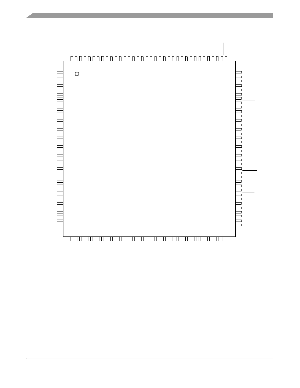
3738394041424344454647484950515253545556575859606162636465666768697071
72
1
2
3
4
5
6
7
8
9
10
11
12
13
14
15
16
17
18
19
20
21
22
23
24
25
26
27
28
29
30
31
32
33
34
35
36
108
107
106
105
104
103
102
101
100
99
98
97
96
95
94
93
92
91
90
89
88
87
86
85
84
83
82
81
80
79
78
77
76
75
74
73
144-Pin
LQFP
ETPUA13
ETPUA12
ETPUA11
ETPUA10
ETPUA9
ETPUA8
ETPUA7
ETPUA6
RTPUA5
VDDEH4A
ETPUA4
VSS
ETPUA3
ETPUA2
ETPUA1
ETPUA0
VDD
EMIOS0
EMIOS2
EMIOS4
EMIOS8
EMIOS9
VSS
EMIOS10
VDDEH4B
EMIOS11
EMIOS12
EMIOS14
EMIOS23
CNTXA
CNRXA
PLLREF
RXDB
BOOTCFG
WKPCFG
TXDB
144
143
142
141
140
139
138
137
136
135
134
133
132
131
130
129
128
127
126
125
124
123
122
121
120
119
118
117
116
115
AN21
AN0
AN1
AN2
AN3
AN4
AN5
AN6
AN7
REFBYPC
VRH
VRL
AN22
AN23
AN24
AN25
AN27
AN28
AN30
AN31
AN32
AN33
AN34
AN35
VDD
AN12-SDS
AN13-SDO
AN14-SDI
AN15-FCK
VSS
MDO3
VDDEH7
MDO2
MDO1
MDO0
MSEO0
AN18
AN17
AN16
AN11
AN9
VDDA0
VSSA0
AN39
AN38
VDDREG
VRCCTL
VSTBY
VRC33
ETPUA31
ETPUA30
ETPUA29
ETPUA28
ETPUA27
ETPUA26
ETPUA25
ETPUA24
VSS
ETPUA23
VDDEH1A
ETPUA22
VDD
ETPUA21
ETPUA20
ETPUA19
ETPUA18
ETPUA17
ETPUA16
ETPUA15
VDDEH1B
ETPUA14
VSS
TMS
TDI
EVTO
TCK
VSS
EVTI
VDDEH7
MSEO1
TDO
MCKO
JCOMP
PCSB3
SOUTB
SINB
PCSB0
VDDEH6B
PCSB1
VSS
PCSB2
SCKB
PCSB4
PCSB5
VDD
RSTOUT
CNTXC
TXDA
RXDA
CNRXC
RESET
VSS
VDDEH6A
VSSPLL
XTAL
EXTAL
VDDPLL
VSS
Figure 3-1. 144-Pin LQFP
MPC563XM Reference Manual, Rev. 1
64 Freescale Semiconductor
Preliminary—Subject to Change Without Notice
Page 65

Freescale Semiconductor 65
3.1.2 Ballmap: 208 MAPBGA
Figure 3-2 shows the ballmap for the 208 MAPBGA package.
1 2 3 4 5 6 7 8 9 1011121314 1516
VSS AN9 AN11 VDDA1 VSSA1 AN1 AN5 VRH VRL AN27 VSSA0 AN12-SDSMDO2 MDO0 VRC33 VSS
A
VDD VSS AN38 AN21 AN0 AN4 REFBYPC AN22 AN25 AN28 VDDA0 AN13-SDOMDO3 MDO1 VSS VDD
B
VSTBY VDD VSS AN17 AN34 AN16 AN3 AN7 AN23 AN32 AN33 AN14-SDI AN15-FCKVSS MSEO0 TCK
C
VDD33 AN39 VDD VSS AN18 AN2 AN6 AN24 AN30 AN31 AN35 VDDEH9 VSS TMS EVTO NC
D
Preliminary—Subject to Change Without Notice
MPC563XM Reference Manual, Rev. 1
ETPUA30 ETPUA31 NC VDD VDDE7 TDI EVTI MSEO1
E
ETPUA28 ETPUA29 ETPUA26 NC VDDEH6 TDO MCKO JCOMP
F
ETPUA24 ETPUA27 ETPUA25 ETPUA21 VSS VSS VSS VSS SOUTB PCSB3 SINB PCSB0
G
ETPUA23 ETPUA22 ETPUA17 ETPUA18 VSS VSS VSS VSS NC PCSB4 PCSB2 PCSB1
H
ETPUA20 ETPUA19 ETPUA14 ETPUA13 VSS VSS VSS VSS PCSB5 TXDA NC SCKB
J
ETPUA16 ETPUA15 ETPUA7 VDDEH1 VSS VSS VSS VSS CNTXC RXDA RSTOUT VDDRE
K
ETPUA12 ETPUA11 ETPUA6 ETPUA0 TXDB CNRXC WKPCFG RESET
L
ETPUA10 ETPUA9 ETPUA1 ETPUA5 RXDB PLLREF BOOTCFG VSSPLL
M
N
P
R
T
1
ETPUA8 ETPUA4 ETPUA0 VSS VDD VDD33 EMIOS2 EMIOS10 VDDEH4 EMIOS12 eTPUA19
ETPUA3 ETPUA2 VSS VDD NC VDDE7 NC EMIOS8 eTPUA29
NC VSS VDD NC EMIOS4 NC EMIOS9 EMIOS11 EMIOS14 eTPUA27
VSS VDD NC EMIOS0 NC NC NC GPIO219 eTPUA25
eTPUA21eTPUA211CNTXA VDD VSS NC XTAL
1
1
eTPUA41eTPUA131NC VDDE7 CLKOUT VDD VSS
1
1
EMIOS23 CNRXA NC VDD VSS VDDPLL
eTPU output only channel.
G
VDD33 VSS VRCCTL NC EXTAL
Figure 3-2. 208 MAPBGA
Page 66

3.2 External Signal Summary
Table 3-1 gives a summary of the MPC563XM external signals and properties.
The MPC563XM pin names consist of the following items separated by underscores:
1. Primary function
2. Alternate functions (if applicable)
3. GPIO
For example, for the pin SCK_B_PCS_C[1]_GPIO[102], SCK_B is the primary function and PCS_C[1]
is the alternate function.
Table 3-1. MPC563xM Signal Properties
Name Function
1
I/O
Type
Vol tag e
Reset
2
State
3
Function /
State After
Reset
4
Reset / Configuration (5)
RESET
External Reset Input I VDDEH6a I / Up RESET /
Up
RSTOUT External Reset Output O VDDEH6a RSTOUT/
Low
PLLREF_
IRQ[4]_
ETRIG[0]_
GPIO[208]
BOOTCFG_
_
IRQ[3]
ETRIG[1]_
GPIO[212]
WKPCFG_
NMI_
GPIO[213]
FMPLL Mode Selection
External Interrupt Request
eQADC Trigger Input
GPIO
Boot Configuration Input
External Interrupt Request
eQADC Trigger Input
GPIO
Weak Pull Configuration Input
Non-Maskable Interruption
GPIO
I
VDDEH6a PLLREF /
I
I
I/O
I
VDDEH6a BOOTCF
I
I
I/O
I
VDDEH6a WKPCFG
I
I/O
Up
G / Down
/ Up
RSTOUT/
High
- / Up 496
- / Down 496
- / Up 496
Calibration (46)
CAL_ADDR[12:15] Calibration Address Bus O VDDE12 O / Low CAL_ADDR /
Low
CAL_ADDR[16:19]_
MDO[0:3]
5
Calibration Address Bus
Nexus Message Data Out
OOVDDE12
VDDE7
6
7
O / Low
8
MDO /
CAL_ADDR5 /
Low
CAL_ADDR[20:27]_
MDO[4:11]
Calibration Address Bus
Nexus Message Data Out
OOVDDE12 O / Low MDO /
CAL_ADDR9 /
Low
CAL_ADDR[28:29]_
MSEO[0:1]
CAL_ADDR[30]_
EVTI
5
5
CAL_EVTO
Calibration Address Bus
Nexus Message Start/End OutOO
Calibration Address Bus
Nexus Event In
Nexus Event Out O VDDE12
OIVDDE12
CAL_MCKO Nexus Message Clock Out O VDDE12
VDDE12
VDDE7
VDDE7
VDDE7
VDDE7
6
7
6
7
6
7
6
7
O / High
10
MSEO9 /
CAL_ADDR
11
—
EVTI /
CAL_ADDR
O / Low EVTO / High 496
O / Low MCKO /
Enabled
10
12
Package
496
208
144
496
208
144
208
144
208
144
208
144
496
496
208
496
496
208
496
208
208
496
208
MPC563XM Reference Manual, Rev. 1
66 Freescale Semiconductor
Preliminary—Subject to Change Without Notice
Page 67

Table 3-1. MPC563xM Signal Properties (continued)
Name Function
1
I/O
Type
Vol tag e
Reset
2
State
NEXUSCFG Nexus/Calibration bus selector I VDDE12 I / Down NEXUSCFG /
3
Function /
State After
Reset
4
Package
496
Down
CAL_CS
[0] Calibration Chip Selects O VDDE12 O / High CAL_CS /
496
High
CAL_CS[2:3]_
CAL_ADDR[10:11]
Calibration Chip Selects
Calibration Address Bus
OOVDDE12 O / High CAL_CS /
High
496
CAL_DATA[0:9] Calibration Data Bus I/O VDDE12 - / Up - / Up 496
CAL_DATA[10:15] Calibration Data Bus I/O VDDE12 - / Up - / Up 496
CAL_OE
Calibration Output Enable O VDDE12 O / High CAL_OE /
496
High
CAL_RD_WR Calibration Read/Write O VDDE12 O / High CAL_RD_WR
496
/High
CAL_TS
CAL_WE_BE
CLKOUT System Clock Output O VDDE12 CLKOUT
ALE
[0:1]
_
Calibration Transfer Start
Address Latch Enable
Calibration Write Enable
Byte Enable
OOVDDE12 O / High CAL_TS /
High
O VDDE12 O / High CAL_WE /
High
CLKOUT /
/ Enabled
Enabled
496
496
208
496
NEXUS (9)
EVTI_
eTPU_A[2]_
GPIO[231]
EVTO _
eTPU_A[4]_
GPIO[227]
MCKO_
GPIO[219]
Nexus Event In
eTPU A Channel
GPIO
Nexus Event Out
eTPU A Channel
GPIO
Nexus Message Clock Out
GPIO
I
VDDEH7 - / - - / - 496
O
I/O
O
VDDEH7 I / Up I / Up 496
O
I/O
O
VDDEH7 - / - - / - 496
I/O
208
144
208
144
208
144
MDO[0]13_
eTPU_A[13]_
GPIO[220]
MDO[1]_
eTPU_A[19]_
GPIO[221]
MDO[2]_
eTPU_A[21]_
GPIO[222]
MDO[3]_
eTPU_A[25]_
GPIO[223]
MSEO[0]
_
eTPU_A[27]_
GPIO[224]
MSEO[1]
_
eTPU_A[29]_
GPIO[225]
Nexus Message Data Out
eTPU A Channel
GPIO
Nexus Message Data Out
eTPU A Channel
GPIO
Nexus Message Data Out
eTPU A Channel
GPIO
Nexus Message Data Out
eTPU A Channel
GPIO
Nexus Message Start/End Out
eTPU A Channel
GPIO
Nexus Message Start/End Out
eTPU A Channel
GPIO
O
VDDEH7 - / - - / - 496
O
I/O
O
VDDEH7 - / - - / - 496
O
I/O
O
VDDEH7 - / - - / - 496
O
I/O
O
VDDEH7 - / - - / - 496
O
I/O
O
VDDEH7 - / - - / - 496
O
I/O
O
VDDEH7 - / - - / - 496
O
I/O
208
144
208
144
208
144
208
144
208
144
208
144
MPC563XM Reference Manual, Rev. 1
Freescale Semiconductor 67
Preliminary—Subject to Change Without Notice
Page 68

Table 3-1. MPC563xM Signal Properties (continued)
Name Function
1
I/O
Type
Vol tag e
Reset
2
State
3
Function /
State After
Reset
4
JTAG / TEST(5)
TCK JTAG Test Clock Input I VDDEH7 TCK /
TCK / Down 496
Down
TDI14_
eMIOS[5]_
GPIO[232]
TDO14_
eMIOS[6]_
GPIO[228]
JTAG Test Data Input
eMIOS Channel
GPIO
JTAG Test Data Output
eMIOS Channel
GPIO
I
VDDEH7 - / - - / - 496
O
I/O
O
VDDEH7 - / - - / - 496
O
I/O
TMS JTAG Test Mode Select Input I VDDEH7 TMS / Up TMS / Up 496
JCOMP JTAG TAP Controller Enable I VDDEH7 JCOMP /
Down
JCOMP /
Down
CAN (4)
CNTX_A_
TXD_A_
GPIO[83]
CNRX_A_
RXD_A_
GPIO[84]
CNTX_C_
GPIO[87]
CNRX_C_
GPIO[88]
CAN_A Transmit
eSCI_A Transmit
GPIO
CAN_A Receive
eSCI_A Receive
GPIO
CAN_C Transmit
-
GPIO
CAN_C Receive
-
GPIO
O
VDDEH4b - / Up - / Up
15
O
I/O
I
VDDEH4b - / Up - / Up 496
I
I/O
O
VDDEH6a - / Up - / Up 496
-
I/O
I
VDDEH6a - / Up - / Up 496
-
I/O
16
eSCI (4)
15
TXD_A_
eMIOS[13]_
GPIO[89]
RXD_A_
eMIOS[15]_
GPIO[90]
TXD_B_
GPIO[91]
RXD_B_
GPIO[92]
eSCI_A Transmit
eMIOS Channel
GPIO
eSCI_A Receive
eMIOS Channel
GPIO
eSCI_B Transmit
-
GPIO
eSCI_B Receive
-
GPIO
VDDEH6a - / Up - / Up 496
O
O
I/O
I
VDDEH6a - / Up - / Up 496
O
I/O
I/O
VDDEH6a - / Up - / Up 496
-
I/O
I
VDDEH6a - / Up - / Up 496
-
I/O
DSPI(9)
SCK_B_
PCS_C[1]_
GPIO[102]
DSPI_C Peripheral Chip Select
DSPI_B Clock
GPIO
I/O
VDDEH6b - / Up - / Up 496
O
I/O
Package
208
144
208
144
208
144
208
144
496
208
144
496
208
144
208
144
208
144
208
144
208
144
144
208
144
208
144
208
144
MPC563XM Reference Manual, Rev. 1
68 Freescale Semiconductor
Preliminary—Subject to Change Without Notice
Page 69

Table 3-1. MPC563xM Signal Properties (continued)
Name Function
SIN_B_
PCS_C[2]_
DSPI_B Data Input
DSPI_C Peripheral Chip Select
GPIO[103]
SOUT_B_
PCS_C[5]_
DSPI_B Data Output
DSPI_C Peripheral Chip Select
GPIO[104]
PCS_B[0]_
DSPI_B Peripheral Chip Select
GPIO[105]
PCS_B[1]_
DSPI_B Peripheral Chip Select
GPIO[106]
PCS_B[2]_
SOUT_C_
DSPI_B Peripheral Chip Select
DSPI_C Data Output
GPIO[107]
PCS_B[3]_
SIN_C_
DSPI_B Peripheral Chip Select
DSPI_C Data Input
GPIO[108]
PCS_B[4]_
SCK_C_
DSPI_B Peripheral Chip Select
DSPI_C Clock
GPIO[109]
PCS_B[5]_
PCS_C[0]_
DSPI_B Peripheral Chip Select
DSPI_C Peripheral Chip Select
GPIO[110]
AN[0]
DAN0+
AN[1]
DAN0-
AN[2]
DAN1+
AN[3]
DAN1-
AN[4]
DAN2+
AN[5]
DAN2-
AN[6]
DAN3+
Single Ended Analog Input
Positive Terminal Differential
Single Ended Analog Input
Negative Terminal Differential
Single Ended Analog Input
Positive Terminal Differential
Single Ended Analog Input
Negative Terminal Differential
Single Ended Analog Input
Positive Terminal Differential
Single Ended Analog Input
Negative Terminal Differential
Single Ended Analog Input
Positive Terminal Differential
GPIO
GPIO
-
GPIO
-
GPIO
GPIO
GPIO
GPIO
GPIO
Input
Input
Input
Input
Input
Input
Input
1
I/O
Type
Vol tag e
I
VDDEH6b - / Up - / Up 496
Reset
2
State
O
I/O
O
VDDEH6b - / Up - / Up 496
O
I/O
I/O
VDDEH6b - / Up - / Up 496
-
I/O
O
VDDEH6b - / Up - / Up 496
-
I/O
O
VDDEH6b - / Up - / Up 496
O
I/O
O
VDDEH6b - / Up - / Up 496
I
I/O
O
VDDEH6b - / Up - / Up 496
I/O
I/O
O
VDDEH6b - / Up - / Up 496
I/O
I/O
3
Function /
State After
Reset
4
Package
208
144
208
144
208
144
208
144
208
144
208
144
208
144
208
144
eQADC(35)
I
VDDA I / - AN[0] / - 496
I
208
144
I
VDDA I / - AN[1] / - 496
I
208
144
I
VDDA I / - AN[2] / - 496
I
208
144
I
VDDA I / - AN[3] / - 496
I
208
144
I
VDDA I / - AN[4] / - 496
I
208
144
I
VDDA I / - AN[5] / - 496
I
208
144
I
VDDA I / - AN[6] / - 496
I
208
144
MPC563XM Reference Manual, Rev. 1
Freescale Semiconductor 69
Preliminary—Subject to Change Without Notice
Page 70

Table 3-1. MPC563xM Signal Properties (continued)
Name Function
AN[7]
DAN3-
Single Ended Analog Input
Negative Terminal Differential
1
I/O
Type
I
Vol tag e
VDDA I / - AN[7] / - 496
Reset
2
State
I
3
Function /
State After
Reset
4
Input
AN[9]_
ANX
Single Ended Analog Input
External Multiplexed Analog
I
VDDA I / - AN[9] / - 496
I
Input
AN[11]_
ANZ
Single Ended Analog Input
External Multiplexed Analog
I
VDDA I / - AN[11] / - 496
I
Input
AN[12]_
MA[0]_
ETPU_A[19]_
SDS
AN[13]_
MA[1]_
ETPU_A[21]_
SDO
AN[14]_
MA[2]_
ETPU_A[27]_
SDI
AN[15]_
FCK_
ETPU_A[29]
Single Ended Analog Input
Mux Address
ETPU_A Channel
eQADC Serial Data Strobe
Single Ended Analog Input
Mux Address
ETPU_A Channel
eQADC Serial Data Out
Single Ended Analog Input
Mux Address
ETPU_A Channel
eQADC Serial Data In
Single Ended Analog Input
eQADC Free Running Clock
ETPU_A Channel
I
VDDEH7 I / - AN[12] / - 496
O
O
O
I
VDDEH7 I / - AN[13] / - 496
O
O
O
I
VDDEH7 I / - AN[14] / - 496
O
O
I
I
VDDEH7 I / - AN[15] / - 496
O
O
AN[16:18] Single Ended Analog Input I VDDA I / - AN[x] / - 496
AN[21:25] Single Ended Analog Input I VDDA I / - AN[x] / - 496
AN[27:28] Single Ended Analog Input I VDDA I / - AN[x] / - 496
AN[30:35] Single Ended Analog Input I VDDA I / - AN[x] / - 496
AN38_8_
ANW_
AN39_10_ANY Single Ended Analog Input
Single Ended Analog Input
Multiplexed Analog Input
I VDDA I / - AN[38] / - 496
I VDDA I / - AN[39] / - 496
Multiplexed Analog Input
VRH Voltage Reference High I VDDA - / - VRH 496
VRL Voltage Reference Low I VSSA0 - / - VRL 496
Package
208
144
208
144
208
144
208
144
208
144
208
144
208
144
208
144
208
144
208
144
208
144
208
144
208
144
208
144
208
144
MPC563XM Reference Manual, Rev. 1
70 Freescale Semiconductor
Preliminary—Subject to Change Without Notice
Page 71

Table 3-1. MPC563xM Signal Properties (continued)
Name Function
1
I/O
Type
Vol tag e
Reset
2
State
3
Function /
State After
Reset
4
REFBYPC Bypass Capacitor Input I VRL - / - REFBYPC 496
eTPU(32)
eTPU_A[0]_
eTPU_A[12]_
eTPU_A[19]_
GPIO[114]
eTPU_A[1:4]_
eTPU_A[13:16]_
GPIO[115:118]
eTPU_A[5]_
eTPU_A[17]_
SCK_B_LVDS-_
GPIO[119]
eTPU_A[6]_
eTPU_A[18]_
SCK_B_LVDS+_
GPIO[120]
eTPU_A[7]_
eTPU_A[19]_
SOUT_B_LVDS-_
eTPU_A[6]_
GPIO[121]
eTPU_A[8]_
eTPU_A[20]_
SOUT_B_LVDS+_
GPIO[122]
eTPU_A[9]_
eTPU_A[21]_
GPIO[123]
eTPU_A[10:11]_
eTPU_A[22:23]_
GPIO[124:125]
eTPU_A[12]_
PCS_B[1]_
GPIO[126]
eTPU_A[13]_
PCS_B[3]_
GPIO[127]
eTPU_A[14]_
PCS_B[4]_
eTPU_A[9]_
GPIO[128]
eTPU_A[15]_
PCS_B[5]_
GPIO[129]
eTPU_A Channel
eTPU_A Channel
eTPU_A Channel
GPIO
eTPU_A Channel
eTPU_A Channel
GPIO
eTPU_A Channel
eTPU_A Channel
SCK_B LVDS-
GPIO
eTPU_A Channel
eTPU_A Channel
SCK_B LVDS+
GPIO
eTPU_A Channel
eTPU_A Channel
SOUT_B LVDS-
eTPU_A channel
GPIO
eTPU_A Channel
eTPU_A Channel
SOUT_B LVDS+
GPIO
eTPU_A Channel
eTPU_A Channel
GPIO
eTPU_A Channel
eTPU_A Channel
GPIO
eTPU_A Channel
DSPI_B Peripheral Chip Select
GPIO
eTPU_A Channel
DSPI_B Peripheral Chip Select
GPIO
eTPU_A Channel
DSPI_B Periph Chip Select
eTPU_A Channel
GPIO
eTPU_A Channel
DSPI_B Periph Chip Select
GPIO
I/O
VDDEH4a - /
O
O
I/O
I/O
VDDEH4a - /
O
I/O
I/O
VDDEH4a - /
O
O
I/O
I/O
VDDEH4a - /
O
O
I/O
I/O
VDDEH4a - /
O
O
O
I/O
I/O
VDDEH4a - /
O
O
I/O
I/O
VDDEH4a - /
O
I/O
I/O
VDDEH1b - /
O
I/O
I/O
VDDEH1b - /
O
I/O
I/O
VDDEH1b - /
O
I/O
I/O
VDDEH1b - /
O
O
I/O
I/O
VDDEH1b - /
O
I/O
- / WKPCFG 496
WKPCFG
- / WKPCFG 496
WKPCFG
- / WKPCFG 496
WKPCFG
- / WKPCFG 496
WKPCFG
- / WKPCFG 496
WKPCFG
- / WKPCFG 496
WKPCFG
- / WKPCFG 496
WKPCFG
- / WKPCFG 496
WKPCFG
- / WKPCFG 496
WKPCFG
- / WKPCFG 496
WKPCFG
- / WKPCFG 496
WKPCFG
- / WKPCFG 496
WKPCFG
Package
208
144
208
144
208
144
208
144
208
144
208
144
208
144
208
144
208
144
208
144
208
144
208
144
208
144
MPC563XM Reference Manual, Rev. 1
Freescale Semiconductor 71
Preliminary—Subject to Change Without Notice
Page 72

Table 3-1. MPC563xM Signal Properties (continued)
Name Function
eTPU_A[16]_
GPIO[130]
eTPU_A[17]_
GPIO[131]
eTPU_A[18]_
GPIO[132]
eTPU_A[19]_
GPIO[133]
eTPU_A[20]_
IRQ[8]_
External Interrupt Request
GPIO[134]
eTPU_A[21]_
IRQ[9]_
eTPU_A Channel (Output Only)
External Interrupt Request
GPIO[135]
eTPU_A[22]_
IRQ[10]_
eTPU_A[17]_
eTPU_A Channel External
External Interrupt Request
eTPU_A Channel External
GPIO[136]
eTPU_A[23]_
IRQ[11]_
eTPU_A[21]_
eTPU_A Channel External
External Interrupt Request
eTPU_A Channel External
GPIO[137]
eTPU_A[24]_
IRQ[12]_
eTPU_A Channel External
External Interrupt Request
SCK_C_LVDS-_
GPIO[138]
eTPU_A[25]_
IRQ[13]_
eTPU_A Channel External
External Interrupt Request
SCK_C_LVDS+_
GPIO[139]
eTPU_A[26]_
IRQ[14]_
eTPU_A Channel External
External Interrupt Request
SOUT_C_LVDS-_
GPIO[140]
eTPU_A[27]_
IRQ[15]_
External Interrupt Request
SOUT_C_LVDS+_
GPIO[141]
eTPU_A[28]_
PCS_C[1]_
eTPU_A Channel (Output Only)
DSPI_C Peripheral Chip Select
GPIO[142]
eTPU_A[29]_
PCS_C[2]_
eTPU_A Channel (Output Only)
DSPI_C Peripheral Chip Select
GPIO[143]
1
eTPU_A Channel
GPIO
eTPU_A Channel
GPIO
eTPU_A Channel
GPIO
eTPU_A Channel
-
GPIO
eTPU_A Channel
GPIO
GPIO
GPIO
GPIO
SCK_C LVDS-
GPIO
SCK_C LVDS+
GPIO
SOUT_C LVDS-
GPIO
eTPU_A Channel
SOUT_C LVDS+
GPIO
GPIO
GPIO
I/O
Type
Vol tag e
I/O
VDDEH1b - /
I/O
I/O
VDDEH1b - /
I/O
I/O
VDDEH1b - /
I/O
I/O
VDDEH1b - /
-
I/O
I/O
VDDEH1b - /
I
I/O
I/O
VDDEH1a - /
I
I/O
I/O
VDDEH1a - /
I
O
I/O
I/O
VDDEH1a - /
I
O
I/O
O
VDDEH1a - /
I
I/O
I/O
O
VDDEH1a - /
I
I/O
I/O
O
VDDEH1a - /
I
O
I/O
O
VDDEH1a - /
I
O
I/O
O
VDDEH1a - /
O
I/O
O
VDDEH1a - /
O
I/O
2
WKPCFG
WKPCFG
WKPCFG
WKPCFG
WKPCFG
WKPCFG
WKPCFG
WKPCFG
WKPCFG
WKPCFG
WKPCFG
WKPCFG
WKPCFG
WKPCFG
Reset
State
Function /
State After
3
Reset
4
- / WKPCFG 496
- / WKPCFG 496
- / WKPCFG 496
- / WKPCFG 496
- / WKPCFG 496
- / WKPCFG 496
- / WKPCFG 496
- / WKPCFG 496
- / WKPCFG 496
- / WKPCFG 496
- / WKPCFG 496
- / WKPCFG 496
- / WKPCFG 496
- / WKPCFG 496
Package
208
144
208
144
208
144
208
144
208
144
208
144
208
144
208
144
208
144
208
144
208
144
208
144
208
144
208
144
MPC563XM Reference Manual, Rev. 1
72 Freescale Semiconductor
Preliminary—Subject to Change Without Notice
Page 73

Table 3-1. MPC563xM Signal Properties (continued)
Function /
State After
3
Reset
4
- / WKPCFG 496
- / WKPCFG 496
Name Function
eTPU_A[30]_
PCS_C[3]_
eTPU_A[11]_
eTPU_A Channel
DSPI_C Peripheral Chip Select
eTPU_A Channel
GPIO[144]
eTPU_A[31]_
PCS_C[4]_
eTPU_A[13]_
eTPU_A Channel
DSPI_C Peripheral Chip Select
eTPU_A Channel
GPIO[145]
GPIO
GPIO
1
I/O
Type
Vol tag e
I/O
VDDEH1a - /
O
2
WKPCFG
Reset
State
O
I/O
I/O
VDDEH1a - /
O
WKPCFG
O
I/O
eMIOS(8)
eMIOS[0]_
eTPU_A[0]_
eTPU_A[25]_
GPIO[179]
eMIOS[2]_
eTPU_A[2]_
GPIO[181]
eMIOS[4]_
eTPU_A[4]_
GPIO[183]
eMIOS[8:9]_
eTPU_A[8:9]_
GPIO[187:188]
eMIOS[10:11]_
GPIO[189:190]
eMIOS[12]_
DSPI_C_SOUT
eTPU_A[27]_
GPIO[191]
eMIOS[14]_
IRQ[0]_
eTPU_A[29]_
GPIO[193]
eMIOS[23]_
GPIO[202]
eMIOS Channel
eTPU_A Channel
eTPU_A Channel
GPIO
eMIOS Channel
eTPU_A Channel
GPIO
eMIOS Channel
eTPU_A Channel
GPIO
eMIOS Channel
eTPU_A Channel
GPIO
eMIOS Channel
-
GPIO
eMIOS Channel
DSPI C Data Output
eTPU_A Channel
GPIO
eMIOS Channel
External Interrupt Request
eTPU_A Channel
GPIO
eMIOS Channel
-
GPIO
I/O
VDDEH4a - /
O
O
I/O
I/O
VDDEH4b - /
O
I/O
I/O
VDDEH4b - /
O
I/O
I/O
VDDEH4b - /
O
I/O
I/O
VDDEH4b - /
-
I/O
O
VDDEH4b - /
O
O
I/O
O
VDDEH4b - /
I
O
I/O
I/O
VDDEH4b - /
-
I/O
- / WKPCFG 496
WKPCFG
- / WKPCFG 496
WKPCFG
- / WKPCFG 496
WKPCFG
- / WKPCFG 496
WKPCFG
- / WKPCFG 496
WKPCFG
- / WKPCFG 496
WKPCFG
- / WKPCFG 496
WKPCFG
- / WKPCFG 496
WKPCFG
Clock Synthesizer (2)
XTAL Crystal Oscillator Output O VDDEH6a O / - XTAL17 / - 496
EXTAL_
EXTCLK
Crystal Oscillator Input
External Clock Input
I VDDEH6a I / - EXTAL18/ - 496
Power / Ground ()
VDDPLL PLL Supply Voltage I VDDPLL
I / - - 496
(1.2V)
Package
208
144
208
144
208
144
208
144
208
144
208
144
208
144
208
144
208
144
208
144
208
144
208
144
208
144
MPC563XM Reference Manual, Rev. 1
Freescale Semiconductor 73
Preliminary—Subject to Change Without Notice
Page 74

Table 3-1. MPC563xM Signal Properties (continued)
Name Function
VSSPLL
19
PLL Ground I VSSPLL I / - - 496
1
I/O
Type
Vol tag e
Reset
2
State
3
Function /
State After
Reset
4
VSTBY Power Supply for Standby RAM I VSTBY I / - - 496
VRC33 3.3V Voltage Regulator Bypass
O VRC33 O / - - 496
Capacitor
VRCCTL Voltage Regulator Control
O NA O / - - 496
Output
20
VDDA
Analog Power Input for eQADC I VDDA
I / - - 496
(5.0V)
21
VSSA
Analog Ground Input for
I VSSA I / - - 496
eQADC
VDDREG Voltage Regulator Supply I VDDREG
I / - - 496
(5.0V)
VDD (x4) Internal Logic Supply Input I VDD
I / - - 496
(1.2V)
VSS (x4) Ground - VSS0 I / - - 496
VDDEH1a
VDDEH1b
I/O Supply Input I VDDEH122
(3.3V -
I / - - 496
5.0V)
VSSE1a
I/O Ground Input I VSSEH1 - 496
VSSE1b
VDDEH4a
VDDEH4b
I/O Supply Input I VDDEH422
(3.3V -
I / - - 496
5.0V)
VSSE4a
I/O Ground Input I VSSEH4 - 496
VSSE4b
VDDEH6a
VDDEH6b
23
I/O Supply Input I VDDEH6
(3.3V -
I / - - 496
5.0V)
VSSE6a
I/O Ground Input I VSSEH6 - 496
VSSE6b
VDDEH7 (x2) I/O Supply Input I VDDEH7
24
I / - - 496
(3.3V -
5.0V)
Package
208
144
208
144
208
144
208
144
208
144
208
144
208
144
208
144
208
144
208
144
208
144
208
144
208
144
208
144
208
144
208
144
MPC563XM Reference Manual, Rev. 1
74 Freescale Semiconductor
Preliminary—Subject to Change Without Notice
Page 75

Table 3-1. MPC563xM Signal Properties (continued)
Name Function
1
I/O
Type
Vol tag e
Reset
2
State
3
Function /
State After
Reset
4
Package
VSSE7 (x2) I/O Ground Input I VSSEH7 - 496
1
For each pin in the table, each line in the Function column is a separate function of the pin. For all I/O pins the
selection of primary pin function or secondary function or GPIO is done in the SIU except where explicitly noted.
2
The VDDE and VDDEH supply inputs are broken into segments. Each segment of slow I/O pins (VDDEH) may
have a separate supply in the 3.3 V to 5.0 V range (+/- 10%). Each segment of fast I/O (VDDE) may have a
separate supply in the 1.8 V to 3.3 V range (+/- 10%).
3
Terminology is O - output, I - input, Up - weak pull up enabled, Down - weak pull down enabled, Low - output
driven low, High - output driven high. A dash for the function in this column denotes that both the input and output
buffer are turned off.
4
Function after reset of GPI is general purpose input. A dash for the function in this column denotes that both the
input and output buffer are turned off.
5
On the 496-pin package, the Nexus function on this pin is enabled when the NEXUSCFG pin is high and Nexus
is configured to full port mode. On the 208-pin package, the Nexus function on this pin is enabled permanently.
6
In the 496-pin package, the I/O segment containing this pin is called VDDE12.
7
In the 208-pin package, the I/O segment containing this pin is called VDDE7
8
When configured as Nexus (208-pin package or 496-pin package with NEXUSCFG=1), and JCOMP is asserted
during reset, MDO[0] is driven high until the crystal oscillator becomes stable, at which time it is then negated.
9
The function of this pin is Nexus when NEXUSCFG is high.
10
High when the pin is configured to Nexus, low otherwise.
11
O/Low for the 496-package with NEXUSCFG=0; I/Up otherwise.
12
CAL_ADDR/Low for the 496-package with NEXUSCFG=0; EVTI/Up otherwise.
13
If JCOMP is asserted during reset, MDO[0] is driven high until the crystal oscillator becomes stable, at which time
it is then negated.
14
TDI and TDO are required for JTAG operation.
15
From the user point of view this is an output pad; to implement the CAN protocol this pad must also implement
the input direction.
16
The function and state of the CAN_A and eSCI_A pins after execution of the BAM program is determined by the
BOOTCFG pin.
17
The function after reset of the XTAL pin is determined by the value of the signal on the PLLCFG[1] pin. When
bypass mode is chosen XTAL has no function and should be grounded.
18
The function after reset of the EXTAL_EXTCLK pin is determined by the value of the signal on the PLLCFG[1]
pin. If the EXTCLK function is chosen, the valid operating voltage for the pin is 1.62 V to 3.6 V. If the EXTAL
function is chosen, the valid operating voltage is 3.3 V.
19
VSSPLL and VSSREG are connected to the same pin.
20
This pin is shared by two pads: VDDA_AN, using pad_vdde_hv, and VDDA_DIG, using pad_vdde_int_hv.
21
This pin is shared by two pads: VSSA_AN, using pad_vsse_hv, and VSSA_DIG, using pad_vsse_int_hv.
22
LVDS pins will not work at 3.3 V.
23
The VDDEH6 segment may be powered from 3.0 V to 5.0 V for mux address or SSI functions, but must meet the
VDDA specifications of 4.5 V to 5.25 V for analog input function.
24
If using JTAG or Nexus, the I/O segment that contains the JTAG and Nexus pins must be powered by a 5 V supply.
The 3.3 V Nexus/JTAG signals are derived from the 5 volt power supply.
208
144
MPC563XM Reference Manual, Rev. 1
Freescale Semiconductor 75
Preliminary—Subject to Change Without Notice
Page 76

3.3 Detailed Signal Descriptions
3.3.1 Reset / Configuration
3.3.1.1 RESET — External Reset Input
The RESET input is asserted by an external device to reset the all modules of this device. The RESET pin
should be asserted during a power-on reset. See Chapter 4, “Resets,” for more details.
3.3.1.2 PLLREF_IRQ[4]_ETRIG[0]_GPIO[208] — FMPLL Mode Selection /
External Interrupt Request / eQADC Trigger Input / GPIO
PLLREF_IRQ[4]_ETRIG[0]_GPIO[208] is used during reset to configure the operating mode of the
FMPLL. It has to be set to the desired value soon after power-on reset and kept stable during the whole
reset cycle. After reset is negated, this pin is used for one of the alternate functions. The alternate function
is an external interrupt request input. The second alternate function is the external trigger input for the
eQADC.
3.3.1.3 BOOTCFG_IRQ[3]_ETRIG[1]_GPIO[212] — Reset Configuration /
External Interrupt Request / eQADC Trigger Input / GPIO
BOOTCFG_IRQ[3]_ETRIG[1]_GPIO[213] are sampled on the negation of the RSTOUT pin. The values
are used by the BAM program to determine the boot configuration of this device. The alternate function
is an external interrupt request input. The second alternate function is the external trigger input for the
eQADC.
3.3.1.4 WKPCFG_NMI_GPIO[213] — Weak Pull Configuration / GPIO
WKPCFG_NMI_GPIO[213] determines whether specified eTPU and eMIOS pins are connected to a
weak pull up or weak pull down during and immediately after reset. The alternate function is the
Non-Maskable Interrupt.
3.3.2 Calibration External Bus Interface (EBI)
3.3.2.1 CAL_ADDR[12:15] — Calibration Address
CAL_ADDR[12:18] are the calibration address signals.
3.3.2.2 CAL_ADDR[16:27]_MDO[0:11] — Calibration Addr / Nexus Message
Data Out
CAL_ADDR[16:27]_MDO[0:11] are the calibration address signals. The altern ate function are nexus
message data outputs.
MPC563XM Reference Manual, Rev. 1
76 Freescale Semiconductor
Preliminary—Subject to Change Without Notice
Page 77

3.3.2.3 CAL_ADDR[28:29]_MSEO[0:1] — Calibration Address / Nexus Message
Start/End Out
CAL_ADDR[28:29]_MSEO[0:1] are the calibration address signals. The alternate function are Nexus
message start/end out.
3.3.2.4 CAL_ADDR[30]_CAL_EVTI — Calibration Address / Nexus Event In
CAL_ADDR[30]_CAL_EVTI is the calibration address signal. The alternate function is Nexus event in.
3.3.2.5 CAL_CS[2:3]_CAL_ADDR[10:11] — Calibration Chip Selects /
Calibration Address
CAL_CS[2:3]_CAL_ADDR[10:11] are the calibration chip se lect output signals. The alternate functions
are calibration address signals.
3.3.2.6 CAL_CS[0] — Calibration Chip Select
CAL_CS[0] is the calibration chip select output signal.
3.3.2.7 CAL_DATA[0:15] — Calibration Data
CAL_DATA[0:15] are the calibration data signals.
3.3.2.8 CAL_OE — Calibration Output Enable
CAL_OE indicates that the calibration interface is ready to accept read data.
3.3.2.9 CAL_RD_WR — Calibration Read/Write
CAL_RD_WR indicates whether a calibration bus transfer is a read or write operation.
3.3.2.10 CAL_TS_ALE — Calibration Transfer Start / Address Latch Enable
The Calibration Transfer Start s ignal CAL_TS is asserted by this device to indicate the s tart of a transfer.
The Address Latch Enable (ALE) signal is used to demultiplex the address from data bus. It is asserted
while the least significant 16 bits of the address are present in the multiplexed address/data bus.
3.3.2.11 CAL_WE[0:1]_BE[0:1] — Calibration Write/Byte Enable
CAL_WE[0:1]_BE[0:1] specify which data pins contain valid data for a calibration bus transfer.
3.3.2.12 CAL_EVTO— Nexus Event out
CAL_EVTO is an output that provides timing to a development tool for a single watchpoint or breakpoint
occurrence.
MPC563XM Reference Manual, Rev. 1
Freescale Semiconductor 77
Preliminary—Subject to Change Without Notice
Page 78

3.3.2.13 CAL_MCKO— Nexus Event out
CAL_MCKO is a free running clock output to the development tools which is used for timing of the MDO
and MSEO signals.
3.3.3 Nexus Port Controller (NPC)
3.3.3.1 NEXUSCFG — Nexus Configuration
NEXUSCFG is an input pin to select which function (nexus or cal_addr) is assigned to pad_cal_addr
outputs.
3.3.3.2 EVTI_eTPU_A[2]_GPIO[231] — Nexus Event In / eTPU_A Channel / GPIO
EVTI is an input that is read on the negation of TRST to enable or disable the Nexus Debug port. After
reset, the EVTI pin is used to initiate program and data trace synchronization messages or generate a
breakpoint. The alternate functions are output channel for eTPU_A[2] module and GPIO[231].
3.3.3.3 EVTO _eTPU_A[4]_GPIO[227] — Nexus Event Out / eTPU_A Channel /
GPIO
EVTO is an output that provides timing to a development tool for a single watchpoint or breakpoint
occurrence. The alternate functions are output channel for eTPU_A[4] module and GPIO[227].
3.3.3.4 MCKO/CLKOUT_GPIO[219] — Nexus Message Clock Out /
CLKOUT/GPIO
MCKO is a free running clock output to the development tools which is used for timing of the MDO and
MSEO signals. The alternate functions is GPIO[219], when package QFP is selected the CLKOUT can
also be used as an alternate function.
3.3.3.5 MDO[0]_eTPU_A[13]_GPIO[220] — Nexus Message Data Out / eTPU_A
Channel / GPIO
Is a trace message output to the development tools. This pin also indicates the status of the crystal oscillator
clock following a power-on reset, when MDO[0] is driven high until the crystal oscillator clock achieves
stability and is then negated. The alternate functions are output channel for eTPU_A[13] module and
GPIO[220].
3.3.3.6 MDO[1]_eTPU_A[19]_GPIO[221] — Nexus Message Data Out / eTPU_A
Channel / GPIO
Is the trace message output to the development tools. The alternate functions are output channel for
eTPU_A[19] module and GPIO[221].
MPC563XM Reference Manual, Rev. 1
78 Freescale Semiconductor
Preliminary—Subject to Change Without Notice
Page 79

3.3.3.7 MDO[2]_eTPU_A[21]_GPIO[222] — Nexus Message Data Out / eTPU_A
Channel / GPIO
Is the trace message output to the development tools. The alternate functions are output channel for
eTPU_A[21] module and GPIO[222].
3.3.3.8 MDO[3]_eTPU_A[25]_GPIO[223] — Nexus Message Data Out / eTPU_A
Channel / GPIO
Is the trace message output to the development tools. The alternate functions are output channel for
eTPU_A[25] module and GPIO[223].
3.3.3.9 MSEO[0]_eTPU_A[27]_GPIO[224] — Nexus Message Start/End Out /
eTPU_A Channel / GPIO
Is the output that indicate when messages start and end on the MDO pins. The alternate functions are
output channel for eTPU_A[27] module and GPIO[224].
3.3.3.10 MSEO[1]_eTPU_A[29]_GPIO[225] — Nexus Message Start/End Out /
eTPU_A Channel / GPIO
Is the output that indicates when messages start and end on the MDO pins. The alternate functions are
output channel for eTPU_A[29] module and GPIO[225].
3.3.4 JTAG
3.3.4.1 TCK — JTAG Test Clock Input
TCK provides the clock input for the on-chip test logic.
3.3.4.2 TDI_eMIOS[5]_GPIO[232] — JTAG Test Data Input
TDI provides the serial test instruction and data input for the on-chip test logic. The alternate functions are
output channel for eMIOS[5] module and GPIO[232].
3.3.4.3 TDO_eMIOS[6]_GPIO[228] — JTAG Test Data Output
TDO provides the serial test data output for the on-chip test logic. The alternate functions are output
channel for eMIOS[6] module and GPIO[228].
3.3.4.4 TMS — JTAG Test Mode Select Input
TMS controls test mode operations for the on-chip test logic.
3.3.4.5 JCOMP — JTAG Compliance Input
The JCOMP pin is used to enable the JTAG TAP controller.
MPC563XM Reference Manual, Rev. 1
Freescale Semiconductor 79
Preliminary—Subject to Change Without Notice
Page 80

3.3.5 FlexCAN
3.3.5.1 CNTX_A_TXD_A_GPIO[83] — CAN_A Transmit / eSCI_A Transmit / GPIO
CNTX_A_TXD_A_GPIO[83] is the transmit pin for the FlexCAN A module. The alternate function is the
transmit pin for the eSCI A module.
3.3.5.2 CNRX_A_RXD_A_GPIO[84] — CAN_A Receive / eSCI_A Receive / GPIO
CNRX_A_RXD_A_GPIO[84] is the receive pin for the FlexCAN A module. The alternate function is the
receive pin for the eSCI A module.
3.3.5.3 CNTX_C_GPIO[87] — CAN_C Transmit / - /GPIO
CNTX_C_GPIO[87] is the transmit pin for the FlexCAN C module. The first alternate function is not
implemented.
3.3.5.4 CNRX_C_GPIO[88] — CAN_C Receive / - / GPIO
CNRX_C_GPIO[88] is the receive pin for the FlexCAN C module. The first alternate function is not
implemented.
3.3.6 eSCI
3.3.6.1 TXD_A_eMIOS[13]_GPIO[89] — eSCI_A Transmit / eMIOS Channel /
GPIO
TXD_A_eMIOS[13]_GPIO[89] is the transmit pin for the eSCI A module. Its alternate function is
eMIOS[13] channel output pin.
3.3.6.2 RXD_A_eMIOS[15]_GPIO[90] — eSCI_A Receive / eMIOS Channel / GPIO
RXD_A_eMIOS[15]_GPIO[90] is the receive pin for the eSCI A module. Its alternate function is
eMIOS[15] channel input and output pin.
3.3.6.3 TXD_B_GPIO[91] — eSCI_B Transmit / GPIO
TXD_B_GPIO[91] is the transmit pin for the eSCI B module.
3.3.6.4 RXD_B_GPIO[92] — eSCI_B Transmit / - / GPIO
RXD_B_GPIO[92] is the transmit pin for the eSCI B module. Its first alternate function is not
implemented.
MPC563XM Reference Manual, Rev. 1
80 Freescale Semiconductor
Preliminary—Subject to Change Without Notice
Page 81

3.3.7 DSPI
3.3.7.1 SCK_B_PCS_C[1]_GPIO[102] — DSPI_B Clock / GPIO
SCK_B_PCS_C[1]_GPIO[102] is the SPI clock pin for the DSPI B module. The alternate function is a
peripheral chip select output pin for the DSPI C module.
3.3.7.2 SIN_B_PCS_C[2]_GPIO[103] — DSPI_B Data Input / GPIO
SIN_B_PCS_C[2]_GPIO[103] is the data input pin for the DSPI B module. The alternate function is a
peripheral chip select output pin for the DSPI C module.
3.3.7.3 SOUT_B_PCS_C[5]_GPIO[104] — DSPI_B Data Output /GPIO
SOUT_B_PCS_C[5]_GPIO[104] is the data output pin for the DSPI B module. The alternate function is
a peripheral chip select output pin for the DSPI C module.
3.3.7.4 PCS_B[0]_GPIO[105] — DSPI_B Chip Select / - / GPIO
PCS_B[0]_GPIO[105] is a peripheral chip select output pin (slave select input pin for slave operation) for
the DSPI B module. Its first alternate function is not implemented.
3.3.7.5 PCS_B[1]_GPIO[106] — DSPI_B Chip Select / - / GPIO
PCS_B[1]_GPIO[106] is a peripheral chip select output pin for the DSPI B module. Its first alternate
function is not implemented.
3.3.7.6 PCS_B[2]_SOUT_C_GPIO[107] — DSPI_B Chip Select/GPIO
PCS_B[2]_SOUT_C_GPIO[107] is a peripheral chip select output pin for the DSPI B module. The
alternate function is a data output pin for the DSPI C module.
3.3.7.7 PCS_B[3]_SIN_C_GPIO[108] — DSPI_B Chip Select/GPIO
PCS_B[3]_SIN_C_GPIO[108] is a peripheral chip select output pin for the DSPI B module. The alternate
function is a data input pin for the DSPI C module.
3.3.7.8 PCS_B[4]_SCK_C_GPIO[109] — DSPI_B Chip Select/GPIO
PCS_B[4]_SCK_C_GPIO[109] is a peripheral chip select output pin for the DSPI B module. The alternate
function is a clock output pin for the DSPI C module.
3.3.7.9 PCS_B[5]_PCS_C[0]_GPIO[110] — DSPI_B Chip Select/GPIO
PCS_B[5]_PCS_C[0]_GPIO[110] is a peripheral chip select output pin for the DSPI B module. The
alternate function is a peripheral chip select output pin for the DSPI C module.
MPC563XM Reference Manual, Rev. 1
Freescale Semiconductor 81
Preliminary—Subject to Change Without Notice
Page 82

3.3.8 eQADC
3.3.8.1 AN[0]_DAN0+ — Analog Input / Differential Analog Input Positive
Terminal
AN[0] is a single ended analog input pin. DAN0+ is the positive terminal input of the differential analog
input DAN0.
3.3.8.2 AN[1]_DAN0- — Analog Input / Differential Analog Input Negative
Terminal
AN[1] is a single ended analog input pin. DAN0- is the negative terminal input of the differential analog
input DAN0.
3.3.8.3 AN[2]_DAN1+ — Analog Input / Differential Analog Input Positive
Terminal
AN[2] is a single ended analog input pin. DAN1+ is the positive terminal input of the differential analog
input DAN1.
3.3.8.4 AN[3]_DAN1- — Analog Input / Differential Analog Input Negative
Terminal
AN[3] is a single ended analog input pin. DAN1- is the negative terminal input of the differential analog
input DAN1.
3.3.8.5 AN[4]_DAN2+ — Analog Input / Differential Analog Input Positive
Terminal
AN[4] is a single ended analog input pin. DAN2+ is the positive terminal input of the differential analog
input DAN2.
3.3.8.6 AN[5]_DAN2- — Analog Input / Differential Analog Input Negative
Terminal
AN[5] is a single ended analog input pin. DAN2- is the negative terminal input of the differential analog
input DAN2.
3.3.8.7 AN[6]_DAN3+ — Analog Input / Differential Analog Input Positive
Terminal
AN[6] is a single ended analog input pin. DAN3+ is the positive terminal input of the differential analog
input DAN3.
MPC563XM Reference Manual, Rev. 1
82 Freescale Semiconductor
Preliminary—Subject to Change Without Notice
Page 83

3.3.8.8 AN[7]_DAN3- — Analog Input / Differential Analog Input Negative
Terminal
AN[7] is a single ended analog input pin. DAN3- is the negative terminal input of the differential analog
input DAN3.
3.3.8.9 AN[8]_ANW_AN[38] — Analog Input / External Multiplexed Analog Input
/ Analog Input
AN[8] and AN[38] are single ended analog input pins. ANW is a single ended analog input to one of the
on-chip ADCs in external multiplexed mode.
3.3.8.10 AN[9]_ANX_BIAS — Analog Input / External Multiplexed Analog Input /
Test Bias
AN[9] is a single ended analog input pin. ANX is a single ended analog input to one of the on-chip ADCs
in external multiplexed mode. BIAS is used during factory test only to verify the bias generator circuit.
3.3.8.11 AN[10]_ANY_AN[39] — Analog Input / External Multiplexed Analog Input
/ Analog Input
AN[10] and AN[39] are single ended analog input pins. ANY is a single ended analog input to one of the
on-chip ADCs in external multiplexed mode.
3.3.8.12 AN[11]_ANZ — Analog Input / External Multiplexed Analog Input
AN[11] is a single ended analog input pin. ANZ is a single ended analog input to one of the on-chip ADCs
in external multiplexed mode.
3.3.8.13 AN[12]_MA[0]_eTPU_A[19]_SDS — Analog Input / MUX Address /
eTPU_A Channel / Serial Data Strobe
AN[12]_MA[0]_eTPU_A[19]_SDS is a single ended analog input pin. The alternate function is a MUX
address pin. The second alternate function is eTPU_A[19] channel input/output pin. The third alternate
function is the serial data strobe for the eQADC SSI.
3.3.8.14 AN[13]_MA[1]_eTPU_A[21]_SDO — Analog Input / MUX Address
/eTPU_A Channel/Serial Data Output
AN[13]_MA[1]_eTPU_A[21]_SDO is a single ended analog input pin. The alternate function is a MUX
address pin. The second alternate function is eTPU_A[21] channel input/output pin. The third alternate
function is the serial data output for the eQADC SSI.
MPC563XM Reference Manual, Rev. 1
Freescale Semiconductor 83
Preliminary—Subject to Change Without Notice
Page 84

3.3.8.15 AN[14]_MA[2]_eTPU_A[27]_SDI— Analog Input / MUX Address /eTPU
Channel (Output Only) / Serial Data Input
AN[14]_MA[2]_eTPU_A[27]_SDI is a single ended analog input pin. The alternate function is a MUX
address pin. The second alternate function is eTPU[27] channel output pin. The third alternate function is
the serial data input for the eQADC SSI.
3.3.8.16 AN[15]_FCK_eTPU_A[29] — Analog Input / Free Running Clock / eTPU
Channel (Output Only)
AN[15]_FCK_eTPU_A[29] is a single ended analog input pin. The first alternate function is the free
running clock for the eQADC SSI. The second alternate function is the eTPU[29] channel output pin.
3.3.8.17 AN[16:18] — Analog Input
AN[16:18] are single ended analog input pins.
3.3.8.18 AN[21:25] — Analog Input
AN[21:25] are single ended analog input pins.
3.3.8.19 AN[27:28] — Analog Input
AN[27:28] are single ended analog input pins.
3.3.8.20 AN[30:35] — Analog Input
AN[30:35] are single ended analog input pins.
3.3.8.21 VRH — Voltage Reference High
VRH is the voltage reference high input pin for the eQADC.
3.3.8.22 VRL — Voltage Reference Low
VRL is the voltage reference low input pin for the eQADC.
3.3.8.23 REFBYPC — Bypass Capacitor
REFBYPC is the bypass capacitor input pin for the eQADC.
MPC563XM Reference Manual, Rev. 1
84 Freescale Semiconductor
Preliminary—Subject to Change Without Notice
Page 85

3.3.9 eTPU
3.3.9.1 eTPU_A[0]_eTPU_A[12]_eTPU_A[19]_GPIO[114] — eTPU_A Channel /
eTPU_A Channel (Output Only) / eTPU_A Channel (Output Only) / GPIO
eTPU_A[0]_eTPU_A[12]_eTPU_A[19]_GPIO[114] is input/output channel pin for the eTPU_A module.
The alternate function is the output channel pin for the eTPU_A.
3.3.9.2 eTPU_A[1:4]_eTPU_A[13:16]_GPIO[115:118] — eTPU_A Channel /
eTPU_A Channel / GPIO
eTPU_A[1:4]_eTPU_A[13:16]_GPIO[115:118] are input/output channel pins for the eTPU_A module.
The alternate functions are the output channel pins for the eTPU_A.
3.3.9.3 eTPU_A[5]_eTPU_A[17]_SCK_B_LVDS-_GPIO[119] — eTPU_A Channel
/ eTPU_A Channel / SCK_B_LVDS- / GPIO
eTPU_A[5]_eTPU_A[17]_SCK_B_LVDS-_GPIO[119] is input/output channel pin for the eTPU_A
module. The alternate function is the output channel pin for the eTPU_A, LVDS- output for DSPI B clock.
3.3.9.4 eTPU_A[6]_eTPU_A[18]_SCK_B_LVDS+_GPIO[120] — eTPU_A Channel
/ eTPU_A Channel / SCK_B_LVDS+ / GPIO
eTPU_A[6]_eTPU_A[18]_SCK_B_LVDS+_GPIO[120] is input/output channel pin for the eTPU_A
module. The alternate function is the output channel pin for the eTPU_A, L VDS+ output for DSPI B clock.
3.3.9.5 eTPU_A[7]_eTPU_A[19]_SOUT_B_LVDS-_eTPU_A[6]_GPIO[121] —
eTPU_A Channel / eTPU_A Channel / SOUT_B_LVDS- / eTPU_A Channel
/GPIO
eTPU_A[7]_eTPU_A[19]_SOUT_B_LVDS-_eTPU_A[6]_GPIO[121] is input/output channel pin for the
eTPU_A module. The alternate function is the output channel pin for the eTPU_A, L VDS- output for DSPI
B chip select.
3.3.9.6 eTPU_A[8]_eTPU_A[20]_SOUT_B_LVDS+_GPIO[122] — eTPU_A
Channel / eTPU_A Channel / SOUT_B LVDS+ / GPIO
eTPU_A[8]_eTPU_A[20]_SOUT_B_LVDS+_GPIO[122] is input/output channel pin for the eTPU_A
module. The alternate function is the output channel pin for the eTPU_A, LVDS+ output for DSPI B chip
select.
3.3.9.7 eTPU_A[9:11]_eTPU_A[21:23]_GPIO[123:125] — eTPU_A Channel /
GPIO
eTPU_A[9:11]_eTPU_A[21:23]_GPIO[123:125] are input/output channel pins for the eTPU_A module.
The alternate functions are the output channel pins for the eTPU_A.
MPC563XM Reference Manual, Rev. 1
Freescale Semiconductor 85
Preliminary—Subject to Change Without Notice
Page 86

3.3.9.8 eTPU_A[12]_PCS_B[1]_GPIO[126] — eTPU_A Channel / DSPI_B Chip
Select /GPIO
eTPU_A[12]_PCS_B[1]_GPIO[126] is an input/output channel pin for the eTPU_A module. The alternate
function is a peripheral chip select for the DSPI B module.
3.3.9.9 eTPU_A[13]_PCS_B[3]_GPIO[127] — eTPU_A Channel / DSPI_B Chip
Select /GPIO
eTPU_A[13]_PCS_B[3]_GPIO[127] is an input/output channel pin for the eTPU_A module. The alternate
function is a peripheral chip select for the DSPI B module.
3.3.9.10 eTPU_A[14]_PCS_B[4]_eTPU_A[9]_GPIO[128] — eTPU_A Channel /
DSPI_B Chip Select / eTPU_A Channel / GPIO
eTPU_A[14]_PCS_B[4]_eTPU_A[9]_GPIO[128] is an input/output channel pin for the eTPU_A module.
The alternate function is a peripheral chip select for the DSPI B module, output channel pin for the
eTPU_A.
3.3.9.11 eTPU_A[15]_PCS_B[5]_GPIO[129] — eTPU_A Channel / DSPI_B Chip
Select /GPIO
eTPU_A[15]_PCS_B[5]_GPIO[129] is an input/output channel pin for the eTPU_A module. The alternate
function is a peripheral chip select for the DSPI B module.
3.3.9.12 eTPU_A[16]_GPIO[130] — eTPU_A Channel / GPIO
eTPU_A[16]_GPIO[130] is an input/output channel pin for the eTPU_A module.
3.3.9.13 eTPU_A[17]_GPIO[131] — eTPU_A Channel / GPIO
eTPU_A[17]_GPIO[131] is an input/output channel pin for the eTPU_A module.
3.3.9.14 eTPU_A[18]_GPIO[132] — eTPU_A Channel / GPIO
eTPU_A[18]_GPIO[132] is an input/output channel pin for the eTPU_A module.
3.3.9.15 eTPU_A[19]_GPIO[133] — eTPU_A Channel / GPIO
eTPU_A[19]_GPIO[133] is an input/output channel pin for the eTPU_A module.
3.3.9.16 eTPU_A[20:21]_IRQ[8:9]_GPIO[134:135] — eTPU_A Channel / External
Interrupt / GPIO
eTPU_A[20:21]_IRQ[8:9]_GPIO[134:135] are input/output channel pins for the eTPU_A module. The
alternate functions are external interrupt request inputs for the SIU module.
MPC563XM Reference Manual, Rev. 1
86 Freescale Semiconductor
Preliminary—Subject to Change Without Notice
Page 87

3.3.9.17 eTPU_A[22]_IRQ[10]_eTPU_A[17]_GPIO[136] — eTPU_A Channel /
External Interrupt / eTPU_A Channel / GPIO
eTPU_A[22]_IRQ[10]_eTPU_A[17]_GPIO[136] is input/output channel pin for the eTPU_A module.
The alternate function is external interrupt request inputs for the SIU module, output channel pin for the
eTPU_A[22].
3.3.9.18 eTPU_A[23]_IRQ[11]_eTPU_A[21]_GPIO[137] — eTPU_A Channel /
External Interrupt / eTPU_A Channel / GPIO
eTPU_A[23]_IRQ[11]_eTPU_A[21]_GPIO[137] is input/output channel pin for the eTPU_A module.
The alternate function is external interrupt request inputs for the SIU module, output channel pin for the
eTPU_A[21].
3.3.9.19 eTPU_A[24]_IRQ[12]_SCK_C_LVDS-_GPIO[138] — eTPU_A Channel
(Output Only) / External Interrupt / eTPU_A Channel / SCK_C_LVDS- /
GPIO
eTPU_A[24]_IRQ[12]_SCK_C_LVDS-_GPIO[138] is output channel pin for the eTPU_A module. The
alternate function is external interrupt request inputs for the SIU module, LVDS- output for DSPI C clock.
3.3.9.20 eTPU_A[25]_IRQ[13]_SCK_C_LVDS+_GPIO[139] — eTPU_A Channel
(Output Only) / External Interrupt / eTPU_A Channel / SCK_C_LVDS+ /
GPIO
eTPU_A[25]_IRQ[13]_SCK_C_LVDS+_GPIO[139] is output channel pin for the eTPU_A module. The
alternate function is external interrupt request inputs for the SIU module, L VDS+ output for DSPI C clock.
3.3.9.21 eTPU_A[26]_IRQ[14]_SOUT_C_LVDS-_GPIO[140] — eTPU_A Channel
(Output Only) / External Interrupt / eTPU_A Channel / SOUT_C_LVDS- /
GPIO
eTPU_A[26]_IRQ[14]_SOUT_C_LVDS-_GPIO[139] is output channel pin for the eTPU_A module. The
alternate function is external interrupt request input for the SIU module, LVDS- output for DSPI C chip
select.
3.3.9.22 eTPU_A[27]_IRQ[15]_SOUT_C_LVDS+_GPIO[141] — eTPU_A Channel
(Output Only) / External Interrupt / eTPU_A Channel / SOUT_C_LVDS+ /
GPIO
eTPU_A[27]_IRQ[15]_SOUT_C_LVDS+_GPIO[141] is output channel pin for the eTPU_A module. The
alternate function is the external interrupt request input for the SIU module, LVDS+ output for DSPI C
chip select.
MPC563XM Reference Manual, Rev. 1
Freescale Semiconductor 87
Preliminary—Subject to Change Without Notice
Page 88

3.3.9.23 eTPU_A[28]_PCS_C[1]_GPIO[142] — eTPU_A Channel / DSPI_C Chip
Select / GPIO
eTPU_A[28]_PCS_C[1]_GPIO[142] is an output channel pin for the eTPU_A module. The alternate
function is a peripheral chip select for the DSPI C module.
3.3.9.24 eTPU_A[29]_PCS_C[2]_GPIO[143] — eTPU_A Channel / DSPI_C Chip
Select / GPIO
eTPU_A[29]_PCS_C[2]_GPIO[143] is an output channel pin for the eTPU_A module. The alternate
function is a peripheral chip select for the DSPI C module.
3.3.9.25 eTPU_A[30]_PCS_C[3]_eTPU_A[11]_GPIO[144] — eTPU_A Channel /
DSPI_C Chip Select / eTPU_A Channel (Output Only) / GPIO
eTPU_A[30]_PCS_C[3]_eTPU_A[11]_GPIO[144] is an input/output channel pin for the eTPU_A
module. The alternate function is a peripheral chip select for the DSPI C module, output channel pin for
the eTPU_A[11].
3.3.9.26 eTPU_A[31]_PCS_C[4]_eTPU_A[13]_GPIO[145] — eTPU_A Channel /
DSPI_C Chip Select / eTPU_A Channel (Output Only) / GPIO
eTPU_A[31]_PCS_C[4]_GPIO[145] is an input/output channel pin for the eTPU_A module. The alternate
function is a peripheral chip select for the DSPI C module, output channel pin for the eTPU_A[31].
3.3.10 eMIOS
3.3.10.1 eMIOS[0]_eTPU_A[0]_eTPU_A[25]_GPIO[179] — eMIOS Channel / eTPU
Channel (Output Only) /eTPU Channel (Output Only)/ GPIO
eMIOS[0]_eTPU_A[0]_eTPU_A[25]_GPIO[179] is an eMIOS channel input and output pin. Alternate
functions are eTPU[0,25] channels output pins.
3.3.10.2 eMIOS[2]_eTPU_A[2]_GPIO[181] — eMIOS Channel / eTPU Channel /
GPIO
eMIOS[2]_eTPU_A[2]_GPIO[181] is an eMIOS channel input and output pin. Alternate function is an
eTPU[2] channel output pin.
3.3.10.3 eMIOS[4]_eTPU_A[4]_GPIO[183] — eMIOS Channel / eTPU Channel /
GPIO
eMIOS[4]_eTPU_A[4]_GPIO[183] is an eMIOS channel input and output pin. Alternate function is an
eTPU[4] channel output pin.
MPC563XM Reference Manual, Rev. 1
88 Freescale Semiconductor
Preliminary—Subject to Change Without Notice
Page 89

3.3.10.4 eMIOS[8:9]_eTPU_A[8:9]_GPIO[187:188] — eMIOS Channel / eTPU
Channel / GPIO
eMIOS[8:9]_eTPU_A[8:9]_GPIO[187:188] are eMIOS channels input and output pins. Alternate
functions are eTPU[8:9] channels output pins.
3.3.10.5 eMIOS[10:11]_GPIO[189:190] — eMIOS Channel / GPIO
eMIOS[10:11]_GPIO[189:190] are eMIOS[10:11] channels input and output pins.
3.3.10.6 eMIOS[12]_DSPI_C_SOUT_eTPU_A[27]_GPIO[191] — eMIOS Channel
(Output Only) / DSPI C Data Output / eTPU_A Channel (Output Only) /
GPIO
eMIOS[12]_DSPI_C_SOUT_eTPU_A[[27]_GPIO[191] is eMIOS[12] channel output pin. The alternate
functions are the data output for the DSPI C module, eTPU[27] channel output pin and GPIO[191].
3.3.10.7 eMIOS[14]_IRQ[0]_eTPU_A[29]_GPIO[193] — eMIOS Channel
(Input/Output) / External Interrupt / eTPU_A Channel (Output Only) /
GPIO
eMIOS[14]_IRQ[0]_eTPU_A[29]_GPIO[193] is an eMIOS[14] channel input/output pin. The alternate
function is external interrupt request input for the SIU module, output channel pin for the eTPU_A[29] and
GPIO[193].
3.3.10.8 eMIOS[23]_GPIO[202] — eMIOS Channel
eMIOS[23]_GPIO[202] is an eMIOS[23] channel input and output pin.
3.3.11 Clock Synthesizer
3.3.11.1 XTAL — Crystal Oscillator Output
XTAL is the output pin for an external crystal oscillator.
3.3.11.2 EXTAL_EXTCLK — Crystal Oscillator/External Clock Input
EXT AL is the input pin for an external crystal oscillator or an external clock source. The alternate function
is the external clock input. The function of this pin is determined by the state of the PLLREF pin during
reset.
3.3.11.3 CLKOUT — System Clock Output
CLKOUT is the MPC563XM clock output for the calibration external bus interface.
MPC563XM Reference Manual, Rev. 1
Freescale Semiconductor 89
Preliminary—Subject to Change Without Notice
Page 90

3.3.12 Power / Ground
3.3.12.1 VDDPLL - PLL Supply Voltage Input
VDDPLL is the 1.2 V power supply input pin for the FMPLL.
3.3.12.2 VSSPLL - PLL GROUND
VSSPLL is the Ground reference for the FMPLL.
3.3.12.3 VSTBY — Standby RAM Power Supply Input
VSTBY is the 0.9 to 6.0 V supply input pin for standby RAM.
3.3.12.4 VRC33 — Voltage Regulator Control Bypass Capacitor
VRC33 is the input pin for the bypass capacitor of the 3.3 V voltage regulator. It is only used on the
144-pin package.
3.3.12.5 VDD33 — Voltage Regulator Control Bypass Capacitor
VDD33 is the input pin for the bypass capacitor of the 3.3V voltage regulator. This pin is used on 208- and
496-pin packages instead of VRC33.
3.3.12.6 VRCCTL — Voltage Regulator Control Output
VRCCTL is the output pin for the on-chip 1.2 V regulator control circuit.
3.3.12.7 VDDA0/1 — Voltage Reference High
VDDA0/1 are the analog supply input pins for the eQADC.
3.3.12.8 VSSA0/1 — Ground Reference
VSSA0/1 are the analog ground reference input pins for the eQADC.
3.3.12.9 VDDREG — Voltage Regulator Supply
VDDREG is the 5 V voltage regulator supply.
3.3.12.10 VDD — Internal Logic Supply Input
VDD is the 1.2 V logic supply input.
3.3.12.11 VDDEH1a/b — I/O Supply Input
VDDEH1a/b are the 3.3 V to 5.0 V +/- 5% supply input pins to the I/O segment 1.
MPC563XM Reference Manual, Rev. 1
90 Freescale Semiconductor
Preliminary—Subject to Change Without Notice
Page 91

3.3.12.12 VDDEH4a/b — I/O Supply Input
VDDEH4a/b are the 3.3 V to 5.0 V +/- 5% supply input pins to the I/O segment 4.
3.3.12.13 VDDEH6a/b — I/O Supply Input
VDDEH6a/b are the 3.3 V to 5.0 V +/- 5% supply input pins to the I/O segment 6.
3.3.12.14 VDDEH7 — I/O Supply Input
VDDEH7 is the 3.3 V to 5.0 V +/- 5% supply input pin to the I/O segment 7. It is only used on the 144and 496-pin packages.
3.3.12.15 VDDE7 — I/O Supply Input
VDDE7 is the 1.8 V to 3.3 V +/- 5% I/O supply input pin to the I/O segment 7. It is only used on the
208-pin package. Segment 7 on the 208-pin package is equivalent to segment 12 in the 496-pin package.
3.3.12.16 VDDEH9 — I/O Supply Input
VDDEH9 is the 3.3 V to 5.0V +/- 5% supply input pin to the I/O segment 9. It is only used on the 208-pin
package. Segment 9 on the 208-pin package is equivalent to segment 7 on the 144- and 496-pin packages.
3.3.12.17 VDDE12 — I/O Supply Input
VDDE12 is the 1.8V to 3.3 V +/- 5% I/O supply input pin to the I/O segment 12. It is only used on the
496-pin package.
3.3.12.18 VSS — Ground
VSS is the ground reference input pin.
MPC563XM Reference Manual, Rev. 1
Freescale Semiconductor 91
Preliminary—Subject to Change Without Notice
Page 92

MPC563XM Reference Manual, Rev. 1
92 Freescale Semiconductor
Preliminary—Subject to Change Without Notice
Page 93

Chapter 4 Resets
4.1 Reset Sources
This device supports the following reset sources:
• Power-on Reset
• External Reset
• Loss of Lock Reset
• Loss of Clock Reset
• Watchdog Timer/Debug Reset
• JTAG Reset
• Checkstop Reset
• Software System Reset
• Software External Reset
All reset sources are processed by the reset controller, which monitors the reset input sources, and upon
detection of a reset event, resets internal logic and controls the assertion of the RSTOUT pin. The Software
External Reset only causes the RSTOUT pin to be asserted for a number of clock cycles determined by the
configuration of the PLL (refer to Section 4.3.2, “RSTOUT”), and does not reset the device.
For all reset sources, the device FMPLL is configured according to the value on the PLLREF pin at the
negation of the RSTOUT pin. In addition, the FMPLL defaults to bypass mode, with the system clock
being supplied directly by the clock reference dictated by the PLLREF pin.
The Reset Status Register (SIU_RSR) gives the source, or sources, of the last reset and indicates whether
a glitch has occurred on the RESET pin. The SIU_RSR is updated for all reset sources except JTAG reset.
All reset sources initiate execution of the Boot Assist Module (BAM) program with the exception of the
Software External Reset.
The Reset Configuration Half Word (RCHW) determines the MCU configuration after reset. The RCHW
is stored in internal flash, or a default configuration is used. During reset, the RCHW is read from internal
flash memory . The BOOTCF G pin is defined in Chapter 16, “System Integration Unit (SIU).” The BAM
program reads the value of the BOOTCFG pin from the BOOTCFG field of the SIU_RSR, then reads the
RCHW from the specified location, and then uses the RCHW value to determine and execute the specified
boot procedure.
NOTE
The reset controller latches the value on the BOOTCFG input to the SIU 4
clock cycles prior to the negation of RSTOUT
.
MPC563XM Reference Manual, Rev. 1
Freescale Semiconductor 93
Preliminary—Subject to Change Without Notice
Page 94

4.2 Reset Vector
The reset vector for this device is 0xFFFF_FFFC. This is a fixed location in the BAM. The BAM program
executes after every internal reset. The BAM program determines where to branch after its execution
completes based on the value on the BOOTCFG pin. See Section 21.5, “Functional Description,” for
details on the BAM program operation and branch location to application software.
4.3 Reset Pins
4.3.1 RESET
The RESET pin is an active low input. The RESET pin is asserted by an external device during a power-on
or external reset. The internal reset signal asserts only if the RESET pin asserts for 10 clock cycles.
Assertion of the RESET pin while the device is in reset causes the reset cycle to start over. The RESET
pin has a glitch detector which detects spikes greater than 2 clocks in duration that fall below the switch
point of the input buffer logic of the VDDEH input pins. The switch point lies between the maximum VIL
and minimum VIH specifications for the VDDEH input pins.
4.3.2 RSTOUT
The RSTOUT pin is an active low output that uses a push/pull configuration. The RSTOUT pin is driven
to the low state by the MCU for all internal and external reset sources.
Depending on the PLL configuration, External Reference or Crystal Mode, the RSTOUT pin is asserted
after a delay defined in Table 4-1, plus 4 cycles for sampling of the configuration pins.
The RSTOUT pin can also be asserted by a write to the SER bit of the System Reset Control Register
(SIU_SRCR). Asserting SER, the RSTOUT duration will follow the value specified in Table 4-1.
Table 4-1. Timing for Reset Sources
Reset Source PLL Reference
POR Crystal
External
ER Crystal
External
LLR Crystal
External
WTR Crystal
External
CR Crystal
External
SWTR Crystal
External
LCR Crystal
External
SSR Crystal
External
Duration
(Clock Cycles)
2400
16000
2900
16500
3400
17000
3900
17500
4400
18000
4900
18500
5400
19000
5900
19500
MPC563XM Reference Manual, Rev. 1
94 Freescale Semiconductor
Preliminary—Subject to Change Without Notice
Page 95

Table 4-1. Timing for Reset Sources
Reset Source PLL Reference
SER Crystal
External
Duration
(Clock Cycles)
6400
20000
4.4 Clock Quality Monitor Gating Signal
When this device is operating with the crystal oscillator as clock reference, the Clock Quality Monitor
module is responsible for keeping reset asserted until the crystal clock is perceived to be of good quality.
The time it takes for the crystal oscillator to stabilize is in addition to those indicated in Table 4-1.
4.5 Reset Source Descriptions
For the following reset source descriptions refer to the reset flow diagrams in Figure 4-1 and Figure 4-2.
Figure 4-1 shows the reset flow for assertion of the RESET pin. Figure 4-2 shows the internal processing
of reset for all reset sources.
MPC563XM Reference Manual, Rev. 1
Freescale Semiconductor 95
Preliminary—Subject to Change Without Notice
Page 96
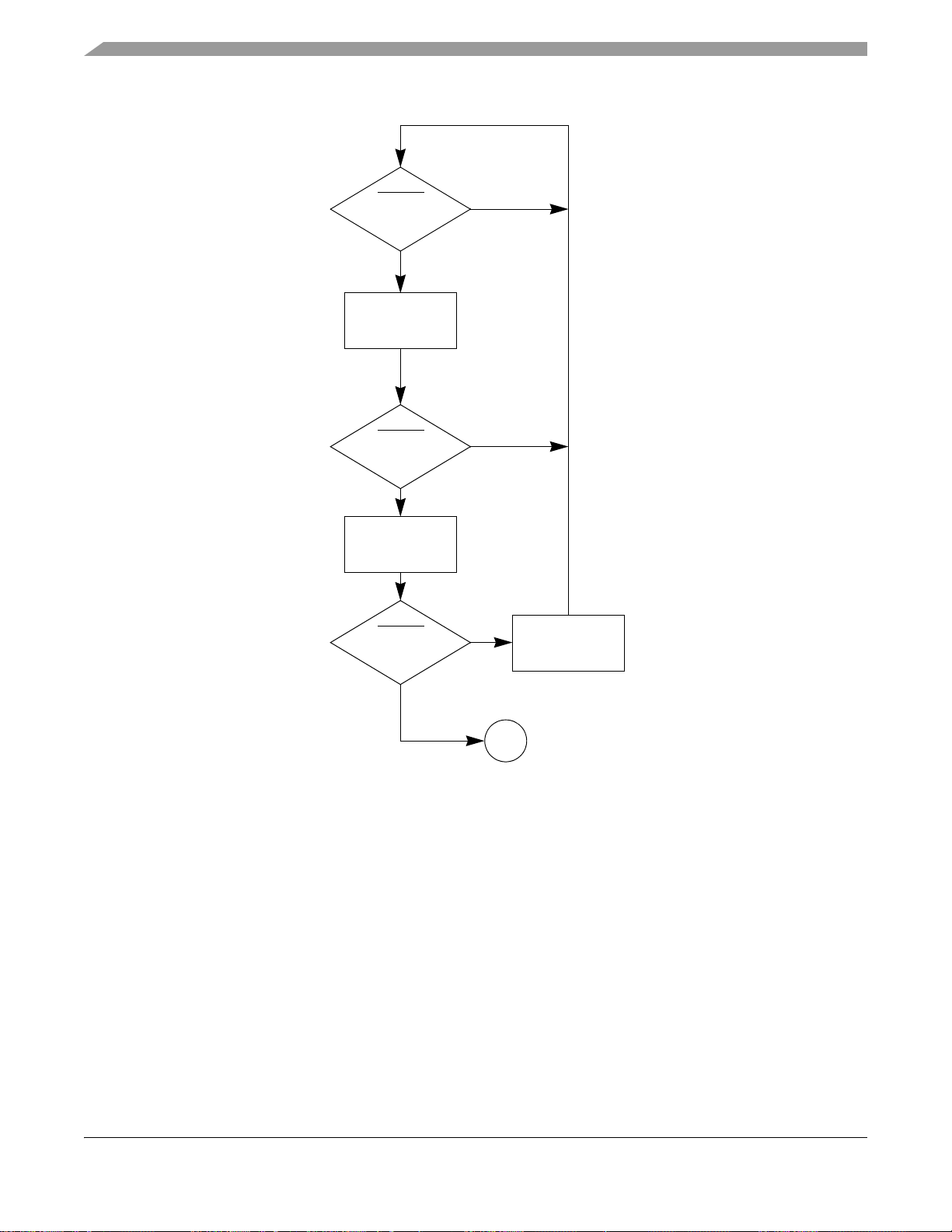
Asserted?
F
T
RESET
F
T
Asserted?
RESET
Asserted?
RESET
A
Wait 2
Clock Cycles
Set Latch,
Wait 8 Clock
Set RGF Bit
To entry point in
internal reset flow
F
T
Cycles
Figure 4-1. External Reset Flow Diagram
96 Freescale Semiconductor
MPC563XM Reference Manual, Rev. 1
Preliminary—Subject to Change Without Notice
Page 97
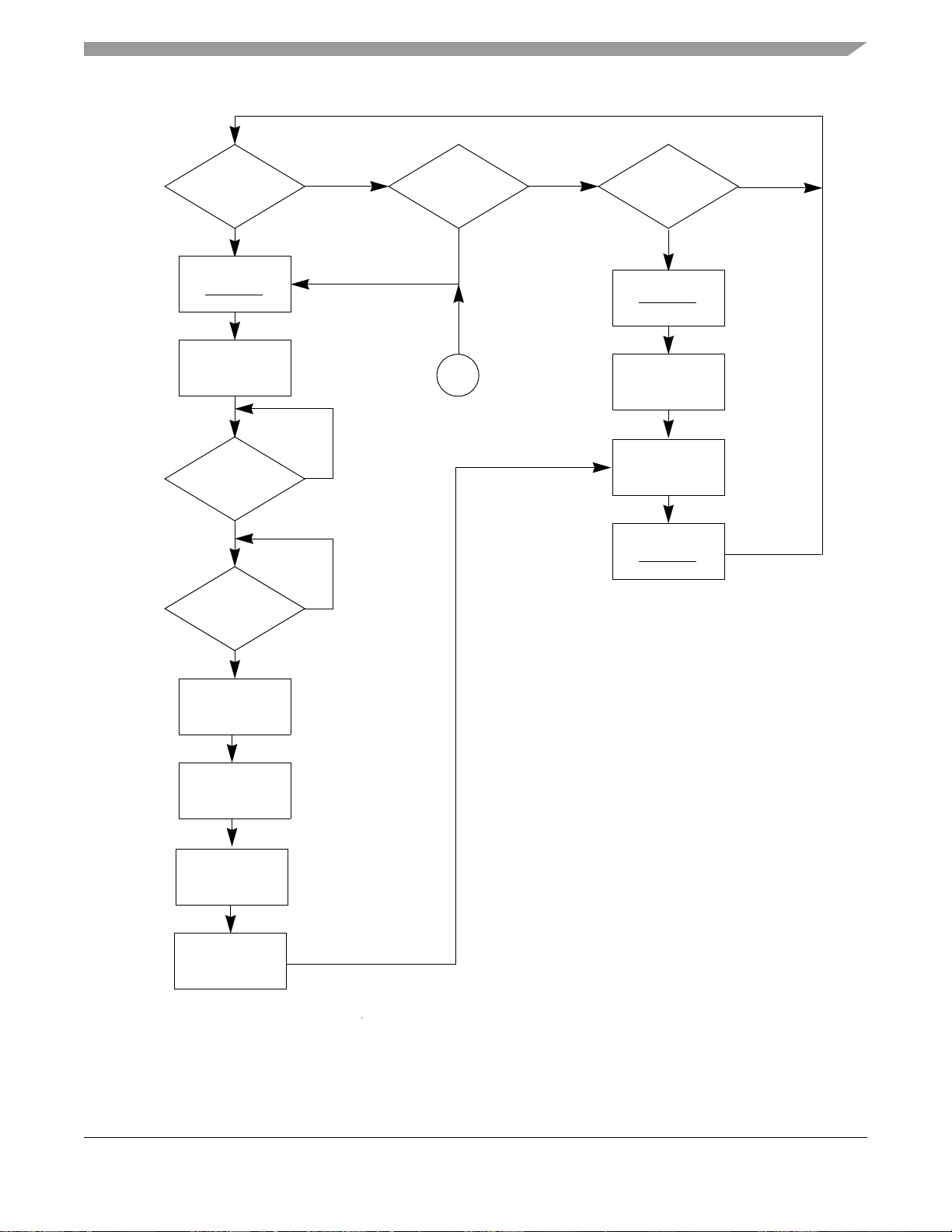
F
T
RSTOUT
Assert
Negated?
Software
Asserted?
External Reset
Update Reset
Status Register
Asserted?
Software
System Reset
F
T
F
T
Clock Cycles
Clock Cycles
F
T
Latch
WKPCFG Pin
Latch PLLREF,
BOOTCFG
Reset
Request
RSTOUT
Negate Internal
Resets and
Wait CNT
1
Wait 4
Clock Cycles
Wait CNT
1
Apply
WKPCFG Pin
RSTOUT
Assert Internal
Resets and
A
Entry point from
Val ues
Asserted?
Internal
Reset
F
T
Crystal Stable?
external reset flow
and POR
NOTES:
1. The clock count CNT depends on the reset source and type of clock reference. Please refer to Tab l e 4 - 1 .
Freescale Semiconductor 97
Figure 4-2. Internal Reset Flow Diagram
MPC563XM Reference Manual, Rev. 1
Preliminary—Subject to Change Without Notice
Page 98

4.5.1 Power-on Reset
The internal power-on reset signal is asserted when either the supply voltages, nominally 3.3 V or 1.2 V
or the RESET supply (VDDEH6a) fall below defined values. See the device data sheet for the threshold
specifications of these voltages. The output signals from the power-on reset circuits are active low signals.
All power-on reset output signals are combined into one POR signal at the 1.2 V level and input to the reset
controller. Although assertion of the power-on reset signal causes reset, the RESET pin must be asserted
during a power-on reset to guarantee proper operation of the MCU.
The PLLREF pin determines the source of reference clock, either crystal or external, at the negation of
RSTOUT. During the assertion of RSTOUT, the system clock will switch to the input specified by the
PLLREF pin. The value on the PLLREF pin must be kept constant during reset to avoid transients in the
system clock. See Section 17.2.3, “Modes of Operation” for more details.
The signal on the WKPCFG pin determines whether weak pull up or pull down devices are enabled after
reset on the eTPU and eMIOS pins. The WKPCFG pin is applied on the assertion of the internal reset
signal (assertion of RSTOUT). See Section 4.7.3, “Reset Weak Pull Up/Down Configuration,” for more
information.
Once a power-on-reset is triggered, if the clock reference is the crystal (PLLREF=1), then the clock to the
whole chip, including the reset state machine, is kept frozen until the Clock Quality Monitor detects that
the crystal oscillator has already stabilized. If the clock reference is external (PLLREF=0) the clock is
released to the system immediately . When the clock is stable and released to the chip, the reset controller
counts a predetermined number of clock cycles (refer to Section 4.3.2, “RSTOUT”) before negating the
RSTOUT pin. The WKPCFG and BOOTCFG pins are sampled 4 clock cycles before the negation of
RSTOUT, and the associated bits/fields are updated in the SIU_RSR. In addition, the PORS and ERS bits
are set, and all other reset status bits are cleared in the Reset Status Register.
4.5.2 External Reset
When the reset controller detects assertion of the RESET pin, the internal reset signal and RSTOUT pin
are asserted. The value on the WKPCFG pin is applied at the assertion of the internal reset signal (assertion
of RSTOUT
), as is the PLLREF value. Once the RESET pin is negated, the reset controller waits for a
predetermined number of clock cycles (refer to Section 4.3.2, “RSTOUT”). When the clock count finishes,
the WKPCFG and BOOTCFG pins are sampled. The reset controller then waits 4 clock cycles before
negating RSTOUT, and the associated bits/fields are updated in the SIU_RSR. In addition, the ERS bit is
set, and all other reset status bits in the SIU_RSR are cleared.
4.5.3 Loss of Lock
A Loss of Lock Reset occurs when the FMPLL loses lock and the Loss of Lock Reset Enable (LOLRE)
bit in the FMPLL Synthesizer Control Register (SYNCR) is set. The internal reset signal and RSTOUT
pin are asserted. The value on the WKPCFG pin is applied at the assertion of the internal reset signal
(assertion of RSTOUT
), as is the PLLREF value. Once the FMPLL Loss of Lock reset request signal is
negated, the reset controller waits for a predetermined number of clock cycles (refer to Section 4.3.2,
“RSTOUT”). Once the clock count finishes, the WKPCFG and BOOTCFG pins are sampled. The reset
controller then waits 4 clock cycles before negating RSTOUT, and the associated bits/fields are updated
MPC563XM Reference Manual, Rev. 1
98 Freescale Semiconductor
Preliminary—Subject to Change Without Notice
Page 99

in the SIU_RSR. In addition, the LLRS bit is set, and all other reset status bits in the SIU_RSR are cleared.
Refer to Section 17.5.3, “Lock Detection,” for more information on loss of lock.
4.5.4 Loss of Clock
A Loss of Clock Reset occurs when the Clock Quality Monitor Module (CQM) detects a failure in either
the reference signal or FMPLL output, and the Loss of Clock Reset Enable (LOCRE) bit in the SYNCR is
set. The internal reset signal and RSTOUT pin are asserted. The value on the WKPCFG pin is applied at
the assertion of the internal reset signal (assertion of RSTOUT), as is the PLLREF value. Once the Loss
of Clock reset request signals is negated, the reset controller waits for a predetermined number of clock
cycles (refer to Section 4.3.2, “RSTOUT”). Once the clock count finishes, the WKPCFG and BOOTCFG
pins are sampled. The reset controller then waits 4 clock cycles before negating RSTOUT, and the
associated bits/fields are updated in the SIU_RSR. In addition, the LCRS bit is set, and all other reset status
bits in the SIU_RSR are cleared. Refer to Section 17.5.4, “Loss-of-Clock Detection,” for more information
on loss of clock.
The CQM module when enabled can generates either a system reset or an interrupt signal, refer to
Section 17.5.4, “Loss-of-Clock Detection,” for details.
4.5.5 Watchdog Timer/Debug Reset
A Watchdog Timer Reset occurs when the e200z335 core Watchdog Timer is enabled, and a time-out
occurs with the Enable Next W atchdog Timer (EWT) and Watchdog T imer Interrupt S tatus (WIS) bits set
in the Timer Status Register, and with the Watchdog Reset Control (WRC) field in the Timer Control
Register configured for a reset. The WDRS bit in the SIU_RSR is also set when a debug reset command
is issued from a debug tool. To determine whether the WDRS bit was set due to a Watchdog Timer or
Debug Reset, see the WRS field in the e200z335 core Timer Status Register. The effect of a Watchdog
Timer or Debug Reset request is the same for the reset controller. The internal reset signal and RSTOUT
pin are asserted. The value on the WKPCFG pin is applied at the assertion of the internal reset signal
(assertion of RSTOUT), as is the PLLREF value. After the Watchdog Timer/Debug reset request is
negated, the reset controller waits for a predetermined number of clock cycles (refer to Section 4.3.2,
“RSTOUT”). Once the clock count finishes the WKPCFG and BOOTCFG pins are sampled. The reset
controller then waits 4 clock cycles before negating RSTOUT
in the SIU_RSR. In addition, the WTRS bit is set, and all other reset status bits in the SIU_RSR are cleared.
Refer to the e200z335 Core Reference Manual for more information on the Watchdog Timer and debug
operation.
, and the associated bits/fields are updated
NOTE
In addition to the e200z335 watchdog timer, this device implements a
system software watchdog timer (see Chapter 20, “Software Watchdog
Timer (SWT)”).
4.5.6 Software Watchdog Timer Reset
A Software Watchdog Timer Reset occurs when the watchdog timer in the SWT module is enabled and
programmed to generate a reset. The effect of a Software Watchdog Timer Reset request is the same for
MPC563XM Reference Manual, Rev. 1
Freescale Semiconductor 99
Preliminary—Subject to Change Without Notice
Page 100

the reset controller. The internal reset signal and RSTOUT pin are asserted. The value on the WKPCFG
pin is applied at the assertion of the internal reset signal (assertion of RSTOUT), as is the PLLREF value.
Once the Software W atchdog T imer rese t request is negated, the reset controller waits for a predetermined
number of clock cycles (refer to Section 4.3.2, “RSTOUT”). When the clock count finishes the WKPCFG
and BOOTCFG pins are sampled. The reset controller then waits 4 clock cycles before negating RSTOUT
and the associated bits/fields are updated in the SIU_RSR. In addition, the SWTRS bit is set, and all other
reset status bits in the SIU_RSR are cleared.
4.5.7 Checkstop Reset
When the e200z335 core enters a checkstop state, and the Checkstop Reset is enabled (the CRE bit in the
System Reset Control Register (SIU_SRCR) is set), a Checkstop Reset occurs. The internal reset signal
and RSTOUT pin are asserted. The value on the WKPCFG pin is applied at the assertion of the internal
reset signal (assertion of RSTOUT), as is the PLLREF value. After the checkstop state signal is negated,
the reset controller waits for a predetermined number of clock cycles (refer to Section 4.3.2, “RSTOUT”).
Once the clock count finishes the WKPCFG and BOOTCFG pins are sampled. The reset controller then
waits 4 clock cycles before negating RSTOUT , and the ass ociated bits/fields are updated in the SIU_RSR.
In addition, the CRS bit is set, and all other reset status bits in the SIU_RSR are cleared. Refer to the
e200z335 Core Reference Manual for more information.
4.5.8 JTAG Reset
,
A system reset occurs when JT AG is enabled and either the EXTEST, CLAMP, or HIGHZ instructions are
executed by the JTAG controller. The internal reset signal is asserted. The state of the RSTOUT pin is
determined by the JTAG instruction. The value on the WKPCFG pin is applied at the assertion of the
internal reset signal, as is the PLLREF value. After the JTAG reset request is negated, the reset controller
waits for a predetermined number of clock cycles (refer to Section 4.3.2, “RSTOUT”). Once the clock
count finishes the WKPCFG and BOOTCFG pins are sampled, and the associated bits/fields are updated
in the SIU_RSR. The reset status bits in the SIU_RSR are unaffected. Refer to Chapter 31, “JTAG
Controller (JTAGC),” for more information.
4.5.9 Software System Reset
A Software System Reset is caused by a write to the SSR bit in the System Reset Control Register
(SIU_SRCR); see Section 16.9.4, “System Reset Control Register (SIU_SRCR).” A write of one to the
SSR bit causes an internal reset of the MCU. The internal reset signal and RSTOUT
value on the WKPCFG pin is applied at the assertion of the internal reset signal (assertion of RSTOUT
as is the PLLREF value. The SSR bit is automatically cleared and the reset controller waits for a
predetermined number of clock cycles (refer to Section 4.3.2, “RSTOUT”). Once the clock count finishes
the WKPCFG and BOOTCFG pins are sampled. The reset controller then waits 4 clock cycles before
negating RSTOUT
, and the associated bits/fields are updated in the SIU_RSR. In addition, the SSRS bit
is set, and all other reset status bits in the SIU_RSR are cleared.
pin are asserted. The
),
MPC563XM Reference Manual, Rev. 1
100 Freescale Semiconductor
Preliminary—Subject to Change Without Notice
 Loading...