

Page 1

Freescale Semiconductor
Rev. 8.2, 09/2013
MPC5604B/C Microcontroller
Reference Manual
This is the MPC5604B/C Reference Manual set consisting of the following files:
• MPC5604B/C Reference Manual Addendum (MPC5604B/CRMAD), Rev. 2
MPC5604BCRM
• MPC5604B/C Reference Manual (MPC5604B/CRM), Rev. 8
© Freescale Semiconductor, Inc., 2013. All rights reserved.
Page 2

Freescale Semiconductor
MPC5604BRMAD
Reference Manual Addendum
MPC5604B/C Microcontroller
Reference Manual Addendum
Rev. 2, 09/2013
This addendum describes corrections to the
MPC5604B/C Microcontr oller Refer ence Manual, order
number MPC5604BCRM. For convenience, the addenda
items are grouped by revision. Please check our website
at http://www.freescale.com/powerarchitecture for the
latest updates.
The current version available of the MPC5604B/C
Microcontroller Reference Manual is Revision 8.1.
Table of Contents
1 Addendum List for Revision 8.1 . . . . . . . . . . . . . . 2
2 Addendum List for Revision 8. . . . . . . . . . . . . . . . 2
3 Revision History . . . . . . . . . . . . . . . . . . . . . . . . . . 4
© Freescale Semiconductor, Inc., 2013. All rights reserved.
Page 3

1 Addendum List for Revision 8.1
Table 1. MPC5604BCRM Rev 8.1 Addenda
Location Description
Chapter 27, “Flash Memory”
page 644
Add a note below Table 27-4, “CFlash TestFlash Structure”.
NOTE
Unique Device ID – Memory location. This device now includes a 128-bit Unique
Identification number (UID) which is programmed during device fabrication.
Start – Stop Address Size (Bytes) Content:
• 0x00403C10 0x00403C17 8 UID 1
• 0x00403C18 0x00403C1F 8 UID 2
2 Addendum List for Revision 8
Table 2. MPC5604BCRM Rev 8 Addenda
Location Description
Chapter 4, Signal description,
page 60
Chapter 6, Clock Description,
page 113
Chapter 9, Reset Generation
Module (MC_RGM), page
209
In Table 4-3, Functional port pin descriptions, row PH[9], change the pin numbers for
MPC560xB 64 LQFP and MPC560xC 64 LQFP from “—” to 60.
In row PH[10], change the pin numbers for MPC560xB 64 LQFP and MPC560xC 64 LQFP
from “—” to 53.
Add Note: to Section 6.8.4.1, Crystal clock monitor:
Note: Functional FXOSC monitoring can only be guaranteed when the FXOSC frequency is
greater than (FIRC / 2
Add Note: to Section 6.8.4.2, FMPLL clock monitor:
Note: Functional FMPLL monitoring can only be guaranteed when the FMPLL frequency is
greater than (FIRC / 4) + 0.5 MHz.
Replace Section 9.4.7, Boot Mode Capturing, with the following:
The MC_RGM samples P A[9:8] whenev er RESET is asserted until five FIRC (16 MHz internal
RC oscillator) clock cycles before its deassertion edge. The result of the sampling is used at
the beginning of reset PHASE3 for boot mode selection and is retained after RESET has been
deasserted for subsequent boots after reset sequences during which RESET is not asserted.
RCDIV
)+0.5MHz.
Chapter 13, Real Time Clock /
Autonomous Periodic
Interrupt (RTC/API), page
262
Note: In order to ensure that the boot mode is correctly captured, the application needs to
apply the valid boot mode value the entire time that RESET is asserted.
RESET can be asserted as a consequence of the internal reset generation. This will force
re-sampling of the boot mode pins. (See Table 9-12 for details.)
In Table 13-3 (RTCC field descriptions), update Note in RTCC[APIVAL] field description:
Note: API functionality starts only when APIVAL is nonzero. The first API interrupt takes two
more cycles because of synchronization of APIVAL to the RTC cloc k, and APIVAL + 1 cycles
for subsequent occurrences. After that, interrupts are periodic in nature. Because of
synchronization issues, the minimum supported value of APIVAL is 4.
MPC5604BRMAD, Rev. 2
Freescale Semiconductor2
Page 4

Table 2. MPC5604BCRM Rev 8 Addenda
Location Description
Chapter 21, LINFlex, p. 412 Insert the following section:
21.8.2.1.6 Overrun
Once the message buffer is full, the next valid message reception leads to an
overrun and a message is lost. The hardware sets the BOF bit in the LINSR to
signal the overrun condition. Which message is lost depends on the
configuration of the RX message buffer:
• If the buffer lock function is disabled (LINCR1[RBLM] = 0) the last
message stored in the buffer is overwritten by the new incoming
message. In this case the latest message is always available to the
application.
• If the buffer lock function is enabled (LINCR1[RBLM] = 0) the most
recent message is discarded and the previous message is available in the
buffer.
Chapter 22, FlexCAN,
throughout chapter
Chapter 22, FlexCAN, page
429
Chapter 22, FlexCAN, page
461
Chapter 22, FlexCAN, page
462
Chapter 22, FlexCAN, page
463
Chapter 25, Analog-to-Digital
Converter (ADC), page
Chapter 25, Analog-to-Digital
Converter (ADC), page 597
Remove references throughout the chapter to “low-cost MCUs.”
Add this Note in the RTR field description of Table 22-4 (Message Buffer Structure field
description):
Note: Do not configure the last Message Buffer to be the RTR frame.
In Section 22.4.9.4, Protocol timing, update the Note following Figure 22-16 (CAN engine
clocking scheme) to read: “This clock selection feature may not be available in all MCUs. A
particular MCU may not have a PLL, in which case it would have only the oscillator clock, or
it may use only the PLL clock feeding the FlexCAN module. In these cases, the CLK_SRC bit
in the CTRL Register has no effect on the module operation.”
Update the table title of Table 22-20 from “CAN Standard Compliant Bit Time Segment Settings”
to “Bosch CAN 2.0B standard compliant bit time segment settings.”
In Section 22.4.9.4, Protocol timing, update the Note following Table 22-20 to read: “Other
combinations of Time Segment 1 and Time Segment 2 can be valid. It is the user’s
responsibility to ensure the bit time settings are in compliance with the CAN standard. For bit
time calculations, use an IPT (Information Processing Time) of 2, which is the value
implemented in the FlexCAN module.”
In Section 28.3.5.2, Presampling channel enable signals, in Table 28-7, Presampling voltage
selection based on PREVALx fields, in the 01 row, change the “Presampling voltage” field to:
V1 = V
DD_HV_ADC0
In Section 25.3.2, Analog clock generator and conversion timings, remove the paragraph:
The direct clock should basically be used only in low power mode when the device is using
only the 16 MHz fast internal RC oscillator, but the conversion still requires a 16 MHz clock
(an 8 MHz clock is not fast enough). In all other cases, the ADC should use the clock divided
by two internally.
or V
DD_HV_ADC1
.
MPC5604BRMAD, Rev. 2
Freescale Semiconductor 3
Page 5

Table 2. MPC5604BCRM Rev 8 Addenda
Location Description
Chapter 25, Analog-to-Digital
Converter (ADC), p. 600
Chapter 25, Analog-to-Digital
Converter (ADC), page 603
Chapter 25, Analog-to-Digital
Converter (ADC), page 610
Chapter 26, Cross Triggering
Unit (CTU), page 633
In Section 25.3.4.2, CTU in trigger mode, replace the sentence:
If another CTU conversion is triggered before the end of the conversion, that request is
discarded.
with:
If another CTU conversion is triggered before the end of the conversion, that request is
discarded. However, if the CTU has triggered a conversion that is still ongoing on a channel,
it will buffer a second request fo r the channel and wait for the end of the first conv ersion before
requesting another conversion. Thus, two conversion requests close together will both be
serviced.
Add Note to Section 25.3.10, Auto-clock-off mode:
Note: The auto-clock-off feature cannot operate when the digital interface runs at the same
rate as the analog interface. This means that when MCR.ADCCLKSEL = 1, the analog clock
will not shut down in IDLE mode.
In Section 25.4.6.2, Main Status Register (MSR), replace the ADCST ATUS field description with
the following:
The value of this parameter depends on ADC status:
000 IDLE — The ADC is powered up but idle.
001 Power-down — The ADC is powered down.
010 Wait state — The ADC is waiting for an external multiplexer . This occurs only when the
DSDR register is nonzero.
011 Reserved
100 Sample — The ADC is sampling the analog signal.
101 Reserved
110 Conversion — The ADC is converting the sampled signal.
111 Reserved
At the end of Section 26.4.1, Event Configuration Registers (CTU_EVTCFGRx) (x = 0...63), add
the following Note:
NOTE
The CTU tracks issued conversion requests to the ADC. When the ADC
is being triggered by the CTU and there is a need to shut down the ADC,
the ADC must be allowed to complete conversions before being shut
down. This ensures that the CTU is notified of completion; if the ADC
is shut down while performing a CTU-triggered conversion, the CTU is
not notified and will not be able to trigger further conversions until the
device is reset.
3 Revision History
Table 3 provides a revision history for this reference manual addendum document.
Table 3. Revision History Table
Rev. Number Substantive Changes Date of Release
2.0 Add a note below Table 27-4, “CFlash TestFlash Structure” 09/2013
1.0 Initial release. 05/2012
MPC5604BRMAD, Rev. 2
Freescale Semiconductor4
Page 6

How to Reach Us:
Home Page:
www.freescale.com
Web Support:
http://www.freescale.com/support
USA/Europe or Locations Not Listed:
Freescale Semiconductor, Inc.
Technical Information Center, EL516
2100 East Elliot Road
Tempe, Arizona 85284
+1-800-521-6274 or +1-480-768-2130
www.freescale.com/support
Europe, Middle East, and Africa:
Freescale Halbleiter Deutschland GmbH
Technical Information Center
Schatzbogen 7
81829 Muenchen, Germany
+44 1296 380 456 (English)
+46 8 52200080 (English)
+49 89 92103 559 (German)
+33 1 69 35 48 48 (French)
www.freescale.com/support
Japan:
Freescale Semiconductor Japan Ltd.
Headquarters
ARCO Tower 15F
1-8-1, Shimo-Meguro, Meguro-ku,
Tokyo 153-0064
Japan
0120 191014 or +81 3 5437 9125
[email protected]
Asia/Pacific:
Freescale Semiconductor China Ltd.
Exchange Building 23F
No. 118 Jianguo Road
Chaoyang District
Beijing 100022
China
+86 10 5879 8000
[email protected]
For Literature Requests Only:
Freescale Semiconductor Literature Distribution Center
1-800-441-2447 or 303-675-2140
Fax: 303-675-2150
[email protected]
Information in this document is provided solely to enable system and
software implementers to use F reescale S emiconductor prod ucts. There ar e
no express or implied copyright licenses granted hereunder to design or
fabricate any integrated circuits or integrated circuits based on the
information in this document.
Freescale Semiconducto r reserves the right to mak e changes without further
notice to any products herein. F reescale Se miconductor m akes no w arranty,
representation or guarantee regarding the suitability of its products for any
particular purpose, nor does Freescale Semiconductor assume any liability
arising out of the application or use of any produ ct or circuit, an d specific ally
disclaims any and all liability, including without limitation consequential or
incidental damages. “Typical” par ameter s that m a y be pro vided in Freescale
Semiconductor data sheets and/or speci fications can and do v ary in differ ent
applications and actual performance may vary over time. All operating
parameters, including “Typicals”, must be validated for each customer
application by customer’s technical experts. Freescale Semiconductor does
not convey any license under its patent rights nor the rights of others.
Freescale Semicondu ctor products are not de signed, intended, or authorized
for use as components in systems intended for surgical implant into the body ,
or other applications intended to support or sustain life, or for any other
application in which the failure of the Freescale Semiconductor product could
create a situation where personal injury or death may occur. Should Buyer
purchase or use Freescal e Semiconductor products f or an y such unintended
or unauthorized application, B uyer sha ll indemnify and hold Freescale
Semiconductor and its officers, employees, subsidiaries, affiliates, and
distributors harmless against all claims, costs, damages, and expenses, and
reasonable attorney fees arising out of, directly or indirectly, any claim of
personal injury or death associated with such unintended or unauthorized
use, even if such claim alleges that Freescale Semiconductor was negligent
regarding the design or manufacture of the part.
Freescale™ and the Freescale logo are trademarks of Freescale
Semiconductor, Inc. All other product or service names are the property
of their respective owners.© Freescale Semiconductor, Inc. 2013. All rights
reserved.
MPC5604BRMAD
Rev. 2
09/2013
Page 7

Freescale Semiconductor
Rev. 8.1, 05/2012
MPC5604B/C Microcontroller
Reference Manual
by: Microcontroller Solutions Group
This is the MPC5604B/C Reference Manual set consisting of the following files:
MPC5604BCRM
• MPC5604B/C Reference Manual Addendum (MPC5604B/CRMAD), Rev. 1
• MPC5604B/C Reference Manual (MPC5604B/CRM), Rev. 8
© Freescale Semiconductor, Inc., 2012. All rights reserved.
Page 8

Freescale Semiconductor
MPC5604BRMAD
Reference Manual Addendum
MPC5604B/C Microcontroller
Reference Manual Addendum
by: Microcontroller Solutions Group
Rev. 1, 05/2012
This addendum document describes corrections to the
MPC5604B/C Microcontr oller Refer ence Manual, order
number MPC5604BCRM. For convenience, the addenda
items are grouped by revision. Please check our website
at http://www.freescale.com/powerarchitecture for the
latest updates.
The current version available of the MPC5604B/C
Microcontroller Reference Manual is Revision 8.
Table of Contents
1 Addendum for Revision 8 . . . . . . . . . . . . . . . . . . . 2
2 Revision History . . . . . . . . . . . . . . . . . . . . . . . . . . 4
© Freescale Semiconductor, Inc., 2012. All rights reserved.
Page 9

Addendum List for Revision 8
1 Addendum List for Revision 8
Table 1. MPC5604BCRM Rev 8 Addenda
Location Description
Chapter 4, Signal description,
page 60
Chapter 6, Clock Description,
page 113
Chapter 9, Reset Generation
Module (MC_RGM), page
209
Chapter 13, Real Time Clock /
Autonomous Periodic
Interrupt (RTC/API), page
262
Chapter 21, LINFlex, p. 412 Insert the following section:
In Table 4-3, Functional port pin descriptions, row PH[9], change the pin numbers for
MPC560xB 64 LQFP and MPC560xC 64 LQFP from “—” to 60.
In row PH[10], change the pin numbers for MPC560xB 64 LQFP and MPC560xC 64 LQFP
from “—” to 53.
Add Note: to Section 6.8.4.1, Crystal clock monitor:
Note: Functional FXOSC monitoring can only be guaranteed when the FXOSC frequency is
greater than (FIRC / 2
Add Note: to Section 6.8.4.2, FMPLL clock monitor:
Note: Functional FMPLL monitoring can only be guaranteed when the FMPLL frequency is
greater than (FIRC / 4) + 0.5 MHz.
Replaced Section 9.4.7, Boot Mode Capturing, with the following:
The MC_RGM samples P A[9:8] whenev er RESET is asserted until five FIRC (16 MHz internal
RC oscillator) clock cycles before its deassertion edge. The result of the sampling is used at
the beginning of reset PHASE3 for boot mode selection and is retained after RESET has been
deasserted for subsequent boots after reset sequences during which RESET is not asserted.
Note: In order to ensure that the boot mode is correctly captured, the application needs to
apply the valid boot mode value the entire time that RESET is asserted.
RESET can be asserted as a consequence of the internal reset generation. This will force
re-sampling of the boot mode pins. (See Table 9-12 for details.)
In Table 13-3 (RTCC field descriptions), update Note in RTCC[APIVAL] field description:
Note: API functionality starts only when APIVAL is nonzero. The first API interrupt takes two
more cycles because of synchronization of APIVAL to the RTC cloc k, and APIVAL + 1 cycles
for subsequent occurrences. After that, interrupts are periodic in nature. Because of
synchronization issues, the minimum supported value of APIVAL is 4.
RCDIV
)+0.5MHz.
21.8.2.1.6 Overrun
Once the message buffer is full, the next valid message reception leads to an
overrun and a message is lost. The hardware sets the BOF bit in the LINSR to
signal the overrun condition. Which message is lost depends on the
configuration of the RX message buffer:
• If the buffer lock function is disabled (LINCR1[RBLM] = 0) the last
message stored in the buffer is overwritten by the new incoming
message. In this case the latest message is always available to the
application.
• If the buffer lock function is enabled (LINCR1[RBLM] = 0) the most
recent message is discarded and the previous message is available in the
buffer.
MPC5604B Reference Manual Errata, Rev. 1
Freescale Semiconductor2
Page 10

Table 1. MPC5604BCRM Rev 8 Addenda
Location Description
Addendum List for Revision 8
Chapter 22, FlexCAN,
throughout chapter
Chapter 22, FlexCAN, page
429
Chapter 22, FlexCAN, page
461
Chapter 22, FlexCAN, page
462
Chapter 22, FlexCAN, page
463
Chapter 25, Analog-to-Digital
Converter (ADC), page
Chapter 25, Analog-to-Digital
Converter (ADC), page 597
Remove references throughout the chapter to “low-cost MCUs.”
Added this Note in the RTR field description of Table 22-4 (Message Buffer Structure field
description):
Note: Do not configure the last Message Buffer to be the RTR frame.
In Section 22.4.9.4, Protocol timing, updated the Note following Figure 22-16 (CAN engine
clocking scheme) to read: “This clock selection feature may not be available in all MCUs. A
particular MCU may not have a PLL, in which case it would have only the oscillator clock, or
it may use only the PLL clock feeding the FlexCAN module. In these cases, the CLK_SRC bit
in the CTRL Register has no effect on the module operation.”
Updated the table title of Table 22-20 from “CAN Standard Compliant Bit Time Segment
Settings” to “Bosch CAN 2.0B standard compliant bit time segment settings.”
In Section 22.4.9.4, Protocol timing, updated the Note following Table 22-20 to read: “Other
combinations of Time Segment 1 and Time Segment 2 can be valid. It is the user’s
responsibility to ensure the bit time settings are in compliance with the CAN standard. For bit
time calculations, use an IPT (Information Processing Time) of 2, which is the value
implemented in the FlexCAN module.”
In Section 28.3.5.2, Presampling channel enable signals, in Table 28-7, Presampling voltage
selection based on PREVALx fields, in the 01 row, change the “Presampling voltage” field to:
V1 = V
DD_HV_ADC0
or V
DD_HV_ADC1
.
In Section 25.3.2, Analog clock generator and conversion timings, remove the paragraph:
The direct clock should basically be used only in low power mode when the device is using
only the 16 MHz fast internal RC oscillator, but the conversion still requires a 16 MHz clock
(an 8 MHz clock is not fast enough). In all other cases, the ADC should use the clock divided
by two internally.
Chapter 25, Analog-to-Digital
Converter (ADC), p. 600
In Section 25.3.4.2, CTU in trigger mode, replace the sentence:
If another CTU conversion is triggered before the end of the conversion, that request is
discarded.
with:
If another CTU conversion is triggered before the end of the conversion, that request is
discarded. However, if the CTU has triggered a conversion that is still ongoing on a channel,
it will buffer a second request fo r the channel and wait for the end of the first conv ersion before
requesting another conversion. Thus, two conversion requests close together will both be
serviced.
Chapter 25, Analog-to-Digital
Converter (ADC), page 603
Add Note to Section 25.3.10, Auto-clock-off mode:
Note: The auto-clock-off feature cannot operate when the digital interface runs at the same
rate as the analog interface. This means that when MCR.ADCCLKSEL = 1, the analog clock
will not shut down in IDLE mode.
MPC5604B Reference Manual Errata, Rev. 1
Freescale Semiconductor 3
Page 11

Revision History
Location Description
Table 1. MPC5604BCRM Rev 8 Addenda
Chapter 25, Analog-to-Digital
Converter (ADC), page 610
Chapter 26, Cross Triggering
Unit (CTU), page 633
In Section 25.4.6.2, Main Status Register (MSR), replace the ADCSTATUS field description with
the following:
The value of this parameter depends on ADC status:
000 IDLE — The ADC is powered up but idle.
001 Power-down — The ADC is powered down.
010 Wait state — The ADC is waiting for an external multiplexer . This occurs only when the
DSDR register is nonzero.
011 Reserved
100 Sample — The ADC is sampling the analog signal.
101 Reserved
110 Conversion — The ADC is converting the sampled signal.
111 Reserved
At the end of Section 26.4.1, Event Configuration Registers (CTU_EVTCFGRx) (x = 0...63), add
the following Note:
NOTE
The CTU tracks issued conversion requests to the ADC. When the ADC
is being triggered by the CTU and there is a need to shut down the ADC,
the ADC must be allowed to complete conversions before being shut
down. This ensures that the CTU is notified of completion; if the ADC
is shut down while performing a CTU-triggered conversion, the CTU is
not notified and will not be able to trigger further conversions until the
device is reset.
2 Revision History
Table 2 provides a revision history for this reference manual addendum document.
Table 2. Revision History Table
Rev. Number Substantive Changes Date of Release
1.0 • Initial release. 05/2012
MPC5604B Reference Manual Errata, Rev. 1
Freescale Semiconductor4
Page 12

MPC5604B/C Microcontroller
MPC5604BCRM
Rev. 8
5 May 2011
Reference Manual
Devices Supported:
MPC5602B
MPC5602C
MPC5603B
MPC5603C
MPC5604B
MPC5604C
MPC5604B/C Microcontroller Reference Manual, Rev. 8
Freescale Semiconductor 1
Page 13

MPC5604B/C Microcontroller Reference Manual, Rev. 8
2 Freescale Semiconductor
Page 14

Chapter 1
Preface
1.1 Overview .........................................................................................................................................19
1.2 Audience ..........................................................................................................................................19
1.3 Guide to this reference manual ........................................................................................................19
1.4 Register description conventions ....................................................................................................22
1.5 References .......................................................................................................................................23
1.6 How to use the MPC5604B documents ..........................................................................................23
1.6.1 The MPC5604B document set ........................................................................................23
1.6.2 Reference manual content ..............................................................................................24
1.7 Using the MPC5604B .....................................................................................................................25
1.7.1 Hardware design .............................................................................................................25
1.7.2 Input/output pins .............................................................................................................26
1.7.3 Software design ..............................................................................................................27
1.7.4 Other features .................................................................................................................27
Chapter 2
Introduction
2.1 The MPC5604B microcontroller family .........................................................................................29
2.2 Features ...........................................................................................................................................29
2.2.1 MPC5604B family comparison ......................................................................................29
2.2.2 Block diagram ................................................................................................................32
2.2.3 Chip-level features ..........................................................................................................33
2.3 Packages ..........................................................................................................................................34
2.4 Developer support ...........................................................................................................................34
Chapter 3
Memory Map
Chapter 4
Signal description
4.1 Introduction .....................................................................................................................................39
4.2 Package pinouts ...............................................................................................................................39
4.3 Pad configuration during reset phases .............................................................................................42
4.4 Voltage supply pins .........................................................................................................................43
4.5 Pad types .........................................................................................................................................43
4.6 System pins .....................................................................................................................................44
4.7 Functional ports ...............................................................................................................................44
4.8 Nexus 2+ pins ..................................................................................................................................61
Chapter 5
Microcontroller Boot
5.1 Boot mechanism ..............................................................................................................................63
5.1.1 Flash memory boot .........................................................................................................64
5.1.2 Serial boot mode .............................................................................................................66
MPC5604B/C Microcontroller Reference Manual, Rev. 8
Freescale Semiconductor 3
Page 15

5.1.3 Censorship ......................................................................................................................66
5.2 Boot Assist Module (BAM) ............................................................................................................71
5.2.1 BAM software flow ........................................................................................................71
5.2.2 LINFlex (RS232) boot ....................................................................................................79
5.2.3 FlexCAN boot ................................................................................................................80
5.3 System Status and Configuration Module (SSCM) ........................................................................82
5.3.1 Introduction ....................................................................................................................82
5.3.2 Features ...........................................................................................................................82
5.3.3 Modes of operation .........................................................................................................83
5.3.4 Memory map and register description ............................................................................83
Chapter 6
Clock Description
6.1 Clock architecture ...........................................................................................................................93
6.2 Clock gating ....................................................................................................................................94
6.3 Fast external crystal oscillator (FXOSC) digital interface ..............................................................95
6.3.1 Main features ..................................................................................................................95
6.3.2 Functional description ....................................................................................................95
6.3.3 Register description ........................................................................................................96
6.4 Slow external crystal oscillator (SXOSC) digital interface ............................................................97
6.4.1 Introduction ....................................................................................................................97
6.4.2 Main features ..................................................................................................................97
6.4.3 Functional description ....................................................................................................97
6.4.4 Register description ........................................................................................................98
6.5 Slow internal RC oscillator (SIRC) digital interface ......................................................................99
6.5.1 Introduction ....................................................................................................................99
6.5.2 Functional description ....................................................................................................99
6.5.3 Register description ......................................................................................................100
6.6 Fast internal RC oscillator (FIRC) digital interface ......................................................................101
6.6.1 Introduction ..................................................................................................................101
6.6.2 Functional description ..................................................................................................101
6.6.3 Register description ......................................................................................................102
6.7 Frequency-modulated phase-locked loop (FMPLL) .....................................................................102
6.7.1 Introduction ..................................................................................................................102
6.7.2 Overview ......................................................................................................................102
6.7.3 Features .........................................................................................................................103
6.7.4 Memory map ................................................................................................................103
6.7.5 Register description ......................................................................................................104
6.7.6 Functional description ..................................................................................................107
6.7.7 Recommendations ........................................................................................................110
6.8 Clock monitor unit (CMU) ............................................................................................................110
6.8.1 Introduction ..................................................................................................................110
6.8.2 Main features ................................................................................................................111
6.8.3 Block diagram ..............................................................................................................111
6.8.4 Functional description ..................................................................................................112
MPC5604B/C Microcontroller Reference Manual, Rev. 8
4 Freescale Semiconductor
Page 16

6.8.5 Memory map and register description ..........................................................................114
Chapter 7
Clock Generation Module (MC_CGM)
7.1 Overview .......................................................................................................................................119
7.2 Features .........................................................................................................................................120
7.3 Modes of Operation .......................................................................................................................121
7.3.1 Normal and Reset Modes of Operation ........................................................................121
7.4 External Signal Description ..........................................................................................................121
7.5 Memory Map and Register Definition ..........................................................................................121
7.5.1 Register Descriptions ....................................................................................................125
7.6 Functional Description ..................................................................................................................129
7.6.1 System Clock Generation .............................................................................................129
7.6.2 Output Clock Multiplexing ...........................................................................................130
7.6.3 Output Clock Division Selection ..................................................................................131
Chapter 8
Mode Entry Module (MC_ME)
8.1 Introduction ...................................................................................................................................133
8.1.1 Overview ......................................................................................................................133
8.1.2 Features .........................................................................................................................135
8.1.3 Modes of Operation ......................................................................................................135
8.2 External Signal Description ..........................................................................................................136
8.3 Memory Map and Register Definition ..........................................................................................136
8.3.1 Register Description .....................................................................................................144
8.4 Functional Description ..................................................................................................................166
8.4.1 Mode Transition Request ..............................................................................................166
8.4.2 Modes Details ...............................................................................................................167
8.4.3 Mode Transition Process ..............................................................................................172
8.4.4 Protection of Mode Configuration Registers ................................................................182
8.4.5 Mode Transition Interrupts ...........................................................................................182
8.4.6 Peripheral Clock Gating ...............................................................................................184
8.4.7 Application Example ....................................................................................................185
Chapter 9
Reset Generation Module (MC_RGM)
9.1 Introduction ...................................................................................................................................187
9.1.1 Overview ......................................................................................................................187
9.1.2 Features .........................................................................................................................188
9.1.3 Modes of operation .......................................................................................................189
9.2 External signal description ............................................................................................................190
9.3 Memory map and register definition .............................................................................................190
9.3.1 Register descriptions ....................................................................................................192
9.4 Functional Description ..................................................................................................................203
9.4.1 Reset State Machine .....................................................................................................203
MPC5604B/C Microcontroller Reference Manual, Rev. 8
Freescale Semiconductor 5
Page 17

9.4.2 Destructive Resets ........................................................................................................207
9.4.3 External Reset ...............................................................................................................207
9.4.4 Functional Resets ..........................................................................................................208
9.4.5 STANDBY Entry Sequence .........................................................................................208
9.4.6 Alternate Event Generation ..........................................................................................208
9.4.7 Boot Mode Capturing ...................................................................................................209
Chapter 10
Power Control Unit (MC_PCU)
10.1 Introduction ...................................................................................................................................211
10.1.1 Overview ......................................................................................................................211
10.1.2 Features .........................................................................................................................212
10.1.3 Modes of Operation ......................................................................................................212
10.2 External Signal Description ..........................................................................................................213
10.3 Memory Map and Register Definition ..........................................................................................213
10.3.1 Register Descriptions ....................................................................................................214
10.4 Functional Description ..................................................................................................................218
10.4.1 General .........................................................................................................................218
10.4.2 Reset / Power-On Reset ................................................................................................218
10.4.3 MC_PCU Configuration ...............................................................................................218
10.4.4 Mode Transitions ..........................................................................................................218
10.5 Initialization Information ..............................................................................................................221
10.6 Application Information ................................................................................................................221
10.6.1 STANDBY Mode Considerations ................................................................................221
Chapter 11
Voltage Regulators and Power Supplies
11.1 Voltage regulators ..........................................................................................................................223
11.1.1 High power regulator (HPREG) ...................................................................................223
11.1.2 Low power regulator (LPREG) ....................................................................................223
11.1.3 Ultra low power regulator (ULPREG) .........................................................................224
11.1.4 LVDs and POR .............................................................................................................224
11.1.5 VREG digital interface .................................................................................................224
11.1.6 Register description ......................................................................................................225
11.2 Power supply strategy ...................................................................................................................225
11.3 Power domain organization ...........................................................................................................226
Chapter 12
Wakeup Unit (WKPU)
12.1 Overview .......................................................................................................................................229
12.2 Features .........................................................................................................................................231
12.3 External signal description ............................................................................................................231
12.4 Memory map and register description ...........................................................................................231
12.4.1 Memory map ................................................................................................................231
12.4.2 NMI Status Flag Register (NSR) ..................................................................................232
MPC5604B/C Microcontroller Reference Manual, Rev. 8
6 Freescale Semiconductor
Page 18

12.4.3 NMI Configuration Register (NCR) .............................................................................233
12.4.4 Wakeup/Interrupt Status Flag Register (WISR) ...........................................................234
12.4.5 Interrupt Request Enable Register (IRER) ...................................................................235
12.4.6 Wakeup Request Enable Register (WRER) ..................................................................235
12.4.7 Wakeup/Interrupt Rising-Edge Event Enable Register (WIREER) .............................236
12.4.8 Wakeup/Interrupt Falling-Edge Event Enable Register (WIFEER) .............................236
12.4.9 Wakeup/Interrupt Filter Enable Register (WIFER) ......................................................237
12.4.10 Wakeup/Interrupt Pullup Enable Register (WIPUER) .................................................237
12.5 Functional description ...................................................................................................................238
12.5.1 General .........................................................................................................................238
12.5.2 Non-maskable interrupts ..............................................................................................238
12.5.3 External wakeups/interrupts .........................................................................................240
12.5.4 On-chip wakeups ..........................................................................................................241
Chapter 13
Real Time Clock / Autonomous Periodic Interrupt (RTC/API)
13.1 Overview .......................................................................................................................................243
13.2 Features .........................................................................................................................................243
13.3 Device-specific information ..........................................................................................................245
13.4 Modes of operation ........................................................................................................................245
13.4.1 Functional mode ...........................................................................................................245
13.4.2 Debug mode ..................................................................................................................246
13.5 Register descriptions .....................................................................................................................246
13.5.1 RTC Supervisor Control Register (RTCSUPV) ...........................................................246
13.5.2 RTC Control Register (RTCC) .....................................................................................247
13.5.3 RTC Status Register (RTCS) ........................................................................................249
13.5.4 RTC Counter Register (RTCCNT) ...............................................................................250
13.6 RTC functional description ...........................................................................................................250
13.7 API functional description ............................................................................................................251
Chapter 14
CAN Sampler
14.1 Introduction ...................................................................................................................................253
14.2 Main features .................................................................................................................................253
14.3 Register description .......................................................................................................................254
14.3.1 Control Register (CR) ...................................................................................................254
14.3.2 Sample register n (n = 0..11) ........................................................................................255
14.4 Functional description ...................................................................................................................256
14.4.1 Enabling/Disabling the CAN sampler ..........................................................................256
14.4.2 Baud rate generation .....................................................................................................257
Chapter 15
e200z0h Core
15.1 Overview .......................................................................................................................................261
15.2 Microarchitecture summary ..........................................................................................................261
MPC5604B/C Microcontroller Reference Manual, Rev. 8
Freescale Semiconductor 7
Page 19

15.3 Block diagram ...............................................................................................................................263
15.4 Features .........................................................................................................................................263
15.4.1 Instruction unit features ................................................................................................264
15.4.2 Integer unit features ......................................................................................................264
15.4.3 Load/Store unit features ...............................................................................................265
15.4.4 e200z0h system bus features ........................................................................................265
15.4.5 Nexus 2+ features .........................................................................................................265
15.5 Core registers and programmer’s model .......................................................................................266
Chapter 16
Interrupt Controller (INTC)
16.1 Introduction ...................................................................................................................................269
16.2 Features .........................................................................................................................................269
16.3 Block diagram ...............................................................................................................................270
16.4 Modes of operation ........................................................................................................................271
16.4.1 Normal mode ................................................................................................................271
16.5 Memory map and register description ...........................................................................................272
16.5.1 Module memory map ...................................................................................................272
16.5.2 Register description ......................................................................................................273
16.6 Functional description ...................................................................................................................280
16.6.1 Interrupt request sources ...............................................................................................289
16.6.2 Priority management ....................................................................................................289
16.6.3 Handshaking with processor .........................................................................................291
16.7 Initialization/application information ............................................................................................293
16.7.1 Initialization flow .........................................................................................................293
16.7.2 Interrupt exception handler ...........................................................................................293
16.7.3 ISR, RTOS, and task hierarchy .....................................................................................295
16.7.4 Order of execution ........................................................................................................296
16.7.5 Priority ceiling protocol ................................................................................................297
16.7.6 Selecting priorities according to request rates and deadlines .......................................297
16.7.7 Software configurable interrupt requests ......................................................................298
16.7.8 Lowering priority within an ISR ..................................................................................299
16.7.9 Negating an interrupt request outside of its ISR ..........................................................299
16.7.10 Examining LIFO contents ............................................................................................300
Chapter 17
Crossbar Switch (XBAR)
17.1 Introduction ...................................................................................................................................301
17.2 Block diagram ...............................................................................................................................301
17.3 Overview .......................................................................................................................................302
17.4 Features .........................................................................................................................................302
17.5 Modes of operation ........................................................................................................................302
17.5.1 Normal mode ................................................................................................................302
17.5.2 Debug mode ..................................................................................................................302
17.6 Functional description ...................................................................................................................302
MPC5604B/C Microcontroller Reference Manual, Rev. 8
8 Freescale Semiconductor
Page 20

17.6.1 Overview ......................................................................................................................302
17.6.2 General operation .........................................................................................................303
17.6.3 Master ports ..................................................................................................................303
17.6.4 Slave ports ....................................................................................................................304
17.6.5 Priority assignment .......................................................................................................304
17.6.6 Arbitration ....................................................................................................................304
Chapter 18
Memory Protection Unit (MPU)
18.1 Introduction ...................................................................................................................................307
18.2 Features .........................................................................................................................................308
18.3 Modes of operation ........................................................................................................................309
18.4 External signal description ............................................................................................................309
18.5 Memory map and register description ...........................................................................................309
18.5.1 Memory map ................................................................................................................309
18.5.2 Register description ......................................................................................................310
18.6 Functional description ...................................................................................................................322
18.6.1 Access evaluation macro ..............................................................................................322
18.6.2 Putting it all together and AHB error terminations ......................................................324
18.7 Initialization information ...............................................................................................................324
18.8 Application information ................................................................................................................324
Chapter 19
System Integration Unit Lite (SIUL)
19.1 Introduction ...................................................................................................................................327
19.2 Overview .......................................................................................................................................327
19.3 Features .........................................................................................................................................329
19.4 External signal description ............................................................................................................329
19.4.1 Detailed signal descriptions ..........................................................................................330
19.5 Memory map and register description ...........................................................................................331
19.5.1 SIUL memory map .......................................................................................................331
19.5.2 Register protection ........................................................................................................332
19.5.3 Register descriptions ....................................................................................................333
19.6 Functional description ...................................................................................................................350
19.6.1 Pad control ....................................................................................................................350
19.6.2 General purpose input and output pads (GPIO) ...........................................................350
19.6.3 External interrupts ........................................................................................................351
19.7 Pin muxing ....................................................................................................................................352
Chapter 20
2
Inter-Integrated Circuit Bus Controller Module (I
20.1 Introduction ...................................................................................................................................355
20.1.1 Overview ......................................................................................................................355
20.1.2 Features .........................................................................................................................355
20.1.3 Block diagram ..............................................................................................................356
C)
MPC5604B/C Microcontroller Reference Manual, Rev. 8
Freescale Semiconductor 9
Page 21

20.2 External signal description ............................................................................................................356
20.2.1 SCL ...............................................................................................................................356
20.2.2 SDA ..............................................................................................................................356
20.3 Memory map and register description ...........................................................................................356
20.3.1 Module memory map ...................................................................................................356
20.3.2 I2C Bus Address Register (IBAD) ...............................................................................357
20.3.3 I2C Bus Frequency Divider Register (IBFD) ...............................................................358
20.3.4 I2C Bus Control Register (IBCR) .................................................................................364
20.3.5 I2C Bus Status Register (IBSR) ....................................................................................365
20.3.6 I2C Bus Data I/O Register (IBDR) ...............................................................................366
20.3.7 I2C Bus Interrupt Config Register (IBIC) ....................................................................367
20.4 Functional description ...................................................................................................................367
20.4.1 I-Bus protocol ...............................................................................................................367
20.4.2 Interrupts .......................................................................................................................371
20.5 Initialization/application information ............................................................................................372
20.5.1 I2C programming examples ..........................................................................................372
Chapter 21
LIN Controller (LINFlex)
21.1 Introduction ...................................................................................................................................377
21.2 Main features .................................................................................................................................377
21.2.1 LIN mode features ........................................................................................................377
21.2.2 UART mode features ....................................................................................................377
21.2.3 Features common to LIN and UART ...........................................................................377
21.3 General description .......................................................................................................................378
21.4 Fractional baud rate generation .....................................................................................................379
21.5 Operating modes ...........................................................................................................................381
21.5.1 Initialization mode ........................................................................................................382
21.5.2 Normal mode ................................................................................................................382
21.5.3 Low power mode (Sleep) .............................................................................................382
21.6 Test modes .....................................................................................................................................382
21.6.1 Loop Back mode ...........................................................................................................382
21.6.2 Self Test mode ..............................................................................................................383
21.7 Memory map and registers description .........................................................................................383
21.7.1 Memory map ................................................................................................................383
21.8 Functional description ...................................................................................................................409
21.8.1 UART mode ..................................................................................................................409
21.8.2 LIN mode ......................................................................................................................411
21.8.3 8-bit timeout counter ....................................................................................................419
21.8.4 Interrupts .......................................................................................................................421
Chapter 22
FlexCAN
22.1 Introduction ...................................................................................................................................423
22.1.1 Overview ......................................................................................................................423
MPC5604B/C Microcontroller Reference Manual, Rev. 8
10 Freescale Semiconductor
Page 22

22.1.2 FlexCAN module features ............................................................................................424
22.1.3 Modes of operation .......................................................................................................425
22.2 External signal description ............................................................................................................425
22.2.1 Overview ......................................................................................................................425
22.2.2 Signal descriptions ........................................................................................................426
22.3 Memory map and register description ...........................................................................................426
22.3.1 FlexCAN memory mapping .........................................................................................426
22.3.2 Message buffer structure ..............................................................................................428
22.3.3 Rx FIFO structure .........................................................................................................431
22.3.4 Register description ......................................................................................................433
22.4 Functional description ...................................................................................................................451
22.4.1 Overview ......................................................................................................................451
22.4.2 Local priority transmission ...........................................................................................452
22.4.3 Transmit process ...........................................................................................................452
22.4.4 Arbitration process .......................................................................................................453
22.4.5 Receive process ............................................................................................................454
22.4.6 Matching process ..........................................................................................................455
22.4.7 Data coherence .............................................................................................................456
22.4.8 Rx FIFO ........................................................................................................................459
22.4.9 CAN protocol related features ......................................................................................460
22.4.10 Modes of operation details ...........................................................................................464
22.4.11 Interrupts .......................................................................................................................465
22.4.12 Bus interface .................................................................................................................465
22.5 Initialization/Application information ...........................................................................................466
22.5.1 FlexCAN initialization sequence ..................................................................................466
22.5.2 FlexCAN addressing and SRAM size configurations ..................................................467
Chapter 23
Deserial Serial Peripheral Interface (DSPI)
23.1 Introduction ...................................................................................................................................469
23.2 Features .........................................................................................................................................470
23.3 Modes of operation ........................................................................................................................471
23.3.1 Master mode .................................................................................................................471
23.3.2 Slave mode ...................................................................................................................471
23.3.3 Module Disable mode ...................................................................................................471
23.3.4 Debug mode ..................................................................................................................472
23.4 External signal description ............................................................................................................472
23.4.1 Signal overview ............................................................................................................472
23.4.2 Signal names and descriptions ......................................................................................472
23.5 Memory map and register description ...........................................................................................474
23.5.1 Memory map ................................................................................................................474
23.5.2 DSPI Module Configuration Register (DSPIx_MCR) .................................................475
23.5.3 DSPI Transfer Count Register (DSPIx_TCR) ..............................................................478
23.5.4 DSPI Clock and Transfer Attributes Registers 0–5 (DSPIx_CTARn) .........................478
23.5.5 DSPI Status Register (DSPIx_SR) ...............................................................................486
MPC5604B/C Microcontroller Reference Manual, Rev. 8
Freescale Semiconductor 11
Page 23

23.5.6 DSPI Interrupt Request Enable Register (DSPIx_RSER) ............................................488
23.5.7 DSPI PUSH TX FIFO Register (DSPIx_PUSHR) .......................................................490
23.5.8 DSPI POP RX FIFO Register (DSPIx_POPR) ............................................................492
23.5.9 DSPI Transmit FIFO Registers 0–3 (DSPIx_TXFRn) .................................................493
23.6 Functional description ...................................................................................................................494
23.6.1 Modes of operation .......................................................................................................495
23.6.2 Start and stop of DSPI transfers ...................................................................................496
23.6.3 Serial peripheral interface (SPI) configuration .............................................................497
23.6.4 DSPI baud rate and clock delay generation ..................................................................500
23.6.5 Transfer formats ...........................................................................................................503
23.6.6 Continuous serial communications clock .....................................................................511
23.6.7 Interrupt requests ..........................................................................................................514
23.6.8 Power saving features ...................................................................................................515
23.7 Initialization and application information .....................................................................................516
23.7.1 How to change queues ..................................................................................................516
23.7.2 Baud rate settings .........................................................................................................516
23.7.3 Delay settings ...............................................................................................................518
23.7.4 Calculation of FIFO pointer addresses .........................................................................518
Chapter 24
Timers
24.1 Introduction ...................................................................................................................................523
24.2 Technical overview ........................................................................................................................523
24.2.1 Overview of the STM ...................................................................................................525
24.2.2 Overview of the eMIOS ...............................................................................................525
24.2.3 Overview of the PIT .....................................................................................................527
24.3 System Timer Module (STM) .......................................................................................................527
24.3.1 Introduction ..................................................................................................................527
24.3.2 External signal description ...........................................................................................528
24.3.3 Memory map and register definition ............................................................................528
24.3.4 Functional description ..................................................................................................532
24.4 Enhanced Modular IO Subsystem (eMIOS) .................................................................................532
24.4.1 Introduction ..................................................................................................................532
24.4.2 External signal description ...........................................................................................535
24.4.3 Memory map and register description ..........................................................................535
24.4.4 Functional description ..................................................................................................547
24.4.5 Initialization/Application information ..........................................................................577
24.5 Periodic Interrupt Timer (PIT) ......................................................................................................580
24.5.1 Introduction ..................................................................................................................580
24.5.2 Features .........................................................................................................................581
24.5.3 Signal description .........................................................................................................581
24.5.4 Memory map and register description ..........................................................................581
24.5.5 Functional description ..................................................................................................586
24.5.6 Initialization and application information ....................................................................587
MPC5604B/C Microcontroller Reference Manual, Rev. 8
12 Freescale Semiconductor
Page 24

Chapter 25
Analog-to-Digital Converter (ADC)
25.1 Overview .......................................................................................................................................591
25.1.1 Device-specific features ...............................................................................................591
25.1.2 Device-specific implementation ...................................................................................592
25.2 Introduction ...................................................................................................................................592
25.3 Functional description ...................................................................................................................593
25.3.1 Analog channel conversion ..........................................................................................593
25.3.2 Analog clock generator and conversion timings ..........................................................597
25.3.3 ADC sampling and conversion timing .........................................................................597
25.3.4 ADC CTU (Cross Triggering Unit) ..............................................................................599
25.3.5 Presampling ..................................................................................................................600
25.3.6 Programmable analog watchdog ..................................................................................601
25.3.7 Interrupts .......................................................................................................................602
25.3.8 External decode signals delay ......................................................................................603
25.3.9 Power-down mode ........................................................................................................603
25.3.10 Auto-clock-off mode ....................................................................................................603
25.4 Register descriptions .....................................................................................................................604
25.4.1 Introduction ..................................................................................................................604
25.4.2 Control logic registers ..................................................................................................607
25.4.3 Interrupt registers ..........................................................................................................611
25.4.4 Threshold registers .......................................................................................................618
25.4.5 Presampling registers ....................................................................................................619
25.4.6 Conversion timing registers CTR[0..2] ........................................................................622
25.4.7 Mask registers ...............................................................................................................622
25.4.8 Delay registers ..............................................................................................................627
25.4.9 Data registers ................................................................................................................628
Chapter 26
Cross Triggering Unit (CTU)
26.1 Introduction ...................................................................................................................................631
26.2 Main features .................................................................................................................................631
26.3 Block diagram ...............................................................................................................................631
26.4 Memory map and register descriptions .........................................................................................631
26.4.1 Event Configuration Registers (CTU_EVTCFGRx) (x = 0...63) .................................632
26.5 Functional description ...................................................................................................................633
26.5.1 Channel value ...............................................................................................................635
Chapter 27
Flash Memory
27.1 Introduction ...................................................................................................................................639
27.2 Main features .................................................................................................................................640
27.3 Block diagram ...............................................................................................................................640
27.4 Functional description ...................................................................................................................641
27.4.1 Module structure ...........................................................................................................641
MPC5604B/C Microcontroller Reference Manual, Rev. 8
Freescale Semiconductor 13
Page 25

27.4.2 Flash memory module sectorization .............................................................................642
27.4.3 TestFlash block .............................................................................................................643
27.4.4 Shadow sector ...............................................................................................................645
27.4.5 User mode operation .....................................................................................................645
27.4.6 Reset .............................................................................................................................646
27.4.7 Power-down mode ........................................................................................................647
27.4.8 Low power mode ..........................................................................................................647
27.5 Register description .......................................................................................................................648
27.5.1 CFlash register description ...........................................................................................649
27.5.2 DFlash register description ...........................................................................................680
27.6 Programming considerations .........................................................................................................703
27.6.1 Modify operation ..........................................................................................................703
27.6.2 Double word program ...................................................................................................704
27.6.3 Sector erase ...................................................................................................................706
27.7 Platform flash memory controller .................................................................................................714
27.7.1 Introduction ..................................................................................................................714
27.7.2 Memory map and register description ..........................................................................717
27.8 Functional description ...................................................................................................................726
27.8.1 Access protections ........................................................................................................727
27.8.2 Read cycles – Buffer miss ............................................................................................727
27.8.3 Read cycles – Buffer hit ...............................................................................................727
27.8.4 Write cycles ..................................................................................................................727
27.8.5 Error termination ..........................................................................................................727
27.8.6 Access pipelining ..........................................................................................................728
27.8.7 Flash error response operation ......................................................................................728
27.8.8 Bank0 page read buffers and prefetch operation ..........................................................728
27.8.9 Bank1 Temporary Holding Register .............................................................................730
27.8.10 Read-while-write functionality ..................................................................................... 731
27.8.11 Wait-state emulation .....................................................................................................732
Chapter 28
Static RAM (SRAM)
28.1 Introduction ...................................................................................................................................735
28.2 Low power configuration ..............................................................................................................735
28.3 Register memory map ...................................................................................................................735
28.4 SRAM ECC mechanism ................................................................................................................735
28.4.1 Access timing ...............................................................................................................736
28.4.2 Reset effects on SRAM accesses ..................................................................................737
28.5 Functional description ...................................................................................................................737
28.6 Initialization and application information .....................................................................................737
Chapter 29
Register Protection
29.1 Introduction ...................................................................................................................................741
29.2 Features .........................................................................................................................................741
MPC5604B/C Microcontroller Reference Manual, Rev. 8
14 Freescale Semiconductor
Page 26

29.3 Modes of operation ........................................................................................................................742
29.4 External signal description ............................................................................................................742
29.5 Memory map and register description ...........................................................................................742
29.5.1 Memory map ................................................................................................................743
29.5.2 Register description ......................................................................................................744
29.6 Functional description ...................................................................................................................746
29.6.1 General .........................................................................................................................746
29.6.2 Change lock settings .....................................................................................................746
29.6.3 Access errors ................................................................................................................750
29.7 Reset ..............................................................................................................................................750
29.8 Protected registers .........................................................................................................................750
Chapter 30
Software Watchdog Timer (SWT)
30.1 Overview .......................................................................................................................................755
30.2 Features .........................................................................................................................................755
30.3 Modes of operation ........................................................................................................................755
30.4 External signal description ............................................................................................................756
30.5 Memory map and register description ...........................................................................................756
30.5.1 Memory map ................................................................................................................756
30.5.2 Register description ......................................................................................................757
30.6 Functional description ...................................................................................................................761
Chapter 31
Error Correction Status Module (ECSM)
31.1 Introduction ...................................................................................................................................763
31.2 Overview .......................................................................................................................................763
31.3 Features .........................................................................................................................................763
31.4 Memory map and register description ...........................................................................................763
31.4.1 Memory map ................................................................................................................763
31.4.2 Register description ......................................................................................................764
31.4.3 Register protection ........................................................................................................783
Chapter 32
IEEE 1149.1 Test Access Port Controller (JTAGC)
32.1 Introduction ...................................................................................................................................787
32.2 Block diagram ...............................................................................................................................787
32.3 Overview .......................................................................................................................................787
32.4 Features .........................................................................................................................................788
32.5 Modes of operation ........................................................................................................................788
32.5.1 Reset .............................................................................................................................788
32.5.2 IEEE 1149.1-2001 defined test modes .........................................................................788
32.6 External signal description ............................................................................................................789
32.7 Memory map and register description ...........................................................................................790
32.7.1 Instruction Register ......................................................................................................790
MPC5604B/C Microcontroller Reference Manual, Rev. 8
Freescale Semiconductor 15
Page 27

32.7.2 Bypass Register ............................................................................................................790
32.7.3 Device Identification Register ......................................................................................790
32.7.4 Boundary Scan Register ...............................................................................................791
32.8 Functional Description ..................................................................................................................791
32.8.1 JTAGC Reset Configuration ......................................................................................... 791
32.8.2 IEEE 1149.1-2001 (JTAG) Test Access Port ................................................................791
32.8.3 TAP controller state machine .......................................................................................792
32.8.4 JTAGC instructions ......................................................................................................794
32.8.5 Boundary Scan ..............................................................................................................796
32.9 e200z0 OnCE controller ................................................................................................................796
32.9.1 e200z0 OnCE Controller Block Diagram .....................................................................796
32.9.2 e200z0 OnCE Controller Functional Description ........................................................797
32.9.3 e200z0 OnCE Controller Register Description ............................................................797
32.10Initialization/application information ............................................................................................799
Chapter 33
Nexus Development Interface (NDI)
33.1 Introduction ...................................................................................................................................801
33.2 Block diagram ...............................................................................................................................801
33.3 Features .........................................................................................................................................802
33.4 Modes of Operation .......................................................................................................................803
33.4.1 Nexus Reset ..................................................................................................................803
33.4.2 Operating Mode ............................................................................................................804
33.5 External Signal Description ..........................................................................................................804
33.5.1 Nexus Signal Reset States ............................................................................................804
33.6 Memory Map and Register Description ........................................................................................804
33.6.1 Nexus Debug Interface Registers .................................................................................805
33.6.2 Register Description .....................................................................................................806
33.7 Functional description ...................................................................................................................815
33.7.1 NPC_HNDSHK module ...............................................................................................815
33.7.2 Enabling Nexus Clients for TAP Access ......................................................................816
33.7.3 Configuring the NDI for Nexus Messaging .................................................................817
33.7.4 Programmable MCKO Frequency ................................................................................817
33.7.5 Nexus Messaging ..........................................................................................................817
33.7.6 EVTO Sharing ..............................................................................................................817
33.7.7 Debug Mode Control ....................................................................................................818
33.7.8 Ownership Trace ...........................................................................................................818
Appendix A
Register Map
Appendix B
Revision History
B.1 Changes between revisions 7 and 8 ...........................................................................................903
MPC5604B/C Microcontroller Reference Manual, Rev. 8
16 Freescale Semiconductor
Page 28

B.2 Changes between revisions 5 and 7 ...........................................................................................908
B.3 Changes between revisions 4 and 5 ............................................................................................910
B.4 Changes between revisions 2 and 4 ............................................................................................911
B.5 Changes between revisions 1 and 2 ............................................................................................920
MPC5604B/C Microcontroller Reference Manual, Rev. 8
Freescale Semiconductor 17
Page 29

MPC5604B/C Microcontroller Reference Manual, Rev. 8
18 Freescale Semiconductor
Page 30

Chapter 1 Preface
1.1 Overview
The primary objective of this document is to define the functionality of the MPC5604B microcontroller
for use by software and hardware developers. The MPC5604B is built on Power Architecture® technology
and integrates technologies that are important for today’s automotive vehicle body applications.
The information in this book is subject to change without notice, as described in the disclaimers on the title
page. As with any technical documentation, it is the reader’s responsibility to be sure he or she is using the
most recent version of the documentation.
To locate any published errata or updates for this document, visit the Freescale Web site at
http://www.freescale.com/.
1.2 Audience
This manual is intended for system software and hardware developers and applications programmers who
want to develop products with the MPC5604B device. It is assumed that the reader understands operating
systems, microprocessor system design, basic principles of software and hardware, and basic details of the
Power Architecture.
1.3 Guide to this reference manual
Table 1-1. Guide to this reference manual
Chapter
#Title
2 Introduction General overview, family description, feature list and
information on how to use the reference manual in
conjunction with other available documents.
3 Memory Map Memory map of all peripherals and memory. Memory map
4 Signal description Pinout diagrams and descriptions of all pads. Signals
5 Microcontroller Boot Boot
• Boot mechanism • Describes what configuration is required by the
user and what processes are involved when the
microcontroller boots from flash memory or serial
boot modes.
• Describes censorship.
• Boot Assist Module (BAM) Features of BAM code and when it's used.
• System Status and
Configuration Module
(SSCM)
Reports information about current state and
configuration of the microcontroller.
Description Functional group
Introductory
material
MPC5604B/C Microcontroller Reference Manual, Rev. 8
Freescale Semiconductor 19
Page 31

Table 1-1. Guide to this reference manual (continued)
Chapter
#Title
Description Functional group
6 Clock Description • Covers configuration of all of the clock sources in
the system.
• Describes the Clock Monitor Unit (CMU).
7 Clock Generation Module
(MC_CGM)
8 Mode Entry Module (MC_ME) Determines the clock source, memory, power and
9 Reset Generation Module
(MC_RGM)
10 Power Control Unit (MC_PCU) Controls the power to different power domains within
11 Voltage Regulators and Power
Supplies
12 Wakeup Unit (WKPU) Always-active analog block. Details configuration of 2
13 Real Time Clock / Autonomous
Periodic Interrupt (RTC/API)
14 CAN Sampler Details on how to configure the CAN sampler which is
Determines how the clock sources are used (including
clock dividers) to generate the reference clocks for all
of the modules and peripherals.
peripherals that are available in each operating mode.
Manages the process of entering and exiting reset,
allows reset sources to be configured (including
LVD's) and provides status reporting.
the microcontroller (allowing SRAM to be selectively
powered in STANDBY mode).
Information on voltage regulator implementation.
Includes enable bit for 5 V LVD (see also MC_RGM).
internal (API/RTC) and 30 external (pin) low power
mode wakeup sources.
Details configuration and operation of timers that are
predominately used for system wakeup.
used to capture the identifier frame of a CAN message
when the microcontroller is in low power mode.
Clocks and power
(includes operating
mode configuration
and how to wake up
from low power
mode)
15 e200z0h Core Overview on cores. For more details consult the core
reference manuals available on www.freescale.com.
16 Interrupt Controller (INTC) Provides the configuration and control of all of the
external interrupts (non-core) that are then routed to
the IVOR4 core interrupt vector.
17 Crossbar Switch (XBAR) Describes the connections of the XBAR masters and
slaves on this microcontroller.
18 Memory Protection Unit (MPU) The MPU sits on the slave side of the XBAR and
allows highly configurable control over all master
accesses to the memory.
19 System Integration Unit Lite
(SIUL)
MPC5604B/C Microcontroller Reference Manual, Rev. 8
20 Freescale Semiconductor
How to configure the pins or ports for input or output
functions including external interrupts and DSI
serialization.
Core platform
modules
Por ts
Page 32

Table 1-1. Guide to this reference manual (continued)
Chapter
#Title
Description Functional group
20 Inter-Integrated Circuit Bus
Controller Module (I2C)
21 LIN Controller (LINFlex)
22 FlexCAN
23 Deserial Serial Peripheral
Interface (DSPI)
24 Timers Timer modules
• Technical overview Gives an overview of the available system timer
• System Timer Module
(STM)
• Enhanced Modular IO
Subsystem (eMIOS)
• Periodic Interrupt Timer
(PIT)
25 Analog-to-Digital Converter
(ADC)
These chapters describe the configuration and
operation of the various communication modules.
Some of these modules support eDMA requests to fill
/ empty buffer queues to minimize CPU overhead.
modules showing links to other modules as well as
tables detailing the external pins associated with
eMIOS timer channels.
A simple 32-bit free running counter with 4 compare
channels with interrupt on match. It can be read at any
time; this is very useful for measuring execution times.
Highly configurable timer module(s) supporting PWM,
output compare and input capture features. Includes
interrupt and eDMA support.
Set of 32-bit countdown timers that provide periodic
events (which can trigger an interrupt) with automatic
re-load.
Details the configuration and operation of the ADC
modules as well as detailing the channels that are
shared between the 10-bit and 12-bit ADC. The ADC
is tightly linked to the INTC, eDMA, PIT_RTI and CTU.
When used in conjunction with these other modules,
the CPU overhead for an ADC conversion is
significantly reduced.
Communication
modules
ADC system
26 Cross Triggering Unit (CTU) The CTU allows an ADC conversion to be
automatically triggered based on an eMIOS event (like
a PWM output going high) or a PIT_RTI event with no
CPU intervention.
27 Flash Memory Details the code and data flash memory structure
(with ECC), block sizes and the flash memory port
configuration, including wait states, line buffer
configuration and pre-fetch control.
28 Static RAM (SRAM) Details the structure of the SRAM (with ECC). There
are no user configurable registers associated with the
SRAM.
MPC5604B/C Microcontroller Reference Manual, Rev. 8
Freescale Semiconductor 21
Memory
Page 33

Table 1-1. Guide to this reference manual (continued)
Chapter
#Title
Description Functional group
29 Register Protection Certain registers in each peripheral can be protected
from further writes using the register protection
mechanism detailed in this section. Registers can
either be configured to be unlocked via a soft lock bit
or locked unit the next reset.
30 Software Watchdog Timer
(SWT)
31 Error Correction Status Module
(ECSM)
32 IEEE 1149.1 Test Access Port
Controller (JTAGC)
33 Nexus Development Interface
(NDI)
A Register Map Summarizes the registers on this microcontroller Register summary
B Revision History Summarizes the changes between each successive
The SWT offers a selection of configurable modes that
can be used to monitor the operation of the
microcontroller and /or reset the device or trigger an
interrupt if the SWT is not correctly serviced. The SWT
is enabled out of reset.
Provides information about the last reset, general
device information, system fault information and
detailed ECC error information.
Used for boundary scan as well as device debug. Debug
Provides advanced debug features including non
intrusive trace capabilities.
revision of this reference manual
1.4 Register description conventions
Integrity
Revision history
information
The register information for MPC5604B is presented in:
• Memory maps containing:
— An offset from the module’s base address
— The name and acronym/abbreviation of each register
— The page number on which each register is described
• Register figures
• Field-description tables
• Associated text
The register figures show the field structure using the conventions in Figure 1-1.
MPC5604B/C Microcontroller Reference Manual, Rev. 8
22 Freescale Semiconductor
Page 34

Figure 1-1. Register figure conventions
R0 1
W
R FIELD1 FIELD2
W
R
FIELD
W
Reserved bits Read-only fields Read/write fields
RFIELD
Ww1c
Write 1 to clear field
(field will always read 0)
R0 00
W FIELD1 FIELD2
Write-only fields
The numbering of register bits and fields on MPC5604B is as follows:
• Register bit numbers, shown at the top of each figure, use the standard Power Architecture bit
ordering (0, 1, 2, ...) where bit 0 is the most significant bit (MSB).
• Multi-bit fields within a register use conventional bit ordering (..., 2, 1, 0) where bit 0 is the least
significant bit (LSB).
1.5 References
In addition to this reference manual, the following documents provide additional information on the
operation of the MPC5604B:
• IEEE-ISTO 5001-2003 Standard for a Global Embedded Processor Interface (Nexus)
• IEEE 1149.1-2001 standard - IEEE Standard Test Access Port and Boundary-Scan Architecture
• Power Architecture Book E V1.0
(http://www.freescale.com/files/32bit/doc/user_guide/BOOK_EUM.pdf)
1.6 How to use the MPC5604B documents
This section:
• Describes how the MPC5604B documents provide information on the microcontroller
• Makes recommendations on how to use the documents in a system design
1.6.1 The MPC5604B document set
The MPC5604B document set comprises:
• This reference manual (provides information on the features of the logical blocks on the device and
how they are integrated with each other)
• The device data sheet (specifies the electrical characteristics of the device)
• The device product brief
The following reference documents (available online at www .freescale.com) are also available to support
the CPU on this device:
Freescale Semiconductor 23
MPC5604B/C Microcontroller Reference Manual, Rev. 8
Page 35

• Programmer’s Reference Manual for Freescale Embedded Processors
• e200z0 Power Architecture Core Reference Manual
• Variable-Length Encoding (VLE) Programming Environments Manual
The aforementioned documents describe all of the functional and electrical characteristics of the
MPC5604B microcontroller.
Depending on your task, you may need to refer to multiple documents to make design decisions. However,
in general the use of the documents can be divided up as follows:
• Use the reference manual (this document) during software development and when allocating
functions during system design.
• Use the data sheet when designing hardware and optimizing power consumption.
• Use the CPU reference documents when doing detailed software development in assembly
language or debugging complex software interactions.
1.6.2 Reference manual content
The content in this document focuses on the functionality of the microcontroller rather than its
performance. Most chapters describe the functionality of a particular on-chip module, such as a CAN
controller or timer. The remaining chapters describe how these modules are integrated into the memory
map, how they are powered and clocked, and the pin-out of the device.
In general, when an individual module is enabled for use all of the detail required to configure and operate
it is contained in the dedicated chapter. In some cases there are multiple implementations of this module,
however, there is only one chapter for each type of module in use. For this reas on, the address of registers
in each module is normally provided as an offset from a base address which can be found in Chapter 3,
Memory Map. The benefit of this approach is that software developed for a particular module can be easily
reused on this device and on other related devices that use the same modules.
The steps to enable a module for use varies but typically these require configuration of the integration
features of the microcontroller . The module will normally have to be powered and enabled at system level,
then a clock may have to be explicitly chosen and finally if required the input and output connections to
the external system must be configured.
The primary integration chapters of the reference manual contain most of the information required to
enable the modules. There are special cases where a chapter may describe module functionality and some
integration features for convenience — for example, the microcontroller input/output (SIUL) module.
Integration and functional content is provided in the manual as shown in Table 1-2.
MPC5604B/C Microcontroller Reference Manual, Rev. 8
24 Freescale Semiconductor
Page 36

Table 1-2. Reference manual integration and functional content
Chapter Integration content Functional content
Introduction • The main features on chip
• A summary of the functions provided by
each module
Memory Map How the memory map is allocated,
including:
• Internal RAM
• Flash memory
• External memory-mapped resources
and the location of the registers used by
the peripherals
Signal Description How the signals from each of the modules
are combined and brought to a particular
pin on a package
Boot Assist Module CPU boot sequence from reset Implementation of the boot options if
Clock Description Clocking architecture of the device (which
clock is available for the system and each
peripheral)
Interrupt Controller Interrupt vector table Operation of the module
Mode Entry Module Module numbering for control and status Operation of operating modes
System Integration Unit
Lite
How input signals are mapped to individual
modules including external interrupt pins
1
—
—
—
internal flash memory is not used
Description of operation of different clock
sources
Operation of GPIO
Voltage regulators and
power supplies
Wakeup Unit Allocation of inputs to the Wakeup Unit Operation of the wakeup feature
1
To find the address of a register in a particular module take the start address of the module given in the memory
map and add the offset for the register given in the module chapter.
Power distribution to the MCU —
1.7 Using the MPC5604B
There are many different approaches to designing a system using the MPC5604B so the guidance in this
section is provided as an example of how the documents can be applied in this task.
Familiarity with the MPC5604B modules can help ensure that its features are being optimally used in a
system design. Therefore, the current chapter is a good starting point. Further information on the detailed
features of a module are provided within the module chapters. These, combined with the current chapter,
should provide a good introduction to the functions available on the MCU.
1.7.1 Hardware design
The MPC5604B requires that certain pins are connected to particular power supplies, system functions and
other voltage levels for operation.
MPC5604B/C Microcontroller Reference Manual, Rev. 8
Freescale Semiconductor 25
Page 37

The MPC5604B internal logic operates from 1.2 V (nominal) supplies that are normally supplied by the
on-chip voltage regulator from a 5 V or 3.3 V supply. The 3.3–5 V (±10%) supply is also used to supply
the input/output pins on the MCU. Chapter 4, Signal description, describes the power supply pin names,
numbers and their purpose. For more detail on the voltage supply of each pin, see Chapter 11, Voltage
Regulators and Power Supplies. For specifications of the voltage ranges and limits and decoupling of the
power supplies see the MPC5604B data sheet.
Certain pins have dedicated functions that affect the behavior of the MCU after reset. These include pins
to force test or alternate boot conditions and debug features. These are described in Chapter 4, Signal
description, and a hardware designer should take care that these pins are connected to allow correct
operation.
Beyond power supply and pins that have special functions there are also pins that have special system
purposes such as oscillator and reset pins. These are also described in Chapter 4, Signal description. The
reset pin is bidirectional and its function is closely tied to the reset generation module [Chapter 9, Reset
Generation Module (MC_RGM)”]. The crystal oscillator pins are dedicated to this function but the
oscillator is not started automatically after reset. The oscillator module is described in Chapter 6, Clock
Description, along with the internal clock architecture and the other oscillator sources on chip.
1.7.2 Input/output pins
The majority of the pins on the MCU are input/output pins which may either operate as general purpose
pins or be connected to a particular on-chip module. The arrangement allows a function to be available on
several pins. The system designer should allocate the function for the pin before connecting to external
hardware. The software should then choose the correct function to match the hardware. The pad
characteristics can vary depending on the functions on the pad. Chapter 4, Signal description, describes
each pad type (for example, S, M, or J). T wo pads may be able to carry the same function but have different
pad types. The electrical specification of the pads is described in the data sheet dependent on the function
enabled and the pad type.
There are three modules that configure the various functions available:
• System Integration Unit Lite (SIUL)
• Wakeup Unit (WKPU)
• 32 KHz oscillator (SXOSC)
The SIUL configures the digital pin functions. Each pin has a register (PCR) in the module that allows
selection of the output functions that is connected to the pin. The available settings for the PCR are
described in Section 4.7, Functional ports. Inputs are selected using the PSMI registers; these are described
in Chapter 19, System Integration Unit Lite (SIUL). (PSMI registers connect a module to one of several
pins, whereas the PCR registers connect a pin to one of several modules).
The WKPU provides the ability to cause interrupts and wake the MCU from low power modes and
operates independently from the SIUL.
In addition to digital I/O functions the SXOSC is a "special function" that provides a slow external crystal.
The SXOSC is enabled independently from the digital I/O which means that the digital function on the pin
must be disabled when the SXOSC is active. The ADC functions are enabled using the PCRs.
MPC5604B/C Microcontroller Reference Manual, Rev. 8
26 Freescale Semiconductor
Page 38

1.7.3 Software design
Certain modules provide system integration functions, and other modules (such as timers) provide specific
functions.
From reset, the modules involved in configuring the system for application software are:
• Boot Assist Module (BAM) — determines the selected boot source
• Reset Generation Module (MC_RGM) — determines the behavior of the MCU when various reset
sources are triggered and reports the source of the reset
• Mode Entry Module (MC_ME) — controls which operating mode the MCU is in and configures
the peripherals and clocks and power supplies for each of the modes
• Power Control Unit (MC_PCU) — determines which power domains are active
• Clock Generation Module (MC_CGM) — chooses the clock source for the system and many
peripherals
After reset, the MCU will automatically select the appropriate reset source and begin to execute code. At
this point the system clock is the 16 MHz FIRC oscillator, the CPU is in supervisor mode and all the
memory is available. Initialization is required before most peripherals may be used and before the SRAM
can be read (since the SRAM is protected by ECC, the syndrome will generally be uninitialized after reset
and reads would fail the check). Accessing disabled features causes error conditions or interrupts.
A typical startup routine would involve initializing the software environment including stacks, heaps,
variable initialization and so on and configuring the MCU for the application.
The MC_ME module enables the modules and other features like clocks. It is therefore an essential part
of the initialization and operation software. In general, the software will configure an MC_ME mode to
make certain peripherals, clocks, and memory active and then switch to that mode.
Chapter 6, Clock Description, includes a graphic of the clock architecture of the MCU. This can be used
to determine how to configure the MC_CGM module. In general software will configure the module to
enable the required clocks and PLLs and route these to the active modules.
After these steps are complete it is possible to configure the input/output pins and the modules for the
application.
1.7.4 Other features
The MC_ME module manages low power modes and so it is likely that it will be used to switch into
different configurations (module sets, clocks) depending on the application requirements.
The MCU includes two other features to improve the integrity of the application:
• It is possible to enable a software watchdog (SWT) immediately at reset or afterwards to help
detect code runaway.
• Individual register settings can be protected from unintended writes using the features of the
Register Protection module. The protected registers are shown in Chapter 29, Register Protection.
Other integration functionality is provided by the System Status and Configuration Module (SSCM).
MPC5604B/C Microcontroller Reference Manual, Rev. 8
Freescale Semiconductor 27
Page 39

MPC5604B/C Microcontroller Reference Manual, Rev. 8
28 Freescale Semiconductor
Page 40

Chapter 2 Introduction
2.1 The MPC5604B microcontroller family
The MPC5604B represents a new generation of 32-bit microcontrollers based on the Power Architecture®.
It belongs to an expanding family of automotive-focused products targeted at addressing the next wave of
body electronics applications within the vehicle.
This document describes the features of the family and options available within the family members, and
highlights important electrical and physical characteristics of the device.
The advanced and cost-efficient host processor core of the family complies with the Power Architecture
embedded category. It operates at speeds of up to 64 MHz and offers high performance processing
optimized for low power consumption. It capitalizes on the available development infrastructure of current
Power Architecture devices and is supported with software drivers, operating systems and configuration
code to assist with users implementations. See Section 2.4, Developer support, for more information.
2.2 Features
This section describes the features of the MPC5604B.
2.2.1 MPC5604B family comparison
Table 2-1 and Table 2-2 report the memory scaling of Code Flash and SRAM.
Table 2-1. Code Flash memory scaling
Memory size Start address End address
256 KB 0x00000000 0x0003FFFF
384 KB 0x00000000 0x0005FFFF
512 KB 0x00000000 0x0007FFFF
Table 2-2. SRAM memory scaling
Memory size Start address End address
24 KB 0x40000000 0x40005FFF
28 KB 0x40000000 0x40006FFF
32 KB 0x40000000 0x40007FFF
40 KB 0x40000000 0x40009FFF
48 KB 0x40000000 0x4000BFFF
Table 2-3 provides a summary of the different members of the MPC5604B family. This information is
intended to provide an understanding of the range of functionality offered by this family.
MPC5604B/C Microcontroller Reference Manual, Rev. 8
Freescale Semiconductor 29
Page 41
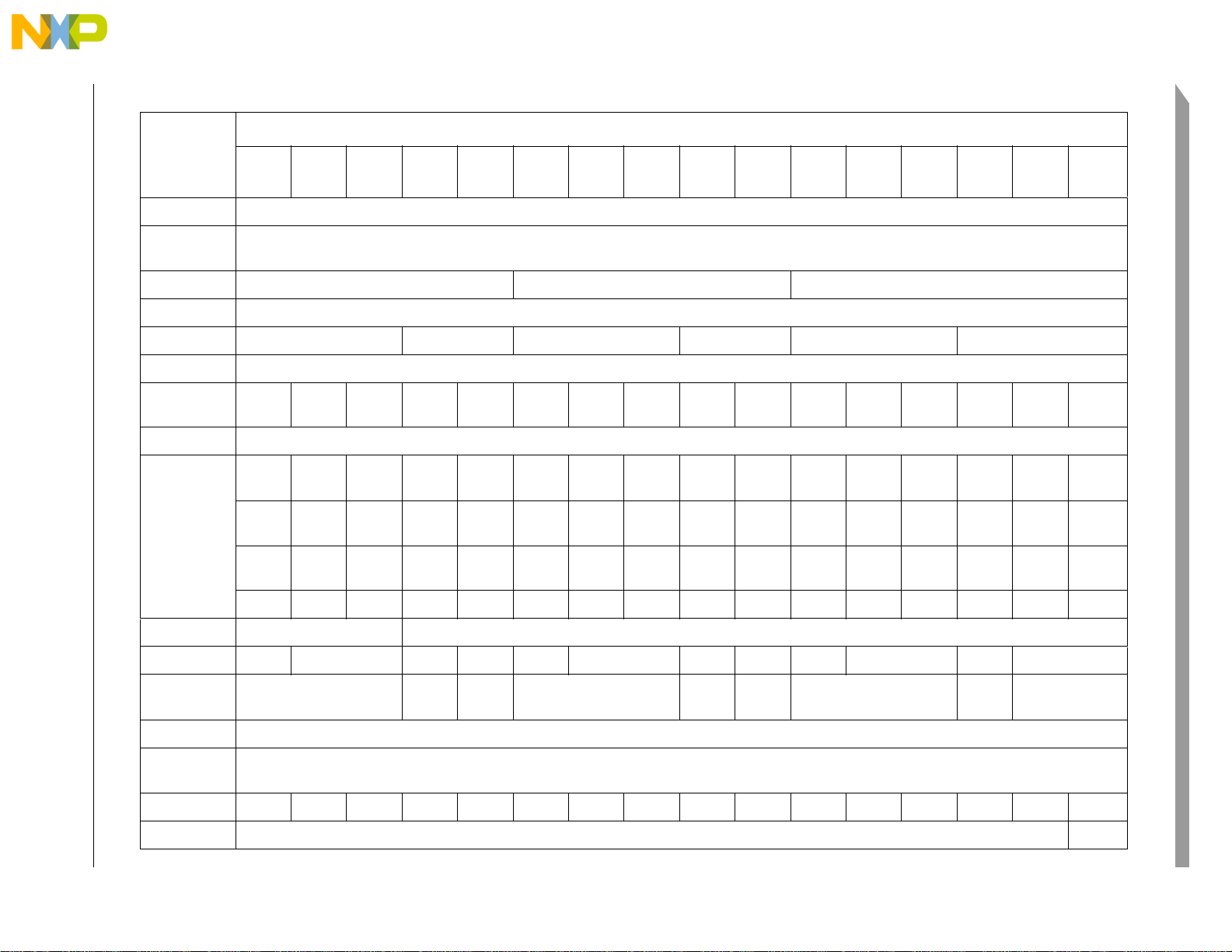
Table 2-3. MPC5604B device comparison
Device
Feature
CPU e200z0h
MPC56
02BxLH
MPC56
02BxLL
MPC56
02BxLQ
MPC56
02CxLH
MPC56
02CxLL
MPC56
03BxLH
MPC56
03BxLL
MPC56
03BxLQ
MPC56
03CxLH
MPC56
03CxLL
1
MPC56
04BxLH
MPC56
04BxLL
MPC56
04BxLQ
MPC56
04CxLH
MPC56
04CxLL
Introduction
MPC560
4BxMG
Freescale Semiconductor30
Execution
2
speed
Code Flash 256 KB 384 KB 512 KB
MPC5604B/C Microcontroller Reference Manual Rev. 8
Static – up to 64 MHz
Data Flash 64 KB (4 × 16 KB)
RAM 24KB 32KB 28KB 40KB 32KB 48 KB
MPU 8-entry
ADC 12 ch,
10-bit
28 ch,
10-bit
36 ch,
10-bit
8ch,
10-bit
28 ch,
10-bit
12 ch,
10-bit
28 ch,
10-bit
36 ch,
10-bit
8ch,
10-bit
28 ch,
10-bit
12 ch,
10-bit
28 ch,
10-bit
36 ch,
10-bit
8ch,
10-bit
CTU Ye s
3
Total timer I/O
eMIOS
• PWM + MC
+ IC/OC
• PWM +
•IC/OC
IC/OC
4
4
12 ch,
16-bit
2 ch 5 ch 10 ch 2 ch 5 ch 2 ch 5 ch 10 ch 2 ch 5 ch 2 ch 5 ch 10 ch 2 ch 5 ch 10 ch
4
10 ch 20 ch 40 ch 10 ch 20 ch 10 ch 20 ch 40 ch 10 ch 20 ch 10 ch 20 ch 40 ch 10 ch 20 ch 40 ch
0ch 3ch 6ch 0ch 3ch 0ch 3ch 6ch 0ch 3ch 0ch 3ch 6ch 0ch 3ch 6ch
SCI (LINFlex) 3
28 ch,
16-bit
5
56 ch,
16-bit
12 ch,
16-bit
28 ch,
16-bit
12 ch,
16-bit
28 ch,
16-bit
56ch,
16-bit
12 ch,
16-bit
28 ch,
16-bit
4
12 ch,
16-bit
28 ch,
16-bit
56 ch,
16-bit
12 ch,
16-bit
SPI (DSPI) 2 3 2 3 2 3 2 3 2 3 2 3
CAN
6
2
56 3
7
56 3
7
56
(FlexCAN)
28 ch,
10-bit
28 ch,
16-bit
36 ch,
10-bit
56 ch,
16-bit
I2C 1
32 kHz
Ye s
oscillator
8
GPIO
45 79 123 45 79 45 79 123 45 79 45 79 123 45 79 123
Debug JTAG Nexus2+
Page 42

Freescale Semiconductor 31
Feature
MPC56
02BxLH
MPC56
02BxLL
MPC56
02BxLQ
Table 2-3. MPC5604B device comparison1 (continued)
Device
MPC56
02CxLH
MPC56
02CxLL
MPC56
03BxLH
MPC56
03BxLL
MPC56
03BxLQ
MPC56
03CxLH
MPC56
03CxLL
MPC56
04BxLH
MPC56
04BxLL
MPC56
04BxLQ
MPC56
04CxLH
MPC56
04CxLL
MPC560
4BxMG
Package 64
1
Feature set dependent on selected peripheral multiplexing—table shows example implementation
2
MPC5604B/C Microcontroller Reference Manual Rev. 8
Based on 125 °C ambient operating temperature
3
See the eMIOS section of the device reference manual for information on the channel configuration and functions.
4
IC - Input Capture; OC - Output Compare; PWM - Pulse Width Modulation; MC - Modulus counter
5
SCI0, SCI1 and SCI2 are available. SCI3 is not available.
6
CAN0, CAN1 are available. CAN2, CAN3, CAN4 and CAN5 are not available.
7
CAN0, CAN1 and CAN2 are available. CAN3, CAN4 and CAN5 are not available.
8
I/O count based on multiplexing with peripherals
9
208 MAPBGA available only as development package for Nexus2+
LQFP
100
LQFP
144
LQFP64LQFP
100
LQFP64LQFP
100
LQFP
144
LQFP64LQFP
100
LQFP64LQFP
100
LQFP
144
LQFP64LQFP
100
LQFP
208
MAPBG
9
A
Introduction
Page 43
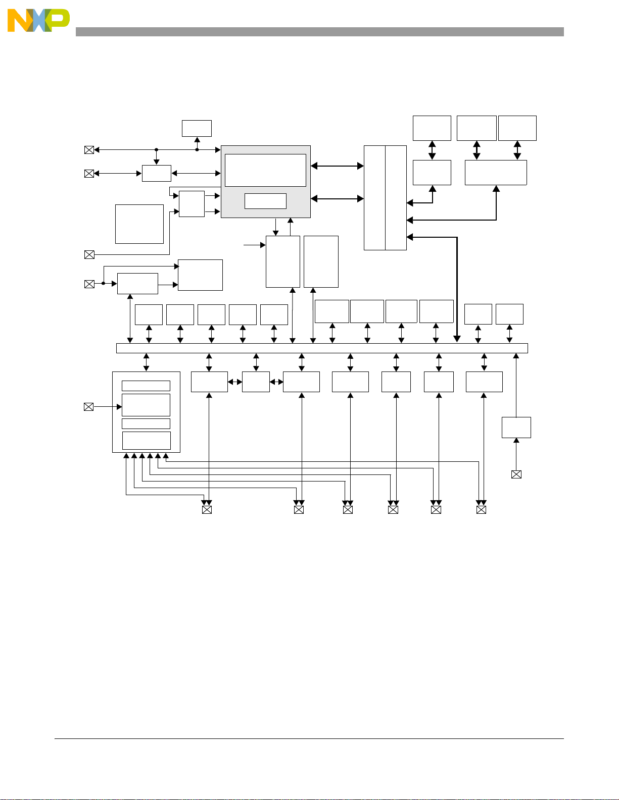
2.2.2 Block diagram
3 x
DSPI
FMPLL
Nexus 2+
Nexus
SRAM
SIUL
Reset control
48 KB
External
IMUX
GPIO and
JTAG
pad control
JTAG port
Nexus port
e200z0h
Interrupt requests
64-bit 2 x 3 Crossbar Switch
6 x
FlexCAN
Peripheral bridge
interrupt
request
Interrupt
request
I/O
Clocks
Instructions
Data
Voltage
regulator
NMI
SWT
PIT
STM
NMI
SIUL
. . .
. . .
. . .
. . .
INTC
I2C
. . .
4 x
LINFlex
2 x
eMIOS
36 Ch.
ADC
MPU
CMU
SRAM
Flash
Code Flash
512 KB
Data Flash
64 KB
MC_PCUMC_MEMC_CGMMC_RGM
BAM
CTU
RTC
SSCM
(Master)
(Master)
(Slave)
(Slave)
(Slave)
controller
controller
Legend:
ADC Analog-to-Digital Converter
BAM Boot Assist Module
FlexCAN Controller Area Network
CMU Clock Monitor Unit
CTU Cross Triggering Unit
DSPI Deserial Serial Peripheral Interface
eMIOS Enhanced Modular Input Output System
FMPLL Frequency-Modulated Phase-Locked Loop
I
2
C Inter-integrated Circuit Bus
IMUX Internal Multiplexer
INTC Interrupt Controller
JTAG JTAG controller
LINFlex Serial Communication Interface (LIN support)
ECSM Error Correction Status Module
MC_CGM Clock Generation Module
MC_ME Mode Entry Module
MC_PCU Power Control Unit
MC_RGM Reset Generation Module
MPU Memory Protection Unit
Nexus Nexus Development Interface (NDI) Level
NMI Non-Maskable Interrupt
PIT Periodic Interrupt Timer
RTC Real-Time Clock
SIUL System Integration Unit Lite
SRAM Static Random-Access Memory
SSCM System Status Configuration Module
STM System Timer Module
SWT Software Watchdog Timer
WKPU Wakeup Unit
MPU
ECSM
from peripheral
registers
blocks
WKPU
Interrupt
request with
wakeup
functionality
Figure 2-1 shows a top-level block diagram of the MPC5604B family.
32 Freescale Semiconductor
MPC5604B/C Microcontroller Reference Manual, Rev. 8
Figure 2-1. MPC5604B block diagram
Page 44

2.2.3 Chip-level features
On-chip modules available within the family include the following features:
• Single issue, 32-bit CPU core complex (e200z0)
— Compliant with the Power Architecture™ embedded category
— Includes an instruction set e nhancement allowing variable length encoding (VLE) for code size
footprint reduction. With the optional encoding of mixed 16-bit and 32-bit instructions, it is
possible to achieve significant code size footprint reduction.
• Up to 512 Kbytes on-chip Code Flash supported with the Flash controller
• Up to 64 Kbytes on-chip Data Flash supported with the Flash controller
• Up to 48 Kbytes on-chip SRAM
• Memory protection unit (MPU) with 8 region descriptors and 32-byte region granularity
• Interrupt controller (INTC) capable of handling 148 selectable-priority interrupt sources
• Frequency-modulated phase-locked loop (FMPLL)
• Crossbar switch architecture for concurrent access to peripherals, Flash, or SRAM from multiple
bus masters
• Boot assist module (BAM) supports internal Flash programming via a serial link (FlexCAN or
LINFlex)
• Timer supports input/output channels providing a range of 16-bit input capture, output compare,
and pulse width modulation functions (eMIOS)
• 10-bit analog-to-digital converter (ADC)
• Up to 3 serial peripheral interface (DSPI) modules
• Up to 4 serial communication interface (LINFlex) modules
— LINFlex 1, 2 and 3: Master capable
— LINFlex 0: Master capable and slave capable
• Up to 6 enhanced full CAN (FlexCAN) modules with 64 configurable message buffers
• 1 inter-integrated circuit (I2C) module
• Up to 123 configurable general purpose pins supporting input and output operations (package
dependent)
• Real time counter (RTC) with clock source from FIRC or SIRC supporting autonomous wake-up
with 1-ms resolution with max timeout of 2 seconds
— Support for RTC with clock source from SXOSC, supporting wake-up with 1-sec resolution
and max timeout of 1 hour
• 6 periodic interrupt timers (PIT) with 32-bit counter resolution
• 1 system module timer (STM)
• Nexus development interface (NDI) per IEEE-ISTO 5001-2003 Class Two Plus
• Device/board boundary scan testing supported with per Joint Test Action Group (JTAG) of IEEE
(IEEE 1149.1)
• On-chip voltage regulator (VREG) for regulation of input supply for all internal levels
MPC5604B/C Microcontroller Reference Manual, Rev. 8
Freescale Semiconductor 33
Page 45

2.3 Packages
MPC5604B family members are offered in the following package types:
• 64-pin LQFP, 10mm x 10mm outline
• 100-pin LQFP, 0.5mm pitch, 14mm x 14mm outline
• 144-pin LQFP, 0.5mm pitch, 20mm x 20mm outline
• 208 MAPBGA, 1mm ball pitch, 17mm x 17mm outline development package
2.4 Developer support
The MPC5604B MCU tools and third-party developers are similar to those used for the Freescale
MPC5500 product family , offering a widespread, established network of tool and software vendors. It also
features a high-performance Nexus debug interface.
The following development support is available:
• Automotive evaluation boards (EVB) featuring CAN, LIN interfaces, and more
• Compilers
• Debuggers
• JTAG and Nexus interfaces
The following software support is available:
• OSEK solutions will be available from multiple third parties
• CAN and LIN drivers
• AUTOSAR package
MPC5604B/C Microcontroller Reference Manual, Rev. 8
34 Freescale Semiconductor
Page 46
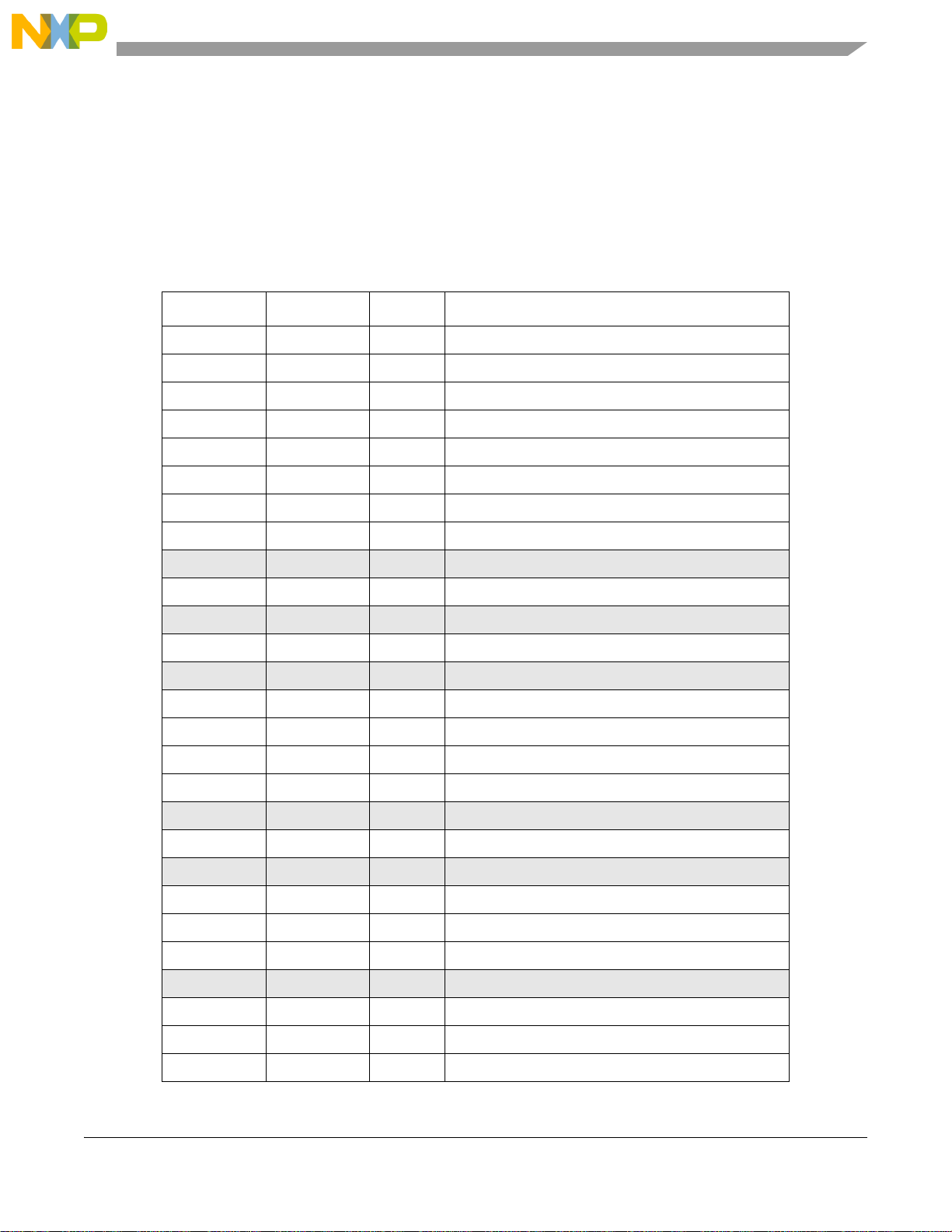
Chapter 3 Memory Map
Table 3-1 shows the memory map for the MPC5604B. All addresses on the device, including those that
are reserved, are identified in the table. The addresses represent the physical addresses assigned to each IP
block.
Table 3-1. MPC5604B memory map
Start address End address Size (KB) Region name
0x0000_0000 0x0000_7FFF 32 Code Flash Sector 0
0x0000_8000 0x0000_BFFF 16 Code Flash Sector 1
0x0000_C000 0x0000_FFFF 16 Code Flash Sector 2
0x0001_0000 0x0001_7FFF 32 Code Flash Sector 3
0x0001_8000 0x0001_FFFF 32 Code Flash Sector 4
0x0002_0000 0x0003_FFFF 128 Code Flash Sector 5
0x0004_0000 0x0005_FFFF 128 Code Flash Sector 6
0x0006_0000 0x0007_FFFF 128 Code Flash Sector 7
0x0008_0000 0x001F_FFFF 1536 Reserved
0x0020_0000 0x0020_3FFF 16 Code Flash Shadow Sector
0x0020_4000 0x003F_FFFF 2032 Reserved
0x0040_0000 0x0040_3FFF 16 Code Flash Test Sector
0x0040_4000 0x007F_FFFF 4080 Reserved
0x0080_0000 0x0080_3FFF 16 Data Flash Array 0
0x0080_4000 0x0080_7FFF 16 Data Flash Array 1
0x0080_8000 0x0080_BFFF 16 Data Flash Array 2
0x0080_C000 0x0080_FFFF 16 Data Flash Array 3
0x0081_0000 0x00BF_FFFF 4032 Reserved
0x00C0_0000 0x00C0_3FFF 16 Data test sector
0x00C0_4000 0x00DF_FFFF 4080 Reserved
0x0100_0000 0x1FFF_FFFF 507904 Flash Emulation Mapping
0x2000_0000 0x3FFF_FFFF 524288 Reserved for External Bus Interface
0x4000_0000 0x4000_BFFF 48 SRAM
0x4000_C000 0xC3F8_7FFF 2162160 Reserved
0xC3F8_8000 0xC3F8_BFFF 16 Code Flash A Configuration
0xC3F8_C000 0xC3F8_FFFF 16 Data Flash A Configuration
0xC3F9_0000 0xC3F9_3FFF 16 SIUL
MPC5604B/C Microcontroller Reference Manual, Rev. 8
Freescale Semiconductor 35
Page 47
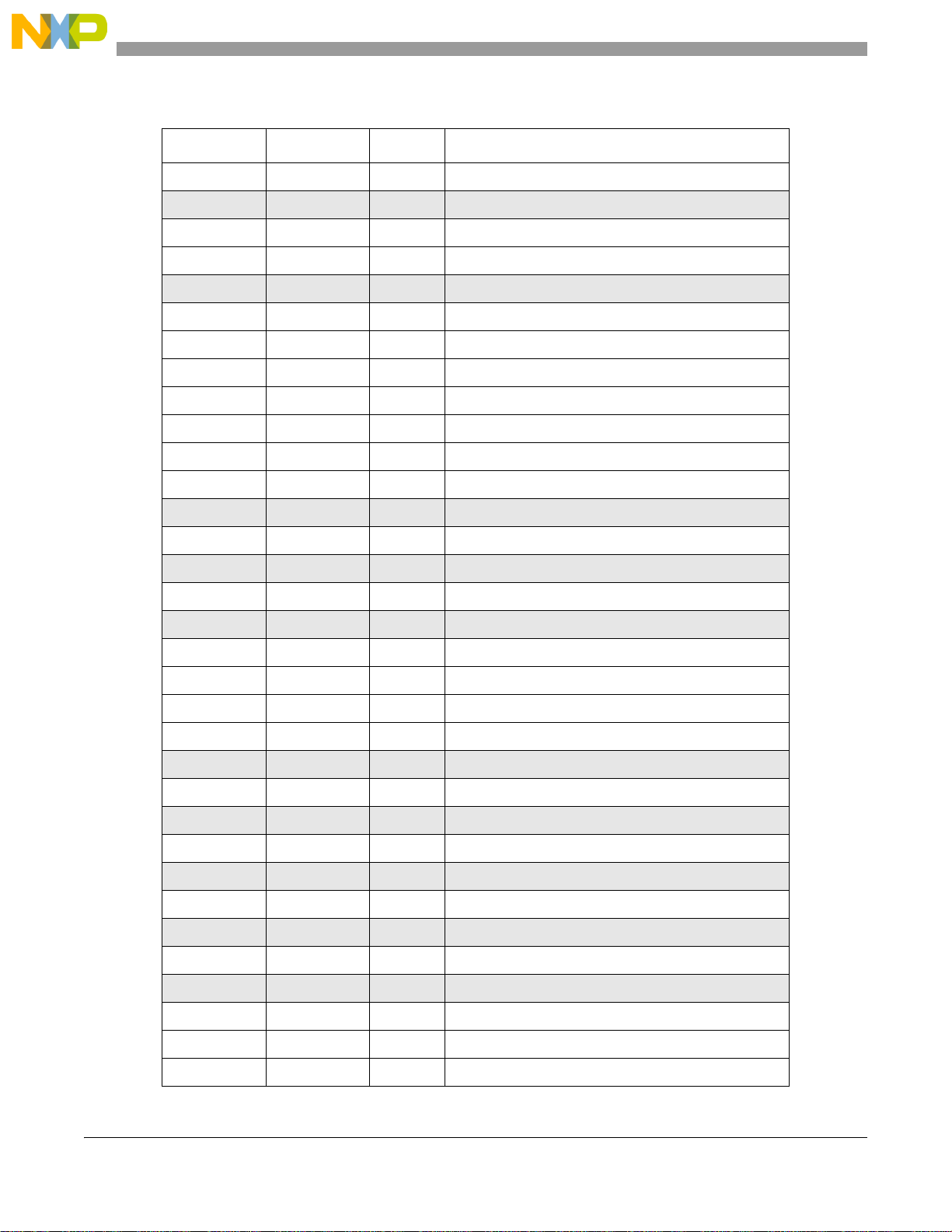
Table 3-1. MPC5604B memory map (continued)
Start address End address Size (KB) Region name
0xC3F9_4000 0xC3F9_7FFF 16 WKPU
0xC3F9_8000 0xC3F9_FFFF 32 Reserved
0xC3FA_0000 0xC3FA_3FFF 16 eMIOS_0
0xC3FA_4000 0xC3FA_7FFF 16 eMIOS_1
0xC3FA_8000 0xC3FD_7FFF 192 Reserved
0xC3FD_8000 0xC3FD_BFFF 16 SSCM
0xC3FD_C000 0xC3FD_FFFF 16 MC_ME
0xC3FE_0000 0xC3FE_3FFF 16 MC_CGM
0xC3FE_4000 0xC3FE_7FFF 16 MC_RGM
0xC3FE_8000 0xC3FE_BFFF 16 MC_PCU
0xC3FE_C000 0xC3FE_FFFF 16 RTC/API
0xC3FF_0000 0xC3FF_3FFF 16 PIT
0xC3FF4000 0xFFDF_FFFF 981040 Reserved
0xFFE0_0000 0xFFE0_3FFF 16 ADC_0
0xFFE0_4000 0xFFE2_FFFF 176 Reserved
0xFFE3_0000 0xFFE3_3FFF 16 I2C_0
0xFFE3_4000 0xFFE3_FFFF 48 Reserved
0xFFE4_0000 0xFFE4_3FFF 16 LINFlex_0
0xFFE4_4000 0xFFE4_7FFF 16 LINFlex_1
0xFFE4_8000 0xFFE4_BFFF 16 LINFlex_2
0xFFE4_C000 0xFFE4_FFFF 16 LINFlex_3
0xFFE5_0000 0xFFE6_3FFF 80 Reserved
0xFFE6_4000 0xFFE6_7FFF 16 CTU
0xFFE6_8000 0xFFE6_FFFF 32 Reserved
0xFFE7_0000 0xFFE7_3FFF 16 CAN sampler
0xFFE7_4000 0xFFE7_FFFF 48 Reserved
0xFFE8_0000 0xFFEF_FFFF 512 Mirrored range 0x3F80000–0xC3FFFFFF
0xFFF0_0000 0xFFF0_FFFF 64 Reserved
0xFFF1_0000 0xFFF1_3FFF 16 MPU
0xFFF1_4000 0xFFF3_7FFF 144 Reserved
0xFFF3_8000 0xFFF3_BFFF 16 SWT
0xFFF3_C000 0xFFF3_FFFF 16 STM
0xFFF4_0000 0xFFF4_3FFF 16 ECSM
MPC5604B/C Microcontroller Reference Manual, Rev. 8
36 Freescale Semiconductor
Page 48
Table 3-1. MPC5604B memory map (continued)
Start address End address Size (KB) Region name
0xFFF4_4000 0xFFF4_7FFF 16 Reserved
0xFFF4_8000 0xFFF4_BFFF 16 INTC
0xFFF4_C000 0xFFF8_FFFF 272 Reserved
0xFFF9_0000 0xFFF9_3FFF 16 DSPI_0
0xFFF9_4000 0xFFF9_7FFF 16 DSPI_1
0xFFF9_8000 0xFFF9_BFFF 16 DSPI_2
0xFFF9_C000 0xFFFB_FFFF 144 Reserved
0xFFFC_0000 0xFFFC_3FFF 16 FlexCAN_0
0xFFFC_4000 0xFFFC_7FFF 16 FlexCAN_1
0xFFFC_8000 0xFFFC_BFFF 16 FlexCAN_2
0xFFFC_C000 0xFFFC_FFFF 16 FlexCAN_3
0xFFFD_0000 0xFFFD_3FFF 16 FlexCAN_4
0xFFFD_4000 0xFFFD_7FFF 16 FlexCAN_5
0xFFFD_8000 0xFFFF_BFFF 144 Reserved
0xFFFF_C000 0xFFFF_FFFF 16 BAM
MPC5604B/C Microcontroller Reference Manual, Rev. 8
Freescale Semiconductor 37
Page 49

MPC5604B/C Microcontroller Reference Manual, Rev. 8
38 Freescale Semiconductor
Page 50

Chapter 4
1
2
3
4
5
6
7
8
9
10
11
12
13
14
15
16
48
47
46
45
44
43
42
41
40
39
38
37
36
35
34
33
171819202122232425
26272829303132
646362616059585756555453525150
49
PB[3]
PC[9]
PA[ 2 ]
PA[ 1 ]
PA[ 0 ]
VSS_HV
VDD_HV
VSS_HV
RESET
VSS_LV
VDD_LV
VDD_BV
PC[10]
PB[0]
PB[1]
PC[6]
PA[11]
PA[10]
PA[ 9 ]
PA[ 8 ]
PA[ 7 ]
PA[ 3 ]
PB[15]
PB[14]
PB[13]
PB[12]
PB[11]
PB[7]
PB[6]
PB[5]
VDD_HV_ADC
VSS_HV_ADC
PC[7]
PA[ 1 5 ]
PA[ 1 4 ]
PA[ 4 ]
PA[ 1 3 ]
PA[ 1 2 ]
VDD_LV
VSS_LV
XTAL
VSS_HV
EXTAL
VDD_HV
PB[9]
PB[8]
PB[10]
PB[4]
PB[2]
PC[8]
PC[4]
PC[5]
PH[9]
PC[0]
VSS_LV
VDD_LV
VDD_HV
VSS_HV
PC[1]
PH[10]
PA[ 6 ]
PA[ 5 ]
PC[2]
PC[3]
64 LQFP
Top v i e w
Signal description
4.1 Introduction
The following sections provide signal descriptions and related information about the functionality and
configuration.
4.2 Package pinouts
The LQFP pinouts and the BGA ballmap are provided in the following figures.
For more information on pin multiplexing on this device, see Table 4-1 through Table 4-4.
Figure 4-1. MPC560xB LQFP 64-pin configuration
MPC5604B/C Microcontroller Reference Manual, Rev. 8
Freescale Semiconductor 39
Page 51

Figure 4-2. MPC560xC LQFP 64-pin configuration
1
2
3
4
5
6
7
8
9
10
11
12
13
14
15
16
48
47
46
45
44
43
42
41
40
39
38
37
36
35
34
33
171819202122232425
26272829303132
646362616059585756555453525150
49
PB[3]
PC[9]
PA[ 2 ]
PA[ 1 ]
PA[ 0 ]
VSS_HV
VDD_HV
VSS_HV
RESET
VSS_LV
VDD_LV
VDD_BV
PC[10]
PB[0]
PB[1]
PC[6]
PA[11]
PA[10]
PA[ 9 ]
PA[ 8 ]
PA[ 7 ]
PF[14]
PF[15]
PG[0]
PG[1]
PA[ 3 ]
PB[15]
PB[14]
PB[11]
PB[7]
VDD_HV_ADC
VSS_HV_ADC
PC[7]
PA[15]
PA[14]
PA[ 4 ]
PA[13]
PA[12]
VDD_LV
VSS_LV
XTAL
VSS_HV
EXTAL
VDD_HV
PB[9]
PB[8]
PB[10]
PB[4]
PB[2]
PC[8]
PC[4]
PC[5]
PH[9]
PC[0]
VSS_LV
VDD_LV
VDD_HV
VSS_HV
PC[1]
PH[10]
PA[ 6 ]
PA[ 5 ]
PC[2]
PC[3]
64 LQFP
Top view
1
2
3
4
5
6
7
8
9
10
11
12
13
14
15
16
17
18
19
20
21
22
23
24
25
75
74
73
72
71
70
69
68
67
66
65
64
63
62
61
60
59
58
57
56
55
54
53
52
51
26272829303132333435363738394041424344454647484950
100
9998979695949392919089888786858483828180797877
76
PB[3]
PC[9]
PC[14]
PC[15]
PA[ 2 ]
PE[0]
PA[ 1 ]
PE[1]
PE[8]
PE[9]
PE[10]
PA[ 0 ]
PE[11]
VSS_HV
VDD_HV
VSS_HV
RESET
VSS_LV
VDD_LV
VDD_BV
PC[11]
PC[10]
PB[0]
PB[1]
PC[6]
PA[ 1 1 ]
PA[ 1 0 ]
PA[ 9 ]
PA[ 8 ]
PA[ 7 ]
VDD_HV
VSS_HV
PA[ 3 ]
PB[15]
PD[15]
PB[14]
PD[14]
PB[13]
PD[13]
PB[12]
PD[12]
PB[11]
PD[11]
PD[10]
PD[9]
PB[7]
PB[6]
PB[5]
VDD_HV_ADC
VSS_HV_ADC
PC[7]
PA[ 15 ]
PA[ 14 ]
PA[ 4 ]
PA[ 13 ]
PA[ 12 ]
VDD_LV
VSS_LV
XTAL
VSS_HV
EXTAL
VDD_HV
PB[9]
PB[8]
PB[10]
PD[0]
PD[1]
PD[2]
PD[3]
PD[4]
PD[5]
PD[6]
PD[7]
PD[8]
PB[4]
PB[2]
PC[8]
PC[13]
PC[12]
PE[7]
PE[6]
PE[5]
PE[4]
PC[4]
PC[5]
PE[3]
PE[2]
PH[9]
PC[0]
VSS_LV
VDD_LV
VDD_HV
VSS_HV
PC[1]
PH[10]
PA[ 6 ]
PA[ 5 ]
PC[2]
PC[3]
PE[12]
100 LQFP
Note:
Availability of port pin alternate functions depends on product selection.
Figure 4-3. LQFP 100-pin configuration (top view)
MPC5604B/C Microcontroller Reference Manual, Rev. 8
40 Freescale Semiconductor
Page 52

Figure 4-4. LQFP 144-pin configuration (top view)
1
2
3
4
5
6
7
8
9
10
11
12
13
14
15
16
17
18
19
20
21
22
23
24
25
26
27
28
29
30
31
32
33
34
35
36
108
107
106
105
104
103
102
101
100
99
98
97
96
95
94
93
92
91
90
89
88
87
86
85
84
83
82
81
80
79
78
77
76
75
74
73
3738394041424344454647484950515253545556575859606162636465666768697071
72
144
143
142
141
140
139
138
137
136
135
134
133
132
131
130
129
128
127
126
125
124
123
122
121
120
119
118
117
116
115
114
113
112
111
110
109
PB[3]
PC[9]
PC[14]
PC[15]
PG[5]
PG[4]
PG[3]
PG[2]
PA[ 2 ]
PE[0]
PA[ 1 ]
PE[1]
PE[8]
PE[9]
PE[10]
PA[ 0 ]
PE[11]
VSS_HV
VDD_HV
VSS_HV
RESET
VSS_LV
VDD_LV
VDD_BV
PG[9]
PG[8]
PC[11]
PC[10]
PG[7]
PG[6]
PB[0]
PB[1]
PF[9]
PF[8]
PF[12]
PC[6]
PA[11]
PA[10]
PA[ 9 ]
PA[ 8 ]
PA[ 7 ]
PE[13]
PF[14]
PF[15]
VDD_HV
VSS_HV
PG[0]
PG[1]
PH[3]
PH[2]
PH[1]
PH[0]
PG[12]
PG[13]
PA[ 3 ]
PB[15]
PD[15]
PB[14]
PD[14]
PB[13]
PD[13]
PB[12]
PD[12]
PB[11]
PD[11]
PD[10]
PD[9]
PB[7]
PB[6]
PB[5]
VDD_HV_ADC
VSS_HV_ADC
PC[7]
PF[10]
PF[11]
PA[ 1 5 ]
PF[13]
PA[ 1 4 ]
PA[ 4 ]
PA[ 1 3 ]
PA[ 1 2 ]
VDD_LV
VSS_LV
XTAL
VSS_HV
EXTAL
VDD_HV
PB[9]
PB[8]
PB[10]
PF[0]
PF[1]
PF[2]
PF[3]
PF[4]
PF[5]
PF[6]
PF[7]
PD[0]
PD[1]
PD[2]
PD[3]
PD[4]
PD[5]
PD[6]
PD[7]
PD[8]
PB[4]
PB[2]
PC[8]
PC[13]
PC[12]
PE[7]
PE[6]
PH[8]
PH[7]
PH[6]
PH[5]
PH[4]
PE[5]
PE[4]
PC[4]
PC[5]
PE[3]
PE[2]
PH[9]
PC[0]
VSS_LV
VDD_LV
VDD_HV
VSS_HV
PC[1]
PH[10]
PA[ 6 ]
PA[ 5 ]
PC[2]
PC[3]
PG[11]
PG[10]
PE[15]
PE[14]
PG[15]
PG[14]
PE[12]
144 LQFP
Note:
Availability of port pin alternate functions depends on product selection.
Freescale Semiconductor 41
MPC5604B/C Microcontroller Reference Manual, Rev. 8
Page 53
1 2 3 4 5 6 7 8 9 10111213141516
PC[8] PC[13] NC NC PH[8] PH[4] PC[5] PC[0] NC NC PC[2] NC PE[15] NC NC NC
A
PC[9] PB[2] NC PC[12] PE[6] PH[5] PC[4] PH[9] PH[10] N C PC[3] PG[11] PG[15] PG[14] PA[11] PA[10]
B
PC[14] VDD_HV PB[3] PE[7] PH[7] PE[5] PE[3] VSS_LV PC[1] NC PA[5] NC PE[14] PE[12] PA[9] PA[8]
C
NC NC PC[15] NC PH[6] PE[4] PE [2] VDD_LV VDD_HV NC PA[6] NC PG[10] PF[14] PE[13] PA[7]
D
PG[4] PG[5] PG[3] PG[2] PG[1] PG[0] PF[15] VDD_HV
E
PE[0] PA[2] PA[1] PE[1] PH[0] PH[1] PH[3] PH[2]
F
PE[9] PE[8] PE[10] PA[0] VSS_HV VSS_HV VSS_HV VSS_HV VDD_HV NC NC MSEO
G
VSS_HV PE[11] VDD_HV NC VSS_HV VSS_HV VSS_HV VSS_HV MDO3 MDO2 MDO0 MDO1
H
RESET VSS_LV NC NC VSS_HV VSS_HV VSS_HV VSS_HV NC NC NC NC
J
EVTI NC VDD_BV VDD_LV VSS_HV VSS_HV VSS_HV VSS_HV NC PG[12] PA[3] PG[13]
K
PG[9] PG[8] NC EVTO PB[15] PD[15] PD[14] PB[14]
L
PG[7] PG[6] PC[10] PC[11] PB[13] PD[13] PD[12] PB[12]
M
PB[1] P F[9] PB[0] NC NC PA[4] VSS_LV EXTAL VDD_HV PF[0] PF[4] NC PB[11] PD[10] PD[9] PD[11]
N
PF[8] NC PC[7] NC NC PA[14] VDD_LV XTAL PB[10] PF[1] PF[5] PD[0] PD[3]
P
PF[12] PC[6] PF[10] PF[11] VDD_HV PA[15] PA[13] NC
R
NC NC NC MCKO NC PF[13] PA[12] NC
T
OSC32K
_XTAL
OSC32K
_EXTAL
PF[3] PF[7] PD[2] PD[4] PD[7]
PF[2] PF[6] PD[1] PD[5] PD[6] PD[8] PB[4]
VDD_HV
_ADC
PB[6] PB[7]
VSS_HV
_ADC
PB[5]
A
B
C
D
E
F
G
H
J
K
L
M
N
P
R
T
1 2 3 4 5 6 7 8 9 10111213141516
Note: 208 MAPBGA available only as development package for Nexus 2+.
NC
= Not connected
Figure 4-5. 208 MAPBGA configuration
4.3 Pad configuration during reset phases
All pads have a fixed configuration under reset.
During the power-up phase, all pads are forced to tristate.
After power-up phase, all pads are forced to tristate with the following exceptions:
• PA[9] (FAB) is pull-down. Without external strong pull-up the device starts fetching from flash.
• PA[8] (ABS[0]) is pull-up.
• RESET pad is driven low. This is pull-up only after PHASE2 reset completion.
• JTAG pads (TCK, TMS and TDI) are pull-up whilst TDO remains tristate.
• Precise ADC pads (PB[7:4] and PD[11:0]) are left tristate (no output buffer available).
MPC5604B/C Microcontroller Reference Manual, Rev. 8
42 Freescale Semiconductor
Page 54

• Main oscillator pads (EXTAL, XTAL) are tristate.
• Nexus output pads (MDO[n], MCKO, EVTO, MSEO) are forced to output.
4.4 Voltage supply pins
Voltage supply pins are used to provide power to the device. Two dedicated pins are used for 1.2 V
regulator stabilization.
Table 4-1. Voltage supply pin descriptions
Pin number
Port pin Function
64 LQFP
1
100 LQFP 144 LQFP
208
MAPBGA
2
VDD_HV Digital supply voltage 7, 28, 56 15, 37, 70, 8419, 51, 100,
123
VSS_HV Digital ground 6, 8, 26, 55 14, 16, 35,
69, 83
VDD_LV 1.2V decoupling pins. Decoupling
capacitor must be connected between
these pins and the nearest V
VSS_LV 1.2V decoupling pins. Decoupling
capacitor must be connected between
these pins and the nearest V
VDD_BV Internal regulator supply voltage 12 20 24 K3
VSS_HV_ADCReference ground and analog ground for
the ADC
VDD_HV_ADCReference voltage and analog supply for
the ADC
1
Pin numbers apply to both the MPC560xB and MPC560xC packages.
2
208 MAPBGA available only as development package for Nexus2+
3
A decoupling capacitor must be placed between each of the three VDD_LV/VSS_LV supply pairs to ensure stable
voltage (see the recommended operating conditions in the device datasheet for details).
SS_LV
DD_LV
pin.
pin.
11, 23, 57 19, 32, 85 23, 46, 124 D8, K4, P7
3
10, 24, 58 18, 33, 86 22, 47, 125 C8, J2, N7
3
33 51 73 R15
34 52 74 P14
18, 20, 49,
99, 122
C2, D9, E16,
G13, H3, N9,
R5
G7, G8, G9,
G10, H1, H7,
H8, H9, H10,
J7, J8, J9,
J10, K7, K8,
K9, K10
4.5 Pad types
In the device the following types of pads are available for system pins and functional port pins:
S = Slow
M = Medium1
1. See the I/O pad electrical characteristics in the device datasheet for details.
2. All medium and fast pads are in slow configuration by default at reset and can be configured as fast or medium (see PCR.SRC
in Section 19.5.3.8, “Pad Configuration Registers (PCR0–PCR122)).
Freescale Semiconductor 43
1
2
MPC5604B/C Microcontroller Reference Manual, Rev. 8
Page 55

F = Fast1
2
I = Input only with analog feature
J = Input/Output with analog feature
X = Oscillator
4.6 System pins
The system pins are listed in Table 4-2.
Table 4-2. System pin descriptions
System
pin
RESET
Bidirectional reset with Schmitt-Trigger
characteristics and noise filter.
Function
1
Pin number
I/O
directio
I/O M Input, weak
Pad
n
typ
e
RESET
config.
pull-up
only after
PHASE2
1
64 LQFP
100 LQFP
91721J1
2
144 LQFP
208 MAPBGA
EXTAL Analog output of the oscillator amplifier
circuit, when the oscillator is not in bypass
mode.
Analog input for the clock generator when the
oscillator is in bypass mode.
XTAL Analog input of the oscillator amplifier circuit.
Needs to be grounded if oscillator is used in
bypass mode.
1
Pin numbers apply to both the MPC560xB and MPC560xC packages.
2
208 MAPBGA available only as development package for Nexus2+
3
See the relevant section of the datasheet
3
3
4.7 Functional ports
The functional port pins are listed in Table 4-3.
I/O X Tristate 27 36 50 N8
I X Tristate 25 34 48 P8
MPC5604B/C Microcontroller Reference Manual, Rev. 8
44 Freescale Semiconductor
Page 56

Table 4-3. Functional port pin descriptions
1
Port pin
PCR
PA[0] PCR[0] AF0
AF1
AF2
AF3
—
PA[1] PCR[1] AF0
AF1
AF2
AF3
—
—
PA[2] PCR[2] AF0
AF1
AF2
AF3
—
Function
Alternate function
GPIO[0]
E0UC[0]
CLKOUT
—
WKUP[19]
GPIO[1]
E0UC[1]
—
—
5
NMI
WKUP[2]
4
GPIO[2]
E0UC[2]
—
—
WKUP[3]
4
Pin number
2
Peripheral
Pad type
I/O direction
100 LQFP
RESET configuration
MPC560xB 64 LQFP
MPC560xC 64 LQFP
SIUL
eMIOS_0
CGL
4
—
WKPU
SIUL
eMIOS_0
—
—
WKPU
WKPU
SIUL
eMIOS_0
—
—
WKPU
I/O
M Tristate 5 5 12 16 G4
I/O
O
—
I
I/O
S Tristate 44711F3
I/O
—
—
I
I
I/O
S Tristate 3359F2
I/O
—
—
I
3
144 LQFP
208 MAPBGA
PA[3] PCR[3] AF0
AF1
AF2
AF3
—
PA[4] PCR[4] AF0
AF1
AF2
AF3
—
PA[5] PCR[5] AF0
AF1
AF2
AF3
PA[6] PCR[6] AF0
AF1
AF2
AF3
—
PA[7] PCR[7] AF0
AF1
AF2
AF3
—
GPIO[3]
E0UC[3]
—
—
EIRQ[0]
GPIO[4]
E0UC[4]
—
—
WKUP[9]
GPIO[5]
E0UC[5]
—
—
GPIO[6]
E0UC[6]
—
—
EIRQ[1]
GPIO[7]
E0UC[7]
LIN3TX
—
EIRQ[2]
SIUL
eMIOS_0
—
—
SIUL
SIUL
eMIOS_0
—
4
—
WKPU
SIUL
eMIOS_0
—
—
SIUL
eMIOS_0
—
—
SIUL
SIUL
eMIOS_0
LINFlex_3
—
SIUL
I/O
S Tristate 43396890K15
I/O
—
—
I
I/O
S Tristate 20202943N6
I/O
—
—
I
I/O
M Tristate 515179118C11
I/O
—
—
I/O
S Tristate 525280119D11
I/O
—
—
I
I/O
S Tristate 444471104D16
I/O
O
—
I
MPC5604B/C Microcontroller Reference Manual, Rev. 8
Freescale Semiconductor 45
Page 57

Table 4-3. Functional port pin descriptions (continued)
1
Port pin
PCR
PA[8] PCR[8] AF0
AF1
AF2
AF3
—
N/A
6
—
PA[9] PCR[9] AF0
AF1
AF2
AF3
N/A
6
PA [1 0] P C R[ 1 0 ] A F 0
AF1
AF2
AF3
Function
Alternate function
GPIO[8]
E0UC[8]
—
—
EIRQ[3]
ABS[0]
LIN3RX
GPIO[9]
E0UC[9]
—
—
FAB
GPIO[10]
E0UC[10]
SDA
—
Peripheral
SIUL
eMIOS_0
—
—
SIUL
BAM
LINFlex_3
SIUL
eMIOS_0
—
—
BAM
SIUL
eMIOS_0
I2C_0
—
Pin number
2
Pad type
I/O direction
100 LQFP
RESET configuration
MPC560xB 64 LQFP
MPC560xC 64 LQFP
I/O
S Input, weak
I/O
pull-up
45 45 72 105 C16
—
—
I
I
I
I/O
S Pull-down 46 46 73 106 C15
I/O
—
—
I
I/O
S Tristate 474774107B16
I/O
I/O
—
3
144 LQFP
208 MAPBGA
PA [1 1] P C R[ 1 1 ] A F 0
AF1
AF2
AF3
PA [1 2] P C R[ 1 2 ] A F 0
AF1
AF2
AF3
—
PA [1 3] P C R[ 1 3 ] A F 0
AF1
AF2
AF3
PA [1 4] P C R[ 1 4 ] A F 0
AF1
AF2
AF3
—
GPIO[11]
E0UC[11]
SCL
—
GPIO[12]
—
—
—
SIN_0
GPIO[13]
SOUT_0
—
—
GPIO[14]
SCK_0
CS0_0
—
EIRQ[4]
SIUL
eMIOS_0
I2C_0
—
SIUL
—
—
—
DSPI0
SIUL
DSPI_0
—
—
SIUL
DSPI_0
DSPI_0
—
SIUL
I/O
S Tristate 484875108B15
I/O
I/O
—
I/O
S Tristate 22223145T7
—
—
—
I
I/O
M Tristate 21213044R7
O
—
—
I/O
M Tristate 19192842P6
I/O
I/O
—
I
MPC5604B/C Microcontroller Reference Manual, Rev. 8
46 Freescale Semiconductor
Page 58

Table 4-3. Functional port pin descriptions (continued)
1
Port pin
PCR
PA [1 5] P C R[ 1 5 ] A F 0
AF1
AF2
AF3
—
PB[0] PCR[16] AF0
AF1
AF2
AF3
PB[1] PCR[17] AF0
AF1
AF2
AF3
—
—
Function
Alternate function
GPIO[15]
CS0_0
SCK_0
—
WKUP[10]
GPIO[16]
CAN0TX
—
—
GPIO[17]
—
—
—
WKUP[4]
4
CAN0RX
4
Peripheral
SIUL
DSPI_0
DSPI_0
—
WKPU
SIUL
FlexCAN_0
—
—
SIUL
—
—
—
WKPU
FlexCAN_0
Pin number
2
Pad type
I/O direction
100 LQFP
RESET configuration
MPC560xB 64 LQFP
MPC560xC 64 LQFP
I/O
M Tristate 18182740R6
I/O
I/O
—
I
I/O
M Tristate 14142331N3
O
—
—
I/O
S Tristate 15152432N1
—
—
—
I
I
3
144 LQFP
208 MAPBGA
PB[2] PCR[18] AF0
AF1
AF2
AF3
PB[3] PCR[19] AF0
AF1
AF2
AF3
—
—
PB[4] PCR[20] AF0
AF1
AF2
AF3
—
PB[5] PCR[21] AF0
AF1
AF2
AF3
—
PB[6] PCR[22] AF0
AF1
AF2
AF3
—
GPIO[18]
LIN0TX
SDA
—
GPIO[19]
—
SCL
—
WKUP[11]
LIN0RX
GPIO[20]
—
—
—
GPI[0]
GPIO[21]
—
—
—
GPI[1]
GPIO[22]
—
—
—
GPI[2]
4
SIUL
LINFlex_0
I2C_0
—
SIUL
—
I2C_0
—
WKPU
LINFlex_0
SIUL
—
—
—
ADC
SIUL
—
—
—
ADC
SIUL
—
—
—
ADC
I/O
M Tristate 64 64 100 144 B2
O
I/O
—
I/O
S Tristate 1111C3
—
I/O
—
I
I
I
I Tristate 32325072T16
—
—
—
I
I
I Tristate 35 — 53 75 R16
—
—
—
I
I
I Tristate 36 — 54 76 P15
—
—
—
I
MPC5604B/C Microcontroller Reference Manual, Rev. 8
Freescale Semiconductor 47
Page 59

Table 4-3. Functional port pin descriptions (continued)
1
Port pin
PCR
PB[7] PCR[23] AF0
AF1
AF2
AF3
—
PB[8] PCR[24] AF0
AF1
AF2
AF3
—
—
PB[9] PCR[25] AF0
AF1
AF2
AF3
—
—
Function
Alternate function
GPIO[23]
—
—
—
GPI[3]
GPIO[24]
—
—
—
ANS[0]
OSC32K_XTAL
GPIO[25]
—
—
—
ANS[1]
OSC32K_EXTAL
7
7
Peripheral
SIUL
—
—
—
ADC
SIUL
—
—
—
ADC
SXOSC
SIUL
—
—
—
ADC
SXOSC
Pin number
2
Pad type
I/O direction
100 LQFP
RESET configuration
MPC560xB 64 LQFP
MPC560xC 64 LQFP
I
I Tristate 37355577P16
—
—
—
I
I
I Tristate 30303953R9
—
—
—
I
I/O
I
I Tristate 29293852T9
—
—
—
I
I/O
3
144 LQFP
208 MAPBGA
PB[10] PCR[26] AF0
AF1
AF2
AF3
—
—
8
PB[11]
PCR[27] AF0
AF1
AF2
AF3
—
PB[12] PCR[28] AF0
AF1
AF2
AF3
—
PB[13] PCR[29] AF0
AF1
AF2
AF3
—
GPIO[26]
—
—
—
ANS[2]
WKUP[8]
GPIO[27]
E0UC[3]
—
CS0_0
ANS[3]
GPIO[28]
E0UC[4]
—
CS1_0
ANX[0]
GPIO[29]
E0UC[5]
—
CS2_0
ANX[1]
SIUL
—
—
—
4
ADC
WKPU
SIUL
eMIOS_0
—
DSPI_0
ADC
SIUL
eMIOS_0
—
DSPI_0
ADC
SIUL
eMIOS_0
—
DSPI_0
ADC
I/O
J Tristate 31314054P9
—
—
—
I
I
I/O
J Tristate 38365981N13
I/O
—
I/O
I
I/O
J Tristate 39 — 61 83 M1
I/O
—
O
I
I/O
J Tristate 40 — 63 85 M1
I/O
—
O
I
6
3
MPC5604B/C Microcontroller Reference Manual, Rev. 8
48 Freescale Semiconductor
Page 60

Table 4-3. Functional port pin descriptions (continued)
1
Port pin
PCR
PB[14] PCR[30] AF0
AF1
AF2
AF3
—
PB[15] PCR[31] AF0
AF1
AF2
AF3
—
9
PC[0]
PCR[32] AF0
AF1
AF2
AF3
9
PC[1]
PCR[33] AF0
AF1
AF2
AF3
Function
Alternate function
GPIO[30]
E0UC[6]
—
CS3_0
ANX[2]
GPIO[31]
E0UC[7]
—
CS4_0
ANX[3]
GPIO[32]
—
TDI
—
GPIO[33]
—
10
TDO
—
Peripheral
SIUL
eMIOS_0
—
DSPI_0
ADC
SIUL
eMIOS_0
—
DSPI_0
ADC
SIUL
—
JTAGC
—
SIUL
—
JTAGC
—
Pin number
2
Pad type
I/O direction
100 LQFP
RESET configuration
MPC560xB 64 LQFP
MPC560xC 64 LQFP
I/O
J Tristate 41376587L16
I/O
—
O
I
I/O
J Tristate 42386789L13
I/O
—
O
I
I/O
M Input, weak
—
pull-up
59 59 87 126 A8
I
—
I/O
M Tristate 545482121C9
—
O
—
3
144 LQFP
208 MAPBGA
PC[2] PCR[34] AF0
AF1
AF2
AF3
—
PC[3] PCR[35] AF0
AF1
AF2
AF3
—
—
—
PC[4] PCR[36] AF0
AF1
AF2
AF3
—
—
GPIO[34]
SCK_1
CAN4TX
—
EIRQ[5]
GPIO[35]
CS0_1
MA[0]
—
CAN1RX
CAN4RX
EIRQ[6]
GPIO[36]
—
—
—
SIN_1
CAN3RX
11
SIUL
DSPI_1
LINFlex_4
—
SIUL
SIUL
DSPI_1
ADC
—
11
FlexCAN_1
FlexCAN_4
SIUL
SIUL
—
—
—
11
DSPI_1
FlexCAN_3
I/O
M Tristate 505078117A11
I/O
O
—
I
I/O
S Tristate 494977116B11
I/O
O
—
I
I
I
I/O
M Tristate 626292131B7
—
—
—
I
I
MPC5604B/C Microcontroller Reference Manual, Rev. 8
Freescale Semiconductor 49
Page 61

Table 4-3. Functional port pin descriptions (continued)
1
Port pin
PCR
PC[5] PCR[37] AF0
AF1
AF2
AF3
—
PC[6] PCR[38] AF0
AF1
AF2
AF3
PC[7] PCR[39] AF0
AF1
AF2
AF3
—
—
Function
Alternate function
GPIO[37]
SOUT_1
CAN3TX
11
—
EIRQ[7]
GPIO[38]
LIN1TX
—
—
GPIO[39]
—
—
—
LIN1RX
WKUP[12]
4
Peripheral
SIUL
DSPI1
FlexCAN_3
—
SIUL
SIUL
LINFlex_1
—
—
SIUL
—
—
—
LINFlex_1
WKPU
Pin number
2
Pad type
I/O direction
100 LQFP
RESET configuration
MPC560xB 64 LQFP
MPC560xC 64 LQFP
I/O
M Tristate 616191130A7
O
O
—
I
I/O
S Tristate 16162536R2
O
—
—
I/O
S Tristate 17172637P3
—
—
—
I
I
3
144 LQFP
208 MAPBGA
PC[8] PCR[40] AF0
AF1
AF2
AF3
PC[9] PCR[41] AF0
AF1
AF2
AF3
—
—
PC[10] PCR[42] AF0
AF1
AF2
AF3
PC[11] PCR[43] AF0
AF1
AF2
AF3
—
—
—
GPIO[40]
LIN2TX
—
—
GPIO[41]
—
—
—
LIN2RX
WKUP[13]
GPIO[42]
CAN1TX
CAN4TX
MA[1]
GPIO[43]
—
—
—
CAN1RX
CAN4RX
WKUP[5]
11
SIUL
LINFlex_2
—
—
SIUL
—
—
—
LINFlex_2
4
WKPU
SIUL
FlexCAN_1
FlexCAN_4
ADC
SIUL
—
—
—
4
FlexCAN_1
FlexCAN_4
WKPU
11
I/O
S Tristate 636399143A1
O
—
—
I/O
S Tristate 2222B1
—
—
—
I
I
I/O
M Tristate 13132228M3
O
O
O
I/O
S Tristate — — 21 27 M4
—
—
—
I
I
I
MPC5604B/C Microcontroller Reference Manual, Rev. 8
50 Freescale Semiconductor
Page 62

Table 4-3. Functional port pin descriptions (continued)
1
Port pin
PCR
PC[12] PCR[44] AF0
AF1
AF2
AF3
—
PC[13] PCR[45] AF0
AF1
AF2
AF3
PC[14] PCR[46] AF0
AF1
AF2
AF3
—
PC[15] PCR[47] AF0
AF1
AF2
AF3
Function
Alternate function
GPIO[44]
E0UC[12]
—
—
SIN_2
GPIO[45]
E0UC[13]
SOUT_2
—
GPIO[46]
E0UC[14]
SCK_2
—
EIRQ[8]
GPIO[47]
E0UC[15]
CS0_2
—
Peripheral
SIUL
eMIOS_0
—
—
DSPI_2
SIUL
eMIOS_0
DSPI_2
—
SIUL
eMIOS_0
DSPI_2
—
SIUL
SIUL
eMIOS_0
DSPI_2
—
Pin number
2
Pad type
I/O direction
RESET configuration
MPC560xB 64 LQFP
MPC560xC 64 LQFP
I/O
M Tristate — — 97 141 B4
I/O
—
—
I
I/O
S Tristate — — 98 142 A2
I/O
O
—
I/O
S Tristate — — 3 3 C1
I/O
I/O
—
I
I/O
M Tristate — — 4 4 D3
I/O
I/O
—
100 LQFP
3
144 LQFP
208 MAPBGA
PD[0] PCR[48] AF0
AF1
AF2
AF3
—
PD[1] PCR[49] AF0
AF1
AF2
AF3
—
PD[2] PCR[50] AF0
AF1
AF2
AF3
—
PD[3] PCR[51] AF0
AF1
AF2
AF3
—
GPIO[48]
—
—
—
GPI[4]
GPIO[49]
—
—
—
GPI[5]
GPIO[50]
—
—
—
GPI[6]
GPIO[51]
—
—
—
GPI[7]
SIUL
—
—
—
ADC
SIUL
—
—
—
ADC
SIUL
—
—
—
ADC
SIUL
—
—
—
ADC
I
ITristate——4163P12
—
—
—
I
I
ITristate——4264T12
—
—
—
I
I
ITristate——4365R12
—
—
—
I
I
ITristate——4466P13
—
—
—
I
MPC5604B/C Microcontroller Reference Manual, Rev. 8
Freescale Semiconductor 51
Page 63

Table 4-3. Functional port pin descriptions (continued)
1
Port pin
PCR
PD[4] PCR[52] AF0
AF1
AF2
AF3
—
PD[5] PCR[53] AF0
AF1
AF2
AF3
—
PD[6] PCR[54] AF0
AF1
AF2
AF3
—
Function
Alternate function
GPIO[52]
—
—
—
GPI[8]
GPIO[53]
—
—
—
GPI[9]
GPIO[54]
—
—
—
GPI[10]
SIUL
—
—
—
ADC
SIUL
—
—
—
ADC
SIUL
—
—
—
ADC
Pin number
2
Peripheral
Pad type
I/O direction
100 LQFP
RESET configuration
MPC560xB 64 LQFP
MPC560xC 64 LQFP
I
ITristate——4567R13
3
144 LQFP
208 MAPBGA
—
—
—
I
I
ITristate——4668T13
—
—
—
I
I
ITristate——4769T14
—
—
—
I
PD[7] PCR[55] AF0
AF1
AF2
AF3
—
PD[8] PCR[56] AF0
AF1
AF2
AF3
—
PD[9] PCR[57] AF0
AF1
AF2
AF3
—
PD[10] PCR[58] AF0
AF1
AF2
AF3
—
PD[11] PCR[59] AF0
AF1
AF2
AF3
—
GPIO[55]
—
—
—
GPI[11]
GPIO[56]
—
—
—
GPI[12]
GPIO[57]
—
—
—
GPI[13]
GPIO[58]
—
—
—
GPI[14]
GPIO[59]
—
—
—
GPI[15]
SIUL
—
—
—
ADC
SIUL
—
—
—
ADC
SIUL
—
—
—
ADC
SIUL
—
—
—
ADC
SIUL
—
—
—
ADC
I
ITristate——4870R14
—
—
—
I
I
ITristate——4971T15
—
—
—
I
I
ITristate——5678N15
—
—
—
I
I
ITristate——5779N14
—
—
—
I
I
ITristate——5880N16
—
—
—
I
MPC5604B/C Microcontroller Reference Manual, Rev. 8
52 Freescale Semiconductor
Page 64

Table 4-3. Functional port pin descriptions (continued)
1
Port pin
PCR
PD[12]8PCR[60] AF0
AF1
AF2
AF3
—
PD[13] PCR[61] AF0
AF1
AF2
AF3
—
PD[14] PCR[62] AF0
AF1
AF2
AF3
—
Function
Alternate function
GPIO[60]
CS5_0
E0UC[24]
—
ANS[4]
GPIO[61]
CS0_1
E0UC[25]
—
ANS[5]
GPIO[62]
CS1_1
E0UC[26]
—
ANS[6]
Peripheral
SIUL
DSPI_0
eMIOS_0
—
ADC
SIUL
DSPI_1
eMIOS_0
—
ADC
SIUL
DSPI_1
eMIOS_0
—
ADC
Pin number
2
Pad type
I/O direction
RESET configuration
MPC560xB 64 LQFP
MPC560xC 64 LQFP
I/O
J Tristate — — 60 82 M1
O
I/O
—
I
I/O
J Tristate — — 62 84 M1
I/O
I/O
—
I
I/O
J Tristate — — 64 86 L15
O
I/O
—
I
100 LQFP
3
144 LQFP
208 MAPBGA
5
4
PD[15] PCR[63] AF0
AF1
AF2
AF3
—
PE[0] PCR[64] AF0
AF1
AF2
AF3
—
—
PE[1] PCR[65] AF0
AF1
AF2
AF3
PE[2] PCR[66] AF0
AF1
AF2
AF3
—
PE[3] PCR[67] AF0
AF1
AF2
AF3
GPIO[63]
CS2_1
E0UC[27]
—
ANS[7]
GPIO[64]
E0UC[16]
—
—
CAN5RX
WKUP[6]
GPIO[65]
E0UC[17]
CAN5TX
—
GPIO[66]
E0UC[18]
—
—
SIN_1
GPIO[67]
E0UC[19]
SOUT_1
—
11
SIUL
DSPI_1
eMIOS_0
—
ADC
SIUL
eMIOS_0
—
11
4
—
FlexCAN_5
WKPU
SIUL
eMIOS_0
FlexCAN_5
—
SIUL
eMIOS_0
—
—
DSPI_1
SIUL
eMIOS_0
DSPI_1
—
I/O
J Tristate — — 66 88 L14
O
I/O
—
I
I/O
STristate——610F1
I/O
—
—
I
I
I/O
MTristate——812F4
I/O
O
—
I/O
M Tristate — — 89 128 D7
I/O
—
—
I
I/O
M Tristate — — 90 129 C7
I/O
O
—
MPC5604B/C Microcontroller Reference Manual, Rev. 8
Freescale Semiconductor 53
Page 65

Table 4-3. Functional port pin descriptions (continued)
1
Port pin
PCR
PE[4] PCR[68] AF0
AF1
AF2
AF3
—
PE[5] PCR[69] AF0
AF1
AF2
AF3
PE[6] PCR[70] AF0
AF1
AF2
AF3
PE[7] PCR[71] AF0
AF1
AF2
AF3
Function
Alternate function
GPIO[68]
E0UC[20]
SCK_1
—
EIRQ[9]
GPIO[69]
E0UC[21]
CS0_1
MA[2]
GPIO[70]
E0UC[22]
CS3_0
MA[1]
GPIO[71]
E0UC[23]
CS2_0
MA[0]
Peripheral
SIUL
eMIOS_0
DSPI_1
—
SIUL
SIUL
eMIOS_0
DSPI_1
ADC
SIUL
eMIOS_0
DSPI_0
ADC
SIUL
eMIOS_0
DSPI_0
ADC
Pin number
2
Pad type
I/O direction
RESET configuration
MPC560xB 64 LQFP
MPC560xC 64 LQFP
I/O
M Tristate — — 93 132 D6
I/O
I/O
—
I
I/O
M Tristate — — 94 133 C6
I/O
I/O
O
I/O
M Tristate — — 95 139 B5
I/O
O
O
I/O
M Tristate — — 96 140 C4
I/O
O
O
100 LQFP
3
144 LQFP
208 MAPBGA
PE[8] PCR[72] AF0
AF1
AF2
AF3
PE[9] PCR[73] AF0
AF1
AF2
AF3
—
—
—
PE[10] PCR[74] AF0
AF1
AF2
AF3
—
PE[11] PCR[75] AF0
AF1
AF2
AF3
—
—
GPIO[72]
CAN2TX
E0UC[22]
CAN3TX
GPIO[73]
—
E0UC[23]
—
WKUP[7]
CAN2RX
CAN3RX
GPIO[74]
LIN3TX
CS3_1
—
EIRQ[10]
GPIO[75]
—
CS4_1
—
LIN3RX
WKUP[14]
12
11
SIUL
FlexCAN_2
eMIOS_0
FlexCAN_3
SIUL
—
eMIOS_0
4
12
11
—
WKPU
FlexCAN_2
FlexCAN_3
SIUL
LINFlex_3
DSPI_1
—
SIUL
SIUL
—
DSPI_1
—
LINFlex_3
4
WKPU
I/O
MTristate——913G2
O
I/O
O
I/O
S Tristate — — 10 14 G1
—
I/O
—
I
I
I
I/O
S Tristate — — 11 15 G3
O
O
—
I
I/O
S Tristate — — 13 17 H2
—
O
—
I
I
MPC5604B/C Microcontroller Reference Manual, Rev. 8
54 Freescale Semiconductor
Page 66

Table 4-3. Functional port pin descriptions (continued)
1
Port pin
PCR
PE[12] PCR[76] AF0
AF1
AF2
AF3
—
—
PE[13] PCR[77] AF0
AF1
AF2
AF3
PE[14] PCR[78] AF0
AF1
AF2
AF3
—
Function
Alternate function
GPIO[76]
—
E1UC[19]
13
—
SIN_2
EIRQ[11]
GPIO[77]
SOUT2
E1UC[20]
—
GPIO[78]
SCK_2
E1UC[21]
—
EIRQ[12]
Peripheral
SIUL
—
eMIOS_1
—
DSPI_2
SIUL
SIUL
DSPI_2
eMIOS_1
—
SIUL
DSPI_2
eMIOS_1
—
SIUL
Pin number
2
Pad type
I/O direction
RESET configuration
MPC560xB 64 LQFP
MPC560xC 64 LQFP
I/O
S Tristate — — 76 109 C14
—
I/O
—
I
I
I/O
S Tristate — — — 103 D15
O
I/O
—
I/O
S Tristate — — — 112 C13
I/O
I/O
—
I
100 LQFP
3
144 LQFP
208 MAPBGA
PE[15] PCR[79] AF0
AF1
AF2
AF3
PF[0] PCR[80] AF0
AF1
AF2
AF3
—
PF[1] PCR[81] AF0
AF1
AF2
AF3
—
PF[2] PCR[82] AF0
AF1
AF2
AF3
—
PF[3] PCR[83] AF0
AF1
AF2
AF3
—
GPIO[79]
CS0_2
E1UC[22]
—
GPIO[80]
E0UC[10]
CS3_1
—
ANS[8]
GPIO[81]
E0UC[11]
CS4_1
—
ANS[9]
GPIO[82]
E0UC[12]
CS0_2
—
ANS[10]
GPIO[83]
E0UC[13]
CS1_2
—
ANS[11]
SIUL
DSPI_2
eMIOS_1
—
SIUL
eMIOS_0
DSPI_1
—
ADC
SIUL
eMIOS_0
DSPI_1
—
I
SIUL
eMIOS_0
DSPI_2
—
ADC
SIUL
eMIOS_0
DSPI_2
—
ADC
I/O
M Tristate — — — 113 A13
I/O
I/O
—
I/O
J Tristate — — — 55 N10
I/O
O
—
I
I/O
J Tristate — — — 56 P10
I/O
O
—
I
I/O
J Tristate — — — 57 T10
I/O
I/O
—
I
I/O
J Tristate — — — 58 R10
I/O
O
—
I
MPC5604B/C Microcontroller Reference Manual, Rev. 8
Freescale Semiconductor 55
Page 67

Table 4-3. Functional port pin descriptions (continued)
1
Port pin
PCR
PF[4] PCR[84] AF0
AF1
AF2
AF3
—
PF[5] PCR[85] AF0
AF1
AF2
AF3
—
PF[6] PCR[86] AF0
AF1
AF2
AF3
—
Function
Alternate function
GPIO[84]
E0UC[14]
CS2_2
—
ANS[12]
GPIO[85]
E0UC[22]
CS3_2
—
ANS[13]
GPIO[86]
E0UC[23]
—
—
ANS[14]
Peripheral
SIUL
eMIOS_0
DSPI_2
—
ADC
SIUL
eMIOS_0
DSPI_2
—
ADC
SIUL
eMIOS_0
—
—
ADC
Pin number
2
Pad type
I/O direction
RESET configuration
MPC560xB 64 LQFP
MPC560xC 64 LQFP
I/O
J Tristate — — — 59 N11
I/O
O
—
I
I/O
J Tristate — — — 60 P11
I/O
O
—
I
I/O
J Tristate — — — 61 T11
I/O
—
—
I
100 LQFP
3
144 LQFP
208 MAPBGA
PF[7] PCR[87] AF0
AF1
AF2
AF3
—
PF[8] PCR[88] AF0
AF1
AF2
AF3
PF[9] PCR[89] AF0
AF1
AF2
AF3
—
—
PF[10] PCR[90] AF0
AF1
AF2
AF3
PF[11] PCR[91] AF0
AF1
AF2
AF3
—
GPIO[87]
—
—
—
ANS[15]
GPIO[88]
CAN3TX
CS4_0
CAN2TX
GPIO[89]
—
CS5_0
—
CAN2RX
CAN3RX
GPIO[90]
—
—
—
GPIO[91]
—
—
—
WKUP[15]
14
15
SIUL
—
—
—
ADC
SIUL
FlexCAN_3
DSPI_0
FlexCAN_2
SIUL
—
DSPI_0
15
14
—
FlexCAN_2
FlexCAN_3
SIUL
—
—
—
SIUL
—
—
4
—
WKPU
I/O
J Tristate — — — 62 R11
—
—
—
I
I/O
MTristate———34P1
O
O
O
I/O
STristate———33N2
—
O
—
I
I
I/O
MTristate———38R3
—
—
—
I/O
STristate———39R4
—
—
—
I
MPC5604B/C Microcontroller Reference Manual, Rev. 8
56 Freescale Semiconductor
Page 68

Table 4-3. Functional port pin descriptions (continued)
1
Port pin
PCR
PF[12] PCR[92] AF0
AF1
AF2
AF3
PF[13] PCR[93] AF0
AF1
AF2
AF3
—
PF[14] PCR[94] AF0
AF1
AF2
AF3
PF[15] PCR[95] AF0
AF1
AF2
AF3
—
—
—
Function
Alternate function
GPIO[92]
E1UC[25]
—
—
GPIO[93]
E1UC[26]
—
—
WKUP[16]
GPIO[94]
CAN4TX
11
E1UC[27]
CAN1TX
GPIO[95]
—
—
—
CAN1RX
CAN4RX
11
EIRQ[13]
4
Peripheral
SIUL
eMIOS_1
—
—
SIUL
eMIOS_1
—
—
WKPU
SIUL
FlexCAN_4
eMIOS_1
FlexCAN_4
SIUL
—
—
—
FlexCAN_1
FlexCAN_4
SIUL
Pin number
2
Pad type
I/O direction
100 LQFP
RESET configuration
MPC560xB 64 LQFP
MPC560xC 64 LQFP
I/O
MTristate———35R1
I/O
—
—
I/O
STristate———41T6
I/O
—
—
I
I/O
M Tristate — 43 — 102 D14
O
I/O
O
I/O
S Tristate — 42 — 101 E15
—
—
—
I
I
I
3
144 LQFP
208 MAPBGA
PG[0] PCR[96] AF0
AF1
AF2
AF3
PG[1] PCR[97] AF0
AF1
AF2
AF3
—
—
PG[2] PCR[98] AF0
AF1
AF2
AF3
PG[3] PCR[99] AF0
AF1
AF2
AF3
—
GPIO[96]
CAN5TX
E1UC[23]
—
GPIO[97]
—
E1UC[24]
—
CAN5RX
EIRQ[14]
GPIO[98]
E1UC[11]
—
—
GPIO[99]
E1UC[12]
—
—
WKUP[17]
11
SIUL
FlexCAN_5
eMIOS_1
—
SIUL
—
eMIOS_1
11
—
FlexCAN_5
SIUL
SIUL
eMIOS_1
—
—
SIUL
eMIOS_1
—
4
—
WKPU
I/O
M Tristate — 41 — 98 E14
O
I/O
—
I/O
S Tristate — 40 — 97 E13
—
I/O
—
I
I
I/O
M Tristate — — — 8 E4
I/O
—
—
I/O
S Tristate — — — 7 E3
I/O
—
—
I
MPC5604B/C Microcontroller Reference Manual, Rev. 8
Freescale Semiconductor 57
Page 69

Table 4-3. Functional port pin descriptions (continued)
1
Port pin
PCR
PG[4] PCR[100] AF0
AF1
AF2
AF3
PG[5] PCR[101] AF0
AF1
AF2
AF3
—
PG[6] PCR[102] AF0
AF1
AF2
AF3
PG[7] PCR[103] AF0
AF1
AF2
AF3
Function
Alternate function
GPIO[100]
E1UC[13]
—
—
GPIO[101]
E1UC[14]
—
—
WKUP[18]
GPIO[102]
E1UC[15]
—
—
GPIO[103]
E1UC[16]
—
—
Pin number
2
Peripheral
Pad type
I/O direction
100 LQFP
RESET configuration
MPC560xB 64 LQFP
MPC560xC 64 LQFP
SIUL
eMIOS_1
—
—
SIUL
eMIOS_1
—
4
—
WKPU
SIUL
eMIOS_1
—
—
SIUL
eMIOS_1
—
—
I/O
M Tristate — — — 6 E1
I/O
—
—
I/O
S Tristate — — — 5 E2
I/O
—
—
I
I/O
MTristate———30M2
I/O
—
—
I/O
MTristate———29M1
I/O
—
—
3
144 LQFP
208 MAPBGA
PG[8] PCR[104] AF0
AF1
AF2
AF3
—
PG[9] PCR[105] AF0
AF1
AF2
AF3
PG[10] PCR[106] AF0
AF1
AF2
AF3
PG[11] PCR[107] AF0
AF1
AF2
AF3
PG[12] PCR[108] AF0
AF1
AF2
AF3
GPIO[104]
E1UC[17]
—
CS0_2
EIRQ[15]
GPIO[105]
E1UC[18]
—
SCK_2
GPIO[106]
E0UC[24]
—
—
GPIO[107]
E0UC[25]
—
—
GPIO[108]
E0UC[26]
—
—
SIUL
eMIOS_1
—
DSPI_2
SIUL
SIUL
eMIOS_1
—
DSPI_2
SIUL
eMIOS_0
—
—
SIUL
eMIOS_0
—
—
SIUL
eMIOS_0
—
—
I/O
S Tristate — — — 26 L2
I/O
—
I/O
I
I/O
S Tristate — — — 25 L1
I/O
—
I/O
I/O
S Tristate — — — 114 D13
I/O
—
—
M Tristate — — — 115 B12
I/O
I/O
—
—
I/O
M Tristate — — — 92 K14
I/O
—
—
MPC5604B/C Microcontroller Reference Manual, Rev. 8
58 Freescale Semiconductor
Page 70

Table 4-3. Functional port pin descriptions (continued)
1
Port pin
PCR
PG[13] PCR[109] AF0
AF1
AF2
AF3
PG[14] PCR[110] AF0
AF1
AF2
AF3
PG[15] PCR[111] AF0
AF1
AF2
AF3
PH[0] PCR[112] AF0
AF1
AF2
AF3
—
Function
Alternate function
GPIO[109]
E0UC[27]
—
—
GPIO[110]
E1UC[0]
—
—
GPIO[111]
E1UC[1]
—
—
GPIO[112]
E1UC[2]
—
—
SIN1
Peripheral
SIUL
eMIOS_0
—
—
SIUL
eMIOS_1
—
—
SIUL
eMIOS_1
—
—
SIUL
eMIOS_1
—
—
DSPI_1
Pin number
2
Pad type
I/O direction
RESET configuration
MPC560xB 64 LQFP
MPC560xC 64 LQFP
I/O
M Tristate — — — 91 K16
I/O
—
—
I/O
S Tristate — — — 110 B14
I/O
—
—
I/O
M Tristate — — — 111 B13
I/O
—
—
I/O
M Tristate — — — 93 F13
I/O
—
—
I
100 LQFP
3
144 LQFP
208 MAPBGA
PH[1] PCR[113] AF0
AF1
AF2
AF3
PH[2] PCR[114] AF0
AF1
AF2
AF3
PH[3] PCR[115] AF0
AF1
AF2
AF3
PH[4] PCR[116] AF0
AF1
AF2
AF3
PH[5] PCR[117] AF0
AF1
AF2
AF3
GPIO[113]
E1UC[3]
SOUT1
—
GPIO[114]
E1UC[4]
SCK_1
—
GPIO[115]
E1UC[5]
CS0_1
—
GPIO[116]
E1UC[6]
—
—
GPIO[117]
E1UC[7]
—
—
SIUL
eMIOS_1
DSPI_1
—
SIUL
eMIOS_1
DSPI_1
—
SIUL
eMIOS_1
DSPI_1
—
SIUL
eMIOS_1
—
—
SIUL
eMIOS_1
—
—
I/O
M Tristate — — — 94 F14
I/O
O
—
I/O
M Tristate — — — 95 F16
I/O
I/O
—
I/O
M Tristate — — — 96 F15
I/O
I/O
—
I/O
M Tristate — — — 134 A6
I/O
—
—
I/O
S Tristate — — — 135 B6
I/O
—
—
MPC5604B/C Microcontroller Reference Manual, Rev. 8
Freescale Semiconductor 59
Page 71

Table 4-3. Functional port pin descriptions (continued)
1
2
Port pin
PH[6] PCR[118] AF0
PH[7] PCR[119] AF0
PH[8] PCR[120] AF0
9
PH[9]
9
PH[10]
1
Alternate functions are chosen by setting the values of the PCR.PA bitfields inside the SIUL module.
PCR
AF1
AF2
AF3
AF1
AF2
AF3
AF1
AF2
AF3
PCR[121] AF0
AF1
AF2
AF3
PCR[122] AF0
AF1
AF2
AF3
Function
Alternate function
GPIO[118]
E1UC[8]
—
MA[2]
GPIO[119]
E1UC[9]
CS3_2
MA[1]
GPIO[120]
E1UC[10]
CS2_2
MA[0]
GPIO[121]
—
TCK
—
GPIO[122]
—
TMS
—
Peripheral
SIUL
eMIOS_1
—
ADC
SIUL
eMIOS_1
DSPI_2
ADC
SIUL
eMIOS_1
DSPI_2
ADC
SIUL
—
JTAGC
—
SIUL
—
JTAGC
—
Pad type
I/O direction
RESET configuration
I/O
M Tristate — — — 136 D5
I/O
—
O
I/O
M Tristate — — — 137 C5
I/O
O
O
I/O
M Tristate — — — 138 A5
I/O
O
O
I/O
S Input, weak
—
pull-up
I
—
I/O
S Input, weak
—
pull-up
I
—
Pin number
100 LQFP
144 LQFP
MPC560xB 64 LQFP
MPC560xC 64 LQFP
——88127B8
——81120B9
PCR.PA = 00 AF0; PCR.PA = 01 AF1; PCR.PA = 10 AF2; PCR.PA = 11 AF3. This is intended to select
the output functions; to use one of the input functions, the PCR.IBE bit must be written to ‘1’, regardless of the
values selected in the PCR.PA bitfields. For this reason, the value corresponding to an input only function is
reported as “—”.
2
Multiple inputs are routed to all respective modules internally. The input of some modules must be configured by
setting the values of the PSMIO.PADSELx bitfields inside the SIUL module.
3
208 MAPBGA available only as development package for Nexus2+
4
All WKUP pins also support external interrupt capability. See wakeup unit chapter for further details.
5
NMI has higher priority than alternate function. When NMI is selected, the PCR.AF field is ignored.
6
“Not applicable” because these functions are available only while the device is booting. Refer to BAM chapter of the
reference manual for details.
7
Value of PCR.IBE bit must be 0
8
Be aware that this pad is used on the MPC5607B 100-pin and 144-pin to provide VDD_HV_ADC and
VSS_HV_ADC1. Therefore, you should be careful in ensuring compatibility between MPC5604B and MPC5607B.
9
Out of reset all the functional pins except PC[0:1] and PH[9:10] are available to the user as GPIO.
PC[0:1] are available as JTAG pins (TDI and TDO respectively).
PH[9:10] are available as JTAG pins (TCK and TMS respectively).
If the user configures these JTAG pins in GPIO mode the device is no longer compliant with IEEE 1149.1-2001.
3
208 MAPBGA
MPC5604B/C Microcontroller Reference Manual, Rev. 8
60 Freescale Semiconductor
Page 72

10
The TDO pad has been moved into the STANDBY domain in order to allow low-power debug handshaking in
STANDBY mode. However, no pull-resistor is active on the TDO pad while in STANDBY mode. At this time the pad
is configured as an input. When no debugger is connected the TDO pad is floating causing additional current
consumption. To avoid the extra consumption TDO must be connected. An external pull-up resistor in the range of
47–100 k should be added between the TDO pin and VDD. Only in case the TDO pin is used as application pin
and a pull-up cannot be used then a pull-down resistor with the same value should be used between TDO pin and
GND instead.
11
Available only on MPC560xC versions and MPC5604B 208 MAPBGA devices
12
Not available on MPC5602B devices
13
Not available in 100 LQFP package
14
Available only on MPC5604B 208 MAPBGA devices
15
Not available on MPC5603B 144-pin devices
4.8 Nexus 2+ pins
In the 208 MAPBGA package, eight additional debug pins are available (see Table 4-4).
Table 4-4. Nexus 2+ pin descriptions
Pin number
Debug pin Function
I/O
direction
Pad type
Function
after reset
100
LQFP
144
LQFP
208 MAP
1
BGA
MCKO Message clock out O F — — — T4
MDO0 Message data out 0 O M — — — H15
MDO1 Message data out 1 O M — — — H16
MDO2 Message data out 2 O M — — — H14
MDO3 Message data out 3 O M — — — H13
EVTI Event in I M Pull-up — — K1
EVTO Event out O M — — — L4
MSEO Message start/end out O M — — — G16
1
208 MAPBGA available only as development package for Nexus2+
MPC5604B/C Microcontroller Reference Manual, Rev. 8
Freescale Semiconductor 61
Page 73

MPC5604B/C Microcontroller Reference Manual, Rev. 8
62 Freescale Semiconductor
Page 74

Chapter 5 Microcontroller Boot
This chapter explains the process of booting the microcontroller . The following entities are involved in the
boot process:
• Boot Assist Module (BAM)
• System Status and Configuration Module (SSCM)
• Flash memory boot sectors (see Chapter 27, Flash Memory)
• Memory Management Unit (MMU)
5.1 Boot mechanism
This section describes the configuration required by the user, and the steps performed by the
microcontroller, in order to achieve a successful boot from flash memory or serial download modes.
There are 2 external pins on the microcontroller that are latched during reset and used to determine whether
the microcontroller will boot from flash memory or attempt a serial download via FlexCAN or LINFlex
(RS232):
• FAB (Force Alternate Boot mode) on pin PA[9]
• ABS (Alternate Boot Select) on pin PA[8]
Table 5-1 describes the configuration options.
Table 5-1. Boot mode selection
Mode FAB pin (PA[9]) ABS pin (PA[8])
Flash memory boot (default mode) 0 X
Serial boot (LINFlex) 1 0
Serial boot (FlexCAN) 1 1
The microcontroller has a weak pull-down on PA[9] and a weak pull-up on PA[8]. This means that if
nothing external is connected to these pins, the microcontroller will enter flash memory boot mode by
default. In order to change the boot behavior, you should use external pullup or pulldown resistors on
PA[9] and PA[8]. If there is any external circuitry connected to either pin, you must ensure that this does
not interfere with the expected value applied to the pin at reset. Otherwise, the microcontroller may boot
into an unexpected mode after reset.
The SSCM preforms a lot of the automated boot activity including reading the latched value of the FAB
(PA[9]) pin to determine whether to boot from flash memory or serial boot mode. This is illustrated in
Figure 5-1.
MPC5604B/C Microcontroller Reference Manual, Rev. 8
Freescale Semiconductor 63
Page 75
Figure 5-1. Boot mode selection
FAB (PA[9]) value?
FAB = 0
Boot from
ABS (PA[8]) value?
Serial boot
(FlexCAN)
SSCM reads latched
values of PA[8] and
PA[9] pins
flash memory
Serial boot
(LINFlex)
FAB = 1
ABS = 0 ABS = 1
5.1.1 Flash memory boot
In order to sucessfully boot from flash memory , you must program two 32-bit fields into one of 5 possible
boot blocks as detailed below. The entities to program are:
• 16-bit Reset Configuration Half Word (RCHW), which contains:
— A BOOT_ID field that must be correctly set to 0x5A in order to "validate" the boot sector
• 32-bit reset vector (this is the start address of the user code)
The location and structure of the boot sectors in flash memory are shown in Figure 5-2.
64 Freescale Semiconductor
MPC5604B/C Microcontroller Reference Manual, Rev. 8
Page 76
32 KB
Boot sector 0
16 KB
16 KB
32 KB
0x0000_0000
0x0000_8000
0x0000_C000
0x0001_0000
Code flash memory
32 KB
0x0001_8000
Boot sector 1
Boot sector 2
Boot sector 3
Boot sector 4
Boot sector structure
Bit 0 Bit 31
Reserved Reserved
78 1516
BOOT_ID
(0x5A)
0x0
(RCHW)
0x4
32-bit reset vector (points to start address of application code)
0x8
Application code (from offset 0x8 and onward)
Figure 5-2. Boot sector structure
The RCHW fields are described in Table 5-2.
Table 5-2. RCHW field descriptions
Field Description
BOOT_ID Boot identifier.
If BOOT_ID = 0x5A, the boot sector is considered valid and bootable.
The SSCM performs a sequential search of each boot sector (starting at sector 0) for a valid BOOT_ID
within the RCHW. If a valid BOOT_ID is found, the SSCM reads the boot vector address. If a valid
BOOT_ID is not found, the SSCM starts the process of putting the microcontroller into static mode.
Finally , the SSCM sets the e200z0h core instruction pointer to the reset v ector address and starts the core
running.
5.1.1.1 Static mode
If no valid BOOT_ID within the RCHW was found, the SSCM sets the CPU core instruction pointer to the
BAM address and the core starts to execute the code to enter static mode as follows:
• The core executes the "wait" instruction which halts the core.
The sequence is illustrated in Figure 5-3.
MPC5604B/C Microcontroller Reference Manual, Rev. 8
Freescale Semiconductor 65
Page 77
Figure 5-3. Flash memory boot mode sequence
SSCM searches flash
boot sectors for valid
Valid
BOOT_ID found?
SSCM reads reset
vector address
Yes No
BOOT_ID (0x5A)
SSCM transfers
execution to e200z0h core
which runs BAM code
BAM code executes
wait instruction
System in static mode
e200z0h core starts
executing code at
vector address
(requires reset to recover)
5.1.1.2 Alternate boot sectors
Some applications require an alternate boot sector so that the main boot code can be erased and
reprogrammed in the field. When an alternate boot is needed, you can create two bootable sectors:
• The valid boot sector located at the lowest address is the main boot sector.
• The valid boot sector located at the next available address is the alternate boot sector.
This scheme ensures that there is always one active boot sector even if the main boot sector is erased.
5.1.2 Serial boot mode
Serial boot provides a mechanism to download and then execute code into the microcontroller SRAM.
Code may be downloaded using either FlexCAN or LINFlex (RS232). After the SSCM has detected that
serial boot mode has been requested, execution is transferred to the BAM which handles all of the serial
boot mode tasks. See Section 5.2, Boot Assist Module (BAM), for more details.
5.1.3 Censorship
Censorship can be enabled to protect the contents of the flash memory from being read or modified. In
order to achieve this, the censorship mechanism controls access to the:
• JTAG / Nexus debug interface
• Serial boot mode (which could otherwise be used to download and execute code to query or modify
the flash memory)
66 Freescale Semiconductor
MPC5604B/C Microcontroller Reference Manual, Rev. 8
Page 78

T o re-gain access to the flash memory via JT AG or serial boot, a 64-bit password must be correctly entered.
CAUTION
When censorship has been enabled, the only way to regain access is with the
password. If this is forgotten or not correctly configured, then there is no
way back into the device.
There are two 64-bit values stored in the shadow flash which control the censorship (see Table 27-6 for a
full description):
• Nonvolatile Private Censorship Password registers, NVPWD0 and NVPWD1
• Nonvolatile System Censorship Control registers, NVSCC0 and NVSCC1
5.1.3.1 Censorship password registers (NVPWD0 and NVPWD1)
The two private password registers combine to form a 64-bit password that should be programmed to a
value known only by you. After factory test these registers are programmed as shown below:
• NVPWD0 = 0xFEED_FACE
• NVPWD1 = 0xCAFE_BEEF
This means that even if censorship was inadvertently enabled by writing to the censorship control registers,
there is an opportunity to get back into the microcontroller using the default private password of
0xFEED_FACE_CAFE_BEEF.
When configuring the private password, each half word (16-bit) must contain at least one "1" and one "0".
Some examples of legal and illegal passwords are shown in Table 5-3:
Table 5-3. Examples of legal and illegal passwords
Legal (valid) passwords Illegal (invalid) passwords
0x0001_0001_0001_0001
0xFFFE_FFFE_FFFE_FFFE
0x1XXX_X2XX_XX4X_XXX8
0x0000_XXXX_XXXX_XXXX
0xFFFF_XXXX_XXXX_XXXX
In uncensored devices it is possible to download code via LINFlex or FlexCAN (Serial Boot Mode) into
internal SRAM even if the 64-bit private password stored in the flash and provided during the boot
sequence is a password that does not conform to the password rules.
5.1.3.2 Nonvolatile System Censorship Control registers (NVSCC0 and NVSCC1)
These registers are used together to define the censorship configuration. After factory test these registers
are programmed as shown below which disables censorship:
• NVSCC0 = 0x55AA_55AA
• NVSCC1 = 0x55AA_55AA
Each 32-bit register is split into an upper and lower 16-bit field. The upper 16 bits (the SC field) are used
to control serial boot mode censorship. The lower 16 bits (the CW field) are used to control flash memory
boot censorship.
MPC5604B/C Microcontroller Reference Manual, Rev. 8
Freescale Semiconductor 67
Page 79

CAUTION
If the contents of the shadow flash memory are erased and the NVSCC0,1
registers are not re-programmed to a valid value, the microcontroller will be
permanently censored with no way for you to regain access. A
microcontroller in this state cannot be debugged or re-flashed.
5.1.3.3 Censorship configuration
The steps to configuring censorship are:
1. Define a valid 64-bit password that conforms to the password rules.
2. Using the table and flow charts below, decide what level of censorship you require and configure
the NVSCC0,1 values.
3. Re-program the shadow flash memory and NVPWD0,1 and NVSCC0,1 registers with your new
values. A POR is required before these will take effect.
CAUTION
If
(NVSCC0 and NVSCC1 do not match)
or
(Either NVSCC0 or NVSCC1 is not set to 0x55AA)
then the microcontroller will be permanently censored with no way to get
back in.
Table 5-4 shows all the possible modes of censorship. The red shaded areas are to be avoided as these show
the configuration for a device that is permanently locked out. If you wish to enable censorship with a
private password there is only one valid configuration — to modify the CW field in both NVSCC0,1
registers so they match but do not equal 0x55AA. This will allow you to enter the private password in both
serial and flash boot modes.
MPC5604B/C Microcontroller Reference Manual, Rev. 8
68 Freescale Semiconductor
Page 80
Table 5-4. Censorship configuration and truth table
Boot configuration Serial
state
0 (flash
memory
boot)
1 (serial
boot)
Control options
Uncensored 0xXXXX AND
Private flash
memory password
and censored
Censored with no
password access
(lockout)
Private flash
memory password
and uncensored
Private flash
memory password
and censored
censorship
control word
(NVSCCn[SC]
)
NVSCC0 ==
NVSCC1
0x55AA AND
NVSCC0 ==
NVSCC1
!0x55AA !0X55AA Enabled Disabled N/A
NVSCC0 != NVSCC1
0x55AA AND
NVSCC0 == NVSCC1
0x55AA AND
NVSCC0 ==
NVSCC1
Censorship
control word
(NVSCCn[CW])
0x55AA AND
NVSCC0 ==
NVSCC1
!0x55AA AND
NVSCC0 ==
NVSCC1
OR
!0x55AA AND
NVSCC0 ==
NVSCC1
Internal
flash
memory
state
Enabled Enabled
Enabled Enabled
Enabled Enabled NVPWD0,1
Enabled Disabled NVPWD1,0
Nexus
state
with
password
Serial
password
(BAM reads
flash
memory
reads flash
memory
1
(SSCM
1
)
)
JTAG
passwordFAB pin
N/A
NVPWD1,0
(SSCM
reads flash
memory
1
)
Public password
and uncensored
Public password
and censored
(lockout)
1
When the SSCM reads the passwords from flash memory, the NVPWD0 and NVPWD1 password order is swapped, so
you have to submit the 64-bit password as {NVPWD1, NVPWD0}.
!0x55AA AND
NVSCC0 !=
NVSCC1
OR NVSCC0 != NVSCC1
= Microcontroller permanently locked out
= Not applicable
0X55AA AND
NVSCC0 !=
NVSCC1
!0x55AA Disabled Disabled Public
Enabled Enabled Public
(0xFEED_F
ACE_CAFE
_BEEF)
(0xFEED_F
ACE_CAFE
_BEEF)
The flow charts in Figure 5-4 and Figure 5-5 provide a way to quickly check what will happen with
different configurations of the NVSCC0,1 registers as well as detailing the correct way to enter the serial
password. In the password examples, assume the 64-bit password has been programmed into the shadow
flash memory in the order {NVPWD0, NWPWD1} and has a value of 0x01234567_89ABCDEF.
MPC5604B/C Microcontroller Reference Manual, Rev. 8
Freescale Semiconductor 69
Page 81
FAB = 0
(Flash boot mode)
NVSCC0 !=
NVSCC1
?
True
Censored with no
password access
(Locked out)
JTAG password details:
Enter password as
{NVPWD1, NVPWD0}
False
False
False
Both
SC and CW !=
0x55AA
CW != 0x55AA
?
?
True
Censored with no
password access
(Locked out)
True
Censored with
private password
over JTAG
Uncensored
example –
0x89ABCDEF_01234567
Note:
SC = 0x55AA
Figure 5-4. Censorship control in flash memory boot mode
70 Freescale Semiconductor
MPC5604B/C Microcontroller Reference Manual, Rev. 8
Page 82
FAB = 1
(Serial boot mode)
NVSCC0 !=
NVSCC1
?
True
Censored with no
password access
(Locked out)
Serial password details:
Enter public password
0xFEEDFACE_CAFEBEEF
False
False
False
Both
SC and CW !=
0x55AA
SC != 0x55AA
?
?
True
Censored with no
password access
(Locked out)
True
Note:
CW = 0x55AA
False
CW != 0x55AA
?
True
Note:
SC = 0x55AA
Public password,
Uncensored
Flash
(private) password,
Censored
Flash
(private) password,
Uncensored
Enter password as
{NVPWD1, NVPWD0}
example –
0x89ABCDEF_01234567
Enter password as
{NVPWD0, NVPWD1}
example –
0x01234567_89ABCDEF
Figure 5-5. Censorship control in serial boot mode
5.2 Boot Assist Module (BAM)
The BAM consits of a block of ROM at address 0xFFFF_C000 containing VLE firmware. The BAM
provides 2 main functions:
• Manages the serial download (FlexCAN or LINFlex protocols supported) including support for a
serial password if censorship is enabled
• Places the microcontroller into static mode if flash memory boot mode is selected and a valid
BOOT_ID is not located in one of the boot sectors by the SSCM
5.2.1 BAM software flow
Figure 5-6 illustrates the BAM logic flow.
Freescale Semiconductor 71
MPC5604B/C Microcontroller Reference Manual, Rev. 8
Page 83
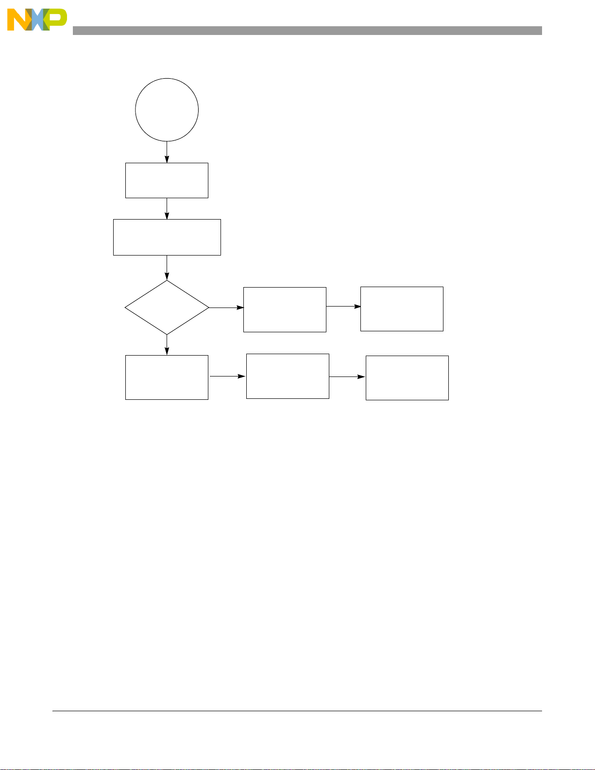
The initial (reset) device configuration is saved including the mode and clock configuration. This means
No
Restore default
configuration
configuration
Save default
BAM Entry
0xFFFF_C000
Boot mode valid?
Download new
code and save in
SRAM
Restore default
configuration
Execute new
code
STATIC mode
Ye s
Check boot
mode at
SSCM_STATUS[BMODE]
that the serial download software running in the BAM can make changes to the modes and clocking and
then restore these to the default values before running the newly downloaded application code from the
SRAM.
The SSCM_STATUS[BMODE] field indicates which boot mode is to be executed (see Table 5-5). This
field is only updated during reset.
There are 2 conditions where the boot mode is not considered valid and the BAM pushes the
microcontroller into static mode after restoring the default configuration:
• BMODE = 011 (flash memory boot mode). This means that the SSCM has been unable to find a
valid BOOT_ID in the boot sectors so has called the BAM
• BMODE = reserved
In static mode a wait instruction is executed to halt the core.
For the FlexCAN and LINFlex serial boot modes, the respective area of BAM code is executed to
download the code to SRAM.
Figure 5-6. BAM logic flow
72 Freescale Semiconductor
MPC5604B/C Microcontroller Reference Manual, Rev. 8
Page 84
Table 5-5. SSCM_STATUS[BMODE] values as used by BAM
BMODE value Corresponding boot mode
000 Reserved
001 FlexCAN_0 serial boot loader
010 LINFlex_0 (RS232 /UART) serial boot loader
011 Flash memory boot mode
100–111 Reserved
After the code has been downloaded to SRAM, the BAM code restores the initial device configuration and
then transfers execution to the start address of the downloaded code.
5.2.1.1 BAM resources
The BAM uses/initializes the following MCU resources:
• MC_ME and MC_CGM to initialize mode and clock sources
• FlexCAN_0, LINFlex _0 and the respective I/O pins when performing serial boot mode
• SSCM and shadow flash memory (NVPWD0,1 and NVSCC0,1) during password check
• SSCM to check the boot mode (see Table 5-5)
• 4–16 MHz fast external crystal oscillator
The system clock is selected directly from the 4–16 MHz fast external crystal oscillator . Thus, the external
oscillator frequency defines the baud rates used for serial download (see Table 5-6).
Table 5-6. Serial boot mode – baud rates
FXOSC frequency
(MHz)
f
FXOSC
8 9600 200K
12 14400 300K
16 19200 400K
LINFlex baud rate
(baud)
f
/833 f
FXOSC
CAN bit rate
(bit/s)
/40
FXOSC
5.2.1.2 Download and execute the new code
From a high level perspective, the download protocol follows these steps:
1. Send the 64-bit password.
2. Send the start address, size of code to be downloaded (in bytes) and the VLE bit1.
3. Download the code.
Each step must be completed before the next step starts. After the download is complete (the specified
number of bytes is downloaded), the code executes from the start address.
1. Since the device supports only VLE code and not Book E code, this flag is used only for backward compatibility.
MPC5604B/C Microcontroller Reference Manual, Rev. 8
Freescale Semiconductor 73
Page 85

The communication is done in half duplex manner, whereby the transmission from the host is followed by
the microcontroller transmission mirroring the transmission back to the host:
• Host sends data to the microcontroller and waits for a response.
• MCU echoes to host the data received.
• Host verifies if echo is correct:
— If data is correct, the host can continue to send data.
— If data is not correct, the host stops transmission and the microcontroller enters static mode.
All multi-byte data structures are sent with MSB first.
A more detailed description of these steps follows.
5.2.1.3 Censorship mode detection and serial password validation
Before the serial download can commence, the BAM code must determine which censorship mode the
microcontroller is in and which password to use. It does this by reading the PUB and SEC fields in the
SSCM Status Register (see Section 5.3.4.1, System Status Register (SSCM_STATUS)) as shown in
Table 5-7.
Table 5-7. BAM censorship mode detection
SSCM_STATUS register fields
Mode Password comparison
PUB SEC
1 0 Uncensored, public password 0xFEED_FACE_CAFE_BEEF
0 0 Uncensored, private password NVPWD0,1 from flash memory via BAM
0 1 Censored, private password NVPWD1,0 from flash memory via SSCM
When censorship is enabled, the flash memory cannot be read by application code running in the BAM or
in the SRAM. This means that the private password in the shadow flash memory cannot be read by the
BAM code. In this case the SSCM is used to obtain the private password from the flash memory of the
censored device. When the SSCM reads the private password it inverts the order of {NVPWD0,
NWPWD1} so the password entered over the serial download needs to be {NVPWD1, NVPWD0}.
MPC5604B/C Microcontroller Reference Manual, Rev. 8
74 Freescale Semiconductor
Page 86
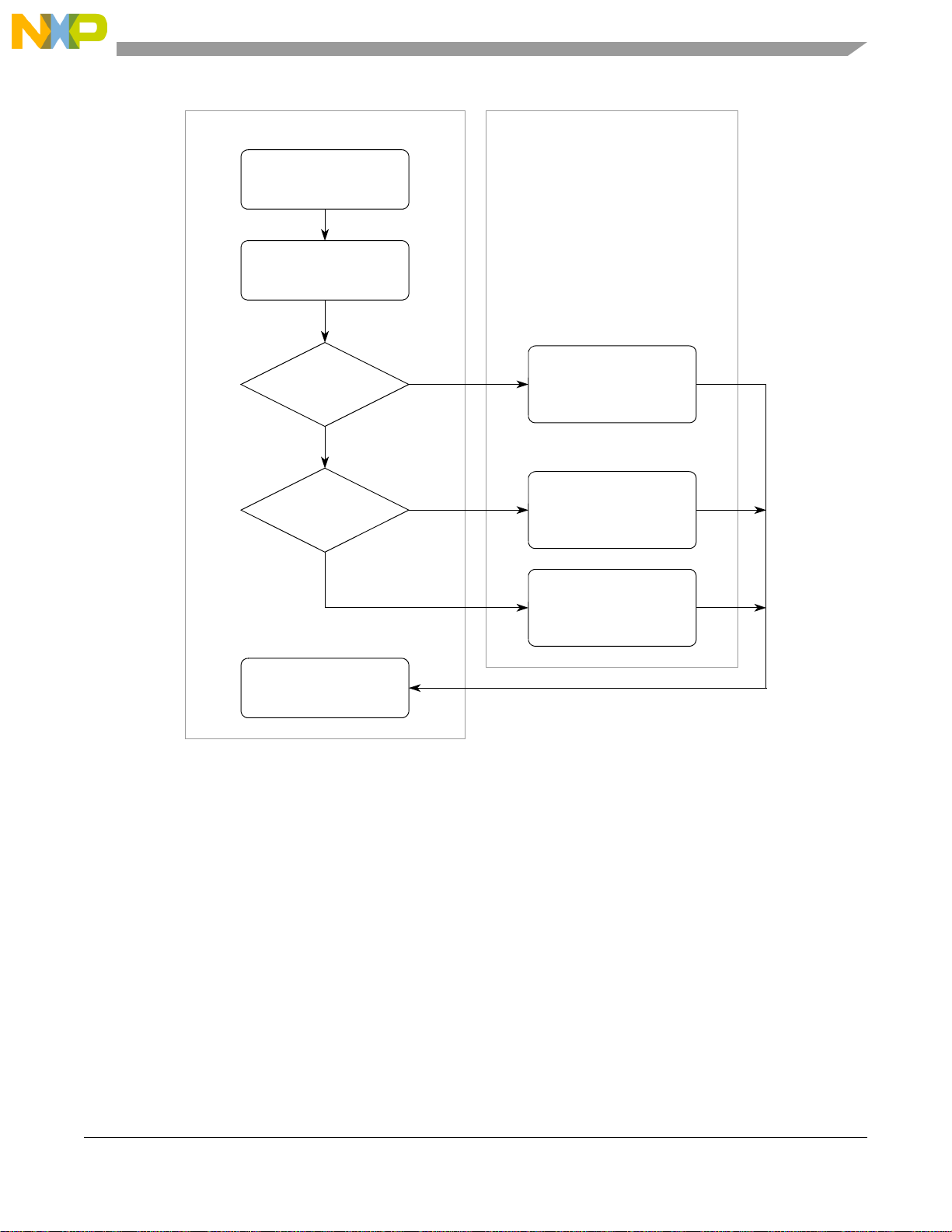
Yes
BAM code is being
executed
(serial boot mode)
No
No
PUB = 1
?
Yes
Start serial download
with password
SSCM_STATUS register
PUB and SEC
bits are read
SEC = 1
?
Public password,
Uncensored,
BAM can directly
check password
Private password,
Censored,
SSCM needed to
check password
Private password,
Uncensored,
BAM can directly
check password
Public password
mode
Is censorship
enabled
BAM tasks Applicable password
?
?
Figure 5-7. BAM censorship mode detection
The first thing to be downloaded is the 64-bit password. If the password does not match the stored
password, then the BAM code pushes the microcontroller into static mode.
The way the password is compared with either the public or private password (depending on mode) varies
depending on whether censorship is enabled as described in the following subsections.
5.2.1.3.1 Censorship disabled (private or public passwords):
1. If the public password is used, the BAM code does a direct comparison between the serial password
and 0xFEED_FACE_CAFE_BEEF.
2. If the private password is used, the BAM code does a direct comparison between the serial
password and the private password in flash memory, {NVPWD0, NVPWD1}.
3. If the password does not match, the BAM code immediately terminates the download and pushes
the microcontroller into static mode.
Freescale Semiconductor 75
MPC5604B/C Microcontroller Reference Manual, Rev. 8
Page 87

5.2.1.3.2 Censorship enabled (private password)
1. Since the flash is secured, the SSCM is required to read the private password.
2. The BAM code writes the serial password to the SSCM_PWCMPH and SSCM_PWCMPL
registers.
3. The BAM code then continues with the serial download (start address, data size and data) until all
the data has been copied to the SRAM.
4. In the meantime the SSCM has compared the private password in flash with the serial download
password the BAM code wrote into SSCM_PWCMPH and SSCM_PWCMPL.
5. If the SSCM obtains a match in the passwords, the censorship is temporarily disabled (until the
next reset).
6. The SSCM updates the status of the security (SEC) bit to reflect whether the passwords matched
(SEC = 0) or not (SEC = 1)
7. Finally, the BAM code reads SEC. If SEC = 0, execution is transferred to the code in the SRAM.
If SEC = 1, the BAM code forces the microcontroller into static mode.
Figure 5-8 shows this in more detail.
MPC5604B/C Microcontroller Reference Manual, Rev. 8
76 Freescale Semiconductor
Page 88
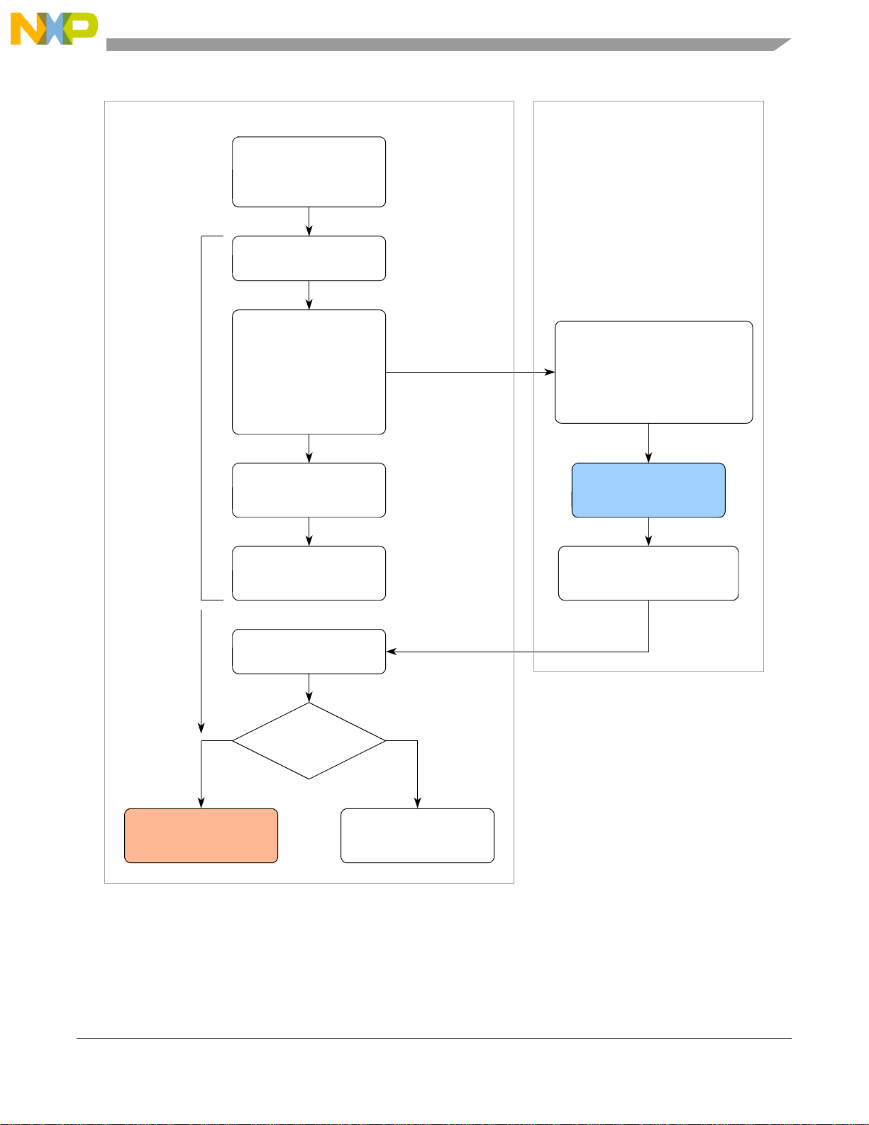
Censorship enabled,
private password,
BAM running
Yes
BAM reads
SSCM_STATUS[SEC]
Serial password
received
Is SEC bit
cleared
BAM tasks SSCM tasks
serial boot mode
BAM writes received
password to SSCM
registers
Upper 32-bits to
SSCM_PWCMPH
Lower 32-bits to
SSCM_PWCMPL
Start address
and data
Data download
received
and copied to SRAM
?
BAM code pushes
microcontroller into
static mode
If any frame
is received
incorrectly,
BAM code
pushes
device into
static mode
If passwords match,
un-censor device
until next POR
Update SSCM_STATUS[SEC]
bit with
censorship state
SSCM compares
registers to private
password in flash
SSCM_PWCMPH to NVPWD1
SSCM_PWCMPL to NVPWD0
No
BAM code transfers
execution to user
code in SRAM
length received
Figure 5-8. BAM serial boot mode flow for censorship enabled and private password
With LINFlex, any receive error will result in static mode. With FlexCAN, the host will re-transmit data
if there has been no acknowledgment from the microcontroller . However there could be a situation where
the receiver configuration has an error which would result in static mode entry.
Freescale Semiconductor 77
MPC5604B/C Microcontroller Reference Manual, Rev. 8
Page 89

NOTE
In a censored device booting with serial boot mode, it is possible to read the
content of the four 32-bit flash memory locations that make up the boot
sector. For example, if the RCHW is stored at address 0x0000_0000, the
reads at address 0x0000_0000, 0x0000_0004, 0x0000_0008 and
0x0000_000C will return a correct value. No other flash memory locations
can be read.
5.2.1.4 Download start address, VLE bit and code size
The next 8 bytes received by the microcontroller contain a 32-bit Start Address, the VLE mode bit and a
31-bit code Length as shown in Figure 5-9.
START_ADDRESS[31:16]
START_ADDRESS[15:0]
VLE CODE_LENGTH[30:16]
CODE_LENGTH[15:0]
Figure 5-9. Start address, VLE bit and download size in bytes
The VLE bit (Variable Length Instruction) is used to indicate whether the code to be downloaded is Book
VLE or Book III-E. This device family supports only VLE = 1; the bit is used for backward compatibility .
The Start Address defines where the received data will be stored and where the MCU will branch after the
download is finished. The start address is 32-bit word aligned and the 2 least significant bits are ignored
by the BAM code.
NOTE
The start address is configurable, but most not lie within the 0x4000_0000
to 0x4000_00FF address range.
The Length defines how many data bytes have to be loaded.
5.2.1.5 Download data
Each byte of data received is stored in the microcontroller’s SRAM, starting from the address specified in
the previous protocol step.
The address increments until the number of bytes of data received matches the number of bytes specified
by the code length.
Since the SRAM is protected by 32-bit wide Error Correction Code (ECC), the BAM code always writes
bytes into SRAM grouped into 32-bit words. If the last byte received does not fall onto a 32-bit boundary ,
the BAM code fills any additional bytes with 0x0.
MPC5604B/C Microcontroller Reference Manual, Rev. 8
78 Freescale Semiconductor
Page 90
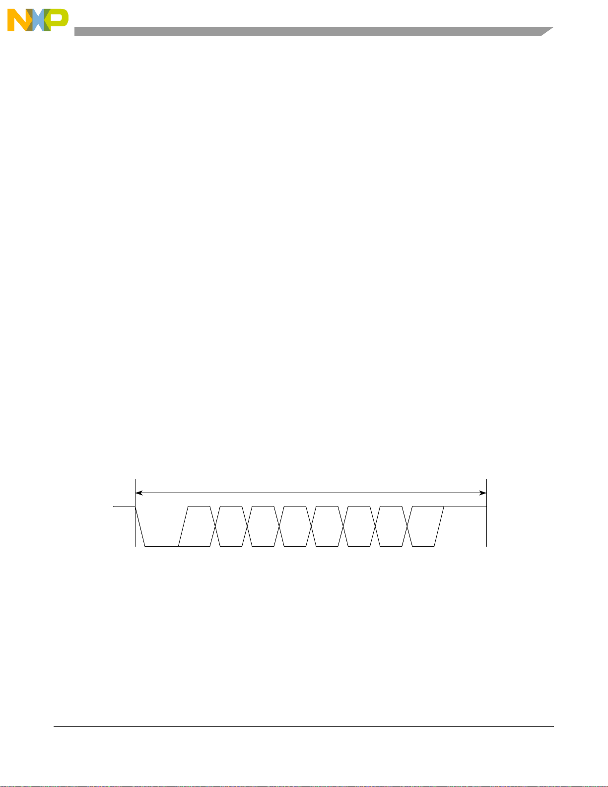
Since the ECC on the SRAM has not been initialized (except for the bytes of data that have just been
D1 D2 D3 D4 D5 D6 D7D0
Byte field
Start
bit
Stop
bit
downloaded), an additional dummy word of 0x0000_0000 is written at the end of the downloaded data
block to avoid any ECC errors during core prefetch.
5.2.1.6 Execute code
The BAM code waits for the last data byte to be received. If the operating mode is censored with a private
password, then the BAM reads the SSCM status register to determine whether the serial password matched
the private password. If there was a password match then the BAM code restores the initial configuration
and transfers execution to the downloaded code start address in SRAM. If the passwords did not match,
the BAM code forces a static mode entry.
NOTE
The watchdog is disabled at the start of BAM code execution. In the case of
an unexpected issue during BAM code execution, the microcontroller may
be stalled and an external reset required to recover the microcontroller.
5.2.2 LINFlex (RS232) boot
5.2.2.1 Configuration
Boot according to the LINFlex boot mode download protocol (see Section 5.2.2.2, Protocol) is performed
by the LINFlex_0 module in UART (RS232) mode. Pins used are:
• LIN0TX mapped on PB[2]
• LIN0RX mapped on PB[3]
Boot from LINFlex uses the system clock driven by the 4–16 MHz external crystal oscillator (FXOSC).
The LINFlex controller is configured to operate at a baud rate = system clock frequency/833, using an 8-bit
data frame without parity bit and 1 stop bit.
Figure 5-10. LINFlex bit timing in UART mode
5.2.2.2 Protocol
Table 5-8 summarizes the protocol and BAM action during this boot mode.
MPC5604B/C Microcontroller Reference Manual, Rev. 8
Freescale Semiconductor 79
Page 91

Table 5-8. UART boot mode download protocol
Protocol
step
Host sent message
1 64-bit password
(MSB first)
2 32-bit store address 32-bit store address Load address is stored for future use.
3 VLE bit + 31-bit
number of bytes
(MSB first)
4 8 bits of raw binary
data
5 None None Branch to downloaded code
BAM response
message
64-bit password Password checked for validity and compared against
stored password.
VLE bit + 31-bit
number of bytes
(MSB first)
8 bits of raw binary
data
Size of download are stored for future use.
Verify if VLE bit is set to 1
8-bit data are packed into a 32-bit word. This word is
saved into SRAM starting from the “Load address”.
“Load address” increments until the number of data
received and stored matches the size as specified in the
previous step.
Action
5.2.3 FlexCAN boot
5.2.3.1 Configuration
Boot according to the FlexCAN boot mode download protocol (see Section 5.2.3.2, Protocol) is performed
by the FlexCAN_0 module. Pins used are:
• CAN0TX mapped on PB[0]
• CAN0RX mapped on PB[1]
NOTE
When the serial download via FlexCAN is selected and the device is part of
a CAN network, the serial download may stop unexpectedly if there is any
other traffic on the network. To avoid this situation, ensure that no other
CAN device on the network is active during the serial download process.
Boot from FlexCAN uses the system clock driven by the 4–16 MHz fast external crystal oscillator.
The FlexCAN controller is configured to operate at a baud rate = system clock frequency/40 (see Table 5-6
for examples of baud rate).
It uses the standard 11-bit identifier format detailed in FlexCAN 2.0A specification.
FlexCAN controller bit timing is programmed with 10 time quanta, and the sample point is 2 time quanta
before the end, as shown in Figure 5-11.
MPC5604B/C Microcontroller Reference Manual, Rev. 8
80 Freescale Semiconductor
Page 92

Figure 5-11. FlexCAN bit timing
SYNC_SEG Time segment 1 Time segment 2
Sample point
NRZ signal
Transmit point
1
time quantum time quanta time quanta
7 2
1 bit time
1 time quantum = 4 system clock periods
5.2.3.2 Protocol
Table 5-9 summarizes the protocol and BAM action during this boot mode. All data are transmitted byte
wise.
Table 5-9. FlexCAN boot mode download protocol
Protoco
l
Host sent message
step
1 CAN ID 0x011 +
64-bit password
2 CAN ID 0x012 +
32-bit store
address + VLE
bit + 31-bit number of
bytes
3 CAN ID 0x013 +
8 to 64 bits of raw
binary data
5 None None Branch to downloaded code
BAM response
message
CAN ID 0x001 +
64-bit password
CAN ID 0x002 +
32-bit store
address + VLE
bit + 31-bit number of
bytes
CAN ID 0x003 +
8 to 64 bits of raw
binary data
Password checked for validity and compared against stored
password
Load address is stored for future use.
Size of download are stored for future use.
Verify if VLE bit is set to 1
8-bit data are packed into 32-bit words. These words are
saved into SRAM starting from the “Load address”.
“Load address” increments until the number of data
received and stored matches the size as specified in the
previous step.
Action
Freescale Semiconductor 81
MPC5604B/C Microcontroller Reference Manual, Rev. 8
Page 93
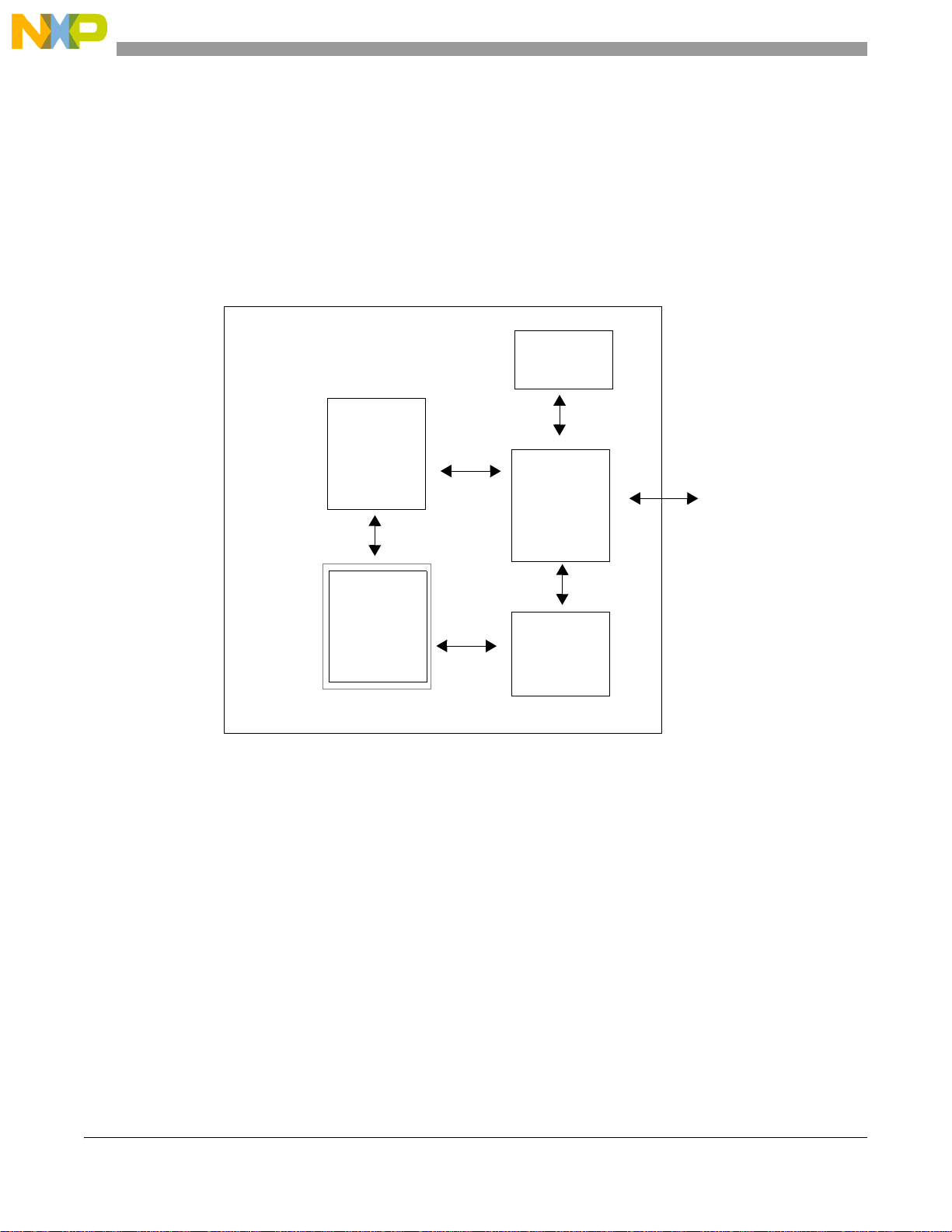
5.3 System Status and Configuration Module (SSCM)
Bus
System Status and Configuration Module
Interface
Password
Comparator
RevID
Hardmacro
Core
Logic
System
Status
Peripheral
Interface
Bus
5.3.1 Introduction
The primary purpose of the SSCM is to provide information about the current state and configuration of
the system that may be useful for configuring application software and for debug of the system.
On microcontrollers with a separate STANDBY power domain, the System Status block is part of that
domain.
Figure 5-12. SSCM block diagram
5.3.2 Features
The SSCM includes these features:
• System Configuration and Status
— Memory sizes/status
— Microcontroller Mode and Security Status (including censorship and serial boot information)
— Search Code Flash for bootable sector
— Determine boot vector
• Device identification information (MCU ID Registers)
• Debug Status Port enable and selection
• Bus and peripheral abort enable/disable
MPC5604B/C Microcontroller Reference Manual, Rev. 8
82 Freescale Semiconductor
Page 94
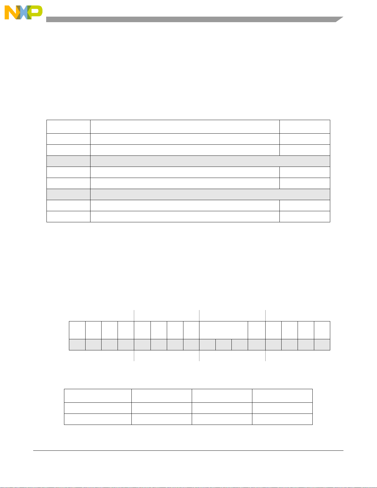
5.3.3 Modes of operation
The SSCM operates identically in all system modes.
5.3.4 Memory map and register description
Table 5-10 shows the memory map for the SSCM. Note that all addresses are offsets; the absolute address
may be calculated by adding the specified offset to the base address of the SSCM.
Table 5-10. SSCM memory map
Address offset Register Location
0x00 System Status Register (SSCM_STATUS) on page 83
0x02 System Memory Configuration Register (SSCM_MEMCONFIG) on page 84
0x04 Reserved
0x06 Error Configuration (SSCM_ERROR) on page 85
0x08 Debug Status Port Register (SSCM_DEBUGPORT) on page 86
0x0A Reserved
0x0C Password Comparison Register High Word (SSCM_PWCMPH) on page 87
0x10 Password Comparison Register Low Word (SSCM_PWCMPL) on page 87
All registers are accessible via 8-bit, 16-bit or 32-bit accesses. However, 16-bit accesses must be aligned
to 16-bit boundaries, and 32-bit accesses must be aligned to 32-bit boundaries. As an example, the
SSCM_STA TUS register is accessible by a 16-bit read/write to address ‘Base + 0x0002’, but performing
a 16-bit access to ‘Base + 0x0003’ is illegal.
5.3.4.1 System Status Register (SSCM_STATUS)
The System Status register is a read-only register that reflects the current state of the system.
Offset:0x00 Access: Read
0 1 2 3 4 5 6 7 8 9 10 11 12 13 14 15
R
0000
W
Reset000000000/10/10/10 0000
Figure 5-13. System Status Register (SSCM_STATUS)
Table 5-11. SSCM_STATUS allowed register accesses
Access type 8-bit 16-bit 32-bit
Read Allowed Allowed Allowed
PUB SEC 0 BMODE 0 0 0 0 0
NXEN
1
Write Not allowed Not allowed Not allowed
MPC5604B/C Microcontroller Reference Manual, Rev. 8
Freescale Semiconductor 83
Page 95

1
All 32-bit accesses must be aligned to 32-bit addresses (i.e., 0x0, 0x4, 0x8 or 0xC).
Table 5-12. SSCM_STATUS field descriptions
Field Description
NXEN Nexus enabled
PUB Public Serial Access Status. This bit indicates whether serial boot mode with public password is
allowed.
1 Serial boot mode with public password is allowed
0 Serial boot mode with private flash memory password is allowed
SEC Security Status. This bit reflects the current security state of the flash memory.
1 The flash memory is secured.
0 The flash memory is not secured.
BMODE Device Boot Mode
000 Reserved
001 FlexCAN_0 Serial Boot Loader
010 LINFlex_0 Serial Boot Loader
011 Single Chip
100 Reserved
101 Reserved
110 Reserved
111 Reserved
This field is only updated during reset.
5.3.4.2 System Memory Configuration Register (SSCM_MEMCONFIG)
The System Memory Configuration register is a read-only register that reflects the memory configuration
of the system.
Offset: 0x02 Access: Read
0123456789101112131415
R 0 0 0 0 0 PRSZ PVLB DTSZ DVLD
W
Resetxxxxxxxxxx1xxxx1
Figure 5-14. System Memory Configuration Register (SSCM_MEMCONFIG)
MPC5604B/C Microcontroller Reference Manual, Rev. 8
84 Freescale Semiconductor
Page 96

Table 5-13. SSCM_MEMCONFIG field descriptions
Field Description
PRSZ Code Flash Size
10000 128 KB
10001 256 KB
10010 384 KB
10011 512 KB
PVLB Code Flash Available
This bit identifies whether or not the on-chip code Flash is available in the system memory map. The
Flash may not be accessible due to security limitations, or because there is no Flash in the system.
1 Code Flash is available
0 Code Flash is not available
DTSZ Data Flash Size
0000 No Data Flash
0011 64 KB
DVLD Data Flash Valid
This bit identifies whether or not the on-chip Data Flash is visible in the system memory map. The Flash
may not be accessible due to security limitations, or because there is no Flash in the system.
1 Data Flash is visible
0 Data Flash is not visible
Table 5-14. SSCM_MEMCONFIG allowed register accesses
Access type 8-bit 16-bit 32-bit
Read Allowed Allowed Allowed
(also reads SSCM_STATUS
register)
Write Not allowed Not allowed Not allowed
5.3.4.3 Error Configuration (SSCM_ERROR)
The Error Configuration register is a read-write register that controls the error handling of the system.
Offset: 0x06 Access: Read/write
0123456789101112131415
R00000000000000
W
Reset0000000000000000
Figure 5-15. Error Configuration (SSCM_ERROR)
PA E R A E
MPC5604B/C Microcontroller Reference Manual, Rev. 8
Freescale Semiconductor 85
Page 97
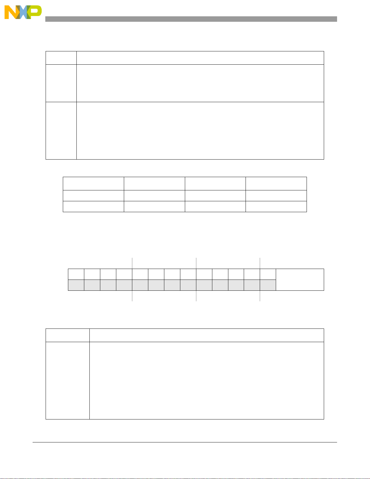
Table 5-15. SSCM_ERROR field descriptions
Field Description
PAE Peripheral Bus Abort Enable
This bit enables bus aborts on any access to a peripheral slot that is not used on the device. This feature
is intended to aid in debugging when developing application code.
1 Illegal accesses to non-existing peripherals produce a Prefetch or Data Abort exception
0 Illegal accesses to non-existing peripherals do not produce a Prefetch or Data Abort exception
RAE Register Bus Abort Enable
This bit enables bus aborts on illegal accesses to off-platform peripherals. Illegal accesses are defined
as reads or writes to reserved addresses within the address space for a particular peripheral. This
feature is intended to aid in debugging when developing application code.
1 Illegal accesses to peripherals produce a Prefetch or Data Abort exception
0 Illegal accesses to peripherals do not produce a Prefetch or Data Abort exception
Transfers to Peripheral Bus resources may be aborted even before they reach the Peripheral Bus (that
is, at the PBRIDGE level). In this case, bits PAE and RAE will have no effect on the abort.
Table 5-16. SSCM_ERROR allowed register accesses
Access type 8-bit 16-bit 32-bit
Read Allowed Allowed Allowed
Write Allowed Allowed Not allowed
5.3.4.4 Debug Status Port Register (SSCM_DEBUGPORT)
The Debug Status Port register is used to (optionally) provide debug data on a set of pins.
Offset: 0x08 Access: Read/write
0123456789101112131415
R0000000000000
W
Reset0000000000000000
Figure 5-16. Debug Status Port Register (SSCM_DEBUGPORT)
Table 5-17. SSCM_DEBUGPORT field descriptions
Field Description
DEBUG_MODE Debug Status Port Mode
This field selects the alternate debug functionality for the Debug Status Port.
000 No alternate functionality selected
001 Mode 1 selected
010 Mode 2 selected
011 Mode 3 selected
100 Mode 4 selected
101 Mode 5 selected
110 Mode 6 selected
111 Mode 7 selected
Ta bl e 5 - 1 8 describes the functionality of the Debug Status Port in each mode.
DEBUG_MODE
MPC5604B/C Microcontroller Reference Manual, Rev. 8
86 Freescale Semiconductor
Page 98

Table 5-18. Debug status port modes
Pin
1
0 SSCM_STATUS
1 SSCM_STATUS
2 SSCM_STATUS
3 SSCM_STATUS
4 SSCM_STATUS
5 SSCM_STATUS
6 SSCM_STATUS
7 SSCM_STATUS
1
All signals are active high, unless otherwise noted
Mode 1 Mode 2 Mode 3 Mode 4 Mode 5 Mode 6 Mode 7
[0]
[1]
[2]
[3]
[4]
[5]
[6]
[7]
SSCM_STATUS
[8]
SSCM_STATUS
[9]
SSCM_STATUS
[10]
SSCM_STATUS
[11]
SSCM_STATUS
[12]
SSCM_STATUS
[13]
SSCM_STATUS
[14]
SSCM_STATUS
[15]
SSCM_MEMCONFI
G[0]
SSCM_MEMCONFI
G[1]
SSCM_MEMCONFI
G[2]
SSCM_MEMCONFI
G[3]
SSCM_MEMCONFI
G[4]
SSCM_MEMCONFI
G[5]
SSCM_MEMCONFI
G[6]
SSCM_MEMCONFI
G[7]
SSCM_MEMCONFI
G[8]
SSCM_MEMCONFI
G[9]
SSCM_MEMCONFI
G[10]
SSCM_MEMCONFI
G[11]
SSCM_MEMCONFI
G[12]
SSCM_MEMCONFI
G[13]
SSCM_MEMCONFI
G[14]
SSCM_MEMCONFI
G[15]
PIN[0..7] referred to in Table 5-18 equates to PC[2..9] (Pad 34..41).
Reserved Reserved Reserved
Reserved Reserved Reserved
Reserved Reserved Reserved
Reserved Reserved Reserved
Reserved Reserved Reserved
Reserved Reserved Reserved
Reserved Reserved Reserved
Reserved Reserved Reserved
Table 5-19. SSCM_DEBUGPORT allowed register accesses
Access type 8-bit 16-bit 32-bit
Read Allowed Allowed Not allowed
Write Allowed Allowed Not allowed
1
All 32-bit accesses must be aligned to 32-bit addresses (i.e., 0x0, 0x4, 0x8 or 0xC).
1
5.3.4.5 Password comparison registers
These registers provide a means for the BAM code to unsecure the device via the SSCM if the password
has been provided via serial download.
MPC5604B/C Microcontroller Reference Manual, Rev. 8
Freescale Semiconductor 87
Page 99
Offset: 0x0C Access: Read/write
0123456789101112131415
R0000000000000000
W PWD_HI[31:16]
Reset0000000000000000
16 17 18 19 20 21 22 23 24 25 26 27 28 29 30 31
R0000000000000000
W PWD_HI[15:0]
Reset0000000000000000
Figure 5-17. Password Comparison Register High Word (SSCM_PWCMPH)
Offset: 0x10 Access: Read/write
0123456789101112131415
R0000000000000000
W PWD_LO[31:16]
Reset0000000000000000
16 17 18 19 20 21 22 23 24 25 26 27 28 29 30 31
R0000000000000000
W PWD_LO[15:0]
Reset0000000000000000
Figure 5-18. Password Comparison Register Low Word (SSCM_PWCMPL)
Table 5-20. Password Comparison Register field descriptions
Field Description
PWD_HI Upper 32 bits of the password
PWD_LO Lower 32 bits of the password
Table 5-21. SSCM_PWCMPH/L allowed register accesses
Access type 8-bit 16-bit 32-bit
Read Allowed Allowed Allowed
Write Not allowed Not allowed Allowed
1
All 32-bit accesses must be aligned to 32-bit addresses (i.e., 0x0, 0x4, 0x8 or 0xC).
1
MPC5604B/C Microcontroller Reference Manual, Rev. 8
88 Freescale Semiconductor
Page 100

In order to unsecure the device, the password needs to be written as follows: first the upper word to the
SSCM_PWCMPH register, then the lower word to the SSCM_PWCMPL register. The SSCM compares
the 64-bit password entered into the SSCM_PWCMPH / SSCM_PWCMPL registers with the
NVPWM[1,0] private password stored in the shadow flash. If the passwords match then the SSCM
temporarily uncensors the microcontroller .
MPC5604B/C Microcontroller Reference Manual, Rev. 8
Freescale Semiconductor 89
 Loading...