

Page 1
LAAS-CNRS
Quick Start to MPC5604B
Embedded Development
Sahin Serdar
21/06/2013
Page 2

Table of Contents
Introduction ......................................................................................................................................................................... 1
1. About this document .......................................................................................................................................... 1
2. About of embedded programming ............................................................................................................... 2
3. Associated documents ....................................................................................................................................... 3
Chapter 1 ....................................................................................................... 4
1. ME: Mode Entry Modules ................................................................................................................................. 4
1.1. Introduction ................................................................................................................................................. 4
1.2. Enabling modes .......................................................................................................................................... 5
1.3. Configuring modes .................................................................................................................................... 5
1.4. Configuring peripherals .......................................................................................................................... 6
1.5. Device mode selection ............................................................................................................................. 7
2. CGM: Clock Generation Module ..................................................................................................................... 8
2.1. Clock Architecture ..................................................................................................................................... 8
2.2. Clock Out ........................................................................................................................................................ 9
2.3. Sysclk ........................................................................................................................................................... 10
2.4. FMPLL .......................................................................................................................................................... 11
3. A device initialisation procedure ............................................................................................................... 13
4. SWT: Software Watchdog Timer ................................................................................................................ 14
Chapter 2 SIUL: System Integration Unit Line ............................................................................................ 15
1. Introduction ........................................................................................................................................................ 15
2. Pad configuration ............................................................................................................................................. 15
3. GPIO: General Purpose Input/Output ...................................................................................................... 17
4. External interrupts .......................................................................................................................................... 19
Chapter 3 INTC: Interrupt Controller ............................................................................................................. 21
1. Introduction ........................................................................................................................................................ 21
2. INTC configuration (Software mode) ...................................................................................................... 23
2.1. Enabling interrupt requests ............................................................................................................... 23
2.2. Configuring hardware ISRs ................................................................................................................. 23
2.3. Configuring software ISRs ................................................................................................................... 24
2.4. Enabling nested interruptions ........................................................................................................... 24
3. Hardware mode INTC ..................................................................................................................................... 24
Chapter 4 Timer Modules .................................................................................................................................... 26
1. Introduction ........................................................................................................................................................ 26
2. STM: System Timer Module ......................................................................................................................... 27
Page 3

3. PIT: Periodic Interrupt Timer ..................................................................................................................... 27
4. RTC/API: Real Time Clock/ Autonomous Periodic Interrupt ........................................................ 29
5. Timer Examples ................................................................................................................................................ 31
Chapter 5 eMIOS: Enhanced Modular I/O Subsystem ............................................................................. 32
1. Module Configuration ..................................................................................................................................... 33
2. Channel Configuration .................................................................................................................................... 34
1.1. Introduction .............................................................................................................................................. 34
1.2. GPIO: General Purpose Input/Output ............................................................................................ 36
1.3. SAIC: Single Action Input Capture .................................................................................................... 37
1.4. SAOC: Single Action Output Compare ............................................................................................. 37
1.5. IPWM: Input Pulse Width Measurement ....................................................................................... 38
1.6. IPM: Input Period Measurement ...................................................................................................... 38
1.7. DAOC: Double Action Output Compare .......................................................................................... 39
1.8. MC: Modulus Counter ............................................................................................................................ 40
1.9. MCB: Modulus Counter Buffered ...................................................................................................... 41
1.10. OPWFMB: Output Pulse Width and Frequency Modulation Buffered ......................... 41
1.11. OPWMCB: Center Aligned Output Pulse Width Buffered .................................................. 43
1.12. OPWMB: Output Pulse Width Modulation Buffered ............................................................ 44
1.13. OPWMT: Output Pulse Width Modulation with Trigger .................................................... 45
3. PWM Channel Initialisation .......................................................................................................................... 46
4. PWM Example .................................................................................................................................................... 46
Chapter 6 ADC: Analog-to-Digital Converter ............................................................................................... 48
1. Presentation of the ADC module ................................................................................................................ 48
1.1. Introduction .............................................................................................................................................. 48
1.2. Conversion ................................................................................................................................................. 49
1.3. ADC clock and conversion timing ..................................................................................................... 50
1.4. Pre-sampling ............................................................................................................................................. 51
1.5. Analog watchdog ..................................................................................................................................... 51
1.6. Low power consumption modes ...................................................................................................... 51
2. ADC Configuration ............................................................................................................................................ 52
2.1. Pad Configuration ................................................................................................................................... 52
2.2. General Registers .................................................................................................................................... 52
2.3. Conversion Registers ............................................................................................................................. 53
2.4. Interrupt Registers ................................................................................................................................. 54
2.5. Watchdog Registers ............................................................................................................................... 54
Page 4

2.6. Channel Registers ................................................................................................................................... 55
3. ADC Example with PIT and eMIOS ............................................................................................................ 55
Chapter 7 CTU: Cross Triggering Unit ............................................................................................................ 58
1. Introduction ........................................................................................................................................................ 58
2. Configuring CTU ................................................................................................................................................ 59
3. Configuring ADC ................................................................................................................................................ 60
4. Implementing a feedback loop with ADC-CTU-eMIOS ...................................................................... 60
Chapter 8 WKPU: Wakeup Unit ......................................................................................................................... 62
1. Low power consumption modes ................................................................................................................ 62
1.1. STOP ............................................................................................................................................................. 62
1.2. STANDBY .................................................................................................................................................... 62
2. Introduction ........................................................................................................................................................ 63
3. Configuration of wakeup events................................................................................................................. 65
Chapter 9 DSPI: Deserial Serial Peripheral Interface ............................................................................... 66
1. Introduction ........................................................................................................................................................ 66
1.1. SPI Protocol Description ...................................................................................................................... 66
1.2. Module Presentation ............................................................................................................................. 68
2. Configuration ...................................................................................................................................................... 69
2.1. Signal Configuration .............................................................................................................................. 69
2.2. Module Configuration Register ......................................................................................................... 69
2.3. Transfer Configuration Register ....................................................................................................... 70
2.3.1. Data attributes ..................................................................................................................................... 71
2.3.2. Baud rate ............................................................................................................................................... 72
2.3.3. CS to SCK delay .................................................................................................................................... 73
2.3.4. After SCK delay .................................................................................................................................... 73
2.3.5. After transfer delay ........................................................................................................................... 73
2.4. Status and Interrupt Registers .......................................................................................................... 73
2.5. Transmit/Receive Registers ............................................................................................................... 74
3. Developing a general purpose SPI Driver............................................................................................... 75
4. Driving smart-MOS switches MC33984 using SPI Driver ................................................................ 77
4.1. Introduction to MC33984 .................................................................................................................... 77
4.2. Driver’s components ............................................................................................................................. 77
4.2.1. Definitions ............................................................................................................................................. 79
4.2.2. Initialization ......................................................................................................................................... 79
4.2.3. Operations ............................................................................................................................................. 80
Page 5

4.2.4. User interface ....................................................................................................................................... 80
4.2.5. Testing .................................................................................................................................................... 80
Chapter 10 UART: Universal Asynchronous Receiver Transmitter ...................................................... 82
1. Introduction to UART...................................................................................................................................... 82
2. Module Presentation ....................................................................................................................................... 82
3. Configuration ...................................................................................................................................................... 83
3.1. Signal Configuration .............................................................................................................................. 83
3.2. LINFlex Module Configuration .......................................................................................................... 83
3.3. UART Mode Configuration .................................................................................................................. 84
3.4. Baud Rate Configuration ...................................................................................................................... 84
3.5. Status Registers and Interrupt Configuration ............................................................................. 85
3.6. Data Transmit/Receive ........................................................................................................................ 86
4. Developing a general purpose UART Driver ......................................................................................... 87
5. Using the UART Driver for a terminal interface ................................................................................... 88
5.1. System initialisation .............................................................................................................................. 88
5.2. SIUL configuration .................................................................................................................................. 88
5.3. ADC configuration................................................................................................................................... 89
5.4. eMIOS configuration .............................................................................................................................. 90
5.5. Main procedure and use of the driver ............................................................................................ 90
5.6. Results ......................................................................................................................................................... 92
Chapter 11 I²C: Inter-Integrated Circuit Bus Controller ............................................................................ 94
1. Presentation of I²C protocol ......................................................................................................................... 94
1.1. Description ................................................................................................................................................ 94
1.2. Baud rate .................................................................................................................................................... 95
1.3. Pull-up resistor calculation ................................................................................................................. 96
2. Using the I²C module ....................................................................................................................................... 96
2.1. Module Presentation ............................................................................................................................. 96
2.2. Module Registers ..................................................................................................................................... 97
2.3. Communication ........................................................................................................................................ 99
2.4. Developing a general purpose I²C Driver .................................................................................. 101
Chapter 12 CAN: Controller Area Network .................................................................................................. 102
6. CAN protocol ................................................................................................................................................... 102
1.1. Introduction ........................................................................................................................................... 102
1.2. Frame Description ............................................................................................................................... 103
1.3. Physical Layer ....................................................................................................................................... 104
Page 6

1.4. Error detection ...................................................................................................................................... 105
1.5. Bit-rate and sampling ......................................................................................................................... 106
7. FlexCAN Module Configuration ............................................................................................................... 107
7.1. Module Description ............................................................................................................................. 107
7.2. Message Buffer mode and RX FIFO mode .................................................................................. 108
7.2.1. Message Buffers ............................................................................................................................... 108
7.2.2. RX FIFO Engine ................................................................................................................................ 110
7.3. Configuration Registers ..................................................................................................................... 111
7.4. Status and Interrupt Registers ....................................................................................................... 113
8. FlexCAN usage explained with an example ........................................................................................ 115
8.1. Initialisation ........................................................................................................................................... 116
8.2. Transmission ......................................................................................................................................... 116
8.3. Reception ................................................................................................................................................. 117
8.4. Interrupt Handling .............................................................................................................................. 117
9. CAN Transceiver(MCZ33905S5EK) Configuration ......................................................................... 118
Appendix 1 Using Code Warrior IDE ............................................................................................................... 120
Appendix 2 Pad Configurations ......................................................................................................................... 127
Appendix 3 Peripheral input pin selection ................................................................................................... 135
Appendix 4 Interrupt Vector Table .................................................................................................................. 137
Appendix 5 I²C Baud Rate Prescaler Values ................................................................................................. 142
Page 7
Introduction
1. About this document
This document is meant to be a simple guide for developing embedded software on Freescale’s
MPC5604B microcontroller, based on Qorrivva architecture. This microcontroller is destined to
be used in automotive applications, mostly related to body control and it comes with many
peripherals.
This guide will be focused on the configuration and use of those peripherals by summarizing the
official reference manual, but it also gives commented code examples and tips for overcoming
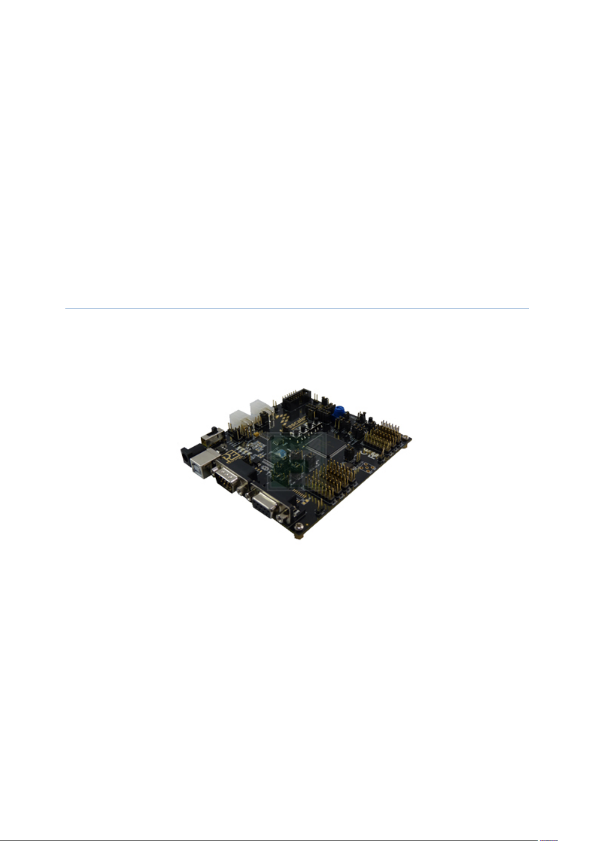
common difficulties. Our tests were carried out on the starter kit evaluation board of MPC5604B,
which embodies a CAN transceiver, a potentiometer, four LEDs and buttons; practical for
examples.
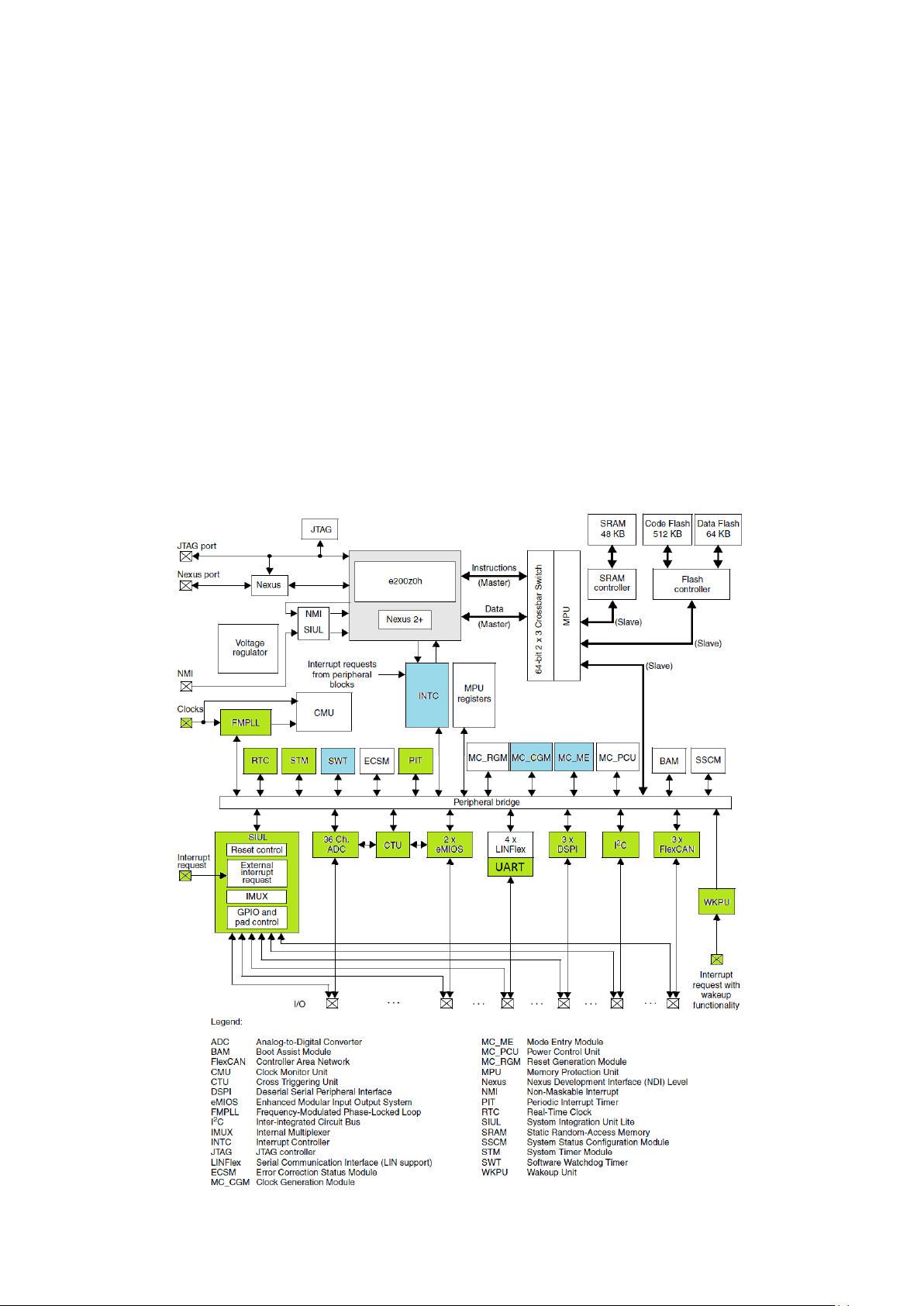
The following figure shows different peripherals contained in the microcontroller. The green
ones are explained in detail in this document, minimal information is given on blue ones.
1
Page 8
2. About embedded programming
DSPI
LINFlex
SIUL
INTC
eMIOS
SPI
UART
PWM
PAD
INTERRUPT
LOAD
DRIVE
MC33984 SMART MOS CONTROLLER
FAULT
HANDLER
USER
INTERFACE
POWER
SUPERVISION
MAIN APPLICATION
APPLICATION
LAYER
APP. SERVICE
LAYER
APP. DRIVER
&
MCU DRIVER
LAYER
MCU HW LAYER
(Registers etc.)
x |= mask; /* Bits specified by the mask are set, others unchanged. */
x ^= mask; /* Bits specified by the mask are toggled, others unchanged. */
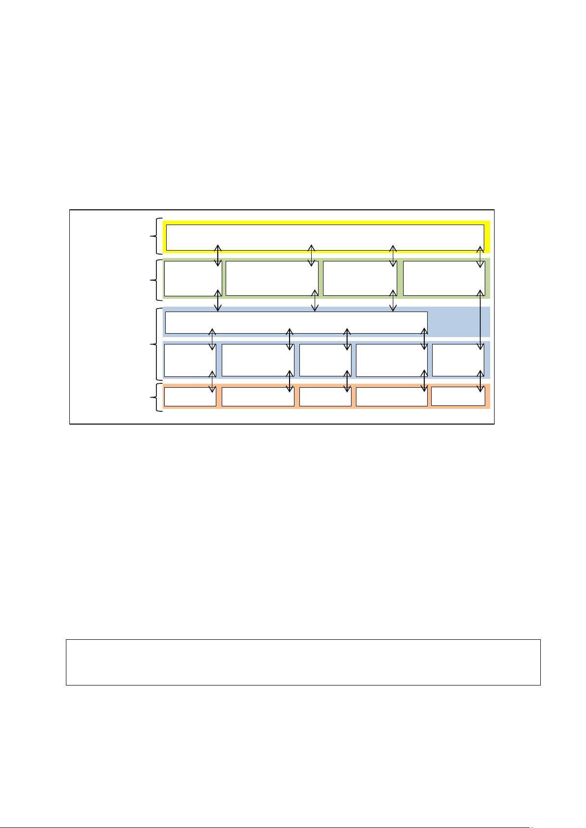
Most embedded software is built on a multi-layer architecture, where lower layers provide
drivers for a simpler way of using different hardware peripherals. Then those drivers can be
used for implementing drivers for more complex devices or for high-level application related
functions.
The figure below illustrates a software architecture example where an MC33984 high side
switch chip is used for driving some loads, supervising their power and detecting errors while
providing a serial communication interface to the user.
This document is focused on lower software layer interacting with the MCU’s peripherals
directly. In embedded C software there are some restrictions compared to regular C software:
The program must never reach the end of main function. It usually ends up having a
main loop with a state machine or an empty infinite loop.
All the local variables have to be defined at the beginning of a function.
Main function has often the same structure: first it initialises the system clock and mode and
then it initialises and configures each peripheral it uses. On this MCU it also has to disable the
watchdog before doing anything else.
Most of the programming is done by writing and reading peripheral registers so use of masks is
pretty common for accessing specific fields (AND ‘&’ mask for clearing, OR ‘|’ for setting, XOR ‘^’
for toggling).
x &= (~mask); /* Bits specified by the mask are cleared, others unchanged. */
Due to limited amount of code and data memory, compiler optimisations are quite handy, but
the result might turn into an undefined behaviour if variables that are altered by external
environment are optimised. To avoid this, the keyword ‘volatile’ can be used with these kind of
variables.
Page 9

3. Associated documents
This document is not as detailed as the MPC5604B’s reference manual and it may not give all the
required information for implementing some specific behaviour with a peripheral. In this case
following documents might be useful:
MPC5604B/C Reference Manual Rev. 8: The official Freescale document which explains
the use of each peripheral.
AN2865: MPC5500&MPC5600 Simple Cookbook: A Freescale application note which
gives example codes with many peripherals in different uses. It also gives the design
procedure of the software.
TRK-MPC5604B Schematic Rev. B: This document is the schematic of MPC5604B starter
kit board. This should be used to check whether a pin is used by some component on the
board. For instance when using the UART pins on the port B, you should check if the
jumpers connecting those pins to the LIN Transceiver are removed. Otherwise you
would receive framing errors.
MPC5604B/C Datasheet Rev. 7: Contains useful information about electrical and timing
characteristics of the device. It also contains important information related to the
peripherals like SPI timing.
MPC5604B/C Errata: Contains a list of known problems with the MCU and possible
workarounds.
This document itself also contains some detailed examples, codes or driver examples:
- A device initialisation procedure
- Timer examples
- PWM Example
- ADC Example with PIT and eMIOS
- Implementing a feedback loop with ADC-CTU-eMIOS
- Developing a general purpose SPI Driver
- Driving smart-MOS switches MC33984 using SPI Driver
- Developing a general purpose UART Driver
- Using the UART Driver for a terminal interface
- FlexCAN usage explained with an example
Page 10
Chapter 1
Initialisation of the controller
1. ME: Mode Entry Modules
1.1. Introduction
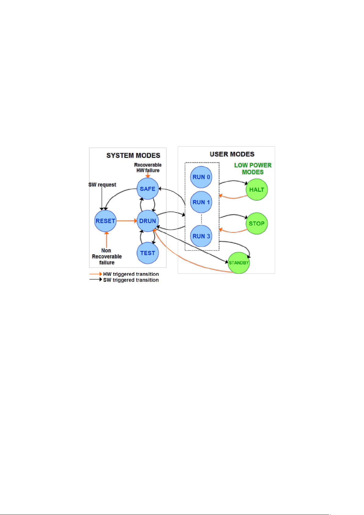
Figure 1 : MC_ME Mode Diagram (Freescale Lecture)
This module controls the device modes, their settings and the transitions between them. On
Figure 1, you can find different modes that are avail controller. They have to be
initialised properly, after reset, in order to get the right configuration for the system.
In this paragraph we will quickly explain RESET, DRUN, SAFE, TEST, RUN 0...3 modes, which are
needed for embedded applications. See Wakeup Events chapter for more information about
STANDBY and STOP modes.
System Modes
o RESET: This state is active after a system reset or a non-recoverable failure.
The device leaves this state once the reset sequence that initialises the chip
and power is completed. The system clock is set to the internal 16MHz RC
oscillator.
o DRUN: This is the entry mode of the software which can control the flash
memories, configure clocks, user modes before going into a user mode. This
is the first thing to be done in “main” procedure (Default RUN).
o SAFE: The device goes into this state once a recoverable hardware failure has
occurred. After handling the failure the system goes in to the DRUN mode,
reinitialising the software.
o TEST: This mode allows software to do on-chip test routines with peripheral
modules, RAM etc.
User Modes
o RUN0…3: This is where the software runs; these four RUN modes can be
configured with different clock and power settings.
4
Page 11
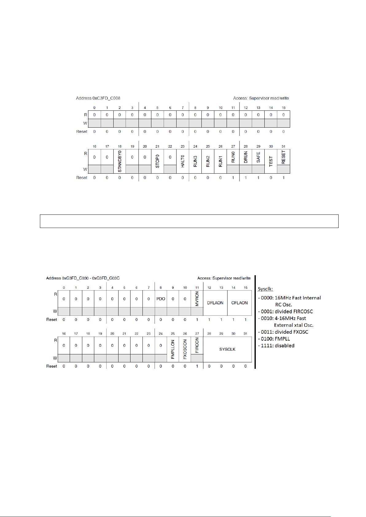
1.2. Enabling modes
Figure 2 : Mode Enable Register (MER) (Reference Manual Rev8 – Fig. 8-4)
1.3. Configuring modes
Figure 3 : Mode Configuration Register for RUN 0…3 (Reference Manual Rev8 – Fig. 8-13)
ME.MER.R = 0x000000FD; /* Enable all RUNx modes along with default modes */
The first thing to be done once the device enters in DRUN is to enable the modes that are going
to be used by the software. This is done using the Mode Enable Register (MER). This register
allows all modes to be enabled/disabled except for RESET, DRUN, SAFE, and RUN0 which are
always enabled.
For instance, enabling all the normal user modes can be done with:
We then need to configure the modes we will need in the software using configuration registers
(‘ME.<mode>.R’). In regular embedded software with no power saving specifications, we will
only need configuring RUN0…3.
Quick explanation of modifiable fields of this register:
• DFLAON : Data flash power-down control, leave it at 11 (normal mode)
• CDFLAON : Code flash power-down control, leave it at 11 (normal mode)
• FMPLLON: Frequency Modulated PLL control, 0 if not needed, 1 if used
• FXOSCON: Fast External Crystal Oscillator control, 0 if not needed, 1 if used
• FIRCON: Fast Internal RC Oscillator control, always needed in case of failure
• SYSCLK: System clock switch control, specify the clock used by system (see next chapter
for details on oscillators and their configuration)
Page 12
Example for configuring RUN0:
1.4. Configuring peripherals
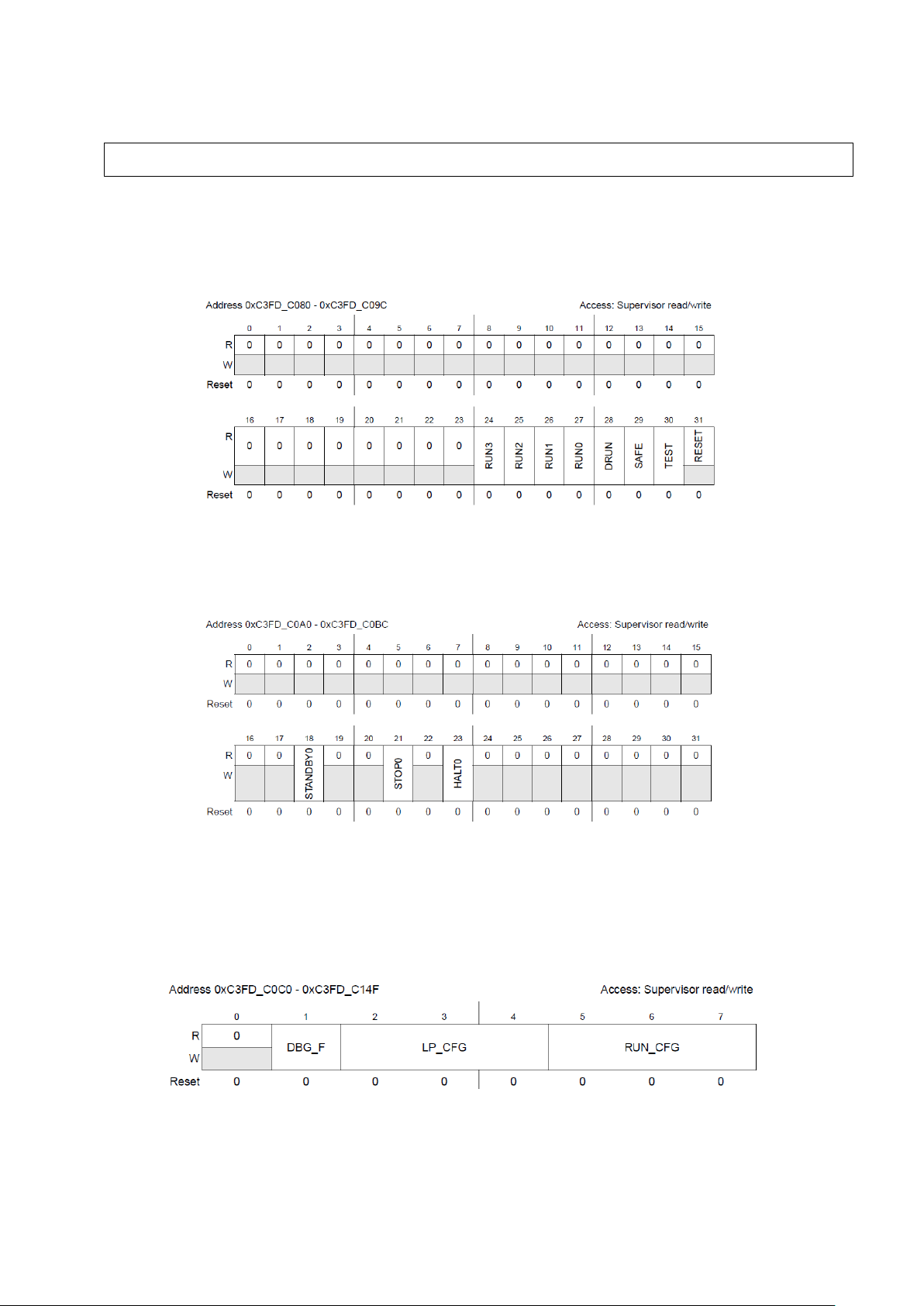
Figure 4 : Run Peripheral Configuration Registers (Reference Manual Rev8 – Fig. 8-21)
Figure 5 : Low Power Peripheral Configuration Registers (Reference Manual Rev8 – Fig. 8-22)
Figure 6 : Peripheral Control Registers (Reference Manual Rev8 – Fig. 8-23)
ME.RUN[0].R = 0x001F0074; /* RUN0 cfg: 16MHzIRCON,OSC0ON,PLL0ON,syclk=PLL0 */
Having configured different modes, we possess 8 different registers that allow us to configure a
peripheral to only run on a set of specific mode. These registers are called Run Peripheral
Configuration Registers (RUNPC[0] to RUNPC[7]).
You may notice that STANDBY, HALT and STOP cannot be selected using this register, you’ll
need to use Low Power Peripheral Configuration registers (LPPC[0] to LPPC[7]).
Once all the possible modes have been selected using these 8+8 registers, each one of the 144
peripherals can be affected to one of the 8 RUNPC register and one of the 8 LPPC registers using
Peripheral Control Registers (PCTL[0] to PCTL[143]). The selected peripheral will only run in
the modes selected by these registers.
DBG_F allows to froze the peripheral in debug mode or not (which can be useful for observing
peripherals internal state), LP_CFG is used to select a low power mode from LPPC registers
6
Page 13
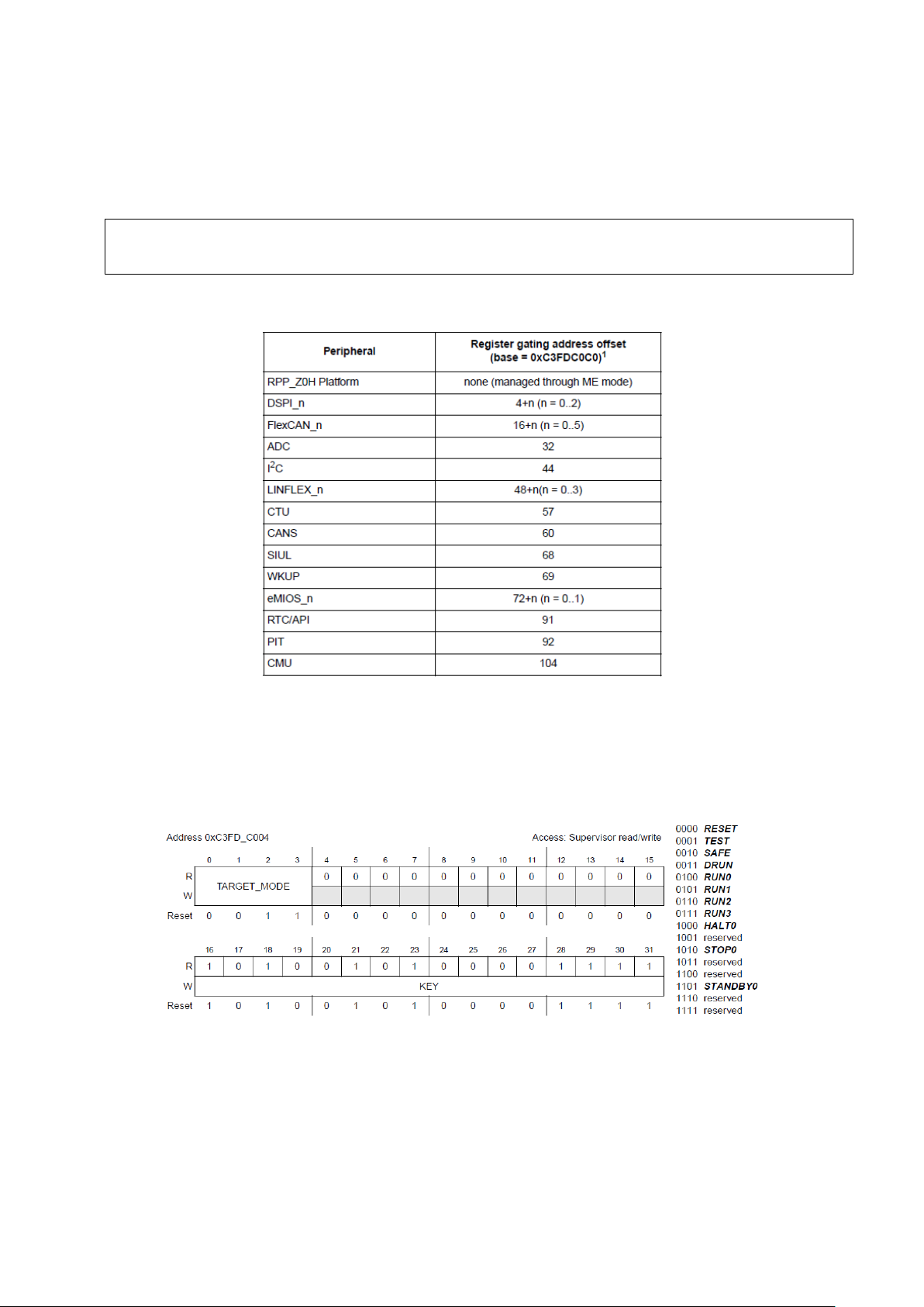
(0...7) for low power operation and RUN_CFG allows to select a normal run mode from RUNPC
Figure 7 : Register gating address offset for peripherals (Reference Manual Rev8 – Fig. 6-1)
1.5. Device mode selection
Figure 8 : Mode Control Register (Reference Manual Rev8 – Fig. 8-3)
ME.RUNPC[1].R = 0x00000010; /* Peri.Cfg. 1 settings: only run in RUN0 mode */
ME.PCTL[68].R = 0x01; /* MPC56xxB/S: select ME.RUNPC[1] */
registers. Note that by default, all peripherals run on RUNPC[0] register.
Example for configuring SIUL peripheral (System Integration Unit Line: GPIO and external
interrupt manager) to run only in RUN0 mode, using RUNPC1:
Here’s a table of peripherals with id numbers up to 143:
After enabling modes we want to use, configuring them and the peripherals, we can change the
current mode of the device using the Mode Control Register.
In order to perform a mode selection, you need to specify the mode in the field TARGET_MODE
and use the Key 0xA50F first, and then repeat the same thing with the inverted key 0x5AF0. This
will trigger a mode transition.
Page 14
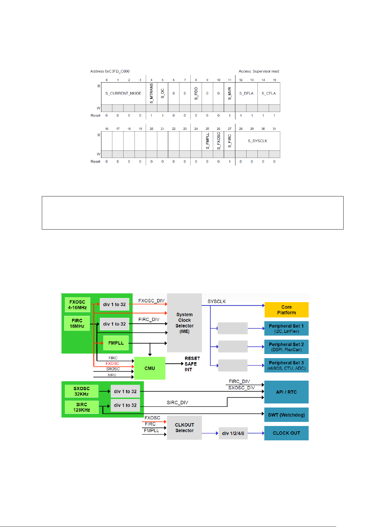
To ensure that the operation was successful, you need to use the read only Global Status Register
Figure 9 : Global Status Register (Reference Manual Rev8 – Fig. 8-2)
2. CGM: Clock Generation Module
2.1. Clock Architecture
Figure 10 : The Clock Architecture (MC_CGM) (Freescale Lecture)
ME.MCTL.R = 0x40005AF0; /* Enter RUN0 Mode & Key */
while (ME.GS.B.S_CURRENTMODE != 4) {} /* Verify RUN0 is the current mode */
div 1 to 16
div 1 to 16
div 1 to 16
to check the current mode.
Here’s an example code for a transition towards RUN0 mode:
ME.MCTL.R = 0x4000A50F; /* Enter RUN0 Mode & Inverted Key */
while (ME.GS.B.S_MTRANS == 1) {} /* Wait for mode transition to complete */
In this section we will discuss different ways to setup the system clock and peripheral clocks in
this microcontroller. The clocking structure is represented on the figure below.
There are three sets of peripherals in this architecture that can have independent clocks as
noted in the figure above, all peripherals not mentioned there are in the core platform.
Page 15
We can see that there are five possible clock sources in this architecture:
2.2. Clock Out
Figure 11 : Output Clock Enable Register (Reference Manual Rev8 – Fig. 7-2)
Figure 12 : Output Clock Division Select Register (Reference Manual Rev8 – Fig. 7-2)
CGM.OCDS_SC.R = 0x32000000; /* Select FMPLL and divide by 2 */
/* Here insert GPIO code that selects CLOCKOUT functionality for the pin
FXOSC: Fast External Crystal Oscillator, between 4-16MHz (8 MHz on TRK-
MPC5604B),
FIRC: Fast Internal RC Oscillator, 16MHz,
SXOSC: Slow External Crystal Oscillator, 32kHz,
SIRC: Slow Internal RC Oscillator, 128kHz,
FMPLL: Frequency Modulated Phase Locked Loop allows delivering a high speed clock
up to 64MHz using FXOSC.
Slow clocks are mostly used for the real time clock module and we will focus more on the fast
ones that are used for system clock generation.
System clock can be selected among FXOSC, FIRC or their division by 1 to 32, or by FMPLL. This
clock drives the core of the microcontroller, it can be gated to different peripheral sets, and can
be divided for power saving. We can also generate an output clock from pin PA [0] called CLOCK
OUT using these fast oscillators.
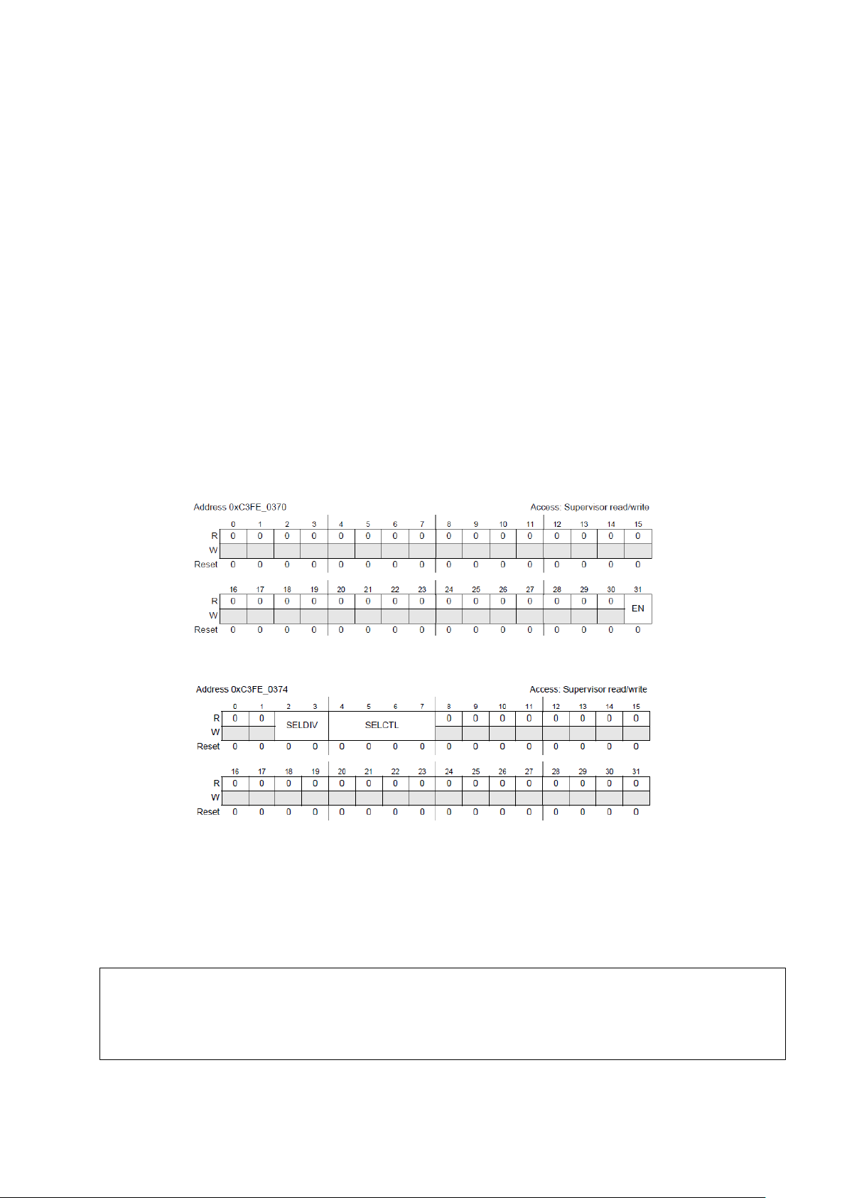
In this section we will review the registers used to generate an output clock. It can be controlled
using two registers.
Use of the enable register is obvious; write 1 to enable the output clock. For the other one,
SELDIV is the amount of division (clock divided by 2
) and SELCTL is the selection of the
source clock among FXOSC (0000), FIRC (0001) and FMPLL (0010).
Here’s an example of using the Output Clock with FMPLL after dividing it by 8:
CGM.OC_EN.B.EN = 1; /* Write 1 to enable bit */
PA[0]: SIU.PCR[0].R = 0x0800;, see chapter on SIUL and pad configurations.*/
Page 16
2.3. Sysclk
Figure 13 : Fast External Crystal Oscillator Control Register (Reference Manual Rev8 – Fig. 6-2)
Figure 14 : System Clock Select Status Register (Reference Manual Rev8 – Fig. 7-4)
Figure 15 : System Clock Divider Configuration Registers (Reference Manual Rev8 – Fig. 7-5)
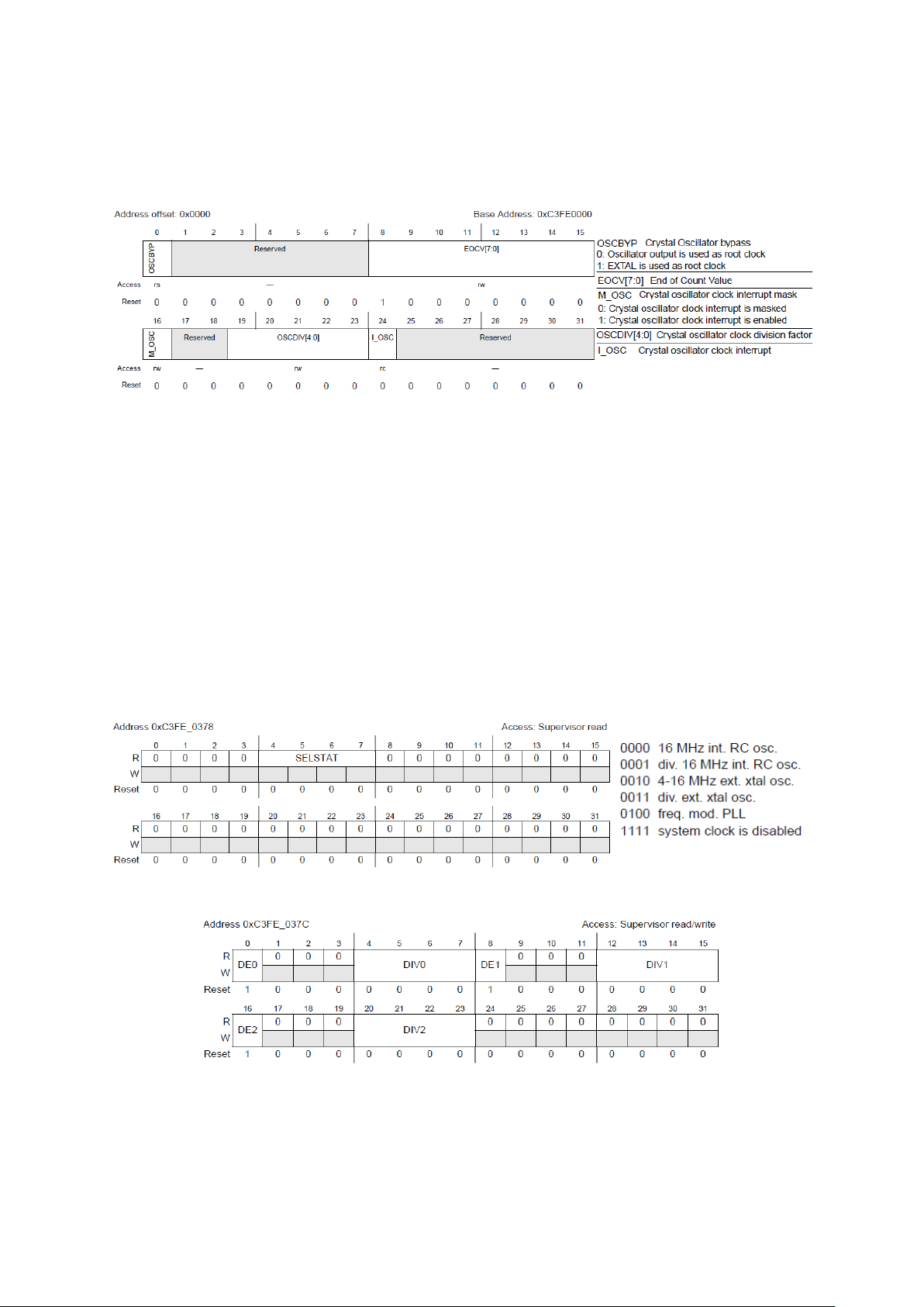
Each of the four clock source has a single control register for its gating towards next blocks. We
will focus only on FXOSC’s control register.
Bypass allows using original crystal signal as clock without going through the oscillator, end of
Count Value is used to check the stability of the clock once the software powers it up. Once a
counter reaches the value EOCV [7:0]×512, if M_OSC is set and interrupt is generated, which has
to be cleared by setting I_OSC to 1, and the clock is ready to be used. The clock is divided by
DIVCLOK+1.
Other clock sources control register are similar with some different features: RC oscillators can
be trimmed by the software to increase precision (FIRC can be up to ± 1% precise) and the
SXOSC has a stability checking field (see chapter 6.3 to 6.6 in reference manual Rev8).
And finally, there are two registers for system clock management, one for reading the selected
source (by ME) and the other one is for managing peripheral clock gating.
DE fields of this register are to enable a divider and the value of division is DIV+1(up to 16).
Page 17
Here’s an example of using a 1MHz by dividing FXOSC by 8, and supplying a 1MHz clock for
2.4. FMPLL
Figure 16 : FMPLL Block Diagram (Reference Manual Rev8 – Fig. 6-6)
Figure 17 : FMPLL Control Register (Reference Manual Rev8 – Fig. 6-7)
CGM.FXOSC_CTL.R = 0x00800700; /* keep reset settings but divide by 8 */
/* Here insert code that configures a user mode’s system clock with divided
this clock setup */
.
.
peripheral set 1, 100 kHz for peripheral set 2, 250 kHz for peripheral set 3.
...
xtal fast oscillator, you can check it with CGM.SC_SS.R read only register */
CGM.SC_DC[0].R = 0x00; /* no division for peripheral set 1 */
CGM.SC_DC[1].R = 0x89; /* divide by 10 for peripheral set 2 */
CGM.SC_DC[2].R = 0x83; /* divide by 4 for peripheral set 3 */
/* Here insert code that makes the mode transition towards the user mode with
You can notice that divider configuration register is made of three 8 bit register instead of one
32bit. See MPC5604B_M27V.h to see how registers are laid out for different modules.
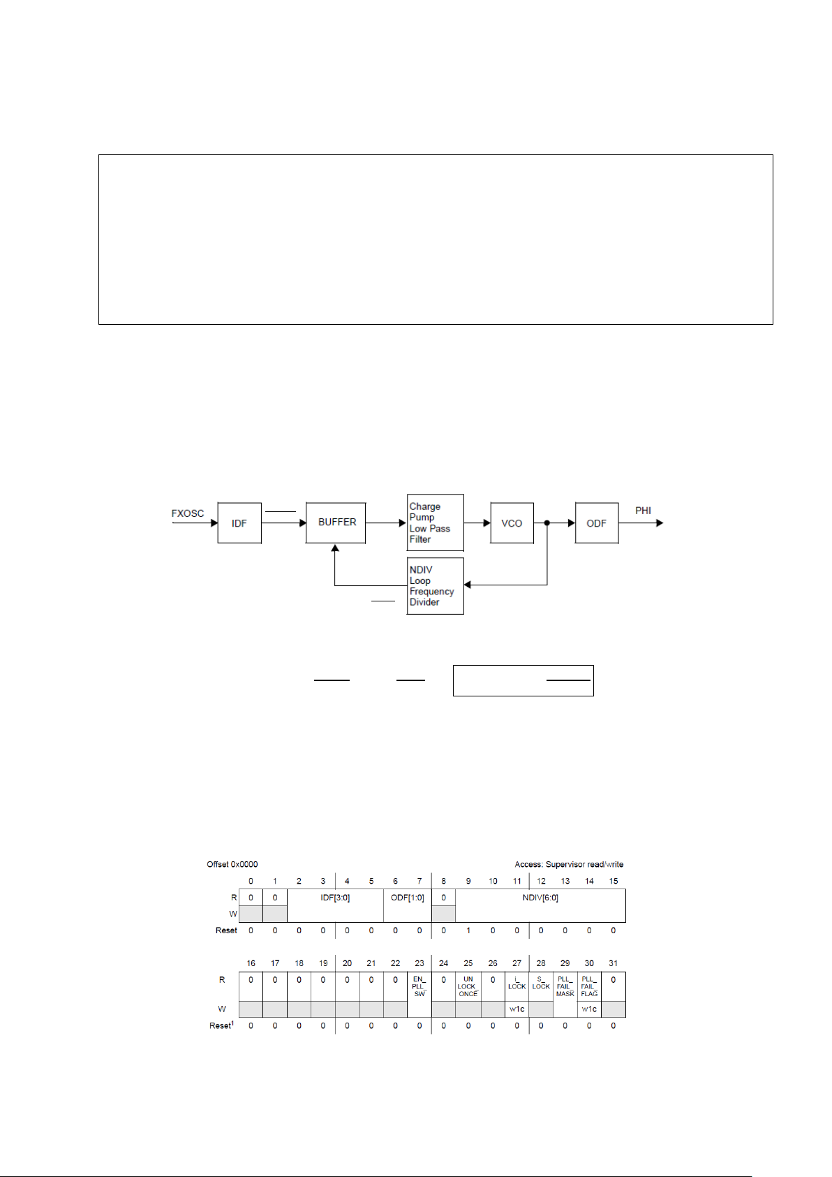
Use of FMPLL allows generating high speed clock by using FXOSC. Its block diagram is on the
figure below.
When the PLL is locked we have
= PHI
, so PHI = FXOSC
.
.This module has the
following constraints:
FXOSC
VCO
[
NDIV
[
4MHz, 16MHz]
256MHz, 512MHz]
[
32, 96]
IDF
ODF {2,4,8,16}
PHI 64MHz
[
1,15]
After carefully choosing values for NDIV, IDF and ODF (using a spread sheet for instance), you
can use the control register of FMPLL module to implement it.
Page 18
Fields of this register are defined as; IDF[3:0]=IDF-1; and IDF [3:0] =1111 means clock
Figure 18 : FMPLL with its different spread modes (Reference
Manual Rev8 – Fig. 6-10)
CGM.FMPLL_CR.B.IDF = 1; //IDF[3:0]=IDF-1=2-1=1
inhibition, ODF[1:0]=log
(ODF)-1, NDIV[6:0]=NDIV. These values must only be changed while
2
the PLL is not the system clock source. The other fields on this register are defined as:
EN_PLL_SW: Progressive clock switching, improves the PLL’s transition but the clock will
only reach PHI after a few cycles (192/PHI secondsng 64MHz).
UNLOCK_ONCE is set once the FMPLL loses lock. It will only be cleared on system reset.
I_LOCK is set each time a lock or unlock event occurs. It’s cleared by writing ‘1’.
S_LOCK: lock(‘1’)/unlock(‘0’) status of FMPLL.
PLL_FAIL_MASK: used to mask the pll_fail output (write ‘1’ to mask).
PLL_FAIL_FLAG: is set to ‘1’ once a loss of lock occurs while PLL is on. Cleared by writing
‘1’.
Here’s an example of using an 8 MHz crystal oscillator to generate a 45MHz system clock. Having
NDIV=90, IDF=2, ODF=8 allows us to get this output frequency while VCO frequency remains at
8x45=360MHz. All values are within constraints.
CGM.FMPLL_CR.B.ODF = 2; //ODF[1:0]=log2(8)-1=3-1=2
CGM.FMPLL_CR.B.NDIV = 0x5A; //0x5A=90
CGM.FMPLL_CR.B.EN_PLL_SW = 1; //progressive transition
//these 4 lines are equivalent to CGM.FMPLL_CR.R = 0x065A0100
/* Here insert code that configures a user mode’s system clock with FMPLL,
you can check it with CGM.SC_SS.R read only register */
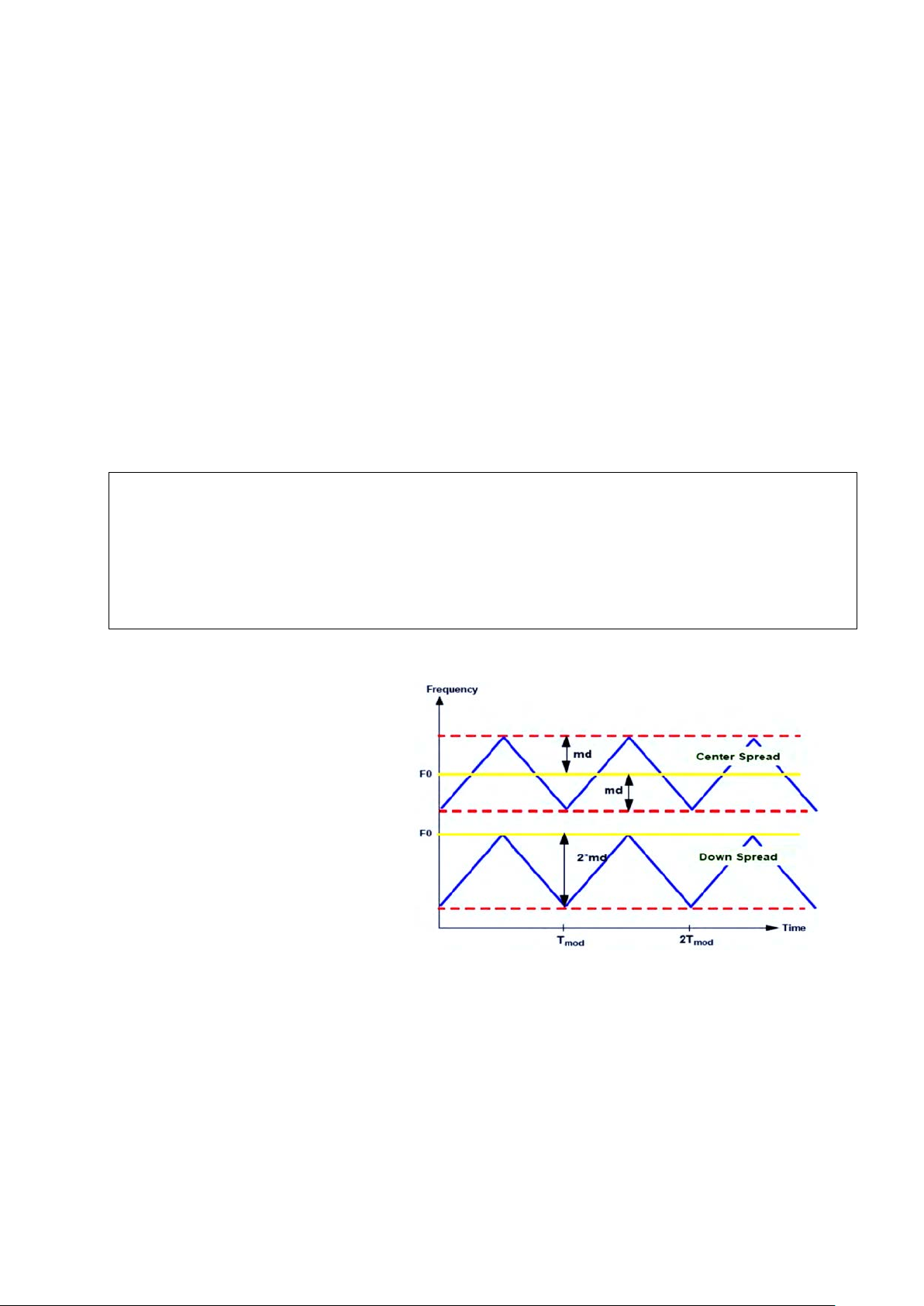
At this point, we only looked at the PLL aspect of the FMPLL module; this module can also
modulate the clock using frequency modulation with a triangular wave. This will help reduce the
effects of electromagnetic interference
generated by the high frequency
harmonics caused around the VCO
(from hundreds of MHz to up to a few
GHz) in the PLL. The electromagnetic
radiations on a specific frequency can
interfere with a surrounding
communication bands and cause errors.
By modulating the clock, its spectrum
will get wider and the energy at a
specific frequency will be less
important. Meanwhile the modulation
depth’s size can be critical in some
applications (like CAN) where FM can
cause errors. FM can be configured
using modulation register.
Frequency modulation can be configured with specifications on (modulation depth)
and
, modulation frequency. Modulation frequency should not be higher than 100kHz and
depth should not be higher than ±4%.
Page 19
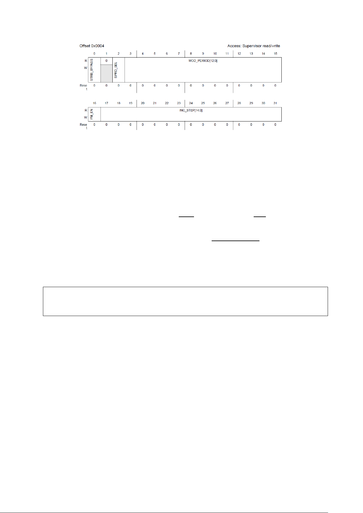
Figure 19 : FMPLL Modulation Register (Reference Manual Rev8 – Fig. 6-8)
3. A device initialisation procedure
CGM.FMPLL_MR.B.MOD_PERIOD = 20; /* fmod=50kHz */
CGM.FMPLL_MR.B.FM_EN = 1; /* enable FM */
Different fields of this register are defined as:
STRB_BYPASS: Strobe bypass; when this bit is set to ‘0’, it allows to change other fields
while FM is not enabled, but if it is set to ‘1’, other fields has to be static while FMPLL is
powered on,
SPRD_SEL: spread selection, if it is ‘0’, the FM is centre spread, if it is ‘1’, the FM is down
spread (see Figure 18),
MOD_PERIOD[12:0]: binary value of
, where
= .
and
modulation frequency,
INC_STEP[14:0]: binary value of =
××
××
,
FM_EN: enable FM by writing ‘1’.
is the
MOD_PERIOD and INC_STEP have to be calculated using selected values of
to respect the following limitation: _ × _
CGM.FMPLL_MR.B.INC_STEP = 29; /* md = 0.1% */
(
2
1
and in order
)
.
Recommended modulation depths are ±0.25% to±4% for center spread and 0.5% to8% for
down spread.
We’ve seen different steps to follow for initialising the microcontroller, we can now write a
generic initialisation function that could be used for a lot of embedded applications.
The structure of the code will remain the same for most of the embedded applications:
Enable modes that may be used.
Make the clock configuration.
Mode configuration.
Peripheral configuration.
Transition towards a user mode.
Page 20

Here’s an example for setting a 64MHz system clock and making SIUL (GPIO) run on this mode.
4. SWT: Software Watchdog Timer
void disableWatchdog(void) {
}
void initModesAndClock(void) {
while(ME.GS.B.S CURRENTMODE != 4) {} /* Verify RUN0 is the current mode */
ME.MER.R = 0x0000001D; /* Enable DRUN, RUN0, SAFE, RESET modes */
CGM.FMPLL_CR.R = 0x02400100; /* 8 MHz xtal: Set PLL0 to 64 MHz */
ME.RUN[0].R = 0x001F0074; /* RUN0 config: clock selection(FMPLL) */
ME.RUNPC[1].R = 0x00000010;
ME.PCTL[68].R = 0x01; /* SIUL use the configuration of RunPC[1]
/* Mode Transition to enter RUN0 mode: */
ME.MCTL.R = 0x40005AF0; /* Enter RUN0 Mode & Key */
ME.MCTL.R = 0x4000A50F; /* Enter RUN0 Mode & Inverted Key */
while (ME.GS.B.S_MTRANS) {} /* Wait for mode transition to complete */
add other peripherals as needed.*/
We could also write “
ME.RUNPC[0].R = 0x00000010;” instead of RUNPC[1] to make all
peripherals run on RUN0, without needing PCTL lines, as all peripherals select RUNPC[0].
Use of FM for PLL is not recommended if there might be time sensitive applications. For example
it might induce transmission errors on CAN protocol if modulation depth and frequency are not
1
correctly selected
.
This timer is used to prevent system lock-up when the software is trapped in a loop or a bus
transaction failed. It is a 32-bit count-down timer, clocked by the 128kHz SIRC. A 32-bit time-out
value (minimum 0x100) value is specified (by default it’s 1280, so 10ms) and the software has
to enter some key sequence before timeout, otherwise a system reset is generated (it can be
modified to generate an interrupt first, and then a reset on a second timeout). By default this
module is frozen in the debug mode.
Using its configuration registers, this module is highly customisable for better fault detection, for
more details; see the chapter 30 of the reference manual rev.8, especially the paragraph 6. On
this document we will only give the code for disabling the watchdog in case it causes a problem.
SWT.SR.R = 0x0000c520; /* Write keys to clear soft lock bit */
SWT.SR.R = 0x0000d928;
SWT.CR.R = 0x8000010A; /* Clear watchdog enable (WEN) */
1
http://www.ti.com/lit/an/spna090/spna090.pdf : A Texas Instruments document that explains how to
choose the right values for FM parameters without affecting the CAN.
Page 21
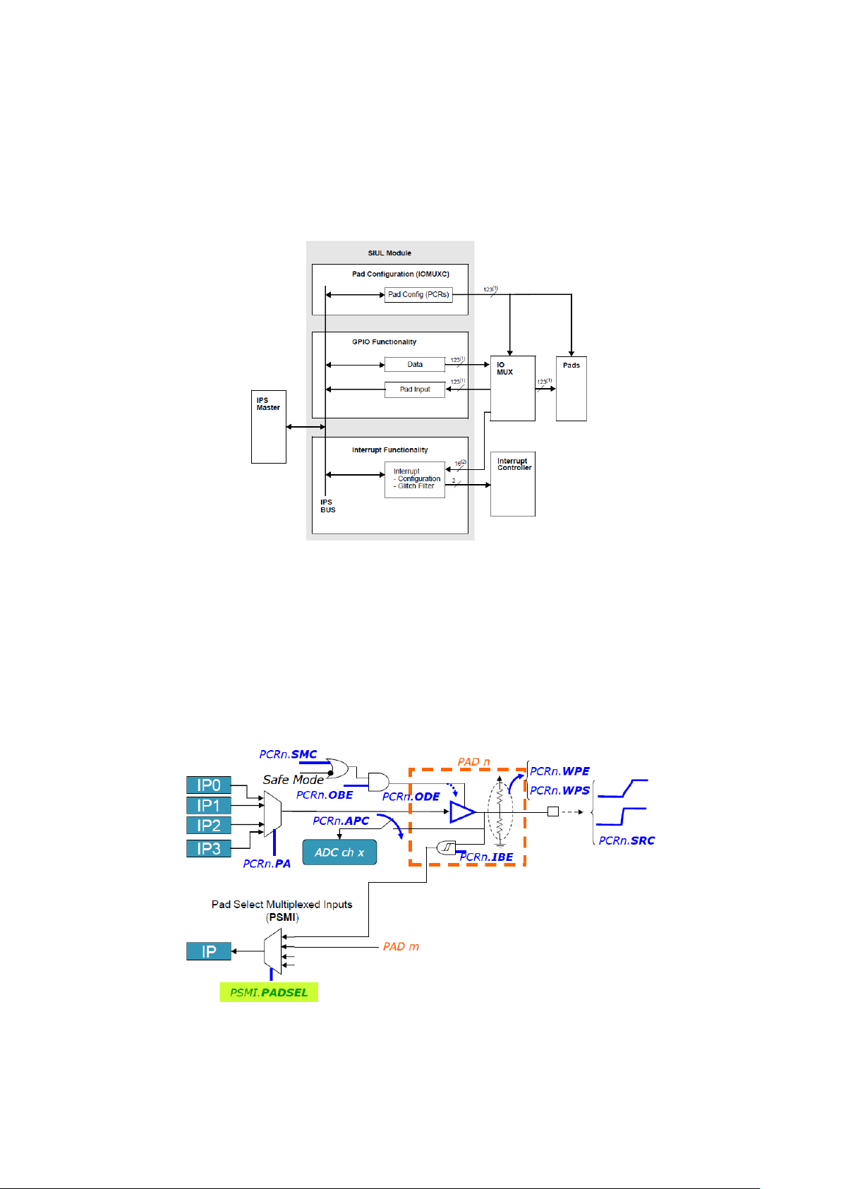
Chapter 2
SIUL: System Integration Unit Line
1. Introduction
Figure 20 : SIUL Block Diagram (Reference Manual Rev8 – Fig. 19-1)
2. Pad configuration
Figure 21 : Pad Architecture (Freescale Lecture)
This module is used for pad management and configuration. It can also process external
interrupts that can be triggered on rising/falling edges. On TRK-MPC5604B there are 123 pads
with GPIO functionality and 16 with external interrupt ability.
This functionality controls pad multiplexing on a low level to set pads as inputs or outputs with
additional parameters that are showed on the figure below.
15
Page 22
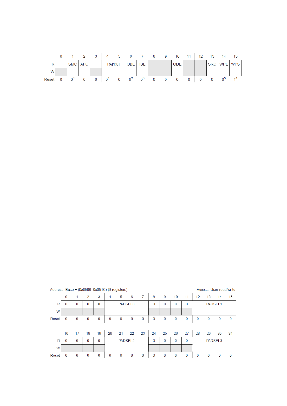
It can be seen that there are two registers that are used for configuring pads; PCR (Pad
Figure 22 : Pad Configuration Register (Reference Manual Rev8 – Fig. 19-9)
Figure 23 : Pad Selection for Multiplexed Inputs Register (Reference Manual Rev7 – Fig. 8-10)
Configuration Register) and PSMI (Pas Selection for Multiplexed Inputs).
There are 123 PCR registers, one for each pad, with following fields:
SMC: Safe Mode Control, by default output buffers are disabled in SAFE mode; writing ‘1’
to this bit keeps outputs functional.
APC: Analog Pad Control, this bit allows the use of the analog input path from the pad by
the ADC.
PA[1:0]: Pad Assignment, each pad can have up to four output alternate functions,
function 00 being always the GPIO, this fields makes the selection. See Appendix 2
OBE: Output Buffer Enable, if the pad is configured as GPIO, this bit allows its use as an
output.
IBE: Input Buffer Enable, enables the input buffer of the pad.
ODE: Open Drain Output Enable, when this bit is ‘0’, pad is configured for push/pull
output and when it is ‘1’, pad is an open drain output.
SRC: Slew Rate Control, by default (‘0’) the pad is slow and writing ‘1’ makes it
configured as medium or fast depending on the pad.
WPE: Weak Pull Up/Down enabling bit. WPS: Selecting Pull Up (‘1’) or Pull Down (‘0’).
But some of these fields are not available for all pads. Pads of type S, M and F are GPIO pads with
digital alternate functions and cannot use APC field. J-type pads are digital pads with analog
functionality and all fields are available for them. And finally, I-type pads can only be used for
ADCs and their only available fields are APC and IBE.
Note: Push/pull outputs are faster and easier to use so for most applications, Open Drain output
should be used if multiple outputs are to be pulled up/down together to implement logic
operations. Open drains are mostly needed in some communication protocols like I²C or CAN.
The other register is shown on the figure below.
Page 23
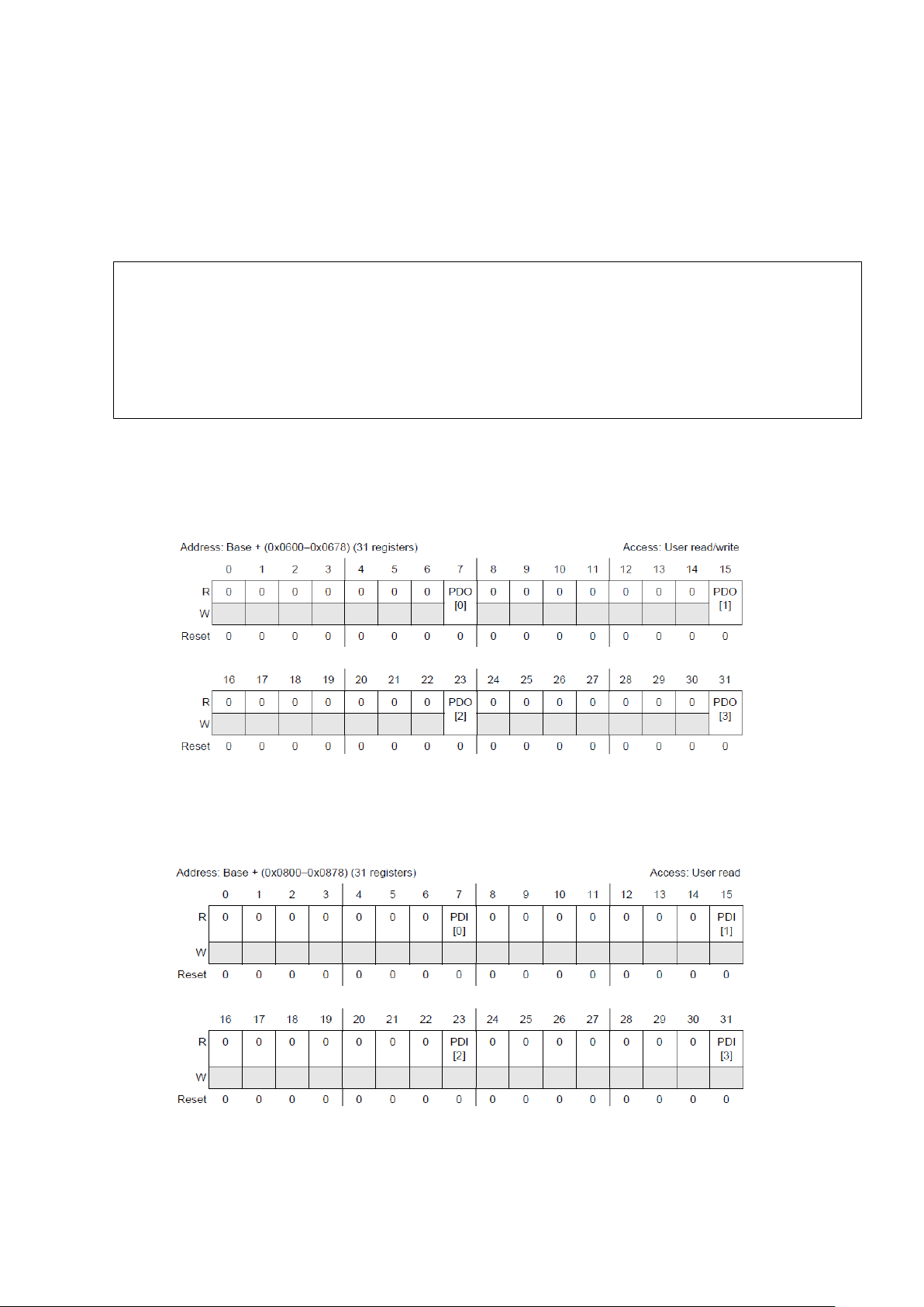
Some peripherals’ inputs can be received from multiple pads, in this case using PSMI registers’
3. GPIO: General Purpose Input/Output
Figure 24 : GPIO Pad Data Output Register (Reference Manual Rev7 – Fig. 8-12)
Figure 25 : GPIO Pad Data Input Register (Reference Manual Rev7 – Fig. 8-13)
void config_PORT_E(void)
}
PADSEL fields; one of the possible pads must be selected. See Appendix 3 for more information
about possible selections. It is mostly needed by communication modules.
Here’s an example code that sets pads connected to four LEDs as GPIO outputs and switch S1 as
an input.
{
SIU.PCR[68].R = 0x0200; /* LEDs are connected between PORT E pins and 5V */
SIU.PCR[69].R = 0x0200; /* PE 4 to PE 7 */
SIU.PCR[70].R = 0x0200;
SIU.PCR[71].R = 0x0200;
SIU.PCR[64].R = 0x0100; /* PE 0 */
General purpose input/output (GPIO) functionality allows reading and writing binary values on
pins (0V/5V). To set or clear a pad we need to use GPIO Pad Data Output register.
These 31 32-bit registers can be seen as 123 8-bit registers with only one field to set or clear the
pad. A very similar register for reading inputs exists is show on the figure below.
Page 24
Here’s an example of usage of these registers on TRK-MPC5604B:
Figure 26 : Parallel GPIO Pad Data In/Out Registers (Reference Manual Rev7 – Table 8-16/17)
/* This extract of code will blink LEDs 1 to 4 sequentially while the button S1
is pressed. */
uint32_t LED_state, i;
int main (void) {
initModesAndClock(); /* Initialisation of the device */
config_PORT_E(); /* Configuration of GPIO */
for (; ;) /* Main loop */
{
/* while button is pressed(signal is 0, see schematic) */
for (LED_state=0; !SIU.GPDI[64].B.PDI; LED_state++)
{
if (LED_state==4)
{
LED_state = 0;
SIU.GPDO[68].B.PDO = 1; // All LEDs are off.
SIU.GPDO[69].B.PDO = 1; // -
SIU.GPDO[70].B.PDO = 1; // -
SIU.GPDO[71].B.PDO = 1; // - */
}
SIU.GPDO[68+ LED_state].B.PDO = 0; /* Set next LED */
for (i=0; i<4500000; i++){} /* wait a while */
}
/* while button is not pressed */
for (; SIU.GPDI[64].B.PDI;){}
}
}
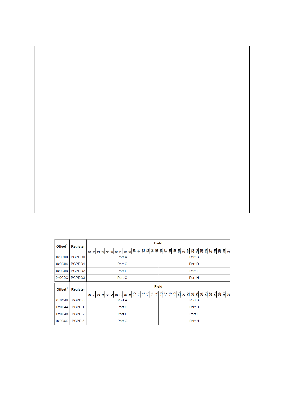
We can notice that use of data input/output registers get repetitive when multiple pads has to be
changed or read. There are parallel input/output registers which simplifies this issue.
These registers allow us to read/write multiple pads on ports with 32 bit registers. For writing
multiple pads masks are often necessary to only change pads of interest, there are masked
parallel registers which simplifies this problem (see figure below).
Page 25
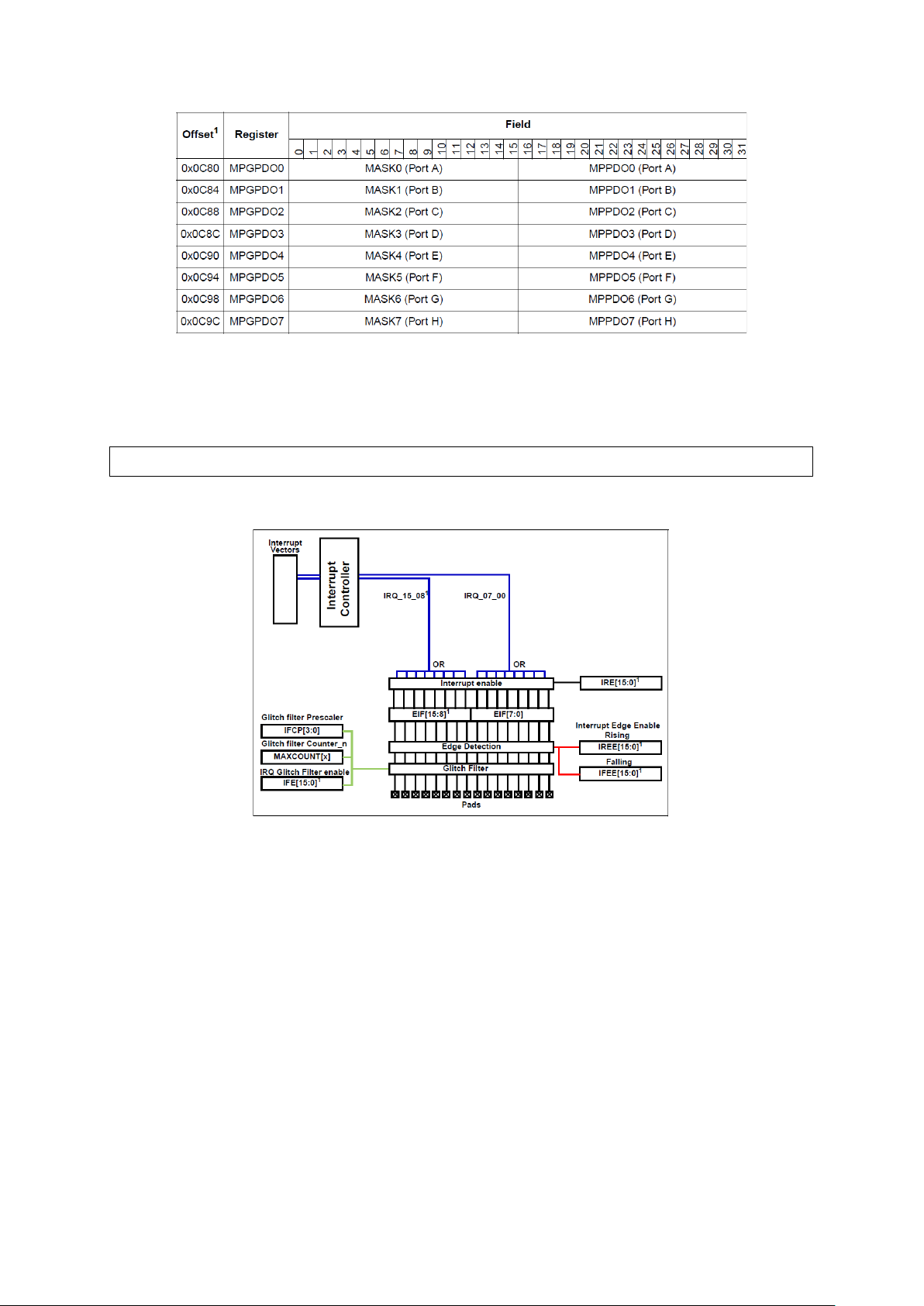
Figure 27 : Masked Parallel GPIO Pad Data Out Registers (Reference Manual Rev7 – Table 8-18)
4. External interrupts
Figure 28 : External Interrupt Pad Diagram (Reference Manual Rev7 – Fig. 8-17)
SIU.MPGPDO[4].R = 0x0F000F00; // All LEDs are off.
Here’s the equivalent code for turning all LEDs off for the previous code written with these new
registers:
16 pads among 123 have External Interrupt functionality, a rising or falling edge can be set to
trigger an interrupt. There are two system interrupt vectors spared for EIRQ pins, IRQ0 for
EIRQ[0:7] and IRQ2 for EIRQ[8:15]. Looking at the diagram above we can identify following
registers:
Interrupt Request Enable Register (IRER) with a 16-bit field to specify pads that can
request interrupts,
Interrupt Status Flag Register (ISR): has a 16-bit flag field called EIF, flags can be
cleared by writing 1,
Interrupt Rising-Edge Event Enable Register (IREER): a rising edge triggers the
interrupt,
Interrupt Falling-Edge Event Enable Register (IFEER): a falling edge triggers the
interrupt, (note that a pad can trigger interrupts on both rising and falling edge
events).
Page 26

There’s also a glitch filter for these pads that avoids erroneous requests that may be triggered by
noise. Interrupt Filter Enable Register (IFER) can set which pads are to be filtered. And IFMC
and IFCPR are used to set filters parameters. These two registers together have only two fields
MAXCNT[x][3:0] (x: one for each pad) is the Maximum Couter, IFCP[3:0] is the clock prescaler
setting common to all pads. Having these two parameters, we have:
Filter Period
[]
=
=
(
×
[]+ ) ( is random in [1,3])
(
+ 1)×
,
= 16
If the signal is steady for at least the Filter Period, then the glitch filter triggers the interrupt.
Page 27
Chapter 3
INTC: Interrupt Controller
1. Introduction
Figure 29 : Interrupt Requests Handling by INTC in Software Vector Mode (Freescale Lecture)
Figure 30 : ISR Handling (SW mode) (Freescale Lecture)
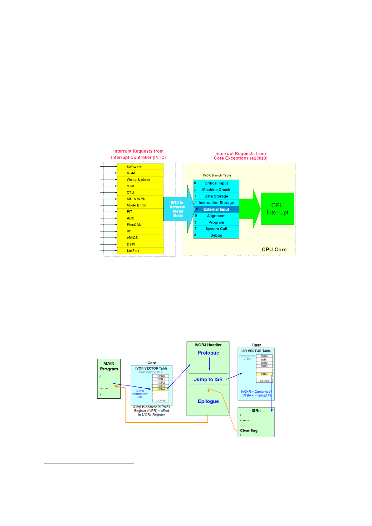
The core of MPC5604B (e200z0h) is associated with registers called Interrupt Vector Offset
Register (IVOR), which handles different kinds of exceptions that might occur during runtime.
Different kinds of core exceptions are handled by different IVORs. IVOR4 is the one used for
interrupt handling.
The Interrupt Controller (INTC) is a module that is used for Interrupt Service Requests (ISR)
2
management. In software vector mode
This exception branches to INTC handling functions which saves current register and program
counter (Prologue), then jumps to the ISR Vector Table where the vector associated to the
particular ISR allows jumping to the ISR handler(written by the user). The handler clears the ISR
flag and returns back to the INTC’s handler routine which restores core’s status (Epilogue).
, ISRs coming from peripherals trigger IVOR4 exceptions.
2
In hardware mode, each handler has to write its own Prologue and Epilogue and their IVORs are
separate. It will be briefly explained at the end of the chapter.
21
Page 28
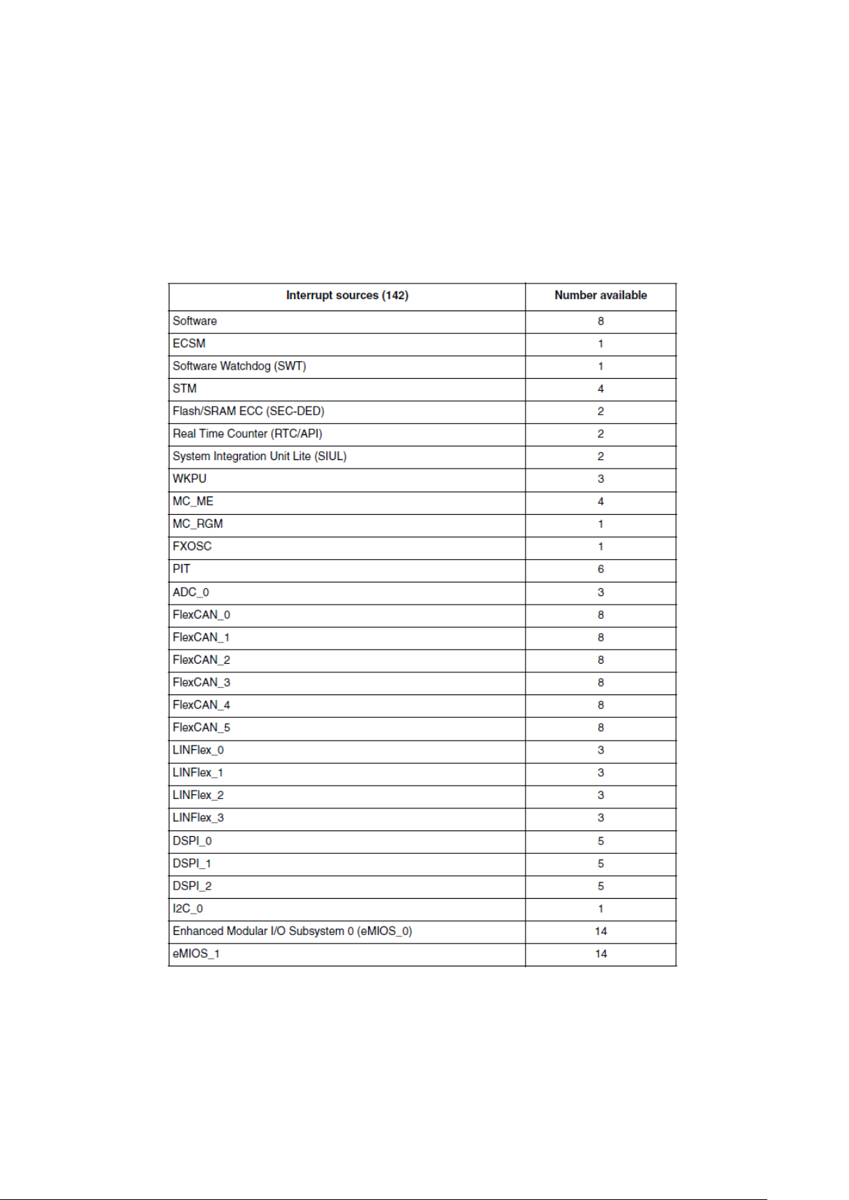
There are 294 vectors on the ISR, the first 11 being vectors from IVOR Vector Table, and among
Figure 31 : Number of ISR vectors available for each interrupt source (R.M. Rev8 – Table 16-1)
the rest only 142 are usable (the others are reserved). Of these usable vectors, 8 of them are
reserved for software triggered interrupts (software ISR) and the other 134 are hardware ISR
linked to the peripherals.
Each of these vectors can be given a priority between 0 and 15, the latter being the highest
priority. An interruption of higher priority will put on hold the others; INTC could handle nested
interruptions and their resource management if configured properly.
Page 29

2. INTC configuration (Software mode)
2.1. Enabling interrupt requests
2.2. Configuring hardware ISRs
void enableIrq(void) {
}
void INTC_InstallINTCInterruptHandler (INTCInterruptFn handlerFn, unsigned short
uint32_t LED_state = 0;
0 is PIT1 vector
}
There are two stages for enabling interrupts; first, at a general level, the interrupt handling in
the microcontroller has to be enabled, then, at the peripheral level, for an ISR to be raised, the
registers in charge of that interrupt has to be configured.
Here’s the code for enabling interrupts at a general level:
INTC.CPR.B.PRI = 0; /* Single Core: Lower INTC's current priority */
asm( "wrteei 1"); /* Enable external interrupts */
Peripheral-level enabling of an ISR will be mentioned on that peripheral’s chapter.
INTC is implemented in following files in a project: INTCInterrupts.h, IntcInterrupts.c,
Exceptions.h, Expcetions.c. These files possess required routines to execute the previously
explained ISR handling procedure. The following function is used to configure an ISR’s handler
and priority:
vectorNum, unsigned char psrPriority);
vectorNum is the ISR’s vector number (see Interrupt Vector Table), handlerFn is a
written by the user, and psrPriority is the priority between 0 and 15 (0 priority is not served).
Example: Blinking a LED when PIT1 (a timer, see following chapters) interrupt is generated.
void PIT1_Interrupt();
int main (void) {
initModesAndClock(); /* Initialisation of the device */
config_PORT_E(); /* Configuration of GPIO */
initPIT(); /* Init the timer PIT1 to trigger ISR every 0.5sec */
INTC_InstallINTCInterruptHandler(PIT1_Interrupt,60,2); /* 6
number, we choose to give a priority of 2 */
}
void PIT1_Interrupt(){
//Finite State Machine for the LED 1
if(LED_state == 0) {
LED_state = 1;
else {
LED_state = 0;
//Clear PIT1 interrupt
PIT.CH[1].TFLG.B.TIF = 1;
enableIrq(); /* Enable interrupts, after interrupt configs */
for (; ;){} /* Main loop */
void function
SIU.GPDO[68].B.PDO = 0; /* Set LED */}
SIU.GPDO[68].B.PDO = 1; /* Clear LED */}
Page 30
The led will blink with a frequency of 1Hz. It should be noted that it’s common to use finite state
2.3. Configuring software ISRs
Figure 32 : INTC Software Set/Clear Interrupt Register (R.M. Rev8 – Fig. 16-7/8)
2.4. Enabling nested interruptions
3. Hardware mode INTC
machines in interrupt handlers.
There are 8 ISRs that can be triggered by the software, the ISR configuration is done in the same
way as hardware ISRs but triggering the interrupt is more complicated. On hardware ISRs,
peripherals are in charge for triggering the interrupt (a button is pushed, a timer has reached a
limit value, an ADC conversion is done etc.)
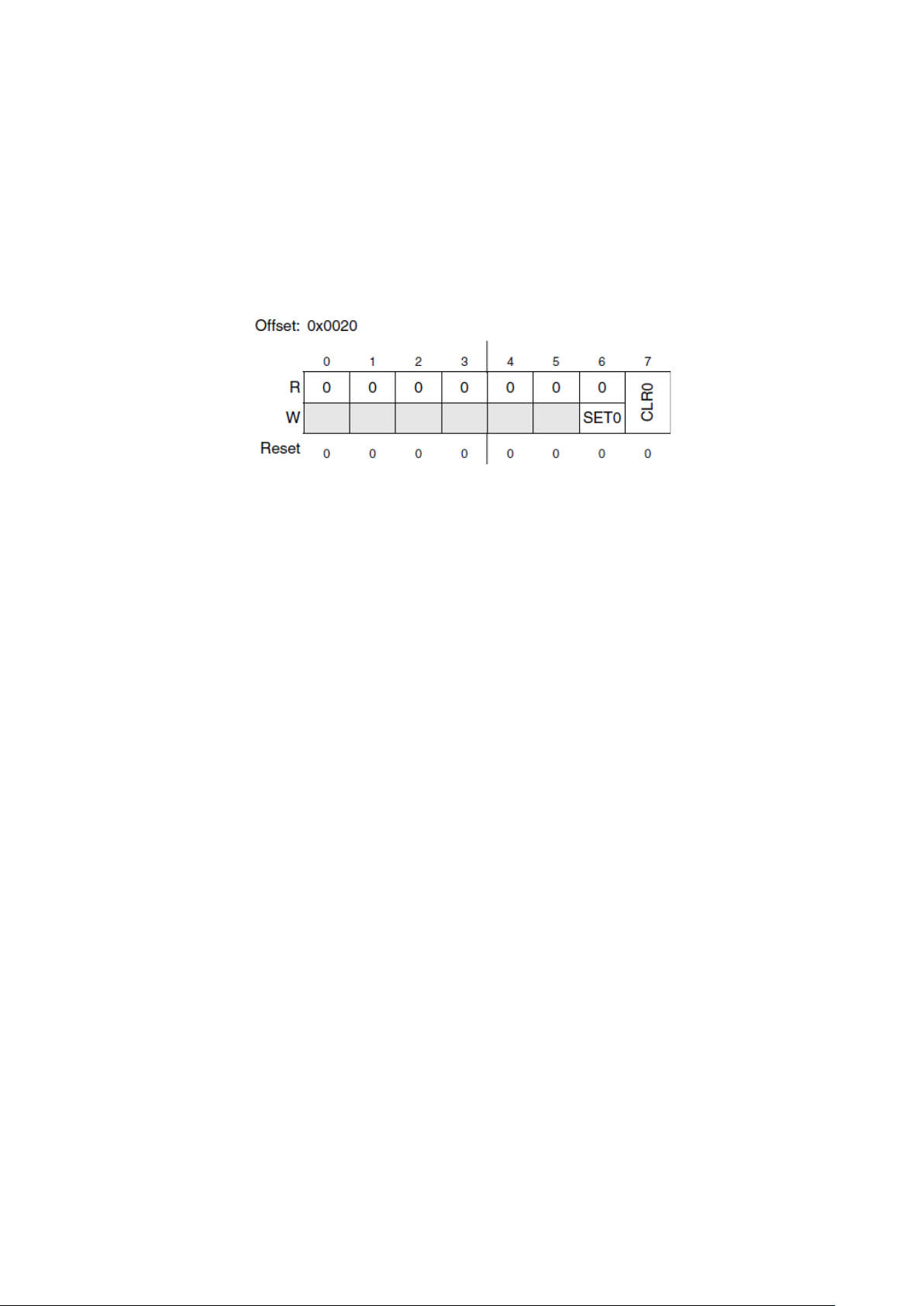
For triggering a software interrupt we use INTC Software Set/Clear Interrupt Registers SSCIR,
each one of these 8-bit registers can trigger a software ISR (writing ‘1’ to SET) and can clear the
flag by writing ‘1’ to CLR.
By default nested interruptions are not enabled, the prologue of INTC handler does not save
every register, this causes a loss of time in interrupt priority handling when a higher priority
interrupt is triggered while a lower priority is being processed. When nested interrupts are
enabled, a higher priority interrupt can pause the handler of a lower priority and finish it up
later (which can sometimes lead to unexpected results in the paused handlers). When nested
interrupts are disabled, higher priority handling has to wait the end of the previous one.
To enable nested interruptions, the user needs to change the value of
INTC_NESTED_INTERRUPT macro at line 17 of “IntcInterrupts.c” to 1.
Previously explained ISR method is only used in software interrupt mode of INTC where the
prologue and epilogue is common to all interrupt. In applications where avoiding saving some
registers is affordable and needed for saving time, it is possible to use hardware interrupts
where the prologue and epilogue are customisable.
The following figure shows the functionality difference between HW and SW mode, if you need
to use HW mode interrupts, then you’ll need to add appropriate handler branch instructions to
the intc_hw_branch_table_vle.s as explained on the figure (see cookbook example) and define
handlers with prologue & epilogue on a handlers_vle.s.
Page 31
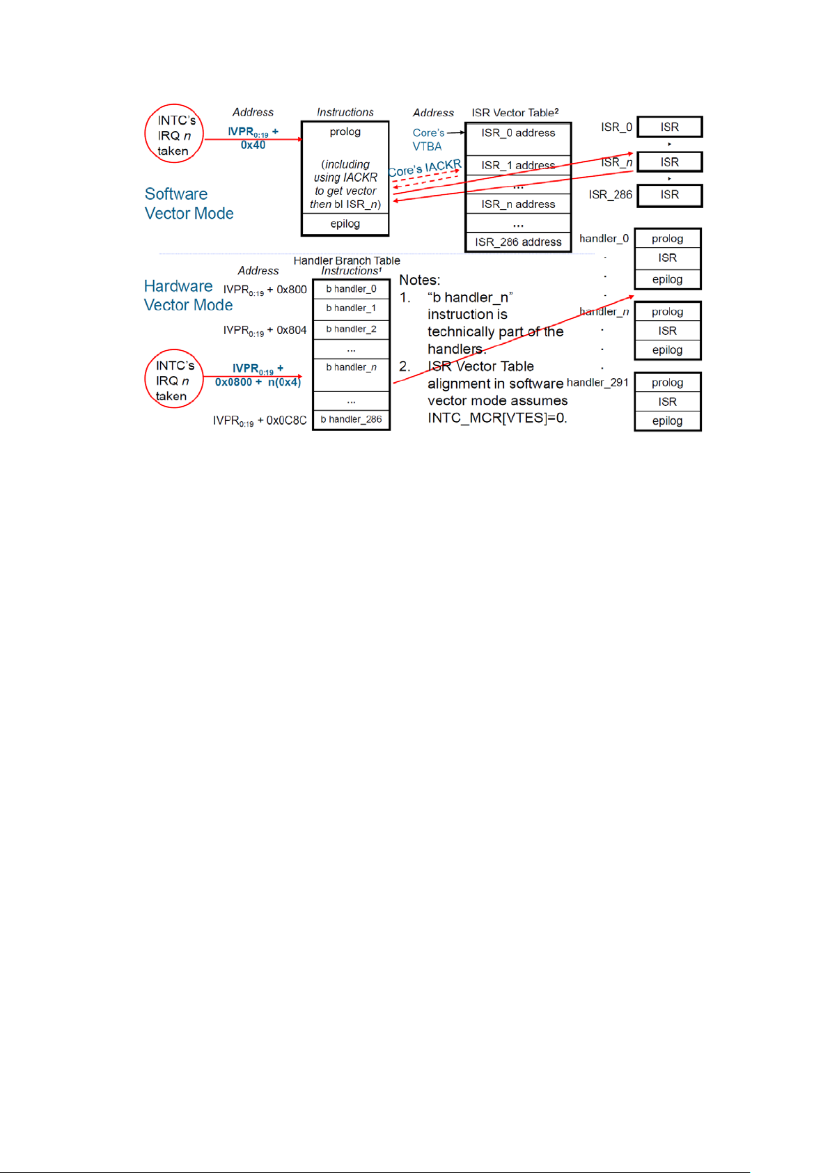
Figure 33 : INTC SW/HW mode comparison (Freescale Tutorial)
Page 32
Chapter 4
Timer Modules
1. Introduction
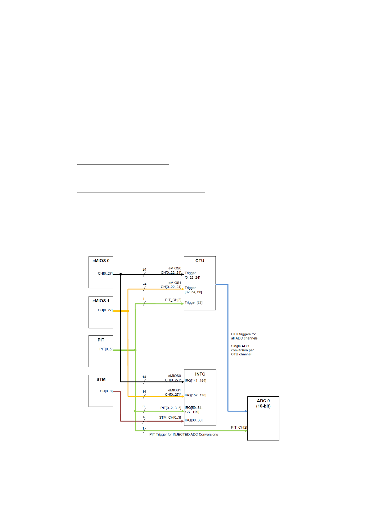
Figure 34 : Interaction between some timers and other peripherals (R.M. Rev8 – Fig. 24-1)
There are various timer-like peripherals available in this microcontroller with different
characteristics and uses. Here’s a list of timer modules with brief descriptions:
System Timer Module (STM): A 32-bit running-up counter, clocked by the system
clock. It has four 32-bit compare channels with individual interrupts. Useful for
measuring code execution time (clock cycles).
Periodic Interrupt Timer (PIT): Made of six timers clocked by the system clock. They
are 32-bit count-down timers; they have to be initialised with a start value. Reaching
0 and restarting triggers an interrupt.
Enhanced Modular I/O Subsystem (eMIOS): This module will not be explained in this
chapter but the next chapter will be solely dedicated to it. It is useful for
measurements and generating PWM.
Real Time Clock/Autonomous Periodic Interrupt (RTC/API): 32-bit counter, can
measure up to 1.5 Months with 1ms resolution. Can trigger interrupts and wakeup
events on match. API module can generate periodic interrupts while RTC keeps
counting.
26
Page 33
2. STM: System Timer Module
Figure 35 : STM Control Register (R.M. Rev8 – Fig. 24-2)
Figure 36 : STM Count Register (R.M. Rev8 – Fig. 24-3)
3. PIT: Periodic Interrupt Timer
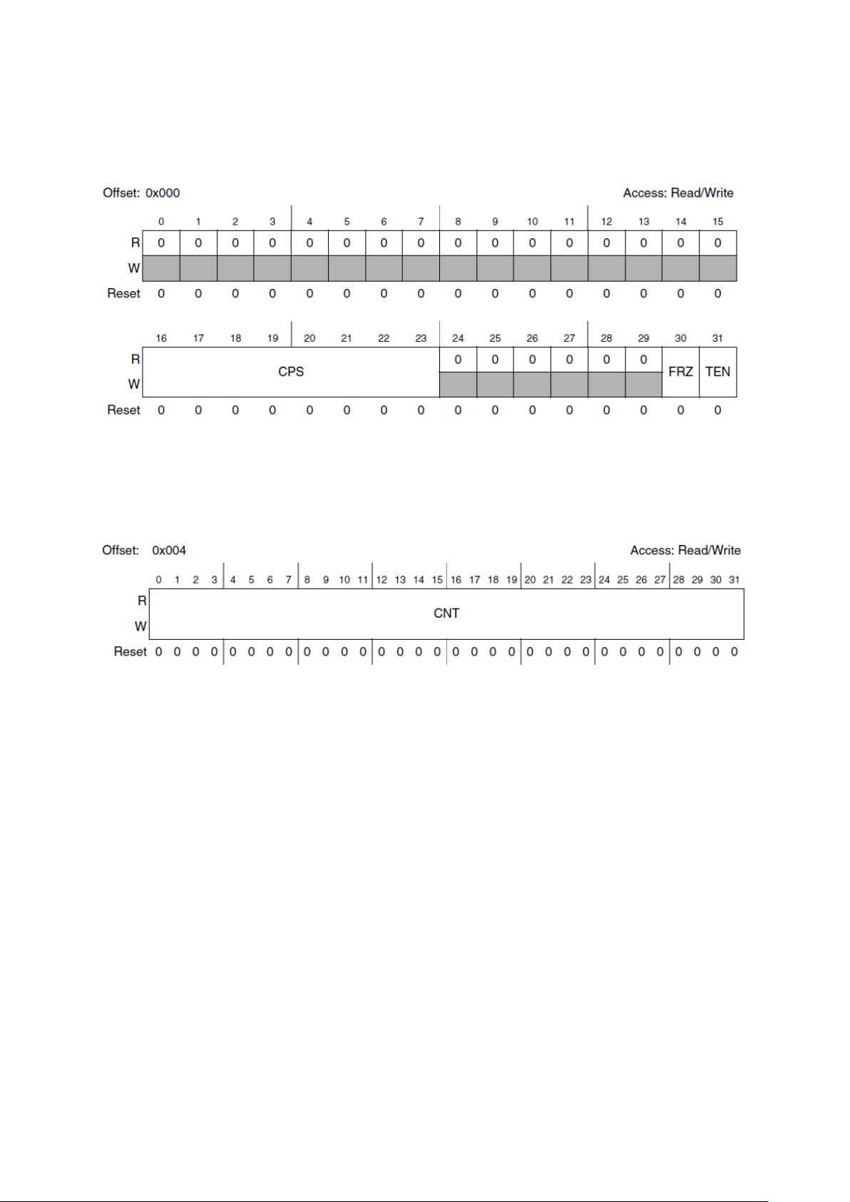
This module has two general registers for control and count value, and 3 register for each one of
four channels.
The control register (STM_CR) can enable the clock using TEN (Timer Enable, write ‘1’ to
enable) and it can set the timers behaviour in debug with FRZ (Freeze, write ‘1’ to stop the timer
in debug mode). The field CPS is the counter prescaler, the clock is divided by (CPS[7:0]+1).
The value of the counter is stored in the count register (STM_CNT). The counter goes up to
0xFFFFFFFF and then starts again from 0x00000000.
Each of the four channels [0...3] have the following registers:
STM Channel Control Register (STM_CCR[n]) with a one bit enable field, CEN.
STM Channel Interrupt Register (STM_CIR[n]) with a one bit channel interrupt flag field
CIF (write ’1’ to clear the flag)
STM Channel Compare Register (STM_CMP[n]) with a 32-bit field compare value CMP.
An interrupt is generated when the counter value reaches the channel compare value (interrupt
n° 30-33).
There are six independent 32-bit count-down timers in this module, with no prescaler, each
having independent timeout values and interrupts. The module has one general control register
and each timer has four configuration registers.
Page 34
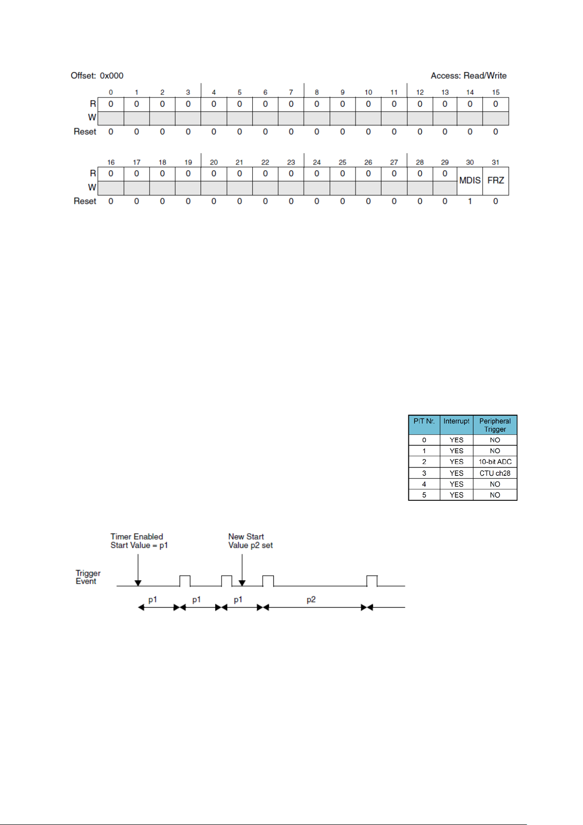
Figure 37 : PIT Module Control Register (R.M. Rev8 – Fig. 24-57)
Figure 39 : Changing Timer Period (R.M. Rev8 – Fig. 24-64)
Figure 38 : Some PITs can
trigger a peripheral event
The module is disabled by default, to enable it; we have to write ‘0’ to MDIS (Module Disable)
field. The FRZ field allows stopping the timers in debug mode by writing ‘1’.
Each of the six timers [0...5] have the following registers:
Timer Control Register (TCTRL) with a 1-bit timer enable (TEN) field and another 1-bit
timer interrupt enable (TIE) field.
Timer Load Value Register (LDVAL) with a 32-bit TSV (Timer Start Value) field.
Current Timer Value Register (CVAL) with a 32-bit TVL (Timer Value) field.
Timer Flag Register (TFLG) with a one bit timer interrupt flag field TIF (write ’1’ to clear
the flag).
Disabling then enabling a timer will restart à new period for the timer
(LDVAL loaded in CVAL). The timer automatically loads LDVAL in CVAL
when it reaches 0 and triggers an interrupt. It is possible to change
LDVAL value while the timer is running; the timer will load the new
value on the next trigger event.
Page 35
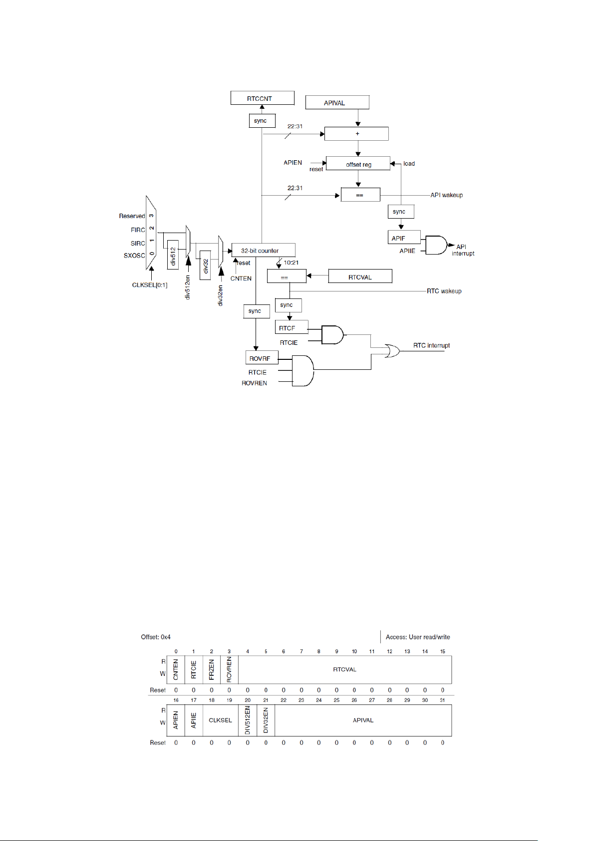
4. RTC/API: Real Time Clock/ Autonomous Periodic Interrupt
Figure 40 : RTC/API Architecture (R.M. Rev8 – Fig. 13-1)
Figure 41 : RTC Control Register (R.M. Rev8 – Fig. 13-2)
The Real Time Clock is an independent 32-bit timer, clocked by either internal RC oscillators
(128kHz or 16MHz) or by a slow external crystal (32kHz). By using dividers by 32 and/or 512,
we can count in (see the last table
of this section). RTC module has a 12-bit match value, that is compared to the bits [21:10] of the
counter, and it can trigger a wakeup or interrupt event.
The Autonomous Periodic Interrupt (API) module can trigger wakeup or interrupt events
periodically; a 10-bit period value is added to the bits [22:31] of current value of the counter,
giving an offset match register that can generate a trigger. Once an event is triggered, the offset
register is updated with a new match value, therefore resulting in periodically triggered events.
The RTC Supervisor Control (RTCSUPV) register can only be modified in device modes and its
SUPV bit can limit access to other registers (true by default) or not. Writing ‘0’ to this bit will
grant access to other registers in user modes.
Page 36
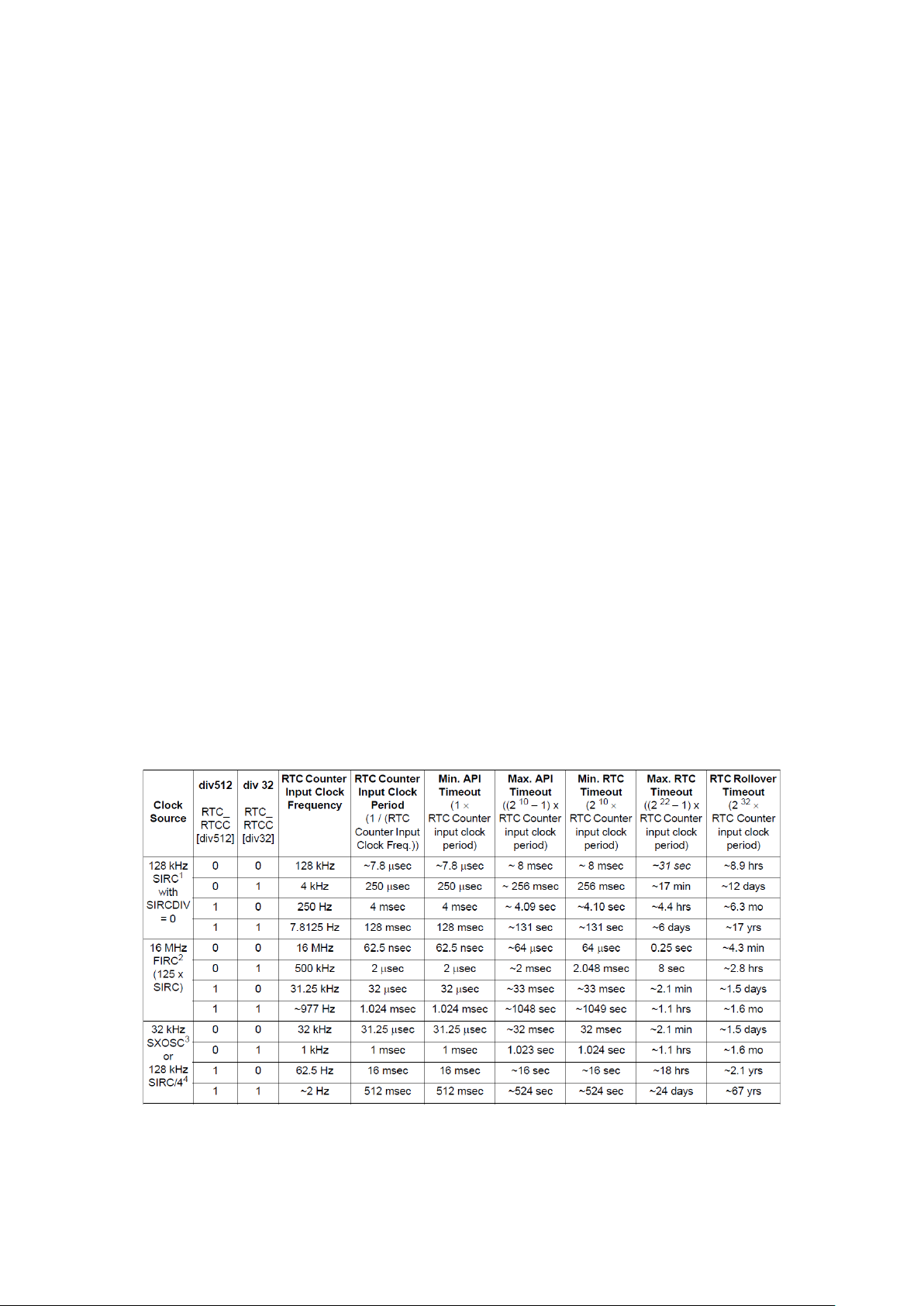
RTC Control (RTCC) register assembles main parameters of this module, modifiable fields are:
Figure 42 : Different resolutions and timeout limits for RTC/API
CNTEN: Counter enable (write ‘1’ for enabled),
RTCIE: RTC interrupts enable (write ‘1’ for enabled),
FRZEN: Freeze enable (write ‘1’ for freezing the module in debug mode),
ROVREN: Counter roll over interrupt/wakeup event enable (write ‘1’ for enabled), when
enabled, if the counter reaches 0xFFFFFFFF and goes back to 0x00000000 an interrupt is
triggered.
RTCVAL: RTC compare value, when bits [21:10] of the counter is matched with this
value, an interrupt is triggered.
APIEN: API module enable (write ‘1’ for enabled),
APIIE: API interrupts enable(write ‘1’ for enabled),
CLKSEL: A 2-bit field for selecting a clock for the counter, 00: SXOSC, 01: SIRC, 10: FIRC,
11: reserved.
DIV512/32EN: Enabling 512/32 divider, these dividers allow to get counter period slow
enough to measure important amounts of time (these dividers should be set before
enabling the counter).
APIVAL: API Compare Value, this is the value of the period for triggering an interrupt.
The minimum value is 4, and its value should be change while API is not enabled. There
will a small transient time in the first period.
The RTC Status (RTCS) register is needed to clear ISR flags; RTCF is for RTC interrupt
generated on match, APIF is for the API interrupt and ROVRF is for the RTC interrupt generated
on roll over.
The last RTC register is the count value (RTCCNT) register it has the 32-bit field RTCCNT
which contains the current value of the RTC counter with maybe up to 6 cycles of delay. The
delay is caused by the clock source difference between system clock and RTC clock but its effects
remain small.
Page 37
5. Timer Examples
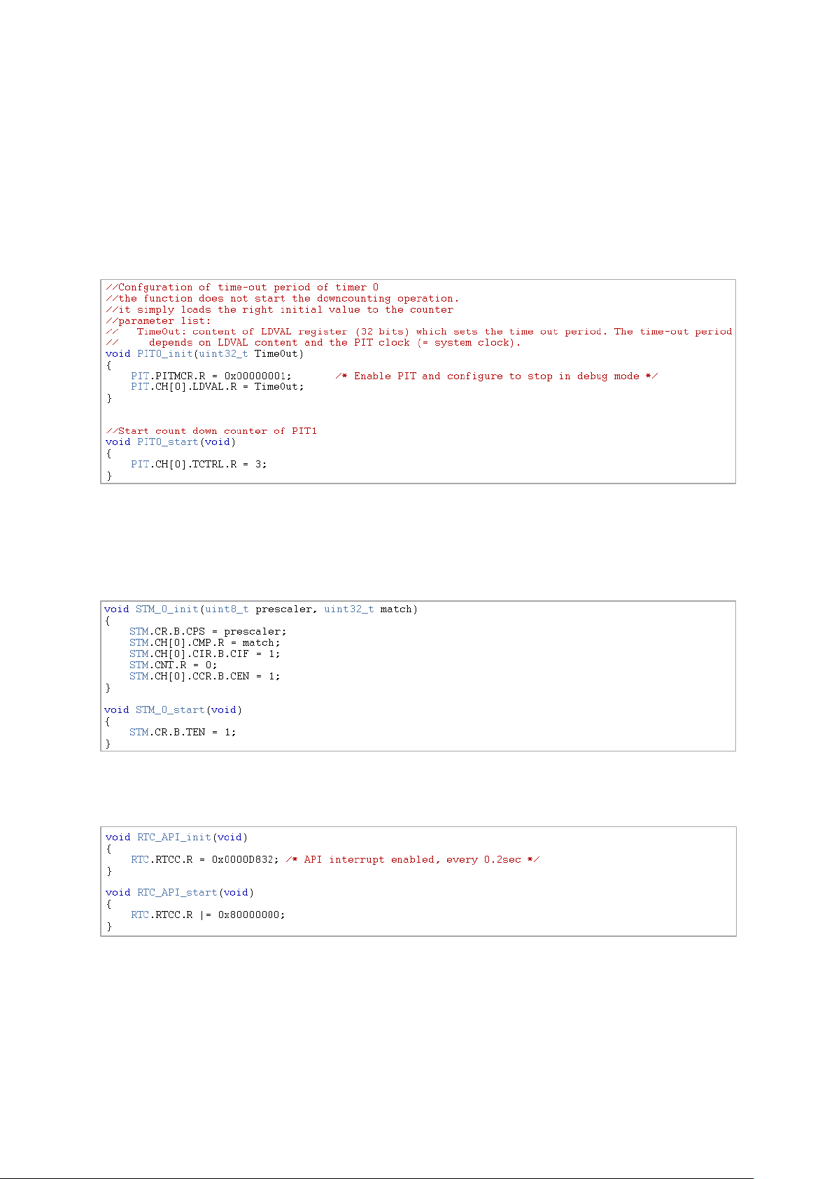
A timer configuration example has been built using STM, PIT and RTC/API where each module
has to toggle a LED at 5Hz frequency (therefore generating à 2.5Hz square wave). Their
precision and ease of use will be compared.
Let’s start with PIT; it has to be initialized with a TimeOut value which will set the frequency. If
we chose the use 8MHz crystal clock, it has to be 1600000=0x186A00 to raise an interrupt at
5Hz frequency. The start function will enable the counter and the interrupt.
For STM it will be harder to generate periodic interrupts, as the counter will try to roll-over after
a match. The 8-bit prescaler field is not large enough to make a 5Hz roll-over therefore after
each match interrupt; the counter has to be reset. This will deteriorate the resulting frequency a
bit.
For configuring RTC/API, we enable API interrupts and using the resolution table we chose SIRC
with the 512 divider. This allows getting an interrupt raised at a 5Hz frequency.
Interrupt handlers of each timer is similar: clear the flag, toggle the LED, but STM’s interrupt
also contains an instruction to clear the counter.
In the end, by measuring the square wawe’s frequency we got 2.5Hz with the PIT, 2.499Hz with
the STM. With the RTC clock we got different values between 1.9Hz and 2.8Hz and we could set
it to 2.5Hz by trimming the SIRC clock with a trimming value of 4.
Page 38
Chapter 5
eMIOS: Enhanced Modular I/O Subsystem
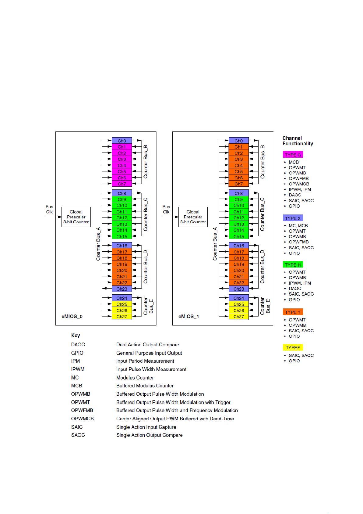
Figure 43 : eMIOS Channel Configuration (R.M. Rev8 – Fig. 24-7)
These modules use timer channels to generate or measure time based events like PWM, counter
generation, period measurement etc. Channels can be configured up to 12 different operation
modes shown on the figure below.
32
Page 39
1. Module Configuration
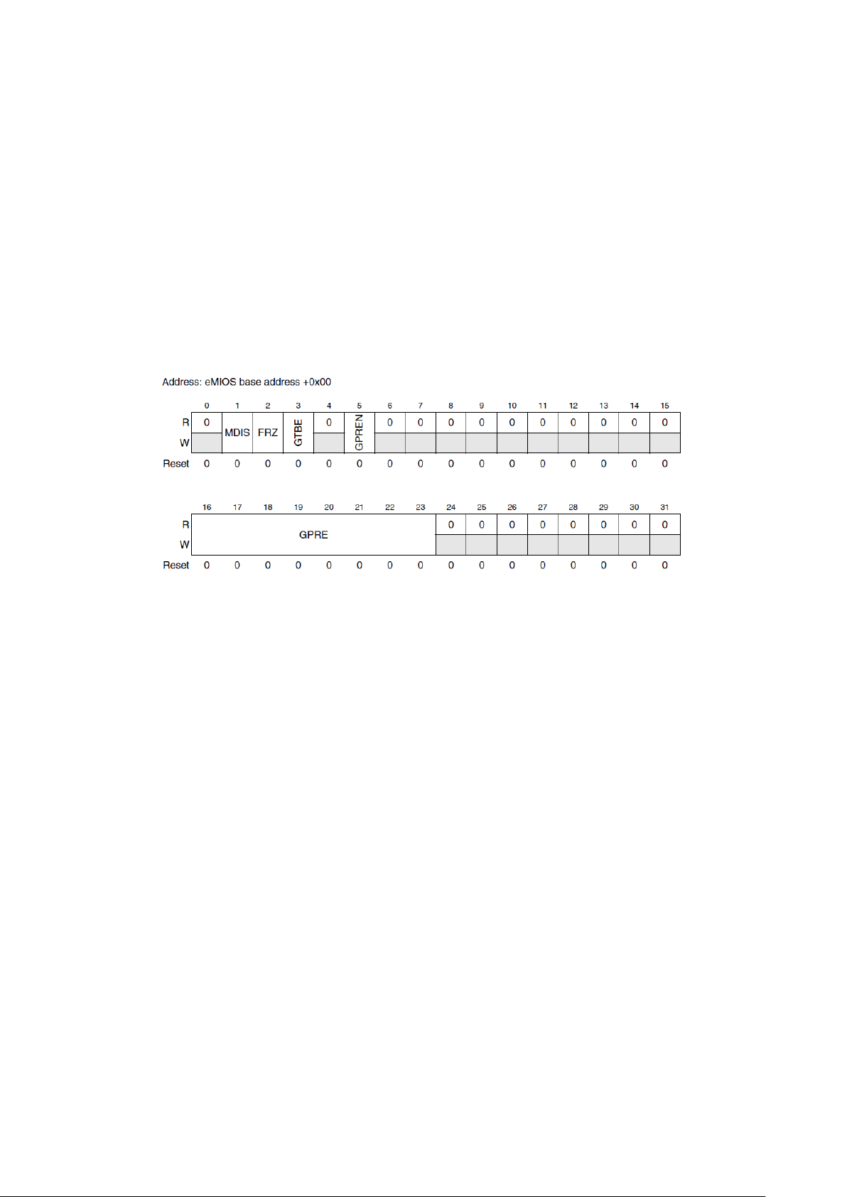
Figure 44 : eMIOS Module Configuration Register (R.M. Rev8 – Fig. 24-8)
Without making any channel configurations, this block can be seen as multiple 16-bit upcounting channels that can select a counter among its internal counter, the 16-bit counter bus A
or one of 16-bit counter busses B, C, D or E, depending on the channel’s position.
Each of these counter busses are controlled by one particular channel configured as a counter,
previous figure shows that bus A is controlled by channel 23 and B, C, D and E are respectively
controlled by channels 0, 8, 16 and 24. Each channel contains four internal 16-bit registers A1,
B1, A2, and B2 that are used for implementing different behaviours.
Each eMIOS module has four general configuration registers:
EMIOS_MCR register has a Module Disable (MDIS) bit to put the block in low power mode when
set, a Freeze (FRZ) bit to freeze each channel in debug mode, which would allow better
debugging. Global Time Base Enable (GTBE) bit is for enabling the global 8-bit counter of the
eMIOS module, Global Prescaler Enable(GPREN) bit disables the clock when set to ‘0’ and
divides the clock of the ‘peripheral set 3’ by Global Prescaler (GPRE+1) when set to ‘1’ (so, the
peripheral clock can be divided up to 256).
Another important register is the eMIOS Global Flag Register (EMIO_GFR), which contains a flag
bit per each 28 channel of the block (F0 … F27). This is a read only register.
eMIOS Disable Channel Register (EMIOS_UCDIS) contains 28 disable bits for each channel
(CHDIS0 … CHDIS27), for disabling (setting to ‘1’) or enabling (clearing) them. Channels should
be all enabled by default.
When a channel is running in MC, MCB or an output mode, values written to A2 and B2 are
transferred to A1 and B2 (either immediately or in the next period). eMIOS Output Update
Disable Register (EMIOS_OUDR) contains 28 bits (OU0 … OU27) for disabling this data transfer
(when set to ‘1’).
Page 40
2. Channel Configuration
1.1. Introduction
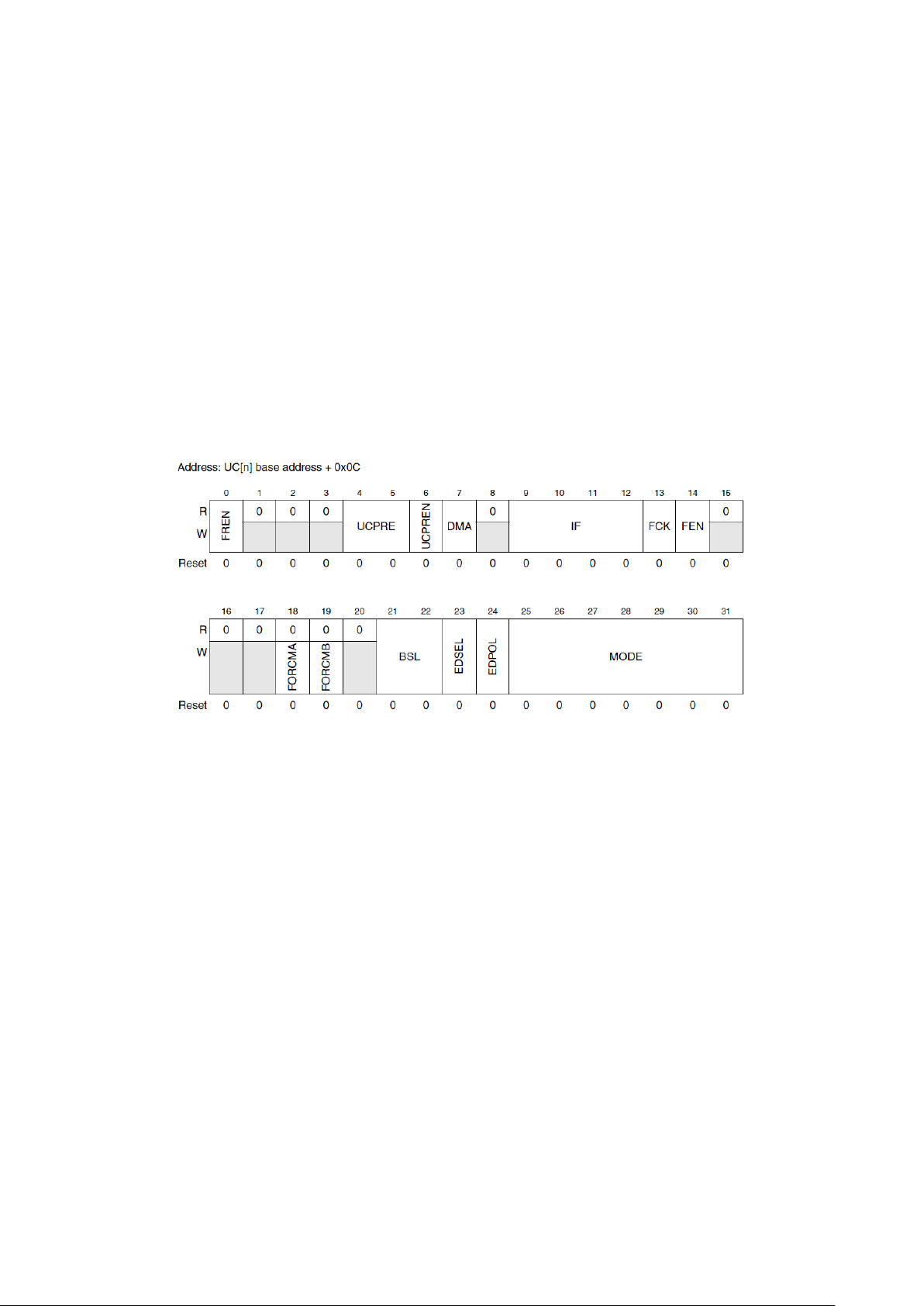
Figure 45 : eMIOS Channel Control Register (R.M. Rev8 – Fig. 24-15)
Unified Channels are made of:
- A counter bus selector, which can select among three time base sources, to be used for time-
based events.
- An internal 16-bit counter clocked by the prescaled eMIOS internal clock.
- Two data registers A and B, double buffered and related to four internal registers (A1, B1,
A2, and B2) that can be used for input capture or output compare.
- Programmable input filter.
- Programmable edge detector.
- An output flip-flop for buffering the logic levels.
Each channel has a control register (EMIOS_CH[n]_CCR) defined as:
Freeze Enable (FREN) bit allows freezing all channel register values in debug if eMIOS
block’s FRZ bit is set.
Bus Select field (BSL) allows to choose between counter bus A (00), secondary counter bus
(B, C, D or E) (01) or the eMIOS internal counter (11). This clock has to be enabled using
Prescaler Enable (UCPREN) bit and it can be prescaled using UCPRE (clock divided by
UCPRE+1).
Direct Memory Access (DMA) bit selects if the FLAG generation leads to an IRQ (0) or a CTU
trigger (1). (See CTU chapter). To enable flags, FEN bit has to be set.
Input Filter (IF) selects the minimum input pulse width that can pass through the filter
(0000: bypassed, 0001: 2 FLT_CLK periods, 0010: 4 periods, 0100: 8 periods, 1000: 16
periods). The Filter Clock (FCK) can either be the main clock (1) or the prescaled clock (0).
While using an output mode, Force Match A/B bit (FORCMA/B) generates a successful
comparison with register A/B. Can be used to force the output to a value.
Edge Polarity (EDPOL) bit: for input modes selects whether a rising (1) edge or a falling (0)
edge triggers and event (a counter, capture or a flag). For output modes, this bit selects the
logic level on the output pint: if it’s set to ‘1’, a match on A sets the output while a match on
B clears it. (It’s the opposite if it’s set to ‘0’).
Page 41
Edge Selection (EDSEL) bit: for input modes, this bit selects whether both edges are
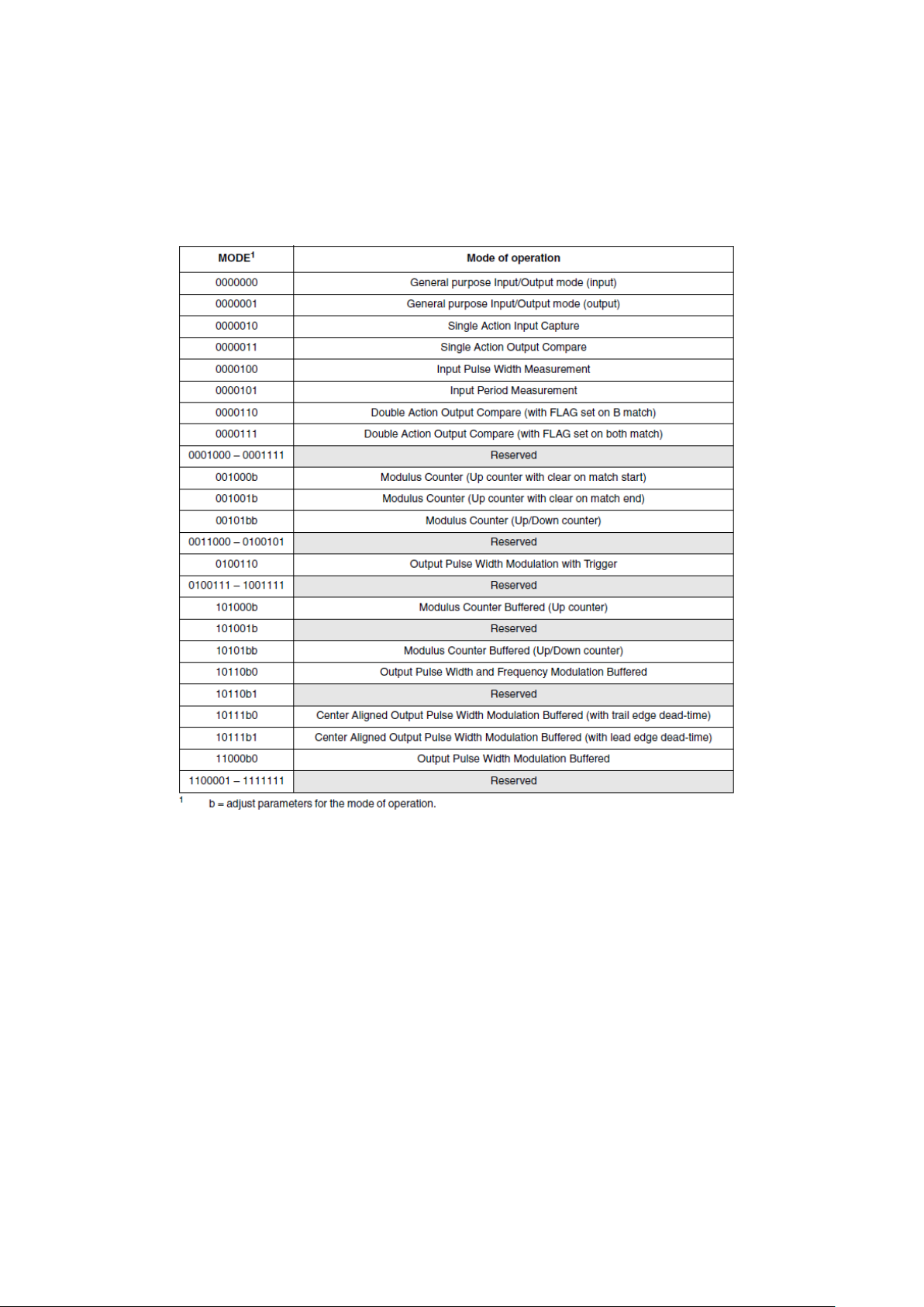
Figure 46 : Channel Mode Selection (R.M. Rev8 – Table 24-21)
triggering (‘1’) or a single edge defined by EDPOL (‘0’). For GPIO input mode, it selects if a
flag can be generated (‘1’: no flag is generated, ‘0’: it’s generated as defined by EDPOL). And
for SAOC mode, it selects if output flip-flop is toggled at each match (see the section below).
MODE field is used for mode selection as described in the table below.
Another major register for a channel is the status register (EMIOS_CH[n]_CSR) containing the
flag bit (FLAG, write ‘1’ to clear), overrun bit (OVR: write ‘1’ to clear) which is set when a flag
generation occurs while FLAG was already set. Overflow bit (OVFL: write ‘1’ to clear) is set when
an overflow has occurred in the internal counter. Two read only fields allow getting the input
(UCIN) or output (UCOUT) state of the pin.
A 16-bit counter register (EMIOS_CH[n]_CCNTR) that contains the current value of the channel’s
internal counter.
And finally, there are three 16-bit data registers that will set the behaviour of the channel in a
particular mode of operation. eMIOS Unified Channel A register (EMIOS_CH[n]_CADR), eMIOS UC
B register (EMIOS_CH[n]_CBDR) and eMIOS Alternate A register (EMIOS_CH[n]_ALTCADR).
These three registers are used to read or write the four internal registers (A1; A2; B1; B2)
previously mentioned. The following table shows the value assignment of different modes.
Page 42
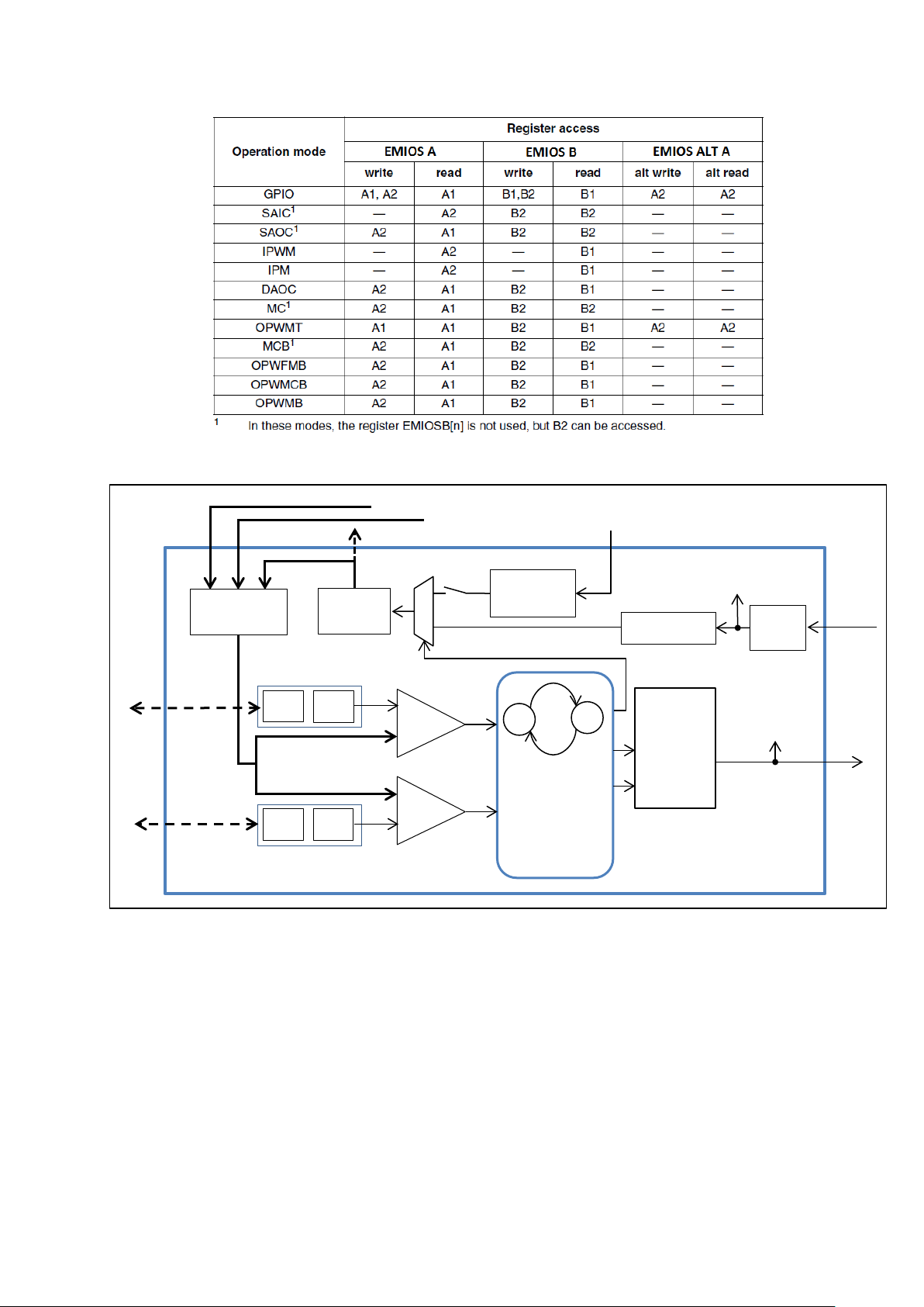
Figure 47 : eMIOS A, B and Alt A Register R/W (R.M. Rev8 – Table 24-16)
Figure 48 : An eMIOS Channel’s Block Diagram
1.2. GPIO: General Purpose Input/Output
Counter Bus
Select (BSL)
Internal
Counter
Prescaler
UCPRE
UCPREN
eMIOS Internal
Counter Clock
Secondary Counter Bus
(B,C…)
Primary Counter Bus A
Input
Filter
IF, FCK
Edge Detect
B1
B2
A1
A2
Comparator
A
Comparator
B
Finite State
Machine
MODE
FORCMA
FORCMB
EMIOS_OUDR
EMIOS_OUDR
SET
R/W
R/W
CLR
Flip-Flop
EDPOL
EDSEL
OUT
UCOUT
UCIN
In the following sections, we will study different modes of operations and how registers A and
B behave in each one of them.
In General Purpose Input/Output mode all input capture, output compare and timing functions
are disabled. Registers A and B hold the same value. All channels are in this mode by default and
have to go through this mode when a mode change occurs.
Page 43
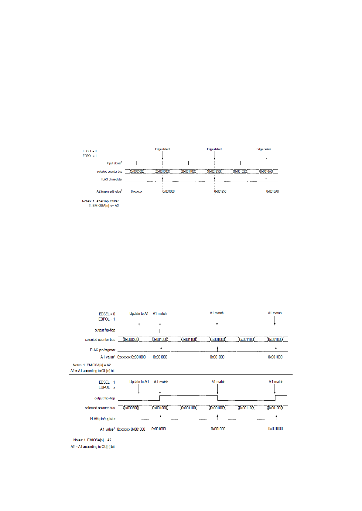
When in GPIO input mode (MODE[0:6]=0000000), the input pin status can be read by UCIN bit
1.3. SAIC: Single Action Input Capture
Figure 49 : SAIC with rising edge triggering example (R.M. Rev8 – Fig. 24-18)
1.4. SAOC: Single Action Output Compare
Figure 50 : SAOC with both possibilities on EDSEL (R.M. Rev8 – Fig. 24-20/21)
in the status register and a flag can be generated at on a rising or an falling edge. (Detection of
both edges isn’t implemented for GPIO).
In GPIO output mode (MODE[0:6]=0000001), the channel is used as a single output pin and the
value of EDPOL is transferred to the output flip-flop.
This is the Single Action Input Capture mode (MODE[0:6]=0000010), when a triggering event
on the input (a rising, falling or either edges) occurs, the flag bit is set and the value of the
selected counter bus is captured by A2 and can be read through the register A.
This is the Single Action Output Compare mode (MODE[0:6]=0000011), a match value written
in the register A is written to A2 and transferred to A1 directly where it’s compared with the
selected time base (the BSL field of the control register). When a match occurs, the flag bit is set
and depending on EDSEL, either the output flip-flop is toggled or the value in EDPOL is
transferred to it.
At initialisation, the flip flop is set to the complement of EDPOL.
Page 44
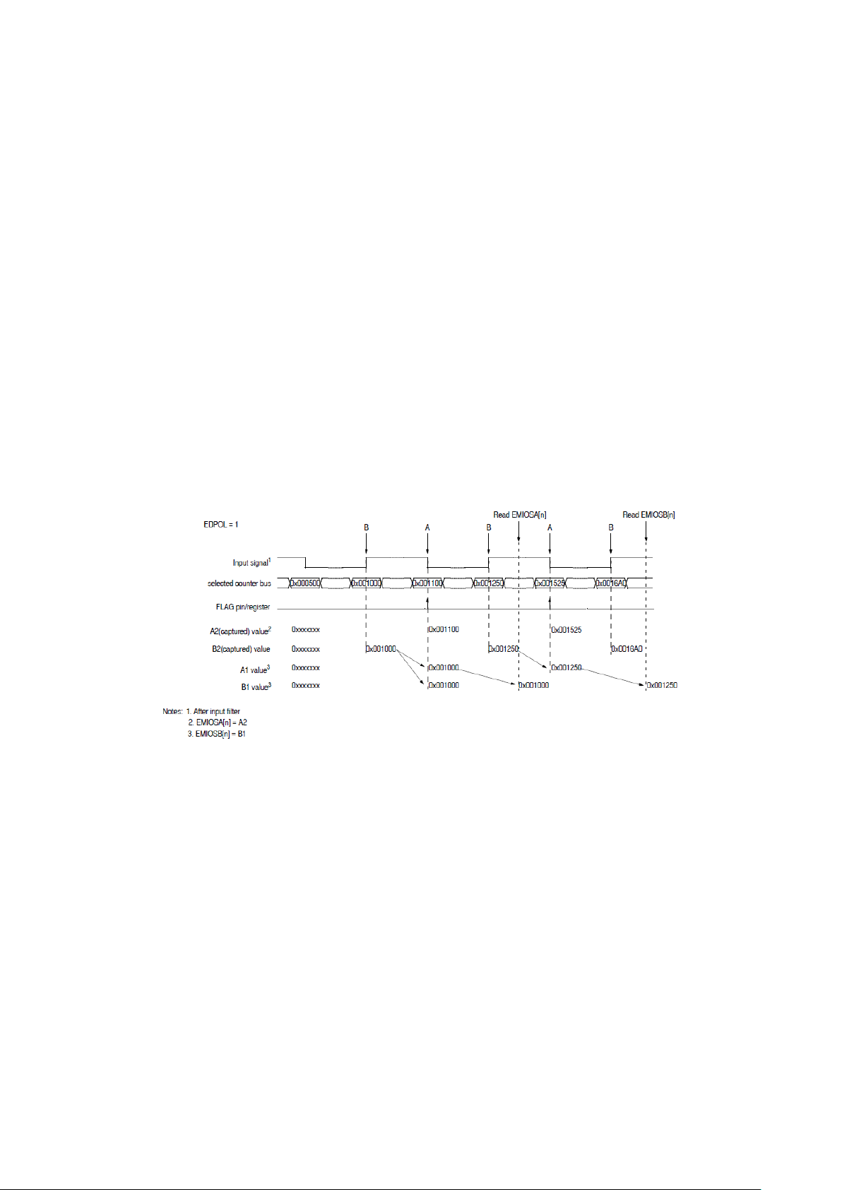
1.5. IPWM: Input Pulse Width Measurement
Figure 51 : IPWM Example (R.M. Rev8 – Fig. 24-23)
1.6. IPM: Input Period Measurement
The Input Pulse Width Measurement mode (MODE[0:6]=0000100), is the measurement of the
width of a positive or a negative (depending on EDPOL) pulse by capturing the leading edge on
B1 and the trailing edge on A2.
The capture on A2 is disabled until B2 gets its first leading edge, then the selected counter bus
(BSL) count value is stored on B2. When the trailing edge is detected, the count value is stored in
A2, the flag bit is set and the value of register B2 is transferred to registers B1 and A1. If new
capture events occur while the flag bit is set, then the flag bit will remain but registers will be
updated with new data.
In order to get coherent width measurement, a read on the register A (so A2) will disable
transfers from B2 to B1 and force a transfer from A1 to B1. The value in B1 will be intact for the
upcoming read on the register B. By subtracting B1 from A2, we can get the pulse width. (See
figure below for an illustration of these register transfers).
Therefore, once a flag is set, reading the register A, then reading the register B and subtracting
them, will always give a coherent reading.
NOTE: If a pulse measurement happens during a counter roll over, maximum counter value has
to be added to A2 before subtracting B2.
The Input Period Measurement mode (MODE[0:6]=0000101), is the measurement of the period
of an input signal by capturing two consecutive rising edges or two consecutive falling edges
(depending on EDPOL). The principle is very similar to the IPWM’s way of operating (see the
previous section).
When the first edge of selected polarity is detected, the count value is stored in A2 and B2 and
the previous value of B2 is transferred to B1 and A1. On the following edges, the flag bit is set
and the value of register B2 is transferred to B1 and A1 and the new count value is captured.
Page 45
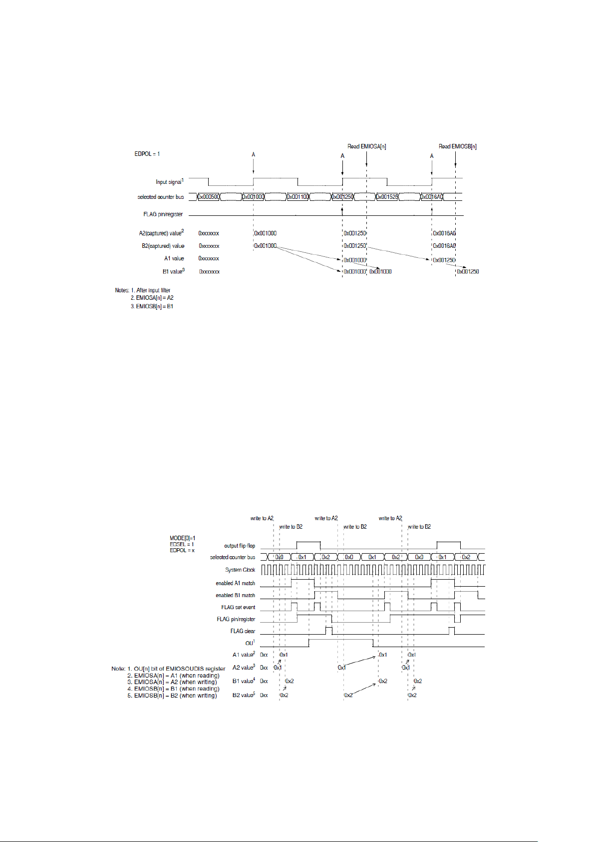
In order to get coherent measurement, a read on the register A (so A2) will disable transfers
Figure 52 : IPM Example (R.M. Rev8 – Fig. 24-26)
1.7. DAOC: Double Action Output Compare
Figure 53 : DAOC with transfer disabling (OU=1) example (R.M. Rev8 – Fig. 24-29)
from B2 to B1 and force a transfer from A1 to B1. The value in B1 will be intact for the upcoming
read on the register B. By subtracting B1 from A2, we can get the period. (See figure below for an
illustration of these register transfers).
NOTE: If a period measurement happens during a counter roll over, maximum counter value has
to be added to A2 before subtracting B2.
In the Double Action Output Compare mode a variable output pulse is generated by matches
occurring on comparators A and B. At initialisation, the output flip-flop is set to the complement
of the EDPOL.
Registers A and B write respectively to A2 and B2, and their data are transferred to A1 and B1 on
the next system clock cycle if OU is clear. The comparators A (and B) are enabled when a
transfer occurs to A1 (and B1), and then they are disabled on the next A (and B) matches.
When a match occurs on register A, the output is set to EDPOL, and on a match on register B, it is
set to complement of EDPOL. There is two possibilities for mode selection, MODE[0:6]=0000110
Page 46
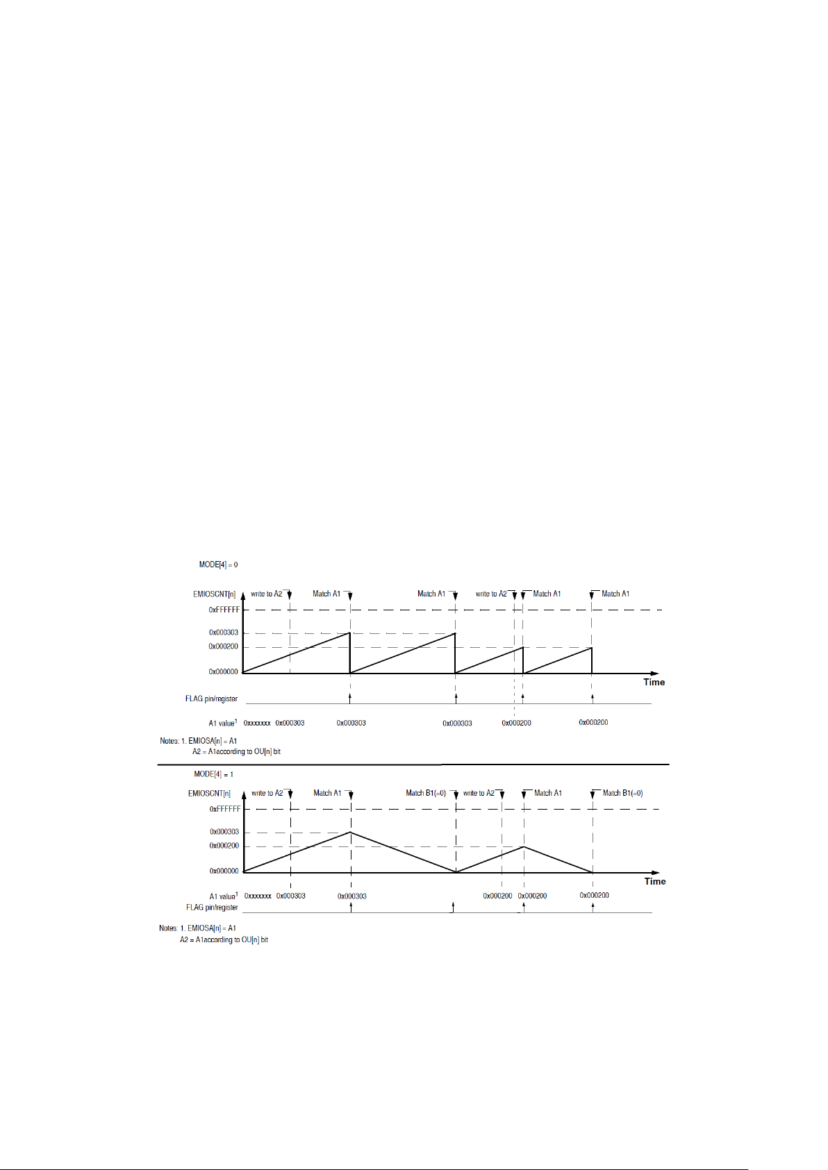
is DAOC with a flag generation on the B match and MODE[0:6]=0000111 is DAOC with a flag
1.8. MC: Modulus Counter
Figure 54 : Modulus Counter Up and Up/Down Mode Examples (R.M. Rev8 – Fig. 24-30/31)
generated on both matches.
For further pulse generation, the comparators have to be re-enabled by transfer of data written
to A2/B2 to A1/B1.
The Modulus Counter mode (MODE[0:6]=0010bbb) is used to generate a counter that can be a
time base for a counter bus or a general purpose timer. In this mode an internal counter counts
up, following a reference clock until a match occurs. And then it is either cleared, or it changes
count direction. There are three bits on the mode field that can configure the operating process:
MODE[6] selects the reference clock, if this bit is set, then the clock is an external clock
connected to the pin as an input and the ticking edge is determined by EDPOL and
EDSEL, if it is clear then the internal prescaled clock source is used.
MODE[5] defines whether the internal counter is cleared on match start or on an match
end. When this bit is clear, the counter is cleared and the flag is set as soon as the match
occurs (which can lead to a shorter 0 count) and when it is set, the counter is cleared and
the flag is set on the next tick following the match.
MODE[4] selects between two counting modes. When it is cleared, the counter counts
up to match A1 value and then it is cleared, and when it is set, after the match with A1,
the counter counts down till it matches with B1 and changes direction again and so on.
Only values greater than 0x0 should be written on the register A and register B1 is always
cleared in this mode and cannot be changed. If A is changed during operation, the behavior of the
counter depends on its actual state; if the counter is less than the new value of A, there won’t be
Page 47
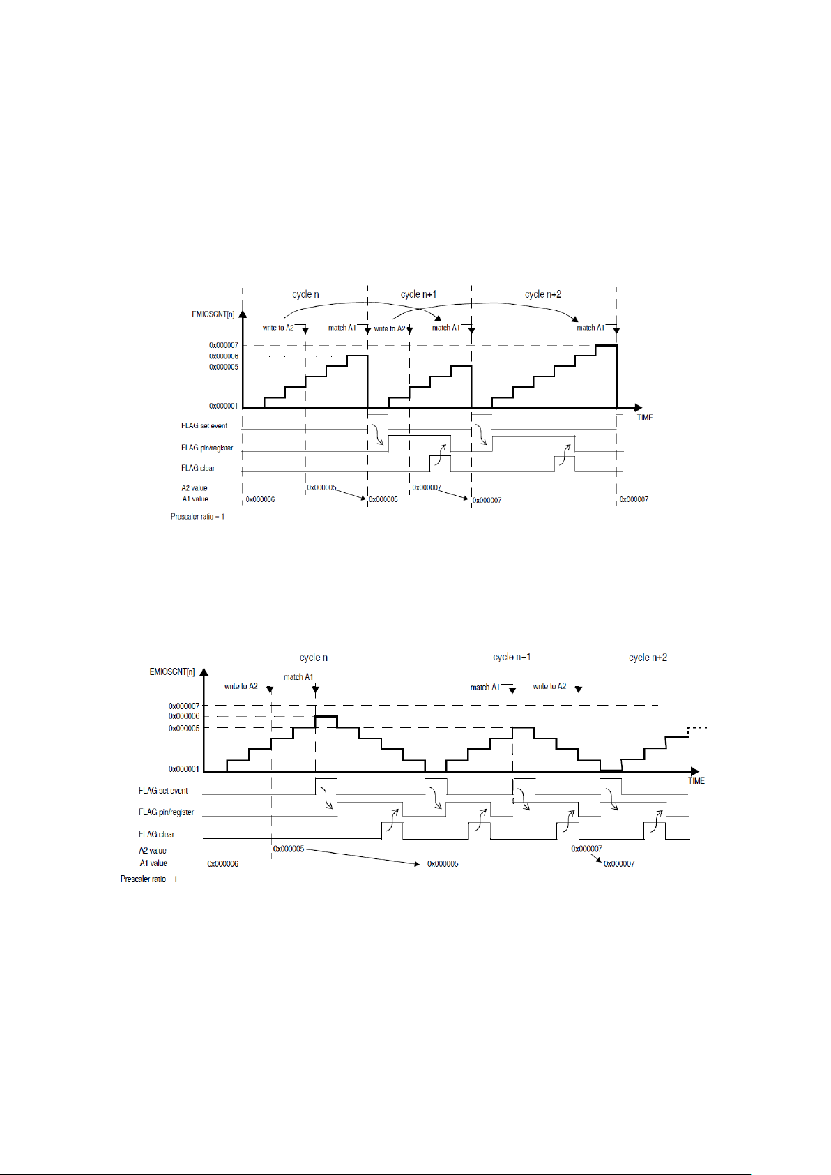
any problem, but if it’s above then we’ll have to wait the counter to roll-over for getting normal
1.9. MCB: Modulus Counter Buffered
Figure 55 : MCB Up Counter Mode Example (R.M. Rev8 – Fig. 24-32)
Figure 56 : MCB Up/Down Counter Mode Example (R.M. Rev8 – Fig. 24-33)
1.10.
OPWFMB: Output Pulse Width and Frequency Modulation Buffered
operation.
In this Modulus Counter Buffered mode (MODE[0:6]=1010b0b), the register A is double
buffered, allowing smoother transitions when the value of A is changed. The match register A1 is
only updated at the end of a cycle, avoiding the need of wait for a roll over. Another main
difference with the MC mode is that the counter counts between 0x1 and A1 value.
The configurable bits MODE[4] and MODE[6] have the exact same effect as on the MC mode.
When the counter is in up mode, the period will take A1 cycles and when it is in up/down mode
it will take 2(A1-1) cycles.
MCB should be preferred over MC for clock generation.
The Output Pulse Width and Frequency Modulation Buffered mode (MODE[0:6]=10110b0) is
used to generated waves with variable duty cycle and frequency. This mode automatically uses
the internal channel counter as it’s time base and comparators on A1 and B1.
Page 48
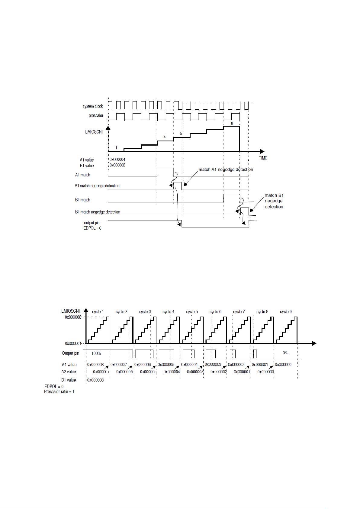
At entry, the output flip-flop is set to the value of EDPOL. When the internal counter match
Figure 57 : OPWFMB Basic Operation with the Output Delay (R.M. Rev8 – Fig. 24-36)
Figure 58 : OPWFMB with fixed frequency, duty cycle from 100% to 0% (R.M. Rev8 – Fig. 24-39)
occurs on comparator A, the output is set to the value of EDPOL, when a match occurs on
comparator B, the output will be set to the complement of EDPOL. Therefore, using A1 as the
duty cycle and B1 as the frequency, the EDPOL must be set to the opposite polarity of the pulse
we want.
Meanwhile it should be noted that the output change after edge detection has an intrinsic one
system clock cycle delay. The example on the figure above shows that this causes an important
effect when the internal counter frequency is close to system clock frequency.
In this mode, registers A and B are buffered, the changes on A1 and B1 occur only at the end of a
cycle, making smoother transitions.
The configurable bit MODE[5] determines the behaviour of the flag generation; when it is
cleared, flags are only generated on B1 matches, when it is set, a flag is generated both on A1 and
B1 matches. Flags are generated one system clock cycle following the matches.
Page 49
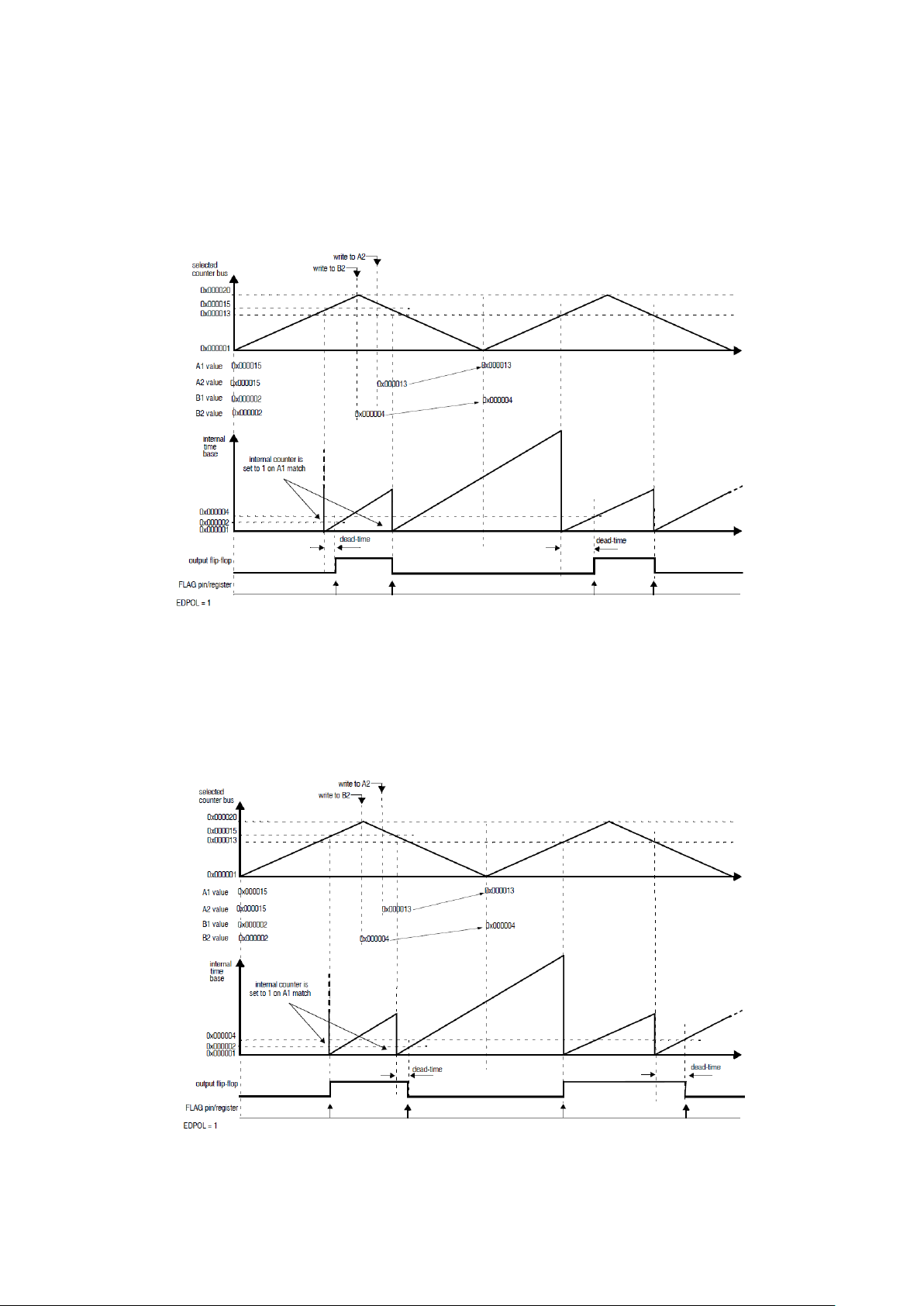
1.11.
OPWMCB: Center Aligned Output Pulse Width Buffered
Figure 59 : OPWMCB with lead dead time (R.M. Rev8 – Fig. 24-41)
Figure 60 : OPWMCB with trail dead time (R.M. Rev8 – Fig. 24-42)
The Center Aligned Output PWM Buffered with Dead-Time mode (MODE[0:6]=10111bb) is
another way of generating a PWM. The time base can be selected via BSL, and it should be a
up/down MCB counter. It is also recommended to start the MCB channel after starting the
OPWMCB mode.
Register A1 controls the duty cycle for the PWM signal, it is compared with the time base, and
comparisons result in centred pulses thanks to up/down counter. Match on A1 will set the
internal timer to 0x1.
*
Page 50
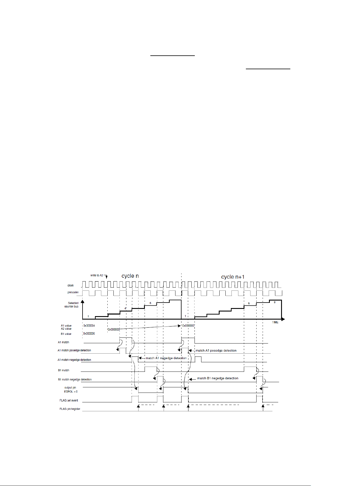
Register B1 controls the dead time, it is compared with the internal counter, for a leading edge
1.12.
OPWMB: Output Pulse Width Modulation Buffered
Figure 61 : OPWMB mode (R.M. Rev8 – Fig. 24-44)
dead time, the duty cycle of the signal is
()
(
of the time base. For a trailing edge dead time, the duty cycle of the signal is
, where MAXCNT is the maximum value
)
()
(
)
.
Registers A and B are buffered, they are only updated when a time base cycle ends.
A and B should be selected in a way that would not induce a roll over in the internal counter, as
this would cause unpredictable behaviour.
The configurable MODE[5] bit is as before, related to the flag generation. If it is cleared, a flag
would be generated at the trailing edge of the PWM, if it is set, a flag will be generated on both
edges.
The MODE[6] bit is for selecting between leading edge (‘1’) or trailing edge (‘0’) dead time
insertion.
The Output Pulse Width Modulation Buffered mode (MODE[0:6]=11000b0) is used for
generating PWM with variable leading and trailing edge placement. BSL should be used to select
a MCB up counting time base.
Register A1 controls the leading edge, when a match occurs between A1 and the time base, the
leading edge is generated, depending on EDPOL. Register B1 controls the trailing edge, on a
match between B1 and the time base, the trailing edge occurs.
Registers A and B are double buffered, updated on new time base cycles. A flag is generated on
B1 matches if MODE[5] is cleared, or on both matches if it is set.
Page 51
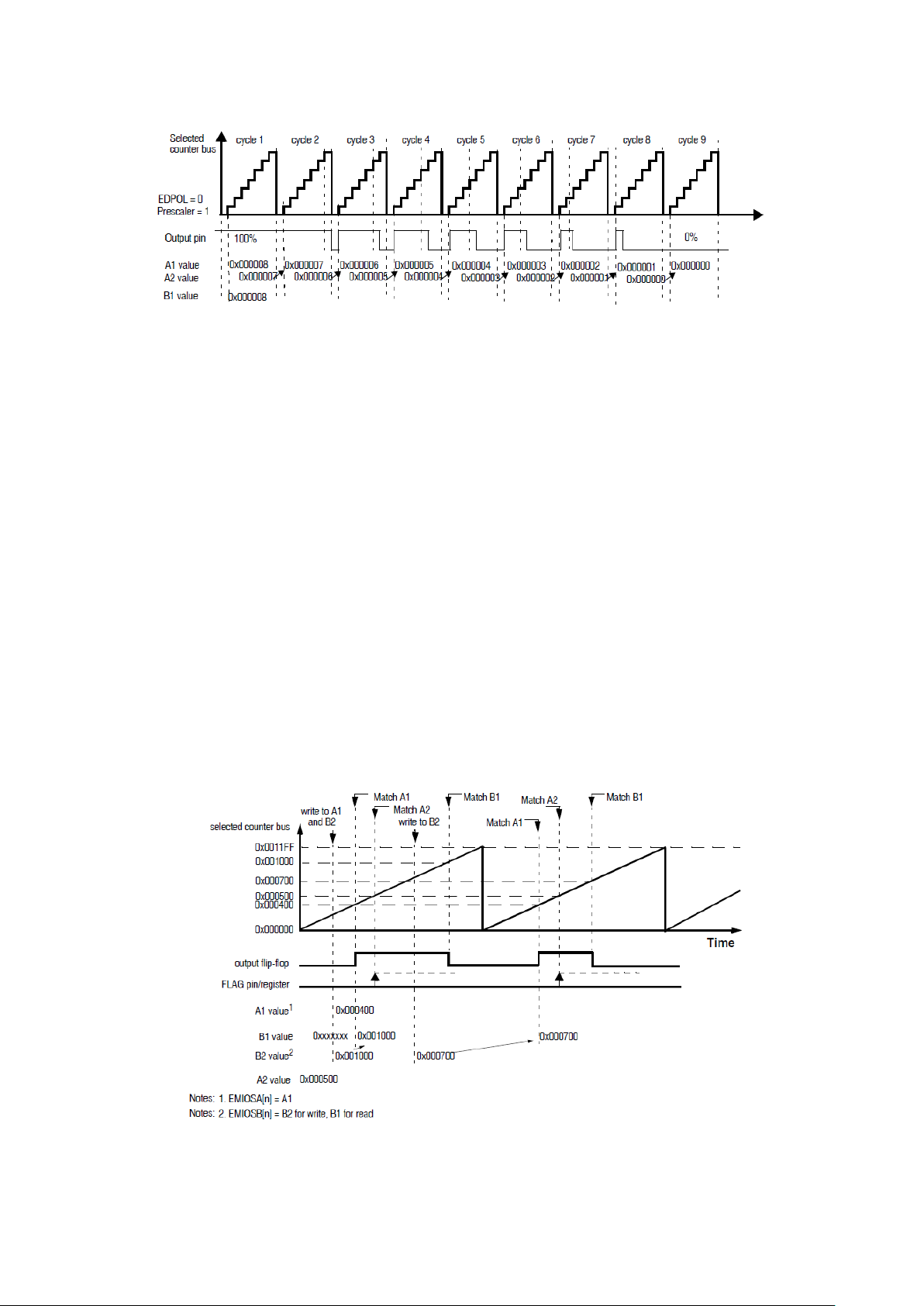
Figure 62 : OPWMB mode with duty cycle going from 100% to 0% (R.M. Rev8 – Fig. 24-42)
1.13.
OPWMT: Output Pulse Width Modulation with Trigger
Figure 63 : OPWMT example (R.M. Rev8 – Fig. 24-47)
The Output Pulse Width Modulation with Trigger mode (MODE[0:6]=0100110) works in a
similar way to OPWMB but with some important differences:
The register A1 is no longer buffered, so changing it could result on a loss of a coherent
pulse.
The register A2 is now an independent (and non-buffered) that triggers flags on match.
This mode should be used for generating fixed period PWM with a fixed leading edge precisely
positioned in reference to a time base which is a counter in MC up(starting from 0) or MCB
up(starting from 1) mode, a variable trailing edge controlled by the B register (buffered) that is
updated on every leading edges and a fixed triggering moment in the period.
This mode is better suited for applications needing multiple PWM signals with the same time
base (multiple channels configured on OPWMT clocked by the same counter bus) and where
regular triggering events are needed, for ADC conversion, for instance.
For modifying A2, the user will need to use Alternative A register in the eMIOS module.
Page 52
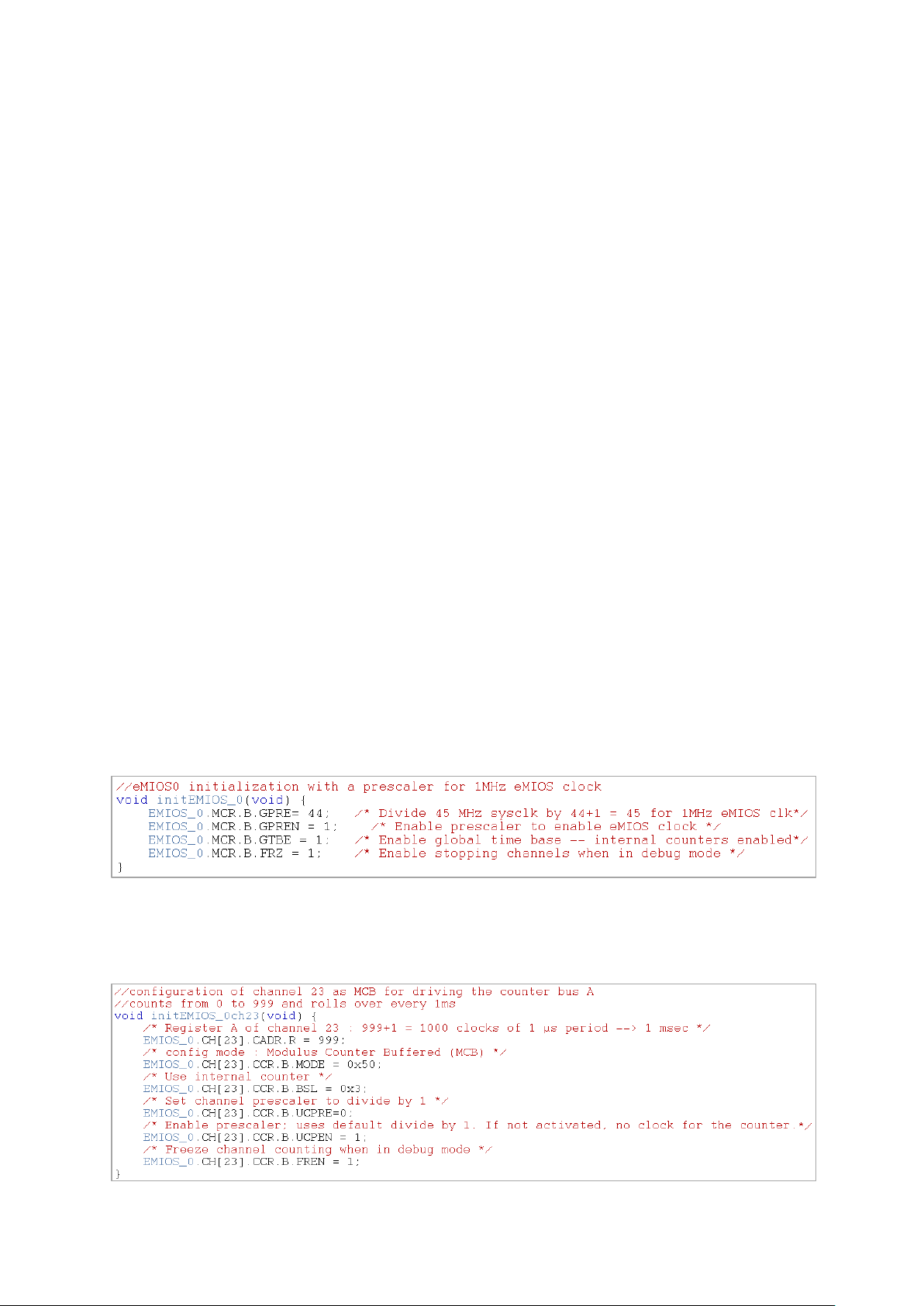
3. PWM Channel Initialisation
4. PWM Example
In order to initialise a PWM channel and a time base channel for it without getting erroneous
signals the following procedure should be followed:
1. Ensure that the channel is in GPIO mode;
2. (eMIOS) Disable global prescaler;
3. (time base channel) Disable channel prescaler;
4. (time base channel) Write the initial value to the internal counter.
5. (time base channel) Set A and B registers;
6. (time base channel) Select MCB up or up/down mode;
7. (time base channel) Set prescaler ratio;
8. (time base channel) Enable channel prescaler;
9. (PWM channel) Disable channel prescaler;
10. (PWM channel) Set A and B registers;
11. (PWM channel) Select time base bus using BSL;
12. (PWM channel) Select the specific PWM mode;
13. (PWM channel) Set prescaler ratio;
14. (PWM channel) Enable channel prescaler;
15. (eMIOS) Enable global prescaler.
For a simple example application, we could configure a channel as MC for driving a bus counter
and then configure two channels connected to this bus as OPWMB with different duty cycle and
starting positions.
We initialise the system with by powering up eMIOS and SIUL, and with a system clock of
45MHz. And then we initialise eMIOS with a prescaler of 45 for getting a 1MHz internal clock.
We select the channel 23 as MC for driving the whole counter bus A. For this it needed to write
999 into register A and then select MC-up mode, select the internal counter and a prescaler of 1.
This will generate a counter from 0 to 999 at 1MHz, so giving a roll over each ms.
Page 53
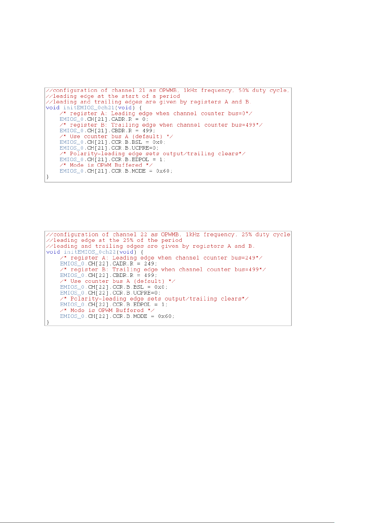
Now we have counter bus running, we can select any channel connected to the bus A and
configure it as OPMWB. For instance we can select channel 21, set the leading edge (register A)
at 0 and trailing edge at 499, running on bus A, with a positive polarity (output is set at leading
edge etc.).
This gives us a PWM at 1kHz with 50% duty cycle.
Similarly we configure channel 22 for a PWM at 1kHz with 25% duty cycle, with a leading edge
at 25% into a period.
Page 54
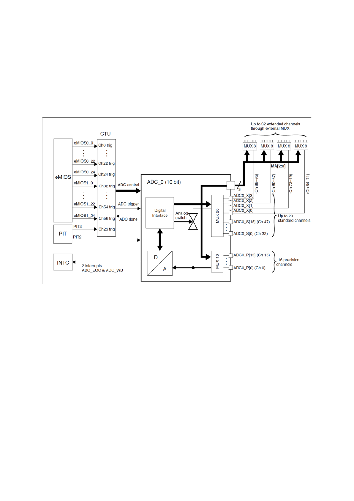
Chapter 6
ADC: Analog-to-Digital Converter
1. Presentation of the ADC module
1.1. Introduction
Figure 64 : ADC Architecture (R.M. Rev8 – Fig. 25-1)
The ADC block is made of multiplexing of 32 channels (expandable to 64 via external
multiplexing) to a 10-bit resolution, successive approximation converter.
A conversion can be triggered by software or hardware (PIT or CTU) and there are different
conversion modes like one shot or scan. There is also a chain injection possibility. Each channel
has individual conversion registers.
There are three types of input channels; 16 internal precision ADC0_P channels, 16+4 internal
standard ADC0_S channels, externally multiplexed standard channels ADC0_X. MA[2:0] pins are
for decoding external multiplexers.
Different timing configurations can be set for these different channel types.
There are 4 analog watchdogs monitoring lower and higher thresholds with interrupt
capabilities.
Pre-sampling functionality exists for higher quality data.
48
Page 55
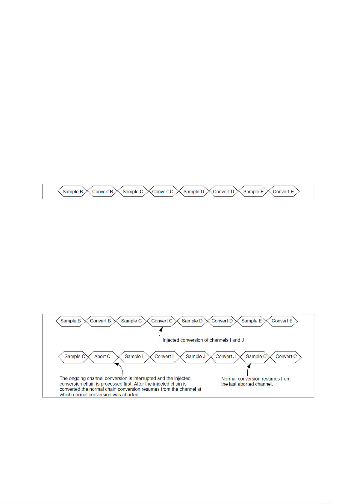
1.2. Conversion
Figure 65 : Normal conversion flow of channels B, C, D and E (R.M. Rev8 – Fig. 25-2)
Figure 66 : Injected mode illustration (R.M. Rev8 – Fig. 25-3)
There are three conversion modes available for this module; normal conversion, injected
conversion and CTU triggered conversion. CTU triggered conversion will be explained in the
chapter dedicated to the CTU module, this section is only about normal and injected modes.
1.2.1. Normal Conversion
A normal conversion can be started from the software by setting the NSTART (Normal Start) bit
of the control register. There are two operating modes available for the normal conversion; one
shot and scan modes.
In one shot mode, a sequential conversion of the channels configured for the normal conversion
is performed only once and the resulting data is stored in data registers. The NSTART bit is reset
once the conversion starts, allowing the software to start another conversion. If the previous
conversion is not finished while a new one is requested, then the new conversion will be done
right after the old one is done.
In scan mode, the sequential conversion of these channels is continuously executed, NSTART bit
is automatically set once the conversion starts and it is not reset. The software can clear it to
stop the conversion. At the end of each conversion, an End of Conversion interrupt is triggered,
allowing the data to be processed, and at the end of the conversion of the whole sequence, an
End of Chain interrupt is triggered.
1.2.2. Injected Conversion
Injected conversions can only occur in one shot mode, it interrupts ongoing normal conversions.
Once the conversions of the injected channels are completed, the normal conversion resumes
from where it was left.
This mode can be starter using either the JSTART bit from the software, in a very similar way
with the normal conversion, or using a trigger signal from the PIT 2, having JTRGEN (injected
trigger enable) set. This mode can be configured to start at a rising or falling edge on the signal
coming from PIT (JSTART is automatically set).
Page 56
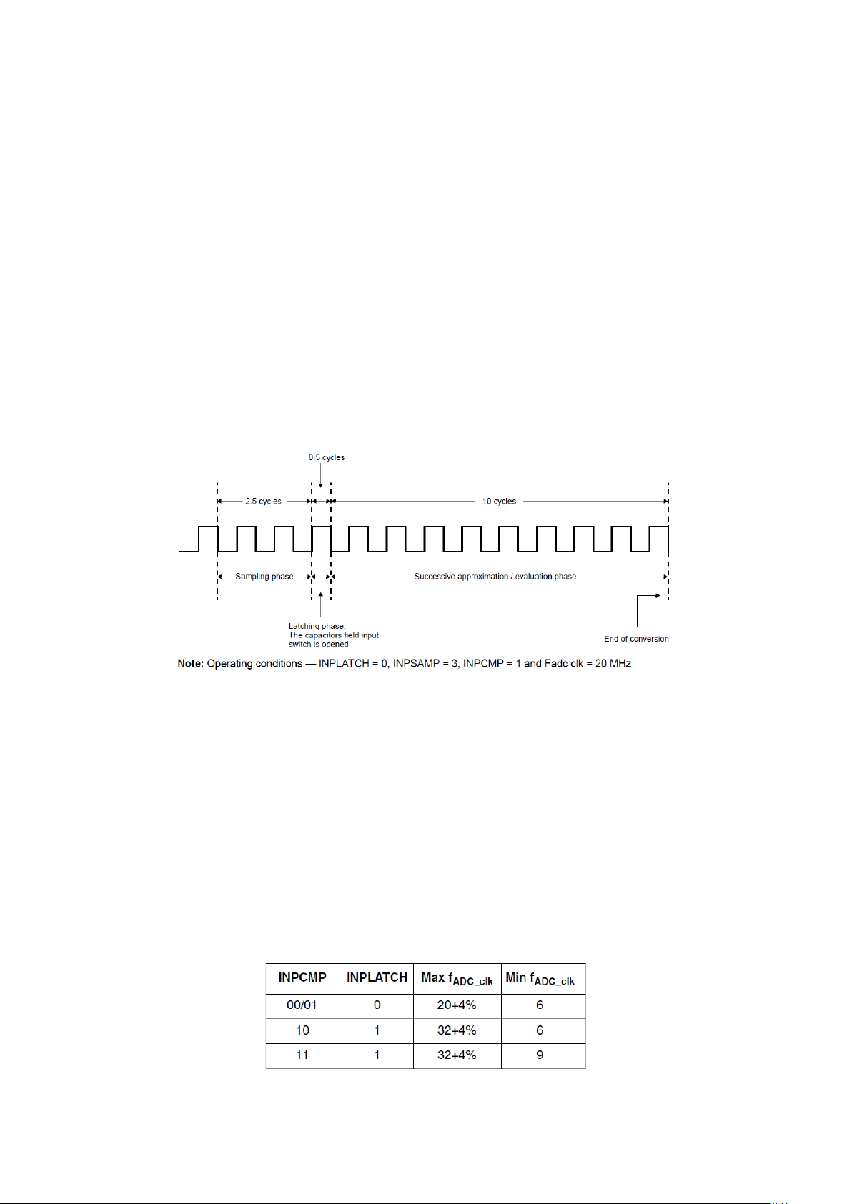
Once the conversion starts, JSTART is reset for further conversion requests. At the end of each
1.3. ADC clock and conversion timing
Figure 67 : Sampling and conversion timing example (R.M. Rev8 – Fig. 25-4)
Figure 68 : Max/min ADC_clk related to parameters (R.M. Rev8 – Table 25-3)
conversion JEOX interrupt is issued and at the end of an injected sequence, JECH interrupt is
triggered.
Any ongoing conversion can be stopped using the ABORT bit in the configuration register, then
the next channel in line will be converted. Using ABOTCHAIN all pending channel conversions
can be aborted. If the last channel of a sequence is aborted, then ECH interrupt is raised.
This module’s clock frequency can be set to the peripheral set 3’s clock frequency or to its half.
When the half divider is not used, it is recommended to not use a divider for the peripheral
clock, as it may not give a 50% duty cycle clock.
The conversion timing can be more or less configured, and each type of channel type can have a
particular timing setting. Conversion time consists of a sampling phase, a latching phase and an
evaluation phase.
The sampling phase is when the ADC’s internal sampling capacitor is connected to the input pin
and charges up to the input voltage value. This phase’s duration is defined as
or equal to 3,
equal to 500ns.
= INPSAMP
is 0.5 if INPSAMP6 and 1 otherwise. And
is the ADC’s clock, derived from the peripheral clock.
The latching phase is when the capacitor’s switch is opened and its duration is
, where INPSAMP is configurable, and has to be greater than
has to be greater than or
.
The evaluation phase is the time needed for successive approximation to be performed, its
duration is
= 10 INPCMP , where INPCMP1 and INPLATCH < INPCMP. These two
values are configurable, and have to be set using the following table.
Page 57
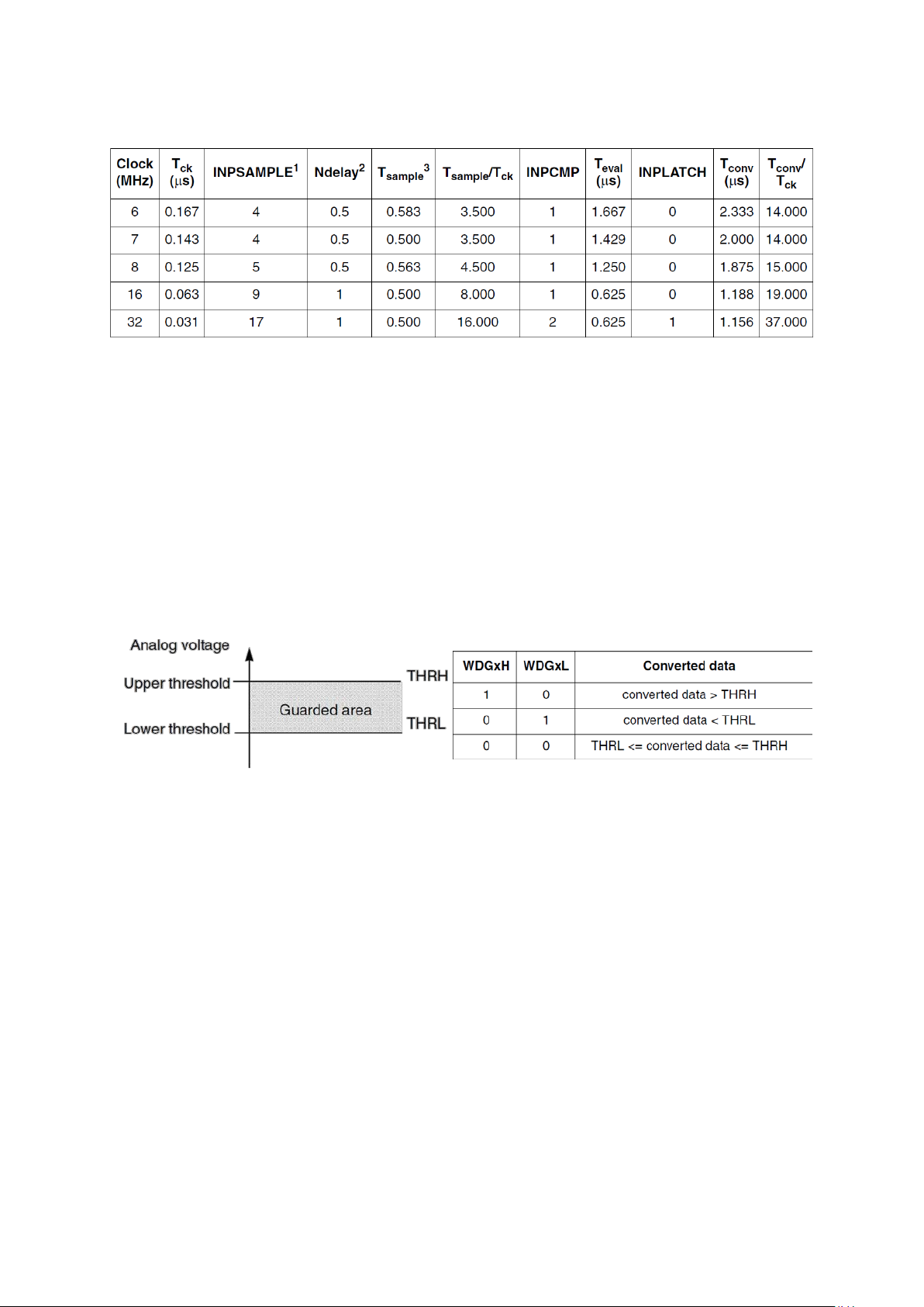
The following table gives some example values for different clock settings:
Figure 69 : ADC sampling and conversion timing (R.M. Rev8 – Table 25-2)
1.4. Pre-sampling
1.5. Analog watchdog
Figure 70 : Analog Watchdog (R.M. Rev8 – Fig. 25-7/Table 25-5)
1.6. Low power consumption modes
For higher quality sampling, resetting the sampling capacitor after a previous sampling is
needed; the ADC capacitor is charged or discharged to one of the two internal voltage references.
This phase can be enabled for a channel, and it would take as much time as a sampling phase. It
is also possible to bypass the real sampling phase to get a conversion of the reference value.
There are four analog watchdogs in this module, and each of them can monitor a channel
conversion to check if it lies in a guarded area limited by a lower and an upper threshold.
In the watchdog status register, two bits called WDGxH and WDGxL whether there has been a
threshold violation or not. An interrupt can be generated at a lower and/or higher threshold
violation.
The ADC module is by default in power-down mode and this state has to be exited before
starting conversions. The software can request this mode by using the appropriate bit field and
once the ongoing conversion if over, ADC will go into this mode. The ADC’s status can be checked
using the status register. If the CTU is enabled, ADC cannot go to the power-down mode; the
conversion has to end for that.
Another power saving mode is the auto-clock-off mode, where the ADC module automatically
turns off its clock when there is no pending conversion.
Page 58
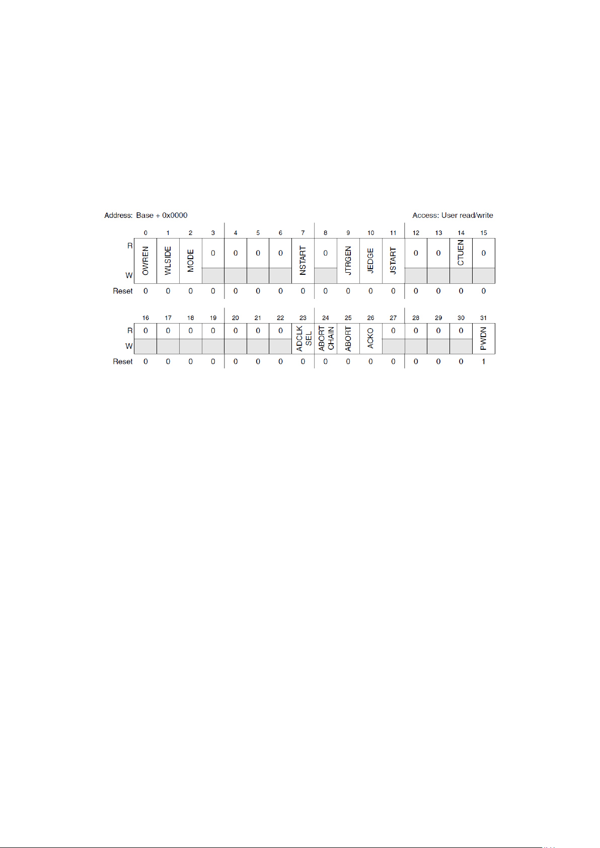
2. ADC Configuration
2.1. Pad Configuration
2.2. General Registers
Figure 71 : Main Configuration Register (R.M. Rev8 – Fig. 25-8)
Using the SIUL module, the software has to set the APC bit of the PCR register of a pad with ADC
functionality, there is no need to bother with other fields or alternate functions.
In this section we will talk about ADC module’s principal configuration registers.
The Main Configuration Register (MCR) has the following fields:
Overwrite enable (OWREN): set this bit to enable converted data to be overwritten
by new conversion. Otherwise new data is discarded until the current data is read.
Write left/right aligned (WLSIDE): changes the DATA fields’ position in the CDR
register. (NOTE: always leave at 0 if the register definition header file is used in C).
MODE: if cleared, one shot mode is selected; else, scan mode is selected.
Normal Start conversion (NSTART): starts a normal mode conversion when set (see
sections above).
Injection external trigger enable (JTRGEN): Injection external trigger enable (set to
enable).
Injection trigger edge selection (JEDGE): clear to trigger at a falling edge, set for
selection a rising edge.
Injection start (JSTART): setting this bit will start the injection mode. Resetting it
won’t stop it. (See sections above).
CTU conversions enable (CTUEN): CTU triggered conversions are enabled if set. (See
next chapter for more information).
Analog clock select (ADCLKSEL): if cleared, ADC clock frequency is half peripheral set
clock frequency. Otherwise it is equal to the peripheral set clock frequency.
Abort chain (ABOTCHAIN): when set, aborts the ongoing sequence.
Abort conversion (ABORT): when set, aborts only the ongoing conversion.
Auto-clock-off enable (ACK0): set to enable this power mode.
Power-down enable (PWDN): set to request a power down.
Page 59
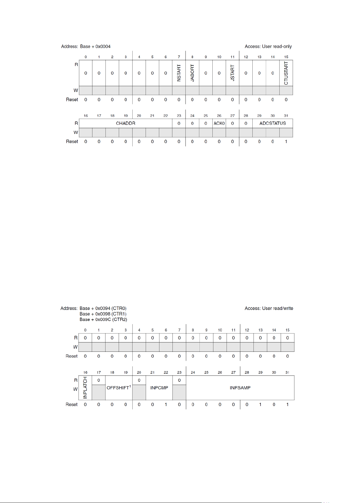
Figure 72 : Main Status Register (R.M. Rev8 – Fig. 25-9)
2.3. Conversion Registers
Figure 73 : Conversion Timing Register (R.M. Rev8 – Fig. 25-26)
The Main Status Register (MSR) is a read-only register allowing the access the current status of
the ADC module: NSTART, JSTART, CTUSTART respectively indicate whether a conversion of
normal, injected or CTU modes is ongoing, CHADDR indicates current conversion channel
address, JABORT signals if an injected conversion is aborted. ADCSTATUS field’s values depend
on ADC’s status: idle (000), power-down (001), wait state (010), sample (100), conversion
(110).
The Decode Signal Delay Register (DSDR) allows to put a delay between the external decode
signals and the sampling phase. It is useful for taking in account the settling time of the external
multiplexers. It has a 8-bit field called DSD and it introduces DSD/2 ADC clock delays.
The Power-Down Exit Delay Register (PDEDR) delays the beginning of a conversion after leaving
the power-down mode, to allow the ADC power supply to stabilise. It has an 8-bit field named
PDED and it introduces PDED ADC clock delays.
The Conversion Timing Registers (CTR[0...2]) are used for configuring the timing of different
phases in the ADC process, for the three types of inputs(respectively, precision, standard,
external standard). See the previous sections on conversion timing for more information about
Page 60

INPLATCH, INPCMP and INPSAMP. The OFFSHIFT field is only available for precision channels
2.4. Interrupt Registers
2.5. Watchdog Registers
(CTR[0]) and it allows selecting how the last bit of the converted data field should behave:
- 00: The transition between 0x000 and 0x001 happens when the input is equal to 1LSB.
- 01: The transition between 0x000 and 0x001 happens when the input is equal to ½ LSB.
- 10: The transition between 0x000 and 0x001 happens when the input is equal to 0.
There are two register for controlling the presampling phase, the first one is the Presampling
Control Register (PSCR), it has the following fields: PREVAL0, PREVAL1, PREVAL2 (respectively
for different input groups) for selecting between two reference voltages
DD_HV_ADC
(01). The PRECONV bit which enables the conversion of the presampled value (for
SS_HV_ADC
(00) and
verification issues).
The other registers related to the presampling are the Presampling Registers (PSR[0…2]) which
can enable the presampling phase for a particular channel. Each PSR register corresponds to a
type of inputs, and PSR[0] and PSR[1] contain fields PRES0 to PRES15 (for precision and
standard channels) and PSR[2] contains fields PRES0 to PRES31 (for external channels). Writing
‘1’ to a PRESn bit enables the channel that corresponds to it.
The Interrupt Status Register (ISR) contains the flag bits of the interrupts generated by the ADC
peripheral. There are five flag bits that are set when an interrupt is raised and they have to be
cleared by writing ‘1’, these are:
EOCTU: End of CTU conversion,
EOC: end of channel conversion,
ECH: end of chain conversion,
JEOC: End of injected channel
conversion,
JECH: End of injected chain conversion.
There are also individual interrupt flags for each channel, for instance we have Channel Pending
Registers (CEOCFR[0…2], for different input types) with the first two having each 16 fields from
EOC_CH0 to EOC_CH15, and the last register having 32 fields for external channels from
EOC_CH0 to EOC_CH31. These flags are set when the measure of the channel is completed, and it
can be cleared by writing ‘1’.
These interrupt flags are maskable using mask registers, the ISR flags can be masked using the
Interrupt Mask Register, with 5 bits for enabling the ISR flags (MSKEOCTU, MSKEOC …
MSKJECH). The CEOCFR[0…2] registers’ flags can be masked using Channel Interrupt Mask
Registers (CIMR[0…2]), containing CIM0…CIM15( or CIM31) fields.
There are a few registers for configuring the analog watchdog, the Threshold Control Registers
(TRC[0…3]) for each watchdog, with a threshold enable bit (THREN) for enabling the detection
on a channel selected using THRCH (a 7-bit field).
Then there are the Threshold Registers (THRHLR[0:3]), each containing a higher threshold
value field (THRH) and a lower one (THRL), as 10-bit fields. By default, THRL=0x000 and
THRH=0x3FF.
Page 61
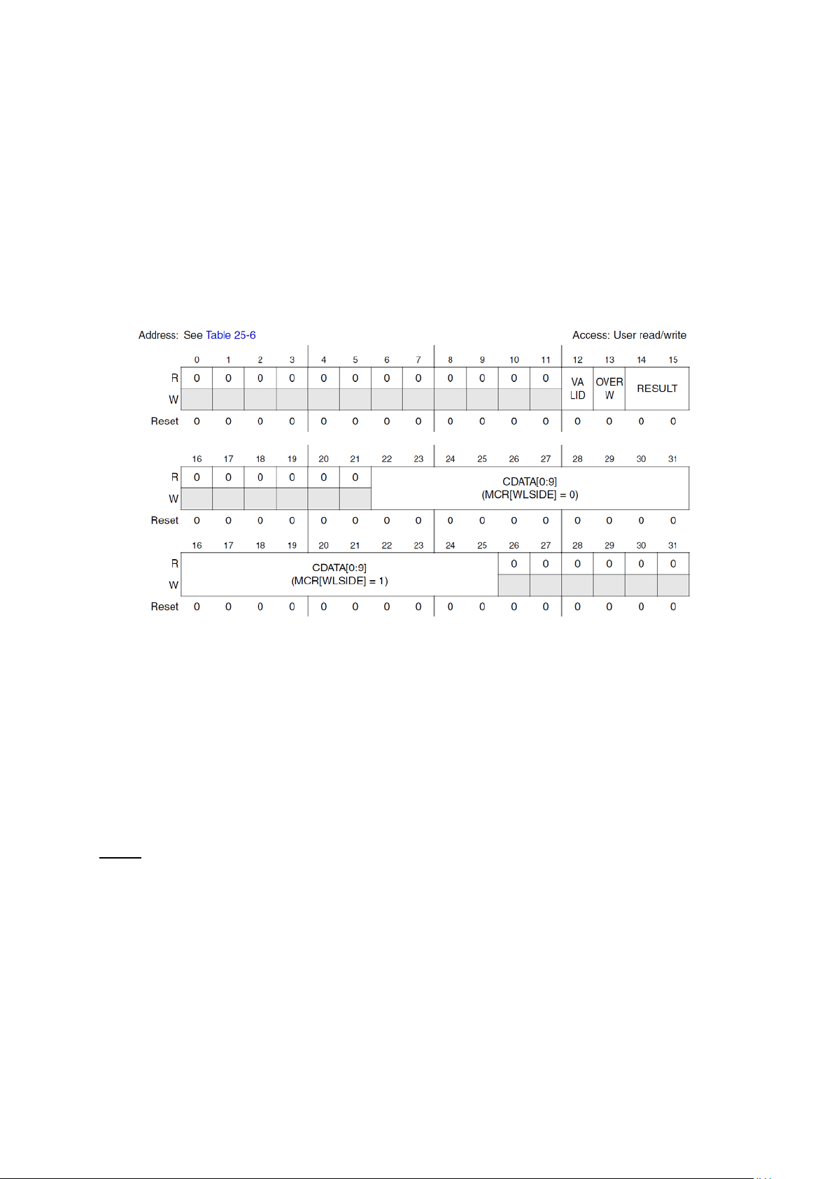
And finally, there is an interrupt flag register (WTISR) for all watchdogs, containing six flags,
2.6. Channel Registers
Figure 74 : Channel Data Register (R.M. Rev8 – Fig. 25-35)
3. ADC Example with PIT and eMIOS
WDGxL and WDGxH, x=0…3, for each interrupt. And a mask register (WTIMR) with six match
bits, MSKWDGxL and MSKWDGxH, x=0…3, that has to be set to enable the corresponding
interrupts.
There are mask registers for enabling sampling phase for each channel; for normal conversions
we have NCMR[0…2] and for injected conversion we have JCMR[0…2]. Both registers have onebit fields for each registers (16 in types 0 and 1 registers, 32 in type 2 register) named CHx,
x=0..31. The sampling of a channel can be enabled by setting these fields.
There are 96 Channel Data Registers (CDR[0…95]) where channels 0…15 are for precision
channels, 32…47 for standard channels and 64…95 are for external multiplexed channels. These
registers contain information about the converted result. The field VALID notifies if a new value
has been written (and it is automatically cleared when data is read). OVERW signals if a previous
non read data has been overwritten (can only occur if OWREN is set) and RESULT indicates from
which mode of conversion the data comes (00:Normal, 01:Injected, 10:CTU). CDATA field
contains the converted data, and its position on the register depends on WLSIDE bit on MCR
register.
NOTE: the C header file only supports WLSIDE=0 field!!
In this example, an ADC reads a potentiometers value and PIT2 triggers an injected conversion
periodically using the hardware connection PIT2 has with ADC. Once a conversion ends,
depending on user’s selection, the value read is either displayed on four LEDs or it is used to set
an eMIOS OPWMs duty cycle.
For setting up the timer the following functions are used:
Page 62
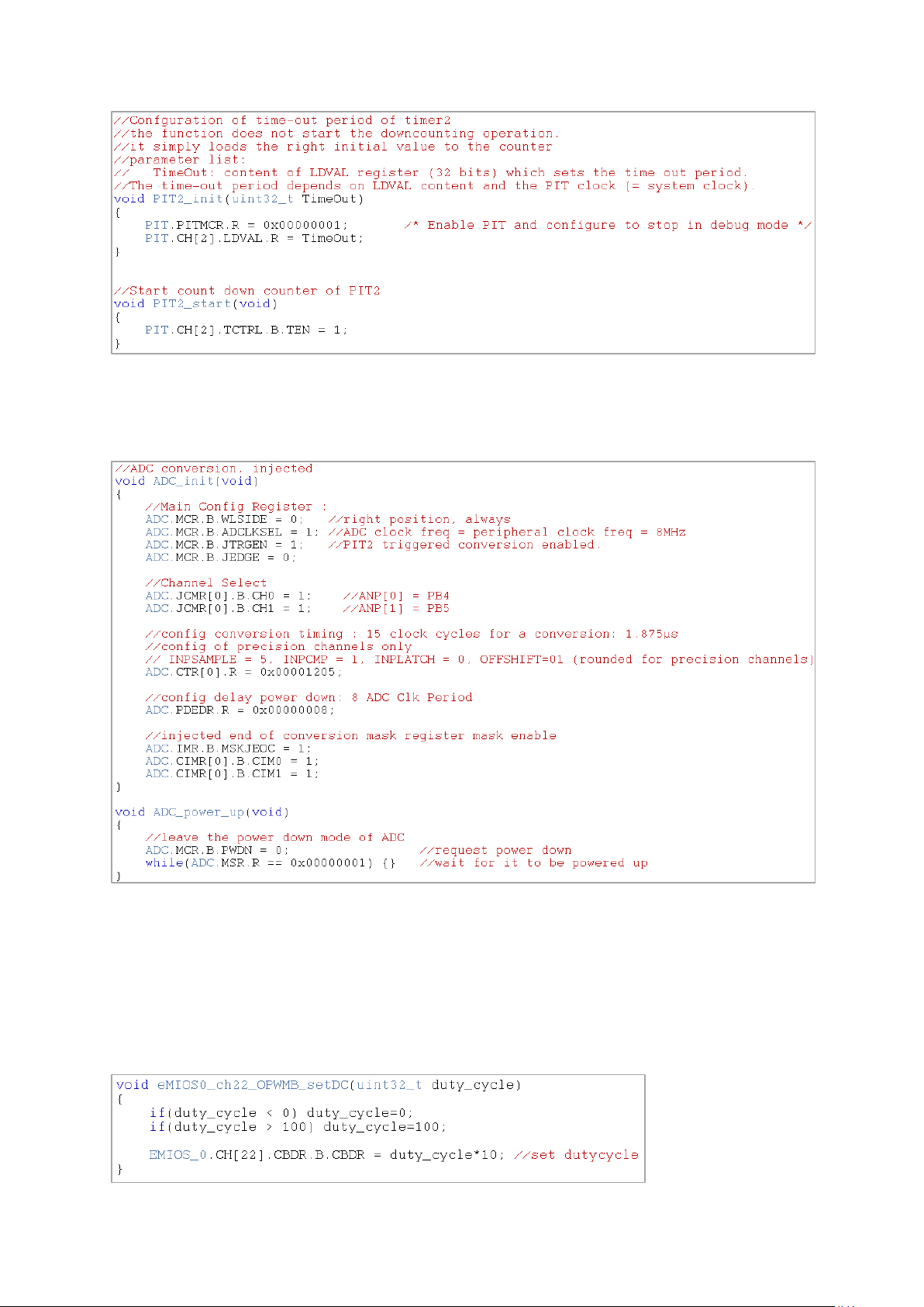
The system clock runs at 8MHz so to get a PIT2 flag with a 1kHz frequency requires a TimeOut
value of 8000. Also ADC has to be configured to run with injected conversions with triggers
coming from PIT 2. Channel 1 and its end of conversion are set:
Meanwhile, from the SIUL, LEDs have to be selected as GPIO output, two buttons as GPIO inputs,
two pins as eMIOS channels and a pin for ADC input.
eMIOS is initialised with a prescaler of 8 for getting 1MHz internal clock. Its channel 23 is
configured as MCB counting from 1 to 1000, giving a roll-over at 1kHz. The channel 22 is
configured as OPWMB with a leading edge at zero and a trailing edge at 25%.And then a function
is given for setting the eMIOS channel’s duty cycle:
Page 63
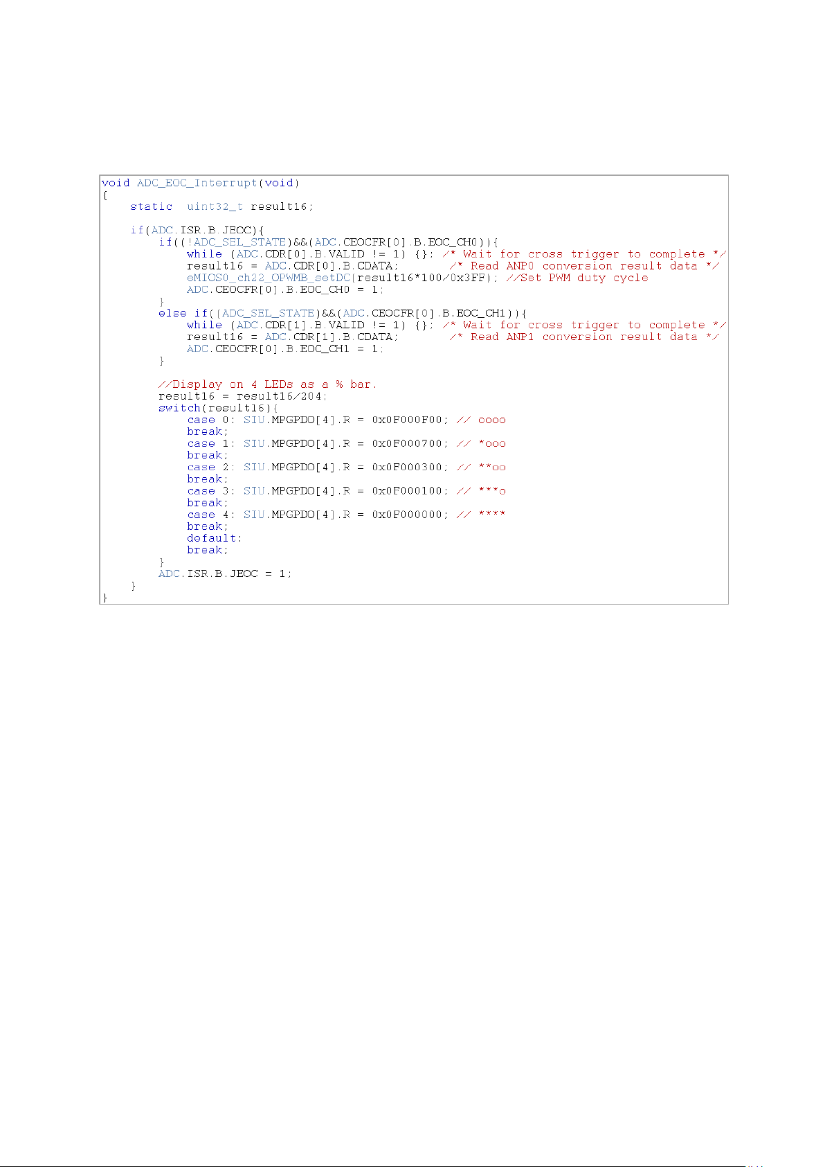
The main program launches each modules, initialises and configures them, the PIT is started
with a time out of 8000, and ADC’s end of conversion interrupt is connected to the
ADC_EOC_Interrupt handler:
Depending on an internal state variable, the value read by the ADC either affects the OPWM’s
duty cycle or some LEDs. The state selection is done in the main loop of the program using input
buttons.
Page 64
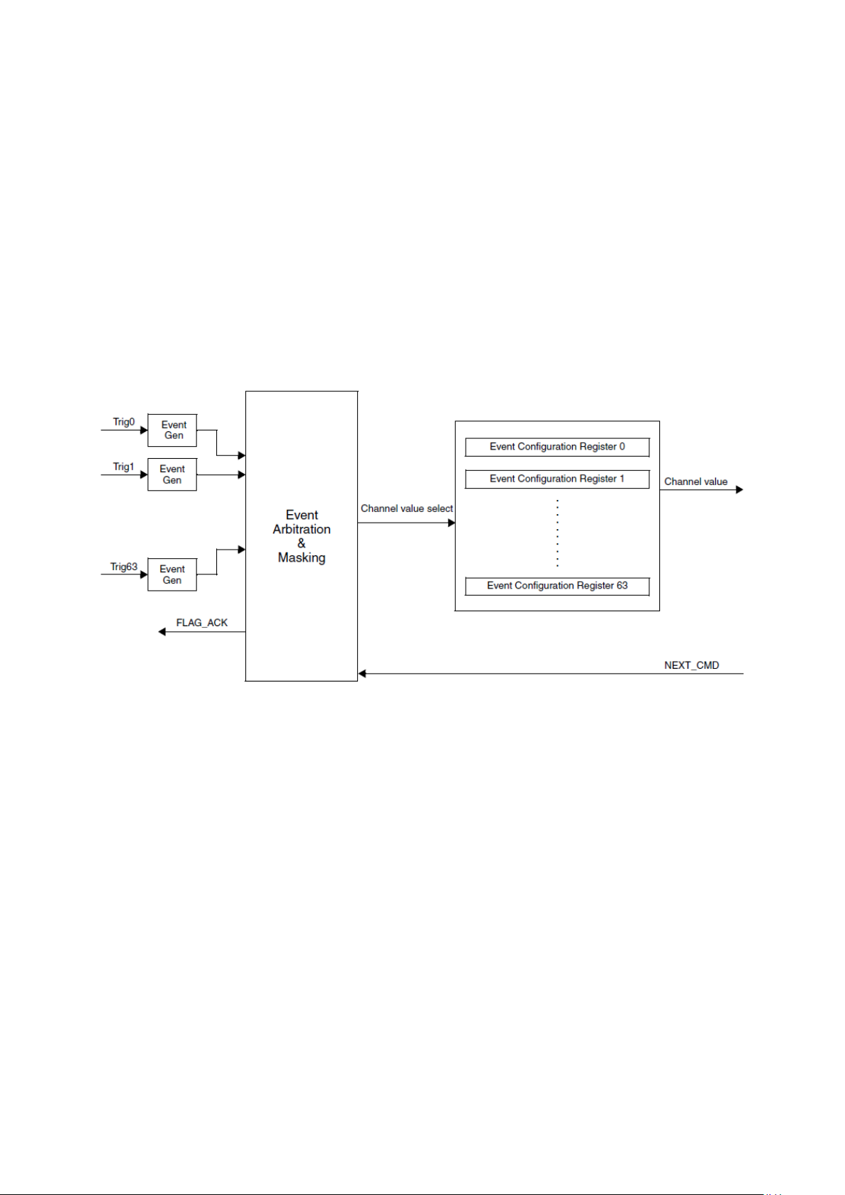
Chapter 7
CTU: Cross Triggering Unit
1. Introduction
Figure 75 : CTU Block Diagram (R.M. Rev8 – Fig. 26-1)
The Cross Triggering Unit synchronises an ADC conversion with a timer (a PIT or eMIOS)
without needing to generate an interrupt. A conversion is only delayed by a cycle from the
trigger event of the timer. The following block diagram illustrates the CTU module.
There are 64 possible trigger sources (in practice, it is fewer, see table below) and each one of
them has an Event Configuration Register which makes a connection between the trigger source
and an ADC channel to be converted. A FLAG_ACK signal is sent to the event source, if the source
is a PIT, for eMIOS, the flags are cleared automatically.
This module can start an ADC faster than an IRQ, with negligible delay between the trigger event
and the start of the ADC conversion. Therefore, this module is useful for applications like system
identification, instrumentation, regulation with precise timing.
Example: using an OPWMT to generate and output signal into a system and then instantly make
ADC measurement on the output of this system. In function of the conversion result, the PWM
duty cycle can be readapted for the control cycle.
58
Page 65
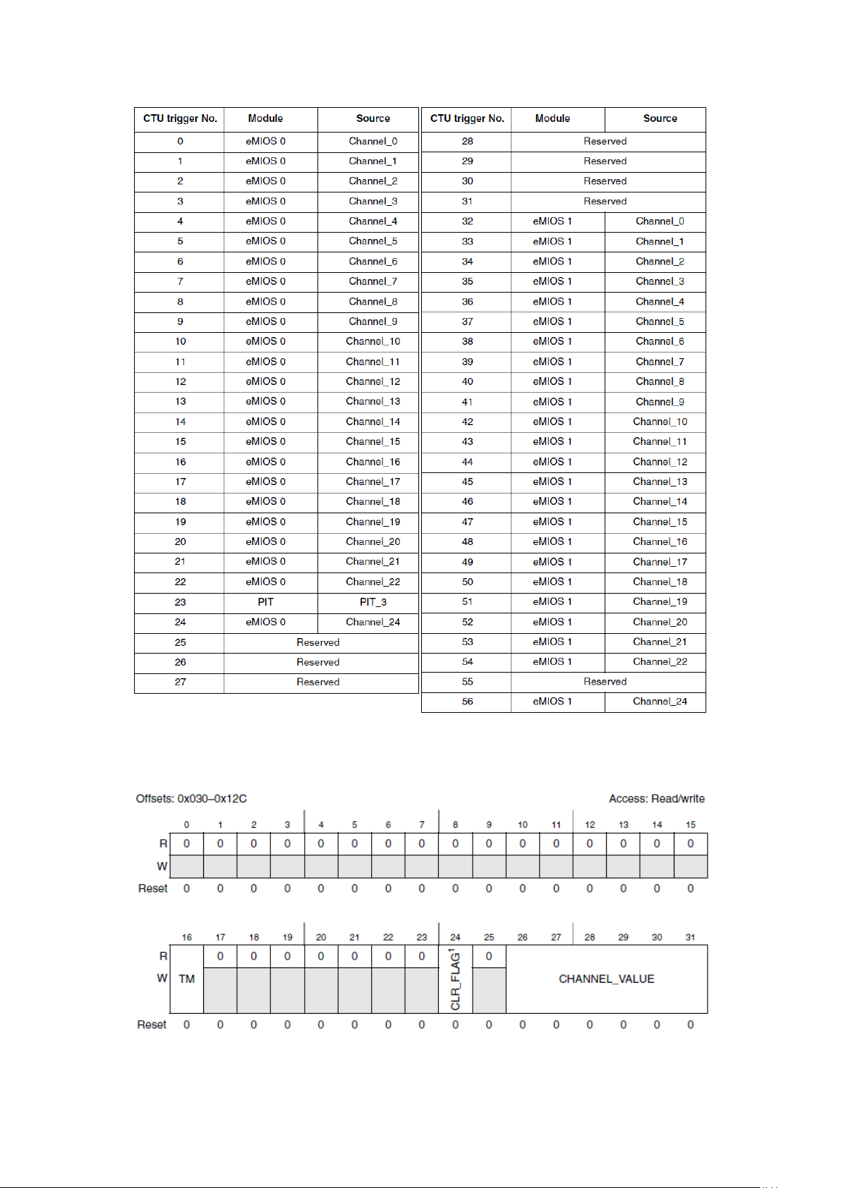
Figure 76 : Trigger Sources (R.M. Rev8 – Table 26-3)
2. Configuring CTU
Figure 77 : Event Configuration Registers (R.M. Rev8 – Fig. 26-2)
Page 66
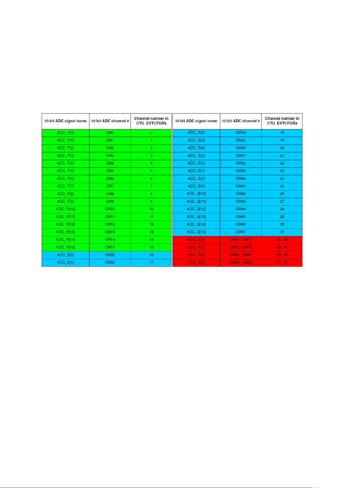
An EVTCFGR[n] register has the following fields:
Figure 78 : ADC assignment to CTU register (R.M. Rev8 – Table 26-4)
3. Configuring ADC
4. Implementing a feedback loop with ADC-CTU-eMIOS
A trigger masking bit (TM), set this bit to enable triggers.
A clear flag (CLR_FLAG) bit to force the software to send and Flag_Ack signal to the
timers. If this bit is set, the Flag_Ack is sent continuously ( may cause a loss of event), and
when it is clear Flag_Ack is handled automatically.
A channel value field (CHANNEL_VALUE) to specify the ADC channel to be converted.
(See the table below for channels associations with these values).
The CTU enable bit has to be set to enable CTU triggered conversions. If a CTU conversion is
triggered while a normal conversion is ongoing, it is treated just like an injected conversion. The
normal conversion is aborted, and it resumes once the CTU conversion is completed.
However, if a CTU conversion is triggered, during and ongoing injected conversion, the injected
conversion is aborted and does not resume later. This situation is signalled by the ADC’s status
register’s JABORT bit.
This example can be used for implementing the feedback loop of a control system; at each PWM
period an input can be read, and PWM’s duty cycle can be altered depending on it. It is very
similar to the chapter 6’s section 3. But in this one the PIT is removed, and ADC interrupt
changes both PWM duty cycle and the LEDs (works on flag EOCTU), there is no internal state.
Page 67
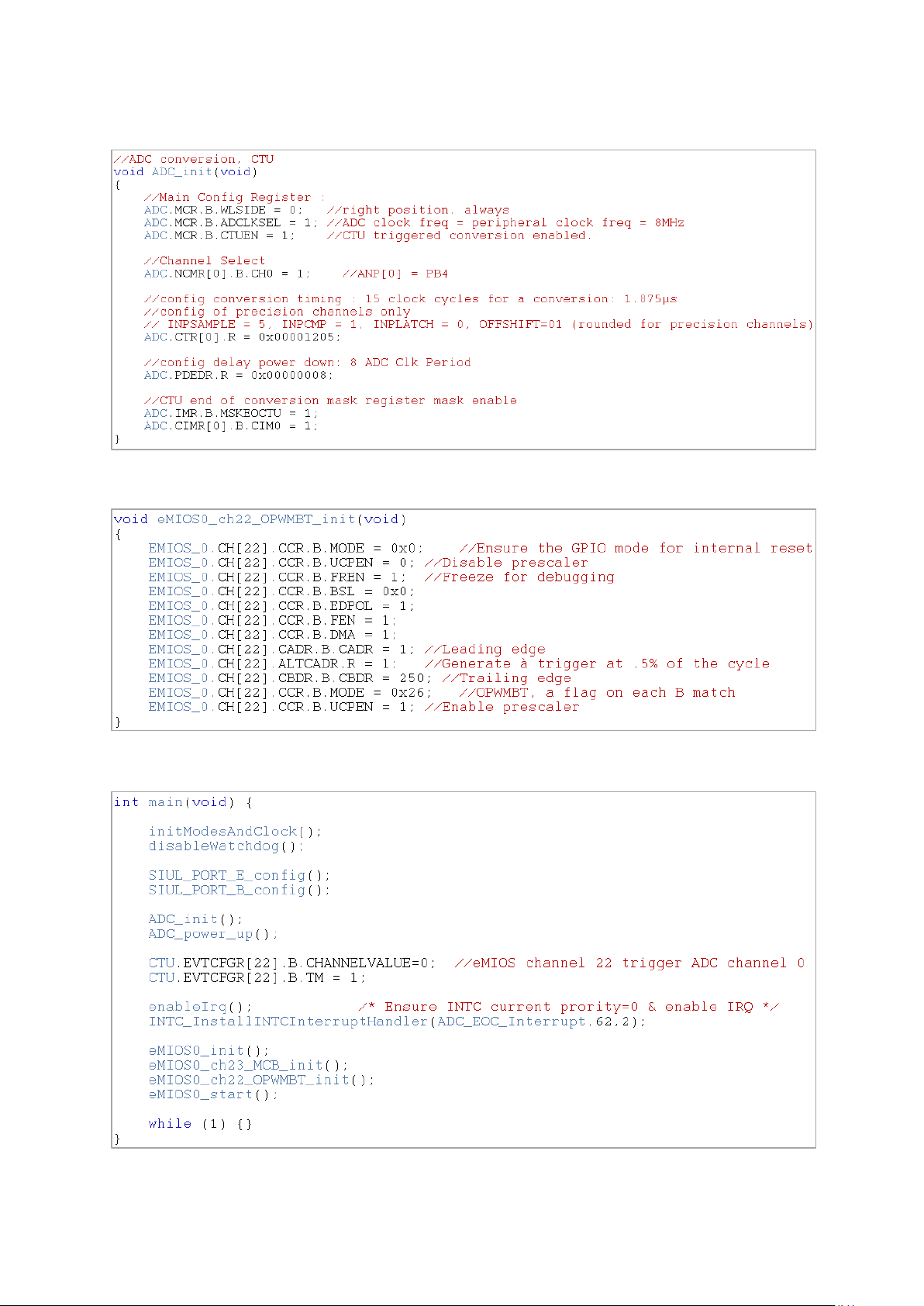
One of the differences comes from the ADC initialisation, where the CTU triggers are enabled:
And the eMIOS channel is changed to an OPWMT from generating triggers (with alt A register):
And in the main code, the CTU is set so that eMIOS channel 22 triggers ADC channel 0:
Page 68
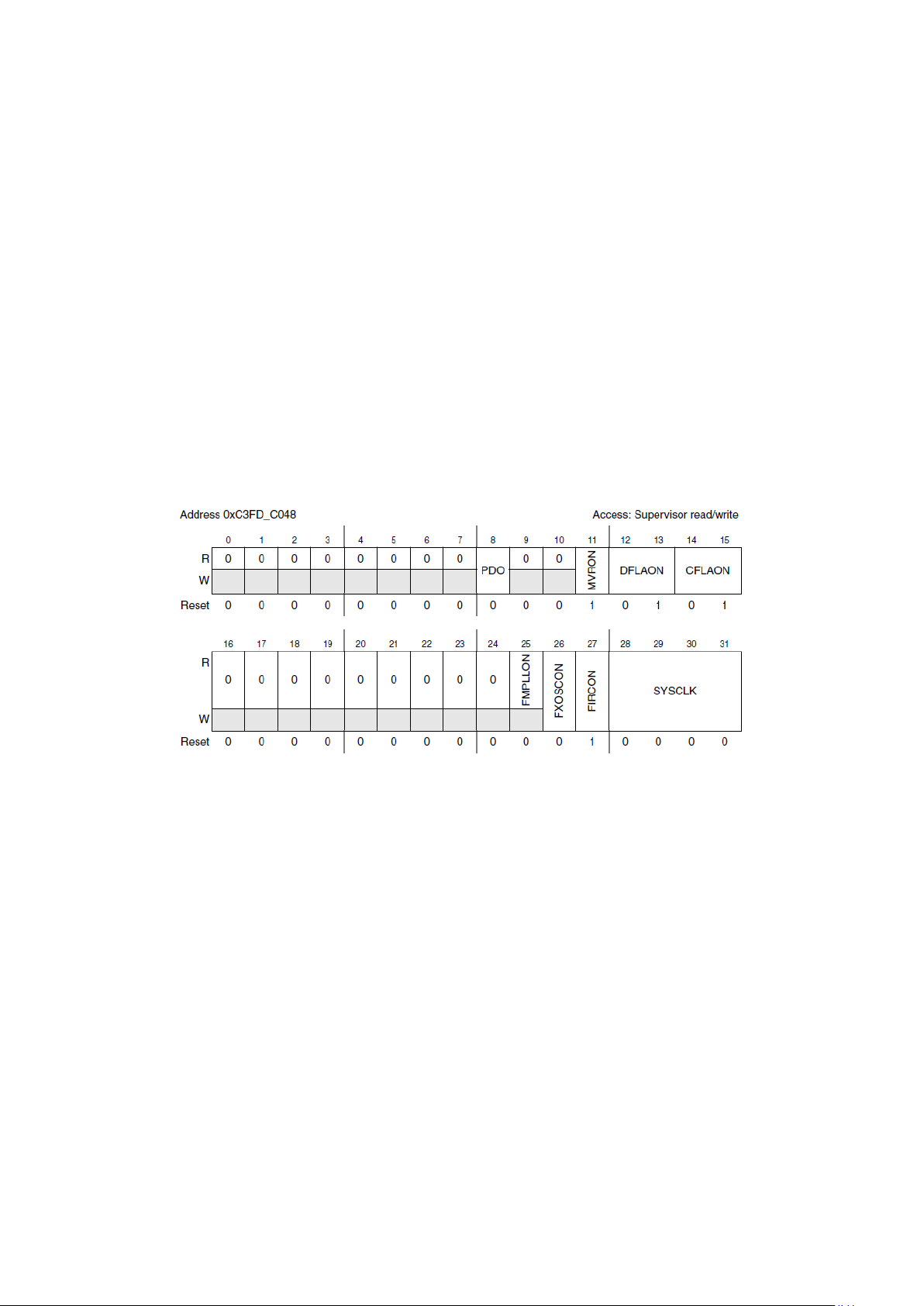
Chapter 8
WKPU: Wakeup Unit
1. Low power consumption modes
1.1. STOP
Figure 79 : STOP Mode Configuration Register (R.M. Rev8 – Fig. 8-15)
1.2. STANDBY
There are three low power user modes: HALT, STOP and STANDBY. We will not go into details
about HALT, as it is very similar to STOP but cannot process wakeup signals.
The STOP mode is a configurable low power mode where the clock to the core is disabled and
most peripherals can be disabled for efficient power saving. It has a realtively quick wakeup
latency and it can only be entered with software request from RUN0…3 modes. On a wakeup
event, the device goes back to the RUN0…3 modes, continuing from where the program was left.
The stop mode can run on all clocks except the FMPLL. The system clock is by default on FIRC
clock but it can be disabled. Data and Code flash memories are by default powered down, but can
be activated, and the main voltage regulator is switched on.
The PDO field in this configuration registers, can be used to power down the I/O, by default the
pads power driver is enabled (‘0’) but by setting this bits it can be disabled while still keeping
the output states.
The STANDBY mode is the most power saving mode among others where most of the power
supply is cut off and with the exception of wakeup pins, all pins are in high impedance mode. It
can be entered from DRUN or RUN0…3 modes and, at a wakeup event, after its relatively long
wakeup latency, the device goes back to DRUN mode, reinitialising the device. The previous
memory content is lost, but it can be restored from backup.
62
Page 69
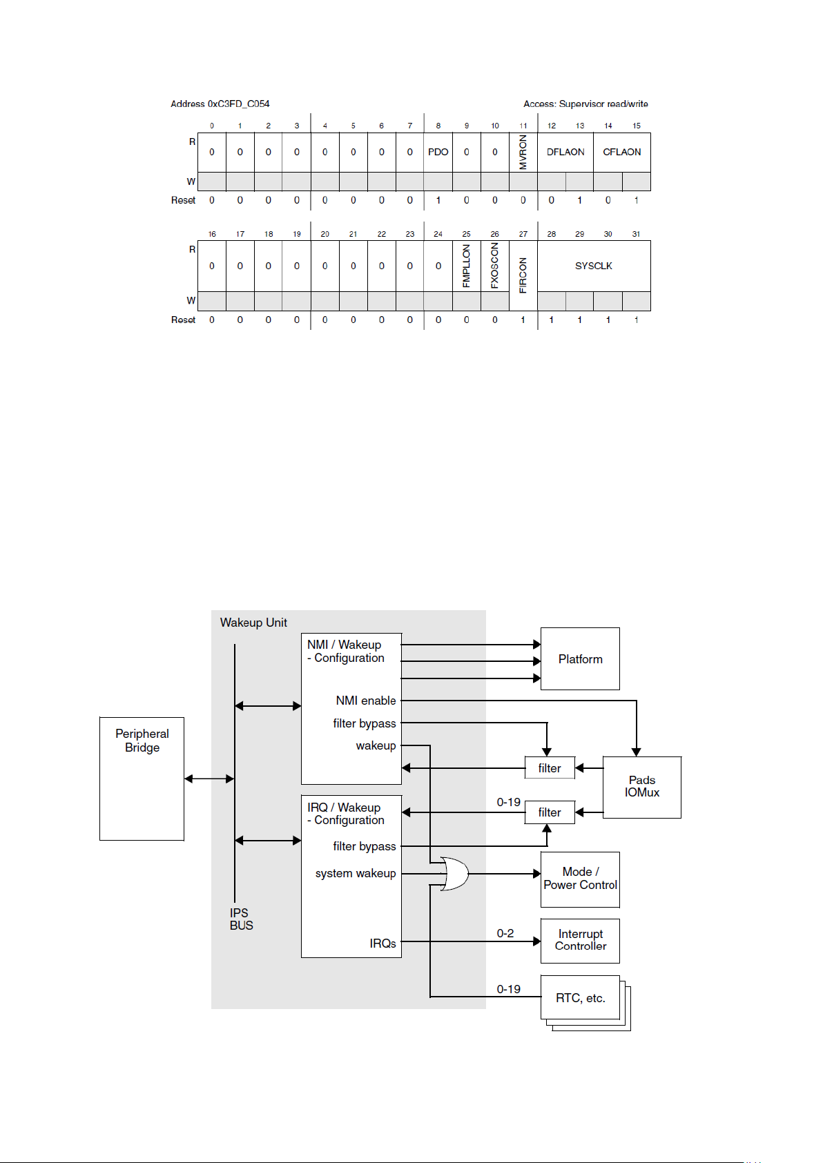
Figure 80 : STANDBY Mode Configuration Register (R.M. Rev8 – Fig. 8-16)
2. Introduction
Figure 81 : Wakeup Unit Block Diagram (R.M. Rev8 – Fig. 12-1)
In this mode, the power supply is only used for MC_RGM (Reset Generation Module), MC_PCU
(Power Control Unit), WKPU (Wakeup unit), 8k RAM, RTC/API, CAN_Sampler, SIRC, FIRC and
SXOSC. This mode is usually configured to run on SIRC or FIRC (running on SIRC and disabling
FIRC saves even more power). When a wakeup signal is received, the device modes and clock are
reconfigured in the DRUN mode (first lines of the “main” function).
Wake-up events allows mode transition from STANDBY mode to DRUN mode or from STOP to
RUN 0…3 modes.
Page 70
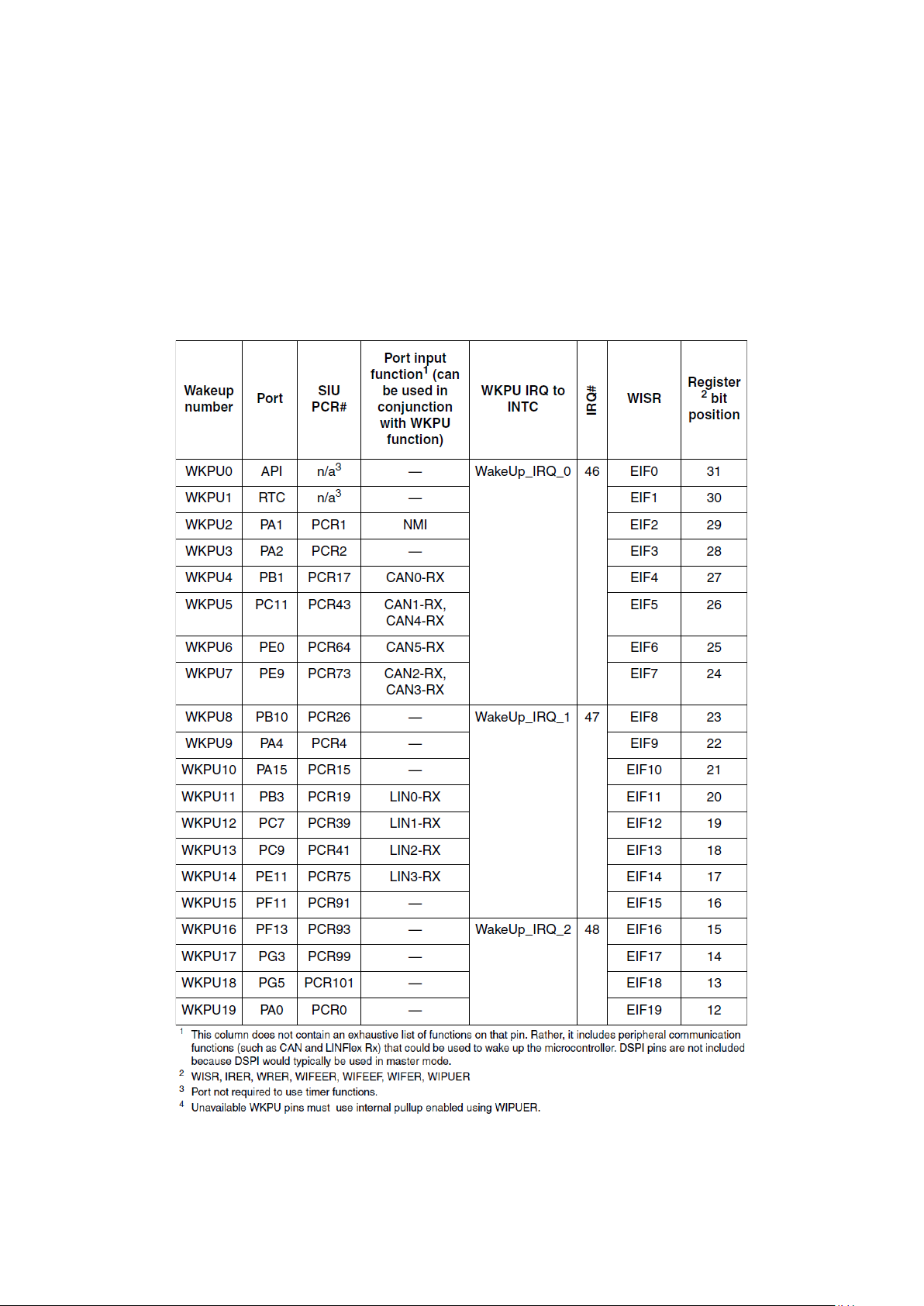
Figure 82 : Wakeup vector mapping (R.M. Rev8 – Table 12-1)
A wakeup signal can be generated from 20 different sources, the source number 0 is the API, the
source number 1 is the RTC and the other ones are external sources that are located on some
specifics pads of some ports that has also communication functionalities like CAN or LIN. This
can allow, for example, to put the device en low power mode while awaiting
information/commands from CAN.
The following table shows different wakeup sources, their id numbers, modules, IRQ
associations and flags.
Page 71
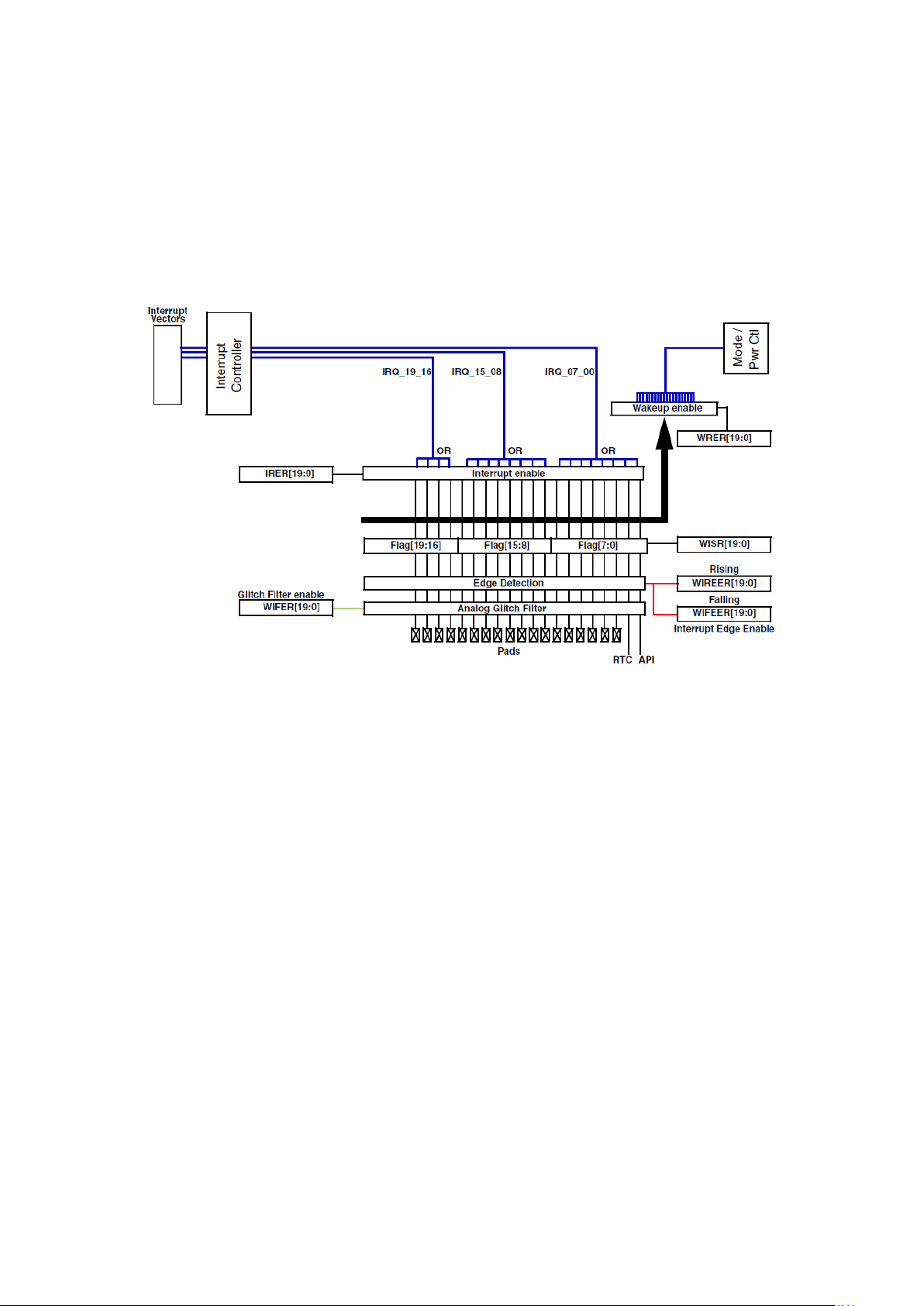
On external interrupts, DSPI is not mentioned because it is thought to be used in master mode
Figure 83 : Wakeup unit external interrupt pad diagram (R.M. Rev8 – Fig. 12-12)
3. Configuration of wakeup events
but it can still be done (see pad configurations) if needed. A more appropriate use would be, for
instance, to wake up the device using CAN signals.
The 18 external sources of the Wakeup Unit will trigger a wakeup signal in STANDBY/STOP
modes but they can still be used as extra external interrupts during a RUN mode. These Wakeup
pins are enabled in all modes, so, in order to ensure that their current consumption stays
minimal, internal pull-up resistors (see following registers) should be used with unused pins.
The non maskable interrupt (NMI) functionalities of this unit will not be explained here.
This unit has a few registers for configuring and managing wakeup events, all of them have a 20bit modifiable field with each bit being associated to a wakeup source.
The Wakeup/Interrupt Filter Enable Register (WIFER) is used to enable a non-configurable
filter on the input signals. Its field is called IFE[19:0]. All filters are disabled by default.
Similarly the Wakeup/Interrupt Pullup Enable Register (WIPUER), with its IPUE[19:0] field can
enable a pull-up register on the selected interrupt pads. It should be used on unused pins to
reduce current leakage.
Then, Wakeup/Interrupt Rising/Falling-Edge Event Enable Registers (WIREER/WIFEER) with
IREE/IFEE fields can be used to select a signal edge (or both) as a triggering event.
The Interrupt/Wakeup Request Enable Registers (IRER/WRER) are used to enable the
generation of an interrupt/wakeup request from the triggering event.
And Wakeup/Interrupt Status Flag Register (WISR) contains the flag generated by the triggering
event and can be cleared by writing ‘1’.
Page 72
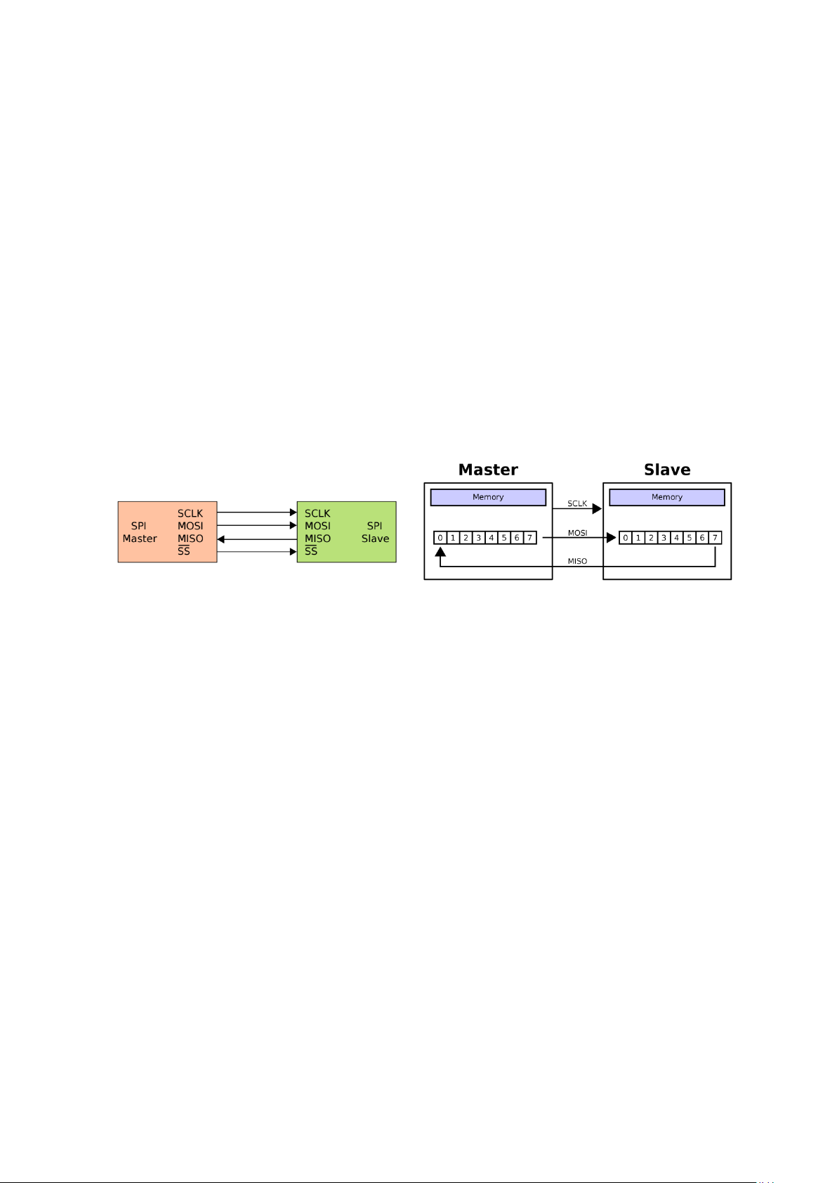
Chapter 9
DSPI: Deserial Serial Peripheral Interface
1. Introduction
1.1. SPI Protocol Description
Figure 84 : SPI Master/Slave Illustrations
There are three identical DSPI modules (0…2) in this microcontroller for using SPI serial bus
protocol in order to communicate with external devices.
The Serial Peripheral Interface (SPI) is a synchronous serial communication bus in which there
is only one master and at least one slave. This bus can operate in full-duplex mode, transmitting
and receiving at the same time. There are at least four logical signals but in a single slave
situation only three of them can be enough.
These signals are:
SCLK (or SCK in DSPI): a clock generated by the master to synchronise the exchange,
MOSI (or SOUT in DSPI Master, SIN in DSPI Slave): Master Output Slave Input, data sent
by the master
MISO(or SIN in DSPI Master, SOUT in DSPI Slave): Master Input Slave Output, data sent
by the slave
SS (or CS in DSPI): Slave Select (Chip Select), selection of a slave.
In MOSI/MISO naming convention, MOSI of the master is connected to MOSI of the slave and
similarly their MISO are connected together, but in SOUT/SIN naming convention (DSPI’s case),
SOUT is connected to SIN and SIN to SOUT.
There is a shift register in both master and slave (usually 8-bit) and following the clock ticking of
the master, these registers are rotated until the data in them is completely exchanged.
There are many parameters about details of this transmission that can be configured, and both
master and slave has to have similar configurations for valid communication like the frame size
(shift register’s size). The master’s clock frequency is also called the SPI Baud Rate, image of the
data transmission speed, can be selected on a wide range on values, and this clock’s polarity
(CPOL) can be selected. Another important parameter is the clock phase (CPHA) with defines
the edge where the data is sampled.
66
Page 73
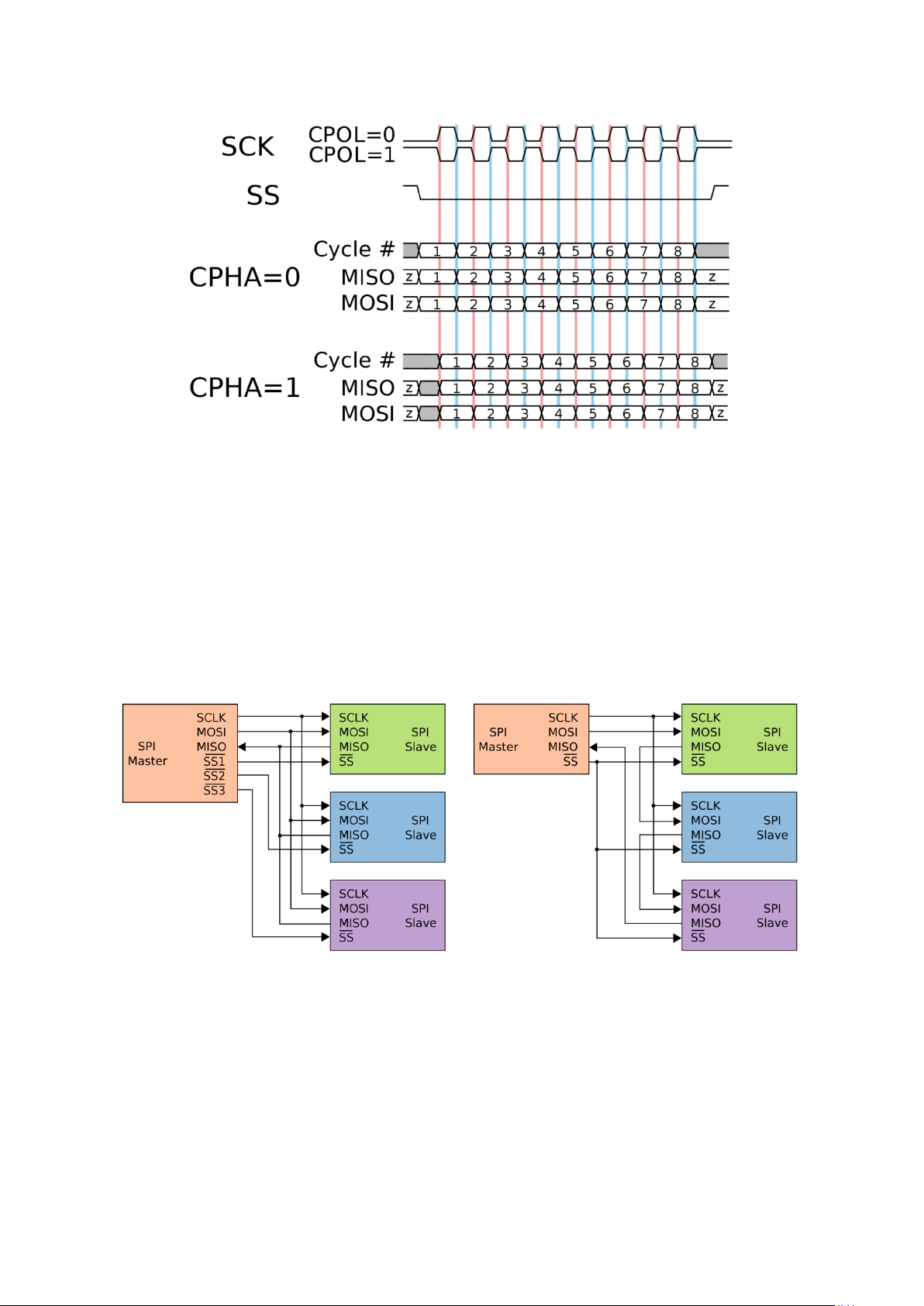
Figure 85 : A time diagram of different signals involved in SPI, depending on CPOL/CPHA
Figure 86 : SPI Configurations: Independent(left) \ Daisy-chained (right)
When using SPI with multiple slaves there are different possibilities for connecting them. If the
master has enough chip select signals, then each slave can be independent and communicate
with the master only when asked. But in the case where the master has only one chip select
signal, then a configuration called daisy-chained SPI can be used. In this chain, each device sends
its data to the next device and receives from the previous one. This can slow down the
communication between far ends of the chain but it also enables slaves to communicate among
each other without needing to go through the master. (Even though this requires some kind of
identification method to be defined.)
Page 74
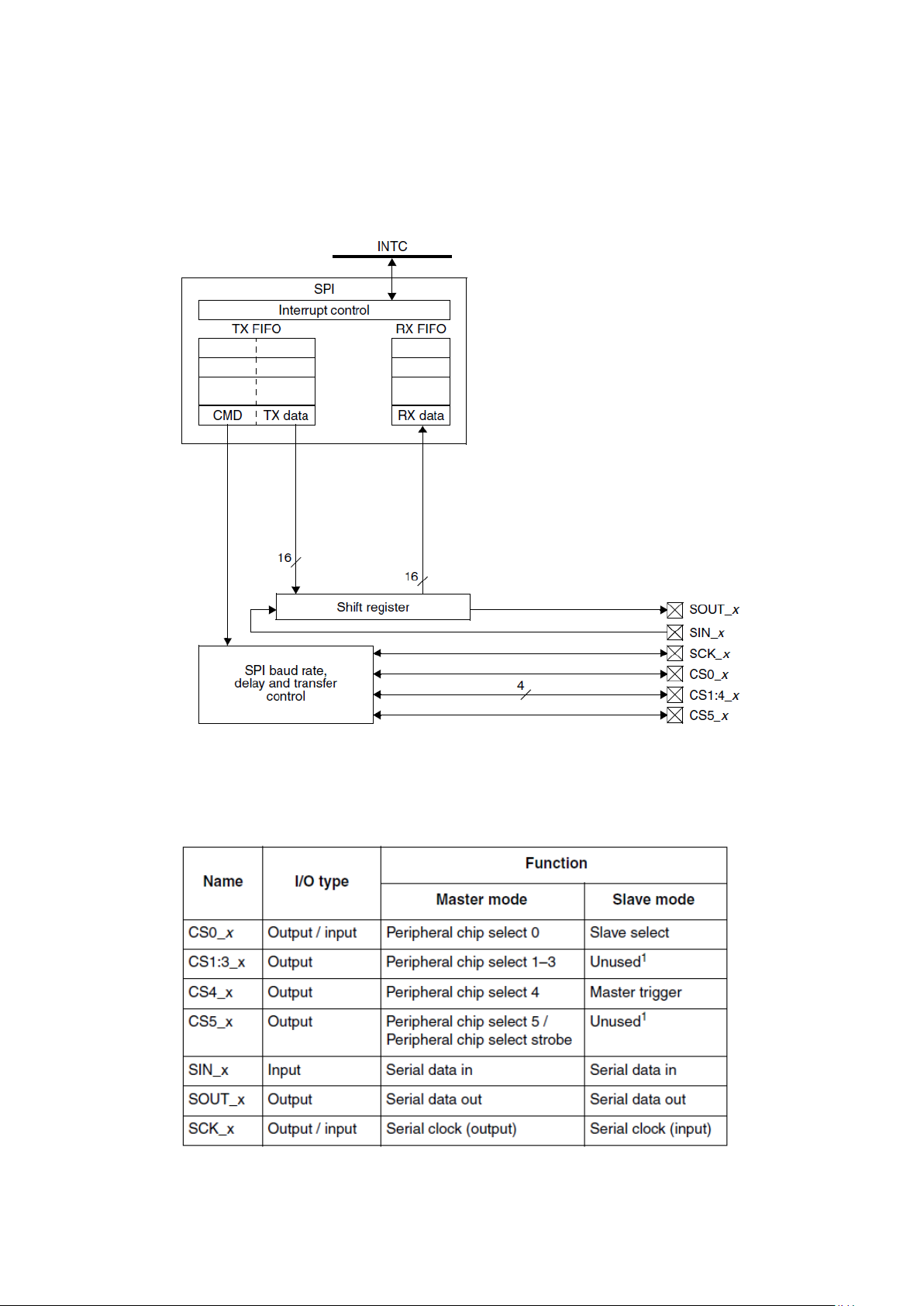
1.2. Module Presentation
Figure 87 : The DSPI module block diagram (R.M. Rev8 – Fig. 23-1)
Figure 88 : DSPI Signal Properties (R.M. Rev8 –Table 23-1)
The DSPI Modules provide an implementation of the SPI protocol with some enhancements like
FIFO buffers in the memory for simpler communication, various interrupts and a precise control
on the baud rate and delays.
Each DSPI module has six chip select (CSx) signals that can handle communication with a
considerable amount of external devices.
Page 75
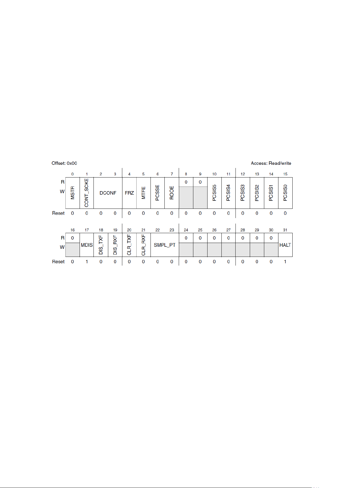
2. Configuration
2.1. Signal Configuration
2.2. Module Configuration Register
Figure 89 : DSPI Module Configuration Register (R.M. Rev8 –Fig. 23-3)
Depending on whether the DSPI is configured as a master or a slave, CS[0:5]_x pins have to be
configured using SIUL.
Output type signals need an output buffer, so the OBE bit SIUL’s pad configuration register is
needed. Also the slew rate of the port might need improving so SRC bit should be set. E.g. : SOUT
at all devices, SCK and SC at master
For the input types the input buffer has to be enabled using IBE and also a pull up resistor is
needed, so the internal pull up can be used by setting WPE and WPS.
This configuration register has the following fields:
MSTR: Master/slave mode select (‘1’ for master),
CONT_SCKE: Continuous SCK enable (see below more details),
FRZ: Freeze, when the device enters debug mode, DSPI transfers halt at the next frame
boundary,
MTFE: Modified timing format enable (see below for more details),
PCSSE (Peripheral Chip Select Strobe Enable): when enabled CS5 signal can be used on
an demultiplexer to decode the CS signals into as much as 32 glitch-free CS signals. It
introduces a delay before and after the frame, allowing for the switching of CS[0:4] on
the demultiplexer to avoid glitches output. See Transfer Configuration Register for
setting these delays.
ROOE: Receive FIFO overflow overwrite enable. If cleared, the incoming data is ignored
when FIFO is full, when set, the incoming data is put in the shift register.
PCSISx; Peripheral chip select inactive state, if cleared, the inactive state is low, is set, the
inactive state is high. In slave mode, it has to be set as inactive high (common in SPI).
MDIS: Module Disable: When set, disable DSPI clocks to save power.
DIS_TXF: Disable transmit FIFO buffer. Similarly with DIS_RXF for receive FIFO.
CLR_TXF: Clear transmit FIFO, reset its counter. Similarly with CLR_RXF for receive FIFO.
Page 76
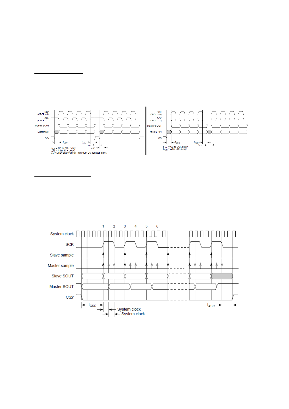
SMPL_PT: Sample point, allows the moment where the master can sample the SIN pin
Continuous transfers:
Figure 90 : Difference between continuous and non-continuous formats (R.M. Rev8 –Fig. 23-20/21)
Modified transfer format:
Figure 91 : Modified transfer format (R.M. Rev8 –Fig. 23-18)
2.3. Transfer Configuration Register
when using modified transfer format: at the odd-numbered-edge of SCK(00), one system
clock cycle following that(01) or two system clock cycles following the SCK edge(10).
HALT: When set, DSPI transfers are stopped. Useful for starting/stopping transfers.
Some chips need to be deselected between two sequential transfers, others need to be keep
selected. By default, the delay after transfer (see below) allows the deselecting, but it can be
removed using continuous transfer mode.
On classical SPI transfer formats, CPOL and CPHA are enough to define the clock polarity and
which edges to use for capturing or changing the data. The modified transfer format allows to
refine the sampling point for applications where the slave chip might have a considerable delay
for changing its transmitted value. Using SMPL_PT the software can set a few system clock ticks
of delay for sampling. The user needs to check that SPI link timing won’t cause any problems.
Each DSPI module contains six Clock and Transfer Attributes Registers[0…5](CTARx), that
define different settings for SPI’s transfer format like the frame size, baud rate, delays etc. When
transmitting, the software can select which CTAR register to use to set the transfer. These
Page 77
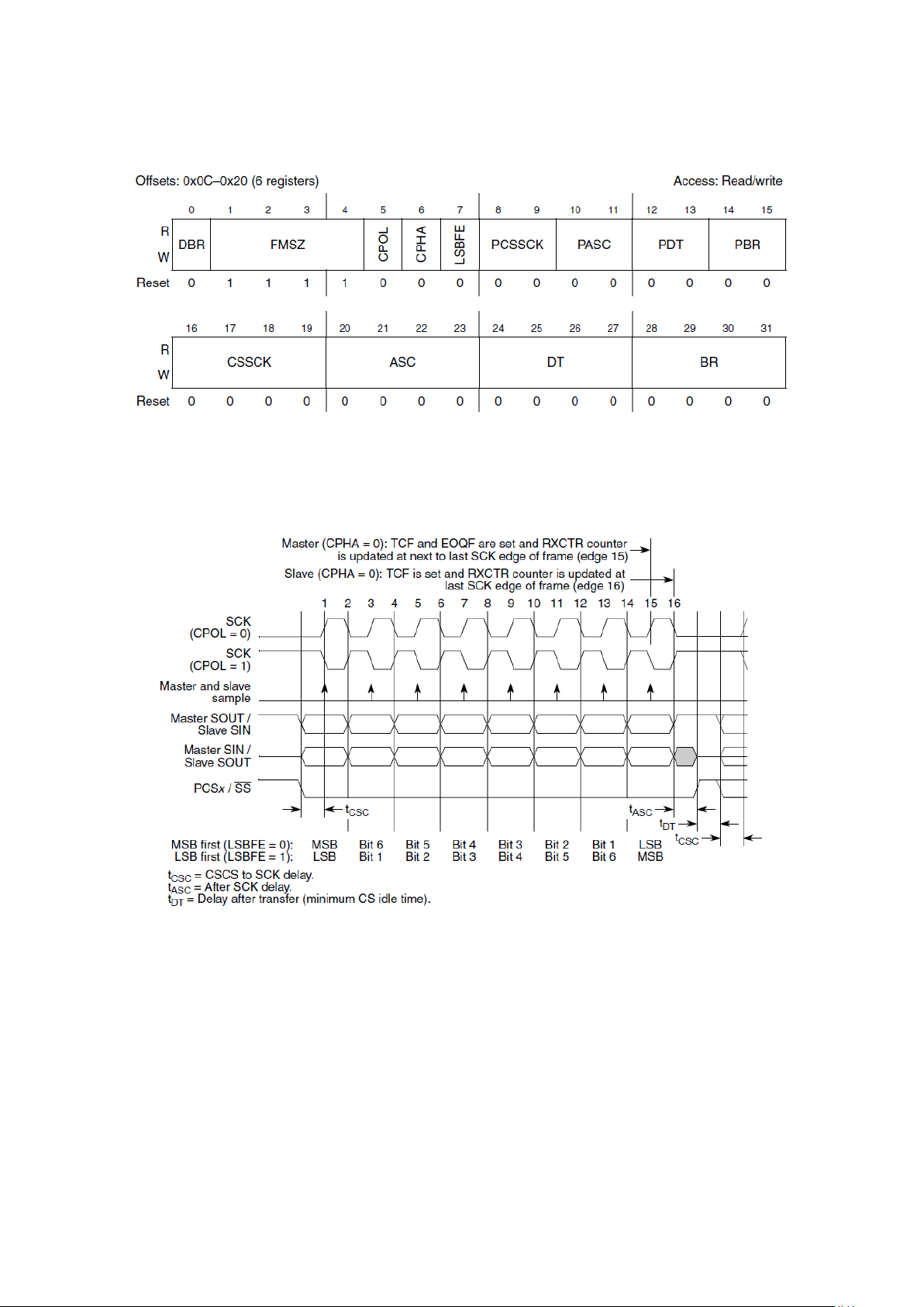
registers should not be changed while DSPI is running. Most of its fields are only used in the
Figure 92 : Clock and Transfer Attributes Registers (CTAR) (R.M. Rev8 –Fig. 23-5)
Figure 93 : Illustration of flag timings on classic SPI transfer format (R.M. Rev8 –Fig. 23-16)
2.3.1. Data attributes
master mode.
This configuration register’s fields are explained in different subsections below for better clarity.
The figure below illustrates the influence of different parameters on the transfer.
These attributes are used to select the parameters related to the transferred data like its size, its
order, on which edge it is read or changed.
FMSZ: frame size, selects the number of bits transferred per frame. Both master and
slave modes need this. The frame size value is FMSE+1 (has to be between 4 and 16).
CPOL: clock polarity, if cleared, the inactive value of SCK is low, else it is high. Both
master and slave modes need this.
CPHA: clock phase, if cleared, the data is captured on the leading edge of SCK, otherwise
it is captured on the falling edge. Both master and slave modes need this.
Page 78
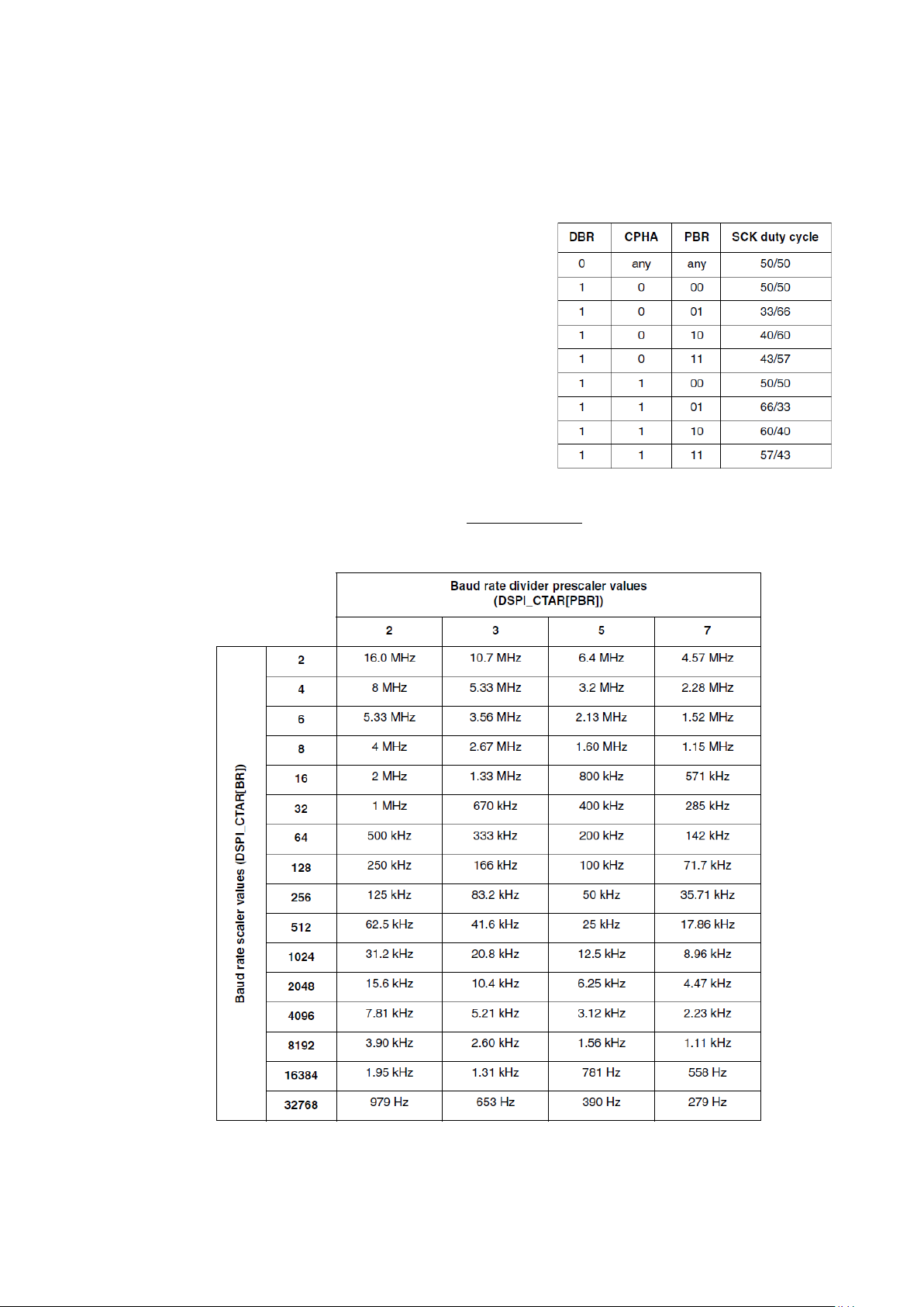
LSBFE: LSB First Enable, if cleared, MSB is transferred first, otherwise LSB is transferred
2.3.2. Baud rate
Figure 94 : Baud Rate values for a 64MHz system clock
first. Master mode only.
These fields are related to the baud rate:
PBR: baud rate prescaler, used in establishing the
transfer baud rate; the prescaler value is either 2
(00), 3(01), 5(10) or 7(11). Master mode only.
DBR: double baud rate, doubles the SCK baud rate,
but depending on PBR and CPHA, it might alter the
50/50 duty cycle of the clock (see at right). Master
mode only.
BR: baud rate scaler, used in establishing the
transfer baud rate; the baud rate scaler value is
[:]
2
it is 2
for BR[0:3]< 2, it is 6 for BR[0:3]=2 and
[:]
for BR[0:3]> 2. Master mode only.
=
(1 + )
×
Page 79
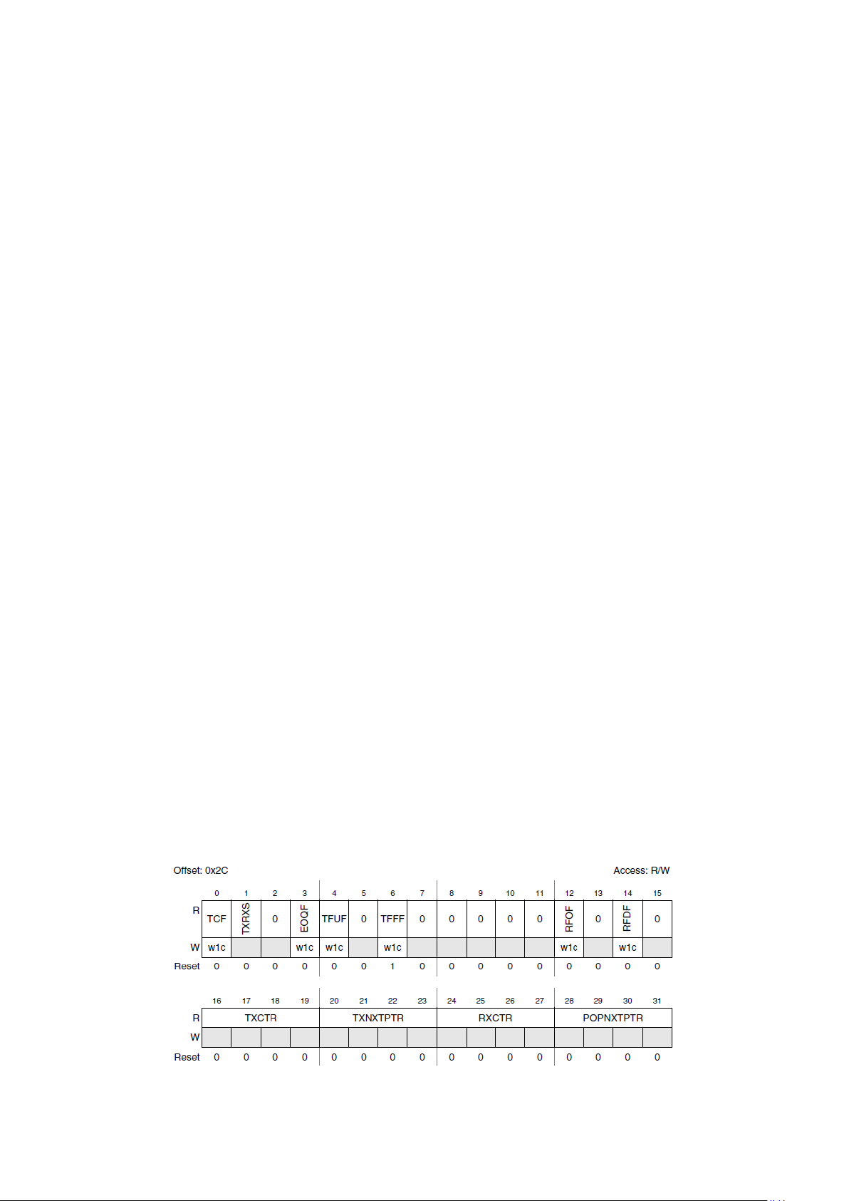
2.3.3. CS to SCK delay
2.3.4. After SCK delay
2.3.5. After transfer delay
2.4. Status and Interrupt Registers
Figure 95 : DSPI Status Register (R.M. Rev8 –Fig. 23-6)
These fields are used to set the delay between the slave select signal and the start of the transfer.
PCSSCK: CS to SCK delay prescaler, used in establishing a delay between Chip Select
signal and the SCK start; the delay prescaler value is
=2×PCSSCK[0:1]+1.
Master mode only.
CSSCK : CS to SCK delay scaler, used in establishing a delay between Chip Select signal
and the SCK start; the delay scaler value is
=
×
[:]
= 2
/
. Master mode only.
These fields are used to set the once the transfer is finished and SCK is stopped.
PASC: after SCK delay prescaler, used in establishing a delay after the SCK stop; the delay
prescaler value is
=2×PASC[0:1]+1. Master mode only.
ASC : after SCK delay scaler, used in establishing a delay after the SCK stop; the delay
[:]
scaler value is
= 2
. Master mode only.
=
×
/
These fields are used to set the minimum CS idle time between two transfers. This delay is not
used in continuous transfer mode.
PDT: after transfer delay prescaler, used in establishing a delay between the end of one
conversion and the start of another one(the Chip Select signal) ; the delay prescaler
value is
=2×PDT[0:1]+1. Master mode only.
DT : after transfer delay scaler, used in establishing a delay between the end of one
conversion and the start of another one(the Chip Select signal) ; the delay scaler value is
= 2
. Master mode only.
=
×
/
[:]
The Transfer Count Register (TRC) counts the number of SPI transfers made. It has a 16-bit field
called SPI_TCNT. It automatically resets to 0 when it goes past 65535, or it can be forced to reset
using a command on transmit register.
Page 80
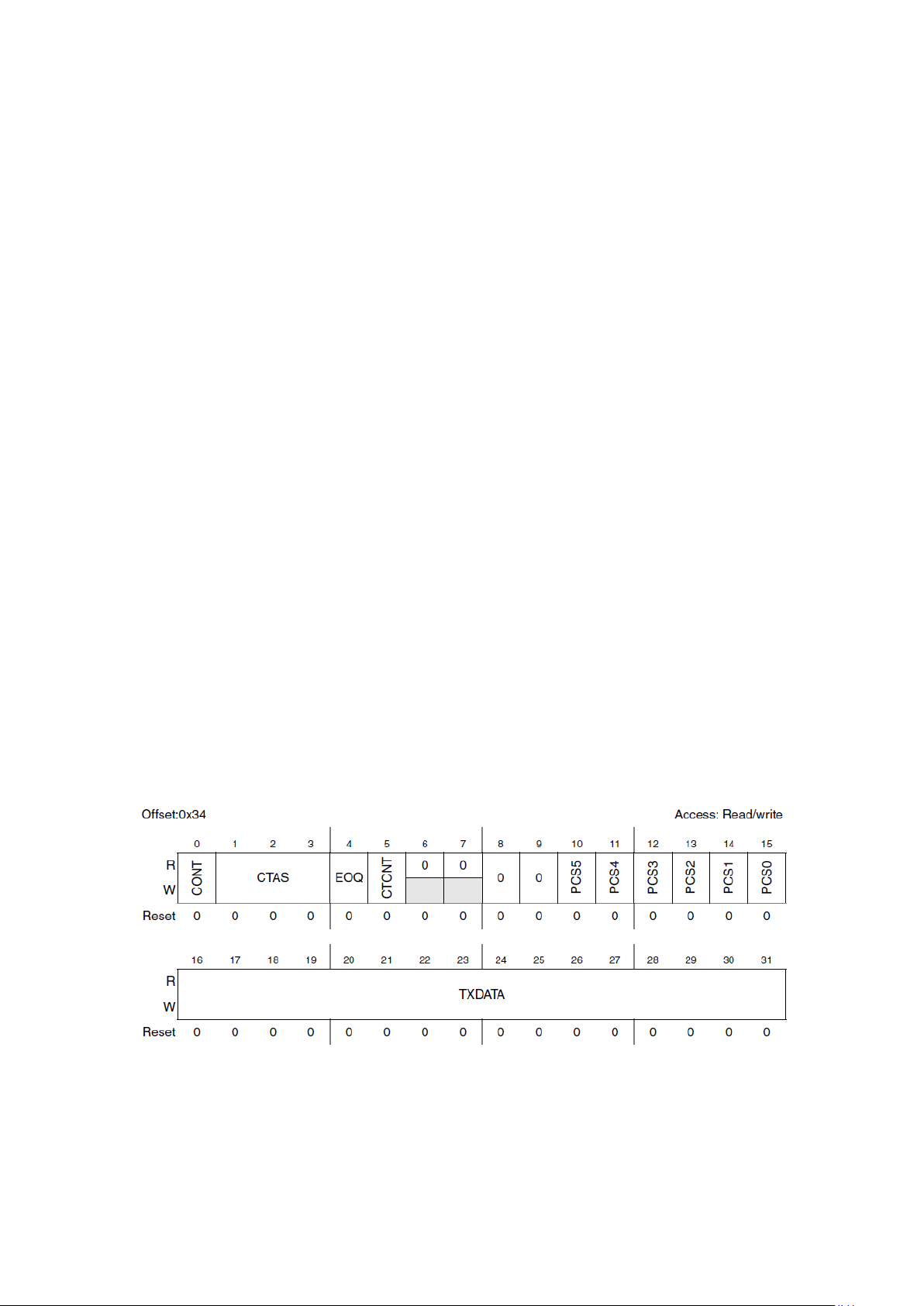
The DSPI Status Register (SR) contains both flags and information about the current status of the
2.5. Transmit/Receive Registers
Figure 96 : DSPI Push TX FIFO Register (R.M. Rev8 –Fig. 23-8)
module. It’s fields are:
TCF: Transfer complete flag, this flag is raised once the last incoming data of a frame is
sampled and before
delay is started.
TXRXS: TX and RX status, when 0, TX/RX operations are disabled and DSPI is in
STOPPED state.
EOQF: End of queue flag, indicated that the ongoing transmission is the last entry in a
queue. This flag can be raised by writing 1 to the EOQ bit in the command field of a TX
FIFO. (see following section.)
TFUF: Transmit FIFO underflow flag, in a slave mode DSPI module, is set when the TX
FIFO is empty and an external master initiated a transfer.
TFFF: Transmit FIFO fill flag, when set, it means that the TX FIFO can be filled with more
entries.
RFOF: Receive FIFO overflow flag, indicates that RX FIFO is full and a transfer is initiated.
RFDF: Receive FIFO drain flag, indicated that there are data in RXFIFO that can be read.
TXCTR/RXCTR: indicates the number of entries in the TX/RX FIFO.
TXTNXTPTR: Transmit next pointer, indicates which TX FIFO entry will be transmitted
on the next transfer.
POPNXTPTR: POP next pointer, indicates which RX FIFO entry will be read on the next
read.
And the DSPI Interrupt Request Enable Register (RSER) can be used to enable interrupts related
to the previous flags, this registers has the following enable fields: TCF_RE, EOQF_RE, TFUF_RE,
TFFF_RE, RFOF_RE and RFDF_RE. Each of these interrupts has a different ISR vector, so a
different handler.
In DSPI module, transmitting and receiving data are done using a PUSH and a POP register for
writing to TX FIFO and reading from RX FIFO.
The DSPI PUSH TX FIFO Register (PUSHR) is made of a 16-bit command field and a 16-bit data
field called TXDATA. TXDATA contains the data to be transmitted and the command field is
made of various sub-fields to configure the transfer.
Page 81

These sub-fields are:
3. Developing a general purpose SPI Driver
Methods
Direction
TX/RX
Master/Slave
Description
Execution
exchange
Full-duplex
TX+RX
Master
a data exchange
Foreground
write
Half-duplex
TX
Master
a data sent
Foreground
read
Half-duplex
RX
Master
a data received
Foreground
show
Half-duplex
RX
Slave
a data written on TX buffer
Foreground
Methods
Direction
TX/RX
Master/Slave
Description
Execution
exchange_array
Full-duplex
TX+RX
Master
a data array exchange,
known size
Foreground
Background
write_array
Half-duplex
TX
Master
a data array sent,
known size
Foreground
Background
read_array
Half-duplex
RX
Master
a data array received,
known size
Foreground
Background
listen
Half-duplex
RX
Slave
a data array received,
known size
Foreground
Background
listen_till
Half-duplex
RX
Slave
a data array received,
known terminating
data
Foreground
Background
show_array
Half-duplex
TX
Slave
a data array written on
TX buffer, known size
Foreground
Background
CONT: Continuous chip selection enable, if set, continuous selection mode is activated.
Available both to the master and to a slave.
CTAS: Clock and transfer attributes select, selects one of CTARx registers. (‘000’ selects
CTAR0, ‘001’ selects CTAR1 etc. until ‘101’). Available only to master.
EOQ: End of queue, signals to the host that current SPI transfer is the last one of a queue.
At the end of the transfer the EOQF flag is raised. Available only to master.
CTNT: Clear SPI_TCNT, the transfer counter register. Available only to master.
PCSx: Peripheral chip select x, selects CSx signals that are going to be asserted.
The DSPI POP RX FIFO Register (POPR) has only a 16-bit RXDATA field containing the data on
the next entry of the RX FIFO.
DSPI is a rich module with a lot options but, for establishing an SPI bus but in common
embedded usage, we don’t need all of those. In order to simplify its initialisation and usage, we
can develop a high-level driver.
A driver with an Object Oriented user interface, for transferring simple data or data arrays in full
or half duplex modes has been developed in C language. A structure was used to represent a
DSPI module’s driver, with function pointers in it for better user interface.
Transfer methods implemented in this driver are show in the table below.
These four single cycle transfer methods run only on foreground, blocking the program flow
until the transfer is completed. There are also data array transferring methods:
Page 82

An array transfer method called with an array size of ‘1’ is pretty much equivalent to a single
struct _SPI_DRV SPI[]; //SPI variable has to be imported from the SPI
and set Sys_Clk(=Peripheral_Clock) to 64MHz if you
//Initialize SPI module
//and PORT_E of DSPI1,
}
#define DSPI0_PORT 'A'
#define DSPI1 PORT 'C'
data transfer (with a few excessive useless clock cycles). Each time a transfer is completed a
‘Completed’ flag in the driver structure is set to 1 and it is automatically cleared when a new
transfer method is called. The driver sets the pins automatically according to its slave/master
needs.
Example:
//Driver module
uint16_t RxData[128]; //An array for storing received data
int main(void) {
initModesAndClks(); //remember to enable DSPI module with PCTL registers,
//
//wish to use predefined baud-rates
initPeriClkGen();
disableWatchdog();
initialise_SPI_DRIVER(); //must be called before using the driver
enableIrq();
SPI[0].init(SPI_BAUD_62500, SPI_DELAY_DEFAULT);
//you wish to use, in this example PORT_A of DSPI0 is defined
SPI[1].init(SPI_BAUD_62500, SPI_DELAY_DEFAULT);
and they are connected with jumper wires.
SPI[0].listen(RxData, 4,1);
SPI[1].write_array((uint16_t*)"Coucou!\0",4,1);
//Both modules are running on the background, 'write array' gets the next
//half word when the current one is transmitted and 'listen' manages the
//RX array storage.
while (!(SPI[0].Completed && SPI[1].Completed)){}
while (1) {} //End of program
There are some constant defines for quick initialisation of the system. Every possible I/O ports
are on the header file and can be selected before compilation.
Example:
Similarly, maximum authorised data array transfer size, data frame size are defined as constants
that can be altered. Some typical baud rates and transfer delays are defined as constants for a
system clock of 64MHz and use can define their own constants by following the explanations on
the driver documentation.
Transfer methods that can run on the background use transfer complete interrupts, and a finite
state machine has been implemented for executing different handlers depending on the transfer
method that is used. The user is free to add their own states for their own handling needs and
modify other methods accordingly.
Page 83
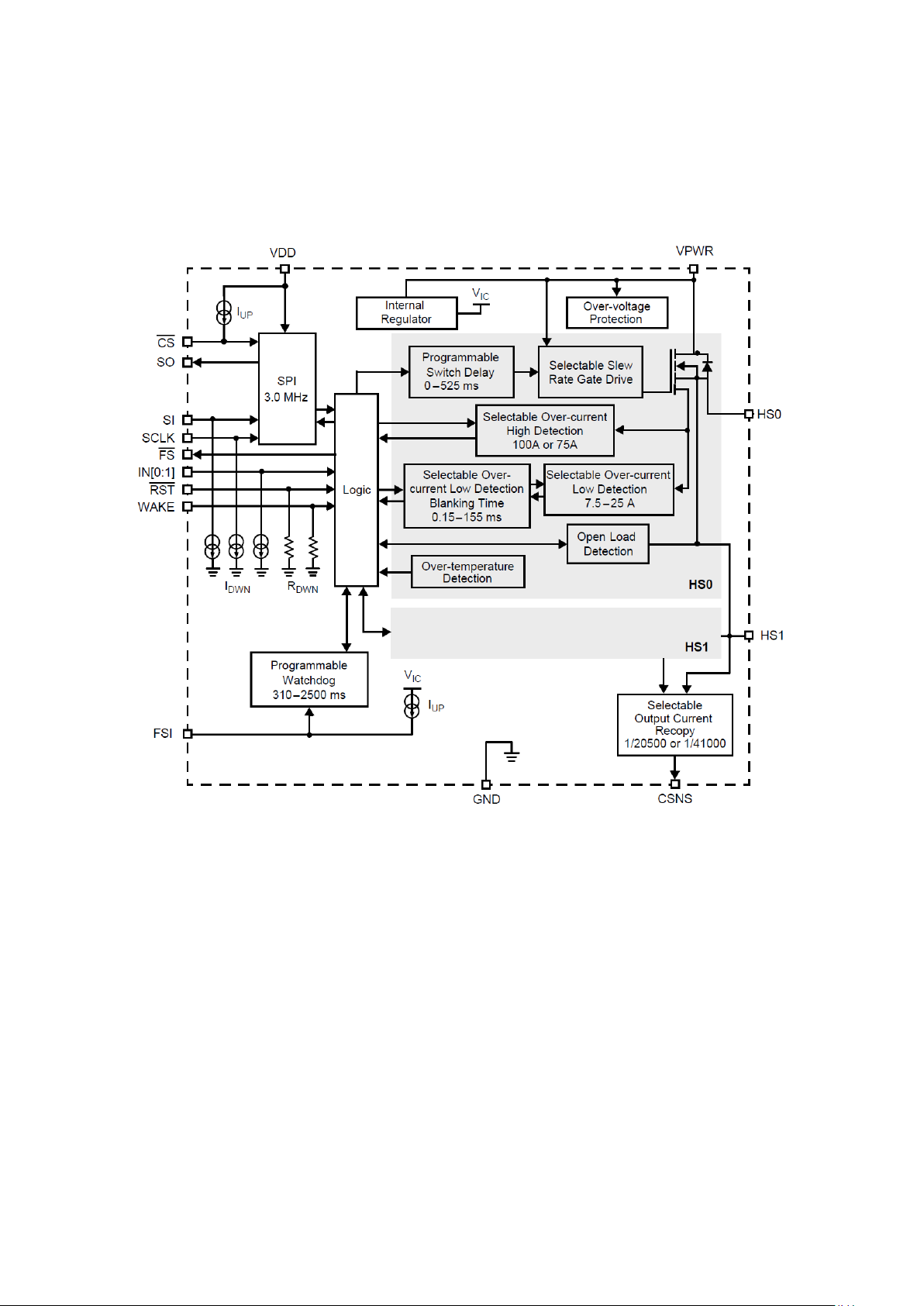
4. Driving smart-MOS switches MC33984 using SPI Driver
4.1. Introduction to MC33984
4.2. Driver’s components
This chip contains two ‘smart-MOS’ devices that can be used for switching high current
consuming loads. It also detects various electrical or thermal defects and can report them.
The figure above illustrates the internal block diagram of the chip. It possesses an SPI interface,
direct output control pins (IN0, IN1) and an analog current image output. The device has a few
registers that can be read or written to configure different aspects and check their status. The
outputs are high side switches; N-MOSFETs with an RDSon of 4mOhms.
In this example, we will develop a serial terminal interface for MPC5604B for commanding this
chip. It will have to initialise the device via SPI, then it can directly control its inputs via IN[0:1]
either as a continuous logic level or as a PWM signal. It can also read the status register from the
device and report faults via the terminal.
There are various ways to implement a driver for this chip, the one we will describe offer
various extension possibilities while being quite simple.
There are two GPIO pins of the MCU that should be used for RST and WAKE pins of the chip,
these allows resetting the chip and putting it in a useable mode.
Page 84
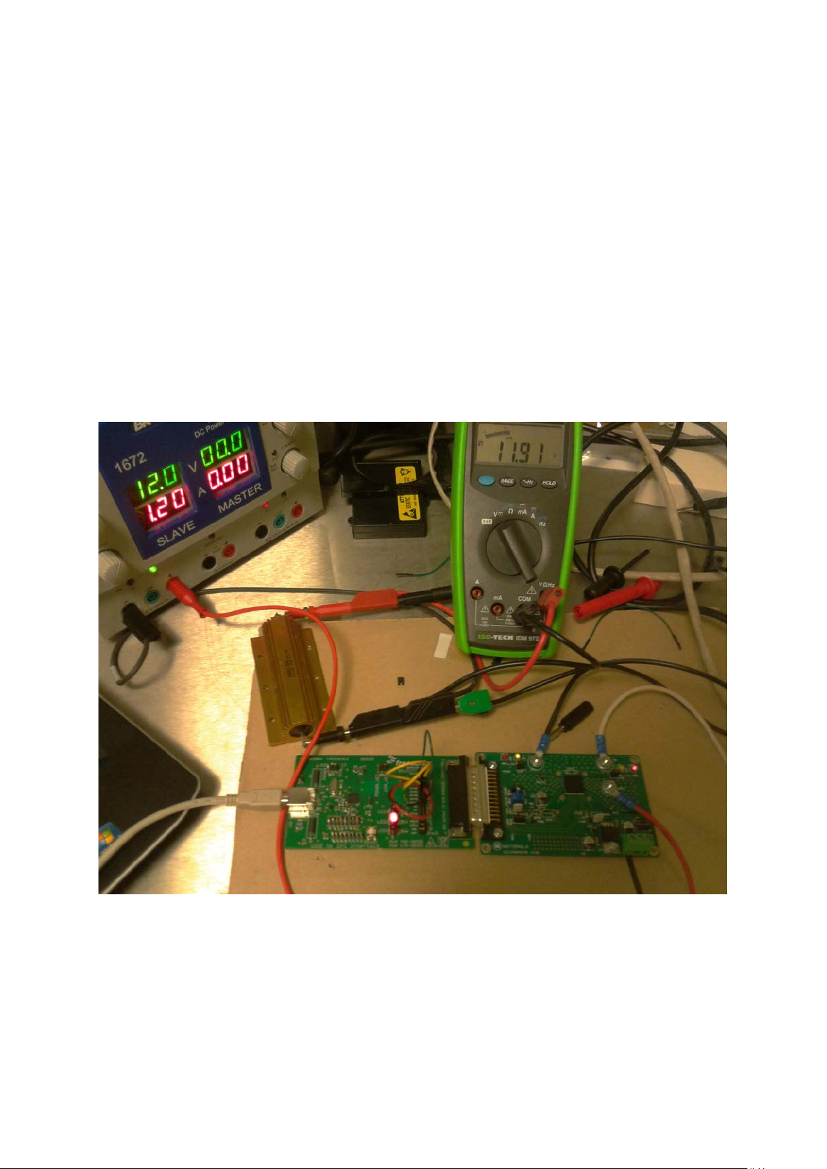
This driver uses SPI to initialise and enable switches. It sets the over-current thresholds to
minimal value. It activates the logical AND mode for the output, so both SPI_INx field in OCR
register and direct control input pin INx has to be set high to close the switch. The SPI_INx field
is therefore used for enabling a switch.
The FS pin can be used to trigger interrupts on falling edges via External Interrupt registers in
SIUL. This will allow getting an instant fault-treatment (not implemented in the example). In this
example the fault status is displayed only when the user asks for it.
CSNS can be used to get the output current value at one of the high side switches. (not
implemented in the example).
FSI is grounded to avoid refreshing the watchdog.
Page 85
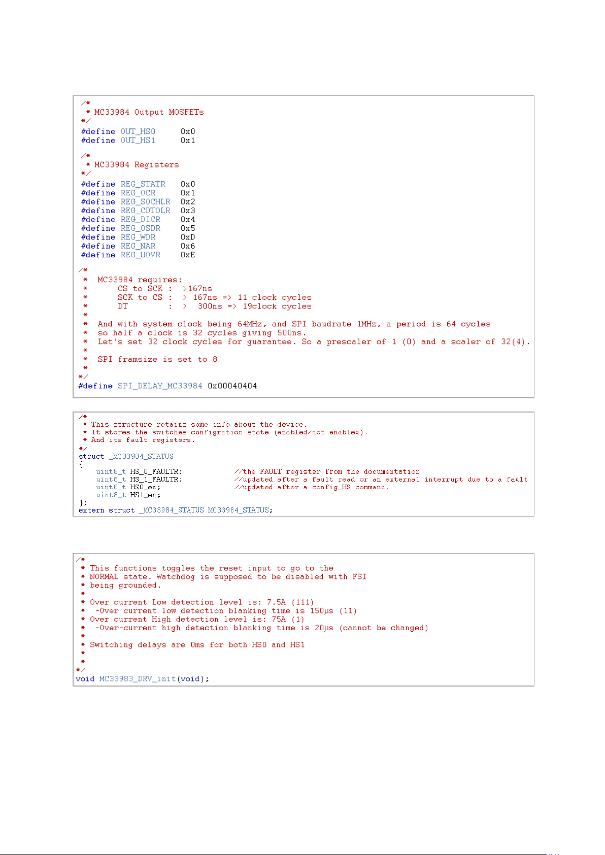
4.2.1. Definitions
4.2.2. Initialization
The initialization function of the driver sends required RST and WAKE signals to prepare the
device and it configures some basic parameters using SPI. This function also calls eMIOS
initialisation functions to set the PWM on specific pads.
Page 86
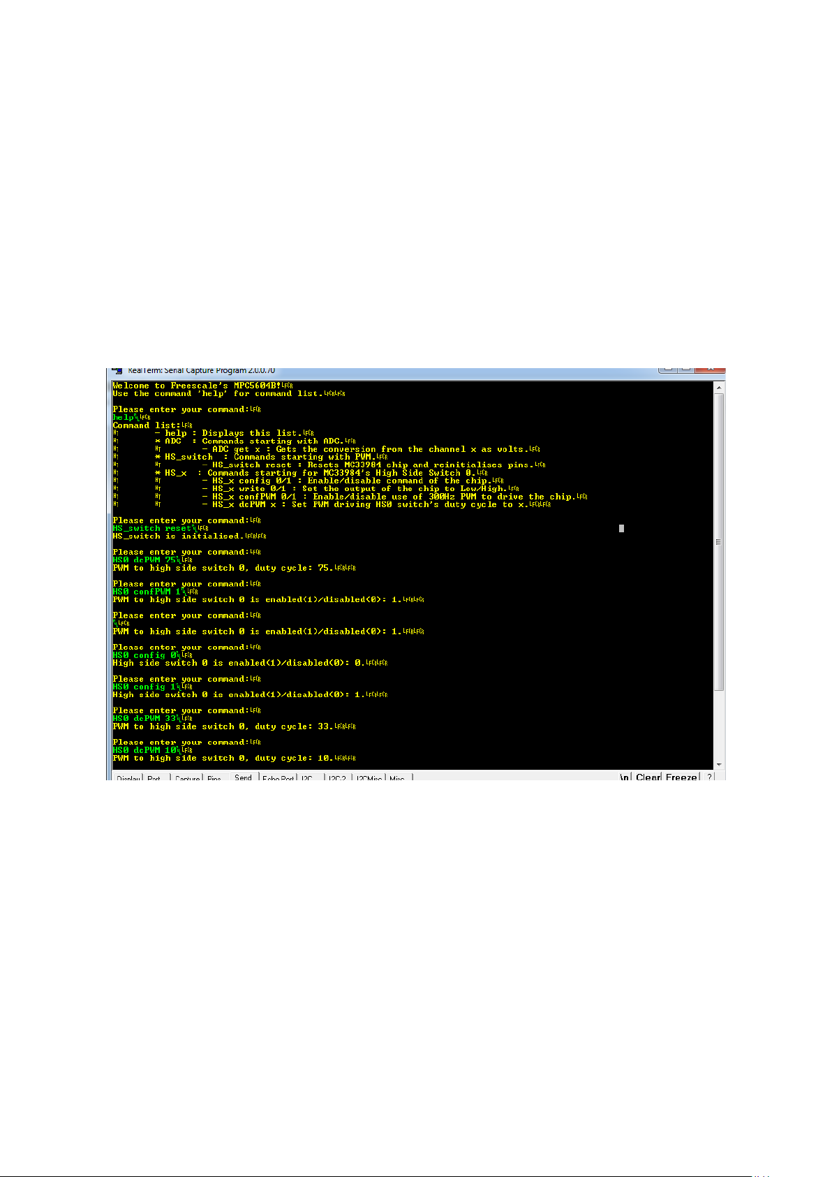
4.2.3. Operations
4.2.4. User interface
4.2.5. Testing
Some common operations are defined, using SPI and PWM, (see code for details),
- config_HS: Enabling/disabling a high-side switch,
- write_HS: Sets/clears a high-side switch output,
- conf_PWM_HS: Starts a 300Hz PWM applied on the high-side switches.
- duty_cycle_PWM_HS: Sets the duty cycle of an output PWM.
- read_fault: a function that updates the _MC33984_STATUS structure’s flag registers.
An UART terminal user interface was developed, allowing the use of some commands to drive
the chip directly from a computer.
Most of this driver’s functionalities were tested. Firstly, Freescale’s SPIGen program was used
with an SPI Dongle to test read and write actions on the device’s registers. Then the developed
terminal application was used to test basic switching operations.
There was a problem on PWM duty cycle: the microcontroller used 5V TTL logic, and the highside switch used 5V CMOS logic. Therefore the duty cycle at the drain of the chip was higher than
the duty cycle at the gate. A pull-up resistor with an adequate value or a level-shifter chip must
be used to output the correct pulse.
Current read and fault reading functionalities were not tested.
SPI driver was updated after the tests so it might need a few adjustments if it does not work as it
is.
Page 87
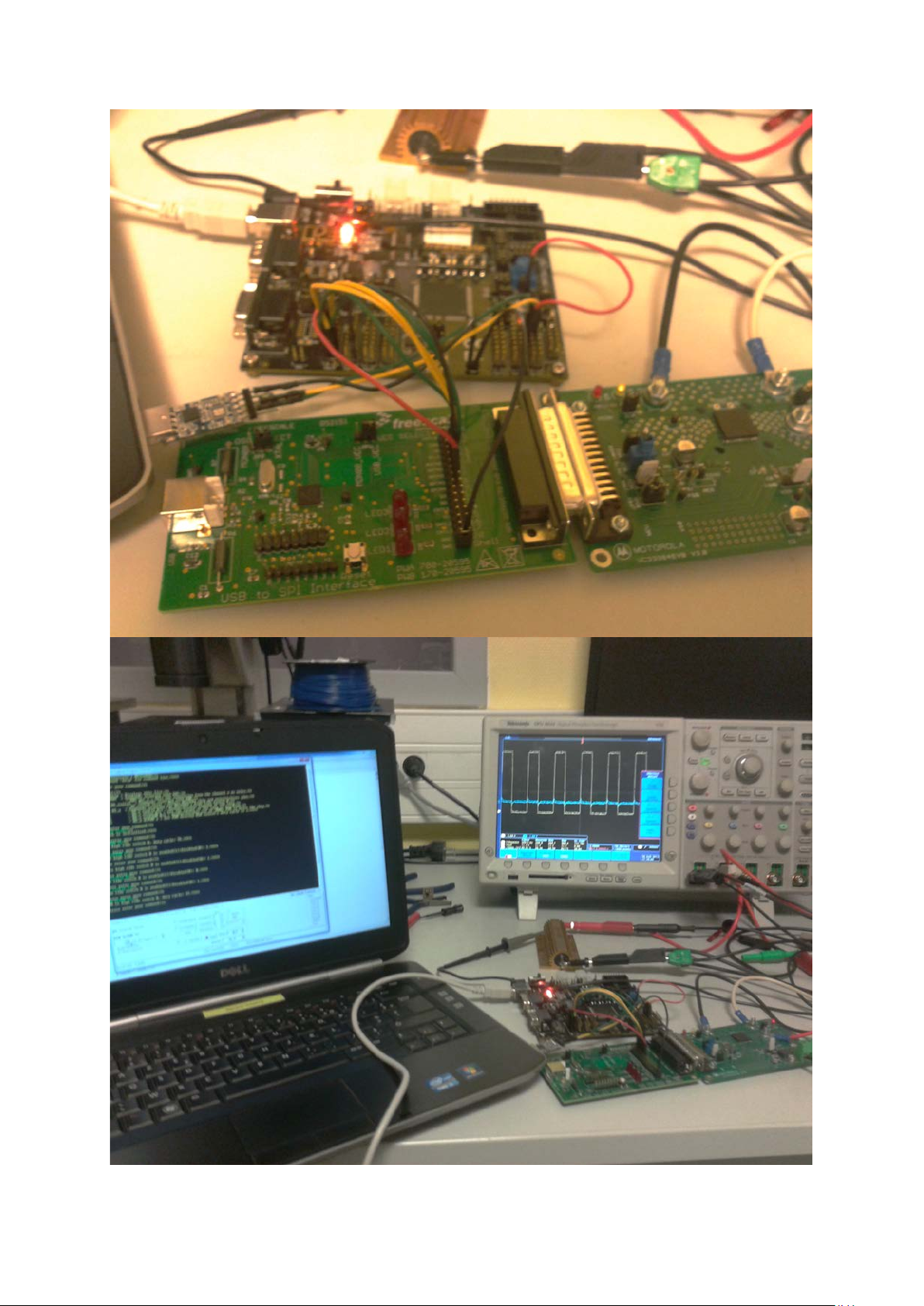
Page 88
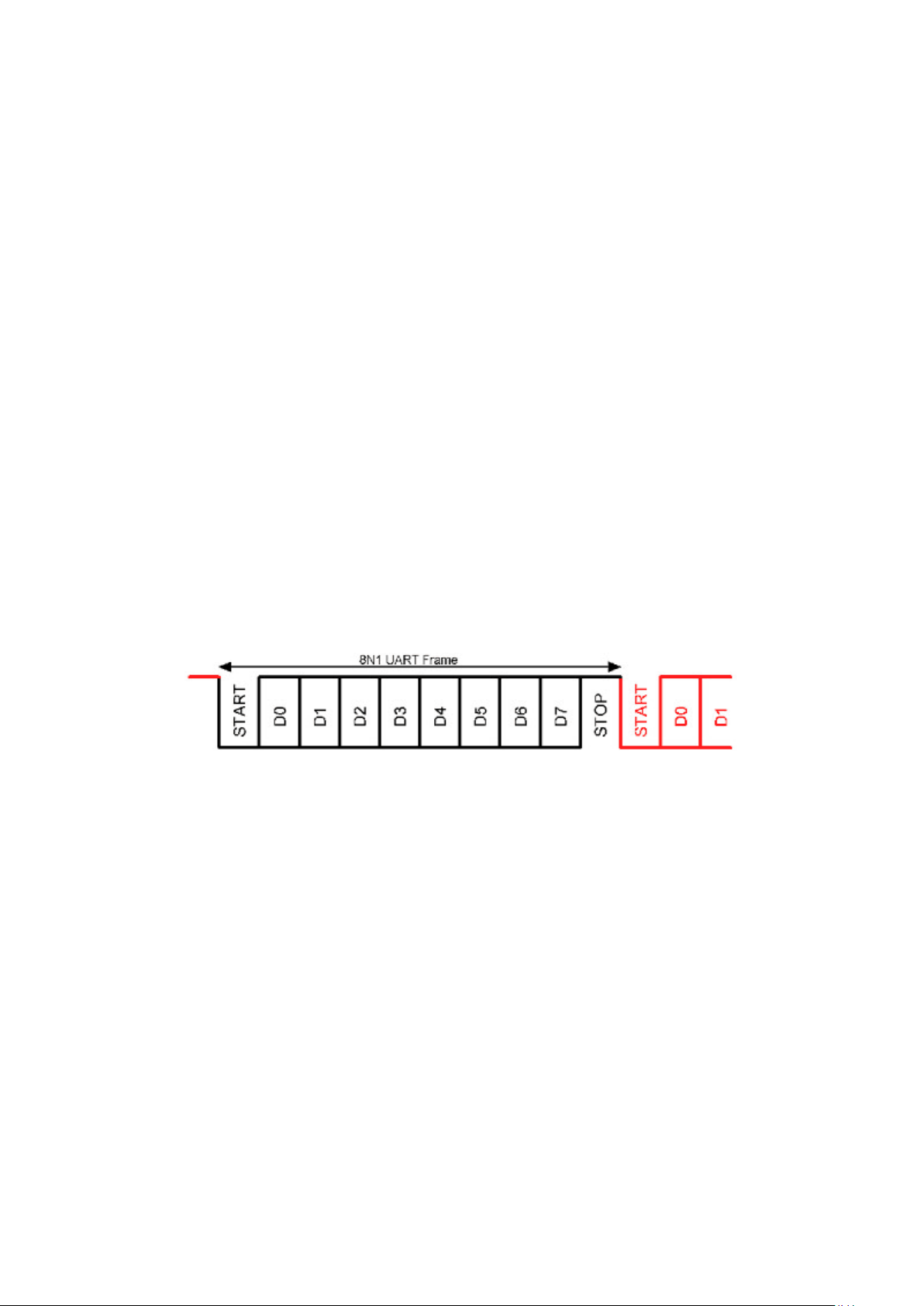
Chapter 10
UART: Universal Asynchronous Receiver
Transmitter
1. Introduction to UART
Figure 97 : An 8N1 UART frame example
2. Module Presentation
Universal Asynchronous Receiver/Transmitter is a very common circuit used for serial
communication between computer hardware, microcontrollers etc. It is at least made of an
emitter write register, a receiver read register, two shift register (one for TX, one for RX), a clock
source and a control logic around it.
Signal lines are at high logic level ‘1’, when idle, a transmission begins with a start bit (‘0’),
followed by 5 to 9 data bits, ending with one or two stop bits(‘1’). Data bits can contain a parity
bit at the end for error checking. A common baud-rate must be selected both at the transmitter
and the receiver (due to communication’s being asynchronous).
As both transmitter and receiver need to be configured in the same way, a way of identifying the
configuration is as follows: “Baud-rate Data-bits Parity Stop Bits”, like 9600 8N1 which means
9600 kbit/s, 8 data bit, no parity bit and one stop bit (very common configuration). N is for no
parity, E is for even parity and O is for odd parity. Up to 3% of baud-rate error is tolerable in
most MCU between two sources.
Most UART modules are able to detect overrun, underrun, framing or parity errors. If the
receiver’s input is at ‘0’ for too long, modules can detect a break condition and stop.
This microcontroller does not include an independent UART module, but UART is still available
through another communications module. The LIN Controller (LINFlex) is used for
implementing a LIN network, a slow but robust network commonly used in automotive
applications. This controller can also be used as UART because the LIN network is built on UART
hardware.
The UART mode of the LINFlex module features full duplex communications with from 7 to 9bit
frames, 4 byte transmit and receive buffers, error indicator flags, and maskable interrupts. The
LINFlex module also includes a fractional baud rate generator.
82
Page 89
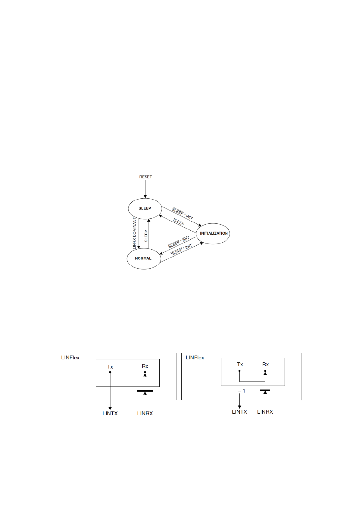
3. Configuration
3.1. Signal Configuration
3.2. LINFlex Module Configuration
Figure 98 : LINFlex operating modes (R.M. Rev8 –Fig. 21-3)
Figure 99 : LINFlex in loopback and self-test modes (R.M. Rev8 –Fig. 21-4/5)
Following configurations are needed in the SIUL module.
Output pads(Tx) need an output buffer, so the OBE bit SIUL’s pad configuration register is
needed. Also the slew rate of the port might need improving so SRC bit should be set.
For the input types the input buffer has to be enabled using IBE and also a pull up resistor is
needed, so the internal pull up can be used by setting WPE and WPS.
For power and clock cycle saving issues, the LINFlex module comes with a finite state machine
for controlling its status.
There are three operating modes as shown on the figure above, the sleep mode is the low power
state, normal mode is the state where a communication is possible and the initialization mode is
a safe state where this module’s registers can be configured. Most of the transitions is done using
SLEEP and INIT bits of the LINFlex control register 1 (LINCR1), but it is possible to enable autowake-up functionality which allows the module to switch automatically to normal mode
whenever a transmission or reception is needed.
There are also two testing modes: Loop Back and Self-Test. In both of this modes, Tx of the
module is connected to the Rx, but in the Loop Back mode Tx is also connected to the external
devices whereas in Self-Test it is not possible.
Page 90
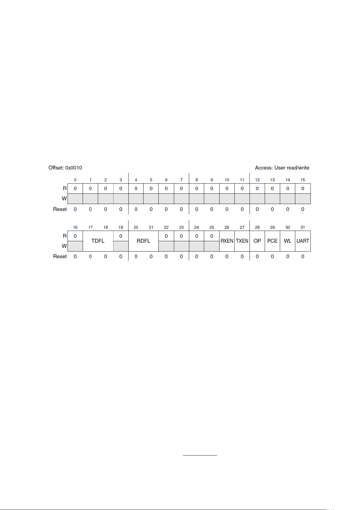
Here is the list of data fields relevant to the UART in the LIN control register 1 (LINCR1):
3.3. UART Mode Configuration
Figure 100 : UART Mode Control Register (R.M. Rev8 –Fig. 21-10)
3.4. Baud Rate Configuration
AWUM: Automatic Wake-Up Mode, when set, on activity on Rx or in internal transmit
registers, the module goes automatically to the Normal mode, clearing SLEEP bit.
SFTM: Self-Test Mode, set this bit to enable this mode.
LBKM: Loop Back Mode, set this bit to enable this mode.
RBLM: Receive Buffer Locked Mode, when this bit is set, if the receive buffer is full, next
incoming data are discarded. Otherwise incoming data overwrites the previous one.
SLEEP: Sleep Mode Request
INIT: Initialisation Request
With the exception of SLEEP and INIT, all these fields can only be changed in Initialisation mode.
The UART mode Control Register (UARTCR) allows configuring different parameters related to
this protocol. Different fields of this register are:
UART: UART mode enable, set this bit to be able to modify other fields of this register.
WL : Word Length in UART mode; 7 bit data + parity bit (0) or 8 bit data + parity bit (1).
(Parity bit is optional). Only set in Initialisation mode.
PCE: Parity Control Enable, if set, a parity bit is attached to the message and a parity
check is enabled on received data. Only set in Initialisation mode.
OP: Odd Parity, if set, the sent parity is odd, otherwise even. Only set in Initialisation
mode.
TXEN: Transmitter Enable. Transmission starts when this bit is set and data is written to
the transmit buffer.
RXEN: Receiver Enable.
RDFL: Receiver Data Field Length, Receive buffer size = RDFL[0:1]+1 bytes.
TDFL: Transmitter Data Field Length, Transmit buffer size = TDFL[0:1]+1 bytes.
The baud rate of this module is set by an unsigned fixed point number called LFDIV.
Tx/Rx
_
=
16 ×
Page 91
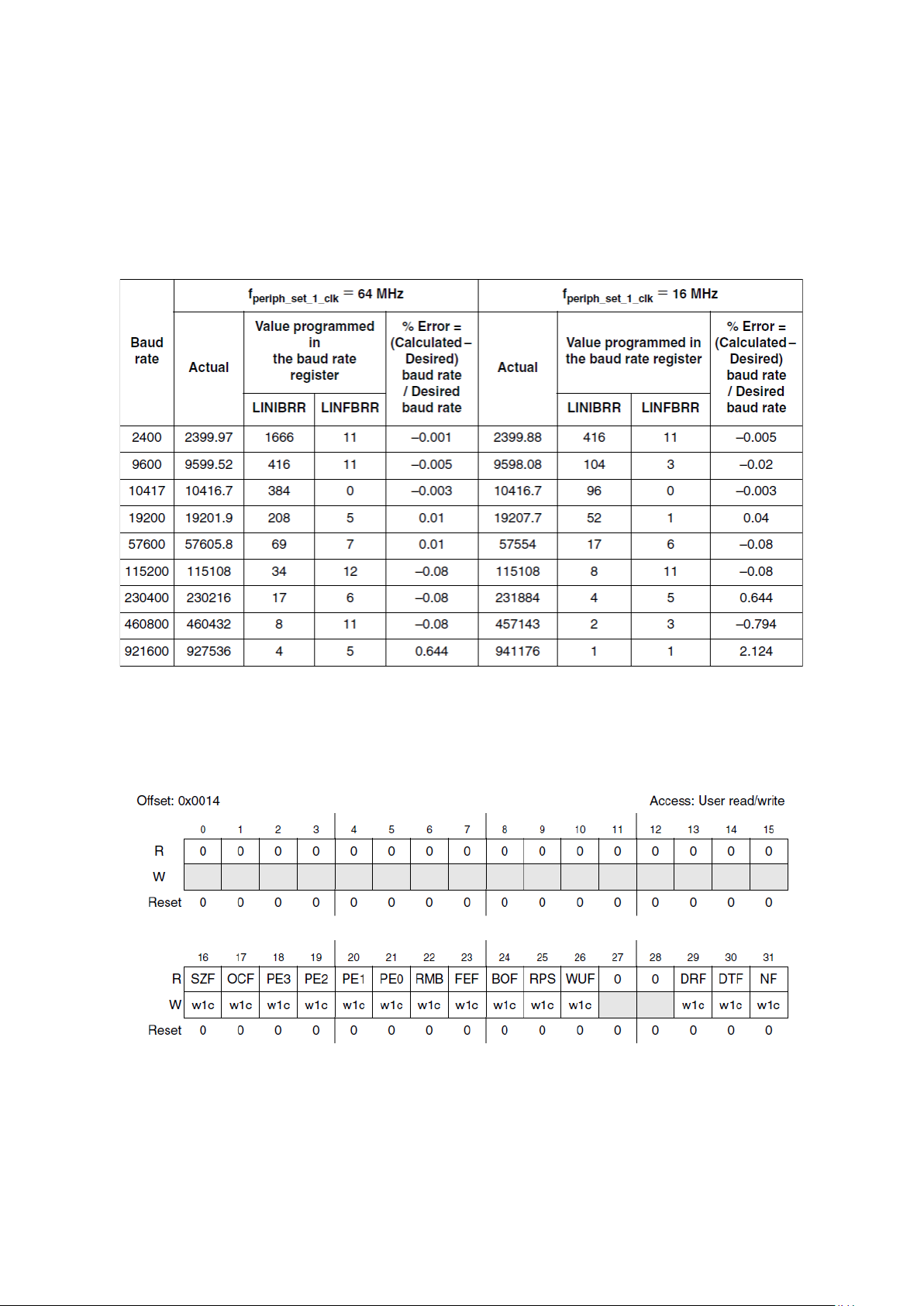
LFDIV is set using two registers: LINIBRR, the integer part of LFDIV and LINFBRR where the
Figure 101 : Error calculation for programmed baud-rates (R.M. Rev8 –Table 21-1)
3.5. Status Registers and Interrupt Configuration
Figure 102 : UART Mode Status Register (R.M. Rev8 –Fig. 21-11)
fractional part is encoded. LINIBRR contains the 13-bit field, DIV_M, which sets a mantissa
between 1 and 8191. If DIV_M is set to 0, then the LINFlex clock is disabled. LINFBRR register
contains a 4-bit DIV_F field where DIV_F = 16× _
(
LFDIV).
There will be some error in baud rate values and an error over 1% - 1.5% should be avoided if
the system clocks are imprecise.
The UART mode Status Register (UARTSR) contains all the flags that signal different kind of
events about the module, and some of them can raise interrupts.
Page 92

All the fields of this register can be cleared by writing ‘1’, and they are:
Interrupt Enable Bit
Flag
Interrupt Vector
SZIE
SZF
ERR
FEIE
FEF
ERR
BOIE
BOF
ERR
WUIE
WUF
RXI
DRIE
DRF
RXI
DTIE
DTF
TXI
3.6. Data Transmit/Receive
NF: Noise Flag, set when hardware detects noise on a receive channel.
DTF: Data Transmission Completed, set by the hardware when the number of bytes
programmed in TDFL have been transmitted.
DRF: Data Reception Completed, set by the hardware when the number of bytes
programmed in RDFL have been received.
WUF: Wake-up Flag, set when a reception is detected while the module is in sleep mode
and auto wakeup is enabled.
RPS: Receive Pin State, reflects the current status of LINRX for diagnostic.
BOF: Buffer Overrun Flag, this bit is set when the receive buffer is full and new data is
being received (discarded or not).
FEF: Framing Error Flag, this bit is set when a framing error is detected (stop or start bit
misplaced).
RMB: Release Message Buffer, this bit is set when there is data in the receive buffer ready
to be read.
PEx (x=0…3), Parity Error Flag, when set, there is a parity error in the received byte x
(in the buffer).
OCF: Output Compare Flag, this flag is related to the LINFlex module internal counter.
Not explained here.
SZF: Stuck at Zero Flag, this bit is set by hardware when the bus is dominant (at 0) for
over a 100-bit time.
Some interrupts are related to these flags and they can be enabled using LIN interrupt enable
register. Here is the list of enable interrupt bits related to UART flags:
There are only three ISR for each LINFlex module, ERR, RXI and TXI. They are shown on the
table above.
There are two buffer data register Buffer data register LSB (BDRL) and Buffer data register MSB
(BDRM). BDRL contains 4 bytes, from DATA0 to DATA3, and BDRM has DATA4 to DATA7. These
register are used as both receive and transmit in LIN mode, but in UART mode, BDRL is the
transmission buffer and BDRM is the receive buffer.
These buffers might not be fully used depending on the specified size on TDFL and RDFL.
Page 93
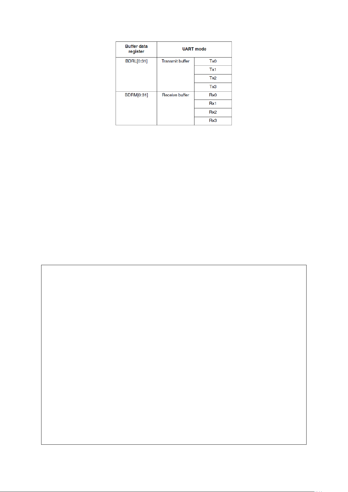
Figure 103 : UART Message Buffer (R.M. Rev8 –Table 21-30)
4. Developing a general purpose UART Driver
struct _UART_DRV UART[]; //UART variable has to be imported from the UART
and set Sys_Clk(=Peripheral_Clock) to 64MHz if you
//simple way for sending
The PC user can send commands, or use UART for
while (1) {} //End of program
The DTF flag is raised when the specified amount of bytes have been transmitted, and similarly
for DRF. If RXEN(or TXEN) is cleared during a transmission, the current transmission is still
completed then no further action is done till RXEN(or TXEN) is set.
In a similar way to the DSPI, a driver was developed to limit LINFlex’s use to a high level UART
interface usage, for simple transfer of 8-bit data (array) at common baud rates.
Transfer functions are similar to the SPI Driver’s, there is single data transfer functions, read,
write and exchange. And there are data array transfer functions like write_array, read_array,
listen_till. But there is also a high level formatted writing function called rprintf for sending
simple messages that might contain information about internal data.
Example:
//Driver module
uint8_t RxData[128]; //An array for storing received data
int main(void) {
initModesAndClks(); //remember to enable LinFlex module
//
initPeriClkGen();
disableWatchdog();
initialise_UART_DRIVER(); //must be called before using the driver
enableIrq();
UART[0].init(UART_BAUD_9600, UART_FRAME_8N1); //Initialize UART module
//Connect pins of PORT B to a serial interface of a PC
UART[0].rprintf("Welcome to MPC5604B!\n\r",);
//messages to a PC serial terminal
UART[0].rprintf("What do you want to do?\n\r1.PWM\n\r2.ADC",););
UART[0].read(RxData); //
debugging.
switch (RxData[0]){
case 1: UART[0].rprintf("PWM is running!\n\r",); //do PWM stuff etc
... //do relevant stuff etc.
}
//wish to use predefined baud-rates
Page 94
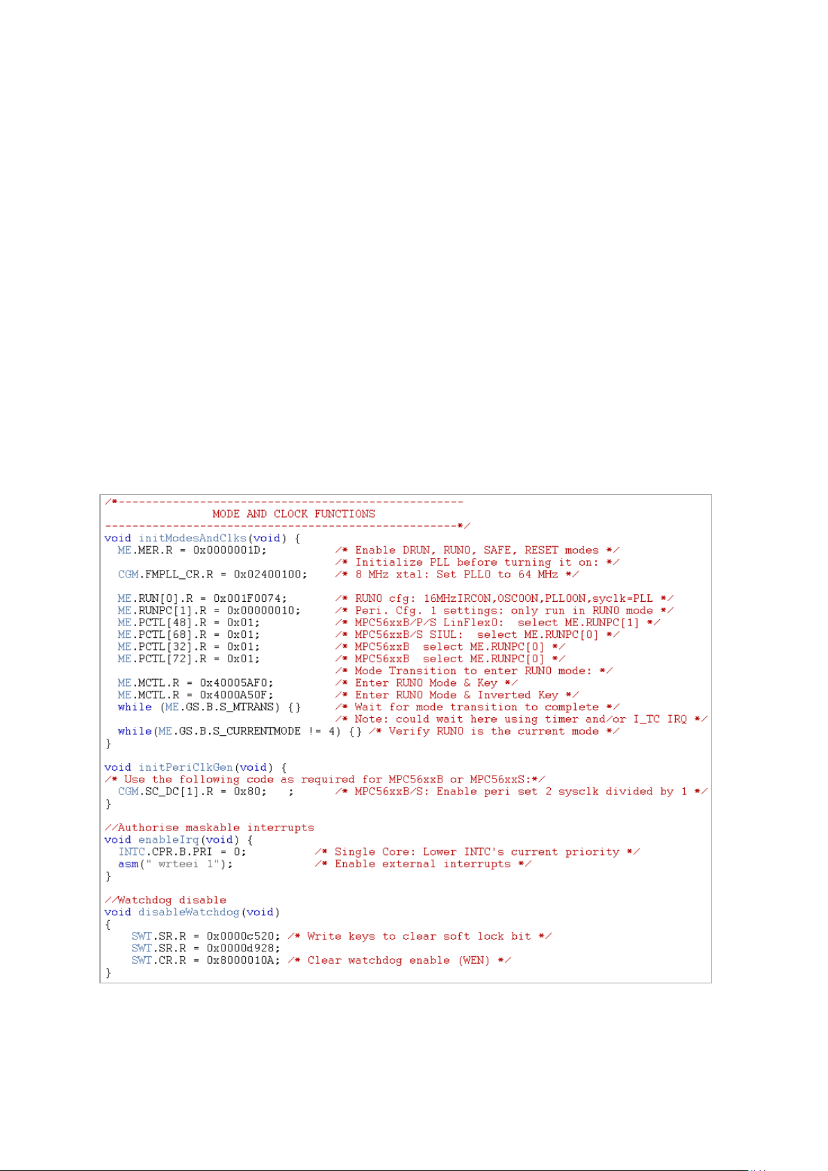
Similarly, an rscanf function was implemented for a scanf like function, reading input until a NUL
5. Using the UART Driver for a terminal interface
5.1. System initialisation
5.2. SIUL configuration
character.
UART can be used for providing a simple human-machine interface using an UART-USB adaptor
(like an FTDI FTR232 or PL2303HX) and a free serial terminal like RealTerm. And then using
the driver from the previous section, one can send orders to the MCU to command its
peripherals. It is only needed to provide a command-line like interface.
The following example provides a simple command-line interface for reading data from ADC and
driving output PWM. Using commands like ‘ADC get x’ for getting data from ADC channel x,
‘PWM start’ for launching a PWM, ‘PWM stop’ for stopping it and ‘PWM DC x’ for setting PWM
duty cycle to x%. And there is a ‘help’ command for explaining these.
We wish to set the system clock to 64MHz, power-up SIUL, LINFlex0 (for UART), ADC and
eMIOS(for PWM).
Typical functions for enabling interrupt requests and disabling SWT watchdog are also needed.
Pins for ADC and eMIOS are to be configured. UART driver configures UART pins by itself.
UART_0 uses pins PB2-PB3. Some LED indicators can be useful too with a write function.
Page 95
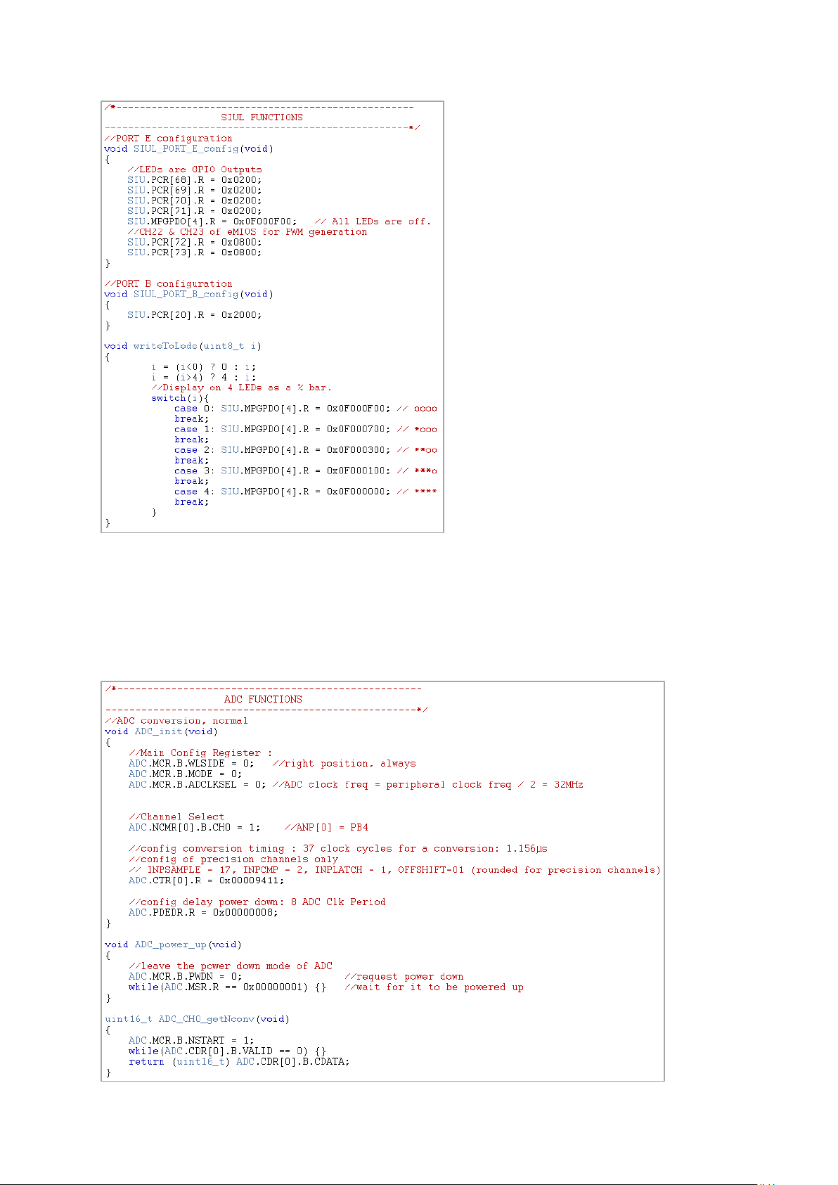
5.3. ADC configuration
ADC will be used in normal mode; a conversion will be made on a user request. As the system
clock is 64MHz, we will set ADC to the maximum possible clock, 32MHz, with the minimum
timing parameters given in the documentation. Only channel 0 connected to a potentiometer is
configured, in normal, one-shot mode.
Page 96
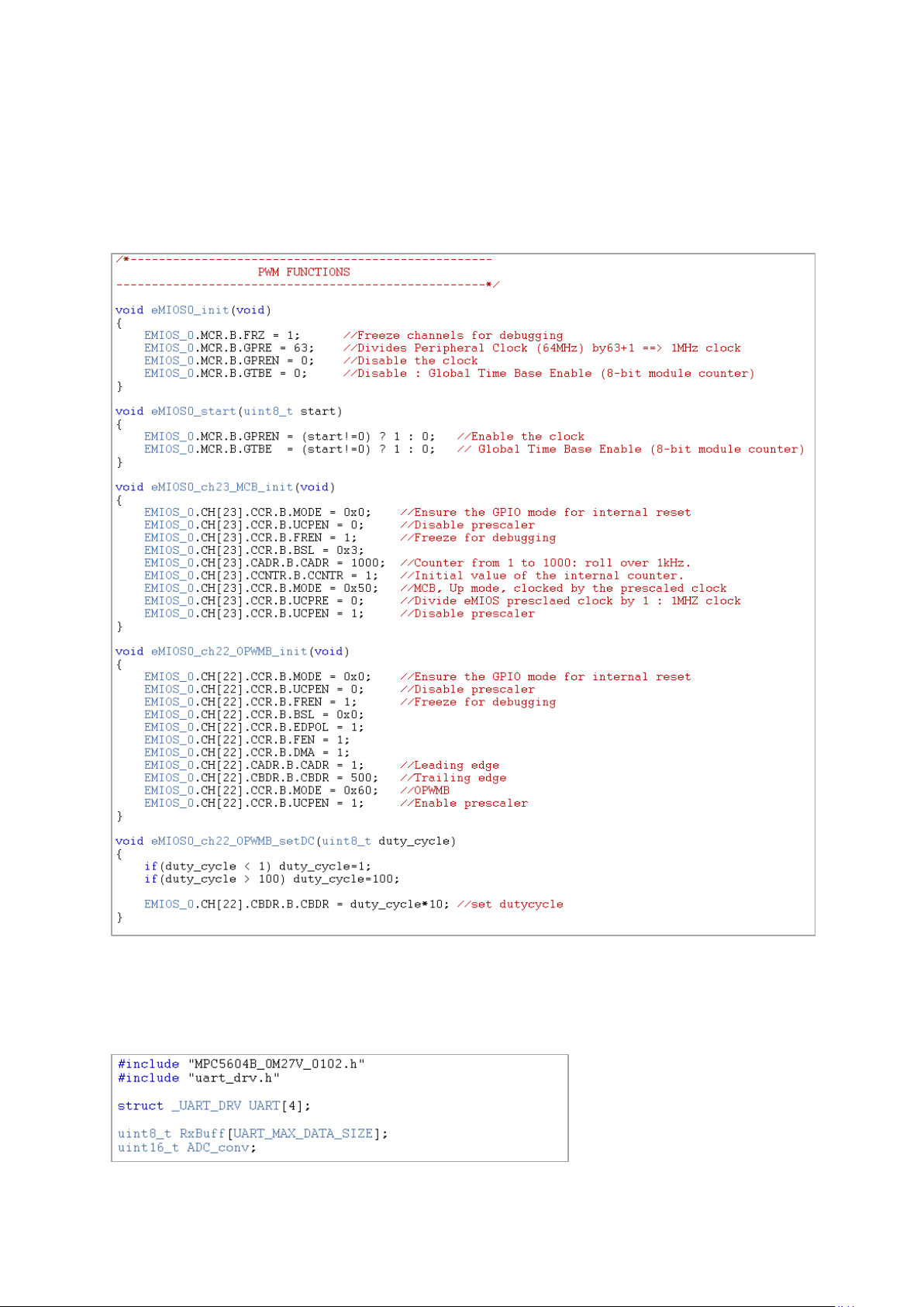
5.4. eMIOS configuration
5.5. Main procedure and use of the driver
eMIOS will be configured to have an output PWM at a fixed frequency whose duty cycle can be
easily altered. The channel 23 is configured as a buffered modulus counter, giving a 1kHz rollover frequency. And the channel 22 is configured as OPWMB with a 50% duty cycle initially. A
function for setting the duty cycle is implemented.
Global variables: imported UART driver and an Rx 8-bit buffer of UART_MAX_DATA_SIZE frames
(defined by the driver) and a 16-bit ADC conversion storage variable.
Page 97
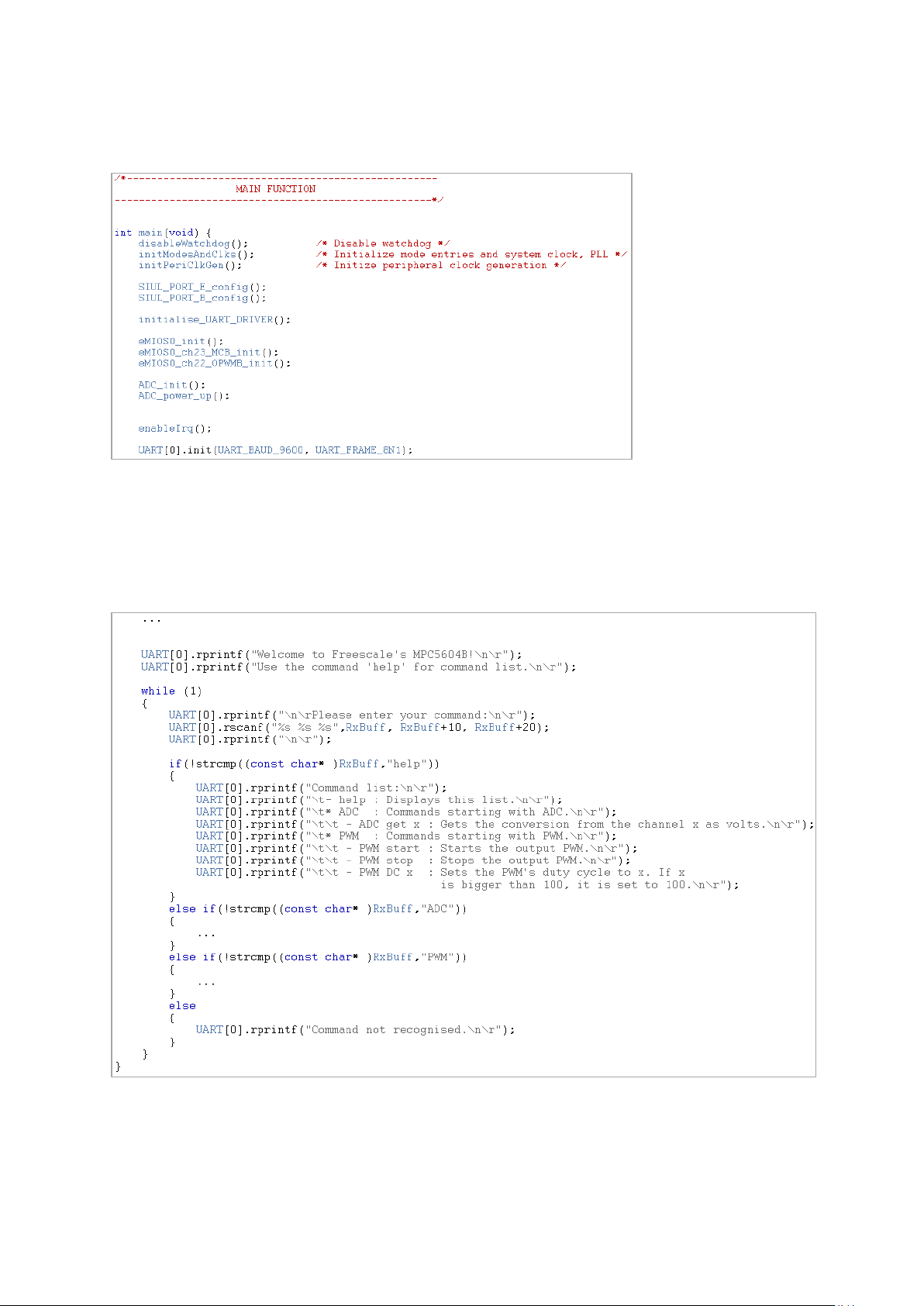
The main function starts by initializing the system and configuring peripherals. UART driver is
set as 9600 8N1.
And then the program sends some welcome and information message and enters in an infinite
loop of communication with a PC. The program waits for an ASCII message made of 3 strings
separated by space characters, ending with a NUL character. The first string is 10 bits long and
stored in 0:9 addresses of RxBuff, the second occupies 10:19 and the last one 20:29. Then the
first one is compared to defined commands for a match.
For a correct match with ‘help’ a help message will be displayed, for other ones, more testing is
needed.
Page 98
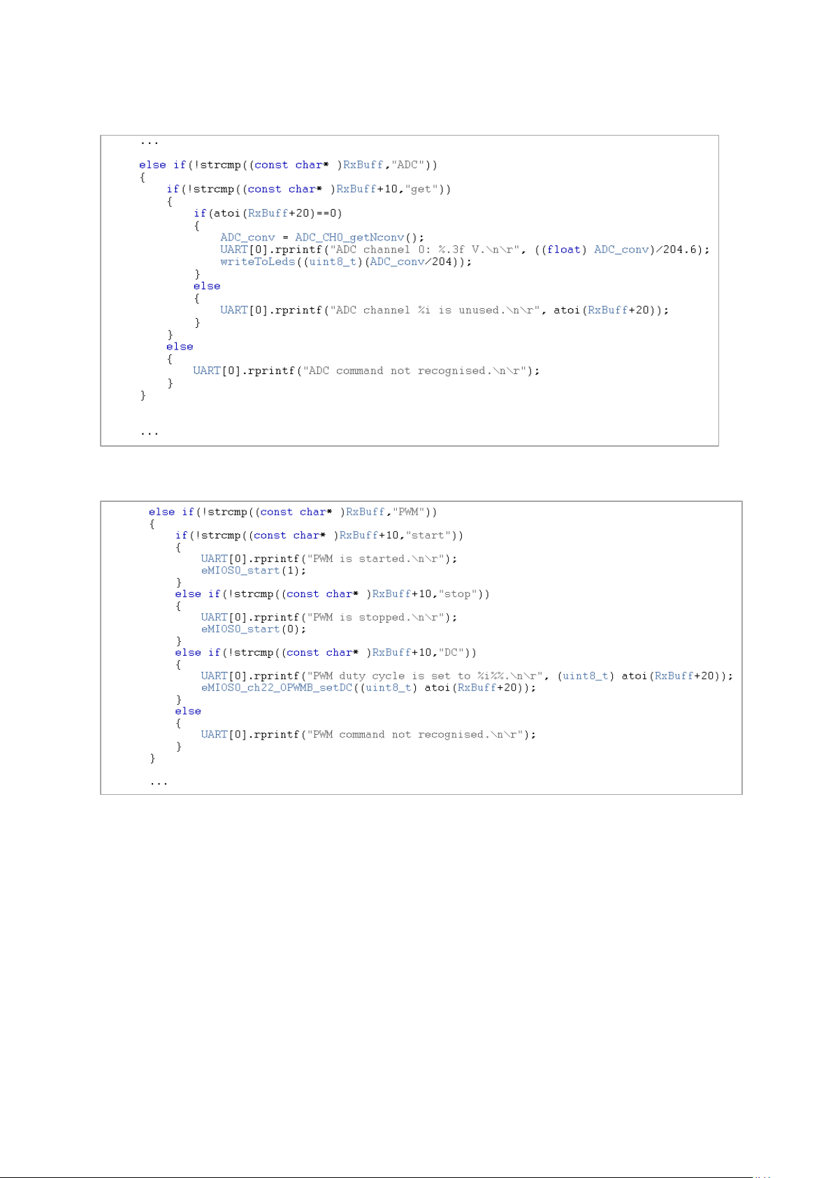
ADC treatment’s detail:
5.6. Results
PWM treatment’s detail:
This example works as foreseen, basic commands are executed through a friendly user interface.
One may even create a GUI exploiting COM port drivers to communicate with the device. Error
management is really important in this kind of loops to avoid needing to reset the device.
Page 99
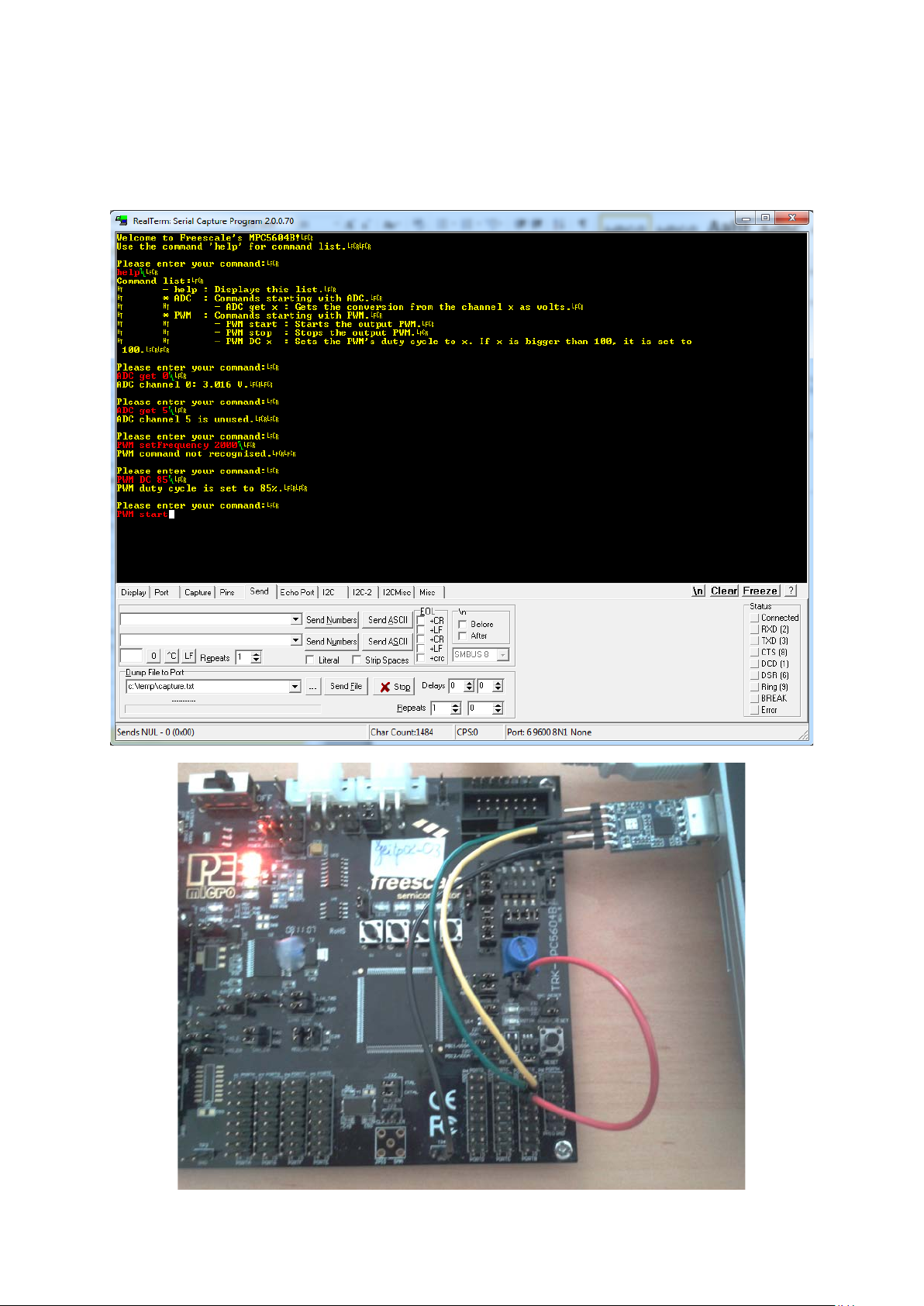
You can see a communication example below where unknown commands are dismissed and
other ones correctly executed:
Page 100
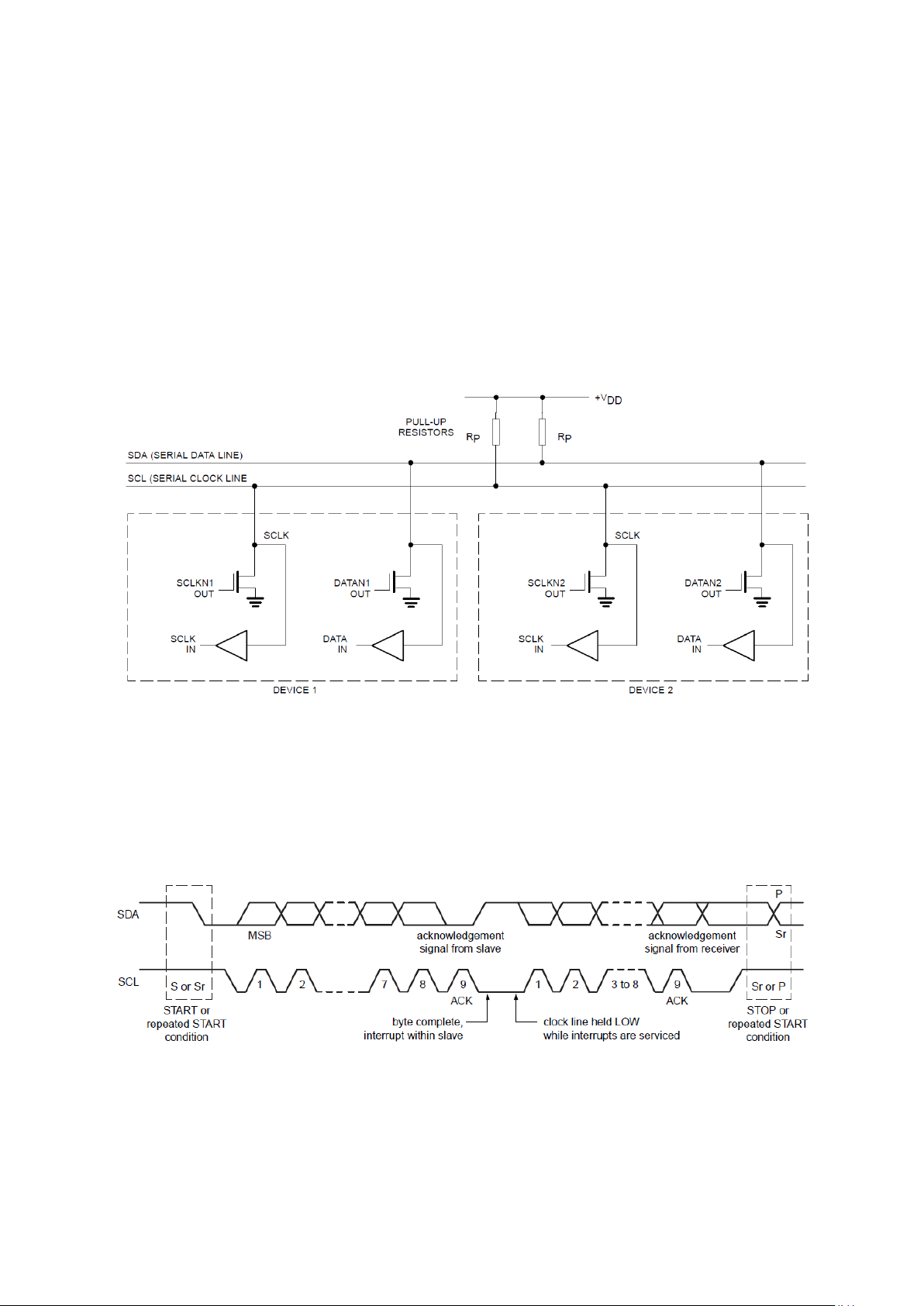
Chapter 11
I²C: Inter-Integrated Circuit Bus Controller
1. Presentation of I²C protocol
1.1. Description
Figure 104 : Physical Interface of I²C Bus
Figure 105 : I²C Communication Time Diagrams
I²C is an half-duplex, two-wire, bidirectional, multi-master, multi-slave communication bus. It
supports addressing, data acknowledging, detecting arbitration loss or busy bus and using
multiple baud rates.
Only masters can initiate a communication with a slave, either for transmitting or receiving, and
most of the devices can switch between master and slave modes. These communications start
with a start signal which is followed by an address transmission for selecting a slave. With the
address, the master indicates whether it needs to receive or transmit on a R/W bit. And then the
communication is maintained until the master sends the stop bit.
After each successfully transmitted byte, the slave uses an acknowledge bit on the bus.
94
 Loading...