

Page 1

Freescale Semiconductor
MPC5565 Microcontroller Reference Manual
MPC5565RM
Rev. 1.1, 05/2012
This MPC5565 Reference Manual set consists of the following files:
• MPC5565 Reference Manual Addendum, Rev 1
• MPC5565 Microcontroller Reference Manual, Rev 2
© Freescale Semiconductor, Inc., 2012. All rights reserved.
Page 2

Freescale Semiconductor
Reference Manual Addendum
MPC5565 Reference Manual
Addendum
MPC5565RMAD
Rev. 2, 05/2012
This errata document describes corrections to the
MPC5565 Preliminary Microcontroller Reference
Manual, order number MPC5565RM. For convenience,
the addenda items are grouped by revision. Please check
our website at
http://www.freescale.com/powerarchitecture for the
latest updates.
The current version available of the MPC5565
Microcontroller Reference Manual is Revision 1.0.
Table of Contents
1 Addendum for Revision 1.0. . . . . . . . . . . . . . . . . . 2
2 Revision history. . . . . . . . . . . . . . . . . . . . . . . . . . 15
© Freescale Semiconductor, Inc., 2009–2012. All rights reserved.
Page 3
Addendum for Revision 1.0
Transfer
Size
TSIZ
[0:1]
Address 32-Bit Port Size 16-Bit Port Size
1
NOTES:
1
Also applies when DBM=1 for 16-bit data bus mode.
A30 A31 D0:D7 D8:D15 D16:D23 D24:D31 D0:D7 D8:D15
Byte 01 0 0 OP0 — — — OP0 —
01 0 1 — OP1 — — — OP1
01 1 0 — — OP2 — OP2 —
01 1 1 — — — OP3 — OP3
16-bit 10 0 0 OP0 OP1 — — OP0 OP1
10 1 0 — — OP2 OP3 OP2 OP3
32-bit 00 0 0 OP0 OP1 OP2 OP3 OP0/
OP2
2
2
This case consists of two 16-bit external transactions, the first writing OP0 and OP1,
the second writing OP2 and OP3.
OP1/OP3
DMA Request Channel Source Description
eSCIA_COMBTX 18 ESCIA.SR[TDRE] ||
ESCIA.SR[TC] ||
ESCIA.SR[TXRDY]
eSCIA combined DMA
request of the Transmit
Data Register Empty
and LIN Transmit Data
Ready DMA requests
1 Addendum for Revision 1.0
Table 1. MPC5565RM Rev 1.0 addendum
Location Description
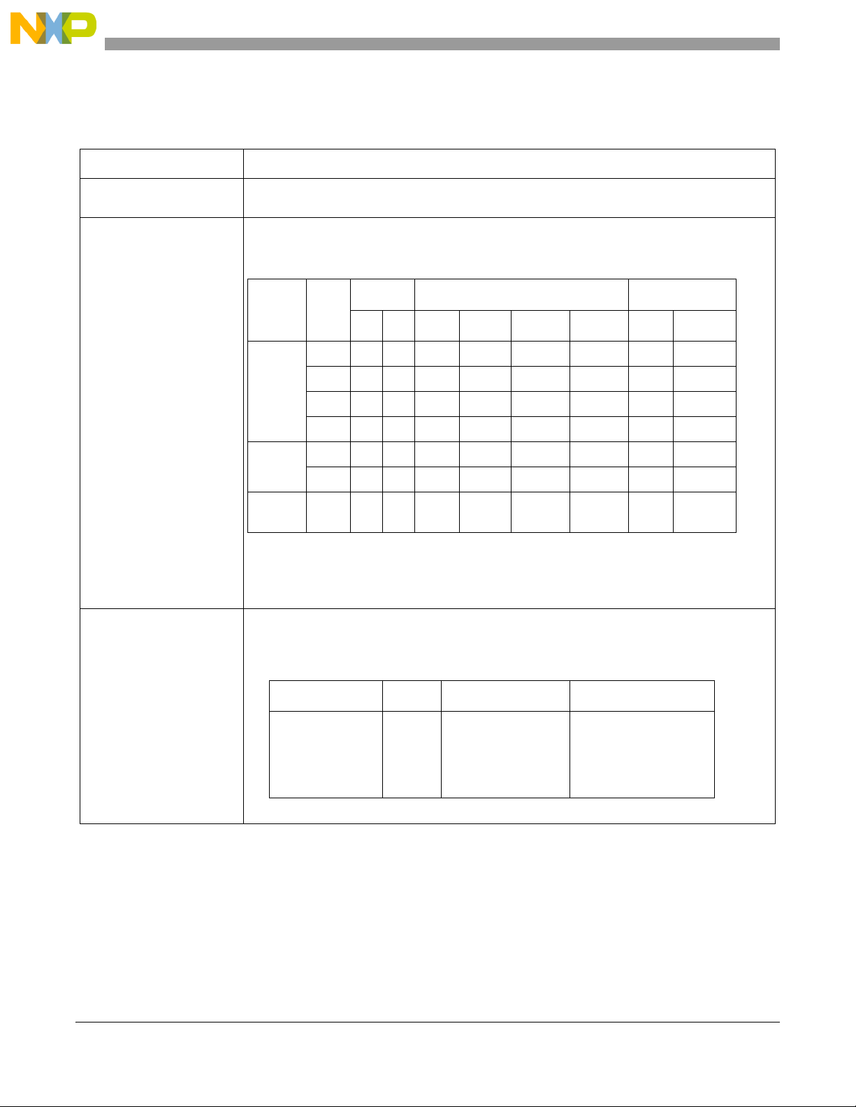
Section 12.4.2.7/Page 12-42 Change sentence “The bytes indicated as ‘—’ are not driven during that write cycle” to read “The
bytes indicated as ‘—’ are indeterminate and may be driven during that write cycle.”
Table 12-19, “Data Bus
Contents for Write
Cycles”/Page 12-43
Table 9-23, “DMA Request
Summary for eDMA”/Page
9-39
Replace table with the one below to correct information about data bus contents for write cycles.
Note that only two columns have changed: under “32-Bit Port Size,” columns “D0:D7” and
“D8:D15.”
Change one row in the table to correct information about eSCI COMBTX DMA request. Only the
Transmit Data Register Empty and LIN Transmit Data Ready flags drive the DMA request. The
Transmit Complete flag is not used.
MPC5565 Reference Manual Addendum, Rev. 2
Freescale Semiconductor2
Page 4
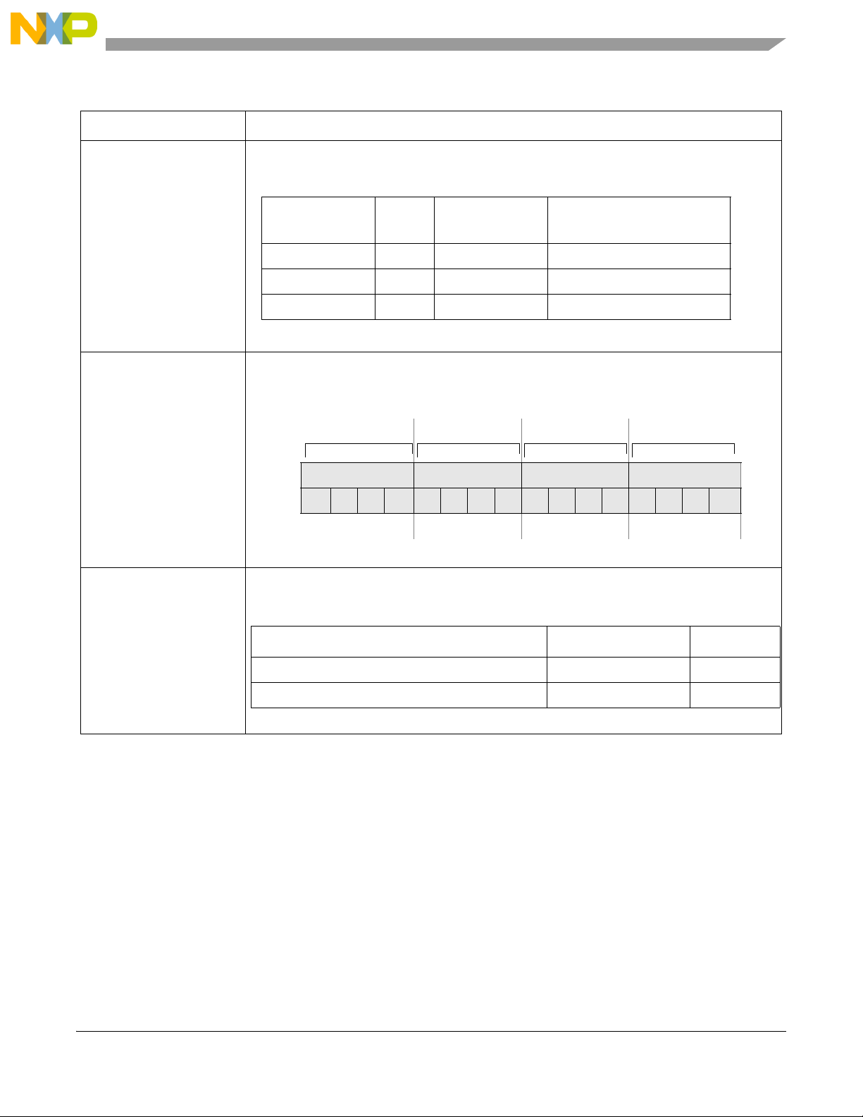
Table 1. MPC5565RM Rev 1.0 addendum (continued)
Hardware Vector
Mode Offset
Vector
Number
Source Description
0x0850 133 DSPI_BSR[TFFF] DSPI B transfer FIFO fill flag
0x0860 134 DSPI_BSR[TCF] DSPI B transfer complete flag
0x0870 135 DSPI_BSR[RFDF] DSPI B receive FIFO drain flag
16 17 18 19 20 21 22 23 24 25 26 27 28 29 30 31
R
W
Reset011 1 01110111011 1
Access Field 4
Access Field 5
Access Field 6
Access Field 7
Module Base Address Page
Peripheral Bridge A (PBRIDGE_A) 0xC3F0_0000 Page A-2
Peripheral Bridge B (PBRIDGE_B) 0xFFF0_0000 Page A-31
Location Description
Addendum for Revision 1.0
Table 10-9, “MPC5565
Interrupt Request
Sources”/Page 10-19
Figure 5-2, “Master Privilege
Control Registers”/Page 5-5
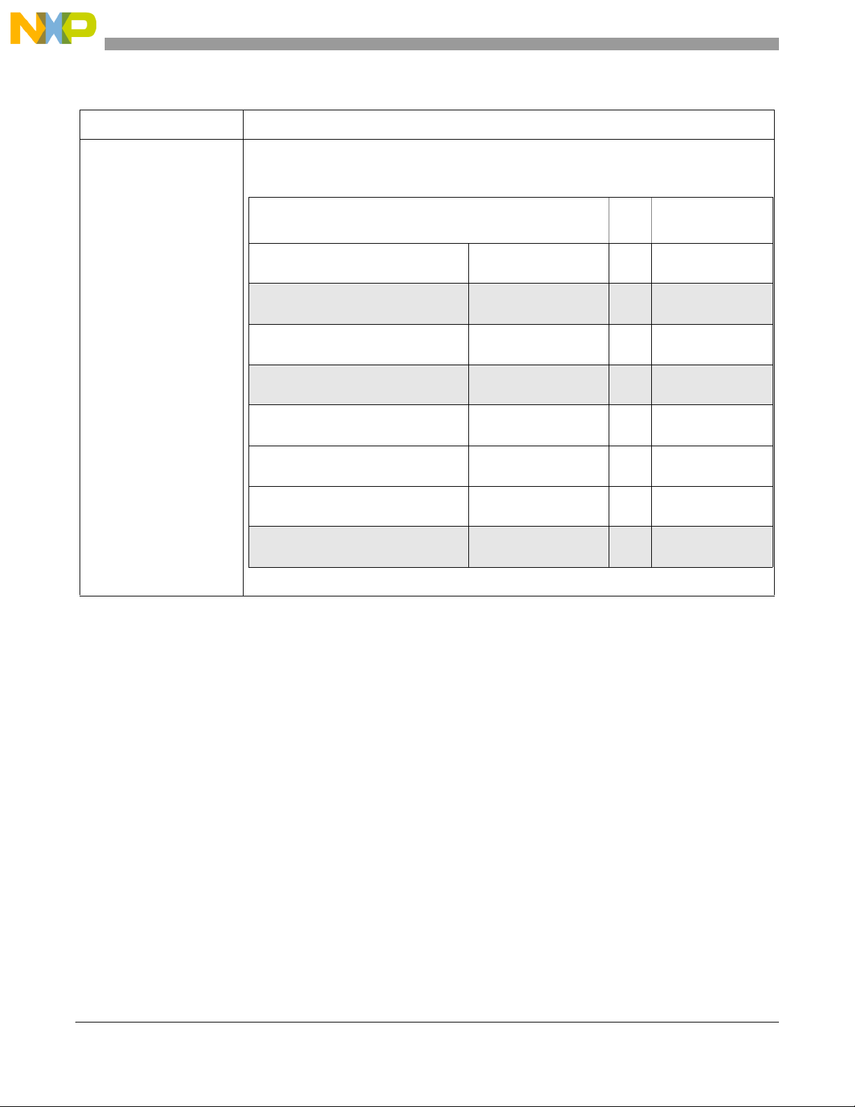
Change three rows in the table to correct DSPI_B information. The three interrupt requests were
not assigned to the correct channel numbers.
Change read status for bits 16–31 from zero to reserved.
Table A-1, “Module Base
Addresses”/Page A-1
Freescale Semiconductor 3
Correct names of peripheral bridge modules by adding underscore (PBRIDGEA becomes
PBRIDGE_A, PBRIDGEB becomes PBRIDGE_B). Only two rows of the table are changed.
MPC5565 Reference Manual Addendum, Rev. 2
Page 5
Addendum for Revision 1.0
Register Description Register Name
Used
Size
Address
Peripheral bridge A master privilege
control register
PBRIDGE_A_MPCR 32-bit Base + 0x0000
Reserved — — Base +
(0x0004-0x001F)
Peripheral bridge A peripheral access
control register 0
PBRIDGE_A_PACR0 32-bit Base + 0x0020
Reserved — — Base +
(0x0024-0x003F)
Peripheral bridge A off-platform
peripheral access control register 0
PBRIDGE_A_OPACR0 32-bit Base + 0x0040
Peripheral bridge A off-platform
peripheral access control register 1
PBRIDGE_A_OPACR1 32-bit Base + 0x0044
Peripheral bridge A off-platform
peripheral access control register 2
PBRIDGE_A_OPACR2 32-bit Base + 0x0048
Reserved — — Base + (0x004C-
0xC3F7_FFFF)
Location Description
Table 1. MPC5565RM Rev 1.0 addendum (continued)
Table A-2, “MPC5565
Detailed Register
Map”/Page A-2
Correct names of peripheral bridge A control registers by adding underscore (PBRIDGEA_x
becomes PBRIDGE_A_x).
MPC5565 Reference Manual Addendum, Rev. 2
Freescale Semiconductor4
Page 6
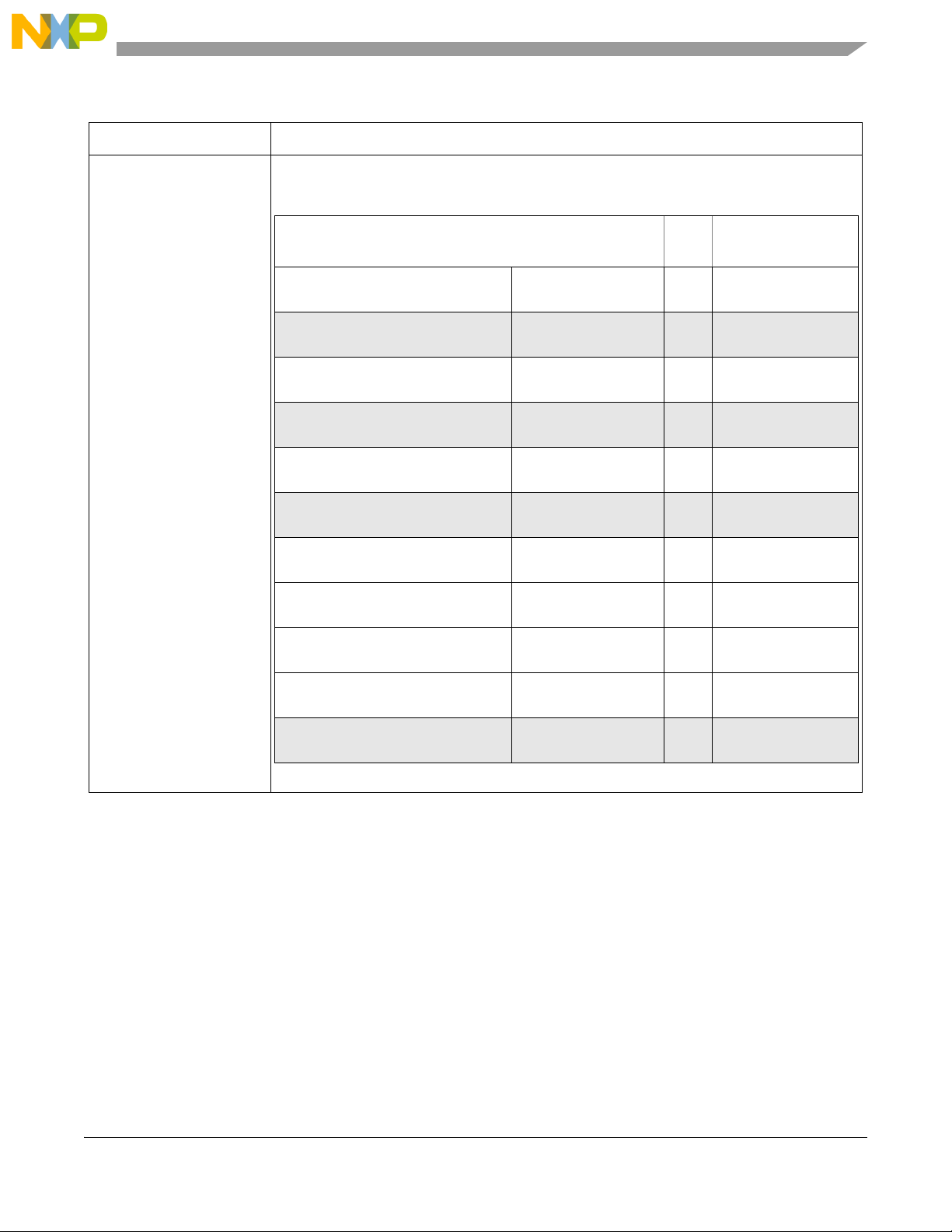
Table 1. MPC5565RM Rev 1.0 addendum (continued)
Register Description Register Name
Used
Size
Address
Peripheral bridge B master privilege
control register
PBRIDGE_B_MPCR 32-bit Base + 0x0000
Reserved — — Base +
(0x0004-0x001F)
Peripheral bridge B peripheral access
control register 0
PBRIDGE_B_PACR0 32-bit Base + 0x0020
Reserved — — Base +
(0x0024-0x0027)
Peripheral bridge B peripheral access
control register 2
PBRIDGE_B_PACR2 32-bit Base + 0x0028
Reserved — — Base +
(0x002C-0x003F)
Peripheral bridge B off-platform
peripheral access control register 0
PBRIDGE_B_OPACR0 32-bit Base + 0x0040
Peripheral bridge B off-platform
peripheral access control register 1
PBRIDGE_B_OPACR1 32-bit Base + 0x0044
Peripheral bridge B off-platform
peripheral access control register 2
PBRIDGE_B_OPACR2 32-bit Base + 0x0048
Peripheral bridge B off-platform
peripheral access control register 3
PBRIDGE_B_OPACR3 32-bit Base + 0x004C
Reserved — — (Base + 0x0050)-
0xFFF0_3FFF)
Location Description
Addendum for Revision 1.0
Table A-2, “MPC5565
Detailed Register
Map”/Page A-23
Correct names of peripheral bridge B control registers by adding underscore (PBRIDGEB_x
becomes PBRIDGE_B_x).
Freescale Semiconductor 5
MPC5565 Reference Manual Addendum, Rev. 2
Page 7
Addendum for Revision 1.0
Location Description
Table 1. MPC5565RM Rev 1.0 addendum (continued)
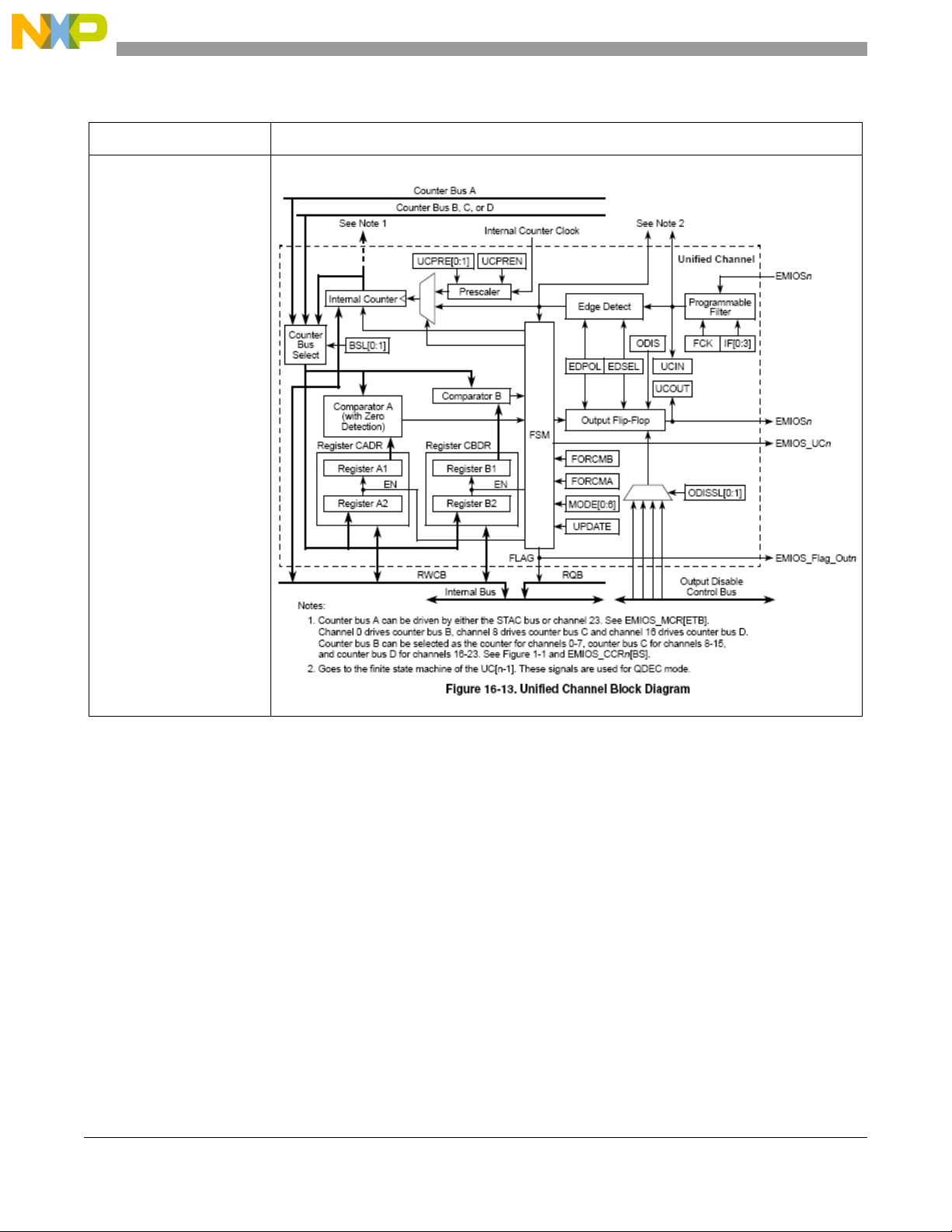
Figure 16-13,” Unified
Channel Block
Diagram”/Page 16-26
Reverse the arrow between the "Programmable Filter" and "Edge Detect".
MPC5565 Reference Manual Addendum, Rev. 2
Freescale Semiconductor6
Page 8
Addendum for Revision 1.0
Table 1. MPC5565RM Rev 1.0 addendum (continued)
Location Description
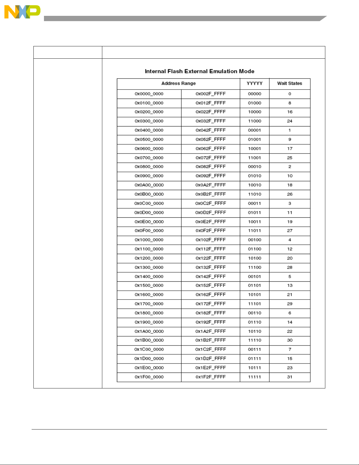
Section13.3/ Page 13-4 Remove cross-reference to Table 13-2. Add the following table and update the cross-reference.
MPC5565 Reference Manual Addendum, Rev. 2
Freescale Semiconductor 7
Page 9
Addendum for Revision 1.0
eMIOS Channel DMA = 0 DMA = 1
0 Interrupt DMA request
1 Interrupt DMA request
2 Interrupt DMA request
3 Interrupt DMA request
4 Interrupt DMA request
5 Interrupt Reserved
6 Interrupt Reserved
7 Interrupt Reserved
8 Interrupt DMA request
9 Interrupt DMA request
10 Interrupt Reserved
11 Interrupt Reserved
12 Interrupt Reserved
13 Interrupt Reserved
14 Interrupt Reserved
15 Interrupt Reserved
16 Interrupt Reserved
17 Interrupt Reserved
18 Interrupt Reserved
19 Interrupt Reserved
20 Interrupt Reserved
21 Interrupt Reserved
22 Interrupt Reserved
23 Interrupt Reserved
Table 1. MPC5565RM Rev 1.0 addendum (continued)
Location Description
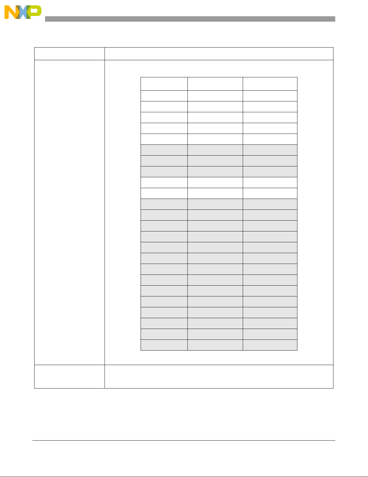
Table 16-9/ Page 16-15 Bit 7—DMA: Replace the table that shows the eMIOS channels that don’t support DMA with the
following table.
Section 9.3.1, “eDMA
Microarchitecture”/ Page
9-29
In the Memory controller sub-bullet, delete the line "The hooks to a BIST controller for the local
TCD memory are included in this module".
MPC5565 Reference Manual Addendum, Rev. 2
Freescale Semiconductor8
Page 10
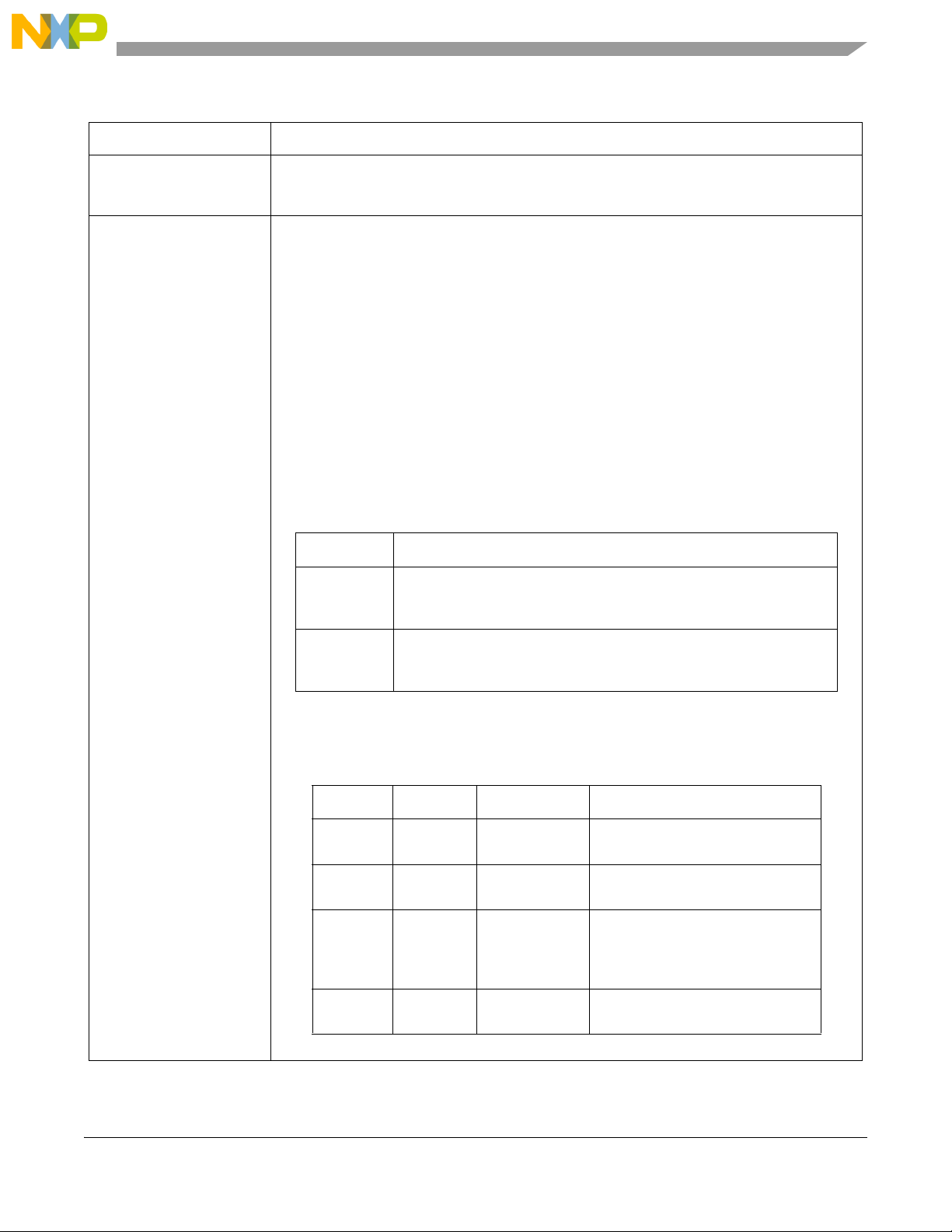
Table 1. MPC5565RM Rev 1.0 addendum (continued)
MSR[EE] and MSR[ME] Bit Settings
Field Description
EE External interrupt enable.
0 External input interrupts disabled.
1 External interrupts enabled.
ME Machine check enable.
0 Machine check interrupts disabled. Enters machine check.
1 Machine interrupts enabled.
Non-correctable Data ECC States
MSR[EE] MSR[ME] Access Type Result
0 0 Instruction or
data
Enters checkstop state. A reset is
required to resume processing.
0 1 Instruction or
data
Machine check interrupt (IVOR1).
1 X Data Data storage interrupt (IVOR2).
External interrupt must be enabled.
Machine check can be enabled or
disabled.
1 X Instruction Instruction storage interrupt
(IVOR3).
Location Description
Addendum for Revision 1.0
Section 9.2.2.13: eDMA
Interrupt Request Register
(EDMA_IRQRL)/ Page 9-17
Section 8.3: Initialization and
Application
Information/Page 8-14
In the second paragraph, remove the last line "without the need to perform a read-modify-write
sequence to the EDMA_IRQRL".
Replace the whole section with the following information:
The Error Correction Code (ECC) is used to verify the contents of the internal SRAM and flash
memories. This is done by generating ECC check bits. Typically ECC check bits are calculated
on writes and then used on reads to detect and correct errors.
• SRAM—Eight ECC check bits for each 64-bit SRAM data doubleword.
• Flash—Eight ECC check bits for each 64-bit flash data doubleword.
After Power on Reset (POR), the contents of internal SRAM is random and the corresponding
ECC check bits are unknown. To prevent generating ECC errors during reads, an initialization
routine must perform 64 bit writes to all SRAM locations. Because the flash module is
non-volatile, the ECC check bits are calculated and stored when the flash is programmed.
Transparent to the application, the ECC uses the check bits to automatically correct single-bit
memory errors. Multi-bit memory errors are not correctable. If the ECC detects a multi-bit error,
an exception is generated. The type of exception generated by a multi-bit error depends on the
settings of the EE and ME in the Machine State Register (MSR), as shown in the following table.
When error reporting is enabled, as long as its priority is 0, an interrupt request is generated to
the interrupt controller (INTC) even though the INTC request is not serviced.
A non-correctable data ECC error executes one of the following actions, regardless of whether
non-correctable reporting is enabled:
Freescale Semiconductor 9
MPC5565 Reference Manual Addendum, Rev. 2
Page 11

Addendum for Revision 1.0
Location Description
Table 1. MPC5565RM Rev 1.0 addendum (continued)
When the device is in the checkstop state, processing is suspended and cannot resume without
a reset. When a debug request is presented to the core while it is in the checkstop state, the core
temporarily exits the checkstop state and enters debug mode. When debug mode exits, the core
re-enters the checkstop state.
If the external interrupt bit in the MSR is enabled, data or instruction stage interrupts are reported
when the ECC errors are a result of CPU accesses, regardless of whether non-correctable
reporting is enabled.
ECC errors generated by other masters (eDMA, etc.) do not generate data or instruction storage
exceptions, and the ECSM is used to report these errors. You must initialize the ECSM to enable
non-correctable reporting with interrupt generation to detect and report ECC interrupts from the
ECSM.
Error reporting details can be independently enabled for flash memory and SRAM. To enable
non-correctable error reporting and save the error details for:
• SRAM—set the ERNCR bit in the ECSM Error Configuration Register (ECSM_ECR).
• Flash—set the EFNCR bit in ECSM_ECR.
When these bits are set and a non-correctable ECC error occurs, error information is recorded
in other ECSM registers and an interrupt request is generated on vector 9 of the interrupt
controller (INTC).
• CPU data access error—Generates data storage exception (IVOR2).
• CPU instruction access error—Generates instruction storage exception (IVOR3).
• Vector 9 of INTC enabled—Generates an external exception (IVOR4)
Section 11.4.3.3, "FM
Calibration Routine"/ Page
11-29
Table 6-135, “SIU_DISR
Field Descriptions”/ Page
6-108
Correct the equation at the end of the third paragraph: change value of M from 640 to 480.
• Bit 14-15–TRIGSELB: Correct the input select description as follows:
00: Replace the term “Invalid value” with “No Trigger”
01: Replace the term “Invalid value” with “No Trigger”
• Bit 22-23–TRIGSELC: Correct the input select description as follows
00: Replace the term “Invalid value” with “No Trigger”
01: Replace the term “Invalid value” with “No Trigger”
• Bit 30-31–TRIGSELD: Correct the input select description as follows
00: Replace the term “Invalid value” with “No Trigger”
01: Replace the term “Invalid value” with “No Trigger”
MPC5565 Reference Manual Addendum, Rev. 2
Freescale Semiconductor10
Page 12
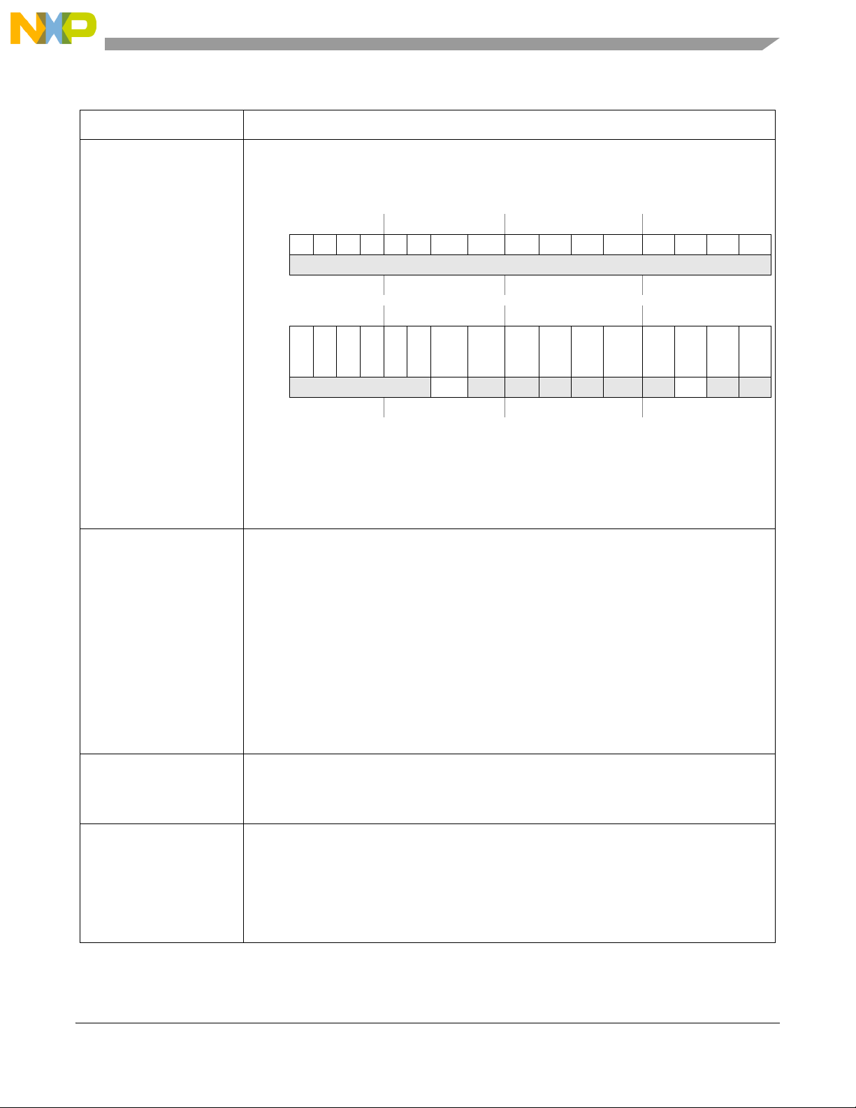
Table 1. MPC5565RM Rev 1.0 addendum (continued)
Addre
ss:
Base + 0x0004 Access: User R/W
012345 6 7 8 9 10 11 12 13 14 15
R 0 0 0 0 0 00 0 000 0 0000
W
Reset0000000 0 000 0 0000
16 17 18 19 20 21 22 23 24 25 26 27 28 29 30 31
R
000000LOLFLOC
MODEPLL
SEL
PLL
REF
LOCKSLOCKLOC
F
CAL
DO
NE
CAL
PA S
S
W
w1c w1c
Reset000000 0 0 —1—1—1—1—2000
1
Reset state determined during reset configuration.
2
Reset state determined during reset.
Note: “w1c” signifies that this bit is cleared by writing a 1 to it.
Synthesizer Status Register (FMPLL_SYNSR)
Location Description
Addendum for Revision 1.0
Figure 11-9, “Synthesizer
Status Register
(FMPLL_SYNSR)”/Page
11-16
Section 10.5.5.2, “Ensuring
Coherency”/ Page 10-33
Correct the figure to reflect bits 23:28 and bits 30:31 as read-only.
Add the following sentence before GetResource source code:
“Processor recognition of interrupts must be enabled before executing the GetResource code
sequence.”
Insert a blank line between the GetResource and ReleaseResource code sequences:
GetResource:
raise PRI
mbar
isync
ReleaseResource:
mbar
lower PRI
Section 10.3.1.3, “INTC
Interrupt Acknowledge
Register
(INTC_IACKR)”/Page 10-11
Table 10-3. INTC Memory
Map/Page 10-8
Freescale Semiconductor 11
Remove the first paragraph from the “Note”:
“The INTC_IACKR must not be read speculatively while in software vector mode. Therefore, for
future compatibility, the TLB entry covering the INTC_IACKR must be configured to be guarded.”
Add the following note at the end of this table:
Note:
To ensure compatibility with all PowerPC processors, the TLB entry covering the INTC memory
map must be configured as guarded, both in software and hardware vector modes.
• In software vector mode, the INTC_IACKR must not be read speculatively.
• In hardware vector mode, guarded writes to the INTC_CPR or INTC_EOIR complete before
the interrupt acknowledge signal from the processor asserts.
MPC5565 Reference Manual Addendum, Rev. 2
Page 13

Addendum for Revision 1.0
Location Description
Table 1. MPC5565RM Rev 1.0 addendum (continued)
Table 10-9. MPC5565
Interrupt Request
Sources/Page 10-23
Section 10.4.2.1.4, “Priority
Comparator Submodule”/
Page 10-25
Section 10.5.5.2, “Ensuring
Coherency”/ Page 10-32
Note:
Update the note at the end of this table as follows:
The INTC has no spurious vector support. Therefore, if an asserted peripheral or software
settable interrupt request (whose PRI value in INTC_PSRn is higher than the PRI value in
INTC_CPR) negates before the interrupt request to the processor for that peripheral or software
settable interrupt request is acknowledged, the interrupt request to the processor still can assert
or remain asserted for that peripheral or software settable interrupt request. If the interrupt
request to the processor does assert or does remain asserted:
• The interrupt vector will correspond to that peripheral or software settable interrupt request.
• The PRI value in the INTC_CPR will be updated with the corresponding PRI value in
INTC_PSRn.
Furthermore, clearing the peripheral interrupt request's enable bit in the peripheral or,
alternatively, setting its mask bit has the same consequences as clearing its flag bit.Setting its
enable bit or clearing its mask bit while its flag bit is asserted has the same effect on the INTC
as an interrupt event setting the flag bit.
Add the following paragraph to this section: One consequence of the priority comparator design
is that once a higher priority interrupt is captured, it must be acknowledged by the CPU before a
subsequent interrupt request of even higher priority can be captured. For example, if the CPU is
executing a priority level 1 interrupt, and a priority level 2 interrupt request is captured by the
INTC, followed shortly by a priority level 3 interrupt request to the INTC, the level 2 interrupt must
be acknowledged by the CPU before a new level 3 interrupt will be generated.
Move the content of this section under a new heading Section 10.5.5.2.1, “Interrupt with Blocked
Priority”.
Add the following paragraph to this section:
Section 10.5.5.2.2: Raised Priority Preserved
Before the instruction after the GetResource system service executes, all pending transactions
have completed. These pending transactions can include an ISR for a peripheral or software
settable interrupt request whose priority was equal to or lower than the raised priority. Also,
during the epilog of the interrupt exception handler for this preempting ISR, the raised priority
has been restored from the LIFO to PRI in INTC_CPR. The shared coherent data block now can
be accessed coherently. Following figure shows the timing diagram for this scenario, and the
table explains the events. The example is for software vector mode, but except for the method of
retrieving the vector and acknowledging the interrupt request to the processor, hardware vector
mode is identical.
MPC5565 Reference Manual Addendum, Rev. 2
Freescale Semiconductor12
Page 14
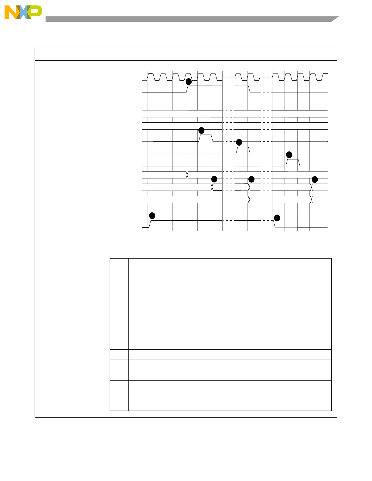
Table 1. MPC5565RM Rev 1.0 addendum (continued)
Last In / First Out
Entry in LIFO
Write
INTC_CPR
Clock
Interrupt Request
to Processor
Hardware Vector
Enable
Interrupt
Acknowledge
Interrupt Vector
Read
INTC_IACKR
Write
INTC_EOIR
INTVEC in
INTC_IACKR
PRI in
INTC_CPR
Peripheral Interrupt
Request 100
0
108
1
208
23
Peripheral Interrupt
Request 200
030
3
A
B
C
D
E
F
G
H
I
Raised Priority Preserved Events
Event Description
A Peripheral interrupt request 200 asserts during execution of ISR108 running at
priority 1.
B Interrupt request to processor asserts. INTVEC in INTC_IACKR updates with vector
for that peripheral interrupt request.
C ISR108 writes to INTC_CPR to raise priority to 3 before accessing shared coherent
data block.
D PRI in INTC_CPR now at 3, reflecting the write. This write, just before accessing
data block, is the last instruction the processor executes before being interrupted.
E Interrupt exception handler prolog acknowledges interrupt by reading INTC_IACKR.
F PRI of 3 pushed onto LIFO. PRI in INTC_CPR updates to 2, the priority of ISR208.
G ISR208 clears its flag bit, deasserting its peripheral interrupt request.
H Interrupt exception handler epilog writes to INTC_EOIR.
I LIFO pops 3, restoring the raised priority onto PRI in INTC_CPR. Next value to pop
from LIFO is the priority from before peripheral interrupt request 100 interrupted.
ISR108 now can access data block coherently after interrupt exception handler
executes rfi instruction.
Location Description
.
Addendum for Revision 1.0
Raised Priority Preserved Timing Diagram
Freescale Semiconductor 13
MPC5565 Reference Manual Addendum, Rev. 2
Page 15

Addendum for Revision 1.0
Location Description
Table 1. MPC5565RM Rev 1.0 addendum (continued)
Section 6.3.1.118 “Pad
Configuration Register 218
(SIU_PCR218)”
Section 11.3.1.1
Synthesizer Control Register
(FMPLL_SYNCR)
• Change PA field from two bits to one bit
• Figure 6-119: Change note 2 to “... set the PA field to 0b0.”
• Table 6-119. PCR218 “PA Field Definition” change as shown below:
0b0 FCK
0b1 AN[15]
Changed the last note in PREDIV field description from
“To use the 8-20 MHz OSC, the PLL predivider must be configured for divide-by-two operation
by tying PLLCFG[2] low (set PREDIV to 0b000).” to
“When using an 8 to 20 MHz reference clock (crystal or external clock), PLLCFG[2] should be
set low for devices that have a PLLCFG[2] pin. This sets the default predivider (PREDIV) to
0b000. To use a crystal or external reference greater than 20 MHz (up to 40 MHz), the PLL
predivider must be configured for divide-by-2 operation by setting PLLCFG[2] high. This sets the
default predivider (PREDIV) to 0b001. After reset, PREDIV must not be configured to a value
less than divide-by-2 (with a 40 MHz crystal/reference).”
MPC5565 Reference Manual Addendum, Rev. 2
Freescale Semiconductor14
Page 16

Revision history
2 Revision history
Table 2 provides a revision history for this document.
Table 2. Revision history
Revision Substantive changes Date of release
1.0 • Initial release. Corrected errors in chapter 12, “External Bus Interface (EBI).” 10/2009
2.0 • Corrected error in chapter 9, “Enhanced Direct Memory Access (eDMA).”
• Corrected errors in chapter 10, “Interrupt Controller (INTC).”
• Corrected errors in chapter 5, “Peripheral Bridge (PBRIDGE A and PBRIDGE B).”
• Corrected peripheral bridge name errors in appendix A, “MPC5565 Register Map.”
• Corrected unified channel block diagram in chapter 16, “Enhanced Modular
Input/Output Subsystem (eMIOS).”
• Corrected the table shown in EMIOS_CCRn: DMA bit description.
• Clarified the description in Section 9.4.1, “eDMA Microarchitecture”.
• Clarified the description in Section 9.3.1.13, “eDMA Interrupt Request Registers
(EDMA_IRQRL).
• Corrected the ECSM initialization information in Section 8.3: Initialization and
Application Information.
• Clarified the code sequence in Section 10.5.5.2: Ensuring Coherency.
• Clarified note in the INTC Interrupt Acknowledge Register .
• Added a note in the INTC Memory Map table.
• Clarified note at the end of the MPC5565 Interrupt Request Sources table.
• Added a paragraph to the Section 10.4.2.1.4, “Priority Comparator Submodule”.
• Updated Section 10.5.5.2, “Ensuring Coherency”.
• Corrected table “PCR218 PA Field Definition” and figure “AN[15]_FCK Pad
Configuration Register (SIU_PCR218)” and update note 2.
• Updated the last note in PREDIV field description of Synthesizer Control Register
(FMPLL_SYNCR).
04/2012
MPC5565 Reference Manual Addendum, Rev. 2
Freescale Semiconductor 15
Page 17

How to Reach Us:
Home Page:
www.freescale.com
Web Support:
http://www.freescale.com/support
USA/Europe or Locations Not Listed:
Freescale Semiconductor, Inc.
Technical Information Center, EL516
2100 East Elliot Road
Tempe, Arizona 85284
+1-800-521-6274 or +1-480-768-2130
www.freescale.com/support
Europe, Middle East, and Africa:
Freescale Halbleiter Deutschland GmbH
Technical Information Center
Schatzbogen 7
81829 Muenchen, Germany
+44 1296 380 456 (English)
+46 8 52200080 (English)
+49 89 92103 559 (German)
+33 1 69 35 48 48 (French)
www.freescale.com/support
Japan:
Freescale Semiconductor Japan Ltd.
Headquarters
ARCO Tower 15F
1-8-1, Shimo-Meguro, Meguro-ku,
Tokyo 153-0064
Japan
0120 191014 or +81 3 5437 9125
[email protected]
Asia/Pacific:
Freescale Semiconductor China Ltd.
Exchange Building 23F
No. 118 Jianguo Road
Chaoyang District
Beijing 100022
China
+86 10 5879 8000
[email protected]
For Literature Requests Only:
Freescale Semiconductor Literature Distribution Center
1-800-441-2447 or 303-675-2140
Fax: 303-675-2150
[email protected]
Information in this document is provided solely to enable system and
software implementers to use Freescale Semiconductor products. There are
no express or implied copyright licenses granted hereunder to design or
fabricate any integrated circuits or integrated circuits based on the
information in this document.
Freescale Semiconductor reserves the right to make changes without further
notice to any products herein. Freescale Semiconductor makes no warranty,
representation or guarantee regarding the suitability of its products for any
particular purpose, nor does Freescale Semiconductor assume any liability
arising out of the application or use of any product or circuit, and specifically
disclaims any and all liability, including without limitation consequential or
incidental damages. “Typical” parameters that may be provided in Freescale
Semiconductor data sheets and/or specifications can and do vary in different
applications and actual performance may vary over time. All operating
parameters, including “Typicals”, must be validated for each customer
application by customer’s technical exper ts. Freescale Semiconductor does
not convey any license under its patent rights nor the rights of others.
Freescale Semiconductor products are not designed, intended, or authorized
for use as components in systems intended for surgical implant into the body,
or other applications intended to support or sustain life, or for any other
application in which the failure of the Freescale Semic onductor product could
create a situation where personal injury or death may occur. Should Buyer
purchase or use Freescale Semiconductor products for any such unintended
or unauthorized application, Buyer shall indemnify and hold Freescale
Semiconductor and its officers, employees, subsidiaries, affiliates, and
distributors harmless against all claims, costs, damages, and expenses, and
reasonable attorney fees arising out of, directly or indirectly, any claim of
personal injury or death associated with such unintended or unauthorized
use, even if such claim alleges that Freescale Semiconductor was negligent
regarding the design or manufacture of the part.
Freescale™ and the Freescale logo are trademarks of Freescale
Semiconductor, Inc. All other product or ser vice names are the property
of their respective owners.© Freescale Semiconductor, Inc. 2009–2012. All
rights reserved.
MPC5565RMAD
Rev. 2
05/2012
Page 18

MPC5565 Microcontroller Reference
Manual
Devices Supported:
MPC5565
MPC5565 RM
Rev. 1.0
09/2007
Page 19

How to Reach Us:
Home Page:
www.freescale.com
E-mail:
USA/Europe or Locations Not Listed:
Freescale Semiconductor
Technical Information Center, CH370
1300 N. Alma School Road
Chandler, Arizona 85224
+1-800-521-6274 or +1-480-768-2130
[email protected]
Europe, Middle East, and Africa:
Freescale Halbleiter Deutschland GmbH
Technical Information Center
Schatzbogen 7
81829 Muenchen, Germany
+44 1296 380 456 (English)
+46 8 52200080 (English)
+49 89 92103 559 (German)
+33 1 69 35 48 48 (French)
[email protected]
Japan:
Freescale Semiconductor Japan Ltd.
Headquarters
ARCO Tower 15F
1-8-1, Shimo-Meguro, Meguro-ku,
Tokyo 153-0064, Japan
0120 191014 or +81 3 5437 9125
[email protected]
Asia/Pacific:
Freescale Semiconductor Hong Kong Ltd.
Technical Information Center
2 Dai King Street
Tai Po Industrial Estate
Tai Po, N.T., Hong Kong
+800 26668334
[email protected]
For Literature Requests Only:
Freescale Semiconductor Literature Distribution Center
P.O. Box 5405
Denver, Colorado 80217
1-800-441-2447 or 303-675-2140
Fax: 303-675-2150
[email protected]
Information in this document is provided solely to enable system and
software implementers to use Freescale Semiconductor products. There are
no express or implied copyright licenses granted hereunder to design or
fabricate any integrated circuits or integrated circuits based on the
information in this document.
Freescale Semiconductor reserves the right to make changes without further
notice to any products herein. Freescale Semiconductor makes no warranty,
representation or guarantee regarding the suitability of its products for any
particular purpose, nor does Freescale Semiconductor assume any liability
arising out of the application or use of any product or circuit, and specifically
disclaims any and all liability, including without limitation consequential or
incidental damages. “Typical” parameters that may be provided in Freescale
Semiconductor data sheets and/or specifications can and do vary in different
applications and actual performance may vary over time. All operating
parameters, including “Typicals”, must be validated for each customer
application by customer’s technical exper ts. Freescale Semiconductor does
not convey any license under its patent rights nor the rights of others.
Freescale Semiconductor products are not designed, intended, or authorized
for use as components in systems intended for surgical implant into the body,
or other applications intended to support or sustain life, or for any other
application in which the failure of the Freescale Semico nductor product could
create a situation where personal injury or death may occur. Should Buyer
purchase or use Freescale Semicondu ctor products for any such unintended
or unauthorized application, Buyer shall indemnify and hold Freescale
Semiconductor and its officers, employees, subsidiaries, affiliates, and
distributors harmless against all claims, costs, damages, and expenses, and
reasonable attorney fees arising out of, directly or indirectly, any claim of
personal injury or death associated with such unintended or unauthorized
use, even if such claim alleges that Freescale Semiconductor was negligent
regarding the design or manufacture of the part.
Freescale™ and the Freescale logo are trademarks of Freescale
Semiconductor, Inc. All other product or service names are the property
of their respective owners.© Freescale Semiconductor, Inc. 2006. All rights
reserved.
MPC5565 RM
Rev. 1.0
09/2007
Page 20

Chapter 1
Introduction
1.1 Overview . . . . . . . . . . . . . . . . . . . . . . . . . . . . . . . . . . . . . . . . . . . . . . . . . . . . . . . . . . . . . . . . . . . 1-1
1.2 Features . . . . . . . . . . . . . . . . . . . . . . . . . . . . . . . . . . . . . . . . . . . . . . . . . . . . . . . . . . . . . . . . . . . . 1-3
1.3 MPC5500 Family Comparison . . . . . . . . . . . . . . . . . . . . . . . . . . . . . . . . . . . . . . . . . . . . . . . . . . . 1-9
1.4 Detailed Features . . . . . . . . . . . . . . . . . . . . . . . . . . . . . . . . . . . . . . . . . . . . . . . . . . . . . . . . . . . . 1-11
1.4.1 e200z6 Core Overview . . . . . . . . . . . . . . . . . . . . . . . . . . . . . . . . . . . . . . . . . . . . . . . 1-11
1.4.2 System Bus Crossbar Switch (XBAR) . . . . . . . . . . . . . . . . . . . . . . . . . . . . . . . . . . . 1-12
1.4.3 Enhanced Direct Memory Access (eDMA) . . . . . . . . . . . . . . . . . . . . . . . . . . . . . . . 1-12
1.4.4 Interrupt Controller (INTC) . . . . . . . . . . . . . . . . . . . . . . . . . . . . . . . . . . . . . . . . . . . 1-13
1.4.5 Frequency Modulated Phase-Locking Loop (FMPLL) . . . . . . . . . . . . . . . . . . . . . . 1-13
1.4.6 External Bus Interface (EBI) . . . . . . . . . . . . . . . . . . . . . . . . . . . . . . . . . . . . . . . . . . 1-13
1.4.7 Calibration Bus Interface (CBI) . . . . . . . . . . . . . . . . . . . . . . . . . . . . . . . . . . . . . . . . 1-13
1.4.8 System Integration Unit (SIU) . . . . . . . . . . . . . . . . . . . . . . . . . . . . . . . . . . . . . . . . . 1-14
1.4.9 Error Correction Status Module (ECSM) . . . . . . . . . . . . . . . . . . . . . . . . . . . . . . . . . 1-14
1.4.10 Flash Memory . . . . . . . . . . . . . . . . . . . . . . . . . . . . . . . . . . . . . . . . . . . . . . . . . . . . . . 1-14
1.4.11 Cache . . . . . . . . . . . . . . . . . . . . . . . . . . . . . . . . . . . . . . . . . . . . . . . . . . . . . . . . . . . . 1-14
1.4.12 Static RAM (SRAM) . . . . . . . . . . . . . . . . . . . . . . . . . . . . . . . . . . . . . . . . . . . . . . . . 1-15
1.4.13 Boot Assist Module (BAM) . . . . . . . . . . . . . . . . . . . . . . . . . . . . . . . . . . . . . . . . . . . 1-15
1.4.14 Enhanced Management Input/Output System (eMIOS) . . . . . . . . . . . . . . . . . . . . . . 1-15
1.4.15 Enhanced Time Processing Unit (eTPU) . . . . . . . . . . . . . . . . . . . . . . . . . . . . . . . . . 1-15
1.4.16 Enhanced Queued A/D Converter (eQADC) . . . . . . . . . . . . . . . . . . . . . . . . . . . . . . 1-16
1.4.17 Deserial/Serial Peripheral Interface (DSPI) . . . . . . . . . . . . . . . . . . . . . . . . . . . . . . . 1-16
1.4.18 Enhanced Serial Communications Interface (eSCI) . . . . . . . . . . . . . . . . . . . . . . . . . 1-16
1.4.19 Flexible Controller Area Network (FlexCAN) . . . . . . . . . . . . . . . . . . . . . . . . . . . . . 1-16
1.4.20 Nexus Development Interface (NDI) . . . . . . . . . . . . . . . . . . . . . . . . . . . . . . . . . . . . 1-17
1.4.21 JTAG Controller (JTAGC) . . . . . . . . . . . . . . . . . . . . . . . . . . . . . . . . . . . . . . . . . . . . 1-17
1.5 MPC5500 Family Memory Map . . . . . . . . . . . . . . . . . . . . . . . . . . . . . . . . . . . . . . . . . . . . . . . . 1-17
1.6 Multi-Master Operation Memory Map . . . . . . . . . . . . . . . . . . . . . . . . . . . . . . . . . . . . . . . . . . . 1-21
1.7 Document Revision History . . . . . . . . . . . . . . . . . . . . . . . . . . . . . . . . . . . . . . . . . . . . . . . . . . . . 1-22
Chapter 2
Signal Description
2.1 Block Diagram . . . . . . . . . . . . . . . . . . . . . . . . . . . . . . . . . . . . . . . . . . . . . . . . . . . . . . . . . . . . . . . 2-1
2.2 External Signal Descriptions . . . . . . . . . . . . . . . . . . . . . . . . . . . . . . . . . . . . . . . . . . . . . . . . . . . . 2-3
2.3 Detailed Signal Description . . . . . . . . . . . . . . . . . . . . . . . . . . . . . . . . . . . . . . . . . . . . . . . . . . . . 2-18
2.3.1 Reset and Configuration Signals . . . . . . . . . . . . . . . . . . . . . . . . . . . . . . . . . . . . . . . . 2-18
2.3.2 External Bus Interface (EBI) Signals . . . . . . . . . . . . . . . . . . . . . . . . . . . . . . . . . . . . 2-19
2.3.3 Nexus Signals . . . . . . . . . . . . . . . . . . . . . . . . . . . . . . . . . . . . . . . . . . . . . . . . . . . . . . 2-23
2.3.4 JTAG Signals . . . . . . . . . . . . . . . . . . . . . . . . . . . . . . . . . . . . . . . . . . . . . . . . . . . . . . 2-24
2.3.5 Controller Area Network (FlexCAN) Signals . . . . . . . . . . . . . . . . . . . . . . . . . . . . . 2-25
2.3.6 Serial Communication Interface (eSCI) Signals . . . . . . . . . . . . . . . . . . . . . . . . . . . . 2-25
2.3.7 Deserial/Serial Peripheral Interface (DSPI) Signals . . . . . . . . . . . . . . . . . . . . . . . . . 2-26
2.3.8 Enhanced Queued A/D Controller (eQADC) Signals . . . . . . . . . . . . . . . . . . . . . . . 2-29
MPC5565 Reference Manual, Rev. 1.0
Freescale Semiconductor 1
Page 21

2.3.9 Enhanced Time Processing Unit (eTPU) Signals . . . . . . . . . . . . . . . . . . . . . . . . . . . 2-32
2.3.10 Enhanced Management Input/Output System (eMIOS) Signals . . . . . . . . . . . . . . . 2-37
2.3.11 General Purpose Input / Output (GPIO) Signals . . . . . . . . . . . . . . . . . . . . . . . . . . . 2-38
2.3.12 Calibration Bus Signals . . . . . . . . . . . . . . . . . . . . . . . . . . . . . . . . . . . . . . . . . . . . . . 2-39
2.3.13 Clock Synthesizer Signals . . . . . . . . . . . . . . . . . . . . . . . . . . . . . . . . . . . . . . . . . . . . 2-40
2.3.14 Power / Ground Signals . . . . . . . . . . . . . . . . . . . . . . . . . . . . . . . . . . . . . . . . . . . . . . 2-41
2.3.15 I/O Power and Ground Segmentation . . . . . . . . . . . . . . . . . . . . . . . . . . . . . . . . . . . . 2-42
2.4 eTPU Pin Connections and Serialization . . . . . . . . . . . . . . . . . . . . . . . . . . . . . . . . . . . . . . . . . . 2-45
2.4.1 ETPUA[0:15] . . . . . . . . . . . . . . . . . . . . . . . . . . . . . . . . . . . . . . . . . . . . . . . . . . . . . . 2-45
2.4.2 ETPUA[16:31] . . . . . . . . . . . . . . . . . . . . . . . . . . . . . . . . . . . . . . . . . . . . . . . . . . . . . 2-47
2.5 eMIOS Pin Connections and Serialization . . . . . . . . . . . . . . . . . . . . . . . . . . . . . . . . . . . . . . . . . 2-48
2.6 Document Revision History . . . . . . . . . . . . . . . . . . . . . . . . . . . . . . . . . . . . . . . . . . . . . . . . . . . . 2-50
Chapter 3
e200z6 Core Complex
3.1 Introduction . . . . . . . . . . . . . . . . . . . . . . . . . . . . . . . . . . . . . . . . . . . . . . . . . . . . . . . . . . . . . . . . . 3-1
3.1.1 Block Diagram . . . . . . . . . . . . . . . . . . . . . . . . . . . . . . . . . . . . . . . . . . . . . . . . . . . . . . 3-1
3.1.2 Overview . . . . . . . . . . . . . . . . . . . . . . . . . . . . . . . . . . . . . . . . . . . . . . . . . . . . . . . . . . . 3-2
3.1.3 Features . . . . . . . . . . . . . . . . . . . . . . . . . . . . . . . . . . . . . . . . . . . . . . . . . . . . . . . . . . . . 3-3
3.1.4 Microarchitecture Summary . . . . . . . . . . . . . . . . . . . . . . . . . . . . . . . . . . . . . . . . . . . . 3-5
3.2 Core Registers and Programmer’s Model . . . . . . . . . . . . . . . . . . . . . . . . . . . . . . . . . . . . . . . . . . 3-6
3.2.1 Power Architecture Registers . . . . . . . . . . . . . . . . . . . . . . . . . . . . . . . . . . . . . . . . . . . 3-8
3.2.2 Core-Specific Registers . . . . . . . . . . . . . . . . . . . . . . . . . . . . . . . . . . . . . . . . . . . . . . 3-11
3.2.3 e200z6 Core Complex Features Not Supported in the Device . . . . . . . . . . . . . . . . . 3-12
3.3 Functional Description . . . . . . . . . . . . . . . . . . . . . . . . . . . . . . . . . . . . . . . . . . . . . . . . . . . . . . . . 3-13
3.3.1 Memory Management Unit (MMU) . . . . . . . . . . . . . . . . . . . . . . . . . . . . . . . . . . . . . 3-13
3.3.2 L1 Cache . . . . . . . . . . . . . . . . . . . . . . . . . . . . . . . . . . . . . . . . . . . . . . . . . . . . . . . . . . 3-22
3.3.3 Interrupt Types . . . . . . . . . . . . . . . . . . . . . . . . . . . . . . . . . . . . . . . . . . . . . . . . . . . . . 3-29
3.3.4 Bus Interface Unit (BIU) . . . . . . . . . . . . . . . . . . . . . . . . . . . . . . . . . . . . . . . . . . . . . 3-31
3.3.5 Timer Facilities . . . . . . . . . . . . . . . . . . . . . . . . . . . . . . . . . . . . . . . . . . . . . . . . . . . . . 3-31
3.3.6 Signal Processing Extension APU (SPE APU) . . . . . . . . . . . . . . . . . . . . . . . . . . . . 3-32
3.3.7 SPE Programming Model . . . . . . . . . . . . . . . . . . . . . . . . . . . . . . . . . . . . . . . . . . . . . 3-32
3.4 External References . . . . . . . . . . . . . . . . . . . . . . . . . . . . . . . . . . . . . . . . . . . . . . . . . . . . . . . . . . 3-33
3.5 Power Architecture Instruction Extensions – VLE . . . . . . . . . . . . . . . . . . . . . . . . . . . . . . . . . . 3-33
3.6 Document Revision History . . . . . . . . . . . . . . . . . . . . . . . . . . . . . . . . . . . . . . . . . . . . . . . . . . . . 3-34
Chapter 4
Reset
4.1 Introduction . . . . . . . . . . . . . . . . . . . . . . . . . . . . . . . . . . . . . . . . . . . . . . . . . . . . . . . . . . . . . . . . . 4-1
4.2 External Signal Description . . . . . . . . . . . . . . . . . . . . . . . . . . . . . . . . . . . . . . . . . . . . . . . . . . . . . 4-2
4.2.1 Reset Input (RESET
4.2.2 Reset Output (RSTOUT
4.2.3 Reset Configuration (RSTCFG) . . . . . . . . . . . . . . . . . . . . . . . . . . . . . . . . . . . . . . . . . 4-3
4.2.4 Weak Pull Configuration (WKPCFG) . . . . . . . . . . . . . . . . . . . . . . . . . . . . . . . . . . . . 4-3
Freescale Semiconductor 2
) . . . . . . . . . . . . . . . . . . . . . . . . . . . . . . . . . . . . . . . . . . . . . . . . . 4-2
) . . . . . . . . . . . . . . . . . . . . . . . . . . . . . . . . . . . . . . . . . . . . . . 4-2
MPC5565 Reference Manual, Rev. 1.0
Page 22

4.2.5 Boot Configuration (BOOTCFG[0:1]) . . . . . . . . . . . . . . . . . . . . . . . . . . . . . . . . . . . . 4-3
4.3 Memory Map/Register Definition . . . . . . . . . . . . . . . . . . . . . . . . . . . . . . . . . . . . . . . . . . . . . . . . 4-3
4.3.1 Register Descriptions . . . . . . . . . . . . . . . . . . . . . . . . . . . . . . . . . . . . . . . . . . . . . . . . . 4-3
4.4 Functional Description . . . . . . . . . . . . . . . . . . . . . . . . . . . . . . . . . . . . . . . . . . . . . . . . . . . . . . . . . 4-6
4.4.1 Reset Vector Locations . . . . . . . . . . . . . . . . . . . . . . . . . . . . . . . . . . . . . . . . . . . . . . . . 4-6
4.4.2 Reset Sources . . . . . . . . . . . . . . . . . . . . . . . . . . . . . . . . . . . . . . . . . . . . . . . . . . . . . . . 4-7
4.4.3 Reset Configuration and Configuration Pins . . . . . . . . . . . . . . . . . . . . . . . . . . . . . . 4-11
4.4.4 Reset Configuration Timing . . . . . . . . . . . . . . . . . . . . . . . . . . . . . . . . . . . . . . . . . . . 4-16
4.4.5 Reset Flow . . . . . . . . . . . . . . . . . . . . . . . . . . . . . . . . . . . . . . . . . . . . . . . . . . . . . . . . 4-18
4.5 Document Revision History . . . . . . . . . . . . . . . . . . . . . . . . . . . . . . . . . . . . . . . . . . . . . . . . . . . . 4-20
Chapter 5
Peripheral Bridge (PBRIDGE_A, PBRIDGE_B)
5.1 Introduction . . . . . . . . . . . . . . . . . . . . . . . . . . . . . . . . . . . . . . . . . . . . . . . . . . . . . . . . . . . . . . . . . 5-1
5.1.1 Block Diagram . . . . . . . . . . . . . . . . . . . . . . . . . . . . . . . . . . . . . . . . . . . . . . . . . . . . . . 5-1
5.1.2 Overview . . . . . . . . . . . . . . . . . . . . . . . . . . . . . . . . . . . . . . . . . . . . . . . . . . . . . . . . . . . 5-1
5.1.3 Features . . . . . . . . . . . . . . . . . . . . . . . . . . . . . . . . . . . . . . . . . . . . . . . . . . . . . . . . . . . . 5-3
5.1.4 Modes of Operation . . . . . . . . . . . . . . . . . . . . . . . . . . . . . . . . . . . . . . . . . . . . . . . . . . 5-3
5.2 External Signal Description . . . . . . . . . . . . . . . . . . . . . . . . . . . . . . . . . . . . . . . . . . . . . . . . . . . . . 5-3
5.3 Memory Map and Register Definitions . . . . . . . . . . . . . . . . . . . . . . . . . . . . . . . . . . . . . . . . . . . . 5-4
5.3.1 Register Descriptions . . . . . . . . . . . . . . . . . . . . . . . . . . . . . . . . . . . . . . . . . . . . . . . . . 5-5
5.4 Functional Description . . . . . . . . . . . . . . . . . . . . . . . . . . . . . . . . . . . . . . . . . . . . . . . . . . . . . . . . 5-11
5.4.1 Access Support . . . . . . . . . . . . . . . . . . . . . . . . . . . . . . . . . . . . . . . . . . . . . . . . . . . . . 5-11
5.4.2 Peripheral Write Buffering . . . . . . . . . . . . . . . . . . . . . . . . . . . . . . . . . . . . . . . . . . . . 5-11
5.4.3 General Operation . . . . . . . . . . . . . . . . . . . . . . . . . . . . . . . . . . . . . . . . . . . . . . . . . . . 5-13
5.5 Document Revision History . . . . . . . . . . . . . . . . . . . . . . . . . . . . . . . . . . . . . . . . . . . . . . . . . . . . 5-14
Chapter 6
System Integration Unit (SIU)
6.1 Introduction . . . . . . . . . . . . . . . . . . . . . . . . . . . . . . . . . . . . . . . . . . . . . . . . . . . . . . . . . . . . . . . . . 6-1
6.1.1 Block Diagram . . . . . . . . . . . . . . . . . . . . . . . . . . . . . . . . . . . . . . . . . . . . . . . . . . . . . . 6-2
6.1.2 Overview . . . . . . . . . . . . . . . . . . . . . . . . . . . . . . . . . . . . . . . . . . . . . . . . . . . . . . . . . . . 6-3
6.1.3 Modes of Operation . . . . . . . . . . . . . . . . . . . . . . . . . . . . . . . . . . . . . . . . . . . . . . . . . . 6-3
6.2 External Signal Description . . . . . . . . . . . . . . . . . . . . . . . . . . . . . . . . . . . . . . . . . . . . . . . . . . . . . 6-4
6.2.1 Detailed Signal Descriptions . . . . . . . . . . . . . . . . . . . . . . . . . . . . . . . . . . . . . . . . . . . 6-4
6.3 Memory Map and Register Definition . . . . . . . . . . . . . . . . . . . . . . . . . . . . . . . . . . . . . . . . . . . . . 6-9
6.3.1 Register Descriptions . . . . . . . . . . . . . . . . . . . . . . . . . . . . . . . . . . . . . . . . . . . . . . . . 6-10
6.4 Functional Description . . . . . . . . . . . . . . . . . . . . . . . . . . . . . . . . . . . . . . . . . . . . . . . . . . . . . . . 6-114
6.4.1 System Configuration . . . . . . . . . . . . . . . . . . . . . . . . . . . . . . . . . . . . . . . . . . . . . . . 6-114
6.4.2 Reset Control . . . . . . . . . . . . . . . . . . . . . . . . . . . . . . . . . . . . . . . . . . . . . . . . . . . . . 6-115
6.4.3 External Interrupt . . . . . . . . . . . . . . . . . . . . . . . . . . . . . . . . . . . . . . . . . . . . . . . . . . 6-115
6.4.4 GPIO Operation . . . . . . . . . . . . . . . . . . . . . . . . . . . . . . . . . . . . . . . . . . . . . . . . . . . 6-116
6.4.5 Internal Multiplexing . . . . . . . . . . . . . . . . . . . . . . . . . . . . . . . . . . . . . . . . . . . . . . . 6-116
6.5 Document Revision History . . . . . . . . . . . . . . . . . . . . . . . . . . . . . . . . . . . . . . . . . . . . . . . . . . . 6-120
MPC5565 Reference Manual, Rev. 1.0
Freescale Semiconductor 3
Page 23

Chapter 7
Crossbar Switch (XBAR)
7.1 Introduction . . . . . . . . . . . . . . . . . . . . . . . . . . . . . . . . . . . . . . . . . . . . . . . . . . . . . . . . . . . . . . . . . 7-1
7.1.1 Block Diagram . . . . . . . . . . . . . . . . . . . . . . . . . . . . . . . . . . . . . . . . . . . . . . . . . . . . . . 7-1
7.1.2 Overview . . . . . . . . . . . . . . . . . . . . . . . . . . . . . . . . . . . . . . . . . . . . . . . . . . . . . . . . . . . 7-2
7.1.3 Features . . . . . . . . . . . . . . . . . . . . . . . . . . . . . . . . . . . . . . . . . . . . . . . . . . . . . . . . . . . . 7-2
7.1.4 Modes of Operation . . . . . . . . . . . . . . . . . . . . . . . . . . . . . . . . . . . . . . . . . . . . . . . . . . 7-3
7.2 Memory Map and Register Definition . . . . . . . . . . . . . . . . . . . . . . . . . . . . . . . . . . . . . . . . . . . . . 7-3
7.2.1 Register Descriptions . . . . . . . . . . . . . . . . . . . . . . . . . . . . . . . . . . . . . . . . . . . . . . . . . 7-4
7.3 Functional Description . . . . . . . . . . . . . . . . . . . . . . . . . . . . . . . . . . . . . . . . . . . . . . . . . . . . . . . . . 7-8
7.3.1 Overview . . . . . . . . . . . . . . . . . . . . . . . . . . . . . . . . . . . . . . . . . . . . . . . . . . . . . . . . . . . 7-8
7.3.2 General Operation . . . . . . . . . . . . . . . . . . . . . . . . . . . . . . . . . . . . . . . . . . . . . . . . . . . . 7-8
7.3.3 Master Ports . . . . . . . . . . . . . . . . . . . . . . . . . . . . . . . . . . . . . . . . . . . . . . . . . . . . . . . . 7-9
7.3.4 Slave Ports . . . . . . . . . . . . . . . . . . . . . . . . . . . . . . . . . . . . . . . . . . . . . . . . . . . . . . . . . 7-9
7.3.5 Priority Assignment . . . . . . . . . . . . . . . . . . . . . . . . . . . . . . . . . . . . . . . . . . . . . . . . . 7-10
7.3.6 Arbitration . . . . . . . . . . . . . . . . . . . . . . . . . . . . . . . . . . . . . . . . . . . . . . . . . . . . . . . . . 7-10
7.4 Document Revision History . . . . . . . . . . . . . . . . . . . . . . . . . . . . . . . . . . . . . . . . . . . . . . . . . . . . 7-12
Chapter 8
Error Correction Status Module (ECSM)
8.1 Introduction . . . . . . . . . . . . . . . . . . . . . . . . . . . . . . . . . . . . . . . . . . . . . . . . . . . . . . . . . . . . . . . . . 8-1
8.1.1 Overview . . . . . . . . . . . . . . . . . . . . . . . . . . . . . . . . . . . . . . . . . . . . . . . . . . . . . . . . . . . 8-1
8.1.2 Features . . . . . . . . . . . . . . . . . . . . . . . . . . . . . . . . . . . . . . . . . . . . . . . . . . . . . . . . . . . . 8-2
8.2 Memory Map and Register Definition . . . . . . . . . . . . . . . . . . . . . . . . . . . . . . . . . . . . . . . . . . . . . 8-2
8.2.1 Register Descriptions . . . . . . . . . . . . . . . . . . . . . . . . . . . . . . . . . . . . . . . . . . . . . . . . . 8-3
8.3 Initialization and Application Information . . . . . . . . . . . . . . . . . . . . . . . . . . . . . . . . . . . . . . . . . 8-14
8.4 Document Revision History . . . . . . . . . . . . . . . . . . . . . . . . . . . . . . . . . . . . . . . . . . . . . . . . . . . . 8-15
Chapter 9
Enhanced Direct Memory Access (eDMA)
9.1 Introduction . . . . . . . . . . . . . . . . . . . . . . . . . . . . . . . . . . . . . . . . . . . . . . . . . . . . . . . . . . . . . . . . . 9-1
9.1.1 Overview . . . . . . . . . . . . . . . . . . . . . . . . . . . . . . . . . . . . . . . . . . . . . . . . . . . . . . . . . . . 9-1
9.1.2 Features . . . . . . . . . . . . . . . . . . . . . . . . . . . . . . . . . . . . . . . . . . . . . . . . . . . . . . . . . . . . 9-2
9.1.3 Modes of Operation . . . . . . . . . . . . . . . . . . . . . . . . . . . . . . . . . . . . . . . . . . . . . . . . . . 9-3
9.2 Memory Map and Register Definition . . . . . . . . . . . . . . . . . . . . . . . . . . . . . . . . . . . . . . . . . . . . . 9-4
9.2.1 Memory Map . . . . . . . . . . . . . . . . . . . . . . . . . . . . . . . . . . . . . . . . . . . . . . . . . . . . . . . 9-4
9.2.2 Register Descriptions . . . . . . . . . . . . . . . . . . . . . . . . . . . . . . . . . . . . . . . . . . . . . . . . . 9-6
9.3 Functional Description . . . . . . . . . . . . . . . . . . . . . . . . . . . . . . . . . . . . . . . . . . . . . . . . . . . . . . . . 9-28
9.3.1 eDMA Microarchitecture . . . . . . . . . . . . . . . . . . . . . . . . . . . . . . . . . . . . . . . . . . . . . 9-28
9.3.2 eDMA Basic Data Flow . . . . . . . . . . . . . . . . . . . . . . . . . . . . . . . . . . . . . . . . . . . . . . 9-30
9.3.3 eDMA Performance . . . . . . . . . . . . . . . . . . . . . . . . . . . . . . . . . . . . . . . . . . . . . . . . . 9-32
9.4 Initialization / Application Information . . . . . . . . . . . . . . . . . . . . . . . . . . . . . . . . . . . . . . . . . . . 9-35
9.4.1 eDMA Initialization . . . . . . . . . . . . . . . . . . . . . . . . . . . . . . . . . . . . . . . . . . . . . . . . . 9-35
9.4.2 DMA Programming Errors . . . . . . . . . . . . . . . . . . . . . . . . . . . . . . . . . . . . . . . . . . . . 9-37
MPC5565 Reference Manual, Rev. 1.0
Freescale Semiconductor 4
Page 24

9.4.3 DMA Request Assignments . . . . . . . . . . . . . . . . . . . . . . . . . . . . . . . . . . . . . . . . . . . 9-38
9.4.4 DMA Arbitration Mode Considerations . . . . . . . . . . . . . . . . . . . . . . . . . . . . . . . . . . 9-39
9.4.5 DMA Transfer . . . . . . . . . . . . . . . . . . . . . . . . . . . . . . . . . . . . . . . . . . . . . . . . . . . . . . 9-41
9.4.6 TCD Status . . . . . . . . . . . . . . . . . . . . . . . . . . . . . . . . . . . . . . . . . . . . . . . . . . . . . . . . 9-44
9.4.7 Channel Linking . . . . . . . . . . . . . . . . . . . . . . . . . . . . . . . . . . . . . . . . . . . . . . . . . . . . 9-45
9.4.8 Dynamic Programming . . . . . . . . . . . . . . . . . . . . . . . . . . . . . . . . . . . . . . . . . . . . . . . 9-46
9.5 Document Revision History . . . . . . . . . . . . . . . . . . . . . . . . . . . . . . . . . . . . . . . . . . . . . . . . . . . . 9-48
Chapter 10
Interrupt Controller (INTC)
10.1 Introduction . . . . . . . . . . . . . . . . . . . . . . . . . . . . . . . . . . . . . . . . . . . . . . . . . . . . . . . . . . . . . . . . 10-1
10.1.1 Block Diagram . . . . . . . . . . . . . . . . . . . . . . . . . . . . . . . . . . . . . . . . . . . . . . . . . . . . . 10-1
10.1.2 Overview . . . . . . . . . . . . . . . . . . . . . . . . . . . . . . . . . . . . . . . . . . . . . . . . . . . . . . . . . . 10-2
10.1.3 Features . . . . . . . . . . . . . . . . . . . . . . . . . . . . . . . . . . . . . . . . . . . . . . . . . . . . . . . . . . . 10-4
10.1.4 Modes of Operation . . . . . . . . . . . . . . . . . . . . . . . . . . . . . . . . . . . . . . . . . . . . . . . . . 10-4
10.2 External Signal Description . . . . . . . . . . . . . . . . . . . . . . . . . . . . . . . . . . . . . . . . . . . . . . . . . . . . 10-6
10.3 Memory Map and Register Definition . . . . . . . . . . . . . . . . . . . . . . . . . . . . . . . . . . . . . . . . . . . . 10-8
10.3.1 Register Descriptions . . . . . . . . . . . . . . . . . . . . . . . . . . . . . . . . . . . . . . . . . . . . . . . . 10-9
10.4 Functional Description . . . . . . . . . . . . . . . . . . . . . . . . . . . . . . . . . . . . . . . . . . . . . . . . . . . . . . . 10-14
10.4.1 Interrupt Request Sources . . . . . . . . . . . . . . . . . . . . . . . . . . . . . . . . . . . . . . . . . . . . 10-14
10.4.2 Priority Management . . . . . . . . . . . . . . . . . . . . . . . . . . . . . . . . . . . . . . . . . . . . . . . 10-24
10.4.3 Details on Handshaking with Processor . . . . . . . . . . . . . . . . . . . . . . . . . . . . . . . . . 10-26
10.5 Initialization/Application Information . . . . . . . . . . . . . . . . . . . . . . . . . . . . . . . . . . . . . . . . . . . 10-28
10.5.1 Initialization Flow . . . . . . . . . . . . . . . . . . . . . . . . . . . . . . . . . . . . . . . . . . . . . . . . . . 10-28
10.5.2 Interrupt Exception Handler . . . . . . . . . . . . . . . . . . . . . . . . . . . . . . . . . . . . . . . . . . 10-28
10.5.3 ISR, RTOS, and Task Hierarchy . . . . . . . . . . . . . . . . . . . . . . . . . . . . . . . . . . . . . . . 10-30
10.5.4 Order of Execution . . . . . . . . . . . . . . . . . . . . . . . . . . . . . . . . . . . . . . . . . . . . . . . . . 10-31
10.5.5 Priority Ceiling Protocol . . . . . . . . . . . . . . . . . . . . . . . . . . . . . . . . . . . . . . . . . . . . . 10-32
10.5.6 Selecting Priorities According to Request Rates
and Deadlines . . . . . . . . . . . . . . . . . . . . . . . . . . . . . . . . . . . . . . . . . . . . . . . . . . . . . 10-33
10.5.7 Software Settable Interrupt Requests . . . . . . . . . . . . . . . . . . . . . . . . . . . . . . . . . . . 10-33
10.5.8 Lowering Priority Within an ISR . . . . . . . . . . . . . . . . . . . . . . . . . . . . . . . . . . . . . . 10-34
10.5.9 Negating an Interrupt Request Outside of its ISR . . . . . . . . . . . . . . . . . . . . . . . . . 10-35
10.5.10 Examining LIFO contents . . . . . . . . . . . . . . . . . . . . . . . . . . . . . . . . . . . . . . . . . . . . 10-35
10.6 Document Revision History . . . . . . . . . . . . . . . . . . . . . . . . . . . . . . . . . . . . . . . . . . . . . . . . . . . 10-36
Chapter 11
Frequency Modulated Phase Locked Loop and System Clocks (FMPLL)
11.1 Introduction . . . . . . . . . . . . . . . . . . . . . . . . . . . . . . . . . . . . . . . . . . . . . . . . . . . . . . . . . . . . . . . . 11-1
11.1.1 Block Diagrams . . . . . . . . . . . . . . . . . . . . . . . . . . . . . . . . . . . . . . . . . . . . . . . . . . . . 11-1
11.1.2 Overview . . . . . . . . . . . . . . . . . . . . . . . . . . . . . . . . . . . . . . . . . . . . . . . . . . . . . . . . . . 11-8
11.1.3 Features . . . . . . . . . . . . . . . . . . . . . . . . . . . . . . . . . . . . . . . . . . . . . . . . . . . . . . . . . . . 11-8
11.1.4 FMPLL Modes of Operation . . . . . . . . . . . . . . . . . . . . . . . . . . . . . . . . . . . . . . . . . . 11-9
11.2 External Signal Description . . . . . . . . . . . . . . . . . . . . . . . . . . . . . . . . . . . . . . . . . . . . . . . . . . . 11-12
MPC5565 Reference Manual, Rev. 1.0
Freescale Semiconductor 5
Page 25

11.3 Memory Map/Register Definition . . . . . . . . . . . . . . . . . . . . . . . . . . . . . . . . . . . . . . . . . . . . . . 11-12
11.3.1 Register Descriptions . . . . . . . . . . . . . . . . . . . . . . . . . . . . . . . . . . . . . . . . . . . . . . . 11-12
11.4 Functional Description . . . . . . . . . . . . . . . . . . . . . . . . . . . . . . . . . . . . . . . . . . . . . . . . . . . . . . . 11-19
11.4.1 Clock Architecture . . . . . . . . . . . . . . . . . . . . . . . . . . . . . . . . . . . . . . . . . . . . . . . . . 11-19
11.4.2 Clock Operation . . . . . . . . . . . . . . . . . . . . . . . . . . . . . . . . . . . . . . . . . . . . . . . . . . . 11-21
11.4.3 Clock Configuration . . . . . . . . . . . . . . . . . . . . . . . . . . . . . . . . . . . . . . . . . . . . . . . . 11-24
11.5 Document Revision History . . . . . . . . . . . . . . . . . . . . . . . . . . . . . . . . . . . . . . . . . . . . . . . . . . . 11-33
Chapter 12
External Bus Interface (EBI)
12.1 Introduction . . . . . . . . . . . . . . . . . . . . . . . . . . . . . . . . . . . . . . . . . . . . . . . . . . . . . . . . . . . . . . . . 12-1
12.1.1 Block Diagram . . . . . . . . . . . . . . . . . . . . . . . . . . . . . . . . . . . . . . . . . . . . . . . . . . . . . 12-2
12.1.2 Overview . . . . . . . . . . . . . . . . . . . . . . . . . . . . . . . . . . . . . . . . . . . . . . . . . . . . . . . . . . 12-3
12.1.3 Features . . . . . . . . . . . . . . . . . . . . . . . . . . . . . . . . . . . . . . . . . . . . . . . . . . . . . . . . . . . 12-4
12.1.4 Modes of Operation . . . . . . . . . . . . . . . . . . . . . . . . . . . . . . . . . . . . . . . . . . . . . . . . . 12-5
12.2 External Signal Description . . . . . . . . . . . . . . . . . . . . . . . . . . . . . . . . . . . . . . . . . . . . . . . . . . . . 12-7
12.2.1 Detailed Signal Descriptions . . . . . . . . . . . . . . . . . . . . . . . . . . . . . . . . . . . . . . . . . . 12-8
12.2.2 Signal Function and Direction by Mode . . . . . . . . . . . . . . . . . . . . . . . . . . . . . . . . . 12-11
12.3 Memory Map and Register Definition . . . . . . . . . . . . . . . . . . . . . . . . . . . . . . . . . . . . . . . . . . . 12-13
12.3.1 Register Descriptions . . . . . . . . . . . . . . . . . . . . . . . . . . . . . . . . . . . . . . . . . . . . . . . 12-14
12.4 Functional Description . . . . . . . . . . . . . . . . . . . . . . . . . . . . . . . . . . . . . . . . . . . . . . . . . . . . . . . 12-21
12.4.1 External Bus Interface Features . . . . . . . . . . . . . . . . . . . . . . . . . . . . . . . . . . . . . . . 12-21
12.4.2 External Bus Operations . . . . . . . . . . . . . . . . . . . . . . . . . . . . . . . . . . . . . . . . . . . . . 12-26
12.5 Initialization and Application Information . . . . . . . . . . . . . . . . . . . . . . . . . . . . . . . . . . . . . . . . 12-61
12.5.1 Booting from External Memory . . . . . . . . . . . . . . . . . . . . . . . . . . . . . . . . . . . . . . . 12-61
12.5.2 Running with SDR (Single Data Rate) Burst Memories . . . . . . . . . . . . . . . . . . . . 12-61
12.5.3 Running with Asynchronous Memories . . . . . . . . . . . . . . . . . . . . . . . . . . . . . . . . . 12-62
12.5.4 Connecting an MCU to Multiple Memories . . . . . . . . . . . . . . . . . . . . . . . . . . . . . . 12-65
12.5.5 Dual-MCU Operation with Reduced Pinout MCUs . . . . . . . . . . . . . . . . . . . . . . . . 12-65
12.5.6 Summary of Differences from MPC5xx . . . . . . . . . . . . . . . . . . . . . . . . . . . . . . . . . 12-67
12.6 Document Revision History . . . . . . . . . . . . . . . . . . . . . . . . . . . . . . . . . . . . . . . . . . . . . . . . . . . 12-68
Chapter 13
Flash Memory
13.1 Introduction . . . . . . . . . . . . . . . . . . . . . . . . . . . . . . . . . . . . . . . . . . . . . . . . . . . . . . . . . . . . . . . . 13-1
13.1.1 Block Diagram . . . . . . . . . . . . . . . . . . . . . . . . . . . . . . . . . . . . . . . . . . . . . . . . . . . . . 13-1
13.1.2 Overview . . . . . . . . . . . . . . . . . . . . . . . . . . . . . . . . . . . . . . . . . . . . . . . . . . . . . . . . . . 13-1
13.1.3 Features . . . . . . . . . . . . . . . . . . . . . . . . . . . . . . . . . . . . . . . . . . . . . . . . . . . . . . . . . . . 13-3
13.1.4 Modes of Operation . . . . . . . . . . . . . . . . . . . . . . . . . . . . . . . . . . . . . . . . . . . . . . . . . 13-3
13.2 External Signal Description . . . . . . . . . . . . . . . . . . . . . . . . . . . . . . . . . . . . . . . . . . . . . . . . . . . . 13-4
13.2.1 Voltage for Flash Only (V
FLASH)
13.2.2 Program and Erase Voltage for Flash Only (V
13.3 Memory Map/Register Description . . . . . . . . . . . . . . . . . . . . . . . . . . . . . . . . . . . . . . . . . . . . . . 13-4
13.3.1 Flash Memory Map . . . . . . . . . . . . . . . . . . . . . . . . . . . . . . . . . . . . . . . . . . . . . . . . . . 13-5
MPC5565 Reference Manual, Rev. 1.0
Freescale Semiconductor 6
. . . . . . . . . . . . . . . . . . . . . . . . . . . . . . . . . . . . . . . 13-4
) . . . . . . . . . . . . . . . . . . . . . . . . . . 13-4
PP
Page 26

13.3.2 Register Descriptions . . . . . . . . . . . . . . . . . . . . . . . . . . . . . . . . . . . . . . . . . . . . . . . . 13-8
13.4 Functional Description . . . . . . . . . . . . . . . . . . . . . . . . . . . . . . . . . . . . . . . . . . . . . . . . . . . . . . . 13-21
13.4.1 Flash Bus Interface Unit (FBIU) . . . . . . . . . . . . . . . . . . . . . . . . . . . . . . . . . . . . . . 13-21
13.4.2 Flash Memory Array: User Mode . . . . . . . . . . . . . . . . . . . . . . . . . . . . . . . . . . . . . 13-24
13.4.3 Flash Memory Array: Stop Mode . . . . . . . . . . . . . . . . . . . . . . . . . . . . . . . . . . . . . . 13-35
13.4.4 Flash Memory Array: Reset . . . . . . . . . . . . . . . . . . . . . . . . . . . . . . . . . . . . . . . . . . 13-36
13.5 Revision History . . . . . . . . . . . . . . . . . . . . . . . . . . . . . . . . . . . . . . . . . . . . . . . . . . . . . . . . . . . . 13-37
Chapter 14
Internal Static RAM (SRAM)
14.1 Introduction . . . . . . . . . . . . . . . . . . . . . . . . . . . . . . . . . . . . . . . . . . . . . . . . . . . . . . . . . . . . . . . . 14-1
14.2 SRAM Operating Modes . . . . . . . . . . . . . . . . . . . . . . . . . . . . . . . . . . . . . . . . . . . . . . . . . . . . . . 14-1
14.3 External Signal Description . . . . . . . . . . . . . . . . . . . . . . . . . . . . . . . . . . . . . . . . . . . . . . . . . . . . 14-1
14.4 Register Memory Map . . . . . . . . . . . . . . . . . . . . . . . . . . . . . . . . . . . . . . . . . . . . . . . . . . . . . . . . 14-2
14.5 Functional Description . . . . . . . . . . . . . . . . . . . . . . . . . . . . . . . . . . . . . . . . . . . . . . . . . . . . . . . . 14-2
14.6 SRAM ECC Mechanism . . . . . . . . . . . . . . . . . . . . . . . . . . . . . . . . . . . . . . . . . . . . . . . . . . . . . . 14-2
14.6.1 Access Timing . . . . . . . . . . . . . . . . . . . . . . . . . . . . . . . . . . . . . . . . . . . . . . . . . . . . . . 14-3
14.6.2 Reset Effects on SRAM Accesses . . . . . . . . . . . . . . . . . . . . . . . . . . . . . . . . . . . . . . 14-4
14.7 Initialization and Application Information . . . . . . . . . . . . . . . . . . . . . . . . . . . . . . . . . . . . . . . . . 14-4
14.7.1 Example Code . . . . . . . . . . . . . . . . . . . . . . . . . . . . . . . . . . . . . . . . . . . . . . . . . . . . . . 14-5
14.8 Document Revision History . . . . . . . . . . . . . . . . . . . . . . . . . . . . . . . . . . . . . . . . . . . . . . . . . . . . 14-5
Chapter 15
Boot Assist Module (BAM)
15.1 Introduction . . . . . . . . . . . . . . . . . . . . . . . . . . . . . . . . . . . . . . . . . . . . . . . . . . . . . . . . . . . . . . . . 15-1
15.1.1 Overview . . . . . . . . . . . . . . . . . . . . . . . . . . . . . . . . . . . . . . . . . . . . . . . . . . . . . . . . . . 15-1
15.1.2 Features . . . . . . . . . . . . . . . . . . . . . . . . . . . . . . . . . . . . . . . . . . . . . . . . . . . . . . . . . . . 15-2
15.1.3 Modes of Operation . . . . . . . . . . . . . . . . . . . . . . . . . . . . . . . . . . . . . . . . . . . . . . . . . 15-2
15.2 Memory Map . . . . . . . . . . . . . . . . . . . . . . . . . . . . . . . . . . . . . . . . . . . . . . . . . . . . . . . . . . . . . . . 15-3
15.3 Functional Description . . . . . . . . . . . . . . . . . . . . . . . . . . . . . . . . . . . . . . . . . . . . . . . . . . . . . . . . 15-3
15.3.1 BAM Program Resources . . . . . . . . . . . . . . . . . . . . . . . . . . . . . . . . . . . . . . . . . . . . . 15-3
15.3.2 BAM Program Operation . . . . . . . . . . . . . . . . . . . . . . . . . . . . . . . . . . . . . . . . . . . . . 15-4
15.3.3 Interrupts . . . . . . . . . . . . . . . . . . . . . . . . . . . . . . . . . . . . . . . . . . . . . . . . . . . . . . . . . 15-16
15.4 Revision History . . . . . . . . . . . . . . . . . . . . . . . . . . . . . . . . . . . . . . . . . . . . . . . . . . . . . . . . . . . . 15-17
Chapter 16
Enhanced Modular Input/Output Subsystem (eMIOS)
16.1 Introduction . . . . . . . . . . . . . . . . . . . . . . . . . . . . . . . . . . . . . . . . . . . . . . . . . . . . . . . . . . . . . . . . 16-1
16.1.1 Overview . . . . . . . . . . . . . . . . . . . . . . . . . . . . . . . . . . . . . . . . . . . . . . . . . . . . . . . . . . 16-3
16.1.2 Features . . . . . . . . . . . . . . . . . . . . . . . . . . . . . . . . . . . . . . . . . . . . . . . . . . . . . . . . . . . 16-3
16.1.3 eMIOS Operating Modes . . . . . . . . . . . . . . . . . . . . . . . . . . . . . . . . . . . . . . . . . . . . . 16-4
16.2 External Signal Description . . . . . . . . . . . . . . . . . . . . . . . . . . . . . . . . . . . . . . . . . . . . . . . . . . . . 16-5
16.2.1 External Signals . . . . . . . . . . . . . . . . . . . . . . . . . . . . . . . . . . . . . . . . . . . . . . . . . . . . 16-5
16.3 Memory Map/Register Definition . . . . . . . . . . . . . . . . . . . . . . . . . . . . . . . . . . . . . . . . . . . . . . . 16-6
MPC5565 Reference Manual, Rev. 1.0
Freescale Semiconductor 7
Page 27

16.3.1 Register Description . . . . . . . . . . . . . . . . . . . . . . . . . . . . . . . . . . . . . . . . . . . . . . . . . 16-8
16.4 Functional Description . . . . . . . . . . . . . . . . . . . . . . . . . . . . . . . . . . . . . . . . . . . . . . . . . . . . . . . 16-22
16.4.1 Bus Interface Unit (BIU) . . . . . . . . . . . . . . . . . . . . . . . . . . . . . . . . . . . . . . . . . . . . 16-23
16.4.2 STAC Client Submodule . . . . . . . . . . . . . . . . . . . . . . . . . . . . . . . . . . . . . . . . . . . . . 16-23
16.4.3 Global Clock Prescaler Submodule (GCP) . . . . . . . . . . . . . . . . . . . . . . . . . . . . . . . 16-24
16.4.4 Unified Channel (UC) . . . . . . . . . . . . . . . . . . . . . . . . . . . . . . . . . . . . . . . . . . . . . . . 16-25
16.5 Initialization/Application Information . . . . . . . . . . . . . . . . . . . . . . . . . . . . . . . . . . . . . . . . . . . 16-75
16.5.1 Considerations on Changing a UC Mode . . . . . . . . . . . . . . . . . . . . . . . . . . . . . . . . 16-75
16.5.2 Generating Correlated Output Signals . . . . . . . . . . . . . . . . . . . . . . . . . . . . . . . . . . 16-75
16.5.3 Time Base Generation . . . . . . . . . . . . . . . . . . . . . . . . . . . . . . . . . . . . . . . . . . . . . . . 16-75
16.6 Document Revision History . . . . . . . . . . . . . . . . . . . . . . . . . . . . . . . . . . . . . . . . . . . . . . . . . . . 16-78
Chapter 17
Enhanced Time Processing Unit (eTPU)
17.1 Introduction . . . . . . . . . . . . . . . . . . . . . . . . . . . . . . . . . . . . . . . . . . . . . . . . . . . . . . . . . . . . . . . . 17-1
17.1.1 MPC5565 eTPU Implementation . . . . . . . . . . . . . . . . . . . . . . . . . . . . . . . . . . . . . . . 17-1
17.1.2 Block Diagram . . . . . . . . . . . . . . . . . . . . . . . . . . . . . . . . . . . . . . . . . . . . . . . . . . . . . 17-2
17.1.3 eTPU Operation Overview . . . . . . . . . . . . . . . . . . . . . . . . . . . . . . . . . . . . . . . . . . . . 17-3
17.1.4 eTPU Engine . . . . . . . . . . . . . . . . . . . . . . . . . . . . . . . . . . . . . . . . . . . . . . . . . . . . . . . 17-4
17.1.5 Features . . . . . . . . . . . . . . . . . . . . . . . . . . . . . . . . . . . . . . . . . . . . . . . . . . . . . . . . . . . 17-8
17.2 Modes of Operation . . . . . . . . . . . . . . . . . . . . . . . . . . . . . . . . . . . . . . . . . . . . . . . . . . . . . . . . . 17-10
17.2.1 User Configuration Mode . . . . . . . . . . . . . . . . . . . . . . . . . . . . . . . . . . . . . . . . . . . . 17-10
17.2.2 User Mode . . . . . . . . . . . . . . . . . . . . . . . . . . . . . . . . . . . . . . . . . . . . . . . . . . . . . . . . 17-10
17.2.3 Debug Mode . . . . . . . . . . . . . . . . . . . . . . . . . . . . . . . . . . . . . . . . . . . . . . . . . . . . . . 17-11
17.2.4 Module Disable Mode . . . . . . . . . . . . . . . . . . . . . . . . . . . . . . . . . . . . . . . . . . . . . . 17-11
17.2.5 eTPU Mode Selection . . . . . . . . . . . . . . . . . . . . . . . . . . . . . . . . . . . . . . . . . . . . . . . 17-11
17.3 External Signal Description . . . . . . . . . . . . . . . . . . . . . . . . . . . . . . . . . . . . . . . . . . . . . . . . . . . 17-11
17.3.1 Overview . . . . . . . . . . . . . . . . . . . . . . . . . . . . . . . . . . . . . . . . . . . . . . . . . . . . . . . . . 17-11
17.3.2 Output and Input Channel Signals . . . . . . . . . . . . . . . . . . . . . . . . . . . . . . . . . . . . . 17-12
17.4 Memory Map and Register Definition . . . . . . . . . . . . . . . . . . . . . . . . . . . . . . . . . . . . . . . . . . . 17-14
17.4.1 eTPU Memory Map Overview . . . . . . . . . . . . . . . . . . . . . . . . . . . . . . . . . . . . . . . . 17-14
17.4.2 eTPU Register Addresses . . . . . . . . . . . . . . . . . . . . . . . . . . . . . . . . . . . . . . . . . . . . 17-16
17.4.3 System Configuration Registers . . . . . . . . . . . . . . . . . . . . . . . . . . . . . . . . . . . . . . . 17-18
17.4.4 Time Base Registers . . . . . . . . . . . . . . . . . . . . . . . . . . . . . . . . . . . . . . . . . . . . . . . . 17-25
17.4.5 Global Channel Registers . . . . . . . . . . . . . . . . . . . . . . . . . . . . . . . . . . . . . . . . . . . . 17-32
17.4.6 Channel Configuration and Control Registers . . . . . . . . . . . . . . . . . . . . . . . . . . . . 17-39
17.5 Functional Description . . . . . . . . . . . . . . . . . . . . . . . . . . . . . . . . . . . . . . . . . . . . . . . . . . . . . . . 17-44
17.6 Initialization/Application Information . . . . . . . . . . . . . . . . . . . . . . . . . . . . . . . . . . . . . . . . . . . 17-44
17.7 Document Revision History . . . . . . . . . . . . . . . . . . . . . . . . . . . . . . . . . . . . . . . . . . . . . . . . . . . 17-45
MPC5565 Reference Manual, Rev. 1.0
Freescale Semiconductor 8
Page 28

Chapter 18
Enhanced Queued Analog-to-Digital Converter (eQADC)
18.1 Introduction . . . . . . . . . . . . . . . . . . . . . . . . . . . . . . . . . . . . . . . . . . . . . . . . . . . . . . . . . . . . . . . . 18-1
18.1.1 Block Diagram . . . . . . . . . . . . . . . . . . . . . . . . . . . . . . . . . . . . . . . . . . . . . . . . . . . . . 18-2
18.1.2 Overview . . . . . . . . . . . . . . . . . . . . . . . . . . . . . . . . . . . . . . . . . . . . . . . . . . . . . . . . . . 18-2
18.1.3 Features . . . . . . . . . . . . . . . . . . . . . . . . . . . . . . . . . . . . . . . . . . . . . . . . . . . . . . . . . . . 18-4
18.1.4 Modes of Operation . . . . . . . . . . . . . . . . . . . . . . . . . . . . . . . . . . . . . . . . . . . . . . . . . 18-5
18.2 External Signal Description . . . . . . . . . . . . . . . . . . . . . . . . . . . . . . . . . . . . . . . . . . . . . . . . . . . . 18-7
18.3 Memory Map and Register Definition . . . . . . . . . . . . . . . . . . . . . . . . . . . . . . . . . . . . . . . . . . . 18-10
18.3.1 eQADC Memory Map . . . . . . . . . . . . . . . . . . . . . . . . . . . . . . . . . . . . . . . . . . . . . . 18-10
18.3.2 eQADC Register Descriptions . . . . . . . . . . . . . . . . . . . . . . . . . . . . . . . . . . . . . . . . 18-13
18.3.3 On-Chip ADC Registers . . . . . . . . . . . . . . . . . . . . . . . . . . . . . . . . . . . . . . . . . . . . . 18-37
18.4 Functional Description . . . . . . . . . . . . . . . . . . . . . . . . . . . . . . . . . . . . . . . . . . . . . . . . . . . . . . . 18-44
18.4.1 Data Flow in the eQADC . . . . . . . . . . . . . . . . . . . . . . . . . . . . . . . . . . . . . . . . . . . . 18-44
18.4.2 Command/Result Queues . . . . . . . . . . . . . . . . . . . . . . . . . . . . . . . . . . . . . . . . . . . . 18-60
18.4.3 eQADC Command FIFOs . . . . . . . . . . . . . . . . . . . . . . . . . . . . . . . . . . . . . . . . . . . 18-60
18.4.4 Result FIFOs . . . . . . . . . . . . . . . . . . . . . . . . . . . . . . . . . . . . . . . . . . . . . . . . . . . . . . 18-83
18.4.5 On-Chip ADC Configuration and Control . . . . . . . . . . . . . . . . . . . . . . . . . . . . . . . 18-87
18.4.6 Internal/External Multiplexing . . . . . . . . . . . . . . . . . . . . . . . . . . . . . . . . . . . . . . . . 18-95
18.4.7 eQADC eDMA/Interrupt Request . . . . . . . . . . . . . . . . . . . . . . . . . . . . . . . . . . . . . 18-99
18.4.8 eQADC Synchronous Serial Interface (SSI) Submodule . . . . . . . . . . . . . . . . . . . 18-102
18.4.9 Analog Submodule . . . . . . . . . . . . . . . . . . . . . . . . . . . . . . . . . . . . . . . . . . . . . . . . 18-107
18.5 Initialization/Application Information . . . . . . . . . . . . . . . . . . . . . . . . . . . . . . . . . . . . . . . . . . 18-109
18.5.1 Multiple Queues Control Setup Example . . . . . . . . . . . . . . . . . . . . . . . . . . . . . . . 18-109
18.5.2 eQADC/eDMA Controller Interface . . . . . . . . . . . . . . . . . . . . . . . . . . . . . . . . . . 18-113
18.5.3 Sending Immediate Command Setup Example . . . . . . . . . . . . . . . . . . . . . . . . . . 18-115
18.5.4 Modifying Queues . . . . . . . . . . . . . . . . . . . . . . . . . . . . . . . . . . . . . . . . . . . . . . . . 18-115
18.5.5 Command Queue and Result Queue Usage . . . . . . . . . . . . . . . . . . . . . . . . . . . . . 18-116
18.5.6 ADC Result Calibration . . . . . . . . . . . . . . . . . . . . . . . . . . . . . . . . . . . . . . . . . . . . 18-117
18.5.7 eQADC versus QADC . . . . . . . . . . . . . . . . . . . . . . . . . . . . . . . . . . . . . . . . . . . . . 18-120
18.6 Document Revision History . . . . . . . . . . . . . . . . . . . . . . . . . . . . . . . . . . . . . . . . . . . . . . . . . . 18-123
Chapter 19
Deserial Serial Peripheral Interface (DSPI)
19.1 Introduction . . . . . . . . . . . . . . . . . . . . . . . . . . . . . . . . . . . . . . . . . . . . . . . . . . . . . . . . . . . . . . . . 19-1
19.1.1 Block Diagram . . . . . . . . . . . . . . . . . . . . . . . . . . . . . . . . . . . . . . . . . . . . . . . . . . . . . 19-2
19.1.2 Overview . . . . . . . . . . . . . . . . . . . . . . . . . . . . . . . . . . . . . . . . . . . . . . . . . . . . . . . . . . 19-2
19.1.3 Features . . . . . . . . . . . . . . . . . . . . . . . . . . . . . . . . . . . . . . . . . . . . . . . . . . . . . . . . . . . 19-3
19.1.4 Modes of Operation . . . . . . . . . . . . . . . . . . . . . . . . . . . . . . . . . . . . . . . . . . . . . . . . . 19-5
19.2 External Signal Description . . . . . . . . . . . . . . . . . . . . . . . . . . . . . . . . . . . . . . . . . . . . . . . . . . . . 19-6
19.2.1 Signal Overview . . . . . . . . . . . . . . . . . . . . . . . . . . . . . . . . . . . . . . . . . . . . . . . . . . . . 19-6
19.2.2 Signal Names and Descriptions . . . . . . . . . . . . . . . . . . . . . . . . . . . . . . . . . . . . . . . . 19-6
19.3 Memory Map and Register Definition . . . . . . . . . . . . . . . . . . . . . . . . . . . . . . . . . . . . . . . . . . . . 19-8
19.3.1 Memory Map . . . . . . . . . . . . . . . . . . . . . . . . . . . . . . . . . . . . . . . . . . . . . . . . . . . . . . 19-8
MPC5565 Reference Manual, Rev. 1.0
Freescale Semiconductor 9
Page 29

19.3.2 Register Descriptions . . . . . . . . . . . . . . . . . . . . . . . . . . . . . . . . . . . . . . . . . . . . . . . . 19-9
19.4 Functional Description . . . . . . . . . . . . . . . . . . . . . . . . . . . . . . . . . . . . . . . . . . . . . . . . . . . . . . . 19-32
19.4.1 Modes of Operation . . . . . . . . . . . . . . . . . . . . . . . . . . . . . . . . . . . . . . . . . . . . . . . . 19-34
19.4.2 Start and Stop of DSPI Transfers . . . . . . . . . . . . . . . . . . . . . . . . . . . . . . . . . . . . . . 19-35
19.4.3 Serial Peripheral Interface (SPI) Configuration . . . . . . . . . . . . . . . . . . . . . . . . . . . 19-36
19.4.4 Deserial Serial Interface (DSI) Configuration . . . . . . . . . . . . . . . . . . . . . . . . . . . . 19-39
19.4.5 Combined Serial Interface (CSI) Configuration . . . . . . . . . . . . . . . . . . . . . . . . . . . 19-50
19.4.6 DSPI Baud Rate and Clock Delay Generation . . . . . . . . . . . . . . . . . . . . . . . . . . . . 19-52
19.4.7 Transfer Formats . . . . . . . . . . . . . . . . . . . . . . . . . . . . . . . . . . . . . . . . . . . . . . . . . . . 19-55
19.4.8 Continuous Serial Communications Clock . . . . . . . . . . . . . . . . . . . . . . . . . . . . . . . 19-62
19.4.9 Interrupts/DMA Requests . . . . . . . . . . . . . . . . . . . . . . . . . . . . . . . . . . . . . . . . . . . . 19-64
19.4.10 Power Saving Features . . . . . . . . . . . . . . . . . . . . . . . . . . . . . . . . . . . . . . . . . . . . . . 19-65
19.5 Initialization and Application Information . . . . . . . . . . . . . . . . . . . . . . . . . . . . . . . . . . . . . . . . 19-66
19.5.1 How to Change Queues . . . . . . . . . . . . . . . . . . . . . . . . . . . . . . . . . . . . . . . . . . . . . 19-66
19.5.2 Baud Rate Settings . . . . . . . . . . . . . . . . . . . . . . . . . . . . . . . . . . . . . . . . . . . . . . . . . 19-67
19.5.3 Delay Settings . . . . . . . . . . . . . . . . . . . . . . . . . . . . . . . . . . . . . . . . . . . . . . . . . . . . . 19-68
19.5.4 MPC5xx QSPI Compatibility with the DSPI . . . . . . . . . . . . . . . . . . . . . . . . . . . . . 19-68
19.5.5 Calculation of FIFO Pointer Addresses . . . . . . . . . . . . . . . . . . . . . . . . . . . . . . . . . 19-69
19.6 Document Revision History . . . . . . . . . . . . . . . . . . . . . . . . . . . . . . . . . . . . . . . . . . . . . . . . . . . 19-71
Chapter 20
Enhanced Serial Communication Interface (eSCI)
20.1 Introduction . . . . . . . . . . . . . . . . . . . . . . . . . . . . . . . . . . . . . . . . . . . . . . . . . . . . . . . . . . . . . . . . 20-1
20.1.1 Block Diagram . . . . . . . . . . . . . . . . . . . . . . . . . . . . . . . . . . . . . . . . . . . . . . . . . . . . . 20-1
20.1.2 Overview . . . . . . . . . . . . . . . . . . . . . . . . . . . . . . . . . . . . . . . . . . . . . . . . . . . . . . . . . . 20-2
20.1.3 Features . . . . . . . . . . . . . . . . . . . . . . . . . . . . . . . . . . . . . . . . . . . . . . . . . . . . . . . . . . . 20-2
20.1.4 Modes of Operation . . . . . . . . . . . . . . . . . . . . . . . . . . . . . . . . . . . . . . . . . . . . . . . . . 20-2
20.2 External Signal Description . . . . . . . . . . . . . . . . . . . . . . . . . . . . . . . . . . . . . . . . . . . . . . . . . . . . 20-3
20.2.1 Detailed Signal Description . . . . . . . . . . . . . . . . . . . . . . . . . . . . . . . . . . . . . . . . . . . 20-3
20.3 Memory Map and Register Definition . . . . . . . . . . . . . . . . . . . . . . . . . . . . . . . . . . . . . . . . . . . . 20-3
20.3.1 Overview . . . . . . . . . . . . . . . . . . . . . . . . . . . . . . . . . . . . . . . . . . . . . . . . . . . . . . . . . . 20-3
20.3.2 Module Memory Map . . . . . . . . . . . . . . . . . . . . . . . . . . . . . . . . . . . . . . . . . . . . . . . . 20-3
20.3.3 Register Descriptions . . . . . . . . . . . . . . . . . . . . . . . . . . . . . . . . . . . . . . . . . . . . . . . . 20-4
20.4 Functional Description . . . . . . . . . . . . . . . . . . . . . . . . . . . . . . . . . . . . . . . . . . . . . . . . . . . . . . . 20-18
20.4.1 Overview . . . . . . . . . . . . . . . . . . . . . . . . . . . . . . . . . . . . . . . . . . . . . . . . . . . . . . . . . 20-18
20.4.2 Data Format . . . . . . . . . . . . . . . . . . . . . . . . . . . . . . . . . . . . . . . . . . . . . . . . . . . . . . 20-19
20.4.3 Baud Rate Generation . . . . . . . . . . . . . . . . . . . . . . . . . . . . . . . . . . . . . . . . . . . . . . . 20-20
20.4.4 Transmitter . . . . . . . . . . . . . . . . . . . . . . . . . . . . . . . . . . . . . . . . . . . . . . . . . . . . . . . 20-21
20.4.5 Receiver . . . . . . . . . . . . . . . . . . . . . . . . . . . . . . . . . . . . . . . . . . . . . . . . . . . . . . . . . 20-26
20.4.6 Single-Wire Operation . . . . . . . . . . . . . . . . . . . . . . . . . . . . . . . . . . . . . . . . . . . . . . 20-33
20.4.7 Loop Operation . . . . . . . . . . . . . . . . . . . . . . . . . . . . . . . . . . . . . . . . . . . . . . . . . . . . 20-33
20.4.8 Modes of Operation . . . . . . . . . . . . . . . . . . . . . . . . . . . . . . . . . . . . . . . . . . . . . . . . 20-34
20.4.9 Interrupt Operation . . . . . . . . . . . . . . . . . . . . . . . . . . . . . . . . . . . . . . . . . . . . . . . . . 20-34
20.4.10 Using the LIN Hardware . . . . . . . . . . . . . . . . . . . . . . . . . . . . . . . . . . . . . . . . . . . . . 20-37
20.5 Document Revision History . . . . . . . . . . . . . . . . . . . . . . . . . . . . . . . . . . . . . . . . . . . . . . . . . . . 20-41
MPC5565 Reference Manual, Rev. 1.0
Freescale Semiconductor 10
Page 30

Chapter 21
FlexCAN2 Controller Area Network
21.1 Introduction . . . . . . . . . . . . . . . . . . . . . . . . . . . . . . . . . . . . . . . . . . . . . . . . . . . . . . . . . . . . . . . . 21-1
21.1.1 Block Diagram . . . . . . . . . . . . . . . . . . . . . . . . . . . . . . . . . . . . . . . . . . . . . . . . . . . . . 21-2
21.1.2 Overview . . . . . . . . . . . . . . . . . . . . . . . . . . . . . . . . . . . . . . . . . . . . . . . . . . . . . . . . . . 21-2
21.1.3 Features . . . . . . . . . . . . . . . . . . . . . . . . . . . . . . . . . . . . . . . . . . . . . . . . . . . . . . . . . . . 21-3
21.1.4 Modes of Operation . . . . . . . . . . . . . . . . . . . . . . . . . . . . . . . . . . . . . . . . . . . . . . . . . 21-4
21.2 External Signal Description . . . . . . . . . . . . . . . . . . . . . . . . . . . . . . . . . . . . . . . . . . . . . . . . . . . . 21-4
21.2.1 Overview . . . . . . . . . . . . . . . . . . . . . . . . . . . . . . . . . . . . . . . . . . . . . . . . . . . . . . . . . . 21-4
21.2.2 Detailed Signal Description . . . . . . . . . . . . . . . . . . . . . . . . . . . . . . . . . . . . . . . . . . . 21-5
21.3 Memory Map/Register Definition . . . . . . . . . . . . . . . . . . . . . . . . . . . . . . . . . . . . . . . . . . . . . . . 21-5
21.3.1 Memory Map . . . . . . . . . . . . . . . . . . . . . . . . . . . . . . . . . . . . . . . . . . . . . . . . . . . . . . 21-5
21.3.2 Message Buffer Structure . . . . . . . . . . . . . . . . . . . . . . . . . . . . . . . . . . . . . . . . . . . . . 21-6
21.3.3 Register Descriptions . . . . . . . . . . . . . . . . . . . . . . . . . . . . . . . . . . . . . . . . . . . . . . . . 21-9
21.4 Functional Description . . . . . . . . . . . . . . . . . . . . . . . . . . . . . . . . . . . . . . . . . . . . . . . . . . . . . . . 21-24
21.4.1 Overview . . . . . . . . . . . . . . . . . . . . . . . . . . . . . . . . . . . . . . . . . . . . . . . . . . . . . . . . . 21-24
21.4.2 Transmit Process . . . . . . . . . . . . . . . . . . . . . . . . . . . . . . . . . . . . . . . . . . . . . . . . . . . 21-24
21.4.3 Receive Process . . . . . . . . . . . . . . . . . . . . . . . . . . . . . . . . . . . . . . . . . . . . . . . . . . . 21-25
21.4.4 Message Buffer Handling . . . . . . . . . . . . . . . . . . . . . . . . . . . . . . . . . . . . . . . . . . . . 21-27
21.4.5 CAN Protocol Related Features . . . . . . . . . . . . . . . . . . . . . . . . . . . . . . . . . . . . . . . 21-29
21.4.6 Modes of Operation Details . . . . . . . . . . . . . . . . . . . . . . . . . . . . . . . . . . . . . . . . . . 21-32
21.4.7 Interrupts . . . . . . . . . . . . . . . . . . . . . . . . . . . . . . . . . . . . . . . . . . . . . . . . . . . . . . . . . 21-33
21.4.8 Bus Interface . . . . . . . . . . . . . . . . . . . . . . . . . . . . . . . . . . . . . . . . . . . . . . . . . . . . . . 21-33
21.5 Initialization and Application Information . . . . . . . . . . . . . . . . . . . . . . . . . . . . . . . . . . . . . . . . 21-34
21.5.1 FlexCAN2 Initialization Sequence . . . . . . . . . . . . . . . . . . . . . . . . . . . . . . . . . . . . . 21-34
21.5.2 FlexCAN2 Addressing and RAM Size . . . . . . . . . . . . . . . . . . . . . . . . . . . . . . . . . . 21-35
21.6 Document Revision History . . . . . . . . . . . . . . . . . . . . . . . . . . . . . . . . . . . . . . . . . . . . . . . . . . . 21-35
Chapter 22
Voltage Regulator Controller (VRC) and POR Module
22.1 Introduction . . . . . . . . . . . . . . . . . . . . . . . . . . . . . . . . . . . . . . . . . . . . . . . . . . . . . . . . . . . . . . . . 22-1
22.1.1 Block Diagram . . . . . . . . . . . . . . . . . . . . . . . . . . . . . . . . . . . . . . . . . . . . . . . . . . . . . 22-1
22.2 External Signal Description . . . . . . . . . . . . . . . . . . . . . . . . . . . . . . . . . . . . . . . . . . . . . . . . . . . . 22-2
22.3 Memory Map and Register Definition . . . . . . . . . . . . . . . . . . . . . . . . . . . . . . . . . . . . . . . . . . . . 22-2
22.4 Functional Description . . . . . . . . . . . . . . . . . . . . . . . . . . . . . . . . . . . . . . . . . . . . . . . . . . . . . . . . 22-2
22.4.1 Voltage Regulator Controller . . . . . . . . . . . . . . . . . . . . . . . . . . . . . . . . . . . . . . . . . . 22-2
22.4.2 POR Circuits . . . . . . . . . . . . . . . . . . . . . . . . . . . . . . . . . . . . . . . . . . . . . . . . . . . . . . . 22-3
22.5 Initialization and Application Information . . . . . . . . . . . . . . . . . . . . . . . . . . . . . . . . . . . . . . . . . 22-5
22.5.1 Voltage Regulator Example . . . . . . . . . . . . . . . . . . . . . . . . . . . . . . . . . . . . . . . . . . . 22-5
22.5.2 Compatible Power Transistors . . . . . . . . . . . . . . . . . . . . . . . . . . . . . . . . . . . . . . . . . 22-5
22.5.3 Power Sequencing Requirements . . . . . . . . . . . . . . . . . . . . . . . . . . . . . . . . . . . . . . . 22-5
22.6 Document Revision History . . . . . . . . . . . . . . . . . . . . . . . . . . . . . . . . . . . . . . . . . . . . . . . . . . . . 22-8
MPC5565 Reference Manual, Rev. 1.0
Freescale Semiconductor 11
Page 31

Chapter 23
IEEE 1149.1 Test Access Port Controller (JTAGC)
23.1 Introduction . . . . . . . . . . . . . . . . . . . . . . . . . . . . . . . . . . . . . . . . . . . . . . . . . . . . . . . . . . . . . . . . 23-1
23.1.1 Block Diagram . . . . . . . . . . . . . . . . . . . . . . . . . . . . . . . . . . . . . . . . . . . . . . . . . . . . . 23-1
23.1.2 Overview . . . . . . . . . . . . . . . . . . . . . . . . . . . . . . . . . . . . . . . . . . . . . . . . . . . . . . . . . . 23-2
23.1.3 Features . . . . . . . . . . . . . . . . . . . . . . . . . . . . . . . . . . . . . . . . . . . . . . . . . . . . . . . . . . . 23-2
23.1.4 Modes of Operation . . . . . . . . . . . . . . . . . . . . . . . . . . . . . . . . . . . . . . . . . . . . . . . . . 23-2
23.2 External Signal Description . . . . . . . . . . . . . . . . . . . . . . . . . . . . . . . . . . . . . . . . . . . . . . . . . . . . 23-4
23.3 Memory Map/Register Definition . . . . . . . . . . . . . . . . . . . . . . . . . . . . . . . . . . . . . . . . . . . . . . . 23-4
23.3.1 Instruction Register . . . . . . . . . . . . . . . . . . . . . . . . . . . . . . . . . . . . . . . . . . . . . . . . . . 23-4
23.3.2 Bypass Register . . . . . . . . . . . . . . . . . . . . . . . . . . . . . . . . . . . . . . . . . . . . . . . . . . . . . 23-5
23.3.3 Device Identification Register . . . . . . . . . . . . . . . . . . . . . . . . . . . . . . . . . . . . . . . . . 23-5
23.3.4 Boundary Scan Register . . . . . . . . . . . . . . . . . . . . . . . . . . . . . . . . . . . . . . . . . . . . . . 23-5
23.4 Functional Description . . . . . . . . . . . . . . . . . . . . . . . . . . . . . . . . . . . . . . . . . . . . . . . . . . . . . . . . 23-6
23.4.1 JTAGC Reset Configuration . . . . . . . . . . . . . . . . . . . . . . . . . . . . . . . . . . . . . . . . . . . 23-6
23.4.2 IEEE 1149.1-2001 (JTAG) Test Access Port . . . . . . . . . . . . . . . . . . . . . . . . . . . . . . 23-6
23.4.3 TAP Controller State Machine . . . . . . . . . . . . . . . . . . . . . . . . . . . . . . . . . . . . . . . . . 23-6
23.4.4 JTAGC Instructions . . . . . . . . . . . . . . . . . . . . . . . . . . . . . . . . . . . . . . . . . . . . . . . . . 23-8
23.4.5 Boundary Scan . . . . . . . . . . . . . . . . . . . . . . . . . . . . . . . . . . . . . . . . . . . . . . . . . . . . 23-10
23.5 Initialization/Application Information . . . . . . . . . . . . . . . . . . . . . . . . . . . . . . . . . . . . . . . . . . . 23-11
23.6 Document Revision History . . . . . . . . . . . . . . . . . . . . . . . . . . . . . . . . . . . . . . . . . . . . . . . . . . . 23-11
Chapter 24
Nexus Development Interface
24.1 Introduction . . . . . . . . . . . . . . . . . . . . . . . . . . . . . . . . . . . . . . . . . . . . . . . . . . . . . . . . . . . . . . . . 24-1
24.1.1 Block Diagram . . . . . . . . . . . . . . . . . . . . . . . . . . . . . . . . . . . . . . . . . . . . . . . . . . . . . 24-2
24.1.2 Features . . . . . . . . . . . . . . . . . . . . . . . . . . . . . . . . . . . . . . . . . . . . . . . . . . . . . . . . . . . 24-3
24.1.3 Modes of Operation . . . . . . . . . . . . . . . . . . . . . . . . . . . . . . . . . . . . . . . . . . . . . . . . . 24-4
24.2 External Signal Description . . . . . . . . . . . . . . . . . . . . . . . . . . . . . . . . . . . . . . . . . . . . . . . . . . . . 24-6
24.2.1 Detailed Signal Descriptions . . . . . . . . . . . . . . . . . . . . . . . . . . . . . . . . . . . . . . . . . . 24-6
24.3 Memory Map . . . . . . . . . . . . . . . . . . . . . . . . . . . . . . . . . . . . . . . . . . . . . . . . . . . . . . . . . . . . . . . 24-8
24.4 NDI Functional Description . . . . . . . . . . . . . . . . . . . . . . . . . . . . . . . . . . . . . . . . . . . . . . . . . . . 24-11
24.4.1 Enabling Nexus Clients for TAP Access . . . . . . . . . . . . . . . . . . . . . . . . . . . . . . . . 24-11
24.4.2 Configuring the NDI for Nexus Messaging . . . . . . . . . . . . . . . . . . . . . . . . . . . . . . 24-11
24.4.3 Programmable MCKO Frequency . . . . . . . . . . . . . . . . . . . . . . . . . . . . . . . . . . . . . 24-12
24.4.4 Nexus Messaging . . . . . . . . . . . . . . . . . . . . . . . . . . . . . . . . . . . . . . . . . . . . . . . . . . 24-12
24.4.5 System Clock Locked Indication . . . . . . . . . . . . . . . . . . . . . . . . . . . . . . . . . . . . . . 24-13
24.5 Nexus Port Controller (NPC) . . . . . . . . . . . . . . . . . . . . . . . . . . . . . . . . . . . . . . . . . . . . . . . . . . 24-13
24.5.1 Overview . . . . . . . . . . . . . . . . . . . . . . . . . . . . . . . . . . . . . . . . . . . . . . . . . . . . . . . . . 24-13
24.5.2 Features . . . . . . . . . . . . . . . . . . . . . . . . . . . . . . . . . . . . . . . . . . . . . . . . . . . . . . . . . . 24-13
24.6 Memory Map/Register Definition . . . . . . . . . . . . . . . . . . . . . . . . . . . . . . . . . . . . . . . . . . . . . . 24-14
24.6.1 Memory Map . . . . . . . . . . . . . . . . . . . . . . . . . . . . . . . . . . . . . . . . . . . . . . . . . . . . . 24-14
24.6.2 Register Descriptions . . . . . . . . . . . . . . . . . . . . . . . . . . . . . . . . . . . . . . . . . . . . . . . 24-14
24.7 NPC Functional Description . . . . . . . . . . . . . . . . . . . . . . . . . . . . . . . . . . . . . . . . . . . . . . . . . . 24-17
MPC5565 Reference Manual, Rev. 1.0
Freescale Semiconductor 12
Page 32

24.7.1 NPC Reset Configuration . . . . . . . . . . . . . . . . . . . . . . . . . . . . . . . . . . . . . . . . . . . . 24-17
24.7.2 Auxiliary Output Port . . . . . . . . . . . . . . . . . . . . . . . . . . . . . . . . . . . . . . . . . . . . . . . 24-18
24.8 NPC Initialization/Application Information . . . . . . . . . . . . . . . . . . . . . . . . . . . . . . . . . . . . . . . 24-26
24.8.1 Accessing NPC Tool-Mapped Registers . . . . . . . . . . . . . . . . . . . . . . . . . . . . . . . . . 24-26
24.9 Nexus Single eTPU Development Interface (NSEDI) . . . . . . . . . . . . . . . . . . . . . . . . . . . . . . . 24-27
24.10e200z6 Class 3 Nexus Module (NZ6C3) . . . . . . . . . . . . . . . . . . . . . . . . . . . . . . . . . . . . . . . . . 24-27
24.10.1 Introduction . . . . . . . . . . . . . . . . . . . . . . . . . . . . . . . . . . . . . . . . . . . . . . . . . . . . . . . 24-27
24.10.2 Block Diagram . . . . . . . . . . . . . . . . . . . . . . . . . . . . . . . . . . . . . . . . . . . . . . . . . . . . 24-28
24.10.3 Overview . . . . . . . . . . . . . . . . . . . . . . . . . . . . . . . . . . . . . . . . . . . . . . . . . . . . . . . . . 24-29
24.10.4 Features . . . . . . . . . . . . . . . . . . . . . . . . . . . . . . . . . . . . . . . . . . . . . . . . . . . . . . . . . . 24-30
24.10.5 Enabling Nexus3 Operation . . . . . . . . . . . . . . . . . . . . . . . . . . . . . . . . . . . . . . . . . . 24-30
24.10.6 TCODEs Supported by NZ6C3 . . . . . . . . . . . . . . . . . . . . . . . . . . . . . . . . . . . . . . . 24-31
24.11NZ6C3 Memory Map/Register Definition . . . . . . . . . . . . . . . . . . . . . . . . . . . . . . . . . . . . . . . . 24-36
24.11.1 Development Control Register 1, 2 (DC1, DC2) . . . . . . . . . . . . . . . . . . . . . . . . . . 24-38
24.11.2 Development Status Register (DS) . . . . . . . . . . . . . . . . . . . . . . . . . . . . . . . . . . . . . 24-40
24.11.3 Read/Write Access Control/Status (RWCS) . . . . . . . . . . . . . . . . . . . . . . . . . . . . . . 24-41
24.11.4 Read/Write Access Address (RWA) . . . . . . . . . . . . . . . . . . . . . . . . . . . . . . . . . . . . 24-42
24.11.5 Read/Write Access Data (RWD) . . . . . . . . . . . . . . . . . . . . . . . . . . . . . . . . . . . . . . . 24-42
24.11.6 Watchpoint Trigger Register (WT) . . . . . . . . . . . . . . . . . . . . . . . . . . . . . . . . . . . . . 24-43
24.11.7 Data Trace Control Register (DTC) . . . . . . . . . . . . . . . . . . . . . . . . . . . . . . . . . . . . 24-44
24.11.8 Data Trace Start Address Registers 1 and 2 (DTSAn) . . . . . . . . . . . . . . . . . . . . . . 24-45
24.11.9 Data Trace End Address Registers 1 and 2 (DTEAn) . . . . . . . . . . . . . . . . . . . . . . 24-46
24.11.10 NZ6C3 Register Access via JTAG / OnCE . . . . . . . . . . . . . . . . . . . . . . . . . . . . . . 24-46
24.11.11 Ownership Trace . . . . . . . . . . . . . . . . . . . . . . . . . . . . . . . . . . . . . . . . . . . . . . . . . . . 24-47
24.11.12 Program Trace . . . . . . . . . . . . . . . . . . . . . . . . . . . . . . . . . . . . . . . . . . . . . . . . . . . . 24-49
24.11.13 Data Trace . . . . . . . . . . . . . . . . . . . . . . . . . . . . . . . . . . . . . . . . . . . . . . . . . . . . . . . 24-58
24.11.14 Watchpoint Support . . . . . . . . . . . . . . . . . . . . . . . . . . . . . . . . . . . . . . . . . . . . . . . . 24-64
24.11.15 NZ6C3 Read/Write Access to Memory-Mapped Resources . . . . . . . . . . . . . . . . . 24-66
24.11.16 Examples . . . . . . . . . . . . . . . . . . . . . . . . . . . . . . . . . . . . . . . . . . . . . . . . . . . . . . . . . 24-71
24.11.17 IEEE‚ 1149.1 (JTAG) RD/WR Sequences . . . . . . . . . . . . . . . . . . . . . . . . . . . . . . . 24-72
24.12Nexus Crossbar eDMA Interface (NXDM) . . . . . . . . . . . . . . . . . . . . . . . . . . . . . . . . . . . . . . . 24-74
24.12.1 Block Diagram . . . . . . . . . . . . . . . . . . . . . . . . . . . . . . . . . . . . . . . . . . . . . . . . . . . . 24-74
24.12.2 Features . . . . . . . . . . . . . . . . . . . . . . . . . . . . . . . . . . . . . . . . . . . . . . . . . . . . . . . . . . 24-75
24.13External Signal Description . . . . . . . . . . . . . . . . . . . . . . . . . . . . . . . . . . . . . . . . . . . . . . . . . . . 24-75
24.13.1 Rules for Output Messages . . . . . . . . . . . . . . . . . . . . . . . . . . . . . . . . . . . . . . . . . . . 24-75
24.13.2 Auxiliary Port Arbitration . . . . . . . . . . . . . . . . . . . . . . . . . . . . . . . . . . . . . . . . . . . . 24-75
24.14NXDM Programmers Model . . . . . . . . . . . . . . . . . . . . . . . . . . . . . . . . . . . . . . . . . . . . . . . . . . 24-75
24.14.1 NXDM Nexus Register Map . . . . . . . . . . . . . . . . . . . . . . . . . . . . . . . . . . . . . . . . . 24-76
24.14.2 NXDM Registers . . . . . . . . . . . . . . . . . . . . . . . . . . . . . . . . . . . . . . . . . . . . . . . . . . 24-76
24.14.3 Functional Description . . . . . . . . . . . . . . . . . . . . . . . . . . . . . . . . . . . . . . . . . . . . . . 24-84
24.14.4 Enabling NXDM Operation . . . . . . . . . . . . . . . . . . . . . . . . . . . . . . . . . . . . . . . . . . 24-84
24.14.5 TCODEs Supported by NXDM . . . . . . . . . . . . . . . . . . . . . . . . . . . . . . . . . . . . . . . 24-85
24.14.6 Watchpoint Support . . . . . . . . . . . . . . . . . . . . . . . . . . . . . . . . . . . . . . . . . . . . . . . . 24-90
24.15Document Revision History . . . . . . . . . . . . . . . . . . . . . . . . . . . . . . . . . . . . . . . . . . . . . . . . . . . 24-92
MPC5565 Reference Manual, Rev. 1.0
Freescale Semiconductor 13
Page 33

Appendix A
MPC5565 Register Map
A.1 Base Addresses of the MPC5565 Device Modules . . . . . . . . . . . . . . . . . . . . . . . . . . . . . . . . . . . 1-1
A.2 MPC5565 Register Map . . . . . . . . . . . . . . . . . . . . . . . . . . . . . . . . . . . . . . . . . . . . . . . . . . . . . . . . 1-2
A.3 Document Revision History . . . . . . . . . . . . . . . . . . . . . . . . . . . . . . . . . . . . . . . . . . . . . . . . . . . . 1-59
Appendix B
Calibration
B.1 Overview . . . . . . . . . . . . . . . . . . . . . . . . . . . . . . . . . . . . . . . . . . . . . . . . . . . . . . . . . . . . . . . . . . . 2-1
B.2 Calibration Bus . . . . . . . . . . . . . . . . . . . . . . . . . . . . . . . . . . . . . . . . . . . . . . . . . . . . . . . . . . . . . . . 2-3
B.3 Device-Specific Information . . . . . . . . . . . . . . . . . . . . . . . . . . . . . . . . . . . . . . . . . . . . . . . . . . . . 2-4
B.3.1 MPC5565 Calibration Bus Implementation . . . . . . . . . . . . . . . . . . . . . . . . . . . . . . . . . 2-4
B.4 Signals and Pads . . . . . . . . . . . . . . . . . . . . . . . . . . . . . . . . . . . . . . . . . . . . . . . . . . . . . . . . . . . . . . 2-4
B.4.1 CAL_CS[0, 2:3] — Calibration Chip Selects 0, 2 and 3 . . . . . . . . . . . . . . . . . . . . . . . . 2-4
B.4.2 Pad Ring . . . . . . . . . . . . . . . . . . . . . . . . . . . . . . . . . . . . . . . . . . . . . . . . . . . . . . . . . . . . . 2-5
B.4.3 CLKOUT . . . . . . . . . . . . . . . . . . . . . . . . . . . . . . . . . . . . . . . . . . . . . . . . . . . . . . . . . . . . 2-5
B.5 Power Supplies . . . . . . . . . . . . . . . . . . . . . . . . . . . . . . . . . . . . . . . . . . . . . . . . . . . . . . . . . . . . . . . 2-5
B.6 Integration Logic Functionality . . . . . . . . . . . . . . . . . . . . . . . . . . . . . . . . . . . . . . . . . . . . . . . . . . 2-5
B.7 Application Information . . . . . . . . . . . . . . . . . . . . . . . . . . . . . . . . . . . . . . . . . . . . . . . . . . . . . . . . 2-6
B.7.1 Enabling Calibration Reflection Suppression . . . . . . . . . . . . . . . . . . . . . . . . . . . . . . . . 2-6
B.7.2 Communication With Development Tool Using I/O . . . . . . . . . . . . . . . . . . . . . . . . . . . 2-6
B.7.3 Matching Access Delay to Internal Flash With Calibration Memory . . . . . . . . . . . . . . 2-6
B.8 Document Revision History . . . . . . . . . . . . . . . . . . . . . . . . . . . . . . . . . . . . . . . . . . . . . . . . . . . . . 2-7
MPC5565 Reference Manual, Rev. 1.0
14 Freescale Semiconductor
Page 34

MPC5565 Reference Manual, Rev. 1.0
Freescale Semiconductor 15
Page 35

MPC5565 Reference Manual, Rev. 1.0
16 Freescale Semiconductor
Page 36

Chapter 1 Introduction
1.1 Overview
The MPC5565 microcontroller (MCU) is a member of the MPC5500 family of next generation powertrain
microcontrollers built on Power Architecture™ technology. The MPC5500 family contains a host
processor core that complies with the Power Architecture embedded category, which is 100 percent user
mode compatible with the original Power PC™ user instruction set architecture (UISA). This family of
parts contains many new features coupled with high-performance CMOS technology to provide significant
performance improvement over the MPC565.
The e200z6 CPU of the MPC5500 family is part of the family of CPU cores that implement versions built
on the Power Architecture embedded category . This core also has additional instructions, including digital
signal processing (DSP) instructions, beyond the classic PowerPC instruction set.
The MPC5565 has two levels of memory hierarchy. The fastest accesses are to the 8 KB unified cache.
The next level in the hierarchy contains up to 80 KB of internal SRAM and 2 MB flash memory . Both the
internal SRAM and the flash memory can hold instructions and data. The external bus interface is designed
to support most of the standard memories used with the MPC5xx family.
The complex I/O timer functions of the MPC5500 family are performed by an enhanced time processor
unit engine (eTPU). The eTPU engine controls 32 hardware channels. The eTPU has been enhanced over
the TPU by providing 24-bit timers, double-action hardware channels, a variable number of parameters
per channel, angle clock hardware, and additional control and arithmetic instructions. The eTPU can be
programmed using a high-level programming language. The less complex timer functions of the MPC5500
family are performed by the enhanced modular input/output system (eMIOS). The eMIOS’ 24 hardware
channels are capable of single action, double action, pulse-width modulation (PWM), and modulus counter
operation. Motor control capabilities include edge-aligned and center-aligned PWM.
Off-chip communication is performed by a suite of serial protocols including: three controller area
networks (FlexCANs); three enhanced deserial/serial peripheral interface (DSPIs); and two enhanced
serial communications interfaces (eSCIs).
The DSPIs support pin reduction through hardware serialization and deserialization of timer channels and
general-purpose input/output (GPIO) signals.
The MCU has two on-chip 40-channel enhanced queued dual analog to digital converters (eQADC).
The system integration unit (SIU) performs several chip-wide configuration functions. Pad configuration
and general-purpose input and output (GPIO) are controlled from the SIU. External interrupts and reset
control are also found in the SIU. The internal multiplexer submodule (SIU_DISR) provides multiplexing
of eQADC trigger sources, daisy chaining the DSPIs, and external interrupt signal multiplexing.
MPC5565 Microcontroller Reference Manual, Rev. 1.0
Freescale Semiconductor 1-1
Page 37
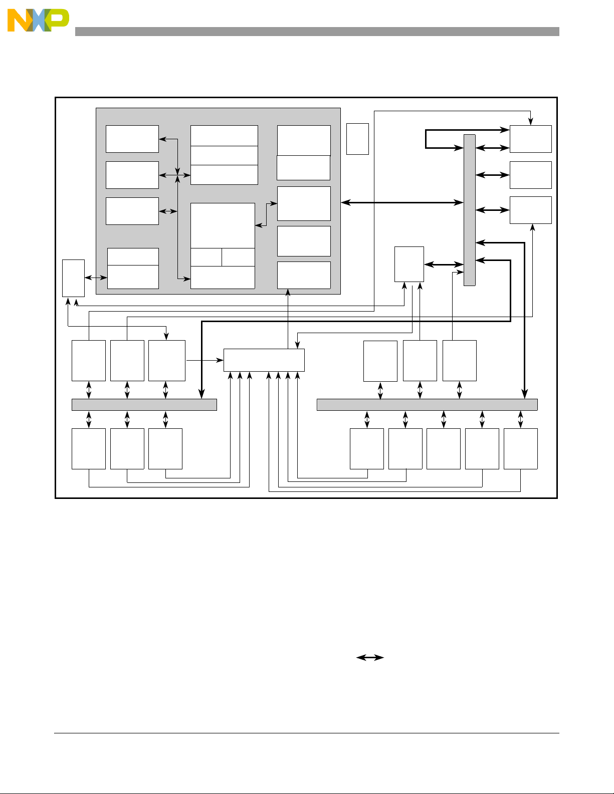
Introduction
Integer
execution
unit
Multiply
unit
LSU
BPUPCU
Instruction
unit
Core registers
e200z6e core
Nexus
SPE
APU
GPRs (64-bits)
SPRs
JTAG
Exception
handler
Timer unit
(TB, DEC,
FIT, WDT)
VLE
MMU
Unified
8-KB
cache
eTPU
XBAR
control
EBI
control
FBIU
eDMA
control
Interrupt controller
SIU eMIOS
DSPI
eSCI
FlexCAN eQADC
FMPLL
EBI
Flash
eDMA
System bus crossbar switch (XBAR)
Peripheral bridge B (PBRIDGE_B)Peripheral bridge A (PBRIDGE_A)
Master
Master
Slave
BAM
NDI
x3
x2
x3 x2
1 engine
Legend
e200z6e core components
APU – Auxiliary processing unit
BIU – Bus interface unit
BPU – Branch processing unit
DEC – Decrementer
FIT – Fixed interval timer
GPR – General-purpose register
JTAG – JTAG controller
LSU – Load/store unit
MMU – Memory management unit
PCU – Program counter unit
SPE – Signal processing engine
SPR – Special purpose register
TB – Time base
VLE – Variable length encoding
WDT – Watchdog timer
Slave
MPC5565 device modules
BAM – Boot assist module
CAN – Controller area network (FlexCAN)
DSPI – Deserial/serial peripheral interface
EBI – External bus interface
ECSM – Error correction status module
eDMA – Enhanced direct memory access
eMIOS – Enhanced modular I/O system
eQADC – Enhanced queued analog/digital converter
eSCI – Enhanced serial communications interface
eTPU – Enhanced time processing unit
FBIU – Flash bus interface unit
FMPLL – Frequency modulated phase-locked loop
INTC – Interrupt controller
NDI – Nexus developmental interface
SIU – System integration unit
SRAM – Internal static RAM
VRC – Voltage regulator controller
XBAR – System bus crossbar switch
2 MB
32 ch
Internal
SRAM
VRC
– System bus
Master
Slave
Slave
Slave
Slave
ECSM
80 KB
Figure 1-1 is a block diagram of the MPC5565.
.
1-2 Freescale Semiconductor
MPC5565 Microcontroller Reference Manual, Rev. 1.0
Figure 1-1. MPC5565 Block Diagram
Page 38

1.2 Features
This section provides a high-level description of the features found in the MPC5565.
• Operating parameters
— Fully static operation, up to 132 MHz
— –40 to 150 °C junction temperature
— Low-power design
– Less than 1.2 Watts power dissipation
– Designed for dynamic power management of core and peripherals
– Software-controlled clock gating of peripherals
– Separate power supply for stand-by operation for portion of internal SRAM
— Fabricated in 0.13 μm process
— 1.5 V internal logic
— Input and output pins with 3.0–5.25 V range
– 35% or 65% V
– Selectable hysteresis
– Selectable slew rate control
— External bus support 1.62–3.6 V operation and Nexus pins support 2.5–3.6 V operation
– Selectable drive strength control
CMOS switch levels (with hysteresis)
DDEH
Introduction
– Unused pins configurable as GPIO
— Designed with EMI reduction techniques
– Frequency modulated phase-locked loop
– On-chip bypass capacitance
– Selectable slew rate and drive strength
• High-performance e200z6 core processor
— 32-bit CPU built on Power Architecture™ technology
— Freescale Variable Length Encoding (VLE) enhancements for code size footprint reduction
— Thirty-two 64-bit general-purpose registers (GPRs)
— Memory management unit (MMU) with 32-entry fully-associative translation look-aside
buffer (TLB)
— Branch processing unit
— Fully pipelined load/store unit
— Eight KB unified cache with line locking
– Two-way set associative
– Two 32-bit fetches per clock
– Eight-entry store buffer
– Way locking
– Supports assigning cache as instruction or data only on a per-way basis
MPC5565 Microcontroller Reference Manual, Rev. 1.0
Freescale Semiconductor 1-3
Page 39

Introduction
– Supports tag and data parity
— Vectored interrupt support
— Interrupt latency is less than 70 ns @132 MHz (measured from interrupt request to execution
of first instruction of interrupt exception handler)
— Reservation instructions for implementing read-modify-write constructs
(internal SRAM and flash)
— Signal processing engine (SPE) auxiliary processing unit (APU) operating on 64-bit GPRs
— Floating point
–IEEE® 754 compatible with software wrapper
– Single precision in hardware, double precision with software library
– Conversion instructions between single precision floating point and fixed point
— Long cycle time instructions, except for guarded loads, do not increase interrupt latency in the
MPC5565; to reduce latency, long cycle time instructions are aborted upon interrupt requests
— Extensive system development support through Nexus debug module
• System bus crossbar switch (XBAR)
— Three master ports, five slave ports.
— 32-bit address bus, 64-bit data bus
— Simultaneous accesses from different masters to different slaves (there is no clock penalty
when a parked master accesses a slave)
• Enhanced direct memory access (eDMA) controller
— 32 channels support independent 8-, 16-, 32-bit single value or block transfers
— Supports variable sized queues and circular queues
— Source and destination address registers are independently configured to post-increment or
remain constant
— Each transfer is initiated by a peripheral, CPU, or eDMA channel request
— Each eDMA channel can optionally send an interrupt request to the CPU on completion of a
single value or block transfer
• Interrupt controller (INTC)
— 231 interrupt request registers
1
– 208 peripheral interrupt requests
– Eight software settable sources
– 16 reserved
— Unique 9-bit vector per interrupt source
— 16 priority levels with fixed hardware arbitration within priority levels for each interrupt source
— Priority elevation for shared resources
1. Although this device has a maximum of 231interrupts, the logic requires that the total number of interrupts be divisible by four.
Therefore, the total number of interrupts specified for this device is 232.
MPC5565 Microcontroller Reference Manual, Rev. 1.0
1-4 Freescale Semiconductor
Page 40

• Frequency modulated phase-locked loop (FMPLL)
— Input clock frequency: 8–20 MHz
— Current controlled oscillator (ICO) range from 48 MHz to maximum device frequency
— Reduced frequency divider (RFD) for reduced frequency operation without re-lock
— Four selectable modes of operation
— Programmable frequency modulation
— Lock detect circuitry continuously monitors lock status
— Loss-of-clock (LOC) detection for reference and feedback clocks
— Self-clocked mode (SCM) operation
— On-chip loop filter (reduces number of external components required)
— Engineering clock output configurable to divide-by-2 to 126 of the system clock frequency
• External bus interface (EBI)
— 1.8–3.3 V nominal I/O voltage
— 324 BGA: 16-bit data bus, 20-bit address bus is default, but configurable to 24-bit address bus.
Although this device is designed to support a 32-bit EBI data bus, only 16 data bus pins are
available and connected on the 324 BGA package. The 496-pin VertiCal assembly provides the
calibration functionality.
— Memory controller with support for various memory types
– Non-burst SDR flash and SRAM
Introduction
– Asynchronous/legacy flash and SRAM
– Most standard memories used with the MPC5xx family
— Configurable bus speed modes
– 50% of system frequency
– 25% of system frequency
— Support for external master accesses to internal addresses
— Burst support
— Bus monitor
– User selectable
– Programmable timeout period (with eight external bus clock resolution)
— Four chip selects: CS
[0:3] multiplexed with ADDR[8:11].
— T wo write/byte enable (WE/BE[0:1]) signals in the 324-pin package and the 496 pin assembly.
— Configurable wait states (via chip selects)
— Optional automatic CLKOUT gating to save power and reduce EMI
— Compatible with MPC5xx external bus (with some limitations):
Selectable drive strengths; 10 pF, 20 pF, 30 pF, 50 pF
• Calibration bus interface
— Calibration bus interface only accessible through 496-pin VertiCal assembly top connector
— 1.8–3.3 V nominal I/O voltage
MPC5565 Microcontroller Reference Manual, Rev. 1.0
Freescale Semiconductor 1-5
Page 41

Introduction
— Memory controller shared with EBI
— 16-bit data bus
— 21-bit address bus with no support for the least significant address bit (ADDR31)
— Up to 22 bit address space providing a 4 MB addressing range (the two most significant bits
shared with CAL_CS
[2:3])
— Chip selects: up to three chip selects (CAL_CS
[0] and CAL_CS[2:3] shared with
CAL_ADDR[10:11])
• System integration unit (SIU)
— Centralized GPIO control of bus pins: 324 BGA package with 150 pins
— Centralized pad control on a per-pin basis
— System reset monitoring and generation
— External interrupt inputs, filtering and control
• Error correction status module (ECSM)
Configurable error-correcting codes (ECC) reporting for internal SRAM and flash memories
• On-chip flash
— Two MB burst flash memory
— 256 KB × 64-bit configuration
— Censorship protection scheme to prevent flash content visibility
— Hardware read-while-write feature that can erase/program blocks while other blocks are read
(used for EEPROM emulation and data calibration)
— 20 blocks with sizes ranging from 16–128 KB to support features such as boot block, operating
system block, and EEPROM emulation. Blocks are structured as follows:
– 2 x 16 KB
– 2 x 48 KB
– 2 x 64 KB
– 14 x 128 KB
— Read while write with multiple partitions
— Page programming mode to support rapid end of line programming
— Hardware programming state machine
• Configurable cache memory, 0–8 KB
— Two-way set-associative unified (instruction and data) cache
— Decouples processor performance from system memory performance
• On-chip internal static RAM (SRAM)
— 80 KB general-purpose SRAM of which 32 KB are on standby power
— ECC performs single-bit correction, double-bit error detection
• Boot assist module (BAM)
— Enables and manages the transition of MCU from reset to user code execution in the following
configurations:
MPC5565 Microcontroller Reference Manual, Rev. 1.0
1-6 Freescale Semiconductor
Page 42

– User application can boot from internal or external flash memory
– Download and execution of code via FlexCAN or eSCI
– User application can boot with either classic Power Architecture code or VLE code
• Enhanced modular I/O system (eMIOS)
— 24 orthogonal channels with double action, PWM, and modulus counter functionality
— Supports all DASM and PWM modes of MIOS14 (MPC5xx)
— Four selectable time bases plus a shared time or angle counter bus
— DMA and interrupt request support
— Motor control capability
• Enhanced time processor unit (eTPU)
— One engine 32-channel engine
— 24-bit timer resolution
— 12 KB shared code memory, 2.5 KB shared data memory
— Event-triggered timer subsystem
— High-level assembler/compiler
— Variable number of parameters to allocate per channel
Introduction
— Double match/capture channels
— Angle clock hardware support
— Shared time or angle counter bus for all eTPU and eMIOS modules
— DMA and interrupt request support
— Nexus class 3 debug support (with some class 4 support)
• Enhanced queued analog/digital converter (eQADC)
— Two independent ADCs with 12-bit A/D resolution
— Common mode conversion range of 0–5 V
— 40 single-ended input channels, expandable to 65 channels with external multiplexers on the
324 BGA package
— Eight channels can be used as four pairs of differential analog input channels
— 10-bit accuracy at 400 ksamples/sec., 8-bit accuracy at 800 ksamples/sec.
— Supports six FIFO queues with fixed priority
— Queue modes with priority-based preemption; initiated by software command, internal
(eTPU and eMIOS), or external triggers
— DMA and interrupt request support
— Supports all functional modes from QADC (MPC5xx family)
• Three deserial serial peripheral interface modules (DSPI)
— Serial peripheral interface (SPI)
– Full duplex communication ports with interrupt and eDMA request support
– Supports all functional modes from QSPI submodule of QSMCM (MPC5xx family)
– Support for queues in RAM
MPC5565 Microcontroller Reference Manual, Rev. 1.0
Freescale Semiconductor 1-7
Page 43

Introduction
– Six chip selects, expandable to 64 with external demultiplexers
– Programmable frame size, baud rate, clock delay, and clock phase on a per-frame basis
– Modified SPI mode for interfacing to peripherals with longer setup time requirements
— Deserial serial interface (DSI)
– Pin reduction by hardware serialization and deserialization of eTPU and eMIOS channels
– Chaining of DSI submodules
– Triggered transfer control and change in data transfer control (for reduced EMI)
• Two enhanced serial communication interface (eSCI) modules
— UART mode provides NRZ format and half or full duplex interface
— eSCI bit rate up to 1 Mb/s
— Advanced error detection, and optional parity generation and detection
— Word length programmable as 8 or 9 bits
— Separately enabled transmitter and receiver
— LIN support
— DMA support
— Interrupt request support
• Three FlexCANs
— 64 message buffers each
— Full implementation of the CAN protocol specification, Version 2.0B
— Based on and including all existing features of the Freescale TouCAN module
— Programmable acceptance filters
— Individual receive filtering per message buffer
— Short latency time for high-priority transmit messages
— Arbitration scheme according to message ID or message buffer number
— Listen-only mode capabilities
— Programmable clock source: system clock or oscillator clock
— Reception queue possible by setting more than one receive message buffer with the same ID
— Backwards compatibility with previous FlexCAN modules
• Nexus development interface (NDI)
— Per IEEE®-ISTO 5001-2003
— Real-time development support for Power Architecture core and eTPU engine through Nexus
class 3 (some class 4 support)
— Data trace of eDMA accesses
— Read and write access
— Configured via the IEEE® 1149.1 (JTAG) port
— High-bandwidth mode for fast message transmission
— Reduced bandwidth mode for reduced pin usage
MPC5565 Microcontroller Reference Manual, Rev. 1.0
1-8 Freescale Semiconductor
Page 44
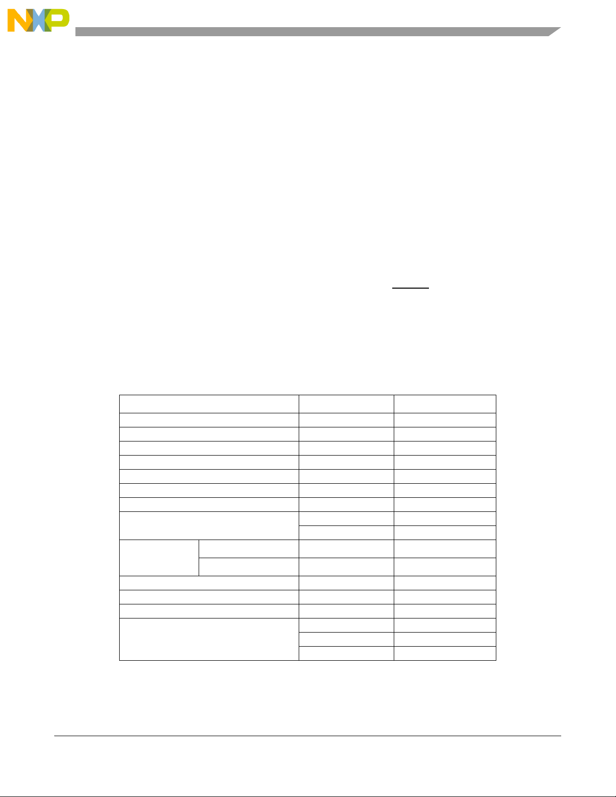
Introduction
•IEEE® 1149.1 JTAG controller (JTAGC)
—IEEE® 1149.1-2001 test access port (TAP) interface
— JCOMP input that provides the ability to share the T AP; selectable modes of operation include
JTAGC/debug or normal system operation
— 5-bit instruction register that supports IEEE® 1149.1-2001 defined instructions
— 5-bit instruction register that supports additional public instructions
— Three test data registers: a bypass register, a boundary scan register , and a device identification
register
— TAP controller state machine that controls the operation of the data registers, instruction
register and associated circuitry
• Voltage regulator controller (VRC)
Provides a low-cost solution to power the core logic; it reduces the number of power supplies
required from the customer power supply chip
• POR block
Provides initial reset condition up to the voltage at which pins (RESET) can be read safely; it does
not guarantee the safe operation of the chip at specified minimum operating voltages
1.3 MPC5500 Family Comparison
The following table compares the product features of the MPC5554 and the MPC5565:
Table 1-1. MPC5500 Product Family Comparison
MPC5500 Device Feature MPC5554 MPC5565
Power PC core e200z6 e200z6
Variable length instruction support Y Y
Unified cache (KB) 32
Memory management unit (MMU) entries 32 32
Crossbar connections 3 x 5 3 x 5
Core Nexus Class 3 + (NZ6C3) Class 3 + (NZ6C3)
SRAM (KB) 64 80
Flash Main array (MB) 2
Shadow block (KB) 1 1
External bus
interface (EBI)
bit-width
Calibration bus interface (CBI) – Y
Direct memory access (DMA) channels 32 32
DMA Nexus Class 3 Class 3
Serial 2 2
Data 32 32
Address 24
eSCI A Y Y
eSCI B Y Y
1
3
5
24
2
8
2
4
5
MPC5565 Microcontroller Reference Manual, Rev. 1.0
Freescale Semiconductor 1-9
Page 45
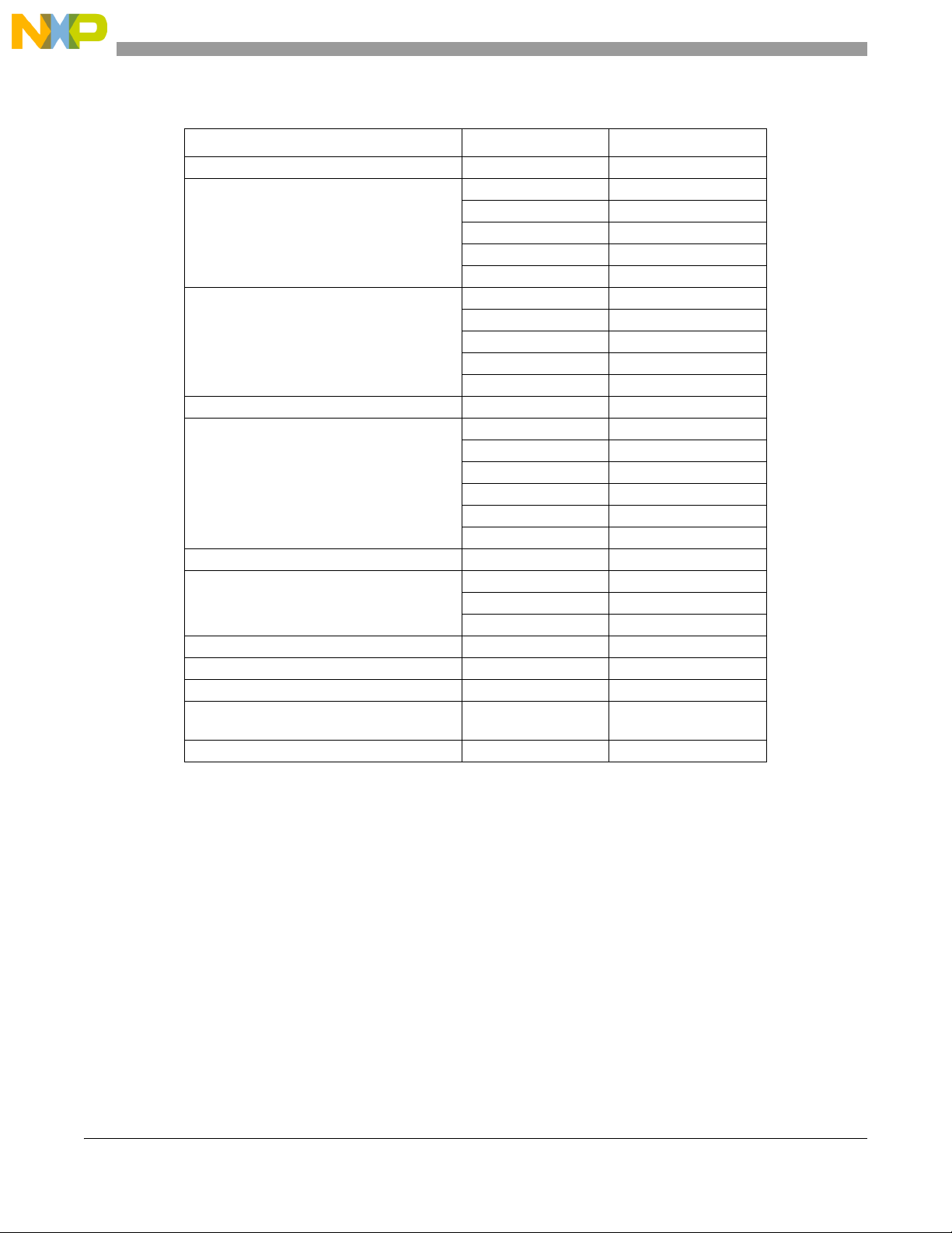
Introduction
Table 1-1. MPC5500 Product Family Comparison (continued)
MPC5500 Device Feature MPC5554 MPC5565
Controller area network (FlexCAN) 3 3
CAN A buffers 64 64
CAN B buffers 64 64
CAN C buffers 64 64
CAN D buffers — —
CAN E buffers — —
Deserial/serial peripheral interface (SPI) 4 3
DSPI A Y —
DSPI B Y Y
DSPI C Y Y
DSPI D Y Y
eMIOS channels 24 24
eTPU channels 64 32
eTPU A Y Y
eTPU B Y —
Code memory (KB) 16 12
Parameter RAM (KB) 3 2.5
Nexus Class 3 Class 3
Interrupt controller channels 300 231
Analog to digital converter channels 40 40
ADC A Y Y
ADC B Y Y
Fast Ethernet controller (FEC) — —
FlexRay — —
FlexRay Nexus data trace — —
Frequency modulated phase lock loop
(FMPLL)
Voltage regulator controller (VRC) Y Y
1
8-way associative
2
2-way associative
3
32-byte flash page size for programming
4
EBI limited to a 16-bit data bus on the 324 package
5
Select either ADDR[8:31] or ADDR[6:29] to configure a 24-bit address bus
6
Updated FlexCAN module with optional individual receive filters
YY
6
MPC5565 Microcontroller Reference Manual, Rev. 1.0
1-10 Freescale Semiconductor
Page 46

Introduction
1.4 Detailed Features
The following sections provide detailed information about each of the on-chip modules.
1.4.1 e200z6 Core Overview
The device uses the e200z6 core explained in detail in the e200z6 PowerPCTM Core Reference Manual.
The e200z6 CPU uses a seven-stage pipeline for instruction execution:
• Instruction fetch 1
• Instruction fetch 2
• Instruction decode and register file read
• Execute 1
• Execute 2 and memory access 1
• Execute 3 and memory access 2
• Register writeback
The operation of the pipeline stages overlap so that most instructions execute in a single-clock.
The integer execution unit consists of a 32-bit arithmetic unit (AU), a logic unit (LU), a 32-bit barrel
shifter, a mask-insertion unit (MIU), a condition register manipulation unit (CRU), a count-leading-zeros
unit (CLZ), a 32 x 32 hardware multiplier array, result feed-forward hardware, and support hardware for
division.
Most arithmetic and logical operations are executed in a single cycle with the exception of multiply and
divide instructions, which are implemented with a pipelined hardware array. The CLZ unit operates in a
single clock cycle.
The instruction unit contains an incremental program counter (PC) and a dedicated branch address adder
to minimize delays during change of flow operations. Sequential prefetching is performed to ensure a
supply of instructions into the execution pipeline. Branch target prefetching is performed to accelerate
taken branches. Prefetched instructions are placed into an instruction buffer capable of holding six
sequential instructions and two branch target instructions.
Branch target addresses are calculated in parallel with branch instruction decode, resulting in execution
time of three clocks. Conditional branches which are not taken execute in a single clock. Branches with
successful look-ahead and target prefetching have an effective execution time of one clock.
Memory load and store operations are provided for byte, halfword, word (32-bits), and doubleword
(64-bits) data with automatic zero or sign extension of byte and halfword load data. These instructions can
be pipelined to allow effective single cycle throughput. Load and store multiple word instructions allow
low overhead context save and restore operations. The load/store unit contains a dedicated effective
address adder to allow effective address generation to be optimized.
The condition register unit supports the condition register (CR) and condition register operations defined
by the Power Architecture technology. The condition register consists of eight 4-bit fields that reflect the
results of certain operations, such as move, integer and floating-point compare, arithmetic, and logical
instructions, and provide a mechanism for testing and branching.
MPC5565 Microcontroller Reference Manual, Rev. 1.0
Freescale Semiconductor 1-11
Page 47

Introduction
Vectored and auto-vectored interrupts are supported by the CPU. Vectored interrupt supports unique
interrupt handlers invoked with no software overhead for multiple interrupt sources.
The signal processing extension (SPE) APU supports vector instructions (SIMD) operating on 16- and
32-bit fixed-point data types, as well as 32-bit IEEE®-754 single-precision floating-point formats, and
supports single-precision floating-point operations in a pipelined fashion. The 64-bit general-purpose
register file is used for source and destination operands, and there is a unified storage model for
single-precision floating-point data types of 32-bits and the normal integer type. Low latency fixed-point
and floating-point add, subtract, multiply, divide, compare, and conversion operations are provided, and
most operations can be pipelined.
The CPU includes support for Variable Length Encoding (VLE) instruction enhancements that have
modified instruction set that uses a combination of 16- and 32-bit instructions from the classic Power
Architecture instruction. This reduces the code size without noticeably affecting performance. The classic
Power Architecture instruction set and VLE instruction set are available concurrently. Regions of the
memory map are designated as PPC or VLE using an additional configuration bit in each table look-aside
buffer (TLB) entry in the MMU.
1.4.2 System Bus Crossbar Switch (XBAR)
The system bus’ multi-port crossbar (XBAR) switch supports simultaneous connections between three
master ports and five slave ports. The crossbar supports a 32-bit address bus width and a 64-bit data bus
width on all master and slave ports.
The crossbar allows concurrent transactions from any master port to any slave port. It is possible to use all
master ports and slave ports at the same time as a result of independent master requests. If a slave port is
simultaneously requested by more than one master port, arbitration logic selects the highest priority master
and grants it ownership of the slave port. All other masters requesting that slave port must wait until the
higher priority master completes its transactions. By default, masters requests’ have equal priority and are
granted access to a slave port in round-robin fashion based on the last master ID granted access.
1.4.3 Enhanced Direct Memory Access (eDMA)
The enhanced direct memory access (eDMA) controller is a second-generation module capable of
performing complex data movements via 32 programmable channels, with minimal intervention from the
CPU. The hardware microarchitecture includes a DMA engine which performs source and destination
address calculations, and the actual data movement operations, along with an SRAM-based memory
containing the transfer control descriptors (TCD) for the channels. This implementation is used to
minimize the overall module size.
MPC5565 Microcontroller Reference Manual, Rev. 1.0
1-12 Freescale Semiconductor
Page 48

Introduction
1.4.4 Interrupt Controller (INTC)
The interrupt controller (INTC) provides priority-based preemptive scheduling of interrupt requests,
suitable for statically scheduled real-time systems. The INTC allows interrupt request servicing from 231
total interrupt vectors.
For high-priority interrupt requests, the time from when the peripheral interrupt request asserts to when
the processor executes the interrupt service routine (ISR) is minimized. A unique vector for each interrupt
request source is used to quickly determine which ISR to execute. The INTC module provides a number
of priorities to ensure that lower priority ISRs do not delay the execution of higher priority ISRs. Software
is used to configure the interrupt priorities for each interrupt source.
When multiple tasks share a resource, coherent accesses to that resource must be supported. The INTC
supports the priority ceiling protocol for coherent accesses. By providing a modifiable priority mask, the
priority level can be raised temporarily so that no task can preempt another task that shares the same
resource.
Multiple processors can assert interrupt requests to each other through software settable interrupt requests
(by using application software to assert requests). These maskable interrupt requests can divide the
software into a high-priority portion and a low-priority portion for servicing the interrupt requests. The
high-priority portion is initiated by a peripheral interrupt request, but then the ISR asserts a software
settable interrupt request to finish the servicing in a lower priority ISR.
1.4.5 Frequency Modulated Phase-Locking Loop (FMPLL)
The frequency modulated phase-locking loop (FMPLL) generates high-speed system clocks from an
8–20 MHz crystal oscillator or an external clock generator. Furthermore, the FMPLL supports
programmable frequency modulation of the system clock. The PLL multiplication factor, output clock
divider ratio, modulation depth, and modulation rate are all software configurable.
1.4.6 External Bus Interface (EBI)
The external bus interface (EBI) controls data transfer across the crossbar switch to/from memories or
peripherals in the external address space. The EBI is available on the 324 BGA package only . The EBI also
enables an external master to access internal address space. The EBI includes a memory controller that
generates interface signals to support a variety of external memories. The memory controller supports
single data rate (SDR) burst mode flash, external SRAM, and asynchronous memories. In addition, the
EBI supports up to four regions (via chip selects), along with programmed region-specific attributes.
1.4.7 Calibration Bus Interface (CBI)
The calibration bus controls data transfer across the crossbar switch to/from memories or peripherals
connected to the VertiCal connector. The calibration bus is only available when the silicon is packaged in
the VertiCal calibration assembly . The bus shares the memory controller and most of the control logic with
the EBI but the two buses use separate pads. The calibration bus memory controller supports single data
rate (SDR) non-burst mode flash, SRAM, and asynchronous memories. In addition, the bus supports up to
MPC5565 Microcontroller Reference Manual, Rev. 1.0
Freescale Semiconductor 1-13
Page 49

Introduction
three regions via dedicated calibration chip selects (two chip selects multiplexed with two address bits),
along with programmed region-specific attributes.
1.4.8 System Integration Unit (SIU)
The device’s system integration uni t (SIU) controls MCU reset configuration, pad configuration, external
interrupt, general-purpose I/O (GPIO), internal peripheral multiplexing, and the system reset operation.
The reset configuration module contains the external pin boot configuration logic. The pad configuration
module controls the static electrical characteristics of I/O pins. The GPIO module provides uniform and
discrete input/output control of the I/O pins of the MCU. The reset controller performs reset monitoring
of internal and external reset sources, and drives the RSTOUT pin. The SIU is accessed by the e200z6 core
through the crossbar switch.
1.4.9 Error Correction Status Module (ECSM)
The error correction status module (ECSM) provides status information regarding platform memory errors
reported by error-correcting codes.
1.4.10 Flash Memory
The MPC5565 provides 2 MB of programmable, non-volatile, flash memory storage. Non-volatile
memory (NVM) can be used for instruction and/or data storage.
The flash memory has a flash bus interface unit (FBIU) that connects the system bus to a dedicated flash
memory array controller. The FBIU supports a 64-bit data bus width at the system bus port, and a 256-bit
read data interface to flash memory. The FBIU contains two 256-bit prefetch buffers, and a prefetch
controller that prefetches sequential lines of data from the flash array into the buffer. Prefetch buffer hits
allow no-wait responses. Normal flash array accesses are registered in the FBIU and are forwarded to the
system bus on the following cycle, incurring three wait-states. Prefetch operations can be automatically
controlled, as well as restricted to servicing a single bus master. Prefetches can also require a trigger for
instruction or data accesses.
1.4.11 Cache
The e200z6 core supports an eight-KB, two-way set-associative, unified (instruction and data) cache with
a 32-byte line size. The cache improves system performance by providing low-latency data to the e200z6
instruction and data pipelines, which decouples processor performance from system memory performance.
The cache is virtually indexed and physically tagged. The e200z6 does not provide hardware support for
cache coherency in a multi-master environment. Software must be designed to maintain cache coherency
with other possible bus masters.
Both instruction and data accesses are performed using a single bus connected to the cache. The processor
uses virtual addresses to index the cache array. The memory management unit (MMU) provides the
virtual-to-physical address conversion to perform the cache tag compare. The MMU can pass the virtual
addresses to the cache as the physical address without the conversion. If the physical address matches a
valid cache tag entry, the access hits in the cache. For a read operation, the cache supplies the data to the
MPC5565 Microcontroller Reference Manual, Rev. 1.0
1-14 Freescale Semiconductor
Page 50

Introduction
processor, and for a write operation, the data from the processor is written to cache. If the access does not
match a valid cache tag entry (misses in the cache), or a write access is required to memory, the cache
performs a bus cycle on the system bus.
1.4.12 Static RAM (SRAM)
The MPC5500 family internal SRAM module provides a general-purpose memory block that supports
mapped read/write accesses from any master . The SRAM size is 80 KB. Included within the SRAM block
is a 32-KB block powered by a separate supply for standby operation and ECC error correction and
detection.
1.4.13 Boot Assist Module (BAM)
The boot assist module (BAM) is read-only memory programmed by Freescale and is identical for all
MCUs with an e200z6 core. The BAM program executes every time the MCU is powered on, or when
reset in normal mode. The BAM supports theseboot modes:
• Booting from internal flash memory
• Single master booting from external memory
• Serial boot loading (program is downloaded to SRAM over an eSCI or FlexCAN peripheral and
then executed)
The BAM reads the reset configuration halfword (RCHW) from flash memory (either internal or external)
to configure the device hardware. The MMU is then configured for all resources and maps all physical
addresses to logical addresses with the minimum address translation, to allow application boot code to
execute as either Classic Power Architecture Book E code (default) or as Freescale VLE code.
1.4.14 Enhanced Management Input/Output System (eMIOS)
The enhanced modular I/O system (eMIOS) module generates or measures time events. A unified channel
(UC) module provides a consistent interface to a superset of all the MIOS channel functionality. This
allows more flexibility to program each unified channel for different functions in different applications.
T o identify up to two timed events, each UC uses two comparators, a time base selector , and registers. This
structure can produce match events to measure or generate a waveform. Alternatively, input events can
capture the time base, allowing measurement of an input signal.
1.4.15 Enhanced Time Processing Unit (eTPU)
The enhanced time processing unit (eTPU) is an enhanced coprocessor designed for timing control.
Operating in parallel with the host CPU, the eTPU processes instructions and real-time input events,
performs output waveform generation, and accesses shared data without host intervention. Consequently ,
for each timer event, the CPU setup and service times are minimized or eliminated. In the MCU, the TPU
engine is combined with shared instruction and data RAM to form a powerful time processing subsystem.
The MPC5565 has one eTPU engine. High-level assembler/compiler and documentation can be used to
develop customized functions for the eTPU. The eTPU supports several features of older TPU versions,
making it easy to port older applications.
MPC5565 Microcontroller Reference Manual, Rev. 1.0
Freescale Semiconductor 1-15
Page 51

Introduction
1.4.16 Enhanced Queued A/D Converter (eQADC)
The enhanced queued analog to digital converter (eQADC) module provides accurate and fast conversions
for a wide range of applications. The eQADC provides a parallel interface to two on-chip analog to digital
converters (ADCs), and a single master-to-single slave serial interface to an off-chip external device. The
two on-chip ADCs are designed to access all the analog channels.
The eQADC transfers commands from multiple command FIFOs (CFIFOs) to the on-chip ADCs or to the
external device. The module can also receive data from the on-chip ADCs or from an off-chip external
device into multiple result FIFOs (RFIFOs) in parallel, independently of the CFIFOs. The eQADC
supports software and external hardware triggers from other modules to initiate transfers of commands
from the CFIFOs to the on-chip ADCs or to the external device. It also monitors the fullness of CFIFOs
and RFIFOs, and accordingly generates eDMA or interrupt requests to control data movement between the
FIFOs and the system memory, which is external to the eQADC.
1.4.17 Deserial/Serial Peripheral Interface (DSPI)
The deserial serial peripheral interface (DSPI) module provides a synchronous serial interface for
communication between the MCU and external devices. The DSPI supports pin-count reduction through
serialization and deserialization of eTPU channels, eMIOS channels and memory-mapped registers. The
channels and register content are transmitted using a SPI-like protocol.
The MPC5565 has three DSPI modules (B, C, and D). The DSPIs have three configurations:
• Serial peripheral interface (SPI) configuration where the DSPIs operate as serial ports only with
support for queues.
• Deserial serial interface (DSI) configuration where the DSPIs serialize eTPU and eMIOS output
channels, and deserialize the input data by passing it to the eTPU and eMIOS input channels.
• Combined serial interface (CSI) configuration where the DSPIs operate in both SPI and DSI
configurations, interleaving DSI frames with SPI frames, and giving priority to SPI frames.
For queued operations, the SPI queues reside in system memory external to the DSPI. Data transfers
between the memory and the DSPI FIFOs use the eDMA controller or the host software.
1.4.18 Enhanced Serial Communications Interface (eSCI)
The enhanced serial communications interface (eSCI) allows asynchronous serial communications with
peripheral devices and other MCUs. It includes special support to interface to local interconnect network
(LIN) slave devices. The MPC5565 has two eSCI modules (A and B).
1.4.19 Flexible Controller Area Network (FlexCAN)
The MCU contains three controller area network (FlexCAN) modules. Each FlexCAN module is a
communication controller implementing the CAN protocol according to CAN Specification version 2.0B.
The CAN protocol is designed to be used primarily as a vehicle serial data bus, meeting the specific
requirements of this field: real-time processing, reliable operation in the EMI environment of a vehicle,
cost-effectiveness, and required bandwidth. Each FlexCAN module contains 64 message buffers.
MPC5565 Microcontroller Reference Manual, Rev. 1.0
1-16 Freescale Semiconductor
Page 52

Introduction
1.4.20 Nexus Development Interface (NDI)
The Nexus development interface (NDI) module provides real-time development support capabilities for
the MPC5500 family’s MCU built on the Power Architecture in compliance with the IEEE®-ISTO
5001-2003 standard. This development support is supplied for MCUs without requiring external address
and data pins for internal visibility. The NDI module integrates several Nexus modules to provide the
development support interface for the MPC5500 family . The NDI module interfaces to the host processor ,
single or dual eTPU processors, and internal buses to provide development support as per the
IEEE®-ISTO 5001-2003 standard. The development support provided includes program trace, data trace,
watchpoint trace, ownership trace, run-time access to the MCU internal memory map, Nexus trace of
eDMA transfers, and access to the Power Architecture and eTPU internal registers during halt, via the
auxiliary port. The Nexus interface also supports a JTAG only mode using only the JTAG pins.
1.4.21 JTAG Controller (JTAGC)
The JT AG controller (JT AGC) module provides the means to test chip functionality and connectivity while
remaining transparent to system logic when not in test mode. Testing is performed via a boundary scan
technique, as defined in the IEEE® 1149.1-2001 standard. All data input to and output from the JTAGC
module is communicated in serial format. The JT AGC module is compliant with the IEEE® 1149.1-2001
standard.
1.5 MPC5500 Family Memory Map
This section describes the MPC5500 family memory map. All addresses in the device, including those that
are reserved, are identified in the tables. The addresses represent the physical addresses assigned to each
module. Logical addresses are translated by the MMU into physical addresses.
Reserved register bits are allocated for future products and have a default value of zero. When writing to
a register, the reserved bits default values must be written as well. Most device features are activated by
writing a non-zero value to them.
Reserved memory is allocated for future products, therefore do not write to memory segments that are
designated as reserved.
Under software control of the MMU, the logical addresses allocated to modules can be changed on a
minimum of a 4 KB boundary. Peripheral modules may be redundantly mapped. The customer must use
the MMU to prevent corruption.
MPC5565 Microcontroller Reference Manual, Rev. 1.0
Freescale Semiconductor 1-17
Page 53
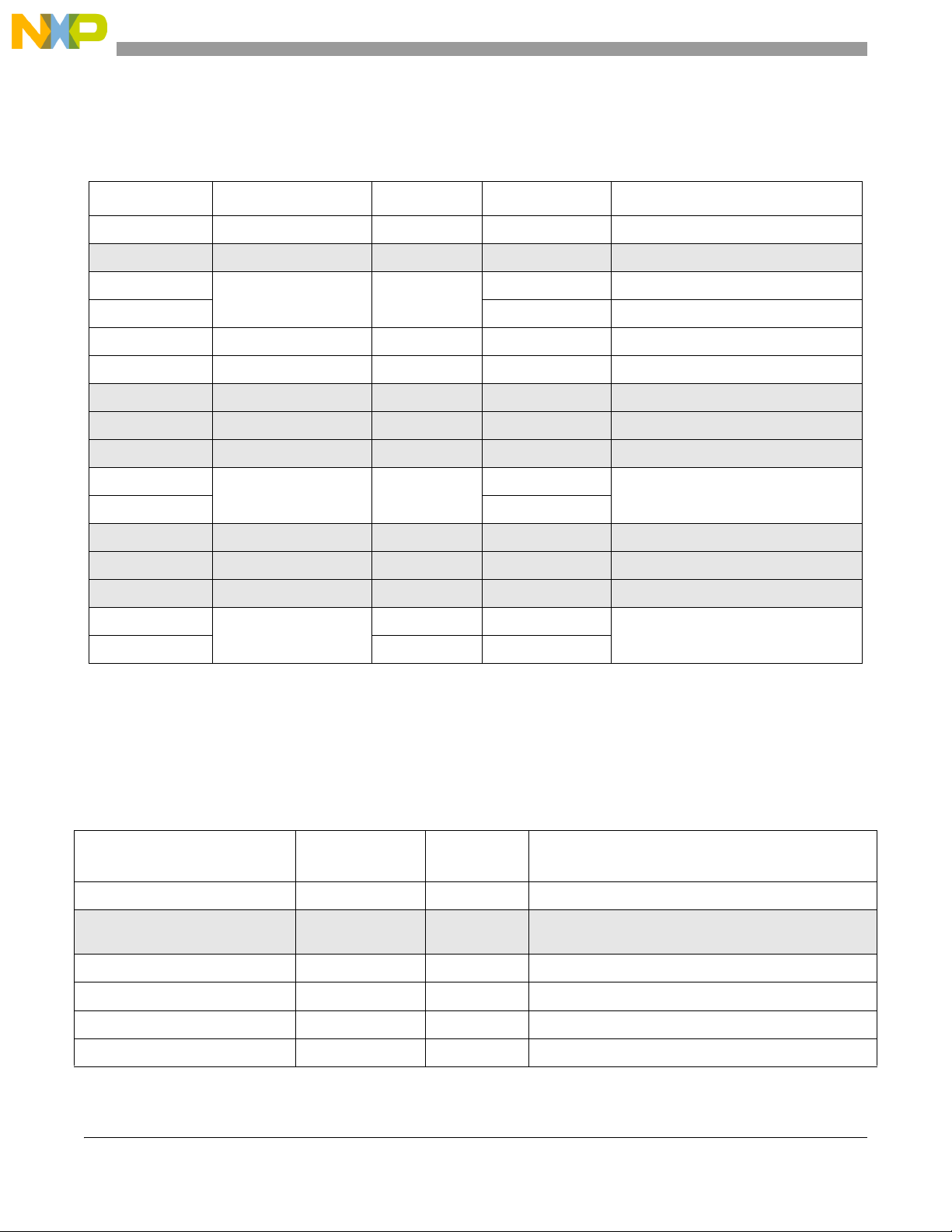
Introduction
Table 1-2 shows an overview of the device memory map. It is intended to illustrate how the crossbar switch
integrates into the memory map.
Table 1-2. MPC5565 Memory Map (Single-Chip or Single-Master Mode)
Base Address XBAR Slave Port ADDR[0:2] Size Use
0x0000_0000 Flash 0b000 2 MB Flash memory array
0x0020_0000 Reserved 0b000 14 MB–512 bytes Reserved
0x00FF_FC00
1 KB Flash shadow row
Flash 0b000
0x0100_0000 496 MB Emulation mapping of flash
0x2000_0000 EBI and calibration
1
0b001 512 MB
2
External bus interface
0x4000_0000 Internal SRAM 0b010 80 KB Internal SRAM
0x4001_4000 Reserved 0b010 512 MB–80 KB Reserved
0x6000_0000 Reserved 0b011– 0b101 1536 MB Reserved
0xC000_0000 Reserved 0b011– 0b101 63 MB Reserved
0xC3F0_0000
Bridge A peripherals 0b110
512 KB
Platform A peripherals
0xC3F8_0000 512 KB
0xC400_0000 Reserved 0b110 512 MB–64 MB Reserved
0xE000_0000 Reserved 0b111 512 MB–64 MB Reserved
0xFC00_0000 Reserved 0b111 63 MB Reserved
0xFFF0_0000
Bridge B peripherals
0b111 512 KB
Platform B peripherals
0xFFF8_0000 0b111 512 KB
1
One method is to assign 0x2000_0000 to 0x2FFF_FFFF to the EBI and assign 0x3000_0000 to 0x3FFF_FFFF to calibration.
Hardware, however, does not force any restriction on EBI memory versus calibration memory.
2
Using four chip select signals and 24 address bus signals, 64 MB can be mapped into the external memory space in
single-master mode. Using four chip select signals and 26 address bus signals, 256 MB can be mapped into the external
memory space in single-master mode.
Table 1-3 shows a detailed list of the device memory map.
Table 1-3. MPC5565 Detailed Memory Map
Address Range
1
Allocated Size
(Bytes)
0x0000_0000–0x001F_FFFF 2 MB 2.0 MB Flash memory array
0x0020_0000–0x00FF_FBFF 14 MB–1 KB
(flash shadow row)
0x00FF_FC00–0x00FF_FFFF 1 KB 1 KB Flash shadow row
0x0100_0000–0x1FFF_FFFF 496 MB 2 MB Emulation mapping of flash array
0x2000_0000–0x3FFF_FFFF 512 MB N/A External memory
0x4000_0000–0x4000_7FFF 32 KB 32 KB Internal SRAM array, standby powered
MPC5565 Microcontroller Reference Manual, Rev. 1.0
1-18 Freescale Semiconductor
1
Used Size
(Bytes)
N/A Reserved
2
Use
Page 54
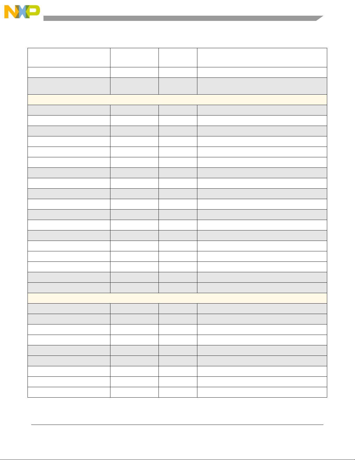
Table 1-3. MPC5565 Detailed Memory Map (continued)
Introduction
Address Range
1
Allocated Size
(Bytes)
1
Used Size
(Bytes)
Use
0x4000_8000–0x4001_3FFF 48 KB 48 KB Internal SRAM array
0x4001_4000–0xBFFF_FFFF 2048 MB–80 KB
N/A Reserved
(total SRAM)
Bridge A Peripherals
0xC000_0000–0xC3EF_FFFF 63 MB N/A Reserved
0xC3F0_0000–0xC3F0_3FFF 16 KB — Bridge A registers
0xC3F0_4000–0xC3F7_FFFF 496 KB N/A Reserved
0xC3F8_0000–0xC3F8_3FFF 16 KB — FMPLL registers
0xC3F8_4000–0xC3F8_7FFF 16 KB 48 External bus interface (EBI) configuration registers
0xC3F8_8000–0xC3F8_BFFF 16 KB 28 Flash configuration registers
0xC3F8_C000–0xC3F8_FFFF 16 KB N/A Reserved
0xC3F9_0000–0xC3F9_3FFF 16 KB 2.5 KB System integration unit (SIU)
0xC3F9_4000–0xC3F9_FFFF 48 KB N/A Reserved
0xC3FA_0000–0xC3FA_3FFF 16 KB 1056 Modular input output timer system (eMIOS)
0xC3FA_4000–0xC3FB_FFFF 112 KB N/A Reserved
0xC3FC_0000–0xC3FC_3FFF 16 KB 3 KB Enhanced time processing unit (eTPU) registers
0xC3FC_4000–0xC3FC_7FFF 16 KB N/A Reserved
0xC3FC_8000–0xC3FC_8BFF 16 KB 2.5 KB eTPU shared data memory (parameter RAM)
0xC3FC_C000–0xC3FC_CBFF 16 KB 2.5 KB eTPU shared data memory (parameter RAM) mirror
0xC3FD_0000–0xC3FD_2FFF 16 KB 12 KB eTPU shared code RAM
0xC3FD_4000–0xC3FF_FFFF 176 KB N/A Reserved
0xC400_0000–0xDFFF_FFFF 512 MB–64 MB N/A Reserved
Bridge B Peripherals
0xE000_0000–0xFBFF_FFFF 512 MB–64 MB N/A Reserved
0xFC00_0000–0xFFEF_FFFF 63 MB N/A Reserved
0xFFF0_0000–0xFFF0_3FFF 16 KB N/A Bridge B registers
0xFFF0_4000–0xFFF0_7FFF 16 KB N/A System bus crossbar switch (XBAR)
0xFFF0__8000–0xFFF0_FFFF 32 KB N/A Reserved
0xFFF1_0000–0xFFF3_FFFF 192 KB N/A Reserved
0xFFF4_0000–0xFFF4_3FFF 16 KB N/A ECSM
0xFFF4_4000–0xFFF4_7FFF 16 KB N/A DMA controller 2 (eDMA)
0xFFF4_8000–0xFFF4_BFFF 16 KB N/A Interrupt controller (INTC)
MPC5565 Microcontroller Reference Manual, Rev. 1.0
Freescale Semiconductor 1-19
Page 55

Introduction
Table 1-3. MPC5565 Detailed Memory Map (continued)
Address Range
1
Allocated Size
(Bytes)
1
Used Size
(Bytes)
Use
0xFFF4_C000–0xFFF4_FFFF 16 KB N/A Reserved
0xFFF5_0000–0xFFF7_FFFF 192 KB N/A Reserved
0xFFF8_0000–0xFFF8_3FFF 16 KB 164 Enhanced queued analog-to-digital converter (eQADC)
0xFFF8_4000–0xFFF8_FFFF 48 KB N/A Reserved
0xFFF9_0000–0xFFF9_3FFF 16 KB N/A Reserved
0xFFF9_4000–0xFFF9_7FFF 16 KB 200 Deserial serial peripheral interface (DSPI B)
0xFFF9_8000–0xFFF9_BFFF 16 KB 200 Deserial serial peripheral interface (DSPI C)
0xFFF9_C000–0xFFF9_FFFF 16 KB 200 Deserial serial peripheral interface (DSPI D)
0xFFFA_0000–0xFFFA_FFFF 64 KB N/A Reserved
0xFFFB_0000–0xFFFB_3FFF 16 KB 44 Serial communications interface (eSCI A)
0xFFFB_4000–0xFFFB_7FFF 16 KB 44 Serial communications interface (eSCI B)
0xFFFB_8000–0xFFFB_FFFF 32 KB N/A Reserved
0xFFFC_0000–0xFFFC_3FFF 16 KB 1152 Controller area network (FlexCAN A)
0xFFFC_4000–0xFFFC_7FFF 16 KB 1152 Controller area network (FlexCAN B)
0xFFFC_8000–0xFFFC_BFFF 16 KB 1152 Controller area network (FlexCAN C)
0xFFFC_C000–0xFFFC_FFFF 16 KB 1152 Reserved
0xFFFD_0000–0xFFFD_3FFF 16 KB 1152 Reserved
0xFFFD_4000–0xFFFD_FFFF 80 KB N/A Reserved
0xFFFE_0000–0xFFFE_3FFF 16 KB 1152 Reserved
0xFFFE_4000–0xFFFF_7FFF 16 KB N/A Reserved
0xFFFE_8000–0xFFFE_BFFF 16 KB 1152 Reserved
0xFFFE_0000–0xFFFF_BFFF 64 KB N/A Reserved
0xFFFF_0000–0xFFFF_FFFF3 16 KB 16 KB Boot assist module (BAM)
1
If the allocated size is more than the used size, then the base address for the module is the lowest address of the listed address
range, unless noted otherwise.
2
A suggested convention to follow is to place EBI from 0x2000_0000 to 0x2FFF_FFFF and to place calibration space from
0x3000_0000 to 0x3FFF_FFFF. Hardware, however, does not force any restriction on EBI versus calibration space.
3
BAM address range is configured so that 4 KB BAM occupies 0xFFFF_F000–0xFFFF_FFFF.
MPC5565 Microcontroller Reference Manual, Rev. 1.0
1-20 Freescale Semiconductor
Page 56
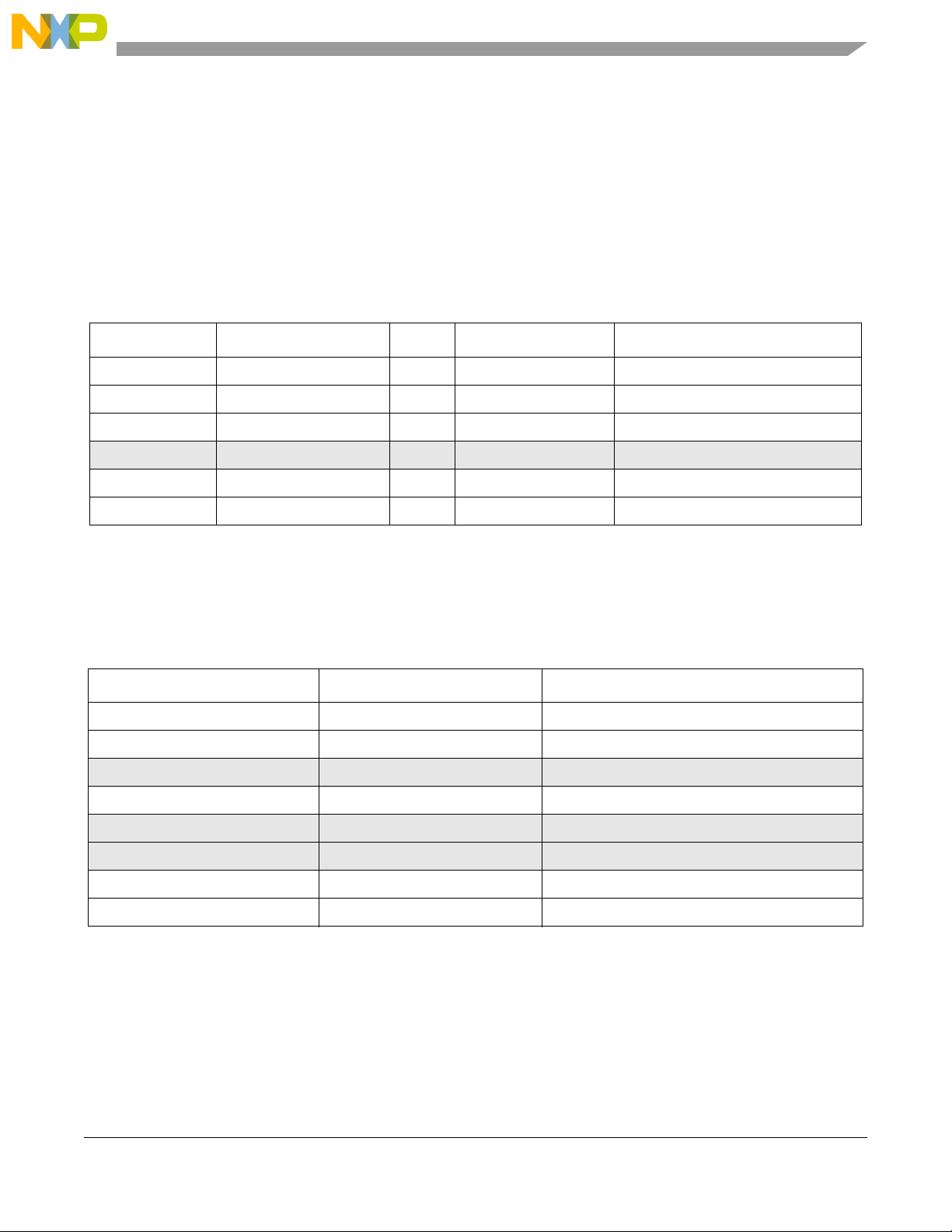
Introduction
1.6 Multi-Master Operation Memory Map
NOTE
When multi-master mode is enabled, the bus is permanently granted to the
external master; therefore, the MPC5565 MCU cannot be a master on a
multi-master bus, only a slave.
When the MCU acts as a slave in a multi-master system, the external bus interface (EBI) translates the
24-bit external address to a 32-bit internal address. Table 1-4 lists the translation parameters.
Table 1-4. External to Internal Memory Map Translation Table for Slave Mode
1
Ext Addr[8:11]
0b0xxx N/A 8 MB N/A n/a. Off-chip flash access
0b10xx 0b0000_0000_00xx 4 MB Internal flash array 0x0000_0000–0x003F_FFFF
0b1100 0b0100_0000_0000 1 MB Internal SRAM 0x4000_0000–0x4000_FFFF
0b1101 0b0110_0000_0000 1 MB Reserved
0b1110 0b1100_0011_1111 1 MB Bridge A peripherals 0xC3F0_0000–0xC3FF_FFFF
0b1111 0b1111_1111_1111 1 MB Bridge B peripherals 0xFFF0_0000–0xFFFF_FFFF
1
Only the lower 24 address signals (ADDR[8:31]) are available off-chip for external master accesses.
2
Reserved for a future module that requires its own crossbar slave port.
Internal Address[0:11] Bytes Internal Slave Internal Address Range
2
0x6000_0000–0x600F_FFFF
Table 1-5 shows the memory map for the MCU acting as a slave in a multi-master system from the point
of view of the external master.
Table 1-5. MPC5565 Family Slave Memory Map as Seen from an External Master
External Address Range
0x0000_0000
0x0080_0000–0x009F_FFFF 2 MB Slave flash
0x00A0_0000–0x00BF_FFFF 2 MB Reserved
0x00C0_0000–0x00C1_3FFF 80 KB Slave internal SRAM
0x00C1_4000–0x00CF_FFFF 1 MB–80 KB (less total SRAM) Reserved
0x00D0_0000–0x00DF_FFFF 1 MB Reserved
0x00E0_0000–0x00EF_FFFF 1 MB Slave bridge A peripherals
0x00F0_0000–0x00FF_FFFF 1 MB Slave bridge B peripherals
1
Only the lower 24 address signals (ADDR[8:31]) are available off-chip for external master accesses.
2
This address range is not part of the MPC5500 family slave memory map, rather it is shown to illustrate the addressing
scheme for off-chip accesses in multi-master mode.
3
The shadow row of the slave flash is not accessible by an external master.
2
–0x007F_FFFF
1
Size (bytes) Use
8 MB n/a. Used for off-chip memory accesses
3
MPC5565 Microcontroller Reference Manual, Rev. 1.0
Freescale Semiconductor 1-21
Page 57

Introduction
1.7 Document Revision History
Table 1-6. Changes Between MPC5565RM Revisions 0.1 and 1
In Features, changed “Parallel programming mode to support rapid end of line programming” to “Page programming mode to
support rapid end of line programming”
Figure 1-1 Changed SRAM to 80 KB, eQADC to 2.
Section 1.5, “MPC5500 Family Memory Map” Added the following text about reserved bits and memory: Reserved register
bits are allocated for future products and have a default value of zero. When writing to a register, the reserved bits default
values must be written as well. Most device features are activated by writing a non-zero value to them.
Reserved memory is allocated for future products, therefore do not write to memory segments that are designated as
reserved.
Section 1.2, “Features”: Added page footnote to read: Although this device has a maximum of 231interrupts, the logic requires
that the total number of interrupts be divisible by four. Therefore, the total number of interrupts specified for this device is 232.
Added: Although this device is designed to support a 32-bit data bus, only 16-pins are available and connected on the 324
BGA package. (the 496-pin VertiCal assembly has the calibration functionality) to the subbullet 324 BGA: 16-bit data bus,
20-bit address bus is default, but configurable to 24-bit address bus under the External Bus Interface bullet in the features list.
Ta bl e 1 - 1 MPC5500 Family Product Comparison: Removed MPC5553 (Moccasin) and MPC5567 (Tiger) and left just
MPC5554 (Copperhead) for comparison. Removed footnote 4: Select either ADDR[8:31] or ADDR[6:29] to configure a 24-bit
address bus from the 32-bit EBI data bus row and added it on the address bus row. Added footnote 5 to the MPC5565 EBI
data bus row that reads: The EBI is limited to a 16-bit data bus on the 324 package.
MPC5565 Microcontroller Reference Manual, Rev. 1.0
1-22 Freescale Semiconductor
Page 58
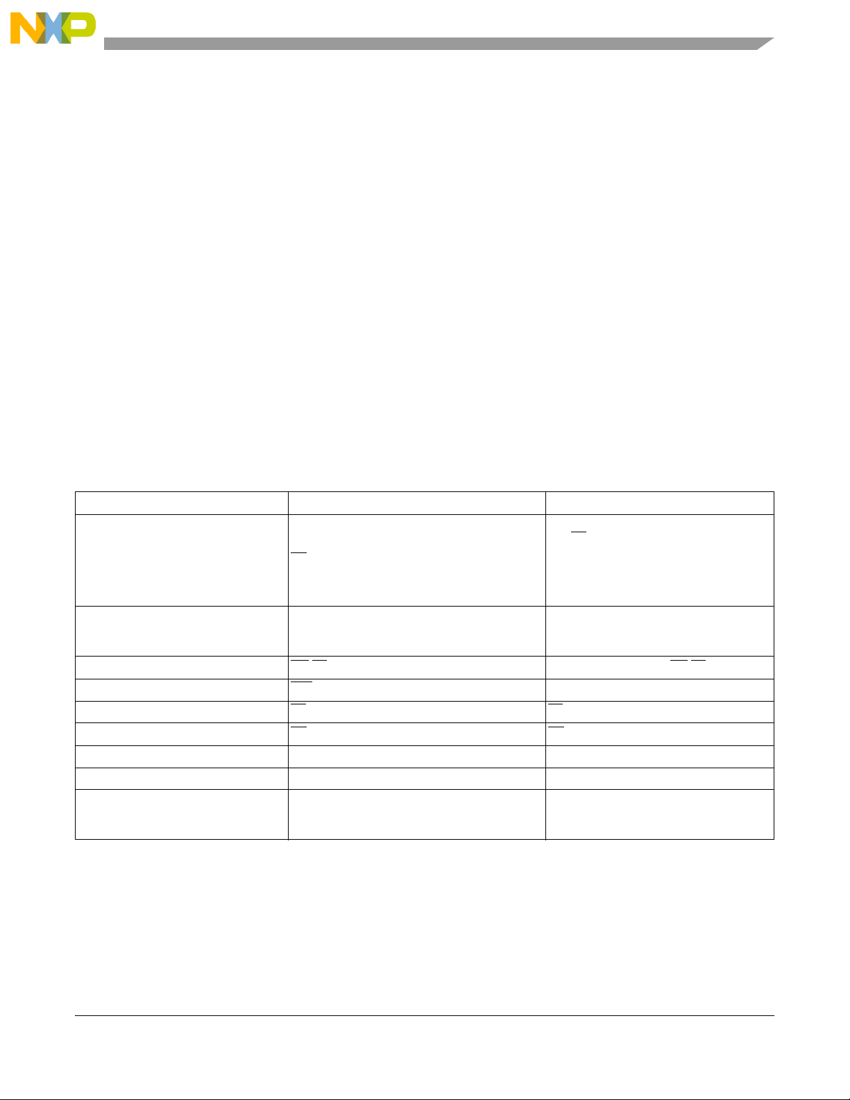
Chapter 2 Signal Description
This chapter describes the external device signals, including a table of signal properties, detailed
descriptions of the available signals, and the I/O pin power/ground segmentation.
2.1 Block Diagram
To provide an extensive feature set as well as compatibility between the MPC5500 family of devices, the
majority of balls are assigned multiplexed signal functions. Figure 2-1 shows only the signals that are
available on the device. Signal functions that are not available on this device are not shown in the diagram.
Primary signal functions that are not available on the device but are used as pin labels in the Ball Grid
Array (BGA) map are listed in Table 2-2.
The 324 package has a limited number of balls which affects the following signals and features:
Table 2-1. MPC5565 324 Package Limitations
Feature Signals MPC5565 Design 324 Package
ADDR[8:31]_GPIO[4:27]; ADDR[8:11] are muxed
as alternate signals with the chip select signals
Maximum 24-bit EBI address bus
Maximum 32-bits wide EBI data bus DATA[0:31]_GPIO[28:59]
Four EBI write enable/byte enable WE
EBI transfer error acknowledge TEA
EBI bus busy BB
EBI bus grant BG
EQADC Event trigger inputs 0 and 1 ETRIG[0:1]_GPIO[111:112] No balls available
General Purpose Input/output GPIO[205] No ball available
Calibration bus
CS
[0:3]_ADDR[8:11]_GPIO[0:3]. ADDR[8:11] is
also muxed with GPIO[4:7], providing four chip
selects and 24-bit address bits.
/BE[0:3] Only two balls available (WE/BE[0:1])
_GPIO[71] No ball available
signal not available. GPIO is available. BB_GPIO[72] no ball available
signal not available GPIO is available. BG_GPIO[73] no ball available
Calibration bus is separate from the EBI but uses
the EBI controller. Refer to Figure 2-1 for the
calibration bus signals.
ADDR[8:11]_GPIO[4:7] no balls available.
Use CS
[0:3]_ADDR[8:11]_GPIO[0:3] to
choose between using chip select signals or
maximizing the number of output address
signals ADDR[8:31]_GPIO[0:3, 8:31] for a
24-bit EBI address bus.
16 balls available for a 16-bits wide
DATA[0:15]_GPIO[28:43]. There are no balls
available for DATA[16:31]_GPIO[44:59].
No balls availables. These signals are only
available in the VertiCal assembly.
Refer to the last two columns in Table 2-2 for a comparison of available signals on the 324 package
compared to the VertiCal assembly.
NOTE
The Vertical assembly has ball connections for all the available signals on
the device.
MPC5565 Microcontroller Reference Manual, Rev. 1.0
Freescale Semiconductor
Page 59
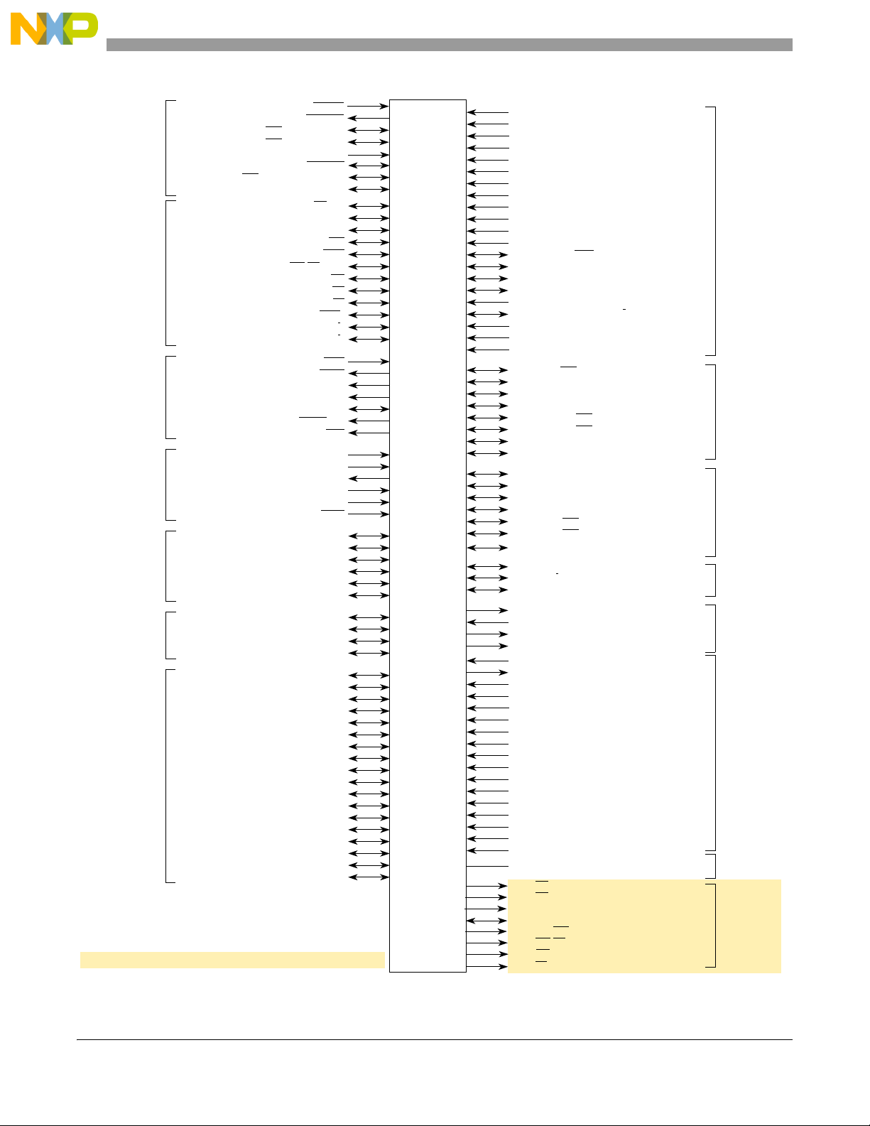
Signal Description
V
RH
V
RL
REFBYPC
ETRIG[0:1]_GPIO[111:112]
1
GPIO[83]_TXDA_CNTXA
GPIO[84]_RXDA_CNRXA
GPIO[85]_PCSC[3]_CNTXB
GPIO[86]_PCSC[4]_CNRXB
GPIO[87]_PCSD[3]_CNTXC
GPIO[88]_PCSD[4]_CNRXC
FlexCAN
GPIO[89]_TXDA
GPIO[90]_RXDA
GPIO[91]_PCSD[1]_TXDB
GPIO[92]_PCSD[5]_RXDB
eSCI
MPC5565
GPIO[93]_PCSC[1]
AN[0]_DAN0+
AN[1]_DAN0–
AN[2]_DAN1+
AN[3]_DAN1–
AN[4]_DAN2+
XTAL
EXTAL_EXTCLK
CLKOUT
ENGCLK
RESET
EVTI
EVTO
MCKO
MDO[3:0]
RSTOUT
GPIO[208]_IRQ[4]_PLLCFG[0]
GPIO[209]_SOUTD_IRQ
[5]_PLLCFG[1]
GPIO[210]_RSTCFG
GPIO[211:212]_IRQ[2:3]_BOOTCFG[0:1]
GPIO[0:3]_ADDR[8:11]_CS
[0:3]
GPIO[4:27]_ADDR[8:31]
1
GPIO[28:59]_DATA[0:31]
1
Nexus
DSPI
GPIO[94]_PCSC[2]
GPIO[95]_PCSC[5]
GPIO[97]_PCSB[2]
GPIO[98]_SCKD
GPIO[99]_SIND
GPIO[100]_SOUTD
GPIO[96]_PCSD[2]
GPIO[82:75]_MDO[11:4]
eQADC
eTPU
NC No Connect
GPIO[213]_WKPCFG
GPIO[73]
1
GPIO[72]
1
GPIO[71]_TEA
1
GPIO[62]_RD_WR
GPIO[63]_BDIP
GPIO[64:67]_WE/BE[0:3]
1
GPIO[68]_OE
GPIO[69]_TS
GPIO[70]_TA
MSEO[1:0]
RDY
GPIO[101]_PCSB[3]
GPIO[102]_PCSC[1]_SCKB
GPIO[104]_PCSC[5]_SOUTB
GPIO[105]_PCSD[2]_PCSB[0]
GPIO[106]_PCSD[0]_PCSB[1]
GPIO[107]_SOUTC_PCSB[2]
GPIO[103]_PCSC[2]_SINB
GPIO[108]_SINC_PCSB[3]
GPIO[109]_SCKC_PCSB[4]
GPIO[110]_PCSC[0]_PCSB[5]
AN[5]_DAN2–
AN[6]_DAN3+
AN[7]_DAN3–
AN[8]_ANW
AN[9]_ANX
AN[10]_ANY
AN[11]_ANZ
AN[12]_MA[0]_SDS
AN[13]_MA[1]_SDO
AN[14]_MA[2]_SDI
AN[15]_FCK
AN[16:39]
TCRCLKA_IRQ
[7]_GPIO[113]
ETPUA[0:11]_ETPUA[12:23]_GPIO[114:125]
ETPUA[12:15]_PCSB[1:5]_GPIO[126:129]
ETPUA[16:19]_PCSD[1:4]_GPIO[130:133]
ETPUA[20:23]_IRQ[8:11]_GPIO[134:137]
ETPUA[24:27]_IRQ
[12:15]_GPIO[138:141]
ETPUA[28:29]_PCSC[1:2]_GPIO[142:143]
ETPUA[30:31]_PCSC[3:4]_GPIO[144:145]
TCK
TDI
TDO
TMS
JCOMP
TEST
JTAG/Test
EMIOS[0:9]_ETPUA[0:9]_GPIO[179:188]
EMIOS[10:11]_PCSD[3:4]_GPIO[189:190]
EMIOS[12]_SOUTC_GPIO[191]
EMIOS[13]_SOUTD_GPIO[192]
EMIOS[16:23]_GPIO[195:202]
EMIOS[14:15]_GPIO[203:204]
EMIOS[14]_IRQ[0]_GPIO[193]
EMIOS[15]_IRQ
[1]_GPIO[194]
GPIO[205]
1
GPIO[206: 207]
GPIO
eMIOS
External
Reset/
Clock
V
RC33
V
RCCTL
V
DDA0
V
SSA0
V
DDA1
V
SSA1
V
DDSYN
V
SSSYN
V
FLASH
V
PP
V
STBY
V
DD
V
DDE
V
DDE12
V
DDEH
V
DD33
Power/
V
SS
Ground
Synthesizer
Configuration
Bus
Interface
(EBI)
1
CAL_CS[0]
2
CAL_CS[2:3]_CAL_ADDR[10:11]
2
CAL_ADDR[12:30]
2
CAL_DATA[0:15]
2
CAL_RD_WR
2
CAL_WE/BE[0:1]
2
CAL_OE
2
CAL_TS
2
Calibration
2
PLLCFG[2]
1
The 324 package does not support all muxed signals designed for this
device. Refer to Tab le 2 - 1 for a list of the signals that are not supported
on the 324 package.
2
The calibration signals only function when using the VertiCal assembly.
2-2 Freescale Semiconductor
Figure 2-1. MPC5565 Signals
MPC5565 Microcontroller Reference Manual, Rev. 1.0
Page 60
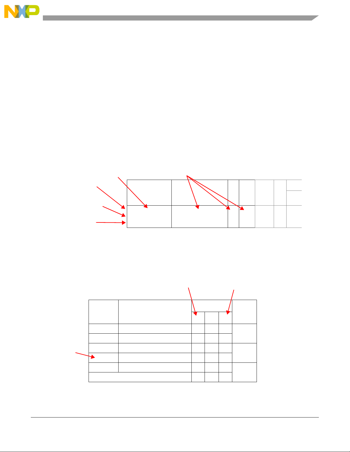
Signal Description
Signal Names Signal Functions
P/
A/GI/O
Type
Vol t ag e
Pad
Typ e
S
During
Reset
PCSA[3]_
21
SIND_
GPIO[99]
—
DSPI D data input
GPIO
—
A
G
—
I
I/O
VDDEH6 MH – / Up
Primary Functions
Secondary Functions
GPIO Functions are
No primary
Footnote
Ta bl e
Table 4-1. Signal Properties
are listed First
are alternate functions
general functions listed Last
function
available
P/A/G
Symbol
PA Function Type
PA Bits
# of
fs
3 4 5
G General purpose I/O
0 0 0
1-bit
2
fs
P Primary
0 0 1
A Alternate
0 1 0
2-bits
4
fs
MP Main
0 1 1
A2 Second alternate
1 0 0
3-bits
> 4
fs
All other values reserved for future use.
n n n
Bit 3 in the SUI_PCR registers
Bit 5 in the
the PA field.
The
main function
is used for device
compatibility.
PA[0:2]
is bit 0 in the PA field.
SUI_PCR
is bit 2 in
registers
2.2 External Signal Descriptions
This section summarizes the external signal functions, their static electrical characteristics, and pad
configuration settings for this device. The signal properties and their electrical characteristics are set in the
System Integration Unit (SIU) Pad Configuration (PCR) registers.
Signal functions are multiplexed to each ball on the BGA in a function hierarchy: Primary , Main Primary,
Alternate, Second Alternate, and General Purpose Input/Output (I/O). For example, in the signal
PCSA[3]_SIND_GPIO[99], the primary signal function is PCSA[3], the first alternate signal function is
SIND, and the GPIO function is a generic General Purpose I/O signal. Multiplexing signal functions
allows for more flexibility when configuring the device, as well as providing compatibility with other
devices in the MPC5500 product family.
The primary signal function name is used in the Ball Grid Array (BGA) map to identify the location of the
ball, however, the primary signal function is not always valid for all devices. As shown in Figure 2-2, when
the primary signal function is not available on the device, a dash appears in the following Signal table
columns: Signal Functions, P/A/G, and I/O Type.
The entries in the P/A/G column designate the position in the signal function hierarchy for multiplexed
functions. These symbols correspond to binary values for the Pin Assignment (PA) field in the SIU_PCR
registers that determine the active signal function. The PA field is from 1- to 3-bits wide, depending on the
PCR register. Figure 2-3 explains the symbol definitions used in the P/A/G column for Table 2-2.
Freescale Semiconductor 2-3
Figure 2-2. Primary Function Not Available on Device
Figure 2-3. Understanding the P/A/G Column Entries
MPC5565 Microcontroller Reference Manual, Rev. 1.0
Page 61
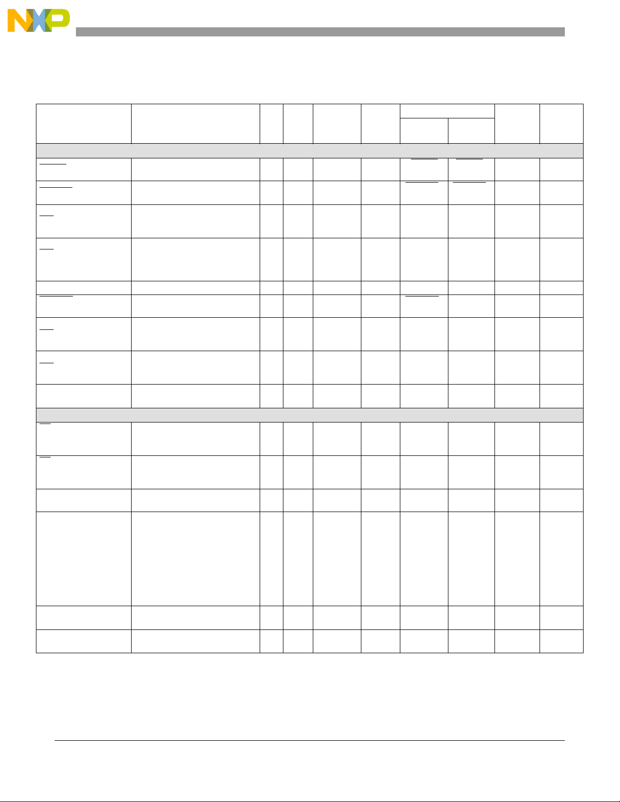
Signal Description
The following table lists the valid signal functions and their properties for this device:
Table 2-2. MPC5565 Signal Properties
P/
Signal Names
1
Signal Functions
2
A/GI/O
Type Voltage
Reset / Configuration
RESET External reset input P I V
RSTOUT
PLLCFG[0]_
IRQ
[4]_
GPIO[208]
PLLCFG[1]_
IRQ
[5]_
SOUTD_
GPIO[209]
PLLCFG[2]
RSTCFG
8
_
GPIO[210]
BOOTCFG[0]_
IRQ
[2]_
GPIO[211]
BOOTCFG[1]_
IRQ
[3]_
GPIO[212]
WKPCFG_
GPIO[213]
External reset output P O V
I
PLLMRFM mode selection
External interrupt request
GPIO
PLLMRFM reference selection
External interrupt request
DSPI D data output
GPIO
P
A
G
P
A
A2
G
I
I/O
I
I
O
I/O
PLLMRFM configuration input 28PI V
Reset configuration input
GPIO
Boot configuration input
External interrupt request
GPIO
Boot configuration input
External interrupt request
GPIO
Weak pull configuration input
GPIO
P
GII/O
P
A
I/O
G
P
A
I/O
G
P
GII/O
I
I
I
I
External Bus Interface (EBI)
CS[0]_
ADDR[8]_
10
GPIO[0]
CS[1:3]_
ADDR[9:11]_
GPIO[1:3]
ADDR[8:11]_
GPIO[4:7]
ADDR[12:26]_
GPIO[8:22]
ADDR[27:29]_
GPIO[23:25]
ADDR[30:31]_
GPIO[26:27]
10, 11
10, 11, 13
External chip selects
External address bus
GPIO
External chip selects
External address bus
GPIO
External address bus
GPIO
External address bus
GPIO
External address bus
GPIO
External address bus
GPIO
10, 11
10, 11
10, 11
11
11
11
O
P
I/O
A
I/O
G
O
P
I/O
A
I/O
G
PGI/O
I/O
PGI/O
I/O
PGI/O
I/O
PGI/O
I/O
DDEH6
DDEH6
V
DDEH6
V
DDEH6
DDEH6
V
DDEH6
V
DDEH6
V
DDEH6
V
DDEH6
V
DDE2
V
DDE2
V
DDE2
V
DDE2
V
DDE2
V
DDE2
Status
Pad
3
Type
SH
SH
MH
MH
MH PLLCFG / – – / – T21 V27
SH
SH
SH
SH
9
F – / Up – / Up
F – / Up – / Up
F – / Up – / Up
F – / Up – / Up
F – / Up – / Up
F – / Up – / Up
4
RSTOUT
PLLCFG /
PLLCFG /
RSTCFG
BOOTCFG
BOOTCFG
WKPCFG /
During
Reset
RESET
/ Up
Low
Up
Up
Up
/ Down
/ Down
Up
6
/
After
Reset
RESET /
Up
RSTOUT /
High
7
Package
324
R22 AA27
P21 W26
– / Up V21 AB27
– / Up U20 AA26
/
– / Up P22 Y28
– / Down U21 AB26
– / Down T20 AB24
– / Up R19 AA24
12
12
12
M4 T7
M3, N2, N1R5, P5,
—
T3, U3,
U4, V3,
P1, P2,
R1, R2,
12
T1, T2,
U1, U2,
V1, V2,
W1
Y2, Y1,
12
AA1
W3, V4
12
4965
VertiCal
assembly
R7
Y5, Y3,
AA3, AB3
Y7, AC3,
AC5, AB5,
T3, T2,
T1, V2,
W1, W2,
Y1, Y2,
AA2, AB2,
AC2
AD2,
AD3, AD1
AF2, AE3
MPC5565 Microcontroller Reference Manual, Rev. 1.0
2-4 Freescale Semiconductor
Page 62

Table 2-2. MPC5565 Signal Properties (continued)
Signal Description
Signal Names
DATA[0:15]_
GPIO[28:43]
DATA[16]_
GPIO[44]
DATA[17]_
GPIO[45]
DATA[18]_
GPIO[46]
DATA[19]_
GPIO[47]
DATA[20]_
GPIO[48]
DATA[21]_
GPIO[49]
DATA[22]_
GPIO[50]
DATA[23]_
GPIO[51]
DATA[24]_
GPIO[52]
DATA[25]_
GPIO[53]
DATA[26]_
GPIO[54]
DATA[27]_
GPIO[55]
DATA[28]_
GPIO[56]
DATA[29]_
GPIO[57]
DATA[30]_
GPIO[58]
DATA[31]_
GPIO[59]
RD_WR
GPIO[62]
BDIP
GPIO[63]
13
13
13
13
13
13
13
13
13
13
13
13
13
13
13
13
_
_
1
Signal Functions
External data bus
GPIO
External data bus
GPIO
External data bus
GPIO
External data bus
GPIO
External data bus
GPIO
External data bus
GPIO
External data bus
GPIO
External data bus
GPIO
External data bus
GPIO
External data bus
GPIO
External data bus
GPIO
External data bus
GPIO
External data bus
GPIO
External data bus
GPIO
External data bus
GPIO
External data bus
GPIO
External data bus
GPIO
External read/write
GPIO
External burst data in progress
GPIO
11
11
11
11
11
11
11
11
11
11
11
11
11
11
11
11
11
P/
2
A/GI/O
Type Voltage
Pad
3
Type
4
Status
During
Reset
After
6
Reset
7
324
Package
5
496
VertiCal
assembly
AG11,
AF12,
AG13,
AH13,
AG14,
AH15,
AG15,
AH16,
AB12,AF1
0, AD13,
AF11,
AB15,
PGI/O
I/O
V
DDE3
F – / Up – / Up
12
AB4, AA5,
AB5, AB6,
AB7, AA8,
AB8, AA9,
Y6, Y7,
Y8, W9,
W10, Y10,
W11, Y11
AD12,
AD15,
AF13
PGI/O
I/O
PGI/O
I/O
PGII/O
I/O
PGI/O
I/O
PGI/O
I/O
PGI/O
I/O
PGI/O
I/O
PGI/O
I/O
PGI/O
I/O
PGI/O
I/O
PGI/O
I/O
PGI/O
I/O
PGI/O
I/O
PGI/O
I/O
PGI/O
I/O
PGI/O
I/O
PGI/O
I/O
P
GOI/O
V
V
V
V
V
V
V
V
V
V
V
V
V
V
V
V
V
V
DDE3
DDE3
DDE3
DDE3
DDE3
DDE3
DDE3
DDE3
DDE3
DDE3
DDE3
DDE3
DDE3
DDE3
DDE3
DDE3
DDE2
DDE2
F – / Up – / Up
F – / Up – / Up
F – / Up – / Up
F – / Up – / Up
F – / Up – / Up
F – / Up – / Up
F – / Up – / Up
F – / Up – / Up
F – / Up – / Up
F – / Up – / Up
F – / Up – / Up
F – / Up – / Up
F – / Up – / Up
F – / Up – / Up
F – / Up – / Up
F – / Up – / Up
F – / Up – / Up
F – / Up – / Up
12
12
12
12
12
12
12
12
12
12
12
12
12
12
12
12
12
12
—AF5
—AG5
—AH5
—AG6
—AG7
—AG8
—AGJ
—AH9
—AD7
—AF6
— AB9
—AF7
—AD8
—AF8
—AD10
—AD11
P3 U3
M1 N1
MPC5565 Microcontroller Reference Manual, Rev. 1.0
Freescale Semiconductor 2-5
Page 63
Signal Description
Table 2-2. MPC5565 Signal Properties (continued)
Signal Names
13
13, 15
[2]_
[3]_
14
13, 14
13, 16
13, 16
13, 16
WE/BE[0:1]_
GPIO[64:65]
WE
/BE[2:3]_
GPIO[66:67]
OE
_
GPIO[68]
TS
_
GPIO[69]
TA
_
GPIO[70]
TEA
_
GPIO[71]
13, 15
BR
_
GPIO[72]
_
BG
GPIO[73]
CAL_CS[0]
CAL_CS
CAL_ADDR[10]
CAL_CS
CAL_ADDR[11]
CAL_ADDR[12]
CAL_ADDR[13]
CAL_ADDR[14]
CAL_ADDR[15]
CAL_ADDR[16]
CAL_ADDR[17]
CAL_ADDR[18]
CAL_ADDR[19]
CAL_ADDR[20]
CAL_ADDR[21]
CAL_ADDR[22]
CAL_ADDR[23]
CAL_ADDR[24]
CAL_ADDR[25]
CAL_ADDR[26]
CAL_ADDR[27]
CAL_ADDR[28]
CAL_ADDR[29]
CAL_ADDR[30]
CAL_DATA[0:7]
13, 16
13, 16
13, 16
13, 16
13, 16
13, 16
13, 16
13, 16
13, 16
13, 16
13, 16
13, 16
13, 16
13, 16
13, 16
13, 16
13, 16
13, 16
13, 16
13, 16
P/
1
Signal Functions
External write/byte enable
2
14
GPIO
External write/byte enable
14
GPIO
External output enable
GPIO
External transfer start
GPIO
External transfer acknowledge
GPIO
External transfer error acknowledge
GPIO
—
GPIO
—
GPIO
Calibration chip select P O
Calibration chip select
Calibration address bus
Calibration chip select
Calibration address bus
Calibration address bus P O V
Calibration address bus P O V
Calibration address bus P O V
Calibration address bus P O V
Calibration address bus P O V
Calibration address bus P O V
Calibration address bus P O V
Calibration address bus P O V
Calibration address bus P O V
Calibration address bus P O V
Calibration address bus P O V
Calibration address bus P O V
Calibration address bus P O V
Calibration address bus P O V
Calibration address bus P O V
Calibration address bus P O V
Calibration address bus P O V
Calibration address bus P O V
Calibration address bus P O V
Calibration data bus P I/O V
A/GI/O
P
GOI/O
P
GOI/O
P
GOI/O
PGI/O
PGI/O
PGI/O
—G—
—G—
P
A
P
A
Type Voltage
V
DDE2
V
DDE2
V
DDE3
V
V
V
V
V
DDE2
DDE2
DDE2
DDE3
DDE3
I/O
I/O
I/O
I/O
I/O
Calibration Bus
V
DDE12
V
O
O
DDE12
V
DDE12
DDE12
DDE12
DDE12
DDE12
DDE12
DDE12
DDE12
DDE12
DDE12
DDE12
DDE12
DDE12
DDE12
DDE12
DDE12
DDE12
DDE12
DDE12
DDE12
DDE12
Status
Pad
3
Type
F – / Up – / Up
F – / Up – / Up
F – / Up – / Up
F – / Up – / Up
F – / Up – / Up
F – / Up – / Up
F – / Up – / Up
F – / Up – / Up
F – / Up – / Up — AB11
F – / Up – / Up — AA10
F – / Up – / Up — AB10
F – / Up – / Up — AA14
F – / Up – / Up — R8
F – / Up – / Up — AA15
F – / Up – / Up — W7
F – / Up – / Up — P7
F – / Up – / Up — P8
F – / Up – / Up — U7
F – / Up – / Up — N7
F – / Up – / Up — M8
F – / Up – / Up — M7
F – / Up – / Up — V7
F – / Up – / Up — L8
F – / Up – / Up — T8
F – / Up – / Up — K8
F – / Up – / Up — L7
F – / Up – / Up — U8
F – / Up – / Up — V8
F – / Up – / Up — AB13
F – / Up – / Up — AB14
F – / Up – / Up —
4
During
Reset
After
6
Reset
12
12
12
12
12
12
12
12
324
7
Package
N4, N3 U5, T5
AB9 AF16
5
496
VertiCal
assembly
—N3, P1
T4 W3
R4 V3
—N2
—AF17
—AG16
W21,Y22,
V21,
W22,
U21, U22,
T21, T22
MPC5565 Microcontroller Reference Manual, Rev. 1.0
2-6 Freescale Semiconductor
Page 64
Table 2-2. MPC5565 Signal Properties (continued)
Signal Description
P/
Signal Names
CAL_DATA[8:13]
CAL_DATA[14:15]
CAL_RD_W
CAL_WE
CAL_OE
CAL_TS
EVTI
EVTO
13, 16
/BE[0:1]
13, 16
13, 16
13, 16
13, 16
13, 16
1
Signal Functions
Calibration data bus P I/O V
Calibration data bus P I/O V
Calibration read/write P O V
Calibration write/byte enable P O V
Calibration output enable P O V
Calibration transfer start P O V
Nexus event in P I V
Nexus event out P O V
2
MCKO Nexus message clock out P O V
18
MDO[0]
Nexus message data out P O V
MDO[3:1] Nexus message data out P O V
MDO[11:4]_
GPIO[82:75]
MSEO
19
[1:0] Nexus message start/end out P O V
RDY
Nexus message data out
GPIO
Nexus ready output P O V
TCK JTAG test clock input P I V
TDI JTAG test data input P I V
TDO JTAG test data output P O V
TMS JTAG test mode select input P I V
JCOMP JTAG TAP controller enable P I V
TEST
CNTXA_
TXDA_
GPIO[83]
CNRXA_
RXDA_
GPIO[84]
CNTXB_
PCSC[3]_
GPIO[85]
Test mode select P I V
FlexCAN A transmit
eSCI A transmit
GPIO
FlexCAN A receive
eSCI A receive
GPIO
FlexCAN B transmit
DSPI C peripheral chip select
GPIO
A/GI/O
Type Voltage
NEXUS
P
GOI/O
JTAG / TEST
FlexCAN
O
P
O
A
I/O
G
I
P
I
A
I/O
G
O
P
O
A
I/O
G
DDE12
DDE12
DDE12
DDE12
DDE12
DDE12
DDE7
DDE7
DDE7
DDE7
DDE7
V
DDE7
DDE7
DDE7
DDE7
DDE7
DDE7
DDE7
DDE7
DDE7
V
DDEH4
V
DDEH4
V
DDEH4
Status
Pad
3
Type
F – / Up – / Up —
F – / Up – / Up —
F – / Up – / Up — W8
F – / Up – / Up — Y8, AA7
F – / Up – / Up — AD16
F – / Up – / Up — AA11
F I / Up EVTI / Up F21 G26
F O / Low
F O / Low
F O / High MDO / Low B20 C25
F O / Low MDO / Low
F O / Low – / Down
F O / High
F O / High RDY / High G19 J24
F
F TDI / Up TDI / Up D22 E28
F TDO / Up TDO / Up E21 F27
F TMS / Up TMS / Up E20 E26
F
F TEST / Up TEST / Up E22 F28
SH I / Up – / Up
SH – / Up – / Up
MH – / Up – / Up AB18 AG23
4
During
Reset
TCK /
Down
JCOMP /
Down
6
After
Reset
EVTO
High
MCKO /
Enabled
MSEO
High
TCK /
Down
JCOMP /
Down
324
7
Package
/
F22 G27
G20 H26
17
D18, C18,
C19
A17:18,
B17, A19,
B18, D17,
C17, B19
/
G22, G21 G24, H24
D21 E27
F20 F26
20
17
Y17 AF22
AA18 AG22
5
496
VertiCal
assembly
AA17,
AB16,
AA18,
AB17,
AA19,AB
19
AA20,
AB20
C23, B21,
C24
A23, C22,
A20, A24,
B23, B20,
C20, B24
MPC5565 Microcontroller Reference Manual, Rev. 1.0
Freescale Semiconductor 2-7
Page 65

Signal Description
Table 2-2. MPC5565 Signal Properties (continued)
Signal Names
CNRXB_
PCSC[4]_
GPIO[86]
CNTXC_
PCSD[3]_
GPIO[87]
CNRXC_
PCSD[4]_
GPIO[88]
TXDA_
GPIO[89]
RXDA_
GPIO[90]
TXDB_
PCSD[1]_
GPIO[91]
RXDB_
PCSD[5]_
GPIO[92]
21
SCKA_
PCSC[1]_
GPIO[93]
21
SINA_
PCSC[2]_
GPIO[94]
SOUTA_
PCSC[5]_
GPIO[95]
PCSA[0]_
PCSD[2]_
GPIO[96]
PCSA[1]_
PCSB[2]_
GPIO[97]
PCSA[2]_
SCKD_
GPIO[98]
PCSA[3]_
SIND_
GPIO[99]
PCSA[4]_
SOUTD_
GPIO[100]
PCSA[5]_
PCSB[3]_
GPIO[101]
21
21
21
21
21
21
21
1
Signal Functions
FlexCAN B receive
DSPI C peripheral chip select
GPIO
FlexCAN C transmit
DSPI D peripheral chip select
GPIO
FlexCAN C receive
DSPI D peripheral chip select
GPIO
eSCI A transmit
GPIO
eSCI A receive
GPIO
eSCI B transmit
DSPI D peripheral chip select
GPIO
eSCI B receive
DSPI D peripheral chip select
GPIO
DSPI C peripheral chip select
GPIO
DSPI C peripheral chip select
GPIO
DSPI C peripheral chip select
GPIO
DSPI D peripheral chip select
GPIO
DSPI B peripheral chip select
GPIO
DSPI D clock
GPIO
DSPI D data input
GPIO
DSPI D data output
GPIO
DSPI B peripheral chip select
GPIO
P/
2
A/GI/O
Type Voltage
I
P
O
A
I/O
G
O
P
O
A
I/O
G
I
P
O
A
I/O
G
V
DDEH4
V
DDEH6
V
DDEH6
Pad
3
Type
4
MH – / Up – / Up AB19 AH23
MH – / Up – / Up P19 W24
MH – / Up – / Up R20 Y26
Status
During
Reset
After
6
Reset
7
324
Package
5
496
VertiCal
assembly
eSCI
P
GOI/O
P
GII/O
P
A
G
P
A
G
O
O
I/O
O
I/O
V
DDEH6
V
DDEH6
V
DDEH6
SH – / Up – / Up N20 V24
SH – / Up – / Up P20 U26
MH – / Up – / Up R21 Y27
I
V
DDEH6
MH – / Up – / Up T19 Y24
DSPI
—
—
—
—
—
—
—
—
—
—
—
O
I/O
—
O
I/O
—
O
I/O
—
O
I/O
—
O
I/O
—
I/O
I/O
—
I/O
—
O
I/O
—
O
I/O
V
DDEH6
V
DDEH6
V
DDEH6
V
DDEH6
V
DDEH6
V
DDEH6
I
V
DDEH6
V
DDEH6
V
DDEH6
MH – / Up – / Up L22 U27
MH – / Up – / Up L21 P27
MH – / Up – / Up L20 P24
MH – / Up – / Up M20 R24
MH – / Up – / Up M19 T24
MH – / Up – / Up M21 N26
MH – / Up – / Up K19 N24
MH – / Up – / Up N19 U24
MH – / Up – / Up N21 T26
A
G
—
A
G
—
A
G
—
A
G
—
A
G
—
A
G
—
A
G
—
A
G
—
A
G
MPC5565 Microcontroller Reference Manual, Rev. 1.0
2-8 Freescale Semiconductor
Page 66

Table 2-2. MPC5565 Signal Properties (continued)
Signal Description
Signal Names
22
SCKB_
PCSC[1]_
GPIO[102]
22
SINB_
PCSC[2]_
GPIO[103]
SOUTB_
PCSC[5]_
GPIO[104]
PCSB[0]_
PCSD[2]_
GPIO[105]
PCSB[1]_
PCSD[0]_
GPIO[106]
PCSB[2]_
SOUTC_
GPIO[107]
PCSB[3]_
SINC_
GPIO[108]
PCSB[4]_
SCKC_
GPIO[109]
PCSB[5]_
PCSC[0]_
GPIO[110]
AN[0]_
DAN0+
AN[1]_
DAN0–
AN[2]_
DAN1+
AN[3]_
DAN1–
AN[4]_
DAN2+
AN[5]_
DAN2–
AN[6]_
DAN3+
AN[7]_
DAN3–
AN[8]_
ANW
AN[9]_
ANX
AN[10]_
ANY
22
22
22
22
22
22
22
1
Signal Functions
DSPI B clock
DSPI C peripheral chip select
GPIO
DSPI B data input
DSPI C peripheral chip select
GPIO
DSPI B data output
DSPI C peripheral chip select
GPIO
DSPI B peripheral chip select
DSPI D peripheral chip select
GPIO
DSPI B peripheral chip select
DSPI D peripheral chip select
GPIO
DSPI B peripheral chip select
DSPI C data output
GPIO
DSPI B peripheral chip select
DSPI C data input
GPIO
DSPI B peripheral chip select
DSPI C clock
GPIO
DSPI B peripheral chip select
DSPI C peripheral chip select
GPIO
Single-ended analog input
Positive terminal differential input
Single-ended analog input
Negative terminal differential input
Single-ended analog input
Positive terminal differential input
Single-ended analog input
Negative terminal differential input
Single-ended analog input
Positive terminal differential input
Single-ended analog input
Negative terminal differential input
Single-ended analog input
Positive terminal differential input
Single-ended analog input
Negative terminal differential input
Single-ended analog input
External multiplexed analog input
Single-ended analog input
External multiplexed analog input
Single-ended analog input
External multiplexed analog input
P/
2
A/GI/O
Type Voltage
I/O
P
O
A
I/O
G
I
P
O
A
I/O
G
O
P
O
A
I/O
G
I/O
P
O
A
I/O
G
O
P
I/O
A
I/O
G
O
P
O
A
I/O
G
O
P
I
A
I/O
G
O
P
I/O
A
I/O
G
O
P
I/O
A
I/O
G
V
DDEH10
V
DDEH10
V
DDEH10
V
DDEH10
V
DDEH10
V
DDEH10
V
DDEH6
V
DDEH6
V
DDEH6
Pad
3
22
22
22
22
22
22
22
22
22
4
Type
MH – / Up – / Up K21 T27
MH – / Up – / Up H22 P28
MH – / Up – / Up J19 N28
MH – / Up – / Up J21 R27
MH – / Up – / Up J22 R28
MH – / Up – / Up K22 T28
MH – / Up – / Up J20 M27
MH – / Up – / Up K20 N27
MH – / Up – / Up L19 M26
Status
During
Reset
After
6
Reset
7
324
Package
5
496
VertiCal
assembly
eQADC
PI
PI
PI
PI
PI
PI
PI
PI
PI
PI
PI
V
V
V
V
V
V
V
V
V
V
V
DDA1
DDA1
DDA1
DDA1
DDA1
DDA1
DDA1
DDA1
DDA1
DDA1
DDA1
23
AE I / – AN[0] / – B8 C9
23
AE I / – AN[1] / – A8 B8
23
AE I / – AN[2] / – D10 G12
23
AE I / – AN[3] / – C9 E10
23
AE I / – AN[4] / – B9 C10
23
AE I / – AN[5] / – A9 B9
23
AE I / – AN[6] / – D11 G13
23
AE I / – AN[7] / – C10 E11
23
AE I / – AN[8] / – C5 E7
23
AE I / – AN[9] / – D7 C4
23
AE I / – AN[10] / – D8 E6
MPC5565 Microcontroller Reference Manual, Rev. 1.0
Freescale Semiconductor 2-9
Page 67
Signal Description
Table 2-2. MPC5565 Signal Properties (continued)
P/
Signal Names
AN[11]_
ANZ
AN[12]_
MA[0]_
SDS
AN[13]_
MA[1]_
SDO
AN[14]_
MA[2]_
SDI
AN[15]_
FCK
1
Signal Functions
Single-ended analog input
External multiplexed analog input
Single-ended analog input
Mux address
eQADC serial data strobe
Single-ended analog input
Mux address
eQADC serial data out
Single-ended analog input
Mux address
eQADC serial data in
Single-ended analog input
eQADC free running clock
2
AN[16:18] Single-ended analog input P I V
AN[19:20] Single-ended analog input P I V
AN[21] Single-ended analog input P I V
AN[22:25] Single-ended analog input P I V
AN[26] Single-ended analog input P I V
AN[27:28] Single-ended analog input P I V
AN[29] Single-ended analog input P I V
AN[30:35] Single-ended analog input P I V
AN[36:39] Single-ended analog input P I V
ETRIG[0]_
GPIO[111]
ETRIG[1]_
GPIO[112]
V
RH
V
RL
13
eQADC trigger input
GPIO
13
eQADC trigger input
GPIO
Voltage reference high P I –
Voltage reference low P I –
REFBYPC Reference bypass capacitor input P I –
A/GI/O
Type Voltage
PI
24
P
G
P
G
P
G
P
G
O
A
25
O
24
O
A
25
O
24
O
A
25
24
25
O
P
GII/O
P
GII/O
I
I
I
I
I
V
V
V
V
V
V
V
DDA1
DDA1
DDA1
DDA1
DDA0
DDA0
DDA0
DDA0
DDA0
DDA1
eTPU
I
TCRCLKA_
IRQ
[7]_
GPIO[113]
ETPUA[0:3]_
ETPUA[12:15]_
GPIO[114:117]
ETPUA[4]_
ETPUA[16]_
GPIO[118]
ETPUA[5]_
ETPUA[17]_
GPIO[119]
eTPU A TCR clock
External interrupt request
GPIO
eTPU A channel
eTPU A channels (output only)
GPIO
eTPU A channel
eTPU A channel (output only)
GPIO
eTPU A channel
eTPU A channel (output only)
GPIO
P
I
I/O
I/O
O
I/O
I/O
O
I/O
I/O
O
I/O
V
V
V
V
A
G
P
A
G
P
A
G
P
A
G
DDEH9
DDEH9
DDEH9
DDEH9
DDEH8
DDEH8
23
23
23
DDEH1
DDEH1
DDEH1
DDEH1
Status
Pad
3
Type
23
AE I / – AN[11] / – A5 B6
MH, A
MH, A
MH, A
MH, A
23
AE I / –
23
AE I / –
23
AE I / – AN[21] / – C8 E9
23
AE I / –
23
AE I / – AN[26] / – B12 C12
23
AE I / –
23
AE I / – AN[29] / – D13 E13
23
AE I / –
23
AE I / –
SH – / Up – / Up — A16
SH – / Up – / Up — B16
V
DDINT
V
SSINT
V
DDINT
SH – / Up – / Up M2 N5
SH
MH
MH
During
4
Reset
26
I / – AN[12] / – A16 H15
26
I / – AN[13] / – B16 G15
26
I / – AN[14] / – C16 E16
26
I / – AN[15] / – D16 C16
6
After
7
Reset
AN[16:18] /
–
Package
B7, C6, D9
AN[19:20] /
–
AN[22:25] / –C11, B11,
D12, C12
AN[27:28] /
–
AN[30:35] /
–
A12, A13 B12, A13
C13, B13,
B14, C14,
D14, A14
AN[36:39] / –B4, A4,
– / – V
– / – V
RH
RL
– / – REFBYPC B10 B10
– /
WKPCFG
– /
WKPCFG
– /
WKPCFG
– /
WKPCFG
– /
WKPCFG
– /
WKPCFG
L3, L4, K3, L2M5, G8,
324
496
VertiCal
assembly
B7, E8,
H12
B6, C7 C7, C8
C11, B11,
H13, E12
C13, B13,
B14, E14,
G14, A14
C5, B5,
D6, B5
B4. C6
A10 A9
A11 A10
M3, L3
L1 L2
K4 H9
5
MPC5565 Microcontroller Reference Manual, Rev. 1.0
2-10 Freescale Semiconductor
Page 68

Table 2-2. MPC5565 Signal Properties (continued)
Signal Description
Signal Names
ETPUA[6]_
ETPUA[18]_
GPIO[120]
ETPUA[7]_
ETPUA[19]_
GPIO[121]
ETPUA[8]_
ETPUA[20]_
GPIO[122]
ETPUA[9]_
ETPUA[21]_
GPIO[123]
ETPUA[10]_
ETPUA[22]_
GPIO[124]
ETPUA[11]_
ETPUA[23]_
GPIO[125]
ETPUA[12]_
PCSB[1]_
GPIO[126]
ETPUA[13]_
PCSB[3]_
GPIO[127]
ETPUA[14]_
PCSB[4]_
GPIO[128]
ETPUA[15]_
PCSB[5]_
GPIO[129]
ETPUA[16]_
PCSD[1]_
GPIO[130]
ETPUA[17]_
PCSD[2]_
GPIO[131]
ETPUA[18]_
PCSD[3]_
GPIO[132]
ETPUA[19]_
PCSD[4]_
GPIO[133]
ETPUA[20]
IRQ
[8]
GPIO[134]
ETPUA[21]
IRQ
[9]
GPIO[135]
ETPUA[22]
IRQ
[10]
GPIO[136]
1
Signal Functions
eTPU A channel
eTPU A channel (output only)
GPIO
eTPU A channel
eTPU A channel (output only)
GPIO
eTPU A channel
eTPU A channel (output only)
GPIO
eTPU A channel
eTPU A channel (output only)
GPIO
eTPU A channel
eTPU A channel (output only)
GPIO
eTPU A channel
eTPU A channel (output only)
GPIO
eTPU A channel
DSPI B peripheral chip select
GPIO
eTPU A channel
DSPI B peripheral chip select
GPIO
eTPU A channel
DSPI B peripheral chip select
GPIO
eTPU A channel
DSPI B peripheral chip select
GPIO
eTPU A channel
DSPI D peripheral chip select
GPIO
eTPU A channel
DSPI D peripheral chip select
GPIO
eTPU A channel
DSPI D peripheral chip select
GPIO
eTPU A channel
DSPI D peripheral chip select
GPIO
eTPU A channel
External interrupt request
GPIO
eTPU A channel
External interrupt request
GPIO
eTPU A channel
External interrupt request
GPIO
P/
2
A/GI/O
Type Voltage
I/O
P
O
A
I/O
G
I/O
P
O
A
I/O
G
I/O
P
O
A
I/O
G
I/O
P
O
A
I/O
G
I/O
P
O
A
I/O
G
I/O
P
O
A
I/O
G
I/O
P
O
A
I/O
G
I/O
P
O
A
I/O
G
I/O
P
O
A
I/O
G
I/O
P
O
A
I/O
G
I/O
P
O
A
I/O
G
I/O
P
O
A
I/O
G
I/O
P
O
A
I/O
G
I/O
P
O
A
I/O
G
I/O
P
I
A
I/O
G
I/O
P
I
A
I/O
G
I/O
P
I
A
I/O
G
V
DDEH1
V
DDEH1
V
DDEH1
V
DDEH1
V
DDEH1
V
DDEH1
V
DDEH1
V
DDEH1
V
DDEH1
V
DDEH1
V
DDEH1
V
DDEH1
V
DDEH1
V
DDEH1
V
DDEH1
V
DDEH1
V
DDEH1
Pad
3
Type
4
SH
SH
SH
SH
SH
SH
MH
MH
MH
MH
MH
MH
MH
MH
MH
MH
MH
Status
During
Reset
– /
WKPCFG
– /
WKPCFG
– /
WKPCFG
– /
WKPCFG
– /
WKPCFG
– /
WKPCFG
– /
WKPCFG
– /
WKPCFG
– /
WKPCFG
– /
WKPCFG
– /
WKPCFG
– /
WKPCFG
– /
WKPCFG
– /
WKPCFG
– /
WKPCFG
– /
WKPCFG
– /
WKPCFG
6
After
Reset
– /
WKPCFG
– /
WKPCFG
– /
WKPCFG
– /
WKPCFG
– /
WKPCFG
– /
WKPCFG
– /
WKPCFG
– /
WKPCFG
– /
WKPCFG
– /
WKPCFG
– /
WKPCFG
– /
WKPCFG
– /
WKPCFG
– /
WKPCFG
– /
WKPCFG
– /
WKPCFG
– /
WKPCFG
7
Package
324
J3 M2
K2 K3
K1 K2
J4 G9
H3 L5
J2 J3
J1 J2
G4 G10
G3 K5
H2 H3
H1 K1
F3 H10
F4 J5
G2 G3
G1 J1
E4 H11
F2 F3
5
496
VertiCal
assembly
MPC5565 Microcontroller Reference Manual, Rev. 1.0
Freescale Semiconductor 2-11
Page 69
Signal Description
Table 2-2. MPC5565 Signal Properties (continued)
Signal Names
ETPUA[23]
IRQ
[11]
GPIO[137]
ETPUA[24:26]_
IRQ
[12:14]_
GPIO[138:140]
ETPUA[27]_
IRQ
[15]_
GPIO[141]
ETPUA[28]_
PCSC[1]_
GPIO[142]
ETPUA[29]_
PCSC[2]_
GPIO[143]
ETPUA[30]_
PCSC[3]_
GPIO[144]
ETPUA[31]_
PCSC[4]_
GPIO[145]
EMIOS[0:2]_
ETPUA[0:2]_
GPIO[179:181]
EMIOS[3:5]_
ETPUA[3:5]_
GPIO[182:184]
EMIOS[6:7]_
ETPUA[6:7]_
GPIO[185:186]
EMIOS[8:9]_
ETPUA[8:9]_
GPIO[187:188]
EMIOS[10:11]_
PCSD[3:4]_
GPIO[189:190]
EMIOS[12]_
SOUTC_
GPIO[191]
EMIOS[13]_
SOUTD_
GPIO[192]
EMIOS[14]_
IRQ
[0]_
GPIO[193]
EMIOS[15]_
IRQ
[1]_
GPIO[194]
EMIOS[16]_
GPIO[195]
1
Signal Functions
eTPU A channel
External interrupt request
GPIO
eTPU A channel (output only)
External Interrupt Request
GPIO
eTPU A channel (output only)
External Interrupt Request
GPIO
eTPU A channel (output only)
DSPI C peripheral chip select
GPIO
eTPU A channel (output only)
DSPI C peripheral chip select
GPIO
eTPU A channel
DSPI C peripheral chip select
GPIO
eTPU A channel
DSPI C peripheral chip select
GPIO
eMIOS channel
eTPU A channel (output only)
GPIO
eMIOS channel
eTPU A channel (output only)
GPIO
eMIOS channel
eTPU A channel (output only)
GPIO
eMIOS channel
eTPU A channel (output only)
GPIO
eMIOS channel
DSPI D peripheral chip select
GPIO
eMIOS channel (output only)
DSPI C data output
GPIO
eMIOS channel (output only)
DSPI D data output
GPIO
eMIOS channel (output only)
External interrupt request
GPIO
eMIOS channel (output only)
External interrupt request
GPIO
eMIOS channel
GPIO
P/
2
A/GI/O
Type Voltage
I/O
P
I
A
I/O
G
O
P
I
A
I/O
G
O
P
I
A
I/O
G
O
P
O
A
I/O
G
O
P
O
A
I/O
G
I/O
P
O
A
I/O
G
I/O
P
O
A
I/O
G
V
DDEH1
V
DDEH1
V
DDEH1
V
DDEH1
V
DDEH1
V
DDEH1
V
DDEH1
Pad
3
Type
4
MH
SH
SH
MH
MH
MH
MH
Status
During
Reset
– /
WKPCFG
– /
WKPCFG
– /
WKPCFG
– /
WKPCFG
– /
WKPCFG
– /
WKPCFG
– /
WKPCFG
6
After
Reset
– /
WKPCFG
– /
WKPCFG
– /
WKPCFG
– /
WKPCFG
– /
WKPCFG
– /
WKPCFG
– /
WKPCFG
7
E1, E3, D3
324
Package
F1 H2
E2 E3
D1 F1
D2 F2
C1 E1
C2 E2
5
496
VertiCal
assembly
G2, H5,
G5
eMIOS
I/O
P
O
A
I/O
G
I/O
P
O
A
I/O
G
I/O
P
O
A
I/O
G
I/O
P
O
A
I/O
G
I/O
P
I/O
A
I/O
G
O
P
O
A
I/O
G
O
P
O
A
I/O
G
O
P
A
I/O
G
O
P
A
I/O
G
PGI/O
O
V
DDEH4
V
DDEH4
V
DDEH4
V
DDEH4
V
DDEH4
V
DDEH4
V
DDEH4
I
V
DDEH4
I
V
DDEH4
V
DDEH4
SH
SH
SH
SH
SH
MH
MH
SH
SH
SH
– /
WKPCFG
– /
WKPCFG
– /
WKPCFG
– /
WKPCFG
– /
WKPCFG
– /
WKPCFG
– /
WKPCFG
– /
WKPCFG
– /
WKPCFG
– /
WKPCFG
– /
WKPCFG
– /
WKPCFG
– /
WKPCFG
– /
WKPCFG
– /
WKPCFG
– /
WKPCFG
– /
WKPCFG
– /
WKPCFG
– /
WKPCFG
– /
WKPCFG
AB10,
AB11,
W12
AA11,
AB12,
AA12
Y12, AB13
W13,
AA13
Y13, AB14
W15 M21
AA14 AF18
AB15 AH19
Y14 M22
AA15 AG19
AD16,
AD21,
P21
R22,
AD18,
AD22
P22,
AD19
N21,
AD23
N22,
AG18
MPC5565 Microcontroller Reference Manual, Rev. 1.0
2-12 Freescale Semiconductor
Page 70
Table 2-2. MPC5565 Signal Properties (continued)
Signal Description
P/
Signal Names
EMIOS[17]_
GPIO[196]
EMIOS[18]_
GPIO[197]
EMIOS[19]_
GPIO[198]
EMIOS[20]_
GPIO[199]
EMIOS[21]_
GPIO[200]
EMIOS[22]_
GPIO[201]
EMIOS[23]_
GPIO[202]
1
eMIOS channel
GPIO
eMIOS channel
GPIO
eMIOS channel
GPIO
eMIOS channel
GPIO
eMIOS channel
GPIO
eMIOS channel
GPIO
eMIOS channel
GPIO
Signal Functions
2
A/GI/O
Type Voltage
PGI/O
O
PGI/O
O
PGI/O
O
PGI/O
I/O
PGI/O
I/O
PGI/O
I/O
PGI/O
I/O
GPIO
EMIOS[14:15]_
GPIO[203:204]
GPIO[205]
13, 28
GPIO[206:207]
27
29
eMIOS channel output only
GPIO
P
GOI/O
GPIO G I/O V
GPIO G I/O V
Clock Synthesizer
XTAL Crystal oscillator output P O V
EXTAL_
EXTCLK
31
Crystal oscillator input
External clock input
P
I
A
I
CLKOUT System clock output P O V
ENGCLK Engineering clock output P O V
Power / Ground
33
V
RC33
V
RCCTL
V
DDA0
V
SSA0
V
DDA1
V
SSA1
V
DDSYN
V
SSSYN
V
FLASH
V
PP
V
STBY
34
34
34
34
35
36
Voltage regulator control supply P I 3.3 V V
Voltage regulator control output P O 3.3 V V
Analog power input ADC[0] P I 5.0 V V
Analog ground input ADC[0] P I — V
Analog power input ADC[1] P I 5.0 V V
Analog ground input ADC[1] P I — V
Clock synthesizer power input P I 3.3 V V
Clock synthesizer ground input P I — V
Flash read supply input P I 3.3 V V
Flash program/erase supply input P I 5.0 V V
SRAM standby power input P I 0.8–1.2 V V
V
DDEH4
V
DDEH4
V
DDEH4
V
DDEH4
V
DDEH4
V
DDEH4
V
DDEH4
V
DDEH6
DDEH8
DDE3
DDSYN
V
DDSYN
DDE5
DDE5
Status
Pad
3
Type
SH
SH
SH
SH
SH
SH
SH
SH – / Up – / Up H20, H21 J26, H27
MH – / Up – / Up — B22
F – / Up – / Up
AE O / – XTAL30 / – V22 AD28
AE I / –
F
F
DDINT
DDINT
DDINT
SSINT
DDINT
SSINT
DDE
SSE
DDINT
DDINT
STBY
4
During
6
Reset
– /
WKPCFG
– /
WKPCFG
– /
WKPCFG
– /
WKPCFG
– /
WKPCFG
– /
WKPCFG
– /
WKPCFG
CLKOUT /
Enabled
ENGCLK/
Enabled
I / – V
O / – V
I / – V
I / – V
I / – V
I / – V
I / – V
I / – V
I / – V
I / – V
I / – V
After
7
Reset
– /
WKPCFG
– /
WKPCFG
– /
WKPCFG
– /
WKPCFG
– /
WKPCFG
– /
WKPCFG
– /
WKPCFG
32
EXTAL
–
CLKOUT /
Enabled
ENGCLK /
Enabled
RC33
RCCTL
DDA0
SSA0
DDA1
SSA1
DDSYN
SSSYN
FLASH
PP
STBY
324
Package
Y15 AF19
AB16 AH20
AA16 AG20
AB17 AG21
W16 L21
Y16 AF20
AA17 AF21
AA7, Y9 AH10,
/
U22 AC28
AA20 AF25
AB21 AG26
W21 AD26
V20 AC26
C15 E15
A15, B15 A15, B15
A6 A5
A7 A6
W22 AD27
T22 AC27
N22 W27
M22 W28
A3 B3
5
496
VertiCal
assembly
AG10
MPC5565 Microcontroller Reference Manual, Rev. 1.0
Freescale Semiconductor 2-13
Page 71

Signal Description
Table 2-2. MPC5565 Signal Properties (continued)
Signal Names
V
DD
37
V
DDE2
37
V
DDE3
V
DDE5
V
DDE7
P/
1
Signal Functions
2
Internal logic supply input P I 1.5 V
A/GI/O
Type Voltage
Pad
3
Type
V
External I/O supply input P I 1.8–3.3 V — I / –
External I/O supply input P I 1.8–3.3 V — I / –
External I/O supply input P I 1.8–3.3 V — I / –
External I/O supply input P I 1.8–3.3 V — I / –
DD
4
Status
During
Reset
I / –
5
After
6
Reset
7
324
Package
496
VertiCal
assembly
B25, C2,
D3, D27,
F5, H7,
A2, A20,
B3, C4,
C22, D5,
V
DD
V19, W5,
W20, Y4,
Y21, AA3,
AA22, AB2
J8, Y21,
AA9,
AA22,
AB8,
AC24,
AD6,
AE26,
AF4,
AF27,
AG3
M9:10,
M11,
N11:13,
P11:13,
R1, V5,
AA5, AC1
V
DDE2
N11, P11,
R3, W2,
W6, W8,
Y5, AA4,
AA6,
AA10, AB3
AB4, AA5,
V
DDE3
AB5, AB6,
AB7, AA7,
AA8, AB8,
AB9, AA9,
Y6, Y7,
Y8, W9,
W10, Y9,
Y10, W11,
T14,
U13:14,
V12:14,
AD9,
AD14,
AH6,
AH14
Y11
V
DDE5
W17, Y18,
AA19,
AB20,
AF23,
AG24,
AH24
C27, D26,
F24, H22,
J21,
L15:18,
M11,
M18,
V
DDE7
B22, C21,
D20, E19,
F19, J14
N11:13,
N18
MPC5565 Microcontroller Reference Manual, Rev. 1.0
2-14 Freescale Semiconductor
Page 72
Table 2-2. MPC5565 Signal Properties (continued)
Signal Description
Signal Names
V
DDE12
V
DDEH1
V
DDEH4
V
DDEH6
V
DDEH8
38
V
DDEH9
V
DDEH10
39
V
DD33
1
Signal Functions
2
External I/O supply input –
calibration
External I/O supply input P I
External I/O supply input P I
External I/O supply input P I
External I/O supply input P I
External I/O supply input P I
External I/O supply input P I
I/O pad pre-driver and level shifter
reference voltage input
P/
A/GI/O
Type Voltage
Pad
3
Type
4
During
Reset
P I 1.8–3.3 V — I / –
3.3–5.0 V —
3.3–5.0 V —
3.3–5.0 V —
3.3–5.0 V —
3.3–5.0 V —
3.3–5.0 V —
P I 3.3 V —
I / – V
I / – V
I / – V
I / – V
I / – V
I / – V
N/A 3.3 V
Status
6
After
Reset
V
DDE12
DDEH
DDEH
DDEH
DDEH
DDEH
DDEH
7
Package
W14 AD20
B1, A21,
P4, Y22,
5
324
496
VertiCal
assembly
K7, N8,
R11:13,
R17:18,
R21,
T11:12,
T15, T18,
U2, U11,
U15:16,
—
V15:17,
V22,
AA13,
AA16,
AB18,
AB21,
AE2,
AG4,
AG12
H4 G11, J7
U19 V26
—C21
D15 H14
H19 K24
B26, D2,
W5,
W7
AE27,
AF9
MPC5565 Microcontroller Reference Manual, Rev. 1.0
Freescale Semiconductor 2-15
Page 73

Signal Description
Table 2-2. MPC5565 Signal Properties (continued)
Status
During
Reset
After
6
Reset
7
324
Package
496
VertiCal
assembly
Signal Names
P/
1
Signal Functions
2
A/GI/O
Type Voltage
Pad
3
Type
4
A1, A2,
A27,
A28, B1,
B2, B27,
B28, C3,
C26, E5,
A1, A22,
B2, B21,
C3, C20,
D4, D19,
J9:13,
K9:14,
L9:14,
M11:14
V
SS
MCU ground P — — — N/A V
SS
N9:10,
N12:14,
P9:10,
P12:14,
W4, W19,
Y3, Y20,
AA2,
AA21,
AB1,
AB22
E24, G7,
G22, H8,
H21,
L11:14,
M12:17,
N14:17,
P14:17,
R14:16,
T13,
T16:17,
U12,
U17:18,
V7, V18,
AA8,
AA21,
AB7,
AB22,
AD5,
AF3,
AF26,
AG1:2,
AG27:28
AH1:2,
AH27:28
No Connect
A19,
B17:19,
C17:19,
E17:23,
G16:21,
H16:20,
J22,
40
NC
1
Because more than one signal is often multiplexed to one pin, each line in the signal name column is a separate function. For all MPC5565 I/O pins the
selection of the primary pin function, alternate function, or GPIO is determined in the SIU_PCR registers.
2
Each line in the signal name column corresponds to a separate signal function on the pin. For all device I/O pins, the primary, alternate, or GPIO signal
functions are designated in the PA field of the system integration unit (SIU) PCR registers except where explicitly noted.
3
V
(fast I/O) and V
DDE
3.3–5.0 V (+5% and –10%) power supply input. Each segment of V
of the V
4
The pad type is indicated by one of the abbreviations; F for fast, MH for medium (high voltage), SH for slow (high voltage), A for analog, AE for analog
DDE2
and V
No connect N/A N/A N/A N/A N/A N/A W18, Y19
(slow I/O) power supply inputs are grouped into segments. Each segment of V
DDEH
segments that are shorted together and must use the same power supply input. This segment is labeled V
DDE3
pins can connect to a separate 1.8–3.3 V (±10%) power supply, with the exception
DDE
pins can connect to a separate
DDEH
DDE2
with ESD protection circuitry. Some pads have two types, depending on which pad function is selected.
J27:28,
K21:22,
K26:28,
L22, L24,
L26:27,
M24, P2,
R2,
AA12,
AG17
in the BGA map.
5
MPC5565 Microcontroller Reference Manual, Rev. 1.0
2-16 Freescale Semiconductor
Page 74

Signal Description
5
The 496 assembly contains the VertiCal base and includes 324 pins.
6
The Status During Reset pin is sampled after the internal POR is negated. Prior to exiting POR, the signal has a high impedance.
Terminology is O - output, I - input, Up - weak pullup enabled, Down - weak pulldown enabled, Low - output driven low, High - output driven high. A dash
on the left side of the slash denotes that both the input and output buffers for the pin are off. A dash on the right side of the slash denotes that there is
no weak pullup/down enabled on the pin. The signal name to the left or right of the slash indicates the pin is enabled.
7
Function after reset of GPI is general purpose input. A dash on the left side of the slash denotes that both the input and output buffers for the pin are off.
A dash on the right side of the slash denotes that there is no weak pullup/down enabled on the pin.
8
Tie PLLCFG[2] to ground.
9
The EBI is specified and tested at 1.8–3.3 V.
10
Do not configure both the primary function in ADDR[8:11]_GPIO[4:7] and the secondary function in CS[0:3]_ADDR[8:11]_GPIO[0:3] pins to be the
address input. Only configure one set of pins for the address input.
11
When using the EBI functions, select the function in the SIU_PCR register, and then enable the EBI functions in the EBI registers for these pins. Both
the SIU and EBI configurations must match to operation correctly.
12
The function and state of this pin(s) after execution of the BAM program is determined by the BOOTCFG[0:1] pins. Refer to Table 15-7 for detail on the
External Bus Interface (EBI) configuration after execution of the BAM program.
13
These signals are not available on the 324 package.
14
The functions for the WE/BE[0:1]_GPIO[64:65] and WE/BE[2:3]_CAL_WE/BE[0:1]_GPIO[66:67] pins are specified in the SIU. When configured for EBI,
the write enable or byte enable operation is specified in the EBI_BR0 through EBI_BR3 registers. When configured for the calibration bus, the write
enable or byte enable operation is specified in the EBI_CAL_BR0 through EBI_CAL_BR3 registers for each chip select region.
15
The BR and BG primary signal functions are not implemented on the MPC5565 324 package, however the pin labels remain BR and BG on the BGA
map of the 496 assembly.
16
These signals are available on the Vertical assembly only.
17
MCKO is only enabled if debug mode is enabled. Debug mode can be enabled before or after exiting System Reset (RSTOUT negated).
18
MDO[0] is driven high following a power-on reset until the system clock achieves lock, at which time it is then negated. There is an internal pullup on
MDO[0].
19
The function of the MDO[11:4]_GPIO[82:75] pins is selected during a debug port reset by the EVTI pin or by selecting FPM in the NPC_PCR. When
functioning as MDO[11:4] the pad configuration specified by the SIU does not apply. Refer to 2.3.3.4 for more detail on MDO[11:4] pin operation.
20
The function and state of the FlexCAN A pins after execution of the BAM program is determined by the BOOTCFG[0:1] pins. Refer to Ta bl e 1 5 - 9 for
details on the FlexCAN pin configurations after the BAM executes.
21
The primary signal is not available on this device and is listed only for reference to the pin label in the BGA Map.
22
For compatibility to the MPC5554, always power V
different operating voltage, connect V
23
All analog input channels are connected to both ADC blocks. The supply designation for this pin(s) specifies only the ESD rail used.
24
Because the primary signal function designations for the analog functions AN[12] through AN[15] are internally reserved, the PA field of the
corresponding SIU_PCR registers must be set to the main primary function value of 0b011 to use analog functions AN[12] through AN[15].
25
To use the serial data strobe functions, the PA field in the SIU_PCR registers must be set to 0b00. Because SDS, SDO, SDI, and FCK use the GPIO
setting, a G is shown in the P/A/G column. However, these signals do not support GPIO functionality.
26
If analog features are used, tie V
27
Because other balls already are named EMIOS[14:15], the balls for these signals are named GPIO[203:204].
28
The GPIO[205] pin is a protect-for-pin for configuring an external boot for a double data rate (DDR) memory.
29
The GPIO[206:207] pins are protect-for-pins for double data rate (DDR) memory data strobes. These pins can be selected as the source for the eQADC
trigger in the eQADC Trigger Input Select Register (SIU_ETISR).
30
The Function After Reset of the XTAL pin is determined by the value of the signal on the PLLCFG[1] pin. Ground the XTAL pin when using bypass mode.
31
When the FMPLL is configured for external reference mode, the V
Section 11.1.4.2, “External Reference Mode.”
32
The function after reset of the EXTAL_EXTCLK pin is determined by the value of the signal on the PLLCFG[1] pin. The operating voltage for the EXTAL
function is 3.3 V; the operating voltage for the EXTCLK function is 1.62–3.6 V.
33
V
is the 3.3 V input for the voltage regulator control.
RC33
34
The V
provides isolation between the analog and digital sections within each ADC.
35
Can be tied to 5.0 V for both read operation and program / erase.
36
Tie the V
37
Both V
38
The V
specifications (4.5–5.25 V) for analog input functions.
39
All pins with pad type F (pad_fc) are driven to the high state if their V
40
The pins are reserved for the clock and inverted clock outputs for the DDR memory interface.
and V
DDAn
STBY
and V
DDE2
segment can be powered by 3.0–5.0 V for mux addresses or SSI functions, however the V
DDEH9
supply inputs are split into separate traces in the package substrate. Each trace is bonded to a separate pad location, which
SSAn
pin to V
SSA0
pins are labeled as V
DDE3
DDEH9
if the battery backed SRAM is not used.
DDEH6
to V
and V
DDA1
DDE2
and V
DDEH6
DDEH10
DDEH10
to separate power supplies, but this configuration is not compatible with the MPC5554,
.
DDE5
pins on the BGA maps. V
DDE
from the same power supply 3.0–5.25 V. To allow one DSPI to operate at a
supply affects the acceptable signal levels for the external reference. Refer to
can be connected internally to V
DDE3
segment is powered before V
segment must comply with the V
DDEH9
.
DD33
DDE2
.
DDA1
MPC5565 Microcontroller Reference Manual, Rev. 1.0
Freescale Semiconductor 2-17
Page 75

Signal Description
2.3 Detailed Signal Description
This section provides detailed descriptions of the signal functions available for the device.
2.3.1 Reset and Configuration Signals
2.3.1.1 External Reset Input RESET
The RESET input is asserted by an external device to reset the all modules of the device MCU. The RESET
pin must be asserted during a power-on reset.
Refer to Section 4.2.1, “Reset Input (RESET).”
2.3.1.2 External Reset Output RSTOUT
The RSTOUT output is a push/pull output that is asserted during an internal device reset. The pin can also
be asserted by software without causing an internal reset of the device MCU.
Refer to Section 4.2.2, “Reset Output (RSTOUT).”
NOTE
During a power-on-reset (POR), RSTOUT is tri-stated.
2.3.1.3 Phase Locked-Loop Configuration / External Interrupt Request / GPIO
PLLCFG[0]_IRQ
PLLCFG[0]_IRQ[4]_GPIO[208] are sampled on the negation of the RESET input pin, if the RSTCFG pin
is asserted at that time. The values are used to configure the FMPLL mode of operation. The alternate
function is an external interrupt request input.
[4]_GPIO[208]
2.3.1.4 Phase Locked-Loop Configuration / External Interrupt Request / DSPI /
GPIO
PLLCFG[1]_IRQ
PLLCFG[1]_IRQ[5]_SOUTD_GPIO[209] — If the RSTCFG signal is asserted, these functions are
sampled at that time when the RESET input pin negates. The values are used to configure the FMPLL
operation mode. The alternate function is an external interrupt request input, and the second alternate
function is the data output for the DSPI module D.
[5]_SOUTD GPIO[209]
2.3.1.5 Phase Locked-Loop Configuration PLLCFG[2]
The MPC5565 does not use PLLCFG[2], therefore it must be tied low.
Refer to Section 11.3.1.1, “Synthesizer Control Register (FMPLL_SYNCR).”
MPC5565 Microcontroller Reference Manual, Rev. 1.0
2-18 Freescale Semiconductor
Page 76

Signal Description
2.3.1.6 Reset Configuration Input / GPIO
RSTCFG
The RSTCFG input is used to enable the BOOTCFG[0:1] and PLLCFG[0:1] pins during reset. If RSTCFG
is negated during reset, the BOOTCFG and PLLCFG pins are not sampled at the negation of RSTOUT . In
that case, the default values for BOOTCFG and PLLCFG are used. If RSTCFG
the values on the BOOTCFG and PLLCFG pins are sampled and configure the boot and FMPLL modes.
_GPIO[210]
is asserted during reset,
2.3.1.7 Reset Configuration / External Interrupt Request / GPIO
BOOTCFG[0:1]_IRQ
BOOTCFG[0:1]_IRQ[2:3]_GPIO[211:212] are sampled on the negation of the RSTOUT pin, if the
RSTCFG pin is asserted at that time. The values are used by the Boot Assist Module (BAM) program to
determine the boot configuration of the device. The alternate functions are the external interrupt request
inputs (IRQs).
[2:3]_GPIO[211:212]
2.3.1.8 Weak Pull Configuration / GPIO WKPCFG_GPIO[213]
WKPCFG_GPIO[213] determines whether specified eTPU and eMIOS pins are connected to a weak
pullup or weak pulldown during and immediately after reset.
2.3.2 External Bus Interface (EBI) Signals
2.3.2.1 External Chip Selects / External Address / GPIO
CS
[0]_ADDR[8]_GPIO[0]
CS[0]_ADDR[8]_GPIO[0] is an external bus interface (EBI) chip select output signals. ADDR[8] is the
alternate signal function and is an external bus address function.
2.3.2.2 External Chip Selects / External Address / GPIO CS[1:3]_ADDR[9:11]_GPIO[1:3]
CS[1:3]_ADDR[9:11]_GPIO[1:3] are the external bus interface (EBI) chip select output signals. The
alternate function is the ADDR[9:11] and is an external bus address function.
2.3.2.3 External Address / GPIO ADDR[8:11]_GPIO[4:7]
ADDR[8:11]_GPIO[4:7] are the External Bus Interface (EBI) address signals. These signals are not
supported in the 324 package.
2.3.2.4 External Address / GPIO ADDR[12:29]_GPIO[8:25]
ADDR[12:29]_GPIO[8:25] are the External Bus Interface (EBI) address signals.
MPC5565 Microcontroller Reference Manual, Rev. 1.0
Freescale Semiconductor 2-19
Page 77

Signal Description
2.3.2.5 External Address / GPIO ADDR[30:31]_GPIO[26:27]
ADDR[30:31]_GPIO[26:27] are the EBI address signals.
2.3.2.6 External Data / GPIO DATA[0:15]_GPIO[28:43]
DATA[0:15]_GPIO[28:43] are the EBI data signals.
2.3.2.7 External Data / GPIO DATA[16]__GPIO[44]
DATA[16]_GPIO[44] is an EBI data signal. These signals are not supported in the 324 package.
2.3.2.8 External Data / GPIO DATA[17]_GPIO[45]
DATA[17]_GPIO[45] is an EBI data signal. These signals are not supported in the 324 package.
2.3.2.9 External Data / GPIO DATA[18]_GPIO[46]
DATA[18]_GPIO[46] is an EBI data signal. These signals are not supported in the 324 package.
2.3.2.10 External Data / GPIO DATA[19]_GPIO[47]
DATA[19]__GPIO[47] is an EBI data signal. These signals are not supported in the 324 package.
2.3.2.11 External Data / GPIO DATA[20]__GPIO[48]
DATA[20]_GPIO[48] is an EBI data signal. These signals are not supported in the 324 package.
2.3.2.12 External Data / GPIO DATA[21]_GPIO[49]
DATA[21]_GPIO[49] is an EBI data signal. These signals are not supported in the 324 package.
2.3.2.13 External Data / GPIO DATA[22]_GPIO[50]
DATA[22]_GPIO[50] is an EBI data signal. These signals are not supported in the 324 package.
MPC5565 Microcontroller Reference Manual, Rev. 1.0
2-20 Freescale Semiconductor
Page 78

Signal Description
2.3.2.14 External Data / GPIO DATA[23]_GPIO[51]
DATA[23]_GPIO[51] is an EBI data signal. These signals are not supported in the 324 package.
2.3.2.15 External Data / GPIO DATA[24]_GPIO[52]
DATA[24]_GPIO[52] is an EBI data signal. These signals are not supported in the 324 package.
2.3.2.16 External Data / GPIO DATA[25]_GPIO[53]
DATA[25]_GPIO[53] is an EBI data signal. These signals are not supported in the 324 package.
2.3.2.17 External Data / GPIO DATA[26]_GPIO[54]
DATA[26]_GPIO[54] is an EBI data signal. These signals are not supported in the 324 package.
2.3.2.18 External Data / GPIO DATA[27]_GPIO[55]
DATA[27]_GPIO[55] is an EBI data signal. These signals are not supported in the 324 package.
2.3.2.19 External Data / GPIO DATA[28]_GPIO[56]
DATA[28]_GPIO[56] is an EBI data signal. These signals are not supported in the 324 package.
2.3.2.20 External Data / GPIO DATA[29]_GPIO[57]
DATA[29]_GPIO[57] is an EBI data signal. These signals are not supported in the 324 package.
2.3.2.21 External Data / GPIO DATA[30]_GPIO[58]
DATA[30]_GPIO[58] is an EBI data signal. These signals are not supported in the 324 package.
2.3.2.22 External Data / GPIO DATA[31]_GPIO[59]
DATA[31]_GPIO[59] is an EBI data signal. These signals are not supported in the 324 package.
MPC5565 Microcontroller Reference Manual, Rev. 1.0
Freescale Semiconductor 2-21
Page 79
Signal Description
2.3.2.23 External Read/Write / GPIO
RD_WR
RD_WR_GPIO[62] indicates whether an external bus transfer is a read or write operation.
_GPIO[62]
2.3.2.24 External Burst Data In Progress / GPIO
BDIP
BDIP_GPIO[63] indicates that an EBI burst transfer is in progress.
_GPIO[63]
2.3.2.25 External Write/Byte Enable / GPIO
WE
/BE[0:3]_GPIO[64:67]
WE/BE[0:3]_GPIO[64:67] specify which data pins contain valid data for an external bus transfer. Only
WE/BE[0:1]_GPIO[64:65] are supported on the 324 package.
2.3.2.26 External Output Enable / GPIO
OE
_GPIO[68]
OE_GPIO[68] indicates that the EBI is ready to accept read data.
2.3.2.27 External Transfer Start / GPIO
TS
_GPIO[69]
TS_GPIO[69] is asserted by the EBI owner to indicate the start of a transfer.
2.3.2.28 External Transfer Acknowledge / GPIO
TA
_GPIO[70]
TA_GPIO[70] is asserted by the EBI owner to acknowledge that the slave has completed the current
transfer.
2.3.2.29 External Transfer Error Acknowledge / GPIO
TEA
_GPIO[71]
TEA_GPIO[71] indicates that an error occurred in the current external bus transfer. These signals are not
supported in the 324 package.
2.3.2.30 External Bus Request / GPIO
BR
_GPIO[72]
BR__GPIO[72] is the bus request.Because the BR primary signal function is reserved on this device, there
is no primary signal function for this ball. GPIO[72] pin has GPIO functionality only. These signals are
not supported in the 324 package.
MPC5565 Microcontroller Reference Manual, Rev. 1.0
2-22 Freescale Semiconductor
Page 80
Signal Description
2.3.2.31 External Bus Grant / GPIO
BG
_GPIO[73]
BG_GPIO[73] is the bus grant.Because the BG primary signal function is reserved on this device, there is
no primary signal function for this ball. GPIO[72] pin has GPIO functionality only. These signals are not
supported in the 324 package.
2.3.3 Nexus Signals
2.3.3.1 Nexus Event In EVTI
EVTI is an input that is read during a debug port reset to enable or disable the Nexus Auxiliary port for
data trace. After reset, the EVTI pin is used to initiate program and data trace synchronization messages
or generate a breakpoint.
2.3.3.2 Nexus Event Out EVTO
EVTO is an output that provides timing to a development tool for a single watchpoint or breakpoint
occurrence.
2.3.3.3 Nexus Message Clock Out MCKO
MCKO is a free running clock output to the development tools which is used for timing of the MDO and
MSEO signals.
2.3.3.4 Nexus Message Data Out MDO[0]
MDO[0] is a trace message output to the development tools. In addition, MDO[0] indicates the lock status
of the system clock following a power-on reset. MDO[0] is driven high following a power-on-reset until
the system clock achieves lock, at which time it is then negated. There is an internal pullup on MDO[0].
2.3.3.5 Nexus Message Data Out MDO[3:1]
MDO[3:1] are the trace message outputs to the development tools.
2.3.3.6 Nexus Message Data Out / GPIO MDO[11:4]_GPIO[82:75]
MDO[11:4]_GPIO[82:75] are the trace message outputs to the development tools for full port mode. These
pins function as GPIO when the Nexus port controller (NPC) operates in reduced port mode.
MPC5565 Microcontroller Reference Manual, Rev. 1.0
Freescale Semiconductor 2-23
Page 81

Signal Description
2.3.3.7 Nexus Message Start/End Out
MSEO
MSEO[1:0] are outputs that indicate when messages start and end on the MDO pins.
[1:0]
2.3.3.8 Nexus Ready Output RDY
RDY is an output that indicates to the development tools the data is ready to be read from or written to the
Nexus read/write access registers.
2.3.4 JTAG Signals
2.3.4.1 JTAG Test Clock Input TCK
TCK provides the clock input for the on-chip test logic.
2.3.4.2 JTAG Test Data Input TDI
TDI provides the serial test instruction and data input for the on-chip test logic.
2.3.4.3 JTAG Test Data Output TDO
TDO provides the serial test data output for the on-chip test logic.
2.3.4.4 JTAG Test Mode Select Input TMS
TMS controls test mode operations for the on-chip test logic.
2.3.4.5 JTAG Compliance Input JCOMP
The JCOMP pin is used to enable the JTAG TAP controller.
2.3.4.6 Test Mode Enable Input TEST
The TEST pin is used to place the chip in test mode. It must be negated for normal operation.
MPC5565 Microcontroller Reference Manual, Rev. 1.0
2-24 Freescale Semiconductor
Page 82

Signal Description
2.3.5 Controller Area Network (FlexCAN) Signals
2.3.5.1 FlexCAN A Transmit / eSCI Transmit / GPIO CNTXA_TXDA_GPIO[83]
CNTXA_TXDA_GPIO[83] is the transmit pin for the FlexCAN A module. The alternate function is the
transmit pin for the eSCI A module.
2.3.5.2 FlexCAN A Receive / eSCI Receive / GPIO CNRXA_RXDA_GPIO[84]
CNRXA_RXDA_GPIO[84] is the receive pin for the FlexCAN A module. The alternate function is the
receive pin for the eSCI A module.
2.3.5.3 FlexCAN B Transmit / DSPI C Chip Select / GPIO CNTXB_PCSC[3]_GPIO[85]
CNTXB_PCSC[3]_GPIO[85] is the transmit pin for the FlexCan B module. The alternate function is a
peripheral chip select output for the DSPI C module.
2.3.5.4 FlexCAN B Receive / DSPI C Chip Select / GPIO CNRXB_PCSC[4]_GPIO[86]
CNRXB_PCSC[4]_GPIO[86] is the receive pin for the FlexCan B module. The alternate function is a
peripheral chip select output for the DSPI C module.
2.3.5.5 FlexCAN C Transmit / DSPI D Chip Select / GPIO CNTXC_PCSD[3]_GPIO[87]
CNTXC_PCSD[3]_GPIO[87] is the transmit pin for the FlexCAN C module. The alternate function is
PCSD[3], a peripheral chip select for the DSPI D module.
2.3.5.6 FlexCAN A Receive / DSPI D Chip Select / GPIO CNRXC_PCSD[4]_GPIO[88]
CNRXC_PCSD[4]_GPIO[88] is the receive pin for the FlexCAN C module. The alternate function is
PCSD[4], a peripheral chip select for the DSPI D module.
2.3.6 Serial Communication Interface (eSCI) Signals
2.3.6.1 eSCI A Transmit / GPIO TXDA_GPIO[89]
TXDA_GPIO[89] is the transmit pin for the eSCI A module.
MPC5565 Microcontroller Reference Manual, Rev. 1.0
Freescale Semiconductor 2-25
Page 83

Signal Description
2.3.6.2 eSCI A Receive / GPIO RXDA_GPIO[90]
RXDA_GPIO[90] is the receive pin for the eSCI A module. The pin is an input only for the RXD function,
but as GPIO the pin is input or output based on the SIU PCR configuration.
2.3.6.3 eSCI B Transmit / DSPI D Chip Select / GPIO TXDB_PCSD[1]_GPIO[91]
TXDB_PCSD[1]_GPIO[91] is the transmit pin for the eSCI B module. The alternate function is a
peripheral chip select output for the DSPI D module.
2.3.6.4 eSCI B Receive / DSPI D Chip Select / GPIO RXDB_PCSD[5]_GPIO[92]
RXDB_PCSD[5]_GPIO[92] is the transmit pin for the eSCI B module. The secondary function is a
peripheral chip select for the DSPI D module.
2.3.7 Deserial/Serial Peripheral Interface (DSPI) Signals
2.3.7.1 DSPI A Clock / DSPI C Chip Select / GPIO SCKA_PCSC[1]_GPIO[93]
SCKA_PCSC[1]_GPIO[93] — Because the SCKA primary signal function is reserved on this device,
there is no primary signal function for this ball. The alternate signal function is the PCSC[1], a peripheral
chip select for the DSPI C module and is available on this device.
2.3.7.2 DSPI A Data Input / DSPI C Chip Select / GPIO SINA_PCSC[2]_GPIO[94]
SINA_PCSC[2]_GPIO[94] — Because the SINA primary signal function is reserved on this device, there
is no primary signal function for this ball.Therefore, the alternate signal function is the PCSC[2], a
peripheral chip select for the DSPI C module and is available on this device.
2.3.7.3 DSPI A Data Output / DSPI C Chip Select / GPIO SOUTA_PCSC[5]_GPIO[95]
SOUTA_PCSC[5]_GPIO[95] — Because the SOUTA primary function is reserved on this device, there
is no primary signal function for this ball. Therefore, the alternate function is the PCSC[5], a peripheral
chip select for the DSPI C module and is available on this device.
MPC5565 Microcontroller Reference Manual, Rev. 1.0
2-26 Freescale Semiconductor
Page 84

Signal Description
2.3.7.4 DSPI A Chip Select / DSPI D Chip Select / GPIO PCSA[0]_PCSD[2]_GPIO[96]
PCSA[0]_PCSD[2]_GPIO[96] — Because the PCSA[0] primary function is reserved on this device, there
is no primary signal function for this ball. Therefore, the alternate function is the PCSD[2], a peripheral
chip select for the DSPI D module.
2.3.7.5 DSPI A Chip Select / DSPI B Chip Select / GPIO PCSA[1]_PCSB[2]_GPIO[97]
PCSA[1]_PCSB[2]_GPIO[97] — Because the PCSA[1] primary function is reserved on this device, there
is no primary signal function for this ball. Therefore, the alternate function is the PCSB[2], a peripheral
chip select for the DSPI B module.
2.3.7.6 DSPI A Chip Select / DSPI D Clock / GPIO PCSA[2]_SCKD_GPIO[98]
PCSA[2]_SCKD_GPIO[98] — Because the PCSA[2] primary function is reserved on this device, there is
no primary signal function. Therefore, the alternate function is the SCKD, a DSPI clock pin for the DSPI D
module.
2.3.7.7 DSPI A Chip Select / DSPI D Data Input / GPIO PCSA[3]_SIND_GPIO[99]
PCSA[3]_SIND_GPIO[99] — Because the PCSA[3] primary function is reserved on this device, there is
no primary signal function. Therefore, the alternate function is the SIND, a data input pin for the DSPI D
module.
2.3.7.8 DSPI A Chip Select / DSPI D Data Output / GPIO PCSA[4]_SOUTD_GPIO[100]
PCSA[4]_SOUTD_GPIO[100] — Because the PCSA[4] primary function is reserved on this device, there
is no primary signal function. Therefore, the alternate function is the SOUTD, a data output pin for the
DSPI D module.
2.3.7.9 DSPI A Chip Select / DSPI B Chip Select / GPIO PCSA[5]_PCSB[3]_GPIO[101]
PCSA[5]_PCSB[3]_GPIO[101] — Because the PCSA[5] primary function is reserved on this device,
there is no primary signal function. Therefore, the alternate function is PCSB[3], a peripheral chip select
output pin for the DSPI B module.
2.3.7.10 DSPI B Clock / DSPI C Chip Select / GPIO SCKB_PCSC[1]_GPIO[102]
SCKB_PCSC[1]_GPIO[102] — SCKB is the primary function, and is the SPI clock pin for the DSPI B
module. The alternate function is PCSC[1], a chip select output for the DSPI C module.
MPC5565 Microcontroller Reference Manual, Rev. 1.0
Freescale Semiconductor 2-27
Page 85

Signal Description
2.3.7.11 DSPI B Data Input / DSPI C Chip Select / GPIO SINB_PCSC[2]_GPIO[103]
SINB_PCSC[2]_GPIO[103] — SINB is the primary function and is the data input pin for the DSPI B
module. The alternate function is a chip select output for the DSPI C module.
2.3.7.12 DSPI B Data Output / DSPI C Chip Select / GPIO SOUTB_PCSC[5]_GPIO[104]
SOUTB_PCSC[5]_GPIO[104] — SOUTB is the primary function and is the data output pin for the DSPI
B module. The alternate function is a chip select output for the DSPI C module.
2.3.7.13 DSPI B Chip Select / DSPI D Chip Select / GPIO PCSB[0]_PCSD[2]_GPIO[105]
PCSB[0]_PCSD[2]_GPIO[105] — PCSB[0] is the primary function and is a DSPI B peripheral chip select
output pin. It also is a Slave Select (SS) input pin for the DSPI B module slave mode operation. The
alternate function is PCSD[2] and is a chip select output for the DSPI D module.
2.3.7.14 DSPI B Chip Select / DSPI D Chip Select / GPIO PCSB[1]_PCSD[0]_GPIO[106]
PCSB[1]_PCSD[0]_GPIO[106] — PCSB[1] is the primary a peripheral chip select output pin for the DSPI
B module. The alternate function is PCSD[0] and is a DSPI D peripheral chip select output that also is a
Slave Select (SS) input pin for DSPI D module slave mode operation.
2.3.7.15 DSPI B Chip Select / DSPI C Data Output / GPIO PCSB[2]_SOUTC_GPIO[107]
PCSB[2]_SOUTC_GPIO[107] — PCSB[2] is the primary function and is a peripheral chip select output
pin for the DSPI B module. SOUTC is the alternate function and is the data output for the DSPI C module.
2.3.7.16 DSPI B Chip Select / DSPI C Data Input / GPIO PCSB[3]_SINC_GPIO[108]
PCSB[3]_SINC_GPIO[108] — PCSB[3] is the primary function and is a peripheral chip select output pin
for the DSPI B module. SINC is the alternate function and is the data input for the DSPI C module.
2.3.7.17 DSPI B Chip Select / DSPI C Clock / GPIO PCSB[4]_SCKC_GPIO[109]
PCSB[4]_SCKC_GPIO[109] — PCSB[4] is the primary function and is a peripheral chip select output pin
for the DSPI B module. SCKC is the alternate function and is the SPI clock for the DSPI C module.
MPC5565 Microcontroller Reference Manual, Rev. 1.0
2-28 Freescale Semiconductor
Page 86

Signal Description
2.3.7.18 DSPI B Chip Select / DSPI C Chip Select / GPIO PCSB[5]_PCSC[0]_GPIO[110]
PCSB[5]_PCSC[0]_GPIO[110] — PCSB[5] is the primary function and is a peripheral chip select output
pin for the DSPI B module. PCSC[0] is the alternate function and is a DSPI C peripheral chip select output
but also is a Slave Select (SS
) input pin for DSPI C module slave mode operation.
2.3.8 Enhanced Queued A/D Controller (eQADC) Signals
2.3.8.1 Analog Input / Differential Analog Input AN[0]_DAN0+
AN[0] is a single-ended analog input to the two on-chip ADCs. DAN0+ is the positive terminal of the
differential analog input DAN0 (DAN0+ to DAN0–).
2.3.8.2 Analog Input / Differential Analog Input
AN[1]_DAN0–
AN[1] is a single-ended analog input to the two on-chip ADCs. DAN0– is the negative terminal of the
differential analog input DAN0 (DAN0+ to DAN0–).
2.3.8.3 Analog Input / Differential Analog Input AN[2]_DAN1+
AN[2] is a single-ended analog input to the two on-chip ADCs. DAN1+ is the positive terminal of the
differential analog input DAN1 (DAN1+ to DAN1–).
2.3.8.4 Analog Input / Differential Analog Input
AN[3]_DAN1–
AN[3] is a single-ended analog input to the two on-chip ADCs. DAN1– is the negative terminal of the
differential analog input DAN1 (DAN1+ to DAN1–).
2.3.8.5 Analog Input / Differential Analog Input AN[4]_DAN2+
AN[4] is a single-ended analog input to the two on-chip ADCs. DAN2+ is the positive terminal of the
differential analog input DAN2 (DAN2+ to DAN2–).
2.3.8.6 Analog Input / Differential Analog Input
AN[5]_DAN2–
AN[5] is a single-ended analog input to the two on-chip ADCs. DAN2– is the negative terminal of the
differential analog input DAN2 (DAN2+ to DAN2–).
MPC5565 Microcontroller Reference Manual, Rev. 1.0
Freescale Semiconductor 2-29
Page 87

Signal Description
2.3.8.7 Analog Input / Differential Analog Input AN[6]_DAN3+
AN[6] is a single-ended analog input to the two on-chip ADCs. DAN3+ is the positive terminal of the
differential analog input DAN3 (DAN3+ to DAN3–).
2.3.8.8 Analog Input / Differential Analog Input
AN[7]_DAN3–
AN[7] is a single-ended analog input to the two on-chip ADCs. DAN3– is the negative terminal of the
differential analog input DAN3 (DAN3+ to DAN3–).
2.3.8.9 Analog Input / Multiplexed Analog Input AN[8]_ANW
AN[8] is an analog input pin. ANW is an analog input in external multiplexed mode.
2.3.8.10 Analog Input / Multiplexed Analog Input AN[9]_ANX
AN[9] is an analog input pin. ANX is an analog input in external multiplexed mode.
2.3.8.11 Analog Input / Multiplexed Analog Input AN[10]_ANY
AN[10] is an analog input pin. ANY is an analog input in external multiplexed mode.
2.3.8.12 Analog Input / Multiplexed Analog Input AN[11]_ANZ
AN[11] is an analog input pin. ANZ is an analog input in external multiplexed mode.
NOTE
Attempts to convert the input voltage applied to AN[12], AN[13], AN[14],
and AN[15] while a non-eQADC function is selected causes an undefined
conversion result.
2.3.8.13 Analog Input / Mux Address 0 / eQADC Serial Data Strobe AN[12]_MA[0]_SDS
AN[12]_MA[0]_SDS is an analog input pin. The alternate function, MA[0], is a MUX address pin. SDS
is the serial data strobe for the eQADC SSI; this function is selected by setting the PA field of
SIU_PCR215 to GPIO. This pin has reduced analog to digital conversion accuracy as compared to the
AN[0:7] and AN[16:39] analog input pins because they are powered by V
pins for the synchronous serial interface (SSI) to external ADCs or used as the multiplexor digital outputs
(MA[0]).
DDEH9
and can be used as digital
MPC5565 Microcontroller Reference Manual, Rev. 1.0
2-30 Freescale Semiconductor
Page 88

Signal Description
SDS is the serial data select output that is muxed with AN[12] and MA[0]. It indicates to the external
(slave) device when it can latch incoming serial data, when it can output its own serial data, and when it
must abort a data transmission. SDS corresponds to the chip select signal in a conventional SPI interface.
This pin is configured by setting the pad configuration register, SIU_PCR215.
2.3.8.14 Analog Input / Mux Address 1 / eQADC Serial Data Out AN[13]_MA[1]_SDO
AN[13]_MA[1]_SDO is an analog input pin. The alternate function, MA[1], is a MUX address pin. SDO
is the serial data output for the eQADC SSI; this function is selected by setting the PA field of
SIU_PCR216 to GPIO. This pin has reduced analog to digital conversion accuracy as compared to the
AN[0:7] and AN[16:39] analog input pins because they are powered by V
DDEH9
and can be used as digital
pins for the synchronous serial interface (SSI) to external ADCs or used as the multiplexor digital outputs
(MA[1]).
This pin is configured by setting the pad configuration register, SIU_PCR216.
2.3.8.15 Analog Input / Mux Address 2 / eQADC Serial Data In
AN[14]_MA[2]_SDI
AN[14]_MA[2]_SDI is an analog input pin. The alternate function, MA[2], is a MUX address pin. SDI is
the serial data input for the eQADC SSI; this function is selected by setting the PA field of SIU_PCR217
to GPIO. This pin has reduced analog to digital conversion accuracy as compared to the AN[0:7] and
AN[16:39] analog input pins because they are powered by V
DDEH9
and can be used as digital pins for the
synchronous serial interface (SSI) to external ADCs or used as the multiplexor digital outputs (MA[2]).
This pin is configured by setting the pad configuration register, SIU_PCR217.
2.3.8.16 Analog Input / eQADC Free Running Clock
AN[15]_FCK
AN[15]_FCK is an analog input pin. The alternate function is the free running clock for the eQADC SSI.
This pin has reduced analog to digital conversion accuracy as compared to the AN[0:7] and AN[16:39]
analog input pins.
This pin is configured by setting the pad configuration register, SIU_PCR218.
2.3.8.17 Analog Input
AN[16:39]
AN[16:39] are analog input pins.
MPC5565 Microcontroller Reference Manual, Rev. 1.0
Freescale Semiconductor 2-31
Page 89

Signal Description
2.3.8.18 External Trigger / GPIO
ETRIG[0:1]_GPIO[111:112]
External trigger signals trigger a software or hardware event. The eQADC can detect rising edge, falling
edge, high level, and low level on each of the external trigger signals. The eQADC also supports
configurable digital filters for these external trigger signals.
The eQADC external trigger input pins can be connected to the eTPU, the eMIOS, or an external signal.
The source is selected by configuring the eQADC trigger source in the SIU_ETISR register. Refer to
Table 6-132.
ETRIG[0] is the external trigger for CFIFO0, CFIFO2, and CFIFO4, and ETRIG[1] serves as the external
trigger for CFIFO1, CFIFO3, and CFIFO5.
GPIO[111:112] are general purpose input/output functions.
These signals are not supported in the 324 package.
2.3.8.19 Voltage Reference High
V
RH
VRH is the voltage reference high input pin for the eQADC.
2.3.8.20 Voltage Reference Low
V
RL
VRL is the voltage reference low input pin for the eQADC.
2.3.8.21 Reference Bypass Capacitor
REFBYPC
REFBYPC is a bypass capacitor input for the eQADC. The REFBYPC pin is used to connect an external
bias capacitor between the REFBYPC pin and VRL. The value of this capacitor must be 100nF . This bypass
capacitor is used to provide a stable reference voltage for the ADC.
2.3.9 Enhanced Time Processing Unit (eTPU) Signals
2.3.9.1 eTPU A TCR Clock / External Interrupt Request / GPIO
TCRCLKA_IRQ
TCRCLKA_IRQ[7]_GPIO[113] is the TCR clock input for the eTPU A module. The alternate function is
an external interrupt request input for the SIU module.
[7]_GPIO[113]
MPC5565 Microcontroller Reference Manual, Rev. 1.0
2-32 Freescale Semiconductor
Page 90

Signal Description
2.3.9.2 eTPU A Channel / eTPU A Channel (Output Only) / GPIO
ETPUA[0]_ETPUA[12]_GPIO[114]
ETPUA[0]_ETPUA[12]_GPIO[114] is an input/output channel pin for the eTPU A module. ETPUA[0] is
the primary function and is an input/output channel for the eTPU A module. The alternate function,
ETPUA[12], is an output channel for the eTPU A module. When configured as ETPUA[12], the pin
functions as output only. ETPUA[12] is an alternate function and is only for eTPU A module output
channels.
2.3.9.3 eTPU A Channel / eTPU A Channel (Output Only) / GPIO
ETPUA[1]_ETPUA[13]_GPIO[115]
ETPUA[1]_ETPUA[13]_GPIO[115] is an input/output channel pin for the eTPU A module. ETPUA[1] is
the primary function and is an input/output channel for the eTPU A module. The alternate function,
ETPUA[13], is an output channel for the eTPU A module. When configured as ETPUA[13], the pin
functions as output only.
2.3.9.4 eTPU A Channel / eTPU A Channel (Output Only) / GPIO
ETPUA[2]_ETPUA[14]_GPIO[116]
ETPUA[2]_ETPUA[14]_GPIO[116] is an input/output channel pin for the
eTPU A module. ETPUA[2] is the primary functions and is an input/output channel for the eTPU A
module. The alternate function is an output channel for the eTPU A module. When configured as
ETPUA[14], the pin functions as output only.
2.3.9.5 eTPU A Channel / eTPU A Channel (Output Only) / GPIO
ETPUA[3]_ETPUA[15]_GPIO[117]
ETPUA[3]_ETPUA[15]_GPIO[117] is an input/output channel pin for the eTPU A module. ETPUA[3] is
the primary functions and is an input/output channel for the eTPU A module. The alternate function is an
output channel for the eTPU A module. When configured as ETPUA[15], the pin functions as output only .
2.3.9.6 eTPU A Channel / eTPU A Channel (Output Only) / GPIO
ETPUA[4]_ETPUA[16]_GPIO[118]
ETPUA[4]_ETPUA[16]_GPIO[118] is an input/output channel pin for the eTPU A module. The alternate
function, ETPUA[16], is an output channel for the eTPU A module. When configured as ETPUA[16], the
pin functions as output only.
2.3.9.7 eTPU A Channel / eTPU A Channel (Output Only) / GPIO
ETPUA[5]_ETPUA[17]_GPIO[119]
ETPUA[5]_ETPUA[17]_GPIO[119] is an input/output channel pin for the eTPU A module. The alternate
function, ETPUA[17], is an output channel for the eTPU A module. When configured as ETPUA[17], the
pin functions as output only.
MPC5565 Microcontroller Reference Manual, Rev. 1.0
Freescale Semiconductor 2-33
Page 91

Signal Description
2.3.9.8 eTPU A Channel / eTPU A Channel (Output Only) / GPIO
ETPUA[6]_ETPUA[18]_GPIO[120]
ETPUA[6]_ETPUA[18]_GPIO[120] is an input/output channel pin for the eTPU A module. The alternate
function, ETPUA[18], is an output channel for the eTPU A module. When configured as ETPUA[18], the
pin functions as output only.
2.3.9.9 eTPU A Channel / eTPU A Channel (Output Only) / GPIO
ETPUA[7]_ETPUA[19]_GPIO[121]
ETPUA[7]_ETPUA[19]_GPIO[121] is an input/output channel pin for the eTPU A module. The alternate
function, ETPUA[19], is an output channel for the eTPU A module. When configured as ETPUA[19], the
pin functions as output only.
2.3.9.10 eTPU A Channel / eTPU A Channel (Output Only) / GPIO
ETPUA[8]_ETPUA[20]_GPIO[122]
ETPUA[8]_ETPUA[20]_GPIO[122] is an input/output channel pin for the eTPU A module. The alternate
function, ETPUA[20], is an output channel for the eTPU A module. When configured as ETPUA[20], the
pin functions as output only.
2.3.9.11 eTPU A Channel / eTPU A Channel (Output Only) / GPIO
ETPUA[9]_ETPUA[21]_GPIO[123]
ETPUA[9]_ETPUA[21]_GPIO[123] is an input/output channel pin for the eTPU A module. The alternate
function, ETPUA[21], is an output channel for the eTPU A module. When configured as ETPUA[21], the
pin functions as output only.
2.3.9.12 eTPU A Channel / eTPU A Channel (Output Only) / GPIO
ETPUA[10]_ETPUA[22]_GPIO[124]
ETPUA[10]_ETPUA[22]_GPIO[124] is an input/output channel pin for the eTPU A module. The
alternate function, ETPUA[22], is an output channel for the eTPU A module. When configured as
ETPUA[22], the pin functions as output only.
2.3.9.13 eTPU A Channel / eTPU A Channel (Output Only) / GPIO
ETPUA[11]_ETPUA[23]_GPIO[125]
ETPUA[11]_ETPUA[23]_GPIO[125] is an input/output channel pin for the eTPU A module. The
alternate function, ETPUA[23], is an output channel for the eTPU A module. When configured as
ETPUA[23], the pin functions as output only.
2.3.9.14 eTPU A Channel / DSPI B Chip Select / GPIO
ETPUA[12]_PCSB[1]_GPIO[126]
ETPUA[12]_PCSB[1]_GPIO[126] is an input/output channel pin for the eTPU A module. The alternate
function is a peripheral chip select for the DSPI B module.
MPC5565 Microcontroller Reference Manual, Rev. 1.0
2-34 Freescale Semiconductor
Page 92

Signal Description
2.3.9.15 eTPU A Channel / DSPI B Chip Select / GPIO
ETPUA[13]_PCSB[3]_GPIO[127]
ETPUA[13]_PCSB[3]_GPIO[127] is an input/output channel pin for the eTPU A module. The alternate
function is a peripheral chip select for the DSPI B module.
2.3.9.16 eTPU A Channel / DSPI B Chip Select / GPIO
ETPUA[14]_PCSB[4]_GPIO[128]
ETPUA[14]_PCSB[4]_GPIO[128] is an input/output channel pin for the eTPU A module. The alternate
function is a peripheral chip select for the DSPI B module.
2.3.9.17 eTPU A Channel / DSPI B Chip Select / GPIO
ETPUA[15]_PCSB[5]_GPIO[129]
ETPUA[15]_PCSB[5]_GPIO[129] is an input/output channel pin for the eTPU A module. The alternate
function is a peripheral chip select for the DSPI B module.
2.3.9.18 eTPU A Channel / DSPI D Chip Select / GPIO
ETPUA[16]_PCSD[1]_GPIO[130]
ETPUA[16]_PCSD[1]_GPIO[130] is an input/output channel pin for the eTPU A module. The alternate
function is a peripheral chip select for the DSPI D module.
2.3.9.19 eTPU A Channel / DSPI D Chip Select / GPIO
ETPUA[17]_PCSD[2]_GPIO[131]
ETPUA[17]_PCSD[2]_GPIO[131] is an input/output channel pin for the eTPU A module. The alternate
function is a peripheral chip select for the DSPI D module.
2.3.9.20 eTPU A Channel / DSPI D Chip Select / GPIO
ETPUA[18]_PCSD[3]_GPIO[132]
ETPUA[18]_PCSD[3]_GPIO[132] is an input/output channel pin for the eTPU A module. The alternate
function is a peripheral chip select for the DSPI D module.
2.3.9.21 eTPU A Channel / DSPI D Chip Select / GPIO
ETPUA[19]_PCSD[4]_GPIO[133]
ETPUA[19]_PCSD[4]_GPIO[133] is an input/output channel pin for the eTPU A module. The alternate
function is a peripheral chip select for the DSPI D module.
2.3.9.22 eTPU A Channel / External Interrupt / GPIO
ETPUA[20]_IRQ
[8]_GPIO[134]
ETPUA[20]_IRQ[8]_GPIO[134] is an input/output channel pin for the eTPU A module. The alternate
functions are an external interrupt request inputs for the SIU module.
MPC5565 Microcontroller Reference Manual, Rev. 1.0
Freescale Semiconductor 2-35
Page 93
Signal Description
2.3.9.23 eTPU A Channel / External Interrupt / GPIO
ETPUA[21]_IRQ
ETPUA[21]_IRQ[9]_GPIO[135] is an input/output channel pin for the eTPU A module. The alternate
functions are an external interrupt request inputs for the SIU module.
[9]_GPIO[135]
2.3.9.24 eTPU A Channel / External Interrupt / GPIO
ETPUA[22]_IRQ
ETPUA[22]_IRQ[10]_GPIO[136] is an input/output channel pin for the eTPU A module. The alternate
functions are an external interrupt request inputs for the SIU module.
[10]_GPIO[136]
2.3.9.25 eTPU A Channel / External Interrupt / GPIO
ETPUA[23]_IRQ
ETPUA[23]_IRQ[11]_GPIO[137] is an input/output channel pin for the eTPU A module. The alternate
functions are an external interrupt request inputs for the SIU module.
[11]_GPIO[137]
2.3.9.26 eTPU A Channel (Output Only) / External Interrupt / GPIO
ETPUA[24:27]_IRQ
[12:15]_GPIO[138:141]
ETPUA[24:27]_IRQ[12:15]_GPIO[138:141] are output channel pins for the eTPU A module. The
alternate function is external interrupt request inputs for the SIU module.
2.3.9.27 eTPU A Channel (Output Only) / DSPI C Chip Select / GPIO
ETPUA[28]_PCSC[1]_GPIO[142]
ETPUA[28]_PCSC[1]_GPIO[142] is an output channel pin for the eTPU A module. The alternate function
is a peripheral chip select for the DSPI C module.
2.3.9.28 eTPU A Channel (Output Only) / DSPI C Chip Select / GPIO
ETPUA[29]_PCSC[2]_GPIO[143]
ETPUA[29]_PCSC[2]_GPIO[143] is an output channel pin for the eTPU A module. The alternate function
is a peripheral chip select for the DSPI C module.
2.3.9.29 eTPU A Channel / DSPI C Chip Select / GPIO
ETPUA[30]_PCSC[3]_GPIO[144]
ETPUA[30]_PCSC[3]_GPIO[144] is an input/output channel pin for the eTPU A module. The alternate
function is a peripheral chip select for the DSPI C module.
2.3.9.30 eTPU A Channel / DSPI C Chip Select / GPIO
ETPUA[31]_PCSC[4]_GPIO[145]
ETPUA[31]_PCSC[4]_GPIO[145] is an input/output channel pin for the eTPU A module. The alternate
function is a peripheral chip select for the DSPI C module.
MPC5565 Microcontroller Reference Manual, Rev. 1.0
2-36 Freescale Semiconductor
Page 94

Signal Description
2.3.10 Enhanced Management Input/Output System (eMIOS) Signals
2.3.10.1 eMIOS Channel / eTPU A Channel (Output Only) / GPIO
EMIOS[0:9]_ETPUA[0:9]_GPIO[179:188]
EMIOS[0:9]_ETPUA[0:9]_GPIO[179:188] is an input/output channel pin for the eMIOS module. The
alternate function is output channels for the eTPU A module; that is, when configured as ETPUA[0:9], the
pins function as outputs only.
2.3.10.2 eMIOS Channel / DSPI D Chip Select / GPIO
EMIOS[10:11]_PCSD[3:4]_GPIO[189:190]
EMIOS[10:11]_PCSD[3:4]_GPIO[189:190] is an input/output channel pin for the eMIOS module.
PCSD[3:4]_ is the alternate function is a peripheral chip select for the DSPI D module.
2.3.10.3 eMIOS Channel (Output Only) / DSPI C Data Output / GPIO
EMIOS[12]_SOUTC_GPIO[191]
EMIOS[12]_SOUTC_GPIO[191] is an output channel pin for the eMIOS module. The alternate function
is the data output for the DSPI C module.
2.3.10.4 eMIOS Channel (Output Only) / DSPI D Data Output / GPIO
EMIOS[13]_SOUTD_GPIO[192]
EMIOS[13]_SOUTD_GPIO[192] is an output channel pin for the eMIOS module. The alternate function
is the data output for the DSPI D module.
2.3.10.5 eMIOS Channel (Output Only) / External Interrupt Request / GPIO
EMIOS[14]_IRQ
EMIOS[14]_IRQ[0]_GPIO[193] is an output channel pin for the eMIOS module. The alternate function
is an external interrupt request input.
[0]_GPIO[193]
2.3.10.6 eMIOS Channel (Output Only) / External Interrupt Request / GPIO
EMIOS[15]_IRQ
EMIOS[15]_IRQ[1]_GPIO[194] is an output channel pin for the eMIOS module. The alternate function
is an external interrupt request input.
[1]_GPIO[194]
2.3.10.7 eMIOS Channel / GPIO
EMIOS[16]_GPIO[195]
EMIOS[16]_GPIO[195] is an input/output channel pin for the eMIOS module.
MPC5565 Microcontroller Reference Manual, Rev. 1.0
Freescale Semiconductor 2-37
Page 95

Signal Description
2.3.10.8 eMIOS Channel / GPIO
EMIOS[17]_GPIO[196]
EMIOS[17]_GPIO[196] is an input/output channel pin for the eMIOS module.
2.3.10.9 eMIOS Channel / GPIO
EMIOS[18]_GPIO[197]
EMIOS[18]_GPIO[197] is an input/output channel pin for the eMIOS module.
2.3.10.10 eMIOS Channel / GPIO
EMIOS[19]_GPIO[198]
EMIOS[19]_GPIO[198] is an input/output channel pin for the eMIOS module.
2.3.10.11 eMIOS Channel / GPIO
EMIOS[20:21]_GPIO[199:200]
EMIOS[20:21]_GPIO[199:200] is an input/output channel pin for the eMIOS module.
2.3.10.12 eMIOS Channel / GPIO
EMIOS[22]_GPIO[201]
EMIOS[22]_GPIO[201] is an input/output channel pin for the eMIOS module.
2.3.10.13 eMIOS Channel / GPIO
EMIOS[23]_GPIO[202]
EMIOS[23]_GPIO[202] is an input/output channel pin for the eMIOS module.
2.3.11 General Purpose Input / Output (GPIO) Signals
2.3.11.1 eMIOS Channel (Output Only) / GPIO
EMIOS[14:15]_GPIO[203:204]
The EMIOS[14:15]_GPIO[203:204] pins’ primary function is EMIOS[14:15]. When configured as
EMIOS[14:15], the pins function as output channels for the eMIOS module. Because other balls on the
BGA map are already named EMIOS[14:15], the ball names on the BGA map for these signals are named
GPIO[203:204]. The general purpose I/O function for these pins is GPIO.
2.3.11.2 General Purpose Input Output
GPIO[205]
The GPIO[205] only has GPIO functionality. This pin is reserved for double data rate memory interface
support. The pad type for GPIO[205] is MH (3.0–5.5 V). This signal is not supported in the 324 package.
MPC5565 Microcontroller Reference Manual, Rev. 1.0
2-38 Freescale Semiconductor
Page 96

Signal Description
2.3.11.3 General Purpose Input Output
GPIO[206:207]
GPIO[206:207] have GPIO functionality. The GPIO pins are reserved for double data rate memory
(DDRAM) interface support. The pad types for GPIO[206:207] are F (1.62–3.6 V).
Refer to Section 6.3.1.108, “Pad Configuration Registers 206–207 (SIU_PCR206–SIU_PCR207).”
The GPIO[206:207] pins can be selected as sources for the ADC trigger in the SIU_ETISR.
2.3.12 Calibration Bus Signals
Calibration signals function only when using the 496 pin assembly.
2.3.12.1 Calibration Chip Select 0 / GPIO
CAL_CS
CAL_CS[0] is the primary function and selects the primary chip for calibration. It is functional only when
using the 496 pin assembly.
[0]
2.3.12.2 Calibration Chip Select / Calibration Address
CAL_CS
CAL_CS[2:3] are calibration chip selects and are the primary functions. CAL_ADDR[10:11] are the
alternate functions and are calibration addresses. It is functional only when using the 496 pin assembly.
[2:3]_CAL_ADDR[10:11]
2.3.12.3 Calibration Address
CAL_ADDR[12:30]
CAL_ADDR[12:30] are the calibration addresses. They are functional only when using the 496 pin
assembly.
2.3.12.4 Calibration Data
CAL_DATA[0:15]
CAL_DATA[0:15] is the primary function and is a calibration address. It is only functional on the 496
assembly.
2.3.12.5 Calibration Read/Write
CAL_RD_WR
CAL_RD_WR is the primary function and is a calibration read/write signal function. It is only functional
on the 496 assembly.
MPC5565 Microcontroller Reference Manual, Rev. 1.0
Freescale Semiconductor 2-39
Page 97

Signal Description
2.3.12.6 Calibration Write/Byte Enable
CAL_WE
CAL_WE/BE[0:1] is the primary function and is a calibration write enable and byte enable. It is only
functional on the 496 assembly.
/BE[0:1]
2.3.12.7 Calibration Output Enable
CAL_OE
CAL_OE is the primary function and is a calibration output enable. It is only functional on the 496
assembly.
2.3.12.8 Calibration Transfer Start
CAL_TS
CAL_TS is the primary function and is a calibration transfer start. It is only functional on the 496
assembly.
2.3.13 Clock Synthesizer Signals
2.3.13.1 Crystal Oscillator Output
XTAL
XTAL is the output pin for an external crystal oscillator.
2.3.13.2 Crystal Oscillator Input / External Clock Input
EXTAL_EXTCLK
EXT AL is the input pin for an external crystal oscillator or an external clock source. The alternate function
is the external clock input. The function of this pin is determined by the PLLCFG configuration pins.
2.3.13.3 System Clock Output
CLKOUT
CLKOUT is the device system clock output.
2.3.13.4 Engineering Clock Output
ENGCLK
ENGCLK is a 50% duty cycle output clock with a maximum frequency of the device system clock divided
by two. ENGCLK is not synchronous to CLKOUT.
MPC5565 Microcontroller Reference Manual, Rev. 1.0
2-40 Freescale Semiconductor
Page 98

2.3.14 Power / Ground Signals
2.3.14.1 Voltage Regulator Control Supply Input
V
RC33
Signal Description
V
is the 3.3 V supply input pin for the on-chip 1.5 V regulator control circuit.
RC33
2.3.14.2 Voltage Regulator Control Output
V
RCCTL
V
RCCTL
is the output pin for the on-chip 1.5 V regulator control circuit.
2.3.14.3 eQADC Analog Supply
V
DDAn
V
is the analog supply input pin for the eQADC.
DDAn
2.3.14.4 eQADC Analog Ground Reference
V
SSAn
V
is the analog ground reference input pin for the eQADC.
SSAn
2.3.14.5 Clock Synthesizer Power Input
V
DDSYN
V
DDSYN
is the power supply input for the FMPLL.
2.3.14.6 Clock Synthesizer Ground Input
V
SSSYN
V
is the ground reference input for the FMPLL.
SSSYN
2.3.14.7 Flash Read Supply Input
V
FLASH
V
is the on-chip Flash read supply input.
FLASH
2.3.14.8 Flash Program/Erase Supply Input
V
PP
VPP is the on-chip flash program/erase supply input.
2.3.14.9 SRAM Standby Power Input
V
STBY
V
power down. If not used, tie V
is the power supply input that is used to maintain a portion of the contents of internal SRAM during
STBY
to VSS.
STBY
MPC5565 Microcontroller Reference Manual, Rev. 1.0
Freescale Semiconductor 2-41
Page 99
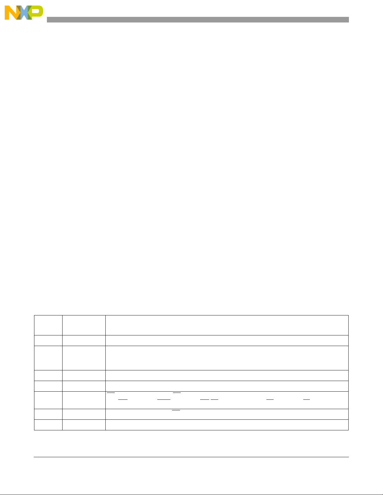
Signal Description
2.3.14.10 Internal Logic Supply Input
V
DD
VDD is the 1.5 V logic supply input.
2.3.14.11 External I/O Supply Input
V
DDEn
V
is the 1.8–3.3 V, with a tolerance of +/– 10% external I/O supply input.
DDEn
2.3.14.12 External I/O Supply Input
V
DDEHn
V
DDEHn
is the 3.3–5.0 V, with a tolerance of -10% to +5% external I/O supply input.
2.3.14.13 Fixed 3.3 V Internal Supply Input
V
DD33
V
is the 3.3 V internal supply input.
DD33
2.3.14.14 Ground
V
SS
VSS is the ground reference input.
2.3.15 I/O Power and Ground Segmentation
Table 2-3 gives the preliminary power/ground segmentation. Each segment provides the power and ground
for the I/O pins and can be powered by any voltage within the allowed voltage range regardless of the
power on the other segments. The power/ground segmentation applies regardless of whether a particular
pin is configured for its primary function or GPIO.
Table 2-3. MPC5565 Power / Ground Segmentation for 324 Pin Package
Power
Segment
V
DDA0
V
DDA1
V
SSA0
V
SSA1
V
DDE2
2
V
DDE3
V
DDE5
2-42 Freescale Semiconductor
Volt ag e
1
Range
5.0 V AN[22:35]
AN[0]_DAN0+, AN[1]_DAN0-, AN[2]_DAN1+, AN[3]_DAN1-, AN[4]_DAN2+, AN[5]_DAN2-,
5.0 V
GND —
GND —
1.8–3.3 V
1.8–3.3 V DATA[0:15]_GPIO[28:43], OE_GPIO[68], GPIO[206:207]
1.8–3.3 V CLKOUT, ENGCLK
AN[6]_DAN3+, AN[7]_DAN3-, AN[8]_ANW, AN[9]_ANX, AN[10]_ANY, AN[11]_ANZ, AN[16:21],
AN[36:39]
[0]_ADDR[8]_GPIO[0], CS[2:3]_ADDR[10:11]_GPIO[2:3], ADDR[12:31]_GPIO[4:27],
CS
RD_WR
_GPIO[62], BDIP_GPIO[63], WE/BE[0:1]_GPIO[64:65], TS_GPIO[69], TA_GPIO[70]
MPC5565 Microcontroller Reference Manual, Rev. 1.0
I/O Pins Powered by Segment
Page 100
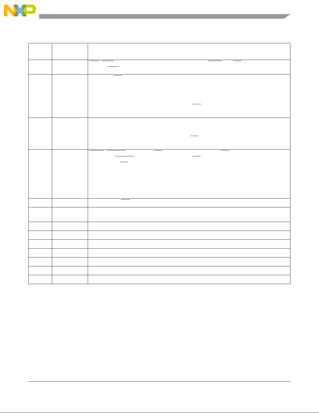
Signal Description
Table 2-3. MPC5565 Power / Ground Segmentation for 324 Pin Package (continued)
Power
Segment
V
DDE7
Volt ag e
Range
1.8–3.3 V
1
EVTI
JCOMP, TEST
TCRCLKA_IRQ
, EVTO, MCKO, MDO[3:0], MDO[11:4]_GPIO[82:75], MSEO[1:0], RDY, TCK, TDI, TDO, TMS,
[7]_GPIO[113], ETPUA[0:3]_ETPUA[12:15]_GPIO[114:117],
ETPUA[4:7]_ETPUA[16:19]_GPIO[118:121], ETPUA[8:11]_ETPUA[20:23]_GPIO[122:125],
ETPUA[12]_PCSB[1]_GPIO[126], ETPUA[14]_PCSB[4]_GPIO[128],
V
DDEH1
3.3–5.0 V
ETPUA[15]_PCSB[5]_GPIO[129], ETPUA[16]_PCSD[1]_GPIO[130],
ETPUA[17]_PCSD[2]_GPIO[131], ETPUA[18]_PCSD[3]_GPIO[132],
ETPUA[19]_PCSD[4]_GPIO[133], ETPUA[20:27]_IRQ
ETPUA[28:31]_PCSC[1:4]_GPIO[142:145]
CNTXA_TXDA_GPIO[83], CNRXA_RXDA_GPIO[84], CNTXB_PCSC[3]_GPIO[85],
CNRXB_PCSC[4]_ GPIO[86], EMIOS[0:9]_ETPUA[0:9]_GPIO[179:188],
V
DDEH4
3.3–5.0 V
EMIOS[10:11]_PCSD[3:4]_GPIO[189:190], EMIOS[12]_SOUTC_GPIO[191],
EMIOS[13]_SOUTD_GPIO[192], EMIOS[14:15]_IRQ
EMIOS[16:23]_GPIO[195:202]
RESET, RSTOUT, PLLCFG[0]_IRQ[4]_GPIO[208], PLLCFG[1]_IRQ[5]_SOUTD_GPIO[209],
PLLCFG[2], RSTCFG
_GPIO[210], BOOTCFG[0]_IRQ[2]_GPIO[211],
BOOTCFG[1]_IRQ[3]_GPIO[212], WKPCFG_GPIO[213], CNTXC_PCSD[3]_GPIO[87],
V
DDEH6
3.3–5.0 V
CNRXC_PCSD[4]_GPIO[88], TXDA_GPIO[89], RXDA_GPIO[90], TXDB_PCSD[1]_GPIO[91],
RXDB_PCSD[5]_GPIO[92], PCSC[1]_GPIO[93], PCSC[2]_GPIO[94], PCSC[5]_GPIO[95],
PCSD[2]_GPIO[96], PCSB[2]_GPIO[97], SCKD_GPIO[98], SIND_GPIO[99],
SOUTD_GPIO[100], PCSB[3]_GPIO[101], PCSB[3]_SINC_GPIO[108],
PCSB[4]_SCKC_GPIO[109], PCSB[5]_PCSC[0]_GPIO[110], EMIOS[14:15]_GPIO[203:204]
V
DDEH9
V
DDEH10
V
DDSYN
V
RC33
V
DD33
V
FLASH
V
PP
V
STBY
3.3–5.0 V AN[12]_MA[0]_SDS, AN[13]_MA[1]_SDO, AN[14]_MA[2]_SDI, AN[15]_FCK
3.3–5.0 V
SCKB_PCSC[1]_GPIO[102], SINB_PCSC[2]_GPIO[103], SOUTB_PCSC[5]_GPIO[104],
PCSB[0]_PCSD[2]_GPIO[105], PCSB[1]_PCSD[0]_GPIO[106], PCSB[2]_SOUTC_GPIO[107]
3.3 V EXTAL_EXTCLK, XTAL
3.3 V V
RCCTL
3.0–3.6 V —
3.0–3.6 V —
4.5–5.25 V
2
0.9–1.1 V —
NC — No connect
1
These are nominal voltages. V
+5% and –10%. V
2
During read operations, VPP can be as high as 5.3 V or as low as 3.0 V.
is ± 10%; V
RC33
is 1.62–3.6 V; V
DDE
DDSYN
is ± 10%; V
DDEH
is 3.0–5.5 V. All V
is –10% to + 5%.
DDA1
I/O Pins Powered by Segment
[8:15]_GPIO[134:141],
[0:1]_GPIO[193:194],
—
voltages are ± 10%; V
DDE
voltages are
DDEH
MPC5565 Microcontroller Reference Manual, Rev. 1.0
Freescale Semiconductor 2-43
 Loading...