

Page 1

Freescale Semiconductor
MPC5553_MPC5554_RM
Rev. 5.1, 03/2012
MPC5553/5554 Microcontroller
Reference Manual
by: Microcontroller Solutions Group
This is the MPC5553/5554 Microcontroller Reference Manual set consisting of the following files:
• MPC5553/5554 Reference Manual Addendum, Rev 3
• MPC5553/5554 Microcontroller Reference Manual, Rev 5
© Freescale Semiconductor, Inc., 2012. All rights reserved.
Page 2

Freescale Semiconductor
Reference Manual Addendum
MPC5553_MPC5554_RMAD
Rev. 3, 03/2012
MPC5553/5554 Reference Manual
Addendum
by: Microcontroller Solutions Group
This errata document describes corrections to the
MPC5553/5554 Microcontroller Reference Manual,
order number MPC5553_MPC5554_RM. For
convenience, the addenda items are grouped by revision.
Please check our website at http://www.freescale.com/
for the latest updates.
The current version available of the MPC5553/5554
Microcontroller Reference Manual is Revision 5.
Table of Contents
1 Errata for Revision 5 . . . . . . . . . . . . . . . . . . . . . . . 2
2 Revision History . . . . . . . . . . . . . . . . . . . . . . . . . . 2
© Freescale Semiconductor, Inc., 2009-2012. All rights reserved.
Page 3

Errata for Revision 5
1 Errata for Revision 5
Table 1. MPC5553/5554 Reference Manual Rev. 5 Errata
Location Description
Table 2-1/Page 2-19 Change V
Table 2-2/Page 2-33 Change V
pin for 416 package from J23 to “—” (N/C).
DDEH10
pin for 416 package from D14 to “—” (N/C).
DDEH10
2 Revision History
Table 2 provides a revision history for this document.
Table 2. Revision History Table
Rev. Number Substantive Changes Date of Release
1.0 Changes in Rev. 1 of this errata have been incorporated in MPC5553/5554
Reference Manual Rev. 5.
2.0 Not publicly released. Changes in Rev. 2 of this errata have been incorporated
in MPC5553/5554 Reference Manual Rev. 5.
3.0 Correct errors in Table 2-1 and Table 2-2 for V
pin for 416 package. 03/2012
DDEH10
10/2009
—
MPC5553/5554 Reference Manual Addendum, Rev. 3
Freescale Semiconductor2
Page 4

MPC5553/5554 Microcontroller
MPC5553_MPC5554_RM
Rev. 5
December 2011
Reference Manual
Devices Supported:
MPC5553
MPC5554
MPC5553/MPC5554 Microcontroller Reference Manual, Rev. 5
Freescale Semiconductor 1
Page 5

MPC5553/MPC5554 Microcontroller Reference Manual, Rev. 5
2 Freescale Semiconductor
Page 6

Chapter 1
Overview
1.1 Introduction . . . . . . . . . . . . . . . . . . . . . . . . . . . . . . . . . . . . . . . . . . . . . . . . . . . . . . . . . . . . . . . . . 1-1
1.2 Features . . . . . . . . . . . . . . . . . . . . . . . . . . . . . . . . . . . . . . . . . . . . . . . . . . . . . . . . . . . . . . . . . . . . 1-5
1.3 MPC5553-Specific Modules . . . . . . . . . . . . . . . . . . . . . . . . . . . . . . . . . . . . . . . . . . . . . . . . . . . 1-11
1.4 MPC5500 Family Comparison . . . . . . . . . . . . . . . . . . . . . . . . . . . . . . . . . . . . . . . . . . . . . . . . . . 1-12
1.5 Detailed Features . . . . . . . . . . . . . . . . . . . . . . . . . . . . . . . . . . . . . . . . . . . . . . . . . . . . . . . . . . . . 1-13
1.5.1 e200z6 Core Overview . . . . . . . . . . . . . . . . . . . . . . . . . . . . . . . . . . . . . . . . . . . . . . . . 1-13
1.5.2 System Bus Crossbar Switch . . . . . . . . . . . . . . . . . . . . . . . . . . . . . . . . . . . . . . . . . . . . 1-14
1.5.3 eDMA . . . . . . . . . . . . . . . . . . . . . . . . . . . . . . . . . . . . . . . . . . . . . . . . . . . . . . . . . . . . . 1-15
1.5.4 INTC . . . . . . . . . . . . . . . . . . . . . . . . . . . . . . . . . . . . . . . . . . . . . . . . . . . . . . . . . . . . . . 1-15
1.5.5 FMPLL . . . . . . . . . . . . . . . . . . . . . . . . . . . . . . . . . . . . . . . . . . . . . . . . . . . . . . . . . . . . . 1-15
1.5.6 EBI . . . . . . . . . . . . . . . . . . . . . . . . . . . . . . . . . . . . . . . . . . . . . . . . . . . . . . . . . . . . . . . . 1-15
1.5.7 SIU . . . . . . . . . . . . . . . . . . . . . . . . . . . . . . . . . . . . . . . . . . . . . . . . . . . . . . . . . . . . . . . . 1-16
1.5.8 ECSM . . . . . . . . . . . . . . . . . . . . . . . . . . . . . . . . . . . . . . . . . . . . . . . . . . . . . . . . . . . . . . 1-16
1.5.9 Flash . . . . . . . . . . . . . . . . . . . . . . . . . . . . . . . . . . . . . . . . . . . . . . . . . . . . . . . . . . . . . . . 1-16
1.5.10 Cache . . . . . . . . . . . . . . . . . . . . . . . . . . . . . . . . . . . . . . . . . . . . . . . . . . . . . . . . . . . . . . 1-16
1.5.11 SRAM . . . . . . . . . . . . . . . . . . . . . . . . . . . . . . . . . . . . . . . . . . . . . . . . . . . . . . . . . . . . . 1-17
1.5.12 BAM . . . . . . . . . . . . . . . . . . . . . . . . . . . . . . . . . . . . . . . . . . . . . . . . . . . . . . . . . . . . . . 1-17
1.5.13 eMIOS . . . . . . . . . . . . . . . . . . . . . . . . . . . . . . . . . . . . . . . . . . . . . . . . . . . . . . . . . . . . . 1-17
1.5.14 eTPU . . . . . . . . . . . . . . . . . . . . . . . . . . . . . . . . . . . . . . . . . . . . . . . . . . . . . . . . . . . . . . 1-17
1.5.15 eQADC . . . . . . . . . . . . . . . . . . . . . . . . . . . . . . . . . . . . . . . . . . . . . . . . . . . . . . . . . . . . 1-18
1.5.16 DSPI . . . . . . . . . . . . . . . . . . . . . . . . . . . . . . . . . . . . . . . . . . . . . . . . . . . . . . . . . . . . . . . 1-18
1.5.17 eSCI . . . . . . . . . . . . . . . . . . . . . . . . . . . . . . . . . . . . . . . . . . . . . . . . . . . . . . . . . . . . . . . 1-18
1.5.18 FlexCAN . . . . . . . . . . . . . . . . . . . . . . . . . . . . . . . . . . . . . . . . . . . . . . . . . . . . . . . . . . . 1-19
1.5.19 NDI . . . . . . . . . . . . . . . . . . . . . . . . . . . . . . . . . . . . . . . . . . . . . . . . . . . . . . . . . . . . . . . 1-19
1.5.20 JTAGC . . . . . . . . . . . . . . . . . . . . . . . . . . . . . . . . . . . . . . . . . . . . . . . . . . . . . . . . . . . . . 1-19
1.5.21 FEC (MPC5553 Only) . . . . . . . . . . . . . . . . . . . . . . . . . . . . . . . . . . . . . . . . . . . . . . . . . 1-19
1.5.22 Calibration Bus (MPC5553 Only) . . . . . . . . . . . . . . . . . . . . . . . . . . . . . . . . . . . . . . . . 1-20
1.6 MPC5500 Family Memory Map . . . . . . . . . . . . . . . . . . . . . . . . . . . . . . . . . . . . . . . . . . . . . . . . 1-20
1.7 Multi-Master Operation Memory Map . . . . . . . . . . . . . . . . . . . . . . . . . . . . . . . . . . . . . . . . . . . 1-23
1.8 Revision History . . . . . . . . . . . . . . . . . . . . . . . . . . . . . . . . . . . . . . . . . . . . . . . . . . . . . . . . . . . . . 1-25
Chapter 2
Signal Description
2.1 Block Diagram . . . . . . . . . . . . . . . . . . . . . . . . . . . . . . . . . . . . . . . . . . . . . . . . . . . . . . . . . . . . . . . 2-1
2.2 External Signal Description . . . . . . . . . . . . . . . . . . . . . . . . . . . . . . . . . . . . . . . . . . . . . . . . . . . . . 2-4
2.2.1 MPC5553 Signals Summary . . . . . . . . . . . . . . . . . . . . . . . . . . . . . . . . . . . . . . . . . . . . . 2-5
2.2.2 MPC5554 Signals Summary . . . . . . . . . . . . . . . . . . . . . . . . . . . . . . . . . . . . . . . . . . . . 2-22
2.3 Detailed Signal Description . . . . . . . . . . . . . . . . . . . . . . . . . . . . . . . . . . . . . . . . . . . . . . . . . . . . 2-36
2.3.1 Reset / Configuration Signals . . . . . . . . . . . . . . . . . . . . . . . . . . . . . . . . . . . . . . . . . . . 2-36
2.3.2 External Bus Interface (EBI) Signals . . . . . . . . . . . . . . . . . . . . . . . . . . . . . . . . . . . . . . 2-37
2.3.3 External Data Signals . . . . . . . . . . . . . . . . . . . . . . . . . . . . . . . . . . . . . . . . . . . . . . . . . . 2-38
2.3.4 Nexus Signals . . . . . . . . . . . . . . . . . . . . . . . . . . . . . . . . . . . . . . . . . . . . . . . . . . . . . . . 2-43
MPC5553/MPC5554 Microcontroller Reference Manual, Rev. 5
Freescale Semiconductor i
Page 7

2.3.5 JTAG Signals . . . . . . . . . . . . . . . . . . . . . . . . . . . . . . . . . . . . . . . . . . . . . . . . . . . . . . . . 2-44
2.3.6 FlexCAN Signals . . . . . . . . . . . . . . . . . . . . . . . . . . . . . . . . . . . . . . . . . . . . . . . . . . . . . 2-45
2.3.7 eSCI Signals . . . . . . . . . . . . . . . . . . . . . . . . . . . . . . . . . . . . . . . . . . . . . . . . . . . . . . . . . 2-46
2.3.8 DSPI Signals . . . . . . . . . . . . . . . . . . . . . . . . . . . . . . . . . . . . . . . . . . . . . . . . . . . . . . . . 2-46
2.3.9 eQADC Signals . . . . . . . . . . . . . . . . . . . . . . . . . . . . . . . . . . . . . . . . . . . . . . . . . . . . . . 2-49
2.3.10 eTPU Signals . . . . . . . . . . . . . . . . . . . . . . . . . . . . . . . . . . . . . . . . . . . . . . . . . . . . . . . . 2-52
2.3.11 eMIOS Signals . . . . . . . . . . . . . . . . . . . . . . . . . . . . . . . . . . . . . . . . . . . . . . . . . . . . . . . 2-54
2.3.12 GPIO Signals . . . . . . . . . . . . . . . . . . . . . . . . . . . . . . . . . . . . . . . . . . . . . . . . . . . . . . . . 2-54
2.3.13 Clock Synthesizer Signals . . . . . . . . . . . . . . . . . . . . . . . . . . . . . . . . . . . . . . . . . . . . . . 2-55
2.3.14 Power/Ground Signals . . . . . . . . . . . . . . . . . . . . . . . . . . . . . . . . . . . . . . . . . . . . . . . . . 2-55
2.3.15 I/O Power/Ground Segmentation . . . . . . . . . . . . . . . . . . . . . . . . . . . . . . . . . . . . . . . . . 2-57
2.4 eTPU Pin Connections and Serialization . . . . . . . . . . . . . . . . . . . . . . . . . . . . . . . . . . . . . . . . . . 2-61
2.4.1 ETPUA[0:15] . . . . . . . . . . . . . . . . . . . . . . . . . . . . . . . . . . . . . . . . . . . . . . . . . . . . . . . . 2-61
2.4.2 ETPUA[16:31] . . . . . . . . . . . . . . . . . . . . . . . . . . . . . . . . . . . . . . . . . . . . . . . . . . . . . . . 2-63
2.4.3 ETPUB[0:31] æ MPC5554 Only . . . . . . . . . . . . . . . . . . . . . . . . . . . . . . . . . . . . . . . . 2-64
2.5 eMIOS Pin Connections and Serialization . . . . . . . . . . . . . . . . . . . . . . . . . . . . . . . . . . . . . . . . . 2-66
2.6 Revision History . . . . . . . . . . . . . . . . . . . . . . . . . . . . . . . . . . . . . . . . . . . . . . . . . . . . . . . . . . . . . 2-67
Chapter 3
e200z6 Core Complex
3.1 Introduction . . . . . . . . . . . . . . . . . . . . . . . . . . . . . . . . . . . . . . . . . . . . . . . . . . . . . . . . . . . . . . . . . 3-1
3.1.1 Block Diagram . . . . . . . . . . . . . . . . . . . . . . . . . . . . . . . . . . . . . . . . . . . . . . . . . . . . . . . . 3-2
3.1.2 Overview . . . . . . . . . . . . . . . . . . . . . . . . . . . . . . . . . . . . . . . . . . . . . . . . . . . . . . . . . . . . 3-2
3.1.3 Features . . . . . . . . . . . . . . . . . . . . . . . . . . . . . . . . . . . . . . . . . . . . . . . . . . . . . . . . . . . . . 3-3
3.1.4 Microarchitecture Summary . . . . . . . . . . . . . . . . . . . . . . . . . . . . . . . . . . . . . . . . . . . . . 3-5
3.2 Core Registers and Programmer’s Model . . . . . . . . . . . . . . . . . . . . . . . . . . . . . . . . . . . . . . . . . . 3-6
3.2.1 Power Architecture Registers . . . . . . . . . . . . . . . . . . . . . . . . . . . . . . . . . . . . . . . . . . . . 3-8
3.2.2 Core-Specific Registers . . . . . . . . . . . . . . . . . . . . . . . . . . . . . . . . . . . . . . . . . . . . . . . . 3-10
3.2.3 e200Z6 Core Complex Features Not Supported in the MPC5553/MPC5554 . . . . . . . 3-11
3.3 Functional Description . . . . . . . . . . . . . . . . . . . . . . . . . . . . . . . . . . . . . . . . . . . . . . . . . . . . . . . . 3-13
3.3.1 Memory Management Unit (MMU) . . . . . . . . . . . . . . . . . . . . . . . . . . . . . . . . . . . . . . 3-13
3.3.2 L1 Cache . . . . . . . . . . . . . . . . . . . . . . . . . . . . . . . . . . . . . . . . . . . . . . . . . . . . . . . . . . . 3-20
3.3.3 Interrupt Types . . . . . . . . . . . . . . . . . . . . . . . . . . . . . . . . . . . . . . . . . . . . . . . . . . . . . . . 3-24
3.3.4 Bus Interface Unit (BIU) . . . . . . . . . . . . . . . . . . . . . . . . . . . . . . . . . . . . . . . . . . . . . . . 3-25
3.3.5 Timer Facilities . . . . . . . . . . . . . . . . . . . . . . . . . . . . . . . . . . . . . . . . . . . . . . . . . . . . . . 3-26
3.3.6 Signal Processing Extension APU (SPE APU) . . . . . . . . . . . . . . . . . . . . . . . . . . . . . . 3-26
3.3.7 SPE Programming Model . . . . . . . . . . . . . . . . . . . . . . . . . . . . . . . . . . . . . . . . . . . . . . 3-27
3.4 External References . . . . . . . . . . . . . . . . . . . . . . . . . . . . . . . . . . . . . . . . . . . . . . . . . . . . . . . . . . 3-27
3.5 Revision History . . . . . . . . . . . . . . . . . . . . . . . . . . . . . . . . . . . . . . . . . . . . . . . . . . . . . . . . . . . . . 3-28
Chapter 4
Reset
4.1 Introduction . . . . . . . . . . . . . . . . . . . . . . . . . . . . . . . . . . . . . . . . . . . . . . . . . . . . . . . . . . . . . . . . . 4-1
4.2 External Signal Description . . . . . . . . . . . . . . . . . . . . . . . . . . . . . . . . . . . . . . . . . . . . . . . . . . . . . 4-2
MPC5553/MPC5554 Microcontroller Reference Manual, Rev. 5
Freescale Semiconductor ii
Page 8

4.2.1 Reset Input (RESET) . . . . . . . . . . . . . . . . . . . . . . . . . . . . . . . . . . . . . . . . . . . . . . . . . . . 4-2
4.2.2 Reset Output (RSTOUT) . . . . . . . . . . . . . . . . . . . . . . . . . . . . . . . . . . . . . . . . . . . . . . . . 4-2
4.2.3 Reset Configuration (RSTCFG) . . . . . . . . . . . . . . . . . . . . . . . . . . . . . . . . . . . . . . . . . . 4-2
4.2.4 Weak Pull Configuration (WKPCFG) . . . . . . . . . . . . . . . . . . . . . . . . . . . . . . . . . . . . . . 4-2
4.2.5 Boot Configuration (BOOTCFG[0:1]) . . . . . . . . . . . . . . . . . . . . . . . . . . . . . . . . . . . . . 4-3
4.3 Memory Map/Register Definition . . . . . . . . . . . . . . . . . . . . . . . . . . . . . . . . . . . . . . . . . . . . . . . . 4-3
4.3.1 Register Descriptions . . . . . . . . . . . . . . . . . . . . . . . . . . . . . . . . . . . . . . . . . . . . . . . . . . . 4-3
4.4 Functional Description . . . . . . . . . . . . . . . . . . . . . . . . . . . . . . . . . . . . . . . . . . . . . . . . . . . . . . . . . 4-7
4.4.1 Reset Vector Locations . . . . . . . . . . . . . . . . . . . . . . . . . . . . . . . . . . . . . . . . . . . . . . . . . 4-7
4.4.2 Reset Sources . . . . . . . . . . . . . . . . . . . . . . . . . . . . . . . . . . . . . . . . . . . . . . . . . . . . . . . . . 4-7
4.4.3 Reset Configuration and Configuration Pins . . . . . . . . . . . . . . . . . . . . . . . . . . . . . . . . 4-10
4.4.4 Reset Configuration Timing . . . . . . . . . . . . . . . . . . . . . . . . . . . . . . . . . . . . . . . . . . . . . 4-15
4.4.5 Reset Flow . . . . . . . . . . . . . . . . . . . . . . . . . . . . . . . . . . . . . . . . . . . . . . . . . . . . . . . . . . 4-17
4.5 Revision History . . . . . . . . . . . . . . . . . . . . . . . . . . . . . . . . . . . . . . . . . . . . . . . . . . . . . . . . . . . . . 4-19
Chapter 5
Peripheral Bridge (PBRIDGE_A, PBRIDGE_B)
5.1 Introduction . . . . . . . . . . . . . . . . . . . . . . . . . . . . . . . . . . . . . . . . . . . . . . . . . . . . . . . . . . . . . . . . . 5-1
5.1.1 Block Diagram . . . . . . . . . . . . . . . . . . . . . . . . . . . . . . . . . . . . . . . . . . . . . . . . . . . . . . . . 5-1
5.1.2 Overview . . . . . . . . . . . . . . . . . . . . . . . . . . . . . . . . . . . . . . . . . . . . . . . . . . . . . . . . . . . . 5-1
5.1.3 Features . . . . . . . . . . . . . . . . . . . . . . . . . . . . . . . . . . . . . . . . . . . . . . . . . . . . . . . . . . . . . 5-3
5.1.4 Modes of Operation . . . . . . . . . . . . . . . . . . . . . . . . . . . . . . . . . . . . . . . . . . . . . . . . . . . . 5-3
5.2 External Signal Description . . . . . . . . . . . . . . . . . . . . . . . . . . . . . . . . . . . . . . . . . . . . . . . . . . . . . 5-4
5.3 Memory Map/Register Definition . . . . . . . . . . . . . . . . . . . . . . . . . . . . . . . . . . . . . . . . . . . . . . . . 5-4
5.3.1 Register Descriptions . . . . . . . . . . . . . . . . . . . . . . . . . . . . . . . . . . . . . . . . . . . . . . . . . . . 5-5
5.4 Functional Description . . . . . . . . . . . . . . . . . . . . . . . . . . . . . . . . . . . . . . . . . . . . . . . . . . . . . . . . 5-12
5.4.1 Access Support . . . . . . . . . . . . . . . . . . . . . . . . . . . . . . . . . . . . . . . . . . . . . . . . . . . . . . 5-12
5.4.2 Peripheral Write Buffering . . . . . . . . . . . . . . . . . . . . . . . . . . . . . . . . . . . . . . . . . . . . . . 5-12
5.4.3 General Operation . . . . . . . . . . . . . . . . . . . . . . . . . . . . . . . . . . . . . . . . . . . . . . . . . . . . 5-13
5.5 Revision History . . . . . . . . . . . . . . . . . . . . . . . . . . . . . . . . . . . . . . . . . . . . . . . . . . . . . . . . . . . . . 5-15
Chapter 6
System Integration Unit (SIU)
6.1 Introduction . . . . . . . . . . . . . . . . . . . . . . . . . . . . . . . . . . . . . . . . . . . . . . . . . . . . . . . . . . . . . . . . . 6-1
6.1.1 Block Diagram . . . . . . . . . . . . . . . . . . . . . . . . . . . . . . . . . . . . . . . . . . . . . . . . . . . . . . . . 6-2
6.1.2 Overview . . . . . . . . . . . . . . . . . . . . . . . . . . . . . . . . . . . . . . . . . . . . . . . . . . . . . . . . . . . . 6-2
6.1.3 Features . . . . . . . . . . . . . . . . . . . . . . . . . . . . . . . . . . . . . . . . . . . . . . . . . . . . . . . . . . . . . 6-3
6.1.4 Modes of Operation . . . . . . . . . . . . . . . . . . . . . . . . . . . . . . . . . . . . . . . . . . . . . . . . . . . . 6-3
6.1.5 Normal Mode . . . . . . . . . . . . . . . . . . . . . . . . . . . . . . . . . . . . . . . . . . . . . . . . . . . . . . . . . 6-3
6.1.6 Debug Mode . . . . . . . . . . . . . . . . . . . . . . . . . . . . . . . . . . . . . . . . . . . . . . . . . . . . . . . . . 6-3
6.2 External Signal Description . . . . . . . . . . . . . . . . . . . . . . . . . . . . . . . . . . . . . . . . . . . . . . . . . . . . . 6-4
6.2.1 Detailed Signal Descriptions . . . . . . . . . . . . . . . . . . . . . . . . . . . . . . . . . . . . . . . . . . . . . 6-4
6.3 Memory Map/Register Definition . . . . . . . . . . . . . . . . . . . . . . . . . . . . . . . . . . . . . . . . . . . . . . . . 6-7
6.3.1 Register Descriptions . . . . . . . . . . . . . . . . . . . . . . . . . . . . . . . . . . . . . . . . . . . . . . . . . . . 6-8
MPC5553/MPC5554 Microcontroller Reference Manual, Rev. 5
Freescale Semiconductor iii
Page 9

6.4 Functional Description . . . . . . . . . . . . . . . . . . . . . . . . . . . . . . . . . . . . . . . . . . . . . . . . . . . . . . . 6-105
6.4.1 System Configuration . . . . . . . . . . . . . . . . . . . . . . . . . . . . . . . . . . . . . . . . . . . . . . . . 6-105
6.4.2 Reset Control . . . . . . . . . . . . . . . . . . . . . . . . . . . . . . . . . . . . . . . . . . . . . . . . . . . . . . . 6-106
6.4.3 External Interrupt . . . . . . . . . . . . . . . . . . . . . . . . . . . . . . . . . . . . . . . . . . . . . . . . . . . . 6-106
6.4.4 GPIO Operation . . . . . . . . . . . . . . . . . . . . . . . . . . . . . . . . . . . . . . . . . . . . . . . . . . . . . 6-107
6.4.5 Internal Multiplexing . . . . . . . . . . . . . . . . . . . . . . . . . . . . . . . . . . . . . . . . . . . . . . . . . 6-107
6.5 Revision History . . . . . . . . . . . . . . . . . . . . . . . . . . . . . . . . . . . . . . . . . . . . . . . . . . . . . . . . . . . . 6-112
Chapter 7
Crossbar Switch (XBAR)
7.1 Introduction . . . . . . . . . . . . . . . . . . . . . . . . . . . . . . . . . . . . . . . . . . . . . . . . . . . . . . . . . . . . . . . . . 7-1
7.1.1 Block Diagram . . . . . . . . . . . . . . . . . . . . . . . . . . . . . . . . . . . . . . . . . . . . . . . . . . . . . . . . 7-1
7.1.2 Overview . . . . . . . . . . . . . . . . . . . . . . . . . . . . . . . . . . . . . . . . . . . . . . . . . . . . . . . . . . . . 7-2
7.1.3 Features . . . . . . . . . . . . . . . . . . . . . . . . . . . . . . . . . . . . . . . . . . . . . . . . . . . . . . . . . . . . . 7-2
7.1.4 Modes of Operation . . . . . . . . . . . . . . . . . . . . . . . . . . . . . . . . . . . . . . . . . . . . . . . . . . . . 7-3
7.2 Memory Map/Register Definition . . . . . . . . . . . . . . . . . . . . . . . . . . . . . . . . . . . . . . . . . . . . . . . . 7-3
7.2.1 Register Descriptions . . . . . . . . . . . . . . . . . . . . . . . . . . . . . . . . . . . . . . . . . . . . . . . . . . . 7-4
7.3 Functional Description . . . . . . . . . . . . . . . . . . . . . . . . . . . . . . . . . . . . . . . . . . . . . . . . . . . . . . . . . 7-8
7.3.1 Overview . . . . . . . . . . . . . . . . . . . . . . . . . . . . . . . . . . . . . . . . . . . . . . . . . . . . . . . . . . . . 7-8
7.3.2 General Operation . . . . . . . . . . . . . . . . . . . . . . . . . . . . . . . . . . . . . . . . . . . . . . . . . . . . . 7-8
7.3.3 Master Ports . . . . . . . . . . . . . . . . . . . . . . . . . . . . . . . . . . . . . . . . . . . . . . . . . . . . . . . . . . 7-9
7.3.4 Slave Ports . . . . . . . . . . . . . . . . . . . . . . . . . . . . . . . . . . . . . . . . . . . . . . . . . . . . . . . . . . . 7-9
7.3.5 Priority Assignment . . . . . . . . . . . . . . . . . . . . . . . . . . . . . . . . . . . . . . . . . . . . . . . . . . . 7-10
7.3.6 Arbitration . . . . . . . . . . . . . . . . . . . . . . . . . . . . . . . . . . . . . . . . . . . . . . . . . . . . . . . . . . 7-10
7.4 Revision History . . . . . . . . . . . . . . . . . . . . . . . . . . . . . . . . . . . . . . . . . . . . . . . . . . . . . . . . . . . . . 7-12
Chapter 8
Error Correction Status Module (ECSM)
8.1 Introduction . . . . . . . . . . . . . . . . . . . . . . . . . . . . . . . . . . . . . . . . . . . . . . . . . . . . . . . . . . . . . . . . . 8-1
8.1.1 Overview . . . . . . . . . . . . . . . . . . . . . . . . . . . . . . . . . . . . . . . . . . . . . . . . . . . . . . . . . . . . 8-1
8.1.2 Features . . . . . . . . . . . . . . . . . . . . . . . . . . . . . . . . . . . . . . . . . . . . . . . . . . . . . . . . . . . . . 8-1
8.2 Memory Map/Register Definition . . . . . . . . . . . . . . . . . . . . . . . . . . . . . . . . . . . . . . . . . . . . . . . . 8-2
8.2.1 Register Descriptions . . . . . . . . . . . . . . . . . . . . . . . . . . . . . . . . . . . . . . . . . . . . . . . . . . . 8-3
8.3 Initialization/Application Information . . . . . . . . . . . . . . . . . . . . . . . . . . . . . . . . . . . . . . . . . . . . 8-15
8.4 Revision History . . . . . . . . . . . . . . . . . . . . . . . . . . . . . . . . . . . . . . . . . . . . . . . . . . . . . . . . . . . . . 8-16
Chapter 9
Enhanced Direct Memory Access (eDMA)
9.1 Introduction . . . . . . . . . . . . . . . . . . . . . . . . . . . . . . . . . . . . . . . . . . . . . . . . . . . . . . . . . . . . . . . . . 9-1
9.1.1 Block Diagram . . . . . . . . . . . . . . . . . . . . . . . . . . . . . . . . . . . . . . . . . . . . . . . . . . . . . . . . 9-2
9.1.2 Overview . . . . . . . . . . . . . . . . . . . . . . . . . . . . . . . . . . . . . . . . . . . . . . . . . . . . . . . . . . . . 9-2
9.1.3 Features . . . . . . . . . . . . . . . . . . . . . . . . . . . . . . . . . . . . . . . . . . . . . . . . . . . . . . . . . . . . . 9-2
9.1.4 Modes of Operation . . . . . . . . . . . . . . . . . . . . . . . . . . . . . . . . . . . . . . . . . . . . . . . . . . . . 9-3
9.2 External Signal Description . . . . . . . . . . . . . . . . . . . . . . . . . . . . . . . . . . . . . . . . . . . . . . . . . . . . . 9-3
MPC5553/MPC5554 Microcontroller Reference Manual, Rev. 5
Freescale Semiconductor iv
Page 10

9.3 Memory Map/Register Definition . . . . . . . . . . . . . . . . . . . . . . . . . . . . . . . . . . . . . . . . . . . . . . . . 9-4
9.3.1 Register Descriptions . . . . . . . . . . . . . . . . . . . . . . . . . . . . . . . . . . . . . . . . . . . . . . . . . . . 9-8
9.4 Functional Description . . . . . . . . . . . . . . . . . . . . . . . . . . . . . . . . . . . . . . . . . . . . . . . . . . . . . . . . 9-30
9.4.1 eDMA Microarchitecture . . . . . . . . . . . . . . . . . . . . . . . . . . . . . . . . . . . . . . . . . . . . . . . 9-30
9.4.2 eDMA Basic Data Flow . . . . . . . . . . . . . . . . . . . . . . . . . . . . . . . . . . . . . . . . . . . . . . . . 9-32
9.4.3 eDMA Performance . . . . . . . . . . . . . . . . . . . . . . . . . . . . . . . . . . . . . . . . . . . . . . . . . . . 9-34
9.5 Initialization / Application Information . . . . . . . . . . . . . . . . . . . . . . . . . . . . . . . . . . . . . . . . . . . 9-37
9.5.1 eDMA Initialization . . . . . . . . . . . . . . . . . . . . . . . . . . . . . . . . . . . . . . . . . . . . . . . . . . . 9-37
9.5.2 DMA Programming Errors . . . . . . . . . . . . . . . . . . . . . . . . . . . . . . . . . . . . . . . . . . . . . 9-39
9.5.3 DMA Request Assignments . . . . . . . . . . . . . . . . . . . . . . . . . . . . . . . . . . . . . . . . . . . . . 9-40
9.5.4 DMA Arbitration Mode Considerations . . . . . . . . . . . . . . . . . . . . . . . . . . . . . . . . . . . 9-42
9.5.5 DMA Transfer . . . . . . . . . . . . . . . . . . . . . . . . . . . . . . . . . . . . . . . . . . . . . . . . . . . . . . . 9-44
9.5.6 TCD Status . . . . . . . . . . . . . . . . . . . . . . . . . . . . . . . . . . . . . . . . . . . . . . . . . . . . . . . . . . 9-47
9.5.7 Channel Linking . . . . . . . . . . . . . . . . . . . . . . . . . . . . . . . . . . . . . . . . . . . . . . . . . . . . . 9-48
9.5.8 Dynamic Programming . . . . . . . . . . . . . . . . . . . . . . . . . . . . . . . . . . . . . . . . . . . . . . . . 9-49
9.6 Revision History . . . . . . . . . . . . . . . . . . . . . . . . . . . . . . . . . . . . . . . . . . . . . . . . . . . . . . . . . . . . . 9-50
Chapter 10
Interrupt Controller (INTC)
10.1 Introduction . . . . . . . . . . . . . . . . . . . . . . . . . . . . . . . . . . . . . . . . . . . . . . . . . . . . . . . . . . . . . . . . 10-1
10.1.1 Block Diagram . . . . . . . . . . . . . . . . . . . . . . . . . . . . . . . . . . . . . . . . . . . . . . . . . . . . . . . 10-2
10.1.2 Overview . . . . . . . . . . . . . . . . . . . . . . . . . . . . . . . . . . . . . . . . . . . . . . . . . . . . . . . . . . . 10-2
10.1.3 Features . . . . . . . . . . . . . . . . . . . . . . . . . . . . . . . . . . . . . . . . . . . . . . . . . . . . . . . . . . . . 10-5
10.1.4 Modes of Operation . . . . . . . . . . . . . . . . . . . . . . . . . . . . . . . . . . . . . . . . . . . . . . . . . . . 10-5
10.2 External Signal Description . . . . . . . . . . . . . . . . . . . . . . . . . . . . . . . . . . . . . . . . . . . . . . . . . . . . 10-7
10.3 Memory Map/Register Definition . . . . . . . . . . . . . . . . . . . . . . . . . . . . . . . . . . . . . . . . . . . . . . . 10-8
10.3.1 Register Descriptions . . . . . . . . . . . . . . . . . . . . . . . . . . . . . . . . . . . . . . . . . . . . . . . . . 10-10
10.4 Functional Description . . . . . . . . . . . . . . . . . . . . . . . . . . . . . . . . . . . . . . . . . . . . . . . . . . . . . . . 10-16
10.4.1 Interrupt Request Sources . . . . . . . . . . . . . . . . . . . . . . . . . . . . . . . . . . . . . . . . . . . . . 10-16
10.4.2 Priority Management . . . . . . . . . . . . . . . . . . . . . . . . . . . . . . . . . . . . . . . . . . . . . . . . . 10-29
10.4.3 Details on Handshaking with Processor . . . . . . . . . . . . . . . . . . . . . . . . . . . . . . . . . . 10-31
10.5 Initialization/Application Information . . . . . . . . . . . . . . . . . . . . . . . . . . . . . . . . . . . . . . . . . . . 10-33
10.5.1 Initialization Flow . . . . . . . . . . . . . . . . . . . . . . . . . . . . . . . . . . . . . . . . . . . . . . . . . . . 10-33
10.5.2 Interrupt Exception Handler . . . . . . . . . . . . . . . . . . . . . . . . . . . . . . . . . . . . . . . . . . . 10-33
10.5.3 ISR, RTOS, and Task Hierarchy . . . . . . . . . . . . . . . . . . . . . . . . . . . . . . . . . . . . . . . . 10-35
10.5.4 Order of Execution . . . . . . . . . . . . . . . . . . . . . . . . . . . . . . . . . . . . . . . . . . . . . . . . . . . 10-36
10.5.5 Priority Ceiling Protocol . . . . . . . . . . . . . . . . . . . . . . . . . . . . . . . . . . . . . . . . . . . . . . 10-37
10.5.6 Selecting Priorities According to Request Rates and Deadlines . . . . . . . . . . . . . . . . 10-40
10.5.7 Software Settable Interrupt Requests . . . . . . . . . . . . . . . . . . . . . . . . . . . . . . . . . . . . . 10-40
10.5.8 Lowering Priority Within an ISR . . . . . . . . . . . . . . . . . . . . . . . . . . . . . . . . . . . . . . . . 10-41
10.5.9 Negating an Interrupt Request Outside of its ISR . . . . . . . . . . . . . . . . . . . . . . . . . . . 10-41
10.5.10Examining LIFO contents . . . . . . . . . . . . . . . . . . . . . . . . . . . . . . . . . . . . . . . . . . . . . 10-42
10.6 Revision History . . . . . . . . . . . . . . . . . . . . . . . . . . . . . . . . . . . . . . . . . . . . . . . . . . . . . . . . . . . . 10-43
MPC5553/MPC5554 Microcontroller Reference Manual, Rev. 5
Freescale Semiconductor v
Page 11

Chapter 11
Frequency Modulated Phase Locked Loop (FMPLL) and System Clocks
11.1 Introduction . . . . . . . . . . . . . . . . . . . . . . . . . . . . . . . . . . . . . . . . . . . . . . . . . . . . . . . . . . . . . . . . 11-1
11.1.1 Block Diagrams . . . . . . . . . . . . . . . . . . . . . . . . . . . . . . . . . . . . . . . . . . . . . . . . . . . . . . 11-1
11.1.2 Overview . . . . . . . . . . . . . . . . . . . . . . . . . . . . . . . . . . . . . . . . . . . . . . . . . . . . . . . . . . . 11-8
11.1.3 Features . . . . . . . . . . . . . . . . . . . . . . . . . . . . . . . . . . . . . . . . . . . . . . . . . . . . . . . . . . . . 11-8
11.1.4 FMPLL Modes of Operation . . . . . . . . . . . . . . . . . . . . . . . . . . . . . . . . . . . . . . . . . . . . 11-9
11.2 External Signal Description . . . . . . . . . . . . . . . . . . . . . . . . . . . . . . . . . . . . . . . . . . . . . . . . . . . 11-12
11.3 Memory Map/Register Definition . . . . . . . . . . . . . . . . . . . . . . . . . . . . . . . . . . . . . . . . . . . . . . 11-12
11.3.1 Register Descriptions . . . . . . . . . . . . . . . . . . . . . . . . . . . . . . . . . . . . . . . . . . . . . . . . . 11-12
11.4 Functional Description . . . . . . . . . . . . . . . . . . . . . . . . . . . . . . . . . . . . . . . . . . . . . . . . . . . . . . . 11-20
11.4.1 Clock Architecture . . . . . . . . . . . . . . . . . . . . . . . . . . . . . . . . . . . . . . . . . . . . . . . . . . . 11-20
11.4.2 Clock Operation . . . . . . . . . . . . . . . . . . . . . . . . . . . . . . . . . . . . . . . . . . . . . . . . . . . . . 11-22
11.4.3 Clock Configuration . . . . . . . . . . . . . . . . . . . . . . . . . . . . . . . . . . . . . . . . . . . . . . . . . 11-25
11.5 Revision History . . . . . . . . . . . . . . . . . . . . . . . . . . . . . . . . . . . . . . . . . . . . . . . . . . . . . . . . . . . . 11-33
Chapter 12
External Bus Interface (EBI)
12.1 Introduction . . . . . . . . . . . . . . . . . . . . . . . . . . . . . . . . . . . . . . . . . . . . . . . . . . . . . . . . . . . . . . . . 12-1
12.1.1 Block Diagram . . . . . . . . . . . . . . . . . . . . . . . . . . . . . . . . . . . . . . . . . . . . . . . . . . . . . . . 12-2
12.1.2 Overview . . . . . . . . . . . . . . . . . . . . . . . . . . . . . . . . . . . . . . . . . . . . . . . . . . . . . . . . . . . 12-3
12.1.3 Features . . . . . . . . . . . . . . . . . . . . . . . . . . . . . . . . . . . . . . . . . . . . . . . . . . . . . . . . . . . . 12-3
12.1.4 Modes of Operation . . . . . . . . . . . . . . . . . . . . . . . . . . . . . . . . . . . . . . . . . . . . . . . . . . . 12-4
12.2 External Signal Description . . . . . . . . . . . . . . . . . . . . . . . . . . . . . . . . . . . . . . . . . . . . . . . . . . . . 12-6
12.2.1 Detailed Signal Descriptions . . . . . . . . . . . . . . . . . . . . . . . . . . . . . . . . . . . . . . . . . . . . 12-7
12.2.2 Signal Function/Direction by Mode . . . . . . . . . . . . . . . . . . . . . . . . . . . . . . . . . . . . . 12-11
12.3 Memory Map/Register Definition . . . . . . . . . . . . . . . . . . . . . . . . . . . . . . . . . . . . . . . . . . . . . . 12-13
12.3.1 Register Descriptions . . . . . . . . . . . . . . . . . . . . . . . . . . . . . . . . . . . . . . . . . . . . . . . . . 12-13
12.4 Functional Description . . . . . . . . . . . . . . . . . . . . . . . . . . . . . . . . . . . . . . . . . . . . . . . . . . . . . . . 12-20
12.4.1 External Bus Interface Features . . . . . . . . . . . . . . . . . . . . . . . . . . . . . . . . . . . . . . . . . 12-20
12.4.2 External Bus Operations . . . . . . . . . . . . . . . . . . . . . . . . . . . . . . . . . . . . . . . . . . . . . . 12-26
12.5 Initialization/Application Information . . . . . . . . . . . . . . . . . . . . . . . . . . . . . . . . . . . . . . . . . . . 12-68
12.5.1 Booting from External Memory . . . . . . . . . . . . . . . . . . . . . . . . . . . . . . . . . . . . . . . . 12-68
12.5.2 Running with SDR (Single Data Rate) Burst Memories . . . . . . . . . . . . . . . . . . . . . . 12-68
12.5.3 Running with Asynchronous Memories . . . . . . . . . . . . . . . . . . . . . . . . . . . . . . . . . . 12-68
12.5.4 Connecting an MCU to Multiple Memories . . . . . . . . . . . . . . . . . . . . . . . . . . . . . . . 12-71
12.5.5 Dual-MCU Operation with Reduced Pinout MCUs . . . . . . . . . . . . . . . . . . . . . . . . . 12-71
12.5.6 Summary of Differences from MPC5xx . . . . . . . . . . . . . . . . . . . . . . . . . . . . . . . . . . 12-72
12.6 Revision History . . . . . . . . . . . . . . . . . . . . . . . . . . . . . . . . . . . . . . . . . . . . . . . . . . . . . . . . . . . . 12-74
Chapter 13
Flash Memory
13.1 Introduction . . . . . . . . . . . . . . . . . . . . . . . . . . . . . . . . . . . . . . . . . . . . . . . . . . . . . . . . . . . . . . . . 13-1
13.1.1 Block Diagram . . . . . . . . . . . . . . . . . . . . . . . . . . . . . . . . . . . . . . . . . . . . . . . . . . . . . . . 13-1
MPC5553/MPC5554 Microcontroller Reference Manual, Rev. 5
vi Freescale Semiconductor
Page 12

13.1.2 Overview . . . . . . . . . . . . . . . . . . . . . . . . . . . . . . . . . . . . . . . . . . . . . . . . . . . . . . . . . . . 13-1
13.1.3 Features . . . . . . . . . . . . . . . . . . . . . . . . . . . . . . . . . . . . . . . . . . . . . . . . . . . . . . . . . . . . 13-3
13.1.4 Modes of Operation . . . . . . . . . . . . . . . . . . . . . . . . . . . . . . . . . . . . . . . . . . . . . . . . . . . 13-3
13.2 External Signal Description . . . . . . . . . . . . . . . . . . . . . . . . . . . . . . . . . . . . . . . . . . . . . . . . . . . . 13-4
13.2.1 Voltage for Flash Only (V
FLASH)
13.2.2 Program and Erase Voltage for Flash Only (V
. . . . . . . . . . . . . . . . . . . . . . . . . . . . . . . . . . . . . . . . . 13-4
) . . . . . . . . . . . . . . . . . . . . . . . . . . . . 13-4
PP
13.3 Memory Map/Register Description . . . . . . . . . . . . . . . . . . . . . . . . . . . . . . . . . . . . . . . . . . . . . . 13-4
13.3.1 Flash Memory Map . . . . . . . . . . . . . . . . . . . . . . . . . . . . . . . . . . . . . . . . . . . . . . . . . . . 13-6
13.3.2 Register Descriptions . . . . . . . . . . . . . . . . . . . . . . . . . . . . . . . . . . . . . . . . . . . . . . . . . . 13-8
13.4 Functional Description . . . . . . . . . . . . . . . . . . . . . . . . . . . . . . . . . . . . . . . . . . . . . . . . . . . . . . . 13-23
13.4.1 Flash Bus Interface Unit (FBIU) . . . . . . . . . . . . . . . . . . . . . . . . . . . . . . . . . . . . . . . . 13-23
13.4.2 Flash Memory Array: User Mode . . . . . . . . . . . . . . . . . . . . . . . . . . . . . . . . . . . . . . . 13-25
13.4.3 Flash Memory Array: Stop Mode . . . . . . . . . . . . . . . . . . . . . . . . . . . . . . . . . . . . . . . 13-36
13.4.4 Flash Memory Array: Reset . . . . . . . . . . . . . . . . . . . . . . . . . . . . . . . . . . . . . . . . . . . . 13-36
13.5 Revision History . . . . . . . . . . . . . . . . . . . . . . . . . . . . . . . . . . . . . . . . . . . . . . . . . . . . . . . . . . . . 13-37
Chapter 14
Fast Ethernet Controller (FEC)
14.1 Introduction . . . . . . . . . . . . . . . . . . . . . . . . . . . . . . . . . . . . . . . . . . . . . . . . . . . . . . . . . . . . . . . . 14-1
14.1.1 Block Diagram . . . . . . . . . . . . . . . . . . . . . . . . . . . . . . . . . . . . . . . . . . . . . . . . . . . . . . . 14-2
14.1.2 Overview . . . . . . . . . . . . . . . . . . . . . . . . . . . . . . . . . . . . . . . . . . . . . . . . . . . . . . . . . . . 14-3
14.1.3 Features . . . . . . . . . . . . . . . . . . . . . . . . . . . . . . . . . . . . . . . . . . . . . . . . . . . . . . . . . . . . 14-4
14.2 Modes of Operation . . . . . . . . . . . . . . . . . . . . . . . . . . . . . . . . . . . . . . . . . . . . . . . . . . . . . . . . . . 14-4
14.2.1 Full- and Half-Duplex Operation . . . . . . . . . . . . . . . . . . . . . . . . . . . . . . . . . . . . . . . . . 14-4
14.2.2 Interface Options . . . . . . . . . . . . . . . . . . . . . . . . . . . . . . . . . . . . . . . . . . . . . . . . . . . . . 14-4
14.2.3 Address Recognition Options . . . . . . . . . . . . . . . . . . . . . . . . . . . . . . . . . . . . . . . . . . . 14-5
14.2.4 Internal Loopback . . . . . . . . . . . . . . . . . . . . . . . . . . . . . . . . . . . . . . . . . . . . . . . . . . . . 14-5
14.3 Programming Model . . . . . . . . . . . . . . . . . . . . . . . . . . . . . . . . . . . . . . . . . . . . . . . . . . . . . . . . . 14-5
14.3.1 Top Level Module Memory Map . . . . . . . . . . . . . . . . . . . . . . . . . . . . . . . . . . . . . . . . . 14-5
14.3.2 Detailed Memory Map (Control/Status Registers) . . . . . . . . . . . . . . . . . . . . . . . . . . . 14-6
14.3.3 MIB Block Counters Memory Map . . . . . . . . . . . . . . . . . . . . . . . . . . . . . . . . . . . . . . . 14-7
14.3.4 Registers . . . . . . . . . . . . . . . . . . . . . . . . . . . . . . . . . . . . . . . . . . . . . . . . . . . . . . . . . . . 14-10
14.4 Functional Description . . . . . . . . . . . . . . . . . . . . . . . . . . . . . . . . . . . . . . . . . . . . . . . . . . . . . . . 14-34
14.4.1 Initialization Sequence . . . . . . . . . . . . . . . . . . . . . . . . . . . . . . . . . . . . . . . . . . . . . . . . 14-34
14.4.2 User Initialization (Prior to Asserting ECR[ETHER_EN]) . . . . . . . . . . . . . . . . . . . . 14-35
14.4.3 Microcontroller Initialization . . . . . . . . . . . . . . . . . . . . . . . . . . . . . . . . . . . . . . . . . . . 14-36
14.4.4 User Initialization (After Asserting ECR[ETHER_EN]) . . . . . . . . . . . . . . . . . . . . . 14-36
14.4.5 Network Interface Options . . . . . . . . . . . . . . . . . . . . . . . . . . . . . . . . . . . . . . . . . . . . . 14-36
14.4.6 FEC Frame Transmission . . . . . . . . . . . . . . . . . . . . . . . . . . . . . . . . . . . . . . . . . . . . . . 14-37
14.4.7 FEC Frame Reception . . . . . . . . . . . . . . . . . . . . . . . . . . . . . . . . . . . . . . . . . . . . . . . . 14-38
14.4.8 Ethernet Address Recognition . . . . . . . . . . . . . . . . . . . . . . . . . . . . . . . . . . . . . . . . . . 14-39
14.4.9 Hash Algorithm . . . . . . . . . . . . . . . . . . . . . . . . . . . . . . . . . . . . . . . . . . . . . . . . . . . . . 14-41
14.4.10Full-Duplex Flow Control . . . . . . . . . . . . . . . . . . . . . . . . . . . . . . . . . . . . . . . . . . . . . 14-44
14.4.11Inter-Packet Gap (IPG) Time . . . . . . . . . . . . . . . . . . . . . . . . . . . . . . . . . . . . . . . . . . . 14-45
14.4.12Collision Handling . . . . . . . . . . . . . . . . . . . . . . . . . . . . . . . . . . . . . . . . . . . . . . . . . . . 14-45
MPC5553/MPC5554 Microcontroller Reference Manual, Rev. 5
Freescale Semiconductor vii
Page 13

14.4.13Internal and External Loopback . . . . . . . . . . . . . . . . . . . . . . . . . . . . . . . . . . . . . . . . . 14-45
14.4.14Ethernet Error-Handling Procedure . . . . . . . . . . . . . . . . . . . . . . . . . . . . . . . . . . . . . . 14-45
14.5 Buffer Descriptors . . . . . . . . . . . . . . . . . . . . . . . . . . . . . . . . . . . . . . . . . . . . . . . . . . . . . . . . . . 14-47
14.5.1 Driver/DMA Operation with Buffer Descriptors . . . . . . . . . . . . . . . . . . . . . . . . . . . . 14-47
14.5.2 Ethernet Receive Buffer Descriptor (RxBD) . . . . . . . . . . . . . . . . . . . . . . . . . . . . . . . 14-49
14.5.3 Ethernet Transmit Buffer Descriptor (TxBD) . . . . . . . . . . . . . . . . . . . . . . . . . . . . . . 14-51
14.6 Revision History . . . . . . . . . . . . . . . . . . . . . . . . . . . . . . . . . . . . . . . . . . . . . . . . . . . . . . . . . . . . 14-52
Chapter 15
Internal Static RAM (SRAM)
15.1 Introduction . . . . . . . . . . . . . . . . . . . . . . . . . . . . . . . . . . . . . . . . . . . . . . . . . . . . . . . . . . . . . . . . 15-1
15.1.1 Block Diagram . . . . . . . . . . . . . . . . . . . . . . . . . . . . . . . . . . . . . . . . . . . . . . . . . . . . . . . 15-1
15.1.2 Overview . . . . . . . . . . . . . . . . . . . . . . . . . . . . . . . . . . . . . . . . . . . . . . . . . . . . . . . . . . . 15-1
15.1.3 Features . . . . . . . . . . . . . . . . . . . . . . . . . . . . . . . . . . . . . . . . . . . . . . . . . . . . . . . . . . . . 15-1
15.2 Modes of Operation . . . . . . . . . . . . . . . . . . . . . . . . . . . . . . . . . . . . . . . . . . . . . . . . . . . . . . . . . . 15-1
15.2.1 Normal (Functional) Mode . . . . . . . . . . . . . . . . . . . . . . . . . . . . . . . . . . . . . . . . . . . . . 15-1
15.2.2 Standby Mode . . . . . . . . . . . . . . . . . . . . . . . . . . . . . . . . . . . . . . . . . . . . . . . . . . . . . . . 15-1
15.3 External Signal Description . . . . . . . . . . . . . . . . . . . . . . . . . . . . . . . . . . . . . . . . . . . . . . . . . . . . 15-2
15.4 Memory Map/Register Definition . . . . . . . . . . . . . . . . . . . . . . . . . . . . . . . . . . . . . . . . . . . . . . . 15-2
15.4.1 Register Descriptions . . . . . . . . . . . . . . . . . . . . . . . . . . . . . . . . . . . . . . . . . . . . . . . . . . 15-2
15.5 Functional Description . . . . . . . . . . . . . . . . . . . . . . . . . . . . . . . . . . . . . . . . . . . . . . . . . . . . . . . . 15-2
15.6 SRAM ECC Mechanism . . . . . . . . . . . . . . . . . . . . . . . . . . . . . . . . . . . . . . . . . . . . . . . . . . . . . . 15-2
15.6.1 Access Timing . . . . . . . . . . . . . . . . . . . . . . . . . . . . . . . . . . . . . . . . . . . . . . . . . . . . . . . 15-3
15.6.2 Reset Operation . . . . . . . . . . . . . . . . . . . . . . . . . . . . . . . . . . . . . . . . . . . . . . . . . . . . . . 15-4
15.7 Initialization/Application Information . . . . . . . . . . . . . . . . . . . . . . . . . . . . . . . . . . . . . . . . . . . . 15-5
15.7.1 Example Code . . . . . . . . . . . . . . . . . . . . . . . . . . . . . . . . . . . . . . . . . . . . . . . . . . . . . . . 15-5
15.8 Revision History . . . . . . . . . . . . . . . . . . . . . . . . . . . . . . . . . . . . . . . . . . . . . . . . . . . . . . . . . . . . . 15-6
Chapter 16
Boot Assist Module (BAM)
16.1 Introduction . . . . . . . . . . . . . . . . . . . . . . . . . . . . . . . . . . . . . . . . . . . . . . . . . . . . . . . . . . . . . . . . 16-1
16.1.1 Block Diagram . . . . . . . . . . . . . . . . . . . . . . . . . . . . . . . . . . . . . . . . . . . . . . . . . . . . . . . 16-1
16.1.2 Overview . . . . . . . . . . . . . . . . . . . . . . . . . . . . . . . . . . . . . . . . . . . . . . . . . . . . . . . . . . . 16-1
16.1.3 Features . . . . . . . . . . . . . . . . . . . . . . . . . . . . . . . . . . . . . . . . . . . . . . . . . . . . . . . . . . . . 16-1
16.1.4 Modes of Operation . . . . . . . . . . . . . . . . . . . . . . . . . . . . . . . . . . . . . . . . . . . . . . . . . . . 16-2
16.2 Memory Map/Register Definition . . . . . . . . . . . . . . . . . . . . . . . . . . . . . . . . . . . . . . . . . . . . . . . 16-2
16.3 Functional Description . . . . . . . . . . . . . . . . . . . . . . . . . . . . . . . . . . . . . . . . . . . . . . . . . . . . . . . . 16-3
16.3.1 BAM Program Resources . . . . . . . . . . . . . . . . . . . . . . . . . . . . . . . . . . . . . . . . . . . . . . 16-3
16.3.2 BAM Program Operation . . . . . . . . . . . . . . . . . . . . . . . . . . . . . . . . . . . . . . . . . . . . . . . 16-3
16.3.3 Interrupts . . . . . . . . . . . . . . . . . . . . . . . . . . . . . . . . . . . . . . . . . . . . . . . . . . . . . . . . . . 16-15
16.4 Revision History . . . . . . . . . . . . . . . . . . . . . . . . . . . . . . . . . . . . . . . . . . . . . . . . . . . . . . . . . . . . 16-15
MPC5553/MPC5554 Microcontroller Reference Manual, Rev. 5
viii Freescale Semiconductor
Page 14

Chapter 17
Enhanced Modular Input/Output Subsystem (eMIOS)
17.1 Introduction . . . . . . . . . . . . . . . . . . . . . . . . . . . . . . . . . . . . . . . . . . . . . . . . . . . . . . . . . . . . . . . . 17-1
17.1.1 Block Diagram . . . . . . . . . . . . . . . . . . . . . . . . . . . . . . . . . . . . . . . . . . . . . . . . . . . . . . . 17-2
17.1.2 Overview . . . . . . . . . . . . . . . . . . . . . . . . . . . . . . . . . . . . . . . . . . . . . . . . . . . . . . . . . . . 17-3
17.1.3 Features . . . . . . . . . . . . . . . . . . . . . . . . . . . . . . . . . . . . . . . . . . . . . . . . . . . . . . . . . . . . 17-3
17.1.4 Modes of Operation . . . . . . . . . . . . . . . . . . . . . . . . . . . . . . . . . . . . . . . . . . . . . . . . . . . 17-3
17.2 External Signal Description . . . . . . . . . . . . . . . . . . . . . . . . . . . . . . . . . . . . . . . . . . . . . . . . . . . . 17-5
17.2.1 Overview . . . . . . . . . . . . . . . . . . . . . . . . . . . . . . . . . . . . . . . . . . . . . . . . . . . . . . . . . . . 17-5
17.3 Memory Map/Register Definition . . . . . . . . . . . . . . . . . . . . . . . . . . . . . . . . . . . . . . . . . . . . . . . 17-7
17.3.1 Register Description . . . . . . . . . . . . . . . . . . . . . . . . . . . . . . . . . . . . . . . . . . . . . . . . . . 17-8
17.4 Functional Description . . . . . . . . . . . . . . . . . . . . . . . . . . . . . . . . . . . . . . . . . . . . . . . . . . . . . . . 17-22
17.4.1 Bus Interface Unit (BIU) . . . . . . . . . . . . . . . . . . . . . . . . . . . . . . . . . . . . . . . . . . . . . . 17-22
17.4.2 STAC Client Submodule . . . . . . . . . . . . . . . . . . . . . . . . . . . . . . . . . . . . . . . . . . . . . . 17-22
17.4.3 Global Clock Prescaler Submodule (GCP) . . . . . . . . . . . . . . . . . . . . . . . . . . . . . . . . 17-24
17.4.4 Unified Channel (UC) . . . . . . . . . . . . . . . . . . . . . . . . . . . . . . . . . . . . . . . . . . . . . . . . 17-24
17.5 Initialization / Application Information . . . . . . . . . . . . . . . . . . . . . . . . . . . . . . . . . . . . . . . . . . 17-65
17.5.1 Considerations on Changing a UC Mode . . . . . . . . . . . . . . . . . . . . . . . . . . . . . . . . . 17-65
17.5.2 Generating Correlated Output Signals . . . . . . . . . . . . . . . . . . . . . . . . . . . . . . . . . . . . 17-65
17.5.3 Time Base Generation . . . . . . . . . . . . . . . . . . . . . . . . . . . . . . . . . . . . . . . . . . . . . . . . 17-65
17.6 Revision History . . . . . . . . . . . . . . . . . . . . . . . . . . . . . . . . . . . . . . . . . . . . . . . . . . . . . . . . . . . . 17-67
Chapter 18
Enhanced Time Processing Unit (eTPU)
18.1 Introduction . . . . . . . . . . . . . . . . . . . . . . . . . . . . . . . . . . . . . . . . . . . . . . . . . . . . . . . . . . . . . . . . 18-1
18.1.1 The MPC5553/MPC5554 eTPU Implementation . . . . . . . . . . . . . . . . . . . . . . . . . . . . 18-1
18.1.2 Block Diagram . . . . . . . . . . . . . . . . . . . . . . . . . . . . . . . . . . . . . . . . . . . . . . . . . . . . . . . 18-2
18.1.3 eTPU Operation Overview . . . . . . . . . . . . . . . . . . . . . . . . . . . . . . . . . . . . . . . . . . . . . 18-3
18.1.4 Features . . . . . . . . . . . . . . . . . . . . . . . . . . . . . . . . . . . . . . . . . . . . . . . . . . . . . . . . . . . . 18-8
18.2 Modes of Operation . . . . . . . . . . . . . . . . . . . . . . . . . . . . . . . . . . . . . . . . . . . . . . . . . . . . . . . . . 18-10
18.2.1 User Configuration Mode . . . . . . . . . . . . . . . . . . . . . . . . . . . . . . . . . . . . . . . . . . . . . 18-10
18.2.2 User Mode . . . . . . . . . . . . . . . . . . . . . . . . . . . . . . . . . . . . . . . . . . . . . . . . . . . . . . . . . 18-10
18.2.3 Debug Mode . . . . . . . . . . . . . . . . . . . . . . . . . . . . . . . . . . . . . . . . . . . . . . . . . . . . . . . 18-10
18.2.4 Module Disable Mode . . . . . . . . . . . . . . . . . . . . . . . . . . . . . . . . . . . . . . . . . . . . . . . . 18-10
18.2.5 eTPU Mode Selection . . . . . . . . . . . . . . . . . . . . . . . . . . . . . . . . . . . . . . . . . . . . . . . . 18-10
18.3 External Signal Description . . . . . . . . . . . . . . . . . . . . . . . . . . . . . . . . . . . . . . . . . . . . . . . . . . . 18-10
18.3.1 Overview . . . . . . . . . . . . . . . . . . . . . . . . . . . . . . . . . . . . . . . . . . . . . . . . . . . . . . . . . . 18-10
18.3.2 Detailed Signal Description . . . . . . . . . . . . . . . . . . . . . . . . . . . . . . . . . . . . . . . . . . . . 18-11
18.4 Memory Map/Register Definition . . . . . . . . . . . . . . . . . . . . . . . . . . . . . . . . . . . . . . . . . . . . . . 18-14
18.4.1 Memory Map . . . . . . . . . . . . . . . . . . . . . . . . . . . . . . . . . . . . . . . . . . . . . . . . . . . . . . . 18-14
18.4.2 Register Description . . . . . . . . . . . . . . . . . . . . . . . . . . . . . . . . . . . . . . . . . . . . . . . . . 18-15
18.5 Functional Description . . . . . . . . . . . . . . . . . . . . . . . . . . . . . . . . . . . . . . . . . . . . . . . . . . . . . . . 18-45
18.6 Initialization/Application Information . . . . . . . . . . . . . . . . . . . . . . . . . . . . . . . . . . . . . . . . . . . 18-46
18.7 Revision History . . . . . . . . . . . . . . . . . . . . . . . . . . . . . . . . . . . . . . . . . . . . . . . . . . . . . . . . . . . . 18-46
MPC5553/MPC5554 Microcontroller Reference Manual, Rev. 5
Freescale Semiconductor ix
Page 15

Chapter 19
Enhanced Queued Analog-to-Digital Converter (eQADC)
19.1 Introduction . . . . . . . . . . . . . . . . . . . . . . . . . . . . . . . . . . . . . . . . . . . . . . . . . . . . . . . . . . . . . . . . 19-1
19.1.1 Block Diagram . . . . . . . . . . . . . . . . . . . . . . . . . . . . . . . . . . . . . . . . . . . . . . . . . . . . . . . 19-1
19.1.2 Overview . . . . . . . . . . . . . . . . . . . . . . . . . . . . . . . . . . . . . . . . . . . . . . . . . . . . . . . . . . . 19-2
19.1.3 Features . . . . . . . . . . . . . . . . . . . . . . . . . . . . . . . . . . . . . . . . . . . . . . . . . . . . . . . . . . . . 19-3
19.1.4 Modes of Operation . . . . . . . . . . . . . . . . . . . . . . . . . . . . . . . . . . . . . . . . . . . . . . . . . . . 19-4
19.2 External Signals . . . . . . . . . . . . . . . . . . . . . . . . . . . . . . . . . . . . . . . . . . . . . . . . . . . . . . . . . . . . . 19-6
19.3 Memory Map/Register Definition . . . . . . . . . . . . . . . . . . . . . . . . . . . . . . . . . . . . . . . . . . . . . . . 19-9
19.3.1 eQADC Memory Map . . . . . . . . . . . . . . . . . . . . . . . . . . . . . . . . . . . . . . . . . . . . . . . . . 19-9
19.3.2 eQADC Register Descriptions . . . . . . . . . . . . . . . . . . . . . . . . . . . . . . . . . . . . . . . . . . 19-13
19.3.3 On-Chip ADC Registers . . . . . . . . . . . . . . . . . . . . . . . . . . . . . . . . . . . . . . . . . . . . . . 19-36
19.4 Functional Description . . . . . . . . . . . . . . . . . . . . . . . . . . . . . . . . . . . . . . . . . . . . . . . . . . . . . . . 19-43
19.4.1 Data Flow in the eQADC . . . . . . . . . . . . . . . . . . . . . . . . . . . . . . . . . . . . . . . . . . . . . . 19-44
19.4.2 Command/Result Queues . . . . . . . . . . . . . . . . . . . . . . . . . . . . . . . . . . . . . . . . . . . . . 19-59
19.4.3 eQADC Command FIFOs . . . . . . . . . . . . . . . . . . . . . . . . . . . . . . . . . . . . . . . . . . . . . 19-60
19.4.4 Result FIFOs . . . . . . . . . . . . . . . . . . . . . . . . . . . . . . . . . . . . . . . . . . . . . . . . . . . . . . . 19-81
19.4.5 On-Chip ADC Configuration and Control . . . . . . . . . . . . . . . . . . . . . . . . . . . . . . . . . 19-84
19.4.6 Internal/External Multiplexing . . . . . . . . . . . . . . . . . . . . . . . . . . . . . . . . . . . . . . . . . 19-92
19.4.7 eQADC eDMA/Interrupt Request . . . . . . . . . . . . . . . . . . . . . . . . . . . . . . . . . . . . . . . 19-96
19.4.8 eQADC Synchronous Serial Interface (SSI) Submodule . . . . . . . . . . . . . . . . . . . . . 19-99
19.4.9 Analog Submodule . . . . . . . . . . . . . . . . . . . . . . . . . . . . . . . . . . . . . . . . . . . . . . . . . 19-103
19.5 Initialization/Application Information . . . . . . . . . . . . . . . . . . . . . . . . . . . . . . . . . . . . . . . . . . 19-105
19.5.1 Multiple Queues Control Setup Example . . . . . . . . . . . . . . . . . . . . . . . . . . . . . . . . 19-105
19.5.2 EQADC/eDMA Controller Interface . . . . . . . . . . . . . . . . . . . . . . . . . . . . . . . . . . . . 19-109
19.5.3 Sending Immediate Command Setup Example . . . . . . . . . . . . . . . . . . . . . . . . . . . . 19-110
19.5.4 Modifying Queues . . . . . . . . . . . . . . . . . . . . . . . . . . . . . . . . . . . . . . . . . . . . . . . . . . .19-111
19.5.5 Command Queue and Result Queue Usage . . . . . . . . . . . . . . . . . . . . . . . . . . . . . . . .19-111
19.5.6 ADC Result Calibration . . . . . . . . . . . . . . . . . . . . . . . . . . . . . . . . . . . . . . . . . . . . . . 19-112
19.5.7 eQADC versus QADC . . . . . . . . . . . . . . . . . . . . . . . . . . . . . . . . . . . . . . . . . . . . . . . 19-114
19.6 Revision History . . . . . . . . . . . . . . . . . . . . . . . . . . . . . . . . . . . . . . . . . . . . . . . . . . . . . . . . . . . 19-117
Chapter 20
Deserial Serial Peripheral Interface (DSPI)
20.1 Introduction . . . . . . . . . . . . . . . . . . . . . . . . . . . . . . . . . . . . . . . . . . . . . . . . . . . . . . . . . . . . . . . . 20-1
20.1.1 Block Diagram . . . . . . . . . . . . . . . . . . . . . . . . . . . . . . . . . . . . . . . . . . . . . . . . . . . . . . . 20-2
20.1.2 Overview . . . . . . . . . . . . . . . . . . . . . . . . . . . . . . . . . . . . . . . . . . . . . . . . . . . . . . . . . . . 20-2
20.1.3 Features . . . . . . . . . . . . . . . . . . . . . . . . . . . . . . . . . . . . . . . . . . . . . . . . . . . . . . . . . . . . 20-3
20.1.4 Modes of Operation . . . . . . . . . . . . . . . . . . . . . . . . . . . . . . . . . . . . . . . . . . . . . . . . . . . 20-4
20.2 External Signal Description . . . . . . . . . . . . . . . . . . . . . . . . . . . . . . . . . . . . . . . . . . . . . . . . . . . . 20-5
20.2.1 Signal Overview . . . . . . . . . . . . . . . . . . . . . . . . . . . . . . . . . . . . . . . . . . . . . . . . . . . . . 20-5
20.2.2 Signal Names and Descriptions . . . . . . . . . . . . . . . . . . . . . . . . . . . . . . . . . . . . . . . . . . 20-5
20.3 Memory Map/Register Definition . . . . . . . . . . . . . . . . . . . . . . . . . . . . . . . . . . . . . . . . . . . . . . . 20-6
20.3.1 Memory Map . . . . . . . . . . . . . . . . . . . . . . . . . . . . . . . . . . . . . . . . . . . . . . . . . . . . . . . . 20-6
MPC5553/MPC5554 Microcontroller Reference Manual, Rev. 5
x Freescale Semiconductor
Page 16

20.3.2 Register Descriptions . . . . . . . . . . . . . . . . . . . . . . . . . . . . . . . . . . . . . . . . . . . . . . . . . . 20-8
20.4 Functional Description . . . . . . . . . . . . . . . . . . . . . . . . . . . . . . . . . . . . . . . . . . . . . . . . . . . . . . . 20-32
20.4.1 Modes of Operation . . . . . . . . . . . . . . . . . . . . . . . . . . . . . . . . . . . . . . . . . . . . . . . . . . 20-33
20.4.2 Start and Stop of DSPI Transfers . . . . . . . . . . . . . . . . . . . . . . . . . . . . . . . . . . . . . . . . 20-34
20.4.3 Serial Peripheral Interface (SPI) Configuration . . . . . . . . . . . . . . . . . . . . . . . . . . . . . 20-35
20.4.4 Deserial Serial Interface (DSI) Configuration . . . . . . . . . . . . . . . . . . . . . . . . . . . . . . 20-38
20.4.5 Combined Serial Interface (CSI) Configuration . . . . . . . . . . . . . . . . . . . . . . . . . . . . 20-50
20.4.6 DSPI Baud Rate and Clock Delay Generation . . . . . . . . . . . . . . . . . . . . . . . . . . . . . 20-52
20.4.7 Transfer Formats . . . . . . . . . . . . . . . . . . . . . . . . . . . . . . . . . . . . . . . . . . . . . . . . . . . . 20-54
20.4.8 Continuous Serial Communications Clock . . . . . . . . . . . . . . . . . . . . . . . . . . . . . . . . 20-61
20.4.9 Interrupts/DMA Requests . . . . . . . . . . . . . . . . . . . . . . . . . . . . . . . . . . . . . . . . . . . . . 20-62
20.4.10Power Saving Features . . . . . . . . . . . . . . . . . . . . . . . . . . . . . . . . . . . . . . . . . . . . . . . . 20-64
20.5 Initialization/Application Information . . . . . . . . . . . . . . . . . . . . . . . . . . . . . . . . . . . . . . . . . . . 20-64
20.5.1 How to Change Queues . . . . . . . . . . . . . . . . . . . . . . . . . . . . . . . . . . . . . . . . . . . . . . . 20-64
20.5.2 Baud Rate Settings . . . . . . . . . . . . . . . . . . . . . . . . . . . . . . . . . . . . . . . . . . . . . . . . . . . 20-65
20.5.3 Delay Settings . . . . . . . . . . . . . . . . . . . . . . . . . . . . . . . . . . . . . . . . . . . . . . . . . . . . . . 20-66
20.5.4 MPC5xx QSPI Compatibility with the DSPI . . . . . . . . . . . . . . . . . . . . . . . . . . . . . . 20-67
20.5.5 Calculation of FIFO Pointer Addresses . . . . . . . . . . . . . . . . . . . . . . . . . . . . . . . . . . . 20-68
20.6 Revision History . . . . . . . . . . . . . . . . . . . . . . . . . . . . . . . . . . . . . . . . . . . . . . . . . . . . . . . . . . . . 20-69
Chapter 21
Enhanced Serial Communication
Interface (eSCI)
21.1 Introduction . . . . . . . . . . . . . . . . . . . . . . . . . . . . . . . . . . . . . . . . . . . . . . . . . . . . . . . . . . . . . . . . 21-1
21.1.1 Block Diagram . . . . . . . . . . . . . . . . . . . . . . . . . . . . . . . . . . . . . . . . . . . . . . . . . . . . . . . 21-1
21.1.2 Overview . . . . . . . . . . . . . . . . . . . . . . . . . . . . . . . . . . . . . . . . . . . . . . . . . . . . . . . . . . . 21-2
21.1.3 Features . . . . . . . . . . . . . . . . . . . . . . . . . . . . . . . . . . . . . . . . . . . . . . . . . . . . . . . . . . . . 21-2
21.1.4 Modes of Operation . . . . . . . . . . . . . . . . . . . . . . . . . . . . . . . . . . . . . . . . . . . . . . . . . . . 21-2
21.2 External Signal Description . . . . . . . . . . . . . . . . . . . . . . . . . . . . . . . . . . . . . . . . . . . . . . . . . . . . 21-3
21.2.1 Overview . . . . . . . . . . . . . . . . . . . . . . . . . . . . . . . . . . . . . . . . . . . . . . . . . . . . . . . . . . . 21-3
21.2.2 Detailed Signal Description . . . . . . . . . . . . . . . . . . . . . . . . . . . . . . . . . . . . . . . . . . . . . 21-3
21.3 Memory Map/Register Definition . . . . . . . . . . . . . . . . . . . . . . . . . . . . . . . . . . . . . . . . . . . . . . . 21-3
21.3.1 Overview . . . . . . . . . . . . . . . . . . . . . . . . . . . . . . . . . . . . . . . . . . . . . . . . . . . . . . . . . . . 21-3
21.3.2 Module Memory Map . . . . . . . . . . . . . . . . . . . . . . . . . . . . . . . . . . . . . . . . . . . . . . . . . 21-3
21.3.3 Register Definition . . . . . . . . . . . . . . . . . . . . . . . . . . . . . . . . . . . . . . . . . . . . . . . . . . . . 21-4
21.4 Functional Description . . . . . . . . . . . . . . . . . . . . . . . . . . . . . . . . . . . . . . . . . . . . . . . . . . . . . . . 21-19
21.4.1 Overview . . . . . . . . . . . . . . . . . . . . . . . . . . . . . . . . . . . . . . . . . . . . . . . . . . . . . . . . . . 21-19
21.4.2 Data Format . . . . . . . . . . . . . . . . . . . . . . . . . . . . . . . . . . . . . . . . . . . . . . . . . . . . . . . . 21-19
21.4.3 Baud Rate Generation . . . . . . . . . . . . . . . . . . . . . . . . . . . . . . . . . . . . . . . . . . . . . . . . 21-20
21.4.4 Transmitter . . . . . . . . . . . . . . . . . . . . . . . . . . . . . . . . . . . . . . . . . . . . . . . . . . . . . . . . . 21-21
21.4.5 Receiver . . . . . . . . . . . . . . . . . . . . . . . . . . . . . . . . . . . . . . . . . . . . . . . . . . . . . . . . . . . 21-25
21.4.6 Single-Wire Operation . . . . . . . . . . . . . . . . . . . . . . . . . . . . . . . . . . . . . . . . . . . . . . . . 21-31
21.4.7 Loop Operation . . . . . . . . . . . . . . . . . . . . . . . . . . . . . . . . . . . . . . . . . . . . . . . . . . . . . 21-32
21.4.8 Modes of Operation . . . . . . . . . . . . . . . . . . . . . . . . . . . . . . . . . . . . . . . . . . . . . . . . . . 21-32
21.4.9 Interrupt Operation . . . . . . . . . . . . . . . . . . . . . . . . . . . . . . . . . . . . . . . . . . . . . . . . . . 21-33
MPC5553/MPC5554 Microcontroller Reference Manual, Rev. 5
Freescale Semiconductor xi
Page 17

21.4.10 Using the LIN Hardware . . . . . . . . . . . . . . . . . . . . . . . . . . . . . . . . . . . . . . . . . . . . . . 21-36
21.5 Revision History . . . . . . . . . . . . . . . . . . . . . . . . . . . . . . . . . . . . . . . . . . . . . . . . . . . . . . . . . . . . 21-40
Chapter 22
FlexCAN2 Controller Area Network
22.1 Introduction . . . . . . . . . . . . . . . . . . . . . . . . . . . . . . . . . . . . . . . . . . . . . . . . . . . . . . . . . . . . . . . . 22-1
22.1.1 Block Diagram . . . . . . . . . . . . . . . . . . . . . . . . . . . . . . . . . . . . . . . . . . . . . . . . . . . . . . . 22-2
22.1.2 Overview . . . . . . . . . . . . . . . . . . . . . . . . . . . . . . . . . . . . . . . . . . . . . . . . . . . . . . . . . . . 22-2
22.1.3 Features . . . . . . . . . . . . . . . . . . . . . . . . . . . . . . . . . . . . . . . . . . . . . . . . . . . . . . . . . . . . 22-3
22.1.4 Modes of Operation . . . . . . . . . . . . . . . . . . . . . . . . . . . . . . . . . . . . . . . . . . . . . . . . . . . 22-3
22.2 External Signal Description . . . . . . . . . . . . . . . . . . . . . . . . . . . . . . . . . . . . . . . . . . . . . . . . . . . . 22-4
22.2.1 Overview . . . . . . . . . . . . . . . . . . . . . . . . . . . . . . . . . . . . . . . . . . . . . . . . . . . . . . . . . . . 22-4
22.2.2 Detailed Signal Description . . . . . . . . . . . . . . . . . . . . . . . . . . . . . . . . . . . . . . . . . . . . . 22-5
22.3 Memory Map/Register Definition . . . . . . . . . . . . . . . . . . . . . . . . . . . . . . . . . . . . . . . . . . . . . . . 22-5
22.3.1 Memory Map . . . . . . . . . . . . . . . . . . . . . . . . . . . . . . . . . . . . . . . . . . . . . . . . . . . . . . . . 22-5
22.3.2 Message Buffer Structure . . . . . . . . . . . . . . . . . . . . . . . . . . . . . . . . . . . . . . . . . . . . . . . 22-6
22.3.3 Register Descriptions . . . . . . . . . . . . . . . . . . . . . . . . . . . . . . . . . . . . . . . . . . . . . . . . . . 22-9
22.4 Functional Description . . . . . . . . . . . . . . . . . . . . . . . . . . . . . . . . . . . . . . . . . . . . . . . . . . . . . . . 22-24
22.4.1 Overview . . . . . . . . . . . . . . . . . . . . . . . . . . . . . . . . . . . . . . . . . . . . . . . . . . . . . . . . . . 22-24
22.4.2 Transmit Process . . . . . . . . . . . . . . . . . . . . . . . . . . . . . . . . . . . . . . . . . . . . . . . . . . . . 22-24
22.4.3 Receive Process . . . . . . . . . . . . . . . . . . . . . . . . . . . . . . . . . . . . . . . . . . . . . . . . . . . . . 22-25
22.4.4 Message Buffer Handling . . . . . . . . . . . . . . . . . . . . . . . . . . . . . . . . . . . . . . . . . . . . . 22-26
22.4.5 CAN Protocol Related Features . . . . . . . . . . . . . . . . . . . . . . . . . . . . . . . . . . . . . . . . 22-27
22.4.6 Modes of Operation Details . . . . . . . . . . . . . . . . . . . . . . . . . . . . . . . . . . . . . . . . . . . . 22-30
22.4.7 Interrupts . . . . . . . . . . . . . . . . . . . . . . . . . . . . . . . . . . . . . . . . . . . . . . . . . . . . . . . . . . 22-31
22.4.8 Bus Interface . . . . . . . . . . . . . . . . . . . . . . . . . . . . . . . . . . . . . . . . . . . . . . . . . . . . . . . 22-31
22.5 Initialization/Application Information . . . . . . . . . . . . . . . . . . . . . . . . . . . . . . . . . . . . . . . . . . . 22-31
22.5.1 FlexCAN2 Initialization Sequence . . . . . . . . . . . . . . . . . . . . . . . . . . . . . . . . . . . . . . 22-31
22.5.2 FlexCAN2 Addressing and RAM Size . . . . . . . . . . . . . . . . . . . . . . . . . . . . . . . . . . . 22-32
22.6 Revision History . . . . . . . . . . . . . . . . . . . . . . . . . . . . . . . . . . . . . . . . . . . . . . . . . . . . . . . . . . . . 22-33
Chapter 23
Voltage Regulator Controller (VRC) and POR Module
23.1 Introduction . . . . . . . . . . . . . . . . . . . . . . . . . . . . . . . . . . . . . . . . . . . . . . . . . . . . . . . . . . . . . . . . 23-1
23.1.1 Block Diagram . . . . . . . . . . . . . . . . . . . . . . . . . . . . . . . . . . . . . . . . . . . . . . . . . . . . . . . 23-1
23.2 External Signal Description . . . . . . . . . . . . . . . . . . . . . . . . . . . . . . . . . . . . . . . . . . . . . . . . . . . . 23-1
23.2.1 Detailed Signal Description . . . . . . . . . . . . . . . . . . . . . . . . . . . . . . . . . . . . . . . . . . . . . 23-2
23.3 Memory Map/Register Definition . . . . . . . . . . . . . . . . . . . . . . . . . . . . . . . . . . . . . . . . . . . . . . . 23-2
23.4 Functional Description . . . . . . . . . . . . . . . . . . . . . . . . . . . . . . . . . . . . . . . . . . . . . . . . . . . . . . . . 23-3
23.4.1 Voltage Regulator Controller . . . . . . . . . . . . . . . . . . . . . . . . . . . . . . . . . . . . . . . . . . . . 23-3
23.4.2 POR Circuits . . . . . . . . . . . . . . . . . . . . . . . . . . . . . . . . . . . . . . . . . . . . . . . . . . . . . . . . 23-3
23.5 Initialization/Application Information . . . . . . . . . . . . . . . . . . . . . . . . . . . . . . . . . . . . . . . . . . . . 23-5
23.5.1 Voltage Regulator Example . . . . . . . . . . . . . . . . . . . . . . . . . . . . . . . . . . . . . . . . . . . . . 23-5
23.5.2 Recommended Power Transistors . . . . . . . . . . . . . . . . . . . . . . . . . . . . . . . . . . . . . . . . 23-5
MPC5553/MPC5554 Microcontroller Reference Manual, Rev. 5
xii Freescale Semiconductor
Page 18

23.5.3 Power Sequencing . . . . . . . . . . . . . . . . . . . . . . . . . . . . . . . . . . . . . . . . . . . . . . . . . . . . 23-5
23.6 Revision History . . . . . . . . . . . . . . . . . . . . . . . . . . . . . . . . . . . . . . . . . . . . . . . . . . . . . . . . . . . . . 23-8
Chapter 24
IEEE 1149.1 Test Access Port Controller (JTAGC)
24.1 Introduction . . . . . . . . . . . . . . . . . . . . . . . . . . . . . . . . . . . . . . . . . . . . . . . . . . . . . . . . . . . . . . . . 24-1
24.1.1 Block Diagram . . . . . . . . . . . . . . . . . . . . . . . . . . . . . . . . . . . . . . . . . . . . . . . . . . . . . . . 24-2
24.1.2 Overview . . . . . . . . . . . . . . . . . . . . . . . . . . . . . . . . . . . . . . . . . . . . . . . . . . . . . . . . . . . 24-3
24.1.3 Features . . . . . . . . . . . . . . . . . . . . . . . . . . . . . . . . . . . . . . . . . . . . . . . . . . . . . . . . . . . . 24-3
24.1.4 Modes of Operation . . . . . . . . . . . . . . . . . . . . . . . . . . . . . . . . . . . . . . . . . . . . . . . . . . . 24-3
24.2 External Signal Description . . . . . . . . . . . . . . . . . . . . . . . . . . . . . . . . . . . . . . . . . . . . . . . . . . . . 24-4
24.2.1 Overview . . . . . . . . . . . . . . . . . . . . . . . . . . . . . . . . . . . . . . . . . . . . . . . . . . . . . . . . . . . 24-4
24.3 Register Definition . . . . . . . . . . . . . . . . . . . . . . . . . . . . . . . . . . . . . . . . . . . . . . . . . . . . . . . . . . . 24-5
24.3.1 Register Descriptions . . . . . . . . . . . . . . . . . . . . . . . . . . . . . . . . . . . . . . . . . . . . . . . . . . 24-5
24.4 Functional Description . . . . . . . . . . . . . . . . . . . . . . . . . . . . . . . . . . . . . . . . . . . . . . . . . . . . . . . . 24-7
24.4.1 JTAGC Reset Configuration . . . . . . . . . . . . . . . . . . . . . . . . . . . . . . . . . . . . . . . . . . . . 24-7
24.4.2 IEEE 1149.1-2001 (JTAG) Test Access Port . . . . . . . . . . . . . . . . . . . . . . . . . . . . . . . . 24-7
24.4.3 TAP Controller State Machine . . . . . . . . . . . . . . . . . . . . . . . . . . . . . . . . . . . . . . . . . . . 24-7
24.4.4 JTAGC Instructions . . . . . . . . . . . . . . . . . . . . . . . . . . . . . . . . . . . . . . . . . . . . . . . . . . . 24-9
24.4.5 Boundary Scan . . . . . . . . . . . . . . . . . . . . . . . . . . . . . . . . . . . . . . . . . . . . . . . . . . . . . . 24-11
24.5 Initialization/Application Information . . . . . . . . . . . . . . . . . . . . . . . . . . . . . . . . . . . . . . . . . . . 24-11
24.6 Revision History . . . . . . . . . . . . . . . . . . . . . . . . . . . . . . . . . . . . . . . . . . . . . . . . . . . . . . . . . . . . 24-12
Chapter 25
Nexus Development Interface
25.1 Introduction . . . . . . . . . . . . . . . . . . . . . . . . . . . . . . . . . . . . . . . . . . . . . . . . . . . . . . . . . . . . . . . . 25-1
25.1.1 Block Diagram . . . . . . . . . . . . . . . . . . . . . . . . . . . . . . . . . . . . . . . . . . . . . . . . . . . . . . . 25-2
25.1.2 Features . . . . . . . . . . . . . . . . . . . . . . . . . . . . . . . . . . . . . . . . . . . . . . . . . . . . . . . . . . . . 25-2
25.1.3 Modes of Operation . . . . . . . . . . . . . . . . . . . . . . . . . . . . . . . . . . . . . . . . . . . . . . . . . . . 25-4
25.2 External Signal Description . . . . . . . . . . . . . . . . . . . . . . . . . . . . . . . . . . . . . . . . . . . . . . . . . . . . 25-5
25.2.1 Detailed Signal Descriptions . . . . . . . . . . . . . . . . . . . . . . . . . . . . . . . . . . . . . . . . . . . . 25-5
25.3 Memory Map . . . . . . . . . . . . . . . . . . . . . . . . . . . . . . . . . . . . . . . . . . . . . . . . . . . . . . . . . . . . . . . 25-6
25.4 NDI Functional Description . . . . . . . . . . . . . . . . . . . . . . . . . . . . . . . . . . . . . . . . . . . . . . . . . . . 25-10
25.4.1 Enabling Nexus Clients for TAP Access . . . . . . . . . . . . . . . . . . . . . . . . . . . . . . . . . . 25-10
25.4.2 Configuring the NDI for Nexus Messaging . . . . . . . . . . . . . . . . . . . . . . . . . . . . . . . . 25-11
25.4.3 Programmable MCKO Frequency . . . . . . . . . . . . . . . . . . . . . . . . . . . . . . . . . . . . . . . 25-12
25.4.4 Nexus Messaging . . . . . . . . . . . . . . . . . . . . . . . . . . . . . . . . . . . . . . . . . . . . . . . . . . . . 25-12
25.4.5 System Clock Locked Indication . . . . . . . . . . . . . . . . . . . . . . . . . . . . . . . . . . . . . . . . 25-13
25.5 Nexus Port Controller (NPC) . . . . . . . . . . . . . . . . . . . . . . . . . . . . . . . . . . . . . . . . . . . . . . . . . . 25-13
25.5.1 Overview . . . . . . . . . . . . . . . . . . . . . . . . . . . . . . . . . . . . . . . . . . . . . . . . . . . . . . . . . . 25-13
25.5.2 Features . . . . . . . . . . . . . . . . . . . . . . . . . . . . . . . . . . . . . . . . . . . . . . . . . . . . . . . . . . . 25-13
25.6 Memory Map/Register Definition . . . . . . . . . . . . . . . . . . . . . . . . . . . . . . . . . . . . . . . . . . . . . . 25-14
25.6.1 Memory Map . . . . . . . . . . . . . . . . . . . . . . . . . . . . . . . . . . . . . . . . . . . . . . . . . . . . . . . 25-14
25.6.2 Register Descriptions . . . . . . . . . . . . . . . . . . . . . . . . . . . . . . . . . . . . . . . . . . . . . . . . . 25-14
MPC5553/MPC5554 Microcontroller Reference Manual, Rev. 5
Freescale Semiconductor xiii
Page 19

25.7 NPC Functional Description . . . . . . . . . . . . . . . . . . . . . . . . . . . . . . . . . . . . . . . . . . . . . . . . . . 25-17
25.7.1 NPC Reset Configuration . . . . . . . . . . . . . . . . . . . . . . . . . . . . . . . . . . . . . . . . . . . . . 25-17
25.7.2 Auxiliary Output Port . . . . . . . . . . . . . . . . . . . . . . . . . . . . . . . . . . . . . . . . . . . . . . . . 25-18
25.8 NPC Initialization/Application Information . . . . . . . . . . . . . . . . . . . . . . . . . . . . . . . . . . . . . . . 25-24
25.8.1 Accessing NPC Tool-Mapped Registers . . . . . . . . . . . . . . . . . . . . . . . . . . . . . . . . . . 25-24
25.9 Nexus Dual eTPU Development Interface (NDEDI) . . . . . . . . . . . . . . . . . . . . . . . . . . . . . . . . 25-25
25.10e200z6 Class 3 Nexus Module (NZ6C3) . . . . . . . . . . . . . . . . . . . . . . . . . . . . . . . . . . . . . . . . . 25-26
25.10.1Introduction . . . . . . . . . . . . . . . . . . . . . . . . . . . . . . . . . . . . . . . . . . . . . . . . . . . . . . . . 25-26
25.10.2Block Diagram . . . . . . . . . . . . . . . . . . . . . . . . . . . . . . . . . . . . . . . . . . . . . . . . . . . . . . 25-26
25.10.3Overview . . . . . . . . . . . . . . . . . . . . . . . . . . . . . . . . . . . . . . . . . . . . . . . . . . . . . . . . . . 25-27
25.10.4Features . . . . . . . . . . . . . . . . . . . . . . . . . . . . . . . . . . . . . . . . . . . . . . . . . . . . . . . . . . . 25-27
25.10.5Enabling Nexus3 Operation . . . . . . . . . . . . . . . . . . . . . . . . . . . . . . . . . . . . . . . . . . . . 25-28
25.10.6TCODEs Supported by NZ63C . . . . . . . . . . . . . . . . . . . . . . . . . . . . . . . . . . . . . . . . . 25-28
25.11 NZ6C3 Memory Map/Register Definition . . . . . . . . . . . . . . . . . . . . . . . . . . . . . . . . . . . . . . . 25-32
25.11.1Development Control Register 1, 2 (DC1, DC2) . . . . . . . . . . . . . . . . . . . . . . . . . . . . 25-33
25.11.2Development Status Register (DS) . . . . . . . . . . . . . . . . . . . . . . . . . . . . . . . . . . . . . . 25-36
25.11.3Read/Write Access Control/Status (RWCS) . . . . . . . . . . . . . . . . . . . . . . . . . . . . . . . 25-36
25.11.4Read/Write Access Data (RWD) . . . . . . . . . . . . . . . . . . . . . . . . . . . . . . . . . . . . . . . . 25-38
25.11.5Read/Write Access Address (RWA) . . . . . . . . . . . . . . . . . . . . . . . . . . . . . . . . . . . . . 25-38
25.11.6 Watchpoint Trigger Register (WT) . . . . . . . . . . . . . . . . . . . . . . . . . . . . . . . . . . . . . . 25-39
25.11.7Data Trace Control Register (DTC) . . . . . . . . . . . . . . . . . . . . . . . . . . . . . . . . . . . . . . 25-40
25.11.8Data Trace Start Address Registers 1 and 2 (DTSAn) . . . . . . . . . . . . . . . . . . . . . . . . 25-41
25.11.9Data Trace End Address Registers 1 and 2 (DTEAn) . . . . . . . . . . . . . . . . . . . . . . . . 25-42
25.11.10 NZ6C3 Register Access via JTAG / OnCE . . . . . . . . . . . . . . . . . . . . . . . . . . . . . . 25-43
25.11.11 Ownership Trace . . . . . . . . . . . . . . . . . . . . . . . . . . . . . . . . . . . . . . . . . . . . . . . . . . 25-44
25.11.12 Program Trace . . . . . . . . . . . . . . . . . . . . . . . . . . . . . . . . . . . . . . . . . . . . . . . . . . . . 25-45
25.11.13 Data Trace . . . . . . . . . . . . . . . . . . . . . . . . . . . . . . . . . . . . . . . . . . . . . . . . . . . . . . . 25-54
25.11.14 Watchpoint Support . . . . . . . . . . . . . . . . . . . . . . . . . . . . . . . . . . . . . . . . . . . . . . . . . 25-60
25.11.15 NZ6C3 Read/Write Access to Memory-Mapped Resources . . . . . . . . . . . . . . . . 25-61
25.11.16 Examples . . . . . . . . . . . . . . . . . . . . . . . . . . . . . . . . . . . . . . . . . . . . . . . . . . . . . . . . . 25-66
25.11.17 IEEE‚ 1149.1 (JTAG) RD/WR Sequences . . . . . . . . . . . . . . . . . . . . . . . . . . . . . . . 25-69
25.12Nexus Crossbar eDMA Interface (NXDM) . . . . . . . . . . . . . . . . . . . . . . . . . . . . . . . . . . . . . . . 25-71
25.12.1Block Diagram . . . . . . . . . . . . . . . . . . . . . . . . . . . . . . . . . . . . . . . . . . . . . . . . . . . . . . 25-71
25.12.2Features . . . . . . . . . . . . . . . . . . . . . . . . . . . . . . . . . . . . . . . . . . . . . . . . . . . . . . . . . . . 25-71
25.13External Signal Description . . . . . . . . . . . . . . . . . . . . . . . . . . . . . . . . . . . . . . . . . . . . . . . . . . . 25-72
25.13.1Rules for Output Messages . . . . . . . . . . . . . . . . . . . . . . . . . . . . . . . . . . . . . . . . . . . . 25-72
25.13.2Auxiliary Port Arbitration . . . . . . . . . . . . . . . . . . . . . . . . . . . . . . . . . . . . . . . . . . . . . 25-72
25.14NXDM Programmers Model . . . . . . . . . . . . . . . . . . . . . . . . . . . . . . . . . . . . . . . . . . . . . . . . . . 25-72
25.14.1NXDM Nexus Register Map . . . . . . . . . . . . . . . . . . . . . . . . . . . . . . . . . . . . . . . . . . . 25-72
25.14.2NXDM Registers . . . . . . . . . . . . . . . . . . . . . . . . . . . . . . . . . . . . . . . . . . . . . . . . . . . . 25-73
25.14.3Functional Description . . . . . . . . . . . . . . . . . . . . . . . . . . . . . . . . . . . . . . . . . . . . . . . . 25-82
25.14.4Enabling NXDM Operation . . . . . . . . . . . . . . . . . . . . . . . . . . . . . . . . . . . . . . . . . . . . 25-82
25.14.5TCODEs Supported by NXDM . . . . . . . . . . . . . . . . . . . . . . . . . . . . . . . . . . . . . . . . . 25-82
25.14.6 Watchpoint Support . . . . . . . . . . . . . . . . . . . . . . . . . . . . . . . . . . . . . . . . . . . . . . . . . 25-88
25.15Revision History . . . . . . . . . . . . . . . . . . . . . . . . . . . . . . . . . . . . . . . . . . . . . . . . . . . . . . . . . . . . 25-89
MPC5553/MPC5554 Microcontroller Reference Manual, Rev. 5
xiv Freescale Semiconductor
Page 20

Appendix A
MPC5553/MPC5554 Register Map
A.1 Module Base Addresses . . . . . . . . . . . . . . . . . . . . . . . . . . . . . . . . . . . . . . . . . . . . . . . . . . . . . . . . A-1
A.2 Detailed Register Map . . . . . . . . . . . . . . . . . . . . . . . . . . . . . . . . . . . . . . . . . . . . . . . . . . . . . . . . . A-2
Appendix B
Calibration
B.1 Overview . . . . . . . . . . . . . . . . . . . . . . . . . . . . . . . . . . . . . . . . . . . . . . . . . . . . . . . . . . . . . . . . . . . B-1
B.2 Calibration Bus . . . . . . . . . . . . . . . . . . . . . . . . . . . . . . . . . . . . . . . . . . . . . . . . . . . . . . . . . . . . . . . B-3
B.3 Device Specific Information . . . . . . . . . . . . . . . . . . . . . . . . . . . . . . . . . . . . . . . . . . . . . . . . . . . . B-4
B.3.1 MPC5554 Calibration Bus Implementation . . . . . . . . . . . . . . . . . . . . . . . . . . . . . . . . . B-5
B.3.2 MPC5553 Calibration Bus Implementation . . . . . . . . . . . . . . . . . . . . . . . . . . . . . . . . . B-5
B.4 Signals and Pads . . . . . . . . . . . . . . . . . . . . . . . . . . . . . . . . . . . . . . . . . . . . . . . . . . . . . . . . . . . . . . B-5
B.4.1 CAL_CS[0,2:3] — Calibration Chip Selects 0, 2-3 — MPC5553 Only . . . . . . . . . . . . B-5
B.4.2 Pad Ring . . . . . . . . . . . . . . . . . . . . . . . . . . . . . . . . . . . . . . . . . . . . . . . . . . . . . . . . . . . . . B-6
B.4.3 CLKOUT . . . . . . . . . . . . . . . . . . . . . . . . . . . . . . . . . . . . . . . . . . . . . . . . . . . . . . . . . . . . B-7
B.5 Packaging . . . . . . . . . . . . . . . . . . . . . . . . . . . . . . . . . . . . . . . . . . . . . . . . . . . . . . . . . . . . . . . . . . . B-7
B.6 Application Information . . . . . . . . . . . . . . . . . . . . . . . . . . . . . . . . . . . . . . . . . . . . . . . . . . . . . . . . B-7
B.6.1 Communication With Development Tool Using I/O . . . . . . . . . . . . . . . . . . . . . . . . . . . B-7
B.6.2 Matching Access Delay to Internal Flash With Calibration Memory . . . . . . . . . . . . . . B-7
B.7 Revision History . . . . . . . . . . . . . . . . . . . . . . . . . . . . . . . . . . . . . . . . . . . . . . . . . . . . . . . . . . . . . . B-8
Appendix C
Revision History
C.1 Changes Between Rev. 4 and Rev. 5 . . . . . . . . . . . . . . . . . . . . . . . . . . . . . . . . . . . . . . . . . . . . . . C-1
MPC5553/MPC5554 Microcontroller Reference Manual, Rev. 5
Freescale Semiconductor xv
Page 21

MPC5553/MPC5554 Microcontroller Reference Manual, Rev. 5
xvi Freescale Semico nductor
Page 22

Chapter 1 Overview
1.1 Introduction
The MPC5553 and MPC5554 microcontrollers (MCU) are the first members of the MPC5500 family of
next generation powertrain microcontrollers built on the Power Architecture technology . The MPC5500
family contains a host processor core that complies with the Power Architecture embedded category,
which is 100 percent user mode compatible with the original Power PC user instruction set architecture
(UISA). This family of parts contains many new features coupled with high performance CMOS
technology to provide significant performance improvement over the MPC565.
The e200z6 CPU of the MPC5500 family is part of the family of CPU cores that implement versions built
on the Power Architecture embedded category . This core also has additional instructions, including digital
signal processing (DSP) instructions, beyond the classic PowerPC instruction set.
The MPC5553 and MPC5554 of the MPC5500 family have two levels of memory hierarchy. The fastest
accesses are to the unified cache (32-kilobytes in the MPC5554, 8-kilobytes in the MPC5553). The next
level in the hierarchy contains the 64-kilobyte internal SRAM and internal flash memory (2 MB flash in
the MPC5554, 1.5 MB in the MPC5553). Both the internal SRAM and the flash memory can hold
instructions and data. The external bus interface has been designed to support most of the standard
memories used with the MPC5xx family.
The complex I/O timer functions of the MPC5500 family are performed by an enhanced time processor
unit engines (eTPU) — two in the MPC5554, one in the MPC5553. Each eTPU engine controls 32
hardware channels. The eTPU has been enhanced over the TPU by providing 24-bit timers, double action
hardware channels, variable number of parameters per channel, angle clock hardware, and additional
control and arithmetic instructions. The eTPU can be programmed using a high-level programming
language.
The less complex timer functions of the MPC5500 family are performed by the enhanced modular
input/output system (eMIOS). The eMIOS’ 24 hardware channels are capable of single action, double
action, pulse width modulation (PWM) and modulus counter operation. Motor control capabilities include
edge-aligned and center-aligned PWM.
Off-chip communication is performed by a suite of serial protocols including controller area networks
(FlexCANs) — three FlexCANs in the MPC5554 and two in the MPC5553, an enhanced deserial/serial
peripheral interface (DSPI) — four in the MPC5554 and three in the MPC5553, and enhanced serial
communications interfaces (eSCIs). The DSPIs support pin reduction through hardware serialization and
deserialization of timer channels and general-purpose input/output (GPIO) signals.
The MCU of the MPC5553 and MPC5554 has an on-chip 40-channel enhanced queued dual analog to
digital converter (eQADC).
MPC5553/MPC5554 Microcontroller Reference Manual, Rev. 5
Freescale Semiconductor 1-1
Page 23

The system integration unit (SIU) performs several chip-wide configuration functions. Pad configuration
and general-purpose input and output (GPIO) are controlled from the SIU. External interrupts and reset
control are also found in the SIU. The internal multiplexer submodule (SIU_DISR) provides multiplexing
of eQADC trigger sources, daisy chaining the DSPIs, and external interrupt signal multiplexing.
The MPC5553 has a fast Ethernet controller (FEC) with a built-in FIFO and a DMA controller.
Figure 1-1 is a block diagram of the MPC5554 (MPC5500 family MCU), and Figure 1-2 is a block
diagram of the MPC5553.
MPC5553/MPC5554 Microcontroller Reference Manual, Rev. 5
1-2 Freescale Semiconductor
Page 24

Unified 32-Kbyte
Interrupt Controller
DSPI
eSCI
FlexCAN
eQADC
Crossbar Switch (XBAR)
Peripheral Bridge B (PBRIDGE_B)
Peripheral Bridge A (PBRIDGE_A)
Master
Master
Master
SlaveSlaveSlaveSlave
Cache
Multiply
Unit
Load/Store Unit
Branch
Instruction
Unit
e200z6 Core
Nexus
LEGEND
JTAG
Exception
Handler
eTPU
32
channel
3K Data
RAM
16K Code
RAM
eMIOS
24
channel
DSPI
DSPI
DSPI
eSCI
FlexCAN
FlexCAN
Flash
2 Mbyte
eDMA
64
channels
AMUX
ADC
ADCi
ADC
External Bus Interface
Slave
Nexus
Interface
External
Master
Interface
eTPU
32
channel
System/Bus
Integration
Boot
Assist
Module
MPC5500 Device Module Acronyms
CAN – Controller ar ea ne twork (FlexCAN)
DSPI – Deserial/serial peripheral interface
eDMA – Enhanced direct memory access
eMIOS – Enhanced modular I/O system
eQADC – Enhanced queued analog/digital converter
eSCI – Enhanced serial communications interface
eTPU – Enhanced time processing units
FMPLL – Frequency modulated phase-locked loop
SRAM – Static RAM
e200z6 Core Component Acronyms
DEC – Decrementer
FIT – Fixed interval timer
TB – Time base
WDT – Watchdog timer
Prediction Unit
Signal
Processing
Engine
64-bit General
Purpose
Registers
Special
Purpose
Registers
Integer
Execution
Unit
SRAM
64 Kbyte
Memory
Management
Unit
Core Timers
Unit
(FIT, TB, DEC)
FMPLL
1.5V
Regulator
Control
Freescale Semiconductor 1-3
MPC5553/MPC5554 Microcontroller Reference Manual, Rev. 5
Figure 1-1. MPC5554 Block Diagram
Page 25

Unified 8-Kbyte
Interrupt Controller
eSCI
FlexCAN
eQADC
Crossbar Switch (XBAR)
Peripheral Bridge B (PBRIDGE_B)
Peripheral Bridge A (PBRIDGE_A)
Master
Master
Master
SlaveSlaveSlaveSlave
Cache
Multiply
Unit
Load/Store Unit
Branch
Instruction
Unit
e200z6 Core
Nexus
LEGEND
JTAG
Exception
Handler
eTPU
32
channel
2.5K Data
RAM
12K Code
RAM
eMIOS
24
channel
DSPI
DSPI
DSPI
eSCI
FlexCAN
Flash
1.5 Mbyte
eDMA
32
channels
AMUX
ADC
ADCi
ADC
External Bus Interface
Slave
Nexus
Interface
External
Master
Interface
System/Bus
Integration
Boot
Assist
Module
MPC5500 Device Module Acronyms
CAN – Contr ol ler area network (FlexCAN)
DSPI – Deserial/serial peripheral interface
eDMA – Enhanced direct memory access
eMIOS – Enhanced modular I/O system
eQADC – Enhanced queued analog/digital converter
eSCI – Enhanced serial communications interface
eTPU – Enhanced time processing units
FMPLL – Frequency modulated phase-locked loop
SRAM – Static RAM
e200z6 Core Component Acronyms
DEC – Decrementer
FIT – Fixed interval timer
TB – Time base
WDT – Watchdog timer
Prediction Unit
Signal
Processing
Engine
64-bit General
Purpose
Registers
Special
Purpose
Registers
Integer
Execution
Unit
SRAM
64 Kbyte
Memory
Management
Unit
Core Timers
Unit
(FIT, TB, DEC)
Master
Fast
EtherNet
Controller
FMPLL
1.5V
Regulator
Control
1-4 Freescale Semiconductor
MPC5553/MPC5554 Microcontroller Reference Manual, Rev. 5
Figure 1-2. MPC5553 Block Diagram
Page 26

1.2 Features
This section provides a high-level description of the features found in the MPC5553 and MPC5554:
• Operating parameters
— Fully static operation, up to 132 MHz
— –40 to 150 C junction temperature
— Low power design
– Less than 1.2 Watts power dissipation
– Designed for dynamic power management of core and peripherals
– Software-controlled clock gating of peripherals
– Separate power supply for stand-by operation for portion of internal SRAM
— Fabricated in 0.13 m process
— 1.5V internal logic
— Input and output pins with 3.0V–5.5V range
– 35%/65% V
– Selectable hysteresis
– Selectable slew rate control
— External bus and Nexus pins support 1.62V–3.6V operation
– Selectable drive strength control
CMOS switch levels (with hysteresis)
DDE
– Unused pins configurable as GPIO
— Designed with EMI reduction techniques
– Frequency modulated phase-locked loop
– On-chip bypass capacitance
– Selectable slew rate and drive strength
• High performance e200z6 core processor
— 32-bit CPU built on Power Architecture
— Thirty-two 64-bit general-purpose registers (GPRs)
— Memory management unit (MMU) with 32-entry fully-associative translation look-aside
buffer (TLB)
— Branch processing unit
— Fully pipelined load/store unit
— 32 kilobyte unified cache (in the MPC5554), 8 kilobyte unified cache (in the MPC5553) with
line locking
– 8-way set associative in the MPC5554, 2-way set associative in the MPC5553
– Two 32-bit fetches per clock
– 8-entry store buffer
– Way locking
– Supports assigning cache as instruction or data only on a per way basis
MPC5553/MPC5554 Microcontroller Reference Manual, Rev. 5
Freescale Semiconductor 1-5
Page 27

– Supports tag and data parity
— Vectored interrupt support
— Interrupt latency < 70 ns @132MHz (measured from interrupt request to execution of first
instruction of interrupt exception handler)
— Reservation instructions for implementing read-modify-write constructs (internal SRAM and
flash)
— Signal processing engine (SPE) auxiliary processing unit (APU) operating on 64-bit GPRs
— Floating point
–IEEE 754 compatible with software wrapper
– Single precision in hardware, double precision with software library
– Conversion instructions between single precision floating point and fixed point
— Long cycle time instructions, except for guarded loads, do not increase interrupt latency in the
MPC5554/MPC5553. To reduce latency in both the MPC5553 and the MPC5554, long cycle
time instructions are aborted upon interrupt requests.
— Extensive system development support through Nexus debug module
• System bus crossbar switch (XBAR)
— 3 master ports in the MPC5554, 4 master ports in the MPC5553; 5 slave ports
— 32-bit address bus, 64-bit data bus
— Simultaneous accesses from different masters to different slaves (there is no clock penalty
when a parked master accesses a slave)
• Enhanced direct memory access (eDMA) controller
— 64 channels (MPC5554) or 32 channels (MPC5553) support independent 8-, 16-, 32-, or 64-bit
single value or block transfers.
— Supports variable sized queues and circular queues.
— Source and destination address registers are independently configured to post-increment or
remain constant.
— Each transfer is initiated by a peripheral, CPU, or eDMA channel request.
— Each eDMA channel can optionally send an interrupt request to the CPU on completion of a
single value or block transfer.
• Interrupt controller (INTC)
— 308 total interrupt vectors (MPC5554) or 212 total interrupt vectors (MPC5553)
– 278 (MPC5554) or 191 (MPC5553) peripheral interrupt requests
– plus 8 software setable sources
– plus 22 reserved interrupts in the MPC5554, 13 reserved in the MPC5553
— Unique 9-bit vector per interrupt source
— 16 priority levels with fixed hardware arbitration within priority levels for each interrupt source
— Priority elevation for shared resources
• Frequency modulated phase-locked loop (FMPLL)
— Input clock frequency from 8 MHz to 20 MHz
MPC5553/MPC5554 Microcontroller Reference Manual, Rev. 5
1-6 Freescale Semiconductor
Page 28

— Current controlled oscillator (ICO) range from 50 MHz to maximum device frequency
— Reduced frequency divider (RFD) for reduced frequency operation without re-lock
— Four selectable modes of operation
— Programmable frequency modulation
— Lock detect circuitry continuously monitors lock status
— Loss of clock (LOC) detection for reference and feedback clocks
— Self-clocked mode (SCM) operation
— On-chip loop filter (reduces number of external components required)
— Engineering clock output
• External bus interface (EBI)
— 1.8V–3.3V nominal I/O voltage
— Memory controller with support for various memory types
— MPC5554 specifications:
– 32-bit data bus, 24-bit address bus with transfer size indication
— MPC5553 specifications:
– 416 BGA: 32-bit data bus, 24-bit address bus without transfer size indication
– 324 BGA: 16-bit data bus, 20-bit address bus (configurable to 24-bit address bus)
– 208 MAPBGA: no external bus
— Selectable drive strengths through pad control in SIU
— Configurable bus speed modes
— Support for external master accesses to internal addresses
— Burst support
— Bus monitor
– User selectable
– Programmable timeout period (with 8 external bus clock resolution)
— Chip selects
– In both the MPC5553 and MPC5554, four chip select (CS
has no CS
signals in the 208 MAPBGA package.
[0:3]) signals; but the MPC5553
– In the MPC5553 only, support for dynamic calibration with up to three calibration chip
selects (CAL_CS
[0] and CAL_CS[2:3])
— Configurable wait states
• System integration unit (SIU)
— Centralized GPIO control of 214 (MPC5554) or 198 (MPC5553) I/O and bus pins
— Centralized pad control on a per-pin basis
— System reset monitoring and generation
— External interrupt inputs, filtering and control
— Internal multiplexer submodule (SIU_DISR, SIU_ETISR, SIU_EIISR)
• Error correction status module (ECSM)
MPC5553/MPC5554 Microcontroller Reference Manual, Rev. 5
Freescale Semiconductor 1-7
Page 29

— Configurable error-correcting codes (ECC) reporting for internal SRAM and flash memories
• On-chip flash
— 2 Mbytes (MPC5554) or 1.5 Mbytes (MPC5553) burst flash memory
— 256K 64-bit (MPC5554) or 196K 64-bit (MPC5553) configuration
— Censorship protection scheme to prevent flash content visibility
— Hardware read-while-write feature that allows blocks to be erased/programmed while other
blocks are being read (used for EEPROM emulation and data calibration)
— 20 blocks (MPC5554) or 16 blocks (MPC5553) with sizes ranging from 16 Kbytes to
128 Kbytes to support features such as boot block, operating system block, and EEPROM
emulation
— Read while write with multiple partitions
— Page programming mode to support rapid end of line programming
— Hardware programming state machine
• Configurable cache memory, 32 kilobyte (MPC5554) / 8 kilobyte (MPC5553)
— 8-way set-associative, unified (instruction and data) cache in the MPC5554
— 2-way set-associative unified (instruction and data) cache in the MPC5553
• On-chip internal static RAM (SRAM)
— 64 kilobyte general-purpose RAM of which 32 kilobytes can be configured for standby
operation
— ECC performs single bit correction, double bit error detection
• Boot assist module (BAM)
— Enables and manages the transition of MCU from reset to user code execution in the following
configurations:
– User application can boot from internal or external flash memory
– Download and execution of code via FlexCAN or eSCI
• Enhanced modular I/O system (eMIOS)
— 24 orthogonal channels with double action, PWM, and modulus counter functionality
— Supports all DASM and PWM modes of MIOS14 (MPC5xx)
— Four selectable time bases plus shared time or angle counter bus
— DMA and interrupt request support
— Motor control capability
• Enhanced time processor unit (eTPU)
— MPC5554 has two eTPU engines, MPC5553 has one engine
— Each eTPU engine is an event-triggered timer subsystem
— High level assembler/compiler
— 32 channels per engine
— 24-bit timer resolution
MPC5553/MPC5554 Microcontroller Reference Manual, Rev. 5
1-8 Freescale Semiconductor
Page 30

— 16 kilobyte shared code memory in the MPC5554, 12 kilobyte shared code memory in the
MPC5553
— 3 kilobyte (MPC5554) or 2.5 kilobyte (MPC5553)Shared data memory
— Variable number of parameters allocatable per channel
— Double match/capture channels
— Angle clock hardware support
— Shared time or angle counter bus for all eTPU and eMIOS modules
— DMA and interrupt request support
— Nexus class 3 debug support (with some class 4 support)
• Enhanced queued analog/digital converter (eQADC)
— Two independent ADCs with 12-bit A/D resolution
— Common mode conversion range of 0–5 V
— 40 single-ended inputs channels, expandable to 65 channels with external multiplexers on 416
and 324 BGA packages
— 34 single-ended inputs channels, expandable to 57 channels with external multiplexers on
208 BGA packages
— Eight channels can be used as four pairs of differential analog input channels
— 10-bit accuracy at 400 ksamples/s, 8-bit accuracy at 800 ksamples/s
— Supports six FIFO queues with fixed priority.
— Queue modes with priority-based preemption; initiated by software command, internal (eTPU
and eMIOS), or external triggers
— DMA and interrupt request support
— Supports all functional modes from QADC (MPC5xx family)
• Four (MPC5554) or three (MPC5553) deserial serial peripheral interface modules (DSPI)
— SPI
– Full-duplex communication ports with interrupt and eDMA request support
– Supports all functional modes from QSPI submodule of QSMCM (MPC5xx family)
– Support for queues in RAM
– Six chip selects, expandable to 64 with external demultiplexers
– Programmable frame size, baud rate, clock delay, and clock phase on a per-frame basis
– Modified SPI mode for interfacing to peripherals with longer setup time requirements
— Deserial serial interface (DSI)
– Pin reduction by hardware serialization and deserialization of eTPU and eMIOS channels
– Chaining of DSI submodules
– Triggered transfer control and change in data transfer control (for reduced EMI)
• Two enhanced serial communication interface (eSCI) modules
— UAR T mode provides NRZ format and half or full-duplex interface
— eSCI bit rate up to 1 Mbps
MPC5553/MPC5554 Microcontroller Reference Manual, Rev. 5
Freescale Semiconductor 1-9
Page 31

— Advanced error detection, and optional parity generation and detection
— Word length programmable as 8 or 9 bits
— Separately enabled transmitter and receiver
— LIN Support
— DMA support
— Interrupt request support
• Three (MPC5554) or two (MPC5553) FlexCANs
— 64 message buffers each
— Full implementation of the CAN protocol specification, Version 2.0B
— Based on and including all existing features of the Freescale TouCAN module
— Programmable acceptance filters
— Short latency time for high priority transmit messages
— Arbitration scheme according to message ID or message buffer number
— Listen only mode capabilities
— Programmable clock source: system clock or oscillator clock
• Nexus development interface (NDI)
— Per IEEE-ISTO 5001-2003
— Real time development support for Power Architecture core and eTPU engines through Nexus
class 3 (some Class 4 support)
— Data trace of eDMA accesses
— Read and write access
— Configured via the IEEE 1149.1 (JTAG) port
— High bandwidth mode for fast message transmission
— Reduced bandwidth mode for reduced pin usage
•IEEE 1149.1 JTAG controller (JTAGC)
—IEEE 1149.1-2001 test access port (TAP) interface
— A JCOMP input that provides the ability to share the TAP. Selectable modes of operation
include JTAGC/debug or normal system operation.
— A 5-bit instruction register that supports IEEE 1149.1-2001 defined instructions.
— A 5-bit instruction register that supports additional public instructions.
— Three test data registers: a bypass register, a boundary scan regist er , and a device identification
register.
— A TAP controller state machine that controls the operation of the data registers, instruction
register and associated circuitry.
• Voltage regulator controller
— Provides a low cost solution to power the core logic. It reduces the number of power supplies
required from the customer power supply chip.
MPC5553/MPC5554 Microcontroller Reference Manual, Rev. 5
1-10 Freescale Semiconductor
Page 32

• POR block
— Provides initial reset condition up to the voltage at which pins (RESET) can be read safely. It
does not guarantee the safe operation of the chip at specified minimum operating voltages.
1.3 MPC5553-Specific Modules
The MPC5553 has two modules not found on the MPC5554, a fast Ethernet controller (FEC) module and
a calibration bus:
• Fast Ethernet controller (MPC5553 only)
— Built-in FIFO and DMA controller
— Fully software compatible to the FEC module of Freescale's industry standard PowerQUICC
communications controller
—IEEE 802.3 MAC (compliant with IEEE 802.3 1998 edition)
— Built-in FIFO and DMA controller
— Support for different Ethernet physical interfaces:
– 100Mbps IEEE 802.3 MII
– 10Mbps IEEE 802.3 MII
– 10Mbps 7-wire interface (industry standard)
— MII management interface for control and status
— Large on-chip transmit and receive Fifes to support a variety of bus latencies
— Retransmission from the transmit FIFO after a collision
— Automatic internal flushing of the receive FIFO for runts and collisions
— External BD tables of user-definable size allow nearly unlimited flexibility in management of
transmit and receive buffer memory
— Address recognition for broadcast, single-station address, promiscuous mode, and multicast
hashing
— Ethernet channel uses DMA burst transactions to transfer data to and from external/system
memory
• Partial calibration interface (MPC5553 Only)
— 1.8
–3.3 V I/O nominal voltage
— Memory controller shared with EBI
— 16-bit calibration data bus shared with the upper 16 bits of the data bus
— 21-bit address bus with the least significant address bit (ADDR31) being not supported:
– CAL_ADDR[10:11] shared with CAL_CS[2:3]
– CAL_ADDR[12:26] shared with ADDR[12:26]
– CAL_ADDR[27:30]
— Up to 22 bit address space providing a 4 Mbyte addressing range (the most significant two bits
shared with CAL_CS[2:3])
— Chip selects: up to three chip selects – CAL_CS
0 and CAL_CS[2:3]
MPC5553/MPC5554 Microcontroller Reference Manual, Rev. 5
Freescale Semiconductor 1-11
Page 33
1.4 MPC5500 Family Comparison
Table 1-1. MPC5500 Family Members
MPC5500 Device MPC5533 MPC5534 MPC5553 MPC5554 MPC5565 MPC5566 MPC5567
Power Architecture Core e200z3 e200z3 e200z6 e200z6 e200z6 e200z6 e200z6
Variable Length Instruction Support Yes Yes No No Yes Yes Yes
Cache None None 8k
Unified
32k
1
Unified
2
Memory Management Unit (MMU) 16 entry 16 entry 32 entry 32 entry 32 entry 32 entry 32 entry
Crossbar 4x5 4x5 4x5 3x5 3x5 4x5 5x5
Core Nexus Class 3+
(NZ3C3)
Class 3+
(NZ3C3)
Class 3+
(NZ6C3)
Class 3+
(NZ6C3)
SRAM 48k 64k 64k 64k 80k 128k 80k
Flash Main Array 768k
4
1M
4
1.5M
5
2M
5
Shadow Block1k1k1k1k1k1k1k
External Bus
Data Bus 16-bit
6
16 bit
6
32 bit
6
32 bit
6
(EBI)
Address Bus 2424242426726
Calibration Bus Yes Yes Partial No Yes Yes Yes
Direct Memory Access (DMA) 32
channel
32
channel
32
channel
64
channel
DMA Nexus None None Class 3 Class 3 Class 3 Class 3 Class 3
Serial 1222222
eSCI_A Yes Yes Yes Yes Yes Yes Yes
eSCI_B No Yes Yes Yes Yes Yes Yes
Controller Area Network (CAN) 2 2 2 3 3
CAN_A 64 buf 64 buf 64 buf 64 buf 64 buf 64 buf 64 buf
CAN_B No No No 64 buf 64 buf 64 buf 64 buf
CAN_C 64 buf 64 buf 64 buf 64 buf 64 buf 64 buf 64 buf
CAN_D No No No No No 64 buf 64 buf
CAN_E NoNoNoNoNoNo64 buf
SPI 2334343
DSPI_A No No No Yes No Y es No
DSPI_B No Yes Yes Yes Yes Yes Yes
DSPI_C Yes Yes Yes Yes Yes Yes Yes
DSPI_D Yes Yes Yes Yes Yes Yes Yes
eMIOS 0
channel
eTPU 32
channel
24
channel
32
channel
24
channel
32
channel
24
channel
64
channel
eTPU_A Yes Yes Yes Yes Yes Yes Yes
eTPU_B No No No Yes No Yes No
Code Memory 12k 12k 12k 16k 12k 20k 12k
8k
Unified
Class 3+
(NZ6C3)
5
2M
6
32-bit
1
32k
Unified
Class 3+
(NZ6C3)
3M
32-bit
7
32
channel64channel
8
24
channel
32
channel
8
4
24
channel
64
channel
5
3
6
8k
1
Unified
Class 3+
(NZ6C3)
5
2M
6
32-bit
7
26
32
channel
8
5
24
channel
32
channel
MPC5553/MPC5554 Microcontroller Reference Manual, Rev. 5
1-12 Freescale Semiconductor
Page 34
Table 1-1. MPC5500 Family Members (Continued)
MPC5500 Device MPC5533 MPC5534 MPC5553 MPC5554 MPC5565 MPC5566 MPC5567
eTPU (continued) Parameter RAM 2.5k 2.5k 2.5k 3k 2.5k 4k 2.5k
Nexus Class 3 Class 3 Class 3 Class 3 Class 3 Class 3 Class 3
Interrupt Controller 178
channel
Analog to Digital Converter (eQADC) 40
channel
ADC_0 Yes Yes Ye s Yes Yes Yes Yes
ADC_1 N o Yes Yes Yes Yes Yes Yes
Fast Ethernet Controller (FEC) No No Yes
FlexRay NoNoNoNoNoNoYes
FlexRay Nexus No No No No No No Class 3
Phase Lock Loop (PLL) FM FM FM FM FM FM FM
Maximum System Frequency
Crystal Range 8-20 MHz 8-20 MHz 8-20 MHz 8-20 MHz 8-20 MHz 8-20 MHz 8-20 MHz
V oltage Regulator Controller (VRC) Yes Yes Yes Yes Yes Yes Yes
1
Two-way associative
2
Eight-way associative
3
Four-way associative
4
16-byte flash page size for programming
5
32-byte flash page size for programming
6
May not be externally available in some package configurations
7
Either ADDR[8:31] or ADDR[6:29] can be selected.
8
Updated FlexCAN module with optional individual receive filters
9
The FEC signals are shared with data bus pins DATA[16:31].
10
The FEC signals are shared with the calibration bus.
11
Initial automotive temperature range qualification.
11
80 MHz 80 MHz 132 MHz 132 MHz 132 MHz 132 MHz 132 MHz
210
channel
40
channel
210
channel
40
channel
9
300
channel
40
channel
No No Yes
231
channel
40
channel
329
channel
40
channel
9
281
channel
40
channel
10
Yes
40 MHz
1.5 Detailed Features
The following sections provided detailed information about each of the on-chip modules.
1.5.1 e200z6 Core Overview
The MPC5553 and MPC5554 use the e200z6 core explained in detail in the e200z6 PowerPCTM Core
Reference Manual. The e200z6 CPU utilizes a seven stage pipeline for instruction execution. The
instruction fetch 1, instruction fetch 2, instruction decode/register file read, execute1, execute2/memory
access1, execute3/memory access2, and register writeback stages operate in an overlapped fashion,
allowing single clock instruction execution for most instructions.
The integer execution unit consists of a 32-bit arithmetic unit (AU), a logic unit (LU), a 32-bit barrel
shifter, a mask-insertion unit (MIU), a condition register manipulation unit (CRU), a count-leading-zeros
unit (CLZ), a 32x32 hardware multiplier array, result feed-forward hardware, and support hardware for
division.
MPC5553/MPC5554 Microcontroller Reference Manual, Rev. 5
Freescale Semiconductor 1-13
Page 35

Most arithmetic and logical operations are executed in a single cycle with the exception of multiply , which
is implemented with a pipelined hardware array, and the divide instructions. The CLZ unit operates in a
single clock cycle.
The instruction unit contains a program counter (PC) incrementer and a dedicated branch address adder to
minimize delays during change of flow operations. Sequential prefetching is performed to ensure a supply
of instructions into the execution pipeline. Branch target prefetching is performed to accelerate taken
branches. Prefetched instructions are placed into an instruction buffer capable of holding six sequential
instructions and two branch target instructions.
Branch target addresses are calculated in parallel with branch instruction decode, resulting in execution
time of three clocks. Conditional branches which are not taken execute in a single clock. Branches with
successful lookahead and target prefetching have an effective execution time of one clock.
Memory load and store operations are provided for byte, halfword, word (32-bit), and doubleword data
with automatic zero or sign extension of byte and halfword load data. These instructions can be pipelined
to allow effective single cycle throughput. Load and store multiple word instructions allow low overhead
context save and restore operations. The load/store unit contains a dedicated effective address adder to
allow effective address generation to be optimized.
The condition register unit supports the condition register (CR) and condition register operations defined
by the Power Architecture technology. The condition register consists of eight 4-bit fields that reflect the
results of certain operations, such as move, integer and floating-point compare, arithmetic, and logical
instructions, and provide a mechanism for testing and branching.
Vectored and auto-vectored interrupts are supported by the CPU. V ectored interrupt support is provided to
allow multiple interrupt sources to have unique interrupt handlers invoked with no software overhead.
The signal processing extension (SPE) APU supports vector instructions (SIMD) operating on 16- and
32-bit fixed-point data types, as well as 32-bit IEEE-754 single-precision floating-point formats, and
supports single-precision floating-point operations in a pipelined fashion. The 64-bit general-purpose
register file is used for source and destination operands, and there is a unified storage model for
single-precision floating-point data types of 32-bits and the normal integer type. Low latency fixed-point
and floating-point add, subtract, multiply, divide, compare, and conversion operations are provided, and
most operations can be pipelined.
1.5.2 System Bus Crossbar Switch
The system bus’s XBAR multi-port crossbar switch supports simultaneous connections between
three(MPC5554) or four (MPC5553) master ports and five slave ports. The crossbar supports a 32-bit
address bus width and a 64-bit data bus width at all master and slave ports.
The crossbar allows for concurrent transactions to occur from any master port to any slave port. It is
possible for all master ports and slave ports to be in use at the same time as a result of independent master
requests. If a slave port is simultaneously requested by more than one master port, arbitration logic will
select the higher priority master and grant it ownership of the slave port. All other masters requesting that
slave port will be stalled until the higher priority master completes its transactions. By default, requesting
masters will be treated with equal priority and will be granted access to a slave port in round-robin fashion,
based upon the ID of the last master to be granted access.
MPC5553/MPC5554 Microcontroller Reference Manual, Rev. 5
1-14 Freescale Semiconductor
Page 36

1.5.3 eDMA
The enhanced direct memory access (eDMA) controller is a second-generation module capable of
performing complex data movements via 64 (MPC5554) or 32 (MPC5553) programmable channels, with
minimal intervention from the CPU. The hardware micro architecture includes a DMA engine which
performs source and destination address calculations, and the actual data movement operations, along with
an SRAM-based memory containing the transfer control descriptors (TCD) for the channels. This
implementation is utilized to minimize the overall module size.
1.5.4 INTC
The interrupt controller (INTC) provides priority-based preemptive scheduling of interrupt requests,
suitable for statically scheduled real-time systems. The INTC allows interrupt request servicing from 308
(MPC5554)/212(MPC5553) interrupt sources.
For high priority interrupt requests, the time from the assertion of the interrupt request from the peripheral
to when the processor is executing the interrupt service routine (ISR) has been minimized. The INTC
provides a unique vector for each interrupt request source for quick determination of which ISR needs to
be executed. It also provides an ample number of priorities so that lower priority ISRs do not delay the
execution of higher priority ISRs. T o allow the appropriate prior ities for e ach source of interrupt request,
the priority of each interrupt request is software configurable.
When multiple tasks share a resource, coherent accesses to that resource must be supported. The INTC
supports the priority ceiling protocol for coherent accesses. By providing a modifiable priority mask, the
priority level can be raised temporarily so that no task can preempt another task that shares the same
resource.
Multiple processors can assert interrupt requests to each other through software settable interrupt requests
(by using application software to assert requests). These maskable interrupt requests can be used to split
the software into a high priority portion and a low priority portion for servicing the interrupt requests. The
high priority portion is initiated by a peripheral interrupt request, but then the ISR asserts a software
settable interrupt request to finish the servicing in a lower priority ISR.
1.5.5 FMPLL
The frequency modulated PLL (FMPLL) allows the user to generate high speed system clocks from an
8 MHz to 20 MHz crystal oscillator or external clock generator. Further, the FMPLL supports
programmable frequency modulation of the system clock. The PLL multiplication factor, output clock
divider ratio, modulation depth, and modulation rate are all software configurable.
1.5.6 EBI
The external bus interface (EBI) controls data transfer across the crossbar switch to/from memories or
peripherals in the external address space. The EBI also enables an external master to access internal
address space. The EBI includes a memory controller that generates interface signals to support a variety
of external memories. The EBI memory controller supports single data rate (SDR) burst mode flash,
MPC5553/MPC5554 Microcontroller Reference Manual, Rev. 5
Freescale Semiconductor 1-15
Page 37

external SRAM, and asynchronous memories. In addition, the EBI supports up to four regions (via chip
selects), along with programmed region-specific attributes.
1.5.7 SIU
The MPC5553/MPC5554 system integration unit (SIU) controls MCU reset configuration, pad
configuration, external interrupt, general-purpose I/O (GPIO), internal peripheral multiplexing, and the
system reset operation. The reset configuration module contains the external pin boot configuration logic.
The pad configuration module controls the static electrical characteristics of I/O pins. The GPIO module
provides uniform and discrete input/output control of the I/O pins of the MCU. The reset controller
performs reset monitoring of internal and external reset sources, and drives the RSTOUT pin. The SIU is
accessed by the e200z6 core through the crossbar switch.
1.5.8 ECSM
The error correction status module (ECSM) provides status information regarding platform memory errors
reported by error-correcting codes.
1.5.9 Flash
The MPC5554 provides 2 Mbytes of programmable, non-volatile, flash memory storage. The MPC5553
provides 1.5 Mbytes of flash memory . The non-volatile memory (NVM) can be used for instruction and/or
data storage.
The MPC5553/MPC5554 flash also contains a flash bus interface unit (FBIU) that interfaces the system
bus to a dedicated flash memory array controller . The FBIU supports a 64-bit data bus width at the system
bus port, and a 256-bit read data interface to flash memory. The FBIU contains two 256-bit prefetch
buffers, and a prefetch controller that prefetches sequential lines of data from the flash array into the buffer .
Prefetch buffer hits allow no-wait responses. Normal flash array accesses are registered in the FBIU and
are forwarded to the system bus on the following cycle, incurring three wait-states. Prefetch operations
may be automatically controlled, and may be restricted to servicing a single bus master. Prefetches may
also be restricted to being triggered for instruction or data accesses.
1.5.10 Cache
The e200z6 core supports a 32-Kbyte (MPC5554) / 8-Kbyte (MPC5553), 8-way (MPC5554) / 2-way
(MPC5553) set-associative, unified (instruction and data) cache with a 32-byte line size. The cache
improves system performance by providing low-latency data to the e200z6 instruction and data pipelines,
which decouples processor performance from system memory performance. The cache is virtually indexed
and physically tagged. The e200z6 does not provide hardware support for cache coherency in a
multi-master environment. Software must be used to maintain cache coherency with other possible bus
masters.
Both instruction and data accesses are performed using a single bus connected to the cache. Addresses
from the processor to the cache are virtual addresses used to index the cache array. The memory
management unit (MMU) provides the virtual to physical translation for use in performing the cache tag
MPC5553/MPC5554 Microcontroller Reference Manual, Rev. 5
1-16 Freescale Semiconductor
Page 38

compare. The MMU may also be configured so that virtual addresses are passed through to the cache as
the physical address untranslated. If the physical address matches a valid cache tag entry, the access hits
in the cache. For a read operation, the cache supplies the data to the processor, and for a write operation,
the data from the processor updates the cache. If the access does not match a valid cache tag entry (misses
in the cache) or a write access must be written through to memory, the cache performs a bus cycle on the
system bus.
1.5.11 SRAM
The MPC5500 family’ s internal SRAM module provides a general-purpose 64-Kbyte memory block that
supports mapped read/write accesses from any master. Included within the 64-Kbyte SRAM block is a
32-Kbyte block powered by a separate supply for standby operation, and ECC error correction and
detection.
1.5.12 BAM
The boot assist module (BAM) is a block of read-only memory that is programmed by Freescale and is
identical for all MCUs with an e200z6 core. The BAM program is executed every time the MCU is
powered-on or reset in normal mode. The BAM supports the following four modes of booting:
• Booting from internal flash memory
• Single master booting from external memory
• Multi master booting from external memory with either no arbitration or external arbitration
• Serial boot loading (a program is downloaded into RAM via eSCI or the FlexCAN and then
executed).
The BAM also reads the reset configuration halfword (RCHW) from flash memory (either internal or
external) and configures the MPC5553 and MPC5554 hardware accordingly.
1.5.13 eMIOS
The enhanced modular I/O system (eMIOS) module provides the functionality to generate or measure time
events. A unified channel (UC) module is employed that provides a superset of the functionality of all the
MIOS channels, while providing a consistent user interface. This allows more flexibility as each unified
channel can be programmed for different functions in different applications. In order to identify up to two
timed events, each UC contains two comparators, a time base selector and registers. This structure is able
to produce match events, which can be configured to measure or generate a waveform. Alternatively , input
events can be used to capture the time base, allowing measurement of an input signal.
1.5.14 eTPU
The enhanced time processing unit (eTPU) is an enhanced co-processor designed for timing control.
Operating in parallel with the CPU, the eTPU processes instructions and real-time input events, performs
output waveform generation, and accesses shared data without host intervention. Consequently, for each
timer event, the CPU setup and service times are minimized or eliminated. In the MPC5554 MCU, two
eTPU engines are grouped together with shared instruction and data RAM to form a powerful time
MPC5553/MPC5554 Microcontroller Reference Manual, Rev. 5
Freescale Semiconductor 1-17
Page 39

processing subsystem. The MPC5553 has one eTPU engine. High-level assembler/compiler and
documentation allows customers to develop their own functions on the eTPU. The eTPU supports several
features of older TPU versions, making it easy to port older applications.
1.5.15 eQADC
The enhanced queued analog to digital converter (eQADC) module provides accurate and fast conversions
for a wide range of applications. The eQADC provides a parallel interface to two on-chip analog to digital
converters (ADCs), and a single master-to-single slave serial interface to an off-chip external device. The
two on-chip ADCs are architected to allow access to all the analog channels.
The eQADC transfers commands from multiple command FIFOs (CFIFOs) to the on-chip ADCs or to the
external device. The module can also receive data from the on-chip ADCs or from an off-chip external
device into multiple result FIFOs (RFIFOs) in parallel, independently of the CFIFOs. The eQADC
supports software and external hardware triggers from other modules to initiate transfers of commands
from the CFIFOs to the on-chip ADCs or to the external device. It also monitors the fullness of CFIFOs
and RFIFOs, and accordingly generates eDMA or interrupt requests to control data movement between the
FIFOs and the system memory, which is external to the eQADC.
1.5.16 DSPI
The deserial serial peripheral interface (DSPI) module provides a synchronous serial interface for
communication between the MCU and external devices. The DSPI supports pin count reduction through
serialization and deserialization of eTPU channels, eMIOS channels and memory-mapped registers. The
channels and register content are transmitted using a SPI-like protocol. There are four identical DSPI
modules (DSPI_A, DSPI_B, DSPI_C, and DSPI_D) on the MPC5554 MCU. The MPC5553 has three
DSPI modules (DSPI_B, DSPI_C, and DSPI_D).
The DSPIs have three configurations:
• Serial peripheral interface (SPI) configuration where the DSPI operates as a SPI with support for
queues
• Deserial serial interface (DSI) configuration where the DSPI serializes eTPU and eMIOS output
channels and deserializes the received data by placing it on the eTPU and eMIOS input channels
• Combined serial interface (CSI) configuration where the DSPI operates in both SPI and DSI
configurations interleaving DSI frames with SPI frames, giving priority to SPI frames
For queued operations, the SPI queues reside in system memory external to the DSPI. Data transfers
between the memory and the DSPI FIFOs are accomplished through the use of the eDMA controller or
through host software.
1.5.17 eSCI
The enhanced serial communications interface (eSCI) allows asynchronous serial communications with
peripheral devices and other MCUs. It includes special support to interface to local interconnect network
(LIN) slave devices.
MPC5553/MPC5554 Microcontroller Reference Manual, Rev. 5
1-18 Freescale Semiconductor
Page 40

1.5.18 FlexCAN
The MCU contains three (MPC5554) or two (MPC5553) controller area network (FlexCAN) modules.
Each FlexCAN module is a communication controller implementing the CAN protocol according to CAN
Specification version 2.0B. The CAN protocol was designed to be used primarily as a vehicle serial data
bus, meeting the specific requirements of this field: real-time processing, reliable operation in the EMI
environment of a vehicle, cost-effectiveness and required bandwidth. Each FlexCAN module contains 64
message buffers (MB).
1.5.19 NDI
The Nexus development interface (NDI) module provides real-time development support capabilities for
the MPC5500 family’s MCU built on the Power Architecture in compliance with the IEEE-ISTO
5001-2003 standard. This development support is supplied for MCUs without requiring external address
and data pins for internal visibility . The NDI module is an integration of several individual Nexus modules
that are selected to provide the development support interface for the MPC5500 family. The NDI module
interfaces to the host processor, to one or dual eTPU processors, and internal buses to provide development
support as per the IEEE-ISTO 5001-2003 standard. The development support provided includes
program trace, data trace, watchpoint trace, ownership trace, run-time access to the MCU’s internal
memory map, and access to the Power Architecture and eTPU internal registers during halt, via the
auxiliary port. The Nexus interface also supports a JTAG only mode using only the JTAG pins.
1.5.20 JTAGC
The JT AG controller (JT AGC) module provides the means to test chip functionality and connectivity while
remaining transparent to system logic when not in test mode. Testing is performed via a boundary scan
technique, as defined in the IEEE 1149.1-2001 standard. All data input to and output from the JTAGC
module is communicated in serial format. The JT AGC module is compliant with the IEEE 1149.1-2001
standard.
1.5.21 FEC (MPC5553 Only)
The fast Ethernet controller (FEC) of the MPC5553 supports several standard MAC-PHY interfaces to
connect to an external Ethernet transceiver:
• 10/100 Mbps MII interface
• 10 Mbps 7-Wire interface that uses a subset of the MII pins
• Built-in FIFO and DMA controller
• Fully software compatible to the FEC module of Freescale's industry standard PowerQUICC
communications controller
•IEEE 802.3 MAC (compliant with IEEE 802.3 1998 edition)
• Built-in FIFO and DMA controller
• Support for different Ethernet physical interfaces:
— 100 Mbps IEEE 802.3 MII
— 10 Mbps IEEE 802.3 MII
MPC5553/MPC5554 Microcontroller Reference Manual, Rev. 5
Freescale Semiconductor 1-19
Page 41

— 10 Mbps 7-wire interface (industry standard)
• MII management interface for control and status
• Large on-chip transmit and receive FIFOs to support a variety of bus latencies
• Retransmission from the transmit FIFO after a collision
• Automatic internal flushing of the receive FIFO for runts and collisions
• Address recognition
— Frames with broadcast address may be always accepted or always rejected
— Exact match for single 48-bit individual (unicast) address
— Hash (64-bit hash) check of individual (unicast) addresses
— Hash (64-bit hash) check of group (multicast) addresses
— Promiscuous mode
• External BD tables of user-definable size allow nearly unlimited flexibility in management of
transmit and receive buffer memory
• Ethernet channel uses DMA burst transactions to transfer data to and from external/system
memory
• Interrupts for network activity and error conditions
1.5.22 Calibration Bus (MPC5553 Only)
The calibration bus controls data transfer across the crossbar switch to/from memories or peripherals. The
bus shares the memory controller and most of the control logic with the EBI but the two buses come out
on two completely independent sets of pads. The calibration bus memory controller supports single data
rate (SDR) non-burst mode flash, SRAM, and asynchronous memories. In addition, the bus supports up to
three regions via dedicated calibration chip selects (two chip selects multiplexed with two address bits),
along with programmed region-specific attributes.
1.6 MPC5500 Family Memory Map
This section describes the MPC5500 family memory map. All addresses in the device, including those that
are reserved, are identified in the tables. The addresses represent the physical addresses assigned to each
module. Logical addresses are translated by the MMU into physical addresses.
Under software control of the MMU, the logical addresses allocated to modules may be changed on a
minimum of a 4-Kbyte boundary . Peripheral modules may be redundantly mapped. The customer must use
the MMU to prevent corruption.
Reserved register bits may be used for features in future family members. The default value of reserved
bits is zero. When writing to a register, the reserved bits default values should be written to that register.
As a general rule, when a feature is added bit field will need a non-zero value to activate it.
Reserved memory also may be used in future family members. These areas should not be used if reserved.
Table 1-2 shows a detailed memory map.
MPC5553/MPC5554 Microcontroller Reference Manual, Rev. 5
1-20 Freescale Semiconductor
Page 42
Table 1-2. Detailed MPC5554/MPC5553 Family Memory Map
Address Range
1
0x0000_0000–0x001F_FFFF
(MPC5554)
0x0000_0000–0x0017_FFFF
(MPC5553)
0x0020_0000–0x00FF_FBFF
(MPC5554)
0x0018_0000–0x00FF_FBFF
(MPC5553)
Allocated Size
(bytes)
2 Mbytes 2 Mbytes
(14 Mbytes -
1 Kbyte)
(MPC5554)
(14.5 Mbytes -
1
Used Size
(MPC5554)
1.5 Mbytes
(MPC5553)
(bytes)
Use
FLASH Memory Array
N/A Reserved
1 Kbyte)
(MPC5553)
0x00FF_FC00–0x00FF_FFFF 1024 1024 bytes FLASH Shadow Row
0x0100_0000–0x1FFF_FFFF 496 Mbytes 2 Mbytes
emulation mapping of FLASH Array
(MPC5554)
1.5 Mbytes
(MPC5553)
0x2000_0000–0x3FFF_FFFF 512 Mbytes N/A External Memory
0x4000_0000–0x4000_7FFF 32 Kbytes 32 Kbytes Internal SRAM Array, Standby Powered
0x4000_8000–0x4000_FFFF 32 Kbytes 32 Kbytes Internal SRAM Array
0x4001_0000–0xBFFF_FFFF (2048 Mbytes–64
N/A Reserved
Kbytes)
Bridge A Peripherals
0xC000_0000–0xC3EF_FFFF 63 M N/A Reserved
0xC3F0_0000–0xC3F0_3FFF 16 K — Bridge A Registers
0xC3F0_4000–0xC3F7_FFFF 496K N/A Reserved
0xC3F8_0000–0xC3F8_3FFF 16 Kbytes — FMPLL Registers
0xC3F8_4000–0xC3F8_7FFF 16 Kbytes 48 External Bus Interface (EBI) Configuration Registers
0xC3F8_8000–0xC3F8_BFFF 16 Kbytes 28 Flash Configuration Registers
0xC3F8_C000–0xC3F8_FFFF 16 Kbytes N/A Reserved
0xC3F9_0000–0xC3F9_3FFF 16 Kbytes 2.5 Kbytes System Integration Unit (SIU)
0xC3F9_4000–0xC3F9_FFFF 48 Kbytes N/A Reserved
0xC3FA_0000–0xC3FA_3FFF 16 Kbytes 1056 Modular Timer System (eMIOS/MTS)
0xC3F A_4000–0xC3FB_FFFF 112 Kbytes N/A Reserved
0xC3FC_0000–0xC3FC_3FFF 16 Kbytes 3 Kbytes Enhanced Time Processing Unit (eTPU)
Registers
0xC3FC_4000–0xC3FC_7FFF 16 Kbytes N/A Reserved
0xC3FC_8000–0xC3FC_BFFF 16 Kbytes 3 Kbytes
eTPU Shared Data Memory (Parameter RAM)
(MPC5554)
2.5 Kbytes
(MPC5553)
MPC5553/MPC5554 Microcontroller Reference Manual, Rev. 5
Freescale Semiconductor 1-21
Page 43
Table 1-2. Detailed MPC5554/MPC5553 Family Memory Map (Continued)
Address Range
1
Allocated Size
(bytes)
0xC3FC_C000–0xC3FC_FFFF 16 Kbytes 3 Kbytes
1
Used Size
(bytes)
Use
eTPU Shared Data Memory (Parameter RAM) mirror
(MPC5554)
2.5 Kbytes
(MPC5553)
0xC3FD_0000–0xC3FD_3FFF 16 Kbytes 16 Kbytes
eTPU Shared Code RAM
(MPC5554)
12 Kbytes
(MPC5553)
0xC3FD_4000–0xC3FF_FFFF 176 Kbytes N/A Reserved
0xC400_0000–0xDFFF_FFFF (512 Mbytes–64
N/A Reserved
Mbytes)
Bridge B Peripherals
0xE000_0000–0xFBFF_FFFF (512 Mbytes–64
N/A Reserved
Mbytes)
0xFC00_0000–0xFFEF_FFFF 63 Mbytes N/A Reserved
0xFFF0_0000–0xFFF0_3FFF 16 K N/A Bridge B Registers
0xFFF0_4000–0xFFF0_7FFF 16 K N/A System Bus Crossbar Switch (XBAR)
0xFFF0__8000–0xFFF0_FFFF 32 K N/A Reserved
0xFFF1_0000–0xFFF3_FFFF 192 K N/A Reserved
0xFFF4_0000–0xFFF4_3FFF 16 K N/A ECSM
0xFFF4_4000–0xFFF4_7FFF 16 K N/A DMA Controller 2 (eDMA)
0xFFF4_8000–0xFFF4_BFFF 16 K N/A Interrupt Controller (INTC)
2
0xFFF4_C000–0xFFF4_FFFF 16 K N/A Fast Ethernet Controller (FEC)
MPC5553 Only
0xFFFC_0000–0xFFF4_FFFF 15 K N/A Reserved -- MPC5554 Only
0xFFF5_0000–0xFFF7_FFFF 192 K N/A Reserved
0xFFF8_0000–0xFFF8_3FFF 16 Kbytes 164 Enhanced Queued Analog-to-Digital Converter
(eQADC)
0xFFF8_4000–0xFFF8_FFFF 48 Kbytes N/A Reserved
0xFFF9_0000–0xFFF9_3FFF 16 Kbytes 200 Deserial Serial Peripheral Interface (DSPI_A)
0xFFF9_4000–0xFFF9_7FFF 16 Kbytes 200 Deserial Serial Peripheral Interface (DSPI_B)
0xFFF9_8000–0xFFF9_BFFF 16 Kbytes 200 Deserial Serial Peripheral Interface (DSPI_C)
0xFFF9_C000–0xFFF9_FFFF 16 Kbytes 200 Deserial Seria l Peripheral Interface (DSPI_D)
0xFFFA_0000–0xFFFA_FFFF 64 Kbytes N/A Reserved
0xFFFB_0000–0xFFFB_3FFF 16 Kbytes 44 Serial Communications Interface (SCI_A)
0xFFFB_4000–0xFFFB_7FFF 16 Kbytes 44 Serial Communications Interface (SCI_B)
0xFFFB_8000–0xFFFB_FFFF 32 Kbytes N/A Reserved
0xFFFC_0000–0xFFFC_3FFF 16 Kbytes 1152 Controller Area Network (FlexCAN_A)
3
MPC5553/MPC5554 Microcontroller Reference Manual, Rev. 5
1-22 Freescale Semiconductor
Page 44
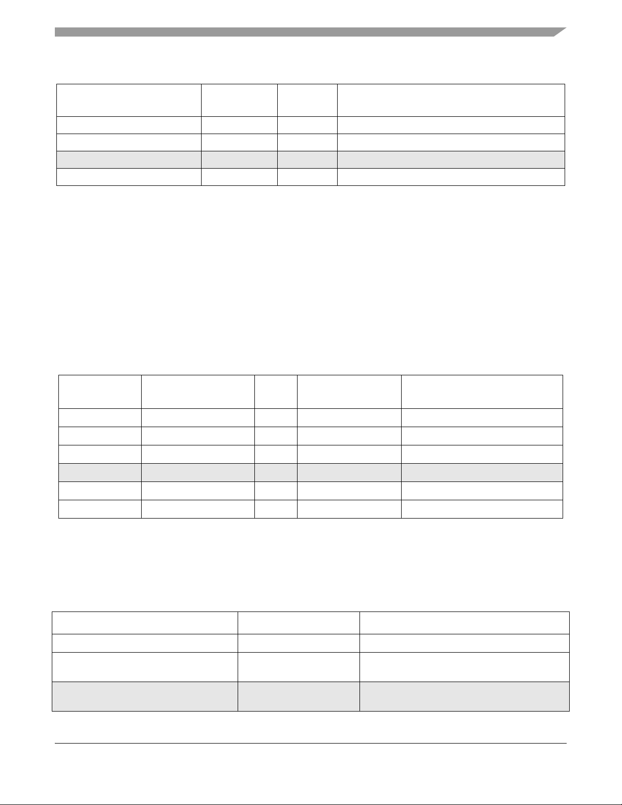
Table 1-2. Detailed MPC5554/MPC5553 Family Memory Map (Continued)
Address Range
1
Allocated Size
(bytes)
0xFFFC_4000–0xFFFC_7FFF 16 Kbytes 1152 Controller Area Network (FlexCAN_B)
1
Used Size
(bytes)
Use
3
0xFFFC_8000–0xFFFC_BFFF 16 Kbytes 1152 Controller Area Network (FlexCAN_C)
0xFFFC_C000–0xFFFF_BFFF 192 Kbytes N/A Reserved
0xFFFF_C000–0xFFFF_FFFF
1
If allocated size used size, then the base address for the module is the lowest address of the listed address range, unless
4
16 Kbytes 16 Kbytes Boot Assist Module (BAM)
noted otherwise.
2
MPC5553 only, not in MPC5554
3
MPC5554 only, not in MPC5553
4
BAM address range is configured so that 4Kbyte BAM occupies 0xFFFF_F000–0xFFFF_FFFF
1.7 Multi-Master Operation Memory Map
When the MPC5553/MPC5554 MCU acts as a slave in a multi-master system, the external bus interface
(EBI) translates the 24-bit external address to a 32-bit internal address. Table 1-3 lists the translation
parameters.
Table 1-3. External to Internal Memory Map Translation Table for Slave Mode
Ext Addr[8:11]
1
Internal Addr[0:11]
Size
(bytes)
Internal Slave Internal Address Range
0b0xxx N/A 8 Mbytes N/A N/A–Off-chip flash access
0b10xx 0b0000_0000_00xx 4 Mbytes Internal Flash Array 0x0000_0000–0x003F_FFFF
0b1100 0b0100_0000_0000 1 Mbyte Internal SRAM 0x4000_0000–0x400F_FFFF
0b1101 0b0110_0000_0000 1 Mbyte Reserved
2
0x6000_0000–0x600F_FFFF
0b1110 0b1100_0011_1111 1 Mbyte Bridge A Peripherals 0xC3F0_0000–0xC3FF_FFFF
0b1111 0b1111_1111_1111 1 Mbyte Bridge B Peripherals 0xFFF0_0000–0xFFFF_FFFF
1
Only the lower 24 address signals (addr[8:31]) are available off-chip.
2
Reserved for a future module that requires its own crossbar slave port.
Table 1-4 shows the memory map for the MPC5553/MPC5554 MCU acting as a slave in a multi-master
system from the point of view of the external master.
Table 1-4. MPC5500 Family Slave Memory Map as Seen from an External Master
External Address Range
2
0x00_0000
–0x7F_FFFF 8 Mbytes N/A–Used for off-chip memory accesses
0x80_0000–0x9F_FFFF(MPC5554)
0x80_0000–0x97_FFFF(MPC5553)
1
Size (bytes) Use
2 Mbytes(MPC5554)
Slave Flash
3
1.5 Mbytes(MPC5553)
0xA0_0000–0xBF_FFFF(MPC5554)0x98_0
000 –0xBF_FFFF(MPC5553)
2 Mbytes(MPC5554)
2.5 Mbytes(MPC5553)
Reserved
MPC5553/MPC5554 Microcontroller Reference Manual, Rev. 5
Freescale Semiconductor 1-23
Page 45
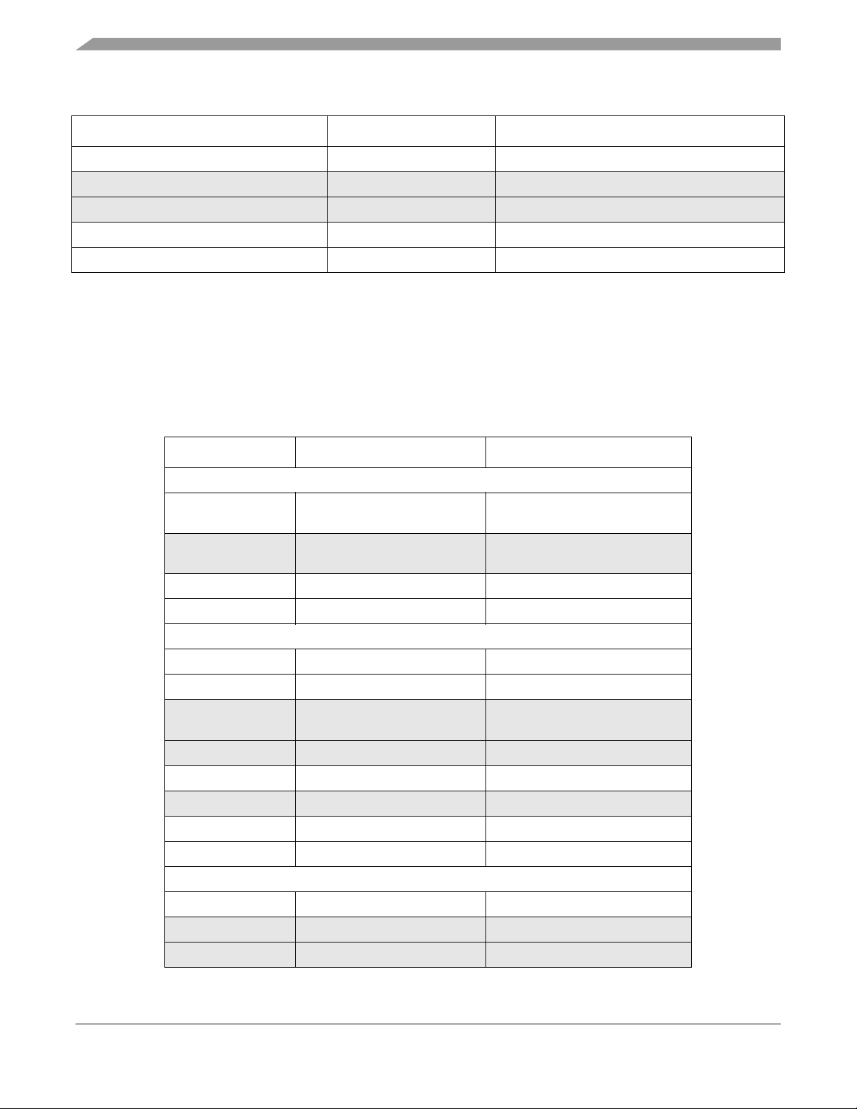
Table 1-4. MPC5500 Family Slave Memory Map as Seen from an External Master (Continued)
External Address Range
1
Size (bytes) Use
0xC0_0000–0xC0_FFFF 64 Kbytes Slave Internal SRAM
0xC1_0000–0xCF_FFFF (1 Mbytes–64 Kbytes) Reserved
0xD0_0000–0xDF_FFFF 1 Mbytes Reserved
0xE0_0000–0xEF_FFFF 1 Mbytes Slave Bridge A Peripherals
0xF0_0000–0xFF_FFFF 1 Mbytes Slave Bridge B Peripherals
1
Only the lower 24 address signals (addr[8:31]) are available off-chip.
2
This address range is not part of the MPC5500 family slav e memory map, rather it is shown to illustrate the addressing scheme
for off-chip accesses in multi-master mode.
3
The shadow row of the slave FLASH is not accessible by an external master.
Table 1-5 shows the memory map for the MPC5553 and MPC5554 family MCU configured as a master
in multi-master system with another MPC5500 family MCU acting as the slave.
Table 1-5. MPC5500 Family Master Memory Map (Multi Master Mode)
Base Address Size (bytes) Use
On-Chip
0x0000_0000 2 Mbytes(MPC55545)
1.5 Mbytes(MPC5553)
Flash array
0x0020_0000
0x0018_0000
(14 Mbytes–1024 bytes)
(14.5 Mbytes – 1024 bytes)
Reserved
0x00FF_FC00 1024 Flash shadow row
0x0100_0000 496 Mbytes Emulation mapping flash
Off-Chip
0x2000_0000 8 Mbytes
1
External memory
0x2080_0000 2 Mbytes Slave Flash
0x20A0_0000
2 Mbytes Reserved
0x2098_0000
Not Addressable 1024 Slave flash shad ow row
0x20C0_0000 64 Kbytes Slave internal SRAM
0x20C1_0000 (2 Mbytes–64 Kbytes) Reserved
0x20E0_0000 1 Mbytes Slave bridge A peripherals
0x20F0_0000 1 Mbytes Slave bridge B peripherals
On-Chip
0x4000_0000 64 Kbytes Internal SRAM
0x4001_0000 (2048 Mbytes–64 Kbytes) Reserved
0xC000_0000 63 Mbytes Reserved
MPC5553/MPC5554 Microcontroller Reference Manual, Rev. 5
1-24 Freescale Semiconductor
Page 46
Table 1-5. MPC5500 Family Master Memory Map (Multi Mast er Mode) (Continued)
Base Address Size (bytes) Use
0xC3F0_0000 1 Mbytes Bridge A peripherals
0xC400_0000 (1024 Mbytes–128 Mbytes) Reserved
0xFC00_0000 63 Mbytes Reserved
0xFFF0_0000 1 Mbyte Bridge B Peripherals
1
By using the 4 chip select signals, 32 Mbytes of external memory can be accessed by the
master in a multi-master system.
1.8 Revision History
Table 1-6. Changes to MPC5553/5554 RM for Rev. 4.0 Release
Description of Change
• Added wording for Power Architecture throughout chapter. Removed PowerPC ter m inology.
• In Features List, added section for Calibration interface
• In Features List, beefed up the section titled “MPC5553-Specific Modules” by adding more information about the FEC.
• In the MPC5553-Specific Modules section, added a section titled “Calibration Bus”
• In the Detailed Features section, beefed up the section titled FEC (MPC5553 Only).
• In the MPC5500 Family Master Memory Map (Multi-Master Mode) table, corrected SRAM values to 64 Kbytes from 96
Kbytes.
Table 1-7. Changes to MPC5553/5554 RM for Rev. 5.0 Release
Description of Change
• In table 1-2, in the address range 0x0100_0000–0x1FFF_FFFF(emulation mapping of FLASH Array), updated the Used
Size (bytes) cell as “2 Mbytes (MPC5554) and 1.5 Mbytes (MPC5553)”.
MPC5553/MPC5554 Microcontroller Reference Manual, Rev. 5
Freescale Semiconductor 1-25
Page 47

MPC5553/MPC5554 Microcontroller Reference Manual, Rev. 5
1-26 Freescale Semiconductor
Page 48

Chapter 2 Signal Description
This chapter describes the signals of the MPC5553 and the MPC5554 that connect off chip. It includes a
table of signal properties, detailed descriptions of signals, and the I/O pin power/ground segmentation.
2.1 Block Diagram
Figure 2-1 shows the signals of the MPC5553, and Figure 2-2 shows the signals of the MPC5554.
MPC5553/MPC5554 Microcontroller Reference Manual, Rev. 5
Freescale Semiconductor -2-1
Page 49
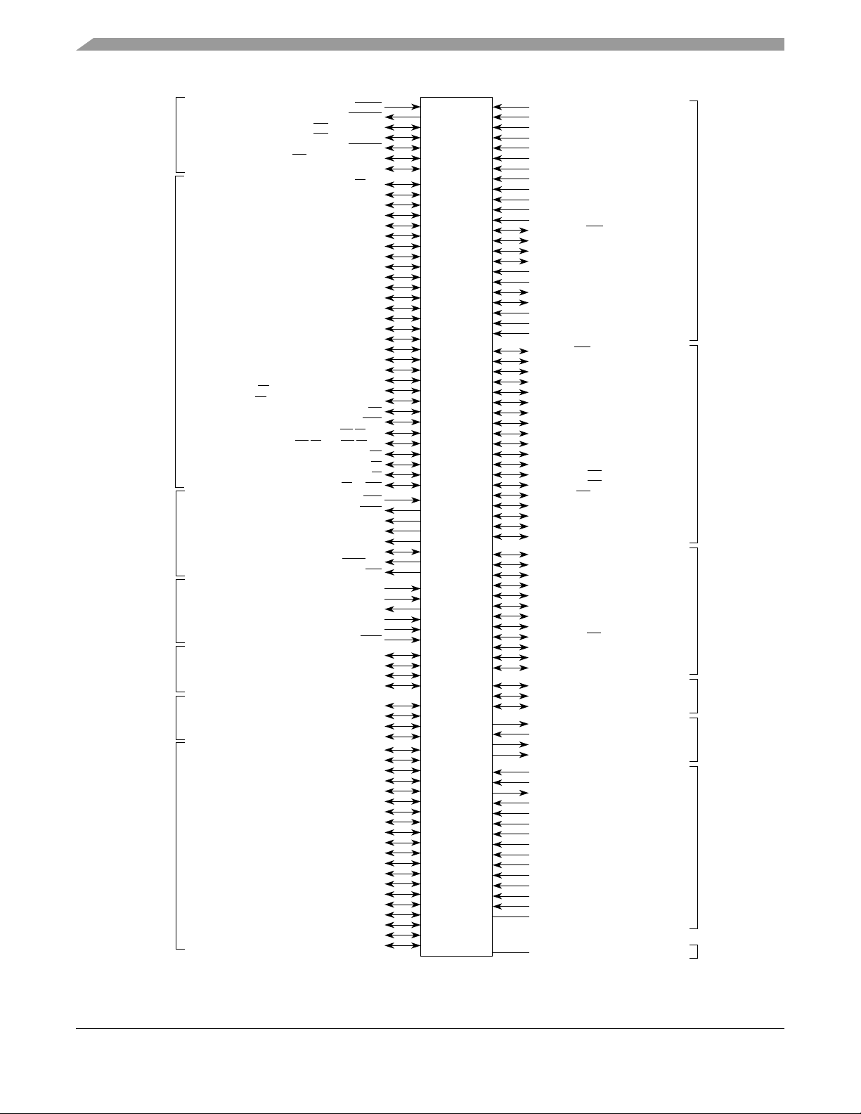
GPIO[83]_CNTXA
GPIO[84]_CNRXA
GPIO[87]_PCSD[3]_CNTXC
GPIO[88]_PCSD[4]_CNRXC
FlexCAN
GPIO[89]_TXDA
GPIO[90]_RXDA
GPIO[91]_PCSD[1]_TXDB
GPIO[92]_PCSD[5]_RXDB
eSCI
MPC5553
AN[0]_DAN0+
AN[1]_DAN0AN[2]_DAN1+
AN[3]_DAN1AN[4]_DAN2+
XTAL
EXTCLK_EXTAL
CLKOUT
ENGCLK
RESET
GPIO[51]_CAL_DATA[7]_FEC_TXD[3]_DATA[23]
EVTI
EVTO
MCKO
MDO[0]
MDO[3:1]
RSTOUT
GPIO[208]_IRQ[4]_PLLCFG[0]
GPIO[209]_SOUTD_IRQ
[5]_PLLCFG[1]
GPIO[210]_RSTCFG
GPIO[211:212]_IRQ[2:3]_BOOTCFG[0:1]
GPIO[0:3]_ADDR[8:11]_CS
[0:3]
GPIO[4:7]_CAL_ADDR[27:30]_ADDR[8:11]
GPIO[8:27]_ADDR[12:31]
GPIO[28:43]_DATA[0:15]
GPIO[44]_CAL_DATA[0]_FEC_TX_CLK_DATA[16]
GPIO[45]_CAL_DATA[1]_FEC_CRS_DATA[17]
GPIO[46]_CAL_DATA[2]_FEC_TX_ER_DATA[18]
GPIO[47]_CAL_DATA[3]_FEC_RX_CLK_DATA[19]
GPIO[48]_CAL_DATA[4]_FEC_TXD[0]_DATA[20]
GPIO[49]_CAL_DATA[5]_FEC_RX_ER_DATA[21]
GPIO[50]_CAL_DATA[6]_FEC_RXD[0]_DATA[22]
NEXUS
DSPI
GPIO[82:75]_MDO[11:4]
eQADC
eTPU
NC
NC
GPIO[213]_WKPCFG
GPIO[73]_CAL_CS[3]_FEC_MDIO_CAL_ADDR[11]
GPIO[52]_CAL_DATA[8]_FEC_COL_DATA[24]
GPIO[53]_CAL_DATA[9]_FEC_RX_DV_DATA[25]
GPIO[54]_CAL_DATA[10]_FEC_TX_EN_DATA[26]
GPIO[55]_CAL_DATA[11]_FEC_TXD[2]_DATA[27]
GPIO[56]_CAL_DATA[12]_FEC_TXD[1]_DATA[28]
GPIO[57]_CAL_DATA[13]_FEC_RXD[1]_DATA[29]
GPIO[58]_CAL_DATA[14]_FEC_RXD[2]_DATA[30]
GPIO[59]_CAL_DATA[15]_FEC_RXD[3]_DATA[31]
GPIO[72]_CAL_CS
[2]_FEC_MDC_CAL_ADDR[10]
GPIO[71]_CAL_CS[0]_TEA
GPIO[62]_RD_WR
GPIO[63]_BDIP
GPIO[64:65]_WE/BE[0:1]
GPIO[66:67]_CAL_WE
/BE[0:1]_WE/BE[2:3]
GPIO[68]_OE
GPIO[69]_TS
GPIO[70]_TA
MSEO[1:0]
RDY
AN[5]_DAN2AN[6]_DAN3+
AN[7]_DAN3AN[8]_ANW
AN[9]_ANX
AN[10]_ANY
AN[11]_ANZ
AN[12]_MA[0]_SDS
AN[13]_MA[1]_SDO
AN[14]_MA[2]_SDI
AN[15]_FCK
AN[16:31]
AN[32:39]
ETRIG[0]_GPIO[111]
ETRIG[1]_GPIO[112]
V
RH
V
RL
REFBYPC
TCRCLKA_IRQ[
7]_GPIO[113]
ETPUA[0:3]_ETPUA[12:15]_GPIO[114:117]
ETPUA[4:7]_ETPUA[16:19]_GPIO[118:121]
ETPUA[8:11]_ETPUA[20:23]_GPIO[122:125]
ETPUA[12]_PCSB[1]_GPIO[126]
ETPUA[13]_PCSB[3]_GPIO[127]
ETPUA[14]_PCSB[4]_GPIO[128]
ETPUA[15]_PCSB[5]_GPIO[129]
ETPUA[16]_PCSD[1]_GPIO[130]
ETPUA[17]_PCSD[2]_GPIO[131]
ETPUA[18]_PCSD[3]_GPIO[132]
ETPUA[19]_PCSD[4]_GPIO[133]
ETPUA[20:23]_IRQ[8:11]_GPIO[134:137]
ETPUA[24:26]_IRQ
[12:14]_GPIO[138:140]
ETPUA[27]_IRQ[15]_GPIO[141]
ETPUA[28]_PCSC[1]_GPIO[142]
ETPUA[29]_PCSC[2]_GPIO[143]
ETPUA[30]_PCSC[3]_GPIO[144]
ETPUA[31]_PCSC[4]_GPIO[145]
TCK
TDI
TDO
TMS
JCOMP
TEST
JTAG/TEST
EMIOS[0:2]_ETPUA[0:2]_GPIO[179:181]
EMIOS[3:5]_ETPUA[3:5]_GPIO[182:184]
EMIOS[6:7]_ETPUA[6:7]_GPIO[185:186]
EMIOS[8:9]_ETPUA[8:9]_GPIO[187:188]
EMIOS[12]_SOUTC_GPIO[191]
EMIOS[13]_SOUTD_GPIO[192]
EMIOS[14:15]_IRQ
[0:1]_GPIO[193:194]
EMIOS[16:18]_ETPUB[0:2]_GPIO[195:197]
EMIOS[19:21]_ETPUB[3:5]_GPIO[198:200]
EMIOS[10]_GPIO[189]
EMIOS[11]_GPIO[190]
EMIOS[22:23]_ETPUB[6:7]_GPIO[201:202]
GPIO[203:204]_EMIOS[14:15]
GPIO[205]
GPIO[206:207]
GPIO
eMIOS
EXTERNAL
BUS
INTERFACE
(EBI)
RESET/
CONFIGURATION
CLOCK
SYNTHESIZER
V
RC33
V
RCVSS
(not available on the 208 package)
V
RCCTL
V
DDAn
V
SSSYN
V
FLASH
(not available on the 208 package)
V
PP
V
STBY
V
DD
V
SSAn
V
DDSYN
V
DDEn
POWER/
V
DDEHn
V
DD33
VSS(GND)
GROUND
GPIO[93]_PCSC[1]_SCKA
GPIO[94]_PCSC[2]_SINA
GPIO[95]_PCSC[5]_SOUTA
GPIO[97]_PCSB[2]_PCSA[1]
GPIO[98]_SCKD_PCSA[2]
GPIO[99]_SIND_PCSA[3]
GPIO[100]_SOUTD_PCSA[4]
GPIO[96]_PCSD[2]_PCSA[0]
GPIO[101]_PCSB[3]_PCSA[5]
GPIO[102]_PCSC[1]_SCKB
GPIO[104]_PCSC[5]_SOUTB
GPIO[105]_PCSD[2]_PCSB[0]
GPIO[106]_PCSD[0]_PCSB[1]
GPIO[107]_SOUTC_PCSB[2]
GPIO[103]_PCSC[2]_SINB
GPIO[108]_SINC_PCSB[3]
GPIO[109]_SCKC_PCSB[4]
GPIO[110]_PCSC[0]_PCSB[5]
GPIO[85]_PCSC[3]_CNTXB
GPIO[86]_PCSC[4]_CNRXB
2-2 Freescale Semiconductor
MPC5553/MPC5554 Microcontroller Reference Manual, Rev. 5
Figure 2-1. MPC5553 Signal Diagram
Page 50
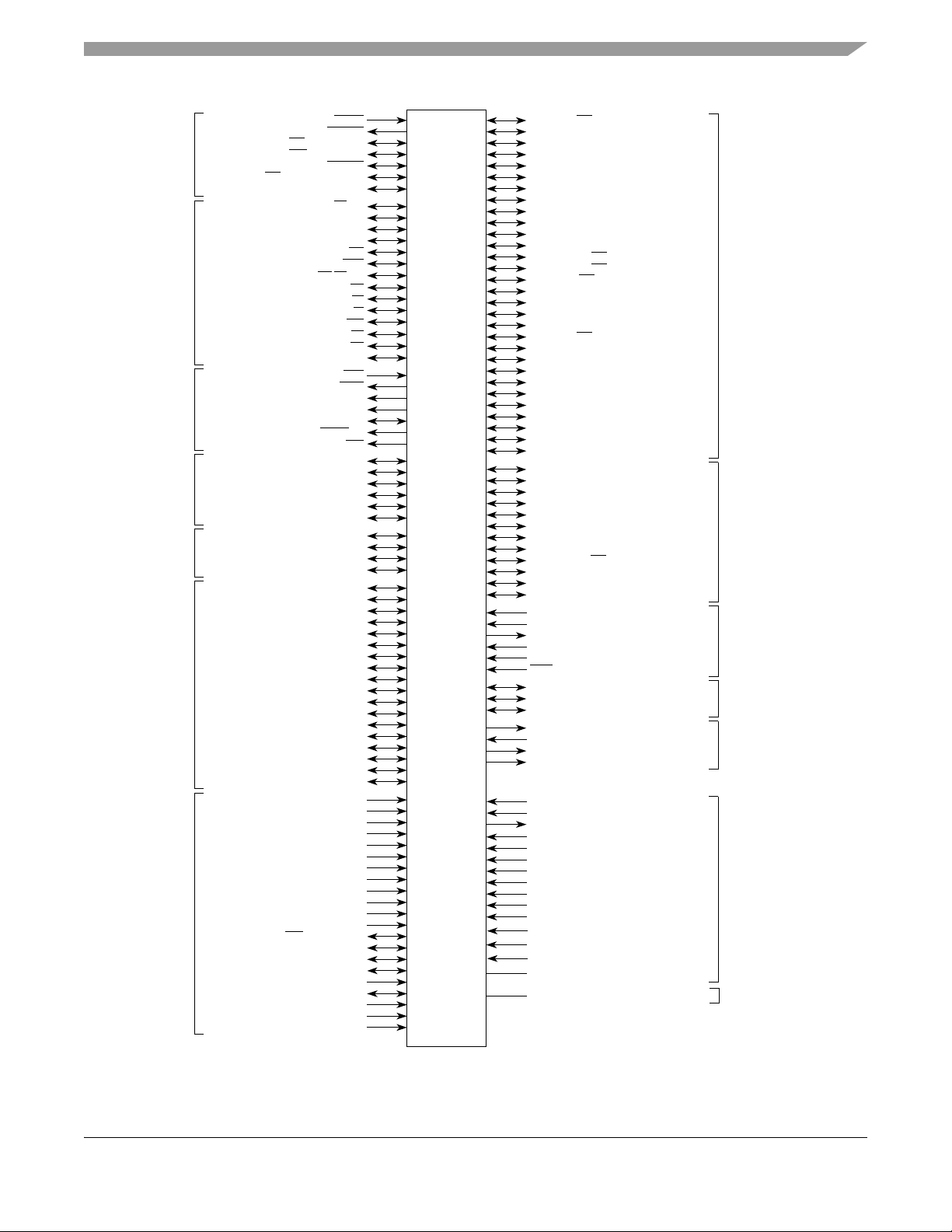
V
RH
V
RL
REFBYPC
ETRIG[0:1]_GPIO[111:112]
GPIO[83]_CNTXA
GPIO[84]_CNRXA
GPIO[85]_PCSC[3]_CNTXB
GPIO[86]_PCSC[4]_CNRXB
GPIO[87]_PCSD[3]_CNTXC
GPIO[88]_PCSD[4]_CNRXC
FlexCAN
GPIO[89]_TXDA
GPIO[90]_RXDA
GPIO[91]_PCSD[1]_TXDB
GPIO[92]_PCSD[5]_RXDB
eSCI
MPC5554
GPIO[93]_PCSC[1]_SCKA
DAN0+_AN[0]
DAN0-_AN[1]
DAN1+_AN[2]
DAN1-_AN[3]
DAN2+_AN[4]
XTAL
EXTCLK_EXTAL
CLKOUT
ENGCLK
RESET
EVTI
EVTO
MCKO
MDO[3:0]
RSTOUT
GPIO[208]_IRQ[4]_PLLCFG[0]
GPIO[209]_SOUTD_IRQ[
5]_PLLCFG[1]
GPIO[210]_RSTCFG
GPIO[211:212]_IRQ[2:3]_BOOTCFG[0:1]
GPIO[0:3]_ADDR[8:11]_CS
[0:3]
GPIO[4:27]_ADDR[8:31]
GPIO[28:59]_DATA[0:31]
GPIO[60:61]_TSIZ[0:1]
NEXUS
DSPI
GPIO[94]_PCSC[2]_SINA
GPIO[95]_PCSC[5]_SOUTA
GPIO[97]_PCSB[2]_PCSA[1]
GPIO[98]_SCKD_PCSA[2]
GPIO[99]_SIND_PCSA[3]
GPIO[100]_SOUTD_PCSA[4]
GPIO[96]_PCSD[2]_PCSA[0]
GPIO[82:75]_MDO[11:4]
eQADC
eTPU
NC
NC
GPIO[213]_WKPCFG
GPIO[73]_BG
GPIO[72]_BR
GPIO[71]_TEA
GPIO[62]_RD_WR
GPIO[63]_BDIP
GPIO[64:67]_WE/BE[0:3]
GPIO[68]_OE
GPIO[69]_TS
GPIO[70]_TA
MSEO[1:0]
RDY
GPIO[101]_PCSB[3]_PCSA[5]
GPIO[102]_PCSC[1]_SCKB
GPIO[104]_PCSC[5]_SOUTB
GPIO[105]_PCSD[2]_PCSB[0]
GPIO[106]_PCSD[0]_PCSB[1]
GPIO[107]_SOUTC_PCSB[2]
GPIO[103]_PCSC[2]_SINB
GPIO[108]_SINC_PCSB[3]
GPIO[109]_SCKC_PCSB[4]
GPIO[110]_PCSC[0]_PCSB[5]
DAN2-_AN[5]
DAN3+_AN[6]
DAN3-_AN[7]
ANW_AN[8]
ANX_AN[9]
ANY_AN[10]
ANZ_AN[11]
SDS_MA[0]_AN[12]
SDO_MA[1]_AN[13]
SDI_MA[2]_AN[14]
FCK_AN[15]
AN[16:39]
TCRCLKA_IRQ
[7]_GPIO[113]
ETPUA[0:3]_ETPUA[12:15]_GPIO[114:117]
ETPUA[4:7]_ETPUA[16:19]_GPIO[118:121]
ETPUA[8:11]_ETPUA[20:23]_GPIO[122:125]
ETPUA[12]_PCSB[1]_GPIO[126]
ETPUA[13]_PCSB[3]_GPIO[127]
ETPUA[14]_PCSB[4]_GPIO[128]
ETPUA[15]_PCSB[5]_GPIO[129]
ETPUA[16]_PCSD[1]_GPIO[130]
ETPUA[17]_PCSD[2]_GPIO[131]
ETPUA[18]_PCSD[3]_GPIO[132]
ETPUA[19]_PCSD[4]_GPIO[133]
ETPUA[20:23]_IRQ[8:11]_GPIO[134:137]
ETPUA[24:26]_IRQ
[12:14]_GPIO[138:140]
ETPUA[27]_IRQ[15]_GPIO[141]
ETPUA[28]_PCSC[1]_GPIO[142]
ETPUA[29]_PCSC[2]_GPIO[143]
ETPUA[30]_PCSC[3]_GPIO[144]
ETPUA[31]_PCSC[4]_GPIO[145]
TCK
TDI
TDO
TMS
JCOMP
TEST
JTAG/TEST
EMIOS[0:2]_ETPUA[0:2]_GPIO[179:181]
EMIOS[3:5]_ETPUA[3:5]_GPIO[182:184]
EMIOS[6:7]_ETPUA[6:7]_GPIO[185:186]
EMIOS[8:9]_ETPUA[8:9]_GPIO[187:188]
EMIOS[12]_SOUTC_GPIO[191]
EMIOS[13]_SOUTD_GPIO[192]
EMIOS[14:15]_IRQ
[0:1]_GPIO[193:194]
EMIOS[16:18]_ETPUB[0:2]_GPIO[195:197]
EMIOS[19:21]_ETPUB[3:5]_GPIO[198:200]
EMIOS[10]_GPIO[189]
EMIOS[11]_GPIO[190]
EMIOS[22:23]_ETPUB[6:7]_GPIO[201:202]
GPIO[203:204]_EMIOS[14:15]
GPIO[205]
GPIO[206:207]
GPIO
EMIOS
EXTERNAL
BUS
INTERFACE
(EBI)
RESET/
CONFIGURATION
CLOCK
SYNTHESIZER
GPIO[74]
TCRCLKB_IRQ[6]_GPIO[146]
ETPUB[0:4]_ETPUB[16:20]_GPIO[147:151]
ETPUB[5:9]_ETPUB[21:25]_GPIO[152:156]
ETPUB[10:15]_ETPUB[26:31]_GPIO[157:162]
ETPUB[16]_PCSA[1]_GPIO[163]
ETPUB[17]_PCSA[2]_GPIO[164]
ETPUB[18]_PCSA[3]_GPIO[165]
ETPUB[19]_PCSA[4]_GPIO[166]
ETPUB[20]_GPIO[167]
ETPUB[21:25]_GPIO[168:172]
ETPUB[26:31]_GPIO[173:178]
V
RC33
V
RCVSS
V
RCCTL
V
SSSYN
V
FLASH
V
PP
V
STBY
V
DD
V
DDSYN
V
DDEHn
POWER/
V
DDEn
GROUND
V
DD33
VSS(GND)
V
SSAn
V
DDAn
Freescale Semiconductor 2-3
Figure 2-2. MPC5554 Signal Diagram
MPC5553/MPC5554 Microcontroller Reference Manual, Rev. 5
Page 51
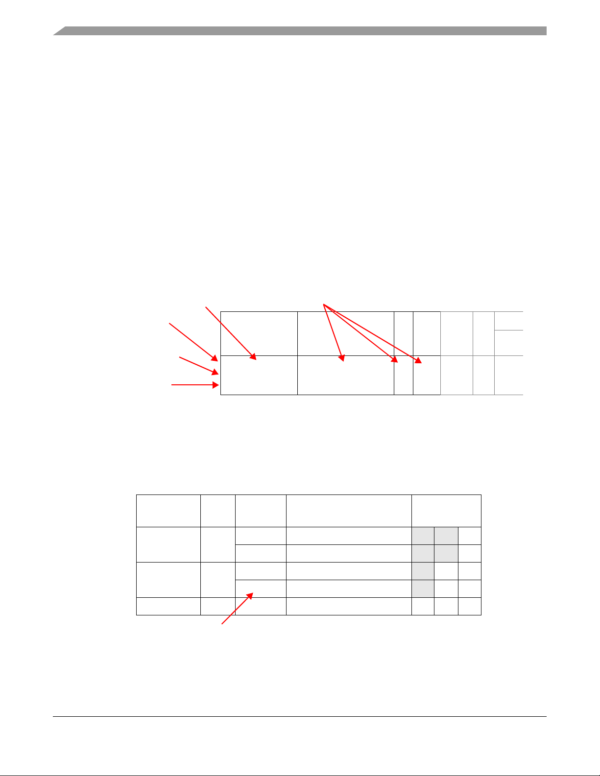
2.2 External Signal Description
Signal Names Signal Functions
P/
A/GI/O
Type
Voltage
Pad
Type
St
During
Reset
PCSA[3]_
21
SIND_
GPIO[99]
—
DSPI_D Data Input
GPIO
—
A
G
—
I
I/O
VDDEH6 MH – / Up
Primary functions
Secondary functions
GPIO functions are
No primary
footnote
Table
are listed first
are alternative functions
general functions listed last
function available
PCR Register
Bit
fs
P/A/G
Symbol
PA Function Type
PA bit values
[0, 1, 2]
5 2 fs
G General-purpose I/O 0 0 0
P Primary 0 0 1
4 3 fs
A Alternate 0 1 0
MP Main 0 1 1
3 4 fs A2 Second alternate 1 0 0
All other values reserved for future use. n n n
SIU_PCR register bits 3 4 5
The
main function
is used for device
compatibility.
This section summarizes the external signal functions, their static electrical characteristics, and pad
configuration settings for this device. Table 2-1 gives a summary of the MPC5553 external signals, and
Table 2-2 provides a summary of the MPC5554 external signals. The signal properties and their electrical
characteristics are set in the system integration unit (SIU) pad configuration registers (PCR).
Signal functions are multiplexed to each ball on the BGA in a function hierarchy: primary , main primary,
alternate, second alternate, and general-purpose input/output (I/O). For example, in the signal
PCSA[3]_SIND_GPIO[99], the primary signal function is PCSA[3], the first alternate signal function is
SIND, and the GPIO function is a generic general-purpose I/O signal. Multiplexing signal functions allows
for more flexibility when configuring the device, as well as providing compatibility with other devices in
the MPC5500 product family.
The primary signal function name is used in the ball grid array (BGA) map to identify the location of the
ball; however, the primary signal function is not always va lid for all devices. As shown in Figure 2-3, when
the primary signal function is not available on the device, a dash appears in the following signal table
columns: signal functions, P/A/G, and I/O type.
The P/A/G column designates the position in the signal function hierarchy for multiplexed functions.
These symbols correspond to binary values for the pin assignment (P A) field in the SIU_PCR registers that
determine the active signal function. The PA field is from 1- to 3-bits wide, depending on the PCR register .
Figure 2-4 explains the symbol definitions used in the P/A/G column for Table 2-1 and Table 2-2.
2-4 Freescale Semiconductor
Figure 2-3. Primary Function Not Available on Device
Figure 2-4. Understanding the P/A/G Column Entries
MPC5553/MPC5554 Microcontroller Reference Manual, Rev. 5
Page 52
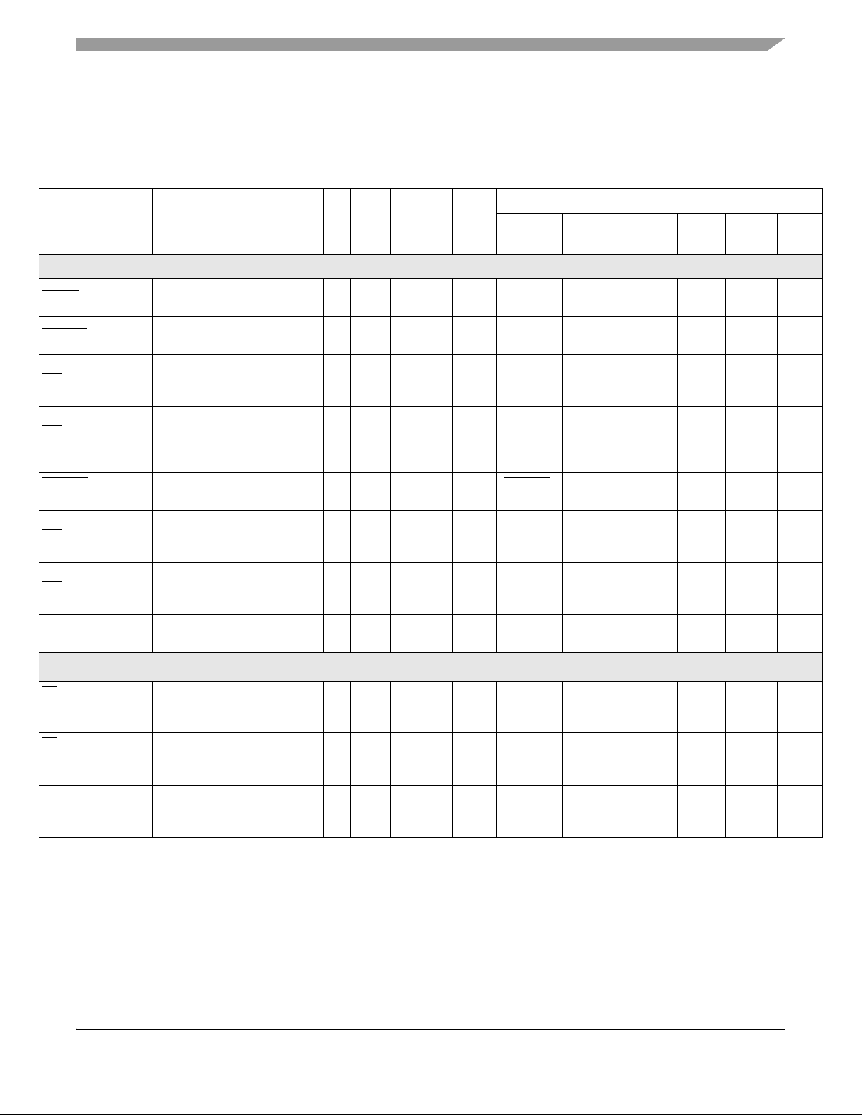
2.2.1 MPC5553 Signals Summary
Table 2-1 gives a summary of the MPC5553 external signals and properties.
Table 2-1. MPC5553 Signal Properties
Signal Name
RESET
RSTOUT
PLLCFG[0]_
IRQ
[4]_
GPIO[208]
PLLCFG[1]_
IRQ
[5]_
SOUTD_
GPIO[209]
RSTCFG
GPIO[210]
BOOTCFG[0]_
IRQ[2]_
GPIO[211]
BOOTCFG[1]_
IRQ
GPIO[212]
WKPCFG_
GPIO[213]
_
[3]_
1
Signal Functions
2
External Reset Input P I V
External Reset Output P O V
FMPLL Mode Selection
External Interrupt Request
General Purpose I/O
FMPLL Mode Selection
External Interrupt Request
DSPI D Data Output
General Purpose I/O
Reset Configuration Input
General Purpose I/O
10
Boot Configuration Input
External Interrupt Request
General Purpose I/O
Boot Configuration Input
External Interrupt Request
General Purpose I/O
Weak Pull Configuration Input
General Purpose I/O
P/
I/O
Type
Voltage
A/G
Reset / Configuration Signals
DDEH6
DDEH6
I
P
I
I/O
I/O
I/O
I/O
V
DDEH6
I
I
V
O
DDEH6
V
DDEH6
I
I
V
DDEH6
I
I
V
DDEH6
V
DDEH6
A
G
P
A
A2
G
P
GII/O
P
A
G
P
A
G
P
GII/O
Pad
Status Pin Labels / Package Type
3
Type
S
S
M
M
S
S
S
S
4
During
Reset
RESET
RSTOUT
Low
PLLCFG /
Up
PLLCFG /
Up
RSTCFG
Up
BOOTCFG /
Down
BOOTCFG /
Down
WKPCFG /
Up
After
5
Reset
/ UpRESET /
Up
/
RSTOUT /
High
4967416
6
AA27 W26 R22 L16
W26 V25 P21 K15
8
– / Up AB27 AB25 V21 M14
– / Up AA26 AA24 U20 N15
/
– / Up Y28 V26 P22 —
– / Down AB26 AA25 U21 —
– / Down AB24 Y24 T20 M15
– / Up AA24 Y23 R19 L15
324 208
9
External Bus Interface (EBI)11 and Calibration Bus Interface (CBI)12 Signals
CS[0]_
ADDR[8]_
13
GPIO[0]
[1:3]_
CS
ADDR[9:11]_
13
GPIO[1:3]
ADDR[8:11]_
13
CAL_ADDR[27:30]_
GPIO[4:7]
External Chip Select 0
External Address Bus
13, 14
General Purpose I/O
External Chip Selects 1–3
External Address Bus
13, 14
General Purpose I/O
External Address Bus
13, 14
Calibration Address Bus
General Purpose I/O
O
P
I/O
A
I/O
G
P
I/O
A
I/O
G
I/O
P
A
I/O
G
V
DDE2
F – / Up – / Up
O
V
DDE2
O
V
DDE2
F – / Up – / Up
F – / Up – / Up
15
T7 P4 M4 R1
R5, P5, R7P3, P2, P1M3, N2,
15
Y5, Y3,
15
AA3,
V4,
W3:4, Y3——
AB3
MPC5553/MPC5554 Microcontroller Reference Manual, Rev. 5
Freescale Semiconductor 2-5
N1
—
Page 53

Table 2-1. MPC5553 Signal Properties (Continued)
Signal Name
ADDR[12:31]_
GPIO[8:27]
DATA[0:15]_
GPIO[28:43]
DATA[16]_
FEC_TX_CLK_
CAL_DATA[0]_
GPIO[44]
DATA[17]_
FEC_CRS_
CAL_DATA[1]_
GPIO[45]
DATA[18]_
FEC_TX_ER_
CAL_DATA[2]_
GPIO[46]
DATA[19]_
FEC_RX_CLK_
CAL_DATA[3]_
GPIO[47]
14
14
14
14
14
1
13, 14, 16
External Address Bus
General Purpose I/O
External Data Bus
General Purpose I/O
External Data Bus
Ethernet Transmit Clock
Calibration Data Bus
General Purpose I/O
External Data Bus
Ethernet Carrier Sense
Calibration Data Bus
General Purpose I/O
External Data Bus
Ethernet Transmit Error
Calibration Data Bus
General Purpose I/O
External Data Bus
Ethernet Receive Clock
Calibration Data Bus
General Purpose I/O
Signal Functions
14, 16
14
14
14
14
14
P/
Status Pin Labels / Package Type
A/G
PGI/O
PGI/O
P
A
A2
G
P
A
A2
G
P
A
A2
G
P
A
A2
G
I/O
Type
I/O
I/O
I/O
I
I/O
I/O
I/O
I
I/O
I/O
I/O
O
I/O
I/O
I/O
I
I/O
I/O
Voltage
V
DDE2
V
DDE3
V
DDE3
V
DDE3
V
DDE3
V
DDE3
2
Pad
3
Type
4
During
Reset
After
5
Reset
F – / Up – / Up
17
F – / Up – / Up
17
F – / Up – / Up
17
F – / Up – / Up
17
F – / Up – / Up
17
F – / Up – / Up
6
4967416
8
AA4,
AA3,
AB4,
AB3, U1,
V2, V1,
W2, W1,
Y2, Y1,
AA2,
AA1,
AB2,
AC1
,
AC2,
AD1,
,
AE1
AD2,
15
Y7,
AC3,
AC5,
AB5, T3,
T2, T1,
V2,
W1:2,
Y1:2,
AA2,
AB2,
AC2,
AD2:3,
AD1,
AF2,
AE3
AC1:3
AG11,
AF12,
AG13,
AH13,
AG14,
AH15,
AG15,
AH16,
15
AB12,
AF10,
AD13,
AF11,
AB15,
AD12,
AD15,
AF13
15
AF5 AF3 — —
15
AG5 AE4 — —
15
AH5 AF4 — —
15
AG6 AE5 — —
AE8,
AF9,
AE9,
AF10,
AE10,
AF12,
AE11,
AF13,
AC11,
AD11,
AC12,
AD12,
AC14,
AD13,
AC15,
AD14
324 208
T3, U3:4,
V3,
P1:2,
R1:2,
T1:2,
U1:2,
V1:2,
W1, Y2,
Y1, AA1,
W3,
V4
AB4,
AA5,
AB5:7,
AA8,
AB8,
AA9,
Y6:8,
W9:10,
Y10,
W11,
Y11
9
—
—
MPC5553/MPC5554 Microcontroller Reference Manual, Rev. 5
2-6 Freescale Semiconductor
Page 54

Table 2-1. MPC5553 Signal Properties (Continued)
Signal Name
DATA[20]_14
FEC_TXD[0]_
CAL_DATA[4]_
GPIO[48]
DATA[21]_
FEC_RX_ER_
CAL_DATA[5]_
GPIO[49]
DATA[22]_
FEC_RXD[0]_
CAL_DATA[6]_
GPIO[50]
DATA[23]_
FEC_TXD[3]_
CAL_DATA[7]_
GPIO[51]
DATA[24]_
FEC_COL_
CAL_DATA[8]_
GPIO[52]
DATA[25]_
FEC_RX_DV_
CAL_DATA[9]_
GPIO[53]
DATA[26]_
FEC_TX_EN_
CAL_DATA[10]_
GPIO[54]
DATA[27]_
FEC_TXD[2]_
CAL_DATA[11]_
GPIO[55]
DATA[28]_
FEC_TXD[1]_
CAL_DATA[12]_
GPIO[56]
DATA[29]_
FEC_RXD[1]_
CAL_DATA[13]_
GPIO[57]
DATA[30]_
FEC_RXD[2]_
CAL_DATA[14]_
GPIO[58]
DATA[31]_
FEC_RXD[3]_
CAL_DATA[15]_
GPIO[59]
14
14
14
14
14
14
14
14
14
14
14
1
Signal Functions
External Data Bus
Ethernet Transmit Data
Calibration Data Bus
General Purpose I/O
External Data Bus
Ethernet Receive Error
Calibration Data Bus
General Purpose I/O
External Data Bus
Ethernet Receive Data
Calibration Data Bus
General Purpose I/O
External Data Bus
Ethernet Transmit Data
Calibration Data Bus
General Purpose I/O
External Data Bus
Ethernet Collision Detect
Calibration Data Bus
General Purpose I/O
External Data Bus
Ethernet Receive Data Valid
Calibration Data Bus
General Purpose I/O
External Data Bus
Ethernet Transmit Enable
Calibration Data Bus
General Purpose I/O
External Data Bus
Ethernet Transmit Data
Calibration Data Bus
General Purpose I/O
External Data Bus
Ethernet Transmit Data
Calibration Data Bus
General Purpose I/O
External Data Bus
Ethernet Receive Data
Calibration Data Bus
General Purpose I/O
External Data Bus
Ethernet Receive Data
Calibration Data Bus
General Purpose I/O
External Data Bus
Ethernet Receive Data
Calibration Data Bus
General Purpose I/O
P/
Status Pin Labels / Package Type
A/G
P
A
A2
G
P
A
A2
G
P
A
A2
G
P
A
A2
G
P
A
A2
G
P
A
A2
G
P
A
A2
G
P
A
A2
G
P
A
A2
G
P
A
A2
G
P
A
A2
G
P
A
A2
G
I/O
Type
I/O
O
I/O
I/O
I/O
I
I/O
I/O
I/O
I
I/O
I/O
I/O
O
I/O
I/O
I/O
I
I/O
I/O
I/O
I
I/O
I/O
I/O
O
I/O
I/O
I/O
O
I/O
I/O
I/O
O
I/O
I/O
I/O
I
I/O
I/O
I/O
I
I/O
I/O
I/O
I
I/O
I/O
Voltage
V
DDE3
V
DDE3
V
DDE3
V
DDE3
V
DDE3
V
DDE3
V
DDE3
V
DDE3
V
DDE3
V
DDE3
V
DDE3
V
DDE3
2
14
14
14
14
14
14
14
14
14
14
14
14
Pad
3
Type
4
During
Reset
17
F – / Up – / Up
17
F – / Up – / Up
17
F – / Up – / Up
17
F – / Up – / Up
17
F – / Up – / Up
17
F – / Up – / Up
17
F – / Up – / Up
17
F – / Up – / Up
17
F – / Up – / Up
17
F – / Up – / Up
17
F – / Up – / Up
17
F – / Up – / Up
After
5
Reset
4967416
6
15
AG7 AF6 — —
15
AG8 AE6 — —
15
AGJ AF7 — —
15
AH9 AE7 — —
15
AD7 AD5 — —
15
AF6 AD6 — —
15
AB9 AC6 — —
15
AF7 AD7 — —
15
AD8 AC7 — —
15
AF8 AD8 — —
15
AD10 AC9 — —
15
AD11 AC10 — —
8
324 208
9
MPC5553/MPC5554 Microcontroller Reference Manual, Rev. 5
Freescale Semiconductor 2-7
Page 55
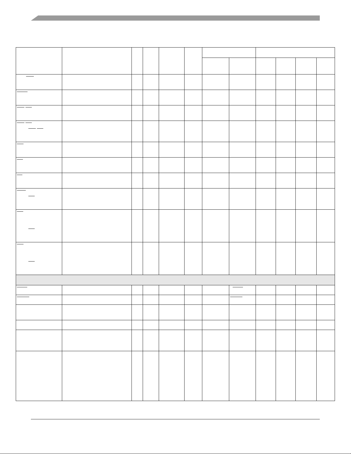
Table 2-1. MPC5553 Signal Properties (Continued)
Signal Name
_
/BE[0:1]_
/BE[2:3]_
20
_
21
_
_
_
22
_
22
_
18
19
19
[0]_
[2]_
[3]_
RD_WR_
GPIO[62]
BDIP
GPIO[63]
WE
GPIO[64:65]
WE
CAL_WE/BE[0:1]_
GPIO[66:67]
OE
GPIO[68]
TS
GPIO[69]
TA
GPIO[70]
TEA
CAL_CS
GPIO[71]
BR
CAL_ADDR[10]_
FEC_MDC_
CAL_CS
GPIO[72]
BG
CAL_ADDR[11]_
FEC_MDIO_
CAL_CS
GPIO[73]
1
Signal Functions
External Data Bus Read/Write
General Purpose I/O
External Burst Data In Progress
General Purpose I/O
External Write/Byte Enable
General Purpose I/O
External Write/Byte Enable
19
Calibration Write/Byte Enable
General Purpose I/O
External Bus Output Enable
General Purpose I/O
External Bus Transfer Start
General Purpose I/O
External Transfer Acknowledge
General Purpose I/O
External Transfer Error Acknowledge
Calibration Chip Select
General Purpose I/O
—
Calibration Address Bus
FEC Management Clock
Calibration Chip Select
General Purpose I/O
—
Calibration Address Bus
FEC Management Data I/O
Calibration Chip Select
General Purpose I/O
P/
Status Pin Labels / Package Type
A/G
PGI/O
PGO
PGO
P
A
G
PGO
PGI/O
PGI/O
P
A
G
—
MP
A
A2
G
—
MP
A
A2
G
I/O
Type
I/O
I/O
I/O
O
O
I/O
I/O
I/O
I/O
I/O
O
I/O
—
I/O
O
O
I/O
—
I/O
I/O
O
I/O
Voltage
V
DDE2
V
DDE2
V
DDE2
V
DDE2
V
DDE3
V
DDE2
V
DDE2
V
DDE2
V
DDE3
V
DDE3
2
19
19
19
Pad
3
Type
4
During
Reset
F – / Up – / Up
F – / Up – / Up
F – / Up – / Up
F – / Up – / Up
17
F – / Up – / Up
F – / Up – / Up
F – / Up – / Up
F – / Up – / Up
17
F – / Up – / Up
17
F — / Up — / Up
After
5
Reset
4967416
6
15
U3 T3 P3 —
15
N1 N1 M1 —
15
U5, T5 R4, R3 N3:4 —
15
N3, P1 R1:2 — —
15
AF16 AE12 AB9 T3
15
W3 V3 T4 —
15
V3 U3 R4 —
15
N2 N2 — —
15
AF17 AE13 — —
15
AG16 AE14 — —
8
324 208
9
Nexus Signals
EVTI Nexus Event In P I V
EVTO
Nexus Event Out P O V
MCKO Nexus Message Clock Out P O V
MDO[0]
24
Nexus Message Data Out P O V
MDO[3:1] Nexus Message Data Out P O V
MDO[11:4]_
GPIO[82:75]
25
Nexus Message Data Out
General Purpose I/O
PGO
I/O
V
DDE7
DDE7
DDE7
DDE7
DDE7
DDE7
F I / Up EVTI / Up G26 F25 F21 E15
F O / Low EVTO / High G27 F26 F22 D15
F O / Low
MCKO /
Enabled
H26G24G20F15
23
F O / High MDO / Low C25 B24 B20 A14
F O / Low MDO / Low
F O / Low – / Down
C23,
B21,
C24
A23,
C22,
A20,
A24,
B23,
B20,
C20,
B24
C22,
D21,
C23
A22,
B21,
C20,
A23,
B22,
C21,
D20,
B23
MPC5553/MPC5554 Microcontroller Reference Manual, Rev. 5
2-8 Freescale Semiconductor
D18,
C18:19
A17:18,
B17,
A19,
B18,
D17,
C17, B19
B13,
A13,
B14
—
Page 56
Table 2-1. MPC5553 Signal Properties (Continued)
P/
Signal Name
1
Signal Functions
2
A/G
I/O
Type
Voltage
MSEO[1:0] Nexus Message Start/End Out P O V
RDY
Nexus Ready Output P O V
JTAG / Test Signals
TCK JTAG Test Clock Input P I V
TDI JTAG Test Data Input P I V
26
TDO
JTAG Test Data Output P O V
TMS JTAG Test Mode Select Input P I V
JCOMP JTAG TAP Controller Enable P I V
TEST
Test Mode Select P I V
FlexCAN Signals
CNTXA_
GPIO[83]
CNRXA_
GPIO[84]
CNTXC_
PCSD[3]_
GPIO[87]
CNRXC_
PCSD[4]_
GPIO[88]
FlexCAN A Transmit
General Purpose I/O
FlexCAN A Receive
General Purpose I/O
FlexCAN C Transmit
DSPI D Peripheral Chip Select
General Purpose I/O
FlexCAN C Receive
DSPI D Peripheral Chip Select
General Purpose I/O
PGO
I/O
P
GII/O
P
A
I/O
G
P
A
I/O
G
O
O
I
O
DDE7
DDE7
DDE7
DDE7
DDE7
DDE7
DDE7
DDE7
V
DDEH4
V
DDEH4
V
DDEH6
V
DDEH6
Pad
Status Pin Labels / Package Type
3
4
Type
During
Reset
F O / High
After
5
Reset
MSEO
High
6
/
4967416
G24,
H24
F23,
G23
8
G21:22
F O / High RDY / High J24 H23 G19 —
F TCK / Down TCK / Down E27 D25 D21 C16
F TDI / Up TDI / Up E28 D26 D22 E14
F TDO / Up26TDO / Up F27 E25 E21 F14
F TMS / Up TMS / Up E26 E24 E20 D14
F
JCOMP /
Down
JCOMP /
Down
F26 F24 F20 F16
F TEST / Up TEST / Up F28 E26 E22 D16
S – / Up – / Up
S – / Up – / Up
27
AF22 AD21 Y17 P12
27
AG22 AE22 AA18 R12
M – / Up – / Up W24 V23 P19 K13
M – / Up – / Up Y26 W24 R20 L14
324 208
E16,
C15
9
eSCI Signals
TXDA_
GPIO[89]
RXDA_
GPIO[90]
TXDB_
PCSD[1]_
GPIO[91]
RXDB_
PCSD[5]_
GPIO[92]
eSCI A Transmit
General Purpose I/O
eSCI A Receive
General Purpose I/O
eSCI B Transmit
DSPI D Peripheral Chip Select
General Purpose I/O
eSCI B Receive
DSPI D Peripheral Chip Select
General Purpose I/O
PGO
I/O
P
GII/O
P
A
I/O
G
P
A
I/O
G
V
DDEH6
V
DDEH6
S – / Up – / Up
S – / Up – / Up
27
V24 U24 N20 J14
27
U26 V24 P20 K14
O
O
V
DDEH6
M – / Up – / Up Y27 W25 R21 L13
I
O
V
DDEH6
M – / Up – / Up Y24 W23 T19 M13
DSPI Signals
CNTXB_
PCSC[3]_
GPIO[85]
CNRXB_
PCSC[4]_
GPIO[86]
28
28
—
DSPI C Peripheral Chip Select
General Purpose I/O
—
DSPI C Peripheral Chip Select
General Purpose I/O
—
—
O
I/O
—
I/O
V
DDEH4
O
V
DDEH4
M – / Up – / Up AG23 AF22 AB16 T12
M – / Up – / Up AH23 AF23 AB19 R13
A
G
—
A
G
MPC5553/MPC5554 Microcontroller Reference Manual, Rev. 5
Freescale Semiconductor 2-9
Page 57

Table 2-1. MPC5553 Signal Properties (Continued)
Signal Name
SCKA_28
PCSC[1]_
GPIO[93]
28
SINA_
PCSC[2]_
GPIO[94]
SOUTA_
PCSC[5]_
GPIO[95]
PCSA[0]_
PCSD[2]_
GPIO[96]
PCSA[1]_
PCSB[2]_
GPIO[97]
PCSA[2]_
SCKD_
GPIO[98]
PCSA[3]_
SIND_
GPIO[99]
PCSA[4]_
SOUTD_
GPIO[100]
PCSA[5]_
PCSB[3]_
GPIO[101]
SCKB_
PCSC[1]_
GPIO[102]
SINB_
PCSC[2]_
GPIO[103]
SOUTB_
PCSC[5]_
GPIO[104]
PCSB[0]_
PCSD[2]_
GPIO[105]
PCSB[1]_
PCSD[0]_
GPIO[106]
28
28
28
28
29
28
29
28
29
28
29
29
29
P/
Status Pin Labels / Package Type
1
Signal Functions
2
—
DSPI C Peripheral Chip Select
General Purpose I/O
—
DSPI C Peripheral Chip Select
General Purpose I/O
—
DSPI C Peripheral Chip Select
General Purpose I/O
—
DSPI D Peripheral Chip Select
General Purpose I/O
—
DSPI B Peripheral Chip Select
General Purpose I/O
—
DSPI D Clock
General Purpose I/O
—
DSPI D Data Input
General Purpose I/O
DSPI D Data Output
—
General Purpose I/O
—
DSPI B Peripheral Chip Select
General Purpose I/O
DSPI B Clock
DSPI C Peripheral Chip Select
General Purpose I/O
DSPI B Data Input
DSPI C Peripheral Chip Select
General Purpose I/O
DSPI B Data Output
DSPI C Peripheral Chip Select
General Purpose I/O
DSPI B Peripheral Chip Select
DSPI D Peripheral Chip Select
General Purpose I/O
DSPI B Peripheral Chip Select
DSPI D Peripheral Chip Select
General Purpose I/O
A/G
—
A
G
—
A
G
—
A
G
—
A
G
P
A
G
—
A
G
—
A
G
—
A
G
—
A
G
P
A
G
P
A
G
P
A
G
P
A
G
P
A
G
I/O
Type
—
O
I/O
—
O
I/O
—
O
I/O
—
O
I/O
—
O
I/O
—
I/O
I/O
—
I
I/O
—
O
I/O
—
O
I/O
I/O
O
I/O
I
O
I/O
O
O
I/O
I/O
O
I/O
O
I/O
I/O
Voltage
V
DDEH6
V
DDEH6
V
DDEH6
V
DDEH6
V
DDEH6
V
DDEH6
V
DDEH6
V
DDEH6
V
DDEH6
V
DDEH10
V
DDEH10
V
DDEH10
V
DDEH10
V
DDEH10
Pad
3
Type
4
During
Reset
After
5
Reset
6
4967416
8
M – / Up – / Up U27 R26 L22 —
M – / Up – / Up P27 R25 L21 —
M – / Up – / Up P24 R24 L20 —
M – / Up – / Up R24 T24 M20 —
M – / Up – / Up T24 T23 M19 —
M – / Up – / Up N26 T25 M21 J15
M – / Up – / Up N24 P23 K19 H13
M – / Up – / Up U24 U23 N19 —
M – / Up – / Up T26 U25 N21 —
30
M – / Up – / Up T27 P25 K21 J16
30
M – / Up – / Up P28 M26 H22 G15
30
M – / Up – / Up N28 N23 J19 G13
30
M – / Up – / Up R27 N25 J21 G16
30
M – / Up – / Up R28 N26 J22 H16
324 208
9
O
PCSB[2]_
SOUTC_
GPIO[107]
29
DSPI B Peripheral Chip Select
DSPI C Data Output
General Purpose I/O
P
O
A
G
V
I/O
DDEH10
30
M – / Up – / Up T28 P26 K22 H15
MPC5553/MPC5554 Microcontroller Reference Manual, Rev. 5
2-10 Freescale Semiconductor
Page 58
Table 2-1. MPC5553 Signal Properties (Continued)
Signal Name
PCSB[3]_
29
SINC_
GPIO[108]
PCSB[4]_
29
SCKC_
GPIO[109]
PCSB[5]_
PCSC[0]_
GPIO[110]
AN[0]_
DAN0+
AN[1]_
DAN0–
AN[2]_
DAN1+
AN[3]_
DAN1–
AN[4]_
DAN2+
AN[5]_
DAN2–
AN[6]_
DAN3+
AN[7]_
DAN3–
AN[8]_
ANW
AN[9]_
ANX_
AN[10]_
ANY
AN[11]_
ANZ
AN[12]_
MA[0]_
SDS
AN[13]_
MA[1]_
SDO
AN[14]_
MA[2]_
SDI
32
33
32
33
32
33
1
Signal Functions
DSPI B Peripheral Chip Select
DSPI C Data Input
General Purpose I/O
DSPI B Peripheral Chip Select
DSPI C Clock
General Purpose I/O
DSPI B Peripheral Chip Select
DSPI C Peripheral Chip Select
General Purpose I/O
Single-ended Analog Input
Positive Differential Input
Single-ended Analog Input
Negative Differential Input
Single-ended Analog Input
Positive Differential Input
Single-ended Analog Input
Negative Differential Input
Single-ended Analog Input
Positive Differential Input
Single-ended Analog Input
Negative Differential Input
Single-ended Analog Input
Positive Differential Input
Single-ended Analog Input
Negative Differential Input
Single-ended Analog Input
External MUX Analog Input
Single-ended Analog Input
External MUX Analog Input
Single-ended Analog Input
External MUX Analog Input
Single-ended Analog Input
External MUX Analog Input
Single-ended Analog Input
MUX Address 0
eQADC Serial Data Select
Single-ended Analog Input
MUX Address 1
eQADC Serial Data Out
Single-ended Analog Input
MUX Address 2
eQADC Serial Data In
P/
Status Pin Labels / Package Type
A/G
P
A
G
P
A
G
P
A
G
I/O
Type
O
I
I/O
O
I/O
I/O
O
I/O
I/O
Voltage
V
DDEH6
V
DDEH6
V
DDEH6
2
eQADC Signals
P
I
V
A
P
A
P
A
P
A
P
A
P
A
P
A
P
A
P
A
P
A
P
A
P
A
MP
A
OOV
DDA1
I
I
V
DDA1
I
I
V
DDA1
I
I
V
DDA1
I
I
V
DDA1
I
I
V
DDA1
I
I
V
DDA1
I
I
V
DDA1
I
I
V
DDA1
I
I
V
DDA1
I
I
V
DDA1
I
I
V
DDA1
I
I
DDEH9
G
I
MP
OOV
A
G
MP
A
G
I
OIV
DDEH9
DDEH9
Pad
3
Type
4
During
Reset
After
5
Reset
6
4967416
8
M – / Up – / Up M27 N24 J20 G14
M – / Up – / Up N27 P24 K20 H14
M – / Up – / Up M26 R23 L19 J13
31
AE I / – AN[0]/ – C9 B7 B8 B5
31
AE I / – AN[1] / – B8 A7 A8 A6
31
AE I / – AN[2] / – G12 D9 D10 D6
31
AE I / – AN[3] / – E10 C8 C9 C7
31
AE I / – AN[4] / – C10 B8 B9 B6
31
AE I / – AN[5] / – B9 A8 A9 A7
31
AE I / – AN[6] / – G13 D10 D11 D7
31
AE I / – AN[7] / – E11 C9 C10 C8
31
AE I / – AN[8] / – E7 C4 C5 —
31
AE I / – AN[9] / – C4 D6 D7 A2
31
AE I / – AN[10] / – E6 D7 D8 —
31
AE I / – AN[11] / – B6 A4 A5 A3
34
A, M I / – AN[12] / – H15 D15 A16 A12
34
A, M I / – AN[13] / – G15 C15 B16 B12
34
A, M I / – AN[14] / – E16 B15 C16 C12
324 208
9
MPC5553/MPC5554 Microcontroller Reference Manual, Rev. 5
Freescale Semiconductor 2-11
Page 59
Table 2-1. MPC5553 Signal Properties (Continued)
P/
Signal Name
AN[15]_
FCK
32
33
1
Signal Functions
Single-ended Analog Input
eQADC Free Running Clock
2
A/G
MPGI
I/O
Type
O
Voltage
V
AN[16:18] Single-ended Analog Inputs P I V
AN[19:20] Single-ended Analog Inputs P
AN[21] Single-ended Analog Input P
AN[22:25] Single-ended Analog Inputs P
AN[26] Single-ended Analog Input P
AN[27:28] Single-ended Analog Input P
AN[29] Single-ended Analog Input P
AN[30:35] Single-ended Analog Inputs P
I
I
I
I
I
I
I
DDEH9
DDA1
V
DDA1
V
DDA1
V
DDA0
V
DDA0
V
DDA0
V
DDA0
V
DDA0
Pad
Status Pin Labels / Package Type
3
34
31
31
31
31
31
31
31
31
4
Type
During
Reset
After
5
Reset
6
4967416
8
A, M I / – AN[15] / – C16 A15 D16 C13
AE I / –
AE I / –
AN[16:18] / – B7, E8,
AN[19:20] /
–
C7:8 B5:6 B6, C7 —
A6, C5, D8B7, C6, D9C6, C4,
H12
AE I / – AN21 / – E9 C7 C8 B4
B10,
A10,
D11,
C11
D12, C12
AE I / –
AN[22:25] /
–
C11,
B11,
H13,
E12
AE I / – AN[26] / – C12 B11 B12 —
AE I / –
AN[27:28] / – B12,
A13
A11:12 A12:13
AE I / – AN[29] / – E13 D12 D13 —
C12,
B12:13,
C13,
D13,
A13
B13:14,
D14, A14
AE I / –
AN[30:35] /
–
C13,
B13:14,
E14,
G14,
A14
324 208
D5
C11,
B11,
C13,
C14,
B8,
C9,
D8, B9
A10,
B10
D9:10,
C10:11,
C5, D11
9
AN[36:39] Single-ended Analog Inputs P I V
ETRIG[0:1]_
GPIO[111:112]
V
RH
V
RL
REFBYPC
eQADC Trigger Inputs
General Purpose I/Os
P
GII/O
Voltage Reference High P I
Voltage Reference Low P I
Reference Bypass Capacitor
Input
PI
eTPU Signals
I
TCRCLKA_
IRQ
[7]_
GPIO[113]
ETPUA[0:3]_
ETPUA[12:15]_
GPIO[114:117]
ETPUA[4:7]_
ETPUA[16:19]_
GPIO[118:121]
ETPUA[8:11]_
ETPUA[20:23]_
GPIO[122:125]
eTPU A TCR Clock
External Interrupt Request
General Purpose I/O
eTPU A Channel
eTPU A Channel (output only)
General Purpose I/O
eTPU A Channel
eTPU A Channel (output only)
General Purpose I/O
eTPU A Channel
eTPU A Channel (output only)
General Purpose I/O
P
I
A
I/O
G
I/O
P
O
A
I/O
G
I/O
P
O
A
I/O
G
I/O
P
O
A
I/O
G
V
V
V
V
V
V
V
V
DDA1
DDA0
DDA0
DDA0
DDEH8
DDEH1
DDEH1
DDEH1
DDEH1
31
AE I / –
S – / Up – / Up
31
V
DDINT
31
V
SSINT
31
AE – / – REFBYPC B10 B9 B10 B7
– / – V
– / – V
AN[36:39] / – C5, B5,
B4. C6
A16
RH
RL
B3, A3,
D5, B4
,
B16
B16
A16
,
A9 A9 A10 A8
A10 C10 A11 A9
S – / Up – / Up N5 N4 M2 L4
S
S
S
– /
WKPCFG
– /
WKPCFG
– /
WKPCFG
– /
WKPCFG
– /
WKPCFG
– /
WKPCFG
M5, G8,
M3, L3
L2, H9,
M2, K3
K2
, G9,
L5, J3
N3,
M4, M3,
M2
M1
, L4,
L3, L2
, K4,
L1
K3, K2
B4, A4,
D6, B5
F4, E3,
B3, D2
——
L3:4,
N3, M3,
K3, L2
L1
J3, K2,
K1, J4,
H3, J2
, K4,
P2, P1
N2, M4,
L3, K3
, M2,
N1
M1, L2
MPC5553/MPC5554 Microcontroller Reference Manual, Rev. 5
2-12 Freescale Semiconductor
Page 60

Table 2-1. MPC5553 Signal Properties (Continued)
Signal Name
ETPUA[12]_
PCSB[1]_
GPIO[126]
ETPUA[13]_
PCSB[3]_
GPIO[127]
ETPUA[14]_
PCSB[4]_
GPIO[128]
ETPUA[15]_
PCSB[5]_
GPIO[129]
ETPUA[16]_
PCSD[1]_
GPIO[130]
ETPUA[17]_
PCSD[2]_
GPIO[131]
ETPUA[18]_
PCSD[3]_
GPIO[132]
ETPUA[19]_
PCSD[4]_
GPIO[133]
1
Signal Functions
eTPU A Channel
DSPI B Peripheral Chip Select
General Purpose I/O
eTPU A Channel
DSPI B Peripheral Chip Select
General Purpose I/O
eTPU A Channel
DSPI B Peripheral Chip Select
General Purpose I/O
eTPU A Channel
DSPI B Peripheral Chip Select
General Purpose I/O
eTPU A Channel
DSPI D Peripheral Chip Select
General Purpose I/O
eTPU A Channel
DSPI D Peripheral Chip Select
General Purpose I/O
eTPU A Channel
DSPI D Peripheral Chip Select
General Purpose I/O
eTPU A Channel
DSPI D Peripheral Chip Select
General Purpose I/O
P/
Status Pin Labels / Package Type
A/G
P
A
G
P
A
G
P
A
G
P
A
G
P
A
G
P
A
G
P
A
G
P
A
G
I/O
Type
I/O
O
I/O
I/O
O
I/O
I/O
O
I/O
I/O
O
I/O
I/O
O
I/O
I/O
O
I/O
I/O
O
I/O
I/O
O
I/O
Voltage
V
DDEH1
V
DDEH1
V
DDEH1
V
DDEH1
V
DDEH1
V
DDEH1
V
DDEH1
V
DDEH1
2
Pad
3
Type
M
M
M
M
M
M
M
M
4
WKPCFG
WKPCFG
WKPCFG
WKPCFG
WKPCFG
WKPCFG
WKPCFG
WKPCFG
During
Reset
– /
– /
– /
– /
– /
– /
– /
– /
5
After
Reset
– /
WKPCFG
– /
WKPCFG
– /
WKPCFG
– /
WKPCFG
– /
WKPCFG
– /
WKPCFG
– /
WKPCFG
– /
WKPCFG
6
4967416
8
J2 K1 J1 L1
G10 J4 G4 J4
K5 J3 G3 J3
H3 J2 H2 K2
K1 J1 H 1 K1
H10 H4 F3 H3
J5 H3 F4 H4
G3 H2 G2 J2
324 208
9
ETPUA[20:23]_
IRQ
[8:11]_
GPIO[134:137]
ETPUA[24:26]_
IRQ
[12:14]_
GPIO[138:140]
ETPUA[27]_
IRQ
[15]_
GPIO[141]
ETPUA[28]_
PCSC[1]_
GPIO[142]
ETPUA[29]_
PCSC[2]_
GPIO[143]
ETPUA[30]_
PCSC[3]_
GPIO[144]
ETPUA[31]_
PCSC[4]_
GPIO[145]
eTPU A Channel
External Interrupt Request
General Purpose I/O
eTPU A Channel (output only)
External Interrupt Request
General Purpose I/O
eTPU A Channel (output only)
External Interrupt Request
General Purpose I/O
eTPU A Channel (Output Only)
DSPI C Peripheral Chip Select
General Purpose I/O
eTPU A Channel (Output Only)
DSPI C Peripheral Chip Select
General Purpose I/O
eTPU A Channel
DSPI C Peripheral Chip Select
General Purpose I/O
eTPU A Channel
DSPI C Peripheral Chip Select
General Purpose I/O
I/O
P
I
I/O
I/O
I/O
I/O
I/O
I/O
I/O
I/O
I/O
V
DDEH1
M
O
I
V
DDEH1
S
O
I
V
DDEH1
S
O
O
V
DDEH1
M
O
O
V
DDEH1
O
V
DDEH1
O
V
DDEH1
M
M
M
A
G
P
A
G
P
A
G
P
A
G
P
A
G
P
A
G
P
A
G
– /
WKPCFG
– /
WKPCFG
– /
WKPCFG
– /
WKPCFG
– /
WKPCFG
– /
WKPCFG
– /
WKPCFG
– /
WKPCFG
– /
WKPCFG
– /
WKPCFG
– /
WKPCFG
– /
WKPCFG
– /
WKPCFG
– /
WKPCFG
J1, H11,
F3, H2
G2, H5, G5F1, G3, F3E1, E3, D3G1, G3,
H1
G2, G1
, G4,
G1
, E4,
F2, F1
J1, G4,
H2, H1
F3
E3 F2 E2 G2
F1 E1 D1 F1
F2 E2 D2 F2
E1 D1 C1 E1
E2 D2 C2 E2
MPC5553/MPC5554 Microcontroller Reference Manual, Rev. 5
Freescale Semiconductor 2-13
Page 61
Table 2-1. MPC5553 Signal Properties (Continued)
Signal Name
EMIOS[0:9]_
ETPUA[0:9]_
GPIO[179:188]
EMIOS[10:11]_
GPIO[189:190]
EMIOS[12]_
SOUTC_
GPIO[191]
EMIOS[13]_
SOUTD_
GPIO[192]
EMIOS[14:15]_
IRQ
[0:1]_
GPIO[193:194]
1
Signal Functions
eMIOS Channel
eTPU A Channel (output only)
General Purpose I/O
eMIOS Channel
General Purpose I/O
eMIOS Channel (Output Only)
DSPI C Data Output
General Purpose I/O
eMIOS Channel (Output Only)
DSPI D Data Output
General Purpose I/O
eMIOS Channel (Output Only)
External Interrupt Request
General Purpose I/O
P/
Status Pin Labels / Package Type
A/G
P
A
G
PGI/O
P
A
G
P
A
G
P
A
G
I/O
Type
I/O
O
I/O
I/O
O
O
I/O
O
O
I/O
O
I
I/O
Voltage
eMIOS Signals
V
DDEH4
V
DDEH4
V
DDEH4
V
DDEH4
V
DDEH4
2
Pad
3
Type
S
S
M
M
S
4
WKPCFG
WKPCFG
WKPCFG
WKPCFG
WKPCFG
During
Reset
– /
– /
– /
– /
– /
5
After
Reset
– /
WKPCFG
– /
WKPCFG
– /
WKPCFG
– /
WKPCFG
– /
WKPCFG
AF15,
AE15,
AC16,
AD15,
AF16,
AE16,
AD16,
AF17,
AC17,
AE17
AD17,
AF18
AF19
AD18
8
AB10:11,
,
4967416
6
AD17,
AD21,
P21
,
R22,
AD18,
AD22
,
P22,
AD19
,
N21,
AD23
N22,
AG18
M21 AC18 W15 N10
AF18 AE18 AA14 T8
AH19,
M22
324 208
W12
,
AA11,
AB12,
AA12
AB13
W13,
AA13
AB14
AB15
Y12,
Y13,
Y14
N7
,
T6
T7
,
,
R9
9
T4:5,
, R6,
R5,
, P7,
, P8,
R7
N8,
R8
, T9
EMIOS[16:23]_
GPIO[195:202]
EMIOS[14:15]_
GPIO[203:204]
GPIO[205]
GPIO[206:207]
XTAL Crystal Oscillator Output P O V
EXTAL_
EXTCLK
CLKOUT System Clock Output P O V
ENGCLK Engineering Clock Output P O V
36
39
eMIOS Channel
General Purpose I/O
EMIOS Channel (Output Only)
35
General Purpose I/O
General Purpose I/O G I/O V
37
General Purpose I/O G I/O V
Crystal Oscillator Input
External Clock Input
I/O
P
O
G
PAO
P
A
V
I/O
GPIO Signals
V
I/O
Clock Synthesizer Signals
IV
DDEH4
DDEH6
DDEH8
DDE3
DDSYN
DDSYN
DDE5
DDE5
AG19
,
AF19,
AH20,
S
S – / Up – / Up
M – / Up – / Up B22 A21 — —
17
F – / Up – / Up
AE O / – XTAL38 / – AD28 AB26 V22 P16
AE I / – EXTAL40 / – AC28 AA26 U22 N16
F
F
– /
WKPCFG
CLKOUT /
Enabled
ENGCLK/
Enabled
– /
WKPCFG
CLKOUT /
Enabled
ENGCLK /
Enabled
AG20,
AG21,
L21,
AF20,
AF21
J26,
H27
AH10,
AG10
AF25 AE24 AA20 —
AG26 AF25 AB21 T14
AE19,
AD19,
AF20,
AE20,
AF21,
AC19 ,
AD20,
AE21
H24,
G25
AF8,
AD10
AA15
,
P9
Y17,
AB16,
AA16,
AB17,
W16,
Y16,
AA17
H20:21 —
AA7, Y9R4,
P10,
T10,
R10,
T11,
N11,
P11,
R11
P5
,
MPC5553/MPC5554 Microcontroller Reference Manual, Rev. 5
2-14 Freescale Semiconductor
Page 62
Table 2-1. MPC5553 Signal Properties (Continued)
Signal Name
41
V
RC33
42
V
RCVSS
V
RCCTL
43
V
DDA0
43
V
SSA0
43
V
DDA1
43
V
SSA1
V
DDSYN
P/
1
Signal Functions
2
A/G
I/O
Type
Voltage
Power / Ground Signals
Voltage Regulator Control
3.3 V Supply
Voltage Regulator Control
Ground
Voltage Regulator Control
Output
P I 3.3 V V
PI — V
P O 3.3 V V
Analog Power Input ADC0 P I 5.0 V V
Analog Ground Input ADC0 P I — V
Analog Power Input P I 5.0 V V
Analog Ground Input P I — V
Clock Synthesizer Power Input P I 3.3 V V
Pad
3
4
Type
DDINT
SSINTVRCVSS
DDINT
DDINT
SSINT
DDINT
SSINT
DDE
Status Pin Labels / Package Type
During
Reset
I / – V
O / – V
I / –
I / –
I / – V
I / – V
I / – V
After
5
Reset
RC33
V
RCVSS
RCCTL
4967416
6
AD26 AC25 W21 P15
—
AC26 AB24 V20 N14
8
Y25 T21
C11,
B11,
H13,
E12,
C12,
B12,
A13,
V
DDA0
E13,
C13,
C14
B13:14,
E14,
G14,
A14,
E15, A9,
A10,
B10,
V
SSA0
A15,
B15
A14,
B14
A5, B7,
E8, H12,
C7:8,
E9, C5,
B5, B4.
C6,
C9,
B8,
DDA1
G12,
E10,
A5 A6 A4
C10,
B9,
G13,
E11,
E7,
C4,
E6,
B6,
SSA1
A6 C6 A7 A5
AD27,
DDSYN
AD28,
AC28
AC26 W22 R16
324 208
T21,
C11,
B11,
D12,
C12,
B12,
A12:13,
D13,
C13,
B13:14,
C14,
D14,
A14,
A10,
A11,
B10
V20 A11
—
B11
9
42
V
SSSYN
V
FLASH
Clock Synthesizer Ground Input P I — V
44
Flash Read Supply Input P I 3.3 V V
SSE
DDINT
I / – V
I / – V
SSSYN
FLASH
AC27 Y26 T22 M16
W27 U26 N22 —
MPC5553/MPC5554 Microcontroller Reference Manual, Rev. 5
Freescale Semiconductor 2-15
44
Page 63
Table 2-1. MPC5553 Signal Properties (Continued)
Signal Name
45
V
PP
46
V
STBY
V
DD
V
DDE2
P/
1
Signal Functions
2
A/G
I/O
Type
Voltage
Pad
3
Type
4
During
Reset
Flash Program/Erase Supply
Input
Internal SRAM Standby Power
Input
Internal Logic Supply Input P I 1.5 V — I / – V
External I/O Supply Input P I 1.8–3.3 V — I / – V
P I 5.0 V V
P I 1.0 V V
DDINT
STBY
I / – V
I / – V
Status Pin Labels / Package Type
After
5
Reset
PP
STBY
DD
DDE
4967416
6
W28 T26 M22 K16
B3 A2 A3 C1
B25, C2,
D3, D27,
F5, H7,
J8, Y21,
AA9,
AA22,
AB8,
AC24,
AD6,
AE26,
AF4,
AF27,
AG3
T7,
R5, P5,
R7,
Y5, Y3,
AA3,
AB3, Y7,
AC3,
AC5,
AB5, T3,
T2, T1,
V2,
W1:2,
Y1:2,
AA2,
AB2,
AC2,
AD2:3,
AD1,
AF2,
AE3, U3,
N1,
U5, T5,
N3, P1,
W3,
V3.
N2.
8
A24,
B1, C2,
C26, D3,
E4,
AB23,
AC5,
AC24,
AD4,
AD25,
AE3,
AE26,
AF2
M10,
M11,
N10,
N11,
P10,
P11,
R10,
R11,
T1, T4,
T10,
T12,
T13,
T14,
T15,
U11,
U12,
U13,
14,
U15,
Y4,
AB1,
AC8,
AC13,
AF5,
AF11
324 208
A2, A20,
B3, C4,
C22, D5,
V19, W5,
W20, Y4,
Y21,
AA3,
AA22,
AB2
M4,
M3, N2,
N1, T3,
U3:4, V3,
P1:2,
R1:2,
T1:2,
U1:2,
V1:2,
W1, Y2,
Y1, AA1,
W3,
V4, P3.
M1.
N3:4. T4,
R4,
B1, C2,
D3, E4,
B16,
P13,
R14,
T15,
N5, P4,
R3, T2
R1
9
AC21,
V
DDE5
External I/O Supply Input P I 1.8–3.3 V — I / – V
DDE
AF25,
AG26
AD22,
AE23,
AF24
MPC5553/MPC5554 Microcontroller Reference Manual, Rev. 5
2-16 Freescale Semiconductor
W17,
Y18,
AA19,
AB20
T13
Page 64

Table 2-1. MPC5553 Signal Properties (Continued)
Signal Name
V
DDE7
V
DDEH1
P/
1
Signal Functions
2
A/G
I/O
Type
Voltage
Pad
3
Type
4
During
Reset
External I/O Supply Input P I 1.8–3.3 V — I / – V
External I/O Supply Input P I 3.3–5.0 V — I / – V
Status Pin Labels / Package Type
After
5
Reset
DDE
DDEH
6
M5, G8,
M3, L3,
L2, H9,
M2, K3,
K2
L5, J3,
J1, H11,
F3, H2,
G2, H5,
F2, E1:2
4967416
G26,
G27,
H26,
C25,
C23,
B21,
C24,
A23,
C22,
A20,
A24,
B23,
B20,
C20,
B24,
G24,
H24,
J24,
E27,
E28,
F27,
E26,
F26,
F28
N5,
, G9,
J2,
G10,
K5,
H3,
K1,
H10,
J5,
G3,
G5,
E3,
F1,
8
324 208
B26,
C25,
D24,
E23,
K14,
K15,
K16,
K17,
L17,
M17,
N17
E3, F4 H4 K4
B26,
C21,
D20,
E19,
F19, J14
E13
9
MPC5553/MPC5554 Microcontroller Reference Manual, Rev. 5
Freescale Semiconductor 2-17
Page 65

Table 2-1. MPC5553 Signal Properties (Continued)
Signal Name
V
DDEH4
P/
1
Signal Functions
2
A/G
I/O
Type
Voltage
Pad
3
Type
4
During
Reset
External I/O Supply Input P I 3.3–5.0 V — I / – V
Status Pin Labels / Package Type
After
5
Reset
DDEH
6
AF22,
AG22,
AG23,
AH23,
AD17,
AD21,
AD18,
AD22
AD19
AD23,
AG18,
AF18,
AH19,
AG19
AF19,
AH20,
AG20,
AG21,
AF20,
4967416
P21
,
R22,
,
P22,
,
N21,
N22,
M21,
M22,
,
L21,
AF21
8
324 208
AC20 W14 N9
9
MPC5553/MPC5554 Microcontroller Reference Manual, Rev. 5
2-18 Freescale Semiconductor
Page 66

Table 2-1. MPC5553 Signal Properties (Continued)
Signal Name
V
DDEH6
P/
1
Signal Functions
2
A/G
I/O
Type
Voltage
Pad
3
Type
4
During
Reset
External I/O Supply Input P I 3.3–5.0 V — I / – V
Status Pin Labels / Package Type
After
5
Reset
DDEH
6
AA27,
AB27,
AA26,
AB26,
AB24,
AA24,
4967416
W26,
Y28,
W24,
Y26,
V24,
U26,
Y27,
Y24,
U27,
P27,
P24,
R24,
T24,
N26,
N24,
U24,
T26,
M27,
N27,
M26,
J26,
H27
8
324 208
AA23 U19 F13
9
V
DDEH8
V
DDEH9
V
DDEH10
V
DD33
A16,
External I/O Supply Input P I 3.3–5.0 V — I / – V
47
48
External I/O Supply Input P I 3.3–5.0 V — I / – V
External I/O Supply Input P I 3.3–5.0 V — I / – V
3.3V I/O Supply Input P I 3.3 V — I / – 3.3 V
DDEH
DDEH
DDEH
B16,
B22
H15,
G15,
E16,
C16,
G11, J7,
AD20,
V26,
C21,
H14,
K24,
T27,
P28,
N28,
R27:28,
T28,
B26, D2,
W5,
AE27,
AF9
D22 — —
D14 D15 D12
J23 H19 —
A25, C1,
U4,
AD9,
AD26
A21, B1,
P4, W7,
Y22
A15,
D1, N6,
N12
MPC5553/MPC5554 Microcontroller Reference Manual, Rev. 5
Freescale Semiconductor 2-19
Page 67
Table 2-1. MPC5553 Signal Properties (Continued)
P/
Status Pin Labels / Package Type
Signal Name
V
SS
49
NC
1
Because more than one signal is often multiplexed to one pin, each line in the signal name column is a separate function. For all MPC5553 I/O pins the
selection of the primary pin function, alternate function, or GPIO is determined in the SIU_PCR registers.
1
Signal Functions
Ground P — — — I / – V
No Connect — — — — — — A17-20,
2
A/G
I/O
Type
Voltage
No Connect
Pad
3
Type
4
During
Reset
After
5
Reset
SS
6
A1, A2,
B1, B2,
L11:14,
M12:17,
N14:17,
P14:17,
R14:16,
T16:17,
U17:18,
AA21,
AB22,
AG1:2,
AH1:2,
AH27,
4967416
A27,
A28,
B27,
B28,
C3,
C26,
E5,
E24,
G7,
G22,
H8,
H21,
T13,
U12,
V7,
V18,
AA8,
AB7,
AD5,
AF3,
AF26,
AG27
AG28
AH28
8
A1,
A26,
B2,
B25,
C3,
C24,
D4,
D23,
K10:13,
L10:16,
M12:16,
N12:16,
P12:17,
R12:17,
T11,
T16,
T17,
U10,
U16:17,
AC4,
AC23,
AD3,
AD24,
AE2,
AE25,
AF1,
AF26
B17-20,
C16-19,
D16-19,
G26,
H25-26,
J24-26,
K23-26,
L23-26,
L23-26,
M23-25,
AC22,
AD23
324 208
A1, A22,
B2, B21,
C3, C20,
D4, D19,
J9:13,
K9:14,
L9:14,
M11:14,
N9:10,
N12:14,
P9:10,
P12:14,
W4,
W19,AA
2, AA21,
AB1,
AB22,
Y3, Y20
W18,
Y19
9
A1, B2,
C3, D4,
D13,
C14,
B15,
A16,
N13,
P14,
R15,
T16,
N4, P3,
R2, T1,
G7:10,
H7:10,
J7:10,
K7:10
—
MPC5553/MPC5554 Microcontroller Reference Manual, Rev. 5
2-20 Freescale Semiconductor
Page 68

2
Each line in the signal name column corresponds to a separate signal function on the pin. For all device I/O pins, the primary, alternate, or GPIO signal
functions are designated in the PA field of the system integration unit (SIU) PCR registers except where explicitly noted.
3
V
(fast I/O) and V
DDE
3.3–5.0 V (5%/–10%) power supply input. Each segment of V
V
and V
DDE2
Refer to Table 2-5 for a definition of the I/O pins that are powered by each segment.
4
The pad type is indicated by one of the abbreviations; F for fast, MH for medium (high voltage), SH for slow (high voltage), A for analog, AE for analog with
ESD protection circuitry. Some pads may have two types, depending on which pad function is selected.
5
The Status During Reset pin is sampled after the internal POR is negated. Prior to exiting POR, the signal has a high impedance. Terminology is O — output,
segments that are shorted together and must use the same power supply input. This segment is labeled V
DDE3
(slow I/O) power supply inputs are grouped into segments. Each segment of V
DDEH
pins can connect to a separate 1.8–3.3 V (10%) power supply, with the exception of the
DDE
pins can connect to a separate
DDEH
in the BGA map.
DDE2
I — input, up — weak pullup enabled, down — weak pulldown enabled, low — output driven low, high — output driven high. A dash on the left side of the
slash denotes that both the input and output buffers for the pin are off. A dash on the right side of the slash denotes that there is no weak pull up/down enabled
on the pin. The signal name to the left or right of the slash indicates the pin is enabled.
6
Function after reset of GPI is general-purpose input. A dash on the left side of the slash denotes that both the input and output buffers for the pin are off. A
dash on the right side of the slash denotes that there is no weak pull up/down enabled on the pin.
7
The 496 assembly is only available as an internal component of the 416, 324, and 208 VertiCal base devices and is not available directly to customers.
8
The calibration signal functions are not available on the 416 package because it does not have a calibration bus. The fast Ethernet controller (FEC) signals
are available on the 416 package as alternate functions muxed with the primary EBI signal functions.
9
Availability currently not planned. Consult factory for availability.
10
BOOTCFG[0] is not available and will always be read as 0 in the 208 package of the MPC5553.
11
The EBI is specified and tested at 1.8 V and 3.3 V.
12
The 32-bit external bus interface (EBI) can be configured as: a 32-bit external I/O data bus for the EBI; a 16-bit ex ternal I/O data b us for the EBI which uses
the lower 16-bits, and a 16-bit FEC, which uses the upper 16-bits; and the calibration bus interface (CBI), which uses 21 address pins [10:30] and 16 data
pins [0:15].
13
Do not configure both the primary function in ADDR[8:11]_GPIO[4:7] and the secondary function in CS[0:3]_ADDR[8:11]_GPIO[0:3] pins as input. Only
configure one set of pins for the address input.
14
When using the EBI functions, select the function in the SIU_PCR register and enable the EBI functions in the EBI for these pins. Both the SIU and EBI
configurations must match for proper operation.
15
The function and state of these pins after execution of the BAM (Boot Assist Module) program is determined by the BOO TCFG[1:0] pins . Ref er to Table 16-6
for detail on the EBI configuration after execution of the BAM program.
16
Because the CBI and the EBI share the same bus, the CBI uses EBI signals ADDR[12:26] in addition to the CAL_ADDR[10:11, 27:30] signals for calibration
addressing. Set the PA field in the SUI_PCR register to 0b1 to use the CBI or EBI.
17
V
and V
DDE3
18
Because the CBI and the EBI share the same external bus, RD_WR is used for both the CBI and the EBI.
19
The function for the WE/BE[0:1]_GPIO[64:65] and WE/BE[2:3]_CAL_WE/BE[0:1]_GPIO[66:67] pins is specified in the SIU. When configured for EBI, the
are shorted together in this device.
DDE2
write enable or byte enable operation is specified in the EBI_BR0 through EBI_BR3 registers. When configured for the Calibration bus, the write enable or
byte enable operation is specified in the EBI_CAL_BR0 through EBI_CAL_BR3 registers for each chip select region.
20
Because the CBI and the EBI share the same external bus, OE is used for both the CBI and the EBI.
21
Because the CBI and the EBI share the same external bus, TS is used for both the CBI and the EBI.
22
The BR and BG functions are not implemented on the MPC5553 and are replaced by FEC and calibration functions. The pin name on the ball map, however,
does remain BR
23
MCKO is only enabled if debug mode is enabled. Debug mode can be enabled before or after exiting System Reset (RSTOUT negated).
24
MDO[0] is driven high following a power-on-reset (POR) until the system clock achie v es lock, at which time it is then negated. There is an internal pull up on
MDO[0].
25
The function of the MDO[11:4]_GPIO[82:75] pins is selected during a debug port reset by the EVTI pin or by selecting FPM in the NPC_PCR. When
and BG. The primary functions for these pins are CAL_ADDR[10] and CAL_ADDR[11], respectively.
functioning as MDO[11:4] the pad configuration specified by the SIU does not apply. Refer to Section 2.3.4.5, “Nexus Message Data Out / GPIO
MDO[11:4]_GPIO[82:75]” for more detail on MDO[11:4] pin operation.
26
The pullup on TDO is functional only when not in JTAG mode (JCOMP negated).
27
The function and state of the FlexCAN A and eSCI A pins after execution of the BAM program is determined by the BOOTCFG[0:1] pins. Ref er to Table 16-9
for details on the FlexCAN A and eSCI A pin configurations after execution of the BAM program.
28
The primary signal is not available on this device and is listed only for reference to the pin label in the BGA map.
29
To allow one DSPI to operate at a different operating voltage than another DSPI, connect V
connecting V
30
For compatibility to the MPC5554, power V
31
All analog input channels are connected to both ADC blocks. The supply designation for this pin(s) specifies only the ESD rail used.
32
Because the primary signal function designations for the analog functions AN[12] through AN[15] are internally reserved, the PA field of the corresponding
SIU_PCR registers must be set to the main primary function value of 0b011 to use analog functions AN[12] through AN[15].
33
To use the serial data strobe functions, the P A field in the SIU_PCR registers must be set to 0b00. Because SDS, SDO , SDI, and FCK use the GPIO setting,
DDEH6
and V
to separate power supplies is not compatible with the MPC5554.
DDEH10
DDEH6
and V
from the same power supply (3–5.25 V).
DDEH10
DDEH6
and V
to separate power supplies. However,
DDEH10
a G is shown in the P/A/G column. However, these signals do not support true GPIO functionality.
34
If analog features are used, tie V
35
Because other balls are already named EMIOS[14:15] on the BGA map, the ball names used for these signals are named GPIO[203:204].
36
The GPIO[205] pin is a protect-for pin for configuring an external boot for a double data rate memory.
37
The GPIO[206:207] pins are protect-for pins for double data rate memory data strobes. These pins can source the ADC trigger in SIU_ETISR.
DDEH9
to V
DDA1
.
MPC5553/MPC5554 Microcontroller Reference Manual, Rev. 5
Freescale Semiconductor 2-21
Page 69
38
The function after reset of the XTAL pin is determined by the value of the signal on the PLLCFG[1] pin. The XTAL pin has no function when bypass mode is
selected and must be grounded.
39
When the FMPLL is configured for external reference mode, the V
“External Reference Mode.”
40
The function after reset of the EXTAL_EXTCLK pin is determined by the value of the signal on the PLLCFG[0:1] pins. If the EXTCLK function is chosen, the
valid operating voltage for the pin is 1.6–3.6 V. If the EXTAL function is chosen, the valid operating voltage is 3.3 V. Refer to Table 11-1.
41
V
is the 3.3 V input for the voltage regulator control.
RC33
42
V
is connected internally to V
RCVSS
43
Each VDDAn and VSSAn connects to one ADC engine to provide isolation.
44
V
is not available on the 208 package; it is connected inside the package to VDD33.
FLASH
45
VPP can be tied to 5.0 V for both the read operation and program/erase operation.
46
Tie the V
47
The V
analog input function.
48
All pins with pad type pad_fc are driven to the high state if their V
49
The pins are reserved for the clock and inv erted clock outputs for the DDR memory interface. In the MPC5553 416-pin package, the two NC pins are isolated
pin to V
STBY
segment can be powered from 3.0–5.0 V for MUX addresses or SSI functions, but must meet the V
DDEH9
if the battery-backed internal SRAM is not used.
SSA0
SSSYN
. V
is not available on the 208 package.
RCVSS
supply affects the signal levels for the external reference. Refer to Section11.1.4.2,
DDE5
specifications of 4.5 V to 5.25 V for
DDA1
segment is powered before V
DDE
DD33
.
(not shorted together in the package substrate).
2.2.2 MPC5554 Signals Summary
Table 2-2 gives a summary of the MPC5554 external signals and properties.
Table 2-2. MPC5554 Signal Properties
P/
Signal Names
1
Signal Functions
2
I/O
A/
Type
G
Reset / Configuration Signals
RESET External Reset Input P I V
RSTOUT
PLLCFG[0]_
IRQ
[4]_
GPIO[208]
PLLCFG[1]_
IRQ
[5]_
SOUTD_
GPIO[209]
RSTCFG
_
GPIO[210]
BOOTCFG[0:1]_
IRQ
[2:3]_
GPIO[211:212]
WKPCFG_
GPIO[213]
External Reset Output P O V
I
FMPLL Mode Selection
External Interrupt Request
General Purpose I/O
FMPLL Mode Selection
External Interrupt Request
DSPI D Data Out
General Purpose I/O
Reset Configuration Input
General Purpose I/O
Boot Configuration Input
External Interrupt Request
General Purpose I/O
Weak Pull Configuration Input
General Purpose I/O
P
A
G
P
A
A2
G
P
AII/O
P
A
G
P
GII/O
I
I/O
I
I
O
I/O
I
I
I/O
Voltage
DDEH6
DDEH6
V
DDEH6
V
DDEH6
V
DDEH6
V
DDEH6
V
DDEH6
Pad
Status Pin Labels / Package
3
Type
SH
SH
MH
MH
SH
SH
SH
4
During
Reset
RESET
RSTOUT /
PLLCFG /
PLLCFG /
RSTCFG
BOOTCFG
/ Down
WKPCFG /
Up
Low
Up
Up
Up
Up
5
/
After
Reset
RESET
/ Up AA27 W26
RSTOUT
High
6
/
496
W26 V 25
– / Up AB27 AB25
– / Up AA26 AA24
/
– / Up Y28 V26
– / Down AB26
– / Up AB24 Y23
7
416
AA25,
Y24
External Bus Interface (EBI)8 Signals
[0:3]_
9
CS
ADDR[8:11]_
GPIO[0:3]
External Chip Selects
9
External Address Bus
General Purpose I/O
9
O
P
I/O
A
I/O
G
V
DDE2
F – / Up – / Up
T7, R5, P5, R7P4, P3,
10
P2, P1
MPC5553/MPC5554 Microcontroller Reference Manual, Rev. 5
2-22 Freescale Semiconductor
Page 70
Table 2-2. MPC5554 Signal Properties (Continued)
Signal Names
ADDR[8:31]_
GPIO[4:27]
DATA[0:31]_
GPIO[28:59]
TSIZ[0:1]_
GPIO[60:61]
_
RD_WR
GPIO[62]
_
BDIP
GPIO[63]
/BE[0:3]_
WE
GPIO[64:67]
OE
_
GPIO[68]
_
TS
GPIO[69]
_
TA
GPIO[70]
_
TEA
GPIO[71]
1
9, 11
Signal Functions
External Address Bus
General Purpose I/O
External Data Bus
General Purpose I/O
External Transfer Size
General Purpose I/O
External Read/Write
General Purpose I/O
External Burst Data In Progress
General Purpose I/O
12
External Write/Byte Enable
General Purpose I/O
External Output Enable
General Purpose I/O
External Transfer Start
General Purpose I/O
External Transfer Acknowledge
General Purpose I/O
External Transfer Error Acknowledge
General Purpose I/O
P/
2
9
, 11
11
I/O
A/
Type
G
PGI/O
I/O
PGI/O
I/O
PGI/O
I/O
PGI/O
I/O
P
GOI/O
P
GOI/O
P
GOI/O
PGI/O
I/O
PGI/O
I/O
PGI/O
I/O
Voltage
V
DDE2
V
DDE3
V
DDE2
V
DDE2
V
DDE2
V
DDE2
V
DDE3
V
DDE2
V
DDE2
V
DDE2
Pad
3
Type
4
F – / Up – / Up
17
F – / Up – / Up
F – / Up – / Up
F – / Up – / Up
F – / Up – / Up
F – / Up – / Up
17
F – / Up – / Up
F – / Up – / Up
F – / Up – / Up
F – / Up – / Up
Status Pin Labels / Package
During
Reset
After
5
Reset
6
496
7
Y5, Y3,
AA3, AB3,
Y7, AC3,
AC5, AB5,
T3, T2, T1,
10
V2, W1:2,
Y1:2, AA2,
AB2, AC2,
AD2, AD3,
AD1, AF2,
AE3
G11, AF12,
AG13,
AH13,
AG14,
AH15,
AG15,
AH16,
AB12,
AF10,
AD13,
AF11,
10
AB15,
AD12,
AD15,
AF13, AF5,
AG5, AH5,
AG6:9,
AH9, AD7,
AF6, AB9,
AF7, AD8,
AF8,
AD10:11
10
R2, P2 T2, U2
10
10
10
10
10
10
10
U3 T3
N1 N1
U5, T5, N3, P1R4, R3,
AF16 AE12
W3 V3
V3 U3
N2 N2
416
V4, W3,
W4, Y3,
AA4, AA3,
AB4, AB3,
U1, V2,
V1, W2,
W1, Y2,
Y1, AA2,
AA1, AB2,
AC1, AC2,
AD1, AE1,
AD2, AC3
AE8, AF9,
AE9, AF10,
AE10,
AF12,
AE11,
AF13,
AC11,
AD11,
AC12,
AD12,
AC14,
AD13,
AC15,
AD14,
AF3, AE4,
AF4, AE5,
AF6, AE6,
AF7, AE7,
AD5, AD6,
AC6, AD7,
AC7, AD8,
AC9, AC10
R2, R1
MPC5553/MPC5554 Microcontroller Reference Manual, Rev. 5
Freescale Semiconductor 2-23
Page 71
Table 2-2. MPC5554 Signal Properties (Continued)
P/
Signal Names
BR_
GPIO[72]
_
BG
GPIO[73]
_
BB
GPIO[74]
1
Signal Functions
External Bus Request
General Purpose I/O
External Bus Grant
General Purpose I/O
External Bus Busy
General Purpose I/O
2
11
11
11
I/O
A/
Type
G
PGI/O
I/O
PGI/O
I/O
PGI/O
I/O
Nexus Signals
EVTI Nexus Event In P I
EVTO
Nexus Event Out P O
MCKO Nexus Message Clock Out P O
MDO[3:0]
MDO[11:4]_
14
15
GPIO[82:75]
MSEO
[1:0] Nexus Message Start/End Out P O
RDY
Nexus Message Data Out P O
Nexus Message Data Out
General Purpose I/O
P
GOI/O
Nexus Ready Output P O
Voltage
V
DDE3
V
DDE3
V
DDE3
V
DDE7
V
DDE7
V
DDE7
V
DDE7
V
DDE7
V
DDE7
V
DDE7
Pad
3
17
17
17
4
Type
During
Reset
5
F – / Up – / Up
F – / Up – / Up
F – / Up – / Up
After
Reset
6
10
10
10
F I / Up EVTI / Up G26 F25
Status Pin Labels / Package
EVTO
F O / Low
F O / Low
F O / Low MDO / Low
High
MCKO /
Enabled
/
13
C23, B21,
C24, C25
A23, C22,
F O / Low – / Down
A20, A24,
B23, B20,
C20, B24
F O / High
MSEO /
High
G24, H24 G23, F23
F O / High RDY / High J24 H23
7
496
416
AF17 AE13
AG16 AE14
AG17 AF14
G27 F26
H26 G24
C22, D21,
C23, B24
A22, B21,
C20, A23,
B22, C21,
D20, B23
JTAG / Test Signals
TCK JTAG Test Clock Input P I
TDI JTAG Test Data Input P I
TDO
16
JTAG Test Data Output P O
TMS JTAG Test Mode Select Input P I
JCOMP JTAG Tap Controller Enable P I
TEST
Test Mode Select P I
FlexCAN Signals
CNTXA_
GPIO[83]
CNRXA_
GPIO[84]
CNTXB_
PCSC[3]_
GPIO[85]
CNRXB_
PCSC[4]_
GPIO[86]
FlexCAN A Transmit
General Purpose I/O
FlexCAN A Receive
General Purpose I/O
FlexCAN B Transmit
DSPI C Peripheral Chip Select
General Purpose I/O
FlexCAN B Receive
DSPI C Peripheral Chip Select
General Purpose I/O
P
GOI/O
P
GII/O
P
A
G
P
A
G
I/O
I/O
V
DDE7
V
DDE7
V
DDE7
V
DDE7
V
DDE7
V
DDE7
V
DDEH4
V
DDEH4
F TCK / Down TCK / Down E27 D25
F TDI / Up TDI / Up E28 D26
F TDO / Up16TDO / Up F27 E25
F TMS / Up TMS / Up E26 E24
F
JCOMP /
Down
JCOMP /
Down
F26 F24
F TEST / Up TEST / Up F28 E26
SH – / Up – / Up
SH – / Up – / Up
17
17
AF22 AD21
AG22 AE22
O
V
O
DDEH4
MH – / Up – / Up AG23 AF22
I
V
O
DDEH4
MH – / Up – / Up AH23 AF23
MPC5553/MPC5554 Microcontroller Reference Manual, Rev. 5
2-24 Freescale Semiconductor
Page 72
Table 2-2. MPC5554 Signal Properties (Continued)
Signal Names
CNTXC_
PCSD[3]_
GPIO[87]
CNRXC_
PCSD[4]_
GPIO[88]
1
Signal Functions
FlexCAN C Transmit
DSPI D Peripheral Chip Select
General Purpose I/O
FlexCAN C Receive
DSPI D Peripheral Chip Select
General Purpose I/O
P/
2
I/O
I/O
I/O
Voltage
O
V
O
DDEH6
I
V
O
DDEH6
A/
Type
G
P
A
G
P
A
G
Pad
3
Type
4
MH – / Up – / Up W24 V23
MH – / Up – / Up Y26 W24
Status Pin Labels / Package
During
Reset
After
5
Reset
6
496
7
416
MPC5553/MPC5554 Microcontroller Reference Manual, Rev. 5
Freescale Semiconductor 2-25
Page 73
Table 2-2. MPC5554 Signal Properties (Continued)
Signal Names
TXDA_
GPIO[89]
RXDA_
GPIO[90]
TXDB_
PCSD[1]_
GPIO[91]
RXDB_
PCSD[5]_
GPIO[92]
SCKA_
PCSC[1]_
GPIO[93]
SINA_
PCSC[2]_
GPIO[94]
SOUTA_
PCSC[5]_
GPIO[95]
1
Signal Functions
eSCI A Transmit Data
General Purpose I/O
eSCI A Receive Data
General Purpose I/O
eSCI B Transmit Data
DSPI D Peripheral Chip Select
General Purpose I/O
eSCI B Receive Data
DSPI D Peripheral Chip Select
General Purpose I/O
DSPI A Clock
DSPI C Peripheral Chip Select
General Purpose I/O
DSPI A Data Input
DSPI C Peripheral Chip Select
General Purpose I/O
DSPI A Data Output
DSPI C Peripheral Chip Select
General Purpose I/O
P/
2
I/O
A/
Type
G
Voltage
Pad
3
Type
4
Status Pin Labels / Package
During
Reset
After
5
Reset
6
496
7
416
eSCI Signals
P
GOI/O
P
GII/O
P
A
I/O
G
P
A
I/O
G
V
DDEH6
V
DDEH6
SH – / Up – / Up
SH – / Up – / Up
O
V
O
DDEH6
MH – / Up – / Up Y27 W25
I
V
O
DDEH6
MH – / Up – / Up Y24 W23
17
17
V24 U24
U26 V24
DSPI Signals
I/O
P
A
G
P
A
G
P
A
G
I/O
I/O
I/O
V
O
DDEH6
MH – / Up – / Up U27 R26
I
V
O
DDEH6
MH – / Up – / Up P27 R25
O
V
O
DDEH6
MH – / Up – / Up P24 R24
PCSA[0]_
PCSD[2]_
GPIO[96]
PCSA[1]_
PCSB[2]_
GPIO[97]
PCSA[2]_
SCKD_
GPIO[98]
PCSA[3]_
SIND_
GPIO[99]
PCSA[4]_
SOUTD_
GPIO[100]
PCSA[5]_
PCSB[3]_
GPIO[101]
SCKB_
PCSC[1]_
GPIO[102]
SINB_
PCSC[2]_
GPIO[103]
DSPI A Peripheral Chip Select
DSPI D Peripheral Chip Select
General Purpose I/O
DSPI A Peripheral Chip Select
DSPI B Peripheral Chip Select
General Purpose I/O
DSPI A Peripheral Chip Select
DSPI D Clock
General Purpose I/O
DSPI A Peripheral Chip Select
DSPI D Data Input
General Purpose I/O
DSPI A Peripheral Chip Select
DSPI D Data Output
General Purpose I/O
DSPI A Peripheral Chip Select
DSPI B Peripheral Chip Select
General Purpose I/O
DSPI B Clock
DSPI C Peripheral Chip Select
General Purpose I/O
DSPI B Data Input
DSPI C Peripheral Chip Select
General Purpose I/O
I/O
P
A
G
P
A
G
P
A
G
P
A
G
P
A
G
P
A
G
P
A
G
P
A
G
I/O
I/O
I/O
I/O
I/O
I/O
I/O
I/O
I/O
I/O
V
O
DDEH6
MH – / Up – / Up R24 T24
O
V
O
DDEH6
MH – / Up – / Up T24 T23
O
V
DDEH6
MH – / Up – / Up N26 T25
O
V
I
DDEH6
MH – / Up – / Up N24 P23
O
V
O
DDEH6
MH – / Up – / Up U24 U23
O
V
O
O
DDEH6
V
DDEH6
MH – / Up – / Up T26 U25
MH – / Up – / Up T27 P25
I
V
O
DDEH6
MH – / Up – / Up P28 M26
MPC5553/MPC5554 Microcontroller Reference Manual, Rev. 5
2-26 Freescale Semiconductor
Page 74

Table 2-2. MPC5554 Signal Properties (Continued)
Signal Names
SOUTB_
PCSC[5]_
GPIO[104]
PCSB[0]_
PCSD[2]_
GPIO[105]
PCSB[1]_
PCSD{0]_
GPIO[106]
PCSB[2]_
SOUTC_
GPIO[107]
PCSB[3]_
SINC_
GPIO[108]
PCSB[4]_
SCKC_
GPIO[109]
PCSB[5]_
PCSC[0]_
GPIO[110]
1
Signal Functions
DSPI B Data Output
DSPI C Peripheral Chip Select
General Purpose I/O
DSPI B Peripheral Chip Select
DSPI D Peripheral Chip Select
General Purpose I/O
DSPI B Peripheral Chip Select
DSPI D Peripheral Chip Select
General Purpose I/O
DSPI B Peripheral Chip Select
DSPI C Data Output
General Purpose I/O
DSPI B Peripheral Chip Select
DSPI C Data Input
General Purpose I/O
DSPI B Peripheral Chip Select
DSPI C Clock
General Purpose I/O
DSPI B Peripheral Chip Select
DSPI C Peripheral Chip Select
General Purpose I/O
P/
2
I/O
I/O
I/O
I/O
I/O
I/O
I/O
I/O
I/O
I/O
I/O
I/O
Voltage
O
V
O
O
DDEH6
V
DDEH6
O
V
DDEH6
O
V
O
DDEH6
O
I
V
DDEH6
O
V
DDEH6
O
V
DDEH6
A/
Type
G
P
A
G
P
A
G
P
A
G
P
A
G
P
A
G
P
A
G
P
A
G
Pad
3
Type
4
MH – / Up – / Up N28 N23
MH – / Up – / Up R27 N25
MH – / Up – / Up R28 N26
MH – / Up – / Up T28 P26
MH – / Up – / Up M27 N24
MH – / Up – / Up N27 P24
MH – / Up – / Up M26 R23
Status Pin Labels / Package
During
Reset
After
5
Reset
6
496
7
416
AN[0]_
DAN0+
AN[1]_
DAN0–
AN[2]_
DAN1+
AN[3]_
DAN1–
AN[4]_
DAN2+
AN[5]_
DAN2–
AN[6]_
DAN3+
AN[7]_
DAN3–
AN[8]_
ANW
AN[9]_
ANX
Single-Ended Analog Input
Positive Differential Analog Input
Single-Ended Analog Input
Negative Differential Analog Input
Single-Ended Analog Input
Positive Differential Analog Input
Single-Ended Analog Input
Negative Differential Analog Input
Single-Ended Analog Input
Positive Differential Analog Input
Single-Ended Analog Input
Negative Differential Analog Input
Single-Ended Analog Input
Positive Differential Analog Input
Single-Ended Analog Input
Negative Differential Analog Input
Single-Ended Analog Input
MUX Input
Single-Ended Analog Input
MUX Input
eQADC Signals
PI
PI
PI
PI
PI
PI
PI
PI
PI
PI
V
V
V
V
V
V
V
V
V
V
DDA1
DDA1
DDA1
DDA1
DDA1
DDA1
DDA1
DDA1
DDA1
DDA1
18
A I / – AN[0] / – C9 B7
18
A I / – AN[1] / – B8 A7
18
A I / – AN[2] / – G12 D9
18
A I / – AN[3] / – E10 C8
18
A I / – AN[4] / – C10 B8
18
A I / – AN[5] / – B9 A8
18
A I / – AN[6] / – G13 D10
18
A I / – AN[7] / – E11 C9
18
A I / – AN[8] / – E7 C4
18
A I / – AN[9] / – C4 D6
MPC5553/MPC5554 Microcontroller Reference Manual, Rev. 5
Freescale Semiconductor 2-27
Page 75

Table 2-2. MPC5554 Signal Properties (Continued)
P/
A/
Type
G
PI
PI
19
MP
A
20
G
19
MP
A
20
G
19
MP
A
20
G
19
MP
20
G
Signal Names
AN[10]_
ANY
AN[11]_
ANZ
19
AN[12]_
MA[0]_
20
SDS
19
AN[13]_
MA[1]_
20
SDO
19
AN[14]_
MA[2]_
20
SDI
19
AN[15]_
20
FCK
1
Signal Functions
Single-Ended Analog Input
MUX Input
Single-Ended Analog Input
MUX Input
Analog Input
MUX Address
eQADC Serial Data Select
Analog Input
MUX Address
eQADC Serial Data Out
Analog Input
MUX Address
eQADC Serial Data In
Analog Input
eQADC Free Running Clock
2
AN[16:39] Analog Input P I
ETRIG[0:1]_
GPIO[111:112]
V
RH
V
RL
eQADC Trigger Input
General Purpose I/O
P
GII/O
Voltage Reference High P I
Voltage Reference Low P I
REFBYPC Reference Bypass Capacitor Input P I
I/O
Voltage
18
V
DDA1
18
V
DDA1
I
V
O
DDEH9
4
Type
During
Reset
After
5
Reset
6
496
7
A I / – AN[10] / – E6 D7
A I / – AN[11] / – B6 A4
21
MHA
I / – AN[12] / – H15 D15
416
Pad
3
O
Status Pin Labels / Package
I
V
O
DDEH9
MHA
21
I / – AN[13] / – G15 C15
O
I
V
O
DDEH9
MHA
21
I / – AN[14] / – E16 B15
I
I
V
V
V
V
V
V
V
DDA1
DDEH9
DDA0
DDEH8
DDA0
DDA0
DDA0
18,
18
18
18
18
O
21
MHA
A I / – AN[n] / –
I / – AN[15] / – C16 A15
B7, E8,
H12, C7:8,
E9, C11,
B11, H13,
E12, C12,
B12, A13,
E13, C13,
B13:14,
E14, G14,
A14, C5,
B5, B4. C6
A6, C5,
D8, B5,
B6, C7,
B10, A10,
D11, C11,
B11, A11,
A12, D12,
C12, B12,
B13, C13,
D13, A13,
B3, A3, D5,
B4
SH – / Up – / Up A16, B16 B16, A16
V
DDINT
V
SSINT
V
DDINT
– / – V
– / – V
RH
RL
A9 A9
A10 C10
– / – REFBYPC B10 B9
MPC5553/MPC5554 Microcontroller Reference Manual, Rev. 5
2-28 Freescale Semiconductor
Page 76

Table 2-2. MPC5554 Signal Properties (Continued)
Signal Names
TCRCLKA_
IRQ
[7]_
GPIO[113]
ETPUA[0:11]_
ETPUA[12:23]_
GPIO[114:125]
ETPUA[12]_
PCSB[1]_
GPIO[126]
ETPUA[13]_
PCSB[3]_
GPIO[127]
ETPUA[14]_
PCSB[4]_
GPIO[128]
ETPUA[15]_
PCSB[5]_
GPIO[129]
ETPUA[16]_
PCSD[1]_
GPIO[130]
ETPUA[17]_
PCSD[2]_
GPIO[131]
1
Signal Functions
eTPU A TCR Clock
External Interrupt Request
General Purpose I/O
eTPU A Channel
eTPU A Channel (Output Only)
General Purpose I/O
eTPU A Channel
DSPI B Peripheral Chip Select
General Purpose I/O
eTPU A Channel
DSPI B Peripheral Chip Select
General Purpose I/O
eTPU A Channel
DSPI B Peripheral Chip Select
General Purpose I/O
eTPU A Channel
DSPI B Peripheral Chip Select
General Purpose I/O
eTPU A Channel
DSPI D Peripheral Chip Select
General Purpose I/O
eTPU A Channel
DSPI D Peripheral Chip Select
General Purpose I/O
P/
2
I/O
Type
Voltage
A/
G
Pad
3
Type
4
Status Pin Labels / Package
During
Reset
After
5
Reset
6
496
7
416
eTPU Signals
I
P
I
I/O
I/O
I/O
I/O
I/O
I/O
I/O
I/O
I/O
I/O
I/O
I/O
I/O
I/O
I/O
V
DDEH1
O
V
DDEH1
O
V
DDEH1
O
V
DDEH1
O
V
DDEH1
O
V
DDEH1
O
V
DDEH1
O
V
DDEH1
SH – / Up – / Up N5 N4
N3, M4, M3,
M2, M1, L4,
L3, L2, L1,
K4, K3, K2
J2 K1
K5 J3
K1 J1
SH
MH
MH
MH
MH
MH
MH
– /
WKPCFG
– /
WKPCFG
– /
WKPCFG
– /
WKPCFG
– /
WKPCFG
– /
WKPCFG
– /
WKPCFG
– /
WKPCFG
– /
WKPCFG
– /
WKPCFG
– /
WKPCFG
– /
WKPCFG
– /
WKPCFG
– /
WKPCFG
M5, G8, M3,
L3, L2, H9,
M2, K3, K2,
G9, L5, J3
G10 J4
H3 J2
H10 H4
A
G
P
A
G
P
A
G
P
A
G
P
A
G
P
A
G
P
A
G
P
A
G
I/O
ETPUA[18]_
PCSD[3]_
GPIO[132]
ETPUA[19]_
PCSD[4]_
GPIO[133]
ETPUA[20:23]_
IRQ
[8:11]_
GPIO[134:137]
ETPUA[24:26]_
IRQ
[12:14]_
GPIO[138:140]
ETPUA[27]_
IRQ
[15]_
GPIO[141]
ETPUA[28]_
PCSC[1]_
GPIO[142]
eTPU A Channel
DSPI D Peripheral Chip Select
General Purpose I/O
eTPU A Channel
DSPI D Peripheral Chip Select
General Purpose I/O
eTPU A Channel
External Interrupt Request
General Purpose I/O
eTPU A Channel (Output Only)
External Interrupt Request
General Purpose I/O
eTPU A Channel (Output Only)
External Interrupt Request
General Purpose I/O
eTPU A Channel (Output Only)
DSPI C Peripheral Chip Select
General Purpose I/O
P
O
I/O
I/O
I/O
I/O
I/O
I/O
I/O
I/O
V
DDEH1
O
V
DDEH1
I
V
DDEH1
MH
MH
MH
O
I
V
DDEH1
SH
O
I
V
DDEH1
SH
O
O
V
DDEH1
MH
A
G
P
A
G
P
A
G
P
A
G
P
A
G
P
A
G
– /
WKPCFG
– /
WKPCFG
– /
WKPCFG
– /
WKPCFG
– /
WKPCFG
– /
WKPCFG
– /
WKPCFG
– /
WKPCFG
– /
WKPCFG
– /
WKPCFG
– /
WKPCFG
– /
WKPCFG
J5 H3
G3 H2
J1, H11, F3, H2H1, G4,
G2, G1
G2, H5, G5 F1, G3, F3
E3 F2
F1 E1
MPC5553/MPC5554 Microcontroller Reference Manual, Rev. 5
Freescale Semiconductor 2-29
Page 77

Table 2-2. MPC5554 Signal Properties (Continued)
Signal Names
ETPUA[29]_
PCSC[2]_
GPIO[143]
ETPUA[30]_
PCSC[3]_
GPIO[144]
ETPUA[31]_
PCSC[4]_
GPIO[145]
TCRCLKB_
IRQ
[6]_
GPIO[146]
ETPUB[0:15]_
ETPUB[16:31]_
GPIO[147:162]
ETPUB[16]_
PCSA[1]_
GPIO[163]
ETUB[17]_
PCSA[2]_
GPIO[164]
ETUB[18]_
PCSA[3]_
GPIO[165]
1
Signal Functions
eTPU A Channel (Output Only)
DSPI C Peripheral Chip Select
General Purpose I/O
eTPU A Channel
DSPI C Peripheral Chip Select
General Purpose I/O
eTPU A Channel
DSPI C Peripheral Chip Select
General Purpose I/O
eTPU B TCR Clock
External Interrupt Request
General Purpose I/O
eTPU B Channel
eTPU B Channel (Output Only)
General Purpose I/O
eTPU B Channel
DSPI A Peripheral Chip Select
General Purpose I/O
eTPU B Channel
DSPI A Peripheral Chip Select
General Purpose I/O
eTPU B Channel
DSPI A Peripheral Chip Select
General Purpose I/O
P/
2
I/O
Type
O
O
I/O
I/O
O
I/O
I/O
O
I/O
I
I
I/O
I/O
O
I/O
I/O
O
I/O
I/O
O
I/O
I/O
O
I/O
Voltage
V
DDEH1
V
DDEH1
V
DDEH1
V
DDEH6
V
DDEH6
V
DDEH8
V
DDEH8
V
DDEH8
A/
G
P
A
G
P
A
G
P
A
G
P
A
G
P
A
G
P
A
G
P
A
G
P
A
G
Pad
3
Type
4
MH
MH
MH
SH – / Up – / Up K21 M23
SH
MH
MH
MH
Status Pin Labels / Package
During
Reset
– /
WKPCFG
– /
WKPCFG
– /
WKPCFG
5
After
Reset
– /
WKPCFG
– /
WKPCFG
– /
WKPCFG
496
6
F2 E2
E1 D1
E2 D2
L22, K22,
L26, M24,
J22, K26,
– /
WKPCFG
– /
WKPCFG
H20, L24,
G21, L27,
H19, K27,
G20, K28,
J27, J28
– /
WKPCFG
– /
WKPCFG
– /
WKPCFG
– /
WKPCFG
– /
WKPCFG
– /
WKPCFG
E18 D16
E19 D17
G17 A17
7
416
M25, M24,
L26, L25,
L24, K26,
L23,
K25, K24,
J26, K23,
J25,
J24, H26,
H25, G26
I/O
ETUB[19]_
PCSA[4]_
GPIO[166]
ETPUB[20:31]_
GPIO[167:178]
eTPU B Channel
DSPI A Peripheral Chip Select
General Purpose I/O
eTPU B Channel
General Purpose I/O
P
A
I/O
G
PGI/O
I/O
O
V
DDEH8
V
DDEH8
MH
MH
– /
WKPCFG
– /
WKPCFG
– /
WKPCFG
– /
WKPCFG
G16 C16
B17, H16,
C17, E20,
B18, E17,
E22, B19,
C18, E21,
E23, C19
A18, B17,
C17, D18,
A19,
B18, C18,
A20, B19,
D19,
C19, B20
MPC5553/MPC5554 Microcontroller Reference Manual, Rev. 5
2-30 Freescale Semiconductor
Page 78
Table 2-2. MPC5554 Signal Properties (Continued)
Signal Names
EMIOS[0:9]_
ETPUA[0:9]_
GPIO[179:188]
EMIOS[10]_
GPIO[189]
EMIOS[11]_
GPIO[190]
EMIOS[12]_
SOUTC_
GPIO[191]
EMIOS[13]_
SOUTD_
GPIO[192]
EMIOS[14:15]_
IRQ
[0:1]_
GPIO[193:194]
EMIOS[16:23]_
ETPUB[0:7]_
GPIO[195:202]
1
Signal Functions
eMIOS Channel
eTPU A Channel (Output Only)
General Purpose I/O
eMIOS Channel
General Purpose I/O
eMIOS Channel
General Purpose I/O
eMIOS Channel (Output Only)
DSPI C Data Output
General Purpose I/O
eMIOS Channel (Output Only)
DSPI D Data Output
General Purpose I/O
eMIOS Channel
External Interrupt Request
General Purpose I/O
eMIOS Channel
eTPU B Channel (Output Only)
General Purpose I/O
P/
2
I/O
Type
Voltage
A/
G
Pad
3
Type
4
Status Pin Labels / Package
During
Reset
After
5
Reset
6
496
7
416
eMIOS Signals
AF15,
AD17,
I/O
P
O
I/O
V
DDEH4
SH
A
G
– /
WKPCFG
– /
WKPCFG
AD21, P21,
R22, AD18,
AD22, P22,
AD19, N21,
AD23
AE15,
AC16,
AD15,
AF16,
AE16,
AD16,
AF17,
AC17, AE17
PGI/O
I/O
PGI/O
I/O
P
A
I/O
G
P
A
I/O
G
I/O
P
A
I/O
G
V
DDEH4
V
DDEH4
SH
SH
O
O
V
DDEH4
MH
O
O
V
DDEH4
I
V
DDEH4
MH
SH
– /
WKPCFG
– /
WKPCFG
– /
WKPCFG
– /
WKPCFG
– /
WKPCFG
– /
WKPCFG
– /
WKPCFG
– /
WKPCFG
– /
WKPCFG
– /
WKPCFG
N22 AD17
AG18 AF18
M21 AC18
AF18 AE18
AH19, M22 AF19, AD18
AE19,
AG19,
I/O
P
O
I/O
V
DDEH4
SH
A
G
– /
WKPCFG
– /
WKPCFG
AF19,
AH20,
AG21, L21,
AF20, AF21
AD19,
AF20,
AE20,
AF21,
AC19,
AD20, AE21
General Purpose Input/Output Signals
EMIOS[14:15]_
GPIO[203:204]
GPIO[205]
23
GPIO[206:207]
eMIOS Channel (Output Only)
22
General Purpose I/O
P
AOI/O
General Purpose I/O G I/O V
24, 25
General Purpose I/O G I/O
V
DDEH6
DDEH8
V
DDE3
SH – / Up – / Up
MH – / Up – / Up B22 A21
17
F – / Up – / Up
J26,
H27
AH10,
AG10
H24, G25
AF8, AD10
Clock Synthesizer Signals
XTAL Crystal Oscillator Output P O V
EXTAL_
EXTCLK
27
Crystal Oscillator Input
External Clock Input
P
I
A
CLKOUT System Clock Output P O
ENGCLK Engineering Clock Output P O
DDSYN
V
DDSYN
V
DDE5
V
DDE5
A O / – XTAL26 / – AD28 AB26
A I / – EXTAL28 / – AC28 AA26
F
F
CLKOUT /
Enabled
ENGCLK/
Enabled
CLKOUT /
Enabled
ENGCLK /
Enabled
AF25 AE24
AG26 AF25
MPC5553/MPC5554 Microcontroller Reference Manual, Rev. 5
Freescale Semiconductor 2-31
Page 79
Table 2-2. MPC5554 Signal Properties (Continued)
Signal Names
29
V
RC33
RCVSS
RCCTL
DDA0
SSA0
DDA1
SSA1
DDSYN
SSSYN
FLASH
PP
STBY
DD
DDE2
V
DDE5
V
DDE7
30
31
31
31
31
32
33
V
V
V
V
V
V
V
V
V
V
V
V
V
P/
1
Signal Functions
2
I/O
Type
Voltage
A/
G
Power and Ground Signals
Voltage Regulator Control Supply P I 3.3 V V
Voltage Regulator Control Ground P I — V
Voltage Regulator Control Output P O
3.3 V
Analog Power Input P I 5.0 V V
Analog Ground Input P I — V
Analog Power Input P I 5.0 V V
Analog Ground Input P I — V
Clock Synthesizer Power Input P I
3.3 V
Clock Synthesizer Ground Input P I — V
Flash Read Supply Input P I
3.3 V
Flash Program/erase Supply Input P I 5.0 V V
SRAM Standby Power Input P I 0.8–1.2 V V
Internal Logic Supply Input P I
External I/O Supply Input P I
1.5 V
1.8–3.3 V
External I/O Supply Input P I 1.8–3.3 V
External I/O Supply Input P I 1.8–3.3 V
Pad
3
Type
DDINT
SSINT
V
DDINT
DDINT
SSINT
DDINT
SSINT
V
V
DDINT
DDINT
STBY
V
DDE
SSE
DD
4
During
5
Reset
N.A. V
N.A. V
N.A.
N.A. V
N.A. V
N.A. V
N.A. V
N.A.
N.A.
N.A.
N.A. V
N.A. V
N.A. V
After
Reset
RC33
RCVSS
V
RCCTL
DDA0
SSA0
DDA1
SSA1
V
DDSYN
V
SSSYN
V
FLASH
PP
STBY
DD
7
496
6
AD26 AC25
V27 Y25
AC26 AB24
E15 C14
A15, B15 A14, B14
A5 A5
A6 C6
AD27 AC26
AC27 Y26
W27 U26
W28 T26
B3 A2
B25, C2,
D3, D27,
F5, H7, J8,
Y21, AA9,
AA22, AB8,
AC24, AD6,
AE26, AF4,
AF27, AG3
416
A24, B1,
C2, C26,
D3, E4,
AB23, AC5,
AC24, AD4,
AD25, AE3,
AE26, AF2
T1, T4, Y4,
AB1, AF5,
AC8, AF11,
Status Pin Labels / Package
M11,
N11:13,
V
DDE
N.A.
V
DDE
P11:13, R1,
V5, AA5,
AC1
AC13,
M10:11
N10:11
P10:11
R10:11,T10
,
U11:15,
T12:15
V
DDE
N.A. V
DDE
AG24,
AH24
C27, D26,
F24, H22,
AF23,
V
DDE
N.A. V
DDE
J21, L15:18,
M11, M18,
N11:13,
N18
AC21,
AD22,
AE23, AF24
B26, C25,
D24, E23,
K14:17,
L17, M17,
N17,
MPC5553/MPC5554 Microcontroller Reference Manual, Rev. 5
2-32 Freescale Semiconductor
Page 80
Table 2-2. MPC5554 Signal Properties (Continued)
Signal Names
V
DDE12
V
DDEH1
V
DDEH4
V
DDEH6
V
DDEH8
DDEH9
DDEH10
35
DD33
34
V
V
V
P/
1
Signal Functions
2
External I/O Supply Input –
Calibration
External I/O High Supply Input P I
External I/O High Supply Input P I
External I/O High Supply Input P I
External I/O High Supply Input P I
External I/O High Supply Input P I
External I/O High Supply Input P I
I/O
Type
Voltage
A/
G
P I 1.8–3.3 V
3.3
–5.0 V
3.3
–5.0 V
3.3
–5.0 V
3.3
–5.0 V
3.3
–5.0 V
3.3
–5.0 V
3.3v I/O SUPPLY Input P I 3.3 V V
Pad
3
Type
4
During
Reset
After
5
Reset
6
496
7
416
K7, N8,
R11:13,
R17:18,
R21,
T11:12,
T15, T18,
Status Pin Labels / Package
V
DDE
N.A. V
DDE12
U2, U11,
U15:16,
V15:17,
V22, AA13,
AA16,
AB18,
AB21, AE2,
AG4, AG12
V
V
V
V
V
V
DDEH
DDEH
DDEH
DDEH
DDEH
DDEH
DD33
N.A. V
N.A. V
N.A. V
N.A. V
N.A. V
N.A. V
N.A. V
DDEH1
DDEH4
DDEH6
DDEH8
DDEH9
DDEH10
DD33
G11, J7 E3, F4
AD20 AC20
V26 AA23, J23
C21 D22
H14 J23
K24 D14
B26, D2,
W5, AE27,
AF9
C1, U4,
AD9,
A25, AD26
MPC5553/MPC5554 Microcontroller Reference Manual, Rev. 5
Freescale Semiconductor 2-33
Page 81
Table 2-2. MPC5554 Signal Properties (Continued)
Signal Names
V
SS
P/
1
Signal Functions
2
I/O
Type
Voltage
A/
G
Ground P N.A V
No Connect (NC)
Pad
3
Type
4
During
Reset
After
5
Reset
6
496
7
416
A1, AF1,
B2, AE2,
Status Pin Labels / Package
C3, AD3,
D4, AC4,
D23, C24,
B25, A26,
AD24, AE
25,
AF26, K10,
K11, K12,
K13, L10,
L11, L12,
L13, L14,
L15, L16,
M12, M13,
M14, M15,
M16, N12,
N13, N14,
N15, N16,
P12, P13,
P14, P15,
P16, P17,
R12, R13,
R14, R15,
R16, R17,
T11, T16,
T17, U10,
SSINT
I / –
A1, A2,
A27, A28,
B1, B2,
B27, B28,
C3, C26,
E5, E24,
G7, G22,
H8, H21,
L11:14,
M12:17,
N14:17,
P14:17,
V
SS
R14:16,
T13,
T16:17,
U12,
U17:18, V7,
V18, AA8,
AA21, AB7,
AB22, AD5,
AF3, AF26,
AG1:2,
AG27:28
AH1:2,
AH27:28
U16, U17,
AC23
A19,
B17:19,
C17:19,
E17:23,
G16:21,
H16:20,
NC
36
No Connect N.A N.A N.A N.A N.A N.A
J22, J27:28,
K21:22,
AC22,
AD23
K26:28,
L22, L24,
L26:27,
M24, P2,
R2, AA12,
AG17
1
Because more than one signal is often multiplexed to one pin, each line in the signal name column is a separate function. For all MPC5554 I/O
pins the selection of the primary pin function, alternate function, or GPIO is determined in the SIU_PCR registers.
2
Each line in the signal name column corresponds to a separate signal function on the pin. For all device I/O pins, the primary, alternate, or GPIO
signal functions are designated in the PA field of the system integration unit (SIU) PCR registers except where explicitly noted.
3
V
(fast I/O) and V
DDE
3.3–5.0 V ( 5%/–10%) power supply input. Each segment of V
exception of the V
DDE2
(slow I/O) power supply inputs are grouped into segments. Each segment of V
DDEH
and V
segments that are shorted together and must use the same power supply input. This segment is labelled V
DDE3
pins can connect to a separate 1.8–3.3 V ( 10%) power supply, with the
DDE
pins can connect to a separate
DDEH
in the BGA map.
Refer to Table 2-3 for a definition of the I/O pins that are powered by each segment.
MPC5553/MPC5554 Microcontroller Reference Manual, Rev. 5
DDE2
2-34 Freescale Semiconductor
Page 82

4
The pad type is indicated by one of the abbreviations; F for fast, MH for medium (high voltage), SH for slow (high voltage), A for analog, AE for
analog with ESD protection circuitry. Some pads may have two types, depending on which pad function is selected.
5
The Status During Reset pin is sampled after the internal POR is negated. Prior to exiting POR, the signal has a high impedance.
T erminology is O — output, I — input, up — weak pullup enabled, do wn — weak pulldown enabled, low — output driven lo w, High — output driv en
high. A dash on the left side of the slash denotes that both the input and output buffers for the pin are off. A dash on the right side of the slash
denotes that there is no weak pull up/down enabled on the pin. The signal name to the left or right of the slash indicates the pin is enabled.
6
Function after reset of GPI is general-purpose input. A dash on the left side of the slash denotes that both the input and output buffers for the pin
are off. A dash on the right side of the slash denotes that there is no weak pull up/down enabled on the pin.
7
The 496 assembly contains the VertiCal base and includes all of the 416 package pins.
8
The EBI is specified and tested at 1.8 V and 3.3 V.
9
To provide more flexibility in configuring the device, the ADDR[8:11] pins are muxed to several signal functions, such as the primary function in
ADDR[8:31]_GPIO[4:27] and the alternate function in signal CS
address input.
10
The function and state of this pin after execution of the BAM program is determined by the BOO TCFG[0:1] pins. Ref er to Table 16-6 for detail on
the external bus interface (EBI) configuration after execution of the BAM program.
11
Although GPIO versus EBI function is specified in the SIU, when EBI function is chosen, the function must also be enabled in the EBI for these
pins. The SIU and EBI configurations must match for proper operation.
12
The active function for the WE/BE[0:3]_GPIO[64:65] is specified in the PA field of the SIU_PCR register. When configured for WE/BE[0:3], specify
the write enable or byte enable operation in the EBI_BR0 through EBI_BR3 registers.
13
MCKO is only enabled if debug mode is enabled. Debug mode can be enabled before or after exiting System Reset (RSTOUT negated).
14
MDO[0] is driven high following a power-on reset until the system clock achieves lock, at which time it is then negated. There is an internal pull
up on MDO[0].
15
The function of the MDO[11:4]_GPIO[82:75] pins is selected during a debug port reset by the EVTI pin or by selecting FPM in the NPC_PCR.
When functioning as MDO[11:4] the pad configuration specified by the SIU does not apply.
16
The pullup on TDO is only functional when not in JTAG mode, that is with JCOMP negated.
17
The function and state of the FlexCAN A and eSCI A pins after execution of the BAM program is determined by the BOOTCFG[0:1] pins. Refer
to Table 16-9 for detail on the FlexCAN and eSCI pin configuration after execution of the BAM program.
18
All analog input channels are connected to both ADC blocks. These pins must only use an ESD rail supply.
19
Because the primary signal function designations for the analog functions AN[12] through AN[15] are internally reserved, the PA field of the
corresponding SIU_PCR register must be set to the Main Primary function value of 0b011 to use analog functions AN[12] through AN[15].
20
To use the Serial Data Strobe functions, the PA fields of the corresponding SIU_PCR registers must be set to the GPIO setting of 0b00. Because
SDS
, SDO, SDI, and FCK use the GPIO setting, a G is shown in the P/A/G column. However , these signals do not support true GPIO functionality.
21
If the analog features are used, tie V
22
Because other balls already are named EMIOS[14:15], the balls for these signals are named GPIO[203:204].
23
The GPIO[205] pin is a protect-for pin for configuring an external boot for a double data rate (DDR) memory.
24
The GPIO[206:207] pins are protect-for pins for double data rate memory data strobes.
25
GPIO[206:207] can be selected as the source for the eQADC trigger in the eQADC Trigger Input Select Register (SIU_ETISR).
26
The function after reset of the XT AL pin is determined by the value of the signal on the PLLCFG[1] pin. When bypass mode is chosen, XTAL has
no function and must be grounded.
27
When the FMPLL is configured for external reference mode, the V
Refer to Section 11.1.4.2, “External Reference Mode.”
28
The function after reset of the EXTAL_EXTCLK pin is determined by the value of the signal on the PLLCFG[0:1] pins. If the EXTCLK function is
chosen, the valid operating voltage for the pin is 1.6–3.6 V. If the EXT AL function is chosen, the valid operating v oltage is 3.3 V . Ref er to Table 1 1-2.
29
V
is the 3.3 V input for the voltage regulator control.
RC33
30
V
is connected internally to V
RCVSS
31
The V
provides isolation between the analog and digital sections within each ADC.
32
VPP can be tied to 5.0 V for both the read operation and program/erase operation.
33
If the battery backed SRAM is not used, tie the V
34
The V
5.25 V for analog input function.
35
All pins with pad type F are driven to the high state if their V
36
The No Connect (NC) pins are reserved for the clock and inverted clock outputs for the DDR memory interface. In the MPC5554 416-pin package,
and V
DDAn
segment can be powered from 3.0–5.0 V for mux addressing or SSI functions, but must meet the V
DDEH9
supply inputs are separate traces in the package substrate. Each trace is bonded to a separate pad location, which
SSAn
DDEH9
SSSYN
to V
.
.
DDA1
pin to VSS ground.
STBY
[0:3]_ADDR[8:11]_GPIO[0:3]. Only configure one set of ADDR[8:11] pins for the
supply affects the acceptable signal levels for the external reference.
DDE5
specifications of 4.5 V to
DDA1
segment is powered on before V
DDE
DD33
.
the two No Connect (NC) pins are isolated (not shorted together in the package substrate).
MPC5553/MPC5554 Microcontroller Reference Manual, Rev. 5
Freescale Semiconductor 2-35
Page 83

2.3 Detailed Signal Description
This section describes the signals for the MPC5553/MPC5554.
2.3.1 Reset / Configuration Signals
2.3.1.1 External Reset Input RESET
The RESET input is asserted by an external device to reset the all modules of the MPC5553/MPC5554
MCU. The RESET pin must be asserted during a power-on reset. Refer to Section 4.2.1, “Reset Input
(RESET).”
2.3.1.2 External Reset Output RSTOUT
The RSTOUT output is a push/pull output asserted during an internal MPC5553/MPC5554 reset. The
RSTOUT can also be asserted by software without causing an internal reset of the MPC5553/MPC5554
MCU. Refer to Section 4.2.2, “Reset Output (RSTOUT).”
NOTE
During an internal power-on reset (POR), RSTOUT is tri-stated.
2.3.1.3 PLL Configuration 0 / External Interrupt Request / GPIO
PLLCFG[0]_IRQ
PLLCFG[0]_IRQ[4]_GPIO[208] are sampled on the negation of the RESET input pin, if the RSTCFG pin
is asserted at that time. The values are used to configure the FMPLL mode of operation. The alternate
function is external interrupt request input.
[4]_GPIO[208]
2.3.1.4 PLL Configuration 1 / External Interrupt Request / DSPI D Data Out / GPIO
PLLCFG[1]_IRQ
PLLCFG[1]_IRQ[5]_SOUTD_GPIO[209] are sampled on the negation of the RESET input pin, if the
RSTCFG pin is asserted at that time. The values are used to configure the FMPLL mode of operation. The
alternate functions are external interrupt request input, and data output for the DSPI module D.
[5]_SOUTD_GPIO[209]
2.3.1.5 Reset Configuration Input / GPIO
RSTCFG
The RSTCFG input is used to enable the BOOTCFG[0:1] and PLLCFG[0:1] pins during reset. If RSTCFG
is negated during reset, the BOOTCFG and PLLCFG pins are not sampled at the negation of RSTOUT . In
that case, the default values for BOOTCFG and PLLCFG are used. If RSTCFG is asserted during reset,
the values on the BOOTCFG and PLLCFG pins are sampled and configure the boot and FMPLL modes.
_GPIO[210]
MPC5553/MPC5554 Microcontroller Reference Manual, Rev. 5
2-36 Freescale Semiconductor
Page 84

2.3.1.6 Reset Boot Configuration / External Interrupt Request / GPIO
BOOTCFG[0:1]_IRQ
BOOTCFG[0:1]_IRQ[2:3]_GPIO[211:212] are sampled on the negation of the RSTOUT pin, if the
RSTCFG pin is asserted at that time. The values are used by the BAM program to determine the boot
configuration of the MPC5553/MPC5554. The alternate function is external interrupt request input.
BOOTCFG[0] does not function in the 208 package of the MPC5553.
[2:3]_GPIO[211:212]
2.3.1.7 Weak Pull Configuration / GPIO WKPCFG_GPIO[213]
WKPCFG_GPIO[213] determines whether specified eTPU and eMIOS pins are connected to a weak
pullup or weak pulldown during and immediately after reset.
2.3.2 External Bus Interface (EBI) Signals
2.3.2.1 External Chip Selects / External Address / GPIO
CS
[0:3]_ADDR[8:11]_GPIO[0:3]
CS[0:3]_ADDR[8:11]_GPIO[0:3] are the external bus interface (EBI) chip select output signals. These
balls can be individually configured as chip selects or GPIO. Because ADDR[8:11] is multiplexed to mo re
than one set of balls, only assign ADDR[8:11] to one set of balls for external address input. Read the
following functions that include ADDR[8:11] in this section.
NOTE
CS[1:3]_ADDR[9:11]_GPIO[1:3] are not pinned out in the 208 PBGA of
the MPC5553.
2.3.2.2 External Address / Calibration Address / GPIO ADDR[8:11]_CAL_ADDR[27:30]_GPIO[4:7]
ADDR[8:11]_CAL_ADDR[27:30]_GPIO[4:7] are the EBI address and calibration signals. Because
ADDR[8:11] is multiplexed to more than one set of pins, ADDR[8:1 1] must be assigned to only one set of
pins for external address input. Refer to the previous and following functions. The alternate function is
used for the calibration bus addressing and is only available on the MPC5553. The calibration function is
not available on the MPC5554. These pins can be used as GPIO signals.
2.3.2.3 External Address / Calibration Address / GPIO ADDR[12:31]_GPIO[8:27]
ADDR[12:31]_GPIO[8:27] has the EBI address signals as the primary signal. These pins can be used as
GPIO signals.
MPC5553/MPC5554 Microcontroller Reference Manual, Rev. 5
Freescale Semiconductor 2-37
Page 85

2.3.3 External Data Signals
The MPC5553/MPC5554 can be configured for 16-bit or 32-bit data bus operation.
2.3.3.0.1 External Data / GPIO
DATA[0:15]_GPIO[28:43]
DAT A[0:15]_GPIO[28:43] are the EBI data signals. For 16-bit data bus operation, the data signals can be
divided into 0 through 7 for data, and 28 through 35 GPIO. These pins can be used as GPIO signals.
2.3.3.0.2 External Data / Ethernet Transmit Clock / Calibration Data / GPIO
DATA[16]_FEC_TX_CLK_CAL_DATA[0]_GPIO[44]
DATA[16]_FEC_TX_CLK_CAL_DATA[0]_GPIO[44] has the external data bus as the primary signal
function. The FEC transmit clock signal is the first alternate function, and the calibration data function is
the second alternate function. The FEC and calibration signals are mapped to the same ball, therefore
either the FEC or calibration function can be used, but not both. The FEC and calibration functions are not
available on the MPC5554. This pin can be used as a GPIO signal.
2.3.3.0.3 External Data / Ethernet Carrier Sense / Calibration Data / GPIO
DATA[17]_FEC_CRS_CAL_DATA[1]_GPIO[45]
DATA[17]_FEC_CRS_CAL_DATA[1]_GPIO[45] has the external data bus as the primary signal
function. The FEC carrier sense signal is the first alternate function, and the calibration data function is the
second alternate function. This pin can also be used as a GPIO signal. The FEC and calibration signals are
mapped to the same ball, therefore either the FEC or calibration function can be used, but not both. The
FEC and calibration functions are not available on the MPC5554. This pin can be used as a GPIO signal.
2.3.3.0.4 External Data / Ethernet Transmit Error / Calibration Data / GPIO
DATA[18]_FEC_TX_ER_CAL_DATA[2]_GPIO[46]
DATA[18]_FEC_TX_ER_CAL_DATA[2]_GPIO[46] has the external data bus as the primary signal
function. The FEC transmit error signal is the first alternate function, and the calibration data function is
the second alternate function. This pin can also be used as a GPIO signal. The FEC and calibration signals
are mapped to the same ball, therefore either the FEC or calibration function can be used, but not both. The
FEC and calibration functions are not available on the MPC5554. This pin can be used as a GPIO signal.
2.3.3.0.5 External Data / Ethernet Receive Clock / Calibration Data / GPIO
DATA[19]_FEC_RX_CLK_CAL_DATA[3]_GPIO[47]
DATA[19]_FEC_RX_CLK_CAL_DATA[3]_GPIO[47] has the external data bus as the primary signal
function. The FEC receive clock signal is the first alternate function, and the calibration data function is
the second alternate function. This pin can also be used as a GPIO signal. The FEC and calibration signals
are mapped to the same ball, therefore either the FEC or calibration function can be used, but not both. The
FEC and calibration functions are not available on the MPC5554. This pin can be used as a GPIO signal.
2.3.3.0.6 External Data / Ethernet Transmit Data / Calibration Data / GPIO
DATA[20]_FEC_TXD[0]_CAL_DATA[4]_GPIO[48]
DATA[20]_FEC_TXD[0]_CAL_DATA[4]_GPIO[48] has the external data bus as the primary signal
function. The FEC transmit data signal is the first alternate function, and the calibration data function is
the second alternate function. This pin can also be used as a GPIO signal. The FEC and calibration signals
MPC5553/MPC5554 Microcontroller Reference Manual, Rev. 5
2-38 Freescale Semiconductor
Page 86

are mapped to the same ball, therefore either the FEC or calibration function can be used, but not both. The
FEC and calibration functions are not available on the MPC5554. This pin can be used as a GPIO signal.
2.3.3.0.7 External Data / Ethernet Receive Error / Calibration Data / GPIO
DATA[21]_FEC_RX_ER_CAL_DATA[5]_GPIO[49]
DATA[21]_FEC_RX_ER_CAL_DATA[5]_GPIO[49] has the external data bus as the primary signal
function. The FEC receive error signal is the first alternate function, and the calibration data function is
the second alternate function. This pin can also be used as a GPIO signal. The FEC and calibration signals
are mapped to the same ball, therefore either the FEC or calibration function can be used, but not both. The
FEC and calibration functions are not available on the MPC5554. This pin can be used as a GPIO signal.
2.3.3.0.8 External Data / Ethernet Receive Data / Calibration Data / GPIO
DATA[22]_FEC_RXD[0]_CAL_DATA[6]_GPIO[50]
DATA[22]_FEC_RXD[0]_CAL_DATA[6]_GPIO[50] has the external data bus as the primary signal
function. The FEC receive data signal is the first alternate function, and the calibration data function is the
second alternate function. This pin can also be used as a GPIO signal. The FEC and calibration signals are
mapped to the same ball, therefore either the FEC or calibration function can be used, but not both. The
FEC and calibration functions are not available on the MPC5554. This pin can be used as a GPIO signal.
2.3.3.0.9 External Data / Ethernet Transmit Data / Calibration Data / GPIO
DATA[23]_FEC_TXD[3]_CAL_DATA[7]_GPIO[51]
DATA[23]_FEC_TXD[3]_CAL_DATA[7]_GPIO[51] has the external data bus as the primary signal
function. The FEC transmit data signal is the first alternate function, and the calibration data function is
the second alternate function. This pin can also be used as a GPIO signal. The FEC and calibration signals
are mapped to the same ball, therefore either the FEC or calibration function can be used, but not both. The
FEC and calibration functions are not available on the MPC5554. This pin can be used as a GPIO signal.
2.3.3.0.10 External Data / Ethernet Collision Detect / Calibration Data / GPIO
DATA[24]_FEC_COL_CAL_DATA[8]_GPIO[52]
DATA[24]_FEC_COL_CAL_DATA[8]_GPIO[52] has the external data bus as the primary signal
function. The FEC collision detect signal is the first alternate function, and the calibration data function is
the second alternate function. This pin can also be used as a GPIO signal. The FEC and calibration signals
are mapped to the same ball, therefore either the FEC or calibration function can be used, but not both. The
FEC and calibration functions are not available on the MPC5554. This pin can be used as a GPIO signal.
2.3.3.0.11 External Data / Ethernet Receive Data Valid / Calibration Data / GPIO
DATA[25]_FEC_RX_DV_CAL_DATA[9]_GPIO[53]
DATA[25]_FEC_RX_DV_CAL_DATA[9]_GPIO[53] has the external data bus as the primary signal
function. The FEC receive data valid signal is the first alternate function, and the calibration data function
is the second alternate function. This pin can also be used as a GPIO signal. The FEC and calibration
signals are mapped to the same ball, therefore either the FEC or calibration function can be used, but not
both. The FEC and calibration functions are not available on the MPC5554. This pin can be used as a GPIO
signal.
MPC5553/MPC5554 Microcontroller Reference Manual, Rev. 5
Freescale Semiconductor 2-39
Page 87

2.3.3.0.12 External Data / Ethernet Transmit Enable / Calibration Data / GPIO
DATA[26]_FEC_TX_EN_CAL_DATA[10]_GPIO[54]
DATA[26]_FEC_TX_EN_CAL_DATA[10]_GPIO[54] has the external data bus as the primary signal
function. The FEC transmit enable signal is the first alternate function, and the calibration data function is
the second alternate function. This pin can also be used as a GPIO signal. The FEC and calibration signals
are mapped to the same ball, therefore either the FEC or calibration function can be used, but not both. The
FEC and calibration functions are not available on the MPC5554. This pin can be used as a GPIO signal.
2.3.3.0.13 External Data / Ethernet Transmit Data / Calibration Data / GPIO
DATA[27]_FEC_TXD[2]_CAL_DATA[11]_GPIO[55]
DATA[27]_FEC_TXD[2]_CAL_DATA[11]_GPIO[55] has the external data bus as the primary signal
function. The FEC transmit data signal is the first alternate function, and the calibration data function is
the second alternate function. This pin can also be used as a GPIO signal. The FEC and calibration signals
are mapped to the same ball, therefore either the FEC or calibration function can be used, but not both. The
FEC and calibration functions are not available on the MPC5554. This pin can be used as a GPIO signal.
2.3.3.0.14 External Data / Ethernet Transmit Data / Calibration Data / GPIO
DATA[28]_FEC_TXD[1]_CAL_DATA[12]_GPIO[56]
DATA[28]_FEC_TXD[1]_CAL_DATA[12]_GPIO[56] has the external data bus as the primary signal
function. The FEC transmit data signal is the first alternate function, and the calibration data function is
the second alternate function. This pin can also be used as a GPIO signal. The FEC and calibration signals
are mapped to the same ball, therefore either the FEC or calibration function can be used, but not both. The
FEC and calibration functions are not available on the MPC5554. This pin can be used as a GPIO signal.
2.3.3.0.15 External Data / Ethernet Receive Data / Calibra tion Data / GPIO
DATA[29]_FEC_RXD[1]_CAL_DATA[13]_GPIO[57]
DATA[29]_FEC_RXD[1]_CAL_DATA[13]_GPIO[57] has the external data bus as the primary signal
function. The FEC receive data signal is the first alternate function, and the calibration data function is the
second alternate function. This pin can also be used as a GPIO signal. The FEC and calibration signals are
mapped to the same ball, therefore either the FEC or calibration function can be used, but not both. The
FEC and calibration functions are not available on the MPC5554. This pin can be used as a GPIO signal.
2.3.3.0.16 External Data / Ethernet Receive Data / Calibra tion Data / GPIO
DATA[30]_FEC_RXD[2]_CAL_DATA[14]_GPIO[58]
DATA[30]_FEC_RXD[2]_CAL_DATA[14]_GPIO[58] has the external data bus as the primary signal
function. The FEC receive data signal is the first alternate function, and the calibration data function is the
second alternate function. The FEC and calibration signals are mapped to the same ball, therefore either
the FEC or calibration function can be used, but not both. The FEC and calibration functions are not
available on the MPC5554. This pin can be used as a GPIO signal.
2.3.3.0.17 External Data / Ethernet Receive Data / Calibra tion Data / GPIO
DATA[31]_FEC_RXD[3]_CAL_DATA[15]_GPIO[59]
DATA[31]_FEC_RXD[3]_CAL_DATA[15]_GPIO[59] has the external data bus as the primary signal
function. The FEC receive data signal is the first alternate function, and the calibration data function is the
second alternate function. This pin can also be used as a GPIO signal. The FEC and calibration signals are
MPC5553/MPC5554 Microcontroller Reference Manual, Rev. 5
2-40 Freescale Semiconductor
Page 88

mapped to the same ball, therefore either the FEC or calibration function can be used, but not both. The
FEC and calibration functions are not available on the MPC5554. This pin can be used as a GPIO signal.
2.3.3.1 External Transfer Size / GPIO MPC5554 Only
TSIZ[0:1]_GPIO[60:61]
TSIZ[0:1]_GPIO[60:61] indicates the size of an external bus transfer when in external master operation or
in slave mode. The TSIZ[0:1] signals are not driven by the EBI in single master operation. The TSIZ[0:1]
signal function is not available on the MPC5553. These pins can also be used as GPIO signals for the
MPC5554 only.
2.3.3.2 External Read/Write / GPIO
RD_WR
RD_WR_GPIO[62] has a primary signal function of RD_WR for an external bus read or write operation.
The MPC5553 and MPC5554 use the RD_WR primary function for reads and writes to the external bus.
Because the MPC5553 calibration bus interface (CBI) shares the bus with the external bus interface (EBI),
the RD_WR primary function is also used for the calibration read/write function. The MPC5554 does not
have a calibration bus. This pin can be used as a GPIO signal on either the MPC5553 or MPC5554.
_GPIO[62]
2.3.3.3 External Burst Data In Progress / GPIO
BDIP
_GPIO[63]
BDIP_GPIO[63] has a primary signal function of external burst data in progress. This signal indicates that
the EBI is currently transferring a burst of data. This pin can be used as a GPIO signal.
2.3.3.4 Write/Byte Enable Signals
2.3.3.4.1 External Write/Byte Enable / GPIO
WE/BE[0:1]_GPIO[64:65]
WE/BE[0:1]_GPIO[64:65] has the write-enable/byte-enable signal as the primary signal function. This
signal specifies which data pins contain valid data for an external bus transfer. These pins can be used as
GPIO signals.
2.3.3.4.2 External Write/Byte Enable / Calibration Write Enable / GPIO
WE/BE[2:3]_CAL_WE/BE[0:1]_GPIO[66:67]
/BE[2:3]_CAL_WE/BE[0:1]_GPIO[66:67] has the write-enable/byte-enable signal as the primary
WE
signal function. This signal specifies which data pins contain valid data for an external bus transfer. The
alternate signal function is the calibration write-enable/byte-enable signal to provide write/byte enables for
the calibration bus and is only available on the MPC5553. The calibration function is not available on the
MPC5554. These pins can be used as GPIO signals.
2.3.3.5 External Bus Output Enable / GPIO
OE
_GPIO[68]
OE_GPIO[68] has a primary signal function of OE for the external bus output enable. It indicates the
calibration bus is enabled to accept read data. The MPC5553 or MPC5554 use the OE primary function to
enable the output on the external bus. Because the MPC5553 calibration bus interface (CBI) shares the bus
MPC5553/MPC5554 Microcontroller Reference Manual, Rev. 5
Freescale Semiconductor 2-41
Page 89

with the external bus interface (EBI), the OE primary function is also used for the calibration output enable
function. The MPC5554 does not have a calibration bus. This pin can be used as a GPIO signal on the
MPC5553 or MPC5554.
2.3.3.6 External Transfer Start / GPIO
TS
_GPIO[69]
TS_GPIO[69] has a primary signal function of TS that indicates the start of an external bus transfer. The
MPC5553 and MPC5554 use the TS primary function for external bus transfers. Because the MPC5553
calibration bus interface (CBI) shares the bus with the external bus interface (EBI), the TS primary
function is also used for the calibration transmit start function. The MPC5554 does not use the calibration
bus. This pin can be used as a GPIO signal on either the MPC5553 or MPC5554.
2.3.3.7 External Transfer Acknowledge / GPIO
TA
_GPIO[70]
TA_GPIO[70] has a primary signal function of external transfer acknowledge. This signal is asserted by
the EBI owner to acknowledge that the slave has completed the current transfer.
2.3.3.8 External Transfer Error Acknowledge / Calibration Chip Select / GPIO TEA_CAL_CS[0]_GPIO[71]
TEA_CAL_CS[0]_GPIO[71] has a primary signal function of external transfer error acknowledge. This
signal indicates that an error has occurred in the current external bus transfer . The alternate signal function
CAL_CS[0] is only available on the MPC5553 and provides a calibration chip select function. The
calibration function CAL_CS[0] is not available on the MPC5554. This pin can be used as a GPIO signal
on either the MPC5553 or MPC5554.
2.3.3.9 External Bus Request / Calibration Address / Ethernet Manage Data
Clock / Calibration
BR
_CAL_ADDR[10]_FEC_MDC_CAL_CS[2]_GPIO[72]
BR_CAL_ADDR[10]_FEC_MDC_CAL_CS[2]_GPIO[72] has a primary signal function of an external
bus request that is only available on the MPC5554. The external bus request function BR
external bus master to request ownership of the EBI from the arbiter. The external bus request function is
not available on the MPC5553. The MPC5553 has a primary signal function of CAL_ADDR[10]. The
alternate signal function FEC_MDC provides a fast Ethernet data clock management to manage the output
signals. The second alternate signal function CAL_CS[2] provides a calibration chip select function. The
FEC function FEC_MDC and the calibration function CAL_CS[2] are not available on the MPC5554.
This pin can be used as a GPIO signal on either the MPC5553 or MPC5554.
Chip Select / GPIO
used by an
2.3.3.10 External Bus Grant / Calibration Address / Ethernet Manage Data I/O /
Calibration
BG
_CAL_ADDR[11]_FEC_MDIO_CAL_CS[3]_GPIO[73]
BG_CAL_ADDR[11]_FEC_MDIO_CAL_CS[3]_GPIO[73] has a primary signal function of external bus
grant that is used by the external bus arbiter to give ownership of the EBI to the requesting master. The
external bus grant function is not available on the MPC5553.
Chip Select / GPIO
MPC5553/MPC5554 Microcontroller Reference Manual, Rev. 5
2-42 Freescale Semiconductor
Page 90

The MPC5553 has a primary signal function of CAL_ADDR[11]. The alternate signal function
FEC_MDIO provides a fast Ethernet data management I/O to manage the data output. The second alternate
signal function CAL_CS[3] provides a calibration chip select function. The FEC function FEC_MDIO and
the calibration function CAL_CS[3] are not available on the MPC5554. This pin can also be used as a
GPIO signal.
2.3.3.11 External Bus Busy / GPIO - MPC5554 Only
BB
_GPIO[74]
BB_GPIO[74] has a primary function of BB that indicates the external bus interface (EBI) is busy. The
BB_GPIO[74] signal function is not available on the MPC5553. This pin can be used as a GPIO signal for
the MPC5554 only.
2.3.4 Nexus Signals
2.3.4.1 Nexus Event In EVTI
EVTI is an input that is read during a debug port reset to enable or disable the Nexus Auxiliary port (for
trace). After reset, the EVTI pin is used to initiate program and data trace synchronization messages or
generate a breakpoint.
2.3.4.2 Nexus Event Out EVTO
EVTO is an output that provides timing to a development tool for a single watchpoint or breakpoint
occurrence.
2.3.4.3 Nexus Message Clock Out MCKO
MCKO is a free running clock output to the development tools which is used for timing of the MDO and
MSEO signals.
2.3.4.4 Nexus Message Data Out MDO[3:0]
MDO[3:0] are the trace message outputs to the development tools.
In addition to being a trace output, MDO[0] indicates the lock status of the system clock following a
power-on reset. MDO[0] is driven high following a power-on reset until the system clock achieves lock,
at which time it is then negated. There is an internal pullup on MDO[0].
2.3.4.5 Nexus Message Data Out / GPIO MDO[11:4]_GPIO[82:75]
MDO[11:4]_GPIO[82:75] are the trace message outputs to the development tools for full port mode. These
pins function as GPIO when the Nexus port controller (NPC) operates in reduced port mode.
MPC5553/MPC5554 Microcontroller Reference Manual, Rev. 5
Freescale Semiconductor 2-43
Page 91

2.3.4.6 Nexus Message Start / End Out
MSEO
MSEO[1:0] are outputs that indicate when messages start and end on the MDO pins.
[1:0]
2.3.4.7 Nexus Ready Output RDY
RDY is an output that indicates to the development tools the data is ready to be read from or written to the
Nexus read/write access registers.
2.3.5 JTAG Signals
2.3.5.1 JTAG Test Clock Input TCK
TCK provides the clock input for the on-chip test logic.
2.3.5.2 JTAG Test Data Input TDI
TDI provides the serial test instruction and data input for the on-chip test logic.
2.3.5.3 JTAG Test Data Output TDO
TDO provides the serial test data output for the on-chip test logic.
2.3.5.4 JTAG Test Mode Select Input TMS
TMS controls test mode operations for the on-chip test logic.
2.3.5.5 JTAG Compliance Input JCOMP
The JCOMP pin is used to enable the JTAG TAP controller.
2.3.5.6 Test Mode Enable Input TEST
Use the TEST signal to place the chip in test mode. The TEST signal must be negated for normal operation.
MPC5553/MPC5554 Microcontroller Reference Manual, Rev. 5
2-44 Freescale Semiconductor
Page 92

2.3.6 FlexCAN Signals
2.3.6.1 FlexCAN A Transmit / GPIO CNTXA_GPIO[83]
CNTXA_GPIO[83] has a primary signal function of FlexCAN A transmit for the FlexCAN A module.
This pin can also be used as a GPIO signal.
2.3.6.2 FlexCAN A Receive / GPIO CNRXA_GPIO[84]
CNRXA_GPIO[84] has a primary signal function of FlexCAN A receive for the FlexCAN A module. This
pin can also be used as a GPIO signal.
2.3.6.3 FlexCAN B Transmit / DSPI C Chip Select / GPIO CNTXB_PCSC[3]_GPIO[85]
CNTXB_PCSC[3]_GPIO[85] has a primary signal function for the FlexCAN B transmit and is only
available on the MPC5554. Because the MPC5553 has FlexCAN A and C only, the FlexCAN B signal
function CNTXB is not available on the MPC5553. The alternate signal function is a peripheral chip select
output for the DSPI C module. This pin can also be used as a GPIO signal.
2.3.6.4 FlexCAN B Receive / DSPI C Chip Select / GPIO CNRXB_PCSC[4]_GPIO[86]
CNRXB_PCSC[4]_GPIO[86] has a primary signal function of FlexCAN B receive for the FlexCAN B
module and is only available on the MPC5554. Because the MPC5553 has FlexCAN A and C only, the
FlexCAN B signal function CNRXB is not available on the MPC5553. The alternate signal function is a
peripheral chip select output for the DSPI C module. This pin can also be used as a GPIO signal.
2.3.6.5 FlexCAN C Transmit / DSPI D Chip Select / GPIO CNTXC_PCSD[3]_GPIO[87]
CNTXC_PCSD[3]_GPIO[87] has a primary signal function of FlexCAN C transmit for the FlexCAN C
module. The alternate function is a peripheral chip select for the DSPI D module. This pin can also be used
as a GPIO signal.
2.3.6.6 FlexCAN C Receive / DSPI D Chip Select / GPIO CNRXC_PCSD[4]_GPIO[88]
CNRXC_PCSD[4]_GPIO[88] has a primary signal function of FlexCAN C receive for the FlexCAN C
module. The alternate function is a peripheral chip select for the DSPI D module. This pin can also be used
as a GPIO signal.
MPC5553/MPC5554 Microcontroller Reference Manual, Rev. 5
Freescale Semiconductor 2-45
Page 93

2.3.7 eSCI Signals
2.3.7.1 eSCI A Transmit / GPIO TXDA_GPIO[89]
TXDA_GPIO[89] has a primary signal function of eSCI A transmit for the eSCI A module. This pin can
also be used as a GPIO signal.
2.3.7.2 eSCI A Receive / GPIO RXDA_GPIO[90]
RXDA_GPIO[90] has a primary signal function of eSCI A receive for the eSCI A module. The pin
functions as input only for the RXD function, but as the GPIO function the pin is input or output based on
the SIU_PCR register configuration.
2.3.7.3 eSCI B Transmit / DSPI D Chip Select / GPIO TXDB_PCSD[1]_GPIO[91]
TXDB_PCSD[1]_GPIO[91] has a primary signal function of eSCI A transmit for the eSCI B module. The
alternate function is a peripheral chip select output for the DSPI D module. This pin can also be used as a
GPIO signal.
2.3.7.4 eSCI B Receive / DSPI D Chip Select / GPIO RXDB_PCSD[5]_GPIO[92]
RXDB_PCSD[5]_GPIO[92] has a primary signal function of eSCI B receive for the eSCI B module. The
secondary function is a peripheral chip select for the DSPI D module. This pin can also be used as a GPIO
signal.
2.3.8 DSPI Signals
Only the MPC5554 has the DSPI A module. Therefore, all muxed DSPI A signal functions are not
available on the MPC5553 device.
2.3.8.1 DSPI A Clock / DSPI C Chip Select 1 / GPIO SCKA_PCSC[1]_GPIO[93]
SCKA_PCSC[1]_GPIO[93] has a primary signal function of the DSPI clock SCKA for the DSPI A
module and is only available on the MPC5554. Because the MPC5553 does not have a DSPI A module,
the primary signal function SCKA is not available on the MPC5553. The peripheral chip select PCSC[1]
for the DSPI C module is the alternate signal function. This pin can also be used as a GPIO signal.
2.3.8.2 DSPI A Data Input / DSPI C Chip Select 2 / GPIO SINA_PCSC[2]_GPIO[94]
SINA_PCSC[2]_GPIO[94] has a primary signal function of SPI data input SINA for the DSPI A module
and is only available on the MPC5554. Because the MPC5553 does not have a DSPI A module, the
primary signal function SINA is not available on the MPC5553. The peripheral chip select PCSC[2] for
the DSPI C module is the alternate signal function. This pin can also be used as a GPIO signal.
MPC5553/MPC5554 Microcontroller Reference Manual, Rev. 5
2-46 Freescale Semiconductor
Page 94

2.3.8.3 DSPI A Data Output / DSPI C Chip Select / GPIO SOUTA_PCSC[5]_GPIO[95]
SOUT A_PCSC[5]_GPIO[95] has a prim ary signal function of source data output SOUTA for the DSPI A
module and is only available on the MPC5554. Because the MPC5553 does not have a DSPI A module,
the primary signal function SOUTA is not available on the MPC5553. The peripheral chip select output
for the DSPI C module PCSC[5] is the alternate signal function. This pin can also be used as a GPIO signal.
2.3.8.4 DSPI A Chip Select / DSPI D Chip Select / GPIO PCSA[0]_PCSD[2]_GPIO[96]
PCSA[0]_PCSD[2]_GPIO[96] has a primary signal function of peripheral chip select output for the DSPI
A module for the MPC5554, PCSA[0] also serves as the slave select input (SS) of the DSPI A module.
Because the MPC5553 does not have a DSPI A module, the primary signal function PCSA[0] is not
available on the MPC5553. The peripheral chip select output for the DSPI D module PCSD[2] is the
alternate signal function. This pin can also be used as a GPIO signal.
2.3.8.5 DSPI A Chip Select / DSPI B Chip Select / GPIO PCSA[1]_PCSB[2]_GPIO[97]
PCSA[1]_PCSB[2]_GPIO[97] has a primary signal function of PCSA[1] that is a peripheral select output
for the DSPI A module for the MPC5554. Because the MPC5553 does not have a DSPI A module, the
primary signal function PCSA[1] is not available on the MPC5553. The peripheral chip select output for
the DSPI B module PCSB[2] is the alternate signal function. This pin can also be used as a GPIO signal.
2.3.8.6 DSPI A Chip Select / DSPI D Clock / GPIO PCSA[2]_SCKD_GPIO[98]
PCSA[2]_SCKD_GPIO[98] has a primary signal function of PCSA[2] that is a peripheral select output for
the DSPI A module for the MPC5554. Because the MPC5553 does not have a DSPI A module, the primary
signal function PCSA[2] is not available on the MPC5553. SCKD is the alternate signal function and is
the SPI clock for the DSPI D module. This pin can also be used as a GPIO signal.
2.3.8.7 DSPI A Chip Select / DSPI D Data Input / GPIO PCSA[3]_SIND_GPIO[99]
PCSA[3]_SIND_GPIO[99] has a primary function of PCSA[3] that is a peripheral select output pin for the
DSPI A module for the MPC5554. Because the MPC5553 does not have a DSPI A module, the primary
signal function PCSA[3] is not available on the MPC5553. The SPI input for the DSPI D module SIND is
the alternate function and is the SPI input. This pin can also be used as a GPIO signal.
2.3.8.8 DSPI A Chip Select / DSPI D Data Output / GPIO PCSA[4]_SOUTD_GPIO[100]
PCSA[4]_SOUTD_GPIO[100] has a primary function of a peripheral chip select output pin for the DSPI
A module and is only available on the MPC5554. Because the MPC5553 does not have a DSPI A module,
the primary signal function PCSA[4] is not available on the MPC5553. The SPI output for the DSPI D
module is the alternate function.
MPC5553/MPC5554 Microcontroller Reference Manual, Rev. 5
Freescale Semiconductor 2-47
Page 95

2.3.8.9 DSPI A Chip Select / DSPI B Chip Select / GPIO PCSA[5]_PCSB[3]_GPIO[101]
PCSA[5]_PCSB[3]_GPIO[101] is a peripheral chip select output pin for the DSPI A module and is only
available on the MPC5554. Because the MPC5553 does not have a DSPI A module, the primary signal
function PCSA[5] is not available on the MPC5553. The SPI output for the DSPI B module is the alternate
function. This pin can also be used as a GPIO signal.
2.3.8.10 DSPI B Clock / DSPI C Chip Select / GPIO SCKB_PCSC[1]_GPIO[102]
SCKB_PCSC[1]_GPIO[102] is the SPI clock pin for the DSPI B module. The alternate function is a chip
select output for the DSPI C module. This pin can also be used as a GPIO signal.
2.3.8.11 DSPI B Data Input / DSPI C Chip Select / GPIO SINB_PCSC[2]_GPIO[103]
SINB_PCSC[2]_GPIO[103] is the data input pin for the DSPI B module. The alternate function is a chip
select output for the DSPI C module. This pin can also be used as a GPIO signal.
2.3.8.12 DSPI B Data Output / DSPI C Chip Select / GPIO SOUTB_PCSC[5]_GPIO[104]
SOUTB_PCSC[5]_GPIO[104] is the data output pin for the DSPI B module. The alternate function is a
chip select output for the DSPI C module. This pin can also be used as a GPIO signal.
2.3.8.13 DSPI B Chip Select / DSPI D Chip Select / GPIO PCSB[0]_PCSD[2]_GPIO[105]
PCSB[0]_PCSD[2]_GPIO[105] is a peripheral chip select output pin (slave select input pin for slave
operation) for the DSPI B module. The alternate function is a chip select output for the DSPI D module.
This pin can also be used as a GPIO signal.
2.3.8.14 DSPI B Chip Select / DSPI D Chip Select / GPIO PCSB[1]_PCSD[0]_GPIO[106]
PCSB[1]_PCSD[0]_GPIO[106] is a peripheral chip select output pin for the DSPI B module. The alternate
function is a chip select output (slave select input pin for slave operation) for the DSPI D module. This pin
can also be used as a GPIO signal.
2.3.8.15 DSPI B Chip Select / DSPI C Data Output / GPIO PCSB[2]_SOUTC_GPIO[107]
PCSB[2]_SOUTC_GPIO[107] is a peripheral chip select output pin for the DSPI B module. The alternate
function is the data output for the DSPI C module. This pin can also be used as a GPIO signal.
MPC5553/MPC5554 Microcontroller Reference Manual, Rev. 5
2-48 Freescale Semiconductor
Page 96

2.3.8.16 DSPI B Chip Select / DSPI C Data Input / GPIO PCSB[3]_SINC_GPIO[108]
PCSB[3]_SINC_GPIO[108] is a peripheral chip select output pin for the DSPI B module. The alternate
function is the data input for the DSPI C module. This pin can also be used as a GPIO signal.
2.3.8.17 DSPI B Chip Select / DSPI C Clock / GPIO PCSB[4]_SCKC_GPIO[109]
PCSB[4]_SCKC_GPIO[109] is a peripheral chip select output pin for the DSPI B module. The alternate
function is the SPI clock for the DSPI C module. This pin can also be used as a GPIO signal.
2.3.8.18 DSPI B Chip Select / DSPI C Chip Select / GPIO PCSB[5]_PCSC[0]_GPIO[110]
PCSB[5]_PCSC[0]_GPIO[110] is a peripheral chip select output pin for the DSPI B module. The alternate
function is a chip select output (slave select input in slave mode) for the DSPI C module. This pin can also
be used as a GPIO signal.
2.3.9 eQADC Signals
2.3.9.1 Analog Input / Differential Analog Input AN[0]_DAN0+
AN[0] is a single-ended analog input to the two on-chip ADCs. DAN0+ is the positive terminal of the
differential analog input DAN0 (DAN0+ to DAN0–).
2.3.9.2 Analog Input / Differential Analog Input
AN[1]_DAN0–
AN[1] is a single-ended analog input to the two on-chip ADCs. DAN0– is the negative terminal of the
differential analog input DAN0 (DAN0+ to DAN0–).
2.3.9.3 Analog Input / Differential Analog Input AN[2]_DAN1+
AN[2] is a single-ended analog input to the two on-chip ADCs. DAN1+ is the positive terminal of the
differential analog input DAN1 (DAN1+ to DAN1–).
2.3.9.4 Analog Input / Differential Analog Input
AN[3]_DAN1–
AN[3] is a single-ended analog input to the two on-chip ADCs. DAN1– is the negative terminal of the
differential analog input DAN1 (DAN1+ to DAN1–).
MPC5553/MPC5554 Microcontroller Reference Manual, Rev. 5
Freescale Semiconductor 2-49
Page 97

2.3.9.5 Analog Input / Differential Analog Input AN[4]_DAN2+
AN[4] is a single-ended analog input to the two on-chip ADCs. DAN2+ is the positive terminal of the
differential analog input DAN2 (DAN2+ to DAN2–).
2.3.9.6 Analog Input / Differential Analog Input
AN[5]_DAN2–
AN[5] is a single-ended analog input to the two on-chip ADCs. DAN2– is the negative terminal of the
differential analog input DAN2 (DAN2+ to DAN2–).
2.3.9.7 Analog Input / Differential Analog Input AN[6]_DAN3+
AN[6] is a single-ended analog input to the two on-chip ADCs. DAN3+ is the positive terminal of the
differential analog input DAN3 (DAN3+ to DAN3–).
2.3.9.8 Analog Input / Differential Analog Input
AN[7]_DAN3–
AN[7] is a single-ended analog input to the two on-chip ADCs. DAN3– is the negative terminal of the
differential analog input DAN3 (DAN3+ to DAN3–).
2.3.9.9 Analog Input / Multiplexed Analog Input AN[8]_ANW
AN[8] is an analog input pin. ANW is an analog input in external multiplexed mode.
2.3.9.10 Analog Input / Multiplexed Analog Input AN[9]_ANX
AN[9] is an analog input pin. ANX is an analog input in external multiplexed mode.
2.3.9.11 Analog Input / Multiplexed Analog Input AN[10]_ANY
AN[10] is an analog input pin. ANY is an analog input in external multiplexed mode.
2.3.9.12 Analog Input / Multiplexed Analog Input AN[11]_ANZ
AN[11] is an analog input pin. ANZ is an analog input in external multiplexed mode.
2.3.9.13 Analog Input / Mux Address 0 / eQADC Serial Data Strobe AN[12]_MA[0]_SDS
AN[12]_MA[0]_SDS is an analog input pin. The alternate function, MA[0], is a MUX address pin. SDS
is the serial data strobe for the eQADC SSI; select this function by setting the PA field of SIU_PCR215 to
MPC5553/MPC5554 Microcontroller Reference Manual, Rev. 5
2-50 Freescale Semiconductor
Page 98

the GPIO setting 0b00. Although the SDS signal uses the GPIO setting, there is no GPIO functionality on
this pin. This pin has reduced analog to digital conversion accuracy as compared to the AN[0:7] and
AN[16:39] analog input pins.
SDS is the serial data select output that is muxed with AN[12] and MA[0]. It indicates to the external
(slave) device when it can latch incoming serial data, when it can output its own serial data, and when it
must terminate a data transmission. SDS corresponds to the chip select signal in a conventional SPI
interface.
2.3.9.14 Analog Input / Mux Address 1 / eQADC Serial Data Out AN[13]_MA[1]_SDO
AN[13]_MA[1]_SDO is an analog input pin. The alternate function, MA[1], is a MUX address pin. SDO
is the serial data output for the eQADC SSI; select this function by setting the PA field of SIU_PCR216 to
the GPIO setting 0b00. Although the SDO signal uses the GPIO setting, there is no GPIO functionality on
this pin. This pin has reduced analog to digital conversion accuracy as compared to the AN[0:7] and
AN[16:39] analog input pins.
2.3.9.15 Analog Input / Mux Address 2 / eQADC Serial Data In AN[14]_MA[2]_SDI
AN[14]_MA[2]_SDI is an analog input pin. The alternate function, MA[2], is a MUX address pin. SDI is
the serial data input for the eQADC SSI; select this function by setting the P A field of SIU_PCR217 to the
GPIO setting 0b00. Although the SDI signal uses the GPIO setting, there is no GPIO functionality on this
pin. This pin has reduced analog to digital conversion accuracy as compared to the AN[0:7] and AN[16:39]
analog input pins.
2.3.9.16 Analog Input / eQADC Free Running Clock AN[15]_FCK
AN[15]_FCK is an analog input pin. The alternate function is the free running clock for the eQADC SSI.
This pin has reduced analog to digital conversion accuracy as compared to the AN[0:7] and AN[16:39]
analog input pins.
This pin is configured by setting the pad configuration register SIU_PCR218.
2.3.9.17 Analog Input AN[16:39]
AN[16:39] are analog input pins.
2.3.9.18 External Trigger / GPIO ETRIG[0:1]_GPIO[111:112]
ETRIG[0:1]_GPIO[111:112] are external trigger input pins for the eQADC.
2.3.9.19 Voltage Reference High
V
RH
VRH is the voltage reference high input pin for the eQADC.
MPC5553/MPC5554 Microcontroller Reference Manual, Rev. 5
Freescale Semiconductor 2-51
Page 99

2.3.9.20 Voltage Reference Low
V
RL
VRL is the voltage reference low input pin for the eQADC.
2.3.9.21 Reference Bypass Capacitor REFBYPC
REFBYPC is a bypass capacitor input for the eQADC. The REFBYPC pin is used to connect an external
bias capacitor between the REFBYPC pin and VRL. The value of this capacitor should be 100 nF.
2.3.10 eTPU Signals
The MPC5553 and MPC5554 support eTPU A signals. Only the MPC5554 supports eTPU B signals.
2.3.10.1 eTPU A TCR Clock / External Interrupt Request / GPIO
TCRCLKA_IRQ
TCRCLKA_IRQ[7]_GPIO[113] is the TCR A clock input for the eTPU module. The alternate function is
an external interrupt request input for the SIU module. This pin can also be used as a GPIO signal.
2.3.10.2 eTPU A Channel / eTPU A Channel (Output Only) / GPIO ETPUA[0:11]_ETPUA[12:23]_GPIO[114:125]
[7]_GPIO[113]
ETPUA[0:11]_ETPUA[12:23]_GPIO[114:125] are input/output channel pins for the eTPU A module.
The primary functions are for the ETPU A module [0:11] and the alternate functions are for ETPU A
module [12:23]. The eTPU A alternate function is for output channels only; when configured as
ETPUA[12:23], the pins function as output only. These pins can be used as GPIO signals.
2.3.10.3 eTPU A Channel / DSPI B Chip Select / GPIO ETPUA[12]_PCSB[1]_GPIO[126]
ETPUA[12]_PCSB[1]_GPIO[126] is an input/output channel pin for the eTPU A module muxed with the
DSPI B signal. The primary function is ETPUA[12] for the ETPU A module, and the alternate function is
PCSB[1] used for as a peripheral select for the DSPI B module. This pin can be used as a GPIO signal.
2.3.10.4 eTPU A Channel / DSPI B Chip Select / GPIO ETPUA[13:15]_PCSB[3:5]_GPIO[127:129]
ETPUA[13:15]_PCSB[3:5]_GPIO[126:129] are input/output channel pins for the eTPU A module muxed
with DSPI B and D pins. The primary functions are for the ETPU A module and the alternate functions
are for DSPI B. These pins can also be used as GPIO signals.
2.3.10.5 eTPU A Channel / DSPI D Chip Select / GPIO ETPUA[16:19]_PCSD[1:4]_GPIO[130:133]
ETPUA[16:19]_PCSD[1:4]_GPIO[130:133] are input/output channel pins for the eTPU A module muxed
with DSPI B and D pins. The primary function is ETPUA[16:19] for the ETPU A module, and the alternate
MPC5553/MPC5554 Microcontroller Reference Manual, Rev. 5
2-52 Freescale Semiconductor
Page 100

function is PCSD[1:4] used as a peripheral select for the DSPI D module. These pins can be used as GPIO
signals.
2.3.10.6 eTPU A Channel / External Interrupt Request / GPIO ETPUA[20:27]_IRQ[8:15]_GPIO[134:141]
ETPUA[20:27]_IRQ[8:15]_GPIO[134:141] are input/output channel pins for the eTPU A module muxed
with interrupt request pins. The primary functions are for the ETPU A module and the alternate functions
are external interrupt requests (IRQs). These pins can be used as GPIO signals.
2.3.10.7 eTPU A Channel / DSPI C Chip Select / GPIO ETPUA[28:31]_PCSC[1:4]_GPIO[142:145]
ETPUA[28:31]_PCSC[1:4]_GPIO[142:145] has a primary signal functions of input/output channels for
the eTPU A module. The alternate functions are PCSC[1:4] for the DSPI C module. These pins can be used
as GPIO signals.
2.3.10.8 MPC5554: eTPU B TCR Clock / External Interrupt Request / GPIO
TCRCLKB_IRQ
TCRCLKB_IRQ[6]_GPIO[146] is the TCR B clock input for the eTPU module. The alternate function is
an external interrupt request input for the SIU module. This pin can be used by the MPC5554 as a GPIO
signal. The TCRCLKB primary signal function is used by the eTPU B module that is not available on the
MPC5553.
[6]_GPIO[146]
2.3.10.9 MPC5554: eTPU B Channel / eTPU B Channel (Output Only) / GPIO ETPUB[0:15]_ETPUB[16:31]_GPIO[147:162]
ETPUB[0:15]_ETPUB[16:31]_GPIO[147:162] are 16 input/output channel pins for the eTPU B module.
The alternate functions are the output channels for the eTPU B module; meaning that the pins function as
outputs only when ETPUB[16:31] is configured. These pins can be used by the MPC5554 as GPIO signals.
ETPUB signal functions are not available on the MPC5553.
2.3.10.10 MPC5554: eTPU B Channel / DSPI A Chip Select / GPIO ETPUB[16:19]_PCSA[1:4]_GPIO[163:166]
ETPUB[16:19]_PCSA[1:4]_GPIO[163:166] are input/output channel pins for the eTPU B module and
DSPI A functionality is the alternate. These pins can be used by the MPC5554 as GPIO signals. ETPUB
signal functions are not available on the MPC5553.
2.3.10.11 MPC5554: eTPU B Channel / GPIO ETPUB[20:31]_GPIO[167:178]
ETPUB[20:31]_GPIO[167:178] are input/output channel pins for the eTPU B module. These pins can be
used by the MPC5554 as GPIO signals. ETPUB signal functions are not available on the MPC5553.
MPC5553/MPC5554 Microcontroller Reference Manual, Rev. 5
Freescale Semiconductor 2-53
 Loading...