

Page 1

MPC5200B Users Guide
Document Number: MPC5200BUG
Rev. 1
05/2005
Page 2

Table of Contents
Paragraph Page
Number Number
Chapter 1 Introduction
1.1 Overview ...................................................................................................................................................................1-1
1.1.1 Features ...............................................................................................................................................................1-1
1.2 Architecture ...............................................................................................................................................................1-2
1.2.1 Embedded G2_LE Core ......................................................................................................................................1-6
1.2.2 BestComm I/O Subsystem .................................................................................................................................1-7
1.2.2.1 Programmable Serial Controllers ( PSCs ) ....................................................................................................1-7
1.2.2.2 10/ 100 Ethernet Controller ..........................................................................................................................1-7
1.2.2.3 Universal Serial Bus ( USB ) .........................................................................................................................1-7
1.2.2.4 Infrared Support ............................................................................................................................................1-7
1.2.2.5 Inter-Integrated Circuit (I
1.2.2.6 Serial Peripheral Interface ( SPI ) ..................................................................................................................1-7
1.2.3 Dual Freescale (formerly Motorola) Scalable (MS ) Controller Area Network (CAN) .....................................1-7
1.2.4 Byte Data Link Controller - Digital BDLC-D ....................................................................................................1-8
1.2.5 System Level Interfaces ......................................................................................................................................1-8
1.2.5.1 Chip Selects ..................................................................................................................................................1-8
1.2.5.2 Interrupt Controller .......................................................................................................................................1-8
1.2.5.3 Timers ...........................................................................................................................................................1-8
1.2.5.4 General Purpose Input / Outputs ( GPIO ) ......................................................................................................1-8
1.2.5.5 Functional Pin Multiplexing .........................................................................................................................1-9
1.2.5.6 Real-Time Clock ( RTC ) ..............................................................................................................................1-9
1.2.6 SDRAM Controller and Interface .......................................................................................................................1-9
1.2.7 Multi-Function External LocalPlus Bus .............................................................................................................1-9
1.2.8 Power Management ............................................................................................................................................1-9
1.2.9 Systems Debug and Test ...................................................................................................................................1-10
1.2.10 Physical Characteristics ....................................................................................................................................1-10
2
C) ......................................................................................................................1-7
Chapter 2 Signal Descriptions
2.1 Overview ...................................................................................................................................................................2-1
2.2 Pinout Tables .............................................................................................................................................................2-4
Chapter 3 Memory Map
3.1 Overview ...................................................................................................................................................................3-1
3.2 Internal Register Memory Map .................................................................................................................................3-2
3.3 MPC5200 Memory Map ...........................................................................................................................................3-3
3.3.1 MPC5200 Internal Register Space ......................................................................................................................3-3
3.3.2 External Busses ...................................................................................................................................................3-3
3.3.2.1 SDRAM Bus .................................................................................................................................................3-3
3.3.2.2 LocalPlus Bus ...............................................................................................................................................3-4
3.3.3 Memory Map Space Register Description ..........................................................................................................3-4
3.3.3.1 Memory Address Base Register —MBAR + 0x0000 ..................................................................................3-4
3.3.3.2 Boot and Chip Select Addresses ...................................................................................................................3-5
3.3.3.3 SDRAM Chip Select Configuration Registers .............................................................................................3-6
3.3.3.4 IPBI Control Register and Wait State Enable —MBAR+0x0054 ...............................................................3-7
Chapter 4 Resets and Reset Configuration
4.1 Overview ...................................................................................................................................................................4-1
4.2 Hard and Soft Reset Pins ...........................................................................................................................................4-1
4.2.1 Power-On Reset—PORESET .............................................................................................................................4-1
MPC5200B Users Guide, Rev. 1
Freescale Semiconductor TOC-1
Page 3

Tab l e Of C o nte n t s
Paragraph Page
Number Number
4.2.2 Hard Reset—HRESET ........................................................................................................................................4-1
4.2.3 Soft Reset—SRESET ..........................................................................................................................................4-2
4.3 Reset Sequence ..........................................................................................................................................................4-2
4.4 Reset Operation .........................................................................................................................................................4-2
4.5 Other Resets ..............................................................................................................................................................4-3
4.6 Reset Configuration ...................................................................................................................................................4-4
Chapter 5 Clocks and Power Management
5.1 Overview ...................................................................................................................................................................5-1
5.2 Clock Distribution Module (CDM) ...........................................................................................................................5-1
5.3 MPC5200 Clock Domains .........................................................................................................................................5-1
5.3.1 MPC5200 Top Level Clock Relations ................................................................................................................5-3
5.3.2 603e G2_LE Core Clock Domain .......................................................................................................................5-5
5.3.3 Processor Bus (XLB ) Clock Domain .................................................................................................................5-7
5.3.4 SDRAM Memory Controller Clock Domain ......................................................................................................5-7
5.3.5 IPB Clock Domain ..............................................................................................................................................5-8
5.3.6 PCI Clock Domain ..............................................................................................................................................5-8
5.4 Power Management ...................................................................................................................................................5-9
5.4.1 Full-Power Mode ................................................................................................................................................5-9
5.4.2 Power Conservation Modes ................................................................................................................................5-9
5.4.3 603e G2_LE Core Power Modes ........................................................................................................................5-9
5.4.3.1 Dynamic Power Mode ................................................................................................................................5-10
5.4.3.2 Doze Mode .................................................................................................................................................5-10
5.4.3.3 Nap Mode ...................................................................................................................................................5-10
5.4.3.4 Sleep Mode .................................................................................................................................................5-10
5.4.4 Deep-Sleep Mode ..............................................................................................................................................5-10
5.4.4.1 Entering Deep Sleep ...................................................................................................................................5-11
5.4.4.2 Exiting Deep Sleep .....................................................................................................................................5-11
5.5 CDM Registers ........................................................................................................................................................5-11
5.5.1 CDM JTAG ID Number Register—MBAR + 0x0200 .....................................................................................5-12
5.5.2 CDM Power On Reset Configuration Register—MBAR + 0x0204 .................................................................5
5.5.3 CDM Bread Crumb Register—MBAR + 0x0208 ............................................................................................5-14
5.5.4 CDM Configuration Register—MBAR + 0x020C ...........................................................................................5-14
5.5.5 CDM 48MHz Fractional Divider Configuration Register—MBAR + 0x0210 ................................................5-15
5.5.6 CDM Clock Enable Register—MBAR + 0x0214 ............................................................................................5-16
5.5.7 CDM System Oscillator Configuration Register—MBAR + 0x0218 ..............................................................5-17
5.5.8 CDM Clock Control Sequencer Configuration Register—MBAR + 0x021C ..................................................5-18
5.5.9 CDM Soft Reset Register—MBAR + 0x0220 ..................................................................................................5-19
5.5.10 CDM System PLL Status Register—MBAR + 0x0224 ...................................................................................5-19
5.5.11 PSC1 Mclock Config Register—MBAR + 0x0228 ..........................................................................................5-20
5.5.12 PSC2 Mclock Config Register—MBAR + 0x022C .........................................................................................5-21
5.5.13 PSC3 Mclock Config Register—MBAR + 0x0230 ..........................................................................................5-21
5.5.14 PSC6 (IrDA) Mclock Config Register—MBAR + 0x0234 ..............................................................................5-22
-12
Chapter 6 G2_LE Processor Core
6.1 Overview ...................................................................................................................................................................6-1
6.2 MPC5200 G2_LE Processor Core Functional Overview ..........................................................................................6-1
6.3 G2_LE Core Reference Manual ................................................................................................................................6-2
6.4 Not supported G2_LE Core Feature ..........................................................................................................................6-2
6.4.1 Not supported instruction ....................................................................................................................................6-2
6.4.2 Not supported XLB parity feature ......................................................................................................................6-2
MPC5200B Users Guide, Rev. 1
TOC-2 Freescale Semiconductor
Page 4

Table of Contents
Paragraph Page
Number Number
Chapter 7 System Integration Unit (SIU)
7.1 Overview ...................................................................................................................................................................7-1
7.2 Interrupt Controller ....................................................................................................................................................7-1
7.2.1 Block Description ...............................................................................................................................................7-1
7.2.1.1 Machine Check Pin—core_mcp ...................................................................................................................7-2
7.2.1.2 System Management Interrupt—core_smi ...................................................................................................7-2
7.2.1.3 Standard Interrupt—core_int ........................................................................................................................7-2
7.2.2 Interface Description ...........................................................................................................................................7-4
7.2.3 Programming Note ..............................................................................................................................................7-4
7.2.4 Interrupt Controller Registers .............................................................................................................................7-5
7.2.4.1 ICTL Peripheral Interrupt Mask Register—MBAR + 0x0500 .....................................................................7-5
7.2.4.2 ICTL Peripheral Priority and HI/ LO Select 1 Register —MBAR + 0x0504 ..............................................7-7
7.2.4.3 ICTL Peripheral Priority and HI/ LO Select 2 Register —MBAR + 0x0508 ..............................................7-8
7.2.4.4 ICTL Peripheral Priority and HI/ LO Select 3 Register —MBAR + 0x050C ..............................................7-8
7.2.4.5 ICTL External Enable and External Types Register —MBAR + 0x0510 ...................................................7-9
7.2.4.6 ICTL Critical Priority and Main Interrupt Mask Register—MBAR + 0x0514 ..........................................7-10
7.2.4.7 ICTL Main Interrupt Priority and INT/ SMI Select 1 Register —MBAR + 0x0518 .................................7-12
7.2.4.8 ICTL Main Interrupt Priority and INT/SMI Select 2 Register—MBAR + 0x051C ..................................7-13
7.2.4.9 ICTL Perstat, MainStat, MainStat, CritStat Encoded Register—MBAR + 0x0524 ..................................7-14
7.2.4.10 ICTL Critical Interrupt Status All Register—MBAR + 0x0528 ................................................................7-15
7.2.4.11 ICTL Main Interrupt Status All Register—MBAR + 0x052C ...................................................................7-16
7.2.4.12 ICTL Peripheral Interrupt Status All Register—MBAR + 0x0530 ............................................................7-17
7.2.4.13 ICTL Peripheral Interrupt Status All Register—MBAR + 0x0538 ...........................................................
7.2.4.14 ICTL Main Interrupt Emulation All Register—MBAR + 0x0540 .............................................................7-19
7.2.4.15 ICTL Peripheral Interrupt Emulation All Register—MBAR + 0x0544 .....................................................7-20
7.2.4.16 ICTL IRQ Interrupt Emulation All Register—MBAR + 0x0548 ..............................................................7-21
7.3 General Purpose I / O ( GPIO ) ..................................................................................................................................7-21
7.3.1 GPIO Pin Multiplexing .....................................................................................................................................7-24
7.3.1.1 PSC1 (UART1/AC97/CODEC1) .............................................................................................................7-25
7.3.1.2 PSC2 (CAN1/2/UART2/AC97/CODEC2) ...............................................................................................7-25
7.3.1.3 PSC3 (USB2/CODEC3/SPI/UART3) .....................................................................................................7-25
7.3.1.4 USB1/RST_CONFIG .................................................................................................................................7-25
7.3.1.5 Ethernet/ USB2 /UART4/5/J1850/ RST_CONFIG .....................................................................................7-25
7.3.1.6 PSC6 ...........................................................................................................................................................7-26
7.3.1.7 I
7.3.1.8 GPIO Timer Pins ........................................................................................................................................7-26
7.3.1.9 Dedicated GPIO Port ..................................................................................................................................7-27
7.3.2 GPIO Programmer’s Model ..............................................................................................................................7-27
7.3.2.1 GPIO Standard Registers—MBAR+0x0B00 ............................................................................................7-27
7.3.2.1.1 GPS Port Configuration Register—MBAR + 0x0B00 ........................................................................7-28
7.3.2.1.2 GPS Simple GPIO Enables Register—MBAR + 0x0B04 ...................................................................7-31
7.3.2.1.3 GPS Simple GPIO Open Drain Type Register —MBAR + 0x0B08 ...................................................7-32
7.3.2.1.4 GPS Simple GPIO Data Direction Register—MBAR + 0x0B0C .......................................................7-33
7.3.2.1.5 GPS Simple GPIO Data Output Values Register —MBAR + 0x0B10 ...............................................7-36
7.3.2.1.6 GPS Simple GPIO Data Input Values Register —MBAR + 0x0B14 ..................................................7-37
7.3.2.1.7 GPS GPIO Output-Only Enables Register —MBAR + 0x0B18 .........................................................7-38
7.3.2.1.8 GPS GPIO Output-Only Data Value Out Register —MBAR + 0x0B1C ............................................7-39
7.3.2.1.9 GPS GPIO Simple Interrupt Enable Register—MBAR + 0x0B20 ......................................................7-40
7.3.2.1.10 GPS GPIO Simple Interrupt Open-Drain Emulation Register —MBAR + 0x0B24 ...........................7-40
7.3.2.1.11 GPS GPIO Simple Interrupt Data Direction Register —MBAR + 0x0B28 ........................................7-41
7.3.2.1.12 GPS GPIO Simple Interrupt Data Value Out Register —MBAR + 0x0B2C ......................................7-42
7.3.2.1.13 GPS GPIO Simple Interrupt Interrupt Enable Register —MBAR + 0x0B30 ......................................7-42
7.3.2.1.14 GPS GPIO Simple Interrupt Interrupt Types Register —MBAR + 0x0B34 .......................................7-43
7.3.2.1.15 GPS GPIO Simple Interrupt Master Enable Register —MBAR + 0x0B38 .........................................7-44
2
C ...............................................................................................................................................................7-26
.7-18
MPC5200B Users Guide, Rev. 1
Freescale Semiconductor TOC-3
Page 5

Tab l e Of C o nte n t s
Paragraph Page
Number Number
7.3.2.1.16 GPS GPIO Simple Interrupt Status Register—MBAR + 0x0B3C ......................................................7-44
7.3.2.2 WakeUp GPIO Registers—MBAR+0x0C00 ............................................................................................7-45
7.3.2.2.1 GPW WakeUp GPIO Enables Register—MBAR + 0x0C00 ...............................................................7-46
7.3.2.2.2 GPW WakeUp GPIO Open Drain Emulation Register —MBAR + 0x0C04 ......................................7-46
7.3.2.2.3 GPW WakeUp GPIO Data Direction Register—MBAR + 0x0C08 ....................................................7-47
7.3.2.2.4 GPW WakeUp GPIO Data Value Out Register —MBAR + 0x0C0C .................................................7-48
7.3.2.2.5 GPW WakeUp GPIO Interrupt Enable Register—MBAR + 0x0C10 .................................................7-48
7.3.2.2.6 GPW WakeUp GPIO Individual Interrupt Enable Register —MBAR + 0x0C14 ...............................7-49
7.3.2.2.7 GPW WakeUp GPIO Interrupt Types Register—MBAR + 0x0C18 ...................................................7-50
7.3.2.2.8 GPW WakeUp GPIO Master Enables Register —MBAR + 0x0C1C .................................................7-51
7.3.2.2.9 GPW WakeUp GPIO Data Input Values Register —MBAR + 0x0C20 .............................................7-52
7.3.2.2.10 GPW WakeUp GPIO Status Register—MBAR + 0x0C24 ..................................................................7-53
7.4 General Purpose Timers ( GPT ) ..............................................................................................................................7-53
7.4.1 Timer Configuration Method ............................................................................................................................7-53
7.4.2 Mode Overview ................................................................................................................................................7-54
7.4.3 Programming Notes ..........................................................................................................................................7-54
7.4.4 GPT Registers—MBAR + 0x0600 ...................................................................................................................7-54
7.4.4.1 GPT 0 Enable and Mode Select Register—MBAR + 0x0600 ...................................................................7-55
7.4.4.2 GPT 0 Counter Input Register—MBAR + 0x0604 ....................................................................................7-58
7.4.4.3 GPT 0 PWM Configuration Register—MBAR + 0x0608 .........................................................................
7.4.4.4 GPT 0 Status Register—MBAR + 0x060C ................................................................................................7-60
7.5 Slice Timers .............................................................................................................................................................7-61
7.5.1 SLT Registers—MBAR + 0x0700 ....................................................................................................................7-61
7.5.1.1 SLT 0 Terminal Count Register—MBAR + 0x0700 .................................................................................7-62
7.5.1.2 SLT 0 Control Register—MBAR + 0x0704 ..............................................................................................7-62
7.5.1.3 SLT 0 Count Value Register—MBAR + 0x0708 ......................................................................................7-63
7.5.1.4 SLT 0 Timer Status Register—MBAR + 0x070C .....................................................................................7-64
7.6 Real-Time Clock .....................................................................................................................................................7-64
7.6.1 Real-Time Clock Signals ..................................................................................................................................7-65
7.6.2 Programming Note ............................................................................................................................................7-65
7.6.3 RTC Interface Registers—MBAR + 0x0800 ....................................................................................................7-65
7.6.3.1 RTC Time Set Register—MBAR + 0x0800 ..............................................................................................7-66
7.6.3.2 RTC Date Set Register—MBAR + 0x0804 ...............................................................................................7-67
7.6.3.3 RTC New Year and Stopwatch Register—MBAR + 0x0808 ....................................................................7-
7.6.3.4 RTC Alarm and Interrupt Enable Register—MBAR + 0x080C ................................................................7-68
7.6.3.5 RTC Current Time Register—MBAR + 0x0810 .......................................................................................7-69
7.6.3.6 RTC Current Date Register—MBAR + 0x0814 ........................................................................................7-70
7.6.3.7 RTC Alarm and Stopwatch Interrupt Register—MBAR + 0x0818 ...........................................................7-70
7.6.3.8 RTC Periodic Interrupt and Bus Error Register—MBAR + 0x081C .........................................................7-71
7.6.3.9 RTC Test Register/Divides Register—MBAR + 0x0820 ..........................................................................7-72
7-59
68
Chapter 8 SDRAM Memory Controller
8.1 Overview ...................................................................................................................................................................8-1
8.2 Terminology and Notation ........................................................................................................................................8-1
8.1.1 “Endian”-ness .....................................................................................................................................................8-1
8.3 Features .....................................................................................................................................................................8-2
8.3.1 Devices Supported ..............................................................................................................................................8-3
8.4 Functional Description ............................................................................................................................................8-11
8.4.1 External Signals (SDRAM Side) ......................................................................................................................8-11
8.4.2 Block Diagram ..................................................................................................................................................8-12
8.4.3 Transfer Size .....................................................................................................................................................8-12
8.4.4 Commands ........................................................................................................................................................8-13
8.4.4.1 Load Mode/Extended Mode Register Command .......................................................................................8-13
8.4.4.2 Precharge All Banks Command .................................................................................................................8-14
MPC5200B Users Guide, Rev. 1
TOC-4 Freescale Semiconductor
Page 6

Table of Contents
Paragraph Page
Number Number
8.4.4.3 Bank Active Command ..............................................................................................................................8-14
8.4.4.4 Read Command ..........................................................................................................................................8-14
8.4.4.5 Write Command .........................................................................................................................................8-14
8.4.4.6 Auto Refresh Command .............................................................................................................................8-15
8.4.4.7 Self Refresh and Power Down Commands ................................................................................................8-15
8.5 Operation .................................................................................................................................................................8-15
8.5.1 Power-Up Initialization .....................................................................................................................................8-15
8.5.2 Read Clock ........................................................................................................................................................8-16
8.5.2.1 Read Clock Programming Algorithm .........................................................................................................8-16
8.6 Programming the SDRAM Controller ....................................................................................................................8-17
8.7 Memory Controller Registers (MBAR+0x0100:0x010C) ......................................................................................8-18
8.7.1 Mode Register—MBAR + 0x0100 ...................................................................................................................8-18
8.7.2 Control Register—MBAR + 0x0104 ................................................................................................................8-19
8.7.3 Configuration Register 1—MBAR + 0x0108 ...................................................................................................8-21
8.7.4 Configuration Register 2—MBAR + 0x010C ..................................................................................................8-23
8.8 Address Bus Mapping .............................................................................................................................................8-25
8.8.1 Example—Physical Address Multiplexing .......................................................................................................8-25
Chapter 9 LocalPlus Bus (External Bus Interface)
9.1 Overview ...................................................................................................................................................................9-1
9.2 Features .....................................................................................................................................................................9-1
9.3 Interface .....................................................................................................................................................................9-2
9.3.1 External Signals ..................................................................................................................................................9-2
9.3.2 Block Diagram .....................................................................................................................................................v2
9.4 Modes of Operation ...................................................................................................................................................9-4
9.4.1 Non-MUXed Mode .............................................................................................................................................9-4
9.4.2 MUXed Mode .....................................................................................................................................................9-6
9.4.2.1 Address Tenure .............................................................................................................................................9-7
9.4.2.2 Data Tenure ..................................................................................................................................................9-8
9.5 Configuration .............................................................................................................................................................9-9
9.5.1 Boot Configuration .............................................................................................................................................9-9
9.5.2 Chip Selects Configuration ...............................................................................................................................9-10
9.5.3 Reset Configuration ..........................................................................................................................................9-10
9.6 DMA (BestComm) Interface (SCLPC) ...................................................................................................................9-11
9.7 Programmer’s Model ...............................................................................................................................................9-11
9.7.1 Interrupt and Bus Errors ....................................................................................................................................9-11
9.7.2 Chip Select/LPC Registers—MBAR + 0x0300 ...............................................................................................9-12
9.7.2.1 Chip Select 0/Boot Configuration Register—MBAR + 0x0300 ................................................................9-13
9.7.2.2 Chip Select 1 Configuration Register—MBAR + 0x0304......................................................................... 9-15
9.7.2.3 Chip Select Control Register—MBAR + 0x0318 ...................................................................................... 9-17
9.7.2.4 Chip Select Status Register—MBAR + 0x031C........................................................................................ 9-18
9.7.2.5 Chip Select Burst Control Register—MBAR + 0x0328 ............................................................................9-19
9.7.2.6 Chip Select Deadcycle Control Register—MBAR + 0x032C ................................................................... 9-22
9.7.3 SCLPC Registers—MBAR + 0x3C00.............................................................................................
9.7.3.1 SCLPC Packet Size Register—MBAR + 0x3C00 ..................................................................................... 9-23
9.7.3.2 SCLPC Start Address Register—MBAR + 0x3C04 ..................................................................................9-24
9.7.3.3 SCLPC Control Register—MBAR + 0x3C08 ............................................................................................9-25
9.7.3.4 SCLPC Enable Register—MBAR + 0x3C0C ............................................................................................9-26
9.7.3.5 SCLPC Bytes Done Status Register—MBAR + 0x3C14 ..........................................................................9-27
9.7.4 SCLPC FIFO Registers—MBAR + 0x3C40 ....................................................................................................9-27
9.7.4.1 LPC Rx/Tx FIFO Data Word Register—MBAR + 0x3C40 ......................................................................9-28
9.7.4.2 LPC Rx/Tx FIFO Status Register—MBAR + 0x3C44 .............................................................................9-28
9.7.4.3 LPC Rx/ Tx FIFO Control Register—MBAR + 0x3C48 ...........................................................................9-29
................. 9-23
MPC5200B Users Guide, Rev. 1
Freescale Semiconductor TOC-5
Page 7

Tab l e Of C o nte n t s
Paragraph Page
Number Number
9.7.4.4 LPC Rx/ Tx FIFO Alarm Register—MBAR + 0x3C4C ............................................................................9-30
9.7.4.5 LPC Rx/ Tx FIFO Read Pointer Register—MBAR + 0x3C50 ..................................................................9-30
9.7.4.6 LPC Rx/Tx FIFO Write Pointer Register—MBAR + 0x3C54 ..................................................................9-31
Chapter 10 PCI Controller
10.1 Overview .................................................................................................................................................................10-1
10.1.1 Features .............................................................................................................................................................10-1
10.1.2 Block Diagram ..................................................................................................................................................10-2
10.2 PCI External Signals ...............................................................................................................................................10-2
10.2.1 PCI_AD[31:0] - Address/Data Bus ..................................................................................................................10-3
10.2.2 PCI_CXBE[3:0] - Command/Byte Enables ......................................................................................................10-3
10.2.3 PCI_DEVSEL - Device Select ..........................................................................................................................10-3
10.2.4 PCI_FRAME - Frame .......................................................................................................................................10-3
10.2.5 PCI_IDSEL - Initialization Device Select ........................................................................................................10-3
10.2.6 PCI_IRDY - Initiator Ready .............................................................................................................................10-3
10.2.6.1 PCI_PAR - Parity .......................................................................................................................................10-3
10.2.7 PCI_CLK - PCI Clock ......................................................................................................................................10-3
10.2.8 PCI_PERR - Parity Error ..................................................................................................................................10-3
10.2.9 PCI_RST - Reset ...............................................................................................................................................10-3
10.2.10 PCI_SERR - System Error ................................................................................................................................10-3
10.2.11 PCI_STOP - Stop ..............................................................................................................................................10-3
10.2.12 PCI_TRDY - Target Ready ..............................................................................................................................10-3
10.3 Registers ..................................................................................................................................................................10-4
10.3.1 PCI Controller Type 0 Configuration Space .....................................................................................................10-6
10.3.1.1 Device ID/ Vendor ID Registers PCIIDR(R) —MBAR + 0x0D00 ...........................................................10-7
10.3.1.2 Status/Command Registers PCISCR(R/RW/RWC) —MBAR + 0x0D04 .................................................10-8
10.3.1.3 Revision ID/ Class Code Registers PCICCRIR(R) —MBAR + 0x0D08 ................................................10-10
10.3.1.4 Configuration 1 Register PCICR1(R/RW) —MBAR + 0x0D0C ............................................................10-10
10.3.1.5 Base Address Register 0 PCIBAR0(RW) —MBAR + 0x0D10 ..............................................................10-11
10.3.1.6 Base Address Register 1 PCIBAR1(RW) —MBAR + 0x0D14 ..............................................................10-12
10.3.1.7 CardBus CIS Pointer Register PCICCPR(RW) —MBAR + 0x0D28 ......................................................10-12
10.3.1.8 Subsystem ID/ Subsystem Vendor ID Registers PCISID(R)—MBAR + 0x0D2C .................................10-12
10.3.1.9 Expansion ROM Base Address PCIERBAR(R) —MBAR + 0x0D30 ....................................................10-12
10.3.1.10 Capabilities Pointer (Cap_Ptr) PCICPR(R)—MBAR + 0x0D34 .............................................................10-12
10.3.1.11 Configuration 2 Register PCICR2 (R/RW) —MBAR + 0x0D3C ...........................................................10-13
10.3.2 General Control/Status Registers ....................................................................................................................10-13
10.3.2.1 Global Status/Control Register PCIGSCR(RW) —MBAR + 0x0D60 ....................................................10-13
10.3.2.2 Target Base Address Translation Register 0 PCITBATR0(RW) —MBAR + 0x0D64 ...........................10-15
10.3.2.3 Target Base Address Translation Register 1 PCITBATR1(RW) —MBAR + 0x0D68 ...........................10-15
10.3.2.4 Target Control Register PCITCR(RW) —MBAR + 0x0D6C .................................................................10-16
10.3.2.5 Initiator Window 0 Base/Translation Address Register PCIIW0BTAR(RW)—MBAR + 0x0D70 ........10-16
10.3.2.6 Initiator Window 1 Base/Translation Address Register PCIIW1BTAR(RW) —MBAR + 0x0D74 .......10-17
10.3.2.7 Initiator Window 2 Base/Translation Address Register PCIIW2BTAR(RW) —MBAR + 0x0D78 .......10-18
10.3.2.8 Initiator Window Configuration Register PCIIWCR(RW) —MBAR + 0x0D80 ....................................10-18
10.3.2.9 Initiator Control Register PCIICR(RW) —MBAR + 0x0D84 .................................................................10-19
10.3.2.10 Initiator Status Register PCIISR(RWC) —MBAR + 0x0D88 .................................................................10-20
10.3.2.11 PCI Arbiter Register PCIARB(RW) —MBAR + 0x0D8C ......................................................................10-20
10.3.2.12 Configuration Address Register PCICAR (RW) —MBAR + 0x0DF8 ....................................................10-21
10.3.3 Communication Sub-System Interface Registers ...........................................................................................10-21
10.3.3.1 Multi-Channel DMA Transmit Interface ..................................................................................................10-21
10.3.3.1.1 Tx Packet Size PCITPSR(RW) —MBAR + 0x3800 .........................................................................10-22
10.3.3.1.2 Tx Start Address PCITSAR(RW) —MBAR + 0x3804 .....................................................................10-22
10.3.3.1.3 Tx Transaction Control Register PCITTCR(RW) —MBAR + 0x3808 ............................................10-22
MPC5200B Users Guide, Rev. 1
TOC-6 Freescale Semiconductor
Page 8

Table of Contents
Paragraph Page
Number Number
10.3.3.1.4 Tx Enables PCITER(RW)—MBAR + 0x380C .................................................................................10-24
10.3.3.1.5 Tx Next Address PCITNAR(R) —MBAR + 0x3810 ........................................................................10-25
10.3.3.1.6 Tx Last Word PCITLWR(R) —MBAR + 0x3814 ............................................................................10-26
10.3.3.1.7 Tx Done Counts PCITDCR(R) —MBAR + 0x3818 .........................................................................10-26
10.3.3.1.8 Tx Status PCITSR(RWC) —MBAR + 0x381C .................................................................................10-27
10.3.3.1.9 Tx FIFO Data Register PCITFDR(RW) —MBAR + 0x3840 ...........................................................10-28
10.3.3.1.10 Tx FIFO Status Register PCITFSR(R/RWC) —MBAR + 0x3844 ...................................................10-28
10.3.3.1.11 Tx FIFO Control Register PCITFCR(RW) —MBAR + 0x3848 .......................................................10-29
10.3.3.1.12 Tx FIFO Alarm Register PCITFAR(RW) —MBAR + 0x384C ........................................................10-30
10.3.3.1.13 Tx FIFO Read Pointer Register PCITFRPR(RW) —MBAR + 0x3850 ............................................10-31
10.3.3.1.14 Tx FIFO Write Pointer Register PCITFWPR(RW) —MBAR + 0x3854 ..........................................10-31
10.3.3.2 Multi-Channel DMA Receive Interface ...................................................................................................10-31
10.3.3.2.1 Rx Packet Size PCIRPSR(RW) —MBAR + 0x3880 ........................................................................10-32
10.3.3.2.2 Rx Start Address PCIRSAR (RW)—MBAR + 0x3884 .....................................................................10-32
10.3.3.2.3 Rx Transaction Control Register PCIRTCR(RW) —MBAR + 0x3888 ............................................10-32
10.3.3.2.4 Rx Enables PCIRER (RW) —MBAR + 0x388C ...............................................................................10-34
10.3.3.2.5 Rx Next Address PCIRNAR(R) —MBAR + 0x3890 ........................................................................10-35
10.3.3.2.6 Rx Last Word PCIRLWR(R) —MBAR + 0x3894 ............................................................................10-35
10.3.3.2.7 RxDone Counts PCIRDCR(R) —MBAR + 0x3898 ..........................................................................10-36
10.3.3.2.8 Rx Status PCIRSR (R/sw1) —MBAR + 0x389C ..............................................................................10-36
10.3.3.2.9 Rx FIFO Data Register PCIRFDR(RW) —MBAR + 0x38C0 ..........................................................10-38
10.3.3.2.10 Rx FIFO Status Register PCIRFSR(R/sw1) —MBAR + 0x38C4 .....................................................10-38
10.3.3.2.11 Rx FIFO Control Register PCIRFCR(RW) —MBAR + 0x38C8 ......................................................10-39
10.3.3.2.12 Rx FIFO Alarm Register PCIRFAR(RW) —MBAR + 0x38CC .......................................................10-40
10.3.3.2.13 Rx FIFO Read Pointer Register PCIRFRPR(RW) —MBAR + 0x38D0 ...........................................10-40
10.3.3.2.14 Rx FIFO Write Pointer Register PCIRFWPR (RW) —MBAR + 0x38D4 ........................................10-41
10.4 Functional Description ..........................................................................................................................................10-41
10.4.1 PCI Bus Protocol .............................................................................................................................................10-41
10.4.1.1 PCI Bus Background ................................................................................................................................10-41
10.4.1.2 Basic Transfer Control ..............................................................................................................................10-42
10.4.1.3 PCI Transactions .......................................................................................................................................10-42
10.4.1.4 PCI Bus Commands ..................................................................................................................................10-44
10.4.1.5 Addressing ................................................................................................................................................10-45
10.4.1.5.1 Memory space addressing .............................................................................................
10.4.1.5.2 I/O space addressing ..........................................................................................................................10-46
10.4.1.5.3 Configuration space addressing and transactions ..............................................................................10-46
10.4.1.5.4 Address decoding ...............................................................................................................................10-47
10.4.2 Initiator Arbitration .........................................................................................................................................10-48
10.4.2.1 Priority Scheme ........................................................................................................................................10-48
10.4.3 Configuration Interface ...................................................................................................................................10-48
10.4.4 XL bus Initiator Interface ................................................................................................................................10-48
10.4.4.1 Endian Translation ....................................................................................................................................10-49
10.4.4.2 Configuration Mechanism ........................................................................................................................10-51
10.4.4.2.1 Type 0 Configuration Translation ......................................................................................................10-51
10.4.4.2.2 Type 1 Configuration Translation ......................................................................................................10-53
10.4.4.2.3 Interrupt Acknowledge Transactions .................................................................................................10-53
10.4.4.2.4 Special Cycle Transactions ................................................................................................................10-53
10.4.4.3 Transaction Termination ...........................................................................................................................10-54
10.4.5 XL bus Target Interface .................................................................................................................................10-54
10.4.5.1 Reads from Local Memory .......................................................................................................................10-55
10.4.5.2 Local Memory Writes ...............................................................................................................................10-55
10.4.5.3 Data Translation .......................................................................................................................................10-55
10.4.5.4 Target Abort .............................................................................................................................................10-56
10.4.5.5 Latrule Disable .........................................................................................................................................10-56
10.4.6 Communication Sub-System Initiator Interface .............................................................................................10-56
10.4.6.1 Access Width ............................................................................................................................................10-57
.....................10-45
MPC5200B Users Guide, Rev. 1
Freescale Semiconductor TOC-7
Page 9

Tab l e Of C o nte n t s
Paragraph Page
Number Number
10.4.6.2 Addressing ................................................................................................................................................10-57
10.4.6.3 Data Translation .......................................................................................................................................10-57
10.4.6.4 Initialization ..............................................................................................................................................10-57
10.4.6.5 Restart and Reset ......................................................................................................................................10-58
10.4.6.6 PCI Commands .........................................................................................................................................10-58
10.4.6.7 FIFO Considerations .................................................................................................................................10-58
10.4.6.8 Alarms ......................................................................................................................................................10-59
10.4.6.9 Bus Errors .................................................................................................................................................10-59
10.4.7 PCI - Supported Clock Ratios .........................................................................................................................10-59
10.4.8 Interrupts .........................................................................................................................................................10-59
10.4.8.1 PCI Bus Interrupts ....................................................................................................................................10-59
10.4.8.2 Internal Interrupt .......................................................................................................................................10-59
10.5 PCI Arbiter ............................................................................................................................................................10-59
10.6 Application Information ........................................................................................................................................10-60
10.6.1 XL bus Initiated Transaction Mapping ...........................................................................................................10-60
10.6.2 Address Maps ..................................................................................................................................................10-61
10.6.2.1 Address Translation ..................................................................................................................................10-61
10.6.2.1.1 Inbound Address Translation .............................................................................................................10-61
10.6.2.1.2 Outbound Address Translation ..........................................................................................................10-62
10.6.2.1.3 Base Address Register Overview .......................................................................................................10-63
10.6.3 XL bus Arbitration Priority .............................................................................................................................10-64
Chapter 11 ATA Controller
11.1 Overview .................................................................................................................................................................11-1
11.2 BestComm Key Features .........................................................................................................................................11-1
11.21 BestComm Read ...............................................................................................................................................11-1
11.2.2 BestComm Write ..............................................................................................................................................11-2
11.3 ATA Register Interface ...........................................................................................................................................11-2
11.3.1 ATA Host Registers—MBAR + 0x3A00 .........................................................................................................11-2
11.3.1.1 ATA Host Configuration Register—MBAR + 0x3A00 .............................................................................11-2
11.3.1.2 ATA Host Status Register—MBAR + 0x3A04 .........................................................................................11-3
11.3.1.3 ATA PIO Timing 1 Register—MBAR + 0x3A08 .....................................................................................11-3
11.3.1.4 ATA PIO Timing 2 Register—MBAR + 0x3A0C .....................................................................................11-4
11.3.1.5 ATA Multiword DMA Timing 1 Register—MBAR + 0x3A10 ................................................................11-4
11.3.1.6 ATA Multiword DMA Timing 2 Register—MBAR + 0x3A14 ................................................................11-5
11.3.1.7 ATA Ultra DMA Timing 1 Register—MBAR + 0x3A18 ..........................................................................11-5
11.3.1.8 ATA Ultra DMA Timing 2 Register—MBAR + 0x3A1C .........................................................................11-6
11.3.1.9 ATA Ultra DMA Timing 3 Register—MBAR + 0x3A20 .........................................................................11-6
11.3.1.10 ATA Ultra DMA Timing 4 Register—MBAR + 0x3A24 ........................................................................
11.3.1.11 ATA Ultra DMA Timing 5 Register—MBAR + 0x3A28 .........................................................................11-8
11.3.1.12 ATA Share Count Register—MBAR + 0x3A2C .......................................................................................11-8
11.3.2 ATA FIFO Registers—MBAR + 0x3A00 ........................................................................................................11-8
11.3.2.1 ATA Rx/Tx FIFO Data Word Register—MBAR + 0x3A3C ....................................................................11-9
11.3.2.2 ATA Rx/Tx FIFO Status Register—MBAR + 0x3A40 ............................................................................11-9
11.3.2.3 ATA Rx/Tx FIFO Control Register—MBAR + 0x3A44 ........................................................................11-10
11.3.2.4 ATA Rx/Tx FIFO Alarm Register—MBAR + 0x3A48 ..........................................................................11-10
11.3.2.5 ATA Rx/Tx FIFO Read Pointer Register—MBAR + 0x3A4C ...............................................................11-11
11.3.2.6 ATA Rx/Tx FIFO Write Pointer Register—MBAR + 0x3A50 ..............................................................11-11
11.3.3 ATA Drive Registers—MBAR + 0x3A00 .....................................................................................................11-12
11.3.3.1 ATA Drive Device Control Register—MBAR + 0x3A5C ......................................................................11-12
11.3.3.2 ATA Drive Alternate Status Register—MBAR + 0x3A5C .....................................................................11-13
11.3.3.3 ATA Drive Data Register—MBAR + 0x3A60 ........................................................................................11-13
11.3.3.4 ATA Drive Features Register—MBAR + 0x3A64 ..................................................................................11-14
.11-7
MPC5200B Users Guide, Rev. 1
TOC-8 Freescale Semiconductor
Page 10

Table of Contents
Paragraph Page
Number Number
11.3.3.5 ATA Drive Error Register—MBAR + 0x3A64 .......................................................................................11-14
11.3.3.6 ATA Drive Sector Count Register—MBAR + 0x3A68 ...........................................................................11-15
11.3.3.7 ATA Drive Sector Number Register—MBAR + 0x3A6C .......................................................................11-15
11.3.3.8 ATA Drive Cylinder Low Register—MBAR + 0x3A70 .........................................................................11-16
11.3.3.9 ATA Drive Cylinder High Register—MBAR + 0x3A74 .........................................................................11-16
11.3.3.10 ATA Drive Device/Head Register—MBAR + 0x3A78 ..........................................................................11-17
11.3.3.11 ATA Drive Device Command Register—MBAR + 0x3A7C ..................................................................11-17
11.3.3.12 ATA Drive Device Status Register—MBAR + 0x3A7C .........................................................................11-19
11.4 ATA Host Controller Operation ............................................................................................................................11-20
11.4.1 PIO State Machine ..........................................................................................................................................11-21
11.4.2 DMA State Machine .......................................................................................................................................11-22
11.4.2.1 Software Requirements .............................................................................................................................11-22
11.5 Signals and Connections .......................................................................................................................................11-23
11.6 ATA Interface Description ....................................................................................................................................11-24
11.7 ATA Bus Background ...........................................................................................................................................11-26
11.7.1 Terminology ....................................................................................................................................................11-26
11.7.2 ATA Modes ....................................................................................................................................................11-27
11.7.3 ATA Addressing .............................................................................................................................................11-27
11.7.31 ATA Register Addressing ........................................................................................................................11-28
11.7.3.2 Drive Interrupt ..........................................................................................................................................11-28
11.7.3.3 Sector Addressing .....................................................................................................................................11-28
11.7.3.4 Physical/Logical Addressing Modes ........................................................................................................11-29
11.7.4 ATA Transactions ...........................................................................................................................................11-30
11.7.4.1 PIO Mode Transactions ............................................................................................................................11-30
11.7.4.1.1 Class 1—PIO Read ............................................................................................................................11-30
11.7.4.1.2 Class 2—PIO Write ............................................................................................................................11-31
11.7.4.1.3 Class 3—Non-Data Command ...........................................................................................................11-32
11.7.4.2 DMA Protocol ..........................................................................................................................................11-32
11.7.4.3 Multiword DMA Transactions .................................................................................................................11-35
11.7.4.3.1 Class 4—DMA Command .................................................................................................................11-35
11.7.4.4 Ultra DMA Protocol .................................................................................................................................11-35
11.8 ATA RESET/Power-Up .......................................................................................................................................11-36
11.8.1 Hardware Reset ...............................................................................................................................................11-36
11.8.2 Software Reset ................................................................................................................................................11-36
11.9 ATA I/O Cable Specifications ..............................................................................................................................11-37
Chapter 12 Universal Serial Bus (USB)
12.1 Overview .................................................................................................................................................................12-1
12.2 Data Transfer Types ................................................................................................................................................12-1
12.3 Host Controller Interface .........................................................................................................................................12-2
12.3.1 Communication Channels .................................................................................................................................12-2
12.3.2 Data Structures ..................................................................................................................................................12-2
12.4 Host Control (HC) Operational Registers ...............................................................................................................12-5
12.4.1 Programming Note ............................................................................................................................................12-5
12.4.2 Control and Status Partition—MBAR + 0x1000 ..............................................................................................12-6
12.4.2.1 USB HC Revision Register—MBAR + 0x1000 ........................................................................................12-6
12.4.2.2 USB HC Control Register—MBAR + 0x1004 ..........................................................................................12-6
12.4.2.3 USB HC Command Status Register—MBAR + 0x1008 ...........................................................................12-8
12.4.2.4 USB HC Interrupt Status Register —MBAR + 0x100C ............................................................................12-9
12.4.2.5 USB HC Interrupt Enable Register—MBAR + 0x 1010 .........................................................................12-10
12.4.2.6 USB HC Interrupt Disable Register—MBAR + 0x1014 .........................................................................12-11
12.4.3 Memory Pointer Partition—MBAR + 0x1018 ...............................................................................................12-12
12.4.3.1 USB HC HCCA Register—MBAR + 0x1018 .........................................................................................12-13
MPC5200B Users Guide, Rev. 1
Freescale Semiconductor TOC-9
Page 11

Tab l e Of C o nte n t s
Paragraph Page
Number Number
12.4.3.2 USB HC Period Current Endpoint Descriptor Register —MBAR + 0x101C ..........................................12-13
12.4.3.3 USB HC Control Head Endpoint Descriptor Register —MBAR + 0x1020 ............................................12-14
12.4.3.4 USB HC Control Current Endpoint Descriptor Register —MBAR + 0x1024 ........................................12-14
12.4.3.5 USB HC Bulk Head Endpoint Descriptor Register—MBAR + 0x1028 ..................................................12-14
12.4.3.6 USB HC Bulk Current Endpoint Descriptor Register—MBAR + 0x102C .............................................12-15
12.4.3.7 USB HC Done Head Register—MBAR + 0x1030 ..................................................................................12-15
12.4.4 Frame Counter Partition—MBAR + 0x1034 ..................................................................................................12-16
12.4.4.1 USB HC Frame Interval Register—MBAR + 0x1034 .............................................................................12-16
12.4.4.2 USB HC Frame Remaining Register—MBAR + 0x1038 ........................................................................12-17
12.4.4.3 USB HC Frame Number Register—MBAR + 0x103C ...........................................................................12-17
12.4.4.4 USB HC Periodic Start Register—MBAR + 0x1040 ...............................................................................12-18
12.4.4.5 USB HC LS Threshold Register—MBAR + 0x1044 ...............................................................................12-18
12.4.5 Root Hub Partition—MBAR + 0x1048 ........................................................................................
12.4.5.1 USB HC Rh Descriptor A Register—MBAR + 0x1048 ..........................................................................12-19
12.4.5.2 USB HC Rh Descriptor B Register—MBAR + 0x104C ..........................................................................12-20
12.4.5.3 USB HC Rh Status Register—MBAR + 0x1050 .....................................................................................12-21
12.4.5.4 USB HC Rh Port1 Status Register—MBAR + 0x1054 ...........................................................................12-22
12.4.5.5 USB HC Rh Port2 Status Register—MBAR + 0x1058 ...........................................................................12-26
..................12-19
chapter 13 BestComm
13.1 Overview .................................................................................................................................................................13-1
13.2 BestComm Functional Description .........................................................................................................................13-1
13.3 Features summary ....................................................................................................................................................13-2
13.4 Descriptors ...............................................................................................................................................................13-2
13.5 Tasks ........................................................................................................................................................................13-2
13.6 Memory Map/ Register Definitions ........................................................................................................................13-2
13.7 Task Table (Entry Table) ........................................................................................................................................13-3
13.8 Task Descriptor Table .............................................................................................................................................13-3
13.9 Variable Table .........................................................................................................................................................13-3
13.10 Function Descriptor Table .......................................................................................................................................13-3
13.11 Context Save Area ...................................................................................................................................................13-3
13.12 BestComm DMA Registers—MBAR+ 0x1200 ......................................................................................................13-3
13.12.1 SDMA Task Bar Register—MBAR + 0x1200 .................................................................................................13-4
13.12.2 SDMA Current Pointer Register—MBAR + 0x1204 .......................................................................................13-4
13.12.3 SDMA End Pointer Register—MBAR + 0x1208 .............................................................................................13-5
13.12.4 SDMA Variable Pointer Register—MBAR + 0x120C .....................................................................................13-5
13.12.5 SDMA Interrupt Vector, PTD Control Register—MBAR + 0x1210 ...............................................................13-6
13.12.6 SDMA Interrupt Pending Register—MBAR + 0x1214 ....................................................................................13-6
13.12.7 SDMA Interrupt Mask Register—MBAR + 0x1218 ........................................................................................13-7
13.12.8 SDMA Task Control 0 Register—MBAR + 0x121C .............................................................................
13.12.9 SDMA Task Control 2 Register—MBAR + 0x1220 ........................................................................................13-9
13.12.10 SDMA Task Control 4 Register—MBAR + 0x1224 ......................................................................................13-10
13.12.11 SDMA Task Control 6 Register—MBAR + 0x1228 ......................................................................................13-10
13.12.12 SDMA Task Control 8 Register—MBAR + 0x122C .....................................................................................13-11
13.12.13 SDMA Task Control A Register—MBAR + 0x1230 .....................................................................................13-11
13.12.14 SDMA Task Control C Register—MBAR + 0x1234 .....................................................................................13-12
13.12.15 SDMA Task Control E Register—MBAR + 0x1238 .....................................................................................13-12
13.12.16 SDMA Initiator Priority 0 Register—MBAR + 0x123C ................................................................................13-13
13.12.17 SDMA Initiator Priority 4 Register—MBAR + 0x1240 .................................................................................13-14
13.12.18 SDMA Initiator Priority 8 Register—MBAR + 0x1244 .................................................................................13-14
13.12.19 SDMA Initiator Priority 12 Register—MBAR + 0x1248 .....................................................................
13.12.20 SDMA Initiator Priority 16 Register—MBAR + 0x124C ..............................................................................13-16
13.12.21 SDMA Initiator Priority 20 Register—MBAR + 0x1250 ...............................................................................13-17
..........13-8
..........13-15
MPC5200B Users Guide, Rev. 1
TOC-10 Freescale Semiconductor
Page 12

Table of Contents
Paragraph Page
Number Number
13.12.22 SDMA Initiator Priority 24 Register—MBAR + 0x1254 ...............................................................................13-17
13.12.23 SDMA Initiator Priority 28 Register—MBAR + 0x1258 ...............................................................................13-18
13.12.24 SDMA Requestor MuxControl—MBAR + 0x125C ......................................................................................13-19
13.12.25 SDMA task Size0—MBAR + 0x1260 ............................................................................................................13-21
13.12.26 SDMA task 0 & task Size 1 map ....................................................................................................................13-21
13.12.27 SDMA Reserved Register 1—MBAR + 0x1268 ............................................................................................13-22
13.12.28 SDMA Reserved Register 2—MBAR + 0x126C ...........................................................................................13-22
13.12.29 SDMA Debug Module Comparator 1, Value1 Register—MBAR + 0x1270 .................................................13-22
13.12.30 SDMA Debug Module Comparator 2, Value2 Register—MBAR + 0x1274 .................................................13-23
13.12.31 SDMA Debug Module Control Register—MBAR + 0x1278 ........................................................................13-23
13.12.32 SDMA Debug Module Status Register—MBAR + 0x127C ..........................................................................13-25
13.13 On-Chip SRAM .....................................................................................................................................................13-26
13.14 Programming Model ..............................................................................................................................................13-26
13.14.1 Task Table .......................................................................................................................................................13-26
13.14.1.1 Integer Mode .............................................................................................................................................13-28
13.14.1.2 Pack ..........................................................................................................................................................13-28
13.14.2 Variable Table .................................................................................................................................................13-28
Chapter 14 Fast Ethernet Controller (FEC)
14.1 Overview .................................................................................................................................................................14-1
14.1.1 Features .............................................................................................................................................................14-2
14.2 Modes of Operation .................................................................................................................................................14-3
14.2.1 Full- and Half-Duplex Operation ......................................................................................................................14-3
14.2.2 10Mbps and 100Mbps MII Interface Operation ...............................................................................................14-3
14.2.3 10Mbps 7-Wire Interface Operation .................................................................................................................14-3
14.2.4 Address Recognition Options ...........................................................................................................................14-3
14.2.5 Internal Loopback .............................................................................................................................................14-3
14.3 I/O Signal Overview ...............................................................................................................................................14-3
14.3.1 Detailed Signal Descriptions .............................................................................................................................14-4
14.3.1.1 MII Ethernet MAC-PHY Interface .............................................................................................................14-4
14.3.1.2 MII Management Frame Structure .............................................................................................................14-5
14.3.1.2.1 MII Management Register Set .............................................................................................................14-6
14.4 FEC Memory Map and Registers ............................................................................................................................14-6
14.4.1 Top Level Module Memory Map .....................................................................................................................14-7
14.4.2 Control and Status (CSR) Memory Map ..........................................................................................................14-7
14.4.3 MIB Block Counters Memory Map ..................................................................................................................14-8
14.5 FEC Registers—MBAR + 0x3000 ........................................................................................................................14-10
14.5.1 FEC ID Register—MBAR + 0x3000 ..............................................................................................................14-11
14.5.2 FEC Interrupt Event Register—MBAR + 0x3004 ..........................................................................................14-12
14.5.3 FEC Interrupt Enable Register—MBAR + 0x3008 ........................................................................................14-14
14.5.4 FEC Rx Descriptor Active Register—MBAR + 0x3010 .........................................................................
14.5.5 FEC Tx Descriptor Active Register—MBAR + 0x3014 ................................................................................14-15
14.5.6 FEC Ethernet Control Register—MBAR + 0x3024 .......................................................................................14-16
14.5.7 FEC MII Management Frame Register—MBAR + 0x3040 ...........................................................................14-17
14.5.8 FEC MII Speed Control Register—MBAR + 0x3044 ....................................................................................14-18
14.5.9 FEC MIB Control Register—MBAR + 0x3064 .............................................................................................14-19
14.5.10 FEC Receive Control Register—MBAR + 0x3084 ........................................................................................14-20
14.5.11 FEC Hash Register—MBAR + 0x3088 ..........................................................................................................14-21
14.5.12 FEC Tx Control Register—MBAR + 0x30C4 ................................................................................................14-21
14.5.13 FEC Physical Address Low Register—MBAR + 0x30E4 .............................................................................14-22
14.5.14 FEC Physical Address High Register—MBAR + 0x30E8 .............................................................................14-23
14.5.15 FEC Opcode/ Pause Duration Register—MBAR + 0x30EC ..........................................................................14-23
14.5.16 FEC Descriptor Individual Address 1 Registe—MBAR + 0x3118 ..............................................................
.......14-14
..14-24
MPC5200B Users Guide, Rev. 1
Freescale Semiconductor TOC-11
Page 13

Tab l e Of C o nte n t s
Paragraph Page
Number Number
14.5.17 FEC Descriptor Individual Address 2 Register—MBAR + 0x311C ..............................................................14-24
14.5.18 FEC Descriptor Group Address 1 Register—MBAR + 0x3120 .....................................................................14-25
14.5.19 FEC Descriptor Group Address 2 Register—MBAR + 0x3124 .....................................................................14-25
14.5.20 FEC Tx FIFO Watermark Register—MBAR + 0x3144 .................................................................................14-26
14.6 FIFO Interface .......................................................................................................................................................14-27
14.6.1 FEC Rx FIFO Data Register—MBAR + 0x3184 ...........................................................................................14-28
14.7 FEC Tx FIFO Data Register—MBAR + 0x31A4................................................................................................. 14-28
14.7.1 FEC Rx FIFO Status Register—MBAR + 0x3188 .........................................................................................14-28
14.8 FEC Tx FIFO Status Register—MBAR + 0x31A8 ...............................................................................................14-28
14.8.1 FEC Rx FIFO Control Register—MBAR + 0x318C ......................................................................................14-29
14.8.2 FEC Rx FIFO Last Read Frame Pointer Register—MBAR + 0x3190 ...........................................................14-30
14.8.3 FEC Rx FIFO Last Write Frame Pointer Register—MBAR + 0x3194 ..........................................................14-31
14.8.4 FEC Rx FIFO Alarm Pointer Register—MBAR + 0x3198 ............................................................................14-31
14.8.5 FEC Rx FIFO Read Pointer Register—MBAR + 0x319C .............................................................................14-32
14.8.6 FEC Rx FIFO Write Pointer Register—MBAR + 0x31A0 ............................................................................14-33
14.8.7 FEC Reset Control Register—MBAR + 0x31C4 ...........................................................................................14-33
14.8.8 FEC Transmit FSM Register—MBAR + 0x31C8 ..........................................................................................14-34
14.9 Initialization Sequence ..........................................................................................................................................14-34
14.9.1 Hardware Controlled Initialization .................................................................................................................14-34
14.9.2 User Initialization (Prior to Asserting ETHER_EN) ......................................................................................14-35
14.9.2.1 Microcontroller Initialization ...................................................................................................................14-35
14.9.3 Frame Control/Status Words ..........................................................................................................................14-35
14.9.3.1 Receive Frame Status Word .....................................................................................................................14-35
14.9.3.2 Transmit Frame Control Word .................................................................................................................14-36
14.9.4 Network Interface Options ..............................................................................................................................14-36
14.9.5 FEC Frame Reception .....................................................................................................................................14-37
14.9.6 Ethernet Address Recognition ........................................................................................................................14-37
14.9.7 Full-Duplex Flow Control ...............................................................................................................................14-42
14.9.8 Inter-Packet Gap Time ....................................................................................................................................14-43
14.9.9 Collision Handling ..........................................................................................................................................14-43
14.9.10 Internal and External Loopback ......................................................................................................................14-44
14.9.11 Ethernet Error-Handling Procedure ................................................................................................................14-44
14.9.11.1 Transmission Errors ..................................................................................................................................14-44
14.9.11.2 Reception Errors .......................................................................................................................................14-44
Chapter 15 Programmable Serial Controllers (PSC)
15.1 Overview .................................................................................................................................................................15-1
15.1.1 PSC Functions Overview ..................................................................................................................................15-1
15.1.2 Features .............................................................................................................................................................15-2
15.2 PSC Registers—MBAR + 0x2000, 0x2200, 0x2400, 0x2600, 0x2800, 0x2C00 ...................................................15-3
15.2.1 Mode Register 1 (0x00)—MR1 ........................................................................................................................15-5
15.2.2 Mode Register 2 (0x00) — MR2 ......................................................................................................................15-6
15.2.3 Status Register (0x04) — SR ............................................................................................................................15-7
15.2.4 Clock Select Register (0x04) — CSR .............................................................................................................15-11
15.2.5 Command Register (0x08)—CR .....................................................................................................................15-11
15.2.6 Rx Buffer Register (0x0C) — RB ..................................................................................................................15-13
15.2.7 Tx Buffer Register (0x0C)—TB .....................................................................................................................15-15
15.2.8 Input Port Change Register (0x10) — IPCR ..................................................................................................15-16
15.2.9 Auxiliary Control Register (0x10) — ACR ....................................................................................................15-17
15.2.10 Interrupt Status Register (0x14) — ISR ..........................................................................................................15-18
15.2.11 Interrupt Mask Register (0x14)—IMR ...........................................................................................................15-18
15.2.12 Counter Timer Upper Register (0x18)—CTUR .............................................................................................15-19
15.2.13 Counter Timer Lower Register (0x1C)—CTLR .............................................................................................15-20
MPC5200B Users Guide, Rev. 1
TOC-12 Freescale Semiconductor
Page 14

Table of Contents
Paragraph Page
Number Number
15.2.14 Codec Clock Register (0x20)—CCR ..............................................................................................................15-21
15.2.15 Interrupt Vector Register (0x30)—IVR ..........................................................................................................15-23
15.2.16 Input Port Register (0x34)—IP .......................................................................................................................15-23
15.2.17 Output Port 1 Bit Set (0x38)—OP1 ................................................................................................................15-24
15.2.18 Output Port 0 Bit Set (0x3C)—OP0 ...............................................................................................................15-24
15.2.19 Serial Interface Control Register (0x40)—SICR ............................................................................................15-25
15.2.20 Infrared Control 1 (0x44)—IRCR1 ................................................................................................................15-27
15.2.21 Infrared Control 2 (0x48)—IRCR2 ................................................................................................................15-28
15.2.22 Infrared SIR Divide Register (0x4C)—IRSDR ..............................................................................................15-29
15.2.23 Infrared MIR Divide Register (0x50)—IRMDR ............................................................................................15-30
15.2.24 Infrared FIR Divide Register (0x54)—IRFDR ..............................................................................
15.2.25 Rx FIFO Number of Data (0x58)—RFNUM .................................................................................................15-33
15.2.26 Tx FIFO Number of Data (0x5C)—TFNUM .................................................................................................15-33
15.2.27 Rx FIFO Data (0x60)—RFDATA ..................................................................................................................15-33
15.2.28 Rx FIFO Status (0x64)—RFSTAT .................................................................................................................15-33
15.2.29 Rx FIFO Control (0x68)—RFCNTL ..............................................................................................................15-34
15.2.30 Rx FIFO Alarm (0x6E)—RFALARM ............................................................................................................15-34
15.2.31 Rx FIFO Read Pointer (0x72)—RFRPTR ......................................................................................................15-35
15.2.32 Rx FIFO Write Pointer(0x76)—RFWPTR .....................................................................................................15-35
15.2.33 Rx FIFO Last Read Frame (0x7A)—RFLRFPTR ..........................................................................................15-35
15.2.34 Rx FIFO Last Write Frame PTR (0x7C)—RFLWFPTR ................................................................................15-36
15.2.35 Tx FIFO Data (0x80)—TFDATA .............................................................................................
15.2.36 Tx FIFO Status (0x84)—TFSTAT .................................................................................................................15-36
15.2.37 Tx FIFO Control (0x88)—TFCNTL ..............................................................................................................15-37
15.2.38 Tx FIFO Alarm (0x8E)—TFALARM ............................................................................................................15-37
15.2.39 Tx FIFO Read Pointer (0x92)—TFRPTR ......................................................................................................15-37
15.2.40 Tx FIFO Write Pointer (0x96)—TFWPTR ....................................................................................................15-38
15.2.41 Tx FIFO Last Read Frame (0x9A)—TFLRFPTR ..........................................................................................15-38
15.2.42 Tx FIFO Last Write Frame PTR (0x9C)—TFLWFPTR ................................................................................15-38
15.3 PSC Operation Modes ...........................................................................................................................................15-39
15.3.1 PSC in UART Mode .......................................................................................................................................15-39
15.3.1.1 Block Diagram and Signal Definition for UART Mode ..........................................................................15-39
15.3.1.2 UART Clock Generation ..........................................................................................................................15-41
15.3.1.3 Transmitting in UART Mode ...................................................................................................................15-41
15.3.1.4 Receiver in UART Mode ..........................................................................................................................15-42
15.3.1.5 Configuration Sequence for UART Mode ................................................................................................15-43
15.3.2 PSC in Codec Mode ........................................................................................................................................15-44
15.3.2.1 Block Diagram and Signal Definition for Codec Mode ...........................................................................15-45
15.3.2.2 Codec Clock and Frame Generation .........................................................................................................15-46
15.3.2.2.1 BitClk and Frame in “normal” Codec and I2S Mode ........................................................................15-47
15.3.2.2.2 BitClk and Frame in “Cell Phone” Mode ..........................................................................................15-47
15.3.2.2.3 BitClk and Frame in SPI Mode ..........................................................................................................15-48
15.3.2.3 Transmitting and Receiving in Codec Mode ............................................................................................15-49
15.3.2.4 Configuration Sequence Examples for Codec Modes ..............................................................................15-50
15.3.2.4.1 PSC1 in 16-bit “soft Modem” Slave Mode ..............................................................................
15.3.2.4.2 PSC2 in 32-bit “soft Modem” Master Mode ......................................................................................15-51
15.3.2.4.3 PSC 1 in Cell Phone Master Mode, PSC2 is Cell Phone Slave .........................................................15-51
15.3.2.4.4 PSC2 in SPI Slave Mode ....................................................................................................................15-52
15.3.2.4.5 PSC3 in SPI Master Mode .................................................................................................................15-53
15.3.2.4.6 PSC1 in I2S Master Mode ..................................................................................................................15-54
15.3.3 PSC in AC97 Mode ........................................................................................................................................15-55
15.3.3.1 Block Diagram and Signal Definition for AC97 Mode ............................................................................15-56
15.3.3.2 Transmitting and Receiving in AC97 Mode .............................................................................................15-57
15.3.3.3 AC97 Low-Power Mode ..........................................................................................................................15-57
.................15-31
.....................15-36
..........15-50
MPC5200B Users Guide, Rev. 1
Freescale Semiconductor TOC-13
Page 15

Tab l e Of C o nte n t s
Paragraph Page
Number Number
15.3.3.4 Configuration Sequence for AC97 Mode .................................................................................................15-58
15.3.4 PSC in SIR Mode ............................................................................................................................................15-58
15.3.4.1 Block Diagram and Signal Definition for SIR Mode ...............................................................................15-58
15.3.4.2 Transmitting and Receiving in SIR Mode ................................................................................................15-59
15.3.4.3 Configuration Sequence Example for SIR Mode .....................................................................................15-59
15.3.5 PSC in MIR Mode ..........................................................................................................................................15-60
15.3.5.1 Block Diagram and Signal Definition for MIR Mode ..............................................................................15-60
15.3.5.2 Transmitting and Receiving in MIR Mode ...............................................................................................15-61
15.3.5.3 Serial Interaction Pulse (SIP) ...................................................................................................................15-62
15.3.5.4 Configuration Sequence Example for MIR Mode ....................................................................................15-62
15.3.6 PSC in FIR Mode ............................................................................................................................................15-63
15.3.6.1 Block Diagram and Signal Definition for FIR Mode ...............................................................................15-63
15.3.6.2 Transmitting and Receiving in FIR Mode ................................................................................................15-63
15.3.6.3 Configuration Sequence Example for FIR Mode .....................................................................................15-64
15.3.7 PSC FIFO System ...........................................................................................................................................15-64
15.3.7.1 RX FIFO ...................................................................................................................................................15-66
15.3.7.2 TX FIFO ...................................................................................................................................................15-67
15.3.8 Looping Modes ...............................................................................................................................................15-67
15.3.8.1 Automatic Echo Mode ..............................................................................................................................15-67
15.3.8.2 Local Loop-Back Mode ............................................................................................................................15-67
15.3.8.3 Remote Loop-Back Mode ........................................................................................................................15-68
15.3.9 Multidrop Mode ..............................................................................................................................................15-68
Chapter 16 XLB Arbiter
16.1 Overview .................................................................................................................................................................16-1
16.1.1 Purpose ..............................................................................................................................................................16-1
16.1.1.1 Prioritization ...............................................................................................................................................16-1
16.1.1.2 Bus Grant Mechanism ................................................................................................................................16-2
16.1.1.2.1 Bus Grant .............................................................................................................................................16-2
16.1.1.2.2 Parking Modes .....................................................................................................................................16-2
16.1.1.3 Configuration, Status, and Interrupt Generation ........................................................................................16-2
16.1.1.4 Watchdog Functions ...................................................................................................................................16-2
16.1.1.4.1 Timer Functions ...................................................................................................................................16-2
16.1.1.4.2 Other Tenure Ending Conditions .........................................................................................................16-3
16.2 XLB Arbiter Registers—MBAR + 0x1F00 ............................................................................................................16-3
16.2.1 Arbiter Configuration Register (R/W)—MBAR + 0x1F40 ..............................................................................16-3
16.2.2 Arbiter Version Register (R)—MBAR + 0x1F44 ............................................................................................16-5
16.2.3 Arbiter Status Register (R/W)—MBAR + 0x1F48 ..........................................................................................16-5
16.2.4 Arbiter Interrupt Enable Register (R/W)—MBAR + 0x1F4C .........................................................................16-6
16.2.5 Arbiter Address Capture Register (R)—MBAR + 0x1F50 ..............................................................................16-7
16.2.6 Arbiter Bus Signal Capture Register (R)—MBAR + 0x1F54 ..........................................................................16-7
16.2.7 Arbiter Address Tenure Time-Out Register (R/W)—MBAR + 0x1F58 ..........................................................16-8
16.2.8 Arbiter Data Tenure Time-Out Register (R/W)—MBAR + 0x1F5C ...............................................................16-9
16.2.9 Arbiter Bus Activity Time-Out Register (R/W)—MBAR + 0x1F60 ..............................................................
16.2.10 Arbiter Master Priority Enable Register (R/W)—MBAR + 0x1F64 ..............................................................16-10
16.2.11 Arbiter Master Priority Register (R/W)—MBAR + 0x1F68 ..........................................................................16-11
16.2.12 Arbiter Snoop Window Register (RW)—MBAR + 0x1F70 ..........................................................................16-11
16.2.13 Arbiter Reserved Registers—MBAR + 0x1F00-1F3C, 0x1F74-1FFF ...........................................................16-13
.16-9
MPC5200B Users Guide, Rev. 1
TOC-14 Freescale Semiconductor
Page 16

Table of Contents
Paragraph Page
Number Number
Chapter 17 Serial Peripheral Interface (SPI)
17.1 Overview .................................................................................................................................................................17-1
17.1.1 Features .............................................................................................................................................................17-1
17.1.2 Modes of Operation ..........................................................................................................................................17-1
17.2 SPI Signal Description ............................................................................................................................................17-2
17.2.1 Master In/Slave Out (MISO ) ...........................................................................................................................17-2
17.2.2 Master Out/Slave In (MOSI ) ...........................................................................................................................17-2
17.2.3 Serial Clock (SCK) ...........................................................................................................................................17-3
17.2.4 Slave-Select (SS ) ..............................................................................................................................................17-3
17.3 SPI Registers—MBAR + 0x0F00 ...........................................................................................................................17-3
17.3.1 SPI Control Register 1—MBAR + 0x0F00 ......................................................................................................17-3
17.3.2 SPI Control Register 2—MBAR + 0x0F01 ......................................................................................................17-4
17.3.3 SPI Baud Rate Register—MBAR + 0x0F04 ....................................................................................................17-5
17.3.4 SPI Status Register —MBAR + 0x0F05 ..........................................................................................................17-6
17.3.5 SPI Data Register—MBAR + 0x0F09 ..............................................................................................................17-7
17.3.6 SPI Port Data Register—MBAR + 0x0F0D .....................................................................................................17-7
17.3.7 SPI Data Direction Register—MBAR + 0x0F10 ..............................................................................................17-7
Chapter 18 Inter-Integrated Circuit (I2C)
18.1 Overview .................................................................................................................................................................18-1
18.1.1 Features .............................................................................................................................................................18-1
18.2 I
18.2.1 START Signal ...................................................................................................................................................18-2
18.2.2 STOP Signal ......................................................................................................................................................18-2
18.2.2.1 Slave Address Transmission .......................................................................................................................18-3
18.2.2.2 Data Transfer ..............................................................................................................................................18-3
18.2.2.3 Acknowledge ..............................................................................................................................................18-3
18.2.2.4 Repeated Start .............................................................................................................................................18-4
18.2.2.5 Clock Synchronization and Arbitration ......................................................................................................18-4
18.3 I
18.3.1 I
18.3.2 I
18.3.3 I
18.3.4 I
18.3.5 I
18.3.6 I
18.4 Initialization Sequence ..........................................................................................................................................18-11
18.5 Transfer Initiation and Interrupt ............................................................................................................................18-11
18.5.1 Post-Transfer Software Response ...................................................................................................................18-12
18.5.2 Slave Mode .....................................................................................................................................................18-12
2
C Controller ..........................................................................................................................................................18-2
2
C Interface Registers ............................................................................................................................................18-5
2
C Address Register (MADR)—MBAR + 0x3D00 ........................................................................................18-5
2
C Frequency Divider Register (MFDR)—MBAR + 0x3D04 ........................................................................18-6
2
C Control Register (MCR)—MBAR + 0x3D08 ............................................................................................18-7
2
C Status Register (MSR)—MBAR + 0x3D0C ..............................................................................................18-8
2
C Data I/O Register (MDR)—MBAR+ x3D10 ..........................................................................................18-10
2
C Interrupt Control Register—MBAR + 0x3D20 ........................................................................................18-10
Chapter 19 Motorola Scalable CAN (MSCAN)
19.1 Overview .................................................................................................................................................................19-1
19.2 Features ...................................................................................................................................................................19-2
19.3 External Signals .......................................................................................................................................................19-2
19.3.1 RXCAN — CAN Receiver Input Pin ...............................................................................................................19-2
19.3.2 TXCAN — CAN Transmitter Output Pin ........................................................................................................19-2
19.4 CAN System ............................................................................................................................................................19-2
19.5 Memory Map / Register Definition .........................................................................................................................19-3
19.5.1 Module Memory Map .......................................................................................................................................19-3
19.5.2 Register Descriptions ........................................................................................................................................19-5
19.5.3 MSCAN Control Register 0 (CANCTL0)—MBAR + 0x0900 ........................................................................19-5
MPC5200B Users Guide, Rev. 1
Freescale Semiconductor TOC-15
Page 17

Tab l e Of C o nte n t s
Paragraph Page
Number Number
19.5.4 MSCAN Control Register 1 (CANCTL1)—MBAR + 0x0901 ........................................................................19-6
19.5.5 MSCAN Bus Timing Register 0 (CANBTR0)—MBAR + 0x0904 .................................................................19-8
19.5.6 MSCAN Bus Timing Register 1 (CANBTR1)—MBAR + 0x0905 .................................................................19-8
19.5.7 MSCAN Receiver Flag Register (CANRFLG)—MBAR+0x0908 ................................................................19-10
19.5.8 MSCAN Receiver Interrupt Enable Register (CANRIER)—MBAR + 0x0909 ............................................19-11
19.5.9 MSCAN Transmitter Flag Register (CANTFLG)—MBAR + 0x090C .........................................................19-12
19.5.10 MSCAN Transmitter Interrupt Enable Register (CANTIER)—MBAR+0x090D .........................................19-13
19.5.11 MSCAN Transmitter Message Abort Request(CANTARQ)—MBAR + 0x0910 .........................................19-13
19.5.12 MSCAN Transmitter Message Abort Ack(CANTAAK)—MBAR +0x0911 ................................................19-14
19.5.13 MSCAN Transmit Buffer Selection (CANTBSEL)—MBAR + 0x0914 .......................................................19-14
19.5.14 MSCAN ID Acceptance Control Register (CANIDAC)—MBAR + 0x0915 ................................................19-15
19.5.15 MSCAN Receive Error Counter Register (CANRXERR)—MBAR + 0x091C .............................................19-16
19.5.16 MSCAN Transmit Error Counter Register (CANTXERR)—MBAR + 0x091D ...........................................19-16
19.5.17 MSCAN ID Acceptance Registers (CANIDAR0-7)—MBAR + 0x0915 ......................................................19-17
19.5.18 MSCAN ID Mask Register (CANIDMR0-7)—MBAR + 0x0928 .................................................................19-19
19.6 Programmer’s Model of Message Storage ............................................................................................................19-21
19.6.1 Identifier Registers (IDR0-3) ..........................................................................................................................19-23
19.6.2 Data Segment Registers (DSR0-7) .................................................................................................................19-23
19.6.3 Data Length Register (DLR) ...........................................................................................................................19-23
19.6.4 MSCAN Transmit Buffer Priority Register (TBPR)—MBAR + 0x0979 ......................................................19-24
19.6.5 MSCAN Time Stamp Register High (TSRH)—MBAR + 0x097C ................................................................19-24
19.6.6 MSCAN Time Stamp Register Low (TSRL)—MBAR + 0x097D .................................................................19-25
19.7 Functional Description ..........................................................................................................................................19-25
19.7.1 General ............................................................................................................................................................19-25
19.7.2 Message Storage .............................................................................................................................................19-26
19.7.2.1 Message Transmit Background ................................................................................................................19-26
19.7.2.2 Transmit Structures ...................................................................................................................................19-27
19.7.2.3 Receive Structures ....................................................................................................................................19-27
19.7.3 Identifier Acceptance Filter ............................................................................................................................19-28
19.7.4 Protocol Violation Protection .........................................................................................................................19-30
19.7.5 Clock System ..................................................................................................................................................19-31
19.7.6 Timer Link ......................................................................................................................................................19-33
19.7.7 Modes of Operation ........................................................................................................................................19-33
19.7.7.1 Normal Modes ..........................................................................................................................................19-33
19.7.7.2 Listen-Only Mode .....................................................................................................................................19-33
19.7.8 Low Power Options ........................................................................................................................................19-33
19.7.8.1 CPU Run Mode ........................................................................................................................................19-34
19.7.8.2 CPU Sleep Mode ......................................................................................................................................19-34
19.7.8.3 CPU Deep Sleep Mode .............................................................................................................................19-34
19.7.8.4 MSCAN Sleep Mode ................................................................................................................................19-34
19.7.8.5 MSCAN Initialization Mode ....................................................................................................................19-35
19.7.8.6 MSCAN Power Down Mode ....................................................................................................................19-36
19.7.8.7 Programmable Wake-Up Function ...........................................................................................................19-36
19.7.9 Description of Interrupt Operation ..................................................................................................................19-36
19.7.9.1 Transmit Interrupt .....................................................................................................................................19-36
19.7.9.2 Receive Interrupt ......................................................................................................................................19-36
19.7.9.3 Wake-Up Interrupt ....................................................................................................................................19-36
19.7.9.4 Error Interrupt ...........................................................................................................................................19-37
19.7.10 Interrupt Acknowledge ...................................................................................................................................19-37
19.7.11 Recovery from STOP or WAIT ......................................................................................................................19-37
MPC5200B Users Guide, Rev. 1
TOC-16 Freescale Semiconductor
Page 18

Table of Contents
Paragraph Page
Number Number
Chapter 20 Byte Data Link Controller (BDLC)
20.1 Overview .................................................................................................................................................................20-1
20.2 Features ...................................................................................................................................................................20-1
20.3 Modes of Operation .................................................................................................................................................20-1
20.4 Block Diagram ........................................................................................................................................................20-4
20.5 Signal Description ...................................................................................................................................................20-5
20.6 Overview .................................................................................................................................................................20-5
20.6.1 Detailed Signal Descriptions .............................................................................................................................20-5
20.6.1.1 TXB - BDLC Transmit Pin ........................................................................................................................20-5
20.6.1.2 RXB - BDLC Receive Pin ..........................................................................................................................20-5
20.7 Memory Map and Registers ....................................................................................................................................20-5
20.7.1 Overview ...........................................................................................................................................................20-5
20.7.2 Module Memory Map .......................................................................................................................................20-5
20.7.3 Register Descriptions ........................................................................................................................................20-5
20.7.3.1 BDLC Control Register 1 (DLCBCR1)—MBAR + 0x1300 .....................................................................20-5
20.7.3.2 BDLC State Vector Register (DLCBSVR) - MBAR + 0x1300 .................................................................20-7
20.7.3.3 BDLC Control Register 2 (DLCBCR2) - MBAR + 0x1304 ......................................................................20-8
20.7.3.4 BDLC Data Register (DLCBDR) - MBAR + 0x1305 .............................................................................20-12
20.7.3.5 BDLC Analog Round Trip Delay Register (DLCBARD) - MBAR + 0x1308 ........................................20-12
20.7.3.6 BDLC Rate Select Register (DLCBRSR) - MBAR + 0x1309 .................................................................20-14
20.7.3.7 BDLC Control Register (DLCSCR) - MBAR + 0x130C .........................................................................20-15
20.7.3.8 BDLC Status Register (DLCBSTAT) - MBAR + 0x130D ......................................................................20-15
20.8 Functional Description ..........................................................................................................................................20-16
20.8.1 General ............................................................................................................................................................20-16
20.8.1.1 J1850 Frame Format .................................................................................................................................20-16
20.8.1.2 J1850 VPW Symbols ................................................................................................................................20-17
20.8.1.3 J1850 VPW Valid/Invalid Bits & Symbols ..............................................................................................20-19
20.8.1.4 J1850 Bus Errors ......................................................................................................................................20-26
20.8.2 Mux Interface ..................................................................................................................................................20-27
20.8.2.1 Mux Interface - Rx Digital Filter ..............................................................................................................20-27
20.8.3 Protocol Handler .............................................................................................................................................20-28
20.8.3.1 Protocol Architecture ................................................................................................................................20-29
20.8.4 Transmitting A Message ................................................................................................................................20-30
20.8.4.1 BDLC Transmission Control Bits ............................................................................................................20-30
20.8.4.2 Transmitting Exceptions ...........................................................................................................................20-31
20.8.4.3 Aborting a Transmission ..........................................................................................................................20-32
20.8.5 Receiving A Message ....................................................................................................................................20-33
20.8.5.1 BDLC Reception Control Bits ..................................................................................................................20-34
20.8.5.2 Receiving a Message with the BDLC module ..........................................................................................20-34
20.8.5.3 Filtering Received Messages ....................................................................................................................20-34
20.8.5.4 Receiving Exceptions ...............................................................................................................................20-34
20.8.6 Transmitting An In-Frame Response (IFR) ...................................................................................................20-36
20.8.6.1 IFR Types Supported by the BDLC module ............................................................................................20-37
20.8.6.2 BDLC IFR Transmit Control Bits ........................................................................................
20.8.6.3 Transmit Single Byte IFR .........................................................................................................................20-38
20.8.6.4 Transmit Multi-Byte IFR 1 .......................................................................................................................20-38
20.8.6.5 Transmit Multi-Byte IFR 0 .......................................................................................................................20-38
20.8.6.6 Transmitting An IFR with the BDLC module ..........................................................................................20-38
20.8.6.7 Transmitting IFR Exceptions ....................................................................................................................20-42
20.8.7 Receiving An In-Frame Response (IFR) .......................................................................................................20-43
20.8.7.1 Receiving an IFR with the BDLC module ...............................................................................................20-44
20.8.7.2 Receiving IFR Exceptions ........................................................................................................................20-45
20.8.8 Special BDLC Module Operations ................................................................................................................20-45
....................20-37
MPC5200B Users Guide, Rev. 1
Freescale Semiconductor TOC-17
Page 19

Tab l e Of C o nte n t s
Paragraph Page
Number Number
20.8.8.1 Transmitting Or Receiving A Block Mode Message ...............................................................................20-45
20.8.8.2 Transmitting Or Receiving A Message In 4X Mode ................................................................................20-46
20.8.9 BDLC Module Initialization ..........................................................................................................................20-47
20.8.9.1 Initialization Sequence .............................................................................................................................20-47
20.8.9.2 Initializing the Configuration Bits ............................................................................................................20-48
20.8.9.3 Exiting Loopback Mode and Enabling the BDLC module ......................................................................20-48
20.8.9.4 Enabling BDLC Interrupts ........................................................................................................................20-48
20.9 Resets .....................................................................................................................................................................20-50
20.9.1 General ............................................................................................................................................................20-50
Chapter 21 Debug Support and JTAG Interface
21.1 Overview .................................................................................................................................................................21-1
21.2 TAP Link Module (TLM) and Slave TAP Implementation ....................................................................................21-1
21.3 TLM and TAP Signal Descriptions .........................................................................................................................21-4
21.3.1 Test Reset (TRST ) ............................................................................................................................................21-4
21.3.2 Test Clock (TCK) .............................................................................................................................................21-4
21.3.3 Test Mode Select ( TMS ) ..................................................................................................................................21-4
21.3.4 Test Data In (TDI) ............................................................................................................................................21-4
21.3.5 Test Data Out (TDO) ........................................................................................................................................21-5
21.4 Slave Test Reset (STRST ) ......................................................................................................................................21-5
21.4.1 Enable Slave—ENA[ 0:n] ................................................................................................................................21-5
21.4.2 Select DR Link—SEL[0: n ] .............................................................................................................................21-5
21.4.3 Slave Test Data Out—STDO[0:n] ..................................................................................................................21-5
21.5 TAP State Machines ................................................................................................................................................21-5
21.6 G2_LE Core JTAG/COP Serial Interface ...............................................................................................................21-6
21.7 TLM Link DR Instructions ......................................................................................................................................21-7
21.7.1 TLM:TLMENA ................................................................................................................................................21-8
21.7.2 TLM:PPCENA .................................................................................................................................................21-8
21.8 TLM Test Instructions .............................................................................................................................................21-8
21.8.1 IDCODE ...........................................................................................................................................................21-8
21.8.1.1 Device ID Register .....................................................................................................................................21-8
21.8.2 BYPASS ...........................................................................................................................................................21-8
21.8.3 SAMPLE/PRELOAD .......................................................................................................................................21-8
21.8.4 EXTEST ............................................................................................................................................................21-9
21.8.5 CLAMP .............................................................................................................................................................21-9
21.8.6 HIGHZ ..............................................................................................................................................................21-9
21.9 G2_LE COP/BDM Interface ..................................................................................................................................21-9
Appendix A Acronyms and Terms
Appendix B List of Registers
MPC5200B Users Guide, Rev. 1
TOC-18 Freescale Semiconductor
Page 20

List of Figures
Figure Page
Number Number
1-1 Simplified Block Diagram—MPC5200 ....................................................................................................................1-4
1-2 MPC5200-Based System............................................................................................................................................1-6
2-1 272-Pin PBGA Pin Detail ..........................................................................................................................................2-2
2-2 272-Pin PBGA — Top View .....................................................................................................................................2-3
2-3 MPC5200 Peripheral Muxing ...................................................................................................................................2-4
2-4 PSC1 Port Map—5 Pins ..........................................................................................................................................2-31
2-5 PSC2 Port Map—5 Pins ..........................................................................................................................................2-34
2-6 PSC3 Port Map—10 Pins ........................................................................................................................................2-37
2-7 USB Port Map—10 Pins .........................................................................................................................................2-43
2-8 Ethernet Output Port Map—8 Pins .........................................................................................................................2-46
2-9 Ethernet Input / Control Port Map—10 Pins ..........................................................................................................2-47
2-10 Timer Port Map—8 Pins .....................................................................................................
2-11 PSC6 Port Map—4 Pins ..........................................................................................................................................2-65
2-12 I
4-1 Reset sequence ..........................................................................................................................................................4-2
4-2 PORESET Assertion .................................................................................................................................................4-3
4-3 Internal Hard Reset vs External HRESET Assertion ................................................................................................4-3
5-1 Primary Synchronous Clock Domains ......................................................................................................................5-2
5-2 MPC5200 Clock Relations ........................................................................................................................................5-3
5-3 Timing Diagram—Clock Waveforms for SDRAM and DDR Memories .................................................................5-8
7-1 Interrupt Sources and Core Interrupt Pins .................................................................................................................7-3
7-2 Interrupt Controller Routing Scheme ........................................................................................................................7-4
7-3 GPIO / Generic MUX Cell .......................................................................................................................................7-24
7-4 Diagram—Suggested Crystal Oscillator Circuit .....................................................................................................7-65
8-1 Block Diagram—SDRAM Subsystem Example .....................................................................................................8-10
8-2 Block Diagram—SDRAM Memory Controller ......................................................................................................8-12
8-3 Address Bus Mapping .............................................................................................................................................8-25
9-1 LPC Concept Diagram ..............................................................................................................................................9-3
9-2 Muxed Mode Address Latching ................................................................................................................................9-3
9-3 Output Enable Signal .................................................................................................................................................9-4
9-4 Timing Diagram—Non-MUXed Mode .....................................................................................................................9-6
9-5 Timing Diagram - MUXed Mode .............................................................................................................................9-9
10-1 PCI Block Diagram .................................................................................................................................................10- 2
10-2 PCI Read Terminated by Master ...........................................................................................................................10-43
10-3 PCI Write Terminated by Target ...........................................................................................................................10-44
10-4 Contents of the AD Bus During Address Phase of a Type 0 Configuration Transaction .....................................10-47
10-5 Contents of the AD Bus During Address Phase of a Type 1 Configuration Transaction .....................................10-47
10-6 Initiator Arbitration Block Diagram ......................................................................................................................10-48
10-7 Type 0 Configuration Translation .........................................................................................................................10-52
10-8 Inbound Address Map ...........................................................................................................................................10-62
10-9 Outbound Address Map .........................................................................................................................................10-63
11-1 ATA Controller Interface ........................................................................................................................................11-1
11-2 Connections—Controller Cable, System Board, MPC5200 .................................................................................11-24
11-3 Pin Description—ATA Interface ...........................................................................................................................11-26
11-4 ATA Sector Format ...............................................................................................................................................11-29
11-5 Timing Diagram—PIO Read Command (Class 1 ) ...............................................................................................11-31
11-6 Timing Diagram—PIO Write Command ( Class 2 ) ..............................................................................................11-32
11-7 Timing Diagram—Non-Data Command (Class 3 ) ...............................................................................................11-32
11-8 Flow Diagram—DMA Command Protocol ..........................................................................................................11-34
11-9 Timing Diagram—DMA Command (Class 4) ......................................................................................................11-35
11-10 Timing Diagram—Reset Timing ...........................................................................................................................11-37
12-1 USB Focus Areas ....................................................................................................................................................12-1
2
C Port Map—4 Pins (two pins each, for two I2Cs) .............................................................................................2-67
....................................2-62
MPC5200B Users Guide, Rev. 1
Freescale Semiconductor LOF-1
Page 21

List of Figures
Figure Page
Number Number
12-2 Communication Channels .......................................................................................................................................12-2
12-3 Typical List Structure ..............................................................................................................................................12-3
12-3 Interrupt ED Structure .............................................................................................................................................12-4
12-4 Sample Interrupt Endpoint Schedule .......................................................................................................................12-5
13-1 Task Table .............................................................................................................................................................13-27
14-1 Block Diagram—FEC .............................................................................................................................................14-2
14-2 Ethernet Address Recognition - receive block decisions ......................................................................................14-39
14-3 Ethernet Address Recognition - microcode decisions ...........................................................................................14-40
15-1 PSC Functions Overview ........................................................................................................................................15-1
15-2 Simplified Block Diagram .......................................................................................................................................15-2
15-3 Signal configuration for a PSC / RS-232 interface .................................................................................................15-41
15-4 Clocking Source Diagram .....................................................................................................................................15-41
15-5 Timing Diagram—Transmitter ..............................................................................................................................15-42
15-6 Timing Diagram—Receiver ..................................................................................................................................15-43
15-7 PSC Codec Block Diagram ...................................................................................................................................15-45
15-8 PSC Codec Interface in Slave Mode .....................................................................................................................15-45
15-9 Clock Generation Diagram for Codec Mode ........................................................................................................15-46
15-10 Clock distribution network in cell phone mode ....................................................................................................15-48
15-11 SPI Parameter ........................................................................................................................................................15-49
15-12 Timing Diagram—16-Bit Codec Interface (lsb First, DTS1 = 0) .........................................................................15-50
15-13 Timing Diagram—8-Bit Codec Interface (msb First) ...........................................................................................15-50
15-14 I2S Data Transmission ..........................................................................................................................................15-55
15-15 PSC AC97 Block Diagram ....................................................................................................................................15-56
15-16 PSC - AC97 Interface ...........................................................................................................................................15-57
15-17 Timing Diagram—AC97 Interface .......................................................................................................................15-57
15-18 PSC SIR Block Diagram .......................................................................................................................................15-59
15-19 Data Format in SIR Mode .....................................................................................................................................15-59
15-20 PSC MIR and FIR Block Diagram ........................................................................................................................15-61
15-21 Serial Interaction Pulse (SIP) ................................................................................................................................15-62
15-22 Data Format in FIR Mode .....................................................................................................................................15-63
15-23 PSC FIFO System .................................................................................................................................................15-66
15-24 Automatic Echo .....................................................................................................................................................15-67
15-25 Local Loop-Back ..........................................................................................................
15-26 Remote Loop-Back ................................................................................................................................................15-68
15-27 Timing Diagram—Multidrop Mode ......................................................................................................................15-69
16-1 Block Diagram of XLB Arbiter ...............................................................................................................................16-1
17-1 Block Diagram—SPI ...............................................................................................................................................17-2
18-1 Block Diagram—I
2
C Module .................................................................................................................................18-2
18-2 Timing Diagram—Start, Address Transfer and Stop Signal ...................................................................................18-3
18-3 Timing Diagram—Data Transfer ............................................................................................................................18-3
18-4 Timing Diagram—Receiver Acknowledgement .....................................................................................................18-4
18-5 Data Transfer, Combined Format ............................................................................................................................18-4
18-6 Timing Diagram—Clock Synchronization .............................................................................................................18-5
18-7 Timing Diagram—Arbitration Procedure ...............................................................................................................18-5
19-1 MSCAN Block Diagram .........................................................................................................................................19-1
19-2 The CAN System .....................................................................................................................................................19-3
19-3 User Model for Message Buffer Organization ......................................................................................................19-26
19-4 32-bit Maskable Identifier Acceptance Filter ........................................................................................................19-29
19-5 16-bit Maskable Identifier Acceptance Filters ......................................................................................................19-29
19-6 8-bit Maskable Identifier Acceptance Filters ........................................................................................................19-30
19-7 MSCAN Clocking Scheme ...................................................................................................................................19-31
19-8 Segments within the Bit Time ...............................................................................................................................19-32
19-9 Sleep Request / Acknowledge Cycle .....................................................................................................................19-34
19-10 Simplified State Transitions for Entering/Leaving Sleep Mode ...........................................................................19-35
.........................................15-68
MPC5200B Users Guide, Rev. 1
LOF-2 Freescale Semiconductor
Page 22

List of Figures
Figure Page
Number Number
19-11 Initialization Request/Acknowledge Cycle ...........................................................................................................19-35
20-1 BDLC Operating Modes State Diagram .................................................................................................................20-2
20-2 BDLC Block Diagram .............................................................................................................................................20-4
20-3 Types of In-Frame Response .................................................................................................................................20-10
20-4 J1850 Bus Message Format (VPW) ......................................................................................................................20-16
20-5 J1850 VPW Symbols .............................................................................................................................................20-18
20-6 J1850 VPW Passive Symbols ................................................................................................................................20-22
20-7 J1850 VPW EOF and IFS Symbols ......................................................................................................................20-23
20-8 J1850 VPW Active Symbols .................................................................................................................................20-24
20-9 J1850 VPW BREAK Symbol ................................................................................................................................20-24
20-10 J1850 VPW Bitwise Arbitrations ..........................................................................................................................20-25
20-11 BDLC Module Rx Digital Filter Block Diagram ..................................................................................................20-28
20-12 BDLC Protocol Handler Outline ...........................................................................................................................20-29
20-13 Basic BDLC Transmit Flowchart ..........................................................................................................................20-33
20-14 Basic BDLC Receive Flowchart ...........................................................................................................................20-36
20-15 Transmitting A Type 1 IFR ...................................................................................................................................20-40
20-16 Transmitting A Type 2 IFR ...................................................................................................................................20-41
20-17 Transmitting A Type 3 IFR ...................................................................................................................................20-43
20-18 Receiving An IFR With the BDLC module ..........................................................................................................20-45
20-19 Basic BDLC Module Transmit Flowchart ............................................................................................................20-47
20-20 Basic BDLC Module Initialization Flowchart ......................................................................................................20-50
21-1 Generic TLM/TAP Architecture Diagram ..............................................................................................................21-2
21-2 Generic TAP Link Module ( TLM ) Diagram ..........................................................................................................21-3
21-3 Generic Slave TAP ..................................................................................................................................................21-4
21-4 State Diagram—TAP Controller .............................................................................................................................21-6
21-5 G2_LE Core JTAG/COP Serial Interface ...............................................................................................................21-7
21-6 COP Connector Diagram .......................................................................................................................................21-11
MPC5200B Users Guide, Rev. 1
Freescale Semiconductor LOF-3
Page 23

List of Figures
Notes
MPC5200B Users Guide, Rev. 1
LOF-4 Freescale Semiconductor
Page 24

List of Tables
Table Page
Number Number
2-1 Signals by Ball/Pin ...................................................................................................................................................2-4
2-2 Signals by Signal Name ............................................................................................................................................2-9
2-3 LocalPlus Bus Address / Data Pin Assignments .....................................................................................................2-13
2-4 LocalPlus Pin Functions ..........................................................................................................................................2-14
2-5 LocalPlus Bus Address / Data Signals ....................................................................................................................2-16
2-6 PCI Dedicated Signals .............................................................................................................................................2-27
2-7 ATA Dedicated Signals ...........................................................................................................................................2-29
2-8 LocalPlus Dedicated Signals ...................................................................................................................................2-30
2-9 PSC1 Pin Functions .................................................................................................................................................2-31
2-10 PSC1 Functions by Pin ............................................................................................................................................2-32
2-11 PSC2 Pin Functions .................................................................................................................................................2-34
2-12 PSC2 Functions by Pin ............................................................................................................................................2-35
2-13 PSC3 Pin Functions .................................................................................................................................................2-37
2-14 PSC3 Pin Functions (cont.) .....................................................................................................................................2-38
2-15 PSC3 Functions by Pin ............................................................................................................................................2-38
2-16 USB Pin Functions ..................................................................................................................................................2-44
2-17 USB Pin Functions by Pin .......................................................................................................................................2-44
2-18 Ethernet Pin Functions ............................................................................................................................................2-47
2-19 Ethernet Pin Functions (cont.) .................................................................................................................................2-48
2-20 Ethernet Output Functions by Pin ...........................................................................................................................2-49
2-21 Ethernet Input / Control Functions by Pin ...............................................................................................................2-57
2-22 Timer Pin Functions ................................................................................................................................................2-62
2-23 Timer Functions by Pin ...........................................................................................................................................2-63
2-24 PSC6 Pin Functions .................................................................................................................................................2-66
2-25 PSC6 Functions by Pin ............................................................................................................................................2-66
2-26 I2C Functions by Pin ...............................................................................................................................................2-67
2-27 SDRAM Bus Pin Functions ....................................................................................................................................2-68
2-28 JTAG Access Port Pin .............................................................................................................................................2-71
2-29 CLOCK / RESET Pin Functions .............................................................................................................................2-72
2-30 Dedicated GPIO Pin Function .................................................................................................................................2-72
2-31 Systems Integration Unit Pin Functions ..................................................................................................................2-72
3-1 Internal Register Memory Map .................................................................................................................................3-2
4-1 Module Specific Reset Signals ..................................................................................................................................4-3
4-2 Reset Configuration Word Source Pins .....................................................................................................................4-4
5-1 Clock Distribution Module ........................................................................................................................................5-1
5-2 System PLL Ratios ....................................................................................................................................................5-4
5-3 MPC5200 Clock Ratios .............................................................................................................................................5-4
5-4 Typical System Clock Frequencies ...........................................................................................................................5-5
5-5 603e G2_LE Core Frequencies vs. XLB Frequencies ..............................................................................................5-6
5-6 603e G2_LE Core APLL Configuration Options ......................................................................................................5-6
5-7 SDRAM Memory Controller Clock Domain ............................................................................................................5-8
5-8 CDM JTAG ID Number Register ...........................................................................................................................5-12
5-9 CDM Power On Reset Configuration Register .......................................................................................................5-12
5-10 CDM Bread Crumb Register ...................................................................................................................................5-14
5-11 CDM Configuration Register ..................................................................................................................................5-14
5-12 CDM 48MHz Fractional Divider Configuration Register ......................................................................................5-15
5-13 CDM Clock Enable Register ...................................................................................................................................5-16
5-14 CDM System Oscillator Configuration Register .....................................................................................................5-17
5-15 CDM Clock Control Sequencer Configuration Register .........................................................................................5-18
5-16 CDM Soft Reset Register ........................................................................................................................................5-19
5-17 CDM System PLL Status Register ..........................................................................................................................5-19
5-18 CDM PSC1 Mclock Config ....................................................................................................................................5-20
MPC5200B Users Guide, Rev. 1
Freescale Semiconductor LOT-1
Page 25

List of Tables
Table Page
Number Number
5-19 CDM PSC2 Mclock Config ....................................................................................................................................5-21
5-20 CDM PSC3 Mclock Config ....................................................................................................................................5-21
5-21 CDM PSC6 Mclock Config ....................................................................................................................................5-22
6-1 SVR Values ...............................................................................................................................................................6-1
7-1 Interrupt Sources .......................................................................................................................................................7-1
7-2 System Management Interrupt Pin Interrupts ...........................................................................................................7-2
7-3 Core Interrupt Pins Summary ....................................................................................................................................7-2
7-4 ICTL Peripheral Interrupt Mask Register .................................................................................................................7-5
7-5 ICTL Peripheral Priority and HI/LO Select 1 Register ............................................................................................7-7
7-6 ICTL Peripheral Priority and HI/LO Select 2 Register ............................................................................................7-8
7-7 ICTL Peripheral Priority and HI/LO Select 3 Register ............................................................................................7-8
7-8 ICTL External Enable and External Types Register .................................................................................................7-9
7-9 ICTL Critical Priority and Main Interrupt Mask Register) .....................................................................................7-10
7-10 ICTL Main Interrupt Priority and INT/SMI Select 1 Register ...............................................................................7-12
7-11 ICTL Main Interrupt Priority and INT/SMI Select 2 Register ...............................................................................7-13
7-12 ICTL PerStat, MainStat, CritStat Encoded Register ...............................................................................................7-14
7-13 ICTL Critical Interrupt Status All Register .............................................................................................................7-15
7-14 ICTL Main Interrupt Status All Register ................................................................................................................7-16
7-15 ICTL Peripheral Interrupt Status All Register ........................................................................................................7-17
7-16 ICTL Bus Error Status Register ..............................................................................................................................7-18
7-17 ICTL Main Interrupt Emulation All Register ..........................................................................................................7-19
7-18 ICTL Peripheral Interrupt Emulation All Register ..................................................................................................7-20
7-19 ICTL IRQ Interrupt Emulation All Register ...........................................................................................................7-21
7-20 GPIO Pin List ..........................................................................................................................................................7-22
7-21 GPS Port Configuration Register ............................................................................................................................7-28
7-22 GPS Simple GPIO Enables Register .......................................................................................................................7-31
7-23 GPS Simple GPIO Open Drain Type Register ........................................................................................................7-32
7-24 GPS Simple GPIO Data Direction Register ............................................................................................................7-33
7-25 GPS Simple GPIO Data Output Values Register ....................................................................................................7-36
7-26 GPS Simple GPIO Data Input Values Register .......................................................................................................7-37
7-27 GPS GPIO Output-Only Enables Register ..............................................................................................................7-38
7-28 GPS GPIO Output-Only Data Value Out Register .................................................................................................7-39
7-29 GPS GPIO Simple Interrupt Enables Register ........................................................................................................7-40
7-30 GPS GPIO Simple Interrupt Open-Drain Emulation Register ................................................................................7-40
7-31 GPS GPIO Simple Interrupt Data Direction Register .............................................................................................7-41
7-32 GPS GPIO Simple Interrupt Data Value Out Register ............................................................................................7-42
7-33 GPS GPIO Simple Interrupt Interrupt Enable Register ...........................................................................................7-42
7-34 GPS GPIO Simple Interrupt Interrupt Types Register ............................................................................................7-43
7-35 GPS GPIO Simple Interrupt Master Enable Register .............................................................................................7-44
7-36 GPS GPIO Simple Interrupt Status Register ...........................................................................................................7-44
7-37 GPW WakeUp GPIO Enables Register ...................................................................................................................7-46
7-38 GPW WakeUp GPIO Open Drain Emulation Register ...........................................................................................7-46
7-39 GPW WakeUp GPIO Data Direction Register ........................................................................................................7-47
7-40 GPW WakeUp GPIO Data Value Out Register ......................................................................................................7-48
7-41 GPW WakeUp GPIO Interrupt Enable Register .................................................................................
7-42 GPW WakeUp GPIO Individual Interrupt Enable Register ....................................................................................7-49
7-43 GPW WakeUp GPIO Interrupt Types Register ......................................................................................................7-50
7-44 GPW WakeUp GPIO Master Enables Register ......................................................................................................7-51
7-45 GPW WakeUp GPIO Data Input Values Register ..................................................................................................7-52
7-46 GPW WakeUp GPIO Status Register .....................................................................................................................7-53
7-47 GPT 0 Enable and Mode Select Register ................................................................................................................7-55
7-48 GPT 0 Counter Input Register .................................................................................................................................7-58
7-49 GPT 0 PWM Configuration Register ......................................................................................................................7-59
7-50 GPT 0 Status Register .............................................................................................................................................7-60
....................7-48
MPC5200B Users Guide, Rev. 1
LOT-2 Freescale Semiconductor
Page 26

List of Tables
Table Page
Number Number
7-51 SLT 0 Terminal Count Register ..............................................................................................................................7-62
7-52 SLT 0 Control Register ...........................................................................................................................................7-62
7-53 SLT 0 Count Value Register ...................................................................................................................................7-63
7-54 SLT 0 Timer Status Register ...................................................................................................................................7-64
7-55 Real-Time Clock Signals .........................................................................................................................................7-65
7-56 RTC Time Set Register ...........................................................................................................................................7-66
7-57 RTC Date Set Register ............................................................................................................................................7-67
7-58 RTC New Year and Stopwatch Register .................................................................................................................7-68
7-59 RTC Alarm and Interrupt Enable Register ..............................................................................................................7-68
7-60 RTC Current Time Register ....................................................................................................................................7-69
7-61 RTC Current Date Register .....................................................................................................................................7-70
7-62 RTC Alarm and Stopwatch Interrupt Register ........................................................................................................7-70
7-63 RTC Periodic Interrupt and Bus Error Register ......................................................................................................7-71
7-64 RTC Test Register/Divides Register .......................................................................................................................7-72
8-1 Legal Memory Configurations ..................................................................................................................................8-4
8-2 SDRAM External Signals .......................................................................................................................................8-11
8-3 SDRAM Commands ................................................................................................................................................8-13
8-4 Memory Controller Mode Register .........................................................................................................................8-18
8-5 Memory Controller Control Register ......................................................................................................................8-19
8-6 High Address Usage ................................................................................................................................................8-20
8-7 SDRAM Address Multiplexing ...............................................................................................................................8-20
8-8 Memory Controller Configuration Register 1 .........................................................................................................8-22
8-9 Memory Controller Configuration Register 2 .........................................................................................................8-23
9-1 LocalPlus External Signals ........................................................................................................................................9-2
9-2 Non-Muxed Mode Options .......................................................................................................................................9-4
9-3 Non-Muxed Aligned Data Transfers .........................................................................................................................9-5
9-4 MUXed Mode Options ..............................................................................................................................................9-6
9-5 Non-Muxed Aligned Data Transfers .........................................................................................................................9-8
9-6 BOOT_CONFIG (RST_CONFIG) Options ............................................................................................................9-11
9-7 Chip Select 0/Boot Configuration Register .............................................................................................................9-13
9-8 Chip Select 1 Configuration Register ......................................................................................................................9-15
9-9 Chip Select Control Register ...................................................................................................................................9-17
9-10 Chip Select Status Register .....................................................................................................................................9-18
9-11 Chip Select Burst Control Register .........................................................................................................................9-19
9-12 Chip Select Deadcycle Control Register .................................................................................................................9-22
9-13 SCLPC Packet Size Register ...................................................................................................................................9-23
9-14 SCLPC Start Address Register ................................................................................................................................9-24
9-15 SCLPC Control Register .........................................................................................................................................9-25
9-16 SCLPC Enable Register ..........................................................................................................................................9-26
9-17 SCLPC Bytes Done Status Register ........................................................................................................................9-27
9-18 LPC Rx/ Tx FIFO Data Word Register ...................................................................................................................9-28
9-19 LPC Rx/ Tx FIFO Status Register ...........................................................................................................................9-28
9-20 LPC Rx/ Tx FIFO Control Register .........................................................................................................................9-29
9-21 LPC Rx/ Tx FIFO Alarm Register ...........................................................................................................................9-30
9-22 LPC Rx/ Tx FIFO Read Pointer Register ................................................................................................................9-30
9-23 LPC Rx/ Tx FIFO Write Pointer Register ...............................................................................................................9-31
10-1 PCI External Signals ...............................................................................................................................................10-2
10-2 PCI Register Map ....................................................................................................................................................10-4
10-3 PCI Communication System Interface Register Map .............................................................................................10-5
10-4 PCI Command encoding .......................................................................................................................................10-42
10-5 PCI Bus Commands ..............................................................................................................................................10-44
10-6 PCI I/O space byte decoding .................................................................................................................................10-46
10-7 XLB bus to PCI Byte Lanes for Memory Transactions .......................................................................................10-49
10-8 Type 0 Configuration Device Number to IDSEL Translation ..............................................................................10-52
MPC5200B Users Guide, Rev. 1
Freescale Semiconductor LOT-3
Page 27

List of Tables
Table Page
Number Number
10-9 Special Cycle Message Encodings ........................................................................................................................10-54
10-10 Unsupported XLB Transfers .................................................................................................................................10-54
10-11 Aligned PCI to XL bus Transfers ..........................................................................................................................10-55
10-12 Non-contiguous PCI to XL bus Transfers (require two XLB bus accesses) .........................................................10-56
10-13 Comm bus to PCI Byte Lanes for Memory Transactions .....................................................................................10-57
10-14 XLB:IP:PCI Clock Ratios .....................................................................................................................................10-59
10-15 Transaction Mapping: XLB -> PCI .......................................................................................................................10-60
11-1 ATA Host Configuration Register ..........................................................................................................................11-2
11-2 ATA Host Status Register .......................................................................................................................................11-3
11-3 ATA PIO Timing 1 Register ...................................................................................................................................11-3
11-4 ATA PIO Timing 2 Register ...................................................................................................................................11-4
11-5 ATA Multiword DMA Timing 1 Register ..............................................................................................................11-4
11-6 ATA Multiword DMA Timing 2 Register ..............................................................................................................11-5
11-7 ATA Ultra DMA Timing 1 Register .......................................................................................................................11-5
11-8 ATA Ultra DMA Timing 2 Register .......................................................................................................................11-6
11-9 ATA Ultra DMA Timing 3 Register .......................................................................................................................11-6
11-10 ATA Ultra DMA Timing 4 Register .......................................................................................................................11-7
11-11 ATA Ultra DMA Timing 5 Register .......................................................................................................................11-8
11-12 ata_shre_cnt .............................................................................................................................................................11-8
11-13 ATA Rx/Tx FIFO Data Word Register ..................................................................................................................11-9
11-14 ATA Rx/Tx FIFO Status Register ..........................................................................................................................11-9
11-15 ATA Rx/Tx FIFO Control Register ......................................................................................................................11-10
11-16 ATA Rx/Tx FIFO Alarm Register ........................................................................................................................11-10
11-17 ATA Rx/Tx FIFO Read Pointer Register .............................................................................................................11-11
11-18 ATA Rx/Tx FIFO Write Pointer Register ............................................................................................................11-11
11-19 ATA Drive Device Control Register .....................................................................................................................11-12
11-20 ATA Drive Alternate Status Register ....................................................................................................................11-13
11-21 ATA Drive Data Register ......................................................................................................................................11-13
11-22 ATA Drive Features Register ................................................................................................................................11-14
11-23 ATA Drive Error Register .....................................................................................................................................11-14
11-24 ATA Drive Sector Count Register ........................................................................................................................11-15
11-25 ATA Drive Sector Number Register .....................................................................................................................11-15
11-26 ATA Drive Cylinder Low Register .......................................................................................................................11-16
11-27 ATA Drive Cylinder High Register ......................................................................................................................11-16
11-28 ATA Drive Device/Head Register ........................................................................................................................11-17
11-29 ATA Drive Device Command Register ................................................................................................................11-17
11-30 ATA Drive Device Status Register .......................................................................................................................11-19
11-31 PIO Timing Requirements .....................................................................................................................................11-21
11-23 Multiword DMA Timing Requirements ................................................................................................................11-22
11-33 MPC5200 External Signals .................................................................................................
11-34 ATA Controller External Connections ..................................................................................................................11-24
11-35 ATA Standards ......................................................................................................................................................11-27
11-36 ATA Physical Level Modes ..................................................................................................................................11-27
11-37 ATA Register Address /Chip Select Decoding .....................................................................................................11-28
11-38 DMA Command Parameters .................................................................................................................................11-33
11-39 Redefinition of Signal Lines for Ultra DMA Protocol ..........................................................................................11-36
11-40 Reset Timing Characteristics .................................................................................................................................11-37
12-1 USB HC Revision Register .....................................................................................................................................12-6
12-2 USB HC Control Register .......................................................................................................................................12-6
12-3 USB HC Command Status Register ........................................................................................................................12-8
12-4 USB HC Interrupt Status Register ...........................................................................................................................12-9
12-5 USB HC Interrupt Enable Register .......................................................................................................................12-10
12-6 USB HC Interrupt Disable Register ......................................................................................................................12-11
12-7 USB HC HCCA Register ......................................................................................................................................12-13
..................................11-23
MPC5200B Users Guide, Rev. 1
LOT-4 Freescale Semiconductor
Page 28

List of Tables
Table Page
Number Number
12-8 USB HC Period Current Endpoint Descriptor Register ........................................................................................12-13
12-9 USB HC Control Head Endpoint Descriptor Register ..........................................................................................12-14
12-10 USB HC Control Current Endpoint Descriptor Register ......................................................................................12-14
12-11 USB HC Bulk Head Endpoint Descriptor Register ...............................................................................................12-15
12-12 USB HC Bulk Current Endpint Descriptor Register .............................................................................................12-15
12-13 USB HC Done Head Register ...............................................................................................................................12-16
12-14 USB HC Frame Interval Register ..........................................................................................................................12-16
12-15 USB HC Frame Remaining Register .....................................................................................................................12-17
12-16 USB HC Frame Number Register .........................................................................................................................12-17
12-17 USB HC Periodic Start Register ...........................................................................................................................12-18
12-18 USB HC LS Threshold Register ...........................................................................................................................12-18
12-19 USB HC Rh Descriptor A Register .......................................................................................................................12-19
12-20 USB HC Rh Descriptor B Register .......................................................................................................................12-21
12-21 USB HC Rh Status Register ..................................................................................................................................12-21
12-22 USB HC Rh Port1 Status Register ........................................................................................................................12-23
12-23 USB HC Rh Port2 Status Register ........................................................................................................................12-26
13-1 SDMA Task Bar Register ........................................................................................................................................13-4
13-2 SDMA Current Pointer Register .............................................................................................................................13-4
13-3 SDMA End Pointer Register ...................................................................................................................................13-5
13-4 SDMA Variable Pointer Register ............................................................................................................................13-5
13-5 SDMA Interrupt Vector, PTD Control Register .....................................................................................................13-6
13-6 SDMA Interrupt Pending Register ..........................................................................................................................13-6
13-7 SDMA Interrupt Mask Register ..............................................................................................................................13-7
13-8 SDMA Tas k Control 0 Register .............................................................................................................................13-8
13-9 SDMA Task Control 2 Register ..............................................................................................................................13-9
13-10 SDMA Task Control 4 Register ............................................................................................................................13-10
13-11 SDMA Task Control 6 Register ............................................................................................................................13-10
13-12 SDMA Task Control 8 Register ............................................................................................................................13-11
13-13 SDMA Task Control A Register ...........................................................................................................................13-11
13-14 SDMA Task Control C Register ...........................................................................................................................13-12
13-15 SDMA Task Control E Register ............................................................................................................................13-12
13-16 SDMA Initiator Priority 0 Register .......................................................................................................................13-13
13-17 SDMA Initiator Priority 4 Register .......................................................................................................................13-14
13-18 SDMA Initiator Priority 8 Register .......................................................................................................................13-14
13-19 SDMA Initiator Priority 12 Register .....................................................................................................................13-15
13-20 SDMA Initiator Priority 16 Register .....................................................................................................................13-16
13-21 SDMA Initiator Priority 20 Register .....................................................................................................................13-17
13-22 SDMA Initiator Priority 24 Register .....................................................................................................................13-17
13-23 SDMA Initiator Priority 28 Register .....................................................................................................................13-18
13-24 SDMA Request MuxControl .................................................................................................................................13-19
13-25 FIxed REquestors Table ........................................................................................................................................13-20
13-26 SDMA task Size 0/1 ..............................................................................................................................................13-21
13-27 SDMA task Size Map ............................................................................................................................................13-21
13-28 SDMA Reserved Register 4 ..................................................................................................................................13-22
13-29 SDMA Reserved Register 2 ..................................................................................................................................13-22
13-30 SDMA Debug Module Comparator 1, Value1 Register .......................................................................................13-22
13-31 SDMA Debug Module Comparator 2, Value2 Register .......................................................................................13-23
13-32 SDMA Debug Module Control Register ...............................................................................................................13-23
13-33 Comparator 1 Type Bit Encoding .........................................................................................................................13-24
13-34 Comparator 2 Type Bit Encoding .........................................................................................................................13-25
13-35 EU Breakpoint encoding .......................................................................................................................................13-25
13-36 SDMA Debug Module Status Register .................................................................................................................13-25
13-37 Behavior of Task Table Control Bits ....................................................................................................................13-28
13-38 Variable Table per Task ........................................................................................................................................13-29
MPC5200B Users Guide, Rev. 1
Freescale Semiconductor LOT-5
Page 29

List of Tables
Table Page
Number Number
14-1 Signal Properties ......................................................................................................................................................14-3
14-2 MII: Valid Encoding of TxD, Tx_EN and Tx_ER ..................................................................................................14-5
14-3 MII: Valid Encoding of RxD, Rx_ER and Rx_DV .................................................................................................14-5
14-4 MMI Format Definitions .........................................................................................................................................14-6
14-5 MII Management Register Set ................................................................................................................................14-6
14-6 Module Memory Map .............................................................................................................................................14-7
14-7 MIB Counters ..........................................................................................................................................................14-9
14-8 FEC ID Register ....................................................................................................................................................14-11
14-9 FEC Interrupt Event Register ................................................................................................................................14-12
14-10 FEC Interrupt Enable Register ..............................................................................................................................14-14
14-11 FEC Rx Descriptor Active Register ......................................................................................................................14-15
14-12 FEC Tx Descriptor Active Register ......................................................................................................................14-15
14-13 FEC Ethernet Control Register ..............................................................................................................................14-16
14-14 FEC MII Management Frame Register .................................................................................................................14-17
14-15 FEC MII Speed Control Register ..........................................................................................................................14-18
14-16 Programming Examples for MII_SPEED Register ...............................................................................................14-19
14-17 FEC MIB Control Register ....................................................................................................................................14-19
14-18 FEC Receive Control Register ..............................................................................................................................14-20
14-19 FEC Hash Register ................................................................................................................................................14-21
14-20 FEC Tx Control Register .......................................................................................................................................14-21
14-21 FEC Physical Address Low Register ....................................................................................................................14-22
14-22 FEC Physical Address High Register ....................................................................................................................14-23
14-23 FEC Opcode/Pause Duration Register ..................................................................................................................14-23
14-24 FEC Descriptor Individual Address 1 Register .....................................................................................................14-24
14-25 FEC Descriptor Individual Address 2 Register .....................................................................................................14-24
14-26 FEC Descriptor Group Address 1 Register ...........................................................................................................14-25
14-27 FEC Descriptor Group Address 2 Register ...........................................................................................................14-25
14-28 FEC Tx FIFO Watermark Register .......................................................................................................................14-26
14-29 FIFO Interface Register Map ................................................................................................................................14-27
14-30 FEC Rx FIFO Status Register ...............................................................................................................................14-28
14-31 FEC Rx FIFO Control Register .............................................................................................................................14-30
14-32 FEC Rx FIFO Last Read Frame Pointer Register .................................................................................................14-30
14-33 FEC Rx FIFO Last Write Frame Pointer Register ................................................................................................14-31
14-34 FEC Rx FIFO Alarm Pointer Register ..................................................................................................................14-32
14-35 FEC Rx FIFO Read Pointer Register ....................................................................................................................14-32
14-36 FEC Rx FIFO Write Pointer Register ...................................................................................................................14-33
14-37 FEC Reset Control Register ..................................................................................................................................14-33
14-38 FEC Transmit FSM Register .................................................................................................................................14-34
14-39 ETHER_EN De-Assertion Affect on FEC ............................................................................................................14-34
14-40 User Initialization ( Before ETHER_EN ) ..............................................................................................................14-35
14-41 Microcontroller Initialization ( FEC ) .....................................................................................................................14-35
14-42 Receive Frame Status Word Format .....................................................................................................................14-35
14-43 Transmit Frame Control Word Format .................................................................................................................14-36
14-44 Destination Address to 6-Bit Hash ........................................................................................................................14-41
14-45 PAUSE Frame Field Specification ........................................................................................................................14-43
14-46 Transmit Pause Frame Registers ...........................................................................................................................14-43
15-1 PSC Functions Overview ........................................................................................................................................15-1
15-2 PSC Memory Map ...................................................................................................................................................15-3
15-3 Mode Register 1 (0x00) for UART Mode ...............................................................................................................15-5
15-4 Mode Register 1 (0x00) for SIR Mode ...................................................................................................................15-5
15-5 Mode Register 1 (0x00) for other Modes ................................................................................................................15-5
15-6 Parity Mode/Parity Type Definitions ......................................................................................................................15-6
15-7 Mode Register 2 (0x00) for UART / SIR Mode .....................................................................................................15-6
15-8 Mode Register 2 (0x00) for other Modes ................................................................................................................15-6
MPC5200B Users Guide, Rev. 1
LOT-6 Freescale Semiconductor
Page 30

List of Tables
Table Page
Number Number
15-9 Stop-Bit Lengths ......................................................................................................................................................15-7
15-10 Status Register (0x04) for UART Mode .................................................................................................................15-8
15-11 Status Register (0x04) for SIR Mode ......................................................................................................................15-8
15-12 Status Register (0x04) for MIR / FIR Mode ...........................................................................................................15-8
15-13 Status Register (0x04) for other Modes ..................................................................................................................15-8
15-14 Clock Select Register (0x04) for UART / SIR Mode ...........................................................................................15-11
15-15 Clock Select Register (0x04) for other Modes ......................................................................................................15-11
15-16 Command Register (0x08) for all Modes ..............................................................................................................15-11
15-17 Rx Buffer Register (0x0C) for UART/SIR/MIR/FIR/ Codec8/16/32 ..................................................................15-14
15-18 Rx Buffer Register (0x0C) for AC97 ...................................................................................................................15-14
15-19 Rx Buffer Register (0x0C) for Codec24 ..............................................................................................................15-14
15-20 Tx Buffer Register (0x0C) for UART/SIR/MIR/FIR/Codec8/16/32 Modes ........................................................15-15
15-21 TX Buffer Register (0x0C) for AC97) Modes ......................................................................................................15-15
15-22 Tx Buffer Register (0x0c) for Codec24 ................................................................................................................15-16
15-23 Input Port Change Register (0x10) for UART/SIR/MIR/FIR Modes ...................................................................15-16
15-24 PSC 1 Auxiliary Control Register (0x10) for all Modes ....................................................................
15-25 Interrupt Status Register (0x14) for UART / SIR Mode .......................................................................................15-18
15-26 Interrupt Status Register (0x14) other Modes .......................................................................................................15-18
15-27 Interrupt Mask Register (0x14) for UART / SIR Mode ........................................................................................15-19
15-28 Interrupt Mask Register (0x14) for other Modes ..................................................................................................15-19
15-29 Counter Timer Upper Register (0x18) for all Modes ............................................................................................15-20
15-30 Counter Timer Lower Register (0x1C) for all Modes ...........................................................................................15-20
15-31 Codec Clock Register (0x20)—CCR for Codec Mode .........................................................................................15-21
15-32 Codec Clock Register (0x20)—CCR for MIR/FIR Mode ....................................................................................15-21
15-33 Codec Clock Register (0x20)—CCR for other Modes .........................................................................................15-22
15-34 Interrupt Vector Register (0x30) for all Modes .....................................................................................................15-23
15-35 Input Port Register (0x34) for UART/SIR/MIR/FIR Modes ................................................................................15-23
15-36 Input Port Register (0x34) for Codec Mode ..........................................................................................................15-23
15-37 Input Port Register (0x34) for AC97 Mode ..........................................................................................................15-23
15-38 Output Port 1 Bit Set Register (0x38) for all Modes ......................................................................
15-39 Output Port 0 Bit Set Register (0x3C) for all Modes ............................................................................................15-24
15-40 Serial Interface Control Register (0x40) for all Modes .........................................................................................15-25
15-41 Infrared Control 1 (0x44) for SIR Mode ...............................................................................................................15-28
15-42 Infrared Control 1 (0x44) for MIR/FIR Modes .....................................................................................................15-28
15-43 Infrared Control 2 (0x48) for MIR/FIR Modes .....................................................................................................15-28
15-44 Infrared Control 2 (0x48) for other Modes ...........................................................................................................15-28
15-45 Infrared SIR Divide Register (0x48) for SIR Mode ..............................................................................................15-29
15-46 Infrared SIR Divide Register (0x48) for other Modes ..........................................................................................15-29
15-47 Infrared MIR Divide Register (0x50) for MIR Mode ...........................................................................................15-30
15-48 Infrared MIR Divide Register (0x50) for other Modes .........................................................................................15-30
15-49 Frequency Selection in MIR Mode .......................................................................................................................15-31
15-50 Infrared FIR Divide Register (0x54) for MIR Mode .........................................................................
15-51 Infrared FIR Divide Register (0x54) for other Modes ..........................................................................................15-31
15-52 Frequency Selection for FIR Mode .......................................................................................................................15-32
15-53 RX FIFO Number of DATA (0x58) ......................................................................................................................15-33
15-54 Tx FIFO Number of Data (0x5C) ..........................................................................................................................15-33
15-55 Rx FIFO Status (0x64) ..........................................................................................................................................15-33
15-56 Rx FIFO Control (0x68) ........................................................................................................................................15-34
15-57 Rx FIFO Alarm (0x6E) .........................................................................................................................................15-34
15-58 Rx FIFO Read Pointer (0x72) ...............................................................................................................................15-35
15-59 Rx FIFO Write Pointer (0x76) ..............................................................................................................................15-35
15-60 Rx FIFO Last Read Frame (0x7A) ........................................................................................................................15-35
15-61 Rx FIFO Last Write Frame PTR (0x7C) ...............................................................................................................15-36
15-62 Tx FIFO STAT (0x84) ..........................................................................................................................................15-36
...................15-17
.......................15-24
...................15-31
MPC5200B Users Guide, Rev. 1
Freescale Semiconductor LOT-7
Page 31

List of Tables
Table Page
Number Number
15-63 Tx FIFO Control (0x88) ........................................................................................................................................15-37
15-64 Tx FIFO Alarm (0x8E) ..........................................................................................................................................15-37
15-65 Tx FIFO Read Pointer (0x92) ...............................................................................................................................15-37
15-66 Tx FIFO Write Pointer (0x96) ...............................................................................................................................15-38
15-67 Tx FIFO Last Read Frame PTR (0x9A) ................................................................................................................15-38
15-68 Tx FIFO Last Write Frame PTR(0x9C) ................................................................................................................15-38
15-69 PSC Modes Overview ...........................................................................................................................................15-39
15-70 Clock Short Cuts ...................................................................................................................................................15-39
15-71 PSC Signal Description for UART Mode .............................................................................................................15-40
15-72 General Configuration Sequence for UART mode ...............................................................................................15-43
15-73 Signal Definition for all Codec Modes ..................................................................................................................15-44
15-74 PSC Signal Description for Codec Mode ..............................................................................................................15-46
15-75 16-Bit “soft Modem“ Slave Mode .........................................................................................................................15-50
15-76 32-Bit “soft Modem“ Master Mode ......................................................................................................................15-51
15-77 24-Bit Cell Phone Master Mode for PSC1 ............................................................................................................15-52
15-78 24-Bit Cell Phone Slave Mode for PSC2 ..............................................................................................................15-52
15-79 8-bit SPI Slave mode for PSC2 .............................................................................................................................15-53
15-80 32-bit SPI Master mode for PSC3 .........................................................................................................................15-53
15-81 32-bit I2S Master Mode for PSC1 .........................................................................................................................15-54
15-82 PSC Signal Description for AC97Mode ...............................................................................................................15-56
15-83 General Configuration Sequence for AC97 Mode ................................................................................................15-58
15-84 Signal Description for IrDa Mode .........................................................................................................................15-58
15-85 Configuration Sequence Example for SIR Mode ..................................................................................................15-60
15-86 Configuration Sequence Example for MIR Mode ................................................................................................15-62
15-87 Configuration Sequence Example for FIR Mode ..................................................................................................15-64
16-1 Arbiter Configuration Register ................................................................................................................................16-4
16-2 Arbiter Version Register .........................................................................................................................................16-5
16-3 Arbiter Status Register ............................................................................................................................................16-5
16-4 Arbiter Interrupt Enable Register ............................................................................................................................16-6
16-5 Arbiter Address Capture Register ...........................................................................................................................16-7
16-6 Arbiter Bus Signal Capture Register .......................................................................................................................16-8
16-7 Arbiter Address Tenure Time-Out Register ............................................................................................................16-8
16-8 Arbiter Data Tenure Time-Out Register .................................................................................................................16-9
16-9 Arbiter Bus Activity Time-Out Register .................................................................................................................16-9
16-10 Arbiter Master Priority Enable Register ................................................................................................................16-10
16-11 Hardware Assignments of Master Priority ............................................................................................................16-10
16-12 Arbiter Master Priority Register ............................................................................................................................16-11
16-13 Arbiter Snoop Window Register ...........................................................................................................................16-12
16-14 Arbiter Reserved Registers ....................................................................................................................................16-13
17-1 SPI External Signal Descriptions ............................................................................................................................17-2
17-2 SPI Control Register 1 .............................................................................................................................................17-3
17-3 SS Input /Output Selection ......................................................................................................................................17-4
17-4 SPI Control Register 2 .............................................................................................................................................17-4
17-5 Bidirectional Pin Configurations .............................................................................................................................17-5
17-6 SPI Baud Rate Register ...........................................................................................................................................17-5
17-7 SPI Baud Rate Selection ..........................................................................................................................................17-6
17-8 SPI Status Register ..................................................................................................................................................17-6
17-9 SPI Data Register ....................................................................................................................................................17-7
17-10 SPI Port Data Register .............................................................................................................................................17-7
17-11 SPI Data Direction Register ....................................................................................................................................17-7
18-1 I
18-2 I
18-3 I
18-4 I
2
C Terminology ......................................................................................................................................................18-2
2
C Address Register ...............................................................................................................................................18-5
2
C Frequency Divider Register ..............................................................................................................................18-6
2
C Tap and Prescale Values ...................................................................................................................................18-6
MPC5200B Users Guide, Rev. 1
LOT-8 Freescale Semiconductor
Page 32

List of Tables
Table Page
Number Number
18-5 I2C Control Register ................................................................................................................................................18-7
18-6 I
18-7 I
18-8 I
2
C Status Register ..................................................................................................................................................18-8
2
C Data I/O Register ............................................................................................................................................18-10
2
C Interrupt Control Register ...............................................................................................................................18-10
19-1 MSCAN Register Organization ...............................................................................................................................19-3
19-2 Module Memory Map .............................................................................................................................................19-4
19-3 MSCAN Control Register 0 ....................................................................................................................................19-5
19-4 MSCAN Control Register 1 ....................................................................................................................................19-6
19-5 MSCAN Bus Timing Register 0 .............................................................................................................................19-8
19-6 Baud Rate Prescaler .................................................................................................................................................19-8
19-7 MSCAN Bus Timing Register 1 .............................................................................................................................19-8
19-8 Time Segment 1 Values ..........................................................................................................................................19-9
19-9 Time Segment 2 Values ..........................................................................................................................................19-9
19-10 MSCAN Receiver Flag Register ...........................................................................................................................19-10
19-11 MSCAN Receiver Interrupt Enable Register ........................................................................................................19-11
19-12 MSCAN Transmitter Flag Register .......................................................................................................................19-12
19-13 MSCAN Transmitter Interrupt Enable Register ....................................................................................................19-13
19-14 MSCAN Transmitter Message Abort Request Register ........................................................................................19-13
19-15 MSCAN Transmitter Message Abort Acknowledgement Register ......................................................................19-14
19-16 MSCAN Transmit Buffer Selection Register ........................................................................................................19-14
19-17 MSCAN ID Acceptance Control Register ............................................................................................................19-15
19-18 Identifier Acceptance Hit Indication .....................................................................................................................19-15
19-19 Identifier Acceptance Mode Settings ....................................................................................................................19-15
19-20 MSCAN Receive Error Counter Register .............................................................................................................19-16
19-21 MSCAN Transmit Error Counter Register ............................................................................................................19-16
19-22 MSCAN ID Acceptance Registers (1st Bank) ......................................................................................................19-17
19-23 MSCAN ID Acceptance Registers (2nd Bank) .....................................................................................................19-18
19-24 MSCAN ID MaskRegisters (1st Bank) .................................................................................................................19-19
19-25 MSCAN ID MaskRegisters (2nd Bank) ................................................................................................................19-20
19-26 Message Buffer Organization ................................................................................................................................19-21
19-27 Receive / Transmit Message Buffer Extended Identifier ......................................................................................19-21
19-28 Standard Identifier Mapping .................................................................................................................................19-22
19-29 Data Length Codes ................................................................................................................................................19-24
19-30 MSCAN Transmit Buffer Priority Register ..........................................................................................................19-24
19-31 MSCAN Time Stamp Register (High Byte) ..........................................................................................................19-24
19-32 MSCAN Time Stamp Register (Low Byte) ..........................................................................................................19-25
19-33 Time Segment Syntax ...........................................................................................................................................19-32
19-34 CAN Standard Compliant Bit Time Segment Settings .........................................................................................19-32
19-35 CPU vs. MSCAN Operating Modes ......................................................................................................................19-33
20-1 Module Memory Map .............................................................................................................................................20-5
20-2 BDLC Control Register 1 ........................................................................................................................................20-6
20-3 BDLC State Vector Register ...................................................................................................................................20-7
20-4 BDLC Control Register 2 ........................................................................................................................................20-8
20-5 BDLC Data Register .............................................................................................................................................20-12
20-6 BDLC Analog Round Trip Delay Register ...........................................................................................................20-13
20-7 BARD Values vs. Transceiver Delay and Transmitter Timing Adjustment .........................................................20-13
20-8 BDLC Rate Select Register ...................................................................................................................................20-14
20-9 BDLC Rate Selection for Binary Frequencies [CLKS = 1] ..................................................................................20-15
20-10 BDLC Rate Selection for Integer Frequencies [CLKS = 0] ..................................................................................20-15
20-11 BDLC Control Register .........................................................................................................................................20-15
20-12 BDLC Status Register ...........................................................................................................................................20-16
20-13 BDLC Transmitter VPW Symbol Timing for Integer Frequencies ......................................................................20-19
20-14 BDLC Transmitter VPW Symbol Timing for Binary Frequencies .......................................................................20-20
20-15 BDLC Receiver VPW Symbol Timing for Integer Frequencies ...........................................................................20-20
MPC5200B Users Guide, Rev. 1
Freescale Semiconductor LOT-9
Page 33

List of Tables
Table Page
Number Number
20-16 BDLC Receiver VPW Symbol Timing for Binary Frequencies ...........................................................................20-21
20-17 BDLC Receiver VPW 4X Symbol Timing for Integer Frequencies .....................................................................20-21
20-18 BDLC Receiver VPW 4X Symbol Timing for Binary Frequencies .....................................................................20-21
20-19 BDLC module J1850 Error Summary ...................................................................................................................20-27
20-20 IFR Control Bit Priority Encoding ........................................................................................................................20-38
21-1 TLM Link-DR Instructions .....................................................................................................................................21-7
21-2 TLM Test Instruction Encoding ..............................................................................................................................21-8
21-3 Device ID Register = 0001101D hex ......................................................................................................................21-8
21-4 COP / BDM Interface Signals ..................................................................................................................................21-9
MPC5200B Users Guide, Rev. 1
LOT-10 Freescale Semiconductor
Page 34

Revision History
Release Date Author Summary of Changes
0 26MAR2005 AS Initial Version
0.1 26MAR2005 AS, TB, PL Updated PCI, PSC, BestComm, I2C, GPIO, CDM chapters.
0.2 03MAY2005 AE Cross refs, hyperlinks, TOC, Verso, and fonts.
1 12AUG2005 AE, TB, PL, CM, ASMinor updates.
MPC5200B Users Guide, Rev. 1
Freescale Semiconductor 1
Page 35

MPC5200B Users Guide, Rev. 1
Freescale Semiconductor
Page 36

Overview
Chapter 1 Introduction
1.1 Overview
The digital communication networking and consumer markets require significant processor performance to enable operating systems and
applications such as VxWorks™, QNX™, JAVA and soft modems. High integration is essential to reducing device and systems costs. The
MPC5200B is specifically designed to meet these market needs while building on the family of microprocessors that use PowerPC™
architecture. For more information on PowerPC architecture, see “The Programming Environments Manual for 32-bit Implementations of the
PowerPC Architecture”.
The MPC5200B integrates a high performance e300 core with a rich set of peripheral functions focused on communications and systems
integration. The e300 core design is based on the PowerPC™ core architecture. The MPC5200B incorporates an innovative I/O subsystem,
which isolates routine maintenance of peripheral functions from the embedded e300 core.
The MPC5200B supports a dual external bus architecture. It has a high speed SDRAM Bus interface that connects directly to the e300 core.
In addition, the MPC5200B has a LocalPlus Bus used as a generalized interface to system level peripheral devices and debug environments.
1.1.1 Features
Key features are shown below.
• e300 core
— Superscalar architecture
— 760MIPS at 400MHz (-40 to +85
— 16k Instruction cache, 16k Data cache
— Double precision FPU
— Instruction and Data MMU
— Standard & Critical interrupt capability
• SDRAM / DDR Memory Interface
— up to 132MHz operation
— SDRAM and DDR SDRAM support
— 256-MByte addressing range per Chip Select (Two CS lines available)
— 32-bit data bus
— Built-in initialization and refresh
• Flexible multi-function External Bus Interface
— Supports interfacing to ROM/Flash/SRAM memories or other memory mapped devices
— 8 programmable Chip Selects
— Non multiplexed data access using 8/16/32 bit databus with up to 26 bit address
— Short or Long Burst capable
— Multiplexed data access using 8/16/32 bit databus with up to 25 bit address
• Peripheral Component Interconnect (PCI) Controller
— Version 2.2 PCI compatibility
— PCI initiator and target operation
— 32-bit PCI Address/Data bus
— 33 and 66 MHz operation
— PCI arbitration function
• ATA Controller
— Version 4 ATA compatible external interface—IDE Disk Drive connectivity
• BestComm DMA subsystem
— Intelligent virtual DMA Controller
— Dedicated DMA channels to control peripheral reception and transmission
— Local memory (SRAM 16kBytes)
• 6 Programmable Serial Controllers (PSC), configurable for:
— UART or RS232 interface
— CODEC interface for Soft Modem, Master/Slave CODEC Mode, I
— Full duplex SPI mode
o
C)
2
S and AC97
MPC5200B Users Guide, Rev. 1
Freescale Semiconductor 1-1
Page 37

Architecture
— IrDA mode from 2400 bps to 4 Mbps
• Fast Ethernet Controller (FEC)
— Supports 100Mbps IEEE 802.3 MII, 10Mbps IEEE 802.3 MII, 10Mbps 7-wire interface
• Universal Serial Bus Controller (USB)
— USB Revision 1.1 Host
— Open Host Controller Interface (OHCI)
— Integrated USB Hub, with two ports.
• Two Inter-Integrated Circuit Interfaces (I
• Serial Peripheral Interface (SPI)
• Dual CAN 2.0 A/B Controller (MSCAN)
— Motorola Scalable CAN (MSCAN) architecture
— Implementation of version 2.0A/ B CAN protocol
— Standard and extended data frames
• J1850 Byte Data Link Controller (BDLC)
— J1850 Class B data communication network interface compatible and ISO compatible for low speed (<125kbps) serial data
communications in automotive applications.
— Supports 4X mode, 41.6 kbps
— In-frame response (IFR) types 0, 1, 2, and 3 supported
• Systems level features
— Interrupt Controller supports 4 external interrupt request lines and 47 internal interrupt sources
— GPIO/Timer functions
– Up to 56 total GPIO pins (depending on functional multiplexing selections) that support a variety of interrupt/ Wake Up
capabilities.
– 8 GPIO pins with timer capability supporting input capture, output compare and pulse width modulation (PWM) functions
— Real-time Clock with 1 second resolution
— Systems Protection (watch dog timer, bus monitor)
— Individual control of functional block clock sources
— Power management: Nap, Doze, Sleep, Deep Sleep modes
— Support of Wake Up from low power modes by different sources (GPIO, RTC, CAN)
• Test/Debug features
— JTAG (IEEE 1149.1 test access port)
— Common On-Chip Processor (COP) debug port
• On-board PLL and clock generation
• Software
— QNX
— VXWorks
— Linux
— Software Modem capable
— J AVA
2
C)
1.2 Architecture
The following areas comprise the MPC5200B system architecture:
• Embedded e300 Core
• BestComm I/O Subsystem
• Controller Area Network (CAN)
• Byte Data Link Controller - Digital BDLC-D
• System Level Interfaces
• SDRAM Controller and Interface
• Multi-Function External LocalPlus Bus
• Power Management
• Systems Debug and Test
• Physical Characteristics
MPC5200B Users Guide, Rev. 1
1-2 Freescale Semiconductor
Page 38

Architecture
A dynamically managed external pin multiplexing scheme minimizes overall pin count. The result is low cost packaging and board assembly
costs.
Figure 1-1 shows a simplified MPC5200B block diagram.
Bus
Local
MSCAN
2x
J1850
USB
2x
SDRAM / DDR
SPI
Real-Time Clock
System Functions
Interrupt Controller
Systems Interface Unit (SIU )
GPIO/Timers
LocalPlus Controller
PCI Bus Controller
ATA Host Controller
I2C
2x
BestComm DMA
Ethernet
SDRAM / DDR
Memory Controller
SRAM 16K
PSC
6x
CommBus
e300 Core
Interface
JTAG / COP
Generation
Reset / Clock
Figure 1-1. Simplified Block Diagram—MPC5200B
MPC5200B Users Guide, Rev. 1
Freescale Semiconductor 1-3
Page 39

Architecture
The MPC5200B supports a dual external bus architecture consisting of:
1. an SDRAM Bus
2. a multi-function LocalPlus Bus
The SDRAM Bus has a Memory Controller interface which supports standard SDRAM and Double Data Rate (DDR ) SDRAM devices. The
Memory Controller has 13 Memory Address (MA) lines multiplexed with 32 Data Bus lines. Standard SDRAM control signals are included.
The high-speed Memory Controller SDRAM interface connects directly to the microprocessor, allowing optimized instruction and data
bursting. The dedicated memory interface, coupled with on-chip 16Kilobyte instruction and 16Kilobyte data caches, enables high
performance for computer intensive applications, such as Java and soft modems. Still, plenty of processing power remains for peripheral
management and system control tasks.
The LocalPlus Bus provides for connection of external peripheral devices, disk storage, and slower speed memory. The LocalPlus Bus also
supports an external Boot ROM/ FLASH / SRAM interface.
The MPC5200B integrates a high performance e300 core with an I/ O subsystem containing an intelligent Direct Memory Access (DMA)
unit, BestComm. The BestComm unit is capable of:
• responding to peripheral interrupts, independent of the e300 core.
• providing low level peripheral management, protocol processing, and peripheral data movement functions.
The MPC5200B has an optimized peripheral mix to support today’s embedded automotive and telematics requirements.
Figure 1-2 shows an MPC5200B-based system.
MPC5200B Users Guide, Rev. 1
1-4 Freescale Semiconductor
Page 40

Architecture
SDRAM/DDR Controller
MPC5200
Embedded
e300 Core
(MPC603e)
Control SRAM
PSC1
PSC2
PSC3
Memory
Controller
DMA
PSC4
PSC5
ATA Interface
SRAM Interface
PSC6
ENET
SIU
PCI Bus
USB
2
C1
I
Demodulator
Transport &
Video Decoder/
Encoder
Graphics
Flash,
Boot ROM
IDE Disk
Interface
Audio
Video
SDRAM
SDRAM
IC Control
AC97
Debug Interface
Codec
UART
UART
Ethernet
IrDA Rx/Tx
Printer or I/O port
Figure 1-2. MPC5200B-Based System
1.2.1 Embedded e300 Core
The MPC5200B embedded e300 core is derived from Freescale’s (formerly Motorola) MPC603e family of Reduced Instruction Set Computer
(RISC) microprocessors. The e300 core is a high-performance, low-power implementation of the PowerPC superscalar architecture. The
MPC5200B e300 core contains:
• 16KBytes of instruction cache
• 16KBytes of data cache
Caches are 4-way set associative and use the Least Recently Used ( LRU ) replacement algorithm.
Four independent execution units are used:
1. Branch Processing Unit (BPU )
2. Integer Unit (IU)
3. Load/Store Unit (LSU )
4. System Register Unit (SRU)
MPC5200B Users Guide, Rev. 1
Freescale Semiconductor 1-5
Page 41

Architecture
Up to 3 instructions can be issued and retired per clock. Most instructions execute in a single cycle. The core contains an integrated Floating
Point Unit (FPU), a Data Cache Memory Management Unit and an Instruction Cache Memory Management Unit.. The core implements the
32-bit portion of the PowerPC architecture, which provides 32-bit effective addressing and integer data types of 8-, 16-, and 32-bits.
Enhancements in this core version, specific to embedded automotive/telematics include:
• Improved interrupt latency (critical interrupt)
• New MMU with additional 8 BAT ( 16 total ) registers and 1KByte page management
The e300 core performance for SPEC95 benchmark integer operations, ranges between 4.4 and 5.1 at 200MHz. In Drystone 2.1 MIPS, the
e300 core is 280MIPS at 200MHz.
1.2.2 BestComm I/O Subsystem
BestComm contains an intelligent DMA unit. This unit provides a front-line interrupt control and data movement interface via a separate
peripheral bus to the on-chip peripheral functions. This leaves the e300 core free for higher level activities. The concurrent operation enables
a significant boost in overall systems performance.
BestComm supports up to 16 simultaneously enabled DMA tasks from up to 32 DMA requestors. Also included is:
• a hardware logic unit
• a hardware CRC unit
BestComm uses internal buffers for prefetched reads and post writes. Bursting is used whenever possible. This optimizes both internal and
external bus activity.
1.2.2.1 Programmable Serial Controllers ( PSCs )
The MPC5200B supports six PSCs. Each can be configured to operate in different modes. PSCs support both synchronous and asynchronous
protocols. They are used to interface to external full-function modems or external CODECs for soft modem support. 8, 16, 24 and 32-bit data
widths are supported. PSCs can be configured to support 1200 baud POTS modem, SPI, I
interface supports connection to an external terminal/computer for debug support.
2
S, V.34 or V.90 protocols. The standard UART
1.2.2.2 10/100 Ethernet Controller
The Ethernet Controller supports the following standard MAC-PHY interfaces:
• 100Mbps IEEE 802.3 MII
• 10Mbps IEEE 802.3 MII
• 10Mbps 7-wire interface
The controller is full duplex, supports a programmable maximum frame length and retransmission from the Tx FIFO following a collision.
1.2.2.3 Universal Serial Bus (USB)
The MPC5200B supports two USB channels. The USB Controller implements the USB Host Controller/Root Hub in compliance with the
USB1.1 specification. The user may choose to have either one or two USB ports on the root hub, each of which can interface to an off-chip
USB transceiver. The Host Controller supports the Open Host Controller Interface (OHCI) standard.
1.2.2.4 Infrared Support
The MPC5200B supports the IrDA format. All three IrDA modes are supported (SIR, MIR, FIR) to 4.0Mbps. The required 48MHz clock can
be generated internally or supplied externally on an input pin.
1.2.2.5 Inter-Integrated Circuit (I2C)
The MPC5200B supports two I2C channels. Both master and slave interfaces can be controlled directly by the processor or can use the
BestComm Controller to buffer Tx/ Rx data when the I
2
C data rate is high.
1.2.2.6 Serial Peripheral Interface (SPI )
The SPI module allows full-duplex, synchronous, serial communication between the MPC5200B and peripheral devices. It supports master
and slave mode, double-buffered operation and can operate in a polling or interrupt driven environment.
1.2.3 Controller Area Network (CAN )
The MPC5200B supports two CAN channels. The CAN is an asynchronous communications protocol used in automotive and industrial
control systems. It is a high speed, short distance, priority based protocol that runs on a variety of mediums. For example, transmission media
of fiber optic cable or unshielded twisted wire pairs can be used.
MPC5200B Users Guide, Rev. 1
1-6 Freescale Semiconductor
Page 42

Architecture
MSCAN supports both standard and extended identifier (ID) message formats specified in BOSCH CAN protocol specification, revision 2.0,
part B. Each MSCAN module contains:
• 4 receive buffers (with FIFO storage scheme )
• 3 transmit buffers
• flexible maskable identifier filters
1.2.4 Byte Data Link Controller - Digital BDLC-D
The MPC5200B supports J1850 Class B data communication network interface compatible and ISO compatible for low speed (<125kbps)
serial data communications in automotive applications.
• Hardware cyclical redundancy check (CRC) generation and checking
• Two power saving modes with automatic wake up on network activity
• Polling and CPU interrupt available
• Block mode receive/transmit supported
• Supports 4X mode, 41.6 kbps
• In-frame response (IFR) types 0, 1, 2, and 3 supported
• Wake up on J1850 message
1.2.5 System Level Interfaces
System Level Interfaces are listed below and described in the sections that follow:
• Chip Selects
• Interrupt Controller
• Timers
• General Purpose Input/Outputs ( GPIO )
• Functional Pin Multiplexing
• Real-Time Clock (RTC)
1.2.5.1 Chip Selects
The MPC5200B integrates the most common system integration interfaces and signals. There are 8 fully programmable external chip selects,
which are independent of the SDRAM interface. LP_CS0 has special features to support a Boot ROM. Two of the chip selects may be used
by the IDE disk drive interface, when enabled.
1.2.5.2 Interrupt Controller
The Interrupt Controller has 4 external interrupt signals and manages both external and internal interrupts. All interrupt levels and priorities
are programmable.
The Interrupt Controller takes advantage of the new critical interrupt feature defined by the PowerPC architecture. This allows e300 core
interrupts outside operating system boundaries, for critical functions such as real-time packet processing.
1.2.5.3 Timers
MPC5200B integrates several timer functions required by most embedded systems:
• Two internal Slice timers can create short-cycle periodic interrupts.
• A WatchDog timer can interrupt the processor if not regularly serviced, catching software hang-ups.
A bus monitor monitors bus cycles and provides an interrupt if transactions take longer than a prescribed time.
1.2.5.4 General Purpose Input/Outputs (GPIO)
A total of 56 pins on the MPC5200B can be programmed as GPIOs.
• 8 pins can interrupt the processor.
• 8 pins can support a “Wake Up” capability that brings the MPC5200B out of low power modes.
• 8 pins are “output only” GPIOs.
The remaining GPIO pins support a simple “set the output level” or “detect the input level” type GPIO function. Eight I/Os can be connected
to one of eight general purpose timers to support input capture, output compare or pulse width modulation functions.
The number of GPIOs available in the various modes depends on the peripheral functionality required. See pin descriptions and I/O port maps
below for more information.
MPC5200B Users Guide, Rev. 1
Freescale Semiconductor 1-7
Page 43

Architecture
1.2.5.5 Functional Pin Multiplexing
Many serial/parallel port pins serve multiple functions, allowing flexibility in optimizing the system to meet a specific set of integration
requirements. For example, when PSC3 interfaces to a full function external modem, 10 pins are required:
• PSC3_TXD—Transmit Data
• PSC3_RXD—Receive Data
• PSC3_
• PSC3_CTS—Clear to Send
• PSC3_CD—Carrier Detect
• MODEM_RI—Ring Indicator
• MODEM_DSR—Hook Switch
• MODEM_IO—Control I/ O ( A0 gain )
• MODEM_IO—Control I/ O ( Mode 1 )
• MODEM_IO—Control I/ O ( Mode 2 )
If PSC3 connects to a simple UART, only the first four signals (shown above) are required. The remaining 6 signals can be used as GPIOs.
If a 7-wire Ethernet connection is adequate, the additional 11 Ethernet I/ Os can be used as GPIOs.
RTS —Ready to Send
1.2.5.6 Real-Time Clock (RTC)
An RTC is included on the MPC5200B. The RTC provides a 2-pin interface to an external 32.768KHz crystal. This allows internal
time-of-day/calendar tracking, as well as clock based periodic interrupts.
1.2.6 SDRAM Controller and Interface
The MPC5200B high speed SDRAM Controller supports both standard SDRAM and Double Data Rate (DDR ) SDRAM devices. It supports
up to 256MBytes per chip select (2 Chip Select lines available) with a 32-bit interface. Memory sizes of 64-Mbit, 128-Mbit, 256-Mbit and
512-Mbit are supported.
1.2.7 Multi-Function External LocalPlus Bus
The MPC5200B supports a multi-function external LocalPlus Bus to allow connections to PCI and ATA compliant devices, as well as external
ROM/SRAM.
The MPC5200B integrates a 3.3V, PCI V2.2 compatible external LocalPlus Bus controller and interface. This bus is a 32-bit multiplexed
address/ data bus.
The external LocalPlus Bus provides support for an ATA disk drive interface. ATA control signals (chip selects, write/read, etc.) are provided
independent of the PCI control signals. This prevents bus contention. However, the 32-bit data bus is shared. When The MPC5200B
recognizes an external LocalPlus Bus access meant for the ATA Controller, ATA control logic arbitrates for PCI interface control. The 32-bit
address/ data bus function is transformed into 16bits of ATA data and 3bits of ATA address.
The external LocalPlus Bus also allows connection to external memory or peripheral devices that adhere to a ROM or SRAM-like interface.
These devices occupy a separate location in the memory map and have independent control signals. When an internal access is decoded to
fall in the SRAM/ ROM memory space, the 32-bit PCI address/data bus is transformed into either:
• 24bits of address and 8bits of data
• 16bits of address and 16bits of data.
The MPC5200B supports a reset configuration mode common on the family of processors that use the PowerPC architecture. 16 bits of
configuration information is driven and sampled during reset to establish the initial processor configuration.
1.2.8 Power Management
The MPC5200B is processed in a low-power static CMOS technology. In addition, it supports the dynamic power management modes
available on the MPC52xx series processors using the e300 core. These modes include:
•nap
• dose
•sleep
• deep sleep
In deep sleep, all internal clocks can be disabled, thus, reducing the power draw to CMOS leakage levels.
MPC5200B Users Guide, Rev. 1
1-8 Freescale Semiconductor
Page 44

Architecture
A Wake Up capability is supported by CAN, RTC, several GPIOs and the interrupt lines. Therefore, the MPC5200B can be shut down to a
low-power standby mode, then re-enabled by one of the Wake Up inputs without resetting the MPC5200B.
1.2.9 Systems Debug and Test
The MPC5200B supports the Common On-chip Processor (COP) debug capability common on other microprocessors that use the PowerPC
architecture. The COP interface supports features such as:
• memory down load
• single step instruction execution
• break/ watch point capability
• access to internal registers
• pipeline tracking, etc.
The MPC5200B also supports a JTAG IEEE 1149.1 controller and test access port (TAP ).
1.2.10 Physical Characteristics
• 1.5V internal, 3.3V external operation ( 2.5 v for DDR interface )
• TTL compatible I / O pins
• 272-pin Plastic Ball Grid Array (PBGA )
MPC5200B Users Guide, Rev. 1
Freescale Semiconductor 1-9
Page 45

Architecture
MPC5200B Users Guide, Rev. 1
1-10 Freescale Semiconductor
Page 46

Overview
Chapter 2 Signal Descriptions
2.1 Overview
The MPC5200B contains a e300 core, an internal DMA engine, BestComm, multiple functional blocks and associated I/O ports. There are
two external data/address bus structures, the LocalPlus bus and SDRAM bus. A block diagram of the MPC5200B structure is shown in Figure
1-1.
In general, the LocalPlus bus connects to external SRAM, FLASH, peripheral devices, etc. The LocalPlus bus is capable of executing standard
memory cycles, PCI cycles and ATA cycles. In addition to the data and address bus pins on the LocalPlus bus, there are pins specifically
dedicated to ATA transactions, PCI transactions and standard memory transactions. When the MPC5200B is released from reset, Chip Select
0 is the only active chip select. Program execution must always start from the “boot device” on the LocalPlus bus. There are 8 chip select
signals associated with the LocalPlus bus. It’s possible to execute from every CS. Also every CS can address “data space”.
The SDRAM bus interfaces to Synchronous DRAM. Both Single Data Rate and Double Data Rate DRAMs are supported. Executable
programs are generally loaded into memory residing on the SDRAM bus. The SDRAM bus has a 32-bit wide data/address bus structure and
is capable of burst accesses. It is possible to execute program code over the LocalPlus bus. However, the data transfer rate on the SDRAM
bus is many times faster than LocalPlus.
There are 16 peripheral functional blocks on the MPC5200B. These are General Purpose I/O, I2C, TIMER, PSC1, PSC2, PSC3, PSC4, PSC5,
PSC6, Ethernet, USB, MSCAN, SPI and J1850. Each of these functional blocks are routed to one or more I/O ports through a system of
multiplexers. A functional block can only be routed to one I/O port at a time and in many cases, several functional blocks can be routed to the
same I/O port.
2
The I/O ports are Dedicated GPIO Group, I
and the USB Group.
Figures 2-2 through 2-10 present detailed on the multiplexing options for each I/O port.
MPC5200B is packaged in a 272-pin Plastic Ball Gate Array (PBGA). Package ball locations are shown in Figure 2-1. See Appendix D, for
case diagram.
C Group, Timer Group, PSC1 Group, PSC2 Group, PSC3 Group, PSC6 Group, Ethernet Group,
MPC5200B Users Guide, Rev. 1
Freescale Semiconductor 2-1
Page 47
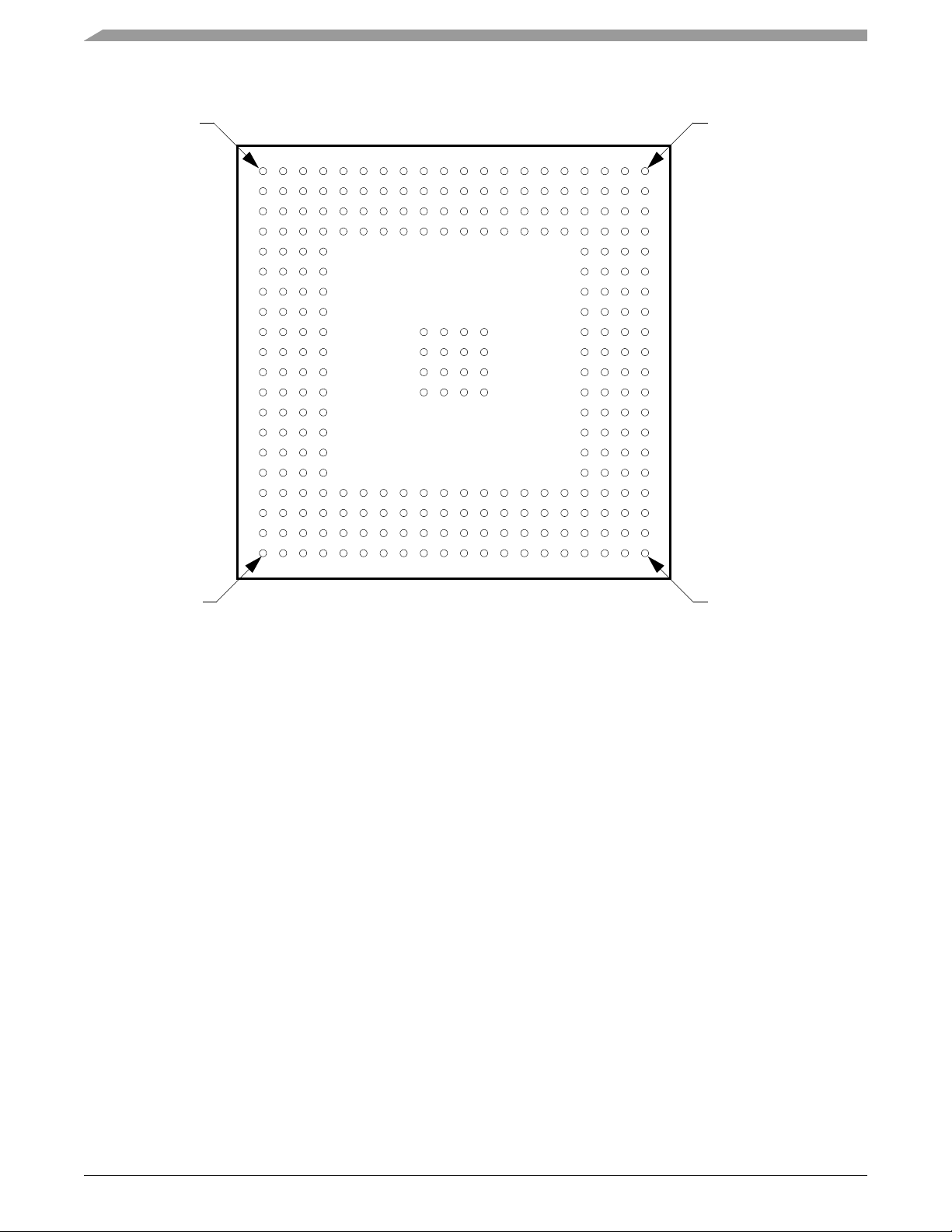
Overview
Y1 signal:
ext_ad_27
W
M
Y20 signal:
View Looking at Pins (Balls)
Y
V
U
T
R
P
N
L
K
J
H
G
F
E
D
C
B
A
timer0
A1 signal:
test_mode_1
101 2 3 4 5 6 7 8 9 11 13 14 15 16 17 18 19 2012
Note: Tab le 2-1 and Table 2- 2 give the signals on each pin/ball.
A20 signal:
mem_dqm_2
Figure 2-1. 272-Pin PBGA Pin Detail
Tab le 2- 1 gives a list of MPC5200B I/O signals sorted by package ball name. Tab le 2- 2 gives the same list sorted by signal name.
Many signal pins can have multiple functions depending on internal register settings. These additional functions are described in Table 2-3
through Table 2-31.
MPC5200B Users Guide, Rev. 1
2-2 Freescale Semiconductor
Page 48

Freescale Semiconductor 2-3
A01 A02 A03 A04 A05 A06 A07 A08 A09 A10 A11 A12 A13 A14 A15 A16 A17 A18 A19 A20
TEST_MODE_1 JTAG_TDO JTAG_TDI JTAG_TMS PSC3_8 PSC3_5 PSC3_2 PSC2_4 PSC2_2 PSC1_4 PSC1_1 PSC6_2 PORRESET SRESET SYS_XTAL_IN MEM_MA_ 1 MEM_MBA_1 MEM_RAS MEM_WE MEM_DQM_2
B01 B02 B03 B04 B05 B06 B07 B08 B09 B10 B11 B12 B13 B14 B15 B16 B17 B18 B19 B20
TEST_SEL_0
TEST_MODE_0
JTAG_TRST JTAG_TCK PSC3_7 PSC3_4 PSC3_1 PSC2_3
PSC2_1 PSC1_3 PSC1_0
PSC6_0HRESET SYS_PLL_AVDD SYS_PLL_TPA MEM_MA _2 MEM_MA_10 MEM_CS_0 MEM_CAS MEM_MA _4
C01 C02 C03 C04 C05 C06 C07 C08 C09 C10 C11 C12 C13 C14 C15 C16 C17 C18 C19 C20
RTC_XTAL_OUT RTC_XTAL_IN TEST_SEL_1 PSC3_9 PSC3_6 PSC3_3 PSC3_0 CORE_PLL_AVDD PSC2_0 PSC1_2 PSC6_1
GPIO_WKUP_7
PSC6_3 SYS_PLL_AVSS
GPIO_WKUP_6
MEM_MA_ 3 MEM_MA_0 MEM_MBA_0 ME M_MA_5 MEM_MA_6
D01 D02 D03 D04 D05 D06 D07 D08 D09 D10 D11 D12 D13 D14 D15 D16 D17D18D19D20
TIMER_4 TIMER_3 TIMER_2 VSS VDD_CORE VDD_IO VDD_CORE LP_OE VDD_IO VDD_CORE VDD_CORE VDD_MEM_IO VDD_MEM_IO SYS_XTAL_OUT VDD_MEM_IO VSS VDD_ MEM_IO MEM_MDQS _2 MEM_MA _7 MEM_MA _8
E01 E02 E03 E04 E17E18E19E20
TIMER_7 TIMER_6 TIMER_5 VDD_IO VDD_MEM_IO MEM_MDQ_16 MEM_MA_ 9 MEM_MA_ 11
F01 F02 F03 F04 Key for IO Balls: F17 F18 F19 F20
USB_7 USB_8 USB_9 VDD_IO
A6
G01 G02 G03 G04 PSC3_5
USB_3 USB_4 USB_5 USB_6 MEM_MDQ_ 18 MEM_MDQ_19 MEM_CLK MEM_CL K
<– Ball
<– Signal Name
VDD_MEM_IO MEM_MDQ_17 MEM_MA_ 12 MEM_CLK_EN
G17 G18 G19 G20
H01 H02 H03 H04 H17dH18
203
USB_0 USB_1 USB_2 VDD_IO VDD_MEM_IO MEM_MDQ_ 20 MEM_DQM_1 MEM_MDQS _1
MPC5200B Users Guide, Rev. 1
J01 J02 J03 J04 J09
ETH_3 ETH_4 ETH_10 ETH_17 MEM_MDQ_ 22 MEM_MDQ_21 MEM_MDQ_ 8 MEM_ MDQ_9
K01 K02 K03 K04 K09
ETH_0 ETH_1 ETH_2 VDD_CORE VDD_MEM_IO MEM_MDQ _23 MEM_MDQ_1 0 MEM_MDQ_11
L01 L02 L03 L04 L09
ETH_9 ETH_16 ETH_5 ETH_11 MEM_DQM_3 MEM_MDQS _3 MEM_MDQ_12 MEM_MDQ _13
M01 M02 M03 M04
ETH_13 ETH_12 ETH_8 VDD_CORE VDD_MEM_IO MEM_MDQ_24 MEM_MDQ_14 MEM_MDQ_15
M09
VSS
VSS
VSS
VSS
J10
VSS
K10
VSS
L10
VSS
M10
VSS
J11
VSS
K11
VSS
L11
VSS
M11
VSS
J12
VSS
K12
VSS
L12
VSS
M12
VSS
J17 J18 J19 J20
K17dK18
193
L17 L18 L19 L20
M17dM18
182
N01 N02 N03 N04 N17N18N19N20
ETH_7 ETH_6 ETH_15 ETH_14 MEM_MDQ_ 25 MEM_MDQ_26 MEM_DQM_0 MEM_MDQS _0
P01 P02 P03 P04
Key for PWR/GND Balls:
IRQ1 IRQ2 IRQ0 VDD_CORE
R01 R02 R03 R04
IRQ3 PCI_RESET EXT_AD _30 PCI_GNT
T01 T02 T03 T04
PCI_CLOCK EXT_AD_26 EXT_AD_ 28 VDD_IO VDD_MEM_IO MEM_ MDQ_30 ME M_MDQ_3 MEM_MDQ _2
VSS
VDD_CORE
VDD IO
VDD_MEM_IO
Core and IO VSS
1.5V Core VDD
3.3V IO VDD
Memory VDD
P17dP18
172
VDD_MEM_IO MEM_MDQ _27 MEM_MDQ _7 MEM_MDQ_ 6
R17R18R19R20
MEM_MDQ_ 28 MEM_MDQ_29 MEM_MDQ_ 5 MEM_ MDQ_4
T17 T18 T19 T20
U01 U02 U03 U04 U05 U06 U07 U08 U09 U10 U11 U12 U13 U14 U15 U16 U17U18U19U20
PCI_REQ PCI_IDSEL EXT_AD_ 24 VSS VDD_IO VDD_IO VDD_CORE EXT_AD_ 15 VDD_IO VDD_IO EXT_AD_ 6 VDD_CORE VDD_IO LP_ACK VDD_ CORE VDD_IO VSS MEM_MDQ _31 MEM_MDQ _1 MEM_MDQ_ 0
V01 V02 V03 V04 V05 V06 V07 V08 V09 V10 V11 V12 V13 V14 V15 V16 V17 V18 V19 V20
EXT_AD_31 EXT_AD_ 20 EXT_AD _22 EXT_AD_ 18 PCI_FRAME PCI_STOP PCI_PAR EXT_AD_ 13 EXT_AD_ 11 EXT_AD_ 9 EXT_AD_4 EXT_AD_2 EXT_AD _0 LP_ALE LP_CS2 LP_CS5 ATA_DRQ TIMER_1 I2C_0 I2C_2
W01 W02 W03 W04 W05 W06 W07 W08 W09 W10 W11 W12 W13 W14 W15 W16 W17 W18 W19 W20
EXT_AD_29 EXT_AD_ 25 EXT_AD _23 EXT_AD_ 16 PCI_TRDY PCI_CBE_2 PCI_DEVSEL PCI_S ERR EXT_AD_ 14 PCI_CBE_0 EXT_AD_ 8 EXT_AD_5 EXT_AD _1 LP_CS0 LP_CS3 LP_RW ATA_ IOW ATA_IOCHRDY I2C_1 I2C_3
Y01 Y02 Y03 Y04 Y05 Y06 Y07 Y08 Y09 Y10 Y11 Y12 Y13 Y14 Y15 Y16 Y17 Y18 Y19 Y20
EXT_AD_ 27 PCI_CBE_3 EXT_AD _21 EXT_AD_ 19 EXT_AD_ 17 PCI_IRDY PCI_PERR PCI_CBE_1 EXT_AD _12 EXT_AD_ 10 EXT_AD_7 EXT_AD _3 LP_TS LP_CS1 LP_CS4 ATA_ ISO LATI ON ATA_I OR ATA_DACK ATA_INTRQ TIMER_0
Figure 2-2. 272-Pin PBGA — Top View
H19
204
K19
194
M19
184
P19
174
H20
206
K20
196
M20
186
P20
176
Page 49

Pinout Tables
SDRAM
CS1
TSIZE_1
G
P
I
O
ATA chip
mux
1
selects
2
1
I
2
C
4 8
mux
4 pins
M
C
N
S
S
P
I
A
P
S
C
5
J
1
8
5
0
P
S
C
6
System
chip
selects
M
R
44
T
I
P
S
C
E
1
P
S
C
2
P
S
C
3
P
S
C
4
S
5 5
5
2
5
E
T
H
E
R
10 100
5
7
18
2
U
S
B
P2 P1
10
10
Reset
Conf.
22
8 4 2
mux mux mux
8 Pins 5 pins 5 pins 10 pins 18 pins 10 pins 4 pins
5 5 10 14 4
mux
8
4
4
5
muxmuxmuxmux
Dedicated
GPIO
I2C
Group
Timer
Group
2.2 Pinout Tables
Ball/Pin Pin Name Ball/Pin Pin Name
A01 TEST_MODE_1 B16 MEM_MA_2
A02 JTAG_TDO B17 MEM_MA _ 10
A03 JTAG_TDI B18 MEM_CS_0
A04 JTAG_TMS B19 MEM_CAS
A05 PSC3_8 B20 MEM_MA _ 4
A06 PSC3_5 C01 RTC_XTAL_OUT
A07 PSC3_2 C02 RTC_XTAL_IN
A08 PSC2_4 C03 TEST_SEL_1
A09 PSC2_2 C04 PSC3_9
PSC1
Group
PSC2
Group
PSC3
Group
Figure 2-3. MPC5200B Peripheral Muxing
Table 2-1. Signals by Ball/Pin
Ethernet
Group
USB
Group
PSC6
Group
A10 PSC1_4 C05 PSC3_6
MPC5200B Users Guide, Rev. 1
2-4 Freescale Semiconductor
Page 50

Table 2-1. Signals by Ball/Pin (continued)
Ball/Pin Pin Name Ball/Pin Pin Name
A11 PSC1_1 C06 PSC3_3
A12 PSC6_2 C07 PSC3_0
A13 PORRESET C08 CORE_PLL_AVDD
A14 SRESET C09 PSC2_0
A15 SYS_XTAL_IN C10 PSC1_2
A16 MEM_MA _ 1 C11 PSC6_1
A17 MEM_MBA_1 C12 GPIO_WKUP_7
A18 MEM_RAS C13 PSC6_3
A19 MEM_WE C14 SYS_PLL_AVSS
A20 MEM_DQM_2 C15 GPIO_WKUP_6
B01 TEST_SEL_0 C16 MEM_MA _ 3
B02 TEST_MODE_0 C17 MEM_MA_0
B03 JTAG_TRST C18 MEM_MBA_0
Pinout Tables
B04 JTAG_TCK C19 MEM_MA_5
B05 PSC3_7 C20 MEM_MA_6
B06 PSC3_4 D01 TIMER_4
B07 PSC3_1 D02 TIMER_3
B08 PSC2_3 D03 TIMER_2
B09 PSC2_1 D04 VSS_IO/CORE
B10 PSC1_3 D05 VDD_CORE
B11 PSC1_0 D06 VDD_IO
B12 PSC6_0 D07 VDD_CORE
B13 HRESET D08 LP_OE
B14 SYS_PLL_AVDD D09 VDD_IO
B15 SYS_PLL_TPA D10 VDD_CORE
D11 VDD_CORE H04 VDD_IO
D12 VDD_MEM_IO H17 VDD_MEM_IO
D13 VDD_MEM_IO H18 MEM_MDQ _ 20
D14 SYS_XTAL_OUT H19 MEM_DQM_1
D15 VDD_MEM_IO H20 MEM_MDQS_ 1
D16 VSS_IO/CORE J01 ETH_3
D17 VDD_MEM_IO J02 ETH_4
D18 MEM_MDQS _ 2 J03 ETH_10
D19 MEM_MA_7 J04 ETH_17
D20 MEM_MA_8 J09 VSS_IO/CORE
MPC5200B Users Guide, Rev. 1
Freescale Semiconductor 2-5
Page 51

Pinout Tables
Table 2-1. Signals by Ball/Pin (continued)
Ball/Pin Pin Name Ball/Pin Pin Name
E01 TIMER_7 J10 VSS_IO/CORE
E02 TIMER_6 J11 VSS_IO/CORE
E03 TIMER_5 J12 VSS_IO/CORE
E04 VDD_IO J17 MEM_MDQ_22
E17 VDD_MEM_IO J18 MEM_MDQ_ 21
E18 MEM_MDQ_16 J19 MEM_MDQ_ 8
E19 MEM_MA _ 9 J20 MEM_MDQ_9
E20 MEM_MA_11 K01 ETH_0
F01 USB_7 K02 ETH_1
F02 USB_8 K03 ETH_2
F03 USB_9 K04 VDD_CORE
F04 VDD_IO K09 VSS_IO/CORE
F17 VDD_MEM_IO K10 VSS_IO/CORE
F18 MEM_MDQ _ 17 K11 VSS_IO/CORE
F19 MEM_MA _ 12 K12 VSS_IO/CORE
F20 MEM_CLK_EN K17 VDD_MEM_IO
G01 USB_3 K18 MEM_MDQ_23
G02 USB_4 K19 MEM_MDQ_10
G03 USB_5 K20 MEM_MDQ_11
G04 USB_6 L01 ETH_9
G17 MEM_MDQ _ 18 L02 ETH_16
G18 MEM_MDQ_ 19 L03 ETH_5
G19 MEM_CLK L04 ETH_11
G20 MEM_CLK
L09 VSS_IO/CORE
H01 USB_0 L10 VSS_IO/CORE
H02 USB_1 L11 VSS_IO/CORE
H03 USB_2 L12 VSS_IO/CORE
L17 MEM_DQM_3 R18 MEM_MDQ _ 29
L18 MEM_MDQS_3 R19 MEM_MDQ_5
L19 MEM_MDQ_ 12 R20 MEM_MDQ _ 4
L20 MEM_MDQ_ 13 T01 PCI_CLOCK
M01 ETH_13 T02 EXT_AD_26
M02 ETH_12 T03 EXT_AD_28
M03 ETH_8 T04 VDD_IO
M04 VDD_CORE T17 VDD_MEM_IO
MPC5200B Users Guide, Rev. 1
2-6 Freescale Semiconductor
Page 52

Table 2-1. Signals by Ball/Pin (continued)
Ball/Pin Pin Name Ball/Pin Pin Name
M09 VSS_IO/CORE T18 MEM_MDQ _ 30
M10 VSS_IO/CORE T19 MEM_MDQ_3
M11 VSS_IO/CORE T20 MEM_MDQ_2
M12 VSS_IO/CORE U01 PCI_REQ
M17 VDD_MEM_IO U02 PCI_IDSEL
M18 MEM_MDQ _ 24 U03 EXT_AD_24
M19 MEM_MDQ _ 14 U04 VSS_IO/CORE
M20 MEM_MDQ _ 15 U05 VDD_IO
N01 ETH_7 U06 VDD_IO
N02 ETH_6 U07 VDD_CORE
N03 ETH_15 U08 EXT_AD_15
N04 ETH_14 U09 VDD_IO
N17 MEM_MDQ_25 U10 VDD_IO
Pinout Tables
N18 MEM_MDQ_ 26 U11 EXT_AD_ 6
N19 MEM_DQM _0 U12 VDD_CORE
N20 MEM_MDQS _ 0 U13 VDD_IO
P01 IRQ1 U14 LP_ACK
P02 IRQ2 U15 VDD_CORE
P03 IRQ0 U16 VDD_IO
P04 VDD_CORE U17 VSS_IO/CORE
P17 VDD_MEM_IO U18 MEM_MDQ_31
P18 MEM_MDQ_27 U19 MEM_MDQ_1
P19 MEM_MDQ _ 7 U20 MEM_MDQ_0
P20 MEM_MDQ _ 6 V01 EXT_AD_31
R01 IRQ3 V02 EXT_AD_20
R02 PCI_RESET V03 EXT_AD _ 22
R03 EXT_AD _ 30 V04 EXT_AD_18
R04 PCI_GNT V05 PCI_FRAME
R17 MEM_MDQ_ 28 V06 PCI_STOP
V07 PCI_PAR Y04 EXT_AD _19
V08 EXT_AD_13 Y05 EXT_AD _ 17
V09 EXT_AD_11 Y06 PCI_IRDY
V10 EXT_AD_ 9 Y07 PCI_PERR
V11 EXT_AD_ 4 Y08 PCI_CBE _1
V12 EXT_AD_ 2 Y09 EXT_AD_12
MPC5200B Users Guide, Rev. 1
Freescale Semiconductor 2-7
Page 53

Pinout Tables
Table 2-1. Signals by Ball/Pin (continued)
Ball/Pin Pin Name Ball/Pin Pin Name
V13 EXT_AD_ 0 Y10 EXT_AD_10
V14 LP_ALE Y11 EXT_AD_7
V15 LP_CS2 Y12 EXT_AD_ 3
V16 LP_CS5 Y13 LP_TS
V17 ATA_DRQ Y14 LP_CS1
V18 TIMER_1 Y15 LP_CS4
V19 I2C_0 Y16 ATA_ISOLATION
V20 I2C_2 Y17 ATA_IOR
W01 EXT_AD _ 29 Y18 ATA_DACK
W02 EXT_AD _ 25 Y19 ATA_INTRQ
W03 EXT_AD _ 23 Y20 TIMER_0
W04 EXT_AD _ 16
W05 PCI_TRDY
W06 PCI_CBE_2
W07 PCI_DEVSEL
W08 PCI_SERR
W09 EXT_AD _ 14
W10 PCI_CBE_0
W11 EXT_AD_ 8
W12 EXT_AD_ 5
W13 EXT_AD_ 1
W14 LP_CS0
W15 LP_CS3
W16 LP_RW
W17 ATA_IOW
W18 ATA_IOCHRDY
W19 I2C_1
W20 I2C_3
Y01 EXT_AD_27
Y02 PCI_CBE _3
Y03 EXT_AD_21
MPC5200B Users Guide, Rev. 1
2-8 Freescale Semiconductor
Page 54

Table 2-2. Signals by Signal Name
Signal Name Ball/Pin Signal Name Ball/Pin
ATA_DACK Y18 EXT_AD_6 U11
ATA_DRQ V17 EXT_AD_ 7 Y11
ATA_INTRQ Y19 EXT_AD _ 8 W11
ATA_IOCHRDY W18 EXT_AD_ 9 V10
ATA_IOR Y17 EXT_AD_10 Y10
ATA_IOW W17 EXT_AD _ 11 V09
ATA_ISOLATION Y16 EXT_AD_ 12 Y09
LP_CS0 W14 EXT_AD_ 13 V08
LP_CS1 Y14 EXT_AD_14 W09
LP_CS2 V15 EXT_AD_15 U08
LP_CS3 W15 EXT_AD_ 16 W04
LP_CS4 Y15 EXT_AD_17 Y05
LP_CS5 V16 EXT_AD_18 V04
Pinout Tables
ETH_0 K01 EXT_AD_19 Y04
ETH_1 K02 EXT_AD_20 V02
ETH_2 K03 EXT_AD_21 Y03
ETH_3 J01 EXT_AD_ 22 V03
ETH_4 J02 EXT_AD_ 23 W03
ETH_5 L03 EXT_AD_24 U03
ETH_6 N02 EXT_AD_25 W02
ETH_7 N01 EXT_AD_26 T02
ETH_8 M03 EXT_AD_27 Y01
ETH_9 L01 EXT_AD_28 T03
ETH_10 J03 EXT_AD_ 29 W01
ETH_11 L04 EXT_AD_ 30 R03
ETH_12 M02 EXT_AD_31 V01
ETH_13 M01 GPIO_WKUP_6 C15
ETH_14 N04 GPIO_WKUP_7 C12
ETH_15 N03 CORE_PLL_AVDD C08
ETH_16 L02 CORE_PLL_AVSS NC (no connection)
ETH_17 J04 HRESET B13
EXT_AD_0 V13 I2C_0 V19
EXT_AD_ 1 W13 I2C_1 W19
EXT_AD_2 V12 I2C_2 V20
EXT_AD_3 Y12 I2C_3 W20
MPC5200B Users Guide, Rev. 1
Freescale Semiconductor 2-9
Page 55

Pinout Tables
Signal Name Ball/Pin Signal Name Ball/Pin
EXT_AD_4 V11 PSC6_0 B12
EXT_AD_5 W12 PSC6_2 A12
JTAG_TCK B04 MEM_MDQ _ 5 R19
JTAG_TDO A02 MEM_MDQ_ 7 P19
JTAG_TMS A04 MEM_MDQ_ 8 J19
JTAG_TRST B03 MEM_MDQ_ 9 J20
Table 2-2. Signals by Signal Name (continued)
PSC6_3 C13 MEM_MBA_1 A17
PSC6_1 C11 MEM_MDQ_0 U20
IRQ0 P03 MEM_MDQ_ 1 U19
IRQ1 P01 MEM_MDQ_ 2 T20
IRQ2 P02 MEM_MDQ_ 3 T19
IRQ3 R01 MEM_MDQ _ 4 R20
JTAG_TDI A03 MEM_MDQ_ 6 P20
LP_ACK U14 MEM_MDQ _ 10 K19
LP_ALE V14 MEM_MDQ_11 K20
LP_OE D08 MEM_MDQ_12 L19
LP_RW W16 MEM_MDQ_13 L20
LP_TS Y13 MEM_MDQ_14 M19
MEM_CAS B19 MEM_MDQ _ 15 M20
MEM_CLK_EN F20 MEM_MDQ_16 E18
MEM_CS_0 B18 MEM_MDQ_ 17 F18
MEM_DQM_0 N19 MEM_MDQ_18 G17
MEM_DQM_1 H19 MEM_MDQ_19 G18
MEM_DQM_2 A20 MEM_MDQ_20 H18
MEM_DQM_3 L17 MEM_MDQ_21 J18
MEM_MA_0 C17 MEM_MDQ _ 22 J17
MEM_MA_1 A16 MEM_MDQ_23 K18
MEM_MA_2 B16 MEM_MDQ_24 M18
MEM_MA_3 C16 MEM_MDQ _ 25 N17
MEM_MA_4 B20 MEM_MDQ_26 N18
MEM_MA_5 C19 MEM_MDQ _ 27 P18
MEM_MA_6 C20 MEM_MDQ _ 28 R17
MEM_MA_7 D19 MEM_MDQ _ 29 R18
MEM_MA_8 D20 MEM_MDQ _ 30 T18
MEM_MA_9 E19 MEM_MDQ_31 U18
MPC5200B Users Guide, Rev. 1
2-10 Freescale Semiconductor
Page 56

Table 2-2. Signals by Signal Name (continued)
Signal Name Ball/Pin Signal Name Ball/Pin
MEM_MA_10 B17 MEM_MDQS_0 N20
MEM_MA_11 E20 MEM_MDQS_1 H20
MEM_MA_ 12 F19 MEM_MDQS _ 2 D18
MEM_MBA_0 C18 MEM_MDQS_ 3 L18
MEM_CLK G19 PSC3_5 A06
Pinout Tables
MEM_CLK
G20 PSC3_6 C05
MEM_RAS A18 PSC3_7 B05
MEM_WE A19 PSC3_8 A05
PCI_CBE_0 W10 PSC3_9 C04
PCI_CBE_1 Y08 RTC_XTAL_IN C02
PCI_CBE_2 W06 RTC_XTAL_OUT C01
PCI_CBE_3 Y02 SRESET A14
PCI_CLOCK T01 SYS_PLL_AVDD B14
PCI_DEVSEL W07 SYS_PLL_AVSS C14
PCI_FRAME V05 SYS_PLL_TPA B15
PCI_GNT R04 SYS_XTAL_IN A15
PCI_IDSEL U02 SYS_XTAL_OUT D14
PCI_IRDY Y06 TEST_MODE_0 B02
PCI_PAR V07 TEST_MODE_1 A01
PCI_PERR Y07 TEST_SEL_0 B01
PCI_REQ U01 TEST_SEL_1 C03
PCI_RESET R02 TIMER_0 Y20
PCI_SERR W08 TIMER_1 V18
PCI_STOP V06 TIMER_2 D03
PCI_TRDY W05 TIMER_3 D02
PORRESET A13 TIMER_4 D01
PSC1_0 B11 TIMER_5 E03
PSC1_1 A11 TIMER_6 E02
PSC1_2 C10 TIMER_7 E01
PSC1_3 B10 USB_0 H01
PSC1_4 A10 USB_1 H02
PSC2_0 C09 USB_2 H03
PSC2_1 B09 USB_3 G01
PSC2_2 A09 USB_4 G02
PSC2_3 B08 USB_5 G03
MPC5200B Users Guide, Rev. 1
Freescale Semiconductor 2-11
Page 57

Pinout Tables
Signal Name Ball/Pin Signal Name Ball/Pin
VDD_CORE D10 VSS_IO/CORE K10
VDD_CORE D11 VSS_IO/CORE K10
VDD_CORE K04 VSS_IO/CORE K11
VDD_CORE M04 VSS_IO/CORE K12
VDD_CORE P04 VSS_IO/CORE L09
VDD_CORE U07 VSS_IO/CORE L10
VDD_CORE U12 VSS_IO/CORE L11
Table 2-2. Signals by Signal Name (continued)
PSC2_4 A08 USB_6 G04
PSC3_0 C07 USB_7 F01
PSC3_1 B07 USB_8 F02
PSC3_2 A07 USB_9 F03
PSC3_3 C06 VDD_CORE D05
PSC3_4 B06 VSS_IO/CORE J12
VDD_CORE U15 VSS_IO/CORE L12
VDD_IO D06 VSS_IO/CORE M09
VDD_IO D09 VSS_IO/CORE M10
VDD_IO E04 VSS_IO/CORE M11
VDD_IO F04 VSS_IO/CORE M12
VDD_IO H4 VSS_IO/CORE U04
VDD_IO T4 VSS_IO/CORE U17
VDD_IO U05 VDD_CORE D07
VDD_IO U06
VDD_IO U09
VDD_IO U10
VDD_IO U13
VDD_IO U16
VDD_MEM_IO D12
VDD_MEM_IO D13
VDD_MEM_IO D15
VDD_MEM_IO D17
VDD_MEM_IO E17
VDD_MEM_IO F17
VDD_MEM_IO H17
VDD_MEM_IO K17
VDD_MEM_IO M17
MPC5200B Users Guide, Rev. 1
2-12 Freescale Semiconductor
Page 58

Table 2-2. Signals by Signal Name (continued)
Signal Name Ball/Pin Signal Name Ball/Pin
VDD_MEM_IO P17
VDD_MEM_IO T17
VSS_IO/CORE D04
VSS_IO/CORE D16
VSS_IO/CORE J09
VSS_IO/CORE J10
VSS_IO/CORE J11
Table 2-3. LocalPlus Bus Address / Data Pin Assignments
Pinout Tables
MPC5200B
LocaLPlus Bus
Address / Data
Pins
16 bit Adr,
16 bit Data
24 bit Adr,
8 bit Data
Muxed modes
All Muxed mode
Address tenures
8 bit Data
tenure
E
E
E
E
E
E
E
E
X
X
X
X
X
X
X
X
T
T
T
T
T
T
T
T
_
_
A
A
D
D
3
3
0
1
D
D
1
1
4
5
D7D6D5D4D3D2D1D0A
0T
S
1
Z
E
2
D7D6D5D
_
_
_
A
A
A
D
D
D
2
2
2
7
8
9
D
D
D
1
1
1
1
2
3
0B
T
T
S
S
1
1
Z
Z
E
E
0
1
D3D2D1D00000000000000000
4
_
_
_
A
A
A
D
D
D
2
2
2
4
5
6
D8D7D6D5D4D3D2D1D0A
D
D
0
1
9
0
A
B
2
S
S
4
0
1
E
E
E
E
E
X
X
X
T
T
T
_
_
_
A
A
A
D
D
D
2
2
2
1
2
3
A
A
2
2
2
3
1
2
A
A
A
2
2
2
1
2
3
E
X
X
X
T
T
T
_
_
_
A
A
A
D
D
D
2
1
1
0
8
9
A
A
A
1
1
2
8
9
0
A
A
A
1
1
2
8
9
0
E
E
E
X
X
X
T
T
T
_
_
_
A
A
A
D
D
D
1
1
1
5
6
7
1
5
A
A
A
1
1
1
5
6
7
A
A
A
1
1
1
5
6
7
E
E
E
X
X
X
T
T
T
_
_
_
A
A
A
D
D
D
1
1
1
2
3
4
A
A
A
1
1
1
2
3
4
A
A
A
1
1
1
2
3
4
A
A
A
1
1
1
2
3
4
E
E
E
X
X
X
T
T
T
_
_
_
A
A
A
D
D
D
9
1
1
0
1
A9A8A7A6A5A4A3A2A1A
A
A
1
1
0
1
A9A8A7A6A5A4A3A2A1A
A
A
1
1
0
1
A9A8A7A6A5A4A3A2A1A
A
A
1
1
0
1
E
E
E
X
X
X
T
T
T
_
_
_
A
A
A
D
D
D
7
8
6
E
E
E
X
X
X
T
T
T
_
_
_
A
A
A
D
D
D
3
4
5
E
E
E
X
X
X
T
T
T
_
_
_
A
A
A
D
D
D
0
1
2
0
0
0
D9D8D7D6D5D4D3D3D2D
D
D
D
D
D
16 bit Data tenureD1
32 bit Data tenureD3
1
1
1
1
1
0
1
2
3
4
5
D
D
D
D
D
D
D
D
D
D
D
D
1
2
2
2
2
2
2
2
2
2
2
3
8
9
0
1
5
6
7
2
3
4
MPC5200B Users Guide, Rev. 1
9
0
1
0
D
D
D
D
D
D
D
1
1
1
1
1
1
8
5
6
7
1
3
4
2
D9D8D7D6D5D4D3D2D1D
D
D
1
1
0
1
0
Freescale Semiconductor 2-13
Page 59

Pinout Tables
Table 2-4. LocalPlus Pin Functions
LocalPlus
Non-mux
Pin name BALL
EXT_AD_31 V01 D7 D15 0 D31 D15 D7 A31 D31 0 0 D31 D15
EXT_AD_30 R03 D6 D14 TSIZ0 D30 D14 D6 A30 D30 0 0 D30 D14
EXT_AD_29 W01 D5 D13 TSIZ1 D29 D13 D5 A29 D29 0 0 D29 D13
EXT_AD_28 T03 D4 D12 TSIZ2 D28 D12 D4 A28 D28 0 0 D28 D12
EXT_AD_27 Y01 D3 D11 0 D27 D11 D3 A27 D27 0 0 D27 D11
EXT_AD_26 T02 D2 D10 BS1 D26 D10 D2 A26 D26 0 0 D26 D10
EXT_AD_25 W02 D1 D9 BS0 D25 D9 D1 A25 D25 0 0 D25 D9
EXT_AD_24 U03 D0 D8 A24 D24 D8 D0 A24 D24 0 0 D24 D8
EXT_AD_23 W03 A23 D7 A23 D23 D7 0 A23 D23 0 0 D23 D7
EXT_AD_22 V03 A22 D6 A22 D22 D6 0 A22 D22 0 0 D22 D6
EXT_AD_21 Y03 A21 D5 A21 D21 D5 0 A21 D21 0 0 D21 D5
EXT_AD_20 V02 A20 D4 A20 D20 D4 0 A20 D20 0 0 D20 D4
EXT_AD_19 Y04 A19 D3 A19 D19 D3 0 A19 D19 0 0 D19 D3
EXT_AD_18 V04 A18 D2 A18 D18 D2 0 A18 D18 0 0 SA_2 D18 D2
EXT_AD_17 Y05 A17 D1 A17 D17 D1 0 A17 D17 0 0 SA_1 D17 D1
EXT_AD_16 W04 A16 D0 A16 D16 D0 0 A16 D16 0 0 SA_0 D16 D0
EXT_AD_15 U08 A15 A15 A15 D15 0 0 A15 D15 D15 0 D15 D15 A15
EXT_AD_14 W09 A14 A14 A14 D14 0 0 A14 D14 D14 0 D14 D14 A14
EXT_AD_13 V08 A13 A13 A13 D13 0 0 A13 D13 D13 0 D13 D13 A13
EXT_AD_12 Y09 A12 A12 A12 D12 0 0 A12 D12 D12 0 D12 D12 A12
EXT_AD_11 V09 A11 A11 A11 D11 0 0 A11 D11 D11 0 D11 D11 A11
EXT_AD_10 Y10 A10 A10 A10 D10 0 0 A10 D10 D10 0 D10 D10 A10
EXT_AD_9 V10 A9 A9 A9 D9 0 0 A9 D9 D9 0 D9 D9 A9
EXT_AD_8 W11 A8 A8 A8 D8 0 0 A8 D8 D8 0 D8 D8 A8
EXT_AD_7 Y11 A7 A7 A7 D7 0 0 A7 D7 D7 D7 D7 D7 A7
EXT_AD_6 U11 A6 A6 A6 D6 0 0 A6 D6 D6 D6 D6 D6 A6
EXT_AD_5 W12 A5 A5 A5 D5 0 0 A5 D5 D5 D5 D5 D5 A5
EXT_AD_4 V11 A4 A4 A4 D4 0 0 A4 D4 D4 D4 D4 D4 A4
EXT_AD_3 Y12 A3 A3 A3 D3 0 0 A3 D3 D3 D3 D3 D3 A3
EXT_AD_2 V12 A2 A2 A2 D2 0 0 A2 D2 D2 D2 D2 D2 A2
EXT_AD_1 W13 A1 A1 A1 D1 0 0 A1 D1 D1 D1 D1 D1 A1
EXT_AD_0 V13 A0 A0 A0 D0 0 0 A0 D0 D0 D0 D0 D0 A0
Addr
/Data
24/8
Addr
/Data
16/16
Address
Phase
LocalPlus
MULTIPLEXED BUS
32-bit
16-bit
Data
Phase
Data
Phase
8-bit
Data
Phase
PCI
Address
Phase
PCI BUS
32-bit
Data
Phase
16-bit
Data
Phase
8-bit
Data
Phase
ATA MOST
Large
Flash
RESET
PCI Dedicated Signals
PCI_PAR V07 PCI_PAR A0 A16
PCI_CBE_0 W10 PCI_CBE_0 A1 A17
PCI_CBE_1 Y08 PCI_CBE_1 A2 A18
MPC5200B Users Guide, Rev. 1
2-14 Freescale Semiconductor
Page 60

Table 2-4. LocalPlus Pin Functions (continued)
Pinout Tables
LocalPlus
Non-mux
Pin name BALL
PCI_CBE_2 W06 PCI_CBE_2 A3 A19
PCI_CBE_3 Y02 PCI_CBE_3 A4 A20
PCI_TRDY W05 PCI_TRDY A5 A21
PCI_IRDY Y06 PCI_IRDY A6 A22
PCI_STOP V06 PCI_STOP A7 A23
PCI_DEVSELW07 PCI_DEVSEL A8 A24
PCI_FRAMEV05 PCI_FRAME A9 A25
PCI_SERR W08 PCI_SERR A10 Note 1
PCI_PERR Y07 PCI_PERR A11 Note 1
PCI_IDSEL U02 PCI_IDSEL A12 Note 1
PCI_REQ U01 PCI_REQ A13 Note 1
PCI_GNT R04 PCI_GNT A14 Note 1
PCI_CL0CK T01 CLK
PCI_RESET R02 PCI_RESET A15 Note 1
Addr
/Data
24/8
OUT
Addr
/Data
16/16
CLK
OUT
Address
Phase
CLK
OUT
LocalPlus
MULTIPLEXED BUS
32-bit
16-bit
Data
CLK
OUT
Data
Phase
CLK
OUT
Phase
8-bit
Data
Phase
CLK
OUT
PCI BUS
PCI
32-bit
Address
Phase
Same as PCI_CLOCK CLK
Data
Phase
16-bit
Phase
Data
8-bit
Data
Phase
ATA MOST
OUT
Large
Flash
CLK
OUT
RESET
ATA Dedicated Signals
ATA_DRQ V17 ATA _DRQA16
ATA_DACK Y18 ATA _D
ATA _I O R Y 17 ATA _IORA18 RST_CF
ATA _I O W W 17 ATA _IOWA19 RST_CF
ATA _I O C HRDYW18 ATA _I
ATA _ IN T R Q Y 19 ATA _ I N
ATA_ISOLA
TION
LP_RW W16 LP_RW LP_RW RST_CF
LP_ALE V14 LP_ALE A23 RST_CF
LP_ACK U14 LP_ACK LP_ACK, Note 2
LP_TS Y13 LP_TS LP_TS RST_CF
Y16 ATA _I S
LocalPlus Dedicated Signals
OCHR
TRQ
OLATI
A17 RST_CF
ACK
A20
DY
A21
A22
ON
G0
G1
G2
G3
G4
G5
MPC5200B Users Guide, Rev. 1
Freescale Semiconductor 2-15
Page 61

Pinout Tables
Table 2-4. LocalPlus Pin Functions (continued)
LocalPlus
Non-mux
Pin name BALL
LP_OE D08 LP_OE LP_OE
LP_CS0 W14 CS_0 / CS_BOOT CS_0 /
LP_CS1 Y14 CS_1 CS_1
LP_CS2 V15 CS_2 CS_2
LP_CS3 W15 CS_3 CS_3
LP_CS4 Y15 CS_4 ATA_C
LP_CS5 V16 CS_5 ATA_C
PSC3_4 B06 CS_6 CS_6
PSC3_5 A06 CS_7 CS_7
GPIO_WKU
P_7
TEST_SEL_1C03 TSIZ2
Addr
/Data
24/8
C12 TSIZ1
Addr
/Data
16/16
Address
Phase
LocalPlus
MULTIPLEXED BUS
32-bit
16-bit
Data
Phase
Data
Phase
PSC 3 Dedicated Signals
GPIO_WKUP Dedicated Signals
JTAG Access Dedicated Signals
8-bit
Data
Phase
PCI
Address
Phase
PCI BUS
32-bit
Data
Phase
16-bit
Data
Phase
8-bit
Data
Phase
ATA MOST
CS_BOOT
S_0
S_1
CS_4
CS_5
Large
Flash
RESET
1. The PCI signals, which are not used as address in Large Flash mode, are drive low during a Large Flash access.
2. For a burst transaction LP_ACK signal indicates the burst
.
Table 2-5. LocalPlus Bus Address / Data Signals
PIN / BALL NUMBER Function
Pin EXT_AD_31 Ball V01
LocalPlus Bus multiplexed mode
Address Phase
8-Bit Data Phase
16-Bit Data Phase
32-Bit Data Phase
logic 0
D7
D15
D31
LocalPlus non-mux
16-bit addr/16-bit data
24-bit addr/8-bit data
D15
D7
LFLASH D15 hi - z Large Flash Data Bit D15
MOST Graphics D31 hi - z MOST Graphics Data Bit D31
ATA ----- ----- -----
PCI
Address Phase
8-Bit Data Phase
16-Bit Data Phase
32-Bit Data Phase
A31
logic 0
logic 0
D31
Reset
Value
hi - z
logic 0
LocalPlus Data Bit 7
LocalPlus Data Bit 15
LocalPlus Data Bit 31
hi - z logic 0
LocalPlus Data Bit 15
hi - z
PCI Address Bit A31
logic 0
logic 0
PCI Data Bit 31
Description
MPC5200B Users Guide, Rev. 1
2-16 Freescale Semiconductor
Page 62

Table 2-5. LocalPlus Bus Address / Data Signals (continued)
Pinout Tables
hi - z
hi - z
hi - z
hi - z
hi - z
hi - z
hi - z
hi - z
hi - z
Reset
Value
Description
LocalPlus TSIZE0
LocalPlus Data Bit 6
LocalPlus Data Bit 14
LocalPlus Data Bit 30
LocalPlus Data Bit 14
LocalPlus Data Bit 6
PCI Address Bit A30
logic 0
logic 0
PCI Data Bit 30
LocalPlus TSIZE1
LocalPlus Data Bit 5
LocalPlus Data Bit 13
LocalPlus Data Bit 29
LocalPlus Data Bit 13
LocalPlus Data Bit 5
PCI Address Bit A29
logic 0
logic 0
PCI Data Bit 29
TSIZE2
LocalPlus Data Bit 4
LocalPlus Data Bit 12
LocalPlus Data Bit 28
LocalPlus Data Bit 12
LocalPlus Data Bit 4
PCI Address Bit A28
logic 0
logic 0
PCI Data Bit 28
PIN / BALL NUMBER Function
Pin EXT_AD_30 Ball R03
LocalPlus Bus multiplexed mode
Address Phase
8-Bit Data Phase
16-Bit Data Phase
32-Bit Data Phase
LocalPlus non-mux
16-bit addr/16-bit data
24-bit addr/8-bit data
LFLASH D14 hi - z Large Flash Data Bit D14
MOST Graphics D30 hi - z MOST Graphics Data Bit D30
ATA ----- ----- -----
PCI
Address Phase
8-Bit Data Phase
16-Bit Data Phase
32-Bit Data Phase
Pin EXT_AD_29 Ball W01
LocalPlus Bus multiplexed mode
Address Phase
8-Bit Data Phase
16-Bit Data Phase
32-Bit Data Phase
LocalPlus non-mux
16-bit addr/16-bit data
24-bit addr/8-bit data
LFLASH D13 hi - z Large Flash Data Bit D13
MOST Graphics D29 hi - z MOST Graphics Data Bit D29
ATA ----- ----- -----
PCI
Address Phase
8-Bit Data Phase
16-Bit Data Phase
32-Bit Data Phase
Pin EXT_AD_28 Ball T03
LocalPlus Bus multiplexed mode
Address Phase
8-Bit Data Phase
16-Bit Data Phase
32-Bit Data Phase
LocalPlus non-mux
16-bit addr/16-bit data
24-bit addr/8-bit data
LFLASH D12 hi - z Large Flash Data Bit D12
MOST Graphics D28 hi - z MOST Graphics Data Bit D28
ATA ----- ----- -----
PCI
Address Phase
8-Bit Data Phase
16-Bit Data Phase
32-Bit Data Phase
TSIZE0
D6
D14
D30
D14
D6
A30
logic 0
logic 0
D30
TSIZE1
D5
D13
D29
D13
D5
A31
logic 0
logic 0
D29
TSIZE2
D4
D12
D28
D12
D4
A28
logic 0
logic 0
D28
MPC5200B Users Guide, Rev. 1
Freescale Semiconductor 2-17
Page 63

Pinout Tables
Table 2-5. LocalPlus Bus Address / Data Signals (continued)
hi - z
hi - z
hi - z
hi - z
hi - z
hi - z
hi - z
hi - z
hi - z
Reset
Value
Description
logic 0
LocalPlus Data Bit 3
LocalPlus Data Bit 11
LocalPlus Data Bit 27
LocalPlus Data Bit 11
LocalPlus Data Bit 3
PCI Address Bit A27
logic 0
logic 0
PCI Data Bit 27
LocalPlus BS1
LocalPlus Data Bit 2
LocalPlus Data Bit 10
LocalPlus Data Bit 26
LocalPlus Data Bit 10
LocalPlus Data Bit 2
PCI Address Bit A26
logic 0
logic 0
PCI Data Bit 26
BS0
LocalPlus Data Bit 1
LocalPlus Data Bit 9
LocalPlus Data Bit 25
LocalPlus Data Bit 9
LocalPlus Data Bit 1
PCI Address Bit A25
logic 0
logic 0
PCI Data Bit 25
PIN / BALL NUMBER Function
Pin EXT_AD_27 Ball Y01
LocalPlus Bus multiplexed mode
Address Phase
8-Bit Data Phase
16-Bit Data Phase
32-Bit Data Phase
LocalPlus non-mux
16-bit addr/16-bit data
24-bit addr/8-bit data
LFLASH D11 hi - z Large Flash Data Bit D11
MOST Graphics D27 hi - z MOST Graphics Data Bit D27
ATA ----- ----- -----
PCI
Address Phase
8-Bit Data Phase
16-Bit Data Phase
32-Bit Data Phase
Pin EXT_AD_26 Ball T02
LocalPlus Bus multiplexed mode
Address Phase
8-Bit Data Phase
16-Bit Data Phase
32-Bit Data Phase
LocalPlus non-mux
16-bit addr/16-bit data
24-bit addr/8-bit data
LFLASH D10 hi - z Large Flash Data Bit D10
MOST Graphics D26 hi - z MOST Graphics Data Bit D26
ATA ----- ----- -----
PCI
Address Phase
8-Bit Data Phase
16-Bit Data Phase
32-Bit Data Phase
Pin EXT_AD_25 Ball W02
LocalPlus Bus multiplexed mode
Address Phase
8-Bit Data Phase
16-Bit Data Phase
32-Bit Data Phase
LocalPlus non-mux
16-bit addr/16-bit data
24-bit addr/8-bit data
LFLASH D9 hi - z Large Flash Data Bit D9
MOST Graphics D25 hi - z MOST Graphics Data Bit D25
ATA ----- ----- -----
PCI
Address Phase
8-Bit Data Phase
16-Bit Data Phase
32-Bit Data Phase
logic 0
D3
D11
D27
D11
D3
A27
logic 0
logic 0
D27
BS1
D2
D10
D26
D10
D2
A26
logic 0
logic 0
D26
BS0
D1
D9
D25
D9
D1
A25
logic 0
logic 0
D25
MPC5200B Users Guide, Rev. 1
2-18 Freescale Semiconductor
Page 64

Table 2-5. LocalPlus Bus Address / Data Signals (continued)
Pinout Tables
hi - z
hi - z
hi - z
hi - z
hi - z
hi - z
hi - z
hi - z
hi - z
Reset
Value
Description
LocalPlus Address Bit 24
LocalPlus Data Bit 0
LocalPlus Data Bit 8
LocalPlus Data Bit 24
LocalPlus Data Bit 8
LocalPlus Data Bit 0
PCI Address Bit A24
logic 0
logic 0
PCI Data Bit 24
Local Address Bit A23
logic 0
LocalPlus Data Bit 7
LocalPlus Data Bit 23
LocalPlus Data Bit 7
LocalPlus Address Bit A23
PCI Address Bit A23
logic 0
logic 0
PCI Data Bit D23
LocalPlus Address Bit A22
logic 0
LocalPlus Data Bit 6
LocalPlus Data Bit D22
LocalPlus Data Bit D6
LocalPlus Address Bit A22
PCI Address Bit A22
logic 0
logic 0
PCI Data Bit D22
PIN / BALL NUMBER Function
Pin EXT_AD_24 Ball U03
LocalPlus Bus multiplexed mode
Address Phase
8-Bit Data Phase
16-Bit Data Phase
32-Bit Data Phase
LocalPlus non-mux
16-bit addr/16-bit data
24-bit addr/8-bit data
LFLASH D8 hi - z Large Flash Data Bit D8
MOST Graphics D24 hi - z MOST Graphics Data Bit D24
ATA ----- ----- -----
PCI
Address Phase
8-Bit Data Phase
16-Bit Data Phase
32-Bit Data Phase
Pin EXT_AD_23 Ball W03
LocalPlus Bus multiplexed mode
Address Phase
8-Bit Data Phase
16-Bit Data Phase
32-Bit Data Phase
LocalPlus non-mux
16-bit addr/16-bit data
24-bit addr/8-bit data
LFLASH D7 hi - z Large Flash Data Bit D7
MOST Graphics D23 hi - z MOST Graphics Data Bit D23
ATA ----- ----- -----
PCI
Address Phase
8-Bit Data Phase
16-Bit Data Phase
32-Bit Data Phase
Pin EXT_AD_22 Ball V03
LocalPlus Bus multiplexed mode
Address Phase
8-Bit Data Phase
16-Bit Data Phase
32-Bit Data Phase
LocalPlus non-mux
16-bit addr/16-bit data
24-bit addr/8-bit data
LFLASH D6 hi - z Large Flash Data Bit D6
MOST Graphics D22 hi - z MOST Graphics Data Bit D22
ATA ----- ----- -----
PCI
Address Phase
8-Bit Data Phase
16-Bit Data Phase
32-Bit Data Phase
A24
D0
D8
D24
D8
D0
A24
logic 0
logic 0
D24
A23
logic 0
D7
D23
D7
A23
A23
logic 0
logic 0
D23
A22
logic 0
D6
D22
D6
A22
A22
logic 0
logic 0
D22
MPC5200B Users Guide, Rev. 1
Freescale Semiconductor 2-19
Page 65

Pinout Tables
Table 2-5. LocalPlus Bus Address / Data Signals (continued)
hi - z
hi - z
hi - z
hi - z
hi - z
hi - z
hi - z
hi - z
hi - z
Reset
Value
Description
LocalPlus Address Bit A21
logic 0
LocalPlus Data Bit 5
LocalPlus Data Bit D21
LocalPlus Data Bit D5
LocalPlus Address Bit A21
PCI Address Bit A21
logic 0
logic 0
PCI Data Bit D21
LocalPlus Address Bit A20
logic 0
LocalPlus Data Bit 4
LocalPlus Data Bit D20
LocalPlus Data Bit D4
LocalPlus Address Bit A20
PCI Address Bit A20
logic 0
logic 0
PCI Data Bit D20
LocalPlus Address Bit A19
logic 0
LocalPlus Data Bit 3
LocalPlus Data Bit D19
LocalPlus Data Bit D3
LocalPlus Address Bit A19
PCI Address Bit A19
logic 0
logic 0
PCI Data Bit D19
PIN / BALL NUMBER Function
Pin EXT_AD_21 Ball Y03
LocalPlus Bus multiplexed mode
Address Phase
8-Bit Data Phase
16-Bit Data Phase
32-Bit Data Phase
LocalPlus non-mux
16-bit addr/16-bit data
24-bit addr/8-bit data
LFLASH D5 hi - z Large Flash Data Bit D5
MOST Graphics D21 hi - z MOST Graphics Data Bit D21
ATA ----- ----- -----
PCI
Address Phase
8-Bit Data Phase
16-Bit Data Phase
32-Bit Data Phase
Pin EXT_AD_20 Ball V02
LocalPlus Bus multiplexed mode
Address Phase
8-Bit Data Phase
16-Bit Data Phase
32-Bit Data Phase
LocalPlus non-mux
16-bit addr/16-bit data
24-bit addr/8-bit data
LFLASH D4 hi - z Large Flash Data Bit D4
MOST Graphics D20 hi - z MOST Graphics Data Bit D20
ATA ----- ----- -----
PCI
Address Phase
8-Bit Data Phase
16-Bit Data Phase
32-Bit Data Phase
Pin EXT_AD_19 Ball Y04
LocalPlus Bus multiplexed mode
Address Phase
8-Bit Data Phase
16-Bit Data Phase
32-Bit Data Phase
LocalPlus non-mux
16-bit addr/16-bit data
24-bit addr/8-bit data
LFLASH D3 hi - z Large Flash Data Bit D3
MOST Graphics D19 hi - z MOST Graphics Data Bit D19
ATA ----- ----- -----
PCI
Address Phase
8-Bit Data Phase
16-Bit Data Phase
32-Bit Data Phase
A21
logic 0
D5
D21
D5
A21
A21
logic 0
logic 0
D21
A20
logic 0
D4
D20
D4
A20
A20
logic 0
logic 0
D20
A19
logic 0
D3
D19
D3
A19
A19
logic 0
logic 0
D19
MPC5200B Users Guide, Rev. 1
2-20 Freescale Semiconductor
Page 66

Table 2-5. LocalPlus Bus Address / Data Signals (continued)
Pinout Tables
hi - z
hi - z
hi - z
hi - z
hi - z
hi - z
hi - z
hi - z
hi - z
Reset
Value
Description
LocalPlus Address Bit A18
logic 0
LocalPlus Data Bit 2
LocalPlus Data Bit D18
LocalPlus Data Bit D2
LocalPlus Address Bit A18
PCI Address Bit A18
logic 0
logic 0
PCI Data Bit D18
LocalPlus Address Bit A17
logic 0
LocalPlus Data Bit 1
LocalPlus Data Bit D17
LocalPlus Data Bit D1
LocalPlus Address Bit A17
PCI Address Bit A17
logic 0
logic 0
PCI Data Bit D17
LocalPlus Address Bit A16
logic 0
LocalPlus Data Bit 0
LocalPlus Data Bit D16
LocalPlus Data Bit D0
LocalPlus Address Bit A16
PCI Address Bit A16
logic 0
logic 0
PCI Data Bit D16
PIN / BALL NUMBER Function
Pin EXT_AD_18 Ball V04
LocalPlus Bus multiplexed mode
Address Phase
8-Bit Data Phase
16-Bit Data Phase
32-Bit Data Phase
LocalPlus non-mux
16-bit addr/16-bit data
24-bit addr/8-bit data
LFLASH D2 hi - z Large Flash Data Bit D2
MOST Graphics D18 hi - z MOST Graphics Data Bit D18
ATA ATA_SA_2 hi - z -----
PCI
Address Phase
8-Bit Data Phase
16-Bit Data Phase
32-Bit Data Phase
Pin EXT_AD_17 Ball Y05
LocalPlus Bus multiplexed mode
Address Phase
8-Bit Data Phase
16-Bit Data Phase
32-Bit Data Phase
LocalPlus non-mux
16-bit addr/16-bit data
24-bit addr/8-bit data
LFLASH D1 hi - z Large Flash Data Bit D1
MOST Graphics D17 hi - z MOST Graphics Data Bit D17
ATA ----- ----- -----
PCI
Address Phase
8-Bit Data Phase
16-Bit Data Phase
32-Bit Data Phase
Pin EXT_AD_16 Ball W04
LocalPlus Bus multiplexed mode
Address Phase
8-Bit Data Phase
16-Bit Data Phase
32-Bit Data Phase
LocalPlus non-mux
16-bit addr/16-bit data
24-bit addr/8-bit data
LFLASH D0 hi - z Large Flash Data Bit D0
MOST Graphics D16 hi - z MOST Graphics Data Bit D16
ATA ATA_SA_0 hi - z ATA_SA_0
PCI
Address Phase
8-Bit Data Phase
16-Bit Data Phase
32-Bit Data Phase
A18
logic 0
D2
D18
D2
A18
A18
logic 0
logic 0
D18
A17
logic 0
D1
D17
D1
A17
A17
logic 0
logic 0
D17
A16
logic 0
D0
D16
D0
A16
A16
logic 0
logic 0
D16
MPC5200B Users Guide, Rev. 1
Freescale Semiconductor 2-21
Page 67

Pinout Tables
Table 2-5. LocalPlus Bus Address / Data Signals (continued)
hi - z
hi - z
hi - z
hi - z
hi - z
Reset
Value
Description
LocalPlus Address Bit A15
logic 0
logic 0
LocalPlus Data Bit D15
LocalPlus Address Bit A15
LocalPlus Address Bit A15
PCI Address Bit A15
logic 0
PCI Data Bit D15
PCI Data Bit D15
LocalPlus Address Bit A14
logic 0
logic 0
LocalPlus Data Bit D14
LocalPlus Address Bit A14
LocalPlus Address Bit A14
PIN / BALL NUMBER Function
Pin EXT_AD_15 Ball U08
LocalPlus Bus multiplexed mode
Address Phase
8-Bit Data Phase
16-Bit Data Phase
32-Bit Data Phase
LocalPlus non-mux
16-bit addr/16-bit data
24-bit addr/8-bit data
LFLASH A15 hi - z Large Flash Address Bit A15
MOST Graphics D15 hi - z MOST Graphics Data Bit D15
ATA ATA _ DATA _ 15hi - z ATA Data Bit 15
PCI
Address Phase
8-Bit Data Phase
16-Bit Data Phase
32-Bit Data Phase
Pin EXT_AD_14 Ball W09
LocalPlus Bus multiplexed mode
Address Phase
8-Bit Data Phase
16-Bit Data Phase
32-Bit Data Phase
LocalPlus non-mux
16-bit addr/16-bit data
24-bit addr/8-bit data
LFLASH A14 hi - z Large Flash Address Bit A14
MOST Graphics D14 hi - z MOST Graphics Data Bit D14
ATA ATA _ DATA _ 14hi - z ATA_DATA_14
A15
logic 0
logic 0
D15
A15
A15
A15
logic 0
D15
D15
A14
logic 0
logic 0
D14
A14
A14
PCI
Address Phase
8-Bit Data Phase
16-Bit Data Phase
32-Bit Data Phase
Pin EXT_AD_13 Ball V08
LocalPlus Bus multiplexed mode
Address Phase
8-Bit Data Phase
16-Bit Data Phase
32-Bit Data Phase
LocalPlus non-mux
16-bit addr/16-bit data
24-bit addr/8-bit data
LFLASH A13 hi - z Large Flash Address Bit A13
MOST Graphics D13 hi - z MOST Graphics Data Bit D13
ATA ATA _ DATA _ 13hi - z ATA Data Bit D13
PCI
Address Phase
8-Bit Data Phase
16-Bit Data Phase
32-Bit Data Phase
A14
logic 0
D14
D14
A13
logic 0
logic 03
D13
A13
A13
A13
logic 0
D13
D13
MPC5200B Users Guide, Rev. 1
hi - z
PCI Address Bit A14
logic 0
PCI Data Bit D14
PCI Data Bit D14
hi - z
LocalPlus Address Bit A13
logic 0
logic 0
LocalPlus Data Bit D13
hi - z
LocalPlus Address Bit A13
LocalPlus Address Bit A13
hi - z
PCI Address Bit A13
logic 0
PCI Data Bit D13
PCI Data Bit D13
2-22 Freescale Semiconductor
Page 68

Table 2-5. LocalPlus Bus Address / Data Signals (continued)
Pinout Tables
hi - z
hi - z
hi - z
hi - z
hi - z
Reset
Value
Description
LocalPlus Address Bit A12
logic 0
logic 0
LocalPlus Data Bit D12
LocalPlus Address Bit A12
LocalPlus Address Bit A12
PCI Address Bit A12
logic 0
PCI Data Bit D12
PCI Data Bit D12
LocalPlus Address Bit A11
logic 0
logic 0
LocalPlus Data Bit D11
LocalPlus Address Bit A11
LocalPlus Address Bit A11
PIN / BALL NUMBER Function
Pin EXT_AD_12 Ball Y09
LocalPlus Bus multiplexed mode
Address Phase
8-Bit Data Phase
16-Bit Data Phase
32-Bit Data Phase
LocalPlus non-mux
16-bit addr/16-bit data
24-bit addr/8-bit data
LFLASH A12 hi - z Large Flash Address Bit A12
MOST Graphics D12 hi - z MOST Graphics Data Bit D12
ATA ATA _ DATA _ 12hi - z ATA_DATA_12
PCI
Address Phase
8-Bit Data Phase
16-Bit Data Phase
32-Bit Data Phase
Pin EXT_AD_11 Ball V09
LocalPlus Bus multiplexed mode
Address Phase
8-Bit Data Phase
16-Bit Data Phase
32-Bit Data Phase
LocalPlus non-mux
16-bit addr/16-bit data
24-bit addr/8-bit data
LFLASH A11 hi - z Large Flash Address Bit A11
MOST Graphics D11 hi - z MOST Graphics Data Bit D11
ATA ATA _ DATA _ 11hi - z ATA_DATA_11
A12
logic 0
logic 0
D12
A12
A12
A12
logic 0
D12
D12
A11
logic 0
logic 0
D11
A11
A11
PCI
Address Phase
8-Bit Data Phase
16-Bit Data Phase
32-Bit Data Phase
Pin EXT_AD_10 Ball Y10
LocalPlus Bus multiplexed mode
Address Phase
8-Bit Data Phase
16-Bit Data Phase
32-Bit Data Phase
LocalPlus non-mux
16-bit addr/16-bit data
24-bit addr/8-bit data
LFLASH A10 hi - z Large Flash Address Bit A10
MOST Graphics D10 hi - z MOST Graphics Data Bit D10
ATA ATA _ DATA _ 10hi - z ATA_DATA_10
PCI
Address Phase
8-Bit Data Phase
16-Bit Data Phase
32-Bit Data Phase
A11
logic 0
D11
D11
A10
logic 0
logic 0
D10
A10
A10
A10
logic 0
D10
D10
MPC5200B Users Guide, Rev. 1
hi - z
PCI Address Bit A11
logic 0
PCI Data Bit D11
PCI Data Bit D11
hi - z
LocalPlus Address Bit A10
logic 0
logic 0
LocalPlus Data Bit D10
hi - z
LocalPlus Address Bit A10
LocalPlus Address Bit A10
hi - z
PCI Address Bit A10
logic 0
PCI Data Bit D10
PCI Data Bit D10
Freescale Semiconductor 2-23
Page 69

Pinout Tables
Table 2-5. LocalPlus Bus Address / Data Signals (continued)
hi - z
hi - z
hi - z
hi - z
hi - z
hi - z
hi - z
hi - z
hi - z
Reset
Value
Description
LocalPlus Address Bit A9
logic 0
logic 0
LocalPlus Data Bit D9
LocalPlus Address Bit A9
LocalPlus Address Bit A9
PCI Address Bit A9
logic 0
PCI Data Bit D9
PCI Data Bit D9
LocalPlus Address Bit A8
logic 0
logic 0
LocalPlus Data Bit D8
LocalPlus Address Bit A8
LocalPlus Address Bit A8
PCI Address Bit A8
logic 0
PCI Data Bit D8
PCI Data Bit D8
LocalPlus Address Bit A7
logic 0
logic 0
LocalPlus Data Bit D7
LocalPlus Address Bit A7
LocalPlus Address Bit A7
PCI Address Bit A7
PCI Data Bit D7
PCI Data Bit D7
PCI Data Bit D7
PIN / BALL NUMBER Function
Pin EXT_AD_9 Ball V10
LocalPlus Bus multiplexed mode
Address Phase
8-Bit Data Phase
16-Bit Data Phase
32-Bit Data Phase
LocalPlus non-mux
16-bit addr/16-bit data
24-bit addr/8-bit data
LFLASH A9 hi - z Large Flash Address Bit A9
MOST Graphics D9 hi - z MOST Graphics Data Bit D22
ATA ATA _DATA_ 9 hi - z ATA_ DATA _ 9
PCI
Address Phase
8-Bit Data Phase
16-Bit Data Phase
32-Bit Data Phase
Pin EXT_AD_8 Ball W11
LocalPlus Bus multiplexed mode
Address Phase
8-Bit Data Phase
16-Bit Data Phase
32-Bit Data Phase
LocalPlus non-mux
16-bit addr/16-bit data
24-bit addr/8-bit data
LFLASH A8 hi - z Large Flash Address Bit A8
MOST Graphics D8 hi - z MOST Graphics Data Bit D8
ATA ATA _DATA_ 8 hi - z ATA_ DATA _ 8
PCI
Address Phase
8-Bit Data Phase
16-Bit Data Phase
32-Bit Data Phase
Pin EXT_AD_7 Ball Y11
LocalPlus Bus multiplexed mode
Address Phase
8-Bit Data Phase
16-Bit Data Phase
32-Bit Data Phase
LocalPlus non-mux
16-bit addr/16-bit data
24-bit addr/8-bit data
LFLASH A7 hi - z Large Flash Address Bit A7
MOST Graphics D7 hi - z MOST Graphics Data Bit D7
ATA ATA _DATA_ 7 hi - z ATA_ DATA _ 7
PCI
Address Phase
8-Bit Data Phase
16-Bit Data Phase
32-Bit Data Phase
A9
logic 0
logic 0
D9
A9
A9
A9
logic 0
D9
D9
A8
logic 0
logic 0
D8
A8
A8
A8
logic 0
D8
D8
A7
logic 0
logic 0
D7
A7
A7
A7
D7
D7
D7
MPC5200B Users Guide, Rev. 1
2-24 Freescale Semiconductor
Page 70

Table 2-5. LocalPlus Bus Address / Data Signals (continued)
Pinout Tables
hi - z
hi - z
hi - z
hi - z
hi - z
hi - z
hi - z
hi - z
hi - z
Reset
Value
Description
LocalPlus Address Bit A6
logic 0
logic 0
LocalPlus Data Bit D6
LocalPlus Address Bit A6
LocalPlus Address Bit A6
PCI Address Bit A6
PCI Data Bit D6
PCI Data Bit D6
PCI Data Bit D6
LocalPlus Address Bit A5
logic 0
logic 0
LocalPlus Data Bit D5
LocalPlus Address Bit A5
LocalPlus Address Bit A5
PCI Address Bit A5
PCI Data Bit D5
PCI Data Bit D5
PCI Data Bit D5
LocalPlus Address Bit A4
logic 0
logic 0
LocalPlus Data Bit D4
LocalPlus Address Bit A4
LocalPlus Address Bit A4
PCI Address Bit A4
PCI Data Bit D4
PCI Data Bit D4
PCI Data Bit D4
PIN / BALL NUMBER Function
Pin EXT_AD_6 Ball U11
LocalPlus Bus multiplexed mode
Address Phase
8-Bit Data Phase
16-Bit Data Phase
32-Bit Data Phase
LocalPlus non-mux
16-bit addr/16-bit data
24-bit addr/8-bit data
LFLASH A6 hi - z Large Flash Address Bit A6
MOST Graphics D6 hi - z MOST Graphics Data Bit D6
ATA ATA _DATA_ 6 hi - z ATA_ DATA _ 6
PCI
Address Phase
8-Bit Data Phase
16-Bit Data Phase
32-Bit Data Phase
Pin EXT_AD_5 Ball W12
LocalPlus Bus multiplexed mode
Address Phase
8-Bit Data Phase
16-Bit Data Phase
32-Bit Data Phase
LocalPlus non-mux
16-bit addr/16-bit data
24-bit addr/8-bit data
LFLASH A5 hi - z Large Flash Address Bit A5
MOST Graphics D5 hi - z MOST Graphics Data Bit D5
ATA ATA _DATA_ 5 hi - z ATA_ DATA _ 5
PCI
Address Phase
8-Bit Data Phase
16-Bit Data Phase
32-Bit Data Phase
Pin EXT_AD_4 Ball V11
LocalPlus Bus multiplexed mode
Address Phase
8-Bit Data Phase
16-Bit Data Phase
32-Bit Data Phase
LocalPlus non-mux
16-bit addr/16-bit data
24-bit addr/8-bit data
LFLASH A4 hi - z Large Flash Address Bit A4
MOST Graphics D4 hi - z MOST Graphics Data Bit D4
ATA ATA _DATA_ 4 hi - z ATA_ DATA _ 4
PCI
Address Phase
8-Bit Data Phase
16-Bit Data Phase
32-Bit Data Phase
A6
logic 0
logic 0
D6
A6
A6
A6
D6
D6
D6
A5
logic 0
logic 0
D5
A5
A5
A5
D5
D5
D5
A4
logic 0
logic 0
D4
A4
A4
A4
D4
D4
D4
MPC5200B Users Guide, Rev. 1
Freescale Semiconductor 2-25
Page 71

Pinout Tables
Table 2-5. LocalPlus Bus Address / Data Signals (continued)
hi - z
hi - z
hi - z
hi - z
hi - z
hi - z
hi - z
hi - z
hi - z
Reset
Value
Description
LocalPlus Address Bit A3
logic 0
logic 0
LocalPlus Data Bit D3
LocalPlus Address Bit A3
LocalPlus Address Bit A3
PCI Address Bit A3
PCI Data Bit D3
PCI Data Bit D3
PCI Data Bit D3
LocalPlus Address Bit A2
logic 0
logic 0
LocalPlus Data Bit D2
LocalPlus Address Bit A2
LocalPlus Address Bit A2
PCI Address Bit A2
PCI Data Bit D2
PCI Data Bit D2
PCI Data Bit D2
LocalPlus Address Bit A1
logic 0
logic 0
LocalPlus Data Bit D1
LocalPlus Address Bit A1
LocalPlus Address Bit A1
PCI Address Bit A1
PCI Data Bit D1
PCI Data Bit D1
PCI Data Bit D1
PIN / BALL NUMBER Function
Pin EXT_AD_3 Ball Y12
LocalPlus Bus multiplexed mode
Address Phase
8-Bit Data Phase
16-Bit Data Phase
32-Bit Data Phase
LocalPlus non-mux
16-bit addr/16-bit data
24-bit addr/8-bit data
LFLASH A3 hi - z Large Flash Address Bit A3
MOST Graphics D3 hi - z MOST Graphics Data Bit D3
ATA ATA _DATA_ 3 hi - z ATA_ DATA _ 3
PCI
Address Phase
8-Bit Data Phase
16-Bit Data Phase
32-Bit Data Phase
Pin EXT_AD_2 Ball V12
LocalPlus Bus multiplexed mode
Address Phase
8-Bit Data Phase
16-Bit Data Phase
32-Bit Data Phase
LocalPlus non-mux
16-bit addr/16-bit data
24-bit addr/8-bit data
LFLASH A2 hi - z Large Flash Address Bit A2
MOST Graphics D2 hi - z MOST Graphics Data Bit D2
ATA ATA _DATA_ 2 hi - z ATA_ DATA _ 2
PCI
Address Phase
8-Bit Data Phase
16-Bit Data Phase
32-Bit Data Phase
Pin EXT_AD_1 Ball W13
LocalPlus Bus multiplexed mode
Address Phase
8-Bit Data Phase
16-Bit Data Phase
32-Bit Data Phase
LocalPlus non-mux
16-bit addr/16-bit data
24-bit addr/8-bit data
LFLASH A1 hi - z Large Flash Address Bit A1
MOST Graphics D1 hi - z MOST Graphics Data Bit D1
ATA ATA _DATA_ 1 hi - z ATA_ DATA _ 1
PCI
Address Phase
8-Bit Data Phase
16-Bit Data Phase
32-Bit Data Phase
A3
logic 0
logic 0
D3
A3
A3
A3
D3
D3
D3
A2
logic 0
logic 0
D2
A2
A2
A2
D2
D2
D2
A1
logic 0
logic 0
D1
A1
A1
A1
D1
D1
D1
MPC5200B Users Guide, Rev. 1
2-26 Freescale Semiconductor
Page 72

Table 2-5. LocalPlus Bus Address / Data Signals (continued)
Pinout Tables
hi - z
hi - z
hi - z
Reset
Value
Description
LocalPlus Address Bit A0
logic 0
logic 0
LocalPlus Data Bit D0
LocalPlus Address Bit A0
LocalPlus Address Bit A0
PCI Address Bit A0
PCI Data Bit 0
PCI Data Bit 0
PCI Data Bit D0
PIN / BALL NUMBER Function
Pin EXT_AD_0 Ball V13
LocalPlus Bus multiplexed mode
Address Phase
8-Bit Data Phase
16-Bit Data Phase
32-Bit Data Phase
LocalPlus non-mux
16-bit addr/16-bit data
24-bit addr/8-bit data
LFLASH A0 hi - z Large Flash Address Bit A0
MOST Graphics D0 hi - z MOST Graphics Data Bit D0
ATA ATA _DATA_ 0 hi - z ATA_ DATA _ 0
PCI
Address Phase
8-Bit Data Phase
16-Bit Data Phase
32-Bit Data Phase
A0
logic 0
logic 0
D0
A0
A0
A0
logic 0
logic 0
D0
Table 2-6. PCI Dedicated Signals
PIN / BALL NUMBER Function
Pin PCI_PAR Ball V07
PCI PCI_PAR logic 1 PCI Bus Parity
LFLASH A16 logic 1 Large Flash Address Bit A16
MOST Graphics A0 logic 1 MOST Graphics Address Bit A0
Pin PCI_CBE_0 Ball W10
PCI PCI_CBE_0 logic 1 PCI Command Byte Enable 0
LFLASH A17 logic 1 Large Flash Address Bit A17
MOST Graphics A1 logic 1 MOST Graphics Address Bit A1
Pin PCI_CBE_1 Ball Y08
PCI PCI_CBE_1 logic 1 PCI Command Byte Enable 1
LFLASH A18 logic 1 Large Flash Address Bit A17
MOST Graphics A2 logic 1 MOST Graphics Address Bit A1
Pin PCI_CBE_2 Ball W06
PCI PCI_CBE_2 logic 1 PCI Command Byte Enable 2
LFLASH A19 logic 1 Large Flash Address Bit A19
MOST Graphics A3 logic 1 MOST Graphics Address Bit A3
Pin PCI_CBE_3 Ball Y02
PCI PCI_CBE_3 logic 1 PCI Command Byte Enable 3
LFLASH A20 logic 1 Large Flash Address Bit A20
MOST Graphics A4 logic 1 MOST Graphics Address Bit A4
Reset
Value
Description
MPC5200B Users Guide, Rev. 1
Freescale Semiconductor 2-27
Page 73

Pinout Tables
Table 2-6. PCI Dedicated Signals (continued)
PIN / BALL NUMBER Function
Pin PCI_TRDY Ball W05
PCI PCI_TRDY logic 1 PCI_TRDY
LFLASH A21 logic 1 Large Flash Address Bit A21
MOST Graphics A5 logic 1 MOST Graphics Address Bit A5
Pin PCI_IRDY Ball Y06
PCI PCI_IRDY logic 1 PCI Initiator (HOST) Ready
LFLASH A22 logic 1 Large Flash Address Bit A22
MOST Graphics A6 logic 1 MOST Graphics Address Bit A6
Pin PCI_STOP Ball V06
PCI PCI_STOP logic 1 PCI Transition Stop
LFLASH A23 logic 1 Large Flash Address Bit A23
MOST Graphics A7 logic 1 MOST Graphics Address Bit A7
Pin PCI_DEVSEL Ball W07
PCI PCI_DEVSEL logic 1 PCI Device Select
LFLASH A24 logic 1 Large Flash Address Bit A24
MOST Graphics A8 logic 1 MOST Graphics Address Bit A8
Pin PCI_FRAME Ball V05
PCI PCI_FRAME logic 1 PCI Frame Start
LFLASH A25 logic 1 Large Flash Address Bit A25
MOST Graphics A9 logic 1 MOST Graphics Address Bit A9
Pin PCI_SERR Ball W08
PCI PCI_SERR logic 1 PCI System Error (open drain)
MOST Graphics A10 logic 1 MOST Graphics Address Bit A10
Pin PCI_PERR Ball Y07
PCI PCI_SERR logic 1 PCI Parity Error
MOST Graphics A11 logic 1 MOST Graphics Address Bit A11
Pin PCI_IDSEL Ball U02
PCI PCI_IDSEL logic 1 PCI Initial Device Select
MOST Graphics A12 logic 1 MOST Graphics Address Bit A12
Pin PCI_REQ Ball U01
PCI PCI_REQ logic 1 PCI Bus Request
MOST Graphics A13 logic 1 MOST Graphics Address Bit A13
Pin PCI_GNT Ball R04
PCI PCI_GNT logic 1 PCI Bus Grant
MOST Graphics A14 logic 1 MOST Graphics Address Bit A14
Pin PCI_CLOCK Ball T01
PCI PCI_CLOCK clk PCI Clock
Reset
Value
Description
PCI Target Ready
MPC5200B Users Guide, Rev. 1
2-28 Freescale Semiconductor
Page 74

Table 2-6. PCI Dedicated Signals (continued)
Pinout Tables
PIN / BALL NUMBER Function
Pin PCI_RESET Ball R02
PCI PCI_RESET logic 0 PCI Reset Output (open drain)
MOST Graphics A15 logic 0 MOST Graphics Address Bit A15
Reset
Value
Description
Table 2-7. ATA Dedicated Signals
PIN / BALL NUMBER Function
Pin ATA_DRQ Ball V17
ATA ATA_DRQ logic 0 ATA DMA Request
MOST Graphics A16 logic 0 MOST Graphics Address Bit A16
Pin ATA_DACK Ball Y18
ATA ATA_DACK logic 1 ATA DMA Request
MOST Graphics A17 logic 1 MOST Graphics Address Bit A17
RESET Config. bit 0 -- ppc_pll_cfg_4
Pin ATA_IOR Ball Y17
ATA ATA_IOR logic 1 ATA read - 0, no read - 1
MOST Graphics A18 logic 1 MOST Graphics Address Bit A18
RESET Config. RST_CFG1 bit 1 -- ppc_pll_cfg_3
Pin ATA_IOW Ball W17
ATA ATA_IOW logic 1 ATA write - 0, no write - 1
MOST Graphics A19 logic 1 MOST Graphics Address Bit A19
RESET Config. RST_CFG2 bit 2 -- ppc_pll_cfg_2
Pin ATA_IOCHDRY Ball W18
ATA ATA_IOCHDRY logic 1 ATA negated to extend transfer
MOST Graphics A20 logic 1 MOST Graphics Address Bit A20
Pin ATA_INTRQ Ball Y19
ATA ATA_INTRQ logic 1 ATA Interrupt Request
MOST Graphics A21 logic 1 MOST Graphics Address Bit A21
Pin ATA_ISOLATION Ball Y16
ATA ATA_ISOLATION logic 1 ATA Levelshifter control signal
MOST Graphics A22 logic 1 MOST Graphics Address Bit A22
Reset
Value
Description
MPC5200B Users Guide, Rev. 1
Freescale Semiconductor 2-29
Page 75

Pinout Tables
Table 2-8. LocalPlus Dedicated Signals
PIN / BALL NUMBER Function
Pin LP_RW Ball W16
LocalPlus Read/Write logic 1 LocalPlus Read/Write LIne
Reset Configuration RST_CFG3 logic 1 Bit 3 -- ppc_pll_cfg_1
Pin LP_ALE Ball V14
LocalPlus Address
Latch Enable
MOST Graphics A23 logic 1 MOST Graphics Address Bit A23
Reset Configuration RST_CFG4 logic 1 Bit 4 ppc_pll_cfg_0
Pin LP_ACK Ball U14
LocalPlus LP
Acknowledge
LFLASH BRST logic 1 BURST indication for Large Flash, if bursts are
MOST Graphics BRST logic 1 BURST indication for MOST Graphics, if bursts are
Pin LP_TS Ball Y13
LocalPlus LP Transfer
Start
Reset Configuration 5 RST_CFG5 logic 1 Bit 5 -- xlb_clk_sel
Pin LP_OE Ball D08
LocalPlus LP Output
Enable
Reset
Value
logic 1 LocalPlus Address Latch Enable for Multiplexed
Transitions
logic 1 Acknowledge signal for LP peripherals.
Acknowledge signal for Large Flash or MOST
Graphics, if bursts are not enabled.
enabled
enabled
logic 1 LocalPlus Transfer Start
bit = 0: XLB_CLK = f
bit = 1: XLB_CLK = f
logic 1 LocalPlus Output Enable
Description
/ 4
system
/ 8
system
MPC5200B Users Guide, Rev. 1
2-30 Freescale Semiconductor
Page 76

Pinout Tables
GPIOAC971UART1(e) CODEC1
45
5
5
Pin Drivers and MUX Logic
PSC_0
Function
GPIO 00X GPIO GPIO GPIO GPIO GPIO_W/WAKE_UP
AC97_1 01X AC97_1_SDATA_O
UART1 100 UART1_TXD UART1_RXD UART1_RTS UART2_CTS GPIO_W/WAKE_UP
UART1e 101 UART1e_TXD UART1e_RXD UART1e_RTS UART1e_CTS UART1e_DCD
CODEC1 110 CODEC1_TXD CODEC1_RXD GPIO CODEC1_CLK CODEC1_FRAME
CODEC1
w/ MCLK
Port_conf
[29:31]
111 CODEC1_w/
PSC_0 PSC_1 PSC_2 PSC_3 PSC_4
UT
MCLK_TXD
AC97_1_SDATA_IN
CODEC1_w/
MCLK_RXD
PSC_1
AC97_1_SYNC AC97_1_BITCLK AC97_1_RES
CODEC1_w/
MCLK_MCLK
Note:
1. CODEC usage leaves pin 3 open for simple GPIO.
2. If port otherwise unused, all five pins are available as GPIO.
3. CODEC plus additional GPIO from elsewhere can implement Soft Modem or RS-232 functionality.
4. AC’97 usage is limited to PSC1 and PSC2.
PSC_2 PSC_3 PSC_4
CODEC1_w/
MCLK_CLK
CODEC1_w/
MCLK_FRAME
Figure 2-4. PSC1 Port Map—5 Pins
Table 2-9. PSC1 Pin Functions
Pin Name Dir. GPIO AC97_1 UART1 UART1e CODEC1
PSC1_0 I/O GPIO AC97_1_SDATA_OUT UART1_TXD UART1e_TXD CODEC1_TXD CODEC1_w/
PSC1_1 I/O GPIO AC97_1_SDATA_IN UART1_RXD UART1e_RXD CODEC1_RXD CODEC1_w/
PSC1_2 I/O GPIO AC97_1_SYNC UART1_RTS UART1e_RTS GPIO CODEC1_w/
PSC1_3 I/O GPIO AC97_1_BITCLK UART1_CTS UART1e_CTS CODEC1_CLK CODEC1_w/
PSC1_4 I/O GPIO_W/W
AKE_UP
AC97_1_RES
GPIO_W/WAKE_UP
UART1e_DCD CODEC1_FRAME CODEC1_w/
CODEC1 w/
MCLK
MCLK_TXD
MCLK_RXD
MCLK_MCLK
MCLK_CLK
MCLK_FRAME
MPC5200B Users Guide, Rev. 1
Freescale Semiconductor 2-31
Page 77
Pinout Tables
Table 2-10. PSC1 Functions by Pin
PIN / BALL NUMBER Function
Pin PSC1_0 Ball B11
GPIO hi - z GPIO
AC97_1 hi - z AC97_1_SDATA_OUT
UART1 hi - z UART1_TXD
UART1e hi - z UART1e_TXD
CODEC1 hi - z CODEC1_TXD
CODEC1_w/MCLK hi - z CODEC1_w/MCLK_TXD
Pin PSC1_1 Ball A11
GPIO hi - z GPIO
AC97_1 hi - z AC97_1_SDATA_IN
UART1 hi - z UART1_RXD
UART1e hi - z UART1e_RXD
CODEC1 hi - z CODEC1_RXD
CODEC1_w/MCLK hi - z CODEC1_w/MCLK_RXD
Pin PSC1_2 Ball C10
GPIO hi - z GPIO
AC97_1 hi - z AC97_1_SYNC
UART1 hi - z UART1_RTS
UART1e hi - z UART1e_RTS
CODEC1 hi - z GPIO
CODEC1_w/MCLK hi - z CODEC1_w/MCLK _MCLK
Reset
Value
Description
Simple General Purpose I/O
AC97 Serial Data Out
Transmit Data
Transmit Data
Transmit Data
Transmit Data
Simple General Purpose I/O
AC97 Serial Data In
Receive Data
Receive Data
Receive Data
Receive Data
Simple General Purpose I/O
AC97 Frame Sync
Ready To Send
Ready To Send
Simple General Purpose I/O
MPC5200B Users Guide, Rev. 1
2-32 Freescale Semiconductor
Page 78

Table 2-10. PSC1 Functions by Pin (continued)
Pinout Tables
PIN / BALL NUMBER Function
Pin PSC1_3 Ball B10
GPIO hi - z GPIO
AC97_1 hi - z AC97_1_BITCLK
UART1 hi - z UART1_CTS
UART1e hi - z UART1e_CTS
CODEC1 hi - z CODEC1_CLK
CODEC1_w/MCLK hi - z CODEC1_w/MCLK_CLK
Pin PSC1_4 Ball A10
GPIO hi - z GPIO
AC97_1 hi - z AC97_1_RES
UART1 hi - z GPIO
UART1e hi - z UART1e_DCD
CODEC1 hi - z CODEC1_FRAME
CODEC1_w/MCLK hi - z CODEC1_w/MCLK_FRAME
Reset
Value
Description
Simple General Purpose I/O
AC97 Bit Clock
UART Clear To Send
UARTe Clear To Send
CODEC Bit Clock
CODEC Bit Clock
Simple General Purpose I/O with WAKE UP
AC97 Reset
Simple General Purpose I/O with WAKE UP
UARTe Carrier Detect
CODEC Frame Sync
CODEC Frame Sync
MPC5200B Users Guide, Rev. 1
Freescale Semiconductor 2-33
Page 79
Pinout Tables
GPIOCAN1/2CODEC2 AC972UART2(e)
45 4
5
5
Pin Drivers and MUX Logic
PSC2_0 PSC2_1 PSC2_2 PSC2_3 PSC2_4
Function
GPIO 000 GPIO GPIO GPIO GPIO GPIO_W/WAKE_UP
CAN1/2 001 CAN1_TX CAN1_RX CAN2_TX CAN2_RX GPIO_W/WAKE_UP
AC97_2 01X
UART2 100 UART2_TXD UART2_RXD UART2_RTS UART2_CTS GPIO_W/WAKE_UP
UART2e 101 UART2e_TXD UART2e_RXD UART2e_RTS UART2e_CTS UART2e_DCD
CODEC2 110 CODEC2_TXD CODEC2_RXD GPIO CODEC2_CLK CODEC2_FRAME
CODEC2 w/
MCLK
Port_conf
[25:27]
111 CODEC2_w/
Note:
1. CODEC usage leaves pin 3 open for simple GPIO.
2. CAN usage leaves pin 5 open for WakeUp GPIO.
3. CODEC plus additional GPIO from elsewhere can implement Soft Modem or RS-232 functionality.
4. AC97 usage is limited to PSC1 or PSC2.
5. MSCAN ports 1 and 2 can be configured here or on timer/I
(i.e., put CAN1 on PSC2 and CAN2 on the timer port).
6. CAN RX input supports WakeUp functionality.
PSC_0 PSC_1 PSC_2 PSC_3 PSC_4
AC97_2_SDATA_OUT
MCLK_TXD
AC97_2_SDATA_IN
CODEC2_w/
MCLK_RXD
AC97_2_SYNC AC97_2_BITCLK AC97_2_RES
CODEC2_w/
MCLK_MCLK
2
C ports. They cannot be split.
CODEC2_w/
MCLK_CLK
CODEC2_w/
MCLK_FRAME
Figure 2-5. PSC2 Port Map—5 Pins
Table 2-11. PSC2 Pin Functions
Pin
Name
PSC2_0 I/O GPIO CAN1_TX AC97_2_SDATA_OUT UART2_TXD UART2e_TXD CODEC2_TXD CODEC2_w/
PSC2_1 I/O GPIO CAN1_RX AC97_2_SDATA_IN UART2_RXD UART2e_RXD CODEC2_RXD CODEC2_w/
PSC2_2 I/O GPIO CAN2_TX AC97_2_SYNC UART2_RTS UART2e_RTS GPIO CODEC2_w/
PSC2_3 I/O GPIO CAN2_RX AC97_2_BITCLK UART2_CTS UART2e_CTS CODEC2_CLK CODEC2_w/
PSC2_4 I/O GPIO_w/
Dir. GPIO CAN1/2 AC97_2 UART2 UART2e CODEC2
WAKE_UP
GPIO_w/
WAKE_UP
AC97_2_RES GPIO_w/
WAKE_UP
UART2e_DCD CODEC2_FRAME
CODEC2 w/
MCLK
MCLK_TXD
MCLK_RXD
MCLK_MCLK
MCLK_CLK
CODEC2_w/
MCLK_FRAME
MPC5200B Users Guide, Rev. 1
2-34 Freescale Semiconductor
Page 80

Table 2-12. PSC2 Functions by Pin
Pinout Tables
PIN / BALL NUMBER Function
Pin PSC2_0 Ball C09
GPIO hi - z GPIO
CAN1, CAN2 hi - z CAN1_TX
AC97_2 hi - z AC97_2_SDATA_OUT
UART2 hi - z UART2_TXD
UART2e hi - z UART2e_TXD
CODEC2 hi - z CODEC2_TXD
CODEC2_w/MCLK hi - z CODEC2_w/MCLK_TXD
Pin PSC2_1 Ball B09
GPIO hi - z GPIO
CAN_1, CAN_2 hi - z CAN1_RX
AC97_2 hi - z AC97_2_SDATA_IN
UART2 hi - z UART2_RXD
UART2e hi - z UART2e_RXD
CODEC2 hi - z CODEC2_RXD
Pin PSC2_2 Ball A09
GPIO hi - z GPIO
CAN1, CAN2 hi - z CAN2_TX
AC97_2 hi - z AC97_2_SYNC
UART2 hi - z UART2_RTS
UART2e hi - z UART2e_RTS
CODEC2 hi - z GPIO
Reset
Value
Description
Simple General Purpose I/O
CAN Transmit
AC97 Serial Data Out
Transmit Data
Transmit Data
Transmit Data
Transmit Data
Simple General Purpose I/O
CAN Receive
AC97 Serial Data In
Receive Data
Receive Data
Receive Data
Simple General Purpose I/O
CAN Transmit
AC97 Frame Sync
Ready To Send
Ready To Send
Simple General Purpose I/O
MPC5200B Users Guide, Rev. 1
Freescale Semiconductor 2-35
Page 81
Pinout Tables
Table 2-12. PSC2 Functions by Pin (continued)
PIN / BALL NUMBER Function
Pin PSC2_3 Ball B08
GPIO hi - z GPIO
CAN1, CAN2 hi - z CAN2_RX
AC97_2 hi - z AC97_2_BITCLK
UART2 hi - z UART2_CTS
UART2e hi - z UART2e_CTS
CODEC2 hi - z CODEC2_CLK
Pin PSC2_4 Ball A08
GPIO hi - z GPIO
CAN1, CAN2 hi - z GPIO
AC97_2 hi - z AC97_2_RES
UART2 hi - z GPIO
UART2e hi - z UART2e_DCD
CODEC2 hi - z CODEC2_FRAME
Reset
Value
Simple General Purpose I/O
CAN Receive Data
AC97 Bit Clock
UART Clear To Send
UARTe Clear To Send
CODEC Bit Clock
Simple General Purpose I/O with WAKE UP
Simple General Purpose I/O with WAKE UP
AC97 Reset
Simple General Purpose I/O with WAKE UP
UARTe Carrier Detect
CODEC Frame
Description
MPC5200B Users Guide, Rev. 1
2-36 Freescale Semiconductor
Page 82

Pinout Tables
GPIOUSB2UART3(e) CODEC3 SPI
Function
GPIO 0000
USB2 0001
UART3 0100
UART3e 0101
CODEC3 0110
CODEC3 w/
MCLK
SPI 100X
UART3 / SPI 1100
UART3e / SPI 11 01
CODEC3 /
SPI
Port_conf
[20:23]
0111
111X
4
105
4
10
Pin Drivers and MUX Logic
PSC3_0 PSC3_1 PSC3_2 PSC3_3 PSC3_4
PSC3_0 PSC3_1 PSC3_2 PSC3_3 PSC3_4 PSC3_5 PSC3_6 PSC3_7 PSC3_8 PSC3_9
GPIO GPIO GPIO GPIO LP_CS_6 or
USB2_OE USB2_TXN USB2_TXP USB2_RXD USB2_RXP USB2_RXN USB2_PRTPWRUSB2_SPEED USB2_SUSPENDUSB2_OVRCNT
UART3_TXD UART3_RXD UART3_RTS UART3_CTS LP_CS_6 LP_CS_7 GPIO GPIO INTERRUPT GPIO_W/WAKE_UP
UART3e_TXD UART3e_RXD UART3e_RTS UART3e_CTS UART3e_DCD LP_CS_7 GPIO GPIO INTERRUPT GPIO_W/WAKE_UP
CODEC3_TXD CODEC3_RXD CODEC3_CLK CODEC3_FRAMELP_CS_6 LP_CS_7 GPIO GPIO INTERRUPT GPIO_W/WAKE_UP
CODEC3_w/
MCLK_TXD
GPIO GPIO GPIO GPIO LP_CS_6 LP_CS_7 SPI_MOSI SPI_MISO SPI_SS SPI_CLK
UART3_TXD UART3_RXD UART3_RTS UART3_CTS LP_CS_6 LP_CS_7 SPI_MOSI SPI_MISO SPI_SS SPI_CLK
UART3e_TXD UART3e_RXD UART3e_RTS UART3e_CTS UART3e_DCD LP_CS_7 SPI_MOSI SPI_MISO SPI_SS SPI_CLK
CODEC3_TXD CODEC3_RXD CODEC3_CLK CODEC3_FRAMELP_CS_6 LP_CS_7 SPI_MOSI SPI_MISO SPI_SS SPI_CLK
CODEC3_w/
MCLK_RXD
CODEC3_w/M
CLK_CLK
CODEC3_w/M
CLK_FRAME
INTERRUPT
LP_CS_6 LP_CS_7 CODEC3_w/M
PSC3_5 PSC3_6 PSC3_7 PSC3_8 PSC3_9
LP_CS_7 or
INTERRUPT
GPIO GPIO INTERRUPT GPIO_W/WAKE-UP
CLK_MCLK
GPIO INTERRUPT GPIO_W/WAKE-UP
NOTES:
1. If Soft Modem or RS-232 functionality is desired, use UARTe/CODEC function and use available
GPIO from this or any other port.
2. Second USB port (USB2) can be configured on PSC3 or on the Ethernet port, but not both locations.
3. PSC3_4 can be configured to be LP_CS6 or an interrupt GPIO, except when PS3 is in USB2 or UART3e modes
In these modes, CS6 is not available.
4. PSC3_5 can be configured to be LP_CS7 or an interrupt GPIO, except when PS3 is in USB2 mode.
In this mode, LP_CS7 is not available.
Figure 2-6. PSC3 Port Map—10 Pins
Table 2-13. PSC3 Pin Functions
Pin name Dir. GPIO USB2 UA RT 3 UART3e CODEC3
PSC3_0 I/O (O) GPIO USB2_OE UART3_TXD UART3e_TXD CODEC3_TXD
PSC3_1 I/O(I) GPIO USB2_TXN UART3_RXD UART3e_RXD CODEC3_RXD
PSC3_2 I/O(I) GPIO USB2_TXP UART3_RTS UART3e_RTS CODEC3_CLK
PSC3_3 I/O(I) GPIO USB2_RXD UART3_CTS UART3e_CTS CODEC3_FRAME
PSC3_4 I/O(I) LP_CS_6 USB2_RXP LP_CS_6 UART3e_DCD LP_CS_6
PSC3_5 I/O LP_CS_7 USB2_RXN LP_CS_7 LP_CS_7 LP_CS_7
PSC3_6 I/O GPIO USB2_PRTPWR GPIO GPIO GPIO
PSC3_7 I/O GPIO USB2_SPEED GPIO GPIO GPIO
PSC3_8 I/O INTERRUPT_8 USB2_SUSPEND INTERRUPT INTERRUPT INTERRUPT
PSC3_9 I/O GPIO_W/WAKE-UP USB2_OVRCNT GPIO_W/WAKE_UP GPIO_W/WAKE_UP GPIO_W/WAKE_UP
MPC5200B Users Guide, Rev. 1
Freescale Semiconductor 2-37
Page 83

Pinout Tables
Table 2-14. PSC3 Pin Functions (cont.)
Pin name Dir. CODEC3 w/ M SPI UART3 / SPI UART3e / SPI CODEC3 / SPI
PSC3_0 I/O CODEC3_w/MCLK_TXD GPIO UART3_TXD UART3e_TXD CODEC3_TXD
PSC3_1 I/O CODEC3_w/MCLK_RXD GPIO UART3_RXD UART3e_RXD CODEC3_RXD
PSC3_2 I/O CODEC3_w/MCLK_CLK GPIO UART3_RTS UART3e_RTS CODEC3_CLK
PSC3_3 I/O CODEC3_w/MCLK_FRAME GPIO UART3_CTS UART3e_CTS CODEC3_FRAME
PSC3_4 I/O LP_CS_6 LP_CS_6 LP_CS_6 UART3e_DCD LP_CS_6
PSC3_5 I/O LP_CS_7 LP_CS_7 LP_CS_7 LP_CS_7 LP_CS_7
PSC3_6 I/O CODEC3_w/MCLK_MCLK SPI_MOSI SPI_MOSI SPI_MOSI SPI_MOSI
PSC3_7 I/O GPIO SPI_MISO SPI_MISO SPI_MISO SPI_MISO
PSC3_8 I/O INTERRUPT SPI_SS SPI_SS SPI_SS SPI_SS
PSC3_9 I/O GPIO_W/WAKE-UP SPI_CLK SPI_CLK SPI_CLK SPI_CLK
Table 2-15. PSC3 Functions by Pin
PIN / BALL NUMBER Function
Pin PSC3_0 Ball C07
GPIO hi - z GPIO
USB2 hi - z USB2_OE
UART3 hi - z UART3_TXD
UART3e hi - z UART3e_TXD
CODEC3 hi - z CODEC3_TXD
CODEC3_w/MCLK hi - z CODEC3_w/MCLK_TXD
SPI hi - z GPIO
UART3, SPI hi - z UART3_TXD
UART3e,SPI hi - z UART3e_TXD
CODEC3, SPI hi - z CODEC3_TXD
Reset
Val ue
Description
Simple General Purpose I/O
USB Output Enable
Uart Transmit Data
Uart Transmit Data
CODEC Transmit Data
CODEC Transmit Data
Simple General Purpose I/O
Uart Transmit Data
Uart Transmit Data
CODEC Transmit Data
MPC5200B Users Guide, Rev. 1
2-38 Freescale Semiconductor
Page 84

Table 2-15. PSC3 Functions by Pin (continued)
Pinout Tables
PIN / BALL NUMBER Function
Pin PSC3_1 Ball B07
GPIO hi - z GPIO
USB2 hi - z USB2_TXN
UART3 hi - z UART3_RXD
UART3e hi - z UART3e_RXD
CODEC3 hi - z CODEC3_RXD
CODEC3_w/MCLK hi - z CODEC3_w/MCLK_RXD
SPI hi - z GPIO
UART3, SPI hi - z UART3_RXD
UART3e,SPI hi - z UART3e_RXD
CODEC3, SPI hi - z CODEC3_RXD
Pin PSC3_2 Ball A07
GPIO hi - z GPIO
USB2 hi - z USB2_TXP
UART3 hi - z UART3_RTS
UART3e hi - z UART3e_RTS
CODEC3 hi - z CODEC3_CLK
CODEC3_w/MCLK hi - z CODEC3_w/MCLK_CLK
SPI hi - z GPIO
UART3, SPI hi - z UART3_RTS
UART3e, SPI hi - z UART3_RTS
CODEC3, SPI hi - z CODEC3_CLK
Reset
Val ue
Description
Simple General Purpose I/O
USB Transmit Negative
Uart Receive Data
Uart Receive Data
CODEC Receive Data
CODEC Receive Data
Simple General Purpose I/O
Uart Receive Data
Uart Receive Data
CODEC Receive Data
Simple General Purpose I/O
USB Transmit Positive
Uart Ready To Send
Uart Ready To Send
CODEC Bit Clock
CODEC Bit Clock
Simple General Purpose I/O
Uart Ready to Send
Uart Ready To Send
CODEC Clock
MPC5200B Users Guide, Rev. 1
Freescale Semiconductor 2-39
Page 85

Pinout Tables
Table 2-15. PSC3 Functions by Pin (continued)
PIN / BALL NUMBER Function
Pin PSC3_3 Ball C06
GPIO hi - z GPIO
USB2 hi - z USB2_RXD
UART3 hi - z UART3_CTS
UART3e hi - z UART3e_CTS
CODEC3 hi - z CODEC3_FRAME
CODEC3_w/MCLK hi - z CODEC3_w/MCLK_FRAME
SPI hi - z GPIO
UART3, SPI hi - z UART3_CTS
UART3e, SPI hi - z UART3e_CTS
CODEC3, SPI hi - z CODEC3_FRAME
Pin PSC3_4 Ball B06
GPIO hi - z LP_CS_6
USB2 hi - z USB2_RXP
UART3 hi - z LP_CS_6
UART3e hi - z UART3e_DCD
CODEC3 hi - z LP_CS_6
CODEC3_w/MCLK hi - z LP_CS_6
SPI hi - z LP_CS_6
UART3, SPI hi - z LP_CS_6
UART3e,SPI hi - z UART3e_DCD
CODEC3, SPI hi - z LP_CS_6
Reset
Val ue
Description
Simple General Purpose I/O
USB Receive Data
Uart Clear To Send
Uart Clear To Send
CODEC Frame Sync
CODEC Frame Sync
Simple General Purpose I/O
Uart Clear to Send
Uart Clear To Send
CODEC Frame Sync
USB Receive Positive
UART3e Carrier Detect
UART3e Carrier Detect
MPC5200B Users Guide, Rev. 1
2-40 Freescale Semiconductor
Page 86

Table 2-15. PSC3 Functions by Pin (continued)
Pinout Tables
PIN / BALL NUMBER Function
Pin PSC3_5 Ball A06
GPIO hi - z LP_CS_7
USB2 hi - z USB2_RXN
UART3 hi - z LP_CS_7
UART3e hi - z LP_CS_7
CODEC3 hi - z LP_CS_7
CODEC3_w/MCLK hi - z CODEC3_w/MCLK_MCLK
SPI hi - z LP_CS_7
UART3, SPI hi - z LP_CS_7
UART3e,SPI hi - z LP_CS_7
CODEC3, SPI hi - z LP_CS_7
Pin PSC3_6 Ball C05
GPIO hi - z GPIO
USB2 hi - z USB2_PRTPWR
UART3 hi - z GPIO
UART3e hi - z GPIO_
CODEC3 hi - z GPIO
CODEC3_w/MCLK hi - z LP_CS_7
SPI hi - z SPI_MOSI
UART3, SPI hi - z SPI_MOSI
UART3e, SPI hi - z SPI_MOSI
CODEC3, SPI hi - z SPI_MOSI
Reset
Val ue
Description
USB Receive Positive
CODEC Clock
Simple General Purpose I/O
USB Port Power
Simple General Purpose I/O
Simple General Purpose I/O
Simple General Purpose I/O
SPI_Master Out Slave In
SPI_Master Out Slave In
SPI_Master Out Slave In
SPI_Master Out Slave In
MPC5200B Users Guide, Rev. 1
Freescale Semiconductor 2-41
Page 87

Pinout Tables
Table 2-15. PSC3 Functions by Pin (continued)
PIN / BALL NUMBER Function
Pin PSC3_7 Ball B05
GPIO hi - z GPIO
USB2 hi - z USB2_SPEED
UART3 hi - z GPIO
UART3e hi - z GPIO
CODEC3 hi - z GPIO
CODEC3_w/MCLK hi - z GPIO
SPI hi - z SPI_MISO
UART3, SPI hi - z SPI_MISO
UART3e, SPI hi - z SPI_MISO
CODEC3, SPI hi - z SPI_MISO
Pin PSC3_8 Ball A05
GPIO hi - z GPIO
USB_2 hi - z USB2_SUSPEND
UART3 hi - z INTERRUPT
UART3e hi - z INTERRUPT
CODEC3 hi - z INTERRUPT
CODEC3_w/MCLK hi - z INTERRUPT
SPI hi - z SPI_SS
UART_3, SPI hi - z SPI_SS
UART3e, SPI hi - z SPI_SS
CODEC3, SPI hi - z SPI_SS
Reset
Val ue
Simple General Purpose I/O
USB Speed
Simple General Purpose I/O
Simple General Purpose I/O
Simple General Purpose I/O
Simple General Purpose I/O
SPI Master In Slave Out
SPI Master In Slave Out
SPI Master In Slave Out
SPI Master In Slave Out
Simple General Purpose I/O
USB Susupend
SPI Slave Select
SPI Slave Select
SPI Slave Select
SPI Slave Select
Description
MPC5200B Users Guide, Rev. 1
2-42 Freescale Semiconductor
Page 88

Table 2-15. PSC3 Functions by Pin (continued)
Pinout Tables
PIN / BALL NUMBER Function
Pin PSC3_9 Ball C04
GPIO hi - z GPIO_W/WAKE_UP
USB2 hi - z USB2_OVRCRNT
UART3 hi - z GPIO_W/WAKE_UP
UART3e hi - z GPIO_W/WAKE_UP
CODEC3 hi - z GPIO_W/WAKE_UP
CODEC3_w/MCLK hi - z GPIO_W/WAKE_UP
SPI hi - z SPI_CLK
UART3, SPI hi - z SPI_CLK
UART3e, SPI hi - z SPI_CLK
CODEC3, SPI hi - z SPI_CLK
Reset
Val ue
Description
Simple General Purpose I/O with WAKE UP
USB Over Current
Simple General Purpose I/O with WAKE UP
Simple General Purpose I/O with WAKE UP
Simple General Purpose I/O with WAKE UP
Simple General Purpose I/O with WAKE UP
SPI Clock
SPI Clock
SPI Clock
SPI Clock
USB Clock
from PSC6 Port
USB Host
10
PSC4
4
PSC5
4
RST_CFG
2
GPIO
5
Pin Drivers and MUX Logic
USB_0 USB_1 USB_2 USB_3 USB_4
Function
RST_CFG --- RST_CFG6 RST_CFG7
GPIO 00 GPIO GPIO GPIO GPIO INTERRUPT
USB 01 USB1_OE USB1_TXN USB1_TXP USB1_RXD USB1_RXP USB1_RXN USB1_POR
2x UART4/5 10 GPIO UART4_RTSUART4 _TXDUART4_RXD UART4_CTS UART5_RXD UART5_TXD
Port_conf
[18:19]
USB_0 USB_1 USB_2 USB_3 USB_4 USB_5 USB_6 USB_7 USB_8 USB_9
NOTE:
1. If not used for USB, this port is available as a GPIO resource.
2. USB clock source can be generated internally or sourced fromUSB_CLK input.
3. Pins 3–5 are not mapped to any function other than USB.
4. RST_config bits are sampled only during Reset.
5. PSC4/5 can be used here or on the Ethernet port, but not in both places.
USB_5 USB_6 USB_7 USB_8 USB_9
USB1_SPEED USB1_SUS
TPWR
UART5 _RTS
UART5_CTS
PEND
USB1_OVERCNT
INTERRUPT
Figure 2-7. USB Port Map—10 Pins
MPC5200B Users Guide, Rev. 1
Freescale Semiconductor 2-43
Page 89

Pinout Tables
Table 2-16. USB Pin Functions
Pin
Name
Dir.
Reset
Configuration
GPIO USB 2x UART4/5
USB_0 I/O GPIO USB1_OE GPIO
USB_1 I/O RST_CFG6 USB1_TXN UART4_RTS
USB_2 I/O RST_CFG7 USB1_TXP UART4_TXD
USB_3 I USB1_RXD UART4_RXD
USB_4 I USB1_RXP UART4_CTS
USB_5 I USB1_RXN UART5_RXD
USB_6 I/O GPIO USB1_PORTPWR UART5_TXD
USB_7 I/O GPIO USB1_SPEED UART5_RTS
USB_8 I/O GPIO USB1_SUSPEND UART5_CTS
USB_9 I/O INTERRUPT USB1_OVERCNT INTERRUPT
Table 2-17. USB Pin Functions by Pin
PIN / BALL NUMBER Function
Pin USB_0 Ball H01
GPIO hi - z GPIO
USB1 hi - z USB1_OE
RESET Config. hi - z ----
UART4 , UART5 hi - z GPIO
Pin USB_1 Ball H02
GPIO hi - z ----
USB1 hi - z USB1_TXN
RESET Config. hi - z RST_CFG6 -- sys_pll_cfg_0
UART4 , UART5 hi - z UART4_RTS
Pin USB_2 Ball H03
GPIO hi - z ----
USB1 hi - z USB1_TXP
RESET Config. hi - z RST_CFG7
UART4 , UART5 hi - z UART4_TXD
Reset
Val ue
Description
USB1 Transmit Negative
bit =0 : f
bit =1 : f
USB1 Transmit Positive
(Pull bit low)
Uart Transmit Data
= 16x SYS_XTAL_IN
system
= 12x SYS_XTAL_IN
system
MPC5200B Users Guide, Rev. 1
2-44 Freescale Semiconductor
Page 90

Table 2-17. USB Pin Functions by Pin (continued)
Pinout Tables
PIN / BALL NUMBER Function
Pin USB_3 Ball G01
GPIO hi - z ----
USB1 hi - z USB1_RXD
RESET Config. hi - z ----
UART4 , UART5 hi - z UART4_RXD
Pin USB_4 Ball G02
GPIO hi - z ----
USB1 hi - z USB1_RXP
RESET Config. hi - z ----
UART_ , UART5 hi - z UART4_CTS
Pin USB_5 Ball G03
GPIO hi - z ----
USB1 hi - z USB1_RXN
RESET Config. hi - z ----
UART4 , UART5 hi - z UART5_RXD
Pin USB_6 Ball G04
GPIO hi - z GPIO
USB1 hi - z USB1_PRTPWR
RESET Config. hi - z ----
UART4 , UART5 hi - z UART5_TXD
Pin USB_7 Ball F01
GPIO hi - z GPIO
USB1 hi - z USB1_SPEED
RESET Config. hi - z ----
UART4 , UART5 hi - z UART5_RTS
Pin USB_8 Ball F02
GPIO hi - z GPIO
USB1 hi - z USB1_SUSPEND
RESET Config. hi - z ----
UART4 , UART5 hi - z UART5_CTS
Reset
Val ue
USB1 Receive Data
Uart Receive Data
USB1 Receive Positive
Uart Clear To Send
USB1 Receive Negative
Uart Recieve Data
Simple General Purpose I/O
USB Receive Negative
Uart Transmit Data
Simple General Purpose I/O
USB Speed
Uart Ready To Send
Simple General Purpose I/O
USB Suspend
Uart Clear To Send
Description
MPC5200B Users Guide, Rev. 1
Freescale Semiconductor 2-45
Page 91

Pinout Tables
Table 2-17. USB Pin Functions by Pin (continued)
PIN / BALL NUMBER Function
Reset
Val ue
Description
Pin USB_9 Ball F03
GPIO hi - z GPIO
Simple General Purpose I/O
USB1 hi - z USB1_OVRCRNT
USB1 Over Current
RESET Config. hi - z ----
UART4 , UART5 hi - z INTERRUPT
J1850
2
PSC4
5
PSC5
5
Ethernet
(Outputs)
RST_CFG
88
USB2
(output portion)
6
GPIO
8
Pin Drivers and MUX Logic
ETH_0 ETH_1 ETH_2 ETH_3 ETH_4
Function
RST_CFG ----- RST_CFG8 RST_CFG15 RST_CFG10 RST_CFG11 RST_CFG12 RST_CFG13 RST_CFG14 -----
GPIO 0000 OUT PUT OUTPUT OUTPUT OUTPUT OUTPUT OUTPUT OUTPUT OUTPUT
USB2 0001 OUTPUT OUTPUT USB2_TXP USB2_PRTPWR USB2_SPEED USB2_SUSPENDUSB2_OE USB2_TXN
Port_conf
[12:15]
ETH_0 ETH_1 ETH_2 ETH_3 ETH_4 ETH_5 ETH_6 ETH_7
ETH_5 ETH_6 ETH_7
ETH7 0010 ETH7_TXEN ETH7_TXD_0 OUTPUT OUTPUT OUTPUT OUTPUT OUTPUT OUTPUT
ETH7 / USB2 0011 ETH7_TXEN ETH7_TXD_0 USB2_TXP USB2_PRTPWR USB2_SPEED USB2_SUSPENDUSB2_OE USB2_TXN
ETH_18 no MD 0100 ETH18_TXEN ETH18_TXD_0 ETH18_TXD_1 ETH18_TXD_2 ETH18_TXD_3 ETH18_TXERR OUTPUT OUTPUT
ETH_18 w/ MD 0101 ETH18_w/MD_T
ETH7 /
UART4e /J18 50
ETH7 /J1850 1001 ETH7_TXEN ETH7_TXD_0 OUTPUT OUTPUT J1850_TX OUTPUT OUTPUT OUTPUT
UART4/5e/J1850 1010 OUTPUT UART5e_TXD UART5e_RTS UART4_TXD J1850_TX UART4_RTS OUTPUT OUTPUT
UART5e/J1850 1011 OUTPUT UART5e__TXD UART5e_RTS OUTPUT J1850_TX OUTPUT OUTPUT OUTPUT
J1850 1100 OUTPUT OUTPUT OUTPUT OUTPUT J1850_TX OUTPUT OUTPUT OUTPUT
1000 ETH7_TXEN ETH7_TXD_0 OUTPUT UART4e_TXD J1850_TX UART4e_RTS OUTPUT OUTPUT
XEN
ETH18_w/MD_T
XD_0
ETH18_w/MD_T
XD_1
ETH18_w/MD_T
XD_2
ETH18_w/MD_T
XD_3
ETH18_w/MD_T
XERR
ETH18_w/MD_
MDC
ETH18_w/MD_
MDIO
Figure 2-8. Ethernet Output Port Map—8 Pins
MPC5200B Users Guide, Rev. 1
2-46 Freescale Semiconductor
Page 92

Pinout Tables
J1850
2
PSC4
5
PSC5
5
Ethernet
10
(I/O portion)(Inputs)
USB2
4
GPIO
9
Pin Drivers and MUX Logic
ETH_8 ETH_9 ETH_10 ETH_11 ETH_12
Function
RST_CFG
GPIO 0000 OUTPUT OUTPUT OUTPUT OUTPUT INTERRUPT INTERRUPT INTERRUPT INTERRUPT GPIO_W/WAK
USB2 0001 OUTPUT OUTPUT OUTPUT OUTPUT USB2_RXD USB2_RXP USB2_RXN USB2_OVR
ETH7 0010 ETH7_CD ETH7_RXCLK ETH7_COL ETH7_TXCLKETH7_RXD_0INTERRUPT INTERRUPT INTERRUPT INTERRUPT GPIO_W/WAK
ETH7 / USB2 0011 ETH7_CD ETH7_RXCLK ETH7_COL ETH7_TXCLKETH7_RXD_0USB2_RXD USB2_RXP USB2_RXN USB2_OVR
ETH_18 no MD0100 ETH18_RXDV ETH18_RXCLKETH18_COL ETH18_TXCLKETH18_RX
ETH_18 w/ MD0101 ETH18_w/MD_
ETH7 /
UART4e/J18
50
ETH7 /J1850 1001 ETH7_CD ETH7_RXCLK ETH7_COL ETH7_TXCLKETH7_RXD_0J1850_RX INTERRUPT INTERRUPT INTERRUPT GPIO_W/WAK
UART4/5e/J1
850
UART5e/J18501011 UART5e_DCD UART5e_CTS OUTPUT OUTPUT UART5e_RXDJ1850_RX INTERRUPT INTERRUPT INTERRUPT GPIO_W/WAK
J1850 1100 GPIO OUTPUT OUTPUT OUTPUT J1850_RX INTERRUPT INTERRUPT INTERRUPT GPIO_W/WAK
Port_
conf
[12:15]
1000 ETH7_CD ETH7_RXCLK ETH7_COL ETH7_TXCLKETH7_RXD_0J1850_RX UART4e_RXD UART4e_CTSUART4 _DCD GPIO_W/ WAK
1010 UART5e_CD UART5e_CTS OUTPUT OUTPUT UART5e_RXDJ1850_RX UART4_RXD UART4_CTS UART4_CD GPIO_W/WAK
ETH_8 ETH_9 ETH_10 ETH_11 ETH_12 ETH_13 ETH_14 ETH_15 ETH_16 ETH_17
D_0
RXDV
ETH18_w/MD_
RXCLK
ETH18_w/M
D_COL
ETH18_TXD ETH18_w/
MD_RXD_0
ETH_13 ETH_14 ETH_15 ETH_16 ETH_17
E_UP
GPIO_W/WAK
CNT
CNT
ETH18_RXD_1ETH18_RXD_2ETH18_RXD_3ETH18_RXERRETH18_CRS
ETH18_w/M
D_RXD_1
ETH18_w/MD
_RXD_2
ETH18_w/M
D_RXD_3
ETH18_w/M
D_RXERR
E_UP
E_UP
GPIO_W/WAK
E_UP
ETH18_W/MD
_CRS
E_UP
E_UP
E_UP
E_UP
E_UP
Figure 2-9. Ethernet Input / Control Port Map—10 Pins
Table 2-18. Ethernet Pin Functions
Pin name Dir.
ETH_0 I/O RST_CFG8 OUTPUT OUTPUT ETH7_TXEN ETH7_TXEN
ETH_1 I/O RST_CFG15 OUTPUT OUTPUT ETH7_TXD_0 ETH7_TXD_0
ETH_2 I/O RST_CFG10 OUTPUT USB2_TXP OUTPUT USB2_TXP
ETH_3 I/O RST_CFG11 OUTPUT USB2_PRTPWR OUTPUT USB2_PRTPWR
ETH_4 I/O RST_CFG12 OUTPUT USB2_SPEED OUTPUT USB2_SPEED
ETH_5 I/O RST_CFG13 OUTPUT USB2_SUSPEND OUTPUT USB2_SUSPEND
ETH_6 I/O RST_CFG14 OUTPUT USB2_OE OUTPUT USB2_OE
ETH_7 I/O OUTPUT USB2_TXN OUTPUT USB2_TXN
ETH_8 I/O GPIO GPIO ETH7__CD ETH7__CD
Freescale Semiconductor 2-47
Reset
Configuration
GPIO USB2 ETH7 ETH7 / USB2
MPC5200B Users Guide, Rev. 1
Page 93

Pinout Tables
Table 2-18. Ethernet Pin Functions (continued)
Pin name Dir.
Reset
Configuration
GPIO USB2 ETH7 ETH7 / USB2
ETH_9 I/O GPIO GPIO ETH7_RXCLK ETH7_RXCLK
ETH_10 I/O GPIO GPIO ETH7_COL ETH7_COL
ETH_11 I/O GPIO GPIO ETH7_TXCLK ETH7_TXCLK
ETH_12 I ETH7_RXD_0 ETH7_RXD_0
ETH_13 I/O INTERRUPT USB2_RXD INTERRUPT USB2_RXD
ETH_14 I/O INTERRUPT USB2_RXP INTERRUPT USB2_RXP
ETH_15 I/O INTERRUPT USB2_RXN INTERRUPT USB2_RXN
ETH_16 I/O INTERRUPT USB2_OVRCNT INTERRUPT USB2_OVRCNT
ETH_17 I/O GPIO_W/WAKE-UP GPIO_W/WAKE-UP GPIO_W/WAKE-UP GPIO_W/
WAKE-UP
Table 2-19. Ethernet Pin Functions (cont.)
Pin name Dir. ETH_18 no MD ETH_18 w/ MD ETH7 /
ETH_0 I/O ETH18_TXEN ETH18_w/|MD_
ETH_1 I/O ETH18_TXD_0 ETH18_w/
ETH_2 I/O ETH18_TXD_1 ETH18_w/
ETH_3 I/O ETH18_TXD_2 ETH18_w/
ETH_4 I/O ETH18_TXD_3 ETH18_w/
ETH_5 I/O ETH18_TXERR ETH18_w/
ETH_6 I/O OUTPUT ETH18_w/
ETH_7 I/O OUTPUT ETH18_w/
ETH_8 I/O ETH18_RXDV ETH18_w/
ETH_9 I/O ETH18_RXCLK ETH18_w/
ETH_10 I/O ETH18_COL ETH18_w/
ETH_11 I/O ETH18_TXCLK ETH18_w/
ETH_12 I ETH18_RXD_0 ETH18_w/
ETH_13 I/O ETH18_RXD_1 ETH18_w/
ETH_14 I/O ETH18_RXD_2 ETH18_w/
ETH_15 I/O ETH18_RXD_3 ETH18_w/
TXEN
MD_TXD_0
MD_TXD_1
MD_TXD_2
MD_TXD_3
MD_TXERR
MD_MDC
MD_MDIO
MD_RXDV
MD_RXCLK
MD_COL
MD_TXCLK
MD_RXD_0
MD_RXD_1
MD_RXD_2
MD_RXD_3
UART4e/J1850
ETH7_TXEN ETH7_TXEN OUTPUT OUTPUT OUTPUT
ETH7_TXD_0 ETH7_TXD_0 UART5e__TXD UART5e__TXD OUTPUT
OUTPUT OUTPUT UART5e__RTS UART5e__RTS OUTPUT
UART4e_TXD OUTPUT P4_TXD OUTPUT OUTPUT
J1850_TX J1850_TX J1850_TX J1850_TX J1850_TX
UART4e__RTS OUTPUT UART4_RTS OUTPUT OUTPUT
OUTPUT OUTPUT OUTPUT OUTPUT OUTPUT
OUTPUT OUTPUT OUTPUT OUTPUT OUTPUT
ETH7__CD ETH7__CD UART5e__DCD UART5e__DCD GPIO
ETH7_RXCLK ETH7_RXCLK UART5e__CTS UART5e__CTS GPIO
ETH7_COL ETH7_COL GPIO GPIO GPIO
ETH7_TXCLK ETH7_TXCLK GPIO GPIO GPIO
ETH7_RXD_O ETH7_RXD_O UART5e__RXD UART5e__RXD -
J1850_RX J1850_RX J1850_RX J1850_RX J1850_RX
UART4e__RXD INTERRUPT UART4_RXD INTERRUPT INTERRUPT
UART4e__CTS INTERRUPT UART4_CTS INTERRUPT INTERRUPT
ETH7 /J1850 2UART4/5e/J1850 UART5e/J1850 J1850
MPC5200B Users Guide, Rev. 1
2-48 Freescale Semiconductor
Page 94

Table 2-19. Ethernet Pin Functions (cont.)
Pinout Tables
Pin name Dir. ETH_18 no MD ETH_18 w/ MD ETH7 /
ETH_16 I/O ETH18_RXERR ETH18_w/
ETH_17 I/O ETH18_CRS ETH18_w/
MD_RXERR
MD_CRS
UART4e/J1850
UART4e__DCD INTERRUPT UART4_CD INTERRUPT INTERRUPT
GPIO_W/WAKE-UPGPIO_W/WAKE-UP GPIO_W/WAKE-UP GPIO_W/WAKE-UPGPIO_W/WAKE-
Table 2-20. Ethernet Output Functions by Pin
PIN / BALL NUMBER Function
Pin ETH_0 Ball K01
GPIO hi - z GPIO
USB2 hi - z GPIO
ETH7 Wire hi - z ETH_TX_EN
ETH7 Wire / USB2 hi - z ETH_TX_EN
ETH18 Wire w/o MD hi - z ETH_TX_EN
ETH18 Wire w/ MD hi - z ETH_TX_EN
ETH7 Wire, UART4e, J1850 hi - z ETH_TX_EN
ETH7 Wire, J1850 hi - z ETH_TX_EN
UART_4, UART5e, J1850 hi - z GPIO
UART5e, J1850 hi - z GPIO
J1850 hi - z GPIO
RESET Config. 8 hi - z bit 8 -- most_graphics_sel
ETH7 /J1850 2UART4/5e/J1850 UART5e/J1850 J1850
Reset
Value
Description
Simple General Purpose Output
Simple General Purpose Output
Ethernet Transmit Enable
Ethernet Transmit Enable
Ethernet Transmit Enable
Ethernet Transmit Enable
Ethernet Transmit Enable
Ethernet Transmit Enable
Simple General Purpose Output
Simple General Purpose Output
Simple General Purpose Output
bit = 0: Most Graphics boot not enabled
bit = 1: Most Graphics boot enabled.
UP
MPC5200B Users Guide, Rev. 1
Freescale Semiconductor 2-49
Page 95

Pinout Tables
Table 2-20. Ethernet Output Functions by Pin (continued)
PIN / BALL NUMBER Function
Pin ETH_1 Ball K02
GPIO hi - z GPIO
USB2 hi - z GPIO
ETH7 Wire hi - z ETH_TXD_0
ETH7 Wire / USB2 hi - z ETH_TXD_0
ETH18 Wire w/o MD hi - z ETH_TXD_0
ETH18 Wire w/ MD hi - z ETH_TXD_0
EHT7 Wire, UART4e, J1850 hi - z ETH_TXD_0
ETH7 Wire, J1850 hi - z ETH_TXD_0
UART_4, UART5e, J1850 hi - z UART5e_TXD
UART5e, J1850 hi - z UART5e_TXD
J1850 hi - z GPIO
RESET Config. hi - z bit 15 -- large_flash_sel
Reset
Value
Description
Simple General Purpose Output
Simple General Purpose Output
Ethernet Transmit Data Output
Ethernet Transmit Data Output
Ethernet Transmit Data Output
Ethernet Transmit Data Output
Ethernet Transmit Data Output
Ethernet Transmit Data Output
Uart Transmit Data
Uart Transmit Data
Simple General Purpose Output
bit = 0: Large Flash boot not enabled
bit = 1: Large Flash boot enabled.
Note 3.
MPC5200B Users Guide, Rev. 1
2-50 Freescale Semiconductor
Page 96

Table 2-20. Ethernet Output Functions by Pin (continued)
Pinout Tables
PIN / BALL NUMBER Function
Pin ETH_2 Ball K03
GPIO hi - z GPIO
USB2 hi - z USB2_TXP
ETH7 Wire hi - z GPIO
ETH7 Wire / USB2 hi - z USB2_TXP
ETH18 Wire w/o MD hi - z ETH_TXD_1
ETH18 Wire w/ MD hi - z ETH_TXD_1
EHT7 Wire, UART4e, J1850 hi - z GPIO
ETH7 Wire, J1850 hi - z GPIO
UART_4, UART5e, J1850 hi - z UART5e_RTS
UART5e, J1850 hi - z UART5e_RTS
J1850 hi - z GPIO
RESET Config. hi - z bit 10 -- ppc_msrip PPC Boot Address / Exception
Reset
Value
Description
Simple General Purpose Output
USB Transmit Positive
Simple General Purpose Output
USB Transmit Positive
Ethernet Transmit Data Output
Ethernet Transmit Data Output
Simple General Purpose Output
Simple General Purpose Output
Uart Transmit Data
Uart Transmit Data
Simple General Purpose Output
Table Loc.
bit = 0: 0000 0100 (hex)
bit = 1: fff0 0100 (hex)
MPC5200B Users Guide, Rev. 1
Freescale Semiconductor 2-51
Page 97

Pinout Tables
Table 2-20. Ethernet Output Functions by Pin (continued)
PIN / BALL NUMBER Function
Pin ETH_3 Ball J01
GPIO hi - z GPIO
USB2 hi - z USB2_PrtPWR
ETH7 Wire hi - z GPIO
ETH7 Wire / USB2 hi - z USB2_PrtPWR
ETH18 Wire w/o MD hi - z ETH_TXD_2
ETH18 Wire w/ MD hi - z ETH_TXD_2
EHT7 Wire, UART4e, J1850 hi - z UART_4_TXD
ETH7 Wire, J1850 hi - z GPIO
UART_4, UART5e, J1850 hi - z UART_4_TXD
UART5e, J1850 hi - z GPIO
J1850 hi - z GPIO
RESET Config. hi - z bit 11 -- boot_rom_wait
Reset
Value
Description
Simple General Purpose Output
USB Port Power
Simple General Purpose Output
USB Port Power
Ethernet Transmit Data Output
Ethernet Transmit Data Output
Uart Transmit Data
Simple General Purpose Output
Uart Transmit Data
Simple General Purpose Output
Simple General Purpose Output
bit = 0: 4 IPbus clocks of waitstate*
bit = 1: 48 IPbus clocks of waitstate*
MPC5200B Users Guide, Rev. 1
2-52 Freescale Semiconductor
Page 98

Table 2-20. Ethernet Output Functions by Pin (continued)
Pinout Tables
PIN / BALL NUMBER Function
Pin ETH_4 Ball J02
GPIO hi - z GPIO
USB2 hi - z USB2_Speed
ETH7 Wire hi - z GPIO
ETH7 Wire / USB2 hi - z USB2_Speed
ETH18 Wire w/o MD hi - z ETH_TXD_3
ETH18 Wire w/ MD hi - z ETH_TXD_3
EHT7 Wire, UART4e, J1850 hi - z J1850_TX
ETH7 Wire, J1850 hi - z J1850_TX
UART_4, UART5e, J1850 hi - z J1850_TX
UART5e, J1850 hi - z J1850_TX
J1850 hi - z J1850_TX
RESET Config. hi - z bit 12 -- boot_rom_swap
Reset
Value
Description
Simple General Purpose Output
USB Speed
Simple General Purpose Output
USB Speed
Ethernet Transmit Data Output
Ethernet Transmit Data Output
J1850 Transmit Data
J1850 Transmit Datat
J1850 Transmit Data
J1850 Transmit Data
J1850 Transmit Data
bit = 0: no byte lane swap - same endian ROM
image
bit = 1: byte lane swap - different endian ROM image
MPC5200B Users Guide, Rev. 1
Freescale Semiconductor 2-53
Page 99

Pinout Tables
Table 2-20. Ethernet Output Functions by Pin (continued)
PIN / BALL NUMBER Function
Pin ETH_5 Ball L03
GPIO hi - z GPIO
USB2 hi - z USB2_Suspend
ETH7 Wire hi - z GPIO
ETH7 Wire / USB2 hi - z USB2_Suspend
ETH18 Wire w/o MD hi - z ETH_TXERR
ETH18 Wire w/ MD hi - z ETH_TXERR
EHT7 Wire, UART4e, J1850 hi - z UART_4_RTS
ETH7 Wire, J1850 hi - z GPIO
UART_4, UART5e, J1850 hi - z UART_4_RTS
UART5e, J1850 hi - z GPIO
J1850 hi - z GPIO
RESET Config. hi - z bit 13 -- boot_rom_size For “non-muxed” boot
Reset
Value
Description
Simple General Purpose Output
USB Suspend
Simple General Purpose Output
USB Suspend
Ethernet Transmit Error Output
Ethernet Transmit Error Output
Uart Ready To Send
Simple General Purpose Output
Uart Ready To Send
Simple General Purpose Output
Simple General Purpose Output
ROMs
bit = 0: 8-bit boot ROM data bus / 24-bit boot ROM
address
bit = 1: 16-bit boot ROM data bus / 16-bit boot ROM
address
For "muxed" boot ROMs boot ROM addr is max 25
significant bits during address tenure.
bit = 0: 16-bit ROM data bus
bit = 1: 32-bit ROM data bus
For "large flash" boot case boot Flash addr is 25
bits.
bit = 0: 8-bit Flash data bus
bit = 1: 16-bit Flash data bus
MPC5200B Users Guide, Rev. 1
2-54 Freescale Semiconductor
Page 100

Table 2-20. Ethernet Output Functions by Pin (continued)
Pinout Tables
PIN / BALL NUMBER Function
Pin ETH_6 Ball N02
GPIO hi - z GPIO
USB2 hi - z USB2_OE
ETH7 Wire hi - z GPIO
ETH7 Wire / USB2 hi - z USB2__OE
ETH18 Wire w/o MD hi - z GPIO
ETH18 Wire w/ MD hi - z ETH_MDC
EHT7 Wire, UART4e, J1850 hi - z GPIO
ETH7 Wire, J1850 hi - z GPIO
UART_4, UART5e, J1850 hi - z GPIO
UART5e, J1850 hi - z GPIO
J1850 hi - z GPIO
RESET Config. hi - z bit 14 -- boot_rom_type
Reset
Value
Description
Simple General Purpose Output
USB Output Enable
Simple General Purpose Output
USB Output Enable
Simple General Purpose Output
Ethernet Transmit Error Output
Simple General Purpose Output
Simple General Purpose Output
Simple General Purpose Output
Simple General Purpose Output
Simple General Purpose Output
bit = 0: non-muxed boot ROM bus, single tenure
transfer.
bit = 1: muxed boot ROM bus, PPC like with address
& data tenures,
ALE_b & TS_b active.
Note 3.
MPC5200B Users Guide, Rev. 1
Freescale Semiconductor 2-55
 Loading...