


MMA955xL Intelligent,
Motion-Sensing Platform Hardware
Reference Manual
Devices Supported:
MMA9550L
MMA9551L
MMA9553L
MMA9559L
Document Number: MMA955xLHWRM
Rev. 1.0, 8/2013

How to Reach Us:
Home Page:
freescale.com
Web Support:
freescale.com/support
Information in this document is provided solely to enable system and software
implementers to use Freescale products. There are no express or implied copyright
licenses granted hereunder to design or fabric ate any int egrate d circuit s based on the
information in this document.
Freescale reserves the right to make changes without further notice to any products
herein. Freescale makes no warranty, representation, or guarantee regarding the
suitability of its products for any particular purpose, nor does Freescale assume any
liability arising out of the application or use of any product or circuit, and specifically
disclaims any and all liability, including without limitation consequential or incidental
damages. “Typical” parameters that may be provided in Freescale data sheets and/or
specifications can and do vary in different applications, and actual perfor mance may
vary over time. All operating parameters, including “typicals,” must be validated for
each customer application by customer’s technical experts. Freescale do es not convey
any license under its patent rights nor the rights of others. Freescale sells products
pursuant to standard terms and conditions of sale, which can be found at the following
address: freescale.com/salestermsandconditions.
Freescale, the Freescale logo, CodeWarrior , ColdFire, Energy Ef ficient Solutions logo,
and Xtrinsic are trademarks of Freescale Semiconductor, Inc., Reg. U.S. Pat. & Tm.
Off. All other product or service names are the property of their respective owners.
© 2013 Freescale Semiconductor, Inc.
Document Number: MMA955xLHWRM
Rev. 1.0
8/2013

Contents
Chapter 1 About This Document
1.1 Overview . . . . . . . . . . . . . . . . . . . . . . . . . . . . . . . . . . . . . . . . . . . . . . . . . . . . . . . . . . . . . . . . . . . 15
1.1.1 Purpose . . . . . . . . . . . . . . . . . . . . . . . . . . . . . . . . . . . . . . . . . . . . . . . . . . . . . . . . . . . . . 15
1.1.2 Audience . . . . . . . . . . . . . . . . . . . . . . . . . . . . . . . . . . . . . . . . . . . . . . . . . . . . . . . . . . . . 15
1.2 Terms and acronyms . . . . . . . . . . . . . . . . . . . . . . . . . . . . . . . . . . . . . . . . . . . . . . . . . . . . . . . . . . 15
1.3 Conventions . . . . . . . . . . . . . . . . . . . . . . . . . . . . . . . . . . . . . . . . . . . . . . . . . . . . . . . . . . . . . . . . 17
1.4 Register figure conventions . . . . . . . . . . . . . . . . . . . . . . . . . . . . . . . . . . . . . . . . . . . . . . . . . . . . . 18
1.5 References . . . . . . . . . . . . . . . . . . . . . . . . . . . . . . . . . . . . . . . . . . . . . . . . . . . . . . . . . . . . . . . . . 19
Chapter 2 Introduction
2.1 Hardware features . . . . . . . . . . . . . . . . . . . . . . . . . . . . . . . . . . . . . . . . . . . . . . . . . . . . . . . . . . . . 23
2.2 Software features . . . . . . . . . . . . . . . . . . . . . . . . . . . . . . . . . . . . . . . . . . . . . . . . . . . . . . . . . . . . 23
2.3 Typical applications . . . . . . . . . . . . . . . . . . . . . . . . . . . . . . . . . . . . . . . . . . . . . . . . . . . . . . . . . . . 24
Chapter 3 Pins and Connections
3.1 Package pinout . . . . . . . . . . . . . . . . . . . . . . . . . . . . . . . . . . . . . . . . . . . . . . . . . . . . . . . . . . . . . . 25
3.1.1 Pin functions . . . . . . . . . . . . . . . . . . . . . . . . . . . . . . . . . . . . . . . . . . . . . . . . . . . . . . . . . . . . . . . . 26
3.1.2 Sensing direction and output response . . . . . . . . . . . . . . . . . . . . . . . . . . . . . . . . . . . . . 27
3.2 Pin descriptions . . . . . . . . . . . . . . . . . . . . . . . . . . . . . . . . . . . . . . . . . . . . . . . . . . . . . . . . . . . . . . 28
3.2.1 V
3.2.2 V
3.2.3 RESETB . . . . . . . . . . . . . . . . . . . . . . . . . . . . . . . . . . . . . . . . . . . . . . . . . . . . . . . . . . . . 28
3.2.4 Slave I
3.2.5 Master I
3.2.6 Analog-to-digital conversion: AN0, AN1 . . . . . . . . . . . . . . . . . . . . . . . . . . . . . . . . . . . . 29
3.2.7 Rapid General-Purpose I/O: RGPIO[9:0] . . . . . . . . . . . . . . . . . . . . . . . . . . . . . . . . . . . 29
3.2.8 Interrupts: INT . . . . . . . . . . . . . . . . . . . . . . . . . . . . . . . . . . . . . . . . . . . . . . . . . . . . . . . . 29
3.2.9 Debug/mode control: BKGD/MS . . . . . . . . . . . . . . . . . . . . . . . . . . . . . . . . . . . . . . . . . . 29
3.2.10 Timer: PDB_A and PDB_B . . . . . . . . . . . . . . . . . . . . . . . . . . . . . . . . . . . . . . . . . . . . . . 30
3.2.11 Slave SPI interface: SCLK, SDI, SDO and SSB . . . . . . . . . . . . . . . . . . . . . . . . . . . . . . 30
3.3 System connections . . . . . . . . . . . . . . . . . . . . . . . . . . . . . . . . . . . . . . . . . . . . . . . . . . . . . . . . . . 31
3.3.1 Platform as an intelligent slave . . . . . . . . . . . . . . . . . . . . . . . . . . . . . . . . . . . . . . . . . . . 31
3.3.2 Platform as a sensor hub . . . . . . . . . . . . . . . . . . . . . . . . . . . . . . . . . . . . . . . . . . . . . . . 32
3.3.3 Power . . . . . . . . . . . . . . . . . . . . . . . . . . . . . . . . . . . . . . . . . . . . . . . . . . . . . . . . . . . . . . 33
3.3.4 RESETB pin . . . . . . . . . . . . . . . . . . . . . . . . . . . . . . . . . . . . . . . . . . . . . . . . . . . . . . . . . 33
3.3.5 Background / mode select (BKGD/MS) . . . . . . . . . . . . . . . . . . . . . . . . . . . . . . . . . . . . . 33
DD
DDA
and V
and V
2
. . . . . . . . . . . . . . . . . . . . . . . . . . . . . . . . . . . . . . . . . . . . . . . . . . . . . . . . . 28
SS
. . . . . . . . . . . . . . . . . . . . . . . . . . . . . . . . . . . . . . . . . . . . . . . . . . . . . . . 28
SSA
C: SDA0 and SCL0 . . . . . . . . . . . . . . . . . . . . . . . . . . . . . . . . . . . . . . . . . . . . . . 28
2
C: SDA1 and SCL1 . . . . . . . . . . . . . . . . . . . . . . . . . . . . . . . . . . . . . . . . . . . . . 28
Chapter 4 Operational Phases and Modes of Operation
4.1 Modes of operation . . . . . . . . . . . . . . . . . . . . . . . . . . . . . . . . . . . . . . . . . . . . . . . . . . . . . . . . . . . 35
4.2 Frame structure . . . . . . . . . . . . . . . . . . . . . . . . . . . . . . . . . . . . . . . . . . . . . . . . . . . . . . . . . . . . . . 35
4.3 Overview . . . . . . . . . . . . . . . . . . . . . . . . . . . . . . . . . . . . . . . . . . . . . . . . . . . . . . . . . . . . . . . . . . . 35
4.3.1 Definitions . . . . . . . . . . . . . . . . . . . . . . . . . . . . . . . . . . . . . . . . . . . . . . . . . . . . . . . . . . . 37
4.3.2 Additional timing parameters . . . . . . . . . . . . . . . . . . . . . . . . . . . . . . . . . . . . . . . . . . . . . 38
4.3.3 Phase triggers . . . . . . . . . . . . . . . . . . . . . . . . . . . . . . . . . . . . . . . . . . . . . . . . . . . . . . . . 38
4.4 Clock operation as a function of mode/phase . . . . . . . . . . . . . . . . . . . . . . . . . . . . . . . . . . . . . . . 40
MMA955xL Intelligent, Motion-Sensing Platform Hardware Reference Manual, Rev. 1.0
Freescale Semiconductor, Inc. 3

4.5 Power control modes of operation . . . . . . . . . . . . . . . . . . . . . . . . . . . . . . . . . . . . . . . . . . . . . . . . 42
Chapter 5 Memory Maps
5.1 High-level memory map . . . . . . . . . . . . . . . . . . . . . . . . . . . . . . . . . . . . . . . . . . . . . . . . . . . . . . . 45
5.2 Alignment issues . . . . . . . . . . . . . . . . . . . . . . . . . . . . . . . . . . . . . . . . . . . . . . . . . . . . . . . . . . . . . 47
5.3 Memory-mapped components . . . . . . . . . . . . . . . . . . . . . . . . . . . . . . . . . . . . . . . . . . . . . . . . . . . 49
5.3.1 Interrupt controller . . . . . . . . . . . . . . . . . . . . . . . . . . . . . . . . . . . . . . . . . . . . . . . . . . . . . 49
5.3.2 Nonvolatile register area . . . . . . . . . . . . . . . . . . . . . . . . . . . . . . . . . . . . . . . . . . . . . . . . 49
5.3.3 RGPIO . . . . . . . . . . . . . . . . . . . . . . . . . . . . . . . . . . . . . . . . . . . . . . . . . . . . . . . . . . . . . . 49
5.4 Detailed register set . . . . . . . . . . . . . . . . . . . . . . . . . . . . . . . . . . . . . . . . . . . . . . . . . . . . . . . . . . 50
5.5 Interrupt vector table . . . . . . . . . . . . . . . . . . . . . . . . . . . . . . . . . . . . . . . . . . . . . . . . . . . . . . . . . . 57
5.6 RAM . . . . . . . . . . . . . . . . . . . . . . . . . . . . . . . . . . . . . . . . . . . . . . . . . . . . . . . . . . . . . . . . . . . . . . 60
Chapter 6 Flash Memory Controller
6.1 Introduction . . . . . . . . . . . . . . . . . . . . . . . . . . . . . . . . . . . . . . . . . . . . . . . . . . . . . . . . . . . . . . . . . 61
6.1.1 Overview . . . . . . . . . . . . . . . . . . . . . . . . . . . . . . . . . . . . . . . . . . . . . . . . . . . . . . . . . . . . 61
6.1.2 Features . . . . . . . . . . . . . . . . . . . . . . . . . . . . . . . . . . . . . . . . . . . . . . . . . . . . . . . . . . . . 62
6.2 Theory of operation . . . . . . . . . . . . . . . . . . . . . . . . . . . . . . . . . . . . . . . . . . . . . . . . . . . . . . . . . . . 62
6.3 Modes of operation . . . . . . . . . . . . . . . . . . . . . . . . . . . . . . . . . . . . . . . . . . . . . . . . . . . . . . . . . . . 63
6.3.1 Flash IDLE . . . . . . . . . . . . . . . . . . . . . . . . . . . . . . . . . . . . . . . . . . . . . . . . . . . . . . . . . . 63
6.3.2 Flash READ . . . . . . . . . . . . . . . . . . . . . . . . . . . . . . . . . . . . . . . . . . . . . . . . . . . . . . . . . 63
6.3.3 Flash PROGRAM . . . . . . . . . . . . . . . . . . . . . . . . . . . . . . . . . . . . . . . . . . . . . . . . . . . . . 63
6.3.4 Flash ERASE . . . . . . . . . . . . . . . . . . . . . . . . . . . . . . . . . . . . . . . . . . . . . . . . . . . . . . . . 63
6.4 Flash memory maps . . . . . . . . . . . . . . . . . . . . . . . . . . . . . . . . . . . . . . . . . . . . . . . . . . . . . . . . . . 64
6.4.1 Array memory map . . . . . . . . . . . . . . . . . . . . . . . . . . . . . . . . . . . . . . . . . . . . . . . . . . . . 64
6.5 Flash registers and control bits . . . . . . . . . . . . . . . . . . . . . . . . . . . . . . . . . . . . . . . . . . . . . . . . . . 65
6.6 Flash memory map/register definition . . . . . . . . . . . . . . . . . . . . . . . . . . . . . . . . . . . . . . . . . . . . . 66
6.6.1 Flash Options register . . . . . . . . . . . . . . . . . . . . . . . . . . . . . . . . . . . . . . . . . . . . . . . . . . 66
6.7 Initialization information . . . . . . . . . . . . . . . . . . . . . . . . . . . . . . . . . . . . . . . . . . . . . . . . . . . . . . . . 68
6.7.1 Factory . . . . . . . . . . . . . . . . . . . . . . . . . . . . . . . . . . . . . . . . . . . . . . . . . . . . . . . . . . . . . 68
6.7.2 End user . . . . . . . . . . . . . . . . . . . . . . . . . . . . . . . . . . . . . . . . . . . . . . . . . . . . . . . . . . . . 68
6.8 Programming model . . . . . . . . . . . . . . . . . . . . . . . . . . . . . . . . . . . . . . . . . . . . . . . . . . . . . . . . . . 68
6.9 Security . . . . . . . . . . . . . . . . . . . . . . . . . . . . . . . . . . . . . . . . . . . . . . . . . . . . . . . . . . . . . . . . . . . . 69
Chapter 7 ROM
7.1 Introduction . . . . . . . . . . . . . . . . . . . . . . . . . . . . . . . . . . . . . . . . . . . . . . . . . . . . . . . . . . . . . . . . . 71
7.2 Boot ROM . . . . . . . . . . . . . . . . . . . . . . . . . . . . . . . . . . . . . . . . . . . . . . . . . . . . . . . . . . . . . . . . . . 71
7.2.1 Boot Step 1: RESET . . . . . . . . . . . . . . . . . . . . . . . . . . . . . . . . . . . . . . . . . . . . . . . . . . . 72
7.2.2 Boot Step 2: Load PC and SSP . . . . . . . . . . . . . . . . . . . . . . . . . . . . . . . . . . . . . . . . . . 73
7.2.3 Boot Step 3: Load configuration parameters . . . . . . . . . . . . . . . . . . . . . . . . . . . . . . . . . 73
7.2.4 Boot steps 4 and 9: For flash boots, jump to flash . . . . . . . . . . . . . . . . . . . . . . . . . . . . 74
7.2.5 Boot Step 5: Initialize Command Interpreter . . . . . . . . . . . . . . . . . . . . . . . . . . . . . . . . . 75
7.2.6 Boot Step 6: Launch ROM Command Interpreter . . . . . . . . . . . . . . . . . . . . . . . . . . . . . 76
7.3 Security and rights management . . . . . . . . . . . . . . . . . . . . . . . . . . . . . . . . . . . . . . . . . . . . . . . . . 77
7.3.1 Access and security rules of thumb . . . . . . . . . . . . . . . . . . . . . . . . . . . . . . . . . . . . . . . 77
7.3.2 Security . . . . . . . . . . . . . . . . . . . . . . . . . . . . . . . . . . . . . . . . . . . . . . . . . . . . . . . . . . . . . 77
7.4 Rights management . . . . . . . . . . . . . . . . . . . . . . . . . . . . . . . . . . . . . . . . . . . . . . . . . . . . . . . . . . 78
7.4.1 Memory-map restrictions . . . . . . . . . . . . . . . . . . . . . . . . . . . . . . . . . . . . . . . . . . . . . . . . 78
MMA955xL Intelligent, Motion-Sensing Platform Hardware Reference Manual, Rev. 1.0
Freescale Semiconductor, Inc. 4

7.4.2 Rights-management variables . . . . . . . . . . . . . . . . . . . . . . . . . . . . . . . . . . . . . . . . . . . . 78
7.4.2.1 Device ID (DID) . . . . . . . . . . . . . . . . . . . . . . . . . . . . . . . . . . . . . . . . . . . . . . . . . 78
7.4.2.2 Page-Release Register . . . . . . . . . . . . . . . . . . . . . . . . . . . . . . . . . . . . . . . . . . . 78
7.4.2.3 Hardware restrictions . . . . . . . . . . . . . . . . . . . . . . . . . . . . . . . . . . . . . . . . . . . . 79
7.5 ROM Command Interpreter . . . . . . . . . . . . . . . . . . . . . . . . . . . . . . . . . . . . . . . . . . . . . . . . . . . . . 80
7.5.1 Callable utilities . . . . . . . . . . . . . . . . . . . . . . . . . . . . . . . . . . . . . . . . . . . . . . . . . . . . . . . 80
7.5.2 Packet transfers and commands overview . . . . . . . . . . . . . . . . . . . . . . . . . . . . . . . . . . 81
7.5.3 Common error codes . . . . . . . . . . . . . . . . . . . . . . . . . . . . . . . . . . . . . . . . . . . . . . . . . . 82
7.5.4 CI_DEV_INFO . . . . . . . . . . . . . . . . . . . . . . . . . . . . . . . . . . . . . . . . . . . . . . . . . . . . . . . . 83
7.5.4.1 CI_DEV_INFO command-packet format . . . . . . . . . . . . . . . . . . . . . . . . . . . . . . 83
7.5.4.2 CI_DEV_INFO response-packet format . . . . . . . . . . . . . . . . . . . . . . . . . . . . . . 83
7.5.4.3 CI_DEV_INFO access/security policies . . . . . . . . . . . . . . . . . . . . . . . . . . . . . . 84
7.5.5 CI_READ_WRITE . . . . . . . . . . . . . . . . . . . . . . . . . . . . . . . . . . . . . . . . . . . . . . . . . . . . . 85
7.5.5.1 Description . . . . . . . . . . . . . . . . . . . . . . . . . . . . . . . . . . . . . . . . . . . . . . . . . . . . 85
7.5.5.2 CI_READ_WRITE Read/Write memory command-packet format . . . . . . . . . . 85
7.5.5.3 CI_READ_WRITE Read/Write memory response-packet format . . . . . . . . . . . 87
7.5.5.4 CI_READ_WRITE access/security policies . . . . . . . . . . . . . . . . . . . . . . . . . . . 88
7.5.5.5 CI_READ_WRITE Read/Write memory example . . . . . . . . . . . . . . . . . . . . . . . 88
7.5.6 CI_ERASE . . . . . . . . . . . . . . . . . . . . . . . . . . . . . . . . . . . . . . . . . . . . . . . . . . . . . . . . . . 90
7.5.6.1 Erase-flash function description . . . . . . . . . . . . . . . . . . . . . . . . . . . . . . . . . . . . 90
7.5.6.2 Erase-command packet format . . . . . . . . . . . . . . . . . . . . . . . . . . . . . . . . . . . . . 90
7.5.6.3 Erase command response-packet format . . . . . . . . . . . . . . . . . . . . . . . . . . . . . 91
7.5.6.4 CI_ERASE access/security policies . . . . . . . . . . . . . . . . . . . . . . . . . . . . . . . . . 92
7.5.6.5 Erase example . . . . . . . . . . . . . . . . . . . . . . . . . . . . . . . . . . . . . . . . . . . . . . . . . 93
7.5.7 CI_CRC . . . . . . . . . . . . . . . . . . . . . . . . . . . . . . . . . . . . . . . . . . . . . . . . . . . . . . . . . . . . . 94
7.5.7.1 CI_CRC Checksum command-packet format . . . . . . . . . . . . . . . . . . . . . . . . . . 94
7.5.7.2 CRC response-packet format . . . . . . . . . . . . . . . . . . . . . . . . . . . . . . . . . . . . . . 95
7.5.7.3 CI_CRC access/security policies . . . . . . . . . . . . . . . . . . . . . . . . . . . . . . . . . . . 95
7.5.7.4 CRC example . . . . . . . . . . . . . . . . . . . . . . . . . . . . . . . . . . . . . . . . . . . . . . . . . . 96
7.5.8 CI_RESET . . . . . . . . . . . . . . . . . . . . . . . . . . . . . . . . . . . . . . . . . . . . . . . . . . . . . . . . . . . 97
7.5.8.1 CI_RESET command-packet format . . . . . . . . . . . . . . . . . . . . . . . . . . . . . . . . . 97
7.5.8.2 CI_RESET response-packet format . . . . . . . . . . . . . . . . . . . . . . . . . . . . . . . . . 98
7.5.8.3 CI_RESET access/security policies . . . . . . . . . . . . . . . . . . . . . . . . . . . . . . . . . 98
7.5.9 CI_PROTECT and CI_UNPROTECT . . . . . . . . . . . . . . . . . . . . . . . . . . . . . . . . . . . . . . 99
7.5.9.1 CI_PROTECT command-packet format . . . . . . . . . . . . . . . . . . . . . . . . . . . . . . 99
7.5.9.2 CI_UNPROTECT command-packet format . . . . . . . . . . . . . . . . . . . . . . . . . . . 99
7.5.9.3 CI_PROTECT and CI_UNPROTECT response-packets format . . . . . . . . . . . . 99
7.5.9.4 CI_PROTECT and CI_UNPROTECT access/security policies . . . . . . . . . . . . . 99
7.6 User-callable ROM functions . . . . . . . . . . . . . . . . . . . . . . . . . . . . . . . . . . . . . . . . . . . . . . . . . . . 100
7.6.1 RMF_GET_DEVICE_INFO . . . . . . . . . . . . . . . . . . . . . . . . . . . . . . . . . . . . . . . . . . . . . 104
7.6.1.1 Description . . . . . . . . . . . . . . . . . . . . . . . . . . . . . . . . . . . . . . . . . . . . . . . . . . . 104
7.6.1.2 RMF_GET_DEVICE_INFO structure syntax . . . . . . . . . . . . . . . . . . . . . . . . . . 104
7.6.1.3 RMF_GET_DEVICE_INFO error codes . . . . . . . . . . . . . . . . . . . . . . . . . . . . . 104
7.6.1.4 RMF_GET_DEVICE_INFO operation . . . . . . . . . . . . . . . . . . . . . . . . . . . . . . . 104
7.6.1.5 RMF_GET_DEVICE_INFO access/security policies . . . . . . . . . . . . . . . . . . . 105
7.6.2 RMF_FLASH_PROGRAM . . . . . . . . . . . . . . . . . . . . . . . . . . . . . . . . . . . . . . . . . . . . . 105
7.6.2.1 Description . . . . . . . . . . . . . . . . . . . . . . . . . . . . . . . . . . . . . . . . . . . . . . . . . . . 105
7.6.2.2 RMF_FLASH_PROGRAM input structure . . . . . . . . . . . . . . . . . . . . . . . . . . . 105
7.6.2.3 RMF_FLASH_PROGRAM output structure . . . . . . . . . . . . . . . . . . . . . . . . . . 106
MMA955xL Intelligent, Motion-Sensing Platform Hardware Reference Manual, Rev. 1.0
Freescale Semiconductor, Inc. 5

7.6.2.4 RMF_FLASH_PROGRAM access/security policies . . . . . . . . . . . . . . . . . . . . 107
7.6.3 RMF_FLASH_ERASE . . . . . . . . . . . . . . . . . . . . . . . . . . . . . . . . . . . . . . . . . . . . . . . . . 108
7.6.3.1 Description . . . . . . . . . . . . . . . . . . . . . . . . . . . . . . . . . . . . . . . . . . . . . . . . . . . 108
7.6.3.2 RMF_FLASH_ERASE input structure . . . . . . . . . . . . . . . . . . . . . . . . . . . . . . . 108
7.6.3.3 RMF_FLASH_ERASE output structure . . . . . . . . . . . . . . . . . . . . . . . . . . . . . . 109
7.6.3.4 RMF_FLASH_ERASE access/security policies . . . . . . . . . . . . . . . . . . . . . . . 110
7.6.4 RMF_FLASH_PROTECT and RMF_FLASH_UNPROTECT . . . . . . . . . . . . . . . . . . . .111
7.6.4.1 Description . . . . . . . . . . . . . . . . . . . . . . . . . . . . . . . . . . . . . . . . . . . . . . . . . . . 111
7.6.4.2 RMF_FLASH_PROTECT and RMF_FLASH_UNPROTECT input structure . 111
7.6.4.3 RMF_FLASH_PROTECT and RMF_FLASH_UNPROTECT output structure 111
7.6.4.4 RMF_FLASH_PROTECT/UNPROTECT access/security policies . . . . . . . . . 111
7.6.5 RMF_FLASH_UNSECURE . . . . . . . . . . . . . . . . . . . . . . . . . . . . . . . . . . . . . . . . . . . . . .111
7.6.5.1 Description . . . . . . . . . . . . . . . . . . . . . . . . . . . . . . . . . . . . . . . . . . . . . . . . . . . 111
7.6.5.2 RMF_FLASH_UNSECURE input structure . . . . . . . . . . . . . . . . . . . . . . . . . . . 111
7.6.5.3 RMF_FLASH_UNSECURE output structure . . . . . . . . . . . . . . . . . . . . . . . . . . 112
7.6.5.4 RMF_FLASH_UNSECURE access/security policies . . . . . . . . . . . . . . . . . . . 112
7.6.6 RMF_CRC . . . . . . . . . . . . . . . . . . . . . . . . . . . . . . . . . . . . . . . . . . . . . . . . . . . . . . . . . . 112
7.6.6.1 Description . . . . . . . . . . . . . . . . . . . . . . . . . . . . . . . . . . . . . . . . . . . . . . . . . . . 112
7.6.6.2 RMF_CRC input structure . . . . . . . . . . . . . . . . . . . . . . . . . . . . . . . . . . . . . . . . 112
7.6.6.3 RMF_CRC output structure . . . . . . . . . . . . . . . . . . . . . . . . . . . . . . . . . . . . . . . 113
7.6.6.4 RMF_CRC error codes . . . . . . . . . . . . . . . . . . . . . . . . . . . . . . . . . . . . . . . . . . 113
7.6.6.5 RMF_CRC access/security policies . . . . . . . . . . . . . . . . . . . . . . . . . . . . . . . . 113
Chapter 8 Slave Port Interface
8.1 Introduction . . . . . . . . . . . . . . . . . . . . . . . . . . . . . . . . . . . . . . . . . . . . . . . . . . . . . . . . . . . . . . . . 115
8.2 I
8.3 Data coherency issues . . . . . . . . . . . . . . . . . . . . . . . . . . . . . . . . . . . . . . . . . . . . . . . . . . . . . . . 121
8.4 Slave memory map/register definitions . . . . . . . . . . . . . . . . . . . . . . . . . . . . . . . . . . . . . . . . . . . 124
2
C features and limitations . . . . . . . . . . . . . . . . . . . . . . . . . . . . . . . . . . . . . . . . . . . . . . . . . . . . 117
8.2.1 I
8.2.2 I
2
C features . . . . . . . . . . . . . . . . . . . . . . . . . . . . . . . . . . . . . . . . . . . . . . . . . . . . . . . . . 117
2
C limitations . . . . . . . . . . . . . . . . . . . . . . . . . . . . . . . . . . . . . . . . . . . . . . . . . . . . . . . 118
8.2.3 SPI features and limitations . . . . . . . . . . . . . . . . . . . . . . . . . . . . . . . . . . . . . . . . . . . . . 118
8.2.4 SPI features . . . . . . . . . . . . . . . . . . . . . . . . . . . . . . . . . . . . . . . . . . . . . . . . . . . . . . . . 120
8.2.5 SPI limitations . . . . . . . . . . . . . . . . . . . . . . . . . . . . . . . . . . . . . . . . . . . . . . . . . . . . . . . 121
8.3.1 Read buffer . . . . . . . . . . . . . . . . . . . . . . . . . . . . . . . . . . . . . . . . . . . . . . . . . . . . . . . . . 122
8.3.2 Binary semaphore (mutex) operation . . . . . . . . . . . . . . . . . . . . . . . . . . . . . . . . . . . . . 123
8.4.1 Slave memory map . . . . . . . . . . . . . . . . . . . . . . . . . . . . . . . . . . . . . . . . . . . . . . . . . . . 124
8.4.2 Slave Port Interface register descriptions . . . . . . . . . . . . . . . . . . . . . . . . . . . . . . . . . . 125
8.4.2.1 Slave Port Mailbox Register n . . . . . . . . . . . . . . . . . . . . . . . . . . . . . . . . . . . . . 125
8.4.2.2 Slave Port Binary Semaphore (Mutex) Register n . . . . . . . . . . . . . . . . . . . . . 126
2
8.4.2.3 Slave Port I
C address register . . . . . . . . . . . . . . . . . . . . . . . . . . . . . . . . . . . . 126
8.4.2.4 Slave Port Status and Control register . . . . . . . . . . . . . . . . . . . . . . . . . . . . . . 127
8.4.2.5 Slave Port Write Status Register 0 . . . . . . . . . . . . . . . . . . . . . . . . . . . . . . . . . 129
8.4.2.6 Slave Port Write Status Register 1 . . . . . . . . . . . . . . . . . . . . . . . . . . . . . . . . . 130
8.4.2.7 Slave Port Write Status Register 2 . . . . . . . . . . . . . . . . . . . . . . . . . . . . . . . . . 131
8.4.2.8 Slave Port Write Status Register 3 . . . . . . . . . . . . . . . . . . . . . . . . . . . . . . . . . 132
8.4.2.9 Slave Port Read Status Register 0 . . . . . . . . . . . . . . . . . . . . . . . . . . . . . . . . . 133
8.4.2.10 Slave Port Read Status Register 1 . . . . . . . . . . . . . . . . . . . . . . . . . . . . . . . . 134
8.4.2.11 Slave Port Read Status Register 2 . . . . . . . . . . . . . . . . . . . . . . . . . . . . . . . . 135
8.4.2.12 Slave Port Read Status Register 3 . . . . . . . . . . . . . . . . . . . . . . . . . . . . . . . . 136
MMA955xL Intelligent, Motion-Sensing Platform Hardware Reference Manual, Rev. 1.0
Freescale Semiconductor, Inc. 6

8.4.2.13 Slave Port Mutext Timeout Register n . . . . . . . . . . . . . . . . . . . . . . . . . . . . . 137
8.4.2.14 Slave Port Output Interrupt Control Register . . . . . . . . . . . . . . . . . . . . . . . . 138
8.4.3 Output interrupt timing . . . . . . . . . . . . . . . . . . . . . . . . . . . . . . . . . . . . . . . . . . . . . . . . . 139
2
8.5 I
C serial protocol and timing . . . . . . . . . . . . . . . . . . . . . . . . . . . . . . . . . . . . . . . . . . . . . . . . . . 141
8.5.1 Baud rates . . . . . . . . . . . . . . . . . . . . . . . . . . . . . . . . . . . . . . . . . . . . . . . . . . . . . . . . . . 141
8.5.2 Serial-addressing . . . . . . . . . . . . . . . . . . . . . . . . . . . . . . . . . . . . . . . . . . . . . . . . . . . . 141
8.5.3 Start, Stop and Repeated Start conditions . . . . . . . . . . . . . . . . . . . . . . . . . . . . . . . . . 141
8.5.4 Bit transfer . . . . . . . . . . . . . . . . . . . . . . . . . . . . . . . . . . . . . . . . . . . . . . . . . . . . . . . . . . 142
8.5.5 Acknowledge . . . . . . . . . . . . . . . . . . . . . . . . . . . . . . . . . . . . . . . . . . . . . . . . . . . . . . . . 143
8.5.6 Slave address . . . . . . . . . . . . . . . . . . . . . . . . . . . . . . . . . . . . . . . . . . . . . . . . . . . . . . . 143
8.5.7 Message format for writing . . . . . . . . . . . . . . . . . . . . . . . . . . . . . . . . . . . . . . . . . . . . . 144
8.5.8 Message format for reading the platform . . . . . . . . . . . . . . . . . . . . . . . . . . . . . . . . . . 146
8.6 SPI serial protocol and timing . . . . . . . . . . . . . . . . . . . . . . . . . . . . . . . . . . . . . . . . . . . . . . . . . . 148
8.6.1 SPI read operation . . . . . . . . . . . . . . . . . . . . . . . . . . . . . . . . . . . . . . . . . . . . . . . . . . . 148
8.6.2 SPI write operation . . . . . . . . . . . . . . . . . . . . . . . . . . . . . . . . . . . . . . . . . . . . . . . . . . . 150
8.7 Interrupts . . . . . . . . . . . . . . . . . . . . . . . . . . . . . . . . . . . . . . . . . . . . . . . . . . . . . . . . . . . . . . . . . . 152
8.7.1 Mailbox interrupt . . . . . . . . . . . . . . . . . . . . . . . . . . . . . . . . . . . . . . . . . . . . . . . . . . . . . 152
8.7.2 Semaphore interrupts . . . . . . . . . . . . . . . . . . . . . . . . . . . . . . . . . . . . . . . . . . . . . . . . . 152
8.8 Reset operation . . . . . . . . . . . . . . . . . . . . . . . . . . . . . . . . . . . . . . . . . . . . . . . . . . . . . . . . . . . . . 152
Chapter 9 Inter-Integrated Circuit
9.1 Introduction . . . . . . . . . . . . . . . . . . . . . . . . . . . . . . . . . . . . . . . . . . . . . . . . . . . . . . . . . . . . . . . . 153
9.1.1 Features . . . . . . . . . . . . . . . . . . . . . . . . . . . . . . . . . . . . . . . . . . . . . . . . . . . . . . . . . . . 153
9.1.2 Modes of operation . . . . . . . . . . . . . . . . . . . . . . . . . . . . . . . . . . . . . . . . . . . . . . . . . . . 154
9.1.3 Block diagram . . . . . . . . . . . . . . . . . . . . . . . . . . . . . . . . . . . . . . . . . . . . . . . . . . . . . . . 154
9.2 External signal description . . . . . . . . . . . . . . . . . . . . . . . . . . . . . . . . . . . . . . . . . . . . . . . . . . . . 155
9.2.1 Serial clock line . . . . . . . . . . . . . . . . . . . . . . . . . . . . . . . . . . . . . . . . . . . . . . . . . . . . . . 155
9.2.2 Serial data line . . . . . . . . . . . . . . . . . . . . . . . . . . . . . . . . . . . . . . . . . . . . . . . . . . . . . . . 155
9.3 Register definitions . . . . . . . . . . . . . . . . . . . . . . . . . . . . . . . . . . . . . . . . . . . . . . . . . . . . . . . . . . 156
9.3.1 I
9.3.2 I
9.4 Functional description . . . . . . . . . . . . . . . . . . . . . . . . . . . . . . . . . . . . . . . . . . . . . . . . . . . . . . . . 168
9.4.1 I
2
C memory map . . . . . . . . . . . . . . . . . . . . . . . . . . . . . . . . . . . . . . . . . . . . . . . . . . . . . 156
2
C register details . . . . . . . . . . . . . . . . . . . . . . . . . . . . . . . . . . . . . . . . . . . . . . . . . . . . 157
9.3.2.1 I
9.3.2.2 I
9.3.2.3 I
9.3.2.4 I
9.3.2.5 I
9.3.2.6 I
9.3.2.7 I
2
C protocol . . . . . . . . . . . . . . . . . . . . . . . . . . . . . . . . . . . . . . . . . . . . . . . . . . . . . . . . . 168
2
C Address Register 1 . . . . . . . . . . . . . . . . . . . . . . . . . . . . . . . . . . . . . . . . . . 157
2
C Frequency Divider register . . . . . . . . . . . . . . . . . . . . . . . . . . . . . . . . . . . . 158
2
C Control register . . . . . . . . . . . . . . . . . . . . . . . . . . . . . . . . . . . . . . . . . . . . . 161
2
C Status register . . . . . . . . . . . . . . . . . . . . . . . . . . . . . . . . . . . . . . . . . . . . . . 163
2
C Data I/O register . . . . . . . . . . . . . . . . . . . . . . . . . . . . . . . . . . . . . . . . . . . . 165
2
C Control Register 2 . . . . . . . . . . . . . . . . . . . . . . . . . . . . . . . . . . . . . . . . . . . 166
2
C Programmable Input Glitch Filter register . . . . . . . . . . . . . . . . . . . . . . . . . 167
9.4.1.1 START signal . . . . . . . . . . . . . . . . . . . . . . . . . . . . . . . . . . . . . . . . . . . . . . . . . 168
9.4.1.2 Slave address transmission . . . . . . . . . . . . . . . . . . . . . . . . . . . . . . . . . . . . . . 169
9.4.1.3 Data transfer . . . . . . . . . . . . . . . . . . . . . . . . . . . . . . . . . . . . . . . . . . . . . . . . . . 169
9.4.1.4 STOP signal . . . . . . . . . . . . . . . . . . . . . . . . . . . . . . . . . . . . . . . . . . . . . . . . . . 170
9.4.1.5 Repeated START signal . . . . . . . . . . . . . . . . . . . . . . . . . . . . . . . . . . . . . . . . . 170
9.4.1.6 Arbitration procedure . . . . . . . . . . . . . . . . . . . . . . . . . . . . . . . . . . . . . . . . . . . . 170
9.4.1.7 Clock synchronization . . . . . . . . . . . . . . . . . . . . . . . . . . . . . . . . . . . . . . . . . . . 170
9.4.1.8 Handshaking . . . . . . . . . . . . . . . . . . . . . . . . . . . . . . . . . . . . . . . . . . . . . . . . . . 171
9.4.1.9 Clock stretching . . . . . . . . . . . . . . . . . . . . . . . . . . . . . . . . . . . . . . . . . . . . . . . . 171
MMA955xL Intelligent, Motion-Sensing Platform Hardware Reference Manual, Rev. 1.0
Freescale Semiconductor, Inc. 7

9.4.2 10-bit address . . . . . . . . . . . . . . . . . . . . . . . . . . . . . . . . . . . . . . . . . . . . . . . . . . . . . . . 171
9.4.2.1 Master-transmitter addresses a slave-receiver . . . . . . . . . . . . . . . . . . . . . . . . 171
9.4.2.2 Master-receiver addresses a slave-transmitter . . . . . . . . . . . . . . . . . . . . . . . . 172
9.4.3 Address matching . . . . . . . . . . . . . . . . . . . . . . . . . . . . . . . . . . . . . . . . . . . . . . . . . . . . 173
9.5 Resets . . . . . . . . . . . . . . . . . . . . . . . . . . . . . . . . . . . . . . . . . . . . . . . . . . . . . . . . . . . . . . . . . . . . 173
9.6 Interrupts . . . . . . . . . . . . . . . . . . . . . . . . . . . . . . . . . . . . . . . . . . . . . . . . . . . . . . . . . . . . . . . . . . 173
9.6.1 Byte-transfer interrupt . . . . . . . . . . . . . . . . . . . . . . . . . . . . . . . . . . . . . . . . . . . . . . . . . 174
9.6.2 Address-detect interrupt . . . . . . . . . . . . . . . . . . . . . . . . . . . . . . . . . . . . . . . . . . . . . . . 174
9.6.3 Exit from Low-Power/Stop modes . . . . . . . . . . . . . . . . . . . . . . . . . . . . . . . . . . . . . . . . 174
9.6.4 Arbitration-lost interrupt . . . . . . . . . . . . . . . . . . . . . . . . . . . . . . . . . . . . . . . . . . . . . . . . 174
9.6.5 Programmable, input-glitch filter . . . . . . . . . . . . . . . . . . . . . . . . . . . . . . . . . . . . . . . . . 175
9.6.6 Address-matching wakeup . . . . . . . . . . . . . . . . . . . . . . . . . . . . . . . . . . . . . . . . . . . . . 175
9.7 Initialization/application information . . . . . . . . . . . . . . . . . . . . . . . . . . . . . . . . . . . . . . . . . . . . . . 176
Chapter 10 Analog Front End
10.1 Introduction . . . . . . . . . . . . . . . . . . . . . . . . . . . . . . . . . . . . . . . . . . . . . . . . . . . . . . . . . . . . . . . . 181
10.2 Features . . . . . . . . . . . . . . . . . . . . . . . . . . . . . . . . . . . . . . . . . . . . . . . . . . . . . . . . . . . . . . . . . . 181
10.3 AFE architecture and theory of operation . . . . . . . . . . . . . . . . . . . . . . . . . . . . . . . . . . . . . . . . . 182
10.3.1 ADC operation . . . . . . . . . . . . . . . . . . . . . . . . . . . . . . . . . . . . . . . . . . . . . . . . . . . . . . . 182
10.3.2 Accelerometer principle of operation . . . . . . . . . . . . . . . . . . . . . . . . . . . . . . . . . . . . . . 184
10.4 Memory map overview . . . . . . . . . . . . . . . . . . . . . . . . . . . . . . . . . . . . . . . . . . . . . . . . . . . . . . . 187
Chapter 11 System Integration Module
11.1 Introduction . . . . . . . . . . . . . . . . . . . . . . . . . . . . . . . . . . . . . . . . . . . . . . . . . . . . . . . . . . . . . . . . 189
11.2 Reset generation . . . . . . . . . . . . . . . . . . . . . . . . . . . . . . . . . . . . . . . . . . . . . . . . . . . . . . . . . . . . 191
11.2.1 Reset sources . . . . . . . . . . . . . . . . . . . . . . . . . . . . . . . . . . . . . . . . . . . . . . . . . . . . . . . 191
11.2.2 Reset outputs . . . . . . . . . . . . . . . . . . . . . . . . . . . . . . . . . . . . . . . . . . . . . . . . . . . . . . . 191
11.3 Mode control . . . . . . . . . . . . . . . . . . . . . . . . . . . . . . . . . . . . . . . . . . . . . . . . . . . . . . . . . . . . . . . 194
11.3.1 STOP mode . . . . . . . . . . . . . . . . . . . . . . . . . . . . . . . . . . . . . . . . . . . . . . . . . . . . . . . . . 194
11.3.2 DEBUG modes . . . . . . . . . . . . . . . . . . . . . . . . . . . . . . . . . . . . . . . . . . . . . . . . . . . . . . 195
11.4 Oscillator control . . . . . . . . . . . . . . . . . . . . . . . . . . . . . . . . . . . . . . . . . . . . . . . . . . . . . . . . . . . . 196
11.4.1 General . . . . . . . . . . . . . . . . . . . . . . . . . . . . . . . . . . . . . . . . . . . . . . . . . . . . . . . . . . . . 196
11.4.2 CPU . . . . . . . . . . . . . . . . . . . . . . . . . . . . . . . . . . . . . . . . . . . . . . . . . . . . . . . . . . . . . . . 196
11.5 Clock gating . . . . . . . . . . . . . . . . . . . . . . . . . . . . . . . . . . . . . . . . . . . . . . . . . . . . . . . . . . . . . . . . 196
11.6 SIM memory map and registers . . . . . . . . . . . . . . . . . . . . . . . . . . . . . . . . . . . . . . . . . . . . . . . . 197
11.6.1 SIM memory map . . . . . . . . . . . . . . . . . . . . . . . . . . . . . . . . . . . . . . . . . . . . . . . . . . . . 197
11.6.2 SIM registers descriptions . . . . . . . . . . . . . . . . . . . . . . . . . . . . . . . . . . . . . . . . . . . . . . 198
11.6.2.1 STOP control register . . . . . . . . . . . . . . . . . . . . . . . . . . . . . . . . . . . . . . . . . . 198
11.6.2.2 Frame Control and Status Register . . . . . . . . . . . . . . . . . . . . . . . . . . . . . . . . 200
11.6.2.3 Reset Control and Status Register . . . . . . . . . . . . . . . . . . . . . . . . . . . . . . . . 201
11.6.2.4 Peripheral Clock Enable Register 0 for STOP
11.6.2.5 Peripheral Clock Enable Register 1 for STOP
11.6.2.6 Peripheral Clock Enable Register 0 for STOP
11.6.2.7 Peripheral Clock Enable Register 1 for STOP
11.6.2.8 Peripheral Clock Enable Register 0 for RUN Mode . . . . . . . . . . . . . . . . . . . 209
11.6.2.9 Peripheral Clock Enable Register 1 for RUN Mode . . . . . . . . . . . . . . . . . . . 211
11.6.2.10 Pin Mux Control Register0 . . . . . . . . . . . . . . . . . . . . . . . . . . . . . . . . . . . . . 212
11.6.2.11 Pin Mux Control Register1 . . . . . . . . . . . . . . . . . . . . . . . . . . . . . . . . . . . . . 213
11.6.2.12 Pin Mux Control Register2 . . . . . . . . . . . . . . . . . . . . . . . . . . . . . . . . . . . . . 214
Mode . . . . . . . . . . . . . . . . 203
FC
Mode . . . . . . . . . . . . . . . . 205
FC
Mode . . . . . . . . . . . . . . . . 206
SC
Mode . . . . . . . . . . . . . . . . 208
SC
MMA955xL Intelligent, Motion-Sensing Platform Hardware Reference Manual, Rev. 1.0
Freescale Semiconductor, Inc. 8

Chapter 12 On-Chip Oscillator
12.1 Introduction . . . . . . . . . . . . . . . . . . . . . . . . . . . . . . . . . . . . . . . . . . . . . . . . . . . . . . . . . . . . . . . . 215
12.2 High-level overview . . . . . . . . . . . . . . . . . . . . . . . . . . . . . . . . . . . . . . . . . . . . . . . . . . . . . . . . . . 215
12.3 CLKGEN Memory Map/Register Definition . . . . . . . . . . . . . . . . . . . . . . . . . . . . . . . . . . . . . . . . 218
12.3.1 Oscillator Control Register . . . . . . . . . . . . . . . . . . . . . . . . . . . . . . . . . . . . . . . . . . . . . 218
12.4 Interrupts . . . . . . . . . . . . . . . . . . . . . . . . . . . . . . . . . . . . . . . . . . . . . . . . . . . . . . . . . . . . . . . . . . 220
Chapter 13 Programmable Delay Block
13.1 Introduction . . . . . . . . . . . . . . . . . . . . . . . . . . . . . . . . . . . . . . . . . . . . . . . . . . . . . . . . . . . . . . . . 221
13.1.1 Features . . . . . . . . . . . . . . . . . . . . . . . . . . . . . . . . . . . . . . . . . . . . . . . . . . . . . . . . . . . 221
13.1.2 Modes of operation . . . . . . . . . . . . . . . . . . . . . . . . . . . . . . . . . . . . . . . . . . . . . . . . . . . 221
13.1.3 Block diagram . . . . . . . . . . . . . . . . . . . . . . . . . . . . . . . . . . . . . . . . . . . . . . . . . . . . . . . 222
13.2 Programmable Delay Block memory map and registers . . . . . . . . . . . . . . . . . . . . . . . . . . . . . . 223
13.2.1 Programmable Delay Block memory map . . . . . . . . . . . . . . . . . . . . . . . . . . . . . . . . . . 223
13.2.2 Programmable Delay Block registers descriptions . . . . . . . . . . . . . . . . . . . . . . . . . . . 224
13.2.2.1 PDB Control and Status Register . . . . . . . . . . . . . . . . . . . . . . . . . . . . . . . . . 224
13.2.2.2 PDB Delay A Register . . . . . . . . . . . . . . . . . . . . . . . . . . . . . . . . . . . . . . . . . . 226
13.2.2.3 PDB Delay B Register (DELAYB) . . . . . . . . . . . . . . . . . . . . . . . . . . . . . . . . . 226
13.2.2.4 PDB Modulus Register (MOD) . . . . . . . . . . . . . . . . . . . . . . . . . . . . . . . . . . . 227
13.2.2.5 PDB COUNT Register (COUNT) . . . . . . . . . . . . . . . . . . . . . . . . . . . . . . . . . 227
13.2.3 Functional description . . . . . . . . . . . . . . . . . . . . . . . . . . . . . . . . . . . . . . . . . . . . . . . . . 228
13.2.3.1 Miscellaneous concerns and SoC integration . . . . . . . . . . . . . . . . . . . . . . . . 228
13.3 Resets . . . . . . . . . . . . . . . . . . . . . . . . . . . . . . . . . . . . . . . . . . . . . . . . . . . . . . . . . . . . . . . . . . . . 228
13.4 Clocks . . . . . . . . . . . . . . . . . . . . . . . . . . . . . . . . . . . . . . . . . . . . . . . . . . . . . . . . . . . . . . . . . . . . 228
13.5 Interrupts . . . . . . . . . . . . . . . . . . . . . . . . . . . . . . . . . . . . . . . . . . . . . . . . . . . . . . . . . . . . . . . . . . 228
Chapter 14 Port Controls
14.1 Port Control customizations . . . . . . . . . . . . . . . . . . . . . . . . . . . . . . . . . . . . . . . . . . . . . . . . . . . 229
14.1.1 General rules . . . . . . . . . . . . . . . . . . . . . . . . . . . . . . . . . . . . . . . . . . . . . . . . . . . . . . . . 229
14.1.2 Exceptions to the general rules . . . . . . . . . . . . . . . . . . . . . . . . . . . . . . . . . . . . . . . . . . 230
14.1.3 Pins not covered by the port control modules . . . . . . . . . . . . . . . . . . . . . . . . . . . . . . . 230
14.2 Standard pin controls . . . . . . . . . . . . . . . . . . . . . . . . . . . . . . . . . . . . . . . . . . . . . . . . . . . . . . . . . 231
14.2.1 Pin controls overview . . . . . . . . . . . . . . . . . . . . . . . . . . . . . . . . . . . . . . . . . . . . . . . . . 231
14.3 Port Controls memory map and registers . . . . . . . . . . . . . . . . . . . . . . . . . . . . . . . . . . . . . . . . . 232
14.3.1 Port Controls memory map . . . . . . . . . . . . . . . . . . . . . . . . . . . . . . . . . . . . . . . . . . . . . 232
14.3.2 Port Controls registers . . . . . . . . . . . . . . . . . . . . . . . . . . . . . . . . . . . . . . . . . . . . . . . . 233
14.3.2.1 Port x Pull-Up Enable Register . . . . . . . . . . . . . . . . . . . . . . . . . . . . . . . . . . . 233
14.3.2.2 Port x Slew Rate Enable Register . . . . . . . . . . . . . . . . . . . . . . . . . . . . . . . . . 235
14.3.2.3 Port x Drive Strength Selection Register . . . . . . . . . . . . . . . . . . . . . . . . . . . . 236
14.3.2.4 Port x Input Filter Enable Register . . . . . . . . . . . . . . . . . . . . . . . . . . . . . . . . 237
Chapter 15 Rapid GPIO
15.1 Introduction . . . . . . . . . . . . . . . . . . . . . . . . . . . . . . . . . . . . . . . . . . . . . . . . . . . . . . . . . . . . . . . . 239
15.1.1 Overview . . . . . . . . . . . . . . . . . . . . . . . . . . . . . . . . . . . . . . . . . . . . . . . . . . . . . . . . . . . 239
15.1.2 Features . . . . . . . . . . . . . . . . . . . . . . . . . . . . . . . . . . . . . . . . . . . . . . . . . . . . . . . . . . . 240
15.1.3 Modes of operation . . . . . . . . . . . . . . . . . . . . . . . . . . . . . . . . . . . . . . . . . . . . . . . . . . . 241
15.2 External signal description . . . . . . . . . . . . . . . . . . . . . . . . . . . . . . . . . . . . . . . . . . . . . . . . . . . . 241
15.2.1 Overview . . . . . . . . . . . . . . . . . . . . . . . . . . . . . . . . . . . . . . . . . . . . . . . . . . . . . . . . . . . 241
MMA955xL Intelligent, Motion-Sensing Platform Hardware Reference Manual, Rev. 1.0
Freescale Semiconductor, Inc. 9

15.2.2 Detailed Rapid GPIO signal descriptions . . . . . . . . . . . . . . . . . . . . . . . . . . . . . . . . . . 241
15.3 Rapid GPIO memory map/register definitions . . . . . . . . . . . . . . . . . . . . . . . . . . . . . . . . . . . . . . 242
15.3.1 Rapid GPIO memory map . . . . . . . . . . . . . . . . . . . . . . . . . . . . . . . . . . . . . . . . . . . . . . 242
15.3.2 Rapid GPIO register descriptions . . . . . . . . . . . . . . . . . . . . . . . . . . . . . . . . . . . . . . . . 243
15.3.2.1 RGPIO Data Direction register . . . . . . . . . . . . . . . . . . . . . . . . . . . . . . . . . . . 243
15.3.2.2 RGPIO Data register . . . . . . . . . . . . . . . . . . . . . . . . . . . . . . . . . . . . . . . . . . . 244
15.3.2.3 RGPIO Pin Enable register . . . . . . . . . . . . . . . . . . . . . . . . . . . . . . . . . . . . . . 245
15.3.2.4 RGPIO Clear Data register . . . . . . . . . . . . . . . . . . . . . . . . . . . . . . . . . . . . . . 246
15.3.2.5 RGPIO Set Data register . . . . . . . . . . . . . . . . . . . . . . . . . . . . . . . . . . . . . . . . 247
15.3.2.6 RGPIO Toggle Data register . . . . . . . . . . . . . . . . . . . . . . . . . . . . . . . . . . . . . 248
15.4 Functional description . . . . . . . . . . . . . . . . . . . . . . . . . . . . . . . . . . . . . . . . . . . . . . . . . . . . . . . . 249
15.5 Initialization information . . . . . . . . . . . . . . . . . . . . . . . . . . . . . . . . . . . . . . . . . . . . . . . . . . . . . . . 249
15.6 Application information . . . . . . . . . . . . . . . . . . . . . . . . . . . . . . . . . . . . . . . . . . . . . . . . . . . . . . . 249
15.6.1 Application 1: Simple square-wave generation . . . . . . . . . . . . . . . . . . . . . . . . . . . . . . 249
15.6.2 Application 2: 16-bit message transmission using SPI protocol . . . . . . . . . . . . . . . . . 250
Chapter 16 Pin Interrupt Function
16.1 Overview . . . . . . . . . . . . . . . . . . . . . . . . . . . . . . . . . . . . . . . . . . . . . . . . . . . . . . . . . . . . . . . . . . 253
16.2 Features . . . . . . . . . . . . . . . . . . . . . . . . . . . . . . . . . . . . . . . . . . . . . . . . . . . . . . . . . . . . . . . . . . 253
16.3 Modes of operation . . . . . . . . . . . . . . . . . . . . . . . . . . . . . . . . . . . . . . . . . . . . . . . . . . . . . . . . . . 253
16.4 Block diagram . . . . . . . . . . . . . . . . . . . . . . . . . . . . . . . . . . . . . . . . . . . . . . . . . . . . . . . . . . . . . . 254
16.5 Pin Interrupt signal description . . . . . . . . . . . . . . . . . . . . . . . . . . . . . . . . . . . . . . . . . . . . . . . . . 254
16.6 Pin Interrupt memory map and registers . . . . . . . . . . . . . . . . . . . . . . . . . . . . . . . . . . . . . . . . . . 255
16.6.1 Pin Interrupt memory map . . . . . . . . . . . . . . . . . . . . . . . . . . . . . . . . . . . . . . . . . . . . . . 255
16.6.2 Register descriptions . . . . . . . . . . . . . . . . . . . . . . . . . . . . . . . . . . . . . . . . . . . . . . . . . . 255
16.6.2.1 Interrupt Status and Control register . . . . . . . . . . . . . . . . . . . . . . . . . . . . . . . 255
16.7 Functional description . . . . . . . . . . . . . . . . . . . . . . . . . . . . . . . . . . . . . . . . . . . . . . . . . . . . . . . . 257
16.7.1 External interrupt pin . . . . . . . . . . . . . . . . . . . . . . . . . . . . . . . . . . . . . . . . . . . . . . . . . . 257
16.7.2 IRQ edge select . . . . . . . . . . . . . . . . . . . . . . . . . . . . . . . . . . . . . . . . . . . . . . . . . . . . . 257
16.7.3 IRQ sensitivity . . . . . . . . . . . . . . . . . . . . . . . . . . . . . . . . . . . . . . . . . . . . . . . . . . . . . . . 257
16.7.4 IRQ interrupts . . . . . . . . . . . . . . . . . . . . . . . . . . . . . . . . . . . . . . . . . . . . . . . . . . . . . . . 257
16.7.5 Clearing an IRQ interrupt request . . . . . . . . . . . . . . . . . . . . . . . . . . . . . . . . . . . . . . . . 257
16.8 Exit from low-power modes . . . . . . . . . . . . . . . . . . . . . . . . . . . . . . . . . . . . . . . . . . . . . . . . . . . . 258
16.8.1 STOP . . . . . . . . . . . . . . . . . . . . . . . . . . . . . . . . . . . . . . . . . . . . . . . . . . . . . . . . . . . . . . 258
16.9 Resets . . . . . . . . . . . . . . . . . . . . . . . . . . . . . . . . . . . . . . . . . . . . . . . . . . . . . . . . . . . . . . . . . . . . 258
16.10Interrupts . . . . . . . . . . . . . . . . . . . . . . . . . . . . . . . . . . . . . . . . . . . . . . . . . . . . . . . . . . . . . . . . . . 258
Chapter 17 16-Bit Modulo Timer
17.1 Introduction . . . . . . . . . . . . . . . . . . . . . . . . . . . . . . . . . . . . . . . . . . . . . . . . . . . . . . . . . . . . . . . . 259
17.2 Features . . . . . . . . . . . . . . . . . . . . . . . . . . . . . . . . . . . . . . . . . . . . . . . . . . . . . . . . . . . . . . . . . . 259
17.2.1 Block diagram . . . . . . . . . . . . . . . . . . . . . . . . . . . . . . . . . . . . . . . . . . . . . . . . . . . . . . . 260
17.2.2 Modes of operation . . . . . . . . . . . . . . . . . . . . . . . . . . . . . . . . . . . . . . . . . . . . . . . . . . . 260
17.2.2.1 MTIM16 in stop modes . . . . . . . . . . . . . . . . . . . . . . . . . . . . . . . . . . . . . . . . . 260
17.2.2.2 MTIM16 in active background mode . . . . . . . . . . . . . . . . . . . . . . . . . . . . . . . 260
17.3 Model-timer memory map/registers . . . . . . . . . . . . . . . . . . . . . . . . . . . . . . . . . . . . . . . . . . . . . . 261
17.3.1 MTIM16 memory map . . . . . . . . . . . . . . . . . . . . . . . . . . . . . . . . . . . . . . . . . . . . . . . . . 261
17.3.2 MTM16 registers . . . . . . . . . . . . . . . . . . . . . . . . . . . . . . . . . . . . . . . . . . . . . . . . . . . . . 262
17.3.2.1 MTIM16 Status and Control register . . . . . . . . . . . . . . . . . . . . . . . . . . . . . . . 262
17.3.2.2 MTIM16 Clock Configuration Register . . . . . . . . . . . . . . . . . . . . . . . . . . . . . 263
MMA955xL Intelligent, Motion-Sensing Platform Hardware Reference Manual, Rev. 1.0
Freescale Semiconductor, Inc. 10

17.3.2.3 MTIM16 Counter Register High/Low . . . . . . . . . . . . . . . . . . . . . . . . . . . . . . . 264
17.3.2.4 MTIM16 Modulo Register High/Low registers . . . . . . . . . . . . . . . . . . . . . . . . 265
17.4 Functional description . . . . . . . . . . . . . . . . . . . . . . . . . . . . . . . . . . . . . . . . . . . . . . . . . . . . . . . . 266
17.4.1 MTIM16 operation example . . . . . . . . . . . . . . . . . . . . . . . . . . . . . . . . . . . . . . . . . . . . 267
Chapter 18 Timer/PWM Module
18.1 Introduction . . . . . . . . . . . . . . . . . . . . . . . . . . . . . . . . . . . . . . . . . . . . . . . . . . . . . . . . . . . . . . . . 269
18.1.1 Features . . . . . . . . . . . . . . . . . . . . . . . . . . . . . . . . . . . . . . . . . . . . . . . . . . . . . . . . . . . 269
18.1.2 Modes of operation . . . . . . . . . . . . . . . . . . . . . . . . . . . . . . . . . . . . . . . . . . . . . . . . . . . 270
18.1.2.1 Input-capture mode . . . . . . . . . . . . . . . . . . . . . . . . . . . . . . . . . . . . . . . . . . . . 270
18.1.2.2 Output-compare mode . . . . . . . . . . . . . . . . . . . . . . . . . . . . . . . . . . . . . . . . . 270
18.1.2.3 Edge-aligned PWM mode . . . . . . . . . . . . . . . . . . . . . . . . . . . . . . . . . . . . . . . 270
18.1.2.4 Center-aligned PWM mode . . . . . . . . . . . . . . . . . . . . . . . . . . . . . . . . . . . . . . 271
18.1.3 Block diagram . . . . . . . . . . . . . . . . . . . . . . . . . . . . . . . . . . . . . . . . . . . . . . . . . . . . . . . 271
18.2 Timer/PWM signal description . . . . . . . . . . . . . . . . . . . . . . . . . . . . . . . . . . . . . . . . . . . . . . . . . . 273
18.2.1 Timer/PWM detailed signal descriptions . . . . . . . . . . . . . . . . . . . . . . . . . . . . . . . . . . . 273
18.2.1.1 TPMxCHn: TPM Channel n I/O Pins . . . . . . . . . . . . . . . . . . . . . . . . . . . . . . . 273
18.3 Timer/PWM memory map/register descriptions . . . . . . . . . . . . . . . . . . . . . . . . . . . . . . . . . . . . 276
18.3.1 Timer/PWM memory map . . . . . . . . . . . . . . . . . . . . . . . . . . . . . . . . . . . . . . . . . . . . . . 276
18.3.2 Timer/PWM register descriptions . . . . . . . . . . . . . . . . . . . . . . . . . . . . . . . . . . . . . . . . 277
18.3.2.1 TPM Status and Control Register . . . . . . . . . . . . . . . . . . . . . . . . . . . . . . . . . 277
18.3.2.2 TPM Counter Register High . . . . . . . . . . . . . . . . . . . . . . . . . . . . . . . . . . . . . 280
18.3.2.3 TPM Counter Register Low . . . . . . . . . . . . . . . . . . . . . . . . . . . . . . . . . . . . . . 281
18.3.2.4 TPM Counter Modulo Register High . . . . . . . . . . . . . . . . . . . . . . . . . . . . . . . 282
18.3.2.5 TPM Counter Modulo Register Low . . . . . . . . . . . . . . . . . . . . . . . . . . . . . . . 283
18.3.2.6 TPM Channel n Status and Control Register . . . . . . . . . . . . . . . . . . . . . . . . 284
18.3.2.7 TPM Channel Value Register High . . . . . . . . . . . . . . . . . . . . . . . . . . . . . . . . 286
18.3.2.8 TPM Channel Value Register Low . . . . . . . . . . . . . . . . . . . . . . . . . . . . . . . . 287
18.4 Functional description . . . . . . . . . . . . . . . . . . . . . . . . . . . . . . . . . . . . . . . . . . . . . . . . . . . . . . . . 289
18.4.1 Counter . . . . . . . . . . . . . . . . . . . . . . . . . . . . . . . . . . . . . . . . . . . . . . . . . . . . . . . . . . . . 289
18.4.1.1 Counter clock source . . . . . . . . . . . . . . . . . . . . . . . . . . . . . . . . . . . . . . . . . . 289
18.4.1.2 Counter overflow and modulo reset . . . . . . . . . . . . . . . . . . . . . . . . . . . . . . . 289
18.4.1.3 Counting modes . . . . . . . . . . . . . . . . . . . . . . . . . . . . . . . . . . . . . . . . . . . . . . 290
18.4.1.4 Manual counter reset . . . . . . . . . . . . . . . . . . . . . . . . . . . . . . . . . . . . . . . . . . 290
18.4.2 Channel-mode selection . . . . . . . . . . . . . . . . . . . . . . . . . . . . . . . . . . . . . . . . . . . . . . . 290
18.4.2.1 Input-capture mode . . . . . . . . . . . . . . . . . . . . . . . . . . . . . . . . . . . . . . . . . . . . 290
18.4.2.2 Output-compare mode . . . . . . . . . . . . . . . . . . . . . . . . . . . . . . . . . . . . . . . . . 291
18.4.2.3 Edge-aligned PWM mode . . . . . . . . . . . . . . . . . . . . . . . . . . . . . . . . . . . . . . . 291
18.4.2.4 Center-aligned PWM mode . . . . . . . . . . . . . . . . . . . . . . . . . . . . . . . . . . . . . . 292
18.5 Reset overview . . . . . . . . . . . . . . . . . . . . . . . . . . . . . . . . . . . . . . . . . . . . . . . . . . . . . . . . . . . . . 294
18.5.1 General . . . . . . . . . . . . . . . . . . . . . . . . . . . . . . . . . . . . . . . . . . . . . . . . . . . . . . . . . . . . 294
18.5.2 Description of reset operation . . . . . . . . . . . . . . . . . . . . . . . . . . . . . . . . . . . . . . . . . . . 294
18.6 Interrupts . . . . . . . . . . . . . . . . . . . . . . . . . . . . . . . . . . . . . . . . . . . . . . . . . . . . . . . . . . . . . . . . . . 294
18.6.1 General . . . . . . . . . . . . . . . . . . . . . . . . . . . . . . . . . . . . . . . . . . . . . . . . . . . . . . . . . . . . 294
18.6.2 Description of interrupt operation . . . . . . . . . . . . . . . . . . . . . . . . . . . . . . . . . . . . . . . . 294
18.6.2.1 Timer overflow interrupt (TOF) description . . . . . . . . . . . . . . . . . . . . . . . . . . 295
18.6.2.2 Channel event interrupt description . . . . . . . . . . . . . . . . . . . . . . . . . . . . . . . 295
MMA955xL Intelligent, Motion-Sensing Platform Hardware Reference Manual, Rev. 1.0
Freescale Semiconductor, Inc. 11

Chapter 19 Interrupt Controller
19.1 Introduction . . . . . . . . . . . . . . . . . . . . . . . . . . . . . . . . . . . . . . . . . . . . . . . . . . . . . . . . . . . . . . . . 297
19.2 Overview . . . . . . . . . . . . . . . . . . . . . . . . . . . . . . . . . . . . . . . . . . . . . . . . . . . . . . . . . . . . . . . . . . 298
19.2.1 Features . . . . . . . . . . . . . . . . . . . . . . . . . . . . . . . . . . . . . . . . . . . . . . . . . . . . . . . . . . . 302
19.2.2 Modes of operation . . . . . . . . . . . . . . . . . . . . . . . . . . . . . . . . . . . . . . . . . . . . . . . . . . . 303
19.2.3 Device-specific exception and interrupt vector tables . . . . . . . . . . . . . . . . . . . . . . . . . 303
19.2.4 External signal description . . . . . . . . . . . . . . . . . . . . . . . . . . . . . . . . . . . . . . . . . . . . . 303
19.3 Interrupt Controller memory map and register definition . . . . . . . . . . . . . . . . . . . . . . . . . . . . . . 303
19.3.1 Interrupt Controller memory map . . . . . . . . . . . . . . . . . . . . . . . . . . . . . . . . . . . . . . . . 304
19.3.2 Interrupt Controller register descriptions . . . . . . . . . . . . . . . . . . . . . . . . . . . . . . . . . . . 304
19.3.2.1 INTC Force Interrupt register . . . . . . . . . . . . . . . . . . . . . . . . . . . . . . . . . . . . 304
19.3.2.2 INTC Programmable Level 6, Priority {7,6} registers . . . . . . . . . . . . . . . . . . 306
19.3.2.3 INTC Wake-up Control register . . . . . . . . . . . . . . . . . . . . . . . . . . . . . . . . . . . 307
19.3.2.4 INTC Set Interrupt Force register . . . . . . . . . . . . . . . . . . . . . . . . . . . . . . . . . 308
19.3.2.5 INTC Clear Interrupt Force register . . . . . . . . . . . . . . . . . . . . . . . . . . . . . . . . 309
19.3.2.6 INTC Software and Level-n IACK registers (n = 1,2,3,...,7) . . . . . . . . . . . . . 310
19.4 Functional description . . . . . . . . . . . . . . . . . . . . . . . . . . . . . . . . . . . . . . . . . . . . . . . . . . . . . . . . 311
19.4.1 Handling of non-maskable, level-7 interrupt requests . . . . . . . . . . . . . . . . . . . . . . . . . 311
19.5 Initialization information . . . . . . . . . . . . . . . . . . . . . . . . . . . . . . . . . . . . . . . . . . . . . . . . . . . . . . . 311
19.6 Application information . . . . . . . . . . . . . . . . . . . . . . . . . . . . . . . . . . . . . . . . . . . . . . . . . . . . . . . 312
19.6.1 Emulation of the HCS08’s one-level, IRQ handling . . . . . . . . . . . . . . . . . . . . . . . . . . . 312
19.6.2 Using INTC_PL6P{7,6} registers . . . . . . . . . . . . . . . . . . . . . . . . . . . . . . . . . . . . . . . . . 312
19.6.3 More on software IACKs . . . . . . . . . . . . . . . . . . . . . . . . . . . . . . . . . . . . . . . . . . . . . . . 313
Chapter 20 ColdFire Core
20.1 Introduction . . . . . . . . . . . . . . . . . . . . . . . . . . . . . . . . . . . . . . . . . . . . . . . . . . . . . . . . . . . . . . . . 315
20.2 Overview . . . . . . . . . . . . . . . . . . . . . . . . . . . . . . . . . . . . . . . . . . . . . . . . . . . . . . . . . . . . . . . . . . 315
20.3 Memory map/register description . . . . . . . . . . . . . . . . . . . . . . . . . . . . . . . . . . . . . . . . . . . . . . . 317
20.3.1 Data registers . . . . . . . . . . . . . . . . . . . . . . . . . . . . . . . . . . . . . . . . . . . . . . . . . . . . . . . 319
20.3.2 Address Registers . . . . . . . . . . . . . . . . . . . . . . . . . . . . . . . . . . . . . . . . . . . . . . . . . . . . 319
20.3.3 Supervisor/user stack pointers (A7 and OTHER_A7) . . . . . . . . . . . . . . . . . . . . . . . . . 320
20.3.3.1 Condition Code Register . . . . . . . . . . . . . . . . . . . . . . . . . . . . . . . . . . . . . . . . 321
20.3.4 Program Counter (PC) . . . . . . . . . . . . . . . . . . . . . . . . . . . . . . . . . . . . . . . . . . . . . . . . 321
20.3.5 Vector Base Register . . . . . . . . . . . . . . . . . . . . . . . . . . . . . . . . . . . . . . . . . . . . . . . . . 322
20.3.6 CPU Configuration Register . . . . . . . . . . . . . . . . . . . . . . . . . . . . . . . . . . . . . . . . . . . . 322
20.3.7 Status Register (SR) . . . . . . . . . . . . . . . . . . . . . . . . . . . . . . . . . . . . . . . . . . . . . . . . . . 324
20.4 Functional description . . . . . . . . . . . . . . . . . . . . . . . . . . . . . . . . . . . . . . . . . . . . . . . . . . . . . . . . 325
20.4.1 Instruction set architecture . . . . . . . . . . . . . . . . . . . . . . . . . . . . . . . . . . . . . . . . . . . . . 325
20.4.2 Exception-processing overview . . . . . . . . . . . . . . . . . . . . . . . . . . . . . . . . . . . . . . . . . . 327
20.4.2.1 Exception stack frame definition . . . . . . . . . . . . . . . . . . . . . . . . . . . . . . . . . . 329
20.4.3 Processor exceptions . . . . . . . . . . . . . . . . . . . . . . . . . . . . . . . . . . . . . . . . . . . . . . . . . 330
20.4.3.1 Access-error exception . . . . . . . . . . . . . . . . . . . . . . . . . . . . . . . . . . . . . . . . . 330
20.4.3.2 Address-error exception . . . . . . . . . . . . . . . . . . . . . . . . . . . . . . . . . . . . . . . . 331
20.4.3.3 Illegal-instruction exception . . . . . . . . . . . . . . . . . . . . . . . . . . . . . . . . . . . . . . 331
20.4.3.4 Privilege violation . . . . . . . . . . . . . . . . . . . . . . . . . . . . . . . . . . . . . . . . . . . . . 332
20.4.3.5 Trace exception . . . . . . . . . . . . . . . . . . . . . . . . . . . . . . . . . . . . . . . . . . . . . . . 333
20.4.3.6 Unimplemented, Line-A opcode . . . . . . . . . . . . . . . . . . . . . . . . . . . . . . . . . . 333
20.4.3.7 Unimplemented, Line-F opcode . . . . . . . . . . . . . . . . . . . . . . . . . . . . . . . . . . 334
20.4.3.8 Debug interrupt . . . . . . . . . . . . . . . . . . . . . . . . . . . . . . . . . . . . . . . . . . . . . . . 334
MMA955xL Intelligent, Motion-Sensing Platform Hardware Reference Manual, Rev. 1.0
Freescale Semiconductor, Inc. 12

20.4.3.9 RTE and format-error exception . . . . . . . . . . . . . . . . . . . . . . . . . . . . . . . . . . 334
20.4.3.10 TRAP-instruction exception . . . . . . . . . . . . . . . . . . . . . . . . . . . . . . . . . . . . . 334
20.4.3.11 Unsupported-instruction exception . . . . . . . . . . . . . . . . . . . . . . . . . . . . . . . 335
20.4.3.12 Interrupt exception . . . . . . . . . . . . . . . . . . . . . . . . . . . . . . . . . . . . . . . . . . . 335
20.4.3.13 Fault-on-fault halt . . . . . . . . . . . . . . . . . . . . . . . . . . . . . . . . . . . . . . . . . . . . 335
20.4.3.14 Reset exception . . . . . . . . . . . . . . . . . . . . . . . . . . . . . . . . . . . . . . . . . . . . . 335
20.4.4 Instruction execution timing . . . . . . . . . . . . . . . . . . . . . . . . . . . . . . . . . . . . . . . . . . . . . 338
20.4.4.1 Timing assumptions . . . . . . . . . . . . . . . . . . . . . . . . . . . . . . . . . . . . . . . . . . . 338
20.4.4.2 MOVE instruction execution times . . . . . . . . . . . . . . . . . . . . . . . . . . . . . . . . 339
20.4.4.3 Standard One operand instruction execution times . . . . . . . . . . . . . . . . . . . 341
20.4.4.4 Standard Two operand instruction execution times . . . . . . . . . . . . . . . . . . . 342
20.4.4.5 Miscellaneous instruction execution times . . . . . . . . . . . . . . . . . . . . . . . . . . 343
20.4.4.6 Branch-instruction execution times . . . . . . . . . . . . . . . . . . . . . . . . . . . . . . . . 344
Chapter 21 Version 1 ColdFire Debug
21.1 Chip-specific information about CF1_DEBUG . . . . . . . . . . . . . . . . . . . . . . . . . . . . . . . . . . . . . 347
21.2 Introduction . . . . . . . . . . . . . . . . . . . . . . . . . . . . . . . . . . . . . . . . . . . . . . . . . . . . . . . . . . . . . . . . 347
21.2.1 Overview . . . . . . . . . . . . . . . . . . . . . . . . . . . . . . . . . . . . . . . . . . . . . . . . . . . . . . . . . . . 348
21.2.2 Features . . . . . . . . . . . . . . . . . . . . . . . . . . . . . . . . . . . . . . . . . . . . . . . . . . . . . . . . . . . 349
21.2.3 Modes of operations . . . . . . . . . . . . . . . . . . . . . . . . . . . . . . . . . . . . . . . . . . . . . . . . . . 349
21.3 External signal descriptions . . . . . . . . . . . . . . . . . . . . . . . . . . . . . . . . . . . . . . . . . . . . . . . . . . . . 352
21.4 Memory map/register definition . . . . . . . . . . . . . . . . . . . . . . . . . . . . . . . . . . . . . . . . . . . . . . . . . 352
21.4.1 Configuration/Status Register . . . . . . . . . . . . . . . . . . . . . . . . . . . . . . . . . . . . . . . . . . . 354
21.4.2 Extended Configuration/Status Register . . . . . . . . . . . . . . . . . . . . . . . . . . . . . . . . . . . 357
21.4.3 Configuration/Status Register 2 (CSR2) . . . . . . . . . . . . . . . . . . . . . . . . . . . . . . . . . . . 361
21.4.4 Configuration/Status Register 3 (CSR3) . . . . . . . . . . . . . . . . . . . . . . . . . . . . . . . . . . . 364
21.4.5 BDM Address Attribute Register (BAAR) . . . . . . . . . . . . . . . . . . . . . . . . . . . . . . . . . . 366
21.4.6 Address Attribute Trigger Register (AATR) . . . . . . . . . . . . . . . . . . . . . . . . . . . . . . . . . 367
21.4.7 Trigger Definition Register . . . . . . . . . . . . . . . . . . . . . . . . . . . . . . . . . . . . . . . . . . . . . . 368
21.4.8 Program Counter Breakpoint/Mask Registers . . . . . . . . . . . . . . . . . . . . . . . . . . . . . . . 372
21.4.9 Address Breakpoint Registers . . . . . . . . . . . . . . . . . . . . . . . . . . . . . . . . . . . . . . . . . . . 374
21.4.10Data Breakpoint and Mask Registers . . . . . . . . . . . . . . . . . . . . . . . . . . . . . . . . . . . . . 375
21.4.11Resulting set of possible trigger combinations . . . . . . . . . . . . . . . . . . . . . . . . . . . . . . 376
21.5 Functional description . . . . . . . . . . . . . . . . . . . . . . . . . . . . . . . . . . . . . . . . . . . . . . . . . . . . . . . . 377
21.5.1 Background Debug Mode (BDM) . . . . . . . . . . . . . . . . . . . . . . . . . . . . . . . . . . . . . . . . 377
21.5.1.1 CPU halt . . . . . . . . . . . . . . . . . . . . . . . . . . . . . . . . . . . . . . . . . . . . . . . . . . . . 377
21.5.1.2 Background Debug Serial interface controller (BDC) . . . . . . . . . . . . . . . . . . 379
21.5.1.3 BDM communication details . . . . . . . . . . . . . . . . . . . . . . . . . . . . . . . . . . . . . 380
21.5.1.4 BDM command set descriptions . . . . . . . . . . . . . . . . . . . . . . . . . . . . . . . . . . 384
21.5.1.5 BDM command set summary . . . . . . . . . . . . . . . . . . . . . . . . . . . . . . . . . . . . 386
21.5.1.6 GO . . . . . . . . . . . . . . . . . . . . . . . . . . . . . . . . . . . . . . . . . . . . . . . . . . . . . . . . . 395
21.5.1.7 Serial interface hardware handshake protocol . . . . . . . . . . . . . . . . . . . . . . . 404
21.5.1.8 Hardware handshake abort procedure . . . . . . . . . . . . . . . . . . . . . . . . . . . . . 406
21.5.2 Real-time debug support . . . . . . . . . . . . . . . . . . . . . . . . . . . . . . . . . . . . . . . . . . . . . . . 409
21.5.3 Freescale-recommended BDM pinout . . . . . . . . . . . . . . . . . . . . . . . . . . . . . . . . . . . . 409
MMA955xL Intelligent, Motion-Sensing Platform Hardware Reference Manual, Rev. 1.0
Freescale Semiconductor, Inc. 13

MMA955xL Intelligent, Motion-Sensing Platform Hardware Reference Manual, Rev. 1.0
14 Freescal e Semiconductor, Inc.

Chapter 1 About This Document
1.1 Overview
1.1.1 Purpose
This reference manual describes the features, architecture and programming model of the MMA955xL
platform, an intelligent, three-axis accelerometer.
1.1.2 Audience
This document is primarily for system architects and software application developers who are using or
considering use of the MMA955xL in a system.
1.2 Terms and acronyms
AFE Analog Front End
APP_ID Application identifier
API Application Programming Interface
BDM Background Debug Module
CC Command Complete
CI Command Interpreter
CMD Command
COCO Conversion Complete or Command Complete
CSR ColdFire Configuration Status Register
DFC Data Format Code
DTAP Double tap (n.)
FIFO First In First Out, a data structure
FOPT Flash Options register
GPIO General-Purpose Input/Output, a microcontroller pin that can be programmed by
software
hash A deterministic, cryptographic function that converts an arbitrary block of data
into a fixed-size bit string—the (cryptographic) hash value—such that an
accidental or intentional change to the data will change that hash value
HG High g
MMA955xL Intelligent, Motion-Sensing Platform Hardware Reference Manual, Rev. 1.0
Freescale Semiconductor, Inc. 15

About This Document
JT AG Joint T e st Action Group (JT AG), the common name for the IEEE 1 149.1 standard
Standard Test Access Port and Boundary-Scan Architecture, for test-access ports
LG Low g
LL Landscape Left
LR Landscape Right
MBOX Mailbox
MCU Microcontroller
MTIMOV Module Timer Overflow Module
PC Program Counter
PD Portrait Down
PDB Program Delay Block
PL Portrait/Landscape
POR Power-on Reset
PU Portrait Up
SFD Start Frame Digital
Shared secret Encrypted data known only to the parties involved in a secure communication.
Can include a password, a pass phrase, a big number, or an array of randomly
chosen bytes.
SSP Supervisor Stack Pointer
TPM Timer Program Module
VBR Vector Base Register, a register in the ColdFire memory map that controls the
location of the exception vector table
MMA955xL Intelligent, Motion-Sensing Platform Hardware Reference Manual, Rev. 1.0
16 Freescal e Semiconductor, Inc.

About This Document
1.3 Conventions
This document uses the following notational conventions:
cleared/set When a bit takes the value 0, it is said to be cleared; when it takes a value of 1, it
is said to be set.
MNEMONICS In text, instruction mnemonics are shown in uppercase.
mnemonics In code and tables, instruction mnemonics are shown in lowercase.
italics Italics indicate variable command parameters.
Book titles also are italicized.
0x0 Prefix to denote a hexadecimal number
0b0 Prefix to denote a binary number
REG[FIELD] Abbreviations for registers are shown in uppercase. Specific bits, fields or ranges
appear in brackets. For example, RAMBAR[BA] identifies the base address field
in the RAM base-address register.
nibble A 4-bit data unit
byte An 8-bit data unit
word A 16-bit data unit
longword A 32-bit data unit
x In some contexts, such as signal encodings, x indicates a “do not care.”
n Used to express an undefined numerical value.
~ NOT logical operator
& AND logical operator
| OR logical operator
|| Field concatenation operator
OVERBAR Indicates that a signal is active-low.
MMA955xL Intelligent, Motion-Sensing Platform Hardware Reference Manual, Rev. 1.0
Freescale Semiconductor, Inc. 17

About This Document
1.4 Register figure conventions
This document uses the following conventions for the register reset values:
— The bit is undefined at reset.
u The bit is unaffected by reset.
[signal_name] Reset value is determined by the polarity of the indicated signal.
The following register fields are used:
Read 0 Indicates a reserved bit field in a memory-mapped register. These bits are always read as 0.
Write
Read 1 Indicates a reserved bit field in a memory-mapped register. These bits are always read as 1.
Write
Read FIELDNAME Indicates a read/write bit.
Write
Read FIELDNAME Indicates a read-only bit field in a memory-mapped register.
Write
Read Indicates a write-only bit field in a memory-mapped register.
Write FIELDNAME
Read FIELDNAME Write 1 to clear: indicates that writing a 1 to this bit field clears it.
Write w1c
Read 0 Indicates a self-clearing bit.
Write FIELDNAME
MMA955xL Intelligent, Motion-Sensing Platform Hardware Reference Manual, Rev. 1.0
18 Freescal e Semiconductor, Inc.

About This Document
1.5 References
1. MMA955xL intelligent, motion-sensing platform documentation: “MMA955xL: Product
Documentation Page”
2. IEEE Standard Test Access Port and Boundary-Scan Architecture, IEEE Std. 1149.1™-2001
(R2008)
3. The I2C-Bus Specification Version 2.1, January 2000, Philips Semiconductors
4. I2C-Bus Specification and User Manual, NXP Semiconductors Document UM10204, Rev. 03 19 June 2007
5. ColdFire Family Programmer’s Reference Manual, Freescale Semiconductor, CFPRM Rev. 3,
02/2005
6. Wikipedia entry for “Semaphore”: http://en.wikipedia.org/wiki/Semaphore_(programming)
7. ITU-T V.41 Recommendation: Code-Independent Error Control System, available at
http://www.itu.int/publications/index.html.
8. ITU-T X.25 Recommendation: Interface between Data Terminal Equipment (DTE) and Data
Circuit-terminating Equipment (DCE) for terminals operating in the packet mode and connected
to public data networks by dedicated circuit, available at
http://www.itu.int/publications/index.html.
9. ITU-T T.30 Recommendation: Procedures for document facsimile transmission in the general
switched telephone network, available at http://www.itu.int/publications/index.html.
MMA955xL Intelligent, Motion-Sensing Platform Hardware Reference Manual, Rev. 1.0
Freescale Semiconductor, Inc. 19

About This Document
MMA955xL Intelligent, Motion-Sensing Platform Hardware Reference Manual, Rev. 1.0
20 Freescal e Semiconductor, Inc.
Chapter 2 Introduction
Analog Front End (AFE)()
BDM
INTC
DBG
X
axis
C to V
Temp
Sensor
I2C slave
SPI slave
Control
and
mailbox
CLKGEN
INT_O
Y
axisZaxis
RESET
V
DDA
V
SSA
RGPIO
SCL0/RGPIO0/SCLK
SDA0/RGPIO1/SDI
RGPIO2/SCL1/SDO
RGPIO3/SDA1/SSB
RGPIO4/INT
RGPIO5/PDB_A/INT_O
RGPIO6/AN0/TPMCH0
RGPIO7/AN1/TPMCH1
RGPIO8/PDB_B
BKGD/MS/RPGPIO9
SCLK
SDI
SDO
SSB
SCL0
SDA0
BKGD
INT
1
V
DD
V
SS
V
SS
V
ColdFire Core
with MAC
SIM
1 K x 32
ROM
4 K x 32
Flash
512 x 32
RAM
I2C Master
ADC
Two-channel, 16-bit
Timer / PWM module
16-bit
Modulo timer module
Programmable
delay block
AN0
AN1
TPMCH0
TPMCH1
SCL1
SCL0
PDB_A
PDB_B
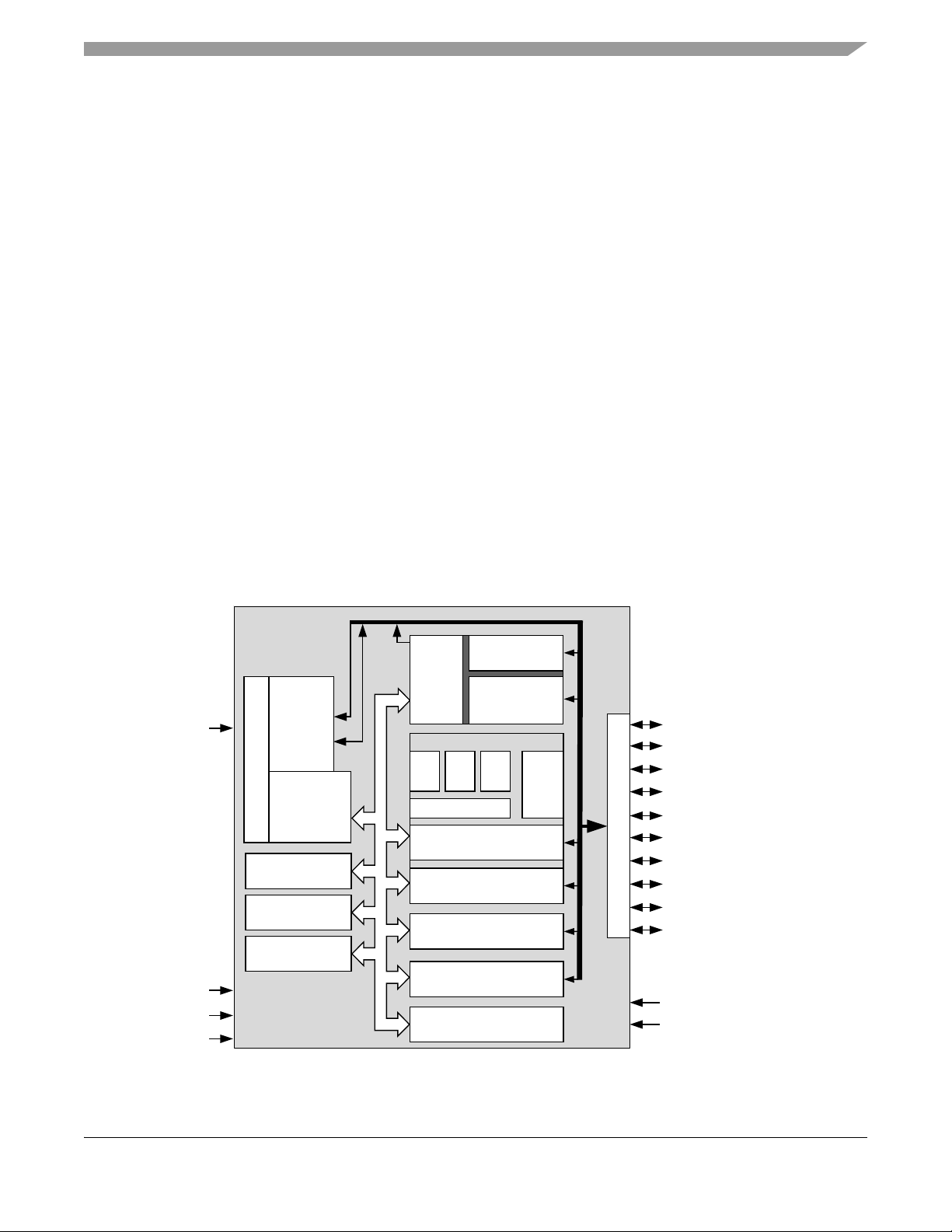
The MMA955xL three-axis accelerometer is a member of Freescale’ s Xtrinsic family of intelligent sensor
platforms. This device incorporates dedicated accelerometer MEMS transducers, signal conditioning, data
conversion and a 32-bit, programmable microcontroller.
This unique blend transforms Freescale’s MMA955xL devi ce into an intelligent, high-precision
motion-sensing platform able to manage multiple sensor inputs and make system-level decisions required
for sophisticated applications such as gesture recognition, tilt computation, and pedometer functionality.
The MMA955xL platform is programmed and configured with CodeWarrior Development Studio
software. This integrated-design environment enables customers to quickly and easily shape and
implement custom algorithms and features to exactly match their application needs.
Using its master I2C module, the MMA955xL platform can manage secondary sensors such as pressure
sensors, magnetometers or gyroscopes. This allows sensor initialization, calibration, data compensation
and computation functions to be off-loaded from the system application processor . Multiple sensor inputs
can be easily consolidated by the MMA955xL device which acts as an intelligent sensing hub and highly
configurable decision engine. T otal system power consumption is significantly r educed as the application
processor stays powered down until absolutely needed.
Freescale Semiconductor, Inc. 21
MMA955xL Intelligent, Motion-Sensing Platform Hardware Reference Manual, Rev. 1.0
Figure 2-1. Platform block diagram

Introduction
2.1 Hardware features
• Three accelerometer operating ranges:
— ±2g: Suits most user-interaction (mouse) motions and free fall
— ±4g: Covers most regular human dynamics (walking, jogging)
— ±8g: Detects most abrupt activities (gaming)
• Integrated temperature sensor
• One slave SPI or I2C interface operates up to 2 MHz dedicated to communication with host
processor
• One master I2C interface operates up to 400 kbps used to communicate with external sensors
• 10, 12, 14 and 16-bit ADC trimmed data formats available.
• 1.8V Supply voltage
• 32-bit ColdFire V1 CPU
• Extensive set of power management features and low power modes.
• Single Wire Background Debug Mode (BDM) pin interface
• 16 KB Flash memory
• 2 KB random access memory
• ROM-based flash controller and slave port command line interpreter
• Two channel timer with input capture, output capture or edge-aligned PWM
• Programmable delay block for scheduling events relative to start of frame
• Modulo timer for scheduling periodic events
2.2 Software features
This device may be programmed to provide any of the following:
• Orientation detection (portrait/landscape)
• High-g/low-g threshold detection
• Pulse detection (single, double and directional tap)
• Auto wake/sleep
• Linear and rotational free fall
• Flick detection
• Embedded smart FIFO
• Power management
• Pedometer
• Shock, vibration and sudden-motion detection
• Tilt-angle computation
The association of a high-performance accelerometer with a powerful, embedded ColdFire V1 MCU core
gives the possibility to grow and customize this list in an unprecedented way.
MMA955xL Intelligent, Motion-Sensing Platform Hardware Reference Manual, Rev. 1.0
22 Freescal e Semiconductor, Inc.

Introduction
2.3 Typical applications
This low-power intelligent sensor is optimized for use in portable and mobile consumer products such as:
• Mobile phones/PMPs/PDAs/digital cameras
— Orientation detection (portrait/landscape)
— Image stability
— Tilt control enabled with higher resolution
— Gesture recognition
— Tap to control
— Auto Wake/Sleep for low power consumption
• Smartbooks/eReaders/netbooks/laptops
— Anti-theft
— Freefall detection for Hard Disk Drives
— Orientation Detection
— Tap Detection
• Pedometers
• Gaming and toys
• Personal navigation devices (PNDs)
• Public transportation ticketing systems
• Activity monitoring in medical applications
• Security
— Anti-theft
— Shock detection
—Tilt
• Fleet monitoring, tracking
— Dead reckoning
— System auto wake-up on movement
— Detection
— Shock recording
— Anti-theft
• Power tools and small appliances
—Tilt
— Safety shutoff
MMA955xL Intelligent, Motion-Sensing Platform Hardware Reference Manual, Rev. 1.0
Freescale Semiconductor, Inc. 23
Chapter 3 Pins and Connections
1
2
3
4
5
678
9
13
12
11
10
16 15 14
V
DD
RGPIO7/AN1/TPMCH1
RGPIO8/PDB_B
SDA0/RGPIO1/SDI
BKGD-MS/RGPIO9
RESETB
SCL0/RGPIO0/SCLK
V
SS
RGPIO2/SCL1/SDO
RGPIO3/SDA1/SSB
RGPIO6/AN0/TPMCH0
RGPIO5/PDB_A/INT_O
V
SS
RGPIO4/INT
V
DDA
V
SSA
Direction of the
detectable accelerations
X
Y
Z
1
(TOP VIEW)
3.1 Package pinout
The package pinout for this device provides a superset of functions found on competitive devices, as well
as other Freescale accelerator devices. All pins on the device are utilized and many pins have multiple
possible uses.
Users may select from multiple pin functions via the SIM pin mux-control registers. (See “Pin Mux
Control Register0” on page 212.)
Figure 3-1. Device pinout and coordinate system
MMA955xL Intelligent, Motion-Sensing Platform Hardware Reference Manual, Rev. 1.0
Freescale Semiconductor, Inc. 25

Pins and Connections
3.1.1 Pin functions
Table 3-1 summarizes functional options for each of the device’s pins.
Table 3-1. Pin functions
Pin # Pin function #1
1 V
2 BKGD/MS RGPIO9 Background debug/mo de select RGPIO9
3 RESETB
4 SCL0 RGPIO0 SCLK
5 V
6 SDA0 RGPIO1 SDI Serial data for slave I2C/RGPIO1/SPI serial data input
7 RGPIO2 SCL1 SDO RGPIO2/Serial clock for master I2C/SPI serial data output
3
8
RGPIO3 SDA1 SSB RGPIO3/Serial data for master I2C/SPI slave select
9 RGPIO4 INT RGPIO4/Interrupt input
10 RESERVED (Connect to VSS) Must be connected to GND externally
11 RGPIO5 PDB_A INT_O RGPIO5/PDB_A/INT_O slave port interrupt output
12 RGPIO6 AN0 TPMCH0 RGPIO6/ADC Input 0 / TPM Channel 0
13 RGPIO7 AN1 TPMCH1 RGPIO7/ADC Input 1 / TPM Channel 1
14 V
15 RGPIO8 PDB_B RGPIO8/PDB_B
16 V
1
Pin Function 1 represents the reset state of the device. Pin functions may be changed via the SIM pin mux-control
registers (“Pin Mux Control Register0”).
2
RESETB is an open-drain, bidirectional pin. By default, the output function is not on.
3
RGPIO3/SDA1/SSB = LOW at startup indicates that SPI should be used as slave instead of the I2C module.
1
Pin function #2 Pin function #3 Description
DD
2
Digital power supply
Active low reset
Serial clock for slave I2C/RGPIO0/Serial clock for slave
SPI
SS
DDA
SSA
Digital ground
Analog power
Analog ground
MMA955xL Intelligent, Motion-Sensing Platform Hardware Reference Manual, Rev. 1.0
26 Freescal e Semiconductor, Inc.
3.1.2 Sensing direction and output response
Top View
PU
Earth Gravity
Pin 1
Xout at 0g
Yout at -1g
Zout at 0g
Xout at 1g
Yout at 0g
Zout at 0g
Xout at 0g
Yout at 1g
Zout at 0g
Xout at -1g
Yout at 0g
Zout at 0g
LL
PD
LR
Side View
FRONT
Xout at 0g
Yout at 0g
Zout at 1g
BACK
Xout at 0g
Yout at 0g
Zout at -1g
Pins and Connections
Figure 3-2. Sensing direction and output response
MMA955xL Intelligent, Motion-Sensing Platform Hardware Reference Manual, Rev. 1.0
Freescale Semiconductor, Inc. 27

Pins and Connections
3.2 Pin descriptions
The following sections provide descriptions of the various pin functions available on the MMA955xL
devices. T en of the device pins are multiplexed with Rapid GPIO (RGPIO) functions. (See “Rapid GPIO”
on page 239.) The “Primary Pin Function #1” column of Table 3-1 lists the functions that are active when
the device exits the reset state. The pin mux control registers in the System Integration Module (or SIM)
can be used to change pin assignments for these pins after reset. (See “System Integration Module” on
page 189.)
3.2.1 VDD and V
SS
These are the digital power and ground pins and must be connected to the same voltage. VDD is nominally
1.8V for this device.
3.2.2 V
These are the analog-power and ground pins. V
to remove any digital noise that may be present on the supply . V
DDA
and V
SSA
is nominally 1.8V for this device and must be filtered
DDA
is usually connected to VDD through
DDA
an appropriate filtering network.
3.2.3 RESETB
The RESETB pin is an open-drain, bidirectional pin with an internal weak pull-up resistor . At power-up,
it is configured strictly as an input pin. Setting RCSR[DR] (Reset Control and Status Register “Drive
Reset” bit) to 1 will cause the RESET function to become bidirectional. (See “Reset Control and Status
Register” on page 201.) Using this feature, the MMA955xL platform can reset external devices whenever
it is reset for any purpose other than power-on-reset.
3.2.4 Slave I2C: SDA0 and SCL0
These are the slave I2C data and clock signals, respectively . The MMA955xL platform may be controlled
via this serial port or through the slave SPI interface.
State at reset: Open-drain, bidirectional in input mode, pull-up resistor disabled.
3.2.5 Master I2C: SDA1 and SCL1
These are the master I2C clock and data signals, respectively . Because th e MMA955xL device contains a
32-bit ColdFire V1 CPU, it is fully capable of mastering other devices in the system via this serial port.
(For details, see “Inter-Integrated Circuit” on page 153.) This allows the MMA955xL platform to off-load
certain tasks from the main CPU, allowing it to conserve power by entering sleep mode. The MMA955xL
device can then issue a wake-up interrupt to the main CPU when motion is detected by the on-chip
transducer or when a slave device (such as pressure sensor or magnetometer) flags that activity has
occurred.
State at r eset: Inactive. SDA1 and SCL1 are secondary functions on RGPIO[3:2], which owns the pins at
reset.
MMA955xL Intelligent, Motion-Sensing Platform Hardware Reference Manual, Rev. 1.0
28 Freescal e Semiconductor, Inc.

Pins and Connections
3.2.6 Analog-to-digital conversion: AN0, AN1
The on-chip ADC can be used to perform a differential, analog-to-digital conversion based on the voltage
present across pins AN0(-) and AN1(+). Conversions on these pins are subject to the same output data rate
(ODR) rules as the MEMS transducer signals.
State at reset: Inactive. AN[1:0] are secondary functions on RGPIO[7:6], which owns the pins at reset.
3.2.7 Rapid General-Purpose I/O: RGPIO[9:0]
The ColdFire V1 CPU has a feature called “Rapid GPIO” (RGPIO). This is a 16-bit input/output port with
single-cycle write, set, clear and toggle functions available to the CPU. The MMA955xL platform brings
out the lower 10 bits of that port as pins of the device.
State at reset:
• RGPIO[9]: Inactive. BKGD/MS owns the pin at reset.
• RGPIO[8:2]: Pin mux registers for these bits are configured as RGPIO. Pull-ups are disabled.
RGPIO functionality can be enabled via RGPIO_ENB[8:2].
• RGPIO[1:0]: Inactive. SDA0 and SCL0 own the pin at reset.
3.2.8 Interrupts: INT
This input pin may be used to wake the CPU from a deep-sleep mode. It can be programmed to trigger on
either rising or falling edge or high or low level. This pin operates as a level-7 (high-priority) interrupt.
State at reset: Inactive. RGPIO[4] owns the pin at reset.
3.2.9 Debug/mode control: BKGD/MS
At power-up, this pin operates as Mode Select. If low during power-up, the CPU will boot into debug halt
mode. If high, the CPU will boot normally and run code.
After power-on reset, this pin can operate as a bidirectional, single-wire background debug port. It can be
used by development tools for downloading code into on-chip RAM and flash and to debug code.
State at reset: Mode Select (MS).
• MS = 0 at exit from reset => Boot to debug halt mode
• MS = 1 at exit from reset => Boot to run mode
State after reset: BKGD. The BKGD pin is a bidirectional, pseudo-open-drain pin used for
communications with a debug environment. For additional details, see “Version 1 ColdFire Debug” on
page 347.
MMA955xL Intelligent, Motion-Sensing Platform Hardware Reference Manual, Rev. 1.0
Freescale Semiconductor, Inc. 29

Pins and Connections
3.2.10 Timer: PDB_A and PDB_B
These are the two outputs of the programmable delay block described in “Programmable Delay Block” on
page 221. Normally, the PDB is used to schedule internal events at some fixed interval(s) with respect to
the start of either an analog or digital phase. By bringing the PDB outputs to these pins, it becomes possible
for the MMA955xL device to initiate some external event, also with respect to start of analog or digital
phase.
3.2.11 Slave SPI interface: SCLK, SDI, SDO and SSB
These are the slave SPI clock, data in, data out and slave select signals, respectively. The MMA955xL
platform may be controlled via this serial port or via the slave I2C interface.
State at reset: In reset, these pins are configured as per I2C and RGPIO[3:2] functions listed above. The
pin may be reconfigured for SPI use as part of the boot process.
MMA955xL Intelligent, Motion-Sensing Platform Hardware Reference Manual, Rev. 1.0
30 Freescal e Semiconductor, Inc.
Pins and Connections
16 15 14
13
12
11
10
9
876
5
4
3
2
1
C
3
0.1 F
C
4
1 F
C
2
0.1 F
C
1
1 µF
Ferrite Bead or
R
P3
R
P1
V
SS
V
DD
V
DD
V
SS
R
P2
SDA0
SCL0
MASTER
CPU
10-F Inductor
V
DD
V
SS
RESETB
4.7 k
4.7 k
4.7 k
BKGD/MS
BDM HEADER
V
DD
Optional
Manual
Reset
1
Optional
EMC
Filter
Sensing Platform
10 k
R
P4
V
DD
3.3 System connections
3.3.1 Platform as an intelligent slave
Figure 3-3 shows an example of the complete system connections when the MMA955xL platform is used
as a smart-accelerometer, slave peripheral to a host processor.
All that are required to attach the MMA955xL device to a master CPU are I2C termination resistors, a
ferrite bead and a few bypass capacitors. Optionally, the RGPIO pins can be programmed to generate
interrupts in order to wake the master CPU, as required by any changes in the inertial input. In the latter
case, the interrupts should be routed to the external interrupt input pins of the master CPU.
Figure 3-3 includes the background debug header connections as well as a manual reset push button.
Figure 3-3. Platform as a slave with BDM header and reset button
MMA955xL Intelligent, Motion-Sensing Platform Hardware Reference Manual, Rev. 1.0
Freescale Semiconductor, Inc. 31
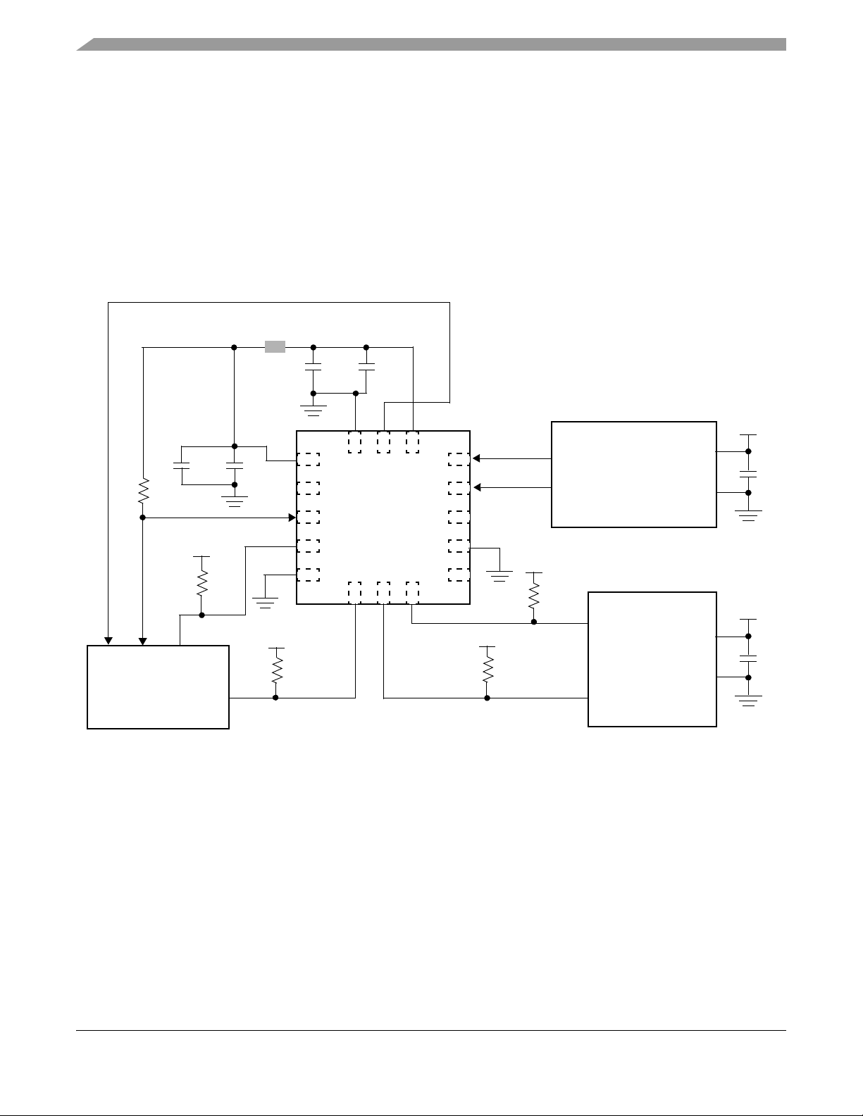
Pins and Connections
V
DD
Digitally
Interfaced
Sensors
R
P3
SDL1
R
P4
SDA1
V
DD
Differential Output
V
SS
16 15 14
13
12
11
10
9
876
5
4
3
2
1
C
3
0.1 F
C
4
1 F
C
2
0.1 F
C
1
1 F
Ferrite Bead or
R
P3
R
P1
V
SS
V
DD
V
DD
V
SS
R
P2
SDA0
SCL0
MASTER
CPU
10-F Inductor
V
DD
V
SS
RESETB
Wake-up
Analog Sensor
V
DD
V
SS
V
DD
4.7 k
4.7 k
4.7 k
4.7 k
4.7 k
Sensing Platform
3.3.2 Platform as a sensor hub
Figure 3-4 shows an example of the system connections when the MMA955xL platform is used as an
autonomous sensor hub. This type of connection increases the overall system efficiency as the various
sensors are handled directly by the MMA955xL device, through its master I²C bus and analog inputs.
In such a sensor-hub configuration, the MMA955xL platform processes and fuses the sensors’ data before
transferring it to the host platform, so that data is refined as higher-level information. The master CPU can
go into Sleep mode as the MMA955xL device will issue a wake-up request should any external event
require the CPU’s attention. The RGPIO8 pin (Pin 15) is typically used for wake-up requests.
Figure 3-4. Platform as a sensor hub
3.3.3 Power
An internal circuit powered by V
order for this signal to be properly recognized, it is important that VDD is powered up before, or
simultaneously with, V
The voltage potential difference between VDD and V
accomplish this is to power both pins from the same voltage source.
When using the same voltage source, some digital noise might reach the analog section. To prevent this,
connect a small inductor or ferrite bead in serial with both the VDDA and VSSA traces. Additionally , two
32 Freescal e Semiconductor, Inc.
MMA955xL Intelligent, Motion-Sensing Platform Hardware Reference Manual, Rev. 1.0
provides the MMA955xL platform with a power-on-reset signal. In
DDA
.
DDA
must not exceed 0.1V. The simplest way to
DDA

Pins and Connections
ceramic capacitors (of approximately 1 µF, + 0.1 µF) can be used to efficiently bypass the power and
ground of both digital and analog supply rails.
3.3.4 RESETB pin
Figure 3-3 on page 31 illustrates an exhaustive arrangement where a Reset event can be generated by:
• An external, manual reset button
• The Background Debug Mode interface
• The VDD main supply
An external, pull-up resistor is necessary to reduce and better control the RESETB voltage-settling time.
An optional shunt capacitor to ground can be added to that node in order to reduce EMC and noise
susceptibility. With the shunt capacitor, the maximum RC time constant has to be strictly bounded. (For
details, see “System Integration Module” on page 189.)
At power-up, the RESETB pin is configured as an input pin, but it also can be programmed as
bidirectional. Using the bidirectional feature, the MMA955xL platform can reset external devices for any
purpose other than power-on-reset. When using the RESETB pin output drive capability, the allowed
upper limit for the RC time constant is reduced to only micro-seconds.
3.3.5 Background / mode select (BKGD/MS)
Figure 3-3 on page 31 depicts the connection to the BKGD/MS pin when in-circuit debug capability is
desired.
In this configuration, the background header also takes control of the RESETB line. This could result in
parasitic capacitance from the BDM connector and its ribbon cable that may increase RESETB settling
time. This situation must be considered in the user’s implementation.
MMA955xL Intelligent, Motion-Sensing Platform Hardware Reference Manual, Rev. 1.0
Freescale Semiconductor, Inc. 33

Pins and Connections
MMA955xL Intelligent, Motion-Sensing Platform Hardware Reference Manual, Rev. 1.0
34 Freescal e Semiconductor, Inc.

Chapter 4 Operational Phases and Modes of Operation
4.1 Modes of operation
The V1 ColdFire core supports RUN, HALT, RESET and ST OP modes natively . These are present on any
ColdFire-based product. The MCU integration adds additional controls to STOP mode, effectively
creating three modes where one existed previously.
The set of modes then becomes:
RUN The CPU executes instructions in this mode that can be further subdivided into
User and Supervisor modes.
HALT Version 1 ColdFire Core HALT/DEBUG mode
RESET Reset asserted. Circuitry in default state. RESET can be divided into several
phases of operation. For details, see “System Integration Module” on page 189.
STOP
STOP
STOP
FC
SC
NC
STOP – Clock in Fast Mode – Nominally used for A (See “Overview” on
page 35.)
STOP – Clock in Low Speed Mode – Nominally used for I (See “Overview” on
page 35.)
STOP – No clocks – All clocks disabled. Nominally used for the SLEEP phase.
4.2 Frame structure
In addition to the modes above, the MMA955xL platform is designed to facilitate a “frame-based”
software scheduler. Analog sensor conversions are best executed when the CPU is quiet and there may be
times when both AFE and CPU are dormant. The MMA955xL device includes hardware mechanisms to
make it easy to schedule these different functions.
4.3 Overview
The MMA955xL platform can be programmed to take a continuous sequence of evenly spaced samples
over time. This section specifies the terms for timing and phases. Figure 4-1 on page 36, Figure 4-2 on
page 36 and Figure 4-3 on page 36 illustrate a number of these terms that will be subsequently defined.
Timing is defined in terms of “frames.” There are two types of frames: Sample and non-sample. Sample
frames include an analog phase in which sensor outputs are sampled. Non-sample frames simply omit the
analog phase.
Output Data Rate (ODR), Frame Rate (FR) and Sample Data Rate (SDR) are three important terms that
will be used throughout the following text.
ODR < SDR < FR
MMA955xL Intelligent, Motion-Sensing Platform Hardware Reference Manual, Rev. 1.0
Freescale Semiconductor, Inc. 35

Operational Phases and Modes of Operation
First sample frame
A
Second sample frame Th ird sample frame
t
F
= FR
-1
A
A
D
D
I
D
I
t
A
t
D
t
I
One “bucket” of
samples has been
converted to raw
digital form.
Digital processing
completed. Slave
registers have been
updated.
First non-sample frame Second non-sample frame Third non-sample frame
D
D
I
D
I
t
D
t
I
Digital processing completed.
tF = FR
-1
First sample frame Non-sample frame Second sample frame
A
D
D
I
D
I
A
The ODR specifies the rate at which an application reads sensor data from the device. The actual SDR is
ODR x OSR, where the integer Over Sample Ratio (OSR) is typically in the range of 1 to 4. As a result,
several sample frames might be required to support a single sensor reading by the application.
Additionally, non-sample frames, may be intermixed with sample frames.
Figure 4-1. Sample-frame timing
Figure 4-2. Non-sample frame timing
Figure 4-3. Mixed-frame timing
MMA955xL Intelligent, Motion-Sensing Platform Hardware Reference Manual, Rev. 1.0
36 Freescal e Semiconductor, Inc.

Operational Phases and Modes of Operation
4.3.1 Definitions
Frame Rate (FR) This is the basic unit of time from which all other events are timed.
Output Data Rate (ODR) The rate at which the MMA955xL platform provides conversion data to the
user for a given quantity. This will be SDR/OSR.
Over-Sample Ratio (OSR) The MMA955xL device can support on-chip filtering of sensor data. The
over-sample ratio specifies how many sample frames are required to support
a specified output data rate using a desired filtering algorithm.
A
Analog phase – All analog (C2V and ADC) processing occurs here.
Depending on configuration data, the analog subsystem may have processed
samples for three dimensions of acceleration and a single auxiliary parameter,
during each A interval. The auxiliary parameters available include
temperature and the external ADC inputs. The CPU and associated peripherals
are normally “quiet” during this mode.
D
Digital phase – The CPU and peripherals are active, analog in low-power
state. Digital filtering and processing of the converted ADC values occurs
here. The length of this phase will vary depending upon the CPU load. It
cannot exceed (tF - tA) for sample frames.
I
Inactive or Idle phase – Most of the device is powered down for minimal
power consumption. This phase is of variable length (tF - tA - tD), where tF is
fixed, tA is determined by the analog front end (AFE) and tD varies depending
on CPU loading.
Sample Frame Sample frames correspond, one-to-one, for each “sample” of data.
Sample Data Rate (SDR) The rate at which the MMA955xL device requires raw conversion data from
its sensors and converters. If the device is configured for additional
over-sampling, this may be some integer times the output data rate or ODR.
One sample frame = SDR-1 seconds.
t
A
t
D
t
I
Length of A
Length of D
Length of I – The idle phase. This may approach zero, depending on CPU
loading.
t
F
MMA955xL Intelligent, Motion-Sensing Platform Hardware Reference Manual, Rev. 1.0
Freescale Semiconductor, Inc. 37
Frame interval. This is equal to 1/FR.

Operational Phases and Modes of Operation
First sample frame
A
Second sample frame Third sample frame
A
A
D
D
I
D
I
Start
D
Start
D
Start
D
Start
A
Start
A
Start
A
4.3.2 Additional timing parameters
Additional terms that occasionally factor into the discussions include:
F
osc-high
F
osc-low
P
osc-high
P
osc-low
The high-speed frequency of the on-chip oscillator. This is nominally 8 MHz.
The low-speed frequency of the on-chip oscillator . This is nominally F
osc-high
The length of time required for one cycle of the oscillator clock in high-speed
mode (= 1/F
osc-high
).
The length of time required for one cycle of the oscillator clock in low-speed mode
(= 1/F
osc-low
= 128/F
osc-high
).
4.3.3 Phase triggers
Figure 11-1 on page 190 illustrates some of the major interactions between modules in this device:
• The “start-of-frame” signal is generated by the frame interval counter.
• SIM hardware is responsible for generating phase triggers for A and D.
• The “End A” signal is generated by the AFE.
• In sample frames, “Start A” results from the start-of-frame from the CLKGEN module. In this
case, “Start D” results from the “End A” signal.
• For non-sample frames, the “start-of-frame” results in “start D”.
•“A started” and “D started” signals (not shown) can be slightly delayed from “start A” and
“start D”. In the event that the system clock is switching from off (or low speed) to high speed,
these signals are not asserted until the oscillator actually switches. The difference in the two sets
of triggers is any latency associated with interrupt assertion and/or CLKGEN-mode switching.
/128.
Figure 4-4 illustrates sequencing of the “Start A“and “Start ” hardware triggers. Figure 4-5 on page 39
shows that a STOP instruction (with STOPCR[SC] = 1) is required to transition into the idle phase. (See
the SIM register map.)
Figure 4-4. Phase triggers required in hardware
MMA955xL Intelligent, Motion-Sensing Platform Hardware Reference Manual, Rev. 1.0
38 Freescal e Semiconductor, Inc.

Operational Phases and Modes of Operation
First sample frame
A
Second sample frame Third sample frame
A
A
D
D
I
D
I
STOP(SC) STOP(SC) ST OP(SC)
Figure 4-5. Phase triggers required in software
In summary:
Start of frame Initiates “start A” or “start D,” depending on whether the frame is a sample
frame or not.
Start
End
Start
A
A
D
started A has been initiated and the clock is in high-speed mode.
A
started D has been initiated and the clock is in high-speed mode.
D
Signal to initiate
A
Is generated by the AFE and indicates the analog phase has been completed.
Signal to initiate D. This signal results from either “start of frame” or “End A”.
MMA955xL Intelligent, Motion-Sensing Platform Hardware Reference Manual, Rev. 1.0
Freescale Semiconductor, Inc. 39

Operational Phases and Modes of Operation
RESET
Special
D
Boot Process
A
D
I
Start data frame
SLEEP
CPU initiates
Sleep mode.
Each pass through A to D and
to
I
constitutes one sample
frame. An output data frame is one
or more sample frames in length,
depending on the amount of oversampling being done.
w
r
i
t
e
OS
C
T
R
L
Wake on external interrupt or
slave I
2
C command received.
Processor executes STOP
prior to “start data frame.”
Software
Overrun
Condition
Start data frame
4.4 Clock operation as a function of mode/phase
Figure 4-6 illustrates the nominal phases of operation for this device. The values of A, D and I were
discussed briefly in “Frame structure” on page 35. The reset operation is described in “Reset generation”
on page 191. The sleep phase is defined as the device oscillator being off and all circuitry in its lowest
power state.
“Power control modes of operation” on page 42 maps these phases into modes of operation of the Version
1 Coldfire CPU.
There is a strong software component to the application phases diagrammed here. They may be rearranged
from time to time depending on the tasks assigned to the sensor. Tasks scheduling will be handled by the
Scheduler Application (ID 0x01) as described in the MMA955xL Intelligent, Motion-Sensing Platform
Software Reference Manual (MMA955XLSWRM).
Figure 4-6. Operational phases
The phases shown above have distinct characteristics with regard to clock operation. These are outlined in
Table 4-1. The operation of clock-gating registers (PCERUNx, PCESSCx and PCESFCx) in the SIM do
not change as a result of debug operation, only the oscillator operation.
40 Freescal e Semiconductor, Inc.
MMA955xL Intelligent, Motion-Sensing Platform Hardware Reference Manual, Rev. 1.0

Table 4-1. Clock operation per phase
CPU and standard peripherals Anal og Front End
Phase
Normal Debug
Reset High Speed
Boot and
(Run
D
High Speed OFF High Speed
Mode)
A
(STOPFC)
OFF High Speed
1
Operational Phases and Modes of Operation
Normal Debug
1
Slave I2C
Not applicable. The I2C is
externally clocked.
I
(STOPSC)
SLEEP
(STOP
NC
1
The ENBDM bit in the Version 1 ColdFire Extended Configuration/Status Register (XCSR) is set to “1” to enable BDM
OFF, oscillator in
Low-Speed Mode
Oscillator in
)
shutdown
High Speed
High Speed
OFF, oscillator in
Low-peed Mode
Oscillator in
shutdown
High Sp ee d
High Sp ee d
communications. The CPU is clocked even during STOP modes. Frequency-hopping is disabled in Debug mode, as BDM
communications require a constant clock rate for proper operation.
MMA955xL Intelligent, Motion-Sensing Platform Hardware Reference Manual, Rev. 1.0
Freescale Semiconductor, Inc. 41

Operational Phases and Modes of Operation
HALT
RESET
RUN
STOP
FC
STOP
SC
STOP
NC
1
2
3
4
5
6
7
I
)
A
)
(SLEEP)
D
& Boot)
8
9
RESET can be entered from any mode.
4.5 Power control modes of operation
The Version 1 ColdFire architecture incorporates several modes of operation. These include Reset, Run,
Stop and Halt (debug). A, I and Sleep phases in Figure 4-6 are all mapped into the ColdFire STOP mode
on this device. The CPU has only a single view of STOP operation, but at the device level, additional levels
of distinction have been added:
STOP
STOP
STOP
FC
SC
NC
STOP – Clock in Fast Mode. Nominally used for A.
STOP – Clock in Low Speed Mode. Nominally used for I.
STOP – All clocks disabled. Nominally used for the SLEEP phase.
Boot and D are functionally identical and map into the Run mode. Figure 4-7 adds HALT mode to the
set and remaps the collection as a full-state transition diagram, including debug modes. Table 4-2
summarizes the triggers that cause transitions from one mode to the next.
Figure 4-7. Allowable state transitions
Transition # From To Trigger
1
RUN STOP
STOP
SC
RUN Any interrupt
Table 4-2. State transitions
XCSR[ENBDM] = 0, STOPCR[SC] = 1; followed by STOP instruction
SC
1
MMA955xL Intelligent, Motion-Sensing Platform Hardware Reference Manual, Rev. 1.0
42 Freescal e Semiconductor, Inc.

Table 4-2. State transitions
Operational Phases and Modes of Operation
Transition # From To Trigger
1
STOPCR[FC] = 1, followed by STOP instruction; OR
2
3
RUN STOP
STOP
FC
RUN HAL T
RUN Any interrupt
XCSR[ENBDM] =1, followed by STOP instruction (STOP
FC
emulated by STOP
in debug mode.)
FC
When a BACKGROUND command is received through the BKGD/MS pin OR
when a HALT instruction is executed OR when encountering a BDM breakpoint.
and STOPNC are
SC
HALT RUN GO instruction issued via BDM
4 RESET RUN
5
RUN STOP
STOP
NC
RUN Any interrupt
De-assert all reset sources. Internal de-assert is subject to timing seque nces
outlined in “Reset generation” on page 191.
XCSR[ENBDM] = 0, STOPCR[NC] = 1, followed by STOP instruction
NC
6 RESET HALT BDM = 0 during POR (device must be unsecure)
7STOP
8STOP
SC
FC
STOP
HAL T
Start of frame signal with STOPCR[A_EN] = 1
FC
When a BACKGROUND command is received through the BKGD/MS pin
(XCSR[ENBDM] must equal one)
9STOPSCHALT In debug mode, STOPSC is emulated by STOPFC.
1
Interrupts are subject to the limitations discussed in “Clock gating” on page 196 and “Peripheral Clock Enable Register 0 for
STOP
Mode” on page 203.
FC
MMA955xL Intelligent, Motion-Sensing Platform Hardware Reference Manual, Rev. 1.0
Freescale Semiconductor, Inc. 43

Operational Phases and Modes of Operation
MMA955xL Intelligent, Motion-Sensing Platform Hardware Reference Manual, Rev. 1.0
44 Freescal e Semiconductor, Inc.

Chapter 5 Memory Maps
5.1 High-level memory map
Table 5-1. V1 ColdFire memory maps
Address range Generic V1 ColdFire memory usage Address range Platform’s memory usage
0x(00)00_0000
Allocated to on-chip flash memory
0x(00)2F_FFFF 0x(00)2F_FFFF
0x(00)30_0000
Allocated to on-chip ROM
0x(00)3F_FFFF 0x(00)30_FFFF
0x(00)40_0000
Optional off-chip expansion
0x(00)7F_FFFF 0x(00)7F_FFFF
0x(00)80_0000
Allocated to on-chip RAM
0x(00)9F_FFFF 0x(00)80_07FF
0x(00)A0_0000
Optional off-chip expansion
0x(00)BF_FFFF 0x(00)BF_FFFF
0x(00)C0_0000
ColdFire Rapid GPIO
0x(00)00_0000
16-KB flash memory
0x(00)00_3FFF
0x(00)00_4000
Unimplemented
0x(00)30_0000
4-KB ROM
0x(00)30_0800
Unimplemented
0x(00)80_0000
2-KB RAM
0x(00)80_0800
Unimplemented
0x(00)C0_0000
ColdFire Rapid GPIO
0x(00)C0_000F 0x(00)C0_000F
0x(00)C0_0010
Unimplemented
0x(FF)FF_7FFF 0x(FF)FF_7FFF
0x(FF)FF_8000
Slave peripherals
0x(FF)FF_FFFF 0x(FF)FF_FFFF
MMA955xL Intelligent, Motion-Sensing Platform Hardware Reference Manual, Rev. 1.0
Freescale Semiconductor, Inc. 45
0x(00)C0_0010
Unimplemented
0x(FF)FF_8000
Slave peripherals

Memory Maps
The left-most map in Table 5-1 is the generic, high-level, memory map applicable to the V1 ColdFire
family . Memory map areas shown for RAM, ROM and flash are a superset for the family. Lesser amounts
of all three will usually be included on specific devices. The memory map for the MMA955xL platform
is shown on the right.
The slave peripherals section of the memory map is further broken down as shown in Table 5-2.
MMA955xL microcontrollers include off-platform, 8-bit and 16-bit peripheral buses. The bus bridges
from the ColdFire system bus to off-platform buses are capable of serializing 32-bit accesses into two
16-bit accesses or four 8-bit accesses. This can be used to speed access to properly aligned peripheral
registers. Not all peripheral registers are aligned to take advantage of this feature.
The off-platform 8- and 16-bit interfaces operate at the same speed as the CPU.
CPU accesses to those parts of the memory map marked as “Unimplemented” in Table 5-1 result in an
illegal address reset if CPUCR[ARD] = 0 or an address error exception if CPUCR[ARD] = 1.
Table 5-2. High-level peripheral memory map
Peripheral Description Instance name
RGPIO Rapid General-Purpose I/O RGPIO 16 0x(00)C0_0000
2
Slave I
CLKGEN CLKGEN CK 8 0x(FF)FF_8080
Port Control module Port I/O Control Module 0 PT0 8 0x(FF)FF_80E0
Port Control module Port I/O Control Module 1 PT1 8 0x(FF)FF_8100
Flash Controller Flash Controller FC 16 N/A
1
The FC registers are only available under Superviser mode.
2
The AFE registers are only available under Superviser mode.
3
The INTC_FRC register is the first in the INC memory map, and is located at the base address + $10, or (FF)FF_F FD0.
C Slave I2CSI
2
I
C Inter-Integrated IC MI2C 8 0x(FF)FF_8040
SIM System Integration Module SIM 8 0x(FF)FF_8060
MTIM16 16-Bit Modulo Timer MTIM 8 0x(FF)FF_80A0
IRQ External Interrupt Module IRQ 8 0x(FF)FF_80C0
TPM
PDB Programmable Delay Block PDB 16 0x(FF)FF_EC00
AFE Analog Front End AFE 16 N/A
INTC V1 ColdFire Interrupt Controller INTC 8 0x(FF)FF_FFC0
Two-Channel, Timer/Pulse-Width
Modulator
2
C 8 0x(FF)FF_8000
TPM 8 0x(FF)FF_8120
Native bus
width
Base address
1
2
3
The lower 32 KB of flash memory (16 KB in the MMA955xL platform) and slave peripherals section of
the memory map are most efficiently accessed using the ColdFire absolute, short-addressing mode. RAM
MMA955xL Intelligent, Motion-Sensing Platform Hardware Reference Manual, Rev. 1.0
46 Freescal e Semiconductor, Inc.

Memory Maps
is most efficiently accessed using the A5-relative addressing mode (address register indirect with
displacement mode).
5.2 Alignment issues
ColdFire has a big endian byte addressable memory architecture, so the most-significant byte of each
address is the lowest-numbered one, as shown in the following figure. Multi-byte operands (such as 16-bit
words and 32-bit-long words) are referenced using an address pointing to the most-significant (first) byte.
Bit 31 24 23 16 15 8 7 0
Longword 0x(00)00_0000
Word 0x(00)00_0000 Word 0x(00)00_0002
Byte 0x(00)00_0000 Byte 0x(00)00_0001 Byte 0x(00)00_0002 Byte 0x(00)00_0003
Longword 0x(00)00_0004
Word 0x(00)00_0004 Word 0x(00)00_0006
Byte 0x(00)00_0004 Byte 0x(00)00_0005 Byte 0x(00)00_0006 Byte 0x(00)00_0007
•
•
•
Bit 31 24 23 16 15 8 7 0
Longword 0x(FF)FF_FFFC
Word 0x(FF)FF_FFFC Word 0x(FF)FF_FFFE
Byte 0x(FF)FF_FFFC Byte 0x(FF)FF_FFFD Byte 0x(FF)FF_FFFE Byte 0x(FF)FF_FFFF
Figure 5-1. ColdFire memory organization
•
•
•
•
•
•
Regions within the memory map are subject to restrictions with regard to the types of CPU accesses
allowed. These are outlined in Table 5-3. Non-supported access types terminate the bus cycle with an error
and would typically generate a system reset in response to the error termination.
MMA955xL Intelligent, Motion-Sensing Platform Hardware Reference Manual, Rev. 1.0
Freescale Semiconductor, Inc. 47

Memory Maps
Table 5-3. V1 ColdFire memory maps
Read Write
Base address Region
Byte Word Long Byte Word Long
0x(00)00_0000 Flash x x x — — x
0x(00)30_0000 ROM x x x — — —
0x(00)80_0000 RAM x x x x x x
0x(00)C0_0000 Rapid GPIO x x x x x x
0x(FF)FF_8000 8-bit peripherals
0x(FF)FF_EC00 16-bit peripherals
1
Allowed access types are peripheral-specific. The peripheral bus bridge will serialize 16- and 32-bit accesses into multiple
8-bit accesses. When using 8-bit peripherals, care must be taken to ensure that all accesses are properly aligned and only
desired 8-bit locations are accessed.
2
Allowed access types are peripheral-specific. The peripheral bus bridge will serialize 32-bit accesses into multiple 16 -bit
accesses. When using 16-bit peripherals, care must be taken to ensure that all accesses are properly aligned and only desired
16-bit locations are accessed.
1
2
xxxxxx
—x x—x x
MMA955xL Intelligent, Motion-Sensing Platform Hardware Reference Manual, Rev. 1.0
48 Freescal e Semiconductor, Inc.

Memory Maps
5.3 Memory-mapped components
5.3.1 Interrupt controller
The CF1_INTC register map is sparsely populated, but retains compatibility with earlier ColdFire
interrupt-controller definitions. The CF1_INTC occupies the upper 64 bytes of the 4-GB address space
and all memory locations are accessed as 8-bit (byte) operands. This 64-byte space includes the
program-visible interrupt controller registers as well as the space used for interrupt-acknowledge (IACK)
cycles.
Table 5-15 is a summary of CF1_INTC user -accessible peripheral registers and control bits. Cells that are
not associated with named bits are shaded. A shaded cell with a 0 indicates this unused bit is always read
as a 0. Shaded cells with dashes indicate unused or reserved bit locations that could be read as 1s or 0s.
When writing to these bits, write a 0 unless otherwise specified.
5.3.2 Nonvolatile register area
There is a nonvolatile register area consisting of a block of 4 bytes in flash memory at
0x(00)00_3FFB–0x(00)00_3FFF . The byte at 0x(00)00_3FFF is allocated to flash protection and security
functions. Additionally, the byte at 0x(00)00_3FFE is used to initialize boot options for the device. See
“Security” on page 69 for further details on both topics.
Because the nonvolatile register locations are flash memory, they must be erased and programmed like
other flash memory locations.
5.3.3 RGPIO
The section of memory at 0x(00)C0_0000 is assigned for use by the ColdFire Rapid GPIO module. See
Table 5-4 for the Rapid GPIO memory map and Chapter 15, “Rapid GPIO” for further details on the
module.
MMA955xL Intelligent, Motion-Sensing Platform Hardware Reference Manual, Rev. 1.0
Freescale Semiconductor, Inc. 49

Memory Maps
5.4 Detailed register set
The following tables summarize register-bit fields for on-chip peripherals. For further details, see the
chapter on applicable peripheral.
Table 5-4. Rapid GPIO (RGPIO) detailed memory map
Address Register
(00)C0_0000 RGPIO_DIR DIR[15:8] (Read/Write)
(00)C0_0002 RGPIO_DATA DATA[15:8] (Read/Write)
(00)C0_0004 RGPIO_ENB E NB[15:8] (Read/Write)
(00)C0_0006 RGPIO_CLR CLR[15:8] (Write only)
(00)C0_0006 RGPIO_DATA DATA[15:8] (Read only)
(00)C0_0008 RGPIO_DIR DIR[15:8] (Read only)
(00)C0_000A RGPIO_SET SET[15:8] (Write only)
Bit
15/7
14/6 13/5 12/4 11/3 10/2 9/1
DIR[7:0] (Read/Write)
DATA[7:0] (Read/Write)
ENB[7:0] (Read/Write)
CLR[7:0] (Write only)
DATA[7:0] (Read only)
DIR[7:0] (Read only)
SET[7:0] (Write only)
Bit
8/0
(00)C0_000A RGPIO_DATA DATA[15:8] (Read only)
DATA[7:0] (Read only)
(00)C0_000C RGPIO_DIR DIR[15:8] (Read only)
DIR[7:0] (Read only)
(00)C0_000E RGPIO_TOG TOG[15:8] (Write only)
TOG[15:0] (Write only)
(00)C0_000E RGPIO_DATA DATA[15:8] (Read only)
DATA[7:0] (Read only)
MMA955xL Intelligent, Motion-Sensing Platform Hardware Reference Manual, Rev. 1.0
50 Freescal e Semiconductor, Inc.

Memory Maps
Table 5-5. Slave port detailed memory map
AddressRegisterBit 7654321Bit 0
(FF)FF_8000 SP_MB0 DATA
(FF)FF_8001 SP_MB1 DATA
(FF)FF_8002 SP_MB2 DATA
(FF)FF_8003 SP_MB3 DATA
(FF)FF_8004 SP_MB4 DATA
(FF)FF_8005 SP_MB5 DATA
(FF)FF_8006 SP_MB6 DATA
(FF)FF_8007 SP_MB7 DATA
(FF)FF_8008 SP_MB8 DATA
(FF)FF_8009 SP_MB9 DATA
(FF)FF_800A SP_MB10 DATA
(FF)FF_800B SP_MB11 DATA
(FF)FF_800C SP_MB12 DATA
(FF)FF_800D SP_MB13 DATA
(FF)FF_800E SP_MB14 DATA
(FF)FF_800F SP_MB15 DATA
(FF)FF_8010 SP_MB16 DATA
(FF)FF_8011 SP_MB17 DATA
(FF)FF_8012 SP_MB18 DATA
(FF)FF_8013 SP_MB19 DATA
(FF)FF_8014 SP_MB20 DATA
(FF)FF_8015 SP_MB21 DATA
(FF)FF_8016 SP_MB22 DATA
(FF)FF_8017 SP_MB23 DATA
(FF)FF_8018 SP_MB24 DATA
(FF)FF_8019 SP_MB25 DATA
(FF)FF_801A SP_MB26 DATA
(FF)FF_801B SP_MB27 DATA
(FF)FF_801C SP_MB28 DATA
(FF)FF_801D SP_MB29 DATA
MMA955xL Intelligent, Motion-Sensing Platform Hardware Reference Manual, Rev. 1.0
Freescale Semiconductor, Inc. 51

Memory Maps
Table 5-5. Slave port detailed memory map (continued)
AddressRegisterBit 7654321Bit 0
(FF)FF_801E SP_MB30 DATA
(FF)FF_801F SP_MB31 DATA
(FF)FF_8020 SP_MUTEX0
(FF)FF_8021 SP_MUTEX1
(FF)FF_8022 SP_ADDR
(FF)FF_8023 SP_SCR EN PS ACTIVE CW RIE WIE WWUP
(FF)FF_8024 SP_WSTS0 D31 D30 D29 D28 D27 D26 D25 D24
(FF)FF_8025 SP_WSTS1 D23 D22 D21 D20 D19 D18 D17 D16
(FF)FF_8026 SP_WSTS2 D15 D14 D13 D12 D11 D10 D9 D8
(FF)FF_8027SP_WSTS3D7D6D5D4D3D2D1D0
(FF)FF_8028 SP_RSTS0 D31 D30 D29 D28 D27 D26 D25 D24
(FF)FF_8029 SP_RSTS1 D23 D22 D21 D20 D19 D18 D17 D16
(FF)FF_802A SP_RSTS2 D15 D14 D13 D12 D11 D10 D9 D8
(FF)FF_802B SP_RSTS3 D7 D6 D5 D4 D3 D2 D1 D0
(FF)FF_802C SP_MTOR0
(FF)FF_802D SP_MTOR1
(FF)FF_802E SP_OIC 0 0 0 0 0POLCLR
0 0 0 0 0 0 SSTS
0 0 0 0 0 0 SSTS
0 ADDR
0TOSTSEN MTE
0TOSTSEN MTE
SET_IN
_O
MMA955xL Intelligent, Motion-Sensing Platform Hardware Reference Manual, Rev. 1.0
52 Freescal e Semiconductor, Inc.

Memory Maps
Table 5-6. Master I2C (MI2C) detailed memory map
Address Register Bit 7 6 5 4 3 2 1 Bit 0
(FF)FF_8040 IIC_A1 AD7 AD6 AD5 AD4 AD3 AD2 AD1
(FF)FF_8041 IIC_F MULT ICR
(FF)FF_8042 IIC_C1 IICEN IICIE MST TX TXAK RSTA
(FF)FF_8043 IIC_S TCF IAAS BUSY ARBL
(FF)FF_8044 IIC_D DATA
(FF)FF_8045 IIC_C2
(FF)FF_8046 IIC_FLT 0 0 0 FLT4 FLT3 FLT2 FLT1 FLT0
GCAE
N
ADEXT
0 0 0 AD10 AD9 AD8
0 SRW IICIF
WUE
N
0
0
RXA
K
Table 5-7. System Integration Module (SIM) detailed memory map
Address RegisterBit 7654321Bit 0
(FF)FF_8060 STOPCR
(FF)FF_8061 FCSR
(FF)FF_8062 RCSR
0 0 0
0 0A_EN SFEIE FESFDIESF
0 DR ASR SW ILOP ILAD PIN POR
SIM_C
LK_EN
FC SC NC
SCtoF
C
(FF)FF_8063 SIM_TR TP1 TP0
(FF)FF_8064 PCESFC0 0 T2 T1 T0 IRQ AFE PCTRL FLSH
(FF)FF_8065 PCESFC1
(FF)FF_8066 PCESSC0
(FF)FF_8067 PCESSC1
(FF)FF_8068 PCERUN0
(FF)FF_8069 PCERUN1
(FF)FF_806A PMCR0 A9 A8 A7 A6
(FF)FF_806B PMCR1 A3 A2 A1 A0
(FF)FF_806C PMCR2
0 0 0 0 0 0MI2CSLAVE
0 T2 T1 T0 IRQ AFE PCTRL FLSH
0 0 0 0 0 0MI2CSLAVE
0 T2 T1 T0 IRQ AFE PCTRL FLSH
0 0 0 0 0 0MI2CSLAVE
0A4
0 0 0 0 0 0A5
Table 5-8. CLKGEN detailed memory map
Address RegisterBit 7654321Bit 0
(FF)FF_8080 CK_OSCTRL FCEN FFCEN FFSEN FLE
MMA955xL Intelligent, Motion-Sensing Platform Hardware Reference Manual, Rev. 1.0
Freescale Semiconductor, Inc. 53

Memory Maps
Table 5-9. 16-bit Modulo Timer (MTIM) detailed memory map
Address RegisterBit 7654321Bit 0
(FF)FF_80A0 MTIM_SC TOF TOIE TRST TSTP
(FF)FF_80A1 MTIM_CLK
(FF)FF_80A2 MTIM_CNTH CNTH
(FF)FF_80A3 MTIM_CNTL CNTL
(FF)FF_80A4 MTIM_MODH MODH
(FF)FF_80A5 MTIM_MODL MODL
0 0CLKS PS
0 0 0 0
Table 5-10. Interrupt (IRQ) pin detailed memory map
AddressRegisterBit 7654321Bit 0
(FF)FF_80C0 IRQSC
0 IRQPDD IRQEDG IRQPE IRQF IRQACK IRQIE IRQMOD
Table 5-11. Port Control (PC0) detailed memory map
Address RegisterBit 7654321Bit 0
(FF)FF_80E0 PC0_PE PE7 PE6 PE5 PE4 PE3 PE2 PE1 PE0
(FF)FF_80E1 PC0_SE SE7 SE6 SE5 SE4 SE3 SE2 SE1 SE0
(FF)FF_80E2 PC0_DS DS7 DS6 DS5 DS4 DS3 DS2 DS1 DS0
(FF)FF_80E3 PC0_IFE IFE7 IFE6 IFE5 IFE4 IFE3 IFE2 IFE1 IFE0
Table 5-12. Port Control (PC1) detailed memory map
Address RegisterBit 7654321Bit 0
(FF)FF_8100 PC1_PE PE7 PE6 PE5 PE4 PE3 PE2 PE1 PE0
(FF)FF_8101 PC1_SE SE7 SE6 SE5 SE4 SE3 SE2 SE1 SE0
(FF)FF_8102 PC1_DS DS7 DS6 DS5 DS4 DS3 DS2 DS1 DS0
(FF)FF_8103 PC1_IFE IFE7 IFE6 IFE5 IFE4 IFE3 IFE2 IFE1 IFE0
MMA955xL Intelligent, Motion-Sensing Platform Hardware Reference Manual, Rev. 1.0
54 Freescal e Semiconductor, Inc.

Memory Maps
Table 5-13. Two-Channel TPM detailed memory map
Address Register Bit 7 654321Bit 0
(FF)FF_8120 TPM_SC TOF TOIE CPWMS CLKS PS
(FF)FF_8121 TPM_CNTH Bit 15 14 13 12 11 10 9 Bit 8
(FF)FF_8122TPM_CNTL Bit 7 654321Bit 0
(FF)FF_8123 TPM_MODH Bit 15 14 13 12 11 10 9 Bit 8
(FF)FF_8124TPM_MODL Bit 7 654321Bit 0
(FF)FF_8125 TPM_C0SC CH0F CH0IE MS0B MS0A ELS0B ELS0A
(FF)FF_8126 TPM_C0VH Bit 15 14 13 12 11 10 9 Bit 8
(FF)FF_8127TPM_C0VL Bit 7 654321Bit 0
(FF)FF_8128 TPM_C1SC CH1F CH1IE MS1B MS1A ELS1B ELS1A
(FF)FF_8129 TPM_C1VH Bit 15 14 13 12 11 10 9 Bit 8
(FF)FF_812ATPM_C1VL Bit 7 654321Bit 0
0 0
0 0
Table 5-14. Programmable Delay Block (PDB) detailed memory map
Address RegisterBit 7654321Bit 0
(FF)FF_EC00 PDB_SCR PRESCALER SB SA IENB IENA BOS[1]
BOS[0] AOS CONT
(FF)FF_EC02 PDB_DELA YA DELAYA[15:8]
DELAYA[7:0]
(FF)FF_EC04 PDB_DELAYB DELAYB[15:8]
DELAYB[7:0]
SWTRI
G
TRIGSEL EN
(FF)FF_EC06 PDB_MOD MOD[15:8]
MOD[7:0]
(FF)FF_EC08 PDB_COUNT COUNT[15:8]
COUNT[7:0]
NOTE
The Flash Controller registers may only be accessed when the CPU is in
Supervisor mode.
NOTE
The AFE registers may only be accessed when the CPU is in Supervisor
mode.
MMA955xL Intelligent, Motion-Sensing Platform Hardware Reference Manual, Rev. 1.0
Freescale Semiconductor, Inc. 55

Memory Maps
Table 5-15. Interrupt Controller (INTC) detailed memory map
Address Register Bit 7 6 5 4 3 2 1 Bit 0
(FF)FF_FFD0 INTC_FRC
(FF)FF_FFD8 INTC_PL6P7
(FF)FF_FFD9 INTC_PL6P6
(FF)FF_FFDB INTC_WCR ENB
(FF)FF_FFDE INTC_SFRC
(FF)FF_FFDF INTC_CFRC
(FF)FF_FFE0 INTC_SWIACK
(FF)FF_FFE4 INTC_LVL1IACK
(FF)FF_FFE8 INTC_LVL2IACK
(FF)FF_FFEC INTC_LVL3IACK
(FF)FF_FFF0 INTC_LVL4IACK
(FF)FF_FFF4 INTC_LVL15ACK
(FF)FF_FFF8 INTC_LVL6IACK
(FF)FF_FFFC INTC_LVL7IACK
0 LVL1LVL2LVL3LVL4LVL5LVL6LVL7
0 0REQN
0 0REQN
0 0 SET
0 0CLR
0VECN
0VECN
0VECN
0VECN
0VECN
0VECN
0VECN
0VECN
0 0 0 0 MASK
MMA955xL Intelligent, Motion-Sensing Platform Hardware Reference Manual, Rev. 1.0
56 Freescal e Semiconductor, Inc.

Memory Maps
5.5 Interrupt vector table
For details of the Interrupt-Controller operation, see Chapter 19, “Interrupt Controller”. Table 5-16
summarizes the default vector map for this device.
Table 5-16. Interrupt vector table
level
Stacked
progra
m
counter
Assignment
Initial supervisor
stack pointer
Initial program
counter
Reserved for
internal CPU
exceptions (see
Table 22-6)
Reserved on this
chip
Interrupt
enable
Interrupt
source
Vector
name
irq 64 0x100 7 mid Next IRQ IRQ_IRQSC[IRQIE] IRQ_IRQSC[IRQF]
frame_err 65 0x104 7 3 Next SIM Frame Error SIM_FCSR[SFEIE] SIM_FCSR[FE]
N/A 66 0x108 7 2 Next Expansion
N/A 67 0x10C 7 1 Next Expansion
Vector
numbers
2–63 N/A —
Vector
address
offset
00 N/A—
1 0x004 N/A —
Interrupt
level
Priority
within
7 7-5
Reserved for
6 7
6 6
N/A 68 0x110 6 5 Next Expansion
N/A 69 0x114 6 4 Next Expansion
tpm1ovf 70 0x118 6 3 Next TPM[OVRF]
tpm1ch0 71 0x11C 6 2 Next TPM[CH0]
tpm1ch1 72 0x120 6 1 Next TPM[CH1]
N/A 73 0x124 5 7 Next Expansion
MMA955xL Intelligent, Motion-Sensing Platform Hardware Reference Manual, Rev. 1.0
Freescale Semiconductor, Inc. 57
Remapped Vector
#1
Reserved for
Remapped Vector
#2
TPM_TPM1SC[TOIE] TPM_TPM1SC[TOF]
TPM_TPM1C0SC[CH
0IE]
TPM_TPM1C1SC[CH
1IE]
TPM_TPM1C0SC[CH0F]
TPM_TPM1C1SC[CH1F]

Memory Maps
Table 5-16. Interrupt vector table (continued)
level
Stacked
progra
m
counter
Assignment
Interrupt
enable
Interrupt
source
Vector
name
Vector
numbers
Vector
address
offset
Interrupt
level
Priority
within
N/A 74 0x128 5 6 Next Expansion
mtim_ovfl 75 0x12C 5 5 Next MTIM Overflow MTIM_SC[TOIE] MTIM_SC[TOF]
pdb_a 76 0x130 5 4 Next
pdb_b 77 0x134 5 3 Next
Programmable
Delay A
Programmable
Delay B
PDB_CSR[IENA] PDB_CSR[SA]
PDB_CSR[IENB] PDB_CSR[SB]
N/A 78 0x138 5 2 Next Expansion
N/A 79 0x13C 5 1 Next Expansion
N/A 80 0x140 4 7 Next Expansion
N/A 81 0x144 4 6 Next Expansion
sp_wake 82 0x148 4 5 Next Slave Port Wake-up SP_SCR[WIE]
Slave Port Write Status
Registers
N/A 83 0x14C 4 4 Next Expansion
N/A 84 0x150 4 3 Next Expansion
N/A 85 0x154 4 2 Next Expansion
N/A 86 0x158 4 1 Next Expansion
N/A 87 0x15C 3 7 Next Expansion
N/A 88 0x160 3 6 Next Expansion
N/A 89 0x164 3 5 Next Expansion
sp_to_0 90 0x168 3 4 Next Mutex Zero Timeout SP_MTOR0[EN] SP_MTOR0[STS]
sp_to_1 91 0x16C 3 3 Next Mutex One Timeout SP_MTOR1[EN] SP_MTOR1[STS]
N/A 92 0x170 3 2 Next Expansion
N/A 93 0x174 3 1 Next Expansion
N/A 94 0x178 2 7 Next Expansion
start_of_
frame
conversion_
complete
95 0x17C 2 6 Next
96 0x180 2 5 Next
Sta r t of Frame
(phase D)
AFE Conversion
Complete Interrupt
SIM_FCSR[SFDIE] SIM_FCSR[SF]
AFE_CSR[CCIEN] AFE_CSR[COCO]
MMA955xL Intelligent, Motion-Sensing Platform Hardware Reference Manual, Rev. 1.0
58 Freescal e Semiconductor, Inc.

Table 5-16. Interrupt vector table (continued)
Memory Maps
level
Stacked
progra
m
counter
Assignment
Vector
name
Vector
numbers
Vector
address
offset
Interrupt
level
Priority
within
N/A 97 0x184 2 4 Next Expansion
N/A 98 0x188 2 3 Next Expansion
N/A 99 0x18C 2 2 Next Expansion
N/A 100 0x190 2 1 Next Expansion
master_i2c
101 0x194 1 7 Next Master I2C
N/A 102 0x198 1 6 Next Expansion
L7swi 103 0x19C 7 0 Next
Level-7 Software
Interrupt
Interrupt
enable
• Complete 1-byte
transfer (TCF)
Interrupt
• Match of received
calling address
(IAAS) Interrupt
• Arbitration Lost
(ARBL) Interrupt
• SMBus Timeout
(SLTF) Interrupt
Interrupt
source
I2C_C1[IICIE]
L6swi 104 0x1A0 6 0 Next
L5swi 105 0x1A4 5 0 Next
L4swi 106 0x1A8 4 0 Next
L3swi 107 0x1AC 3 0 Next
L2swi 108 0x1B0 2 0 Next
L1swi 109 0x1B4 1 0 Next
Level-6 Software
Interrupt
Level-5 Software
Interrupt
Level-4 Software
Interrupt
Level-3 Software
Interrupt
Level-2 Software
Interrupt
Level-1 Software
Interrupt
N/A 110 0x1B8 1 5 Next Expansion
N/A 111 0x1BC 1 4 Next Expansion
N/A 112 0x1C0 1 3 Next Expansion
N/A 113 0x1C4 1 2 Next Expansion
N/A 114 0x1C8 1 1 Next Expansion
MMA955xL Intelligent, Motion-Sensing Platform Hardware Reference Manual, Rev. 1.0
Freescale Semiconductor, Inc. 59

Memory Maps
Table 5-16. Interrupt vector table (continued)
level
Stacked
progra
m
counter
Assignment
Reserved on this
chip
Reserved on this
chip
Reserved on this
chip
Interrupt
enable
Interrupt
source
Vector
name
N/A 115 0x1CC N/A N/A Next
N/A ... ... ... Next
N/A 255 0x3FC N/A N/A Next
Vector
numbers
Vector
address
offset
Interrupt
level
Priority
within
Error exceptions arising from user-mode attempts to access supervisor-only memory and registers will
result in a soft-reset of the device being performed by the “access error” exception handler specified at
Vector #2 of the exception table.
5.6 RAM
This microcontroller includes 2 KB of static RAM. RAM is most efficiently accessed using the A5-relative
addressing mode (address register indirect with displacement mode). Any single bit in this area can be
accessed with the bit manipulation instructions (such as BCLR and BSET).
At power-on, the contents of RAM are uninitialized. RAM data is unaffected by any reset provided that
the supply voltage does not drop below the minimum value for RAM retention (V
RAM
).
MMA955xL Intelligent, Motion-Sensing Platform Hardware Reference Manual, Rev. 1.0
60 Freescal e Semiconductor, Inc.
Chapter 6 Flash Memory Controller
Version1
ColdFire CPU
RPP
Flash
Controller
Flash
Array
system
buses
16‐bit
IP‐Bus
DataIn/Out
Address
Control
6.1 Introduction
NOTE
Flash controller registers are available only from Supervisor mode. User
access to flash functions is encapsulated via a set of ROM routines. The
flash array can only be written in Supervisor mode. Violations to this, as
well as the restrictions above, will result in an access-error exception.
6.1.1 Overview
The main flash memory array is intended primarily for program storage. In-circuit programming allows
the operating program to be loaded into the flash memory after final assembly of the application product.
It is possible to program the entire array through the single-wire, background-debug interface.
Figure 6-1. Flash-memory block diagram
Freescale Semiconductor, Inc. 61
MMA955xL Intelligent, Motion-Sensing Platform Hardware Reference Manual, Rev. 1.0

Flash Memory Controller
Flash address and data values are communicated over system busses. Flash controls are managed via
registers mapped onto the IP-bus space. User access to program/erase functions is via dedicated ROM
function calls. Direct access to flash controller registers is disallowed.
6.1.2 Features
Features of the on-chip flash memory include:
• 4K-deep by 32-bit main array (16 KB total)
• Page erase size = 512 bytes
• Security lockout
• Protection against accidental programming/erase operations
• Program, erase and mass-erase procedures can be performed using pre-programmed ROM
routines.
6.2 Theory of operation
Flash memory is nonvolatile and is ideal for single-supply applications allowing for field reprogramming
with no need for external, high-voltage sources for programming or erase operations. Contents are retained
for an extended period of time over 100 years under nominal conditions.
Contents of flash memory can be read randomly, just like RAM. Array read-access time is one bus cycle
for bytes, aligned words and aligned double-words. Unlike random access memory, flash memory cannot
simply be written with a desired value. It must first be “erased” and “programmed.” For flash memory , an
erased bit reads 1 and a programmed bit reads 0. Once programmed to 0, a bit cell remains in that state
until erased again. A bit cell cannot be “programmed” to change from 0 to 1.
It is not possible to read from flash memory while it is being erased or programmed.
Bit cells can be erased/programmed a finite number of times before data integrity issues begin to occur.
Nevertheless minimum number of erase/program cycles can exceed 20,000 under nominal conditions.
NOTE
A flash block address must be in the erased state before being programmed.
Cumulative programming of bits within a flash block address is not allowed
except for status field updates required in EEPROM emulation applications.
The flash hard block has a number of control signals associated with programming and erase operations.
These must be sequenced over time and in a specified manner in order to erase and subsequently program
flash memory . Internally generated, high voltages are a pplied for specific periods of time which must not
be exceeded.
The hardware wrapper for flash memory provides rudimentary interlocks and safeguards, as well as some
strobe generation. Higher-level intelligence is provided via canned ROM routines for basic flash
operations.
All program erase operations must be performed using ROM routines executed while the CPU is in
Supervisor mode. A special trap function (call_trap) is supplied which places the CPU in the Supervisor
MMA955xL Intelligent, Motion-Sensing Platform Hardware Reference Manual, Rev. 1.0
62 Freescal e Semiconductor, Inc.

Flash Memory Controller
state, calls the appropriate ROM routine and then returns to User mode. For additional details, see
“User-callable ROM functions”, “RMF_FLASH_PROGRAM” and “RMF_FLASH_ERASE”.
Any attempt to directly write any flash controller registers in normal mode of operation will result in
generation of an access-error exception.
6.3 Modes of operation
There are four user modes of operation for the flash controller: IDLE, READ, PROGRAM and ERASE.
PROGRAM and ERASE modes will only be reached while CPU is in Supervisor state.
6.3.1 Flash IDLE
Whenever the flash is not accessed by the CPU, including during WAIT and STOP modes, it will be in this
IDLE mode. The flash module will be in standby and consume minimal power.
6.3.2 Flash READ
The flash will be in READ mode when it is read by the CPU. However, when the flash is in either
PROGRAM or ERASE mode, the flash module cannot be read. Any attempt to read data from flash will
return undefined data.
6.3.3 Flash PROGRAM
In this mode, the flash array can be programmed 32 bits at a time. Individual data bits can be programmed
from 1 to 0, but not from 0 to 1.
6.3.4 Flash ERASE
Flash memory can be erased one page (512 bytes) at a time or the entire main array can be erased in one
mass-erase action.
The erase state of all data bits in the array is 1.
MMA955xL Intelligent, Motion-Sensing Platform Hardware Reference Manual, Rev. 1.0
Freescale Semiconductor, Inc. 63

Flash Memory Controller
6.4 Flash memory maps
The flash module is partitioned into two spaces in memory . The firs t is the array memory which contains
the main flash array . The second area allows supervisor access to module registers and is mapped into the
16-bit, IP-bus space. User access to the flash controller is via dedicated ROM functions. Direct user access
to the controller register set is prohibited.
6.4.1 Array memory map
The main flash array is designed to support 16 KB of general program storage. Four bytes of this are
reserved for use in storing non-volatile parameters.
Table 6-1. Flash array memory map
Address range Function
(00) 00_0000 – (00) 00_3FFB
16380 (16K - 4) bytes
(00) 00_3FFC – (00) 00_3FFF
4 bytes
Reserved for nonvolatile options (4 bytes)
FOPT[7:0] is loaded from address 0x3FFF during each reset sequence.
General storage
The boot-to-flash flag (FOPT[FB]) is set to the inverse of Bit 5 of addr ess 0x3FFE during the ROM
boot process on power-on-r eset. Thus, if Bit 5 of 0x3FFE is set to “1,” the device will not boot to flash.
As a consequence, a virgin device with erased flash will boot directly into the ROM command interpreter
on power-up.
Similarly, the FOPT[9:8] bits are loaded from bits [1:0] of 0x3FFE during the POR boot sequence by the
ROM bootloader.
MMA955xL Intelligent, Motion-Sensing Platform Hardware Reference Manual, Rev. 1.0
64 Freescal e Semiconductor, Inc.

Flash Memory Controller
6.5 Flash registers and control bits
The last word of the flash array (at $3FFC) is reserved and should not be used by the application program.
The least-significant byte of this location ($3FFF) is referred to as NVOP T . It contains bits that define flash
security and write-protection levels.
Table 6-2. Reserved locations in the main array
0x3FFC 0x3FFD 0x3FFE 0x3FFF
Identifier CRC[15:8] CRC[7:0] NVBOPT NVOPT
Used for
Expected CRC to be computed
over 0x0000 to 0x3FFB
FOPT[15:8]
The boot-to-flash flag (FOPT[FB]) is set to the
inverse of Bit 5 of address 0x3FFE during the ROM
boot process on power-on-reset.
FOPT[10:8] are loaded from bits 2:0 of 0x3FFE
during the ROM sequence.
FOPT[7:0]
FOPT[7:0] is loaded
with NVOPT byte at
reset.
The second least-significant byte of this location ($3FFE) is referred to as NVBOPT. It contains control
bits that define whether or not a CRC check is run at boot time and whether the device boots to flash or
not. Finally, the 16-bit CRC value is stored at 0x3FFC.
MMA955xL Intelligent, Motion-Sensing Platform Hardware Reference Manual, Rev. 1.0
Freescale Semiconductor, Inc. 65

Flash Memory Controller
6.6 Flash memory map/register definition
Flash control registers are not available directly from User mode. Nevertheless, the FOP T register will be
altered during POR and reset with the content of the upper two bytes of the main flash array. Flash
functions can only be accessed via the ROM routines described in Chapter 7, “ROM”.
Table 6-3. Flash memory map
Address offset Register Access Reset Details
0x0000 Flash Options Register (FOPT) RW 0x00FE page 66
6.6.1 Flash Options register
FOPT[7:0] is loaded from the last byte of the main array (NVOPT) during the reset sequence. Therefore
all modifications to FOP T[7:0] are lost at the next reset. Permanent changes to FOP T[7:0] can only be done
by modifying the flash data stored at NVOPT.
To change the value in this register, erase and reprogram the NVOPT location in flash memory as usual
and then issue a new MCU reset.
FOPT can only be read or modified when the CPU is in Supervisor mode.
1514131211109876543210
Read Reserved
Write 0 0 0
Reset0000000011111110
= Unimplemented or Reserved
BF
Rsv’d 0
CHECKB
MECFB
11
PW
1
SSW SSC
PROTB
Figure 6-2. Flash Options register (FOPT)
Table 6-4. Flash Options register (FOPT) field descriptions
Bit(s) Field Description
15:14 —
13 BF
12 —
Reserved
Always write as “00.”
Boot from Flash
This is a simple R/W bit in the flash controller. This bit is initialized to the inverse of Bit 5 of flash location
0x3FFE by the boot ROM on power-up. It is read by the ROM code in a later step of the reset process.
The code value affects where control is ultimately transferred.
0 Do not boot from flash.
1 Boot from flash on next reset.
Reserved
Always write as “0.”
11 — Reserved
MMA955xL Intelligent, Motion-Sensing Platform Hardware Reference Manual, Rev. 1.0
66 Freescal e Semiconductor, Inc.

Table 6-4. Flash Options register (FOPT) field descriptions (continued)
Bit(s) Field Description
Mass Erase on CRC Failure
A control bit for the ROM boot function. It is only applicable if CHECKB = 01 or 10. In those cases, if
the CRC check fails and MECF=0, then the user portion of the flash memory will be erased.
This bit provides additional protection of customer code from hacker attempts to bypass security via
10 MECFB
9:8 CHECKB
7:6 — Reserved
“interrupted” erase operations.
This bit is initialized to Bit 2 of flash location 0x3FFE by the boot ROM on power-up. It is read by the
ROM code in a later step of the reset process.
1 Do nothing.
0 Erase the user portion of the main flash array.
Perform Flash Checksum
A control bit for the ROM boot function. It controls whether or not a flash checksum is computed and
checked against expected results before transferring control to code executing in flash. This field is
loaded from location 0x3FFE by the ROM bootloader on POR only. It can be modified via software and
will affect operation during subsequent non-power-on reset sequences.
00 Do not perform checksum.
01 Perform checksum on POR only.
10 Perform checksum on any reset.
11 Do not perform checksum.
Flash Memory Controller
PROTB Writeable
5PW
4PROTB
3—Reserved
2 SSW
1:0 SSC
The PROTB bit can be written from software only when PW = 1. If PW = 0, it must first be reset to 1
before PROTB can be modified.
Active Low Write Protect
Used to inhibit programming and erase operations.
This bit can only be written when PW = 1.
0 Array is protected from unintentional program/erase operations.
1 Array is not protected from unintentional program/erase operations.
Security State Wr iteable
The SSC bit field can be written from software only when SSW = 1. If SSW = 0, it must first be reset to
one before SSC can be modified.
Security State Code
Determine the security state of the MCU. When the MCU is secure, the contents of flash memory
cannot be accessed by instructions from any unsecure source including the background debug
interface.
These bits can only be written when SSW = 1. Security can be temporarily cleared by setting these bits
to 11, however , they will be re-initialized from NVOPT on every reset. These bits are initialized from bits
1:0 of flash location 0x3FFF during each reset sequence.
These bits are initialized to 10 (Secure) by when the peripheral reset is asserted. The flash wrapper will
almost immediate overwrite them as the module exits reset.
00 Unsecured
01 Unsecured
10 SECURE
11 Unsecured
MMA955xL Intelligent, Motion-Sensing Platform Hardware Reference Manual, Rev. 1.0
Freescale Semiconductor, Inc. 67

Flash Memory Controller
6.7 Initialization information
6.7.1 Factory
Devices are usually shipped with the lower portion of flash memory pre programmed with a sensor
scheduler, trim algorithms and basic sensor functions included. The upper portion of the flash memory is
normally shipped in an erased condition.
6.7.2 End user
The flash module can be read after the device has completed the reset ope ra tion. No s pecial initialization
procedure is required to initialize the module.
FOPT[7:0] is automatically loaded from NVOPT ($3FFF) during any reset sequence.
A user program may need to be programmed to the flash module before the device can be used in the
targeted application. The following sections describe the programming and erase operation of the flash
module.
In order to facilitate user, flash-area erase and program operations, Freescale will provide with the
MMA955xL platform evaluation kit appropriate abstraction tools that will isolate the end user from the
ROM routines.
6.8 Programming model
All user access to the flash controller is via Freescale supplied ROM routines which are described in
“ROM” on page 71. Please note that interrupts are disabled when these functions execute and STOP mode
operation is temporarily disabled. System clocks will remain in their high-speed states (16 MHz) during
these operations.
For details of the ROM function for flash programming, see “RMF_FLASH_PROGRAM” on page 105.
For details of the ROM function for flash erase, see “RMF_FLASH_ERASE” on page 108.
The user can control the state of the FOPT[PROTB] bit via RMF_FLASH_PROTECT and
RMF_FLASH_UNPROTECT. (See “RMF_FLASH_PROTECT and RMF_FLASH_UNPROTECT” on
page 111.)
Security can be temporarily suspended via RMF_FLASH_UNSECURE (See
“RMF_FLASH_UNSECURE” on page 111.)
MMA955xL Intelligent, Motion-Sensing Platform Hardware Reference Manual, Rev. 1.0
68 Freescal e Semiconductor, Inc.

Flash Memory Controller
6.9 Security
This family of devices include circuitry to prevent unauthorized access to the contents of flash memory.
When security is engaged, BDM control/communication with the CPU is extremely limited. Read/Write
access via BDM is then limited to XCSR[31–24], CSR2[31–24].
It is possible to check STOP/HALT status of the CPU, enable BDM clocks, configure reset behavior and
assert reset.
Table 6-5. CPU resources available via BDM In Secure mode
Register Field Access Function
XCSR[31] CPU_HALT R 1, if CPU is Halted
XCSR[30] CPU_STOP R 1, if CPU is in STOP mode
XCSR[29:27] CSTAT R BDM Command Status
XCSR[26] CLKSW R/W BDM Clock Select (no function on the device)
XCSR[25] SEC R/W Security Status (1 = Secured)
XCSR[24] ENBDM R/W Enable BDM (1 = BDM is enabled)
CSR2[31] PSTBP R PST Buffer Stop
CSR2[30] RESERVED N/A
CSR2[29] COPHR R/W COP halt after reset (no function on the device)
CSR2[28] IOPHR R/W Illegal Operation halt after reset
CSR2[27] IADHR R/W Illegal Address halt after reset
CSR2[26] RESERVED N/A
CSR2[25] BFHBR R/W BDM force halt on BDM reset
CSR2[24] BDFR W Background debug force reset
Security is engaged or disengaged based on the state of nonvolatile register bits shown in FOPT[SSC].
During the reset sequence, the contents in bits 7:0 of the nonvolatile location NVOP T ($3FFF) are copied
from flash into bits 7:0 of the working FOPT register. A user engages security by programming the
NVOPT location which can be done at the same time that the flash memory is programmed.
Notice the erased state (SSC = 11b) makes the MCU unsecure. When SSC bits of NVOPT are programmed
to SECURE (10b), the next reset will engage security. In order to permanently disengage security, the
NVOP T bits must be erased. Security can be disengaged by a software interrupt (SWI) that will switch the
MMA955xL platform to Supervisor mode. The SWI should perform the following functions:
1. If necessary, set PROTB = 1b.
2. Mass-erase the flash and verify that the contents have been erased.
3. Set SSC = 11b, assuming verify passed.
4. Return.
MMA955xL Intelligent, Motion-Sensing Platform Hardware Reference Manual, Rev. 1.0
Freescale Semiconductor, Inc. 69

Flash Memory Controller
When the device boots up to normal operating mode—where MS pin is high
during RESET and SSC programmed to SECURE (10)—flash security is
engaged. In this state, all BDM communication is blocked and background
debugging is not allowed.
NOTE
MMA955xL Intelligent, Motion-Sensing Platform Hardware Reference Manual, Rev. 1.0
70 Freescal e Semiconductor, Inc.

Chapter 7 ROM
7.1 Introduction
There are several classes of functions stored in ROM:
• A boot program, including ROM-based, slave-port command interpreter
• A collection of utilities that can be invoked via the ROM-based slave port interpreter
• ROM functions that are callable from user code using the call_trap() function
ROM code can only be executed when the CPU is in Supervisor mode. Any attempt to access the ROM
while in User mode will result in a privilege violation exception. Error exceptions arising from User-mode
attempts to access Supervisor-only resources will result in a reset of the device.
7.2 Boot ROM
The MMA955xL platform boots from a standard routine in ROM. This boot function (shown in
Figure 7-1) is responsible for a number of initialization steps before transferring control to user code in
flash memory. The ROM also contains a simple command interpreter capable of running a number of
utility and test functions for programming and erasing flash memory, as well as a limited set of other
functions.
Individual steps shown in Figure 7-1 are described in more detail in subsequent sections. One common
theme is the use of the Flash Options Register (FOP T). This register is not visible to software operating in
User mode on the ColdFire core. Normally, it is accessed only by supervisor code operating out of the
on-chip ROM.
One of the functions of FOP T is to configure boot options for the device. These are normally fetched once
at power-up from the locations 0x3FFE and 0x3FFF. FOPT bits control the security state of the device,
such as whether or not a mass-erase operation is pending (required to clear device security) and whether
the part is to boot to flash, RAM or the slave-port command interpreter. For a flash boot, the FOPT also
controls whether a checksum is calculated prior to transferring control to flash and determines what is done
if a checksum fails.
Because FOPT[15:8] is initialized only at power-up, it can be manipulated by the slave-port command
interpreter and BDM to reconfigure device operation on subsequent reset operations.
For fielded applications, the normal control flow for the boot function is 1-2-3-4-9. (See Figure 7-1.) Other
options are intended primarily for debug and development purposes.
MMA955xL Intelligent, Motion-Sensing Platform Hardware Reference Manual, Rev. 1.0
Freescale Semiconductor, Inc. 71

ROM
Reset
LoadPC&SSP
initialize
commandinterpreter
Load config
params onPORonly
BF MECFB CH ECKB
deviceconfig urationinFOPT[15:8]
MassErase
ROM
Command
Interpre ter
initializeFO PT[15:8]onPORonly
Isflash boot
enabled?
no
Jumptoflash
yes
RESET canbeinitiated viaa
slavepor tcommand orexternal
RESETBinput.
Sla ve
Port
Commandsissuedbythehost
viatheslave port.
1
2
3
4
5
6
7
8
9
MasseraseuserflashifoptionalCRC
checkfailsand FOPT[MECFB]==0.
goto (5)ifoptionalCRC checkfails
andFOPT[MECFB]==1.
The choice of I2C or SPI communication is determined by the state of the SSB pin during the boot process.
Low = SPI, High = I
2
C.
7.2.1 Boot Step 1: RESET
Any hardware- or software-initiated reset will return the device to this phase. Hardware logic on the chip
is returned to its default state.
During this phase, the FOPT[7:0] (which includes the device’s security state) is reloaded from location
0x3FFF in flash memory . If the reset is a result of a power -on sequence, FOPT[15:8] will be initialized to
all 0s. These register bits are not affected by subsequent reset operations. They are used to coordinate boot
and flash operations across reset sequences.
MMA955xL Intelligent, Motion-Sensing Platform Hardware Reference Manual, Rev. 1.0
72 Freescal e Semiconductor, Inc.
Figure 7-1. Flow diagram for ROM boot routine

ROM
Is RGPIO[3]
low?
Configure device
to use SPI-based
slave port.
Configure device
to use I
2
C-based
slave port.
YES
NO
Continue to test for mass erase
For Power-on Reset only,
set FOPT[15:8] based on
contents of 0x3FFE
7.2.2 Boot Step 2: Load PC and SSP
The Version 1 ColdFire CPU will load the program counter and supervisor-stack pointer from the first two
long-words in ROM. The program execution in ROM begins and start-up code initializes the status register
to 0x2700 and sets the Vector Base Register (VBR) to point to the beginning of ROM (0x300000).
7.2.3 Boot Step 3: Load configuration parameters
Figure 7-2. Boot step 3: Load configuration parameters
Subsequent to reset, configuration parameters are read from reserved locations in flash and are stored in
specific fields of control registers in the memory map.
For power-up sequences only:
• FOPT[BF] is set to the inverse of Bit 5 of memory location 0x3FFE in flash. This bit controls
whether or not control is transferred to flash in Step 5.
• The FOPT[MECFB,CHECKB] data is loaded from location 0x3FFFE in flash.
MMA955xL Intelligent, Motion-Sensing Platform Hardware Reference Manual, Rev. 1.0
Freescale Semiconductor, Inc. 73

ROM
Is FOPT[FB]
set?
YES
NO
FOPT[CHECKB]
= 00 or
NO
YES. No CRC-check needed.
Proceed to ROM command-interpreter initialization.
= 11?
FOPT[CHECKB]
= 10?
NO
YES
Was this
a power
on reset?
Perform CRC check.
YES
Transfer control
to code residing
in flash.
NO
CRC
passed?
Yes
No
[See continuation in next figure.]
VBR = 0x0
SP = (0x0)
PC = (0x4)
7.2.4 Boot steps 4 and 9: For flash boots, jump to flash
Figure 7-3. Boot-to-flash and associated checks (Part 1)
MMA955xL Intelligent, Motion-Sensing Platform Hardware Reference Manual, Rev. 1.0
74 Freescal e Semiconductor, Inc.
ROM
[CRC failure from previous figure]
FOPT
[MECFB]=0?
Mass-erase user
portion of main
flash array.
Transfer control to the
Slave Port Command Interpreter.
YES
NO
If FOPT[BF]1 has been set, the boot code assumes that the flash is in a programmed state. The boot code
checks FOPT[CHECKB] to determine if a CRC check needs to be run to confirm the flash image. If no
check is needed or a check is run and succeeds, control is transferred to the address specified at location
0x(00)00_0000 in flash memory.
The supervisor stack pointer is re-initialized to the address contained at location 0x(00)00_0004. The
ColdFire Vector Base Register (VBR) is reset to 0x(00)00_0000. If FOP T[FB] has not been set, control is
transferred to Step 5 (Initialize Command Interpreter). If the CRC check fails, and FOP T[MECFB] is set,
the device will be subjected to Mass Erase of User Portion Flash. Control then is transferred to Step 5
(Initialize Command Interpreter). For more details, see “Boot Step 5: Initialize Command Interpreter”.
The “transfer control” block, above, transfers control to code located in flash memory by performing the
following functions:
• Resets the Vector Base Register to 0x(00)00_0000
• Reloads the supervisor stack pointer from the value stored at 0x(00)00_0000 in flash
• Reloads the program counter from location 0x(00)00_0004
Figure 7-4. Boot-to-flash and associated checks (Part 2)
7.2.5 Boot Step 5: Initialize Command Interpreter
This step initializes RAM variables and hardware configuration for use by the ROM command interpreter
(Step 6).
The stack pointer is reset on each loop through the command interpreter.
1. This was initialized in Step 3 to the inverse of Bit 5 of flash location 0x(00)00_3FFE.
Freescale Semiconductor, Inc. 75
MMA955xL Intelligent, Motion-Sensing Platform Hardware Reference Manual, Rev. 1.0

ROM
7.2.6 Boot Step 6: Launch ROM Command Interpreter
This function continuously monitors the slave port for commands submitted serially via that port. The
operation is single-threaded.
The port is monitored until a command is entered. An entered command is executed and the interpreter
returns to the monitor loop. If, however, entered commands include a reset command, the state machine
restarts at Step 1.
Commands are submitted and statuses returned via the slave-port mailbox registers. Related details are
provided in “ROM Command Interpreter”.
RGPIO3/SDA1/SSB = LOW at start-up indicates that the SPI should be used as slave instead of I2C. This
is a function of the application boot code, not of the hardware. The boot routine needs to read the RGPIO3
input value and act accordingly.
MMA955xL Intelligent, Motion-Sensing Platform Hardware Reference Manual, Rev. 1.0
76 Freescal e Semiconductor, Inc.

7.3 Security and rights management
7.3.1 Access and security rules of thumb
• PROTB protects against accidental programming/erasures by software running on-chip. It does not
prevent mass-erase via BDM or slave port CI.
• The Page Release Register (PRR) allocates the pages of the flash array to be used by Freescale code
and the user application code. (See “Page-Release Register”.) Pages assigned to Freescale are
protected from accidental erasure and can only be erased under tightly controlled conditions.
• Mass-erase operational requests supply a mask parameter of 0xFFFFFFFF.
• The following resources are restricted to use in Supervisor mode:
— ROM code
— AFE registers
— Flash-controller registers
• Asserting security shuts down almost all access via the BDM and slave ports. The only supported
operations in secure state are RESET, MASS ERASE and GET DEVICE INFO.
ROM
7.3.2 Security
Users may secure their code from prying eyes by writing a secure code to NVOP T in the flash array . When
the part is subsequently reset, access to the BDM development port is disabled. In addition, ROM-based,
slave-port access is severely restricted.
Security may be cleared by mass-erasing the device. This can be done via BDM by setting
XCSR[ERASE]1 and resetting the device. The ROM boot code will then erase all application pages (PRR
= 1)2 in flash memory, regardless of the setting of the flash-protection bit (FOPT[PROTB])3.
Security may also be cleared by mass-erasing the part via the slave-port interface. In such cases (as is the
case for software running on-chip), it is necessary first to set FOP T[PROTB] = 1 using the flash-unprotect
function4.
If an attempt is made to read/write any on-chip memory while the device is in a secure state, the
ROM-based, slave-port functions will fail and return a security violation.
1. “Extended Configuration/Status Register” on page 357.
2. “Page-Release Register” on page 78.
3. “Flash Options register” on page 66.
4. “RMF_FLASH_PROTECT and RMF_FLASH_UNPROTECT” on page 111
MMA955xL Intelligent, Motion-Sensing Platform Hardware Reference Manual, Rev. 1.0
Freescale Semiconductor, Inc. 77

ROM
7.4 Rights management
7.4.1 Memory-map restrictions
This section describes generic techniques for managing user access to restricted functions.
The MMA955xL platform is designed to accommodate a varying mix of Freescale and third-party
software. On-chip ROM is dedicated to Freescale use. The flash-memory array can be split between
Freescale and third-party code.
Table 7-1. NVM memory allocations
Memory Size Freescale Third-Party Usage
Boot functions, ROM command interpreter, flash-controller
ROM 4 KB X —
Main Flash Array 16 KB X X
functions, common utilities. ROM code can be accessed only
when the CPU is in Supervisor mode.
There are 32 512-byte pages of flash memory.
Any of these can be assigned to either Freescale or
third-party use. All content is visible in User mode.
7.4.2 Rights-management variables
Non-volatile parameters used for rights management are shown in Table 7-2.
Table 7-2. Variables used for rights management
Register Name Description Bits 31-24 Bits 23-16 Bits 15-8 Bits 7-0
DID Device ID ID[31:0]
PRR
1
Not available in User mode.
Page Release Register
(Factory Settings)
7.4.2.1 Device ID (DID)
The Device ID provides a relatively unique identifier for any particular device. Freescale does not
guarantee every unit to have a unique number. However, the field will vary from device to device.
7.4.2.2 Page-Release Register
As previously mentioned, the main flash array on this device has 32 pages of 512 bytes each. User
programming/erase access to these pages is controlled via a virtual “Page-Release Register” (PRR). The
PRR is dynamically calculated by flash programming/erase firmware routines.
1
PE[31:0]
There is one page-enable (PE) bit in the PRR for each page. If set to “0”, the page is allocated for
Freescale use and will not be made available for customer programming. If set to “1”, the page is available
MMA955xL Intelligent, Motion-Sensing Platform Hardware Reference Manual, Rev. 1.0
78 Freescal e Semiconductor, Inc.

ROM
for customer use. Bit 0 corresponds to the page beginning at address 0x(00)00_0000. Bit 31 corresponds
to the page beginning at 0x(00)00_3E00.
7.4.2.3 Hardware restrictions
The flash memory controller contains a non-volatile bit (FOP T[PROTB]) that can be used to protect flash
memory from accidental programming/erase operations.
This bit is sourced from the NVOPT loca tion in flash memory on rese t. It can be temporarily switched in
and out via software. Various mechanism for manipulating this value are described in the descriptions of
the flash-access functions, later in this chapter.
MMA955xL Intelligent, Motion-Sensing Platform Hardware Reference Manual, Rev. 1.0
Freescale Semiconductor, Inc. 79

ROM
7.5 ROM Command Interpreter
7.5.1 Callable utilities
Functions available via the ROM Command Interpreter are summarized in Table 7-3. For a general
overview of the user model associated with these functions, see “Packet transfers and commands
overview” on page 81. Subsequent sections provide the details of the individual functions.
Even on secured devices, it is possible to return the device ID and revision numbers and to change the
flash-protection status. The latter does not waive security at all. Before attempting to mass-erase a secured
device via the ROM command interpreter, however, you must unprotect flash memory.
Table 7-3. Functions callable via ROM Interpreter
Five-bit
Command Description
CI_DEV_INFO Return device information 0x00 Allowed page 83
CI_READ_WRITE
CI_ERASE
CI_CRC Calculate CRC over memory range 0x04
CI_RESET RESET 0x05 Allowed page 97
CI_PROTECT Protect flash memory 0x07 Allowed page 99
CI_UNPROTECT Unprotect flash memory 0x08 Al lowed page 99
1
All other command codes return the RMF_ERROR_COMMAND code (bad command).
Read/write memory (including flash
programming)
Erase flash memory (page and
mass-erase)
command
code
0x01
0x02 Mass-erase only page 90
Secure mode
Operation not
performed.
Security violation
returned.
Operation not
performed.
Security violation
returned.
1
operation
Details
page 85
page 94
MMA955xL Intelligent, Motion-Sensing Platform Hardware Reference Manual, Rev. 1.0
80 Freescal e Semiconductor, Inc.

ROM
7.5.2 Packet transfers and commands overview
Most ROM-interpreter functions support transfer of two packets of information. One packet transfer is
from the host to the slave, specifying the command to be executed and any required parameters. The
second transfer is the response packet from the slave. The second transfer is optional in cases where the
response carries only status information.
The Reset command has no return packet.
Mailbox registers on the MMA955xL platform transfer information to and from the command interpreter
via the slave port. The following sections specify the function of each of the mailboxes on a per-command
basis.
Many of the following sections includes one or more examples of how a specific command might be
encoded in the data stream to and from a slave, I2C port. These examples use a consolidated table format
to document I2C bit sequences.
These commands are easily mapped into standard I2C waveforms by noting use of the following notation:
S Start bit/Repeated start
A Acknowledge bit
NAK Not acknowledge bit
P Stop bit
In the “example” tables, later in this chapter , green-shaded table cells indicate the bits written by the slave.
Unshaded bits are written by the master. Gray-shaded entries are non-existent, for formatting purposes
only. Heavy borders around a table cell indicate those bits in the sequence that map to specific mailbox
locations.
MMA955xL Intelligent, Motion-Sensing Platform Hardware Reference Manual, Rev. 1.0
Freescale Semiconductor, Inc. 81

ROM
7.5.3 Common error codes
All CI response packets utilize the same set of common return codes in the most-significant nibble of
Mailbox 1. Bit 8 is used as “Command Complete” or “COCO.” It is set to 0 when the command interpreter
first recognizes the incoming command, then is set to 1 when the command is complete (with or without
errors). COCO = 1 means that the command interpreter has done all it can with the command. Mailbox 1
bits 6-4 hold any applicable error code.
Table 7-4. Common CI error codes
Error name
PENDING 0x0 - 0x7 0x0 - 0x7 The command is still bein g executed.
RMF_ERROR_NONE 000 0x8 Command completed with no errors
RMF_ERROR_PARAM 001 0x9
RMF_ERROR_PROT 010 0xA
RMF_ERROR_
SECURITY
RMF_ERROR_VERIFY 100 0xC
RMF_ERROR_RIGHTS 101 0xD
Error =
bits 6:4
01 1 0xB
Mailbox 1
MS nibble
Description
An input parameter did not pass muster. Examples include:
incorrect MEM field supplied in CI read/write packet and erase
password does not match RMF_ENABLE_FLASH_ERASE.
Returned when an attempt is made to program or erase flash while
flash protection is active (FOPT[PROTB] = 0). Call the CI function to
unprotect flash before attempting to program/erase the flash.
Most CI commands are unavailable when security has been set
(FOPT[SSC] = 10). This error code will be returned when an attempt
has been made to execute a prohibited function.
Returned as a result of a PROGRAM or ERASE command if the
final results of the operation do not match expected values. (ERASE
values are all Fs. PROGRAM values are the input values.)
The address offset of the first found error will be returned in
mailboxes 2 and 3. This error only occurs when the VERF bit is set
in the command byte.
Indicates that the user does not have access rights to perform a
function, such as attempting to write to ROM.
Generally applicable to cases where an input parameter is not within
RMF_ERROR_RANGE 110 0xE
RMF_ERROR_
COMMAND
MMA955xL Intelligent, Motion-Sensing Platform Hardware Reference Manual, Rev. 1.0
82 Freescal e Semiconductor, Inc.
111 0xF
an expected range of values. For example, a write command that
attempts to program flash memory across physical rows of the
device.
This code is returned when the command interpreter does not
recognize a command code or an incomplete packet is recognized.

ROM
7.5.4 CI_DEV_INFO
This function returns the 32-bit device ID, along with ROM, flash and chip version numbers.
The Error Field of the Response Packet also returns a status code indicating whether or not the device is
secure.
7.5.4.1 CI_DEV_INFO command-packet format
The five-bit command code for the device-info command is 0x00.The extension bits are 0.
Mailbox # Description Bit 7 Bit 6 Bit 5 Bit 4 Bit 3 Bit 2 Bit 1 Bit 0
0 Command byte 00000000
1 Parameter byte 0 0 0 0 0 0 0 0
2-31 NOT USED NOT USED
Table 7-5. CI_DEV_INFO Command Packet Format at Mailbox Level
7.5.4.2 CI_DEV_INFO response-packet format
The first byte of the response packet contains the command packet previously sent.
The second byte is a general status byte. COCO is set to 1 when the command response is complete. The
ERR field will be set to RMF_ERROR_SECURITY (0x3) if the device is in a secure state. This should be
treated as a status indicator, not an error , as other packet information will be correct, regardless of security
setting.
Additional mailboxes return:
• 32-bit device ID
• ROM software version number (ROM_MAJOR.ROM_MINOR)
• Freescale flash-based software version number (FT_FLASH_MAJOR.FT_FLASH_MINOR)
• Hardware version number (HW_MAJOR.HW_MINOR)
Table 7-6. CI_DEF_INFO response packet format at mailbox level
Mailbox # Description Bit 7 Bit 6 Bit 5 Bit 4 Bit 3 Bit 2 Bit 1 Bit 0
0 Command byte 00000000
1 Status byte COCO ERR 0000
2 ID MSB ID[31:24]
3 ID MSB+1 ID[23:16]
4 ID MSB+2 ID[15:8]
5 ID LSB ID[7:0]
6
Freescale Semiconductor, Inc. 83
ROM Major Version
Number
MMA955xL Intelligent, Motion-Sensing Platform Hardware Reference Manual, Rev. 1.0
ROM_MAJOR

ROM
Table 7-6. CI_DEF_INFO response packet format at mailbox level (continued)
Mailbox # Description Bit 7 Bit 6 Bit 5 Bit 4 Bit 3 Bit 2 Bit 1 Bit 0
7
8
9
10
11
12 0xFF 11111111
13 RESERVED 11111111
14-31 NOT USED NOT USED
ROM Minor Version
Number
Freescale Flash Code
Major Version Number
Freescale Flash Code
Minor Version Number
Sensor Major Version
Number
Sensor Minor Version
Number
ROM_MINOR
FT_FLASH_MAJOR
FT_FLASH_MINOR
HW_MAJOR
HW_MINOR
7.5.4.3 CI_DEV_INFO access/security policies
Table 7-7 details security policies for the CI Return Device Info command.
Table 7-7. Access/security policies for CI return device info command
Security enabled Security disabled
Available Available
MMA955xL Intelligent, Motion-Sensing Platform Hardware Reference Manual, Rev. 1.0
84 Freescal e Semiconductor, Inc.

ROM
7.5.5 CI_READ_WRITE
7.5.5.1 Description
This function encapsulates all memory read/write functions, including those required for programming
flash memory. Please note that flash memory must be erased prior to any program operation.
Memory mapped components, RAM, ROM and flash memory can be read/written with a common set of
memory-access sequences. Read commands require eight mailbox locations. W rite commands also require
eight locations, but with an additional payload of 0 to 24 bytes of write data stored in mailboxes 8 through
31.
Payload offsets map to on-chip addresses one-to-one. The first location accessed in the memory map
corresponds to the value specified with the MEM and ADDR[15:0] parameters. Addresses are
auto-incremented as the payload size increases.
NOTE
The 16-bit peripherals are restricted to word and long-word accesses on read
and write. Flash is restricted to long words during programming sequences.
The CI read/write commands are not responsible for checking that the
packet structure has data packet sizes which are Modulo 2 or 4 for the
various types. It is the responsibility of the user to make sure they are
correct.
Read response packets are two mailboxes plus the payload in length. Write respons e packets consume four
mailbox values.
7.5.5.2 CI_READ_WRITE Read/Write memory command-packet format
The five-bit command code for the read/write command is 0x01.
Table 7-8. CI_READ_WRITE command-packet format at mailbox level
Mailbox # Description Bit 7 Bit 6 Bit 5 Bit 4 Bit 3 Bit 2 Bit 1 Bit 0
0 Command byte 0 0 0010VERFTYPE
1 Parameter byte MEM NUMBER
2
3 CI_PW[23:16]
4 CI_PW[15:8]
5 CI_PW[7:0]
6 Address bits [15:8] ADDR[15:8]
7 Address bits [7:0] ADDR[7:0]
8 - 31 Write data
1
Not applicable to Read Operations
Command interpreter
password
1
CI_PW[31:24]
WDATA
MMA955xL Intelligent, Motion-Sensing Platform Hardware Reference Manual, Rev. 1.0
Freescale Semiconductor, Inc. 85

ROM
Table 7-9. CI_READ_WRITE command field descriptions
Field Description
Verify Writes (not applicable in Read accesses)
VERF
TYPE
MEM
NUMBER
0 Do not verify.
1 Verify that written value matches intent.
Type of Access
0 Write
1 Read
Memory Space
Values other than the following are reserved.
000 Flash memory
001 ROM (Valid CI_PW match required.)
010 RAM
011 RGPIO
100 8-bit peripherals
101 16-bit peripheral (Valid CI_PW match required.)
Number
Values other than the following are reserved.
Number of bytes to read/write.
0 NO-OP
1 to 28 for writes
1 to 30 for reads
CI_PW
ADDR
WDATA
Command Interpreter Password
Certain restricted functions require a Freescale-supplied password to unlock access.
The value of this parameter is ignored for non-restricted functions. “CI_READ_WRITE access/security policies”
on page 88 for details.
Address
The lower 16-bits of the first memory address to be accessed.
The upper bits are implied by the MEM variable.
Write Data
The NUMBER of bytes of data to be transferred in write command.
Flash program packets must contain payloads that are multiples of 4 bytes.
MMA955xL Intelligent, Motion-Sensing Platform Hardware Reference Manual, Rev. 1.0
86 Freescal e Semiconductor, Inc.

7.5.5.3 CI_READ_WRITE Read/Write memory response-packet format
There are two slightly different forms of the response packet. For reads:
• The first byte of the response packet contains the command packet previously sent.
• The second byte is a general status byte.
• Bytes 3 through 32 are optional and contain data read from the internal memory map of the device.
Table 7-10. CI_READ_WRITE Read command response-packet format at mailbox level
Mailbox # Description Bit 7 Bit 6 Bit 5 Bit 4 Bit 3 Bit 2 Bit 1 Bit 0
0 Command byte 0 0 0 0 1 0 VERF TYPE
1 Status byte COCO ERR 0 0 0 0
2-31 Read data
1
Not applicable to Write functions
1
For writes:
• The first byte of the response packet contains the command packet previously sent.
• The second byte is a general status byte.
• Bytes 3 and 4 are optional and contain data the first address at which a Verify error was detected
(if VERF has been set).
RDATA
ROM
Table 7-11. CI_READ_WRITE Write command response-packet format at mailbox level
Mailbox # Description Bit 7 Bit 6 Bit 5 Bit 4 Bit 3 Bit 2 Bit 1 Bit 0
0 Command byte 0 00010VERFTYPE
1 Status byte COCO ERR 0 0 0 0
2 Verify error addr MSB VERF_ERR_ADDR[15:8]
3 Verify error addr LSB VERF_ERR_ADDR[7:0]
Table 7-12. CI_READ_WRITE command response field descriptions
Field Description
Verify Writes (not applicable in Read accesses)
VERF
TYPE
If a verify error is found, the address at which the first error is detected will be written to mailboxes 2 and 3.
0 Do not verify
1 Verify that written value matches intent.
Type of Access
0 Write
1 Read
MMA955xL Intelligent, Motion-Sensing Platform Hardware Reference Manual, Rev. 1.0
Freescale Semiconductor, Inc. 87

ROM
Field Description
COCO
Table 7-12. CI_READ_WRITE command response field descriptions
Command Complete
Because flash program sequences take quite some time to complete, you may need to repeatedly poll the
port before the operation completes.
1 Previous command has been completed or aborted. (The ERR flag will be set for aborted sequences.)
0 Previous command not completed.
ERR
RDATA
VERF_ADDR
Error Flag
For the set of common CI error codes, see Table 7-4 on page 82.
Read Data
If ERR = 000, this is the NUMBER of bytes of data transferred in read command.
If ERR is any other value, the data contained in these bytes is not guaranteed.
Verify Address[15:0]
For write operations with verify, this is the lower 16 bits of the first location in which a verify error was
detected.
7.5.5.4 CI_READ_WRITE access/security policies
Table 7-13 details security policies for the CI Read/Write command.
Table 7-13. Access/security policies for CI read/write memory command
Security enabled Security disabled
Read Write Read Write
Main array of flash memory No access Allowed Subject to PRR
RAM No access Allowed
ROM No acces s
CI_PW match
required
Not allowed
16-bit peripherals No access CI_PW match required
8-bit peripherals and RGPIO No access Allowed
Policy descriptions are:
Subject to PRR Writes to flash memory are restricted to those in which the PRR
[page number] bit is 1b. Flash protection must be disabled prior
to any attempt at programming.
CI_PW match required A valid command interpreter password must be supplied.
7.5.5.5 CI_READ_WRITE Read/Write memory example
This example does the following:
• Reads 4 bytes from RAM
• Starts at location 0x(00)80_0008
2
•Uses the I
88 Freescal e Semiconductor, Inc.
C slave port, mapped to location 0x03 on the I2C bus
MMA955xL Intelligent, Motion-Sensing Platform Hardware Reference Manual, Rev. 1.0

The Read packet must write four mailbox registers in the slave port.
Table 7-14. Command to read four bytes from RAM starting at offset 0x08 for Device 4C on I2C bus
Start/Stop76543210
ROM
S Slave address = 0x4C R/W = 0
Register address = Mailbox #0 = 0x00 A
Mailbox 0 = READ command = 0x09 A
Mailbox 1 = “4 bytes from RAM” = 0x44 A
Mailbox 2 = CI_PW[31:24] A
Mailbox 3 = CI_PW[23:16] A
Mailbox 4 = CI_PW[15:8] A
Mailbox 5 = CP_PW[7:0] A
Mailbox 6 = MSB of starting address = 0x00 A
Mailbox 7 = LSB of starting address = 0x08 A
P
A
The response packet uses the I2C “combined format” that is described in “Message format for reading the
platform” on page 146. This format combines a write (to establish the slave address and the first register
address) and a read of the six mailbox registers to transfer the required data.
Table 7-15. Response to Previous Read Command on I2C bus
Start/Stop76543210
S Slave address = 0x4C R/W = 0
Register address= 0x00 A
S Slave address = 0x4C R/W = 1
Mailbox 0 = Read command = 0x09 A
Mailbox 1 = Status = 0x84 (command complete, read 4 bytes) A
Mailbox 2 = Data Byte from RAM Location (00)80_0008 A
Mailbox 3 = Data Byte from RAM Location (00)80_0009 A
Mailbox 4 = Data Byte from RAM Location (00)80_000A A
Mailbox 5 = Data byte from RAM location (00)80_000B NACK
P
MMA955xL Intelligent, Motion-Sensing Platform Hardware Reference Manual, Rev. 1.0
Freescale Semiconductor, Inc. 89
A
A

ROM
7.5.6 CI_ERASE
7.5.6.1 Erase-flash function description
This function encapsulates all functions for page- and mass-erase actions of the flash memory.
The command packet is six mailboxes in length. The response packets are two to four mailboxes in length.
User requests for mass-erase will honor protection provided by the PRR. Only pages whose PRR bit is 1
will be erased. Effectively, the mass-erase operation is translated on the fly to a series of page-erase
operations.
Page-erase requests are not supported for secured devices. A mass-erase must be requested.
The same function call encapsulates both page- and mass-erase operations. The ROM software will use
mass-erase when possible, page-erase when not.
7.5.6.2 Erase-command packet format
The five-bit command code for the erase command is 0x02.
Table 7-16. Command packet format at mailbox level
Mailbox # Description Bit 7 Bit 6 Bit 5 Bit 4 Bit 3 Bit 2 Bit 1 Bit 0
0 Command byte 000100VERF0
1 Parameter byte PB = 0xC5
2
3 MASK [23:16]
4 MASK [15:8]
5 MASK [7:0]
6 - 31 NOT USED NOT USED
Field Description
Verify Erase
VERF
PB
If a verify error is found, the address at which the first error is detected will be written to mailboxes 2 and 3.
0 Do not verify
1 Verify that written value matches intent.
PB
Constant value = 0xC5
Values other than 0xC5 will trigger a security error.
MASK
Table 7-17. CI_ERASE command field descriptions
MASK[31:24]
MMA955xL Intelligent, Motion-Sensing Platform Hardware Reference Manual, Rev. 1.0
90 Freescal e Semiconductor, Inc.

Table 7-17. CI_ERASE command field descriptions
Field Description
Page Mask
The main flash array on this device is composed of 32 512-byte pages of memory. A page is the minimum amount
of flash memory that can be erased in a single operation. The 32 bits of the mask variable correspond to pages 0
through 31. Page MASK[0] corresponds to the page starting at 0x(00)00_0000. MASK[31] corresponds to the page
starting at 0x(00)00_3E00. For each page, these bits have the following function:
MASK
1
“RMF_FLASH_PROTECT and RMF_FLASH_UNPROTECT” on page 111.
Erase operations are subject to usage rights previously established for the device. Some pages in flash memory
may be dedicated to Freescale-developed code. Erase requests for those pages will normally be rejected.
“Page-Release Register” on page 78 for additional details.
The Page Mask must be set to 0xFFFFFFFF for mass-erase requests. Other values will result in security violations
if the device is secured. It is necessary to unprotect flash memory
0 Do not erase.
1 Erase requested.
1
before attempting to erase it.
7.5.6.3 Erase command response-packet format
The first byte of the response packet contains the command packet previously sent.
The second byte is a general status byte.
ROM
Table 7-18. CI_ERASE response packet format at mailbox level
Mailbox # Description Bit 7 Bit 6 Bit 5 Bit 4 Bit 3 Bit 2 Bit 1 Bit 0
0 Command byte 0 0 0 1 0 0 VERF 0
1 Status byte COCO ERR 0 0 0 0
2 Verify error addr MSB VERF_ERR_ADDR[15:8]
3 Verify error addr LSB VERF_ERR_ADDR[7:0]
4 - 31 Not Used Not Used
Table 7-19. CI_ERASE command field descriptions
Field Description
Verify Erase
VERF
COCO
If a verify error is found, the address at which the first error is detected will be written to mailboxes 2 and 3.
0 Do not verify.
1 Verify that written value matches intent.
Command Complete
0 Previous command not completed. Because the flash program sequences take quite some time to
complete, you may need to repeatedly poll the port before the operation completes.
1 Previous command has been completed or aborted. (The ERR flag will be set for aborted sequences.)
MMA955xL Intelligent, Motion-Sensing Platform Hardware Reference Manual, Rev. 1.0
Freescale Semiconductor, Inc. 91

ROM
Table 7-19. CI_ERASE command field descriptions (continued)
Field Description
Error Flag
See Table 7-4 on page 82 for the set of common CI error codes. Of those, the following error code
ERR
VERF_ADDR
interpretations apply to this device:
RMF_ERROR_SECURITY – The only erase operation allowed on a secured device is mass erase.
RMF_ERROR_VERIFY – Some portion of the erasure was incomplete.
RMF_ERROR_PROT – FOPT[PROTB] needs to be reset to 1 before erase.
Verify Address[15:0]
This is the lower 16 bits of the first location in which a verify error was detected. This is only applicable if
VERF is set and RMF_ERROR_VERIFY is returned in the ERR field.
7.5.6.4 CI_ERASE access/security policies
Table 7-20 details security policies for the CI Erase command.
Table 7-20. Access/Security Policies for CI Erase Flash Command
Security enabled Security disabled
Page erase Mass erase Page erase Mass erase
Upper portion of flash
memory array
1
The PRR bits for the upper portion of flash are all ones. This section is available for application use.
1
Not supported Erased when
(PB = 0xC5 and
Mask=0xFFFFFFFF)
Subject to PRR Erased when
(Mask=0xFFFFFFFF)
Policy descriptions are:
Subject to PRR Erasures of flash memory are restricted to those in which the PRR [page number]
bit is 1b. The flash protection must be disabled prior to any attempts to page-erase.
MMA955xL Intelligent, Motion-Sensing Platform Hardware Reference Manual, Rev. 1.0
92 Freescal e Semiconductor, Inc.

7.5.6.5 Erase example
This example performs a mass-erase of the upper portion of the main array in flash memory.
The command packet must write six mailbox registers in the slave port.
Table 7-21. Command to mass-erase flash on Device 4C on I2C bus
Start/Stop76543210
ROM
S Slave address = 0x4C R/W = 0
Register address = Mailbox 0 = 0x00 A
Mailbox 0 = Mass erase main array only command = 0x12 A
Mailbox 1 = Parameter byte = 0xC5 A
Mailbox 2 = 0xFF A
Mailbox 3 = 0xFF A
Mailbox 4 = 0xFF A
Mailbox 5 = 0xFF A
P
A
The response packet uses the I2C “combined format” that is described in “Message format for reading the
platform” on page 146. This format combines a write (to establish the slave address and first register
address) and a read of mailbox registers to transfer the required data. T able 8-10 shows the case where only
status information was retrieved. Diagnostic information in mailbox 2 and 3 was ignored.
Table 7-22. Response to previous mass-erase command on I2C bus
Start/Stop76543210
S Slave address = 0x04C R/W = 0
Register address= 0x00 A
S Slave address = 0x4C R/W = 1
Mailbox 0 = Mass erase main array only command = 0x12 A
Mailbox 1 = Status = 0x80 (command complete, no errors) NACK
P
MMA955xL Intelligent, Motion-Sensing Platform Hardware Reference Manual, Rev. 1.0
Freescale Semiconductor, Inc. 93
A
A

ROM
7.5.7 CI_CRC
CodeWarrior has the ability to calculate a CRC over a range of code and include it as part of the flash or
ROM image. This function replicates the same algorithm, which can be used to confirm code integrity over
time.
The CRC function will fail with a security violation if the device has security enabled.
7.5.7.1 CI_CRC Checksum command-packet format
The 5-bit command code for the CRC command is 0x04. The command packet requires 8 mailboxes and
is shown in Table 7-23.
Table 7-23. Command packet format (RANGE=1, CS=1) at mailbox level
Mailbox # Description Bit 7 Bit 6 Bit 5 Bit 4 Bit 3 Bit 2 Bit 1 Bit 0
0 Command byte 0 0 1 0 0 0 0 0
1 Parameter byte MEM RESERVED
2 CRC Seed [15:8] SEED[15:8]
3 CRC seed [7:0] SEED[7:0]
4 Starting offset [15:8] OFFL[15:8]
5 Starting offset [7:0] OFFL[7:0]
6 Ending offset [15:8] OFFH[15:8]
7 Ending offset [7:0] OFFH[7:0]
8 - 31 NOT USED NOT USED
Table 7-24. CI_CRC command field descriptions
Field Description
Memory Space
All values other than the following are reserved.
MEM
RESERVED
SEED[15:0]
000 Flash memory
001 ROM
010 RAM
Reserved Bit Field
Write as 0x00
CRC Seed Value
CRC calculations start with a known seed value. The recommended seed is 0x1D0F, although any value may
be used.
Low Address Offset
OFFL[15:0]
94 Freescal e Semiconductor, Inc.
The base address of the memory + OFFL represents the first location in memory that will be accessed for the
CRC calculation.
MMA955xL Intelligent, Motion-Sensing Platform Hardware Reference Manual, Rev. 1.0

Table 7-24. CI_CRC command field descriptions
Field Description
High Address Offset
OFFH[15:0]
The base address of the memory + OFFH represents the last location in memory that will be accessed for the
CRC calculation.
OFFH must be greater than OFFL.
7.5.7.2 CRC response-packet format
The response packet for the CRC calculation has a length of four mailboxes. These include:
• The first byte of the response packet, that contains the command packet previously sent.
• The second byte is a general status byte.
• Bytes 3 and 4 contain the signature calculated by the CRC function.
Table 7-25. CI_CRC Write command response packet format at mailbox level
Mailbox # Description Bit 7 Bit 6 Bit 5 Bit 4 Bit 3 Bit 2 Bit 1 Bit 0
0 Command byte 0 0 1 0 0 0 1 1
ROM
1 Status byte COCO ERR 0 0 0 0
2 MSB of signature SIG[15:8]
3 LSB of signature SIG[7:0]
Table 7-26. CI_CRC command field descriptions
Field Description
Command Complete
COCO
ERR
SIG
0 Previous command not completed. Test sequences take quite some time to complete. You may need to
repeatedly poll the port before the operation completes.
1 Previous command has been completed or aborted. (The ERR flag will be set for aborted sequences.)
Error Flag
For the set of common CI error codes, see Table 7-4 on page 82.
Signature[15:0]
16-bit signature calculated by the CRC function.
7.5.7.3 CI_CRC access/security policies
Table 7-27 details security policies for the CI CRC command.
Table 7-27. Access/security policies for CI CRC command
Security enabled Security disabled
Not Available Available
MMA955xL Intelligent, Motion-Sensing Platform Hardware Reference Manual, Rev. 1.0
Freescale Semiconductor, Inc. 95

ROM
7.5.7.4 CRC example
This example calculates a CRC across the entire range of the ROM.
The command packet must write eight mailbox registers in the slave port.
Table 7-28. CI_CRC I2C command packet to calculate the ROM CRC
Start/Stop76543210
S Slave address = 0x4C R/W=0
Register address = Mailbox 0 = 0x00 A
Mailbox 0 = CRC command = 0x20 A
Mailbox 1 = Test ROM = 0x20 A
Mailbox 2 = MSB of Seed = 0x1D
Mailbox 3 = LSB of Seed = 0x0F
Mailbox 4 = 0x00
Mailbox 5 = 0x00
Mailbox 6 = 0x10
Mailbox 7 = 0x00
P
A
The minimum response packet uses the I2C “combined format”, which is described in “Message format
for reading the platform” on page 146. (“Slave Port Interface” on page 115.) This format combines a write
(to establish the slave address and first register address) and a read of the six mailbox registers to transfer
the required data.
Table 7-29. Response to Previous Read Command on I2C bus
Start/Stop76543210
S Slave address = 0x4C R/W = 0
Register address= 0x00 A
S Slave address = 0x4C R/W = 1
Mailbox 0 = CRC command = 0x20 A
Mailbox 1 = Status = 0x80 (command complete, no errors) A
Mailbox 2 = SIG[15:8] A
Mailbox 3 = SIG[7:0] NACK
P
MMA955xL Intelligent, Motion-Sensing Platform Hardware Reference Manual, Rev. 1.0
96 Freescal e Semiconductor, Inc.
A
A

ROM
7.5.8 CI_RESET
The Reset command configures FOP T[BF] to control flash/ROM Command Interpreter boot options and
initiates a reset by writing RCSR[SW] = 1. Because a hardware reset results from this operation, the
RESET command has no response packet unless an error is encountered. In cases of an error, the
“standard,” two-mailbox response packet is generated.
7.5.8.1 CI_RESET command-packet format
The command packet requires two mailboxes.
The five-bit command code for the reset command is 0x05.
Table 7-30. CI_RESET Command-packet format at mailbox level
Mailbox # Description Bit 7 Bit 6 Bit 5 Bit 4 Bit 3 Bit 2 Bit 1 Bit 0
0 Command byte 00101DR0 FL
1 RESERVED 0 0 0 0 0 0 0 0
2 - 31 NOT USED NOT USED
Table 7-31. Reset command: field descriptions
Field Description
DRIVE
DR
FL
0 Set RCSR[DR] = 0 – RESETB pin is input only.
1 Set RCSR[DR] = 1 – RESETB pin is driven low on device reset.
Boot to Flash
0 Do not boot to flash.
1 Boot to flash.
The FL bit determines at what address the device boots on reset.
Table 7-32. Reset boot options
FL Memory Base Address
0 ROM 0x(00) 30_0000
1 Flash 0x(00) 00_0000
MMA955xL Intelligent, Motion-Sensing Platform Hardware Reference Manual, Rev. 1.0
Freescale Semiconductor, Inc. 97

ROM
7.5.8.2 CI_RESET response-packet format
The response packet for the CI_RESET command has a length of 2 mailboxes. These include:
• The first byte of the response packet contains the command packet previously sent.
• The second byte is a general status byte.
The response packet is only available when an error condition is found. Otherwise the device resets itself.
Table 7-33. CI_RESET command response-packet format at mailbox level
Mailbox # Description Bit 7 Bit 6 Bit 5 Bit 4 Bit 3 Bit 2 Bit 1 Bit 0
0 Command byte 00101DR0FL
1 Status byte COCO ERR 0000
In addition to the command byte parameters already described, the response packet includes standard
COCO and ERR fields.
Ta ble 7-34. CI_RESET response-packet field descriptions
Field Description
Command complete
COCO
ERR
0 Command not complete
1 Command complete
Error Flag
For the set of common CI error codes, see Table 7-4 on page 82.
7.5.8.3 CI_RESET access/security policies
Table 7-35 details security policies for the CI_RESET command.
Table 7-35. Access/security policies for CI_RESET command
Security Enabled Security Disabled
Available Available
MMA955xL Intelligent, Motion-Sensing Platform Hardware Reference Manual, Rev. 1.0
98 Freescal e Semiconductor, Inc.

ROM
7.5.9 CI_PROTECT and CI_UNPROTECT
These complementary functions are used for toggling the state of the FOPT[PROTB] control bit. Flash
programing/erase checks the status of this bit prior to undertaking any changes to the flash array. If
FOPT[PROTB] = 0, the device is considered in a “protected” state and (except for BDM-initiated
mass-erase) the flash memory will not be modified. Any calls to CI_READ_WRITE or CI_ERASE to
modify the flash memory should be preceded by a call to CI_UNPROTECT and followed by a call to
CI_PROTECT.
7.5.9.1 CI_PROTECT command-packet format
The five-bit command code for the CI_PROTECT command is 0x07 The extension bits are 0.
Mailbox # Description Bit 7 Bit 6 Bit 5 Bit 4 Bit 3 Bit 2 Bit 1 Bit 0
0 Command byte 0 0 1 1 1 0 0 0
1 Parameter byte 00000000
2-31 NOT USED NOT USED
Table 7-36. CI_PROTECT command-packet format at mailbox level
7.5.9.2 CI_UNPROTECT command-packet format
The five-bit command code for the CI_UNPROTECT command is 0x08. The extension bits are 0.
Mailbox # Description Bit 7 Bit 6 Bit 5 Bit 4 Bit 3 B it 2 Bit 1 Bit 0
0 Command byte 01000000
1 Parameter byte 00000000
2-31 NOT USED NOT USED
Table 7-37. CI_PROTECT Command Packet Format at Mailbox Level
7.5.9.3 CI_PROTECT and CI_UNPROTECT response-packets format
The first byte of the response packet contains the command packet previously sent.
The second byte is a general status byte. COCO is set to 1 when the command response is complete.
7.5.9.4 CI_PROTECT and CI_UNPROTECT access/security policies
Table 7-38 details security policies for the CI _PROTECT and CI_UNPROTECT commands.
Table 7-38. Access/Security Policies for CI Return Device Info Command
Security enabled Security disabled
Available Available
MMA955xL Intelligent, Motion-Sensing Platform Hardware Reference Manual, Rev. 1.0
Freescale Semiconductor, Inc. 99

ROM
asm trap #0
function table
Security &
Use Policies
(optional)
Primary
Function
cast
cast cast
A0
D0
rmf_return_tvoid *data_ptr
void *ptrunsigned short fid
cast
cast
rmf_return_t
call_trap()
rom_trap_handler()
callable ROM fu nct ion
USER MODE
SUPERVISOR MODE
asm trap #0
function table
Security &
Use Policies
(optional)
Primary
Function
cast
cast cast
A0
D0
rmf_return_tvoid *data_ptr
void *ptrunsigned short fid
cast
cast
rmf_return_t
call_trap()
rom_trap_handler()
callable ROM fu nct ion
USER MODE
SUPERVISOR MODE
7.6 User-callable ROM functions
The primary function of the MMA955xL ROM is to provide a repository for flash programming/erase
firmware and perform some basic management of device functions. A small number of ROM functions
are accessible from user code. The calling hierarchy is illustrated in Figure 7-5.
Figure 7-5. Call hierarchy for ROM functions
100 Freescale Semiconductor, Inc.
MMA955xL Intelligent, Motion-Sensing Platform Hardware Reference Manual, Rev. 1.0

ROM
All user-callable ROM functions are invoked via the call_trap() function. The C-prototype for this function
is:
Example 7-1. Invoking user-callable ROM functions
typedef union {
void * ptr;
unsigned long val;
} rmf_return_t;
rmf_return_t call_trap(unsigned short fid, void *ptr);
Input parameters are a function ID code (fid) and a void pointer which is internally recast to a structure
type specific to the function being called.
There are 32 bits of data returned. Depending on the function, these may be a pointer to a structure or
simply an unsigned long. When using the rmf_return_t C language data type, the user will need to specify
varName.ptr or varName.val, depending on the data type into which the user needs to cast the result.
It is possible to call ROM functions directly in assembler. An inspection of the call_trap() source code in
the example below shows how this is done. Simply load register D0 with the function ID and A0 with a
structure pointer . Then run the assembler “trap #0” instruction to transfer control to the supervisor routine
associated with that instruction.
The result will be returned in register A0.
Example 7-2. call_trap()
rmf_return_t call_trap(unsigned short fid, void *ptr)
{
rmf_return_t result;
asm {
move.w fid,d0 // D0 contains function ID (16 bits)
move.l ptr,a0 // A0 contains pointer to structure (32 bits)
trap #0
move.l a0,result // store in local 'result' variable
}
return result;
}
Only predefined, Freescale functions can be called via call_trap(). These are defined in Table 7-39.
MMA955xL Intelligent, Motion-Sensing Platform Hardware Reference Manual, Rev. 1.0
Freescale Semiconductor, Inc. 101
 Loading...