

Page 1

Freescale Semiconductor
Rev. 6.1, 03/2012
MCF54455 Reference Manual
by: Microcontroller Solutions Group
MCF54455RM
This is the MCF54455 Reference Manual set consisting of the following files:
• MCF54455 Reference Manual Errata, Rev 1
• MCF54455 Reference Manual, Rev 6
© Freescale Semiconductor, Inc., 2012. All rights reserved.
Page 2

Freescale Semiconductor
Reference Manual Errata
MCF54455RMAD
Rev. 1, 11/2011
MCF54455 Reference Manual Errata
by: Microcontroller Solutions Group
This errata document describes corrections to the
MCF54455 Reference Manual, order number
MC54455RM. For convenience, the addenda items are
grouped by revision. Please check our website at
http://www.freescale.com for the latest updates.
The current available version of the MCF54455
Reference Manual is Revision 6.
Table of Contents
1 Errata for Revision 6 . . . . . . . . . . . . . . . . . . . . . . . 2
2 Revision History . . . . . . . . . . . . . . . . . . . . . . . . . . 2
© Freescale Semiconductor, Inc., 2011. All rights reserved.
Page 3

Errata for Revision 6
1 Errata for Revision 6
Table 1. MCF54455 Reference Manual Rev 6 Errata
Location Description
Section 16.2, “External Signal
Description”/Table 16-2/Page
16-11
Add pin N7 to the VSS pin list for the 360 TEPBGA.
2 Revision History
Table 2 provides a revision history for this document.
Table 2. Revision History Table
Rev. Number Substantive Changes Date of Release
1.0 Initial release. Correct errors in section 16.2, “External Signal Description”. 11/2011
MCF54455 Reference Manual Errata, Rev. 1
Freescale Semiconductor2
Page 4

THIS PAGE IS INTENTIONALLY LEFT BLANK
MCF54455 Reference Manual Errata, Rev. 1
Freescale Semiconductor 3
Page 5

How to Reach Us:
Home Page:
www.freescale.com
Web Support:
http://www.freescale.com/support
USA/Europe or Locations Not Listed:
Freescale Semiconductor, Inc.
Technical Information Center, EL516
2100 East Elliot Road
Tempe, Arizona 85284
1-800-521-6274 or +1-480-768-2130
www.freescale.com/support
Europe, Middle East, and Africa:
Freescale Halbleiter Deutschland GmbH
Technical Information Center
Schatzbogen 7
81829 Muenchen, Germany
+44 1296 380 456 (English)
+46 8 52200080 (English)
+49 89 92103 559 (German)
+33 1 69 35 48 48 (French)
www.freescale.com/support
Japan:
Freescale Semiconductor Japan Ltd. Headquarters
ARCO Tower 15F
1-8-1, Shimo-Meguro, Meguro-ku,
Tokyo 153-0064
Japan
0120 191014 or +81 3 5437 9125
[email protected]
Asia/Pacific:
Freescale Semiconductor China Ltd.
Exchange Building 23F
No. 118 Jianguo Road
Chaoyang District
Beijing 100022
China
+86 10 5879 8000
[email protected]
Information in this document is provided solely to enable system and
software implementers to use Freescale Semiconductor products. There are
no express or implied copyright licenses granted hereunder to design or
fabricate any integrated circuits or integrated circuits based on the
information in this document.
Freescale Semiconductor reserves the right to make changes without further
notice to any products herein. Freescale Semiconductor makes no warranty,
representation or guarantee regarding the suitability of its products for any
particular purpose, nor does Freescale Semiconductor assume any liability
arising out of the application or use of any product or circuit, and specifically
disclaims any and all liability, including without limitation consequential or
incidental damages. “Typical” parameters that may be provided in Freescale
Semiconductor data sheets and/or specifications can and do vary in different
applications and actual performance may vary over time. All operating
parameters, including “Typicals”, must be validated for each customer
application by customer’s technical exper ts. Freescale Semiconductor does
not convey any license under its patent rights nor the rights of others.
Freescale Semiconductor products are not designed, intended, or authorized
for use as components in systems intended for surgical implant into the body,
or other applications intended to support or sustain life, or for any other
application in which the failure of the Freescale Semico nductor product could
create a situation where personal injury or death may occur. Should Buyer
purchase or use Freescale Semicondu ctor products for any such unintended
or unauthorized application, Buyer shall indemnify and hold Freescale
Semiconductor and its officers, employees, subsidiaries, affiliates, and
distributors harmless against all claims, costs, damages, and expenses, and
reasonable attorney fees arising out of, directly or indirectly, any claim of
personal injury or death associated with such unintended or unauthorized
use, even if such claim alleges that Freescale Semiconductor was negligent
regarding the design or manufacture of the part.
Freescale Semiconductor Literature Distribution Center
1-800-441-2447 or +1-303-675-2140
Fax: +1-303-675-2150
[email protected]
Freescale™ and the Freescale logo are trademarks of Freescale
Semiconductor, Inc. The described product contains a PowerPC processor
core. The PowerPC name is a trademark of IBM Corp. and used under license.
All other product or service names are the property of their respective owners.
© Freescale Semiconductor, Inc. 2011. All rights reserved.
MCF54455RMAD
Rev. 1
November 2011
Page 6

MCF54455 Reference Manual
Devices Supported:
MCF54450
MCF54451
MCF54452
MCF54453
MCF54454
MCF54455
Document Number: MCF54455RM
Rev. 6
5/2011
Page 7

How to Reach Us:
Home Page:
www.freescale.com
E-mail:
USA/Europe or Locations Not Listed:
Freescale Semiconductor
Technical Information Center, CH370
1300 N. Alma School Road
Chandler, Arizona 85224
+1-800-521-6274 or +1-480-768-2130
[email protected]
Europe, Middle East, and Africa:
Freescale Halbleiter Deutschland GmbH
Technical Information Center
Schatzbogen 7
81829 Muenchen, Germany
+44 1296 380 456 (English)
+46 8 52200080 (English)
+49 89 92103 559 (German)
+33 1 69 35 48 48 (French)
[email protected]
Japan:
Freescale Semiconductor Japan Ltd.
Headquarters
ARCO Tower 15F
1-8-1, Shimo-Meguro, Meguro-ku,
Tokyo 153-0064, Japan
0120 191014 or +81 3 5437 9125
[email protected]
Asia/Pacific:
Freescale Semiconductor China Ltd.
Exchange Building 23F
No. 118 Jianguo Road
Chaoyang District
Beijing 100022
China
+86 10 5879 8000
[email protected]
For Literature Requests Only:
Freescale Semiconductor Literature Distribution Center
1-800-441-2447 or 303-675-2140
Fax: 303-675-2150
[email protected]
Information in this document is provided solely to enable system and
software implementers to use Freescale Semiconductor products. There are
no express or implied copyright licenses granted hereunder to design or
fabricate any integrated circuits or integrated circuits based on the
information in this document.
Freescale Semiconductor reserves the right to make changes without further
notice to any products herein. Freescale Semiconductor makes no warranty,
representation or guarantee regarding the suitability of its products for any
particular purpose, nor does Freescale Semiconductor assume any liability
arising out of the application or use of any product or circuit, and specifically
disclaims any and all liability, including without limitation consequential or
incidental damages. “Typical” parameters that may be provided in Freescale
Semiconductor data sheets and/or specifications can and do vary in different
applications and actual performance may vary over time. All operating
parameters, including “Typicals”, must be validated for each customer
application by customer’s technical exper ts. Freescale Semiconductor does
not convey any license under its patent rights nor the rights of others.
Freescale Semiconductor products are not designed, intended, or authorized
for use as components in systems intended for surgical implant into the body,
or other applications intended to support or sustain life, or for any other
application in which the failure of the Freescale Semico nductor product could
create a situation where personal injury or death may occur. Should Buyer
purchase or use Freescale Semicondu ctor products for any such unintended
or unauthorized application, Buyer shall indemnify and hold Freescale
Semiconductor and its officers, employees, subsidiaries, affiliates, and
distributors harmless against all claims, costs, damages, and expenses, and
reasonable attorney fees arising out of, directly or indirectly, any claim of
personal injury or death associated with such unintended or unauthorized
use, even if such claim alleges that Freescale Semiconductor was negligent
regarding the design or manufacture of the part.
Freescale™ and the Freescale logo are trademarks of Freescale
Semiconductor, Inc. All other product or service names are the property
of their respective owners.© Freescale Semiconductor, Inc. 2009, 2011. All
rights reserved.
MCF54455RM
Rev. 6
5/2011
Page 8

Table of Contents
About This Book .............................................................................................................xxv
Audience .................................................................................................................xxv
Suggested Reading ..................................................................................................xxv
General Information ................................................................................................xxv
ColdFire Documentation ...................................................................................... xxvi
Conventions .......................................................................................................... xxvi
Register Figure Conventions ............................................................................... xxvii
Chapter 1
Overview
1.1 MCF5445x Family Comparison . . . . . . . . . . . . . . . . . . . . . . . . . . . . . . . . . . . . . . . . . . . 1-1
1.2 Block Diagram . . . . . . . . . . . . . . . . . . . . . . . . . . . . . . . . . . . . . . . . . . . . . . . . . . . . . . . . 1-3
1.3 Operating Parameters . . . . . . . . . . . . . . . . . . . . . . . . . . . . . . . . . . . . . . . . . . . . . . . . . . 1-4
1.4 Packages . . . . . . . . . . . . . . . . . . . . . . . . . . . . . . . . . . . . . . . . . . . . . . . . . . . . . . . . . . . . 1-4
1.5 Chip Level Features . . . . . . . . . . . . . . . . . . . . . . . . . . . . . . . . . . . . . . . . . . . . . . . . . . . 1-4
1.6 Module-by-Module Feature List . . . . . . . . . . . . . . . . . . . . . . . . . . . . . . . . . . . . . . . . . . . 1-4
1.6.1 Version 4 ColdFire variable-length RISC processor . . . . . . . . . . . . . . . . . . . . . 1-5
1.6.2 On-chip Memories . . . . . . . . . . . . . . . . . . . . . . . . . . . . . . . . . . . . . . . . . . . . . . 1-5
1.6.3 Phase Locked Loop (PLL) . . . . . . . . . . . . . . . . . . . . . . . . . . . . . . . . . . . . . . . . 1-5
1.6.4 Power Management . . . . . . . . . . . . . . . . . . . . . . . . . . . . . . . . . . . . . . . . . . . . . 1-5
1.6.5 Chip Configuration Module (CCM) . . . . . . . . . . . . . . . . . . . . . . . . . . . . . . . . . . 1-5
1.6.6 Reset Controller . . . . . . . . . . . . . . . . . . . . . . . . . . . . . . . . . . . . . . . . . . . . . . . . 1-6
1.6.7 System Control Module . . . . . . . . . . . . . . . . . . . . . . . . . . . . . . . . . . . . . . . . . . 1-6
1.6.8 Crossbar Switch . . . . . . . . . . . . . . . . . . . . . . . . . . . . . . . . . . . . . . . . . . . . . . . . 1-6
1.6.9 Peripheral Component Interconnect (PCI) Bus . . . . . . . . . . . . . . . . . . . . . . . . 1-6
1.6.10 Universal Serial Bus (USB) 2.0 On-The-Go (OTG) Controller . . . . . . . . . . . . . 1-6
1.6.11 DDR SDRAM Controller . . . . . . . . . . . . . . . . . . . . . . . . . . . . . . . . . . . . . . . . . . 1-6
1.6.12 FlexBus (External Interface) . . . . . . . . . . . . . . . . . . . . . . . . . . . . . . . . . . . . . . . 1-7
1.6.13 Synchronous Serial Interface (SSI) . . . . . . . . . . . . . . . . . . . . . . . . . . . . . . . . . 1-7
1.6.14 ATA Controller . . . . . . . . . . . . . . . . . . . . . . . . . . . . . . . . . . . . . . . . . . . . . . . . . 1-7
1.6.15 Fast Ethernet Media Access Controller (FEC MAC) . . . . . . . . . . . . . . . . . . . . . 1-7
1.6.16 Random Number Generator (RNG) . . . . . . . . . . . . . . . . . . . . . . . . . . . . . . . . . 1-8
1.6.17 Real Time Clock . . . . . . . . . . . . . . . . . . . . . . . . . . . . . . . . . . . . . . . . . . . . . . . . 1-8
1.6.18 Software Watchdog Timer . . . . . . . . . . . . . . . . . . . . . . . . . . . . . . . . . . . . . . . . 1-8
1.6.19 Programmable Interrupt Timers (PIT) . . . . . . . . . . . . . . . . . . . . . . . . . . . . . . . . 1-8
1.6.20 DMA Timers . . . . . . . . . . . . . . . . . . . . . . . . . . . . . . . . . . . . . . . . . . . . . . . . . . . 1-8
1.6.21 DMA Serial Peripheral Interface (DSPI) . . . . . . . . . . . . . . . . . . . . . . . . . . . . . . 1-8
1.6.22 Universal Asynchronous Receiver Transmitters (UARTs) . . . . . . . . . . . . . . . . 1-9
Freescale Semiconductor iii
Page 9

1.6.23 I2C Module . . . . . . . . . . . . . . . . . . . . . . . . . . . . . . . . . . . . . . . . . . . . . . . . . . . . 1-9
1.6.24 Interrupt Controllers . . . . . . . . . . . . . . . . . . . . . . . . . . . . . . . . . . . . . . . . . . . . . 1-9
1.6.25 Edge Port Module . . . . . . . . . . . . . . . . . . . . . . . . . . . . . . . . . . . . . . . . . . . . . . . 1-9
1.6.26 DMA Controller . . . . . . . . . . . . . . . . . . . . . . . . . . . . . . . . . . . . . . . . . . . . . . . . . 1-9
1.6.27 General Purpose I/O interface . . . . . . . . . . . . . . . . . . . . . . . . . . . . . . . . . . . . 1-10
1.6.28 System Debug Support . . . . . . . . . . . . . . . . . . . . . . . . . . . . . . . . . . . . . . . . . . 1-10
1.6.29 JTAG Support . . . . . . . . . . . . . . . . . . . . . . . . . . . . . . . . . . . . . . . . . . . . . . . . . 1-10
1.7 Memory Map Overview . . . . . . . . . . . . . . . . . . . . . . . . . . . . . . . . . . . . . . . . . . . . . . . . 1-10
1.7.1 Internal Peripheral Space . . . . . . . . . . . . . . . . . . . . . . . . . . . . . . . . . . . . . . . . 1-11
1.8 Documentation . . . . . . . . . . . . . . . . . . . . . . . . . . . . . . . . . . . . . . . . . . . . . . . . . . . . . . 1-12
Chapter 2
Signal Descriptions
2.1 Introduction . . . . . . . . . . . . . . . . . . . . . . . . . . . . . . . . . . . . . . . . . . . . . . . . . . . . . . . . . . 2-1
2.2 Signal Properties Summary . . . . . . . . . . . . . . . . . . . . . . . . . . . . . . . . . . . . . . . . . . . . . . 2-1
2.3 Signal Primary Functions . . . . . . . . . . . . . . . . . . . . . . . . . . . . . . . . . . . . . . . . . . . . . . . . 2-9
2.3.1 Reset Signals . . . . . . . . . . . . . . . . . . . . . . . . . . . . . . . . . . . . . . . . . . . . . . . . . . 2-9
2.3.2 PLL and Clock Signals . . . . . . . . . . . . . . . . . . . . . . . . . . . . . . . . . . . . . . . . . . 2-10
2.3.3 Mode Selection . . . . . . . . . . . . . . . . . . . . . . . . . . . . . . . . . . . . . . . . . . . . . . . . 2-10
2.3.4 FlexBus Signals . . . . . . . . . . . . . . . . . . . . . . . . . . . . . . . . . . . . . . . . . . . . . . . 2-11
2.3.5 SDRAM Controller Signals . . . . . . . . . . . . . . . . . . . . . . . . . . . . . . . . . . . . . . . 2-12
2.3.6 PCI Controller Signals . . . . . . . . . . . . . . . . . . . . . . . . . . . . . . . . . . . . . . . . . . 2-13
2.3.7 Serial Boot Facility Signals . . . . . . . . . . . . . . . . . . . . . . . . . . . . . . . . . . . . . . . 2-14
2.3.8 External Interrupt Signals . . . . . . . . . . . . . . . . . . . . . . . . . . . . . . . . . . . . . . . . 2-14
2.3.9 DMA Signals . . . . . . . . . . . . . . . . . . . . . . . . . . . . . . . . . . . . . . . . . . . . . . . . . . 2-14
2.3.10 Fast Ethernet Controller (FEC0 and FEC1) Signals . . . . . . . . . . . . . . . . . . . . 2-14
2.3.11 I2C I/O Signals . . . . . . . . . . . . . . . . . . . . . . . . . . . . . . . . . . . . . . . . . . . . . . . . 2-15
2.3.12 ATA Controller Signals . . . . . . . . . . . . . . . . . . . . . . . . . . . . . . . . . . . . . . . . . . 2-16
2.3.13 DMA Serial Peripheral Interface (DSPI) Signals . . . . . . . . . . . . . . . . . . . . . . . 2-17
2.3.14 Synchronous Serial Interface (SSI) Signals . . . . . . . . . . . . . . . . . . . . . . . . . . 2-17
2.3.15 Universal Serial Bus (USB) Signals . . . . . . . . . . . . . . . . . . . . . . . . . . . . . . . . 2-18
2.3.16 UART Module Signals . . . . . . . . . . . . . . . . . . . . . . . . . . . . . . . . . . . . . . . . . . 2-18
2.3.17 DMA Timer Signals . . . . . . . . . . . . . . . . . . . . . . . . . . . . . . . . . . . . . . . . . . . . . 2-19
2.3.18 Debug Support Signals . . . . . . . . . . . . . . . . . . . . . . . . . . . . . . . . . . . . . . . . . . 2-19
2.3.19 Test Signals . . . . . . . . . . . . . . . . . . . . . . . . . . . . . . . . . . . . . . . . . . . . . . . . . . 2-20
2.3.20 Power and Ground Pins . . . . . . . . . . . . . . . . . . . . . . . . . . . . . . . . . . . . . . . . . 2-21
2.4 External Boot Mode . . . . . . . . . . . . . . . . . . . . . . . . . . . . . . . . . . . . . . . . . . . . . . . . . . . 2-21
Chapter 3
ColdFire Core
3.1 Introduction . . . . . . . . . . . . . . . . . . . . . . . . . . . . . . . . . . . . . . . . . . . . . . . . . . . . . . . . . . 3-2
3.1.1 Overview . . . . . . . . . . . . . . . . . . . . . . . . . . . . . . . . . . . . . . . . . . . . . . . . . . . . . . 3-2
iv Freescale Semiconductor
Page 10

3.2 Memory Map/Register Description . . . . . . . . . . . . . . . . . . . . . . . . . . . . . . . . . . . . . . . . 3-5
3.2.1 Data Registers (D0–D7) . . . . . . . . . . . . . . . . . . . . . . . . . . . . . . . . . . . . . . . . . . 3-7
3.2.2 Address Registers (A0–A6) . . . . . . . . . . . . . . . . . . . . . . . . . . . . . . . . . . . . . . . 3-8
3.2.3 Supervisor/User Stack Pointers (A7 and OTHER_A7) . . . . . . . . . . . . . . . . . . . 3-8
3.2.4 Condition Code Register (CCR) . . . . . . . . . . . . . . . . . . . . . . . . . . . . . . . . . . . . 3-9
3.2.5 Program Counter (PC) . . . . . . . . . . . . . . . . . . . . . . . . . . . . . . . . . . . . . . . . . . 3-10
3.2.6 Cache Programming Model . . . . . . . . . . . . . . . . . . . . . . . . . . . . . . . . . . . . . . 3-10
3.2.7 MMU Programming Model . . . . . . . . . . . . . . . . . . . . . . . . . . . . . . . . . . . . . . . 3-10
3.2.8 Vector Base Register (VBR) . . . . . . . . . . . . . . . . . . . . . . . . . . . . . . . . . . . . . . 3-10
3.2.9 Status Register (SR) . . . . . . . . . . . . . . . . . . . . . . . . . . . . . . . . . . . . . . . . . . . . 3-11
3.2.10 Memory Base Address Register (RAMBAR) . . . . . . . . . . . . . . . . . . . . . . . . . 3-12
3.3 Functional Description . . . . . . . . . . . . . . . . . . . . . . . . . . . . . . . . . . . . . . . . . . . . . . . . . 3-12
3.3.1 Version 4 ColdFire Microarchitecture . . . . . . . . . . . . . . . . . . . . . . . . . . . . . . . 3-12
3.3.2 Instruction Set Architecture (ISA_C) . . . . . . . . . . . . . . . . . . . . . . . . . . . . . . . . 3-14
3.3.3 Exception Processing Overview . . . . . . . . . . . . . . . . . . . . . . . . . . . . . . . . . . . 3-15
3.3.4 Processor Exceptions . . . . . . . . . . . . . . . . . . . . . . . . . . . . . . . . . . . . . . . . . . . 3-18
3.3.5 Instruction Execution Timing . . . . . . . . . . . . . . . . . . . . . . . . . . . . . . . . . . . . . . 3-27
Chapter 4
Memory Management Unit (MMU)
4.1 Introduction . . . . . . . . . . . . . . . . . . . . . . . . . . . . . . . . . . . . . . . . . . . . . . . . . . . . . . . . . . 4-1
4.1.1 Block Diagram . . . . . . . . . . . . . . . . . . . . . . . . . . . . . . . . . . . . . . . . . . . . . . . . . 4-1
4.1.2 Features . . . . . . . . . . . . . . . . . . . . . . . . . . . . . . . . . . . . . . . . . . . . . . . . . . . . . . 4-2
4.2 Memory Map/Register Definition . . . . . . . . . . . . . . . . . . . . . . . . . . . . . . . . . . . . . . . . . . 4-3
4.2.1 Address Space ID (ASID) . . . . . . . . . . . . . . . . . . . . . . . . . . . . . . . . . . . . . . . . . 4-4
4.2.2 MMU Base Address Register (MMUBAR) . . . . . . . . . . . . . . . . . . . . . . . . . . . . 4-4
4.2.3 MMU Control Register (MMUCR) . . . . . . . . . . . . . . . . . . . . . . . . . . . . . . . . . . . 4-5
4.2.4 MMU Operation Register (MMUOR) . . . . . . . . . . . . . . . . . . . . . . . . . . . . . . . . . 4-6
4.2.5 MMU Status Register (MMUSR) . . . . . . . . . . . . . . . . . . . . . . . . . . . . . . . . . . . . 4-7
4.2.6 MMU Fault, Test, or TLB Address Register (MMUAR) . . . . . . . . . . . . . . . . . . . 4-8
4.2.7 MMU Read/Write Tag Entry Registers (MMUTR) . . . . . . . . . . . . . . . . . . . . . . . 4-8
4.2.8 MMU Read/Write Data Entry Register (MMUDR) . . . . . . . . . . . . . . . . . . . . . . . 4-9
4.3 Functional Description . . . . . . . . . . . . . . . . . . . . . . . . . . . . . . . . . . . . . . . . . . . . . . . . . 4-10
4.3.1 Virtual Memory Management Architecture . . . . . . . . . . . . . . . . . . . . . . . . . . . 4-11
4.3.2 Debugging in a Virtual Environment . . . . . . . . . . . . . . . . . . . . . . . . . . . . . . . . 4-15
4.3.3 Virtual Memory Architecture Processor Support . . . . . . . . . . . . . . . . . . . . . . . 4-15
4.3.4 Effective Address Attribute Determination . . . . . . . . . . . . . . . . . . . . . . . . . . . 4-17
4.3.5 MMU Functionality . . . . . . . . . . . . . . . . . . . . . . . . . . . . . . . . . . . . . . . . . . . . . 4-18
4.3.6 MMU TLB . . . . . . . . . . . . . . . . . . . . . . . . . . . . . . . . . . . . . . . . . . . . . . . . . . . . 4-18
4.3.7 MMU Operation . . . . . . . . . . . . . . . . . . . . . . . . . . . . . . . . . . . . . . . . . . . . . . . 4-18
4.3.8 MMU Implementation . . . . . . . . . . . . . . . . . . . . . . . . . . . . . . . . . . . . . . . . . . . 4-20
4.3.9 MMU Instructions . . . . . . . . . . . . . . . . . . . . . . . . . . . . . . . . . . . . . . . . . . . . . . 4-23
Freescale Semiconductor v
Page 11

Chapter 5
Enhanced Multiply-Accumulate Unit (EMAC)
5.1 Introduction . . . . . . . . . . . . . . . . . . . . . . . . . . . . . . . . . . . . . . . . . . . . . . . . . . . . . . . . . . 5-2
5.1.1 Overview . . . . . . . . . . . . . . . . . . . . . . . . . . . . . . . . . . . . . . . . . . . . . . . . . . . . . . 5-2
5.2 Memory Map/Register Definition . . . . . . . . . . . . . . . . . . . . . . . . . . . . . . . . . . . . . . . . . . 5-4
5.2.1 MAC Status Register (MACSR) . . . . . . . . . . . . . . . . . . . . . . . . . . . . . . . . . . . . 5-4
5.2.2 Mask Register (MASK) . . . . . . . . . . . . . . . . . . . . . . . . . . . . . . . . . . . . . . . . . . . 5-6
5.2.3 Accumulator Registers (ACC0–3) . . . . . . . . . . . . . . . . . . . . . . . . . . . . . . . . . . . 5-8
5.2.4 Accumulator Extension Registers (ACCext01, ACCext23) . . . . . . . . . . . . . . . . 5-8
5.3 Functional Description . . . . . . . . . . . . . . . . . . . . . . . . . . . . . . . . . . . . . . . . . . . . . . . . . . 5-9
5.3.1 Fractional Operation Mode . . . . . . . . . . . . . . . . . . . . . . . . . . . . . . . . . . . . . . . 5-11
5.3.2 EMAC Instruction Set Summary . . . . . . . . . . . . . . . . . . . . . . . . . . . . . . . . . . . 5-13
5.3.3 EMAC Instruction Execution Times . . . . . . . . . . . . . . . . . . . . . . . . . . . . . . . . 5-14
5.3.4 Data Representation . . . . . . . . . . . . . . . . . . . . . . . . . . . . . . . . . . . . . . . . . . . . 5-15
5.3.5 MAC Opcodes . . . . . . . . . . . . . . . . . . . . . . . . . . . . . . . . . . . . . . . . . . . . . . . . 5-15
Chapter 6
Cache
6.1 Introduction . . . . . . . . . . . . . . . . . . . . . . . . . . . . . . . . . . . . . . . . . . . . . . . . . . . . . . . . . . 6-1
6.1.1 Block Diagram . . . . . . . . . . . . . . . . . . . . . . . . . . . . . . . . . . . . . . . . . . . . . . . . . 6-1
6.1.2 Overview . . . . . . . . . . . . . . . . . . . . . . . . . . . . . . . . . . . . . . . . . . . . . . . . . . . . . . 6-1
6.2 Cache Organization . . . . . . . . . . . . . . . . . . . . . . . . . . . . . . . . . . . . . . . . . . . . . . . . . . . . 6-2
6.2.1 Cache Line States: Invalid, Valid-Unmodified, and Valid-Modified . . . . . . . . . . 6-3
6.2.2 The Cache at Start-Up . . . . . . . . . . . . . . . . . . . . . . . . . . . . . . . . . . . . . . . . . . . 6-3
6.3 Memory Map/Register Definition . . . . . . . . . . . . . . . . . . . . . . . . . . . . . . . . . . . . . . . . . . 6-5
6.3.1 Cache Control Register (CACR) . . . . . . . . . . . . . . . . . . . . . . . . . . . . . . . . . . . . 6-5
6.3.2 Access Control Registers (ACRn) . . . . . . . . . . . . . . . . . . . . . . . . . . . . . . . . . . 6-8
6.4 Functional Description . . . . . . . . . . . . . . . . . . . . . . . . . . . . . . . . . . . . . . . . . . . . . . . . . . 6-9
6.4.1 Caching Modes . . . . . . . . . . . . . . . . . . . . . . . . . . . . . . . . . . . . . . . . . . . . . . . . 6-12
6.4.2 Cache Protocol . . . . . . . . . . . . . . . . . . . . . . . . . . . . . . . . . . . . . . . . . . . . . . . . 6-14
6.4.3 Cache Coherency (Data Cache Only) . . . . . . . . . . . . . . . . . . . . . . . . . . . . . . 6-16
6.4.4 Memory Accesses for Cache Maintenance . . . . . . . . . . . . . . . . . . . . . . . . . . 6-16
6.4.5 Cache Locking . . . . . . . . . . . . . . . . . . . . . . . . . . . . . . . . . . . . . . . . . . . . . . . . 6-17
6.4.6 Cache Management . . . . . . . . . . . . . . . . . . . . . . . . . . . . . . . . . . . . . . . . . . . . 6-20
6.4.7 Cache Operation Summary . . . . . . . . . . . . . . . . . . . . . . . . . . . . . . . . . . . . . . 6-22
6.4.8 CPUSHL Enhancements . . . . . . . . . . . . . . . . . . . . . . . . . . . . . . . . . . . . . . . . 6-26
6.5 Initialization/Application Information . . . . . . . . . . . . . . . . . . . . . . . . . . . . . . . . . . . . . . 6-28
Chapter 7
Static RAM (SRAM)
7.1 Introduction . . . . . . . . . . . . . . . . . . . . . . . . . . . . . . . . . . . . . . . . . . . . . . . . . . . . . . . . . . 7-1
vi Freescale Semiconductor
Page 12

7.1.1 Overview . . . . . . . . . . . . . . . . . . . . . . . . . . . . . . . . . . . . . . . . . . . . . . . . . . . . . . 7-1
7.1.2 Features . . . . . . . . . . . . . . . . . . . . . . . . . . . . . . . . . . . . . . . . . . . . . . . . . . . . . . 7-1
7.2 Memory Map/Register Description . . . . . . . . . . . . . . . . . . . . . . . . . . . . . . . . . . . . . . . . 7-2
7.2.1 SRAM Base Address Register (RAMBAR) . . . . . . . . . . . . . . . . . . . . . . . . . . . . 7-2
7.3 Initialization/Application Information . . . . . . . . . . . . . . . . . . . . . . . . . . . . . . . . . . . . . . . 7-4
7.3.1 SRAM Initialization Code . . . . . . . . . . . . . . . . . . . . . . . . . . . . . . . . . . . . . . . . . 7-4
7.3.2 Power Management . . . . . . . . . . . . . . . . . . . . . . . . . . . . . . . . . . . . . . . . . . . . . 7-5
Chapter 8
Clock Module
8.1 Introduction . . . . . . . . . . . . . . . . . . . . . . . . . . . . . . . . . . . . . . . . . . . . . . . . . . . . . . . . . . 8-1
8.1.1 Block Diagram . . . . . . . . . . . . . . . . . . . . . . . . . . . . . . . . . . . . . . . . . . . . . . . . . 8-3
8.1.2 Features . . . . . . . . . . . . . . . . . . . . . . . . . . . . . . . . . . . . . . . . . . . . . . . . . . . . . . 8-3
8.1.3 Modes of Operation . . . . . . . . . . . . . . . . . . . . . . . . . . . . . . . . . . . . . . . . . . . . . 8-4
8.2 Memory Map/Register Definition . . . . . . . . . . . . . . . . . . . . . . . . . . . . . . . . . . . . . . . . . . 8-5
8.2.1 PLL Control Register (PCR) . . . . . . . . . . . . . . . . . . . . . . . . . . . . . . . . . . . . . . . 8-6
8.2.2 PLL Status Register (PSR) . . . . . . . . . . . . . . . . . . . . . . . . . . . . . . . . . . . . . . . . 8-8
8.3 Functional Description . . . . . . . . . . . . . . . . . . . . . . . . . . . . . . . . . . . . . . . . . . . . . . . . . . 8-9
8.3.1 PLL Frequency Multiplication Factor Select . . . . . . . . . . . . . . . . . . . . . . . . . . . 8-9
8.3.2 Lock Conditions . . . . . . . . . . . . . . . . . . . . . . . . . . . . . . . . . . . . . . . . . . . . . . . 8-10
8.3.3 Loss-of-Lock . . . . . . . . . . . . . . . . . . . . . . . . . . . . . . . . . . . . . . . . . . . . . . . . . . 8-10
8.3.4 System Clock Modes . . . . . . . . . . . . . . . . . . . . . . . . . . . . . . . . . . . . . . . . . . . 8-11
8.3.5 Clock Operation During Reset . . . . . . . . . . . . . . . . . . . . . . . . . . . . . . . . . . . . 8-12
Chapter 9
Power Management
9.1 Introduction . . . . . . . . . . . . . . . . . . . . . . . . . . . . . . . . . . . . . . . . . . . . . . . . . . . . . . . . . . 9-1
9.1.1 Features . . . . . . . . . . . . . . . . . . . . . . . . . . . . . . . . . . . . . . . . . . . . . . . . . . . . . . 9-1
9.2 Memory Map/Register Definition . . . . . . . . . . . . . . . . . . . . . . . . . . . . . . . . . . . . . . . . . . 9-1
9.2.1 Wake-up Control Register (WCR) . . . . . . . . . . . . . . . . . . . . . . . . . . . . . . . . . . 9-2
9.2.2 Peripheral Power Management Set Register (PPMSR0) . . . . . . . . . . . . . . . . . 9-3
9.2.3 Peripheral Power Management Clear Register (PPMCR0) . . . . . . . . . . . . . . . 9-4
9.2.4 Peripheral Power Management Registers (PPMHR0 and PPMLR0) . . . . . . . 9-4
9.2.5 Low-Power Control Register (LPCR) . . . . . . . . . . . . . . . . . . . . . . . . . . . . . . . . 9-7
9.3 Functional Description . . . . . . . . . . . . . . . . . . . . . . . . . . . . . . . . . . . . . . . . . . . . . . . . . . 9-7
9.3.1 Peripheral Shut Down . . . . . . . . . . . . . . . . . . . . . . . . . . . . . . . . . . . . . . . . . . . . 9-8
9.3.2 Limp mode . . . . . . . . . . . . . . . . . . . . . . . . . . . . . . . . . . . . . . . . . . . . . . . . . . . . 9-8
9.3.3 Low-Power Modes . . . . . . . . . . . . . . . . . . . . . . . . . . . . . . . . . . . . . . . . . . . . . . 9-8
9.3.4 Peripheral Behavior in Low-Power Modes . . . . . . . . . . . . . . . . . . . . . . . . . . . . 9-9
9.3.5 Summary of Peripheral State During Low-power Modes . . . . . . . . . . . . . . . . 9-14
Freescale Semiconductor vii
Page 13

Chapter 10
Universal Serial Bus Interface – On-The-Go Module
10.1 Introduction . . . . . . . . . . . . . . . . . . . . . . . . . . . . . . . . . . . . . . . . . . . . . . . . . . . . . . . . . 10-1
10.1.1 Overview . . . . . . . . . . . . . . . . . . . . . . . . . . . . . . . . . . . . . . . . . . . . . . . . . . . . . 10-1
10.1.2 Block Diagram . . . . . . . . . . . . . . . . . . . . . . . . . . . . . . . . . . . . . . . . . . . . . . . . 10-2
10.1.3 Features . . . . . . . . . . . . . . . . . . . . . . . . . . . . . . . . . . . . . . . . . . . . . . . . . . . . . 10-3
10.1.4 Modes of Operation . . . . . . . . . . . . . . . . . . . . . . . . . . . . . . . . . . . . . . . . . . . . 10-4
10.2 External Signal Description . . . . . . . . . . . . . . . . . . . . . . . . . . . . . . . . . . . . . . . . . . . . . 10-5
10.2.1 USB OTG Control and Status Signals . . . . . . . . . . . . . . . . . . . . . . . . . . . . . . 10-6
10.3 Memory Map/Register Definition . . . . . . . . . . . . . . . . . . . . . . . . . . . . . . . . . . . . . . . . . 10-7
10.3.1 Module Identification Registers . . . . . . . . . . . . . . . . . . . . . . . . . . . . . . . . . . . . 10-9
10.3.2 Device/Host Timer Registers . . . . . . . . . . . . . . . . . . . . . . . . . . . . . . . . . . . . 10-13
10.3.3 Capability Registers . . . . . . . . . . . . . . . . . . . . . . . . . . . . . . . . . . . . . . . . . . . 10-14
10.3.4 Operational Registers . . . . . . . . . . . . . . . . . . . . . . . . . . . . . . . . . . . . . . . . . . 10-18
10.4 Functional Description . . . . . . . . . . . . . . . . . . . . . . . . . . . . . . . . . . . . . . . . . . . . . . . . 10-47
10.4.1 System Interface . . . . . . . . . . . . . . . . . . . . . . . . . . . . . . . . . . . . . . . . . . . . . . 10-47
10.4.2 DMA Engine . . . . . . . . . . . . . . . . . . . . . . . . . . . . . . . . . . . . . . . . . . . . . . . . . 10-47
10.4.3 FIFO RAM Controller . . . . . . . . . . . . . . . . . . . . . . . . . . . . . . . . . . . . . . . . . . 10-47
10.4.4 Physical Layer (PHY) Interface . . . . . . . . . . . . . . . . . . . . . . . . . . . . . . . . . . . 10-47
10.5 Initialization/Application Information . . . . . . . . . . . . . . . . . . . . . . . . . . . . . . . . . . . . . 10-48
10.5.1 Host Operation . . . . . . . . . . . . . . . . . . . . . . . . . . . . . . . . . . . . . . . . . . . . . . . 10-48
10.5.2 Device Data Structures . . . . . . . . . . . . . . . . . . . . . . . . . . . . . . . . . . . . . . . . . 10-49
10.5.3 Device Operation . . . . . . . . . . . . . . . . . . . . . . . . . . . . . . . . . . . . . . . . . . . . . 10-56
10.5.4 Servicing Interrupts . . . . . . . . . . . . . . . . . . . . . . . . . . . . . . . . . . . . . . . . . . . . 10-74
10.5.5 Deviations from the EHCI Specifications . . . . . . . . . . . . . . . . . . . . . . . . . . . 10-75
Chapter 11
Chip Configuration Module (CCM)
11.1 Introduction . . . . . . . . . . . . . . . . . . . . . . . . . . . . . . . . . . . . . . . . . . . . . . . . . . . . . . . . . 11-1
11.1.1 Block Diagram . . . . . . . . . . . . . . . . . . . . . . . . . . . . . . . . . . . . . . . . . . . . . . . . 11-1
11.1.2 Features . . . . . . . . . . . . . . . . . . . . . . . . . . . . . . . . . . . . . . . . . . . . . . . . . . . . . 11-1
11.1.3 Modes of Operation . . . . . . . . . . . . . . . . . . . . . . . . . . . . . . . . . . . . . . . . . . . . 11-1
11.2 External Signal Descriptions . . . . . . . . . . . . . . . . . . . . . . . . . . . . . . . . . . . . . . . . . . . . 11-2
11.2.1 BOOTMOD[1:0] . . . . . . . . . . . . . . . . . . . . . . . . . . . . . . . . . . . . . . . . . . . . . . . 11-2
11.2.2 FB_AD[7:0] (Reset Configuration Override) . . . . . . . . . . . . . . . . . . . . . . . . . . 11-2
11.3 Memory Map/Register Definition . . . . . . . . . . . . . . . . . . . . . . . . . . . . . . . . . . . . . . . . . 11-2
11.3.1 Chip Configuration Register (CCR) . . . . . . . . . . . . . . . . . . . . . . . . . . . . . . . . 11-3
11.3.2 Reset Configuration Register (RCON) . . . . . . . . . . . . . . . . . . . . . . . . . . . . . . 11-7
11.3.3 Chip Identification Register (CIR) . . . . . . . . . . . . . . . . . . . . . . . . . . . . . . . . . . 11-8
11.3.4 Miscellaneous Control Register (MISCCR) . . . . . . . . . . . . . . . . . . . . . . . . . . 11-8
11.3.5 Clock-Divider Register (CDR) . . . . . . . . . . . . . . . . . . . . . . . . . . . . . . . . . . . . 11-11
11.3.6 USB On-the-Go Controller Status Register (UOCSR) . . . . . . . . . . . . . . . . . 11-11
viii Freescale Semiconductor
Page 14

11.4 Functional Description . . . . . . . . . . . . . . . . . . . . . . . . . . . . . . . . . . . . . . . . . . . . . . . . 11-13
11.4.1 Reset Configuration . . . . . . . . . . . . . . . . . . . . . . . . . . . . . . . . . . . . . . . . . . . 11-13
11.4.2 Boot Configuration . . . . . . . . . . . . . . . . . . . . . . . . . . . . . . . . . . . . . . . . . . . . 11-19
11.4.3 Low Power Configuration . . . . . . . . . . . . . . . . . . . . . . . . . . . . . . . . . . . . . . . 11-20
Chapter 12
Serial Boot Facility (SBF)
12.1 Introduction . . . . . . . . . . . . . . . . . . . . . . . . . . . . . . . . . . . . . . . . . . . . . . . . . . . . . . . . . 12-1
12.1.1 Overview . . . . . . . . . . . . . . . . . . . . . . . . . . . . . . . . . . . . . . . . . . . . . . . . . . . . . 12-1
12.1.2 Features . . . . . . . . . . . . . . . . . . . . . . . . . . . . . . . . . . . . . . . . . . . . . . . . . . . . . 12-2
12.2 External Signal Description . . . . . . . . . . . . . . . . . . . . . . . . . . . . . . . . . . . . . . . . . . . . . 12-2
12.3 Memory Map/Register Definition . . . . . . . . . . . . . . . . . . . . . . . . . . . . . . . . . . . . . . . . . 12-2
12.3.1 Serial Boot Facility Status Register (SBFSR) . . . . . . . . . . . . . . . . . . . . . . . . . 12-3
12.3.2 Serial Boot Facility Control Register (SBFCR) . . . . . . . . . . . . . . . . . . . . . . . . 12-3
12.4 Functional Description . . . . . . . . . . . . . . . . . . . . . . . . . . . . . . . . . . . . . . . . . . . . . . . . . 12-4
12.4.1 Serial Initialization and Shift Clock Frequency Adjustment . . . . . . . . . . . . . . . 12-4
12.4.2 Reset Configuration and Optional Boot Load . . . . . . . . . . . . . . . . . . . . . . . . . 12-5
12.4.3 Execution Transfer . . . . . . . . . . . . . . . . . . . . . . . . . . . . . . . . . . . . . . . . . . . . . 12-6
12.5 Initialization Information . . . . . . . . . . . . . . . . . . . . . . . . . . . . . . . . . . . . . . . . . . . . . . . . 12-6
12.5.1 SPI Memory Initialization . . . . . . . . . . . . . . . . . . . . . . . . . . . . . . . . . . . . . . . . 12-6
12.5.2 FAST_READ Feature Initialization . . . . . . . . . . . . . . . . . . . . . . . . . . . . . . . . . 12-7
Chapter 13
Reset Controller Module
13.1 Introduction . . . . . . . . . . . . . . . . . . . . . . . . . . . . . . . . . . . . . . . . . . . . . . . . . . . . . . . . . 13-1
13.1.1 Block Diagram . . . . . . . . . . . . . . . . . . . . . . . . . . . . . . . . . . . . . . . . . . . . . . . . 13-1
13.1.2 Features . . . . . . . . . . . . . . . . . . . . . . . . . . . . . . . . . . . . . . . . . . . . . . . . . . . . . 13-1
13.2 External Signal Description . . . . . . . . . . . . . . . . . . . . . . . . . . . . . . . . . . . . . . . . . . . . . 13-2
13.2.1 RESET . . . . . . . . . . . . . . . . . . . . . . . . . . . . . . . . . . . . . . . . . . . . . . . . . . . . . . 13-2
13.2.2 RSTOUT
13.3 Memory Map/Register Definition . . . . . . . . . . . . . . . . . . . . . . . . . . . . . . . . . . . . . . . . . 13-2
13.3.1 Reset Control Register (RCR) . . . . . . . . . . . . . . . . . . . . . . . . . . . . . . . . . . . . 13-2
13.3.2 Reset Status Register (RSR) . . . . . . . . . . . . . . . . . . . . . . . . . . . . . . . . . . . . . 13-3
13.4 Functional Description . . . . . . . . . . . . . . . . . . . . . . . . . . . . . . . . . . . . . . . . . . . . . . . . . 13-4
13.4.1 Reset Sources . . . . . . . . . . . . . . . . . . . . . . . . . . . . . . . . . . . . . . . . . . . . . . . . 13-4
13.4.2 Reset Control Flow . . . . . . . . . . . . . . . . . . . . . . . . . . . . . . . . . . . . . . . . . . . . . 13-5
13.4.3 Concurrent Resets . . . . . . . . . . . . . . . . . . . . . . . . . . . . . . . . . . . . . . . . . . . . . 13-7
. . . . . . . . . . . . . . . . . . . . . . . . . . . . . . . . . . . . . . . . . . . . . . . . . . . . . 13-2
Chapter 14
System Control Module (SCM)
14.1 Introduction . . . . . . . . . . . . . . . . . . . . . . . . . . . . . . . . . . . . . . . . . . . . . . . . . . . . . . . . . 14-1
Freescale Semiconductor ix
Page 15

14.1.1 Overview . . . . . . . . . . . . . . . . . . . . . . . . . . . . . . . . . . . . . . . . . . . . . . . . . . . . . 14-1
14.1.2 Features . . . . . . . . . . . . . . . . . . . . . . . . . . . . . . . . . . . . . . . . . . . . . . . . . . . . . 14-1
14.2 Memory Map/Register Definition . . . . . . . . . . . . . . . . . . . . . . . . . . . . . . . . . . . . . . . . . 14-1
14.2.1 Master Privilege Register (MPR) . . . . . . . . . . . . . . . . . . . . . . . . . . . . . . . . . . 14-2
14.2.2 Peripheral Access Control Registers (PACRx) . . . . . . . . . . . . . . . . . . . . . . . . 14-4
14.2.3 Core Watchdog Control Register (CWCR) . . . . . . . . . . . . . . . . . . . . . . . . . . . 14-7
14.2.4 Core Watchdog Service Register (CWSR) . . . . . . . . . . . . . . . . . . . . . . . . . . . 14-8
14.2.5 SCM Interrupt Status Register (SCMISR) . . . . . . . . . . . . . . . . . . . . . . . . . . . 14-9
14.2.6 Burst Configuration Register (BCR) . . . . . . . . . . . . . . . . . . . . . . . . . . . . . . . 14-10
14.2.7 Core Fault Address Register (CFADR) . . . . . . . . . . . . . . . . . . . . . . . . . . . . . 14-10
14.2.8 Core Fault Interrupt Enable Register (CFIER) . . . . . . . . . . . . . . . . . . . . . . . 14-11
14.2.9 Core Fault Location Register (CFLOC) . . . . . . . . . . . . . . . . . . . . . . . . . . . . 14-11
14.2.10 Core Fault Attributes Register (CFATR) . . . . . . . . . . . . . . . . . . . . . . . . . . . . 14-12
14.2.11 Core Fault Data Register (CFDTR) . . . . . . . . . . . . . . . . . . . . . . . . . . . . . . . 14-13
14.3 Functional Description . . . . . . . . . . . . . . . . . . . . . . . . . . . . . . . . . . . . . . . . . . . . . . . . 14-13
14.3.1 Access Control . . . . . . . . . . . . . . . . . . . . . . . . . . . . . . . . . . . . . . . . . . . . . . . 14-13
14.3.2 Core Watchdog Timer . . . . . . . . . . . . . . . . . . . . . . . . . . . . . . . . . . . . . . . . . . 14-13
14.3.3 Core Data Fault Recovery Registers . . . . . . . . . . . . . . . . . . . . . . . . . . . . . . 14-14
Chapter 15
Crossbar Switch (XBS)
15.1 Overview . . . . . . . . . . . . . . . . . . . . . . . . . . . . . . . . . . . . . . . . . . . . . . . . . . . . . . . . . . . 15-1
15.2 Features . . . . . . . . . . . . . . . . . . . . . . . . . . . . . . . . . . . . . . . . . . . . . . . . . . . . . . . . . . . 15-3
15.3 Modes of Operation . . . . . . . . . . . . . . . . . . . . . . . . . . . . . . . . . . . . . . . . . . . . . . . . . . . 15-3
15.4 Memory Map / Register Definition . . . . . . . . . . . . . . . . . . . . . . . . . . . . . . . . . . . . . . . . 15-3
15.4.1 XBS Priority Registers (XBS_PRSn) . . . . . . . . . . . . . . . . . . . . . . . . . . . . . . . 15-4
15.4.2 XBS Control Registers (XBS_CRSn) . . . . . . . . . . . . . . . . . . . . . . . . . . . . . . . 15-5
15.5 Functional Description . . . . . . . . . . . . . . . . . . . . . . . . . . . . . . . . . . . . . . . . . . . . . . . . . 15-7
15.5.1 Arbitration . . . . . . . . . . . . . . . . . . . . . . . . . . . . . . . . . . . . . . . . . . . . . . . . . . . . 15-7
15.6 Initialization/Application Information . . . . . . . . . . . . . . . . . . . . . . . . . . . . . . . . . . . . . . 15-8
Chapter 16
Pin Multiplexing and Control
16.1 Introduction . . . . . . . . . . . . . . . . . . . . . . . . . . . . . . . . . . . . . . . . . . . . . . . . . . . . . . . . . 16-1
16.1.1 Overview . . . . . . . . . . . . . . . . . . . . . . . . . . . . . . . . . . . . . . . . . . . . . . . . . . . . . 16-3
16.1.2 Features . . . . . . . . . . . . . . . . . . . . . . . . . . . . . . . . . . . . . . . . . . . . . . . . . . . . . 16-3
16.2 External Signal Description . . . . . . . . . . . . . . . . . . . . . . . . . . . . . . . . . . . . . . . . . . . . . 16-3
16.3 Memory Map/Register Definition . . . . . . . . . . . . . . . . . . . . . . . . . . . . . . . . . . . . . . . . 16-12
16.3.1 Port Output Data Registers (PODR_x) . . . . . . . . . . . . . . . . . . . . . . . . . . . . . 16-16
16.3.2 Port Data Direction Registers (PDDR_x) . . . . . . . . . . . . . . . . . . . . . . . . . . . 16-18
16.3.3 Port Pin Data/Set Data Registers (PPDSDR_x) . . . . . . . . . . . . . . . . . . . . . . 16-20
16.3.4 Port Clear Output Data Registers (PCLRR_x) . . . . . . . . . . . . . . . . . . . . . . . 16-23
x Freescale Semiconductor
Page 16

16.3.5 Pin Assignment Registers (PAR_x) . . . . . . . . . . . . . . . . . . . . . . . . . . . . . . . 16-25
16.3.6 SDRAM Mode Select Control Register (MSCR_SDRAM) . . . . . . . . . . . . . . 16-38
16.3.7 PCI Mode Select Control Register (MSCR_PCI) . . . . . . . . . . . . . . . . . . . . . 16-39
16.3.8 Drive Strength Control Registers (DSCR_x) . . . . . . . . . . . . . . . . . . . . . . . . . 16-39
16.4 Functional Description . . . . . . . . . . . . . . . . . . . . . . . . . . . . . . . . . . . . . . . . . . . . . . . . 16-42
16.4.1 Overview . . . . . . . . . . . . . . . . . . . . . . . . . . . . . . . . . . . . . . . . . . . . . . . . . . . . 16-42
16.4.2 Port Digital I/O Timing . . . . . . . . . . . . . . . . . . . . . . . . . . . . . . . . . . . . . . . . . . 16-42
16.5 Initialization/Application Information . . . . . . . . . . . . . . . . . . . . . . . . . . . . . . . . . . . . . 16-43
Chapter 17
Interrupt Controller Modules
17.1 Introduction . . . . . . . . . . . . . . . . . . . . . . . . . . . . . . . . . . . . . . . . . . . . . . . . . . . . . . . . . 17-1
17.1.1 68 K/ColdFire Interrupt Architecture Overview . . . . . . . . . . . . . . . . . . . . . . . . 17-1
17.2 Memory Map/Register Definition . . . . . . . . . . . . . . . . . . . . . . . . . . . . . . . . . . . . . . . . . 17-2
17.2.1 Interrupt Pending Registers (IPRHn, IPRLn) . . . . . . . . . . . . . . . . . . . . . . . . . 17-4
17.2.2 Interrupt Mask Register (IMRHn, IMRLn) . . . . . . . . . . . . . . . . . . . . . . . . . . . . 17-5
17.2.3 Interrupt Force Registers (INTFRCHn, INTFRCLn) . . . . . . . . . . . . . . . . . . . . 17-6
17.2.4 Interrupt Configuration Register (ICONFIG) . . . . . . . . . . . . . . . . . . . . . . . . . . 17-7
17.2.5 Set Interrupt Mask Register (SIMRn) . . . . . . . . . . . . . . . . . . . . . . . . . . . . . . . 17-8
17.2.6 Clear Interrupt Mask Register (CIMRn) . . . . . . . . . . . . . . . . . . . . . . . . . . . . . 17-9
17.2.7 Current Level Mask Register (CLMASK) . . . . . . . . . . . . . . . . . . . . . . . . . . . . 17-9
17.2.8 Saved Level Mask Register (SLMASK) . . . . . . . . . . . . . . . . . . . . . . . . . . . . 17-10
17.2.9 Interrupt Control Register (ICR0n, ICR1n, (n = 00, 01, 02, ..., 63)) . . . . . . . 17-11
17.2.10 Software and Level 1–7 IACK Registers (SWIACKn, L1IACKn–L7IACKn) . 17-15
17.3 Functional Description . . . . . . . . . . . . . . . . . . . . . . . . . . . . . . . . . . . . . . . . . . . . . . . . 17-16
17.3.1 Interrupt Controller Theory of Operation . . . . . . . . . . . . . . . . . . . . . . . . . . . . 17-16
17.3.2 Prioritization Between Interrupt Controllers . . . . . . . . . . . . . . . . . . . . . . . . . 17-18
17.3.3 Low-Power Wake-up Operation . . . . . . . . . . . . . . . . . . . . . . . . . . . . . . . . . . 17-18
17.4 Initialization/Application Information . . . . . . . . . . . . . . . . . . . . . . . . . . . . . . . . . . . . . 17-18
17.4.1 Interrupt Service Routines . . . . . . . . . . . . . . . . . . . . . . . . . . . . . . . . . . . . . . 17-19
Chapter 18
Edge Port Module (EPORT)
18.1 Introduction . . . . . . . . . . . . . . . . . . . . . . . . . . . . . . . . . . . . . . . . . . . . . . . . . . . . . . . . . 18-1
18.2 Low-Power Mode Operation . . . . . . . . . . . . . . . . . . . . . . . . . . . . . . . . . . . . . . . . . . . . 18-2
18.3 Signal Descriptions . . . . . . . . . . . . . . . . . . . . . . . . . . . . . . . . . . . . . . . . . . . . . . . . . . . 18-2
18.4 Memory Map/Register Definition . . . . . . . . . . . . . . . . . . . . . . . . . . . . . . . . . . . . . . . . . 18-2
18.4.1 EPORT Pin Assignment Register (EPPAR) . . . . . . . . . . . . . . . . . . . . . . . . . . 18-3
18.4.2 EPORT Data Direction Register (EPDDR) . . . . . . . . . . . . . . . . . . . . . . . . . . . 18-4
18.4.3 Edge Port Interrupt Enable Register (EPIER) . . . . . . . . . . . . . . . . . . . . . . . . . 18-5
18.4.4 Edge Port Data Register (EPDR) . . . . . . . . . . . . . . . . . . . . . . . . . . . . . . . . . . 18-5
18.4.5 Edge Port Pin Data Register (EPPDR) . . . . . . . . . . . . . . . . . . . . . . . . . . . . . . 18-5
Freescale Semiconductor xi
Page 17

18.4.6 Edge Port Flag Register (EPFR) . . . . . . . . . . . . . . . . . . . . . . . . . . . . . . . . . . 18-6
Chapter 19
Enhanced Direct Memory Access (eDMA)
19.1 Overview . . . . . . . . . . . . . . . . . . . . . . . . . . . . . . . . . . . . . . . . . . . . . . . . . . . . . . . . . . . 19-1
19.1.1 Block Diagram . . . . . . . . . . . . . . . . . . . . . . . . . . . . . . . . . . . . . . . . . . . . . . . . 19-1
19.1.2 Features . . . . . . . . . . . . . . . . . . . . . . . . . . . . . . . . . . . . . . . . . . . . . . . . . . . . . 19-2
19.2 Modes of Operation . . . . . . . . . . . . . . . . . . . . . . . . . . . . . . . . . . . . . . . . . . . . . . . . . . . 19-2
19.2.1 Normal Mode . . . . . . . . . . . . . . . . . . . . . . . . . . . . . . . . . . . . . . . . . . . . . . . . . 19-2
19.2.2 Debug Mode . . . . . . . . . . . . . . . . . . . . . . . . . . . . . . . . . . . . . . . . . . . . . . . . . . 19-3
19.3 External Signal Description . . . . . . . . . . . . . . . . . . . . . . . . . . . . . . . . . . . . . . . . . . . . . 19-3
19.3.1 External Signal Timing . . . . . . . . . . . . . . . . . . . . . . . . . . . . . . . . . . . . . . . . . . 19-3
19.4 Memory Map/Register Definition . . . . . . . . . . . . . . . . . . . . . . . . . . . . . . . . . . . . . . . . . 19-4
19.4.1 eDMA Control Register (EDMA_CR) . . . . . . . . . . . . . . . . . . . . . . . . . . . . . . . 19-4
19.4.2 eDMA Error Status Register (EDMA_ES) . . . . . . . . . . . . . . . . . . . . . . . . . . . . 19-5
19.4.3 eDMA Enable Request Register (EDMA_ERQ) . . . . . . . . . . . . . . . . . . . . . . . 19-8
19.4.4 eDMA Enable Error Interrupt Registers (EDMA_EEI) . . . . . . . . . . . . . . . . . . 19-9
19.4.5 eDMA Set Enable Request Register (EDMA_SERQ) . . . . . . . . . . . . . . . . . 19-10
19.4.6 eDMA Clear Enable Request Register (EDMA_CERQ) . . . . . . . . . . . . . . . . 19-10
19.4.7 eDMA Set Enable Error Interrupt Register (EDMA_SEEI) . . . . . . . . . . . . . . 19-11
19.4.8 eDMA Clear Enable Error Interrupt Register (EDMA_CEEI) . . . . . . . . . . . . 19-11
19.4.9 eDMA Clear Interrupt Request Register (EDMA_CINT) . . . . . . . . . . . . . . . . 19-12
19.4.10 eDMA Clear Error Register (EDMA_CERR) . . . . . . . . . . . . . . . . . . . . . . . . . 19-13
19.4.11 eDMA Set START Bit Register (EDMA_SSRT) . . . . . . . . . . . . . . . . . . . . . . 19-13
19.4.12 eDMA Clear DONE Status Bit Register (EDMA_CDNE) . . . . . . . . . . . . . . . 19-14
19.4.13 eDMA Interrupt Request Register (EDMA_INT) . . . . . . . . . . . . . . . . . . . . . . 19-15
19.4.14 eDMA Error Register (EDMA_ERR) . . . . . . . . . . . . . . . . . . . . . . . . . . . . . . . 19-15
19.4.15 eDMA Channel n Priority Registers (DCHPRIn) . . . . . . . . . . . . . . . . . . . . . . 19-16
19.4.16 Transfer Control Descriptors (TCDn) . . . . . . . . . . . . . . . . . . . . . . . . . . . . . . 19-17
19.5 Functional Description . . . . . . . . . . . . . . . . . . . . . . . . . . . . . . . . . . . . . . . . . . . . . . . . 19-24
19.5.1 eDMA Microarchitecture . . . . . . . . . . . . . . . . . . . . . . . . . . . . . . . . . . . . . . . . 19-24
19.5.2 eDMA Basic Data Flow . . . . . . . . . . . . . . . . . . . . . . . . . . . . . . . . . . . . . . . . . 19-25
19.6 Initialization/Application Information . . . . . . . . . . . . . . . . . . . . . . . . . . . . . . . . . . . . . 19-28
19.6.1 eDMA Initialization . . . . . . . . . . . . . . . . . . . . . . . . . . . . . . . . . . . . . . . . . . . . 19-28
19.6.2 DMA Programming Errors . . . . . . . . . . . . . . . . . . . . . . . . . . . . . . . . . . . . . . 19-31
19.6.3 DMA Arbitration Mode Considerations . . . . . . . . . . . . . . . . . . . . . . . . . . . . . 19-31
19.6.4 DMA Transfer . . . . . . . . . . . . . . . . . . . . . . . . . . . . . . . . . . . . . . . . . . . . . . . . 19-32
19.6.5 eDMA TCDn Status Monitoring . . . . . . . . . . . . . . . . . . . . . . . . . . . . . . . . . . 19-35
19.6.6 Channel Linking . . . . . . . . . . . . . . . . . . . . . . . . . . . . . . . . . . . . . . . . . . . . . . 19-36
19.6.7 Dynamic Programming . . . . . . . . . . . . . . . . . . . . . . . . . . . . . . . . . . . . . . . . . 19-37
Chapter 20
xii Freescale Semiconductor
Page 18

FlexBus
20.1 Introduction . . . . . . . . . . . . . . . . . . . . . . . . . . . . . . . . . . . . . . . . . . . . . . . . . . . . . . . . . 20-1
20.1.1 Overview . . . . . . . . . . . . . . . . . . . . . . . . . . . . . . . . . . . . . . . . . . . . . . . . . . . . . 20-1
20.1.2 Features . . . . . . . . . . . . . . . . . . . . . . . . . . . . . . . . . . . . . . . . . . . . . . . . . . . . . 20-1
20.1.3 Modes of Operation . . . . . . . . . . . . . . . . . . . . . . . . . . . . . . . . . . . . . . . . . . . . 20-2
20.2 External Signals . . . . . . . . . . . . . . . . . . . . . . . . . . . . . . . . . . . . . . . . . . . . . . . . . . . . . . 20-2
20.2.1 Address and Data Buses (FB_An, FB_Dn, FB_ADn) . . . . . . . . . . . . . . . . . . . 20-3
20.2.2 Chip Selects (FB_CS[5:0]) . . . . . . . . . . . . . . . . . . . . . . . . . . . . . . . . . . . . . . . 20-3
20.2.3 Byte Enables/Byte Write Enables (FB_BE/BWE[3:0]) . . . . . . . . . . . . . . . . . . 20-3
20.2.4 Output Enable (FB_OE) . . . . . . . . . . . . . . . . . . . . . . . . . . . . . . . . . . . . . . . . . 20-3
20.2.5 Read/Write (FB_R/W) . . . . . . . . . . . . . . . . . . . . . . . . . . . . . . . . . . . . . . . . . . . 20-4
20.2.6 Address Latch Enable (FB_ALE) . . . . . . . . . . . . . . . . . . . . . . . . . . . . . . . . . . 20-4
20.2.7 Transfer Size (FB_TSIZ[1:0]) . . . . . . . . . . . . . . . . . . . . . . . . . . . . . . . . . . . . . 20-4
20.2.8 Transfer Burst (FB_TBST) . . . . . . . . . . . . . . . . . . . . . . . . . . . . . . . . . . . . . . . 20-5
20.2.9 Transfer Acknowledge (FB_TA) . . . . . . . . . . . . . . . . . . . . . . . . . . . . . . . . . . . 20-5
20.3 Memory Map/Register Definition . . . . . . . . . . . . . . . . . . . . . . . . . . . . . . . . . . . . . . . . . 20-5
20.3.1 Chip-Select Address Registers (CSAR0 – CSAR5) . . . . . . . . . . . . . . . . . . . . 20-6
20.3.2 Chip-Select Mask Registers (CSMR0 – CSMR5) . . . . . . . . . . . . . . . . . . . . . . 20-7
20.3.3 Chip-Select Control Registers (CSCR0 – CSCR5) . . . . . . . . . . . . . . . . . . . . . 20-7
20.4 Functional Description . . . . . . . . . . . . . . . . . . . . . . . . . . . . . . . . . . . . . . . . . . . . . . . . 20-10
20.4.1 Chip-Select Operation . . . . . . . . . . . . . . . . . . . . . . . . . . . . . . . . . . . . . . . . . 20-10
20.4.2 Data Transfer Operation . . . . . . . . . . . . . . . . . . . . . . . . . . . . . . . . . . . . . . . . 20-11
20.4.3 Data Byte Alignment and Physical Connections . . . . . . . . . . . . . . . . . . . . . . 20-12
20.4.4 Address/Data Bus Multiplexing . . . . . . . . . . . . . . . . . . . . . . . . . . . . . . . . . . . 20-12
20.4.5 Bus Cycle Execution . . . . . . . . . . . . . . . . . . . . . . . . . . . . . . . . . . . . . . . . . . . 20-13
20.4.6 FlexBus Timing Examples . . . . . . . . . . . . . . . . . . . . . . . . . . . . . . . . . . . . . . 20-14
20.4.7 Burst Cycles . . . . . . . . . . . . . . . . . . . . . . . . . . . . . . . . . . . . . . . . . . . . . . . . . 20-26
20.4.8 Misaligned Operands . . . . . . . . . . . . . . . . . . . . . . . . . . . . . . . . . . . . . . . . . . 20-34
20.4.9 Bus Errors . . . . . . . . . . . . . . . . . . . . . . . . . . . . . . . . . . . . . . . . . . . . . . . . . . . 20-34
Chapter 21
SDRAM Controller (SDRAMC)
21.1 Introduction . . . . . . . . . . . . . . . . . . . . . . . . . . . . . . . . . . . . . . . . . . . . . . . . . . . . . . . . . 21-1
21.1.1 Block Diagram . . . . . . . . . . . . . . . . . . . . . . . . . . . . . . . . . . . . . . . . . . . . . . . . 21-2
21.1.2 Features . . . . . . . . . . . . . . . . . . . . . . . . . . . . . . . . . . . . . . . . . . . . . . . . . . . . . 21-2
21.1.3 Terminology . . . . . . . . . . . . . . . . . . . . . . . . . . . . . . . . . . . . . . . . . . . . . . . . . . 21-3
21.2 External Signal Description . . . . . . . . . . . . . . . . . . . . . . . . . . . . . . . . . . . . . . . . . . . . . 21-3
21.3 Interface Recommendations . . . . . . . . . . . . . . . . . . . . . . . . . . . . . . . . . . . . . . . . . . . . 21-5
21.3.1 Supported Memory Configurations . . . . . . . . . . . . . . . . . . . . . . . . . . . . . . . . . 21-5
21.3.2 SDRAM DDR Component Connections . . . . . . . . . . . . . . . . . . . . . . . . . . . . . 21-8
21.3.3 DDR SDRAM Layout Considerations . . . . . . . . . . . . . . . . . . . . . . . . . . . . . . . 21-8
21.4 Memory Map/Register Definition . . . . . . . . . . . . . . . . . . . . . . . . . . . . . . . . . . . . . . . . . 21-9
Freescale Semiconductor xiii
Page 19

21.4.1 SDRAM Mode/Extended Mode Register (SDMR) . . . . . . . . . . . . . . . . . . . . 21-10
21.4.2 SDRAM Control Register (SDCR) . . . . . . . . . . . . . . . . . . . . . . . . . . . . . . . . 21-11
21.4.3 SDRAM Configuration Register 1 (SDCFG1) . . . . . . . . . . . . . . . . . . . . . . . . 21-12
21.4.4 SDRAM Configuration Register 2 (SDCFG2) . . . . . . . . . . . . . . . . . . . . . . . . 21-15
21.4.5 SDRAM Chip Select Configuration Registers (SDCSn) . . . . . . . . . . . . . . . . 21-16
21.5 Functional Description . . . . . . . . . . . . . . . . . . . . . . . . . . . . . . . . . . . . . . . . . . . . . . . . 21-17
21.5.1 SDRAM Commands . . . . . . . . . . . . . . . . . . . . . . . . . . . . . . . . . . . . . . . . . . . 21-17
21.5.2 Read Clock Recovery (RCR) Block . . . . . . . . . . . . . . . . . . . . . . . . . . . . . . . 21-26
21.6 Initialization/Application Information . . . . . . . . . . . . . . . . . . . . . . . . . . . . . . . . . . . . . 21-27
21.6.1 DDR SDRAM Initialization Sequence . . . . . . . . . . . . . . . . . . . . . . . . . . . . . . 21-27
21.6.2 Low-power/Mobile SDRAM Initialization Sequence . . . . . . . . . . . . . . . . . . . 21-28
21.6.3 DDR2 SDRAM Initialization Sequence . . . . . . . . . . . . . . . . . . . . . . . . . . . . . 21-28
21.6.4 Page Management . . . . . . . . . . . . . . . . . . . . . . . . . . . . . . . . . . . . . . . . . . . . 21-29
21.6.5 Transfer Size . . . . . . . . . . . . . . . . . . . . . . . . . . . . . . . . . . . . . . . . . . . . . . . . 21-30
Chapter 22
PCI Bus Controller
22.1 Introduction . . . . . . . . . . . . . . . . . . . . . . . . . . . . . . . . . . . . . . . . . . . . . . . . . . . . . . . . . 22-1
22.1.1 Block Diagram . . . . . . . . . . . . . . . . . . . . . . . . . . . . . . . . . . . . . . . . . . . . . . . . 22-1
22.1.2 Overview . . . . . . . . . . . . . . . . . . . . . . . . . . . . . . . . . . . . . . . . . . . . . . . . . . . . . 22-1
22.1.3 Features . . . . . . . . . . . . . . . . . . . . . . . . . . . . . . . . . . . . . . . . . . . . . . . . . . . . . 22-2
22.1.4 Modes of Operation . . . . . . . . . . . . . . . . . . . . . . . . . . . . . . . . . . . . . . . . . . . . 22-2
22.2 External Signal Description . . . . . . . . . . . . . . . . . . . . . . . . . . . . . . . . . . . . . . . . . . . . . 22-3
22.2.1 Address/Data Bus (PCI_AD[31:0]) . . . . . . . . . . . . . . . . . . . . . . . . . . . . . . . . . 22-3
22.2.2 Clock (PCI_CLK) . . . . . . . . . . . . . . . . . . . . . . . . . . . . . . . . . . . . . . . . . . . . . . 22-3
22.2.3 Command/Byte Enables (PCI_CBE[3:0]) . . . . . . . . . . . . . . . . . . . . . . . . . . . . 22-3
22.2.4 Device Select (PCI_DEVSEL) . . . . . . . . . . . . . . . . . . . . . . . . . . . . . . . . . . . . 22-4
22.2.5 Frame (PCI_FRAME) . . . . . . . . . . . . . . . . . . . . . . . . . . . . . . . . . . . . . . . . . . . 22-4
22.2.6 Grant (PCI_GNT
22.2.7 Initialization Device Select (PCI_IDSEL) . . . . . . . . . . . . . . . . . . . . . . . . . . . . 22-4
22.2.8 Interrupt (PCI_INTA) . . . . . . . . . . . . . . . . . . . . . . . . . . . . . . . . . . . . . . . . . . . . 22-4
22.2.9 Initiator Ready (PCI_IRDY) . . . . . . . . . . . . . . . . . . . . . . . . . . . . . . . . . . . . . . . 22-4
22.2.10 Parity (PCI_PAR) . . . . . . . . . . . . . . . . . . . . . . . . . . . . . . . . . . . . . . . . . . . . . . 22-4
22.2.11 Parity Error (PCI_PERR) . . . . . . . . . . . . . . . . . . . . . . . . . . . . . . . . . . . . . . . . 22-4
22.2.12 Request (PCI_REQ[3:0]) . . . . . . . . . . . . . . . . . . . . . . . . . . . . . . . . . . . . . . . . 22-4
22.2.13 Reset (PCI_RST) . . . . . . . . . . . . . . . . . . . . . . . . . . . . . . . . . . . . . . . . . . . . . . 22-5
22.2.14 System Error (PCI_SERR) . . . . . . . . . . . . . . . . . . . . . . . . . . . . . . . . . . . . . . . 22-5
22.2.15 Stop (PCI_STOP) . . . . . . . . . . . . . . . . . . . . . . . . . . . . . . . . . . . . . . . . . . . . . . 22-5
22.2.16 Target Ready (PCI_TRDY) . . . . . . . . . . . . . . . . . . . . . . . . . . . . . . . . . . . . . . . 22-5
22.3 Memory Map/Register Definition . . . . . . . . . . . . . . . . . . . . . . . . . . . . . . . . . . . . . . . . . 22-5
22.3.1 PCI Type 0 Configuration Registers . . . . . . . . . . . . . . . . . . . . . . . . . . . . . . . . 22-7
22.3.2 General Control/Status Registers . . . . . . . . . . . . . . . . . . . . . . . . . . . . . . . . . 22-14
[3:0]) . . . . . . . . . . . . . . . . . . . . . . . . . . . . . . . . . . . . . . . . . . . 22-4
xiv Freescale Semiconductor
Page 20

22.3.3 PCI Arbiter Registers . . . . . . . . . . . . . . . . . . . . . . . . . . . . . . . . . . . . . . . . . . 22-25
22.4 Functional Description . . . . . . . . . . . . . . . . . . . . . . . . . . . . . . . . . . . . . . . . . . . . . . . . 22-27
22.4.1 PCI Bus Protocol . . . . . . . . . . . . . . . . . . . . . . . . . . . . . . . . . . . . . . . . . . . . . 22-28
22.4.2 Configuration Interface . . . . . . . . . . . . . . . . . . . . . . . . . . . . . . . . . . . . . . . . . 22-35
22.4.3 Internal Bus Initiator Interface . . . . . . . . . . . . . . . . . . . . . . . . . . . . . . . . . . . . 22-36
22.4.4 Internal Bus Target Interface . . . . . . . . . . . . . . . . . . . . . . . . . . . . . . . . . . . . 22-42
22.4.5 PCI Arbiter . . . . . . . . . . . . . . . . . . . . . . . . . . . . . . . . . . . . . . . . . . . . . . . . . . 22-46
22.4.6 PCI Clock Scheme . . . . . . . . . . . . . . . . . . . . . . . . . . . . . . . . . . . . . . . . . . . . 22-52
22.4.7 Interrupts . . . . . . . . . . . . . . . . . . . . . . . . . . . . . . . . . . . . . . . . . . . . . . . . . . . . 22-53
22.4.8 Reset . . . . . . . . . . . . . . . . . . . . . . . . . . . . . . . . . . . . . . . . . . . . . . . . . . . . . . 22-53
22.5 Application Information . . . . . . . . . . . . . . . . . . . . . . . . . . . . . . . . . . . . . . . . . . . . . . . 22-53
22.5.1 Internal Bus-Initiated Transaction Mapping . . . . . . . . . . . . . . . . . . . . . . . . . 22-53
22.5.2 Address Translation . . . . . . . . . . . . . . . . . . . . . . . . . . . . . . . . . . . . . . . . . . . 22-54
Chapter 23
Advanced Technology Attachment (ATA)
23.1 Introduction . . . . . . . . . . . . . . . . . . . . . . . . . . . . . . . . . . . . . . . . . . . . . . . . . . . . . . . . . 23-1
23.1.1 Overview . . . . . . . . . . . . . . . . . . . . . . . . . . . . . . . . . . . . . . . . . . . . . . . . . . . . . 23-1
23.1.2 Features . . . . . . . . . . . . . . . . . . . . . . . . . . . . . . . . . . . . . . . . . . . . . . . . . . . . . 23-2
23.1.3 Modes of Operation . . . . . . . . . . . . . . . . . . . . . . . . . . . . . . . . . . . . . . . . . . . . 23-2
23.2 External Signal Description . . . . . . . . . . . . . . . . . . . . . . . . . . . . . . . . . . . . . . . . . . . . . 23-3
23.2.1 Detailed Signal Descriptions . . . . . . . . . . . . . . . . . . . . . . . . . . . . . . . . . . . . . . 23-4
23.3 Memory Map/Register Definition . . . . . . . . . . . . . . . . . . . . . . . . . . . . . . . . . . . . . . . . . 23-5
23.3.1 Endianness . . . . . . . . . . . . . . . . . . . . . . . . . . . . . . . . . . . . . . . . . . . . . . . . . . . 23-6
23.3.2 Timing Registers (TIME_x) . . . . . . . . . . . . . . . . . . . . . . . . . . . . . . . . . . . . . . . 23-7
23.3.3 FIFO Data Register (FIFO_DATA_n) . . . . . . . . . . . . . . . . . . . . . . . . . . . . . . . 23-7
23.3.4 FIFO_FILL Register . . . . . . . . . . . . . . . . . . . . . . . . . . . . . . . . . . . . . . . . . . . . 23-8
23.3.5 ATA Control Register (ATA_CR) . . . . . . . . . . . . . . . . . . . . . . . . . . . . . . . . . . 23-8
23.3.6 Interrupt Registers . . . . . . . . . . . . . . . . . . . . . . . . . . . . . . . . . . . . . . . . . . . . . 23-9
23.3.7 FIFO Alarm Register (FIFO_ALARM) . . . . . . . . . . . . . . . . . . . . . . . . . . . . . . 23-12
23.3.8 Drive Registers . . . . . . . . . . . . . . . . . . . . . . . . . . . . . . . . . . . . . . . . . . . . . . . 23-12
23.4 Functional Description . . . . . . . . . . . . . . . . . . . . . . . . . . . . . . . . . . . . . . . . . . . . . . . . 23-13
23.4.1 Timing on ATA Bus . . . . . . . . . . . . . . . . . . . . . . . . . . . . . . . . . . . . . . . . . . . . 23-13
23.4.2 Resetting ATA Bus . . . . . . . . . . . . . . . . . . . . . . . . . . . . . . . . . . . . . . . . . . . . 23-21
23.4.3 Programming ATA Bus Timing and IORDYEN . . . . . . . . . . . . . . . . . . . . . . . 23-21
23.4.4 Access to ATA Bus in PIO Mode . . . . . . . . . . . . . . . . . . . . . . . . . . . . . . . . . 23-21
23.4.5 Using DMA Mode to Receive Data from ATA Bus . . . . . . . . . . . . . . . . . . . . 23-21
23.4.6 Using DMA Mode to Transmit Data to ATA Bus . . . . . . . . . . . . . . . . . . . . . . 23-23
Chapter 24
Cryptographic Acceleration Unit (CAU)
24.1 Introduction . . . . . . . . . . . . . . . . . . . . . . . . . . . . . . . . . . . . . . . . . . . . . . . . . . . . . . . . . 24-2
Freescale Semiconductor xv
Page 21

24.1.1 Block Diagram . . . . . . . . . . . . . . . . . . . . . . . . . . . . . . . . . . . . . . . . . . . . . . . . 24-2
24.1.2 Overview . . . . . . . . . . . . . . . . . . . . . . . . . . . . . . . . . . . . . . . . . . . . . . . . . . . . . 24-2
24.1.3 Features . . . . . . . . . . . . . . . . . . . . . . . . . . . . . . . . . . . . . . . . . . . . . . . . . . . . . 24-3
24.2 Memory Map/Register Definition . . . . . . . . . . . . . . . . . . . . . . . . . . . . . . . . . . . . . . . . . 24-3
24.2.1 CAU Status Register (CASR) . . . . . . . . . . . . . . . . . . . . . . . . . . . . . . . . . . . . . 24-4
24.2.2 CAU Accumulator (CAA) . . . . . . . . . . . . . . . . . . . . . . . . . . . . . . . . . . . . . . . . 24-4
24.2.3 CAU General Purpose Registers (CAn) . . . . . . . . . . . . . . . . . . . . . . . . . . . . . 24-5
24.3 Functional Description . . . . . . . . . . . . . . . . . . . . . . . . . . . . . . . . . . . . . . . . . . . . . . . . . 24-5
24.3.1 Programming Model . . . . . . . . . . . . . . . . . . . . . . . . . . . . . . . . . . . . . . . . . . . . 24-5
24.3.2 Coprocessor Instructions . . . . . . . . . . . . . . . . . . . . . . . . . . . . . . . . . . . . . . . . 24-5
24.3.3 CAU Commands . . . . . . . . . . . . . . . . . . . . . . . . . . . . . . . . . . . . . . . . . . . . . . . 24-6
24.4 Application/Initialization Information . . . . . . . . . . . . . . . . . . . . . . . . . . . . . . . . . . . . . 24-11
24.4.1 Code Example . . . . . . . . . . . . . . . . . . . . . . . . . . . . . . . . . . . . . . . . . . . . . . . 24-11
24.4.2 Assembler Equate Values . . . . . . . . . . . . . . . . . . . . . . . . . . . . . . . . . . . . . . 24-11
Chapter 25
Random Number Generator (RNG)
25.1 Introduction . . . . . . . . . . . . . . . . . . . . . . . . . . . . . . . . . . . . . . . . . . . . . . . . . . . . . . . . . 25-1
25.1.1 Overview . . . . . . . . . . . . . . . . . . . . . . . . . . . . . . . . . . . . . . . . . . . . . . . . . . . . . 25-1
25.2 Memory Map/Register Definition . . . . . . . . . . . . . . . . . . . . . . . . . . . . . . . . . . . . . . . . . 25-2
25.2.1 RNG Control Register (RNGCR) . . . . . . . . . . . . . . . . . . . . . . . . . . . . . . . . . . 25-2
25.2.2 RNG Status Register (RNGSR) . . . . . . . . . . . . . . . . . . . . . . . . . . . . . . . . . . . 25-3
25.2.3 RNG Entropy Register (RNGER) . . . . . . . . . . . . . . . . . . . . . . . . . . . . . . . . . . 25-4
25.2.4 RNG Output FIFO (RNGOUT) . . . . . . . . . . . . . . . . . . . . . . . . . . . . . . . . . . . . 25-4
25.3 Functional Description . . . . . . . . . . . . . . . . . . . . . . . . . . . . . . . . . . . . . . . . . . . . . . . . . 25-5
25.3.1 Output FIFO . . . . . . . . . . . . . . . . . . . . . . . . . . . . . . . . . . . . . . . . . . . . . . . . . . 25-5
25.3.2 RNG Core/Control Logic Block . . . . . . . . . . . . . . . . . . . . . . . . . . . . . . . . . . . . 25-5
25.4 Initialization/Application Information . . . . . . . . . . . . . . . . . . . . . . . . . . . . . . . . . . . . . . 25-6
Chapter 26
Fast Ethernet Controllers (FEC0 and FEC1)
26.1 Introduction . . . . . . . . . . . . . . . . . . . . . . . . . . . . . . . . . . . . . . . . . . . . . . . . . . . . . . . . . 26-1
26.1.1 Overview . . . . . . . . . . . . . . . . . . . . . . . . . . . . . . . . . . . . . . . . . . . . . . . . . . . . 26-1
26.1.2 Block Diagram . . . . . . . . . . . . . . . . . . . . . . . . . . . . . . . . . . . . . . . . . . . . . . . . 26-2
26.1.3 Features . . . . . . . . . . . . . . . . . . . . . . . . . . . . . . . . . . . . . . . . . . . . . . . . . . . . . 26-3
26.2 Modes of Operation . . . . . . . . . . . . . . . . . . . . . . . . . . . . . . . . . . . . . . . . . . . . . . . . . . . 26-4
26.2.1 Full and Half Duplex Operation . . . . . . . . . . . . . . . . . . . . . . . . . . . . . . . . . . . . 26-4
26.2.2 Interface Options . . . . . . . . . . . . . . . . . . . . . . . . . . . . . . . . . . . . . . . . . . . . . . 26-4
26.2.3 Address Recognition Options . . . . . . . . . . . . . . . . . . . . . . . . . . . . . . . . . . . . . 26-5
26.2.4 Internal Loopback . . . . . . . . . . . . . . . . . . . . . . . . . . . . . . . . . . . . . . . . . . . . . . 26-5
26.3 External Signal Description . . . . . . . . . . . . . . . . . . . . . . . . . . . . . . . . . . . . . . . . . . . . . 26-5
26.4 Memory Map/Register Definition . . . . . . . . . . . . . . . . . . . . . . . . . . . . . . . . . . . . . . . . . 26-6
xvi Freescale Semiconductor
Page 22

26.4.1 MIB Block Counters Memory Map . . . . . . . . . . . . . . . . . . . . . . . . . . . . . . . . . 26-8
26.4.2 Ethernet Interrupt Event Registers (EIR0 & EIR1) . . . . . . . . . . . . . . . . . . . . 26-11
26.4.3 Interrupt Mask Registers (EIMR0 & EIMR1) . . . . . . . . . . . . . . . . . . . . . . . . . 26-13
26.4.4 Receive Descriptor Active Registers (RDAR0 & RDAR1) . . . . . . . . . . . . . . 26-14
26.4.5 Transmit Descriptor Active Registers (TDAR0 & TDAR1) . . . . . . . . . . . . . . 26-14
26.4.6 Ethernet Control Registers (ECR0 & ECR1) . . . . . . . . . . . . . . . . . . . . . . . . 26-15
26.4.7 MII Management Frame Registers (MMFR0 & MMFR1) . . . . . . . . . . . . . . . 26-16
26.4.8 MII Speed Control Registers (MSCR0 & MSCR1) . . . . . . . . . . . . . . . . . . . . 26-17
26.4.9 MIB Control Registers (MIBC0 & MIBC1) . . . . . . . . . . . . . . . . . . . . . . . . . . . 26-18
26.4.10 Receive Control Registers (RCR0 & RCR1) . . . . . . . . . . . . . . . . . . . . . . . . . 26-19
26.4.11 Transmit Control Registers (TCR0 & TCR1) . . . . . . . . . . . . . . . . . . . . . . . . 26-21
26.4.12 Physical Address Lower Registers (PALR0 & PALR1) . . . . . . . . . . . . . . . . . 26-22
26.4.13 Physical Address Upper Registers (PAUR0 & PAUR1) . . . . . . . . . . . . . . . . 26-22
26.4.14 Opcode/Pause Duration Registers (OPD0 & OPD1) . . . . . . . . . . . . . . . . . . 26-23
26.4.15 Descriptor Individual Upper Address Registers (IAUR0 & IAUR1) . . . . . . . . 26-23
26.4.16 Descriptor Individual Lower Address Registers (IALR0 & IALR1) . . . . . . . . 26-24
26.4.17 Descriptor Group Upper Address Registers (GAUR0 & GAUR1) . . . . . . . . . 26-24
26.4.18 Descriptor Group Lower Address Registers (GALR0 & GALR1) . . . . . . . . . 26-25
26.4.19 Transmit FIFO Watermark Registers (TFWR0 & TFWR1) . . . . . . . . . . . . . . 26-25
26.4.20 FIFO Receive Bound Registers (FRBR0 & FRBR1) . . . . . . . . . . . . . . . . . . . 26-26
26.4.21 FIFO Receive Start Registers (FRSR0 & FRSR1) . . . . . . . . . . . . . . . . . . . . 26-26
26.4.22 Receive Descriptor Ring Start Registers (ERDSR0 & ERDSR1) . . . . . . . . . 26-27
26.4.23 Transmit Buffer Descriptor Ring Start Registers (ETSDR0 & ETSDR1) . . . 26-27
26.4.24 Receive Buffer Size Registers (EMRBR0 & EMRBR1) . . . . . . . . . . . . . . . . 26-28
26.5 Functional Description . . . . . . . . . . . . . . . . . . . . . . . . . . . . . . . . . . . . . . . . . . . . . . . . 26-29
26.5.1 Buffer Descriptors . . . . . . . . . . . . . . . . . . . . . . . . . . . . . . . . . . . . . . . . . . . . . 26-29
26.5.2 Initialization Sequence . . . . . . . . . . . . . . . . . . . . . . . . . . . . . . . . . . . . . . . . . 26-34
26.5.3 User Initialization (Prior to Setting ECRn[ETHER_EN]) . . . . . . . . . . . . . . . . 26-34
26.5.4 Microcontroller Initialization . . . . . . . . . . . . . . . . . . . . . . . . . . . . . . . . . . . . . 26-35
26.5.5 User Initialization (After Setting ECRn[ETHER_EN]) . . . . . . . . . . . . . . . . . . 26-36
26.5.6 Network Interface Options . . . . . . . . . . . . . . . . . . . . . . . . . . . . . . . . . . . . . . 26-36
26.5.7 FEC Frame Transmission . . . . . . . . . . . . . . . . . . . . . . . . . . . . . . . . . . . . . . . 26-37
26.5.8 FEC Frame Reception . . . . . . . . . . . . . . . . . . . . . . . . . . . . . . . . . . . . . . . . . 26-39
26.5.9 Ethernet Address Recognition . . . . . . . . . . . . . . . . . . . . . . . . . . . . . . . . . . . 26-39
26.5.10 Hash Algorithm . . . . . . . . . . . . . . . . . . . . . . . . . . . . . . . . . . . . . . . . . . . . . . . 26-42
26.5.11 Full Duplex Flow Control . . . . . . . . . . . . . . . . . . . . . . . . . . . . . . . . . . . . . . . . 26-45
26.5.12 Inter-Packet Gap (IPG) Time . . . . . . . . . . . . . . . . . . . . . . . . . . . . . . . . . . . . 26-46
26.5.13 Collision Managing . . . . . . . . . . . . . . . . . . . . . . . . . . . . . . . . . . . . . . . . . . . . 26-46
26.5.14 MII Internal and External Loopback . . . . . . . . . . . . . . . . . . . . . . . . . . . . . . . 26-46
26.5.15 RMII Loopback . . . . . . . . . . . . . . . . . . . . . . . . . . . . . . . . . . . . . . . . . . . . . . . 26-47
26.5.16 RMII Echo . . . . . . . . . . . . . . . . . . . . . . . . . . . . . . . . . . . . . . . . . . . . . . . . . . . 26-47
26.5.17 Ethernet Error-Managing Procedure . . . . . . . . . . . . . . . . . . . . . . . . . . . . . . . 26-47
Freescale Semiconductor xvii
Page 23

Chapter 27
Synchronous Serial Interface (SSI)
27.1 Introduction . . . . . . . . . . . . . . . . . . . . . . . . . . . . . . . . . . . . . . . . . . . . . . . . . . . . . . . . . 27-1
27.1.1 Overview . . . . . . . . . . . . . . . . . . . . . . . . . . . . . . . . . . . . . . . . . . . . . . . . . . . . . 27-2
27.1.2 Features . . . . . . . . . . . . . . . . . . . . . . . . . . . . . . . . . . . . . . . . . . . . . . . . . . . . . 27-3
27.1.3 Modes of Operation . . . . . . . . . . . . . . . . . . . . . . . . . . . . . . . . . . . . . . . . . . . . 27-3
27.2 External Signal Description . . . . . . . . . . . . . . . . . . . . . . . . . . . . . . . . . . . . . . . . . . . . . 27-5
27.2.1 SSI_CLKIN — SSI Clock Input . . . . . . . . . . . . . . . . . . . . . . . . . . . . . . . . . . . . 27-5
27.2.2 SSI_BCLK — Serial Bit Clock . . . . . . . . . . . . . . . . . . . . . . . . . . . . . . . . . . . . . 27-5
27.2.3 SSI_MCLK — Serial Master Clock . . . . . . . . . . . . . . . . . . . . . . . . . . . . . . . . . 27-5
27.2.4 SSI_FS — Serial Frame Sync . . . . . . . . . . . . . . . . . . . . . . . . . . . . . . . . . . . . 27-5
27.2.5 SSI_RXD — Serial Receive Data . . . . . . . . . . . . . . . . . . . . . . . . . . . . . . . . . . 27-5
27.2.6 SSI_TXD — Serial Transmit Data . . . . . . . . . . . . . . . . . . . . . . . . . . . . . . . . . 27-6
27.3 Memory Map/Register Definition . . . . . . . . . . . . . . . . . . . . . . . . . . . . . . . . . . . . . . . . . 27-7
27.3.1 SSI Transmit Data Registers 0 and 1 (SSI_TX0/1) . . . . . . . . . . . . . . . . . . . . 27-8
27.3.2 SSI Transmit FIFO 0 and 1 Registers . . . . . . . . . . . . . . . . . . . . . . . . . . . . . . . 27-9
27.3.3 SSI Transmit Shift Register (TXSR) . . . . . . . . . . . . . . . . . . . . . . . . . . . . . . . . 27-9
27.3.4 SSI Receive Data Registers 0 and 1 (SSI_RX0/1) . . . . . . . . . . . . . . . . . . . . 27-10
27.3.5 SSI Receive FIFO 0 and 1 Registers . . . . . . . . . . . . . . . . . . . . . . . . . . . . . . 27-11
27.3.6 SSI Receive Shift Register (RXSR) . . . . . . . . . . . . . . . . . . . . . . . . . . . . . . . 27-11
27.3.7 SSI Control Register (SSI_CR) . . . . . . . . . . . . . . . . . . . . . . . . . . . . . . . . . . . 27-13
27.3.8 SSI Interrupt Status Register (SSI_ISR) . . . . . . . . . . . . . . . . . . . . . . . . . . . . 27-15
27.3.9 SSI Interrupt Enable Register (SSI_IER) . . . . . . . . . . . . . . . . . . . . . . . . . . . 27-20
27.3.10 SSI Transmit Configuration Register (SSI_TCR) . . . . . . . . . . . . . . . . . . . . . 27-21
27.3.11 SSI Receive Configuration Register (SSI_RCR) . . . . . . . . . . . . . . . . . . . . . 27-23
27.3.12 SSI Clock Control Register (SSI_CCR) . . . . . . . . . . . . . . . . . . . . . . . . . . . . 27-24
27.3.13 SSI FIFO Control/Status Register (SSI_FCSR) . . . . . . . . . . . . . . . . . . . . . . 27-25
27.3.14 SSI AC97 Control Register (SSI_ACR) . . . . . . . . . . . . . . . . . . . . . . . . . . . . 27-32
27.3.15 SSI AC97 Command Address Register (SSI_ACADD) . . . . . . . . . . . . . . . . 27-33
27.3.16 SSI AC97 Command Data Register (SSI_ACDAT) . . . . . . . . . . . . . . . . . . . 27-33
27.3.17 SSI AC97 Tag Register (SSI_ATAG) . . . . . . . . . . . . . . . . . . . . . . . . . . . . . . 27-34
27.3.18 SSI Transmit Time Slot Mask Register (SSI_TMASK) . . . . . . . . . . . . . . . . . 27-34
27.3.19 SSI Receive Time Slot Mask Register (SSI_RMASK) . . . . . . . . . . . . . . . . . 27-35
27.4 Functional Description . . . . . . . . . . . . . . . . . . . . . . . . . . . . . . . . . . . . . . . . . . . . . . . . 27-35
27.4.1 Detailed Operating Mode Descriptions . . . . . . . . . . . . . . . . . . . . . . . . . . . . . 27-35
27.4.2 SSI Clocking . . . . . . . . . . . . . . . . . . . . . . . . . . . . . . . . . . . . . . . . . . . . . . . . . 27-47
27.4.3 External Frame and Clock Operation . . . . . . . . . . . . . . . . . . . . . . . . . . . . . . 27-50
27.4.4 Supported Data Alignment Formats . . . . . . . . . . . . . . . . . . . . . . . . . . . . . . . 27-50
27.4.5 Receive Interrupt Enable Bit Description . . . . . . . . . . . . . . . . . . . . . . . . . . . 27-52
27.4.6 Transmit Interrupt Enable Bit Description . . . . . . . . . . . . . . . . . . . . . . . . . . . 27-52
27.5 Initialization/Application Information . . . . . . . . . . . . . . . . . . . . . . . . . . . . . . . . . . . . . 27-53
xviii Freescale Semiconductor
Page 24

Chapter 28
Real-Time Clock
28.1 Introduction . . . . . . . . . . . . . . . . . . . . . . . . . . . . . . . . . . . . . . . . . . . . . . . . . . . . . . . . . 28-1
28.1.1 Overview . . . . . . . . . . . . . . . . . . . . . . . . . . . . . . . . . . . . . . . . . . . . . . . . . . . . . 28-1
28.1.2 Features . . . . . . . . . . . . . . . . . . . . . . . . . . . . . . . . . . . . . . . . . . . . . . . . . . . . . 28-2
28.1.3 Modes of Operation . . . . . . . . . . . . . . . . . . . . . . . . . . . . . . . . . . . . . . . . . . . . 28-2
28.2 External Signal Description . . . . . . . . . . . . . . . . . . . . . . . . . . . . . . . . . . . . . . . . . . . . . 28-3
28.3 Memory Map/Register Definition . . . . . . . . . . . . . . . . . . . . . . . . . . . . . . . . . . . . . . . . . 28-3
28.3.1 RTC Hours and Minutes Counter Register (RTC_HOURMIN) . . . . . . . . . . . . 28-3
28.3.2 RTC Seconds Counter Register (RTC_SECONDS) . . . . . . . . . . . . . . . . . . . . 28-4
28.3.3 RTC Hours and Minutes Alarm Register (RTC_ALRM_HM) . . . . . . . . . . . . . 28-4
28.3.4 RTC Seconds Alarm Register (RTC_ALRM_SEC) . . . . . . . . . . . . . . . . . . . . 28-5
28.3.5 RTC Control Register (RTC_CR) . . . . . . . . . . . . . . . . . . . . . . . . . . . . . . . . . . 28-6
28.3.6 RTC Interrupt Status Register (RTC_ISR) . . . . . . . . . . . . . . . . . . . . . . . . . . . 28-6
28.3.7 RTC Interrupt Enable Register (RTC_IER) . . . . . . . . . . . . . . . . . . . . . . . . . . . 28-7
28.3.8 RTC Stopwatch Minutes Register (RTC_STPWCH) . . . . . . . . . . . . . . . . . . . 28-9
28.3.9 RTC Days Counter Register (RTC_DAYS) . . . . . . . . . . . . . . . . . . . . . . . . . . 28-9
28.3.10 RTC Day Alarm Register (RTC_ALRM_DAY) . . . . . . . . . . . . . . . . . . . . . . . . 28-9
28.3.11 RTC General Oscillator Clock Upper Register (RTC_GOCU) . . . . . . . . . . . 28-10
28.3.12 RTC General Oscillator Clock Lower Register (RTC_GOCL) . . . . . . . . . . . 28-10
28.4 Functional Description . . . . . . . . . . . . . . . . . . . . . . . . . . . . . . . . . . . . . . . . . . . . . . . . 28-11
28.4.1 Clock Generation and Counter . . . . . . . . . . . . . . . . . . . . . . . . . . . . . . . . . . . 28-11
28.4.2 Alarm . . . . . . . . . . . . . . . . . . . . . . . . . . . . . . . . . . . . . . . . . . . . . . . . . . . . . . 28-12
28.4.3 Sampling Timer . . . . . . . . . . . . . . . . . . . . . . . . . . . . . . . . . . . . . . . . . . . . . . . 28-12
28.4.4 Minute Stopwatch . . . . . . . . . . . . . . . . . . . . . . . . . . . . . . . . . . . . . . . . . . . . . 28-13
28.5 Initialization/Application Information . . . . . . . . . . . . . . . . . . . . . . . . . . . . . . . . . . . . . 28-13
28.5.1 Flow Chart of RTC Operation . . . . . . . . . . . . . . . . . . . . . . . . . . . . . . . . . . . . 28-13
28.5.2 Programming the Alarm or Time-of-Day Registers . . . . . . . . . . . . . . . . . . . . 28-13
Chapter 29
Programmable Interrupt Timers (PIT0–PIT3)
29.1 Introduction . . . . . . . . . . . . . . . . . . . . . . . . . . . . . . . . . . . . . . . . . . . . . . . . . . . . . . . . . 29-1
29.1.1 Overview . . . . . . . . . . . . . . . . . . . . . . . . . . . . . . . . . . . . . . . . . . . . . . . . . . . . . 29-1
29.1.2 Block Diagram . . . . . . . . . . . . . . . . . . . . . . . . . . . . . . . . . . . . . . . . . . . . . . . . 29-1
29.1.3 Low-Power Mode Operation . . . . . . . . . . . . . . . . . . . . . . . . . . . . . . . . . . . . . . 29-1
29.2 Memory Map/Register Definition . . . . . . . . . . . . . . . . . . . . . . . . . . . . . . . . . . . . . . . . . 29-2
29.2.1 PIT Control and Status Register (PCSRn) . . . . . . . . . . . . . . . . . . . . . . . . . . . 29-3
29.2.2 PIT Modulus Register (PMRn) . . . . . . . . . . . . . . . . . . . . . . . . . . . . . . . . . . . . 29-5
29.2.3 PIT Count Register (PCNTRn) . . . . . . . . . . . . . . . . . . . . . . . . . . . . . . . . . . . . 29-5
29.3 Functional Description . . . . . . . . . . . . . . . . . . . . . . . . . . . . . . . . . . . . . . . . . . . . . . . . . 29-6
29.3.1 Set-and-Forget Timer Operation . . . . . . . . . . . . . . . . . . . . . . . . . . . . . . . . . . . 29-6
29.3.2 Free-Running Timer Operation . . . . . . . . . . . . . . . . . . . . . . . . . . . . . . . . . . . . 29-6
Freescale Semiconductor xix
Page 25

29.3.3 Timeout Specifications . . . . . . . . . . . . . . . . . . . . . . . . . . . . . . . . . . . . . . . . . . 29-7
29.3.4 Interrupt Operation . . . . . . . . . . . . . . . . . . . . . . . . . . . . . . . . . . . . . . . . . . . . . 29-7
Chapter 30
DMA Timers (DTIM0–DTIM3)
30.1 Introduction . . . . . . . . . . . . . . . . . . . . . . . . . . . . . . . . . . . . . . . . . . . . . . . . . . . . . . . . . 30-1
30.1.1 Overview . . . . . . . . . . . . . . . . . . . . . . . . . . . . . . . . . . . . . . . . . . . . . . . . . . . . . 30-1
30.1.2 Features . . . . . . . . . . . . . . . . . . . . . . . . . . . . . . . . . . . . . . . . . . . . . . . . . . . . . 30-2
30.2 Memory Map/Register Definition . . . . . . . . . . . . . . . . . . . . . . . . . . . . . . . . . . . . . . . . . 30-3
30.2.1 DMA Timer Mode Registers (DTMRn) . . . . . . . . . . . . . . . . . . . . . . . . . . . . . . 30-3
30.2.2 DMA Timer Extended Mode Registers (DTXMRn) . . . . . . . . . . . . . . . . . . . . . 30-5
30.2.3 DMA Timer Event Registers (DTERn) . . . . . . . . . . . . . . . . . . . . . . . . . . . . . . 30-5
30.2.4 DMA Timer Reference Registers (DTRRn) . . . . . . . . . . . . . . . . . . . . . . . . . . 30-7
30.2.5 DMA Timer Capture Registers (DTCRn) . . . . . . . . . . . . . . . . . . . . . . . . . . . . 30-7
30.2.6 DMA Timer Counters (DTCNn) . . . . . . . . . . . . . . . . . . . . . . . . . . . . . . . . . . . . 30-8
30.3 Functional Description . . . . . . . . . . . . . . . . . . . . . . . . . . . . . . . . . . . . . . . . . . . . . . . . . 30-8
30.3.1 Prescaler . . . . . . . . . . . . . . . . . . . . . . . . . . . . . . . . . . . . . . . . . . . . . . . . . . . . . 30-8
30.3.2 Capture Mode . . . . . . . . . . . . . . . . . . . . . . . . . . . . . . . . . . . . . . . . . . . . . . . . . 30-8
30.3.3 Reference Compare . . . . . . . . . . . . . . . . . . . . . . . . . . . . . . . . . . . . . . . . . . . . 30-8
30.3.4 Output Mode . . . . . . . . . . . . . . . . . . . . . . . . . . . . . . . . . . . . . . . . . . . . . . . . . . 30-9
30.4 Initialization/Application Information . . . . . . . . . . . . . . . . . . . . . . . . . . . . . . . . . . . . . . 30-9
30.4.1 Code Example . . . . . . . . . . . . . . . . . . . . . . . . . . . . . . . . . . . . . . . . . . . . . . . . 30-9
30.4.2 Calculating Time-Out Values . . . . . . . . . . . . . . . . . . . . . . . . . . . . . . . . . . . . 30-10
Chapter 31
DMA Serial Peripheral Interface (DSPI)
31.1 Introduction . . . . . . . . . . . . . . . . . . . . . . . . . . . . . . . . . . . . . . . . . . . . . . . . . . . . . . . . . 31-1
31.1.1 Block Diagram . . . . . . . . . . . . . . . . . . . . . . . . . . . . . . . . . . . . . . . . . . . . . . . . 31-1
31.1.2 Overview . . . . . . . . . . . . . . . . . . . . . . . . . . . . . . . . . . . . . . . . . . . . . . . . . . . . . 31-1
31.1.3 Features . . . . . . . . . . . . . . . . . . . . . . . . . . . . . . . . . . . . . . . . . . . . . . . . . . . . . 31-2
31.1.4 Modes of Operation . . . . . . . . . . . . . . . . . . . . . . . . . . . . . . . . . . . . . . . . . . . . 31-3
31.2 External Signal Description . . . . . . . . . . . . . . . . . . . . . . . . . . . . . . . . . . . . . . . . . . . . . 31-4
31.2.1 Signal Overview . . . . . . . . . . . . . . . . . . . . . . . . . . . . . . . . . . . . . . . . . . . . . . . 31-4
31.2.2 Peripheral Chip Select/Slave Select (DSPI_PCS0/SS) . . . . . . . . . . . . . . . . . 31-4
31.2.3 Peripheral Chip Selects 1–3 (DSPI_PCS[1:3]) . . . . . . . . . . . . . . . . . . . . . . . . 31-4
31.2.4 Peripheral Chip Select 5/Peripheral Chip Select Strobe (DSPI_PCS5/PCSS) 31-4
31.2.5 Serial Input (DSPI_SIN) . . . . . . . . . . . . . . . . . . . . . . . . . . . . . . . . . . . . . . . . . 31-5
31.2.6 Serial Output (DSPI_SOUT) . . . . . . . . . . . . . . . . . . . . . . . . . . . . . . . . . . . . . . 31-5
31.2.7 Serial Clock (DSPI_SCK) . . . . . . . . . . . . . . . . . . . . . . . . . . . . . . . . . . . . . . . . 31-5
31.3 Memory Map/Register Definition . . . . . . . . . . . . . . . . . . . . . . . . . . . . . . . . . . . . . . . . . 31-5
31.3.1 DSPI Module Configuration Register (DSPI_MCR) . . . . . . . . . . . . . . . . . . . . 31-5
31.3.2 DSPI Transfer Count Register (DSPI_TCR) . . . . . . . . . . . . . . . . . . . . . . . . . . 31-8
xx Freescale Semiconductor
Page 26

31.3.3 DSPI Clock and Transfer Attributes Registers 0–7 (DSPI_CTARn) . . . . . . . . 31-8
31.3.4 DSPI Status Register (DSPI_SR) . . . . . . . . . . . . . . . . . . . . . . . . . . . . . . . . . 31-14
31.3.5 DSPI DMA/Interrupt Request Select and Enable Register (DSPI_RSER) . . 31-16
31.3.6 DSPI Push Transmit FIFO Register (DSPI_PUSHR) . . . . . . . . . . . . . . . . . . 31-17
31.3.7 DSPI Pop Receive FIFO Register (DSPI_POPR) . . . . . . . . . . . . . . . . . . . . 31-19
31.3.8 DSPI Transmit FIFO Registers 0–15 (DSPI_TXFRn) . . . . . . . . . . . . . . . . . . 31-19
31.3.9 DSPI Receive FIFO Registers 0–15 (DSPI_RXFRn) . . . . . . . . . . . . . . . . . . 31-20
31.4 Functional Description . . . . . . . . . . . . . . . . . . . . . . . . . . . . . . . . . . . . . . . . . . . . . . . . 31-21
31.4.1 Start and Stop of DSPI Transfers . . . . . . . . . . . . . . . . . . . . . . . . . . . . . . . . . 31-21
31.4.2 Serial Peripheral Interface (SPI) Configuration . . . . . . . . . . . . . . . . . . . . . . . 31-22
31.4.3 DSPI Baud Rate and Clock Delay Generation . . . . . . . . . . . . . . . . . . . . . . . 31-25
31.4.4 Transfer Formats . . . . . . . . . . . . . . . . . . . . . . . . . . . . . . . . . . . . . . . . . . . . . 31-28
31.4.5 Continuous Serial Communications Clock . . . . . . . . . . . . . . . . . . . . . . . . . . 31-34
31.4.6 Interrupts/DMA Requests . . . . . . . . . . . . . . . . . . . . . . . . . . . . . . . . . . . . . . . 31-35
31.4.7 Power Saving Features . . . . . . . . . . . . . . . . . . . . . . . . . . . . . . . . . . . . . . . . 31-37
31.5 Initialization/Application Information . . . . . . . . . . . . . . . . . . . . . . . . . . . . . . . . . . . . . 31-38
31.5.1 How to Change Queues . . . . . . . . . . . . . . . . . . . . . . . . . . . . . . . . . . . . . . . . 31-38
31.5.2 Switching Master and Slave Mode . . . . . . . . . . . . . . . . . . . . . . . . . . . . . . . . 31-38
31.5.3 Baud Rate Settings . . . . . . . . . . . . . . . . . . . . . . . . . . . . . . . . . . . . . . . . . . . . 31-38
31.5.4 Delay Settings . . . . . . . . . . . . . . . . . . . . . . . . . . . . . . . . . . . . . . . . . . . . . . . . 31-39
31.5.5 Calculation of FIFO Pointer Addresses . . . . . . . . . . . . . . . . . . . . . . . . . . . . 31-40
Chapter 32
UART Modules
32.1 Introduction . . . . . . . . . . . . . . . . . . . . . . . . . . . . . . . . . . . . . . . . . . . . . . . . . . . . . . . . . 32-1
32.1.1 Overview . . . . . . . . . . . . . . . . . . . . . . . . . . . . . . . . . . . . . . . . . . . . . . . . . . . . . 32-1
32.1.2 Features . . . . . . . . . . . . . . . . . . . . . . . . . . . . . . . . . . . . . . . . . . . . . . . . . . . . . 32-2
32.2 External Signal Description . . . . . . . . . . . . . . . . . . . . . . . . . . . . . . . . . . . . . . . . . . . . . 32-3
32.3 Memory Map/Register Definition . . . . . . . . . . . . . . . . . . . . . . . . . . . . . . . . . . . . . . . . . 32-3
32.3.1 UART Mode Registers 1 (UMR1n) . . . . . . . . . . . . . . . . . . . . . . . . . . . . . . . . . 32-5
32.3.2 UART Mode Register 2 (UMR2n) . . . . . . . . . . . . . . . . . . . . . . . . . . . . . . . . . . 32-6
32.3.3 UART Status Registers (USRn) . . . . . . . . . . . . . . . . . . . . . . . . . . . . . . . . . . . 32-8
32.3.4 UART Clock Select Registers (UCSRn) . . . . . . . . . . . . . . . . . . . . . . . . . . . . . 32-9
32.3.5 UART Command Registers (UCRn) . . . . . . . . . . . . . . . . . . . . . . . . . . . . . . . . 32-9
32.3.6 UART Receive Buffers (URBn) . . . . . . . . . . . . . . . . . . . . . . . . . . . . . . . . . . . 32-11
32.3.7 UART Transmit Buffers (UTBn) . . . . . . . . . . . . . . . . . . . . . . . . . . . . . . . . . . 32-12
32.3.8 UART Input Port Change Registers (UIPCRn) . . . . . . . . . . . . . . . . . . . . . . . 32-12
32.3.9 UART Auxiliary Control Register (UACRn) . . . . . . . . . . . . . . . . . . . . . . . . . . 32-13
32.3.10 UART Interrupt Status/Mask Registers (UISRn/UIMRn) . . . . . . . . . . . . . . . 32-13
32.3.11 UART Baud Rate Generator Registers (UBG1n/UBG2n) . . . . . . . . . . . . . . . 32-15
32.3.12 UART Input Port Register (UIPn) . . . . . . . . . . . . . . . . . . . . . . . . . . . . . . . . . 32-15
32.3.13 UART Output Port Command Registers (UOP1n/UOP0n) . . . . . . . . . . . . . . 32-16
Freescale Semiconductor xxi
Page 27

32.4 Functional Description . . . . . . . . . . . . . . . . . . . . . . . . . . . . . . . . . . . . . . . . . . . . . . . . 32-16
32.4.1 Transmitter/Receiver Clock Source . . . . . . . . . . . . . . . . . . . . . . . . . . . . . . . 32-16
32.4.2 Transmitter and Receiver Operating Modes . . . . . . . . . . . . . . . . . . . . . . . . . 32-18
32.4.3 Looping Modes . . . . . . . . . . . . . . . . . . . . . . . . . . . . . . . . . . . . . . . . . . . . . . . 32-22
32.4.4 Multidrop Mode . . . . . . . . . . . . . . . . . . . . . . . . . . . . . . . . . . . . . . . . . . . . . . . 32-23
32.4.5 Bus Operation . . . . . . . . . . . . . . . . . . . . . . . . . . . . . . . . . . . . . . . . . . . . . . . . 32-25
32.5 Initialization/Application Information . . . . . . . . . . . . . . . . . . . . . . . . . . . . . . . . . . . . . 32-25
32.5.1 Interrupt and DMA Request Initialization . . . . . . . . . . . . . . . . . . . . . . . . . . . 32-26
32.5.2 UART Module Initialization Sequence . . . . . . . . . . . . . . . . . . . . . . . . . . . . . 32-27
Chapter 33
2
C Interface
I
33.1 Introduction . . . . . . . . . . . . . . . . . . . . . . . . . . . . . . . . . . . . . . . . . . . . . . . . . . . . . . . . . 33-1
33.1.1 Block Diagram . . . . . . . . . . . . . . . . . . . . . . . . . . . . . . . . . . . . . . . . . . . . . . . . 33-1
33.1.2 Overview . . . . . . . . . . . . . . . . . . . . . . . . . . . . . . . . . . . . . . . . . . . . . . . . . . . . . 33-2
33.1.3 Features . . . . . . . . . . . . . . . . . . . . . . . . . . . . . . . . . . . . . . . . . . . . . . . . . . . . . 33-2
33.2 Memory Map/Register Definition . . . . . . . . . . . . . . . . . . . . . . . . . . . . . . . . . . . . . . . . . 33-3
33.2.1 I2C Address Register (I2ADR) . . . . . . . . . . . . . . . . . . . . . . . . . . . . . . . . . . . . 33-3
33.2.2 I2C Frequency Divider Register (I2FDR) . . . . . . . . . . . . . . . . . . . . . . . . . . . . 33-3
33.2.3 I2C Control Register (I2CR) . . . . . . . . . . . . . . . . . . . . . . . . . . . . . . . . . . . . . . 33-4
33.2.4 I2C Status Register (I2SR) . . . . . . . . . . . . . . . . . . . . . . . . . . . . . . . . . . . . . . . 33-5
33.2.5 I2C Data I/O Register (I2DR) . . . . . . . . . . . . . . . . . . . . . . . . . . . . . . . . . . . . . 33-6
33.3 Functional Description . . . . . . . . . . . . . . . . . . . . . . . . . . . . . . . . . . . . . . . . . . . . . . . . . 33-7
33.3.1 START Signal . . . . . . . . . . . . . . . . . . . . . . . . . . . . . . . . . . . . . . . . . . . . . . . . . 33-7
33.3.2 Slave Address Transmission . . . . . . . . . . . . . . . . . . . . . . . . . . . . . . . . . . . . . 33-8
33.3.3 Data Transfer . . . . . . . . . . . . . . . . . . . . . . . . . . . . . . . . . . . . . . . . . . . . . . . . . 33-8
33.3.4 Acknowledge . . . . . . . . . . . . . . . . . . . . . . . . . . . . . . . . . . . . . . . . . . . . . . . . . 33-9
33.3.5 STOP Signal . . . . . . . . . . . . . . . . . . . . . . . . . . . . . . . . . . . . . . . . . . . . . . . . . . 33-9
33.3.6 Repeated START . . . . . . . . . . . . . . . . . . . . . . . . . . . . . . . . . . . . . . . . . . . . . . 33-9
33.3.7 Clock Synchronization and Arbitration . . . . . . . . . . . . . . . . . . . . . . . . . . . . . 33-11
33.3.8 Handshaking and Clock Stretching . . . . . . . . . . . . . . . . . . . . . . . . . . . . . . . . 33-12
33.4 Initialization/Application Information . . . . . . . . . . . . . . . . . . . . . . . . . . . . . . . . . . . . . 33-12
33.4.1 Initialization Sequence . . . . . . . . . . . . . . . . . . . . . . . . . . . . . . . . . . . . . . . . . 33-12
33.4.2 Generation of START . . . . . . . . . . . . . . . . . . . . . . . . . . . . . . . . . . . . . . . . . . 33-12
33.4.3 Post-Transfer Software Response . . . . . . . . . . . . . . . . . . . . . . . . . . . . . . . . 33-13
33.4.4 Generation of STOP . . . . . . . . . . . . . . . . . . . . . . . . . . . . . . . . . . . . . . . . . . . 33-13
33.4.5 Generation of Repeated START . . . . . . . . . . . . . . . . . . . . . . . . . . . . . . . . . . 33-14
33.4.6 Slave Mode . . . . . . . . . . . . . . . . . . . . . . . . . . . . . . . . . . . . . . . . . . . . . . . . . . 33-14
33.4.7 Arbitration Lost . . . . . . . . . . . . . . . . . . . . . . . . . . . . . . . . . . . . . . . . . . . . . . . 33-14
Chapter 34
Debug Module
xxii Freescale Semiconductor
Page 28

34.1 Introduction . . . . . . . . . . . . . . . . . . . . . . . . . . . . . . . . . . . . . . . . . . . . . . . . . . . . . . . . . 34-2
34.1.1 Block Diagram . . . . . . . . . . . . . . . . . . . . . . . . . . . . . . . . . . . . . . . . . . . . . . . . 34-2
34.1.2 Overview . . . . . . . . . . . . . . . . . . . . . . . . . . . . . . . . . . . . . . . . . . . . . . . . . . . . . 34-2
34.2 Signal Descriptions . . . . . . . . . . . . . . . . . . . . . . . . . . . . . . . . . . . . . . . . . . . . . . . . . . . 34-4
34.2.1 Processor Status/Debug Data (PSTDDATA[7:0]) . . . . . . . . . . . . . . . . . . . . . . 34-5
34.3 Memory Map/Register Definition . . . . . . . . . . . . . . . . . . . . . . . . . . . . . . . . . . . . . . . . . 34-6
34.3.1 Shared Debug Resources . . . . . . . . . . . . . . . . . . . . . . . . . . . . . . . . . . . . . . . 34-8
34.3.2 Configuration/Status Register (CSR) . . . . . . . . . . . . . . . . . . . . . . . . . . . . . . . 34-9
34.3.3 BDM Address Attribute Register (BAAR) . . . . . . . . . . . . . . . . . . . . . . . . . . . 34-11
34.3.4 Address Attribute Trigger Registers (AATR, AATR1) . . . . . . . . . . . . . . . . . . 34-12
34.3.5 Trigger Definition Register (TDR) . . . . . . . . . . . . . . . . . . . . . . . . . . . . . . . . . 34-14
34.3.6 Program Counter Breakpoint/Mask Registers (PBR0–3, PBMR) . . . . . . . . . 34-17
34.3.7 PC Breakpoint ASID Control Register (PBAC) . . . . . . . . . . . . . . . . . . . . . . . 34-18
34.3.8 Address Breakpoint Registers (ABLR/ABLR1, ABHR/ABHR1) . . . . . . . . . . 34-19
34.3.9 Data Breakpoint and Mask Registers (DBR/DBR1, DBMR/DBMR1) . . . . . . 34-20
34.3.10 PC Breakpoint ASID Register (PBASID) . . . . . . . . . . . . . . . . . . . . . . . . . . . 34-21
34.3.11 Extended Trigger Definition Register (XTDR) . . . . . . . . . . . . . . . . . . . . . . . . 34-22
34.4 Functional Description . . . . . . . . . . . . . . . . . . . . . . . . . . . . . . . . . . . . . . . . . . . . . . . . 34-26
34.4.1 Background Debug Mode (BDM) . . . . . . . . . . . . . . . . . . . . . . . . . . . . . . . . . 34-26
34.4.2 Real-Time Debug Support . . . . . . . . . . . . . . . . . . . . . . . . . . . . . . . . . . . . . . 34-49
34.4.3 Concurrent BDM and Processor Operation . . . . . . . . . . . . . . . . . . . . . . . . . 34-52
34.4.4 Real-Time Trace Support . . . . . . . . . . . . . . . . . . . . . . . . . . . . . . . . . . . . . . . 34-52
34.4.5 Processor Status, Debug Data Definition . . . . . . . . . . . . . . . . . . . . . . . . . . . 34-57
34.4.6 Freescale-Recommended BDM Pinout . . . . . . . . . . . . . . . . . . . . . . . . . . . . 34-63
Chapter 35
IEEE 1149.1 Test Access Port (JTAG)
35.1 Introduction . . . . . . . . . . . . . . . . . . . . . . . . . . . . . . . . . . . . . . . . . . . . . . . . . . . . . . . . . 35-1
35.1.1 Block Diagram . . . . . . . . . . . . . . . . . . . . . . . . . . . . . . . . . . . . . . . . . . . . . . . . 35-1
35.1.2 Features . . . . . . . . . . . . . . . . . . . . . . . . . . . . . . . . . . . . . . . . . . . . . . . . . . . . . 35-2
35.1.3 Modes of Operation . . . . . . . . . . . . . . . . . . . . . . . . . . . . . . . . . . . . . . . . . . . . 35-2
35.2 External Signal Description . . . . . . . . . . . . . . . . . . . . . . . . . . . . . . . . . . . . . . . . . . . . . 35-2
35.2.1 JTAG Enable (JTAG_EN) . . . . . . . . . . . . . . . . . . . . . . . . . . . . . . . . . . . . . . . . 35-2
35.2.2 Test Clock Input (TCLK) . . . . . . . . . . . . . . . . . . . . . . . . . . . . . . . . . . . . . . . . . 35-3
35.2.3 Test Mode Select/Breakpoint (TMS/BKPT
35.2.4 Test Data Input/Development Serial Input (TDI/DSI) . . . . . . . . . . . . . . . . . . . 35-3
35.2.5 Test Reset/Development Serial Clock (TRST/DSCLK) . . . . . . . . . . . . . . . . . 35-4
35.2.6 Test Data Output/Development Serial Output (TDO/DSO) . . . . . . . . . . . . . . 35-4
35.3 Memory Map/Register Definition . . . . . . . . . . . . . . . . . . . . . . . . . . . . . . . . . . . . . . . . . 35-4
35.3.1 Instruction Shift Register (IR) . . . . . . . . . . . . . . . . . . . . . . . . . . . . . . . . . . . . . 35-4
35.3.2 IDCODE Register . . . . . . . . . . . . . . . . . . . . . . . . . . . . . . . . . . . . . . . . . . . . . . 35-5
35.3.3 Bypass Register . . . . . . . . . . . . . . . . . . . . . . . . . . . . . . . . . . . . . . . . . . . . . . . 35-5
) . . . . . . . . . . . . . . . . . . . . . . . . . . 35-3
Freescale Semiconductor xxiii
Page 29

35.3.4 TEST_CTRL Register . . . . . . . . . . . . . . . . . . . . . . . . . . . . . . . . . . . . . . . . . . . 35-5
35.3.5 Boundary Scan Register . . . . . . . . . . . . . . . . . . . . . . . . . . . . . . . . . . . . . . . . . 35-6
35.4 Functional Description . . . . . . . . . . . . . . . . . . . . . . . . . . . . . . . . . . . . . . . . . . . . . . . . . 35-6
35.4.1 JTAG Module . . . . . . . . . . . . . . . . . . . . . . . . . . . . . . . . . . . . . . . . . . . . . . . . . 35-6
35.4.2 TAP Controller . . . . . . . . . . . . . . . . . . . . . . . . . . . . . . . . . . . . . . . . . . . . . . . . 35-6
35.4.3 JTAG Instructions . . . . . . . . . . . . . . . . . . . . . . . . . . . . . . . . . . . . . . . . . . . . . . 35-7
35.5 Initialization/Application Information . . . . . . . . . . . . . . . . . . . . . . . . . . . . . . . . . . . . . 35-10
35.5.1 Restrictions . . . . . . . . . . . . . . . . . . . . . . . . . . . . . . . . . . . . . . . . . . . . . . . . . . 35-10
35.5.2 Nonscan Chain Operation . . . . . . . . . . . . . . . . . . . . . . . . . . . . . . . . . . . . . . 35-10
Appendix A
Revision History
A.1 Changes Between Rev. 2 and Rev. 3 . . . . . . . . . . . . . . . . . . . . . . . . . . . . . . . . . . . . . . 1-1
A.2 Changes Between Rev. 3 and Rev. 4 . . . . . . . . . . . . . . . . . . . . . . . . . . . . . . . . . . . . . . 1-3
A.3 Changes Between Rev. 4 and Rev. 5 . . . . . . . . . . . . . . . . . . . . . . . . . . . . . . . . . . . . . . 1-5
A.4 Changes Between Rev. 5 and Rev. 6 . . . . . . . . . . . . . . . . . . . . . . . . . . . . . . . . . . . . . . 1-5
xxiv Freescale Semiconductor
Page 30

About This Book
The primary objective of this reference manual is to define the processor for software and hardware
developers. The information in this book is subject to change without notice, as described in the
disclaimers on the title page. As with any technical documentation, the reader must use the most recent
version of the documentation.
To locate any published errata or updates for this document, refer to the world-wide web at
http://www.freescale.com/coldfire.
Portions of Chapter 23, “Universal Serial Bus Interface – Host Module,” and Chapter 10, “Universal Serial
Bus Interface – On-The-Go Module,”relating to the EHCI specification are Copyright © Intel Corporation
1999-2001. The EHCI specification is provided “As Is” with no warranties whatsoever, including any
warranty of merchantability, non-infringement, fitness for any particular purpose, or any warranty
otherwise arising out of any proposal, specification or sample. Intel disclaims all liability, including
liability for infringement of any proprietary rights, relating to use of information in the EHCI specification.
Intel may make changes to the EHCI specifications at any time, without notice.
Audience
This manual is intended for system software and hardware developers and applications programmers who
want to develop products with this ColdFire processor. It is assumed that the reader understands operating
systems, microprocessor system design, basic principles of software and hardware, and basic details of the
ColdFire® architecture.
Suggested Reading
This section lists additional reading that provides background for the information in this manual as well as
general information about ColdFire architecture.
General Information
Useful information about the ColdFire architecture and computer architecture in general:
• ColdFire Programmers Reference Manual (MCF5200PRM/AD)
• Using Microprocessors and Microcomputers: The Motorola Family, William C. Wray, Ross
Bannatyne, Joseph D. Greenfield
• Computer Architecture: A Quantitative Approach, Second Edition, by John L. Hennessy and David
A. Patterson.
• Computer Organization and Design: The Hardware/Software Interface, Second Edition, David A.
Patterson and John L. Hennessy.
Freescale Semiconductor xxv
Page 31

ColdFire Documentation
ColdFire documentation is available from the sources listed on the back cover of this manual, as well as
our web site, http://www.freescale.com/coldfire.
• Reference manuals — These books provide details about individual ColdFire implementations and
are intended to be used in conjunction with the ColdFire Programmers Reference Manual.
• Data sheets — Data sheets provide specific data regarding pin-out diagrams, bus timing, signal
behavior, and AC, DC, and thermal characteristics, as well as other design considerations.
• Product briefs — Each device has a product brief that provides an overview of its features. This
document is roughly equivalent to the overview (Chapter 1) of an device’s reference manual.
• Application notes — These short documents address specific design issues useful to programmers
and engineers working with Freescale Semiconductor processors.
Additional literature is published as new processors become available. For a current list of ColdFire
documentation, refer to http://www.freescale.com/coldfire.
Conventions
This document uses the following notational conventions:
cleared/set When a bit takes the value zero, it is said to be cleared; when it takes a value of
one, it is said to be set.
MNEMONICS In text, instruction mnemonics are shown in uppercase.
mnemonics In code and tables, instruction mnemonics are shown in lowercase.
italics Italics indicate variable command parameters.
Book titles in text are set in italics.
0x0 Prefix to denote hexadecimal number
0b0 Prefix to denote binary number
REG[FIELD] Abbreviations for registers are shown in uppercase. Specific bits, fields, or ranges
appear in brackets. For example, RAMBAR[BA] identifies the base address field
in the RAM base address register.
nibble A 4-bit data unit
byte An 8-bit data unit
word A 16-bit data unit
1
longword A 32-bit data unit
x In some contexts, such as signal encodings, x indicates a don’t care.
n Used to express an undefined numerical value
~ NOT logical operator
& AND logical operator
| OR logical operator
1
The only exceptions to this appear in the discussion of serial communication modules that support variable-length data
transmission units. To simplify the discussion these units are referred to as words regardless of length.
xxvi Freescale Semiconductor
Page 32
|| Field concatenation operator
OVERBAR An overbar indicates that a signal is active-low.
Register Figure Conventions
This document uses the following conventions for the register reset values:
— Undefined at reset.
u Unaffected by reset.
[signal_name] Reset value is determined by the polarity of the indicated signal.
The following register fields are used:
R 0 Indicates a reserved bit field in a memory-mapped register. These bits are always read as zeros.
W
R 1 Indicates a reserved bit field in a memory-mapped register. These bits are always read as ones.
W
R FIELDNAME Indicates a read/write bit.
W
R FIELDNAME Indicates a read-only bit field in a memory-mapped register.
W
R Indicates a write-only bit field in a memory-mapped register.
W FIELDNAME
R FIELDNAME Write 1 to clear: indicates that writing a 1 to this bit field clears it.
Ww1c
R 0 Indicates a self-clearing bit.
W FIELDNAME
Freescale Semiconductor xxvii
Page 33

xxviii Freescale Semiconductor
Page 34
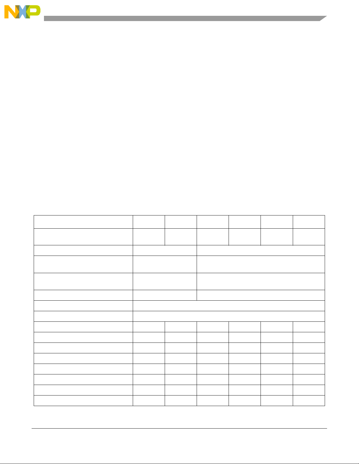
Chapter 1 Overview
The MCF5445x devices are a family of highly-integrated 32-bit microprocessors based on the Version 4
ColdFire microarchitecture. This product line is well suited for secure networked applications in factory
automation, process control, and motion control. The rich feature set and flexibility make it attractive to
many different applications in consumer and industrial markets.
All MCF5445x devices contain a Version 4 ColdFire core, 32-Kbyte internal SRAM, USB On-the-Go
controllers, a 2-bank DDR/DDR2/mobile-DDR SDRAM controller, a 16-channel DMA controller, a serial
boot facility, an SSI interface, and other serial interfaces. Optional peripherals include a PCI bus controller,
ATA controller, Fast Ethernet controllers, and an encryption coprocessor.
1.1 MCF5445x Family Comparison
The following table compares the various device derivatives available within the MCF5445x family.
Tabl e 1 - 1. MCF5445 x Family Configurations
Module MCF54450 MCF54451 MCF54452 MCF54453 MCF54454 MCF54455
ColdFire Version 4 Core with EMAC
(Enhanced Multiply-Accumulate Unit)
Core (System) Clock up to 240 MHz up to 266 MHz
Peripheral Bus Clock
(Core clock 2)
External Bus Clock
(Core clock 4)
Performance (Dhrystone/2.1 MIPS) up to 370 up to 410
Independent Data/Instruction Cache 16 Kbytes each
Static RAM (SRAM) 32 Kbytes
PCI Controller — — • • • •
Cryptography Acceleration Unit (CAU) — • — • — •
ATA Controller ———— • •
DDR SDRAM Controller ••••••
FlexBus External Interface ••••••
USB 2.0 On-the-Go ••••••
UTMI+ Low Pin Interface (ULPI) ••••••
Synchronous Serial Interface (SSI) ••••••
••••••
up to 120 MHz up to 133 MHz
up to 60 MHz up to 66 MHz
Freescale Semiconductor 1-1
Page 35
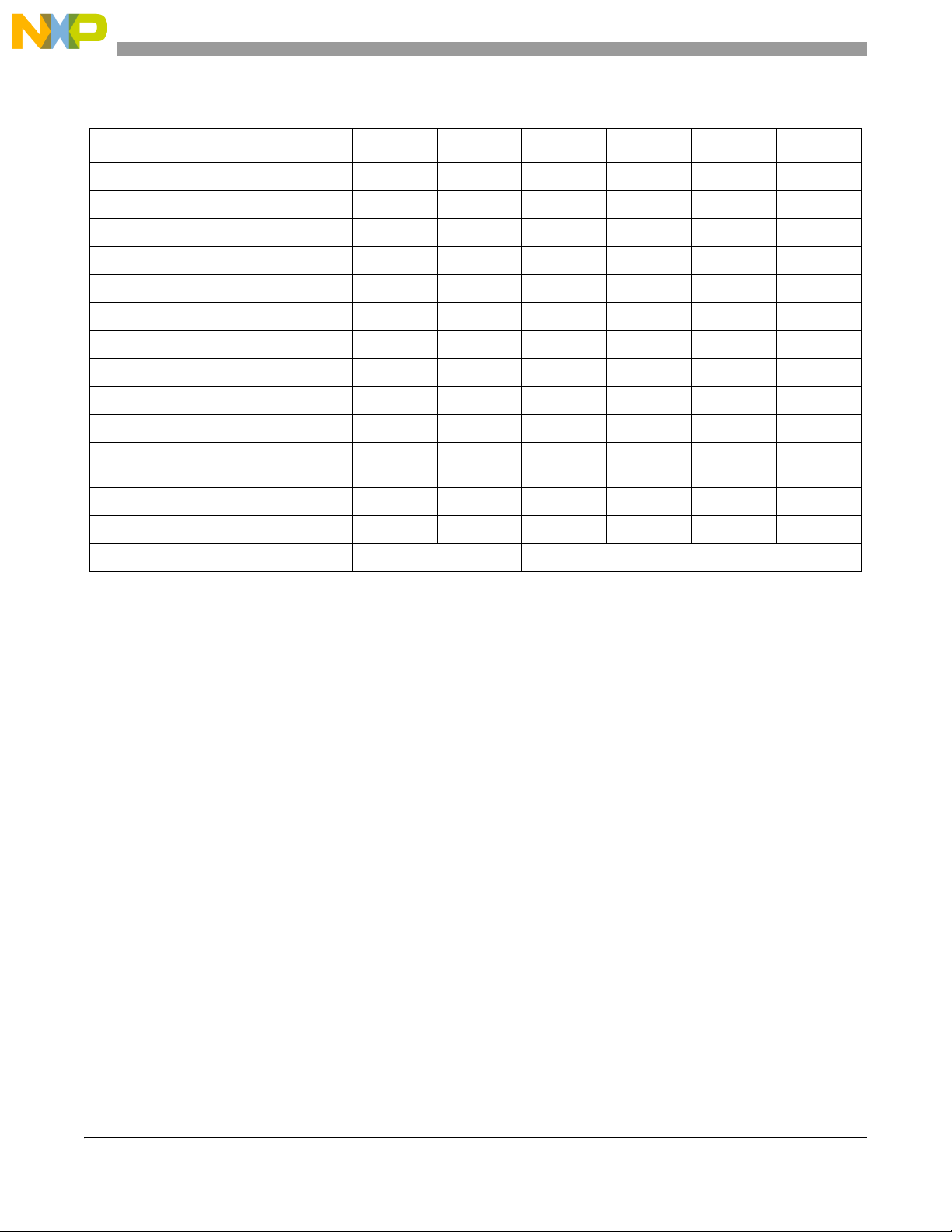
Overview
Table 1-1. MCF5445x Family Configurations (continued)
Module MCF54450 MCF54451 MCF54452 MCF54453 MCF54454 MCF54455
Fast Ethernet Controller (FEC) 112222
UARTs 333333
2
C ••••••
I
DSPI ••••••
Real Time Clock ••••••
32-bit DMA Timers 444444
Watchdog Timer (WDT) ••••••
Periodic Interrupt Timers (PIT) 444444
Edge Port Module (EPORT) ••••••
Interrupt Controllers (INTC) 222222
16-channel Direct Memory Access
(DMA)
••••••
General Purpose I/O (GPIO) ••••••
JTAG - IEEE® 1149.1 Test Access Port••••••
Package 256 MAPBGA 360 TEPBGA
1-2 Freescale Semiconductor
Page 36
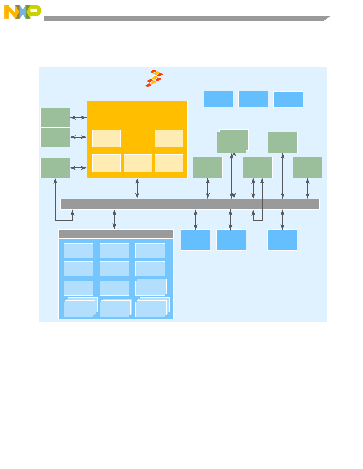
Version 4 ColdFire Core
LEGEND
2 INTCs
DSPI
EPORT
3 UARTs
I2C
Watchdog
4 DMA
RTC
ATA – Advanced Technology Attachment Controller
BDM – Background debug module
CAU – Cryptography acceleration unit
DSPI – DMA serial peripheral interface
eDMA – Enhanced direct memory access
EMAC – Enchance multiply-accumulate unit
EPORT – Edge port module
FEC – Fast Ethernet controller
GPIO – General Purpose Input/Output
I
2
C – Inter-Intergrated Circuit
INTC – Interrupt controller
JTAG – Joint Test Action Group interface
MMU – Memory management unit
PCI – Peripheral Component Interconnect
PIT – Programmable interrupt timers
PLL – Phase locked loop module
RNG – Random Number Generator
RTC – Real time clock
SSI – Synchronous Serial Interface
USB OTG – Universal Serial Bus On-the-Go controller
MCF54455
EMAC
2 FECs
Crossbar Switch (XBS)
32K
SRAM
Peripheral Bridge
CAU
16K
Instruction
Cache
16K
Data
Cache
Timers
BDM
ATA
SDRAM
Controller
FlexBus
eDMA
USB OTG
4 PITs
SSI RNG GPIO
MMU
Hardware
Divide
Oscillator PLLJTAG
PCI Serial Boot
1.2 Block Diagram
Figure 1-1 shows a top-level block diagram of the MCF54455 superset device.
Overview
Freescale Semiconductor 1-3
Figure 1-1. MCF54455 Block Diagram
Page 37

Overview
1.3 Operating Parameters
• 0ºC to 70ºC and –40ºC to 85ºC junction temperature devices are available
• 1.5V Core, 3.3V I/O, 1.8V/2.5V/3.3V external memory bus
1.4 Packages
Depending on device, the MCF5445x family is available in the following packages:
• 256-pin molded array process ball grid array (MAPBGA)
• 360-pin plastic ball grid array (TEPBGA)
1.5 Chip Level Features
• Version 4 ColdFire core with MMU and EMAC
• Up to 410 Dhrystone 2.1 MIPS @ 266 MHz
• 16 Kbytes instruction cache and 16 Kbytes data cache
• 32 Kbytes internal SRAM
• Support for booting from SPI-compatible flash, EEPROM, and FRAM devices
• Crossbar switch technology (XBS) for concurrent access to peripherals or RAM from multiple bus
masters
• 16 channel DMA controller
• 16-bit 133MHz DDR/mobile-DDR/DDR2 Controller
• USB 2.0 On-the-Go controller with ULPI support
• 32-bit PCI controller at 66 MHz
• ATA/ ATAPI c o n troller
• 2 10/100 Ethernet MACs
• Coprocessor for acceleration of the DES, 3DES, AES, MD5, and SHA-1 algorithms
• Random number generator
• Synchronous serial interface (SSI)
• 4 periodic interrupt timers (PIT)
• 4 32-bit timers with DMA support
• DMA supported serial peripheral interface (DSPI)
• 3 UARTs
2
C bus interface
•I
1.6 Module-by-Module Feature List
The following is a brief summary of the functional blocks in the MCF54455 superset device. For more
details refer to the MCF54455 ColdFire Microprocessor Reference Manual (MCF54455RM).
1-4 Freescale Semiconductor
Page 38

1.6.1 Version 4 ColdFire variable-length RISC processor
• Static operation
• 32-bit address and data path on-chip
• Maximum 266 MHz processor core, 133 MHz internal peripheral, and 66 MHz external FlexBus
frequency
• Sixteen total general-purpose 32-bit registers data and address
• Enhanced multiply-accumulate unit (EMAC) for DSP and fast multiply operations
• Hardware divide execution unit supporting various 32-bit operations
• Implements the ColdFire Instruction Set Architecture, ISA_C
• Cryptography acceleration unit (CAU)
— DES and AES block cipher engines
— MD5, SHA-1, and HMAC hash accelerator
1.6.2 On-chip Memories
• 32 Kbyte dual-ported SRAM on CPU internal bus
— Accessible to non-core bus masters (e.g. FEC, DMA, USB OTG, and PCI controllers) via the
crossbar switch
• Non-blocking, independent 16 Kbyte data and instruction caches organized as 4-way set
associative with 16 bytes per cache line and 1024 cache lines, supporting copy-back and
write-through modes of operation
Overview
1.6.3 Phase Locked Loop (PLL)
• 16–40 MHz reference crystal
• Loss-of-lock detection
1.6.4 Power Management
• Fully static operation with processor sleep and whole chip stop modes
• Very rapid response to interrupts from the low-power sleep mode (wake-up feature)
• Peripheral power management register to enable/disable clocks to most modules
• Software controlled disable of external clock input for low power consumption
1.6.5 Chip Configuration Module (CCM)
• System configuration during reset
• Bus monitor, abort monitor
• Configurable output pad drive strength control
• Unique part identification and part revision numbers
• Serial boot capability
Freescale Semiconductor 1-5
Page 39

Overview
— Supports SPI-compatible EEPROM, flash, and FRAM
— Configurable boot clock frequency
1.6.6 Reset Controller
• Separate reset in and reset out signals
• Six sources of reset: power-on reset (POR), external, software, watchdog timer, loss of lock, JTAG
instruction
• Status flag indication of source of last reset
1.6.7 System Control Module
• Access control registers
• Core watchdog timer with a 2n (where n = 8–31) clock cycle selectable timeout period
• Core fault reporting
1.6.8 Crossbar Switch
• Concurrent access from different masters to different slaves
• Slave arbitration attributes configured on a slave by slave basis
• Fixed or round-robin arbitration
1.6.9 Peripheral Component Interconnect (PCI) Bus
• Compatible with PCI 2.2 specification
• Supports up to 4 external PCI masters
• 32-bit target and intiator operation
• 33–66 MHz operation with PCI bus to internal bus divider ratios of 1:1, 1:2, 1:3, 2:3, and 1:4
1.6.10 Universal Serial Bus (USB) 2.0 On-The-Go (OTG) Controller
• Support for full speed (FS) and low speed (LS) via a serial interface or on-chip FS/LS transceiver
• Optional UTMI+ Low Pin Count Interface (ULPI) on some packages to support high speed (HS)
transfers
• Uses 60 MHz reference clock based off of the system clock or from an external pin
1.6.11 DDR SDRAM Controller
• Supports a glueless interface to DDR, DDR2, and mobile/low-power DDR SDRAM devices
• Support for 16-bit fixed memory port width
• 16-byte critical word first burst transfer
• Up to 14 lines of row address, up to 11 column address lines (16-bit bus), 2 bits of bank address,
and two pinned-out chip selects. The maximum row bits plus column bits equals 25.
1-6 Freescale Semiconductor
Page 40

• Supports up to 512 MByte of memory; minimum memory configuration of 8 MByte
• Supports page mode to maximize the data rate
• Supports sleep mode and self-refresh mode
1.6.12 FlexBus (External Interface)
• Glueless connections to 16-, and 32-bit external memory devices (SRAM, flash, ROM, etc.)
• Support for independent primary and secondary wait states per chip select
• Programmable address setup and hold time with respect to chip-select assertion, per transfer
direction
• Glueless interface to SRAM devices with or without byte strobe inputs
• Programmable wait state generator
• 32-bit external bidirectional data bus and 24-bit address bus
• Up to four chip selects available
• Byte/write enables (byte strobes)
• Ability to boot from external memories that are 8, 16, or 32 bits wide
Overview
1.6.13 Synchronous Serial Interface (SSI)
• Supports shared (synchronous) transmit and receive sections
• Normal mode operation using frame sync
• Network mode operation allowing multiple devices to share the port with as many as 32 time slots
• Gated clock mode operation requiring no frame sync
• Programmable data interface modes such as I2S, LSB aligned, and MSB aligned
• Programmable word length up to 24 bits
• AC97 support
1.6.14 ATA Controller
• Compliant with ATA-6 specification
• Supports PIO modes 0, 1, 2, 3 and 4
• Supports multiword DMA modes 0, 1 and 2
• Supports ultra DMA modes 0, 1, 2, 3 and 4 with an internal bus clock of at least 50 Mhz
• Supports ultra DMA mode 5 with an internal bus clock of at least 80 Mhz
• 128 byte FIFO part of interface
• FIFO receive alarm, FIFO transmit alarm and FIFO end of transmission alarm to DMA unit
• Zero-wait cycles transfer between DMA bus and FIFO allows fast FIFO reading/writing
1.6.15 Fast Ethernet Media Access Controller (FEC MAC)
• 10/100 BaseT/TX capability, half duplex or full duplex
Freescale Semiconductor 1-7
Page 41

Overview
• On-chip transmit and receive FIFOs
• Built-in dedicated DMA controller
• Memory-based flexible descriptor rings
• Media independent interface (MII) to external transceiver (PHY)
• Separate RMII gasket to interface with RMII-compatible PHY
1.6.16 Random Number Generator (RNG)
• FIPS-140 compliant for randomness and non-determinism
1.6.17 Real Time Clock
• Full clock: days, hours, minutes, seconds
• Minute countdown timer with interrupt
• Programmable daily alarm with interrupt
• Sampling timer with interrupt
• Once-per-day, once-per-hour, once-per-minute, and once-per-second interrupts
• Operation determined by reference input oscillator clock frequency and value programmed into
user-accessible registers
• Ability to wake the processor from low-power modes (wait, doze, and stop) via the RTC interrupts
1.6.18 Software Watchdog Timer
• 16-bit down-counter which resets the device if not serviced
1.6.19 Programmable Interrupt Timers (PIT)
• Four programmable interrupt timers each with a 16-bit counter
• Configurable as a down counter or free-running counter
1.6.20 DMA Timers
• Four 32-bit timers with DMA and interrupt request trigger capability
• Input capture and reference compare modes
1.6.21 DMA Serial Peripheral Interface (DSPI)
• Full-duplex, three-wire synchronous transfer
• Up to five chip selects available
• Master and slave modes with programmable master bit-rates
• Up to 16 pre-programmed transfers
1-8 Freescale Semiconductor
Page 42

1.6.22 Universal Asynchronous Receiver Transmitters (UARTs)
• 16-bit divider for clock generation
• Interrupt control logic
• DMA support with separate transmit and receive requests
• Programmable clock-rate generator
• Data formats can be 5, 6, 7 or 8 bits with even, odd or no parity
• Up to two stop bits in 1/16 increments
• Error-detection capabilities
1.6.23 I2C Module
• Interchip bus interface for EEPROMs, LCD controllers, A/D converters, and keypads
• Fully compatible with industry-standard I2C bus
• Master or slave modes support multiple masters
• Automatic interrupt generation with programmable level
1.6.24 Interrupt Controllers
Overview
• Two interrupt controllers, supporting up to 64 interrupt sources each, organized as seven
programmable levels
• Unique vector number for each interrupt source
• Ability to mask any individual interrupt source plus a global mask-all capability
• Support for service routine software interrupt acknowledge (IACK) cycles
• Combinational path to provide wake-up from low power modes
1.6.25 Edge Port Module
• Each pin can be individually configured as low level sensistive interrupt pin or edge-detecting
interrupt pin (rising, falling, or both)
• Exit stop mode via level-detect function
1.6.26 DMA Controller
• 16 fully programmable channels with 32-byte transfer control
• Data movement via dual-address transfers for 8-, 16-, 32- and 128-bit data values
• Programmable source, destination addresses, transfer size, support for enhanced address modes
• Support for major and minor nested counters with one request and one interrupt per channel
• Support for channel-to-channel linking and scatter/gather for continuous transfers with fixed
priority and round-robin channel arbitration
• External request pins for up to 2 channels
Freescale Semiconductor 1-9
Page 43
Overview
1.6.27 General Purpose I/O interface
• Up to 93 bits of GPIO for the MCF54450 and MCF54451
• Up to 132 bits of GPIO for the MCF54452, MCF54453, MCF54454, and MCF54455
• Bit manipulation supported via set/clear functions
• Various unused peripheral pins may be used as GPIO
1.6.28 System Debug Support
• Background debug mode (BDM) Revision D+
• Real time debug support, with four PC breakpoint registers and a pair of address breakpoint
registers with optional data
1.6.29 JTAG Support
• JTAG part identification and part revision numbers
1.7 Memory Map Overview
Table 1-2 illustrates the overall memory map of the device.
Table 1-2. System Memory Map
Internal
Address[31:28]
00xx 0x0000_0000 – 0x3FFF_FFFF FlexBus 1024 MB
01xx 0x4000_0000 – 0x7FFF_FFFF SDRAM Controller 1024 MB
1000 0x8000_0000 – 0x8FFF_FFFF Internal SRAM 256 MB
1001 0x9000_0000 – 0x9FFF_FFFF ATA Controller 256 MB
101x 0xA000_0000 – 0xBFFF_FFFF PCI Controller 512 MB
110x 0xC000_0000 – 0xDFFF_FFFF FlexBus 512 MB
1110 0xE000_0000 – 0xEFFF_FFFF Reserved 256 MB
1111 0xF000_0000 – 0xFFFF_FFFF Internal Peripheral Space 256 MB
Address Range Destination Slave Slave Memory Size
1-10 Freescale Semiconductor
Page 44

Overview
NOTE
This memory map provides two disjoint regions mapped to the FlexBus
controller to support glueless connections to external memories (e.g., flash
and SRAM), as well as a second space with one (or more) unique
chip-selects that can be used for non-cacheable, non-memory devices
(addresses 0xC000_0000 – 0xDFFF_FFFF). Additionally, this mapping is
selected because it easily maps into the ColdFire access control registers,
which provide a coarse association between memory addresses and their
attributes (e.g., cacheable, non-cacheable). For this device, one possible
configuration defines the default memory attribute as non-chacheable, and
one ACR is then used to identify cacheable addresses. For example,
ADDR[31] equaling 0 identifies the cacheable space.
1.7.1 Internal Peripheral Space
The internal peripheral space contains locations for all internal registers used to program and control the
device’s functional blocks and external interfaces. Table 1-3 summarizes the various register spaces and
their base addresses. Each slot is 16 kB in size, which is not necessarily taken up entirely by the functional
blocks. Any slot not illustrated is reserved. See corresponding chapter for details on their individual
memory maps.
Table 1-3. Internal Peripheral Space Memory Map
Base Address Slot Number Peripheral
0xFC00_0000 0 SCM (MPR and PACRs)
0xFC00_4000 1 Crossbar switch
0xFC00_8000 2 FlexBus
0xFC03_0000 12 FEC0
0xFC03_4000 13 FEC1
0xFC03_C000 15 Real-Time Clock
0xFC04_0000 16 SCM (CWT and Core Fault Registers)
0xFC04_4000 17 eDMA Controller
0xFC04_8000 18 Interrupt Controller 0
0xFC04_C000 19 Interrupt Controller 1
0xFC05_4000 21 Interrupt Controller IACK
2
0xFC05_8000 22 I
0xFC05_C000 23 DSPI
0xFC06_0000 24 UART0
C
0xFC06_4000 25 UART1
0xFC06_8000 26 UART2
0xFC07_0000 28 DMA Timer 0
Freescale Semiconductor 1-11
Page 45

Overview
Table 1-3. Internal Peripheral Space Memory Map (continued)
Base Address Slot Number Peripheral
0xFC07_4000 29 DMA Timer 1
0xFC07_8000 30 DMA Timer 2
0xFC07_C000 31 DMA Timer 3
0xFC08_0000 32 PIT 0
0xFC08_4000 33 PIT 1
0xFC08_8000 34 PIT 2
0xFC08_C000 35 PIT 3
0xFC09_4000 37 Edge Port
0xFC0A_0000 40 CCM, Reset Controller, Power Management
0xFC0A_4000 41 Pin Multiplexing and Control (GPIO)
0xFC0A_8000 42 PCI Controller
0xFC0A_C000 43 PCI Arbiter
0xFC0B_0000 44 USB On-the-Go
0xFC0B_4000 45 RNG
0xFC0B_8000 46 SDRAM Controller
0xFC0B_C000 47 SSI
0xFC0C_4000 49 PLL
1.8 Documentation
Documentation is available from a local Freescale distributor, a Freescale sales office, the Freescale
Literature Distribution Center, or through the Freescale world-wide web address at
http://www.freescale.com/coldfire.
1-12 Freescale Semiconductor
Page 46
Chapter 2 Signal Descriptions
2.1 Introduction
This chapter describes the external signals on the device. It includes an alphabetical signal listing of signals
that characterizes each signal as an input or output, defines its state at reset, and identifies whether a
pull-up resistor should be used.
NOTE
The terms assertion and negation are used to avoid confusion when dealing
with a mixture of active-low and active-high signals. The term asserted
indicates that a signal is active, independent of the voltage level. The term
negated indicates that a signal is inactive.
Active-low signals, such as SD_SRAS and TA, are indicated with an
overbar.
2.2 Signal Properties Summary
The below table lists the signals grouped by functionality.
NOTE
In this table and throughout this document, a single signal within a group is
designated without square brackets (i.e., FB_AD23), while designations for
multiple signals within a group use brackets (i.e., FB_AD[23:21]) and is
meant to include all signals within the two bracketed numbers when these
numbers are separated by a colon.
NOTE
The primary functionality of a pin is not necessarily its default functionality.
Most pins that are muxed with GPIO default to their GPIO functionality. See
Table 2-1 for a list of the exceptions.
Table 2-1. Special-Case Default Signal Functionality
Pin 256 MAPBGA 360 TEPBGA
FB_AD[31:0] FB_AD[31:0] except when serial boot selects 0-bit
boot port size.
FB_BE/BWE
FB_CS[3:1] FB_CS[3:1]
[3:0] FB_BE/BWE[3:0]
Freescale Semiconductor 2-1
Page 47
Signal Descriptions
Table 2-1. Special-Case Default Signal Functionality (continued)
Pin 256 MAPBGA 360 TEPBGA
FB_OE
FB_OE
FB_R/W FB_R/W
FB_TA FB_TA
FB_TS FB_TS
PCI_GNT[3:0] GPIO PCI_GNT[3:0]
PCI_REQ[3:0] GPIO PCI_REQ[3:0]
IRQ1 GPIO PCI_INTA and
configured as an agent.
ATA_RESET GPIO ATA reset
Tabl e 2 - 2. MCF5445 x Signal Information and Muxing
Signal Name GPIO Alternate 1 Alternate 2
Reset
RESET — — — U
RSTOUT — — — —
1
2
Pull-up (U)
Pull-down (D)
I EVDD L4 Y18
O EVDD M15 B17
Direction
MCF54450
MCF54451
256 MAPBGA
Voltag e
Domain
MCF54452
MCF54453
MCF54454
MCF54455
360 TEPBGA
Clock
EXTAL/PCI_CLK — — — —
XTAL — — — U
Mode Selection
BOOTMOD[1:0] — — — —
FlexBus
4
FB_AD[31:24] PFBADH[7:0]
FB_AD[23:16] PFBADMH[7:0]
FB_AD[15:8] PFBADML[7:0]
FB_AD[7:0] PFBADL[7:0]
FB_D[31:24] — —
4
FB_D[23:16] — —
4
FB_D[15:8] — —
4
FB_D[7:0] — —
FB_BE/BWE[3:2] PBE[3:2] FB_TSIZ[1:0] — —
FB_BE/BWE[1:0] PBE[1:0] — — —
I EVDD M16 A16
3
O EVDD L16 A17
I EVDD M5, M7 AB17, AB21
I/O EVDD A14, A13, D12,
I/O EVDD B11, A11, D10,
I/O EVDD B9, A9, D8, C8,
I/O EVDD B7, A7, D6, C6,
O EVDD B5, A5 Y1, W2
O EVDD B4, A4 W3, Y2
C12, B12, A12,
D11, C11
C10, B10, A10,
D9, C9
B8, A8, D7, C7
B6, A6, D5, C5
J2, K4, J1, K1–3,
L1, L4
L2, L3, M1–4,
N1–2
P1–2, R1–3, P4,
T1–2
T3–4, U1–3,
V1–2, W1
2-2 Freescale Semiconductor
Page 48
Table 2-2. MCF5445x Signal Information and Muxing (continued)
Signal Descriptions
1
Signal Name GPIO Alternate 1 Alternate 2
Pull-up (U)
FB_CLK — — —
—
FB_CS[3:1] PCS[3:1] — — —
FB_CS0 —— ——
FB_OE PFBCTL3 — — —
FB_R/W PFBCTL2 — — —
FB_TA PFBCTL1 — — U
FB_TS PFBCTL0 FB_ALE FB_TBST —
PCI Controller
5
PCI_AD[31:0] — FB_A[31:0] — —
— — FB_A[23:0] — —
PCI_CBE[3:0] — — — —
PCI_DEVSEL —— ——
PCI_FRAME —— ——
PCI_GNT3 PPCI7 ATA_DMACK — —
PCI_GNT[2:1] PPCI[6:5] — — —
PCI_GNT0/
PPCI4 — — —
PCI_EXTREQ
PCI_IDSEL — — — —
PCI_IRDY —— ——
PCI_PAR — — — —
PCI_PERR —— ——
PCI_REQ3 PPCI3 ATA_INTRQ — —
PCI_REQ[2:1] PPCI[2:1] — — —
PCI_REQ0/
PPCI0 — — —
PCI_EXTGNT
2
MCF54450
MCF54451
256 MAPBGA
Voltag e
Direction
Pull-down (D)
O EVDD B13 J3
O EVDD C2, D4, C3 W5, AA4, AB3
O EVDD C4 Y4
O EVDD A2 AA1
O EVDD B2 AA3
I EVDD B1 AB2
O EVDD A3 Y3
I/O EVDD — C11, D11, A10,
I/O EVDD K14–13, J15–13,
I/O EVDD — G4, E4, D1, B1
O EVDD — F2
I/O EVDD — B2
O EVDD — B7
O EVDD — C8, C9
O EVDD — A9
I EVDD — D5
I/O EVDD — C3
I/O EVDD — C4
I/O EVDD — B4
I EVDD — C7
I EVDD — D7, C5
I EVDD — A2
Domain
H13–15, G15–13,
F14–13, E15–13,
D16, B16, C15,
B15, C14, D15,
C16, D14
MCF54452
MCF54453
MCF54454
MCF54455
360 TEPBGA
B10, J4, G2, G3,
F1, D12, C12,
B12, A11, B11,
B9, D9, D10, A8,
B8, A5, B5, A4,
A3, B3, D4, D3,
E3–E1, F3, C2,
D2, C1
—
Freescale Semiconductor 2-3
Page 49
Signal Descriptions
Table 2-2. MCF5445x Signal Information and Muxing (continued)
1
Signal Name GPIO Alternate 1 Alternate 2
PCI_RST
—— ——
PCI_SERR —— ——
PCI_STOP —— ——
PCI_TRDY —— ——
SDRAM Controller
SD_A[13:0] — — —
—
SD_BA[1:0] — — — —
SD_CAS —— ——
SD_CKE — — — —
SD_CLK — — — —
SD_CLK —— ——
SD_CS[1:0] — — — —
SD_D[31:16] — — — —
SD_DM[3:2] — — — —
SD_DQS[3:2] — — — —
SD_RAS —— ——
SD_VREF — — — —
SD_WE —— ——
External Interrupts Port
6
2
MCF54450
MCF54451
256 MAPBGA
Voltag e
Pull-up (U)
Direction
Pull-down (D)
O EVDD — B6
I/O EVDD — A6
I/O EVDD — A7
I/O EVDD — C10
O SDVDD R1, P1, N2, P2,
O SDVDD P4, T5 P22, P19
O SDVDD T6 L19
O SDVDD N5 N22
O SDVDD T9 L22
O SDVDD T8 M22
O SDVDD P6, R6 L20, M20
I/O SDVDD N6, T7, N7, P7,
O SDVDD P9, N12 H21, E21
O SDVDD R9, N11 H22, E22
O SDVDD P5 N21
I SDVDD M8 M21
O SDVDD R5 N20
Domain
R2, T2, M4, N3,
P3, R3, T3, T4,
R4, N4
R7, R8, P8, N8,
N9, T10, R10,
P10, N10, T11,
R11, P11
MCF54452
MCF54453
MCF54454
MCF54455
360 TEPBGA
V22, U20–22,
T19–22, R20–22,
N19, P20–21
L21, K22, K21,
K20, J20, J19,
J21, J22, H20,
G22, G21, G20,
G19, F22, F21,
F20
IRQ7 PIRQ7 — — —
IRQ4 PIRQ4 — SSI_CLKIN —
IRQ3 PIRQ3 — — —
IRQ1 PIRQ1 PCI_INTA — —
I EVDD L1 ABB13
I EVDD L2 ABB13
I EVDD L3 AB14
I EVDD F15 C6
FEC0
FEC0_MDC PFECI2C3 — — —
FEC0_MDIO PFECI2C2 — — —
O EVDD F3 AB8
I/O EVDD F2 Y7
2-4 Freescale Semiconductor
Page 50
Table 2-2. MCF5445x Signal Information and Muxing (continued)
Signal Descriptions
1
Signal Name GPIO Alternate 1 Alternate 2
Pull-up (U)
FEC0_COL PFEC0H4 — ULPI_DATA7 —
FEC0_CRS PFEC0H0 — ULPI_DATA6 —
FEC0_RXCLK PFEC0H3 — ULPI_DATA1 —
FEC0_RXDV PFEC0H2 FEC0_RMII_
— —
CRS_DV
FEC0_RXD[3:2] PFEC0L[3:2] — ULPI_DATA[5:4] —
FEC0_RXD1 PFEC0L1 FEC0_RMII_RXD1 — —
FEC0_RXD0 PFEC0H1 FEC0_RMII_RXD0 — —
FEC0_RXER PFEC0L0 FEC0_RMII_RXER — —
FEC0_TXCLK PFEC0H7 FEC0_RMII_
— —
REF_CLK
FEC0_TXD[3:2] PFEC0L[7:6] — ULPI_DATA[3:2] —
FEC0_TXD1 PFEC0L5 FEC0_RMII_TXD1 — —
FEC0_TXD0 PFEC0H5 FEC0_RMII_TXD0 — —
FEC0_TXEN PFEC0H6 FEC0_RMII_TXEN — —
FEC0_TXER PFEC0L4 — ULPI_DATA0 —
2
MCF54450
MCF54451
256 MAPBGA
Voltag e
Direction
Pull-down (D)
I EVDD E1 AB7
I EVDD F1 AA7
I EVDD G1 AA8
I EVDD G2 Y8
I EVDD G3, G4 AB9, Y9
I EVDD H1 W9
I EVDD H2 AB10
I EVDD H3 AA10
I EVDD H4 Y10
O EVDD J1, J2 W10, AB11
O EVDD J3 AA11
O EVDD J4 Y11
O EVDD K1 W11
O EVDD K2 AB12
Domain
360 TEPBGA
MCF54452
MCF54453
MCF54454
MCF54455
FEC1
FEC1_MDC PFECI2C5 — ATA _D I O R —
FEC1_MDIO PFECI2C4 — ATA _ D IO W —
FEC1_COL PFEC1H4 — ATA _ DATA 7 —
FEC1_CRS PFEC1H0 — ATA _ D ATA6 —
FEC1_RXCLK PFEC1H3 — ATA _ DATA 5 —
FEC1_RXDV PFEC1H2 FEC1_RMII_
ATA _DATA 1 5 —
CRS_DV
FEC1_RXD[3:2] PFEC1L[3:2] — ATA_DATA[4:3] —
FEC1_RXD1 PFEC1L1 FEC1_RMII_RXD1 ATA _ DATA 1 4 —
FEC1_RXD0 PFEC1H1 FEC1_RMII_RXD0 ATA _ DATA 1 3 —
FEC1_RXER PFEC1L0 FEC1_RMII_RXER ATA _DATA 1 2 —
FEC1_TXCLK PFEC1H7 FEC1_RMII_
ATA _DATA 1 1 —
REF_CLK
FEC1_TXD[3:2] PFEC1L[7:6] — ATA_DATA[2:1] —
O EVDD — W20
I/O EVDD — Y22
I EVDD — AB18
I EVDD — AA18
I EVDD — W14
I EVDD — AB15
I EVDD — AA15, Y15
I EVDD — AA17
I EVDD — Y17
I EVDD — W17
I EVDD — AB19
O EVDD — Y19, W18
Freescale Semiconductor 2-5
Page 51
Signal Descriptions
Table 2-2. MCF5445x Signal Information and Muxing (continued)
1
Signal Name GPIO Alternate 1 Alternate 2
FEC1_TXD1 PFEC1L5 FEC1_RMII_TXD1 ATA _ DATA 1 0 —
FEC1_TXD0 PFEC1H5 FEC1_RMII_TXD0 ATA _ DATA 9 —
FEC1_TXEN PFEC1H6 FEC1_RMII_TXEN ATA _ DATA 8 —
FEC1_TXER PFEC1L4 — ATA _ DATA 0 —
USB On-the-Go
USB_DM — — — —
USB_DP — — — —
USB_VBUS_EN PUSB1 USB_PULLUP ULPI_NXT —
USB_VBUS_OC PUSB0 — ULPI_STP UD
ATA
ATA _BU FF E R _E N PATA H 5 — — —
ATA _ CS [1:0] PATAH[4:3] — — —
ATA_DA[2:0] PATAH[2:0] — — —
ATA_RESET PATA L 2 — — —
ATA_DMARQ PATA L1 — — —
ATA _I OR DY PATA L 0 — — —
2
MCF54450
MCF54451
256 MAPBGA
Voltag e
Pull-up (U)
Direction
Pull-down (D)
O EVDD — AA19
O EVDD — Y20
O EVDD — AA21
O EVDD — AA22
O USB
O USB
O USB
7
I USB
O EVDD — Y13
O EVDD — W21, W22
O EVDD — V19–21
O EVDD — W13
I EVDD — AA14
I EVDD — Y14
Domain
F16 A14
VDD
E16 A15
VDD
E5 AA2
VDD
B3 V4
VDD
MCF54452
MCF54453
MCF54454
MCF54455
360 TEPBGA
Real Time Clock
EXTAL32K — — — —
XTAL32K — — — —
I EVDD J16 A13
O EVDD H16 A12
SSI
SSI_MCLK PSSI4 — — —
SSI_BCLK PSSI3 U1CTS — —
SSI_FS PSSI2 U1RTS — —
SSI_RXD PSSI1 U1RXD — UD
SSI_TXD PSSI0 U1TXD — UD
O EVDD T13 D20
I/O EVDD R13 E19
I/O EVDD P12 E20
I EVDD T12 D21
O EVDD R12 D22
I2C
I2C_SCL PFECI2C1 — U2TXD U
I/O EVDD K3 AA12
2-6 Freescale Semiconductor
Page 52
Table 2-2. MCF5445x Signal Information and Muxing (continued)
Signal Descriptions
1
Signal Name GPIO Alternate 1 Alternate 2
I2C_SDA PFECI2C0 — U2RXD U
DMA
DACK1 PDMA3 — ULPI_DIR —
DREQ1 PDMA2 — USB_CLKIN U
DACK0 PDMA1 DSPI_PCS3 — —
DREQ0 PDMA0 — — U
DSPI
DSPI_PCS5/PCSS PDSPI6 — — —
DSPI_PCS2 PDSPI5 — — —
DSPI_PCS1 PDSPI4 SBF_CS — —
DSPI_PCS0/SS PDSPI3 — — U
DSPI_SCK PDSPI2 SBF_CK — —
DSPI_SIN PDSPI1 SBF_DI —
DSPI_SOUT PDSPI0 SBF_DO — —
2
MCF54450
MCF54451
256 MAPBGA
Voltag e
Pull-up (U)
8
Direction
Pull-down (D)
I/O EVDD K4 Y12
O
I
O
I
O EVDD N14 D18
O EVDD L13 A19
O EVDD P14 B20
I/O EVDD R16 D17
I/O EVDD R15 A20
I EVDD P15 B19
O EVDD N13 C20
Domain
EVDD M14 C17
EVDD P16 C18
EVDD N15 A18
EVDD N16 B18
MCF54452
MCF54453
MCF54454
MCF54455
360 TEPBGA
UARTs
U1CTS PUART7 — — —
U1RTS PUART6 — — —
U1RXD PUART5 — — —
U1TXD PUART4 — — —
U0CTS PUART3 — — —
U0RTS PUART2 — — —
U0RXD PUART1 — — —
U0TXD PUART0 — — —
Note: The UART1 and UART 2 signals are multiplexed on the DMA timers and I2C pins.
DMA Timers
DT3IN PTIMER3 DT3OUT U2RXD —
DT2IN PTIMER2 DT2OUT U2TXD —
DT1IN PTIMER1 DT1OUT U2CTS —
DT0IN PTIMER0 DT0OUT U2RTS —
I EVDD — V3
O EVDD — U4
I EVDD — P3
O EVDD — N3
I EVDD M3 Y16
O EVDD M2 AA16
I EVDD N1 AB16
O EVDD M1 W15
I EVDD C13 H2
I EVDD D13 H1
I EVDD B14 H3
I EVDD A15 G1
Freescale Semiconductor 2-7
Page 53
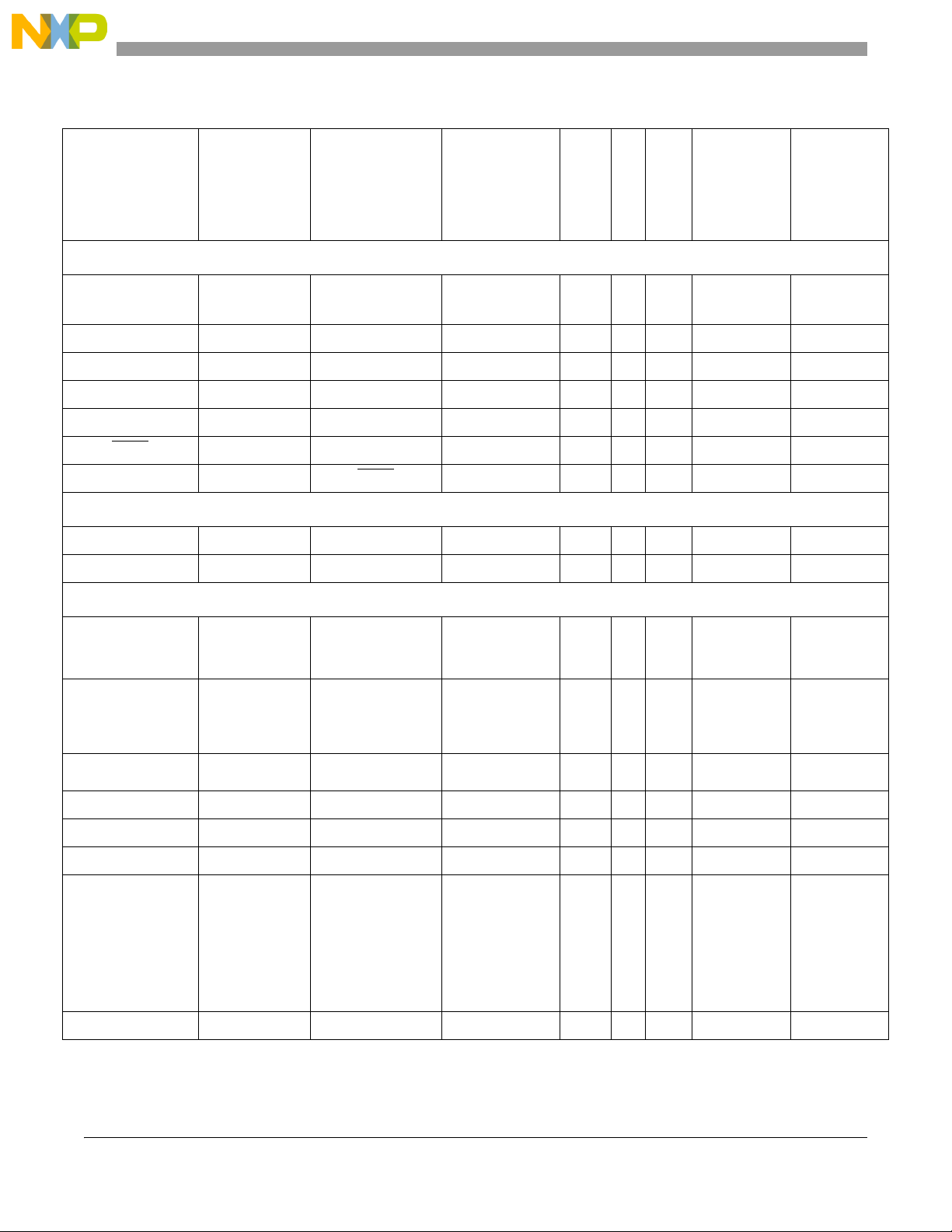
Signal Descriptions
Table 2-2. MCF5445x Signal Information and Muxing (continued)
1
Signal Name GPIO Alternate 1 Alternate 2
BDM/JTAG
9
PSTDDATA[7:0] — — — —
JTAG_EN — — — D
PSTCLK — TCLK — —
DSI — TDI — U
DSO — TDO — —
BKPT — TMS — U
DSCLK — TRST — U
Test
TEST — — — D
PLLTEST — — — —
Power Supplies
2
MCF54450
MCF54451
256 MAPBGA
Voltag e
Pull-up (U)
Direction
Pull-down (D)
O EVDD E2, D1, F4, E3,
I EVDD M11 C21
I EVDD P13 C22
I EVDD T15 C19
O EVDD T14 A21
I EVDD R14 B21
I EVDD M13 B22
I EVDD M6 AB20
O EVDD K16 D15
Domain
D2, C1, E4, D3
MCF54452
MCF54453
MCF54454
MCF54455
360 TEPBGA
AA6, AB6, AB5,
W6, Y6, AA5,
AB4, Y5
IVDD — — — — — —
EVDD — — — — — —
SD_VDD — — — — — —
VDD_OSC — — — — — —
VDD_A_PLL — — — — — —
VDD_RTC — — — — — —
VSS — — — — — —
VSS_OSC — — — — — —
1
Pull-ups are generally only enabled on pins with their primary function, except as noted.
2
Refers to pin’s primary function.
E6–12, F5, F12 D6, D8, D14, F4,
G5, G12, H5, H12,
J5, J12, K5, K12,
L5–6, L12
L7–11, M9, M10 F19, H19, K19,
L14 B16
K15 C14
M12 C13
A1, A16, F6–11,
G6–11, H6–11,
J6–11, K6–11, T1,
T16
L15 C16
H4, N4, R4, W4,
W7, W8, W12,
W16, W19
D13, D19, G8,
G11, G14, G16,
J7, J16, L7, L16,
N16, P7, R16, T8,
T12, T14, T16
M19, R19, U19
A1, A22, B14, G7,
G9–10, G12–13,
G15, H7, H16,
J9–14, K7, K9–14,
K16, L9–14, M7,
M9–M14, M16,
N9–14, P9–14,
P16, R7, T7,
T9–11, T13, T15,
AB1, AB22
2-8 Freescale Semiconductor
Page 54
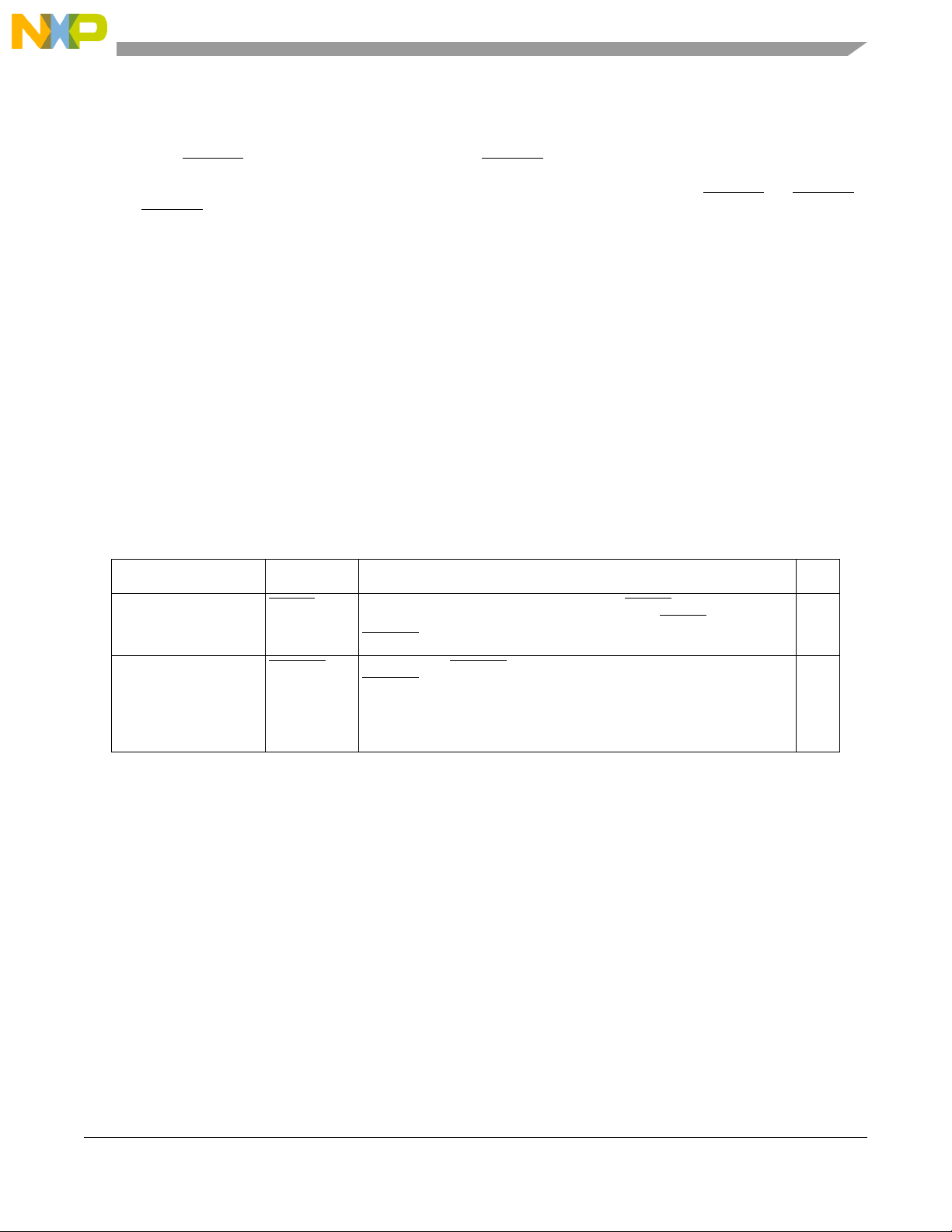
Signal Descriptions
3
Enabled only in oscillator bypass mode (internal crystal oscillator is disabled).
4
Serial boot must select 0-bit boot port size to enable the GPIO mode on these pins.
5
When the PCI is enabled, all PCI bus pins come up configured as such. This includes the PCI_GNT and PCI_REQ lines, which have
GPIO. The IRQ1/PCI_INTA signal is a special case. It comes up as PCI_INTA when booting as a PCI agent and as GPIO when booting
as a PCI host.
For the 360 TEPBGA, booting with PCI disabled results in all dedicated PCI pins being safe-stated. The PCI_GNT
and IRQ1/PCI_INTA
6
GPIO functionality is determined by the edge port module. The pin multiplexing and control module is only responsible for assigning
the alternate functions.
7
Depends on programmed polarity of the USB_VBUS_OC signal.
8
Pull-up when the serial boot facility (SBF) controls the pin
9
If JTAG_EN is asserted, these pins default to Alternate 1 (JTAG) functionality. The pin multiplexing and control module is not
responsible for assigning these pins.
come up as GPIO.
and PCI_REQ lines
NOTE
2.3 Signal Primary Functions
2.3.1 Reset Signals
Table 2-3 describes signals used to reset the chip or to indicate a reset.
Table 2-3. Reset Signals
Signal Name Abbreviation Function I/O
Reset In RESET Primary reset input to the device. Asserting RESET resets the core and
peripherals after four FB_CLK cycles. Asserting RESET
RSTOUT to be asserted.
Reset Out RSTOUT Reset output (RSTOUT) is an indicator that the chip is in reset.
RSTOUT is asserted at least 512 internal system bus clock cycles (256
FB_CLK cycles) in response to any internal or external reset. (The
exact time depends on how long it takes for the PLL to lock and/or the
serial boot sequence to complete.)
also causes
I
O
Freescale Semiconductor 2-9
Page 55
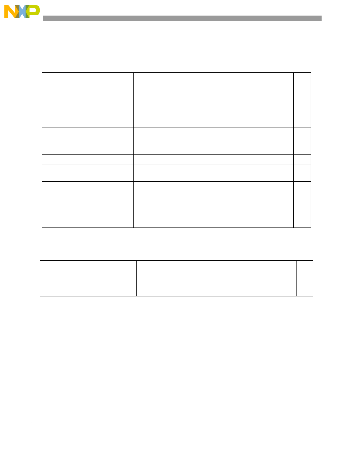
Signal Descriptions
2.3.2 PLL and Clock Signals
Table 2-4 describes signals that are used to support the on-chip clock generation circuitry.
Table 2-4. PLL and Clock Signals
Signal Name Abbreviation Function I/O
External Clock In EXTAL Always driven by an external clock input except when used as a
connection to the external crystal if the internal oscillator circuit is
used. Clock source may be configured during reset. See Chapter 11,
“Chip Configuration Module (CCM),” for more details.
Note: This signal is also PCI_CLK (33 or 66 MHz) when running from
an external oscillator with PCI enabled.
Crystal XTAL Used as a connection to the external crystal when the internal
oscillator circuit is used to drive the crystal.
RTC External Clock In EXTAL32K Crystal input clock for the real-time clock module. I
RTC Crystal XTAL32K Oscillator output to EXTAL RTC crystal. O
FlexBus Clock Out FB_CLK Reflects one-half of the internal bus clock (or one-fourth the
core/system clock). (f
USB Clock In USB_CLKIN This pin allows the user to drive the reference clock to the USB module
as an alternate method of generating the USB reference clock during
FS/LS operation. This pin should be driven only with a 60 MHz clock.
When using the ULPI USB interface, this pin is the ULPI input clock.
SSI Clock In SSI_CLKIN This pin allows the user to drive a specific clock frequency to the SSI
module.
sys/4
)
2.3.3 Mode Selection
Table 2-5. Mode Selection Signals
I
O
O
I
I
Signal Name Abbreviation Function I/O
Boot mode BOOTMOD[1:0] Indicates the device’s boot mode and chip configuration at reset. See
Chapter 11, “Chip Configuration Module (CCM),” for the signal
encodings.
2-10 Freescale Semiconductor
I
Page 56
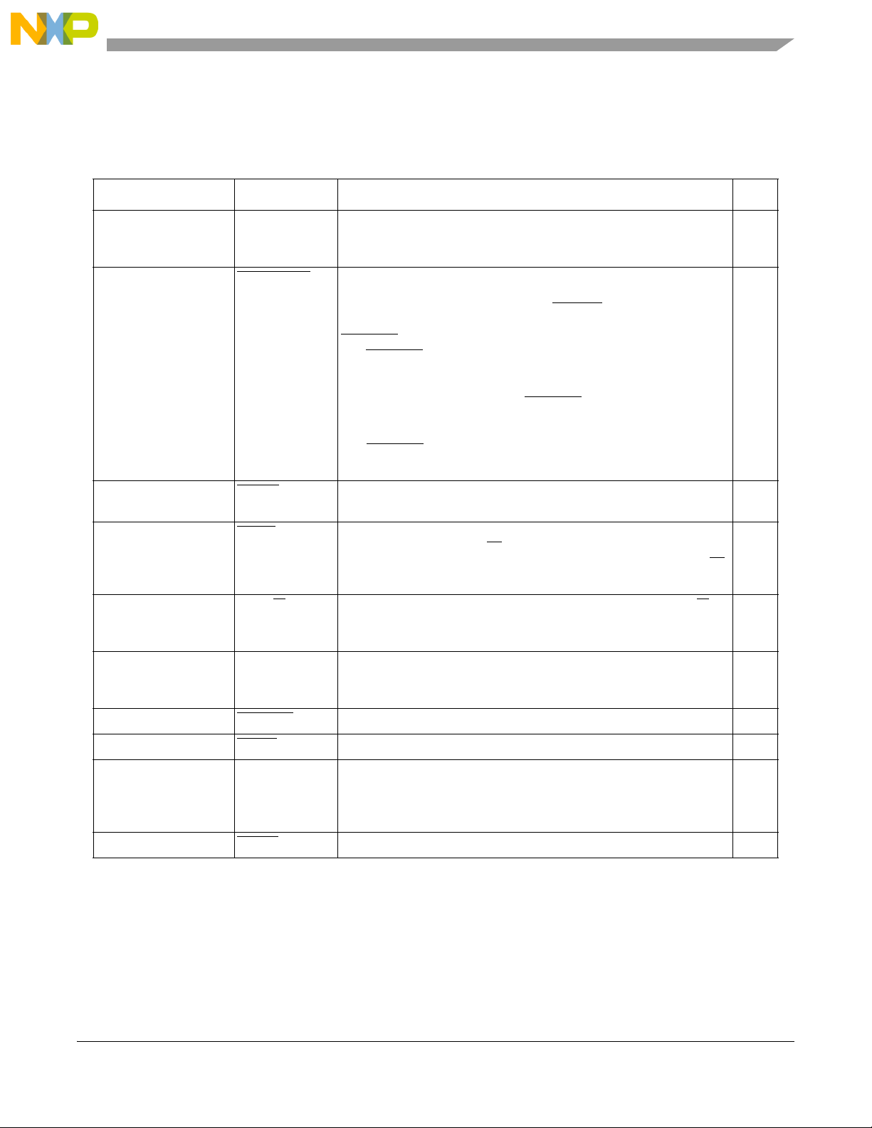
2.3.4 FlexBus Signals
Table 2-6 describes signals that are used for performing transactions on the external bus.
Tabl e 2 - 6. Flex B u s Signals
Signal Name Abbreviation Function I/O
Signal Descriptions
Address/Data Bus FB_AD[31:0] Defines address and data of external byte, word, and longword
accesses. This three-state, bi-directional bus is the general-purpose
address/data path to external SRAM and flash devices.
Byte Enables FB_BE/BWE
Output Enable FB_OE Indicates when an external device can drive data during external read
Transfer Acknowledge FB_TA Indicates external data transfer is complete. During a read cycle, when
Read/Write FB_R/W Indicates direction of the data transfer on the bus for SRAM (R/W)
[3:0] Defines flow of data on data bus. During peripheral accesses, these
output signals indicate that data is to be latched or driven onto a byte
of the data bus when driven low. The BE/BWE
asserted only to the memory bytes used during a read or write access.
BE/BWE0 controls access to the most significant byte lane of data,
and BE/BWE
data.
For SRAM or Flash devices, the BE/BWE
connected to individual byte strobe signals.
The BE/BWE
peripherals, but not to on-chip SRAM or cache.
cycles.
the processor recognizes TA
the bus cycle. During a write cycle, when the processor recognizes TA,
the bus cycle is terminated.
accesses. A logic 1 indicates a read from a slave device and a logic 0
indicates a write to a slave device.
3 controls access to the least significant byte lane of
n signals are asserted during accesses to on-chip
, it latches the data and then terminates
[3:0] signals are
n outputs should be
I/O
O
O
I
O
Transfer Size FB_TSIZ[1:0] Indicates bus width (8, 16, or 32 bits) for each chip select. The initial
width for the bootstrap program chip select is determined by the initial
state of TSIZ[1:0].
Transfer Burst FB_TBST
Transfer Start FB_TS Bus control output signal indicating the start of a transfer. O
Address Latch Enable FB_ALE Indicates device has begun a bus transaction and the address and
Chip Selects FB_CS
Freescale Semiconductor 2-11
[3:0] Select external devices for external bus transactions. O
Indicates external bus access is a burst access. O
attributes are valid. FB_ALE is asserted for one bus clock cycle. In
multiplexed mode, ALE is used externally as an address latch enable
to capture the address phase of the bus transfer.
O
O
Page 57
Signal Descriptions
2.3.5 SDRAM Controller Signals
Table 2-7 describes signals used for SDRAM accesses.
Table 2-7. SDRAM Controller Signals
Signal Name Abbreviation Function I/O
SDRAM Address Bus SD_A[13:0] Address bus used for multiplexed row and column addresses during
SDRAM bus cycles.
SDRAM Data Bus SD_D[31:16] Bidirectional, non-multiplexed data bus for SDRAM accesses. I/O
SDRAM Bank Address SD_BA[1:0] Selects one of the four SDRAM row banks. O
SDRAM Clock Enable SD_CKE SDRAM clock enable. O
DDR SDRAM Clock SD_CLK Output clock for DDR SDRAM. O
DDR SDRAM Clock SD_CLK
SDRAM Chip Selects SD_CS[1:0] SDRAM chip select signals. O
DDR SDRAM Data Strobes SD_DQS[3:2] Indicates when valid data is on data bus. I/O
SDRAM Write Data Byte
Mask
SDRAM Column Address
Strobe
SDRAM Row Address
Strobe
SDRAM Write Enable SD_WE
SD_DQM[3:2] Used to determine which byte lanes of data bus should be latched
SD_CAS
SD_RAS SDRAM row address strobe. O
Inverted output clock for DDR SDRAM. O
during a write cycle.
The SD_DQMn should be connected to individual SDRAM DQM
signals. Most SDRAMs associate DQM3 with the MSB, in which case
SD_DQM3 should be connected to the SDRAM's DQM3 input.
SDRAM column address strobe. O
Indicates direction of data transfer on bus for SDRAM accesses. A
logic 1 indicates a read from a slave device and a logic 0 indicates a
write to a slave device.
O
O
O
SDRAM Voltage Reference SD_VREF Reference voltage for differential I/O pad cells. Should be half the
voltage of the memory used in the system. For example, 2.5 V DDR
results in an SD_VREF of 1.25 V. See the device’s datasheet for the
voltages and tolerances for the various memory modes.
2-12 Freescale Semiconductor
I
Page 58
Signal Descriptions
2.3.6 PCI Controller Signals
Table 2-8 describes the external interrupt signals used on the external PCI bus.
Table 2-8. PCI Controller Signals
Signal Name Abbreviation Function I/O
PCI Address/Data Bus PCI_AD[31:0] Multiplexed address/data bus. I/O
PCI Command/Byte
Enables
PCI Device Select PCI_DEVSEL
PCI Frame PCI_FRAME Asserted by a PCI initiator to indicate the beginning of a transaction.
PCI External Bus Grant PCI_GNT
PCI External Bus
Grant/Request
PCI Initialization Device
Select
PCI Initiator Ready PCI_IRDY
PCI Parity PCI_PAR Indicates the parity of the data on the PCI_AD[31:0] and
PCI_CBE[3:0] Multiplexed PCI command and byte enables. The PCI command is
present during address phase; the byte enables are present during
data phase.
Indicates processor has recognized itself as the target of a PCI
transaction from address presented on the PCI bus.
It is negated when initiator is ready to complete final data phase.
[3:1] Asserted to an external master to give it control of PCI bus. If internal
PCI arbiter is enabled, it asserts one of the PCI_GNT[3:1] signals to
grant ownership of PCI bus to external master. When PCI arbiter is
disabled, PCI_GNT
PCI_GNT0/
PCI_EXTREQ
PCI_IDSEL Asserted during a PCI type-0 configuration cycle to address the PCI
Asserted to external master device 0 to give it control of the PCI bus.
When the PCI arbiter is disabled, the signal operates as the
PCI_EXTREQ output, which is asserted when the processor needs to
initiate a PCI transaction.
configuration header.
Indicates that PCI initiator is ready to transfer data. During a write
operation, assertion indicates the master is driving valid data on bus.
During a read operation assertion indicates that master is ready to
accept data.
PCI_CBE
[3:0] signals.
[3:1] are driven high and should be ignored.
I/O
O
I/O
O
O
O
I/O
I/O
PCI Parity Error PCI_PERR Asserted when data phase parity error is detected if enabled. I/O
PCI External Bus
Request
PCI External Bus
Request/Grant
PCI Reset PCI_RST Asserted by processor to reset PCI bus. It is asserted when processor
PCI System Error PCI_SERR
PCI Stop PCI_STOP Indicates that the currently addressed target wishes to stop the
PCI Target Ready PCI_TRDY Indicates currently addressed target is ready to complete the current
PCI Interrupt A PCI_INTA
Freescale Semiconductor 2-13
PCI_REQ[3:1] Asserted by an external PCI master when it requires access to the PCI
bus.
/
PCI_REQ0
PCI_EXTGNT
Asserted by external PCI master device 0 when it requires access to
the PCI bus. When internal PCI arbiter is disabled, this signal is used
as a grant input for PCI bus, which is driven by an external PCI arbiter.
is reset and must be negated to enable usage on PCI bus.
Indicates detection of an address-phase-parity error. I/O
current transaction.
data phase.
This output is the PCI interrupt A signal. O
I
I
O
I/O
I/O
Page 59
Signal Descriptions
2.3.7 Serial Boot Facility Signals
Table 2-9. SBF Signals
Signal Name Abbreviation Function I/O
SBF Chip Select SBF_CS
SBF Clock SBF_CK 25 MHz clock source for external SPI memory. O
SBF Data In SBF_DI Data being driven by SPI memory. I
SBF Data Out SBF_DO Data out to SPI memory. SBF uses this output solely for the purpose
Chip select used to access external SPI memory. O
of issuing the SPI memory
to SPI memory.
READ command. SBF does not write data
2.3.8 External Interrupt Signals
Table 2-10. External Interrupt Signals
Signal Name Abbreviation Function I/O
External Interrupts IRQ[7,4,3,1] External interrupt sources. I
2.3.9 DMA Signals
Table 2-11. DMA Signals
Signal Name Abbreviation Function I/O
DMA Request DREQ
DMA Acknowledge DACK[1:0] Asserted by processor to indicate DMA request has been recognized. O
[1:0] Asserted by an external device to request a DMA transfer. I
O
2.3.10 Fast Ethernet Controller (FEC0 and FEC1) Signals
The following signals are used by the two Ethernet modules.
Table 2-12. Ethernet Module (FEC) Signals
Signal Name Abbreviation Function I/O
Management Data FECn_MDIO Transfers control information between external PHY and the
media-access controller. Data is synchronous to FECn_MDC. Applies
to MII mode operation. This signal is an input after reset. When the
FEC is operated in 10Mbps 7-wire interface mode, this signal should
be connected to VSS.
Management Data
Clock
Collision FECn_COL Asserted upon collision detection and remains asser ted while collision
Carrier Receive Sense FECn_CRS When asserted, indicates transmit or receive medium is not idle.
2-14 Freescale Semiconductor
FECn_MDC In Ethernet mode, FECn_MDC is an output clock that provides a
timing reference to PHY for data transfers on FECn_MDIO signal.
Applies to MII mode operation.
persists. This signal is not defined for full-duplex mode.
Applies to MII mode operation.
I/O
O
I
I
Page 60
Signal Descriptions
Table 2-12. Ethernet Module (FEC) Signals (continued)
Signal Name Abbreviation Function I/O
Transmit Clock FECn_TXCLK Input clock providing a timing reference for FECn_TXEN,
FECn_TXD[3:0] and FECn_TXER
Transmit Enable FECn_TXEN Indicates when valid nibbles are present on MII. This signal is
asserted with the first nibble of a preamble and is negated before the
first FECn_TXCLK following the final nibble of the frame.
Transmit Data 0 FECn_TXD0 FECn_TXD0 is the serial output Ethernet data and is valid only during
the assertion of FECn_TXEN. This signal is used for 10-Mbps
Ethernet data. Also used for MII mode data in conjunction with
FECn_TXD[3:1].
Transmit Data 1–3 FECn_TXD[3:1] In Ethernet mode, these pins contain serial output Ethernet data and
are valid only during assertion of FECn_TXEN in MII mode.
Transmit Error FECn_TXER In Ethernet mode, when FECn_TXER is asserted for one or more
clock cycles while FECn_TXEN is also asserted, the PHY sends one
or more illegal symbols. FECn_TXER has no effect at 10 Mbps or
when FECn_TXEN is negated. Applies to MII mode operation.
Receive Clock FECn_RXCLK Provides a timing reference for FECn_RXDV, FECn_RXD[3:0], and
FECn_RXER.
Receive Data Valid FECn_RXDV Asserting the FECn_RXDV input indicates that the PHY has valid
nibbles present on the MII. FECn_RXDV should remain asserted from
the first recovered nibble of the frame through to the last. Assertion of
FECn_RXDV must start no later than the SFD and exclude any EOF.
Receive Data 0 FECn_RXD0 FECn_RXD0 is the Ethernet input data transferred from the PHY to
the media-access controller when FECn_RXDV is asserted. This
signal is used for 10-Mbps Ethernet data. This signal is also used for
MII mode Ethernet data in conjunction with FECn_RXD[3:1].
I
O
O
O
O
I
I
I
Receive Data 1–3 FECn_RXD[3:1] In Ethernet mode, these pins contain Ethernet input data transferred
from the PHY to the media access controller when FECn
asserted in MII mode operation.
Receive Error FECn_RXER In Ethernet mode, when asserted with FECn_RXDV, FECn_RXER
indicates that the PHY has detected an error in current frame. When
FECn_RXDV is not asserted FECn_RXER has no effect. Applies to
MII mode operation.
_RXDV is
2.3.11 I2C I/O Signals
Table 2-13. I2C I/O Signals
Signal Name Abbreviation Function I/O
Serial Clock I2C_SCL Open-drain clock signal for I
when the bus is in master mode, or it becomes the clock input when
2
C is in slave mode.
the I
Serial Data I2C_SDA Open-drain signal serving as the data input/output for the I2C
interface.
2
C interface. It is driven by the I2C module
I
I
I/O
I/O
Freescale Semiconductor 2-15
Page 61
Signal Descriptions
2.3.12 ATA Controller Signals
Table 2-14. ATA Controller Signals
Signal Name Abbreviation Function I/O
ATA Data Bus ATA_DATA[15:0] The bi-directional, three-state ATA data bus. I/O
ATA Buffer Enable ATA_BUFFER_EN This output signal is the ATA transceiver direction-control signal. O
ATA Chip Selects ATA_CS
ATA Address ATA_DA[2:0] These output signals are ATA bus address group. O
ATA Reset ATA_RESET This output signal is ATA reset signal. When asserted, ATA bus is in
ATA DMA Request ATA_DMARQ This input signal is the ATA bus device DMA request. It is asserted by
ATA DMA Acknowledge ATA_DMACK
ATA I/O Ready In ATA_IORDY This input is the ATA IORDY line. It has three functions:
ATA DIO Read ATA_DIOR
ATA DIO Write ATA_DIOW
[1:0] These output signals ATA bus chip selects. O
reset state. When negated, no reset. ATA bus is in reset when the
appropriate bit in the control register is cleared. After system reset,
ATA bus is in reset.
the device if it wants to transfer data using multiword DMA or ultra
DMA mode
This output signal is the ATA bus host DMA acknowledge. It is
asserted by the host when it grants the DMA request.
• IORDY—active low wait during PIO cycles,
• DDMARDY—active low device ready during ultra DMA out
transfers
• DSTROBE—device strobe during ultra DMA in transfers
This output signal corresponds to ATA signal DIOR. During PIO and
multiword DMA transfers, its function is read strobe. During ultra DMA
IN burst, its function is HDMARDY. During ultra DMA OUT burst, its
function is host strobe (HSTROBE).
This output signal corresponds to ATA signal DIOW. During PIO and
multiword DMA transfers, its function is write strobe. During ultra DMA
burst, its function is STOP, signalling when the host wants to terminate
an ultra DMA transfer.
O
I
O
I
O
O
ATA Interrupt Request ATA_INTRQ This input signal is the ATA bus interrupt request. It is asserted by the
device when it wants to interrupt.
2-16 Freescale Semiconductor
I
Page 62
2.3.13 DMA Serial Peripheral Interface (DSPI) Signals
Table 2-15. DMA Serial Peripheral Interface (DSPI) Signals
Signal Name Abbreviation Function I/O
Signal Descriptions
DSPI Synchronous
Serial Output
DSPI Synchronous
Serial Data Input
DSPI Serial Clock DSPI_SCK Provides the serial clock from the DSPI. In master mode, the
DSPI Peripheral Chip
Select 5/Peripheral Chip
Select Strobe
DSPI Peripheral Chip
Selects
DSPI Peripheral Chip
Select 0/Slave Select
DSPI_SOUT Provides the serial data from the DSPI and can be programmed to be
driven on the rising or falling edge of DSPI_SCK. Each byte is sent
msb first.
DSPI_SIN Provides the serial data to the DSPI and can be programmed to be
sampled on the rising or falling edge of DSPI_SCK. Each byte is
written to RAM lsb first.
processor generates DSPI_SCK, while in slave mode, DSPI_SCK is
an input from an external bus master.
DSPI_PCS5/
DSPI_PCSS
DSPI_PCS[3:1] Provide DSPI peripheral chip selects that can be programmed to be
DSPI_PCS0/
DSPI_SS
When in master mode and the DSPI_MCR[PCSSE] bit cleared,
DSPI_PCS5 is a peripheral chip select output that selects which slave
device the current transmission is intended.
DSPI_PCSS
external demultiplexer for deglitching of the DSPI_PCSn signals.
When in master mode and the DSPI_MCR[PCSSE] bit is set,
DSPI_PCSS
DSPI_PCS[3:0] signals, which prevents glitches from occurring.
In slave mode, this signal is not used.
active high or low.
In master mode, DSPI_PCS0 is a peripheral chip select output that
selects which slave device the current transmission is intended.
In slave mode, the SS signal is a slave select input that allows an SPI
master to select the processor as the target for transmission.
provides a strobe signal that can be used with an
provides the appropriate timing for the decoding of the
O
I
I/O
O
O
I/O
2.3.14 Synchronous Serial Interface (SSI) Signals
Table 2-16. SSI Module Signals
Signal Name Abbreviation Function I/O
Serial Bit Clock SSI_BCLK Used by the receive and transmit blocks. In gated clock mode,
SSI_BCLK is only valid during transmission of data, otherwise it is
pulled to an inactive state.
Serial Master Clock SSI_MCLK This clock signal is output from the device when it is the master. When
Serial Frame Sync SSI_FS Used by transmitter/receiver to synchronize the transfer of data. In
Serial Receive Data SSI_RXD Receives data into the receive data shift register I
Serial Transmit Data SSI_TXD Transmits data from the serial transmit shift register. O
Freescale Semiconductor 2-17
2
S master mode, this signal is referred to as the oversampling
in I
clock. The frequency of SSI_MCLK is a multiple of the frame clock.
gated clock mode, this signal is not used. When configured as an
input, the external device should drive SSI_FS during the rising edge
of SSI_BCLK.
I/O
O
I/O
Page 63
Signal Descriptions
2.3.15 Universal Serial Bus (USB) Signals
Table 2-17. USB Module Signals
Signal Name Abbreviation Function I/O
USB D- USB_DM D- output of the dual-speed transceiver for the On-the-Go module. O
USB D+ USB_DP D+ output of the dual-speed transceiver for the On-the-Go module. O
USB VBUS Enable USB_VBUS_EN Enables the off-chip VBUS charge pump when USB OTG module is
configured as a host.
USB VBUS over-current USB_VBUS_OC Indicates to the processor that a short has occurred on USB data
bus.
USB External Pull-up
Enable
ULPI Data Bus ULPI_DATA[7:0] These bi-directional signals are ULPI data bus. Synchronous to
ULPI Next Data ULPI_NXT This input is the ULPI next data. Synchronous to USB_CLKIN. I
ULPI Stop Data ULPI_STP This output is the ULPI stop data. Synchronous to USB_CLKIN. O
ULPI Data Bus
Direction
USB_PULLUP Either use this pullup enable output signal, or turn it off in the CCM’s
MISCCR[USBPUE] bit. If internal pullup (and not this output signal)
is used, the internal pullup automatically switches impedances
based on whether USB is transmitting or receiving.
USB_CLKIN.
ULPI_DIR This input is the ULPI data bus direction. Synchronous to
USB_CLKIN.
O
I
O
I/O
I
2.3.16 UART Module Signals
Table 2-18 describes the signals of the three UART modules, where n equals 0 – 2. Baud-rate clock inputs
are not supported.
Table 2-18. UART Module Signals
Signal Name Abbreviation Function I/O
Transmit Serial Data
Output
Receive Serial Data
Input
Clear-to-Send U
Request-to-Send UnRTS Automatic request-to-send outputs from UART modules. They may
2-18 Freescale Semiconductor
UnTXD Data is shifted out lsb first at the falling edge of the serial clock source.
Output is held high when transmitter is disabled, idle, or in local
loopback mode.
UnRXD Data is sampled Isb first at the serial clock source’s rising edge. When
the UART clock is stopped for power-down mode, any transition on this
pin restarts it.
nCTS Indicates UART modules can begin data transmission I
also be asserted and negated as a function of the received FIFO level.
O
I
O
Page 64
2.3.17 DMA Timer Signals
Table 2-19 describes the signals of the four DMA timer modules, where n equals 0 – 3.
Table 2-19. DMA Timer Signals
Signal Name Abbreviation Function I/O
Signal Descriptions
DMA Timer n Input DTnIN Can be programmed to cause events in the respective timer. It can
clock the event counter or provide a trigger to the timer value capture
logic.
DMA Timer n Output DTnOUT Output from respective timer. O
I
2.3.18 Debug Support Signals
These signals are used as the interface to the on-chip JTAG controller and the BDM logic. Pin functionality
between JTAG and BDM is dependent upon the JTAG_EN pin.
Table 2-20. Debug Support Signals
Signal Name Abbreviation Function I/O
JTAG Enable JTAG_EN Enables JTAG (asserted) or BDM (negated) operation. I
JTAG Signals
Test Reset TRST
Test Clock TCLK Used to synchronize the JTAG logic. I
Test Mode Select TMS Used to sequence the JTAG state machine. TMS is sampled on the
Test Data Input TDI Serial input for test instructions and data. TDI is sampled on the rising
Active-low signal used to initialize the JTAG logic asynchronously. I
I
rising edge of TCLK.
I
edge of TCLK.
Test Data Output TDO Serial output for test instructions and data. TDO is three-stateable and
actively driven in the shift-IR and shift-DR controller states. TDO
changes on the falling edge of TCLK.
BDM Signals
Development Serial
Clock
Breakpoint BKPT
Development Serial
Input
Development Serial
Output
Processor Status Clock PSTCLK Used by the development system to know when to sample DDATA and
Processor Status/
Debug Data
Freescale Semiconductor 2-19
DSCLK Clocks the serial communication port to the BDM module during
packet transfers.
Used to request a manual breakpoint. I
DSI Internally-synchronized signal provides data input for the serial
communication port to the BDM module.
DSO Internally-registered signal provides serial output communication for
BDM module responses.
PST signals.
PSTDDATA[7:0] Display captured processor status and captured address/data values.
These outputs change on the negative edge of PSTCLK.
O
I
I
O
O
O
Page 65
Signal Descriptions
Table 2-21. Processor Status
PST[3:0] Processor Status
0000 Continue execution
0001 Begin execution of one instruction
0010 Reserved
0011 Entry into user mode
0100 Begin execution of PULSE and WDDATA instructions
0101 Begin execution of taken branch
0110 Reserved
0111 Begin execution of RTE instruction
1000 Begin one-byte transfer on PSTDDATA
1001 Begin two-byte transfer on PSTDDATA
1010 Begin three-byte transfer on PSTDDATA
1011 Begin four-byte transfer on PSTDDATA
1100 Exception processing
1101 Reserved
1110 Processor is stopped
1111 Processor is halted
2.3.19 Test Signals
Table 2-22 describes test signals reserved for factory testing.
Table 2-22. Test Signals
Signal Name Abbreviation Function I/O
Test TEST Reserved for factory testing only and in normal modes of operation
should be connected to VSS to prevent unintentional activation of test
functions.
PLL Test PLL_TEST Reserved for factory testing only and should be treated as a
no-connect (NC).
I
O
2-20 Freescale Semiconductor
Page 66
Signal Descriptions
2.3.20 Power and Ground Pins
The pins described in Table 2-23 provide system power and ground to the device. Multiple pins are
provided for adequate current capability. All power supply pins must have adequate bypass capacitance
for high-frequency noise suppression.
Table 2-23. Power and Ground Pins
Signal Name Abbreviation Function I/O
PLL Analog Supply VDD_A_PLL Dedicated power supply signal to isolate the sensitive PLL analog
(VCO) circuitry from the normal levels of noise present on the digital
power supply.
Oscillator VDD_OSC
VSS_OSC
Positive I/O Supply EVDD These pins supply positive power to the I/O pads
Positive Core Supply IVDD These pins supply positive power to the core logic. —
SDRAMC Supply SD_VDD These pins supply positive power to the SDRAM controller. —
USB Supply USB_VDD These pins supply positive power to the USB controller. —
Real-time clock Supply RTC_VDD These pins supply positive power to the RTC module. —
Ground VSS These pins are the negative supply (ground) for the device. —
Dedicated power supply signals to isolate the sensitive oscillator
circuitry from the normal levels of noise present on the digital power
supply.
. —
—
—
2.4 External Boot Mode
After reset the address bus, data bus, FlexBus control signals, and SDRAM control signals default to their
bus functionalities. All other signals default to GPIO inputs (if applicable).
Freescale Semiconductor 2-21
Page 67

Freescale Semiconductor -1
Page 68

Chapter 3 ColdFire Core
3.1 Introduction
This section describes the organization of the Version 4 (V4) ColdFire® processor core and an overview
of the program-visible registers. For detailed information on instructions, see the ISA_C definition in the
ColdFire Family Programmer’s Reference Manual. The V4 ColdFire core includes the enhanced
multiply-accumulate unit (EMAC), and memory management unit (MMU), which are explained in detail
in their own chapters. This chapter also includes a full description of exception handling, data formats, an
instruction set summary, and a table of instruction timings.
3.1.1 Overview
As with all ColdFire cores, the V4 ColdFire core is comprised of two separate pipelines decoupled by an
instruction buffer.
Freescale Semiconductor 3-2
Page 69
ColdFire Core
Internal
IAG
IC1
IC2
IED
IB
DS
OAG
OC1
OC2
EX
DA
Branch
Cache
Branch
Accel.
PSTDDATADSODSCLK DSI
DDATA Debug
Instruction Fetch
Pipeline
Operand Execution
Pipeline
Instruction
Memory
Data
Misalignment
(Operand)
Memory
Module
PSTCLK
secDS
Bus
The instruction fetch pipeline (IFP) is a four-stage pipeline for prefetching instructions. The prefetched
instruction stream is then gated into the five-stage operand execution pipeline (OEP), that decodes the
Figure 3-1. V4 ColdFire Core Pipelines
instruction, fetches the required operands, and then executes the required function. Because the IFP and
OEP pipelines are decoupled by an instruction buffer serving as a FIFO queue, the IFP is able to prefetch
instructions in advance of their actual use by the OEP thereby minimizing time stalled waiting for
instructions.
3-3 Freescale Semiconductor
Page 70

The V4 ColdFire core pipeline stages include the following:
• Four-stage instruction fetch pipeline (IFP) (plus optional instruction buffer stage)
— Instruction address generation (IAG) — Calculates the next prefetch address
— Instruction fetch cycle 1 (IC1) — Prefetch on the processor’s local bus
— Instruction fetch cycle 2 (IC2) — Completes prefetch on the processor’s local bus
— Instruction early decode (IED) — Generates time-critical decode signals needed for the OEP
— Instruction buffer (IB) — Optional buffer stage minimizes fetch latency effects using FIFO
queue
• Five-stage operand execution pipeline (OEP) with two optional processor bus write cycles
— Decode and select (DS/secDS) — Decodes and selects two sequential instructions and selects
operands for effective address calculation
— Operand address generation (OAG) — Generates the effective (logical) address
— Operand fetch cycle 1 (OC1) — Initiates memory operand fetch on the processor’s local bus
— Operand fetch cycle 2 (OC2) — Completes memory operand fetch on the processor’s local bus,
as well as immediate and/or register operand fetches
— Execute (EX) — Performs prescribed operations on previously fetched data operands
— Write data available (DA) — Makes data available for operand write operations only
ColdFire Core
— Store data (ST) — Updates memory element for operand write operations only
When the instruction buffer is empty, opcodes are loaded directly from the IED cycle into the operand
execution pipeline. If the buffer is not empty, the IFP stores the contents of the fetched instruction and its
early decode information in the IB until it is required by the OEP.
The five stage operand execution pipeline structure is a key factor in the performance of the Version 4
ColdFire design. The pipeline structure is termed a limited superscalar design because there are certain,
heavily-used instruction constructs that support multiple-instruction dispatch. In particular, folding two
consecutive instructions into a single pipeline issue effectively creates zero-cycle execution times for
certain instructions.
With the increased performance, the bandwidth needed to support operand references requires a split bus
(or Harvard architecture) where there are separate instruction and operand memory connections. These
connections may be accessed concurrently to double the amount of available bandwidth to the processor's
pipelines.
The resulting pipeline and local bus structure allow the V4 ColdFire core to deliver sustained high
performance across a variety of demanding embedded applications.
3.1.1.1 Change-of-Flow Acceleration
To maximize the performance of conditional branch instructions, the IFP implements a sophisticated
two-level acceleration mechanism. The first level is an 8-entry, direct-mapped branch cache with 2 bits for
indicating four prediction states (strongly or weakly; taken or not-taken) for each entry. The branch cache
also provides the association between instruction addresses and the corresponding target address. In the
event of a branch cache hit, if the branch is predicted as taken, the branch cache sources the target address
Freescale Semiconductor 3-4
Page 71

ColdFire Core
from the IC1 stage back into the IAG to redirect the prefetch stream to the new location as shown in
Figure 3-1.
The branch cache implements instruction folding, so conditional branch instructions correctly predicted as
taken can execute in zero cycles. For conditional branches with no information in the branch cache, a
second-level, direct-mapped prediction table is accessed. Each of its 128 entries uses the same 2-bit
prediction mechanism as the branch cache.
If a branch is predicted as taken, branch acceleration logic in the IED stage generates the target address.
Other change-of-flow instructions, including unconditional branches, jumps, and subroutine calls, use a
similar mechanism where the IFP calculates the target address. The performance of the subroutine return
instruction (RTS) is improved through the use of a four-entry, LIFO hardware return stack. In all cases,
these mechanisms allow the IFP to redirect the fetch stream down the predicted path ahead of instruction
execution.
3.1.1.2 Operand Execution Pipeline (OEP)
The two instruction registers in the decode stage (DS) of the OEP are loaded from the FIFO instruction
buffer or are bypassed directly from the instruction early decode (IED). The OEP consists of two
traditional, two-stage RISC compute engines with a dual-ported register file access feeding an arithmetic
logic unit (ALU).
The compute engine at the top of the OEP (the address ALU) is used typically for operand address
calculations; the execution ALU at the bottom is used for instruction execution. The resulting structure
provides almost 4 GB/s read operand bandwidth (at 250 MHz) to the two compute engines and supports
single-cycle execution speeds for most instructions, including all load and store operations and most
embedded-load operations. The V4 OEP supports the ColdFire instruction set architecture (ISA)
revision C.
Advanced performance features implemented by the OEP:
• Stalls are minimized by dynamically basing the choice between the address ALU or execution
ALU for instruction execution on the pipeline state.
• The address ALU and register renaming resources together can execute heavily used opcodes and
forward results to subsequent instructions with no pipeline stalls.
• Instruction folding involving MOVE instructions allows two instructions to be issued in one cycle.
The resulting microarchitecture approaches full superscalar performance at a much lower silicon
cost.
3.2 Memory Map/Register Description
The following sections describe the processor registers in the user and supervisor programming models.
The programming model is selected based on the processor privilege level (user mode or supervisor mode)
as defined by the S bit of the status register (SR). Table 3 -1 lists the processor registers.
The user-programming model consists of the following registers:
• 16 general-purpose 32-bit registers (D0–D7, A0–A7)
• 32-bit program counter (PC)
3-5 Freescale Semiconductor
Page 72
ColdFire Core
(described fully in Chapter 5, “Enhanced Multiply-Accumulate Unit (EMAC
• One 32-bit memory base address register (RAMBAR)
• 8-bit condition code register (CCR)
• EMAC registers
— Four 48-bit accumulator registers partitioned as follows:
– Four 32-bit accumulators (ACC0–ACC3)
– Eight 8-bit accumulator extension bytes (two per accumulator). These are grouped into two
32-bit values for load and store operations (ACCEXT01 and ACCEXT23).
Accumulators and extension bytes can be loaded, copied, and stored; results from EMAC
arithmetic operations generally affect the entire 48-bit destination.
— One 16-bit mask register (MASK)
— One 32-bit Status register (MACSR) including four indicator bits signaling product or
accumulation overflow (one for each accumulator: PAV0–PAV3)
The supervisor programming model is to be used only by system control software to implement restricted
operating system functions, I/O control, and memory management. All accesses that affect the control
features of ColdFire processors are in the supervisor programming model, that consists of registers
available in user mode as well as the following control registers:
• 16-bit status register (SR)
• 32-bit supervisor stack pointer (SSP)
• 32-bit vector base register (VBR)
• 32-bit cache control register (CACR)
• 32-bit access control registers (ACR0, ACR1, ... ACR3)
• 32-bit address space ID register (ASID)
• 32-bit MMU base address register (MMUBAR)
Table 3-1. ColdFire Core Programming Model
1
BDM
Load: 0x080
Store: 0x180
Load: 0x081
Store: 0x181
Load: 0x082–7
Store: 0x182–7
Load: 0x088–8E
Store: 0x188–8E
Load: 0x08F
Store: 0x18F
Register
Supervisor/User Access Registers
Data Register 0 (D0) 32 R/W 0xCF42_602B No 3.2.1/3-7
Data Register 1 (D1) 32 R/W 0x0600_2670 No 3.2.1/3-7
Data Register 2–7 (D2–D7) 32 R/W Undefined No 3.2.1/3-7
Address Register 0–6 (A0–A6) 32 R/W Undefined No 3.2.2/3-8
Supervisor/User A7 Stack Pointer (A7) 32 R/W Undefined No 3.2.3/3-8
Width
(bits)
Access Reset Value
Written with
MOVEC
Section/Page
0x804 MAC Status Register (MACSR) 32 R/W 0x0000_0000 No 5.2.1/5-4
Freescale Semiconductor 3-6
Page 73
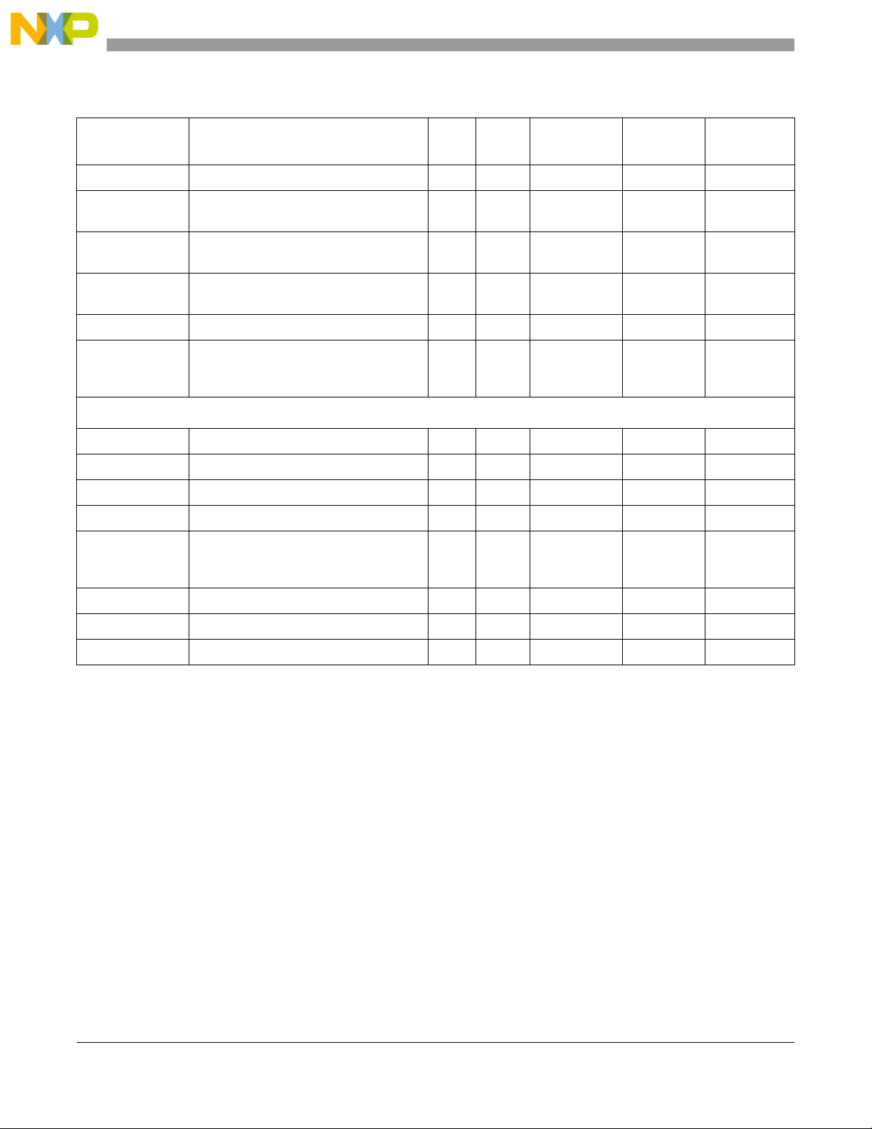
ColdFire Core
Table 3-1. ColdFire Core Programming Model (continued)
1
BDM
0x805 MAC Address Mask Register (MASK) 32 R/W 0xFFFF_FFFF No 5.2.2/5-6
0x806, 0x809,
0x80A, 0x80B
0x807 MAC Accumulator 0,1 Extension Bytes
0x808 MAC Accumulator 2,3 Extension Bytes
0x80E Condition Code Register (CCR) 8 R/W Undefined No 3.2.4/3-9
0x80F Program Counter (PC) 32 R/W Contents of
0x002 Cache Control Register (CACR) 32 R/W 0x0000_0000 Yes 3.2.6/3-10
0x003 Address Space Identifier (ASID) 8 R/W 0x00 Yes 4.2.1/4-4
0x004–7 Access Control Register 0–3 (ACR0–3) 32 R/W See Section Yes 6.3.2/6-8
0x008 MMU Base Address Register (MMUBAR) 32 R/W 0x0000_0000 Yes 4.2.2/4-4
0x800 User/Supervisor A7 Stack Pointer
MAC Accumulators 0–3 (ACC0–3) 32 R/W Undefined No 5.2.3/5-8
(ACCext01)
(ACCext23)
(OTHER_A7)
Register
Supervisor Access Only Registers
Width
(bits)
Access Reset Value
32 R/W Undefined No 5.2.4/5-8
32 R/W Undefined No 5.2.4/5-8
location
0x0000_0004
32 R/W Contents of
location
0x0000_0000
Written with
MOVEC
No 3.2.5/3-10
No 3.2.3/3-8
Section/Page
0x801 Vector Base Register (VBR) 32 R/W 0x0000_0000 Yes 3.2.8/3-10
0x80E Status Register (SR) 16 R/W 0x27-- No 3.2.9/3-11
0xC05 RAM Base Address Register (RAMBAR) 32 R/W See Section Yes 3.2.10/3-12
1
The values listed in this column represent the Rc field used when accessing the core registers via the BDM port. For more
information see Chapter 34, “Debug Module”.
3.2.1 Data Registers (D0–D7)
D0–D7 data registers are for bit (1-bit), byte (8-bit), word (16-bit) and longword (32-bit) operations; they
can also be used as index registers.
NOTE
Registers D0 and D1 contain hardware configuration details after reset. See
Section 3.3.4.15, “Reset Exception” for more details.
3-7 Freescale Semiconductor
Page 74
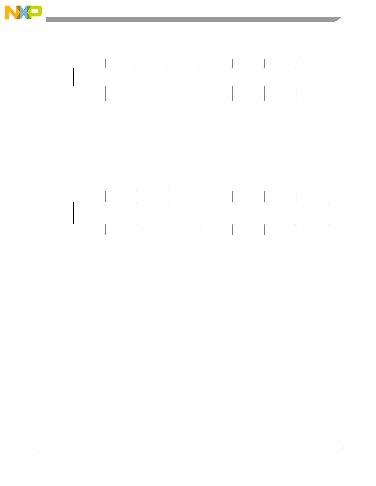
ColdFire Core
BDM: Load: 0x080 + n; n = 0-7 (Dn)
Store: 0x180 + n; n = 0-7 (Dn)
313029282726252423222120191817161514131211109876543210
R
W
Reset
(D2-D7)
(D0, D1)
––––––––––––––––––––––––––––––––
Reset
Data
See Section 3.3.4.15, “Reset Exception”
Figure 3-2. Data Registers (D0–D7)
Access: User read/write
BDM read/write
3.2.2 Address Registers (A0–A6)
These registers can be used as software stack pointers, index registers, or base address registers. They can
also be used for word and longword operations.
BDM: Load: 0x088 + n; n =0–6 (An)
Store: 0x188 + n; n =0–6 (An)
313029282726252423222120191817161514131211109876543210
R
Address
W
Access: User read/write
BDM read/write
Reset––––––––––––––––––––––––––––––––
Figure 3-3. Address Registers (A0–A6)
3.2.3 Supervisor/User Stack Pointers (A7 and OTHER_A7)
The ColdFire architecture supports two independent stack pointer (A7) registers—the supervisor stack
pointer (SSP) and the user stack pointer (USP). The hardware implementation of these two
program-visible 32-bit registers does not identify one as the SSP and the other as the USP. Instead, the
hardware uses one 32-bit register as the active A7 and the other as OTHER_A7. Thus, the register contents
are a function of the processor operation mode, as shown in the following:
if SR[S] = 1
then A7 = Supervisor Stack Pointer
OTHER_A7 = User Stack Pointer
else A7 = User Stack Pointer
OTHER_A7 = Supervisor Stack Pointer
The BDM programming model supports direct reads and writes to the (active) A7 and OTHER_A7. It is
the responsibility of the external development system to determine, based on the setting of SR[S], the
mapping of A7 and OTHER_A7 to the two program-visible definitions (SSP and USP). This functionality
is enabled by setting the enable user stack pointer bit, CACR[EUSP]. If this bit is cleared, only a single
stack pointer (A7), originally defined for ColdFire ISA_A, is available. EUSP is cleared at reset.
To support dual stack pointers, the following two supervisor instructions are included in the ColdFire
instruction set architecture to load/store the USP:
move.l Ay,USP;move to USP
Freescale Semiconductor 3-8
Page 75
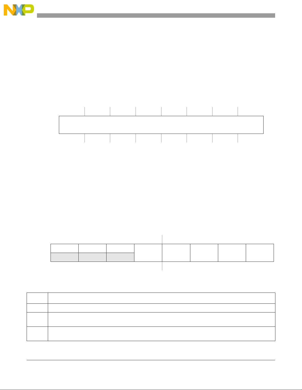
ColdFire Core
move.l USP,Ax;move from USP
These instructions are described in the ColdFire Family Programmer’s Reference Manual. All other
instruction references to the stack pointer, explicit or implicit, access the active A7 register.
NOTE
The SSP is loaded during reset exception processing with the contents of
location 0x0000_0000.
BDM: Load: 0x08F (A7)
Store: 0x18F (A7)
0x800 (OTHER_A7)
313029282726252423222120191817161514131211109876543210
R
Address
W
Reset––––––––––––––––––––––––––––––––
Access: A7: User or BDM read/write
OTHER_A7: Supervisor or BDM read/write
Figure 3-4. Stack Pointer Registers (A7 and OTHER_A7)
3.2.4 Condition Code Register (CCR)
The CCR is the LSB of the processor status register (SR). Bits 4–0 act as indicator flags for results
generated by processor operations. The extend bit (X) is also an input operand during multiprecision
arithmetic computations.
NOTE
The CCR register must be explicitly loaded after reset and before any
compare (CMP), Bcc, or Scc instructions are executed.
BDM: LSB of Status Register (SR) Access: User read/write
BDM read/write
76543210
R 0 0 0
W
Reset:0 0 0 —————
X N Z V C
Figure 3-5. Condition Code Register (CCR)
Table 3-2. CCR Field Descriptions
Field Description
7–5 Reserved, must be cleared.
4
Extend condition code bit. Set to the C-bit value for arithmetic operations; otherwise not affected or set to a specified
X
result.
3
Negative condition code bit. Set if most significant bit of the result is set; otherwise cleared.
N
3-9 Freescale Semiconductor
Page 76
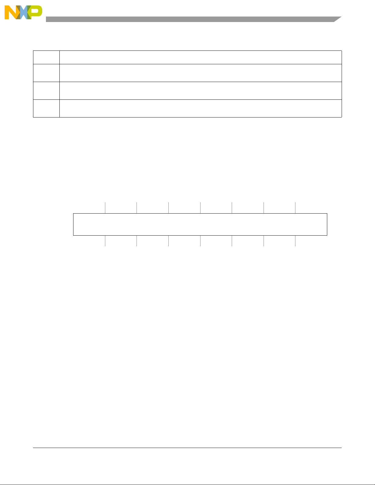
ColdFire Core
Table 3-2. CCR Field Descriptions (continued)
Field Description
2
Zero condition code bit. Set if result equals zero; otherwise cleared.
Z
1
Overflow condition code bit. Set if an arithmetic overflow occurs implying the result cannot be represented in operand
V
size; otherwise cleared.
0
Carry condition code bit. Set if a carry out of the operand msb occurs for an addition or if a borrow occurs in a
C
subtraction; otherwise cleared.
3.2.5 Program Counter (PC)
The PC contains the currently executing instruction address. During instruction execution and exception
processing, the processor automatically increments PC contents or places a new value in the PC. The PC
is a base address for PC-relative operand addressing.
The PC is initially loaded during reset exception processing with the contents at location 0x0000_0004.
BDM: 0x80F (PC) Access: User read/write
BDM read/write
313029282726252423222120191817161514131211109876543210
R
W
Reset––––––––––––––––––––––––––––––––
Figure 3-6. Program Counter Register (PC)
Address
3.2.6 Cache Programming Model
The registers in the cache portion of the programming model are described in Chapter 6, “Cache.”
3.2.7 MMU Programming Model
The registers in the MMU portion of the programming model are described in Chapter 4, “Memory
Management Unit (MMU).”
3.2.8 Vector Base Register (VBR)
The VBR contains the base address of the exception vector table in the memory. To access the vector table,
the displacement of an exception vector is added to the value in VBR. The lower 20 bits of the VBR are
not implemented by ColdFire processors. They are assumed to be zero, forcing the table to be aligned on
a 1 MB boundary.
Freescale Semiconductor 3-10
Page 77
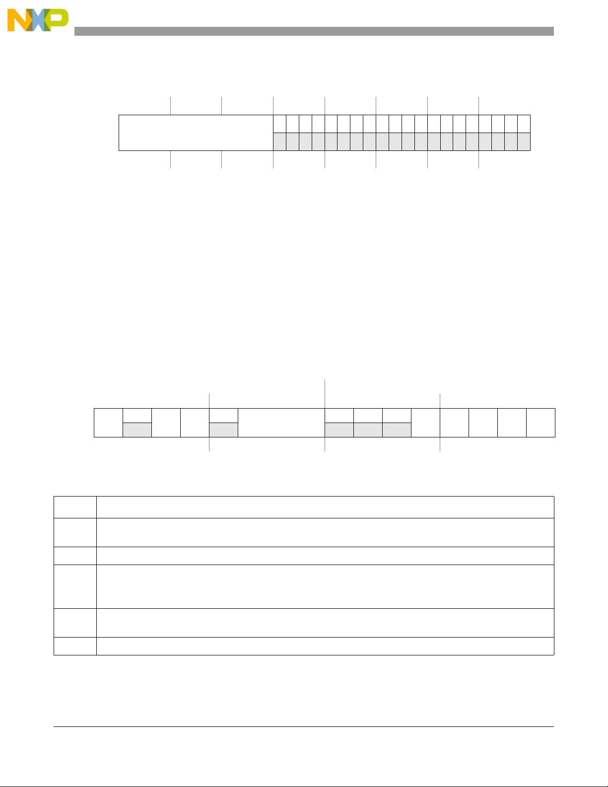
ColdFire Core
BDM: 0x801 (VBR) Access: Supervisor read/write
BDM read/write
313029282726252423222120191817161514131211109876543210
R
Base Address
W
Reset00000000000000000000000000000000
0 0 0 0 0 000000000 000 0 00
Figure 3-7. Vector Base Register (VBR)
3.2.9 Status Register (SR)
The SR stores the processor status and includes the CCR, the interrupt priority mask, and other control
bits. In supervisor mode, software can access the entire SR. In user mode, only the lower 8 bits (CCR) are
accessible. The control bits indicate the following states for the processor: trace mode (T bit), supervisor
or user mode (S bit), and master or interrupt state (M bit). All defined bits in the SR have read/write access
when in supervisor mode.
NOTE
The lower byte of the SR (the CCR) must be loaded explicitly after reset and
before any compare (CMP), Bcc, or Scc instructions execute.
BDM: 0x80E (SR) Access: Supervisor read/write
BDM read/write
System Byte Condition Code Register (CCR)
1514131211109876543210
R
W
Reset00100111000—————
0
T
S M
0
I
000
X N ZVC
Figure 3-8. Status Register (SR)
Table 3-3. SR Field Descriptions
Field Description
15TTrace enable. When set, the processor performs a trace exception after every instruction.
14 Reserved, must be cleared.
13SSupervisor/user state.
0User mode
1 Supervisor mode
12MMaster/interrupt state. Bit is cleared by an interrupt exception and software can set it during execution of the RTE or
move to SR instructions.
11 Reserved, must be cleared.
3-11 Freescale Semiconductor
Page 78

ColdFire Core
3.2.10 Memory Base Address Register (RAMBAR)
The memory base address register is used to specify the base address of the internal SRAM module and
indicates the types of references mapped to it. The base address register includes a base address,
write-protect bit, address space mask bits, and an enable bit. RAMBAR determines the base address of
the on-chip RAM. For more information, refer to Section 7.2.1, “SRAM Base Address Register
(RAMBAR)”.
Table 3-3. SR Field Descriptions (continued)
Field Description
10–8IInterrupt level mask. Defines current interrupt level. Interrupt requests are inhibited for all priority levels less than or
equal to current level, except edge-sensitive level 7 requests, which cannot be masked.
7–0
CCR
Refer to Section 3.2.4, “Condition Code Register (CCR)”.
3.3 Functional Description
3.3.1 Version 4 ColdFire Microarchitecture
As previously discussed, the unrolling of the operand execution pipeline into a five-stage structure is a key
factor in the improved performance of the Version 4 ColdFire design. The resulting pipeline structure is
termed a limited superscalar design because there are certain, heavily-used instruction constructs that
support multiple-instruction dispatch. The following figure presents the top-level spatial block diagram of
the Version 4 ColdFire operand execution pipeline, where the major hardware structures associated with
each pipeline stage are clearly visible.
Freescale Semiconductor 3-12
Page 79
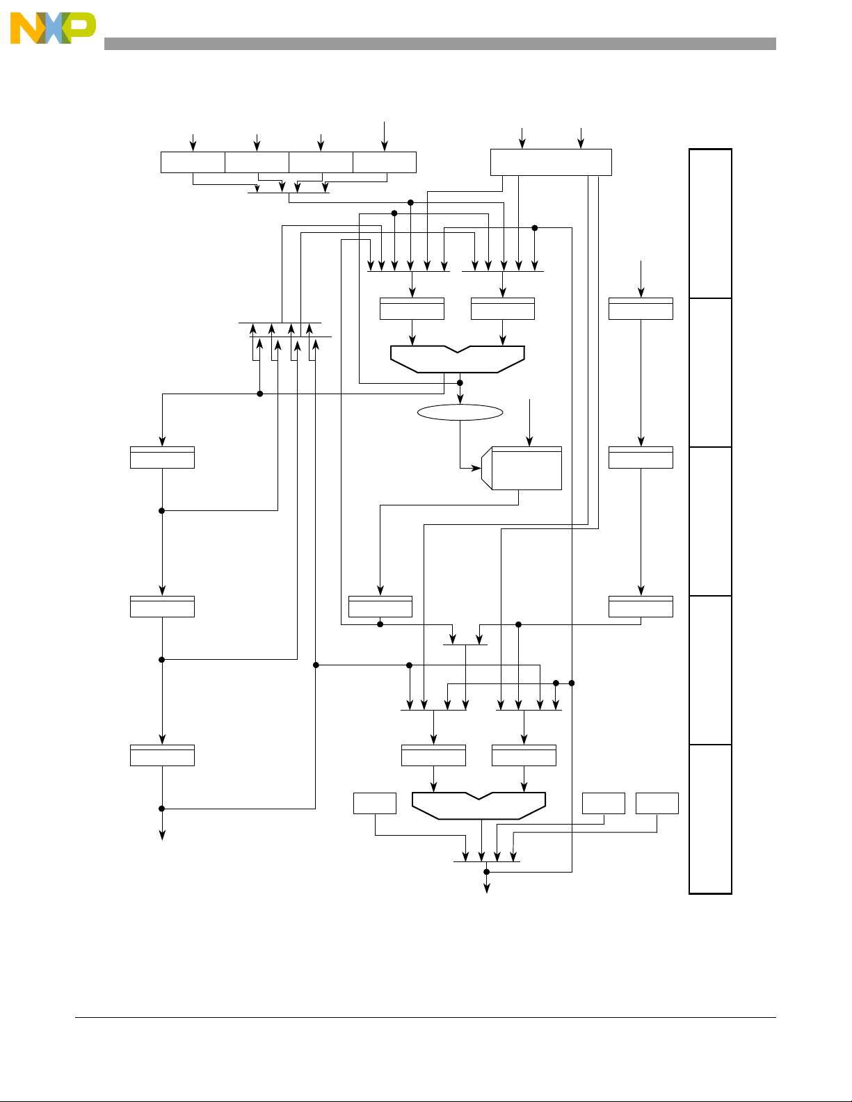
ColdFire Core
OAG
OC1
OC2
EX
DS
IndexBase
Register File
EMAC BSU DIV
Operand
Memory
Opword Extension 1
Extension 2
Extended
Opword
Figure 3-9. Version 4 ColdFire Processor Operand Execution Pipeline Diagram
3-13 Freescale Semiconductor
Page 80
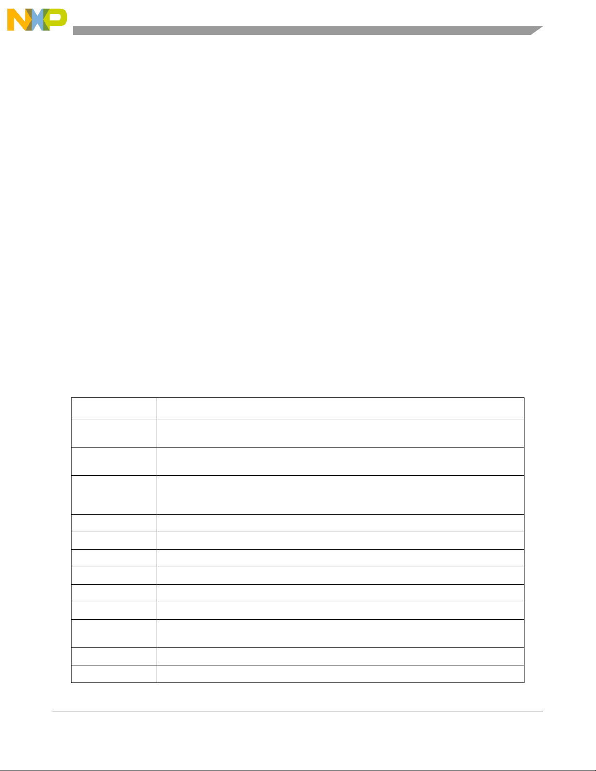
ColdFire Core
3.3.2 Instruction Set Architecture (ISA_C)
The original ColdFire instruction set architecture (ISA_A) was derived from the M68000 family opcodes
based on extensive analysis of embedded application code. The ISA was optimized for code compiled
from high-level languages where the dominant operand size was the 32-bit integer declaration. This
approach minimized processor complexity and cost, while providing excellent performance for compiled
applications.
After the initial ColdFire compilers were created, developers noted there were certain ISA additions that
would enhance code density and overall performance. Additionally, as users implemented ColdFire-based
designs into a wide range of embedded systems, they found certain frequently-used instruction sequences
that could be improved by the creation of additional instructions.
The original ISA definition minimized support for instructions referencing byte- and word-sized operands.
Full support for the move byte and move word instructions was provided, but the only other opcodes
supporting these data types are CLR (clear) and TST (test). A set of instruction enhancements has been
implemented in subsequent ISA revisions, ISA_B and ISA_C. The added opcodes primarily addressed
three areas:
1. Enhanced support for byte and word-sized operands
2. Enhanced support for position-independent code
3. Miscellaneous instruction additions to address new functionality
Table 3-4 summarizes the instructions added to revision ISA_A to form revision ISA_C. For more details
see the ColdFire Family Programmer’s Reference Manual.
Table 3-4. Instruction Enhancements over Revision ISA_A
Instruction Description
BITREV The contents of the destination data register are bit-reversed; that is, new Dn[31] equals old
Dn[0], new Dn[30] equals old Dn[1], ..., new Dn[0] equals old Dn[31].
BYTEREV The contents of the destination data register are byte-reversed; that is, new Dn[31:24] equals
old Dn[7:0], ..., new Dn[7:0] equals old Dn[31:24].
FF1 The data register, Dn, is scanned, beginning from the most-significant bit (Dn[31]) and ending
with the least-significant bit (Dn[0]), searching for the first set bit. The data register is then
loaded with the offset count from bit 31 where the first set bit appears.
INTOUCH Loads blocks of instructions to be locked in the instruction cache.
MOV3Q.L Moves 3-bit immediate data to the destination location.
Move from USP User Stack Pointer Destination register
Move to USP Source register User Stack Pointer
MVS.{B,W} Sign-extends source operand and moves it to destination register.
MVZ.{B,W} Zero-fills source operand and moves it to destination register.
SATS.L Performs saturation operation for signed arithmetic and updates destination register,
depending on CCR[V] and bit 31 of the register.
TAS.B Performs indivisible read-modify-write cycle to test and set addressed memory byte.
Bcc.L Branch conditionally, longword
Freescale Semiconductor 3-14
Page 81
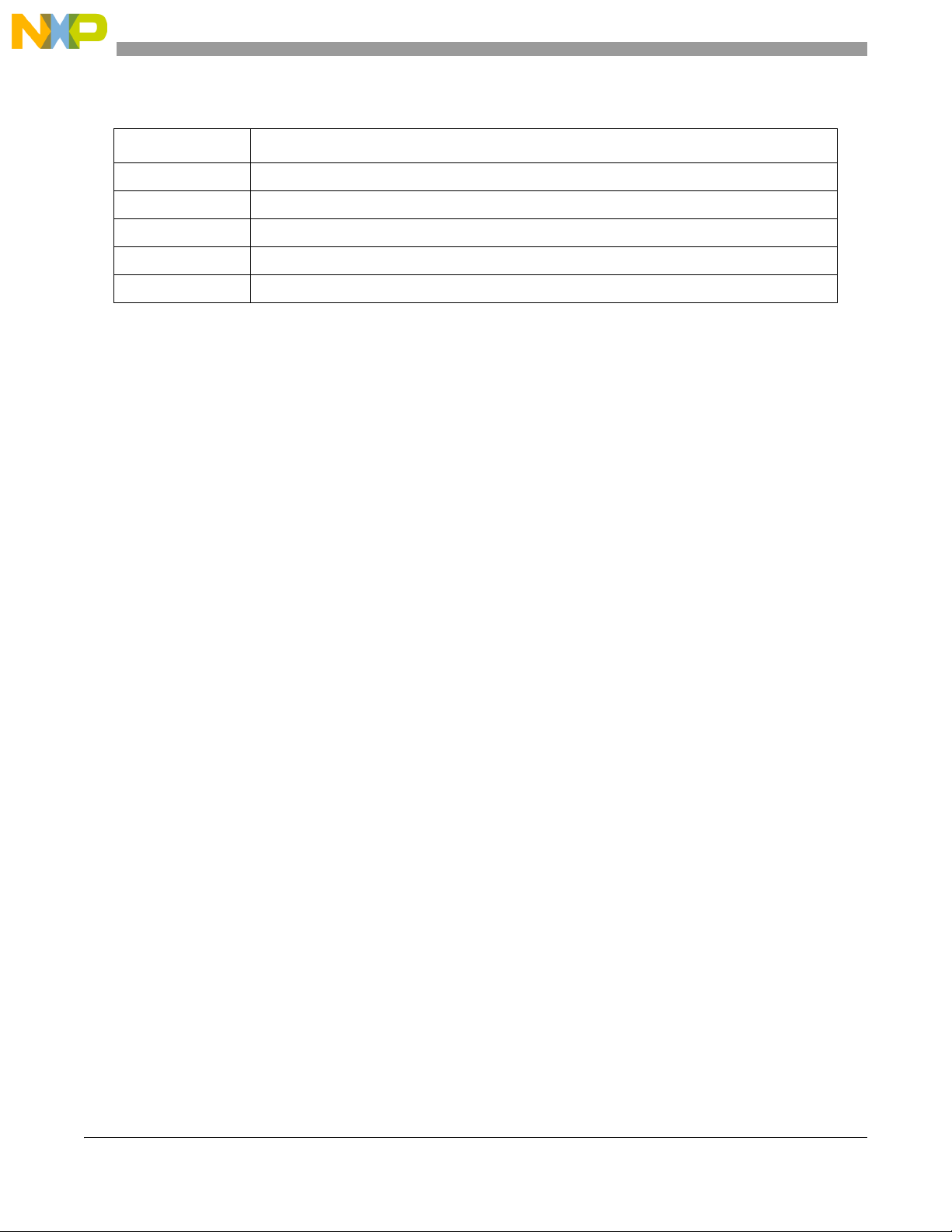
ColdFire Core
2. The processor determines the exception vector number. For all faults except interrupts, the
processor performs this calculation based on exception type. For interrupts, the processor
performs an interrupt-acknowledge (IACK) bus cycle to obtain the vector number from the
interrupt controller. The IACK cycle is mapped to special locations within the interrupt
controller’s address space with the interrupt level encoded in the address.
Table 3-4. Instruction Enhancements over Revision ISA_A (continued)
Instruction Description
BSR.L Branch to sub-routine, longword
CMP.{B,W} Compare, byte and word
CMPA.W Compare address, word
CMPI.{B,W} Compare immediate, byte and word
MOVEI Move immediate, byte and word to memory using Ax with displacement
3.3.3 Exception Processing Overview
Exception processing for ColdFire processors is streamlined for performance. The ColdFire processors
differ from the M68000 family because they include:
• A simplified exception vector table
• Reduced relocation capabilities using the vector-base register
• A single exception stack frame format
• A precise instruction restart model for translation (TLB miss) and access faults. This functionality
extends the existing ColdFire access error fault vector in the exception stack frames.
All ColdFire processors use an instruction restart exception model. Exception processing includes all
actions from fault condition detection to the initiation of fetch for first handler instruction. Exception
processing is comprised of four major steps:
1. The processor makes an internal copy of the SR and then enters supervisor mode by setting the S
bit and disabling trace mode by clearing the T bit. The interrupt exception also forces the M bit to
be cleared and the interrupt priority mask to set to current interrupt request level.
3. The processor saves the current context by creating an exception stack frame on the system stack.
The exception stack frame is created at a 0-modulo-4 address on top of the system stack pointed to
by the supervisor stack pointer (SSP). As shown in Figure 3-10, the processor uses a simplified
fixed-length stack frame for all exceptions with additional fault status (FS) encodings to support
the MMU. The exception type determines whether the program counter placed in the exception
stack frame defines the location of the faulting instruction (fault) or the address of the next
instruction to be executed (next).
4. The processor calculates the address of the first instruction of the exception handler. By definition,
the exception vector table is aligned on a 1 MB boundary. This instruction address is generated by
fetching an exception vector from the table located at the address defined in the vector base register.
3-15 Freescale Semiconductor
Page 82

ColdFire Core
All ColdFire processors support a 1024-byte vector table aligned on any 1 Mbyte address boundary (see
Table 3-5).
The index into the exception table is calculated as (4 vector number). After the exception vector
has been fetched, the vector contents determine the address of the first instruction of the desired
handler. After the instruction fetch for the first opcode of the handler has initiated, exception
processing terminates and normal instruction processing continues in the handler.
The table contains 256 exception vectors; the first 64 are defined for the core and the remaining 192 are
device-specific peripheral interrupt vectors. See Chapter 17, “Interrupt Controller Modules” for details on
the device-specific interrupt sources.
Table 3-5. Exception Vector Assignments
Vector
Number(s)
0 0x000 — Initial supervisor stack pointer
1 0x004 — Initial program counter
2 0x008 Fault Access error
3 0x00C Fault Address error
4 0x010 Fault Illegal instruction
5 0x014 Fault Divide by zero
6–7 0x018–0x01C — Reserved
8 0x020 Fault Privilege violation
9 0x024 Next Trace
10 0x028 Fault Unimplemented line-A opcode
11 0x02C Fault Unimplemented line-F opcode
12 0x030 Next Non-PC breakpoint debug interrupt
13 0x034 Next PC breakpoint debug interrupt
14 0x038 Fault Format error
15 0x03C Next Uninitialized interrupt
16–23 0x040–0x05C — Reserved
Vector
Offset (Hex)
Stacked
Program
Counter
Assignment
24 0x060 Next Spurious interrupt
25–31 0x064–0x07C Next Level 1–7 autovectored interrupts
32–47 0x080–0x0BC Next Trap # 0-15 instructions
48–60 0x0C0–0x0F0 — Reserved
61 0x0F4 Fault Unsupported instruction
62–63 0x0F8–0x0FC — Reserved
64–255 0x100–0x3FC Next Device-specific interrupts
1
Fault refers to the PC of the instruction that caused the exception. Next refers to the PC
of the instruction that follows the instruction that caused the fault.
Freescale Semiconductor 3-16
Page 83
ColdFire Core
All ColdFire processors inhibit interrupt sampling during the first instruction of all exception handlers.
This allows any handler to disable interrupts effectively, if necessary, by raising the interrupt mask level
contained in the status register. For more details, see ColdFire Family Programmer’s Reference Manual.
3.3.3.1 Exception Stack Frame Definition
Figure 3-10 shows exception stack frame. The first longword contains the 16-bit format/vector word (F/V)
and the 16-bit status register, and the second longword contains the 32-bit program counter address.
313029282726252423222120191817161514131211109876543210
SSP Format FS[3:2] Vector FS[1:0] Status Register
+ 0x4
Figure 3-10. Exception Stack Frame Form
The 16-bit format/vector word contains three unique fields:
• A 4-bit format field at the top of the system stack is always written with a value of 4, 5, 6, or 7 by
the processor, indicating a two-longword frame format. See Table 3-6.
Table 3-6. Format Field Encodings
Program Counter
Original SSP @ Time
of Exception, Bits 1:0
00 Original SSP - 8 0100
01 Original SSP - 9 0101
10 Original SSP - 10 0110
11 Original SSP - 11 0111
SSP @ 1st
Instruction of
Handler
Format Field
• There is a 4-bit fault status field, FS[3:0], at the top of the system stack. This field is defined for
access and address errors only and written as zeros for all other exceptions. See Tabl e 3-7.
Table 3-7. Fault Status Encodings
FS[3:0] Definition
0000 Not an access or address error nor an interrupted debug service routine
0001 Reserved
0010 Interrupt during a debug service routine for faults other than access errors
0011 Reserved
0100 Error on instruction fetch
0101 TLB miss on opword of instruction fetch
1
0110 TLB miss on extension word of instruction fetch
0111 IFP access error while executing in emulator mode
1000 Error on operand write
1001 Attempted write to write-protected space
3-17 Freescale Semiconductor
Page 84
Table 3-7. Fault Status Encodings (continued)
FS[3:0] Definition
1010 TLB miss on data write
1011 Reserved
1100 Error on operand read
1101 Attempted read, read-modify-write of protected space
1110 TLB miss on data read, or read-modify-write
ColdFire Core
1111
1
This refers to taking an I/O interrupt during a debug service routine. If an access error occurs
during a debug service routine, FS is set to 0111 if it is due to an instruction fetch or to 1111
for a data access.
OEP access error while executing in emulator mode
• The 8-bit vector number, vector[7:0], defines the exception type and is calculated by the processor
for all internal faults and represents the value supplied by the interrupt controller in case of an
interrupt. See Table 3 -5.
3.3.4 Processor Exceptions
3.3.4.1 Access Error Exception
The exact processor response to an access error depends on the memory reference being performed. For
an instruction fetch, the processor postpones the error reporting until the faulted reference is needed by an
instruction for execution. Therefore, faults during instruction prefetches followed by a change of
instruction flow do not generate an exception. When the processor attempts to execute an instruction with
a faulted opword and/or extension words, the access error is signaled and the instruction is aborted. For
this type of exception, the programming model has not been altered by the instruction generating the access
error.
If the access error occurs on an operand read, the processor immediately aborts the current instruction’s
execution and initiates exception processing. The operand execution pipeline includes logic to fully
recover program-visible register updates in the event of a bus transfer error acknowledge on an operand
memory reference. This allows for a precise instruction restart from this class of exceptions. See
Section 3.3.4.16, “Precise Faults”, for additional information.
If the MMU is disabled, access errors are reported only with an attempted store to write-protected memory.
Therefore, access errors associated with instruction fetch or operand read accesses are not possible. The
Version 4 ColdFire processor, unlike the Version 2 and 3 ColdFire processors, updates the condition code
register if a write-protect error occurs during a CLR or MOV3Q operation to memory.
Internal memory accesses that fault (terminate with an internal memory transfer error acknowledge)
generate an access error exception. MMU TLB misses and access violations use the same fault. If the
MMU is enabled, all TLB misses and protection violations generate an access error exception. To
determine if a fault is due to a TLB miss or another type of access error, new FS encodings (described in
Table 3-7) signal TLB misses on instruction fetch, instruction extension fetch, and data read and writes.
Freescale Semiconductor 3-18
Page 85
ColdFire Core
3.3.4.2 Address Error Exception
Any attempted execution transferring control to an odd instruction address (if bit 0 of the target address is
set) results in an address error exception.
Any attempted use of a word-sized index register (Xn.w) or a scale factor of eight on an indexed effective
addressing mode generates an address error, as does an attempted execution of a full-format indexed
addressing mode, which is defined by bit 8 of extension word 1 being set.
If an address error occurs on a JSR instruction, the Version 4 ColdFire processor first pushes the return
address onto the stack and then calculates the target address. If an address error occurs on an RTS
instruction, the Version 4 ColdFire processor preserves the original return PC and writes the exception
stack frame above this value.
3.3.4.3 Illegal Instruction Exception
The ColdFire variable-length instruction set architecture supports three instruction sizes: 16, 32, or 48 bits.
The first instruction word is known as the operation word (or opword), while the optional words are known
as extension word 1 and extension word 2. The opword is further subdivided into three sections: the upper
four bits segment the entire ISA into 16 instruction lines, the next 6 bits define the operation mode
(opmode), and the low-order 6 bits define the effective address. See Figure 3-11. The opword line
definition is shown in Table 3-8.
1514131211109876543210
Line OpMode Effective Address
Mode Register
Figure 3-11. ColdFire Instruction Operation Word (Opword) Format
Table 3-8. ColdFire Opword Line Definition
Opword[Line] Instruction Class
0x0 Bit manipulation, Arithmetic and Logical Immediate
0x1 Move Byte
0x2 Move Long
0x3 Move Word
0x4 Miscellaneous
0x5 Add (ADDQ) and Subtract Quick (SUBQ), Set according to Condition Codes (Scc)
0x6 PC-relative change-of-flow instructions
Conditional (Bcc) and unconditional (BRA) branches, subroutine calls (BSR)
0x7 Move Quick (MOVEQ), Move with sign extension (MVS) and zero fill (MVZ)
0x8 Logical OR (OR)
0x9 Subtract (SUB), Subtract Extended (SUBX)
0xA EMAC, Move 3-bit Quick (MOV3Q)
0xB Compare (CMP), Exclusive-OR (EOR)
3-19 Freescale Semiconductor
Page 86

ColdFire Core
Table 3-8. ColdFire Opword Line Definition (continued)
Opword[Line] Instruction Class
0xC Logical AND (AND), Multiply Word (MUL)
0xD Add (ADD), Add Extended (ADDX)
0xE Arithmetic and logical shifts (ASL, ASR, LSL, LSR)
0xF Cache Push (CPUSHL), Write DDATA (WDDATA), Write Debug (WDEBUG)
In the original M68000 ISA definition, lines A and F were effectively reserved for user-defined operations
(line A) and co-processor instructions (line F). Accordingly, there are two unique exception vectors
associated with illegal opwords in these two lines.
Any attempted execution of an illegal 16-bit opcode (except for line-A and line-F opcodes) generates an
illegal instruction exception (vector 4). Additionally, any attempted execution of any non-MAC line-A and
most line-F opcodes generate their unique exception types, vector numbers 10 and 11, respectively.
ColdFire cores do not provide illegal instruction detection on the extension words on any instruction,
including MOVEC.
3.3.4.4 Divide-By-Zero
Attempting to divide by zero causes an exception (vector 5, offset equal 0x014).
3.3.4.5 Privilege Violation
The attempted execution of a supervisor mode instruction while in user mode generates a privilege
violation exception. See ColdFire Programmer’s Reference Manual for a list of supervisor-mode
instructions.
There is one special case involving the HALT instruction. Normally, this opcode is a supervisor mode
instruction, but if the debug module's CSR[UHE] is set, then this instruction can be also be executed in
user mode for debugging purposes.
3.3.4.6 Trace Exception
To aid in program development, all ColdFire processors provide an instruction-by-instruction tracing
capability. While in trace mode, indicated by setting of the SR[T] bit, the completion of an instruction
execution (for all but the stop instruction) signals a trace exception. This functionality allows a debugger
to monitor program execution.
The stop instruction has the following effects:
1. The instruction before the stop executes and then generates a trace exception. In the exception stack
frame, the PC points to the stop opcode.
2. When the trace handler is exited, the stop instruction executes, loading the SR with the immediate
operand from the instruction.
3. The processor then generates a trace exception. The PC in the exception stack frame points to the
instruction after the stop, and the SR reflects the value loaded in the previous step.
Freescale Semiconductor 3-20
Page 87

ColdFire Core
If the processor is not in trace mode and executes a stop instruction where the immediate operand sets
SR[T], hardware loads the SR and generates a trace exception. The PC in the exception stack frame points
to the instruction after the stop, and the SR reflects the value loaded in step 2.
Because ColdFire processors do not support any hardware stacking of multiple exceptions, it is the
responsibility of the operating system to check for trace mode after processing other exception types. As
an example, consider a TRAP instruction execution while in trace mode. The processor initiates the trap
exception and then passes control to the corresponding handler. If the system requires that a trace exception
be processed, it is the responsibility of the trap exception handler to check for this condition (SR[T] in the
exception stack frame set) and pass control to the trace handler before returning from the original
exception.
3.3.4.7 Unimplemented Line-A Opcode
A line-A opcode is defined when bits 15-12 of the opword are 0b1010. This exception is generated by the
attempted execution of an undefined line-A opcode.
3.3.4.8 Unimplemented Line-F Opcode
A line-F opcode is defined when bits 15-12 of the opword are 0b1111. This exception is generated when
attempting to execute an undefined line-F opcode.
3.3.4.9 Debug Interrupts
See Chapter 34, “Debug Module,” for a detailed explanation of these exceptions, which are generated in
response to hardware breakpoint register triggers. The processor does not generate an IACK cycle, but
rather calculates the vector number internally (vector number 12 or 13, depending on the type of
breakpoint trigger). Additionally, SR[M,I] are unaffected by the interrupt.
Separate exception vectors are provided for PC breakpoints and for address/data breakpoints. In the case
of a two-level trigger, the last breakpoint determines the vector. There are two unique vectors for these
exceptions: vector 0x030 corresponds to non-PC breakpoints and vector 0x034 corresponds to PC
breakpoints.
3.3.4.10 RTE and Format Error Exception
When an RTE instruction is executed, the processor first examines the 4-bit format field to validate the
frame type. For a ColdFire core, any attempted RTE execution (where the format is not equal to {4,5,6,7})
generates a format error. The exception stack frame for the format error is created without disturbing the
original RTE frame and the stacked PC pointing to the RTE instruction.
The selection of the format value provides some limited debug support for porting code from M68000
applications. On M68000 family processors, the SR was located at the top of the stack. On those
processors, bit 30 of the longword addressed by the system stack pointer is typically zero. Thus, if an RTE
is attempted using this old format, it generates a format error on a ColdFire processor.
If the format field defines a valid type, the processor: (1) reloads the SR operand, (2) fetches the second
longword operand, (3) adjusts the stack pointer by adding the format value to the auto-incremented address
3-21 Freescale Semiconductor
Page 88

ColdFire Core
after the fetch of the first longword, and then (4) transfers control to the instruction address defined by the
second longword operand within the stack frame.
3.3.4.11 TRAP Instruction Exception
The TRAP #n instruction always forces an exception as part of its execution and is useful for implementing
system calls. The TRAP instruction may be used to change from user to supervisor mode.
3.3.4.12 Unsupported Instruction Exception
If execution of a valid instruction is attempted but the required hardware is not present in the processor, an
unsupported instruction exception is generated. The instruction functionality can then be emulated in the
exception handler, if desired.
All ColdFire cores record the processor hardware configuration in the D0 register immediately after the
negation of RESET. See Section 3.3.4.15, “Reset Exception,” for details.
3.3.4.13 Interrupt Exception
Interrupt exception processing includes interrupt recognition and the fetch of the appropriate vector from
the interrupt controller using an IACK cycle. See Chapter 17, “Interrupt Controller Modules,” for details
on the interrupt controller.
3.3.4.14 Fault-on-Fault Halt
If a ColdFire processor encounters any type of fault during the exception processing of another fault, the
processor immediately halts execution with the catastrophic fault-on-fault condition. A reset is required to
to exit this state.
3.3.4.15 Reset Exception
Asserting the reset input signal (RESET) to the processor causes a reset exception. The reset exception has
the highest priority of any exception; it provides for system initialization and recovery from catastrophic
failure. Reset also aborts any processing in progress when the reset input is recognized. Processing cannot
be recovered.
The reset exception places the processor in the supervisor mode by setting the SR[S] bit and disables
tracing by clearing the SR[T] bit. This exception also clears the SR[M] bit and sets the processor’s SR[I]
field to the highest level (level 7, 0b111). Next, the VBR is initialized to zero (0x0000_0000). The control
registers specifying the operation of any memories (e.g., cache and/or RAM modules) connected directly
to the processor are disabled.
NOTE
Other implementation-specific registers are also affected. Refer to each
module in this reference manual for details on these registers.
After the processor is granted the bus, it performs two longword read-bus cycles. The first longword at
address 0x0000_0000 is loaded into the supervisor stack pointer and the second longword at address
Freescale Semiconductor 3-22
Page 89
ColdFire Core
(This is the value used for this device.)
0x0000_0004 is loaded into the program counter. After the initial instruction is fetched from memory,
program execution begins at the address in the PC. If an access error or address error occurs before the first
instruction is executed, the processor enters the fault-on-fault state.
ColdFire processors load hardware configuration information into the D0 and D1 general-purpose
registers after system reset. The hardware configuration information is loaded immediately after the
reset-in signal is negated. This allows an emulator to read out the contents of these registers via the BDM
to determine the hardware configuration.
Information loaded into D0 defines the processor hardware configuration as shown in Figure 3-12.
BDM: Load: 0x080 (D0)
Store: 0x180 (D0)
31 30 29 28 27 26 25 24 23 22 21 20 19 18 17 16
R PF VER REV
W
Reset1100111101000010
15 14 13 12 11 10 9 8 7 6 5 4 3 2 1 0
R MAC DIVEMACFPU0000 ISA DEBUG
W
Reset0110000000101011
Access: User read-only
BDM read-only
Figure 3-12. D0 Hardware Configuration Info
Table 3-9. D0 Hardware Configuration Info Field Description
Field Description
31–24PFProcessor family. This field is fixed to a hex value of 0xCF indicating a ColdFire core is present.
23–20
VER
ColdFire core version number. Defines the hardware microarchitecture version of ColdFire core.
0001 V1 ColdFire core
0010 V2 ColdFire core
0011 V3 ColdFire core
0100 V4 ColdFire core (This is the value used for this device.)
0101 V5 ColdFire core
Else Reserved for future use
19–16
REV
MAC
EMAC
3-23 Freescale Semiconductor
Processor revision number. The default is 0b0010.
15
MAC present. This bit signals if the optional multiply-accumulate (MAC) execution engine is present in processor core.
0 MAC execute engine not present in core. (This is the value used for this device.)
1 MAC execute engine is present in core.
14
Divide present. This bit signals if the hardware divider (DIV) is present in the processor core.
DIV
0 Divide execute engine not present in core.
1 Divide execute engine is present in core.
13
EMAC present. This bit signals if the optional enhanced multiply-accumulate (EMAC) execution engine is present in
processor core.
0 EMAC execute engine not present in core.
1 EMAC execute engine is present in core. (This is the value used for this device.)
Page 90
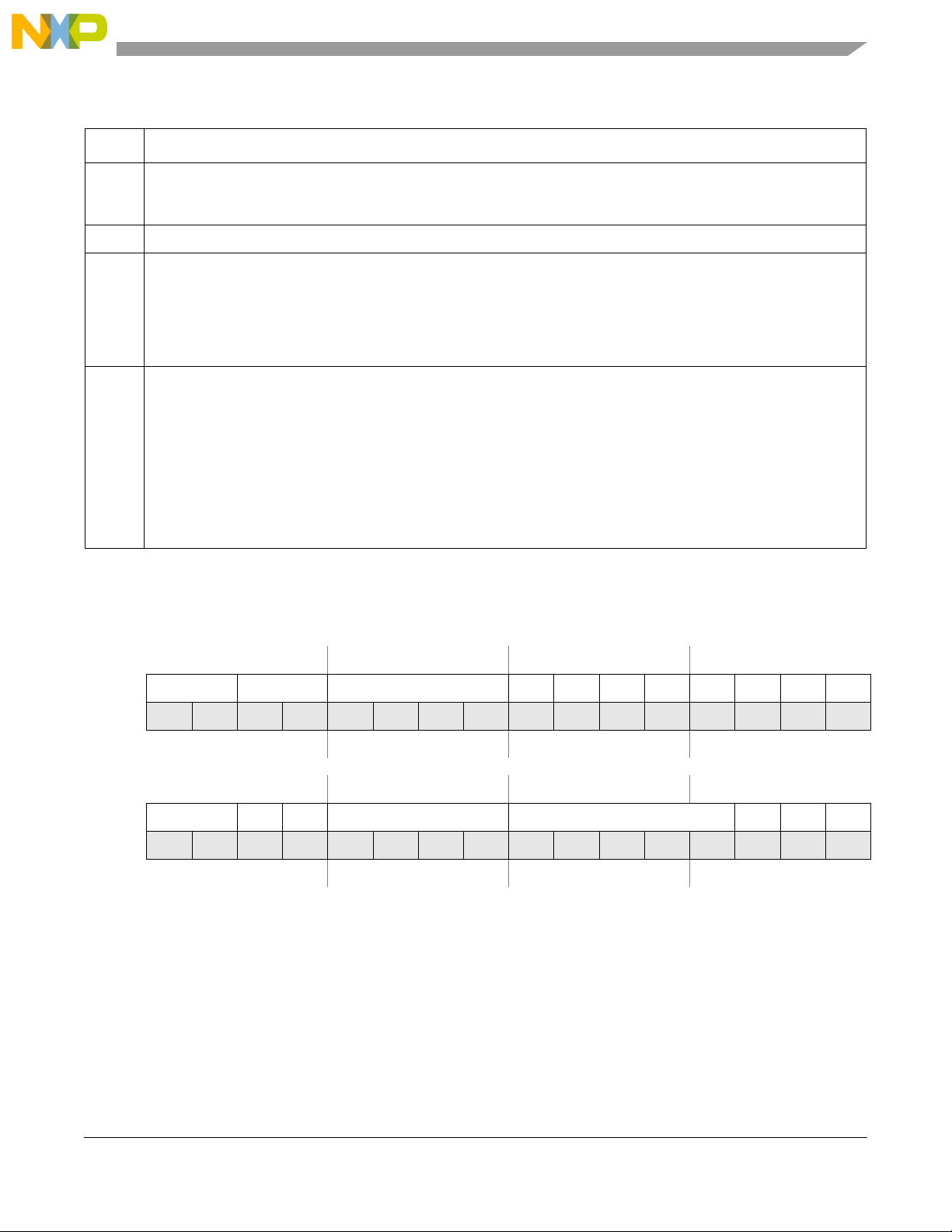
Table 3-9. D0 Hardware Configuration Info Field Description (continued)
Field Description
12
FPU present. This bit signals if the optional floating-point (FPU) execution engine is present in processor core.
FPU
11–8 Reserved.
DEBUG
0 FPU execute engine not present in core. (This is the value used for this device.)
1 FPU execute engine is present in core.
7–4
ISA revision. Defines the instruction-set architecture (ISA) revision level implemented in ColdFire processor core.
ISA
0000 ISA_A
0001 ISA_B
0010 ISA_C (This is the value used for this device.)
1000 ISA_A+
Else Reserved
3–0
Debug module revision number. Defines revision level of the debug module used in the ColdFire processor core.
0000 DEBUG_A
0001 DEBUG_B
0010 DEBUG_C
0011 DEBUG_D
0100 DEBUG_E
1001 DEBUG_B+
1011 DEBUG_D+ (This is the value used for this device.)
1111 DEBUG_D+PST Buffer
Else Reserved
ColdFire Core
Information loaded into D1 defines the local memory hardware configuration as shown in the figure below.
BDM: Load: 0x081 (D1)
Store: 0x181 (D1)
31 30 29 28 27 26 25 24 23 22 21 20 19 18 17 16
RCLSZ ICAS ICSZ 00000000
W
Reset0000011000000000
1514131211109876543210
R MBSZ CPES DCAS DCSZ SRAMSZ 0 0 0
W
Reset0010011001110000
Figure 3-13. D1 Hardware Configuration Info
Access: User read-only
BDM read-only
Freescale Semiconductor 3-24
Page 91

ColdFire Core
Table 3-10. D1 Hardware Configuration Information Field Description
Field Description
31–30
Cache line size. This field is fixed to a hex value of 0x0 indicating a 16-byte cache line size.
CLSZ
29–28
ICAS
Instruction cache associativity.
00 Four-way (This is the value used for this device)
01 Direct mapped
Else Reserved for future use
27–24
ICSZ
Instruction cache size. Indicates the amount of instruction cache.
0000 No instruction cache
0001 512 B instruction cache
0010 1 KB instruction cache
0011 2 KB instruction cache
0100 4 KB instruction cache
0101 8 KB instruction cache
0110 16 KB instruction cache (This is the value used for this device)
0111 32 KB instruction cache
1000 64 KB instruction cache
Else Reserved
23–16 Reserved.
15–14
MBSZ
Bus size. Defines the width of the ColdFire master bus datapath.
00 32-bit system bus datapath (This is the value used for this device)
01 64-bit system bus datapath
Else Reserved
13
CPES
CPUSHL enhancements supported. Specifies whether the enhancements to the CPUSHL instructions are
supported by the processor core. See Section 6.4.8, “CPUSHL Enhancements,” for details.
0 CPUSHL instruction enhancements are not supported
1 CPUSHL instruction enhancements are supported (This is the value used for this device)
12
DCAS
11–8
DCSZ
Data cache associativity. Defines the data cache set-associativity.
0 Four-way (This is the value used for this device)
1 Direct mapped
Data cache size. Indicates the size of the unified cache.
0000 No data cache
0001 512 bytes
0010 1 KB
0011 2 KB
0100 4 KB
0101 8 KB
0110 16 KB (This is the value used for this device)
0111 32 KB
Else Reserved for future use
3-25 Freescale Semiconductor
Page 92

Table 3-10. D1 Hardware Configuration Information Field Description (continued)
Field Description
ColdFire Core
7–3
SRAMSZ
2–0 Reserved.
SRAM bank size.
00000 No SRAM
00010 512 bytes
00100 1 KB
00110 2 KB
01000 4 KB
01010 8 KB
01100 16 KB
01111 24 KB
01110 32 KB (This is the value used for this device)
10000 64 KB
10010 128 KB
Else Reserved for future use
3.3.4.16 Precise Faults
To support a demand-paged virtual-memory environment, all memory references require precise,
recoverable faults. The ColdFire instruction restart mechanism ensures that a faulted instruction restarts
from the execution beginning. No internal state information is saved when an exception occurs nor is any
restored when the handler ends. Given the PC address defined in the exception stack frame, the processor
re-establishes program execution by transferring control to the given location as part of the RTE (return
from exception) instruction.
The instruction restart recovery model requires program-visible register changes made during execution
to be undone if that instruction subsequently faults.
The Version 4 (and later) ColdFire OEP structure naturally supports this concept for most instructions;
program-visible registers are updated only in the final OEP stage when fault collection is complete. If any
exception occurs, pending register updates are discarded.
For V4 ColdFire cores and later, most single-cycle instructions naturally support precise faults and
instruction restart, while complex instruction do not. Consider the following memory-to-memory move:
move.l (Ay)+,(Ax)+ # copy 4 bytes from source to destination
This instruction takes one cycle to read the source operand (Ay) and one to write the data into Ax. Source
and destination address pointers are updated as part of execution. Table 3-11 lists the operations performed
in execute stage (EX).
Freescale Semiconductor 3-26
Page 93

ColdFire Core
Table 3-11. OEP EX Cycle Operations
EX Cycle Operations
1 Read source operand from memory @ (Ay), update Ay, new Ay = old Ay + 4
2 Write operand into destination memory @ (Ax), update Ax, new Ax = old Ax + 4, update CCR
A fault detected with the destination memory write is reported during the second cycle. At this point,
operations performed in the first cycle are complete, so if the destination write takes any type of access
error, Ay is updated. After the access error handler executes and the faulting instruction restarts, the
processor’s operation would be incorrect (without the special register recovery hardware) because the
source-address register has an incorrect (post-incremented) value.
To recover the original state of the programming model for all instructions, the Version 4 ColdFire core
adds the needed hardware to support full-register recovery. This hardware allows program-visible registers
to be restored to their original state for multi-cycle instructions so that the instruction restart mechanism
is supported. Memory-to-memory moves and move-multiple loads are representative of the complex
instructions needing the special recovery support.
Recall the IFP and OEP are decoupled by a FIFO instruction buffer. In the V4 ColdFire IFP, each buffer
entry includes 48 bits of instruction data fetched from memory and 64 bits of early decode and branch
prediction information. This datapath also includes IFP fault-status information. Therefore, every IFP
access can be tagged if an instruction fetch terminates with an error acknowledge. IFP access errors are
recognized after the buffered instruction enters the OEP.
NOTE
For access errors signaled on instruction prefetches, an access error
exception is generated only if instruction execution is attempted. If an
instruction fetch access error exception is generated and the FS field
indicates the fault occurred on an extension word, it may be necessary for
the exception PC to be rounded-up to the next page address to determine the
faulting instruction fetch address.
3.3.5 Instruction Execution Timing
This section presents processor instruction execution times in terms of processor-core clock cycles. The
number of operand references for each instruction is enclosed in parentheses following the number of
processor clock cycles. Each timing entry is presented as C(R/W) where:
•C is the number of processor clock cycles, including all applicable operand fetches and writes, and
all internal core cycles required to complete the instruction execution.
• R/W is the number of operand reads (R) and writes (W) required by the instruction. An operation
performing a read-modify-write function is denoted as (1/1).
This section includes the assumptions concerning the timing values and the execution time details.
3-27 Freescale Semiconductor
Page 94

ColdFire Core
3.3.5.1 Timing Assumptions
For the timing data presented in this section, these assumptions apply:
1. The OEP is loaded with the opword and all required extension words at the beginning of each
instruction execution. This implies that the OEP does not wait for the IFP to supply opwords and/or
extension words.
2. Execution times for individual instructions make no assumptions concerning the OEP’s ability to
dispatch multiple instructions in one machine cycle. For sequences where instruction pairs are
issued, the execution time of the first instruction defines the execution time of pair; the second
instruction effectively executes in zero cycles.
3. The OEP does not experience any sequence-related pipeline stalls. The most common example of
stall occurs when a register is modified in the EX engine and a subsequent instruction generates an
address that uses the previously modified register. The second instruction stalls in the OEP until
the previous instruction updates the register. For example, in the following code:
muls.l #<data>,d0
move.l (a0,d0.l*4),d1
the move.l instruction waits three cycles for the muls.l to update D0. If consecutive instructions
update a register and use that register as a base of index value with a scale factor of 1 (Xi.l*1) in
an address calculation, a 2-cycle pipeline stall occurs. If the destination register is used as an index
register with any other scale factor (Xi.l*2, Xi.l*4), a 3-cycle stall occurs.
NOTE
Address register results from post-increment and pre-decrement modes are
available to subsequent instructions without stalls.
4. The OEP completes all memory accesses without any stall conditions caused by the memory itself.
Thus, the timing details provided in this section assume that an infinite zero-wait state memory is
attached to the processor core.
5. All operand data accesses are aligned on the same byte boundary as the operand size; for example,
16-bit operands aligned on 0-modulo-2 addresses, 32-bit operands aligned on 0-modulo-4
addresses.
The processor core decomposes misaligned operand references into a series of aligned accesses as
shown in Table 3-12.
Table 3-12. Misaligned Operand References
address[1:0] Size
01 or 11 Word Byte, Byte 2(1/0) if read
01 or 11 Long Byte, Word,
10 Long Word, Word 2(1/0) if read
Bus
Operations
Byte
Additional
C(R/W)
1(0/1) if write
3(2/0) if read
2(0/2) if write
1(0/1) if write
Freescale Semiconductor 3-28
Page 95
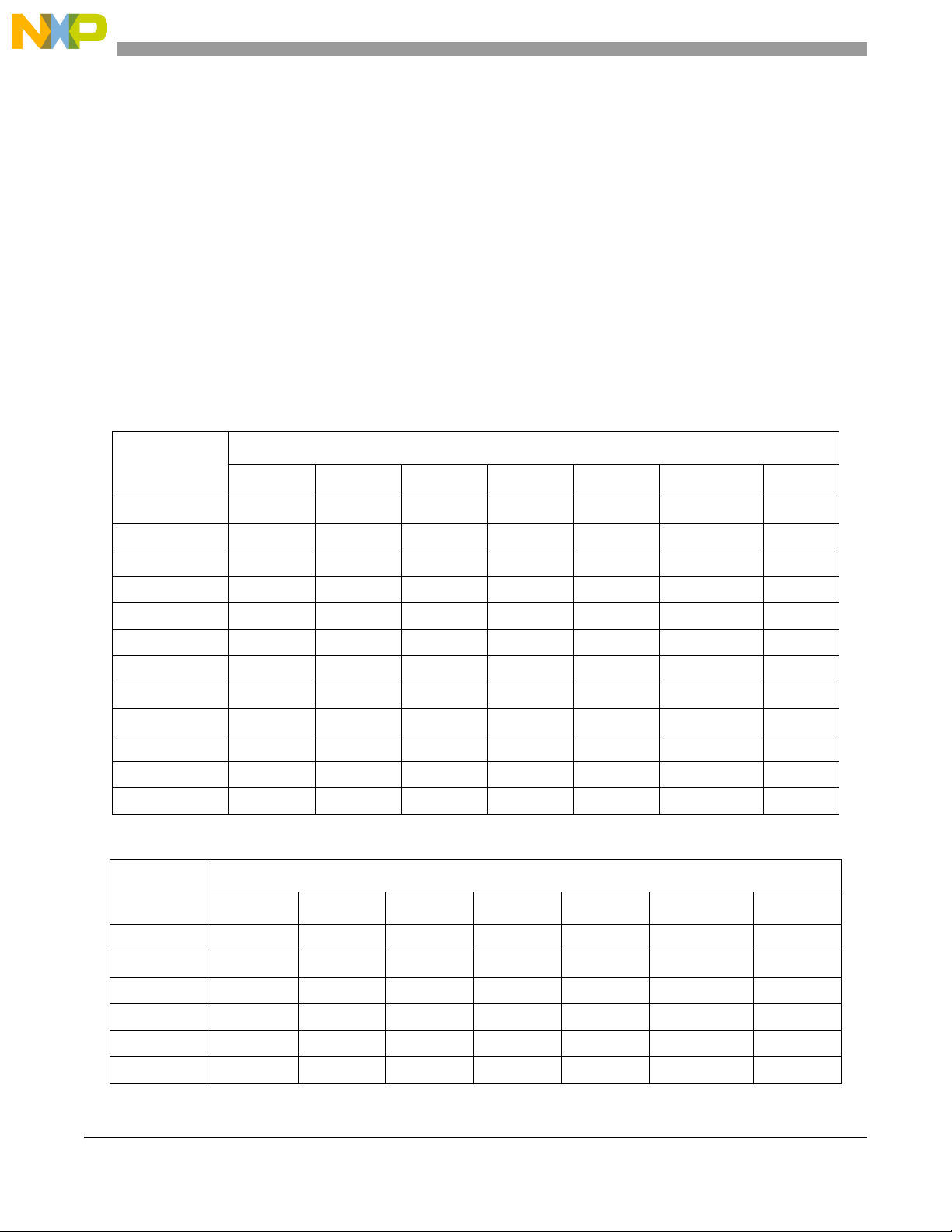
ColdFire Core
3.3.5.2 MOVE Instruction Execution Times
Table 3-13 lists execution times for MOVE.{B,W} instructions; Table 3-14 lists timings for MOVE.L.
NOTE
For all tables in this section, the execution time of any instruction using the
PC-relative effective addressing modes is the same for the comparable
An-relative mode.
ET with {<ea> = (d16,PC)} equals ET with {<ea> = (d16,An)}
ET with {<ea> = (d8,PC,Xi*SF)} equals ET with {<ea> = (d8,An,Xi*SF)}
The nomenclature xxx.wl refers to both forms of absolute addressing, xxx.w
and xxx.l.
Table 3-13. MOVE Byte and Word Execution Times
Destination
Source
Rx (Ax) (Ax)+ -(Ax) (d16,Ax) (d8,Ax,Xi*SF) xxx.wl
Dy 1(0/0) 1(0/1) 1(0/1) 1(0/1) 1(0/1) 2(0/1) 1(0/1)
Ay 1(0/0) 1(0/1) 1(0/1) 1(0/1) 1(0/1) 2(0/1) 1(0/1)
(Ay) 1(1/0) 2(1/1) 2(1/1) 2(1/1) 2(1/1) 3(1/1)) 2(1/1)
(Ay)+ 1(1/0) 2(1/1) 2(1/1) 2(1/1) 2(1/1) 3(1/1)) 2(1/1)
-(Ay) 1(1/0) 2(1/1) 2(1/1) 2(1/1) 2(1/1) 3(1/1)) 2(1/1)
(d16,Ay) 1(1/0) 2(1/1) 2(1/1) 2(1/1) 2(1/1) — —
(d8,Ay,Xi*SF) 2(1/0) 3(1/1) 3(1/1) 3(1/1) — — —
xxx.w 1(1/0) 2(1/1) 2(1/1) 2(1/1) — — —
xxx.l 1(1/0) 2(1/1) 2(1/1) 2(1/1) — — —
(d16,PC) 1(1/0) 2(1/1) 2(1/1) 2(1/1) 2(1/1) — —
(d8,PC,Xi*SF) 2(1/0) 3(1/1) 3(1/1) 3(1/1)) — — —
#xxx 1(0/0) 1(0/1) 1(0/1) 1(0/1) 1(0/1) — —
Table 3-14. MOVE Long Execution Times
Destination
Source
Rx (Ax) (Ax)+ -(Ax) (d16,Ax) (d8,Ax,Xi*SF) xxx.wl
Dy 1(0/0) 1(0/1) 1(0/1) 1(0/1) 1(0/1) 2(0/1) 1(0/1)
Ay 1(0/0) 1(0/1) 1(0/1) 1(0/1) 1(0/1) 2(0/1) 1(0/1)
(Ay) 1(1/0) 2(1/1) 2(1/1) 2(1/1) 2(1/1) 3(1/1) 2(1/1)
(Ay)+ 1(1/0) 2(1/1) 2(1/1) 2(1/1) 2(1/1) 3(1/1) 2(1/1)
-(Ay) 1(1/0) 2(1/1) 2(1/1) 2(1/1) 2(1/1) 3(1/1) 2(1/1)
(d16,Ay) 1(1/0) 2(1/1) 2(1/1) 2(1/1) 2(1/1) — —
3-29 Freescale Semiconductor
Page 96
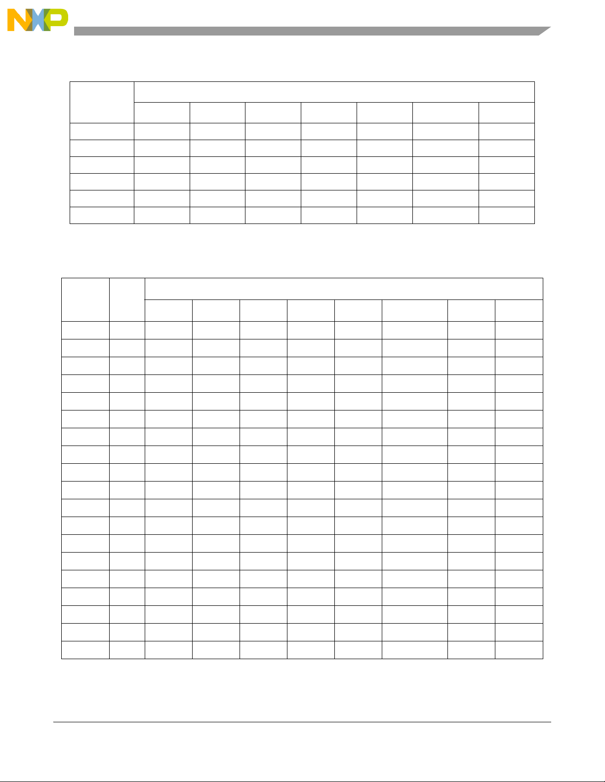
ColdFire Core
Table 3-14. MOVE Long Execution Times (continued)
Destination
Source
Rx (Ax) (Ax)+ -(Ax) (d16,Ax) (d8,Ax,Xi*SF) xxx.wl
(d8,Ay,Xi*SF) 2(1/0) 3(1/1) 3(1/1) 3(1/1) — — —
xxx.w 1(1/0) 2(1/1) 2(1/1) 2(1/1) — — —
xxx.l 1(1/0) 2(1/1) 2(1/1) 2(1/1) — — —
(d16,PC) 1(1/0) 2(1/1) 2(1/1) 2(1/1) 2(1/1) — —
(d8,PC,Xi*SF) 2(1/0) 3(1/1) 3(1/1) 3(1/1) — — —
#xxx 1(0/0) 1(0/1) 1(0/1) 1(0/1) — — —
3.3.5.3 Standard One Operand Instruction Execution Times
Table 3-15. One Operand Instruction Execution Times
Effective Address
Opcode <EA>
Rn (An) (An)+ -(An) (d16,An) (d8,An,Xn*SF) xxx.wl #xxx
BITREVDx1(0/0)———— — ——
BYTEREVDx1(0/0)———— — ——
CLR.B <ea> 1(0/0) 1(0/1) 1(0/1) 1(0/1) 1(0/1) 2(0/1) 1(0/1) —
CLR.W <ea> 1(0/0) 1(0/1) 1(0/1) 1(0/1) 1(0/1) 2(0/1) 1(0/1) —
CLR.L <ea> 1(0/0) 1(0/1) 1(0/1) 1(0/1) 1(0/1) 2(0/1) 1(0/1) —
EXT.WDx1(0/0)———— — ——
EXT.LDx1(0/0)———— — ——
EXTB.LDx1(0/0)———— — ——
FF1Dx1(0/0)———— — ——
NEG.LDx1(0/0)———— — ——
NEGX.LDx1(0/0)———— — ——
NOT.LDx1(0/0)———— — ——
SATS.LDx1(0/0)———— — ——
SCCDx1(0/0)———— — ——
SWAPDx1(0/0)———— — ——
TAS.B <ea> — 1(1/1) 1(1/1) 1(1/1) 1(1/1) 2(1/1) 1(1/1) —
TST.B <ea> 1(0/0) 1(1/0) 1(1/0) 1(1/0) 1(1/0) 2(1/0) 1(1/0) 1(0/0)
TST.W <ea> 1(0/0) 1(1/0) 1(1/0) 1(1/0) 1(1/0) 2(1/0) 1(1/0) 1(0/0)
TST.L <ea> 1(0/0) 1(1/0) 1(1/0) 1(1/0) 1(1/0) 2(1/0) 1(1/0) 1(0/0)
Freescale Semiconductor 3-30
Page 97

ColdFire Core
3.3.5.4 Standard Two Operand Instruction Execution Times
Table 3-16. Two Operand Instruction Execution Times
Effective Address
Opcode <EA>
Rn (An) (An)+ -(An)
ADD.L <ea>,Rx 1(0/0) 1(1/0) 1(1/0) 1(1/0) 1(1/0) 2(1/0) 1(1/0) 1(0/0)
ADD.L Dy,<ea> — 1(1/1) 1(1/1) 1(1/1) 1(1/1) 2(1/1) 1(1/1) —
ADDI.L #imm,Dx 1(0/0) — — — — — — —
ADDQ.L #imm,<ea> 1(0/0) 1(1/1) 1(1/1) 1(1/1) 1(1/1) 2(1/1) 1(1/1) —
ADDX.L Dy,Dx 1(0/0) — — — — — — —
AND.L <ea>,Rx 1(0/0) 1(1/0) 1(1/0) 1(1/0) 1(1/0) 2(1/0) 1(1/0) 1(0/0)
AND.L Dy,<ea> — 1(1/1) 1(1/1) 1(1/1) 1(1/1) 2(1/1) 1(1/1) —
ANDI.L #imm,Dx 1(0/0) — — — — — — —
ASL.L <ea>,Dx 1(0/0) — — — — — — 1(0/0)
ASR.L <ea>,Dx 1(0/0) — — — — — — 1(0/0)
BCHG Dy,<ea> 2(0/0) 2(1/1) 2(1/1) 2(1/1) 2(1/1) 3(1/1) 2(1/1) —
BCHG #imm,<ea> 2(0/0) 2(1/1) 2(1/1) 2(1/1) 2(1/1) — — —
BCLR Dy,<ea> 2(0/0) 2(1/1) 2(1/1) 2(1/1) 2(1/1) 3(1/1) 2(1/1) —
BCLR #imm,<ea> 2(0/0) 2(1/1) 2(1/1) 2(1/1) 2(1/1) — — —
BSET Dy,<ea> 2(0/0) 2(1/1) 2(1/1) 2(1/1) 2(1/1) 3(1/1) 2(1/1) —
BSET #imm,<ea> 2(0/0) 2(1/1) 2(1/1) 2(1/1) 2(1/1) — — —
BTST Dy,<ea> 2(0/0) 1(1/0) 1(1/0) 1(1/0) 1(1/0) 2(1/0) 1(1/0) —
BTST #imm,<ea> 1(0/0) 1(1/0) 1(1/0) 1(1/0) 1(1/0) — — —
CMP.B <ea>,Rx 1(0/0) 1(1/0) 1(1/0) 1(1/0) 1(1/0) 2(1/0) 1(1/0) 1(0/0)
CMP.W <ea>,Rx 1(0/0) 1(1/0) 1(1/0) 1(1/0) 1(1/0) 2(1/0) 1(1/0) 1(0/0)
CMP.L <ea>,Rx 1(0/0) 1(1/0) 1(1/0) 1(1/0) 1(1/0) 2(1/0) 1(1/0) 1(0/0)
CMPI.B #imm,Dx 1(0/0) — — — — — — —
CMPI.W #imm,Dx 1(0/0) — — — — — — —
CMPI.L #imm,Dx 1(0/0) — — — — — — —
DIVS.W <ea>,Dx 20(0/0) 20(1/0) 20(1/0) 20(1/0) 20(1/0) 21(1/0) 20(1/0) 20(0/0)
DIVU.W <ea>,Dx 20(0/0) 20(1/0) 20(1/0) 20(1/0) 20(1/0) 21(1/0) 20(1/0) 20(0/0)
DIVS.L <ea>,Dx 35(0/0) 35(1/0) 35(1/0) 35(1/0) 35(1/0) — — —
DIVU.L <ea>,Dx 35(0/0) 35(1/0) 35(1/0) 35(1/0) 35(1/0) — — —
EOR.L Dy,<ea> 1(0/0) 1(1/1) 1(1/1) 1(1/1) 1(1/1) 2(1/1) 1(1/1) —
EORI.L #imm,Dx 1(0/0) — — — — — — —
LEA <ea>,Ax — 1(0/0) — — 1(0/0) 2(0/0) 1(0/0) —
LSL.L <ea>,Dx 1(0/0) — — — — — — 1(0/0)
LSR.L <ea>,Dx 1(0/0) — — — — — — 1(0/0)
(d16,An)
(d16,PC)
(d8,An,Xn*SF)
(d8,PC,Xn*SF)
xxx.wl #xxx
3-31 Freescale Semiconductor
Page 98
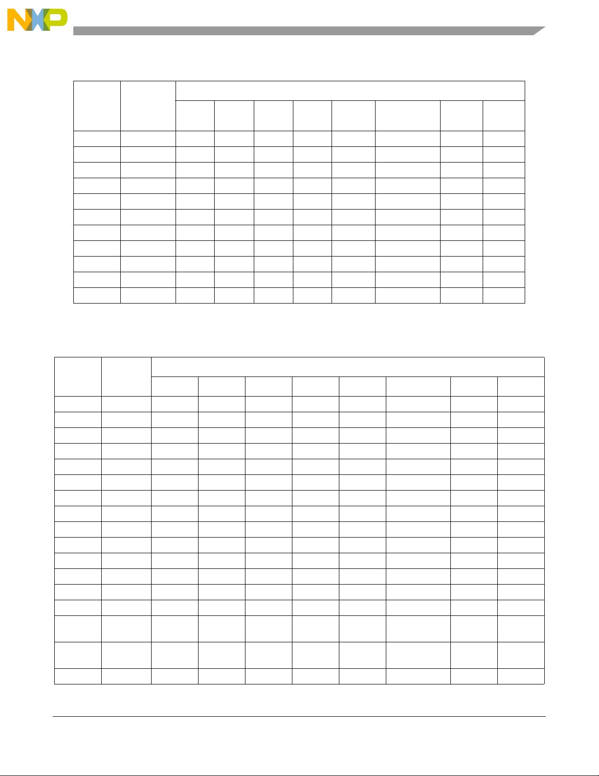
Table 3-16. Two Operand Instruction Execution Times (continued)
Effective Address
Opcode <EA>
Rn (An) (An)+ -(An)
MOVEQ.L #imm,Dx — — — — — — — 1(0/0)
OR.L <ea>,Rx 1(0/0) 1(1/0) 1(1/0) 1(1/0) 1(1/0) 2(1/0) 1(1/0) 1(0/0)
OR.L Dy,<ea> — 1(1/1) 1(1/1) 1(1/1) 1(1/1) 2(1/1) 1(1/1) —
ORI.L #imm,Dx 1(0/0) — — — — — — —
REMS.L <ea>,Dx 35(0/0) 35(1/0) 35(1/0) 35(1/0) 35(1/0) — — —
REMU.L <ea>,Dx 35(0/0) 35(1/0) 35(1/0) 35(1/0) 35(1/0) — — —
SUB.L <ea>,Rx 1(0/0) 1(1/0) 1(1/0) 1(1/0) 1(1/0) 2(1/0) 1(1/0) 1(0/0)
SUB.L Dy,<ea> — 1(1/1) 1(1/1) 1(1/1) 1(1/1) 2(1/1) 1(1/1) —
SUBI.L #imm,Dx 1(0/0) — — — — — — —
SUBQ.L #imm,<ea> 1(0/0) 1(1/1) 1(1/1) 1(1/1) 1(1/1) 2(1/1) 1(1/1) —
SUBX.L Dy,Dx 1(0/0) — — — — — — —
(d16,An)
(d16,PC)
(d8,An,Xn*SF)
(d8,PC,Xn*SF)
xxx.wl #xxx
3.3.5.5 Miscellaneous Instruction Execution Times
ColdFire Core
Table 3-17. Miscellaneous Instruction Execution Times
Effective Address
Opcode <EA>
CPUSHL (Ax) — 9(0/1) — — — — — —
CPUSHL bc,Ax — 18(0/1) — — — — — —
CPUSHL dc,Ax — 12(0/1) — — — — — —
CPUSHL ic,Ax — 18(0/1) — — — — — —
INTOUCH (Ay) — 19(1/0) — — — — — —
LINK.W Ay,#imm 2(0/1) — — — — — — —
MOV3Q.L #imm,<ea> 1(0/0) 1(0/1) 1(0/1) 1(0/1) 1(0/1) 2(0/1) 1(0/1) —
MOVE.L Ay,USP 3(0/0) — — — — — — —
MOVE.L USP,Ax 3(0/0) — — — — — — —
MOVE.W CCR,Dx 1(0/0) — — — — — — —
MOVE.W <ea>,CCR 1(0/0) — — — — — — 1(0/0)
MOVE.W SR,Dx 1(0/0) — — — — — — —
MOVE.W <ea>,SR 4(0/0) — — — — — — 4(0/0)
MOVEC Ry,Rc 20(0/1) — — — — — — —
MOVEM.L <ea>, and
list
MOVEM.L and
list,<ea>
MVS <ea>,Dx 1(0/0) 1(1/0) 1(1/0) 1(1/0) 1(1/0) 2(1/0) 1(1/0) 1(0/0)
Rn (An) (An)+ -(An) (d16,An) (d8,An,Xn*SF) xxx.wl #xxx
—n(n/0)— —n(n/0) — — —
—n(0/n)— —n(0/n) — — —
2
Freescale Semiconductor 3-32
Page 99
ColdFire Core
Table 3-17. Miscellaneous Instruction Execution Times (continued)
Opcode <EA>
Effective Address
Rn (An) (An)+ -(An) (d16,An) (d8,An,Xn*SF) xxx.wl #xxx
MVZ <ea>,Dx 1(0/0) 1(1/0) 1(1/0) 1(1/0) 1(1/0) 2(1/0) 1(1/0) 1(0/0)
NOP 6(0/0)———— — ——
PEA <ea> — 1(0/1) — — 1(0/1)
4
2(0/1)
5
1(0/1) —
PULSE 1(0/0)———— — ——
STOP#imm————— — —6(0/0)
3
TRAP#imm————— — —18(1/2)
TPF 1(0/0)———— — ——
TPF.W 1(0/0)———— — ——
TPF.L 1(0/0)———— — ——
UNLK Ax 1(1/0) — — — — — — —
WDDATA <ea> — 1(1/0) 1(1/0) 1(1/0) 1(1/0) 2(1/0) 1(1/0) —
WDEBUG<ea> —3(2/0)— —3(2/0) — — —
1
The n is the number of registers moved by the MOVEM opcode.
2
If a MOVE.W #imm,SR instruction is executed and imm[13] equals 1, the execution time is 1(0/0).
3
The execution time for STOP is the time required until the processor begins sampling continuously for interrupts.
4
PEA execution times are the same for (d16,PC).
5
PEA execution times are the same for (d8,PC,Xn*SF).
3.3.5.6 EMAC Instruction Execution Times
Table 3-18. EMAC Instruction Execution Times
Opcode <EA>
Rn (An) (An)+ -(An) (d16,An)
MAC.L Ry, Rx, Raccx 1(0/0) — — — — — — —
MAC.L Ry, Rx, <ea>, Rw, Raccx — 1(1/0) 1(1/0) 1(1/0) 1(1/0)
MAC.W Ry, Rx, Raccx 1(0/0) — — — — — — —
MAC.W Ry, Rx, <ea>, Rw, Raccx — 1(1/0) 1(1/0) 1(1/0) 1(1/0)
MOVE.L <ea>y, Raccx 1(0/0) — — — — — — 1(0/0)
MOVE.L Raccy, Raccx 1(0/0) — — — — — — —
MOVE.L <ea>y, MACSR 8(0/0) — — — — — — 8(0/0)
MOVE.L <ea>y, Rmask 7(0/0) — — — — — — 7(0/0)
MOVE.L <ea>y,Raccext01 1(0/0) — — — — — — 1(0/0)
MOVE.L <ea>y,Raccext23 1(0/0) — — — — — — 1(0/0)
MOVE.L Raccx, <ea>x 1(0/0)2——— — — ——
Effective Address
1
1
(d8,An,
Xn*SF)
xxx.wl #xxx
———
———
3-33 Freescale Semiconductor
Page 100
ColdFire Core
Table 3-18. EMAC Instruction Execution Times (continued)
Effective Address
Opcode <EA>
Rn (An) (An)+ -(An) (d16,An)
MOVE.L MACSR, <ea>x 1(0/0) — — — — — — —
MOVE.L Rmask, <ea>x 1(0/0) — — — — — — —
MOVE.L Raccext01,<ea.x 1(0/0) — — — — — — —
MOVE.L Raccext23,<ea>x 1(0/0) — — — — — — —
MSAC.L Ry, Rx, Raccx 1(0/0) — — — — — — —
MSAC.W Ry, Rx, Raccx 1(0/0) — — — — — — —
MSAC.L Ry, Rx, <ea>, Rw, Raccx — 1(1/0) 1(1/0) 1(1/0) 1(1/0)
MSAC.W Ry, Rx, <ea>, Rw, Raccx — 1(1/0) 1(1/0) 1(1/0) 1(1/0)
MULS.L <ea>y, Dx 4(0/0) 4(1/0) 4(1/0) 4(1/0) 4(1/0) — — —
MULS.W <ea>y, Dx 4(0/0) 4(1/0) 4(1/0) 4(1/0) 4(1/0) 5(1/0) 4(1/0) 4(0/0)
MULU.L <ea>y, Dx 4(0/0) 4(1/0) 4(1/0) 4(1/0) 4(1/0) — — —
(d8,An,
Xn*SF)
1
1
xxx.wl #xxx
———
———
MULU.W <ea>y, Dx 4(0/0) 4(1/0) 4(1/0) 4(1/0) 4(1/0) 5(1/0) 4(1/0) 4(0/0)
1
Effective address of (d16,PC) not supported
2
Storing an accumulator requires one additional processor clock cycle when saturation is enabled, or fractional
rounding is performed (MACSR[7:4] equals 1---, -11-, --11)
NOTE
The execution times for moving the contents of the Racc, Raccext[01,23],
MACSR, or Rmask into a destination location <ea>x shown in this table
represent the best-case scenario when the store instruction is executed and
there are no load or M{S}AC instructions in the EMAC execution pipeline.
In general, these store operations require only a single cycle for execution,
but if preceded immediately by a load, MAC, or MSAC instruction, the
depth of the EMAC pipeline is exposed and the execution time is four
cycles.
3.3.5.7 Branch Instruction Execution Times
Table 3-19. General Branch Instruction Execution Times
Effective Address
Opcode <EA>
Rn (An) (An)+ -(An)
BRA — — — — 1(0/1)
BSR — — — — 1(0/1)
(d16,An)
(d16,PC)
1
2
(d8,An,Xi*SF)
(d8,PC,Xi*SF)
———
———
xxx.wl #xxx
Freescale Semiconductor 3-34
 Loading...