

Page 1

MC9S12ZVM-Family
Reference Manual
HCS12
Microcontrollers
Rev. 1.3
20 JAN 2014
MC9S12ZVMRMV1
freescale.com
Page 2

To provide the most up-to-date information, the document revision on the Internet is the most current. A
printed copy may be an earlier revision. To verify you have the latest information available, refer to :
freescale.com.
The following revision history table summarizes changes contained in this document. The individual
module sections contain revision history tables with more detailed information.
This document containsinformation for all constituent modules, with the exception of the S12Z CPU. For
S12ZCPU information please refer to the CPU S12Z Reference Manual.
Revision History
Date
12 Dec 2013 1.2 Replaced generic 8-channel TIM section with specific 4-channel TIM section
20 JAN 2014 1.3 Updated Stop mode description for BDC enabled case
Freescale Semiconductor reserves the right to make changes without further notice to any products herein. Freescale Semiconductor makes no warranty,
representation or guaranteeregardingthe suitability of its products for any particular purpose, nor does Freescale Semiconductor assume any liability arising out of
the application or use of any product or circuit, and specifically disclaims anyand all liability, including without limitation consequential or incidental damages. “Typical”
parameters that may be provided in FreescaleSemiconductor data sheets and/or specifications can and do vary in different applications and actual performance may
vary over time. All operating parameters, including “Typicals”, must be validated for each customer application by customer’s technical experts. Freescale
Semiconductor does not convey any license under its patent rights nor the rights of others. Freescale Semiconductor products are not designed, intended, or
authorized for use as components in systems intended for surgical implant into the body, or other applications intended to support or sustain life, or for any other
application in which the failure of the Freescale Semiconductor product could create a situation where personal injuryor death may occur. Should Buyer purchase or
useFreescaleSemiconductorproducts for any such unintended orunauthorized application, Buyer shall indemnifyand hold Freescale Semiconductor and its officers,
employees,subsidiaries, affiliates, and distributors harmless against all claims, costs, damages, and expenses, and reasonable attorney fees arising out of, directly
or indirectly,anyclaim of personal injury or death associated with such unintended or unauthorized use, evenif such claim alleges that FreescaleSemiconductor was
negligent regarding the design or manufacture of the part.
Revision
Level
Description
Textual enhancements and corrections throughout
Updated electrical parameter section and added parameters for temperataures up to 175°C
- Added Table A-5
- Merged Table A-8 and A-9 into Table A-9. Values updated. .
- Table A-15. Parameter #2. max changed from 800uA to 1050uA
- Table A-15. Inserted new C class parameter ISUPS at 85C. typ. 80uA
- Appendices B,D and E. Updated parameter values based on characterization results.
- Appendix C. Added parameter values for range above T=150
- Table F-3. Merged rows 2a and 2b. Merged rows 6a and 6b.
- Appendix G. Merged tables G-1 and G-2.
- Tables H-1 and H-2 values updated.
Removed false reference to modified clock monitor assert frequency
Updated electricals for 175
- Removed temperature range disclaimer from electrical parameter spec.footer
- Added sentence above table A-3
- Table D-1. LINPHY parameters 12a and 12b replaced by 12a, 12b and 12c-
- Table D-2. LINPHY wake up pulse over whole temperature range
- Table E-1. FET gate charge spec. updated
°C Grade0
°C
Page 3

Chapter 1
Device Overview MC9S12ZVM-Family
1.1 Introduction . . . . . . . . . . . . . . . . . . . . . . . . . . . . . . . . . . . . . . . . . . . . . . . . . . . . . . . . . . . . . . . . . . 17
1.2 Features . . . . . . . . . . . . . . . . . . . . . . . . . . . . . . . . . . . . . . . . . . . . . . . . . . . . . . . . . . . . . . . . . . . . . 18
1.2.1 MC9S12ZVM-Family Member Comparison . . . . . . . . . . . . . . . . . . . . . . . . . . . . . . . . . 18
1.2.2 Functional Differences Between N06E and 0N95G Masksets . . . . . . . . . . . . . . . . . . . . 18
1.2.3 Functional Differences Between 1N95G and 0N95G Masksets . . . . . . . . . . . . . . . . . . . 20
1.3 Chip-Level Features . . . . . . . . . . . . . . . . . . . . . . . . . . . . . . . . . . . . . . . . . . . . . . . . . . . . . . . . . . . . 20
1.4 Module Features . . . . . . . . . . . . . . . . . . . . . . . . . . . . . . . . . . . . . . . . . . . . . . . . . . . . . . . . . . . . . . . 21
1.4.1 S12Z Central Processor Unit (CPU) . . . . . . . . . . . . . . . . . . . . . . . . . . . . . . . . . . . . . . . . 21
1.4.2 Embedded Memory . . . . . . . . . . . . . . . . . . . . . . . . . . . . . . . . . . . . . . . . . . . . . . . . . . . . . 22
1.4.3 Clocks, Reset & Power Management Unit (CPMU) . . . . . . . . . . . . . . . . . . . . . . . . . . . . 23
1.4.4 Main External Oscillator (XOSCLCP) . . . . . . . . . . . . . . . . . . . . . . . . . . . . . . . . . . . . . . 23
1.4.5 Timer (TIM) . . . . . . . . . . . . . . . . . . . . . . . . . . . . . . . . . . . . . . . . . . . . . . . . . . . . . . . . . . . 24
1.4.6 Pulse width Modulator with Fault protection (PMF) . . . . . . . . . . . . . . . . . . . . . . . . . . . . 24
1.4.7 Programmable Trigger Unit (PTU) . . . . . . . . . . . . . . . . . . . . . . . . . . . . . . . . . . . . . . . . . 24
1.4.8 LIN physical layer transceiver . . . . . . . . . . . . . . . . . . . . . . . . . . . . . . . . . . . . . . . . . . . . . 24
1.4.9 Serial Communication Interface Module (SCI) . . . . . . . . . . . . . . . . . . . . . . . . . . . . . . . . 25
1.4.10 Multi-Scalable Controller Area Network (MSCAN) . . . . . . . . . . . . . . . . . . . . . . . . . . . . 25
1.4.11 Serial Peripheral Interface Module (SPI) . . . . . . . . . . . . . . . . . . . . . . . . . . . . . . . . . . . . . 25
1.4.12 Analog-to-Digital Converter Module (ADC) . . . . . . . . . . . . . . . . . . . . . . . . . . . . . . . . . . 25
1.4.13 Supply Voltage Sensor (BATS) . . . . . . . . . . . . . . . . . . . . . . . . . . . . . . . . . . . . . . . . . . . . 26
1.4.14 On-Chip Voltage Regulator system (VREG) . . . . . . . . . . . . . . . . . . . . . . . . . . . . . . . . . . 26
1.4.15 Gate Drive Unit (GDU) . . . . . . . . . . . . . . . . . . . . . . . . . . . . . . . . . . . . . . . . . . . . . . . . . . 26
1.4.16 Current Sense . . . . . . . . . . . . . . . . . . . . . . . . . . . . . . . . . . . . . . . . . . . . . . . . . . . . . . . . . . 27
1.5 Block Diagram . . . . . . . . . . . . . . . . . . . . . . . . . . . . . . . . . . . . . . . . . . . . . . . . . . . . . . . . . . . . . . . . 28
1.6 Device Memory Map . . . . . . . . . . . . . . . . . . . . . . . . . . . . . . . . . . . . . . . . . . . . . . . . . . . . . . . . . . . 29
1.6.1 Part ID Assignments . . . . . . . . . . . . . . . . . . . . . . . . . . . . . . . . . . . . . . . . . . . . . . . . . . . .32
1.7 Signal Description and Device Pinouts . . . . . . . . . . . . . . . . . . . . . . . . . . . . . . . . . . . . . . . . . . . . . 32
1.7.1 Pin Assignment Overview . . . . . . . . . . . . . . . . . . . . . . . . . . . . . . . . . . . . . . . . . . . . . . . . 32
1.7.2 Detailed External Signal Descriptions . . . . . . . . . . . . . . . . . . . . . . . . . . . . . . . . . . . . . . . 33
1.7.3 Power Supply Pins . . . . . . . . . . . . . . . . . . . . . . . . . . . . . . . . . . . . . . . . . . . . . . . . . . . . . .39
1.7.4 Package and Pinouts . . . . . . . . . . . . . . . . . . . . . . . . . . . . . . . . . . . . . . . . . . . . . . . . . . . .40
1.8 Internal Signal Mapping . . . . . . . . . . . . . . . . . . . . . . . . . . . . . . . . . . . . . . . . . . . . . . . . . . . . . . . . . 46
1.8.1 ADC Connectivity . . . . . . . . . . . . . . . . . . . . . . . . . . . . . . . . . . . . . . . . . . . . . . . . . . . . . .46
1.8.2 Motor Control Loop Signals . . . . . . . . . . . . . . . . . . . . . . . . . . . . . . . . . . . . . . . . . . . . . . 47
1.8.3 Device Level PMF Connectivity . . . . . . . . . . . . . . . . . . . . . . . . . . . . . . . . . . . . . . . . . . . 48
1.8.4 BDC Clock Source Connectivity . . . . . . . . . . . . . . . . . . . . . . . . . . . . . . . . . . . . . . . . . . . 48
1.8.5 LINPHY Connectivity . . . . . . . . . . . . . . . . . . . . . . . . . . . . . . . . . . . . . . . . . . . . . . . . . . . 48
1.8.6 FTMRZ Connectivity . . . . . . . . . . . . . . . . . . . . . . . . . . . . . . . . . . . . . . . . . . . . . . . . . . . . 48
1.8.7 CPMU Connectivity . . . . . . . . . . . . . . . . . . . . . . . . . . . . . . . . . . . . . . . . . . . . . . . . . . . . . 48
1.9 Modes of Operation . . . . . . . . . . . . . . . . . . . . . . . . . . . . . . . . . . . . . . . . . . . . . . . . . . . . . . . . . . . . 49
1.9.1 Chip Configuration Modes . . . . . . . . . . . . . . . . . . . . . . . . . . . . . . . . . . . . . . . . . . . . . . . . 49
1.9.2 Debugging Modes . . . . . . . . . . . . . . . . . . . . . . . . . . . . . . . . . . . . . . . . . . . . . . . . . . . . . .49
1.9.3 Low Power Modes . . . . . . . . . . . . . . . . . . . . . . . . . . . . . . . . . . . . . . . . . . . . . . . . . . . . . . 50
MC9S12ZVM Family Reference Manual Rev. 1.3
Freescale Semiconductor 3
Page 4

1.10 Security . . . . . . . . . . . . . . . . . . . . . . . . . . . . . . . . . . . . . . . . . . . . . . . . . . . . . . . . . . . . . . . . . . . . . . 51
1.10.1 Features . . . . . . . . . . . . . . . . . . . . . . . . . . . . . . . . . . . . . . . . . . . . . . . . . . . . . . . . . . . . . . 51
1.10.2 Securing the Microcontroller . . . . . . . . . . . . . . . . . . . . . . . . . . . . . . . . . . . . . . . . . . . . . . 51
1.10.3 Operation of the Secured Microcontroller . . . . . . . . . . . . . . . . . . . . . . . . . . . . . . . . . . . . 52
1.10.4 Unsecuring the Microcontroller . . . . . . . . . . . . . . . . . . . . . . . . . . . . . . . . . . . . . . . . . . . . 52
1.10.5 Reprogramming the Security Bits . . . . . . . . . . . . . . . . . . . . . . . . . . . . . . . . . . . . . . . . . . 53
1.10.6 Complete Memory Erase . . . . . . . . . . . . . . . . . . . . . . . . . . . . . . . . . . . . . . . . . . . . . . . . . 53
1.11 Resets and Interrupts . . . . . . . . . . . . . . . . . . . . . . . . . . . . . . . . . . . . . . . . . . . . . . . . . . . . . . . . . . . 53
1.11.1 Resets . . . . . . . . . . . . . . . . . . . . . . . . . . . . . . . . . . . . . . . . . . . . . . . . . . . . . . . . . . . . . . . . 53
1.11.2 Interrupt Vectors . . . . . . . . . . . . . . . . . . . . . . . . . . . . . . . . . . . . . . . . . . . . . . . . . . . . . . . . 54
1.11.3 Effects of Reset . . . . . . . . . . . . . . . . . . . . . . . . . . . . . . . . . . . . . . . . . . . . . . . . . . . . . . . . 57
1.12 Module device level dependencies . . . . . . . . . . . . . . . . . . . . . . . . . . . . . . . . . . . . . . . . . . . . . . . . . 57
1.12.1 CPMU COP Configuration . . . . . . . . . . . . . . . . . . . . . . . . . . . . . . . . . . . . . . . . . . . . . . . 57
1.12.2 CPMU High Temperature Trimming . . . . . . . . . . . . . . . . . . . . . . . . . . . . . . . . . . . . . . . . 58
1.12.3 Flash IFR Mapping . . . . . . . . . . . . . . . . . . . . . . . . . . . . . . . . . . . . . . . . . . . . . . . . . . . . .58
1.13 Application Information . . . . . . . . . . . . . . . . . . . . . . . . . . . . . . . . . . . . . . . . . . . . . . . . . . . . . . . . . 58
1.13.1 ADC Calibration . . . . . . . . . . . . . . . . . . . . . . . . . . . . . . . . . . . . . . . . . . . . . . . . . . . . . . . 58
1.13.2 SCI Baud Rate Detection . . . . . . . . . . . . . . . . . . . . . . . . . . . . . . . . . . . . . . . . . . . . . . . . . 59
1.13.3 Motor Control Application Overview . . . . . . . . . . . . . . . . . . . . . . . . . . . . . . . . . . . . . . . 59
1.13.4 BDCM Complementary Mode Operation . . . . . . . . . . . . . . . . . . . . . . . . . . . . . . . . . . . . 68
1.13.5 BLDC Six-Step Commutation . . . . . . . . . . . . . . . . . . . . . . . . . . . . . . . . . . . . . . . . . . . . . 72
1.13.6 PMSM Control . . . . . . . . . . . . . . . . . . . . . . . . . . . . . . . . . . . . . . . . . . . . . . . . . . . . . . . . . 74
1.13.7 Power Domain Considerations . . . . . . . . . . . . . . . . . . . . . . . . . . . . . . . . . . . . . . . . . . . . 78
Chapter 2
Port Integration Module (S12ZVMPIMV1)
2.1 Introduction . . . . . . . . . . . . . . . . . . . . . . . . . . . . . . . . . . . . . . . . . . . . . . . . . . . . . . . . . . . . . . . . . . 83
2.1.1 Overview . . . . . . . . . . . . . . . . . . . . . . . . . . . . . . . . . . . . . . . . . . . . . . . . . . . . . . . . . . . . . 83
2.1.2 Features . . . . . . . . . . . . . . . . . . . . . . . . . . . . . . . . . . . . . . . . . . . . . . . . . . . . . . . . . . . . . . 84
2.2 External Signal Description . . . . . . . . . . . . . . . . . . . . . . . . . . . . . . . . . . . . . . . . . . . . . . . . . . . . . . 84
2.3 Memory Map and Register Definition . . . . . . . . . . . . . . . . . . . . . . . . . . . . . . . . . . . . . . . . . . . . . .89
2.3.1 Register Map . . . . . . . . . . . . . . . . . . . . . . . . . . . . . . . . . . . . . . . . . . . . . . . . . . . . . . . . . . 90
2.3.2 PIM Registers 0x0200-0x020F . . . . . . . . . . . . . . . . . . . . . . . . . . . . . . . . . . . . . . . . . . . . 94
2.3.3 PIM Generic Registers . . . . . . . . . . . . . . . . . . . . . . . . . . . . . . . . . . . . . . . . . . . . . . . . . . 101
2.3.4 PIM Generic Register Exceptions . . . . . . . . . . . . . . . . . . . . . . . . . . . . . . . . . . . . . . . . . 109
2.4 Functional Description . . . . . . . . . . . . . . . . . . . . . . . . . . . . . . . . . . . . . . . . . . . . . . . . . . . . . . . . . 110
2.4.1 General . . . . . . . . . . . . . . . . . . . . . . . . . . . . . . . . . . . . . . . . . . . . . . . . . . . . . . . . . . . . . . 110
2.4.2 Registers . . . . . . . . . . . . . . . . . . . . . . . . . . . . . . . . . . . . . . . . . . . . . . . . . . . . . . . . . . . . . 111
2.4.3 Pin I/O Control . . . . . . . . . . . . . . . . . . . . . . . . . . . . . . . . . . . . . . . . . . . . . . . . . . . . . . . . 112
2.4.4 Interrupts . . . . . . . . . . . . . . . . . . . . . . . . . . . . . . . . . . . . . . . . . . . . . . . . . . . . . . . . . . . . 113
2.4.5 Pin interrupts and Key-Wakeup (KWU) . . . . . . . . . . . . . . . . . . . . . . . . . . . . . . . . . . . . 114
2.4.6 Over-Current Interrupt . . . . . . . . . . . . . . . . . . . . . . . . . . . . . . . . . . . . . . . . . . . . . . . . . . 115
2.5 Initialization and Application Information . . . . . . . . . . . . . . . . . . . . . . . . . . . . . . . . . . . . . . . . . . 115
2.5.1 Port Data and Data Direction Register writes . . . . . . . . . . . . . . . . . . . . . . . . . . . . . . . . 115
2.5.2 Over-Current Protection on EVDD1 . . . . . . . . . . . . . . . . . . . . . . . . . . . . . . . . . . . . . . . 115
MC9S12ZVM Family Reference Manual Rev. 1.3
4 Freescale Semiconductor
Page 5

Chapter 3
Memory Mapping Control (S12ZMMCV1)
3.1 Introduction . . . . . . . . . . . . . . . . . . . . . . . . . . . . . . . . . . . . . . . . . . . . . . . . . . . . . . . . . . . . . . . . . 117
3.1.1 Glossary . . . . . . . . . . . . . . . . . . . . . . . . . . . . . . . . . . . . . . . . . . . . . . . . . . . . . . . . . . . . . 118
3.1.2 Overview . . . . . . . . . . . . . . . . . . . . . . . . . . . . . . . . . . . . . . . . . . . . . . . . . . . . . . . . . . . . 118
3.1.3 Features . . . . . . . . . . . . . . . . . . . . . . . . . . . . . . . . . . . . . . . . . . . . . . . . . . . . . . . . . . . . . 118
3.1.4 Modes of Operation . . . . . . . . . . . . . . . . . . . . . . . . . . . . . . . . . . . . . . . . . . . . . . . . . . . . 119
3.1.5 Block Diagram . . . . . . . . . . . . . . . . . . . . . . . . . . . . . . . . . . . . . . . . . . . . . . . . . . . . . . . . 119
3.2 External Signal Description . . . . . . . . . . . . . . . . . . . . . . . . . . . . . . . . . . . . . . . . . . . . . . . . . . . . . 119
3.3 Memory Map and Register Definition . . . . . . . . . . . . . . . . . . . . . . . . . . . . . . . . . . . . . . . . . . . . . 120
3.3.1 Memory Map . . . . . . . . . . . . . . . . . . . . . . . . . . . . . . . . . . . . . . . . . . . . . . . . . . . . . . . . . 120
3.3.2 Register Descriptions . . . . . . . . . . . . . . . . . . . . . . . . . . . . . . . . . . . . . . . . . . . . . . . . . . . 120
3.4 Functional Description . . . . . . . . . . . . . . . . . . . . . . . . . . . . . . . . . . . . . . . . . . . . . . . . . . . . . . . . . 125
3.4.1 Global Memory Map . . . . . . . . . . . . . . . . . . . . . . . . . . . . . . . . . . . . . . . . . . . . . . . . . . . 125
3.4.2 Illegal Accesses . . . . . . . . . . . . . . . . . . . . . . . . . . . . . . . . . . . . . . . . . . . . . . . . . . . . . . . 127
3.4.3 Uncorrectable ECC Faults . . . . . . . . . . . . . . . . . . . . . . . . . . . . . . . . . . . . . . . . . . . . . . . 128
Chapter 4
Interrupt (S12ZINTV0)
4.1 Introduction . . . . . . . . . . . . . . . . . . . . . . . . . . . . . . . . . . . . . . . . . . . . . . . . . . . . . . . . . . . . . . . . . 129
4.1.1 Glossary . . . . . . . . . . . . . . . . . . . . . . . . . . . . . . . . . . . . . . . . . . . . . . . . . . . . . . . . . . . . . 130
4.1.2 Features . . . . . . . . . . . . . . . . . . . . . . . . . . . . . . . . . . . . . . . . . . . . . . . . . . . . . . . . . . . . . 130
4.1.3 Modes of Operation . . . . . . . . . . . . . . . . . . . . . . . . . . . . . . . . . . . . . . . . . . . . . . . . . . . . 131
4.1.4 Block Diagram . . . . . . . . . . . . . . . . . . . . . . . . . . . . . . . . . . . . . . . . . . . . . . . . . . . . . . . . 131
4.2 External Signal Description . . . . . . . . . . . . . . . . . . . . . . . . . . . . . . . . . . . . . . . . . . . . . . . . . . . . . 132
4.3 Memory Map and Register Definition . . . . . . . . . . . . . . . . . . . . . . . . . . . . . . . . . . . . . . . . . . . . . 132
4.3.1 Module Memory Map . . . . . . . . . . . . . . . . . . . . . . . . . . . . . . . . . . . . . . . . . . . . . . . . . . 132
4.3.2 Register Descriptions . . . . . . . . . . . . . . . . . . . . . . . . . . . . . . . . . . . . . . . . . . . . . . . . . . . 133
4.4 Functional Description . . . . . . . . . . . . . . . . . . . . . . . . . . . . . . . . . . . . . . . . . . . . . . . . . . . . . . . . . 138
4.4.1 S12Z Exception Requests . . . . . . . . . . . . . . . . . . . . . . . . . . . . . . . . . . . . . . . . . . . . . . . 138
4.4.2 Interrupt Prioritization . . . . . . . . . . . . . . . . . . . . . . . . . . . . . . . . . . . . . . . . . . . . . . . . . . 138
4.4.3 Priority Decoder . . . . . . . . . . . . . . . . . . . . . . . . . . . . . . . . . . . . . . . . . . . . . . . . . . . . . . . 139
4.4.4 Reset Exception Requests . . . . . . . . . . . . . . . . . . . . . . . . . . . . . . . . . . . . . . . . . . . . . . . 139
4.4.5 Exception Priority . . . . . . . . . . . . . . . . . . . . . . . . . . . . . . . . . . . . . . . . . . . . . . . . . . . . . 140
4.4.6 Interrupt Vector Table Layout . . . . . . . . . . . . . . . . . . . . . . . . . . . . . . . . . . . . . . . . . . . . 140
4.5 Initialization/Application Information . . . . . . . . . . . . . . . . . . . . . . . . . . . . . . . . . . . . . . . . . . . . . 140
4.5.1 Initialization . . . . . . . . . . . . . . . . . . . . . . . . . . . . . . . . . . . . . . . . . . . . . . . . . . . . . . . . . . 140
4.5.2 Interrupt Nesting . . . . . . . . . . . . . . . . . . . . . . . . . . . . . . . . . . . . . . . . . . . . . . . . . . . . . . 141
4.5.3 Wake Up from Stop or Wait Mode . . . . . . . . . . . . . . . . . . . . . . . . . . . . . . . . . . . . . . . . 142
Chapter 5
Background Debug Controller (S12ZBDCV2)
5.1 Introduction . . . . . . . . . . . . . . . . . . . . . . . . . . . . . . . . . . . . . . . . . . . . . . . . . . . . . . . . . . . . . . . . . 143
5.1.1 Glossary . . . . . . . . . . . . . . . . . . . . . . . . . . . . . . . . . . . . . . . . . . . . . . . . . . . . . . . . . . . . . 143
MC9S12ZVM Family Reference Manual Rev. 1.3
Freescale Semiconductor 5
Page 6

5.1.2 Features . . . . . . . . . . . . . . . . . . . . . . . . . . . . . . . . . . . . . . . . . . . . . . . . . . . . . . . . . . . . . 144
5.1.3 Modes of Operation . . . . . . . . . . . . . . . . . . . . . . . . . . . . . . . . . . . . . . . . . . . . . . . . . . . . 144
5.1.4 Block Diagram . . . . . . . . . . . . . . . . . . . . . . . . . . . . . . . . . . . . . . . . . . . . . . . . . . . . . . . . 146
5.2 External Signal Description . . . . . . . . . . . . . . . . . . . . . . . . . . . . . . . . . . . . . . . . . . . . . . . . . . . . . 147
5.3 Memory Map and Register Definition . . . . . . . . . . . . . . . . . . . . . . . . . . . . . . . . . . . . . . . . . . . . . 147
5.3.1 Module Memory Map . . . . . . . . . . . . . . . . . . . . . . . . . . . . . . . . . . . . . . . . . . . . . . . . . . 147
5.3.2 Register Descriptions . . . . . . . . . . . . . . . . . . . . . . . . . . . . . . . . . . . . . . . . . . . . . . . . . . . 148
5.4 Functional Description . . . . . . . . . . . . . . . . . . . . . . . . . . . . . . . . . . . . . . . . . . . . . . . . . . . . . . . . . 152
5.4.1 Security . . . . . . . . . . . . . . . . . . . . . . . . . . . . . . . . . . . . . . . . . . . . . . . . . . . . . . . . . . . . . 152
5.4.2 Enabling BDC And Entering Active BDM . . . . . . . . . . . . . . . . . . . . . . . . . . . . . . . . . . 152
5.4.3 Clock Source . . . . . . . . . . . . . . . . . . . . . . . . . . . . . . . . . . . . . . . . . . . . . . . . . . . . . . . . . 153
5.4.4 BDC Commands . . . . . . . . . . . . . . . . . . . . . . . . . . . . . . . . . . . . . . . . . . . . . . . . . . . . . . 153
5.4.5 BDC Access Of Internal Resources . . . . . . . . . . . . . . . . . . . . . . . . . . . . . . . . . . . . . . . . 169
5.4.6 BDC Serial Interface . . . . . . . . . . . . . . . . . . . . . . . . . . . . . . . . . . . . . . . . . . . . . . . . . . . 172
5.4.7 Serial Interface Hardware Handshake (ACK Pulse) Protocol . . . . . . . . . . . . . . . . . . . . 175
5.4.8 Hardware Handshake Abort Procedure . . . . . . . . . . . . . . . . . . . . . . . . . . . . . . . . . . . . . 177
5.4.9 Hardware Handshake Disabled (ACK Pulse Disabled) . . . . . . . . . . . . . . . . . . . . . . . . . 178
5.4.10 Single Stepping . . . . . . . . . . . . . . . . . . . . . . . . . . . . . . . . . . . . . . . . . . . . . . . . . . . . . . . 179
5.4.11 Serial Communication Timeout . . . . . . . . . . . . . . . . . . . . . . . . . . . . . . . . . . . . . . . . . . . 180
5.5 Application Information . . . . . . . . . . . . . . . . . . . . . . . . . . . . . . . . . . . . . . . . . . . . . . . . . . . . . . . . 180
5.5.1 Clock Frequency Considerations . . . . . . . . . . . . . . . . . . . . . . . . . . . . . . . . . . . . . . . . . . 180
Chapter 6
S12Z Debug (S12ZDBGV2) Module
6.1 Introduction . . . . . . . . . . . . . . . . . . . . . . . . . . . . . . . . . . . . . . . . . . . . . . . . . . . . . . . . . . . . . . . . . 181
6.1.1 Glossary . . . . . . . . . . . . . . . . . . . . . . . . . . . . . . . . . . . . . . . . . . . . . . . . . . . . . . . . . . . . . 181
6.1.2 Overview . . . . . . . . . . . . . . . . . . . . . . . . . . . . . . . . . . . . . . . . . . . . . . . . . . . . . . . . . . . . 182
6.1.3 Features . . . . . . . . . . . . . . . . . . . . . . . . . . . . . . . . . . . . . . . . . . . . . . . . . . . . . . . . . . . . . 182
6.1.4 Modes of Operation . . . . . . . . . . . . . . . . . . . . . . . . . . . . . . . . . . . . . . . . . . . . . . . . . . . . 183
6.1.5 Block Diagram . . . . . . . . . . . . . . . . . . . . . . . . . . . . . . . . . . . . . . . . . . . . . . . . . . . . . . . . 183
6.2 External Signal Description . . . . . . . . . . . . . . . . . . . . . . . . . . . . . . . . . . . . . . . . . . . . . . . . . . . . . 184
6.2.1 External Event Input . . . . . . . . . . . . . . . . . . . . . . . . . . . . . . . . . . . . . . . . . . . . . . . . . . . 184
6.2.2 Profiling Output . . . . . . . . . . . . . . . . . . . . . . . . . . . . . . . . . . . . . . . . . . . . . . . . . . . . . . . 184
6.3 Memory Map and Registers . . . . . . . . . . . . . . . . . . . . . . . . . . . . . . . . . . . . . . . . . . . . . . . . . . . . . 184
6.3.1 Module Memory Map . . . . . . . . . . . . . . . . . . . . . . . . . . . . . . . . . . . . . . . . . . . . . . . . . . 184
6.3.2 Register Descriptions . . . . . . . . . . . . . . . . . . . . . . . . . . . . . . . . . . . . . . . . . . . . . . . . . . . 187
6.4 Functional Description . . . . . . . . . . . . . . . . . . . . . . . . . . . . . . . . . . . . . . . . . . . . . . . . . . . . . . . . . 208
6.4.1 DBG Operation . . . . . . . . . . . . . . . . . . . . . . . . . . . . . . . . . . . . . . . . . . . . . . . . . . . . . . . 208
6.4.2 Comparator Modes . . . . . . . . . . . . . . . . . . . . . . . . . . . . . . . . . . . . . . . . . . . . . . . . . . . . . 208
6.4.3 Events . . . . . . . . . . . . . . . . . . . . . . . . . . . . . . . . . . . . . . . . . . . . . . . . . . . . . . . . . . . . . . . 212
6.4.4 State Sequence Control . . . . . . . . . . . . . . . . . . . . . . . . . . . . . . . . . . . . . . . . . . . . . . . . . 214
6.4.5 Trace Buffer Operation . . . . . . . . . . . . . . . . . . . . . . . . . . . . . . . . . . . . . . . . . . . . . . . . . 215
6.4.6 Code Profiling . . . . . . . . . . . . . . . . . . . . . . . . . . . . . . . . . . . . . . . . . . . . . . . . . . . . . . . . 224
6.4.7 Breakpoints . . . . . . . . . . . . . . . . . . . . . . . . . . . . . . . . . . . . . . . . . . . . . . . . . . . . . . . . . . 228
6.5 Application Information . . . . . . . . . . . . . . . . . . . . . . . . . . . . . . . . . . . . . . . . . . . . . . . . . . . . . . . . 229
MC9S12ZVM Family Reference Manual Rev. 1.3
6 Freescale Semiconductor
Page 7

6.5.1 Avoiding Unintended Breakpoint Re-triggering . . . . . . . . . . . . . . . . . . . . . . . . . . . . . . 229
6.5.2 Debugging Through Reset . . . . . . . . . . . . . . . . . . . . . . . . . . . . . . . . . . . . . . . . . . . . . . . 229
6.5.3 Breakpoints from other S12Z sources . . . . . . . . . . . . . . . . . . . . . . . . . . . . . . . . . . . . . . 230
6.5.4 Code Profiling . . . . . . . . . . . . . . . . . . . . . . . . . . . . . . . . . . . . . . . . . . . . . . . . . . . . . . . . 230
Chapter 7
ECC Generation Module (SRAM_ECCV1)
7.1 Introduction . . . . . . . . . . . . . . . . . . . . . . . . . . . . . . . . . . . . . . . . . . . . . . . . . . . . . . . . . . . . . . . . . 231
7.1.1 Features . . . . . . . . . . . . . . . . . . . . . . . . . . . . . . . . . . . . . . . . . . . . . . . . . . . . . . . . . . . . . 231
7.2 Memory Map and Register Definition . . . . . . . . . . . . . . . . . . . . . . . . . . . . . . . . . . . . . . . . . . . . . 231
7.2.1 Register Summary . . . . . . . . . . . . . . . . . . . . . . . . . . . . . . . . . . . . . . . . . . . . . . . . . . . . . 231
7.2.2 Register Descriptions . . . . . . . . . . . . . . . . . . . . . . . . . . . . . . . . . . . . . . . . . . . . . . . . . . . 233
7.3 Functional Description . . . . . . . . . . . . . . . . . . . . . . . . . . . . . . . . . . . . . . . . . . . . . . . . . . . . . . . . . 237
7.3.1 Aligned 2 and 4 Byte Memory Write Access . . . . . . . . . . . . . . . . . . . . . . . . . . . . . . . . 238
7.3.2 Other Memory Write Access . . . . . . . . . . . . . . . . . . . . . . . . . . . . . . . . . . . . . . . . . . . . 238
7.3.3 Memory Read Access . . . . . . . . . . . . . . . . . . . . . . . . . . . . . . . . . . . . . . . . . . . . . . . . . . 239
7.3.4 Memory Initialization . . . . . . . . . . . . . . . . . . . . . . . . . . . . . . . . . . . . . . . . . . . . . . . . . . 239
7.3.5 Interrupt Handling . . . . . . . . . . . . . . . . . . . . . . . . . . . . . . . . . . . . . . . . . . . . . . . . . . . . . 239
7.3.6 ECC Algorithm . . . . . . . . . . . . . . . . . . . . . . . . . . . . . . . . . . . . . . . . . . . . . . . . . . . . . . . 240
7.3.7 ECC Debug Behavior . . . . . . . . . . . . . . . . . . . . . . . . . . . . . . . . . . . . . . . . . . . . . . . . . . . 240
Chapter 8
S12 Clock, Reset and Power Management Unit (S12CPMU_UHV_V6)
8.1 Introduction . . . . . . . . . . . . . . . . . . . . . . . . . . . . . . . . . . . . . . . . . . . . . . . . . . . . . . . . . . . . . . . . . 243
8.1.1 Features . . . . . . . . . . . . . . . . . . . . . . . . . . . . . . . . . . . . . . . . . . . . . . . . . . . . . . . . . . . . . 244
8.1.2 Modes of Operation . . . . . . . . . . . . . . . . . . . . . . . . . . . . . . . . . . . . . . . . . . . . . . . . . . . . 246
8.1.3 S12CPMU_UHV_V6 Block Diagram . . . . . . . . . . . . . . . . . . . . . . . . . . . . . . . . . . . . . . 249
8.2 Signal Description . . . . . . . . . . . . . . . . . . . . . . . . . . . . . . . . . . . . . . . . . . . . . . . . . . . . . . . . . . . . 251
8.2.1
8.2.2 EXTAL and XTAL . . . . . . . . . . . . . . . . . . . . . . . . . . . . . . . . . . . . . . . . . . . . . . . . . . . . . 251
8.2.3 VSUP — Regulator Power Input Pin . . . . . . . . . . . . . . . . . . . . . . . . . . . . . . . . . . . . . . . 251
8.2.4 VDDA, VSSA — Regulator Reference Supply Pins . . . . . . . . . . . . . . . . . . . . . . . . . . . 251
8.2.5 VDDX, VSSX— Pad Supply Pins . . . . . . . . . . . . . . . . . . . . . . . . . . . . . . . . . . . . . . . . . 251
8.2.6 BCTL— Base Control Pin for external PNP . . . . . . . . . . . . . . . . . . . . . . . . . . . . . . . . . 252
8.2.7 VSS1,2 — Core Ground Pins . . . . . . . . . . . . . . . . . . . . . . . . . . . . . . . . . . . . . . . . . . . . 252
8.2.8 VDD— Core Logic Supply Pin . . . . . . . . . . . . . . . . . . . . . . . . . . . . . . . . . . . . . . . . . . . 252
8.2.9 VDDF— NVM Logic Supply Pin . . . . . . . . . . . . . . . . . . . . . . . . . . . . . . . . . . . . . . . . . 252
8.2.10 API_EXTCLK — API external clock output pin . . . . . . . . . . . . . . . . . . . . . . . . . . . . . 252
8.2.11 TEMPSENSE — Internal Temperature Sensor Output Voltage . . . . . . . . . . . . . . . . . . 252
8.3 Memory Map and Registers . . . . . . . . . . . . . . . . . . . . . . . . . . . . . . . . . . . . . . . . . . . . . . . . . . . . . 253
8.3.1 Module Memory Map . . . . . . . . . . . . . . . . . . . . . . . . . . . . . . . . . . . . . . . . . . . . . . . . . . 253
8.3.2 Register Descriptions . . . . . . . . . . . . . . . . . . . . . . . . . . . . . . . . . . . . . . . . . . . . . . . . . . . 255
8.4 Functional Description . . . . . . . . . . . . . . . . . . . . . . . . . . . . . . . . . . . . . . . . . . . . . . . . . . . . . . . . . 293
8.4.1 Phase Locked Loop with Internal Filter (PLL) . . . . . . . . . . . . . . . . . . . . . . . . . . . . . . . 293
RESET . . . . . . . . . . . . . . . . . . . . . . . . . . . . . . . . . . . . . . . . . . . . . . . . . . . . . . . . . . . . . . 251
MC9S12ZVM Family Reference Manual Rev. 1.3
Freescale Semiconductor 7
Page 8

8.4.2 Startup from Reset . . . . . . . . . . . . . . . . . . . . . . . . . . . . . . . . . . . . . . . . . . . . . . . . . . . . . 295
8.4.3 Stop Mode using PLLCLK as source of the Bus Clock . . . . . . . . . . . . . . . . . . . . . . . . 295
8.4.4 Full Stop Mode using Oscillator Clock as source of the Bus Clock . . . . . . . . . . . . . . . 296
8.4.5 External Oscillator . . . . . . . . . . . . . . . . . . . . . . . . . . . . . . . . . . . . . . . . . . . . . . . . . . . . . 297
8.4.6 System Clock Configurations . . . . . . . . . . . . . . . . . . . . . . . . . . . . . . . . . . . . . . . . . . . . 298
8.5 Resets . . . . . . . . . . . . . . . . . . . . . . . . . . . . . . . . . . . . . . . . . . . . . . . . . . . . . . . . . . . . . . . . . . . . . . 299
8.5.1 General . . . . . . . . . . . . . . . . . . . . . . . . . . . . . . . . . . . . . . . . . . . . . . . . . . . . . . . . . . . . . . 299
8.5.2 Description of Reset Operation . . . . . . . . . . . . . . . . . . . . . . . . . . . . . . . . . . . . . . . . . . . 300
8.5.3 Oscillator Clock Monitor Reset . . . . . . . . . . . . . . . . . . . . . . . . . . . . . . . . . . . . . . . . . . . 300
8.5.4 PLL Clock Monitor Reset . . . . . . . . . . . . . . . . . . . . . . . . . . . . . . . . . . . . . . . . . . . . . . . 300
8.5.5 Computer Operating Properly Watchdog (COP) Reset . . . . . . . . . . . . . . . . . . . . . . . . . 301
8.5.6 Power-On Reset (POR) . . . . . . . . . . . . . . . . . . . . . . . . . . . . . . . . . . . . . . . . . . . . . . . . . 302
8.5.7 Low-Voltage Reset (LVR) . . . . . . . . . . . . . . . . . . . . . . . . . . . . . . . . . . . . . . . . . . . . . . . 302
8.6 Interrupts . . . . . . . . . . . . . . . . . . . . . . . . . . . . . . . . . . . . . . . . . . . . . . . . . . . . . . . . . . . . . . . . . . . 302
8.6.1 Description of Interrupt Operation . . . . . . . . . . . . . . . . . . . . . . . . . . . . . . . . . . . . . . . . . 303
8.7 Initialization/Application Information . . . . . . . . . . . . . . . . . . . . . . . . . . . . . . . . . . . . . . . . . . . . . 305
8.7.1 General Initialization Information . . . . . . . . . . . . . . . . . . . . . . . . . . . . . . . . . . . . . . . . . 305
8.7.2 Application information for COP and API usage . . . . . . . . . . . . . . . . . . . . . . . . . . . . . 305
8.7.3 Application Information for PLL and Oscillator Startup . . . . . . . . . . . . . . . . . . . . . . . . 305
Chapter 9
Analog-to-Digital Converter (ADC12B_LBA_V1)
9.1 Introduction . . . . . . . . . . . . . . . . . . . . . . . . . . . . . . . . . . . . . . . . . . . . . . . . . . . . . . . . . . . . . . . . . 307
9.2 Key Features . . . . . . . . . . . . . . . . . . . . . . . . . . . . . . . . . . . . . . . . . . . . . . . . . . . . . . . . . . . . . . . . . 309
9.2.1 Modes of Operation . . . . . . . . . . . . . . . . . . . . . . . . . . . . . . . . . . . . . . . . . . . . . . . . . . . . 310
9.2.2 Block Diagram . . . . . . . . . . . . . . . . . . . . . . . . . . . . . . . . . . . . . . . . . . . . . . . . . . . . . . . . 313
9.3 Signal Description . . . . . . . . . . . . . . . . . . . . . . . . . . . . . . . . . . . . . . . . . . . . . . . . . . . . . . . . . . . . 314
9.3.1 Detailed Signal Descriptions . . . . . . . . . . . . . . . . . . . . . . . . . . . . . . . . . . . . . . . . . . . . . 314
9.4 Memory Map and Register Definition . . . . . . . . . . . . . . . . . . . . . . . . . . . . . . . . . . . . . . . . . . . . . 315
9.4.1 Module Memory Map . . . . . . . . . . . . . . . . . . . . . . . . . . . . . . . . . . . . . . . . . . . . . . . . . . 315
9.4.2 Register Descriptions . . . . . . . . . . . . . . . . . . . . . . . . . . . . . . . . . . . . . . . . . . . . . . . . . . . 318
9.5 Functional Description . . . . . . . . . . . . . . . . . . . . . . . . . . . . . . . . . . . . . . . . . . . . . . . . . . . . . . . . . 350
9.5.1 Overview . . . . . . . . . . . . . . . . . . . . . . . . . . . . . . . . . . . . . . . . . . . . . . . . . . . . . . . . . . . . 350
9.5.2 Analog Sub-Block . . . . . . . . . . . . . . . . . . . . . . . . . . . . . . . . . . . . . . . . . . . . . . . . . . . . . 350
9.5.3 Digital Sub-Block . . . . . . . . . . . . . . . . . . . . . . . . . . . . . . . . . . . . . . . . . . . . . . . . . . . . . 351
9.6 Resets . . . . . . . . . . . . . . . . . . . . . . . . . . . . . . . . . . . . . . . . . . . . . . . . . . . . . . . . . . . . . . . . . . . . . . 364
9.7 Interrupts . . . . . . . . . . . . . . . . . . . . . . . . . . . . . . . . . . . . . . . . . . . . . . . . . . . . . . . . . . . . . . . . . . . 364
9.7.1 ADC Conversion Interrupt . . . . . . . . . . . . . . . . . . . . . . . . . . . . . . . . . . . . . . . . . . . . . . . 364
9.7.2 ADC Sequence Abort Done Interrupt . . . . . . . . . . . . . . . . . . . . . . . . . . . . . . . . . . . . . . 364
9.7.3 ADC Error and Conversion Flow Control Issue Interrupt . . . . . . . . . . . . . . . . . . . . . . . 365
9.8 Use Cases and Application Information . . . . . . . . . . . . . . . . . . . . . . . . . . . . . . . . . . . . . . . . . . . . 366
9.8.1 List Usage — CSL single buffer mode and RVL single buffer mode . . . . . . . . . . . . . . 366
9.8.2 List Usage — CSL single buffer mode and RVL double buffer mode . . . . . . . . . . . . . 366
9.8.3 List Usage — CSL double buffer mode and RVL double buffer mode . . . . . . . . . . . . . 367
MC9S12ZVM Family Reference Manual Rev. 1.3
8 Freescale Semiconductor
Page 9

9.8.4 List Usage — CSL double buffer mode and RVL single buffer mode . . . . . . . . . . . . . 367
9.8.5 List Usage — CSL double buffer mode and RVL double buffer mode . . . . . . . . . . . . . 368
9.8.6 RVL swapping in RVL double buffer mode and related registers ADCIMDRI and
ADCEOLRI 368
9.8.7 Conversion flow control application information . . . . . . . . . . . . . . . . . . . . . . . . . . . . . 370
9.8.8 Continuous Conversion . . . . . . . . . . . . . . . . . . . . . . . . . . . . . . . . . . . . . . . . . . . . . . . . . 372
9.8.9 Triggered Conversion — Single CSL . . . . . . . . . . . . . . . . . . . . . . . . . . . . . . . . . . . . . . 373
9.8.10 Fully Timing Controlled Conversion . . . . . . . . . . . . . . . . . . . . . . . . . . . . . . . . . . . . . . . 374
Chapter 10
Supply Voltage Sensor - (BATSV3)
10.1 Introduction . . . . . . . . . . . . . . . . . . . . . . . . . . . . . . . . . . . . . . . . . . . . . . . . . . . . . . . . . . . . . . . . . 375
10.1.1 Features . . . . . . . . . . . . . . . . . . . . . . . . . . . . . . . . . . . . . . . . . . . . . . . . . . . . . . . . . . . . . 375
10.1.2 Modes of Operation . . . . . . . . . . . . . . . . . . . . . . . . . . . . . . . . . . . . . . . . . . . . . . . . . . . . 375
10.1.3 Block Diagram . . . . . . . . . . . . . . . . . . . . . . . . . . . . . . . . . . . . . . . . . . . . . . . . . . . . . . . . 376
10.2 External Signal Description . . . . . . . . . . . . . . . . . . . . . . . . . . . . . . . . . . . . . . . . . . . . . . . . . . . . . 376
10.2.1 VSUP — Voltage Supply Pin . . . . . . . . . . . . . . . . . . . . . . . . . . . . . . . . . . . . . . . . . . . . 376
10.3 Memory Map and Register Definition . . . . . . . . . . . . . . . . . . . . . . . . . . . . . . . . . . . . . . . . . . . . . 377
10.3.1 Register Summary . . . . . . . . . . . . . . . . . . . . . . . . . . . . . . . . . . . . . . . . . . . . . . . . . . . . . 377
10.3.2 Register Descriptions . . . . . . . . . . . . . . . . . . . . . . . . . . . . . . . . . . . . . . . . . . . . . . . . . . . 377
10.4 Functional Description . . . . . . . . . . . . . . . . . . . . . . . . . . . . . . . . . . . . . . . . . . . . . . . . . . . . . . . . . 381
10.4.1 General . . . . . . . . . . . . . . . . . . . . . . . . . . . . . . . . . . . . . . . . . . . . . . . . . . . . . . . . . . . . . . 381
10.4.2 Interrupts . . . . . . . . . . . . . . . . . . . . . . . . . . . . . . . . . . . . . . . . . . . . . . . . . . . . . . . . . . . . 381
Chapter 11
Timer Module (TIM16B4CV3) Block Description
11.1 Introduction . . . . . . . . . . . . . . . . . . . . . . . . . . . . . . . . . . . . . . . . . . . . . . . . . . . . . . . . . . . . . . . . . 385
11.1.1 Features . . . . . . . . . . . . . . . . . . . . . . . . . . . . . . . . . . . . . . . . . . . . . . . . . . . . . . . . . . . . . 385
11.1.2 Modes of Operation . . . . . . . . . . . . . . . . . . . . . . . . . . . . . . . . . . . . . . . . . . . . . . . . . . . . 385
11.1.3 Block Diagrams . . . . . . . . . . . . . . . . . . . . . . . . . . . . . . . . . . . . . . . . . . . . . . . . . . . . . . . 386
11.2 External Signal Description . . . . . . . . . . . . . . . . . . . . . . . . . . . . . . . . . . . . . . . . . . . . . . . . . . . . . 386
11.2.1 IOC3 - IOC0 — Input Capture and Output Compare Channel 3-0 . . . . . . . . . . . . . . . . 387
11.3 Memory Map and Register Definition . . . . . . . . . . . . . . . . . . . . . . . . . . . . . . . . . . . . . . . . . . . . . 387
11.3.1 Module Memory Map . . . . . . . . . . . . . . . . . . . . . . . . . . . . . . . . . . . . . . . . . . . . . . . . . . 387
11.3.2 Register Descriptions . . . . . . . . . . . . . . . . . . . . . . . . . . . . . . . . . . . . . . . . . . . . . . . . . . . 387
11.4 Functional Description . . . . . . . . . . . . . . . . . . . . . . . . . . . . . . . . . . . . . . . . . . . . . . . . . . . . . . . . . 399
11.4.1 Prescaler . . . . . . . . . . . . . . . . . . . . . . . . . . . . . . . . . . . . . . . . . . . . . . . . . . . . . . . . . . . . . 400
11.4.2 Input Capture . . . . . . . . . . . . . . . . . . . . . . . . . . . . . . . . . . . . . . . . . . . . . . . . . . . . . . . . . 401
11.4.3 Output Compare . . . . . . . . . . . . . . . . . . . . . . . . . . . . . . . . . . . . . . . . . . . . . . . . . . . . . . . 401
11.5 Resets . . . . . . . . . . . . . . . . . . . . . . . . . . . . . . . . . . . . . . . . . . . . . . . . . . . . . . . . . . . . . . . . . . . . . 402
11.6 Interrupts . . . . . . . . . . . . . . . . . . . . . . . . . . . . . . . . . . . . . . . . . . . . . . . . . . . . . . . . . . . . . . . . . . . 402
11.6.1 Channel [3:0] Interrupt (C[3:0]F) . . . . . . . . . . . . . . . . . . . . . . . . . . . . . . . . . . . . . . . . . 402
11.6.2 Timer Overflow Interrupt (TOF) . . . . . . . . . . . . . . . . . . . . . . . . . . . . . . . . . . . . . . . . . . 402
MC9S12ZVM Family Reference Manual Rev. 1.3
Freescale Semiconductor 9
Page 10

Chapter 12
Freescale’s Scalable Controller Area Network (S12MSCANV3)
12.1 Introduction . . . . . . . . . . . . . . . . . . . . . . . . . . . . . . . . . . . . . . . . . . . . . . . . . . . . . . . . . . . . . . . . . 403
12.1.1 Glossary . . . . . . . . . . . . . . . . . . . . . . . . . . . . . . . . . . . . . . . . . . . . . . . . . . . . . . . . . . . . . 404
12.1.2 Block Diagram . . . . . . . . . . . . . . . . . . . . . . . . . . . . . . . . . . . . . . . . . . . . . . . . . . . . . . . . 404
12.1.3 Features . . . . . . . . . . . . . . . . . . . . . . . . . . . . . . . . . . . . . . . . . . . . . . . . . . . . . . . . . . . . . 405
12.1.4 Modes of Operation . . . . . . . . . . . . . . . . . . . . . . . . . . . . . . . . . . . . . . . . . . . . . . . . . . . . 405
12.2 External Signal Description . . . . . . . . . . . . . . . . . . . . . . . . . . . . . . . . . . . . . . . . . . . . . . . . . . . . . 406
12.2.1 RXCAN — CAN Receiver Input Pin . . . . . . . . . . . . . . . . . . . . . . . . . . . . . . . . . . . . . . 406
12.2.2 TXCAN — CAN Transmitter Output Pin . . . . . . . . . . . . . . . . . . . . . . . . . . . . . . . . . . 406
12.2.3 CAN System . . . . . . . . . . . . . . . . . . . . . . . . . . . . . . . . . . . . . . . . . . . . . . . . . . . . . . . . . 406
12.3 Memory Map and Register Definition . . . . . . . . . . . . . . . . . . . . . . . . . . . . . . . . . . . . . . . . . . . . . 407
12.3.1 Module Memory Map . . . . . . . . . . . . . . . . . . . . . . . . . . . . . . . . . . . . . . . . . . . . . . . . . . 407
12.3.2 Register Descriptions . . . . . . . . . . . . . . . . . . . . . . . . . . . . . . . . . . . . . . . . . . . . . . . . . . . 409
12.3.3 Programmer’s Model of Message Storage . . . . . . . . . . . . . . . . . . . . . . . . . . . . . . . . . . . 428
12.4 Functional Description . . . . . . . . . . . . . . . . . . . . . . . . . . . . . . . . . . . . . . . . . . . . . . . . . . . . . . . . . 439
12.4.1 General . . . . . . . . . . . . . . . . . . . . . . . . . . . . . . . . . . . . . . . . . . . . . . . . . . . . . . . . . . . . . . 439
12.4.2 Message Storage . . . . . . . . . . . . . . . . . . . . . . . . . . . . . . . . . . . . . . . . . . . . . . . . . . . . . . 439
12.4.3 Identifier Acceptance Filter . . . . . . . . . . . . . . . . . . . . . . . . . . . . . . . . . . . . . . . . . . . . . . 442
12.4.4 Modes of Operation . . . . . . . . . . . . . . . . . . . . . . . . . . . . . . . . . . . . . . . . . . . . . . . . . . . . 448
12.4.5 Low-Power Options . . . . . . . . . . . . . . . . . . . . . . . . . . . . . . . . . . . . . . . . . . . . . . . . . . . . 450
12.4.6 Reset Initialization . . . . . . . . . . . . . . . . . . . . . . . . . . . . . . . . . . . . . . . . . . . . . . . . . . . . . 454
12.4.7 Interrupts . . . . . . . . . . . . . . . . . . . . . . . . . . . . . . . . . . . . . . . . . . . . . . . . . . . . . . . . . . . . 454
12.5 Initialization/Application Information . . . . . . . . . . . . . . . . . . . . . . . . . . . . . . . . . . . . . . . . . . . . . 456
12.5.1 MSCAN initialization . . . . . . . . . . . . . . . . . . . . . . . . . . . . . . . . . . . . . . . . . . . . . . . . . . 456
12.5.2 Bus-Off Recovery . . . . . . . . . . . . . . . . . . . . . . . . . . . . . . . . . . . . . . . . . . . . . . . . . . . . . 456
Chapter 13
Programmable Trigger Unit (PTUV2)
13.1 Introduction . . . . . . . . . . . . . . . . . . . . . . . . . . . . . . . . . . . . . . . . . . . . . . . . . . . . . . . . . . . . . . . . . 457
13.1.1 Features . . . . . . . . . . . . . . . . . . . . . . . . . . . . . . . . . . . . . . . . . . . . . . . . . . . . . . . . . . . . . 457
13.1.2 Modes of Operation . . . . . . . . . . . . . . . . . . . . . . . . . . . . . . . . . . . . . . . . . . . . . . . . . . . . 458
13.1.3 Block Diagram . . . . . . . . . . . . . . . . . . . . . . . . . . . . . . . . . . . . . . . . . . . . . . . . . . . . . . . . 459
13.2 External Signal Description . . . . . . . . . . . . . . . . . . . . . . . . . . . . . . . . . . . . . . . . . . . . . . . . . . . . . 459
13.2.1 PTUT0 — PTU Trigger 0 . . . . . . . . . . . . . . . . . . . . . . . . . . . . . . . . . . . . . . . . . . . . . . . 459
13.2.2 PTUT1 — PTU Trigger 1 . . . . . . . . . . . . . . . . . . . . . . . . . . . . . . . . . . . . . . . . . . . . . . . 459
13.2.3 PTURE — PTUE Reload Event . . . . . . . . . . . . . . . . . . . . . . . . . . . . . . . . . . . . . . . . . . 460
13.3 Memory Map and Register Definition . . . . . . . . . . . . . . . . . . . . . . . . . . . . . . . . . . . . . . . . . . . . . 460
13.3.1 Register Summary . . . . . . . . . . . . . . . . . . . . . . . . . . . . . . . . . . . . . . . . . . . . . . . . . . . . . 460
13.3.2 Register Descriptions . . . . . . . . . . . . . . . . . . . . . . . . . . . . . . . . . . . . . . . . . . . . . . . . . . . 462
13.4 Functional Description . . . . . . . . . . . . . . . . . . . . . . . . . . . . . . . . . . . . . . . . . . . . . . . . . . . . . . . . . 478
13.4.1 General . . . . . . . . . . . . . . . . . . . . . . . . . . . . . . . . . . . . . . . . . . . . . . . . . . . . . . . . . . . . . . 478
13.4.2 Memory based trigger event list . . . . . . . . . . . . . . . . . . . . . . . . . . . . . . . . . . . . . . . . . . . 480
13.4.3 Reload mechanism . . . . . . . . . . . . . . . . . . . . . . . . . . . . . . . . . . . . . . . . . . . . . . . . . . . . . 481
MC9S12ZVM Family Reference Manual Rev. 1.3
10 Freescale Semiconductor
Page 11

13.4.4 Async reload event . . . . . . . . . . . . . . . . . . . . . . . . . . . . . . . . . . . . . . . . . . . . . . . . . . . . . 481
13.4.5 Interrupts and error handling . . . . . . . . . . . . . . . . . . . . . . . . . . . . . . . . . . . . . . . . . . . . . 482
13.4.6 Debugging . . . . . . . . . . . . . . . . . . . . . . . . . . . . . . . . . . . . . . . . . . . . . . . . . . . . . . . . . . . 483
Chapter 14
Pulse Width Modulator with Fault Protection (PMF15B6CV3)
14.1 Introduction . . . . . . . . . . . . . . . . . . . . . . . . . . . . . . . . . . . . . . . . . . . . . . . . . . . . . . . . . . . . . . . . . 486
14.1.1 Features . . . . . . . . . . . . . . . . . . . . . . . . . . . . . . . . . . . . . . . . . . . . . . . . . . . . . . . . . . . . . 486
14.1.2 Modes of Operation . . . . . . . . . . . . . . . . . . . . . . . . . . . . . . . . . . . . . . . . . . . . . . . . . . . . 487
14.1.3 Block Diagram . . . . . . . . . . . . . . . . . . . . . . . . . . . . . . . . . . . . . . . . . . . . . . . . . . . . . . . . 488
14.2 Signal Descriptions . . . . . . . . . . . . . . . . . . . . . . . . . . . . . . . . . . . . . . . . . . . . . . . . . . . . . . . . . . . 489
14.2.1 PWM0–PWM5 Pins . . . . . . . . . . . . . . . . . . . . . . . . . . . . . . . . . . . . . . . . . . . . . . . . . . . 489
14.2.2 FAULT0–FAULT5 Pins . . . . . . . . . . . . . . . . . . . . . . . . . . . . . . . . . . . . . . . . . . . . . . . . . 489
14.2.3 IS0–IS2 Pins . . . . . . . . . . . . . . . . . . . . . . . . . . . . . . . . . . . . . . . . . . . . . . . . . . . . . . . . . 489
14.2.4 Global Load OK Signal — glb_ldok . . . . . . . . . . . . . . . . . . . . . . . . . . . . . . . . . . . . . . . 489
14.2.5 Commutation Event Signal — async_event . . . . . . . . . . . . . . . . . . . . . . . . . . . . . . . . . 489
14.2.6 Commutation Event Edge Select Signal — async_event_edge_sel[1:0] . . . . . . . . . . . . 490
14.2.7 PWM Reload Event Signals — pmf_reloada,b,c . . . . . . . . . . . . . . . . . . . . . . . . . . . . . . 490
14.2.8 PWM Reload-Is-Asynchronous Signal — pmf_reload_is_async . . . . . . . . . . . . . . . . . 490
14.3 Memory Map and Registers . . . . . . . . . . . . . . . . . . . . . . . . . . . . . . . . . . . . . . . . . . . . . . . . . . . . . 491
14.3.1 Module Memory Map . . . . . . . . . . . . . . . . . . . . . . . . . . . . . . . . . . . . . . . . . . . . . . . . . . 491
14.3.2 Register Descriptions . . . . . . . . . . . . . . . . . . . . . . . . . . . . . . . . . . . . . . . . . . . . . . . . . . . 496
14.4 Functional Description . . . . . . . . . . . . . . . . . . . . . . . . . . . . . . . . . . . . . . . . . . . . . . . . . . . . . . . . . 523
14.4.1 Block Diagram . . . . . . . . . . . . . . . . . . . . . . . . . . . . . . . . . . . . . . . . . . . . . . . . . . . . . . . . 523
14.4.2 Prescaler . . . . . . . . . . . . . . . . . . . . . . . . . . . . . . . . . . . . . . . . . . . . . . . . . . . . . . . . . . . . . 524
14.4.3 PWM Generator . . . . . . . . . . . . . . . . . . . . . . . . . . . . . . . . . . . . . . . . . . . . . . . . . . . . . . . 524
14.4.4 Independent or Complementary Channel Operation . . . . . . . . . . . . . . . . . . . . . . . . . . . 528
14.4.5 Deadtime Generators . . . . . . . . . . . . . . . . . . . . . . . . . . . . . . . . . . . . . . . . . . . . . . . . . . . 529
14.4.6 Top/Bottom Correction . . . . . . . . . . . . . . . . . . . . . . . . . . . . . . . . . . . . . . . . . . . . . . . . . 531
14.4.7 Asymmetric PWM Output . . . . . . . . . . . . . . . . . . . . . . . . . . . . . . . . . . . . . . . . . . . . . . 537
14.4.8 Variable Edge Placement PWM Output . . . . . . . . . . . . . . . . . . . . . . . . . . . . . . . . . . . . . 538
14.4.9 Double Switching PWM Output . . . . . . . . . . . . . . . . . . . . . . . . . . . . . . . . . . . . . . . . . . 539
14.4.10Output Polarity . . . . . . . . . . . . . . . . . . . . . . . . . . . . . . . . . . . . . . . . . . . . . . . . . . . . . . . . 541
14.4.11Software Output Control . . . . . . . . . . . . . . . . . . . . . . . . . . . . . . . . . . . . . . . . . . . . . . . . 541
14.4.12PWM Generator Loading . . . . . . . . . . . . . . . . . . . . . . . . . . . . . . . . . . . . . . . . . . . . . . . . 544
14.4.13Fault Protection . . . . . . . . . . . . . . . . . . . . . . . . . . . . . . . . . . . . . . . . . . . . . . . . . . . . . . . 549
14.5 Resets . . . . . . . . . . . . . . . . . . . . . . . . . . . . . . . . . . . . . . . . . . . . . . . . . . . . . . . . . . . . . . . . . . . . . . 551
14.6 Clocks . . . . . . . . . . . . . . . . . . . . . . . . . . . . . . . . . . . . . . . . . . . . . . . . . . . . . . . . . . . . . . . . . . . . . . 551
14.7 Interrupts . . . . . . . . . . . . . . . . . . . . . . . . . . . . . . . . . . . . . . . . . . . . . . . . . . . . . . . . . . . . . . . . . . . 552
14.8 Initialization and Application Information . . . . . . . . . . . . . . . . . . . . . . . . . . . . . . . . . . . . . . . . . . 552
14.8.1 Initialization . . . . . . . . . . . . . . . . . . . . . . . . . . . . . . . . . . . . . . . . . . . . . . . . . . . . . . . . . . 552
14.8.2 BLDC 6-Step Commutation . . . . . . . . . . . . . . . . . . . . . . . . . . . . . . . . . . . . . . . . . . . . . 553
MC9S12ZVM Family Reference Manual Rev. 1.3
Freescale Semiconductor 11
Page 12

Chapter 15
Serial Communication Interface (S12SCIV6)
15.1 Introduction . . . . . . . . . . . . . . . . . . . . . . . . . . . . . . . . . . . . . . . . . . . . . . . . . . . . . . . . . . . . . . . . . 557
15.1.1 Glossary . . . . . . . . . . . . . . . . . . . . . . . . . . . . . . . . . . . . . . . . . . . . . . . . . . . . . . . . . . . . . 557
15.1.2 Features . . . . . . . . . . . . . . . . . . . . . . . . . . . . . . . . . . . . . . . . . . . . . . . . . . . . . . . . . . . . . 558
15.1.3 Modes of Operation . . . . . . . . . . . . . . . . . . . . . . . . . . . . . . . . . . . . . . . . . . . . . . . . . . . . 559
15.1.4 Block Diagram . . . . . . . . . . . . . . . . . . . . . . . . . . . . . . . . . . . . . . . . . . . . . . . . . . . . . . . . 559
15.2 External Signal Description . . . . . . . . . . . . . . . . . . . . . . . . . . . . . . . . . . . . . . . . . . . . . . . . . . . . . 560
15.2.1 TXD — Transmit Pin . . . . . . . . . . . . . . . . . . . . . . . . . . . . . . . . . . . . . . . . . . . . . . . . . . . 560
15.2.2 RXD — Receive Pin . . . . . . . . . . . . . . . . . . . . . . . . . . . . . . . . . . . . . . . . . . . . . . . . . . . 560
15.3 Memory Map and Register Definition . . . . . . . . . . . . . . . . . . . . . . . . . . . . . . . . . . . . . . . . . . . . . 560
15.3.1 Module Memory Map and Register Definition . . . . . . . . . . . . . . . . . . . . . . . . . . . . . . . 560
15.3.2 Register Descriptions . . . . . . . . . . . . . . . . . . . . . . . . . . . . . . . . . . . . . . . . . . . . . . . . . . . 561
15.4 Functional Description . . . . . . . . . . . . . . . . . . . . . . . . . . . . . . . . . . . . . . . . . . . . . . . . . . . . . . . . . 574
15.4.1 Infrared Interface Submodule . . . . . . . . . . . . . . . . . . . . . . . . . . . . . . . . . . . . . . . . . . . . 575
15.4.2 LIN Support . . . . . . . . . . . . . . . . . . . . . . . . . . . . . . . . . . . . . . . . . . . . . . . . . . . . . . . . . . 575
15.4.3 Data Format . . . . . . . . . . . . . . . . . . . . . . . . . . . . . . . . . . . . . . . . . . . . . . . . . . . . . . . . . . 576
15.4.4 Baud Rate Generation . . . . . . . . . . . . . . . . . . . . . . . . . . . . . . . . . . . . . . . . . . . . . . . . . . 577
15.4.5 Transmitter . . . . . . . . . . . . . . . . . . . . . . . . . . . . . . . . . . . . . . . . . . . . . . . . . . . . . . . . . . . 578
15.4.6 Receiver . . . . . . . . . . . . . . . . . . . . . . . . . . . . . . . . . . . . . . . . . . . . . . . . . . . . . . . . . . . . . 583
15.4.7 Single-Wire Operation . . . . . . . . . . . . . . . . . . . . . . . . . . . . . . . . . . . . . . . . . . . . . . . . . . 591
15.4.8 Loop Operation . . . . . . . . . . . . . . . . . . . . . . . . . . . . . . . . . . . . . . . . . . . . . . . . . . . . . . . 592
15.5 Initialization/Application Information . . . . . . . . . . . . . . . . . . . . . . . . . . . . . . . . . . . . . . . . . . . . . 592
15.5.1 Reset Initialization . . . . . . . . . . . . . . . . . . . . . . . . . . . . . . . . . . . . . . . . . . . . . . . . . . . . . 592
15.5.2 Modes of Operation . . . . . . . . . . . . . . . . . . . . . . . . . . . . . . . . . . . . . . . . . . . . . . . . . . . . 593
15.5.3 Interrupt Operation . . . . . . . . . . . . . . . . . . . . . . . . . . . . . . . . . . . . . . . . . . . . . . . . . . . . . 593
15.5.4 Recovery from Wait Mode . . . . . . . . . . . . . . . . . . . . . . . . . . . . . . . . . . . . . . . . . . . . . . . 596
15.5.5 Recovery from Stop Mode . . . . . . . . . . . . . . . . . . . . . . . . . . . . . . . . . . . . . . . . . . . . . . . 596
Chapter 16
Serial Peripheral Interface (S12SPIV5)
16.1 Introduction . . . . . . . . . . . . . . . . . . . . . . . . . . . . . . . . . . . . . . . . . . . . . . . . . . . . . . . . . . . . . . . . . 597
16.1.1 Glossary of Terms . . . . . . . . . . . . . . . . . . . . . . . . . . . . . . . . . . . . . . . . . . . . . . . . . . . . . 597
16.1.2 Features . . . . . . . . . . . . . . . . . . . . . . . . . . . . . . . . . . . . . . . . . . . . . . . . . . . . . . . . . . . . . 597
16.1.3 Modes of Operation . . . . . . . . . . . . . . . . . . . . . . . . . . . . . . . . . . . . . . . . . . . . . . . . . . . . 597
16.1.4 Block Diagram . . . . . . . . . . . . . . . . . . . . . . . . . . . . . . . . . . . . . . . . . . . . . . . . . . . . . . . . 598
16.2 External Signal Description . . . . . . . . . . . . . . . . . . . . . . . . . . . . . . . . . . . . . . . . . . . . . . . . . . . . . 599
16.2.1 MOSI — Master Out/Slave In Pin . . . . . . . . . . . . . . . . . . . . . . . . . . . . . . . . . . . . . . . . . 599
16.2.2 MISO — Master In/Slave Out Pin . . . . . . . . . . . . . . . . . . . . . . . . . . . . . . . . . . . . . . . . . 599
16.2.3
16.2.4 SCK — Serial Clock Pin . . . . . . . . . . . . . . . . . . . . . . . . . . . . . . . . . . . . . . . . . . . . . . . . 600
16.3 Memory Map and Register Definition . . . . . . . . . . . . . . . . . . . . . . . . . . . . . . . . . . . . . . . . . . . . . 600
16.3.1 Module Memory Map . . . . . . . . . . . . . . . . . . . . . . . . . . . . . . . . . . . . . . . . . . . . . . . . . . 600
16.3.2 Register Descriptions . . . . . . . . . . . . . . . . . . . . . . . . . . . . . . . . . . . . . . . . . . . . . . . . . . . 601
12 Freescale Semiconductor
SS — Slave Select Pin . . . . . . . . . . . . . . . . . . . . . . . . . . . . . . . . . . . . . . . . . . . . . . . . . . 600
MC9S12ZVM Family Reference Manual Rev. 1.3
Page 13

16.4 Functional Description . . . . . . . . . . . . . . . . . . . . . . . . . . . . . . . . . . . . . . . . . . . . . . . . . . . . . . . . . 609
16.4.1 Master Mode . . . . . . . . . . . . . . . . . . . . . . . . . . . . . . . . . . . . . . . . . . . . . . . . . . . . . . . . . 610
16.4.2 Slave Mode . . . . . . . . . . . . . . . . . . . . . . . . . . . . . . . . . . . . . . . . . . . . . . . . . . . . . . . . . . 611
16.4.3 Transmission Formats . . . . . . . . . . . . . . . . . . . . . . . . . . . . . . . . . . . . . . . . . . . . . . . . . . 612
16.4.4 SPI Baud Rate Generation . . . . . . . . . . . . . . . . . . . . . . . . . . . . . . . . . . . . . . . . . . . . . . . 617
16.4.5 Special Features . . . . . . . . . . . . . . . . . . . . . . . . . . . . . . . . . . . . . . . . . . . . . . . . . . . . . . . 618
16.4.6 Error Conditions . . . . . . . . . . . . . . . . . . . . . . . . . . . . . . . . . . . . . . . . . . . . . . . . . . . . . . . 619
16.4.7 Low Power Mode Options . . . . . . . . . . . . . . . . . . . . . . . . . . . . . . . . . . . . . . . . . . . . . . . 620
Chapter 17
Gate Drive Unit (GDUV4)
17.1 Introduction . . . . . . . . . . . . . . . . . . . . . . . . . . . . . . . . . . . . . . . . . . . . . . . . . . . . . . . . . . . . . . . . . 623
17.1.1 Features . . . . . . . . . . . . . . . . . . . . . . . . . . . . . . . . . . . . . . . . . . . . . . . . . . . . . . . . . . . . . 623
17.1.2 Modes of Operation . . . . . . . . . . . . . . . . . . . . . . . . . . . . . . . . . . . . . . . . . . . . . . . . . . . . 624
17.1.3 Block Diagram . . . . . . . . . . . . . . . . . . . . . . . . . . . . . . . . . . . . . . . . . . . . . . . . . . . . . . . . 625
17.2 External Signal Description . . . . . . . . . . . . . . . . . . . . . . . . . . . . . . . . . . . . . . . . . . . . . . . . . . . . . 626
17.2.1 HD — High-Side Drain Connection . . . . . . . . . . . . . . . . . . . . . . . . . . . . . . . . . . . . . . . 626
17.2.2 VBS[2:0] — Bootstrap Capacitor Connection Pins . . . . . . . . . . . . . . . . . . . . . . . . . . . . 626
17.2.3 HG[2:0] — High-Side Gate Pins . . . . . . . . . . . . . . . . . . . . . . . . . . . . . . . . . . . . . . . . . . 626
17.2.4 HS[2:0] — High-Side Source Pins . . . . . . . . . . . . . . . . . . . . . . . . . . . . . . . . . . . . . . . . 626
17.2.5 VLS[2:0] — Voltage Supply for Low-Side Pre-Drivers . . . . . . . . . . . . . . . . . . . . . . . . 626
17.3 Memory Map and Register Definition . . . . . . . . . . . . . . . . . . . . . . . . . . . . . . . . . . . . . . . . . . . . . 628
17.3.1 Register Summary . . . . . . . . . . . . . . . . . . . . . . . . . . . . . . . . . . . . . . . . . . . . . . . . . . . . . 628
17.3.2 Register Descriptions . . . . . . . . . . . . . . . . . . . . . . . . . . . . . . . . . . . . . . . . . . . . . . . . . . . 629
17.4 Functional Description . . . . . . . . . . . . . . . . . . . . . . . . . . . . . . . . . . . . . . . . . . . . . . . . . . . . . . . . . 647
17.4.1 General . . . . . . . . . . . . . . . . . . . . . . . . . . . . . . . . . . . . . . . . . . . . . . . . . . . . . . . . . . . . . . 647
17.4.2 Low-Side FET Pre-Drivers . . . . . . . . . . . . . . . . . . . . . . . . . . . . . . . . . . . . . . . . . . . . . . 647
17.4.3 High-Side FET Pre-Driver . . . . . . . . . . . . . . . . . . . . . . . . . . . . . . . . . . . . . . . . . . . . . . . 648
17.4.4 Charge Pump . . . . . . . . . . . . . . . . . . . . . . . . . . . . . . . . . . . . . . . . . . . . . . . . . . . . . . . . . 650
17.4.5 Desaturation Error . . . . . . . . . . . . . . . . . . . . . . . . . . . . . . . . . . . . . . . . . . . . . . . . . . . . . 651
17.4.6 Phase Comparators . . . . . . . . . . . . . . . . . . . . . . . . . . . . . . . . . . . . . . . . . . . . . . . . . . . . . 652
17.4.7 Fault Protection Features . . . . . . . . . . . . . . . . . . . . . . . . . . . . . . . . . . . . . . . . . . . . . . . . 652
17.4.8 Current Sense Amplifier and Overcurrent Comparator . . . . . . . . . . . . . . . . . . . . . . . . . 656
17.4.9 GDU DC Link Voltage Monitor . . . . . . . . . . . . . . . . . . . . . . . . . . . . . . . . . . . . . . . . . . 657
17.4.10Boost Converter . . . . . . . . . . . . . . . . . . . . . . . . . . . . . . . . . . . . . . . . . . . . . . . . . . . . . . . 658
17.4.11Interrupts . . . . . . . . . . . . . . . . . . . . . . . . . . . . . . . . . . . . . . . . . . . . . . . . . . . . . . . . . . . . 659
17.5 Application Information . . . . . . . . . . . . . . . . . . . . . . . . . . . . . . . . . . . . . . . . . . . . . . . . . . . . . . . . 660
17.5.1 FET Pre-Driver Details . . . . . . . . . . . . . . . . . . . . . . . . . . . . . . . . . . . . . . . . . . . . . . . . . 660
17.5.2 Calculation of Bootstrap Capacitor . . . . . . . . . . . . . . . . . . . . . . . . . . . . . . . . . . . . . . . . 661
Chapter 18
LIN Physical Layer (S12LINPHYV2)
18.1 Introduction . . . . . . . . . . . . . . . . . . . . . . . . . . . . . . . . . . . . . . . . . . . . . . . . . . . . . . . . . . . . . . . . . 663
18.1.1 Features . . . . . . . . . . . . . . . . . . . . . . . . . . . . . . . . . . . . . . . . . . . . . . . . . . . . . . . . . . . . . 663
MC9S12ZVM Family Reference Manual Rev. 1.3
Freescale Semiconductor 13
Page 14

18.1.2 Modes of Operation . . . . . . . . . . . . . . . . . . . . . . . . . . . . . . . . . . . . . . . . . . . . . . . . . . . . 664
18.1.3 Block Diagram . . . . . . . . . . . . . . . . . . . . . . . . . . . . . . . . . . . . . . . . . . . . . . . . . . . . . . . . 665
18.2 External Signal Description . . . . . . . . . . . . . . . . . . . . . . . . . . . . . . . . . . . . . . . . . . . . . . . . . . . . . 666
18.2.1 LIN — LIN Bus Pin . . . . . . . . . . . . . . . . . . . . . . . . . . . . . . . . . . . . . . . . . . . . . . . . . . . . 666
18.2.2 LGND — LIN Ground Pin . . . . . . . . . . . . . . . . . . . . . . . . . . . . . . . . . . . . . . . . . . . . . . 666
18.2.3 VLINSUP — Positive Power Supply . . . . . . . . . . . . . . . . . . . . . . . . . . . . . . . . . . . . . . 666
18.2.4 LPTxD — LIN Transmit Pin . . . . . . . . . . . . . . . . . . . . . . . . . . . . . . . . . . . . . . . . . . . . . 666
18.2.5 LPRxD — LIN Receive Pin . . . . . . . . . . . . . . . . . . . . . . . . . . . . . . . . . . . . . . . . . . . . . . 666
18.3 Memory Map and Register Definition . . . . . . . . . . . . . . . . . . . . . . . . . . . . . . . . . . . . . . . . . . . . . 667
18.3.1 Module Memory Map . . . . . . . . . . . . . . . . . . . . . . . . . . . . . . . . . . . . . . . . . . . . . . . . . . 667
18.3.2 Register Descriptions . . . . . . . . . . . . . . . . . . . . . . . . . . . . . . . . . . . . . . . . . . . . . . . . . . . 668
18.4 Functional Description . . . . . . . . . . . . . . . . . . . . . . . . . . . . . . . . . . . . . . . . . . . . . . . . . . . . . . . . . 675
18.4.1 General . . . . . . . . . . . . . . . . . . . . . . . . . . . . . . . . . . . . . . . . . . . . . . . . . . . . . . . . . . . . . . 675
18.4.2 Slew Rate and LIN Mode Selection . . . . . . . . . . . . . . . . . . . . . . . . . . . . . . . . . . . . . . . . 675
18.4.3 Modes . . . . . . . . . . . . . . . . . . . . . . . . . . . . . . . . . . . . . . . . . . . . . . . . . . . . . . . . . . . . . . . 676
18.4.4 Interrupts . . . . . . . . . . . . . . . . . . . . . . . . . . . . . . . . . . . . . . . . . . . . . . . . . . . . . . . . . . . . 679
18.5 Application Information . . . . . . . . . . . . . . . . . . . . . . . . . . . . . . . . . . . . . . . . . . . . . . . . . . . . . . . . 682
18.5.1 Module Initialization . . . . . . . . . . . . . . . . . . . . . . . . . . . . . . . . . . . . . . . . . . . . . . . . . . . 682
18.5.2 Interrupt handling in Interrupt Service Routine (ISR) . . . . . . . . . . . . . . . . . . . . . . . . . . 682
Chapter 19
128 KB Flash Module (S12ZFTMRZ128K512V2)
19.1 Introduction . . . . . . . . . . . . . . . . . . . . . . . . . . . . . . . . . . . . . . . . . . . . . . . . . . . . . . . . . . . . . . . . . 686
19.1.1 Glossary . . . . . . . . . . . . . . . . . . . . . . . . . . . . . . . . . . . . . . . . . . . . . . . . . . . . . . . . . . . . . 686
19.1.2 Features . . . . . . . . . . . . . . . . . . . . . . . . . . . . . . . . . . . . . . . . . . . . . . . . . . . . . . . . . . . . . 687
19.1.3 Block Diagram . . . . . . . . . . . . . . . . . . . . . . . . . . . . . . . . . . . . . . . . . . . . . . . . . . . . . . . . 688
19.2 External Signal Description . . . . . . . . . . . . . . . . . . . . . . . . . . . . . . . . . . . . . . . . . . . . . . . . . . . . . 688
19.3 Memory Map and Registers . . . . . . . . . . . . . . . . . . . . . . . . . . . . . . . . . . . . . . . . . . . . . . . . . . . . . 689
19.3.1 Module Memory Map . . . . . . . . . . . . . . . . . . . . . . . . . . . . . . . . . . . . . . . . . . . . . . . . . . 689
19.3.2 Register Descriptions . . . . . . . . . . . . . . . . . . . . . . . . . . . . . . . . . . . . . . . . . . . . . . . . . . . 693
19.4 Functional Description . . . . . . . . . . . . . . . . . . . . . . . . . . . . . . . . . . . . . . . . . . . . . . . . . . . . . . . . . 713
19.4.1 Modes of Operation . . . . . . . . . . . . . . . . . . . . . . . . . . . . . . . . . . . . . . . . . . . . . . . . . . . . 713
19.4.2 IFR Version ID Word . . . . . . . . . . . . . . . . . . . . . . . . . . . . . . . . . . . . . . . . . . . . . . . . . . . 713
19.4.3 Flash Block Read Access . . . . . . . . . . . . . . . . . . . . . . . . . . . . . . . . . . . . . . . . . . . . . . . . 713
19.4.4 Internal NVM resource . . . . . . . . . . . . . . . . . . . . . . . . . . . . . . . . . . . . . . . . . . . . . . . . . 714
19.4.5 Flash Command Operations . . . . . . . . . . . . . . . . . . . . . . . . . . . . . . . . . . . . . . . . . . . . . . 714
19.4.6 Allowed Simultaneous P-Flash and EEPROM Operations . . . . . . . . . . . . . . . . . . . . . . 719
19.4.7 Flash Command Description . . . . . . . . . . . . . . . . . . . . . . . . . . . . . . . . . . . . . . . . . . . . . 720
19.4.8 Interrupts . . . . . . . . . . . . . . . . . . . . . . . . . . . . . . . . . . . . . . . . . . . . . . . . . . . . . . . . . . . . 736
19.4.9 Wait Mode . . . . . . . . . . . . . . . . . . . . . . . . . . . . . . . . . . . . . . . . . . . . . . . . . . . . . . . . . . . 737
19.4.10Stop Mode . . . . . . . . . . . . . . . . . . . . . . . . . . . . . . . . . . . . . . . . . . . . . . . . . . . . . . . . . . . 737
19.5 Security . . . . . . . . . . . . . . . . . . . . . . . . . . . . . . . . . . . . . . . . . . . . . . . . . . . . . . . . . . . . . . . . . . . . . 737
19.5.1 Unsecuring the MCU using Backdoor Key Access . . . . . . . . . . . . . . . . . . . . . . . . . . . . 738
19.5.2 Unsecuring the MCU in Special Single Chip Mode using BDM . . . . . . . . . . . . . . . . . 738
19.5.3 Mode and Security Effects on Flash Command Availability . . . . . . . . . . . . . . . . . . . . . 739
MC9S12ZVM Family Reference Manual Rev. 1.3
14 Freescale Semiconductor
Page 15

19.6 Initialization . . . . . . . . . . . . . . . . . . . . . . . . . . . . . . . . . . . . . . . . . . . . . . . . . . . . . . . . . . . . . . . . . 739
Appendix A
MCU Electrical Specifications
A.1 General . . . . . . . . . . . . . . . . . . . . . . . . . . . . . . . . . . . . . . . . . . . . . . . . . . . . . . . . . . . . . . . . . . . . . 741
Appendix B
CPMU Electrical Specifications (VREG, OSC, IRC, PLL)
B.1 VREG Electrical Specifications. . . . . . . . . . . . . . . . . . . . . . . . . . . . . . . . . . . . . . . . . . . . . . . . . . . 757
B.2 IRC and OSC Electrical Specifications. . . . . . . . . . . . . . . . . . . . . . . . . . . . . . . . . . . . . . . . . . . . . 759
B.3 Phase Locked Loop . . . . . . . . . . . . . . . . . . . . . . . . . . . . . . . . . . . . . . . . . . . . . . . . . . . . . . . . . . . . 759
Appendix C
ADC Electrical Specifications
C.1 ADC Operating Characteristics. . . . . . . . . . . . . . . . . . . . . . . . . . . . . . . . . . . . . . . . . . . . . . . . . . . 763
Appendix D
LINPHY Electrical Specifications
D.1 Static Electrical Characteristics. . . . . . . . . . . . . . . . . . . . . . . . . . . . . . . . . . . . . . . . . . . . . . . . . . . 769
D.2 Dynamic Electrical Characteristics. . . . . . . . . . . . . . . . . . . . . . . . . . . . . . . . . . . . . . . . . . . . . . . . 770
Appendix E
GDU Electrical Specifications
Appendix F
NVM Electrical Parameters
F.1 NVM Timing Parameters . . . . . . . . . . . . . . . . . . . . . . . . . . . . . . . . . . . . . . . . . . . . . . . . . . . . . . . 777
F.2 NVM Reliability Parameters. . . . . . . . . . . . . . . . . . . . . . . . . . . . . . . . . . . . . . . . . . . . . . . . . . . . . 780
F.3 NVM Factory Shipping Condition . . . . . . . . . . . . . . . . . . . . . . . . . . . . . . . . . . . . . . . . . . . . . . . . 780
Appendix G
BATS Electrical Specifications
G.1 Static Electrical Characteristics. . . . . . . . . . . . . . . . . . . . . . . . . . . . . . . . . . . . . . . . . . . . . . . . . . . 781
G.2 Dynamic Electrical Characteristics. . . . . . . . . . . . . . . . . . . . . . . . . . . . . . . . . . . . . . . . . . . . . . . . 782
Appendix H
SPI Electrical Specifications
H.1 Master Mode . . . . . . . . . . . . . . . . . . . . . . . . . . . . . . . . . . . . . . . . . . . . . . . . . . . . . . . . . . . . . . . . . 783
MC9S12ZVM Family Reference Manual Rev. 1.3
Freescale Semiconductor 15
Page 16

Appendix I
MSCAN Electrical Specifications
Appendix J
Package Information
Appendix K
Ordering Information
Appendix L
Detailed Register Address Map
L.1 0x0000–0x0003 Part ID . . . . . . . . . . . . . . . . . . . . . . . . . . . . . . . . . . . . . . . . . . . . . . . . . . . . . . . . 793
L.2 0x0010–0x001F S12ZINT . . . . . . . . . . . . . . . . . . . . . . . . . . . . . . . . . . . . . . . . . . . . . . . . . . . . . . 794
L.3 0x0070-0x00FF S12ZMMC . . . . . . . . . . . . . . . . . . . . . . . . . . . . . . . . . . . . . . . . . . . . . . . . . . . . . 794
L.4 0x0100-0x017F S12ZDBG . . . . . . . . . . . . . . . . . . . . . . . . . . . . . . . . . . . . . . . . . . . . . . . . . . . . . . 795
L.5 0x0200-0x02FF PIM. . . . . . . . . . . . . . . . . . . . . . . . . . . . . . . . . . . . . . . . . . . . . . . . . . . . . . . . . . . 799
L.6 0x0380-0x039F FTMRZ128K512 . . . . . . . . . . . . . . . . . . . . . . . . . . . . . . . . . . . . . . . . . . . . . . . . 803
L.7 0x03C0-0x03CF SRAM_ECC_32D7P. . . . . . . . . . . . . . . . . . . . . . . . . . . . . . . . . . . . . . . . . . . . . 804
L.8 0x0500-x053F PMF15B6C. . . . . . . . . . . . . . . . . . . . . . . . . . . . . . . . . . . . . . . . . . . . . . . . . . . . . . 805
L.9 0x0580-0x059F PTU. . . . . . . . . . . . . . . . . . . . . . . . . . . . . . . . . . . . . . . . . . . . . . . . . . . . . . . . . . . 809
L.10 0x05C0-0x05FF TIM0 . . . . . . . . . . . . . . . . . . . . . . . . . . . . . . . . . . . . . . . . . . . . . . . . . . . . . . . . . 811
L.11 0x0600-0x063F ADC0 . . . . . . . . . . . . . . . . . . . . . . . . . . . . . . . . . . . . . . . . . . . . . . . . . . . . . . . . . 813
L.12 0x0640-0x067F ADC1 . . . . . . . . . . . . . . . . . . . . . . . . . . . . . . . . . . . . . . . . . . . . . . . . . . . . . . . . . 815
L.13 0x06A0-0x06BF GDU . . . . . . . . . . . . . . . . . . . . . . . . . . . . . . . . . . . . . . . . . . . . . . . . . . . . . . . . . 817
L.14 0x06C0-0x06DF CPMU . . . . . . . . . . . . . . . . . . . . . . . . . . . . . . . . . . . . . . . . . . . . . . . . . . . . . . . . 818
L.15 0x06F0-0x06F7 BATS . . . . . . . . . . . . . . . . . . . . . . . . . . . . . . . . . . . . . . . . . . . . . . . . . . . . . . . . . 820
L.16 0x0700-0x0707 SCI0 . . . . . . . . . . . . . . . . . . . . . . . . . . . . . . . . . . . . . . . . . . . . . . . . . . . . . . . . . . 820
L.17 0x0710-0x0717 SCI1 . . . . . . . . . . . . . . . . . . . . . . . . . . . . . . . . . . . . . . . . . . . . . . . . . . . . . . . . . . 822
L.18 0x0780-0x0787 SPI0. . . . . . . . . . . . . . . . . . . . . . . . . . . . . . . . . . . . . . . . . . . . . . . . . . . . . . . . . . . 822
L.19 0x0800–0x083F CAN0 . . . . . . . . . . . . . . . . . . . . . . . . . . . . . . . . . . . . . . . . . . . . . . . . . . . . . . . . . 823
L.20 0x0980-0x0987 LINPHY0 . . . . . . . . . . . . . . . . . . . . . . . . . . . . . . . . . . . . . . . . . . . . . . . . . . . . . . 824
MC9S12ZVM Family Reference Manual Rev. 1.3
16 Freescale Semiconductor
Page 17

Chapter 1 Device Overview MC9S12ZVM-Family
Table 1-1. Revision History
Version
Number
1.4 12.Dec.2012 Section 1.4.8
1.5 19.Jun.2013 Section 1.2.3
1.6 03.Jan.2014 Section 1.2.2 • Removed false reference to modified clock monitor assert frequency
Revision
Date
Sections
Affected
Section 1.4.9
Section 1.2.1
Figure 1-5
Section 1.4.8
Section 1.6.1
Description of Changes
• Added LINPHY dominant timeout to feature list
• Changed SCI baud rate select to 16-bit
• Added S12ZVML32 to family
• Added S12ZVM pinout
• Documented differences between 0N95G and 1N95G masksets
• Updated LINPHY feature list
• Updated Part ID table
1.1 Introduction
The MC9S12ZVM-Family is an automotive 16-bit microcontroller family using the NVM + UHV
technology that offers the capability to integrate 40 V analog components. This family reuses many
features from the existing S12/S12X portfolio. The particular differentiating features of this family are the
enhanced S12Z core, the combination of dual-ADC synchronized with PWM generation and the
integration of “high-voltage” analog modules, including the voltage regulator (VREG), Gate Driver Unit
(GDU) and a Local Interconnect Network (LIN) physical layer. These features enable a fully integrated
single chip solution to drive up to 6 external power MOSFETs for BLDC or PMSM motor drive
applications.
The MC9S12ZVM-Family includes error correction code (ECC) on RAM and flash memory, EEPROM
for diagnostic or data storage, a fast analog-to-digital converter (ADC) and a frequency modulated phase
locked loop (IPLL) that improves the EMC performance. The MC9S12ZVM-Family delivers an optimized
solution with the integration of several key system components into a single device, optimizing system
architecture and achieving significant space savings. The MC9S12ZVM-Family delivers all the
advantages and efficiencies of a 16-bit MCU while retaining the low cost, power consumption, EMC, and
code-size efficiency advantages currently enjoyed by users of existing S12(X) families. The
MC9S12ZVM-Family is available in two different pinout options, both using the 64-pin LQFP-EP
package to accommodate both LIN and CAN based applications. In addition to the I/O ports available in
each module, further I/O ports are available with interrupt capability allowing wake-up from stop or wait
modes.
The MC9S12ZVM-Family is a general-purpose family of devices suitable for a range of applications,
including:
• 3-phase sensorless BLDC motor control for
— Fuel pump
MC9S12ZVM Family Reference Manual Rev.1.3
Freescale Semiconductor 17
Page 18

Chapter 1 Device Overview MC9S12ZVM-Family
— Water pump
— Oil pump
— A/C compressor
— HVAC blower
— Engine cooling fan
— Electric vehicle battery cooling fan
• Brush DC motor control that need driving in 2 directions, along with PWM control for
— Reversible wiper
— Trunk opener
1.2 Features
This section describes the key features of the MC9S12ZVM-Family.
1.2.1 MC9S12ZVM-Family Member Comparison
Table 1-2 provides a summary of feature set differences within the MC9S12ZVM-Family. All other
features are common to all MC9S12ZVM-Family members.
Table 1-2. S12ZVM -Family Differences
Feature S12ZVML32 S12ZVM32 S12ZVML64 S12ZVMC64 S12ZVML128 S12ZVMC128
Flash (ECC) 32 KB 32 KB 64 KB 64 KB 128 KB 128 KB
EEPROM (ECC) 512 Bytes – 512 Bytes 512 Bytes 512 Bytes 512 Bytes
RAM (ECC) 2 KB 2 KB 4 KB 4 KB 8 KB 8 KB
LIN Physical
layer
CAN VREG –––1–1
SCI 2 1
SPI 111111
ADC channels 4+5 4+5 4+5 4+5 4+5 4+5
PMF channels 666666
TIM channels 444444
MSCAN
1. Options featuring a single SCI include the SCI1 instantiation
2. External CAN physical interface required
(2)
1–1–1–
(1)
––1111
2222
1.2.2 Functional Differences Between N06E and 0N95G Masksets
NOTE
N95G also includes bug fixes that are not listed here because they do not constitute
MC9S12ZVM Family Reference Manual Rev. 1.3
18 Freescale Semiconductor
Page 19

Chapter 1 Device Overview MC9S12ZVM-Family
specification changes. Please refer to the Mask Set Errata documents for details.
• Device Level
— Changed BDC fast clock source from core clock to bus clock
— Added exposed pad electrical connection to die VSS.
— Device level current injection immunity improved
— GDU register address range changed
— Removed mapping of VRL to PAD7
— Added ADC reference voltages to IFR
— Increased over voltage detect thresholds to allow operating range up to 26.5V
• GDU
— Added status flags for overvoltage on HD pin and low voltage on VLS
— Blanking time: start internal blanking time generator with HGx/LGx instead of PWM signal
— Added over current shutdown feature
— Added low pass filter to desaturation comparators
• SCI V6 replaces V5
— Enhanced baud rate options
• LINPHY
— Direct Power Injection (DPI) robustness improvements
— TX dominant timeout feature
— Internal pull-up adjusted to stay in 27KOhm to 40KOhm range
• OSC, CPMU:
— Added full swing Pierce mode
— Added a configuration bit OMRE (Oscillator Monitor Reset Enable) that will enable the
Monitor Reset. By default, clock monitor reset disabled (OMRE=0).
• PTU:
— Allow swapping the trigger list at every reload event with load_ok active
— Made the TG0LIST and TG1LIST writable if the associated TG0/TG1 is disabled
— Allow SW to clear the PTULDOK bit when the PTU is disabled
• FTMRZ:
— Added wait state configuration option bits for bus accesses
— Removed interdependency of DFDF and SFDIF bits
— Changed FTMRZ behavior when forbidden simultaneous P-flash/D-flash operations occur
• DBG:
— Added register access restrictions when DBG is disarmed but a profiling transmission is still
active
— Added a register bit to indicate that the profiling transmission is still active
• BDC
— Improved handling of attempted internal accesses during STOP mode
MC9S12ZVM Family Reference Manual Rev. 1.3
Freescale Semiconductor 19
Page 20

Chapter 1 Device Overview MC9S12ZVM-Family
1.2.3 Functional Differences Between 1N95G and 0N95G Masksets
• GDU version changed from V2 to V4
— Added low side driver shutdown flexibility in overvoltage case
– Switched off if overvoltage condition and GOCA1=1
– Switched on if overvoltage condition and GOCA1=0
— Changed time constant of HD overvoltage monitor to improve noise filtering
1.3 Chip-Level Features
On-chip modules available within the family include the following features:
• S12Z CPU core
• 128, 64 or 32 KB on-chip flash with ECC
• 512 byte EEPROM with ECC
• 8, 4 or 2 KB on-chip SRAM with ECC
• Phase locked loop (IPLL) frequency multiplier with internal filter
• 1 MHz internal RC oscillator with +/-1.3% accuracy over rated temperature range
• 4-20MHz amplitude controlled pierce oscillator
• Internal COP (watchdog) module
• 6-channel, 15-bit pulse width modulator with fault protection (PMF)
• Low side and high side FET pre-drivers for each phase
— Gate drive pre-regulator
— LDO (Low Dropout Voltage Regulator) (typically 11V)
— High side gate supply generated using bootstrap circuit with external diode and capacitor
— Sustaining charge pump with two external capacitors and diodes
— High side drain (HD) monitoring on internal ADC channel using HD/5 voltage
• Two parallel analog-to-digital converters (ADC) with 12-bit resolution and up to 9 channels
available on external pins
• Programmable Trigger Unit (PTU) for synchronization of PMF and ADC
• One serial peripheral interface (SPI) module
• One serial communication interface (SCI) module with interface to internal LIN physical layer
transceiver (with RX connected to a timer channel for frequency calibration purposes, if desired)
• Up to one additional SCI (not connected to LIN physical layer)
• One on-chip LIN physical layer transceiver fully compliant with the LIN 2.2 standard
• 4-channel timer module (TIM) with input capture/output compare
• MSCAN (1 Mbit/s, CAN 2.0 A, B software compatible) module
• On-chip voltage regulator (VREG) for regulation of input supply and all internal voltages
— Optional VREG ballast control output to supply an external CAN physical layer
• Two current sense circuits for overcurrent detection or torque measurement
MC9S12ZVM Family Reference Manual Rev. 1.3
20 Freescale Semiconductor
Page 21

Chapter 1 Device Overview MC9S12ZVM-Family
• Autonomous periodic interrupt (API)
• 20mA high-current output for use as Hall sensor supply
• Supply voltage sense with low battery warning
• Chip temperature sensor
1.4 Module Features
The following sections provide more details of the integrated modules.
1.4.1 S12Z Central Processor Unit (CPU)
The S12Z CPU is a revolutionary high-speed core, with code size and execution efficiencies over the S12X
CPU. The S12Z CPU also provides a linear memory map eliminating the inconvenience and performance
impact of page swapping.
• Harvard Architecture - parallel data and code access
• 3 stage pipeline
• 32-Bit wide instruction and databus
• 32-Bit ALU
• 24-bit addressing, of 16MB linear address space
• Instructions and Addressing modes optimized for C-Programming & Compiler
• Optimized address path so it is capable to run at 50MHz without Flash wait states
— MAC unit 32bit += 32bit*32bit
— Hardware divider
— Single cycle multi-bit shifts (Barrel shifter)
— Special instructions for fixed point math
• Unimplemented opcode traps
• Unprogrammed byte value (0xFF) defaults to SWI instruction
1.4.1.1 Background Debug Controller (BDC)
• Background debug controller (BDC) with single-wire interface
— Non-intrusive memory access commands
— Supports in-circuit programming of on-chip nonvolatile memory
1.4.1.2 Debugger (DBG)
• Enhanced DBG module including:
— Four comparators (A, B, C and D) each configurable to monitor PC addresses or addresses of
data accesses
— A and C compare full address bus and full 32-bit data bus with data bus mask register
— B and D compare full address bus only
MC9S12ZVM Family Reference Manual Rev. 1.3
Freescale Semiconductor 21
Page 22

Chapter 1 Device Overview MC9S12ZVM-Family
— Three modes: simple address/data match, inside address range, or outside address range
— Tag-type or force-type hardware breakpoint requests
• State sequencer control
• 64 x 64-bit circular trace buffer to capture change-of-flow addresses or address and data of every
access
— Begin, End and Mid alignment of tracing to trigger
• Profiling mode for external visibility of internal program flow
1.4.2 Embedded Memory
1.4.2.1 Memory Access Integrity
• Illegal address detection
• ECC support on embedded NVM and system RAM
1.4.2.2 Flash
On-chip flash memory on the MC9S12ZVM-family on the features the following:
• Up to128 KB of program flash memory
— 32 data bits plus 7 syndrome ECC (error correction code) bits allow single bit fault correction
and double fault detection
— Erase sector size 512 bytes
— Automated program and erase algorithm
— User margin level setting for reads
— Protection scheme to prevent accidental program or erase
1.4.2.3 EEPROM
• Up to 512 bytes EEPROM
— 16 data bits plus 6 syndrome ECC (error correction code) bits allow single bit error correction
and double fault detection
— Erase sector size 4 bytes
— Automated program and erase algorithm
— User margin level setting for reads
1.4.2.4 SRAM
• Up to 8 KB of general-purpose RAM with ECC
— Single bit error correction and double bit error detection
MC9S12ZVM Family Reference Manual Rev. 1.3
22 Freescale Semiconductor
Page 23

Chapter 1 Device Overview MC9S12ZVM-Family
1.4.3 Clocks, Reset & Power Management Unit (CPMU)
• Real time interrupt (RTI)
• Clock monitor, supervising the correct function of the oscillator (CM)
• Computer operating properly (COP) watchdog
— Configurable as window COP for enhanced failure detection
— Can be initialized out of reset using option bits located in flash memory
• System reset generation
• Autonomous periodic interrupt (API) (combination with cyclic, watchdog)
• Low Power Operation
— RUN mode is the main full performance operating mode with the entire device clocked.
— WAIT mode when the internal CPU clock is switched off, so the CPU does not execute
instructions.
— Pseudo STOP - system clocks are stopped but the oscillator the RTI, the COP, and API modules
can be enabled
— STOP - the oscillator is stopped in this mode, all clocks are switched off and all counters and
dividers remain frozen, with the exception of the COP and API which can optionally run from
ACLK.
1.4.3.1 Internal Phase-Locked Loop (IPLL)
• Phase-locked-loop clock frequency multiplier
— No external components required
— Reference divider and multiplier allow large variety of clock rates
— Automatic bandwidth control mode for low-jitter operation
— Automatic frequency lock detector
— Configurable option to spread spectrum for reduced EMC radiation (frequency modulation)
— Reference clock sources:
– Internal 1 MHz RC oscillator (IRC)
– External 4-20 MHz crystal oscillator/resonator
1.4.3.2 Internal RC Oscillator (IRC)
• Trimmable internal 1MHz reference clock.
— Trimmed accuracy over -40°C to 150°C junction temperature range: ±1.3%max.
1.4.4 Main External Oscillator (XOSCLCP)
• Amplitude controlled Pierce oscillator using 4 MHz to 20 MHz crystal
— Current gain control on amplitude output
— Signal with low harmonic distortion
MC9S12ZVM Family Reference Manual Rev. 1.3
Freescale Semiconductor 23
Page 24

Chapter 1 Device Overview MC9S12ZVM-Family
— Low power
— Good noise immunity
— Eliminates need for external current limiting resistor
— Trans conductance sized for optimum start-up margin for typical crystals
— Oscillator pins shared with GPIO functionality
1.4.5 Timer (TIM)
• 4 x 16-bit channels Timer module for input capture or output compare
• 16-bit free-running counter with 8-bit precision prescaler
1.4.6 Pulse width Modulator with Fault protection (PMF)
• 6 x 15-bit channel PWM resolution
• Each pair of channels can be combined to generate a PWM signal (with independent control of
edges of PWM signal)
• Dead time insertion available for each complementary pair
• Center-aligned or edge-aligned outputs
• Programmable clock select logic with a wide range of frequencies
• Programmable fault detection
1.4.7 Programmable Trigger Unit (PTU)
• Enables synchronization between PMF and ADC
• 2 trigger input sources and software trigger source
• 2 trigger outputs
• One 16-bit delay register pre-trigger output
• Operation in One-Shot or Continuous modes
1.4.8 LIN physical layer transceiver
• Compliant with LIN Physical Layer 2.2 specification.
• Compliant with the SAE J2602-2 LIN standard.
• Standby mode with glitch-filtered wake-up.
• Slew rate selection optimized for the baud rates: 10.4kBit/s, 20kBit/s and Fast Mode (up to
250kBit/s).
• Switchable 34kW/330kW pull-ups (in shutdown mode, 330kW only)
• Current limitation for LIN Bus pin falling edge.
• Over-current protection.
• LIN TxD-dominant timeout feature monitoring the LPTxD signal.
• Automatic transmitter shutdown in case of an over-current or TxD-dominant timeout.
MC9S12ZVM Family Reference Manual Rev. 1.3
24 Freescale Semiconductor
Page 25

Chapter 1 Device Overview MC9S12ZVM-Family
• Fulfills the OEM “Hardware Requirements for LIN (CAN and FlexRay) Interfaces in Automotive
Applications” v1.3.
1.4.9 Serial Communication Interface Module (SCI)
• Full-duplex or single-wire operation
• Standard mark/space non-return-to-zero (NRZ) format
• Selectable IrDA 1.4 return-to-zero-inverted (RZI) format with programmable pulse widths
• 16-bit baud rate selection
• Programmable character length
• Programmable polarity for transmitter and receiver
• Active edge receive wakeup
• Break detect and transmit collision detect supporting LIN
1.4.10 Multi-Scalable Controller Area Network (MSCAN)
• Implementation of the CAN protocol — Version 2.0A/B
• Five receive buffers with FIFO storage scheme
• Three transmit buffers with internal prioritization using a “local priority” concept
• Flexible maskable identifier filter supports two full-size (32-bit) extended identifier filters, or four
16-bit filters, or either 8-bit filters
• Programmable wake-up functionality with integrated low-pass filter
1.4.11 Serial Peripheral Interface Module (SPI)
• Configurable 8- or 16-bit data size
• Full-duplex or single-wire bidirectional
• Double-buffered transmit and receive
• Master or slave mode
• MSB-first or LSB-first shifting
• Serial clock phase and polarity options
1.4.12 Analog-to-Digital Converter Module (ADC)
• Dual ADC
— 12-bit resolution
— Up to 9 external channels & 8 internal channels
— 2.5us for single 12-bit resolution conversion
— Left or right aligned result data
— Continuous conversion mode
MC9S12ZVM Family Reference Manual Rev. 1.3
Freescale Semiconductor 25
Page 26

Chapter 1 Device Overview MC9S12ZVM-Family
• Programmers model with list based command and result storage architecture
ADC directly writes results to RAM, preventing stall of further conversions
• Internal signals monitored with the ADC module
— VRH, VRL, (VRL+VRH)/2, Vsup monitor, Vbg, TempSense, GDU phase, GDU DC-link
• External pins can also be used as digital I/O
1.4.13 Supply Voltage Sensor (BATS)
• Monitoring of supply (VSUP) voltage
• Internal ADC interface from an internal resistive divider
• Generation of low or high voltage interrupts
1.4.14 On-Chip Voltage Regulator system (VREG)
• Voltage regulator
— Linear voltage regulator directly supplied by VSUP
— Low-voltage detect on VSUP
— Power-on reset (POR)
— Low-voltage reset (LVR) for VDDX domain
— External ballast device support to reduce internal power dissipation
— Capable of supplying both the MCU internally plus external components
— Over-temperature interrupt
• Internal voltage regulator
— Linear voltage regulator with bandgap reference
— Low-voltage detect on VDDA
— Power-on reset (POR) circuit
— Low-voltage reset for VDD domain
• Package option for VREG ballast control output to supply external CANPHY
1.4.15 Gate Drive Unit (GDU)
• Low side and high side FET pre-drivers for each phase
• Gate drive pre-regulator LDO (Low Dropout Voltage Regulator)
• High side gate supply done via bootstrap circuit with external diode and capacitor
• Sustaining charge pump with two external capacitors and diodes
• Optional boost convertor configuration with voltage feedback
• FET-Predriver desaturation and error recognition
• Monitoring of FET High Side drain (HD) voltage
• Diagnostic failure management
MC9S12ZVM Family Reference Manual Rev. 1.3
26 Freescale Semiconductor
Page 27

1.4.16 Current Sense
• 2 channel, integrated op-amp functionality
Chapter 1 Device Overview MC9S12ZVM-Family
MC9S12ZVM Family Reference Manual Rev. 1.3
Freescale Semiconductor 27
Page 28
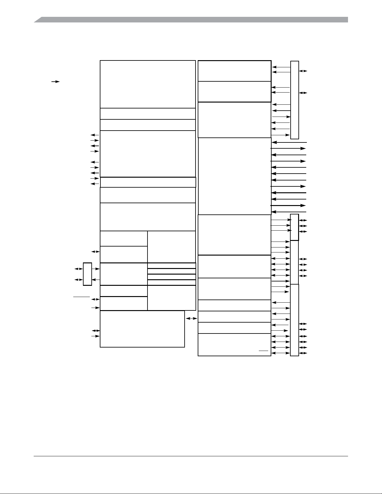
Chapter 1 Device Overview MC9S12ZVM-Family
1.5 Block Diagram
5V Analog Supply
VDDA/VSSA
VDD
VSS2
VDDF
VSS1
VDDX1/VDDX2
VSUP
BCTL
VDDC
BCTLC
BKGD
PE0
PE1
RESET
TEST
LIN0
LGND
32K, 64K, 128KB Flash with ECC
2K, 4K, 8KB RAM with ECC
512 bytes EEPROM with ECC
CAN VREG
BATS
Voltage Supply Monitor
Interrupt Module
BDC
Background
Debug Controller
EXTAL
Low Power Pierce
PTE
Oscillator
XTAL
PLL with Frequency
Modulation option
Reset Generation
and Test Entry
LINPHY0
LIN0
LGND
Voltage Regulator
(Nominal 12V)
S12ZCPU
DBG
Debug Module
4 Comparators
Trace Buffer
Clock Monitor
COP Watchdog
Real Time Interrupt
Auton. Periodic Int.
Internal RC Oscillator
ADC0
12-bit
Analog-Digital Converter
ADC1
12-bit
Analog-Digital Converter
Current Sense Circuits
GDU
Gate Drive Unit
PMF
15-bit 6 channel
Pulse Width Modulator
TIM
16-bit 4-Channel Timer
PTU
Programmable Trigger
Unit
SCI1
Asynchronous Serial IF
SCI0
Asynchronous Serial IF
CAN0
msCAN 2.0B
SPI0
Synchronous Serial IF
AN0_[4:0]
AN1_[3:0]
VRH
VRL
VRH
VRL
AMPP0
AMPM0
AMP0
AMPP1
AMPM1
AMP1
HD
CP
VCP
VLS_OUT
BST
VSSB
VBS[2:0]
HG[2:0]
HS[2:0]
VLS[2:0]
LG[2:0]
LS[2:0]
PWM0
PWM1
PWM2
PWM3
PWM4
PWM5
IOC0_0
IOC0_1
IOC0_2
IOC0_3
PTURE
PTUT0
PTUT1
RXD1
TXD1
RXD0
TXD0
RXCAN0
TXCAN0
MISO0
MOSI0
SCK0
SS0
PAD[4:0]
PAD[8:5]
PTAD / KWAD
HD
CP
VCP
VLS_OUT
BST
VSSB
VBS[2:0]
HG[2:0]
HS[2:0]
VLS[2:0]
LG[2:0]
LS[2:0]
PP0
PP1
PP2
PTP / KWP
PT0
PT1
PT2
PTT
PT3
PS0
PS1
PTS / KWS
PS2
PS3
PS4
PS5
Not all pins or all peripherals are available on all devices and packages.
Block Diagram shows the maximum configuration
Rerouting options are not shown.
Figure 1-1. MC9S12ZVM-Family Block Diagram
MC9S12ZVM Family Reference Manual Rev. 1.3
28 Freescale Semiconductor
Page 29
Chapter 1 Device Overview MC9S12ZVM-Family
1.6 Device Memory Map
Table 1-3 shows the device register memory map. All modules that can be instantiated more than once on
S12 devices are listed with an index number, even if they are only instantiated once on this device family.
Table 1-3. Module Register Address Ranges
Address Module
0x0000–0x0003 Part ID Register Section 1.6.1 4
0x0004–0x000F
0x0010–0x001F INT 16
0x0020–0x006F
0x0070–0x008F MMC 32
0x0090–0x00FF
0x0100–0x017F DBG 128
0x0180–0x01FF
0x0200–0x02FF PIM 256
0x0300–0x037F
0x0380–0x039F FTMRZ 32
0x03A0–0x03BF
0x03C0–0x03CF RAM ECC 16
0x03D0–0x04FF
0x0500–0x053F PMF 64
0x0540–0x057F
0x0580–0x059F PTU 32
0x05A0–0x05BF
0x05C0–0x05EF TIM0 48
0x05F0–0x05FF
0x0600–0x063F ADC0 64
Reserved 12
Reserved 80
MMC Reserved 112
Reserved 128
Reserved 128
Reserved 32
Reserved 304
Reserved 64
Reserved 32
Reserved 16
Size
(Bytes)
0x0640–0x067F ADC1 64
0x0680–0x069F
(1)
0x06A0–0x06BF GDU 32
0x06C0–0x06DF CPMU 32
0x06E0–0x06EF
0x06F0–0x06F7 BATS 8
0x06F8–0x06FF
0x0700–0x0707 SCI0 8
0x0708–0x070F
0x0710–0x0717 SCI1 8
MC9S12ZVM Family Reference Manual Rev. 1.3
Freescale Semiconductor 29
Reserved 32
Reserved 16
Reserved 8
Reserved 8
Page 30
Chapter 1 Device Overview MC9S12ZVM-Family
Table 1-3. Module Register Address Ranges
Address Module
0x0718–0x077F Reserved 104
0x0780–0x0787 SPI0 8
0x0788–0x07FF
0x0800–0x083F CAN0 64
0x0840–0x097F
0x0980–0x0987 LINPHY 8
0x0988–0x0FFF
Reserved 120
Reserved 320
Reserved 1656
Size
(Bytes)
1. Address range = 0x0690-0x069F on Maskset N06E
NOTE
Reserved register space shown above is not allocated to any module. This
register space is reserved for future use. Writing to these locations has no
effect. Read access to these locations returns zero.
MC9S12ZVM Family Reference Manual Rev. 1.3
30 Freescale Semiconductor
Page 31
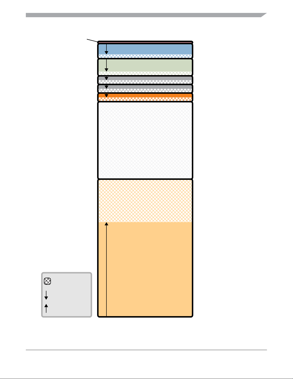
Chapter 1 Device Overview MC9S12ZVM-Family
Register Space
4 KB
RAM
max. 1 MByte - 4 KB
EEPROM
max. 1 MByte - 48 KB
Reserved
Reserved (read only)
NVM IFR
Unmapped
6 MByte
512 Byte
6 KB
256 Byte
0x00_0000
0x00_1000
0x10_0000
0x1F_4000
0x1F_8000
0x1F_C000
0x20_0000
Unmapped
address range
Low address aligned
High address aligned
0x80_0000
Program NVM
max. 8 MB
0xFF_FFFF
Figure 1-2. MC9S12ZVM-Family Global Memory Map. (See Table 1-2 for individual device details)
MC9S12ZVM Family Reference Manual Rev. 1.3
Freescale Semiconductor 31
Page 32
Chapter 1 Device Overview MC9S12ZVM-Family
1.6.1 Part ID Assignments
The part ID is located in four 8-bit registers at addresses 0x0000-0x0003. The read-only value is a unique
part ID for each revision of the chip. Table 1-4 shows the assigned part ID number and mask set number.
Table 1-4. Assigned Part ID Numbers
Device Mask Set Number Part ID Bonding Option
MC9S12ZVM128 N06E 0x00170000 LIN
MC9S12ZVM128 N06E 0x00170001 CAN-VREG
MC9S12ZVM128 N56G 0x00171000 LIN
MC9S12ZVM128
MC9S12ZVM128 0N95G 0x00172000 LIN
MC9S12ZVM128 0N95G 0x00172001 CAN-VREG
MC9S12ZVM128 1N95G 0x00172100 LIN
MC9S12ZVM128 1N95G 0x00172101 CAN-VREG
MC9S12ZVM32 TBD 0x00150000 LIN
1. This version for Freescale internal engineering puirposes only
(1)
N56G 0x00171xxx CAN-VREG / LIN
1.7 Signal Description and Device Pinouts
This section describes signals that connect off-chip. It includes pin out diagrams a table of signal
properties, and detailed discussion of signals. Internal inter module signal mapping at device level is
described in 1.8 Internal Signal Mapping.
1.7.1 Pin Assignment Overview
Table 1-5 provides a summary of which ports are available.
Table 1-5. Port Availability by Package Option
Port 64 LQFP
Port AD PAD[8:0]
Port E PE[1:0]
Port P PP[2:0]
Port S PS[5:0]
Port T PT[3:0]
sum of ports 24
MC9S12ZVM Family Reference Manual Rev. 1.3
32 Freescale Semiconductor
Page 33

Chapter 1 Device Overview MC9S12ZVM-Family
NOTE
To avoid current drawn from floating inputs, all non-bonded pins should be
configured as output or configured as input with a pull up or pull down
device enabled
1.7.2 Detailed External Signal Descriptions
This section describes the properties of signals available at device pins. Signal names associated with
modules that can be instantiated more than once on an S12 are indexed, even if the module is only
instantiated once on the
is inserted before the channel number. Thus ANx_y corresponds to AN instance x, channel number y.
1.7.2.1 RESET — External Reset Signal
The RESET signal is an active low bidirectional control signal. It acts as an input to initialize the MCU to
a known start-up state, and an output when an internal MCU function causes a reset. The
an internal pull-up device.
1.7.2.2 TEST — Test Pin
MC9S12ZVM-Family. If a signal already includes a channel number, then the index
RESET pin has
This input only pin is reserved for factory test. This pin has an internal pull-down device.
NOTE
The TEST pin must be tied to ground in all applications.
1.7.2.3 MODC — Mode C Signal
The MODC signal is used as an MCU operating mode select during reset. The state of this signal is latched
to the MODC bit at the rising edge of
RESET. The signal has an internal pull-up device.
1.7.2.4 PAD[8:0] / KWAD[8:0] — Port AD, Input Pins of ADC
PAD[8:0] are general-purpose input or output signals. The signals can be configured on per signal basis as
interrupt inputs with wake-up capability (KWAD[8:0]). These signals can have a pull-up or pull-down
device selected and enabled on per signal basis. During and out of reset the pull devices are disabled.
1.7.2.5 PE[1:0] — Port E I/O Signals
PE[1:0] are general-purpose input or output signals. The signals can have a pull-down device, enabled by
on a per pin basis. Out of reset the pull-down devices are enabled.
1.7.2.6 PP[2:0] / KWP[2:0] — Port P I/O Signals
PP[2:0] are general-purpose input or output signals. The signals can be configured on per signal basis as
interrupt inputs with wake-up capability (KWP[2:0]). They can have a pull-up or pull-down device
selected and enabled on per signal basis. During and out of reset the pull devices are disabled.
MC9S12ZVM Family Reference Manual Rev. 1.3
Freescale Semiconductor 33
Page 34

Chapter 1 Device Overview MC9S12ZVM-Family
1.7.2.7 PS[5:0] / KWS[5:0] — Port S I/O Signals
PS[5:0] are general-purpose input or output signals. The signals can be configured on per signal basis as
interrupt inputs with wake-up capability (KWS[5:0]). They can have a pull-up or pull-down device
selected and enabled on per signal basis. During and out of reset the pull-up devices are enabled.
1.7.2.8 PT[3:0] — Port T I/O Signals
PT[3:0] are general-purpose input or output signals. They can have a pull-up or pull-down device selected
and enabled on per signal basis. During and out of reset the pull devices are disabled.
1.7.2.9 AN0_[4:0], AN1_[3:0]— ADC Input Signals
These are the analog inputs of the Analog-to-Digital Converters. ADC0 has 5 analog input channels
connected to PAD port pins. ADC1 has 4 analog input channels connected to PAD port pins.
1.7.2.10 VRH, VRL — ADC Reference Signals
VRH and VRL are the reference voltage input pins for the analog-to-digital converter.
1.7.2.11 SPI0 Signals
1.7.2.11.1 SS0 Signal
This signal is associated with the slave select SS functionality of the serial peripheral interface SPI0.
1.7.2.11.2 SCK0 Signal
This signal is associated with the serial clock SCK functionality of the serial peripheral interface SPI0.
1.7.2.11.3 MISO0 Signal
This signal is associated with the MISO functionality of the serial peripheral interface SPI0. This signal
acts as master input during master mode or as slave output during slave mode.
1.7.2.11.4 MOSI0 Signal
This signal is associated with the MOSI functionality of the serial peripheral interface SPI0. This signal
acts as master output during master mode or as slave input during slave mode
1.7.2.12 SCI[1:0] Signals
1.7.2.12.1 RXD[1:0] Signals
These signals are associated with the receive functionality of the serial communication interfaces
(SCI[1:0]).
MC9S12ZVM Family Reference Manual Rev. 1.3
34 Freescale Semiconductor
Page 35

Chapter 1 Device Overview MC9S12ZVM-Family
1.7.2.12.2 TXD[1:0] Signals
These signals are associated with the transmit functionality of the serial communication interfaces
(SCI[1:0]).
1.7.2.13 CAN0 Signals
1.7.2.13.1 RXCAN0 Signal
This signal is associated with the receive functionality of the scalable controller area network controller
(MSCAN0).
1.7.2.13.2 TXCAN0 Signal
This signal is associated with the transmit functionality of the scalable controller area network controller
(MSCAN0).
1.7.2.14 Timer IOC0_[3:0] Signals
The signals IOC0_[3:0] are associated with the input capture or output compare functionality of the timer
(TIM0) module.
1.7.2.15 PWM[5:0] Signals
The signals PWM[5:0] are associated with the PMF module digital channel outputs.
1.7.2.16 PTU Signals
1.7.2.16.1 PTUT[1:0] Signals
These signals are the PTU trigger output signals. These signals are routed to pins for debugging purposes.
1.7.2.16.2 PTURE Signal
This signal is the PTU reload enable output signal. This signal is routed to a pin for debugging purposes.
1.7.2.17 Interrupt Signals — IRQ and XIRQ
IRQ is a maskable level or falling edge sensitive input. XIRQ is a non-maskable level-sensitive interrupt.
1.7.2.18 Oscillator and Clock Signals
1.7.2.18.1 Oscillator Pins — EXTAL and XTAL
EXTAL and XTAL are the crystal driver and external clock pins. On reset all the device clocks are derived
from the internal PLLCLK, independent of EXTAL and XTAL. XTAL is the oscillator output.
MC9S12ZVM Family Reference Manual Rev. 1.3
Freescale Semiconductor 35
Page 36

Chapter 1 Device Overview MC9S12ZVM-Family
1.7.2.18.2 ECLK
This signal is associated with the output of the bus clock (ECLK).
NOTE
This feature is only intended for debug purposes at room temperature.
It must not be used for clocking external devices in an application.
1.7.2.19 BDC and Debug Signals
1.7.2.19.1 BKGD — Background Debug signal
The BKGD signal is used as a pseudo-open-drain signal for the background debug communication. The
BKGD signal has an internal pull-up device.
1.7.2.19.2 PDO — Profiling Data Output
This is the profiling data output signal used when the DBG module profiling feature is enabled. This signal
is output only and provides a serial, encoded data stream that can be used by external development tools
to reconstruct the internal CPU code flow.
1.7.2.19.3 PDOCLK — Profiling Data Output Clock
This is the PDO clock signal used when the DBG module profiling feature is enabled. This signal is output
only. During code profiling this is the clock signal that can be used by external development tools to sample
the PDO signal.
1.7.2.19.4 DBGEEV — External Event Input
This signal is the DBG external event input. It is input only. Within the DBG module, it allows an external
event to force a state sequencer transition, or trace buffer entry, or to gate trace buffer entries. A falling
edge at the external event signal constitutes an event. Rising edges have no effect. The maximum frequency
of events is half the internal core bus frequency.
1.7.2.20 FAULT5 — External Fault Input
This is the PMF fault input signal, with configurable polarity, that can be used to disable PMF operation
when asserted. Asynchronous shutdown of the GDU outputs HG[2:0] and LG[2:0] is not supported. Select
QSMPm[1:0] > 0 in PMF.
1.7.2.21 LIN Physical Layer Signals
1.7.2.21.1 LIN0
This pad is connected to the single-wire LIN data bus. This signal is only available on S12ZVML versions.
1.7.2.21.2 LP0TXD
This is the LIN physical layer transmitter input signal.
MC9S12ZVM Family Reference Manual Rev. 1.3
36 Freescale Semiconductor
Page 37

Chapter 1 Device Overview MC9S12ZVM-Family
1.7.2.21.3 LP0RXD
This is the LIN physical layer receiver output signal.
1.7.2.21.4 LP0DR1
This is the LIN LP0DR1 register bit, visible at the designated pin for debug purposes.
1.7.2.22 Gate Drive Unit (GDU) Signals
These are associated with driving the external FETs.
1.7.2.22.1 HD — FET predriver High side Drain Input
This is the drain connection of the external high-side FETs. The voltage present at this input is scaled down
by an internal voltage divider, and can be routed to the internal ADC via an analog multiplexer.
This is also used as the LINPHY supply, VLINSUP.
1.7.2.22.2 VBS[2:0] - Bootstrap Capacitor Connections
These signals are the bootstrap capacitor connections for phases HS[2:0]. The capacitor connected
between HS[2:0] and these signals provides the gate voltage and current to drive the external FET.
1.7.2.22.3 HG[2:0] - High-Side Gate signals
The pins are the gate drives for the three high-side power FETs. The drivers provide a high current with
low impedance to turn on and off the high-side power FETs.
1.7.2.22.4 HS[2:0] - High-Side Source signals
The pins are the source connection for the high-side power FETs and the drain connection for the low-side
power FETs. The low voltage end of the bootstrap capacitor is also connected to this pin.
1.7.2.22.5 VLS[2:0] - Voltage Supply for Low -Side Drivers
The pins are the voltage supply pins for the three low-side FET pre-drivers. This pins should be connected
to the voltage regulator output pin VLS_OUT.
1.7.2.22.6 LG[2:0] - Low-Side Gate signals
The pins are the gate drives for the low-side power FETs. The drivers provide a high current with low
impedance to turn on and off the low-side power FETs.
1.7.2.22.7 LS[2:0] - Low-Side Source signals
The pins are the low-side source connections for the low-side power FETs. The pins are the power ground
pins used to return the gate currents from the low-side power FETs.
MC9S12ZVM Family Reference Manual Rev. 1.3
Freescale Semiconductor 37
Page 38

Chapter 1 Device Overview MC9S12ZVM-Family
1.7.2.22.8 CP - Charge Pump Output signal
This pin is the switching node of the charge pump circuit. The supply voltage for charge pump driver is
the output of the voltage regulator VLS_OUT. The output voltage of this pin switches typically between
0V and 11V. Must be left unconnected if not used.
1.7.2.22.9 VCP - Charge Pump Input for High-Side Driver Supply
This is the charge pump input for the FET high-side gate drive supply circuit. The pin must be left
unconnected if not used.
1.7.2.22.10 BST - Boost signal
This pin provides the basic switching elements required to implement a boost converter for low battery
voltage conditions. This requires external diodes, capacitors and a coil. This pin must be left unconnected
if not used.
1.7.2.22.11 VSSB - Boost Ground signal
This pin is a separate ground pin for the on chip boost converter switching device.
1.7.2.22.12 VLS_OUT - 11V Voltage Regulator Output
This pin is the output of the integrated voltage regulator. The output voltage is typically V
=11V. The
VLS
input voltage to the voltage regulator is the VSUP pin.
1.7.2.22.13 AMPP[1:0] - Current Sense Amplifier Non-Inverting Input
These are the current sense amplifier non-inverting inputs.
1.7.2.22.14 AMPM[1:0] - Current Sense Amplifier Inverting Input
These are the current sense amplifier inverting inputs.
1.7.2.22.15 AMP[1:0] - Current Sense Amplifier Output
These are the current sense amplifier outputs.
1.7.2.23 CAN Physical Interface Support
The MCU can supply an external CAN physical interface device directly, thus removing the need for an
external voltage regulator.
1.7.2.23.1 BCTLC
BCTLC provides the base current of an external bipolar that supplies an external CAN physical interface.
This signal is only available on S12ZVMC versions.
MC9S12ZVM Family Reference Manual Rev. 1.3
38 Freescale Semiconductor
Page 39

Chapter 1 Device Overview MC9S12ZVM-Family
1.7.2.23.2 VDDC
VDDC is the CANPHY supply. This is the output voltage of the external bipolar, fed back to the MCU.
This signal is only available on S12ZVMC versions.
1.7.2.24 High Current Output — EVDD1
This is a high current, low voltage drop output intended for supplying external devices in a range of up to
20mA. Configuring the pin direction as output automatically enables the high current capability.
1.7.2.25 BCTL
BCTL is the ballast connection for the on chip voltage regulator. It provides the base current of an external
bipolar for the VDDX and VDDA supplies.
1.7.3 Power Supply Pins
The power and ground pins are described below. Because fast signal transitions place high, short-duration
current demands on the power supply, use bypass capacitors with high-frequency characteristics and place
them as close to the MCU as possible.
NOTE
All ground pins must be connected together in the application.
1.7.3.1 VDDX1, VDDX2, VSSX1 — Digital I/O Power and Ground Pins
VDDX1, VDDX2 are voltage regulator outputs to supply the digital I/O drivers.
The VSSX1 pin is the ground pin for the digital I/O drivers.
Bypass requirements on VDDX2, VDDX1, VSSX1 depend on how heavily the MCU pins are loaded.
1.7.3.2 VDDA, VSSA — Power Supply Pins for ADC
These are the power supply and ground pins for the analog-to-digital converter and the voltage regulator.
1.7.3.3 VDD, VSS2 — Core Power and Ground Pin
The VDD voltage supply of nominally 1.8V is generated by the internal voltage regulator. The return
current path is through the VSS2 pin.
1.7.3.4 VDDF, VSS1 — NVM Power and Ground Pin
The VDDF voltage supply of nominally 2.8V is generated by the internal voltage regulator. The return
current path is through the VSS1 pin.
MC9S12ZVM Family Reference Manual Rev. 1.3
Freescale Semiconductor 39
Page 40

Chapter 1 Device Overview MC9S12ZVM-Family
1.7.3.5 LGND — LINPHY Ground Pin
LGND is the ground pin for the LIN physical layer LINPHY. This signal is only available on S12ZVM(L)
versions, for which it must be connected to board ground, even if the LINPHY is not used.
1.7.3.6 VSUP — Voltage Supply Pin for Voltage Regulator
VSUP is the main supply pin typically coming from the car battery/alternator in the 12V supply voltage
range. This is the voltage supply input from which the voltage regulator generates the on chip voltage
supplies. It must be protected externally against a reverse battery connection.
1.7.4 Package and Pinouts
The following package options are offered.
• 64LQFP-EP (exposed pad) with internal LIN PHY.
• 64LQFP-EP (exposed pad) without internal LIN PHY but with CAN VREG to support the addition
of a low cost external CAN PHY.
The exposed pad must be connected to a grounded contact pad on the PCB.
The exposed pad has an electrical connection within the package to VSSFLAG (VSSX die connection).
The pin out details are shown in the following diagrams. Signals in brackets denote routing options.
NOTE
For the S12ZVM32 derivative the pins 1 and 64 are unused. Pin 64 must be
connected to ground and pin1 left unconnected.
MC9S12ZVM Family Reference Manual Rev. 1.3
40 Freescale Semiconductor
Page 41
The exposed pad on the package bottom must be
connected to a grounded contact pad on the PCB.
Chapter 1 Device Overview MC9S12ZVM-Family
MODC / BKGD
LIN0
TUT0 / (LP0RXD) / RXCAN0 / RXD1 / KWS0 / PS0
PTUT1 / (LP0TXD) / TXCAN0 / TXD1 / KWS1 / PS1
MISO0 / (RXD1) / KWS2 / PS2
MOSI0 / (TXD1) / DBGEEV / KWS3 / PS3
PDOCLK / SCK0 / KWS4 / PS4
PDO / SS0 / KWS5 / PS5
BCTL
HD
VCP
BST
VSSB
CP
VLS_OUT
VSUP
LGND
646362616059585756555453525150
1
2
3
4
5
6
7
8
9
10
11
12
13
14
15
16
171819202122232425262728293031
VDDX2
PP1 / KWP1 / (PWM1) / IRQ
VSSX1
VDDX1
PP0 / EVDD1 / KWP0 / (PWM0) / ECLK / FAULT5 / XIRQ
PP2 / KWP2 / (PWM2)
VDDF
VSS1
PE0 / EXTAL
PE1 / XTAL
MC9S12ZVML Versions
64-pin LQFP-EP
VDD
TEST
VSS2
AN0_3 / KWAD3 / PAD3
AN0_4 / KWAD4 / PAD4
PT2 / IOC0_2 / (PWM5) / (SCK0)
PT1 / IOC0_1 / (PWM4) / (MOSI0) / (TXD0) / LP0DR1 / PTURE
PT0 / IOC0_0 / (PWM3) / (MISO0) / (RXD0)
VDDA
HS1
49
48
47
46
45
44
43
42
41
40
39
38
37
36
35
34
33
32
LS0
VSSA
HG1
VBS1
VLS1
LG1
LS1
LS2
LG2
VLS2
VBS2
HG2
HS2
HS0
HG0
VBS0
VLS0
LG0
RESET
PT3 / IOC0_3 / (SS0)
AN0_0 / AMP0 / KWAD0 / PAD0
AN0_1 / AMPM0 / KWAD1 / PAD1
AN0_2 / AMPP0 / KWAD2 / PAD2
AN1_0 / AMP1 / KWAD5 / PAD5
VRH / AN1_3 / KWAD8 / PAD8
AN1_2 / AMPP1 / KWAD7 / PAD7
(SS0) / AN1_1 / AMPM1 / KWAD6 / PAD6
Figure 1-3. MC9S12ZVM-Family 64-pin LQFP pin out - LIN PHY option
MC9S12ZVM Family Reference Manual Rev. 1.3
Freescale Semiconductor 41
Page 42
Chapter 1 Device Overview MC9S12ZVM-Family
The exposed pad on the package bottom must be
connected to a grounded contact pad on the PCB.
VDDC
VSSX1
PP2 / KWP2 / (PWM2)
VDDF
PP1 / KWP1 / (PWM1) / IRQ
VSS1
VDDX1
PP0 / EVDD1 / KWP0 / (PWM0) / ECLK / FAULT5 / XIRQ
PE0 / EXTAL
PT2 / IOC0_2 / (PWM5) / (SCK0)
PT1 / IOC0_1 / (PWM4) / (MOSI0) / (TXD0) / PTURE
PT0 / IOC0_0 / (PWM3) / (MISO0) / (RXD0)
PE1 / XTAL
RESET
PT3 / IOC0_3 / (SS0)
HS1
BCTLC
PTUT0 / RXCAN0 / RXD1 / KWS0 / PS0
PTUT1 / TXCAN0 / TXD1 / KWS1 / PS1
MISO0 / (RXD1) / KWS2 / PS2
MOSI0 / (TXD1) / DBGEEV / KWS3 / PS3
PDOCLK / SCK0 / KWS4 / PS4
PDO /
MODC / BKGD
SS0 / KWS5 / PS5
BCTL
HD
VCP
BST
VSSB
CP
VLS_OUT
VSUP
646362616059585756555453525150
1
2
3
4
5
6
MC9S12ZVMC Versions
7
64-pin LQFP-EP
8
9
10
11
12
13
14
15
16
171819202122232425262728293031
VDD
TEST
VSS2
VDDX2
AN0_3 / KWAD3 / PAD3
AN0_4 / KWAD4 / PAD4
AN0_0 / AMP0 / KWAD0 / PAD0
AN0_1 / AMPM0 / KWAD1 / PAD1
AN0_2 / AMPP0 / KWAD2 / PAD2
AN1_0 / AMP1 / KWAD5 / PAD5
AN1_2 / AMPP1 / KWAD7 / PAD7
VRH / AN1_3 / KWAD8 / PAD8
VDDA
49
48
47
46
45
44
43
42
41
40
39
38
37
36
35
34
33
32
LS0
VSSA
HG1
VBS1
VLS1
LG1
LS1
LS2
LG2
VLS2
VBS2
HG2
HS2
HS0
HG0
VBS0
VLS0
LG0
(SS0) / AN1_1 / AMPM1 / KWAD6 / PAD6
Figure 1-4. MC9S12ZVM-Family 64-pin LQFP pin out - External CAN PHY option
MC9S12ZVM Family Reference Manual Rev. 1.3
42 Freescale Semiconductor
Page 43
The exposed pad on the package bottom must be
connected to a grounded contact pad on the PCB.
Chapter 1 Device Overview MC9S12ZVM-Family
MODC / BKGD
N.C.
PTUT0 / RXD1 / KWS0 / PS0
PTUT1 / TXD1 / KWS1 / PS1
MISO0 / (RXD1) / KWS2 / PS2
MOSI0 / (TXD1) / DBGEEV / KWS3 / PS3
PDOCLK / SCK0 / KWS4 / PS4
PDO / SS0 / KWS5 / PS5
BCTL
HD
VCP
BST
VSSB
CP
VLS_OUT
VSUP
N.C. (connect to ground on board)
646362616059585756555453525150
1
2
3
4
5
6
7
8
9
10
11
12
13
14
15
16
171819202122232425262728293031
VDDX2
PP1 / KWP1 / (PWM1) / IRQ
VSSX1
VDDX1
PP0 / EVDD1 / KWP0 / (PWM0) / ECLK / FAULT5 / XIRQ
PP2 / KWP2 / (PWM2)
VDDF
VSS1
PE0 / EXTAL
PE1 / XTAL
MC9S12ZVM32 Version
64-pin LQFP-EP
VDD
TEST
VSS2
AN0_3 / KWAD3 / PAD3
AN0_4 / KWAD4 / PAD4
PT2 / IOC0_2 / (PWM5) / (SCK0)
PT1 / IOC0_1 / (PWM4) / (MOSI0) / PTURE
PT0 / IOC0_0 / (PWM3) / (MISO0)
VDDA
HS1
49
48
47
46
45
44
43
42
41
40
39
38
37
36
35
34
33
32
LS0
VSSA
HG1
VBS1
VLS1
LG1
LS1
LS2
LG2
VLS2
VBS2
HG2
HS2
HS0
HG0
VBS0
VLS0
LG0
RESET
PT3 / IOC0_3 / (SS0)
AN0_0 / AMP0 / KWAD0 / PAD0
AN0_1 / AMPM0 / KWAD1 / PAD1
AN0_2 / AMPP0 / KWAD2 / PAD2
AN1_0 / AMP1 / KWAD5 / PAD5
VRH / AN1_3 / KWAD8 / PAD8
AN1_2 / AMPP1 / KWAD7 / PAD7
(SS0) / AN1_1 / AMPM1 / KWAD6 / PAD6
Figure 1-5. MC9S12ZVM32 64-pin LQFP pin out
MC9S12ZVM Family Reference Manual Rev. 1.3
Freescale Semiconductor 43
Page 44
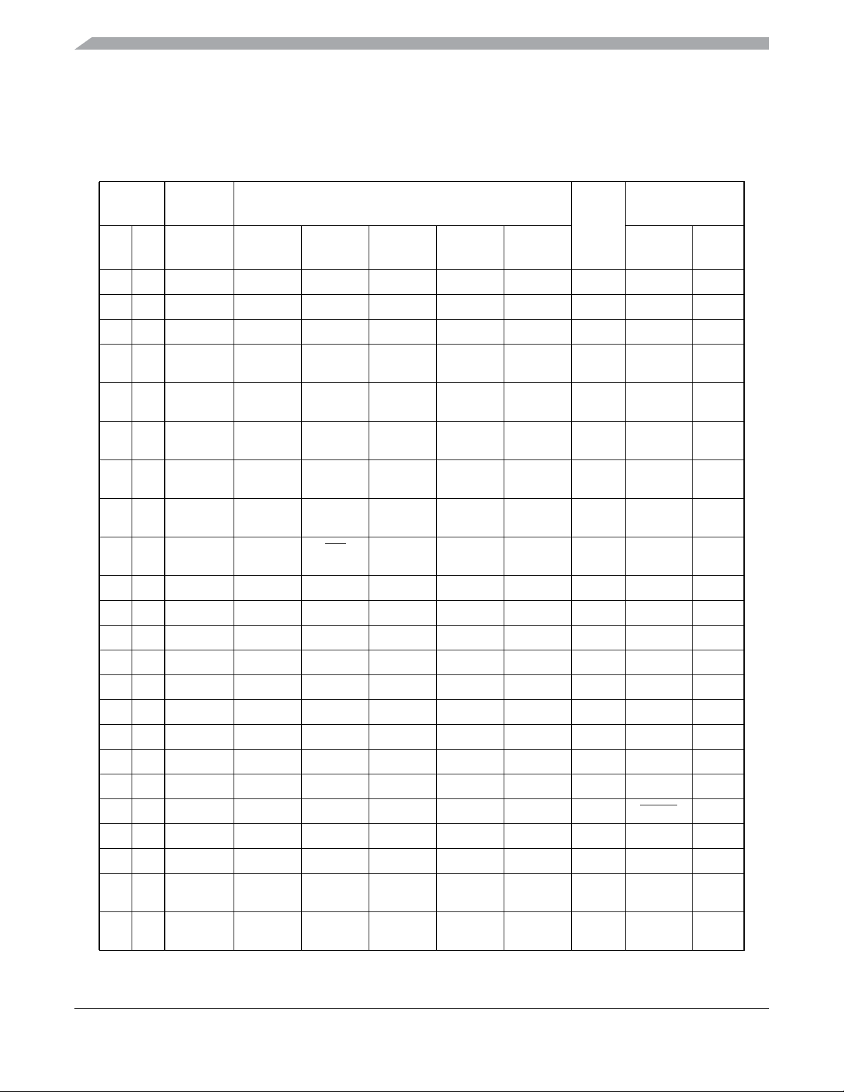
Chapter 1 Device Overview MC9S12ZVM-Family
Table 1-6. Pin Summary (Sheet 1 of 3)
LQFP
Option
64L64
Function
Power
C
Pin
1st
Func.
2nd
Func.
3rd
Func.
4th
Func.
5th
Func.
Supply
Internal Pull
Resistor
CTRL
Reset
State
1—LIN————————
— 1 BCTLC ————————
2 2 BKGD MODC ————V
3 3 PS0 KWS0 RXD1 RXCAN0 LP0RXD PTUT0 V
DDX
DDX
—Up
PERS/
Up
PPSS
4 4 PS1 KWS1 TXD1 TXCAN0 LP0TXD PTUT1 V
DDX
PERS/
Up
PPSS
5 5 PS2 KWS2 RXD1 MISO0 — — V
DDX
PERS/
Up
PPSS
6 6 PS3 KWS3 DBGEEV TXD1 MOSI0 — V
DDX
PERS/
Up
PPSS
7 7 PS4 KWS4 SCK0 PDOCLK — — V
DDX
PERS/
Up
PPSS
8 8 PS5 KWS5 SS0 PDO — — V
DDX
PERS/
Up
PPSS
9 9 BCTL ————————
1010HD————————
1111VCP————————
1212BST————————
13 13 VSSB ————————
1414CP————————
15 15 VLS_OUT ————————
16 16 VSUP —————V
17 17 VDDX2 —————V
SUP
DDX
——
——
18 18 TEST ——————RESET Down
19 19 VSS2 ————————
2020VDD—————VDD——
21 21 PAD0 KWAD0 AN0_0 AMP0 — — V
DDA
PERADL/
Off
PPSADL
22 22 PAD1 KWAD1 AN0_1 AMPM0 — — V
DDA
PERADL/
Off
PPSADL
MC9S12ZVM Family Reference Manual Rev. 1.3
44 Freescale Semiconductor
Page 45

Chapter 1 Device Overview MC9S12ZVM-Family
Table 1-6. Pin Summary (Sheet 2 of 3)
LQFP
Option
64L64
C
Pin
1st
Func.
2nd
Func.
Function
3rd
Func.
4th
Func.
5th
Func.
Power
Supply
23 23 PAD2 KWAD2 AN0_2 AMPP0 — — V
DDA
Internal Pull
Resistor
CTRL
PERADL/
Reset
State
Off
PPSADL
24 24 PAD3 KWAD3 AN0_3 — — — V
DDA
PERADL/
Off
PPSADL
25 25 PAD4 KWAD4 AN0_4 — — — V
26 26 PAD5 KWAD5 AN1_0 AMP1 — — V
DDA
DDA
PERADL/
PPSADL
PERADL/
Off
Off
PPSADL
27 27 PAD6 KWAD6 AN1_1 AMPM1 SS0 — V
DDA
PERADL/
Off
PPSADL
28 28 PAD7 KWAD7 AN1_2 AMPP1 — — V
DDA
PERADL/
Off
PPSADL
29 29 PAD8 KWAD8 AN1_3 VRH — — V
DDA
PERADH/
Off
PPSADH
3030VDDA—————V
DDA
——
31 31 VSSA ————————
3232LS0————————
3333LG0————————
34 34 VLS0 ————————
35 35 VBS0 ————————
3636HG0————————
3737HS0————————
3838HS2————————
3939HG2————————
40 40 VBS2 ————————
41 41 VLS2 ————————
4242LG2————————
4343LS2————————
4444LS1————————
4545LG1————————
46 46 VLS1 ————————
47 47 VBS1 ————————
4848HG1————————
MC9S12ZVM Family Reference Manual Rev. 1.3
Freescale Semiconductor 45
Page 46

Chapter 1 Device Overview MC9S12ZVM-Family
Table 1-6. Pin Summary (Sheet 3 of 3)
LQFP
Option
64L64
C
4949HS1————————
50 50 PT0 IOC0_0 PWM3 MISO0 RXD0 — V
51 51 PT1 IOC0_1 PWM4 MOSI0 TXD0 LP0DR1/
52 52 PT2 IOC0_2 PWM5 SCK0 — — V
53 53 PT3 IOC0_3
54 54 RESET —————V
5555PE1XTAL————V
5656PE0EXTAL————V
57 57 VSS1 ————————
58 58 VDDF —————V
59 59 PP2 KWP2 PWM2 — — — V
Pin
1st
Func.
2nd
Func.
SS0 — — — V
Function
3rd
Func.
4th
Func.
5th
Func.
PTURE
Power
Supply
DDX
V
DDX
DDX
DDX
DDX
DDX
DDX
DDF
DDX
Internal Pull
Resistor
CTRL
PERT/
PPST
PERT/
PPST
PERT/
PPST
PERT/
PPST
TEST pin Up
PERE/
PPSE
PERE/
PPSE
——
PERP/
PPSP
Reset
State
Off
Off
Off
Off
Down
Down
Off
60 60 PP1 KWP1 PWM1 IRQ — — V
61 61 PP0 /
EVDD1
62 62 VDDX1 —————V
63 63 VSSX1 ————————
64 — LGND ————————
— 64 VDDC ————————
KWP0 PWM0 ECLK FAULT5 XIRQ V
DDX
DDX
DDX
PERP/
PPSP
PERP/
PPSP
——
Off
Off
1.8 Internal Signal Mapping
This section specifies the mapping of inter-module signals at device level.
1.8.1 ADC Connectivity
1.8.1.1 ADC Reference Voltages
For both ADC modules, VRH_1 is mapped to VDDA; VRH_0 is mapped to PAD[8]; VRL_0 and VRL_1
are both mapped to VSSA, whereby VRL_1 is the preferred reference for low noise.
MC9S12ZVM Family Reference Manual Rev. 1.3
46 Freescale Semiconductor
Page 47
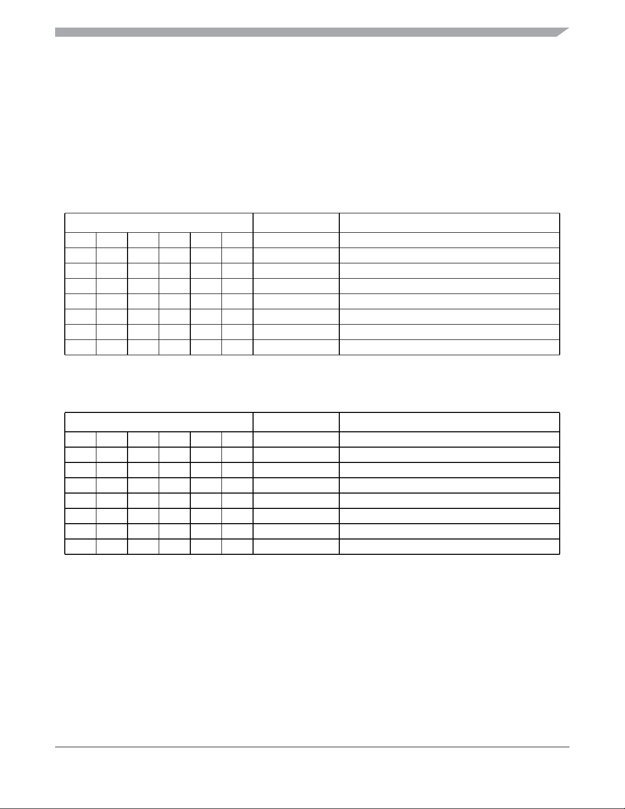
Chapter 1 Device Overview MC9S12ZVM-Family
1.8.1.2 ADC Internal Channels
The ADC0 and ADC1 internal channel mapping is shown in Table 1-7 and Table 1-8 respectively.
The GDU current sense amplifier outputs are mapped to pins with ADC input functionality. Thus
configuring the ADC to convert these pin channels automatically converts the current sense outputs.
The ADC internal temperature sensors must be calibrated by the user. No electrical parameters are
specified for these sensors. The VREG temperature sensor electrical parameters are given in the
appendices.
Table 1-7. Usage of ADC0 Internal Channels
ADCCMD_1 CH_SEL[5:0]
0 0 1 0 0 0 Internal_0 ADC0 temperature sensor
0 0 1 0 0 1 Internal_1 VREG temperature sensor or bandgap (V
0 0 1 0 1 0 Internal_2 GDU phase multiplexer voltage
0 0 1 0 1 1 Internal_3 GDU DC link voltage monitor
0 0 1 1 0 0 Internal_4 BATS VSUP sense voltage
0 0 1 1 0 1 Internal_5 Reserved
0 0 1 1 1 0 Internal_6 Reserved
0 0 1 1 1 1 Internal_7 Reserved
1. Selectable in CPMU
ADC Channel
Usage
Table 1-8. Usage of ADC1 Internal Channels
ADCCMD_1 CH_SEL[5:0]
0 0 1 0 0 0 Internal_0 ADC1 temperature sensor
0 0 1 0 0 1 Internal_1 VREG temperature sensor or bandgap (V
0 0 1 0 1 0 Internal_2 GDU phase multiplexer voltage
0 0 1 0 1 1 Internal_3 GDU DC link voltage monitor
0 0 1 1 0 0 Internal_4 Reserved
0 0 1 1 0 1 Internal_5 Reserved
0 0 1 1 1 0 Internal_6 Reserved
0 0 1 1 1 1 Internal_7 Reserved
1. Selectable in CPMU
ADC Channel
Usage
BG
BG
(1)
)
(1)
)
1.8.2 Motor Control Loop Signals
The motor control loop signals are described in 1.13.3.1 Motor Control Loop Overview
MC9S12ZVM Family Reference Manual Rev. 1.3
Freescale Semiconductor 47
Page 48

Chapter 1 Device Overview MC9S12ZVM-Family
1.8.3 Device Level PMF Connectivity
Table 1-9. Mapping of PMF signals
PMF Connection
Channel0 High-Side Gate and Source Pins HG[0], HS[0]
Channel1 Low-Side Gate and Source Pins LG[0], LS[0]
Channel2 High-Side Gate and Source Pins HG[1], HS[1]
Channel3 Low-Side Gate and Source Pins LG[1], LS[1]
Channel4 High-Side Gate and Source Pins HG[2], HS[2]
Channel5 Low-Side Gate and Source Pins LG[2], LS[2]
FAULT5 External FAULT5 pin
FAULT4 HD Over voltage or GDU over current
FAULT3 VLS under voltage
FAULT2 GDU Desaturation[2] or GDU over current
FAULT1 GDU Desaturation[1] or GDU over current
FAULT0 GDU Desaturation[0] or GDU over current
IS2 GDU Phase Status[2]
IS1 GDU Phase Status[1]
IS0 GDU Phase Status[0]
async_event_edge_sel[1:0] Tied to b11 (both edges active)
1.8.4 BDC Clock Source Connectivity
Usage
The BDC clock, BDCCLK, is mapped to the IRCCLK generated in the CPMU module.
The BDC clock, BDCFCLK is mapped to the device bus clock, generated in the CPMU module.
1.8.5 LINPHY Connectivity
The VLINPHY supply is connected to the device HD pin.
1.8.6 FTMRZ Connectivity
The soc_erase_all_req input to the flash module is driven directly by a BDC erase flash request resulting
from the BDC ERASE_FLASH command.
The FTMRZ FCLKDIV register is forced to 0x05 by the BDC ERASE_FLASH command. This
configures the clock frequency correctly for the initial bus frequency on leaving reset. The bus frequency
must not be changed before launching the ERASE_FLASH command.
1.8.7 CPMU Connectivity
The API clock generated in the CPMU is not mapped to a device pin in the MC9S12ZVM-Family.
MC9S12ZVM Family Reference Manual Rev. 1.3
48 Freescale Semiconductor
Page 49

Chapter 1 Device Overview MC9S12ZVM-Family
1.9 Modes of Operation
The MCU can operate in different modes. These are described in 1.9.1 Chip Configuration Modes.
The MCU can operate in different power modes to facilitate power saving when full system performance
is not required. These are described in 1.9.3 Low Power Modes.
Some modules feature a software programmable option to freeze the module status whilst the background
debug module is active to facilitate debugging. This is referred to as freeze mode at module level.
1.9.1 Chip Configuration Modes
The different modes and the security state of the MCU affect the debug features (enabled or disabled).
The operating mode out of reset is determined by the state of the MODC signal during reset (Table 1-10).
The MODC bit in the MODE register shows the current operating mode and provides limited mode
switching during operation. The state of the MODC signal is latched into this bit on the rising edge of
RESET.
Table 1-10. Chip Modes
Chip Modes MODC
Normal single chip 1
Special single chip 0
1.9.1.1 Normal Single-Chip Mode
This mode is intended for normal device operation. The opcode from the on-chip memory is being
executed after reset (requires the reset vector to be programmed correctly). The processor program is
executed from internal memory.
1.9.1.2 Special Single-Chip Mode
This mode is used for debugging operation, boot-strapping, or security related operations. The background
debug mode (BDM) is active on leaving reset in this mode.
1.9.2 Debugging Modes
The background debug mode (BDM) can be activated by the BDC module or directly when resetting into
Special Single-Chip mode. Detailed information can be found in the BDC module section.
Writing to internal memory locations using the debugger, whilst code is running or at a breakpoint, can
change the flow of application code.
The MC9S12ZVM-Family supports BDC communication throughout the device Stop mode. During Stop
mode, writes to control registers can alter the operation and lead to unexpected results. It is thus
recommended not to reconfigure the peripherals during STOP using the debugger.
MC9S12ZVM Family Reference Manual Rev. 1.3
Freescale Semiconductor 49
Page 50

Chapter 1 Device Overview MC9S12ZVM-Family
The DBG module supports breakpoint, tracing and profiling features. At board level the profiling pins can
use the same 6-pin connector typically used for the BDC BKGD pin. The connector pin mapping shown
in Figure 1-6 is supported by device evaluation boards and leading development tool vendors.
GND BKGD
2
1
PDO
3
4
RST
5
PDOCLK
VDDX
Figure 1-6. Standard Debug Connector Pin Mapping
6
1.9.3 Low Power Modes
The device has two dynamic-power modes (run and wait) and two static low-power modes stop and pseudo
stop). For a detailed description refer to the CPMU section.
• Dynamic power mode: Run
— Run mode is the main full performance operating mode with the entire device clocked. The user
can configure the device operating speed through selection of the clock source and the phase
locked loop (PLL) frequency. To save power, unused peripherals must not be enabled.
• Dynamic power mode: Wait
— This mode is entered when the CPU executes the WAI instruction. In this mode the CPU does
not execute instructions. The internal CPU clock is switched off. All peripherals can be active
in system wait mode. For further power consumption the peripherals can individually turn off
their local clocks. Asserting
RESET, XIRQ, IRQ, or any other interrupt that is not masked,
either locally or globally by a CCR bit, ends system wait mode.
• Static power modes:
Static power (Stop) modes are entered following the CPU STOP instruction unless an NVM
command is active. When no NVM commands are active, the Stop request is acknowledged and
the device enters either Stop or Pseudo Stop mode. Further to the general system aspects of Stop
mode discussed here, the motor control loop specific considerations are described in
Section 1.13.3.10.
— Pseudo-stop: In this mode the system clocks are stopped but the oscillator is still running and
the real time interrupt (RTI), watchdog (COP) and Autonomous Periodic Interrupt (API) may
be enabled. Other peripherals are turned off. This mode consumes more current than system
STOP mode but, as the oscillator continues to run, the full speed wake up time from this mode
is significantly shorter.
— Stop: In this mode the oscillator is stopped and clocks are switched off. The counters and
dividers remain frozen. The autonomous periodic interrupt (API) may remain active but has a
very low power consumption. The key pad, SCI and MSCAN transceiver modules can be
configured to wake the device, whereby current consumption is negligible.
If the BDC is enabled in Stop mode, the VREG remains in full performance mode and the
CPMU continues operation as in run mode. With BDC enabled and BDCCIS bit set, then all
clocks remain active to allow BDC access to internal peripherals. If the BDC is enabled and
MC9S12ZVM Family Reference Manual Rev. 1.3
50 Freescale Semiconductor
Page 51

Chapter 1 Device Overview MC9S12ZVM-Family
BDCCIS is clear, then the BDCSI clock remains active, but bus and core clocks are disabled.
With the BDC enabled during Stop, the VREG full performance mode and clock activity lead
to higher current consumption than with BDC disabled. If the BDC is enabled in Stop mode,
then the BATS voltage monitoring remains enabled.
1.10 Security
The MCU security mechanism prevents unauthorized access to the flash memory. It must be emphasized
that part of the security must lie with the application code. An extreme example would be application code
that dumps the contents of the internal memory. This would defeat the purpose of security. Also, if an
application has the capability of downloading code through a serial port and then executing that code (e.g.
an application containing bootloader code), then this capability could potentially be used to read the
EEPROM and Flash memory contents even when the microcontroller is in the secure state. In this example,
the security of the application could be enhanced by requiring a response authentication before any code
can be downloaded.
Device security details are also described in the flash block description.
1.10.1 Features
The security features of the S12Z chip family are:
• Prevent external access of the non-volatile memories (Flash, EEPROM) content
• Restrict execution of NVM commands
1.10.2 Securing the Microcontroller
The chip can be secured by programming the security bits located in the options/security byte in the Flash
memory array. These non-volatile bits keep the device secured through reset and power-down.
This byte can be erased and programmed like any other Flash location. Two bits of this byte are used for
security (SEC[1:0]). The contents of this byte are copied into the Flash security register (FSEC) during a
reset sequence.
The meaning of the security bits SEC[1:0] is shown in Table 1-11. For security reasons, the state of device
security is controlled by two bits. To put the device in unsecured mode, these bits must be programmed to
SEC[1:0] = ‘10’. All other combinations put the device in a secured mode. The recommended value to put
the device in secured state is the inverse of the unsecured state, i.e. SEC[1:0] = ‘01’.
Table 1-11. Security Bits
SEC[1:0] Security State
00 1 (secured)
01 1 (secured)
10 0 (unsecured)
11 1 (secured)
MC9S12ZVM Family Reference Manual Rev. 1.3
Freescale Semiconductor 51
Page 52

Chapter 1 Device Overview MC9S12ZVM-Family
NOTE
Please refer to the Flash block description for more security byte details.
1.10.3 Operation of the Secured Microcontroller
By securing the device, unauthorized access to the EEPROM and Flash memory contents is prevented.
Secured operation has the following effects on the microcontroller:
1.10.3.1 Normal Single Chip Mode (NS)
• Background debug controller (BDC) operation is completely disabled.
• Execution of Flash and EEPROM commands is restricted (described in flash block description).
1.10.3.2 Special Single Chip Mode (SS)
• Background debug controller (BDC) commands are restricted
• Execution of Flash and EEPROM commands is restricted (described in flash block description).
In special single chip mode the device is in active BDM after reset. In special single chip mode on a secure
device, only the BDC mass erase and BDC control and status register commands are possible. BDC access
to memory mapped resources is disabled. The BDC can only be used to erase the EEPROM and Flash
memory without giving access to their contents.
1.10.4 Unsecuring the Microcontroller
Unsecuring the microcontroller can be done using three different methods:
1. Backdoor key access
2. Reprogramming the security bits
3. Complete memory erase
1.10.4.1 Unsecuring the MCU Using the Backdoor Key Access
In normal single chip mode, security can be temporarily disabled using the backdoor key access method.
This method requires that:
• The backdoor key has been programmed to a valid value
• The KEYEN[1:0] bits within the Flash options/security byte select ‘enabled’.
• The application program programmed into the microcontroller has the capability to write to the
backdoor key locations
The backdoor key values themselves would not normally be stored within the application data, which
means the application program would have to be designed to receive the backdoor key values from an
external source (e.g. through a serial port)
The backdoor key access method allows debugging of a secured microcontroller without having to erase
the Flash. This is particularly useful for failure analysis.
MC9S12ZVM Family Reference Manual Rev. 1.3
52 Freescale Semiconductor
Page 53
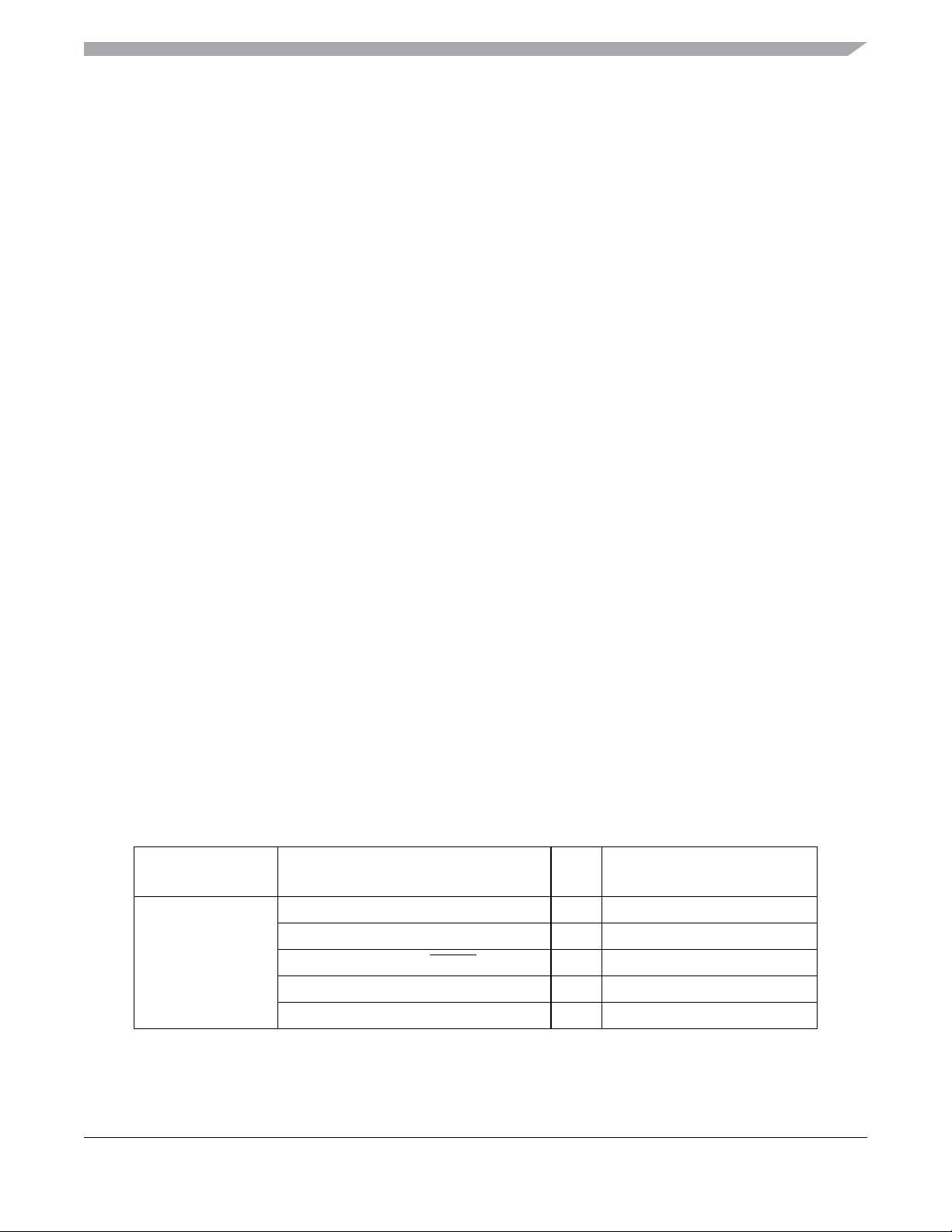
Chapter 1 Device Overview MC9S12ZVM-Family
NOTE
No backdoor key word is allowed to have the value 0x0000 or 0xFFFF.
1.10.5 Reprogramming the Security Bits
Security can also be disabled by erasing and reprogramming the security bits within the flash
options/security byte to the unsecured value. Since the erase operation will erase the entire sector
(0x7F_FE00–0x7F_FFFF) the backdoor key and the interrupt vectors will also be erased; this method is
not recommended for normal single chip mode. The application software can only erase and program the
Flash options/security byte if the Flash sector containing the Flash options/security byte is not protected
(see Flash protection). Thus Flash protection is a useful means of preventing this method. The
microcontroller enters the unsecured state after the next reset following the programming of the security
bits to the unsecured value.
This method requires that:
• The application software previously programmed into the microcontroller has been designed to
have the capability to erase and program the Flash options/security byte.
• The Flash sector containing the Flash options/security byte is not protected.
1.10.6 Complete Memory Erase
The microcontroller can be unsecured by erasing the entire EEPROM and Flash memory contents. If
ERASE_FLASH is successfully completed, then the Flash unsecures the device and programs the security
byte automatically.
1.11 Resets and Interrupts
1.11.1 Resets
Table 1-12. lists all reset sources and the vector locations. Resets are explained in detail in the Chapter 8,
“S12 Clock, Reset and Power Management Unit (S12CPMU_UHV_V6)”.
Table 1-12. Reset Sources and Vector Locations
Vector Address Reset Source
0xFFFFFC Power-On Reset (POR) None None
Low Voltage Reset (LVR) None None
External pin RESET None None
CCR
Mask
Local Enable
Clock monitor reset None OSCE Bit in CPMUOSC register
COP watchdog reset None CR[2:0] in CPMUCOP register
MC9S12ZVM Family Reference Manual Rev. 1.3
Freescale Semiconductor 53
Page 54
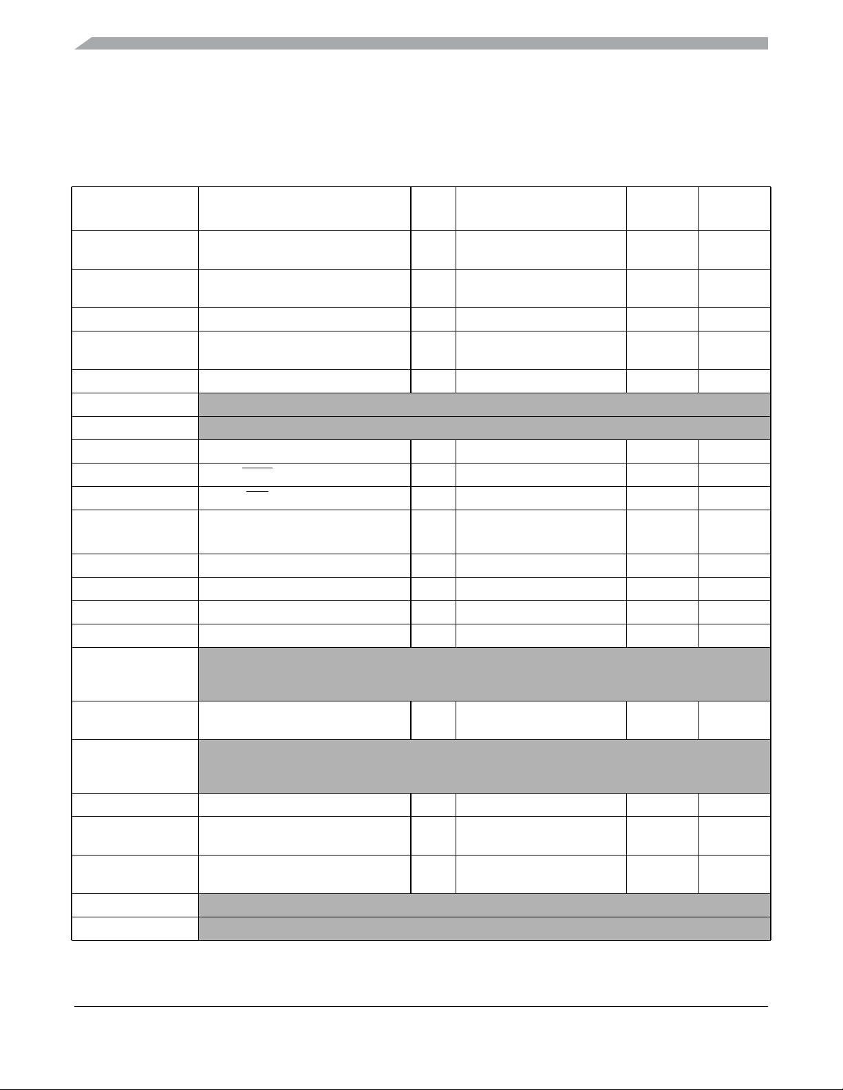
Chapter 1 Device Overview MC9S12ZVM-Family
1.11.2 Interrupt Vectors
Table 1-13 lists all interrupt sources and vectors in the default order of priority. The interrupt module
description provides an interrupt vector base register (IVBR) to relocate the vectors.
Table 1-13. Interrupt Vector Locations (Sheet 1 of 4)
Vector Address
Vector base + 0x1F8 Unimplemented page1 op-code trap
Vector base + 0x1F4 Unimplemented page2 op-code trap
Vector base + 0x1F0 Software interrupt instruction (SWI) None None - -
Vector base + 0x1EC System call interrupt instruction
Vector base + 0x1E8 Machine exception None None - Vector base + 0x1E4
Vector base + 0x1E0
Vector base + 0x1DC Spurious interrupt — None - -
Vector base + 0x1D8
Vector base + 0x1D4
Vector base + 0x1D0 RTI time-out interrupt I bit CPMUINT (RTIE)
Vector base + 0x1CC TIM0 timer channel 0 I bit TIM0TIE (C0I) No Yes
Vector base + 0x1C8 TIM0 timer channel 1 I bit TIM0TIE (C1I) No Yes
(1)
Interrupt Source
(SPARE)
(TRAP)
(SYS)
XIRQ interrupt request X bit None Yes Yes
IRQ interrupt request I bit IRQCR(IRQEN) Yes Yes
CCR
Mask
None None - -
None None - -
None None - -
Reserved
Reserved
Local Enable
Wake up
from STOP
SeeCPMU
section
Wake up
fromWAIT
Yes
Vector base + 0x1C4 TIM0 timer channel 2 I bit TIM0TIE (C2I) No Yes
Vector base + 0x1C0 TIM0 timer channel 3 I bit TIM0TIE (C3I) No Yes
Vector base + 0x1BC
to
Vector base + 0x1B0
Vector base + 0x1AC TIM0 timer overflow I bit TIM0TSCR2(TOI) No Yes
Vector base + 0x1A8
to
Vector base + 0x1A4
Vector base + 0x1A0 SPI0 I bit SPI0CR1 (SPIE, SPTIE) No Yes
Vector base + 0x19C SCI0 I bit SCI0CR2
Vector base + 0x198 SCI1 I bit SCI1CR2
Vector base + 0x194
Vector base + 0x190
MC9S12ZVM Family Reference Manual Rev. 1.3
Reserved
Reserved
Yes Yes
(TIE, TCIE, RIE, ILIE)
Yes Yes
(TIE, TCIE, RIE, ILIE)
Reserved
Reserved
54 Freescale Semiconductor
Page 55
Chapter 1 Device Overview MC9S12ZVM-Family
Table 1-13. Interrupt Vector Locations (Sheet 1 of 4)
Vector Address
(1)
Interrupt Source
CCR
Mask
Local Enable
Vector base + 0x18C ADC0 Error I bit ADC0EIE (IA_EIE,
Wake up
from STOP
No Yes
Wake up
fromWAIT
CMD_EIE, EOL_EIE,
TRIG_EIE, RSTAR_EIE,
LDOK_EIE)
ADC0IE(CONIF_OIE)
Vector base + 0x188 ADC0 conversion sequence abort I bit ADC0IE(SEQAD_IE) No Yes
Vector base + 0x184 ADC0 conversion complete I bit ADC0CONIE[15:0] No Yes
Vector base + 0x180
Oscillator status interrupt I bit
CPMUINT (OSCIE)
No Yes
Vector base + 0x17C PLL lock interrupt I bit CPMUINT (LOCKIE) No Yes
Vector base + 0x178
to
Reserved
Vector base + 0x174
Vector base + 0x170 RAM error I bit EECIE (SBEEIE) No Yes
Vector base + 0x16C
to
Reserved
Vector base + 0x168
Vector base + 0x164 FLASH error I bit FERCNFG (SFDIE) No Yes
Vector base + 0x160 FLASH command I bit FCNFG (CCIE) No Yes
Vector base + 0x15C CAN0 wake-up I bit CAN0RIER (WUPIE) Yes Yes
Vector base + 0x158 CAN0 errors I bit CAN0RIER (CSCIE, OVRIE) No Yes
Vector base + 0x154 CAN0 receive I bit CAN0RIER (RXFIE) No Yes
Vector base + 0x150 CAN0 transmit I bit CAN0TIER (TXEIE[2:0]) No Yes
Vector base + 0x14C
to
Reserved
Vector base + 0x148
Vector base + 0x144 LINPHY over-current interrupt I bit LPIE (LPDTIE,LPOCIE) No Yes
Vector base + 0x140 BATS supply voltagemonitor interrupt I bit BATIE (BVHIE,BVLIE) No Yes
Vector base + 0x13C GDU Desaturation Error I bit GDUIE (GDSEIE) No Yes
Vector base + 0x138 GDU Voltage Limit Detected I bit GDUIE (GOCIE, GHHDFIE,
No Yes
GLVLSFIE)
Vector base + 0x134
to
Reserved
Vector base + 0x128
Vector base + 0x124 Port S interrupt I bit PIES[5:0] Yes Yes
Vector base + 0x120 Reserved
MC9S12ZVM Family Reference Manual Rev. 1.3
Freescale Semiconductor 55
Page 56
Chapter 1 Device Overview MC9S12ZVM-Family
Table 1-13. Interrupt Vector Locations (Sheet 1 of 4)
Vector Address
(1)
Interrupt Source
CCR
Mask
Local Enable
Vector base + 0x11C ADC1 Error I bit ADC1EIE (IA_EIE,
Wake up
from STOP
No Yes
Wake up
fromWAIT
CMD_EIE, EOL_EIE,
TRIG_EIE, RSTAR_EIE,
LDOK_EIE)
ADC1IE(CONIF_OIE)
Vector base + 0x118 ADC1 conversion sequence abort I bit ADC1IE(SEQAD_IE) No Yes
Vector base + 0x114 ADC1 conversion complete I bit ADC1CONIE[15:0] No Yes
Vector base + 0x110
Reserved
Vector base + 0x10C Port P interrupt I bit PIEP[2:0] Yes Yes
Vector base + 0x108 EVDD1 over-current interrupt I bit PIEP(OCIE1) No Yes
Vector base + 0x104 Low-voltage interrupt (LVI) I bit CPMULVCTL (LVIE) No Yes
Vector base + 0x100 Autonomous periodical interrupt
(API)
I bit
CPMUAPICTRL (APIE)
Yes Yes
Vector base + 0xFC High temperature interrupt I bit CPMUHTCTL(HTIE) Yes Yes
Vector base + 0xF8
Vector base + 0xF4 Port AD interrupt I bit PIEADH(PIEADH0)
Reserved
Yes Yes
PIEADL(PIEADL[7:0])
Vector base + 0xF0 PTU Reload Overrun I bit PTUIEH(PTUROIE) No Yes
Vector base + 0xEC PTU Trigger0 Error I bit PTUIEL(TG0AEIE,
No Yes
TG0REIE,TG0TEIE)
Vector base + 0xE8 PTU Trigger1 Error I bit PTUIEL(TG1AEIE,TG1REIE,
No Yes
TG1TEIE)
Vector base + 0xE4 PTU Trigger0 Done I bit PTUIEL(TG0DIE) No Yes
Vector base + 0xE0 PTU Trigger1 Done I bit PTUIEL(TG1DIE) No Yes
Vector base + 0xDC
to
Reserved
Vector base + 0xD4
Vector base + 0xD0 PMF Reload A I bit PMFENCA(PWMRIEA) No Yes
Vector base + 0xCC PMF Reload B I bit PMFENCB(PWMRIEB) No Yes
Vector base + 0xC8 PMF Reload C I bit PMFENCC(PWMRIEC) No Yes
Vector base + 0xC4 PMF Fault I bit PMFFIE(FIE[5:0]) No Yes
Vector base + 0xC0 PMF Reload Overrun I bit PMFROIE(PMFROIEA,PMF
No Yes
ROIEB,PMFROIEC)
Vector base + 0xBC
to
Reserved
Vector base + 0x10
1. 15 bits vector address based
MC9S12ZVM Family Reference Manual Rev. 1.3
56 Freescale Semiconductor
Page 57

Chapter 1 Device Overview MC9S12ZVM-Family
1.11.3 Effects of Reset
When a reset occurs, MCU registers and control bits are initialized. Refer to the respective block sections
for register reset states.
On each reset, the Flash module executes a reset sequence to load Flash configuration registers.
1.11.3.1 Flash Configuration Reset Sequence Phase
On each reset, the Flash module will hold CPU activity while loading Flash module registers from the
Flash memory. If double faults are detected in the reset phase, Flash module protection and security may
be active on leaving reset. This is explained in more detail in the Flash module description.
1.11.3.2 Reset While Flash Command Active
If a reset occurs while any Flash command is in progress, that command will be immediately aborted. The
state of the word being programmed or the sector/block being erased is not guaranteed.
1.11.3.3 I/O Pins
Refer to the PIM section for reset configurations of all peripheral module ports.
1.11.3.4 RAM
The system RAM arrays, including their ECC syndromes, are initialized following a power on reset. All
other RAM arrays are not initialized out of any type of reset.
With the exception of a power-on-reset the RAM content is unaltered by a reset occurrence.
1.12 Module device level dependencies
1.12.1 CPMU COP Configuration
The COP time-out rate bits CR[2:0] and the WCOP bit in the CPMUCOP register are loaded from the
Flash configuration field byte at global address 0xFF_FE0E during the reset sequence. See Table 1-14 and
Table 1-15 for coding.
MC9S12ZVM Family Reference Manual Rev. 1.3
Freescale Semiconductor 57
Page 58
Chapter 1 Device Overview MC9S12ZVM-Family
Table 1-14. Initial COP Rate Configuration
NV[2:0] in
FOPT Register
000 111
001 110
010 101
011 100
100 011
101 010
110 001
111 000
Table 1-15. Initial WCOP Configuration
NV[3] in
FOPT Register
10
01
CR[2:0] in
CPMUCOP Register
WCOP in
CPMUCOP Register
1.12.2 CPMU High Temperature Trimming
The value loaded from the flash into the CPMUHTTR register is a default value for the device family.
There is no device specific trimming carried out during production. The specified V
value that is part dependent and should thus be calibrated.
value is a typical
HT
1.12.3 Flash IFR Mapping
Table 1-16. Flash IFR Mapping
1514131211109876543210 IFR Byte Address
ADC0 reference conversion using VDDA/VSSA
ADC0 reference conversion using PAD8/VSSA
ADC1 reference conversion using VDDA/VSSA
ADC1 reference conversion using PAD8/VSSA
0x1F_C040 & 0x1F_C041
0x1F_C042 & 0x1F_C043
0x1F_C044 & 0x1F_C045
0x1F_C046 & 0x1F_C047
1.13 Application Information
1.13.1 ADC Calibration
For applications that do not provide external ADC reference voltages, the VDDA/VSSA supplies can be
used as sources for VRH/VRL respectively. Since the VDDA must be connected to VDDX at board level
in the application, the accuracy of the VDDA reference is limited by the internal voltage regulator
accuracy. In order to compensate for VDDA reference voltage variation in this case, the reference voltage
MC9S12ZVM Family Reference Manual Rev. 1.3
58 Freescale Semiconductor
Page 59

Chapter 1 Device Overview MC9S12ZVM-Family
is measured during production test using the internal reference voltage VBG, which has a narrow variation
over temperature and external voltage supply. V
(Table 1-7,Table 1-8). The resulting 12-bit left justified ADC conversion results of V
is mapped to an internal channel of each ADC module
BG
are stored to the
BG
flash IFR for reference, as listed in Table 1-16.
The measurement conditions of the reference conversion are listed in the device electrical parameters
appendix. By measuring the voltage V
reference value in the IFR, it is possible to determine the current ADC reference voltage V
in the application environment and comparing the result to the
BG
:
RH
StoredReference
V
------------------------------------------------------ -
RH
ConvertedReference
5V•=
The exact absolute value of an analog conversion can be determined as follows:
StoredReference 5V•
------------------------------------------------------------------
Result ConvertedADInput
•=
ConvertedReference 2
n
•
With:
ConvertedADInput: Result of the analog to digital conversion of the desired pin
ConvertedReference: Result of internal channel conversion
StoredReference: Value in IFR location
n: ADC resolution (12 bit)
NOTE
The ADC reference voltage V
must remain at a constant level throughout
RH
the conversion process.
1.13.2 SCI Baud Rate Detection
The baud rate for SCI0 and SCI1 is achieved by using a timer channel to measure the data rate on the RXD
signal.
1. Establish the link:
— For SCI0: Set [T0IC3RR1:T0IC3RR0]=0b01 to disconnect IOC0_3 from TIM0 input capture
channel 3 and reroute the timer input to the RXD0 signal of SCI0.
— For SCI1: Set [T0IC3RR1:T0IC3RR0]=0b10 to disconnect IOC0_3 from TIM0 input capture
channel 3 and reroute the timer input to the RXD1 signal of SCI1.
2. Determine pulse width of incoming data: Configure TIM0 IC3 to measure time between incoming
signal edges.
1.13.3 Motor Control Application Overview
The following sections provide information for using the device in motor control applications. These
sections provide a description of motor control loop considerations that are not detailed in the individual
MC9S12ZVM Family Reference Manual Rev. 1.3
Freescale Semiconductor 59
Page 60

Chapter 1 Device Overview MC9S12ZVM-Family
module sections, since they concern device level inter module operation specific for motor control. More
detailed information is available in application notes. The applications described are as follows:
1. BDCM - wiper pumps fans
2. BLDCM - pumps, fans and blowers
– based on Hall sensors
– sensorless based on back-EMF zero crossing comparators
– sensorless based on back-EMF ADC measurements
3. PMSM - high-end wiper, pumps, fans and blowers
– simple sinewave commutation with position sensor Hall effect, sine-cos
– FOC with sine-cos position sensor
– sensorless 3-phase sinewave control
MC9S12ZVM Family Reference Manual Rev. 1.3
60 Freescale Semiconductor
Page 61
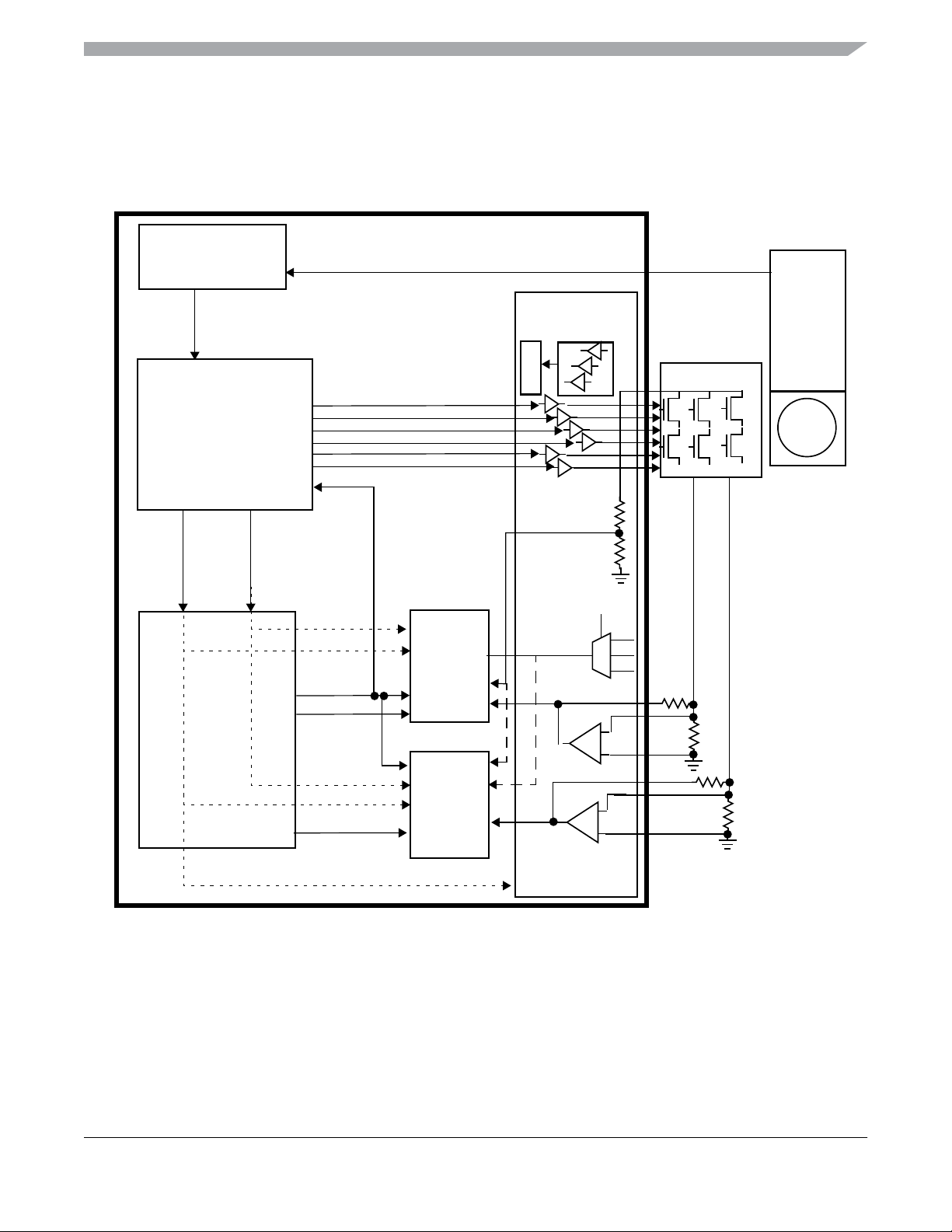
Chapter 1 Device Overview MC9S12ZVM-Family
1.13.3.1 Motor Control Loop Overview
The mapping of motor control events at device level as depicted in Figure 1-7 is listed in Table 1-17,
whereby the columns list the names used in the module level descriptions
Figure 1-7. Internal Control Loop Configuration
TIM
OC0
GDU
commutation_event
zero crossing
comparators
PMF
reloada
reload
PTU
async_reload
If PTU enabled
async reload
async reload
reload
glb_ldok
trigger_0
If PTU enabled
async reload
reload
glb_ldok
ADC0
ADC1
GPHS
dc_bus_voltage
back-EMF
PHMUX
P1
P2
P3
SENSOR
M
dc_bus_current
trigger_1
reload
The control loop consists of the PMF, GDU, ADC and PTU modules. The control loop operates using
either static, dynamic or asynchronous timing. In the following text the event names given in bold type
correspond to those shown in Figure 1-7. The PTU and ADC operate using lists stored in memory. These
lists define trigger points for the PTU, commands for the ADC and results from the ADC. If the PTU is
enabled the reload and async_reload events are immediately passed through to the ADC and GDU
modules.
MC9S12ZVM Family Reference Manual Rev. 1.3
Freescale Semiconductor 61
Page 62
Chapter 1 Device Overview MC9S12ZVM-Family
.
Table 1-17. Control Loop Events
Device Level Event TIM PMF PTU ADC0 ADC1
commutation_event OC0
reload
async_reload
trigger_0
trigger_1
glb_ldok
1. TIM channel OC0 must be configured to toggle on both edges.
2. PMF events reloadb and reloadc are not connected at device level
(1)
—
—
——
——
—
commutation_event
reloada
async_reload async_reload Seq_abort Seq_abort
(2)
glb_ldok glb_ldok LoadOK LoadOK
———
reload Restart Restart
trigger_0 Trigger
trigger_1
—
—
Trigger
Each control loop cycle is started by a PMF reload event. The PMF reload event restarts the PTU time
base. If the PTU is enabled, the reload is immediately passed through to the ADC and GDU modules.
The PMF generates the reload event at the required PWM reload frequency. The PMF reload event causes
the PTU time base to restart, to acquire the first trigger times from the list and the ADCs to start loading
the ADC conversion command from the Command Sequence List (CSL).
NOTE
In the PTU there is 7 bus cycle maximum time window after the reload
event assertion to access the first trigger times from the list. In this window
the trigger can not be generated. In the ADC there is 10 bus cycle maximum
time window after the reload event assertion to access the first ADC
command from the list. In this window the ADC conversion can not be
started. If the measurement is control loop related these delays are
negligible due to much larger delays in the PWM-GDU-feedback loop.
When the trigger time is encountered the corresponding PTU trigger generates the trigger_x event for the
associated ADC. For simultaneous sampling the PTU generates simultaneous trigger_x events for both
ADCs. At the trigger_x event the ADC starts the first conversion of the next conversion sequence in the
CSL (the first ADC command is already downloaded).
A commutation event is used by the PMF to generate an async_reload event. The async_reload is used by
the PTU to update lists and re-initialize the trigger lists. If the PTU is enabled the async_reload is
immediately passed through to the ADC.
1.13.3.2 Control Loop Timing Considerations
Delays within the separate control loop elements require consideration to ensure correct synchronization.
Regarding the raw PWM signal as the starting point and stepping through the control loop stages, the
factors shown in Figure 1-8 contribute to delays within the control loop, starting with the deadtime
MC9S12ZVM Family Reference Manual Rev. 1.3
62 Freescale Semiconductor
Page 63
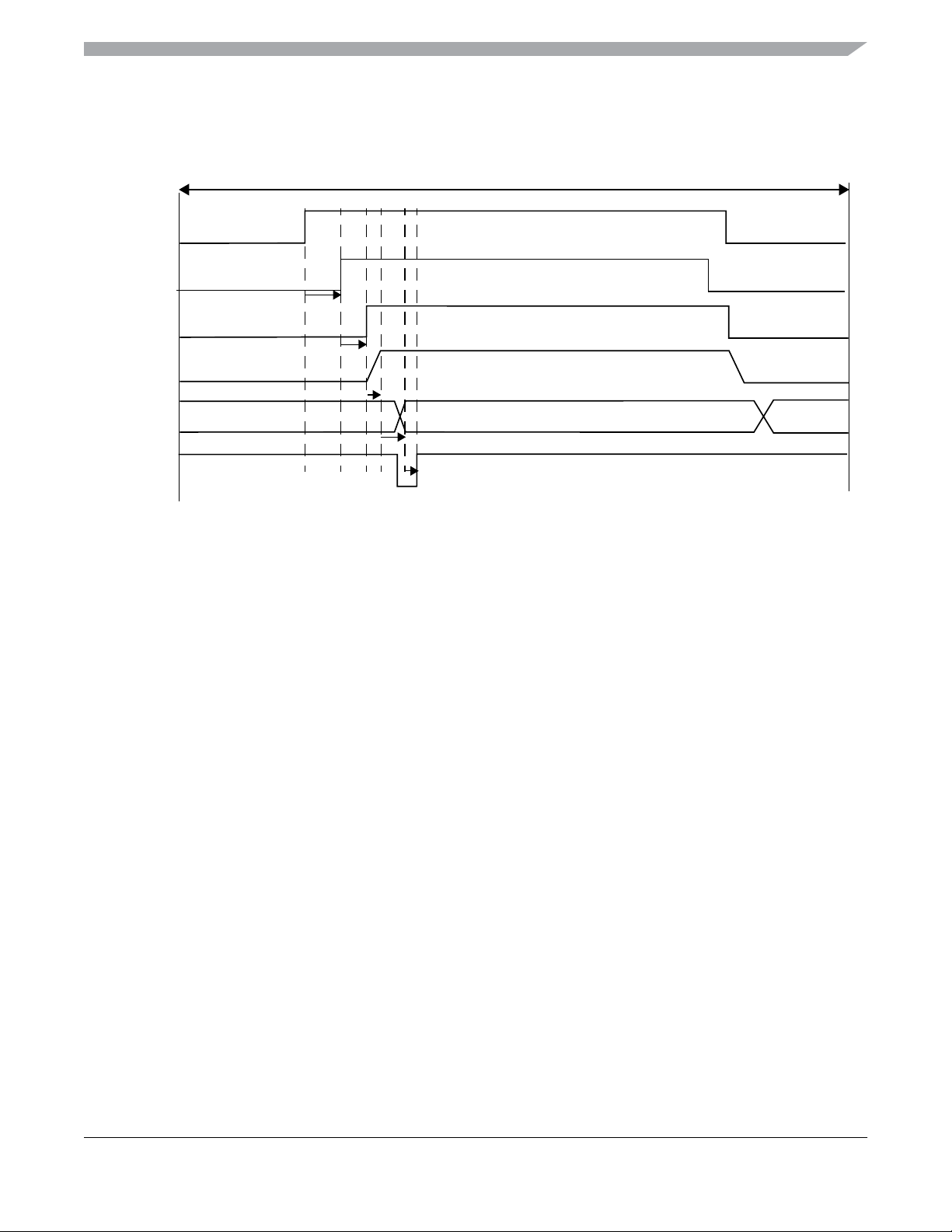
Chapter 1 Device Overview MC9S12ZVM-Family
insertion, going through the external FETs and back into the internal ADC measurements of external
voltages and currents.
Figure 1-8. Control Loop Delay Overview
PWM cycle
PWM base
PWM with
deadtime
GDU
propagation
FET
turn on
Current sense
settling time
(tcslsst)
ADC delay
T
DEAD_x
t
delon
t
HGON
The PWM deadtime (T
DEAD_X
) is an integral number of bus clock cycles, configured by the PMF
deadtime registers.
The GDU propagation delays (t
The FET turn on times (t
HGON
, t
delon
) are load dependent but are specified for particular loads in the electrical
) are specified in the electrical parameter Table E-1.
deloff
parameter Table E-1.
The current sense amplifier delay is highly dependent on external components.
The ADC delay until a result is available is specified as the conversion period N
in Table C-1.
CONV
1.13.3.3 Static Timing Operation
The timing frame is static if it is the same in every control cycle (defined by reload frequency) and is
relative to start of the control cycle. The only settings modified from one control cycle to the next one are
the PWM duty cycle registers.
The main control cycle synchronization event is the PMF reload event. The PMF reload event can be
generated every n PWM periods.
This mode can optionally be extended by a timer channel trigger to PMF to change the PWM channel
operation (e.g. used for BLDCM commutation). In this case, the PMF configuration can propagate the
trigger through the control loop or can prevent propagation so the static timing of the control cycle and
inter-block coherency are not affected by the trigger.
At the end of the conversion sequence the first ADC command from the new sequence is loaded and the
ADCx waits for the next trigger_x. The PTU continues to generate the trigger_x events for each trigger
time from the list until a new reload or async_reload occurs.
MC9S12ZVM Family Reference Manual Rev. 1.3
Freescale Semiconductor 63
Page 64

Chapter 1 Device Overview MC9S12ZVM-Family
Before the upcoming reload event the CPU:
• reads the ADC results from the buffered Conversion Result List
• clears the conversion complete flag
• services the reload by setting new duty cycle values
• sets the PTULDOK bit (corresponding to glb_ldok) to signal the duty cycle coherence
The CPU actions are typically performed in an ISR triggered by the conversion complete flag.
1.13.3.4 Static Timing Fault Handling
The following Faults and/or errors can occur:
• Desaturation error, Overvoltage, Undervoltage, Temperature sensor, External fault
The application run-time error is handled by the GDU without CPU interaction. Firstly the FETs are
disabled and the PMF signals switched to an inactive state. To re-enable the operation first the GDU fault
and then PWM fault must be cleared, to automatically re-enable the FET driving at the next PWM
boundary.
• PTU reload overrun error
This is an application run-time error caused by the CPU not setting PTULDOK on time. Servicing this
type of error is application dependent and may range from a further reload attempt to a total shut down.
• PTU trigger generator reload error, PTU trigger generator error
Since all timing is static, this error should only occur during application debugging. This type of error
occurring in a static timing configuration indicates possible data corruption. This can be serviced by a
control loop shutdown.
• PTU memory access error, Memory access double bit ECC error
This type of error occurring in an application indicates data corruption. This can be serviced by a control
loop shutdown.
• ADC sequence overrun, ADC command overrun, ADC command error
Since all timing is static, this error should only occur during application debugging. This type of error
occurring in an application indicates possible data corruption. This can be serviced by a control loop
shutdown.
1.13.3.5 Dynamic Timing Operation
The timing frame is dynamic if the following are modified on a cycle by cycle basis:
• PMF - duty cycle value registers (PMF_VALx), modulo registers
• PTU - Trigger Event List (PTU_TELx)
• ADC - Command Sequence List (ADCx_CSL)
The main philosophy is that all cycle-by-cycle settings for cycle n need to be done within cycle n-1. The
main control cycle synchronization event is the PMF reload event, which can be generated every n PWM
periods.
MC9S12ZVM Family Reference Manual Rev. 1.3
64 Freescale Semiconductor
Page 65

Chapter 1 Device Overview MC9S12ZVM-Family
This mode can optionally be extended by a timer channel trigger PMF to change PWM channel operation
(e.g. used for BLDCM commutation).
The event flow is the same as for static timing.
Before the upcoming reload event the CPU:
• reads the ADC results from the buffered Conversion Result List
• clears the conversion complete flag
• services the reload by setting new duty cycle values and a new PMF modulo value
• updates the non-active PTU_TELx
• updates the non-active ADCx_CSL
• sets the PTULDOK bit (corresponding to glb_ldok) to signal the duty cycle coherence
The CPU actions are typically performed in an ISR triggered by the conversion complete flag.
1.13.3.6 Dynamic Timing Fault Handling
The following Faults and/or errors can occur:
• Desaturation error, Overvoltage, Undervoltage, Temperature sensor, External fault
The application run-time error is handled by the GDU without CPU interaction. Firstly the FETs are
disabled and the PMF signals switched to an inactive state. To re-enable the operation first the GDU fault
and then PWM fault must be cleared, to automatically re-enable the FET driving at the next PWM
boundary.
• PTU reload overrun error
This is an application run-time error caused by the CPU not setting PTULDOK on time. Servicing this
type of error is application dependent and may range from a further reload attempt to a total shut down.
• PTU trigger generator reload error, PTU trigger generator error
This indicates an application run-time error caused by a settings mismatch. Servicing this type of error is
application dependent. In some cases, the ADC values for the current control cycle can be ignored.
• PTU memory access error, Memory access double bit ECC error
This type of error occurring in an application indicates possible data corruption. This can be serviced by a
control loop shutdown.
• ADC sequence overrun, ADC command overrun, ADC command error
This indicates an application run-time error caused by a settings mismatch. Servicing this type of error is
application dependent. In some cases, the ADC values for the current control cycle can be ignored.
1.13.3.7 Asynchronous Timing
This case is an extension of the dynamic timing case by an asynchronous event generated by the Timer.
Note the asynchronous term is referenced to the control cycle.
MC9S12ZVM Family Reference Manual Rev. 1.3
Freescale Semiconductor 65
Page 66

Chapter 1 Device Overview MC9S12ZVM-Family
The timing frame is the same as in dynamic timing case plus it can be asynchronously restarted at any time
within the control cycle.
At the asynchronous commutation_event
• the PMF actions are:
1. counter re-start, re-initialization
2. PWM configuration re-initialization according to the selected PWM settings (center/edge-aligned
pattern, normal/inverted type etc.)
3. re-initialization of the dead time generators (in case the commutation takes place at a time when
one of the dead times is being generated)
4. re-initialization of the PWM outputs according to pre-set PWM channel output settings in double
buffered registers (mask, swap, output control)
5. re-initialization of the automatic fault clearing
6. generates async_reload event for the PTU
7. optionally updates the PWM duty cycle values based on LDOK state
• the PTU actions are:
1. abortion of the trigger_x event generation
2. re-initialization and re-start the PTU counter
3. update of the current list index TGxList based on the glb_ldok state
4. fetch first trigger time from updated TGxList
5. passes the async_reload event immediately to the ADC (if the PTU is enabled)
6. generates the reload event for the ADC
• the ADC actions are:
1. the conversion in progress is completed
2. the ADC conversion sequence is aborted and the SEQA flag is set to indicate that the final
conversion occurred during the abortion process (potentially coinciding with a commutation and is
thus less precise than under normal conditions)
3. update of the current lists index ADxLists
4. re-start of the conversion sequencing upon successful abortion - fetches the first ADC command
from the ADCx_CSL, re-sets the result pointer to the top of the list
Note: in case the lists index ADxLists is not updated at the sequence abortion the new restarted A/D
conversions will overwrite the previously converted results.
• the GDU actions are:
1. standard operation
1.13.3.8 Control Loop Startup Guidelines
The sequence for control loop start up is to firstly configure the signal measurement (inputs/feedback).
Once the measurement is properly configured (correct value is measured at defined time) the output
actuation (control action) is configured. The following modules are involved in signal measurements.
• TIM (to identify asynchronous commutation) [BLDC applications only]
MC9S12ZVM Family Reference Manual Rev. 1.3
66 Freescale Semiconductor
Page 67

Chapter 1 Device Overview MC9S12ZVM-Family
• PMF (to generate main synchronous events for PTU and ADC)
• PTU (to generate delay relative to synchronous events generated by PMF)
• ADC (to acquire analog signals under synchronous control)
• GDU (zero crossing comparators, Back-EMF muxing) [application dependent]
The TIM OC0 channel identifies the commutation event and restarts the PMF counter. In order to establish
this link TIM and PMF need to be configured and started. Then to sample accurately within one PMF cycle
the PTU needs to be used, so the next step is to configure the PTU to establish PMF to PTU link. The PTU
sends triggers to the ADC to perform a measurement of control signals. So the next step is to configure the
ADC. In some cases the GDU involvement is required and therefore configured.
The control action involves the PMF (to generate the duty cycle for GDU) and the GDU (to propagate the
signal to the MOSFETs). Since the PMF has already been configured for the measurements, only the GDU
need be configured to complete startup. Sometimes the GDU can be configured earlier but the GDU output
is always enabled last.
The recommended startup sequence is summarized as follows:
• Configure TIM and PMF to establish the link between TIM OC0 commutation event and PMF
• Configure PTU to establish the PMF to PTU link and ensure correct sampling within PMF cycle
• Configure the ADC
• Configure the GDU
1.13.3.9 Control Loop Shutdown Guidelines
1. Remove energy stored in the system after the power stage
kinetic energy - stop all rotating/moving mass
magnetic energy - gracefully drive currents to zero
2. Put GDU and PMF outputs to safe state
1.13.3.10 Control Loop Stop Mode Considerations
In Stop mode the PWM, PTU, ADC can not run because the bus clock is not running. Thus the GDU must
transition to a disabled state. Before entering Stop mode the application must perform the following steps:
1. Remove energy stored in the system after the power stage
kinetic energy - stop all rotating/moving mass
magnetic energy - gracefully drive currents to zero
2. Put GDU and PMF outputs to safe state
3. Verify GDU and PMF safe states
4. Verify fault flags and service if necessary
5. Execute the STOP instruction
The return from stop is expected in reverse order:
1. On returning from Stop mode the clocks are automatically enabled coherently
2. Initialize and check device proper functionality (charge pump etc.)
MC9S12ZVM Family Reference Manual Rev. 1.3
Freescale Semiconductor 67
Page 68

Chapter 1 Device Overview MC9S12ZVM-Family
3. Check functionality of the external system
4. Initializes control loop operation, however with PMF and GDU outputs still in safe state
5. Read the ADC values to check the system
6. Start driving energy into the system
based on the measurements from the previous step, the PWM duty cycle values are calculated
7. PMF and GDU outputs are enabled (actively driven)
The device does not support putting the FETs in an active driving state during STOP as the GDU charge
pump clock is not running. This means the device cannot be put in stop mode if the FETS need to be in an
active driving state to protect the system from external energy supply (e.g. externally driven motorgenerator).
NOTE
It is imperative, that whatever the modules perform on entering/exiting Stop
mode, the pre-set complementary mode of operation and dead time insertion
must be guaranteed all the times.
1.13.3.11 Application Signal Visibility
In typical motor control applications, TIM OC0 is used internally to indicate commutation events. To
switch off OC0 visibility at port pin PT0:
• Disable output compare signal on pin PT0 in TIM: OCPD[OCPD0]=0b1.
1.13.3.12 Debug Signal Visibility
Depending on required visibility of internal signals on port pins enable the following registers:
• Set [PWMPRR]=0b1 in PIM if monitoring of internal PWM waveforms is needed. PWM5-3 are
driven out on pins PT[2:0] and PWM2-0 on pins PP[2:0].
• Enable output compare channel OC0 to output commutation event on pin PT0 in TIM:
OCPD[OCPD0]=0b0.
• Set PTUDEBUG[PTUREPE]=0b1 in PTU to output the reload event.
• Set PTUDEBUG[PTUTxPE]=0b1 with x=0,1 in PTU to output the trigger events.
1.13.4 BDCM Complementary Mode Operation
This section describes BDCM control using center aligned complementary mode with deadtime insertion.
The DC Brushed motor power stage topology is a classical full bridge as shown in Figure 1-9. The DC
Brushed motor is driven by the DC voltage source. A rotational field is created by means of commutator
and brushes on the motor. These drives are still very popular because sophisticated calculations and
algorithms such as commutation, waveform generation, or space vector modulation are not required.
MC9S12ZVM Family Reference Manual Rev. 1.3
68 Freescale Semiconductor
Page 69
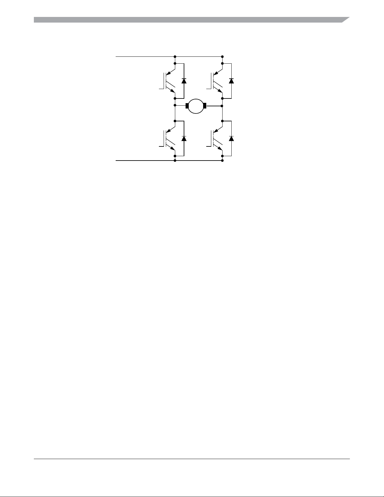
Chapter 1 Device Overview MC9S12ZVM-Family
Figure 1-9. DC Brushed Motor External Configuration
+ 1/2 U
PWM
0
A
PWM
1
- 1/2 U
PWM
2
B
PWM
3
Usually the control consists of an outer, speed control loop with inner current (torque) control loop. The
inner loop controls DC voltage applied onto the motor winding. The control loop is calculated regularly
within a given period. In most cases, this period matches the PWM reload period.
Driving the DC motor from a DC voltage source, the motor can work in all four quadrants. The
complementary mode of operation with deadtime insertion is needed for smooth reversal of the motor
MC9S12ZVM Family Reference Manual Rev. 1.3
Freescale Semiconductor 69
Page 70
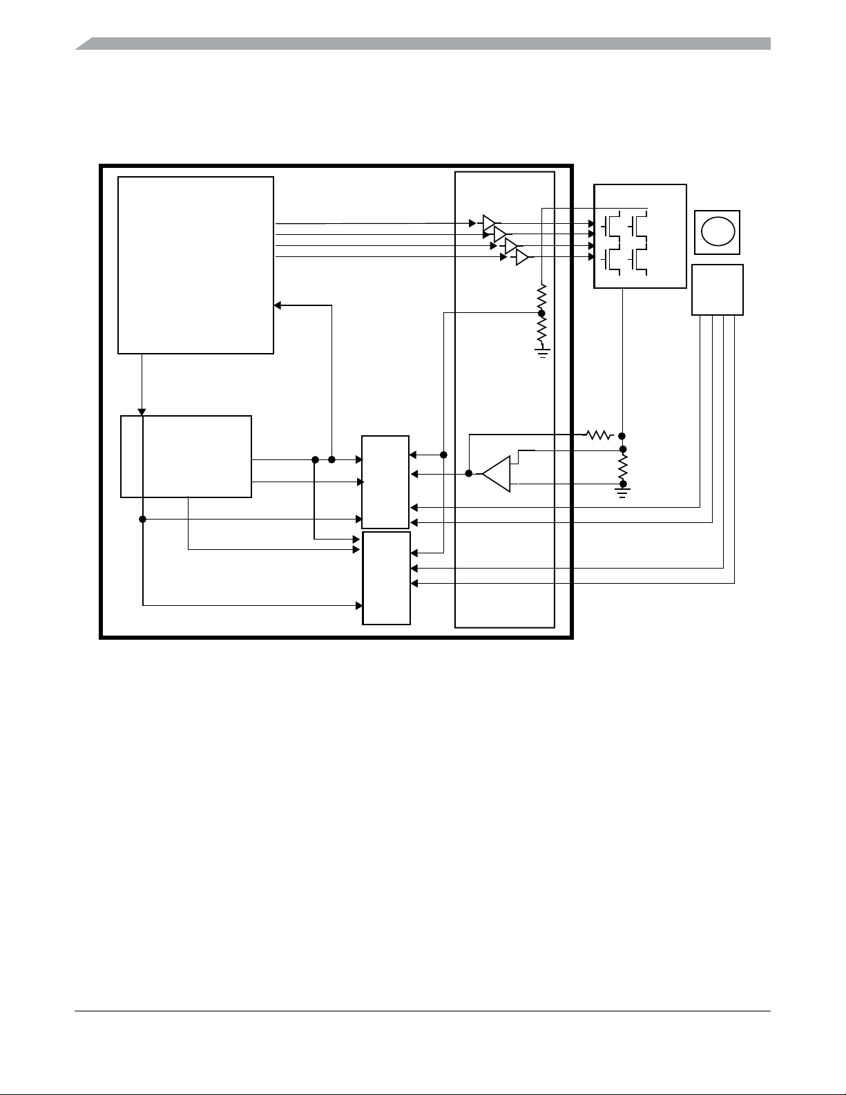
Chapter 1 Device Overview MC9S12ZVM-Family
current (motor torque), hence smooth full four quadrant control. Usually the center-aligned PWM is
chosen to lower electromagnetic emissions.
Figure 1-10. BDCM Control Loop Configuration
PMF
reloada
reload
GDU
dc_bus_voltage
M
sine/
cosine
sensor
dc_bus_current0
glb_ldok
trigger_0
PTU
ADC0
trigger_1
reload
ADC1
The PWM frequency selection is always a compromise between audible noise, electromagnetic emissions,
current ripples and power switching losses.
The BDCM control loop goal is to provide a controlled DC voltage to the motor winding, whereby it is
controlled cycle-by-cycle using a speed, current or torque feedback loop.
The center aligned PWM waveforms generated by the PMF module are applied to the bridge as shown in
Figure 1-11 whereby the base waveform for PWM0 and PWM1 is depicted at the top and the
complementary PWM0 and PWM1 waveforms are shown with deadtime insertion depicted by the gray
phases before the switching edges.
MC9S12ZVM Family Reference Manual Rev. 1.3
70 Freescale Semiconductor
Page 71
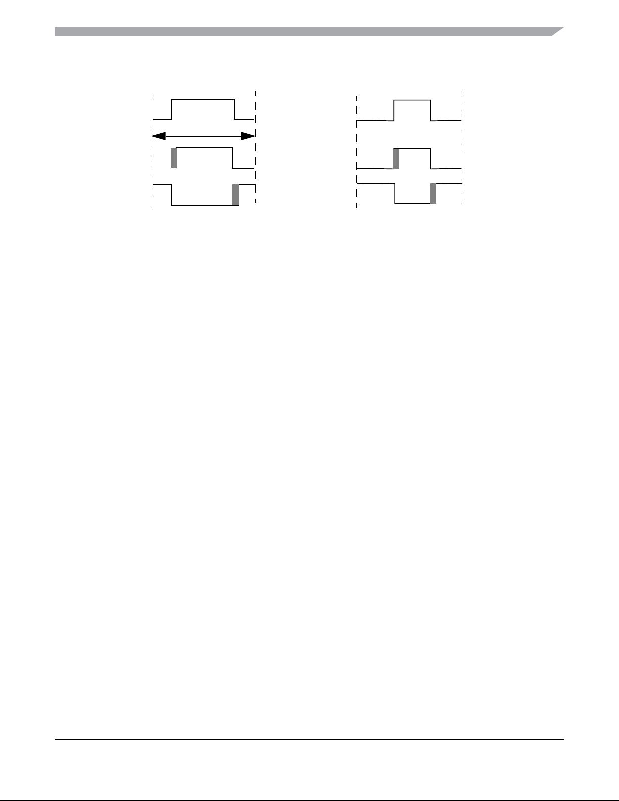
Chapter 1 Device Overview MC9S12ZVM-Family
Figure 1-11. BDCM Complementary Mode Waveform
PWM0, PWM1 base
PWM0
PWM1
T
PWM
PWM2, PWM3 base
PWM2
PWM3
Assuming first quadrant operation, forward accelerating operation, the applied voltage at node A must
exceed the applied voltage at node B (Figure 1-9). Thus the PWM0 duty cycle must exceed the PWM2
duty cycle.
The PWM duty cycle of PWM0 defines the voltage at the first power stage branch.
The PWM duty cycle of PWM2 defines the voltage at the second power stage branch.
Modulating the PWM duty cycle every period using the function F
PWM0 duty-cycle = 0.5 + (0.5 * F
PWM2 duty-cycle = 0.5 - (0.5 * F
PWM
PWM
)
); For -1<=F
PWM
<= 1;
then the duty cycle is expressed as:
PWM
MC9S12ZVM Family Reference Manual Rev. 1.3
Freescale Semiconductor 71
Page 72
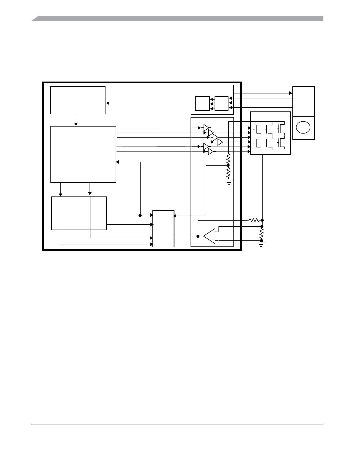
Chapter 1 Device Overview MC9S12ZVM-Family
1.13.5 BLDC Six-Step Commutation
1.13.5.1 Hall Sensor Triggered Commutation
Figure 1-12. BLDC Configuration With Hall Sensors
TIM
PMF
reload
OC0
PTU
reload
IC1
commutation_event
async_reload
glb_ldok
trigger_0
async_reload
ADC0
PIM
XOR
GDU
PTIT
EVDD1
PT1
PT2
PT3
dc_bus_voltage
dc_bus_current
Hall
Sensor
M
This BLDC application uses Hall sensor signals to create commutation triggers. The integrated sense
amplifier and an ADC module are used to measure DC bus current, for torque calculation. The DC bus
voltage measurement is used in the control algorithm to counter-modulate the PWM such that the variation
of the DC-bus voltage does not affect the motor current closed loop. The configuration is as follows:
1. Connect the three Hall sensor signals from the motor to input pins PT3-1.
2. Set [T0IC1RR=1] in the register MODRR2 to establish the link from Hall sensor input pins to TIM
input capture channel 1.
3. Setup TIM IC1 for speed measurement of XORed Hall sensor signals. Enable interrupt on both
edges.
4. Enable TIM OC0 and select toggle action on output compare event: TCTL2[OM0:OL0]=01.
5. Configure PMF for edge-aligned PWM mode with or without restart at commutation:
PMFENCx[RSTRT]. If using the restart option, then select generator A as reload signal source and
keep the following configurations at their default setting: multi timebase generators
(PMFCFG0[MTG]=b0), reload frequency (PMFFQCx[LDFQx]=b0), prescaler
(PMFFQCx[PRSCx]=b00).
6. Enable PMF commutation event input: PMFCFG1[ENCE]=1.
MC9S12ZVM Family Reference Manual Rev. 1.3
72 Freescale Semiconductor
Page 73
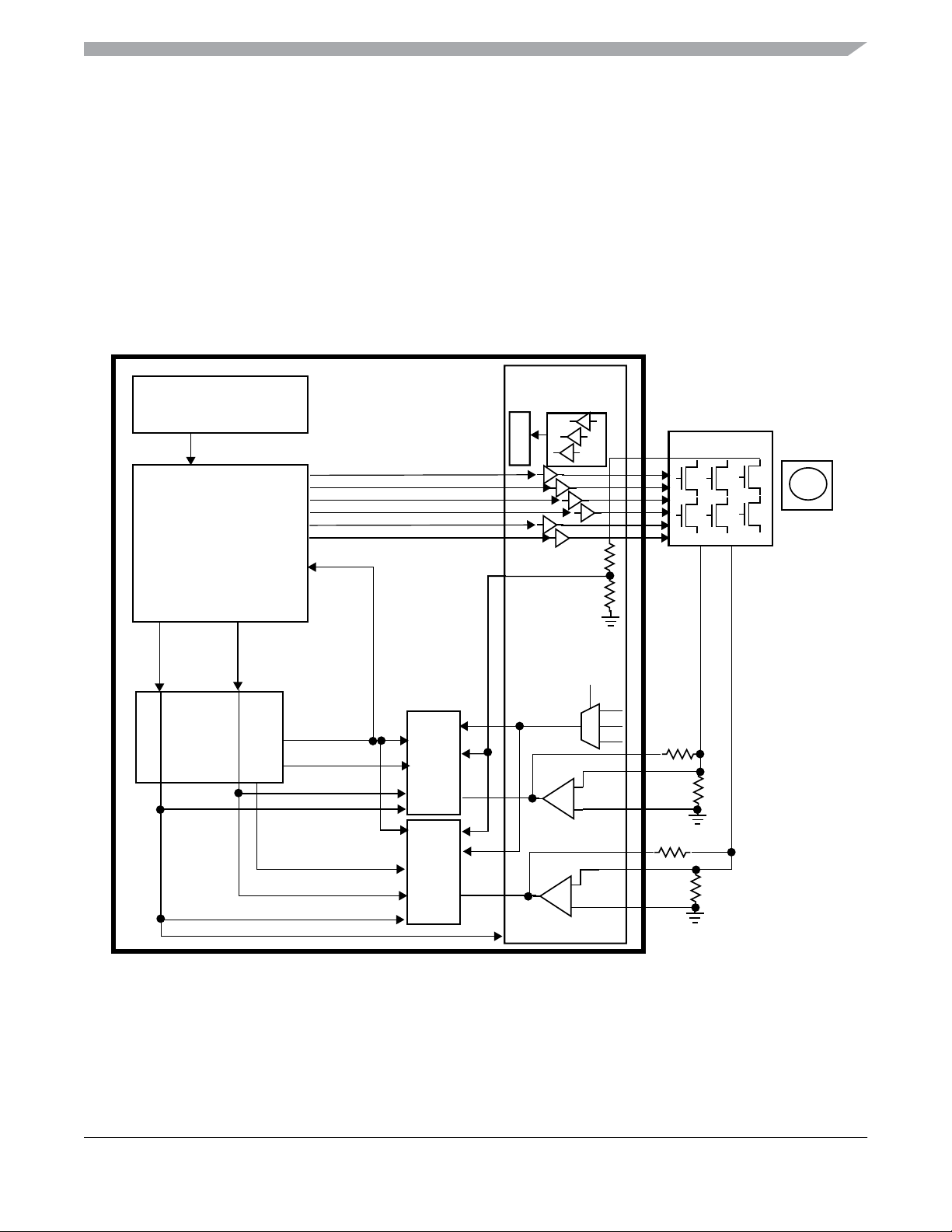
Chapter 1 Device Overview MC9S12ZVM-Family
7. Read port register PTIT[3:1] to determine starting sector.
8. Startup motor by applying PWM to the related motor phase.
9. In IC1 interrupt ISR calculate the delay to next commutation and store value to output compare
register. Update registers with next values of mask and swap.
10. On next output compare event the buffered mask and swap information is transferred to the active
PWM registers to execute the commutation.
1.13.5.2 Sensorless Commutation
Figure 1-13. Sensorless BLDC Configuration
GDU
TIM
OC0
commutation_event
zero crossing
comparators
GPHS
dc_bus_voltage
PMF
reloada
reload
reload
async_reload
async_reload
PTU
trigger_1
async_reload
glb_ldok
trigger_0
ADC0
ADC1
back-EMF
PHMUX
P1
P2
P3
dc_bus_current0
dc_bus_current1
M
To calculate the commutation time in a sensorless motor system the back-EMF zero crossing event of the
currently non-fed phase within an electrical rotation cycle must be determined. For fast motor rotation, the
ADC is used to measure the back-EMF voltage and the DC bus voltage to determine the zero crossing time.
For slow motor rotation the GPHS register can be polled. In either case the zero crossing event is handled
MC9S12ZVM Family Reference Manual Rev. 1.3
Freescale Semiconductor 73
Page 74

Chapter 1 Device Overview MC9S12ZVM-Family
by the CPU monitoring flags or responding to interrupts. The TIM then generates the commutation_event
under CPU control, based on the zero crossing time.
1. Enable TIM OC0 and select toggle action on output compare event: TCTL2[OM0:OL0]=0b01.
2. Enable PMF commutation event input: PMFCFG1[ENCE]=0b1.
3. Enable internal ADC channel for measuring the phase voltages from the muxed GDU outputs.
4. Align rotor to stator field. Initialize phase MUX using register GDUPHMUX.
5. Startup motor by applying PWM to an arbitrary motor phase.
6. Take samples of the phase voltages periodically based on PWM cycle to detect zero crossing.
7. Calculate the delay to next commutation and store value to output compare register. Update
registers with next values of mask and swap.
8. On next output compare event the buffered mask and swap information are transferred to the active
PWM register to execute the commutation.
1.13.6 PMSM Control
PMSM control drives all 3 phases simultaneously with sinusoidal waveforms. Both sensorless and SineCosine position sensor control loop operation are supported.
1.13.6.1 PMSM Sensorless Operation
In this configuration the PMSM stator winding currents are driven sinusoidally and the back EMF
waveform is also sinusoidal. Thus all 3 phases are active simultaneously. The rotor position and speed are
determined by the current and calculated voltages respectively. The back EMF voltage is calculated based
on the currents.
1. Configure PMF for complementary mode operation.
2. Configure PMF for center aligned or phase shifted operation.
3. Select correct PMF deadtime insertion based on external FET switches.
4. Enable GDU current sense opamps for measuring the phase currents from 2 external shunts.
5. Map the output pin of each current sense opamp to the ADC input.
6. Optionally use GDU phase comparators for zero crossing detection to correct deadtime distortion.
7. Fetch targeted motor speed parameter from external source (e.g. SCI)
8. Configure PMF period and duty cycle.
9. Startup motor by applying FOC startup algorithm.
10. Take samples of the phase currents periodically based on PWM cycle to determine motor speed.
11. Calculate FOC algorithm to determine back EMF and motor position.
MC9S12ZVM Family Reference Manual Rev. 1.3
74 Freescale Semiconductor
Page 75
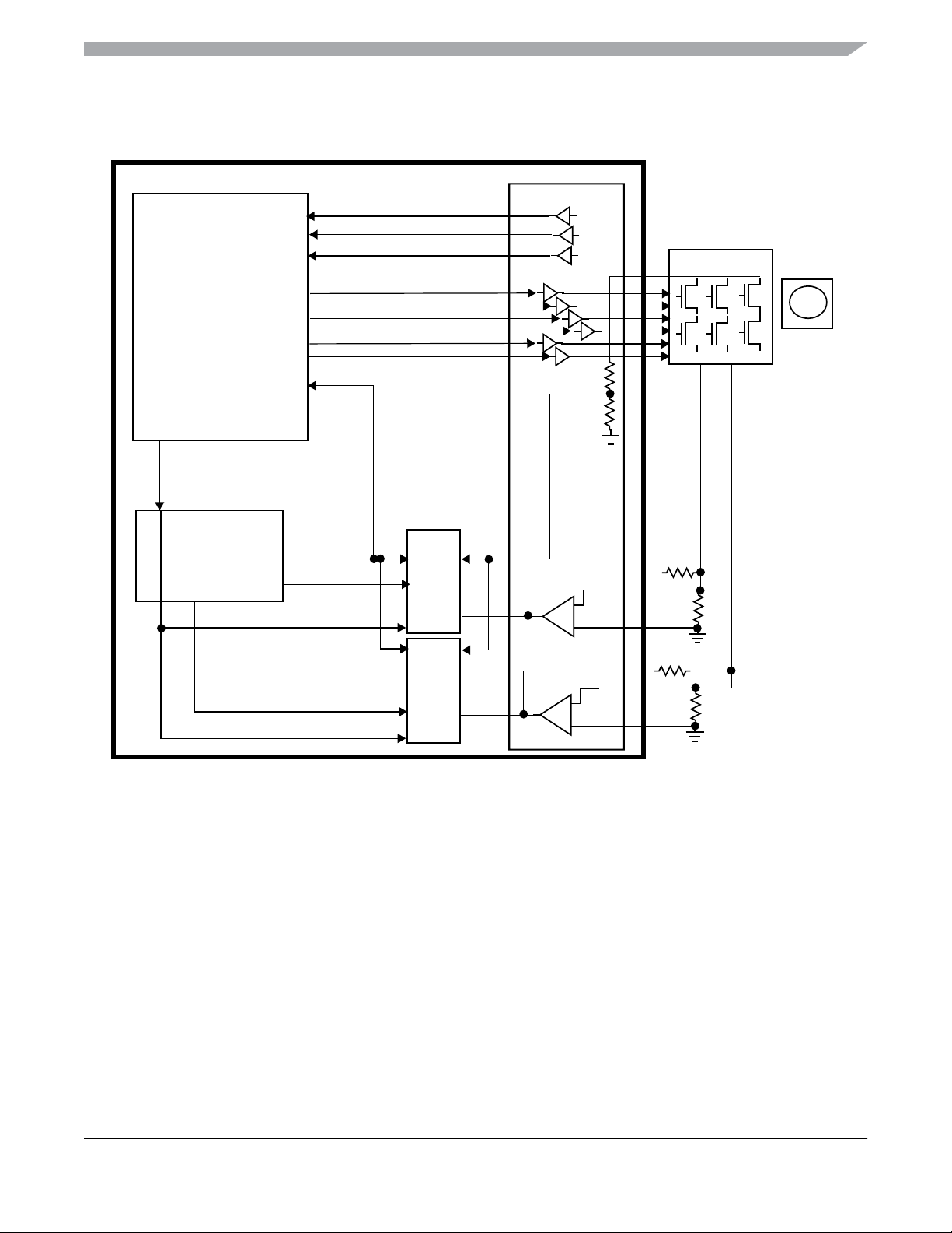
Chapter 1 Device Overview MC9S12ZVM-Family
Figure 1-14. Sensorless PMSM Control Loop Configuration
PMF
reloada
reload
PTU
IS0
IS1
IS2
glb_ldok
trigger_0
zero crossing
phase comparison
ADC0
GDU
dc_bus_voltage
dc_bus_current1
dc_bus_current0
M
trigger_1
reload
ADC1
1.13.6.2 PMSM Operation With Sine-Cosine Position Sensor
In this configuration the PMSM stator winding currents are driven sinusoidally and the back EMF
waveform is also sinusoidal. Thus all 3 phases are active simultaneously. The back EMF voltage is
calculated based on the currents. The rotor position and speed are determined by a sine/cosine sensor,
which generates sinusoidal sine/cosine signals, indicating the angle of the rotor in relation to sensor
windings. The sensor is supplied by the EVDD1 pin.
1. Configure PMF for complementary mode operation.
2. Configure PMF for center aligned or phase shifted operation.
3. Select correct PMF deadtime insertion based on external FET switches.
4. Enable GDU current sense opamps for measuring the phase currents from external shunts.
5. Map the output pin of each current sense opamp to the ADC input.
MC9S12ZVM Family Reference Manual Rev. 1.3
Freescale Semiconductor 75
Page 76
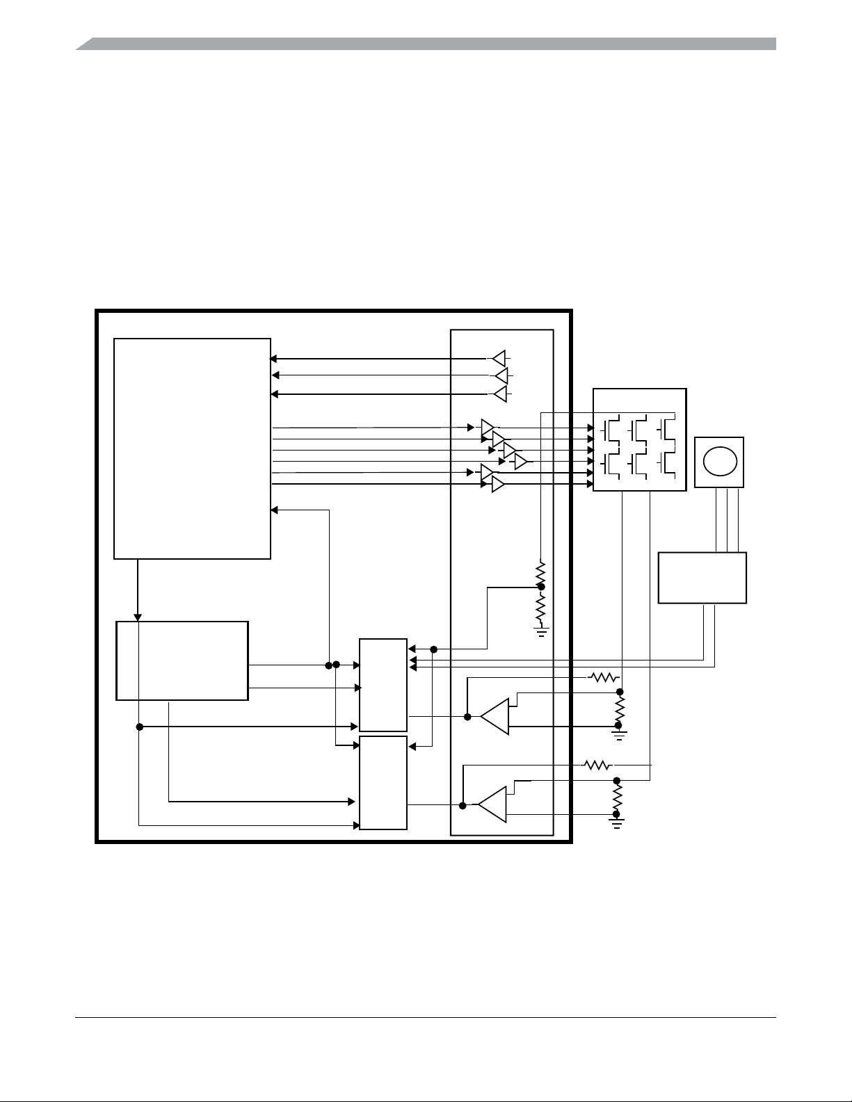
Chapter 1 Device Overview MC9S12ZVM-Family
6. Map the sine/cosine input signals to ADC input channels.
7. Configure the EVDD1 pin as output.
8. Optionally use GDU phase comparators for zero crossing detection to correct dead time distortion.
9. Fetch targeted motor speed parameter from external source (e.g. SCI)
10. Configure PMF period and duty cycle.
11. Start motor by applying startup algorithm.
12. Sample the sine/cosine voltages periodically based on PWM cycle to determine motor position.
13. Use FOC algorithm to determine back EMF and motor speed.
Figure 1-15. PMSM Sine/Cosine Control Loop Configuration
PMF
reload
PTU
IS0
IS1
IS2
glb_ldok
trigger_0
zero crossing
phase comparison
ADC0
GDU
dc_bus_voltage
sine/cosine
sensor
dc_bus_current1
dc_bus_current0
M
trigger_1
reload
MC9S12ZVM Family Reference Manual Rev. 1.3
76 Freescale Semiconductor
ADC1
Page 77

Chapter 1 Device Overview MC9S12ZVM-Family
1.13.6.3 Dead time Distortion Correction
PMSM motor control applications driven by sinusoidal voltages by default require zero crossing
information of phase currents to determine the point in time to change sign of deadtime compensation
value to be added to duty cycles.
The GDU phase comparator signals are connected internally to the PMF ISx inputs. This allows the dead
time distortion correction to be applied directly based on the phase status.
1. Align rotor to stator field.
2. Await phase comparator status change.
3. Switch to alternate duty cycle register to compensate distortion.
MC9S12ZVM Family Reference Manual Rev. 1.3
Freescale Semiconductor 77
Page 78
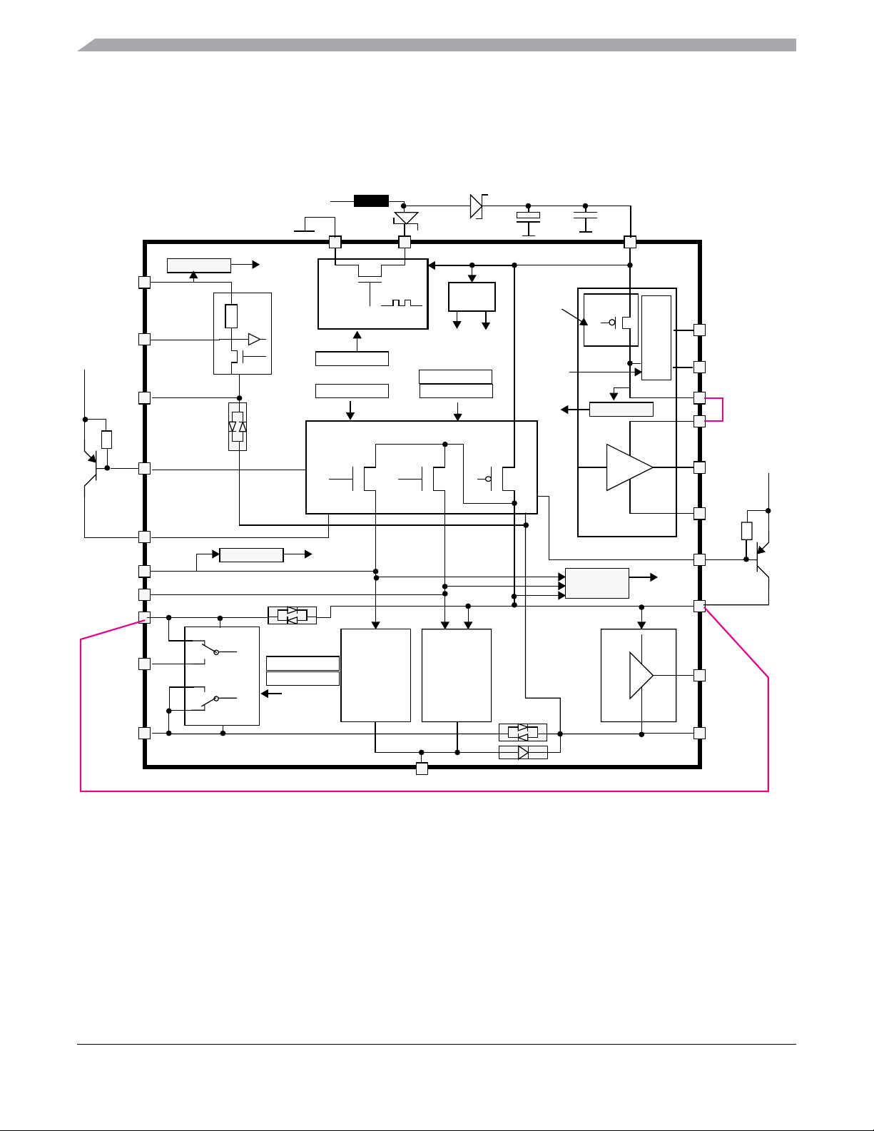
Chapter 1 Device Overview MC9S12ZVM-Family
1.13.7 Power Domain Considerations
The MC9S12ZVM-Family power domains are illustrated in Figure 1-16. More detailed information is
included in the individual module descriptions.
Figure 1-16. Power Domain Overview
OPT L = LINPHY package option
OPT C = CANPHY package option
VRBATP
L
VSSB BST
VSUP (12V/18V)
VRBATP
LGND
BCTLC
VDDC
VDDF
VDDA
PAD8
VSSA
HD
LIN
(5V)
VDD
GHHDF
(OPT L)
(OPT L)
(OPT C)
(OPT C)
LINPHY
VDDA
ADC
VSSA
PORF
VRH
VRL
INT
VRL_SEL
VRH_SEL
BOOST
GBOE
VREG_AUTO
1.8V
RES
CORE
RAM’s
PLL
IRC
OSC
INTXON
EXTXONEXTCON
2.8V
FLASH
BATS
ADC
5V
INT
GFDE
GCPE
INT
LDO
GLVLSF
GDU
LVRF
PADS
CPS
RES
VCP
CP
VLS_OUT
(11V)
VLS
LG
LS
BCTL
VDDX
GPIO
VSSX
VRBATP
VSS
The system supply voltage VRBATP is a reverse battery protected input voltage. It must be protected
against reverse battery connections and must not be connected directly to the battery voltage (VBAT).
The device supply voltage VSUP provides the input voltage for the internal regulator, VREG_AUTO,
which generates the voltages VDDX, VDD and VDDF. The VDDX domain supplies the device I/O pins,
VDDA supplies the ADC and internal bias current generators. The VDDA and VDDX pins must be
connected at board level, they are not connected directly internally. ESD protection diodes exist between
VDDX and VDDA, therefore forcing a common operating range. The VDD domain supplies the internal
device logic. The VDDF domain supplies sections of the internal Flash NVM circuitry.
MC9S12ZVM Family Reference Manual Rev. 1.3
78 Freescale Semiconductor
Page 79

Chapter 1 Device Overview MC9S12ZVM-Family
The device supports the use of an external PNP to supplement the VDDX supply, for reducing on chip
power dissipation. In this configuration, most of the current flowing from VRBATP to VDDX, flows
through the external PNP. This configuration, using the BCTL pin, can be enabled by register bits
EXTXON and INTXON.
A supply for an external CANPHY is offered via external device pins BCTLC and VDDC, whereby
BCTLC provides the base current of an external PNP and VDDC is the CANPHY supply (output voltage
of the external PNP). This is only available in the CANPHY package option. This configuration can be
enabled by the register bit EXTCON.
The LINPHY pull-up resistor is internally connected to the HD voltage. This is chosen as opposed to
VSUP to ensure that the LINPHY is not disturbed by the internal VSUP boost circuit. The external
connections for the HD pin must ensure a reverse battery protection.
The ADC register bit VRH_SEL maps the ADC reference VRH to VDDA or to the device pad PAD8.
1.13.7.1 Voltage Domain Monitoring
The BATS module monitors the voltage on the VSUP pin, providing status and flag bits, an interrupt and
a connection to the ADC, for accurate measurement of the scaled VSUP level.
The POR circuit monitors the VDD and VDDA domains, ensuring a reset assertion until an adequate
voltage level is attained. The LVR circuit monitors the VDD, VDDF and VDDX domains, generating a
reset when the voltage in any of these domains drops below the specified assert level. The VDDX LVR
monitor is disabled when the VREG is in reduced power mode. A low voltage interrupt circuit monitors
the VDDA domain.
The GDU high side drain voltage, pin HD, is monitored within the GDU and mapped to an interrupt. A
connection to the ADC is provided for accurate measurement of a scaled HD level.
1.13.7.2 FET-Predriver (GDU) Supplies
A dedicated low drop regulator is used to generate the VLS_OUT voltage from VSUP. The VLS_OUT
voltage is used to supply the low side drivers and can be directly connected to the VLS inputs of each low
side driver. For FET-predriver operation at lower VSUP levels, a boost circuit can be enabled by the GBOE
register bit. The boost circuit requires Shottky diodes, a coil and capacitors, as shown in Figure 1-16. More
detailed information is included in the GDU module description.
1.13.7.2.1 Bootstrap Precharge
The FET-predriver high side driver must provide a sufficient gate-source voltage and sufficient charge for
the gate capacitance of the external FETs. A bootstrap circuit is used to provide sufficient charge, whereby
the capacitor C
Figure 1-17. When the high side driver switches on, the charge on this capacitor, supplies the FET-
predriver via the VBSx pin. The C
a long period of inactivity of the low side driver, the C
low side driver must be switched on to charge C
to discharge the bootstrap capacitor C
the leakage current on VBSx pin.
is first charged to VLS_OUT via an external diode, when the low side driver is active
BS
capacitor can only be charged if the low side driver is active, so after
BS
capacitor becomes discharged. In this case, the
BS
before commencing high side driving. The time it takes
BS
can be calculated from the size of the bootstrap capacitor CBSand
BS
MC9S12ZVM Family Reference Manual Rev. 1.3
Freescale Semiconductor 79
Page 80

Chapter 1 Device Overview MC9S12ZVM-Family
The bootstrap capacitors must be precharged before turning on the high-side drivers for the first time. This
can be done by using the PMF software output control mechanism:
PMFOUTC = 0x3F; // SW control on all outputs
PMFOUTB = 0x2A; // All high-sides off, all low-sides on
The PWM signals should be configured to start with turning on the low-side before the high-side drivers
in order to assure precharged bootstraps. Therefore invert the PWM signals:
PMFCINV = 0x3F; // Invert all channels to precharge bootstraps
1.13.7.2.2 High Side Charge Pump For 100% Duty Cycle
A charge pump voltage is used to supply the high side FET-predriver with enough current to maintain the
gate source voltage. To generate this voltage an external charge pump is driven by the pin CP, switching
between 0V and 11V. The pumped voltage is then applied to the pin VCP.
At 100% duty cycle operation the low-side turn on time is zero during a masked commutation cycle before
the high-side gates are attempted to be turned on. This can cause bootstrap charge to decay.
In order to speed-up the high-side gate voltage level directly after commutation, the software should drive
the first PWM cycle with a duty cycle meeting an on-time of at least t
minpulse
for the low-side drivers and
then switch back to 100% again.
The recommended procedure is to use the manual correction method (PMFCCTL[ISENS]) as described
for the BLDC applications:
Set odd PMF values to alternative duty cycle. At commutation event when one of the three high-side
drivers it turned on (every 120˚) set the PMFCCTL[IPOLx] bits and clear them in at next PWM reload
event.
Given unipolar switching mode:
// TIM OC0 ISR:
if ((PMFOUTC == 0x1c) || (PMFOUTC == 0x07) || (PMFOUTC == 0x31)) // all high-side turn-on sectors
PMFCCTL = 0x17; // select odd PMF values
// PMF reload ISR:
PMFCCTL = 0x10; // select even PMF values
The GDU high side drain voltage, pin HD, is supplied from VBAT through a reverse battery protection
circuit. In a typical application the charge pump is used to switch on an external NMOS, N1, with source
connected to VBAT, by generating a voltage of VBAT+VLS-(2xVdiode). In a reverse battery scenario, the
external bipolar turns on, ensuring that the HD pin is isolated from VBAT by the external NMOS, N1.
MC9S12ZVM Family Reference Manual Rev. 1.3
80 Freescale Semiconductor
Page 81
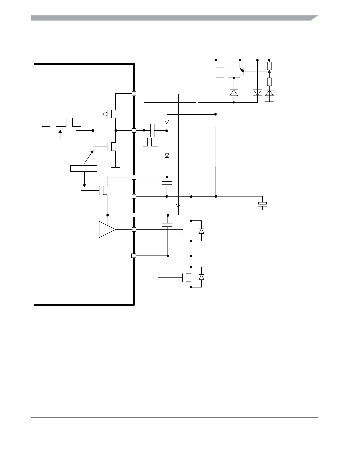
Chapter 1 Device Overview MC9S12ZVM-Family
Figure 1-17. High Side Supply and Charge Pump Concept
GCPCD
GCPE
VLS_OUT
10nF
CP
11V
0V
VCP
HD
VBSx
HGx
VBAT
(11V)
S
N1
D
1nF
1000µF
(Motor Dependent)
C
BS
HIGH SIDE
HSx
LOW SIDE
Diode voltage drop = Vdiode
MC9S12ZVM Family Reference Manual Rev. 1.3
Freescale Semiconductor 81
Page 82

Chapter 1 Device Overview MC9S12ZVM-Family
MC9S12ZVM Family Reference Manual Rev. 1.3
82 Freescale Semiconductor
Page 83

Chapter 2 Port Integration Module (S12ZVMPIMV1)
Revision History
Rev. No.
(Item No.)
V01.00 11 Nov 2012 • Initial release
V01.01 20 Feb 2013 Table 2-1 • Removed VRL
Date (Submitted
By)
Sections
Affected
Substantial Change(s)
• Corrected typo
2.1 Introduction
2.1.1 Overview
The S12ZVM-family port integration module establishes the interface between the peripheral modules and
the I/O pins for all ports. It controls the electrical pin properties as well as the signal prioritization and
multiplexing on shared pins.
This document covers:
• 2-pin port E associated with the external oscillator
• 4-pin port T associated with either combination of 4 TIM channels, 3 PWM channels of PMF, 1
SPI and 1 SCI
• 6-pin port S with pin interrupts and key-wakeup function; associated with 1 MSCAN, 1 SCI and 1
SPI modules
• 3-pin port P with pin interrupts and key-wakeup function; associated with
IRQ, XIRQ interrupt inputs
—
— 3 PWM channels of PMF
— ECLK output
• 9-pin port AD associated with 9 ADC channels shared among two ADC and two GDU AMP
modules - inputs can be used as an external interrupt and key-wakeup source
Most I/O pins can be configured by register bits to select data direction and to enable and select pullup or
pulldown devices.
MC9S12ZVM Family Reference Manual Rev.1.3
Freescale Semiconductor 83
Page 84

Chapter 2 Port Integration Module (S12ZVMPIMV1)
NOTE
This document assumes the availability of all features offered in the largest
package option. Refer to the package and pinout section in the device
overview for functions not available in lower pin count packages.
2.1.2 Features
The PIM includes these distinctive registers:
• Data registers and data direction registers for ports T, S, P and AD when used as general-purpose
I/O
• Control registers to enable pull devices and select pullups/pulldowns on ports E, T, S, P and AD
• Control register to enable open-drain (wired-or) mode on port S
• Control register to enable digital input buffers on port AD
• Interrupt flag register for pin interrupts and key-wakeup (KWU) on port S, P and AD
• Control register to configure
• Control register to enable ECLK output
• Routing registers to support signal relocation on external pins and control internal routings:
IRQ pin operation
— SPI0 to alternative pins
— Various SCI0-LINPHY0 routing options supporting standalone use and conformance testing
— Optional RXD0 to TIM0 link
— Optional RXD1 to TIM0 link
— PWM channels to GDU and/or pins
— 3 pin input mux to one TIM0 IC channel
A standard port pin has the following minimum features:
• Input/output selection
• 5V output drive
• 5V digital and analog input
• Input with selectable pullup or pulldown device
Optional features supported on dedicated pins:
• Open drain for wired-or connections
• Interrupt input with glitch filtering
2.2 External Signal Description
This section lists and describes the signals that do connect off-chip.
Table 2-1 shows all pins with the pins and functions that are controlled by the PIM. Routing options are
denoted in parenthesis.
MC9S12ZVM Family Reference Manual Rev. 1.3
84 Freescale Semiconductor
Page 85
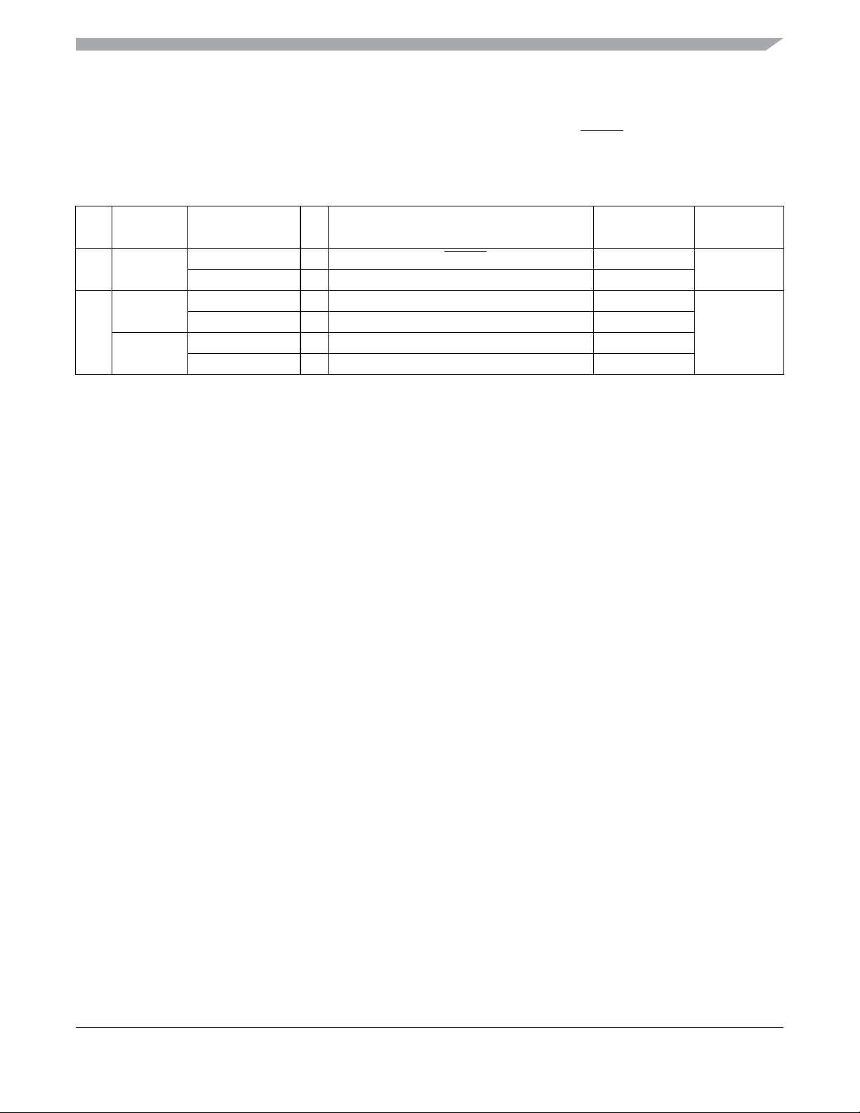
Chapter 2 Port Integration Module (S12ZVMPIMV1)
NOTE
If there is more than one function associated with a pin, the
output priority
is indicated by the position in the table from top (highest priority) to bottom
(lowest priority).
Table 2-1. Pin Functions and Priorities
Port Pin Name
- BKGD MODC
E PE1 XTAL - CPMU OSC signal — GPIO
PE0 EXTAL - CPMU OSC signal —
Pin Function
& Priority
(2)
BKGD I/O S12ZBDC communication —
PTE[1] I/O General-purpose —
PTE[0] I/O General-purpose —
I/O Description
(1)
I MODC input during RESET — BKGD
Routing
Register Bit
Pin Function
after Reset
MC9S12ZVM Family Reference Manual Rev. 1.3
Freescale Semiconductor 85
Page 86

Chapter 2 Port Integration Module (S12ZVMPIMV1)
Port Pin Name
Pin Function
& Priority
(1)
I/O Description
Routing
Register Bit
Pin Function
after Reset
AD PAD8 VRH I ADC0&1 voltage reference high — GPIO
AN1_3 I ADC1 analog input —
PTADH[0]/
I/O General-purpose; with interrupt and wakeup —
KWADH[0]
PAD7 AMPP1 I GDU AMP1 non-inverting input (+) —
AN1_2 I ADC1 analog input —
PTADL[7]/
I/O General-purpose; with interrupt and wakeup —
KWADL[7]
PAD6 AMPM1 I GDU AMP1 inverting input (-)
SS0) I/O SPI0 slave select SPI0RR
(
SPI0SSRR
AN1_1 I ADC1 analog input —
PTADL[6]/
I/O General-purpose; with interrupt and wakeup —
KWADL[6]
PAD5 AMP1 O GDU AMP1 output —
AN1_0 I ADC1 analog input —
PTADL[5]/
I/O General-purpose; with interrupt and wakeup —
KWADL[5]
PAD4-3 AN0_4:AN0_3 I ADC0 analog input —
PTADL[4:3]/
I/O General-purpose; with interrupt and wakeup —
KWADL[4:3]
PAD2 AMPP0 I GDU AMP0 non-inverting input (+) —
AN0_2 I ADC0 analog input —
PTADL[2]/
I/O General-purpose; with interrupt and wakeup —
KWADL[2]/
PAD1 AMPM0 I GDU AMP0 inverting input (-) —
AN0_1 I ADC0 analog input —
PTADL[1]/
I/O General-purpose; with interrupt and wakeup —
KWADL[1]
PAD0 AMP0 O GDU AMP0 output —
AN0_0 I ADC0 analog input —
PTADL[0]/
I/O General-purpose; with interrupt and wakeup —
KWADL[0]
MC9S12ZVM Family Reference Manual Rev. 1.3
86 Freescale Semiconductor
Page 87
Chapter 2 Port Integration Module (S12ZVMPIMV1)
Port Pin Name
T PT3 (
PT2 (SCK0) I/O SPI0 serial clock SPI0RR
PT1 PTURE O PTU reload event —
PT0 (RXD0) I SCI0 receive S0L0RR2-0
Pin Function
& Priority
(1)
I/O Description
Routing
Register Bit
SS0) I/O SPI0 slave select SPI0RR
SPI0SSRR
(3)
(IOC0_3)
I/O TIM0 channel 3 T0IC3RR1-0
PTT[3] I/O General-purpose —
(PWM5) O PWM channel 5 PWM54RR
PWMPRR
IOC0_2 I/O TIM0 channel 2 —
PTT[2] I/O General-purpose —
(TXD0)/
(LPDC0)
O SCI0 transmit/
LPTXD0 direct control by LP0DR[LP0DR1]
S0L0RR2-0
(MOSI0) I/O SPI0 master out/slave in SPI0RR
(PWM4) O PWM channel 4 PWM54RR
PWMPRR
3
(IOC0_1)
I/O TIM0 channel 1 T0IC1RR
PTT[1] I/O General-purpose —
(MISO0) I/O SPI0 master in/slave out SPI0RR
(PWM3) O PWM channel 3 PWM32RR
PWMPRR
IOC0_0 I/O TIM0 channel 0 —
PTT[0] I/O General-purpose —
Pin Function
after Reset
GPIO
MC9S12ZVM Family Reference Manual Rev. 1.3
Freescale Semiconductor 87
Page 88

Chapter 2 Port Integration Module (S12ZVMPIMV1)
Port Pin Name
Pin Function
& Priority
(1)
I/O Description
Routing
Register Bit
Pin Function
after Reset
S PS5 PDO O DBG profiling data output — GPIO
SS0 I/O SPI0 slave select SPI0RR
SPI0SSRR
PTS[5]/
I/O General-purpose; with interrupt and wakeup —
KWS[5]
PS4 PDOCLK O DBG profiling clock —
SCK0 I/O SPI0 serial clock SPI0RR
PTS[4]/
I/O General-purpose; with interrupt and wakeup —
KWS[4]
PS3 MOSI0 I/O SPI0 master out/slave in SPI0RR
(TXD1) O SCI1 transmit SCI1RR
DBGEEV I DBG external event —
PTS[3]/
I/O General-purpose; with interrupt and wakeup —
KWS[3]
PS2 MISO0 I/O SPI0 master in/slave out SPI0RR
(RXD1) I SCI1 receive SCI1RR
PTS[2]/
I/O General-purpose; with interrupt and wakeup —
KWS[2]
PS1 PTUT1 O PTU trigger 1 —
(LPTXD0) I LINPHY0 transmit input S0L0RR2-0
TXCAN0 O MSCAN0 transmit —
TXD1 O SCI1 transmit SCI1RR
PTS[1]/
I/O General-purpose; with interrupt and wakeup —
KWS[1]
PS0 PTUT0 O PTU trigger 0 —
(LPRXD0) O LINPHY0 receive output S0L0RR2-0
RXCAN0 I MSCAN0 receive —
RXD1 I SCI1 receive SCI1RR
PTS[0]/
I/O General-purpose; with interrupt and wakeup —
KWS[0]
MC9S12ZVM Family Reference Manual Rev. 1.3
88 Freescale Semiconductor
Page 89
Chapter 2 Port Integration Module (S12ZVMPIMV1)
Port Pin Name
P PP2 (PWM2) O PWM channel 2 PWM32RR
PP1
PP0
1. Signals in parentheses denote alternative module routing pins.
Pin Function
& Priority
PTP[2]/
KWP[2]
IRQ I Maskable level- or falling edge-sensitive
(PWM1) O PWM channel 1 PWM10RR
PTP[1]/
KWP[1]
XIRQ I Non-maskable level-sensitive interrupt
FAULT5 I PMF fault —
ECLK O Free-running clock —
(PWM0) O PWM channel 0 with over-current interrupt;
PTP[0]/
KWP[0]/
EVDD1
I/O Description
(1)
I/O General-purpose; with interrupt and wakeup —
interrupt
I/O General-purpose; with interrupt and wakeup —
(4)
high-current capable (20 mA)
I/O General-purpose; with interrupt and wakeup
Switchable external power supply output with
over-current interrupt; high-current capable
(20 mA)
Routing
Register Bit
PWMPRR
PWMPRR
PWM10RR
PWMPRR
Pin Function
after Reset
GPIO
—
—
—
2. Function active when RESET asserted.
3. Routable input capture function.
4. The interrupt is enabled by clearing the X mask bit in the CPU CCR. The pin is forced to input upon first clearing of the X bit
and is held in this state until reset. A stop or wait recovery with the X bit set (refer to S12ZCPU reference manual) is not
available.
2.3 Memory Map and Register Definition
This section provides a detailed description of all port integration module registers.
MC9S12ZVM Family Reference Manual Rev. 1.3
Freescale Semiconductor 89
Page 90
Chapter 2 Port Integration Module (S12ZVMPIMV1)
2.3.1 Register Map
Global
Address
0x0200 MODRR0
0x0201 MODRR1
0x0202 MODRR2
0x0203–
0x0207
0x0208 ECLKCTL
0x0209 IRQCR
0x020A PIMMISC
Register
Name
Reserved
Bit 7 654321Bit 0
R0 0
W
R0000
W
R0000
W
R00000000
W
R
NECLK
W
R
IRQE IRQEN
W
R000000
W
SPI0SSRR SPI0RR SCI1RR S0L0RR2-0
PWMPRR PWM54RR PWM32RR PWM10RR
T0IC3RR1-0 T0IC1RR
0000000
000000
OCPE1
0
0
0x020B–
0x020D
0x020E Reserved
0x020F Reserved
0x0210–
0x025F
0x0260 PTE
0x0261 Reserved
0x0262 PTIE
0x0263 Reserved
Reserved
Reserved
R00000000
W
R
Reserved Reserved Reserved Reserved Reserved Reserved Reserved Reserved
W
R
Reserved Reserved Reserved Reserved Reserved Reserved Reserved Reserved
W
R00000000
W
R000000
W
R00000000
W
R000000PTIE1 PTIE0
W
R00000000
W
PTE1 PTE0
MC9S12ZVM Family Reference Manual Rev. 1.3
90 Freescale Semiconductor
Page 91
Chapter 2 Port Integration Module (S12ZVMPIMV1)
Global
Address
Register
Name
0x0264 DDRE
0x0265 Reserved
0x0266 PERE
0x0267 Reserved
0x0268 PPSE
0x0269–
0x027F
Reserved
0x0280 PTADH
Bit 7 654321Bit 0
R000000
W
DDRE1 DDRE0
R00000000
W
R000000
W
PERE1 PERE0
R00000000
W
R000000
W
PPSE1 PPSE0
R00000000
W
R0000000
W
PTADH0
0x0281 PTADL
0x0282 PTIADH
0x0283 PTIADL
0x0284 DDRADH
0x0285 DDRADL
0x0286 PERADH
0x0287 PERADL
0x0288 PPSADH
R
PTADL7 PTADL6 PTADL5 PTADL4 PTADL3 PTADL2 PTADL1 PTADL0
W
R0000000PTIADH0
W
R PTIADL7 PTIADL6 PTIADL5 PTIADL4 PTIADL3 PTIADL2 PTIADL1 PTIADL0
W
R0000000
W
R
DDRADL7 DDRADL6 DDRADL5 DDRADL4 DDRADL3 DDRADL2 DDRADL1 DDRADL0
W
DDRADH0
R0000000
W
R
PERADL7 PERADL6 PERADL5 PERADL4 PERADL3 PERADL2 PERADL1 PERADL0
W
PERADH0
R0000000
W
PPSADH0
0x0289 PPSADL
R
PPSADL7 PPSADL6 PPSADL5 PPSADL4 PPSADL3 PPSADL2 PPSADL1 PPSADL0
W
MC9S12ZVM Family Reference Manual Rev. 1.3
Freescale Semiconductor 91
Page 92
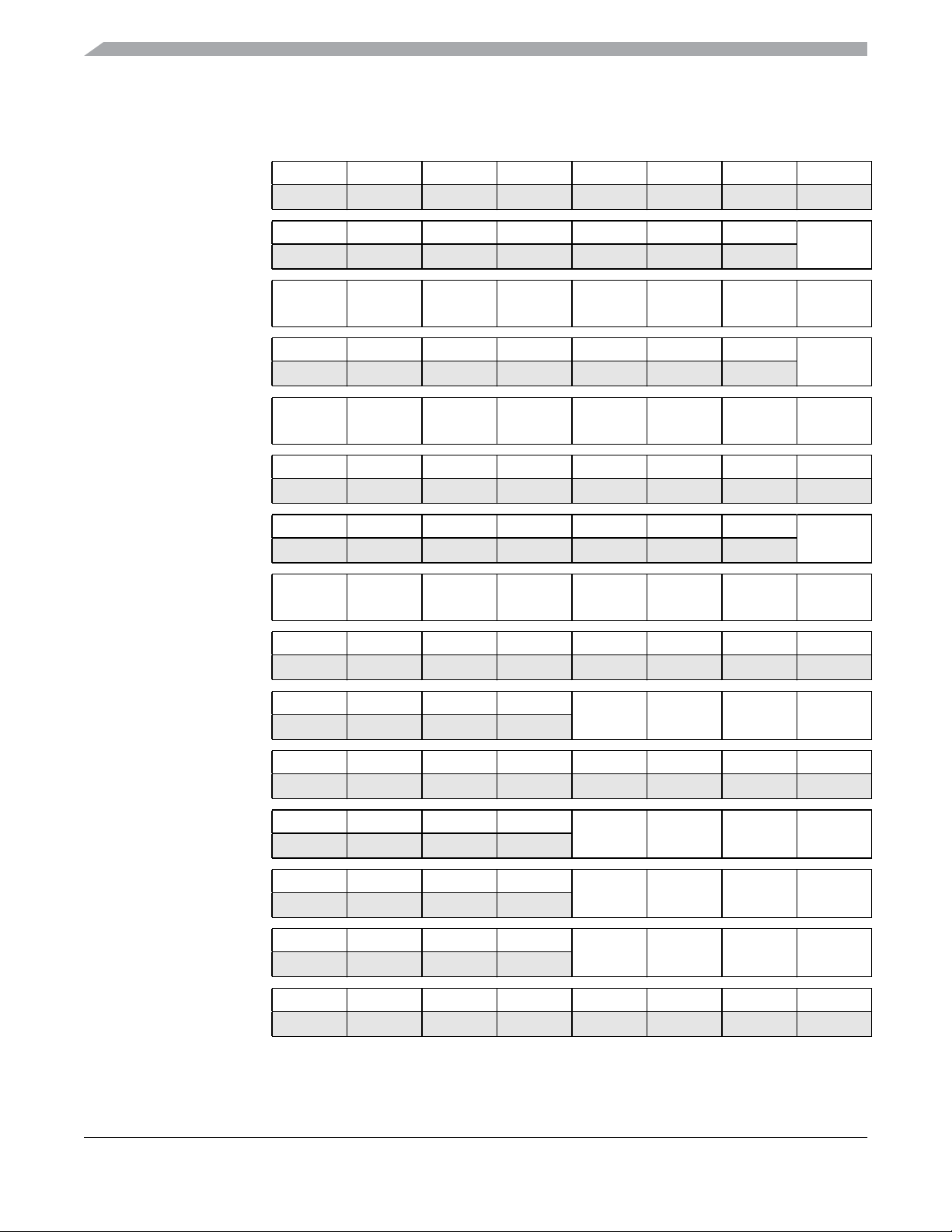
Chapter 2 Port Integration Module (S12ZVMPIMV1)
Global
Address
0x028A–
0x028B
Register
Name
Reserved
0x028C PIEADH
0x028D PIEADL
0x028E PIFADH
0x028F PIFADL
0x0290–
0x0297
Reserved
0x0298 DIENADH
Bit 7 654321Bit 0
R00000000
W
R0000000
W
R
PIEADL7 PIEADL6 PIEADL5 PIEADL4 PIEADL3 PIEADL2 PIEADL1 PIEADL0
W
PIEADH0
R0000000
W
R
PIFADL7 PIFADL6 PIFADL5 PIFADL4 PIFADL3 PIFADL2 PIFADL1 PIFADL0
W
PIFADH0
R00000000
W
R0000000
W
DIENADH0
0x0299 DIENADL
0x029A–
0x02BF
Reserved
0x02C0 PTT
0x02C1 PTIT
0x02C2 DDRT
0x02C3 PERT
0x02C4 PPST
0x02C5–
0x02CF
Reserved
R
DIENADL7 DIENADL6 DIENADL5 DIENADL4 DIENADL3 DIENADL2 DIENADL1 DIENADL0
W
R00000000
W
R0000
W
PTT3 PTT2 PTT1 PTT0
R0000PTIT3 PTIT2 PTIT1 PTIT0
W
R0000
W
DDRT3 DDRT2 DDRT1 DDRT0
R0000
W
PERT3 PERT2 PERT1 PERT0
R0000
W
PPST3 PPST2 PPST1 PPST0
R00000000
W
MC9S12ZVM Family Reference Manual Rev. 1.3
92 Freescale Semiconductor
Page 93
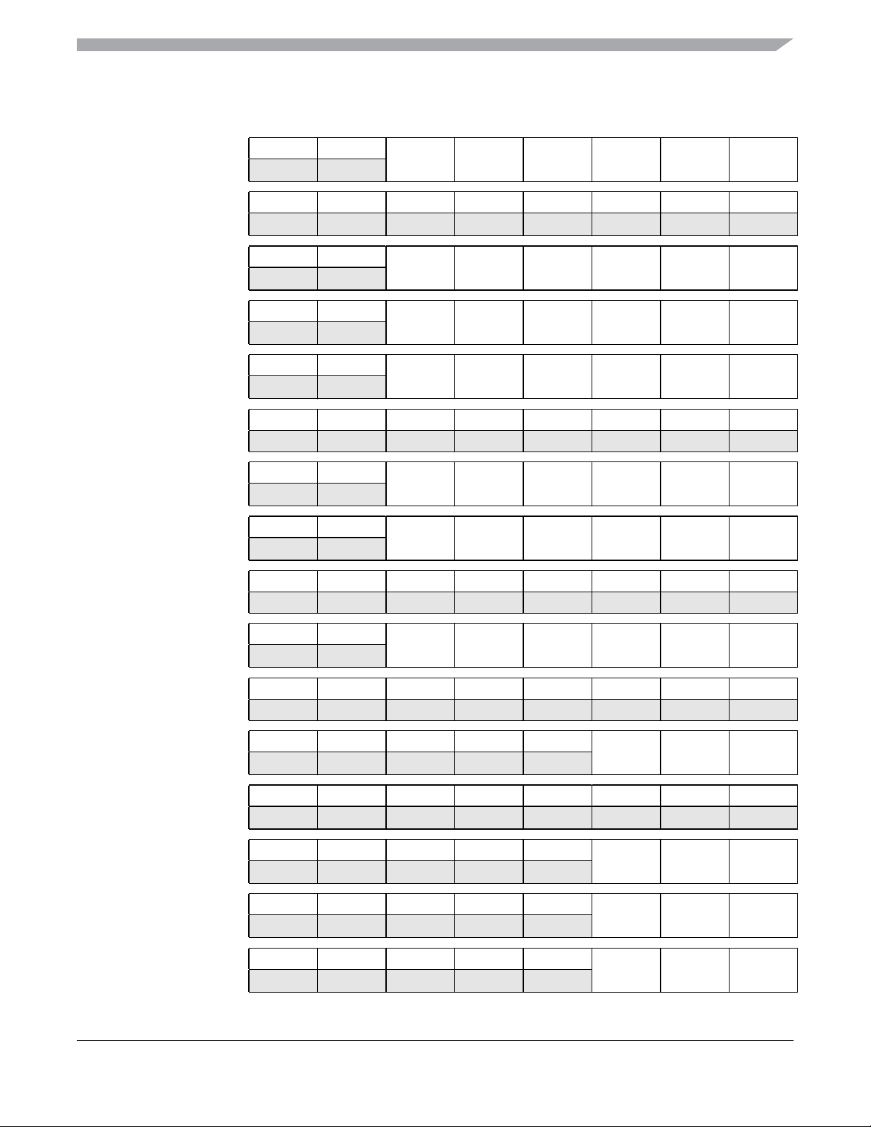
Chapter 2 Port Integration Module (S12ZVMPIMV1)
Global
Address
Register
Name
0x02D0 PTS
0x02D1 PTIS
0x02D2 DDRS
0x02D3 PERS
0x02D4 PPSS
0x02D5 Reserved
0x02D6 PIES
Bit 7 654321Bit 0
R0 0
W
PTS5 PTS4 PTS3 PTS2 PTS1 PTS0
R 0 0 PTIS5 PTIS4 PTIS3 PTIS2 PTIS1 PTIS0
W
R0 0
W
DDRS5 DDRS4 DDRS3 DDRS2 DDRS1 DDRS0
R0 0
W
PERS5 PERS4 PERS3 PERS2 PERS1 PERS0
R0 0
W
PPSS5 PPSS4 PPSS3 PPSS2 PPSS1 PPSS0
R00000000
W
R0 0
W
PIES5 PIES4 PIES3 PIES2 PIES1 PIES0
0x02D7 PIFS
0x02D8–
0x02DE
Reserved
0x02DF WOMS
0x02E0–
0x02EF
Reserved
0x02F0 PTP
0x02F1 PTIP
0x02F2 DDRP
0x02F3 PERP
R0 0
W
PIFS5 PIFS4 PIFS3 PIFS2 PIFS1 PIFS0
R00000000
W
R0 0
W
WOMS5 WOMS4 WOMS3 WOMS2 WOMS1 WOMS0
R00000000
W
R00000
W
PTP2 PTP1 PTP0
R00000PTIP2 PTIP1 PTIP0
W
R00000
W
DDRP2 DDRP1 DDRP0
R00000
W
PERP2 PERP1 PERP0
0x02F4 PPSP
W
PPSP2 PPSP1 PPSP0
MC9S12ZVM Family Reference Manual Rev. 1.3
Freescale Semiconductor 93
R00000
Page 94
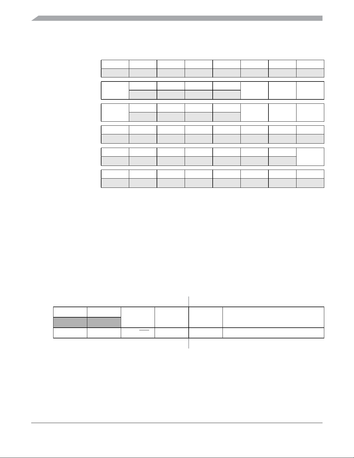
Chapter 2 Port Integration Module (S12ZVMPIMV1)
Global
Address
0x02F5 Reserved
0x02F6 PIEP
0x02F7 PIFP
0x02F8–
0x02FC
0x02FD RDRP
0x02FE–
0x02FF
Register
Name
Reserved
Reserved
Bit 7 654321Bit 0
R00000000
W
R
OCIE1
W
R
OCIF1
W
R00000000
W
R0000000
W
R00000000
W
0000
0000
2.3.2 PIM Registers 0x0200-0x020F
PIEP2 PIEP1 PIEP0
PIFP2 PIFP1 PIFP0
RDRP0
This section details the specific purposes of register implemented in address range 0x0200-0x020F. These
registers serve for specific PIM related functions not part of the generic port registers.
• If not stated differently, writing to reserved bits has no effect and read returns zero.
• All register read accesses are synchronous to internal clocks.
• Register bits can be written at any time if not stated differently.
2.3.2.1 Module Routing Register 0 (MODRR0)
Address 0x0200 Access: User read/write
76543210
R0 0
SPI0SSRR SPI0RR SCI1RR S0L0RR2-0
W
— — SPI0 SS0 SPI0 SCI1 SCI0-LINPHY0 (see Figure 2-2)
Reset 00000000
Figure 2-1. Module Routing Register 0 (MODRR0)
1. Read: Anytime
Write: Once in normal, anytime in special mode
(1)
MC9S12ZVM Family Reference Manual Rev. 1.3
94 Freescale Semiconductor
Page 95
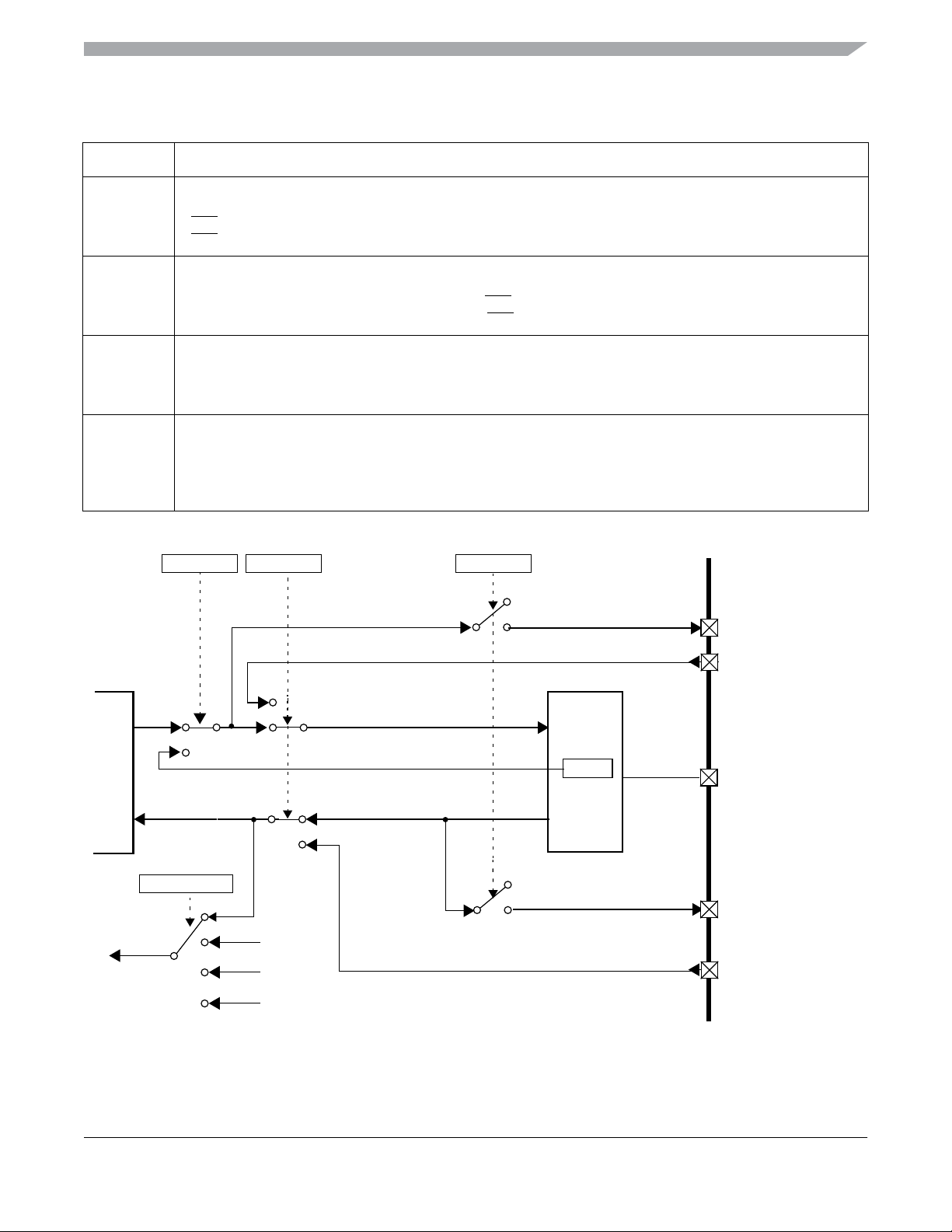
Table 2-2. MODRR0 Routing Register Field Descriptions
Field Description
Chapter 2 Port Integration Module (S12ZVMPIMV1)
5
SPI0SSR
4
SPI0RR
3
SCI1RR
2-0
S0L0RR2-0
Module Routing Register — SPI0 SS0 routing
1
SS0 on PAD6
0
SS0 based on SPI0RR
Module Routing Register — SPI0 routing
1 MISO0 on PT0; MOSI0 on PT1; SCK0 on PT2;
0 MISO0 on PS2; MOSI0 on PS3; SCK0 on PS4;
Module Routing Register — SCI1 routing
1 TXD1 on PS3; RXD1 on PS2
0 TXD1 on PS1; RXD1 on PS0
Module Routing Register — SCI0-LINPHY0 routing
Selection of SCI0-LINPHY0 interface routing options to support probing and conformance testing. Refer to
Figure 2-2 foran illustration and Table 2-3 for preferred settings. SCI0 must be enabled for TXD0 routing to take
effect on pins. LINPHY0 must be enabled for LPRXD0 and LPDC0 routings to take effect on pins.
SS0 on PT3
SS0 on PS5
S0L0RR2S0L0RR1S0L0RR0
0
1
PT1 / TXD0 / LPDC0
SCI0
TXD0
RXD0
TIM0 input
capture
channel 3
0
1
T0IC3RR1-0
01
10
11
00
1
0
0
LINPHY0
LPTXD0
LPDR1
LPRXD0
1
0
1
RXD1
ACLK
IOC0_3
Figure 2-2. SCI0-to-LINPHY0 Routing Options Illustration
PS1 / LPTXD0
LIN
PS0 / LPRXD0
PT0 / RXD0
MC9S12ZVM Family Reference Manual Rev. 1.3
Freescale Semiconductor 95
Page 96
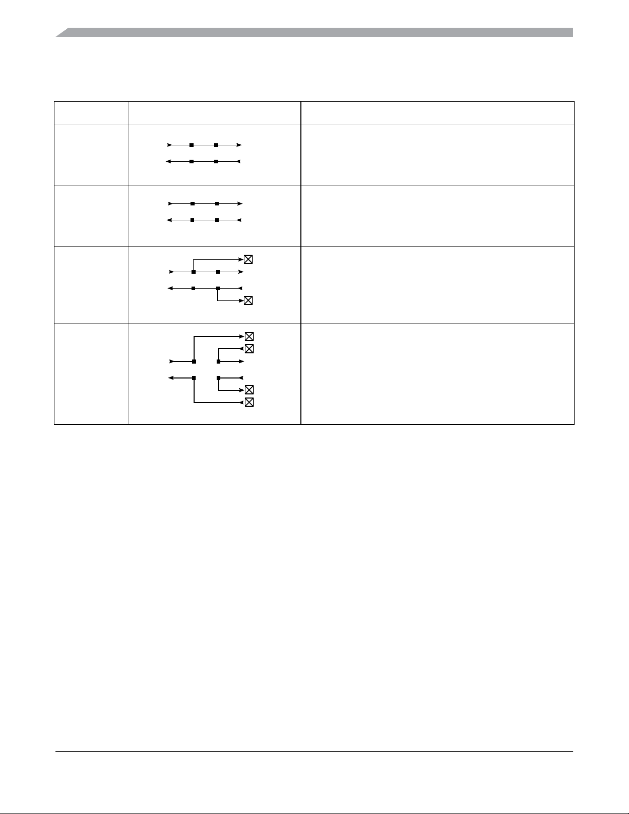
Chapter 2 Port Integration Module (S12ZVMPIMV1)
Table 2-3. Preferred Interface Configurations
S0L0RR[2:0] Signal Routing Description
000 Default setting:
SCI0 connects to LINPHY0, interface internal only
001 Direct control setting:
100 Probe setting:
110 Conformance test setting:
LP0DR[LPDR1] register bit controls LPTXD0, interface internal
only
SCI0 connects to LINPHY0, interface accessibleon 2 external pins
Interface opened and all 4 signals routed externally
NOTE
For standalone usage of SCI0 on external pins set
[S0L0RR2:S0L0RR0]=0b110 and disable the LINPHY0 (LPCR[LPE]=0).
This releases PS0 and PS1 to other associated functions and maintains
TXD0 and RXD0 signals on PT1 and PT0, respectively, if no other function
with higher priority takes precedence.
MC9S12ZVM Family Reference Manual Rev. 1.3
96 Freescale Semiconductor
Page 97
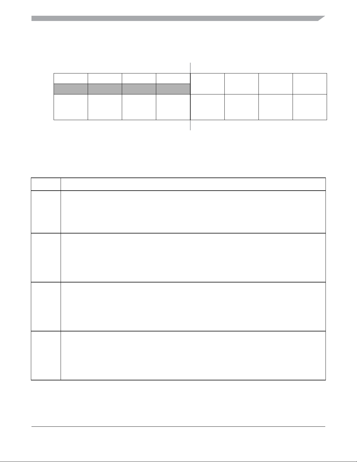
2.3.2.2 Module Routing Register 1 (MODRR1)
Chapter 2 Port Integration Module (S12ZVMPIMV1)
Address 0x0201 Access: User read/write
76543210
R0000
W
— — — —
Reset 00000000
PWMPRR PWM54RR PWM32RR PWM10RR
PWM
probe
PWM4
PWM5
GDU/pins
PWM2
PWM3
GDU/pins
PWM0
PWM1
GDU/pins
Figure 2-3. Module Routing Register 1 (MODRR1)
1. Read: Anytime
Write: Once in normal, anytime in special mode
Table 2-4. MODRR1 Routing Register Field Descriptions
Field Description
3
PWMPRR
Module Routing Register — PWM probe
All six internal PWM outputs can be probed on related external pins.
1 All PWM channels connected to related PWM[5:0] pins
0 All PWM channels disconnected from related PWM[5:0] pins
(1)
2
PWM54RR
1
PWM32RR
0
PWM10RR
Module Routing Register — PWM4 and PWM5 routing
The PWM channel pair can be configured for internal use with the GDU or with its related external pins only. If set
the signal routing to the pins is established and the related GDU inputs are forced low.
1 PWM4 to PT1; PWM5 to PT2
0 PWM4 to GDU; PWM5 to GDU
Module Routing Register — PWM2 and PWM3 routing
The PWM channel pair can be configured for internal use with the GDU or with its related external pins only. If set
the signal routing to the pins is established and the related GDU inputs are forced low.
1 PWM2 to PP2; PWM3 to PT0
0 PWM2 to GDU; PWM3 to GDU
Module Routing Register — PWM0 and PWM1 routing
The PWM channel pair can be configured for internal use with the GDU or with its related external pins only. If set
the signal routing to the pins is established and the related GDU inputs are forced low.
1 PWM0 to PP0; PWM1 to PP1
0 PWM0 to GDU; PWM1 to GDU
MC9S12ZVM Family Reference Manual Rev. 1.3
Freescale Semiconductor 97
Page 98
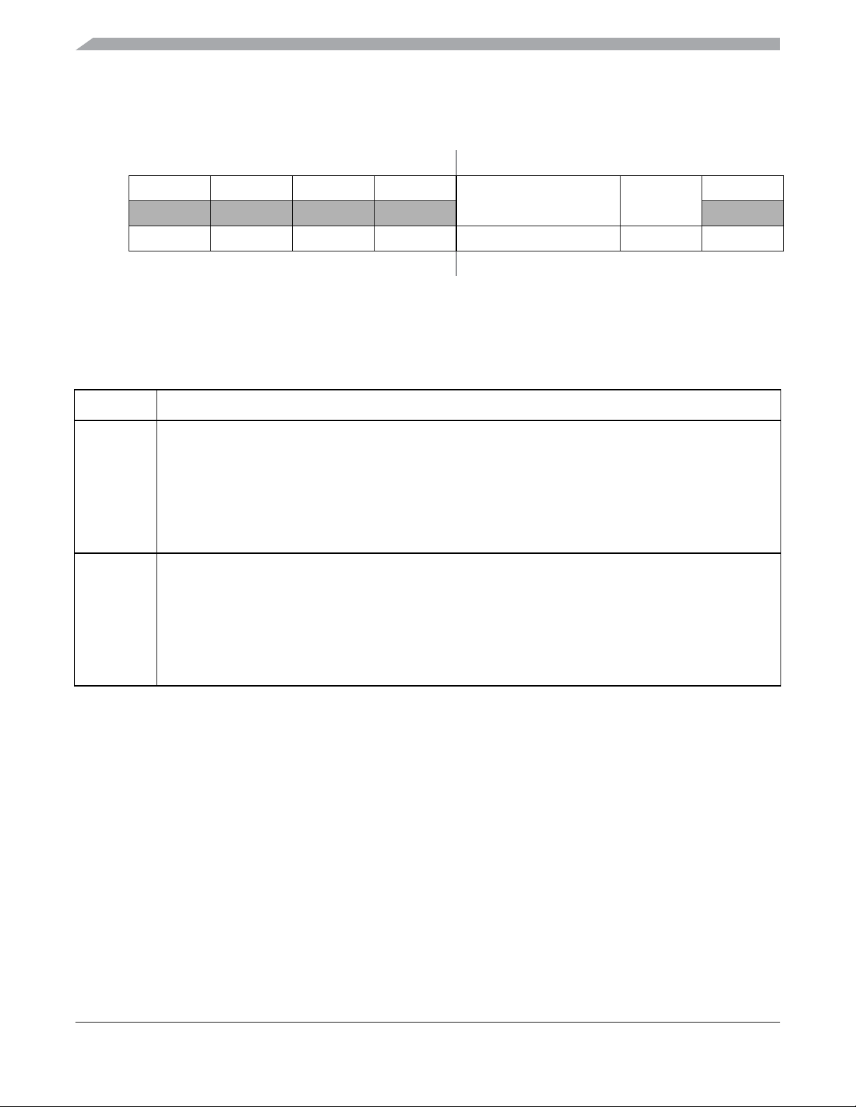
Chapter 2 Port Integration Module (S12ZVMPIMV1)
2.3.2.3 Module Routing Register 2 (MODRR2)
Address 0x0202 Access: User read/write
76543210
R0000
T0IC3RR1-0 T0IC1RR
W
TIM0 IC3 TIM0 IC1
Reset 00000000
0
Figure 2-4. Module Routing Register 2 (MODRR2)
1. Read: Anytime
Write: Once in normal, anytime in special mode
Table 2-5. MODRR2 Routing Register Field Descriptions
Field Description
3-2
T0IC3RR1-0
Module Routing Register — TIM0 IC3 routing
One out of four different sources can be selected as input to timer channel 3.
11 TIM0 input capture channel 3 is connected to ACLK
10 TIM0 input capture channel 3 is connected to RXD1
01 TIM0 input capture channel 3 is connected to RXD0
00 TIM0 input capture channel 3 is connected to PT3
(1)
1
T0IC1RR
Module Routing Register — TIM0 IC1 routing
Timer input capture channel 1 can be used to determine the asynchronous commutation event in BLDC motor
applications with Hall sensors. An integrated XOR gate supportsdirect connection of the three sensor inputs to
the device.
1 TIM0 input capture channel 1 is connected to logically XORed input signals of pins PT3-1
0 TIM0 input capture channel 1 is connected to PT1
MC9S12ZVM Family Reference Manual Rev. 1.3
98 Freescale Semiconductor
Page 99
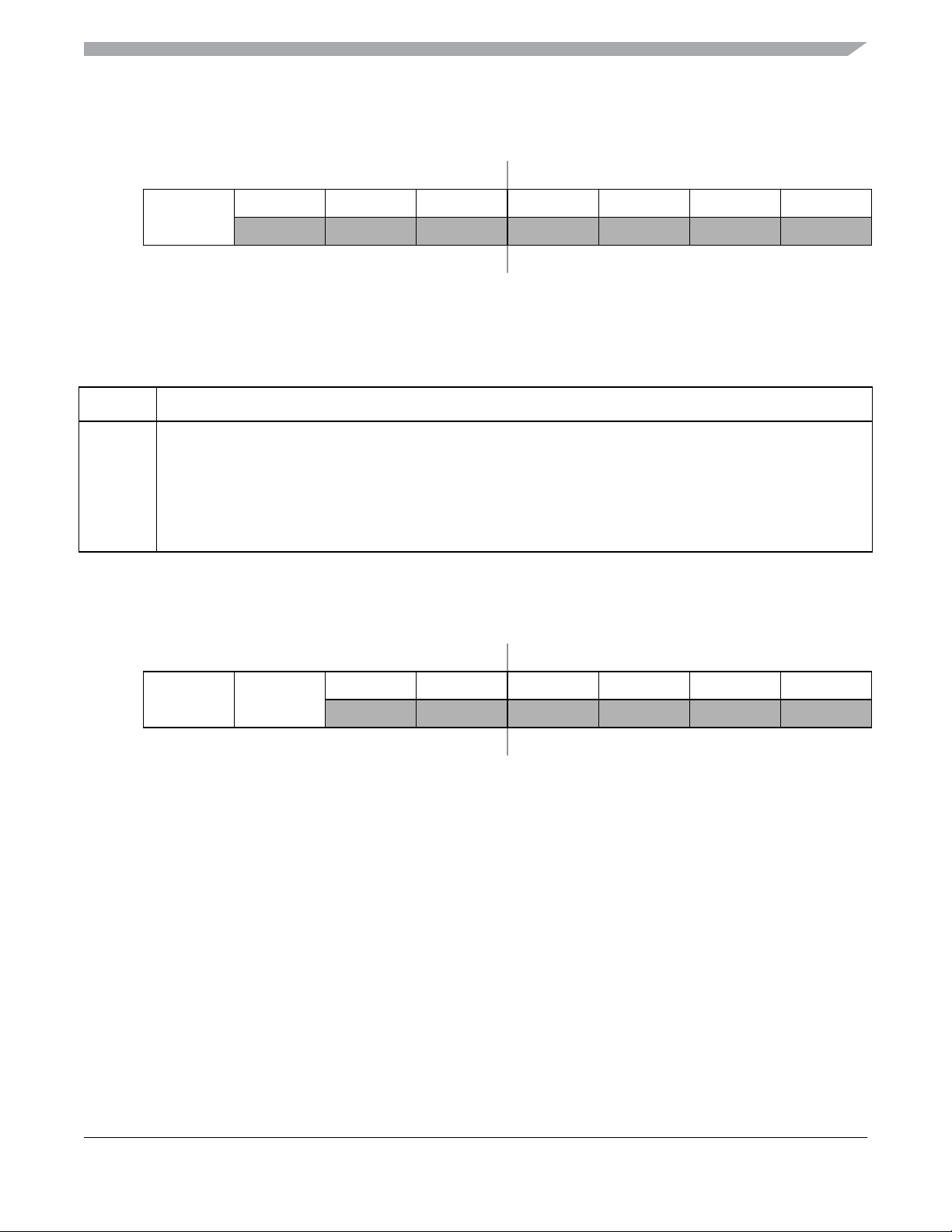
2.3.2.4 ECLK Control Register (ECLKCTL)
Chapter 2 Port Integration Module (S12ZVMPIMV1)
Address 0x0208 Access: User read/write
76543210
R
NECLK
W
Reset: 10000000
0000000
(1)
Figure 2-5. ECLK Control Register (ECLKCTL)
1. Read: Anytime
Write: Anytime
Table 2-6. ECLKCTL Register Field Descriptions
Field Description
7
NECLK
No ECLK — Disable ECLK output
This bit controls the availabilityof a free-running clock on the ECLK pin. This clock has a fixed rate equivalentto the
internal bus clock.
1 ECLK disabled
0 ECLK enabled
2.3.2.5 IRQ Control Register (IRQCR)
Address 0x0209 Access: User read/write
76543210
R
IRQE IRQEN
W
Reset 00000000
000000
Figure 2-6. IRQ Control Register (IRQCR)
1. Read: Anytime
Write:
IRQE: Once in normal mode, anytime in special mode
IRQEN: Anytime
(1)
MC9S12ZVM Family Reference Manual Rev. 1.3
Freescale Semiconductor 99
Page 100
Chapter 2 Port Integration Module (S12ZVMPIMV1)
Table 2-7. IRQCR Register Field Descriptions
Field Description
7
IRQE
6
IRQEN
IRQ select edge sensitive only —
1
IRQ pin configured to respond only to falling edges. Falling edges on the IRQ pin are detected anytime when
IRQE=1 and will be cleared only upon a reset or the servicing of the
0
IRQ configured for low level recognition
IRQ enable —
1
IRQ pin is connected to interrupt logic
0
IRQ pin is disconnected from interrupt logic
IRQ interrupt.
2.3.2.6 PIM Miscellaneous Register (PIMMISC)
Address 0x020A Access: User read/write
76543210
R000000
OCPE1
W
Reset 00000000
Figure 2-7. PIM Miscellaneous Register (PIMMISC)
1. Read: Anytime
Write:Anytime
0
(1)
Table 2-8. PIM Miscellaneous Register Field Descriptions
Field Description
1
OCPE1
Over-Current Protection Enable — Activate over-current detector on PP0
Refer to Section 2.5.2, “Over-Current Protection on EVDD1”
1 PP0 over-current detector enabled
0 PP0 over-current detector disabled
2.3.2.7 Reserved Register
Address 0x020E Access: User read/write
76543210
R
Reserved Reserved Reserved Reserved Reserved Reserved Reserved Reserved
W
Reset xxxxxxxx
Figure 2-8. Reserved Register
(1)
MC9S12ZVM Family Reference Manual Rev. 1.3
100 Freescale Semiconductor
 Loading...