

Page 1

MC9S12XDP512
Data Sheet
HCS12X
Microcontrollers
MC9S12XDP512
Rev. 2.11
5/2005
freescale.com
Page 2

Page 3

MC9S12XDP512 Data Sheet
covers
MC9S12XDT384 & MC9S12XA512
MC9S12XDP512V2
Rev. 2.11
7/2005
Page 4

To provide the most up-to-date information, the revision of our documents on the World Wide Web will be
the most current. Your printed copy may be an earlier revision. To verify you have the latest information
available, refer to:
http://freescale.com/
The following revision history table summarizes changes contained in this document.
Revision History
Date
April, 2005 02.07 New Book
May, 2005 02.08 Minor corrections
May, 2005 02.09
May 2005 02.10 Improvements to NVM reliabity spec, added part numbers
July 2005 02.11 Added ROM parts to App.
Revision
Level
Description
removed ESD Machine Model from electrical characteristics
added thermal characteristics
added more details to run current measurement configurations
VDDA supply voltage range 3.15V - 3.6V fot ATD Operating Characteristics
I/O Chararcteristics for alll pins except EXTAL, XTAL ....
corrected VREG electrical spec
IDD wait max 95mA
Freescale™ and the Freescale logo are trademarks of Freescale Semiconductor, Inc.
This product incorporates SuperFlash® technology licensed from SST.
© Freescale Semiconductor, Inc., 2005. All rights reserved.
MC9S12XDP512 Data Sheet, Rev. 2.11
4 Freescale Semiconductor
Page 5

Contents
Section Number Title Page
Chapter 1 Device Overview (MC9S12XDP512V2) . . . . . . . . . . . . . . . . . . .23
Chapter 2 512 Kbyte Flash Module (S12XFTX512K4V2). . . . . . . . . . . . .101
Chapter 3 4 Kbyte EEPROM Module (S12XEETX4KV2) . . . . . . . . . . . . .145
Chapter 4 Port Integration Module (S12XDP512PIMV2) . . . . . . . . . . . . . 177
Chapter 5 Clocks and Reset Generator (S12CRGV6) . . . . . . . . . . . . . . .271
Chapter 6 Pierce Oscillator (S12XOSCLCPV1) . . . . . . . . . . . . . . . . . . . .311
Chapter 7 Analog-to-Digital Converter (ATD10B16CV4) . . . . . . . . . . . . 317
Chapter 8 Analog-to-Digital Converter (ATD10B8CV3) . . . . . . . . . . . . .347
Chapter 9 XGATE (S12XGATEV2). . . . . . . . . . . . . . . . . . . . . . . . . . . . . . .373
Chapter 10 Security (S12X9SECV2) . . . . . . . . . . . . . . . . . . . . . . . . . . . . . 499
Chapter 11 Enhanced Capture Timer (S12MC9S12XDP51216B8CV2) . . 507
Chapter 12 Pulse-Width Modulator (S12PWM8B8CV1) . . . . . . . . . . . . . . 561
Chapter 13 Inter-Integrated Circuit (MC9S12XDP512) Block Description . .
593
Chapter 14 Freescale’s Scalable Controller Area Network (S12MSCANV3).
617
Chapter 15 Serial Communication Interface (S12MC9S12XDP512V5) . .673
Chapter 16 Serial Peripheral Interface (S12SPIV4) . . . . . . . . . . . . . . . . . .711
Chapter 17 Voltage Regulator (S12VREG3V3V5) . . . . . . . . . . . . . . . . . . .735
Chapter 18 Periodic Interrupt Timer (S12PIT24B4CV1) . . . . . . . . . . . . . .749
Chapter 19 Background Debug Module (S12XBDMV2) . . . . . . . . . . . . . .765
Chapter 20 Debug (S12XDBGV2) . . . . . . . . . . . . . . . . . . . . . . . . . . . . . . . .791
Chapter 21 Interrupt (S12MC9S12XDP512V1) . . . . . . . . . . . . . . . . . . . . . .843
Chapter 22 External Bus Interface (S12XEBIV2) . . . . . . . . . . . . . . . . . . .861
MC9S12XDP512 Data Sheet, Rev. 2.11
Freescale Semiconductor 5
Page 6

Section Number Title Page
Chapter 23 Memory Mapping Control (S12XMMCV2). . . . . . . . . . . . . . . .881
Appendix A Electrical Characteristics. . . . . . . . . . . . . . . . . . . . . . . . . . . . .919
Appendix B Package Information . . . . . . . . . . . . . . . . . . . . . . . . . . . . . . . .965
Appendix C Recommended PCB Layout . . . . . . . . . . . . . . . . . . . . . . . . . .969
Appendix D Derivative Differences . . . . . . . . . . . . . . . . . . . . . . . . . . . . . . . . 974
Appendix E Ordering Information . . . . . . . . . . . . . . . . . . . . . . . . . . . . . . . .981
MC9S12XDP512 Data Sheet, Rev. 2.11
6 Freescale Semiconductor
Page 7

Contents
Section Number Title Page
Chapter 1
Device Overview (MC9S12XDP512V2)
1.1 Introduction . . . . . . . . . . . . . . . . . . . . . . . . . . . . . . . . . . . . . . . . . . . . . . . . . . . . . . . . . . . . . . . . . . 23
1.1.1 Features . . . . . . . . . . . . . . . . . . . . . . . . . . . . . . . . . . . . . . . . . . . . . . . . . . . . . . . . . . . . . . 24
1.1.2 Modes of Operation . . . . . . . . . . . . . . . . . . . . . . . . . . . . . . . . . . . . . . . . . . . . . . . . . . . . .26
1.1.3 Block Diagram . . . . . . . . . . . . . . . . . . . . . . . . . . . . . . . . . . . . . . . . . . . . . . . . . . . . . . . . . 26
1.1.4 Device Memory Map . . . . . . . . . . . . . . . . . . . . . . . . . . . . . . . . . . . . . . . . . . . . . . . . . . . . 28
1.1.5 Address Mapping . . . . . . . . . . . . . . . . . . . . . . . . . . . . . . . . . . . . . . . . . . . . . . . . . . . . . . .30
1.1.6 Detailed Register Map . . . . . . . . . . . . . . . . . . . . . . . . . . . . . . . . . . . . . . . . . . . . . . . . . . . 33
1.1.7 Part ID Assignments . . . . . . . . . . . . . . . . . . . . . . . . . . . . . . . . . . . . . . . . . . . . . . . . . . . .71
1.2 Signal Description . . . . . . . . . . . . . . . . . . . . . . . . . . . . . . . . . . . . . . . . . . . . . . . . . . . . . . . . . . . . . 71
1.2.1 Device Pinout . . . . . . . . . . . . . . . . . . . . . . . . . . . . . . . . . . . . . . . . . . . . . . . . . . . . . . . . . . 71
1.2.2 Signal Properties Summary . . . . . . . . . . . . . . . . . . . . . . . . . . . . . . . . . . . . . . . . . . . . . . . 75
1.2.3 Detailed Signal Descriptions . . . . . . . . . . . . . . . . . . . . . . . . . . . . . . . . . . . . . . . . . . . . . . 78
1.2.4 Power Supply Pins . . . . . . . . . . . . . . . . . . . . . . . . . . . . . . . . . . . . . . . . . . . . . . . . . . . . . .88
1.3 System Clock Description . . . . . . . . . . . . . . . . . . . . . . . . . . . . . . . . . . . . . . . . . . . . . . . . . . . . . . . 91
1.4 Chip Configuration Summary . . . . . . . . . . . . . . . . . . . . . . . . . . . . . . . . . . . . . . . . . . . . . . . . . . . . 92
1.5 Modes of Operation . . . . . . . . . . . . . . . . . . . . . . . . . . . . . . . . . . . . . . . . . . . . . . . . . . . . . . . . . . . . 94
1.5.1 User Modes . . . . . . . . . . . . . . . . . . . . . . . . . . . . . . . . . . . . . . . . . . . . . . . . . . . . . . . . . . . 94
1.5.2 Low-Power Modes . . . . . . . . . . . . . . . . . . . . . . . . . . . . . . . . . . . . . . . . . . . . . . . . . . . . . . 94
1.5.3 Freeze Mode . . . . . . . . . . . . . . . . . . . . . . . . . . . . . . . . . . . . . . . . . . . . . . . . . . . . . . . . . . . 95
1.6 Resets and Interrupts . . . . . . . . . . . . . . . . . . . . . . . . . . . . . . . . . . . . . . . . . . . . . . . . . . . . . . . . . . . 95
1.6.1 Vectors . . . . . . . . . . . . . . . . . . . . . . . . . . . . . . . . . . . . . . . . . . . . . . . . . . . . . . . . . . . . . . . 95
1.6.2 Effects of Reset . . . . . . . . . . . . . . . . . . . . . . . . . . . . . . . . . . . . . . . . . . . . . . . . . . . . . . . . 98
1.7 COP Configuration . . . . . . . . . . . . . . . . . . . . . . . . . . . . . . . . . . . . . . . . . . . . . . . . . . . . . . . . . . . . . 99
1.8 ATD0 External Trigger Input Connection . . . . . . . . . . . . . . . . . . . . . . . . . . . . . . . . . . . . . . . . . . . 99
1.9 ATD1 External Trigger Input Connection . . . . . . . . . . . . . . . . . . . . . . . . . . . . . . . . . . . . . . . . . . 100
Chapter 2
512 Kbyte Flash Module (S12XFTX512K4V2)
2.1 Introduction . . . . . . . . . . . . . . . . . . . . . . . . . . . . . . . . . . . . . . . . . . . . . . . . . . . . . . . . . . . . . . . . . 101
2.1.1 Glossary . . . . . . . . . . . . . . . . . . . . . . . . . . . . . . . . . . . . . . . . . . . . . . . . . . . . . . . . . . . . . 101
2.1.2 Features . . . . . . . . . . . . . . . . . . . . . . . . . . . . . . . . . . . . . . . . . . . . . . . . . . . . . . . . . . . . . 101
2.1.3 Modes of Operation . . . . . . . . . . . . . . . . . . . . . . . . . . . . . . . . . . . . . . . . . . . . . . . . . . . . 102
2.1.4 Block Diagram . . . . . . . . . . . . . . . . . . . . . . . . . . . . . . . . . . . . . . . . . . . . . . . . . . . . . . . . 102
2.2 External Signal Description . . . . . . . . . . . . . . . . . . . . . . . . . . . . . . . . . . . . . . . . . . . . . . . . . . . . . 103
2.3 Memory Map and Register Definition . . . . . . . . . . . . . . . . . . . . . . . . . . . . . . . . . . . . . . . . . . . . . 104
2.3.1 Module Memory Map . . . . . . . . . . . . . . . . . . . . . . . . . . . . . . . . . . . . . . . . . . . . . . . . . . 104
MC9S12XDP512 Data Sheet, Rev. 2.11
Freescale Semiconductor 7
Page 8

Section Number Title Page
2.3.2 Register Descriptions . . . . . . . . . . . . . . . . . . . . . . . . . . . . . . . . . . . . . . . . . . . . . . . . . . . 107
2.4 Functional Description . . . . . . . . . . . . . . . . . . . . . . . . . . . . . . . . . . . . . . . . . . . . . . . . . . . . . . . . . 122
2.4.1 Flash Command Operations . . . . . . . . . . . . . . . . . . . . . . . . . . . . . . . . . . . . . . . . . . . . . . 122
2.4.2 Flash Commands . . . . . . . . . . . . . . . . . . . . . . . . . . . . . . . . . . . . . . . . . . . . . . . . . . . . . . 125
2.4.3 Illegal Flash Operations . . . . . . . . . . . . . . . . . . . . . . . . . . . . . . . . . . . . . . . . . . . . . . . . . 140
2.5 Operating Modes . . . . . . . . . . . . . . . . . . . . . . . . . . . . . . . . . . . . . . . . . . . . . . . . . . . . . . . . . . . . . 141
2.5.1 Wait Mode . . . . . . . . . . . . . . . . . . . . . . . . . . . . . . . . . . . . . . . . . . . . . . . . . . . . . . . . . . . 141
2.5.2 Stop Mode . . . . . . . . . . . . . . . . . . . . . . . . . . . . . . . . . . . . . . . . . . . . . . . . . . . . . . . . . . . 141
2.5.3 Background Debug Mode . . . . . . . . . . . . . . . . . . . . . . . . . . . . . . . . . . . . . . . . . . . . . . . 141
2.6 Flash Module Security . . . . . . . . . . . . . . . . . . . . . . . . . . . . . . . . . . . . . . . . . . . . . . . . . . . . . . . . . 141
2.6.1 Unsecuring the MCU using Backdoor Key Access . . . . . . . . . . . . . . . . . . . . . . . . . . . . 142
2.6.2 Unsecuring the MCU in Special Single Chip Mode using BDM . . . . . . . . . . . . . . . . . 143
2.7 Resets . . . . . . . . . . . . . . . . . . . . . . . . . . . . . . . . . . . . . . . . . . . . . . . . . . . . . . . . . . . . . . . . . . . . . . 143
2.7.1 Flash Reset Sequence . . . . . . . . . . . . . . . . . . . . . . . . . . . . . . . . . . . . . . . . . . . . . . . . . . . 143
2.7.2 Reset While Flash Command Active . . . . . . . . . . . . . . . . . . . . . . . . . . . . . . . . . . . . . . . 143
2.8 Interrupts . . . . . . . . . . . . . . . . . . . . . . . . . . . . . . . . . . . . . . . . . . . . . . . . . . . . . . . . . . . . . . . . . . . 143
2.8.1 Description of Flash Interrupt Operation . . . . . . . . . . . . . . . . . . . . . . . . . . . . . . . . . . . . 144
Chapter 3
4 Kbyte EEPROM Module (S12XEETX4KV2)
3.1 Introduction . . . . . . . . . . . . . . . . . . . . . . . . . . . . . . . . . . . . . . . . . . . . . . . . . . . . . . . . . . . . . . . . . 145
3.1.1 Glossary . . . . . . . . . . . . . . . . . . . . . . . . . . . . . . . . . . . . . . . . . . . . . . . . . . . . . . . . . . . . . 145
3.1.2 Features . . . . . . . . . . . . . . . . . . . . . . . . . . . . . . . . . . . . . . . . . . . . . . . . . . . . . . . . . . . . . 145
3.1.3 Modes of Operation . . . . . . . . . . . . . . . . . . . . . . . . . . . . . . . . . . . . . . . . . . . . . . . . . . . . 145
3.1.4 Block Diagram . . . . . . . . . . . . . . . . . . . . . . . . . . . . . . . . . . . . . . . . . . . . . . . . . . . . . . . . 146
3.2 External Signal Description . . . . . . . . . . . . . . . . . . . . . . . . . . . . . . . . . . . . . . . . . . . . . . . . . . . . . 146
3.3 Memory Map and Register Definition . . . . . . . . . . . . . . . . . . . . . . . . . . . . . . . . . . . . . . . . . . . . . 146
3.3.1 Module Memory Map . . . . . . . . . . . . . . . . . . . . . . . . . . . . . . . . . . . . . . . . . . . . . . . . . . 146
3.3.2 Register Descriptions . . . . . . . . . . . . . . . . . . . . . . . . . . . . . . . . . . . . . . . . . . . . . . . . . . . 148
3.4 Functional Description . . . . . . . . . . . . . . . . . . . . . . . . . . . . . . . . . . . . . . . . . . . . . . . . . . . . . . . . . 156
3.4.1 EEPROM Command Operations . . . . . . . . . . . . . . . . . . . . . . . . . . . . . . . . . . . . . . . . . . 156
3.4.2 EEPROM Commands . . . . . . . . . . . . . . . . . . . . . . . . . . . . . . . . . . . . . . . . . . . . . . . . . . 159
3.4.3 Illegal EEPROM Operations . . . . . . . . . . . . . . . . . . . . . . . . . . . . . . . . . . . . . . . . . . . . . 173
3.5 Operating Modes . . . . . . . . . . . . . . . . . . . . . . . . . . . . . . . . . . . . . . . . . . . . . . . . . . . . . . . . . . . . . 174
3.5.1 Wait Mode . . . . . . . . . . . . . . . . . . . . . . . . . . . . . . . . . . . . . . . . . . . . . . . . . . . . . . . . . . . 174
3.5.2 Stop Mode . . . . . . . . . . . . . . . . . . . . . . . . . . . . . . . . . . . . . . . . . . . . . . . . . . . . . . . . . . . 174
3.5.3 Background Debug Mode . . . . . . . . . . . . . . . . . . . . . . . . . . . . . . . . . . . . . . . . . . . . . . . 174
3.6 EEPROM Module Security . . . . . . . . . . . . . . . . . . . . . . . . . . . . . . . . . . . . . . . . . . . . . . . . . . . . . 174
3.6.1 Unsecuring the MCU in Special Single Chip Mode using BDM . . . . . . . . . . . . . . . . . 175
3.7 Resets . . . . . . . . . . . . . . . . . . . . . . . . . . . . . . . . . . . . . . . . . . . . . . . . . . . . . . . . . . . . . . . . . . . . . . 175
3.7.1 EEPROM Reset Sequence . . . . . . . . . . . . . . . . . . . . . . . . . . . . . . . . . . . . . . . . . . . . . . . 175
3.7.2 Reset While EEPROM Command Active . . . . . . . . . . . . . . . . . . . . . . . . . . . . . . . . . . . 175
MC9S12XDP512 Data Sheet, Rev. 2.11
8 Freescale Semiconductor
Page 9

Section Number Title Page
3.8 Interrupts . . . . . . . . . . . . . . . . . . . . . . . . . . . . . . . . . . . . . . . . . . . . . . . . . . . . . . . . . . . . . . . . . . . 175
3.8.1 Description of EEPROM Interrupt Operation . . . . . . . . . . . . . . . . . . . . . . . . . . . . . . . . 176
Chapter 4
Port Integration Module (S12XDP512PIMV2)
4.1 Introduction . . . . . . . . . . . . . . . . . . . . . . . . . . . . . . . . . . . . . . . . . . . . . . . . . . . . . . . . . . . . . . . . . 177
4.1.1 Features . . . . . . . . . . . . . . . . . . . . . . . . . . . . . . . . . . . . . . . . . . . . . . . . . . . . . . . . . . . . . 178
4.1.2 Block Diagram . . . . . . . . . . . . . . . . . . . . . . . . . . . . . . . . . . . . . . . . . . . . . . . . . . . . . . . . 178
4.2 External Signal Description . . . . . . . . . . . . . . . . . . . . . . . . . . . . . . . . . . . . . . . . . . . . . . . . . . . . . 180
4.2.1 Signal Properties . . . . . . . . . . . . . . . . . . . . . . . . . . . . . . . . . . . . . . . . . . . . . . . . . . . . . . 180
4.3 Memory Map and Register Definition . . . . . . . . . . . . . . . . . . . . . . . . . . . . . . . . . . . . . . . . . . . . . 187
4.3.1 Module Memory Map . . . . . . . . . . . . . . . . . . . . . . . . . . . . . . . . . . . . . . . . . . . . . . . . . . 187
4.3.2 Register Descriptions . . . . . . . . . . . . . . . . . . . . . . . . . . . . . . . . . . . . . . . . . . . . . . . . . . . 190
4.4 Functional Description . . . . . . . . . . . . . . . . . . . . . . . . . . . . . . . . . . . . . . . . . . . . . . . . . . . . . . . . . 260
4.4.1 Registers . . . . . . . . . . . . . . . . . . . . . . . . . . . . . . . . . . . . . . . . . . . . . . . . . . . . . . . . . . . . . 260
4.4.2 Ports . . . . . . . . . . . . . . . . . . . . . . . . . . . . . . . . . . . . . . . . . . . . . . . . . . . . . . . . . . . . . . . . 262
4.4.3 Pin Interrupts . . . . . . . . . . . . . . . . . . . . . . . . . . . . . . . . . . . . . . . . . . . . . . . . . . . . . . . . . 266
4.4.4 Expanded Bus Pin Functions . . . . . . . . . . . . . . . . . . . . . . . . . . . . . . . . . . . . . . . . . . . . . 267
4.4.5 Low-Power Options . . . . . . . . . . . . . . . . . . . . . . . . . . . . . . . . . . . . . . . . . . . . . . . . . . . . 268
4.5 Initialization and Application Information . . . . . . . . . . . . . . . . . . . . . . . . . . . . . . . . . . . . . . . . . . 268
Chapter 5
Clocks and Reset Generator (S12CRGV6)
5.1 Introduction . . . . . . . . . . . . . . . . . . . . . . . . . . . . . . . . . . . . . . . . . . . . . . . . . . . . . . . . . . . . . . . . . 271
5.1.1 Features . . . . . . . . . . . . . . . . . . . . . . . . . . . . . . . . . . . . . . . . . . . . . . . . . . . . . . . . . . . . . 271
5.1.2 Modes of Operation . . . . . . . . . . . . . . . . . . . . . . . . . . . . . . . . . . . . . . . . . . . . . . . . . . . . 272
5.1.3 Block Diagram . . . . . . . . . . . . . . . . . . . . . . . . . . . . . . . . . . . . . . . . . . . . . . . . . . . . . . . . 273
5.2 External Signal Description . . . . . . . . . . . . . . . . . . . . . . . . . . . . . . . . . . . . . . . . . . . . . . . . . . . . . 274
5.2.1 V
DDPLL
and V
5.2.2 XFC — External Loop Filter Pin . . . . . . . . . . . . . . . . . . . . . . . . . . . . . . . . . . . . . . . . . . 274
5.2.3
RESET — Reset Pin . . . . . . . . . . . . . . . . . . . . . . . . . . . . . . . . . . . . . . . . . . . . . . . . . . . 274
5.3 Memory Map and Register Definition . . . . . . . . . . . . . . . . . . . . . . . . . . . . . . . . . . . . . . . . . . . . . 274
5.3.1 Module Memory Map . . . . . . . . . . . . . . . . . . . . . . . . . . . . . . . . . . . . . . . . . . . . . . . . . . 275
5.3.2 Register Descriptions . . . . . . . . . . . . . . . . . . . . . . . . . . . . . . . . . . . . . . . . . . . . . . . . . . . 276
5.4 Functional Description . . . . . . . . . . . . . . . . . . . . . . . . . . . . . . . . . . . . . . . . . . . . . . . . . . . . . . . . . 290
5.4.1 Functional Blocks . . . . . . . . . . . . . . . . . . . . . . . . . . . . . . . . . . . . . . . . . . . . . . . . . . . . . 290
5.4.2 Operating Modes . . . . . . . . . . . . . . . . . . . . . . . . . . . . . . . . . . . . . . . . . . . . . . . . . . . . . . 295
5.4.3 Low Power Options . . . . . . . . . . . . . . . . . . . . . . . . . . . . . . . . . . . . . . . . . . . . . . . . . . . . 296
5.5 Resets . . . . . . . . . . . . . . . . . . . . . . . . . . . . . . . . . . . . . . . . . . . . . . . . . . . . . . . . . . . . . . . . . . . . . . 305
5.5.1 Description of Reset Operation . . . . . . . . . . . . . . . . . . . . . . . . . . . . . . . . . . . . . . . . . . . 305
5.5.2 Clock Monitor Reset . . . . . . . . . . . . . . . . . . . . . . . . . . . . . . . . . . . . . . . . . . . . . . . . . . . 307
5.5.3 Computer Operating Properly Watchdog (COP) Reset . . . . . . . . . . . . . . . . . . . . . . . . . 307
— Operating and Ground Voltage Pins . . . . . . . . . . . . . . . . . . . . 274
SSPLL
MC9S12XDP512 Data Sheet, Rev. 2.11
Freescale Semiconductor 9
Page 10

Section Number Title Page
5.5.4 Power On Reset, Low Voltage Reset . . . . . . . . . . . . . . . . . . . . . . . . . . . . . . . . . . . . . . . 307
5.6 Interrupts . . . . . . . . . . . . . . . . . . . . . . . . . . . . . . . . . . . . . . . . . . . . . . . . . . . . . . . . . . . . . . . . . . . 308
5.6.1 Real Time Interrupt . . . . . . . . . . . . . . . . . . . . . . . . . . . . . . . . . . . . . . . . . . . . . . . . . . . . 308
5.6.2 PLL Lock Interrupt . . . . . . . . . . . . . . . . . . . . . . . . . . . . . . . . . . . . . . . . . . . . . . . . . . . . 309
5.6.3 Self Clock Mode Interrupt . . . . . . . . . . . . . . . . . . . . . . . . . . . . . . . . . . . . . . . . . . . . . . . 309
Chapter 6
Pierce Oscillator (S12XOSCLCPV1)
6.1 Introduction . . . . . . . . . . . . . . . . . . . . . . . . . . . . . . . . . . . . . . . . . . . . . . . . . . . . . . . . . . . . . . . . . 311
6.1.1 Features . . . . . . . . . . . . . . . . . . . . . . . . . . . . . . . . . . . . . . . . . . . . . . . . . . . . . . . . . . . . . 311
6.1.2 Modes of Operation . . . . . . . . . . . . . . . . . . . . . . . . . . . . . . . . . . . . . . . . . . . . . . . . . . . . 311
6.1.3 Block Diagram . . . . . . . . . . . . . . . . . . . . . . . . . . . . . . . . . . . . . . . . . . . . . . . . . . . . . . . . 312
6.2 External Signal Description . . . . . . . . . . . . . . . . . . . . . . . . . . . . . . . . . . . . . . . . . . . . . . . . . . . . . 312
6.2.1 V
DDPLL
and V
6.2.2 EXTAL and XTAL — Input and Output Pins . . . . . . . . . . . . . . . . . . . . . . . . . . . . . . . . 312
6.2.3 XCLKS — Input Signal . . . . . . . . . . . . . . . . . . . . . . . . . . . . . . . . . . . . . . . . . . . . . . . . . 314
6.3 Memory Map and Register Definition . . . . . . . . . . . . . . . . . . . . . . . . . . . . . . . . . . . . . . . . . . . . . 314
6.4 Functional Description . . . . . . . . . . . . . . . . . . . . . . . . . . . . . . . . . . . . . . . . . . . . . . . . . . . . . . . . . 314
6.4.1 Gain Control . . . . . . . . . . . . . . . . . . . . . . . . . . . . . . . . . . . . . . . . . . . . . . . . . . . . . . . . . . 314
6.4.2 Clock Monitor . . . . . . . . . . . . . . . . . . . . . . . . . . . . . . . . . . . . . . . . . . . . . . . . . . . . . . . . 314
6.4.3 Wait Mode Operation . . . . . . . . . . . . . . . . . . . . . . . . . . . . . . . . . . . . . . . . . . . . . . . . . . . 315
6.4.4 Stop Mode Operation . . . . . . . . . . . . . . . . . . . . . . . . . . . . . . . . . . . . . . . . . . . . . . . . . . . 315
— Operating and Ground Voltage Pins . . . . . . . . . . . . . . . . . . . . 312
SSPLL
Chapter 7
Analog-to-Digital Converter (ATD10B16CV4)
7.1 Introduction . . . . . . . . . . . . . . . . . . . . . . . . . . . . . . . . . . . . . . . . . . . . . . . . . . . . . . . . . . . . . . . . . 317
7.1.1 Features . . . . . . . . . . . . . . . . . . . . . . . . . . . . . . . . . . . . . . . . . . . . . . . . . . . . . . . . . . . . . 317
7.1.2 Modes of Operation . . . . . . . . . . . . . . . . . . . . . . . . . . . . . . . . . . . . . . . . . . . . . . . . . . . . 317
7.1.3 Block Diagram . . . . . . . . . . . . . . . . . . . . . . . . . . . . . . . . . . . . . . . . . . . . . . . . . . . . . . . . 317
7.2 External Signal Description . . . . . . . . . . . . . . . . . . . . . . . . . . . . . . . . . . . . . . . . . . . . . . . . . . . . . 319
7.2.1 ANx (x = 15, 14, 13, 12, 11, 10, 9, 8, 7, 6, 5, 4, 3, 2, 1, 0) — Analog Input Channel x Pins
319
7.2.2 ETRIG3, ETRIG2, ETRIG1, ETRIG0 — External Trigger Pins . . . . . . . . . . . . . . . . . 319
7.2.3 V
7.2.4 V
7.3 Memory Map and Register Definition . . . . . . . . . . . . . . . . . . . . . . . . . . . . . . . . . . . . . . . . . . . . . 319
7.3.1 Module Memory Map . . . . . . . . . . . . . . . . . . . . . . . . . . . . . . . . . . . . . . . . . . . . . . . . . . 319
7.3.2 Register Descriptions . . . . . . . . . . . . . . . . . . . . . . . . . . . . . . . . . . . . . . . . . . . . . . . . . . . 321
7.4 Functional Description . . . . . . . . . . . . . . . . . . . . . . . . . . . . . . . . . . . . . . . . . . . . . . . . . . . . . . . . . 342
7.4.1 Analog Sub-block . . . . . . . . . . . . . . . . . . . . . . . . . . . . . . . . . . . . . . . . . . . . . . . . . . . . . 342
7.4.2 Digital Sub-Block . . . . . . . . . . . . . . . . . . . . . . . . . . . . . . . . . . . . . . . . . . . . . . . . . . . . . 343
7.4.3 Operation in Low Power Modes . . . . . . . . . . . . . . . . . . . . . . . . . . . . . . . . . . . . . . . . . . 344
, VRL — High Reference Voltage Pin, Low Reference Voltage Pin . . . . . . . . . . . . 319
RH
DDA
, V
— Analog Circuitry Power Supply Pins . . . . . . . . . . . . . . . . . . . . . . . . . 319
SSA
MC9S12XDP512 Data Sheet, Rev. 2.11
10 Freescale Semiconductor
Page 11

Section Number Title Page
7.5 Resets . . . . . . . . . . . . . . . . . . . . . . . . . . . . . . . . . . . . . . . . . . . . . . . . . . . . . . . . . . . . . . . . . . . . . . 345
7.6 Interrupts . . . . . . . . . . . . . . . . . . . . . . . . . . . . . . . . . . . . . . . . . . . . . . . . . . . . . . . . . . . . . . . . . . . 345
Chapter 8
Analog-to-Digital Converter (ATD10B8CV3)
8.1 Introduction . . . . . . . . . . . . . . . . . . . . . . . . . . . . . . . . . . . . . . . . . . . . . . . . . . . . . . . . . . . . . . . . . 347
8.1.1 Features . . . . . . . . . . . . . . . . . . . . . . . . . . . . . . . . . . . . . . . . . . . . . . . . . . . . . . . . . . . . . 347
8.1.2 Modes of Operation . . . . . . . . . . . . . . . . . . . . . . . . . . . . . . . . . . . . . . . . . . . . . . . . . . . . 347
8.1.3 Block Diagram . . . . . . . . . . . . . . . . . . . . . . . . . . . . . . . . . . . . . . . . . . . . . . . . . . . . . . . . 348
8.2 External Signal Description . . . . . . . . . . . . . . . . . . . . . . . . . . . . . . . . . . . . . . . . . . . . . . . . . . . . . 348
8.2.1 ANx (x = 7, 6, 5, 4, 3, 2, 1, 0) — Analog Input Pin . . . . . . . . . . . . . . . . . . . . . . . . . . . 348
8.2.2 ETRIG3, ETRIG2, ETRIG1, and ETRIG0 — External Trigger Pins . . . . . . . . . . . . . . 348
8.2.3 V
8.2.4 V
RH andVRL
and V
DDA
8.3 Memory Map and Register Definition . . . . . . . . . . . . . . . . . . . . . . . . . . . . . . . . . . . . . . . . . . . . . 350
8.3.1 Module Memory Map . . . . . . . . . . . . . . . . . . . . . . . . . . . . . . . . . . . . . . . . . . . . . . . . . . 350
8.3.2 Register Descriptions . . . . . . . . . . . . . . . . . . . . . . . . . . . . . . . . . . . . . . . . . . . . . . . . . . . 350
8.4 Functional Description . . . . . . . . . . . . . . . . . . . . . . . . . . . . . . . . . . . . . . . . . . . . . . . . . . . . . . . . . 369
8.4.1 Analog Sub-Block . . . . . . . . . . . . . . . . . . . . . . . . . . . . . . . . . . . . . . . . . . . . . . . . . . . . . 369
8.4.2 Digital Sub-Block . . . . . . . . . . . . . . . . . . . . . . . . . . . . . . . . . . . . . . . . . . . . . . . . . . . . . 370
8.5 Resets . . . . . . . . . . . . . . . . . . . . . . . . . . . . . . . . . . . . . . . . . . . . . . . . . . . . . . . . . . . . . . . . . . . . . . 372
8.6 Interrupts . . . . . . . . . . . . . . . . . . . . . . . . . . . . . . . . . . . . . . . . . . . . . . . . . . . . . . . . . . . . . . . . . . . 372
— High and Low Reference Voltage Pins . . . . . . . . . . . . . . . . . . . . . . . . 348
— Power Supply Pins . . . . . . . . . . . . . . . . . . . . . . . . . . . . . . . . . . . . . 348
SSA
Chapter 9
XGATE (S12XGATEV2)
9.1 Introduction . . . . . . . . . . . . . . . . . . . . . . . . . . . . . . . . . . . . . . . . . . . . . . . . . . . . . . . . . . . . . . . . . 373
9.1.1 Features . . . . . . . . . . . . . . . . . . . . . . . . . . . . . . . . . . . . . . . . . . . . . . . . . . . . . . . . . . . . . 373
9.1.2 Modes of Operation . . . . . . . . . . . . . . . . . . . . . . . . . . . . . . . . . . . . . . . . . . . . . . . . . . . . 374
9.1.3 Block Diagram . . . . . . . . . . . . . . . . . . . . . . . . . . . . . . . . . . . . . . . . . . . . . . . . . . . . . . . . 374
9.2 External Signal Description . . . . . . . . . . . . . . . . . . . . . . . . . . . . . . . . . . . . . . . . . . . . . . . . . . . . . 374
9.3 Memory Map and Register Definition . . . . . . . . . . . . . . . . . . . . . . . . . . . . . . . . . . . . . . . . . . . . . 375
9.3.1 Module Memory Map . . . . . . . . . . . . . . . . . . . . . . . . . . . . . . . . . . . . . . . . . . . . . . . . . . 375
9.3.2 Register Descriptions . . . . . . . . . . . . . . . . . . . . . . . . . . . . . . . . . . . . . . . . . . . . . . . . . . . 376
9.4 Functional Description . . . . . . . . . . . . . . . . . . . . . . . . . . . . . . . . . . . . . . . . . . . . . . . . . . . . . . . . . 392
9.4.1 XGATE RISC Core . . . . . . . . . . . . . . . . . . . . . . . . . . . . . . . . . . . . . . . . . . . . . . . . . . . . 392
9.4.2 Programmer’s Model . . . . . . . . . . . . . . . . . . . . . . . . . . . . . . . . . . . . . . . . . . . . . . . . . . . 393
9.4.3 Memory Map . . . . . . . . . . . . . . . . . . . . . . . . . . . . . . . . . . . . . . . . . . . . . . . . . . . . . . . . . 393
9.4.4 Semaphores . . . . . . . . . . . . . . . . . . . . . . . . . . . . . . . . . . . . . . . . . . . . . . . . . . . . . . . . . . 394
9.4.5 Software Error Detection . . . . . . . . . . . . . . . . . . . . . . . . . . . . . . . . . . . . . . . . . . . . . . . . 396
9.5 Interrupts . . . . . . . . . . . . . . . . . . . . . . . . . . . . . . . . . . . . . . . . . . . . . . . . . . . . . . . . . . . . . . . . . . . 397
9.5.1 Incoming Interrupt Requests . . . . . . . . . . . . . . . . . . . . . . . . . . . . . . . . . . . . . . . . . . . . . 397
9.5.2 Outgoing Interrupt Requests . . . . . . . . . . . . . . . . . . . . . . . . . . . . . . . . . . . . . . . . . . . . . 397
MC9S12XDP512 Data Sheet, Rev. 2.11
Freescale Semiconductor 11
Page 12

Section Number Title Page
9.6 Debug Mode . . . . . . . . . . . . . . . . . . . . . . . . . . . . . . . . . . . . . . . . . . . . . . . . . . . . . . . . . . . . . . . . . 397
9.6.1 Debug Features . . . . . . . . . . . . . . . . . . . . . . . . . . . . . . . . . . . . . . . . . . . . . . . . . . . . . . . 397
9.6.2 Entering Debug Mode . . . . . . . . . . . . . . . . . . . . . . . . . . . . . . . . . . . . . . . . . . . . . . . . . . 398
9.6.3 Leaving Debug Mode . . . . . . . . . . . . . . . . . . . . . . . . . . . . . . . . . . . . . . . . . . . . . . . . . . . 399
9.7 Security . . . . . . . . . . . . . . . . . . . . . . . . . . . . . . . . . . . . . . . . . . . . . . . . . . . . . . . . . . . . . . . . . . . . . 399
9.8 Instruction Set . . . . . . . . . . . . . . . . . . . . . . . . . . . . . . . . . . . . . . . . . . . . . . . . . . . . . . . . . . . . . . . 399
9.8.1 Addressing Modes . . . . . . . . . . . . . . . . . . . . . . . . . . . . . . . . . . . . . . . . . . . . . . . . . . . . . 399
9.8.2 Instruction Summary and Usage . . . . . . . . . . . . . . . . . . . . . . . . . . . . . . . . . . . . . . . . . . 403
9.8.3 Cycle Notation . . . . . . . . . . . . . . . . . . . . . . . . . . . . . . . . . . . . . . . . . . . . . . . . . . . . . . . . 406
9.8.4 Thread Execution . . . . . . . . . . . . . . . . . . . . . . . . . . . . . . . . . . . . . . . . . . . . . . . . . . . . . . 406
9.8.5 Instruction Glossary . . . . . . . . . . . . . . . . . . . . . . . . . . . . . . . . . . . . . . . . . . . . . . . . . . . . 406
9.8.6 Instruction Coding . . . . . . . . . . . . . . . . . . . . . . . . . . . . . . . . . . . . . . . . . . . . . . . . . . . . . 479
9.9 Initialization and Application Information . . . . . . . . . . . . . . . . . . . . . . . . . . . . . . . . . . . . . . . . . . 482
9.9.1 Initialization . . . . . . . . . . . . . . . . . . . . . . . . . . . . . . . . . . . . . . . . . . . . . . . . . . . . . . . . . . 482
9.9.2 Code Example (Transmit "Hello World!" on SCI) . . . . . . . . . . . . . . . . . . . . . . . . . . . . 482
Chapter 10
Security (S12X9SECV2)
10.1 Introduction . . . . . . . . . . . . . . . . . . . . . . . . . . . . . . . . . . . . . . . . . . . . . . . . . . . . . . . . . . . . . . . . . 499
10.1.1 Features . . . . . . . . . . . . . . . . . . . . . . . . . . . . . . . . . . . . . . . . . . . . . . . . . . . . . . . . . . . . . 499
10.1.2 Modes of Operation . . . . . . . . . . . . . . . . . . . . . . . . . . . . . . . . . . . . . . . . . . . . . . . . . . . . 500
10.1.3 Securing the Microcontroller . . . . . . . . . . . . . . . . . . . . . . . . . . . . . . . . . . . . . . . . . . . . . 500
10.1.4 Operation of the Secured Microcontroller . . . . . . . . . . . . . . . . . . . . . . . . . . . . . . . . . . . 501
10.1.5 Unsecuring the Microcontroller . . . . . . . . . . . . . . . . . . . . . . . . . . . . . . . . . . . . . . . . . . . 503
10.1.6 Reprogramming the Security Bits . . . . . . . . . . . . . . . . . . . . . . . . . . . . . . . . . . . . . . . . . 504
10.1.7 Complete Memory Erase (Special Modes) . . . . . . . . . . . . . . . . . . . . . . . . . . . . . . . . . . 504
Chapter 11
Enhanced Capture Timer (S12MC9S12XDP51216B8CV2)
11.1 Introduction . . . . . . . . . . . . . . . . . . . . . . . . . . . . . . . . . . . . . . . . . . . . . . . . . . . . . . . . . . . . . . . . . 507
11.1.1 Features . . . . . . . . . . . . . . . . . . . . . . . . . . . . . . . . . . . . . . . . . . . . . . . . . . . . . . . . . . . . . 507
11.1.2 Modes of Operation . . . . . . . . . . . . . . . . . . . . . . . . . . . . . . . . . . . . . . . . . . . . . . . . . . . . 507
11.1.3 Block Diagram . . . . . . . . . . . . . . . . . . . . . . . . . . . . . . . . . . . . . . . . . . . . . . . . . . . . . . . . 508
11.2 External Signal Description . . . . . . . . . . . . . . . . . . . . . . . . . . . . . . . . . . . . . . . . . . . . . . . . . . . . . 509
11.2.1 IOC7 — Input Capture and Output Compare Channel 7 . . . . . . . . . . . . . . . . . . . . . . . . 509
11.2.2 IOC6 — Input Capture and Output Compare Channel 6 . . . . . . . . . . . . . . . . . . . . . . . . 509
11.2.3 IOC5 — Input Capture and Output Compare Channel 5 . . . . . . . . . . . . . . . . . . . . . . . . 509
11.2.4 IOC4 — Input Capture and Output Compare Channel 4 . . . . . . . . . . . . . . . . . . . . . . . . 509
11.2.5 IOC3 — Input Capture and Output Compare Channel 3 . . . . . . . . . . . . . . . . . . . . . . . . 509
11.2.6 IOC2 — Input Capture and Output Compare Channel 2 . . . . . . . . . . . . . . . . . . . . . . . . 509
11.2.7 IOC1 — Input Capture and Output Compare Channel 1 . . . . . . . . . . . . . . . . . . . . . . . . 509
11.2.8 IOC0 — Input Capture and Output Compare Channel 0 . . . . . . . . . . . . . . . . . . . . . . . . 509
MC9S12XDP512 Data Sheet, Rev. 2.11
12 Freescale Semiconductor
Page 13

Section Number Title Page
11.3 Memory Map and Register Definition . . . . . . . . . . . . . . . . . . . . . . . . . . . . . . . . . . . . . . . . . . . . . 510
11.3.1 Module Memory Map . . . . . . . . . . . . . . . . . . . . . . . . . . . . . . . . . . . . . . . . . . . . . . . . . . 510
11.3.2 Register Descriptions . . . . . . . . . . . . . . . . . . . . . . . . . . . . . . . . . . . . . . . . . . . . . . . . . . . 512
11.4 Functional Description . . . . . . . . . . . . . . . . . . . . . . . . . . . . . . . . . . . . . . . . . . . . . . . . . . . . . . . . . 548
11.4.1 Enhanced Capture Timer Modes of Operation . . . . . . . . . . . . . . . . . . . . . . . . . . . . . . . 555
11.4.2 Reset . . . . . . . . . . . . . . . . . . . . . . . . . . . . . . . . . . . . . . . . . . . . . . . . . . . . . . . . . . . . . . . . 558
11.4.3 Interrupts . . . . . . . . . . . . . . . . . . . . . . . . . . . . . . . . . . . . . . . . . . . . . . . . . . . . . . . . . . . . 559
Chapter 12
Pulse-Width Modulator (S12PWM8B8CV1)
12.1 Introduction . . . . . . . . . . . . . . . . . . . . . . . . . . . . . . . . . . . . . . . . . . . . . . . . . . . . . . . . . . . . . . . . . 561
12.1.1 Features . . . . . . . . . . . . . . . . . . . . . . . . . . . . . . . . . . . . . . . . . . . . . . . . . . . . . . . . . . . . . 561
12.1.2 Modes of Operation . . . . . . . . . . . . . . . . . . . . . . . . . . . . . . . . . . . . . . . . . . . . . . . . . . . . 561
12.1.3 Block Diagram . . . . . . . . . . . . . . . . . . . . . . . . . . . . . . . . . . . . . . . . . . . . . . . . . . . . . . . . 562
12.2 External Signal Description . . . . . . . . . . . . . . . . . . . . . . . . . . . . . . . . . . . . . . . . . . . . . . . . . . . . . 562
12.2.1 PWM7 — PWM Channel 7 . . . . . . . . . . . . . . . . . . . . . . . . . . . . . . . . . . . . . . . . . . . . . . 562
12.2.2 PWM6 — PWM Channel 6 . . . . . . . . . . . . . . . . . . . . . . . . . . . . . . . . . . . . . . . . . . . . . . 562
12.2.3 PWM5 — PWM Channel 5 . . . . . . . . . . . . . . . . . . . . . . . . . . . . . . . . . . . . . . . . . . . . . . 563
12.2.4 PWM4 — PWM Channel 4 . . . . . . . . . . . . . . . . . . . . . . . . . . . . . . . . . . . . . . . . . . . . . . 563
12.2.5 PWM3 — PWM Channel 3 . . . . . . . . . . . . . . . . . . . . . . . . . . . . . . . . . . . . . . . . . . . . . . 563
12.2.6 PWM3 — PWM Channel 2 . . . . . . . . . . . . . . . . . . . . . . . . . . . . . . . . . . . . . . . . . . . . . . 563
12.2.7 PWM3 — PWM Channel 1 . . . . . . . . . . . . . . . . . . . . . . . . . . . . . . . . . . . . . . . . . . . . . . 563
12.2.8 PWM3 — PWM Channel 0 . . . . . . . . . . . . . . . . . . . . . . . . . . . . . . . . . . . . . . . . . . . . . . 563
12.3 Memory Map and Register Definition . . . . . . . . . . . . . . . . . . . . . . . . . . . . . . . . . . . . . . . . . . . . . 563
12.3.1 Module Memory Map . . . . . . . . . . . . . . . . . . . . . . . . . . . . . . . . . . . . . . . . . . . . . . . . . . 563
12.3.2 Register Descriptions . . . . . . . . . . . . . . . . . . . . . . . . . . . . . . . . . . . . . . . . . . . . . . . . . . . 564
12.4 Functional Description . . . . . . . . . . . . . . . . . . . . . . . . . . . . . . . . . . . . . . . . . . . . . . . . . . . . . . . . . 579
12.4.1 PWM Clock Select . . . . . . . . . . . . . . . . . . . . . . . . . . . . . . . . . . . . . . . . . . . . . . . . . . . . . 579
12.4.2 PWM Channel Timers . . . . . . . . . . . . . . . . . . . . . . . . . . . . . . . . . . . . . . . . . . . . . . . . . . 582
12.5 Resets . . . . . . . . . . . . . . . . . . . . . . . . . . . . . . . . . . . . . . . . . . . . . . . . . . . . . . . . . . . . . . . . . . . . . . 590
12.6 Interrupts . . . . . . . . . . . . . . . . . . . . . . . . . . . . . . . . . . . . . . . . . . . . . . . . . . . . . . . . . . . . . . . . . . . 591
Chapter 13
Inter-Integrated Circuit (MC9S12XDP512) Block Description
13.1 Introduction . . . . . . . . . . . . . . . . . . . . . . . . . . . . . . . . . . . . . . . . . . . . . . . . . . . . . . . . . . . . . . . . . 593
13.1.1 Features . . . . . . . . . . . . . . . . . . . . . . . . . . . . . . . . . . . . . . . . . . . . . . . . . . . . . . . . . . . . . 593
13.1.2 Modes of Operation . . . . . . . . . . . . . . . . . . . . . . . . . . . . . . . . . . . . . . . . . . . . . . . . . . . . 594
13.1.3 Block Diagram . . . . . . . . . . . . . . . . . . . . . . . . . . . . . . . . . . . . . . . . . . . . . . . . . . . . . . . . 594
13.2 External Signal Description . . . . . . . . . . . . . . . . . . . . . . . . . . . . . . . . . . . . . . . . . . . . . . . . . . . . . 595
13.2.1 IIC_SCL — Serial Clock Line Pin . . . . . . . . . . . . . . . . . . . . . . . . . . . . . . . . . . . . . . . . 595
13.2.2 IIC_SDA — Serial Data Line Pin . . . . . . . . . . . . . . . . . . . . . . . . . . . . . . . . . . . . . . . . . 595
13.3 Memory Map and Register Definition . . . . . . . . . . . . . . . . . . . . . . . . . . . . . . . . . . . . . . . . . . . . . 595
MC9S12XDP512 Data Sheet, Rev. 2.11
Freescale Semiconductor 13
Page 14

Section Number Title Page
13.3.1 Module Memory Map . . . . . . . . . . . . . . . . . . . . . . . . . . . . . . . . . . . . . . . . . . . . . . . . . . 595
13.3.2 Register Descriptions . . . . . . . . . . . . . . . . . . . . . . . . . . . . . . . . . . . . . . . . . . . . . . . . . . . 596
13.4 Functional Description . . . . . . . . . . . . . . . . . . . . . . . . . . . . . . . . . . . . . . . . . . . . . . . . . . . . . . . . . 607
13.4.1 I-Bus Protocol . . . . . . . . . . . . . . . . . . . . . . . . . . . . . . . . . . . . . . . . . . . . . . . . . . . . . . . . 607
13.4.2 Operation in Run Mode . . . . . . . . . . . . . . . . . . . . . . . . . . . . . . . . . . . . . . . . . . . . . . . . . 611
13.4.3 Operation in Wait Mode . . . . . . . . . . . . . . . . . . . . . . . . . . . . . . . . . . . . . . . . . . . . . . . . . 611
13.4.4 Operation in Stop Mode . . . . . . . . . . . . . . . . . . . . . . . . . . . . . . . . . . . . . . . . . . . . . . . . . 611
13.5 Resets . . . . . . . . . . . . . . . . . . . . . . . . . . . . . . . . . . . . . . . . . . . . . . . . . . . . . . . . . . . . . . . . . . . . . . 611
13.6 Interrupts . . . . . . . . . . . . . . . . . . . . . . . . . . . . . . . . . . . . . . . . . . . . . . . . . . . . . . . . . . . . . . . . . . . 611
13.7 Initialization/Application Information . . . . . . . . . . . . . . . . . . . . . . . . . . . . . . . . . . . . . . . . . . . . . 612
13.7.1 IIC Programming Examples . . . . . . . . . . . . . . . . . . . . . . . . . . . . . . . . . . . . . . . . . . . . . 612
Chapter 14
Freescale’s Scalable Controller Area Network (S12MSCANV3)
14.1 Introduction . . . . . . . . . . . . . . . . . . . . . . . . . . . . . . . . . . . . . . . . . . . . . . . . . . . . . . . . . . . . . . . . . 617
14.1.1 Glossary . . . . . . . . . . . . . . . . . . . . . . . . . . . . . . . . . . . . . . . . . . . . . . . . . . . . . . . . . . . . . 617
14.1.2 Block Diagram . . . . . . . . . . . . . . . . . . . . . . . . . . . . . . . . . . . . . . . . . . . . . . . . . . . . . . . . 618
14.1.3 Features . . . . . . . . . . . . . . . . . . . . . . . . . . . . . . . . . . . . . . . . . . . . . . . . . . . . . . . . . . . . . 618
14.1.4 Modes of Operation . . . . . . . . . . . . . . . . . . . . . . . . . . . . . . . . . . . . . . . . . . . . . . . . . . . . 619
14.2 External Signal Description . . . . . . . . . . . . . . . . . . . . . . . . . . . . . . . . . . . . . . . . . . . . . . . . . . . . . 619
14.2.1 RXCAN — CAN Receiver Input Pin . . . . . . . . . . . . . . . . . . . . . . . . . . . . . . . . . . . . . . 619
14.2.2 TXCAN — CAN Transmitter Output Pin . . . . . . . . . . . . . . . . . . . . . . . . . . . . . . . . . . 619
14.2.3 CAN System . . . . . . . . . . . . . . . . . . . . . . . . . . . . . . . . . . . . . . . . . . . . . . . . . . . . . . . . . 619
14.3 Memory Map and Register Definition . . . . . . . . . . . . . . . . . . . . . . . . . . . . . . . . . . . . . . . . . . . . . 620
14.3.1 Module Memory Map . . . . . . . . . . . . . . . . . . . . . . . . . . . . . . . . . . . . . . . . . . . . . . . . . . 620
14.3.2 Register Descriptions . . . . . . . . . . . . . . . . . . . . . . . . . . . . . . . . . . . . . . . . . . . . . . . . . . . 622
14.3.3 Programmer’s Model of Message Storage . . . . . . . . . . . . . . . . . . . . . . . . . . . . . . . . . . . 644
14.4 Functional Description . . . . . . . . . . . . . . . . . . . . . . . . . . . . . . . . . . . . . . . . . . . . . . . . . . . . . . . . . 653
14.4.1 General . . . . . . . . . . . . . . . . . . . . . . . . . . . . . . . . . . . . . . . . . . . . . . . . . . . . . . . . . . . . . . 653
14.4.2 Message Storage . . . . . . . . . . . . . . . . . . . . . . . . . . . . . . . . . . . . . . . . . . . . . . . . . . . . . . 654
14.4.3 Identifier Acceptance Filter . . . . . . . . . . . . . . . . . . . . . . . . . . . . . . . . . . . . . . . . . . . . . . 657
14.4.4 Timer Link . . . . . . . . . . . . . . . . . . . . . . . . . . . . . . . . . . . . . . . . . . . . . . . . . . . . . . . . . . . 663
14.4.5 Modes of Operation . . . . . . . . . . . . . . . . . . . . . . . . . . . . . . . . . . . . . . . . . . . . . . . . . . . . 664
14.4.6 Low-Power Options . . . . . . . . . . . . . . . . . . . . . . . . . . . . . . . . . . . . . . . . . . . . . . . . . . . . 664
14.4.7 Reset Initialization . . . . . . . . . . . . . . . . . . . . . . . . . . . . . . . . . . . . . . . . . . . . . . . . . . . . . 669
14.4.8 Interrupts . . . . . . . . . . . . . . . . . . . . . . . . . . . . . . . . . . . . . . . . . . . . . . . . . . . . . . . . . . . . 669
14.5 Initialization/Application Information . . . . . . . . . . . . . . . . . . . . . . . . . . . . . . . . . . . . . . . . . . . . . 671
14.5.1 MSCAN initialization . . . . . . . . . . . . . . . . . . . . . . . . . . . . . . . . . . . . . . . . . . . . . . . . . . 671
14.5.2 Bus-Off Recovery . . . . . . . . . . . . . . . . . . . . . . . . . . . . . . . . . . . . . . . . . . . . . . . . . . . . . 672
MC9S12XDP512 Data Sheet, Rev. 2.11
14 Freescale Semiconductor
Page 15

Section Number Title Page
Chapter 15
Serial Communication Interface (S12MC9S12XDP512V5)
15.1 Introduction . . . . . . . . . . . . . . . . . . . . . . . . . . . . . . . . . . . . . . . . . . . . . . . . . . . . . . . . . . . . . . . . . 673
15.1.1 Features . . . . . . . . . . . . . . . . . . . . . . . . . . . . . . . . . . . . . . . . . . . . . . . . . . . . . . . . . . . . . 673
15.1.2 Modes of Operation . . . . . . . . . . . . . . . . . . . . . . . . . . . . . . . . . . . . . . . . . . . . . . . . . . . . 674
15.1.3 Block Diagram . . . . . . . . . . . . . . . . . . . . . . . . . . . . . . . . . . . . . . . . . . . . . . . . . . . . . . . . 674
15.2 External Signal Description . . . . . . . . . . . . . . . . . . . . . . . . . . . . . . . . . . . . . . . . . . . . . . . . . . . . . 675
15.2.1 TXD — Transmit Pin . . . . . . . . . . . . . . . . . . . . . . . . . . . . . . . . . . . . . . . . . . . . . . . . . . . 675
15.2.2 RXD — Receive Pin . . . . . . . . . . . . . . . . . . . . . . . . . . . . . . . . . . . . . . . . . . . . . . . . . . . 675
15.3 Memory Map and Register Definition . . . . . . . . . . . . . . . . . . . . . . . . . . . . . . . . . . . . . . . . . . . . . 675
15.3.1 Module Memory Map and Register Definition . . . . . . . . . . . . . . . . . . . . . . . . . . . . . . . 675
15.3.2 Register Descriptions . . . . . . . . . . . . . . . . . . . . . . . . . . . . . . . . . . . . . . . . . . . . . . . . . . . 676
15.4 Functional Description . . . . . . . . . . . . . . . . . . . . . . . . . . . . . . . . . . . . . . . . . . . . . . . . . . . . . . . . . 688
15.4.1 Infrared Interface Submodule . . . . . . . . . . . . . . . . . . . . . . . . . . . . . . . . . . . . . . . . . . . . 689
15.4.2 LIN Support . . . . . . . . . . . . . . . . . . . . . . . . . . . . . . . . . . . . . . . . . . . . . . . . . . . . . . . . . . 689
15.4.3 Data Format . . . . . . . . . . . . . . . . . . . . . . . . . . . . . . . . . . . . . . . . . . . . . . . . . . . . . . . . . . 690
15.4.4 Baud Rate Generation . . . . . . . . . . . . . . . . . . . . . . . . . . . . . . . . . . . . . . . . . . . . . . . . . . 691
15.4.5 Transmitter . . . . . . . . . . . . . . . . . . . . . . . . . . . . . . . . . . . . . . . . . . . . . . . . . . . . . . . . . . . 692
15.4.6 Receiver . . . . . . . . . . . . . . . . . . . . . . . . . . . . . . . . . . . . . . . . . . . . . . . . . . . . . . . . . . . . . 697
15.4.7 Single-Wire Operation . . . . . . . . . . . . . . . . . . . . . . . . . . . . . . . . . . . . . . . . . . . . . . . . . . 705
15.4.8 Loop Operation . . . . . . . . . . . . . . . . . . . . . . . . . . . . . . . . . . . . . . . . . . . . . . . . . . . . . . . 706
15.5 Initialization/Application Information . . . . . . . . . . . . . . . . . . . . . . . . . . . . . . . . . . . . . . . . . . . . . 706
15.5.1 Reset Initialization . . . . . . . . . . . . . . . . . . . . . . . . . . . . . . . . . . . . . . . . . . . . . . . . . . . . . 706
15.5.2 Modes of Operation . . . . . . . . . . . . . . . . . . . . . . . . . . . . . . . . . . . . . . . . . . . . . . . . . . . . 706
15.5.3 Interrupt Operation . . . . . . . . . . . . . . . . . . . . . . . . . . . . . . . . . . . . . . . . . . . . . . . . . . . . . 707
15.5.4 Recovery from Wait Mode . . . . . . . . . . . . . . . . . . . . . . . . . . . . . . . . . . . . . . . . . . . . . . . 709
15.5.5 Recovery from Stop Mode . . . . . . . . . . . . . . . . . . . . . . . . . . . . . . . . . . . . . . . . . . . . . . . 709
Chapter 16
Serial Peripheral Interface (S12SPIV4)
16.1 Introduction . . . . . . . . . . . . . . . . . . . . . . . . . . . . . . . . . . . . . . . . . . . . . . . . . . . . . . . . . . . . . . . . . 711
16.1.1 Features . . . . . . . . . . . . . . . . . . . . . . . . . . . . . . . . . . . . . . . . . . . . . . . . . . . . . . . . . . . . . 711
16.1.2 Modes of Operation . . . . . . . . . . . . . . . . . . . . . . . . . . . . . . . . . . . . . . . . . . . . . . . . . . . . 711
16.1.3 Block Diagram . . . . . . . . . . . . . . . . . . . . . . . . . . . . . . . . . . . . . . . . . . . . . . . . . . . . . . . . 712
16.2 External Signal Description . . . . . . . . . . . . . . . . . . . . . . . . . . . . . . . . . . . . . . . . . . . . . . . . . . . . . 713
16.2.1 MOSI — Master Out/Slave In Pin . . . . . . . . . . . . . . . . . . . . . . . . . . . . . . . . . . . . . . . . . 713
16.2.2 MISO — Master In/Slave Out Pin . . . . . . . . . . . . . . . . . . . . . . . . . . . . . . . . . . . . . . . . . 713
16.2.3
16.2.4 SCK — Serial Clock Pin . . . . . . . . . . . . . . . . . . . . . . . . . . . . . . . . . . . . . . . . . . . . . . . . 713
16.3 Memory Map and Register Definition . . . . . . . . . . . . . . . . . . . . . . . . . . . . . . . . . . . . . . . . . . . . . 713
16.3.1 Module Memory Map . . . . . . . . . . . . . . . . . . . . . . . . . . . . . . . . . . . . . . . . . . . . . . . . . . 713
16.3.2 Register Descriptions . . . . . . . . . . . . . . . . . . . . . . . . . . . . . . . . . . . . . . . . . . . . . . . . . . . 714
Freescale Semiconductor 15
SS — Slave Select Pin . . . . . . . . . . . . . . . . . . . . . . . . . . . . . . . . . . . . . . . . . . . . . . . . . . 713
MC9S12XDP512 Data Sheet, Rev. 2.11
Page 16

Section Number Title Page
16.4 Functional Description . . . . . . . . . . . . . . . . . . . . . . . . . . . . . . . . . . . . . . . . . . . . . . . . . . . . . . . . . 723
16.4.1 Master Mode . . . . . . . . . . . . . . . . . . . . . . . . . . . . . . . . . . . . . . . . . . . . . . . . . . . . . . . . . 724
16.4.2 Slave Mode . . . . . . . . . . . . . . . . . . . . . . . . . . . . . . . . . . . . . . . . . . . . . . . . . . . . . . . . . . 725
16.4.3 Transmission Formats . . . . . . . . . . . . . . . . . . . . . . . . . . . . . . . . . . . . . . . . . . . . . . . . . . 726
16.4.4 SPI Baud Rate Generation . . . . . . . . . . . . . . . . . . . . . . . . . . . . . . . . . . . . . . . . . . . . . . . 730
16.4.5 Special Features . . . . . . . . . . . . . . . . . . . . . . . . . . . . . . . . . . . . . . . . . . . . . . . . . . . . . . . 730
16.4.6 Error Conditions . . . . . . . . . . . . . . . . . . . . . . . . . . . . . . . . . . . . . . . . . . . . . . . . . . . . . . . 732
16.4.7 Low Power Mode Options . . . . . . . . . . . . . . . . . . . . . . . . . . . . . . . . . . . . . . . . . . . . . . . 732
Chapter 17
Voltage Regulator (S12VREG3V3V5)
17.1 Introduction . . . . . . . . . . . . . . . . . . . . . . . . . . . . . . . . . . . . . . . . . . . . . . . . . . . . . . . . . . . . . . . . . 735
17.1.1 Features . . . . . . . . . . . . . . . . . . . . . . . . . . . . . . . . . . . . . . . . . . . . . . . . . . . . . . . . . . . . . 735
17.1.2 Modes of Operation . . . . . . . . . . . . . . . . . . . . . . . . . . . . . . . . . . . . . . . . . . . . . . . . . . . . 735
17.1.3 Block Diagram . . . . . . . . . . . . . . . . . . . . . . . . . . . . . . . . . . . . . . . . . . . . . . . . . . . . . . . . 736
17.2 External Signal Description . . . . . . . . . . . . . . . . . . . . . . . . . . . . . . . . . . . . . . . . . . . . . . . . . . . . . 737
17.2.1 VDDR — Regulator Power Input Pins . . . . . . . . . . . . . . . . . . . . . . . . . . . . . . . . . . . . . 737
17.2.2 VDDA, VSSA — Regulator Reference Supply Pins . . . . . . . . . . . . . . . . . . . . . . . . . . . 737
17.2.3 VDD, VSS — Regulator Output1 (Core Logic) Pins . . . . . . . . . . . . . . . . . . . . . . . . . . 737
17.2.4 VDDPLL, VSSPLL — Regulator Output2 (PLL) Pins . . . . . . . . . . . . . . . . . . . . . . . . . 738
17.2.5 V
17.3 Memory Map and Register Definition . . . . . . . . . . . . . . . . . . . . . . . . . . . . . . . . . . . . . . . . . . . . . 738
17.3.1 Module Memory Map . . . . . . . . . . . . . . . . . . . . . . . . . . . . . . . . . . . . . . . . . . . . . . . . . . 738
17.3.2 Register Descriptions . . . . . . . . . . . . . . . . . . . . . . . . . . . . . . . . . . . . . . . . . . . . . . . . . . . 739
17.4 Functional Description . . . . . . . . . . . . . . . . . . . . . . . . . . . . . . . . . . . . . . . . . . . . . . . . . . . . . . . . . 744
17.4.1 General . . . . . . . . . . . . . . . . . . . . . . . . . . . . . . . . . . . . . . . . . . . . . . . . . . . . . . . . . . . . . . 744
17.4.2 Regulator Core (REG) . . . . . . . . . . . . . . . . . . . . . . . . . . . . . . . . . . . . . . . . . . . . . . . . . . 744
17.4.3 Low-Voltage Detect (LVD) . . . . . . . . . . . . . . . . . . . . . . . . . . . . . . . . . . . . . . . . . . . . . . 745
17.4.4 Power-On Reset (POR) . . . . . . . . . . . . . . . . . . . . . . . . . . . . . . . . . . . . . . . . . . . . . . . . . 745
17.4.5 Low-Voltage Reset (LVR) . . . . . . . . . . . . . . . . . . . . . . . . . . . . . . . . . . . . . . . . . . . . . . . 745
17.4.6 Regulator Control (CTRL) . . . . . . . . . . . . . . . . . . . . . . . . . . . . . . . . . . . . . . . . . . . . . . . 745
17.4.7 Autonomous Periodical Interrupt (API) . . . . . . . . . . . . . . . . . . . . . . . . . . . . . . . . . . . . . 745
17.4.8 Resets . . . . . . . . . . . . . . . . . . . . . . . . . . . . . . . . . . . . . . . . . . . . . . . . . . . . . . . . . . . . . . . 746
17.4.9 Description of Reset Operation . . . . . . . . . . . . . . . . . . . . . . . . . . . . . . . . . . . . . . . . . . . 746
17.4.10Interrupts . . . . . . . . . . . . . . . . . . . . . . . . . . . . . . . . . . . . . . . . . . . . . . . . . . . . . . . . . . . . 746
REGEN —
Optional Regulator Enable Pin . . . . . . . . . . . . . . . . . . . . . . . . . . . . . . . . . . 738
Chapter 18
Periodic Interrupt Timer (S12PIT24B4CV1)
18.1 Introduction . . . . . . . . . . . . . . . . . . . . . . . . . . . . . . . . . . . . . . . . . . . . . . . . . . . . . . . . . . . . . . . . . 749
18.1.1 Features . . . . . . . . . . . . . . . . . . . . . . . . . . . . . . . . . . . . . . . . . . . . . . . . . . . . . . . . . . . . . 749
18.1.2 Modes of Operation . . . . . . . . . . . . . . . . . . . . . . . . . . . . . . . . . . . . . . . . . . . . . . . . . . . . 749
18.1.3 Block Diagram . . . . . . . . . . . . . . . . . . . . . . . . . . . . . . . . . . . . . . . . . . . . . . . . . . . . . . . . 750
MC9S12XDP512 Data Sheet, Rev. 2.11
16 Freescale Semiconductor
Page 17

Section Number Title Page
18.2 External Signal Description . . . . . . . . . . . . . . . . . . . . . . . . . . . . . . . . . . . . . . . . . . . . . . . . . . . . . 750
18.3 Memory Map and Register Definition . . . . . . . . . . . . . . . . . . . . . . . . . . . . . . . . . . . . . . . . . . . . . 751
18.3.1 Module Memory Map . . . . . . . . . . . . . . . . . . . . . . . . . . . . . . . . . . . . . . . . . . . . . . . . . . 751
18.3.2 Register Descriptions . . . . . . . . . . . . . . . . . . . . . . . . . . . . . . . . . . . . . . . . . . . . . . . . . . . 752
18.4 Functional Description . . . . . . . . . . . . . . . . . . . . . . . . . . . . . . . . . . . . . . . . . . . . . . . . . . . . . . . . . 761
18.4.1 Timer . . . . . . . . . . . . . . . . . . . . . . . . . . . . . . . . . . . . . . . . . . . . . . . . . . . . . . . . . . . . . . . 761
18.4.2 Interrupt Interface . . . . . . . . . . . . . . . . . . . . . . . . . . . . . . . . . . . . . . . . . . . . . . . . . . . . . 762
18.4.3 Hardware Trigger . . . . . . . . . . . . . . . . . . . . . . . . . . . . . . . . . . . . . . . . . . . . . . . . . . . . . . 763
18.5 Initialization/Application Information . . . . . . . . . . . . . . . . . . . . . . . . . . . . . . . . . . . . . . . . . . . . . 763
18.5.1 Startup . . . . . . . . . . . . . . . . . . . . . . . . . . . . . . . . . . . . . . . . . . . . . . . . . . . . . . . . . . . . . . 763
18.5.2 Shutdown . . . . . . . . . . . . . . . . . . . . . . . . . . . . . . . . . . . . . . . . . . . . . . . . . . . . . . . . . . . . 763
18.5.3 Flag Clearing . . . . . . . . . . . . . . . . . . . . . . . . . . . . . . . . . . . . . . . . . . . . . . . . . . . . . . . . . 763
Chapter 19
Background Debug Module (S12XBDMV2)
19.1 Introduction . . . . . . . . . . . . . . . . . . . . . . . . . . . . . . . . . . . . . . . . . . . . . . . . . . . . . . . . . . . . . . . . . 765
19.1.1 Features . . . . . . . . . . . . . . . . . . . . . . . . . . . . . . . . . . . . . . . . . . . . . . . . . . . . . . . . . . . . . 765
19.1.2 Modes of Operation . . . . . . . . . . . . . . . . . . . . . . . . . . . . . . . . . . . . . . . . . . . . . . . . . . . . 766
19.1.3 Block Diagram . . . . . . . . . . . . . . . . . . . . . . . . . . . . . . . . . . . . . . . . . . . . . . . . . . . . . . . . 767
19.2 External Signal Description . . . . . . . . . . . . . . . . . . . . . . . . . . . . . . . . . . . . . . . . . . . . . . . . . . . . . 768
19.3 Memory Map and Register Definition . . . . . . . . . . . . . . . . . . . . . . . . . . . . . . . . . . . . . . . . . . . . . 768
19.3.1 Module Memory Map . . . . . . . . . . . . . . . . . . . . . . . . . . . . . . . . . . . . . . . . . . . . . . . . . . 768
19.3.2 Register Descriptions . . . . . . . . . . . . . . . . . . . . . . . . . . . . . . . . . . . . . . . . . . . . . . . . . . . 769
19.3.3 Family ID Assignment . . . . . . . . . . . . . . . . . . . . . . . . . . . . . . . . . . . . . . . . . . . . . . . . . . 773
19.4 Functional Description . . . . . . . . . . . . . . . . . . . . . . . . . . . . . . . . . . . . . . . . . . . . . . . . . . . . . . . . . 774
19.4.1 Security . . . . . . . . . . . . . . . . . . . . . . . . . . . . . . . . . . . . . . . . . . . . . . . . . . . . . . . . . . . . . 774
19.4.2 Enabling and Activating BDM . . . . . . . . . . . . . . . . . . . . . . . . . . . . . . . . . . . . . . . . . . . 774
19.4.3 BDM Hardware Commands . . . . . . . . . . . . . . . . . . . . . . . . . . . . . . . . . . . . . . . . . . . . . 775
19.4.4 Standard BDM Firmware Commands . . . . . . . . . . . . . . . . . . . . . . . . . . . . . . . . . . . . . . 776
19.4.5 BDM Command Structure . . . . . . . . . . . . . . . . . . . . . . . . . . . . . . . . . . . . . . . . . . . . . . . 778
19.4.6 BDM Serial Interface . . . . . . . . . . . . . . . . . . . . . . . . . . . . . . . . . . . . . . . . . . . . . . . . . . . 780
19.4.7 Serial Interface Hardware Handshake Protocol . . . . . . . . . . . . . . . . . . . . . . . . . . . . . . . 782
19.4.8 Hardware Handshake Abort Procedure . . . . . . . . . . . . . . . . . . . . . . . . . . . . . . . . . . . . . 784
19.4.9 SYNC — Request Timed Reference Pulse . . . . . . . . . . . . . . . . . . . . . . . . . . . . . . . . . . 787
19.4.10Instruction Tracing . . . . . . . . . . . . . . . . . . . . . . . . . . . . . . . . . . . . . . . . . . . . . . . . . . . . . 788
19.4.11Serial Communication Time Out . . . . . . . . . . . . . . . . . . . . . . . . . . . . . . . . . . . . . . . . . . 789
Chapter 20
Debug (S12XDBGV2)
20.1 Introduction . . . . . . . . . . . . . . . . . . . . . . . . . . . . . . . . . . . . . . . . . . . . . . . . . . . . . . . . . . . . . . . . . 791
20.1.1 Glossary of Terms . . . . . . . . . . . . . . . . . . . . . . . . . . . . . . . . . . . . . . . . . . . . . . . . . . . . . 791
20.1.2 Features . . . . . . . . . . . . . . . . . . . . . . . . . . . . . . . . . . . . . . . . . . . . . . . . . . . . . . . . . . . . . 792
MC9S12XDP512 Data Sheet, Rev. 2.11
Freescale Semiconductor 17
Page 18

Section Number Title Page
20.1.3 Modes of Operation . . . . . . . . . . . . . . . . . . . . . . . . . . . . . . . . . . . . . . . . . . . . . . . . . . . . 792
20.1.4 Block Diagram . . . . . . . . . . . . . . . . . . . . . . . . . . . . . . . . . . . . . . . . . . . . . . . . . . . . . . . . 793
20.2 External Signal Description . . . . . . . . . . . . . . . . . . . . . . . . . . . . . . . . . . . . . . . . . . . . . . . . . . . . . 793
20.3 Memory Map and Register Definition . . . . . . . . . . . . . . . . . . . . . . . . . . . . . . . . . . . . . . . . . . . . . 795
20.3.1 Register Descriptions . . . . . . . . . . . . . . . . . . . . . . . . . . . . . . . . . . . . . . . . . . . . . . . . . . . 795
20.4 Functional Description . . . . . . . . . . . . . . . . . . . . . . . . . . . . . . . . . . . . . . . . . . . . . . . . . . . . . . . . . 812
20.4.1 DBG Operation . . . . . . . . . . . . . . . . . . . . . . . . . . . . . . . . . . . . . . . . . . . . . . . . . . . . . . . 812
20.4.2 Comparator Modes . . . . . . . . . . . . . . . . . . . . . . . . . . . . . . . . . . . . . . . . . . . . . . . . . . . . . 813
20.4.3 Trigger Modes . . . . . . . . . . . . . . . . . . . . . . . . . . . . . . . . . . . . . . . . . . . . . . . . . . . . . . . . 816
20.4.4 State Sequence Control . . . . . . . . . . . . . . . . . . . . . . . . . . . . . . . . . . . . . . . . . . . . . . . . . 818
20.4.5 Trace Buffer Operation . . . . . . . . . . . . . . . . . . . . . . . . . . . . . . . . . . . . . . . . . . . . . . . . . 819
20.4.6 Tagging . . . . . . . . . . . . . . . . . . . . . . . . . . . . . . . . . . . . . . . . . . . . . . . . . . . . . . . . . . . . . 826
20.4.7 Breakpoints . . . . . . . . . . . . . . . . . . . . . . . . . . . . . . . . . . . . . . . . . . . . . . . . . . . . . . . . . . 827
Chapter 21
Interrupt (S12MC9S12XDP512V1)
21.1 Introduction . . . . . . . . . . . . . . . . . . . . . . . . . . . . . . . . . . . . . . . . . . . . . . . . . . . . . . . . . . . . . . . . . 843
21.1.1 Glossary . . . . . . . . . . . . . . . . . . . . . . . . . . . . . . . . . . . . . . . . . . . . . . . . . . . . . . . . . . . . . 844
21.1.2 Features . . . . . . . . . . . . . . . . . . . . . . . . . . . . . . . . . . . . . . . . . . . . . . . . . . . . . . . . . . . . . 844
21.1.3 Modes of Operation . . . . . . . . . . . . . . . . . . . . . . . . . . . . . . . . . . . . . . . . . . . . . . . . . . . . 844
21.1.4 Block Diagram . . . . . . . . . . . . . . . . . . . . . . . . . . . . . . . . . . . . . . . . . . . . . . . . . . . . . . . . 846
21.2 External Signal Description . . . . . . . . . . . . . . . . . . . . . . . . . . . . . . . . . . . . . . . . . . . . . . . . . . . . . 847
21.3 Memory Map and Register Definition . . . . . . . . . . . . . . . . . . . . . . . . . . . . . . . . . . . . . . . . . . . . . 847
21.3.1 Register Descriptions . . . . . . . . . . . . . . . . . . . . . . . . . . . . . . . . . . . . . . . . . . . . . . . . . . . 848
21.4 Functional Description . . . . . . . . . . . . . . . . . . . . . . . . . . . . . . . . . . . . . . . . . . . . . . . . . . . . . . . . . 855
21.4.1 S12X Exception Requests . . . . . . . . . . . . . . . . . . . . . . . . . . . . . . . . . . . . . . . . . . . . . . . 855
21.4.2 Interrupt Prioritization . . . . . . . . . . . . . . . . . . . . . . . . . . . . . . . . . . . . . . . . . . . . . . . . . . 855
21.4.3 XGATE Requests . . . . . . . . . . . . . . . . . . . . . . . . . . . . . . . . . . . . . . . . . . . . . . . . . . . . . . 856
21.4.4 Priority Decoders . . . . . . . . . . . . . . . . . . . . . . . . . . . . . . . . . . . . . . . . . . . . . . . . . . . . . . 856
21.4.5 Reset Exception Requests . . . . . . . . . . . . . . . . . . . . . . . . . . . . . . . . . . . . . . . . . . . . . . . 857
21.4.6 Exception Priority . . . . . . . . . . . . . . . . . . . . . . . . . . . . . . . . . . . . . . . . . . . . . . . . . . . . . 857
21.5 Initialization/Application Information . . . . . . . . . . . . . . . . . . . . . . . . . . . . . . . . . . . . . . . . . . . . . 858
21.5.1 Initialization . . . . . . . . . . . . . . . . . . . . . . . . . . . . . . . . . . . . . . . . . . . . . . . . . . . . . . . . . . 858
21.5.2 Interrupt Nesting . . . . . . . . . . . . . . . . . . . . . . . . . . . . . . . . . . . . . . . . . . . . . . . . . . . . . . 858
21.5.3 Wake Up from Stop or Wait Mode . . . . . . . . . . . . . . . . . . . . . . . . . . . . . . . . . . . . . . . . 859
Chapter 22
External Bus Interface (S12XEBIV2)
22.1 Introduction . . . . . . . . . . . . . . . . . . . . . . . . . . . . . . . . . . . . . . . . . . . . . . . . . . . . . . . . . . . . . . . . . 861
22.1.1 Features . . . . . . . . . . . . . . . . . . . . . . . . . . . . . . . . . . . . . . . . . . . . . . . . . . . . . . . . . . . . . 861
22.1.2 Modes of Operation . . . . . . . . . . . . . . . . . . . . . . . . . . . . . . . . . . . . . . . . . . . . . . . . . . . . 861
22.1.3 Block Diagram . . . . . . . . . . . . . . . . . . . . . . . . . . . . . . . . . . . . . . . . . . . . . . . . . . . . . . . . 862
MC9S12XDP512 Data Sheet, Rev. 2.11
18 Freescale Semiconductor
Page 19

Section Number Title Page
22.2 External Signal Description . . . . . . . . . . . . . . . . . . . . . . . . . . . . . . . . . . . . . . . . . . . . . . . . . . . . . 862
22.3 Memory Map and Register Definition . . . . . . . . . . . . . . . . . . . . . . . . . . . . . . . . . . . . . . . . . . . . . 864
22.3.1 Module Memory Map . . . . . . . . . . . . . . . . . . . . . . . . . . . . . . . . . . . . . . . . . . . . . . . . . . 864
22.3.2 Register Descriptions . . . . . . . . . . . . . . . . . . . . . . . . . . . . . . . . . . . . . . . . . . . . . . . . . . . 864
22.4 Functional Description . . . . . . . . . . . . . . . . . . . . . . . . . . . . . . . . . . . . . . . . . . . . . . . . . . . . . . . . . 868
22.4.1 Operating Modes and External Bus Properties . . . . . . . . . . . . . . . . . . . . . . . . . . . . . . . 868
22.4.2 Internal Visibility . . . . . . . . . . . . . . . . . . . . . . . . . . . . . . . . . . . . . . . . . . . . . . . . . . . . . . 869
22.4.3 Accesses to Port Replacement Registers . . . . . . . . . . . . . . . . . . . . . . . . . . . . . . . . . . . . 872
22.4.4 Stretched External Bus Accesses . . . . . . . . . . . . . . . . . . . . . . . . . . . . . . . . . . . . . . . . . . 872
22.4.5 Data Select and Data Direction Signals . . . . . . . . . . . . . . . . . . . . . . . . . . . . . . . . . . . . . 873
22.4.6 Low-Power Options . . . . . . . . . . . . . . . . . . . . . . . . . . . . . . . . . . . . . . . . . . . . . . . . . . . . 875
22.5 Initialization/Application Information . . . . . . . . . . . . . . . . . . . . . . . . . . . . . . . . . . . . . . . . . . . . . 875
22.5.1 Normal Expanded Mode . . . . . . . . . . . . . . . . . . . . . . . . . . . . . . . . . . . . . . . . . . . . . . . . 876
22.5.2 Emulation Modes . . . . . . . . . . . . . . . . . . . . . . . . . . . . . . . . . . . . . . . . . . . . . . . . . . . . . . 877
Chapter 23
Memory Mapping Control (S12XMMCV2)
23.1 Introduction . . . . . . . . . . . . . . . . . . . . . . . . . . . . . . . . . . . . . . . . . . . . . . . . . . . . . . . . . . . . . . . . . 881
23.1.1 Features . . . . . . . . . . . . . . . . . . . . . . . . . . . . . . . . . . . . . . . . . . . . . . . . . . . . . . . . . . . . . 881
23.1.2 Modes of Operation . . . . . . . . . . . . . . . . . . . . . . . . . . . . . . . . . . . . . . . . . . . . . . . . . . . . 881
23.1.3 Block Diagram . . . . . . . . . . . . . . . . . . . . . . . . . . . . . . . . . . . . . . . . . . . . . . . . . . . . . . . . 882
23.2 External Signal Description . . . . . . . . . . . . . . . . . . . . . . . . . . . . . . . . . . . . . . . . . . . . . . . . . . . . . 882
23.3 Memory Map and Registers . . . . . . . . . . . . . . . . . . . . . . . . . . . . . . . . . . . . . . . . . . . . . . . . . . . . . 884
23.3.1 Module Memory Map . . . . . . . . . . . . . . . . . . . . . . . . . . . . . . . . . . . . . . . . . . . . . . . . . . 884
23.3.2 Register Descriptions . . . . . . . . . . . . . . . . . . . . . . . . . . . . . . . . . . . . . . . . . . . . . . . . . . . 885
23.4 Functional Description . . . . . . . . . . . . . . . . . . . . . . . . . . . . . . . . . . . . . . . . . . . . . . . . . . . . . . . . . 898
23.4.1 MCU Operating Mode . . . . . . . . . . . . . . . . . . . . . . . . . . . . . . . . . . . . . . . . . . . . . . . . . . 898
23.4.2 Memory Map Scheme . . . . . . . . . . . . . . . . . . . . . . . . . . . . . . . . . . . . . . . . . . . . . . . . . . 899
23.4.3 Chip Access Restrictions . . . . . . . . . . . . . . . . . . . . . . . . . . . . . . . . . . . . . . . . . . . . . . . . 908
23.4.4 Chip Bus Control . . . . . . . . . . . . . . . . . . . . . . . . . . . . . . . . . . . . . . . . . . . . . . . . . . . . . . 910
23.4.5 Interrupts . . . . . . . . . . . . . . . . . . . . . . . . . . . . . . . . . . . . . . . . . . . . . . . . . . . . . . . . . . . . 911
23.5 Initialization/Application Information . . . . . . . . . . . . . . . . . . . . . . . . . . . . . . . . . . . . . . . . . . . . . 911
23.5.1 CALL and RTC Instructions . . . . . . . . . . . . . . . . . . . . . . . . . . . . . . . . . . . . . . . . . . . . . 911
23.5.2 Port Replacement Registers (PRRs) . . . . . . . . . . . . . . . . . . . . . . . . . . . . . . . . . . . . . . . 912
23.5.3 On-Chip ROM Control . . . . . . . . . . . . . . . . . . . . . . . . . . . . . . . . . . . . . . . . . . . . . . . . . 914
Appendix A
Electrical Characteristics
A.1 General . . . . . . . . . . . . . . . . . . . . . . . . . . . . . . . . . . . . . . . . . . . . . . . . . . . . . . . . . . . . . . . . . . . . . 919
A.1.1 Parameter Classification . . . . . . . . . . . . . . . . . . . . . . . . . . . . . . . . . . . . . . . . . . . . . . . . . . 919
A.1.2 Power Supply . . . . . . . . . . . . . . . . . . . . . . . . . . . . . . . . . . . . . . . . . . . . . . . . . . . . . . . . . . 919
A.1.3 Pins . . . . . . . . . . . . . . . . . . . . . . . . . . . . . . . . . . . . . . . . . . . . . . . . . . . . . . . . . . . . . . . . . . 920
MC9S12XDP512 Data Sheet, Rev. 2.11
Freescale Semiconductor 19
Page 20

Section Number Title Page
A.1.4 Current Injection . . . . . . . . . . . . . . . . . . . . . . . . . . . . . . . . . . . . . . . . . . . . . . . . . . . . . . . . 920
A.1.5 Absolute Maximum Ratings . . . . . . . . . . . . . . . . . . . . . . . . . . . . . . . . . . . . . . . . . . . . . . . 921
A.1.6 ESD Protection and Latch-up Immunity . . . . . . . . . . . . . . . . . . . . . . . . . . . . . . . . . . . . . . 922
A.1.7 Operating Conditions . . . . . . . . . . . . . . . . . . . . . . . . . . . . . . . . . . . . . . . . . . . . . . . . . . . . 923
A.1.8 Power Dissipation and Thermal Characteristics . . . . . . . . . . . . . . . . . . . . . . . . . . . . . . . . 924
A.1.9 I/O Characteristics. . . . . . . . . . . . . . . . . . . . . . . . . . . . . . . . . . . . . . . . . . . . . . . . . . . . . . . 926
A.1.10Supply Currents . . . . . . . . . . . . . . . . . . . . . . . . . . . . . . . . . . . . . . . . . . . . . . . . . . . . . . . . 928
A.2 ATD Characteristics . . . . . . . . . . . . . . . . . . . . . . . . . . . . . . . . . . . . . . . . . . . . . . . . . . . . . . . . . . . 932
A.2.1 ATD Operating Characteristics . . . . . . . . . . . . . . . . . . . . . . . . . . . . . . . . . . . . . . . . . . . . . 932
A.2.2 Factors Influencing Accuracy . . . . . . . . . . . . . . . . . . . . . . . . . . . . . . . . . . . . . . . . . . . . . . 933
A.2.3 ATD Accuracy . . . . . . . . . . . . . . . . . . . . . . . . . . . . . . . . . . . . . . . . . . . . . . . . . . . . . . . . . 935
A.3 NVM, Flash, and EEPROM . . . . . . . . . . . . . . . . . . . . . . . . . . . . . . . . . . . . . . . . . . . . . . . . . . . . . 938
A.3.1 NVM Timing. . . . . . . . . . . . . . . . . . . . . . . . . . . . . . . . . . . . . . . . . . . . . . . . . . . . . . . . . . . 938
A.3.2 NVM Reliability . . . . . . . . . . . . . . . . . . . . . . . . . . . . . . . . . . . . . . . . . . . . . . . . . . . . . . . . 941
A.4 Voltage Regulator . . . . . . . . . . . . . . . . . . . . . . . . . . . . . . . . . . . . . . . . . . . . . . . . . . . . . . . . . . . . . 943
A.5 Reset, Oscillator, and PLL . . . . . . . . . . . . . . . . . . . . . . . . . . . . . . . . . . . . . . . . . . . . . . . . . . . . . . 944
A.5.1 Startup . . . . . . . . . . . . . . . . . . . . . . . . . . . . . . . . . . . . . . . . . . . . . . . . . . . . . . . . . . . . . . . . 944
A.5.2 Oscillator . . . . . . . . . . . . . . . . . . . . . . . . . . . . . . . . . . . . . . . . . . . . . . . . . . . . . . . . . . . . . . 945
A.5.3 Phase Locked Loop . . . . . . . . . . . . . . . . . . . . . . . . . . . . . . . . . . . . . . . . . . . . . . . . . . . . . . 947
A.6 MSCAN. . . . . . . . . . . . . . . . . . . . . . . . . . . . . . . . . . . . . . . . . . . . . . . . . . . . . . . . . . . . . . . . . . . . . 950
A.7 SPI Timing . . . . . . . . . . . . . . . . . . . . . . . . . . . . . . . . . . . . . . . . . . . . . . . . . . . . . . . . . . . . . . . . . . 950
A.7.1 Master Mode . . . . . . . . . . . . . . . . . . . . . . . . . . . . . . . . . . . . . . . . . . . . . . . . . . . . . . . . . . . 951
A.7.2 Slave Mode . . . . . . . . . . . . . . . . . . . . . . . . . . . . . . . . . . . . . . . . . . . . . . . . . . . . . . . . . . . . 952
A.8 External Bus Timing . . . . . . . . . . . . . . . . . . . . . . . . . . . . . . . . . . . . . . . . . . . . . . . . . . . . . . . . . . . 954
A.8.1 Normal Expanded Mode (External Wait Feature Disabled) . . . . . . . . . . . . . . . . . . . . . . . 954
A.8.2 Normal Expanded Mode (External Wait Feature Enabled) . . . . . . . . . . . . . . . . . . . . . . . 956
A.8.3 Emulation Single-Chip Mode (Without Wait States) . . . . . . . . . . . . . . . . . . . . . . . . . . . . 959
A.8.4 Emulation Expanded Mode (With Optional Access Stretching) . . . . . . . . . . . . . . . . . . . 961
A.8.5 External Tag Trigger Timing . . . . . . . . . . . . . . . . . . . . . . . . . . . . . . . . . . . . . . . . . . . . . . 964
Appendix B
Package Information
B.1 General . . . . . . . . . . . . . . . . . . . . . . . . . . . . . . . . . . . . . . . . . . . . . . . . . . . . . . . . . . . . . . . . . . . . . 965
B.2 144-Pin LQFP . . . . . . . . . . . . . . . . . . . . . . . . . . . . . . . . . . . . . . . . . . . . . . . . . . . . . . . . . . . . . . . . 966
B.3 112-Pin LQFP Package . . . . . . . . . . . . . . . . . . . . . . . . . . . . . . . . . . . . . . . . . . . . . . . . . . . . . . . . . 967
B.4 80-Pin QFP Package . . . . . . . . . . . . . . . . . . . . . . . . . . . . . . . . . . . . . . . . . . . . . . . . . . . . . . . . . . . 968
MC9S12XDP512 Data Sheet, Rev. 2.11
20 Freescale Semiconductor
Page 21

Section Number Title Page
Appendix C
Recommended PCB Layout
Appendix D
Derivative Differences
D.1 Memory Sizes and Package Options S12XD - Family . . . . . . . . . . . . . . . . . . . . . . . . . . . . . . . . . 974
D.2 Memory Sizes and Package Options S12XA - Family . . . . . . . . . . . . . . . . . . . . . . . . . . . . . . . . . 976
D.3 MC9S12XD-Family Flash Configuration . . . . . . . . . . . . . . . . . . . . . . . . . . . . . . . . . . . . . . . . . 977
D.4 Peripheral Sets S12XD - Family . . . . . . . . . . . . . . . . . . . . . . . . . . . . . . . . . . . . . . . . . . . . . . . . . . 978
D.5 Peripheral Sets S12XA - Family . . . . . . . . . . . . . . . . . . . . . . . . . . . . . . . . . . . . . . . . . . . . . . . . . . 979
D.6 Pinout explanations: . . . . . . . . . . . . . . . . . . . . . . . . . . . . . . . . . . . . . . . . . . . . . . . . . . . . . . . . . . . 980
Appendix E
Ordering Information
MC9S12XDP512 Data Sheet, Rev. 2.11
Freescale Semiconductor 21
Page 22

Section Number Title Page
MC9S12XDP512 Data Sheet, Rev. 2.11
22 Freescale Semiconductor
Page 23

Chapter 1 Device Overview (MC9S12XDP512V2)
1.1 Introduction
The MC9S12XD family will retain the low cost, power consumption, EMC and code-size efficiency
advantages currently enjoyed by users of Freescale's existing 16-Bit MC9S12 MCU Family.
Based around an enhanced S12 core, the MC9S12XD-Family will deliver 2 to 5 times the performance of
a 25-MHz S12 whilst retaining a high degree of pin and code compatibility with the S12.
The MC9S12XD-Family introduces the performance boosting XGATE module. Using enhanced DMA
functionality, this parallel processing module offloads the CPU by providing high-speed data processing
and transfer between peripheral modules, RAM, and I/O ports. Providing up to 80 MIPS of performance
additional to the CPU, the XGATE can access all peripherals and the RAM block.
The MC9S12XDP512 is composed of standard on-chip peripherals including 512 Kbytes of Flash
EEPROM,32 Kbytes of RAM, 4 Kbytes of EEPROM, six asynchronous serial communications interfaces
(SCI), three serial peripheral interfaces (SPI), an 8-channel IC/OC enhanced capture timer, an 8-channel,
10-bit analog-to-digital converter, a 16-channel, 10-bit analog-to-digital converter, an 8-channel
pulse-width modulator (PWM), five CAN 2.0 A, B software compatible modules (MSCAN12), two
inter-IC bus blocks, and a periodic interrupt timer. The MC9S12XDP512 has full 16-bit data paths
throughout. The non-multiplexed expanded bus interface available on the 144-pin versions allows an easy
interface to external memories.
The inclusion of a PLL circuit allows power consumption and performance to be adjusted to suit
operationalrequirements. System power consumption can befurther improvedwith the new “fast exit from
stop mode” feature.
In addition to the I/O ports available in each module, up to 25 further I/O ports are available with interrupt
capability allowing wake-up from stop or wait mode.
The MC9S12XDP512 will be availablein 144-pin LQFP with external bus interface and in 112-pin LQFP
or 80-pin QFP package without external bus interface.
MC9S12XDP512 Data Sheet, Rev. 2.11
Freescale Semiconductor 23
Page 24

Chapter 1 Device Overview (MC9S12XDP512V2)
1.1.1 Features
• HCS12X Core
— 16-bit HCS12X CPU
– Upward compatible with MC9S12 instruction set
– Interrupt stacking and programmer’s model identical to MC9S12
– Instruction queue
– Enhanced indexed addressing
– Enhanced instruction set
— EBI (external bus interface)
— MMC (module mapping control)
— INT (interrupt controller)
— DBG (debug module to monitor HCS12X CPU and XGATE bus activity)
— BDM (background debug mode)
• XGATE (peripheral coprocessor)
— Parallel processing module off loads the CPU by providing high-speed data processing and
transfer
— Data transfer between Flash EEPROM, RAM, peripheral modules, and I/O ports
• PIT (periodic interrupt timer)
— Four timers with independent time-out periods
24
— Time-out periods selectable between 1 and 2
bus clock cycles
• CRG (clock and reset generator)
— Low noise/low power Pierce oscillator
— PLL
— COP watchdog
— Real time interrupt
— Clock monitor
— Fast wake-up from stop mode
• 8-bit ports with interrupt functionality
— Digital filtering
— Programmable rising or falling edge trigger
• Memory
— 512-Kbyte Flash EEPROM
— 4-Kbyte EEPROM
— 32-Kbyte RAM
• One 8-channel and one 16-channel ADC (analog-to-digital converter)
— 10-bit resolution
— External conversion trigger capability
MC9S12XDP512 Data Sheet, Rev. 2.11
24 Freescale Semiconductor
Page 25

Chapter 1 Device Overview (MC9S12XDP512V2)
• Five 1 M bit per second, CAN 2.0 A, B software compatible modules
— Five receive and three transmit buffers
— Flexible identifier filter programmable as 2 x 32 bit, 4 x 16 bit, or 8 x 8 bit
— Four separate interrupt channels for Rx, Tx, error, and wake-up
— Low-pass filter wake-up function
— Loop-back for self-test operation
• ECT (enhanced capture timer)
— 16-bit main counter with 7-bit prescaler
— 8 programmable input capture or output compare channels
— Four 8-bit or two 16-bit pulse accumulators
• 8 PWM (pulse-width modulator) channels
— Programmable period and duty cycle
— 8-bit 8-channel or 16-bit 4-channel
— Separate control for each pulse width and duty cycle
— Center-aligned or left-aligned outputs
— Programmable clock select logic with a wide range of frequencies
— Fast emergency shutdown input
— Usable as interrupt inputs
• Serial interfaces
— Six asynchronous serial communication interfaces (SCI) with additional LIN support and
selectable IrDA 1.4 return-to-zero-inverted (RZI) format with programmable pulse width
— Three Synchronous Serial Peripheral Interfaces (SPI)
• Two IIC (Inter-IC bus) Modules
— Compatible with IIC bus standard
— Multi-master operation
— Software programmable for one of 256 different serial clock frequencies
• On-Chip Voltage Regulator
— Two parallel, linear voltage regulators with bandgap reference
— Low-voltage detect (LVD) with low-voltage interrupt (LVI)
— Power-on reset (POR) circuit
— 3.3-V–5.5-V operation
— Low-voltage reset (LVR)
— Ultra low-power wake-up timer
• 144 -pin LQFP, 112-pin LQFP, and 80-pin QFP packages
— I/O lines with 5-V input and drive capability
— Input threshold on external bus interface inputs switchable for 3.3-V or 5-V operation
— 5-V A/D converter inputs
— Operation at 80 MHz equivalent to 40-MHz bus speed
MC9S12XDP512 Data Sheet, Rev. 2.11
Freescale Semiconductor 25
Page 26

Chapter 1 Device Overview (MC9S12XDP512V2)
• Development support
— Single-wire background debug™ mode (BDM)
— Four on-chip hardware breakpoints
1.1.2 Modes of Operation
User modes:
• Normal and emulation operating modes
— Normal single-chip mode
— Normal expanded mode
— Emulation of single-chip mode
— Emulation of expanded mode
• Special Operating Modes
— Special single-chip mode with active background debug mode
— Special test mode (Freescale use only)
Low-power modes:
• System stop modes
— Pseudo stop mode
— Full stop mode
• System wait mode
1.1.3 Block Diagram
Figure 1-1 shows a block diagram of the MC9S12XDP512 device.
MC9S12XDP512 Data Sheet, Rev. 2.11
26 Freescale Semiconductor
Page 27
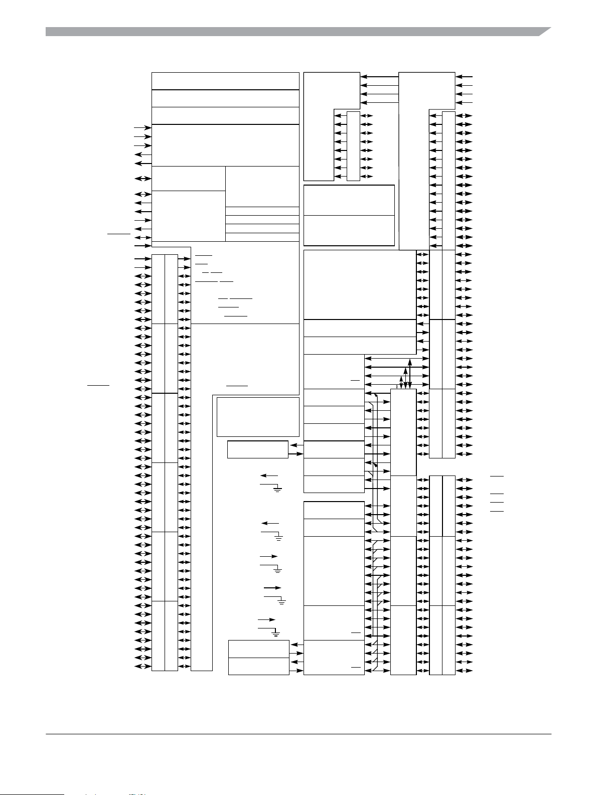
Chapter 1 Device Overview (MC9S12XDP512V2)
ADDR16
ADDR17
ADDR18
ADDR19
ADDR20
ADDR21
ADDR22
EWAIT
ADDR15
ADDR14
ADDR13
ADDR12
ADDR11
ADDR10
ADDR9
ADDR8
ADDR7
ADDR6
ADDR5
ADDR4
ADDR3
ADDR2
ADDR1
ADDR0UDS
DATA15
DATA14
DATA13
DATA12
DATA11
DATA10
DATA9
DATA8
DATA7
DATA6
DATA5
DATA4
DATA3
DATA2
DATA1
DATA0
V
DDR
V
SSR
V
REGEN
V
DD1,2
V
SS1,2
BKGD
XFC
V
DDPLL
V
SSPLL
EXTAL
XTAL
RESET
TEST
PE0
PE1
PE2
PE3
PE4
PE5
PE6
PE7
PK0
PK1
PK2
PK3
PK4
PK5
PK6
PK7
PA 7
PA 6
PA 5
PA 4
PA 3
PA 2
PA 1
PA 0
PB7
PB6
PB5
PB4
PB3
PB2
PB1
PB0
PC7
PC6
PC5
PC4
PC3
PC2
PC1
PC0
PD7
PD6
PD5
PD4
PD3
PD2
PD1
PD0
512/384/256/128/64-Kbyte Flash
32/20/16/14/10/8/4-Kbyte RAM
4/2/1-Kbyte EEPROM
Voltage Regulator
Single-Wire
Background
Debug Module
PLL
Clock
and Reset
Generation
Periodic Interrupt
COP Watchdog
Module
XIRQ
IRQ
R/
W/WE
LSTRB/LDS/EROMCTL
DDRE
ECLK
MODA/
RE/TAGLO
PTE
MODB/TAGHI
XCLKS
ECLKX2/
IQSTAT0
IQSTAT1
IQSTAT2
IQSTAT3
PTK
DDRK
ACC0
ACC1
ACC2
ROMCTL/EWAIT
16-Bit with Prescaler
PTAPTB
DDRADDRB
for Internal Timebases
SCI3
Digital Supply 2.5 V
V
DD1,2
V
SS1,2
PLL Supply 2.5 V
V
DDPLL
V
SSPLL
Analog Supply 3-5 V
VDDA
PTCPTD
DDRCDDRD
Non-Multiplexed External Bus Interface (EBI)
VSSA
I/O Supply 3-5 V
V
DDX1,2
V
SSX1,2
Voltage Regulator 3-5 V
V
DDR1,2
V
SSR1,2
SCI4
SCI5
CPU12X
Clock Monitor
Breakpoints
8-Bit PPAGE
Allows 4-MByte
Program space
Timer
4-Channel
RXD
TXD
RXD
TXD
RXD
TXD
V
ATD0
AN0
AN1
AN2
AN3
AN4
AN5
AN6
AN7
Peripheral Co-Processor
RH
V
RL
V
DDA
V
SSA
DDRAD0 & AD0
Enhanced Multilevel
Interrupt Module
XGATE
Enhanced Capture
Timer
PAD00
PAD01
PAD02
PAD03
PAD04
PAD05
PAD06
PAD07
SCI0
SCI1
MISO
MOSI
SPI0
SCK
SS
RXCAN
CAN0
TXCAN
RXCAN
CAN1
TXCAN
RXCAN
CAN2
TXCAN
RXCAN
CAN3
TXCAN
RXCAN
CAN4
TXCAN
SCI2
IIC1
IIC0
RXD
TXD
SDA
SCL
SDA
SCL
PWM0
PWM1
PWM2
PWM3
PWM
PWM4
PWM5
PWM6
PWM7
MISO
SPI1
MOSI
SCK
SS
MISO
SPI2
MOSI
SCK
SS
IOC0
IOC1
IOC2
IOC3
IOC4
IOC5
IOC6
IOC7
RXD
TXD
RXD
TXD
Module to Port Routing
KWJ0
KWJ1
KWJ2
KWJ4
KWJ6
KWJ7
KWP0
KWP1
KWP2
KWP3
KWP4
KWP5
KWP6
KWP7
KWH0
KWH1
KWH2
KWH3
KWH4
KWH5
KWH6
KWH7
ATD1
AN8
AN9
AN10
AN11
AN12
AN13
AN14
AN15
AN16
AN17
AN18
AN19
AN20
AN21
AN22
AN23
V
RH
V
RL
V
DDA
V
SSA
DDRAD1 & AD1
PTT
DDRT
PTS
DDRS
PTM
DDRM
PTJ
DDRJ
PTP
DDRP
PTH
DDRH
V
RH
V
RL
V
DDA
V
SSA
PAD08
PAD09
PAD10
PAD11
PAD12
PAD13
PAD14
PAD15
PAD16
PAD17
PAD18
PAD19
PAD20
PAD21
PAD22
PAD23
PT0
PT1
PT2
PT3
PT4
PT5
PT6
PT7
PS0
PS1
PS2
PS3
PS4
PS5
PS6
PS7
PM0
PM1
PM2
PM3
PM4
PM5
PM6
PM7
PJ0 CS3
PJ1
PJ2
CS1
CS0
PJ4
PJ5 CS2KWJ5
PJ6
PJ7
PP0
PP1
PP2
PP3
PP4
PP5
PP6
PP7
PH0
PH1
PH2
PH3
PH4
PH5
PH6
PH7
Signals shown in Bold-Italics are neither available on the 112-pin nor on the 80-pin oackage option
Signals shown in Bold are not available on the 80-pin package
Figure 1-1. MC9S12XD-Family Block Diagram
MC9S12XDP512 Data Sheet, Rev. 2.11
Freescale Semiconductor 27
Page 28

Chapter 1 Device Overview (MC9S12XDP512V2)
1.1.4 Device Memory Map
Table 1-1shows the device register memory map of the MC9S12XDP512.
Table 1-1. Device Register Memory Map
Address Module
0x0000–0x0009 PIM (port integration module
0x000A–0x000B MMC (memory map control) 2
0x000C–0x000D PIM (port integration module) 2
0x000E–0x000F EBI (external bus interface) 2
0x0010–0x0017 MMC (memory map control) 8
0x0018–0x0019 Reserved 2
0x001A–0x001B Device ID register 2
0x001C–0x001F PIM (port integration module) 4
0x0020–0x002F DBG (debug module) 16
0x0030–0x0031 MMC (memory map control) 2
0x0032–0x0033 PIM (port integration module) 2
0x0034–0x003F CRG (clock and reset generator) 12
0x0040–0x007F ECT (enhanced capture timer 16-bit 8-channel)s 64
0x0080–0x00AF ATD1 (analog-to-digital converter 10-bit 16-channel) 48
0x00B0–0x00B7 IIC1 (inter IC bus) 8
0x00B8–0x00BF SCI2 (serial communications interface) 8
) 10
Size
(Bytes)
0x00C0–0x00C7 SCI3 (serial communications interface) 8
0x00C8–0x00CF SCI0 (serial communications interface) 8
0x00D0–0x00D7 SCI1 (serial communications interface) 8
0x00D8–0x00DF SPI0 (serial peripheral interface) 8
0x00E0–0x00E7 IIC0 (inter IC bus) 8
0x00E8–0x00EF Reserved 8
0x00F0–0x00F7 SPI1 (serial peripheral interface) 8
0x00F8–0x00FF SPI2 (serial peripheral interface) 8
0x0100–0x010F Flash control register 16
0x0110–0x011B EEPROM control register 12
0x011C–0x011F MMC (memory map control) 4
0x0120–0x012F INT (interrupt module) 16
0x0130–0x0137 SCI4 (serial communications interface) 8
0x0138–0x013F SCI5 (serial communications interface) 8
0x0140–0x017F CAN0 (scalable CAN) 64
MC9S12XDP512 Data Sheet, Rev. 2.11
28 Freescale Semiconductor
Page 29

Chapter 1 Device Overview (MC9S12XDP512V2)
Table 1-1. Device Register Memory Map (continued)
Address Module
0x0180–0x01BF CAN1 (scalable CAN) 64
0x01C0–0x01FF CAN2 (scalable CAN) 64
0x0200–0x023F CAN3 (scalable CAN) 64
0x0240–0x027F PIM (port integration module) 64
0x0280–0x02BF CAN4 (scalable CAN) 64
0x02C0–0x02DF ATD0 (analog-to-digital converter 10 bit 8-channel) 32
0x02E0–0x02EF Reserved 16
0x02F0–0x02F7 Voltage regulator 8
0x02F8–0x02FF Reserved 8
0x0300–0x0327 PWM (pulse-width modulator 8 channels) 40
0x0328–0x033F Reserved 24
0x0340–0x0367 Periodic interrupt timer 40
0x0368–0x037F Reserved 24
0x0380–0x03BF XGATE 64
0x03C0–0x03FF Reserved 64
0x0400–0x07FF Reserved 1024
Size
(Bytes)
NOTE
Reserved register space shown in Table 1-1 is not allocated to any module.
This register space is reserved for future use. Writing to these locations have
no effect. Read access to these locations returns zero.
MC9S12XDP512 Data Sheet, Rev. 2.11
Freescale Semiconductor 29
Page 30
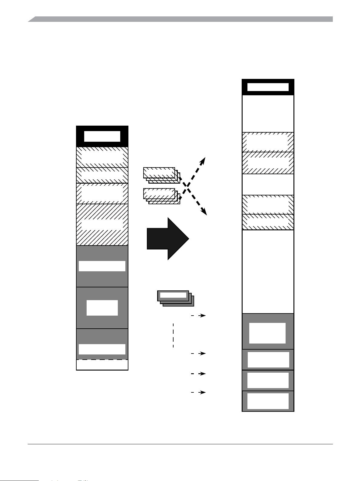
Chapter 1 Device Overview (MC9S12XDP512V2)
1.1.5 Address Mapping
1.1.5.1 Local-to-Global Address Mapping
$0000
$0800
$0C00
$1000
$2000
$4000
2K Registers
EEPROM
1K paged
1K EEPROM
RAM
4K paged
8K RAM
EPAGE
RPAGE
$00_0000
$00_0800
$0F_8000
$0F_DFFF
$0F_E000
$0F_FFFF
$10_0000
$13_F000
$13_FC00
$14_0000
2K Registers
RAM
6*4K paged
8K RAM
EEPROM
3*1K paged
1K EEPROM
$8000
$C000
$FFFF
Unpaged Flash
PPAGE
Flash
16K paged
Unpaged Flash
Vectors
PPAGE = $E0
PPAGE = $FD
PPAGE = $FE
PPAGE = $FF
$78_0000
$7F_4000
$7F_8000
$7F_C000
$7F_FFFF
PPAGES
29 * 16K
Unpaged 16K
or PPAGE $FD
Unpaged 16K
or PPAGE $FE
Unpaged 16K
or PPAGE $FF
Figure 1-2. Local-to-Global Address Mapping S12X_CPU/S12X_BDM
MC9S12XDP512 Data Sheet, Rev. 2.11
30 Freescale Semiconductor
Page 31

Chapter 1 Device Overview (MC9S12XDP512V2)
XGATE
Local Memory Map
$0000
2K Registers
$0800
FLASH
$00_0000
$00_0800
$00_1000
$0F_8000
$0F_FFFF
$10_0000
Device Global Memory Map
2K Registers
RAM
$7FFF
$8000
$FFFF
RAM
$78_0800
30KB FLASH
$78_7FFF
$78_8000
Not Used by XGATE
$7F_FFFF
Figure 1-3. Local-to-Global Address Mapping XGATE
MC9S12XDP512 Data Sheet, Rev. 2.11
Freescale Semiconductor 31
Page 32

Chapter 1 Device Overview (MC9S12XDP512V2)
1.1.5.2 Logical Address Map
$0000
$0800
$0C00
$1000
$2000
$4000
$8000
$C000
$FF00
$FFFF
Normal
Single Chip
EXT
VectorsVectors Vectors
Expanded Special
Single Chip
Figure 1-4. Memory Map
$0000
$07FF
$0800
$0FFF
$1000
$3FFF
$4000
$7FFF
$8000
$BFFF
$BF00
$BFFF
$C000
$FFFF
$FF00
$FFFF
2-K Register Space
4-Kbytes EEPROM
four * 1K pages accessible through $0800–$0BFF
32-Kbytes RAM
eight * 4K pages accessible
through $1000–$1FFF
16-K Fixed Flash EEPROM
16-K Page Window
thirtytwo * 16-K Flash EEPROM Pages
BDM visible on PPAGE = $FF
(If Active)
16-K Fixed Flash EEPROM
2-K, 4-K, 8-K, or 16-K Protected Boot Sector
BDM
(If Active, except for specific BDM hardware
command, for details refer to BDM BlockGuide)
MC9S12XDP512 Data Sheet, Rev. 2.11
32 Freescale Semiconductor
Page 33

Chapter 1 Device Overview (MC9S12XDP512V2)
1.1.6 Detailed Register Map
The following tables show the detailed register map of the MC9S12XDP512.
0x0000–0x0009 Port Integration Module (PIM) Map 1 of 5
Address Name Bit 7 Bit 6 Bit 5 Bit 4 Bit 3 Bit 2 Bit 1 Bit 0
0x0000 PORTA
0x0001 PORTB
0x0002 DDRA
0x0003 DDRB
0x0004 PORTC
0x0005 PORTD
0x0006 DDRC
0x0007 DDRD
0x0008 PORTE
0x0009 DDRE
R
PA7 PA6 PA5 PA4 PA3 PA2 PA1 PA 0
W
R
PB7 PB6 PB5 PB4 PB3 PB2 PB1 PB0
W
R
DDRA7 DDRA6 DDRA5 DDRA4 DDRA3 DDRA2 DDRA1 DDRA0
W
R
DDRB7 DDRB6 DDRB5 DDRB4 DDRB3 DDRB2 DDRB1 DDRB0
W
R
PC7 PC6 PC5 PC4 PC3 PC2 PC1 PC0
W
R
PD7 PD6 PD5 PD4 PD3 PD2 PD1 PD0
W
R
DDRC7 DDRC6 DDRC5 DDRC4 DDRC3 DDRC2 DDRC1 DDRC0
W
R
DDRD7 DDRD6 DDRD5 DDRD4 DDRD3 DDRD2 DDRD1 DDRD0
W
R
PE7 PE6 PE5 PE4 PE3 PE2
W
R
DDRE7 DDRE6 DDRE5 DDRE4 DDRE3 DDRE2
W
PE1 PE0
00
0x000A–0x000B Module Mapping Control (S12XMMC) Map 1 of 4
Address Name Bit 7 Bit 6 Bit 5 Bit 4 Bit 3 Bit 2 Bit 1 Bit 0
0x000A MMCCTL0
0x000B MODE
R00000
W
R
MODC MODB MODA
W
00000
CS2E CS1E CS0E
0x000C–0x000D Port Integration Module (PIM) Map 2 of 5
Address Name Bit 7 Bit 6 Bit 5 Bit 4 Bit 3 Bit 2 Bit 1 Bit 0
0x000C PUCR
0x000D RDRIV
R
PUPKE BKPUE
W
R
RDPK
W
00
0
PUPEE PUPDE PUPCE PUPBE PUPAE
RDPE RDPD RDPC RDPB RDPA
0x000E–0x000F External Bus Interface (S12XEBI) Map
Address Name Bit 7 Bit 6 Bit 5 Bit 4 Bit 3 Bit 2 Bit 1 Bit 0
0x000E EBICTL0
0x000F EBICTL1
R
W
R
W
ITHRS
EWAITE
0
0000
HDBE ASIZ4 ASIZ3 ASIZ2 ASIZ1 ASIZ0
EXSTR2 EXSTR1 EXSTR0
MC9S12XDP512 Data Sheet, Rev. 2.11
Freescale Semiconductor 33
Page 34

Chapter 1 Device Overview (MC9S12XDP512V2)
0x0010–0x0017 Module Mapping Control (S12XMMC) Map 2 of 4
Address Name Bit 7 Bit 6 Bit 5 Bit 4 Bit 3 Bit 2 Bit 1 Bit 0
0x0010 GPAGE
0x0011 DIRECT
0x0012 Reserved
0x0013 MMCCTL1
0x0014 Reserved
0x0015 Reserved
0x0016 RPAGE
0x0017 EPAGE
R0
W
R
DP15 DP14 DP13 DP12 DP11 DP10 DP9 DP8
W
R00000000
W
R00000
W
R00000000
W
R00000000
W
R
RP7 RP6 RP5 RP4 RP3 RP2 RP1 RP0
W
R
EP7 EP6 EP5 EP4 EP3 EP2 EP1 EP0
W
GP6 GP5 GP4 GP3 GP2 GP1 GP0
EROMON ROMHM ROMON
0x0018–0x001B Miscellaneous Peripheral
Address Name Bit 7 Bit 6 Bit 5 Bit 4 Bit 3 Bit 2 Bit 1 Bit 0
0x0018 Reserved
0x0019 Reserved
0x001A PARTIDH
0x001B PARTIDL
R00000000
W
R00000000
W
R11000100
W
R00000000
W
0x001C–0x001F Port Integration Module (PIM) Map 3 of 5
Address Name Bit 7 Bit 6 Bit 5 Bit 4 Bit 3 Bit 2 Bit 1 Bit 0
0x001C ECLKCTL
0x001D Reserved
0x001E IRQCR
0x001F Reserved
R
NECLK NCLKX2
W
R00000000
W
R
IRQE IRQEN
W
R00000000
W
0000
000000
EDIV1 EDIV0
MC9S12XDP512 Data Sheet, Rev. 2.11
34 Freescale Semiconductor
Page 35

Chapter 1 Device Overview (MC9S12XDP512V2)
0x0020–0x0027 Debug Module (S12XDBG) Map
Address Name Bit 7 Bit 6 Bit 5 Bit 4 Bit 3 Bit 2 Bit 1 Bit 0
0x0020 DBGC1
0x0021 DBGSR
0x0022 DBGTCR
0x0023 DBGC2
0x0024 DBGTBH
0x0025 DBGTBL
0x0026 DBGCNT
0x0027 DBGSCRX
0x0028
0x0028
(COMPA/C)
DBGXCTL
2
(COMPB/D)
DBGXCTL
1
0x0029 DBGXAH
0x002A DBGXAM
0x002B DBGXAL
0x002C DBGXDH
0x002D DBGXDL
0x002E DBGXDHM
0x002F DBGXDLM
1
This represents the contents if the Comparator A or C control register is blended into this address
2
This represents the contents if the Comparator B or D control register is blended into this address
R
ARM
W TRIG
R TBF EXTF 0 0 0 SSF2 SSF1 SSF0
W
R
W
TSOURCE TRANGE TRCMOD TALIGN
R0000
W
R Bit 15 Bit 14 Bit 13 Bit 12 Bit 11 Bit 10 Bit 9 Bit 8
W
R Bit 7 Bit 6 Bit 5 Bit 4 Bit 3 Bit 2 Bit 1 Bit 0
W
R 0 CNT
W
R0000
W
R0
W
R
SZE SZ TAG BRK RW RWE SRC COMPE
W
R0
W
R
Bit 15 14 13 12 11 10 9 Bit 8
W
R
Bit 7 6 54321Bit 0
W
R
Bit 15 14 13 12 11 10 9 Bit 8
W
R
Bit 7 654321Bit 0
W
R
Bit 15 14 13 12 11 10 9 Bit 8
W
R
Bit 7 654321Bit 0
W
0
XGSBPE BDM DBGBRK COMRV
CDCM ABCM
SC3 SC2 SC1 SC0
NDB TAG BRK RW RWE SRC COMPE
Bit 22 21 20 19 18 17 Bit 16
MC9S12XDP512 Data Sheet, Rev. 2.11
Freescale Semiconductor 35
Page 36

Chapter 1 Device Overview (MC9S12XDP512V2)
0x0030–0x0031 Module Mapping Control (S12XMMC) Map 3 of 4
Address Name Bit 7 Bit 6 Bit 5 Bit 4 Bit 3 Bit 2 Bit 1 Bit 0
0x0030 PPAGE
0x0031 Reserved
R
PIX7 PIX6 PIX5 PIX4 PIX3 PIX2 PIX1 PIX0
W
R00000000
W
0x0032–0x0033 Port Integration Module (PIM) Map 4 of 5
Address Name Bit 7 Bit 6 Bit 5 Bit 4 Bit 3 Bit 2 Bit 1 Bit 0
0x0032 PORTK
0x0033 DDRK
R
PK7 PK6 PK5 PK4 PK3 PK2 PK1 PK0
W
R
DDRK7 DDRK6 DDRK5 DDRK4 DDRK3 DDRK2 DDRK1 DDRK0
W
0x0034–0x003F Clock and Reset Generator (CRG) Map
Address Name Bit 7 Bit 6 Bit 5 Bit 4 Bit 3 Bit 2 Bit 1 Bit 0
0x0034 SYNR
0x0035 REFDV
0x0036 CTFLG
0x0037 CRGFLG
0x0038 CRGINT
0x0039 CLKSEL
0x003A PLLCTL
0x003B RTICTL
0x003C COPCTL
0x003D FORBYP
0x003E CTCTL
0x003F ARMCOP
R0 0
W
R
W
R00000000
W Reserved For Factory Test
R
W
R
W
R
W
R
W
R
W
R
W
R00000000
W Reserved For Factory Test
R0000 000
W Reserved For Factory Test
R00000000
W Bit 7 654321Bit 0
00
RTIF PORF LVRF LOCKIF
RTIE ILAF
PLLSEL PSTP
CME PLLON AUTO ACQ FSTWKP PRE PCE SCME
RTDEC RTR6 RTR5 RTR4 RTR3 RTR2 RTR1 RTR0
WCOP RSBCK
SYN5 SYN4 SYN3 SYN2 SYN1 SYN0
REFDV5 REFDV4 REFDV3 REFDV2 REFDV1 REFDV0
LOCK TRACK
0
00
000
LOCKIE
00
PLLWAI
SCMIF
SCMIE
0
CR2 CR1 CR0
RTIWAI COPWAI
SCM
0
MC9S12XDP512 Data Sheet, Rev. 2.11
36 Freescale Semiconductor
Page 37

Chapter 1 Device Overview (MC9S12XDP512V2)
0x0040–0x007F Enhanced Capture Timer 16-Bit 8-Channels (ECT) Map (Sheet 1 of 3)
Address Name Bit 7 Bit 6 Bit 5 Bit 4 Bit 3 Bit 2 Bit 1 Bit 0
0x0040 TIOS
0x0041 CFORC
0x0042 OC7M
0x0043 OC7D
0x0044 TCNT (hi)
0x0045 TCNT (lo)
0x0046 TSCR1
0x0047 TTOV
0x0048 TCTL1
0x0049 TCTL2
0x004A TCTL3
0x004B TCTL4
0x004C TIE
0x004D TSCR2
0x004E TFLG1
0x004F TFLG2
0x0050 TC0 (hi)
0x0051 TC0 (lo)
0x0052 TC1 (hi)
0x0053 TC1 (lo)
0x0054 TC2 (hi)
0x0055 TC2 (lo)
R
IOS7 IOS6 IOS5 IOS4 IOS3 IOS2 IOS1 IOS0
W
R00000000
W FOC7 FOC6 FOC5 FOC4 FOC3 FOC2 FOC1 FOC0
R
OC7M7 OC7M6 OC7M5 OC7M4 OC7M3 OC7M2 OC7M1 OC7M0
W
R
OC7D7 OC7D6 OC7D5 OC7D4 OC7D3 OC7D2 OC7D1 OC7D0
W
R Bit 15 14 13 12 11 10 9 Bit 8
W
R Bit 7 654321Bit 0
W
R
TEN TSWAI TSFRZ TFFCA PRNT
W
R
TOV7 TOV6 TOV5 TOV4 TOV3 TOV2 TOV1 TOV0
W
R
OM7 OL7 OM6 OL6 OM5 OL5 OM4 OL4
W
R
OM3 OL3 OM2 OL2 OM1 OL1 OM0 OL0
W
R
EDG7B EDG7A EDG6B EDG6A EDG5B EDG5A EDG4B EDG4A
W
R
EDG3B EDG3A EDG2B EDG2A EDG1B EDG1A EDG0B EDG0A
W
R
C7I C6I C5I C4I C3I C2I C1I C0I
W
R
TOI
W
R
C7F C6F C5F C4F C3F C2F C1F C0F
W
R
TOF
W
R
Bit 15 14 13 12 11 10 9 Bit 8
W
R
Bit 7 654321Bit 0
W
R
Bit 15 14 13 12 11 10 9 Bit 8
W
R
Bit 7 654321Bit 0
W
R
Bit 15 14 13 12 11 10 9 Bit 8
W
R
Bit 7 654321Bit 0
W
000
0000000
TCRE PR2 PR1 PR0
000
MC9S12XDP512 Data Sheet, Rev. 2.11
Freescale Semiconductor 37
Page 38

Chapter 1 Device Overview (MC9S12XDP512V2)
0x0040–0x007F Enhanced Capture Timer 16-Bit 8-Channels (ECT) Map (Sheet 2 of 3)
Address Name Bit 7 Bit 6 Bit 5 Bit 4 Bit 3 Bit 2 Bit 1 Bit 0
0x0056 TC3 (hi)
0x0057 TC3 (lo)
0x0058 TC4 (hi)
0x0059 TC4 (lo)
0x005A TC5 (hi)
0x005B TC5 (lo)
0x005C TC6 (hi)
0x005D TC6 (lo)
0x005E TC7 (hi)
0x005F TC7 (lo)
0x0060 PACTL
0x0061 PAFLG
0x0062 PACN3 (hi)
0x0063 PACN2 (lo)
0x0064 PACN1 (hi)
0x0065 PACN0 (lo)
0x0066 MCCTL
0x0067 MCFLG
0x0068 ICPAR
0x0069 DLYCT
0x006A ICOVW
0x006B ICSYS
0x006C Reserved
R
Bit 15 14 13 12 11 10 9 Bit 8
W
R
Bit 7 654321Bit 0
W
R
Bit 15 14 13 12 11 10 9 Bit 8
W
R
Bit 7 654321Bit 0
W
R
Bit 15 14 13 12 11 10 9 Bit 8
W
R
Bit 7 654321Bit 0
W
R
Bit 15 14 13 12 11 10 9 Bit 8
W
R
Bit 7 654321Bit 0
W
R
Bit 15 14 13 12 11 10 9 Bit 8
W
R
Bit 7 654321Bit 0
W
R0
W
R000000
W
R
Bit 7 654321Bit 0
W
R
Bit 7 654321Bit 0
W
R
Bit 7 654321Bit 0
W
R
Bit 7 654321Bit 0
W
R
MCZI MODMC RDMCL
W ICLAT FLMC
R
MCZF
W
R0000
W
R
DLY7 DLY6 DLY5 DLY4 DLY3 DLY2 DLY1 DLY0
W
R
NOVW7 NOVW6 NOVW5 NOVW4 NOVW3 NOVW2 NOVW1 NOVW0
W
R
SH37 SH26 SH15 SH04 TFMOD PACMX BUFEN LATQ
W
R00000000
W
PAEN PAMOD PEDGE CLK1 CLK0 PAOVI PAI
PAOVF PAIF
00
0 0 0 POLF3 POLF2 POLF1 POLF0
PA3EN PA2EN PA1EN PA0EN
MCEN MCPR1 MCPR0
MC9S12XDP512 Data Sheet, Rev. 2.11
38 Freescale Semiconductor
Page 39

Chapter 1 Device Overview (MC9S12XDP512V2)
0x0040–0x007F Enhanced Capture Timer 16-Bit 8-Channels (ECT) Map (Sheet 3 of 3)
Address Name Bit 7 Bit 6 Bit 5 Bit 4 Bit 3 Bit 2 Bit 1 Bit 0
0x006D TIMTST
0x006E PTPSR
0x006F PTMCPSR
0x0070 PBCTL
0x0071 PBFLG
0x0072 PA3H
0x0073 PA2H
0x0074 PA1H
0x0075 PA0H
0x0076 MCCNT (hi)
0x0077 MCCNT (lo)
0x0078 TC0H (hi)
0x0079 TC0H (lo)
0x007A TC1H (hi)
0x007B TC1H (lo)
0x007C TC2H (hi)
0x007D TC2H (lo)
0x007E TC3H (hi)
0x007F TC3H (lo)
R00000000
W
R
PTPS7 PTPS6 PTPS5 PTPS4 PTPS3 PTPS2 PTPS1 PTPS0
W
R
PTMPS7 PTMPS6 PTMPS5 PTMPS4 PTMPS3 PTMPS2 PTMPS1 PTMPS0
W
R0
W
R000000
W
R PA3H7 PA3H6 PA3H5 PA3H4 PA3H3 PA3H2 PA3H1 PA3H0
W
R PA2H7 PA2H6 PA2H5 PA2H4 PA2H3 PA2H2 PA2H1 PA2H0
W
R PA1H7 PA1H6 PA1H5 PA1H4 PA1H3 PA1H2 PA1H1 PA1H 0
W
R PA0H7 PA0H6 PA0H5 PA0H4 PA0H3 PA0H2 PA0H1 PA0H0
W
R
Bit 15 14 13 12 11 10 9 Bit 8
W
R
Bit 7 654321Bit 0
W
R Bit 15 14 13 12 11 10 9 Bit 8
W
R Bit 7 654321Bit 0
W
R Bit 15 14 13 12 11 10 9 Bit 8
W
R Bit 7 654321Bit 0
W
R Bit 15 14 13 12 11 10 9 Bit 8
W
R Bit 7 654321Bit 0
W
R Bit 15 14 13 12 11 10 9 Bit 8
W
R Bit 7 654321Bit 0
W
PBEN
Reserved For Factory Test
0000
PBOVI
PBOVF
0
0
MC9S12XDP512 Data Sheet, Rev. 2.11
Freescale Semiconductor 39
Page 40

Chapter 1 Device Overview (MC9S12XDP512V2)
0x0080–0x00AF Analog-to-Digital Converter 10-bit 16-Channels (ATD1) Map (Sheet 1 of
3)
Address Name Bit 7 Bit 6 Bit 5 Bit 4 Bit 3 Bit 2 Bit 1 Bit 0
0x0080 ATD1CTL0
0x0081 ATD1CTL1
0x0082 ATD1CTL2
0x0083 ATD1CTL3
0x0084 ATD1CTL4
0x0085 ATD1CTL5
0x0086 ATD1STAT0
0x0087 Reserved
0x0088 ATD1TEST0
0x0089 ATD1TEST1
0x008A ATD1STAT2
0x008B ATD1STAT1
0x008C ATD1DIEN0
0x008D ATD1DIEN
0x008E ATD1PTAD0
0x008F ATD1PTAD1
0x0090 ATD1DR0H
0x0091 ATD1DR0L
0x0092 ATD1DR1H
0x0093 ATD1DR1L
0x0094 ATD1DR2H
0x0095 ATD1DR2L
R0000
W
R
ETRIG
SEL
W
R
ADPU AFFC AWAI ETRIGLE ETRIGP ETRIGE ASCIE
W
R0
W
R
SRES8 SMP1 SMP0 PRS4 PRS3 PRS2 PRS1 PRS0
W
R
DJM DSGN SCAN MULT CD CC CB CA
W
R
SCF
W
R00000000
W
RUUUUUUUU
W
R00000000
W
R CCF15 CCF14 CCF13 CCF12 CCF11 CCF10 CCF9 CCF8
W
R CCF7 CCF6 CCF5 CCF4 CCF3 CCF2 CCF1 CCF0
W
R
IEN15 IEN14 IEN13 IEN12 IEN11 IEN10 IEN9 IEN8
W
R
IEN7 IEN6 IEN5 IEN4 IEN3 IEN2 IEN1 IEN0
W
R PTAD15 PTAD14 PTAD13 PTAD12 PTAD11 PTAD10 PTAD9 PTAD8
W
R PTAD7 PTAD6 PTAD5 PTAD4 PTAD3 PTAD2 PTAD1 PTAD0
W
R Bit15 14 13 12 11 10 9 Bit8
W
R Bit7 Bit6 000000
W
R Bit15 14 13 12 11 10 9 Bit8
W
R Bit7 Bit6 000000
W
R Bit15 14 13 12 11 10 9 Bit8
W
R Bit7 Bit6 000000
W
000
S8C S4C S2C S1C FIFO FRZ1 FRZ0
0
ETORF FIFOR
Reserved For Factory Test
Reserved For Factory Test
WRAP3 WRAP2 WRAP1 WRAP0
ETRIG
CH3
CC3 CC2 CC1 CC0
ETRIG
CH2
ETRIG
CH1
ETRIG
CH0
ASCIF
MC9S12XDP512 Data Sheet, Rev. 2.11
40 Freescale Semiconductor
Page 41

Chapter 1 Device Overview (MC9S12XDP512V2)
0x0080–0x00AF Analog-to-Digital Converter 10-bit 16-Channels (ATD1) Map (Sheet 2 of
3)
Address Name Bit 7 Bit 6 Bit 5 Bit 4 Bit 3 Bit 2 Bit 1 Bit 0
0x0096 ATD1DR3H
0x0097 ATD1DR3L
0x0098 ATD1DR4H
0x0099 ATD1DR4L
0x009A ATD1DR5H
0x009B ATD1DR5L
0x009C ATD1DR6H
0x009D ATD1DR6L
0x009E ATD1DR7H
0x009F ATD1DR7L
0x00A0 ATD1DR8H
0x00A1 ATD1DR8L
0x00A2 ATD1DR9H
0x00A3 ATD1DR9L
0x00A4 ATD1DR10H
0x00A5 ATD1DR10L
0x00A6 ATD1DR11H
0x00A7 ATD1DR11L
0x00A8 ATD1DR12H
0x00A9 ATD1DR12L
0x00AA ATD1DR13H
0x00AB ATD1DR13L
R Bit15 14 13 12 11 10 9 Bit8
W
R Bit7 Bit6 000000
W
R Bit15 14 13 12 11 10 9 Bit8
W
R Bit7 Bit6 000000
W
R Bit15 14 13 12 11 10 9 Bit8
W
R Bit7 Bit6 000000
W
R Bit15 14 13 12 11 10 9 Bit8
W
R Bit7 Bit6 000000
W
R Bit15 14 13 12 11 10 9 Bit8
W
R Bit7 Bit6 000000
W
R Bit15 14 13 12 11 10 9 Bit8
W
R Bit7 Bit6 000000
W
R Bit15 14 13 12 11 10 9 Bit8
W
R Bit7 Bit6 000000
W
R Bit15 14 13 12 11 10 9 Bit8
W
R Bit7 Bit6 000000
W
R Bit15 14 13 12 11 10 9 Bit8
W
R Bit7 Bit6 000000
W
R Bit15 14 13 12 11 10 9 Bit8
W
R Bit7 Bit6 000000
W
R Bit15 14 13 12 11 10 9 Bit8
W
R Bit7 Bit6 000000
W
MC9S12XDP512 Data Sheet, Rev. 2.11
Freescale Semiconductor 41
Page 42

Chapter 1 Device Overview (MC9S12XDP512V2)
0x0080–0x00AF Analog-to-Digital Converter 10-bit 16-Channels (ATD1) Map (Sheet 3 of
3)
Address Name Bit 7 Bit 6 Bit 5 Bit 4 Bit 3 Bit 2 Bit 1 Bit 0
0x00AC ATD1DR14H
0x00AD ATD1DR14L
0x00AE ATD1DR15H
0x00AF ATD1DR15L
R Bit15 14 13 12 11 10 9 Bit8
W
R Bit7 Bit6 000000
W
R Bit15 14 13 12 11 10 9 Bit8
W
R Bit7 Bit6 000000
W
0x00B0–0x00B7 Inter IC Bus (IIC1) Map
Address Name Bit 7 Bit 6 Bit 5 Bit 4 Bit 3 Bit 2 Bit 1 Bit 0
0x00B0 IBAD
0x00B1 IBFD
0x00B2 IBCR
0x00B3 IBSR
0x00B4 IBDR
0x00B5 Reserved
0x00B6 Reserved
0x00B7 Reserved
R
ADR7 ADR6 ADR5 ADR4 ADR3 ADR2 ADR1
W
R
IBC7 IBC6 IBC5 IBC4 IBC3 IBC2 IBC1 IBC0
W
R
IBEN IBIE MS/
W RSTA
R TCF IAAS IBB
W
R
D7 D6 D5 D4 D3 D2 D1 D 0
W
R0 0 0 0 0 0 0 0
W
R00000000
W
R00000000
W
SL TX/RX TXAK
IBAL
0SRW
00
IBIF
0
IBSWAI
RXAK
0x00B8–0x00BF Asynchronous Serial Interface (SCI2) Map
Address Name Bit 7 Bit 6 Bit 5 Bit 4 Bit 3 Bit 2 Bit 1 Bit 0
R
0x00B8 SCI2BDH
0x00B9 SCI2BDL
0x00BA SCI2CR1
0x00B8 SCI2ASR1
0x00B9 SCI2ACR1
0x00BA SCI2ACR2
42 Freescale Semiconductor
1
1
1
2
2
2
IREN TNP1 TNP0 SBR12 SBR11 SBR10 SBR9 SBR8
W
R
SBR7 SBR6 SBR5 SBR4 SBR3 SBR2 SBR1 SBR0
W
R
LOOPS SCISWAI RSRC M WAKE ILT PE PT
W
R
RXEDGIF
W
R
RXEDGIE
W
R00000
W
0000
00000
MC9S12XDP512 Data Sheet, Rev. 2.11
BERRV BERRIF BKDIF
BERRM1 BERRM0 BKDFE
BERRIE BKDIE
Page 43

Chapter 1 Device Overview (MC9S12XDP512V2)
0x00B8–0x00BF Asynchronous Serial Interface (SCI2) Map (continued)
Address Name Bit 7 Bit 6 Bit 5 Bit 4 Bit 3 Bit 2 Bit 1 Bit 0
0x00BB SCI2CR2
0x00BC SCI2SR1
0x00BD SCI2SR2
0x00BE SCI2DRH
0x00BF SCI2DRL
1
Those registers are accessible if the AMAP bit in the SCI2SR2 register is set to zero
2
Those registers are accessible if the AMAP bit in the SCI2SR2 register is set to one
R
TIE TCIE RIE ILIE TE RE RWU SBK
W
R TDRE TC RDRF IDLE OR NF FE PF
W
R
AMAP
W
RR8
W
00
T8
000000
TXPOL RXPOL BRK13 TXDIR
RAF
RR7R6R5R4R3R2R1R0
WT7T6T5T4T3T2T1T0
0x00C0–0x00C7 Asynchronous Serial Interface (SCI3) Map
Address Name Bit 7 Bit 6 Bit 5 Bit 4 Bit 3 Bit 2 Bit 1 Bit 0
R
0x00C0 SCI3BDH
0x00C1 SCI3BDL
0x00C2 SCI3CR1
0x00C0 SCI3ASR1
0x00C1 SCI3ACR1
0x00C2 SCI3ACR2
1
1
1
2
2
2
0x00C3 SCI3CR2
0x00C4 SCI3SR1
0x00C5 SCI3SR2
0x00C6 SCI3DRH
0x00C7 SCI3DRL
1
Those registers are accessible if the AMAP bit in the SCI3SR2 register is set to zero
2
Those registers are accessible if the AMAP bit in the SCI3SR2 register is set to one
IREN TNP1 TNP0 SBR12 SBR11 SBR10 SBR9 SBR8
W
R
SBR7 SBR6 SBR5 SBR4 SBR3 SBR2 SBR1 SBR0
W
R
LOOPS SCISWAI RSRC M WAKE ILT PE PT
W
R
RXEDGIF
W
R
RXEDGIE
W
R00000
W
R
TIE TCIE RIE ILIE TE RE RWU SBK
W
0000
00000
BERRV BERRIF BKDIF
BERRIE BKDIE
BERRM1 BERRM0 BKDFE
R TDRE TC RDRF IDLE OR NF FE PF
W
R
AMAP
W
RR8
W
00
T8
000000
TXPOL RXPOL BRK13 TXDIR
RAF
RR7R6R5R4R3R2R1R0
WT7T6T5T4T3T2T1T0
MC9S12XDP512 Data Sheet, Rev. 2.11
Freescale Semiconductor 43
Page 44

Chapter 1 Device Overview (MC9S12XDP512V2)
0x00C8–0x00CF Asynchronous Serial Interface (SCI0) Map
Address Name Bit 7 Bit 6 Bit 5 Bit 4 Bit 3 Bit 2 Bit 1 Bit 0
R
0x00C8 SCI0BDH
0x00C9 SCI0BDL
0x00CA SCI0CR1
0x00C8 SCI0ASR1
0x00C9 SCI0ACR1
0x00CA SCI0ACR2
0x00CB SCI0CR2
0x00CC SCI0SR1
0x00CD SCI0SR2
0x00CE SCI0DRH
0x00CF SCI0DRL
1
Those registers are accessible if the AMAP bit in the SCI0SR2 register is set to zero
2
Those registers are accessible if the AMAP bit in the SCI0SR2 register is set to one
1
1
1
2
2
2
IREN TNP1 TNP0 SBR12 SBR11 SBR10 SBR9 SBR8
W
R
SBR7 SBR6 SBR5 SBR4 SBR3 SBR2 SBR1 SBR0
W
R
LOOPS SCISWAI RSRC M WAKE ILT PE PT
W
R
RXEDGIF
W
R
RXEDGIE
W
R00000
W
R
TIE TCIE RIE ILIE TE RE RWU SBK
W
0000
00000
BERRV BERRIF BKDIF
BERRIE BKDIE
BERRM1 BERRM0 BKDFE
R TDRE TC RDRF IDLE OR NF FE PF
W
R
AMAP
W
RR8
W
00
T8
000000
TXPOL RXPOL BRK13 TXDIR
RAF
RR7R6R5R4R3R2R1R0
WT7T6T5T4T3T2T1T0
0x00D0–0x00D7 Asynchronous Serial Interface (SCI1) Map
Address Name Bit 7 Bit 6 Bit 5 Bit 4 Bit 3 Bit 2 Bit 1 Bit 0
R
0x00D0 SCI1BDH
0x00D1 SCI1BDL
0x00D2 SCI1CR1
0x00D0 SCI1ASR1
0x00D1 SCI1ACR1
0x00D2 SCI1ACR2
0x00D3 SCI1CR2
0x00D4 SCI1SR1
1
1
1
2
2
2
IREN TNP1 TNP0 SBR12 SBR11 SBR10 SBR9 SBR8
W
R
SBR7 SBR6 SBR5 SBR4 SBR3 SBR2 SBR1 SBR0
W
R
LOOPS SCISWAI RSRC M WAKE ILT PE PT
W
R
RXEDGIF
W
R
RXEDGIE
W
R00000
W
R
TIE TCIE RIE ILIE TE RE RWU SBK
W
0000
00000
BERRV BERRIF BKDIF
BERRIE BKDIE
BERRM1 BERRM0 BKDFE
R TDRE TC RDRF IDLE OR NF FE PF
W
MC9S12XDP512 Data Sheet, Rev. 2.11
44 Freescale Semiconductor
Page 45

Chapter 1 Device Overview (MC9S12XDP512V2)
0x00D0–0x00D7 Asynchronous Serial Interface (SCI1) Map (continued)
Address Name Bit 7 Bit 6 Bit 5 Bit 4 Bit 3 Bit 2 Bit 1 Bit 0
0x00D5 SCI1SR2
0x00D6 SCI1DRH
0x00D7 SCI1DRL
1
Those registers are accessible if the AMAP bit in the SCI1SR2 register is set to zero
2
Those registers are accessible if the AMAP bit in the SCI1SR2 register is set to one
R
AMAP
W
RR8
W
RR7R6R5R4R3R2R1R0
WT7T6T5T4T3T2T1T0
00
T8
000000
TXPOL RXPOL BRK13 TXDIR
RAF
0x00D8–0x00DF Serial Peripheral Interface (SPI0) Map
Address Name Bit 7 Bit 6 Bit 5 Bit 4 Bit 3 Bit 2 Bit 1 Bit 0
0x00D8 SPI0CR1
0x00D9 SPI0CR2
0x00DA SPI0BR
0x00DB SPI0SR
0x00DC Reserved
0x00DD SPI0DR
0x00DE Reserved
0x00DF Reserved
R
SPIE SPE SPTIE MSTR CPOL CPHA SSOE LSBFE
W
R0 0 0
W
R0
W
R SPIF 0 SPTEF MODF 0 0 0 0
W
R00000000
W
R
Bit7 654321Bit0
W
R00000000
W
R00000000
W
SPPR2 SPPR1 SPPR0
MODFEN BIDIROE
0
0
SPR2 SPR1 SPR0
SPISWAI SPC0
0x00E0–0x00E7 Inter IC Bus (IIC0) Map
Address Name Bit 7 Bit 6 Bit 5 Bit 4 Bit 3 Bit 2 Bit 1 Bit 0
0x00E0 IBAD
0x00E1 IBFD
0x00E2 IBCR
0x00E3 IBSR
0x00E4 IBDR
Freescale Semiconductor 45
R
ADR7 ADR6 ADR5 ADR4 ADR3 ADR2 ADR1
W
R
IBC7 IBC6 IBC5 IBC4 IBC3 IBC2 IBC1 IBC0
W
R
IBEN IBIE MS/
W RSTA
R TCF IAAS IBB
W
R
D7 D6 D5 D4 D3 D2 D1 D 0
W
MC9S12XDP512 Data Sheet, Rev. 2.11
SL TX/RX TXAK
IBAL
0SRW
00
IBIF
0
IBSWAI
RXAK
Page 46

Chapter 1 Device Overview (MC9S12XDP512V2)
0x00E0–0x00E7 Inter IC Bus (IIC0) Map (continued)
Address Name Bit 7 Bit 6 Bit 5 Bit 4 Bit 3 Bit 2 Bit 1 Bit 0
0x00E5 Reserved
0x00E6 Reserved
0x00E7 Reserved
R0 0 0 0 0 0 0 0
W
R00000000
W
R00000000
W
0x00E8–0x00EF Reserved
Address Name Bit 7 Bit 6 Bit 5 Bit 4 Bit 3 Bit 2 Bit 1 Bit 0
0x00E8 Reserved
0x00E9 Reserved
0x00EA Reserved
0x00EB Reserved
0x00EC Reserved
0x00ED Reserved
0x00EE Reserved
0x00EF Reserved
R00000000
W
R00000000
W
R00000000
W
R
W
R0
W
R
W
R
W
R
W
0 0 0 0 0 0 0 0
0000000
0 0 0 0 0 0 0 0
0 0 0 0 0 0 0 0
0 0 0 0 0 0 0 0
0x00F0–0x00F7 Serial Peripheral Interface (SPI1) Map
Address Name Bit 7 Bit 6 Bit 5 Bit 4 Bit 3 Bit 2 Bit 1 Bit 0
0x00F0 SPI1CR1
0x00F1 SPI1CR2
0x00F2 SPI1BR
0x00F3 SPI1SR
0x00F4 Reserved
0x00F5 SPI1DR
0x00F6 Reserved
0x00F7 Reserved
46 Freescale Semiconductor
R
SPIE SPE SPTIE MSTR CPOL CPHA SSOE LSBFE
W
R0 0 0
W
R0
W
R SPIF 0 SPTEF MODF 0 0 0 0
W
R00000000
W
R
Bit7 654321Bit0
W
R00000000
W
R00000000
W
SPPR2 SPPR1 SPPR0
MC9S12XDP512 Data Sheet, Rev. 2.11
MODFEN BIDIROE
0
0
SPR2 SPR1 SPR0
SPISWAI SPC0
Page 47

Chapter 1 Device Overview (MC9S12XDP512V2)
0x00F8–0x00FF Serial Peripheral Interface (SPI2) Map
Address Name Bit 7 Bit 6 Bit 5 Bit 4 Bit 3 Bit 2 Bit 1 Bit 0
0x00F8 SPI2CR1
0x00F9 SPI2CR2
0x00FA SPI2BR
0x00FB SPI2SR
0x00FC Reserved
0x00FD SPI2DR
0x00FE Reserved
0x00FF Reserved
R
SPIE SPE SPTIE MSTR CPOL CPHA SSOE LSBFE
W
R0 0 0
W
R0
W
R SPIF 0 SPTEF MODF 0 0 0 0
W
R00000000
W
R
Bit7 654321Bit0
W
R00000000
W
R00000000
W
SPPR2 SPPR1 SPPR0
MODFEN BIDIROE
0
0
SPR2 SPR1 SPR0
SPISWAI SPC0
0x0100–0x010F Flash Control Register (FTX512K4) Map
Address Name Bit 7 Bit 6 Bit 5 Bit 4 Bit 3 Bit 2 Bit 1 Bit 0
0x0100 FCLKDIV
0x0101 FSEC
0x0102 FTSTMOD
0x0103 FCNFG
0x0104 FPROT
0x0105 FSTAT
0x0106 FCMD
0x0107 FCTL
0x0108 FADDRHI
0x0109 FADDRLO
0x010A FDATAHI
0x010B FDATALO
R FDIVLD
W
R KEYEN1 KEYEN0 RNV5 RNV4 RNV3 RNV2 SEC1 SEC0
W
R0
W
R
CBEIE CCIE KEYACC
W
R
FPOPEN
W
R
CBEIF
W
R0
W
R NV7 NV6 NV5 NV4 NV3 NV2 NV1 NV0
W
R FADDRHI
W
R FADDRLO
W
R FDATAHI
W
R FDATALO
W
PRDIV8 FDIV5 FDIV4 FDIV3 FDIV2 FDIV1 FDIV0
MRDS WRALL
RNV6
CCIF
FPHDIS FPHS1 FPHS0 FPLDIS FPLS1 FPLS0
PVIOL ACCERR
00000
0000
0 BLANK 0 0
CMDB[6:0]
MC9S12XDP512 Data Sheet, Rev. 2.11
Freescale Semiconductor 47
Page 48

Chapter 1 Device Overview (MC9S12XDP512V2)
0x0100–0x010F Flash Control Register (FTX512K4) Map (continued)
Address Name Bit 7 Bit 6 Bit 5 Bit 4 Bit 3 Bit 2 Bit 1 Bit 0
0x010C Reserved
0x010D Reserved
0x010E Reserved
0x010F Reserved
R00000000
W
R00000000
W
R00000000
W
R00000000
W
0x0110–0x011B EEPROM Control Register (EETX4K) Map
Address Name Bit 7 Bit 6 Bit 5 Bit 4 Bit 3 Bit 2 Bit 1 Bit 0
0x0110 ECLKDIV
0x0111 Reserved
0x0112 Reserved
0x0113 ECNFG
0x0114 EPROT
0x0115 ESTAT
0x0116 ECMD
0x0117 Reserved
0x0118 EADDRHI
0x0119 EADDRLO
0x011A EDATAHI
0x011B EDATALO
R EDIVLD
W
R00000000
W
R00000000
W
R
CBEIE CCIE
W
R
EPOPEN
W
R
CBEIF
W
R0
W
R00000000
W
R00000 EABHI
W
R EABLO
W
R EDHI
W
R EDLO
W
PRDIV8 EDIV5 EDIV4 EDIV3 EDIV2 EDIV1 EDIV0
000000
RNV6 RNV5 RNV4
CCIF
PVIOL ACCERR
EPDIS EPS2 EPS1 EPS0
0 BLANK 0 0
CMDB[6:0]
MC9S12XDP512 Data Sheet, Rev. 2.11
48 Freescale Semiconductor
Page 49

Chapter 1 Device Overview (MC9S12XDP512V2)
0x011C–0x011F Memory Map Control (S12XMMC) Map 4 of 4
Address Name Bit 7 Bit 6 Bit 5 Bit 4 Bit 3 Bit 2 Bit 1 Bit 0
0x011C RAMWPC
0x011D RAMXGU
0x011E RAMSHL
0x011F RAMSHU
R
RPWE
W
R1
W
R1
W
R1
W
00000
XGU6 XGU5 XGU4 XGU3 XGU2 XGU1 XGU0
SHL6 SHL5 SHL4 SHL3 SHL2 SHL1 SHL0
SHU6 SHU5 SHU4 SHU3 SHU2 SHU1 SHU0
AVIE AVIF
0x0120–0x012F Interrupt Module (S12XINT) Map
Address Name Bit 7 Bit 6 Bit 5 Bit 4 Bit 3 Bit 2 Bit 1 Bit 0
0x0120 Reserved
0x0121 IVBR
0x0122 Reserved
0x0123 Reserved
0x0124 Reserved
0x0125 Reserved
0x0126 INT_XGPRIO
0x0127 INT_CFADDR
0x0128 INT_CFDATA0
0x0129 INT_CFDATA1
0x012A INT_CFDATA2
0x012B INT_CFDATA3
0x012C INT_CFDATA4
0x012D INT_CFDATA5
0x012E INT_CFDATA6
0x012F INT_CFDATA7
R00000000
W
R
W
R00000000
W
R00000000
W
R00000000
W
R00000000
W
R00000
W
W
W
W
W
W
W
W
W
W
R
R
RQST
R
RQST
R
RQST
R
RQST
R
RQST
R
RQST
R
RQST
R
RQST
INT_CFADDR[7:4]
0000
0000
0000
0000
0000
0000
0000
0000
IVB_ADDR[7:0]
XILVL[2:0]
0000
PRIOLVL[2:0]
PRIOLVL[2:0]
PRIOLVL[2:0]
PRIOLVL[2:0]
PRIOLVL[2:0]
PRIOLVL[2:0]
PRIOLVL[2:0]
PRIOLVL[2:0]
MC9S12XDP512 Data Sheet, Rev. 2.11
Freescale Semiconductor 49
Page 50

Chapter 1 Device Overview (MC9S12XDP512V2)
0x00130–0x0137 Asynchronous Serial Interface (SCI4) Map
Address Name Bit 7 Bit 6 Bit 5 Bit 4 Bit 3 Bit 2 Bit 1 Bit 0
R
0x0130 SCI4BDH
0x0131 SCI4BDL
0x0132 SCI4CR1
0x0130 SCI4ASR1
0x0131 SCI4ACR1
0x0132 SCI4ACR2
0x0133 SCI4CR2
0x0134 SCI4SR1
0x0135 SCI4SR2
0x0136 SCI4DRH
0x0137 SCI4DRL
1
Those registers are accessible if the AMAP bit in the SCI4SR2 register is set to zero
2
Those registers are accessible if the AMAP bit in the SCI4SR2 register is set to one
1
1
1
2
2
2
IREN TNP1 TNP0 SBR12 SBR11 SBR10 SBR9 SBR8
W
R
SBR7 SBR6 SBR5 SBR4 SBR3 SBR2 SBR1 SBR0
W
R
LOOPS SCISWAI RSRC M WAKE ILT PE PT
W
R
RXEDGIF
W
R
RXEDGIE
W
R00000
W
R
TIE TCIE RIE ILIE TE RE RWU SBK
W
0000
00000
BERRV BERRIF BKDIF
BERRIE BKDIE
BERRM1 BERRM0 BKDFE
R TDRE TC RDRF IDLE OR NF FE PF
W
R
AMAP
W
RR8
W
00
T8
000000
TXPOL RXPOL BRK13 TXDIR
RAF
RR7R6R5R4R3R2R1R0
WT7T6T5T4T3T2T1T0
0x0138–0x013F Asynchronous Serial Interface (SCI5) Map
Address Name Bit 7 Bit 6 Bit 5 Bit 4 Bit 3 Bit 2 Bit 1 Bit 0
R
0x0138 SCI5BDH
0x0139 SCI5BDL
0x013A SCI5CR1
0x0138 SCI5ASR1
0x0139 SCI5ACR1
0x013A SCI5ACR2
0x013B SCI5CR2
0x013C SCI5SR1
1
1
1
2
2
2
IREN TNP1 TNP0 SBR12 SBR11 SBR10 SBR9 SBR8
W
R
SBR7 SBR6 SBR5 SBR4 SBR3 SBR2 SBR1 SBR0
W
R
LOOPS SCISWAI RSRC M WAKE ILT PE PT
W
R
RXEDGIF
W
R
RXEDGIE
W
R00000
W
R
TIE TCIE RIE ILIE TE RE RWU SBK
W
0000
00000
BERRV BERRIF BKDIF
BERRIE BKDIE
BERRM1 BERRM0 BKDFE
R TDRE TC RDRF IDLE OR NF FE PF
W
MC9S12XDP512 Data Sheet, Rev. 2.11
50 Freescale Semiconductor
Page 51

Chapter 1 Device Overview (MC9S12XDP512V2)
0x0138–0x013F Asynchronous Serial Interface (SCI5) Map (continued)
Address Name Bit 7 Bit 6 Bit 5 Bit 4 Bit 3 Bit 2 Bit 1 Bit 0
0x013D SCI5SR2
0x013E SCI5DRH
0x013F SCI5DRL
1
Those registers are accessible if the AMAP bit in the SCI5SR2 register is set to zero
2
Those registers are accessible if the AMAP bit in the SCI5SR2 register is set to one
R
AMAP
W
RR8
W
RR7R6R5R4R3R2R1R0
WT7T6T5T4T3T2T1T0
00
T8
000000
TXPOL RXPOL BRK13 TXDIR
RAF
0x0140–0x017F Freescale Scalable CAN — MSCAN (CAN0) Map
Address Name Bit 7 Bit 6 Bit 5 Bit 4 Bit 3 Bit 2 Bit 1 Bit 0
0x0140 CAN0CTL0
0x0141 CAN0CTL1
0x0142 CAN0BTR0
0x0143 CAN0BTR1
0x0144 CAN0RFLG
0x0145 CAN0RIER
0x0146 CAN0TFLG
0x0147 CAN0TIER
0x0148 CAN0TARQ
0x0149 CAN0TAAK
0x014A CAN0TBSEL
0x014B CAN0IDAC
0x014C Reserved
0x014D CAN0MISC
0x014E CAN0RXERR
0x014F CAN0TXERR
R
RXFRM
W
R
CANE CLKSRC LOOPB LISTEN BORM WUPM
W
R
SJW1 SJW0 BRP5 BRP4 BRP3 BRP2 BRP1 BRP0
W
R
SAMP TSEG22 TSEG21 TSEG20 TSEG13 TSEG12 TSEG11 TSEG10
W
R
WUPIF CSCIF
W
R
WUPIE CSCIE RSTATE1 RSTATE0 TSTATE1 TSTATE0 OVRIE RXFIE
W
R00000
W
R00000
W
R00000
W
R00000ABTAK2ABTAK1ABTAK0
W
R00000
W
R0 0
W
R00000000
W
R0000000
W
R RXERR7 RXERR6 RXERR5 RXERR4 RXERR3 RXERR2 RXERR1 RXERR0
W
R TXERR7 TXERR6 TXERR5 TXERR4 TXERR3 TXERR2 TXERR1 TXERR0
W
RXACT
CSWAI
RSTAT1 RSTAT0 TSTAT1 TSTAT0
IDAM1 IDAM0
SYNCH
TIME WUPE SLPRQ INITRQ
TXE2 TXE1 TXE0
TXEIE2 TXEIE1 TXEIE0
ABTRQ2 ABTRQ1 ABTRQ0
TX2 TX1 TX0
0 IDHIT2 IDHIT1 IDHIT0
SLPAK INITAK
OVRIF RXF
BOHOLD
MC9S12XDP512 Data Sheet, Rev. 2.11
Freescale Semiconductor 51
Page 52

Chapter 1 Device Overview (MC9S12XDP512V2)
0x0140–0x017F Freescale Scalable CAN — MSCAN (CAN0) Map (continued)
Address Name Bit 7 Bit 6 Bit 5 Bit 4 Bit 3 Bit 2 Bit 1 Bit 0
0x0150–
0x0153
0x0154–
0x0157
0x0158–
0x015B
0x015C
–
0x015F
0x0160–
0x016F
0x0170–
0x017F
CAN0IDAR0–
CAN0IDAR3
CAN0IDMR0–
CAN0IDMR3
CAN0IDAR4–
CAN0IDAR7
CAN0IDMR4–
CAN0IDMR7
CAN0RXFG
CAN0TXFG
R
AC7 AC6 AC5 AC4 AC3 AC2 AC1 AC0
W
R
AM7 AM6 AM5 AM4 AM3 AM2 AM1 AM0
W
R
AC7 AC6 AC5 AC4 AC3 AC2 AC1 AC0
W
R
AM7 AM6 AM5 AM4 AM3 AM2 AM1 AM0
W
R FOREGROUND RECEIVE BUFFER
(See Detailed MSCAN Foreground Receive and Transmit Buffer Layout)
W
W
R
(See Detailed MSCAN Foreground Receive and Transmit Buffer Layout)
FOREGROUND TRANSMIT BUFFER
Detailed MSCAN Foreground Receive and Transmit Buffer Layout
Address Name Bit 7 Bit 6 Bit 5 Bit 4 Bit 3 Bit 2 Bit 1 Bit 0
Extended ID R ID28 ID27 ID26 ID25 ID24 ID23 ID22 ID21
0xXXX0
0xXXX1
0xXXX2
0xXXX3
0xXXX4
0xXXXB
0xXXXC CANRxDLR
0xXXXD Reserved
0xXXXE CANxRTSRH
0xXXXF CANxRTSRL
0xXX10
Standard ID R ID10 ID9 ID8 ID7 ID6 ID5 ID4 ID3
CANxRIDR0 W
Extended ID R ID20 ID19 ID18 SRR=1 IDE=1 ID17 ID16 ID15
Standard ID R ID2 ID1 ID0 RTR IDE=0
CANxRIDR1 W
Extended ID R ID14 ID13 ID12 ID11 ID10 ID9 ID8 ID7
Standard ID R
CANxRIDR2 W
Extended ID R ID6 ID5 ID4 ID3 ID2 ID1 ID0 RTR
Standard ID R
CANxRIDR3 W
CANxRDSR0–
–
CANxRDSR7
Extended ID R
CANxTIDR0 W
Standard ID R
R DB7 DB6 DB5 DB4 DB3 DB2 DB1 DB0
W
R
W
R
W
R TSR15 TSR14 TSR13 TSR12 TSR11 TSR10 TSR9 TSR8
W
R TSR7 TSR6 TSR5 TSR4 TSR3 TSR2 TSR1 TSR0
W
ID28 ID27 ID26 ID25 ID24 ID23 ID22 ID21
ID10 ID9 ID8 ID7 ID6 ID5 ID4 ID3
W
DLC3 DLC2 DLC1 DLC0
MC9S12XDP512 Data Sheet, Rev. 2.11
52 Freescale Semiconductor
Page 53

Chapter 1 Device Overview (MC9S12XDP512V2)
Detailed MSCAN Foreground Receive and Transmit Buffer Layout (continued)
Address Name Bit 7 Bit 6 Bit 5 Bit 4 Bit 3 Bit 2 Bit 1 Bit 0
Extended ID R
0xXX0x
XX10
0xXX12
0xXX13
0xXX14
0xXX1B
0xXX1C CANxTDLR
0xXX1D CANxTTBPR
0xXX1E CANxTTSRH
0xXX1F CANxTTSRL
CANxTIDR1 W
Standard ID R
Extended ID R
CANxTIDR2 W
Standard ID R
Extended ID R
CANxTIDR3 W
Standard ID R
CANxTDSR0–
–
CANxTDSR7
ID20 ID19 ID18 SRR=1 IDE=1 ID17 ID16 ID15
ID2 ID1 ID0 RTR IDE=0
W
ID14 ID13 ID12 ID11 ID10 ID9 ID8 ID7
W
ID6 ID5 ID4 ID3 ID2 ID1 ID0 RTR
W
R
DB7 DB6 DB5 DB4 DB3 DB2 DB1 DB0
W
R
W
R
PRIO7 PRIO6 PRIO5 PRIO4 PRIO3 PRIO2 PRIO1 PRIO0
W
R TSR15 TSR14 TSR13 TSR12 TSR11 TSR10 TSR9 TSR8
W
R TSR7 TSR6 TSR5 TSR4 TSR3 TSR2 TSR1 TSR0
W
DLC3 DLC2 DLC1 DLC0
0x0180–0x01BF Freescale Scalable CAN — MSCAN (CAN1) Map (Sheet 1 of 3)
Address Name Bit 7 Bit 6 Bit 5 Bit 4 Bit 3 Bit 2 Bit 1 Bit 0
0x0180 CAN1CTL0
0x0181 CAN1CTL1
0x0182 CAN1BTR0
0x0183 CAN1BTR1
0x0184 CAN1RFLG
0x0185 CAN1RIER
0x0186 CAN1TFLG
0x0187 CAN1TIER
0x0188 CAN1TARQ
R
RXFRM
W
R
CANE CLKSRC LOOPB LISTEN BORM WUPM
W
R
SJW1 SJW0 BRP5 BRP4 BRP3 BRP2 BRP1 BRP0
W
R
SAMP TSEG22 TSEG21 TSEG20 TSEG13 TSEG12 TSEG11 TSEG10
W
R
WUPIF CSCIF
W
R
WUPIE CSCIE RSTATE1 RSTATE0 TSTATE1 TSTATE0 OVRIE RXFIE
W
R00000
W
R00000
W
R00000
W
RXACT
CSWAI
RSTAT1 RSTAT0 TSTAT1 TSTAT0
SYNCH
TIME WUPE SLPRQ INITRQ
TXE2 TXE1 TXE0
TXEIE2 TXEIE1 TXEIE0
ABTRQ2 ABTRQ1 ABTRQ0
SLPAK INITAK
OVRIF RXF
MC9S12XDP512 Data Sheet, Rev. 2.11
Freescale Semiconductor 53
Page 54

Chapter 1 Device Overview (MC9S12XDP512V2)
0x0180–0x01BF Freescale Scalable CAN — MSCAN (CAN1) Map (Sheet 2 of 3)
Address Name Bit 7 Bit 6 Bit 5 Bit 4 Bit 3 Bit 2 Bit 1 Bit 0
0x0189 CAN1TAAK
0x018A CAN1TBSEL
0x018B CAN1IDAC
0x018C Reserved
0x018D CAN1MISC
0x018E CAN1RXERR
0x018F CAN1TXERR
0x0190 CAN1IDAR0
0x0191 CAN1IDAR1
0x0192 CAN1IDAR2
0x0193 CAN1IDAR3
0x0194 CAN1IDMR0
0x0195 CAN1IDMR1
0x0196 CAN1IDMR2
0x0197 CAN1IDMR3
0x0198 CAN1IDAR4
0x0199 CAN1IDAR5
0x019A CAN1IDAR6
0x019B CAN1IDAR7
0x019C CAN1IDMR4
0x019D CAN1IDMR5
0x019E CAN1IDMR6
R00000ABTAK2ABTAK1ABTAK0
W
R00000
W
R0 0
W
R00000000
W
R0000000
W
R RXERR7 RXERR6 RXERR5 RXERR4 RXERR3 RXERR2 RXERR1 RXERR0
W
R TXERR7 TXERR6 TXERR5 TXERR4 TXERR3 TXERR2 TXERR1 TXERR0
W
R
AC7 AC6 AC5 AC4 AC3 AC2 AC1 AC0
W
R
AC7 AC6 AC5 AC4 AC3 AC2 AC1 AC0
W
R
AC7 AC6 AC5 AC4 AC3 AC2 AC1 AC0
W
R
AC7 AC6 AC5 AC4 AC3 AC2 AC1 AC0
W
R
AM7 AM6 AM5 AM4 AM3 AM2 AM1 AM0
W
R
AM7 AM6 AM5 AM4 AM3 AM2 AM1 AM0
W
R
AM7 AM6 AM5 AM4 AM3 AM2 AM1 AM0
W
R
AM7 AM6 AM5 AM4 AM3 AM2 AM1 AM0
W
R
AC7 AC6 AC5 AC4 AC3 AC2 AC1 AC0
W
R
AC7 AC6 AC5 AC4 AC3 AC2 AC1 AC0
W
R
AC7 AC6 AC5 AC4 AC3 AC2 AC1 AC0
W
R
AC7 AC6 AC5 AC4 AC3 AC2 AC1 AC0
W
R
AM7 AM6 AM5 AM4 AM3 AM2 AM1 AM0
W
R
AM7 AM6 AM5 AM4 AM3 AM2 AM1 AM0
W
R
AM7 AM6 AM5 AM4 AM3 AM2 AM1 AM0
W
IDAM1 IDAM0
0 IDHIT2 IDHIT1 IDHIT0
TX2 TX1 TX0
BOHOLD
MC9S12XDP512 Data Sheet, Rev. 2.11
54 Freescale Semiconductor
Page 55

Chapter 1 Device Overview (MC9S12XDP512V2)
0x0180–0x01BF Freescale Scalable CAN — MSCAN (CAN1) Map (Sheet 3 of 3)
Address Name Bit 7 Bit 6 Bit 5 Bit 4 Bit 3 Bit 2 Bit 1 Bit 0
0x019F CAN1IDMR7
0x01A0–
0x01AF
0x01B0–
0x01BF
CAN1RXFG
CAN1TXFG
R
AM7 AM6 AM5 AM4 AM3 AM2 AM1 AM0
W
R FOREGROUND RECEIVE BUFFER
(See Detailed MSCAN Foreground Receive and Transmit Buffer Layout)
W
W
R
(See Detailed MSCAN Foreground Receive and Transmit Buffer Layout)
FOREGROUND TRANSMIT BUFFER
0x01C0–0x01FF Freescale Scalable CAN — MSCAN (CAN2) Map
Address Name Bit 7 Bit 6 Bit 5 Bit 4 Bit 3 Bit 2 Bit 1 Bit 0
0x01C0 CAN2CTL0
0x01C1 CAN2CTL1
0x01C2 CAN2BTR0
0x01C3 CAN2BTR1
0x01C4 CAN2RFLG
0x01C5 CAN2RIER
0x01C6 CAN2TFLG
0x01C7 CAN2TIER
0x01C8 CAN2TARQ
0x01C9 CAN2TAAK
0x01CA CAN2TBSEL
0x01CB CAN2IDAC
0x01CC Reserved
0x01CD CAN2MISC
0x01CE CAN2RXERR
0x01CF CAN2TXERR
0x01D0 CAN2IDAR0
R
RXFRM
W
R
CANE CLKSRC LOOPB LISTEN BORM WUPM
W
R
SJW1 SJW0 BRP5 BRP4 BRP3 BRP2 BRP1 BRP0
W
R
SAMP TSEG22 TSEG21 TSEG20 TSEG13 TSEG12 TSEG11 TSEG10
W
R
WUPIF CSCIF
W
R
WUPIE CSCIE RSTATE1 RSTATE0 TSTATE1 TSTATE0 OVRIE RXFIE
W
R00000
W
R00000
W
R00000
W
R00000ABTAK2ABTAK1ABTAK0
W
R00000
W
R0 0
W
R00000000
W
R0000000
W
R RXERR7 RXERR6 RXERR5 RXERR4 RXERR3 RXERR2 RXERR1 RXERR0
W
R TXERR7 TXERR6 TXERR5 TXERR4 TXERR3 TXERR2 TXERR1 TXERR0
W
R
AC7 AC6 AC5 AC4 AC3 AC2 AC1 AC0
W
RXACT
CSWAI
RSTAT1 RSTAT0 TSTAT1 TSTAT0
IDAM1 IDAM0
SYNCH
TIME WUPE SLPRQ INITRQ
TXE2 TXE1 TXE0
TXEIE2 TXEIE1 TXEIE0
ABTRQ2 ABTRQ1 ABTRQ0
TX2 TX1 TX0
0 IDHIT2 IDHIT1 IDHIT0
SLPAK INITAK
OVRIF RXF
BOHOLD
MC9S12XDP512 Data Sheet, Rev. 2.11
Freescale Semiconductor 55
Page 56

Chapter 1 Device Overview (MC9S12XDP512V2)
0x01C0–0x01FF Freescale Scalable CAN — MSCAN (CAN2) Map (continued)
Address Name Bit 7 Bit 6 Bit 5 Bit 4 Bit 3 Bit 2 Bit 1 Bit 0
0x01D1 CAN2IDAR1
0x01D2 CAN2IDAR2
0x01D3 CAN2IDAR3
0x01D4 CAN2IDMR0
0x01D5 CAN2IDMR1
0x01D6 CAN2IDMR2
0x01D7 CAN2IDMR3
0x01D8 CAN2IDAR4
0x01D9 CAN2IDAR5
0x01DA CAN2IDAR6
0x01DB CAN2IDAR7
0x01DC CAN2IDMR4
0x01DD CAN2IDMR5
0x01DE CAN2IDMR6
0x01DF CAN2IDMR7
0x01E0–
0x01EF
0x01F0–
0x01FF
CAN2RXFG
CAN2TXFG
R
AC7 AC6 AC5 AC4 AC3 AC2 AC1 AC0
W
R
AC7 AC6 AC5 AC4 AC3 AC2 AC1 AC0
W
R
AC7 AC6 AC5 AC4 AC3 AC2 AC1 AC0
W
R
AM7 AM6 AM5 AM4 AM3 AM2 AM1 AM0
W
R
AM7 AM6 AM5 AM4 AM3 AM2 AM1 AM0
W
R
AM7 AM6 AM5 AM4 AM3 AM2 AM1 AM0
W
R
AM7 AM6 AM5 AM4 AM3 AM2 AM1 AM0
W
R
AC7 AC6 AC5 AC4 AC3 AC2 AC1 AC0
W
R
AC7 AC6 AC5 AC4 AC3 AC2 AC1 AC0
W
R
AC7 AC6 AC5 AC4 AC3 AC2 AC1 AC0
W
R
AC7 AC6 AC5 AC4 AC3 AC2 AC1 AC0
W
R
AM7 AM6 AM5 AM4 AM3 AM2 AM1 AM0
W
R
AM7 AM6 AM5 AM4 AM3 AM2 AM1 AM0
W
R
AM7 AM6 AM5 AM4 AM3 AM2 AM1 AM0
W
R
AM7 AM6 AM5 AM4 AM3 AM2 AM1 AM0
W
R FOREGROUND RECEIVE BUFFER
(See Detailed MSCAN Foreground Receive and Transmit Buffer Layout)
W
W
R
(See Detailed MSCAN Foreground Receive and Transmit Buffer Layout)
FOREGROUND TRANSMIT BUFFER
MC9S12XDP512 Data Sheet, Rev. 2.11
56 Freescale Semiconductor
Page 57

Chapter 1 Device Overview (MC9S12XDP512V2)
0x0200–0x023F Freescale Scalable CAN — MSCAN (CAN3)
Address Name Bit 7 Bit 6 Bit 5 Bit 4 Bit 3 Bit 2 Bit 1 Bit 0
0x0200 CAN3CTL0
0x0201 CAN3CTL1
0x0202 CAN3BTR0
0x0203 CAN3BTR1
0x0204 CAN3RFLG
0x0205 CAN3RIER
0x0206 CAN3TFLG
0x0207 CAN3TIER
0x0208 CAN3TARQ
0x0209 CAN3TAAK
0x020A CAN3TBSEL
0x020B CAN3IDAC
0x020C Reserved
0x020D Reserved
0x020E CAN3RXERR
0x020F CAN3TXERR
0x0210 CAN3IDAR0
0x0211 CAN3IDAR1
0x0212 CAN3IDAR2
0x0213 CAN3IDAR3
0x0214 CAN3IDMR0
0x0215 CAN3IDMR1
R
RXFRM
W
R
CANE CLKSRC LOOPB LISTEN BORM WUPM
W
R
SJW1 SJW0 BRP5 BRP4 BRP3 BRP2 BRP1 BRP0
W
R
SAMP TSEG22 TSEG21 TSEG20 TSEG13 TSEG12 TSEG11 TSEG10
W
R
WUPIF CSCIF
W
R
WUPIE CSCIE RSTATE1 RSTATE0 TSTATE1 TSTATE0 OVRIE RXFIE
W
R00000
W
R00000
W
R00000
W
R00000ABTAK2ABTAK1ABTAK0
W
R00000
W
R0 0
W
R00000000
W
R0000000
W
R RXERR7 RXERR6 RXERR5 RXERR4 RXERR3 RXERR2 RXERR1 RXERR0
W
R TXERR7 TXERR6 TXERR5 TXERR4 TXERR3 TXERR2 TXERR1 TXERR0
W
R
AC7 AC6 AC5 AC4 AC3 AC2 AC1 AC0
W
R
AC7 AC6 AC5 AC4 AC3 AC2 AC1 AC0
W
R
AC7 AC6 AC5 AC4 AC3 AC2 AC1 AC0
W
R
AC7 AC6 AC5 AC4 AC3 AC2 AC1 AC0
W
R
AM7 AM6 AM5 AM4 AM3 AM2 AM1 AM0
W
R
AM7 AM6 AM5 AM4 AM3 AM2 AM1 AM0
W
RXACT
CSWAI
RSTAT1 RSTAT0 TSTAT1 TSTAT0
IDAM1 IDAM0
SYNCH
TIME WUPE SLPRQ INITRQ
TXE2 TXE1 TXE0
TXEIE2 TXEIE1 TXEIE0
ABTRQ2 ABTRQ1 ABTRQ0
TX2 TX1 TX0
0 IDHIT2 IDHIT1 IDHIT0
SLPAK INITAK
OVRIF RXF
BOHOLD
MC9S12XDP512 Data Sheet, Rev. 2.11
Freescale Semiconductor 57
Page 58

Chapter 1 Device Overview (MC9S12XDP512V2)
0x0200–0x023F Freescale Scalable CAN — MSCAN (CAN3) (continued)
Address Name Bit 7 Bit 6 Bit 5 Bit 4 Bit 3 Bit 2 Bit 1 Bit 0
0x0216 CAN3IDMR2
0x0217 CAN3IDMR3
0x0218 CAN3IDAR4
0x0219 CAN3IDAR5
0x021A CAN3IDAR6
0x021B CAN3IDAR7
0x021C CAN3IDMR4
0x021D CAN3IDMR5
0x021E CAN3IDMR6
0x021F CAN3IDMR7
0x0220–
0x022F
0x0230–
0x023F
CAN3RXFG
CAN3TXFG
R
AM7 AM6 AM5 AM4 AM3 AM2 AM1 AM0
W
R
AM7 AM6 AM5 AM4 AM3 AM2 AM1 AM0
W
R
AC7 AC6 AC5 AC4 AC3 AC2 AC1 AC0
W
R
AC7 AC6 AC5 AC4 AC3 AC2 AC1 AC0
W
R
AC7 AC6 AC5 AC4 AC3 AC2 AC1 AC0
W
R
AC7 AC6 AC5 AC4 AC3 AC2 AC1 AC0
W
R
AM7 AM6 AM5 AM4 AM3 AM2 AM1 AM0
W
R
AM7 AM6 AM5 AM4 AM3 AM2 AM1 AM0
W
R
AM7 AM6 AM5 AM4 AM3 AM2 AM1 AM0
W
R
AM7 AM6 AM5 AM4 AM3 AM2 AM1 AM0
W
R FOREGROUND RECEIVE BUFFER
(See Detailed MSCAN Foreground Receive and Transmit Buffer Layout)
W
W
R
(See Detailed MSCAN Foreground Receive and Transmit Buffer Layout)
FOREGROUND TRANSMIT BUFFER
0x0240–0x027F Port Integration Module PIM_9DX (PIM) Map (Sheet 1 of 4)
Address Name Bit 7 Bit 6 Bit 5 Bit 4 Bit 3 Bit 2 Bit 1 Bit 0
0x0240 PTT
0x0241 PTIT
0x0242 DDRT
0x0243 RDRT
0x0244 PERT
0x0245 PPST
0x0246 Reserved
0x0247 Reserved
R
PTT7 PTT6 PTT5 PTT4 PTT3 PTT2 PTT1 PTT0
W
R PTIT7 PTIT6 PTIT5 PTIT4 PTIT3 PTIT2 PTIT1 PTIT0
W
R
DDRT7 DDRT7 DDRT5 DDRT4 DDRT3 DDRT2 DDRT1 DDRT0
W
R
RDRT7 RDRT6 RDRT5 RDRT4 RDRT3 RDRT2 RDRT1 RDRT0
W
R
PERT7 PERT6 PERT5 PERT4 PERT3 PERT2 PERT1 PERT0
W
R
PPST7 PPST6 PPST5 PPST4 PPST3 PPST2 PPST1 PPST0
W
R00000000
W
R00000000
W
MC9S12XDP512 Data Sheet, Rev. 2.11
58 Freescale Semiconductor
Page 59

Chapter 1 Device Overview (MC9S12XDP512V2)
0x0240–0x027F Port Integration Module PIM_9DX (PIM) Map (Sheet 2 of 4)
Address Name Bit 7 Bit 6 Bit 5 Bit 4 Bit 3 Bit 2 Bit 1 Bit 0
0x0248 PTS
0x0249 PTIS
0x024A DDRS
0x024B RDRS
0x024C PERS
0x024D PPSS
0x024E WOMS
0x024F Reserved
0x0250 PTM
0x0251 PTIM
0x0252 DDRM
0x0253 RDRM
0x0254 PERM
0x0255 PPSM
0x0256 WOMM
0x0257 MODRR
0x0258 PTP
0x0259 PTIP
0x025A DDRP
0x025B RDRP
0x025C PERP
0x025D PPSP
0x025E PIEP
0x025F PIFP
R
PTS7 PTS6 PTS5 PTS4 PTS3 PTS2 PTS1 PTS0
W
R PTIS7 PTIS6 PTIS5 PTIS4 PTIS3 PTIS2 PTIS1 PTIS0
W
R
DDRS7 DDRS7 DDRS5 DDRS4 DDRS3 DDRS2 DDRS1 DDRS0
W
R
RDRS7 RDRS6 RDRS5 RDRS4 RDRS3 RDRS2 RDRS1 RDRS0
W
R
PERS7 PERS6 PERS5 PERS4 PERS3 PERS2 PERS1 PERS0
W
R
PPSS7 PPSS6 PPSS5 PPSS4 PPSS3 PPSS2 PPSS1 PPSS0
W
R
WOMS7 WOMS6 WOMS5 WOMS4 WOMS3 WOMS2 WOMS1 WOMS0
W
R00000000
W
R
PTM7 PTM6 PTM5 PTM4 PTM3 PTM2 PTM1 PTM0
W
R PTIM7 PTIM6 PTIM5 PTIM4 PTIM3 PTIM2 PTIM1 PTIM0
W
R
DDRM7 DDRM7 DDRM5 DDRM4 DDRM3 DDRM2 DDRM1 DDRM0
W
R
RDRM7 RDRM6 RDRM5 RDRM4 RDRM3 RDRM2 RDRM1 RDRM0
W
R
PERM7 PERM6 PERM5 PERM4 PERM3 PERM2 PERM1 PERM0
W
R
PPSM7 PPSM6 PPSM5 PPSM4 PPSM3 PPSM2 PPSM1 PPSM0
W
R
WOMM7 WOMM6 WOMM5 WOMM4 WOMM3 WOMM2 WOMM1 WOMM0
W
R0
W
R
PTP7 PTP6 PTP5 PTP4 PTP3 PTP2 PTP1 PTP0
W
R PTIP7 PTIP6 PTIP5 PTIP4 PTIP3 PTIP2 PTIP1 PTIP0
W
R
DDRP7 DDRP7 DDRP5 DDRP4 DDRP3 DDRP2 DDRP1 DDRP0
W
R
RDRP7 RDRP6 RDRP5 RDRP4 RDRP3 RDRP2 RDRP1 RDRP0
W
R
PERP7 PERP6 PERP5 PERP4 PERP3 PERP2 PERP1 PERP0
W
R
PPSP7 PPSP6 PPSP5 PPSP4 PPSP3 PPSP2 PPSP1 PPSS0
W
R
PIEP7 PIEP6 PIEP5 PIEP4 PIEP3 PIEP2 PIEP1 PIEP0
W
R
PIFP7 PIFP6 PIFP5 PIFP4 PIFP3 PIFP2 PIFP1 PIFP0
W
MODRR6 MODRR5 MODRR4 MODRR3 MODRR2 MODRR1 MODRR0
MC9S12XDP512 Data Sheet, Rev. 2.11
Freescale Semiconductor 59
Page 60

Chapter 1 Device Overview (MC9S12XDP512V2)
0x0240–0x027F Port Integration Module PIM_9DX (PIM) Map (Sheet 3 of 4)
Address Name Bit 7 Bit 6 Bit 5 Bit 4 Bit 3 Bit 2 Bit 1 Bit 0
0x0260 PTH
0x0261 PTIH
0x0262 DDRH
0x0263 RDRH
0x0264 PERH
0x0265 PPSH
0x0266 PIEH
0x0267 PIFH
0x0268 PTJ
0x0269 PTIJ
0x026A DDRJ
0x026B RDRJ
0x026C PERJ
0x026D PPSJ
0x026E PIEJ
0x026F PIFJ
0x0270 Reserved
0x0271 PT1AD0
0x0272 Reserved
0x0273 DDR1AD0
0x0274 Reserved
0x0275 RDR1AD0
0x0276 Reserved
0x0277 PER1AD0
R
PTH7 PTH6 PTH5 PTH4 PTH3 PTH2 PTH1 PTH0
W
R PTIH7 PTIH6 PTIH5 PTIH4 PTIH3 PTIH2 PTIH1 PTIH0
W
R
DDRH7 DDRH7 DDRH5 DDRH4 DDRH3 DDRH2 DDRH1 DDRH0
W
R
RDRH7 RDRH6 RDRH5 RDRH4 RDRH3 RDRH2 RDRH1 RDRH0
W
R
PERH7 PERH6 PERH5 PERH4 PERH3 PERH2 PERH1 PERH0
W
R
PPSH7 PPSH6 PPSH5 PPSH4 PPSH3 PPSH2 PPSH1 PPSH0
W
R
PIEH7 PIEH6 PIEH5 PIEH4 PIEH3 PIEH2 PIEH1 PIEH0
W
R
PIFH7 PIFH6 PIFH5 PIFH4 PIFH3 PIFH2 PIFH1 PIFH0
W
R
PTJ7 PTJ6 PTJ5 PTJ4
W
R PTIJ7 PTIJ6 PTIJ5 PTIJ4 0 PTIJ2 PTIJ1 PTIJ0
W
R
DDRJ7 DDRJ7 DDRJ5 DDRJ4
W
R
RDRJ7 RDRJ6 RDRJ5 RDRJ4
W
R
PERJ7 PERJ6 PERJ5 PERJ4
W
R
PPSJ7 PPSJ6 PPSJ5 PPSJ4
W
R
PIEJ7 PIEJ6 PIEJ5 PIEJ4
W
R
PIFJ7 PIFJ6 PIFJ5 PIFJ4
W
R00000000
W
R
PT1AD07 PT1AD06 PT1AD05 PT1AD04 PT1AD03 PT1AD02 PT1AD01 PT1AD00
W
R00000000
W
R
DDR1AD07DDR1AD06DDR1AD05DDR1AD04DDR1AD03DDR1AD02DDR1AD01DDR1AD0
W
R00000000
W
R
RDR1AD07RDR1AD06RDR1AD05RDR1AD04RDR1AD03RDR1AD02RDR1AD01RDR1AD0
W
R00000000
W
R
PER1AD07PER1AD06PER1AD05PER1AD04PER1AD03PER1AD02PER1AD01PER1AD0
W
0
0
0
0
0
0
0
PTJ2 PTJ1 PTJ0
DDRJ2 DDRJ1 DDRJ0
RDRJ2 RDRJ1 RDRJ0
PERJ2 PERJ1 PERJ0
PPSJ2 PPSJ1 PPSJ0
PIEJ2 PIEJ1 PIEJ0
PIFJ2 PIFJ1 PIFJ0
1
0
0
MC9S12XDP512 Data Sheet, Rev. 2.11
60 Freescale Semiconductor
Page 61

Chapter 1 Device Overview (MC9S12XDP512V2)
0x0240–0x027F Port Integration Module PIM_9DX (PIM) Map (Sheet 4 of 4)
Address Name Bit 7 Bit 6 Bit 5 Bit 4 Bit 3 Bit 2 Bit 1 Bit 0
R
0x0278 PT0AD1
0x0279 PT1AD1
0x027A DDR0AD1
0x027B DDR1AD1
0x027C RDR0AD1
0x027D RDR1AD1
0x027E PER0AD1
0x027F PER1AD1
PT0AD123PT0AD122PT0AD121PT0AD120PT0AD119PT0AD118PT0AD117PT0AD1
W
R
PT1AD115PT1AD114PT1AD113PT1AD112PT1AD111PT1AD110PT1AD19PT1AD1
W
R
DDR0AD123DDR0AD122DDR0AD121DDR0AD120DDR0AD119DDR0AD118DDR0AD117DDR0AD1
W
R
DDR1AD115DDR1AD114DDR1AD113DDR1AD112DDR1AD111DDR1AD110DDR1AD19DDR1AD1
W
R
RDR0AD123RDR0AD122RDR0AD121RDR0AD120RDR0AD119RDR0AD118RDR0AD117RDR0AD1
W
R
RDR1AD1
15
W
R
PER0AD123PER0AD122PER0AD121PER0AD120PER0AD119PER0AD118PER0AD117PER0AD1
W
R
PER1AD115PER1AD114PER1AD113PER1AD112PER1AD111PER1A1D10PER1AD19PER1AD1
W
RDR1AD114RDR1AD113RDR1AD112RDR1AD111RDR1AD110RDR1AD19RDR1AD1
16
16
16
16
0x0280–0x02BF Freescale Scalable CAN — MSCAN (CAN4) Map
8
8
8
8
Address Name Bit 7 Bit 6 Bit 5 Bit 4 Bit 3 Bit 2 Bit 1 Bit 0
0x0280 CAN4CTL0
0x0281 CAN4CTL1
0x0282 CAN4BTR0
0x0283 CAN4BTR1
0x0284 CAN4RFLG
0x0285 CAN4RIER
0x0286 CAN4TFLG
0x0287 CAN4TIER
0x0288 CAN4TARQ
0x0289 CAN4TAAK
0x028A CAN4TBSEL
0x028B CAN4IDAC
0x028C Reserved
R
RXFRM
W
R
CANE CLKSRC LOOPB LISTEN BORM WUPM
W
R
SJW1 SJW0 BRP5 BRP4 BRP3 BRP2 BRP1 BRP0
W
R
SAMP TSEG22 TSEG21 TSEG20 TSEG13 TSEG12 TSEG11 TSEG10
W
R
WUPIF CSCIF
W
R
WUPIE CSCIE RSTATE1 RSTATE0 TSTATE1 TSTATE0 OVRIE RXFIE
W
R00000
W
R00000
W
R00000
W
R00000ABTAK2ABTAK1ABTAK0
W
R00000
W
R0 0
W
R00000000
W
RXACT
CSWAI
RSTAT1 RSTAT0 TSTAT1 TSTAT0
IDAM1 IDAM0
SYNCH
TIME WUPE SLPRQ INITRQ
TXE2 TXE1 TXE0
TXEIE2 TXEIE1 TXEIE0
ABTRQ2 ABTRQ1 ABTRQ0
TX2 TX1 TX0
0 IDHIT2 IDHIT1 IDHIT0
SLPAK INITAK
OVRIF RXF
MC9S12XDP512 Data Sheet, Rev. 2.11
Freescale Semiconductor 61
Page 62

Chapter 1 Device Overview (MC9S12XDP512V2)
0x0280–0x02BF Freescale Scalable CAN — MSCAN (CAN4) Map (continued)
Address Name Bit 7 Bit 6 Bit 5 Bit 4 Bit 3 Bit 2 Bit 1 Bit 0
0x028D CAN4MISC
0x028E CAN4RXERR
0x028F CAN4TXERR
0x0290 CAN4IDAR0
0x0291 CAN4IDAR1
0x0292 CAN4IDAR2
0x0293 CAN4IDAR3
0x0294 CAN4IDMR0
0x0295 CAN4IDMR1
0x0296 CAN4IDMR2
0x0297 CAN4IDMR3
0x0298 CAN4IDAR4
0x0299 CAN4IDAR5
0x029A CAN4IDAR6
0x029B CAN4IDAR7
0x029C CAN4IDMR4
0x029D CAN4IDMR5
0x029E CAN4IDMR6
0x029F CAN4IDMR7
0x02A0–
0x02AF
0x02B0–
0x02BF
CAN4RXFG
CAN4TXFG
R0000000
W
R RXERR7 RXERR6 RXERR5 RXERR4 RXERR3 RXERR2 RXERR1 RXERR0
W
R TXERR7 TXERR6 TXERR5 TXERR4 TXERR3 TXERR2 TXERR1 TXERR0
W
R
AC7 AC6 AC5 AC4 AC3 AC2 AC1 AC0
W
R
AC7 AC6 AC5 AC4 AC3 AC2 AC1 AC0
W
R
AC7 AC6 AC5 AC4 AC3 AC2 AC1 AC0
W
R
AC7 AC6 AC5 AC4 AC3 AC2 AC1 AC0
W
R
AM7 AM6 AM5 AM4 AM3 AM2 AM1 AM0
W
R
AM7 AM6 AM5 AM4 AM3 AM2 AM1 AM0
W
R
AM7 AM6 AM5 AM4 AM3 AM2 AM1 AM0
W
R
AM7 AM6 AM5 AM4 AM3 AM2 AM1 AM0
W
R
AC7 AC6 AC5 AC4 AC3 AC2 AC1 AC0
W
R
AC7 AC6 AC5 AC4 AC3 AC2 AC1 AC0
W
R
AC7 AC6 AC5 AC4 AC3 AC2 AC1 AC0
W
R
AC7 AC6 AC5 AC4 AC3 AC2 AC1 AC0
W
R
AM7 AM6 AM5 AM4 AM3 AM2 AM1 AM0
W
R
AM7 AM6 AM5 AM4 AM3 AM2 AM1 AM0
W
R
AM7 AM6 AM5 AM4 AM3 AM2 AM1 AM0
W
R
AM7 AM6 AM5 AM4 AM3 AM2 AM1 AM0
W
R FOREGROUND RECEIVE BUFFER
(See Detailed MSCAN Foreground Receive and Transmit Buffer Layout)
W
W
R
(See Detailed MSCAN Foreground Receive and Transmit Buffer Layout)
FOREGROUND TRANSMIT BUFFER
BOHOLD
MC9S12XDP512 Data Sheet, Rev. 2.11
62 Freescale Semiconductor
Page 63

Chapter 1 Device Overview (MC9S12XDP512V2)
0x02C0–0x02DF Analog-to-Digital Converter 10-Bit 8-Channel (ATD0) Map
Address Name Bit 7 Bit 6 Bit 5 Bit 4 Bit 3 Bit 2 Bit 1 Bit 0
0x02C0 ATD0CTL0
0x02C1 ATD0CTL1
0x02C2 ATD0CTL2
0x02C3 ATD0CTL3
0x02C4 ATD0CTL4
0x02C5 ATD0CTL5
0x02C6 ATD0STAT0
0x02C7 Reserved
0x02C8 ATD0TEST0
0x02C9 ATD0TEST1
0x02CA Reserved
0x02CB ATD0STAT1
0x02CC Reserved
0x02CD ATD0DIEN
0x02CE Reserved
0x02CF ATD0PTAD0
0x02D0 ATD0DR0H
0x02D1 ATD0DR0L
0x02D2 ATD0DR1H
0x02D3 ATD0DR1L
0x02D4 ATD0DR2H
0x02D5 ATD0DR2L
R00000
W
R
ETRIG
SEL
W
R
ADPU AFFC AWAI ETRIGLE ETRIGP ETRIGE ASCIE
W
R0
W
R
SRES8 SMP1 SMP0 PRS4 PRS3 PRS2 PRS1 PRS0
W
R
DJM DSGN SCAN MULT
W
R
SCF
W
RUUUUUUUU
W
RUUUUUUUU
W
RUU00000
W
R00000000
W
R CCF7 CCF6 CCF5 CCF4 CCF3 CCF2 CCF1 CCF0
W
R00000000
W
R
IEN7 IEN6 IEN5 IEN4 IEN3 IEN2 IEN1 IEN0
W
R00000000
W
R Bit7 654321BIT 0
W
R Bit15 14 13 12 11 10 9 Bit8
W
R Bit7 Bit6 000000
W
R Bit15 14 13 12 11 10 9 Bit8
W
R Bit7 Bit6 000000
W
R Bit15 14 13 12 11 10 9 Bit8
W
R Bit7 Bit6 000000
W
0000
S8C S4C S2C S1C FIFO FRZ1 FRZ0
0
0
ETORF FIFOR
0 CC2 CC1 CC0
WRAP2 WRAP1 WRAP0
ETRIG
CH2
CC CB CA
ETRIG
CH1
ETRIG
CH0
ASCIF
SC
MC9S12XDP512 Data Sheet, Rev. 2.11
Freescale Semiconductor 63
Page 64

Chapter 1 Device Overview (MC9S12XDP512V2)
0x02C0–0x02DF Analog-to-Digital Converter 10-Bit 8-Channel (ATD0) Map (continued)
Address Name Bit 7 Bit 6 Bit 5 Bit 4 Bit 3 Bit 2 Bit 1 Bit 0
0x02D6 ATD0DR3H
0x02D7 ATD0DR3L
0x02D8 ATD0DR4H
0x02D9 ATD0DR4L
0x02DA ATD0DR5H
0x02DB ATD0DR5L
0x02DC ATD0DR6H
0x02DD ATD0DR6L
0x02DE ATD0DR7H
0x02DF ATD0DR7L
R Bit15 14 13 12 11 10 9 Bit8
W
R Bit7 Bit6 000000
W
R Bit15 14 13 12 11 10 9 Bit8
W
R Bit7 Bit6 000000
W
R Bit15 14 13 12 11 10 9 Bit8
W
R Bit7 Bit6 000000
W
R Bit15 14 13 12 11 10 9 Bit8
W
R Bit7 Bit6 000000
W
R Bit15 14 13 12 11 10 9 Bit8
W
R Bit7 Bit6 000000
W
0x02E0–0x02EF Reserved
Address Name Bit 7 Bit 6 Bit 5 Bit 4 Bit 3 Bit 2 Bit 1 Bit 0
0x02E0–
0x02EF
Reserved
R00000000
W
0x02F0–0x02F7 Voltage Regulator (VREG_3V3) Map
Address Name Bit 7 Bit 6 Bit 5 Bit 4 Bit 3 Bit 2 Bit 1 Bit 0
0x02F0 VREGHTCL
0x02F1 VREGCTRL
0x02F2 VREGAPICL
0x02F3 VREGAPITR
0x02F4 VREGAPIRH
0x02F5 VREGAPIRL
0x02F6 Reserved
0x02F7 Reserved
R
W
R00000LVDS
W
R
APICLK
W
R
APITR5 APITR4 APITR3 APITR2 APITR1 APITR0
W
R0000
W
R
APIR7 APIR6 APIR5 APIR4 APIR3 APIR2 APIR1 APIR0
W
R00000000
W
R00000000
W
0000
Reserved for Factory Test
LVIE LVIF
APIFE APIE APIF
00
APIR11 APIR10 APIR9 APIR8
MC9S12XDP512 Data Sheet, Rev. 2.11
64 Freescale Semiconductor
Page 65

Chapter 1 Device Overview (MC9S12XDP512V2)
0x02F8–0x02FF Reserved
Address Name Bit 7 Bit 6 Bit 5 Bit 4 Bit 3 Bit 2 Bit 1 Bit 0
0x02F8–
0x02FF
Reserved
R00000000
W
0x0300–0x0327 Pulse Width Modulator 8-Bit 8-Channel (PWM) Map
Address Name Bit 7 Bit 6 Bit 5 Bit 4 Bit 3 Bit 2 Bit 1 Bit 0
0x0300 PWME
0x0301 PWMPOL
0x0302 PWMCLK
0x0303 PWMPRCLK
0x0304 PWMCAE
0x0305 PWMCTL
0x0306
0x0307 PWMPRSC
0x0308 PWMSCLA
0x0309 PWMSCLB
0x030A PWMSCNTA
0x030B PWMSCNTB
0x030C PWMCNT0
0x030D PWMCNT1
0x030E PWMCNT2
0x030F PWMCNT3
0x0310 PWMCNT4
0x0311 PWMCNT5
0x0312 PWMCNT6
0x0313 PWMCNT7
PWMTST
Test Only
R
PWME7 PWME6 PWME5 PWME4 PWME3 PWME2 PWME1 PWME0
W
R
PPOL7 PPOL6 PPOL5 PPOL4 PPOL3 PPOL2 PPOL1 PPOL0
W
R
PCLK7 PCLK6 PCLK5 PCLK4 PCLK3 PCLK2 PCLK1 PCLK0
W
R0
W
R
CAE7 CAE6 CAE5 CAE4 CAE3 CAE2 CAE1 CAE0
W
R
CON67 CON45 CON23 CON01 PSWAI PFRZ
W
R00000000
W
R00000000
W
R
Bit 7 6 5 4 3 2 1 Bit 0
W
R
Bit 7 6 5 4 3 2 1 Bit 0
W
R00000000
W
R00000000
W
R Bit 7 6 5 4 3 2 1 Bit 0
W00000000
R Bit 7 654321Bit 0
W00000000
R Bit 7 654321Bit 0
W00000000
R Bit 7 654321Bit 0
W00000000
R Bit 7 654321Bit 0
W00000000
R Bit 7 654321Bit 0
W00000000
R Bit 7 654321Bit 0
W00000000
R Bit 7 654321Bit 0
W00000000
PCKB2 PCKB1 PCKB0
0
PCKA2 PCKA1 PCKA0
00
MC9S12XDP512 Data Sheet, Rev. 2.11
Freescale Semiconductor 65
Page 66

Chapter 1 Device Overview (MC9S12XDP512V2)
0x0300–0x0327 Pulse Width Modulator 8-Bit 8-Channel (PWM) Map
Address Name Bit 7 Bit 6 Bit 5 Bit 4 Bit 3 Bit 2 Bit 1 Bit 0
0x0314 PWMPER0
0x0315 PWMPER1
0x0316 PWMPER2
0x0317 PWMPER3
0x0318 PWMPER4
0x0319 PWMPER5
0x031A PWMPER6
0x031B PWMPER7
0x031C PWMDTY0
0x031D PWMDTY1
0x031E PWMDTY2
0x031F PWMDTY3
0x0320 PWMDTY4
0x0321 PWMDTY5
0x0322 PWMDTY6
0x0323 PWMDTY7
0x0324 PWMSDN
0x0325 Reserved
0x0326 Reserved
0x0327 Reserved
R
Bit 7 6 5 4 3 2 1 Bit 0
W
R
Bit 7 6 5 4 3 2 1 Bit 0
W
R
Bit 7 6 5 4 3 2 1 Bit 0
W
R
Bit 7 6 5 4 3 2 1 Bit 0
W
R
Bit 7 6 5 4 3 2 1 Bit 0
W
R
Bit 7 6 5 4 3 2 1 Bit 0
W
R
Bit 7 6 5 4 3 2 1 Bit 0
W
R
Bit 7 6 5 4 3 2 1 Bit 0
W
R
Bit 7 6 5 4 3 2 1 Bit 0
W
R
Bit 7 6 5 4 3 2 1 Bit 0
W
R
Bit 7 6 5 4 3 2 1 Bit 0
W
R
Bit 7 6 5 4 3 2 1 Bit 0
W
R
Bit 7 6 5 4 3 2 1 Bit 0
W
R
Bit 7 6 5 4 3 2 1 Bit 0
W
R
Bit 7 6 5 4 3 2 1 Bit 0
W
R
Bit 7 6 5 4 3 2 1 Bit 0
W
R
PWMIF PWMIE
W PWM
R00000000
W
R00000000
W
R00000000
W
0
RSTRT
PWMLVL
0 PWM7IN
PWM7INL
PWM7
ENA
MC9S12XDP512 Data Sheet, Rev. 2.11
66 Freescale Semiconductor
Page 67

Chapter 1 Device Overview (MC9S12XDP512V2)
0x0328–0x033F Reserved
Address Name Bit 7 Bit 6 Bit 5 Bit 4 Bit 3 Bit 2 Bit 1 Bit 0
0x0328–
0x033F
Reserved
R00000000
W
0x0340–0x0367 Periodic Interrupt Timer (PIT) Map
Address Name Bit 7 Bit 6 Bit 5 Bit 4 Bit 3 Bit 2 Bit 1 Bit 0
0x0340 PITCFLMT
0x0341 PITFLT
0x0342 PITCE
0x0343 PITMUX
0x0344 PITINTE
0x0345 PITTF
0x0346 PITMTLD0
0x0347 PITMTLD1
0x0348 PITLD0 (hi)
0x0349 PITLD0 (lo)
0x034A PITCNT0 (hi)
0x034B PITCNT0 (lo)
0x034C PITLD1 (hi)
0x034D PITLD1 (lo)
0x034E PITCNT1 (hi)
0x034F PITCNT1 (lo)
0x0350 PITLD2 (hi)
0x0351 PITLD2 (lo)
0x0352 PITCNT2 (hi)
0x0353 PITCNT2 (lo)
R
PITE PITSWAI PITFRZ
W
R00000000
W
R0 0 0 0
W
R0 0 0 0
W
R0 0 0
W
R0 0 0 0
W
R
PMTLD7 PMTLD6 PMTLD5 PMTLD4 PMTLD3 PMTLD2 PMTLD1 PMTLD0
W
R
PMTLD7 PMTLD6 PMTLD5 PMTLD4 PMTLD3 PMTLD2 PMTLD1 PMTLD0
W
R
PLD15 PLD14 PLD13 PLD12 PLD11 PLD10 PLD9 PLD8
W
R
PLD7 PLD6 PLD5 PLD4 PLD3 PLD2 PLD1 PLD0
W
R
PCNT15 PCNT14 PCNT13 PCNT12 PCNT11 PCNT10 PCNT9 PCNT8
W
R
PCNT7 PCNT6 PCNT5 PCNT4 PCNT3 PCNT2 PCNT1 PCNT0
W
R
PLD15 PLD14 PLD13 PLD12 PLD11 PLD10 PLD9 PLD8
W
R
PLD7 PLD6 PLD5 PLD4 PLD3 PLD2 PLD1 PLD0
W
R
PCNT15 PCNT14 PCNT13 PCNT12 PCNT11 PCNT10 PCNT9 PCNT8
W
R
PCNT7 PCNT6 PCNT5 PCNT4 PCNT3 PCNT2 PCNT1 PCNT0
W
R
PLD15 PLD14 PLD13 PLD12 PLD11 PLD10 PLD9 PLD8
W
R
PLD7 PLD6 PLD5 PLD4 PLD3 PLD2 PLD1 PLD0
W
R
PCNT15 PCNT14 PCNT13 PCNT12 PCNT11 PCNT10 PCNT9 PCNT8
W
R
PCNT7 PCNT6 PCNT5 PCNT4 PCNT3 PCNT2 PCNT1 PCNT0
W
00000
PFLMT1 PFLMT0
PFLT3 PFLT2 PFLT1 PFLT0
PCE3 PCE2 PCE1 PCE0
PMUX3 PMUX2 PMUX1 PMUX0
PINTE3 PINTE2 PINTE1 PINTE0
PTF3 PTF2 PTF1 PTF0
MC9S12XDP512 Data Sheet, Rev. 2.11
Freescale Semiconductor 67
Page 68

Chapter 1 Device Overview (MC9S12XDP512V2)
0x0340–0x0367 Periodic Interrupt Timer (PIT) Map (continued)
Address Name Bit 7 Bit 6 Bit 5 Bit 4 Bit 3 Bit 2 Bit 1 Bit 0
0x0354 PITLD3 (hi)
0x0355 PITLD3 (lo)
0x0356 PITCNT3 (hi)
0x0357 PITCNT3 (lo)
0x0358–
0x0367
Reserved
R
PLD15 PLD14 PLD13 PLD12 PLD11 PLD10 PLD9 PLD8
W
R
PLD7 PLD6 PLD5 PLD4 PLD3 PLD2 PLD1 PLD0
W
R
PCNT15 PCNT14 PCNT13 PCNT12 PCNT11 PCNT10 PCNT9 PCNT8
W
R
PCNT7 PCNT6 PCNT5 PCNT4 PCNT3 PCNT2 PCNT1 PCNT0
W
R00000000
W
0x0368–0x037F Reserved
Address Name Bit 7 Bit 6 Bit 5 Bit 4 Bit 3 Bit 2 Bit 1 Bit 0
0x0368–
0x037F
Reserved
R00000000
W
0x0380–0x03BF XGATE Map (Sheet 1 of 3)
Address Name Bit 7 Bit 6 Bit 5 Bit 4 Bit 3 Bit 2 Bit 1 Bit 0
R0000000
0x0380 XGMCTL
0x0381 XGMCTL
0x0382 XGCHID
0x0383 Reserved
0x0384 XGVBR
0x0385 XGVBR
0x0386 XGVBR
0x0387 XGVBR
0x0388 XGIF
0x0389 XGIF
0x038A XGIF
0x023B XGIF
0x023C XGIF
W
XGEM XGFRZM XGDBGM XGSSM XGFACTM
R
XGE XGFRZ XGDBG XGSS XGFACT
W
R 0 XGCHID[6:0]
W
R00000000
W
R00000000
W
R000000000
W
R
W
R
W
R0000000
W
R
XGIF_77 XGIF_76 XGIF_75 XGIF_74 XGIF_73 XGIF_72 XGIF_71 XGIF_70
W
R
XGIF_6F XGIF_6E XGIF_6D XGIF_6C XGIF_6B XGIF_6A XGIF_69 XGIF_68
W
R
XGIF_67 XGIF_66 XGIF_65 XGIF_64 XGIF_63 XGIF_62 XGIF_61 XGIF_60
W
R
XGIF_5F XGIF_5E XGIF_5D XGIF_5C XGIF_5B XGIF_5A XGIF_59 XGIF_58
W
XGVBR[15:8]
XGVBR[7:1]
0
XGS
WEIFM
XGSWEIF XGIE
XGIEM
0
XGIF_78
MC9S12XDP512 Data Sheet, Rev. 2.11
68 Freescale Semiconductor
Page 69

Chapter 1 Device Overview (MC9S12XDP512V2)
0x0380–0x03BF XGATE Map (Sheet 2 of 3)
Address Name Bit 7 Bit 6 Bit 5 Bit 4 Bit 3 Bit 2 Bit 1 Bit 0
0x038D XGIF
0x038E XGIF
0x038F XGIF
0x0390 XGIF
0x0391 XGIF
0x0392 XGIF
0x0393 XGIF
0x0394 XGIF
0x0395 XGIF
0x0396 XGIF
0x0397 XGIF
0x0398 XGSWT (hi)
0x0399 XGSWT (lo)
0x039A XGSEM (hi)
0x039B XGSEM (lo)
0x039C Reserved
0x039D XGCCR
0x039E XGPC (hi)
0x039F XGPC (lo)
0x03A0 Reserved
0x03A1 Reserved
0x03A2 XGR1 (hi)
0x03A3 XGR1 (lo)
R
XGIF_57 XGIF_56 XGIF_55 XGIF_54 XGIF_53 XGIF_52 XGIF_51 XGIF_50
W
R
XGIF_4F XGIF_4E XGIF_4D XGIF_4C XGIF_4B XGIF_4A XGIF_49 XGIF_48
W
R
XGIF_47 XGIF_46 XGIF_45 XGIF_44 XGIF_43 XGIF_42 XGIF_41 XGIF_40
W
R
XGIF_3F XGIF_3E XGIF_3D XGIF_3C XGIF_3B XGIF_3A XGIF_39 XGIF_38
W
R
XGIF_37 XGIF_36 XGIF_35 XGIF_34 XGIF_33 XGIF_32 XGIF_31 XGIF_30
W
R
XGIF_2F XGIF_2E XGIF_2D XGIF_2C XGIF_2B XGIF_2A XGIF_29 XGIF_28
W
R
XGIF_27 XGIF_26 XGIF_25 XGIF_24 XGIF_23 XGIF_22 XGIF_21 XGIF_20
W
R
XGIF_1F XGIF_1E XGIF_1D XGIF_1C XGIF_1B XGIF_1A XGIF_19 XGIF_18
W
R
XGIF_17 XGIF_16 XGIF_15 XGIF_14 XGIF_13 XGIF_12 XGIF_11 XGIF_10
W
R
XGIF_0F XGIF_0E XGIF_0D XGIF_0C XGIF_0B XGIF_0A XGIF_09
W
R00000000
W
R00000000
W XGSWTM[7:0]
R
W
R00000000
W XGSEMM[7:0]
R
W
R00000000
W
R0 0 0 0
W
R
W
R
W
R00000000
W
R00000000
W
R
W
R
W
XGSWT[7:0]
XGSEM[7:0]
XGN XGZ XGV XGC
XGPC[15:8]
XGPC[7:0]
XGR1[15:8]
XGR1[7:0]
0
MC9S12XDP512 Data Sheet, Rev. 2.11
Freescale Semiconductor 69
Page 70

Chapter 1 Device Overview (MC9S12XDP512V2)
0x0380–0x03BF XGATE Map (Sheet 3 of 3)
Address Name Bit 7 Bit 6 Bit 5 Bit 4 Bit 3 Bit 2 Bit 1 Bit 0
0x03A4 XGR2 (hi)
0x03A5 XGR2 (lo)
0x03A6 XGR3 (hi)
0x03A7 XGR3 (lo)
0x03A8 XGR4 (hi)
0x03A9 XGR4 (lo)
0x03AA XGR5 (hi)
0x03AB XGR5(lo)
0x03AC XGR6 (hi)
0x03AD XGR6 (lo)
0x03AE XGR7 (hi)
0x03AF XGR7 (lo)
0x03B0–
0x03BF
Reserved
R
W
R
W
R
W
R
W
R
W
R
W
R
W
R
W
R
W
R
W
R
W
R
W
R00000000
W
XGR2[15:8]
XGR2[7:0]
XGR3[15:8]
XGR3[7:0]
XGR4[15:8]
XGR4[7:0]
XGR5[15:8]
XGR5[7:0]
XGR6[15:8]
XGR6[7:0]
XGR7[15:8]
XGR7[7:0]
0x03C0–0x07FF Reserved
Address Name Bit 7 Bit 6 Bit 5 Bit 4 Bit 3 Bit 2 Bit 1 Bit 0
0x03C0
–0x07FF
70 Freescale Semiconductor
Reserved
R00000000
W
MC9S12XDP512 Data Sheet, Rev. 2.11
Page 71

Chapter 1 Device Overview (MC9S12XDP512V2)
1.1.7 Part ID Assignments
The part ID is located in two 8-bit registers PARTIDH and PARTIDL (addresses 0x001A and 0x001B).
The read-only value is a unique part ID for each revision of the chip. Table 1-2 shows the assigned part ID
number and Mask Set number.
Table 1-2. Assigned Part ID Numbers
Device Mask Set Number Part ID
MC9S12XDP512 L15Y 0xC410
MC9S12XDT384 L15Y 0xC410
1
The coding is as follows:
Bit 15-12: Major family identifier
Bit 11-8: Minor family identifier
Bit 7-4: Major mask set revision number including FAB transfers
Bit 3-0: Minor — non full — mask set revision
1
1.2 Signal Description
This section describes signals that connect off-chip. It includes a pinout diagram, a table of signal
properties, and detailed discussion of signals. It is built from the signal description sections of the Block
User Guides of the individual IP blocks on the device.
1.2.1 Device Pinout
The XD-Family of devices offers pin-compatible packaged devicesto assist with system developmentand
accommodate expansion of the application.
The MC9S12XD-Family and MC9S12XA-Family devices are offered in the following package options:
• 144-pin LQFP package with an external bus interface (address/data bus)
• 112-pin LQFP without external bus interface
• 80-pin QFP without external bus interface
Most pins perform two or more functions, as described in more detail in Section 1.2.2, “Signal Properties
Summary”. Figure 1-5, Figure 1-6, and Figure 1-7 show the pin assignments for the various packages.
MC9S12XDP512 Data Sheet, Rev. 2.11
Freescale Semiconductor 71
Page 72

Chapter 1 Device Overview (MC9S12XDP512V2)
SS2
PP4/KWP4/PWM4/MISO2
PP5/KPW5/PWM5/MOSI2
PP6/KWP6/PWM6/
PP7/KWP7/PWM7/SCK2
PK7/ROMCTL/EWAIT
VDDX1
VSSX1
144
143
142
141
140
139
SS1/PWM3/KWP3/PP3
SCK1/PWM2/KWP2/PP2
MOSI1/PWM1/KWP1/PP1
MISO1/PWM0/KWP0/PP0
CS1/KWJ2/PJ2
ACC2/ADDR22/PK6
IQSTAT3/ADDR19/PK3
IQSTAT2/ADDR18/PK2
IQSTAT1/ADDR17/PK1
IQSTAT0/ADDR16/PK0
IOC0/PT0
IOC1/PT1
IOC2/PT2
IOC3/PT3
VDD1
VSS1
IOC4/PT4
IOC5/PT5
IOC6/PT6
IOC7/PT7
ACC1/ADDR21/PK5
ACC0/ADDR20/PK4
TXD2/KWJ1/PJ1
CS3/RXD2/KWJ0/PJ0
MODC/BKGD
VDDX2
VSSX2
DATA8/PC0
DATA9/PC1
DATA10/PC2
DATA11/PC3
UDS/ADDR0/PB0
ADDR1/PB1
ADDR2/PB2
ADDR3/PB3
ADDR4/PB4
1
2
3
4
5
6
7
8
9
10
11
12
13
14
15
16
17
18
19
20
21
22
23
24
25
26
27
28
29
30
31
32
33
34
35
36
3738394041424344454647484950515253545556575859606162636465666768697071
138
Pins shown in BOLD-ITALICS are not available on the
112-Pin LQFP or the 80-Pin QFP package option
SS0
CS0
CS2
SS0
PM4/RXCAN2/RXCAN0/RXCAN4/MOSI0
PM5/TXCAN2/TXCAN0/TXCAN4/SCK0
PM0/RXCAN0
PM1/TXCAN0
PM2/RXCAN1/RXCAN0/MISO0
137
136
135
PJ4/KWJ4/SDA1/
PM3/TXCAN1/TXCAN0/
134
133
132
131
PJ5/KWJ5/SCL1/
PJ6/KWJ6/RXCAN4/SDA0/RXCAN0
130
129
PS6/SCK0
PS5/MOSI0
PS4/MISO0
PS3/TXD1
PS2/RXD1
PS1/TXD0
122
121
PS0/RXD0
120
119
PJ7/KWJ7/TXCAN4/SCL0/TXCAN0
VREGEN
PS7/
128
127
126
125
124
123
MC9S12XD-Family
144-Pin LQFP
Pins shown in BOLD are not available on the
80-Pin QFP package option
PM6/RXCAN3/RXCAN4/RXD3
PM7/TXCAN3/TXCAN4/TXD3
PAD23/AN23
PAD22/AN22
PAD21/AN21
PAD20/AN20
PAD19/AN19
PAD18/AN18
118
117
116
115
114
113
112
111
VSSA
110
VRL
109
108
107
106
105
104
103
102
101
100
72
99
98
97
96
95
94
93
92
91
90
89
88
87
86
85
84
83
82
81
80
79
78
77
76
75
74
73
VRH
VDDA
PAD17/AN17
PAD16/AN16
PAD15/AN15
PAD07/AN07
PAD14/AN14
PAD06/AN06
PAD13/AN13
PAD05/AN05
PAD12/AN12
PAD04/AN04
PAD11/AN11
PAD03/AN03
PAD10/AN10
PAD02/AN02
PAD09/AN09
PAD01/AN01
PAD08/AN08
PAD00/AN00
VSS2
VDD2
PD7/DATA7
PD6/DATA6
PD5/DATA5
PD4/DATA4
VDDR2
VSSR2
PA7/ADDR15
PA6/ADDR14
PA5/ADDR13
PA4/ADDR12
PA3/ADDR11
PA2/ADDR10
PA1/ADDR9
PA0/ADDR8
XFC
XTAL
TEST
ADDR5/PB5
ADDR6/PB6
ADDR7/PB7
DATA12/PC4
DATA13/PC5
DATA14/PC6
DATA15/PC7
SS2/KWH7/PH7
TXD5/
RXD5/SCK2/KWH6/PH6
VSSR1
ECLK/PE4
TAGHI/MODB/PE6
XCLKS/ECLKX2/PE7
TXD4/MOSI2/KWH5/PH5
RE/TAGLO/MODA/PE5
RXD4/MISO2/KWH4/PH4
RESET
VDDR1
VDDPLL
EXTAL
VSSPLL
SS1/KWH3/PH3
SCK1/KWH2/PH2
MOSI1/KWH1/PH1
MISO1/KWH0/PH0
IRQ/PE1
PD0/DATA0
PD1/DATA1
PD2/DATA2
PD3/DATA3
WE/R/W/PE2
LDS/LSTRB/PE3/EROMCTL
XIRQ/PE0
Figure 1-5. MC9S12XD-Family Pin Assignment 144-Pin LQFP Package
MC9S12XDP512 Data Sheet, Rev. 2.11
72 Freescale Semiconductor
Page 73

PP7/KWP7/PWM7/SCK2
PP4/KWP4/PWM4/MISO2
PK7/ROMCTL
PP5/KPW5/PWM5/MOSI2
PP6/KWP6/PWM6/SS2
VDDX
VSSX
PM0/RXCAN0
PM1/TXCAN0
PM2/RXCAN1/RXCAN0/MISO0
PM3/TXCAN1/TXCAN0/SS0
PM4/RXCAN2/RXCAN0/RXCAN4/MOS
PM5/TXCAN2/TXCAN0/TXCAN4/SCK0
PJ6/KWJ6/RXCAN4/SDA0/RXCAN0
PJ7/KWJ7/TXCAN4/SCL0/TXCAN0
VREGEN
Chapter 1 Device Overview (MC9S12XDP512V2)
PS6/SCK0
PS5/MOSI0
PS4/MISO0
PS3/TXD1
PS2/RXD1
PS1/TXD0
PS0/RXD0
PM6/RXCAN3/RXCAN4/RXD3
PM7/TXCAN3/TXCAN4/TXD3
VSSA
PS7/SS0
VRL
SS1/PWM3/KWP3/PP3
SCK1/PWM2/KWP2/PP2
MOSI1/PWM1/KWP1/PP1
MISO1/PWM0/KWP0/PP0
PK3
PK2
PK1
PK0
IOC0/PT0
IOC1/PT1
IOC2/PT2
IOC3/PT3
VDD1
VSS1
IOC4/PT4
IOC5/PT5
IOC6/PT6
IOC7/PT7
PK5
PK4
TXD2/KWJ1/PJ1
CS3/RXD2/KWJ0/PJ0
MODC/BKGD
PB0
PB1
PB2
PB3
PB4
112
111
110
109
108
107
106
105
104
1
2
3
4
5
6
7
8
9
10
11
12
13
14
15
16
17
18
19
20
21
22
23
24
25
26
27
28
293031323334353637383940414243444546474849505152535455
Pins shown in BOLD are not available on the
103
MC9S12XD-Family
112-Pin LQFP
80-Pin QFP package option
999897969594939291908988878685
102
101
100
84
83
82
81
80
79
78
77
76
75
74
73
72
71
70
69
68
67
66
65
64
63
62
61
60
59
58
57
56
V
RH
V
DDA
PAD15/AN15
PAD07/AN07
PAD14/AN14
PAD06/AN06
PAD13/AN13
PAD05/AN05
PAD12/AN12
PAD04/AN04
PAD11/AN11
PAD03/AN03
PAD10/AN10
PAD02/AN02
PAD09/AN09
PAD01/AN01
PAD08/AN08
PAD00/AN00
V
SS2
V
DD2
PA 7
PA 6
PA 5
PA 4
PA 3
PA 2
PA 1
PA 0
PB5
PB6
PB7
TXD5/SS2/KWH7/PH7
RXD5/SCK2/KWH6/PH6
TXD4/MOSI2/KWH5/PH5
RXD4/MISO2/KWH4/PH4
MODA/PE5
MODB/PE6
XCLKS/PE7
SSR1
DDR1
V
V
ECLK/PE4
DDPLL
V
RESET
XFC
SSPLL
V
EXTAL
XTAL
TEST
SS1/KWH3/PH3
PE3
PE2
SCK1/KWH2/PH2
MOSI1/KWH1/PH1
MISO1/KWH0/PH0
IRQ/PE1
XIRQ/PE0
Figure 1-6. MC9S12XD-Family Pin Assignments 112-Pin LQFP Package
MC9S12XDP512 Data Sheet, Rev. 2.11
Freescale Semiconductor 73
Page 74

Chapter 1 Device Overview (MC9S12XDP512V2)
SS1/PWM3/KWP3/PP3
SCK1/PWM2/KWP2/PP2
MOSI1/PWM1/KWP1/PP1
MISO1/PWM0/KWP0/PP0
IOC0/PT0
IOC1/PT1
IOC2/PT2
IOC3/PT3
V
DD1
V
SS1
IOC4/PT4
IOC5/PT5
IOC6/PT6
IOC7/PT7
MODC/BKGD
PB0
PB1
PB2
PB3
PB4
PP4/KWP4/PWM4/MISO2
1
DDXVSSX
PP5/KWP5/PWM5/MOSI2
PP7/KWP7/PWM7/SCK2
V
PM0/RXCAN0
PM1/TXCAN0
PM2/RXCAN1/RXCAN0/MISO0
PM3/TXCAN1/TXCAN0/SS0
PM4/RXCAN2/RXCAN0/RXCAN4/MOSI0
PM5/TXCAN2/TXCAN0/TXCAN4/SCK0
80797877767574737271706968676665646362
2
3
4
5
6
7
8
9
10
11
12
MC9S12XD-Family
80-Pin QFP
13
14
15
16
17
18
19
20
21222324252627282930313233343536373839
PB5
PB6
PB7
XCLKS/PE7
MODB/PE6
ECLK/PE4
MODA/PE5
SSR1
V
DDR1
V
V
RESET
REGEN
PJ6/KWJ6/RXCAN4/SDA0/RXCAN0
PJ7/KWJ7/TXCAN4/SCL0/TXCAN0
V
PS3/TXD1
PS2/RXD1
XFC
DDPLL
SSPLL
V
EXTAL
XTAL
TEST
SSAVRL
PS1/TXD0
PS0/RXD0
V
PE3
PE2
IRQ/PE1
61
60
59
58
57
56
55
54
53
52
51
50
49
48
47
46
45
44
43
42
41
40
XIRQ/PE0
Figure 1-7. MC9S12XD-Family Pin Assignments 80-Pin QFP Package
V
RH
V
DDA
PAD07/AN07
PAD06/AN06
PAD05/AN05
PAD04/AN04
PAD03/AN03
PAD02/AN02
PAD01/AN01
PAD00/AN00
V
SS2
V
DD2
PA 7
PA 6
PA 5
PA 4
PA 3
PA 2
PA 1
PA 0
MC9S12XDP512 Data Sheet, Rev. 2.11
74 Freescale Semiconductor
Page 75

1.2.2 Signal Properties Summary
Table 1-3 summarizes the pin functionality.
Table 1-3. Signal Properties Summary (Sheet 1 of 4)
Chapter 1 Device Overview (MC9S12XDP512V2)
Pin
Name
Function 1
Pin
Name
Function 2
Pin
Name
Function 3
Pin
Name
Function 4
Pin
Name
Function 5
Supply
EXTAL — — — — V
XTAL — — — — V
RESET — — — — V
TEST — — — — N.A.
V
REGEN
————V
XFC — — — — V
BKGD MODC — — — V
PAD[23:08] AN[23:8] — — — V
PAD[07:00] AN[7:0] — — — V
PA[7:0] ADDR[15:8] IVD[15:8] — — V
PB[7:1] ADDR[7:1] IVD[7:0] — — V
PB0 ADDR0
UDS V
PC[7:0] DATA[15:8] — — — V
PD[7:0] DATA[7:0] — — — V
PE7 ECLKX2
PE6
PE5
TAGHI MODB — — V
RE MODA TAGLO — V
XCLKS — — V
PE4 ECLK — — — V
PE3
PE2 R/
PE1
PE0
LSTRB LDS EROMCTL — V
W WE — — V
IRQ — — — V
XIRQ — — — V
Power
DDPLL
DDPLL
DDR
DDX
DDPLL
DDR
DDA
DDA
DDR
DDR
DDR
DDR
DDR
DDR
DDR
DDR
DDR
DDR
DDR
DDR
DDR
Internal Pull
Resistor
Description
CTRL
Reset
State
NA NA Oscillator pins
NA NA
PULLUP External reset
RESET pin DOWN Test input
PUCR Up Voltage regulator enable
Input
NA NA PLL loop filter
Always on Up Background debug
PER0
AD1/
Disabled Port AD inputs of ATD1,
analog inputs of ATD1
PER1
AD1
PER1
AD0
Disabled Port AD inputs of ATD0,
analog inputs of ATD0
PUCR Disabled Port A I/O, address bus,
internal visibility data
PUCR Disabled Port B I/O, address bus,
internal visibility data
PUCR Disabled Port B I/O, address bus,
upper data strobe
PUCR Disabled Port C I/O, data bus
PUCR Disabled Port D I/O, data bus
PUCR Up Port E I/O, system clock
output, clock select
While RESET
pin is low: down
While RESET
pin is low: down
Port E I/O, tag high, mode
input
Port E I/O, read enable,
mode input, tag low input
PUCR Up Port E I/O, bus clock output
PUCR Up Port E I/O, low byte data
strobe, EROMON control
PUCR Up Port E I/O, read/write
PUCR Up Port E Input, maskable
interrupt
PUCR Up Port E input, non-maskable
interrupt
MC9S12XDP512 Data Sheet, Rev. 2.11
Freescale Semiconductor 75
Page 76

Chapter 1 Device Overview (MC9S12XDP512V2)
Table 1-3. Signal Properties Summary (Sheet 2 of 4)
Pin
Name
Function 1
PH7 KWH7
Pin
Name
Function 2
Pin
Name
Function 3
Pin
Name
Function 4
Pin
Name
Function 5
SS2 TXD5 — V
PH6 KWH6 SCK2 RXD5 — V
PH5 KWH5 MOSI2 TXD4 — V
PH4 KWH4 MISO2 RXD4 — V
PH3 KWH3 SS1 — — V
PH2 KWH2 SCK1 — — V
PH1 KWH1 MOSI1 — — V
PH0 KWH0 MISO1 — — V
PJ7 KWJ7 TXCAN4 SCL0 TXCAN0 V
PJ6 KWJ6 RXCAN4 SDA0 RXCAN0 V
PJ5 KWJ5 SCL1
PJ4 KWJ4 SDA1
PJ2 KWJ2
CS1 — — V
CS2 — V
CS0 — V
PJ1 KWJ1 TXD2 — — V
PJ0 KWJ0 RXD2
PK7
PK[6:4] ADDR
EWAIT ROMCTL — — V
ACC[2:0] — — V
CS3 — V
[22:20]
PK3 ADDR19 IQSTAT3 — — V
PK2 ADDR18 IQSTAT2 — — V
PK1 ADDR17 IQSTAT1 — — V
Power
Supply
DDR
DDR
DDR
DDR
DDR
DDR
DDR
DDR
DDX
DDX
DDX
DDX
DDX
DDX
DDX
DDX
DDX
DDX
DDX
DDX
Internal Pull
Resistor
Description
CTRL
Reset
State
PERH/PPSH Disabled Port H I/O, interrupt, SS of
SPI2, TXD of SCI5
PERH/
PPSH
PERH/
PPSH
Disabled Port H I/O, interrupt, SCK of
SPI2, RXD of SCI5
Disabled Port H I/O, interrupt, MOSI
of SPI2, TXD of SCI4
PERH/PPSH Disabled Port H I/O, interrupt, MISO
of SPI2, RXD of SCI4
PERH/PPSH Disabled Port H I/O, interrupt, SS of
SPI1
PERH/PPSH Disabled Port H I/O, interrupt, SCK of
SPI1
PERH/PPSH Disabled Port H I/O, interrupt, MOSI
of SPI1
PERH/PPSH Disabled Port H I/O, interrupt, MISO
of SPI1
PERJ/
PPSJ
Up Port J I/O, interrupt, TX of
CAN4, SCL of IIC0, TX of
CAN0
PERJ/
PPSJ
Up Port J I/O, interrupt, RX of
CAN4, SDA of IIC0, RX of
CAN0
PERJ/
PPSJ
PERJ/
PPSJ
PERJ/
PPSJ
PERJ/
PPSJ
PERJ/
PPSJ
Up Port J I/O, interrupt, SCL of
IIC1, chip select 2
Up Port J I/O, interrupt, SDA of
IIC1, chip select 0
Up Port J I/O, interrupt, chip
select 1
Up Port J I/O, interrupt, TXD of
SCI2
Up Port J I/O, interrupt, RXD of
SCI2
PUCR Up Port K I/O, EWAIT input,
ROM on control
PUCR Up Port K I/O, extended
addresses, access source
for external access
PUCR Up Extended address, PIPE
status
PUCR Up Extended address, PIPE
status
PUCR Up Extended address, PIPE
status
MC9S12XDP512 Data Sheet, Rev. 2.11
76 Freescale Semiconductor
Page 77

Chapter 1 Device Overview (MC9S12XDP512V2)
Table 1-3. Signal Properties Summary (Sheet 3 of 4)
Pin
Name
Function 1
Pin
Name
Function 2
Pin
Name
Function 3
Pin
Name
Function 4
Pin
Name
Function 5
PK0 ADDR16 IQSTAT0 — — V
PM7 TXCAN3 TXD3 TXCAN4 — V
PM6 RXCAN3 RXD3 RXCAN4 — V
PM5 TXCAN2 TXCAN0 TXCAN4 SCK0 V
PM4 RXCAN2 RXCAN0 RXCAN4 MOSI0 V
PM3 TXCAN1 TXCAN0 —
SS0 V
PM2 RXCAN1 RXCAN0 — MISO0 V
PM1 TXCAN0 — — V
PM0 RXCAN0 — — V
PP7 KWP7 PWM7 SCK2 — V
PP6 KWP6 PWM6
SS2 — V
PP5 KWP5 PWM5 MOSI2 — V
PP4 KWP4 PWM4 MISO2 — V
PP3 KWP3 PWM3
SS1 — V
PP2 KWP2 PWM2 SCK1 — V
PP1 KWP1 PWM1 MOSI1 — V
PP0 KWP0 PWM0 MISO1 — V
PS7
SS0 — — — V
PS6 SCK0 — — — V
PS5 MOSI0 — — — V
PS4 MISO0 — — — V
Power
Supply
DDX
DDX
DDX
DDX
DDX
DDX
DDX
DDX
DDX
DDX
DDX
DDX
DDX
DDX
DDX
DDX
DDX
DDX
DDX
DDX
DDX
Internal Pull
Resistor
Description
CTRL
Reset
State
PUCR Up Extended address, PIPE
status
PERM/
PPSM
Disabled Port M I/O, TX of CAN3 and
CAN4, TXD of SCI3
PERM/PPSM Disabled Port M I/O RX of CAN3 and
CAN4, RXD of SCI3
PERM/PPSM Disabled Port M I/OCAN0, CAN2,
CAN4, SCK of SPI0
PERM/PPSM Disabled Port M I/O, CAN0, CAN2,
CAN4, MOSI of SPI0
PERM/PPSM Disabled Port M I/O TX of CAN1,
CAN0,
SS of SPI0
PERM/PPSM Disabled Port M I/O, RX of CAN1,
CAN0, MISO of SPI0
PERM/PPSM Disabled Port M I/O, TX of CAN0
PERM/PPSM Disabled Port M I/O, RX of CAN0
PERP/
PPSP
Disabled Port P I/O, interrupt, channel
7
of PWM, SCK of SPI2
PERP/
PPSP
PERP/
PPSP
PERP/
PPSP
PERP/
PPSP
PERP/
PPSP
PERP/
PPSP
PERP/
PPSP
PERS/
Disabled Port P I/O, interrupt, channel
6 of PWM,
SS of SPI2
Disabled Port P I/O, interrupt, channel
5 of PWM, MOSI of SPI2
Disabled Port P I/O, interrupt, channel
4 of PWM, MISO2 of SPI2
Disabled Port P I/O, interrupt, channel
3 of PWM,
SS of SPI1
Disabled Port P I/O, interrupt, channel
2 of PWM, SCK of SPI1
Disabled Port P I/O, interrupt, channel
1 of PWM, MOSI of SPI1
Disabled Port P I/O, interrupt, channel
0 of PWM, MISO2 of SPI1
Up Port S I/O, SS of SPI0
PPSS
PERS/
Up Port S I/O, SCK of SPI0
PPSS
PERS/
Up Port S I/O, MOSI of SPI0
PPSS
PERS/
Up Port S I/O, MISO of SPI0
PPSS
MC9S12XDP512 Data Sheet, Rev. 2.11
Freescale Semiconductor 77
Page 78

Chapter 1 Device Overview (MC9S12XDP512V2)
Table 1-3. Signal Properties Summary (Sheet 4 of 4)
Pin
Name
Function 1
PS3 TXD1 — — — V
PS2 RXD1 — — — V
PS1 TXD0 — — — V
PS0 RXD0 — — — V
PT[7:0] IOC[7:0] — — — V
Pin
Name
Function 2
Pin
Name
Function 3
Pin
Name
Function 4
Pin
Name
Function 5
NOTE
For devices assembled in 80-pin and 112-pin packages all non-bonded out
pins should be configured as outputs after reset in order to avoid current
drawn from floating inputs. Refer to Table 1-3 for affected pins.
1.2.3 Detailed Signal Descriptions
Power
Supply
DDX
DDX
DDX
DDX
DDX
Internal Pull
Resistor
CTRL
PERS/
PPSS
PERS/
PPSS
PERS/
PPSS
PERS/
PPSS
PERT/
PPST
Reset
Description
State
Up Port S I/O, TXD of SCI1
Up Port S I/O, RXD of SCI1
Up Port S I/O, TXD of SCI0
Up Port S I/O, RXD of SCI0
Disabled Port T I/O, timer channels
1.2.3.1 EXTAL, XTAL — Oscillator Pins
EXTAL and XTAL are the crystal driverand external clock pins. On reset all the device clocks are derived
from the EXTAL input frequency. XTAL is the crystal output.
1.2.3.2 RESET — External Reset Pin
The RESET pin is an active low bidirectional control signal. It acts as an input to initialize the MCU to a
known start-up state, and an output when an internal MCU function causes a reset.The
RESET pin has an
internal pullup device.
1.2.3.3 TEST — Test Pin
This input only pin is reserved for test. This pin has a pulldown device.
NOTE
The TEST pin must be tied to V
1.2.3.4 V
REGEN
— Voltage Regulator Enable Pin
This input only pin enables or disables the on-chip voltage regulator. The input has a pullup device.
in all applications.
SS
MC9S12XDP512 Data Sheet, Rev. 2.11
78 Freescale Semiconductor
Page 79

Chapter 1 Device Overview (MC9S12XDP512V2)
1.2.3.5 XFC — PLL Loop Filter Pin
Please ask your Freescale representative for the interactive application note to compute PLL loop filter
elements. Any current leakage on this pin must be avoided.
V
DDPLL
C
MCU
XFC
Figure 1-8. PLL Loop Filter Connections
S
R
0
V
DDPLL
C
P
1.2.3.6 BKGD / MODC — Background Debug and Mode Pin
The BKGD/MODC pin is used as a pseudo-open-drain pin for the background debug communication. It
is used as a MCU operating mode select pin during reset. The state of this pin is latched to the MODC bit
at the rising edge of
RESET. The BKGD pin has a pullup device.
1.2.3.7 PAD[23:8] / AN[23:8] — Port AD Input Pins of ATD1
PAD[23:8] are general-purpose input or output pins and analog inputs AN[23:8] of the analog-to-digital
converter ATD1.
1.2.3.8 PAD[7:0] / AN[7:0] — Port AD Input Pins of ATD0
PAD[7:0] are general-purpose input or output pins and analog inputs AN[7:0] of the analog-to-digital
converter ATD0.
1.2.3.9 PA[7:0] / ADDR[15:8] / IVD[15:8] — Port A I/O Pins
PA[7:0] are general-purpose input or output pins. In MCU expanded modes of operation, these pins are
used for the external address bus. In MCU emulation modes of operation, these pins are used for external
address bus and internal visibility read data.
1.2.3.10 PB[7:1] / ADDR[7:1] / IVD[7:1] — Port B I/O Pins
PB[7:1] are general-purpose input or output pins. In MCU expanded modes of operation, these pins are
used for the external address bus. In MCU emulation modes of operation, these pins are used for external
address bus and internal visibility read data.
MC9S12XDP512 Data Sheet, Rev. 2.11
Freescale Semiconductor 79
Page 80

Chapter 1 Device Overview (MC9S12XDP512V2)
1.2.3.11 PB0 / ADDR0 / UDS / IVD[0] — Port B I/O Pin 0
PB0 is a general-purpose input or output pin. In MCU expanded modes of operation, this pin is used for
the external address bus ADDR0 or as upper data strobe signal. In MCU emulation modes of operation,
this pin is used for external address bus ADDR0 and internal visibility read data IVD0.
1.2.3.12 PC[7:0] / DATA [15:8] — Port C I/O Pins
PC[7:0] are general-purpose input or output pins. In MCU expanded modes of operation, these pins are
used for the external data bus.
Theinput voltage thresholds for PC[7:0]can be configured to reduced levels,to allow data from anexternal
3.3-V peripheral to be read by the MCU operating at 5.0 V. The input voltage thresholds for PC[7:0] are
configured to reduced levels out of reset in expanded and emulation modes. The input voltage thresholds
for PC[7:0] are configured to 5-V levels out of reset in normal modes.
1.2.3.13 PD[7:0] / DATA [7:0] — Port D I/O Pins
PD[7:0] are general-purpose input or output pins. In MCU expanded modes of operation, these pins are
used for the external data bus.
The input voltage thresholds for PD[7:0] can be configured to reduced levels, to allow data from an
external 3.3-V peripheral to be read by the MCU operating at 5.0 V. The input voltage thresholds for
PD[7:0] are configured to reduced levels out of reset in expanded and emulation modes. The input voltage
thresholds for PC[7:0] are configured to 5-V levels out of reset in normal modes.
1.2.3.14 PE7 / ECLKX2 / XCLKS — Port E I/O Pin 7
PE7 is a general-purpose input or output pin. The XCLKS is an input signal which controls whether a
crystal in combination with the internal loop controlled (low power) Pierce oscillator is used or whether
full swing Pierce oscillator/external clock circuitry is used.
XCLKS signal selects the oscillator configuration during reset low phase while a clock quality check
The
is ongoing. This is the case for:
• Power on reset or low-voltage reset
• Clock monitor reset
• Any reset while in self-clock mode or full stop mode
The selected oscillator configuration is frozen with the rising edge of reset.
The pin can be configured to drive the internal system clock ECLKX2.
MC9S12XDP512 Data Sheet, Rev. 2.11
80 Freescale Semiconductor
Page 81

Chapter 1 Device Overview (MC9S12XDP512V2)
EXTAL
C
1
MCU
XTAL
Crystal or
Ceramic Resonator
C
2
V
SSPLL
Figure 1-9. Loop Controlled Pierce Oscillator Connections (PE7 = 1)
EXTAL
C
1
MCU
XTAL
R
B
R
S
Crystal or
Ceramic Resonator
C
2
V
SSPLL
Figure 1-10. Full Swing Pierce Oscillator Connections (PE7 = 0)
EXTAL
MCU
XTAL
Not Connected
CMOS-Compatible
External Oscillator
Figure 1-11. External Clock Connections (PE7 = 0)
1.2.3.15 PE6 / MODB / TAGHI — Port E I/O Pin 6
PE6 is a general-purpose input or output pin. It is used as a MCU operating mode select pin during reset.
The state of this pin is latched to the MODB bit at the rising edge of
pull-down device which is only active when
RESET is low. TAGHI is used to tag the high half of the
instruction word being read into the instruction queue.
The input voltage threshold for PE6 can be configured to reduced levels, to allow data from an external
3.3-V peripheral to be read by the MCU operating at 5.0 V. The input voltage threshold for PE6 is
configured to reduced levels out of reset in expanded and emulation modes.
RESET. This pin is an input with a
MC9S12XDP512 Data Sheet, Rev. 2.11
Freescale Semiconductor 81
Page 82

Chapter 1 Device Overview (MC9S12XDP512V2)
1.2.3.16 PE5 / MODA / TAGLO / RE — Port E I/O Pin 5
PE5 is a general-purpose input or output pin. It is used as a MCU operating mode select pin during reset.
The state of this pin is latched to the MODA bit at the rising edge of
read enable
TAGLO is used to tag the low half of the instruction word being read into the instruction queue.
low.
RE output. This pin is an input with a pull-down device which is only active when RESET is
RESET. This pin is shared with the
The input voltage threshold for PE5 can be configured to reduced levels, to allow data from an external
3.3-V peripheral to be read by the MCU operating at 5.0 V. The input voltage threshold for PE5 is
configured to reduced levels out of reset in expanded and emulation modes.
1.2.3.17 PE4 / ECLK — Port E I/O Pin 4
PE4 is a general-purpose input or output pin. It can be configured to drive the internal bus clock ECLK.
ECLK can be used as a timing reference.
1.2.3.18 PE3 / LSTRB / LDS / EROMCTL— Port E I/O Pin 3
PE3 is a general-purpose input or output pin. In MCU expanded modes of operation, LSTRB or LDS can
be used for the low byte strobe function to indicate the type of bus access. At the rising edge of
the state of this pin is latched to the EROMON bit.
RESET
1.2.3.19 PE2 / R/W / WE— Port E I/O Pin 2
PE2 is a general-purpose input or output pin. In MCU expanded modes of operations, this pin drives the
read/write output signal or write enable output signal for the external bus. It indicates the direction of data
on the external bus.
1.2.3.20 PE1 / IRQ — Port E Input Pin 1
PE1 is a general-purpose input pin and the maskable interrupt request input that provides a means of
applying asynchronous interrupt requests. This will wake up the MCU from stop or wait mode.
1.2.3.21 PE0 / XIRQ — Port E Input Pin 0
PE0 is a general-purpose input pin and the non-maskable interrupt request input that provides a means of
applying asynchronous interrupt requests. This will wake up the MCU from stop or wait mode.
1.2.3.22 PH7 / KWH7 / SS2 / TXD5 — Port H I/O Pin 7
PH7 is a general-purpose input or output pin. It can be configured to generate an interrupt causing the
MCU to exit stop or wait mode. It can be configured as slave select pin
interface 2 (SPI2). It can be configured as the transmit pin TXD of serial communication interface 5
(SCI5).
SS of the serial peripheral
MC9S12XDP512 Data Sheet, Rev. 2.11
82 Freescale Semiconductor
Page 83

Chapter 1 Device Overview (MC9S12XDP512V2)
1.2.3.23 PH6 / KWH6 / SCK2 / RXD5 — Port H I/O Pin 6
PH6 is a general-purpose input or output pin. It can be configured to generate an interrupt causing the
MCU to exit stop or wait mode. It can be configured as serial clock pin SCK of the serial peripheral
interface 2 (SPI2). It can be configured as the receive pin (RXD) of serial communication interface 5
(SCI5).
1.2.3.24 PH5 / KWH5 / MOSI2 / TXD4 — Port H I/O Pin 5
PH5 is a general-purpose input or output pin. It can be configured to generate an interrupt causing the
MCU to exit stop or wait mode. It can be configured as master output (during master mode) or slave input
pin (during slave mode) MOSI of the serial peripheral interface 2 (SPI2). It can be configured as the
transmit pin TXD of serial communication interface 4 (SCI4).
1.2.3.25 PH4 / KWH4 / MISO2 / RXD4 — Port H I/O Pin 4
PH4 is a general-purpose input or output pin. It can be configured to generate an interrupt causing the
MCU to exit stop or wait mode. It can be configured as master input (during master mode) or slave output
(duringslavemode) pin MISO of the serial peripheral interface 2 (SPI2). It can be configured as the receive
pin RXD of serial communication interface 4 (SCI4).
1.2.3.26 PH3 / KWH3 / SS1 — Port H I/O Pin 3
PH3 is a general-purpose input or output pin. It can be configured to generate an interrupt causing the
MCU to exit stop or wait mode. It can be configured as slave select pin
SS of the serial peripheral
interface 1 (SPI1).
1.2.3.27 PH2 / KWH2 / SCK1 — Port H I/O Pin 2
PH2 is a general-purpose input or output pin. It can be configured to generate an interrupt causing the
MCU to exit stop or wait mode. It can be configured as serial clock pin SCK
of the serial peripheral
interface 1 (SPI1).
1.2.3.28 PH1 / KWH1 / MOSI1 — Port H I/O Pin 1
PH1 is a general-purpose input or output pin. It can be configured to generate an interrupt causing the
MCU to exit stop or wait mode. It can be configured as master output (during master mode) or slave input
pin (during slave mode) MOSI of the serial peripheral interface 1 (SPI1).
1.2.3.29 PH0 / KWH0 / MISO1 — Port H I/O Pin 0
PH0 is a general-purpose input or output pin. It can be configured to generate an interrupt causing the
MCU to exit stop or wait mode. It can be configured as master input (during master mode) or slave output
(during slave mode) pin MISO of the serial peripheral interface 1 (SPI1).
MC9S12XDP512 Data Sheet, Rev. 2.11
Freescale Semiconductor 83
Page 84

Chapter 1 Device Overview (MC9S12XDP512V2)
1.2.3.30 PJ7 / KWJ7 / TXCAN4 / SCL0 / TXCAN0— PORT J I/O Pin 7
PJ7 is a general-purpose input or output pin. It can be configured to generate an interrupt causing the MCU
to exit stop or wait mode. It can be configured as the transmit pin TXCAN for the scalable controller area
network controller 0 or 4 (CAN0 or CAN4) or as the serial clock pin SCL of the IIC0 module.
1.2.3.31 PJ6 / KWJ6 / RXCAN4 / SDA0 / RXCAN0 — PORT J I/O Pin 6
PJ6 is a general-purpose input or output pin. It can be configured to generate an interrupt causing the MCU
to exit stop or wait mode. It can be configured as the receive pin RXCAN for the scalable controller area
network controller 0 or 4 (CAN0 or CAN4) or as the serial data pin SDA of the IIC0 module.
1.2.3.32 PJ5 / KWJ5 / SCL1 / CS2 — PORT J I/O Pin 5
PJ5 is a general-purpose input or output pin. It can be configured to generate an interrupt causing the MCU
to exit stop or wait mode. It can be configured as the serial clock pin SCL of the IIC1 module. It can be
configured to provide a chip-select output.
1.2.3.33 PJ4 / KWJ4 / SDA1 / CS0 — PORT J I/O Pin 4
PJ4 is a general-purpose input or output pin. It can be configured to generate an interrupt causing the MCU
to exit stop or wait mode. It can be configured as the serial data pin SDA of the IIC1 module. It can be
configured to provide a chip-select output.
1.2.3.34 PJ2 / KWJ2 / CS1 — PORT J I/O Pin 2
PJ2 is a general-purpose input or output pins. It can be configured to generate an interrupt causing the
MCU to exit stop or wait mode. It can be configured to provide a chip-select output.
1.2.3.35 PJ1 / KWJ1 / TXD2 — PORT J I/O Pin 1
PJ1 is a general-purpose input or output pin. It can be configured to generate an interrupt causing the MCU
to exit stop or wait mode. It can be configured as the transmit pin TXD of the serial communication
interface 2 (SCI2).
1.2.3.36 PJ0 / KWJ0 / RXD2 / CS3 — PORT J I/O Pin 0
PJ0 is a general-purpose input or output pin. It can be configured to generate an interrupt causing the MCU
toexit stop or waitmode. It can be configured as the receivepin RXD of the serial communication interface
2 (SCI2).It can be configured to provide a chip-select output.
1.2.3.37 PK7 / EWAIT / ROMCTL — Port K I/O Pin 7
PK7 is a general-purpose input or output pin. During MCU emulation modes and normal expanded modes
of operation, this pin is used to enable the Flash EEPROM memory in the memory map (ROMCTL). At
the rising edge of
RESET, the state of this pin is latched to the ROMON bit. The EWAIT input signal
MC9S12XDP512 Data Sheet, Rev. 2.11
84 Freescale Semiconductor
Page 85

Chapter 1 Device Overview (MC9S12XDP512V2)
maintains the external bus access until the external device is ready to capture data (write) or provide data
(read).
The input voltage threshold for PK7 can be configured to reduced levels, to allow data from an external
3.3-V peripheral to be read by the MCU operating at 5.0 V. The input voltage threshold for PK7 is
configured to reduced levels out of reset in expanded and emulation modes.
1.2.3.38 PK[6:4] / ADDR[22:20] / ACC[2:0] — Port K I/O Pin [6:4]
PK[6:4] are general-purpose input or output pins. During MCU expanded modes of operation, the
ACC[2:0] signals are used to indicate the access source of the bus cycle. This pins also provide the
expanded addresses ADDR[22:20] for the external bus. In Emulation modes ACC[2:0] is available and is
time multiplexed with the high addresses
1.2.3.39 PK[3:0] / ADDR[19:16] / IQSTAT[3:0] — Port K I/O Pins [3:0]
PK3-PK0 are general-purpose input or output pins. In MCU expanded modes of operation, these pins
provide the expanded address ADDR[19:16] for the external bus and carry instruction pipe information.
1.2.3.40 PM7 / TXCAN3 / TXCAN4 / TXD3 — Port M I/O Pin 7
PM7 is a general-purpose input or output pin. It can be configured as the transmit pin TXCAN of the
scalable controller area network controller 3 or 4 (CAN3 or CAN4). PM7 can be configured as the transmit
pin TXD3 of the serial communication interface 3 (SCI3).
1.2.3.41 PM6 / RXCAN3 / RXCAN4 / RXD3 — Port M I/O Pin 6
PM6 is a general-purpose input or output pin. It can be configured as the receive pin RXCAN of the
scalable controller area network controller 3 or 4 (CAN3 or CAN4). PM6 can be configured as the receive
pin RXD3 of the serial communication interface 3 (SCI3).
1.2.3.42 PM5 / TXCAN0 / TXCAN2 / TXCAN4 / SCK0 — Port M I/O Pin 5
PM5 is a general-purpose input or output pin. It can be configured as the transmit pin TXCAN of the
scalable controller area network controllers 0, 2 or 4 (CAN0, CAN2, or CAN4). It can be configured as
the serial clock pin SCK of the serial peripheral interface 0 (SPI0).
1.2.3.43 PM4 / RXCAN0 / RXCAN2 / RXCAN4 / MOSI0 — Port M I/O Pin 4
PM4 is a general-purpose input or output pin. It can be configured as the receive pin RXCAN of the
scalable controller area network controllers 0, 2, or 4 (CAN0, CAN2, or CAN4). It can be configured as
the master output (during master mode) or slave input pin (during slave mode) MOSI for the serial
peripheral interface 0 (SPI0).
MC9S12XDP512 Data Sheet, Rev. 2.11
Freescale Semiconductor 85
Page 86

Chapter 1 Device Overview (MC9S12XDP512V2)
1.2.3.44 PM3 / TXCAN1 / TXCAN0 / SS0 — Port M I/O Pin 3
PM3 is a general-purpose input or output pin. It can be configured as the transmit pin TXCAN of the
scalable controller area network controllers 1 or 0 (CAN1 or CAN0). It can be configured as the slave
select pin
SS of the serial peripheral interface 0 (SPI0).
1.2.3.45 PM2 / RXCAN1 / RXCAN0 / MISO0 — Port M I/O Pin 2
PM2 is a general-purpose input or output pin. It can be configured as the receive pin RXCAN of the
scalable controller area network controllers 1 or 0 (CAN1 or CAN0). It can be configured as the master
input (during master mode) or slave output pin (during slave mode) MISO for the serial peripheral
interface 0 (SPI0).
1.2.3.46 PM1 / TXCAN0 — Port M I/O Pin 1
PM1 is a general-purpose input or output pin. It can be configured as the transmit pin TXCAN of the
scalable controller area network controller 0 (CAN0).
1.2.3.47 PM0 / RXCAN0 — Port M I/O Pin 0
PM0 is a general-purpose input or output pin. It can be configured as the receive pin RXCAN of the
scalable controller area network controller 0 (CAN0).
1.2.3.48 PP7 / KWP7 / PWM7 / SCK2 — Port P I/O Pin 7
PP7 is a general-purpose input or output pin. It can be configured to generate an interrupt causing the MCU
to exit stop or wait mode. It can be configured as pulse width modulator (PWM) channel 7 output. It can
be configured as serial clock pin SCK of the serial peripheral interface 2 (SPI2).
1.2.3.49 PP6 / KWP6 / PWM6 / SS2 — Port P I/O Pin 6
PP6 is a general-purpose input or output pin. It can be configured to generate an interrupt causing the MCU
to exit stop or wait mode. It can be configured as pulse width modulator (PWM) channel 6 output. It can
be configured as slave select pin
SS of the serial peripheral interface 2 (SPI2).
1.2.3.50 PP5 / KWP5 / PWM5 / MOSI2 — Port P I/O Pin 5
PP5 is a general-purpose input or output pin. It can be configured to generate an interrupt causing the MCU
to exit stop or wait mode. It can be configured as pulse width modulator (PWM) channel 5 output. It can
be configured as master output (during master mode) or slave input pin (during slave mode) MOSI of the
serial peripheral interface 2 (SPI2).
1.2.3.51 PP4 / KWP4 / PWM4 / MISO2 — Port P I/O Pin 4
PP4 is a general-purpose input or output pin. It can be configured to generate an interrupt causing the MCU
to exit stop or wait mode. It can be configured as pulse width modulator (PWM) channel 4 output. It can
MC9S12XDP512 Data Sheet, Rev. 2.11
86 Freescale Semiconductor
Page 87

Chapter 1 Device Overview (MC9S12XDP512V2)
be configured as master input (during master mode) or slave output (during slave mode) pin MISO of the
serial peripheral interface 2 (SPI2).
1.2.3.52 PP3 / KWP3 / PWM3 / SS1 — Port P I/O Pin 3
PP3 is a general-purpose input or output pin. It can be configured to generate an interrupt causing the MCU
to exit stop or wait mode. It can be configured as pulse width modulator (PWM) channel 3 output. It can
be configured as slave select pin
SS of the serial peripheral interface 1 (SPI1).
1.2.3.53 PP2 / KWP2 / PWM2 / SCK1 — Port P I/O Pin 2
PP2 is a general-purpose input or output pin. It can be configured to generate an interrupt causing the MCU
to exit stop or wait mode. It can be configured as pulse width modulator (PWM) channel 2 output. It can
be configured as serial clock pin SCK of the serial peripheral interface 1 (SPI1).
1.2.3.54 PP1 / KWP1 / PWM1 / MOSI1 — Port P I/O Pin 1
PP1 is a general-purpose input or output pin. It can be configured to generate an interrupt causing the MCU
to exit stop or wait mode. It can be configured as pulse width modulator (PWM) channel 1 output. It can
be configured as master output (during master mode) or slave input pin (during slave mode) MOSI of the
serial peripheral interface 1 (SPI1).
1.2.3.55 PP0 / KWP0 / PWM0 / MISO1 — Port P I/O Pin 0
PP0 is a general-purpose input or output pin. It can be configured to generate an interrupt causing the MCU
to exit stop or wait mode. It can be configured as pulse width modulator (PWM) channel 0 output. It can
be configured as master input (during master mode) or slave output (during slave mode) pin MISO of the
serial peripheral interface 1 (SPI1).
1.2.3.56 PS7 / SS0 — Port S I/O Pin 7
PS7 is a general-purpose input or output pin. It can be configured as the slave select pin SS of the serial
peripheral interface 0 (SPI0).
1.2.3.57 PS6 / SCK0 — Port S I/O Pin 6
PS6 is a general-purpose input or output pin. It can be configured as the serial clock pin SCK of the serial
peripheral interface 0 (SPI0).
1.2.3.58 PS5 / MOSI0 — Port S I/O Pin 5
PS5 is a general-purpose input or output pin. It can be configured as master output (during master mode)
or slave input pin (during slave mode) MOSI of the serial peripheral interface 0 (SPI0).
MC9S12XDP512 Data Sheet, Rev. 2.11
Freescale Semiconductor 87
Page 88

Chapter 1 Device Overview (MC9S12XDP512V2)
1.2.3.59 PS4 / MISO0 — Port S I/O Pin 4
PS4 is a general-purpose input or output pin. It can be configured as master input (during master mode) or
slave output pin (during slave mode) MOSI of the serial peripheral interface 0 (SPI0).
1.2.3.60 PS3 / TXD1 — Port S I/O Pin 3
PS3 is a general-purpose input or output pin. It can be configured as the transmit pin TXD of serial
communication interface 1 (SCI1).
1.2.3.61 PS2 / RXD1 — Port S I/O Pin 2
PS2 is a general-purpose input or output pin. It can be configured as the receive pin RXD of serial
communication interface 1 (SCI1).
1.2.3.62 PS1 / TXD0 — Port S I/O Pin 1
PS1 is a general-purpose input or output pin. It can be configured as the transmit pin TXD of serial
communication interface 0 (SCI0).
1.2.3.63 PS0 / RXD0 — Port S I/O Pin 0
PS0 is a general-purpose input or output pin. It can be configured as the receive pin RXD of serial
communication interface 0 (SCI0).
1.2.3.64 PT[7:0] / IOC[7:0] — Port T I/O Pins [7:0]
PT[7:0] are general-purpose input or output pins. They can be configured as input capture or output
compare pins IOC[7:0] of the enhanced capture timer (ECT).
1.2.4 Power Supply Pins
MC9S12XDP512 power and ground pins are described below.
NOTE
All V
1.2.4.1 V
DDX1
External power and ground for I/O drivers. Because fast signal transitions place high, short-duration
current demands on the power supply, use bypass capacitors with high-frequency characteristics and place
them as close to the MCU as possible. Bypass requirements depend on how heavily the MCU pins are
loaded.
pins must be connected together in the application.
SS
, V
DDX2
, V
SSX1,VSSX2
— Power and Ground Pins for I/O Drivers
MC9S12XDP512 Data Sheet, Rev. 2.11
88 Freescale Semiconductor
Page 89

Chapter 1 Device Overview (MC9S12XDP512V2)
1.2.4.2 V
DDR1
, V
DDR2
, V
SSR1
, V
— Power and Ground Pins for I/O Drivers
SSR2
and for Internal Voltage Regulator
External power and ground for I/O drivers and input to the internal voltage regulator. Because fast signal
transitions place high, short-duration current demands on the power supply, use bypass capacitors with
high-frequency characteristics and place them as close to the MCU as possible. Bypass requirements
depend on how heavily the MCU pins are loaded.
1.2.4.3 V
Power is supplied to the MCU through VDD and VSS. Because fast signal transitions place high,
short-duration current demands on the power supply, use bypass capacitors with high-frequency
characteristics and place them as close to the MCU as possible. This 2.5-V supply is derived from the
internal voltage regulator. There is no static load on those pins allowed. The internal voltage regulator is
turned off, if V
1.2.4.4 V
V
DDA,VSSA
converters.
are the powersupply and ground input pins for the voltage regulator and the analog-to-digital
, V
DD1
REGEN
DD2
, V
SS1
, V
is tied to ground.
— Core Power Pins
SS2
NOTE
No load allowed except for bypass capacitors.
DDA
, V
— Power Supply Pins for ATD and V
SSA
REG
1.2.4.5 VRH, VRL — ATD Reference Voltage Input Pins
VRH and VRL are the reference voltage input pins for the analog-to-digital converter.
1.2.4.6 V
DDPLL
Provides operating voltage and ground for the oscillator and the phased-locked loop. This allows the
supply voltage to the oscillator and PLL to be bypassed independently. This 2.5-V voltage is generated by
the internal voltage regulator.
No load allowed except for bypass capacitors.
1.2.4.7 V
REGEN
Enables the internal 5 V to 2.5 V voltage regulator. If this pin is tied low, V
supplied externally.
, V
SSPLL
— Power Supply Pins for PLL
NOTE
— On--Chip Voltage Regulator Enable
DD1,2
and V
DDPLL
must be
MC9S12XDP512 Data Sheet, Rev. 2.11
Freescale Semiconductor 89
Page 90

Chapter 1 Device Overview (MC9S12XDP512V2)
Table 1-4. MC9S12XDP512 Power and Ground Connection Summary
Pin Number
Mnemonic
144-Pin
LQFP
112-Pin
LQFP
80-Pin
QFP
Nominal
Voltage
Description
V
DD1, 2
V
SS1, 2
V
DDR1
V
SSR1
V
DDX1
V
SSX1
V
DDX2
V
SSX2
V
DDR2
V
SSR2
V
DDA
V
SSA
V
V
V
DDPLL
V
SSPLL
RL
RH
15, 87 13, 65 9, 49 2.5 V Internal power and ground generated by
16, 88 14, 66 10, 50 0V
internal regulator
53 41 29 5.0 V External power and ground, supply to pin
52 40 28 0 V
drivers and internal voltage regulator
139 107 77 5.0 V External power and ground, supply to pin
138 106 76 0 V
drivers
26 N.A. N.A. 5.0 V External power and ground, supply to pin
27 N.A. N.A. 0 V
drivers
82 N.A. N.A. 5.0 V External power and ground, supply to pin
81 N.A. N.A. 0 V
drivers
107 83 59 5.0 V Operating voltage and ground for the
110 86 62 0 V
analog-to-digital converters and the
reference for the internal voltage regulator,
allows the supply voltage to the A/D to be
bypassed independently.
109 85 61 0 V Reference voltages for the analog-to-digital
108 84 60 5.0 V
converter.
55 43 31 2.5 V Provides operating voltage and ground for
57 45 33 0 V
the phased-locked loop. This allows the
supply voltage to the PLL to be bypassed
independently. Internal power and ground
generated by internal regulator.
V
REGEN
127 97 N.A. 5V Internal voltage regulator enable/disable
MC9S12XDP512 Data Sheet, Rev. 2.11
90 Freescale Semiconductor
Page 91

Chapter 1 Device Overview (MC9S12XDP512V2)
1.3 System Clock Description
The clock and reset generator module (CRG) provides the internal clock signals for the core and all
peripheral modules. Figure 1-12 shows the clock connections from the CRG to all modules.
Consult the CRG Block User Guide for details on clock generation.
SCI0 . . SCI 5
CAN0 . . CAN4
SPI0 . . SPI2
IIC0 & IIC1
Bus Clock
ATD0 & ATD1
PIT
EXTAL
CRG
XTAL
Core Clock
RAM S12X XGATE EEPROMFLASH
Figure 1-12. Clock Connections
Oscillator Clock
ECT
PIM
The MCU’ssystemclock can besupplied in severalwaysenablinga range of system operating frequencies
to be supported:
• The on-chip phase locked loop (PLL)
• the PLL self clocking
• the oscillator
The clock generated by the PLL or oscillator provides the main system clock frequencies core clock and
bus clock. As shown in Figure 1-12, this system clocks are used throughout the MCU to drive the core, the
memories, and the peripherals.
MC9S12XDP512 Data Sheet, Rev. 2.11
Freescale Semiconductor 91
Page 92

Chapter 1 Device Overview (MC9S12XDP512V2)
The program Flash memory and the EEPROM are supplied by the bus clock and the oscillator clock.The
oscillator clock is used as a time base to derive the program and erase times for the NVM’s. Consult the
FTX512k4 Block Guide and the EETX4K Block Guide for more details on the operation of the NVM’s.
The CAN modules may be configured to have their clock sources derived either from the bus clock or
directly from the oscillator clock. This allows the user to select its clock based on the required jitter
performance. Consult MSCAN block description for more details on the operation and configuration of
the CAN blocks.
In order to ensure the presence of the clock the MCU includes an on-chip clock monitor connected to the
output of the oscillator. The clock monitor can be configured to invoke the PLL self-clocking mode or to
generate a system reset if it is allowed to time out as a result of no oscillator clock being present.
In addition to the clock monitor, the MCU also provides a clock quality checker which performs a more
accurate check of the clock. The clock quality checker counts a predetermined number of clock edges
within a defined time window to insure that the clock is running. The checker can be invoked following
specific events such as on wake-up or clock monitor failure.
1.4 Chip Configuration Summary
The MCU can operate in six different modes. The different modes, the state of ROMCTL and EROMCTL
signal on rising edge of
characteristics:
RESET, and the security state of the MCU affects the following device
• External bus interface configuration
• Flash in memory map, or not
• Debug features enabled or disabled
The operating mode out of reset is determined by the states of the MODC, MODB, and MODA signals
during reset (see Table 1-5). The MODC, MODB, and MODA bits in the MODE register showthe current
operating mode and provide limited mode switching during operation. The states of the MODC, MODB,
and MODA signals are latched into these bits on the rising edge of
RESET.
In normal expanded mode and in emulation modes the ROMON bit and the EROMON bit in the
MMCCTL1 register defines if the on chip flash memory is the memory map, or not. (See Table 1-5.) For
a detailed description of the ROMON and EROMON bits refer to the S12X_MMC Block Guide.
The state of the ROMCTL signal is latched into the ROMON bit in the MMCCTL1 register on the rising
edge of
on the rising edge of
RESET. The state of the EROMCTL signal is latched into the EROMON bit in the MISC register
RESET.
MC9S12XDP512 Data Sheet, Rev. 2.11
92 Freescale Semiconductor
Page 93

Chapter 1 Device Overview (MC9S12XDP512V2)
Table 1-5. Chip Modes and Data Sources
Chip Modes
Normal single chip 1 0 0 X X Internal
Special single chip 0 0 0
Emulation single chip 0 0 1 X 0 Emulation memory
Normal expanded 1 0 1 0 X External application
Emulation expanded 0 1 1 0 X External application
Special test 0 1 0 0 X External application
1
Internal means resources inside the MCU are read/written.
Internal Flash means Flash resources inside the MCU are read/written.
Emulation memory means resources inside the emulator are read/written (PRU registers, Flash replacement, RAM, EEPROM,
and register space are always considered internal).
External application means resources residing outside the MCU are read/written.
BKGD =
MODC
PE6 =
MODB
PE5 =
MODA
PK7 =
ROMCTL
X 1 Internal Flash
1 X Internal Flash
1 0 Emulation memory
1 1 Internal Flash
1 X Internal Flash
PE3 =
EROMCTL
Data Source
1
The configuration of the oscillator can be selected using the XCLKS signal (see Table 1-6). For a detailed
description please refer to the CRG Block Guide.
Table 1-6. Clock Selection Based on PE7
PE7 = XCLKS Description
0 Full swing Pierce oscillator or external clock source selected
1 Loop controlled Pierce oscillator selected
The logic level on the voltage regulator enable pin V
regulator is enabled or disabled (see Table 1-7).
Table 1-7. Voltage Regulator VREGEN
V
REGEN
1 Internal voltage regulator enabled
0 Internal voltage regulator disabled, V
supplied externally
REGEN
Description
determines whether the on-chip voltage
DD1,2
and V
DDPLL
must be
MC9S12XDP512 Data Sheet, Rev. 2.11
Freescale Semiconductor 93
Page 94

Chapter 1 Device Overview (MC9S12XDP512V2)
1.5 Modes of Operation
1.5.1 User Modes
1.5.1.1 Normal Expanded Mode
Ports K, A, and B are configured as a 23-bit address bus, ports C and D are configured as a 16-bit data bus,
and port E provides bus control and status signals. This mode allows 16-bit external memory and
peripheral devices to be interfaced to the system. The fastest external bus rate is divide by 2 from the
internal bus rate.
1.5.1.2 Normal Single-Chip Mode
There is no external bus in this mode. The processor program is executed from internal memory. Ports A,
B,C,D, K, and most pins of port E are available as general-purpose I/O.
1.5.1.3 Special Single-Chip Mode
This mode is used for debugging single-chip operation, boot-strapping, or security related operations. The
background debug module BDM is active in this mode. The CPU executes a monitor program located in
an on-chip ROM. BDM firmware is waiting for additional serial commands through the BKGD pin. There
is no external bus after reset in this mode.
1.5.1.4 Emulation of Expanded Mode
Developers use this mode for emulation systems in which the users target application is normal expanded
mode. Code is executed from external memory or from internal memory depending on the state of
ROMON and EROMON bit. In this mode the internal operation is visible on external bus interface.
1.5.1.5 Emulation of Single-Chip Mode
Developers use this mode for emulation systems in which the user’s target application is normal
single-chipmode. Code is executedfrom external memory or from internal memory depending on the state
of ROMON and EROMON bit. In this mode the internal operation is visible on external bus interface.
1.5.1.6 Special Test Mode
Freescale internal use only.
1.5.2 Low-Power Modes
The microcontroller features two main low-power modes. Consult the respective Block Guide for
information on the module behavior in system stop, system pseudo stop, and system wait mode. An
important source of information about the clock system is the Clock and Reset Generator Block Guide
(CRG).
MC9S12XDP512 Data Sheet, Rev. 2.11
94 Freescale Semiconductor
Page 95

Chapter 1 Device Overview (MC9S12XDP512V2)
1.5.2.1 System Stop Modes
The system stop modes are entered if the CPU executes the STOP instruction and the XGATE doesn’t
execute a thread and the XGFACT bit in the XGMCTL register is cleared. Depending on the state of the
PSTP bit in the CLKSEL register the MCU goes into pseudo stop mode or full stop mode. Please refer to
CRG Block Guide. Asserting
RESET, XIRQ, IRQ or any other interrupt ends the system stop modes.
1.5.2.2 Pseudo Stop Mode
In this mode the clocks are stopped but the oscillator is still running and the real time interrupt (RTI) or
watchdog (COP) submodule can stay active. Other peripherals are turned off. This mode consumes more
current than the system stop mode, but the wake up time from this mode is significantly shorter.
1.5.2.3 Full Stop Mode
The oscillator is stopped in this mode. All clocks are switched off. All counters and dividers remain frozen.
1.5.2.4 System Wait Mode
This mode is entered when the CPU executes the WAI instruction. In this mode the CPU will not execute
instructions. The internal CPU clock is switched off. All peripherals and the XGATE can be active in
system wait mode. For further power consumption the peripherals can individually turn off their local
clocks. Asserting
mode.
RESET, XIRQ, IRQ or any other interrupt that has not been masked ends system wait
1.5.3 Freeze Mode
The enhanced capture timer, pulse width modulator, analog-to-digital converters, the periodic interrupt
timer and the XGATE module provide a software programmable option to freeze the module status during
the background debug module is active. This is useful when debugging application software. For detailed
description of the behaviorof the ATD0, ATD1, ECT,PWM,XGATE and PITwhen the background debug
module is active consult the corresponding Block Guides.
1.6 Resets and Interrupts
Consult the S12XCPU Block Guide for information on exception processing.
1.6.1 Vectors
Table 1-8 lists all interrupt sources and vectors in the default order of priority. The interrupt module
(S12XINT) provides an interrupt vector base register (IVBR) to relocate the vectors. Associated with each
I-bit maskable service request is a configuration register. It selects if the service request is enabled, the
service request priority level and whether the service request is handled either by the S12X CPU or by the
XGATE module.
MC9S12XDP512 Data Sheet, Rev. 2.11
Freescale Semiconductor 95
Page 96

Chapter 1 Device Overview (MC9S12XDP512V2)
Table 1-8. Interrupt Vector Locations (Sheet 1 of 3)
Vector Address
1
XGATE
Channel ID
2
Interrupt Source
CCR
Mask
Local Enable
$FFFE — System reset or illegal access reset None None
$FFFC — Clock monitor reset None PLLCTL (CME, SCME)
$FFFA — COP watchdog reset None COP rate select
Vector base + $F8 — Unimplemented instruction trap None None
Vector base+ $F6 — SWI None None
Vector base+ $F4 —
Vector base+ $F2 —
XIRQ X Bit None
IRQ I bit IRQCR (IRQEN)
Vector base+ $F0 $78 Real time interrupt I bit CRGINT (RTIE)
Vector base+ $EE $77 Enhanced capture timer channel 0 I bit TIE (C0I)
Vector base + $EC $76 Enhanced capture timer channel 1 I bit TIE (C1I)
Vector base+ $EA $75 Enhanced capture timer channel 2 I bit TIE (C2I)
Vector base+ $E8 $74 Enhanced capture timer channel 3 I bit TIE (C3I)
Vector base+ $E6 $73 Enhanced capture timer channel 4 I bit TIE (C4I)
Vector base+ $E4 $72 Enhanced capture timer channel 5 I bit TIE (C5I)
Vector base + $E2 $71 Enhanced capture timer channel 6 I bit TIE (C6I)
Vector base+ $E0 $70 Enhanced capture timer channel 7 I bit TIE (C7I)
Vector base+ $DE $6F Enhanced capture timer overflow I bit TSRC2 (TOF)
Vector base+ $DC $6E Pulse accumulator A overflow I bit PACTL (PAOVI)
Vector base + $DA $6D Pulse accumulator input edge I bit PACTL (PAI)
Vector base + $D8 $6C SPI0 I bit SPI0CR1 (SPIE, SPTIE)
Vector base+ $D6 $6B SCI0 I bit SCI0CR2
(TIE, TCIE, RIE, ILIE)
Vector base + $D4 $6A SCI1 I bit SCI1CR2
(TIE, TCIE, RIE, ILIE)
Vector base + $D2 $69 ATD0 I bit ATD0CTL2 (ASCIE)
Vector base + $D0 $68 ATD1 I bit ATD1CTL2 (ASCIE)
Vector base + $CE $67 Port J I bit PIEJ (PIEJ7-PIEJ0)
Vector base + $CC $66 Port H I bit PIEH (PIEH7-PIEH0)
Vector base + $CA $65 Modulus down counter underflow I bit MCCTL(MCZI)
Vector base + $C8 $64 Pulse accumulator B overflow I bit PBCTL(PBOVI)
Vector base + $C6 $63 CRG PLL lock I bit CRGINT(LOCKIE)
Vector base + $C4 $62 CRG self-clock mode I bit CRGINT (SCMIE)
Vector base + $C2 $61 Reserved
Vector base + $C0 $60 IIC0 bus I bit IBCR0 (IBIE)
Vector base + $BE $5F SPI1 I bit SPI1CR1 (SPIE, SPTIE)
MC9S12XDP512 Data Sheet, Rev. 2.11
96 Freescale Semiconductor
Page 97

Chapter 1 Device Overview (MC9S12XDP512V2)
Table 1-8. Interrupt Vector Locations (Sheet 2 of 3)
Vector Address
1
XGATE
Channel ID
2
Interrupt Source
CCR
Mask
Local Enable
Vector base + $BC $5E SPI2 I bit SPI2CR1 (SPIE, SPTIE)
Vector base + $BA $5D EEPROM I bit ECNFG (CCIE, CBEIE)
Vector base + $B8 $5C FLASH I bit FCNFG (CCIE, CBEIE)
Vector base + $B6 $5B CAN0 wake-up I bit CAN0RIER (WUPIE)
Vector base + $B4 $5A CAN0 errors I bit CAN0RIER (CSCIE, OVRIE)
Vector base + $B2 $59 CAN0 receive I bit CAN0RIER (RXFIE)
Vector base + $B0 $58 CAN0 transmit I bit CAN0TIER (TXEIE[2:0])
Vector base + $AE $57 CAN1 wake-up I bit CAN1RIER (WUPIE)
Vector base + $AC $56 CAN1 errors I bit CAN1RIER (CSCIE, OVRIE)
Vector base + $AA $55 CAN1 receive I bit CAN1RIER (RXFIE)
Vector base + $A8 $54 CAN1 transmit I bit CAN1TIER (TXEIE[2:0])
Vector base + $A6 $53 CAN2 wake-up I bit CAN2RIER (WUPIE)
Vector base + $A4 $52 CAN2 errors I bit CAN2RIER (CSCIE, OVRIE)
Vector base + $A2 $51 CAN2 receive I bit CAN2RIER (RXFIE)
Vector base + $A0 $50 CAN2 transmit I bit CAN2TIER (TXEIE[2:0])
Vector base + $9E $4F CAN3 wake-up I bit CAN3RIER (WUPIE)
Vector base+ $9C $4E CAN3 errors I bit CAN3RIER (CSCIE, OVRIE)
Vector base+ $9A $4D CAN3 receive I bit CAN3RIER (RXFIE)
Vector base + $98 $4C CAN3 transmit I bit CAN3TIER (TXEIE[2:0])
Vector base + $96 $4B CAN4 wake-up I bit CAN4RIER (WUPIE)
Vector base + $94 $4A CAN4 errors I bit CAN4RIER (CSCIE, OVRIE)
Vector base + $92 $49 CAN4 receive I bit CAN4RIER (RXFIE)
Vector base + $90 $48 CAN4 transmit I bit CAN4TIER (TXEIE[2:0])
Vector base + $8E $47 Port P Interrupt I bit PIEP (PIEP7-PIEP0)
Vector base+ $8C $46 PWM emergency shutdown I bit PWMSDN (PWMIE)
Vector base + $8A $45 SCI2 I bit SCI2CR2
(TIE, TCIE, RIE, ILIE)
Vector base + $88 $44 SCI3 I bit SCI3CR2
(TIE, TCIE, RIE, ILIE)
Vector base + $86 $43 SCI4 I bit SCI4CR2
(TIE, TCIE, RIE, ILIE)
Vector base + $84 $42 SCI5 I bit SCI5CR2
(TIE, TCIE, RIE, ILIE)
Vector base + $82 $41 IIC1 Bus I bit IBCR (IBIE)
Vector base + $80 $40 Low-voltage interrupt (LVI) I bit VREGCTRL (LVIE)
MC9S12XDP512 Data Sheet, Rev. 2.11
Freescale Semiconductor 97
Page 98

Chapter 1 Device Overview (MC9S12XDP512V2)
Table 1-8. Interrupt Vector Locations (Sheet 3 of 3)
Vector Address
Vector base + $7E $3F Autonomous periodical interrupt (API) I bit VREGAPICTRL (APIE)
Vector base + $7C $3E Reserved
Vector base + $7A $3D Periodic interrupt timer channel 0 I bit PITINTE (PINTE0)
Vector base + $78 $3C Periodic interrupt timer channel 1 I bit PITINTE (PINTE1)
Vector base + $76 $3B Periodic interrupt timer channel 2 I bit PITINTE (PINTE2)
Vector base + $74 $3A Periodic interrupt timer channel 3 I bit PITINTE (PINTE3)
Vector base + $72 $39 XGATE software trigger 0 I bit XGMCTL (XGIE)
Vector base + $70 $38 XGATE software trigger 1 I bit XGMCTL (XGIE)
Vector base + $6E $37 XGATE software trigger 2 I bit XGMCTL (XGIE)
Vector base + $6C $36 XGATE software trigger 3 I bit XGMCTL (XGIE)
Vector base + $6A $35 XGATE software trigger 4 I bit XGMCTL (XGIE)
Vector base + $68 $34 XGATE software trigger 5 I bit XGMCTL (XGIE)
Vector base + $66 $33 XGATE software trigger 6 I bit XGMCTL (XGIE)
Vector base + $64 $32 XGATE software trigger 7 I bit XGMCTL (XGIE)
Vector base + $62 — XGATE software error interrupt I bit XGMCTL (XGIE)
Vector base + $60 — S12XCPU RAM access violation I bit RAMWPC (AVIE)
Vector base+ $12
to
Vector base + $5E
1
XGATE
Channel ID
2
Interrupt Source
Reserved
CCR
Mask
Local Enable
Vector base + $10 — Spurious interrupt — None
1
16 bits vector address based
2
For detailed description of XGATE channel ID refer to XGATE Block Guide
1.6.2 Effects of Reset
When a reset occurs, MCU registers and control bits are changed to known start-up states. Refer to the
respective module Block Guides for register reset states.
1.6.2.1 I/O Pins
Refer to the PIM Block Guide for reset configurations of all peripheral module ports.
1.6.2.2 Memory
The RAM array is not initialized out of reset.
MC9S12XDP512 Data Sheet, Rev. 2.11
98 Freescale Semiconductor
Page 99

Chapter 1 Device Overview (MC9S12XDP512V2)
1.7 COP Configuration
The COP timeout rate bits CR[2:0] and the WCOP bit in the COPCTL register are loaded on rising edge
RESET from the Flash control register FCTL ($0107) located in the Flash EEPROM block. See
of
Table 1-9 and Table 1-10 for coding. The FCTL register is loaded from the Flash configuration field byte
at global address $7FFF0E during the reset sequence
NOTE
If the MCU is secured the COP timeout rate is always set to the longest
period (CR[2:0] = 111) after COP reset.
Table 1-9. Initial COP Rate Configuration
NV[2:0] in
FCTL Register
000 111
001 110
010 101
011 100
100 011
101 010
110 001
111 000
Table 1-10. Initial WCOP Configuration
NV[3] in
FCTL Register
10
01
CR[2:0] in
COPCTL Register
WCOP in
COPCTL Register
1.8 ATD0 External Trigger Input Connection
The ATD_10B8C module includes four external trigger inputs ETRIG0, ETRIG1, ETRIG, and ETRIG3.
The external trigger allows the user to synchronize ATD conversion to external trigger events. Table 1-11
shows the connection of the external trigger inputs on MC9S12XDP512.
Table 1-11. ATD0 External Trigger Sources
External Trigger
Input
ETRIG0 Pulse width modulator channel 1
ETRIG1 Pulse width modulator channel 3
ETRIG2 Periodic interrupt timer hardware trigger 0
ETRIG3 Periodic interrupt timer hardware trigger 1
MC9S12XDP512 Data Sheet, Rev. 2.11
Freescale Semiconductor 99
Connectivity
Page 100

Chapter 1 Device Overview (MC9S12XDP512V2)
Consult the ATD_10B8C Block Guide for information about the analog-to-digital converter module.
When the ATD_10B8C Block Guide refers to freeze mode this is equivalent to active BDM mode.
1.9 ATD1 External Trigger Input Connection
The ATD_10B16C module includes four external trigger inputs ETRIG0, ETRIG1, ETRIG, and ETRIG3.
The external trigger feature allows the user to synchronize ATD conversion to external trigger events.
Table 1-12 shows the connection of the external trigger inputs on MC9S12XDP512.
Table 1-12. ATD1 External Trigger Sources
External Trigger
Input
ETRIG0 Pulse width modulator channel 1
ETRIG1 Pulse width modulator channel 3
ETRIG2 Periodic interrupt timer hardware trigger 0
ETRIG3 Periodic interrupt timer hardware trigger 1
Connectivity
Consult the ATD_10B16C Block Guide for information about the analog-to-digital converter module.
When the ATD_10B16C Block Guide refers to freeze mode this is equivalent to active BDM mode.
MC9S12XDP512 Data Sheet, Rev. 2.11
100 Freescale Semiconductor
 Loading...