

Page 1

MC9S08PT60 Reference Manual
Supports: MC9S08PT60(A) and MC9S08PT32(A)
Document Number: MC9S08PT60RM
Rev 4, 08/2014
Page 2

MC9S08PT60 Reference Manual, Rev. 4, 08/2014
2 Freescale Semiconductor, Inc.
Page 3

Contents
Section number Title Page
Chapter 1
Device Overview
1.1 Introduction.....................................................................................................................................................................35
1.2 MCU block diagram....................................................................................................................................................... 36
1.3 System clock distribution................................................................................................................................................38
Chapter 2
Pins and connections
2.1 Device pin assignment.................................................................................................................................................... 41
2.2 Pin functions................................................................................................................................................................... 45
2.2.1 Power (VDD, VSS)..........................................................................................................................................45
2.2.2 Analog power supply and reference pins (VDDA/VREFH and VSSA/VREFL)............................................46
2.2.3 Oscillator (XTAL, EXTAL)............................................................................................................................ 47
2.2.4 External reset pin (RESET) and interrupt pin (IRQ)....................................................................................... 48
2.2.5 Background/mode select (BKGD/MS)............................................................................................................ 49
2.2.6 Port A input/output (I/O) pins (PTA7–PTA0)................................................................................................. 50
2.2.7 Port B input/output (I/O) pins (PTB7–PTB0)..................................................................................................50
2.2.8 Port C input/output (I/O) pins (PTC7–PTC0)..................................................................................................50
2.2.9 Port D input/output (I/O) pins (PTD7–PTD0)................................................................................................. 50
2.2.10 Port E input/Output (I/O) pins (PTE7–PTE0)..................................................................................................51
2.2.11 Port F input/output (I/O) pins (PTF7–PTF0)................................................................................................... 51
2.2.12 Port G input/output (I/O) pins (PTG3–PTG0)................................................................................................. 51
2.2.13 Port H input/output (I/O) pins (PTH7–PTH6, PTH2–PTH0).......................................................................... 51
2.2.14 True open drain pins (PTA3–PTA2)................................................................................................................51
2.2.15 High current drive pins (PTB4, PTB5, PTD0, PTD1, PTE0, PTE1, PTH0, PTH1)........................................52
2.2.16 Peripheral pinouts............................................................................................................................................ 52
Chapter 3
Power management
3.1 Introduction.....................................................................................................................................................................55
MC9S08PT60 Reference Manual, Rev. 4, 08/2014
Freescale Semiconductor, Inc. 3
Page 4

Section number Title Page
3.2 Features...........................................................................................................................................................................55
3.2.1 Run mode......................................................................................................................................................... 55
3.2.2 Wait mode........................................................................................................................................................56
3.2.3 Stop3 mode...................................................................................................................................................... 56
3.2.4 Active BDM enabled in stop3 mode................................................................................................................56
3.2.5 LVD enabled in stop mode.............................................................................................................................. 57
3.2.6 Power modes behaviors................................................................................................................................... 57
3.3 Low voltage detect (LVD) system..................................................................................................................................58
3.3.1 Power-on reset (POR) operation......................................................................................................................59
3.3.2 LVD reset operation.........................................................................................................................................59
3.3.3 Low-voltage warning (LVW).......................................................................................................................... 59
3.4 Bandgap reference.......................................................................................................................................................... 60
3.5 Power management control bits and registers................................................................................................................ 60
3.5.1 System Power Management Status and Control 1 Register (PMC_SPMSC1)................................................60
3.5.2 System Power Management Status and Control 2 Register (PMC_SPMSC2)................................................62
Chapter 4
Memory map
4.1 Memory map...................................................................................................................................................................63
4.2 Reset and interrupt vector assignments...........................................................................................................................64
4.3 Register addresses and bit assignments.......................................................................................................................... 65
4.4 Random-access memory (RAM).................................................................................................................................... 77
4.5 Flash and EEPROM........................................................................................................................................................77
4.5.1 Overview..........................................................................................................................................................77
4.5.2 Function descriptions....................................................................................................................................... 79
4.5.2.1 Modes of operation........................................................................................................................ 79
4.5.2.2 Flash and EEPROM memory map.................................................................................................80
4.5.2.3 Flash and EEPROM initialization after system reset.....................................................................80
MC9S08PT60 Reference Manual, Rev. 4, 08/2014
4 Freescale Semiconductor, Inc.
Page 5

Section number Title Page
4.5.2.4 Flash and EEPROM command operations.....................................................................................81
4.5.2.5 Flash and EEPROM interrupts.......................................................................................................86
4.5.2.6 Protection....................................................................................................................................... 87
4.5.2.7 Security.......................................................................................................................................... 91
4.5.2.8 Flash and EEPROM commands.....................................................................................................93
4.5.2.9 Flash and EEPROM command summary...................................................................................... 95
4.6 Flash and EEPROM registers descriptions.....................................................................................................................109
4.6.1 Flash Clock Divider Register (NVM_FCLKDIV)...........................................................................................109
4.6.2 Flash Security Register (NVM_FSEC)............................................................................................................110
4.6.3 Flash CCOB Index Register (NVM_FCCOBIX)............................................................................................ 111
4.6.4 Flash Configuration Register (NVM_FCNFG)............................................................................................... 111
4.6.5 Flash Error Configuration Register (NVM_FERCNFG).................................................................................112
4.6.6 Flash Status Register (NVM_FSTAT).............................................................................................................113
4.6.7 Flash Error Status Register (NVM_FERSTAT).............................................................................................. 114
4.6.8 Flash Protection Register (NVM_FPROT)......................................................................................................115
4.6.9 EEPROM Protection Register (NVM_EEPROT)............................................................................................116
4.6.10 Flash Common Command Object Register:High (NVM_FCCOBHI)............................................................ 118
4.6.11 Flash Common Command Object Register: Low (NVM_FCCOBLO)...........................................................118
4.6.12 Flash Option Register (NVM_FOPT)..............................................................................................................118
Chapter 5
Interrupt
5.1 Interrupts.........................................................................................................................................................................121
5.1.1 Interrupt stack frame........................................................................................................................................ 122
5.1.2 Interrupt vectors, sources, and local masks......................................................................................................123
5.1.3 Hardware nested interrupt................................................................................................................................126
5.1.3.1 Interrupt priority level register....................................................................................................... 127
5.1.3.2 Interrupt priority level comparator set........................................................................................... 128
5.1.3.3 Interrupt priority mask update and restore mechanism..................................................................128
5.1.3.4 Integration and application of the IPC........................................................................................... 129
MC9S08PT60 Reference Manual, Rev. 4, 08/2014
Freescale Semiconductor, Inc. 5
Page 6

Section number Title Page
5.2 IRQ..................................................................................................................................................................................129
5.2.1 Features............................................................................................................................................................ 130
5.2.1.1 Pin configuration options............................................................................................................... 130
5.2.1.2 Edge and level sensitivity.............................................................................................................. 131
5.3 Interrupt pin request register...........................................................................................................................................131
5.3.1 Interrupt Pin Request Status and Control Register (IRQ_SC).........................................................................132
5.4 Interrupt priority control register.................................................................................................................................... 133
5.4.1 IPC Status and Control Register (IPC_SC)......................................................................................................134
5.4.2 Interrupt Priority Mask Pseudo Stack Register (IPC_IPMPS)........................................................................ 135
5.4.3 Interrupt Level Setting Registers n (IPC_ILRSn)............................................................................................135
Chapter 6
System control
6.1 System device identification (SDID)..............................................................................................................................137
6.2 Universally unique identification (UUID)......................................................................................................................137
6.3 Reset and system initialization........................................................................................................................................137
6.4 System options................................................................................................................................................................138
6.4.1 BKGD pin enable.............................................................................................................................................138
6.4.2 RESET pin enable............................................................................................................................................138
6.4.3 SCI0 pin reassignment..................................................................................................................................... 138
6.4.4 SPI0 pin reassignment......................................................................................................................................139
6.4.5 IIC pins reassignments.....................................................................................................................................139
6.4.6 FTM2 channels pin reassignment.................................................................................................................... 139
6.4.7 Bus clock output pin enable.............................................................................................................................139
6.5 System interconnection...................................................................................................................................................140
6.5.1 ACMP output selection....................................................................................................................................140
6.5.2 SCI0 TxD modulation......................................................................................................................................140
6.5.3 SCI0 RxD capture............................................................................................................................................ 141
6.5.4 SCI0 RxD filter................................................................................................................................................ 141
6.5.5 RTC capture..................................................................................................................................................... 142
MC9S08PT60 Reference Manual, Rev. 4, 08/2014
6 Freescale Semiconductor, Inc.
Page 7

Section number Title Page
6.5.6 FTM2 software synchronization...................................................................................................................... 142
6.5.7 ADC hardware trigger......................................................................................................................................142
6.6 System Control Registers................................................................................................................................................143
6.6.1 System Reset Status Register (SYS_SRS).......................................................................................................143
6.6.2 System Background Debug Force Reset Register (SYS_SBDFR)..................................................................145
6.6.3 System Device Identification Register: High (SYS_SDIDH)......................................................................... 146
6.6.4 System Device Identification Register: Low (SYS_SDIDL).......................................................................... 146
6.6.5 System Options Register 1 (SYS_SOPT1)...................................................................................................... 147
6.6.6 System Options Register 2 (SYS_SOPT2)...................................................................................................... 148
6.6.7 System Options Register 3 (SYS_SOPT3)...................................................................................................... 150
6.6.8 System Options Register 4 (SYS_SOPT4)...................................................................................................... 150
6.6.9 Illegal Address Register: High (SYS_ILLAH)................................................................................................151
6.6.10 Illegal Address Register: Low (SYS_ILLAL)................................................................................................. 152
6.6.11 Universally Unique Identifier Register 1 (SYS_UUID1)................................................................................ 152
6.6.12 Universally Unique Identifier Register 2 (SYS_UUID2)................................................................................ 153
6.6.13 Universally Unique Identifier Register 3 (SYS_UUID3)................................................................................ 153
6.6.14 Universally Unique Identifier Register 4 (SYS_UUID4)................................................................................ 154
6.6.15 Universally Unique Identifier Register 5 (SYS_UUID5)................................................................................ 154
6.6.16 Universally Unique Identifier Register 6 (SYS_UUID6)................................................................................ 155
6.6.17 Universally Unique Identifier Register 7 (SYS_UUID7)................................................................................ 155
6.6.18 Universally Unique Identifier Register 8 (SYS_UUID8)................................................................................ 156
Chapter 7
Parallel input/output
7.1 Introduction.....................................................................................................................................................................157
7.2 Port data and data direction.............................................................................................................................................159
7.3 Internal pullup enable..................................................................................................................................................... 160
7.4 Input glitch filter setting..................................................................................................................................................160
7.5 High current drive...........................................................................................................................................................161
7.6 Pin behavior in stop mode...............................................................................................................................................161
MC9S08PT60 Reference Manual, Rev. 4, 08/2014
Freescale Semiconductor, Inc. 7
Page 8

Section number Title Page
7.7 Port data registers............................................................................................................................................................161
7.7.1 Port A Data Register (PORT_PTAD)..............................................................................................................162
7.7.2 Port B Data Register (PORT_PTBD).............................................................................................................. 163
7.7.3 Port C Data Register (PORT_PTCD).............................................................................................................. 163
7.7.4 Port D Data Register (PORT_PTDD)..............................................................................................................164
7.7.5 Port E Data Register (PORT_PTED)...............................................................................................................164
7.7.6 Port F Data Register (PORT_PTFD)............................................................................................................... 165
7.7.7 Port G Data Register (PORT_PTGD)..............................................................................................................165
7.7.8 Port H Data Register (PORT_PTHD)..............................................................................................................166
7.7.9 Port High Drive Enable Register (PORT_HDRVE)........................................................................................167
7.7.10 Port A Output Enable Register (PORT_PTAOE)............................................................................................168
7.7.11 Port B Output Enable Register (PORT_PTBOE)............................................................................................ 169
7.7.12 Port C Output Enable Register (PORT_PTCOE)............................................................................................ 170
7.7.13 Port D Output Enable Register (PORT_PTDOE)............................................................................................172
7.7.14 Port E Output Enable Register (PORT_PTEOE).............................................................................................173
7.7.15 Port F Output Enable Register (PORT_PTFOE)............................................................................................. 174
7.7.16 Port G Output Enable Register (PORT_PTGOE)............................................................................................175
7.7.17 Port H Output Enable Register (PORT_PTHOE)............................................................................................176
7.7.18 Port A Input Enable Register (PORT_PTAIE)................................................................................................ 177
7.7.19 Port B Input Enable Register (PORT_PTBIE)................................................................................................ 178
7.7.20 Port C Input Enable Register (PORT_PTCIE)................................................................................................ 179
7.7.21 Port D Input Enable Register (PORT_PTDIE)................................................................................................ 181
7.7.22 Port E Input Enable Register (PORT_PTEIE)................................................................................................. 182
7.7.23 Port F Input Enable Register (PORT_PTFIE)................................................................................................. 183
7.7.24 Port G Input Enable Register (PORT_PTGIE)................................................................................................ 184
7.7.25 Port H Input Enable Register (PORT_PTHIE)................................................................................................ 185
7.7.26 Port Filter Register 0 (PORT_IOFLT0)...........................................................................................................186
7.7.27 Port Filter Register 1 (PORT_IOFLT1)...........................................................................................................187
7.7.28 Port Filter Register 2 (PORT_IOFLT2)...........................................................................................................188
MC9S08PT60 Reference Manual, Rev. 4, 08/2014
8 Freescale Semiconductor, Inc.
Page 9

Section number Title Page
7.7.29 Port Clock Division Register (PORT_FCLKDIV).......................................................................................... 189
7.7.30 Port A Pullup Enable Register (PORT_PTAPE)............................................................................................. 190
7.7.31 Port B Pullup Enable Register (PORT_PTBPE)..............................................................................................191
7.7.32 Port C Pullup Enable Register (PORT_PTCPE)..............................................................................................192
7.7.33 Port D Pullup Enable Register (PORT_PTDPE)............................................................................................. 194
7.7.34 Port E Pullup Enable Register (PORT_PTEPE).............................................................................................. 195
7.7.35 Port F Pullup Enable Register (PORT_PTFPE).............................................................................................. 196
7.7.36 Port G Pullup Enable Register (PORT_PTGPE)............................................................................................. 198
7.7.37 Port H Pullup Enable Register (PORT_PTHPE)............................................................................................. 199
Chapter 8
Clock management
8.1 Clock module..................................................................................................................................................................201
8.2 Internal clock source (ICS)............................................................................................................................................. 203
8.2.1 Function description.........................................................................................................................................203
8.2.1.1 Bus frequency divider.................................................................................................................... 204
8.2.1.2 Low power bit usage...................................................................................................................... 204
8.2.1.3 Internal reference clock (ICSIRCLK)............................................................................................204
8.2.1.4 Fixed frequency clock (ICSFFCLK)..............................................................................................205
8.2.1.5 BDC clock......................................................................................................................................206
8.2.2 Modes of operation.......................................................................................................................................... 206
8.2.2.1 FLL engaged internal (FEI)........................................................................................................... 207
8.2.2.2 FLL engaged external (FEE)..........................................................................................................208
8.2.2.3 FLL bypassed internal (FBI)..........................................................................................................208
8.2.2.4 FLL bypassed internal low power (FBILP)................................................................................... 208
8.2.2.5 FLL bypassed external (FBE)........................................................................................................ 209
8.2.2.6 FLL bypassed external low power (FBELP)................................................................................. 209
8.2.2.7 Stop (STOP)................................................................................................................................... 210
8.2.3 FLL lock and clock monitor.............................................................................................................................211
8.2.3.1 FLL clock lock............................................................................................................................... 211
MC9S08PT60 Reference Manual, Rev. 4, 08/2014
Freescale Semiconductor, Inc. 9
Page 10

Section number Title Page
8.2.3.2 External reference clock monitor................................................................................................... 211
8.3 Initialization / application information........................................................................................................................... 211
8.3.1 Initializing FEI mode....................................................................................................................................... 212
8.3.2 Initializing FBI mode.......................................................................................................................................212
8.3.3 Initializing FEE mode...................................................................................................................................... 212
8.3.4 Initializing FBE mode......................................................................................................................................213
8.3.5 External oscillator (OSC).................................................................................................................................213
8.3.5.1 Bypass mode.................................................................................................................................. 214
8.3.5.2 Low-power configuration.............................................................................................................. 214
8.3.5.3 High-gain configuration................................................................................................................. 215
8.3.5.4 Initializing external oscillator for peripherals................................................................................ 215
8.4 1 kHz low-power oscillator (LPO)................................................................................................................................. 216
8.5 Peripheral clock gating................................................................................................................................................... 216
8.6 ICS control registers....................................................................................................................................................... 216
8.6.1 ICS Control Register 1 (ICS_C1).................................................................................................................... 217
8.6.2 ICS Control Register 2 (ICS_C2).................................................................................................................... 218
8.6.3 ICS Control Register 3 (ICS_C3).................................................................................................................... 219
8.6.4 ICS Control Register 4 (ICS_C4).................................................................................................................... 219
8.6.5 ICS Status Register (ICS_S)............................................................................................................................ 220
8.6.6 OSC Status and Control Register (ICS_OSCSC)............................................................................................ 221
8.7 System clock gating control registers............................................................................................................................. 222
8.7.1 System Clock Gating Control 1 Register (SCG_C1).......................................................................................223
8.7.2 System Clock Gating Control 2 Register (SCG_C2).......................................................................................224
8.7.3 System Clock Gating Control 3 Register (SCG_C3).......................................................................................225
8.7.4 System Clock Gating Control 4 Register (SCG_C4).......................................................................................226
Chapter 9
Chip configurations
9.1 Introduction.....................................................................................................................................................................229
MC9S08PT60 Reference Manual, Rev. 4, 08/2014
10 Freescale Semiconductor, Inc.
Page 11

Section number Title Page
9.2 Core modules.................................................................................................................................................................. 229
9.2.1 Central processor unit (CPU)...........................................................................................................................229
9.2.2 Debug module (DBG)......................................................................................................................................229
9.3 System modules.............................................................................................................................................................. 230
9.3.1 Watchdog (WDOG)......................................................................................................................................... 230
9.4 Clock module..................................................................................................................................................................230
9.5 Memory...........................................................................................................................................................................232
9.5.1 Random-access-memory (RAM)..................................................................................................................... 232
9.5.2 Non-volatile memory (NVM).......................................................................................................................... 232
9.6 Power modules................................................................................................................................................................232
9.7 Security........................................................................................................................................................................... 233
9.7.1 Cyclic redundancy check (CRC)......................................................................................................................233
9.8 Timers............................................................................................................................................................................. 235
9.8.1 FlexTimer module (FTM)................................................................................................................................235
9.8.1.1 FTM0 interconnection....................................................................................................................236
9.8.1.2 FTM1 interconnection....................................................................................................................237
9.8.1.3 FTM2 interconnection....................................................................................................................237
9.8.2 8-bit modulo timer (MTIM).............................................................................................................................237
9.8.2.1 MTIM0 as ADC hardware trigger................................................................................................. 239
9.8.3 Real-time counter (RTC)................................................................................................................................. 239
9.9 Communication interfaces.............................................................................................................................................. 241
9.9.1 Serial communications interface (SCI)............................................................................................................241
9.9.1.1 SCI0 infrared functions.................................................................................................................. 243
9.9.2 8-Bit Serial Peripheral Interface (8-bit SPI).................................................................................................... 244
9.9.3 16-bit serial peripheral interface (16-bit SPI).................................................................................................. 246
9.9.4 Inter-Integrated Circuit (I2C)...........................................................................................................................248
9.10 Analog.............................................................................................................................................................................250
9.10.1 Analog-to-digital converter (ADC)..................................................................................................................250
9.10.1.1 ADC channel assignments............................................................................................................. 251
MC9S08PT60 Reference Manual, Rev. 4, 08/2014
Freescale Semiconductor, Inc. 11
Page 12

Section number Title Page
9.10.1.2 Alternate clock............................................................................................................................... 252
9.10.1.3 Hardware trigger............................................................................................................................ 253
9.10.1.4 Temperature sensor........................................................................................................................253
9.10.2 Analog comparator (ACMP)............................................................................................................................254
9.10.2.1 ACMP configuration information..................................................................................................256
9.10.2.2 ACMP in stop3 mode.....................................................................................................................256
9.10.2.3 ACMP to FTM configuration information.....................................................................................256
9.10.2.4 ACMP for SCI0 RXD filter........................................................................................................... 256
9.11 Human-machine interfaces HMI.....................................................................................................................................257
9.11.1 Keyboard interrupts (KBI)............................................................................................................................... 257
9.11.2 Touch sense input (TSI)................................................................................................................................... 259
9.11.2.1 TSI channel assignments................................................................................................................260
9.11.2.2 Hardware trigger............................................................................................................................ 261
Chapter 10
Central processor unit
10.1 Introduction.....................................................................................................................................................................263
10.1.1 Features............................................................................................................................................................ 263
10.2 Programmer's Model and CPU Registers....................................................................................................................... 264
10.2.1 Accumulator (A).............................................................................................................................................. 264
10.2.2 Index Register (H:X)........................................................................................................................................265
10.2.3 Stack Pointer (SP)............................................................................................................................................ 265
10.2.4 Program Counter (PC)..................................................................................................................................... 266
10.2.5 Condition Code Register (CCR)...................................................................................................................... 266
10.3 Addressing Modes.......................................................................................................................................................... 267
10.3.1 Inherent Addressing Mode (INH).................................................................................................................... 268
10.3.2 Relative Addressing Mode (REL)....................................................................................................................268
10.3.3 Immediate Addressing Mode (IMM)............................................................................................................... 268
10.3.4 Direct Addressing Mode (DIR)........................................................................................................................269
10.3.5 Extended Addressing Mode (EXT)..................................................................................................................269
MC9S08PT60 Reference Manual, Rev. 4, 08/2014
12 Freescale Semiconductor, Inc.
Page 13

Section number Title Page
10.3.6 Indexed Addressing Mode............................................................................................................................... 270
10.3.6.1 Indexed, No Offset (IX).................................................................................................................270
10.3.6.2 Indexed, No Offset with Post Increment (IX+)..............................................................................270
10.3.6.3 Indexed, 8-Bit Offset (IX1)............................................................................................................270
10.3.6.4 Indexed, 8-Bit Offset with Post Increment (IX1+)........................................................................ 271
10.3.6.5 Indexed, 16-Bit Offset (IX2)..........................................................................................................271
10.3.6.6 SP-Relative, 8-Bit Offset (SP1)..................................................................................................... 271
10.3.6.7 SP-Relative, 16-Bit Offset (SP2)................................................................................................... 272
10.3.7 Memory to memory Addressing Mode............................................................................................................ 272
10.3.7.1 Direct to Direct...............................................................................................................................272
10.3.7.2 Immediate to Direct....................................................................................................................... 272
10.3.7.3 Indexed to Direct, Post Increment..................................................................................................272
10.3.7.4 Direct to Indexed, Post-Increment................................................................................................. 273
10.4 Operation modes............................................................................................................................................................. 273
10.4.1 Stop mode........................................................................................................................................................ 273
10.4.2 Wait mode........................................................................................................................................................ 273
10.4.3 Background mode............................................................................................................................................ 274
10.4.4 Security mode.................................................................................................................................................. 275
10.5 HCS08 V6 Opcodes........................................................................................................................................................277
10.6 Special Operations.......................................................................................................................................................... 277
10.6.1 Reset Sequence................................................................................................................................................ 277
10.6.2 Interrupt Sequence........................................................................................................................................... 277
10.7 Instruction Set Summary.................................................................................................................................................278
Chapter 11
Keyboard Interrupts (KBI)
11.1 Introduction.....................................................................................................................................................................291
11.1.1 Features............................................................................................................................................................ 291
11.1.2 Modes of Operation......................................................................................................................................... 291
11.1.2.1 KBI in Wait mode..........................................................................................................................291
MC9S08PT60 Reference Manual, Rev. 4, 08/2014
Freescale Semiconductor, Inc. 13
Page 14

Section number Title Page
11.1.2.2 KBI in Stop modes.........................................................................................................................292
11.1.2.3 KBI in Active Background mode...................................................................................................292
11.1.3 Block Diagram................................................................................................................................................. 292
11.2 External signals description............................................................................................................................................ 293
11.3 Register definition...........................................................................................................................................................293
11.4 Memory Map and Registers............................................................................................................................................293
11.4.1 KBI Status and Control Register (KBIx_SC).................................................................................................. 294
11.4.2 KBIx Pin Enable Register (KBIx_PE)............................................................................................................. 294
11.4.3 KBIx Edge Select Register (KBIx_ES)........................................................................................................... 295
11.5 Functional Description....................................................................................................................................................295
11.5.1 Edge-only sensitivity........................................................................................................................................296
11.5.2 Edge and level sensitivity................................................................................................................................ 296
11.5.3 KBI Pullup Resistor......................................................................................................................................... 296
11.5.4 KBI initialization..............................................................................................................................................296
Chapter 12
FlexTimer Module (FTM)
12.1 Introduction.....................................................................................................................................................................299
12.1.1 FlexTimer philosophy...................................................................................................................................... 299
12.1.2 Features............................................................................................................................................................ 300
12.1.3 Modes of operation.......................................................................................................................................... 301
12.1.4 Block diagram.................................................................................................................................................. 301
12.2 Signal description............................................................................................................................................................304
12.2.1 EXTCLK — FTM external clock.................................................................................................................... 304
12.2.2 CHn — FTM channel (n) I/O pin.................................................................................................................... 304
12.2.3 FAULTj — FTM fault input............................................................................................................................ 304
12.3 Memory map and register definition...............................................................................................................................305
12.3.1 Module memory map....................................................................................................................................... 305
12.3.2 Register descriptions........................................................................................................................................ 305
12.3.3 Status and Control (FTMx_SC)....................................................................................................................... 309
MC9S08PT60 Reference Manual, Rev. 4, 08/2014
14 Freescale Semiconductor, Inc.
Page 15

Section number Title Page
12.3.4 Counter High (FTMx_CNTH)......................................................................................................................... 310
12.3.5 Counter Low (FTMx_CNTL).......................................................................................................................... 311
12.3.6 Modulo High (FTMx_MODH)........................................................................................................................ 311
12.3.7 Modulo Low (FTMx_MODL)......................................................................................................................... 312
12.3.8 Channel Status and Control (FTMx_CnSC).................................................................................................... 312
12.3.9 Channel Value High (FTMx_CnVH)...............................................................................................................315
12.3.10 Channel Value Low (FTMx_CnVL)................................................................................................................316
12.3.11 Counter Initial Value High (FTMx_CNTINH)................................................................................................ 316
12.3.12 Counter Initial Value Low (FTMx_CNTINL)................................................................................................. 317
12.3.13 Capture and Compare Status (FTMx_STATUS)............................................................................................. 317
12.3.14 Features Mode Selection (FTMx_MODE)...................................................................................................... 319
12.3.15 Synchronization (FTMx_SYNC)..................................................................................................................... 320
12.3.16 Initial State for Channel Output (FTMx_OUTINIT)....................................................................................... 322
12.3.17 Output Mask (FTMx_OUTMASK)................................................................................................................. 324
12.3.18 Function for Linked Channels (FTMx_COMBINEn)..................................................................................... 325
12.3.19 Deadtime Insertion Control (FTMx_DEADTIME)......................................................................................... 327
12.3.20 External Trigger (FTMx_EXTTRIG).............................................................................................................. 328
12.3.21 Channels Polarity (FTMx_POL)...................................................................................................................... 329
12.3.22 Fault Mode Status (FTMx_FMS).....................................................................................................................331
12.3.23 Input Capture Filter Control (FTMx_FILTERn)............................................................................................. 332
12.3.24 Fault Input Filter Control (FTMx_FLTFILTER).............................................................................................333
12.3.25 Fault Input Control (FTMx_FLTCTRL)..........................................................................................................334
12.4 Functional Description....................................................................................................................................................335
12.4.1 Clock Source.................................................................................................................................................... 336
12.4.1.1 Counter Clock Source.................................................................................................................... 336
12.4.2 Prescaler........................................................................................................................................................... 337
12.4.3 Counter.............................................................................................................................................................337
12.4.3.1 Up counting....................................................................................................................................337
12.4.3.2 Up-down counting..........................................................................................................................340
MC9S08PT60 Reference Manual, Rev. 4, 08/2014
Freescale Semiconductor, Inc. 15
Page 16

Section number Title Page
12.4.3.3 Free running counter...................................................................................................................... 341
12.4.3.4 Counter reset.................................................................................................................................. 342
12.4.4 Input capture mode...........................................................................................................................................342
12.4.4.1 Filter for input capture mode......................................................................................................... 343
12.4.5 Output compare mode...................................................................................................................................... 344
12.4.6 Edge-aligned PWM (EPWM) mode................................................................................................................ 346
12.4.7 Center-aligned PWM (CPWM) mode..............................................................................................................348
12.4.8 Combine mode................................................................................................................................................. 350
12.4.8.1 Asymmetrical PWM...................................................................................................................... 357
12.4.9 Complementary mode...................................................................................................................................... 357
12.4.10 Update of the registers with write buffers........................................................................................................358
12.4.10.1 CNTINH:L registers...................................................................................................................... 358
12.4.10.2 MODH:L registers......................................................................................................................... 358
12.4.10.3 CnVH:L registers........................................................................................................................... 359
12.4.11 PWM synchronization......................................................................................................................................360
12.4.11.1 Hardware trigger............................................................................................................................ 360
12.4.11.2 Software trigger..............................................................................................................................361
12.4.11.3 Boundary cycle.............................................................................................................................. 362
12.4.11.4 MODH:L registers synchronization...............................................................................................363
12.4.11.5 CnVH:L registers synchronization.................................................................................................365
12.4.11.6 OUTMASK register synchronization............................................................................................ 365
12.4.11.7 FTM counter synchronization........................................................................................................367
12.4.11.8 Summary of PWM synchronization...............................................................................................369
12.4.12 Deadtime insertion........................................................................................................................................... 371
12.4.12.1 Deadtime insertion corner cases.................................................................................................... 372
12.4.13 Output mask..................................................................................................................................................... 373
12.4.14 Fault control..................................................................................................................................................... 374
12.4.14.1 Automatic fault clearing.................................................................................................................376
12.4.14.2 Manual fault clearing..................................................................................................................... 377
MC9S08PT60 Reference Manual, Rev. 4, 08/2014
16 Freescale Semiconductor, Inc.
Page 17

Section number Title Page
12.4.15 Polarity control.................................................................................................................................................378
12.4.16 Initialization..................................................................................................................................................... 378
12.4.17 Features priority............................................................................................................................................... 379
12.4.18 Channel trigger output..................................................................................................................................... 379
12.4.19 Initialization trigger..........................................................................................................................................380
12.4.20 Capture test mode.............................................................................................................................................382
12.4.21 Dual edge capture mode...................................................................................................................................383
12.4.21.1 One-shot capture mode.................................................................................................................. 385
12.4.21.2 Continuous capture mode...............................................................................................................385
12.4.21.3 Pulse width measurement...............................................................................................................386
12.4.21.4 Period measurement.......................................................................................................................388
12.4.21.5 Read coherency mechanism...........................................................................................................390
12.4.22 TPM emulation................................................................................................................................................ 392
12.4.22.1 MODH:L and CnVH:L synchronization........................................................................................392
12.4.22.2 Free running counter...................................................................................................................... 392
12.4.22.3 Write to SC.....................................................................................................................................392
12.4.22.4 Write to CnSC................................................................................................................................392
12.4.23 BDM mode.......................................................................................................................................................392
12.5 Reset overview................................................................................................................................................................393
12.6 FTM Interrupts................................................................................................................................................................395
12.6.1 Timer overflow interrupt..................................................................................................................................395
12.6.2 Channel (n) interrupt........................................................................................................................................ 395
12.6.3 Fault interrupt...................................................................................................................................................395
Chapter 13
8-bit modulo timer (MTIM)
13.1 Introduction.....................................................................................................................................................................397
13.2 Features...........................................................................................................................................................................397
13.3 Modes of operation......................................................................................................................................................... 397
13.3.1 MTIM in wait mode......................................................................................................................................... 398
MC9S08PT60 Reference Manual, Rev. 4, 08/2014
Freescale Semiconductor, Inc. 17
Page 18

Section number Title Page
13.3.2 MTIM in stop mode......................................................................................................................................... 398
13.3.3 MTIM in active background mode.................................................................................................................. 398
13.4 Block diagram.................................................................................................................................................................398
13.5 External signal description..............................................................................................................................................399
13.6 Register definition...........................................................................................................................................................399
13.6.1 MTIM Status and Control Register (MTIMx_SC).......................................................................................... 400
13.6.2 MTIM Clock Configuration Register (MTIMx_CLK).................................................................................... 401
13.6.3 MTIM Counter Register (MTIMx_CNT)........................................................................................................ 402
13.6.4 MTIM Modulo Register (MTIMx_MOD)....................................................................................................... 402
13.7 Functional description.....................................................................................................................................................402
13.7.1 MTIM operation example................................................................................................................................ 404
Chapter 14
Real-time counter (RTC)
14.1 Introduction.....................................................................................................................................................................405
14.2 Features...........................................................................................................................................................................405
14.2.1 Modes of operation.......................................................................................................................................... 405
14.2.1.1 Wait mode......................................................................................................................................405
14.2.1.2 Stop modes.....................................................................................................................................406
14.2.2 Block diagram.................................................................................................................................................. 406
14.3 External signal description..............................................................................................................................................406
14.4 Register definition...........................................................................................................................................................407
14.4.1 RTC Status and Control Register 1 (RTC_SC1)............................................................................................. 407
14.4.2 RTC Status and Control Register 2 (RTC_SC2)............................................................................................. 408
14.4.3 RTC Modulo Register: High (RTC_MODH).................................................................................................. 409
14.4.4 RTC Modulo Register: Low (RTC_MODL)................................................................................................... 409
14.4.5 RTC Counter Register: High (RTC_CNTH)................................................................................................... 410
14.4.6 RTC Counter Register: Low (RTC_CNTL).................................................................................................... 410
14.5 Functional description.....................................................................................................................................................411
14.5.1 RTC operation example................................................................................................................................... 412
MC9S08PT60 Reference Manual, Rev. 4, 08/2014
18 Freescale Semiconductor, Inc.
Page 19

Section number Title Page
14.6 Initialization/application information............................................................................................................................. 414
Chapter 15
Serial communications interface (SCI)
15.1 Introduction.....................................................................................................................................................................415
15.1.1 Features............................................................................................................................................................ 415
15.1.2 Modes of operation.......................................................................................................................................... 415
15.1.3 Block diagram.................................................................................................................................................. 416
15.2 SCI signal descriptions................................................................................................................................................... 418
15.2.1 Detailed signal descriptions............................................................................................................................. 418
15.3 Register definition...........................................................................................................................................................418
15.3.1 SCI Baud Rate Register: High (SCIx_BDH)................................................................................................... 419
15.3.2 SCI Baud Rate Register: Low (SCIx_BDL).................................................................................................... 420
15.3.3 SCI Control Register 1 (SCIx_C1)...................................................................................................................421
15.3.4 SCI Control Register 2 (SCIx_C2)...................................................................................................................422
15.3.5 SCI Status Register 1 (SCIx_S1)..................................................................................................................... 423
15.3.6 SCI Status Register 2 (SCIx_S2)..................................................................................................................... 425
15.3.7 SCI Control Register 3 (SCIx_C3)...................................................................................................................427
15.3.8 SCI Data Register (SCIx_D)............................................................................................................................ 428
15.4 Functional description.....................................................................................................................................................429
15.4.1 Baud rate generation........................................................................................................................................ 429
15.4.2 Transmitter functional description................................................................................................................... 430
15.4.2.1 Send break and queued idle........................................................................................................... 430
15.4.3 Receiver functional description....................................................................................................................... 431
15.4.3.1 Data sampling technique................................................................................................................432
15.4.3.2 Receiver wake-up operation...........................................................................................................433
15.4.4 Interrupts and status flags................................................................................................................................ 434
15.4.5 Baud rate tolerance...........................................................................................................................................435
15.4.5.1 Slow data tolerance........................................................................................................................ 436
15.4.5.2 Fast data tolerance..........................................................................................................................437
MC9S08PT60 Reference Manual, Rev. 4, 08/2014
Freescale Semiconductor, Inc. 19
Page 20

Section number Title Page
15.4.6 Additional SCI functions................................................................................................................................. 438
15.4.6.1 8- and 9-bit data modes..................................................................................................................438
15.4.6.2 Stop mode operation...................................................................................................................... 438
15.4.6.3 Loop mode..................................................................................................................................... 439
15.4.6.4 Single-wire operation.....................................................................................................................439
Chapter 16
8-Bit Serial Peripheral Interface (8-bit SPI)
16.1 Introduction.....................................................................................................................................................................441
16.1.1 Features............................................................................................................................................................ 441
16.1.2 Modes of Operation......................................................................................................................................... 442
16.1.3 Block Diagrams................................................................................................................................................442
16.1.3.1 SPI System Block Diagram............................................................................................................443
16.1.3.2 SPI Module Block Diagram...........................................................................................................443
16.2 External Signal Description............................................................................................................................................ 444
16.2.1 SPSCK — SPI Serial Clock.............................................................................................................................445
16.2.2 MOSI — Master Data Out, Slave Data In....................................................................................................... 445
16.2.3 MISO — Master Data In, Slave Data Out....................................................................................................... 445
16.2.4 SS — Slave Select............................................................................................................................................445
16.3 Register Definition..........................................................................................................................................................446
16.3.1 SPI control register 1 (SPIx_C1)......................................................................................................................446
16.3.2 SPI control register 2 (SPIx_C2)......................................................................................................................448
16.3.3 SPI baud rate register (SPIx_BR).....................................................................................................................449
16.3.4 SPI status register (SPIx_S)............................................................................................................................. 450
16.3.5 SPI data register (SPIx_D)............................................................................................................................... 451
16.3.6 SPI match register (SPIx_M)........................................................................................................................... 452
16.4 Functional Description....................................................................................................................................................452
16.4.1 General............................................................................................................................................................. 452
16.4.2 Master Mode.................................................................................................................................................... 453
16.4.3 Slave Mode...................................................................................................................................................... 454
MC9S08PT60 Reference Manual, Rev. 4, 08/2014
20 Freescale Semiconductor, Inc.
Page 21

Section number Title Page
16.4.4 SPI Clock Formats........................................................................................................................................... 456
16.4.5 SPI Baud Rate Generation............................................................................................................................... 459
16.4.6 Special Features............................................................................................................................................... 459
16.4.6.1 SS Output....................................................................................................................................... 459
16.4.6.2 Bidirectional Mode (MOMI or SISO)........................................................................................... 460
16.4.7 Error Conditions...............................................................................................................................................461
16.4.7.1 Mode Fault Error............................................................................................................................461
16.4.8 Low Power Mode Options............................................................................................................................... 462
16.4.8.1 SPI in Run Mode............................................................................................................................462
16.4.8.2 SPI in Wait Mode...........................................................................................................................462
16.4.8.3 SPI in Stop Mode........................................................................................................................... 463
16.4.9 Reset.................................................................................................................................................................463
16.4.10 Interrupts.......................................................................................................................................................... 464
16.4.10.1 MODF............................................................................................................................................ 464
16.4.10.2 SPRF.............................................................................................................................................. 464
16.4.10.3 SPTEF............................................................................................................................................ 465
16.4.10.4 SPMF............................................................................................................................................. 465
16.5 Initialization/Application Information............................................................................................................................465
16.5.1 Initialization Sequence..................................................................................................................................... 465
16.5.2 Pseudo-Code Example..................................................................................................................................... 466
Chapter 17
16-Bit Serial Peripheral Interface (16-Bit SPI)
17.1 Introduction.....................................................................................................................................................................469
17.1.1 Features............................................................................................................................................................ 469
17.1.2 Modes of operation.......................................................................................................................................... 470
17.1.3 Block diagrams................................................................................................................................................ 471
17.1.3.1 SPI system block diagram..............................................................................................................471
17.1.3.2 SPI module block diagram.............................................................................................................471
MC9S08PT60 Reference Manual, Rev. 4, 08/2014
Freescale Semiconductor, Inc. 21
Page 22

Section number Title Page
17.2 External signal description..............................................................................................................................................473
17.2.1 SPSCK — SPI Serial Clock.............................................................................................................................474
17.2.2 MOSI — Master Data Out, Slave Data In....................................................................................................... 474
17.2.3 MISO — Master Data In, Slave Data Out....................................................................................................... 474
17.2.4 SS — Slave Select............................................................................................................................................474
17.3 Memory map/register definition..................................................................................................................................... 475
17.3.1 SPI Control Register 1 (SPIx_C1)................................................................................................................... 475
17.3.2 SPI Control Register 2 (SPIx_C2)................................................................................................................... 477
17.3.3 SPI Baud Rate Register (SPIx_BR)................................................................................................................. 478
17.3.4 SPI Status Register (SPIx_S)........................................................................................................................... 479
17.3.5 SPI data register high (SPIx_DH).................................................................................................................... 482
17.3.6 SPI Data Register low (SPIx_DL)................................................................................................................... 483
17.3.7 SPI match register high (SPIx_MH)................................................................................................................ 484
17.3.8 SPI Match Register low (SPIx_ML)................................................................................................................ 484
17.3.9 SPI control register 3 (SPIx_C3)......................................................................................................................485
17.3.10 SPI clear interrupt register (SPIx_CI).............................................................................................................. 486
17.4 Functional description.....................................................................................................................................................487
17.4.1 General............................................................................................................................................................. 488
17.4.2 Master mode.....................................................................................................................................................488
17.4.3 Slave mode....................................................................................................................................................... 489
17.4.4 SPI FIFO Mode................................................................................................................................................ 491
17.4.5 Data Transmission Length............................................................................................................................... 492
17.4.6 SPI clock formats............................................................................................................................................. 493
17.4.7 SPI baud rate generation.................................................................................................................................. 496
17.4.8 Special features................................................................................................................................................ 496
17.4.8.1 SS Output....................................................................................................................................... 496
17.4.8.2 Bidirectional mode (MOMI or SISO)............................................................................................497
17.4.9 Error conditions................................................................................................................................................498
17.4.9.1 Mode fault error............................................................................................................................. 498
MC9S08PT60 Reference Manual, Rev. 4, 08/2014
22 Freescale Semiconductor, Inc.
Page 23

Section number Title Page
17.4.10 Low-power mode options................................................................................................................................ 499
17.4.10.1 SPI in Run mode............................................................................................................................ 499
17.4.10.2 SPI in Wait mode........................................................................................................................... 499
17.4.10.3 SPI in Stop mode............................................................................................................................500
17.4.11 Reset.................................................................................................................................................................500
17.4.12 Interrupts.......................................................................................................................................................... 501
17.4.12.1 MODF............................................................................................................................................ 501
17.4.12.2 SPRF.............................................................................................................................................. 501
17.4.12.3 SPTEF............................................................................................................................................ 502
17.4.12.4 SPMF............................................................................................................................................. 502
17.4.12.5 TNEAREF .....................................................................................................................................502
17.4.12.6 RNFULLF .....................................................................................................................................502
17.5 Initialization/application information............................................................................................................................. 503
17.5.1 Initialization sequence......................................................................................................................................503
17.5.2 Pseudo-Code Example..................................................................................................................................... 503
Chapter 18
Inter-Integrated Circuit (I2C)
18.1 Introduction.....................................................................................................................................................................507
18.1.1 Features............................................................................................................................................................ 507
18.1.2 Modes of operation.......................................................................................................................................... 508
18.1.3 Block diagram.................................................................................................................................................. 508
18.2 I2C signal descriptions....................................................................................................................................................509
18.3 Memory map/register definition..................................................................................................................................... 510
18.3.1 I2C Address Register 1 (I2C_A1)....................................................................................................................510
18.3.2 I2C Frequency Divider register (I2C_F)..........................................................................................................511
18.3.3 I2C Control Register 1 (I2C_C1).....................................................................................................................512
18.3.4 I2C Status register (I2C_S).............................................................................................................................. 513
18.3.5 I2C Data I/O register (I2C_D)......................................................................................................................... 515
18.3.6 I2C Control Register 2 (I2C_C2).....................................................................................................................516
MC9S08PT60 Reference Manual, Rev. 4, 08/2014
Freescale Semiconductor, Inc. 23
Page 24

Section number Title Page
18.3.7 I2C Programmable Input Glitch Filter Register (I2C_FLT)............................................................................ 516
18.3.8 I2C Range Address register (I2C_RA)............................................................................................................ 517
18.3.9 I2C SMBus Control and Status register (I2C_SMB).......................................................................................517
18.3.10 I2C Address Register 2 (I2C_A2)....................................................................................................................519
18.3.11 I2C SCL Low Timeout Register High (I2C_SLTH)....................................................................................... 519
18.3.12 I2C SCL Low Timeout Register Low (I2C_SLTL).........................................................................................520
18.4 Functional description.....................................................................................................................................................520
18.4.1 I2C protocol..................................................................................................................................................... 520
18.4.1.1 START signal................................................................................................................................ 521
18.4.1.2 Slave address transmission.............................................................................................................521
18.4.1.3 Data transfers................................................................................................................................. 522
18.4.1.4 STOP signal................................................................................................................................... 522
18.4.1.5 Repeated START signal.................................................................................................................523
18.4.1.6 Arbitration procedure.....................................................................................................................523
18.4.1.7 Clock synchronization....................................................................................................................523
18.4.1.8 Handshaking...................................................................................................................................524
18.4.1.9 Clock stretching............................................................................................................................. 524
18.4.1.10 I2C divider and hold values........................................................................................................... 524
18.4.2 10-bit address................................................................................................................................................... 525
18.4.2.1 Master-transmitter addresses a slave-receiver............................................................................... 526
18.4.2.2 Master-receiver addresses a slave-transmitter............................................................................... 526
18.4.3 Address matching.............................................................................................................................................527
18.4.4 System management bus specification............................................................................................................ 528
18.4.4.1 Timeouts.........................................................................................................................................528
18.4.4.2 FAST ACK and NACK................................................................................................................. 530
18.4.5 Resets............................................................................................................................................................... 530
18.4.6 Interrupts.......................................................................................................................................................... 530
18.4.6.1 Byte transfer interrupt.................................................................................................................... 531
18.4.6.2 Address detect interrupt................................................................................................................. 531
MC9S08PT60 Reference Manual, Rev. 4, 08/2014
24 Freescale Semiconductor, Inc.
Page 25

Section number Title Page
18.4.6.3 Exit from low-power/stop modes...................................................................................................531
18.4.6.4 Arbitration lost interrupt................................................................................................................ 532
18.4.6.5 Timeout interrupt in SMBus.......................................................................................................... 532
18.4.7 Programmable input glitch filter...................................................................................................................... 533
18.4.8 Address matching wake-up.............................................................................................................................. 533
18.5 Initialization/application information............................................................................................................................. 534
Chapter 19
Analog-to-digital converter (ADC)
19.1 Introduction.....................................................................................................................................................................537
19.1.1 Features............................................................................................................................................................ 537
19.1.2 Block Diagram................................................................................................................................................. 538
19.2 External Signal Description............................................................................................................................................ 538
19.2.1 Analog Power (VDDA)................................................................................................................................... 539
19.2.2 Analog Ground (VSSA)...................................................................................................................................539
19.2.3 Voltage Reference High (VREFH).................................................................................................................. 539
19.2.4 Voltage Reference Low (VREFL)................................................................................................................... 539
19.2.5 Analog Channel Inputs (ADx)......................................................................................................................... 539
19.3 ADC Control Registers...................................................................................................................................................540
19.3.1 Status and Control Register 1 (ADC_SC1)......................................................................................................540
19.3.2 Status and Control Register 2 (ADC_SC2)......................................................................................................542
19.3.3 Status and Control Register 3 (ADC_SC3)......................................................................................................543
19.3.4 Status and Control Register 4 (ADC_SC4)......................................................................................................544
19.3.5 Conversion Result High Register (ADC_RH)................................................................................................. 545
19.3.6 Conversion Result Low Register (ADC_RL).................................................................................................. 546
19.3.7 Compare Value High Register (ADC_CVH)...................................................................................................547
19.3.8 Compare Value Low Register (ADC_CVL)....................................................................................................547
19.3.9 Pin Control 1 Register (ADC_APCTL1)......................................................................................................... 548
19.3.10 Pin Control 2 Register (ADC_APCTL2)......................................................................................................... 549
MC9S08PT60 Reference Manual, Rev. 4, 08/2014
Freescale Semiconductor, Inc. 25
Page 26

Section number Title Page
19.4 Functional description.....................................................................................................................................................550
19.4.1 Clock select and divide control........................................................................................................................ 551
19.4.2 Input select and pin control.............................................................................................................................. 551
19.4.3 Hardware trigger.............................................................................................................................................. 552
19.4.4 Conversion control........................................................................................................................................... 552
19.4.4.1 Initiating conversions.....................................................................................................................552
19.4.4.2 Completing conversions.................................................................................................................553
19.4.4.3 Aborting conversions..................................................................................................................... 553
19.4.4.4 Power control................................................................................................................................. 554
19.4.4.5 Sample time and total conversion time..........................................................................................554
19.4.5 Automatic compare function............................................................................................................................555
19.4.6 FIFO operation................................................................................................................................................. 556
19.4.7 MCU wait mode operation...............................................................................................................................559
19.4.8 MCU Stop3 mode operation............................................................................................................................ 560
19.4.8.1 Stop3 mode with ADACK disabled...............................................................................................560
19.4.8.2 Stop3 mode with ADACK enabled................................................................................................560
19.5 Initialization information................................................................................................................................................ 561
19.5.1 ADC module initialization example................................................................................................................ 561
19.5.1.1 Initialization sequence....................................................................................................................561
19.5.1.2 Pseudo-code example.....................................................................................................................562
19.5.2 ADC FIFO module initialization example.......................................................................................................562
19.5.2.1 Pseudo-code example.....................................................................................................................563
19.6 Application information..................................................................................................................................................564
19.6.1 External pins and routing................................................................................................................................. 564
19.6.1.1 Analog supply pins.........................................................................................................................564
19.6.1.2 Analog reference pins.................................................................................................................... 564
19.6.1.3 Analog input pins...........................................................................................................................565
19.6.2 Sources of error................................................................................................................................................ 566
19.6.2.1 Sampling error................................................................................................................................566
MC9S08PT60 Reference Manual, Rev. 4, 08/2014
26 Freescale Semiconductor, Inc.
Page 27

Section number Title Page
19.6.2.2 Pin leakage error............................................................................................................................ 566
19.6.2.3 Noise-induced errors......................................................................................................................566
19.6.2.4 Code width and quantization error.................................................................................................567
19.6.2.5 Linearity errors...............................................................................................................................568
19.6.2.6 Code jitter, non-monotonicity, and missing codes.........................................................................569
Chapter 20
Analog comparator (ACMP)
20.1 Introduction.....................................................................................................................................................................571
20.1.1 Features............................................................................................................................................................ 571
20.1.2 Modes of operation.......................................................................................................................................... 571
20.1.2.1 Operation in Wait mode.................................................................................................................572
20.1.2.2 Operation in Stop3 mode............................................................................................................... 572
20.1.2.3 Operation in Debug mode..............................................................................................................572
20.1.3 Block diagram.................................................................................................................................................. 572
20.2 External signal description..............................................................................................................................................573
20.3 Memory map and register definition...............................................................................................................................573
20.3.1 ACMP Control and Status Register (ACMP_CS)........................................................................................... 574
20.3.2 ACMP Control Register 0 (ACMP_C0).......................................................................................................... 575
20.3.3 ACMP Control Register 1 (ACMP_C1).......................................................................................................... 575
20.3.4 ACMP Control Register 2 (ACMP_C2).......................................................................................................... 576
20.4 Functional description.....................................................................................................................................................576
20.5 Setup and operation of ACMP........................................................................................................................................577
20.6 Resets..............................................................................................................................................................................578
20.7 Interrupts.........................................................................................................................................................................578
Chapter 21
Touch Sense Input (TSI)
21.1 Introduction.....................................................................................................................................................................579
21.1.1 Features............................................................................................................................................................ 579
21.1.2 Modes of operation.......................................................................................................................................... 580
MC9S08PT60 Reference Manual, Rev. 4, 08/2014
Freescale Semiconductor, Inc. 27
Page 28

Section number Title Page
21.1.3 Block diagram.................................................................................................................................................. 580
21.2 External signal description..............................................................................................................................................581
21.2.1 TSI[15:0].......................................................................................................................................................... 581
21.3 Register definition...........................................................................................................................................................581
21.3.1 TSI Control and Status Register 0 (TSI_CS0)................................................................................................. 582
21.3.2 TSI Control and Status Register 1 (TSI_CS1)................................................................................................. 583
21.3.3 TSI Control and Status Register 2 (TSI_CS2)................................................................................................. 585
21.3.4 TSI Control and Status Register 3 (TSI_CS3)................................................................................................. 586
21.3.5 TSI Pin Enable Register 0 (TSI_PEN0)...........................................................................................................587
21.3.6 TSI Pin Enable Register 1 (TSI_PEN1)...........................................................................................................588
21.3.7 TSI Counter Register: High (TSI_CNTH).......................................................................................................589
21.3.8 TSI Counter Register: Low (TSI_CNTL)........................................................................................................ 589
21.4 Functional description.....................................................................................................................................................590
21.4.1 Capacitance measurement................................................................................................................................590
21.4.1.1 TSI electrode oscillator.................................................................................................................. 590
21.4.1.2 Electrode oscillator and counter module control........................................................................... 591
21.4.1.3 TSI reference oscillator..................................................................................................................592
21.4.2 TSI measurement result................................................................................................................................... 593
21.4.3 Enable TSI module...........................................................................................................................................593
21.4.4 Software and hardware trigger......................................................................................................................... 593
21.4.5 Scan times........................................................................................................................................................ 594
21.4.6 Clock setting.................................................................................................................................................... 594
21.4.7 Reference voltage.............................................................................................................................................594
21.4.8 Current source.................................................................................................................................................. 595
21.4.9 Pin enable......................................................................................................................................................... 595
21.4.10 End of scan.......................................................................................................................................................595
21.4.11 Noise detection mode.......................................................................................................................................596
MC9S08PT60 Reference Manual, Rev. 4, 08/2014
28 Freescale Semiconductor, Inc.
Page 29

Section number Title Page
Chapter 22
Cyclic redundancy check (CRC)
22.1 Introduction.....................................................................................................................................................................603
22.2 Features...........................................................................................................................................................................603
22.3 Block diagram.................................................................................................................................................................603
22.4 Modes of operation......................................................................................................................................................... 604
22.5 Register definition...........................................................................................................................................................604
22.5.1 CRC Data 0 Register (CRC_D0)..................................................................................................................... 605
22.5.2 CRC Data 1 Register (CRC_D1)..................................................................................................................... 605
22.5.3 CRC Data 2 Register (CRC_D2)..................................................................................................................... 606
22.5.4 CRC Data 3 Register (CRC_D3)..................................................................................................................... 607
22.5.5 CRC Polynomial 0 Register (CRC_P0)........................................................................................................... 607
22.5.6 CRC Polynomial 1 Register (CRC_P1)........................................................................................................... 608
22.5.7 CRC Polynomial 2 Register (CRC_P2)........................................................................................................... 608
22.5.8 CRC Polynomial 3 Register (CRC_P3)........................................................................................................... 609
22.5.9 CRC Control Register (CRC_CTRL).............................................................................................................. 609
22.6 Functional description.....................................................................................................................................................610
22.6.1 16-bit CRC calculation.....................................................................................................................................610
22.6.2 32-bit CRC calculation.....................................................................................................................................610
22.6.3 Bit reverse........................................................................................................................................................ 611
22.6.4 Result complement...........................................................................................................................................611
22.6.5 CCITT compliant CRC example......................................................................................................................611
Chapter 23
Watchdog (WDOG)
23.1 Introduction.....................................................................................................................................................................613
23.1.1 Features............................................................................................................................................................ 613
23.1.2 Block diagram.................................................................................................................................................. 614
23.2 Memory map and register definition...............................................................................................................................615
23.2.1 Watchdog Control and Status Register 1 (WDOG_CS1)................................................................................ 615
MC9S08PT60 Reference Manual, Rev. 4, 08/2014
Freescale Semiconductor, Inc. 29
Page 30

Section number Title Page
23.2.2 Watchdog Control and Status Register 2 (WDOG_CS2)................................................................................ 617
23.2.3 Watchdog Counter Register: High (WDOG_CNTH)...................................................................................... 618
23.2.4 Watchdog Counter Register: Low (WDOG_CNTL)....................................................................................... 618
23.2.5 Watchdog Timeout Value Register: High (WDOG_TOVALH)..................................................................... 619
23.2.6 Watchdog Timeout Value Register: Low (WDOG_TOVALL)...................................................................... 619
23.2.7 Watchdog Window Register: High (WDOG_WINH)..................................................................................... 620
23.2.8 Watchdog Window Register: Low (WDOG_WINL)...................................................................................... 620
23.3 Functional description.....................................................................................................................................................621
23.3.1 Watchdog refresh mechanism.......................................................................................................................... 621
23.3.1.1 Window mode................................................................................................................................622
23.3.1.2 Refreshing the Watchdog...............................................................................................................622
23.3.1.3 Example code: Refreshing the Watchdog......................................................................................623
23.3.2 Configuring the Watchdog...............................................................................................................................623
23.3.2.1 Reconfiguring the Watchdog......................................................................................................... 623
23.3.2.2 Unlocking the Watchdog............................................................................................................... 624
23.3.2.3 Example code: Reconfiguring the Watchdog................................................................................ 624
23.3.3 Clock source.....................................................................................................................................................624
23.3.4 Using interrupts to delay resets........................................................................................................................ 626
23.3.5 Backup reset..................................................................................................................................................... 626
23.3.6 Functionality in debug and low-power modes................................................................................................. 626
23.3.7 Fast testing of the watchdog.............................................................................................................................627
23.3.7.1 Testing each byte of the counter.................................................................................................... 627
23.3.7.2 Entering user mode........................................................................................................................ 628
Chapter 24
Development support
24.1 Introduction.....................................................................................................................................................................629
24.1.1 Forcing active background...............................................................................................................................629
24.1.2 Features............................................................................................................................................................ 629
MC9S08PT60 Reference Manual, Rev. 4, 08/2014
30 Freescale Semiconductor, Inc.
Page 31

Section number Title Page
24.2 Background debug controller (BDC)..............................................................................................................................630
24.2.1 BKGD pin description..................................................................................................................................... 631
24.2.2 Communication details.................................................................................................................................... 632
24.2.3 BDC commands............................................................................................................................................... 634
24.2.4 BDC hardware breakpoint............................................................................................................................... 637
24.3 On-chip debug system (DBG)........................................................................................................................................ 637
24.3.1 Comparators A and B.......................................................................................................................................638
24.3.2 Bus capture information and FIFO operation.................................................................................................. 638
24.3.3 Change-of-flow information............................................................................................................................ 639
24.3.4 Tag vs. force breakpoints and triggers............................................................................................................. 640
24.3.5 Trigger modes.................................................................................................................................................. 641
24.3.6 Hardware breakpoints...................................................................................................................................... 642
24.4 Memory map and register description............................................................................................................................ 643
24.4.1 BDC Status and Control Register (BDC_SCR)............................................................................................... 643
24.4.2 BDC Breakpoint Match Register: High (BDC_BKPTH)................................................................................ 645
24.4.3 BDC Breakpoint Register: Low (BDC_BKPTL)............................................................................................ 646
24.4.4 System Background Debug Force Reset Register (BDC_SBDFR).................................................................646
Chapter 25
Debug module (DBG)
25.1 Introduction.....................................................................................................................................................................649
25.1.1 Features............................................................................................................................................................ 649
25.1.2 Modes of operation.......................................................................................................................................... 650
25.1.3 Block diagram.................................................................................................................................................. 650
25.2 Signal description............................................................................................................................................................651
25.3 Memory map and registers..............................................................................................................................................651
25.3.1 Debug Comparator A High Register (DBG_CAH)......................................................................................... 652
25.3.2 Debug Comparator A Low Register (DBG_CAL).......................................................................................... 653
25.3.3 Debug Comparator B High Register (DBG_CBH)..........................................................................................654
25.3.4 Debug Comparator B Low Register (DBG_CBL)...........................................................................................654
MC9S08PT60 Reference Manual, Rev. 4, 08/2014
Freescale Semiconductor, Inc. 31
Page 32

Section number Title Page
25.3.5 Debug Comparator C High Register (DBG_CCH)..........................................................................................655
25.3.6 Debug Comparator C Low Register (DBG_CCL)...........................................................................................656
25.3.7 Debug FIFO High Register (DBG_FH)...........................................................................................................656
25.3.8 Debug FIFO Low Register (DBG_FL)............................................................................................................ 657
25.3.9 Debug Comparator A Extension Register (DBG_CAX)................................................................................. 658
25.3.10 Debug Comparator B Extension Register (DBG_CBX)..................................................................................659
25.3.11 Debug Comparator C Extension Register (DBG_CCX)..................................................................................660
25.3.12 Debug FIFO Extended Information Register (DBG_FX)................................................................................661
25.3.13 Debug Control Register (DBG_C)...................................................................................................................661
25.3.14 Debug Trigger Register (DBG_T)................................................................................................................... 662
25.3.15 Debug Status Register (DBG_S)......................................................................................................................664
25.3.16 Debug Count Status Register (DBG_CNT)..................................................................................................... 665
25.4 Functional description.....................................................................................................................................................666
25.4.1 Comparator.......................................................................................................................................................666
25.4.1.1 RWA and RWAEN in full modes..................................................................................................666
25.4.1.2 Comparator C in loop1 capture mode............................................................................................666
25.4.2 Breakpoints...................................................................................................................................................... 667
25.4.2.1 Hardware breakpoints.................................................................................................................... 667
25.4.3 Trigger selection.............................................................................................................................................. 668
25.4.4 Trigger break control (TBC)............................................................................................................................ 668
25.4.4.1 Begin- and end-trigger................................................................................................................... 669
25.4.4.2 Arming the DBG module...............................................................................................................669
25.4.4.3 Trigger modes................................................................................................................................ 670
25.4.5 FIFO................................................................................................................................................................. 672
25.4.5.1 Storing data in FIFO...................................................................................................................... 673
25.4.5.2 Storing with begin-trigger..............................................................................................................673
25.4.5.3 Storing with end-trigger.................................................................................................................673
25.4.5.4 Reading data from FIFO................................................................................................................ 673
25.4.6 Interrupt priority...............................................................................................................................................674
MC9S08PT60 Reference Manual, Rev. 4, 08/2014
32 Freescale Semiconductor, Inc.
Page 33

Section number Title Page
25.5 Resets..............................................................................................................................................................................675
MC9S08PT60 Reference Manual, Rev. 4, 08/2014
Freescale Semiconductor, Inc. 33
Page 34

MC9S08PT60 Reference Manual, Rev. 4, 08/2014
34 Freescale Semiconductor, Inc.
Page 35
Chapter 1
Device Overview
1.1 Introduction
These devices are members of the low-cost, high-performance HCS08 family of 8-bit
microcontroller units (MCUs). All MCUs in the family use the enhanced HCS08 central
processor unit and are available with a variety of modules, memory sizes and types, and
package types. The following table summarizes the peripheral availability per package
type for the devices available.
Table 1-1. Memory and package availability
Feature MC9S08PT60 MC9S08PT32
Flash size (bytes) 60,864 32,768
EEPROM size (bytes) 256 256
RAM size (bytes) 4,096 4,096
LQFP-64 Yes Yes
QFP-64 Yes Yes
LQFP-48 Yes Yes
LQFP-44 Yes Yes
LQFP-32 Yes Yes
Table 1-2. Feature availability
Pin number 64-pin 48-pin 44-pin 32-pin
Bus frequency
(MHz)
IRQ Yes
WDOG Yes
DBG Yes
IPC Yes
CRC Yes
ICS Yes
Freescale Semiconductor, Inc. 35
20 20 20 20
Table continues on the next page...
MC9S08PT60 Reference Manual, Rev. 4, 08/2014
Page 36
MCU block diagram
Table 1-2. Feature availability (continued)
Pin number 64-pin 48-pin 44-pin 32-pin
XOSC Yes
RTC Yes
FTM0 channels 2-ch
FTM1 channels 2-ch
FTM2 channels 6-ch
MTIM0 Yes
MTIM1 Yes
SPI0 (8-bit) Yes
SPI1 (16-bit) Yes
IIC Yes
ACMP Yes
SCI0 Yes
SCI1 Yes
SCI2 Yes No
ADC channels 16 12 12 12
TSI channels 16 12 12 12
KBI pins 16 16 12 12
GPIO 57 41 37 28
1.2 MCU block diagram
The block diagram below shows the structure of the MCUs.
MC9S08PT60 Reference Manual, Rev. 4, 08/2014
36 Freescale Semiconductor, Inc.
Page 37
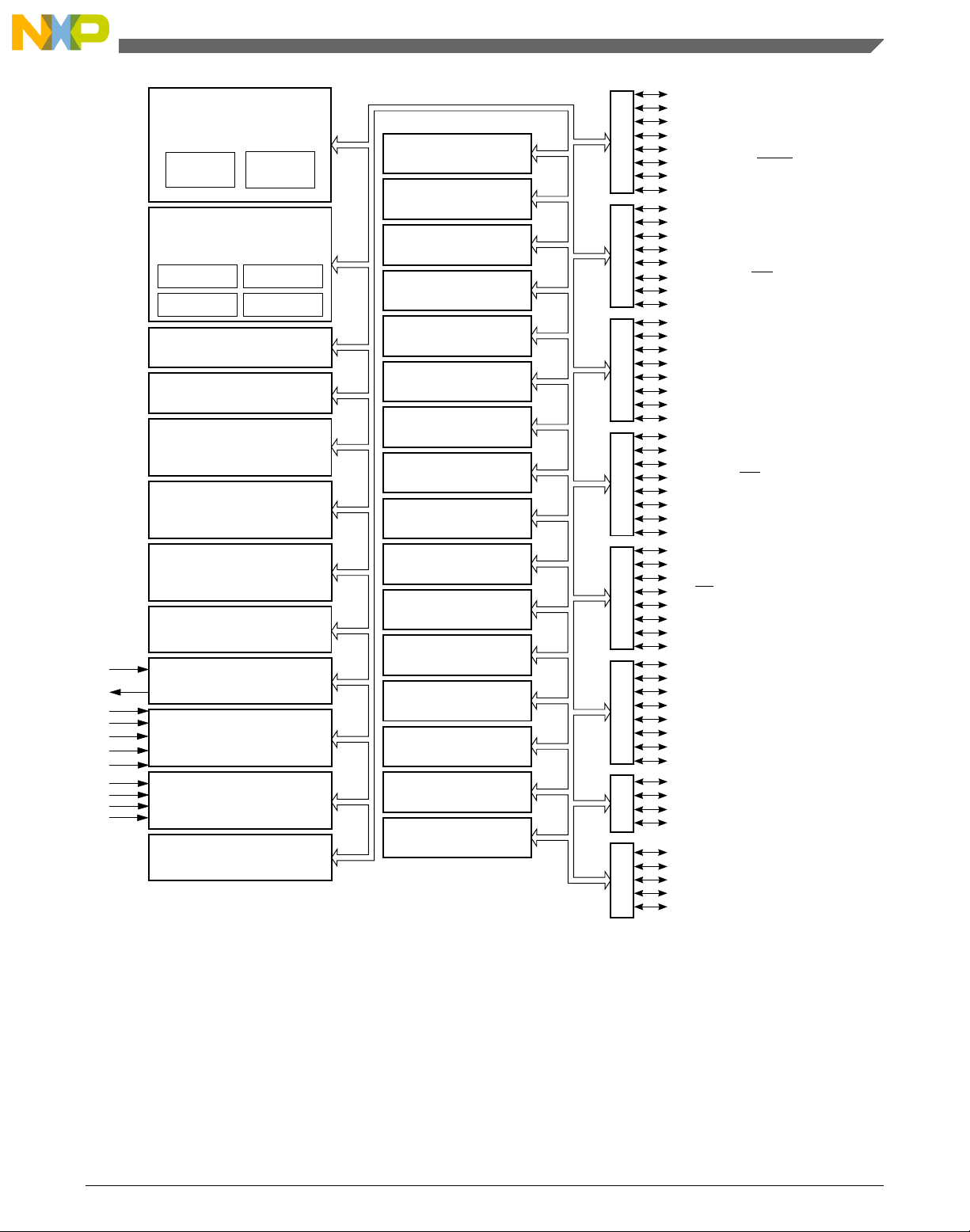
HCS08 CORE
POWER MANAGEMENT
16-CH 12-BIT
ANALOG-TO-DIGITAL
CONVERTER(ADC)
CYCLIC REDUNDANCY
CHECK (CRC)
INTERFACE (TSI)
TOUCH SENSE
(RTC)
REAL-TIME COUNTER
(ACMP)
ANALOG COMPARATOR
CIRCUIT(IIC)
INTER-INTEGRATED
INTERFACE MODULE(SPI1)
16-BIT SERIAL PERIPHERAL
INTERFACE MODULE(SPI0)
8-BIT SERIAL PERIPHERAL
INTERFACE (SCI2)
SERIAL COMMUNICATION
INTERFACE (SCI1)
SERIAL COMMUNICATION
INTERFACE (SCI0)
SERIAL COMMUNICATION
MODULE (FTM2)
6-CH FTM TIMER
MODULE (FTM1)
2-CH FLEX TIMER
MODULE (FTM0)
2-CH FLEX TIMER
(MTIM1)
8-BIT MODULO TIMER
8-BIT MODULO TIMER
(MTIM0)
MODULE (KBI1)
KBYBOARD INTERRUPT
MODULE (KBI0)
KEYBOARD INTERRUPT
PTA1/KBI0P1/FTM0CH1/ACMP1/ADP1
PTA3/KBI0P3/TxD0/SCL
PTA4/ACMPO/BKGD/MS
PTA5/IRQ/TCLK0/RESET
PTA6/FTM2FAULT1/ADP2/TSI0
PTA7/FTM2FAULT2/ADP3/TSI1
PTB0/KBI0P4/RxD0/ADP4/TSI2
PTB1/KBI0P5/TxD0/ADP5/TSI3
PTB2/KBI0P6/SPSCK0/ADP6/TSI4
PTB3/KBI0P7/MOSI0/ADP7/TSI5
PTB4/FTM2CH4/MISO0
PTB5/FTM2CH5/SS0
PTB6/SDA/XTAL
PTB7/SCL/EXTAL
PTC0/FTM2CH0/ADP8/TSI6
PTC1/FTM2CH1/ADP9/TSI7
PTC2/FTM2CH2/ADP10
PTC4/FTM1CH0/RTCO
PTC5/FTM1CH1
PTC3/FTM2CH3/ADP11
PTC6/RxD1/TSI8
PTC7/TxD1/TSI9
PTD0/KBI1P0/FTM2CH2/SPSCK1
PTD1/KBI1P1/FTM2CH3/MOSI1
PTD2/KBI1P2/MISO1/TSI10
PTD3/KBI1P3/SS1/TSI11
PTD4/KBI1P4
PTD5/KBI1P5
PTD6/KBI1P6/RxD2
PTD7/KBI1P7/TxD2
PTE1/MOSI0
PTE2/MISO0
PTE3/SS0
PTE4
PTE5
PTE6
PTE7/TCLK2
PTF0/TSI12
PTF1/TSI13
PTF2/TSI14
PTF3/TSI15
PTF4/ADP12
PTF5/ADP13
PTF6/ADP14
PTF7/ADP15
PTG0
PTG1
PTG2
PTG3
PTH0/FTM2CH0
PTH1/FTM2CH1
PTH2/BUSOUT
PTH6
PTH7
PTE0/SPSCK0/TCLK1
PTA2/KBI0P2/RxD0/SDA
PTA0/KBI0P0/FTM0CH0/ACMP0/ADP0
20 MHz INTERNAL CLOCK
SOURCE (ICS)
EXTERNAL OSCILLATOR
SOURCE (XOSC)
Port A
LVD
1 kHz OSC
WDOG
SS
V
SS
V
REFH
V
REFL
V
DDA
V
SSA
IRQ
XTAL
EXTAL
V
V
V
DD
CPU
BDC
CONTROLLER(IPC)
INTERRUPT PRIORITY
ON-CHIP ICE AND
DEBUG MODUE (DBG)
Port BPort CPort DPort EPort F
USER EEPROM
Port GPort H
USER RAM
CONTROLLER (PMC)
V
SS
DD
MC9S08PT60 = 4,096 bytes
MC9S08PT32 = 4,096 bytes
MC9S08PT60 = 256 bytes
USER FLASH
MC9S08PT32 = 32,768 bytes
MC9S08PT60 = 60,864 bytes
MODULE (
SIM)
SYSTEM INTEGRATION
MC9S08PT32 = 256 bytes
4
2
3
3
3
3
3
3
3
3
5
5
5
1. PTA2 and PTA3 operate as true open drain when working as output.
3. PTB4, PTB5, PTD0, PTD1, PTE0, PTE1, PTH0 and PTH1 can provide high sink/source current drive.
in 32-pin packages.
4. The frequency of the clock from BUSOUT must be equal or less than 10 MHz with 25 pF loading at PAD.
2. PTA4/ACMPO/BKGD/MS is an output-only pin when used as port pin.
5. The secondary power pair of V and V (pin 41 and pin 40 in 64-pin packages) and the third V (pin 13 in 64-pin packages) are not bonded
DD
SS
SS
1
1
Chapter 1 Device Overview
Figure 1-1. MCU block diagram
Freescale Semiconductor, Inc. 37
MC9S08PT60 Reference Manual, Rev. 4, 08/2014
Page 38
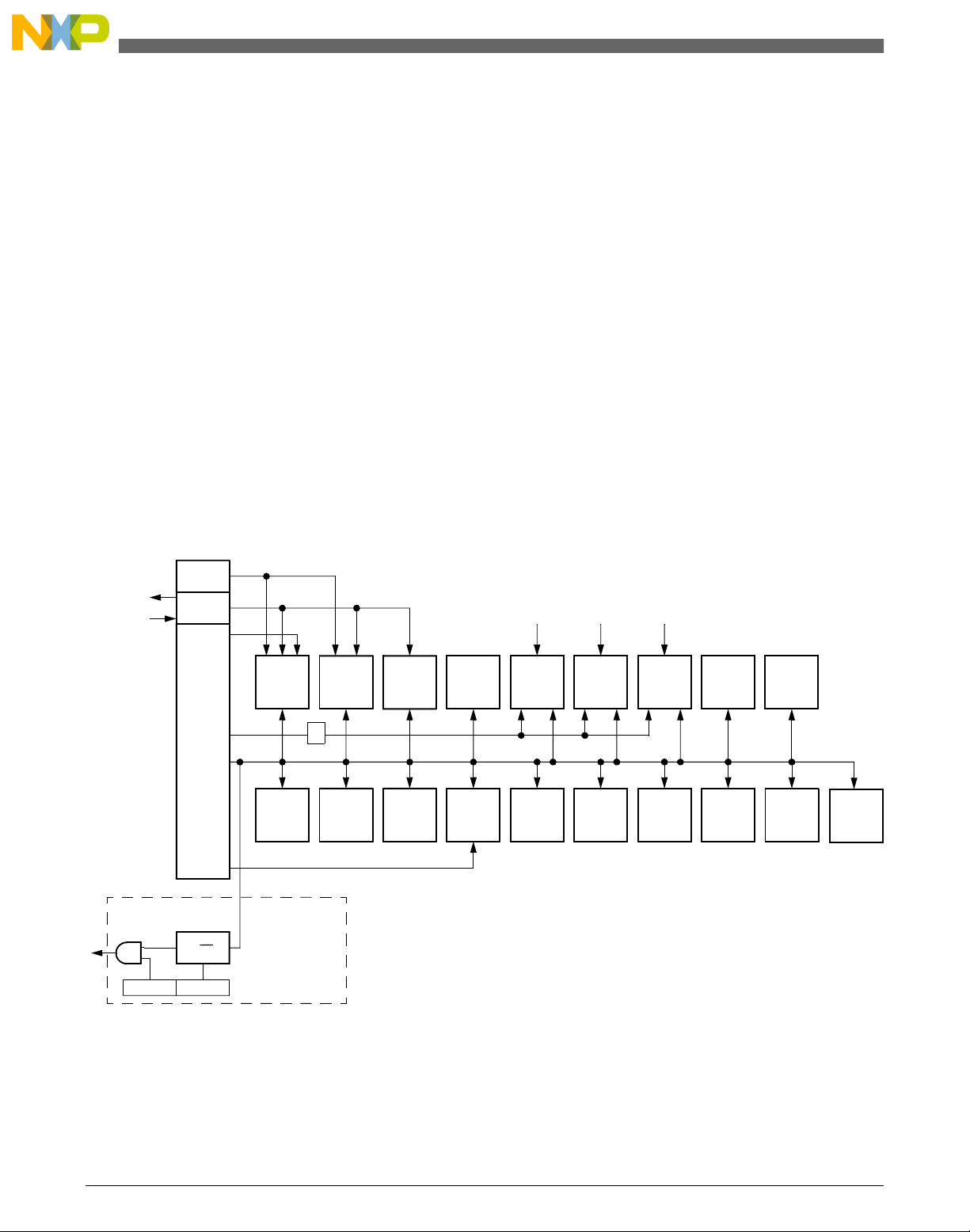
ICSLCLK
ICSFFCLK
XTAL
EXTAL
RTC
FTM0
MTIM0
FTM1
MTIM1
FTM2ADC
SPI0
CPU
BDC
IIC
FLASH
ACMP
RAM
LPOCLK
ICS
SCI0
OSC
OSCOUT
1-kHz
LPO
ICSIRCLK
CRC
IPCDBG
2
N
CLKOUT
ICSCLK ( )
CLKOE
SCI1
SCI2
SPI1
System Control
KBI0
KBI1
TSI
TCLK0 TCLK1
TCLK2
WDOG
~8 MHz after reset
BUSREF
1/2
1
System clock distribution
1.3 System clock distribution
These series contain three on-chip clock sources:
• Internal clock source (ICS) module — The main clock source generator providing
bus clock and other reference clocks to peripherals
• External oscillator (XOSC) module — The external oscillator providing reference
clock to internal clock source (ICS), the real-time clock counter clock module (RTC)
and other MCU sub-systems.
• Low-power oscillator (LPO) module — The on-chip low-power oscillator providing
1 kHz reference clock to RTC and watchdog (WDOG).
NOTE
For this device, the system clock is the bus clock.
The following figure shows a simplified clock connection diagram.
Figure 1-2. System clock distribution diagram
The clock system supplies:
38 Freescale Semiconductor, Inc.
MC9S08PT60 Reference Manual, Rev. 4, 08/2014
Page 39

Chapter 1 Device Overview
• ICSCLK(BUS) — This up to 20 MHz clock source is used as the bus clock that is
the reference to CPU and all peripherals. Control bits in the ICS control registers
determine which of the clock sources is connected:
• Internal reference clock
• External reference clock
• Frequency-locked loop (FLL) output
• ICSLCLK — This clock source is derived from the digitally controlled oscillator
(DCO) of the ICS when the ICS is configured to run off of the internal or external
reference clock. Development tools can select this internal self-clocked source (8
MHz) to speed up BDC communications in systems where the bus clock is slow.
• ICSIRCLK — This is the internal reference clock and can be selected as the clock
source to the WDOG module.
• ICSFFCLK — This generates the fixed frequency clock (FFCLK) after being
synchronized to the bus clock. It can be selected as clock source to the FTM and
MTIM modules. The frequency of the ICSFFCLK is determined by the setting of the
ICS.
• LPOCLK — This clock is generated from an internal low power oscillator (≈1 kHz)
that is completely independent of the ICS module. The LPOCLK can be selected as
the clock source to the RTC or WDOG modules.
• OSCOUT — This is the direct output of the external oscillator module and can be
selected as the clock source for RTC, WDOG and ADC.
• TCLK0 — This is an optional external clock source for the FTM0 and MTIM0
modules. The TCLK0 must be limited to 1/4th frequency of the bus clock for
synchronization.
• TCLK1 — This is an optional external clock source for the FTM1 and MTIM1
modules. The TCLK1 must be limited to 1/4th frequency of the bus clock for
synchronization.
• TCLK2 — This is an optional external clock source for the FTM2 module. The
TCLK2 must be limited to 1/4th frequency of the bus clock for synchronization.
MC9S08PT60 Reference Manual, Rev. 4, 08/2014
Freescale Semiconductor, Inc. 39
Page 40

System clock distribution
MC9S08PT60 Reference Manual, Rev. 4, 08/2014
40 Freescale Semiconductor, Inc.
Page 41

Chapter 2
Pins and connections
2.1 Device pin assignment
MC9S08PT60 Reference Manual, Rev. 4, 08/2014
Freescale Semiconductor, Inc. 41
Page 42
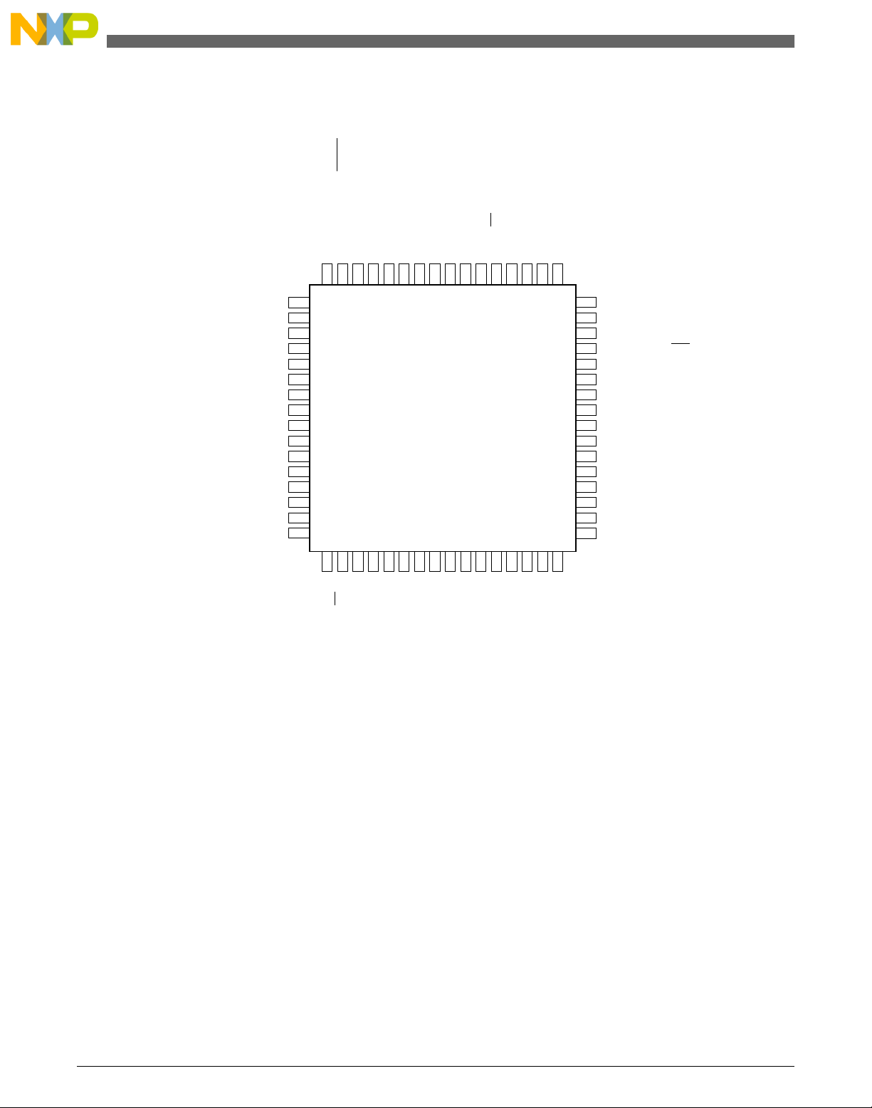
PTF0/TSI12
PTF2/TSI14
PTB1/KBI0P5/TxD0/ADP5/TSI3
PTB2/KBI0P6/SPSCK0/ADP6/TSI4
PTF6/ADP14
PTC3/FTM2CH3/ADP11
2. True open drain pins
PTE6
PTG3
PTF1/TSI13
PTF3/TSI15
PTB0/KBI0P4/RxD0/ADP4/TSI2
PTB3/KBI0P7/MOSI0/ADP7/TSI5
PTF4/ADP12
PTF5/ADP13
PTF7/ADP15
PTA7/FTM2FAULT2/ADP3/TSI1
PTA6/FTM2FAULT1/ADP2/TSI0
PTE4
V
SS
V
DD
PTD4/KBI1P4
PTD3/KBI1P3/SS1/TSI11
PTD2/KBI1P2/MISO1/TSI10
PTA3/KBI0P3/TxD0/SCL
2
PTA2/KBI0P2/RxD0/SDA
2
PTG0
PTG2
PTG1
PTA1/KBI0P1/FTM0CH1/ACMP1/ADP1
PTA0/KBI0P0/FTM0CH0/ACMP0/ADP0
PTC7/TxD1/TSI9
PTC6/RxD1/TSI8
PTE3/SS0
PTE2/MISO0
PTE1/MOSI0
1
PTE0/SPSCK0/TCLK1
1
PTC5/FTM1CH1
PTC4/FTM1CH0/RTCO
PTA5/IRQ/TCLK0/RESET
PTA4/ACMPO/BKGD/MS
PTD1/KBI1P1/FTM2CH3/MOSI1
1
PTD0/KBI1P0/FTM2CH2/SPSCK1
1
PTH7
PTH6
PTE7/TCLK2
PTH2/BUSOUT
V
DD
V
DDA /V
REFH
V
SSA /V
REFL
V
SS
V
SS
PTB7/SCL/EXTAL
PTB6/SDA/XTAL
PTH1/FTM2CH1
1
PTH0/FTM2CH0
1
PTE5
PTB5/FTM2CH5/SS0
1
PTB4/FTM2CH4/MISO0
1
PTC2/FTM2CH2/ADP10
PTD7/KBI1P7/TxD2
PTD6/KBI1P6/RxD2
PTD5/KBI1P5
PTC1/FTM2CH1/ADP9/TSI7
PTC0/FTM2CH0/ADP8/TSI6
1. High source/sink current pins
Pins in bold are not available on less pi n-count packages.
37
17
18
19
20
212223242526272829
303132
1
2
3
4
5
6
7
8
9
10
12
11
13
14
15
16
39
40
38
36
35
34
33
41
42
43
44
45
46
47
48
49
50
51
52
53
54
55
56
57
595860
61
62
63
64
Device pin assignment
Figure 2-1. MC9S08PT60 64-pin QFP and LQFP package
42 Freescale Semiconductor, Inc.
MC9S08PT60 Reference Manual, Rev. 4, 08/2014
Page 43

PTB1/KBI0P5/TxD0/ADP5/TSI3
PTC3/FTM2CH3/ADP11
2. True open drain pins
PTE6
PTB0/KBI0P4/RxD0/ADP4/TSI2
PTB3/KBI0P7/MOSI0/ADP7/TSI5
PTA7/FTM2FAULT2/ADP3/TSI1
PTA6/FTM2FAULT1/ADP2/TSI0
PTE4
V
SS
V
DD
PTD4/KBI1P4
PTD3/KBI1P3/SS1/TSI11
PTD2/KBI1P2/MISO1/TSI10
PTA3/KBI0P3/TxD0/SCL
2
PTA2/KBI0P2/RxD0/SDA
2
PTA1/KBI0P1/FTM0CH1/ACMP1/ADP1
PTA0/KBI0P0/FTM0CH0/ACMP0/ADP0
PTC7/TxD1/TSI9
PTC6/RxD1/TSI8
PTE3/SS0
PTE2/MISO0
PTE1/MOSI0
1
PTE0/SPSCK0/TCLK1
1
PTC5/FTM1CH1
PTC4/FTM1CH0/RTCO
PTA5/IRQ/TCLK0/RESET
PTA4/ACMPO/BKGD/MS
PTD1/KBI1P1/FTM2CH3/MOSI1
1
PTD0/KBI1P0/FTM2CH2/SPSCK1
1
PTE7/TCLK2
PTH2/BUSOUT
V
DD
V
DDA /V
REFH
V
SSA /V
REFL
V
SS
V
SS
PTB7/SCL/EXTAL
PTB6/SDA/XTAL
PTE5
PTB5/FTM2CH5/SS0
1
PTB4/FTM2CH4/MISO0
1
PTC2/FTM2CH2/ADP10
PTD7/KBI1P7/TxD2
PTD6/KBI1P6/RxD2
PTD5/KBI1P5
PTC1/FTM2CH1/ADP9/TSI7
PTC0/FTM2CH0/ADP8/TSI6
1. High source/sink current pins
Pins in bold are not available on less pi n-count packages.
37
17
18
19
20
212223
24
25
26
27
28
29
30
31
32
1
2
3
4
5
6
7
8
9
10
12
11
13
14
15
16
39
40
38
36
35
34
33
41
42
43
44
45
46
47
48
Chapter 2 Pins and connections
Figure 2-2. MC9S08PT60 48-pin LQFP package
Freescale Semiconductor, Inc. 43
MC9S08PT60 Reference Manual, Rev. 4, 08/2014
Page 44
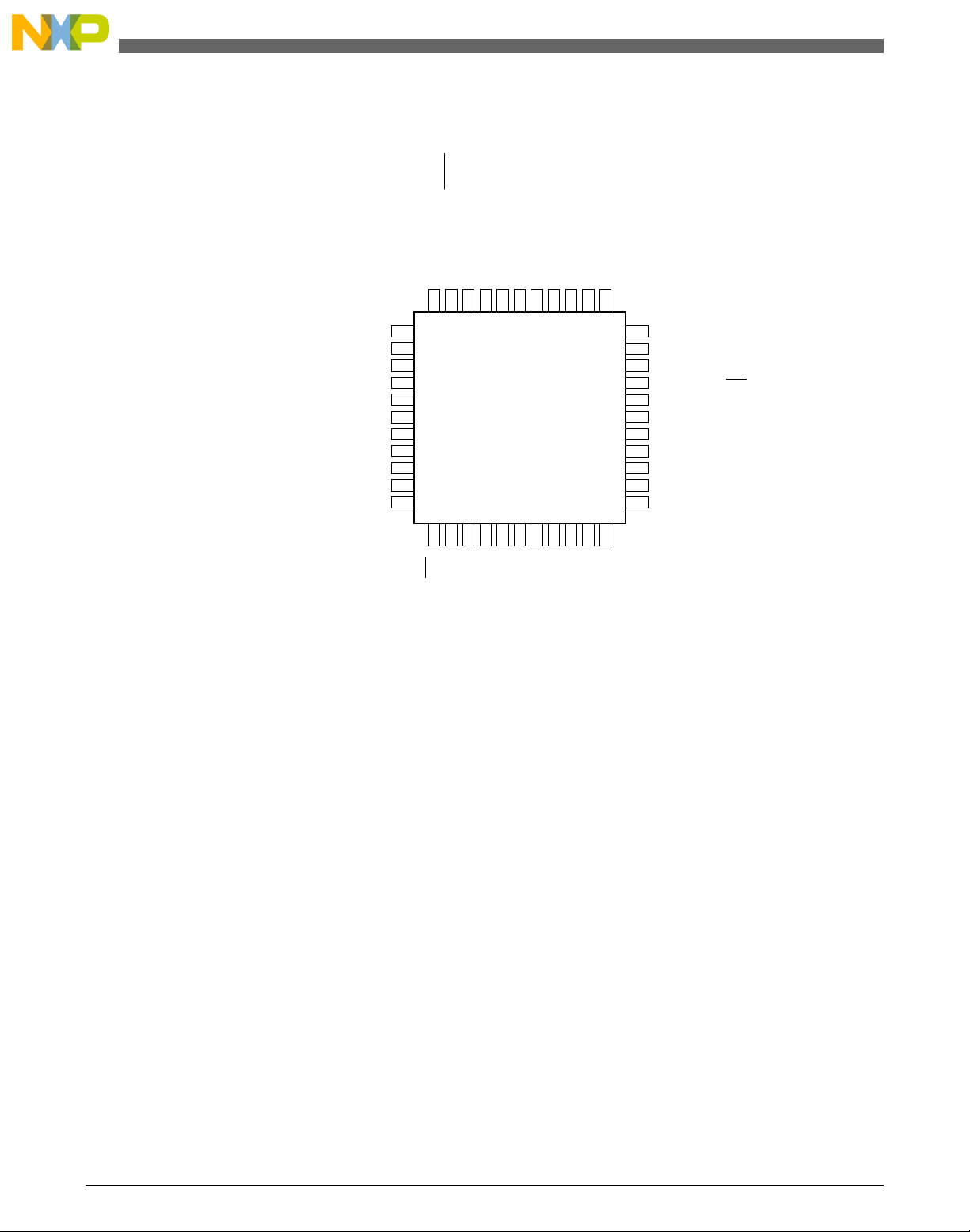
PTB1/KBI0P5/TxD0/ADP5/TSI3
PTC3/FTM2CH3/ADP11
2. True open drain pins
PTB0/KBI0P4/RxD0/ADP4/TSI2
PTB3/KBI0P7/MOSI0/ADP7/TSI5
PTA7/FTM2FAULT2/ADP3/TSI1
PTA6/FTM2FAULT1/ADP2/TSI0
V
SS
V
DD
PTD4/KBI1P4
PTD3/KBI1P3/SS1/TSI11
PTD2/KBI1P2/MISO1/TSI10
PTA2/KBI0P2/RxD0/SDA
2
PTA1/KBI0P1/FTM1CH1/ACMP1/ADP1
PTA0/KBI0P0/FTM0CH0/ACMP0/ADP0
PTC7/TxD1/TSI9
PTC6/RxD1/TSI8
PTE2/MISO0
PTE1/MOSI0
1
PTE0/SPSCK0/TCLK1
1
PTC5/FTM1CH1
PTC4/FTM1CH0/RTCO
PTA5/IRQ/TCLK0/RESET
PTA4/ACMPO/BKGD/MS
PTD1/KBI1P1/FTM2CH3/MOSI1
1
PTD0/KBI1P0/FTM2CH2/SPSCK1
1
PTE7/TCLK2
PTH2/BUSOUT
V
DD
V
DDA /V
REFH
V
SSA /V
REFL
V
SS
V
SS
PTB7/SCL/EXTAL
PTB6/SDA/XTAL
PTB5/FTM2CH5/SS0
1
PTB4/FTM2CH4/MISO0
1
PTC2/FTM2CH2/ADP10
PTD7/KBI1P7/TxD2
PTD6/KBI1P6/RxD2
PTD5/KBI1P5
PTC1/FTM2CH1/ADP9/TSI7
PTC0/FTM2CH0/ADP8/TSI6
1. High source/sink current pins
Pins in bold are not available on less pi n-count packages.
37
17
18
19
20
21
22
23
24
25
26
27
28
29
30
31
32
1
2
3
4
5
6
7
8
9
10
12
11
13
14
15
16
39
40
38
36
35
34
33
41
42
43
44
PTA3/KBI0P3/TxD0/SCL2
Device pin assignment
Figure 2-3. MC9S08PT60 44-pin LQFP package
44 Freescale Semiconductor, Inc.
MC9S08PT60 Reference Manual, Rev. 4, 08/2014
Page 45
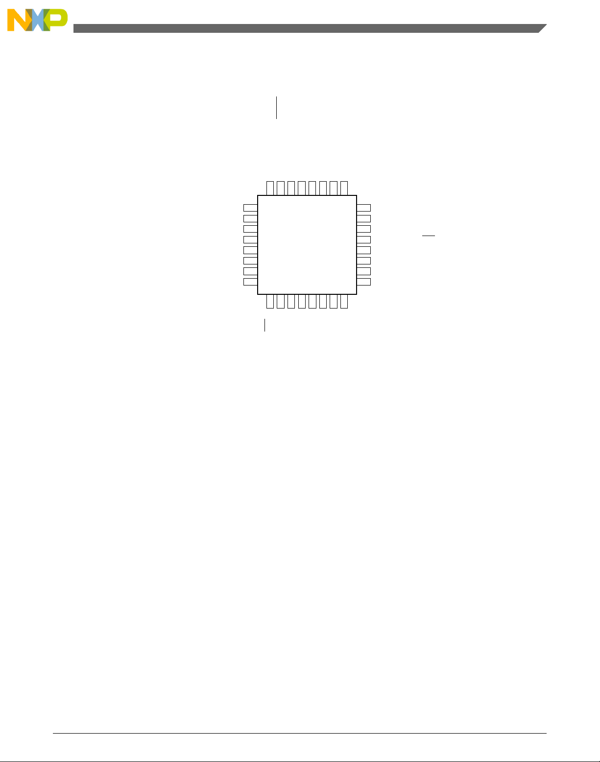
PTB1/KBI0P5/TxD0/ADP5/TSI3
PTB2/KBI0P6/SPSCK0/ADP6/TSI4
PTC3/FTM2CH3/ADP11
2. True open drain pins
PTB0/KBI0P4/RxD0/ADP4/TSI2
PTB3/KBI0P7/MOSI0/ADP7/TSI5
PTA7/FTM2FAULT2/ADP3/TSI1
PTA6/FTM2FAULT1/ADP2/TSI0
PTD3/KBI1P3/SS1/TSI11
PTD2/KBI1P2/MISO1/TSI10
PTA2/KBI0P2/RxD0/SDA
2
PTA1/KBI0P1/FTM0CH1/ACMP1/ADP1
PTA0/KBI0P0/FTM0CH0/ACMP0/ADP0
PTC7/TxD1/TSI9
PTC6/RxD1/TSI8
PTC5/FTM1CH1
PTC4/FTM1CH0/RTCO
PTA5/IRQ/TCLK0/RESET
PTA4/ACMPO/BKGD/MS
PTD1/KBI1P1/FTM2CH3/MOSI1
1
PTD0/KBI1P0/FTM2CH2/SPSCK1
1
V
DD
V
DDA /V
REFH
V
SSA /V
REFL
V
SS
PTB7/SCL/EXTAL
PTB6/SDA/XTAL
PTB5/FTM2CH5/SS0
1
PTB4/FTM2CH4/MISO0
1
PTC2/FTM2CH2/ADP10
PTC1/FTM2CH1/ADP9/TSI7
PTC0/FTM2CH0/ADP8/TSI6
1. High source/sink current pins
17
18
19
20
21
22
23
24
25
26
27
28
29
30
31
32
1
2
3
4
5
6
7
8
9
10
12
11
13
14
15
16
PTA3/KBI0P3/TxD0/SCL2
Chapter 2 Pins and connections
2.2
2.2.1
VDD and VSS are the primary power supply pins for the MCU. This voltage source
supplies power to all I/O buffer circuitry and to an internal voltage regulator. The internal
voltage regulator provides a regulated lower-voltage source to the CPU and to the MCU's
other internal circuitry.
Pin functions
Freescale Semiconductor, Inc. 45
Figure 2-4. MC9S08PT60 32-pin LQFP package
Power (VDD, VSS)
MC9S08PT60 Reference Manual, Rev. 4, 08/2014
Page 46
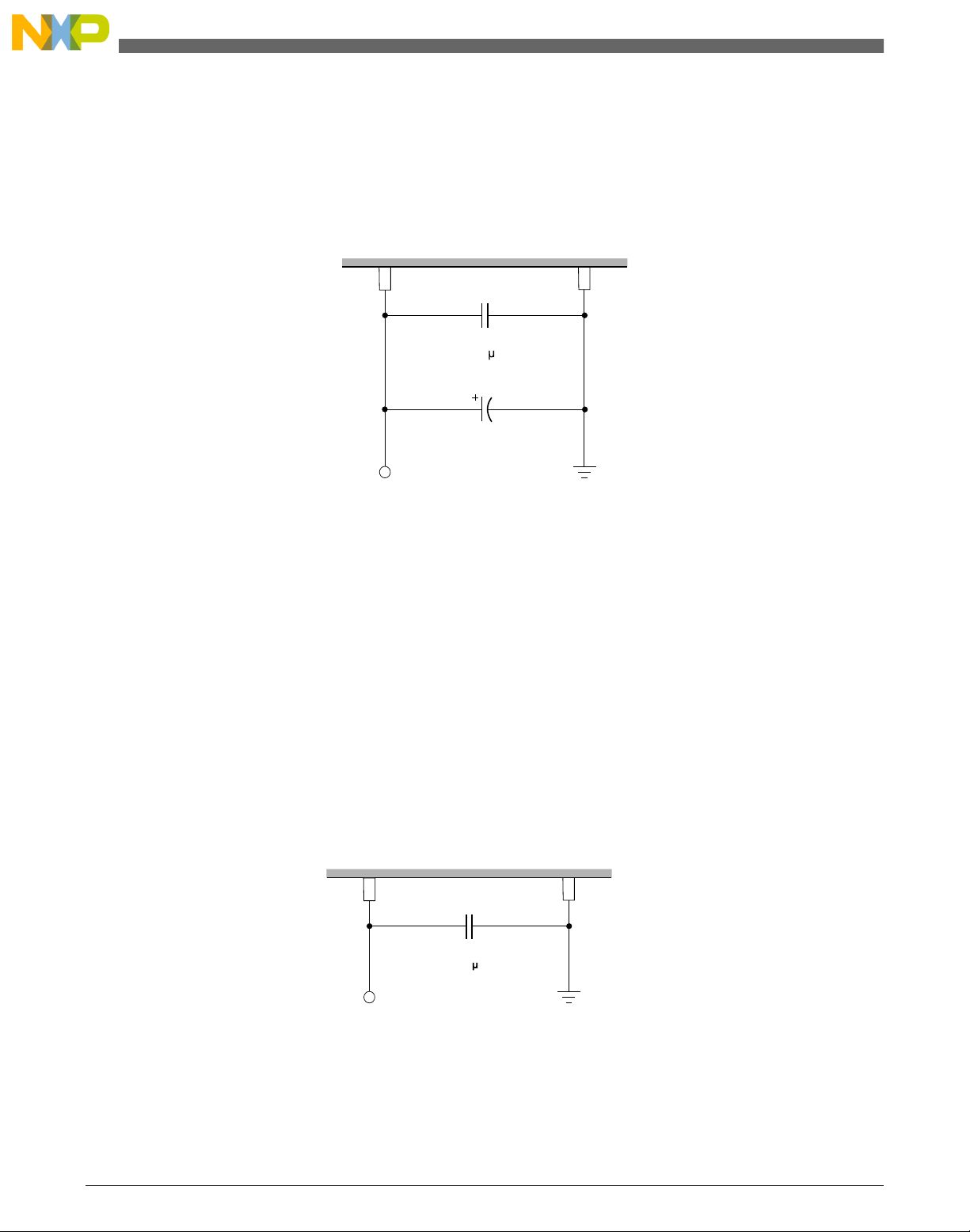
MCU
C1
C2
V
DD
V
ss
V
0.1
F
MCU
C1
V
DDA /V
REFH
V
SSA /V
REFL
F
0.1
External reference voltage
Pin functions
Typically, application systems have two separate capacitors across the power pins. In this
case, there should be a bulk electrolytic capacitor, such as a 10 µF tantalum capacitor,
that provides bulk charge storage for the overall system and a 0.1 µF ceramic bypass
capacitor located as near to the paired VDD and VSS power pins as practical to suppress
high-frequency noise.
Figure 2-5. Power supply bypassing
2.2.2
V
DDA
Connect the V
Analog power supply and reference pins (V
V
SSA/VREFL
and V
are the power supply pins for the analog-to-digital converter (ADC).
SSA
DDA
)
pin to the same voltage potential as VDD, and the V
DDA/VREFH
pin to the same
SSA
voltage potential as VSS.
De-coupling of these pins should be as per the digital supply. A 0.1 µF ceramic bypass
capacitor should be located as near to the MCU power pins as practical to suppress highfrequency noise.
V
V
is the high reference supply for the ADC, and is internally connected to V
REFH
is the low reference supply for the ADC, and is internally connected to V
REFL
Figure 2-6. Analog power supply bypassing
and
DDA
.
SSA
.
46 Freescale Semiconductor, Inc.
MC9S08PT60 Reference Manual, Rev. 4, 08/2014
Page 47
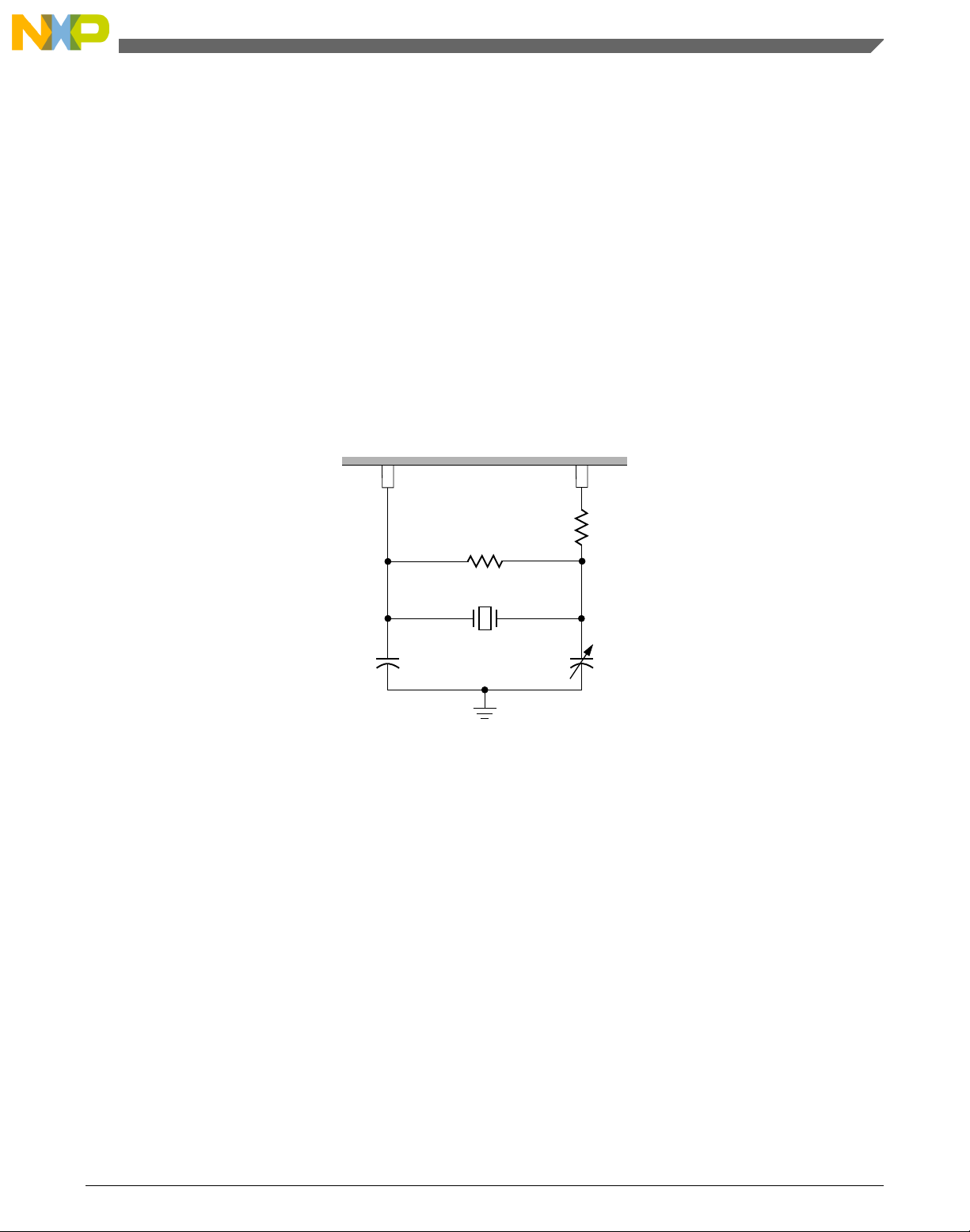
MCU
EXTAL
XTAL
R
s
R
F
C1
C2
X1
Chapter 2 Pins and connections
2.2.3 Oscillator (XTAL, EXTAL)
The XTAL and EXTAL pins are used to provide the connections for the on-chip
oscillator. The oscillator (XOSC) in this MCU is a Pierce oscillator that can
accommodate a crystal or ceramic resonator. Optionally, an external clock source can be
connected to the EXTAL input pin. The oscillator can be configured to run in stop3
mode.
Refer to the following figure, RS (when used) and RF must be low-inductance resistors
such as carbon composition resistors. Wire-wound resistors, and some metal film
resistors, have too much inductance. C1 and C2 normally must be high-quality ceramic
capacitors that are specifically designed for high-frequency applications.
Figure 2-7. Typical crystal or resonator circuit
RF is used to provide a bias path to keep the EXTAL input in its linear range during
crystal startup; its value is not generally critical. Typical systems use 1 M to 10 M.
Higher values are sensitive to humidity and lower values reduce gain and (in extreme
cases) could prevent startup.
C1 and C2 are typically in the 5 pF to 25 pF range and are chosen to match the
requirements of a specific crystal or resonator. Take into account printed circuit board
(PCB) capacitance and MCU pin capacitance when selecting C1 and C2. The crystal
manufacturer typically specifies a load capacitance, which is the series combination of
C1 and C2 (which are usually the same size). As a first-order approximation, use 10 pF as
an estimate of combined pin and PCB capacitance for each oscillator pin (EXTAL and
XTAL).
Freescale Semiconductor, Inc. 47
MC9S08PT60 Reference Manual, Rev. 4, 08/2014
Page 48
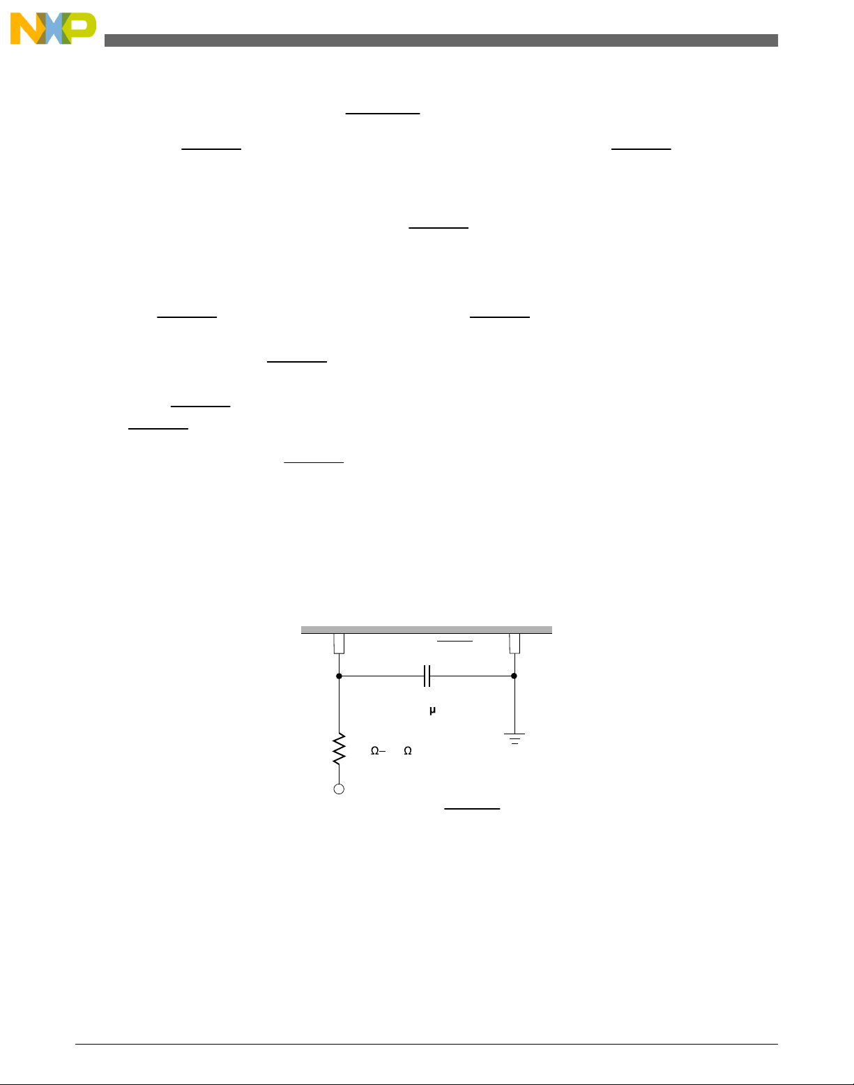
MCU
V
DD
PTA5/IRQ/TCLK0/RESET
V
SS
F
0.1
4.7k
10k
Pin functions
2.2.4 External reset pin (RESET) and interrupt pin (IRQ)
A low on the RESET pin forces the MCU to an known startup state. RESET is
bidirectional, allowing a reset of the entire system. It is driven low when any internal
reset source is asserted. This pin contains an internal pullup resistor.
RESET shares an I/O pin with PTA5. The RESET pin function is enabled by default after
POR reset, because internal power-on reset and low-voltage reset circuitry typically make
external reset circuitry unnecessary. This pin is normally connected to the standard 6-pin
background debug connector so that a development system can directly reset the MCU
system. If RESET function of PTA5/IRQ/TCLK0/RESET pin is enabled, a manual
external reset can be added by supplying a simple switch to ground (pull reset pin low to
force a reset). When the RESET pin function is enabled, an internal pullup resistor is
connected to this pin and a reset signal can feed into MCU with an input hysteresis. POR
reset brings RESET pin into its default configuration, reset other than POR has no effect
on the RESET pin function configuration.
When PTA5/IRQ/TCLK0/
RESET is enabled as IRQ pin, it is the input source for the
IRQ interrupt and is also the input for the BIH and BIL instructions. IRQ is asynchronous
external interrupt pins.
In EMC-sensitive applications, an external RC filter is recommended on the reset pin.
See the following figure for example.
Figure 2-8. PTA5/IRQ/TCLK0/RESET external RC filter
48 Freescale Semiconductor, Inc.
MC9S08PT60 Reference Manual, Rev. 4, 08/2014
Page 49
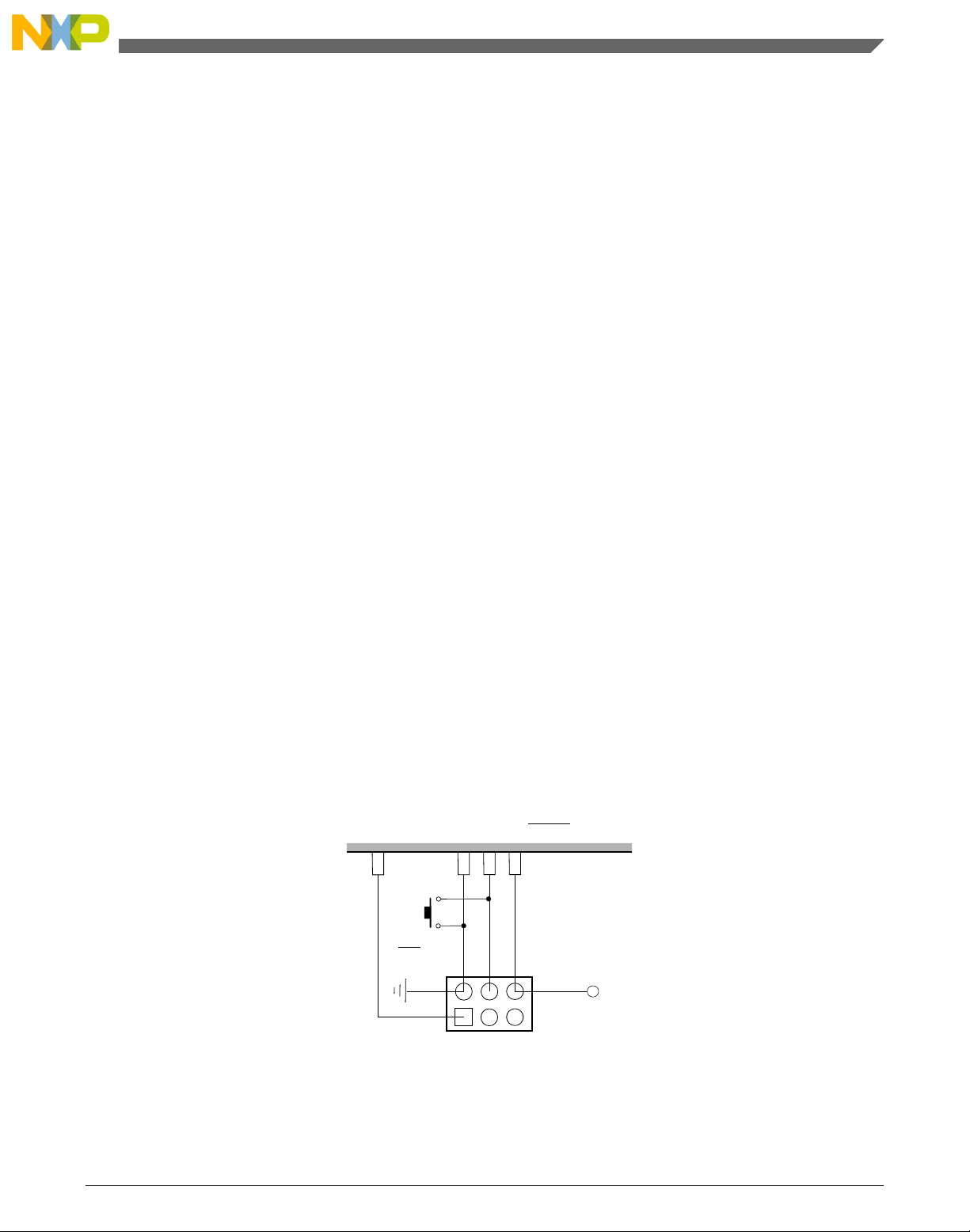
Optional Manual Reset
BKGD/MS
V
DD
V
SS
PTA5/IRQ/TCLK0/RESET
Chapter 2 Pins and connections
2.2.5 Background/mode select (BKGD/MS)
During a power-on-reset (POR) or background debug force reset, the PTA4/ACMPO/
BKGD/MS pin functions as a mode select pin. Immediately after internal reset rises the
pin functions as the background pin and can be used for background debug
communication. While the pin functions as a background/mode selection pin, it includes
an internal pullup device and a standard output driver.
The background debug communication function is enabled when SOPT1[BKGDPE] bit
is set. SOPT1[BKGDPE] is set following any reset of the MCU and must be cleared to
use the PTA4/ACMPO/BKGD/MS pin's alternative pin functions.
If this pin is floating, the MCU will enter normal operating mode at the rising edge of
reset. If a debug system is connected to the 6-pin standard background debug header, it
can hold BKGD/MS low during the POR or immediately after issuing a background
debug force reset, which will force the MCU into active background mode.
The BKGD pin is used primarily for background debug controller (BDC)
communications using a custom protocol that uses 16 clock cycles of the target MCU's
BDC clock per bit time. The target MCU's BDC clock can run as fast as the bus clock, so
there should never be any significant capacitance connected to the BKGD/MS pin that
interferes with background serial communications. When the pin performs output only
PTA4, it can drive only capacitance-limited MOSFET. Driving a bipolar transistor
directly by PTA4 is prohibited because this can cause mode entry fault and BKGD errors.
Although the BKGD pin is a pseudo open-drain pin, the background debug
communication protocol provides brief, actively driven, high speedup pulses to ensure
fast rise time. Small capacitances from cables and the absolute value of the internal
pullup device play almost no role in determining rise and fall time on the BKGD pin.
Freescale Semiconductor, Inc. 49
Figure 2-9. Typical debug circuit
MC9S08PT60 Reference Manual, Rev. 4, 08/2014
Page 50

Pin functions
2.2.6 Port A input/output (I/O) pins (PTA7–PTA0)
PTA7–PTA0 except PTA4 are general-purpose, bidirectional I/O port pins. These port
pins also have selectable pullup devices when configured for input mode except PTA4.
The pullup devices are selectable on an individual port bit basis. The pulling devices are
disengaged when configured for output mode except when PTA2 and PTA3 are used as
SDA and SCL function.
PTA4 is output only when used as port pin. The pulling device is disabled at this
condition.
PTA3 and PTA2 provide true open drain when operated as output.
2.2.7
PTB7–PTB0 are general-purpose, bidirectional I/O port pins. These port pins also have
selectable pullup devices when configured for input mode, the pullup devices are
selectable on an individual port bit basis. The pulling devices are disengaged when
configured for output mode.
2.2.8
PTC7–PTC0 are general-purpose, bidirectional I/O port pins. These port pins also have
selectable pullup devices when configured for input mode, and the pullup devices are
selectable on an individual port bit basis. The pulling devices are disengaged when
configured for output mode.
2.2.9
PTD7–PTD0 are general-purpose, bidirectional I/O port pins. These port pins also have
selectable pullup devices when configured for input mode, the pullup devices are
selectable on an individual port bit basis. The pulling devices are disengaged when
configured for output mode.
Port B input/output (I/O) pins (PTB7–PTB0)
Port C input/output (I/O) pins (PTC7–PTC0)
Port D input/output (I/O) pins (PTD7–PTD0)
MC9S08PT60 Reference Manual, Rev. 4, 08/2014
50 Freescale Semiconductor, Inc.
Page 51

Chapter 2 Pins and connections
2.2.10 Port E input/Output (I/O) pins (PTE7–PTE0)
PTE7–PTE0 are general-purpose, bidirectional I/O port pins. These port pins also have
selectable pullup devices when configured for input mode, the pullup devices are
selectable on an individual port bit basis. The pulling devices are disengaged when
configured for output mode.
2.2.11 Port F input/output (I/O) pins (PTF7–PTF0)
PTF7–PTF0 are general-purpose, bidirectional I/O port pins. These port pins also have
selectable pullup devices when configured for input mode, the pullup devices are
selectable on an individual port bit basis. The pulling devices are disengaged when
configured for output mode.
2.2.12
PTG3–PTG0 are general-purpose, bidirectional I/O port pins. These port pins also have
selectable pull-up devices when configured for input mode, the pullup devices are
selectable on an individual port bit basis. The pulling devices are disengaged when
configured for output mode.
2.2.13
PTH7–PTH6, PTH2–PTH0 are general-purpose, bidirectional I/O port pins. These port
pins also have selectable pullup devices when configured for input mode, the pullup
devices are selectable on an individual port bit basis. The pulling devices are disengaged
when configured for output mode.
2.2.14
PTA3 and PTA2 operate in true open drain mode.
Port G input/output (I/O) pins (PTG3–PTG0)
Port H input/output (I/O) pins (PTH7–PTH6, PTH2–PTH0)
True open drain pins (PTA3–PTA2)
NOTE
When configuring IIC to use SDA(PTA2) and SCL(PTA3)
pins, if an application uses internal pullups instead of external
pullups, the internal pullups remain present setting when the
MC9S08PT60 Reference Manual, Rev. 4, 08/2014
Freescale Semiconductor, Inc. 51
Page 52
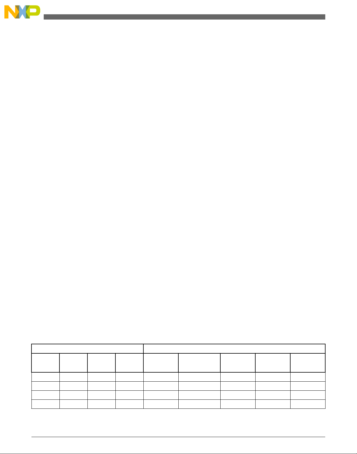
Pin functions
pins are configured as outputs, but they are automatically
disabled to save power when the output values are low.
2.2.15 High current drive pins (PTB4, PTB5, PTD0, PTD1, PTE0,
PTE1, PTH0, PTH1)
When high current function is enabled, PTB4, PTB5, PTD0, PTD1, PTE0, PTE1, PTH0
and PTH1 can drive output current. Each high current drive pin can drive higher sink/
source current than the other normal pins, please refer to data sheet for the drive capacity.
WARNING
The total sink/source current should be under the chip's
capacity, please refer to data sheet on max current allowed.
2.2.16
Peripheral pinouts
These MCUs support up to 57 general-purpose I/O pins, which are shared with on-chip
peripheral functions (FTM, ACMP, ADC, SCI, SPI, IIC, KBI, etc.). These 57 generalpurpose I/O pins include one output-only pin (PTA4).
When a port pin is configured as general-purpose input, or when a peripheral uses the
port pin as an input, the software can enable a pullup device.
When a high current drive port pin is configured as general-purpose output or when a
peripheral uses the port pin as an output, software can select alternative drive strengths.
For information about controlling these pins as general-purpose I/O pins, see the Parallel
input/output. For information about how and when on-chip peripheral systems use these
pins, see the appropriate module chapter.
Immediately after reset, all pins are configured as high-impedance general-purpose IO
with internal pullup devices disabled.
Table 2-1. Pin availability by package pin-count
Pin Number Lowest Priority <-- --> Highest
64-LQFP
64-QFP
1 1 1 1 PTD1
2 2 2 2 PTD0
3 — — — PTH7 — — — —
4 — — — PTH6 — — — —
48-LQFP 44-LQFP 32-LQFP Port Pin Alt 1 Alt 2 Alt 3 Alt 4
1
1
KBI1P1 FTM2CH3 MOSI1 —
KBI1P0 FTM2CH2 SPSCK1 —
Table continues on the next page...
MC9S08PT60 Reference Manual, Rev. 4, 08/2014
52 Freescale Semiconductor, Inc.
Page 53

Chapter 2 Pins and connections
Table 2-1. Pin availability by package pin-count (continued)
Pin Number Lowest Priority <-- --> Highest
64-LQFP
64-QFP
5 3 3 — PTE7 — TCLK2 — —
6 4 4 — PTH2 — BUSOUT — —
7 5 5 3 — — — — V
8 6 6 4 — — — V
9 7 7 5 — — — V
10 8 8 6 — — — — V
11 9 9 7 PTB7 — SCL — EXTAL
12 10 10 8 PTB6 — SDA — XTAL
13 11 11 — — — — — V
14 — — — PTH1
15 — — — PTH0
16 12 — — PTE6 — — — —
17 13 — — PTE5 — — — —
18 14 12 9 PTB5
19 15 13 10 PTB4
20 16 14 11 PTC3 FTM2CH3 — ADP11 —
21 17 15 12 PTC2 FTM2CH2 — ADP10 —
22 18 16 — PTD7 KBI1P7 TXD2 — —
23 19 17 — PTD6 KBI1P6 RXD2 — —
24 20 18 — PTD5 KBI1P5 — — —
25 21 19 13 PTC1 — FTM2CH1 ADP9 TSI7
26 22 20 14 PTC0 — FTM2CH0 ADP8 TSI6
27 — — — PTF7 — — ADP15 —
28 — — — PTF6 — — ADP14 —
29 — — — PTF5 — — ADP13 —
30 — — — PTF4 — — ADP12 —
31 23 21 15 PTB3 KBI0P7 MOSI0 ADP7 TSI5
32 24 22 16 PTB2 KBI0P6 SPSCK0 ADP6 TSI4
33 25 23 17 PTB1 KBI0P5 TXD0 ADP5 TSI3
34 26 24 18 PTB0 KBI0P4 RXD0 ADP4 TSI2
35 — — — PTF3 — — — TSI15
36 — — — PTF2 — — — TSI14
37 27 25 19 PTA7 FTM2FAULT2 — ADP3 TSI1
38 28 26 20 PTA6 FTM2FAULT1 — ADP2 TSI0
39 29 — — PTE4 — — — —
40 30 27 — — — — — V
41 31 28 — — — — — V
48-LQFP 44-LQFP 32-LQFP Port Pin Alt 1 Alt 2 Alt 3 Alt 4
DDA
SSA
1
1
1
1
— FTM2CH1 — —
— FTM2CH0 — —
FTM2CH5 SS0 — —
FTM2CH4 MISO0 — —
Table continues on the next page...
V
V
DD
REFH
REFL
SS
SS
SS
DD
MC9S08PT60 Reference Manual, Rev. 4, 08/2014
Freescale Semiconductor, Inc. 53
Page 54
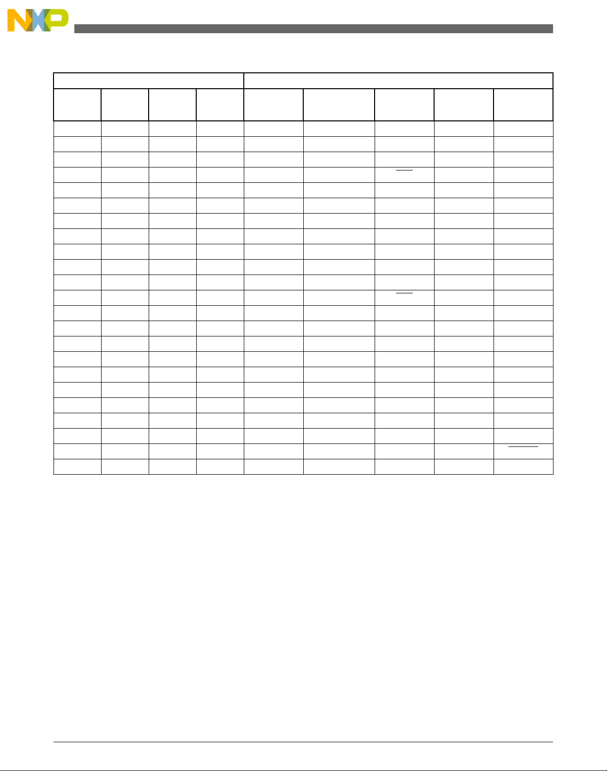
Pin functions
Table 2-1. Pin availability by package pin-count (continued)
Pin Number Lowest Priority <-- --> Highest
64-LQFP
64-QFP
42 — — — PTF1 — — — TSI13
43 — — — PTF0 — — — TSI12
44 32 29 — PTD4 KBI1P4 — — —
45 33 30 21 PTD3 KBI1P3 SS1 — TSI11
46 34 31 22 PTD2 KBI1P2 MISO1 — TSI10
47 35 32 23 PTA3
48 36 33 24 PTA2
49 37 34 25 PTA1 KBI0P1 FTM0CH1 ACMP1 ADP1
50 38 35 26 PTA0 KBI0P0 FTM0CH0 ACMP0 ADP0
51 39 36 27 PTC7 — TxD1 — TSI9
52 40 37 28 PTC6 — RxD1 — TSI8
53 41 — — PTE3 — SS0 — —
54 42 38 — PTE2 — MISO0 — —
55 — — — PTG3 — — — —
56 — — — PTG2 — — — —
57 — — — PTG1 — — — —
58 — — — PTG0 — — — —
59 43 39 — PTE1
60 44 40 — PTE0
61 45 41 29 PTC5 — FTM1CH1 — —
62 46 42 30 PTC4 — FTM1CH0 RTCO —
63 47 43 31 PTA5 IRQ TCLK0 — RESET
64 48 44 32 PTA4 — ACMPO BKGD MS
48-LQFP 44-LQFP 32-LQFP Port Pin Alt 1 Alt 2 Alt 3 Alt 4
2
2
1
1
KBI0P3 TXD0 SCL —
KBI0P2 RXD0 SDA —
— MOSI0 — —
— SPSCK0 TCLK1 —
1. This is a high current drive pin when operated as output. Please see High current drive for more information.
2. This is a true open-drain pin when operated as output.
Note
When an alternative function is first enabled, it is possible to
get a spurious edge to the module. User software must clear any
associated flags before interrupts are enabled. The table above
illustrates the priority if multiple modules are enabled. The
highest priority module will have control over the pin. Selecting
a higher priority pin function with a lower priority function
already enabled can cause spurious edges to the lower priority
module. Disable all modules that share a pin before enabling
another module.
MC9S08PT60 Reference Manual, Rev. 4, 08/2014
54 Freescale Semiconductor, Inc.
Page 55

Chapter 3
Power management
3.1 Introduction
The operating modes of the device are described in this chapter. Entry into each mode,
exit from each mode, and functionality while in each of the modes are described.
3.2
These MCUs feature the following power modes:
3.2.1
Features
• Run mode
• Wait mode
• CPU shuts down to conserve power
• Bus clocks are running
• Full voltage regulation is maintained
• Stop3 modes
• System clocks stopped; voltage regulator in standby
• all internal circuits powered for fast recovery
Run mode
This is the normal operating mode. In this mode, the CPU executes code from internal
memory with execution beginning at the address fetched from memory at 0xFFFE:
0xFFFF after reset. The power supply is fully regulating and all peripherals can be active
in run mode.
MC9S08PT60 Reference Manual, Rev. 4, 08/2014
Freescale Semiconductor, Inc. 55
Page 56

Features
3.2.2 Wait mode
Wait mode is entered by executing a WAIT instruction. Upon execution of the WAIT
instruction, the CPU enters a low-power state in which it is not clocked. The I bit in CCR
is cleared when the CPU enters the wait mode, enabling interrupts. When an interrupt
request occurs, the CPU exits the wait mode and resumes processing, beginning with the
stacking operations leading to the interrupt service routine.
While the MCU is in wait mode, there are some restrictions on which background debug
commands can be used. Only the BACKGROUND command and memory-access-withstatus commands are available when the MCU is in wait mode. The memory-access-withstatus commands do not allow memory access, but they report an error indicating that the
MCU is in either stop or wait mode. The BACKGROUND command can be used to
wake the MCU from wait mode and enter active background mode.
3.2.3
Stop3 mode
To enter stop3, the user must execute a STOP instruction with stop mode enabled
(SOPT1[STOPE] = 1). Upon entering the stop3 mode, all of the clocks in the MCU are
halted by default, but OSC clock and internal reference clock can be turned on by setting
the ICS control registers. The ICS enters its standby state, as does the voltage regulator
and the ADC. The states of all of the internal registers and logic, as well as the RAM
content, are maintained. The I/O pin states are not latched at the pin. Instead they are
maintained by virtue of the states of the internal logic driving the pins being maintained.
Exit from stop3 is done by asserting reset or through an interrupt. The interrupt include
the asynchronous interrupt from the IRQ or KBI pins, the SCI receive interrupt, the ADC,
ACMP, TSI , IIC or LVI interrupt and the real-time interrupt.
If stop3 is exited by means of the
RESET pin, then the MCU will be reset and operation
will resume after taking the reset vector. Exit by means of an asynchronous interrupt or
the real-time interrupt will result in the MCU taking the appropriate interrupt vector.
The LPO (≈1 kHz) for the real-time counter clock allows a wakeup from stop3 mode with
no external components. When RTC_SC2[RTCPS] is clear, the real-time counter clock
function is disabled.
MC9S08PT60 Reference Manual, Rev. 4, 08/2014
56 Freescale Semiconductor, Inc.
Page 57

Chapter 3 Power management
3.2.4 Active BDM enabled in stop3 mode
Entry into the active background mode from run mode is enabled if the
BDC_SCR[ENBDM] bit is set. This register is described in the development support. If
BDC_SCR[ENBDM] is set when the CPU executes a STOP instruction, the system
clocks to the background debug logic remain active when the MCU enters stop mode, so
background debug communication is still possible. In addition, the voltage regulator does
not enter its low-power standby state but maintains full internal regulation.
Most background commands are not available in stop mode. The memory-access-withstatus commands do not allow memory access, but they report an error indicating that the
MCU is in either stop or wait mode. The BACKGROUND command can be used to
wake the MCU from stop and enter active background mode if the BDC_SCR[ENBDM]
bit is set. After entering background debug mode, all background commands are
available.
3.2.5
LVD enabled in stop mode
The LVD system is capable of generating either an interrupt or a reset when the supply
voltage drops below the LVD voltage. If the LVD is enabled in stop (LVDE and LVDSE
bits in SPMSC1 both set) at the time the CPU executes a STOP instruction, then the
voltage regulator remains active during stop3 mode.
3.2.6
Power modes behaviors
Executing the WAIT or STOP command puts the MCU in a low power consumption
mode for standby situations. The system integration module (SIM) holds the CPU in a
non-clocked state. The operation of each of these modes is described in the following
subsections. Both STOP and WAIT clear the interrupt mask (I) in the condition code
register, allowing interrupt to occur. The following table shows the low power mode
behaviors.
Table 3-1. Low power mode behavior
Mode Run Wait Stop3
PMC Full regulation Full regulation Loose regulation
ICS On On Optional on
OSC On On Optional on
LPO On On On
CPU On Standby Standby
FLASH On On Standby
Table continues on the next page...
MC9S08PT60 Reference Manual, Rev. 4, 08/2014
Freescale Semiconductor, Inc. 57
Page 58
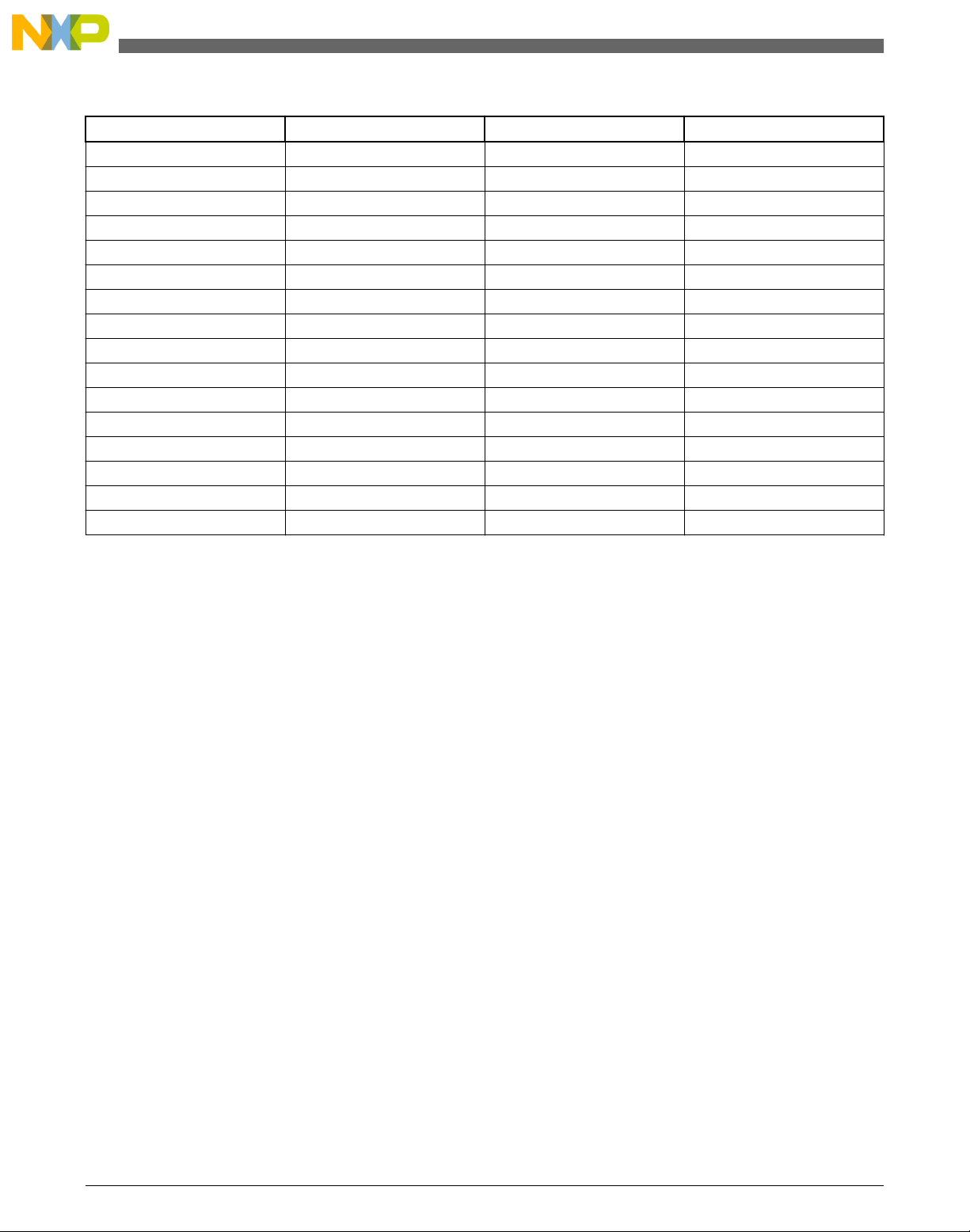
Low voltage detect (LVD) system
Table 3-1. Low power mode behavior (continued)
Mode Run Wait Stop3
RAM On Standby Standby
ADC On On Optional on
ACMP On On Optional on
TSI On On Optional on
I/O On On States held
SCI On On Standby
SPI On On Standby
IIC On On Standby
FTM On On Standby
MTIM On On Standby
WDOG On On Optional on
DBG On On Standby
IPC On On Standby
CRC On On Standby
RTC On On Optional on
LVD On On Optional on
3.3 Low voltage detect (LVD) system
This device includes a system to protect against low voltage conditions in order to protect
memory contents and control MCU system states during supply voltage variations. This
system consists of a power-on reset (POR) circuit and an LVD circuit with a user
selectable trip voltage, either high (V
when SPMSC1[LVDE] is set and the trip voltage is selected by SPMSC2[LVDV]. The
LVD is disabled upon entering the stop modes unless the SPMSC1[LVDSE] bit is set or
active BDM enabled (BDCSCR[ENBDM]=1). If SPMSC1[LVDSE] and
SPMSC1[LVDE] are both set, the current consumption in stop3 with the LVD enabled
will be greater.
LVDH
) or low (V
). The LVD circuit is enabled
LVDL
MC9S08PT60 Reference Manual, Rev. 4, 08/2014
58 Freescale Semiconductor, Inc.
Page 59
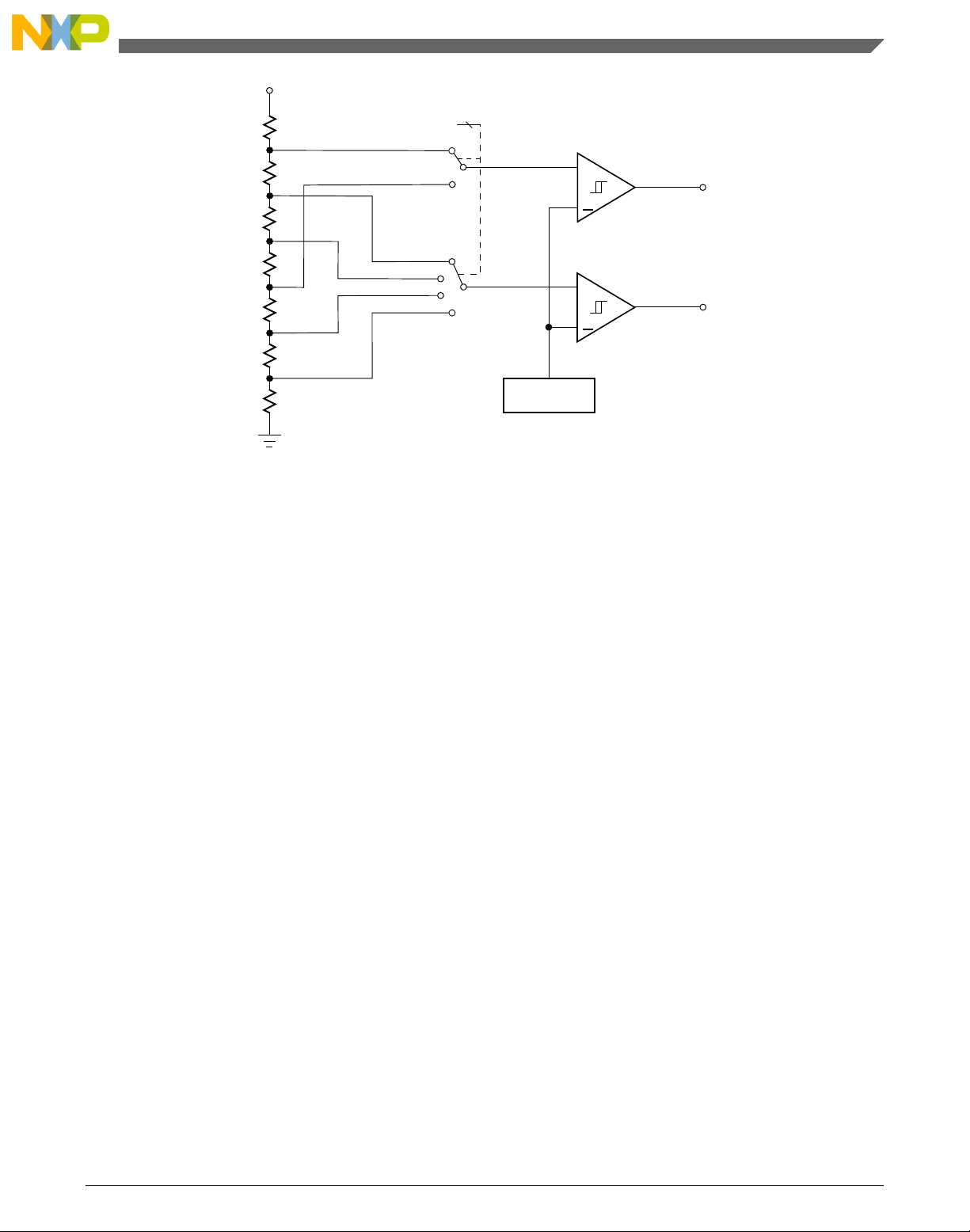
Bandgap
+
vD
D
v
ss
v
BG
R
1
R
7
LVDV:LVDWV
LVD0
LVD1
LVD
+
LVW
LVW0
LVW1
LVW2
LVW3
Chapter 3 Power management
Figure 3-1. Low voltage detect (LVD) block diagram
3.3.1
Power-on reset (POR) operation
When power is initially applied to the MCU, or when the supply voltage drops below the
V
LVD circuit will hold the chip in reset until the supply has risen above the V
level, the POR circuit will cause a reset condition. As the supply voltage rises, the
POR
LVDL
level.
Both the SRS[POR] and SRS[LVD] are set following a POR.
3.3.2
LVD reset operation
The LVD can be configured to generate a reset upon detection of a low voltage condition
by setting SPMSC1[LVDRE] to 1. After an LVD reset has occurred, the LVD system
will hold the MCU in reset until the supply voltage has risen above the level determined
by LVDV. The SRS[LVD] bit is set following either an LVD reset or POR.
3.3.3
Low-voltage warning (LVW)
The LVD system has a low voltage warning flag to indicate that the supply voltage is
approaching the LVD voltage. When a low voltage condition is detected and the LVD
circuit is configured for interrupt operation (SPMSC1[LVDE] set, SPMSC1[LVWIE]
set), SPMSC1[LVWF] will be set and LVW interrupt will occur. There are four userselectable trip voltages for the LVW upon each LVDV configuration. The trip voltage is
selected by SPMSC2[LVWV].
MC9S08PT60 Reference Manual, Rev. 4, 08/2014
Freescale Semiconductor, Inc. 59
Page 60
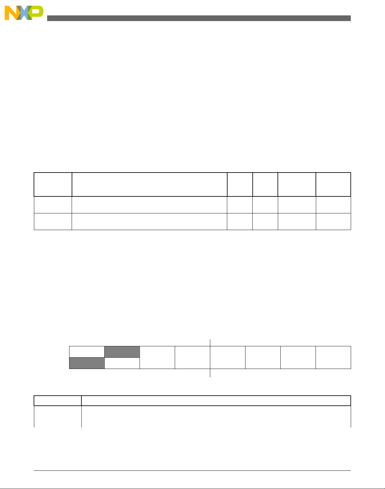
Bandgap reference
3.4 Bandgap reference
This device includes an on-chip bandgap reference (≈1.2V) connected to ADC channel
and ACMP. The bandgap reference voltage will not drop under the full operating voltage
even when the operating voltage is falling. This reference voltage acts as an ideal
reference voltage for accurate measurements.
3.5 Power management control bits and registers
PMC memory map
Absolute
address
(hex)
3040
3041
Register name
System Power Management Status and Control 1 Register
(PMC_SPMSC1)
System Power Management Status and Control 2 Register
(PMC_SPMSC2)
Width
(in bits)
Access Reset value
8 R/W 1Ch 3.5.1/60
8 R/W 00h 3.5.2/62
Section/
page
3.5.1 System Power Management Status and Control 1 Register
(PMC_SPMSC1)
This high page register contains status and control bits to support the low-voltage
detection function, and to enable the bandgap voltage reference for use by the ADC
module. This register should be written during the user's reset initialization program to
set the desired controls, even if the desired settings are the same as the reset settings.
Address:
3040h base + 0h offset = 3040h
Bit 7 6 5 4 3 2 1 0
Read LVWF 0
Write LVWACK
Reset
0 0 0 1 1 1 0 0
LVWIE LVDRE LVDSE LVDE BGBDS BGBE
PMC_SPMSC1 field descriptions
Field Description
7
LVWF
60 Freescale Semiconductor, Inc.
Low-Voltage Warning Flag
The LVWF bit indicates the low-voltage warning status.
Table continues on the next page...
MC9S08PT60 Reference Manual, Rev. 4, 08/2014
Page 61

PMC_SPMSC1 field descriptions (continued)
Field Description
6
LVWACK
5
LVWIE
4
LVDRE
NOTE:
0 Low-voltage warning is not present.
1 Low-voltage warning is present or was present.
Low-Voltage Warning Acknowledge
If LVWF = 1, a low-voltage condition has occurred. To acknowledge this low-voltage warning, write 1 to
LVWACK, which automatically clears LVWF to 0 if the low-voltage warning is no longer present.
Low-Voltage Warning Interrupt Enable
This bit enables hardware interrupt requests for LVWF.
0 Hardware interrupt disabled (use polling).
1 Request a hardware interrupt when LVWF = 1.
Low-Voltage Detect Reset Enable
This write-once bit enables LVD events to generate a hardware reset (provided LVDE = 1).
LVWF will be set in the case when V
is already below V
. LVWF bit may be 1 after power on reset, therefore, to use LVW interrupt
LVW
transitions below the trip point or after reset and V
Supply
function, before enabling LVWIE, LVWF must be cleared by writing LVWACK first.
Chapter 3 Power management
Supply
3
LVDSE
2
LVDE
1
BGBDS
0
BGBE
NOTE:
This bit can be written only one time after reset. Additional writes are ignored.
0 LVD events do not generate hardware resets.
1 Force an MCU reset when an enabled low-voltage detect event occurs.
Low-Voltage Detect Stop Enable
Provided LVDE = 1, this read/write bit determines whether the low-voltage detect function operates when
the MCU is in stop mode.
0 Low-voltage detect disabled during stop mode.
1 Low-voltage detect enabled during stop mode.
Low-Voltage Detect Enable
This write-once bit enables low-voltage detect logic and qualifies the operation of other bits in this register.
NOTE:
This bit can be written only one time after reset. Additional writes are ignored.
0 LVD logic disabled.
1 LVD logic enabled.
Bandgap Buffer Drive Select
This bit is used to select the high drive mode of the bandgap buffer.
0 Bandgap buffer enabled in low drive mode if BGBE = 1.
1 Bandgap buffer enabled in high drive mode if BGBE = 1.
Bandgap Buffer Enable
This bit enables an internal buffer for the bandgap voltage reference for use by the ADC module on one of
its internal channels.
0 Bandgap buffer disabled.
1 Bandgap buffer enabled.
MC9S08PT60 Reference Manual, Rev. 4, 08/2014
Freescale Semiconductor, Inc. 61
Page 62

Power management control bits and registers
3.5.2 System Power Management Status and Control 2 Register
(PMC_SPMSC2)
This register is used to report the status of the low-voltage warning function, and to
configure the stop mode behavior of the MCU. This register should be written during the
user's reset initialization program to set the desired controls, even if the desired settings
are the same as the reset settings.
Address: 3040h base + 1h offset = 3041h
Bit 7 6 5 4 3 2 1 0
Read 0
Write
Reset
0 0 0 0 0 0 0 0
LVDV LVWV
PMC_SPMSC2 field descriptions
Field Description
7
Reserved
6
LVDV
This field is reserved.
This read-only field is reserved and always has the value 0.
Low-Voltage Detect Voltage Select
This write-once bit selects the low-voltage detect (LVD) trip point setting. See data sheet for details.
0
0 Low trip point selected (V
1 High trip point selected (V
5–4
LVWV
Reserved This field is reserved.
Low-Voltage Warning Voltage Select
This bit selects the low-voltage warning (LVW) trip point voltage. See data sheet for details.
00 Low trip point selected (V
01 Middle 1 trip point selected (V
10 Middle 2 trip point selected (V
11 High trip point selected (V
This read-only field is reserved and always has the value 0.
LVD
LVD
LVW
LVW
= V
= V
= V
= V
LVDL
LVW
LVW
LVDH
LVW1
= V
= V
LVW4
).
).
).
LVW2
LVW3
).
).
).
MC9S08PT60 Reference Manual, Rev. 4, 08/2014
62 Freescale Semiconductor, Inc.
Page 63

Chapter 4
Memory map
4.1 Memory map
The HCS08 core processor can address 64 KB of memory space. The memory map,
shown in the following figure, includes:
• User flash memory (flash)
• MC9S08PT60: 60,864 bytes; 119 pages of 512 bytes each
• MC9S08PT32: 32,768 bytes; 64 pages of 512 bytes each
• Random-access memory (RAM)
• MC9S08PT60: 4,096 bytes
• MC9S08PT32: 4,096 bytes
• Electrically erasable programmable read-only memory (EEPROM)
• MC9S08PT60: 256 bytes; 128 pages of 2 bytes each
• MC9S08PT32: 256 bytes; 128 pages of 2 bytes each
• Direct-page registers (0x0000 through 0x003F)
• High-page registers (0x3000 through 0x30FF)
MC9S08PT60 Reference Manual, Rev. 4, 08/2014
Freescale Semiconductor, Inc. 63
Page 64
52,736B FLASH
32,768B FLASH
VECTOR TABLE
0xFFAF
0xFFB0
0xFFFF
0x8000
0x31FF
0x3100
0x30FF
0x3000
0x103F
0x0040
0x0000
0x003F
0x0000
0x003F
0x0040
0x103F
0x1040
0x2FFF
0x3000
0x30FF
0x3100
0x31FF
0x3200
4096 BYTES RAM
DIRECT PAGE REGISTERS
8,128 BYTES FLASH
HIGH PAGE REGISTERS
256 BYTES EEPROM
VECTOR TABLE
0xFFAF
0xFFB0
0xFFFF
DIRECT PAGE REGISTERS
RAM 4,096 BYTES
HIGH PAGE REGISTERS
256 BYTES EEPROM
UNIMPLEMENTED
UNIMPLEMENTED
MC9S08PT60
MC9S08PT32
Reset and interrupt vector assignments
Figure 4-1. Memory map
4.2
Reset and interrupt vector assignments
The following table shows address assignments for reset and interrupt vectors. The vector
names shown in this table are the labels used in the Freescale-provided header files for
the device.
Table 4-1. Reset and interrupt vectors
Address
(high/low)
0xFFB0:FFB1 NVM Vnvm
0xFFB2:FFB3 KBI1 Vkbi1
0xFFB4:FFB5 KBI0 Vkbi0
0xFFB6:FFB7 TSI Vtsi
0xFFB8:FFB9 RTC Vrtc
0xFFBA:FFBB IIC Viic
0xFFBC:FFBD SPI1 Vspi1
0xFEBE:FFBF SPI0 Vspi0
0xFFC0:FFC1 SCI2 transmit Vsci2txd
Vector Vector name
Table continues on the next page...
MC9S08PT60 Reference Manual, Rev. 4, 08/2014
64 Freescale Semiconductor, Inc.
Page 65

Table 4-1. Reset and interrupt vectors (continued)
Chapter 4 Memory map
Address
(high/low)
0xFFC2:FFC3 SCI2 receive Vsci2rxd
0xFFC4:FFC5 SCI2 error Vsci2err
0xFFC6:FFC7 SCI1 transmit Vsci1txd
0xFFC8:FFC9 SCI1 receive Vsci1rxd
0xFFCA:FFCB SCI1 error Vsci1err
0xFFCC:FFCD SCI0 transmit Vsci0txd
0xFFCE:FFCF SCI0 receive Vsci0rxd
0xFFD0:FFD1 SCI0 error Vsci0err
0xFFD2:FFD3 ADC Vadc
0xFFD4:FFD5 ACMP Vacmp
0xFFD6:FFD7 MTIM1 Vmtim1
0xFFD8:FFD9 MTIM0 Vmtim0
0xFFDA:FFDB FTM0 overflow Vftm0ovf
0xFFDC:FFDD FTM0 channel 1 Vftm0ch1
0xFFDE:FFDF FTM0 channel 0 Vftm0ch0
0xFFE0:FFE1 FTM1 overflow Vftm1ovf
0xFFE2:FFE3 FTM1 channel 1 Vftm1ch1
0xFFE4:FFE5 FTM1 channel 0 Vftm1ch0
0xFFE6:FFE7 FTM2 overflow Vftm2ovf
0xFFE8:FFE9 FTM2 channel 5 Vftm2ch5
0xFFEA:FFEB FTM2 channel 4 Vftm2ch4
0xFFEC:FFED FTM2 channel 3 Vftm2ch3
0xFFEE:FFEF FTM2 channel 2 Vftm2ch2
0xFFF0:FFF1 FTM2 channel 1 Vftm2ch1
0xFFF2:FFF3 FTM2 channel 0 Vftm2ch0
0xFFF4:FFF5 FTM2 fault Vftm2flt
0xFFF6:FFF7 Clock loss of lock Vclk
0xFFF8:FFF9 Low voltage warning Vlvw
0xFFFA:FFFB IRQ or Watchdog Virq or Vwdog
0xFFFC:FFFD SWI Vswi
0xFFFE:FFFF Reset Vreset
Vector Vector name
4.3 Register addresses and bit assignments
The register definitions vary in different memory sizes. The register addresses of unused
peripherals are reserved. The following table shows the register availability of the
devices.
MC9S08PT60 Reference Manual, Rev. 4, 08/2014
Freescale Semiconductor, Inc. 65
Page 66

Register addresses and bit assignments
Table 4-2. Peripheral registers availability
Address Bytes Peripheral registers
0x0000—0x0007 8 Port data
0x0008—0x000F 8 TSI
0x0010—0x0017 8 ADC
0x0018—0x001B 4 MTIM0
0x001C—0x001F 4 MTIM1
0x0020—0x002A 11 FTM0
0x002C—0x002F 4 ACMP
0x0030—0x003A 11 FTM1
0x003B—0x003B 1 IRQ
0x003C—0x003C 1 KBI0
0x003D—0x003D 1 KBI1
0x003E—0x003F 2 IPC
0x3000—0x300B 12 SIM
0x300C—0x300F 4 SCG
0x3010—0x301F 16 DBG
0x3020—0x302C 13 NVM
0x3030—0x3037 8 WDOG
0x3038—0x303E 7 ICS, XOSC
0x3040—0x3041 2 PMC
0x304A—0x304B 2 SYS
0x3050—0x3059 10 IPC
0x3060—0x3068 9 CRC
0x306A—0x306F 6 RTC
0x3070—0x307B 12 IIC
0x307C—0x307D 2 KBI0
0x307E—0x307F 2 KBI1
0x3080—0x3087 8 SCI0
0x3088—0x308F 8 SCI1
0x3090—0x3097 8 SCI2
0x3098—0x309F 8 SPI0
0x30A0—0x30A9 10 SPI1
0x30AC—0x30AD 2 ADC
0x30AF—0x30AF 1 Port high drive enable
0x30B0—0x30B7 8 Port output enable
0x30B8—0x30BF 8 Port input enable
0x30C0—0x30EA 43 FTM2
0x30EC—0x30EF 4 Port filter
0x30F0—0x30F7 8 Port pullup
0x30F8—0x30FF 8 SYS
MC9S08PT60 Reference Manual, Rev. 4, 08/2014
66 Freescale Semiconductor, Inc.
Page 67
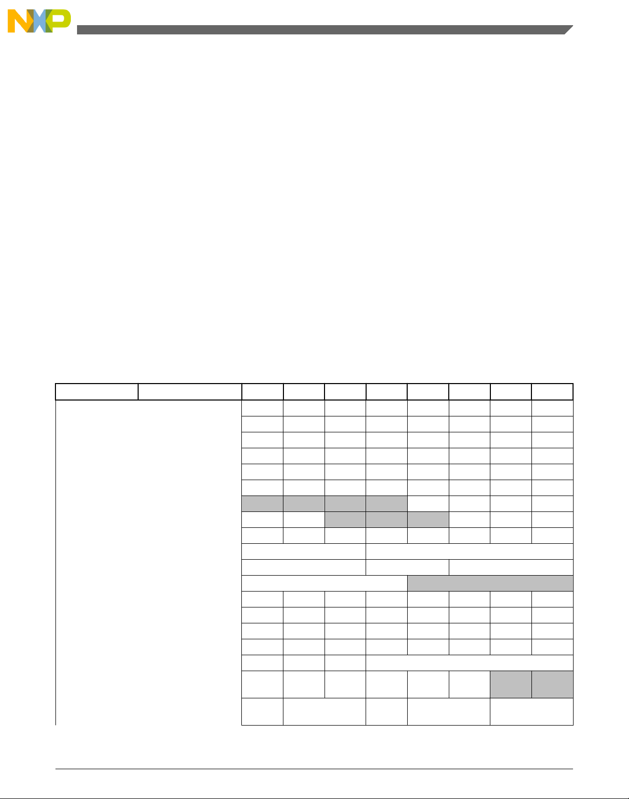
Chapter 4 Memory map
The registers in the devices are divided into two groups:
• Direct-page registers are located in the first 64 locations in the memory map, so they
can be accessed with efficient direct addressing mode instructions.
• High-page registers are used much less often, so they are located above 0x3000 in
the memory map. This leaves room in the direct page for more frequently used
registers and variables.
Direct-page registers can be accessed with efficient direct addressing mode instructions.
Bit manipulation instructions can be used to access any bit in a direct-page register.
The direct page registers can use the more efficient direct addressing mode, which
requires only the lower byte of the address.
The following tables are summaries of all user-accessible direct-page and high-page
registers and control bits. Cells that are not associated with named bits are shaded. A
shaded cell with a 0 indicates this unused bit always reads as a 0; and a shaded cell with a
1 indicates this unused bit always reads as a 1. Shaded cells with dashes indicate unused
or reserved bit locations that could read as 1s or 0s.
Table 4-3. Direct-page register allocation
Address Register name Bit 7 6 5 4 3 2 1 Bit 0
0x0000 PORT_PTAD
0x0001 PORT_PTBD PTBD7 PTBD6 PTBD5 PTBD4 PTBD3 PTBD2 PTBD1 PTBD0
0x0002 PORT_PTCD PTCD7 PTCD6 PTCD5 PTCD4 PTCD3 PTCD2 PTCD1 PTCD0
0x0003 PORT_PTDD PTDD7 PTDD6 PTDD5 PTDD4 PTDD3 PTDD2 PTDD1 PTDD0
0x0004 PORT_PTED PTED7 PTED6 PTED5 PTED4 PTED3 PTED2 PTED1 PTED0
0x0005 PORT_PTFD PTFD7 PTFD6 PTFD5 PTFD4 PTFD3 PTFD2 PTFD1 PTFD0
0x0006 PORT_PTGD — — — — PTGD3 PTGD2 PTGD1 PTGD0
0x0007 PORT_PTHD PTHD7 PTHD6 — — — PTHD2 PTHD1 PTHD0
0x0008 TSI_CS0 TSIEN TSIIEN STPE STM SCNIP EOSF CURSW SWTS
0x0009 TSI_CS1 PS NSCN
0x000A TSI_CS2 REFCHRG DVOLT EXTCHRG
0x000B TSI_CS3 TSICH —
0x000C TSI_PEN0 PEN7 PEN6 PEN5 PEN4 PEN3 PEN2 PEN1 PEN0
0x000D TSI_PEN1 PEN15 PEN14 PEN13 PEN12 PEN11 PEN10 PEN9 PEN8
0x000E TSI_CNTH Bit 15 14 13 12 11 10 9 Bit 8
0x000F TSI_CNTL Bit 7 6 5 4 3 2 1 Bit 0
0x0010 ADC_SC1 COCO AIEN ADCO ADCH
0x0011 ADC_SC2 ADACT ADTRG ACFE ACFGT
0x0012 ADC_SC3 ADLPC ADIV
PTAD7 PTAD6 PTAD5 PTAD4 PTAD3 PTAD2 PTAD1 PTAD0
FEMPT
ADLSM
P
FFULL — —
Y
MODE ADICLK
Table continues on the next page...
MC9S08PT60 Reference Manual, Rev. 4, 08/2014
Freescale Semiconductor, Inc. 67
Page 68
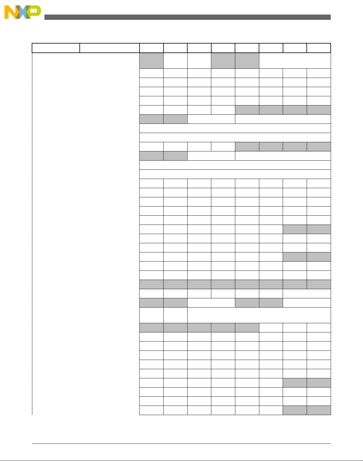
Register addresses and bit assignments
Table 4-3. Direct-page register allocation (continued)
Address Register name Bit 7 6 5 4 3 2 1 Bit 0
ASCAN
0x0013 ADC_SC4
0x0014 ADC_RH Bit 15 14 13 12 11 10 9 Bit 8
0x0015 ADC_RL Bit 7 6 5 4 3 2 1 Bit 0
0x0016 ADC_CVH Bit 15 14 13 12 11 10 9 Bit 8
0x0017 ADC_CVL Bit 7 6 5 4 3 2 1 Bit 0
0x0018 MTIM0_SC TOF TOIE TRST TSTP — — — —
0x0019 MTIM0_CLK — — CLKS PS
0x001A MTIM0_CNT COUNT
0x001B MTIM0_MOD MOD
0x001C MTIM1_SC TOF TOIE TRST TSTP — — — —
0x001D MTIM1_CLK — — CLKS PS
0x001E MTIM1_CNT COUNT
0x001F MTIM1_MOD MOD
0x0020 FTM0_SC TOF TOIE CPWMS CLKS1 CLKS0 PS2 PS1 PS0
0x0021 FTM0_CNTH Bit 15 14 13 12 11 10 9 Bit 8
0x0022 FTM0_CNTL Bit 7 6 5 4 3 2 1 Bit 0
0x0023 FTM0_MODH Bit 15 14 13 12 11 10 9 Bit 8
0x0024 FTM0_MODL Bit 7 6 5 4 3 2 1 Bit 0
0x0025 FTM0_C0SC CHF CHIE MSB MSA ELSB ELSA — —
0x0026 FTM0_C0VH Bit 15 14 13 12 11 10 9 Bit 8
0x0027 FTM0_C0VL Bit 7 6 5 4 3 2 1 Bit 0
0x0028 FTM0_C1SC CHF CHIE MSB MSA ELSB ELSA — —
0x0029 FTM0_C1VH Bit 15 14 13 12 11 10 9 Bit 8
0x002A FTM0_C1VL Bit 7 6 5 4 3 2 1 Bit 0
0x002B Reserved — — — — — — — —
0x002C ACMP_CS ACE HYST ACF ACIE ACO ACOPE ACMOD
0x002D ACMP_C0 — — ACPSEL — — ACNSEL
0x002E ACMP_C1 DACEN
0x002F ACMP_C2 — — — — — ACIPE2 ACIPE1 ACIPE0
0x0030 FTM1_SC TOF TOIE CPWMS CLKS1 CLKS0 PS2 PS1 PS0
0x0031 FTM1_CNTH Bit 15 14 13 12 11 10 9 Bit 8
0x0032 FTM1_CNTL Bit 7 6 5 4 3 2 1 Bit 0
0x0033 FTM1_MODH Bit 15 14 13 12 11 10 9 Bit 8
0x0034 FTM1_MODL Bit 7 6 5 4 3 2 1 Bit 0
0x0035 FTM1_C0SC CHF CHIE MSB MSA ELSB ELSA — —
0x0036 FTM1_C0VH Bit 15 14 13 12 11 10 9 Bit 8
0x0037 FTM1_C0VL Bit 7 6 5 4 3 2 1 Bit 0
0x0038 FTM1_C1SC CHF CHIE MSB MSA ELSB ELSA — —
—
DACRE
ACFSEL — — AFDEP
E
F
DACVAL
Table continues on the next page...
MC9S08PT60 Reference Manual, Rev. 4, 08/2014
68 Freescale Semiconductor, Inc.
Page 69
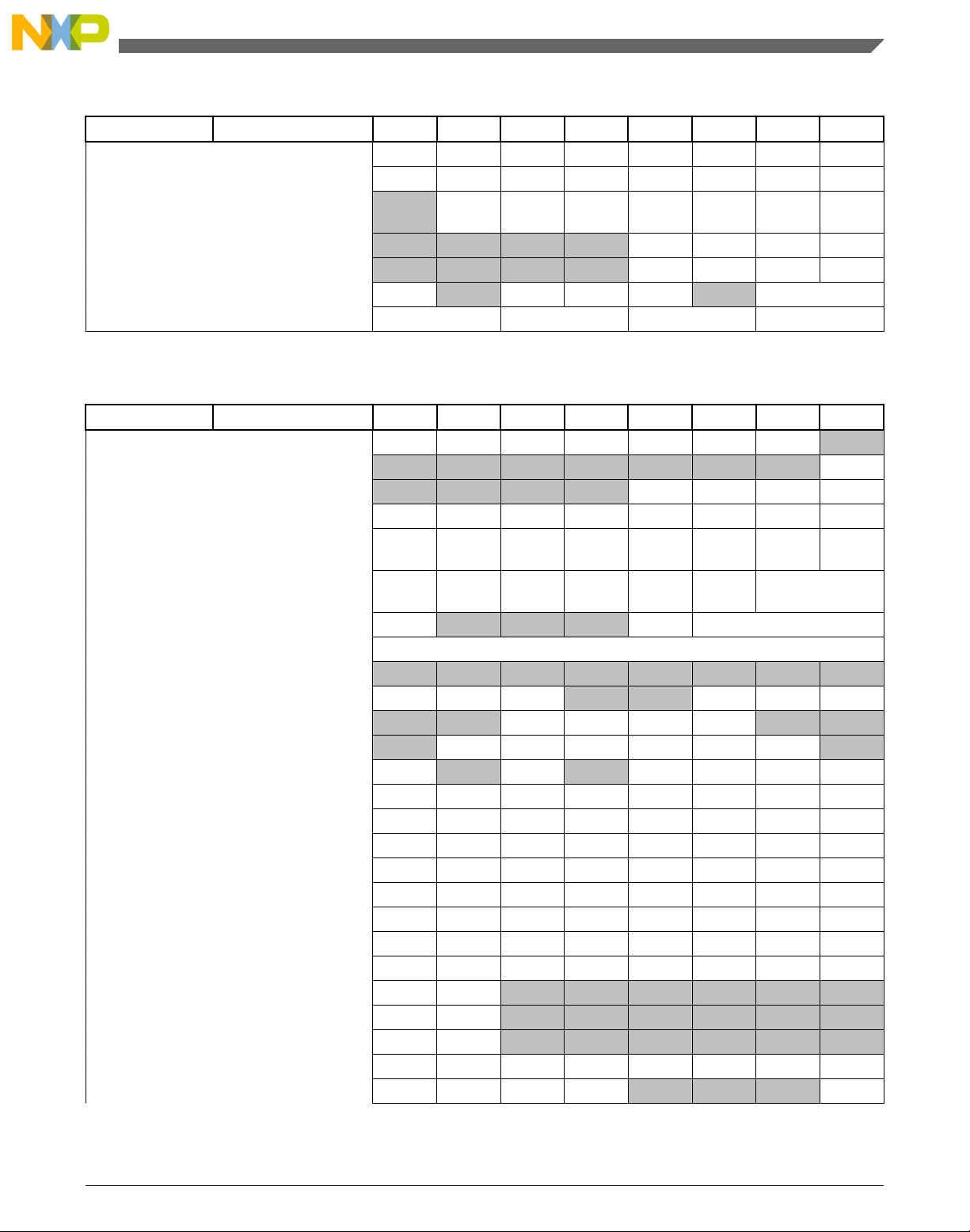
Chapter 4 Memory map
Table 4-3. Direct-page register allocation (continued)
Address Register name Bit 7 6 5 4 3 2 1 Bit 0
0x0039 FTM1_C1VH
0x003A FTM1_C1VL Bit 7 6 5 4 3 2 1 Bit 0
0x003B IRQ_SC — IRQPDD IRQEDG IRQPE IRQF IRQACK IRQIE
0x003C KBI0_SC — — — — KBF KBACK KBIE KBMOD
0x003D KBI1_SC — — — — KBF KBACK KBIE KBMOD
0x003E IPC_SC IPCE — PSE PSF PULIPM — IPM
0x003F IPC_IPMPS
Bit 15 14 13 12 11 10 9 Bit 8
IRQMO
D
IPM3 IPM2 IPM1 IPM0
Table 4-4. High-page register allocation
Address Register name Bit 7 6 5 4 3 2 1 Bit 0
0x3000 SYS_SRS
0x3001 SYS_SBDFR — — — — — — — BDFR
0x3002 SYS_SDIDH — — — — ID11 ID10 ID9 ID8
0x3003 SYS_SDIDL ID7 ID6 ID5 ID4 ID3 ID2 ID1 ID0
0x3004 SYS_SOPT1 SCI0PS SPI0PS IICPS FTM2PS
0x3005 SYS_SOPT2 TXDME
0x3006 SYS_SOPT3 DLYACT — — — CLKOE BUSREF
0x3007 SYS_SOPT4 DELAY
0x3008-0x300B Reserved — — — — — — — —
0x300C SCG_C1 FTM2 FTM1 FTM0 — — MTIM1 MTIM0 RTC
0x300D SCG_C2 — — DBG NVM IPC CRC — —
0x300E SCG_C3 — SCI2 SCI1 SCI0 SPI1 SPI0 IIC —
0x300F SCG_C4 ACMP — ADC — IRQ TSI KBI1 KBI0
0x3010 DBG_CAH Bit 15 14 13 12 11 10 9 Bit 8
0x3011 DBG_CAL Bit 7 6 5 4 3 2 1 Bit 0
0x3012 DBG_CBH Bit 15 14 13 12 11 10 9 Bit 8
0x3013 DBG_CBL Bit 7 6 5 4 3 2 1 Bit 0
0x3014 DBG_CCH Bit 15 14 13 12 11 10 9 Bit 8
0x3015 DBG_CCL Bit 7 6 5 4 3 2 1 Bit 0
0x3016 DBG_FH Bit 15 14 13 12 11 10 9 Bit 8
0x3017 DBG_FL Bit 7 6 5 4 3 2 1 Bit 0
0x3018 DBG_CAX RWAEN RWA — — — — — —
0x3019 DBG_CBX RWBEN RWB — — — — — —
0x301A DBG_CCX RWCEN RWC — — — — — —
0x301B DBG_FX PPACC — — — — — — Bit 16
0x301C DBG_C DBGEN ARM TAG BRKEN — — — LOOP1
POR PIN WDOG ILOP ILAD LOC LVD —
FTMSY
NC
BKGDP
RXDFE RXDCE ACIC RTCC ADHWTS
RSTPE FWAKE STOPE
E
Table continues on the next page...
MC9S08PT60 Reference Manual, Rev. 4, 08/2014
Freescale Semiconductor, Inc. 69
Page 70
Register addresses and bit assignments
Table 4-4. High-page register allocation (continued)
Address Register name Bit 7 6 5 4 3 2 1 Bit 0
0x301D DBG_T
0x301E DBG_S AF BF CF — — — — ARMF
0x301F DBG_CNT — — — — CNT
0x3020 NVM_FCLKDIV FDIVLD
0x3021 NVM_FSEC KEYEN1 KEYEN0 1 1 1 1 SEC1 SEC0
0x3022 NVM_FCCOBIX — — — — —
0x3023 Reserved — — — — — — — —
0x3024 NVM_FCNFG CCIE — — IGNSF — — FDFD FSFD
0x3025 NVM_FERCNFG — — — — — — DFDIE SFDIE
0x3026 NVM_FSTAT CCIF —
0x3027 NVM_FERSTAT — — — — — — DFDIF SFDIF
0x3028 NVM_FPROT FPOEN — FPHDIS FPHS1 FPHS0 FPLDIS FPLS1 FPLS0
0x3029 NVM_EEPROT
0x302A NVM_FCCOBHI
0x302B NVM_FCCOBLO CCOB7 CCOB6 CCOB5 CCOB4 CCOB3 CCOB2 CCOB1 CCOB0
0x302C NVM_FOPT NV7 NV6 NV5 NV4 NV3 NV2 NV1 NV0
0x302D-0x302F Reserved — — — — — — — —
0x3030 WDOG_CS1 EN INT
0x3031 WDOG_CS2 WIN FLG — PRES — — CLK
0x3032 WDOG_CNTH Bit 15 14 13 12 11 10 9 Bit 8
0x3033 WDOG_CNTL Bit 7 6 5 4 3 2 1 Bit 0
0x3034 WDOG_TOVALH Bit 15 14 13 12 11 10 9 Bit 8
0x3035 WDOG_TOVALL Bit 7 6 5 4 3 2 1 Bit 0
0x3036 WDOG_WINH Bit 15 14 13 12 11 10 9 Bit 8
0x3037 WDOG_WINL Bit 7 6 5 4 3 2 1 Bit 0
0x3038 ICS_C1 CLKS RDIV IREFS
0x3039 ICS_C2 BDIV LP — — — —
0x303A ICS_C3 SCTRIM
0x303B ICS_C4 LOLIE — CME — — — —
0x303C ICS_S LOLS LOCK — IREFST CLKST — —
0x303D Reserved — — — — — — — —
0x303E ICS_OSCSC OSCEN —
TRGSE
DPOPE
CCOB15CCOB14CCOB13CCOB12CCOB11CCOB1
BEGIN — — TRG
L
FDIVLC
K
N
— — — — DPS2 DPS1 DPS0
FDIV5 FDIV4 FDIV3 FDIV2 FDIV1 FDIV0
ACCER
R
UPDAT
E
OSCST
EN
FPVIOL
OSCOS — RANGE HGO
MGBUS
Y
TST DBG WAIT STOP
CCOBIX2CCOBIX1CCOBIX
MGSTAT1MGSTA
—
CCOB9 CCOB8
0
IRCLKENIREFST
0
T0
EN
SCFTRI
M
OSCINI
T
Table continues on the next page...
MC9S08PT60 Reference Manual, Rev. 4, 08/2014
70 Freescale Semiconductor, Inc.
Page 71
Chapter 4 Memory map
Table 4-4. High-page register allocation (continued)
Address Register name Bit 7 6 5 4 3 2 1 Bit 0
0x303F Reserved
0x3040 PMC_SPMSC1 LVWF
0x3041 PMC_SPMSC2 — LVDV LVWV — — — —
0x3042-0x3049 Reserved — — — — — — — —
0x304A SYS_ILLAH Bit 15 14 13 12 11 19 9 Bit 8
0x304B SYS_ILLAL Bit 7 6 5 4 3 2 1 Bit 0
0x304C-0x304F Reserved — — — — — — — —
0x3050 IPC_ILRS0 ILR3 ILR2 ILR1 ILR0
0x3051 IPC_ILRS1 ILR7 ILR6 ILR5 ILR4
0x3052 IPC_ILRS2 ILR11 ILR10 ILR9 ILR8
0x3053 IPC_ILRS3 ILR15 ILR14 ILR13 ILR12
0x3054 IPC_ILRS4 ILR19 ILR18 ILR17 ILR16
0x3055 IPC_ILRS5 ILR23 ILR22 ILR21 ILR20
0x3056 IPC_ILRS6 ILR27 ILR26 ILR25 ILR24
0x3057 IPC_ILRS7 ILR31 ILR30 ILR29 ILR28
0x3058 IPC_ILRS8 ILR35 ILR34 ILR33 ILR32
0x3059 IPC_ILRS9 ILR39 ILR38 ILR37 ILR36
0x305A-0x305F Reserved — — — — — — — —
0x3060 CRC_D0 Bit 31 30 29 28 27 26 25 Bit 24
0x3061 CRC_D1 Bit 23 22 21 20 19 18 17 Bit 16
0x3062 CRC_D2 Bit 15 14 13 12 11 10 9 Bit 8
0x3063 CRC_D3 Bit 7 6 5 4 3 2 1 Bit 0
0x3064 CRC_P0 Bit 31 30 29 28 27 26 25 Bit 24
0x3065 CRC_P1 Bit 23 22 21 20 19 18 17 Bit 16
0x3066 CRC_P2 Bit 15 14 13 12 11 10 9 Bit 8
0x3067 CRC_P3 Bit 7 6 5 4 3 2 1 Bit 0
0x3068 CRC_CTRL TOT TOTR 0 FXOR WAS TCRC
0x3069 Reserved — — — — — — — —
0x306A RTC_SC1 RTIF RTIE — RTCO — — — —
0x306B RTC_SC2 RTCLKS — — — RTCPS
0x306C RTC_MODH MODH
0x306D RTC_MODL MODL
0x306E RTC_CNTH CNTH
0x306F RTC_CNTL CNTL
0x3070 I2C_A1 AD7 AD6 AD5 AD4 AD3 AD2 AD1 0
0x3071 I2C_F MULT ICR
0x3072 I2C_C1 IICEN IICIE MST TX TXAK RSTA WUEN —
0x3073 I2C_S TCF IAAS BUSY ARBL RAM SRW IICIF RXAK
0x3074 I2C_D DATA
— — — — — — — —
LVWAC
LVWIE LVDRE LVDSE LVDE BGBDS BGBE
K
Table continues on the next page...
MC9S08PT60 Reference Manual, Rev. 4, 08/2014
Freescale Semiconductor, Inc. 71
Page 72
Register addresses and bit assignments
Table 4-4. High-page register allocation (continued)
Address Register name Bit 7 6 5 4 3 2 1 Bit 0
0x3075 I2C_C2
0x3076 I2C_FLT — — — FLT4 FLT3 FLT2 FLT1 FLT0
0x3077 I2C_RA RAD —
0x3078 I2C_SMB FACK
0x3079 I2C_A2 SAD7 SAD6 SAD5 SAD4 SAD3 SAD2 SAD1 —
0x307A I2C_SLTH SSLT15 SSLT14 SSLT13 SSLT12 SSLT11 SSLT10 SSLT9 SSLT8
0x307B I2C_SLTL SSLT7 SSLT6 SSLT5 SSLT4 SSLT3' SSLT2 SSLT1 SSLT0
0x307C KBI0_PE KBIPE7 KBIPE6 KBIPE5 KBIPE4 KBIPE3 KBIPE2 KBIPE1 KBIPE0
0x307D KBI0_ES
0x307E KBI1_PE KBIPE7 KBIPE6 KBIPE5 KBIPE4 KBIPE3 KBIPE2 KBIPE1 KBIPE0
0x307F KBI1_ES
0x3080 SCI0_BDH LBKDIE
0x3081 SCI0_BDL SBR7 SBR6 SBR5 SBR4 SBR3 SBR2 SBR1 SBR0
0x3082 SCI0_C1 LOOPS
0x3083 SCI0_C2 TIE TCIE RIE ILIE TE RE RWU SBK
0x3084 SCI0_S1 TDRE TC RDRF IDLE OR NF FE PF
0x3085 SCI0_S2 LBKDIF
0x3086 SCI0_C3 R8 T8 TXDIR TXINV ORIE NEIE FEIE PEIE
0x3087 SCI0_D D7 D6 D5 D4 D3 D2 D1 D0
0x3088 SCI1_BDH LBKDIE
0x3089 SCI1_BDL SBR7 SBR6 SBR5 SBR4 SBR3 SBR2 SBR1 SBR0
0x308A SCI1_C1 LOOPS
0x308B SCI1_C2 TIE TCIE RIE ILIE TE RE RWU SBK
0x308C SCI1_S1 TDRE TC RDRF IDLE OR NF FE PF
0x308D SCI1_S2 LBKDIF
0x308E SCI1_C3 R8 T8 TXDIR TXINV ORIE NEIE FEIE PEIE
0x308F SCI1_D D7 D6 D5 D4 D3 D2 D1 D0
0x3090 SCI2_BDH LBKDIE
0x3091 SCI2_BDL SBR7 SBR6 SBR5 SBR4 SBR3 SBR2 SBR1 SBR0
0x3092 SCI2_C1 LOOPS
0x3093 SCI2_C2 TIE TCIE RIE ILIE TE RE RWU SBK
0x3094 SCI2_S1 TDRE TC RDRF IDLE OR NF FE PF
GCAEN ADEXT HDRS SBRC RMEN AD10 AD9 AD8
ALERTENSIICAE
KBEDG7KBEDG6KBEDG5KBEDG4KBEDG3KBEDG2KBEDG1KBEDG
KBEDG7KBEDG6KBEDG5KBEDG4KBEDG3KBEDG2KBEDG1KBEDG
RXEDGI
E
SCISWA
RXEDGI
F
RXEDGI
E
SCISWA
RXEDGI
F
RXEDGI
E
SCISWA
SBNS SBR12 SBR11 SBR10 SBR9 SBR8
RSRC M WAKE ILT PE PT
I
SBNS SBR12 SBR11 SBR10 SBR9 SBR8
RSRC M WAKE ILT PE PT
I
SBNS SBR12 SBR11 SBR10 SBR9 SBR8
RSRC M WAKE ILT PE PT
I
TCKSEL SLTF SHTF1 SHTF2
N
— RXINV RWUID BRK13 LBKDE RAF
— RXINV RWUID BRK13 LBKDE RAF
SHTF2I
E
0
0
Table continues on the next page...
MC9S08PT60 Reference Manual, Rev. 4, 08/2014
72 Freescale Semiconductor, Inc.
Page 73
Chapter 4 Memory map
Table 4-4. High-page register allocation (continued)
Address Register name Bit 7 6 5 4 3 2 1 Bit 0
0x3095 SCI2_S2
0x3096 SCI2_C3 R8 T8 TXDIR TXINV ORIE NEIE FEIE PEIE
0x3097 SCI2_D D7 D6 D5 D4 D3 D2 D1 D0
0x3098 SPI0_C1 SPIE SPE SPTIE MSTR CPOL CPHA SSOE LSBFE
0x3099 SPI0_C2 SPMIE — —
0x309A SPI0_BR — SPPR2 SPPR1 SPPR0 SPR3 SPR2 SPR1 SPR0
0x309B SPI0_S SPRF SPMF SPTEF MODF — — — —
0x309C Reserved — — — — — — — —
0x309D SPI0_D Bit 7 6 5 4 3 2 1 Bit 0
0x309E Reserved — — — — — — — —
0x309F SPI0_M Bit 7 6 5 4 3 2 1 Bit 0
0x30A0 SPI1_C1 SPIE SPE SPTIE MSTR CPOL CPHA SSOE LSBFE
0x30A1 SPI1_C2 SPMIE
0x30A2 SPI1_BR — SPPR2 SPPR1 SPPR0 SPR3 SPR2 SPR1 SPR0
0x30A3 SPI1_S SPRF SPMF SPTEF MODF
0x30A4 SPI1_DH Bit 15 14 13 12 11 10 9 Bit 8
0x30A5 SPI1_DL Bit 7 6 5 4 3 2 1 Bit 0
0x30A6 SPI1_MH Bit 15 14 13 12 11 10 9 Bit 8
0x30A7 SPI1_ML Bit 7 6 5 4 3 2 1 Bit 0
0x30A8 SPI1_C3 — —
0x30A9 SPI1_CI
0x30AA-0x30AB Reserved — — — — — — — —
0x30AC ADC_APCTL1 ADPC7 ADPC6 ADPC5 ADPC4 ADPC3 ADPC2 ADPC1 ADPC0
0x30AD ADC_APCTL2 ADPC15 ADPC14 ADPC13 ADPC12 ADPC11 ADPC10 ADPC9 ADPC8
0x30AE Reserved — — — — — — — —
0x30AF PORT_HDRVE PTH1 PTH0 PTE1 PTE0 PTD1 PTD0 PTB5 PTB4
0x30B0 PORT_PTAOE PTAOE7 PTAOE6 PTAOE5 PTAOE4 PTAOE3 PTAOE2 PTAOE1 PTAOE0
0x30B1 PORT_PTBOE PTBOE7 PTBOE6 PTBOE5 PTBOE4 PTBOE3 PTBOE2 PTBOE1 PTBOE0
0x30B2 PORT_PTCOE
0x30B3 PORT_PTDOE
0x30B4 PORT_PTEOE PTEOE7 PTEOE6 PTEOE5 PTEOE4 PTEOE3 PTEOE2 PTEOE1 PTEOE0
0x30B5 PORT_PTFOE PTFOE7 PTFOE6 PTFOE5 PTFOE4 PTFOE3 PTFOE2 PTFOE1 PTFOE0
LBKDIF
TXFERRRXFER
PTCOE7PTCOE6PTCOE5PTCOE4PTCOE3PTCOE2PTCOE1PTCOE
PTDOE7PTDOE6PTDOE5PTDOE4PTDOE3PTDOE2PTDOE1PTDOE
RXEDGI
F
SPIMOD
E
R
— RXINV RWUID BRK13 LBKDE RAF
MODFENBIDIRO
MODFENBIDIRO
—
TNEAR
EF_MA
TXFOF RXFOF
RNFULL
F_MARKINTCLR
RK
E
E
RNFULLFTNEAREFTXFULLFRFIFOE
TNEARIENRNFULL
TNEAR
EFCI
RNFULL
FCI
—
—
SPISWA
I
SPISWA
I
IEN
SPTEFC
I
SPC0
SPC0
FIFOMO
DE
SPRFCI
F
0
0
Table continues on the next page...
MC9S08PT60 Reference Manual, Rev. 4, 08/2014
Freescale Semiconductor, Inc. 73
Page 74
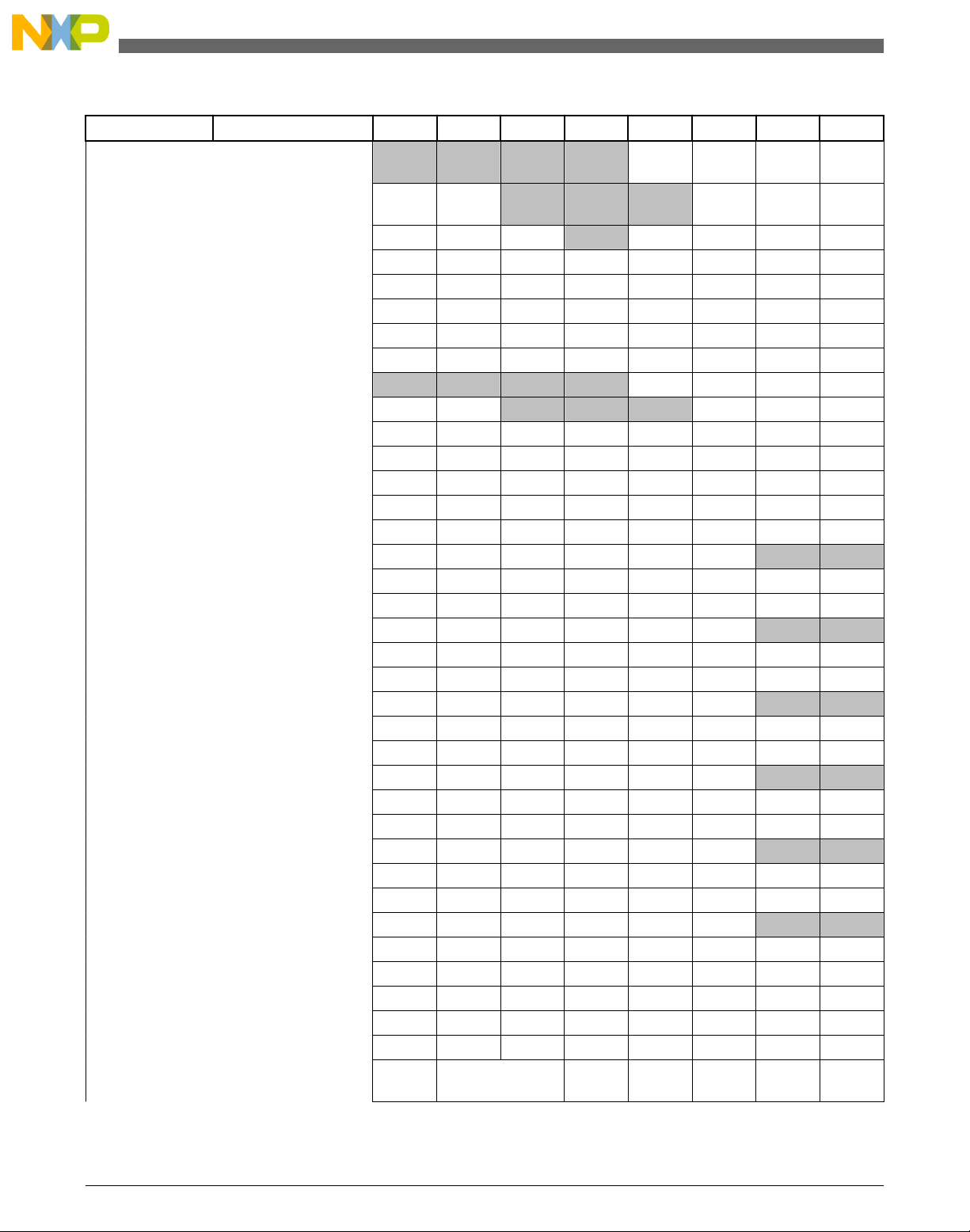
Register addresses and bit assignments
Table 4-4. High-page register allocation (continued)
Address Register name Bit 7 6 5 4 3 2 1 Bit 0
0x30B6 PORT_PTGOE
0x30B7 PORT_PTHOE
0x30B8 PORT_PTAIE PTAIE7 PTAIE6 PTAIE5 — PTAIE3 PTAIE2 PTAIE1 PTAIE0
0x30B9 PORT_PTBIE PTBIE7 PTBIE6 PTBIE5 PTBIE4 PTBIE3 PTBIE2 PTBIE1 PTBIE0
0x30BA PORT_PTCIE PTCIE7 PTCIE6 PTCIE5 PTCIE4 PTCIE3 PTCIE2 PTCIE1 PTCIE0
0x30BB PORT_PTDIE PTDIE7 PTDIE6 PTDIE5 PTDIE4 PTDIE3 PTDIE2 PTDIE1 PTDIE0
0x30BC PORT_PTEIE PTEIE7 PTEIE6 PTEIE5 PTEIE4 PTEIE3 PTEIE2 PTEIE1 PTEIE0
0x30BD PORT_PTFIE PTFIE7 PTFIE6 PTFIE5 PTFIE4 PTFIE3 PTFIE2 PTFIE1 PTFIE0
0x30BE PORT_PTGIE — — — — PTGIE3 PTGIE2 PTGIE1 PTGIE0
0x30BF PORT_PTHIE PTHIE7 PTHIE6 — — — PTHIE2 PTHIE1 PTHIE0
0x30C0 FTM2_SC TOF TOIE CPWMS CLKS1 CLKS0 PS2 PS1 PS0
0x30C1 FTM2_CNTH Bit 15 14 13 12 11 10 9 Bit 8
0x30C2 FTM2_CNTL Bit 7 6 5 4 3 2 1 Bit 0
0x30C3 FTM2_MODH Bit 15 14 13 12 11 10 9 Bit 8
0x30C4 FTM2_MODL Bit 7 6 5 4 3 2 1 Bit 0
0x30C5 FTM2_C0SC CHF CHIE MSB MSA ELSB ELSA — —
0x30C6 FTM2_C0VH Bit 15 14 13 12 11 10 9 Bit 8
0x30C7 FTM2_C0VL Bit 7 6 5 4 3 2 1 Bit 0
0x30C8 FTM2_C1SC CHF CHIE MSB MSA ELSB ELSA — —
0x30C9 FTM2_C1VH Bit 15 14 13 12 11 10 9 Bit 8
0x30CA FTM2_C1VL Bit 7 6 5 4 3 2 1 Bit 0
0x30CB FTM2_C2SC CHF CHIE MSB MSA ELSB ELSA — —
0x30CC FTM2_C2VH Bit 15 14 13 12 11 10 9 Bit 8
0x30CD FTM2_C2VL Bit 7 6 5 4 3 2 1 Bit 0
0x30CE FTM2_C3SC CHF CHIE MSB MSA ELSB ELSA — —
0x30CF FTM2_C3VH Bit 15 14 13 12 11 10 9 Bit 8
0x30D0 FTM2_C3VL Bit 7 6 5 4 3 2 1 Bit 0
0x30D1 FTM2_C4SC CHF CHIE MSB MSA ELSB ELSA — —
0x30D2 FTM2_C4VH Bit 15 14 13 12 11 10 9 Bit 8
0x30D3 FTM2_C4VL Bit 7 6 5 4 3 2 1 Bit 0
0x30D4 FTM2_C5SC CHF CHIE MSB MSA ELSB ELSA — —
0x30D5 FTM2_C5VH Bit 15 14 13 12 11 10 9 Bit 8
0x30D6 FTM2_C5VL Bit 7 6 5 4 3 2 1 Bit 0
0x30D7 FTM2_CNTINH Bit 15 14 13 12 11 10 9 Bit 8
0x30D8 FTM2_CNTINL Bit 7 6 5 4 3 2 1 Bit 0
0x30D9 FTM2_STATUS CH7F CH6F CH5F CH4F CH3F CH2F CH1F CH0F
0x30DA FTM2_MODE
— — — —
PTHOE7PTHOE
6
FAULTI
E
FAULTM
— — —
CAPTESTPWMSY
PTGOE3PTGOE2PTGOE1PTGOE
PTHOE2PTHOE1PTHOE
NC
WPDIS INIT FTMEN
0
0
Table continues on the next page...
MC9S08PT60 Reference Manual, Rev. 4, 08/2014
74 Freescale Semiconductor, Inc.
Page 75
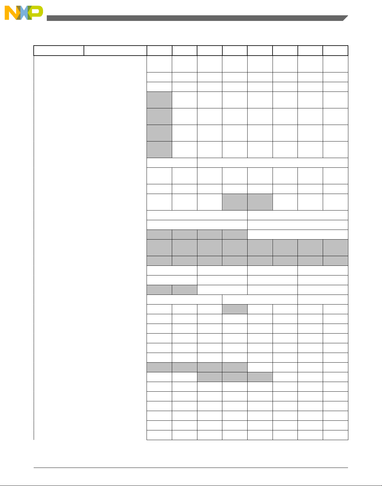
Chapter 4 Memory map
Table 4-4. High-page register allocation (continued)
Address Register name Bit 7 6 5 4 3 2 1 Bit 0
0x30DB FTM2_SYNC
0x30DC FTM2_OUTINIT CH7OI CH6OI CH5OI CH4OI CH3OI CH2OI CH1OI CH0OI
0x30DD FTM2_OUTMASK CH7OM CH6OM CH5OM CH4OM CH3OM CH2OM CH1OM CH0OM
0x30DE FTM2_COMBINE0 —
0x30DF FTM2_COMBINE1 —
0x30E0 FTM2_COMBINE2 —
0x30E1 FTM2_COMBINE3 —
0x30E2 FTM2_DEATIME DTPS DTVAL
0x30E3 FTM2_EXTTRIG TRIGF
0x30E4 FTM2_POL POL7 POL6 POL5 POL4 POL3 POL2 POL1 POL0
0x30E5 FTM2_FMS FAULTF WPEN
0x30E6 FTM2_FILTER0 CHoddFVAL CHevenFVAL
0x30E7 FTM2_FILTER1 CHoddFVAL CHevenFVAL
0x30E8 FTM2_FLTFILTER — — — — FFVAL
0x30E9 FTM2_FLTCTRL
0x30EA-0x30EB Reserved — — — — — — — —
0x30EC PORT_IOFLT0 FLTD FLTC FLTB FLTA
0x30ED PORT_IOFLT1 FLTH FLTG FLTF FLTE
0x30EE PORT_IOFLT2 — — FLTKBI1 FLTKBI0 FLTRST
0x30EF PORT_FCLKDIV FLTDIV3 FLTDIV2 FLTDIV1
0x30F0 PORT_PTAPE PTAPE7 PTAPE6 PTAPE5 — PTAPE3 PTAPE2 PTAPE1 PTAPE0
0x30F1 PORT_PTBPE PTBPE7 PTBPE6 PTBPE5 PTBPE4 PTBPE3 PTBPE2 PTBPE1 PTBPE0
0x30F2 PORT_PTCPE PTCPE7 PTCPE6 PTCPE5 PTCPE4 PTCPE3 PTCPE2 PTCPE1 PTCPE0
0x30F3 PORT_PTDPE PTDPE7 PTDPE6 PTDPE5 PTDPE4 PTDPE3 PTDPE2 PTDPE1 PTDPE0
0x30F4 PORT_PTEPE PTEPE7 PTEPE6 PTEPE5 PTEPE4 PTEPE3 PTEPE2 PTEPE1 PTEPE0
0x30F5 PORT_PTFPE PTFPE7 PTFPE6 PTFPE5 PTFPE4 PTFPE3 PTFPE2 PTFPE1 PTFPE0
0x30F6 PORT_PTGPE — — — — PTGPE3 PTGPE2 PTGPE1 PTGPE0
0x30F7 PORT_PTHPE PTHPE7 PTHPE6 — — — PTHPE2 PTHPE1 PTHPE0
0x30F8 SYS_UUID1 ID63 ID62 ID61 ID60 ID59 ID58 ID57 ID56
0x30F9 SYS_UUID2 ID55 ID54 ID53 ID52 ID51 ID50 ID49 ID48
0x30FA SYS_UUID3 ID47 ID46 ID45 ID44 ID43 ID42 ID41 ID40
0x30FB SYS_UUID4 ID39 ID38 ID37 ID36 ID35 ID34 ID33 ID32
0x30FC SYS_UUID5 ID31 ID30 ID29 ID28 ID27 ID26 ID25 ID24
0x30FD SYS_UUID6 ID23 ID22 ID21 ID20 ID19 ID18 ID17 ID16
SWSYN
C
FFLTR3ENFFLTR2ENFFLTR1ENFFLTR0ENFAULT3ENFAULT2ENFAULT1ENFAULT0
TRIG2 TRIG1 TRIG0
FAULTENSYNCE
N
FAULTENSYNCE
N
FAULTENSYNCE
N
FAULTENSYNCE
N
INITTRI
GEN
CH1TRIGCH0TRIGCH5TRIGCH4TRIGCH3TRIGCH2TRI
FAULTI
N
DTEN DECAP
DTEN DECAP
DTEN DECAP
DTEN DECAP
SYNCH
OM
— —
REINIT
DECAP
EN
DECAP
EN
DECAP
EN
DECAP
EN
FAULTF2FAULTF1FAULTF
CNTMA
X
COMP
COMP
COMP
COMP
CNTMIN
COMBI
NE
COMBI
NE
COMBI
NE
COMBI
NE
G
EN
0
Table continues on the next page...
MC9S08PT60 Reference Manual, Rev. 4, 08/2014
Freescale Semiconductor, Inc. 75
Page 76
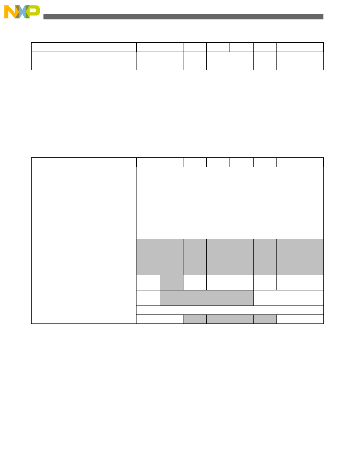
Register addresses and bit assignments
Table 4-4. High-page register allocation (continued)
Address Register name Bit 7 6 5 4 3 2 1 Bit 0
0x30FE SYS_UUID7
0x30FF SYS_UUID8
ID15 ID14 ID13 ID12 ID11 ID10 ID9 ID8
ID7 ID6 ID5 ID4 ID3 ID2 ID1 ID0
Several reserved flash memory locations, shown in the following table, are used for
storing values used by several registers. These registers include an 8-byte backdoor key,
NV_BACKKEY, which can be used to gain access to secure memory resources. During
reset events, the contents of NVPROT and NVOPT in the reserved flash memory are
transferred into corresponding FPROT and FOPT registers in the high-page registers area
to control security and block protection options.
Table 4-5. Reserved flash memory addresses
Address Register Name Bit 7 6 5 4 3 2 1 Bit 0
0xFF70 NV_BACKKEY0
0xFF71 NV_BACKKEY1 BACKKEY1
0xFF72 NV_BACKKEY2 BACKKEY2
0xFF73 NV_BACKKEY3 BACKKEY3
0xFF74 NV_BACKKEY4 BACKKEY4
0xFF75 NV_BACKKEY5 BACKKEY5
0xFF76 NV_BACKKEY6 BACKKEY6
0xFF77 NV_BACKKEY7 BACKKEY7
0xFF78 Reserved — — — — — — — —
0xFF79 Reserved — — — — — — — —
0xFF7A Reserved — — — — — — — —
0xFF7B Reserved — — — — — — — —
0xFF7C NV_FPROT
0xFF7D NV_EEPROT
0xFF7E NV_FOPT NV
0xFF7F NV_FSEC
FPOPE
N
DPOPE
N
KEYEN 1 1 1 1 SEC
— FPHDIS FPH FPLDIS FPLS
BACKKEY0
— DPS
The 8-byte comparison key can be used to temporarily disengage memory security
provided the key enable field, NV_FSEC[KEYEN], is 10b. This key mechanism can be
accessed only through user code running in secure memory. A security key cannot be
entered directly through background debug commands. This security key can be disabled
completely by programming the NV_FSEC[KEYEN] bit to 0. If the security key is
disabled, the only way to disengage security is by mass erasing the flash if needed,
MC9S08PT60 Reference Manual, Rev. 4, 08/2014
76 Freescale Semiconductor, Inc.
Page 77

Chapter 4 Memory map
normally through the background debug interface and verifying that flash is blank. To
avoid returning to secure mode after the next reset, program the security bits,
NV_FSEC[SEC], to the unsecured state (10b).
4.4 Random-access memory (RAM)
This section describes the 4,096 bytes of RAM (random-access memory).
These devices include static RAM. The locations in RAM below 0x0100 can be accessed
using the more efficient direct addressing mode. Any single bit in this area can be
accessed with the bit manipulation instructions (BCLR, BSET, BRCLR, and BRSET).
The RAM retains data when the MCU is in low-power wait, or stop3 mode. At power-on,
the contents of RAM are uninitialized. RAM data is unaffected by any reset provided that
the supply voltage does not drop below the minimum value for RAM retention.
For compatibility with older M68HC05 MCUs, the HCS08 resets the stack pointer to
0x00FF. In this series, re-initialize the stack pointer to the top of the RAM so that the
direct-page RAM can be used for frequently accessed RAM variables and bit-addressable
program variables. Include the following 2-instruction sequence in your reset
initialization routine (where RamLast is equated to the highest address of the RAM in the
Freescale-provided equate file).
LDHX #RamLast+1 ;point one past RAM
TXS ;SP<-(H:X-1)
When security is enabled, the RAM is considered a secure memory resource and is not
accessible through BDM or code executing from non-secure memory.
4.5
Flash and EEPROM
4.5.1 Overview
This device includes various configuration of flash and EEPROM. The controller for
flash and EEPROM is ideal for single-supply applications for field programming without
external high voltage sources for program or erase operations.
The flash memory is ideal for single-supply applications that allow for field
reprogramming without requiring external high voltage sources for program or erase
operations. The flash module includes a memory controller that executes commands to
modify flash memory contents. The user interface to the memory controller consists of
the indexed flash common command object (FCCOB) register, which is written to with
MC9S08PT60 Reference Manual, Rev. 4, 08/2014
Freescale Semiconductor, Inc. 77
Page 78
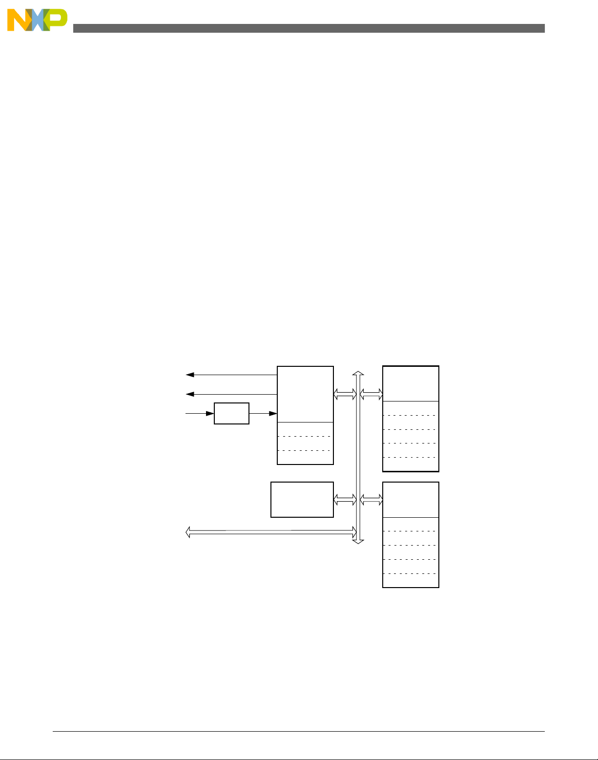
Divider
Clock
Command Interrupt Request
Protection
Registers
Security
Sector 1
Sector 1
Sector 127
Sector 0
Sector 0
FLASH
EEPROM
Interface
NVM controller
Bus Clock
Error Interrupt Request
CPU
16K
x3
2
256
x8
Sector 127
Flash
Flash and EEPROM
the command, global address, data, and any required command parameters. The memory
controller must complete the execution of a command before the FCCOB register is
written to with a new command.
CAUTION
A flash byte or longword must be in the erased state before
being programmed. Cumulative programming of bits within a
flash byte or longword is not allowed.
The flash memory is read as bytes. Read access time is one bus
cycle for bytes. For flash memory, an erased bit reads 1 and a
programmed bit reads 0. It is possible to read from flash
memory while commands are being executed on EEPROM
memory. It is not possible to read from EEPROM memory
while a command (erase/program) is executing on flash
memory. Simultaneous EEPROM memory are implemented
with error correction codes (ECC) that can resolve single bit
faults and detect double bit faults.
The following figure shows the block diagram of the flash and EEPROM module.
Flash features:
• 64 KB of flash memory composed of one 64 KB flash block divided into 128 sectors
of 512 bytes
• Automated program and erase algorithm with verification
• Fast sector erase and longword program operation
78 Freescale Semiconductor, Inc.
Figure 4-2. Flash and EEPROM block diagram
MC9S08PT60 Reference Manual, Rev. 4, 08/2014
Page 79

Chapter 4 Memory map
• Ability to read the flash memory while programming a word in the EEPROM
memory
• Flexible protection scheme to prevent accidental program or erase of flash memory
EEPROM features:
• 256 bytes of EEPROM memory composed of one 256 byte EEPROM block divided
into 128 sectors of 2 bytes
• Single bit fault correction and double bit fault detection within a word during read
operations
• Automated program and erase algorithm with verification and generation of ECC
parity bits
• Fast sector erase and byte program operation
• Protection scheme to prevent accidental program or erase of EEPROM memory
• Ability to program up to four bytes in a burst sequence
Other features
• No external high-voltage power supply required for flash memory program and erase
operations
• Interrupt generation on flash command completion and flash error detection
• Security mechanism to prevent unauthorized access to the flash memory
4.5.2
Function descriptions
4.5.2.1 Modes of operation
The flash and EEPROM module provides the normal user mode of operation. The
operating mode is determined by module-level inputs and affects the FCLKDIV,
FCNFG, and EEPROT registers.
4.5.2.1.1
The flash and EEPROM module is not affected if the MCU enters wait mode. The flash
module can recover the MCU from wait via the CCIF interrupt. See Flash and EEPROM
interrupts.
4.5.2.1.2
If a flash and EEPROM command is active, that is, FSTAT[CCIF] = 0, when the MCU
requests stop mode, the current NVM operation will be completed before the MCU is
allowed to enter stop mode.
Wait mode
Stop mode
MC9S08PT60 Reference Manual, Rev. 4, 08/2014
Freescale Semiconductor, Inc. 79
Page 80

Flash and EEPROM
4.5.2.2 Flash and EEPROM memory map
The MCU places the flash memory between global address 0x0000 and 0xFFFF as
shown in the following table. Not all flash are available to users because some addresses
are overlapped with RAM, EEPROM, and registers.
MC9S08PT60 contains a piece of 64 KB flash in which only 60,864 bytes flash are
available for users. This flash block is divided into 128 sectors of 512 bytes.
MC9S08PT32 contains a piece of 32 KB flash that is fully available for users. This flash
block is divided into 64 sectors of 512 bytes.
Table 4-6. Flash memory addressing
Device Global address
MC9S08PT60 0x0000 — 0xFFFF 64 KB
MC9S08PT32 0x8000 — 0xFFFF 32 KB
Size
(Bytes)
Description User availability
Sector [0:7]: N/A
Sector [8]: Last 448 bytes available
Flash block contains
flash configuration field
Flash block contains
flash configuration field
Sector [9:23]: fully available
Sector [24]: N/A
Sector [25:127]: fully available
Sector [64:127]: fully available
4.5.2.3 Flash and EEPROM initialization after system reset
On each system reset, the flash and EEPROM module executes an initialization sequence
that establishes initial values for the flash and EEPROM block configuration parameters,
the FPROT and EEPROT protection registers, and the FOPT and FSEC registers. The
initialization routine reverts to built-in default values that leave the module in a fully
protected and secured state if errors are encountered during execution of the reset
sequence. If a double bit fault is detected during the reset sequence, both
FSTAT[MGSTAT] bits will be set.
FSTAT[CCIF] is cleared throughout the initialization sequence. The NVM module holds
off all CPU access for a portion of the initialization sequence. Flash and EEPROM reads
are allowed after the hold is removed. Completion of the initialization sequence is
marked by setting FSTAT[CCIF] high, which enables user commands.
If a reset occurs while any flash or EEPROM command is in progress, that command will
be immediately aborted. The state of the word being programmed or the sector/block
being erased is not guaranteed.
MC9S08PT60 Reference Manual, Rev. 4, 08/2014
80 Freescale Semiconductor, Inc.
Page 81

Chapter 4 Memory map
4.5.2.4 Flash and EEPROM command operations
Flash and EEPROM command operations are used to modify flash and EEPROM
memory contents.
The command operations contain three steps:
1. Configure the clock for flash or EEPROM program and erase command operations.
2. Use command write sequence to set flash and EEPROM command parameters and
launch execution.
3. Execute valid flash and EEPROM commands according to MCU functional mode
and MCU security state.
The figure below shows a general flowchart of the flash or EEPROM command write
sequence.
MC9S08PT60 Reference Manual, Rev. 4, 08/2014
Freescale Semiconductor, Inc. 81
Page 82
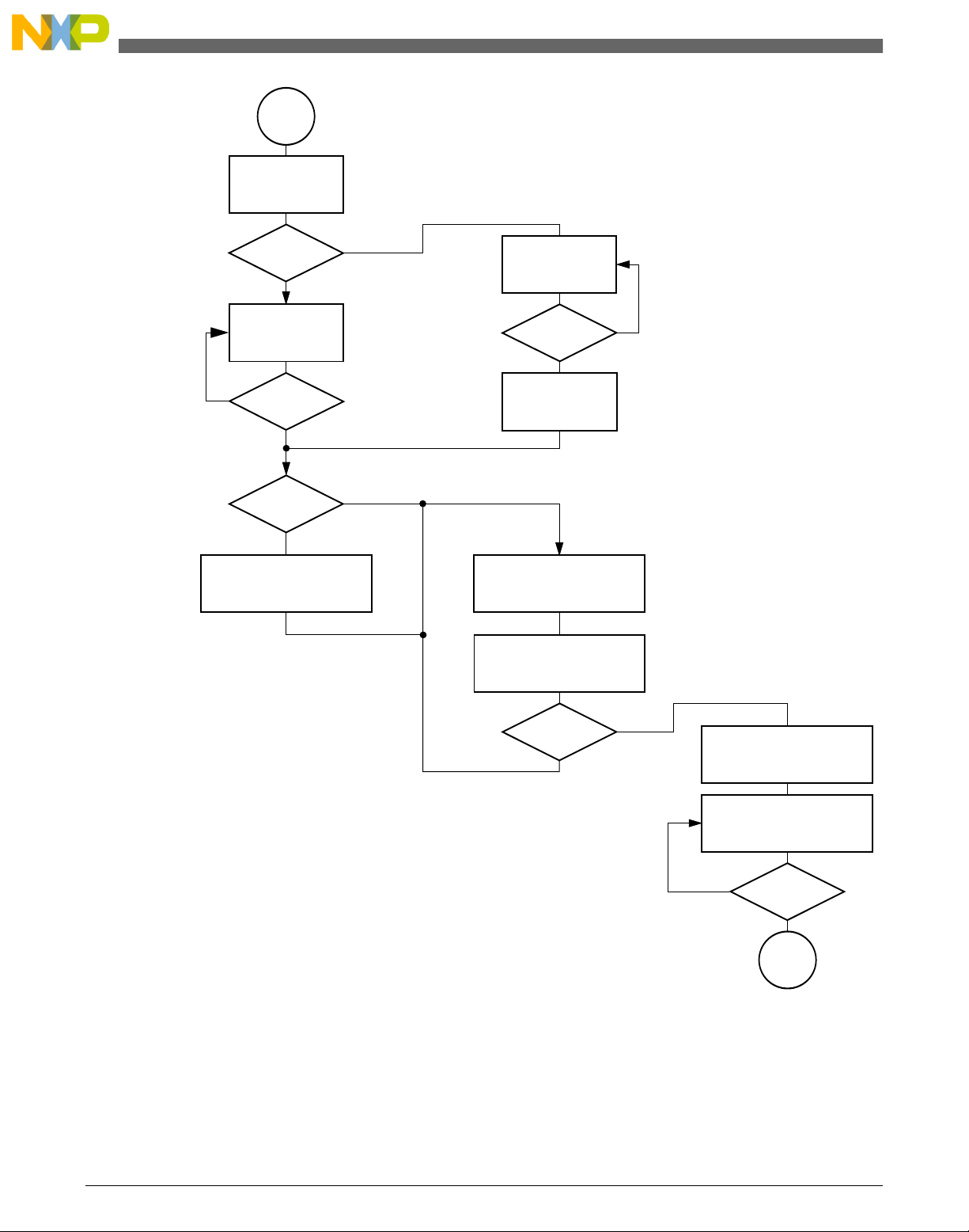
Read: FCLKDIV
START
FDIV
Read: FSTAT
Read: FSTAT
CCIF
Write: FCLKDIV
register
NOTE: FCLKDIV must be
set after each reset
Set?
CCIF
ACCERR
Results from previous Command
Write to FCCOBIX register
to identify specific command
parameter to load
Write to FCCOB register
to load required command
parameter
More
Write: FSTAT register
(to launch command)
Read: FSTAT register
CCIF Set?
Bit Polling for
Command Completion Check
Clear CCIF 0x80
Parameters?
Write: FSTAT register
Clear ACCERR
FPVIOL 0x30
or FPVIOL Set?
Access Error and
Protection Violation Check
Set?
No
No
No
Yes
Yes
Yes
No
Yes
END
register
No
No
Yes
Yes
Clock Divider
Value Check
FCCOB
Availability Check
register
Correct?
register
Flash and EEPROM
Figure 4-3. Generic flash and EEPROM command write sequence flowchart
MC9S08PT60 Reference Manual, Rev. 4, 08/2014
82 Freescale Semiconductor, Inc.
Page 83
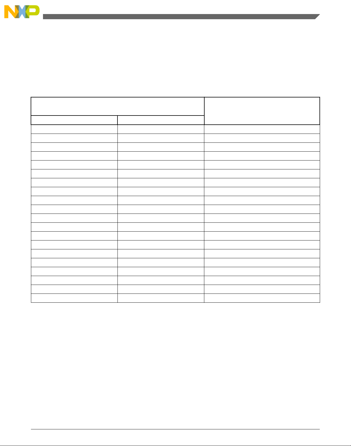
Chapter 4 Memory map
4.5.2.4.1 Writing the FCLKDIV register
Prior to issuing any flash and EEPROM program or erase command after a reset, the user
is required to write the FCLKDIV register to divide BUSCLK down to a target FCLK of
1MHz. The following table shows recommended values for the FDIV field based on
BUSCLK frequency.
Table 4-7. FDIV values for various BUSCLK frequencies
BUSCLK frequency
(MHz)
1
MIN
1.0 1.6 0x00
1.6 2.6 0x01
2.6 3.6 0x02
3.6 4.6 0x03
4.6 5.6 0x04
5.6 6.6 0x05
6.6 7.6 0x06
7.6 8.6 0x07
8.6 9.6 0x08
9.6 10.6 0x09
10.6 11.6 0x0A
11.6 12.6 0x0B
12.6 13.6 0x0C
13.6 14.6 0x0D
14.6 15.6 0x0E
15.6 16.6 0x0F
16.6 17.6 0x10
17.6 18.6 0x11
18.6 19.6 0x12
19.6 20.0 0x13
MAX
2
FDIV[5:0]
1. BUSCLK is greater than this value
2. BUSCLK is less than or equal to this value
CAUTION
Programming or erasing the flash and EEPROM memory
cannot be performed if the bus clock runs at less than 0.8 MHz.
Setting FCLKDIV[FDIV] too high can destroy the flash and
EEPROM memory due to overstress. Setting FCLKDIV[FDIV]
too low can result in incomplete programming or erasure of the
flash and EEPROM memory cells.
MC9S08PT60 Reference Manual, Rev. 4, 08/2014
Freescale Semiconductor, Inc. 83
Page 84

Flash and EEPROM
When the FCLKDIV register is written, the FCLKDIV[FDIVLD] bit is set automatically.
If the FCLKDIV[FDIVLD] bit is 0, the FCLKDIV register has not been written since the
last reset. If the FCLKDIV register has not been written, any flash and EEPROM
program or erase command loaded during a command write sequence will not execute
and the FSTAT[ACCERR] bit will be set.
4.5.2.4.2 Command write sequence
The memory controller will launch all valid flash and EEPROM commands entered using
a command write sequence.
Before launching a command, the FSTAT[ACCERR] and FSTAT[FPVIOL] bits must be
clear and the FSTAT[CCIF] flag will be tested to determine the status of the current
command write sequence. If FSTAT[CCIF] is 0, indicating that the previous command
write sequence is still active, a new command write sequence cannot be started and all
writes to the FCCOB register are ignored.
The FCCOB parameter fields must be loaded with all required parameters for the flash
and EEPROM command being executed. Access to the FCCOB parameter fields is
controlled via FCCOBIX[CCOBIX] bits.
Flash and EEPROM command mode uses the indexed FCCOB register to provide a
command code and its relevant parameters to the memory controller. First, the user must
set up all required FCCOB field. Then they can initiate the command's execution by
writing a 1 to the FSTAT[CCIF] bit. This action clears the CCIF command completion
flag to 0. When the user clears the FSTAT[CCIF] bit all FCCOB parameter field are
locked and cannot be changed by the user until the command completes (evidenced by
the memory controller returning FSTAT[CCIF] to1). Some commands return information
to the FCCOB register array.
The generic format for the FCCOB parameter fields in flash and EEPROM command
mode is shown in the following table. The return values are available for reading after the
FSTAT[CCIF] flag has been returned to 1 by the memory controller. Writes to the
unimplemented parameter fields, FCCOBIX[CCOBIX] =110b and FCCOBIX[CCOBIX]
= 111b, are ignored with read from these fields returning 0x0000.
The table below shows the generic flash command format. The high byte of the first word
in the CCOB array contains the command code, followed by the parameters for this
specific flash command. For details on the FCCOB settings required by each command,
see the flash command descriptions in Flash and EEPROM command summary .
MC9S08PT60 Reference Manual, Rev. 4, 08/2014
84 Freescale Semiconductor, Inc.
Page 85
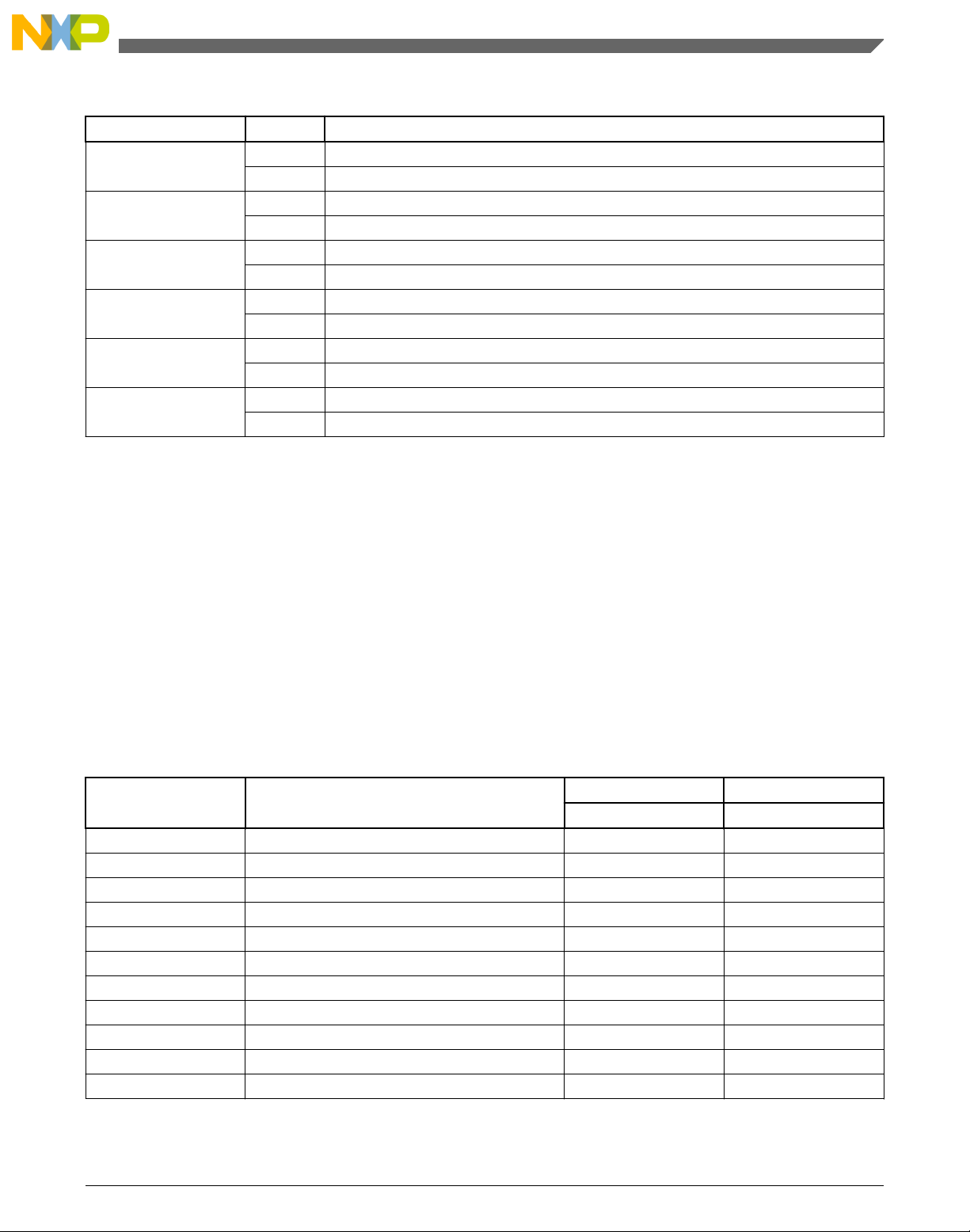
Chapter 4 Memory map
Table 4-8. FCCOB – flash and EEPROM command mode typical usage
CCOBIX[2:0] Byte FCCOB parameter fields in flash and EEPROM command mode
000
001
010
011
100
101
HI FCMD[7:0] defining flash command
LO Global address [23:16]
HI Global address [15:8]
LO Global address [7:0]
HI Data 0 [15:8]
LO Data 0 [7:0]
HI Data 1 [15:8]
LO Data 1 [7:0]
HI Data 2 [15:8]
LO Data 2 [7:0]
HI Data 3 [15:8]
LO Data 3 [7:0]
The contents of the FCCOB parameter fields are transferred to the memory controller
when the user clears the FSTAT[CCIF] command completion flag by writing 1. The
CCIF flag will remain clear until the flash and EEPROM command has completed. Upon
completion, the memory controller will return FSTAT[CCIF] to 1 and the FCCOB
register will be used to communicate any results.
The following table presents the valid flash and EEPROM commands, as enabled by the
combination of the functional MCU mode with the MCU security state of unsecured or
secured.
MCU secured state is selected by NVM_FSEC[SEC].
Table 4-9. Flash and EEPROM commands by mode and security state
FCMD Command
0x01 Erase verify all blocks * *
0x02 Erase verify block * *
0x03 Erase verify flash section * N/A
0x04 Read once * N/A
0x06 Program flash * N/A
0x07 Program once * N/A
0x08 Erase all block * *
0x09 Erase flash block * *
0x0A Erase flash sector * N/A
0x0B Unsecure NVM N/A *
0x0C Verify backdoor access key * *
Unsecured Secured
1
U
2
U
Table continues on the next page...
MC9S08PT60 Reference Manual, Rev. 4, 08/2014
Freescale Semiconductor, Inc. 85
Page 86
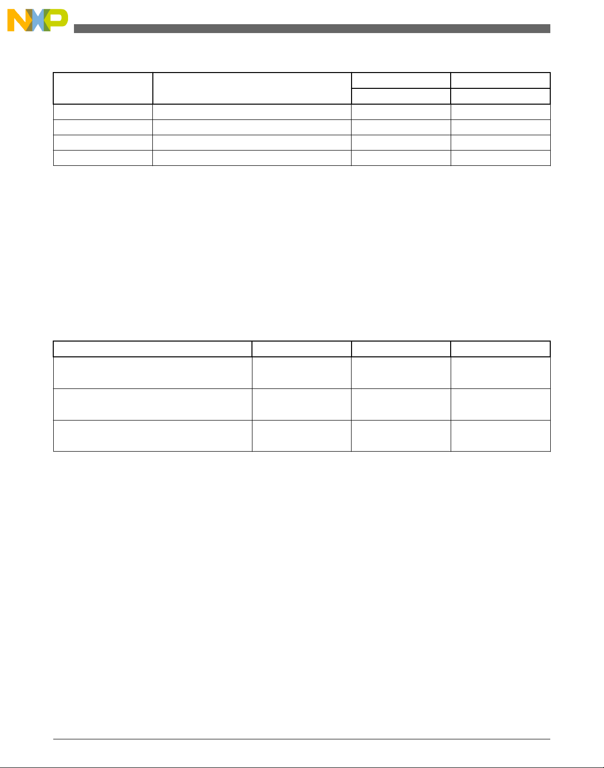
Flash and EEPROM
Table 4-9. Flash and EEPROM commands by mode and security state (continued)
FCMD Command
0x0D Set user margin level * N/A
0x10 Erase verify EEPROM section * *
0x11 Program EEPROM * N/A
0x12 Erase EEPROM sector * N/A
1. Unsecured User mode
2. Secured User mode
Unsecured Secured
1
U
2
U
4.5.2.5 Flash and EEPROM interrupts
The flash and EEPROM module can generate an interrupt when a flash command
operation has completed or when a flash and EEPROM command operation has detected
an ECC fault.
Table 4-10. Flash interrupt source
Interrupt source Interrupt flag Local enable Global (CCR) mask
Flash and EEPROM command complete
ECC double bit fault on flash and EEPROM read
ECC single bit fault on flash and EEPROM read
CCIF
(FSTAT register)
DFDIF
(FERSTAT register)
SFDIF
(FERSTAT register)
(FERCNFG register)
(FERCNFG register)
CCIE
I Bit
(FCNFG register)
DFDIE
I Bit
SFDIE
I Bit
4.5.2.5.1 Description of flash and EEPROM interrupt operation
The flash module uses the FSTAT[CCIF] flag in combination with the FCNFG[CCIE]
interrupt enable bit to generate the flash command interrupt request. The flash module
uses the DFDIF and SFDIF flags in combination with the FERSTAT[DFDIE] and
FERSTAT[SFDIE] interrupt enable bits to generate the flash error interrupt request.
The logic used for generating the flash module interrupts is shown in the following
figure.
MC9S08PT60 Reference Manual, Rev. 4, 08/2014
86 Freescale Semiconductor, Inc.
Page 87
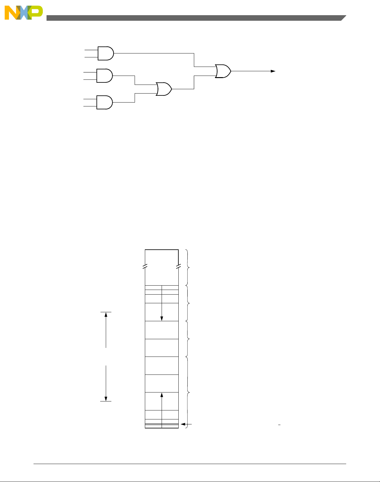
CCIE
CCIF
SFDIF
Flash and EEPROM Command
Flash and EEPROM
Complete Interrupt Request
Error Interrupt Request
CPU Interrupt
Flash Protected/Unprotected Region 32 Kbytes
Flash Configuration Field 16 bytes (0xFF70
0xFF7F)
Flash Protected/Unprotected Higher Region 2, 4, 8, 16 Kbytes
Flash Protected/Unprotected Lower Region 1, 2, 4, 8 Kbytes
Flash Protected/Unprotected Region 8 Kbytes (up to 29 Kbytes)
0x0000
0x8000
0x8400
0x8800
0x9000
0xA000
0xB000
0xC000
0xD000
0xE000
0xF000
0xF800
0xFFFF
Chapter 4 Memory map
Figure 4-4. Flash and EEPROM module interrupts implementation
4.5.2.6 Protection
The FPROT register can be set to protect regions in the flash memory from accidental
programming or erasing. Three separate memory regions, one growing upward from
global address 0x8000 in the flash memory, called the lower region; one growing
downward from global address 0xFFFF in the flash memory, called the higher region;
and the remaining addresses in the flash memory, can be activated for protection. The
flash memory addresses covered by these protectable regions are shown in the flash
memory map. The higher address region is mainly targeted to hold the boot loader code
because it covers the vector space.
Figure 4-5. Flash protection memory map
MC9S08PT60 Reference Manual, Rev. 4, 08/2014
Freescale Semiconductor, Inc. 87
Page 88
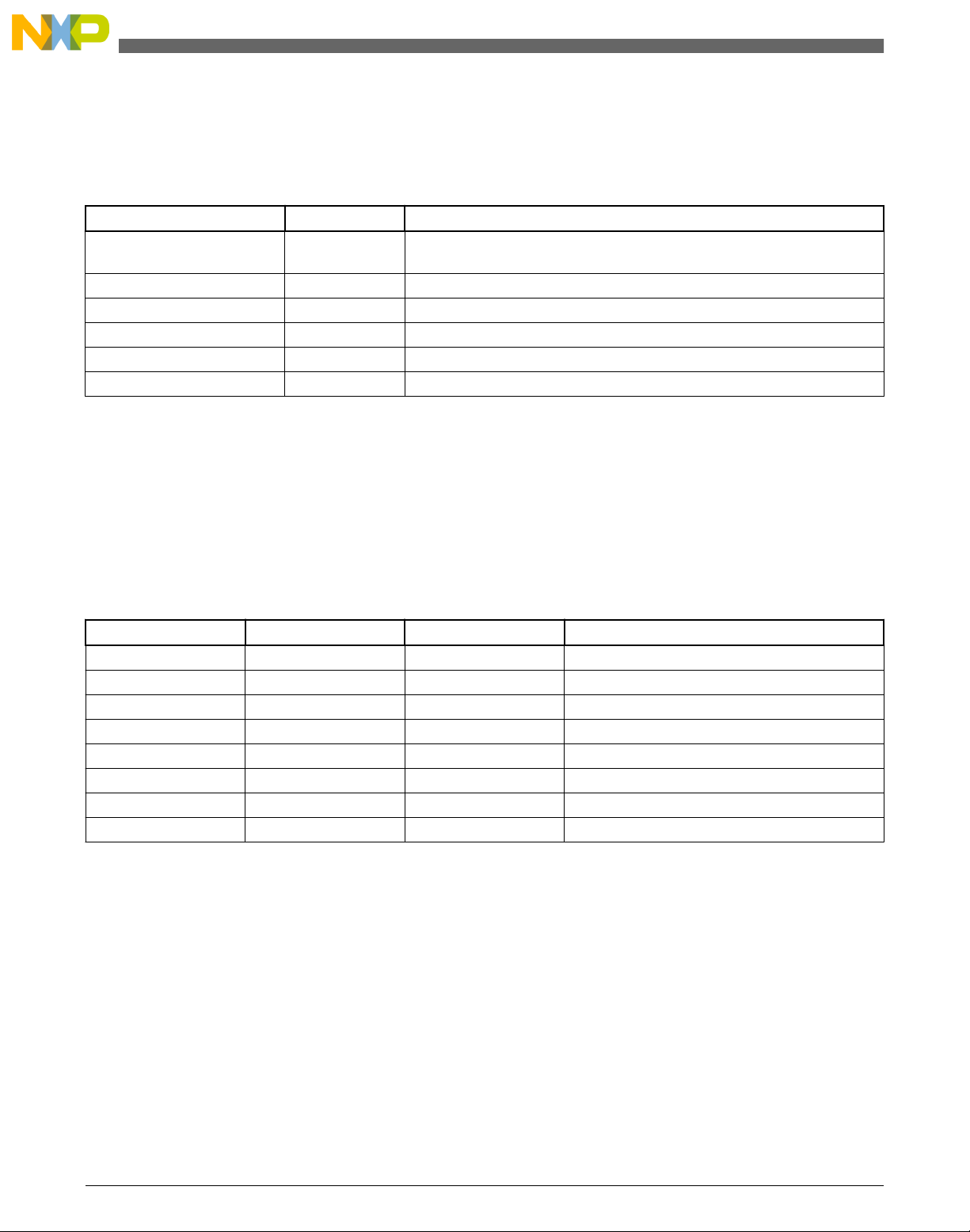
Flash and EEPROM
Default protection settings as well as security information that allows the MCU to restrict
access to the flash module are stored in the flash configuration field as described in the
table below.
Table 4-11. Flash configuration field
Global address Size (Bytes) Description
0xFF70 — 0xFF77
0xFF78 — 0xFF7B 4 Reserved
0xFF7C
0xFF7D
0xFF7E
0xFF7F
1. 0xFF78–0xFF7F for a flash phrase and must be programmed in a single command write sequence. Each byte in the
0xFF78-0xFF7B reserved field must be programmed to 0xFF.
1
1
1
1
1
8
1 Flash protection byte
1 EEPROM protection byte
1 Flash nonvolatile byte
1 Flash security byte
Backdoor comparison key. See Verify backdoor access key command and
Unsecuring the MCU using backdoor key access.
The flash and EEPROM module provides protection to the MCU. During the reset
sequence, the FPROT register is loaded with the contents of the flash protection byte in
the flash configuration field at global address 0xFF7C in flash memory. The protection
functions depend on the configuration of bit settings in FPORT register.
Table 4-12. Flash protection function
FPOPEN FPHDIS FPLDIS Function
1 1 1 No flash protection
1 1 0 Protected low range
1 0 1 Protected high range
1 0 0 Protected high and low ranges
0 1 1 Full p-flash memory protected
0 1 0 Unprotected low range
0 0 1 Unprotected high range
0 0 0 Unprotected high and low ranges
1. For range sizes, see Table 4 and Table 5
1
The flash protection scheme can be used by applications requiring reprogramming in
single chip mode while providing as much protection as possible if reprogramming is not
required.
MC9S08PT60 Reference Manual, Rev. 4, 08/2014
88 Freescale Semiconductor, Inc.
Page 89
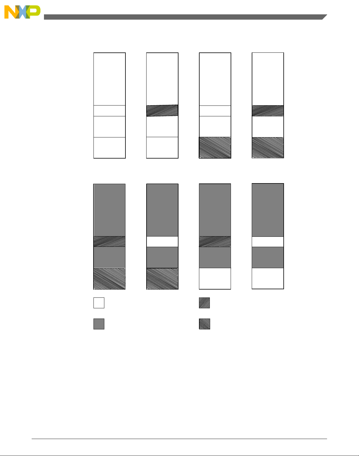
Scenario 4
Scenario 6
Scenario 7
Scenario 5
FPHDIS = 1
FPLDIS = 1
FPHDIS = 1
FPLDIS = 0
FPHDIS = 0
FPLDIS = 1
FPHDIS = 0
FPLDIS = 0
Protected region
not defined by FPLS, FPHS
Unprotected region
Protected region with size
defined by FPLS
Protected region with size
defined by FPHS
FPLS[1:0]
FPHS[1:0]
FPHS[1:0]
FPLS[1:0]
FPOPEN = 1
FPOPEN = 1
FPOPEN = 1FPOPEN = 1
Scenario 3
Scenario 2
Scenario 1
Scenario 0
0x8000
0xFFFF
0x8000
0xFFFF
FPOPEN = 0FPOPEN = 0FPOPEN = 0FPOPEN = 0FPOPEN = 0
Chapter 4 Memory map
Figure 4-6. Flash protection scenarios
The general guideline is that flash protection can only be added and not removed. The
following table specifies all valid transitions between flash protection scenarios. Any
attempt to write an invalid scenario to the FPROT register will be ignored. The contents
of the FPROT register reflect the active protection scenario. See the FPROT[FPHS] and
FPROT[FPLS] bit descriptions for additional restrictions.
Freescale Semiconductor, Inc. 89
MC9S08PT60 Reference Manual, Rev. 4, 08/2014
Page 90
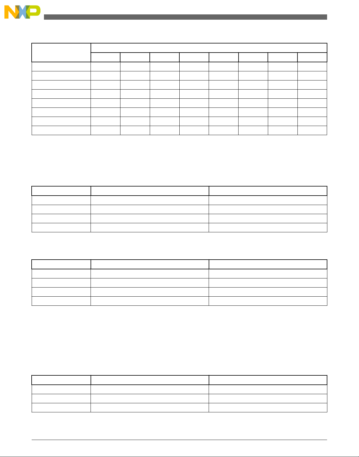
Flash and EEPROM
Table 4-13. Flash protection scenario transitions
From protection
scenario
0 × × × ×
1 × ×
2 × ×
3 ×
4 × ×
5 × × × ×
6 × × × ×
7 × × × × × × × ×
0 1 2 3 4 5 6 7
To protection scenario
The flash protection address range is listed in the following two tables regarding the
scenarios in the table above.
Table 4-14. Flash protection higher address range
FPHS[1:0] Global address range Protected size
00 0xF800 – 0xFFFF 2 Kbytes
01 0xF000 – 0xFFFF 4 Kbytes
10 0xE000 – 0xFFFF 8 Kbytes
11 0xC000 – 0xFFFF 16 Kbytes
Table 4-15. Flash protection lower address range
FPLS[1:0] Global address range Protected size
00 0x8000 – 0x83FF 1 Kbytes
01 0x8000 – 0x87FF 2 Kbytes
10 0x8000 – 0x8FFF 4 Kbytes
11 0x8000 – 0x9FFF 8 Kbytes
During the reset sequence, fields NVM_EEPROT[DPOPEN] and NVM_EEPROT[DPS]
are loaded with the contents of the EEPROM protection byte in the flash configuration
field at global address 0xFF7D located in flash memory. EEPROM protection address
range is specified by the NVM_EEPROT[DPS].
Table 4-16. EEPROM protection address range
DPS[2:0] Global address range Protected size
000 0x3100 – 0x311F 32 bytes
001 0x3100 – 0x313F 64 bytes
010 0x3100 – 0x315F 96 bytes
Table continues on the next page...
MC9S08PT60 Reference Manual, Rev. 4, 08/2014
90 Freescale Semiconductor, Inc.
Page 91

Chapter 4 Memory map
Table 4-16. EEPROM protection address range (continued)
DPS[2:0] Global address range Protected size
011 0x3100 – 0x317F 128 bytes
100 0x3100 – 0x319F 160 bytes
101 0x3100 – 0x31BF 192 bytes
110 0x3100 – 0x31DF 224 bytes
111 0x3100 – 0x31FF 256 bytes
All possible flash protection scenarios are shown in Figure 4-6. Although the protection
scheme is loaded from the flash memory at global address 0xFF7C during the reset
sequence, it can be changed by the user.
4.5.2.7 Security
The flash and EEPROM module provides security information to the MCU. The flash
security state is defined by the NVM_FSEC[SEC] bits. During reset, the flash module
initializes the NVM_FSEC register using data read from the security byte of the flash and
EEPROM configuration field at global address 0xFF7F. The security state out of reset
can be permanently changed by programming the security byte, assuming that the MCU
is starting from a mode where the necessary flash and EEPROM erase and program
commands are available and that the upper region of the flash is unprotected. If the flash
security byte is successfully programmed, its new value will take affect after the next
MCU reset.
The following subsections describe these security-related subjects:
• Unsecuring the MCU using backdoor key access
• Unsecuring the MCU using BDM
• Mode and security effects on flash and EEPROM command availability
4.5.2.7.1
Unsecuring the MCU using backdoor key access
The MCU may be unsecured by using the backdoor key access feature which requires
knowledge of the contents of the backdoor keys, which are four 16-bit words
programmed at addresses 0xFF70–0xFF77. If the KEYEN[1:0] bits are in the enabled
state, the verify backdoor access key command – see Verify backdoor access key
command, allows the user to present four prospective keys for comparison to the keys
stored in the flash and EEPROM memory via the memory controller. If the keys
presented in the verify backdoor access key command match the backdoor keys stored in
MC9S08PT60 Reference Manual, Rev. 4, 08/2014
Freescale Semiconductor, Inc. 91
Page 92

Flash and EEPROM
the flash and EEPROM memory, the FSEC[SEC] bits will be changed to unsecure the
MCU. Key values of 0x0000 and 0xFFFF are not permitted as backdoor keys. While the
Verify Backdoor Access Key command is active, flash memory and EEPROM memory
will not be available for read access and will return invalid data.
The user code stored in the flash memory must have a method of receiving the backdoor
keys from an external stimulus. This external stimulus would typically be through one of
the on-chip serial ports.
If the KEYEN[1:0] bits are in the enabled state, the MCU can be unsecured by the
backdoor key access sequence described below:
1. Follow the command sequence for the verify backdoor access key command as
explained in Verify backdoor access key command.
2. If the verify backdoor access key command is successful, the MCU is unsecured and
the FSEC[SEC] bits are forced to the unsecure state of 10.
The verify backdoor access key command is monitored by the memory controller and an
illegal key will prohibit future use of the verify backdoor access key command. A reset of
the MCU is the only method to re-enable the verify backdoor access key command. The
security as defined in the flash and EEPROM security byte (0xFF7F) is not changed by
using the verify backdoor access key command sequence. The backdoor keys stored in
addresses 0xFF70–0xFF77 are unaffected by the verify backdoor access key command
sequence. The verify backdoor access key command sequence has no effect on the
program and erase protections defined in the flash and EEPROM protection register,
FPORT.
After the backdoor keys have been correctly matched, the MCU will be unsecured. After
the MCU is unsecured, the sector containing the flash and EEPROM security byte can be
erased and the flash and EEPROM security byte can be reprogrammed to the unsecure
state, if desired. In the unsecure state, the user has full control of the contents of the
backdoor keys by programming addresses 0xFF70–0xFF77 in the flash configuration
field.
4.5.2.7.2
Unsecuring the MCU using BDM
A secured MCU can be unsecured by using the following method to erase the flash and
EEPROM memory:
1. Reset the MCU.
2. Set FCDIV register as described in Writing the FCLKDIV register.
MC9S08PT60 Reference Manual, Rev. 4, 08/2014
92 Freescale Semiconductor, Inc.
Page 93

Chapter 4 Memory map
3. Configure registers NVM_FERSTAT and NVM_FPROT to disable protection in the
flash and EEPROM memory.
4. Execute the erase all blocks command write sequence to erase the flash and
EEPROM memory. Alternately, the unsecure NVM command can be executed.
If the flash and EEPROM memory are verified as erased, the MCU will be
unsecured. All BDM. commands will now be enabled and the flash security byte may
be programmed to the unsecure state by continuing with the steps that follow.
5. Execute the program flash command write sequence to program the flash security
byte to the unsecured state.
6. Reset the MCU.
4.5.2.7.3 Mode and security effects on flash and EEPROM command availability
The availability of flash and EEPROM module commands depends on the MCU
operating mode and security state as shown in Table 4-9.
4.5.2.8
Flash and EEPROM commands
4.5.2.8.1 Flash commands
The following table summarizes the valid flash commands as well as the effects of the
commands on the flash block and other resources within the flash and EEPROM module.
Table 4-17. Flash commands
FCMD Command Function on flash memory
0x01 Erase verify all blocks Verify that all flash (and EEPROM) blocks are erased
0x02 Erase verify block Verify that a flash block is erased
0x03 Erase verify flash section Verify that a given number of words starting at the address provided are erased
0x04 Read Once
0x06 Program flash Program up to two longwords in a flash block
0x07 Program once
0x08 Erase all block
0x09 Erase flash block Erase a flash or EEPROM block
Read a dedicated 64 byte field in the nonvolatile information register in flash
block that was previously programmed using the program once command
Program a dedicated 64 byte field in the nonvolatile information register in flash
block that is allowed to be programmed only once
Erase all flash and EEPROM blocks
An erase of all flash blocks is possible only when the FPROT[FPLDIS],
FPROT[FPHDIS], and FPROT[FPOEN] bits and the EEPROT[DPOPEN] bit are
set prior to launching the command
Table continues on the next page...
MC9S08PT60 Reference Manual, Rev. 4, 08/2014
Freescale Semiconductor, Inc. 93
Page 94
Flash and EEPROM
Table 4-17. Flash commands (continued)
FCMD Command Function on flash memory
An erase of the full flash block is possible only when FPROT[FPLDIS],
FPROT[FPHDIS], and FPROT[FPOEN] bits are set prior to launching the
command
0x0A Erase flash sector Erase all bytes in a flash sector
0x0B Unsecure flash
0x0C Verify backdoor access key Supports a method of releasing MCU security by verifying a set of security keys
0x0D Set user margin level Specifies a user margin read level for all flash blocks
Supports a method of releasing MCU security by erasing all flash (and
EEPROM) blocks and verifying that all flash (and EEPROM) blocks are erased
4.5.2.8.2 EEPROM commands
The following table summarizes the valid EEPROM commands along with the effects of
the commands on the EEPROM block.
Table 4-18. EEPROM commands
FCMD Command Function on flash memory
0x01 Erase verify all blocks Verify that all EEPROM (and flash) blocks are erased.
0x02 Erase verify block Verify that an EEPROM block is erased.
Erase all EEPROM and flash blocks
0x08 Erase all block
0x09 Erase EEPROM Block
0x0B Unsecure EEPROM
0x0D Set User Margin Level Specifies a user margin read level for all flash blocks.
0x10
0x11 Program EEPROM Program up to four bytes in the EEPROM block.
0x12 Erase EEPROM Sector Erase all bytes in a sector of the EEPROM block.
Erase Verify EEPROM
Section
An erase of all EEPROM blocks is possible only when the FPROT[FPLDIS],
FPROT[FPHDIS], and FPROT[FPOEN] bits and the DPOPEN bit in the
EEPORT register are set prior to launching the command.
Erase a EEPROM and flash block
An erase of the full flash block is possible only when FPROT[FPLDIS],
FPROT[FPHDIS] and FPROT[FPOPEN] bits are set prior to launching the
command.
Supports a method of releasing MCU security by erasing all EEPROM and flash
blocks and verifying that all EEPROM and flash blocks are erased.
Verify that a given number of bytes starting at the address provided are erased.
MC9S08PT60 Reference Manual, Rev. 4, 08/2014
94 Freescale Semiconductor, Inc.
Page 95
Chapter 4 Memory map
4.5.2.8.3 Allowed simultaneous flash and EEPROM operations
Only the operations marked 'OK' in the following table are permitted to be run
simultaneously on the flash and EEPROM blocks. Some operations cannot be executed
simultaneously because certain hardware resources are shared by the two memories. The
priority has been placed on permitting flash reads while program and erase operations
execute on the EEPROM, providing read (flash) while write (EEPROM) functionality.
Table 4-19. Allowed simultaneous flash and EEPROM operations
Program flash
Read OK OK OK
Margin Read
Program
Sector Erase
Mass Erase
1. A 'Margin read' is any read after executing the margin setting commands 'Set user margin level' or 'Set field margin level'
with anything but the 'normal' level specified. See the Note on margin settings in
2. The 'Mass erase' operations are commands 'Erase all blocks' and 'Erase flash block'
1
2
Read Margin read Program Sector erase Mass erase
EEPROM
OK
4.5.2.9 Flash and EEPROM command summary
This section provides details of all available flash commands launched by a command
write sequence. The FSTAT[ACCERR] bit will be set during the command write
sequence if any of the following illegal steps are performed, causing the command not to
be processed by the memory controller:
• Starting any command write sequence that programs or erases flash memory before
initializing the FLCKDIV register.
• Writing an invalid command as part of the command write sequence.
• For additional possible errors, refer to the error handling table provided for each
command.
If a flash block is read during the execution of an algorithm (FSTAT[CCIF] = 0) on that
same block, the read operation will return invalid data if both flags FERSTAT[SFDIF]
and FERSTAT[DFDIF] are set. If the FERSTAT[SFDIF] or FERSTAT[DFDIF] flags
were not previously set when the invalid read operation occurred, both the
FERSTAT[SFDIF] and FERSTAT[DFDIF] flags will be set.
If the FSTAT[ACCERR] or FSTAT[FPVIOL] bits are set, the user must clear these bits
before starting any command write sequence.
MC9S08PT60 Reference Manual, Rev. 4, 08/2014
Freescale Semiconductor, Inc. 95
Page 96

Flash and EEPROM
CAUTION
An EEPROM byte or flash longword must be in the erased state
before being programmed. Cumulative programming of bits
within an EEPROM byte or flash longword is not allowed.
4.5.2.9.1 Erase verify all blocks command
The erase verify all blocks command will verify that all flash and EEPROM blocks have
been erased.
Table 4-20. Erase verify all blocks command FCCOB requirements
CCOBIX[2:0] NVM_FCCOBHI parameters NVM_FCCOBLO parameters
000 0x01 Not required
Upon clearing NVM_FSTAT[CCIF] to launch the erase verify all blocks command, the
memory controller will verify that the entire flash memory space is erased. The
NVM_FSTAT[CCIF] flag will set after the erase verify all blocks operation has
completed. If all blocks are not erased, it means blank check failed and both
NVM_FSTAT[MGSTAT] bits will be set.
Table 4-21. Erase verify all blocks command error handling
Register Error bit Error condition
ACCERR Set if CCOBIX[2:0] != 000 at command launch
FPVIOL None
NVM_FSTAT
1. As found in the memory map for NVM
MGSTAT1
MGSTAT0
Set if any errors have been encountered during the read1 or if blank check
failed
Set if any non-correctable errors have been encountered during the read
or if blank check failed
4.5.2.9.2 Erase verify block command
The erase verify block command allows the user to verify that an entire flash or
EEPROM block has been erased. The FCCOB global address [23:0] bits determine which
block must be verified.
Table 4-22. Erase verify block command FCCOB requirements
CCOBIX[2:0] NVM_FCCOBHI parameters NVM_FCCOBLO parameters
000 0x02 Global address [23:16] to identify Flash block
001 Global address [15:0] in flash block to be verified
1
MC9S08PT60 Reference Manual, Rev. 4, 08/2014
96 Freescale Semiconductor, Inc.
Page 97

Chapter 4 Memory map
1. Global address [23] selects between flash (0) or EEPROM (1) block, that can otherwise eventually share the same
address on the MCU global memory map.
Upon clearing NVM_FSTAT[CCIF] to launch the erase verify block command, the
memory controller will verify that the selected flash or EEPROM block is erased. The
NVM_FSTAT[CCIF] flag will set after the erase verify block operation has completed. If
the block is not erased, it means blank check failed and both NVM_FSTAT[MGSTAT]
bits will be set.
Table 4-23. Erase verify block command error handling
Register Error bit Error condition
ACCERR
FPVIOL None
FSTAT
MGSTAT1
MGSTAT0
Set if CCOBIX[2:0] != 000 at command launch
Set if an invalid global address [23:0] is supplied
Set if any errors have been encountered during the read or if blank check
failed
Set if any non-correctable errors have been encountered during the read
or if blank check failed
1
1. As found in the memory map for NVM
4.5.2.9.3 Erase verify flash section command
The erase verify flash section command will verify that a section of code in the flash
memory is erased. The erase verify flash section command defines the starting point of
the code to be verified and the number of longwords.
Table 4-24. Erase verify flash section command FCCOB requirements
CCOBIX[2:0] NVM_FCCOBHI parameters NVM_FCCOBLO parameters
000 0x03 Global address [23:16] of flash block
001 Global address [15:0] of the first longwords to be verified
010 Number of long words to be verified
Upon clearing NVM_FSTAT[CCIF] to launch the erase verify flash section command,
the memory controller will verify that the selected section of flash memory is erased. The
NVM_FSTAT[CCIF] flag will set after the erase verify flash section operation has
completed. If the section is not erased, it means blank check failed and both
FSTAT[MGSTAT] bits will be set.
Table 4-25. Erase verify flash section command error handling
Register Error bit Error condition
FSTAT ACCERR Set if CCOBIX[2:0] != 010 at command launch
Table continues on the next page...
MC9S08PT60 Reference Manual, Rev. 4, 08/2014
Freescale Semiconductor, Inc. 97
Page 98
Flash and EEPROM
Table 4-25. Erase verify flash section command error handling (continued)
Register Error bit Error condition
Set if command not available in current mode (see Table 4-9)
1
2
FPVIOL None
MGSTAT1
MGSTAT0
1. As defined by the memory map for NVM
2. As found in the memory map for NVM
Set if an invalid global address [23:0] is supplied (see Table 4-6)
Set if a misaligned long words address is supplied (global address[1:0] !=
00)
Set if the requested section crosses flash address boundary
Set if any errors have been encountered during the read2 or if blank check
failed
Set if any non-correctable errors have been encountered during the read
or if blank check failed
4.5.2.9.4 Read once command
The read once command provides read access to a reserved 64 byte field (8 phrase)
located in the nonvolatile information register of flash. The read once field can only be
programmed once and can not be erased. It can be used to store the product ID or any
other information that can be written only once. It is programmed using the program once
command described in Program once command. To avoid code runaway, the read once
command must not be executed from the flash block containing the program once
reserved field.
Table 4-26. Read once command FCCOB requirements
CCOBIX[2:0] FCCOB parameters
000 0x04 Not required
001 Read once phrase index (0x0000 – 0x0007)
010 Read once word 0 value
011 Read once word 1 value
100 Read once word 2 value
101 Read once word 3 value
Upon clearing FSTAT[CCIF] to launch the read once command, a read once phrase is
fetched and stored in the FCCOB indexed register. The FSTAT[CCIF] flag will set after
the read once operation has completed. Valid phrase index values for the read once
command range from 0x0000 to 0x0007. During execution of the read once command,
any attempt to read addresses within flash block will return invalid data.
MC9S08PT60 Reference Manual, Rev. 4, 08/2014
98 Freescale Semiconductor, Inc.
Page 99
Chapter 4 Memory map
Table 4-27. Read once command error handling
Register Error bit Error condition
Set if CCOBIX[2:0] != 001 at command launch
FSTAT
ACCERR
FPVIOL None
MGSTAT1 Set if any errors have been encountered during the read
MGSTAT0 Set if any non-correctable errors have been encountered during the read
Set if command is not available in current mode (see Table 4-9)
Set if an invalid phrase index is supplied
4.5.2.9.5 Program flash command
The program flash operation will program up to two previously erased longwords in the
flash memory using an embedded algorithm.
Note
A flash phrase must be in the erased state before being
programmed. Cumulative programming of bits within a flash
phrase is not allowed.
Table 4-28. Program flash command FCCOB requirements
CCOBIX[2:0] NVM_FCCOBHI parameters NVM_FCCOBLO parameters
000 0x06 Global address [23:16] to identify flash block
001 Global address [15:0] of longwords location to be programmed
010 Word 0 (longword 0) program value
011 Word 1 (longword 0) program value
100 Word 2 (longword 1) program value
101 Word 3 (longword 1) program value
1. Global address [1:0] must be 00.
1
Upon clearing NVM_FSTAT[CCIF] to launch the program flash command, the memory
controller will program the data words to the supplied global address and will then
proceed to verify the data words read back as expected. The NVM_FSTAT[CCIF] flag
will set after the program flash operation has completed.
Table 4-29. Program flash command error handling
Register Error bit Error condition
Set if CCOBIX[2:0] ≠ 011 or 101 at command launch
NVM_FSTAT ACCERR
Set if command not available in current mode (see Table 4-9)
Set if an invalid global address [23:0] is supplied (see Table 4-6)
1
Table continues on the next page...
MC9S08PT60 Reference Manual, Rev. 4, 08/2014
Freescale Semiconductor, Inc. 99
Page 100
Flash and EEPROM
Table 4-29. Program flash command error handling (continued)
Register Error bit Error condition
Set if a misaligned longword address is supplied (global address [1:0] !=
00)
Set if the requested group of words breaches the end of the flash block.
FPVIOL Set if the global address [23:0] points to a protected data
MGSTAT1 Set if any errors have been encountered during the verify operation
MGSTAT0
1. As defined by the memory map of NVM
Set if any non-correctable errors have been encountered during the verify
operation
4.5.2.9.6 Program once command
The program once command restricts programming to a reserved 64 byte field (8 phrases)
in the nonvolatile information register located in flash. The program once reserved field
can be read using the read once command as described in Read once command. The
program once command must be issued only because the nonvolatile information register
in flash cannot be erased. To avoid code runaway, the read once command must not be
executed from the flash block containing the program once reserved field.
Table 4-30. Program once command FCCOB requirements
CCOBIX[2:0] FCCOB parameters
000 0x07 Not required
001 Program Once phrase index (0x000 – 0x0007)
010 Program once Word 0 value
011 Program once Word 1value
100 Program once Word 2 value
101 Program once Word 3 value
Upon clearing FSTAT[CCIF] to launch the program once command, the memory
controller first verifies that the selected phrase is erased. If erased, then the selected
phrase will be programmed and then verified with read back. The FSTAT[CCIF] flag will
remain clear, setting only after the program once operation has completed.
The reserved nonvolatile information register accessed by the program once command
cannot be erased, and any attempt to program one of these phrases a second time will not
be allowed. Valid phrase index values for the program once command range from 0x0000
to 0x0007. During execution of the program once command, any attempt to read
addresses within flash will return invalid data.
MC9S08PT60 Reference Manual, Rev. 4, 08/2014
100 Freescale Semiconductor, Inc.
 Loading...