


..
.
nc
Freescale Semiconductor, Inc.
MC9S12D-FamilyPP
Rev 6.1, 23-Oct-02
MC9S12D-Family
Product Brief
16-Bit Microcontroller
Designed for automotive multiplexin g application s, members of th e MC9S12D-Fami ly of 16 bit Flashbased microcontrollers are fully pin compatible and enable users to choose between different memory
and peripheral options for scalable designs. All MC9S12D-Family members are composed of standard
on-chip peripherals including a 16-bit central processing unit (CPU12), up to 512K bytes of Flash
EEPROM, 14K bytes of RAM, 4K bytes of EEPROM, two asynchronous serial communications
interfaces (SCI), three serial peripheral interfaces (SPI), IIC-bus, an enhanced capture timer (ECT), two
8-channel 10-bit analog -to-digital converters (ADC), an eight-c hannel pulse-width modulator (PWM),
J1850 interface and up to five CAN 2.0 A, B software compatible modules (MSCAN12). System
resource mapping , clock ge nerati on, i nterrupt control and b us in terfaci ng are m anaged by th e syste m
integration module (SIM). The MC9S12D-Family has full 16 -bit data paths throughout, howev er, the
external bus can operate in an 8-bit narrow mode so s ingle 8-bit wide memory can be interfaced for
lower cost system s. The inclusion o f a PLL circui t allows power co nsumption and pe rformance to be
adjusted to suit operational requirements. In addition to the I/O ports available in each module, up to 22
I/O ports are available with interrupt capability allowing Wake-Up from STOP or WAIT mode.
Features
NOTE
Not all features listed here are available in all configurations.
Additional information about D and B family inter-operability is given in:
EB386 “HCS12 D-Family Compatibility Considerations” and
EB388 “Using the HCS12 D-Family as a development platform for the HCS12 B family”
• 16-bit CPU12
— Upward compatible with M68HC11 instruction set
— Interrupt stacking and programmer’s model identical to M68HC11
— HCS12 Instruction queue
— Enhanced indexed addressing
• Multiplexed bus
— Single chip or expanded
— 16 address/16 data wide or 16 address/8 data narrow modes
Freescale Semiconductor, I
— External address space 1MByte for Data and Program space (112 pin package only)
• Wake-up interrupt inputs depending on the package option
— 8-bit port H
— 2-bit port J1:0
— 2-bit port J7:6 shared with IIC, CAN4 and CAN0 module
— 8-bit port P shared with PWM or SPI1,2
• Memory options
— 32K, 64K, 128K, 256K, 512K Byte Flash EEPROM
— 1K, 2K, 4K Byte EEPROM
— 2K, 4K, 8K, 12K, 14K Byte RAM
For More Information On This Produ
Go to: www.freescale.com

Freescale Semiconductor, Inc.
• Analog-to-Digital Converters
— One or two 8-channel modules with 10-bit resolution depending on the package option
— External conversion trigger capability
• Up to five 1M bit per second, CAN 2.0 A, B software compatible modules
— Five receive and three transmit buffers
— Flexible identifier filter programmable as 2 x 32 bit, 4 x 16 bit or 8 x 8 bit
— Four separate interrupt channels for Receive, Transmit, Error and Wake-up
— Low-pass filter wake-up function in STOP mode
— Loop-back for self test operation
• Enhanced Capture Timer (ECT)
— 16-bit main counter with 7-bit prescaler
— 8 programmable input capture or output compare channels; 4 of the 8 input captures with buffer
— Input capture filters and buffers, th ree s uccessiv e capt ures on fo ur channe ls, or two cap tures on f our
channels with a capture/compare selectable on the remaining four
— Four 8-bit or two 16-bit pulse accumulators
..
.
— 16-bit modulus down-counter with 4-bit prescaler
— Four user-selectable delay counters for signal filtering
nc
Freescale Semiconductor, I
• 8 PWM channels with programmable period and duty cycle (7 channels on 80 Pin Packages)
— 8-bit, 8-channel or 16-bit, 4-channel
— Separate control for each pulse width and duty cycle
— Center- or left-aligned outputs
— Programmable clock select logic with a wide range of frequencies
• Serial interfaces
— Two asynchronous serial communications interfaces (SCI)
— Up to three synchronous serial peripheral interfaces (SPI)
— IIC
• SAE J1850 Compatible Module (BDLC)
— 10.4 kbps Variable Pulse Width format
— Byte level receive and transmit
— 4x receive mode supported
• SIM (System Integration Module)
— CRG (windowed COP watchdog, real time interrupt, clock monitor, clock generation and reset)
— MEBI (multiplexed external bus interface)
— INT (interrupt control)
• Clock generation
— Phase-locked loop clock frequency multiplier
— Limp home mode in absence of external clock
— Clock Monitor
— Low power 0.5 to 16 MHz crystal oscillator reference clock
• Operating frequency for ambient temperatures T
— 50MHz equivalent to 25MHz Bus Speed for single chip
40MHz equivalent to 20MHz Bus Speed in expanded bus modes.
• Internal 5V to 2.5V Regulator
• 112-Pin LQFP or 80-Pin QFP package
— I/O lines with 5V input and drive capability
— 5V A/D converter inputs and 5V I/O
— 2.5V logic supply
• Development support
— Single-wire background debug™ mode (BDM)
— On-chip hardware breakpoints
2 PRODUCT PROPOSAL, Rev 6.1, 23-Oct-02
For More Information On This Product,
Go to: www.freescale.com
-40°C <= TA <= 125°C
A
MC9S
..
.
nc
Freescale Semiconductor, Inc.
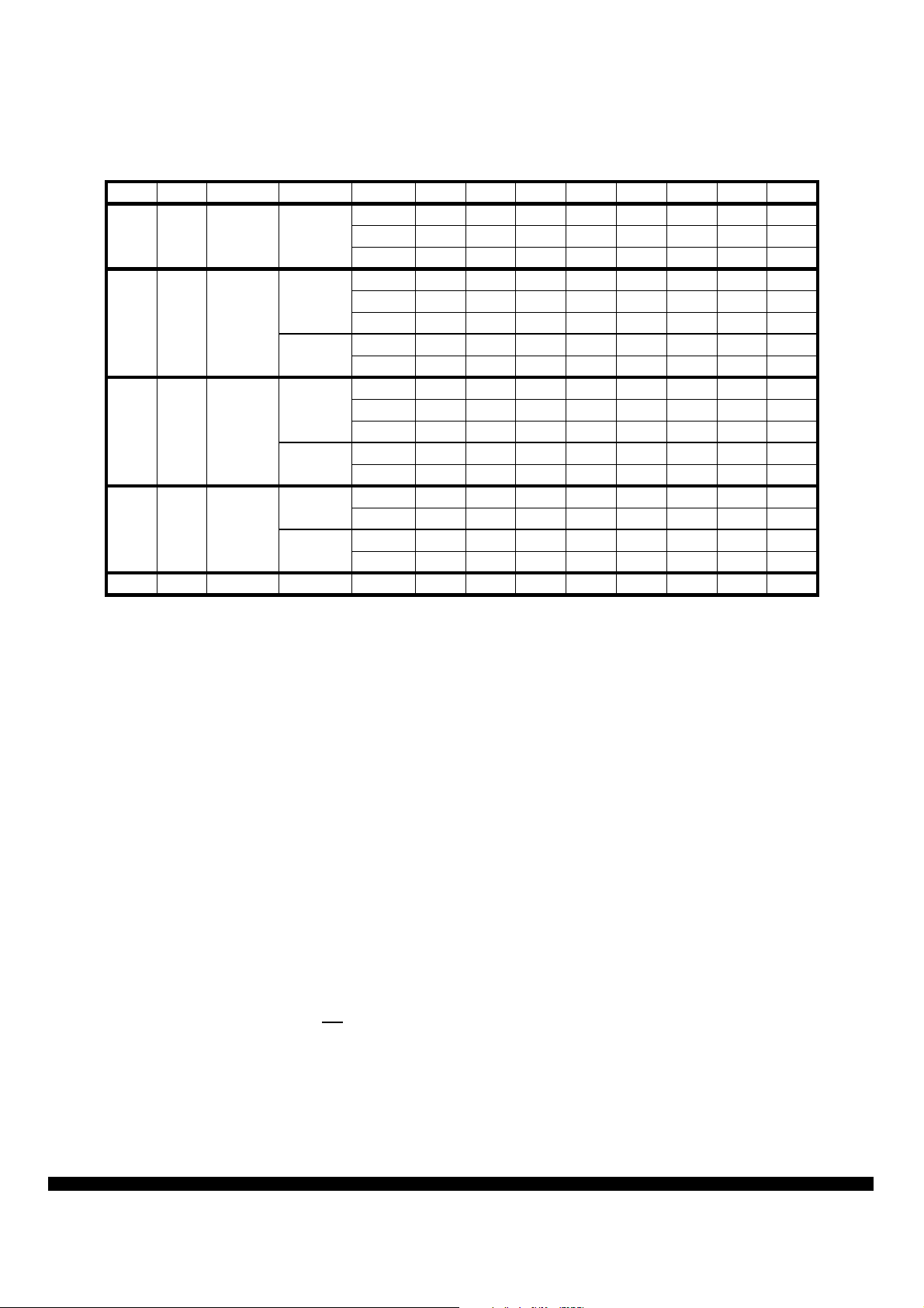
Table 1 List of MC9S12D-Family members
Flash RAM EEPROM Package Device CAN J1850 SCI SPI IIC A/D PWM I/O
512K 14K 4K 112LQFP
112LQFP
256K 12K 4K
80QFP
112LQFP
128K 8K 2K
80QFP
112LQFP
64K 4K 1K
80QFP
32K2K1K80QFPD32 102101/8759
DP512512312/16891
DT512302312/16891
DJ512212312/16891
DT256302312/16891
DJ256212312/16891
DG256202312/16891
DJ256212311/8759
DG256202311/8759
DT128302212/16891
DJ128212212/16891
DG128202212/16891
DJ128212211/8759
DG128202211/8759
DJ64 112112/16891
D64 102112/16891
DJ64 112111/8759
D64 102111/8759
• Pin out explanations:
— A/D is the number of modules/total number of A/D channels.
— I/O is the sum of ports capable to act as digital input or output.
112 Pin Packages:
Port A = 8, B = 8, E = 6 + 2 input only, H = 8, J = 4, K = 7, M = 8, P = 8, S = 8, T = 8, PAD = 16 input
only.
22 inputs provide Interrupt capability (H =8, P= 8, J = 4, IRQ, XIRQ)
80 Pin Packages:
Port A = 8, B = 8, E = 6 + 2 input only, J = 2, M = 6, P = 7, S = 4, T = 8, PAD = 8 input only.
11 inputs provide Interrupt capability (P= 7, J = 2, IRQ, XIRQ)
— CAN0 pins are shared between J1850 pins.
— CAN0 can be routed under software control from PM1:0 to pins PM3:2 or PM5:4 or PJ7:6.
— CAN4 pins are shared between IIC pins.
— CAN4 can be routed under software control from PJ7:6 to pins PM5:4 or PM7:6.
Freescale Semiconductor, I
— Versions with 4 CAN modules will have CAN0, CAN1, CAN2 and CAN4.
— Versions with 3 CANs modules will have CAN0, CAN1 and CAN4.
— Versions with 2 CAN modules will have CAN0 and CAN4.
— Versions with one CAN module will have CAN0.
— Versions with 2 SPI modules will have SPI0 and SPI1.
— Versions with 1 SPI will have SPI0.
— SPI0 can be routed to either Ports PS7:4 or PM5:2.
— SPI2 pins are shared with PW M7: 4; In 11 2 pin vers io ns S PI2 can be route d und er soft ware control to
PH7:4. In 80 pin packages SS
CAN and SPI routing features are not available on the 1st PC9S12DP256 mask set 0K36N!
-signal of SPI2 is not bonded out!
NOTE
PRODUCT PROPOSAL, Rev 6.1, 23-Oct-02 3
For More Information On This Product,
Go to: www.freescale.com
Freescale Semiconductor, Inc.
..
.
nc
Freescale Semiconductor, I
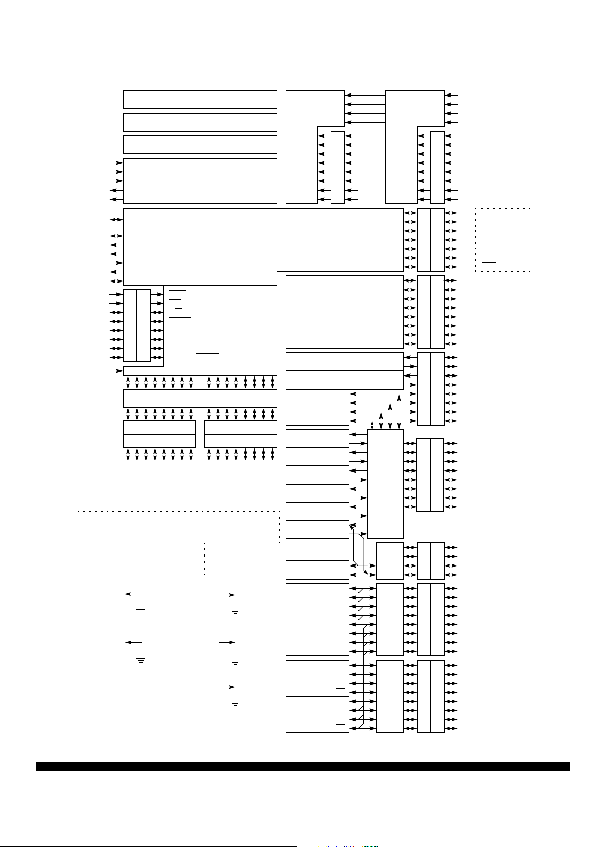
32K - 512K Byte Flash EEPROM
2K - 14K Byte RAM
1K - 4K Byte EEPROM
VDDR
VSSR
VREGEN
VDD1,2
VSS1,2
BKGD
XFC
VDDPLL
VSSPLL
EXTAL
XTAL
RESET
PE0
PE1
PE2
PE3
PE4
PE5
PE6
PE7
TEST
Single-wire Background
PLL
PTE
Voltage Regulator
Debug Module
Clock and
Reset
Generation
Module
XIRQ
IRQ
R/W
LSTRB
ECLK
DDRE
MODA
MODB
NOACC/XCLKS
CPU12
Periodic Interrupt
COP Watchdog
Clock Monitor
Breakpoints
System
Integration
Module
(SIM)
Multiplexed Address/Data Bus
DDRA DDRB
PTA PTB
PA4
PA3
PA2
PA1
PA0
ADDR11
ADDR10
ADDR9
ADDR8
DATA11
DATA10
DATA9
DATA8
PB7
PB6
ADDR7
ADDR6
DATA7
DATA6
PB4
PB5
ADDR4
ADDR5
DATA4
DATA5
Multiplexed
Wide Bus
PA7
PA6
PA5
ADDR12
ADDR15
ADDR14
ADDR13
DATA12
DATA15
DATA14
DATA13
Multiplexed
Narrow Bus
Internal Logic 2.5V
VDD1,2
VSS1,2
PLL 2.5V
VDDPLL
VSSPLL
DATA4
DATA3
DATA2
DATA1
DATA7
DATA6
DATA5
DATA0
I/O Driver 5V
VDDX
VSSX
A/D Converter 5V &
Voltage Regulator Reference
VDDA
VSSA
Voltage Regulator 5V & I/O
VDDR
VSSR
Not all functionality shown in this
Block diagram is available in all Versions!
PB3
PB2
ADDR3
ADDR2
DATA3
DATA2
PB1
PB0
ADDR1
ADDR0
DATA1
DATA0
AN0
AN1
AN2
AN3
AN4
AN5
AN6
AN7
VRH
VRL
VDDA
VSSA
AD0
ATD0
PPAGE
Enhanced Capture
Timer
SCI0
SCI1
MISO
SPI0
BDLC
(J1850)
CAN0
CAN1
CAN2
CAN3
CAN4
IIC
PWM
SPI1
SPI2
MOSI
SCK
SS
RXB
TXB
RXCAN
TXCAN
RXCAN
TXCAN
RXCAN
TXCAN
RXCAN
TXCAN
RXCAN
TXCAN
SDA
SCL
PWM0
PWM1
PWM2
PWM3
PWM4
PWM5
PWM6
PWM7
MISO
MOSI
SCK
SS
MISO
MOSI
SCK
SS
PAD00
PAD01
PAD02
PAD03
PAD04
PAD05
PAD06
PAD07
ATD1
PIX0
PIX1
PIX2
PIX3
PIX4
PIX5
ECS
IOC0
IOC1
IOC2
IOC3
IOC4
IOC5
IOC6
IOC7
RXD
TXD
RXD
TXD
Module to Port Routing
KWJ0
KWJ1
KWJ6
KWJ7
KWP0
KWP1
KWP2
KWP3
KWP4
KWP5
KWP6
KWP7
KWH0
KWH1
KWH2
KWH3
KWH4
KWH5
KWH6
KWH7
AN0
AN1
AN2
AN3
AN4
AN5
AN6
AN7
VRH
VRL
VDDA
VSSA
DDRK
DDRT
DDRS
DDRM
DDRJ
DDRP
DDRH
AD1
PTK
PTT
PTS
PTM
PTJ
PTP
PTH
VRH
VRL
VDDA
VSSA
PAD08
PAD09
PAD10
PAD11
PAD12
PAD13
PAD14
PAD15
PK0
PK1
PK2
PK3
PK4
PK5
PK7
PT0
PT1
PT2
PT3
PT4
PT5
PT6
PT7
PS0
PS1
PS2
PS3
PS4
PS5
PS6
PS7
PM0
PM1
PM2
PM3
PM4
PM5
PM6
PM7
PJ0
PJ1
PJ6
PJ7
PP0
PP1
PP2
PP3
PP4
PP5
PP6
PP7
PH0
PH1
PH2
PH3
PH4
PH5
PH6
PH7
XADDR14
XADDR15
XADDR16
XADDR17
XADDR18
XADDR19
ECS
/ROMONE
Signals shown in Bold are not available on the 80 Pin Package
4 PRODUCT PROPOSAL, Rev 6.1, 23-Oct-02
For More Information On This Product,
MC9S
Go to: www.freescale.com
..
.
nc
Freescale Semiconductor, I
SS1/PWM3/KWP3/PP3
SCK1/PWM2/KWP2/PP2
MOSI1/PWM1/KWP1/PP1
MISO1/PWM0/KWP0/PP0
XADDR17/PK3
XADDR16/PK2
XADDR15/PK1
XADDR14/PK0
IOC0/PT0
IOC1/PT1
IOC2/PT2
IOC3/PT3
VDD1
VSS1
IOC4/PT4
IOC5/PT5
IOC6/PT6
IOC7/PT7
XADDR19/PK5
XADDR18/PK4
KWJ1/PJ1
MODC/TAGHI/
KWJ0/PJ0
BKGD
ADDR0/DATA0/PB0
ADDR1/DATA1/PB1
ADDR2/DATA2/PB2
ADDR3/DATA3/PB3
ADDR4/DATA4/PB4
Freescale Semiconductor, Inc.
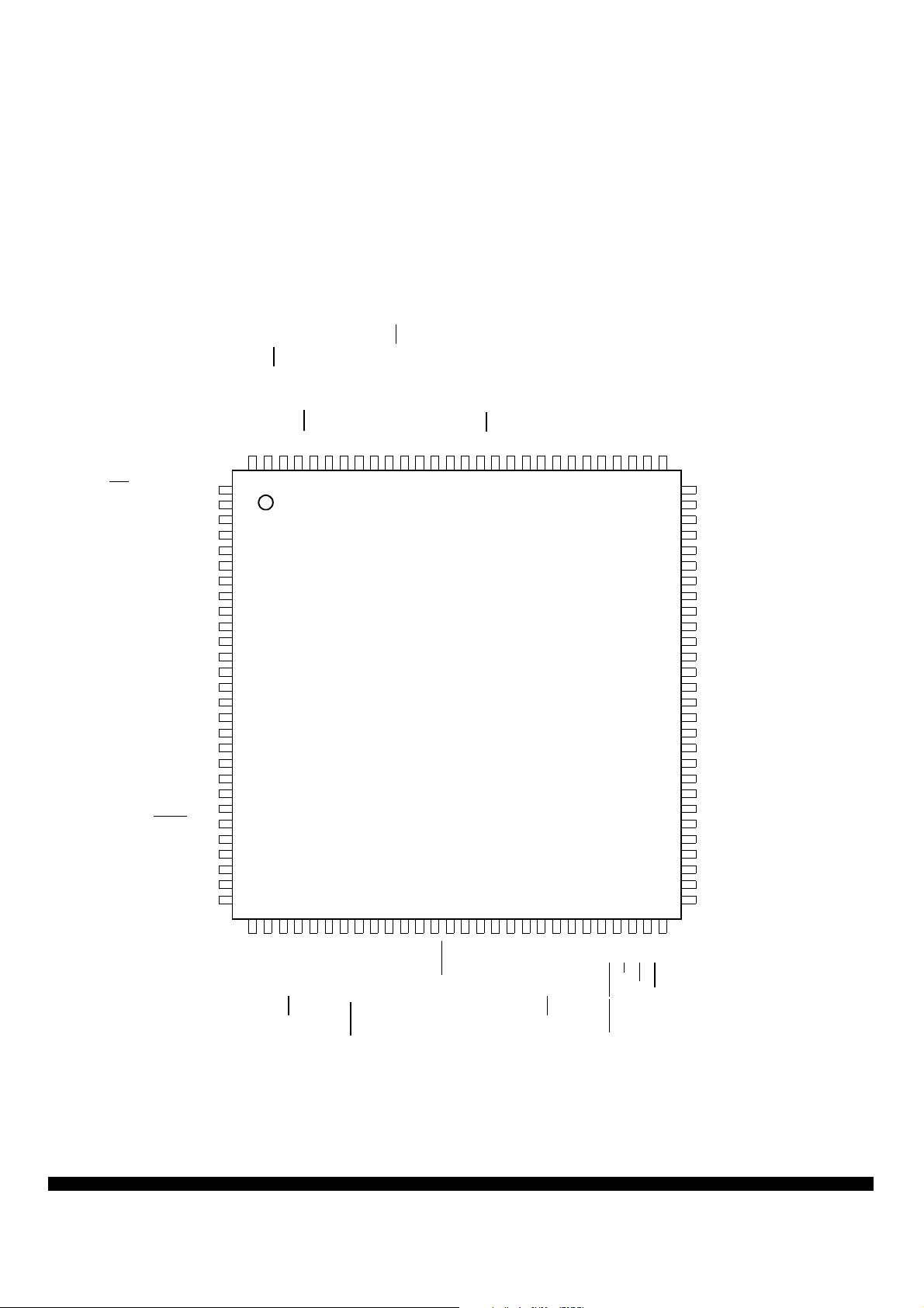
Figure 1 Pin assignments 112 LQFP for MC9S12D-Family
/ROMONE
PP4/KWP4/PWM4/MISO2
PP5/KPW5/PWM5/MOSI2
PP6/KWP6/PWM6/SS2
PP7/KWP7/PWM7/SCK2
PK7/ECS
VDDX
VSSX
PM0/RXCAN0/RXB
111
112
110
109
108
107
106
1
2
3
4
5
6
7
8
9
10
11
12
13
14
15
16
17
18
19
20
21
22
23
24
25
26
27
28
293031323334353637383940414243444546474849505152535455
105
PM4/RXCAN2/RXCAN0/RXCAN4/MOSI0
PM1/TXCAN0/TXB
PM2/RXCAN1/RXCAN0/MISO0
PM3/TXCAN1/TXCAN0/SS0
104
103
102
101
MC9S12D-Family
112LQFP
PM5/TXCAN2/TXCAN0/TXCAN4/SCK0
PJ6/KWJ6/RXCAN4/SDA/RXCAN0
PJ7/KWJ7/TXCAN4/SCL/TXCAN0
VREGEN
PS7/SS0
PS6/SCK0
PS5/MOSI0
PS4/MISO0
PS3/TXD1
PS2/RXD1
PS1/TXD0
PS0/RXD0
PM6/RXCAN3/RXCAN4
999897969594939291908988878685
100
PM7/TXCAN3/TXCAN4
VSSA
VRL
84
VRH
83
VDDA
82
PAD15/AN15/ETRIG1
81
PAD07/AN07/ETRIG0
80
PAD14/AN14
79
PAD06/AN06
78
PAD13/AN13
77
PAD05/AN05
76
PAD12/AN12
75
PAD04/AN04
74
PAD11/AN11
73
PAD03/AN03
72
PAD10/AN10
71
PAD02/AN02
70
PAD09/AN09
69
PAD01/AN01
68
PAD08/AN08
67
PAD00/AN00
66
VSS2
65
VDD2
64
PA7/ADDR15/DATA15
63
PA6/ADDR14/DATA14
62
PA5/ADDR13/DATA13
61
PA4/ADDR12/DATA12
60
PA3/ADDR11/DATA11
59
PA2/ADDR10/DATA10
58
PA1/ADDR9/DATA9
57
PA0/ADDR8/DATA8
56
XFC
XTAL
VSSR
VDDR
RESET
/KWH7/PH7
SS2
SCK2/KWH6/PH6
MOSI2/KWH5/PH5
ADDR5/DATA5/PB5
ADDR6/DATA6/PB6
ADDR7/DATA7/PB7
MISO2/KWH4/PH4
ECLK/PE4
/NOACC/PE7
MODB/IPIPE1/PE6
MODA/IPIPE0/PE5
XCLKS
VDDPLL
Signals shown in Bold are not available on the 80 Pin Package
TEST
EXTAL
VSSPLL
/KWH3/PH3
SS1
/PE3
/PE1
/PE0
IRQ
R/W/PE2
XIRQ
/TAGLO
SCK1/KWH2/PH2
MOSI1/KWH1/PH1
MISO1/KWH0/PH0
LSTRB
PRODUCT PROPOSAL, Rev 6.1, 23-Oct-02 5
For More Information On This Product,
Go to: www.freescale.com
..
.
nc
Freescale Semiconductor, I
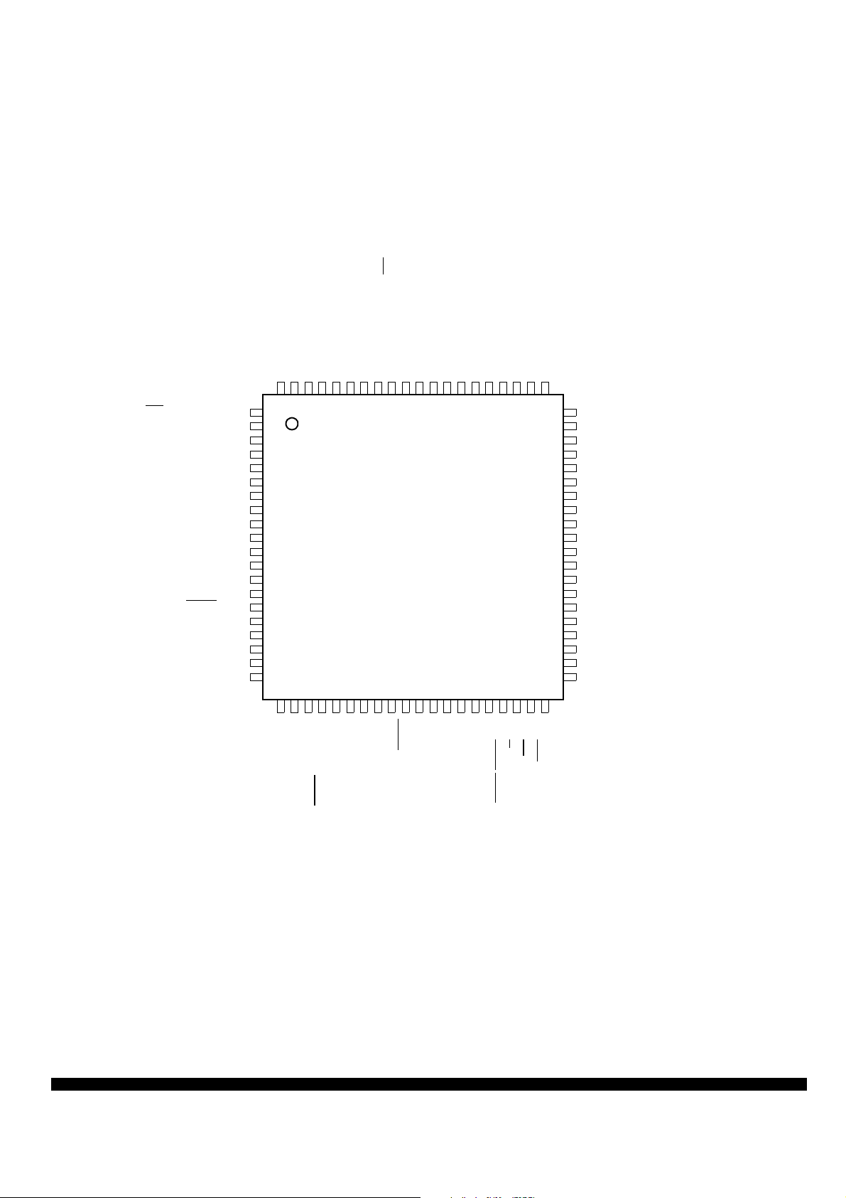
Figure 2 Pin Assignments in 80 QFP for MC9S12D-Family
SS1/PWM3/KWP3/PP3
SCK1/PWM2/KWP2/PP2
MOSI1/PWM1/KWP1/PP1
MISO1/PWM0/KWP0/PP0
MODC/TAGHI/
IOC0/PT0
IOC1/PT1
IOC2/PT2
IOC3/PT3
VDD1
VSS1
IOC4/PT4
IOC5/PT5
IOC6/PT6
IOC7/PT7
BKGD
ADDR0/DATA0/PB0
ADDR1/DATA1/PB1
ADDR2/DATA2/PB2
ADDR3/DATA3/PB3
ADDR4/DATA4/PB4
Freescale Semiconductor, Inc.
PP4/KWP4/PWM4/MISO2
80797877767574737271706968676665646362
1
2
3
4
5
6
7
8
9
10
11
12
13
14
15
16
17
18
19
20
21222324252627282930313233343536373839
ADDR5/DATA5/PB5
PP5/KWP5/PWM5/MOSI2
ADDR6/DATA6/PB6
PP7/KWP7/PWM7/SCK2
VDDX
VSSX
PM0/RXCAN0/RXB
PM1/TXCAN0/TXB
PM2/RXCAN1/RXCAN0/MISO0
PM3/TXCAN1/TXCAN0/SS0
PM4/RXCAN2/RXCAN0/RXCAN4/MOSI0
PM5/TXCAN2/TXCAN0/TXCAN4/SCK0
PJ6/KWJ6/RXCAN4/SDA/RXCAN0
PJ7/KWJ7/TXCAN4/SCL/TXCAN0
VREGEN
PS3/TXD1
PS2/RXD1
PS1/TXD0
PS0/RXD0
VSSA
VRL
61
60
VRH
59
VDDA
58
PAD07/AN07/ETRIG0
57
PAD06/AN06
56
PAD05/AN05
55
PAD04/AN04
54
PAD03/AN03
53
PAD02/AN02
52
PAD01/AN01
51
MC9S12D-Family
80 QFP
VDDR
RESET
XFC
VSSPLL
VDDPLL
VSSR
ECLK/PE4
/NOACC/PE7
MODB/IPIPE1/PE6
MODA/IPIPE0/PE5
ADDR7/DATA7/PB7
XCLKS
/PE3
/PE2
TEST
/TAGLO
LSTRB
/PE1
IRQ
R/W
XTAL
EXTAL
PAD00/AN00
50
VSS2
49
VDD2
48
PA7/ADDR15/DATA15
47
PA6/ADDR14/DATA14
46
PA5/ADDR13/DATA13
45
PA4/ADDR12/DATA12
44
PA3/ADDR11/DATA11
43
PA2/ADDR10/DATA10
42
PA1/ADDR9/DATA9
41
PA0/ADDR8/DATA8
40
/PE0
XIRQ
6 PRODUCT PROPOSAL, Rev 6.1, 23-Oct-02
For More Information On This Product,
MC9S
Go to: www.freescale.com
Freescale Semiconductor, Inc.
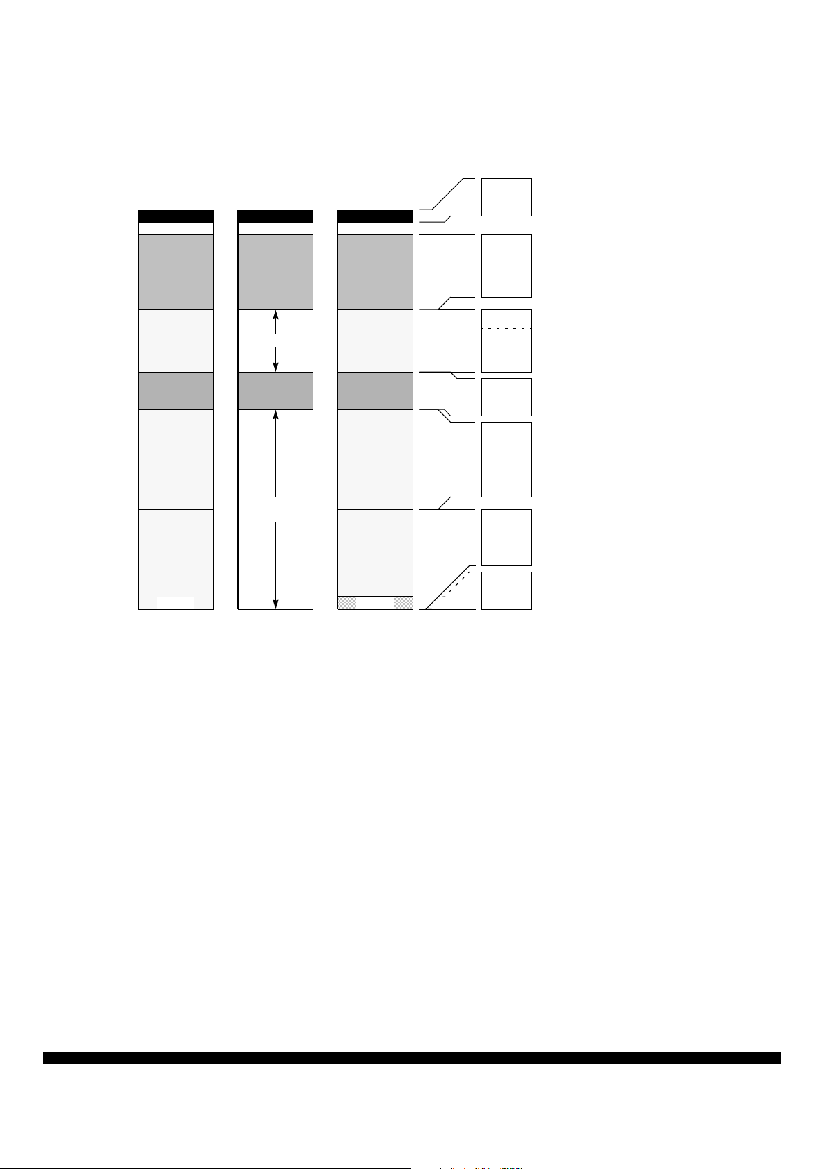
Figure 3 MC9S12Dx512 User Configurable Memory Map
..
.
nc
$0000
$0000
$0400
$0800
$4000
$7000
$8000
$C000
$FF00
$FFFF
NORMAL
SINGLE CHIP
EXT
EXT
VECTORSVECTORS VECTORS
EXPANDED SPECIAL
SINGLE CHIP
$03FF
$0800
$3FFF
$4000
$6FFF
$7000
$7FFF
$8000
$BFFF
$C000
$FFFF
$FF00
$FFFF
The figure shows a useful map, which is not the map out of reset. After reset the map is:
$0000 - $03FF: Register Space
$0800 - $3FFF: 14K RAM
$0000 - $0FFF: 4K EEPROM (1k $0400 - $07FF visible, $0000 - $03FF and $0800 - $0FFF are not visible)
Various possibilities to make more of the EEPROM fully visible are available, one of them is shown above
1K Register Spa ce
Mappable to any 2K Bo undary
14K Bytes RAM
Alignable to top ($0800 - $3FFF)
or bottom ($0000 - $37FF)
Mappable to any 16 K Boundary
0.5K, 1K, 2K or 4K Protec te d Sec to r
12K Fixed Flash EEPROM
4K Flash overlapped by EEPROM in this configuration
4K Bytes EEPROM
Mappable to any 4K Bo undary
16K Page Window
thirty two * 16K Flash EEPROM Pages
16K Fixed Flash EEPROM
2K, 4K, 8K or 16K Protected Boot Sector
BDM
(If Active)
Freescale Semiconductor, I
PRODUCT PROPOSAL, Rev 6.1, 23-Oct-02 7
For More Information On This Product,
Go to: www.freescale.com
Freescale Semiconductor, Inc.
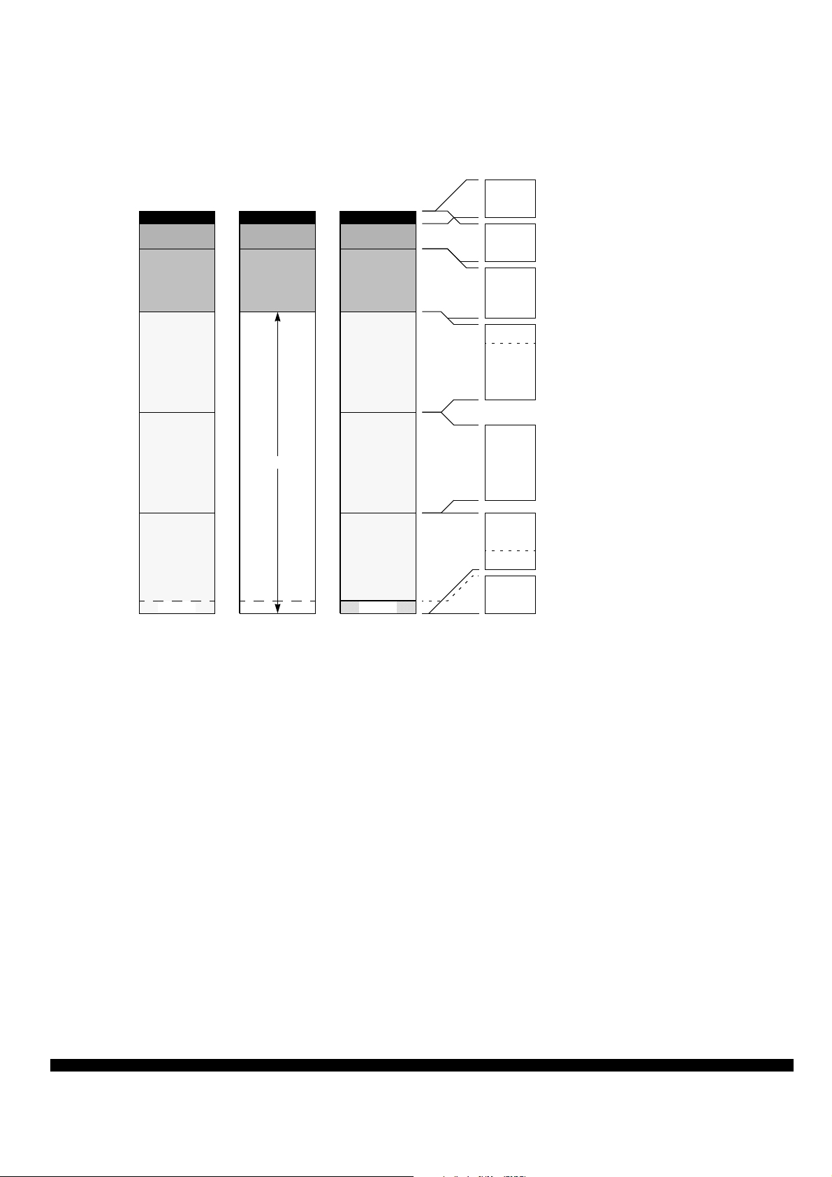
Figure 4 MC9S12Dx256 User Configurable Memory Map
..
.
nc
$0000
$0400
$1000
$4000
$8000
$C000
$FF00
$FFFF
NORMAL
SINGLE CHIP
EXT
VECTORSVECTORS VECTORS
EXPANDED SPECIAL
SINGLE CHIP
$0000
$03FF
$0000
$0FFF
$1000
$3FFF
$4000
$7FFF
$8000
$BFFF
$C000
$FFFF
$FF00
$FFFF
1K Register Spa ce
Mappable to any 2K Bo undary
4K Bytes EEPROM
Initially ove rlapped by register space
Mappable to any 4K Bo undary
12K Bytes RAM
Alignable to top ($1000 - $3FFF)
or bottom ($0000 - $2FFF)
Mappable to any 16K Boundary
0.5K, 1K, 2K or 4K Protec te d Sec to r
16K Fixed Flash EEPROM
16K Page Window
sixteen * 16K Flash EEPROM Page s
16K Fixed Flash EEPROM
2K, 4K, 8K or 16K Protected Boot Sector
BDM
(If Active)
Freescale Semiconductor, I
8 PRODUCT PROPOSAL, Rev 6.1, 23-Oct-02
For More Information On This Product,
Go to: www.freescale.com
MC9S

Freescale Semiconductor, Inc.
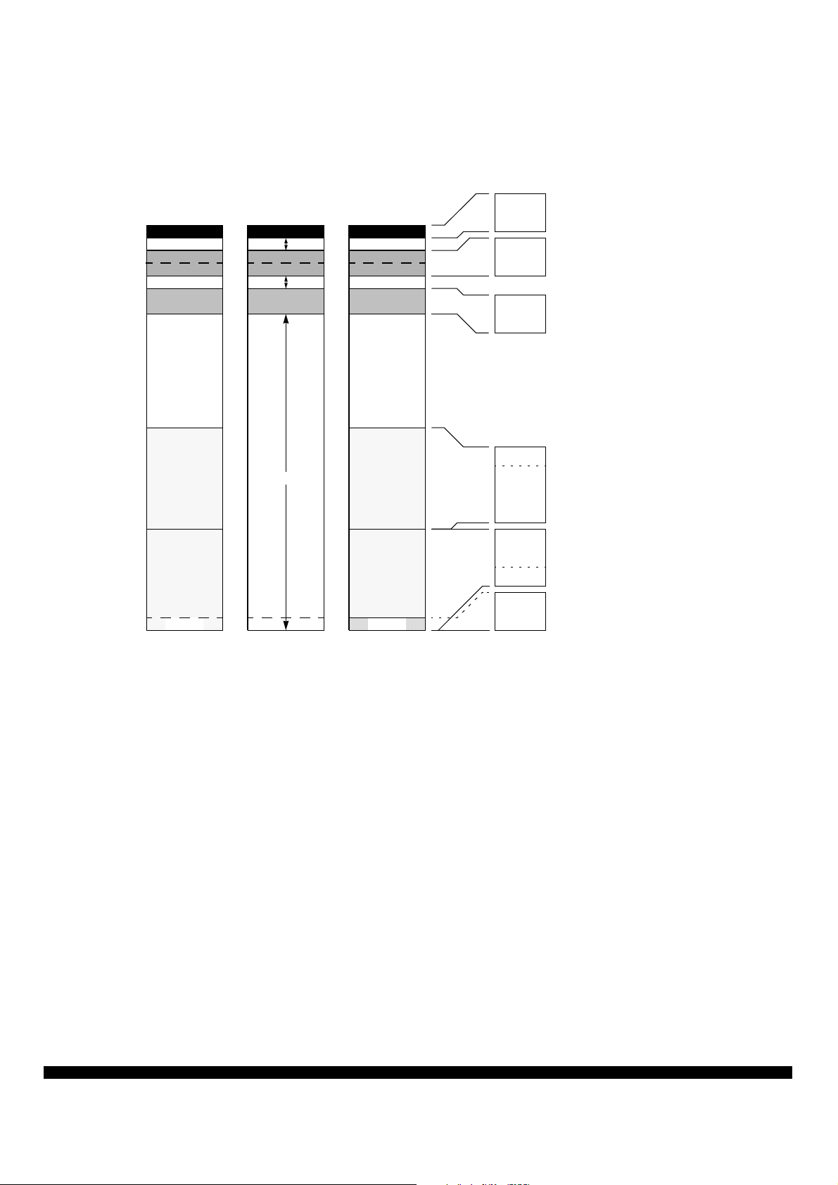
Figure 5 MC9S12Dx128 User Configurable Memory Map
..
.
nc
$0000
$0000
$0400
$0800
$1000
$2000
$4000
$8000
EXT
$C000
$FF00
$FFFF
NORMAL
SINGLE CHIP
The figure shows a useful map, which is not the map out of reset. After reset the map is:
$0000 - $03FF: Register Space
$0000 - $1FFF: 8K RAM
$0000 - $07FF: 1K EEPROM (not visible)
VECTORSVECTORS VECTORS
EXPANDED SPECIAL
SINGLE CHIP
$03FF
$0800
$0FFF
$2000
$3FFF
$4000
$7FFF
$8000
$BFFF
$C000
$FFFF
$FF00
$FFFF
1K Register Spa ce
Mappable to any 2K Bo undary
2K Bytes EEPROM
Mappable to any 2K Bo undary
8K Bytes RAM
Mappable to any 8K Bo undary
0.5K, 1K, 2K or 4K Protec te d Sec to r
16K Fixed Flash EEPROM
16K Page Window
eight * 16K Flash EEPROM Pages
16K Fixed Flash EEPROM
2K, 4K, 8K or 16K Protected Boot Sector
BDM
(If Active)
Freescale Semiconductor, I
PRODUCT PROPOSAL, Rev 6.1, 23-Oct-02 9
For More Information On This Product,
Go to: www.freescale.com

Freescale Semiconductor, Inc.
Figure 6 MC9S12Dx64 User Configurable Memory Map
..
.
nc
$0000
$0000
$0400
$0800
$1000
$3000
$4000
$8000
$C000
$FF00
$FFFF
NORMAL
SINGLE CHIP
EXT
VECTORSVECTORS VECTORS
EXPANDED SPECIAL
SINGLE CHIP
$03FF
$0800
$0FFF
$3000
$3FFF
$4000
$7FFF
$8000
$BFFF
$C000
$FFFF
$FF00
$FFFF
The figure shows a useful map, which is not the map out of reset. After reset the map is:
$0000 - $03FF: Register Space
$0000 - $0FFF: 4K RAM
$0000 - $07FF: 1K EEPROM (not visible)
1K Register Spa ce
Mappable to any 2K Bo undary
1K Bytes EEPROM
repeated twice in the 2K space
Mappable to any 2K Bo undary
4K Bytes RAM
Mappable to any 4K Bo undary
0.5K, 1K, 2K or 4K Protec te d Sec to r
16K Fixed Flash EEPROM
16K Page Window
four * 16K Flash EEPROM Pages
16K Fixed Flash EEPROM
2K, 4K, 8K or 16K Protected Boot Sector
BDM
(If Active)
Freescale Semiconductor, I
10 PRODUCT PROPOSAL, Rev 6.1, 23-Oct-02
For More Information On This Product,
Go to: www.freescale.com
MC9S
Freescale Semiconductor, Inc.
Figure 7 MC9S12Dx32 User Configurable Memory Map
..
.
nc
$0000
$0000
$0400
$0800
$1000
$3800
$4000
$8000
EXT
$C000
$FF00
$FFFF
NORMAL
SINGLE CHIP
The figure shows a useful map, which is not the map out of reset. After reset the map is:
$0000 - $03FF: Register Space
$0800 - $0FFF: 2K RAM
$0000 - $07FF: 1K EEPROM (not visible)
VECTORSVECTORS VECTORS
EXPANDED SPECIAL
SINGLE CHIP
$03FF
$0800
$0FFF
$3800
$3FFF
$8000
$BFFF
$C000
$FFFF
$FF00
$FFFF
1K Register Space
Mappable to any 2K Boundary
1K Bytes EEPROM
Repeated twice in the 2K space
Mappable to any 2K Boundary
2K Bytes RAM
Mappable to any 2K Boundary
0.5K, 1K, 2K or 4K Protected Sector
two * 16K Flash EEPROM Pages
16K Fixed Flash EEPROM
16K Fixed Flash EEPROM
2K, 4K, 8K or 16K Protected Boot Sector
BDM
(If Active)
Freescale Semiconductor, I
PRODUCT PROPOSAL, Rev 6.1, 23-Oct-02 11
For More Information On This Product,
Go to: www.freescale.com

Freescale Semiconductor, Inc.
..
.
nc
Freescale Semiconductor, I
PIN 1
IDENT
C
4X
112 85
1
VIEW Y
L
28 57
29 56
C2
0.050
C1
VIEW AB
S1
A1
L-M0.20 NT
A
S
θ
N
(Y)
(Z)
θ
R
(K)
E
4X 28 TIPS
2θ
3
R2
R
R1
L-M0.20 NT
84
B
M
B1
V1
VIEW AB
0.10
SEATING
PLANE
T
0.25
GAGE PLAN E
1θ
C
V
112X
T
J1
J1
L
J
0.13 NT
SECTION J1-J1
ROTATED 90 COUNTERCLOCKWISE
NOTES:
1. DIMENSIONING AND TOLERANCING PER
ASME Y14.5M, 1994.
2. DIMENSIONS IN MILLIMETERS.
3. DATUMS L, M AND N TO BE DETERMINED AT
SEATING PLANE, DATUM T.
4. DIMENSIONS S AND V TO BE DETE R MINED AT
SEATING PLANE, DATUM T.
5. DIMENSIONS A AND B DO NO T INCLUDE
MOLD PROTRUSION. ALLOWABLE
PROTRUSION IS 0.25 PER SIDE. DIMENSIONS
A AND B INCLUDE MOLD MISMATCH.
6. DIMENSION D DOES NOT INCLUDE DAMBAR
DIMAMIN MAX
A1 10.000 BSC
B 20.000 BSC
B1 10.000 BSC
C --- 1.600
C1 0.050 0.150
C2 1.350 1.450
D 0.270 0.370
E 0.450 0.750
F 0.270 0.330
G 0.650 BSC
J 0.090 0.170
K 0.500 REF
P 0.325 BSC
R1 0.100 0.200
R2 0.100 0.200
S 22.000 BSC
S1 11.000 BSC
V 22.000 BSC
V1 11.000 BSC
Y 0.250 REF
Z 1.000 REF
AA 0.090 0.160
θ
θ
1
θ
2
θ 11 °
3
108X
G
VIEW Y
F
D
M
°
MILLIMETERS
20.000 BSC
0 °
3 °
11 °
4X
P
X
X=L, M OR N
AA
L-M
8 °
7 °
13 °
13 °
BASE
METAL
Figure 8 112-pin LQFP Mechanical Dimensions (case no. 987)
12 PRODUCT PROPOSAL, Rev 6.1, 23-Oct-02
For More Information On This Product,
Go to: www.freescale.com
MC9S

Freescale Semiconductor, Inc.
L
..
.
nc
Freescale Semiconductor, I
60
61
-A-
L
DETAIL A
80
120
M
0.20 D
A-B
0.05
M
0.20 D
E
C DATUM
-C-
SEATING
PLANE
DATUM
PLANE
H
G
-H-
W
X
DETAIL C
-D-
A
S
A-B
H
S
A-B
C
K
S
S
S
U
T
R
Q
41
40
-B-
21
M
M
NOTES:
1. DIMENS IO NING AND TOLERANCIN G PER
ANSI Y14.5M, 1982.
2. CONTROLLING DIMENSION: MILLIMETER.
3. DATUM PLANE -H- IS LOCATED AT BOTTOM OF
LEAD AND IS COINCIDENT WITH THE
LEAD WHERE THE LEAD EXITS THE PLASTIC
BODY AT THE BOTTOM OF THE PARTING LINE.
4. DATUMS -A- , -B- AND -D- TO BE
DETERMINED AT DATUM PLANE - H-.
5. DIMENSIONS S AND V TO BE DETERMINED
AT SEATING PLANE -C-.
6. DIMENSIONS A AND B DO NOT INCLUDE
MOLD PROTRUSION. ALLOWABLE
PROTRUSION IS 0.25 PER SIDE. DIMENSIONS
A AND B DO INCLUDE MOLD MISMATCH
AND ARE DETERMINED AT DATUM PLANE -H-.
7. DIMENS IO N D DO ES NOT INCLUDE DAMBAR
PROTRUSION . ALLOWABLE DAMBAR
PROTRUSION SHALL BE 0.08 TOTA L IN
EXCESS OF THE D DIMENSION AT MAXIMUM
MATERIAL CONDITION. DA M BA R CANNOT
BE LOCATED ON THE LOWER RADIUS OR
THE FOOT.
S
D
S
A-B
B
H
M
0.20
DETAIL C
-H-
PLANE
0.10
S
D
S
A-B
V
C
D
M
0.20
0.05
B
B
DETAIL A
F
J
D
M
0.20 D
SECTION B-B
VIEW ROTATED 90
A-B
C
MILLIMETERS
DIM MIN MAX
A 13.90 14.10
B 13.90 14.10
C 2.15 2.45
D 0.22 0.38
E 2.00 2.40
F 0.22 0.33
G 0.65 BSC
H --- 0.25
J 0.13 0.23
K 0.65 0.95
L 12.35 REF
M 5 10
°°
N 0.13 0.17
P 0.325 BSC
Q 0 7
°°
R 0.13 0.30
S 16.95 17.45
T 0.13 ---
U 0 ---
°
V 16.95 17.45
W 0.35 0.45
X 1.6 REF
P
-A-,-B-,-D-
N
S
S
°
Figure 9 80-pin QFP Mechanical Dimensions (case no. 841B)
PRODUCT PROPOSAL, Rev 6.1, 23-Oct-02 13
For More Information On This Product,
Go to: www.freescale.com

..
Home Page:
www.freescale.com
email:
support@freescale.com
USA/Europe or Locations Not Listed:
Freescale Semiconductor
Technical Information Center, CH370
1300 N. Alma School Road
Chandler, Arizona 85224
(800) 521-6274
480-768-2130
support@freescale.com
Europe, Middle East, and Africa:
Freescale Halbleiter Deutschland GmbH
Technical Information Center
Schatzbogen 7
81829 Muenchen, Germany
+44 1296 380 456 (English)
+46 8 52200080 (English)
+49 89 92103 559 (German)
+33 1 69 35 48 48 (French)
support@freescale.com
Japan:
Freescale Semiconductor Japan Ltd.
Headquarters
ARCO Tower 15F
1-8-1, Shimo-Meguro, Meguro-ku
Tokyo 153-0064, Japan
0120 191014
+81 2666 8080
support.japan@freescale.com
Asia/Pacific:
Freescale Semiconductor Hong Kong Ltd.
Technical Information Center
2 Dai King Street
Tai Po Industrial Estate,
Tai Po, N.T., Hong Kong
+800 2666 8080
support.asia@freescale.com
For Literature Requests Only:
Freescale Semiconductor
Literature Distribution Center
P.O. Box 5405
Denver, Colorado 80217
(800) 441-2447
303-675-2140
Fax: 303-675-2150
LDCForFreescaleSemiconductor
@hibbertgroup.com
Information in this document is provided solely to enable system and software
implementers to use Freescale Semiconductor products. There are no express or
implied copyright licenses granted hereunder to design or fabricate any integrated
circuits or integrated circuits based on the information in this document.
Freescale Semiconductor reserves the right to make changes without further notice to
any products herein. Freescale Semiconductor makes no warranty, representation or
guarantee regarding the suitability of its products for any particular purpose, nor does
Freescale Semiconductor assume any liability arising out of the application or use of
any product or circuit, and specifically disclaims any and all liability, including without
limitation consequential or incidental damages. “Typical” parameters which may be
provided in Freescale Semiconductor data sheets and/or specifications can and do
vary in different applications and actual performance may vary over time. All operating
parameters, including “Typicals” must be validated for each customer application by
customer’s technical experts. Freescale Semiconductor does not convey any license
under its patent rights nor the rights of others. Freescale Semiconductor pro ducts are
not designed, intended, or authorized for use as components in systems intended for
surgical implant into the body, or other applications intended to support or sustain life,
or for any other application in which the failure of the Freescale Semiconductor product
could create a situation where personal injury or death may occur. Should Buyer
purchase or use Freescale Semiconductor products for any such unintended or
unauthorized application, Buyer shall indemnify and hold Freescale Semiconductor
and its officers, employees, subsidiaries, affiliates, and distributors harmless against all
claims, costs, damages, and expenses, and reasonable attorney fees arising out of,
directly or indirectly, any claim of personal injury or death associated with such
unintended or unauthorized use, even if such claim alleges that Freescale
Semiconductor was negligent regarding the design or manufacture of the part.
RoHS-compliant and/or Pb- free versions of Freescale products have the functionality
and electrical characteristics of their non-RoHS-compliant and/or non-Pb- free
counterparts. For further information, see http://www.freescale.com or contact your
Freescale sales representative.
For information on Freescale.s Environmental Products program, go to
http://www.freescale.com/epp.
.
nc
Freescale Semiconductor, Inc.
Freescale Semiconductor, I
More Information On This Product,
Go to: www.freescale.com
 Loading...