

Page 1
查询MC9328MX1_06供应商
Freescale Semiconductor
Data Sheet: Technical Data
MC9328MX1
Document Number: MC9328MX1
Rev. 7, 12/2006
MC9328MX1
Package Information
Plastic Package
Case 1304B-01
(MAPBGA–225)
Ordering Information
See Ta b le 1 on page 3
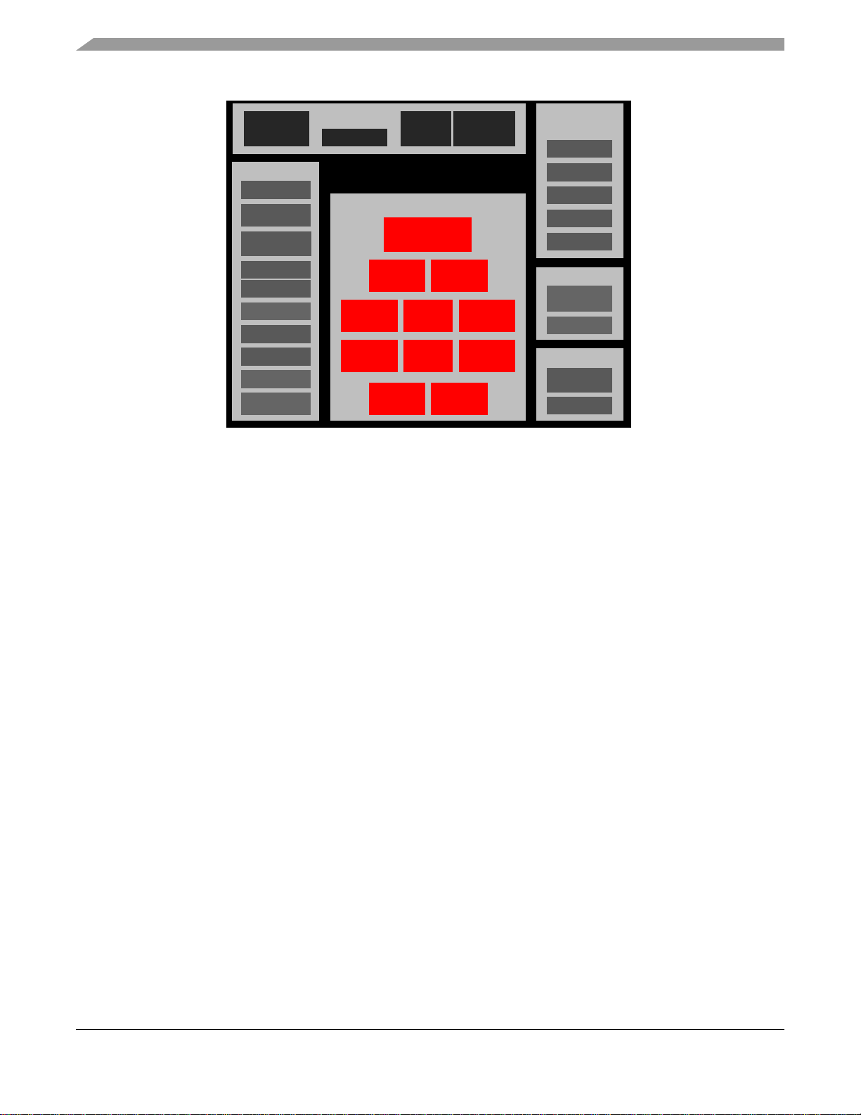
1 Introduction
The i.MX Family of applications processors provides a
leap in performance with an ARM9™ microprocessor
core and highly integrated system functions. The i.MX
family specifically addresses the requirements of the
personal, portable product market by providing
intelligent integrated peripherals, an advanced processor
core, and power management capabilities.
The MC9328MX1 (i.MX1) processor features the
advanced and power-efficient ARM920T™ core that
operates at speeds up to 200 MHz. Integrated modules,
which include a USB device, an LCD controller, and an
MMC/SD host controller, support a suite of peripherals
to enhance portable products seeking to provide a rich
multimedia experience. It is packaged in a 256-contact
Mold Array Process-Ball Grid Array (MAPBGA).
Figure 1 shows the functional block diagram of the
i.MX1 processor.
Contents
1 Introduction . . . . . . . . . . . . . . . . . . . . . . . . . . 1
2 Signals and Connections . . . . . . . . . . . . . . . 4
3 Electrical Characteristics . . . . . . . . . . . . . . 22
4 Functional Description and Application
Information . . . . . . . . . . . . . . . . . . . . . . . . . . 25
5 Pin-Out and Package Information . . . . . . . . 96
6 Product Documentation . . . . . . . . . . . . . . . . 98
Contact Information . . . . . . . . . . . . . . . Last Page
Freescale reserves the right to change the detail specifications as may be required to permit improvements in the design of its
products.
© Freescale Semiconductor, Inc., 2004, 2005, 2006. All rights reserved.
Page 2
Introduction
JTAG/ICE
Connectivity
MMC/SD
Memory Stick®
Host Controller
SPI 1 and
SPI 2
UART 1
UART 2 & 3
SSI/I2S 1 & 2
I2C
USB Device
SmartCard I/F
Bluetooth
Accelerator
System Control
Bootstrap
AIPI 1
AIPI 2
Power
Control (DPLLx2)
MC9328MX1
CPU Complex
ARM9TDMI™
I Cache
D Cache
VMMU
CGM
Interrupt
Controller
BusDMAC
Control(11 Chnl)
eSRAMEIM &
(128K)SDRAMC
Standard
System I/O
GPIO
PWM
Timer 1 & 2
RTC
Watchdog
Multimedia
Multimedia
Accelerator
Video Port
Human Interface
Analog Signal
Processor
LCD Controller
Figure 1. i.MX1 Functional Block Diagram
1.1 Features
To support a wide variety of applications, the processor offers a robust array of features, including the following:
• ARM920T™ Microprocessor Core
• AHB to IP Bus Interfaces (AIPIs)
• External Interface Module (EIM)
• SDRAM Controller (SDRAMC)
• DPLL Clock and Power Control Module
• Three Universal Asynchronous Receiver/Transmitters (UART 1, UART 2, and UART3)
• Two Serial Peripheral Interfaces (SPI1 and SPI2)
• Two General-Purpose 32-bit Counters/Timers
• Watchdog Timer
• Real-Time Clock/Sampling Timer (RTC)
• LCD Controller (LCDC)
• Pulse-Width Modulation (PWM) Module
• Universal Serial Bus (USB) Device
• Multimedia Card and Secure Digital (MMC/SD) Host Controller Module
• Memory Stick® Host Controller (MSHC)
• Direct Memory Access Controller (DMAC)
• Two Synchronous Serial Interfaces and an Inter-IC Sound (SSI1 and SSI2/I2S) Module
2
•Inter-IC (I
C) Bus Module
•Video Port
MC9328MX1 Technical Data, Rev. 7
2 Freescale Semiconductor
Page 3
Introduction
• General-Purpose I/O (GPIO) Ports
• Bootstrap Mode
• Analog Signal Processing (ASP) Module
• Bluetooth™ Accelerator (BTA)
• Multimedia Accelerator (MMA)
• Power Management Features
• Operating Voltage Range: 1.7 V to 1.9 V core, 1.7 V to 3.3 V I/O
• 256-pin MAPBGA Package
1.2 Target Applications
The i.MX1 processor is targeted for advanced information appliances, smart phones, Web browsers, based
on the popular Palm OS platform
Accompli
TM
008 GSM/GPRS interactive communicator.
, and messaging applications such as wireless cellular products, including the
1.3 Ordering Information
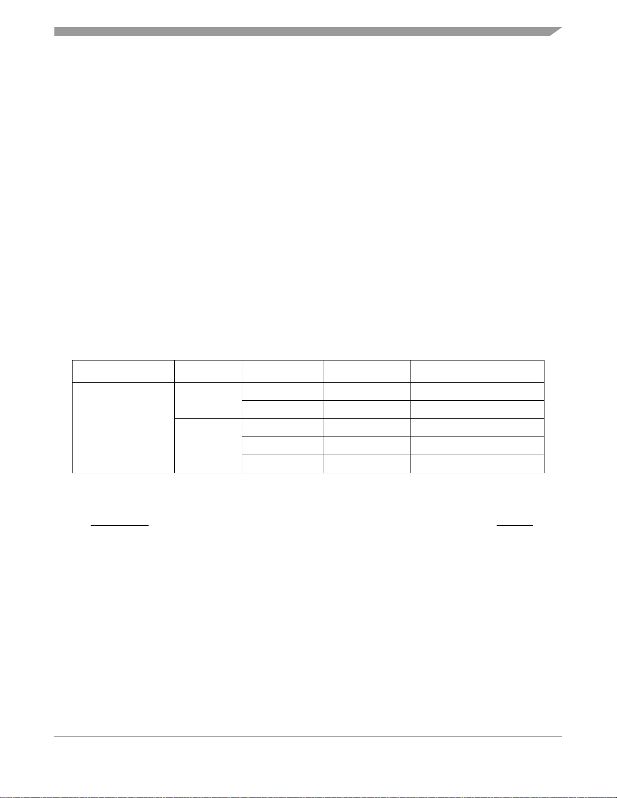
Table 1 provides ordering information.
Table 1. Ordering Information
Package Type Frequency Temperature Solderball Type Order Number
256-lead MAPBGA 200 MHz 0°C to 70°C Pb-free MC9328MX1VM20(R2)
-30°C to 70°C Pb-free MC9328MX1DVM20(R2)
150 MHz 0°C to 70°C Pb-free MC9328MX1VM15(R2)
-30°C to 70°C Pb-free MC9328MX1DVM15(R2)
-40°C to 85°C Pb-free MC9328MX1CVM15(R2)
1.4 Conventions
This document uses the following conventions:
• OVERBAR is used to indicate a signal that is active when pulled low: for example, RESET.
• Logic level one is a voltage that corresponds to Boolean true (1) state.
• Logic level zero is a voltage that corresponds to Boolean false (0) state.
•To set a bit or bits means to establish logic level one.
•To clear a bit or bits means to establish logic level zero.
•A signal is an electronic construct whose state conveys or changes in state convey information.
•A pin is an external physical connection. The same pin can be used to connect a number of signals.
• Asserted means that a discrete signal is in active logic state.
— Active low signals change from logic level one to logic level zero.
— Active high signals change from logic level zero to logic level one.
MC9328MX1 Technical Data, Rev. 7
Freescale Semiconductor 3
Page 4
Signals and Connections
• Negated means that an asserted discrete signal changes logic state.
— Active low signals change from logic level zero to logic level one.
— Active high signals change from logic level one to logic level zero.
• LSB means least significant bit or bits, and MSB means most significant bit or bits. References to
low and high bytes or words are spelled out.
• Numbers preceded by a percent sign (%) are binary. Numbers preceded by a dollar sign ($) or 0x
are hexadecimal.
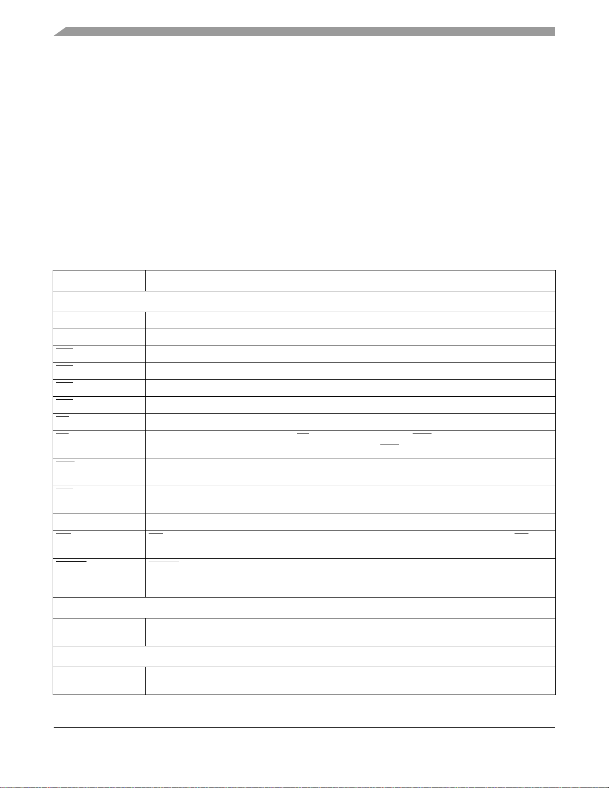
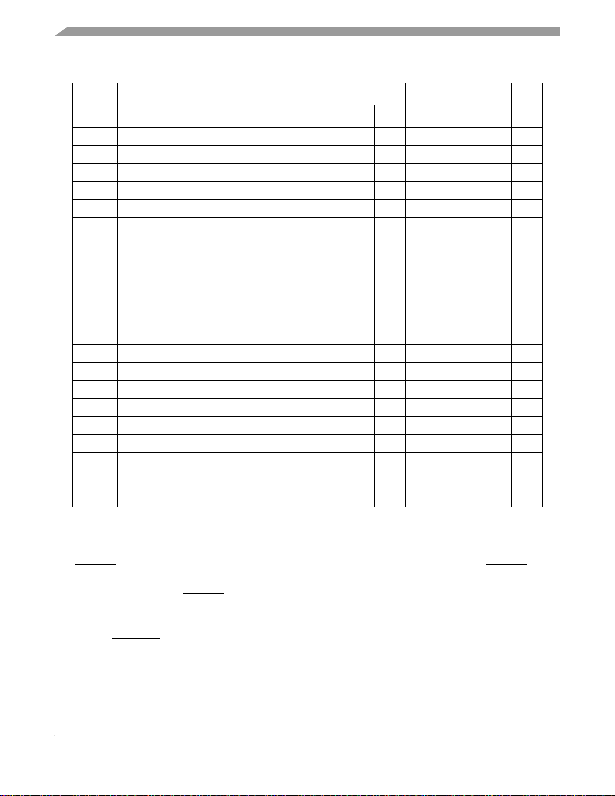
2 Signals and Connections
Table 2 identifies and describes the i.MX1 processor signals that are assigned to package pins. The signals
are grouped by the internal module that they are connected to.
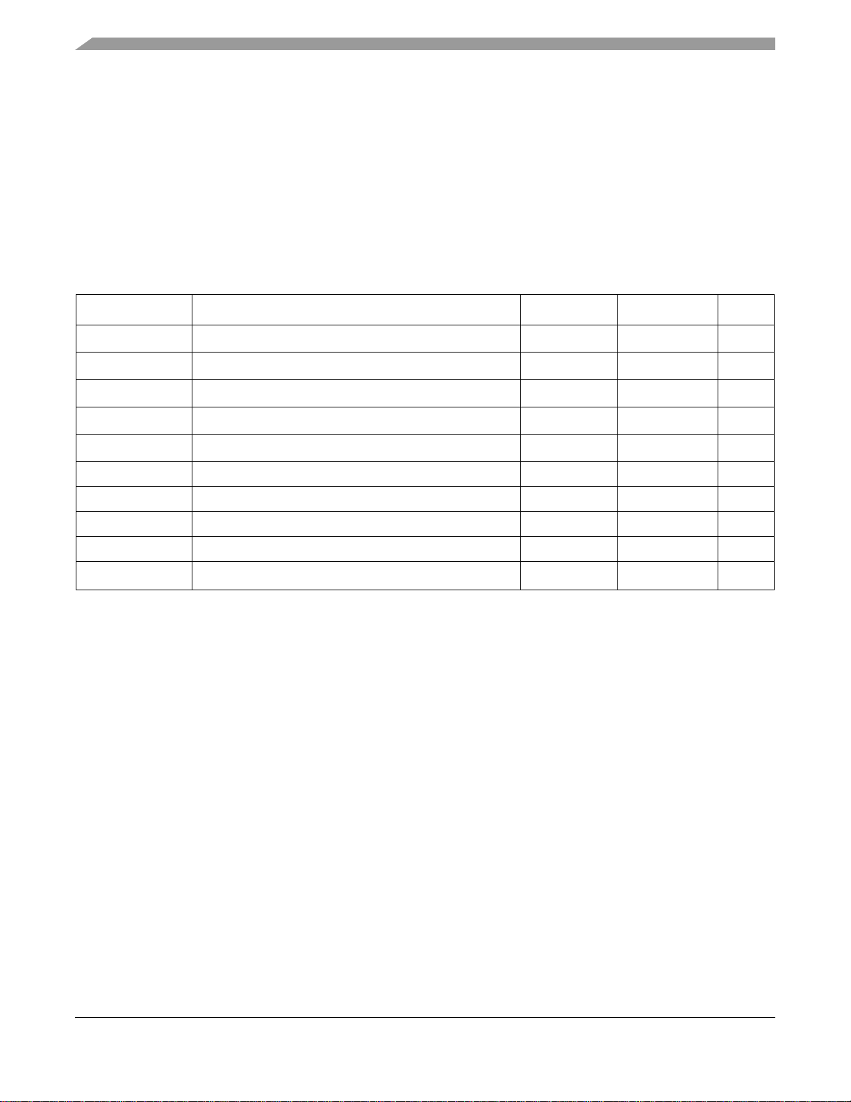
Table 2. i.MX1 Signal Descriptions
Signal Name Function/Notes
External Bus/Chip-Select (EIM)
A[24:0] Address bus signals
D[31:0] Data bus signals
EB0 MSB Byte Strobe—Active low external enable byte signal that controls D [31:24].
EB1 Byte Strobe—Active low external enable byte signal that controls D [23:16].
EB2 Byte Strobe—Active low external enable byte signal that controls D [15:8].
EB3 LSB Byte Strobe—Active low external enable byte signal that controls D [7:0].
OE Memory Output Enable—Active low output enables external data bus.
CS [5:0] Chip-Select—The chip-select signals CS [3:2] are multiplexed with CSD [1:0] and are selected by the
Function Multiplexing Control Register (FMCR). By default CSD
ECB Active low input signal sent by a flash device to the EIM whenever the flash device must terminate an
on-going burst sequence and initiate a new (long first access) burst sequence.
LBA Active low signal sent by a flash device causing the external burst device to latch the starting burst
address.
BCLK (burst clock) Clock signal sent to external synchronous memories (such as burst flash) during burst mode.
RW RW signal—Indicates whether external access is a read (high) or write (low) cycle. Used as a WE input
signal by external DRAM.
DTACK DTACK signal—The external input data acknowledge signal. When using the external DTACK signal
as a data acknowledge signal, the bus time-out monitor generates a bus error when a bus cycle is not
terminated by the external DTACK signal after 1022 clock counts have elapsed.
Bootstrap
BOOT [3:0] System Boot Mode Select—The operational system boot mode of the i.MX1 processor upon system
reset is determined by the settings of these pins.
[1:0] is selected.
SDRAM Controller
SDBA [4:0] SDRAM non-interleave mode bank address multiplexed with address signals A [15:11]. These signals
are logically equivalent to core address p_addr [25:21] in SDRAM cycles.
MC9328MX1 Technical Data, Rev. 7
4 Freescale Semiconductor
Page 5
Signals and Connections
Table 2. i.MX1 Signal Descriptions (Continued)
Signal Name Function/Notes
SDIBA [3:0] SDRAM interleave addressing mode bank address multiplexed with address signals A [19:16]. These
signals are logically equivalent to core address p_addr [12:9] in SDRAM cycles.
MA [11:10] SDRAM address signals
MA [9:0] SDRAM address signals which are multiplexed with address signals A [10:1]. MA [9:0] are selected on
SDRAM cycles.
DQM [3:0] SDRAM data enable
CSD0 SDRAM Chip-select signal which is multiplexed with the CS2 signal. These two signals are selectable
by programming the system control register.
CSD1 SDRAM Chip-select signal which is multiplexed with CS3 signal. These two signals are selectable by
programming the system control register. By default, CSD1 is selected, so it can be used as boot
chip-select by properly configuring BOOT [3:0] input pins.
RAS SDRAM Row Address Select signal
CAS SDRAM Column Address Select signal
SDWE SDRAM Write Enable signal
SDCKE0 SDRAM Clock Enable 0
SDCKE1 SDRAM Clock Enable 1
SDCLK SDRAM Clock
RESET_SF Not Used
Clocks and Resets
EXTAL16M Crystal input (4 MHz to 16 MHz), or a 16 MHz oscillator input when the internal oscillator circuit is shut
down.
XTAL16M Crystal output
EXTAL32K 32 kHz crystal input
XTAL32K 32 kHz crystal output
CLKO Clock Out signal selected from internal clock signals.
RESET_IN Master Reset—External active low Schmitt trigger input signal. When this signal goes active, all
modules (except the reset module and the clock control module) are reset.
RESET_OUT Reset Out—Internal active low output signal from the Watchdog Timer module and is asserted from the
following sources: Power-on reset, External reset (RESET_IN), and Watchdog time-out.
POR Power On Reset—Internal active high Schmitt trigger input signal. The POR signal is normally
generated by an external RC circuit designed to detect a power-up event.
JTAG
TRST Test Reset Pin—External active low signal used to asynchronously initialize the JTAG controller.
TDO Serial Output for test instructions and data. Changes on the falling edge of TCK.
TDI Serial Input for test instructions and data. Sampled on the rising edge of TCK.
TCK Test Clock to synchronize test logic and control register access through the JTAG port.
TMS Test Mode Select to sequence the JTAG test controller’s state machine. Sampled on the rising edge of
TCK.
MC9328MX1 Technical Data, Rev. 7
Freescale Semiconductor 5
Page 6
Signals and Connections
Table 2. i.MX1 Signal Descriptions (Continued)
Signal Name Function/Notes
DMA
DMA_REQ DMA Request—external DMA request signal. Multiplexed with SPI1_SPI_RDY.
BIG_ENDIAN Big Endian—Input signal that determines the configuration of the external chip-select space. If it is
driven logic-high at reset, the external chip-select space will be configured to big endian. If it is driven
logic-low at reset, the external chip-select space will be configured to little endian. This input must not
change state after power-on reset negates or during chip operation.
ETM
ETMTRACESYNC ETM sync signal which is multiplexed with A24. ETMTRACESYNC is selected in ETM mode.
ETMTRACECLK ETM clock signal which is multiplexed with A23. ETMTRACECLK is selected in ETM mode.
ETMPIPESTAT [2:0] ETM status signals which are multiplexed with A [22:20]. ETMPIPESTAT [2:0] are selected in ETM
mode.
ETMTRACEPKT [7:0] ETM packet signals which are multiplexed with ECB, LBA, BCLK (burst clock), PA17, A [19:16].
ETMTRACEPKT [7:0] are selected in ETM mode.
CMOS Sensor Interface
CSI_D [7:0] Sensor port data
CSI_MCLK Sensor port master clock
CSI_VSYNC Sensor port vertical sync
CSI_HSYNC Sensor port horizontal sync
CSI_PIXCLK Sensor port data latch clock
LCD Controller
LD [15:0] LCD Data Bus—All LCD signals are driven low after reset and when LCD is off.
FLM/VSYNC Frame Sync or Vsync—This signal also serves as the clock signal output for the gate
driver (dedicated signal SPS for Sharp panel HR-TFT).
LP/HSYNC Line pulse or H sync
LSCLK Shift clock
ACD/OE Alternate crystal direction/output enable.
CONTRAST This signal is used to control the LCD bias voltage as contrast control.
SPL_SPR Program horizontal scan direction (Sharp panel dedicated signal).
PS Control signal output for source driver (Sharp panel dedicated signal).
CLS Start signal output for gate driver. This signal is an inverted version of PS (Sharp panel dedicated
signal).
REV Signal for common electrode driving signal preparation (Sharp panel dedicated signal).
SIM
SIM_CLK SIM Clock
SIM_RST SIM Reset
SIM_RX Receive Data
MC9328MX1 Technical Data, Rev. 7
6 Freescale Semiconductor
Page 7
Signals and Connections
Table 2. i.MX1 Signal Descriptions (Continued)
Signal Name Function/Notes
SIM_TX Transmit Data
SIM_PD Presence Detect Schmitt trigger input
SIM_SVEN SIM Vdd Enable
SPI 1 and SPI 2
SPI1_MOSI Master Out/Slave In
SPI1_MISO Slave In/Master Out
SPI1_SS Slave Select (Selectable polarity)
SPI1_SCLK Serial Clock
SPI1_SPI_RDY Serial Data Ready
SPI2_TXD SPI2 Master TxData Output—This signal is multiplexed with a GPI/O pin yet shows up as a primary or
alternative signal in the signal multiplex scheme table. Please refer to the SPI and GPIO chapters in
the MC9328MX1 Reference Manual for information about how to bring this signal to the assigned pin.
SPI2_RXD SPI2 Master RxData Input—This signal is multiplexed with a GPI/O pin yet shows up as a primary or
alternative signal in the signal multiplex scheme table. Please refer to the SPI and GPIO chapters in
the MC9328MX1 Reference Manual for information about how to bring this signal to the assigned pin.
SPI2_SS SPI2 Slave Select—This signal is multiplexed with a GPI/O pin yet shows up as a primary or alternative
signal in the signal multiplex scheme table. Please refer to the SPI and GPIO chapters in the
MC9328MX1 Reference Manual for information about how to bring this signal to the assigned pin.
SPI2_SCLK SPI2 Serial Clock—This signal is multiplexed with a GPI/O pin yet shows up as a primary or alternative
signal in the signal multiplex scheme table. Please refer to the SPI and GPIO chapters in the
MC9328MX1 Reference Manual for information about how to bring this signal to the assigned pin.
General Purpose Timers
TIN Timer Input Capture or Timer Input Clock—The signal on this input is applied to both timers
simultaneously.
TMR2OUT Timer 2 Output
USB Device
USBD_VMO USB Minus Output
USBD_VPO USB Plus Output
USBD_VM USB Minus Input
USBD_VP USB Plus Input
USBD_SUSPND USB Suspend Output
USBD_RCV USB Receive Data
USBD_ROE USB OE
USBD_AFE USB Analog Front End Enable
Secure Digital Interface
SD_CMD SD Command—If the system designer does not wish to make use of the internal pull-up, via the Pull-up
enable register, a 4.7K–69K external pull up resistor must be added.
MC9328MX1 Technical Data, Rev. 7
Freescale Semiconductor 7
Page 8
Signals and Connections
Table 2. i.MX1 Signal Descriptions (Continued)
Signal Name Function/Notes
SD_CLK MMC Output Clock
SD_DAT [3:0] Data—If the system designer does not wish to make use of the internal pull-up, via the Pull-up enable
register, a 50K–69K external pull up resistor must be added.
Memory Stick Interface
MS_BS Memory Stick Bus State (Output)—Serial bus control signal
MS_SDIO Memory Stick Serial Data (Input/Output)
MS_SCLKO Memory Stick Serial Clock (Input)—Serial protocol clock source for SCLK Divider
MS_SCLKI Memory Stick External Clock (Output)—Test clock input pin for SCLK divider. This pin is only for test
purposes, not for use in application mode.
MS_PI0 General purpose Input0—Can be used for Memory Stick Insertion/Extraction detect
MS_PI1 General purpose Input1—Can be used for Memory Stick Insertion/Extraction detect
UARTs – IrDA/Auto-Bauding
UART1_RXD Receive Data
UART1_TXD Transmit Data
UART1_RTS Request to Send
UART1_CTS Clear to Send
UART2_RXD Receive Data
UART2_TXD Transmit Data
UART2_RTS Request to Send
UART2_CTS Clear to Send
UART2_DSR Data Set Ready
UART2_RI Ring Indicator
UART2_DCD Data Carrier Detect
UART2_DTR Data Terminal Ready
UART3_RXD Receive Data
UART3_TXD Transmit Data
UART3_RTS Request to Send
UART3_CTS Clear to Send
UART3_DSR Data Set Ready
UART3_RI Ring Indicator
UART3_DCD Data Carrier Detect
UART3_DTR Data Terminal Ready
Serial Audio Port – SSI (configurable to I2S protocol)
SSI_TXDAT Transmit Data
SSI_RXDAT Receive Data
MC9328MX1 Technical Data, Rev. 7
8 Freescale Semiconductor
Page 9
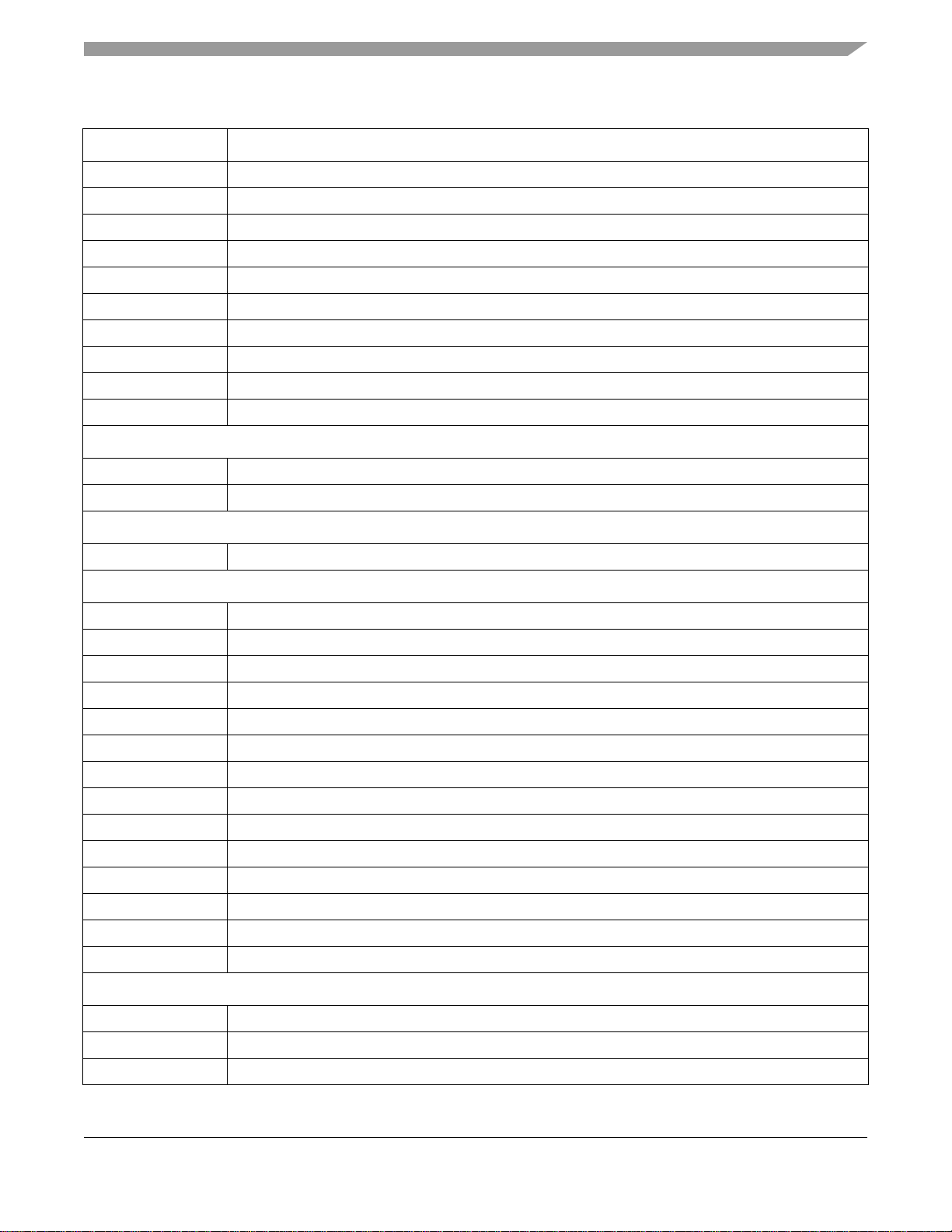
Table 2. i.MX1 Signal Descriptions (Continued)
Signal Name Function/Notes
SSI_TXCLK Transmit Serial Clock
SSI_RXCLK Receive Serial Clock
SSI_TXFS Transmit Frame Sync
SSI_RXFS Receive Frame Sync
SSI2_TXDAT TxD
SSI2_RXDAT RxD
SSI2_TXCLK Transmit Serial Clock
SSI2_RXCLK Receive Serial Clock
SSI2_TXFS Transmit Frame Sync
SSI2_RXFS Receive Frame Sync
I2C
I2C_SCL I2C Clock
I2C_SDA I2C Data
Signals and Connections
PWM
PWMO PWM Output
ASP
UIN Positive U analog input (for low voltage, temperature measurement)
UIP Negative U analog input (for low voltage, temperature measurement)
PX1 Positive pen-X analog input
PY1 Positive pen-Y analog input
PX2 Negative pen-X analog input
PY2 Negative pen-Y analog input
R1A Positive resistance input (a)
R1B Positive resistance input (b)
R2A Negative resistance input (a)
R2B Negative resistance input (b)
RVP Positive reference for pen ADC
RVM Negative reference for pen ADC
AVDD Analog power supply
AGND Analog ground
BlueTooth
BT1 I/O clock signal
BT2 Output
BT3 Input
MC9328MX1 Technical Data, Rev. 7
Freescale Semiconductor 9
Page 10
Signals and Connections
Table 2. i.MX1 Signal Descriptions (Continued)
Signal Name Function/Notes
BT4 Input
BT5 Output
BT6 Output
BT7 Output
BT8 Output
BT9 Output
BT10 Output
BT11 Output
BT12 Output
BT13 Output
BTRF VDD Power supply from external BT RFIC
BTRF GND Ground from external BT RFIC
Test Function
TRISTATE Forces all I/O signals to high impedance for test purposes. For normal operation, terminate this input
with a 1 k ohm resistor to ground. (TRI-STATE® is a registered trademark of National Semiconductor.)
Digital Supply Pins
NVDD Digital Supply for the I/O pins
NVSS Digital Ground for the I/O pins
Supply Pins – Analog Modules
AVDD Supply for analog blocks
Internal Power Supply
QVDD Power supply pins for silicon internal circuitry
QVSS Ground pins for silicon internal circuitry
2.1 I/O Pads Power Supply and Signal Multiplexing Scheme
This section describes detailed information about both the power supply for each I/O pin and its function
multiplexing scheme. The user can reference information provided in Table 6 on page 23 to configure the
power supply scheme for each device in the system (memory and external peripherals). The function
multiplexing information also shown in Table 6 allows the user to select the function of each pin by
configuring the appropriate GPIO registers when those pins are multiplexed to provide different functions.
MC9328MX1 Technical Data, Rev. 7
10 Freescale Semiconductor
Page 11

Default
(At/After)
RESE
State
Signals and Connections
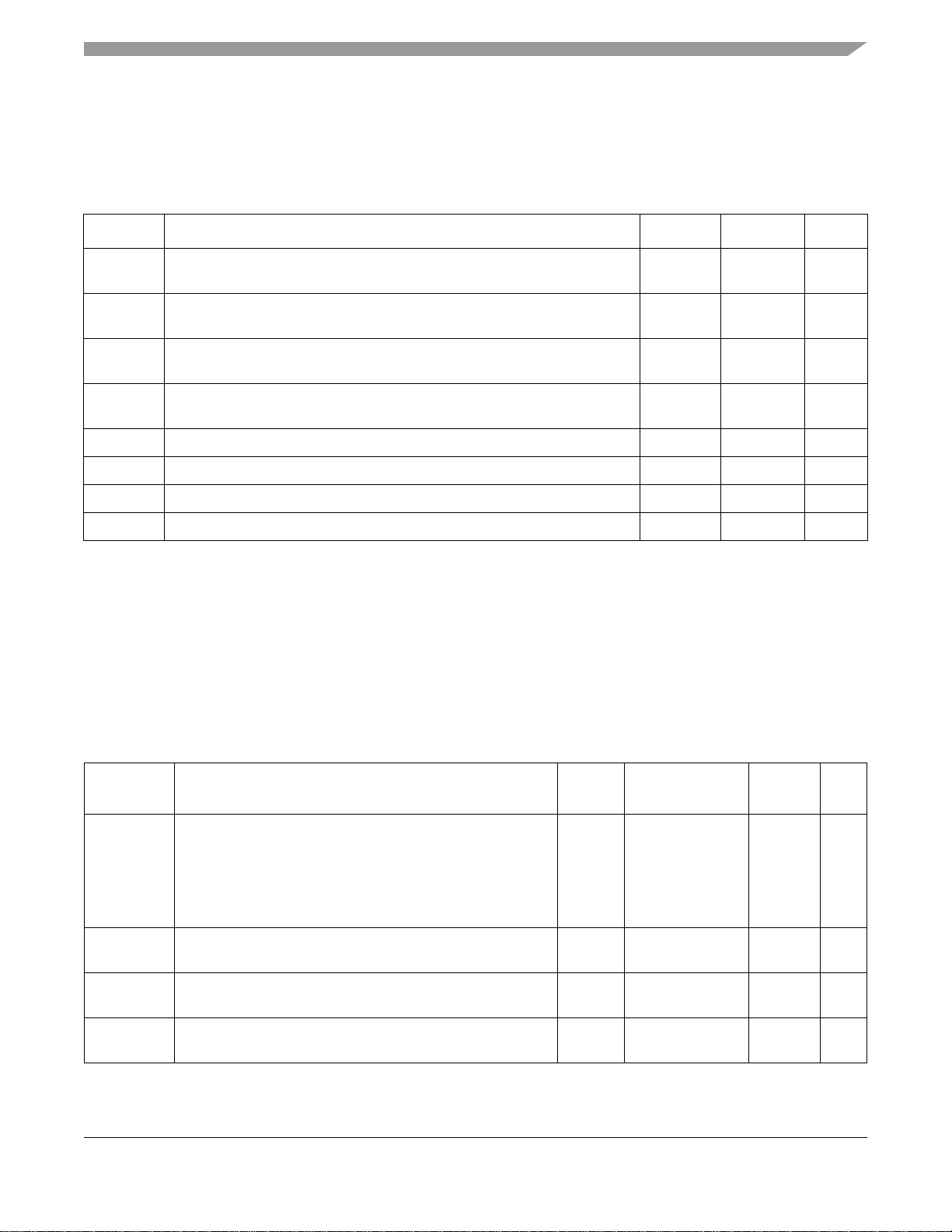
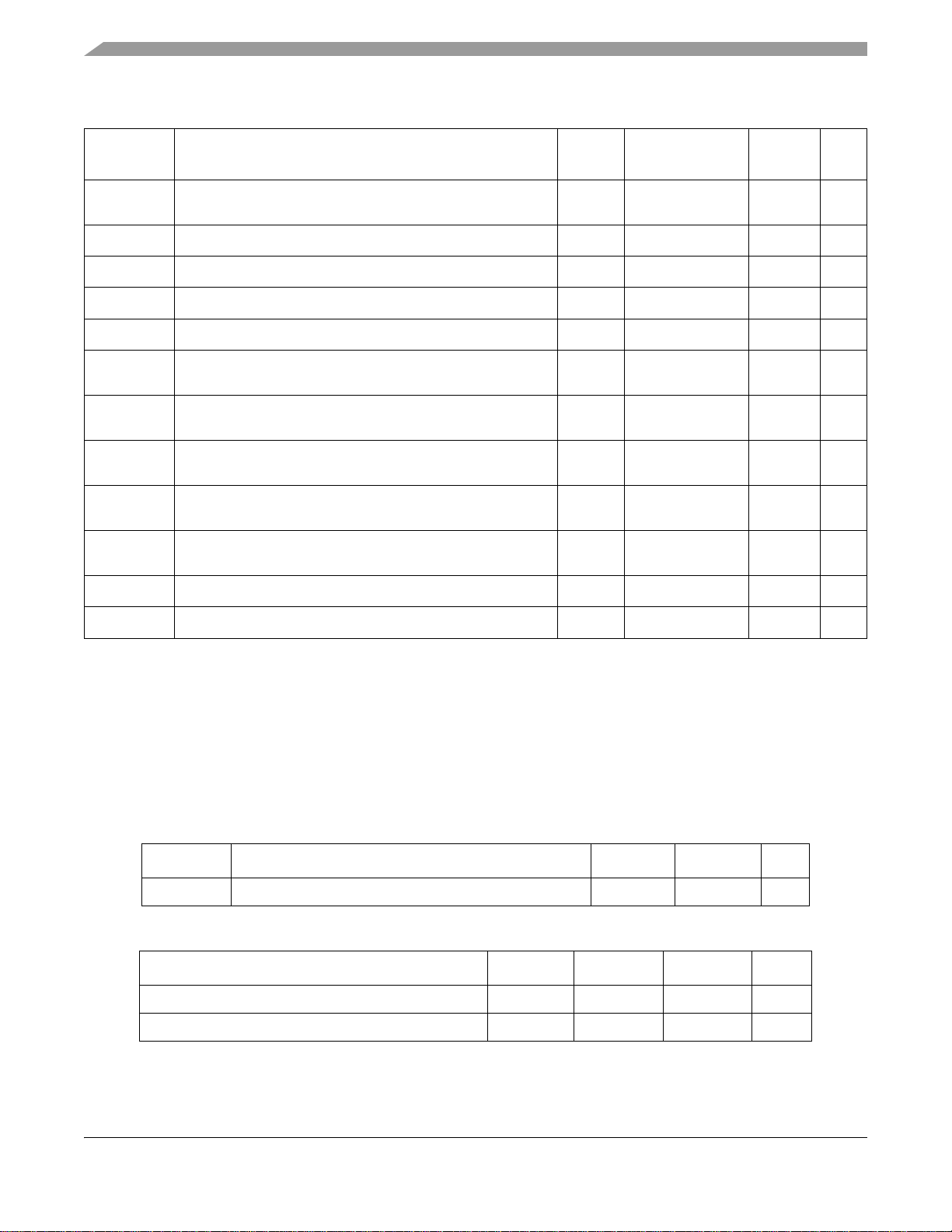
Table 3. MC9328MX1 Signal Multiplexing Scheme
Primary Alternate GPIO
O PA0 69K SPI2_CLK L A24
C
Signal Dir Pull-up Signal Dir Mux Pull-up Ain Bin Aout
Pin
BGA
NVDD1 K8 NVDD1 Static
NVDD1 B1 A24 O ETMTRACESYN
NVDD1 C2 D31 I/O 69K Pull-H
NVDD1 C1 A23 O ETMTRACECLK O PA31 69K L A23
NVDD1 D2 D30 I/O 69K Pull-H
NVDD1 D1 A22 O ETMPIPESTAT2 O PA30 69K L A22
NVDD1 D3 D29 I/O 69K Pull-H
NVDD1 E2 A21 O ETMPIPESTAT1 O PA29 69K L A21
NVDD1 E3 D28 I/O 69K Pull-H
NVDD1 E1 A20 O ETMPIPESTAT0 O PA28 69K L A20
NVDD1 F2 D27 I/O 69K Pull-H
Voltage
I/O Supply
NVDD1 F4 A19 O ETMTRACEPKT3 O PA27 69K L A19
A1 VSS Static
NVDD1 E4 D26 I/O 69K Pull-H
NVDD1 H5 NVDD1 Static
NVDD1 F1 A18 O ETMTRACEPKT2 O PA26 69K L A18
NVDD1 F3 D25 I/O 69K Pull-H
NVDD1 G2 A17 O ETMTRACEPKT1 O PA25 69K L A17
NVDD1 G3 D24 I/O 69K Pull-H
NVDD1 F5 A16 O ETMTRACEPKT0 O PA24 69K L A16
NVDD1 G4 D23 I/O 69K Pull-H
NVDD1 G1 A15 O L
NVDD1 H2 D22 I/O 69K Pull-H
NVDD1 H3 A14 O L
MC9328MX1 Technical Data, Rev. 7
reescale Semiconductor 11
Page 12

Signals and Connections
Default
(At/After)
RESE
State
Table 3. MC9328MX1 Signal Multiplexing Scheme (Continued)
Primary Alternate GPIO
Signal Dir Pull-up Signal Dir Mux Pull-up Ain Bin Aout
Pin
BGA
NVDD1 G5 D21 I/O 69K Pull-H
Voltage
I/O Supply
NVDD1 H1 A13 O L
T1 VSS Static
NVDD1 H4 D20 I/O 69K Pull-H
QVDD1 H9 QVDD1 Static
H8 VSS Static
NVDD1 J5 NVDD1 Static
NVDD1 J1 A12 O L
NVDD1 J4 D19 I/O 69K Pull-H
NVDD1 J2 A11 O L
NVDD1 J3 D18 I/O 69K Pull-H
NVDD1 K1 A10 O L
NVDD1 K4 D17 I/O 69K Pull-H
NVDD1 K3 A9 O L
NVDD1 K2 D16 I/O 69K Pull-H
NVDD1 L1 A8 O L
NVDD1 L4 D15 I/O 69K Pull-H
NVDD1 L2 A7 O L
MC9328MX1 Technical Data, Rev. 7
12 Freescale Semiconductor
K6 VSS Static
NVDD1 L5 D14 I/O 69K Pull-H
NVDD1 K5 NVDD1 Static
NVDD1 M4 A6 O L
NVDD1 L3 D13 I/O 69K Pull-H
NVDD1 M1 A5 O L
NVDD1 M2 D12 I/O 69K Pull-H
Page 13
Default
(At/After)
RESE
State
Signals and Connections
Table 3. MC9328MX1 Signal Multiplexing Scheme (Continued)
O H
Primary Alternate GPIO
Signal Dir Pull-up Signal Dir Mux Pull-up Ain Bin Aout
Pin
BGA
NVDD1 N1 A4 O L
NVDD1 M3 D11 I/O 69K Pull-H
NVDD1 P3 EB0
Voltage
I/O Supply
NVDD1 N3 D10 I/O 69K Pull-H
reescale Semiconductor 13
O H
NVDD1 P1 A3 O L
NVDD1 N2 EB1
O H
M6 VSS Static
NVDD1 P2 D9 I/O 69K Pull-H
NVDD1 R1 EB2
NVDD1 H6 NVDD1 Static
O H
NVDD1 T2 A2 O L
NVDD1 R2 EB3
O H
NVDD1 R5 D8 I/O 69K Pull-H
NVDD1 T3 OE
O PA23 69K Pull-H PA23
NVDD1 R3 A1 O L
NVDD1 T4 CS5
O PA22 69K Pull-H PA22
NVDD1 N4 D7 I/O 69K Pull-H
NVDD1 R4 CS4
NVDD1 N5 A0 O PA21 69K L A0
OCSD1 HCSD1
NVDD1 P4 CS3
NVDD1 P5 D6 I/O 69K Pull-H
OCSD0 HCSD0
H7 VSS Static
NVDD1 T5 CS2
NVDD1 J6 NVDD1 Static
NVDD1 M5 SDCLK O H
MC9328MX1 Technical Data, Rev. 7
Page 14

Signals and Connections
Default
RESE
(At/After)
1
H
H
State
Table 3. MC9328MX1 Signal Multiplexing Scheme (Continued)
O
Primary Alternate GPIO
Signal Dir Pull-up Signal Dir Mux Pull-up Ain Bin Aout
Pin
BGA
NVDD1 T6 CS1 O H
Voltage
I/O Supply
NVDD1 T7 CS0
14 Freescale Semiconductor
I ETMTRACEPKT7 PA20 69K Pull-H ECB
NVDD1 R6 D5 I/O 69K Pull-H
NVDD1 P6 ECB
O ETMTRACEPKT6 PA19 69K H LBA
J7 VSS Static
NVDD1 N6 D4 I/O 69K Pull-H
NVDD1 R7 LBA
NVDD1 P8 D3 I/O 69K Pull-H
NVDD1 R8 BCLK ETMTRACEPKT5 PA18 69K L BCLK
NVDD1 P7 D2 I/O 69K Pull-H
NVDD1 L6 NVDD1 Static
NVDD1 N7 DTACK I ETMTRACEPKT4 PA17 69K SPI2_SS A25 Pull-H PA17
NVDD1 N8 D1 I/O 69K Pull-H
NVDD1 M7 RW
NVDD1 T8 MA11 O L
NVDD1 M8 MA10 O L
K7 VSS Static
NVDD1 R9 D0 I/O 69K Pull-H
NVDD1 P9 DQM3 O L
NVDD1 T9 DQM2 O L
NVDD1 N9 DQM1 O L
O H
O H
NVDD1 R10 DQM0 O L
NVDD1 M9 RAS
NVDD1 L8 CAS
NVDD1 J8 NVDD1 Static
MC9328MX1 Technical Data, Rev. 7
Page 15
Default
Signals and Connections
RESE
(At/After)
2
L/H
2
3
4
4
4
4
4
Hiz
Hiz
Hiz
Hiz
Hiz
H/L
Hiz
State
Table 3. MC9328MX1 Signal Multiplexing Scheme (Continued)
O L/H
Primary Alternate GPIO
Signal Dir Pull-up Signal Dir Mux Pull-up Ain Bin Aout
Pin
BGA
NVDD1 T10 SDWE O H
NVDD1 R11 SDCKE0 O H
NVDD1 P10 SDCKE1 O H
Voltage
I/O Supply
NVDD1 N10 RESET_SF
L7 VSS Static
NVDD1 T11 CLKO O L
reescale Semiconductor 15
I 69K
AVDD1 T12 AVDD1 Static
AVDD1 M10 RESET_IN
AVDD1 N11 RESET_OUT O L/H
AVDD1 M11 BIG_ENDIAN I
AVDD1 P11 BOOT3 I
AVDD1 N12 BOOT2 I
AVDD1 R12 POR I
AVDD1 R13 BOOT1 I
MC9328MX1 Technical Data, Rev. 7
T16 VSS Static
AVDD1 P12 BOOT0 I
AVDD1 T13 TRISTATE I
AVDD1 P13 TRST I 69K H
QVDD2 R15 QVDD2 Static
AVDD1 T14 EXTAL16M I Hiz
AVDD1 T15 XTAL16M O
AVDD1 R16 EXTAL32K I Hiz
AVDD1 P16 XTAL32K O
NVDD2 K10 NVDD2 Static
Page 16

Signals and Connections
Default
5
(At/After)
RESE
Hiz
State
Table 3. MC9328MX1 Signal Multiplexing Scheme (Continued)
Primary Alternate GPIO
Signal Dir Pull-up Signal Dir Mux Pull-up Ain Bin Aout
Pin
BGA
NVDD2 R14 TDO O
NVDD2 N15 TMS I 69K Pull-H
NVDD2 L9 TCK I 69K Pull-H
NVDD2 N16 TDI I 69K Pull-H
NVDD2 P14 I2C_SCL O PA16 69K Pull-H PA16
NVDD2 P15 I2C_SDA I/O PA15 69K Pull-H PA15
NVDD2 N13 CSI_PIXCLK I PA14 69K Pull-H PA14
NVDD2 M13 CSI_HSYNC I PA13 69K Pull-H PA13
NVDD2 M14 CSI_VSYNC I PA12 69K Pull-H PA12
NVDD2 N14 CSI_D7 I PA11 69K Pull-H PA11
NVDD2 M15 CSI_D6 I PA10 69K Pull-H PA10
NVDD2 M16 CSI_D5 I PA9 69K Pull-H PA9
NVDD2 J10 VSS Static
NVDD2 M12 CSI_D4 I PA8 69K Pull-H PA8
NVDD2 L16 CSI_D3 I PA7 69K Pull-H PA7
NVDD2 L15 CSI_D2 I PA6 69K Pull-H PA6
NVDD2 L14 CSI_D1 I PA5 69K Pull-H PA5
NVDD2 L13 CSI_D0 I PA4 69K Pull-H PA4
NVDD2 L12 CSI_MCLK O PA3 69K Pull-H PA3
NVDD2 L11 PWMO O PA2 69K Pull-H PA2
NVDD2 L10 TIN I PA1 69K SPI2_RxD Pull-H PA1
NVDD2 K15 TMR2OUT O PD31 69K SPI2_TxD Pull-H PD31
NVDD2 K16 LD15 O PD30 69K Pull-H PD30
NVDD2 K14 LD14 O PD29 69K Pull-H PD29
Voltage
I/O Supply
MC9328MX1 Technical Data, Rev. 7
16 Freescale Semiconductor
NVDD2 K13 LD13 O PD28 69K Pull-H PD28
Page 17
Default
Signals and Connections
RESE
(At/After)
State
Pull-H PD11
SPI2_SS2
O PD10 69K SPI2_TxD Pull-H PD10
O PD9 69K SPI2_RxD Pull-H PD9
O PD8 69K SPI2_SS Pull-H PD8
I PD7 69K SPI2_CLK Pull-H PD7
Table 3. MC9328MX1 Signal Multiplexing Scheme (Continued)
Primary Alternate GPIO
Signal Dir Pull-up Signal Dir Mux Pull-up Ain Bin Aout
Pin
BGA
NVDD2 K12 LD12 O PD27 69K Pull-H PD27
Voltage
I/O Supply
reescale Semiconductor 17
QVDD3 J15 QVDD3 Static
J16 VSS Static
NVDD2 K9 NVDD2 Static
NVDD2 J14 LD11 O PD26 69K Pull-H PD26
NVDD2 K11 LD10 O PD25 69K Pull-H PD25
NVDD2 H15 LD9 O PD24 69K Pull-H PD24
NVDD2 J13 LD8 O PD23 69K Pull-H PD23
NVDD2 J12 LD7 O PD22 69K Pull-H PD22
NVDD2 J11 LD6 O PD21 69K Pull-H PD21
NVDD2 H14 LD5 O PD20 69K Pull-H PD20
NVDD2 H13 LD4 O PD19 69K Pull-H PD19
MC9328MX1 Technical Data, Rev. 7
NVDD2 H16 LD3 O PD18 69K Pull-H PD18
NVDD2 H12 LD2 O PD17 69K Pull-H PD17
NVDD2 G16 LD1 O PD16 69K Pull-H PD16
NVDD2 H11 LD0 O PD15 69K Pull-H PD15
NVDD2 G15 FLM/VSYNC O PD14 69K Pull-H PD14
NVDD2 G14 LP/HSYNC O PD13 69K Pull-H PD13
NVDD2 G13 ACD/OE O PD12 69K Pull-H PD12
NVDD2 G12 CONTRAST O PD11 69K
NVDD2 F16 SPL_SPR O UART2_DSR
NVDD2 H10 PS O UART2_RI
NVDD2 G11 CLS O UART2_DCD
NVDD2 F12 REV O UART2_DTR
NVDD2 F15 LSCLK O PD6 69K Pull-H PD6
Page 18

Signals and Connections
Default
(At/After)
RESE
State
Table 3. MC9328MX1 Signal Multiplexing Scheme (Continued)
Primary Alternate GPIO
Signal Dir Pull-up Signal Dir Mux Pull-up Ain Bin Aout
J9 VSS Static
Pin
BGA
Voltage
I/O Supply
E16 R2A I qvdd
6
QVDD
18 Freescale Semiconductor
F14 PX1 I
F13 PY1 I
E15 PX2 I
D16 R2B I
6
6
6
QVDD
QVDD
QVDD
E14 PY2 I
D15 R1A I
C16 R1B I
C15 VSS Static
6
6
6
6
QVDD
QVDD
QVDD
QVDD
C14 AVDD2 Static
6
AVDD2
B16 NC I
A16 NC I
B15 UIN I
A15 UIP I
E13 NC I
6
6
6
6
6
QVDD
QVDD
QVDD
QVDD
QVDD
B14 RVM I
D14 NC I
6
QVDD
A14 RVP I
D13 NC I
6
6
6
QVDD
QVDD
QVDD
E12 NC O
C13 NC I
6
6
QVDD
QVDD
MC9328MX1 Technical Data, Rev. 7
Page 19
Default
Signals and Connections
RESE
(At/After)
Hiz PC30
Pull-H PC28
Pull-H PC27
LPC25
Pull-H PC13
State
DMA_Req
UART3_TX
UART3_CTS
UART3_DTR L PC26
SPI2_SS3
UART3_DCD
UART3_DSR
Table 3. MC9328MX1 Signal Multiplexing Scheme (Continued)
NVDD3 B9 SPI1_SCLK I/O PC14 69K Pull-H PC14
I PC13 69K
NVDD3 D9 SPI1_SPI_RDY
NVDD3 A9 UART1_RXD I PC12 69K Pull-H PC12
I/O PC15 69K Pull-H PC15
Primary Alternate GPIO
Signal Dir Pull-up Signal Dir Mux Pull-up Ain Bin Aout
Pin
BGA
I/O Supply
D12 NC O
6
QVDD
Voltage
QVDD4 A13 QVDD4 Static
B13 VSS Static
BTRFVDD C11 BT8 O SSI2_RXFS PC24 69K UART3_RI Hiz PC24
BTRFVDD G10 BT9 O SSI2_RX PC23 69K L PC23
BTRFVDD F10 BT10 O SSI2_TX PC22 69K H PC22
BTRFVDD B10 BT11 O SSI2_TXCLK PC21 69K H PC21
BTRFVDD A12 BT3 I PC29 69K UART3_RTS Pull-H PC29
BTRFVDD E11 BT4 I PC28 69K
BTRFVDD A11 BT5 I/O PC27 69K
BTRFVDD C12 BTRFVDD Static
BTRFVDD B12 BT1 I PC31 69K UART3_RX Pull-H PC31
BTRFVDD F11 BT2 O PC30 69K
BTRFVDD D11 BT6 O PC26 69K
BTRFVDD B11 BT7 O PC25 69K
BTRFVDD E10 BT12 O SSI2_TXFS PC20 69K Hiz PC20
BTRFVDD D10 BT13 O SSI2_RXCLK PC19 69K L PC19
C10 BTRFGND Static
NVDD3 A10 NVDD3 Static
NVDD3 G9 SPI1_MOSI I/O PC17 69K Pull-H PC17
NVDD3 F9 SPI1_MISO I/O PC16 69K Pull-H PC16
NVDD3 E9 SPI1_SS
MC9328MX1 Technical Data, Rev. 7
reescale Semiconductor 19
Page 20
Signals and Connections
Default
(At/After)
RESE
State
Table 3. MC9328MX1 Signal Multiplexing Scheme (Continued)
I PC10 69K Pull-H PC10
O PC9 69K Pull-H PC9
Primary Alternate GPIO
Signal Dir Pull-up Signal Dir Mux Pull-up Ain Bin Aout
NVDD3 C8 SSI_RXFS I/O PC3 69K Pull-H PC3
A7 VSS Static
NVDD4 C7 UART2_RXD I PB31 69K Pull-H PB31
Pin
BGA
NVDD3 G8 UART1_CTS
NVDD3 B8 SSI_TXCLK I/O PC8 69K Pull-H PC8
NVDD3 F8 SSI_TXFS I/O PC7 69K Pull-H PC7
NVDD3 E8 SSI_TXDAT O PC6 69K Pull-H PC6
NVDD3 D8 SSI_RXDAT I PC5 69K Pull-H PC5
NVDD3 C9 UART1_TXD O PC11 69K Pull-H PC11
Voltage
I/O Supply
NVDD3 A8 UART1_RTS
NVDD3 B7 SSI_RXCLK I/O PC4 69K Pull-H PC4
MC9328MX1 Technical Data, Rev. 7
20 Freescale Semiconductor
I PB29 69K Pull-H PB29
O PB28 69K Pull-H PB28
NVDD4 F7 UART2_TXD O PB30 69K Pull-H PB30
NVDD4 C6 UART2_CTS
NVDD4 E7 UART2_RTS
NVDD4 D7 USBD_VMO O PB27 69K Pull-H PB27
NVDD4 D6 USBD_VPO O PB26 69K Pull-H PB26
NVDD4 E6 USBD_VM I PB25 69K Pull-H PB25
O PB23 69K Pull-H PB23
ROE O PB21 69K Pull-H PB21
USBD_SUSPND
A4 VSS Static
NVDD4 B6 USBD_VP I PB24 69K Pull-H PB24
NVDD4 D5
NVDD4 C5 USBD_RCV I/O PB22 69K Pull-H PB22
NVDD4 B5 USBD_
NVDD4 A5 USBD_AFE O PB20 69K Pull-H PB20
NVDD4 A6 NVDD4 Static
NVDD4 G7 SIM_CLK O SSI_TXCLK I/O PB19 69K Pull-H PB19
Page 21
Default
Signals and Connections
RESE
(At/After)
State
Pull-L PB11
(pull down)
Table 3. MC9328MX1 Signal Multiplexing Scheme (Continued)
Primary Alternate GPIO
Signal Dir Pull-up Signal Dir Mux Pull-up Ain Bin Aout
Pin
BGA
NVDD4 F6 SIM_RST O SSI_TXFS I/O PB18 69K Pull-H PB18
NVDD4 G6 SIM_RX I SSI_TXDAT O PB17 69K Pull-H PB17
NVDD4 B4 SIM_TX I/O SSI_RXDAT I PB16 69K Pull-H PB16
NVDD4 C4 SIM_PD I SSI_RXCLK I/O PB15 69K Pull-H PB15
NVDD4 D4 SIM_SVEN O SSI_RXFS I/O PB14 69K Pull-H PB14
NVDD4 B3 SD_CMD I/O MS_BS O PB13 69K Pull-H PB13
NVDD4 A3 SD_CLK O MS_SCLKO O PB12 69K Pull-H PB12
NVDD4 A2 SD_DAT3 I/O MS_SDIO I/O PB11 69K
NVDD4 E5 SD_DAT2 I/O MS_SCLKI I PB10 69K Pull-H PB10
NVDD4 B2 SD_DAT1 I/O MS_PI1 I PB9 69K Pull-H PB9
NVDD4 C3 SD_DAT0 I/O MS_PI0 I PB8 69K Pull-H PB8
Voltage
I/O Supply
MC9328MX1 Technical Data, Rev. 7
reescale Semiconductor 21
After reset, CS0 goes H/L depends on BOOT[3:0].2Need external circuitry to drive the signal.3Need external pull-up.4External resistor is needed.5Need external pull-up or pull-down.6ASP signals are clamped by AVDD2 to prevent ESD (electrostatic discharge) damage. AVDD2 must be greater than QVDD to keep diodes reverse-biased.
1
Page 22
Electrical Characteristics
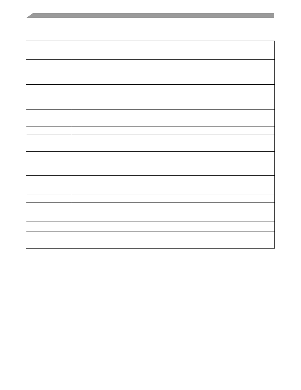
3 Electrical Characteristics
This section contains the electrical specifications and timing diagrams for the i.MX1 processor.
3.1 Maximum Ratings
Table 4 provides information on maximum ratings which are those values beyond which damage to the
device may occur. Functional operation should be restricted to the limits listed in Recommended Operating
Range Table 5 on page 23 or the DC Characteristics table.
Table 4. Maximum Ratings
Symbol Rating Minimum Maximum Unit
NV
DD
QV
DD
QV
DD
AV
DD
BTRFV
DD
VESD_HBM ESD immunity with HBM (human body model) – 2000 V
VESD_MM ESD immunity with MM (machine model) – 100 V
ILatchup Latch-up immunity – 200 mA
Test Storage temperature -55 150 °C
Pmax Power Consumption
1
A typical application with 30 pads simultaneously switching assumes the GPIO toggling and instruction fetches from the ARM®
core-that is, 7x GPIO, 15x Data bus, and 8x Address bus.
2
A worst-case application with 70 pads simultaneously switching assumes the GPIO toggling and instruction fetches from the
ARM core-that is, 32x GPIO, 30x Data bus, 8x Address bus. These calculations are based on the core running its heaviest OS
application at MHz, and where the whole image is running out of SDRAM. QVDD at V, NVDD and AVDD at 3.3V, therefore,
180mA is the worst measurement recorded in the factory environment, max 5mA is consumed for OSC pads, with each toggle
GPIO consuming 4mA.
DC I/O Supply Voltage -0.3 3.3 V
DC Internal (core = 150 MHz) Supply Voltage -0.3 1.9 V
DC Internal (core = 200 MHz) Supply Voltage -0.3 2.0 V
DC Analog Supply Voltage -0.3 3.3 V
DC Bluetooth Supply Voltage -0.3 3.3 V
800
1
1300
2
mW
3.2 Recommended Operating Range
Table 5 provides the recommended operating ranges for the supply voltages and temperatures. The i.MX1
processor has multiple pairs of VDD and VSS power supply and return pins. QVDD and QVSS pins are
used for internal logic. All other VDD and VSS pins are for the I/O pads voltage supply, and each pair of
VDD and VSS provides power to the enclosed I/O pads. This design allows different peripheral supply
voltage levels in a system.
Because AVDD pins are supply voltages to the analog pads, it is recommended to isolate and noise-filter
the AVDD pins from other VDD pins.
BTRFVDD is the supply voltage for the Bluetooth interface signals. It is quite sensitive to the data
transmit/receive accuracy. Please refer to Bluetooth RF spec for special handling. If Bluetooth is not used
MC9328MX1 Technical Data, Rev. 7
22 Freescale Semiconductor
Page 23
Electrical Characteristics
in the system, these Bluetooth pins can be used as general purpose I/O pins and BTRFVDD can be used
as other NVDD pins.
For more information about I/O pads grouping per VDD, please refer to Table 2 on page 4.
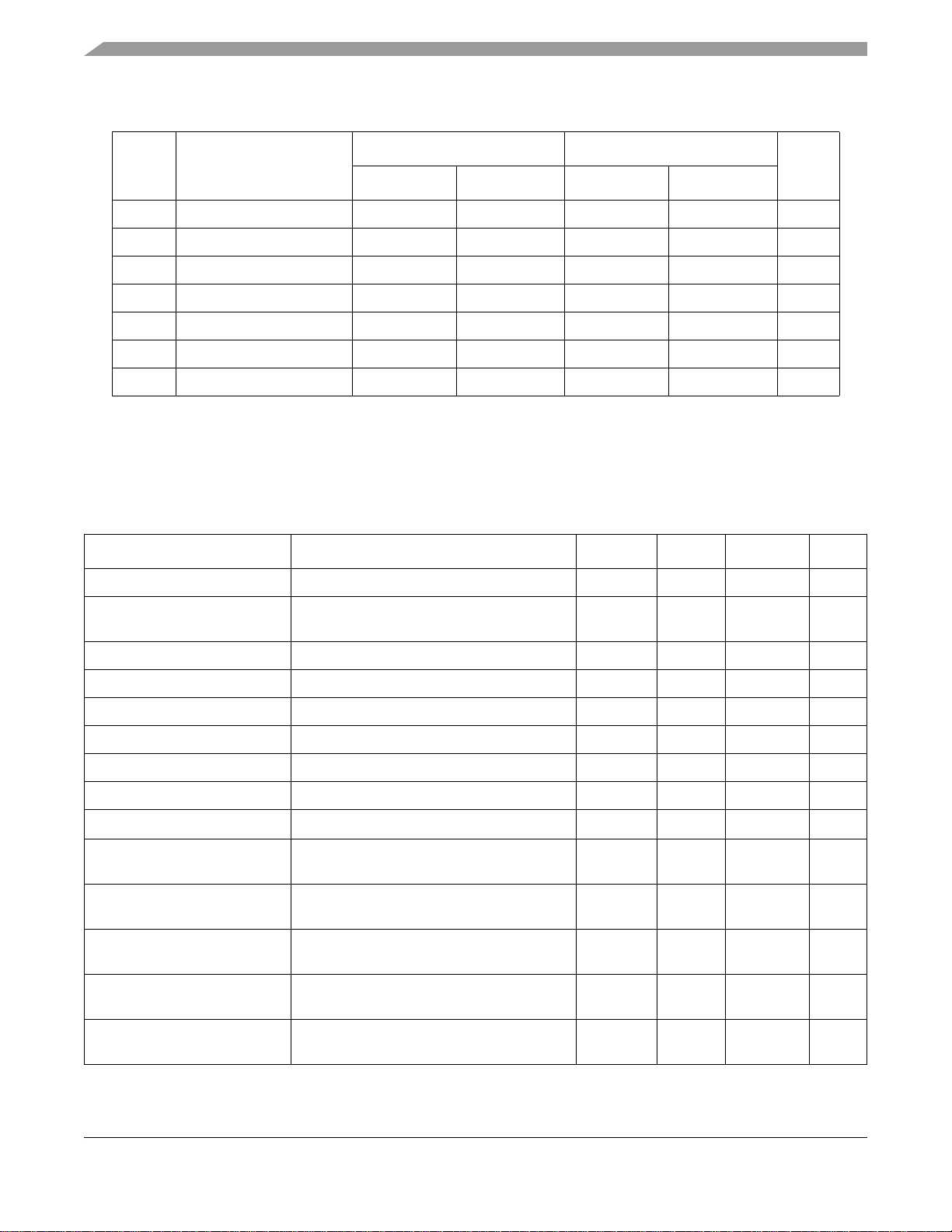
Table 5. Recommended Operating Range
Symbol Rating Minimum Maximum Unit
T
T
T
NVDD I/O supply voltage (if using MSHC, CSI, SPI, BTA, LCD, and USBd which
NVDD I/O supply voltage (if not using the peripherals listed above) 1.70 3.30 V
QVDD Internal supply voltage (Core = 150 MHz) 1.70 1.90 V
QVDD Internal supply voltage (Core = 200 MHz) 1.80 2.00 V
AVDD Analog supply voltage 1.70 3.30 V
Operating temperature range
A
MC9328MX1VM20\MC9328MX1VM15
Operating temperature range
A
MC9328MX1DVM20\MC9328MX1DVM15
Operating temperature range
A
MC9328MX1CVM15
are only 3 V interfaces)
070°C
-30 70 °C
-40 85 °C
2.70 3.30 V
3.3 Power Sequence Requirements
For required power-up and power-down sequencing, please refer to the “Power-Up Sequence” section of
application note AN2537 on the i.MX applications processor website.
3.4 DC Electrical Characteristics
Table 6 contains both maximum and minimum DC characteristics of the i.MX1 processor.
Table 6. Maximum and Minimum DC Characteristics
Number or
Symbol
Iop Full running operating current at 1.8V for QVDD, 3.3V for
NVDD/AVDD (Core = 96 MHz, System = 96 MHz, MPEG4
decoding playback from external memory card to both
external SSI audio decoder and driving TFT display panel,
and OS with MMU enabled memory system is running on
external SDRAM).
Sidd
Sidd
Sidd
Freescale Semiconductor 23
Standby current
1
(Core = 150 MHz, QVDD = 1.8V, temp = 25°C)
Standby current
2
(Core = 150 MHz, QVDD = 1.8V, temp = 55
Standby current
3
(Core = 150 MHz, QVDD = 2.0V, temp = 25°C)
Parameter Min Typical Max Unit
– QVDD at
1.8V = 120mA;
NVDD+AVDD at
3.0V = 30mA
–25 –μA
–45 –μA
–mA
°C)
–35 –μA
MC9328MX1 Technical Data, Rev. 7
Page 24
Electrical Characteristics
Table 6. Maximum and Minimum DC Characteristics (Continued)
Number or
Symbol
Sidd
4
V
IH
V
IL
V
OH
V
OL
I
IL
I
IH
I
OH
I
OL
I
OZ
C
i
Parameter Min Typical Max Unit
Standby current
(Core = 150 MHz, QVDD = 2.0V, temp = 55°C)
Input high voltage 0.7V
Input low voltage – – 0.4 V
Output high voltage (IOH= 2.0 mA) 0.7V
Output low voltage (IOL= -2.5 mA) – – 0.4 V
Input low leakage current
= GND, no pull-up or pull-down)
(V
IN
Input high leakage current
(V
IN=VDD
Output high current
(V
OH
Output low current
(VOL=0.4V, VDD=1.8V)
Output leakage current
(V
out=VDD
Input capacitance – – 5 pF
, no pull-up or pull-down)
=0.8VDD, VDD=1.8V)
, output is high impedance)
–60 –μA
DD
DD
––±1μA
––±1μA
4.0 – – mA
-4.0 – – mA
––±5μA
–Vdd+0.2V
–VddV
C
o
Output capacitance – – 5 pF
3.5 AC Electrical Characteristics
The AC characteristics consist of output delays, input setup and hold times, and signal skew times. All
signals are specified relative to an appropriate edge of other signals. All timing specifications are specified
at a system operating frequency from 0 MHz to 96 MHz (core operating frequency 150 MHz) with an
operating supply voltage from V
DD min
timing is measured at 30 pF loading.
Pin Parameter Minimum Maximum Unit
TRISTATE Time from TRISTATE activate until I/O becomes Hi-Z – 20.8 ns
Table 8. 32k/16M Oscillator Signal Timing
Parameter Minimum RMS Maximum Unit
EXTAL32k input jitter (peak to peak) – 5 20 ns
EXTAL32k startup time 800 – – ms
to V
DD max
under an operating temperature from TL to TH. All
Table 7. Tristate Signal Timing
MC9328MX1 Technical Data, Rev. 7
24 Freescale Semiconductor
Page 25
Functional Description and Application Information
Table 8. 32k/16M Oscillator Signal Timing (Continued)
Parameter Minimum RMS Maximum Unit
EXTAL16M input jitter (peak to peak)
EXTAL16M startup time
1
The 16 MHz oscillator is not recommended for use in new designs.
1
1
–TBDTBD–
TBD – – –
4 Functional Description and Application Information
This section provides the electrical information including and timing diagrams for the individual modules
of the i.MX1.
4.1 Embedded Trace Macrocell
All registers in the ETM9 are programmed through a JTAG interface. The interface is an extension of the
ARM920T processor’s TAP controller, and is assigned scan chain 6. The scan chain consists of a 40-bit
shift register comprised of the following:
• 32-bit data field
• 7-bit address field
• A read/write bit
The data to be written is scanned into the 32-bit data field, the address of the register into the 7-bit address
field, and a 1 into the read/write bit.
A register is read by scanning its address into the address field and a 0 into the read/write bit. The 32-bit
data field is ignored. A read or a write takes place when the TAP controller enters the UPDATE-DR state.
The timing diagram for the ETM9 is shown in Figure 2. See Table 9 for the ETM9 timing parameters used
in Figure 2.
TRACECLK
TRACECLK
(Half-Rate Clocking Mode)
Output Trace Port
2a
3a
3b
Figure 2. Trace Port Timing Diagram
2b
Valid Data
4a
1
Valid Data
4b
MC9328MX1 Technical Data, Rev. 7
Freescale Semiconductor 25
Page 26
Functional Description and Application Information
Table 9. Trace Port Timing Diagram Parameter Table
1.8 ± 0.1 V 3.0 ± 0.3 V
Ref No. Parameter
Minimum Maximum Minimum Maximum
1 CLK frequency 0 85 0 100 MHz
2a Clock high time 1.3 – 2 – ns
2b Clock low time 3 – 2 – ns
3a Clock rise time – 4 – 3 ns
3b Clock fall time – 3 – 3 ns
4a Output hold time 2.28 – 2 – ns
4b Output setup time 3.42 – 3 – ns
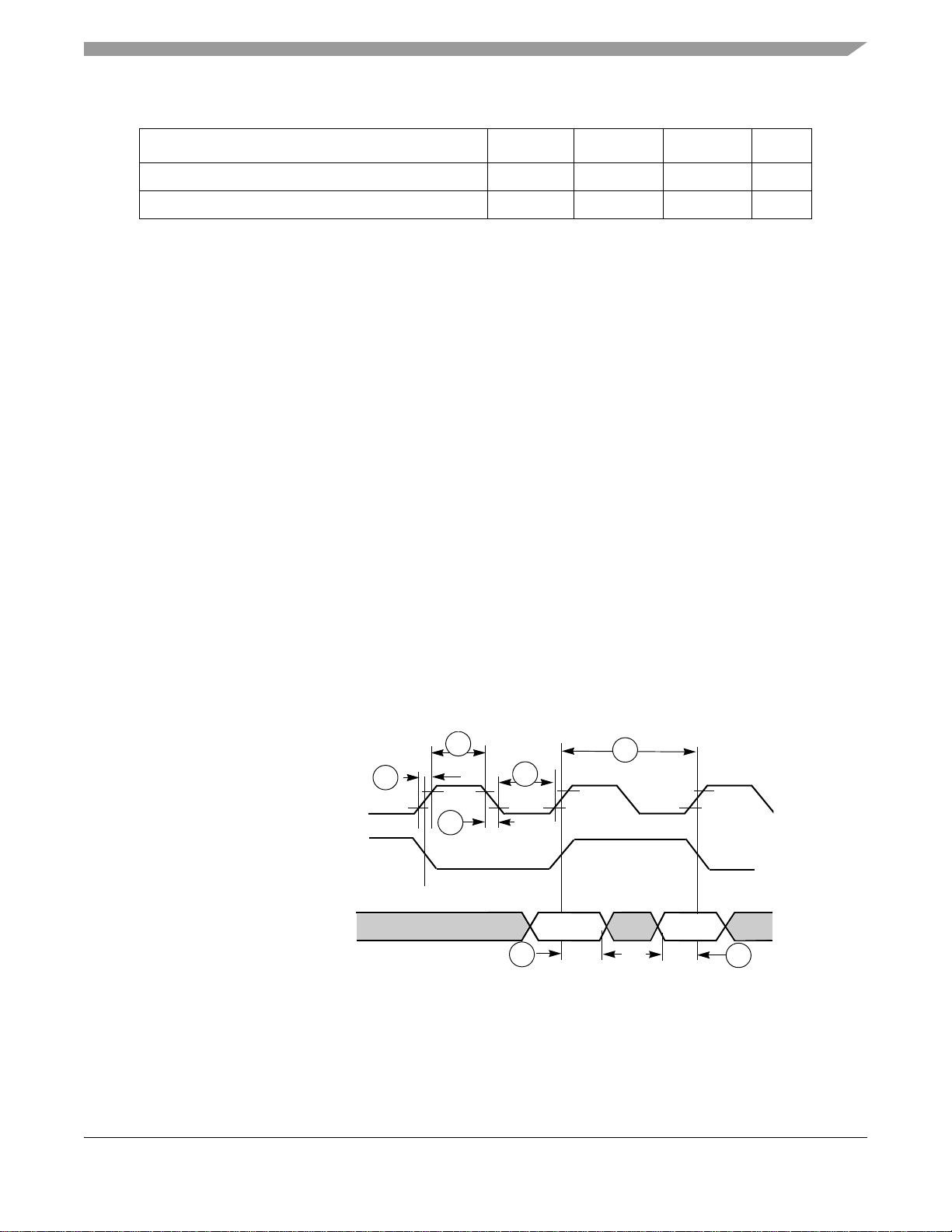
4.2 DPLL Timing Specifications
Unit
Parameters of the DPLL are given in Table 10. In this table, T
pre-divider and T
is the output double clock period.
dck
is a reference clock period after the
ref
Table 10. DPLL Specifications
Parameter Test Conditions Minimum Typical Maximum Unit
DPLL input clock freq range Vcc = 1.8V 5 – 100 MHz
Pre-divider output clock
freq range
DPLL output clock freq range Vcc = 1.8V 80 – 220 MHz
Pre-divider factor (PD) – 1 – 16 –
Total multiplication factor (MF) Includes both integer and fractional parts 5 – 15 –
MF integer part – 5 – 15 –
MF numerator Should be less than the denominator 0 – 1022 –
MF denominator – 1 – 1023 –
Pre-multiplier lock-in time –
Freq lock-in time after
full reset
Freq lock-in time after
partial reset
Vcc = 1.8V
FOL mode for non-integer MF
(does not include pre-multi lock-in time)
FOL mode for non-integer MF (does not
include pre-multi lock-in time)
5–30MHz
– – 312.5
250
220
280
(56 μs)
250
(50 μs)
300
270
μsec
T
T
ref
ref
Phase lock-in time after
full reset
Phase lock-in time after
partial reset
Freq jitter (p-p) –
26 Freescale Semiconductor
FPL mode and integer MF (does not include
pre-multi lock-in time)
FPL mode and integer MF (does not include
pre-multi lock-in time)
MC9328MX1 Technical Data, Rev. 7
300
270
–
350
(70 μs)
320
(64 μs)
0.005
(0.01%)
400
370
0.01
2•T
T
ref
T
ref
dck
Page 27
Functional Description and Application Information
Table 10. DPLL Specifications (Continued)
Parameter Test Conditions Minimum Typical Maximum Unit
Phase jitter (p-p) Integer MF, FPL mode, Vcc=1.8V
–
1.0
(10%)
1.5 ns
Power supply voltage – 1.7 – 2.5 V
Power dissipation FOL mode, integer MF,
= MHz, Vcc = 1.8V
f
dck
––4mW
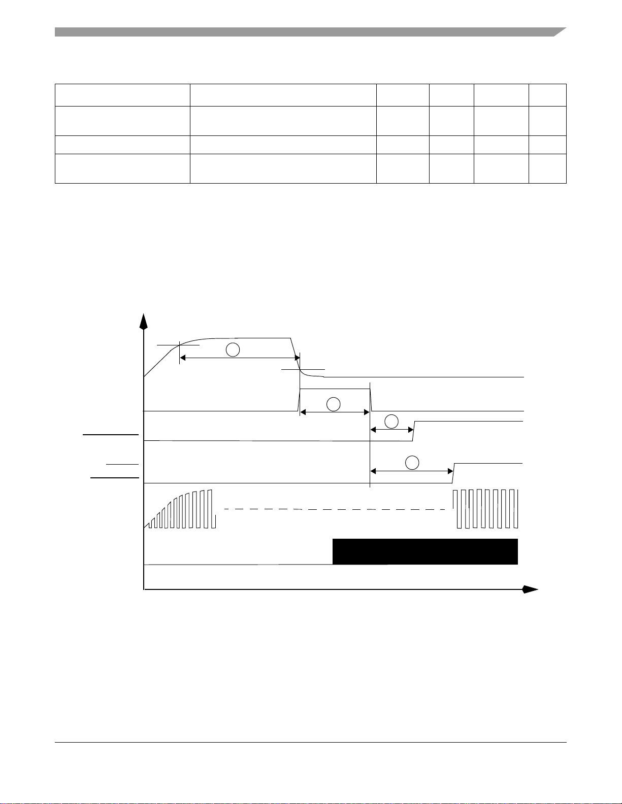
4.3 Reset Module
The timing relationships of the Reset module with the POR and RESET_IN are shown in Figure 3 and
Figure 4.
NOTE
Be aware that NVDD must ramp up to at least 1.8V before QVDD is powered up
to prevent forward biasing.
90% AVDD
1
POR
RESET_POR
RESET_DRAM
10% AVDD
2
Exact 300ms
3
7 cycles @ CLK32
HRESET
RESET_OUT
CLK32
HCLK
4
14 cycles @ CLK32
Figure 3. Timing Relationship with POR
MC9328MX1 Technical Data, Rev. 7
Freescale Semiconductor 27
Page 28
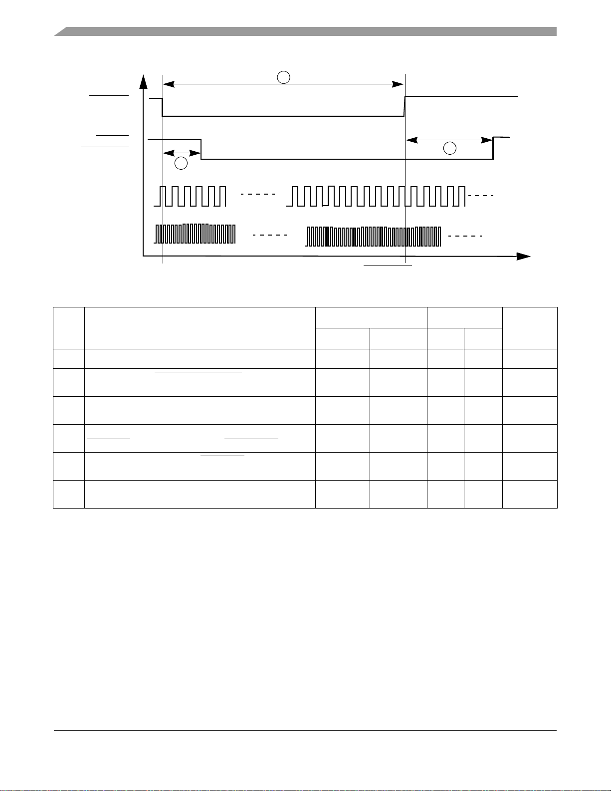
Functional Description and Application Information
RESET_IN
5
HRESET
RESET_OUT
6
CLK32
HCLK
14 cycles @ CLK32
4
Figure 4. Timing Relationship with RESET_IN
Table 11. Reset Module Timing Parameter Table
Ref
No.
1 Width of input POWER_ON_RESET
2 Width of internal POWER_ON_RESET
(9600 *CLK32 at 32 kHz)
3 7K to 32K-cycle stretcher for SDRAM reset 7 7 7 7 Cycles of
4 14K to 32K-cycle stretcher for internal system reset
HRESERT
5 Width of external hard-reset RESET_IN
and output reset at pin RESET_OUT
Parameter
1.8 ± 0.1 V 3.0 ± 0.3 V
Unit
Min Max Min Max
1
note
300 300 300 300 ms
14 14 14 14 Cycles of
4 – 4 – Cycles of
–
note
1
––
CLK32
CLK32
CLK32
6 4K to 32K-cycle qualifier 4 4 4 4 Cycles of
CLK32
1
POR width is dependent on the 32 or 32.768 kHz crystal oscillator start-up time. Design margin should allow for crystal
tolerance, i.MX chip variations, temperature impact, and supply voltage influence. Through the process of supplying crystals
for use with CMOS oscillators, crystal manufacturers have developed a working knowledge of start-up time of their crystals.
Typically, start-up times range from 400 ms to 1.2 seconds for this type of crystal.
If an external stable clock source (already running) is used instead of a crystal, the width of POR should be ignored in
calculating timing for the start-up process.
4.4 External Interface Module
The External Interface Module (EIM) handles the interface to devices external to the i.MX1 processor,
including the generation of chip-selects for external peripherals and memory. The timing diagram for the
EIM is shown in Figure 5, and Table 12 defines the parameters of signals.
MC9328MX1 Technical Data, Rev. 7
28 Freescale Semiconductor
Page 29
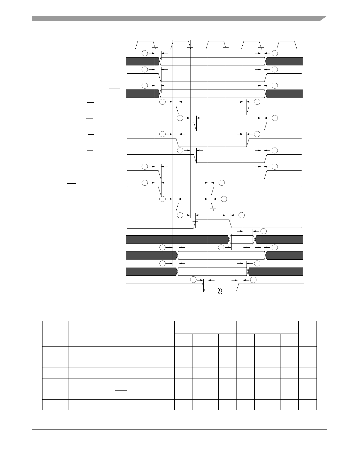
(HCLK) Bus Clock
Address
Chip-select
Read (Write
Functional Description and Application Information
1a 1b
2a 2b
3b3a
)
(rising edge)
OE
(falling edge)
OE
EB
(rising edge)
EB
(falling edge)
LBA
(negated falling edge)
LBA
(negated rising edge)
BCLK (burst clock) - rising edge
BCLK (burst clock) - falling edge
Read Data
Write Data (negated falling)
Write Data (negated rising)
DTACK_B
4a 4b
4c 4d
5a 5b
5c 5d
6a
6a
7a 7b
7c
9a
9a
10a
6c
7d
8a
10a
6b
8b
9b
9c
Figure 5. EIM Bus Timing Diagram
Table 12. EIM Bus Timing Parameter Table
1.8 ± 0.1 V 3.0 ± 0.3 V
Ref No. Parameter
Min Typical Max Min Typical Max
1a Clock fall to address valid 2.48 3.31 9.11 2.4 3.2 8.8 ns
1b Clock fall to address invalid 1.55 2.48 5.69 1.5 2.4 5.5 ns
2a Clock fall to chip-select valid 2.69 3.31 7.87 2.6 3.2 7.6 ns
2b Clock fall to chip-select invalid 1.55 2.48 6.31 1.5 2.4 6.1 ns
3a Clock fall to Read (Write
) Valid 1.35 2.79 6.52 1.3 2.7 6.3 ns
3b Clock fall to Read (Write) Invalid 1.86 2.59 6.11 1.8 2.5 5.9 ns
MC9328MX1 Technical Data, Rev. 7
Freescale Semiconductor 29
Unit
Page 30
Functional Description and Application Information
Table 12. EIM Bus Timing Parameter Table (Continued)
Ref No. Parameter
4a Clock1 rise to Output Enable Valid 2.32 2.62 6.85 2.3 2.6 6.8 ns
4b Clock1 rise to Output Enable Invalid 2.11 2.52 6.55 2.1 2.5 6.5 ns
4c Clock1 fall to Output Enable Valid 2.38 2.69 7.04 2.3 2.6 6.8 ns
4d Clock1 fall to Output Enable Invalid 2.17 2.59 6.73 2.1 2.5 6.5 ns
5a Clock1 rise to Enable Bytes Valid 1.91 2.52 5.54 1.9 2.5 5.5 ns
5b Clock1 rise to Enable Bytes Invalid 1.81 2.42 5.24 1.8 2.4 5.2 ns
5c Clock1 fall to Enable Bytes Valid 1.97 2.59 5.69 1.9 2.5 5.5 ns
5d Clock1 fall to Enable Bytes Invalid 1.76 2.48 5.38 1.7 2.4 5.2 ns
6a Clock1 fall to Load Burst Address Valid 2.07 2.79 6.73 2.0 2.7 6.5 ns
6b Clock1 fall to Load Burst Address Invalid 1.97 2.79 6.83 1.9 2.7 6.6 ns
6c Clock1 rise to Load Burst Address Invalid 1.91 2.62 6.45 1.9 2.6 6.4 ns
7a Clock1 rise to Burst Clock rise 1.61 2.62 5.64 1.6 2.6 5.6 ns
1.8 ± 0.1 V 3.0 ± 0.3 V
Unit
Min Typical Max Min Typical Max
7b Clock1rise to Burst Clock fall 1.61 2.62 5.84 1.6 2.6 5.8 ns
7c Clock1 fall to Burst Clock rise 1.55 2.48 5.59 1.5 2.4 5.4 ns
7d Clock1 fall to Burst Clock fall 1.55 2.59 5.80 1.5 2.5 5.6 ns
8a Read Data setup time 5.54 – – 5.5 – – ns
8b Read Data hold time 0 – – 0 – – ns
9a Clock1 rise to Write Data Valid 1.81 2.72 6.85 1.8 2.7 6.8 ns
9b Clock1 fall to Write Data Invalid 1.45 2.48 5.69 1.4 2.4 5.5 ns
9c Clock1 rise to Write Data Invalid 1.63 – – 1.62 – – ns
10a DTACK setup time 2.52 – – 2.5 – – ns
1
Clock refers to the system clock signal, HCLK, generated from the System DPLL
4.4.1 DTACK Signal Description
The DTACK signal is the external input data acknowledge signal. When using the external DTACK signal
as a data acknowledge signal, the bus time-out monitor generates a bus error when a bus cycle is not
terminated by the external DTACK signal after 1022 HCLK counts have elapsed. Only the CS5 group
supports DTACK signal function when the external DTACK signal is used for data acknowledgement.
4.4.2 DTACK Signal Timing
Figure 6 through Figure 9 show the access cycle timing used by chip-select 5. The signal values and units
of measure for this figure are found in the associated tables.
MC9328MX1 Technical Data, Rev. 7
30 Freescale Semiconductor
Page 31

4.4.2.1 WAIT Read Cycle without DMA
Functional Description and Application Information
Address
CS5
1
programmable
min 0ns
DATABUS
1)
EB
OE
WAIT
Figure 6. WAIT Read Cycle without DMA
Table 13. WAIT Read Cycle without DMA: WSC = 111111, DTACK_SEL=1, HCLK=96MHz
Number Characteristic
3
2
8
9
5
4
67
1110
3.0 ± 0.3 V
Unit
Minimum Maximum
1OE
2CS5 pulse width 3T – ns
3OE negated to address inactive 56.81 – ns
4 Wait asserted after OE asserted – 1020T ns
5 Wait asserted to OE negated 2T+2.2 3T+7.17 ns
6 Data hold timing after OE negated T-1.86 – ns
7 Data ready after wait asserted 0 T ns
8 OE negated to CS negated 1.5T+0.24 1.5T+0.85 ns
9 OE negated after EB negated 0.5 1.5 ns
10 Become low after CS5 asserted 0 1019T ns
11 Wait pulse width 1T 1020T ns
Note:
1. T is the system clock period. (For 96 MHz system clock, T=10.42 ns)
and EB assertion time is programmable by OEA bit in CS5L register. EB assertion in read cycle will occur only when
2. OE
EBC bit in CS5L register is clear.
3. Address becomes valid and CS asserts at the start of read access cycle.
4. The external wait input requirement is eliminated when CS5
and EB assertion time See note 2 – ns
is programmed to use internal wait state.
MC9328MX1 Technical Data, Rev. 7
Freescale Semiconductor 31
Page 32

Functional Description and Application Information
4.4.2.2 WAIT Read Cycle DMA Enabled
Address
CS5
EB
1
programmable
min 0ns
2
9
10
3
6
4
OE
RW
(logic high)
WAIT
5
7
DATABUS
put to
X1)
11
12
8
Figure 7. DTACK WAIT Read Cycle DMA Enabled
Table 14. DTACK WAIT Read Cycle DMA Enabled: WSC = 111111, DTACK_SEL=1, HCLK=96MHz
3.0 ± 0.3 V
Number Characteristic
Minimum Maximum
Unit
1OE and EB assertion time See note 2 – ns
2CS pulse width 3T – ns
3OE negated before CS5 is negated 1.5T+0.24 1.5T+0.85 ns
4 Address inactived before CS negated – 0.93 ns
5 Wait asserted after CS5
6Wait asserted to OE
7 Data hold timing after OE
8 Data ready after wait is asserted – T ns
9CS deactive to next CS active T – ns
10 OE negate after EB negate 0.5 1.5 ns
11 Wait becomes low after CS5 asserted 0 1019T ns
asserted – 1020T ns
negated 2T+2.2 3T+7.17 ns
negated T-1.86 – ns
MC9328MX1 Technical Data, Rev. 7
32 Freescale Semiconductor
Page 33

Functional Description and Application Information
Table 14. DTACK WAIT Read Cycle DMA Enabled: WSC = 111111, DTACK_SEL=1, HCLK=96MHz (Continued)
3.0 ± 0.3 V
Number Characteristic
Minimum Maximum
12 Wait pulse width 1T 1020T ns
Note:
1. T is the system clock period. (For 96 MHz system clock, T=10.42 ns)
and EB assertion time is programmable by OEA bit in CS5L register. EB assertion in read cycle will occur only when
2. OE
EBC bit in CS5L register is clear.
3. Address becomes valid and CS
4. The external wait input requirement is eliminated when CS5 is programmed to use internal wait state.
asserts at the start of read access cycle.
Unit
4.4.2.3 WAIT Write Cycle without DMA
Address
1
programmable
CS5
min 0ns
2
EB
RW
(logic high)
OE
WAIT
DATABUS
(output from
i.MX1)
programmable
min 0ns
11
9
Figure 8. WAIT Write Cycle without DMA
Table 15. WAIT Write Cycle without DMA: WSC = 111111, DTACK_SEL=1, HCLK=96MHz
Number Characteristic
5
3
10
7
4
6
12
Minimum Maximum
8
3.0 ± 0.3 V
Unit
1CS5
2EB assertion time See note 2 – ns
3CS5 pulse width 3T – ns
4RW negated before CS5 is negated 2.5T-0.29 2.5T+0.68 ns
5RW negated to Address inactive 67.28 – ns
6 Wait asserted after CS5 asserted – 1020T ns
Freescale Semiconductor 33
assertion time See note 2 – ns
MC9328MX1 Technical Data, Rev. 7
Page 34

Functional Description and Application Information
Table 15. WAIT Write Cycle without DMA: WSC = 111111, DTACK_SEL=1, HCLK=96MHz (Continued)
3.0 ± 0.3 V
Number Characteristic
Minimum Maximum
7 Wait asserted to RW negated 1T+2.15 2T+7.34 ns
8 Data hold timing after RW negated 2.5T-1.18 – ns
9 Data ready after CS5 is asserted – T ns
10 EB negated after CS5 is negated 1.5T+0.74 1.5T+2.35 ns
11 Wait becomes low after CS5 asserted 0 1019T ns
12 Wait pulse width 1T 1020T ns
Note:
1. T is the system clock period. (For 96 MHz system clock, T=10.42 ns)
assertion can be controlled by CSA bits. EB assertion can also be programmable by WEA bits in CS5L register.
2. CS5
3. Address becomes valid and RW asserts at the start of write access cycle.
4. The external wait input requirement is eliminated when CS5
is programmed to use internal wait state.
4.4.2.4 WAIT Write Cycle DMA Enabled
Unit
Address
OE
(logic high)
DATABUS
1
CS5
2
EB
RW
WAIT
3
programmable
min 0ns
programmable
min 0ns
6
12
9
13
Figure 9. WAIT Write Cycle DMA Enabled
5
10
11
7
4
8
MC9328MX1 Technical Data, Rev. 7
34 Freescale Semiconductor
Page 35

Table 16. WAIT Write Cycle DMA Enabled: WSC = 111111, DTACK_SEL=1, HCLK=96MHz
Number Characteristic
Functional Description and Application Information
3.0 ± 0.3 V
Unit
Minimum Maximum
1 CS5
2EB
3CS5 pulse width 3T – ns
4RW negated before CS5 is negated 2.5T-0.29 2.5T+0.68 ns
5 Address inactived after CS negated – 0.93 ns
6 Wait asserted after CS5 asserted – 1020T ns
7 Wait asserted to RW negated T+2.15 2T+7.34 ns
8 Data hold timing after RW negated 24.87 – ns
9 Data ready after CS5 is asserted – T ns
10 CS deactive to next CS active T – ns
11 EB negate after CS negate 1.5T+0.74 1.5T+2.35
12 Wait becomes low after CS5 asserted 0 1019T ns
13 Wait pulse width 1T 1020T ns
Note:
1. T is the system clock period. (For 96 MHz system clock, T=10.42 ns)
2. CS5 assertion can be controlled by CSA bits. EB assertion also can be programmable by WEA bits in CS5L register.
3. Address becomes valid and RW
4.The external wait input requirement is eliminated when CS5 is programmed to use internal wait state.
assertion time See note 2 – ns
assertion time See note 2 – ns
asserts at the start of write access cycle.
4.4.3 EIM External Bus Timing
The External Interface Module (EIM) is the interface to devices external to the i.MX1, including
generation of chip-selects for external peripherals and memory. The timing diagram for the EIM is shown
in Figure 5, and Table 12 defines the parameters of signals.
MC9328MX1 Technical Data, Rev. 7
Freescale Semiconductor 35
Page 36

Functional Description and Application Information
hclk
hsel_weim_cs[0]
htrans
hwrite
haddr
hready
weim_hrdata
Internal signals - shown only for illustrative purposes
weim_hready
BCLK (burst clock)
ADDR
CS2
R/W
LBA
Seq/Nonseq
Read
V1
Last Valid Data
Last Valid Address
V1
V1
Read
OE
EBx1 (EBC2=0)
1
(EBC2=1)
EBx
DATA
Note 1: x = 0, 1, 2 or 3
Note 2: EBC = Enable Byte Control bit (bit 11) on the Chip Select Control Register
Figure 10. WSC = 1, A.HALF/E.HALF
MC9328MX1 Technical Data, Rev. 7
V1
36 Freescale Semiconductor
Page 37

hclk
hsel_weim_cs[0]
Functional Description and Application Information
htrans
hwrite
haddr
hready
hwdata
weim_hrdata
Internal signals - shown only for illustrative purposes
weim_hready
BCLK (burst clock)
ADDR
CS0
R/W
Nonseq
Write
V1
Last Valid Data
Last Valid Address
Write Data (V1) Unknown
Last Valid Data
V1
Write
LBA
OE
EB
DATA
Last Valid Data Write Data (V1)
Figure 11. WSC = 1, WEA = 1, WEN = 1, A.HALF/E.HALF
MC9328MX1 Technical Data, Rev. 7
Freescale Semiconductor 37
Page 38

Functional Description and Application Information
hclk
hsel_weim_cs[0]
htrans
hwrite
haddr
hready
weim_hrdata
Internal signals - shown only for illustrative purposes
weim_hready
BCLK (burst clock)
ADDR
CS
R/W
LBA
Nonseq
Read
V1
Last Valid Data
Address V1
0
Read
Address V1 + 2Last Valid Addr
V1 Word
OE
EBx1 (EBC2=0)
1
(EBC2=1)
EBx
DATA
Note 1: x = 0, 1, 2 or 3
Note 2: EBC = Enable Byte Control bit (bit 11) on the Chip Select Control Register
1/2 Half Word 2/2 Half Word
Figure 12. WSC = 1, OEA = 1, A.WORD/E.HALF
MC9328MX1 Technical Data, Rev. 7
38 Freescale Semiconductor
Page 39

hclk
hsel_weim_cs[0]
Functional Description and Application Information
htrans
hwrite
haddr
hready
hwdata
Internal signals - shown only for illustrative purposes
weim_hrdata
weim_hready
BCLK (burst clock)
ADDR
CS0
R/W
Nonseq
Write
V1
Last Valid Data
Write Data (V1 Word)
Last Valid Data
Address V1
Address V1 + 2Last Valid Addr
Write
LBA
OE
EB
DATA
1/2 Half Word 2/2 Half Word
Figure 13. WSC = 1, WEA = 1, WEN = 2, A.WORD/E.HALF
MC9328MX1 Technical Data, Rev. 7
Freescale Semiconductor 39
Page 40

Functional Description and Application Information
hclk
hsel_weim_cs[3]
htrans
hwrite
haddr
hready
weim_hrdata
Internal signals - shown only for illustrative purposes
weim_hready
BCLK (burst clock)
ADDR
CS
[3]
R/W
LBA
Nonseq
Read
V1
Last Valid Data
Address V1
V1 Word
Address V1 + 2Last Valid Addr
Read
OE
EBx1 (EBC2=0)
1
(EBC2=1)
EBx
DATA
Note 1: x = 0, 1, 2 or 3
Note 2: EBC = Enable Byte Control bit (bit 11) on the Chip Select Control Register
1/2 Half Word 2/2 Half Word
Figure 14. WSC = 3, OEA = 2, A.WORD/E.HALF
MC9328MX1 Technical Data, Rev. 7
40 Freescale Semiconductor
Page 41

hclk
hsel_weim_cs[3]
Functional Description and Application Information
htrans
hwrite
haddr
hready
hwdata
weim_hrdata
Internal signals - shown only for illustrative purposes
weim_hready
BCLK (burst clock)
ADDR
CS
R/W
Last Valid
3
Nonseq
Write
V1
Data
Write Data (V1 Word)
Address V1
Last Valid Data
Address V1 + 2Last Valid Addr
Write
LBA
OE
EB
DATA
Last Valid Data
1/2 Half Word 2/2 Half Word
Figure 15. WSC = 3, WEA = 1, WEN = 3, A.WORD/E.HALF
MC9328MX1 Technical Data, Rev. 7
Freescale Semiconductor 41
Page 42

Functional Description and Application Information
hclk
hsel_weim_cs[2]
htrans
hwrite
haddr
hready
weim_hrdata
Internal signals - shown only for illustrative purposes
weim_hready
BCLK (burst clock)
ADDR
CS
R/W
LBA
Nonseq
Read
V1
Last Valid Data
Address V1
2
Read
Address V1 + 2Last Valid Addr
V1 Word
OE
EBx1 (EBC2=0)
1
(EBC2=1)
EBx
weim_data_in
Note 1: x = 0, 1, 2 or 3
Note 2: EBC = Enable Byte Control bit (bit 11) on the Chip Select Control Register
1/2 Half Word 2/2 Half Word
Figure 16. WSC = 3, OEA = 4, A.WORD/E.HALF
MC9328MX1 Technical Data, Rev. 7
42 Freescale Semiconductor
Page 43

hclk
hsel_weim_cs[2]
Functional Description and Application Information
htrans
hwrite
haddr
hready
hwdata
Internal signals - shown only for illustrative purposes
weim_hrdata
weim_hready
BCLK (burst clock)
ADDR
CS
R/W
Last Valid
2
Nonseq
Write
V1
Data
Address V1
Write Data (V1 Word)
Last Valid Data
Address V1 + 2Last Valid Addr
Write
LBA
OE
EB
DATA
Last Valid Data
1/2 Half Word 2/2 Half Word
Figure 17. WSC = 3, WEA = 2, WEN = 3, A.WORD/E.HALF
MC9328MX1 Technical Data, Rev. 7
Freescale Semiconductor 43
Page 44

Functional Description and Application Information
hclk
hsel_weim_cs[2]
htrans
hwrite
haddr
hready
weim_hrdata
Internal signals - shown only for illustrative purposes
weim_hready
BCLK (burst clock)
ADDR
CS
R/W
LBA
Nonseq
Read
V1
Last Valid Data
Address V1
2
Read
Address V1 + 2Last Valid Addr
V1 Word
OE
EBx1 (EBC2=0)
1
(EBC2=1)
EBx
DATA
Note 1: x = 0, 1, 2 or 3
Note 2: EBC = Enable Byte Control bit (bit 11) on the Chip Select Control Register
1/2 Half Word 2/2 Half Word
Figure 18. WSC = 3, OEN = 2, A.WORD/E.HALF
MC9328MX1 Technical Data, Rev. 7
44 Freescale Semiconductor
Page 45

hclk
hsel_weim_cs[2]
Functional Description and Application Information
htrans
hwrite
hready
weim_hrdata
Internal signals - shown only for illustrative purposes
weim_hready
BCLK (burst clock)
ADDR
haddr
CS2
R/W
LBA
Nonseq
Read
V1
Last Valid Data
Address V1
V1 Word
Address V1 + 2Last Valid Addr
Read
OE
EBx1 (EBC2=0)
1
(EBC2=1)
EBx
DATA
Note 1: x = 0, 1, 2 or 3
Note 2: EBC = Enable Byte Control bit (bit 11) on the Chip Select Control Register
1/2 Half Word 2/2 Half Word
Figure 19. WSC = 3, OEA = 2, OEN = 2, A.WORD/E.HALF
MC9328MX1 Technical Data, Rev. 7
Freescale Semiconductor 45
Page 46

Functional Description and Application Information
hclk
hsel_weim_cs[2]
htrans
hwrite
haddr
hready
hwdata
Internal signals - shown only for illustrative purposes
weim_hrdata
weim_hready
BCLK (burst clock)
ADDR
CS2
R/W
Nonseq
Write
V1
Last Valid
Data
Address V1
Write Data (V1 Word)
Last Valid Data
Write
Unknown
Address V1 + 2Last Valid Addr
LBA
OE
EB
DATA
Last Valid Data
1/2 Half Word 2/2 Half Word
Figure 20. WSC = 2, WWS = 1, WEA = 1, WEN = 2, A.WORD/E.HALF
MC9328MX1 Technical Data, Rev. 7
46 Freescale Semiconductor
Page 47

hclk
hsel_weim_cs[2]
Functional Description and Application Information
htrans
hwrite
haddr
hready
hwdata
Internal signals - shown only for illustrative purposes
weim_hrdata
weim_hready
BCLK (burst clock)
ADDR
CS2
R/W
Nonseq
Write
V1
Last Valid
Data
Write Data (V1 Word)
Address V1
Unknown
Last Valid Data
Address V1 + 2Last Valid Addr
Write
LBA
OE
EB
DATA
Last Valid Data
1/2 Half Word 2/2 Half Word
Figure 21. WSC = 1, WWS = 2, WEA = 1, WEN = 2, A.WORD/E.HALF
MC9328MX1 Technical Data, Rev. 7
Freescale Semiconductor 47
Page 48

Functional Description and Application Information
hclk
hsel_weim_cs[2]
hready
hwdata
Internal signals - shown only for illustrative purposes
weim_hrdata
weim_hready
BCLK (burst clock)
htrans
hwrite
haddr
ADDR
CS2
R/W
Nonseq
Read
V1
Last Valid Data
Last Valid Data Read Data
Read
Nonseq
Write
V8
Address V1
Write Data
Address V8Last Valid Addr
Write
EBx
EBx
LBA
OE
1
(EBC2=0)
1
(EBC2=1)
DATA
DATA
Note 1: x = 0, 1, 2 or 3
Note 2: EBC = Enable Byte Control bit (bit 11) on the Chip Select Control Register
Last Valid Data Write Data
Read Data
Figure 22. WSC = 2, WWS = 2, WEA = 1, WEN = 2, A.HALF/E.HALF
MC9328MX1 Technical Data, Rev. 7
48 Freescale Semiconductor
Page 49

hclk
hsel_weim_cs[2]
Functional Description and Application Information
Read WriteIdle
htrans
hwrite
haddr
hready
Internal signals - shown only for illustrative purposes
BCLK (burst clock)
hwdata
weim_hrdata
weim_hready
ADDR
CS
R/W
Nonseq
Read
V1
Last Valid Data
Last Valid Data
2
Read
Nonseq
Write
V8
Write Data
Read Data
Address V1 Address V8Last Valid Addr
Write
LBA
OE
EBx1 (EBC2=0)
1
EBx
(EBC2=1)
DATA
DATA
Note 1: x = 0, 1, 2 or 3
Note 2: EBC = Enable Byte Control bit (bit 11) on the Chip Select Control Register
Read Data
Last Valid Data Write Data
Figure 23. WSC = 2, WWS = 1, WEA = 1, WEN = 2, EDC = 1, A.HALF/E.HALF
MC9328MX1 Technical Data, Rev. 7
Freescale Semiconductor 49
Page 50

Functional Description and Application Information
hclk
hsel_weim_cs[4]
htrans
hwrite
haddr
hready
hwdata
Internal signals - shown only for illustrative purposes
weim_hrdata
weim_hready
BCLK (burst clock)
ADDR
CS
R/W
Nonseq
Write
V1
Last Valid
Data
Write Data (Word)
Last Valid Data
Address V1 Address V1 + 2Last Valid Addr
Write
LBA
OE
EB
DATA
Last Valid Data Write Data (1/2 Half Word) Write Data (2/2 Half Word)
Figure 24. WSC = 2, CSA = 1, WWS = 1, A.WORD/E.HALF
MC9328MX1 Technical Data, Rev. 7
50 Freescale Semiconductor
Page 51

hclk
hsel_weim_cs[4]
Functional Description and Application Information
htrans
hwrite
haddr
hready
Internal signals - shown only for illustrative purposes
BCLK (burst clock)
hwdata
weim_hrdata
weim_hready
ADDR
CS
R/W
Nonseq
Read
V1
Last Valid Data
Last Valid Data Read Data
Address V1 Address V8Last Valid Addr
4
Read
Nonseq
Write
V8
Write Data
Write
LBA
OE
1
EBx
(EBC2=0)
1
EBx
(EBC2=1)
DATA
Note 1: x = 0, 1, 2 or 3
Note 2: EBC = Enable Byte Control bit (bit 11) on the Chip Select Control Register
Read Data
Figure 25. WSC = 3, CSA = 1, A.HALF/E.HALF
MC9328MX1 Technical Data, Rev. 7
Write DataLast Valid DataDATA
Freescale Semiconductor 51
Page 52

Functional Description and Application Information
hclk
hsel_weim_cs[4]
htrans
hwrite
haddr
hready
weim_hrdata
Internal signals - shown only for illustrative purposes
weim_hready
BCLK (burst clock)
ADDR
CS4
R/W
LBA
Nonseq
Read
V1
Last Valid Data
Idle
Seq
Read
V2
Address V1
Read
Read Data (V1)
CNC
Read Data (V2)
Address V2Last Valid
OE
1
EBx
(EBC2=0)
1
EBx
(EBC2=1)
DATA
Note 1: x = 0, 1, 2 or 3
Note 2: EBC = Enable Byte Control bit (bit 11) on the Chip Select Control Register
Read Data
(V1)
Read Data
(V2)
Figure 26. WSC = 2, OEA = 2, CNC = 3, BCM = 1, A.HALF/E.HALF
MC9328MX1 Technical Data, Rev. 7
52 Freescale Semiconductor
Page 53

hclk
hsel_weim_cs[4]
Functional Description and Application Information
htrans
hwrite
haddr
hready
hwdata
Internal signals - shown only for illustrative purposes
weim_hrdata
weim_hready
BCLK (burst clock)
ADDR
CS4
R/W
Nonseq
Read
V1
Last Valid Data
Last Valid Data
Idle
Read
Nonseq
Write
V8
Write Data
Read Data
Address V1 Address V8Last Valid Addr
CNC
Write
LBA
OE
1
(EBC2=0)
EBx
1
EBx
(EBC2=1)
DATA
DATA
Note 1: x = 0, 1, 2 or 3
Note 2: EBC = Enable Byte Control bit (bit 11) on the Chip Select Control Register
Last Valid Data Write Data
Read Data
Figure 27. WSC = 2, OEA = 2, WEA = 1, WEN = 2, CNC = 3, A.HALF/E.HALF
MC9328MX1 Technical Data, Rev. 7
Freescale Semiconductor 53
Page 54

Functional Description and Application Information
hclk
hsel_weim_cs[2]
htrans
hwrite
haddr
hready
weim_hrdata
Internal signals - shown only for illustrative purposes
weim_hready
BCLK (burst clock)
ADDR
CS2
R/W
LBA
Nonseq Nonse
Read Read
V1 V5
Address V1Last Valid Addr Address V5
Idle
Read
OE
EBx1 (EBC2=0)
1
EBx
(EBC2=1)
ECB
DATA
Note 1: x = 0, 1, 2 or 3
Note 2: EBC = Enable Byte Control bit (bit 11) on the Chip Select Control Register
V1 Word V2 Word V5 Word V6 Word
Figure 28. WSC = 3, SYNC = 1, A.HALF/E.HALF
MC9328MX1 Technical Data, Rev. 7
54 Freescale Semiconductor
Page 55

hclk
hsel_weim_cs[2]
Functional Description and Application Information
hready
weim_hrdata
Internal signals - shown only for illustrative purposes
weim_hready
BCLK (burst clock)
ADDR
htrans
hwrite
haddr
CS2
R/W
LBA
Nonseq Seq
Read
V1
Last Valid Data V1 Word V2 Word V3 Word V4 Word
Read Read Read
V2 V3 V4
Seq Seq
Address V1Last Valid Addr
Read
Idle
OE
1
(EBC2=0)
EBx
1
EBx
(EBC2=1)
ECB
DATA
Note 1: x = 0, 1, 2 or 3
Note 2: EBC = Enable Byte Control bit (bit 11) on the Chip Select Control Register
V1 Word V2 Word V3 Word V4 Word
Figure 29. WSC = 2, SYNC = 1, DOL = [1/0], A.WORD/E.WORD
MC9328MX1 Technical Data, Rev. 7
Freescale Semiconductor 55
Page 56

Functional Description and Application Information
hclk
hsel_weim_cs[2]
htrans
hwrite
haddr
hready
weim_hrdata
Internal signals - shown only for illustrative purposes
weim_hready
BCLK (burst clock)
ADDR
CS2
R/W
LBA
Nonseq
Read
V1
Last Valid Data V1 Word V2 Word
Address V1Last Valid
Seq
Read
V2
Address V2
Read
Idle
OE
1
(EBC2=0)
EBx
1
EBx
(EBC2=1)
ECB
DATA
Note 1: x = 0, 1, 2 or 3
Note 2: EBC = Enable Byte Control bit (bit 11) on the Chip Select Control Register
V1 1/2 V1 2/2 V2 1/2 V2 2/2
Figure 30. WSC = 2, SYNC = 1, DOL = [1/0], A.WORD/E.HALF
MC9328MX1 Technical Data, Rev. 7
56 Freescale Semiconductor
Page 57

hclk
hsel_weim_cs[2]
Functional Description and Application Information
htrans
hwrite
haddr
hready
weim_hrdata
Internal signals - shown only for illustrative purposes
weim_hready
BCLK (burst clock)
ADDR
CS2
R/W
LBA
Non
seq
Read
V1
Last
Seq
Read
V2
Last Valid Data V1 Word V2 Word
Address V1
Read
Idle
OE
EBx1 (EBC2=0)
1
EBx
(EBC2=1)
ECB
DATA
Note 1: x = 0, 1, 2 or 3
Note 2: EBC = Enable Byte Control bit (bit 11) on the Chip Select Control Register
V1 1/2 V1 2/2 V2 1/2 V2 2/2
Figure 31. WSC = 7, OEA = 8, SYNC = 1, DOL = 1, BCD = 1, BCS = 2, A.WORD/E.HALF
MC9328MX1 Technical Data, Rev. 7
Freescale Semiconductor 57
Page 58

Functional Description and Application Information
hclk
hsel_weim_cs[2]
htrans
hwrite
haddr
hready
weim_hrdata
Internal signals - shown only for illustrative purposes
weim_hready
BCLK (burst clock)
ADDR
CS2
R/W
LBA
Non
seq
Read
V1
Last
Seq
Read
V2
Last Valid Data V1 Word V2 Word
Address V1
Read
Idle
OE
1
EBx
(EBC2=0)
1
EBx
(EBC2=1)
ECB
DATA
Note 1: x = 0, 1, 2 or 3
Note 2: EBC = Enable Byte Control bit (bit 11) on the Chip Select Control Register
V1 1/2 V1 2/2 V2 1/2 V2 2/2
Figure 32. WSC = 7, OEA = 8, SYNC = 1, DOL = 1, BCD = 1, BCS = 1, A.WORD/E.HALF
MC9328MX1 Technical Data, Rev. 7
58 Freescale Semiconductor
Page 59

4.4.4 Non-TFT Panel Timing
Functional Description and Application Information
VSYN
HSYN
SCLK
LD[15:0]
Symbol Parameter
T1 HSYN to VSYN delay
T1
T2
T3
XMAX
Figure 33. Non-TFT Panel Timing
Table 17. Non TFT Panel Timing Diagram
Allowed Register
Minimum Value
3
1, 2
0HWAIT2+2
T4
Ts
Actual Value Unit
T2
Tpix
T1
4
T2 HSYN pulse width 0 HWIDTH+1 Tpix
T3 VSYN to SCLK –
T4 SCLK to HSYN 0 HWAIT1+1 Tpix
1
Maximum frequency of LCDC_CLK is 48 MHz, which is controlled by Peripheral Clock Divider Register.
2
Maximum frequency of SCLK is HCLK / 5, otherwise LD output will be wrong.
3
VSYN, HSYN and SCLK can be programmed as active high or active low. In the above timing diagram, all
these 3 signals are active high.
4
Tpix is the pixel clock period which equals LCDC_CLK period * (PCD + 1).
5
Ts is the shift clock period. Ts = Tpix * (panel data bus width).
0 ≤ T3 ≤ Ts
4.5 Pen ADC Specifications
The specifications for the pen ADC are shown in Table 18 through Table 20.
Table 18. Pen ADC System Performance
Full Range Resolution
Non-Linearity Error
Accuracy
1
Tested under input = 0~1.8V at 25°C
1
1
1
13 bits
4 bits
9 bits
5
–
MC9328MX1 Technical Data, Rev. 7
Freescale Semiconductor 59
Page 60

Functional Description and Application Information
Table 19. Pen ADC Test Conditions
Vp max 1800 mV ip max +7 µA
Vp min GND ip min 1.5 µA
Vn GND in 1.5 µA
Sample frequency 12 MHz
Sample rate 1.2 KHz
Input frequency 100 Hz
Input range 0–1800 mV
Note: Ru1 = Ru2 = 200K
Table 20. Pen ADC Absolute Rating
ip max +9.5 µA
ip min -2.5 µA
in max +9.5 µA
in min -2.5 µA
4.6 ASP Touch Panel Controller
The following sections contain the electrical specifications of the ASP touch panel controller. The value
of parameters and their corresponding measuring conditions are mentioned as well.
4.6.1 Electrical Specifications
Test conditions: Temperature = 25º C, QVDD = 1800mV.
Table 21. ASP Touch Panel Controller Electrical Spec
Parameter Minimum Typical Maximum Unit
Offset – 32768 – –
Offset Error – – 8199 –
Gain – 13.65 –
Gain Error – – 33% –
DNL 8 9 – Bits
INL – 0 – Bits
Accuracy (without missing code) 8 9 – Bits
Operating Voltage Range (Pen) – – QVDD mV
Operating Voltage Range (U) Negative QVDD – QVDD mV
On-resistance of switches SW[8:1] – 10 – Ohm
mV
-1
Note that QVDD should be 1800mV.
MC9328MX1 Technical Data, Rev. 7
60 Freescale Semiconductor
Page 61

Functional Description and Application Information
4.6.2 Gain Calculations
The ideal mapping of input voltage to output digital sample is defined as follows:
Sample
65535
Smax
C0
-2400
1800
Figure 34. Gain Calculations
In general, the mapping function is:
S = G * V + C
Where V is input, S is output, G is the slope, and C is the y-intercept.
Nominal Gain G0 = 65535 / 4800 = 13.65mV
-1
Nominal Offset C0 = 65535 / 2 = 32767
4.6.3 Offset Calculations
The ideal mapping of input voltage to output digital sample is defined as:
G0
Vi
2400
Sample
65535
Smax
C0
-2400
1800
Figure 35. Offset Calculations
In general, the mapping function is:
S = G * V + C
Where V is input, S is output, G is the slope, and C is the y-intercept.
Nominal Gain G0 = 65535 / 4800 = 13.65mV
-1
Nominal Offset C0 = 65535 / 2 = 32767
MC9328MX1 Technical Data, Rev. 7
G0
Vi
2400
Freescale Semiconductor 61
Page 62

Functional Description and Application Information
4.6.4 Gain Error Calculations
Gain error calculations are made using the information in this section.
Sample
- 2400
65535
Gmax
Smax
C0
1800
Figure 36. Gain Error Calculations
G0
Vi
2400
Assuming the offset remains unchanged, the mapping is rotated around y-intercept to determine the
maximum gain allowed. This occurs when the sample at 1800mV has just reached the ceiling of the 16-bit
range, 65535.
Maximum Offset G
G
max
max,
= (65535 - C0) / 1800
= (65535 - 32767) / 1800
= 18.20
Gain Error G
G
r,
r
= (G
- G0) / G0 * 100%
max
= (18.20 - 13.65) / 13.65 * 100%
= 33%
4.7 Bluetooth Accelerator
CAUTION
On-chip accelerator hardware is not supported by software. An external
Bluetooth chip interfaced to a UART is recommended.
The Bluetooth Accelerator (BTA) radio interface supports the Wireless RF Transceiver, MC13180 using
an SPI interface. This section provides the data bus timing diagrams and SPI interface timing diagrams
shown in Figure 37 and Figure 38, and the associated parameters shown in Table 22 and Table 23.
MC9328MX1 Technical Data, Rev. 7
62 Freescale Semiconductor
Page 63

BT CLK (BT1)
Functional Description and Application Information
2
7
FS (BT5)
Receive
1
PKT DATA (BT3)
3
4
RXTX_EN (BT9)
Transmit
PKT DATA (BT2)
8
5
6
Figure 37. MC13180 Data Bus Timing Diagram
Table 22. MC13180 Data Bus Timing Parameter Table
Ref No. Parameter Minimum Typical Maximum Unit
1 FrameSync setup time relative to BT CLK rising edge
2 FrameSync hold time relative to BT CLK rising edge
3 Receive Data setup time relative to BT CLK rising edge
4 Receive Data hold time relative to BT CLK rising edge
5 Transmit Data setup time relative to RXTX_EN rising edge
1
1
1
1
2
–4–ns
–12–ns
–6–ns
–13–ns
172.5 – 192.5 µs
6 TX DATA period 1000 +/- 0.02 ns
7 BT CLK duty cycle 40 – 60 %
8 Transmit Data hold time relative to RXTX_EN falling edge 4 – 10 µs
1
Please refer to 2.4 GHz RF Transceiver Module (MC13180) Technical Data documentation.
2
The setup and hold times of RX_TX_EN can be adjusted by programming Time_A_B register (0x00216050) and
RF_Status (0x0021605C) registers.
MC9328MX1 Technical Data, Rev. 7
Freescale Semiconductor 63
Page 64

Functional Description and Application Information
5
2
6
3
SPI CLK (BT13)
SPI_EN (BT11)
SPI_DATA_OUT (BT12)
SPI_DATA_IN (BT4)
1
8
7
4
9
Figure 38. SPI Interface Timing Diagram Using MC13180
Table 23. SPI Interface Timing Parameter Table Using MC13180
Ref No. Parameter Minimum Maximum Unit
1 SPI_EN setup time relative to rising edge of SPI_CLK 15 – ns
2 Transmit data delay time relative to rising edge of SPI_CLK 0 15 ns
3 Transmit data hold time relative to rising edge of SPI_EN 0 15 ns
4 SPI_CLK rise time 0 25 ns
5 SPI_CLK fall time 0 25 ns
6 SPI_EN hold time relative to falling edge of SPI_CLK 15 – ns
7 Receive data setup time relative to falling edge of SPI_CLK
8 Receive data hold time relative to falling edge of SPI_CLK
9 SPI_CLK frequency, 50% duty cycle required
1
The SPI_CLK clock frequency and duty cycle, setup and hold times of receive data can be set by programming
SPI_Control (0x00216138) register together with system clock.
1
1
1
15 – ns
15 – ns
–20MHz
4.8 SPI Timing Diagrams
To use the internal transmit (TX) and receive (RX) data FIFOs when the SPI 1 module is configured as a
master, two control signals are used for data transfer rate control: the SS signal (output) and the SPI_RDY
signal (input). The SPI1 Sample Period Control Register (PERIODREG1) and the SPI2 Sample Period
Control Register (PERIODREG2) can also be programmed to a fixed data transfer rate for either SPI 1 or
SPI 2. When the SPI 1 module is configured as a slave, the user can configure the SPI1 Control Register
(CONTROLREG1) to match the external SPI master’s timing. In this configuration, SS
signal, and is used to latch data into or load data out to the internal data shift registers, as well as to
increment the data FIFO. Figure 39 through Figure 43 show the timing relationship of the master SPI using
different triggering mechanisms.
becomes an input
MC9328MX1 Technical Data, Rev. 7
64 Freescale Semiconductor
Page 65

Functional Description and Application Information
SPIRDY
SCLK, MOSI, MISO
SS
SPIRDY
SCLK, MOSI, MISO
(output)
SS
SS
2
1
3
5
4
Figure 39. Master SPI Timing Diagram Using SPI_RDY Edge Trigger
Figure 40. Master SPI Timing Diagram Using SPI_RDY
Level Trigger
SCLK, MOSI, MISO
Figure 41. Master SPI Timing Diagram Ignore SPI_RDY
SS (input)
SCLK, MOSI, MISO
Figure 42. Slave SPI Timing Diagram FIFO Advanced by BIT COUNT
SS
(input)
SCLK, MOSI, MISO
Figure 43. Slave SPI Timing Diagram FIFO Advanced by SS
Level Trigger
6
7
Rising Edge
MC9328MX1 Technical Data, Rev. 7
Freescale Semiconductor 65
Page 66

Functional Description and Application Information
Table 24. Timing Parameter Table for Figure 39 through Figure 43
Ref No. Parameter
3.0 ± 0.3 V
Unit
Minimum Maximum
1 SPI_RDY
2SS output low to first SCLK edge
3 Last SCLK edge to SS output high 2 • Tsclk – ns
4SS output high to SPI_RDY low 0 – ns
5SS output pulse width
6SS
7SS input pulse width T – ns
1
T = CSPI system clock period (PERCLK2).
2
Tsclk = Period of SCLK.
3
WAIT = Number of bit clocks (SCLK) or 32.768 kHz clocks per Sample Period Control Register.
SCLK
to SS output low
Tsclk + WAIT
input low to first SCLK edge T – ns
8
99
1
2T
3 • Tsclk
–ns
2
3
–ns
–ns
Figure 44. SPI SCLK Timing Diagram
Table 25. Timing Parameter Table for SPI SCLK
3.0 ± 0.3 V
Ref No. Parameter
Minimum Maximum
8 SCLK frequency 0 10 MHz
9 SCLK pulse width 100 – ns
Unit
4.9 LCD Controller
This section includes timing diagrams for the LCD controller. For detailed timing diagrams of the LCD
controller with various display configurations, refer to the LCD controller chapter of the MC9328MX1
Reference Manual.
LSCLK
1
LD[15:0]
Figure 45. SCLK to LD Timing Diagram
MC9328MX1 Technical Data, Rev. 7
66 Freescale Semiconductor
Page 67

Functional Description and Application Information
Table 26. LCDC SCLK Timing Parameter Table
3.0 ± 0.3 V
Ref No.
1 SCLK to LD valid – 2 ns
Parameter
T1
T3
Display regionNon-display
T4
UnitMinimum Maximum
VSYN
HSYN
OE
LD[15:0]
HSYN
SCLK
OE
LD[15:0]
VSYN
T2
Line Y
T5
T6
T8
(1,1)
T9 T10
XMAX
(1,2)
Line 1 Line Y
(1,X)
Figure 46. 4/8/16 Bit/Pixel TFT Color Mode Panel Timing
T7
Table 27. 4/8/16 Bit/Pixel TFT Color Mode Panel Timing
Symbol Description Minimum Corresponding Register Value Unit
T1 End of OE to beginning of VSYN T5+T6
+T7+T9
T2 HSYN period XMAX+5 XMAX+T5+T6+T7+T9+T10 Ts
T3 VSYN pulse width T2 VWIDTH·(T2) Ts
T4 End of VSYN to beginning of OE 2 VWAIT2·(T2) Ts
T5 HSYN pulse width 1 HWIDTH+1 Ts
T6 End of HSYN to beginning to T9 1 HWAIT2+1 Ts
T7 End of OE to beginning of HSYN 1 HWAIT1+1 Ts
MC9328MX1 Technical Data, Rev. 7
Freescale Semiconductor 67
(VWAIT1·T2)+T5+T6+T7+T9 Ts
Page 68

Functional Description and Application Information
Table 27. 4/8/16 Bit/Pixel TFT Color Mode Panel Timing (Continued)
Symbol Description Minimum Corresponding Register Value Unit
T8 SCLK to valid LD data -3 3 ns
T9 End of HSYN idle2 to VSYN edge
(for non-display region)
T9 End of HSYN idle2 to VSYN edge
(for Display region)
T10 VSYN to OE active (Sharp = 0) when VWAIT2 = 0 1 1 Ts
T10 VSYN to OE active (Sharp = 1) when VWAIT2 = 0 2 2 Ts
Note:
22Ts
11Ts
• Ts is the SCLK period which equals LCDC_CLK / (PCD + 1). Normally LCDC_CLK = 15ns.
• VSYN, HSYN and OE can be programmed as active high or active low. In Figure 46, all 3 signals
are active low.
• The polarity of SCLK and LD[15:0] can also be programmed.
• SCLK can be programmed to be deactivated during the VSYN pulse or the OE deasserted period.
In Figure 46, SCLK is always active.
• For T9 non-display region, VSYN is non-active. It is used as an reference.
• XMAX is defined in pixels.
4.10 Multimedia Card/Secure Digital Host Controller
The DMA interface block controls all data routing between the external data bus (DMA access), internal
MMC/SD module data bus, and internal system FIFO access through a dedicated state machine that
monitors the status of FIFO content (empty or full), FIFO address, and byte/block counters for the
MMC/SD module (inner system) and the application (user programming).
Bus Clock
CMD_DAT Input
CMD_DAT Output
3a
3b
4a
5a
Valid Data
6a
1
2
4b
5b
Valid Data
7
Valid DataValid Data
6b
Figure 47. Chip-Select Read Cycle Timing Diagram
MC9328MX1 Technical Data, Rev. 7
68 Freescale Semiconductor
Page 69

Functional Description and Application Information
Table 28. SDHC Bus Timing Parameter Table
Ref
No.
1 CLK frequency at Data transfer Mode
(PP)1—10/30 cards
2 CLK frequency at Identification Mode
3a Clock high time
3b Clock low time1—10/30 cards 15/75 – 10/50 – ns
4a Clock fall time1—10/30 cards – 10/50
4b Clock rise time
5a Input hold time
5b Input setup time3—10/30 cards 10.3/10.3 – 9/9 – ns
6a Output hold time3—10/30 cards 5.7/5.7 – 5/5 – ns
6b Output setup time3—10/30 cards 5.7/5.7 – 5/5 – ns
7 Output delay time
1
C
≤ 100 pF / 250 pF (10/30 cards)
L
2
C
≤ 250 pF (21 cards)
L
3
C
≤ 25 pF (1 card)
L
Parameter
2
1
—10/30 cards 6/33 – 10/50 – ns
1
—10/30 cards – 14/67
3
—10/30 cards
3
1.8 ± 0.1 V 3.0 ± 0.3 V
Minimum Maximum Minimum Maximum
0 25/5 0 25/5 MHz
0 400 0 400 kHz
3
(5.00)
3
(6.67)
10.3/10.3 – 9/9 – ns
0 16 0 14 ns
– 10/50 ns
– 10/50 ns
Unit
4.10.1 Command Response Timing on MMC/SD Bus
The card identification and card operation conditions timing are processed in open-drain mode. The card
response to the host command starts after exactly NID clock cycles. For the card address assignment,
SET_RCA is also processed in the open-drain mode. The minimum delay between the host command and
card response is NCR clock cycles as illustrated in Figure 48. The symbols for Figure 48 through
Figure 52 are defined in Table 29.
Table 29. State Signal Parameters for Figure 48 through Figure 52
Card Active Host Active
Symbol Definition Symbol Definition
Z High impedance state S Start bit (0)
D Data bits T Transmitter bit (Host = 1, Card = 0)
* Repetition P One-cycle pull-up (1)
CRC Cyclic redundancy check bits (7 bits) E End bit (1)
MC9328MX1 Technical Data, Rev. 7
Freescale Semiconductor 69
Page 70

Functional Description and Application Information
Host Command
N
cycles
ID
CID/OCR
CMD
CMD
Content
S T E Z Z S T
Host Command
Content
S T E Z Z S T
CRC
CRC
******
N
CR
******
cycles
Content
Identification Timing
CID/OCR
Content
SET_RCA Timing
Z Z
Z Z
Z
Z
Figure 48. Timing Diagrams at Identification Mode
After a card receives its RCA, it switches to data transfer mode. As shown on the first diagram in
Figure 49, SD_CMD lines in this mode are driven with push-pull drivers. The command is followed by a
period of two Z bits (allowing time for direction switching on the bus) and then by P bits pushed up by the
responding card. The other two diagrams show the separating periods NRC and NCC.
N
cycles
CR
Host Command
CMD
Content
S T E Z Z P P S T
Response
CRC
Command response timing (data transfer mode)
N
RC
******
cycles
Response
Content
Host Command
CRC
E Z Z
Z
CMD
CMD
Content
S T E Z Z S T
Host Command
Content
S T E Z Z S T
CRC
Timing response end to next CMD start (data transfer mode)
CRC
******
N
cycles
CC
******
Timing of command sequences (all modes)
Content
Host Command
Content
CRC
CRC
E Z Z
E Z Z
Z
Z
Figure 49. Timing Diagrams at Data Transfer Mode
Figure 50 shows basic read operation timing. In a read operation, the sequence starts with a single block
read command (which specifies the start address in the argument field). The response is sent on the
SD_CMD lines as usual. Data transmission from the card starts after the access time delay NAC, beginning
from the last bit of the read command. If the system is in multiple block read mode, the card sends a
continuous flow of data blocks with distance N
until the card sees a stop transmission command. The
AC
data stops two clock cycles after the end bit of the stop command.
MC9328MX1 Technical Data, Rev. 7
70 Freescale Semiconductor
Page 71

Host Command
N
CR
Functional Description and Application Information
cycles
Response
CMD
DAT
Host Command
CMD
DAT
Content
S T E Z Z P P S T
Z****Z
CMD
Content
S T E Z Z P P S T
Z****Z
N
CR
CRC
Z Z P P S D
NAC cycles
Host Command
Content
S T E Z Z P P S T
cycles
******
******
CRC
Z Z P P S D
NAC cycles
CRC
******
******
Response
Content
D D D P
Read Data
N
cycles
CR
CRC
*****
******
Content
D D D
Read Data
Timing of single block read
E Z
N
Response
Content
CRC
E Z
*****
*****
AC
cycles
P S DD DD
Timing of multiple block read
CRC
E Z
*****
Read Data
NST
DAT
D D DD D DD D Z
*****
Valid Read Data
ZZE
Timing of stop command
(CMD12, data transfer mode)
*****
Figure 50. Timing Diagrams at Data Read
Figure 51 shows the basic write operation timing. As with the read operation, after the card response, the
data transfer starts after NWR cycles. The data is suffixed with CRC check bits to allow the card to check
for transmission errors. The card sends back the CRC check result as a CC status token on the data line. If
there was a transmission error, the card sends a negative CRC status (101); otherwise, a positive CRC
status (010) is returned. The card expects a continuous flow of data blocks if it is configured to multiple
block mode, with the flow terminated by a stop transmission command.
MC9328MX1 Technical Data, Rev. 7
Freescale Semiconductor 71
Page 72

Functional Description and Application Information
P P P
Response
******
E Z Z P
CRC
Content
L*L
Status
E Z Z S E S E Z
CRC
Content
Z Z Z P P S
X X X X X X X ZX XXE Z ZP P S
X X X X X X
CRC
Content
Z Z Z
Busy
CRC status
Write Data
cycles
N
WR
******
L*L
Status
E Z Z S E S E Z
CRC
Content
X X X X X X
E Z Z X X X X X X XX X X Z
CRC
Content
Busy
Write Data
CRC status
cycles
WR
N
Status
X X X X X X
E Z Z X X Z P P S
CRC
Content
Z Z P P S
DAT
CRC status
Write Data
cycles
N
WR
Timing of the multiple block write command
cycles
N
CR
Host Command
******
E Z Z P P S T
CRC
Content
S T
CMD
Z****Z
DAT
Z****Z
DAT
Timing of the block write command
E Z Z P P P P
CMD
E Z Z S E Z P P S
CRC
Content
Z Z P P S
DAT
Figure 51. Timing Diagrams at Data Write
The stop transmission command may occur when the card is in different states. Figure 52 shows the
different scenarios on the bus.
MC9328MX1 Technical Data, Rev. 7
72 Freescale Semiconductor
Page 73

E
CRC
Content
Host Command
S T
Z
E Z Z
CRC
Stop transmission during data transfer
from the host.
Stop transmission during CRC status transfer
from the card.
Functional Description and Application Information
Stop transmission received after last data block.
Card becomes busy programming.
Stop transmission received after last data block.
Card becomes busy programming.
Card Response
cycles
CR
N
Host Command
CMD
Content
******
CRC
Content
S T E Z Z P P S T
******
D DD D DD Z Z Z ZD D DD DD DE Z Z S L Z Z Z Z Z Z Z Z ZZ Z Z Z Z Z Z Z Z Z Z Z ZE
DAT
Busy (Card is programming)
Write Data
******
E
CRC
D DD D DD Z Z Z ZD Z Z S Z Z S L Z Z Z Z Z Z Z Z ZZ Z Z Z Z Z Z Z Z Z Z Z ZE
DAT
******
S L Z Z Z Z Z Z Z Z Z Z Z Z ZZ Z Z Z Z Z Z Z Z Z Z Z ZE
DAT
******
Z Z Z Z Z Z Z Z Z ZZ Z Z Z Z Z Z Z Z Z S L Z Z Z Z Z Z Z Z ZZ Z Z Z Z Z Z Z Z Z Z Z ZE
DAT
Figure 52. Stop Transmission During Different Scenarios
Table 30. Timing Values for Figure 48 through Figure 52
Parameter Symbol Minimum Maximum Unit
MMC/SD bus clock, CLK (All values are referred to minimum (VIH) and maximum (VIL)
Command response cycle NCR 2 64 Clock cycles
Identification response cycle NID 5 5 Clock cycles
Access time delay cycle NAC 2 TAAC + NSAC Clock cycles
MC9328MX1 Technical Data, Rev. 7
Freescale Semiconductor 73
Page 74

Functional Description and Application Information
Table 30. Timing Values for Figure 48 through Figure 52 (Continued)
Parameter Symbol Minimum Maximum Unit
Command read cycle NRC 8 – Clock cycles
Command-command cycle NCC 8 – Clock cycles
Command write cycle NWR 2 – Clock cycles
Stop transmission cycle NST 2 2 Clock cycles
TAAC: Data read access time -1 defined in CSD register bit[119:112]
NSAC: Data read access time -2 in CLK cycles (NSAC·100) defined in CSD register bit[111:104]
4.10.2 SDIO-IRQ and ReadWait Service Handling
In SDIO, there is a 1-bit or 4-bit interrupt response from the SDIO peripheral card. In 1-bit mode, the
interrupt response is simply that the SD_DAT[1] line is held low. The SD_DAT[1] line is not used as data
in this mode. The memory controller generates an interrupt according to this low and the system interrupt
continues until the source is removed (SD_DAT[1] returns to its high level).
In 4-bit mode, the interrupt is less simple. The interrupt triggers at a particular period called the “Interrupt
Period” during the data access, and the controller must sample SD_DAT[1] during this short period to
determine the IRQ status of the attached card. The interrupt period only happens at the boundary of each
block (512 bytes).
CMD
DAT[1]
For 4-bit
DAT[1]
For 1-bit
Content
S T E Z Z P E Z Z
Interrupt Period IRQ IRQ
CRC
Response
S Z Z
Block Data
ES
L H
Interrupt Period
******
Block Data
Z Z
ES
Figure 53. SDIO IRQ Timing Diagram
ReadWait is another feature in SDIO that allows the user to submit commands during the data transfer. In
this mode, the block temporarily pauses the data transfer operation counter and related status, yet keeps
the clock running, and allows the user to submit commands as normal. After all commands are submitted,
the user can switch back to the data transfer operation and all counter and status values are resumed as
access continues.
MC9328MX1 Technical Data, Rev. 7
74 Freescale Semiconductor
Page 75

Functional Description and Application Information
CMD
DAT[1]
For 4-bit
DAT[2]
For 4-bit
******
Block Data
Block Data
ES
Z Z L H ES
E Z ZS
L L L L L L L L L L L L L L L L L L L L L H Z S
CMD52
P S T E Z Z
CRC
Z
******
Block Data
Block Data
E
Figure 54. SDIO ReadWait Timing Diagram
4.11 Memory Stick Host Controller
The Memory Stick protocol requires three interface signal line connections for data transfers: MS_BS,
MS_SDIO, and MS_SCLKO. Communication is always initiated by the MSHC and operates the bus in
either four-state or two-state access mode.
The MS_BS signal classifies data on the SDIO into one of four states (BS0, BS1, BS2, or BS3) according
to its attribute and transfer direction. BS0 is the INT transfer state, and during this state no packet
transmissions occur. During the BS1, BS2, and BS3 states, packet communications are executed. The BS1,
BS2, and BS3 states are regarded as one packet length and one communication transfer is always
completed within one packet length (in four-state access mode).
The Memory Stick usually operates in four state access mode and in BS1, BS2, and BS3 bus states. When
an error occurs during packet communication, the mode is shifted to two-state access mode, and the BS0
and BS1 bus states are automatically repeated to avoid a bus collision on the SDIO.
MC9328MX1 Technical Data, Rev. 7
Freescale Semiconductor 75
Page 76

Functional Description and Application Information
2 3
MS_SCLKI
MS_SCLKO
MS_BS
MS_SDIO(output)
MS_SDIO (input)
(RED bit = 0)
MS_SDIO (input)
(RED bit = 1)
1
6
11
12
13
4 5
15
7
9 10
8
11
12
14
16
Figure 55. MSHC Signal Timing Diagram
Table 31. MSHC Signal Timing Parameter Table
Ref
No.
Parameter
1 MS_SCLKI frequency – 25 MHz
2 MS_SCLKI high pulse width 20 – ns
3 MS_SCLKI low pulse width 20 – ns
4 MS_SCLKI rise time – 3 ns
5 MS_SCLKI fall time – 3 ns
6 MS_SCLKO frequency
7 MS_SCLKO high pulse width
8 MS_SCLKO low pulse width
9 MS_SCLKO rise time
10 MS_SCLKO fall time
11 MS_BS delay time
1
1
1
1
1
1
3.0 ± 0.3 V
Unit
Minimum Maximum
–25MHz
20 – ns
15 – ns
–5ns
–5ns
–3ns
MC9328MX1 Technical Data, Rev. 7
76 Freescale Semiconductor
Page 77

Functional Description and Application Information
Table 31. MSHC Signal Timing Parameter Table (Continued)
Ref
No.
12 MS_SDIO output delay time
13 MS_SDIO input setup time for MS_SCLKO rising edge (RED bit = 0)
14 MS_SDIO input hold time for MS_SCLKO rising edge (RED bit = 0)
15 MS_SDIO input setup time for MS_SCLKO falling edge (RED bit = 1)
16 MS_SDIO input hold time for MS_SCLKO falling edge (RED bit = 1)
1
Loading capacitor condition is less than or equal to 30pF.
2
An external resistor (100 ~ 200 ohm) should be inserted in series to provide current control on the MS_SDIO pin,
Parameter
1,2
3
3
4
4
3.0 ± 0.3 V
Unit
Minimum Maximum
–3ns
18 – ns
0–ns
23 – ns
0–ns
because of a possibility of signal conflict between the MS_SDIO pin and Memory Stick SDIO pin when the pin
direction changes.
3
If the MSC2[RED] bit = 0, MSHC samples MS_SDIO input data at MS_SCLKO rising edge.
4
If the MSC2[RED] bit = 1, MSHC samples MS_SDIO input data at MS_SCLKO falling edge.
4.12 Pulse-Width Modulator
The PWM can be programmed to select one of two clock signals as its source frequency. The selected
clock signal is passed through a divider and a prescaler before being input to the counter. The output is
available at the pulse-width modulator output (PWMO) external pin. Its timing diagram is shown in
Figure 56 and the parameters are listed in Table 32.
2a
System Clock
2b
1
3b
3a
4b
4a
PWM Output
Figure 56. PWM Output Timing Diagram
Table 32. PWM Output Timing Parameter Table
1.8 ± 0.1 V 3.0 ± 0.3 V
Ref No. Parameter
Minimum Maximum Minimum Maximum
1
1 System CLK frequency
2a Clock high time1 3.3 – 5/10 – ns
1
2b Clock low time
3a Clock fall time
7.5 – 5/10 – ns
1
0870100MHz
–5–5/10ns
Unit
MC9328MX1 Technical Data, Rev. 7
Freescale Semiconductor 77
Page 78

Functional Description and Application Information
Table 32. PWM Output Timing Parameter Table (Continued)
1.8 ± 0.1 V 3.0 ± 0.3 V
Ref No. Parameter
Unit
Minimum Maximum Minimum Maximum
3b Clock rise time
4a Output delay time
4b Output setup time
1
CL of PWMO = 30 pF
1
1
1
–6.67–5/10ns
5.7 – 5 – ns
5.7 – 5 – ns
4.13 SDRAM Controller
This section shows timing diagrams and parameters associated with the SDRAM (synchronous dynamic
random access memory) Controller.
1
SDCLK
2
CS
3S
3
RAS
CAS
WE
ADDR
DQ
DQM
3S
3
S
3H
4S
4H
ROW/BA
3H
3H
COL/BA
8
3S
3H
5
6
Data
7
3S
3H
Note: CKE is high during the read/write cycle.
Figure 57. SDRAM Read Cycle Timing Diagram
MC9328MX1 Technical Data, Rev. 7
78 Freescale Semiconductor
Page 79

Functional Description and Application Information
Table 33. SDRAM Read Timing Parameter Table
Ref
No.
Parameter
1.8 ± 0.1 V 3.0 ± 0.3 V
Unit
Minimum Maximum Minimum Maximum
1 SDRAM clock high-level width 2.67 – 4 – ns
2 SDRAM clock low-level width 6–4–ns
3 SDRAM clock cycle time 11.4 – 10 – ns
3S CS, RAS, CAS, WE, DQM setup time 3.42 – 3 – ns
3H CS, RAS, CAS, WE, DQM hold time 2.28 – 2 – ns
4S Address setup time 3.42 – 3 – ns
4H Address hold time 2.28 – 2 – ns
5 SDRAM access time (CL = 3) – 6.84 – 6 ns
5 SDRAM access time (CL = 2) – 6.84 – 6 ns
5 SDRAM access time (CL = 1) – 22 – 22 ns
6 Data out hold time 2.85 – 2.5 – ns
7 Data out high-impedance time (CL = 3) – 6.84 – 6 ns
7 Data out high-impedance time (CL = 2) – 6.84 – 6 ns
7 Data out high-impedance time (CL = 1) – 22 – 22 ns
8 Active to read/write command period (RC = 1)
1
t
= SDRAM clock cycle time. This settings can be found in the MC9328MX1 reference manual.
RCD
t
RCD
1
–t
RCD1
–ns
MC9328MX1 Technical Data, Rev. 7
Freescale Semiconductor 79
Page 80

Functional Description and Application Information
SDCLK
CS
RAS
CAS
WE
ADDR
DQ
4
/ BA
1
2
3
6
5
7
ROW/BA
COL/BA
8
DATA
9
DQM
Figure 58. SDRAM Write Cycle Timing Diagram
Table 34. SDRAM Write Timing Parameter Table
1.8 ± 0.1 V 3.0 ± 0.3 V
Ref No. Parameter
Minimum Maximum Minimum Maximum
1 SDRAM clock high-level width 2.67 – 4 – ns
2 SDRAM clock low-level width
3 SDRAM clock cycle time 11.4 – 10 – ns
4 Address setup time 3.42 – 3 – ns
5 Address hold time 2.28 – 2 – ns
6 Precharge cycle period
1
7 Active to read/write command delay t
8 Data setup time 4.0 – 2 – ns
9 Data hold time 2.28 – 2 – ns
1
Precharge cycle timing is included in the write timing diagram.
2
tRP and t
= SDRAM clock cycle time. These settings can be found in the MC9328MX1 reference manual.
RCD
6–4–ns
t
RP
RCD2
2
–t
–t
RP2
RCD2
–ns
–ns
Unit
MC9328MX1 Technical Data, Rev. 7
80 Freescale Semiconductor
Page 81

SDCLK
CS
RAS
CAS
3
1 2
6
Functional Description and Application Information
WE
ADDR
DQ
DQM
BA
7
4
5
7
ROW/BA
Figure 59. SDRAM Refresh Timing Diagram
Table 35. SDRAM Refresh Timing Parameter Table
1.8 ± 0.1 V 3.0 ± 0.3 V
Ref No. Parameter
Minimum Maximum Minimum Maximum
1 SDRAM clock high-level width 2.67 – 4 – ns
Unit
2 SDRAM clock low-level width
6–4–ns
3 SDRAM clock cycle time 11.4 – 10 – ns
4 Address setup time 3.42 – 3 – ns
5 Address hold time 2.28 – 2 – ns
6 Precharge cycle period
7 Auto precharge command period t
1
tRP and tRC = SDRAM clock cycle time. These settings can be found in the MC9328MX1 reference manual.
t
RP
RC1
1
–t
–t
RP1
RC1
–ns
–ns
MC9328MX1 Technical Data, Rev. 7
Freescale Semiconductor 81
Page 82

Functional Description and Application Information
SDCLK
CS
RAS
CAS
WE
ADDR
DQ
DQM
CKE
BA
Figure 60. SDRAM Self-Refresh Cycle Timing Diagram
4.14 USB Device Port
Four types of data transfer modes exist for the USB module: control transfers, bulk transfers, isochronous
transfers, and interrupt transfers. From the perspective of the USB module, the interrupt transfer type is
identical to the bulk data transfer mode, and no additional hardware is supplied to support it. This section
covers the transfer modes and how they work from the ground up.
Data moves across the USB in packets. Groups of packets are combined to form data transfers. The same
packet transfer mechanism applies to bulk, interrupt, and control transfers. Isochronous data is also moved
in the form of packets, however, because isochronous pipes are given a fixed portion of the USB
bandwidth at all times, there is no end-of-transfer.
MC9328MX1 Technical Data, Rev. 7
82 Freescale Semiconductor
Page 83

USBD_AFE
(Output)
USBD_ROE
(Output)
USBD_VPO
(Output)
USBD_VMO
(Output)
USBD_SUSPND
(Output)
USBD_RCV
(Input)
USBD_VP
(Input)
1
t
ROE_VPO
t
ROE_VMO
Functional Description and Application Information
t
VMO_ROE
6
t
PERIOD
t
2
FEOPT
4
3
t
VPO_ROE
5
Ref
No.
1t
2t
3t
4t
5t
6t
USBD_VM
(Input)
Figure 61. USB Device Timing Diagram for Data Transfer to USB Transceiver (TX)
Table 36. USB Device Timing Parameters for Data Transfer to USB Transceiver (TX)
3.0 ± 0.3 V
Parameter
Minimum Maximum
ROE_VPO
ROE_VMO
VPO_ROE
VMO_ROE
FEOPT
PERIOD
; USBD_ROE active to USBD_VPO low 83.14 83.47 ns
; USBD_ROE active to USBD_VMO high 81.55 81.98 ns
; USBD_VPO high to USBD_ROE deactivated 83.54 83.80 ns
; USBD_VMO low to USBD_ROE deactivated (includes SE0) 248.90 249.13 ns
; SE0 interval of EOP 160.00 175.00 ns
; Data transfer rate 11.97 12.03 Mb/s
Unit
MC9328MX1 Technical Data, Rev. 7
Freescale Semiconductor 83
Page 84

Functional Description and Application Information
USBD_AFE
(Output)
USBD_ROE
(Output)
USBD_VPO
(Output)
USBD_VMO
(Output)
USBD_SUSPND
(Output)
USBD_RCV
(Input)
USBD_VP
(Input)
t
FEOPR
1
USBD_VM
(Input)
Figure 62. USB Device Timing Diagram for Data Transfer from USB Transceiver (RX)
Table 37. USB Device Timing Parameter Table for Data Transfer from USB Transceiver (RX)
3.0 ± 0.3 V
Ref No. Parameter
Unit
Minimum Maximum
1t
; Receiver SE0 interval of EOP 82 – ns
FEOPR
4.15 I2C Module
The I2C communication protocol consists of seven elements: START, Data Source/Recipient, Data
Direction, Slave Acknowledge, Data, Data Acknowledge, and STOP.
SDA
5
SCL
1
3
2
4
6
Figure 63. Definition of Bus Timing for I2C
MC9328MX1 Technical Data, Rev. 7
84 Freescale Semiconductor
Page 85

Functional Description and Application Information
Table 38 . I
Ref No. Parameter
1 Hold time (repeated) START condition 182 – 160 – ns
2 Data hold time
3 Data setup time 11.4 – 10 – ns
4 HIGH period of the SCL clock 80 – 120 – ns
5 LOW period of the SCL clock 480 – 320 – ns
6 Setup time for STOP condition 182.4 – 160 – ns
2
C Bus Timing Parameter Table
1.8 ± 0.1 V 3.0 ± 0.3 V
Minimum Maximum Minimum Maximum
01710150ns
Unit
4.16 Synchronous Serial Interface
The transmit and receive sections of the SSI can be synchronous or asynchronous. In synchronous mode,
the transmitter and the receiver use a common clock and frame synchronization signal. In asynchronous
mode, the transmitter and receiver each have their own clock and frame synchronization signals.
Continuous or gated clock mode can be selected. In continuous mode, the clock runs continuously. In gated
clock mode, the clock functions only during transmission. The internal and external clock timing diagrams
are shown in Figure 65 through Figure 67.
Normal or network mode can also be selected. In normal mode, the SSI functions with one data word of
I/O per frame. In network mode, a frame can contain between 2 and 32 data words. Network mode is
typically used in star or ring-time division multiplex networks with other processors or codecs, allowing
interface to time division multiplexed networks without additional logic. Use of the gated clock is not
allowed in network mode. These distinctions result in the basic operating modes that allow the SSI to
communicate with a wide variety of devices.
1
STCK Output
2
STFS (bl) Output
STFS (wl) Output
STXD Output
SRXD Input
4
6
10
31
11
32
8
12
Note: SRXD input in synchronous mode only.
Figure 64. SSI Transmitter Internal Clock Timing Diagram
MC9328MX1 Technical Data, Rev. 7
Freescale Semiconductor 85
Page 86

Functional Description and Application Information
SRCK Output
1
SRFS (bl) Output
SRFS (wl) Output
SRXD Input
STCK Input
STFS (bl) Input
STFS (wl) Input
3
5
7
13
14
Figure 65. SSI Receiver Internal Clock Timing Diagram
15
16
18
17
22
26
20
27
9
24
28
STXD Output
SRXD Input
Note: SRXD Input in Synchronous mode only
Figure 66. SSI Transmitter External Clock Timing Diagram
33
34
MC9328MX1 Technical Data, Rev. 7
86 Freescale Semiconductor
Page 87

SRCK Input
16
Functional Description and Application Information
15
17
19
SRFS (bl) Input
SRFS (wl) Input
23
21
25
30
29
SRXD Input
Figure 67. SSI Receiver External Clock Timing Diagram
Table 39. SSI (Port C Primary Function) Timing Parameter Table
1.8 ± 0.1 V 3.0 ± 0.3 V
Ref No. Parameter
Minimum Maximum Minimum Maximum
Internal Clock Operation
1
(Port C Primary Function2)
1 STCK/SRCK clock period1 95 – 83.3 – ns
2 STCK high to STFS (bl) high3 1.54.51.33.9ns
3 SRCK high to SRFS (bl) high3 -1.2 -1.7 -1.1 -1.5 ns
4 STCK high to STFS (bl) low3 2.54.32.23.8ns
Unit
5 SRCK high to SRFS (bl) low3 0.1 -0.8 0.1 -0.8 ns
6 STCK high to STFS (wl) high3 1.48 4.45 1.3 3.9 ns
3
7 SRCK high to SRFS (wl) high
-1.1 -1.5 -1.1 -1.5 ns
8 STCK high to STFS (wl) low3 2.51 4.33 2.2 3.8 ns
9 SRCK high to SRFS (wl) low3 0.1 -0.8 0.1 -0.8 ns
10 STCK high to STXD valid from high impedance 14.25 15.73 12.5 13.8 ns
11a STCK high to STXD high 0.91 3.08 0.8 2.7 ns
11b STCK high to STXD low 0.57 3.19 0.5 2.8 ns
12 STCK high to STXD high impedance 12.88 13.57 11.3 11.9 ns
13 SRXD setup time before SRCK low 21.1 – 18.5 – ns
14 SRXD hold time after SRCK low 0 – 0 – ns
2
External Clock Operation (Port C Primary Function
15 STCK/SRCK clock period
1
92.8 – 81.4 – ns
)
16 STCK/SRCK clock high period 27.1 – 40.7 – ns
17 STCK/SRCK clock low period 61.1 – 40.7 – ns
MC9328MX1 Technical Data, Rev. 7
Freescale Semiconductor 87
Page 88

Functional Description and Application Information
Table 39. SSI (Port C Primary Function) Timing Parameter Table (Continued)
1.8 ± 0.1 V 3.0 ± 0.3 V
Ref No. Parameter
Minimum Maximum Minimum Maximum
18 STCK high to STFS (bl) high
19 SRCK high to SRFS (bl) high
20 STCK high to STFS (bl) low
21 SRCK high to SRFS (bl) low
22 STCK high to STFS (wl) high
23 SRCK high to SRFS (wl) high
24 STCK high to STFS (wl) low
25 SRCK high to SRFS (wl) low
26 STCK high to STXD valid from high impedance 18.01 28.16 15.8 24.7 ns
27a STCK high to STXD high 8.98 18.13 7.0 15.9 ns
27b STCK high to STXD low 9.12 18.24 8.0 16.0 ns
28 STCK high to STXD high impedance 18.47 28.5 16.2 25.0 ns
3
3
3
3
3
3
3
3
– 92.8 0 81.4 ns
– 92.8 0 81.4 ns
– 92.8 0 81.4 ns
– 92.8 0 81.4 ns
– 92.8 0 81.4 ns
– 92.8 0 81.4 ns
– 92.8 0 81.4 ns
– 92.8 0 81.4 ns
Unit
29 SRXD setup time before SRCK low 1.14 – 1.0 – ns
30 SRXD hole time after SRCK low 0 – 0 – ns
Synchronous Internal Clock Operation (Port C Primary Function
2
)
31 SRXD setup before STCK falling 15.4 – 13.5 – ns
32 SRXD hold after STCK falling 0 – 0 – ns
2
Synchronous External Clock Operation (Port C Primary Function
)
33 SRXD setup before STCK falling 1.14 – 1.0 – ns
34 SRXD hold after STCK falling 0 – 0 – ns
1
All the timings for the SSI are given for a non-inverted serial clock polarity (TSCKP/RSCKP = 0) and a non-inverted frame sync
(TFSI/RFSI = 0). If the polarity of the clock and/or the frame sync have been inverted, all the timing remains valid by inverting
the clock signal STCK/SRCK and/or the frame sync STFS/SRFS shown in the tables and in the figures.
2
There are 2 sets of I/O signals for the SSI module. They are from Port C primary function (pad 257 to pad 261) and Port B
alternate function (pad 283 to pad 288). When SSI signals are configured as outputs, they can be viewed both at Port C primary
function and Port B alternate function. When SSI signals are configured as input, the SSI module selects the input based on
status of the FMCR register bits in the Clock controller module (CRM). By default, the input are selected from Port C primary
function.
3
bl = bit length; wl = word length.
MC9328MX1 Technical Data, Rev. 7
88 Freescale Semiconductor
Page 89

Functional Description and Application Information
Table 40. SSI (Port B Alternate Function) Timing Parameter Table
Ref
No.
Parameter
1 STCK/SRCK clock period
2 STCK high to STFS (bl) high
Internal Clock Operation
1
95 – 83.3 – ns
3
1
1.8 ± 0.1 V 3.0 ± 0.3 V
Unit
Minimum Maximum Minimum Maximum
(Port B Alternate Function2)
1.7 4.8 1.5 4.2 ns
3 SRCK high to SRFS (bl) high3 -0.1 1.0 -0.1 1.0 ns
4 STCK high to STFS (bl) low3 3.08 5.24 2.7 4.6 ns
5 SRCK high to SRFS (bl) low3 1.25 2.28 1.1 2.0 ns
6 STCK high to STFS (wl) high
7 SRCK high to SRFS (wl) high
3
3
1.71 4.79 1.5 4.2 ns
-0.1 1.0 -0.1 1.0 ns
8 STCK high to STFS (wl) low3 3.08 5.24 2.7 4.6 ns
9 SRCK high to SRFS (wl) low
3
1.25 2.28 1.1 2.0 ns
10 STCK high to STXD valid from high impedance 14.93 16.19 13.1 14.2 ns
11a STCK high to STXD high 1.25 3.42 1.1 3.0 ns
11b STCK high to STXD low 2.51 3.99 2.2 3.5 ns
12 STCK high to STXD high impedance 12.43 14.59 10.9 12.8 ns
13 SRXD setup time before SRCK low 20 – 17.5 – ns
14 SRXD hold time after SRCK low 0 – 0 – ns
External Clock Operation (Port B Alternate Function
2
)
15 STCK/SRCK clock period1 92.8 – 81.4 – ns
16 STCK/SRCK clock high period 27.1 – 40.7 – ns
17 STCK/SRCK clock low period 61.1 – 40.7 – ns
18 STCK high to STFS (bl) high
19 SRCK high to SRFS (bl) high
20 STCK high to STFS (bl) low
21 SRCK high to SRFS (bl) low
22 STCK high to STFS (wl) high
23 SRCK high to SRFS (wl) high
24 STCK high to STFS (wl) low
25 SRCK high to SRFS (wl) low
3
3
3
3
3
3
3
3
– 92.8 0 81.4 ns
– 92.8 0 81.4 ns
– 92.8 0 81.4 ns
– 92.8 0 81.4 ns
– 92.8 0 81.4 ns
– 92.8 0 81.4 ns
– 92.8 0 81.4 ns
– 92.8 0 81.4 ns
26 STCK high to STXD valid from high impedance 18.9 29.07 16.6 25.5 ns
27a STCK high to STXD high 9.23 20.75 8.1 18.2 ns
27b STCK high to STXD low 10.60 21.32 9.3 18.7 ns
MC9328MX1 Technical Data, Rev. 7
Freescale Semiconductor 89
Page 90

Functional Description and Application Information
Table 40. SSI (Port B Alternate Function) Timing Parameter Table (Continued)
Ref
No.
Parameter
1.8 ± 0.1 V 3.0 ± 0.3 V
Minimum Maximum Minimum Maximum
28 STCK high to STXD high impedance 17.90 29.75 15.7 26.1 ns
29 SRXD setup time before SRCK low 1.14 – 1.0 – ns
30 SRXD hold time after SRCK low 0 – 0 – ns
Synchronous Internal Clock Operation (Port B Alternate Function
2
)
31 SRXD setup before STCK falling 18.81 – 16.5 – ns
32 SRXD hold after STCK falling 0 – 0 – ns
2
Synchronous External Clock Operation (Port B Alternate Function
)
33 SRXD setup before STCK falling 1.14 – 1.0 – ns
34 SRXD hold after STCK falling 0 – 0 – ns
1
All the timings for the SSI are given for a non-inverted serial clock polarity (TSCKP/RSCKP = 0) and a non-inverted frame sync
(TFSI/RFSI = 0). If the polarity of the clock and/or the frame sync have been inverted, all the timing remains valid by inverting
the clock signal STCK/SRCK and/or the frame sync STFS/SRFS shown in the tables and in the figures.
2
There are 2 set of I/O signals for the SSI module. They are from Port C primary function (pad 257 to pad 261) and Port B
alternate function (pad 283 to pad 288). When SSI signals are configured as outputs, they can be viewed both at Port C primary
function and Port B alternate function. When SSI signals are configured as inputs, the SSI module selects the input based on
FMCR register bits in the Clock controller module (CRM). By default, the input are selected from Port C primary function.
3
bl = bit length; wl = word length.
Unit
Table 41. SSI 2 (Port C Alternate Function) Timing Parameter Table
Ref
No.
Parameter
Internal Clock Operation
1 STCK/SRCK clock period1 95 – 83.3 – ns
2 STCK high to STFS (bl) high
3
3 SRCK high to SRFS (bl) high3 -0.11.0-0.11.0ns
4 STCK high to STFS (bl) low3 3.08 5.24 2.7 4.6 ns
5 SRCK high to SRFS (bl) low3 1.25 2.28 1.1 2.0 ns
6 STCK high to STFS (wl) high
7 SRCK high to SRFS (wl) high
3
3
8 STCK high to STFS (wl) low3 3.08 5.24 2.7 4.6 ns
9 SRCK high to SRFS (wl) low
3
10 STCK high to STXD valid from high impedance 14.93 16.19 13.1 14.2 ns
11a STCK high to STXD high 1.25 3.42 1.1 3.0 ns
1.8V +/- 0.10V 3.0V +/- 0.30V
Unit
Minimum Maximum Minimum Maximum
1
(Port C Alternate Function)
2
1.7 4.8 1.5 4.2 ns
1.71 4.79 1.5 4.2 ns
-0.11.0-0.11.0ns
1.25 2.28 1.1 2.0 ns
MC9328MX1 Technical Data, Rev. 7
90 Freescale Semiconductor
Page 91

Functional Description and Application Information
Table 41. SSI 2 (Port C Alternate Function) Timing Parameter Table (Continued)
Ref
No.
Parameter
1.8V +/- 0.10V 3.0V +/- 0.30V
Unit
Minimum Maximum Minimum Maximum
11b STCK high to STXD low 2.51 3.99 2.2 3.5 ns
12 STCK high to STXD high impedance 12.43 14.59 10.9 12.8 ns
13 SRXD setup time before SRCK low 20 – 17.5 – ns
14SRXD hold time after SRCK low 0–0–ns
External Clock Operation (Port C Alternate Function)
2
15 STCK/SRCK clock period1 92.8 – 81.4 – ns
16 STCK/SRCK clock high period 27.1 – 40.7 – ns
17 STCK/SRCK clock low period 61.1 – 40.7 – ns
18 STCK high to STFS (bl) high
19 SRCK high to SRFS (bl) high
20 STCK high to STFS (bl) low
21 SRCK high to SRFS (bl) low
22 STCK high to STFS (wl) high
23 SRCK high to SRFS (wl) high
24 STCK high to STFS (wl) low
25 SRCK high to SRFS (wl) low
3
3
3
3
3
3
3
3
–92.8081.4ns
–92.8081.4ns
–92.8081.4ns
–92.8081.4ns
–92.8081.4ns
–92.8081.4ns
–92.8081.4ns
–92.8081.4ns
26 STCK high to STXD valid from high impedance 18.9 29.07 16.6 25.5 ns
27a STCK high to STXD high 9.23 20.75 8.1 18.2 ns
27b STCK high to STXD low 10.60 21.32 9.3 18.7 ns
28 STCK high to STXD high impedance 17.90 29.75 15.7 26.1 ns
29 SRXD setup time before SRCK low 1.14 – 1.0 – ns
30SRXD hole time after SRCK low 0–0–ns
Synchronous Internal Clock Operation (Port C Alternate Function)
2
31 SRXD setup before STCK falling 18.81 – 16.5 – ns
32SRXD hold after STCK falling 0–0–ns
Synchronous External Clock Operation (Port C Alternate Function)
2
33 SRXD setup before STCK falling 1.14 – 1.0 – ns
34SRXD hold after STCK falling 0–0–ns
1
All the timings for both SSI modules are given for a non-inverted serial clock polarity (TSCKP/RSCKP = 0) and a non-inverted
frame sync (TFSI/RFSI = 0). If the polarity of the clock and/or the frame sync have been inverted, all the timing remains valid
by inverting the clock signal STCK/SRCK and/or the frame sync STFS/SRFS shown in the tables and in the figures.
MC9328MX1 Technical Data, Rev. 7
Freescale Semiconductor 91
Page 92

Functional Description and Application Information
2
There is one set of I/O signals for the SSI2 module. They are from Port C alternate function (PC19 – PC24). When SSI signals
are configured as outputs, they can be viewed at Port C alternate function a. When SSI signals are configured as inputs, the
SSI module selects the input based on FMCR register bits in the Clock controller module (CRM). By default, the input is selected
from Port C alternate function.
3
bl = bit length; wl = word length
4.17 CMOS Sensor Interface
The CMOS Sensor Interface (CSI) module consists of a control register to configure the interface timing,
a control register for statistic data generation, a status register, interface logic, a 32 × 32 image data receive
FIFO, and a 16 × 32 statistic data FIFO.
4.17.1 Gated Clock Mode
Figure 68 shows the timing diagram when the CMOS sensor output data is configured for negative edge
and the CSI is programmed to received data on the positive edge. Figure 69 shows the timing diagram
when the CMOS sensor output data is configured for positive edge and the CSI is programmed to received
data in negative edge. The parameters for the timing diagrams are listed in Table 42.
1
VSYNC
HSYNC
PIXCLK
DATA[7:0]
7
5 6
2
Valid Data
3 4
Valid Data Valid Data
Figure 68. Sensor Output Data on Pixel Clock Falling Edge
CSI Latches Data on Pixel Clock Rising Edge
MC9328MX1 Technical Data, Rev. 7
92 Freescale Semiconductor
Page 93

Functional Description and Application Information
1
VSYNC
HSYNC
PIXCLK
DATA[7:0]
2
Valid Data
3 4
Valid Data Valid Data
7
Figure 69. Sensor Output Data on Pixel Clock Rising Edge
CSI Latches Data on Pixel Clock Falling Edge
Table 42. Gated Clock Mode Timing Parameters
Ref No. Parameter Min Max Unit
1 csi_vsync to csi_hsync 180 – ns
2 csi_hsync to csi_pixclk 1 – ns
3 csi_d setup time 1 – ns
4 csi_d hold time 1 – ns
56
5 csi_pixclk high time 10.42 – ns
6 csi_pixclk low time 10.42 – ns
7 csi_pixclk frequency 0 48 MHz
The limitation on pixel clock rise time / fall time are not specified. It should be calculated from the hold
time and setup time, according to:
Rising-edge latch data
max rise time allowed = (positive duty cycle - hold time)
max fall time allowed = (negative duty cycle - setup time)
In most of case, duty cycle is 50 / 50, therefore
max rise time = (period / 2 - hold time)
max fall time = (period / 2 - setup time)
For example: Given pixel clock period = 10ns, duty cycle = 50 / 50, hold time = 1ns, setup time = 1ns.
positive duty cycle = 10 / 2 = 5ns
=> max rise time allowed = 5 - 1 = 4ns
negative duty cycle = 10 / 2 = 5ns
=> max fall time allowed = 5 - 1 = 4ns
MC9328MX1 Technical Data, Rev. 7
Freescale Semiconductor 93
Page 94

Functional Description and Application Information
Falling-edge latch data
max fall time allowed = (negative duty cycle - hold time)
max rise time allowed = (positive duty cycle - setup time)
4.17.2 Non-Gated Clock Mode
Figure 70 shows the timing diagram when the CMOS sensor output data is configured for negative edge
and the CSI is programmed to received data on the positive edge. Figure 71 shows the timing diagram
when the CMOS sensor output data is configured for positive edge and the CSI is programmed to received
data in negative edge. The parameters for the timing diagrams are listed in Table 43.
1
VSYNC
PIXCLK
DATA[7:0]
VSYNC
PIXCLK
6
4 5
Valid Data
2
Valid Data
3
Valid Data
Figure 70. Sensor Output Data on Pixel Clock Falling Edge
CSI Latches Data on Pixel Clock Rising Edge
1
6
5
4
DATA[7:0]
Valid Data
2
Valid Data
3
Valid Data
Figure 71. Sensor Output Data on Pixel Clock Rising Edge
CSI Latches Data on Pixel Clock Falling Edge
Table 43. Non-Gated Clock Mode Parameters
Ref No. Parameter Min Max Unit
1 csi_vsync to csi_pixclk 180 – ns
2 csi_d setup time 1 – ns
MC9328MX1 Technical Data, Rev. 7
94 Freescale Semiconductor
Page 95

Functional Description and Application Information
Table 43. Non-Gated Clock Mode Parameters (Continued)
Ref No. Parameter Min Max Unit
3 csi_d hold time 1 – ns
4 csi_pixclk high time 10.42 – ns
5 csi_pixclk low time 10.42 – ns
6 csi_pixclk frequency 0 48 MHz
The limitation on pixel clock rise time / fall time are not specified. It should be calculated from the hold
time and setup time, according to:
max rise time allowed = (positive duty cycle - hold time)
max fall time allowed = (negative duty cycle - setup time)
In most of case, duty cycle is 50 / 50, therefore:
max rise time = (period / 2 - hold time)
max fall time = (period / 2 - setup time)
For example: Given pixel clock period = 10ns, duty cycle = 50 / 50, hold time = 1ns, setup time = 1ns.
positive duty cycle = 10 / 2 = 5ns
=> max rise time allowed = 5 - 1 = 4ns
negative duty cycle = 10 / 2 = 5ns
=> max fall time allowed = 5 - 1 = 4ns
Falling-edge latch data
max fall time allowed = (negative duty cycle - hold time)
max rise time allowed = (positive duty cycle - setup time)
MC9328MX1 Technical Data, Rev. 7
Freescale Semiconductor 95
Page 96

Pin-Out and Package Information
E
D
SPI1_
LD1 G
FLM/
VSYNC
LP/
HSYNC
BT9 CLS CONTRAST ACD/OE
BT10 BT2 REV PY1 PX1 LSCLK SPL_SPR F
MISO
MOSI
SPI1_
CTS
UART1_
SSI_TXFS
CSI_VSYNC CSI_D6 CSI_D5 M
CSI_
HSYNC
CSI_D4
BIG_
ENDIAN
CSI_D7 TMS TDI N
CSI_
PIXCLK
BOOT2
OUT
RESET_
2
RESET_SF
D0 DQM0 SDCKE0 POR BOOT1 TDO QVDD2 EXTAL32K R
3
BCLK
R1B C
R2B
R2A
VSS
1
AVDD2
BT11 BT7 BT1 QVSS RVM UIN N.C. B
NVDD3 BT5 BT3 QVDD4 RVP UIP N.C. A
RXD
SCLK
SPI1_
UART1_
RTS
UART1_
UART1_
SSI_
BTRFGND BT8 BTRFVDD N.C.
TXD
RXFS
BT13 BT6 N.C. N.C. N.C. R1A
SPI1_
SPI_RDY
SSI_RXDAT
SSI_TXDAT SPI1_SS BT12 BT4 N.C. N.C. PY2 PX2
Table 44. i.MX1 256 MAPBGA Pin Assignments
12345678910111213141516
5 Pin-Out and Package Information
Table 44 illustrates the package pin assignments for the 256-pin MAPBGA package. For a complete listing of signals, see the Signal
Multiplexing Table 3 on page 11.
NVDD4 NVSS
AFE
USBD_
A NVSS SD_DAT3 SD_CLK NVSS
USBD_VP SSI_RXCLK SSI_TXCLK
ROE
USBD_
B A24 SD_DAT1 SD_CMD SIM_TX
RXD
UART2_
CTS
UART2_
RCV
USBD_
C A23 D31 SD_DAT0 SIM_PD
RTS
VMO
USBD_
VPO
USBD_
USBD_
SUSPND
D A22 D30 D29 SIM_SVEN
TXD
UART2_
UART2_
E A20 A21 D28 D26 SD_DAT2 USBD_VM
F A18D27D25A19A16SIM_RST
G A15 A17 D24 D23 D21 SIM_RX SIM_CLK
J A12 A11 D18 D19 NVDD1 NVDD1 NVSS NVDD1 NVSS NVSS LD6 LD7 LD8 LD11 QVDD3 QVSS J
H A13 D22 A14 D20 NVDD1 NVDD1 NVSS QVSS QVDD1 PS LD0 LD2 LD4 LD5 LD9 LD3 H
K A10 D16 A9 D17 NVDD1 NVSS NVSS NVDD1 NVDD2 NVDD2 LD10 LD12 LD13 LD14 TMR2OUT LD15 K
MC9328MX1 Technical Data, Rev. 7
L A8 A7 D13 D15 D14 NVDD1 NVSS CAS TCK TIN PWMO CSI_MCLK CSI_D0 CSI_D1 CSI_D2 CSI_D3 L
N A4 EB1 D10D7A0D4PA17D1DQM1
M A5 D12 D11 A6 SDCLK NVSS RW MA10 RAS RESET_IN
12345678910111213141516
ASP signals are clamped by AVDD2 to prevent ESD (Electrostatic Discharge) damage. AVDD2 must be greater than QVDD to keep diodes reversed-biased.
This signal is not used and should be floated in an actual application.
R EB2 EB3 A1 CS4 D8 D5 LBA
T NVSS A2 OE CS5 CS2 CS1 CS0 MA11 DQM2 SDWE CLKO AVDD1 TRISTATE EXTAL16M XTAL16M QVSS T
1
P A3 D9 EB0 CS3 D6 ECB D2 D3 DQM3 SDCKE1 BOOT3 BOOT0 TRST I2C_SCL I2C_SDA XTAL32K P
burst clock
2
3
96 Freescale Semiconductor
Page 97

Pin-Out and Package Information
5.1 MAPBGA 256 Package Dimensions
Figure 72 illustrates the 256 MAPBGA 14 mm × 14 mm × 1.30 mm package, with an 0.8 mm pad pitch.
The device designator for the MAPBGA package is VH.
Case Outline 1367
TOP VIEW
BOTTOM VIEW
SIDE VIEW
NOTES:
1. ALL DIMENSIONS ARE IN MILLIMETERS.
2.INTERPRET DIMENSIONS AND TOLERANCES PER ASME Y14 5M-1994.
3.MAXIMUM SOLDER BALL DIAMETER MEASURED PARALLEL TO DATUM A.
4. DATUM A, THE SEATING PLANE IS DEFINED BY SPHERICAL CROWNS OF THE SOLDER BALLS.
Figure 72. i.MXL 256 MAPBGA Mechanical Drawing
MC9328MX1 Technical Data, Rev. 7
Freescale Semiconductor 97
Page 98

Product Documentation
6 Product Documentation
6.1 Revision History
Table 45 provides revision history for this release. This history includes technical content revisions only
and not stylistic or grammatical changes.
Table 45. i.MX1 Data Sheet Revision History Rev. 7
Location Revision
Table 1 on page 3
Signal Names and
Descriptions
Table 3 on page 11
Signal Multiplex Table i.MX1
Table 10 on page 26 Changed first and second parameters descriptions:
Table 3 on page 11 Added Signal Multiplex table.
• Added the DMA_REQ signal to table.
• Corrected signal name from USBD_OE
• Corrected signal names
From: C10 BTRFGN, To: BTRFGND
From: G6 SIM_RST, To: SIM_RX
From: G7 UART2_TXD, To: SIM_CLK
Added Signal Multiplex table from Reference Manual with the following changes:
• Changed I/O Supply Voltage, PB31–14, from NVDD3 to NVDD4
• Corrected footnotes 1–5.
• Changed AVDD2 references to QVDD, except for C14. Added footnote regarding ESD.
• Changed occurrence of SD_SCLK to SD_CLK.
• Removed 69K pull-up resistor from EB1, EB2, and added to D9
From: Reference Clock freq range, To: DPLL input clock freq range
From: Double clock freq range, To: DPLL output freq range
to USBD_ROE
6.2 Reference Documents
The following documents are required for a complete description of the MC9328MX1 and are necessary
to design properly with the device. Especially for those not familiar with the ARM920T processor or
previous i.MX processor products, the following documents are helpful when used in conjunction with this
document.
ARM Architecture Reference Manual (ARM Ltd., order number ARM DDI 0100)
ARM9DT1 Data Sheet Manual (ARM Ltd., order number ARM DDI 0029)
ARM Technical Reference Manual (ARM Ltd., order number ARM DDI 0151C)
EMT9 Technical Reference Manual (ARM Ltd., order number DDI O157E)
MC9328MX1 Product Brief (order number MC9328MX1P)
MC9328MX1 Reference Manual (order number MC9328MX1RM)
The Freescale manuals are available on the Freescale Semiconductors Web site at
http://www.freescale.com/imx. These documents may be downloaded directly from the Freescale Web
site, or printed versions may be ordered. The ARM Ltd. documentation is available from
http://www.arm.com.
MC9328MX1 Technical Data, Rev. 7
98 Freescale Semiconductor
Page 99

NOTES
MC9328MX1 Technical Data, Rev. 7
Freescale Semiconductor 99
Page 100

How to Reach Us:
Home Page:
www.freescale.com
E-mail:
support@freescale.com
USA/Europe or Locations Not Listed:
Freescale Semiconductor
Technical Information Center, CH370
1300 N. Alma School Road
Chandler, Arizona 85224
+1-800-521-6274 or +1-480-768-2130
support@freescale.com
Europe, Middle East, and Africa:
Freescale Halbleiter Deutschland GmbH
Technical Information Center
Schatzbogen 7
81829 Muenchen, Germany
+44 1296 380 456 (English)
+46 8 52200080 (English)
+49 89 92103 559 (German)
+33 1 69 35 48 48 (French)
support@freescale.com
Japan:
Freescale Semiconductor Japan Ltd.
Headquarters
ARCO Tower 15F
1-8-1, Shimo-Meguro, Meguro-ku,
Tokyo 153-0064, Japan
0120 191014 or +81 3 5437 9125
support.japan@freescale.com
Asia/Pacific:
Freescale Semiconductor Hong Kong Ltd.
Technical Information Center
2 Dai King Street
Tai Po Industrial Estate
Tai Po, N.T., Hong Kong
+800 2666 8080
support.asia@freescale.com
For Literature Requests Only:
Freescale Semiconductor Literature Distribution Center
P.O. Box 5405
Denver, Colorado 80217
1-800-521-6274 or 303-675-2140
Fax: 303-675-2150
LDCForFreescaleSemiconductor@hibbertgroup.com
Information in this document is provided solely to enable system and software implementers to use
Freescale Semiconductor products. There are no express or implied copyright licenses granted
hereunder to design or fabricate any integrated circuits or integrated circuits based on the information
in this document.
Freescale Semiconductor reserves the right to make changes without further notice to any products
herein. Freescale Semiconductor makes no warranty, representation or guarantee regarding the
suitability of its products for any particular purpose, nor does Freescale Semiconductor assume any
liability arising out of the application or use of any product or circuit, and specifically disclaims any
and all liability, including without limitation consequential or incidental damages. “Typical” parameters
that may be provided in Freescale Semiconductor data sheets and/or specifications can and do vary
in different applications and actual performance may vary over time. All operating parameters,
including “Typicals”, must be validated for each customer application by customer’s technical experts.
Freescale Semiconductor does not convey any license under its patent rights nor the rights of others.
Freescale Semiconductor products are not designed, intended, or authorized for use as components
in systems intended for surgical implant into the body, or other applications intended to support or
sustain life, or for any other application in which the failure of the Freescale Semiconductor product
could create a situation where personal injury or death may occur. Should Buyer purchase or use
Freescale Semiconductor products for any such unintended or unauthorized application, Buyer shall
indemnify and hold Freescale Semiconductor and its officers, employees, subsidiaries, affiliates, and
distributors harmless against all claims, costs, damages, and expenses, and reasonable attorney
fees arising out of, directly or indirectly, any claim of personal injury or death associated with such
unintended or unauthorized use, even if such claim alleges that Freescale Semiconductor was
negligent regarding the design or manufacture of the part.
Freescale™ and the Freescale logo are trademarks of Freescale Semiconductor, Inc. ARM and the
ARM POWERED logo are the registered trademarks of ARM Limited. ARM9, ARM920T, and
ARM9TDMI are the trademarks of ARM Limited. All other product or service names are the property
of their respective owners.
© Freescale Semiconductor, Inc. 2006. All rights reserved.
RoHS-compliant and/or Pb-free versions of Freescale products have the functionality and electrical
characteristics of their non-RoHS-compliant and/or non-Pb-free counterparts. For further
information, see http://www.freescale.com or contact your Freescale sales representative.
For information on Freescale’s Environmental Products program, go to
http://www.freescale.com/epp.
Document Number: MC9328MX1
Rev. 7
12/2006
 Loading...