

Page 1

MC68HC908MR8
Technical Data
M68HC08
Microcontrollers
Rev. 4.1
MC68HC908MR8/D
August 16, 2005
freescale.com
Page 2

Page 3

MC68HC908MR8
Technical Data — Rev 4.0
Freescale reserves the right to make changes without further notice to any products
herein. Freescale makes no warranty, representation or guarantee regarding the
suitability of its products for any particular purpose, nor does Freescale assume any
liability arising out of the application or use of any product or circuit, and specifically
disclaims any and all liability, including without limitation consequential or incidental
damages. "Typical" parameters which may be provided in Freescale data sheets
and/or specifications can and do vary in different applications and actual performance
may vary over time. All operating par ameters, including "Typicals" m ust be validated
for each customer application by customer's technical experts. Freescale does not
convey any license under its pa tent rig hts n or th e righ ts of ot hers . Fre esca le pro duc ts
are not designed, intended, or authorized for use as components in systems intended
for surgical implant into the body, or other applications intended to support or sustain
life, or for any other application in which the failure of the Freescale product could
create a situation where personal injury or death may occur. Should Buyer pur chase or
use Freescale products for any such unintended or unauthorized application, Buyer
shall indemnify and hold Freescale and its officers, employees, subsidiaries, affiliates,
and distributors harmless against all claims, costs, damages, and expenses, and
reasonable attorney fees arising out of, directly or indirectly, any claim of personal
injury or death associated with such unintend ed or unauthorized use, even if such claim
alleges that Freescale was negligent regarding the design or manufacture of the part.
Freescale, Inc. is an Equal Opportunity/Affirmative Action Employer.
© Freescale, Inc., 2005
MC68HC908MR8 — Rev 4.1 Technical Data
Freescale Semiconductor 3
Page 4

Technical Data MC68HC908MR8 — Rev 4.1
4 Freescale Semiconductor
Page 5

Technical Data — MC68HC908MR8
Section 1. General Description . . . . . . . . . . . . . . . . . . . .29
Section 2. Memory Map . . . . . . . . . . . . . . . . . . . . . . . . . . 37
Section 3. Random-Access Memory (RAM) . . . . . . . . . . 53
Section 4. FLASH Memory . . . . . . . . . . . . . . . . . . . . . . . .55
Section 5. Configuration Register (CONFIG) . . . . . . . . . 67
Section 6. Central Processor Unit (CPU) . . . . . . . . . . . . 71
Section 7. System Integration Module (SIM) . . . . . . . . .89
Section 8. Clock Generator Module (CGM). . . . . . . . . . 111
List of Paragraphs
Section 9. Pulse-Width Modulator for Motor Control
(PWMMC) . . . . . . . . . . . . . . . . . . . . . . . . . . . .139
Section 10. Monitor ROM (MON) . . . . . . . . . . . . . . . . . . 187
Section 11. Timer Interface A (TIMA). . . . . . . . . . . . . . . 199
Section 12. Timer Interface B (TIMB). . . . . . . . . . . . . . . 223
Section 13. Serial Communications Interface (SCI). . . 247
Section 14. Input/Output (I/O) Ports . . . . . . . . . . . . . . . 279
Section 15. Computer Operating Properly (COP) . . . . 291
Section 16. External Interrupt (IRQ) . . . . . . . . . . . . . . .297
Section 17. Low-Voltage Inhibit (LVI) . . . . . . . . . . . . . .305
Section 18. Analog-to-Digital Converter (ADC) . . . . . .311
Section 19. Power-On Reset (POR) . . . . . . . . . . . . . . . 327
MC68HC908MR8 — Rev 4.1 Technical Data
Freescale Semiconductor List of Paragraphs 5
Page 6

List of Paragraphs
Section 20. Break (BRK) . . . . . . . . . . . . . . . . . . . . . . . . .329
Section 21. Electrical Specifications. . . . . . . . . . . . . . . 339
Section 22. Mechanical Specifications . . . . . . . . . . . . .351
Section 23. Ordering Information . . . . . . . . . . . . . . . . . 355
Technical Data — Revision History. . . . . . . . . . . . . . . .357
Technical Data MC68HC908MR8 — Rev 4.1
6 List of Paragraphs Freescale Semiconductor
Page 7

Technical Data — MC68HC908MR8
Section 1. General Description
1.1 Contents . . . . . . . . . . . . . . . . . . . . . . . . . . . . . . . . . . . . . . . . . .29
1.2 Introduction. . . . . . . . . . . . . . . . . . . . . . . . . . . . . . . . . . . . . . . .29
1.3 Features . . . . . . . . . . . . . . . . . . . . . . . . . . . . . . . . . . . . . . . . . .30
1.4 MCU Block Diagram . . . . . . . . . . . . . . . . . . . . . . . . . . . . . . . . .31
1.5 Pin Assignments. . . . . . . . . . . . . . . . . . . . . . . . . . . . . . . . . . . .33
1.5.1 Power Supply Pins (VDD and VSS) . . . . . . . . . . . . . . . . . . . .34
1.5.2 Oscillator Pins (OSC1 and OSC2) . . . . . . . . . . . . . . . . . . . .34
1.5.3 External Reset Pin (RST) . . . . . . . . . . . . . . . . . . . . . . . . . . . 34
1.5.4 External Interrupt Pin (IRQ) . . . . . . . . . . . . . . . . . . . . . . . . .35
1.5.5 CGM Power Supply Pins (V
1.5.6 ADC Reference Voltage Input Pin (V
1.5.7 External Filter Capacitor Pin (CGMXFC) . . . . . . . . . . . . . . . 35
1.5.8 Port A Input/Output (I/O) Pins (PTA6/ATD6–PTA0/ATD0). . 35
1.5.9 Port B I/O Pins (PTB6/TCHB1–PTB0/RxD) . . . . . . . . . . . . .36
1.5.10 Port C I/O Pins (PTC1/FAULT1–PTC0/FAULT4). . . . . . . . . 36
1.5.11 PWM Pins (PWM6–PWM1) . . . . . . . . . . . . . . . . . . . . . . . . . 36
Table of Contents
DDA
and V
) . . . . . . . . . . . . .35
SSA
) . . . . . . . . . . . . .35
REFH
Section 2. Memory Map
2.1 Contents . . . . . . . . . . . . . . . . . . . . . . . . . . . . . . . . . . . . . . . . . .37
2.2 Introduction. . . . . . . . . . . . . . . . . . . . . . . . . . . . . . . . . . . . . . . .37
2.3 Unimplemented Memory Locations . . . . . . . . . . . . . . . . . . . . .38
2.4 Reserved Memory Locations . . . . . . . . . . . . . . . . . . . . . . . . . .38
2.5 I/O Section . . . . . . . . . . . . . . . . . . . . . . . . . . . . . . . . . . . . . . . . 39
2.6 Monitor ROM . . . . . . . . . . . . . . . . . . . . . . . . . . . . . . . . . . . . . .52
MC68HC908MR8 — Rev 4.1 Technical Data
Freescale Semiconductor Table of Contents 7
Page 8

Table of Contents
Section 3. Random-Access Memory (RAM)
3.1 Contents . . . . . . . . . . . . . . . . . . . . . . . . . . . . . . . . . . . . . . . . . .53
3.2 Introduction. . . . . . . . . . . . . . . . . . . . . . . . . . . . . . . . . . . . . . . .53
3.3 Functional Description . . . . . . . . . . . . . . . . . . . . . . . . . . . . . . .53
Section 4. FLASH Memory
4.1 Contents . . . . . . . . . . . . . . . . . . . . . . . . . . . . . . . . . . . . . . . . . .55
4.2 Introduction. . . . . . . . . . . . . . . . . . . . . . . . . . . . . . . . . . . . . . . .55
4.2.1 Functional Description . . . . . . . . . . . . . . . . . . . . . . . . . . . . . 56
4.2.2 FLASH Control Register. . . . . . . . . . . . . . . . . . . . . . . . . . . . 57
4.2.3 FLASH Page Erase Operation . . . . . . . . . . . . . . . . . . . . . . .58
4.2.4 FLASH Mass Erase Operation . . . . . . . . . . . . . . . . . . . . . . . 59
4.2.5 FLASH Program/Read Operation. . . . . . . . . . . . . . . . . . . . . 59
4.3 FLASH Programming Algorithm . . . . . . . . . . . . . . . . . . . . . . . .60
4.3.1 FLASH Block Protection. . . . . . . . . . . . . . . . . . . . . . . . . . . .62
4.3.2 FLASH Block Protect Register . . . . . . . . . . . . . . . . . . . . . . .63
4.3.3 Low-Power Modes . . . . . . . . . . . . . . . . . . . . . . . . . . . . . . . .64
4.3.3.1 Wait Mode . . . . . . . . . . . . . . . . . . . . . . . . . . . . . . . . . . . . 64
4.3.3.2 Stop Mode . . . . . . . . . . . . . . . . . . . . . . . . . . . . . . . . . . . . 65
Section 5. Configuration Register (CONFIG)
5.1 Contents . . . . . . . . . . . . . . . . . . . . . . . . . . . . . . . . . . . . . . . . . .67
5.2 Introduction. . . . . . . . . . . . . . . . . . . . . . . . . . . . . . . . . . . . . . . .67
5.3 CONFIG . . . . . . . . . . . . . . . . . . . . . . . . . . . . . . . . . . . . . . . . . .68
5.4 CONFIG Bits. . . . . . . . . . . . . . . . . . . . . . . . . . . . . . . . . . . . . . .68
Section 6. Central Processor Unit (CPU)
6.1 Contents . . . . . . . . . . . . . . . . . . . . . . . . . . . . . . . . . . . . . . . . . .71
6.2 Introduction. . . . . . . . . . . . . . . . . . . . . . . . . . . . . . . . . . . . . . . .71
6.3 Features . . . . . . . . . . . . . . . . . . . . . . . . . . . . . . . . . . . . . . . . . .72
6.4 CPU Registers . . . . . . . . . . . . . . . . . . . . . . . . . . . . . . . . . . . . .72
6.4.1 Accumulator . . . . . . . . . . . . . . . . . . . . . . . . . . . . . . . . . . . . .73
6.4.2 Index Register . . . . . . . . . . . . . . . . . . . . . . . . . . . . . . . . . . .73
6.4.3 Stack Pointer . . . . . . . . . . . . . . . . . . . . . . . . . . . . . . . . . . . .74
Technical Data MC68HC908MR8 — Rev 4.1
8 Table of Contents Freescale Semiconductor
Page 9

Table of Contents
6.4.4 Program Counter . . . . . . . . . . . . . . . . . . . . . . . . . . . . . . . . .75
6.4.5 Condition Code Register . . . . . . . . . . . . . . . . . . . . . . . . . . .76
6.5 Arithmetic/Logic Unit (ALU) . . . . . . . . . . . . . . . . . . . . . . . . . . .78
6.6 Low-Power Modes . . . . . . . . . . . . . . . . . . . . . . . . . . . . . . . . . .78
6.6.1 Wait Mode . . . . . . . . . . . . . . . . . . . . . . . . . . . . . . . . . . . . . .78
6.6.2 Stop Mode . . . . . . . . . . . . . . . . . . . . . . . . . . . . . . . . . . . . . .78
6.7 Instruction Set Summary . . . . . . . . . . . . . . . . . . . . . . . . . . . . .79
6.8 Opcode Map . . . . . . . . . . . . . . . . . . . . . . . . . . . . . . . . . . . . . . . 86
Section 7. System Integration Module (SIM)
7.1 Contents . . . . . . . . . . . . . . . . . . . . . . . . . . . . . . . . . . . . . . . . . .89
7.2 Introduction. . . . . . . . . . . . . . . . . . . . . . . . . . . . . . . . . . . . . . . .90
7.3 SIM Bus Clock Control and Generation . . . . . . . . . . . . . . . . . .93
7.3.1 Bus Timing . . . . . . . . . . . . . . . . . . . . . . . . . . . . . . . . . . . . . .93
7.3.2 Clock Startup from POR or LVI Reset . . . . . . . . . . . . . . . . . 93
7.3.3 Clocks in Wait Mode. . . . . . . . . . . . . . . . . . . . . . . . . . . . . . . 94
7.4 Reset and System Initialization. . . . . . . . . . . . . . . . . . . . . . . . .94
7.4.1 External Pin Reset . . . . . . . . . . . . . . . . . . . . . . . . . . . . . . . .94
7.4.2 Active Resets from Internal Sources . . . . . . . . . . . . . . . . . . 95
7.4.2.1 Power-On Reset (POR) . . . . . . . . . . . . . . . . . . . . . . . . . .96
7.4.2.2 Computer Operating Properly (COP) Reset. . . . . . . . . . .97
7.4.2.3 Illegal Opcode Reset . . . . . . . . . . . . . . . . . . . . . . . . . . . . 98
7.4.2.4 Illegal Address Reset . . . . . . . . . . . . . . . . . . . . . . . . . . . . 98
7.4.2.5 Low-Voltage Inhibit (LVI) Reset . . . . . . . . . . . . . . . . . . . .98
7.5 SIM Counter . . . . . . . . . . . . . . . . . . . . . . . . . . . . . . . . . . . . . . .99
7.5.1 SIM Counter During Power-On Reset . . . . . . . . . . . . . . . . . 99
7.5.2 SIM Counter and Reset States. . . . . . . . . . . . . . . . . . . . . . .99
7.6 Exception Control . . . . . . . . . . . . . . . . . . . . . . . . . . . . . . . . . . .99
7.6.1 Interrupts . . . . . . . . . . . . . . . . . . . . . . . . . . . . . . . . . . . . . .100
7.6.1.1 Hardware Interrupts . . . . . . . . . . . . . . . . . . . . . . . . . . . .102
7.6.1.2 SWI Instruction. . . . . . . . . . . . . . . . . . . . . . . . . . . . . . . . 103
7.6.2 Reset . . . . . . . . . . . . . . . . . . . . . . . . . . . . . . . . . . . . . . . . .103
7.6.3 Status Flag Protection in Break Mode . . . . . . . . . . . . . . . . 103
7.7 Low-Power Mode . . . . . . . . . . . . . . . . . . . . . . . . . . . . . . . . . .104
7.7.1 Wait Mode . . . . . . . . . . . . . . . . . . . . . . . . . . . . . . . . . . . . .104
MC68HC908MR8 — Rev 4.1 Technical Data
Freescale Semiconductor Table of Contents 9
Page 10

Table of Contents
7.7.2 Stop Mode . . . . . . . . . . . . . . . . . . . . . . . . . . . . . . . . . . . . .106
7.7.3 SIM Break Status Register . . . . . . . . . . . . . . . . . . . . . . . . .106
7.7.4 SIM Reset Status Register . . . . . . . . . . . . . . . . . . . . . . . .108
7.7.5 SIM Break Flag Control Register . . . . . . . . . . . . . . . . . . . .109
Section 8. Clock Generator Module (CGM)
8.1 Contents . . . . . . . . . . . . . . . . . . . . . . . . . . . . . . . . . . . . . . . . .111
8.2 Introduction. . . . . . . . . . . . . . . . . . . . . . . . . . . . . . . . . . . . . . .112
8.3 Features . . . . . . . . . . . . . . . . . . . . . . . . . . . . . . . . . . . . . . . . .112
8.4 Functional Description . . . . . . . . . . . . . . . . . . . . . . . . . . . . . .113
8.4.1 Crystal Oscillator Circuit . . . . . . . . . . . . . . . . . . . . . . . . . . . 113
8.4.2 Phase-Locked Loop Circuit (PLL) . . . . . . . . . . . . . . . . . . .115
8.4.2.1 PLL Circuits . . . . . . . . . . . . . . . . . . . . . . . . . . . . . . . . . .115
8.4.2.2 Acquisition and Tracking Modes . . . . . . . . . . . . . . . . . . 118
8.4.2.3 Manual and Automatic PLL Bandwidth Modes . . . . . . .118
8.4.2.4 Programming the PLL . . . . . . . . . . . . . . . . . . . . . . . . . . 120
8.4.2.5 Special Programming Exceptions . . . . . . . . . . . . . . . . . 121
8.4.3 Base Clock Selector Circuit . . . . . . . . . . . . . . . . . . . . . . . . 121
8.4.4 CGM External Connections . . . . . . . . . . . . . . . . . . . . . . . . 122
8.5 I/O Signals . . . . . . . . . . . . . . . . . . . . . . . . . . . . . . . . . . . . . . . 123
8.5.1 Crystal Amplifier Input Pin (OSC1). . . . . . . . . . . . . . . . . . . 123
8.5.2 Crystal Amplifier Output Pin (OSC2) . . . . . . . . . . . . . . . . . 123
8.5.3 External Filter Capacitor Pin (CGMXFC) . . . . . . . . . . . . . . 123
8.5.4 PLL Analog Power Pin (V
) . . . . . . . . . . . . . . . . . . . . . .124
DDA
8.5.5 Oscillator Enable Signal (SIMOSCEN). . . . . . . . . . . . . . . . 124
8.5.6 Crystal Output Frequency Signal (CGMXCLK) . . . . . . . . .124
8.5.7 CGM Base Clock Output (CGMOUT). . . . . . . . . . . . . . . . . 124
8.5.8 CGM CPU Interrupt (CGMINT) . . . . . . . . . . . . . . . . . . . . .124
8.6 CGM Registers . . . . . . . . . . . . . . . . . . . . . . . . . . . . . . . . . . . . 125
8.6.1 PLL Control Register . . . . . . . . . . . . . . . . . . . . . . . . . . . . . 126
8.6.2 PLL Bandwidth Control Register . . . . . . . . . . . . . . . . . . . .129
8.6.3 PLL Programming Register . . . . . . . . . . . . . . . . . . . . . . . . 131
8.7 Interrupts. . . . . . . . . . . . . . . . . . . . . . . . . . . . . . . . . . . . . . . . .132
8.8 Wait Mode. . . . . . . . . . . . . . . . . . . . . . . . . . . . . . . . . . . . . . . .133
8.9 Stop Mode . . . . . . . . . . . . . . . . . . . . . . . . . . . . . . . . . . . . . . .133
Technical Data MC68HC908MR8 — Rev 4.1
10 Table of Contents Freescale Semiconductor
Page 11

Table of Contents
8.10 CGM During Break Mode . . . . . . . . . . . . . . . . . . . . . . . . . . . .133
8.11 Acquisition/Lock Time Specifications . . . . . . . . . . . . . . . . . . .134
8.11.1 Acquisition/Lock Time Definitions. . . . . . . . . . . . . . . . . . . . 134
8.11.2 Parametric Influences on Reaction Time . . . . . . . . . . . . . .135
8.11.3 Choosing a Filter Capacitor . . . . . . . . . . . . . . . . . . . . . . . . 136
8.11.4 Reaction Time Calculation . . . . . . . . . . . . . . . . . . . . . . . . .137
Section 9. Pulse-Width Modulator for Motor Control
(PWMMC)
9.1 Contents . . . . . . . . . . . . . . . . . . . . . . . . . . . . . . . . . . . . . . . . .139
9.2 Introduction. . . . . . . . . . . . . . . . . . . . . . . . . . . . . . . . . . . . . . .140
9.3 Features . . . . . . . . . . . . . . . . . . . . . . . . . . . . . . . . . . . . . . . . .141
9.4 Timebase . . . . . . . . . . . . . . . . . . . . . . . . . . . . . . . . . . . . . . . .146
9.4.1 Resolution . . . . . . . . . . . . . . . . . . . . . . . . . . . . . . . . . . . . .146
9.4.2 Prescaler . . . . . . . . . . . . . . . . . . . . . . . . . . . . . . . . . . . . . .148
9.5 PWM Generators . . . . . . . . . . . . . . . . . . . . . . . . . . . . . . . . . .148
9.5.1 Load Operation. . . . . . . . . . . . . . . . . . . . . . . . . . . . . . . . . .148
9.5.2 PWM Data Overflow and Underflow Conditions. . . . . . . . . 152
9.6 Output Control . . . . . . . . . . . . . . . . . . . . . . . . . . . . . . . . . . . .152
9.6.1 Selecting Six Independent PWMs or Three Complementary
PWM Pairs . . . . . . . . . . . . . . . . . . . . . . . . . . . . . . . . . . . . .152
9.6.2 Dead-Time Insertion. . . . . . . . . . . . . . . . . . . . . . . . . . . . . .154
9.6.3 Output Polarity . . . . . . . . . . . . . . . . . . . . . . . . . . . . . . . . . . 157
9.6.4 Output Port Control Register . . . . . . . . . . . . . . . . . . . . . . .159
9.7 Fault Protection. . . . . . . . . . . . . . . . . . . . . . . . . . . . . . . . . . . .161
9.7.1 Fault Condition Input Pins . . . . . . . . . . . . . . . . . . . . . . . . .164
9.7.1.1 Fault Pin Filter . . . . . . . . . . . . . . . . . . . . . . . . . . . . . . . . 165
9.7.1.2 Automatic Mode . . . . . . . . . . . . . . . . . . . . . . . . . . . . . . . 165
9.7.1.3 Manual Mode . . . . . . . . . . . . . . . . . . . . . . . . . . . . . . . . .167
9.7.2 Software Output Disable . . . . . . . . . . . . . . . . . . . . . . . . . .168
9.7.3 Output Port Control . . . . . . . . . . . . . . . . . . . . . . . . . . . . . .168
9.8 Initialization and the PWMEN Bit . . . . . . . . . . . . . . . . . . . . . . 169
9.9 PWM Operation in Wait Mode . . . . . . . . . . . . . . . . . . . . . . . . 170
9.10 PWM Operation in Stop Mode . . . . . . . . . . . . . . . . . . . . . . . .170
9.11 PWM Operation in Break Mode . . . . . . . . . . . . . . . . . . . . . . .171
MC68HC908MR8 — Rev 4.1 Technical Data
Freescale Semiconductor Table of Contents 11
Page 12

Table of Contents
9.12 Control Logic Block. . . . . . . . . . . . . . . . . . . . . . . . . . . . . . . . .172
9.12.1 PWM Counter Registers. . . . . . . . . . . . . . . . . . . . . . . . . . . 172
9.12.2 PWM Counter Modulo Registers . . . . . . . . . . . . . . . . . . . . 173
9.12.3 PWMx Value Registers . . . . . . . . . . . . . . . . . . . . . . . . . . .174
9.12.4 PWM Control Register 1. . . . . . . . . . . . . . . . . . . . . . . . . . . 175
9.12.5 PWM Control Register 2. . . . . . . . . . . . . . . . . . . . . . . . . . . 177
9.12.6 Dead-Time Write-Once Register . . . . . . . . . . . . . . . . . . . . 179
9.12.7 PWM Disable Mapping Write-Once Register . . . . . . . . . . .179
9.12.8 Fault Control Register . . . . . . . . . . . . . . . . . . . . . . . . . . . .180
9.12.9 Fault Status Register . . . . . . . . . . . . . . . . . . . . . . . . . . . . . 181
9.12.10 Fault Acknowledge Register. . . . . . . . . . . . . . . . . . . . . . . . 182
9.12.11 PWM Output Control Register . . . . . . . . . . . . . . . . . . . . . . 184
9.13 PWM Glossary . . . . . . . . . . . . . . . . . . . . . . . . . . . . . . . . . . . .185
Section 10. Monitor ROM (MON)
10.1 Contents . . . . . . . . . . . . . . . . . . . . . . . . . . . . . . . . . . . . . . . . .187
10.2 Introduction. . . . . . . . . . . . . . . . . . . . . . . . . . . . . . . . . . . . . . .187
10.3 Features . . . . . . . . . . . . . . . . . . . . . . . . . . . . . . . . . . . . . . . . .187
10.4 Functional Description . . . . . . . . . . . . . . . . . . . . . . . . . . . . . .188
10.4.1 Entering Monitor Mode . . . . . . . . . . . . . . . . . . . . . . . . . . . .188
10.4.2 Forced Monitor Mode . . . . . . . . . . . . . . . . . . . . . . . . . . . . .190
10.4.3 Baud Rate . . . . . . . . . . . . . . . . . . . . . . . . . . . . . . . . . . . . .191
10.4.4 Data Format . . . . . . . . . . . . . . . . . . . . . . . . . . . . . . . . . . . .191
10.4.5 Echoing . . . . . . . . . . . . . . . . . . . . . . . . . . . . . . . . . . . . . . .192
10.4.6 Break Signal . . . . . . . . . . . . . . . . . . . . . . . . . . . . . . . . . . . .192
10.4.7 Commands . . . . . . . . . . . . . . . . . . . . . . . . . . . . . . . . . . . . .193
10.5 Security. . . . . . . . . . . . . . . . . . . . . . . . . . . . . . . . . . . . . . . . . .196
Section 11. Timer Interface A (TIMA)
11.1 Contents . . . . . . . . . . . . . . . . . . . . . . . . . . . . . . . . . . . . . . . . .199
11.2 Introduction. . . . . . . . . . . . . . . . . . . . . . . . . . . . . . . . . . . . . . .200
11.3 Features . . . . . . . . . . . . . . . . . . . . . . . . . . . . . . . . . . . . . . . . .200
11.4 Functional Description . . . . . . . . . . . . . . . . . . . . . . . . . . . . . .204
11.4.1 TIMA Counter Prescaler. . . . . . . . . . . . . . . . . . . . . . . . . . .204
11.4.2 Input Capture . . . . . . . . . . . . . . . . . . . . . . . . . . . . . . . . . . .204
Technical Data MC68HC908MR8 — Rev 4.1
12 Table of Contents Freescale Semiconductor
Page 13

Table of Contents
11.4.3 Output Compare. . . . . . . . . . . . . . . . . . . . . . . . . . . . . . . . .205
11.4.3.1 Unbuffered Output Compare . . . . . . . . . . . . . . . . . . . . . 206
11.4.3.2 Buffered Output Compare . . . . . . . . . . . . . . . . . . . . . . . 206
11.4.4 Pulse-Width Modulation (PWM) . . . . . . . . . . . . . . . . . . . . .207
11.4.4.1 Unbuffered PWM Signal Generation . . . . . . . . . . . . . . .208
11.4.4.2 Buffered PWM Signal Generation . . . . . . . . . . . . . . . . . 209
11.4.4.3 PWM Initialization . . . . . . . . . . . . . . . . . . . . . . . . . . . . .210
11.5 Interrupts. . . . . . . . . . . . . . . . . . . . . . . . . . . . . . . . . . . . . . . . .211
11.6 Wait Mode. . . . . . . . . . . . . . . . . . . . . . . . . . . . . . . . . . . . . . . .211
11.7 Stop Mode . . . . . . . . . . . . . . . . . . . . . . . . . . . . . . . . . . . . . . .212
11.8 TIMA During Break Interrupts. . . . . . . . . . . . . . . . . . . . . . . . .212
11.9 I/O Signals . . . . . . . . . . . . . . . . . . . . . . . . . . . . . . . . . . . . . . . 212
11.9.1 TIMA Clock Pin (PTB2/TCLKA) . . . . . . . . . . . . . . . . . . . . . 213
11.9.2 TIMA Channel I/O Pins (PTB3/TCH0A–PTB4/TCH1A) . . . 213
11.10 I/O Registers. . . . . . . . . . . . . . . . . . . . . . . . . . . . . . . . . . . . . .213
11.10.1 TIMA Status and Control Register . . . . . . . . . . . . . . . . . . . 214
11.10.2 TIMA Counter Registers. . . . . . . . . . . . . . . . . . . . . . . . . . . 216
11.10.3 TIMA Counter Modulo Registers . . . . . . . . . . . . . . . . . . . . 217
11.10.4 TIMA Channel Status and Control Registers . . . . . . . . . . .218
11.10.5 TIMA Channel Registers . . . . . . . . . . . . . . . . . . . . . . . . . .222
Section 12. Timer Interface B (TIMB)
12.1 Contents . . . . . . . . . . . . . . . . . . . . . . . . . . . . . . . . . . . . . . . . .223
12.2 Introduction. . . . . . . . . . . . . . . . . . . . . . . . . . . . . . . . . . . . . . .224
12.3 Features . . . . . . . . . . . . . . . . . . . . . . . . . . . . . . . . . . . . . . . . .224
12.4 Functional Description . . . . . . . . . . . . . . . . . . . . . . . . . . . . . .227
12.4.1 TIMB Counter Prescaler. . . . . . . . . . . . . . . . . . . . . . . . . . .228
12.4.2 Input Capture . . . . . . . . . . . . . . . . . . . . . . . . . . . . . . . . . . .228
12.4.3 Output Compare. . . . . . . . . . . . . . . . . . . . . . . . . . . . . . . . .230
12.4.3.1 Unbuffered Output Compare . . . . . . . . . . . . . . . . . . . . . 230
12.4.3.2 Buffered Output Compare . . . . . . . . . . . . . . . . . . . . . . . 231
12.4.4 Pulse-Width Modulation (PWM) . . . . . . . . . . . . . . . . . . . . .231
12.4.4.1 Unbuffered PWM Signal Generation . . . . . . . . . . . . . . .232
12.4.4.2 Buffered PWM Signal Generation . . . . . . . . . . . . . . . . . 233
12.4.4.3 PWM Initialization . . . . . . . . . . . . . . . . . . . . . . . . . . . . .234
MC68HC908MR8 — Rev 4.1 Technical Data
Freescale Semiconductor Table of Contents 13
Page 14

Table of Contents
12.5 Interrupts. . . . . . . . . . . . . . . . . . . . . . . . . . . . . . . . . . . . . . . . .235
12.6 Wait Mode. . . . . . . . . . . . . . . . . . . . . . . . . . . . . . . . . . . . . . . .235
12.7 Stop Mode . . . . . . . . . . . . . . . . . . . . . . . . . . . . . . . . . . . . . . .236
12.8 TIMB During Break Interrupts. . . . . . . . . . . . . . . . . . . . . . . . .236
12.9 TIMB Channel I/O Pins (PTB5/TCH0B–PTB6/TCH1B) . . . . .237
12.10 I/O Registers. . . . . . . . . . . . . . . . . . . . . . . . . . . . . . . . . . . . . .237
12.10.1 TIMB Status and Control Register . . . . . . . . . . . . . . . . . . . 237
12.10.2 TIMB Counter Registers. . . . . . . . . . . . . . . . . . . . . . . . . . . 240
12.10.3 TIMB Counter Modulo Registers . . . . . . . . . . . . . . . . . . . . 241
12.10.4 TIMB Channel Status and Control Registers . . . . . . . . . . .242
12.10.5 TIMB Channel Registers . . . . . . . . . . . . . . . . . . . . . . . . . .245
Section 13. Serial Communications Interface (SCI)
13.1 Contents . . . . . . . . . . . . . . . . . . . . . . . . . . . . . . . . . . . . . . . . .247
13.2 Introduction. . . . . . . . . . . . . . . . . . . . . . . . . . . . . . . . . . . . . . .248
13.3 Features . . . . . . . . . . . . . . . . . . . . . . . . . . . . . . . . . . . . . . . . .248
13.4 Functional Description . . . . . . . . . . . . . . . . . . . . . . . . . . . . . .249
13.4.1 Data Format . . . . . . . . . . . . . . . . . . . . . . . . . . . . . . . . . . . .251
13.4.2 Transmitter . . . . . . . . . . . . . . . . . . . . . . . . . . . . . . . . . . . . .252
13.4.2.1 Character Length . . . . . . . . . . . . . . . . . . . . . . . . . . . . . .252
13.4.2.2 Character Transmission. . . . . . . . . . . . . . . . . . . . . . . . . 252
13.4.2.3 Break Characters . . . . . . . . . . . . . . . . . . . . . . . . . . . . . . 253
13.4.2.4 Idle Characters. . . . . . . . . . . . . . . . . . . . . . . . . . . . . . . . 255
13.4.2.5 Inversion of Transmitted Output. . . . . . . . . . . . . . . . . . . 255
13.4.2.6 Transmitter Interrupts. . . . . . . . . . . . . . . . . . . . . . . . . . . 255
13.4.3 Receiver . . . . . . . . . . . . . . . . . . . . . . . . . . . . . . . . . . . . . . .256
13.4.3.1 Character Length . . . . . . . . . . . . . . . . . . . . . . . . . . . . . .257
13.4.3.2 Character Reception . . . . . . . . . . . . . . . . . . . . . . . . . . . 257
13.4.3.3 Data Sampling . . . . . . . . . . . . . . . . . . . . . . . . . . . . . . . .257
13.4.3.4 Framing Errors . . . . . . . . . . . . . . . . . . . . . . . . . . . . . . . . 260
13.4.3.5 Receiver Wakeup. . . . . . . . . . . . . . . . . . . . . . . . . . . . . . 260
13.4.3.6 Receiver Interrupts. . . . . . . . . . . . . . . . . . . . . . . . . . . . . 261
13.4.3.7 Error Interrupts. . . . . . . . . . . . . . . . . . . . . . . . . . . . . . . .261
13.5 Wait Mode. . . . . . . . . . . . . . . . . . . . . . . . . . . . . . . . . . . . . . . .262
13.6 Stop Mode . . . . . . . . . . . . . . . . . . . . . . . . . . . . . . . . . . . . . . .262
Technical Data MC68HC908MR8 — Rev 4.1
14 Table of Contents Freescale Semiconductor
Page 15

Table of Contents
13.7 SCI During Break Module Interrupts. . . . . . . . . . . . . . . . . . . .262
13.8 I/O Signals . . . . . . . . . . . . . . . . . . . . . . . . . . . . . . . . . . . . . . . 263
13.8.1 PTE2/TxD (Transmit Data). . . . . . . . . . . . . . . . . . . . . . . . .263
13.8.2 PTB0/RxD (Receive Data) . . . . . . . . . . . . . . . . . . . . . . . . .263
13.9 I/O Registers. . . . . . . . . . . . . . . . . . . . . . . . . . . . . . . . . . . . . .263
13.9.1 SCI Control Register 1 . . . . . . . . . . . . . . . . . . . . . . . . . . .264
13.9.2 SCI Control Register 2 . . . . . . . . . . . . . . . . . . . . . . . . . . .267
13.9.3 SCI Control Register 3 . . . . . . . . . . . . . . . . . . . . . . . . . . .269
13.9.4 SCI Status Register 1 . . . . . . . . . . . . . . . . . . . . . . . . . . . .271
13.9.5 SCI Status Register 2 . . . . . . . . . . . . . . . . . . . . . . . . . . . .275
13.9.6 SCI Data Register . . . . . . . . . . . . . . . . . . . . . . . . . . . . . . .276
13.9.7 SCI Baud Rate Register . . . . . . . . . . . . . . . . . . . . . . . . . .276
Section 14. Input/Output (I/O) Ports
14.1 Contents . . . . . . . . . . . . . . . . . . . . . . . . . . . . . . . . . . . . . . . . .279
14.2 Introduction. . . . . . . . . . . . . . . . . . . . . . . . . . . . . . . . . . . . . . .279
14.3 Port A . . . . . . . . . . . . . . . . . . . . . . . . . . . . . . . . . . . . . . . . . . .281
14.3.1 Port A Data Register . . . . . . . . . . . . . . . . . . . . . . . . . . . . .281
14.3.2 Data Direction Register A . . . . . . . . . . . . . . . . . . . . . . . . . 282
14.4 Port B . . . . . . . . . . . . . . . . . . . . . . . . . . . . . . . . . . . . . . . . . . .284
14.4.1 Port B Data Register . . . . . . . . . . . . . . . . . . . . . . . . . . . . .284
14.4.2 Data Direction Register B. . . . . . . . . . . . . . . . . . . . . . . . . .285
14.5 Port C . . . . . . . . . . . . . . . . . . . . . . . . . . . . . . . . . . . . . . . . . . .286
14.5.1 Port C Data Register . . . . . . . . . . . . . . . . . . . . . . . . . . . . .287
14.5.2 Data Direction Register C . . . . . . . . . . . . . . . . . . . . . . . . . 288
Section 15. Computer Operating Properly (COP)
15.1 Contents . . . . . . . . . . . . . . . . . . . . . . . . . . . . . . . . . . . . . . . . .291
15.2 Introduction. . . . . . . . . . . . . . . . . . . . . . . . . . . . . . . . . . . . . . .291
15.3 Functional Description . . . . . . . . . . . . . . . . . . . . . . . . . . . . . .292
15.4 I/O Signals . . . . . . . . . . . . . . . . . . . . . . . . . . . . . . . . . . . . . . . 293
15.4.1 CGMXCLK . . . . . . . . . . . . . . . . . . . . . . . . . . . . . . . . . . . . .293
15.4.2 COPCTL Write . . . . . . . . . . . . . . . . . . . . . . . . . . . . . . . . . .293
15.4.3 Power-On Reset. . . . . . . . . . . . . . . . . . . . . . . . . . . . . . . . .293
15.4.4 Internal Reset . . . . . . . . . . . . . . . . . . . . . . . . . . . . . . . . . . .294
MC68HC908MR8 — Rev 4.1 Technical Data
Freescale Semiconductor Table of Contents 15
Page 16

Table of Contents
15.4.5 Reset Vector Fetch. . . . . . . . . . . . . . . . . . . . . . . . . . . . . . .294
15.4.6 COP Disable. . . . . . . . . . . . . . . . . . . . . . . . . . . . . . . . . . . .294
15.5 COP Control Register. . . . . . . . . . . . . . . . . . . . . . . . . . . . . . .294
15.6 Interrupts. . . . . . . . . . . . . . . . . . . . . . . . . . . . . . . . . . . . . . . . .294
15.7 Monitor Mode . . . . . . . . . . . . . . . . . . . . . . . . . . . . . . . . . . . . .295
15.8 Wait Mode. . . . . . . . . . . . . . . . . . . . . . . . . . . . . . . . . . . . . . . .295
15.9 Stop Mode . . . . . . . . . . . . . . . . . . . . . . . . . . . . . . . . . . . . . . .295
15.10 COP Module During Break Mode . . . . . . . . . . . . . . . . . . . . . .295
Section 16. External Interrupt (IRQ)
16.1 Contents . . . . . . . . . . . . . . . . . . . . . . . . . . . . . . . . . . . . . . . . .297
16.2 Introduction. . . . . . . . . . . . . . . . . . . . . . . . . . . . . . . . . . . . . . .297
16.3 Features . . . . . . . . . . . . . . . . . . . . . . . . . . . . . . . . . . . . . . . . .297
16.4 Functional Description . . . . . . . . . . . . . . . . . . . . . . . . . . . . . .298
16.5 IRQ Pin . . . . . . . . . . . . . . . . . . . . . . . . . . . . . . . . . . . . . . . . . . 301
16.6 IRQ Module During Wait Mode. . . . . . . . . . . . . . . . . . . . . . . .302
16.7 IRQ Module During Stop Mode. . . . . . . . . . . . . . . . . . . . . . . .302
16.8 IRQ Module During Break Mode. . . . . . . . . . . . . . . . . . . . . . .302
16.9 IRQ Status and Control Register . . . . . . . . . . . . . . . . . . . . . .303
Section 17. Low-Voltage Inhibit (LVI)
17.1 Contents . . . . . . . . . . . . . . . . . . . . . . . . . . . . . . . . . . . . . . . . .305
17.2 Introduction. . . . . . . . . . . . . . . . . . . . . . . . . . . . . . . . . . . . . . .305
17.3 Features . . . . . . . . . . . . . . . . . . . . . . . . . . . . . . . . . . . . . . . . .305
17.4 Functional Description . . . . . . . . . . . . . . . . . . . . . . . . . . . . . .306
17.4.1 Polled LVI Operation . . . . . . . . . . . . . . . . . . . . . . . . . . . . .307
17.4.2 Forced Reset Operation . . . . . . . . . . . . . . . . . . . . . . . . . . .307
17.4.3 False Reset Protection . . . . . . . . . . . . . . . . . . . . . . . . . . . . 307
17.4.4 LVI Trip Selection . . . . . . . . . . . . . . . . . . . . . . . . . . . . . . . .308
17.5 LVI Status and Control Register . . . . . . . . . . . . . . . . . . . . . . .308
17.6 LVI Interrupts . . . . . . . . . . . . . . . . . . . . . . . . . . . . . . . . . . . . . 309
17.7 Wait Mode. . . . . . . . . . . . . . . . . . . . . . . . . . . . . . . . . . . . . . . .309
Technical Data MC68HC908MR8 — Rev 4.1
16 Table of Contents Freescale Semiconductor
Page 17

Table of Contents
17.8 Stop Mode . . . . . . . . . . . . . . . . . . . . . . . . . . . . . . . . . . . . . . .309
Section 18. Analog-to-Digital Converter (ADC)
18.1 Contents . . . . . . . . . . . . . . . . . . . . . . . . . . . . . . . . . . . . . . . . .311
18.2 Introduction. . . . . . . . . . . . . . . . . . . . . . . . . . . . . . . . . . . . . . .312
18.3 Features . . . . . . . . . . . . . . . . . . . . . . . . . . . . . . . . . . . . . . . . .312
18.4 Functional Description . . . . . . . . . . . . . . . . . . . . . . . . . . . . . .312
18.4.1 ADC Port I/O Pins . . . . . . . . . . . . . . . . . . . . . . . . . . . . . . .313
18.4.2 Voltage Conversion . . . . . . . . . . . . . . . . . . . . . . . . . . . . . .314
18.4.3 Conversion Time . . . . . . . . . . . . . . . . . . . . . . . . . . . . . . . .314
18.4.4 Continuous Conversion . . . . . . . . . . . . . . . . . . . . . . . . . . .315
18.4.5 Result Justification . . . . . . . . . . . . . . . . . . . . . . . . . . . . . . .315
18.4.6 Monotonicity . . . . . . . . . . . . . . . . . . . . . . . . . . . . . . . . . . . .316
18.5 Interrupts. . . . . . . . . . . . . . . . . . . . . . . . . . . . . . . . . . . . . . . . .316
18.6 Wait Mode. . . . . . . . . . . . . . . . . . . . . . . . . . . . . . . . . . . . . . . .317
18.7 Stop Mode . . . . . . . . . . . . . . . . . . . . . . . . . . . . . . . . . . . . . . .317
18.8 I/O Signals . . . . . . . . . . . . . . . . . . . . . . . . . . . . . . . . . . . . . . . 317
18.8.1 ADC Voltage Reference Pin (V
) . . . . . . . . . . . . . . . . .317
REFH
18.8.2 ADC Voltage In (ADVIN) . . . . . . . . . . . . . . . . . . . . . . . . . .318
18.8.3 ADC External Connection . . . . . . . . . . . . . . . . . . . . . . . . .318
18.8.3.1 V
REFH . . . . . . . . . . . . . . . . . . . . . . . . . . . . . . . . . . . . . . . . . . . . . . . . .318
18.8.3.2 ANx . . . . . . . . . . . . . . . . . . . . . . . . . . . . . . . . . . . . . . . .318
18.8.3.3 Grounding . . . . . . . . . . . . . . . . . . . . . . . . . . . . . . . . . . .318
18.9 I/O Registers. . . . . . . . . . . . . . . . . . . . . . . . . . . . . . . . . . . . . .319
18.9.1 ADC Status and Control Register. . . . . . . . . . . . . . . . . . . . 319
18.9.2 ADC Data Register High . . . . . . . . . . . . . . . . . . . . . . . . . .322
18.9.3 ADC Data Register Low . . . . . . . . . . . . . . . . . . . . . . . . . . .323
18.9.4 ADC Clock Register . . . . . . . . . . . . . . . . . . . . . . . . . . . . . .324
Section 19. Power-On Reset (POR)
19.1 Contents . . . . . . . . . . . . . . . . . . . . . . . . . . . . . . . . . . . . . . . . .327
19.2 Introduction. . . . . . . . . . . . . . . . . . . . . . . . . . . . . . . . . . . . . . .327
19.3 Functional Description . . . . . . . . . . . . . . . . . . . . . . . . . . . . . .327
MC68HC908MR8 — Rev 4.1 Technical Data
Freescale Semiconductor Table of Contents 17
Page 18

Table of Contents
Section 20. Break (BRK)
20.1 Contents . . . . . . . . . . . . . . . . . . . . . . . . . . . . . . . . . . . . . . . . .329
20.2 Introduction. . . . . . . . . . . . . . . . . . . . . . . . . . . . . . . . . . . . . . .329
20.3 Features . . . . . . . . . . . . . . . . . . . . . . . . . . . . . . . . . . . . . . . . .330
20.4 Functional Description . . . . . . . . . . . . . . . . . . . . . . . . . . . . . .330
20.4.1 Flag Protection During Break Interrupts . . . . . . . . . . . . . . . 330
20.4.2 CPU During Break Interrupts . . . . . . . . . . . . . . . . . . . . . . . 332
20.4.3 TIM During Break Interrupts . . . . . . . . . . . . . . . . . . . . . . . .332
20.4.4 COP During Break Interrupts . . . . . . . . . . . . . . . . . . . . . . .332
20.5 Low-Power Modes . . . . . . . . . . . . . . . . . . . . . . . . . . . . . . . . .333
20.5.1 Wait Mode . . . . . . . . . . . . . . . . . . . . . . . . . . . . . . . . . . . . .333
20.5.2 Stop Mode . . . . . . . . . . . . . . . . . . . . . . . . . . . . . . . . . . . . .333
20.6 Break Module Registers . . . . . . . . . . . . . . . . . . . . . . . . . . . . .333
20.6.1 Break Status and Control Register. . . . . . . . . . . . . . . . . . . 333
20.6.2 Break Address Registers . . . . . . . . . . . . . . . . . . . . . . . . . . 334
20.6.3 SIM Break Status Register . . . . . . . . . . . . . . . . . . . . . . . . .336
20.6.4 SIM Break Flag Control Register . . . . . . . . . . . . . . . . . . . . 337
Section 21. Electrical Specifications
21.1 Contents . . . . . . . . . . . . . . . . . . . . . . . . . . . . . . . . . . . . . . . . .339
21.2 Introduction. . . . . . . . . . . . . . . . . . . . . . . . . . . . . . . . . . . . . . .339
21.3 Absolute Maximum Ratings . . . . . . . . . . . . . . . . . . . . . . . . . .340
21.4 Functional Operating Range. . . . . . . . . . . . . . . . . . . . . . . . . .341
21.5 Thermal Characteristics . . . . . . . . . . . . . . . . . . . . . . . . . . . . .342
21.6 DC Electrical Characteristics . . . . . . . . . . . . . . . . . . . . . . . . .343
21.7 Memory Characteristics . . . . . . . . . . . . . . . . . . . . . . . . . . . . . 345
21.8 Control Timing . . . . . . . . . . . . . . . . . . . . . . . . . . . . . . . . . . .346
21.9 TImer Interface Module Characteristics . . . . . . . . . . . . . . . . .346
21.10 Clock Generation Module Component Specifications . . . . . .347
21.11 CGM Operating Conditions. . . . . . . . . . . . . . . . . . . . . . . . . . .347
21.12 CGM Acquisition/Lock Time Specifications . . . . . . . . . . . .348
21.13 Analog-to-Digital Converter (ADC) Characteristics. . . . . . . . . 349
Technical Data MC68HC908MR8 — Rev 4.1
18 Table of Contents Freescale Semiconductor
Page 19

Table of Contents
Section 22. Mechanical Specifications
22.1 Contents . . . . . . . . . . . . . . . . . . . . . . . . . . . . . . . . . . . . . . . . .351
22.2 Introduction. . . . . . . . . . . . . . . . . . . . . . . . . . . . . . . . . . . . . . .351
22.3 32-Pin LQFP (Case #873A) . . . . . . . . . . . . . . . . . . . . . . . . . .352
22.4 28-Pin PDIP (Case #710) . . . . . . . . . . . . . . . . . . . . . . . . . . . .353
22.5 28-Pin SOIC (Case #751F). . . . . . . . . . . . . . . . . . . . . . . . . . .353
Section 23. Ordering Information
23.1 Contents . . . . . . . . . . . . . . . . . . . . . . . . . . . . . . . . . . . . . . . . .355
23.2 Introduction. . . . . . . . . . . . . . . . . . . . . . . . . . . . . . . . . . . . . . .355
23.3 MC Order Numbers . . . . . . . . . . . . . . . . . . . . . . . . . . . . . . . .355
Technical Data — Revision History
Contents . . . . . . . . . . . . . . . . . . . . . . . . . . . . . . . . . . . . . . . . .357
Introduction. . . . . . . . . . . . . . . . . . . . . . . . . . . . . . . . . . . . . . .357
Changes from Rev 3.0 published in April 2002 to Rev 4.0 pub-
lished in July 2002 . . . . . . . . . . . . . . . . . . . . . . . . . . . . . . . . .357
MC68HC908MR8 — Rev 4.1 Technical Data
Freescale Semiconductor Table of Contents 19
Page 20

Table of Contents
Technical Data MC68HC908MR8 — Rev 4.1
20 Table of Contents Freescale Semiconductor
Page 21

Technical Data — MC68HC908MR8
Figure Title Page
1-1 MCU Block Diagram. . . . . . . . . . . . . . . . . . . . . . . . . . . . . . .32
1-2 QFP and DIP/SOIC Pin Assignments . . . . . . . . . . . . . . . . .33
1-3 Power Supply Bypassing . . . . . . . . . . . . . . . . . . . . . . . . . . .34
2-1 Memory Map . . . . . . . . . . . . . . . . . . . . . . . . . . . . . . . . . . . .40
2-2 Control, Status, and Data Registers. . . . . . . . . . . . . . . . . . .41
4-1 FLASH Control Register (FLCR) . . . . . . . . . . . . . . . . . . . . . 57
4-2 FLASH Programming Algorithm . . . . . . . . . . . . . . . . . . . . . .61
4-3 FLASH Block Protect Register (FLBPR) . . . . . . . . . . . . . . .63
4-4 FLASH Block Protect Address . . . . . . . . . . . . . . . . . . . . . . .64
List of Figures
5-1 CONFIG Register . . . . . . . . . . . . . . . . . . . . . . . . . . . . . . . . .68
6-1 CPU Registers . . . . . . . . . . . . . . . . . . . . . . . . . . . . . . . . . . . 72
6-2 Accumulator (A) . . . . . . . . . . . . . . . . . . . . . . . . . . . . . . . . . . 73
6-3 Index Register (H:X). . . . . . . . . . . . . . . . . . . . . . . . . . . . . . . 73
6-4 Stack Pointer (SP) . . . . . . . . . . . . . . . . . . . . . . . . . . . . . . . .74
6-5 Program Counter (PC) . . . . . . . . . . . . . . . . . . . . . . . . . . . . .75
6-6 Condition Code Register (CCR) . . . . . . . . . . . . . . . . . . . . . . 76
7-1 SIM Block Diagram. . . . . . . . . . . . . . . . . . . . . . . . . . . . . . . .91
7-2 SIM I/O Register Summary . . . . . . . . . . . . . . . . . . . . . . . . .92
7-3 CGM Clock Signals . . . . . . . . . . . . . . . . . . . . . . . . . . . . . . .93
7-4 External Reset Timing . . . . . . . . . . . . . . . . . . . . . . . . . . . . .95
7-5 Internal Reset Timing . . . . . . . . . . . . . . . . . . . . . . . . . . . . . .95
7-6 Sources of Internal Reset. . . . . . . . . . . . . . . . . . . . . . . . . . .96
7-7 POR Recovery . . . . . . . . . . . . . . . . . . . . . . . . . . . . . . . . . . .97
7-8 Interrupt Entry. . . . . . . . . . . . . . . . . . . . . . . . . . . . . . . . . . . 100
7-9 Interrupt Processing . . . . . . . . . . . . . . . . . . . . . . . . . . . . . .101
7-10 Interrupt Recovery . . . . . . . . . . . . . . . . . . . . . . . . . . . . . . . 102
7-11 Interrupt Recognition Example . . . . . . . . . . . . . . . . . . . . . . 103
MC68HC908MR8 — Rev 4.1 Technical Data
Freescale Semiconductor List of Figures 21
Page 22

List of Figures
7-12 Wait Mode Entry Timing . . . . . . . . . . . . . . . . . . . . . . . . . . . 104
7-13 Wait Recovery from Interrupt or Break. . . . . . . . . . . . . . . . 105
7-14 Wait Recovery from Internal Reset . . . . . . . . . . . . . . . . . .105
7-15 SIM Break Status Register (SBSR) . . . . . . . . . . . . . . . . . .106
7-16 SIM Reset Status Register (SRSR) . . . . . . . . . . . . . . . . . .108
7-17 SIM Break Flag Control Register (SBFCR) . . . . . . . . . . . . 109
8-1 CGM Block Diagram. . . . . . . . . . . . . . . . . . . . . . . . . . . . . .114
8-2 CGM I/O Register Summary . . . . . . . . . . . . . . . . . . . . . . .115
8-3 CGM External Connections . . . . . . . . . . . . . . . . . . . . . . . .123
8-4 CGM I/O Register Summary . . . . . . . . . . . . . . . . . . . . . . .125
8-5 PLL Control Register (PCTL) . . . . . . . . . . . . . . . . . . . . . . .126
8-6 PLL Bandwidth Control Register (PBWC) . . . . . . . . . . . . . 129
8-7 PLL Programming Register (PPG) . . . . . . . . . . . . . . . . . . . 131
9-1 PWM Module Block Diagram . . . . . . . . . . . . . . . . . . . . . . .141
9-2 Register Summary . . . . . . . . . . . . . . . . . . . . . . . . . . . . . . .142
9-3 Center-Aligned PWM (Positive Polarity). . . . . . . . . . . . . . . 147
9-4 Edge-Aligned PWM (Positive Polarity) . . . . . . . . . . . . . . . . 147
9-5 Reload Frequency Change . . . . . . . . . . . . . . . . . . . . . . . .149
9-6 PWM Interrupt Requests . . . . . . . . . . . . . . . . . . . . . . . . . .150
9-7 Center-Aligned PWM Value Loading . . . . . . . . . . . . . . . . . 150
9-8 Center-Aligned Loading of Modulus . . . . . . . . . . . . . . . . . . 151
9-9 Edge-Aligned PWM Value Loading . . . . . . . . . . . . . . . . . . 151
9-10 Edge-Aligned Modulus Loading . . . . . . . . . . . . . . . . . . . . .151
9-11 Complementary Pairing . . . . . . . . . . . . . . . . . . . . . . . . . . . 153
9-12 Typical AC Motor Drive . . . . . . . . . . . . . . . . . . . . . . . . . . .153
9-13 Dead-Time Generators. . . . . . . . . . . . . . . . . . . . . . . . . . . . 155
9-14 Effects of Dead-Time Insertion. . . . . . . . . . . . . . . . . . . . . . 156
9-15 Dead-Time at Duty Cycle Boundaries . . . . . . . . . . . . . . . . 156
9-16 Dead-Time and Small Pulse Widths. . . . . . . . . . . . . . . . . . 157
9-17 PWM Polarity . . . . . . . . . . . . . . . . . . . . . . . . . . . . . . . . . . .158
9-18 PWM Output Control Register (PWMOUT) . . . . . . . . . . . . 159
9-19 Dead-Time Insertion During OUTCTL = 1 . . . . . . . . . . . . .160
9-20 Dead-Time Insertion During OUTCTL = 1 . . . . . . . . . . . . .161
9-21 PWM Disabling Scheme. . . . . . . . . . . . . . . . . . . . . . . . . . . 162
9-22 PWM Disable Mapping Write-Once Register (DISMAP) . . 163
Technical Data MC68HC908MR8 — Rev 4.1
22 List of Figures Freescale Semiconductor
Page 23

List of Figures
9-23 PWM Disabling Decode Scheme . . . . . . . . . . . . . . . . . . . .164
9-24 PWM Disabling in Automatic Mode . . . . . . . . . . . . . . . . . . 166
9-25 PWM Disabling in Manual Mode (Example 1) . . . . . . . . . . 167
9-26 PWM Disabling in Manual Mode (Example 2) . . . . . . . . . . 167
9-27 PWM Software Disable . . . . . . . . . . . . . . . . . . . . . . . . . . .168
9-28 PWMEN and PWM Pins. . . . . . . . . . . . . . . . . . . . . . . . . . . 169
9-29 PWM Counter Register High (PCNTH) . . . . . . . . . . . . . . .172
9-30 PWM Counter Register Low (PCNTH) . . . . . . . . . . . . . . . . 172
9-31 PWM Counter Modulo Register High (PDMODH) . . . . . . . 173
9-32 PWM Counter Modulo Register Low (PDMODL) . . . . . . . .173
9-33 PWMx Value Registers High (PVALxH) . . . . . . . . . . . . . . . 174
9-34 PWMx Value Registers Low (PVALxL) . . . . . . . . . . . . . . .174
9-35 PWM Control Register 1 (PCTL1) . . . . . . . . . . . . . . . . . . . 175
9-36 PWM Control Register 2 (PCTL2) . . . . . . . . . . . . . . . . . . . 177
9-37 Dead-Time Write-Once Register (DEADTM) . . . . . . . . . . .179
9-38 PWM Disable Mapping Write-Once Register (DISMAP) . . 179
9-39 Fault Control Register (FCR) . . . . . . . . . . . . . . . . . . . . . . . 180
9-40 Fault Status Register (FSR) . . . . . . . . . . . . . . . . . . . . . . . .181
9-41 Fault Acknowledge Register (FTACK) . . . . . . . . . . . . . . . .182
9-42 PWM Output Control Register (PWMOUT) . . . . . . . . . . . . 184
9-43 PWM Clock Cycle and PWM Cycle Definitions . . . . . . . . . 186
9-44 PWM Load Cycle/Frequency Definition . . . . . . . . . . . . . . . 186
10-1 Monitor Mode Circuit . . . . . . . . . . . . . . . . . . . . . . . . . . . . .189
10-2 Monitor Data Format . . . . . . . . . . . . . . . . . . . . . . . . . . . . .191
10-3 Sample Monitor Waveforms . . . . . . . . . . . . . . . . . . . . . . . .191
10-4 Read Transaction . . . . . . . . . . . . . . . . . . . . . . . . . . . . . . . .192
10-5 Break Transaction . . . . . . . . . . . . . . . . . . . . . . . . . . . . . . .192
10-6 Monitor Mode Entry Timing . . . . . . . . . . . . . . . . . . . . . . . .196
11-1 TIMA Block Diagram . . . . . . . . . . . . . . . . . . . . . . . . . . . . .201
11-2 TIMA I/O Register Summary . . . . . . . . . . . . . . . . . . . . . . .201
11-3 PWM Period and Pulse Width . . . . . . . . . . . . . . . . . . . . . . 208
11-4 TIMA Status and Control Register (TASC). . . . . . . . . . . . . 214
11-5 TIMA Counter Registers (TACNTH and TACNTL). . . . . . . 216
11-6 TIMA Counter Modulo Registers (TMODH and TMODL). . 217
MC68HC908MR8 — Rev 4.1 Technical Data
Freescale Semiconductor List of Figures 23
Page 24

List of Figures
11-7 TIMA Channel Status and Control Registers (TASC0–TASC1)
218
11-8 CHxMAX Latency . . . . . . . . . . . . . . . . . . . . . . . . . . . . . . . .221
11-9 TIMA Channel Registers (TACH0H/L–TACH1H/L) . . . . . . 222
12-1 TIMB Block Diagram . . . . . . . . . . . . . . . . . . . . . . . . . . . . .225
12-2 TIMB I/O Register Summary . . . . . . . . . . . . . . . . . . . . . . .225
12-3 PWM Period and Pulse Width . . . . . . . . . . . . . . . . . . . . . . 232
12-4 TIMB Status and Control Register (TBSC). . . . . . . . . . . . . 238
12-5 TIMB Counter Registers (TBCNTH and TBCNTL). . . . . . . 240
12-6 TIMB Counter Modulo Registers (TMODH and TMODL). . 241
12-7 TIMB Channel Status and Control Registers (TBSC0–TBSC1)
. . . . . . . . . . . . . . . . . . . . . . . . . . . . . . . . . . . . . . . . . . . . . .242
12-8 CHxMAX Latency . . . . . . . . . . . . . . . . . . . . . . . . . . . . . . . .245
12-9 TIMB Channel Registers (TBCH0H/L–TBCH1H/L) . . . . . . 246
13-1 SCI Module Block Diagram . . . . . . . . . . . . . . . . . . . . . . . .250
13-2 SCI I/O Register Summary. . . . . . . . . . . . . . . . . . . . . . . . . 251
13-3 SCI Data Formats. . . . . . . . . . . . . . . . . . . . . . . . . . . . . . . .252
13-4 SCI Transmitter . . . . . . . . . . . . . . . . . . . . . . . . . . . . . . . . .254
13-5 SCI Receiver Block Diagram . . . . . . . . . . . . . . . . . . . . . . . 256
13-6 Receiver Data Sampling. . . . . . . . . . . . . . . . . . . . . . . . . . . 258
13-7 SCI Control Register 1 (SCC1) . . . . . . . . . . . . . . . . . . . . .264
13-8 SCI Control Register 2 (SCC2) . . . . . . . . . . . . . . . . . . . . .267
13-9 SCI Control Register 3 (SCC3) . . . . . . . . . . . . . . . . . . . . .270
13-10 SCI Status Register 1 (SCS1) . . . . . . . . . . . . . . . . . . . . . .271
13-11 Flag Clearing Sequence. . . . . . . . . . . . . . . . . . . . . . . . . . .274
13-12 SCI Status Register 2 (SCS2) . . . . . . . . . . . . . . . . . . . . . .275
13-13 SCI Data Register (SCDR) . . . . . . . . . . . . . . . . . . . . . . . . . 276
13-14 SCI Baud Rate Register (SCBR) . . . . . . . . . . . . . . . . . . . .276
14-1 I/O Port Register Summary . . . . . . . . . . . . . . . . . . . . . . . .280
14-2 Port A Data Register (PTA) . . . . . . . . . . . . . . . . . . . . . . . .281
14-3 Data Direction Register A (DDRA) . . . . . . . . . . . . . . . . . . .282
14-4 Port A I/O Circuit . . . . . . . . . . . . . . . . . . . . . . . . . . . . . . . .283
14-5 Port B Data Register (PTB) . . . . . . . . . . . . . . . . . . . . . . . .284
14-6 Data Direction Register B (DDRB) . . . . . . . . . . . . . . . . . . .285
14-7 Port B I/O Circuit . . . . . . . . . . . . . . . . . . . . . . . . . . . . . . . .286
Technical Data MC68HC908MR8 — Rev 4.1
24 List of Figures Freescale Semiconductor
Page 25

List of Figures
14-8 Port C Data Register (PTC) . . . . . . . . . . . . . . . . . . . . . . . . 287
14-9 Data Direction Register C (DDRC). . . . . . . . . . . . . . . . . . . 288
14-10 Port C I/O Circuit . . . . . . . . . . . . . . . . . . . . . . . . . . . . . . . .289
15-1 COP Block Diagram . . . . . . . . . . . . . . . . . . . . . . . . . . . . . .292
15-2 COP I/O Register Summary . . . . . . . . . . . . . . . . . . . . . . . .292
15-3 COP Control Register (COPCTL). . . . . . . . . . . . . . . . . . . . 294
16-1 IRQ Module Block Diagram . . . . . . . . . . . . . . . . . . . . . . . . 298
16-2 IRQ I/O Register Summary . . . . . . . . . . . . . . . . . . . . . . . .298
16-3 IRQ Interrupt Flowchart . . . . . . . . . . . . . . . . . . . . . . . . . . .300
16-4 IRQ Status and Control Register (ISCR) . . . . . . . . . . . . . . 303
17-1 LVI Module Block Diagram. . . . . . . . . . . . . . . . . . . . . . . . . 306
17-2 LVI I/O Register Summary . . . . . . . . . . . . . . . . . . . . . . . . .307
17-3 LVI Status and Control Register (LVISCR) . . . . . . . . . . . .308
18-1 ADC Block Diagram . . . . . . . . . . . . . . . . . . . . . . . . . . . . . .313
18-2 8-Bit Truncation Mode Error . . . . . . . . . . . . . . . . . . . . . . . .316
18-3 ADC Status and Control Register (ADSCR). . . . . . . . . . . . 319
18-4 ADC Data Register High (ADRH) Left Justified Mode . . . . 322
18-5 ADC Data Register High (ADRH) Right Justified Mode . . .322
18-6 ADC Data Register Low (ADRL) Left Justified Mode . . . . . 323
18-7 ADC Data Register Low (ADRL) Right Justified Mode. . . . 323
18-8 ADC Data Register Low (ADRL) 8-Bit Mode . . . . . . . . . . . 324
18-9 ADC Clock Register (ADCLK) . . . . . . . . . . . . . . . . . . . . . . 324
20-1 Break Module Block Diagram. . . . . . . . . . . . . . . . . . . . . . . 331
20-2 I/O Register Summary . . . . . . . . . . . . . . . . . . . . . . . . . . . .331
20-3 Break Status and Control Register (BRKSCR) . . . . . . . . .333
20-4 Break Address Register High (BRKH) . . . . . . . . . . . . . . . . 334
20-5 Break Address Register Low (BRKL) . . . . . . . . . . . . . . . . . 335
20-6 SIM Break Status Register (SBSR) . . . . . . . . . . . . . . . . . .336
20-7 Example Code . . . . . . . . . . . . . . . . . . . . . . . . . . . . . . . . . . 337
20-8 SIM Break Flag Control Register (SBFCR) . . . . . . . . . . . . 337
MC68HC908MR8 — Rev 4.1 Technical Data
Freescale Semiconductor List of Figures 25
Page 26

List of Figures
Technical Data MC68HC908MR8 — Rev 4.1
26 List of Figures Freescale Semiconductor
Page 27

Technical Data — MC68HC908MR8
Table Title Page
2-1 Vector Addresses . . . . . . . . . . . . . . . . . . . . . . . . . . . . . . . . . .51
6-1 Instruction Set Summary . . . . . . . . . . . . . . . . . . . . . . . . . . . .79
6-2 Opcode Map. . . . . . . . . . . . . . . . . . . . . . . . . . . . . . . . . . . . . .87
7-1 Signal Name Conventions . . . . . . . . . . . . . . . . . . . . . . . . . . .92
7-2 PIN Bit Set Timing . . . . . . . . . . . . . . . . . . . . . . . . . . . . . . . . .95
8-1 VCO Frequency Multiplier (N) Selection. . . . . . . . . . . . . . . .131
9-1 PWM Prescaler. . . . . . . . . . . . . . . . . . . . . . . . . . . . . . . . . . .148
9-2 PWM Reload Frequency . . . . . . . . . . . . . . . . . . . . . . . . . . .149
9-3 PWM Data Overflow and Underflow Conditions. . . . . . . . . . 152
9-4 OUTx Bits . . . . . . . . . . . . . . . . . . . . . . . . . . . . . . . . . . . . . . .159
9-5 PWM Reload Frequency . . . . . . . . . . . . . . . . . . . . . . . . . . .177
9-6 PWM Prescaler. . . . . . . . . . . . . . . . . . . . . . . . . . . . . . . . . . .178
9-7 OUTx Bits . . . . . . . . . . . . . . . . . . . . . . . . . . . . . . . . . . . . . . .185
10-1 Mode Selection. . . . . . . . . . . . . . . . . . . . . . . . . . . . . . . . . . .188
10-2 Mode Differences . . . . . . . . . . . . . . . . . . . . . . . . . . . . . . . . .190
10-3 READ (Read Memory) Command . . . . . . . . . . . . . . . . . . . .193
10-4 WRITE (Write Memory) Command. . . . . . . . . . . . . . . . . . . . 193
10-5 IREAD (Indexed Read) Command . . . . . . . . . . . . . . . . . . . .194
10-6 IWRITE (Indexed Write) Command . . . . . . . . . . . . . . . . . . .194
10-7 READSP (Read Stack Pointer) Command. . . . . . . . . . . . . .195
10-8 RUN (Run User Program) Command. . . . . . . . . . . . . . . . . . 195
11-1 Prescaler Selection. . . . . . . . . . . . . . . . . . . . . . . . . . . . . . . .215
11-2 Mode, Edge, and Level Selection. . . . . . . . . . . . . . . . . . . . .220
12-1 Prescaler Selection. . . . . . . . . . . . . . . . . . . . . . . . . . . . . . . .239
12-2 Mode, Edge, and Level Selection. . . . . . . . . . . . . . . . . . . . .244
13-1 Start Bit Verification . . . . . . . . . . . . . . . . . . . . . . . . . . . . . . .258
13-2 Data Bit Recovery. . . . . . . . . . . . . . . . . . . . . . . . . . . . . . . . .259
13-3 Stop Bit Recovery. . . . . . . . . . . . . . . . . . . . . . . . . . . . . . . . .259
13-4 Character Format Selection . . . . . . . . . . . . . . . . . . . . . . . . .266
List of Tables
MC68HC908MR8 — Rev 4.1 Technical Data
Freescale Semiconductor List of Tables 27
Page 28

List of Tables
13-5 SCI Baud Rate Prescaling . . . . . . . . . . . . . . . . . . . . . . . . . .277
13-6 SCI Baud Rate Selection . . . . . . . . . . . . . . . . . . . . . . . . . . .277
13-7 SCI Baud Rate Selection Examples . . . . . . . . . . . . . . . . . . .278
14-1 Port A Pin Functions. . . . . . . . . . . . . . . . . . . . . . . . . . . . . . .283
14-2 Port B Pin Functions. . . . . . . . . . . . . . . . . . . . . . . . . . . . . . .286
14-3 Port C Pin Functions. . . . . . . . . . . . . . . . . . . . . . . . . . . . . . .289
17-1 LVIOUT Bit Indication. . . . . . . . . . . . . . . . . . . . . . . . . . . . . .308
18-1 Mux Channel Select . . . . . . . . . . . . . . . . . . . . . . . . . . . . . . .321
18-2 ADC Clock Divide Ratio . . . . . . . . . . . . . . . . . . . . . . . . . . . .325
23-1 MC Order Numbers . . . . . . . . . . . . . . . . . . . . . . . . . . . . . . . 355
Technical Data MC68HC908MR8 — Rev 4.1
28 List of Tables Freescale Semiconductor
Page 29

Technical Data — MC68HC908MR8
1.1 Contents
1.2 Introduction. . . . . . . . . . . . . . . . . . . . . . . . . . . . . . . . . . . . . . .29
1.3 Features. . . . . . . . . . . . . . . . . . . . . . . . . . . . . . . . . . . . . . . . . .30
1.4 MCU Block Diagram . . . . . . . . . . . . . . . . . . . . . . . . . . . . . . . .31
1.5 Pin Assignments. . . . . . . . . . . . . . . . . . . . . . . . . . . . . . . . . . .33
1.5.1 Power Supply Pins (VDD and VSS) . . . . . . . . . . . . . . . . . .34
1.5.2 Oscillator Pins (OSC1 and OSC2). . . . . . . . . . . . . . . . . . . 34
1.5.3 External Reset Pin (RST) . . . . . . . . . . . . . . . . . . . . . . . . . .34
1.5.4 External Interrupt Pin (IRQ) . . . . . . . . . . . . . . . . . . . . . . . .35
1.5.5 CGM Power Supply Pins (V
1.5.6 ADC Reference Voltage Input Pin (V
1.5.7 External Filter Capacitor Pin (CGMXFC) . . . . . . . . . . . . .35
1.5.8 Port A Input/Output (I/O) Pins (PTA6/ATD6–PTA0/ATD0)
. . . . . . . . . . . . . . . . . . . . . . . . . . . . . . . . . . . . . . . . . . . . . . .35
1.5.9 Port B I/O Pins (PTB6/TCHB1–PTB0/RxD) . . . . . . . . . . . .36
1.5.10 Port C I/O Pins (PTC1/FAULT1–PTC0/FAULT4). . . . . . . . 36
1.5.11 PWM Pins (PWM6–PWM1) . . . . . . . . . . . . . . . . . . . . . . . . . 36
Section 1. General Description
DDA
and V
). . . . . . . . . . . . 35
SSA
) . . . . . . . . . . . .35
REFH
1.2 Introduction
The MC68HC908MR8 is a member of the low-cost, high-performance
M68HC08 Family of 8-bit microcontroller units (MCU). The M68HC08
Family is based on the customer-specified integrated circuit (CSIC)
design strategy. All MCUs in the family use the enhanced M68HC08
central processor unit (CPU08) and are available with a variety of
modules, memory sizes and types, and package types.
MC68HC908MR8 — Rev 4.1 Technical Data
Freescale Semiconductor General Description 29
Page 30

General Description
1.3 Features
Features of the MC68HC908MR8 include:
• High-performance M68HC08 architecture
• Fully upward-compatible object code with M6805, M146805, and
M68HC05 Families
• 8-MHz internal bus frequency
• 8 Kbytes of on-chip FLASH
• On-chip programming firmware for use with host personal
computer
• 256 bytes of on-chip random-access memory (RAM):
• 12-bit, 6-channel center-aligned or edge-aligned pulse-width
modulator (PWMMC)
• Serial communications interface module (SCI)
• Two 16-bit, 2-channel timer interface modules (TIMA and TIMB)
• Eight high current sink and source pins (PTA1/ATD1, PTA0/ATD0,
PTB6/TCH1B, PTB5/TCH0B, PTB4/TCH1A, PTB3/TCH0A,
PTB2/TCLKA, and PTB1/TxD)
• Clock generator module (CGM)
• Digitally filtered low-voltage inhibit (LVI), software selectable for
±5 percent or ±10 percent tolerance
• 10-bit, 4 to 7-channel analog-to-digital converter (ADC)
• System protection features:
– Optional computer operating properly (COP) reset
– Low-voltage detection with optional reset
– Illegal opcode detection with optional reset
– Illegal address detection with optional reset
– Fault detection with optional PWM disabling
Technical Data MC68HC908MR8 — Rev 4.1
30 General Description Freescale Semiconductor
Page 31

General Description
MCU Block Diagram
• Available packages:
– 32-pin low-profile quad flat pack (LQFP)
– 28-pin dual in-line package (PDIP)
– 28-pin small outline package (SOIC)
• Low-power design, fully static with stop and wait modes
• Break (BRK) module allows single breakpoint setting during
in-circuit debugging
• Master reset pin and power-on reset (POR)
Features of the CPU08 include:
• Enhanced HC05 programming model
• Extensive loop control functions
• 16 addressing modes (eight more than the M68HC05)
• 16-bit index register and stack pointer
• Memory-to-memory data transfers
• Fast 8 × 8 multiply instruction
• Fast 16 ÷ 8 divide instruction
• Binary-coded decimal (BCD) instructions
• Optimization for controller applications
• C language support
1.4 MCU Block Diagram
Figure 1-1 shows the structure of the MC68HC908MR8.
MC68HC908MR8 — Rev 4.1 Technical Data
Freescale Semiconductor General Description 31
Page 32

Technical Data MC68HC908MR8 — Rev 4.1
32 General Description Freescale Semiconductor
INTERNAL BUS
M68HC08 CPU
General Description
CPU
REGISTERS
CONTROL AND STATUS REGISTERS — 112 BYTES
USER FLASH — 7680 BYTES
USER RAM — 256 BYTES
MONITOR ROM — 313 BYTES
USER VECTOR SPACE — 46 BYTES
OSC1
OSC2
CGMXFC
RST
IRQ
ARITHMETIC/LOGIC
CLOCK GENERATOR
SYSTEM INTEGRATION
UNIT (ALU)
MODULE
MODULE
IRQ
MODULE
LOW-VOLTAGE INHIBIT
MODULE
COMPUTER OPERATING PROPERLY
MODULE
BREAK
MODULE
TIMER A AND TIMER B INTERFACE
MODULES
SERIAL COMMUNICATIONS INTERFACE
MODULE
POWER-ON RESET
MODULE
DDRA
DDRB
PULSE-WIDTH
PTA6/ATD6
PTA5/ATD5
PTA4/ATD4
PTA
PTB
MODULATOR
PTA3/ATD3
PTA2/ATD2
PTA1/ATD1
PTA0/ATD0
PTB6/TCH1B
PTB5/TCH0B
PTB4/TCH1A
PTB3/TCH0A
PTB2/TCLKA
PTB1/TxD
PTB0/RxD
PWM6
PWM5
PWM4
PWM3
PWM2
PWM1
PTC1/FAULT4
PTC0/FAULT1
V
REFH
V
V
V
V
DD
DDA
SSA
SS
ANALOG-TO-DIGITAL CONVERTER
MODULE
PULSE-WIDTH MODULATOR
MODULE
POWER
Figure 1-1. MCU Block Diagram
Page 33

1.5 Pin Assignments
Figure 1-2 shows 32-pin QFP and 28-pin DIP/SOIC pin assignments.
V
SSA
OSC2
OSC1
CGMXFC
IRQ
PWM1
PWM2
PWM3
General Description
Pin Assignments
******
REFH
DDA
RST
V
V
32
O
1
2
3
4
5
6
7
8
9
PTA6/ATD6
29
30
31
32-PIN QFP
1112131415
10
PTA4/ATD4
PTA5/ATD5
27
28
26
PTA3/ATD3
PTA2/ATD2
25
24
23
22
21
20
19
18
17
16
PTA1/ATD1
PTA0/ATD0
PTB6/TCH1B
PTB5/TCH0B
V
SS
V
DD
PTB4/TCH1A
PTB3/TCH0A
*
*
PWM4
PWM5
PWM6
PTB1/TxD
PTB0/RxD
21
PTB2/TCLKA
*
PTA3/ATD3
PTA2/ATD2
PTA1/ATD1
PTA0/ATD0
PTB6/TCH1B
PTB5/TCH0B
V
SS
V
DD
PTB4/TCH1A
PTB3/TCH0A
PTB2/TCLKA
PTB1/TxD
PTB0/RxD
PTC0/FAULT1
*
*
V
REFH
RST
V
DDA
V
SSA
OSC2
OSC1
CGMXFC
IRQ
PWM1
PWM2
PWM3
PWM4
PWM5
PWM6
O
1
2
3
4
5
6
7
8
9
10
11
12
13
14
PTC0/FAULT1
28-PIN
DIP/SOIC
PTC1/FAULT4
**
28
27
26
25
24
23
22
20
19
18
17
16
15
* High current pins
** These pins are not bonded on the 28-pin package.
Figure 1-2. QFP and DIP/SOIC Pin Assignments
MC68HC908MR8 — Rev 4.1 Technical Data
Freescale Semiconductor General Description 33
Page 34

General Description
1.5.1 Power Supply Pins (VDD and VSS)
VDD and VSS are the power supply and ground pins. The MCU operates
from a single power supply.
Fast signal transitions on MCU pins place high, short-duration current
demands on the power supply. To prevent noise problems, take special
care to provide power supply bypassing at the MCU as Figure 1-3
shows. Place the C1 bypass capacitor as close to the MCU as possible.
Use a high-frequency-response ceramic capacitor for C1. C2 is an
optional bulk current bypass capacitor for use in applications that require
the port pins to source high current levels.
MCU
Note: Component values shown represent typical applications.
Figure 1-3. Power Supply Bypassing
1.5.2 Oscillator Pins (OSC1 and OSC2)
The OSC1 and OSC2 pins are the connections for the on-chip oscillator
circuit. See Section 8. Clock Generator Module (CGM).
1.5.3 External Reset Pin (RST)
V
DD
C1
0.1 µF
+
C2
V
DD
V
SS
A logic 0 on the RST
pin forces the MCU to a known startup state. RST
is bidirectional, allowing a reset of the entire system. It is driven low when
any internal reset source is asserted. See Section 7. System
Integration Module (SIM).
Technical Data MC68HC908MR8 — Rev 4.1
34 General Description Freescale Semiconductor
Page 35

1.5.4 External Interrupt Pin (IRQ)
IRQ is an asynchronous external interrupt pin. See Section 16. External
Interrupt (IRQ).
General Description
Pin Assignments
1.5.5 CGM Power Supply Pins (V
V
and V
DDA
and V
DDA
are the power supply pins for the analog portion of the
SSA
SSA
clock generator module (CGM) and the analog-to-digital converter
(ADC). Decoupling of these pins should be per the digital supply. See
Section 8. Clock Generator Module (CGM) and Section 18.
Analog-to-Digital Converter (ADC).
1.5.6 ADC Reference Voltage Input Pin (V
V
is the power supply input for setting the reference voltage. See
REFH
REFH
Section 18. Analog-to-Digital Converter (ADC).
1.5.7 External Filter Capacitor Pin (CGMXFC)
CGMXFC is an external filter capacitor connection for the CGM. See
Section 8. Clock Generator Module (CGM).
)
)
1.5.8 Port A Input/Output (I/O) Pins (PTA6/ATD6–PTA0/ATD0)
Port A is a 7-bit special function port, sharing all of its pins with the
analog-to-digital converter (ADC). On the 32-pin QFP package, all seven
bits (PTA6/ATD6–PTA0/ATD0) of the port are available. On the 28-pin
package, four bits (PTA3/ATD3–PTA0/ATD0) are available.
PTA3–PTA0 have high current source and sink capability. See
Section 14. Input/Output (I/O) Ports.
MC68HC908MR8 — Rev 4.1 Technical Data
Freescale Semiconductor General Description 35
Page 36

General Description
1.5.9 Port B I/O Pins (PTB6/TCHB1–PTB0/RxD)
Port B is a 7-bit special function port, sharing five of its pins with the timer
interface modules (TIMA and TIMB) and two of its pins with the serial
communications interface (SCI). See Section 11. Timer Interface A
(TIMA), Section 12. Timer Interface B (TIMB), Section 14.
Input/Output (I/O) Ports, and Section 13. Serial Communications
Interface (SCI).
1.5.10 Port C I/O Pins (PTC1/FAULT1–PTC0/FAULT4)
Port C is a 2-bit special function port, sharing its pins with pulse-width
modulator fault inputs. See Section 9. Pulse-Width Modulator for
Motor Control (PWMMC) and Section 14. Input/Output (I/O) Ports.
1.5.11 PWM Pins (PWM6–PWM1)
PWM6–PWM1 are dedicated pins used for the outputs of the pulsewidth modulator module (PWMMC). See Section 9. Pulse-Width
Modulator for Motor Control (PWMMC).
Technical Data MC68HC908MR8 — Rev 4.1
36 General Description Freescale Semiconductor
Page 37

Technical Data — MC68HC908MR8
2.1 Contents
2.2 Introduction. . . . . . . . . . . . . . . . . . . . . . . . . . . . . . . . . . . . . . .37
2.3 Unimplemented Memory Locations . . . . . . . . . . . . . . . . . . .38
2.4 Reserved Memory Locations. . . . . . . . . . . . . . . . . . . . . . . . .38
2.5 I/O Section. . . . . . . . . . . . . . . . . . . . . . . . . . . . . . . . . . . . . . . . 39
2.6 Monitor ROM . . . . . . . . . . . . . . . . . . . . . . . . . . . . . . . . . . . . . .52
2.2 Introduction
Section 2. Memory Map
The central processor unit (CPU08) can address 64 Kbytes of memory
space.
The memory map, shown in Figure 2-1, includes these features:
• 8 Kbytes of FLASH
• 256 bytes of RAM
• 313 bytes of monitor ROM
• 46 bytes of user-defined vectors
MC68HC908MR8 — Rev 4.1 Technical Data
Freescale Semiconductor Memory Map 37
Page 38

Memory Map
2.3 Unimplemented Memory Locations
Some addresses are unimplemented. Accessing an unimplemented
address will cause an illegal address reset. In the memory map and in
the input/output (I/O) register summary, unimplemented addresses are
shaded.
Some I/O bits are read-only; the write function is unimplemented. Writing
to a read-only I/O bit has no effect on MCU operation. In register figures,
the write function of read-only bits is shaded. Similarly, some I/O bits are
write-only; the read function is unimplemented. Reading of write-only I/O
bits has no effect on microcontroller unit (MCU) operation. In register
figures, the read function of write-only bits is shaded.
2.4 Reserved Memory Locations
Some addresses are reserved. Writing to a reserved address can have
unpredictable effects on MCU operation. In the memory map and in the
I/O register summary, reserved addresses are marked with the word
reserved.
Some I/O bits are reserved. Writing to a reserved bit can have
unpredictable effects on MCU operation. In register figures, reserved
bits are marked with the letter R.
Technical Data MC68HC908MR8 — Rev 4.1
38 Memory Map Freescale Semiconductor
Page 39

2.5 I/O Section
Memory Map
I/O Section
Addresses $0000–$005F, shown in Figure 2-2, contain most of the
control, status, and data registers. Additional I/O registers have these
addresses:
• $FE00, system integration module (SIM) break status register
(SBSR)
• $FE01, SIM reset status register (SRSR)
• $FE03, SIM break flag control register (SBFCR)
• $FE08, FLASH control register (FLCR)
• $FF57, FLASH test control register (FLTCR)
• $FE0C, break address register high (BRKH)
• $FE0D, break flag control register low (BRKL)
• $FE0E, break status and control register (BRKSCR)
• $FE0F, low-voltage inhibit (LVI) status and control register
(LVISCR)
• $FF7E, FLASH block protect register (FLBPR)
• $FFFF, computer operating properly (COP) control register
(COPCTL)
MC68HC908MR8 — Rev 4.1 Technical Data
Freescale Semiconductor Memory Map 39
Page 40

Memory Map
MC68HC908MR8
$0000
↓ ↓
$005F $005F
$0060
↓
$011F
$0120 $015F
↓ UNIMPLEMENTED — 56,992 BYTES
$EDFF
$EE00
↓
$FDFF $FDFF
$FE00 SIM BREAK STATUS REGISTER (SBSR) $FE00
$FE01 SIM RESET STATUS REGISTER (SRSR) $FE01
$FE02 RESERVED $FE02
$FE03 SIM BREAK FLAG CONTROL REGISTER (SBFCR) $FE03
$FE04 RESERVED $FE04
$FE05 RESERVED $FE05
$FE06 RESERVED $FE06
$FE07 RESERVED $FE07
$FE07 FLASH CONTROL REGISTER (FLCR) $FE08
$FE09 UNIMPLEMENTED $FE09
$FE0A RESERVED $FE0A
$FE0B UNIMPLEMENTED $FE0B
$FE0C BREAK ADDRESS REGISTER HIGH (BRKH) $FE0C
$FE0D BREAK ADDRESS REGISTER LOW (BRKL) $FE0D
$FE0E BREAK STATUS AND CONTROL REGISTER (BRKSCR) $FE0E
$FE0F LVI STATUS AND CONTROL REGISTER (LVISCR) $FE0F
$FE10
I/O REGISTERS — 96 BYTES
RAM — 256 BYTES
FLASH MEMORY — 7,680 BYTES
$0000
$0060
↓
$0160
↓
$DFFF
$E000
↓
$FE10
↓
$FF48 $FF48
$FF49
↓ ↓
$FF7D $FF7D
MONITOR ROM — 313 BYTES
UNIMPLEMENTED — 53 BYTES
↓
$FF49
Figure 2-1. Memory Map
Technical Data MC68HC908MR8 — Rev 4.1
40 Memory Map Freescale Semiconductor
Page 41

Memory Map
I/O Section
$FF7E FLASH BLOCK PROTECT REGISTER (FLBPR) $FF7E
$FF7F
↓ ↓
UNIMPLEMENTED — 83 BYTES
$FF7F
$FFD1 $FFD1
$FFD2
↓ ↓
VECTORS — 45 BYTES (46 including $FFFF)
$FFD2
$FFFE $FFFE
$FFFF
Low byte of reset vector when read
COP Control Register
(COPCTL)
$FFFF
Figure 2-1. Memory Map
Addr. Register Name Bit 7 6 5 4 3 2 1 Bit 0
Port A Data Register
$0000
See page 281.
Port B Data Register
$0001
See page 284.
Port C Data Register
$0002
See page 287.
$0003 Unimplemented
Data Direction Register
$0004
See page 282.
(PTA)
(PTB)
(PTC)
(DDRA)
Read
Write:
Reset Unaffected by reset
Read:
Write:
Reset:
Read:
Write:
Reset:
Read:
A
Write:
Reset:
U PTA6 PTA5 PTA4 PTA3 PTA2 PTA1 PTA0
U PTB6 PTB5 PTB4 PTB3 PTB2 PTB1 PTB0
Unaffected by reset
U U U U U U PTC1 PTC0
Unaffected by reset
U DDRA6 DDRA5 DDRA4 DDRA3 DDRA2 DDRA1 DDRA0
U0 0 0 0 0 0 0
U = Unaffected X = Indeterminate
R
= Reserved
Bold
= Buff-
ered
= Unimplemented
Figure 2-2. Control, Status, and Data Registers (Sheet 1 of 10)
MC68HC908MR8 — Rev 4.1 Technical Data
Freescale Semiconductor Memory Map 41
Page 42

Memory Map
Addr. Register Name Bit 7 6 5 4 3 2 1 Bit 0
Read:
Data Direction Register
$0005
See page 284.
Data Direction Register
$0006
See page 288.
$0007 Unimplemented
↓
$000D Unimplemented
(DDRB)
(DDRC)
B
C
Write:
Reset:
Read:
Write:
Reset:
U DDRB6 DDRB5 DDRB4 DDRB3 DDRB2 DDRB1 DDRB0
U0 0 0 0 0 0 0
DDRC1 DDRC0
UU U U U U 0 0
$000E
$000F
$0010
$0011
$0012
$0013
TIMA Status/Control
Register (TASC)
See page 214.
TIMA Counter Register
High
(TACNTH)
See page 216.
TIMA Counter Register
Low
(TACNTL)
See page 216.
TIMA Counter Modulo
Register High
(TAMODH)
See page 217.
TIMA Counter Modulo
Register Low (TAMODL)
See page 217.
TIMA Channel 0 Sta-
tus/Control Register
(TASC0)
See page 218.
Read: TOF
TOIE TSTOP
Write: 0 TRST R
Reset: 0 0 1 0 0 0 0 0
Read: Bit 15 Bit 14 Bit 13 Bit 12 Bit 11 Bit 10 Bit 9 Bit 8
Write: R R R R R R R R
Reset: 0 0 0 0 0 0 0 0
Read: Bit 7 Bit 6 Bit 5 Bit 4 Bit 3 Bit 2 Bit 1 Bit 0
Write: R R R R R R R R
Reset: 0 0 0 0 0 0 0 0
Read:
Bit 15 14 13 12 11 10 9 Bit 8
Write:
Reset: 1 1 1 1 1 1 1 1
Read:
Bit 7 6 5 4 3 2 1 Bit 0
Write:
Reset: 1 1 1 1 1 1 1 1
Read: CH0F
CH0IE MS0B MS0A ELS0B ELS0A TOV0
Write: 0
Reset: 0 0 0 0 0 0 0 0
00
PS2 PS1 PS0
CH0MA
X
U = Unaffected X = Indeterminate
R
= Reserved
Bold
= Buff-
ered
= Unimplemented
Figure 2-2. Control, Status, and Data Registers (Sheet 2 of 10)
Technical Data MC68HC908MR8 — Rev 4.1
42 Memory Map Freescale Semiconductor
Page 43

Memory Map
I/O Section
Addr. Register Name Bit 7 6 5 4 3 2 1 Bit 0
TIMA Channel 0 Regis-
$0014
$0015
$0016
$0017
$0018
$0019 Unimplemented
↓
ter High (TACH0H)
See page 222.
TIMA Channel 0 Regis-
ter Low (TACH0L)
See page 218.
TIMA Channel 1 Sta-
tus/Control
Register (TASC1)
See page 222.
TIMA Channel 1 Regis-
ter High (TACH1H)
See page 222.
TIMA Channel 1 Regis-
ter Low (TACH1L)
See page 222.
Read:
Write:
Reset: Indeterminate after reset
Read:
Write:
Reset: Indeterminate after reset
Read: CH1F
Write: 0 R
Reset: 0 0 0 0 0 0 0 0
Read:
Write:
Reset: Indeterminate after reset
Read:
Write:
Reset: Indeterminate after reset
Bit 15 14 13 12 11 10 9 Bit 8
Bit 7 6 5 4 3 2 1 Bit 0
CH1IE
Bit 15 14 13 12 11 10 9 Bit 8
Bit 7 6 5 4 3 2 1 Bit 0
0
MS1A ELS1B ELS1A TOV1
CH1MA
X
$001E Unimplemented
$001F
$0020
$0021
U = Unaffected X = Indeterminate
Configuration Register
(CONFIG)
See page 68.
PWM Control Register 1
(PCTL1)
See page 175.
PWM Control Register 2
(PCTL2)
See page 177.
Read:
EDGE
Write:
Reset: 0 0 0 0 1 1 0 0
Read:
DISX DISY
Write:
Reset: 0 0 0 0 0 0 0 0
Read:
LDFQ1 LDFQ0
Write:
Reset: 0 0 0 0 0 0 0 0
R
BOT-
NEG
= Reserved
TOP-
NEG
PW-
MINT
0
INDEP LVIRST LVIPWR STOPE COPD
PWMF
SEL12 SEL34 SEL56 PRSC1 PRSC0
Bold
= Buff-
ered
Figure 2-2. Control, Status, and Data Registers (Sheet 3 of 10)
LDOK
= Unimplemented
PW-
MEN
MC68HC908MR8 — Rev 4.1 Technical Data
Freescale Semiconductor Memory Map 43
Page 44

Memory Map
Addr. Register Name Bit 7 6 5 4 3 2 1 Bit 0
$0022
$0023
$0024
$0025
$0026
Fault Control Register
(FCR)
See page 180.
Fault Status Register
(FSR)
See page 181.
Fault Acknowledge Reg-
ister (FTACK)
See page 182.
PWM Output Control
(PWMOUT)
See page 159.
PWM Counter Register
High (PCNTH)
See page 172.
Read:
Write:
Reset: 0 0 0 0 0 0 0 0
Read:
Write:
Reset:
Read:
Write:
Reset: 0 0 0 0 0 0 0 0
Read:
Write:
Reset: 0 0 0 0 0 0 0 0
Read:
Write:
Reset: 0 0 0 0 0 0 0 0
FINT4
FPIN4
FMODE
4
FFLAG
4
FINT1
00 0 0FPIN1
FMODE
FFLAG
U0 U 0 U 0 U 0
00 0 0 0 0 0 0
FTACK
FTACK
4
0
OUT-
CTL
OUT6 OUT5 OUT4 OUT3 OUT2 OUT1
0 0 0 0 Bit 11 Bit 10 Bit 9 Bit 8
1
1
1
PWM Counter Register
$0027
PWM Counter Modulo
$0028
$0029
$002A
U = Unaffected X = Indeterminate
Register High (PMODH)
PWM Counter Modulo
Register Low (PMODL)
PWM 1 Value Register
Low (PCNTL)
See page 172.
See page 173.
See page 173.
High (PVAL1H)
See page 174.
Figure 2-2. Control, Status, and Data Registers (Sheet 4 of 10)
Read: Bit 7 Bit 6 Bit 5 Bit 4 Bit 3 Bit 2 Bit 1 Bit 0
Write:
Reset: 0 0 0 0 0 0 0 0
Read:
Write:
Reset: 0 0 0 0 X X X X
Read:
Write:
Reset: X X X X X X X X
Read:
Write:
Reset: 0 0 0 0 0 0 0 0
00 0 0
Bit 11 Bit 10 Bit 9 Bit 8
Bit 7 Bit 6 Bit 5 Bit 4 Bit 3 Bit 2 Bit 1 Bit 0
Bit 15 Bit 14 Bit 13 Bit 12 Bit 11 Bit 10 Bit 9 Bit 8
R
= Reserved
Bold
= Buff-
ered
= Unimplemented
Technical Data MC68HC908MR8 — Rev 4.1
44 Memory Map Freescale Semiconductor
Page 45

Memory Map
I/O Section
Addr. Register Name Bit 7 6 5 4 3 2 1 Bit 0
$002B
$002C
$002D
$002E
$002F
$0030
PWM 1 Value Register
Low (PVAL1L)
See page 174.
PWM 2 Value Register
High (PVAL2H)
See page 174.
PWM 2 Value Register
Low (PVAL2L)
See page 174.
PWM 3 Value Register
High (PVAL3H)
See page 174.
PWM 3 Value Register
Low (PVAL3L)
See page 174.
PWM 4 Value Register
High (PVAL4H)
See page 174.
Read:
Bit 7 Bit 6 Bit 5 Bit 4 Bit 3 Bit 2 Bit 1 Bit 0
Write:
Reset: 0 0 0 0 0 0 0 0
Read:
Bit 15 Bit 14 Bit 13 Bit 12 Bit 11 Bit 10 Bit 9 Bit 8
Write:
Reset: 0 0 0 0 0 0 0 0
Read:
Bit 7 Bit 6 Bit 5 Bit 4 Bit 3 Bit 2 Bit 1 Bit 0
Write:
Reset: 0 0 0 0 0 0 0 0
Read:
Bit 15 Bit 14 Bit 13 Bit 12 Bit 11 Bit 10 Bit 9 Bit 8
Write:
Reset: 0 0 0 0 0 0 0 0
Read:
Bit 7 Bit 6 Bit 5 Bit 4 Bit 3 Bit 2 Bit 1 Bit 0
Write:
Reset: 0 0 0 0 0 0 0 0
Read:
Bit 15 Bit 14 Bit 13 Bit 12 Bit 11 Bit 10 Bit 9 Bit 8
Write:
Reset: 0 0 0 0 0 0 0 0
PWM 4 Value Register
$0031
PWM 5 Value Register
$0032
PWM 5 Value Register
$0033
PWM 6 Value Register
$0034
U = Unaffected X = Indeterminate
Low (PVAL4L)
See page 174.
High (PMVAL5H)
See page 174.
Low (PVAL5L)
See page 174.
High (PVAL6H)
See page 174.
Figure 2-2. Control, Status, and Data Registers (Sheet 5 of 10)
Read:
Write:
Reset: 0 0 0 0 0 0 0 0
Read:
Write:
Reset: 0 0 0 0 0 0 0 0
Read:
Write:
Reset: 0 0 0 0 0 0 0 0
Read:
Write:
Reset: 0 0 0 0 0 0 0 0
Bit 7 Bit 6 Bit 5 Bit 4 Bit 3 Bit 2 Bit 1 Bit 0
Bit 15 Bit 14 Bit 13 Bit 12 Bit 11 Bit 10 Bit 9 Bit 8
Bit 7 Bit 6 Bit 5 Bit 4 Bit 3 Bit 2 Bit 1 Bit 0
Bit 15 Bit 14 Bit 13 Bit 12 Bit 11 Bit 10 Bit 9 Bit 8
R
= Reserved
Bold
= Buff-
ered
= Unimplemented
MC68HC908MR8 — Rev 4.1 Technical Data
Freescale Semiconductor Memory Map 45
Page 46

Memory Map
Addr. Register Name Bit 7 6 5 4 3 2 1 Bit 0
$0035
$0036
$0037
$0038
$0039
$003A
PWM 6 Value Register
Low (PMVAL6L)
See page 174.
Dead-Time Write-Once
Register (DEADTM)
See page 179.
PWM Disable Mapping
Write-Once Register
(DISMAP)
See page 179.
SCI Control Register 1
(SCC1)
See page 264.
SCI Control Register 2
(SCC2)
See page 267.
SCI Control Register 3
(SCC3)
See page 270.
Read:
Write:
Reset: 0 0 0 0 0 0 0 0
Read:
Write:
Reset: 1 1 1 1 1 1 1 1
Read:
Write:
Reset: 1 1 1 1 1 1 1 1
Read:
Write:
Reset: 0 0 0 0 0 0 0 0
Read:
Write:
Reset: 0 0 0 0 0 0 0 0
Read: R8
Write: R R R
Reset: U U 0 0 0 0 0 0
Bit 7 Bit 6 Bit 5 Bit 4 Bit 3 Bit 2 Bit 1 Bit 0
Bit 7 Bit 6 Bit 5 Bit 4 Bit 3 Bit 2 Bit 1 Bit 0
Bit 7 Bit 6 Bit 5 Bit 4 Bit 3 Bit 2 Bit 1 Bit 0
LOOP
SCTIE TCIE SCRIE ILIE TE RE RWU SBK
ENSCI TXINV M WAKE ILTY PEN PTY
S
T8
00
ORIE NEIE FEIE PEIE
SCI Status Register 1
$003B
See page 271.
SCI Status Register 2
$003C
See page 275.
SCI Data Register
$003D
See page 276.
SCI Baud Rate Register
$003E
See page 276.
U = Unaffected X = Indeterminate
(SCS1)
(SCS2)
(SCDR)
(SCBR)
Figure 2-2. Control, Status, and Data Registers (Sheet 6 of 10)
Read: SCTE TC SCRF IDLE OR NF FE PE
Write: R R R R R R R R
Reset: 1 1 0 0 0 0 0 0
Read: 0 0 0 0 0 0 BKF RPF
Write: R R R R R R R R
Reset: 0 0 0 0 0 0 0 0
Read: R7 R6 R5 R4 R3 R2 R1 R0
Write: T7 T6 T5 T4 T3 T2 T1 T0
Reset: Unaffected by reset
Read: 0 0
Write: R R R
Reset: 0 0 0 0 0 0 0 0
= Reserved
R
SCP1 SCP0
Bold
= Buff-
ered
0
SCR2 SCR1 SCR0
= Unimplemented
Technical Data MC68HC908MR8 — Rev 4.1
46 Memory Map Freescale Semiconductor
Page 47

Memory Map
I/O Section
Addr. Register Name Bit 7 6 5 4 3 2 1 Bit 0
IRQ Status/Control Reg-
$003F
See page 303.
ADC Status and Control
$0040
$0041
$0042
$0043
$0044 Unimplemented
↓
Register (ADSCR)
See page 319.
ADC Data Register High
See page 322.
ADC Data Register Low
See page 323.
ADC Clock Register
See page 324.
(ISCR)
(ADRH)
(ADRL)
(ADCLK)
Read: 0 0 0 0
ister
Write: R R R R ACK1
Reset: 0 0 0 0 0 0 0 0
Read:
Write:
Reset: 0 0 0 1 1 1 1 1
Read: 0 0 0 0 0 0 AD9 AD8
Write: R R R R R R R R
Reset: Unaffected by reset
Read: AD7 AD6 AD5 AD4 AD3 AD2 AD1 AD0
Write: R R R R R R R R
Reset: Unaffected by reset
Read:
Write: R
Reset: 0 0 0 0 0 1 0 0
COCO AIEN ADCO ADCH4 ADCH3 ADCH2 ADCH1 ADCH0
ADIV2 ADIV1 ADIV0 ADICLK MODE1 MODE0 0
IRQF
0
IMASK1 MODE1
0
$0050 Unimplemented
TIMB Status/Control
$0051
$0052
$0053
$0054
U = Unaffected X = Indeterminate
Register (TBSC)
See page 238.
TIMB Counter Register
High
(TBCNTH)
See page 240.
TIMB Counter Register
Low
(TBCNTL)
See page 240.
TIMB Counter Modulo
Register High (TB-
MODH)
See page 241.
Read: TOF
Write: 0 TRST R
Reset: 0 0 1 0 0 0 0 0
Read: Bit 15 Bit 14 Bit 13 Bit 12 Bit 11 Bit 10 Bit 9 Bit 8
Write: R R R R R R R R
Reset: 0 0 0 0 0 0 0 0
Read; Bit 7 Bit 6 Bit 5 Bit 4 Bit 3 Bit 2 Bit 1 Bit 0
Write: R R R R R R R R
Reset: 0 0 0 0 0 0 0 0
Read:
Bit 15 Bit 14 Bit 13 Bit 12 Bit 11 Bit 10 Bit 9 Bit 8
Write:
Reset: 1 1 1 1 1 1 1 1
R
TOIE TSTOP
= Reserved
00
Bold
= Buff-
ered
Figure 2-2. Control, Status, and Data Registers (Sheet 7 of 10)
PS2 PS1 PS0
= Unimplemented
MC68HC908MR8 — Rev 4.1 Technical Data
Freescale Semiconductor Memory Map 47
Page 48

Memory Map
Addr. Register Name Bit 7 6 5 4 3 2 1 Bit 0
$0055
$0056
$0057
$0058
$0059
$005A
TIMB Counter Modulo
Register Low (TBMODL)
See page 241.
TIMB Channel 0 Sta-
tus/Control Register
(TBSC0)
See page 242.
TIMB Channel 0 Regis-
ter High (TBCH0H)
See page 246.
TIMB Channel 0 Regis-
ter Low (TBCH0L)
See page 246.
TIMB Channel 1 Sta-
tus/Control Register
(TBSC1)
See page 242.
TIMB Channel 1 Regis-
ter High (TBCH1H)
See page 246.
Read:
Write:
Reset: 1 1 1 1 1 1 1 1
Read: CH0F
Write: 0
Reset: 0 0 0 0 0 0 0 0
Read:
Write:
Reset: Indeterminate after reset
Read:
Write:
Reset: Indeterminate after reset
Read: CH1F
Write: 0 R
Reset: 0 0 0 0 0 0 0 0
Read:
Write:
Reset: Indeterminate after reset
Bit 7 Bit 6 Bit 5 Bit 4 Bit 3 Bit 2 Bit 1 Bit 0
CH0IE MS0B MS0A ELS0B ELS0A TOV0
Bit 15 Bit 14 Bit 13 Bit 12 Bit 11 Bit 10 Bit 9 Bit 8
Bit 7 Bit 6 Bit 5 Bit 4 Bit 3 Bit 2 Bit 1 Bit 0
CH1IE
Bit 15 Bit 14 Bit 13 Bit 12 Bit 11 Bit 10 Bit 9 Bit 8
0
MS1A ELS1B ELS1A TOV1
CH0MA
CH1MA
X
X
TIMB Channel 1 Regis-
$005B
$005C
$005D
$005E
U = Unaffected X = Indeterminate
ter Low (TBCH1L)
See page 246.
PLL Control Register
(PCTL)
See page 126.
PLL Bandwidth Control
Register (PBWC)
See page 129.
PLL Programming Reg-
ister
(PPG)
See page 131.
Figure 2-2. Control, Status, and Data Registers (Sheet 8 of 10)
Read:
Write:
Reset: Indeterminate after reset
Read:
Write: R R R R R
Reset: 0 0 1 0 1 1 1 1
Read:
Write: R R R R R
Reset: 0 0 0 0 0 0 0 0
Read:
Write:
Reset: 0 1 1 0 0 1 1 0
Bit 7 Bit 6 Bit 5 Bit 4 Bit 3 Bit 2 Bit 1 Bit 0
PLLIE
AUTO
MUL7 MUL6 MUL5 MUL4 VRS7 VRS6 VRS5 VRS4
R
PLLF
LOCK
= Reserved
PLLON BCS
ACQ
XLD
Bold
1111
0000
= Buff-
ered
= Unimplemented
Technical Data MC68HC908MR8 — Rev 4.1
48 Memory Map Freescale Semiconductor
Page 49

Memory Map
I/O Section
Addr. Register Name Bit 7 6 5 4 3 2 1 Bit 0
$005F Reserved R R R R R R R R
$FE00
SIM Break Status Regis-
ter
(SBSR)
See page 336.
Read:
RR R R R R
Write:
Reset: 0
SBSW
Note
(1)
Note 1. Writing a logic 0 clears SBSW.
SIM Reset Status Regis-
$FE01
SIM Break Flag Control
$FE03
$FE08
$FE0A Reserved R R R R R R R R
$FE0B Unimplemented
Register (SBFCR)
FLASH Control Register
(SRSR)
See page 108.
See page 109.
(FLCR)
See page 57.
Read: POR PIN COP ILOP ILAD 0 LVI 0
ter
Write: R R R R R R R R
Reset: 1 0 0 0 0 0 0 0
Read:
Write:
Reset: 0
Read:
BCFE R R R R R R R
00 0 0
HVEN MASS ERASE PGM
Write:
Reset: 0 0 0 0 0 0 0 0
R
Break Address Register
$FE0C
Break Address Register
$FE0D
Break Status and Con-
$FE0E
U = Unaffected X = Indeterminate
trol Register (BRKSCR)
High (BRKH)
See page 334.
Low (BRKL)
See page 334.
See page 333.
Read:
Write:
Reset: 0 0 0 0 0 0 0 0
Read:
Write:
Reset: 0 0 0 0 0 0 0 0
Read:
Write:
Reset: 0 0 0 0 0 0 0 0
Bit 15 Bit 14 Bit 13 Bit 12 Bit 11 Bit 10 Bit 9 Bit 8
Bit 7 Bit 6 Bit 5 Bit 4 Bit 3 Bit 2 Bit 1 Bit 0
BRKE BRKA
= Reserved
R
00 0 000
Bold
= Buff-
ered
= Unimplemented
Figure 2-2. Control, Status, and Data Registers (Sheet 9 of 10)
MC68HC908MR8 — Rev 4.1 Technical Data
Freescale Semiconductor Memory Map 49
Page 50

Memory Map
Addr. Register Name Bit 7 6 5 4 3 2 1 Bit 0
LVI Status and Control
$FE0F
$FF7E
$FFFF
U = Unaffected X = Indeterminate
Register (LVISCR)
See page 308.
FLASH Block Protect
Register (FLBPR)
See page 63.
COP Control Register
(COPCTL)
See page 294.
Figure 2-2. Control, Status, and Data Registers (Sheet 10 of 10)
Read:
Write: R R R R R R R
Reset: 0 0 0 0 0 0 0 0
Read:
Write:
Reset: Unaffected by reset
Read: Low byte of reset vector
Write: Clear COP counter
Reset: Unaffected by reset
LVI-
OUT
BPR7 BPR6 BPR5 BPR4 BPR3 BPR2 BPR1 BPR0
R
0
= Reserved
TRPS-
EL
00000
Bold
= Buff-
ered
= Unimplemented
Technical Data MC68HC908MR8 — Rev 4.1
50 Memory Map Freescale Semiconductor
Page 51

Table 2-1 is a list of vector locations.
Table 2-1. Vector Addresses
Address Vector
$FFD2 SCI transmit vector (high)
Low
$FFD3 SCI transmit vector (low)
$FFD4 SCI receive vector (high)
$FFD5 SCI receive vector (low)
$FFD6 SCI error vector (high)
$FFD7 SCI error vector (low)
$FFD8 Reserved
$FFD9 Reserved
$FFDA Reserved
$FFDB Reserved
Memory Map
I/O Section
Priority
$FFDC A/D vector (high)
$FFDD A/D vector (low)
$FFDE TIMB overflow vector (high)
$FFDF TIMB overflow vector (low)
$FFE0 TIMB channel 1 vector (high)
$FFE1 TIMB channel 1 vector (low)
$FFE2 TIMB channel 0 vector (high)
$FFE3 TIMB channel 0 vector (low)
$FFE4 TIMA overflow vector (high)
$FFE5 TIMA overflow vector (low)
$FFE6 Reserved
$FFE7 Reserved
$FFE8 Reserved
$FFE9 Reserved
$FFEA TIMA channel 1 vector (high)
$FFEB TIMA channel 1 vector (low)
$FFEC TIMA channel 0 vector (high)
$FFED TIMA channel 0 vector (low)
MC68HC908MR8 — Rev 4.1 Technical Data
Freescale Semiconductor Memory Map 51
Page 52

Memory Map
Priority
Table 2-1. Vector Addresses (Continued)
Address Vector
$FFEE PWMMC vector (high)
$FFEF PWMMC vector (low)
$FFF0 FAULT 4 (high)
$FFF1 FAULT 4 (low)
$FFF2 Reserved
$FFF3 Reserved
$FFF4 Reserved
$FFF5 Reserved
$FFF6 FAULT 1 (high)
$FFF7 FAULT 1 (low)
$FFF8 PLL vector (high)
$FFF9 PLL vector (low)
2.6 Monitor ROM
$FFFA IRQ vector (high)
$FFFB IRQ vector (low)
$FFFC SWI vector (high)
$FFFD SWI vector (low)
$FFFE Reset vector (high)
High
$FFFF Reset vector (low)
313 bytes at addresses $FE10–$FF48 are reserved ROM addresses
that contain the instructions for the monitor functions.
See Section 10. Monitor ROM (MON).
Technical Data MC68HC908MR8 — Rev 4.1
52 Memory Map Freescale Semiconductor
Page 53

Technical Data — MC68HC908MR8
Section 3. Random-Access Memory (RAM)
3.1 Contents
3.2 Introduction. . . . . . . . . . . . . . . . . . . . . . . . . . . . . . . . . . . . . . .53
3.3 Functional Description. . . . . . . . . . . . . . . . . . . . . . . . . . . . . .53
3.2 Introduction
This section describes the 256 bytes of random-access memory (RAM)
on the MC68HC908MR8.
3.3 Functional Description
Addresses $0060–$015F are RAM locations. The location of the stack
RAM is programmable. The 16-bit stack pointer allows the stack to be
anywhere in the 64-Kbyte memory space.
NOTE: For correct operation, the stack pointer must point only to RAM
locations.
Within page zero are 160 bytes of RAM. Because the location of the
stack RAM is programmable, all page zero RAM locations can be used
for input/output (I/O) control and user data or code. When the stack
pointer is moved from its reset location at $00FF, direct addressing
mode instructions can access efficiently all page zero RAM locations.
Page zero RAM, therefore, provides ideal locations for frequently
accessed global variables.
Before processing an interrupt, the CPU uses five bytes of the stack to
save the contents of the central processor unit (CPU) registers.
NOTE: For M6805 compatibility, the H register is not stacked.
MC68HC908MR8 — Rev 4.1 Technical Data
Freescale Semiconductor Random-Access Memory (RAM) 53
Page 54

Random-Access Memory (RAM)
During a subroutine call, the CPU uses two bytes of the stack to store
the return address. The stack pointer decrements during pushes and
increments during pulls.
NOTE: Be careful when using nested subroutines. The CPU may overwrite data
in the RAM during a subroutine or during the interrupt stacking
operation.
Technical Data MC68HC908MR8 — Rev 4.1
54 Random-Access Memory (RAM) Freescale Semiconductor
Page 55

Technical Data — MC68HC908MR8
4.1 Contents
4.2 Introduction. . . . . . . . . . . . . . . . . . . . . . . . . . . . . . . . . . . . . . .55
4.2.1 Functional Description . . . . . . . . . . . . . . . . . . . . . . . . . . .56
4.2.2 FLASH Control Register . . . . . . . . . . . . . . . . . . . . . . . . . .57
4.2.3 FLASH Page Erase Operation . . . . . . . . . . . . . . . . . . . . . .58
4.2.4 FLASH Mass Erase Operation. . . . . . . . . . . . . . . . . . . . . . 59
4.2.5 FLASH Program/Read Operation . . . . . . . . . . . . . . . . . . .59
4.3 FLASH Programming Algorithm . . . . . . . . . . . . . . . . . . . . . .60
4.3.1 FLASH Block Protection . . . . . . . . . . . . . . . . . . . . . . . . . .62
4.3.2 FLASH Block Protect Register . . . . . . . . . . . . . . . . . . . . . 63
4.3.3 Low-Power Modes . . . . . . . . . . . . . . . . . . . . . . . . . . . . . . .64
Section 4. FLASH Memory
4.2 Introduction
This section describes the operation of the MC68HC908MR8 embedded
FLASH memory. This memory can be read, programmed, and erased
from a single external supply. The program and erase operations are
enabled through the use of an internal charge pump.
MC68HC908MR8 — Rev 4.1 Technical Data
Freescale Semiconductor FLASH Memory 55
Page 56

FLASH Memory
4.2.1 Functional Description
The FLASH memory physically consists of an array of 7680 bytes with
an additional 46 bytes of user vectors and one byte of block protection.
An erased bit reads as a logic 1 and a programmed bit reads as a logic 0.
Program and erase operations are facilitated through control bits in a
memory mapped register. Details for these operations appear later in
this section.
Memory in the FLASH array is organized into two rows per page base.
For the 8-K word by 8-bit embedded FLASH memory, the page size is
64 bytes per page. The minimum erase page size is 64 bytes. Program
and erase operations are performed through control bits in the FLASH
control register (FLCR).
The address ranges for the user memory, control register, and vectors
are:
• $E000–$FDFF, user memory
• $FF7E, block protect register (FLBPR)
• $FE08, FLASH control register (FLCR)
• $FFD2–$FFFF, locations reserved for user-defined interrupt and
reset vectors
Programming tools are available from Freescale. Contact a local
Freescale representative for more information.
NOTE: A security feature
1
prevents viewing of the FLASH contents.
1. No security feature is absolutely secure. However, Freescale’s strategy is to make reading or
copying the FLASH difficult for unauthorized users.
Technical Data MC68HC908MR8 — Rev 4.1
56 FLASH Memory Freescale Semiconductor
Page 57

4.2.2 FLASH Control Register
The FLASH control register (FLCR) controls the FLASH program, erase,
and read operations.
Ad-
$FE08
dress:
FLASH Memory
Introduction
Bit 7654321Bit 0
Read:0000
Write:
Reset:00000000
= Unimplemented
HVEN MASS ERASE PGM
Figure 4-1. FLASH Control Register (FLCR)
HVEN — High-Voltage Enable Bit
This read/write bit enables the charge pump to drive high voltages for
program and erase operations in the array. HVEN can be set only if
either PGM = 1 or ERASE = 1 and the proper sequence for
program/margin read or erase is followed.
1 = High voltage enabled to array and charge pump on
0 = High voltage disabled to array and charge pump off
MASS — Mass Erase Control Bit
This read/write bit configures the memory for mass erase operation.
1 = Mass erase operation selected
0 = Mass erase operation unselected
ERASE — Erase Control Bit
This read/write bit configures the memory for erase operation.
ERASE is interlocked with the PGM bit such that both bits cannot be
set at the same time.
1 = Erase operation selected
0 = Erase operation unselected
MC68HC908MR8 — Rev 4.1 Technical Data
Freescale Semiconductor FLASH Memory 57
Page 58

FLASH Memory
PGM — Program Control Bit
This read/write bit configures the memory for program operation.
PGM is interlocked with the ERASE bit such that both bits cannot be
set at the same time.
1 = Program operation selected
0 = Program operation unselected
4.2.3 FLASH Page Erase Operation
Use this step-by-step procedure to erase a page (64 bytes) of FLASH
memory to read as logic 1:
1. Set the ERASE bit and clear the MASS bit in the FLASH control
register.
2. Read the FLASH block protect register.
3. Write to any FLASH address with any data within the page
address range desired.
4. Wait for a time, t
(minimum of 10 µs).
NVS
5. Set the HVEN bit.
6. Wait for a time, t
(minimum of 1 ms).
Erase
7. Clear the ERASE bit.
8. Wait for a time, t
(minimum of 5 µs).
NVH
9. Clear the HVEN bit.
10. After a time, t
(typically 1 µs), the memory can be accessed in
RCV
read mode again.
NOTE: While these operations must be performed in the order shown, other
unrelated operations may occur between the steps. Do not exceed t
maximum. See 21.7 Memory Characteristics.
NVH
Technical Data MC68HC908MR8 — Rev 4.1
58 FLASH Memory Freescale Semiconductor
Page 59

4.2.4 FLASH Mass Erase Operation
Use this step-by-step procedure to erase the entire FLASH memory to
read as logic 1:
1. Set the ERASE bit and the MASS bit in the FLASH control register.
2. Read the block protect register.
3. Write to any FLASH address with any data within the page
address range desired.
FLASH Memory
Introduction
4. Wait for a time, t
5. Set the HVEN bit.
6. Wait for a time, t
7. Clear the ERASE bit.
8. Wait for a time, t
9. Clear the HVEN bit.
10. After a time, t
read mode again.
NOTE: Programming and erasing of FLASH locations cannot be performed by
code being executed from the FLASH memory. While these operations
must be performed in the order shown, other unrelated operations may
occur between the steps. Do not exceed t
Memory Characteristics.
4.2.5 FLASH Program/Read Operation
(minimum of 10 µs).
NVS
(minimum of 4 ms).
Erase
(minimum of 100 µs).
NVHL
(typically 1 µs), the memory can be accessed in
RCV
maximum. See 21.7
NVH
Programming of the FLASH memory is done on a row basis. A row
consists of 32 consecutive bytes starting from address $XX00, $XX20,
$XX40, and $XX80.
Use this step-by-step procedure to program a row of FLASH memory:
1. Set the PGM bit in the FLASH control register. This configures the
memory for program operation and enables the latching of
address and data programming.
2. Read the block protect register.
3. Write to any FLASH address with any data within the page
MC68HC908MR8 — Rev 4.1 Technical Data
Freescale Semiconductor FLASH Memory 59
Page 60

FLASH Memory
address range desired.
4. Wait for a time, t
(minimum of 10 µs).
NVS
5. Set the HVEN bit.
6. Wait for a time, t
(minimum of 5 µs).
PGS
7. Write data to the FLASH address to be programmed.
8. Wait for a time, t
PROG
(minimum of 30 µs).
9. Repeat step 7 and step 8 until all the bytes within the row are
programmed.
10. Clear the PGM bit.
11. Wait for a time, t
(minimum of 5 µs).
NVH
12. Clear the HVEN bit.
13. After a time, t
(typically 1 µs), the memory can be accessed in
RCV
read mode again.
NOTE: The time between each FLASH address change, or the time between
the last FLASH address programmed to clear the PGM bit, must not
exceed the maximum programming time, t
PROG
.
Programming and erasing of FLASH locations cannot be performed by
code being executed from the FLASH memory. While these operations
must be performed in the order shown, other unrelated operations may
occur between the steps. Do not exceed t
Memory Characteristics.
4.3 FLASH Programming Algorithm
Refer to Figure 4-2 for an algorithm for programming a row (32 bytes) of
FLASH memory.
maximum. See 21.7
PROG
Technical Data MC68HC908MR8 — Rev 4.1
60 FLASH Memory Freescale Semiconductor
Page 61

FLASH Memory
FLASH Programming Algorithm
Note:
This page program algorithm assumes the rows to be
programmed are initially erased.
PROGRAM FLASH
SET PGM BIT
READ FLASH BLOCK
PROTECT REGISTER
WRITE ANY DATA TO
SELECTED PAGE
WAIT FOR A TIME,
SET HVEN BIT
WAIT FOR A TIME, t
WRITE DATA TO THE FLASH
ADDRESS TO BE PROGRAMMED
WAIT FOR A TIME,
t
NVS
PGS
t
PROG
Note:
The time between each address change, or the time
between the last FLASH address programmed to clear
the PGM bit, must not exceed the maximum
programming time, t
PROG
.
Figure 4-2. FLASH Programming Algorithm
NO
COMPLETED
PROGRAMMING
THIS ROW?
YES
CLEAR PGM BIT
WAIT FOR A TIME,
CLEAR HVEN BIT
WAIT FOR A TIME, TPROG
PROGRAMMING OPERATION
COMPLETE
t
PROG
MC68HC908MR8 — Rev 4.1 Technical Data
Freescale Semiconductor FLASH Memory 61
Page 62

FLASH Memory
4.3.1 FLASH Block Protection
Due to the ability of the on-board charge pump to erase and program the
FLASH memory in the target application, provision is made for protecting
blocks of memory from unintentional erase or program operations due to
system malfunction. This protection is done by using a FLASH protection
register (FLBPR).
The FLBPR determines the range of the FLASH memory which is to be
protected. The range of the protected area starts from a location defined
by FLBPR and ends at the bottom of the FLASH memory ($FFFF). When
the memory is protected, the HVEN bit cannot be set in either erase or
program operations.
NOTE: In performing a program erase operation, the FLASH block protect
register must be read after setting the PGM or ERASE bit and before
asserting the HVEN bit.
When the block protect register is erased (all 1s), the entire memory is
accessible for program and erase. When bits within the register are
programmed (set to 0), they lock blocks of memory address ranges as
shown in 4.3.2 FLASH Block Protect Register. Once the block protect
register is programmed with value other than $FF, any erase or program
of the block protect register or the protected pages will be prohibited. The
block protect register itself can be erased or programmed only with an
external voltage VHI present on the IRQ pin. The presence of VHI on the
IRQ pin also allows entry into monitor mode out of reset. Therefore, the
ability to change the block protect register is voltage dependent and can
occur in either user or monitor modes.
Technical Data MC68HC908MR8 — Rev 4.1
62 FLASH Memory Freescale Semiconductor
Page 63

4.3.2 FLASH Block Protect Register
The block protect register (FLBPR) is implemented as a byte within the
FLASH memory, and therefore can only be written during a
programming sequence of the FLASH memory. The value in this register
determines the starting location of the protected range within the FLASH
memory.
Ad-
$FF7E
dress:
Bit 7654321Bit 0
Read:
Write:
Reset:UUUUUUUU
BPR7 BPR6 BPR5 BPR4 BPR3 BPR2 BPR1 BPR0
U= Unaffected by reset. Initial value from factory is 1.
Write to this register by a programming sequence to the FLASH memory.
FLASH Memory
FLASH Programming Algorithm
Figure 4-3. FLASH Block Protect Register (FLBPR)
BPR[7:0] — Block Protect Register Bits
These eight bits represent bits [13:6] of a 16-bit memory address.
Bits[15:14] are logical 1s and bits [5:0] are logic 0s.
The resultant 16-bit address is used for specifying the start address
of the FLASH memory for block protection. The FLASH is protected
from this start address to the end of FLASH memory at $FFFF. With
this mechanism, the protect start address can be $XX00, $XX40,
$XX80, and $XXC0 (64-byte page boundaries) within the FLASH
memory.
MC68HC908MR8 — Rev 4.1 Technical Data
Freescale Semiconductor FLASH Memory 63
Page 64

FLASH Memory
16-BIT MEMORY ADDRESS
START ADDRESS OF
FLASH
BLOCK PROTECT
11
FLBPR VALUE 000000
Figure 4-4. FLASH Block Protect Address
$80 = The entire FLASH memory is protected.
$81 = Protected range: $E040–$FFFF
$82 = Protected range: $E080–$FFFF
↓↓↓
$FE = Protected range: $FF80–$FFFF
$FF = Entire FLASH memory is not protected.
If all bits are erased, then all of the memory is available for erase and
program. The presence of a voltage VHI on the IRQ pin will bypass the
block protection so that all of the memory, including the block protect
register, is open for program and erase operations.
4.3.3 Low-Power Modes
The WAIT and STOP instructions will place the MCU in a low powerconsumption standby mode.
4.3.3.1 Wait Mode
Putting the MCU into wait mode while the FLASH is in read mode does
not affect the operation of the FLASH memory directly, but there will not
be any memory activity since the CPU is inactive.
The WAIT instruction should never be executed while performing a
program or erase operation on the FLASH. When the MCU is put into
wait mode, the charge pump for the FLASH is disabled so that either a
program or erase operation will not continue. If the memory is in either
program mode (PGM = 1, HVEN = 1) or erase mode (ERASE = 1,
HVEN = 1), then it will remain in that mode during wait.
NOTE: Exiting from wait must now be done with a reset rather than an interrupt
because if exiting wait with an interrupt, the memory will not be in read
mode and the interrupt vector cannot be read from the memory.
Technical Data MC68HC908MR8 — Rev 4.1
64 FLASH Memory Freescale Semiconductor
Page 65

4.3.3.2 Stop Mode
NOTE: Standby mode is the power-saving mode of the FLASH module, in which
FLASH Memory
FLASH Programming Algorithm
If the FLASH is in read mode, when the MCU is put into stop mode, the
FLASH will be put into low-power standby mode.
The STOP instruction should never be executed while performing a
program or erase operation on the FLASH. Otherwise the operation will
be discontinued and the FLASH will be in standby mode.
all internal control signals to the FLASH are inactive and the current
consumption of the FLASH is minimum.
MC68HC908MR8 — Rev 4.1 Technical Data
Freescale Semiconductor FLASH Memory 65
Page 66

FLASH Memory
Technical Data MC68HC908MR8 — Rev 4.1
66 FLASH Memory Freescale Semiconductor
Page 67

Technical Data — MC68HC908MR8
Section 5. Configuration Register (CONFIG)
5.1 Contents
5.2 Introduction. . . . . . . . . . . . . . . . . . . . . . . . . . . . . . . . . . . . . . .67
5.3 CONFIG . . . . . . . . . . . . . . . . . . . . . . . . . . . . . . . . . . . . . . . . . .68
5.4 CONFIG Bits . . . . . . . . . . . . . . . . . . . . . . . . . . . . . . . . . . . . . .68
5.2 Introduction
This section describes the configuration register (CONFIG).
The CONFIG registers contain bits that configure these options:
• Resets caused by the low-voltage inhibit (LVI) module
• Power to the LVI module
• Computer operating properly (COP) module
• Top-side pulse-width modulator (PWM) polarity
• Bottom-side PWM polarity
• Edge-aligned versus center-aligned PWMs
• Six independent PWMs versus three complementary PWM pairs
•STOP instruction enable
MC68HC908MR8 — Rev 4.1 Technical Data
Freescale Semiconductor Configuration Register (CONFIG) 67
Page 68

Configuration Register (CONFIG)
5.3 CONFIG
The configuration register (CONFIG) is a write-once register. Once the
register is written, further writes will have no effect until a reset occurs.
5.4 CONFIG Bits
NOTE: If the LVI module and the LVI reset signal are enabled, a reset occurs
when VDD falls to a voltage, LVI
for at least nine consecutive central processor unit (CPU) cycles. Once
an LVI reset occurs, the microcontroller unit (MCU) remains in reset until
VDD rises to a voltage, LVI
Address: $001F
Bit 7654321Bit 0
Read:
Write:
Reset
states:
CONFIG00001100
EDGE
BOT-
NEG
TRIPR
TOP-
NEG
, and remains at or below that level
TRIPF
.
INDEP LVIRST
LVIP-
WR
STOPE COPD
Figure 5-1. CONFIG Register
EDGE — Edge-Align Enable Bit
EDGE determines if the motor control PWM will operate in
edge-aligned mode or center-aligned mode. See Section 9.
Pulse-Width Modulator for Motor Control (PWMMC).
1 = Edge-aligned mode enabled
0 = Center-aligned mode enabled
BOTNEG — Bottom-Side PWM Polarity Bit
BOTNEG determines if the bottom-side PWMs will have positive or
negative polarity. See Section 9. Pulse-Width Modulator for Motor
Control (PWMMC).
1 = Negative polarity
0 = Positive polarity
Technical Data MC68HC908MR8 — Rev 4.1
68 Configuration Register (CONFIG) Freescale Semiconductor
Page 69

Configuration Register (CONFIG)
CONFIG Bits
TOPNEG — Top-Side PWM Polarity Bit
TOPNEG determines if the top-side PWMs will have positive or
negative polarity. See Section 9. Pulse-Width Modulator for Motor
Control (PWMMC).
1 = Negative polarity
0 = Positive polarity
INDEP — Independent Mode Enable Bit
INDEP determines if the motor control PWMs will be six independent
PWMs or three complementary PWM pairs. See Section 9.
Pulse-Width Modulator for Motor Control (PWMMC).
1 = Six independent PWMs
0 = Three complementary PWM pairs
LVIPWR — LVI Power Enable Bit
LVIPWR enables the LVI module. See Section 17. Low-Voltage
Inhibit (LVI).
1 = LVI module power enabled
0 = LVI module power disabled
LVIRST — LVI Reset Enable Bit
LVIRST enables the reset signal from the LVI module. See
Section 17. Low-Voltage Inhibit (LVI).
1 = LVI module resets enabled
0 = LVI module resets disabled
STOPE — STOP Enable Bit
STOPE enables the STOP instruction. See Section 6. Central
Processor Unit (CPU).
1 = STOP instruction is enabled.
0 = STOP instruction is disabled and executes as an illegal
instruction.
COPD — COP Disable Bit
COPD disables the COP module. See Section 15. Computer
Operating Properly (COP).
1 = COP module disabled
0 = COP module enabled
MC68HC908MR8 — Rev 4.1 Technical Data
Freescale Semiconductor Configuration Register (CONFIG) 69
Page 70

Configuration Register (CONFIG)
Technical Data MC68HC908MR8 — Rev 4.1
70 Configuration Register (CONFIG) Freescale Semiconductor
Page 71

Technical Data — MC68HC908MR8
Section 6. Central Processor Unit (CPU)
6.1 Contents
6.2 Introduction. . . . . . . . . . . . . . . . . . . . . . . . . . . . . . . . . . . . . . .71
6.3 Features. . . . . . . . . . . . . . . . . . . . . . . . . . . . . . . . . . . . . . . . . .72
6.4 CPU Registers. . . . . . . . . . . . . . . . . . . . . . . . . . . . . . . . . . . . .72
6.4.1 Accumulator . . . . . . . . . . . . . . . . . . . . . . . . . . . . . . . . . . . .73
6.4.2 Index Register. . . . . . . . . . . . . . . . . . . . . . . . . . . . . . . . . . .73
6.4.3 Stack Pointer . . . . . . . . . . . . . . . . . . . . . . . . . . . . . . . . . . .74
6.4.4 Program Counter . . . . . . . . . . . . . . . . . . . . . . . . . . . . . . . .75
6.4.5 Condition Code Register . . . . . . . . . . . . . . . . . . . . . . . . . .76
6.5 Arithmetic/Logic Unit (ALU). . . . . . . . . . . . . . . . . . . . . . . . . .78
6.2 Introduction
6.6 Low-Power Modes . . . . . . . . . . . . . . . . . . . . . . . . . . . . . . . . . 78
6.6.1 Wait Mode . . . . . . . . . . . . . . . . . . . . . . . . . . . . . . . . . . . . . .78
6.6.2 Stop Mode . . . . . . . . . . . . . . . . . . . . . . . . . . . . . . . . . . . . . .78
6.7 Instruction Set Summary . . . . . . . . . . . . . . . . . . . . . . . . . . . .79
6.8 Opcode Map . . . . . . . . . . . . . . . . . . . . . . . . . . . . . . . . . . . . . .86
This section describes the central processor unit (CPU08, version A).
The M68HC08 CPU is an enhanced and fully object-code-compatible
version of the M68HC05 CPU. The CPU08 Reference Manual,
Freescale document number CPU08RM/AD, contains a description of
the CPU instruction set, addressing modes, and architecture.
MC68HC908MR8 — Rev 4.1 Technical Data
Freescale Semiconductor Central Processor Unit (CPU) 71
Page 72

Central Processor Unit (CPU)
6.3 Features
Features of the CPU include:
• Fully upward, object-code compatibility with M68HC05 family
• 16-bit stack pointer with stack manipulation instructions
• 16-bit index register with X-register manipulation instructions
• 8-MHz CPU internal bus frequency
• 64-Kbyte program/data memory space
• Sixteen addressing modes
• Memory-to-memory data moves without using the accumulator
• Fast 8-bit by 8-bit multiply and 16-bit by 8-bit divide instructions
• Enhanced binary-coded decimal (BCD) data handling
• Modular architecture with expandable internal bus definition for
extension of addressing range beyond 64 Kbytes
6.4 CPU Registers
• Low-power stop and wait modes
Figure 6-1 shows the five CPU registers. CPU registers are not part of
the memory map.
7
15
H X
15
15
70
V11HINZC
0
ACCUMULATOR (A)
0
INDEX REGISTER (H:X)
0
STACK POINTER (SP)
0
PROGRAM COUNTER (PC)
CONDITION CODE REGISTER (CCR)
CARRY/BORROW FLAG
ZERO FLAG
NEGATIVE FLAG
INTERRUPT MASK
HALF-CARRY FLAG
TWO’S COMPLEMENT OVERFLOW FLAG
Figure 6-1. CPU Registers
Technical Data MC68HC908MR8 — Rev 4.1
72 Central Processor Unit (CPU) Freescale Semiconductor
Page 73

6.4.1 Accumulator
Central Processor Unit (CPU)
CPU Registers
The accumulator is a general-purpose 8-bit register. The CPU uses the
accumulator to hold operands and the results of arithmetic/logic
operations.
Bit 7654321Bit 0
Read:
Write:
6.4.2 Index Register
Reset:
Unaffected by reset
Figure 6-2. Accumulator (A)
The 16-bit index register allows indexed addressing of a 64-Kbyte
memory space. H is the upper byte of the index register, and X is the
lower byte. H:X is the concatenated 16-bit index register.
In the indexed addressing modes, the CPU uses the contents of the
index register to determine the conditional address of the operand.
Bit
151413121110987654321
Read:
Write:
Re-
00000000XXXXXXXX
set:
Bit
0
X = Indeterminate
Figure 6-3. Index Register (H:X)
The index register can serve also as a temporary data storage location.
MC68HC908MR8 — Rev 4.1 Technical Data
Freescale Semiconductor Central Processor Unit (CPU) 73
Page 74

Central Processor Unit (CPU)
6.4.3 Stack Pointer
The stack pointer (SP) is a 16-bit register that contains the address of
the next location on the stack. During a reset, the stack pointer is preset
to $00FF. The reset stack pointer (RSP) instruction sets the least
significant byte to $FF and does not affect the most significant byte. The
stack pointer decrements as data is pushed onto the stack and
increments as data is pulled from the stack.
In the stack pointer 8-bit offset and 16-bit offset addressing modes, the
stack pointer can function as an index register to access data on the
stack. The CPU uses the contents of the stack pointer to determine the
conditional address of the operand.
Read:
Write:
Reset:
Bit
15 14 13 12 11 10 9 8 7 6 5 4 3 2 1
0000000011111111
Bit
0
Figure 6-4. Stack Pointer (SP)
NOTE: The location of the stack is arbitrary and may be relocated anywhere in
RAM. Moving the SP out of page zero ($0000 to $00FF) frees direct
address (page zero) space. For correct operation, the stack pointer must
point only to RAM locations.
Technical Data MC68HC908MR8 — Rev 4.1
74 Central Processor Unit (CPU) Freescale Semiconductor
Page 75

6.4.4 Program Counter
The program counter (PC) is a 16-bit register that contains the address
of the next instruction or operand to be fetched.
Normally, the program counter automatically increments to the next
sequential memory location every time an instruction or operand is
fetched. Jump, branch, and interrupt operations load the program
counter with an address other than that of the next sequential location.
During reset, the program counter is loaded with the reset vector
address located at $FFFE and $FFFF. The vector address is the
address of the first instruction to be executed after exiting the reset state.
Central Processor Unit (CPU)
CPU Registers
Read:
Write:
Reset:
Bit
15 14 13 12 11 10 9 8 7 6 5 4 3 2 1
Loaded with vector from $FFFE and $FFFF
Figure 6-5. Program Counter (PC)
Bit
0
MC68HC908MR8 — Rev 4.1 Technical Data
Freescale Semiconductor Central Processor Unit (CPU) 75
Page 76

Central Processor Unit (CPU)
6.4.5 Condition Code Register
The 8-bit condition code register (CCR) contains the interrupt mask and
five flags that indicate the results of the instruction just executed. Bit 6
and bit 5 are set permanently to logic 1. The functions of the condition
code register are described here.
Bit 7654321Bit 0
Read
:
V11H I NZC
Write:
Reset:
X11X1XXX
X = Indeterminate
Figure 6-6. Condition Code Register (CCR)
V — Overflow Flag
The CPU sets the overflow flag when a two's complement overflow
occurs. The signed branch instructions BGT, BGE, BLE, and BLT use
the overflow flag.
1 = Overflow
0 = No overflow
H — Half-Carry Flag
The CPU sets the half-carry flag when a carry occurs between
accumulator bits 3 and 4 during an add without carry (ADD) or add
with carry (ADC) operation. The half-carry flag is required for
binary-coded decimal (BCD) arithmetic operations. The DAA
instruction uses the states of the H and C flags to determine the
appropriate correction factor.
1 = Carry between bits 3 and 4
0 = No carry between bits 3 and 4
I — Interrupt Mask
When the interrupt mask is set, all maskable CPU interrupts are
disabled. CPU interrupts are enabled when the interrupt mask is
cleared. When a CPU interrupt occurs, the interrupt mask is set
automatically after the CPU registers are saved on the stack, but
before the interrupt vector is fetched.
Technical Data MC68HC908MR8 — Rev 4.1
76 Central Processor Unit (CPU) Freescale Semiconductor
Page 77

Central Processor Unit (CPU)
CPU Registers
1 = Interrupts disabled
0 = Interrupts enabled
NOTE: To maintain M6805 compatibility, the upper byte of the index register (H)
is not stacked automatically. If the interrupt service routine modifies H,
then the user must stack and unstack H using the PSHH and PULH
instructions.
After the I bit is cleared, the highest-priority interrupt request is
serviced first.
A return-from-interrupt (RTI) instruction pulls the CPU registers from
the stack and restores the interrupt mask from the stack. After any
reset, the interrupt mask is set and can be cleared only by the clear
interrupt mask software instruction (CLI).
N — Negative Flag
The CPU sets the negative flag when an arithmetic operation, logic
operation, or data manipulation produces a negative result, setting
bit 7 of the result.
1 = Negative result
0 = Non-negative result
Z — Zero Flag
The CPU sets the zero flag when an arithmetic operation, logic
operation, or data manipulation produces a result of $00.
1 = Zero result
0 = Non-zero result
C — Carry/Borrow Flag
The CPU sets the carry/borrow flag when an addition operation
produces a carry out of bit 7 of the accumulator or when a subtraction
operation requires a borrow. Some instructions — such as bit test and
branch, shift, and rotate — also clear or set the carry/borrow flag.
1 = Carry out of bit 7
0 = No carry out of bit 7
MC68HC908MR8 — Rev 4.1 Technical Data
Freescale Semiconductor Central Processor Unit (CPU) 77
Page 78

Central Processor Unit (CPU)
6.5 Arithmetic/Logic Unit (ALU)
The ALU performs the arithmetic and logic operations defined by the
instruction set.
Refer to the CPU08 Reference Manual, Freescale document number
CPU08RM/AD, for a description of the instructions and addressing
modes and more detail about CPU architecture.
6.6 Low-Power Modes
The WAIT and STOP instructions put the MCU in low power-consumption
standby modes.
6.6.1 Wait Mode
6.6.2 Stop Mode
The WAIT instruction:
• Clears the interrupt mask (I bit) in the condition code register,
enabling interrupts. After exit from wait mode by interrupt, the I bit
remains clear. After exit by reset, the I bit is set.
• Disables the CPU clock
The STOP instruction:
• Clears the interrupt mask (I bit) in the condition code register,
enabling external interrupts. After exit from stop mode by external
interrupt, the I bit remains clear. After exit by reset, the I bit is set.
• Disables the CPU clock
After exiting stop mode, the CPU clock begins running after the oscillator
stabilization delay.
Technical Data MC68HC908MR8 — Rev 4.1
78 Central Processor Unit (CPU) Freescale Semiconductor
Page 79

6.7 Instruction Set Summary
Table 6-1 provides a summary of the M68HC08 instruction set.
Table 6-1. Instruction Set Summary (Sheet 1 of 8)
Central Processor Unit (CPU)
Instruction Set Summary
Source
Form
ADC #opr
ADC opr
ADC opr
ADC opr,X
ADC opr,X
ADC ,X
ADC opr,SP
ADC opr,SP
ADD #opr
ADD opr
ADD opr
ADD opr,X
ADD opr,X
ADD ,X
ADD opr,SP
ADD opr,SP
AIS #opr Add Immediate Value (Signed) to SP SP ← (SP) + (16 « M) ––––––IMM A7 ii 2
AIX #opr Add Immediate Value (Signed) to H:X H:X ← (H:X) + (16 « M) ––––––IMM AF ii 2
AND #opr
AND opr
AND opr
AND opr,X
AND opr,X
AND ,X
AND opr,SP
AND opr,SP
ASL opr
ASLA
ASLX
ASL opr,X
ASL ,X
ASL opr,SP
ASR opr
ASRA
ASRX
ASR opr,X
ASR opr,X
ASR opr,SP
Add with Carry A ← (A) + (M) + (C) ↕↕– ↕↕↕
Add without Carry A ← (A) + (M) ↕↕– ↕↕↕
Logical AND A ← (A) & (M) 0 – – ↕↕–
Arithmetic Shift Left
(Same as LSL)
Arithmetic Shift Right ↕ ––↕↕↕
Operation Description
C
b7
b7
0
b0
C
b0
Effect on CCR
VH I NZC
↕ ––↕↕↕
IMM
DIR
EXT
IX2
IX1
IX
SP1
SP2
IMM
DIR
EXT
IX2
IX1
IX
SP1
SP2
IMM
DIR
EXT
IX2
IX1
IX
SP1
SP2
DIR
INH
INH
IX1
IX
SP1
DIR
INH
INH
IX1
IX
SP1
Address
Mode
Opcode
A9
B9
C9
D9
E9
F9
9EE9
9ED9
AB
BB
CB
DB
EB
FB
9EEB
9EDB
A4
B4
C4
D4
E4
F4
9EE4
9ED4
38
48
58
68
78
9E68
37
47
57
67
77
9E67
ii
dd
hh ll
ee ff
ff
ff
ee ff
ii
dd
hh ll
ee ff
ff
ff
ee ff
ii
dd
hh ll
ee ff
ff
ff
ee ff
dd
ff
ff
dd
ff
ff
Operand
2
3
4
4
3
2
4
5
2
3
4
4
3
2
4
5
2
3
4
4
3
2
4
5
4
1
1
4
3
5
4
1
1
4
3
5
Cycles
BCC rel Branch if Carry Bit Clear PC ← (PC) + 2 + rel ? (C) = 0 – – – – – – REL 24 rr 3
MC68HC908MR8 — Rev 4.1 Technical Data
Freescale Semiconductor Central Processor Unit (CPU) 79
Page 80

Central Processor Unit (CPU)
Table 6-1. Instruction Set Summary (Sheet 2 of 8)
Source
Form
BCLR n, opr Clear Bit n in M Mn ← 0 ––––––
BCS rel Branch if Carry Bit Set (Same as BLO) PC ← (PC) + 2 + rel ? (C) = 1 ––––––REL 25 rr 3
BEQ rel Branch if Equal PC ← (PC) + 2 + rel ? (Z) = 1 ––––––REL 27 rr 3
BGE opr
BGT opr
BHCC rel Branch if Half Carry Bit Clear PC ← (PC) + 2 + rel ? (H) = 0 ––––––REL 28 rr 3
BHCS rel Branch if Half Carry Bit Set PC ← (PC) + 2 + rel ? (H) = 1 ––––––REL 29 rr 3
BHI rel Branch if Higher PC ← (PC) + 2 + rel ? (C) | (Z) = 0 – – – – – – REL 22 rr 3
BHS rel
BIH rel Branch if IRQ
BIL rel Branch if IRQ
BIT #opr
BIT opr
BIT opr
BIT opr,X
BIT opr,X
BIT ,X
BIT opr,SP
BIT opr,SP
Branch if Greater Than or Equal To
(Signed Operands)
Branch if Greater Than
(Signed Operands)
Branch if Higher or Same
(Same as BCC)
Bit Test (A) & (M) 0 – – ↕↕–
Operation Description
PC ← (PC) + 2 + rel ? (N Ý V) = 0 ––––––REL 90 rr 3
PC ← (PC) + 2 + rel ? (Z) | (N Ý V) = 0 – – – – – – REL 92 rr 3
PC ← (PC) + 2 + rel ? (C) = 0 ––––––REL 24 rr 3
Pin High PC ← (PC) + 2 + rel ? IRQ = 1 ––––––REL 2F rr 3
Pin Low PC ← (PC) + 2 + rel ? IRQ = 0 ––––––REL 2E rr 3
Effect on CCR
VH I NZC
Address
DIR (b0)
DIR (b1)
DIR (b2)
DIR (b3)
DIR (b4)
DIR (b5)
DIR (b6)
DIR (b7)
IMM
DIR
EXT
IX2
IX1
IX
SP1
SP2
Mode
11
13
15
17
19
1B
1D
1F
A5
B5
C5
D5
E5
F5
9EE5
9ED5
Opcode
dd
dd
dd
dd
dd
dd
dd
dd
ii
dd
hh ll
ee ff
ff
ff
ee ff
Operand
4
4
4
4
4
4
4
4
2
3
4
4
3
2
4
5
Cycles
BLE opr
BLO rel Branch if Lower (Same as BCS) PC ← (PC) + 2 + rel ? (C) = 1 ––––––REL 25 rr 3
BLS rel Branch if Lower or Same PC ← (PC) + 2 + rel ? (C) | (Z) = 1 – – – – – – REL 23 rr 3
BLT opr Branch if Less Than (Signed Operands) P C ← (PC) + 2 + rel ? (N Ý V) =1 ––––––REL 91 rr 3
BMC rel Branch if Interrupt Mask Clear PC ← (PC) + 2 + rel ? (I) = 0 ––––––REL 2C rr 3
BMI rel Branch if Minus PC ← (PC) + 2 + rel ? (N) = 1 ––––––REL 2B rr 3
BMS rel Branch if Interrupt Mask Set PC ← (PC) + 2 + rel ? (I) = 1 ––––––REL 2D rr 3
Branch if Less Than or Equal To
(Signed Operands)
PC ← (PC) + 2 + rel ? (Z) | (N Ý V) = 1 – – – – – – REL 93 rr 3
Technical Data MC68HC908MR8 — Rev 4.1
80 Central Processor Unit (CPU) Freescale Semiconductor
Page 81

Central Processor Unit (CPU)
Table 6-1. Instruction Set Summary (Sheet 3 of 8)
Instruction Set Summary
Source
Form
BNE rel Branch if Not Equal PC ← (PC) + 2 + rel ? (Z) = 0 ––––––REL 26 rr 3
BPL rel Branch if Plus PC ← (PC) + 2 + rel ? (N) = 0 ––––––REL 2A rr 3
BRA rel Branch Always PC ¨ (PC) + 2 + rel ––––––REL 20 rr 3
BRCLR n,opr,rel Branch if Bit n in M Clear PC ← (PC) + 3 + rel ? (Mn) = 0 –––––↕
BRN rel Branch Never PC ← (PC) + 2 ––––––REL 21 rr 3
BRSET n,opr,rel Branch if Bit n in M Set PC ← (PC) + 3 + rel ? (Mn) = 1 –––––↕
BSET n,opr Set Bit n in M Mn ← 1 ––––––
BSR rel Branch to Subroutine
CBEQ opr,rel
CBEQA #opr,rel
CBEQX #opr,rel
CBEQ opr,X+,rel
CBEQ X+,rel
CBEQ opr,SP,rel
Compare and Branch if Equal
Operation Description
PC ← (PC) + 2; push (PCL)
SP ← (SP) – 1; push (PCH)
SP ← (SP) – 1
PC ← (PC) + rel
PC ← (PC) + 3 + rel ? (A) – (M) = $00
PC ← (PC) + 3 + rel ? (A) – (M) = $00
PC ← (PC) + 3 + rel ? (X) – (M) = $00
PC ← (PC) + 3 + rel ? (A) – (M) = $00
PC ← (PC) + 2 + rel ? (A) – (M) = $00
PC ← (PC) + 4 + rel ? (A) – (M) = $00
Effect on CCR
VH I NZC
––––––REL AD rr 4
––––––
Address
DIR (b0)
DIR (b1)
DIR (b2)
DIR (b3)
DIR (b4)
DIR (b5)
DIR (b6)
DIR (b7)
DIR (b0)
DIR (b1)
DIR (b2)
DIR (b3)
DIR (b4)
DIR (b5)
DIR (b6)
DIR (b7)
DIR (b0)
DIR (b1)
DIR (b2)
DIR (b3)
DIR (b4)
DIR (b5)
DIR (b6)
DIR (b7)
DIR
IMM
IMM
IX1+
IX+
SP1
Mode
01
03
05
07
09
0B
0D
0F
00
02
04
06
08
0A
0C
0E
10
12
14
16
18
1A
1C
1E
31
41
51
61
71
9E61
Opcode
dd rr
dd rr
dd rr
dd rr
dd rr
dd rr
dd rr
dd rr
dd rr
dd rr
dd rr
dd rr
dd rr
dd rr
dd rr
dd rr
dd
dd
dd
dd
dd
dd
dd
dd
dd rr
ii rr
ii rr
ff rr
rr
ff rr
Operand
5
5
5
5
5
5
5
5
5
5
5
5
5
5
5
5
4
4
4
4
4
4
4
4
5
4
4
5
4
6
Cycles
CLC Clear Carry Bit C ← 0 –––––0INH 98 1
CLI Clear Interrupt Mask I ← 0 ––0–––INH 9A 2
CLR opr
CLRA
CLRX
CLRH
CLR opr,X
CLR ,X
CLR opr,SP
Clear
M ← $00
A ← $00
X ← $00
H ← $00
M ← $00
M ← $00
M ← $00
0––01–
DIR
INH
INH
INH
IX1
IX
SP1
3F
4F
5F
8C
6F
7F
9E6F
dd
ff
ff
3
1
1
1
3
2
4
MC68HC908MR8 — Rev 4.1 Technical Data
Freescale Semiconductor Central Processor Unit (CPU) 81
Page 82

Central Processor Unit (CPU)
Table 6-1. Instruction Set Summary (Sheet 4 of 8)
Source
Form
CMP #opr
CMP opr
CMP opr
CMP opr,X
CMP opr,X
CMP ,X
CMP opr,SP
CMP opr,SP
COM opr
COMA
COMX
COM opr,X
COM ,X
COM opr,SP
CPHX #opr
CPHX opr
CPX #opr
CPX opr
CPX opr
CPX ,X
CPX opr,X
CPX opr,X
CPX opr,SP
CPX opr,SP
DAA Decimal Adjust A
DBNZ opr,rel
DBNZA rel
DBNZX rel
DBNZ opr,X,rel
DBNZ X,rel
DBNZ opr,SP,rel
DEC opr
DECA
DECX
DEC opr,X
DEC ,X
DEC opr,SP
Compare A with M (A) – (M) ↕ ––↕↕↕
Complement (One’s Complement)
Compare H:X with M (H:X) – (M:M + 1) ↕ ––↕↕↕
Compare X with M (X) – (M) ↕ ––↕↕↕
Decrement and Branch if Not Zero
Decrement
Operation Description
) = $FF – (M)
M ← (M
A ← (A) = $FF – (M)
X ← (X) = $FF – (M)
M ← (M) = $FF – (M)
M ← (M) = $FF – (M)
M ← (M) = $FF – (M)
(A)
10
A ← (A) – 1 or M ← (M) – 1 or X ←(X) – 1
PC ← (PC) + 3 + rel ? (result) ¼ 0
PC ← (PC) + 2 + rel ? (result) ¼ 0
PC ← (PC) + 2 + rel ? (result) ¼ 0
PC ← (PC) + 3 + rel ? (result) ¼ 0
PC ← (PC) + 2 + rel ? (result) ¼ 0
PC ← (PC) + 4 + rel ? (result) ¼ 0
M ← M) – 1
A ← A) – 1
X ← (X) – 1
M ← (M) – 1
M ← (M) – 1
M ← (M) – 1
Effect on CCR
VH I NZC
0––↕↕1
U––↕↕↕INH 72 2
––––––
↕ ––↕↕–
IMM
DIR
EXT
IX2
IX1
IX
SP1
SP2
DIR
INH
INH
IX1
IX
SP1
IMM
DIR
IMM
DIR
EXT
IX2
IX1
IX
SP1
SP2
DIR
INH
INH
IX1
IX
SP1
DIR
INH
INH
IX1
IX
SP1
Address
Mode
Opcode
Operand
A1
ii
B1
dd
C1
hh ll
D1
ee ff
E1
ff
F1
9EE1
ff
9ED1
ee ff
33
dd
43
53
63
ff
73
9E63
ff
6575ii ii+1dd3
A3
ii
B3
dd
C3
hh ll
D3
ee ff
E3
ff
F3
9EE3
ff
9ED3
ee ff
3B
dd rr
4B
rr
5B
rr
6B
ff rr
7B
rr
9E6B
ff rr
3A
dd
4A
5A
6A
ff
7A
9E6A
ff
Cycles
2
3
4
4
3
2
4
5
4
1
1
4
3
5
4
2
3
4
4
3
2
4
5
5
3
3
5
4
6
4
1
1
4
3
5
DIV Divide
EOR #opr
EOR opr
EOR opr
EOR opr,X
EOR opr,X
EOR ,X
EOR opr,SP
EOR opr,SP
Exclusive OR M with A A ← (A Ý M) 0––↕↕–
A ← (H:A)/(X)
H ← Remainder
––––↕↕INH 52 7
IMM
DIR
EXT
IX2
IX1
IX
SP1
SP2
A8
B8
C8
D8
E8
F8
9EE8
9ED8
ii
dd
hh ll
ee ff
ff
ff
ee ff
2
3
4
4
3
2
4
5
Technical Data MC68HC908MR8 — Rev 4.1
82 Central Processor Unit (CPU) Freescale Semiconductor
Page 83

Central Processor Unit (CPU)
Table 6-1. Instruction Set Summary (Sheet 5 of 8)
Instruction Set Summary
Source
Form
INC opr
INCA
INCX
INC opr,X
INC ,X
INC opr,SP
JMP opr
JMP opr
JMP opr,X
JMP opr,X
JMP ,X
JSR opr
JSR opr
JSR opr,X
JSR opr,X
JSR ,X
LDA #opr
LDA opr
LDA opr
LDA opr,X
LDA opr,X
LDA ,X
LDA opr,SP
LDA opr,SP
LDHX #opr
LDHX opr
LDX #opr
LDX opr
LDX opr
LDX opr,X
LDX opr,X
LDX ,X
LDX opr,SP
LDX opr,SP
Operation Description
Effect on CCR
VH I NZC
M ← M) + 1
A ← (A) + 1
Increment
X ← X) + 1
M ← (M) + 1
↕ ––↕↕–
M ← (M) + 1
M ← (M) + 1
Jump PC ← Jump Address ––––––
PC ← (PC) + n (n = 1, 2, or 3)
Jump to Subroutine
Push (PCL); SP ← (SP) – 1
Push (PCH); SP ← (SP) – 1
––––––
PC ← Unconditional Address
Load A from M A ← (M) 0––↕↕ –
Load H:X from M H:X ← (M:M + 1) 0 – – ↕↕–
Load X from M X ← (M) 0––↕↕ –
DIR
INH
INH
IX1
IX
SP1
DIR
EXT
IX2
IX1
IX
DIR
EXT
IX2
IX1
IX
IMM
DIR
EXT
IX2
IX1
IX
SP1
SP2
IMM
DIR
IMM
DIR
EXT
IX2
IX1
IX
SP1
SP2
Address
Mode
Opcode
Operand
3C
dd
4C
5C
6C
ff
7C
9E6C
ff
BC
dd
CC
hh ll
DC
ee ff
EC
ff
FC
BD
dd
CD
hh ll
DD
ee ff
ED
ff
FD
A6
ii
B6
dd
C6
hh ll
D6
ee ff
E6
ff
F6
9EE6
ff
9ED6
ee ff
4555ii jjdd3
AE
ii
BE
dd
CE
hh ll
DE
ee ff
EE
ff
FE
9EEE
ff
9EDE
ee ff
Cycles
4
1
1
4
3
5
2
3
4
3
2
4
5
6
5
4
2
3
4
4
3
2
4
5
4
2
3
4
4
3
2
4
5
LSL opr
LSLA
LSLX
LSL opr,X
LSL ,X
LSL opr,SP
LSR opr
LSRA
LSRX
LSR opr,X
LSR ,X
LSR opr,SP
MOV opr,opr
MOV opr,X+
MOV #opr,opr
MOV X+,opr
Logical Shift Left
(Same as ASL)
Logical Shift Right ↕ ––0↕↕
Move
C
(M)
b7
b7
Destination
← (M)
b0
b0
Source
0
C0
↕ ––↕↕↕
0––↕↕–
H:X ← (H:X) + 1 (IX+D, DIX+)
DIR
INH
INH
IX1
IX
SP1
DIR
INH
INH
IX1
IX
SP1
DD
DIX+
IMD
IX+D
38
48
58
68
78
9E68
34
44
54
64
74
9E64
4E
5E
6E
7E
dd
ff
ff
dd
ff
ff
dd dd
dd
ii dd
dd
4
1
1
4
3
5
4
1
1
4
3
5
5
4
4
4
MUL Unsigned multiply X:A ¨ (X) ¥ (A) – 0 – – – 0 INH 42 5
MC68HC908MR8 — Rev 4.1 Technical Data
Freescale Semiconductor Central Processor Unit (CPU) 83
Page 84

Central Processor Unit (CPU)
Table 6-1. Instruction Set Summary (Sheet 6 of 8)
Source
Form
NEG opr
NEGA
NEGX
NEG opr,X
NEG ,X
NEG opr,SP
Operation Description
Negate (Two’s Complement)
M ← –(M) = $00 – (M)
A ← –(A) = $00 – (A)
X ← –(X) = $00 – (X)
M ← –(M) = $00 – (M)
M ← –(M) = $00 – (M)
Effect on CCR
VH I NZC
↕ ––↕↕↕
DIR
INH
INH
IX1
IX
SP1
Address
Mode
30
40
50
60
70
9E60
Opcode
dd
ff
ff
Operand
4
1
1
4
3
5
NOP No Operation None ––––––INH 9D 1
NSA Nibble Swap A A ← (A[3:0]:A[7:4]) – – – – – – INH 62 3
ORA #opr
ORA opr
ORA opr
ORA opr,X
ORA opr,X
ORA ,X
ORA opr,SP
ORA opr,SP
Inclusive OR A and M A ← (A) | (M) 0 – – ↕↕ –
IMM
DIR
EXT
IX2
IX1
IX
SP1
SP2
AA
BA
CA
DA
EA
FA
9EEA
9EDA
ii
dd
hh ll
ee ff
ff
ff
ee ff
2
3
4
4
3
2
4
5
PSHA Push A onto Stack Push (A); SP ← (SP) – 1 ––––––INH 87 2
PSHH Push H onto Stack Push (H); SP ← (SP) – 1 ––––––INH 8B 2
PSHX Push X onto Stack Push (X); SP ← (SP) – 1 ––––––INH 89 2
PULA Pull A from Stack SP ← (SP + 1); Pull (A) ––––––INH 86 2
PULH Pull H from Stack SP ← (SP + 1); Pull (H) ––––––INH 8A 2
Cycles
PULX Pull X from Stack SP ← (SP + 1); Pull (X) ––––––INH 88 2
ROL opr
ROLA
ROLX
ROL opr,X
ROL ,X
ROL opr,SP
ROR opr
RORA
RORX
ROR opr,X
ROR ,X
ROR opr,SP
Rotate Left through Carry ↕ ––↕↕↕
Rotate Right through Carry ↕ ––↕↕↕
C
b7
b7
b0
C
b0
DIR
INH
INH
IX1
IX
SP1
DIR
INH
INH
IX1
IX
SP1
39
49
59
69
79
9E69
36
46
56
66
76
9E66
dd
ff
ff
dd
ff
ff
4
1
1
4
3
5
4
1
1
4
3
5
RSP Reset Stack Pointer SP ← $FF ––––––INH 9C 1
SP ← SP) + 1; Pull (CCR)
SP ← (SP) + 1; Pull (A)
RTI Return from Interrupt
SP ← (SP) + 1; Pull (X)
↕↕↕↕↕↕INH 80 7
SP ← (SP) + 1; Pull (PCH)
SP ← (SP) + 1; Pull (PCL)
RTS Return from Subroutine
SP ← SP + 1; Pull (PCH)
SP ← SP + 1; Pull (PCL)
––––––INH 81 4
Technical Data MC68HC908MR8 — Rev 4.1
84 Central Processor Unit (CPU) Freescale Semiconductor
Page 85
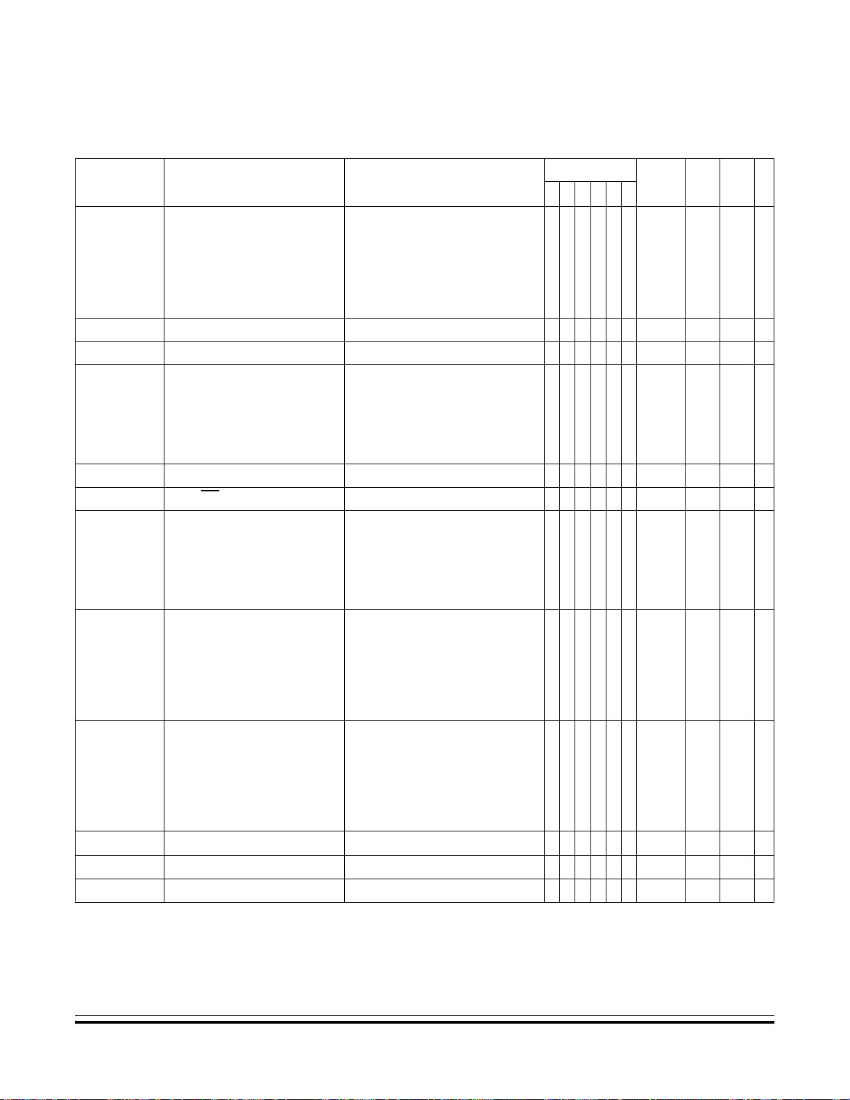
Central Processor Unit (CPU)
Table 6-1. Instruction Set Summary (Sheet 7 of 8)
Instruction Set Summary
Source
Form
SBC #opr
SBC opr
SBC opr
SBC opr,X
SBC opr,X
SBC ,X
SBC opr,SP
SBC opr,SP
SEC Set Carry Bit C ← 1 –––––1INH 99 1
SEI Set Interrupt Mask I ← 1 ––1–––INH 9B 2
STA opr
STA opr
STA opr,X
STA opr,X
STA ,X
STA opr,SP
STA opr,SP
STHX opr Store H:X in M (M:M + 1) ← (H:X) 0––↕↕ – DIR 35 dd 4
STOP Enable IRQ
STX opr
STX opr
STX opr,X
STX opr,X
STX ,X
STX opr,SP
STX opr,SP
SUB #opr
SUB opr
SUB opr
SUB opr,X
SUB opr,X
SUB ,X
SUB opr,SP
SUB opr,SP
SWI Software Interrupt
Subtract with Carry A ← (A) – (M) – (C) ↕ ––↕↕↕
Store A in M M ← (A) 0––↕↕–
Store X in M M ← (X) 0––↕↕–
Subtract A ← (A) – (M) ↕ ––↕↕↕
Operation Description
Pin; Stop Oscillator I ← 0; Stop Oscillator ––0–––INH 8E 1
PC ← (PC) + 1; Push (PCL)
SP ← (SP) – 1; Push (PCH)
SP ← (SP) – 1; Push (X)
SP ← (SP) – 1; Push (A)
SP ← (SP) – 1; Push (CCR)
SP ¨ (SP) – 1; I ¨ 1
PCH ← Interrupt Vector High Byte
PCL ← Interrupt Vector Low Byte
Effect on CCR
VH I NZC
––1–––INH 83 9
IMM
DIR
EXT
IX2
IX1
IX
SP1
SP2
DIR
EXT
IX2
IX1
IX
SP1
SP2
DIR
EXT
IX2
IX1
IX
SP1
SP2
IMM
DIR
EXT
IX2
IX1
IX
SP1
SP2
Address
Mode
A2
B2
C2
D2
E2
F2
9EE2
9ED2
B7
C7
D7
E7
F7
9EE7
9ED7
BF
CF
DF
EF
FF
9EEF
9EDF
A0
B0
C0
D0
E0
F0
9EE0
9ED0
Opcode
ii
dd
hh ll
ee ff
ff
ff
ee ff
dd
hh ll
ee ff
ff
ff
ee ff
dd
hh ll
ee ff
ff
ff
ee ff
ii
dd
hh ll
ee ff
ff
ff
ee ff
Operand
2
3
4
4
3
2
4
5
3
4
4
3
2
4
5
3
4
4
3
2
4
5
2
3
4
4
3
2
4
5
Cycles
TAP Transfer A to CCR CCR ← (A) ↕↕↕↕↕↕INH 84 2
TAX Transfer A to X X ← (A) ––––––INH 97 1
TPA Transfer CCR to A A ← (CCR) ––––––INH 85 1
MC68HC908MR8 — Rev 4.1 Technical Data
Freescale Semiconductor Central Processor Unit (CPU) 85
Page 86

Central Processor Unit (CPU)
Table 6-1. Instruction Set Summary (Sheet 8 of 8)
Source
Form
TST opr
TSTA
TSTX
TST opr,X
TST ,X
TST opr,SP
Operation Description
Test for Negative or Zero (A) – $00 or (X) – $00 or (M) – $00 0 – – ↕↕ –
Effect on CCR
VH I NZC
DIR
INH
INH
IX1
IX
SP1
Address
Mode
3D
4D
5D
6D
7D
9E6D
Opcode
dd
ff
ff
Operand
3
1
1
3
2
4
TSX Transfer SP to H:X H:X ← (SP) + 1 ––––––INH 95 2
TXA Transfer X to A A ← (X) ––––––INH 9F 1
TXS Transfer H:X to SP (SP) ← (H:X) – 1 ––––––INH 94 2
WAIT Enable Interrupts; Stop Processor I bit ← 0 ––0–––INH 8F 1
A Accumulator n Any bit
C Carry/borrow bit opr Operand (one or two bytes)
CCR Condition code register PC Program counter
dd Direct address of operand PCH Program counter high byte
dd rr Direct address of operand and relative offset of branch instruction PCL Program counter low byte
DD Direct to direct addressing mode REL Relative addressing mode
DIR Direct addressing mode rel Relative program counter offset byte
DIX+ Direct to indexed with post increment addressing mode rr Relative program counter offset byte
ee ff High and low bytes of offset in indexed, 16-bit offset addressing SP1 Stack pointer, 8-bit offset addressing mode
EXT Extended addressing mode SP2 Stack pointer 16-bit offset addressing mode
ff Offset byte in indexed, 8-bit offset addressing SP Stack pointer
H Half-carry bit U Undefined
H Index register high byte V Overflow bit
hh ll High and low bytes of operand address in extended addressing X Index register low byte
I Interrupt mask Z Zero bit
ii Immediate operand byte & Logical AND
IMD Immediate source to direct destination addressing mode | Logical OR
IMM Immediate addressing mode
INH Inherent addressing mode ( ) Contents of
IX Indexed, no offset addressing mode –( ) Negation (two’s complement)
IX+ Indexed, no offset, post increment addressing mode # Immediate value
IX+D Indexed with post increment to direct addressing mode
IX1 Indexed, 8-bit offset addressing mode ← Loaded with
IX1+ Indexed, 8-bit offset, post increment addressing mode ? If
IX2 Indexed, 16-bit offset addressing mode : Concatenated with
M Memory location ↕ Set or cleared
N Negative bit — Not affected
⊕ Logical EXCLUSIVE OR
« Sign extend
Cycles
6.8 Opcode Map
See Table 6-2.
Technical Data MC68HC908MR8 — Rev 4.1
86 Central Processor Unit (CPU) Freescale Semiconductor
Page 87

Freescale Semiconductor Central Processor Unit (CPU) 87
MC68HC908MR8 — Rev 4.1 Technical Data
MSB
LSB
05BRSET0
15BRCLR0
25BRSET1
35BRCLR1
45BRSET2
55BRCLR2
65BRSET3
75BRCLR3
85BRSET4
95BRCLR4
A5BRSET5
B5BRCLR5
C5BRSET6
D5BRCLR6
E5BRSET7
F5BRCLR7
Table 6-2. Opcode Map
Bit Manipulation Branch Read-Modify-Write Control Register/Memory
DIR DIR REL DIR INH INH IX1 SP1 IX INH INH IMM DIR EXT IX2 SP2 IX1 SP1 IX
0 1234569E6789ABCD9EDE9EEF
3DIR
3DIR
3DIR
3DIR
3DIR
3DIR
3DIR
3DIR
3DIR
3DIR
3DIR
3DIR
3DIR
3DIR
3DIR
3DIR
4
BSET0
2DIR
4
BCLR0
2DIR
4
BSET1
2DIR
4
BCLR1
2DIR
4
BSET2
2DIR
4
BCLR2
2DIR
4
BSET3
2DIR
4
BCLR3
2DIR
4
BSET4
2DIR
4
BCLR4
2DIR
4
BSET5
2DIR
4
BCLR5
2DIR
4
BSET6
2DIR
4
BCLR6
2DIR
4
BSET7
2DIR
4
BCLR7
2DIR
3
BRA
2REL
3
BRN
2REL
3
BHI
2REL
3
BLS
2REL
3
BCC
2REL
3
BCS
2REL
3
BNE
2REL
3
BEQ
2REL
3
BHCC
2REL
3
BHCS
2REL
3
BPL
2REL
3
BMI
2REL
3
BMC
2REL
3
BMS
2REL
3
BIL
2REL
3
BIH
2REL
4
NEG
2DIR
5
CBEQ
3DIR
4
COM
2DIR
4
LSR
2DIR
4
STHX
2DIR
4
ROR
2DIR
4
ASR
2DIR
4
LSL
2DIR
4
ROL
2DIR
4
DEC
2DIR
5
DBNZ
3DIR
4
INC
2DIR
3
TST
2DIR
3
CLR
2DIR
1
NEGA
1INH
4
CBEQA
3IMM
5
MUL
1INH
1
COMA
1INH
1
LSRA
1INH
3
LDHX
3IMM
1
RORA
1INH
1
ASRA
1INH
1
LSLA
1INH
1
ROLA
1INH
1
DECA
1INH
3
DBNZA
2INH
1
INCA
1INH
1
TSTA
1INH
5
MOV
3DD
1
CLRA
1INH
1
NEGX
1INH
4
CBEQX
3IMM
7
DIV
1INH
1
COMX
1INH
1
LSRX
1INH
4
LDHX
2DIR
1
RORX
1INH
1
ASRX
1INH
1
LSLX
1INH
1
ROLX
1INH
1
DECX
1INH
3
DBNZX
2INH
1
INCX
1INH
1
TSTX
1INH
4
MOV
2DIX+
1
CLRX
1INH
4
NEG
2IX1
3IX1+
1INH
2IX1
2IX1
3IMM
2IX1
2IX1
2IX1
2IX1
2IX1
3IX1
2IX1
2IX1
3IMD
2IX1
CBEQ
NSA
COM
LSR
CPHX
ROR
ASR
LSL
ROL
DEC
DBNZ
INC
TST
MOV
CLR
3SP1
5
4SP1
3
4
3SP1
4
3SP1
3
4
3SP1
4
3SP1
4
3SP1
4
3SP1
4
3SP1
5
4SP1
4
3SP1
3
3SP1
4
3
3SP1
NEG
CBEQ
COM
LSR
ROR
ASR
LSL
ROL
DEC
DBNZ
INC
TST
CLR
5
6
5
5
5
5
5
5
5
6
5
4
4
3
NEG
1IX
4
CBEQ
2IX+
2
DAA
1INH
3
COM
1IX
3
LSR
1IX
4
CPHX
2DIR
3
ROR
1IX
3
ASR
1IX
3
LSL
1IX
3
ROL
1IX
3
DEC
1IX
4
DBNZ
2IX
3
INC
1IX
2
TST
1IX
4
MOV
2IX+D
2
CLR
1IX
7
RTI
1INH
4
RTS
1INH
9
SWI
1INH
2
TAP
1INH
1
TPA
1INH
2
PULA
1INH
2
PSHA
1INH
2
PULX
1INH
2
PSHX
1INH
2
PULH
1INH
2
PSHH
1INH
1
CLRH
1INH
1
STOP
1INH
1
WAIT
1INH
3
BGE
2REL
3
BLT
2REL
3
BGT
2REL
3
BLE
2REL
2
TXS
1INH
2
TSX
1INH
1
TAX
1INH
1
CLC
1INH
1
SEC
1INH
2
CLI
1INH
2
SEI
1INH
1
RSP
1INH
1
NOP
1INH
*
1
TXA
1INH
2
SUB
2IMM
2
CMP
2IMM
2
SBC
2IMM
2
CPX
2IMM
2
AND
2IMM
2
BIT
2IMM
2
LDA
2IMM
2
AIS
2IMM
2
EOR
2IMM
2
ADC
2IMM
2
ORA
2IMM
2
ADD
2IMM
4
BSR
2REL
2
LDX
2IMM
2
AIX
2IMM
3
SUB
2DIR
3
CMP
2DIR
3
SBC
2DIR
3
CPX
2DIR
3
AND
2DIR
3
BIT
2DIR
3
LDA
2DIR
3
STA
2DIR
3
EOR
2DIR
3
ADC
2DIR
3
ORA
2DIR
3
ADD
2DIR
2
JMP
2DIR
4
JSR
2DIR
3
LDX
2DIR
3
STX
2DIR
4
SUB
3 EXT
4
CMP
3 EXT
4
SBC
3 EXT
4
CPX
3 EXT
4
AND
3 EXT
4
BIT
3 EXT
4
LDA
3 EXT
4
STA
3 EXT
4
EOR
3 EXT
4
ADC
3 EXT
4
ORA
3 EXT
4
ADD
3 EXT
3
JMP
3 EXT
5
JSR
3 EXT
4
LDX
3 EXT
4
STX
3 EXT
4
SUB
3IX2
4
CMP
3IX2
4
SBC
3IX2
4
CPX
3IX2
4
AND
3IX2
4
BIT
3IX2
4
LDA
3IX2
4
STA
3IX2
4
EOR
3IX2
4
ADC
3IX2
4
ORA
3IX2
4
ADD
3IX2
4
JMP
3IX2
6
JSR
3IX2
4
LDX
3IX2
4
STX
3IX2
5
SUB
4SP2
5
CMP
4SP2
5
SBC
4SP2
5
CPX
4SP2
5
AND
4SP2
5
BIT
4SP2
5
LDA
4SP2
5
STA
4SP2
5
EOR
4SP2
5
ADC
4SP2
5
ORA
4SP2
5
ADD
4SP2
5
LDX
4SP2
5
STX
4SP2
3
SUB
2IX1
3
CMP
2IX1
3
SBC
2IX1
3
CPX
2IX1
3
AND
2IX1
3
BIT
2IX1
3
LDA
2IX1
3
STA
2IX1
3
EOR
2IX1
3
ADC
2IX1
3
ORA
2IX1
3
ADD
2IX1
3
JMP
2IX1
5
JSR
2IX1
3
LDX
2IX1
3
STX
2IX1
4
SUB
3SP1
4
CMP
3SP1
4
SBC
3SP1
4
CPX
3SP1
4
AND
3SP1
4
BIT
3SP1
4
LDA
3SP1
4
STA
3SP1
4
EOR
3SP1
4
ADC
3SP1
4
ORA
3SP1
4
ADD
3SP1
4
LDX
3SP1
4
STX
3SP1
SUB
1IX
CMP
1IX
SBC
1IX
CPX
1IX
AND
1IX
BIT
1IX
LDA
1IX
STA
1IX
EOR
1IX
ADC
1IX
ORA
1IX
ADD
1IX
JMP
1IX
JSR
1IX
LDX
1IX
STX
1IX
2
2
2
2
2
2
2
2
2
2
2
2
2
4
2
2
Central Processor Unit (CPU)
INH Inherent REL Relative SP1 Stack Pointer, 8-Bit Offset
IMM Immediate IX Indexed, No Offset SP2 Stack Pointer, 16-Bit Offset
DIR Direct IX1 Indexed, 8-Bit Offset IX+ Indexed, No Offset with
EXT Extended IX2 Indexed, 16-Bit Offset Post Increment
DD Direct-Direct IMD Immediate-Direct IX1+ Indexed, 1-Byte Offset with
IX+D Indexed-Direct DIX+ Direct-Indexed Post Increment
*Pre-byte for stack pointer indexed instructions
MSB
LSB
Low Byte of Opcode in Hexadecimal 05BRSET0
0 High Byte of Opcode in Hexadecimal
3DIR
Cycles
Opcode Mnemonic
Number of Bytes / Addressing Mode
Opcode Map
Page 88

Central Processor Unit (CPU)
Technical Data MC68HC908MR8 — Rev 4.1
88 Central Processor Unit (CPU) Freescale Semiconductor
Page 89

Technical Data — MC68HC908MR8
Section 7. System Integration Module (SIM)
7.1 Contents
7.2 Introduction. . . . . . . . . . . . . . . . . . . . . . . . . . . . . . . . . . . . . . .90
7.3 SIM Bus Clock Control and Generation . . . . . . . . . . . . . . . .93
7.3.1 Bus Timing . . . . . . . . . . . . . . . . . . . . . . . . . . . . . . . . . . . . . 93
7.3.2 Clock Startup from POR or LVI Reset . . . . . . . . . . . . . . .93
7.3.3 Clocks in Wait Mode . . . . . . . . . . . . . . . . . . . . . . . . . . . . .94
7.4 Reset and System Initialization. . . . . . . . . . . . . . . . . . . . . . .94
7.4.1 External Pin Reset . . . . . . . . . . . . . . . . . . . . . . . . . . . . . . .94
7.4.2 Active Resets from Internal Sources . . . . . . . . . . . . . . . . 95
7.5 SIM Counter. . . . . . . . . . . . . . . . . . . . . . . . . . . . . . . . . . . . . . .99
7.5.1 SIM Counter During Power-On Reset. . . . . . . . . . . . . . . . 99
7.5.2 SIM Counter and Reset States . . . . . . . . . . . . . . . . . . . . .99
7.6 Exception Control. . . . . . . . . . . . . . . . . . . . . . . . . . . . . . . . . .99
7.6.1 Interrupts. . . . . . . . . . . . . . . . . . . . . . . . . . . . . . . . . . . . . .100
7.6.2 Reset . . . . . . . . . . . . . . . . . . . . . . . . . . . . . . . . . . . . . . . . .103
7.6.3 Status Flag Protection in Break Mode . . . . . . . . . . . . . . 103
7.7 Low-Power Mode . . . . . . . . . . . . . . . . . . . . . . . . . . . . . . . . . 104
7.7.1 Wait Mode . . . . . . . . . . . . . . . . . . . . . . . . . . . . . . . . . . . . .106
7.7.2 Stop Mode . . . . . . . . . . . . . . . . . . . . . . . . . . . . . . . . . . . . .106
7.7.3 SIM Break Status Register. . . . . . . . . . . . . . . . . . . . . . . . 106
7.7.4 SIM Reset Status Register. . . . . . . . . . . . . . . . . . . . . . . . 108
7.7.5 SIM Break Flag Control Register . . . . . . . . . . . . . . . . . .109
MC68HC908MR8 — Rev 4.1 Technical Data
Freescale Semiconductor System Integration Module (SIM) 89
Page 90

System Integration Module (SIM)
7.2 Introduction
This section describes the system integration module (SIM). Together
with the central processor unit (CPU), the SIM controls all
microcontroller unit (MCU) activities. A block diagram of the SIM is
shown in Figure 7-1. Figure 7-2 is a summary of the SIM inout/output
(I/O) registers.
The SIM is a system state controller that coordinates CPU and exception
timing. The SIM is responsible for:
• Bus clock generation and control for CPU and peripherals:
– Stop, wait, reset, break entry, and recovery
– Internal clock control
• Master reset control, including power-on reset (POR) and
computer operating properly (COP) timeout
• Interrupt control:
– Acknowledge timing
– Arbitration control timing
– Vector address generation
• CPU enable/disable timing
• Modular architecture expandable to 128 interrupt sources
Technical Data MC68HC908MR8 — Rev 4.1
90 System Integration Module (SIM) Freescale Semiconductor
Page 91

STOP/WAIT
CONTROL
System Integration Module (SIM)
Introduction
MODULE WAIT
MODULE STOP
CPU WAIT (FROM CPU)
CPU STOP (FROM CPU)
SIMOSCEN (TO CGM)
RESET
PIN LOGIC
CLOCK
CONTROL
POR CONTROL
RESET PIN CONTROL
SIM RESET STATUS REGISTER
INTERRUPT CONTROL
AND PRIORITY DECODE
SIM
COUNTER
÷ 2
CLOCK GENERATORS
MASTER
RESET
CONTROL
RESET
COP CLOCK
CGMXCLK (FROM CGM)
CGMOUT (FROM CGM)
INTERNAL CLOCKS
LVI (FROM LVI MODULE)
ILLEGAL OPCODE (FROM CPU)
ILLEGAL ADDRESS (FROM ADDRESS
MAP DECODERS)
COP (FROM COP MODULE)
INTERRUPT SOURCES
CPU INTERFACE
Figure 7-1. SIM Block Diagram
MC68HC908MR8 — Rev 4.1 Technical Data
Freescale Semiconductor System Integration Module (SIM) 91
Page 92

System Integration Module (SIM)
Addr. Register Name Bit 7 6 5 4 3 2 1 Bit 0
SIM Break Status Register
$FE00
See page 106.
SIM Reset Status Register
$FE01
See page 108.
SIM Break Flag Control
$FE03
Note 1. Writing a logic 0 clears SBSW.
Register (SBFCR)
See page 109.
(SBSR)
(SRSR)
Figure 7-2. SIM I/O Register Summary
Read:
RRRRRR
Write: Note 1
Reset:
Read: POR PIN COP ILOP ILAD 0 LVI 0
Write:RRRRRRRR
Reset:
Read:
Write:
Reset:
10000000
BCFERRRRRRR
0
= Reserved
R
SBSW
R
0
Table 7-1 shows the internal signal names used in this section.
Table 7-1. Signal Name Conventions
Signal Name Description
CGMXCLK Buffered version of OSC1 from clock generator module (CGM)
CGMVCLK PLL output
CGMOUT
IAB Internal address bus
IDB Internal data bus
PORRST Signal from the power-on reset module to the SIM
IRST Internal reset signal
R/W
PLL-based or OSC1-based clock output from CGM module
(bus clock = CGMOUT divided by two)
Read/write signal
Technical Data MC68HC908MR8 — Rev 4.1
92 System Integration Module (SIM) Freescale Semiconductor
Page 93

7.3 SIM Bus Clock Control and Generation
The bus clock generator provides system clock signals for the CPU and
peripherals on the MCU. The system clocks are generated from an
incoming clock, CGMOUT, as shown in Figure 7-3. This clock can come
from either an external oscillator or from the on-chip phase-locked loop
(PLL). See Section 8. Clock Generator Module (CGM).
System Integration Module (SIM)
SIM Bus Clock Control and Generation
OSC1
7.3.1 Bus Timing
CGMVCLK
PLL
CLOCK
SELECT
CIRCUIT
BCS
MONITOR MODE
USER MODE
÷ 2
A
B
S*
*When S = 1,
CGMXCLK
CGMOUT
CGMOUT = B
SIM COUNTER
÷ 2
SIM
BUS CLOCK
GENERATORS
CGM
Figure 7-3. CGM Clock Signals
In user mode, the internal bus frequency is either the crystal oscillator
output (CGMXCLK) divided by four or the PLL output (CGMVCLK)
divided by four. See Section 8. Clock Generator Module (CGM).
7.3.2 Clock Startup from POR or LVI Reset
When the power-on reset (POR) module or the low-voltage inhibit (LVI)
module generates a reset, the clocks to the CPU and peripherals are
inactive and held in an inactive phase until after the 4096 CGMXCLK
cycle POR timeout has completed. The RST pin is driven low by the SIM
during this entire period. The IBUS clocks start upon completion of the
timeout.
MC68HC908MR8 — Rev 4.1 Technical Data
Freescale Semiconductor System Integration Module (SIM) 93
Page 94

System Integration Module (SIM)
7.3.3 Clocks in Wait Mode
In wait mode, the CPU clocks are inactive. The SIM also produces two
sets of clocks for other modules. Refer to the wait mode subsection of
each module to see if the module is active or inactive in wait mode.
Some modules can be programmed to be active in wait mode.
7.4 Reset and System Initialization
The MCU has these reset sources:
• Power-on reset module (POR)
• External reset pin (RST)
• Computer operating properly module (COP)
• Low-voltage inhibit module (LVI)
All of these resets produce the vector $FFFE–FFFF ($FEFE–FEFF in
monitor mode) and assert the internal reset signal (IRST). IRST causes
all registers to be returned to their default values and all modules to be
returned to their reset states.
An internal reset clears the SIM counter (see 7.5 SIM Counter), but an
external reset does not. Each of the resets sets a corresponding bit in
the SIM reset status register (SRSR). See 7.7.4 SIM Reset Status
Register.
7.4.1 External Pin Reset
Pulling the asynchronous RST
of the SIM reset status register (SRSR) is set as long as RST is held low
for a minimum of 67 CGMXCLK cycles, assuming that neither the POR
nor the LVI was the source of the reset. See Table 7-2 for details.
Figure 7-4 shows the relative timing.
• Illegal opcode
• Illegal address
pin low halts all processing. The PIN bit
Technical Data MC68HC908MR8 — Rev 4.1
94 System Integration Module (SIM) Freescale Semiconductor
Page 95

CGMOUT
RST
System Integration Module (SIM)
Reset and System Initialization
Table 7-2. PIN Bit Set Timing
Reset Type Number of Cycles Required to set PIN
POR/LVI 4163 (4096 + 64 + 3)
All Others 67 (64 + 3)
IAB
PC
Figure 7-4. External Reset Timing
7.4.2 Active Resets from Internal Sources
All internal reset sources actively pull the RST pin low for 32 CGMXCLK
cycles to allow resetting of external peripherals. The internal reset signal
(IRST) continues to be asserted for an additional 32 cycles (see
Figure 7-5). An internal reset can be caused by an illegal address, illegal
opcode, COP timeout, LVI, or POR (see Figure 7-6).
NOTE: For LVI or POR resets, the SIM cycles through 4096 CGMXCLK cycles
during which the SIM forces the RST
then follows the sequence from the falling edge of RST as shown in
Figure 7-5.
IRST
VECT H VECT L
pin low. The internal reset signal
RST
CGMXCLK
IAB
RST PULLED LOW BY MCU
32 CYCLES 32 CYCLES
VECTOR HIGH
Figure 7-5. Internal Reset Timing
MC68HC908MR8 — Rev 4.1 Technical Data
Freescale Semiconductor System Integration Module (SIM) 95
Page 96

System Integration Module (SIM)
The COP reset is asynchronous to the bus clock.
The active reset feature allows the part to issue a reset to peripherals
and other chips within a system built around the MCU.
7.4.2.1 Power-On Reset (POR)
When power is first applied to the MCU, the power-on reset (POR)
module generates a pulse to indicate that power-on has occurred. The
external reset pin (RST) is held low while the SIM counter counts out
4096 CGMXCLK cycles. Sixty-four CGMXCLK cycles later, the CPU and
memories are released from reset to allow the reset vector sequence to
occur.
ILLEGAL ADDRESS RST
ILLEGAL OPCODE RST
COPRST
LVI
POR
INTERNAL RESET
Figure 7-6. Sources of Internal Reset
At power-on, these events occur:
• A POR pulse is generated.
• The internal reset signal is asserted.
• The SIM enables CGMOUT.
• Internal clocks to the CPU and modules are held inactive for 4096
CGMXCLK cycles to allow stabilization of the oscillator.
• The RST pin is driven low during the oscillator stabilization time.
• The POR bit of the SIM reset status register (SRSR) is set and all
other bits in the register are cleared.
Technical Data MC68HC908MR8 — Rev 4.1
96 System Integration Module (SIM) Freescale Semiconductor
Page 97

OSC1
PORRST
System Integration Module (SIM)
Reset and System Initialization
CGMXCLK
CGMOUT
RST
IAB
4096
CYCLES
32
CYCLES
32
CYCLES
Figure 7-7. POR Recovery
7.4.2.2 Computer Operating Properly (COP) Reset
An input to the SIM is reserved for the COP reset signal. The overflow of
the COP counter causes an internal reset and sets the COP bit in the
SIM reset status register (SRSR). The SIM actively pulls down the RST
pin for all internal reset sources.
To prevent a COP module timeout, write any value to location $FFFF.
Writing to location $FFFF clears the COP counter and bits 12–4 of the
SIM counter. The SIM counter output, which occurs at least every
213–24 CGMXCLK cycles, drives the COP counter. The COP should be
serviced as soon as possible out of reset to guarantee the maximum
amount of time before the first timeout.
$FFFE $FFFF
The COP module is disabled if the RST
pin or the IRQ pin is held at
VDD+VHI while the MCU is in monitor mode. The COP module can be
disabled only through combinational logic conditioned with the high
voltage signal on the RST or the IRQ pin. This prevents the COP from
becoming disabled as a result of external noise. During a break state,
VDD+VHI on the RST pin disables the COP module.
MC68HC908MR8 — Rev 4.1 Technical Data
Freescale Semiconductor System Integration Module (SIM) 97
Page 98

System Integration Module (SIM)
7.4.2.3 Illegal Opcode Reset
The SIM decodes signals from the CPU to detect illegal instructions. An
illegal instruction sets the ILOP bit in the SIM reset status register
(SRSR) and causes a reset.
Because the MC68HC08MR8 has stop mode disabled by bit 1 in the
CONFIG register, execution of the STOP instruction will cause an illegal
opcode reset if stop mode has not been enabled by setting CONFIG
register bit 1.
7.4.2.4 Illegal Address Reset
An opcode fetch from addresses other than FLASH, I/O, or RAM
addresses generates an illegal address reset (unimplemented locations
within memory map). The SIM verifies that the CPU is fetching an
opcode prior to asserting the ILAD bit in the SIM reset status register
(SRSR) and resetting the MCU. A data fetch from an unmapped address
does not generate a reset.
7.4.2.5 Low-Voltage Inhibit (LVI) Reset
The low-voltage inhibit module (LVI) asserts its output to the SIM when
the VDD voltage falls to the LVI
level for at least nine consecutive CPU cycles. The LVI bit in the SIM
reset status register (SRSR) is set, and the external reset pin (RST) is
held low while the SIM counter counts out 4096 CGMXCLK cycles.
Sixty-four CGMXCLK cycles later, the CPU is released from reset to
allow the reset vector sequence to occur. The SIM actively pulls down
the RST
pin for all internal reset sources.
voltage and remains at or below that
LVRX
Technical Data MC68HC908MR8 — Rev 4.1
98 System Integration Module (SIM) Freescale Semiconductor
Page 99

7.5 SIM Counter
The SIM counter is used by the POR module to allow the oscillator time
to stabilize before enabling the internal bus (IBUS) clocks. The SIM
counter also serves as a prescaler for the COP module. The SIM counter
overflow supplies the clock for the COP module. The SIM counter is 13
bits long and is clocked by the falling edge of CGMXCLK.
7.5.1 SIM Counter During Power-On Reset
The POR detects power applied to the MCU. At power-on, the POR
circuit asserts the signal PORRST. Once the SIM is initialized, it enables
the clock generation module (CGM) to drive the bus clock state machine.
7.5.2 SIM Counter and Reset States
System Integration Module (SIM)
SIM Counter
External reset has no effect on the SIM counter. The SIM counter is
free-running after all reset states. See 7.4.2 Active Resets from
Internal Sources for counter control and internal reset recovery
sequences.
7.6 Exception Control
Normal, sequential program execution can be changed in three different
ways:
1. Interrupts:
2. Reset
3. Break interrupts
a. Maskable hardware CPU interrupts
b. Non-maskable software interrupt instruction (SWI)
MC68HC908MR8 — Rev 4.1 Technical Data
Freescale Semiconductor System Integration Module (SIM) 99
Page 100

System Integration Module (SIM)
7.6.1 Interrupts
At the beginning of an interrupt, the CPU saves the CPU register
contents on the stack and sets the interrupt mask (I bit) to prevent
additional interrupts. At the end of an interrupt, the return from interrupt
(RTI) instruction recovers the CPU register contents from the stack so
that normal processing can resume. Figure 7-8 shows interrupt entry
timing. Figure 7-10 shows interrupt recovery timing.
Interrupts are latched, and arbitration is performed in the SIM at the start
of interrupt processing. The arbitration result is a constant that the CPU
uses to determine which vector to fetch. Once an interrupt is latched by
the SIM, no other interrupt can take precedence, regardless of priority,
until the latched interrupt is serviced (or the I bit is cleared). See
Figure 7-9.
MODULE
INTERRUPT
I BIT
IAB
IDB
R/W
DUMMY
SP SP – 1 SP – 2 SP – 3 SP – 4 VECT H VECT L START ADDR
DUMMY PC – 1[7:0] PC – 1[15:8] X A CCR V DATA H V DATA L OPCODE
Figure 7-8
. Interrupt Entry
Technical Data MC68HC908MR8 — Rev 4.1
100 System Integration Module (SIM) Freescale Semiconductor
 Loading...